KR890003904B1 - Inspection method of photomask reticle for semiconductor device fabrication - Google Patents
Inspection method of photomask reticle for semiconductor device fabricationDownload PDFInfo
- Publication number
- KR890003904B1 KR890003904B1KR1019840002878AKR840002878AKR890003904B1KR 890003904 B1KR890003904 B1KR 890003904B1KR 1019840002878 AKR1019840002878 AKR 1019840002878AKR 840002878 AKR840002878 AKR 840002878AKR 890003904 B1KR890003904 B1KR 890003904B1
- Authority
- KR
- South Korea
- Prior art keywords
- pattern
- reticle
- inspection
- database
- patterns
- Prior art date
- Legal status (The legal status is an assumption and is not a legal conclusion. Google has not performed a legal analysis and makes no representation as to the accuracy of the status listed.)
- Expired
Links
Images


Classifications
- G—PHYSICS
- G01—MEASURING; TESTING
- G01N—INVESTIGATING OR ANALYSING MATERIALS BY DETERMINING THEIR CHEMICAL OR PHYSICAL PROPERTIES
- G01N21/00—Investigating or analysing materials by the use of optical means, i.e. using sub-millimetre waves, infrared, visible or ultraviolet light
- G01N21/84—Systems specially adapted for particular applications
- G01N21/88—Investigating the presence of flaws or contamination
- G01N21/95—Investigating the presence of flaws or contamination characterised by the material or shape of the object to be examined
- G01N21/956—Inspecting patterns on the surface of objects
- G01N21/95607—Inspecting patterns on the surface of objects using a comparative method
- H—ELECTRICITY
- H01—ELECTRIC ELEMENTS
- H01L—SEMICONDUCTOR DEVICES NOT COVERED BY CLASS H10
- H01L22/00—Testing or measuring during manufacture or treatment; Reliability measurements, i.e. testing of parts without further processing to modify the parts as such; Structural arrangements therefor
- H—ELECTRICITY
- H01—ELECTRIC ELEMENTS
- H01L—SEMICONDUCTOR DEVICES NOT COVERED BY CLASS H10
- H01L21/00—Processes or apparatus adapted for the manufacture or treatment of semiconductor or solid state devices or of parts thereof
- H01L21/02—Manufacture or treatment of semiconductor devices or of parts thereof
- H01L21/04—Manufacture or treatment of semiconductor devices or of parts thereof the devices having potential barriers, e.g. a PN junction, depletion layer or carrier concentration layer
- H01L21/18—Manufacture or treatment of semiconductor devices or of parts thereof the devices having potential barriers, e.g. a PN junction, depletion layer or carrier concentration layer the devices having semiconductor bodies comprising elements of Group IV of the Periodic Table or AIIIBV compounds with or without impurities, e.g. doping materials
- H01L21/30—Treatment of semiconductor bodies using processes or apparatus not provided for in groups H01L21/20 - H01L21/26
Landscapes
- Engineering & Computer Science (AREA)
- Physics & Mathematics (AREA)
- General Physics & Mathematics (AREA)
- Manufacturing & Machinery (AREA)
- Computer Hardware Design (AREA)
- Microelectronics & Electronic Packaging (AREA)
- Power Engineering (AREA)
- Condensed Matter Physics & Semiconductors (AREA)
- Health & Medical Sciences (AREA)
- Life Sciences & Earth Sciences (AREA)
- Chemical & Material Sciences (AREA)
- Analytical Chemistry (AREA)
- Biochemistry (AREA)
- General Health & Medical Sciences (AREA)
- Immunology (AREA)
- Pathology (AREA)
- Preparing Plates And Mask In Photomechanical Process (AREA)
- Investigating Materials By The Use Of Optical Means Adapted For Particular Applications (AREA)
- Testing Or Measuring Of Semiconductors Or The Like (AREA)
Abstract
Description
Translated fromKorean제1도는 감사되어질 레티클 패턴의 평면도.1 is a plan view of a reticle pattern to be audited.
제2도는 종래의 래티클 검사기의 블록선도.2 is a block diagram of a conventional reticle inspector.
제3도는 본 발명을 설명하기 위한 제1도의 동일패턴을 갖는 래티클의 도형.3 is a diagram of a reticle having the same pattern of FIG. 1 for explaining the present invention.
제4도는 본 발명에 대한 레티클 검사기의 블록선도.4 is a block diagram of a reticle checker for the present invention.
제5도는 본 발명에 대한 레티클 검사기의 기능을 설명하는 파형도.5 is a waveform diagram illustrating the function of the reticle checker according to the present invention.
제5(a)도는 아래 파형에 일치시키기 위하여 제3도의 주사부분을 확대시킨것, 제5(b)도는 제4도에서 1차 파형성형회로 8(선 101에 연결되었을 때)로부터의 출력파형, 제5(c)도는 제4도에서 2차 파형성형 회로 10(선102에 연결되었을 때)으로부터의 출력파형, 제5(d)도는 제4도에서 제어단자 55(선 103에 연결되었을때)로부터의 출력파형, 제5(e)도는 제4도에서 비교기 111(선 104에 연결되었을 때)로부터의 출력파형이다.Fig. 5 (a) is an enlargement of the scanning part of Fig. 3 so as to correspond to the waveform shown below. Fig. 5 (b) is an output waveform from the primary waveform shaping circuit 8 (when connected to line 101) in Fig. 4; 5 (c) is the output waveform from the secondary waveform shaping circuit 10 (when connected to line 102) in FIG. 4, and FIG. 5 (d) is the control terminal 55 (line 103) in FIG. Figure 5 (e) is the output waveform from comparator 111 (when connected to line 104) in FIG.
본 발명은 반도체소자의 제작에 사용되는 포토마스크 레티클을 검사하는 방법에 관한 것이다. 특히, 본 발명은 데이타베이스(Data base)검사방법이라 불리우고 있는, 자기 테이프등의 매체에 저장된 검사자료로서, 대용량집적 회로(LSI)나 대규모 집적회로(VLSI)에 대한 포토마스크레티클을 검사하는 방법에 관한 것이다.The present invention relates to a method for inspecting a photomask reticle used in the fabrication of semiconductor devices. In particular, the present invention is a test data stored in a medium such as a magnetic tape, called a database test method, and a method for inspecting a photomask for a large-capacity integrated circuit (LSI) or a large-scale integrated circuit (VLSI). It is about.
최근, 반도체 소자의 매우 높은 기록밀도(Packing Density)에 따라, 포토마스크 패턴은 복잡하고 미세하여지고 있다. 포토마스레티클은 반도체 소자를 제작하기 위한 모(母)패턴에 대응하기 때문에 레티클의 우수한 품질은 확보하는 것이 가장 중요한 요건중의 하나이다. 즉, 그것이 매우 섬세할 지라도 패턴의 결함이 존재하는 것을 용남할 수 없다는 것이다.In recent years, with the extremely high packing density of semiconductor devices, the photomask pattern has become complicated and fine. Since the photomask reticle corresponds to a mother pattern for manufacturing a semiconductor device, securing excellent quality of the reticle is one of the most important requirements. In other words, even if it is very delicate, it cannot tolerate the existence of a defect in the pattern.
LSI나 VLSI 반도체 다이(die)로, 보통 동일패턴을 갖는 많은 반도체소자들이 제작되어진다. 그러므로, 포토마스트 레티클의 검사는 제일 먼저 현미경을 사용하여 인접하는 동일패턴과 시각적으로 비교하므로써 행하여진다. 이 시각적 검사는 영상을 비교하는 전자회로와 전하결합소자(charge couple device) 카메라와 같은 영상 센서(sensor)를 사용하는 자동광학적 비교검사인 "패턴 비교검사"로 대치되어졌다.With LSI or VLSI semiconductor dies, many semiconductor devices having the same pattern are usually manufactured. Therefore, the inspection of the photomask reticle is first performed by visually comparing with the same pattern adjacent to each other using a microscope. This visual inspection was replaced by "pattern comparison", an automatic optical comparison that uses an image sensor such as an electronic circuit to compare images and a camera with a charge couple device.
그러나, 최근에 다이의 패턴이 단지 패턴비교 검사 방법에 의해 정확히 비교하기 어려울 정도로 매우 복잡하여 졌다. 앞으로, 패턴 비교검사는 비교를 위한 표준 패턴이 필요하기 때문에, 만약 표준 패턴에 결함이 있다면 모든 검사는 실패가 된다. 게다가 만약, 다이가 동일 형태와 크기를 갖지 않는 단 한개의 패턴만으로 구성되어 있다면 그 마스크 비교검사는 사용될수 없다.Recently, however, the pattern of the die has become so complex that it is difficult to accurately compare by only the pattern comparison test method. In the future, the pattern comparison test requires a standard pattern for comparison, so if the standard pattern is defective, all the tests fail. In addition, if the die consists of only one pattern that does not have the same shape and size, the mask comparison test cannot be used.
한편, "설계 데이타베이스"를 사용하는 CAD(Computer Aided Design)방식과 같은 컴퓨터 기술에 의한 레티클 패턴의 설계방법이 개발 되었다. 결과적으로, CAD방식긔 개념이 검사에 도입되므로써 "데이타베이스 검사"라 불리우는 "검사데이타베이스"에 의해 검사가 이루어지고 있다.Meanwhile, a method of designing a reticle pattern by computer technology such as a computer aided design (CAD) method using a "design database" has been developed. As a result, the CAD system concept is introduced into the inspection, and the inspection is performed by the "inspection database" called "database inspection".
데이타베이스 검사를 시작할 때, 설계데이타는 데이타베이스 검사를 위하여 이용되지만, 후에 "검사데이타 베이스"는 단독으로 만들어 지는데, 이는 검사과정이 쉽게 만들어지며, 제작과 감사에 중복되는 실수를 피할 수 있기 때문이다. 데이타베이스 검사방법을 적용하면, 검사의 정확도가 매우 높아진다.When starting a database check, the design data is used to check the database, but later the "check database" is created by itself, because the check process is easy to create and avoids duplicate mistakes in production and audit. to be. Applying a database check method increases the accuracy of the check.
데이타베이스 검사는 레티클 패턴에 대한 검사데이카가 자기테이프등이 기록매체에 저장되어있는 "레티클검사기"라 불리워지는 장치에 의하여 이루어질수 있다. 그러나, 최근의 반도체가 너무 복잡해지고, 너무 많은 종류로 되기 때문에 검사 데이타의 용량은 커지게 된다. 따라서, 기록매체를 비축하기위한 공간을 유지하는 것은 거위 불가능하여, 검사에 많은 시간을 소모한다. 이는 데이타베이스 검사가 고정확도르 유지할 필요가 있음에도 불구하고, 포토마스크 레티클검사에 대해 큰 문제로 나타나고 있다.The database inspection can be performed by a device called "reticle inspector" in which inspection data for a reticle pattern is stored on a recording medium such as magnetic tape. However, the capacity of the inspection data becomes large because recent semiconductors become too complicated and too many kinds. Therefore, it is impossible to keep the space for storing the recording medium, which takes a lot of time for inspection. This is a big problem for photomask reticle inspection, even though database inspection needs to be maintained with high accuracy.
그러므로, 본 발명의 목적은 검사의 고정확도를 유지하기 위한 데이타베이스 검사방법을 적용하여 검사데이타매체를 저장하기 위한 공간과 검사를 수행하는 시간을 절약하는데 있다. 본 발명은 마스크 비교검사와 데이타베이스 검사방법을 조합함으로써 수행되어질수 있기때문에 후자의 방법이 포토마스크 레티클에서 각각이 동일모양과 크기를 갖는 레티클패턴에 적용되어 있다.Therefore, an object of the present invention is to save the space for storing the inspection data medium and the time for performing the inspection by applying a database inspection method for maintaining a high accuracy of the inspection. Since the present invention can be performed by combining a mask comparison test and a database check method, the latter method is applied to a reticle pattern each having the same shape and size in the photomask reticle.
포토마스크 레티클의 검사에 본 발명을 적용하면, 검사의 고정확도가 전자의 방법에 의해 유지되어질 수 있고, 데이타베이스의 공간과 검사하는 시간이 후자에 의해 절약되어 질수 있다.Applying the present invention to the inspection of the photomask reticle, the high accuracy of the inspection can be maintained by the former method, and the space of the database and the inspection time can be saved by the latter.
본 발명을 설명하기전에, 종래 기술의 레티클 검사기에 의한 데이타베이스 검사 방법에 서술될 것이다. 왜냐하면, 레티클 검사기는 종래래기술의 데이타베이스 검사에 사용되는 전형적인 방법이었으며, 또한 본 발명은 레티클 검사기의 개선에 관한 것이다.Before describing the present invention, a database inspection method by a reticle checker of the prior art will be described. Because the reticle checker was a typical method used for prior art database checks, the present invention also relates to an improvement of the reticle checker.
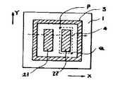
제1도는 검사되어질 레티클 패턴의 평면도이다. 실제적인 레티클에 있어서는 수개의 장방형의 패턴이 설명의 목적으로 나타내어진 제1도에 나타난것보다 더욱 복잡하게 되어있다. 도면에서, 참조번호 1은 레티클이고, 21, 22와 3은 레티클 1위의 패턴들이다. 패턴은 불투명 피름으로 광학적 투과제위에 인쇄되어 있고, 설명의 목적을 위해 단순화된 패턴들로 도시되어 있기 때문에 패턴 21, 22는 패턴 3에 의해 둘러쌓인 동일 모양과 크기로서 병렬로 배열된다. 참조번호 4는 레티클 1의 데이타베이스 검사를 위한 광학적 주사선을 보여주며, 도면에서 X축을 따라 좌에서 우로 레티클의 표면을 과학적으로 주사한다.1 is a plan view of a reticle pattern to be inspected. For practical reticles, several rectangular patterns are more complex than those shown in Figure 1, which is shown for illustrative purposes. In the figure,
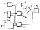
제2도는 종래 레티클검사기의 블록선도이다. 도면에서 각 단자나 회로는 다음과 같이 동작한다.2 is a block diagram of a conventional reticle inspector. In the figure, each terminal or circuit operates as follows.
참조번호 1은 뒤에 설명될 X-Y단에 놓여진 제1도와 같은 레티클이다.
참조번호 5뭄 레티클 검사기의 동작에 대한 여러 제어신호를 출력시키는 제어단자이다.Ref. No. 5 This is a control terminal that outputs various control signals for the operation of the reticle tester.
참조번호 6은 레티클 1이 검사되어지도록 놓이고, 제어단자 5로부터의 제어신호에 의해 제어되어지고 있는 제1도에서 위에서 아래로 정밀 기계에 의해 Y축 방향으로 주사되어지는 X-Y단이다.Reference numeral 6 denotes an X-Y stage which is placed so that
참조번호 7은 레티클 1이 제어단자 5로부터 제어신호와 동기화하는 X축 방향으로 주사하는 카메라이며, 카메라 7은 X-Y단 6과 카메라 7은 주사에 대응하는 전자비데오 신호를 출력한다.
참조번호 9은 자기테이프와 같은 기록매체에 검사 데이타를 저장하고, 제어단자 5로부터 제어신호에 의해 제어되어지는 X-Y단 6과 카메라 7의 주사와 협력하여 데이타비데오 시호를 출력하는 데이타 기록 장치이다.Reference numeral 9 is a data recording apparatus that stores test data on a recording medium such as a magnetic tape, and outputs a data video signal in cooperation with scanning of the X-Y stage 6 and the
참조 번호 8은 지정된 진폭을 갖는 비교기 11에 대해 "데이타 비데오 신호"를 공급하기위해 데이타 기록장치 9로부터의 출력을 성형하는 1차 파형성형회로이다.
참조 번호 10은 주사된 패턴의 결함이 없는 파형성형회로 8로부터의 데이타 비데오 신호의 지정된 진폭과 같은 진폭을 갖는 배교기 11에 대해 "광학적 비데오 신호"를 공급하기 위해 카메라 7로부터의 출력을 성형하는 2차 파형성형회로이다.
참조 번호11은 데이타 비데오 신호와 광학적 비데오 신호를 비교하는 비교기이다. 신호는 제어단자 5에 의해 제어되는 동시에 비교기 11로 가고, 또한 비교가 제어단자 5로부터 제어신호에 의해 이루어진다. 데이타비데오 신호와 광학적비데오신호의 진폭이 같은때, 그것은 그 패턴에 결함이 없으며, 비교기 11이 무(無)출력을 나타낼것이며, 반대로 패턴에 결함이 있다면, 비교기 11은 결함신호를 나타낸다는 것이다.Reference numeral 11 is a comparator for comparing the data video signal with the optical video signal. The signal is controlled by the
참조번호 12는 제어단자 5로부터 제어신호에 의해 포토마스크 레티클의 패턴과 같은 메모리의 번지에 결함신호를 기억하는 메모리이다. 메모리 12에서 결함신호는 검사의 결과를 점검할수 있는 비데오 영상기나 인쇄지상에 시작적으로 얻을수있다. 결과적으로 결함은 보수가 가능하여질수 있으며, 결함 데이타는 반도체 소자제작의 품질조절을 위해 저장할수 있다.
제1도는 예로서 간단한 레티클 모형을 나타낸다. 여기에서는 종래기술의 레티클검사기 조차도 데이타 응용을 위한 용량의 문제가 없다. 그러나, 앞에서 언급한 바와같이, 최근 레티클 패턴은 너무 복잡하게 되어 데이타에 대한 매체를 저장하기위해 매우 큰 공간이 요구되고 있다. 그러므로, 종래기술의 레티클 검사기를 이용한 데이타베이스검사는 대용량집적회로 이상에 적용하는 것이 거의 불가능하게 되었다.1 shows a simple reticle model as an example. Here, even prior art reticle checkers have no capacity issues for data applications. However, as mentioned earlier, the recent reticle pattern has become so complex that very large spaces are required to store the medium for data. Therefore, database inspection using the reticle checker of the prior art has become almost impossible to be applied to large integrated circuit anomalies.
그너나, 높은 기록밀도를 갖는 반도체소자른 일반적으로 각각이 동일패턴을 갖는 대다수의 소자들로 이루어졌다. 그래서, 레티클도 대다수의 동일모양과 크기를 갖는다. 본 발명은 이 사실에서 유도 되었다, 즉, 각각이 동일모양과 크기를 갖는 패턴들은 개별적으로 검사할 필요가 없다. 다시말해서, 하나의 패턴이 데이타베이스 검사방법에 의해 검사하는 것만으로 충분하다는 것이다. 만약 각각이 동일모양과 크기를 갖는 패턴들이 데이타베이스 검사로부터 무시되어질수 있다면, 저장매체에 대한 저장소는 크게 감소시킬수 있을 것이다. 이는 다음과 같이 해결할 수 있다. 각각이 동일 모양과 크기를 갖는 패턴으로부터 하나를 취함으로써 레티클 검사기는 데이타베이스 검사방법에 의해 선택된 패턴을 검사한다. 그러면, 나머지 패턴들은 비교하기위한 표준패턴처럼 선택된 패턴을 한정하는 일반 패턴 비교검사방법에 의해 검사된다.However, semiconductor devices having a high recording density generally consist of a large number of devices each having the same pattern. Thus, reticles also have the majority of the same shape and size. The present invention is derived from this fact, that is, patterns each having the same shape and size do not need to be examined individually. In other words, it is enough for a pattern to be checked by a database checking method. If patterns of the same shape and size each can be ignored from a database check, the storage for the storage medium can be greatly reduced. This can be solved as follows. By taking one from the patterns each having the same shape and size, the reticle checker checks the pattern selected by the database check method. The remaining patterns are then examined by a general pattern comparison test method that defines the selected pattern as a standard pattern for comparison.
위에서 설명한 바와같이, 데이타베이스 검사와 패턴비교검사방법을 적용하면, 종래 기술의 문제점이 해결된다. 즉, 각각이 동일모양과 크기를 갖는 패턴의 데이타는 자장할 필요가 없을 뿐만 아니라 검사 정확도가 높게 유지될 수 있기 때문이다. 이것이 본 발명의 요지이다. 즉, 본 발명은 데이타베이스 검사에서 각가기 동일모양과 크기를 갖는 패턴에 대해 검사데이타의 한 패턴만의 필요로하며, 각각이 동일 크기와 모양을 갖는 다른 나머지 패터은 패턴비교검사에 의해 빨리 검사되어진다.As described above, applying the database check and the pattern comparison check method solves the problems of the prior art. That is, data of patterns each having the same shape and size does not need to be self-magnetized, and inspection accuracy can be maintained high. This is the gist of the present invention. That is, the present invention requires only one pattern of test data for each pattern having the same shape and size in the database test, and the other remaining patterns each having the same size and shape are quickly tested by the pattern comparison test. It is done.
제3도는 본 발명을 설명하기 위한 제1도의 레티클과 동일 크기와 모양은 갖는 레티클의 평면도이다. 도면에서 참조번호 혹은 기호는 P와 Q를 제외하고, 제1도와 같다. 기호 P와 Q는 패턴 21과 동일한 모양을 갖는 패턴 22를 포함하는 점선으로 둘러쌓인 사각형으로 제외되는 영역 P-Q를 지정하는 X-Y 좌표의 점이다.3 is a plan view of a reticle having the same size and shape as the reticle of FIG. 1 for explaining the present invention. In the drawings, reference numerals or symbols are the same as in FIG. 1 except for P and Q. The symbols P and Q are points of the X-Y coordinates specifying the area P-Q, which is excluded by a rectangle surrounded by a dotted line, including a
먼저 패턴 21이 데이타베이스 검사에 의해 검사 되어지고 패턴 비교 검사방법이 패턴 21에서 패턴 22를 비교하는 영역 P-Q에 적용하였을때, 영역 P-Q 안에 있는 패턴은 데이타베이스 검사의 목적에서 제외시킬 수 있다. 그러한 영역 P-Q는 이하 "제외영역"이라 하겠다. 이렇게 함으로써 데이타베이스 검사에 대한 데이타가 자기테이프를 저장하기 위한 공간을 줄일 수 있으며, 검사를 위한 시간이 절약되어질 수 있다는 것이다.First, when
제4도는 본 발명의 장치(레티클 검사기)의 블록선도이며, 제5도는 데이타베이스 검사의 목적으로부터 각각이 동일 모양과 크기를 갖는 패턴들은 제외하는 본 발명의 레티클 검사기의 기능을 설명하는 파형도이다.4 is a block diagram of an apparatus (reticle checker) of the present invention, and FIG. 5 is a waveform diagram illustrating the function of the reticle checker of the present invention excluding patterns having the same shape and size, respectively, from the purpose of database inspection. .
제4도에서 제2도와 같은 참조번호를 갖는 각 블록은 같은 기능을 갖는다. 참조번호 13은 제3도에서 패턴 22와 같은 제외영역안에 있는 패턴의 데이타베이스 검사를 제외하기위해 제3도의 제외영역 P-Q와 같은 제외되는 영역을 한정시키는 "영역한정기(region setter)"이다. 제어단 55와 비교기 111은 제2도에서 제각기 제어단자 5와 비교기 11과 같은 기능을 갖지만 제외영역을 한정하도록 수정되어진다.In FIG. 4, each block having the same reference numeral as FIG. 2 has the same function.
제5(a)도는 아래파형과 동일한 확대되어진 제3도의 주사부분이다. 제5(b)도, 제5(c)도, 제5(d)도와 제5(e)도는 광학적 주사가 제5(a)도에서 나타나 있듯이 레티클 1위에 이루어질 때, 제각기 블록선도에서 참조번호 101, 102, 103과 104의 선에서의 파형이다. 레티클검사의 시초에 각각이 동일 모양과 크기를 갖는 패턴들의 무리들은 레티클패턴들의 설계 데이타로부터 선별되어진다. 즉, 제3도에서 패턴 21과 22를 포함하는 그룹이 그 예이다. 그리고 한 패턴이 각 무리에서 선택되어진다. 즉, 제3도에서 패턴 21이 그 예이다. 설계 데이타로부터 제외영역의 번지정보-예를들면 제3도에서 P-Q는 데이타베이스 검사의 목적으로부터 제외영역을 제외시키는 검사기에 의해 제어단자 55를 한정하게된다. 선택된 패터은 데이타베이스 방법에 의해 검사되어지고, 또한 패턴 비교 검사를 위한 표준 패턴을 사용되어진다.5 (a) is an enlarged scanning portion of FIG. 3 which is the same as the lower waveform. 5 (b), 5 (c), 5 (d) and 5 (e) show reference numerals respectively in the block diagram when the optical scanning is performed on the first reticle as shown in FIG. 5 (a). Waveforms at
제 4도에서 P와 Q의 번지가 검사기에 의해 한정기 13에 주어질때, 영역 한정기 13은 제3도 혹은 제5(a)도에서 제외영역 P-Q와 같은 제외영역을 지정하기 위해 제어단자 55를 제어한다. 제5(a)도에서는 P만 도시되어있다. 카메라 7은, 제3도 또는 제5(a)도에서, 광학적 주사선 4와 같이 레티클 1을 주사할때, 제어단자 55는 선 101에서 데이타비데오 신호가 제5(b)도에서 보여주듯이 제외영역 P-Q에서 패턴 22로 움직이므로 비교기 111로 가도록 1차 파형성회로 8을 제어한다. 한편 카메라 비데오 신호는 제5(c)도에서 나타난것처럼 파형이 선 102를 통해 비교기 111로 들어간다. 선 104에서 비교기 111로부터 출력신호는 제5(c)도에서처럼 결함 정보가 없기 때문에 비교기 111은 "ON"신호가 제5(d)도에서 나타나듯이 제어단자55로부터 선103에 공급되어지는 시간동안 파형 (b)와 (c)를 비교한다.When the address of P and Q in Fig. 4 is given to the
만약 거기에 기이트(gate)신호가 없다면 비교기 111은 제5(e)도에서 점선파형 51과 같은 결함신호가 나타날 것이다. 비교기 111로부터의 결함신호는 만약 레티클 패턴상에 결함이 있고 제어단자 55에 의한 제어하에 각 번지에 기억되어졌다면, 메모리 12로 들어간다. 검사결과는 앞에 언급된것처럼 메모리 12로부터 판단 신호에 의해 점검되어질 수 있다.If there is no gate signal there, the comparator 111 will show a fault signal such as dotted line 51 in Fig. 5 (e). The defect signal from the comparator 111 enters the
패턴 21이 위 데이타베이스 검사에 의해 정확하게 판정되어진후, 패턴 21와 같은 제어영역에서의 패턴은 종래기술방법에 의해 검사되어질 수 있다. 즉, 비교를 위해 표준 패턴으로서 패턴 21을 한정시키는 패턴 비교 검사방법이다. 실제 공장에서 실현되어진 반도체다이의 제작에서, 본 발명은 종래 기술의 검사방법에 비해, 데이타에 대한 기록매체의 용량이 줄어들고, 검사데이타 설계의 소비시간을 절약할 수 있고, 또한 반도체 소자의 검사 소비시간을 단축할 수 있다.After the
Claims (1)
Translated fromKoreanApplications Claiming Priority (3)
| Application Number | Priority Date | Filing Date | Title |
|---|---|---|---|
| JP58-113230 | 1983-06-23 | ||
| JP113230 | 1983-06-23 | ||
| JP11323083AJPH0750664B2 (en) | 1983-06-23 | 1983-06-23 | Reticle inspection method |
Publications (2)
| Publication Number | Publication Date |
|---|---|
| KR850000787A KR850000787A (en) | 1985-03-09 |
| KR890003904B1true KR890003904B1 (en) | 1989-10-10 |
Family
ID=14606857
Family Applications (1)
| Application Number | Title | Priority Date | Filing Date |
|---|---|---|---|
| KR1019840002878AExpiredKR890003904B1 (en) | 1983-06-23 | 1984-05-25 | Inspection method of photomask reticle for semiconductor device fabrication |
Country Status (5)
| Country | Link |
|---|---|
| US (1) | US5125040A (en) |
| EP (1) | EP0129751B1 (en) |
| JP (1) | JPH0750664B2 (en) |
| KR (1) | KR890003904B1 (en) |
| DE (1) | DE3475226D1 (en) |
Families Citing this family (20)
| Publication number | Priority date | Publication date | Assignee | Title |
|---|---|---|---|---|
| JPS60138924A (en)* | 1983-12-27 | 1985-07-23 | Fujitsu Ltd | Test of pattern and device thereof |
| US5131755A (en)* | 1988-02-19 | 1992-07-21 | Chadwick Curt H | Automatic high speed optical inspection system |
| US5085517A (en)* | 1989-10-31 | 1992-02-04 | Chadwick Curt H | Automatic high speed optical inspection system |
| US5586058A (en)* | 1990-12-04 | 1996-12-17 | Orbot Instruments Ltd. | Apparatus and method for inspection of a patterned object by comparison thereof to a reference |
| US5307421A (en)* | 1992-10-14 | 1994-04-26 | Commissariat A L'energie Atomique | Process for producing a synthesized reference image for the inspection of objects and apparatus for performing the same |
| TW285721B (en)* | 1994-12-27 | 1996-09-11 | Siemens Ag | |
| JP3515199B2 (en)* | 1995-01-06 | 2004-04-05 | 大日本スクリーン製造株式会社 | Defect inspection equipment |
| KR960035944A (en)* | 1995-03-28 | 1996-10-28 | 김주용 | Failure analysis method in manufacturing semiconductor device |
| GB2307547B (en)* | 1995-11-22 | 2000-02-16 | Europ Gas Turbines Ltd | A method of detecting manufacturing errors in an article |
| US5795688A (en)* | 1996-08-14 | 1998-08-18 | Micron Technology, Inc. | Process for detecting defects in photomasks through aerial image comparisons |
| JP3566470B2 (en) | 1996-09-17 | 2004-09-15 | 株式会社日立製作所 | Pattern inspection method and apparatus |
| US6608676B1 (en)* | 1997-08-01 | 2003-08-19 | Kla-Tencor Corporation | System for detecting anomalies and/or features of a surface |
| US6483580B1 (en) | 1998-03-06 | 2002-11-19 | Kla-Tencor Technologies Corporation | Spectroscopic scatterometer system |
| JP3201471B2 (en)* | 1998-04-24 | 2001-08-20 | 日本電気株式会社 | Reticle inspection equipment |
| US7463765B2 (en)* | 2003-02-25 | 2008-12-09 | Lamda-Lite Enterprises Incorporated | System and method for detecting and reporting fabrication defects using a multi-variant image analysis |
| US7558419B1 (en)* | 2003-08-14 | 2009-07-07 | Brion Technologies, Inc. | System and method for detecting integrated circuit pattern defects |
| US7515253B2 (en)* | 2005-01-12 | 2009-04-07 | Kla-Tencor Technologies Corporation | System for measuring a sample with a layer containing a periodic diffracting structure |
| US7869645B2 (en)* | 2008-07-22 | 2011-01-11 | Seiko Epson Corporation | Image capture and calibratiion |
| EP2803079A1 (en)* | 2012-01-13 | 2014-11-19 | KLA-Tencor Corporation | Method and appparatus for database-assisted requalification reticle inspection |
| KR102409943B1 (en) | 2017-11-29 | 2022-06-16 | 삼성전자주식회사 | Method of detecting a defect and apparatus for performing the same |
Family Cites Families (13)
| Publication number | Priority date | Publication date | Assignee | Title |
|---|---|---|---|---|
| US4056716A (en)* | 1976-06-30 | 1977-11-01 | International Business Machines Corporation | Defect inspection of objects such as electronic circuits |
| JPS5915381B2 (en)* | 1978-10-16 | 1984-04-09 | 日本電信電話株式会社 | Pattern inspection method |
| DE3070433D1 (en)* | 1980-12-18 | 1985-05-09 | Ibm | Method for the inspection and automatic sorting of objects with configurations of fixed dimensional tolerances, and device for carrying out the method |
| JPS57157378A (en)* | 1981-03-25 | 1982-09-28 | Hitachi Ltd | Setting method of binary-coded threshold level |
| US4448532A (en)* | 1981-03-31 | 1984-05-15 | Kla Instruments Corporation | Automatic photomask inspection method and system |
| US4441207A (en)* | 1982-01-19 | 1984-04-03 | Environmental Research Institute Of Michigan | Design rule checking using serial neighborhood processors |
| US4589139A (en)* | 1982-02-04 | 1986-05-13 | Nippon Kogaku K. K. | Apparatus for detecting defects in pattern |
| DE3379611D1 (en)* | 1982-04-15 | 1989-05-18 | Toshiba Kk | Pattern features extracting apparatus and method and pattern recognition system |
| DE3267548D1 (en)* | 1982-05-28 | 1986-01-02 | Ibm Deutschland | Process and device for an automatic optical inspection |
| GB2129547B (en)* | 1982-11-02 | 1986-05-21 | Cambridge Instr Ltd | Reticle inspection |
| US4579455A (en)* | 1983-05-09 | 1986-04-01 | Kla Instruments Corporation | Photomask inspection apparatus and method with improved defect detection |
| US4532650A (en)* | 1983-05-12 | 1985-07-30 | Kla Instruments Corporation | Photomask inspection apparatus and method using corner comparator defect detection algorithm |
| US4555798A (en)* | 1983-06-20 | 1985-11-26 | Kla Instruments Corporation | Automatic system and method for inspecting hole quality |
- 1983
- 1983-06-23JPJP11323083Apatent/JPH0750664B2/ennot_activeExpired - Lifetime
- 1984
- 1984-05-25KRKR1019840002878Apatent/KR890003904B1/ennot_activeExpired
- 1984-06-07EPEP84106502Apatent/EP0129751B1/ennot_activeExpired
- 1984-06-07DEDE8484106502Tpatent/DE3475226D1/ennot_activeExpired
- 1990
- 1990-09-24USUS07/587,557patent/US5125040A/ennot_activeExpired - Lifetime
Also Published As
| Publication number | Publication date |
|---|---|
| JPH0750664B2 (en) | 1995-05-31 |
| EP0129751A3 (en) | 1985-09-11 |
| JPS605522A (en) | 1985-01-12 |
| DE3475226D1 (en) | 1988-12-22 |
| US5125040A (en) | 1992-06-23 |
| KR850000787A (en) | 1985-03-09 |
| EP0129751A2 (en) | 1985-01-02 |
| EP0129751B1 (en) | 1988-11-17 |
Similar Documents
| Publication | Publication Date | Title |
|---|---|---|
| KR890003904B1 (en) | Inspection method of photomask reticle for semiconductor device fabrication | |
| US4809341A (en) | Test method and apparatus for a reticle or mask pattern used in semiconductor device fabrication | |
| JP3668215B2 (en) | Pattern inspection device | |
| JP4014379B2 (en) | Defect review apparatus and method | |
| US8903158B2 (en) | Inspection system and inspection method | |
| KR960013357B1 (en) | Image data inspection method and device | |
| US4778745A (en) | Defect detection method of semiconductor wafer patterns | |
| JP2004212221A (en) | Pattern inspection method and pattern inspection device | |
| KR900002690B1 (en) | Inspector for semiconductor exposure patern data | |
| US12062166B2 (en) | Method and system for diagnosing a semiconductor wafer | |
| US20060110025A1 (en) | Method for inspecting mask defects | |
| KR970007974B1 (en) | Semiconductor process defect inspection method | |
| JPS58196445A (en) | Method of inspecting mask | |
| JPH02139676A (en) | Inspection equipment | |
| JPS6128809A (en) | Visual inspection equipment | |
| JPH02236406A (en) | Method for inspecting mask pattern | |
| JP2532110B2 (en) | Electron beam exposure method | |
| JPH048780B2 (en) | ||
| KR100675888B1 (en) | Semiconductor device inspection device and semiconductor device inspection method using the same | |
| JPH04225252A (en) | Method and apparatus for inspecting semiconductor device | |
| JPS59121335A (en) | Method and device for inspecting photomask | |
| JPS61120007A (en) | pattern inspection equipment | |
| JPH0316781B2 (en) | ||
| JPS60231325A (en) | Mask inspection method | |
| JPH02284140A (en) | Pattern inspecting apparatus for reticule |
Legal Events
| Date | Code | Title | Description |
|---|---|---|---|
| A201 | Request for examination | ||
| PA0201 | Request for examination | ||
| PA0109 | Patent application | Patent event code:PA01091R01D Comment text:Patent Application Patent event date:19840525 | |
| PG1501 | Laying open of application | ||
| E902 | Notification of reason for refusal | ||
| PE0902 | Notice of grounds for rejection | Comment text:Notification of reason for refusal Patent event date:19890517 Patent event code:PE09021S01D | |
| G160 | Decision to publish patent application | ||
| PG1605 | Publication of application before grant of patent | Comment text:Decision on Publication of Application Patent event code:PG16051S01I Patent event date:19890906 | |
| E701 | Decision to grant or registration of patent right | ||
| PE0701 | Decision of registration | Patent event code:PE07011S01D Comment text:Decision to Grant Registration Patent event date:19891229 | |
| GRNT | Written decision to grant | ||
| PR0701 | Registration of establishment | Comment text:Registration of Establishment Patent event date:19900109 Patent event code:PR07011E01D | |
| PR1002 | Payment of registration fee | Payment date:19900109 End annual number:3 Start annual number:1 | |
| PR1001 | Payment of annual fee | Payment date:19920826 Start annual number:4 End annual number:4 | |
| PR1001 | Payment of annual fee | Payment date:19930810 Start annual number:5 End annual number:5 | |
| PR1001 | Payment of annual fee | Payment date:19941005 Start annual number:6 End annual number:6 | |
| PR1001 | Payment of annual fee | Payment date:19951006 Start annual number:7 End annual number:7 | |
| PR1001 | Payment of annual fee | Payment date:19961002 Start annual number:8 End annual number:8 | |
| PR1001 | Payment of annual fee | Payment date:19970830 Start annual number:9 End annual number:9 | |
| PR1001 | Payment of annual fee | Payment date:19980922 Start annual number:10 End annual number:10 | |
| PR1001 | Payment of annual fee | Payment date:19990930 Start annual number:11 End annual number:11 | |
| PR1001 | Payment of annual fee | Payment date:20001007 Start annual number:12 End annual number:12 | |
| PR1001 | Payment of annual fee | Payment date:20011004 Start annual number:13 End annual number:13 | |
| PR1001 | Payment of annual fee | Payment date:20020918 Start annual number:14 End annual number:14 | |
| FPAY | Annual fee payment | Payment date:20030924 Year of fee payment:15 | |
| PR1001 | Payment of annual fee | Payment date:20030924 Start annual number:15 End annual number:15 | |
| EXPY | Expiration of term | ||
| PC1801 | Expiration of term |