KR890002088B1 - Insulation Connector Sheet - Google Patents
Insulation Connector SheetDownload PDFInfo
- Publication number
- KR890002088B1 KR890002088B1KR8205898AKR820005898AKR890002088B1KR 890002088 B1KR890002088 B1KR 890002088B1KR 8205898 AKR8205898 AKR 8205898AKR 820005898 AKR820005898 AKR 820005898AKR 890002088 B1KR890002088 B1KR 890002088B1
- Authority
- KR
- South Korea
- Prior art keywords
- electrically conductive
- layer
- adhesive layer
- adhesive
- connector sheet
- Prior art date
- Legal status (The legal status is an assumption and is not a legal conclusion. Google has not performed a legal analysis and makes no representation as to the accuracy of the status listed.)
- Expired
Links
Images


Classifications
- H—ELECTRICITY
- H05—ELECTRIC TECHNIQUES NOT OTHERWISE PROVIDED FOR
- H05K—PRINTED CIRCUITS; CASINGS OR CONSTRUCTIONAL DETAILS OF ELECTRIC APPARATUS; MANUFACTURE OF ASSEMBLAGES OF ELECTRICAL COMPONENTS
- H05K3/00—Apparatus or processes for manufacturing printed circuits
- H05K3/30—Assembling printed circuits with electric components, e.g. with resistor
- H05K3/32—Assembling printed circuits with electric components, e.g. with resistor electrically connecting electric components or wires to printed circuits
- H05K3/321—Assembling printed circuits with electric components, e.g. with resistor electrically connecting electric components or wires to printed circuits by conductive adhesives
- H05K3/323—Assembling printed circuits with electric components, e.g. with resistor electrically connecting electric components or wires to printed circuits by conductive adhesives by applying an anisotropic conductive adhesive layer over an array of pads
- H—ELECTRICITY
- H01—ELECTRIC ELEMENTS
- H01R—ELECTRICALLY-CONDUCTIVE CONNECTIONS; STRUCTURAL ASSOCIATIONS OF A PLURALITY OF MUTUALLY-INSULATED ELECTRICAL CONNECTING ELEMENTS; COUPLING DEVICES; CURRENT COLLECTORS
- H01R4/00—Electrically-conductive connections between two or more conductive members in direct contact, i.e. touching one another; Means for effecting or maintaining such contact; Electrically-conductive connections having two or more spaced connecting locations for conductors and using contact members penetrating insulation
- H01R4/04—Electrically-conductive connections between two or more conductive members in direct contact, i.e. touching one another; Means for effecting or maintaining such contact; Electrically-conductive connections having two or more spaced connecting locations for conductors and using contact members penetrating insulation using electrically conductive adhesives
- H—ELECTRICITY
- H01—ELECTRIC ELEMENTS
- H01L—SEMICONDUCTOR DEVICES NOT COVERED BY CLASS H10
- H01L2924/00—Indexing scheme for arrangements or methods for connecting or disconnecting semiconductor or solid-state bodies as covered by H01L24/00
- H01L2924/0001—Technical content checked by a classifier
- H01L2924/0002—Not covered by any one of groups H01L24/00, H01L24/00 and H01L2224/00
- H—ELECTRICITY
- H05—ELECTRIC TECHNIQUES NOT OTHERWISE PROVIDED FOR
- H05K—PRINTED CIRCUITS; CASINGS OR CONSTRUCTIONAL DETAILS OF ELECTRIC APPARATUS; MANUFACTURE OF ASSEMBLAGES OF ELECTRICAL COMPONENTS
- H05K2201/00—Indexing scheme relating to printed circuits covered by H05K1/00
- H05K2201/09—Shape and layout
- H05K2201/09818—Shape or layout details not covered by a single group of H05K2201/09009 - H05K2201/09809
- H05K2201/09945—Universal aspects, e.g. universal inner layers or via grid, or anisotropic interposer
- H—ELECTRICITY
- H05—ELECTRIC TECHNIQUES NOT OTHERWISE PROVIDED FOR
- H05K—PRINTED CIRCUITS; CASINGS OR CONSTRUCTIONAL DETAILS OF ELECTRIC APPARATUS; MANUFACTURE OF ASSEMBLAGES OF ELECTRICAL COMPONENTS
- H05K2201/00—Indexing scheme relating to printed circuits covered by H05K1/00
- H05K2201/10—Details of components or other objects attached to or integrated in a printed circuit board
- H05K2201/10227—Other objects, e.g. metallic pieces
- H05K2201/1025—Metallic discs
- H—ELECTRICITY
- H05—ELECTRIC TECHNIQUES NOT OTHERWISE PROVIDED FOR
- H05K—PRINTED CIRCUITS; CASINGS OR CONSTRUCTIONAL DETAILS OF ELECTRIC APPARATUS; MANUFACTURE OF ASSEMBLAGES OF ELECTRICAL COMPONENTS
- H05K2203/00—Indexing scheme relating to apparatus or processes for manufacturing printed circuits covered by H05K3/00
- H05K2203/11—Treatments characterised by their effect, e.g. heating, cooling, roughening
- H05K2203/1189—Pressing leads, bumps or a die through an insulating layer
- H—ELECTRICITY
- H05—ELECTRIC TECHNIQUES NOT OTHERWISE PROVIDED FOR
- H05K—PRINTED CIRCUITS; CASINGS OR CONSTRUCTIONAL DETAILS OF ELECTRIC APPARATUS; MANUFACTURE OF ASSEMBLAGES OF ELECTRICAL COMPONENTS
- H05K3/00—Apparatus or processes for manufacturing printed circuits
- H05K3/36—Assembling printed circuits with other printed circuits
- H05K3/361—Assembling flexible printed circuits with other printed circuits
Landscapes
- Engineering & Computer Science (AREA)
- Manufacturing & Machinery (AREA)
- Microelectronics & Electronic Packaging (AREA)
- Adhesive Tapes (AREA)
- Adhesives Or Adhesive Processes (AREA)
- Cable Accessories (AREA)
- Insulated Conductors (AREA)
- Manufacturing Of Electric Cables (AREA)
- Laminated Bodies (AREA)
- Conductive Materials (AREA)
- Connections Effected By Soldering, Adhesion, Or Permanent Deformation (AREA)
Abstract
Translated fromKoreanDescription
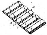
Translated fromKorean제1도는 본 발명의 예시적인 전기 접속기 테이프의 단부 부분의 확대 투시도.1 is an enlarged perspective view of an end portion of an exemplary electrical connector tape of the present invention.
제2도는 제1도에 도시한 본 발명의 예시적인 전기 접속기 테이프의 단면도.2 is a cross-sectional view of an exemplary electrical connector tape of the present invention shown in FIG.
제3도 내지 제5도는 본 발명의 다른 예시적인 복수의 전기 접속이 테이프의 단면도.3 to 5 are cross-sectional views of another exemplary plurality of electrical connections tapes of the present invention.
* 도면의 주요부분에 대한 부호의 설명* Explanation of symbols for main parts of the drawings
11 : 평판형 전기 절연 시이트 12 : 전기 전도성 스트라이프11: flat electrical insulating sheet 12: electrically conductive stripe
13 : 비전도성 접착재 14 : 전기 전도성 입자13: non-conductive adhesive material 14: electrically conductive particles
15 : 박막 절연층 20 : 전기 전도성 접착제15 thin
21 : 전기 전도성 스트라이프 22 : 전기 정도성 입자21: electrically conductive stripe 22: electric precision particles
24 : 전기 전도성 시이트 26 : 절연층24: electrically conductive sheet 26: insulating layer
27 : 전기 전도성, 접착재 28 : 전기 전도성 스트라이프27: electrically conductive, adhesive 28: electrically conductive stripe
29 : 다른 접착재29: other adhesive
본 발명은 전기 부품에 대한 접착 및 전기 접속을 행하는 데 유용한 시이트 재료에 관한 것이다.The present invention relates to sheet materials useful for making adhesion and electrical connections to electrical components.
최근, 전자산업분야에서는 인쇄 회로 기판이나 혹은 액정 표시부의 단자 패드와 같은 소형의 나란한 단자 패드에 편리하고도 안정된 전기접속을 행하는 위한 수단의 필요성이 대두 하고 있다.In recent years, in the electronic industry, there is a need for a means for making convenient and stable electrical connection to small side-by-side terminal pads such as printed circuit boards or terminal pads of liquid crystal displays.
이러한 접속을 행하기 위한 기술은 공개된 영국 특허 출원 제2,048,582A호에서 개시되어 있는 바, 여기서는 가요성 절연 시이트와, 이 시이트 상에서 지지되는 다수의 나란하고 독립된 전도성 스트라이프와, 그리고 이 전도성 스트라이프들을 덮고 있는 전도성 접착재로 이루어진 접착성을 접속기 테이프를 시사하고 있다.Techniques for making this connection are disclosed in published British Patent Application No. 2,048,582A, where a flexible insulating sheet, a number of side-by-side independent conductive stripes supported on the sheet, and covering the conductive stripes It is suggested that the adhesive tape made of a conductive adhesive material.
전기적인 접속은 테이프상의 개개의 스트라이프를 개개의 패드와 정렬되게 하여 그 테이프의 한 단부를 한세트의 단자 패드에 접착시킴으로써 이루어질 수 있다.Electrical connections can be made by aligning the individual stripes on the tape with the individual pads and then attaching one end of the tape to a set of terminal pads.
상술된 바와 같은 시이트 재료를 만족스럽게 사용하기 위해서, 그 시이트 재료에서의 전기 전도성 접착재는 실시간 동안 안정된 저 저항성 접합을 이룰 수 있어야 하며 또한 그 시이트 재료에 예상되는 동작상태에 따라서도 양호한 접합을 이룰 수 있어야 한다. 그러나, 종래의 전도성 접착재는 필요한 정도의 안정성과정 저항성을 제공해주지 못하였다.In order to satisfactorily use the sheet material as described above, the electrically conductive adhesive in the sheet material must be able to achieve a stable low resistance bond during real time and also a good bond depending on the expected operating conditions of the sheet material. Should be However, conventional conductive adhesives have not provided the necessary degree of stability and process resistance.
즉, 접착제의 접합 작용을 보완할 수 있도록 종종 기계적인 클램핑 기술을 사용해야 할 만큼 초기의 저항값이 너무 높을 뿐만 아니라 사용시에는 그 저항값이 더욱 증가하는 경향이 있었다.In other words, in order to compensate for the bonding action of the adhesive, not only the initial resistance value was so high that mechanical clamping techniques were often used, but also the resistance value tended to increase further in use.
또한, 상술한 코넥터 테이프의 결점은 스트라이프들(stripes)을 덮고 있는 전도성 접착재가 테이프 길이 방향의 중간 부분에서 비 의도적으로 전자 에셈블리의 타 부재들과 접촉될 수 있기 때문에 어셈블리내에 불필요한 전기접속이 행해진다는 점이다.In addition, the drawback of the connector tape described above is that unnecessary electrical connection is made in the assembly because the conductive adhesive covering the stripes can be intentionally contacted with other members of the electronic assembly in the middle of the tape longitudinal direction. Is that.
이러한 비의도적인 접촉들은, 종래 기술(전기전도성 스트라이프들을 지지하는 형판형 시이트로 이루어진 케이블을 기재하고 있는 미합중국 특허 제4,113,981호 참조)인 몇몇 소형의 평판형 케이블에서 개시된 바와 같은 절연층으로 테이프의 중간부분을 커버링 함으로써 방지되게 할 수 있다. 그러나, 이와 같은 케이블의 중간 커버링은 특정 사용을 위해 특정길이 만큼의 절연재료를 도포하여야 하기 때문에 불편하고 비경제적이다.These unintentional contacts are the middle of the tape with an insulating layer as disclosed in some small flat cable types of the prior art (see US Pat. No. 4,113,981, which describes a cable consisting of template sheets supporting electroconductive stripes). It can be prevented by covering the part. However, the intermediate covering of such cables is inconvenient and uneconomical because of the application of a certain length of insulation material for a particular use.
특정길이 만큼의 절연재료를 도포하는 것은 상이한 작업에 대해 별도의 절연 길이를 갖는 케이블 품목을 유지해야 하기 때문에 더더욱 어려운 작업이다. 이에 대한 대안으로, 케이블의 단부부분으로 부터 절연층을 제거하는 방식이 있을 수 있으나, 이것은 속도가 빠른 고속 자동차 작업에는 적합치가 않다.Applying a certain length of insulation material is even more difficult because it requires maintaining cable items with separate insulation lengths for different operations. As an alternative, there may be a way to remove the insulation from the end of the cable, but this is not suitable for high speed automotive work.
본 발명은 바람직한 실시예에서 그 전체 접착면상에서 절연되어, 한번의 작업으로 번자부품에 직접 본딩 및 전기 접속되게 할 수 있는 신규한 전도성 접착 시이트 재료를 제공하는 것이다. 이러한 신규한 제품의 한가지 유형은 시이트 재료에 평면에 전기 전도성을 제공하도록 절연 시이트상에 증기 코팅된 금속층과 같은 전기 전도층을 포함하고 있다. 그 다른 유형은 재료를 포함하는 것인데, 이것은 상기 전기 전도층을 갖는 접착제 사이에 도포될 수 있거나 혹은 상기 전기 전도층과 그 밖의 층을 갖는 테이프에 부착될 수 있다.The present invention provides a novel conductive adhesive sheet material which, in a preferred embodiment, can be insulated on its entire adhesive surface, allowing direct bonding and electrical connection to the component in one operation. One type of this novel product includes an electrically conductive layer, such as a metal layer vapor coated on an insulating sheet to provide electrical conductivity in plane to the sheet material. Another type is to include a material, which may be applied between the adhesive with the electrically conductive layer or attached to a tape with the electrically conductive layer and other layers.
이들 양자의 유형으로된 본 발명의 시이트 재료는 일반적으로 급속 입자와 같이 별도로 분리된 전기전도성 소자들의 단일 층이 분산되어 있는 중합층 또는 접착층으로 구성되어 있는 데, 상술한 전기 전도성 소자의 두께는 전술한 전기전도층과 실질적으로 같거나 혹은 더 두껍다. 또, 박막 전기 절연층은 전기 전도성 소자들의 단일층상에 배치되어 있는 데, 이는 실온(즉, 20℃)에서 들러붙지 않거나 불량하게 들로 붙는 전기적 절연 물질로 구성되어, 본 명세서의 후술되는 테스트에서 상기 전기 전도층을 통해 적어도 약 1메가 오옴의 전기 저항을 전기 전도성 소자들에 제공하고, 승온으로 가열하면 접착성을 지닌 유동 상태로 연화되며, 실온으로 냉각하면 실질상 유동하지 않는 견고한 상태로 된다.Sheet materials of the present invention of both types are generally composed of a polymerized or adhesive layer in which a single layer of separately separated electroconductive elements, such as fast particles, is dispersed. It is substantially the same as or thicker than one conductive layer. In addition, the thin film electrical insulation layer is disposed on a single layer of electrically conductive elements, which consists of an electrically insulating material that does not adhere or poorly adheres at room temperature (ie, 20 ° C.), in the tests described herein below. The electrically conductive layer provides at least about 1 mega ohms of electrical resistance to the electrically conductive elements, and when heated to elevated temperature, softens to an adhesive flow state, and when cooled to room temperature, becomes a solid state that does not substantially flow. .
상술한 시이트 재료는 쉽게 다룰 수 있고, 실내 온도에서는 전도성 본딩을 할 필요가 없지만 전기 전도성 소자들이 상기 절연층을 통해 기판과의 전기 접속으로 연장하는 본딩접속을 행할 수 있도록 기판에 대해 악착 및 가열되어야 한다.The sheet material described above is easily handled and does not require conductive bonding at room temperature but must be adhered and heated to the substrate so that electrically conductive elements can make a bonding connection that extends through the insulating layer to an electrical connection with the substrate. do.
전기 전도성 소자들이 분산되어 있는 중합층 또는 접착층은 일반적으로 가요성 시이트상에서 지지되고, 또한 하나 이상의 전기 전도층들도 이러한 가요성 시이트상에서 지지될 수 있거나 혹은 이 가요성 시이트를 구성될 수 있다. 이 접착층은 승온으로 가열하면 접착 상태로 연화되게 하고, 그후 실온에서 실질상 비유동성 상태를 나타내도록 경화되게 하는 것이 바람직하다. 그리고 상기 접착층에서 분산된 전도성 소자들은 그 평균 두께를 접착층의 평균 두께보다 더 크게하고, 실질적으로 각 소자의 상부 단부는 그 소자를 에워싸는 접착층의 외부면의 적어도 일부분보다 더 높게 하는 것이 바람직하다.The polymerized or adhesive layer in which the electrically conductive elements are dispersed is generally supported on the flexible sheet, and also one or more electrically conductive layers may be supported on or constitute such a flexible sheet. It is preferable that the adhesive layer is softened to an adhesive state when heated to an elevated temperature, and then cured to exhibit a substantially non-flowable state at room temperature. And the conductive elements dispersed in the adhesive layer preferably have an average thickness greater than the average thickness of the adhesive layer, and substantially the upper end of each element is higher than at least a portion of the outer surface of the adhesive layer surrounding the device.
상술된 바람직한 시이트 재료를 기판에 본딩시키는 동안, 전도성 소자 주위의 접착재 기판의 접촉으로 압척되어 기판에 접착성 본딩을 형성한다. 이 접착층이 지지되는 상기 시이트도 역시 기판으로 압착되어 전도성 소자 주위에서 접착층보다 더 두꺼워진다. 이러한 시이트는 전도성 소자 주위의 장력에 따라 유지되고, 이 전도성 소자를 기판에 대해 압축상태로 배치되게 한다. 접착층을 견고한, 실질상 비유동적인 상태로 되게 하고, 또 전도성 소자들을 기판을 유지되게 함으로서, 저 저항값을 가지며 이 저항값을 오랫동안 유지할 수 있는 전기 접속이 이루어진다.During the bonding of the preferred sheet material described above to the substrate, it is pressed by contact of the adhesive substrate around the conductive element to form an adhesive bond to the substrate. The sheet on which this adhesive layer is supported is also pressed onto the substrate, becoming thicker than the adhesive layer around the conductive element. This sheet is held in accordance with the tension around the conductive element, causing the conductive element to be placed in compression relative to the substrate. By bringing the adhesive layer into a rigid, substantially non-flowing state, and keeping the conductive elements on the substrate, an electrical connection is made that has a low resistance value and can maintain this resistance value for a long time.
본 발명에 의한 시이트 재료의 유용성은 미합중국 특허 제3,475,213호에서 기술된 유형의 상업용 압축감응 접착 접속기 테이프 제품과는 대조를 이룬다. 이들 테이프는 접착층에서 분산된 비교적 큰 입자들의 단일층을 갖는 전기 전도성 시이트(통상, 금속포일)상에 코우팅 된 압측감응 전착층을 사용한다. 이들 테이프들이 입자들의 두께는 접착층과 실질상 동일하거나, 때로는 접착층보다 더 두꺼운 것이다.The usefulness of the sheet material according to the present invention contrasts with commercial compression sensitive adhesive connector tape products of the type described in US Pat. No. 3,475,213. These tapes use pressure sensitive electrodeposition layers coated on electrically conductive sheets (usually metal foils) with a single layer of relatively large particles dispersed in the adhesive layer. These tapes are of substantially the same thickness as the adhesive layer or sometimes thicker than the adhesive layer.
그러나, 이들 테이프들은 테이프를 기판에 유지하기 위해 클램프를 사용하지 않으면 저 저항의 전기 접속을 달성할 수가 없었다. 기판에 입자를 유지시키기 위한 힘은 테이프가 접착재의 유동의 결과에 따라 제자리에 접착된 후에는 점차적으로 감소한다.However, these tapes could not achieve low resistance electrical connections without the use of clamps to hold the tape to the substrate. The force for retaining particles on the substrate gradually decreases after the tape is stuck in place as a result of the flow of adhesive.
이러한 종래의 기술에 반해, 본 발명의 바람직한 시이트 재료는 절연재료층을 충분한 두께로 되게 하여 전기 절연 및 물리적인 보호를 제공하므로, 열 및 압력을 이용하는 이러한 절연층을 통해 신뢰성있고 완전한 전기접속이 이루어질 수 있다.In contrast to this prior art, the preferred sheet material of the present invention provides a layer of insulating material with sufficient thickness to provide electrical insulation and physical protection, so that a reliable and complete electrical connection is achieved through this insulating layer using heat and pressure. Can be.
이 열 및 압력은 절연재료를 전기 도체상에서 변위되게 하며, 이 절연재료는 절연재료의 견고한 상태로의 냉각에 의해 그 변위된 위치에서 그대로 유지된다. 이에따라 오랜 사용기간에 걸쳐 저 저항이 유지되는 전기접속이 형성된다.This heat and pressure cause the insulating material to be displaced on the electrical conductor, which is held in its displaced position by cooling the insulating material to a solid state. This creates an electrical connection that maintains low resistance over a long period of use.
본 발명의 시이트 재료는 저장 및 사용의 편의상 롤 형태로 자체감겨진 신장형 테이프 형태를 갖는다. 또한, 다수의 전기 전도성 층들이 전형적으로 폭이 좁고 나란한 신장형 스트라이프 들로써 포함되어 있는 바, 이들 스트라이프들은 신장형 절연 웨브상에서 지지되어 서로 측면 방향으로 이격되어 있으며, 상기 절연 웨브의 길이만큼 연장되어 있다. 따라서, 다수의 독립되고 나란한 단자 패드들로 구성된 단자 기판들 사이의 접속이 용이하게 이루어진다. 그러나, 본 발명의 시이트 재료의 몇가지 실시예에서는 특수한 응용을 위해 나란한 스트라이프들외에도 전도성 스트라이프들 또한 통로들의 다른 구성이 사용된다.The sheet material of the present invention has the form of an elongated tape that is self-wound in roll form for ease of storage and use. In addition, a plurality of electrically conductive layers are typically included as narrow, side-by-side elongated stripes, which are supported on the elongate insulating web and spaced laterally from one another and extend the length of the insulating web. . Thus, a connection between terminal boards composed of a plurality of independent and side-by-side terminal pads is facilitated. However, in some embodiments of the sheet material of the present invention, in addition to side-by-side stripes for special applications, other configurations of conductive stripes and passageways are used.
이하, 첨부한 도면을 참조하여 본 발명을 더욱 상세히 설명한다.Hereinafter, with reference to the accompanying drawings will be described the present invention in more detail.
제1,2도에서 예시적으로 도시한 테이프(10)는 평판형 전기 절연 시이트(11), 전기 전도성 스트라이프(12), 이 전도성 스트라이프상에 코우팅된 비전도성 접착제(13), 이 접착재에서 분산된 전기 전도성 입자(14), 그리고 테이프의 상부면 전반에 걸쳐 코우팅된 박막 절연층(15)으로 구성되어 있다.The tape 10 shown by way of example in FIGS. 1 and 2 includes a flat electrical insulating sheet 11, an electrically conductive stripe 12, a non-conductive adhesive 13 coated on the conductive stripe, and the adhesive material. It consists of dispersed electrically conductive particles 14 and a thin film insulating layer 15 coated over the top surface of the tape.
평판형 전기 절연 시이트(11)는 통상 폴리에틸렌 테레프탈 레이트 또는 폴리아미드 필림등과 같은 필림이나 혹은 수지가 함침된 섬유성 웨브로 구성되어 있다. 이 시이트는 본딩 작업을 행하는 동안 전기 전도성 소자들 둘레를 따라 그 시이트상에 지지된 접착재가 본딩이 이루어질 기판과 접촉될 수 있도록 하는 가요성을 갖는 구성인 것이 바람직하다.The flat electrical insulating sheet 11 is usually composed of a film such as polyethylene terephthalate or polyamide film or a fibrous web impregnated with a resin. The sheet is preferably of a configuration having flexibility such that an adhesive supported on the sheet along the periphery of the electrically conductive elements can contact the substrate to be bonded during the bonding operation.
양호한 필름들은 폴리에틸렌 테레프탈레이트의 25 또는 50마이크로미터 두께 정도의 가요성을 갖는다. 그러나 일반적으로 본딩 작업중에 보다 큰 압력을 사용함으로써, 그리고 필름을 보다 얇은 접착층과 일치시킬 필요성이 약간 두꺼운 접착층들을 사용함으로써 보다 작은 가요성 필름들이 사용될 수 있다.Preferred films have flexibility on the order of 25 or 50 micrometers thick of polyethylene terephthalate. In general, however, smaller flexible films can be used by using greater pressure during bonding operations, and by using adhesive layers that are slightly thicker in need of matching the film with a thinner adhesive layer.
전기 전도성 스트라이프들(12)은 통상 평판 시이트상에 은, 금, 알루미늄, 또는 구리가 증착된 하나의 금속층을 포함한다. 이러한 금속층 대신에 부착될 수 있는 금속포일과 같은 전도층, 또는 평판 시이트상에서 스퍼터링되는 금속층이나, 혹은 전도성 코우팅 평판 시이트상에서 스퍼터링되는 금속층이나, 혹은 전도성 코우팅 조성물 또는 잉크로부터 형성되며 통상 금속 또는 탄소 입자들과 같은 코우팅 매체 및 도체로 구성 된 층이 사용될 수 있다. 접착제(13)는 가열동작동안 접착성 본딩을 형성하는 열 활성화된 재료이다. 가열동작 동안에는 접착재료가 기판에 접착이 되도록 기판이 습윤된다. 따라서, 성분의 냉각 또는 반응에 의해서 본 발명의 접착 경도 및 시이트 재료와 전도성 입자들은 접착재에 대해 적소에 유지된다. 이러한 견지에서, 접착 재료는 무접착성 이거나 약간의 착성을 갖는다.The electrically conductive stripes 12 typically comprise one metal layer deposited with silver, gold, aluminum, or copper on a flat sheet. A conductive layer, such as a metal foil, which can be attached instead of such a metal layer, or a metal layer sputtered on a plate sheet, or a metal layer sputtered on a conductive coated plate sheet, or formed from a conductive coating composition or ink, and is usually formed of metal or carbon A layer consisting of a coating medium and a conductor such as particles can be used. Adhesive 13 is a heat activated material that forms an adhesive bond during a heating operation. During the heating operation the substrate is wetted such that the adhesive material adheres to the substrate. Thus, by the cooling or reaction of the components, the adhesive hardness and sheet material and conductive particles of the present invention are held in place relative to the adhesive material. In this respect, the adhesive material is adhesive or has a slight adhesion.
고온 접착성 접착재료로 알려진 양호한 접착성 재료는 1982년 12월에 출원된 미합중국 특허 출원 제334,820호에 기술되어 있다. 그 출원서에서 기술된 바와 같은 접착성 재료는 섭씨 20℃에서 부 접착성이거나 약간의 접착성을 갖지만 가열될때는 압력에 민감하고 적극적인 접착성을 갖게 된다.Good adhesive materials known as high temperature adhesive adhesive materials are described in US Patent Application No. 334,820, filed in December 1982. The adhesive material as described in that application is either subadhesive or slightly adhesive at 20 ° C. but is pressure sensitive and aggressive when heated.
양호한 본딩은 교차 결합 또는 다른 화학 반응을 필요로 함이 없이 접착성와 온도에서 즉시 형성된다. 그 접착성 재료는 아크릴 산 중합체나 혹은 적어도 하나의 알킬 아크릴 레이트 및 메타아트릴 레이트 에스테르 단량체(여기서는 아트릴산 에스테르 안량체로 지칭됨)의 혼합재를 포함하며, 종래 기술의 접착재와는 다음과 같은 점에서 다르다:1) 상기 아크릴산 에스테르 단량체는 접착성층의 하나이상의 아크릴산 중합체의 적어도 50몰%를 제공한다. 2) 상기 하나이상의 아크릴산 중합체들은 Ta(유리 천이 온도) 또는 무게 평균된 -10° 내지 80℃까지의 Ta를 갖는다. 3) 접착재의 한층은 다음 값들을 갖는다. a) 20℃에서 75(gf)(grams of force) 보다 작은 프로브 택값(후술됨) b) 적어도 50℃의 범위에 걸쳐 적어도 75(gf)의 프로브택 값들(이 값은 실질상 40℃에서 30일이 지날때까지 일정하게 유지됨) c) 60℃에서 적어도 25분간의 전단값(후술됨) 4) 하나이상의 아크릴산 중합체들의 50몰%까지는 아크릴산, 메타아크릴산, 이타콘산, 말레산 또는 무수물, 상기 산들의 아미드, 아크릴오니트릴, 메타아크릴오니트릴 및 N-비닐-2-피롤리돈과 같은 극성군을 갖는 혼성중합기능 단량체에 의해서 제공될 수 있다.Good bonding is formed immediately at adhesion and temperature without requiring cross linking or other chemical reactions. The adhesive material comprises an acrylic acid polymer or a mixture of at least one alkyl acrylate and methacrylate ester monomers, referred to herein as atrylic acid ester oligomers, in the following respects with prior art adhesives: Different: 1) The acrylic ester monomer provides at least 50 mole percent of one or more acrylic acid polymers of the adhesive layer. 2) The at least one acrylic acid polymer has Ta (glass transition temperature) or weight averaged Ta from -10 ° to 80 ° C. 3) One layer of the adhesive has the following values. a) probe tag values smaller than 75 (gf) (grams of force) at 20 ° C. (described below) b) probe tag values of at least 75 (gf) over a range of at least 50 ° C. C) shear value of at least 25 minutes at 60 ° C. (described later) 4) up to 50 mole% of one or more acrylic polymers are acrylic acid, methacrylic acid, itaconic acid, maleic acid or anhydride, the acids It may be provided by a hybrid polymerization functional monomer having a polar group such as amide, acrylonitrile, methacrylonitrile and N-vinyl-2-pyrrolidone.
상기 하나 이상의 아크릴산 중합체들은 -10℃부터 80℃의 범위내에서 Ta를 제공하는 아크릴산 에스테르단량체의 호모 폴리머, 즉 메틸 아크릴레이트나, 혹은 상기 범위내에서 Ta를 갖는 공중합 가능한 극성 단량체 및 아크릴산 에스테르 단량체의 공중합체 일수도 있다. 적어도 -10℃에서의 Ta로 호모 폴리머와 하는 유용한 아크릴산 에스테르 단량체들은 메틸아크릴레이트, 메틸메타크릴레이트, 에틸 메타크릴레이트, 프로필 메타트릴레이트, 부틸 아크릴레이트, 2-페녹시 메틸 아크릴레이트 아타콘산의 모노 및 디메틸 및 에틸에스테르, 말레산의 모노 및 디메틸 및 에틸 에스테르를 포함한다.The at least one acrylic acid polymer may be a homopolymer of an acrylic ester monomer which provides Ta in the range of -10 ° C to 80 ° C, ie methyl acrylate, or a copolymerizable polar monomer and acrylic ester monomer having Ta within the above range. It may be a copolymer. Useful acrylic ester monomers with the homopolymer at Ta at at least −10 ° C. include those of methyl acrylate, methyl methacrylate, ethyl methacrylate, propyl methacrylate, butyl acrylate, 2-phenoxy methyl acrylate ataconic acid. Mono and dimethyl and ethyl esters, mono and dimethyl and ethyl esters of maleic acid.
감소된 Ta를 제공하는 유용한 아크릴산 에스테르 단량체들은 에틸, 부틸 및 옥틸 아트릴레이트들과, 그리고 N-아밀, 핵실 및 옥틸메타 아크릴레이트들은 포함한다.Useful acrylic ester monomers that provide reduced Ta include ethyl, butyl and octyl atrylates, and N-amyl, nucleus and octylmethacrylates.
메틸 메타 아크릴레이트의 43몰% 및 메틸아크릴레이트의 53몰% 및 아크릴아미드의 4몰%의 공중합체는 약 50℃의 Ta를 갖는다.The copolymer of 43 mol% of methyl methacrylate and 53 mol% of methyl acrylate and 4 mol% of acrylamide has a Ta of about 50 ° C.
메틸 메타릴레이트의 73몰%, 메타아트릴레이트의 19몰%, 에틸아크릴레이트의 4몰%, 그리고 아크릴 아미드의 4몰%의 공중합체는 약 79℃의 Tg를 갖는다.The copolymer of 73 mole% of methyl methacrylate, 19 mole% of methacrylate, 4 mole% of ethylacrylate, and 4 mole% of acrylamide has a Tg of about 79 ° C.
상술된 고온 접착성 재료는, 약 40℃나 혹은 그 이상의 온도, 양호하게는 75℃ 혹은 그 이상의 온도에 대해 본 발명을 사용함으로써 가열시, 압력에 민감하고 적극적인 접착성을 갖게 된다.The above-mentioned high temperature adhesive material has pressure sensitive and active adhesiveness upon heating by using the present invention at a temperature of about 40 ° C. or higher, preferably 75 ° C. or higher.
그후 본딩 온도나 혹은 그 이상의 온도로 될때는 적당한 본딩 강도가 유지될 수 있다. 전기 전도성 입자들은 접착성 재료속으로 분산되어 전동성 본딩을 형성하고, 또 입자들 및 접착재들은 굳은 접착성 재료에 의해서 실온 및 상승된 온도에서도 그들의 본딩위치에서 유지되려는 경향이 있다.The bonding strength can then be maintained when the temperature is at or above the bonding temperature. The electrically conductive particles are dispersed into the adhesive material to form a motorized bonding, and the particles and adhesives tend to be held at their bonding positions even at room temperature and at elevated temperatures by the hard adhesive material.
또한, 다른 공중합가능 단량체들도 역시 본 출원서에서 교시된 목적을 위해 아트릴산 공중합체의 값들을 떨어뜨림없이 작은 양으로 사용될 수 있다. 이러한 공중합 가능 단량체들은 스티렌, 비닐아세티이트 및 비닐 클로라이드이며, 그들 각각은 전체 단량체의 약 5몰%까지의 양으로 사용될 수 있다.In addition, other copolymerizable monomers may also be used in small amounts without sacrificing the values of the atrylic acid copolymer for the purposes taught herein. These copolymerizable monomers are styrene, vinylacetate and vinyl chloride, each of which may be used in amounts up to about 5 mole percent of the total monomers.
사용될 수 있는 다른 열 활성화된 접착성 재료는 고용융 접착성 재료로서 이루어지는 데, 이것들은 통상 유동상태까지 연화되고 그후 냉각되어 접착성 본딩을 형성하고 에폭시 기초된 접착재와 같은 반응성 조성물을 형성하는 열가소성 재료들이다. 접착성 재료가 실온에서 압력에 감응하게 되는 시이트 재료는 본 발명에 의한 잇점을 갖고 있는 데, 즉, 가요성 시이트상의 압력 감응 접착층들과 함께 본 명세서에서 예시한 크기의 전기 전도성 소자를 사용하므로써, 전기 접속상태에 따른 고주위 온도 및 압력을 겪지 않는 다는 잇점이 있다.Other heat activated adhesive materials that can be used are made of high melt adhesive materials, which are typically softened to a fluid state and then cooled to form an adhesive bond and to form a reactive composition such as an epoxy based adhesive. admit. The sheet material, where the adhesive material is pressure sensitive at room temperature, has the advantage of the present invention, i.e., by using an electrically conductive element of the size exemplified herein with the pressure sensitive adhesive layers on the flexible sheet, The advantage is that it does not suffer from high ambient temperatures and pressures due to electrical connections.
제1도 및 제2도에서 도시된 본 발명의 시이트 재료에서의 전도성 입자들(14)은 일반적으로 공통 두께로 평평하게 되어 있다. 예를들면, 본래 구형 입장자들의 선택된 한 묶음은 미합중국 특허 제3,475,213호에서 도시된 바와 같은 페인트 밀(mill)에서의 닙 로울들(nip roll)을 통과할 수 있다.The conductive particles 14 in the sheet material of the invention shown in FIGS. 1 and 2 are generally flat to a common thickness. For example, a selected bundle of original spherical entrants may pass through nip rolls in a paint mill as shown in US Pat. No. 3,475,213.
상기 평평해진 입자들은 그들이 그 평평해진 측상에 놓이려는 경향이 있고 또한 고 백분율의 입자들이 접착 본드내의 접착층을 통해 전기적으로 전도하려는 경향이 있기 때문에 특히 바람직한 것이다.The flattened particles are particularly preferred because they tend to lie on their flattened side and also a high percentage of the particles tend to electrically conduct through the adhesive layer in the adhesive bond.
구형 입자들도 역시 유용하며, 특히 고 백분율의 입자들이 거의 동일한 크기를 갖도록 좁은 크기의 영역내에서 걸러질때 유용하다. 입자들은 본딩동작동안 절연층을 관통할 수 있도록 충분히 견고해야 한다.Spherical particles are also useful, especially when high percentages of the particles are filtered out in a narrow area so that they have approximately the same size. The particles must be strong enough to penetrate the insulating layer during the bonding operation.
이 입자들은 대개 금속이며 양호하게는 은이지만 대체적으로 구리나 알루미늄으로 할 수도 있으며(미합중국 특허 제3,475,213호에 기술된 것과 같은 첨가제가 호환성을 달성하는 데 바람직하기 때문임), 또 유리구슬, 탄소입자들과 같은 금속화한 입자들이나 다른 금속으로 할 수도 있다. 또한 전기 전도성 소자들은 미합중국 특허 제3,497,383호에서 교시된 금속박으로 부터 돌출된 것과 같은 전도성 시이트로부터 돌출된 재료의 형태를 취한다. 아울러, 함께 밀접하게 뭉쳐진 작은 입자들도 전기 전도성 소자를 포함할 수 있다.These particles are usually metals, preferably silver, but may also be copper or aluminum in general (because additives such as those described in US Pat. No. 3,475,213 are preferred to achieve compatibility), and glass beads, carbon particles It may be made of metallized particles such as these or other metals. The electrically conductive elements also take the form of a material protruding from a conductive sheet such as protruding from a metal foil taught in US Pat. No. 3,497,383. In addition, small particles tightly agglomerated together may include electrically conductive elements.
상기 입자들은 적어도 10 내지 500마이크로 미터까지의 두께 범위를 가지며, 양호하게는 20에서 100마이크로미터의 두께 범위를 갖는다. 그리고, 접착층은 그 두께에 있어 적어도 6에서 450마이크로미터까지의 범위 일 수 있다(접착성 층의 평균 두께는 층에서의 접착성 재료들의 체적을 측정하고 그 체적을 시이트 재료의 면적으로 나눔으로써 결정된다). 기판에 대해 양호한 접착성 결합들을 얻는 것은 일반적으로 만일 접착성 층의 평균 두께가 전기전도성 엘리먼트들의 평균 두께의 약 60% 보다 적은 경우에는 어렵지만, 지속되는 저-저항 전기 접속이 전기 전도성 소자보다 매우 얇게 접착성 층들을 만들므로 즉, 도전성 소자들의 평균두께보다 약 90%이거나 그 이하의 평균 두께가 전기 전도성 소자의 평균 두께의 70%에서 80%까지 일때 달성된다.The particles have a thickness in the range of at least 10 to 500 micrometers and preferably in the range of 20 to 100 micrometers. And the adhesive layer can range in thickness from at least 6 to 450 micrometers (the average thickness of the adhesive layer is determined by measuring the volume of adhesive materials in the layer and dividing the volume by the area of the sheet material). do). Obtaining good adhesive bonds to the substrate is generally difficult if the average thickness of the adhesive layer is less than about 60% of the average thickness of the conductive elements, but the sustained low-resistance electrical connection is much thinner than the electrically conductive element. By making the adhesive layers, that is, when the average thickness of about 90% or less than the average thickness of the conductive elements is from 70% to 80% of the average thickness of the electrically conductive element.
상술한 설명의 결과에 따라, 그리고 지속되는 저-저항 전기 접속에 대한 보다 큰 기여에 따라, 양호한 구조에서의 모든 전기 전도성 소자들의 상부 단부는 압자를 둘러싼 접착성층의 적어도 일부보다 높다. 즉, 제1도의 각 입자(14)의 크기(16)는 입자를 둘러 쌈으로써 접착층의 외부 표면상의 적어도 어떤 점에서의 접착성 층의 크기(17) 보다 크다. 실질상 각 입자의 전체는 전기 전도성 소자의 상부단부 보다 높지 않은 접착층의 면적에 의해 둘러싸여지는 것이 바람직하다. 또한, 전기 전도성 소자들은 모두 그 소자들의 평균 직경에 의해서 분리되는 것이 바람직하다. 그리고, 통상 평균 직경의 4배 또는 5배나 혹은 그 이상으로 되게하여 본당동작동안 그 시이트를 소자들 주위에 일치되도록 하는 것이 바람직하다.As a result of the above description, and with a greater contribution to sustained low-resistance electrical connections, the upper end of all electrically conductive elements in a good structure is higher than at least a portion of the adhesive layer surrounding the indenter. That is, the size 16 of each particle 14 in FIG. 1 is larger than the size 17 of the adhesive layer at least at some point on the outer surface of the adhesive layer by surrounding the particles. In practice, the entirety of each particle is preferably surrounded by the area of the adhesive layer no higher than the upper end of the electrically conductive element. In addition, it is preferable that all electrically conductive elements are separated by the average diameter of the elements. Then, it is usually desirable to be four or five times or more of the average diameter so that the sheet is matched around the elements during the parish operation.
한편, 전기 전도성 소자들은 시이트 재료의 면적의 적어도 2%를 차지하고 보다 양호하게는 4%를 차지하도록 하는 것이 좋다.On the other hand, it is preferable that the electrically conductive elements occupy at least 2% and more preferably 4% of the area of the sheet material.
전기적 절연 재료의 층(15)은 설사 제2도 및 제3도에서 도시된 바와 같은 구조에서 전도성 입자들(14)의 두께가 10마이크로미터 정도로 얇아진다 하더라도 유용한 전기 절연을 제공한다.The layer of electrically insulating material 15 provides useful electrical insulation even if the thickness of the conductive particles 14 is as thin as 10 micrometers in the structure as shown in FIGS. 2 and 3.
층(15)에서 도전성 입자간의 저항값은 적어도 1메가오옴이 되어야 한다. 이 저항값은 1cm2의 구리기판상에 실험샘플을 올려 놓고 또 실온에서 시험샘플위에 500g의 중량을 올려 놓음으로써 측정된다.The resistance value between the conductive particles in the layer 15 should be at least 1 megohm. This resistance is measured by placing the test sample on a 1 cm2 copper substrate and placing a weight of 500 g on the test sample at room temperature.
열과 압력에 의해 급속도체와 시험 샘플의 전도층 사이에서 전기적 접속이 미리 이루어진다(예로써, 제1도 및 제2도에서 도시된 시이트에서의 스트라이프 12). 구리기판을 접지한 상태에서는 금속 도체에 5볼트의 전압을 인가함으로써 회로내의 저항값이 측정된다.The electrical connection is made in advance between the rapid conductor and the conductive layer of the test sample by heat and pressure (eg, stripe 12 in the sheets shown in FIGS. 1 and 2). When the copper substrate is grounded, the resistance value in the circuit is measured by applying a voltage of 5 volts to the metal conductor.
절연층(15)은 전도성 입자(14)가 분산된 비전도성 접착재(13)와 유사하거나 동일한 물질을 포함하는 것이 바람직한다. 양호한 고온 접착재에 대해서는 이미 언급한 공동 계류 출원서에서 교시 되어 있다. 한가지 잇점은 본딩영역이 실온까지 냉각되지 않았더라도 접착성 접속이 유지될 수 있도록 폭넓은 온도 범위의 접착성을 갖는 다는 점이다.The insulating layer 15 preferably includes a material that is similar to or the same as the nonconductive adhesive 13 in which the conductive particles 14 are dispersed. Good high temperature adhesives are taught in the co-pending applications already mentioned. One advantage is that the bonding area has adhesive over a wide temperature range so that the adhesive connection can be maintained even if it is not cooled to room temperature.
몇가지 경우에는 상기 절연층이 전기전도성 입자가 분산되어 있는 접착성 물질보다 낮은 유리 전이온도(Tg)를 갖는 것과 같은 다른 유형의 고온 접착재를 포함할 수 있다. 낮은 Tg의 절연층은 쉽게 흐르고 원하는 접착제 본딩의 형성을 도모하는 반면에, 높은 Tg 접착성 물질은 상온에서 탁월한 견고성을 제공한다. 또한, 고온 용융 접착재와 같은 다른 접착성 물질이나 반응하는 물질들이 사용되어 질수도 있다.In some cases, the insulating layer may comprise another type of high temperature adhesive, such as having a lower glass transition temperature (Tg) than the adhesive material on which the electrically conductive particles are dispersed. The low Tg insulation layer flows easily and facilitates the formation of the desired adhesive bonding, while the high Tg adhesive material provides excellent firmness at room temperature. In addition, other adhesive materials or reacting materials, such as hot melt adhesives, may be used.
제1도와 제2도에 도시된 시이트 물질의 실시예에서, 입자(14)는 오직 비 전도성 접착재의 층(13)에 부분적으로 매설되어 있다. 또한, 박막 절연층(15)은 일정한 두께로 삐져나온 입자들에 의해서 측면에 같은 모양을 갖는 것으로 된다. 따라서, 인접한 입자들 사이에는 조그만 협곡이 형성되며, 또 절연물질이 본당동작 동안 양호하게 대체될 수 있다. 절연물질의 대체는 접착제(13) 및 전도성 입자(14)가 단지 전기 전도성 스트라이프들(12)상에만 배치됨에 따라 촉진된다.In the embodiment of the sheet material shown in FIGS. 1 and 2, the particles 14 are only partially embedded in the layer 13 of the non-conductive adhesive. In addition, the thin film insulating layer 15 has the same shape on the side by the particles protruding to a certain thickness. Thus, a small canyon is formed between adjacent particles, and the insulating material can be replaced satisfactorily during the main action. Replacement of the insulating material is facilitated as the adhesive 13 and the conductive particles 14 are placed only on the electrically conductive stripes 12.
본 발명의 시이트 재료의 바람직한 실시예에 있어서, 절연층의 외부 표면은 예를들어 전도성 입자들이 그 입자들과 같은 두께의 접착층에 침지되는 경우에는 평판형으로 된다.In a preferred embodiment of the sheet material of the invention, the outer surface of the insulating layer becomes flat, for example when the conductive particles are immersed in an adhesive layer of the same thickness as the particles.
이러한 실시예는 절연물질을 대치시키도록 본딩이 행하여지는 위치에서 보다 높은 압력을 공급하는 단자 기판과 함께 사용되는 것이 바람직하다. 예를들면, 단자 패드는 단자 패드 및 전기 전도성 스트라이프 또는 층 사이의 접착재에 추가 압력을 공급하기 위하여 약간 융기되어 질 수 있다.This embodiment is preferably used with a terminal substrate that supplies a higher pressure at a location where bonding is performed to replace the insulating material. For example, the terminal pad may be slightly raised to apply additional pressure to the adhesive between the terminal pad and the electrically conductive stripe or layer.
제1도 및 제2도에 도시한 시이트 재료는 본 발명의 시이트 재료의 또다른 바람직한 특징을 예시하고 있다. 즉, 시이트 재료의 접착면은 접착성 표면의 일부로서 측면을 나타내는 것이 바람직하다.The sheet material shown in FIGS. 1 and 2 illustrates another preferred feature of the sheet material of the present invention. That is, it is preferable that the adhesive surface of the sheet material exhibits side surfaces as part of the adhesive surface.
전기 전도성 스트라이프들 사이에 형성된 공간의 일부분은 접착면이 다른 영역밑에 오목하게 리세스 되어 있다. 따라서, 전도성 스트라이프들의 영역내에 있는 얼마간의 접착성 물질은 그 줄사이의 오목한 부분안으로 그 본딩작업동안에 대체될 수 있다. 그리고 전기 전도성 소자들은 기판과 전기적으로 근접한 접속관계로 배치된다. 이러한 대체는 접착성 물질의 유동성의 정도와 본딩작업중에 접착성 물질로 공급되는 열과 압력의 정도에 비례하여 발생한다.A portion of the space formed between the electrically conductive stripes is recessed recessed under the area where the adhesive surface is different. Thus, some adhesive material in the area of the conductive stripes can be replaced during the bonding operation into the recesses between the rows. The electrically conductive elements are arranged in a close electrical connection with the substrate. This substitution occurs in proportion to the degree of fluidity of the adhesive material and the amount of heat and pressure supplied to the adhesive material during the bonding operation.
고온 접착성 재료는 본딩 작업동안에 대량으로 흐를 수는 없으므로 가요성 시이트는 접착층의 측면 두께와 같게 되어진다.Since the hot adhesive material cannot flow in large quantities during the bonding operation, the flexible sheet becomes equal to the side thickness of the adhesive layer.
접착층의 오목한 영역은 접착층의 오목하지 않은 영역의 평균높이 이하인 적어도 10 페센트가 리세스되며, 양호하게는 적어도 25 페센트가 리세스되는 것이 바람직하다.The concave region of the adhesive layer is recessed at least 10 percent below the average height of the non-concave region of the adhesive layer, preferably at least 25 percent is recessed.
제1도 및 제2도에 도시된 실시예의 절연층(15)은 다소 일정한 두께를 가지며 삐져나온 입자와 접착성 재료(13)의 좌측면과 같은 모양이 된다.The insulating layer 15 of the embodiment shown in FIGS. 1 and 2 has a somewhat constant thickness and is shaped like the left side of the protruding particles and the adhesive material 13.
기판에 결합시킨 후에는 본 발명의 시이트 재료의 접착면은 일반적으로 기판의 표면을 수반한다. 기판안으로 끼워넣은 단자 패드와 기판의 나머지 부분이 공통 평면형으로 되는 것과 마찬가지로 본 발명의 시이트 재료가 사용된 단자기판은 평판형으로 된다.After bonding to the substrate, the adhesive side of the sheet material of the present invention generally involves the surface of the substrate. Just as the terminal pads inserted into the substrate and the rest of the substrate become a common planar shape, the terminal substrate using the sheet material of the present invention becomes flat.
이 경우에 시이트 재료는 일반적으로 기판과의 평판형 전면적 접착부를 형성한다. 그러나, 전술한 바와 같이, 단자 패드는 약간 융기되어 있다.In this case the sheet material generally forms a planar all-in-one bond with the substrate. However, as described above, the terminal pad is slightly raised.
본딩이 완료된 후에는 전기 전도성 소자들이 접착성 물질에 필요한 쌍극자 파괴를 허용하고, 전도성 스트라이프와 시이트 재료가 부착된 기판간의 통전을 이루기 위하여 접착 본딩의 충분한 비율의 두께를 갖는다. 양호하게 전기 전도성 소자들은 접착재가 접착부를 접촉하는 실제 부위를 남기기 위해 한 본딩의 평판내에 최소비율의 구역을 점유하며 또한 전기 전도성 스트라이프들의 구역에 관계된 적은 구역을 점유한다.After bonding is complete, the electrically conductive elements have the thickness of a sufficient proportion of adhesive bonding to permit dipole breakage required for the adhesive material and to conduct electricity between the conductive stripe and the substrate to which the sheet material is attached. Preferably the electrically conductive elements occupy the smallest proportion of area in the plate of a bond and also occupy a small area relative to the area of the electrically conductive stripes to leave the actual area where the adhesive material contacts the adhesive.
접착성 물질과 전기 전도성 소자들은 상호 전도층을 통전하며, 그러나 그 층 내에서 측면으로는 통전하지 않는 전기 전도성 접착층을 제공한다.The adhesive material and the electrically conductive elements provide an electrically conductive adhesive layer that conducts mutually conductive layers, but does not conduct laterally within the layer.
제3도에서 도시된 바와 같이, 전기 전도성 접착층(20)은 시이트 재료의 한면의 전체 표면을 통털어서 확장되고 고로 오직 전기적 전도성 스트리이트 위에 전기 전도성 접착성의 제한된 코팅이 필요성을 제거시킨다.As shown in FIG. 3, the electrically conductive
전기 전도성 접착층은 옆으로는 통전한지 않으므로, 인접한 줄(21)은 서로 전기적으로 절연된 상태로 남게 된다. 전기 전도성 접착층안에 있는 전도성 입자(22)는 전기 전도성 스트라이프(21)로 부터 단자 패드로 접착가층을 통해서만 접속된다.Since the electrically conductive adhesive layer is not energized sideways, adjacent strings 21 remain electrically insulated from each other. The conductive particles 22 in the electrically conductive adhesive layer are only connected through the adhesive layer from the electrically conductive stripe 21 to the terminal pads.
제4도에서 도시된 본 발명의 시이트 재료의 또다른 다양성은 시이트 재료의 최대 범위를 넘어 확장되는 전기 전도성 시이트(24)를 포함한다는 것이다. 예를들어, 금속박이나 금속도포된 폴리메틱 필름과 같은 모양을 한 시이트를 갖는 시이트 재료는 금속 새시와 그 새시위에 놓여진 부분 사이에서와 같이 접지를 만드는데 유용하다.Another variety of the sheet materials of the present invention shown in FIG. 4 is that it includes an electrically conductive sheet 24 that extends beyond the maximum range of sheet materials. For example, sheet materials having sheets shaped like metal foil or coated metallized films are useful for making grounding, such as between a metal chassis and the portions placed on the chassis.
제5도는 본 발명의 상이한 실시예를 예시한 것인데, 절연층(26) 및 전기 전도성 접착층(27)은 전기 전도성 스트라이프(28) 상에만 코우팅되고 그 스트라이프 사이의 공간은 다른 접착재(29)로 채워진다.5 illustrates a different embodiment of the present invention, wherein the insulating layer 26 and the electrically conductive adhesive layer 27 are coated only on the electrically conductive stripe 28 and the space between the stripes is with another adhesive 29. Is filled.
예를들어, 압력 감응 접착성 재료는 접착상태로 스트라이프(28)상에 있는 전기 전도성 접착층과 절연층을 가열함으로써 나중에 보충되는 기판에 시이트 재료의 상온 접착력을 제공함으로써 사용되어진다. 또한, 고온 용융이나 반응적 접착성 재료는 스트라이프 사이의 공간에 채워진다.For example, pressure sensitive adhesive materials are used by providing an ambient temperature adhesion of the sheet material to a substrate that is later supplemented by heating the electrically conductive adhesive layer and the insulating layer on the stripe 28 in an adhesive state. In addition, hot melt or reactive adhesive materials are filled in the spaces between the stripes.
본 발명의 시이트 재료는 특히 연장된 테이프가 롤 형태로 감겨 질때 비 접착성 측면위의 저 접착력 뒷 크기나 절연층 위에 배열된 방출선을 포함한다. 또한, 프리머는 접착제나 절연층에 대한 접착부가 시이트상에서 지지되도록 중합체나 금속 시이트에 인가될 수 있다.The sheet material of the present invention comprises a low adhesion back size on the non-adhesive side or an emission line arranged over an insulating layer, especially when the extended tape is wound in roll form. The primer can also be applied to the polymer or metal sheet such that the adhesive to the adhesive or insulating layer is supported on the sheet.
본 발명의 시이트 재료는 테이프의 단부를 소망의 기판상에 정렬시킴으로써, 이를 통하여 시이트 재료를 기판에 압착시키는 동시에 시이트 재료를 가열하는 접속이 이루어지게 한다.The sheet material of the present invention aligns the ends of the tape onto the desired substrate, thereby making a connection that heats the sheet material while pressing the sheet material to the substrate.
본 발명의 전달 접착 시이트 재료는 소망의 접착재들 사이에 배치될 수 있으며, 또한 열 및 압력을 인가함으로써 결합된 전기 접속이 이루어질 수 있다.The transfer adhesive sheet material of the present invention may be disposed between the desired adhesives, and a combined electrical connection may be made by applying heat and pressure.
이러한 전달 접착판 물질에 있어서는 전기적으로 전도성을 갖는 소자들이 소자용 지지판을 형성하는 접착재료에 분산되어 있으며, 이 절연층은 입자를 포함한 판의 한쪽 또는 양쪽면에 배열된다. 그리고 소자들은 판의 양쪽으로 돌출되게 한다. 또한, 입자들이 분산되어 있는 물질은 비접착성 중합막이고, 절연층에 의해 접착이 제공된다.In such transfer adhesive plate materials, electrically conductive elements are dispersed in an adhesive material forming a support plate for the element, and the insulating layer is arranged on one or both sides of the plate including the particles. The elements then protrude to both sides of the plate. In addition, the material in which the particles are dispersed is a non-adhesive polymer film, and adhesion is provided by an insulating layer.
마찬가지로, 제1도와 제2도에 도시된 것처럼 생성된 층(13)은 항구적이고 견고한 상태로 반응하기 때문에 비접착성이 된다.Likewise, as shown in FIGS. 1 and 2, the resulting layer 13 becomes non-adhesive because it reacts in a permanent and rigid state.
아래의 실시예에 의한 본 발명을 좀더 설명하고자 한다.It will be described in more detail the present invention by the following examples.
[실시예 1]Example 1
마이크로미터 두께를 가진 폴리에틸렌 테레프탈레이트(25)의 막은 875 마이크로미터 떨어져 이격된 폭 875 마이크로미터의 온 스트라이프를 형성하도록 슬롯된 마이크를 통해 한 표면상에서 증가-코팅되어 있다. 그 스트라이프들은 두께가 약 400Å(40나노미터)이며 센티미터 길이당 전기 저항이 4옴이다.A film of polyethylene terephthalate 25 with a micrometer thickness is incrementally-coated on one surface through a slotted microphone to form an on stripe of 875 micrometers wide spaced 875 micrometers apart. The stripes are about 400 nanometers (40 nanometers) thick and have 4 ohms of electrical resistance per centimeter long.
전기적으로 도전성인 접착재는 아크릴 터폴리머의 94.9 체적부를 혼합함으로써 준비되는데, 이는 10.4중량 퍼센트의 메틸메타크릴레이트와, 85.6중량 퍼센트의 메틸 아크릴레이트와, 에틸아세테이트에 용해된 4중량 퍼센트의 아크릴 아미드, 그리고 은 입자들의 5.1 체적부들로 구성되어 있다.An electrically conductive adhesive is prepared by mixing 94.9 volumes of an acrylic terpolymer, comprising 10.4 weight percent methyl methacrylate, 85.6 weight percent methyl acrylate, 4 weight percent acrylamide dissolved in ethyl acetate, And 5.1 volumes of silver particles.
입자들은 14-메쉬 스크린(미합중국 표준:메쉬크기 105 아이크로미터)으로 걸러지며, 170-메쉬 스크린(88 마이크로미터)에 유지되고, 두께가 약 48마이크로미터인 입자들을 평평하게 하기 위해 롤로 밀(roller mill)을 통과한다.The particles are filtered on a 14-mesh screen (US standard: mesh size 105 micrometers), held on a 170-mesh screen (88 micrometers), and rolled into a roll to flatten particles of about 48 micrometers in thickness. pass through the roller mill.
접착제와 입자들의 혼합은 슬롯된 마스크를 통해 코팅함으로써 전도성 스트라이프에 코우된다. 건조후에는 접착성 터폴리머가 약 20마이크로미터의 두께를 가지게 된다.The mixture of adhesive and particles is nosed into the conductive stripe by coating through a slotted mask. After drying, the adhesive terpolymer has a thickness of about 20 micrometers.
40중량퍼센트의 에틸 아크릴리에트 내에서, 56중량 퍼센트의 메틸 아트릴레이트 그리고 에틸 아세테이트내에서 약 25중량 퍼센트의 고체상태로 용해된 4중량 퍼센트의 아크릴 아미드 등을 포함하고 있는 아크릴터폴리머의 절연층은 바아 코팅에 이해 시이트 재료의 전 표면에 도포된다. 그리고 접착-코우팅된 스트라이프들을 덮고 또한 스트라이프들 사이를 지지하고 있는 막을 덮고 있다. 건조 후에는 제2도에서의 도시된 것처럼 약 10마이크로미터의 비교적 일정한 두께를 가진 층이 형성된다.Insulation of an acrylic terpolymer comprising 56 weight percent methyl atylate in 40 weight percent ethyl acrylate and 4 weight percent acrylamide dissolved in about 25 weight percent solids in ethyl acetate, and the like. The layer is applied to the entire surface of the sheet material, which is understood in bar coating. And covering the adhesive-coated stripes and a film supporting between the stripes. After drying, a layer with a relatively constant thickness of about 10 micrometers is formed as shown in FIG.
입자들의 평균 두께에 대한 접착층과 절연층(30 마이크로미터)의 결합된 두께에 대한 접착층과 절연층(30 마이크로미터)의 결합된 두께의 비는 62.5퍼센트이다.The ratio of the combined thickness of the adhesive layer and the insulating layer (30 micrometers) to the combined thickness of the adhesive layer and the insulating layer (30 micrometers) relative to the average thickness of the particles is 62.5 percent.
상술된 방법으로 측정된 층을 통한 저항값은 약 1000 메가옴이다. 절연층이 없는 비슷한 테이프와 비교해 보면 10옴의 저항값이 나타나는 것을 알 수 있다.The resistance value through the layer measured by the method described above is about 1000 megohms. Compared to similar tapes without an insulating layer, a resistance of 10 ohms can be seen.
이러한 실시예의 테이프의 한 단부는 평방 인치당 150 파운드의 힘(평방 센티당 10.5 킬로그램)으로 기판데 대한 테이프에 압력을 가하고 테이프의 한 단부를 5초동안 170℃로 가열함으로써, 인쇄된 회로 시험기판의 전기적으로 도전성인 단자 패드에 접착되게 된다.One end of the tape of this embodiment was pressurized to tape the substrate with a force of 150 pounds per square inch (10.5 kilograms per square centimeter) and heating one end of the tape to 170 ° C. for 5 seconds, thereby It is adhered to an electrically conductive terminal pad.
접속점이 냉각된 후 이 접속점에서의 저항값은 4단자 저항 측정법에 의해 측정되며 10밀리 옴이 되는 것을 알 수 있다.After the junction cools down, the resistance at this junction is measured by a four-terminal resistance measurement method and can be seen to be 10 milliohms.
상기 시이트는 제2도에 도시된 바와 같이 울퉁 불퉁하게 되며, 기판에 대한 접속점의 껍질 강도는 또한 ASTM-1000에 따라 측정되고, 폭인치당 2.5-5 파운드(센티당 0.45-0.9킬로그램)가 되는 것을 알 수 있다.The sheet is rugged as shown in FIG. 2, and the peel strength of the junction to the substrate is also measured according to ASTM-1000 and is 2.5-5 pounds per inch (0.45-0.9 kilograms per centimeter). Able to know.
[실시예 2]Example 2
실시예 1에서 설명한 두개의 상이한 테이프 약 40마이크로미터의 평탄한 두께를 가지고 있고, 두께가 약 15마이크로미터인 접착층을 제공하기 위해 입자들과의 혼합물에서 충분한 접착재료를 가지고 있고, 두개의 서로 다른 두께를 가진 절연층-하나(실시예 2A)는 약 9마이크로미터 그리고 다른 하나(실시예 2B)는 약 21 마이크로미터-등을 가지고 있는 입자들을 사용하기 위해 준비된다.Two different tapes described in Example 1 have a flat thickness of about 40 micrometers and have sufficient adhesive material in the mixture with the particles to provide an adhesive layer having a thickness of about 15 micrometers and two different thicknesses. An insulating layer having an insulating layer (Example 2A) having about 9 micrometers and the other (Example 2B) having about 21 micrometers- is prepared for use.
평균 입자에 대한 접착층과 절연접착층과의 결합된 두께의 비는 실시예 2A에서 60%이고 실시예 2B에서는 90%이다.The ratio of the combined thickness of the adhesive layer and the insulating adhesive layer to the average particle is 60% in Example 2A and 90% in Example 2B.
테이프의 조각들은 크기에 따라 절단되며, 5초동안 150℃에서 200psi의 압력을 사용하여 인쇄된 회로판의 도전성 패드와 유리 시험판에 증기-코팅된 ITO(Indium tin oxide) 표면 사이에 결합된다.Pieces of tape are cut according to size and bonded between the conductive pad of the printed circuit board and the indium tin oxide (ITO) surface coated on the glass test plate using a pressure of 200 psi at 150 ° C. for 5 seconds.
각 테이프에 의해 ITO 시험판에 만들어진 다중 접속은 포-와이어 옴법(four-wire ohms method)을 사용하여 개개의 접촉 저항을 감시하게 된다.Multiple connections made to the ITO trial by each tape will monitor the individual contact resistances using the four-wire ohms method.
시험판은 4시간 마다-40℃와 150℃ 사이를 순환한다.The test plate cycles between -40 ° C and 150 ° C every 4 hours.
아래의 표 I은 기록된 시험 주기동안 관축된 최대 접촉 저항에 대한 결과를 나타내고 있다.Table I below shows the results for the maximum contact resistance observed during the recorded test period.
수치들은 상기 언급한 온도 사이클 동안 접착 두께가 입자두께의 60%범위에 있을때 안정된 전기적 성능이 있음을 설명하고 접착 두께가 입자 두께의 90%가 될때 불량한 전기적 성능을 가지게 되는 것을 설명한다.The figures demonstrate that there is a stable electrical performance when the adhesive thickness is in the 60% range of the particle thickness during the above-mentioned temperature cycle, and that the poor electrical performance is obtained when the adhesive thickness is 90% of the particle thickness.
더낮은 온도 사이클과 짧은 시간으로 행해진 또다른 시험에서, 입자두께에 대한 접착 두께의 비가 90%일때 테이프는 적절한 안정성을 제공하는 것을 알 수 있었다.In another test conducted with lower temperature cycles and shorter time, it was found that the tape provided adequate stability when the ratio of adhesion thickness to particle thickness was 90%.
[표 I]TABLE I

1. 프로우브택(Probe Tack)값은 아래의 경우를 제외하고는 ASTM D-2979에서 설명된 바와 같이 결정된다.1. Probe Tack values are determined as described in ASTM D-2979 except as follows.
1. 여러가지 시험온도로 프로우브 택 값을 제공하기 위해, 환상의 추가 결코 220℃ 이상으로 가열되면 안된다는 것을 제외하고 프로우브와 환상 추는 시험 온도로 가열된다.1. Probes and annular weights are heated to the test temperature, except that the addition of an annulus should never be heated above 220 ° C. to provide the probe probe values at various test temperatures.
2. 프로우브의 단부는 환상이며 내부의 외부 직경은 각각 3.83mm와 5.10mm이다.2. The end of the probe is annular and the inner diameter of the probe is 3.83mm and 5.10mm, respectively.
3. 환상의 추는 19.8이다.3. The weight of the illusion is 19.8.
4. 10초 동안 머무른다.4. Stay for 10 seconds.
2. 전단 응력의 값은 접착 플리머의 무게 평균 Tg 이상인 오븐에서 15분 동안 115℃의 온도로 소둔된 스테인레스 강철 판을 가열함으로써 결정된다. 강철판을 수평으로 놓고 폭이 1.27cm인 테이프의 부분을 연방 정부 표준 147에 따라 각 방향으로 두개의 통로를 제공하는 2.04kg의 핸드롤로를 사용하여 강철판을 부착한다. 판에 부착된 테이프의 길이는 정확하게 1.27cm로 트리망하고, 이 어셈블리는 15분동안 본딩온도에 유지된다. 판은 꼭대기에서 후방 경사가 2 되도록 전단 스탠드를 가진 오븐으로 옮겨진다(전단후는 판을 향해 테이프에 힘을 좀 가하게 된다). 65℃로 15분이 경과한 후 1kg의 추는 테이프의 자유 단부에 걸리게 되며, 추가 떨어진 후의 시간은 65℃의 전단치이다.2. The value of shear stress is determined by heating an annealing stainless steel plate at a temperature of 115 ° C. for 15 minutes in an oven of at least Tg weight average Tg of the adhesive polymer. The steel sheet is placed horizontally and a portion of the 1.27 cm wide tape is attached to the steel sheet using a 2.04 kg handroll that provides two passages in each direction in accordance with Federal Standard 147. The length of the tape attached to the plate is exactly 1.27 cm, and the assembly is held at the bonding temperature for 15 minutes. The plate is transferred to an oven with a shear stand at the top so that there is a rear slope of 2 (after shearing, some force is applied to the tape towards the plate). After 15 minutes at 65 ° C., 1 kg of weight is caught on the free end of the tape and the time after further drop is 65 ° C. shear value.
Claims (35)
Translated fromKoreanApplications Claiming Priority (3)
| Application Number | Priority Date | Filing Date | Title |
|---|---|---|---|
| US33482181A | 1981-12-28 | 1981-12-28 | |
| US334821 | 1981-12-28 | ||
| US334,821 | 1981-12-28 |
Publications (2)
| Publication Number | Publication Date |
|---|---|
| KR840003152A KR840003152A (en) | 1984-08-13 |
| KR890002088B1true KR890002088B1 (en) | 1989-06-16 |
Family
ID=23308980
Family Applications (1)
| Application Number | Title | Priority Date | Filing Date |
|---|---|---|---|
| KR8205898AExpiredKR890002088B1 (en) | 1981-12-28 | 1982-12-28 | Insulation Connector Sheet |
Country Status (8)
| Country | Link |
|---|---|
| EP (1) | EP0083503B1 (en) |
| KR (1) | KR890002088B1 (en) |
| AT (1) | ATE41080T1 (en) |
| AU (1) | AU561951B2 (en) |
| CA (1) | CA1184622A (en) |
| DE (1) | DE3279498D1 (en) |
| HK (1) | HK75590A (en) |
| IE (1) | IE55072B1 (en) |
Families Citing this family (6)
| Publication number | Priority date | Publication date | Assignee | Title |
|---|---|---|---|---|
| EP0134624A3 (en)* | 1983-06-13 | 1987-05-13 | Minnesota Mining And Manufacturing Company | Multiple-connector adhesive tape |
| AU572615B2 (en)* | 1983-12-27 | 1988-05-12 | Sony Corporation | Electrically conductive adhesive sheet circuit board and electrical connection structure |
| AU588925B2 (en)* | 1985-11-06 | 1989-09-28 | Minnesota Mining And Manufacturing Company | Anisotropically conductive polymeric matrix |
| AU608745B2 (en)* | 1986-02-07 | 1991-04-18 | Minnesota Mining And Manufacturing Company | Connector with fine-pitched conductive passages |
| US6908318B2 (en) | 2001-08-08 | 2005-06-21 | 3M Innovative Properties Company | Batch electrically connecting sheet |
| JP2003069198A (en)* | 2001-08-08 | 2003-03-07 | Three M Innovative Properties Co | Sheet for collective electrical connection |
Family Cites Families (7)
| Publication number | Priority date | Publication date | Assignee | Title |
|---|---|---|---|---|
| US3475213A (en)* | 1965-09-13 | 1969-10-28 | Minnesota Mining & Mfg | Electrically conductive adhesive tape |
| US3514326A (en)* | 1967-11-17 | 1970-05-26 | Minnesota Mining & Mfg | Tape |
| US4113981A (en)* | 1974-08-14 | 1978-09-12 | Kabushiki Kaisha Seikosha | Electrically conductive adhesive connecting arrays of conductors |
| JPS51117634A (en)* | 1975-04-08 | 1976-10-15 | Jujo Paper Co Ltd | Laminated paper |
| JPS5724456Y2 (en)* | 1977-09-09 | 1982-05-27 | ||
| DE2758491A1 (en)* | 1977-12-28 | 1979-07-05 | Michels Gmbh & Co Kg | Multiconductor tape cable used in electronic data processing machines - is obtd. by fusing polyamide melt-adhesive tape on parallel positioned leads |
| CA1132213A (en)* | 1979-04-02 | 1982-09-21 | Matthew Pobog | Printed circuit board connector |
- 1982
- 1982-12-23CACA000418477Apatent/CA1184622A/ennot_activeExpired
- 1982-12-24ATAT82306966Tpatent/ATE41080T1/enactive
- 1982-12-24DEDE8282306966Tpatent/DE3279498D1/ennot_activeExpired
- 1982-12-24EPEP82306966Apatent/EP0083503B1/ennot_activeExpired
- 1982-12-24AUAU91910/82Apatent/AU561951B2/ennot_activeCeased
- 1982-12-28KRKR8205898Apatent/KR890002088B1/ennot_activeExpired
- 1982-12-30IEIE3105/82Apatent/IE55072B1/ennot_activeIP Right Cessation
- 1990
- 1990-09-20HKHK755/90Apatent/HK75590A/enunknown
Also Published As
| Publication number | Publication date |
|---|---|
| HK75590A (en) | 1990-09-28 |
| EP0083503A3 (en) | 1986-11-20 |
| KR840003152A (en) | 1984-08-13 |
| IE823105L (en) | 1983-06-28 |
| IE55072B1 (en) | 1990-05-23 |
| EP0083503A2 (en) | 1983-07-13 |
| ATE41080T1 (en) | 1989-03-15 |
| CA1184622A (en) | 1985-03-26 |
| AU9191082A (en) | 1983-07-07 |
| AU561951B2 (en) | 1987-05-21 |
| EP0083503B1 (en) | 1989-03-01 |
| DE3279498D1 (en) | 1989-04-06 |
Similar Documents
| Publication | Publication Date | Title |
|---|---|---|
| US4729809A (en) | Anisotropically conductive adhesive composition | |
| US4931598A (en) | Electrical connector tape | |
| JP6124905B2 (en) | Nonwoven adhesive tape and articles made therefrom | |
| US4731282A (en) | Anisotropic-electroconductive adhesive film | |
| US4642421A (en) | Adhesive electrical interconnecting means | |
| EP0613590A1 (en) | ASSEMBLY OF ELECTRICAL COMPONENTS WITH UNIAXIAL CONDUCTIVE ADHESIVE. | |
| EP0508722A1 (en) | Electrically conductive adhesive tape | |
| US4569877A (en) | Sheet material adapted to provide long-lived stable adhesive-bonded electrical connections | |
| US5059262A (en) | Method for making electrical connector tape | |
| KR890002088B1 (en) | Insulation Connector Sheet | |
| EP0083499B1 (en) | Hot-tackifying adhesive tape | |
| US4568602A (en) | Sheet material adapted to provide long-lived stable adhesive-bonded electrical connections | |
| TWI484504B (en) | Anisotropic conductive film, preparation method thereof, and method for pressing circuit terminal | |
| US4610908A (en) | Insulated connected sheet material | |
| EP0501270A1 (en) | Electronic device using a uniaxial conductive adhesive composition | |
| JPH11209714A (en) | Anisotropically electroconductive adhesive | |
| US4960490A (en) | Method of making multiple-connector adhesive tape | |
| JPH0311061B2 (en) | ||
| JPH0416336B2 (en) | ||
| WO1985004980A1 (en) | Anisotropically conductive adhesive composition | |
| KR102395930B1 (en) | Anisotropic conductive film, connection method, and joined structure | |
| CA1209717A (en) | Sheet material adapted to provide long-lived stable adhesive-bonded electrical connections | |
| JPH0421966B2 (en) | ||
| JP6442628B2 (en) | Anisotropic conductive film, and manufacturing method and bonded body of bonded body | |
| JPH08124613A (en) | Structure and method for connecting electric member |
Legal Events
| Date | Code | Title | Description |
|---|---|---|---|
| PA0109 | Patent application | St.27 status event code:A-0-1-A10-A12-nap-PA0109 | |
| R17-X000 | Change to representative recorded | St.27 status event code:A-3-3-R10-R17-oth-X000 | |
| P11-X000 | Amendment of application requested | St.27 status event code:A-2-2-P10-P11-nap-X000 | |
| P13-X000 | Application amended | St.27 status event code:A-2-2-P10-P13-nap-X000 | |
| R17-X000 | Change to representative recorded | St.27 status event code:A-3-3-R10-R17-oth-X000 | |
| PG1501 | Laying open of application | St.27 status event code:A-1-1-Q10-Q12-nap-PG1501 | |
| R17-X000 | Change to representative recorded | St.27 status event code:A-3-3-R10-R17-oth-X000 | |
| PA0201 | Request for examination | St.27 status event code:A-1-2-D10-D11-exm-PA0201 | |
| PE0902 | Notice of grounds for rejection | St.27 status event code:A-1-2-D10-D21-exm-PE0902 | |
| T11-X000 | Administrative time limit extension requested | St.27 status event code:U-3-3-T10-T11-oth-X000 | |
| P11-X000 | Amendment of application requested | St.27 status event code:A-2-2-P10-P11-nap-X000 | |
| P13-X000 | Application amended | St.27 status event code:A-2-2-P10-P13-nap-X000 | |
| R17-X000 | Change to representative recorded | St.27 status event code:A-3-3-R10-R17-oth-X000 | |
| PE0902 | Notice of grounds for rejection | St.27 status event code:A-1-2-D10-D21-exm-PE0902 | |
| T11-X000 | Administrative time limit extension requested | St.27 status event code:U-3-3-T10-T11-oth-X000 | |
| T11-X000 | Administrative time limit extension requested | St.27 status event code:U-3-3-T10-T11-oth-X000 | |
| PG1605 | Publication of application before grant of patent | St.27 status event code:A-2-2-Q10-Q13-nap-PG1605 | |
| PE0701 | Decision of registration | St.27 status event code:A-1-2-D10-D22-exm-PE0701 | |
| PR0701 | Registration of establishment | St.27 status event code:A-2-4-F10-F11-exm-PR0701 | |
| PR1002 | Payment of registration fee | St.27 status event code:A-2-2-U10-U11-oth-PR1002 Fee payment year number:1 | |
| PR1001 | Payment of annual fee | St.27 status event code:A-4-4-U10-U11-oth-PR1001 Fee payment year number:4 | |
| PR1001 | Payment of annual fee | St.27 status event code:A-4-4-U10-U11-oth-PR1001 Fee payment year number:5 | |
| PR1001 | Payment of annual fee | St.27 status event code:A-4-4-U10-U11-oth-PR1001 Fee payment year number:6 | |
| PR1001 | Payment of annual fee | St.27 status event code:A-4-4-U10-U11-oth-PR1001 Fee payment year number:7 | |
| PR1001 | Payment of annual fee | St.27 status event code:A-4-4-U10-U11-oth-PR1001 Fee payment year number:8 | |
| PR1001 | Payment of annual fee | St.27 status event code:A-4-4-U10-U11-oth-PR1001 Fee payment year number:9 | |
| PR1001 | Payment of annual fee | St.27 status event code:A-4-4-U10-U11-oth-PR1001 Fee payment year number:10 | |
| R18-X000 | Changes to party contact information recorded | St.27 status event code:A-5-5-R10-R18-oth-X000 | |
| R18-X000 | Changes to party contact information recorded | St.27 status event code:A-5-5-R10-R18-oth-X000 | |
| PR1001 | Payment of annual fee | St.27 status event code:A-4-4-U10-U11-oth-PR1001 Fee payment year number:11 | |
| PR1001 | Payment of annual fee | St.27 status event code:A-4-4-U10-U11-oth-PR1001 Fee payment year number:12 | |
| PR1001 | Payment of annual fee | St.27 status event code:A-4-4-U10-U11-oth-PR1001 Fee payment year number:13 | |
| PC1903 | Unpaid annual fee | St.27 status event code:A-4-4-U10-U13-oth-PC1903 Not in force date:20020617 Payment event data comment text:Termination Category : DEFAULT_OF_REGISTRATION_FEE | |
| PC1903 | Unpaid annual fee | St.27 status event code:N-4-6-H10-H13-oth-PC1903 Ip right cessation event data comment text:Termination Category : DEFAULT_OF_REGISTRATION_FEE Not in force date:20020617 | |
| R18-X000 | Changes to party contact information recorded | St.27 status event code:A-5-5-R10-R18-oth-X000 |