KR850001689B1 - How to encode digital information - Google Patents
How to encode digital informationDownload PDFInfo
- Publication number
- KR850001689B1 KR850001689B1KR1019810000190AKR810000190AKR850001689B1KR 850001689 B1KR850001689 B1KR 850001689B1KR 1019810000190 AKR1019810000190 AKR 1019810000190AKR 810000190 AKR810000190 AKR 810000190AKR 850001689 B1KR850001689 B1KR 850001689B1
- Authority
- KR
- South Korea
- Prior art keywords
- inversion
- bit
- bits
- data
- continuous
- Prior art date
- Legal status (The legal status is an assumption and is not a legal conclusion. Google has not performed a legal analysis and makes no representation as to the accuracy of the status listed.)
- Expired
Links
Images


Classifications
- G—PHYSICS
- G11—INFORMATION STORAGE
- G11B—INFORMATION STORAGE BASED ON RELATIVE MOVEMENT BETWEEN RECORD CARRIER AND TRANSDUCER
- G11B5/00—Recording by magnetisation or demagnetisation of a record carrier; Reproducing by magnetic means; Record carriers therefor
- G11B5/02—Recording, reproducing, or erasing methods; Read, write or erase circuits therefor
- G11B5/09—Digital recording
- G—PHYSICS
- G11—INFORMATION STORAGE
- G11B—INFORMATION STORAGE BASED ON RELATIVE MOVEMENT BETWEEN RECORD CARRIER AND TRANSDUCER
- G11B20/00—Signal processing not specific to the method of recording or reproducing; Circuits therefor
- G11B20/10—Digital recording or reproducing
Landscapes
- Engineering & Computer Science (AREA)
- Signal Processing (AREA)
- Dc Digital Transmission (AREA)
- Compression, Expansion, Code Conversion, And Decoders (AREA)
Abstract
Description
Translated fromKorean제1a도 내지 제1k도, 제2a도 내지 제2h도 및 제3a도 내지 제3i도는 2진 부호 변환방법의 제1실시예에 대한 변환규칙을 설명하기 위한 개략도.1A to 1K, 2A to 2H, and 3A to 3I are schematic diagrams for explaining a conversion rule for the first embodiment of the binary code conversion method.
제4도는 제1도내지 제3도에 도시된 부호변환을 수행하는 인코더의 한 실시예에 대한 블럭선도.4 is a block diagram of one embodiment of an encoder for performing the code conversion shown in FIGS.
제5도는 제4도의 인코더에 사용된 롬(ROM)의 기억내용표.5 is a storage table of ROMs used in the encoder of FIG.
제6a도내지 제6c도는 각각 제4도의 인코더에 사용된 클럭 및 펄스에 대한 타이밍차트.6a to 6c show timing charts for clocks and pulses used in the encoder of FIG.
제7a도 및 제7b도는 제1도 내지 제3도에 도시된 제1실시예의 프레임 동기신호를 도시한 개략도.7A and 7B are schematic diagrams showing frame synchronization signals of the first embodiment shown in FIGS.
제8도는 제4도의 인코더에 의해 부호화된 데이타를 원래의 형태로 변환시키는 디코더의 한 실시예에 대한 블럭선도.FIG. 8 is a block diagram of one embodiment of a decoder for converting data encoded by the encoder of FIG. 4 to its original form.
제9도는 2진 부호 변환방법의 제2실시예에 대한 변환규칙을 설명하기 위한 개략도.9 is a schematic diagram for explaining a conversion rule for the second embodiment of the binary code conversion method.
제10a도내지 제10k도 및 제11a도, 제11a'도, 제11b도, 제11b'도와 제11c도내지 제11k도는 제1도내지 제3도와 제9도에 도시된 실시예를 개선한 또다른 실시예에 대한 변환규칙의 설명을 위한 개략도.10a to 10k and 11a, 11a ', 11b, 11b' and 11c to 11k improve the embodiments shown in FIGS. 1 to 3 and 9; Schematic for explaining the conversion rule for another embodiment.
제12도는 제10도 및 제11도에 도시된 변환규칙을 수행하는 인코더의 한 실시예에 대한 블럭선도.FIG. 12 is a block diagram of one embodiment of an encoder that performs the conversion rules shown in FIGS. 10 and 11. FIG.
제13도는 제10도 및 제11도에 도시된 프레임 동기신호를 도시한 개략도.FIG. 13 is a schematic diagram showing the frame synchronization signal shown in FIGS. 10 and 11;
제14도는 제12도의 인코더에 의해 부호화된 데이타를 원래의 형태로 변환시키는 디코더의 한 실시예에 대한 블럭선도.FIG. 14 is a block diagram of one embodiment of a decoder for converting data encoded by the encoder of FIG. 12 into its original form.
본 발명은 일반적으로 디지탈 정보를 인코딩하는 방법에 관한 것이다.The present invention generally relates to a method of encoding digital information.
디지탈 정보 즉, 2진 부호 변환방법의 하나로서 m비트의 데이타 워드를 n비트의 코드워드로 변환하는 것이 있는데, 그 일예로서 m=3, n=6인 3PM(Three Position Modtlation) 방식이 공지되어 있다. 이 방식은 인접하는 '1'사이에 최소한 2개의 '0'이 존재하도록 변환하는 것이며, 따라서 2개의 반전(transition)사이의 간격은 3이다. 데이타 워드의 비트셀의 주기를 T로 하면, 3PM방식의 경우에 있어서, 2개의 반전 사이의 최소 반전간격 Tmin롸 최대 발전간격 Tmax은 각각 Tmin=1.57및 Tmax=6T가 된다. 실제로, 최소반전간격 Tmin이 길수록 데이타밀도가 높기 때문에 최소 반전간격 Tim이 길수록 좋고, 최대반전 간격 Tmax이 짧을수록 수신 또는 재생측에 있어서 클럭에 의한 재생이 용이해진다. 3PM방식은 다른 방식과 비교하여 Tmin이 길다는 장점이 있는 반면, Tmax이 길다는 문제가 있기 때문에, 셀프를려을 행하는 경우에 반드시 적합한 것은 아니다.One of digital information, that is, binary code conversion methods, includes converting an m-bit data word into an n-bit codeword. For example, a 3PM (Three Position Modtlation) method in which m = 3 and n = 6 is known. have. This method converts at least two '0's between adjacent' 1's, so the interval between two transitions is three. If the period of the bit cell of the data word is T, in the case of the 3PM system, the minimum inversion interval Tmin 롸 maximum generation interval Tmax between the two inversions is Tmin = 1.57 and Tmax = 6T, respectively. In fact, the longer the minimum inversion interval Tmin is, the higher the data density is, so the longer the minimum inversion interval Tim is good, and the shorter the maximum inversion interval Tmax is easier to reproduce by clock on the receiving or reproducing side. The 3PM method has the advantage that the Tmin is long compared with the other methods, while the problem is that the Tmax is long. Therefore, the 3PM method is not necessarily suitable for self-taking.
본 발명의 목적은 종래의 3PM방식과 데이타 밀도가 동등한 경우에도 3PM방식과 비교하여 최대 반전간격을 단축시킬 수 있는 2진 부호 변환방법을 실현하는데 있다.An object of the present invention is to realize a binary code conversion method capable of shortening the maximum inversion interval compared to the 3PM method even when the data density is the same as the conventional 3PM method.
본 발명에 따른 2진 부호 변환 방법을 실현할 경우, 최소 반전간격은 1.5T이고 최대 반전간격은, 예를들어, 4T 또는 4.5T가 되며, 따라서 셀프클럭이 용이해진다.When realizing the binary code conversion method according to the present invention, the minimum inversion interval is 1.5T and the maximum inversion interval is, for example, 4T or 4.5T, thus facilitating self clocking.
또한, 본 발명에 따른 2진 부호 변환 방법은 간단한 구조의 인코더를 사용하여 수행할 수 있다.In addition, the binary code conversion method according to the present invention can be performed using an encoder having a simple structure.
본 발명의 개념에 따르면, 다음과 같은 특징을 갖는 디지탈 정보 인코딩 방법이 제공된다. 즉, 2진 부호인 입력 데이타의 비트가 제2값으로 부터 제1값으로 변화할 경우에는, 상기 입력 데이타의 비트셀의 제1기준점에서 반전이 생기고 : 상기 입력 데이타가 제1값의 비트가 연속하는 패턴인 경우에는, 연속하는 비트가 비트셀의 제2기준점으로서 2비트 또는 3비트 마다 분할된 후 상기 비트셀의 제2기준점에서 반전이 생기며 ; 한편 상기 입력 데이타가 제2값의 비트가 연속하는 패턴인 경우에는, 앞서의 반전으로부터 3.5T이상(여기서, T는 입력 데이타의 비트셀의 주기이다)떨어지고 또한 앞서의 반전으로부터 최초에 나타나는 제1값의 제1기준점으로 부터 1.5T이상 떨어지도록 한 조건을 만족하는 제2기준점에서 반전이 생긴다.According to the concept of the present invention, there is provided a digital information encoding method having the following characteristics. That is, when a bit of the input data having a binary code changes from the second value to the first value, an inversion occurs at the first reference point of the bit cell of the input data: In the case of a continuous pattern, the consecutive bits are divided every two or three bits as the second reference point of the bit cell, and then inversion occurs at the second reference point of the bit cell; On the other hand, if the input data is a pattern in which the bits of the second value are continuous, the first first appearing from the previous inversion is 3.5T or more (where T is the period of the bit cell of the input data). The inversion occurs at the second reference point that satisfies the condition that it is 1.5T or more away from the first reference point of the value.
이하, 첨부된 도면을 참조하면서 본 발명에 관해 더욱 상세히 설명하기로 한다.Hereinafter, the present invention will be described in more detail with reference to the accompanying drawings.
본 발명에 따르면, 2진 부호 입력 데이타의 비트가 제2값으로부터 제1값으로 변화할때, 입력데이타의 비트셀의 제1기준점에서 반전이 생긴다. 이하의 설명에서는, 제1값을 고레벨 '1'로 하고, 제2값은 저 레벨 '0'로 하며 ; 비트셀의 제1기준점은 제1값의 중앙으로 하고, 제2기준점은 인접 비트셀 사이의 경계로 한다. 그러나, 상기의 관계가 서로 바뀔지라도, 전체적으로는 등가이다.According to the present invention, when a bit of binary code input data is changed from a second value to a first value, an inversion occurs at the first reference point of the bit cell of the input data. In the following description, the first value is set to high level '1' and the second value is set to low level '0'; The first reference point of the bit cell is the center of the first value, and the second reference point is the boundary between adjacent bit cells. However, even if the above relationships are interchanged with each other, they are equivalent overall.
상술한 변환규칙은 NRx1방식의 변환규칙과 유사하다. 그러므로, 상기의 변환규칙만에 의해서는 '1'이 연속하도록 한 경우를 고찰해 보면 명백히 알 수 있듯이, Tmin=T가 되고, 한편 '0'이 연속하도록 한 경우에는 Tmax이 제한되지 않는다. 따라서, 본 발명에서는 상기 변환규칙을 수정하여, '1'이 연속하는 경우에는 Tmin=1.5T가 되게하고, '0'이 연속하는 경우에는 실시예의 경우에 따라 Tmax=4.5T 또는 4T로 제한한다.The above-described conversion rule is similar to the conversion rule of the NRx1 method. Therefore, as will be apparent from the above-described conversion rule, Tmin = T, as is apparent from the case where '1' is continuous, while Tmax is not limited when '0' is continuous. Therefore, in the present invention, the conversion rule is modified to make Tmin = 1.5T when '1' is continuous, and to limit Tmax = 4.5T or 4T when '0' is continuous according to the embodiment. .
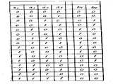
이하, 본 발명의 양호한 실시예에 관해서 설명하기로 한다. 제1도 내지 제3도는 각각 본 발명의 변환규칙을 도시한 것으로서, 각 도면에 도시되어 있는 타임차트는 입력데이타, 변환된 전송파형 및 변환된 데이타를 나타낸다(제1a도, 제2a도 및 제3a도 참조). 변환된 데이타는 '1'의 경우예 0.5T의 비트셀의 전단 엣지에서 반전이 행해지도록 하였다.Hereinafter, a preferred embodiment of the present invention will be described. 1 to 3 show the conversion rules of the present invention, respectively, and the time charts shown in the drawings show input data, converted transmission waveforms, and converted data (FIGS. 1A, 2A, and 1). See also 3a). The converted data was to be inverted at the front edge of the bit cell of Example 0.5T in the case of '1'.
제1a도에 도시된 바와같이, 입력 데이터가 '010'인 경우에는, 전술한 바와같이 '1'의 중앙에서 반전이 생긴다. 제1b도에 도시된 바와같이 2개의 '1'이 연속하는 경우, 즉 입력 데이타가 '0110' 일때에는, 최초의 '1'의 중앙에서 제1반전이 생기고, 다음 '1'의 후미 경계에서 제2반전이 생긴다. 이때, 인접반전사이의 반전 간격은 1.5T(=Tmin)가 된다. '0110'로 '1'이 3개 연속하는 경우에는, 제1a도에 도시된 바와같이, 최초 '1'의 중앙에서 제1반전이 생기고, 마지막 '1'의 후미 경계에서 제2반전이 생긴다. 이때As shown in FIG. 1A, when the input data is '010', inversion occurs at the center of '1' as described above. As shown in FIG. 1B, when two '1's are continuous, that is, when the input data is' 0110', a first inversion occurs at the center of the first '1', and at the trailing boundary of the next '1'. A second inversion occurs. At this time, the inversion interval between adjacent inversions is 1.5T (= Tmin). In the case of three consecutive '1's as' 0110', as shown in FIG. 1a, a first inversion occurs at the center of the first '1', and a second inversion occurs at the trailing edge of the last '1'. . At this time
제1d도, 제1f도, 제1h도 및 제1f도에 도시된 바와같이, '1'이 4개 또는 그 이상의 짝수개로 연속하여 데이타가 나머지 없이 2비트마다 분할될 수 있는 경우, 최초의 2비트 유니트에 대한 반전간격은 1.5T이고 나머지의 2비트 유니트에 대한 반전간격은 2T이다. 제1e도에 도시된 바와같이, '1'이 5개 연속하는 경우, 데이타는 2비트 및 3비트로 분할된다. 따라서, 2비트 유니트의 반전간격은 1.5T이고 3비트 유니트의 반전간격은 3T이다. 제1g도, 제1i도 및 제1k도에 도시된 바와같이, '1'이 7이상의 홀수개로 연속As shown in FIGS. 1d, 1f, 1h, and 1f, the first 2 when '1' can be divided into 4 or more even numbers consecutively and data can be divided every 2 bits without a remainder. The inversion interval for the bit unit is 1.5T and the inversion interval for the remaining two bit units is 2T. As shown in Fig. 1e, when '1' is five consecutive, data is divided into 2 bits and 3 bits. Therefore, the inversion interval of the 2-bit unit is 1.5T and the inversion interval of the 3-bit unit is 3T. As shown in Figs. 1g, 1i and 1k, '1' is continuous in odd numbers of 7 or more.
본 실시예로 부터 알 수 있는 바와같이, 연속하는 '1'의 선두로부터 1비트를 유니트로 하여 분할하고, 마지막 유니트를 2비트 또는 3비트로 하여 데이타를 분할하면, 어떠한 연속패턴도 본 실시예에 포함될 수 있으며, 각 유니트 마다의 마지막 '1'의 후미 경계에서 반전이 생긴다. 이 경우 '1'이 연속하는 패턴에서 최초의 2비트 유니트에 대한 반전간격은 제1b도에 도시된 바와같이 1.5T이고, 중간 및 마지막 2비트 유니트에 대한 반전간격은 2T이며, 3비트 유니트에 대한 반전간격은 3T이다.As can be seen from this embodiment, if one bit is divided into units from the beginning of consecutive '1' and the data is divided into two or three bits as the last unit, any continuous pattern can be applied to this embodiment. A reversal occurs at the trailing boundary of the last '1' for each unit. In this case, in the pattern where '1' is continuous, the inversion interval for the first two-bit unit is 1.5T, as shown in FIG. 1B, and the inversion interval for the middle and last two-bit units is 2T, The reversal interval for is 3T.
제1도에 도시된 실시예와는 달리, '1'이 연속하는 패턴의 데이타를 3비트 마다 분할하는 것을 원칙으로 하는 것도 가능하다. 이 경우, 데이타에서 '1'이 3의 배수로 연속되면, 데이타는 나머지 없이 3비트로 분할되며, 그 이외의 경우에는, 1비트의 나머지가 생기지 않도록 분할된다. 즉, 예를들어, 8개의 '1'이 연속하는 경우에는, 마지막 유니트는 2비트로 된다. 또한, 4개의 '1'이 연속하는 경우나 7개의 '1'이 연속하는 경우등에는, 마지막 유니트와 그 전의 유니트가 각각 2비트가 되도록 분할되고, 그렇게 분할된 2비트 또는 3비트 유니트 마다에 대해 상술한 바와 마찬가지의 변환이 수행된다.Unlike the embodiment shown in FIG. 1, it is also possible to divide data of a pattern in which '1' is continuous every 3 bits. In this case, if '1' is continuous in multiples of three in the data, the data is divided into three bits without a remainder. Otherwise, the data is divided so that a remainder of one bit does not occur. That is, for example, when eight '1's are continuous, the last unit is two bits. In the case where four '1's are continuous or seven' 1s' are continuous, the last unit and the previous unit are divided into two bits, and each divided two or three bit unit is divided. The same conversion as described above is performed for the above.
또한, 데이타 패턴에서 '1'이 연속되는 경우에 있어서, 2비트 유니트 및 3비트 유니트가 교대로 존재하도록 데이타를 분할하는 방법이 사용될 수도 있다. 즉, '1'이 연속하는 패턴의 데이타를 2비트 또는 3비트 유니트로 분할하면 되는 것이다. 상기의 방법에 의해, 최소 반전간격 Tmin은 1.5T로 선택할 수 있다.In addition, in the case where '1' is consecutive in the data pattern, a method of dividing data such that two-bit units and three-bit units alternately may be used. That is, the data of the pattern in which '1' is continuous may be divided into two or three bit units. By the above method, the minimum inversion interval Tmin can be selected to 1.5T.
이제, 제2도 및 제3도를 참조하여, '0'이 연속하는 데이타 패턴에 대하여 적용되는 변환규칙, 즉 최대반전간격 Tmax을 4.5T로 제한할 수 있는 변환규칙에 관해 설명하기로 한다. 연속하는 '0'앞의 2비트가 '01'인 경우에는 데이타 패턴은 제2도에 도시된 바와같이 변환되고, 반면에 연속하는 '0'앞의 2비트가 '11'인 경우에는, 제3도에 도시된 바와같이 변환된다. 상술한 바로 부터 명백히 알 수 있듯이,'01'의 경우에는 '1'의 중앙에서 반전이 생긴다. 따라서, '0101' 및 '1101'의 경우와 같이 '0'이 1개만 존재하는 경우에는, 제2a도 및 제3a도에 각각 도시된 바와같이, '0'다음의 '1'의 중앙에서 반전이 생긴다.Now, with reference to FIGS. 2 and 3, a conversion rule applied to a continuous data pattern of '0', that is, a conversion rule that can limit the maximum inversion interval Tmax to 4.5T will be described. If the two bits before the contiguous '0' are '01', the data pattern is converted as shown in FIG. 2. On the other hand, when the two bits before the '0' are '11', It is converted as shown in 3 degrees. As is apparent from the foregoing description, in the case of '01', inversion occurs at the center of '1'. Therefore, in the case where there is only one '0' as in the case of '0101' and '1101', as shown in FIGS. 2A and 3A, the inversion is performed at the center of '1' after '0', respectively. This occurs.
'0'이 2개 이상 연속하는 경우에는, 제1반전으로부터 3.5T이상, 예를들면, 제1반전으로 부터 3.5T떨어지고 앞의 '1'로부터 최초로 나타나는 '1'의 중앙에서 1.5T이상 떨어져 있는 조건을 만족하는 비트셀의 경계에서 제2반전이 생긴다. 제2b도 및 제2c도에 도시된 바와같이,'01001' 및 '010001'인 경우에는, 상기 조건이 만족되지 않으므로, 마지막 '0'다음의 '1'의 중앙에서 제2반전이 생긴다. 제2d, 제2e도 및 제2f도에 도시된 바와같이, '01'다음에 '0'이 4개, 5개 및 6개 연속하는 경우에는, 상기 조건이 만족If two or more '0's are continuous, 3.5T or more from the first inversion, for example, 3.5T away from the first inversion and 1.5T or more from the center of' 1 'first appearing from the first' 1 '. A second inversion occurs at the boundary of the bit cell that satisfies the condition. As shown in FIG. 2B and FIG. 2C, in the case of '01001' and '010001', since the condition is not satisfied, a second inversion occurs in the center of '1' after the last '0'. As shown in Figs. 2D, 2E, and 2F, the condition is satisfied when '0' is followed by four, five, and six consecutive '0's.
'11'다음에 '0'이 연속하는 경우에도 마찬가지의 규칙에 의해 입력데이타가 처리된다. 제3b도 및 제3c도에 도시된 바와같이 ; '11'다음에 2개 및 3개의 '0'이 연속하는 경우에는, 반전간격은 각각 2.5T 및 3.5T가 된다. 제3d도에 도시된 바와같이, '11'다음에 4개의 '0'이 연속하는 경우에, 만일 제1반전으로 부터 3.5T떨어진 곳에서 제2반전이 생기게 된다면 제2반전으로부터 마지막 '0'다음의 최초의 '1'의 중심 까지의 간격이 T에 불과하게 되므로, 이곳에서는 제2반전이 생기지 않는다. 따라서, 이 경우의 반전간격은 최대 반전간격 Tmax(=4.5T)이 된다. 제3e도, 제3f도 및 제3g도에 도시된 바와같이, '11'다음에 각각 5개, 6개 및 7개의 '0'이 연속하는 경우에는, 제1반전으로부터 4T떨어진 곳에서 제2반전이 생기고, 제2반전과 제3반전 사이의 간격은 각각 1.5T, 2.5T 및 3.5T가 된다. 그리고, '11'다음에 '0'이 8개 연속하는 제 3h도의 경우에는, 제2반전과 제3반전 사이의 간격은 3.5T이상이 된다. 즉, 이 경우 제3반전과 마지막, '0'다음의 '1'의 중앙 사이의 간격이 단지 T에 붙과하게 되므로, 제3반전은 3.5T의 간격에서 생기지 않으며, 이때The input data is processed according to the same rule even when '0' continues after '11'. As shown in FIGS. 3B and 3C; In the case where two and three '0's after' 11 'are continuous, the inversion intervals are 2.5T and 3.5T, respectively. As shown in FIG. 3d, in the case where four '0's are consecutive after' 11 ', if a second inversion occurs 3.5T away from the first inversion, the last' 0 'from the second inversion is generated. Since the distance to the center of the next first '1' is only T, there is no second inversion here. Therefore, the inversion interval in this case is the maximum inversion interval Tmax (= 4.5T). As shown in FIGS. 3E, 3F, and 3G, when 5, 6, and 7 '0's are consecutive after' 11 ', respectively, the second part is 4T away from the first inversion. Inversion occurs, and the interval between the second inversion and the third inversion is 1.5T, 2.5T, and 3.5T, respectively. Then, in the case of 3h in which '0' is 8 consecutively after '11', the interval between the second inversion and the third inversion is 3.5T or more. That is, in this case, since the interval between the third inversion and the center of the last, '1' after '0' is only attached to T, the third inversion does not occur at the interval of 3.5T, where
상술한 바와같이, '0'이 몇개 연속하더라도, 본 실시예에서 최대 반전간격 Tmax은 4.5T로 제한된다. 제2g도 제3d도 및 제3h도의 경우에서, 각각 Tmax가 발생하는데, 이때 주의해야 할 것은 Tmax가 2번 이상 연속해서 나타나지는 않는다는 것이다.As described above, even if several '0's are continuous, the maximum reversal interval Tmax is limited to 4.5T in this embodiment. In the case of FIGS. 2g and 3d and 3h, respectively, Tmax occurs, where it should be noted that Tmax does not appear two or more times in succession.
상기 실시예에서는, '0'이 연속할 경우에 반전이 생기도록 하는 판정기준을 '1'이 연속하는 경우와 구별하기 위하여, 그 기준을 3.5T로 하였다. 그러나, 판정기준을 3.5T이상으로 길게할 수도 있으며, 그럴 경우 Tmax값이 변하게 된다. 판정기준을 4T 또는 4.5T로 하면, Tmax는 5.5T가 되고, 판정기준을 5T 또는 5.5T로 하면, Tmax는 6T가 된다. 또한, 이 판정기준을 어떤 값으로 제한하지 ,않고, 연속하는 '0'이 수를 예측할 수 있으면 경우에 따라 변화시켜서, 실질적으로 반전간격이 4.5T를 초과하지 않도록 할 수도 있다.In the above embodiment, the criterion was set to 3.5T in order to distinguish the criterion for reversal when '0' is continuous from the case where '1' is continuous. However, the criterion may be extended to 3.5T or more, in which case the Tmax value changes. If the criterion is 4T or 4.5T, Tmax is 5.5T. If the criterion is 5T or 5.5T, Tmax is 6T. In addition, without limiting this criterion to any value, if the number of consecutive '0's can be predicted, it may be changed in some cases so that the inversion interval does not substantially exceed 4.5T.
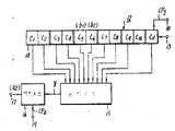
상술한 바와같은 부호변환을 행하는 인코더의 일예를 제4도에 도시하였다. 본 실시예의 인코더 (1)는 3비트 a1,a2및 a3시프트 레지스터(2)를 구비하고 있다. 이 3비트 시프트레지스터(2)에는 단자(4)로부터의 클럭 CP1에 의해 변환될 데이타가 데이타 입력단자(3)를 통해 직렬로 입력된다. 상세히 설명하면, 단자(3)로부터 입력 데이타중의 한 비트가 제6a도에 도시된 시프트 클럭 CP1의 상승 엣지에서 시프트 레지스터(2)에 인가된다. 시프트 레지스터 (2)의 내용은 다음 시프트 클럭 CP1의 상승 엣지가 시프트 레지스터(2)에 인가될때까지는 변하지 않는다. 이 주기가 인코더(1)의 한 동작 사이클 ECC이다.An example of an encoder for performing code conversion as described above is shown in FIG. The
매시간 시프트 레지스터(2)에 저장된 데이타 중에서, a1은 이미 변환된 데이타, a2는 이제 변환될 데이타, a3는 다음번에 변환될 데이타를 각각 나타낸다. 3비트의 데이타 a1,a2및 a3와 논리회로(11)의 출력 x(이에 관해서는 후술함)은 어드레스 신호로서 롬(ROM)(5)에 모두 공급된다. 롬(5)에는 4비트의 어드레스 신호에 응답하여 2비트의 변환 데이타가 기억되고, 한편 롬(5)은 어드레스 신호에 응답하여 입력데이타 a2에 대응하는 2비트의 변Of the data stored in the
시프트 레지스터 (8)내의 8비트 데이타 A, B, C, D, E, F, G 및 H와 시프트 레지스터 (2)의 제1비트 a1는 모두 논리회로(11)에 병렬로 공급되어, 어드레스 신호의 한 비트 x를 결정하거나 다음 논리식에 의한 출력 비트 x를 발생시킨다.
상기 동작은 연속적으로 반복될 것이며, 출력단자(10)에서 얻어지는 것은 상기 규칙에 따른 출력 데이타이다.The above operation will be repeated continuously, and what is obtained at the
제4도에 도시된 인코더(1)는 단지 한 실시예에 불과하며 여러 형태로 변형시킬 수 있다. 예를들어, 롬(5)대신에 논리회로가 사용될 수 있는데, 이 논리회로는 다음 논리식으로 표현되는 출력 b1및 b2을 전달하도록 구성된다. 즉,The

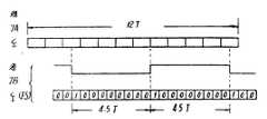
상술한 인코더(1)의 출력을 전송하는 경우, 예를들면 비데오 디스크와 같은 디스크에 수록하는 경우에는, 프레임 동기신호 FS를 부가하도록 한다. 비데오 디스크에는 자기 기록 재생장치에 의한 데이타의 2진 값과 다른 제3값의 동기신호를 부가할 수 없기 때문에, 데이타 스트림내에 프레임 동기신호 FS를 삽입하지 않으면 안된다. 재생축에 있어서의 비트 동기의 추출은 최대 반전 간격 Tmax(본 실시예에서는 4.5T)를 검출하면 가능하다. 왜냐하면, 본 실시예에서 4.5T의 Tmax은 그 앞의 반전When the output of the above-described
y=C6·C5·(C9+C11+
래치회로(16)는, 단자(19)로 부터의 래치펄스 CP4에 의해서 논리회로(15)의 출력을 래치한다. 이 래치펄스 CP4의 주기는 시프트 클럭 CP3의 주기의 2배(=T)이다.The latch circuit 16 latches the output of the logic circuit 15 by the latch pulse CP4 from the terminal 19. The period of this latch pulse CP4 is twice the period of the shift clock CP3 (= T).
그리고, 재생 데이타의 비트셀 사이의 경계가 시프트 레지스터 (14)의 C2및 C3사이, C4및 C5사이, C6및 C7사이, C8및 C9사이, C10및 C11사이와 일치하는 타이밍으로 동기되어 래치펄스 CP4가 발생된다.Then, the boundary between the bit cells of the reproduction data is between C2 and C3, between C4 and C5, between C6 and C7, between C8 and C9, between C10 and C11 of the shift register 14. The latch pulse CP4 is generated in synchronization with the timing coinciding with the above.
제4도에 도시된 인코더 (1)에서는, 입력 데이타의 a2비트와 대응하여 롬(5)으로부터 2비트 출력 b1및 b2이 발생하였지만, 디코더(12)가 인코더(1)와 대응하면, 시프트 레지스터(14)의 2비트 C5및 C6가 b1및 b2비트로 되고, 그때 출력단자(17)에서 취출되는 것은 a2비트가 된다.In the
제8도에 도시된 디코더(12)에 대해서도 여러 형태로 변형시킬 수 있다. 예를들어, 논리회로(15)와 래치회로(16)대신에 롬을 사용할 수 있다.The
본 발명은 입력 데이타 패턴내에서 연속하는 '1'의 수가 우수인지 또는 기수인지를 미리 판별할 수 있는 경우에 적용될 수 있다. 즉, 제1도에 도시된 바와같이, 상술한 실시예에서는, 4개 이상 연속하는 '1'을 최초로 부터 2비트 유니트로 분할하여 최후의 유니트가 2비트 또는 3비트 유니트가 되도록 데이타 패턴을 나머지 없이 분할한다. 그리하여, 최후의 유니트가 3비트이면, 반전간격은 3T가 된다. 이와 구별하기 위해서, '0'이 연속하는 패턴을 변환할때의 판정기준을 3.5T로 선택할 수 있다.The present invention can be applied when it is possible to determine in advance whether the number of consecutive '1's in the input data pattern is excellent or odd. That is, as shown in FIG. 1, in the above-described embodiment, the data pattern is divided so that the last unit is a 2-bit or 3-bit unit by dividing four or more consecutive '1's from the first into 2-bit units. Split without. Thus, if the last unit is 3 bits, the inversion interval is 3T. To distinguish from this, the criterion when converting a pattern in which '0' is continuous can be selected as 3.5T.
연속하는 '1'의 수가 기수인 것을 미리 검출할 수 있으면, 최초에 3비트 유니트를 할당함으로써 반전간격을 2.5T로 할 수 있고, 따라서 3T의 반전간격이 생기지 않도록 할 수 있다. 제1k도에 도시된 바와 같이 11개의 '1'이 연속하는 경우에 대해서 상기 사상을 적용한 경우를 제9도에 도시하였다. 제9도의 경우에 있어서, 최초의 분할 유니트를 3비트 유니트로 하고, 나머지를 2비트 유니트로 하여 분할하였기 때문에, 최초의 반전 간격은 2.5T가 된다.If it is possible to detect in advance that the number of consecutive '1's is an odd number, the inversion interval can be set to 2.5T by allocating a 3-bit unit first, thus preventing the inversion interval of 3T from occurring. As shown in FIG. 1k, FIG. 9 illustrates a case where the above idea is applied to 11 consecutive '1's. In the case of Fig. 9, since the first division unit is divided into three bit units and the remainder is divided into two bit units, the first inversion interval is 2.5T.
연속하는 '1'의 수가 우수인 경우에는 제1도의 경우와 마찬가지의 방법으로 변환된다. 그리고, '0'이 연속하는 경우에 반전을 발생시키는 판정기준은 3.5T로 부터 3T로 단축시킬 수 있다. 이렇게 함으로써, 최대 반전간격을 4.5T에서 4T로 단축시킬 수 있다. 인코더를 구성하는 경우, '1'이 연속하는 수가 우수인지 또 기수인지를 판별하기 위해서는 버퍼 메모리가 필요하다. 실제로는, '1'이 무한히 연속하는 경우는 없으며, 유한한 수로 제한되기 때문에 이것과 대응하는 용량의 버퍼 메모리를 사용하는 것이 바When the number of consecutive "1s" is excellent, it is converted in the same manner as in the case of FIG. And, the criterion for generating inversion when '0' is continuous can be shortened from 3.5T to 3T. By doing this, the maximum inversion interval can be shortened from 4.5T to 4T. In the case of configuring the encoder, a buffer memory is required to determine whether the number of consecutive '1's is good or odd. In practice, since '1' is not infinitely continuous and is limited to a finite number, it is recommended to use a buffer memory of a corresponding capacity.
이러한 문제를 해결하기 위해서, 데이타에 상관없이 상기에 언급된 최대 반전간격이 나타나도록 하고 또한 버퍼 메모리의 용량을 비교적 적도록 한 제2실시예가 구성된다. 즉, '1' 또는 '0'이 연속하여 나타날때, 마지막 몇개의 비트, 예를들어 마지막 5개의 비트에서 연속하는 수가 우수인지 또는 기수인지를 검출하여 반전위치를 조절한다.In order to solve this problem, a second embodiment is constructed in which the above-mentioned maximum inversion interval is shown irrespective of data and the capacity of the buffer memory is relatively small. That is, when '1' or '0' appears consecutively, the inversion position is adjusted by detecting whether the consecutive number in the last few bits, for example, the last five bits, is even or odd.
제10도를 참조로 하면, 제10a도 내지 제10c도는 제1실시예와 유사한 반전이 발생하는 특별한 경우를 도시하고 있다. '1'이 4비트 이상 연속하는 경우, 이 데이타 패턴은 비트셀 사이의 경계에서 2비트 마다 분할된다. 데이타 패턴을 분할할때 나머지가 생기면, 연속하는 '1'비트중에서 마지막 '1'비트 다음에 최초로 나타나는 '0'비트 앞의 5비트는 3비트와 다음의 2비트 사이의 경계에서 분할되며, 분할후 비트셀 사이의 경계에서 반전이 생긴다. 따라서, 연속하는 '1'의 수가 우수인 경우에는, 제1실시예와 마찬Referring to FIG. 10, FIGS. 10A to 10C show a special case in which inversion similar to that of the first embodiment occurs. When '1' is continuous for 4 or more bits, this data pattern is divided every 2 bits at the boundary between bit cells. If the remainder occurs when dividing the data pattern, the 5 bits before the '0' bit that appears first after the last '1' bit among consecutive '1' bits are divided at the boundary between 3 bits and the next 2 bits. Afterwards, inversion occurs at the boundary between the bitcells. Therefore, in the case where the number of consecutive '1's is excellent, similarly to the first embodiment
제10e도에 도시된 바와같이, 5개의 '1'이 연속하는 경우, 데이타 패턴은 상기 규칙에 따라 3비트 및 다음와 2비트로 분할되어, 이때 최초 3비트 유니트의 반전간격은 2.5T이고, 다음 2비트 유너트의 반전간격은 2T이다. 또한, 제10g도, 제10i도 및 제10k도에 도시된 바와같이 '1'이 7개, 9개 및 11개 연속하는 경우에 있어서, 데이타 패턴을 2비트 유니트 마다 분할하게 되면, 나머지가 생기게 된다. 그러므로, 마지막 '1'다음에 최초로 나타나는 '0'앞의 5비트가 3비트 및 다음의 2비트 사이의 경계에서 분할되어, 이 경계에서 반전이 생긴다.As shown in FIG. 10E, when five '1's are consecutive, the data pattern is divided into 3 bits and the next and 2 bits according to the above rules, wherein the inversion interval of the first 3 bit unit is 2.5T, and the next 2 The inversion interval of the bit unit is 2T. Also, as shown in FIGS. 10G, 10I, and 10K, in the case where seven, nine, and eleven consecutive '1's are divided, the data pattern is divided into two bit units, and the rest is generated. do. Therefore, the 5 bits before the '0' first appearing after the last '1' are divided at the boundary between 3 bits and the next 2 bits, so that inversion occurs at this boundary.
상술할 방법에 의해, 최소 반전간격 Tmin은 1.5T가 된다. '1'이 연속함에 따라 나타나는 최대 반전간격 Tmax은 3T가 된다. 이 경우, '1'이 연속하는 비트 패턴의 마지막 5비트중 앞의 3비트에서는 3T(또는 2.5T)의 반전간격이 생기기 때문에, 3T(또는 2.5T)다음의 반전간격은 하자 없이 2T가 된다. 따라서, '0'이 연속하는 패턴에 대한 판정기준으로 3.5T의 반전간격이 이용될 수 있고, 이때 최대 반전간격 Tmax은 4T로 제한될 수 있다.By the above-described method, the minimum inversion interval Tmin is 1.5T. The maximum inversion interval Tmax that appears as '1' continues is 3T. In this case, since the inversion interval of 3T (or 2.5T) occurs in the preceding 3 bits among the last 5 bits of the bit pattern in which '1' is continuous, the inversion interval after 3T (or 2.5T) becomes 2T without defect. . Therefore, an inversion interval of 3.5T may be used as a criterion for the pattern in which '0' is continuous, and the maximum inversion interval Tmax may be limited to 4T.
제11a도, 제11a'도와 제11b도,제11b'도에 도시된 바와같이, '0'이 2개 또는 2개 연속하는 경우에는, 제1실시예와 마찬가지의 반전이 생긴다. 3개 이상의 '0'이 연속하는 경우에는, 제2반전이 제1반전으로 부터 3.5T이상 떨어지고 또한 마지막 '0'다음의 처음 나타나는 '1'의 중앙에서 1.5T이상 떨어져 있는 조건을 만족하는 비트셀의 경계에서 반전이 생긴다.As shown in FIGS. 11A, 11A ', 11B, and 11B', when two or two '0's are continuous, the same inversion as in the first embodiment occurs. If three or more '0's are continuous, the bit that satisfies the condition that the second inversion is more than 3.5T from the first inversion and is more than 1.5T from the center of the first' 1 'after the last' 0 ' Inversion occurs at the boundary of the cell.
제11c도 및 그 이하의 도면에 있어서, 연속하는 '0'앞의 2비트가 '01'일때의 반전 패턴과 '11'일때의 반전패턴이 동일 도면에 도시되어 있으며, 이때 점선은 '11'인 경우의 반전 패턴을 나타낸다.In FIG. 11C and the following figures, the inversion pattern when two bits before the continuous '0' is '01' and the inversion pattern when '11' are shown in the same drawing, where the dotted line is '11' The inversion pattern in case of is shown.
제11c도에 도시된 바와같이, '0'이 3개 연속하는 경우에는 상기 조건이 만족되지 않는다. 따라서, 다음 '1'의 중앙에서 반전이 생긴다. 연속하는 '0'앞의 2비트가 '01'인 경우에는, 반전간격은 3.5T이지만, '11'인 경우에는, 반전간격은 최대 반전간격 Tmax인 4T가 된다. 최대 반전간격 Tmax은 이 경우에만 나타난다.As shown in Fig. 11C, in the case where three '0's are consecutive, the condition is not satisfied. Thus, inversion occurs at the center of the next '1'. When the two bits before the continuous '0' are '01', the inversion interval is 3.5T, but in the case of '11', the inversion interval is 4T which is the maximum inversion interval Tmax. The maximum reversal interval Tmax appears only in this case.
제11d도, 제11e도 및 11F도에 도시된 바와갈이, '0'이 4개 이상 연속하는 경우에는, 상기 조건이 만족되므로, 제1반전으로부터 3.5T(또는 연속하는 '0'앞의 2비트가 '11'인 경우에는 3T) 떨어진 곳에서 제2반전이 생긴다. 제11g도,제11h도 및 제11i도에 도시된 바와같이, '0'이 7개 이상 연속하는 경우에는, 제1반전으로 부터 3.5T(또는 3T)떨어진 곳에서 제2반전이 생기고, 다시 제2반전으로부터 3T떨어진 곳에서 제3반전이 생긴다. 마찬가지로, 제11j도 및 제11k도에 도시된 바와같이 3T마다 반전이 생기고 마지As shown in Figs. 11D, 11E, and 11F, when four or more '0's are continuous, the above conditions are satisfied, and therefore, 3.5T (or before the continuous' 0') from the first inversion. When 2 bits are '11', a second inversion occurs 3T) away. As shown in FIGS. 11G, 11H and 11I, when seven or more '0's are continuous, a second inversion occurs at 3.5T (or 3T) away from the first inversion, and again. The third inversion occurs 3T away from the second inversion. Similarly, reversal occurs every 3T as shown in FIGS. 11j and 11k.
상술한 바와같이, 몇개의 '0'이 연속하더라도, 최대 반전간격 Tmax은 4T로 제한된다. 제11도로 부터 알 수 있는 바와같이, '1'이 연속하는 경우와 마찬가지로 '0'이 연속하는 경우에 3T의 반전간격이 나타난다. 따라서, 디코딩에 있어서 연속하는 '0'의 수를 연속하는 '1'의 수와 구별할 수 없다. 그러나, '0'이 연속하는 경우에는, 3T의 반전간격 다음에 2T의 반전간격이 절대로 나타날 수 없고, 1.5T, 2.5T, 3T 및 3.5T와 같은 다른 반전간격이 나타난다. 반대로, '1'이 연속하는 경우에는, 상술한 바와같이 3TAs described above, even if several '0's are continuous, the maximum inversion interval Tmax is limited to 4T. As can be seen from FIG. 11, the reversal interval of 3T appears when '0' is continuous as in the case where '1' is continuous. Thus, in decoding, the number of consecutive '0's cannot be distinguished from the number of consecutive' 1's. However, when '0' is continuous, the inversion interval of 2T can never appear after the inversion interval of 3T, and other inversion intervals such as 1.5T, 2.5T, 3T, and 3.5T appear. In contrast, when '1' is continuous, 3T as described above
상기 부호 변환을 실행하는 또다른 인코더 (21)의 실시예가 제12도에 도시되어 있다. 제12도에 도시된 인코더 (1)는 기본적으로, 제4도의 인코더(1)에서 사용된 3비트 시프트 레지스터 대신, 5비트 시프트 레지스터(22)를 구비하고 있다. 이 시프트 레지스터 (22)는 단자(24)로 부터의 클럭 CP1에 응답하여 입력단자(23)를 통해 데이타가 입력된다. 시프트 레지스터 (22)의 5비트 a1,a2,a3,a4및 a5는 논리회로(31)의 출력 x과 함께 논리 회로(25)에 병렬로 공급된다. 여기서, 논리회로(25)는 제4도의 인코더(1)에 사용된 롬(5)대신 사용되는 것이다. 논리회로(25)는 상기 6개의 비트로부터 다음 논리식으로 표시되는 2비트의 출력 b1및 b2을 발생시킨다. 즉, 시프트 레지스터(22)내의 5비트 데이타중 비트 a2가 2비트 b1및 b2로 변환된다.An embodiment of another

2비트 출력 b1및 b2은 단자(27)로 부터의 로드 펄스 LD에 따라 2비트 시프트레트스터(26)에 입력된다.The two bit outputs b1 and b2 are input to the two
시프트 레지스터 (26)의 내용은 단자(29)로 부터의 클럭 CP2에 따라 8비트 시프트 레지스터 (28)에 연속으로 인가되고, 변환된 데이타의 시프트 레지스터(28)로 부터 출력단자(30)로 전달된다. 시프트 레지스터(28)의 내용 A,B,D,E, F, 및 G(C를 제외)는 시프트 레지스터(22)의 제1비트 a1과 함께 논리회로(31)에 인가되고, 그후 다음 논리식에 따라 출력비트 x가 발생한다.The contents of the

상기 작동에 의해 입력 데이타가 연속적으로 인코드된다. 이 경우, 클럭 CP1및 CP2와 로드 펄스 LD는 제6도와 동일한 타이밍을 갖는다.By this operation, input data is continuously encoded. In this case, the clocks CP1 and CP2 and the load pulse LD have the same timing as in FIG.
제12도의 인코더 (21)에 대해서도 여러 형태로 변형시킬 수 있다. 예를들어, 제4도의 인코더 (1)에서와 같이 논리회로(25)대신 롬을 사용할 수도 있다.The
제1실시예와 마찬가지로, 제2실시예에 있어서도 전송에러가 없으면, 데이타에는 절대로 나타나지 않는 비트 패턴이 동기신호로 사용될 수 있다. 상기 조건을 만족시키는 일례로서, 4T의 반전 간격 다음에 3.5T의 반전간격이 뒤따르고, 다시 그뒤에 2T의 반전간격이 존재하도록 제13도에 도시된 바과같은 패턴이 존재한다. 전술한 바와같이 4T의 최대 반전간격 Tmax은 제11c도의 경우에서만 나타나며, 그것은 비트셀의 중앙에서 시작해서 중앙에서 끝난다. 따라서 3.5T의 반전간격의 종료측에서의 반전은 비트셀의Similarly to the first embodiment, even in the second embodiment, if there is no transmission error, a bit pattern that never appears in the data can be used as the synchronization signal. As an example of satisfying the above condition, there is a pattern as shown in FIG. 13 so that an inversion interval of 3.5T is followed by an inversion interval of 4T followed by an inversion interval of 2T. As described above, the maximum inversion interval Tmax of 4T appears only in the case of FIG. 11C, which starts at the center of the bit cell and ends at the center. Therefore, the inversion at the end of the inversion interval of 3.5T indicates that
제14도는 디코더(32)의 제2실시예이다. 디코더(32)는 입력단자(33)로부터 재생된 데이타가 공급되는 15비트 시프트 레지스터(34)와 논리회로(35) 및 래치회로(36)로 구성된다. 래치회로(36)의 출력단자(37)에서는 디코드된 출력 데이타가 얻어진다. 시프트 레지스터(34)에는, 단자(38)로부터의 시프트 클럭 CP3(0.5T의 주기)에 응답하여, 재생 데이타가 1비트씩 인가되고, 논리회로(35)에는 시프트 레지스터(34)로 부터 C10, C12및 C14비트를 제외한 12개의 비트 C1내지 C15가 공급되어, 다음 논리식에 따른 출력 y을 발생시킨다.14 is a second embodiment of the
y=C6+C5·
래치회로(36)는 논리회로(35)의 출력 y을 단자(39)의 래치펄스 CP4로 래치한다. 래치펄스 CP4의 주기는 시프트 클럭펄스 CP3의 주기의 2배(=T)이다. 그리고, 재생 데이타의 비트셀 사이의 경계가 C2및 C3,C4및 C5,C6및 C7,C8및 C9,C10및 C11,C12및 C13,C 및15사이와 일치하는 타이밍으로 동기되어 래치 펄스 CP5가 발생된다.The
제12도에 도시된 인코더 (21)에서, 입력 데이타의 데이타 a1에 응답하여 논리회로(25)로 부터 2비트 출력 b1및 b2이 발생한다. 따라서, 디코더 (32)와 인코더(25)가 대응한다면, 시프트 레지스터(34)의 2비트 C5및 C6는 출력비트 b1및 b2가 되고, 이전 출력단자(37)에 전달된 비트는 a2가 된다.In the
디코더 (32)에 대해서도 여러 형태로 변형시킬 수 있으며, 예를들어, 논리회로(35) 및 래치회로(36) 대신 롬을 사용할 수 있다.The
본 발명의 실시예에 따라 상술한 바와같이, 본 발명에 따르면, 2진 부호는 최소반전간격 Tmin이 1.5T이고 최대 반전간격 Tmax이 실시예에 따라 4.5T 또는 4T가 되도록 변환 또는 디코드된다. 따라서, 3PM방식과 실제로 데이타 밀도는 동일하면서도, 최대 반전간격을 6T이하로 단축시킬 수 있다.As described above according to the embodiment of the present invention, according to the present invention, the binary code is converted or decoded such that the minimum inversion interval Tmin is 1.5T and the maximum inversion interval Tmax is 4.5T or 4T according to the embodiment. Therefore, while the data density is the same as the 3PM method, the maximum inversion interval can be shortened to 6T or less.
비데오 디스크를 이용한 PCM오디오 디스크에서와 같이, 동기신호를 위하여 데이타와 구별할 수 있는 값을 사용할 수 없을 경우에는, 재생측에서 데이타 스트림으로 부터 동기 재생을 행하도록 할 필요가 있다. 본 발명에 따라, 최대 반전간격이 단축될수 있기 때문에, 본 발명은 상기와 같은 경우에 적합하다. 그러나, 실제로는, 재생데이타가 포함하는 시간측 변동분등에 의해서 6T이상의 최대 반전간격으로서도 차질이 없는 경우도 있다.As in the PCM audio disc using a video disc, when a value distinguishable from data cannot be used for a synchronous signal, it is necessary to perform synchronous reproduction from the data stream on the reproduction side. According to the present invention, since the maximum reversal interval can be shortened, the present invention is suitable for such a case. In practice, however, there may be no disruption even at the maximum reversal interval of 6T or more due to the time variation of the reproduction data.
또한, 본 발명에서는 간단한 구성의 인코더를 사용할 수 있다는 장점이 있다.In addition, the present invention has the advantage that the encoder of a simple configuration can be used.
Claims (1)
Translated fromKoreanPriority Applications (2)
| Application Number | Priority Date | Filing Date | Title |
|---|---|---|---|
| KR1019810000190AKR850001689B1 (en) | 1981-01-22 | 1981-01-22 | How to encode digital information |
| KR1019840007543AKR850001690B1 (en) | 1981-01-22 | 1984-11-30 | Digital Data Decoding Method |
Applications Claiming Priority (1)
| Application Number | Priority Date | Filing Date | Title |
|---|---|---|---|
| KR1019810000190AKR850001689B1 (en) | 1981-01-22 | 1981-01-22 | How to encode digital information |
Related Child Applications (1)
| Application Number | Title | Priority Date | Filing Date |
|---|---|---|---|
| KR1019840007543ADivisionKR850001690B1 (en) | 1981-01-22 | 1984-11-30 | Digital Data Decoding Method |
Publications (2)
| Publication Number | Publication Date |
|---|---|
| KR830005770A KR830005770A (en) | 1983-09-09 |
| KR850001689B1true KR850001689B1 (en) | 1985-11-22 |
Family
ID=19220012
Family Applications (2)
| Application Number | Title | Priority Date | Filing Date |
|---|---|---|---|
| KR1019810000190AExpiredKR850001689B1 (en) | 1981-01-22 | 1981-01-22 | How to encode digital information |
| KR1019840007543AExpiredKR850001690B1 (en) | 1981-01-22 | 1984-11-30 | Digital Data Decoding Method |
Family Applications After (1)
| Application Number | Title | Priority Date | Filing Date |
|---|---|---|---|
| KR1019840007543AExpiredKR850001690B1 (en) | 1981-01-22 | 1984-11-30 | Digital Data Decoding Method |
Country Status (1)
| Country | Link |
|---|---|
| KR (2) | KR850001689B1 (en) |
- 1981
- 1981-01-22KRKR1019810000190Apatent/KR850001689B1/ennot_activeExpired
- 1984
- 1984-11-30KRKR1019840007543Apatent/KR850001690B1/ennot_activeExpired
Also Published As
| Publication number | Publication date |
|---|---|
| KR850001690B1 (en) | 1985-11-22 |
| KR850004703A (en) | 1985-07-25 |
| KR830005770A (en) | 1983-09-09 |
Similar Documents
| Publication | Publication Date | Title |
|---|---|---|
| US4553130A (en) | Variable-length encoding-decoding system | |
| US4760378A (en) | Method and apparatus for converting a run length limited code | |
| SU1148572A3 (en) | Device for converting binary code to magnetic medium code | |
| US4779072A (en) | Channel encoder | |
| US4675650A (en) | Run-length limited code without DC level | |
| JPH0158705B2 (en) | ||
| JP2002271205A (en) | Modulation method, modulator, demodulation method, demodulator, information recoding medium, information transmitting method and information transmitting equipment | |
| JPS6129578B2 (en) | ||
| EP0557130B1 (en) | Data conversion method and recording/reproducing apparatus using the same | |
| JP3935217B2 (en) | Conversion from a sequence of m-bit information words to a modulated signal | |
| US4617552A (en) | Method and apparatus for converting a digital data | |
| US6265994B1 (en) | Device for encoding/decoding n-bit source words into corresponding m-bit channel words, and vice versa | |
| US4502036A (en) | Encoding and decoding systems for binary data | |
| US4369472A (en) | Method and apparatus for encoding digital data | |
| US5175545A (en) | Data coding system in a magnetic recording apparatus | |
| KR950010213B1 (en) | Digital Code Conversion Apparatus and Method | |
| JP2002280907A (en) | Modulation method, modulator, demodulation method, demodulator, information recording medium, information transmission method and information transmitter | |
| KR850001689B1 (en) | How to encode digital information | |
| JP2003536315A (en) | Device for encoding a stream of data bits of a binary source signal into a stream of data bits for a binary channel signal, a memory means, a device for recording information, a record carrier, a device for encoding, and a device for reproducing | |
| US4428007A (en) | Method and apparatus for decoding digital data | |
| JP2586073B2 (en) | Frame synchronization method | |
| JPS60114053A (en) | Code conversion system | |
| USRE32432E (en) | Method and apparatus for decoding digital data | |
| JPS635825B2 (en) | ||
| JPS635826B2 (en) |
Legal Events
| Date | Code | Title | Description |
|---|---|---|---|
| PA0109 | Patent application | St.27 status event code:A-0-1-A10-A12-nap-PA0109 | |
| PG1501 | Laying open of application | St.27 status event code:A-1-1-Q10-Q12-nap-PG1501 | |
| PE0902 | Notice of grounds for rejection | St.27 status event code:A-1-2-D10-D21-exm-PE0902 | |
| R17-X000 | Change to representative recorded | St.27 status event code:A-3-3-R10-R17-oth-X000 | |
| T11-X000 | Administrative time limit extension requested | St.27 status event code:U-3-3-T10-T11-oth-X000 | |
| P11-X000 | Amendment of application requested | St.27 status event code:A-2-2-P10-P11-nap-X000 | |
| P13-X000 | Application amended | St.27 status event code:A-2-2-P10-P13-nap-X000 | |
| PE0902 | Notice of grounds for rejection | St.27 status event code:A-1-2-D10-D21-exm-PE0902 | |
| T11-X000 | Administrative time limit extension requested | St.27 status event code:U-3-3-T10-T11-oth-X000 | |
| PG1605 | Publication of application before grant of patent | St.27 status event code:A-2-2-Q10-Q13-nap-PG1605 | |
| PE0701 | Decision of registration | St.27 status event code:A-1-2-D10-D22-exm-PE0701 | |
| PR0701 | Registration of establishment | St.27 status event code:A-2-4-F10-F11-exm-PR0701 | |
| PR1002 | Payment of registration fee | St.27 status event code:A-2-2-U10-U11-oth-PR1002 Fee payment year number:1 | |
| PR1001 | Payment of annual fee | St.27 status event code:A-4-4-U10-U11-oth-PR1001 Fee payment year number:4 | |
| PR1001 | Payment of annual fee | St.27 status event code:A-4-4-U10-U11-oth-PR1001 Fee payment year number:5 | |
| PR1001 | Payment of annual fee | St.27 status event code:A-4-4-U10-U11-oth-PR1001 Fee payment year number:6 | |
| PR1001 | Payment of annual fee | St.27 status event code:A-4-4-U10-U11-oth-PR1001 Fee payment year number:7 | |
| PR1001 | Payment of annual fee | St.27 status event code:A-4-4-U10-U11-oth-PR1001 Fee payment year number:8 | |
| PR1001 | Payment of annual fee | St.27 status event code:A-4-4-U10-U11-oth-PR1001 Fee payment year number:9 | |
| PR1001 | Payment of annual fee | St.27 status event code:A-4-4-U10-U11-oth-PR1001 Fee payment year number:10 | |
| PC1903 | Unpaid annual fee | St.27 status event code:A-4-4-U10-U13-oth-PC1903 Not in force date:19951123 Payment event data comment text:Termination Category : DEFAULT_OF_REGISTRATION_FEE | |
| PC1903 | Unpaid annual fee | St.27 status event code:N-4-6-H10-H13-oth-PC1903 Ip right cessation event data comment text:Termination Category : DEFAULT_OF_REGISTRATION_FEE Not in force date:19951123 | |
| R18-X000 | Changes to party contact information recorded | St.27 status event code:A-5-5-R10-R18-oth-X000 | |
| PN2301 | Change of applicant | St.27 status event code:A-5-5-R10-R13-asn-PN2301 St.27 status event code:A-5-5-R10-R11-asn-PN2301 | |
| P22-X000 | Classification modified | St.27 status event code:A-4-4-P10-P22-nap-X000 | |
| PN2301 | Change of applicant | St.27 status event code:A-5-5-R10-R13-asn-PN2301 St.27 status event code:A-5-5-R10-R11-asn-PN2301 |