KR800000936B1 - Auto Beam Current Limiter - Google Patents
Auto Beam Current LimiterDownload PDFInfo
- Publication number
- KR800000936B1 KR800000936B1KR7601141AKR760001141AKR800000936B1KR 800000936 B1KR800000936 B1KR 800000936B1KR 7601141 AKR7601141 AKR 7601141AKR 760001141 AKR760001141 AKR 760001141AKR 800000936 B1KR800000936 B1KR 800000936B1
- Authority
- KR
- South Korea
- Prior art keywords
- signal
- voltage
- coupled
- transistor
- brightness
- Prior art date
- Legal status (The legal status is an assumption and is not a legal conclusion. Google has not performed a legal analysis and makes no representation as to the accuracy of the status listed.)
- Expired
Links
- 230000002194synthesizing effectEffects0.000claimsdescription2
- 239000003990capacitorSubstances0.000description17
- 238000010894electron beam technologyMethods0.000description14
- 230000007423decreaseEffects0.000description9
- 238000004804windingMethods0.000description4
- 230000001360synchronised effectEffects0.000description3
- 230000015556catabolic processEffects0.000description2
- 230000008878couplingEffects0.000description2
- 238000010168coupling processMethods0.000description2
- 238000005859coupling reactionMethods0.000description2
- 238000010586diagramMethods0.000description2
- OAICVXFJPJFONN-UHFFFAOYSA-NPhosphorusChemical compound[P]OAICVXFJPJFONN-UHFFFAOYSA-N0.000description1
- 230000015572biosynthetic processEffects0.000description1
- 239000002131composite materialSubstances0.000description1
- 238000006731degradation reactionMethods0.000description1
- 238000001514detection methodMethods0.000description1
- 230000000694effectsEffects0.000description1
- 230000005611electricityEffects0.000description1
- 230000001939inductive effectEffects0.000description1
- 238000000034methodMethods0.000description1
- -1redChemical compound0.000description1
- 238000003786synthesis reactionMethods0.000description1
Images
Landscapes
- Video Image Reproduction Devices For Color Tv Systems (AREA)
Abstract
Translated fromKoreanDescription
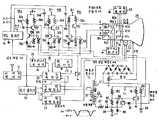
Translated fromKorean도면은 본 발명에 의해 구성된 장치를 사용하는 칼라 텔레비죤수신기의 일반적인 배열을 도시한 일부 계통도 및 일부 개략도.The drawings show some schematic diagrams and some schematic diagrams showing a general arrangement of a color television receiver using the device constructed in accordance with the present invention.
본 발명은 부하전류제한회로에 관한 것으로, 특히, 영상재생 키네스코프와 같은 장치에 의해 유도된 전자비이전류를 제한하기 위한 회로에 관한 것이다.BACKGROUND OF THE INVENTION 1. Field of the Invention The present invention relates to a load current limiting circuit, and more particularly to a circuit for limiting electron specific current induced by a device such as a video reproduction kinescope.
고동작전압은 고명암도(휘도)의 영상을 제공하도록 텔레비죤수신기내에 포함된 영상재생키네스코프의 초점 및 고압전극들에 결합된다. 고압원으로부터 유도된 전자 비임전류의 크기는 전자비임의 발생을 제어하도록 키네스코프에 결합된 신호의 특수내용에 따라 과대하게 될 수 있다.The high operating voltage is coupled to the focus and high voltage electrodes of the image reproduction kinescopes contained within the television receiver to provide a high brightness image. The magnitude of the electron beam current derived from the high voltage source may be excessive depending on the particulars of the signal coupled to the kinescope to control the generation of the electron beam.
과대비임전류가 흑백 텔레비죤수신기에서 발생될 수 있지만, 이것들은 칼라영상재생 키네스코프에 인가되는 비교적 높은 동작전압과 칼라수신기에 자주 사용하는 비데오신호의 DC결합 때문에 칼라텔레비죤 수신기에서 더욱 자주 발생된다.Over-contrast currents can be generated in black and white television receivers, but they are more common in color television receivers because of the relatively high operating voltages applied to color image reproduction kinescopes and the DC coupling of video signals often used in color receivers.
과대비임전류는 수신기 편향시스템의 성능저하, 화면조정(화면이 장면내용에 따라 변화되어 점점 밝아지거나 어둡게 됨) 및 스폿트 비접속(전자비임직경의 증가)등의 다수의 바람직하지 못한 효과를 야기시킨다. 원래, 과대비임전류는 수신기가 즐겁게 시청할 수 없는 영상을 만들게 할 수 있다.Overpotential currents can cause a number of undesirable effects, such as degradation of the receiver deflection system, adjustment of the screen (the screen changes depending on the scene content, making it brighter or darker), and spot disconnection (increased electron beam diameter). Let's do it. Originally, excessive contrast currents can cause receivers to create images that cannot be enjoyed.
비임전류제한회로들은 “자동비임세기리미터”, 란 제목으로 알. 삐. 한센 등에게 허여된 미합중국특허 제3,456,095호, “기준전류원을 사용하는 자동비임전류 제한”이란 제목으로 이. 더블유, 커티스에게 허여된 미합중국특허 제3,541,240호, “자동비임전류리미터회로”란 제목으로 지. 씨. 웨이브라이트에게 허여된 미합중국특허 제3,619,705호에 설명되어 있다.Beam current limiting circuits are known under the heading “Auto beam intensity limiter”. Beep. United States Patent No. 3,456,095 issued to Hansen et al. Entitled “Automatic Beam Current Limiting Using Reference Current Source”. W. U.S. Patent No. 3,541,240 to Curtis, entitled “Automatic Beam Current Limiter Circuit”. Seed. US Pat. No. 3,619,705 to Wavelight.
칼라 텔레비죤수신기내에 사용될 비임전류제한 회로는 이러한 비임전류가 색도신호뿐만 아니라 명도신호에도 응답하여 발생될 수 있기 때문에 과대비임전류를 억제하도록 명도 및 색도신호처리회로 양자에 동작적으로 관련된다. 예를들어 과대비임전류는 과대명도신호에 의해 필연적으로 수반되지 않는 짙은 한색의 재생으로 인해서 뿐만 아니라 고레벨 명도신호에 의해 재생되는 고휘도 백색영상부분으로 인해서 발생될수 있다.The beam current limiting circuit to be used in the color television receiver is operatively related to both the brightness and the chroma signal processing circuit so as to suppress the excess contrast current since such beam current can be generated in response to the brightness signal as well as the chroma signal. For example, the excess contrast current can be generated not only by the reproduction of dark one color, which is not necessarily accompanied by the excessive brightness signal, but also by the high brightness white image portion reproduced by the high level brightness signal.
본 발명의 실시예에 의하면, 비임전류제한 장치는 명도신호처리용 명도채널, 색도신호로부터 색차신호를 유도하기 위한 색도채널, 다수의 칼라전자비임형성장치를 포함하는 키네스코프, 및 키네스코프에 동작전위를 제공하기 위한 고전압 공급장치를 포함하는 텔레비죤신호 처리용 시스템에 제공된다. 비임전류 제한장치는 고전압공급장치로부터 키네스코프에 의해 유도된 전류의 크기를 나타내는 제어신호를 유도하기 위한 장치를 포함한다. 증폭장치는 칼라신호를 유지하도록 명도신호와 색차신호를 합성하기 위해 제공된다. 칼라 신호는 전자비임의 발생을 제어하도록 키네스코프의 전자비임형성장치에 결합된다. 제어신호에 응답하여 증폭장치의 동작점을 제어하기 위한 장치는 증폭장치와 관련된다. 증폭장치의 동작점은 키네스코프에 의해 유도된 전류의 크기와 직접 관계하여 전자비임의 발생을 더욱 억제하도록 제어된다.According to an embodiment of the present invention, a beam current limiting device operates on a brightness channel for brightness signal processing, a chroma channel for deriving a color difference signal from a chroma signal, a kinescope including a plurality of color electron beam forming devices, and a kinescope. Provided is a system for television signal processing that includes a high voltage supply for providing a potential. The beam current limiting device includes a device for inducing a control signal indicative of the magnitude of the current induced by the kinescope from the high voltage supply. An amplifying apparatus is provided for synthesizing the brightness signal and the color difference signal to maintain the color signal. The color signal is coupled to the electron beam forming apparatus of the kinescope to control the generation of the electron beam. An apparatus for controlling the operating point of the amplifier in response to the control signal is associated with the amplifier. The operating point of the amplifier is controlled to further suppress the generation of the electron beam in direct relation with the magnitude of the current induced by the kinescope.
본 발명의 또 다른 특징에 의하면, 증폭장치의 동작점을 제어하기 위한 장치는 증폭장치의 예정된 회로점을 제어전압으로 주기적으로 고정하기 위한 클램핑장치를 포함한다.According to another feature of the invention, the device for controlling the operating point of the amplifier includes a clamping device for periodically fixing a predetermined circuit point of the amplifier to a control voltage.
도면을 참조하여 본 발명을 상세히 설명하면 다음과 같다. 본 발명을 사용하는 칼라텔레비죤수신기는 적당한 중간주파수 회로(도시안됨)과 검파회로(도시안됨)에 의해 색도, 명도, 음성 및 동기부분을 포함하는 합성비데오신호를 발생시키기 위한 무선주파수(RF)텔레비죤 신호에 응답하는 비데오처리단 12를 포함한다. 신호처리단 12의 출력은 색도처리단 16을 포함하는 색도채널 14와 명도처리단 20을 포함하는 명도채널 18에 결합된다.Hereinafter, the present invention will be described in detail with reference to the accompanying drawings. The color television receiver using the present invention is a radio frequency (RF) television for generating a composite video signal including chromaticity, brightness, voice and synchronization by means of a suitable intermediate frequency circuit (not shown) and detection circuit (not shown). And a
색도 처리단 16은 예를들어 R-Y, B-Y 및 G-Y정보를 나타내는 색차신호를 유도하도록 색도복조기(도시안됨)를 포함한다. 이들 색차신호들은 단 44a,44b 및 44c를 포함하는 키네스코프구동기 22에 인가되는데, 여기서 이 신호들은 예를들어 적색(R), 청색(B) 및 녹색(G)정보를 나타내는 칼라신호를 발생시키도록 명도처리회로 20의 출력신호 -Y와 합성된다. 이 칼라신호들은 키네스코프 24에 결합된다.Chromaticity processing stage 16 includes a chromaticity demodulator (not shown) to derive a color difference signal representing, for example, R-Y, B-Y and G-Y information. These color difference signals are applied to a kinescope driver 22 comprising only 44a, 44b and 44c, where they generate color signals representing, for example, red (R), blue (B) and green (G) information. Is combined with the output signal -Y of the
키네스코프 24는 예를들어 델타총, 샤도우(shadow) 혹은 개구마스크, 또는 정밀 인-라인 키네스코프 등과 같은 다수총 키네스코프일 수도 있다. 키네스코프 24는 키네스코프 24의 내면상에 피착된 적색, 녹색 및 청색과 같은 각각의 상이한 형광체에 대한 전자비임을 발생키기고 변조시키기 위한 총을 포함한다. 도시된 바와같이, 각각의 총들은 제각기 캐소드 38a,38b 및 38c, 제어그리드 40a,40b 및 40c 및 스크린그리드 42a,42b 및 42c를 포함한다. 키네스코프 24는 전자총에 의해 발생된 전자비임들을 가속시키도록 캐패시터 47에 의해 나타난 고압전극과 초점전극 45도 포함한다.The
바이어스 제어전압은 이어스제어단 41로부터 제어그리드 40a,40b 및 40c에 결합되며 스크린 제어전압은 각각의 전자총의 컷오프점을 조정하도록 스크린 제어단 43으로부터 스크린그리드 42a,42b 및 42c에 결합된다.The bias control voltage is coupled to the
명도처리단 20은 명도신호 -Y를 발생시키도록 비데오신호들을 증폭하고 처리하도록 작용한다.The
콘트라스트 제어단 26은 명도신호의 진폭을 제어하도록 명도처리단 20에 결합되고 휘도제어단 28은 명도 신호의 DC성분을 제어하도록 명도처리단 20에 결합된다.The
비데오처리단 12의 출력신호 합성비데오신호로부터 수평 및 수직동기펄스를 분리시키는 동기분리기 30에 결합된다. 동기펄스들은 수평편향회로 32와 수평편향회로 34에 결합된다. 편향회로 32 및 34는 키네스코프 24에 의해 발생한 전자비임의 편향을 제어하도록 키네스코프 24에 결합된다.It is coupled to a
하나 이상의 전자비임들은 “수평소인선”기간동안 비데오신호들에 따라 변조되는 키네스코프의 스크린상에 수평소인선을 발생시키도록 수평으로 편향된다. 전자비임이 수평주사선의 말단에 도달했을 때, 이것은 “수평귀선”기간동안 다음 수평주사선의 시작으로 신속하게 다시 편향된다. 이 비임은 바람직한 라스터를 생성시키도록 수직방향으로 천천히 수직으로 편향된다.One or more electron beams are horizontally deflected to generate a horizontal sweep line on the screen of the kinescope that is modulated according to the video signals during the "horizontal sweep line" period. When the electron beam reaches the end of the horizontal scan line, it is quickly deflected back to the beginning of the next horizontal scan line during the “horizontal retracement” period. This beam is slowly and vertically deflected in the vertical direction to produce the desired raster.
편향회로 32 및 34는 수평 및 수직귀선기간에 제각기 대응하는 기간을 갖고 있는 수평 및 수직소거신호를 발생시킨다. 소거신호는 이것들이 명도신호와 조합되는 명도처리단 20에 결합된다. 소거펄스는 명도신호 -Y의 흑색방향(예, 정방향)으로 연장되고 수평 및 수직소인선 기간동안 키네스코프 24에 의해 전자비임의 발생을 억제시키는 경향이 있다.The
수평편향회로 32에 의해 발생되는 수평궤환신호는 수평궤환변압기 33의 1차 권선 35에 결합된다. 변압기 33의 2차 권선 37은 전압트리폴러로서 도시된 DC배압기 64와 접지간에 용량적으로 결합된다. DC배압기 64는 수평궤환신호에 응답하여 종래의 방법으로 키네스코프 24의 초점 및 고압전극 45,47에 필요한 고전압을 발생시키도록 작용한다.The horizontal feedback signal generated by the
수평궤환신호는 변압기 33의 3차 권선 39를 통해 게이팅회로 62에도 결합된다. 수평궤한신호의 부펄스들은 수평소거펄스들과 동기되는 시간에 보통 발생된다. 즉, 이것들은 수평귀선 기간동안 발생된다.The horizontal feedback signal is also coupled to the gating circuit 62 through the third winding 39 of transformer 33. Negative pulses of the horizontal trace signal are usually generated at a time synchronized with the horizontal erase pulses. They occur during the horizontal retrace period.
게이팅회로 62는 DC배압기 64로부터 유도된 키네스코프 비임전류의 크기에 따라서 수평귀선 기간동안 키네스코프 구동기 22의 단 44a,44b 및 44c의 동작점을 제어하도록 제어신호를 발생시키는 역할을 한다.The gating circuit 62 serves to generate a control signal to control the operating points of
키네스코프구동기 22는 키네스코프 24의 각각의 총을 구동시키도록 단 44a,44b 및 44c를 포함한다. 이 단들은 비슷하기 때문에, 단 44a만 상세히 설명하겠다. 단 44a는 NPN트랜지스터 46a 및 NPN트랜지스터 48a를 포함한다. PNP명도증폭기트랜지스터 50은 3개의 단 44a,4b 및 44c에 공통으로 결합된다.The kinescope driver 22 includes only 44a, 44b and 44c to drive each gun of the
단 44a에 관련하여, 반대도전형 트랜지스터들 46a 및 50은 가변구동제어저항 52a를 통하여 함께 결합된 에미터전극들을 갖고 있다. 트랜지스터 46a의 베이스는 캐패시터 54a를 통하여 색도처리단 16의 R-Y출력에 결합된다. 트랜지스터 50의 베이스는 명도 처리단 29의 출력에 직류결합된다. 트랜지스터 46a의 콜렉터는 저항 56a를 통해 정동작전압원 B+에 결합된다. 트랜지스터 46a의 에미터는 가변바이어스 제어저항 58a를 통해 접지에 결합된다. 트랜지스터 46a의 콜렉터는 키네스코프 24의 적색(R)총의 캐소드 38a에 결합된다.With respect to only 44a, the anticonducting transistors 46a and 50 have emitter electrodes coupled together through a variable
트랜지스터 46a 및 50은 트랜지스터 46a의 콜렉터에서 적색(R)을 나타내는 칼라신호를 생성시키도록 R-Y색차신호와 -Y명도신호를 합성하도록 상호동작한다. 트랜지스터 46a는 R-Y색차신호를 증폭하도록 공통에미터모우드로 동작한다. 트랜지스터 46a와 50의 에미터결합으로 인해, 트랜지스터 46a는 명도신호 -Y를 증폭하도록 공통베이스모우드로 동작한다. 트랜지스터 46a,46b 및 46c의 각각의 콜렉터에서 발생되는 적색(R), 청색(B) 및 녹색(G)을 나타내는 신호들은 캐소드 38a,38b 및 38c에 각각 결합된다.Transistors 46a and 50 interoperate to combine the R-Y color difference signal and the -Y brightness signal to produce a color signal representing red (R) at the collector of transistor 46a. Transistor 46a operates as a common emitter mode to amplify the R-Y chrominance signal. Due to the emitter coupling of transistors 46a and 50, transistor 46a acts as a common base mode to amplify the brightness signal -Y. Signals representing red (R), blue (B) and green (G) generated at the respective collectors of
NPN트랜지스터 48a는 NPN트랜지스터 46a의 궤환관계로 배열된다. 이 조합은 색도처리단 16의 R-Y출력의 DC상태와 트랜지스터 46a의 베이스-대-에미터전압변동에 무관하게 단 44a의 동작점을 유지시키도록 클램핑회로를 형성하도록 캐패시터 54a와 저항 60a에 결합된다. 트랜지스터 48a의 베이스는 트랜지스터 46a의 에미터에 직류결합된다. 트랜지스터 48a의 콜렉터는 트랜지스터 46a의 베이스에 직류결합된다. 트랜지스터 48a의 에미터는 다이오드 78a를 통해 게이팅회로 62의 PNP트랜지스터 74의 에미터에 결합된다. 다이오드 78a는 트랜지스터 48a의 베이스-에미터 접합의 역 브레이크다운을 억제하도록 작용한다. 게이팅회로 62가 각각의 수평귀선 기간동안 트랜지스터 48a의 에미터에 제어전압을 결합시킬 때, 트랜지스터 48a는 도통되고 색도처리단 16의 R-Y 출력의 DC상태에 무관하고 트랜지스터 46a의 베이스-에미터전압의 온도 유도변동에 무관한 전압(트랜지스터 48a의 베이스-에미터전압+다이오드 78a의 캐소드 및 애노드간에 발생된 전압+제어전압)으로 트랜지스터 46a의 에미터를 고정시키도록 트랜지스터 46a와 캐패시터 54a와 상호 동작하다. 단 44a의 상세한 동작설명은 디. 애취. 윌리스가 “증폭기의 안정동작점을 유지시키기 위한 회로”라는 제목으로 출원한 미합중국특허원 제504,357호에 기술되어 있다.NPN transistors 48a are arranged in a feedback relationship of NPN transistors 46a. This combination is coupled to capacitor 54a and resistor 60a to form a clamping circuit to maintain the operating point of only 44a independent of the DC state of the RY output of chromaticity stage 16 and the base-to-emitter voltage variation of transistor 46a. . The base of transistor 48a is DC coupled to the emitter of transistor 46a. The collector of transistor 48a is DC coupled to the base of transistor 46a. The emitter of transistor 48a is coupled to the emitter of PNP transistor 74 of gating circuit 62 through diode 78a. Diode 78a acts to suppress reverse breakdown of the base-emitter junction of transistor 48a. When gating circuit 62 couples the control voltage to the emitter of transistor 48a during each horizontal retrace period, transistor 48a is conductive and independent of the DC state of the RY output of chromaticity stage 16, Interacts with transistor 46a and capacitor 54a to fix the emitter of transistor 46a with a voltage independent of temperature induced fluctuations (base-emitter voltage of transistor 48a + voltage between cathode and anode of diode 78a and control voltage). . However, detailed operation description of 44a is available. Love. It is described in US Patent Application No. 504,357 filed by Willis under the heading "Circuit for Maintaining the Stable Operating Point of an Amplifier."
단 44a의 동작점은 트랜지스터 46a의 에미터에서 발생된 전압에 의해 결정되기 때문에, 단 44a의 동작점은 색도처리단 16의 R-Y출력의 DC상태와 트랜지스터 46a의 베이스-에미터전압에 무관하게 유지된다. 이와 마찬가지로, 단 44b의 동작점은 색도처리단 16의 B-Y출력의 DC상태에 무관하게 유지되며, 트랜지스터 46b의 베이스-에미터전압과 단 44c의 동작점은 색도 처리단 16의 G-Y출력과 트랜지스터 46c의 베이스-에미터 전압의 DC상태에 무관하게 유지된다.Since the operating point of stage 44a is determined by the voltage generated by the emitter of transistor 46a, the operating point of stage 44a remains independent of the DC state of the RY output of chromaticity stage 16 and the base-emitter voltage of transistor 46a. do. Similarly, the operating point of
게이팅회로 62는 정공급전압원 C+와 배압기 64사이에 결합된 저항 66을 포함한다. 캐패시터 68은 배압기 64와 저항 66의 접합부 사이에서 접지에 결합되고, 저항 66과 접속되어 전원 C+로부터 저항 66을 통해 유도되는 비임전류를 여파시키도록 작용한다.Gating circuit 62 includes
저항 66 및 캐패시터 68의 접합부는 다이오드 70을 통해 PNP 트랜지스터 72의 베이스에 결합된다. 저항 80,82 및 84를 포함하는 전압분배기는 C+와 접지 사이에 결합된다. PNP트랜지스터 72의 에미터는 저항 80과 82의 접합부에 결합되며 이것의 콜렉터는 저항 82 및 84의 접합부에 결합된다. 캐패시터 86은 저항 82 양단에 결합된다. 다이오드 70은 이것의 캐소드에서 발생된 전압이 예정된 값 이하로 떨어질 때 다이오드 70과 랜지스터 72가 도통되게 하는 극성을 갖고 있다.The junction of
3차 권선 39에 의해 제공된 수평궤한신호는 저항 87 및 다이오드 90의 직렬접속을 통해 저항 82 및 84의 접합부에 결합된다. 다이오드 88은 저항 84양단에 결합된다. 다이오드를 88 및 90이 수평궤환신호의 정부분동안 (수평소인선기간동안) 비도통되고 부의 부분동안(수평귀선기간동안) 도통되도록 다이오드 88 및 90은 극성을 갖고 있고, 저항 80,82,84 및 87의 값들이 선택된다.The horizontal trace signal provided by the tertiary winding 39 is coupled to the junction of
PNP트랜지스터 72의 에미터는 PNP트랜지스터 74의 베이스의 결합된다. 트랜지스터 74의 콜렉터는 접지에 결합된다. 트랜지스터 74의 에미터는 저항 76을 통해 C+에 결합되며 각각의 다이오드들 78a,78b 및 78c를 통해 트랜지스터 48a,48b 및 48c의 에미터들에 결합된다.The emitter of the
도표에 도시한 소신기의 부분들에 대한 대표값들은 아래와 같다.Representative values for the parts of the Shinshingi shown in the table are as follows.
전압 B+ +240 VDCVoltage B + +240 VDC
가변공칭 52a 100Ω(공칭)Variable Nominal 52a 100Ω (nominal)
캐패시터 54a 4.7μFCapacitor 54a 4.7μF
저항 56a 8.2KΩResistor 56a 8.2KΩ
가변저항 58a 1.2KΩ(공칭)Variable Resistance 58a 1.2KΩ (nominal)
저항 60a 560KΩResistance 60a 560KΩ
전압 C+ +28 VDCVoltage C + +28 VDC
저항 66 하기에 설명된 바와같이 선택됨
캐패시터 68 10μF
저항 76 2.2KΩ
저항 80 39KΩ
저항 82 8.2KΩResistance 82 8.2KΩ
저항 84 18KΩ
저항 87 22KΩ
제1도에 도시한 일반배열은 예를들어 미국, 인디아나주 인디아나폴리스시 알 씨 에이 코포레이숀에 의해 간행된 CTC-68형 수신기용 RCA칼라텔레비죤 서어비스데이터 1973년 제C-8호에서 도시한 형태의 칼라텔레비죤수신기에 사용하기에 적합하다.The general arrangement shown in FIG. 1 is shown, for example, in RCA Color Television Service Data No. C-8, 1973, for a CTC-68 type receiver published by RCA Corporation in Indianapolis, Indiana, USA. It is suitable for use in the form of color television receivers.
동작할 때, 수평소인선기간동안 도면에 도시한 수평궤환신호의 정부분(예, +20V DC레벨)은 다이오드 90의 캐소드에 결합된다. 전류는 C+로부터 저항 80,82 및 84를 통해 접지로 흐르며 제1정전압은 저항 80 및 82의 접합부에서 발생된다. 제2정전압은 저항 82 및 84의 접합부(다이오드 88의 캐소드)에서 발생된다. 이 제2전압은 제1전압보다 작은 정전압이며 다이오드 90의 캐소드에서 발생된 전압보다 작은 정전압이다. 그러므로 다이오드 90은 역바이어스되며 비도통 상태로 된다. 다이오드 88은 역바이어스되며 비도통상태로 된다. 캐패시터 86은 저항 82양단에서 발생한 전압으로 충전되어 축적된다. 저항 80 및 82의 접합부에서 발생된 제1전압은 이에미터폴로워로서 배열된 트랜지스터 74를 통해 다이오드 78a,78b 및 78c의 캐소드에 결합된다. 저항 80 및 82의 접합부에서 발생된 제1전압은 다이오드 78a,78b 및 78c를 도통시키기에 충분히 크며 트랜지스터 48a,48b 및 48c를 비도통시키기에 충분하다.In operation, the fraction of the horizontal feedback signal (e.g., + 20V DC level) shown in the figure during the horizontal sweep line is coupled to the cathode of
다이오드 70의 캐소드에서 발생된 전압은 저항 66을 통해 유도되는 키네스코프 비임전류의 크기에 의해 결정된다. 다이오드 70의 캐소드에서의 전압은 비임전류가 증가함에 따라 감소된다. 트랜지스터 72와 다이오드 70이 도통될 때 다이오드 70의 애노드 및 캐소드와 트랜지스터 72의 에미터와 베이스 사이에 발생되는 전압의 합과 동일한 전압보다 작은 저항 80 및 82의 접합부(트랜지스터 72의 에미터)에서 발생된 제1전압 이하로 다이오드 70의 캐소드에서의 전압이 떨어질 때 보통 비도통상태인 트랜지스터 72는 도통상태로 된다. 저항 66의 값은 트랜지스터 72를 도통시킬 비임전류의 전기를 결정하도록 선택된다. 이것이 도통상태로 된 후 트랜지스터 72의 에미터와 콜렉터간의 임피던스는 다이오등 70의 캐소드에서 발생된 전압의 크기에 의해 결정된다. 트랜지스터 72의 에미터와 콜렉터간의 임피던스는 다이오드 70의 캐소드에서 발생된 전압의 크기가 감소됨에 따라 감소된다. 즉 트랜지스터 72의 에미터와 콜렉터간의 임피던스는 비임전류의 크기가 증가됨에 따라 감소된다. 캐패시터 86에 의해 축전된 전압의 크기는 자항 80 및 82의 접합부와 저항 82 및 84의 접합부 사이의 임피던스에 달려 있기 때문에, 캐패시터 86에 의해 축적된 전압의 크기는 비임전류의 크기가 증가함에 따라 감소된다.The voltage generated at the cathode of diode 70 is determined by the magnitude of the kinescope beam current induced through
저항 80 및 82의 접합부와 저항 82 및 84의 접합부사이에 발생된 전압이 비임전류의 함수로서 변동되어도, 저항 80,82 및 84의 값들은 저항 80 및 82의 접합부로부터 접지에 발생된 전압이 수평소인선기간동안 충분히 커져서 트랜지스터 48a,48b 및 48c의 에미터들에 결합된 전압이 이때 이것들을 비도통시키도록 적당히 선택된다.Although the voltage generated between the junctions of
수평귀선기간동안, 수평궤환신호의 부의 부분(예, -180 볼트펄스)은 다이오드 90의 캐소드에 결합되어 다이오드 90 및 88을 순방향 바이어스시킨다. 저항 82 및 84의 접합부에서 발생된 전압은 다이오드 88의 캐소드와 애노드사이에 발생된 전압과 동일한 전압으로 떨어진.. 캐패시터 86양단의 전압은 순간적으로 변화될 수 없기 때문에, 다이오드 78a,78b 및 78c의 캐소드들에 결합된 전압은 다이오드 88위 캐소드와 애노드사이에 발생된 전압과 트랜지스터 74의 에미터 및 베이스 사이에 발생된 전압과 수평소인선기간동안 캐패시터 86양단에 발생된 전압을 더한 전압과 동일한 전압으로 떨어진다.During the horizontal retrace period, a negative portion of the horizontal feedback signal (eg -180 volts pulse) is coupled to the cathode of
저항 80,82 및 84의 값들은 트랜지스터 72가 비도통상태로 될 때, 즉 과대비임전류가 수평소인선기간동안 유도되지 않을 때, 수평귀선기간동안 다이오드 78a,78b 및 78c의 캐소드들에 결합되고 캐패시터 86양단에 발생된 전압이 다이오드 78a,78b 및 78c와 트랜지스너 48a,48b 및 48c를 도통시키도록 충분히 낮아지도록 선택된다. 그러므로, 캐패시터 86양단에 발생된 전압이 수평소인선기간동안 비임전류의 증가에 응답하여 감소할 경우, 수평귀선기간동안 다이오드 78a,78b 및 78c의 캐소드들에 결합된 전압은 과대비임 전류가 수평소인선기간동안 유도되지 않는 경우에 다이오드 78a,78b 및 78c의 캐소드들에 결합되는 전압보다 더욱 낮아지게 된다. 결과적으로, 트랜지스터 48a,48b 및 48c는 과대비임전류가 유도되지 않는 소인선기간 후보다는 과대비임전류가 유도되는 귀선기간후에 더욱 도전상태로 된다. 수평기간동안 다이오드 78a,78b 및 78c의 캐소드에 결합되는 전압의 특정한 크기는 이전의 수평소인선기간동안 유도된 과대 비임 전류의 특정한 크기에 의존한다.The values of
수평귀선기간동안 크랜지스터 46a,46b 및 46c의 베이스에서 발생된 전압은 트랜지스터 48a,48b 및 48c의 도통상태가 증가함에 따라 각각 감소한다. 그러므로, 트랜지스터 46a,46b 및 46c의 에미터들은 키네스코프 24에 의해 유도되는 비임전류의 크기가 증가함에 따라 감소하는 수평귀선기간동안의 전압으로 고정된다. 그러므로, 트랜지스터 46a,46b 및 46c의 각각의 도통상태와 트랜지스터 46a,46b 및 46c의 각각의 콜렉터에 발생된 전압은 트랜지스터 46a,46b 및 46c의 각각의 에미터전압이 감소함에 따라 증가한다. 트랜지스터 46a,46b 및 46c의 콜렉터전압, 즉 캐소드 38a,38b 및 38c에서의 각각의 전압이 증가하기 때문에, 키네스코프 24의 각각의 전자총들에 의한 전자비임들의 발생은 크게 억제되며 이와 상응하여 키네스코프 24에 의해 유도되는 비임전류가 감소한다.The voltage generated at the bases of the
트랜지스터 72의 이득 때문에, 게이팅회로 62는 비임전류 내의 변동에 신속하게 응답한다. 비임전류내의 변동에 더욱 느린 반응이 바람직한 경우나 게이팅회로 62의 비용을 감소시키는 것이 바람직한 경우, 트랜지스터 72는 생략될 수 있다. 이 경우, 다이오드 70의 에노드는 저항 80 및 82의 접합부에 결합되어야 하고 다이오드 70의 캐소드는 저항 66 및 캐패시터 68의 접합부에 결합되어야 한다. 비록 트랜지스터 74가 수평소인선 및 평수귀선기간 동안 도통되는 것으로서 설명되었으나, 트랜지스터 74의 회로배열은 그 트랜지스터 74가 수평소인선기간동안 비도통상태로 되고 수평귀선기간동안 도통상태로 되도록 수정될 수 있다. 이러한 배열은 동시출원중인 디. 에취. 일리스가 “클램핑회로를 포함하는 비데오구동용 게이팅회로”란 제목으로 출원한 미합중국특허원 제580,688호에 설명되어 있다. 여기서 트랜지스터 74와 비슷하게 배열된 트랜지스터는 수직귀선기간의 수평소인선 부분동안 이것을 컷오프시키도록 키네스코프신호를 결합시킨다.Because of the gain of
또한, 본 발명은 특정한 키네스코프 구동기와 클램핑회로에 대해 설명했으나, 다른 배열이 이용될 수도 있다. 이 밖에도 본 발명의 범위에서 본 발명을 수정 변경할 수 있다.Also, although the present invention has been described with respect to particular kinescope drivers and clamping circuits, other arrangements may be used. In addition, the present invention can be modified and changed within the scope of the present invention.
Claims (1)
Translated fromKoreanPriority Applications (1)
| Application Number | Priority Date | Filing Date | Title |
|---|---|---|---|
| KR7601141AKR800000936B1 (en) | 1976-05-10 | 1976-05-10 | Auto Beam Current Limiter |
Applications Claiming Priority (1)
| Application Number | Priority Date | Filing Date | Title |
|---|---|---|---|
| KR7601141AKR800000936B1 (en) | 1976-05-10 | 1976-05-10 | Auto Beam Current Limiter |
Publications (1)
| Publication Number | Publication Date |
|---|---|
| KR800000936B1true KR800000936B1 (en) | 1980-09-12 |
Family
ID=19202248
Family Applications (1)
| Application Number | Title | Priority Date | Filing Date |
|---|---|---|---|
| KR7601141AExpiredKR800000936B1 (en) | 1976-05-10 | 1976-05-10 | Auto Beam Current Limiter |
Country Status (1)
| Country | Link |
|---|---|
| KR (1) | KR800000936B1 (en) |
- 1976
- 1976-05-10KRKR7601141Apatent/KR800000936B1/ennot_activeExpired
Similar Documents
| Publication | Publication Date | Title |
|---|---|---|
| US3914545A (en) | Automatic contrast control utilizing three control signals | |
| US4516152A (en) | Video signal processor with automatic kinescope white balance and beam current limiter control systems | |
| US3959811A (en) | Set-up arrangement for a color television receiver | |
| US4599642A (en) | Video signal processor with bias error compensation | |
| CA1093206A (en) | Brightness control apparatus | |
| US3996609A (en) | Amplifier suitable for use as a color kinescope driver | |
| US3970895A (en) | Circuit for maintaining operating point stability of an amplifier | |
| EP0041554B1 (en) | Automatic peak beam current leveler system | |
| US3971067A (en) | Automatic beam current limiter | |
| US4272777A (en) | Service switch apparatus | |
| GB1601305A (en) | Average beam current limiter | |
| US4554578A (en) | Error compensated control system in a video signal processor | |
| US4584596A (en) | Television receiver alignment system | |
| US4118729A (en) | Set-up arrangement for a color television receiver | |
| US3525801A (en) | Service aid for color television receiver | |
| US4731564A (en) | Service switch for video display apparatus | |
| US3555175A (en) | Kinescope bias tracking circuits | |
| KR800000936B1 (en) | Auto Beam Current Limiter | |
| US4123776A (en) | Service switch arrangement for a color television receiver | |
| US3984864A (en) | Gating circuit for a video driver including a clamping circuit | |
| KR800000931B1 (en) | Gating circuit for kinesco off driver with clamping circuit | |
| CA1219353A (en) | Video signal processor with bias error compensation | |
| KR820000861B1 (en) | Set-up arrangement for color television receiver | |
| KR800000295B1 (en) | Operation point stabilization circuit of amplifier | |
| CA1214859A (en) | Television receiver alignment system |