KR20250095741A - Switching of root complexes to multiple endpoints via die-to-die data interfaces - Google Patents
Switching of root complexes to multiple endpoints via die-to-die data interfacesDownload PDFInfo
- Publication number
- KR20250095741A KR20250095741AKR1020257018310AKR20257018310AKR20250095741AKR 20250095741 AKR20250095741 AKR 20250095741AKR 1020257018310 AKR1020257018310 AKR 1020257018310AKR 20257018310 AKR20257018310 AKR 20257018310AKR 20250095741 AKR20250095741 AKR 20250095741A
- Authority
- KR
- South Korea
- Prior art keywords
- die
- data
- circuit die
- circuit
- upstream
- Prior art date
- Legal status (The legal status is an assumption and is not a legal conclusion. Google has not performed a legal analysis and makes no representation as to the accuracy of the status listed.)
- Pending
Links
Images


Classifications
- G—PHYSICS
- G06—COMPUTING OR CALCULATING; COUNTING
- G06F—ELECTRIC DIGITAL DATA PROCESSING
- G06F13/00—Interconnection of, or transfer of information or other signals between, memories, input/output devices or central processing units
- G06F13/38—Information transfer, e.g. on bus
- G06F13/42—Bus transfer protocol, e.g. handshake; Synchronisation
- G06F13/4282—Bus transfer protocol, e.g. handshake; Synchronisation on a serial bus, e.g. I2C bus, SPI bus
- G06F13/4295—Bus transfer protocol, e.g. handshake; Synchronisation on a serial bus, e.g. I2C bus, SPI bus using an embedded synchronisation
- G—PHYSICS
- G06—COMPUTING OR CALCULATING; COUNTING
- G06F—ELECTRIC DIGITAL DATA PROCESSING
- G06F13/00—Interconnection of, or transfer of information or other signals between, memories, input/output devices or central processing units
- G06F13/38—Information transfer, e.g. on bus
- G06F13/40—Bus structure
- G06F13/4004—Coupling between buses
- G06F13/4022—Coupling between buses using switching circuits, e.g. switching matrix, connection or expansion network
- G—PHYSICS
- G06—COMPUTING OR CALCULATING; COUNTING
- G06F—ELECTRIC DIGITAL DATA PROCESSING
- G06F13/00—Interconnection of, or transfer of information or other signals between, memories, input/output devices or central processing units
- G06F13/38—Information transfer, e.g. on bus
- G06F13/42—Bus transfer protocol, e.g. handshake; Synchronisation
- G06F13/4204—Bus transfer protocol, e.g. handshake; Synchronisation on a parallel bus
- G06F13/4221—Bus transfer protocol, e.g. handshake; Synchronisation on a parallel bus being an input/output bus, e.g. ISA bus, EISA bus, PCI bus, SCSI bus
- G—PHYSICS
- G06—COMPUTING OR CALCULATING; COUNTING
- G06F—ELECTRIC DIGITAL DATA PROCESSING
- G06F2213/00—Indexing scheme relating to interconnection of, or transfer of information or other signals between, memories, input/output devices or central processing units
- G06F2213/0026—PCI express
Landscapes
- Engineering & Computer Science (AREA)
- Theoretical Computer Science (AREA)
- Physics & Mathematics (AREA)
- General Engineering & Computer Science (AREA)
- General Physics & Mathematics (AREA)
- Mathematical Physics (AREA)
- Computer Hardware Design (AREA)
- Information Transfer Systems (AREA)
- Communication Control (AREA)
Abstract
Translated fromKoreanDescription
Translated fromKorean관련 출원들의 교차 참조Cross-reference to related applications
본 출원은 2022년 11월 9일자로 출원되고 발명의 명칭이 "ROOT COMPLEX SWITCHING ACROSS INTER-DIE DATA INTERFACE TO MULTIPLE ENDPOINTS"인 미국 가출원 제63/382,901호의 이익을 청구하며, 상기 출원은 이로써 모든 목적들을 위해 그 전체가 참조로 통합된다.This application claims the benefit of U.S. Provisional Application No. 63/382,901, filed November 9, 2022, entitled “ROOT COMPLEX SWITCHING ACROSS INTER-DIE DATA INTERFACE TO MULTIPLE ENDPOINTS,” which is hereby incorporated by reference in its entirety for all purposes.
이전 세대(예를 들어, PCIe 4.0 MAX 16 Gbps)에 비해 PCIe 5.0(32 Gbps)의 데이터 레이트가 증가되면서 채널 도달 범위가 이전보다 훨씬 짧아지고, 리타이머(retimer)들의 필요성이 더욱 명확해진다. 일반적인 채널들은 시스템 보드들, 백플레인들, 케이블들, 라이저 카드(riser-card)들 및 애드인(add-in) 카드들을 포함한다. 이러한 종류의 채널들을 통한 접속들(종종 이러한 채널들과 소켓들의 조합)은 일반적으로 16 ㎓에서 -36 dB의 특정된 타겟 손실을 초과하는 손실들을 갖는다. 리타이머들은 리타이머 없이도 가능한 경계를 넘어 채널 도달 범위를 확장한다.As data rates increase in PCIe 5.0 (32 Gbps) over previous generations (e.g., PCIe 4.0 MAX 16 Gbps), channel reach becomes much shorter than before, making the need for retimers more evident. Typical channels include system boards, backplanes, cables, riser-cards, and add-in cards. Connections over these types of channels (often a combination of these channels and sockets) typically have loss exceeding the specified target loss of -36 dB at 16 GHz. Retimers extend the channel reach beyond what was possible without a retimer.
리타이머들은 호스트(루트 컴플렉스, 간략화된 RC)와 디바이스(엔드 포인트) 사이의 링크를 2개의 별개의 세그먼트들로 나눈다. 따라서, 리타이머는 새로운 PCIe 링크를 재확립하며, 이는 물리적 및 링크 계층을 구현하는 리트레이닝 및 적절한 등화를 포함한다.Retimers divide the link between the host (root complex, RC for short) and the device (end point) into two separate segments. The retimer thus re-establishes a new PCIe link, which includes retraining and appropriate equalization that implements the physical and link layers.
리드라이버(redriver)들은 감쇠를 보상하기 위해 신호를 부스팅하는 순수 아날로그 증폭기들이지만, 이들은 또한 잡음을 부스팅하고 보통 지터에 기여한다. 대신 리타이머들은 아날로그 및 디지털 로직을 포함한다. 리타이머들은 신호를 등화하고, 클록킹(clocking)을 검색하고, 높은 진폭과 낮은 잡음 및 지터를 갖는 신호를 출력한다. 또한, 리타이머들은 시스템 전력을 낮게 유지하기 위해 전력 상태들을 유지한다.Redrivers are purely analog amplifiers that boost the signal to compensate for attenuation, but they also boost noise and usually contribute to jitter. Instead, retimers contain analog and digital logic. Retimers equalize the signal, retrieve clocking, and output a signal with high amplitude and low noise and jitter. Retimers also maintain power states to keep system power low.
PCIe 4.0에서 리타이머들이 처음 특정되었다. PCIe 5.0의 경우, 리타이머들의 사용이 예상된다. 도 1 및 도 2는 일부 실시예들에 따른 리타이머들에 대한 전형적인 애플리케이션들을 도시한다. 도 1에서, 하나의 리타이머가 이용된다. 리타이머는 마더보드 상에 위치하며, 논리적으로 리타이머는 PCIe 루트 컴플렉스(RC)와 PCIe 엔드포인트 사이에 있다.Retimers were first specified in PCIe 4.0. For PCIe 5.0, the use of retimers is anticipated. Figures 1 and 2 illustrate typical applications for retimers according to some embodiments. In Figure 1, a single retimer is utilized. The retimer is located on the motherboard and logically the retimer is between a PCIe root complex (RC) and a PCIe endpoint.
도 2는 2개의 리타이머들의 사용을 도시한다. 제1 리타이머는 유사하게 마더보드 상에 위치되는 반면, 제2 리타이머는 PCIe 엔드포인트를 포함하는 애드인 카드와 마더보드를 접속시키는 라이저 카드에 있다.Figure 2 illustrates the use of two retimers. The first retimer is similarly located on the motherboard, while the second retimer is on a riser card that connects the motherboard to an add-in card containing a PCIe endpoint.
컴플렉스 PCIe 시스템들에서, PCIe 엔드포인트들의 수는 자유 PCIe 포트들의 수보다 상당히 높을 수 있다. 이러한 시나리오들에서, 스위치 디바이스들은 PCIe 포트들의 수를 확장하기 위해 사용될 수 있다. 스위치들은 몇몇 엔드포인트들을 하나의 루트 컴플렉스에 접속시키고, 단순히 데이터를 모든 포트들에 미러링하는 대신 데이터 패킷들을 특정된 목적지들로 라우팅할 수 있다. 스위치들의 하나의 중요한 특성은 대역폭 공유인데, 이는 모든 엔드포인트들이 루트 포인트의 대역폭을 공유하기 때문이다.In complex PCIe systems, the number of PCIe endpoints can be significantly higher than the number of free PCIe ports. In such scenarios, switch devices can be used to expand the number of PCIe ports. Switches can connect several endpoints to a root complex and route data packets to specific destinations instead of simply mirroring the data to all ports. One important characteristic of switches is bandwidth sharing, since all endpoints share the bandwidth of the root point.
제1 회로 다이의 업스트림 의사-포트(pseudo-port; PP)들의 복수의 세트들 - 각각의 업스트림 PP는 적어도 2개의 루트 컴플렉스 디바이스(root complex device)들 중 개개의 루트 컴플렉스 디바이스에 대한 접속을 가짐 -, 제2 회로 다이의 다운스트림 PP들의 복수의 세트들 - 다운스트림 PP들의 각각의 세트는 적어도 2개의 엔드포인트들 중 개개의 엔드포인트에 대한 접속들을 가짐 -, 제1 회로 다이와 제2 회로 다이 사이의 다이-간 데이터 인터페이스 - 다이-간 데이터 인터페이스는 적응 계층 프로토콜에 따라 각각의 회로 다이 상의 적응 계층 포트들을 통해 제1 및 제2 회로 다이들의 업스트림 PP들과 다운스트림 PP들 사이의 리타이머 RPCS(physical coding sublayer) 데이터 흐름들을 확립하도록 구성됨 -, 업스트림 PP들의 세트들 중 적어도 하나 및 다운스트림 PP들의 대응하는 세트를 적응 계층 프로토콜에 따라 제1 및 제2 회로 다이들 상의 개개의 적응 계층 포트들에 맵핑하도록 구성된 제1 및 제2 회로 다이들 내의 레인 라우팅 로직(lane routing logic), 및 제1 및 제2 회로 다이들 둘 모두에서 레인 라우팅 로직을 구성하기 위한 제1 및 제2 회로 다이들 중 하나 상의 프로세서를 갖는 장치를 포함하는 방법들 및 시스템들이 설명된다.a plurality of sets of upstream pseudo-ports (PPs) of a first circuit die, each upstream PP having a connection to a respective one of at least two root complex devices; a plurality of sets of downstream PPs of a second circuit die, each set of the downstream PPs having connections to a respective one of at least two endpoints; a die-to-die data interface between the first circuit die and the second circuit die, the die-to-die data interface configured to establish retimer physical coding sublayer (RPCS) data flows between the upstream PPs and the downstream PPs of the first and second circuit dies via the adaptation layer ports on their respective circuit dies in accordance with an adaptation layer protocol; lane routing logic within the first and second circuit dies configured to map at least one of the sets of upstream PPs and a corresponding set of downstream PPs to respective adaptation layer ports on the first and second circuit dies in accordance with the adaptation layer protocol; and both of the first and second circuit dies. Methods and systems are described that include a device having a processor on one of first and second circuit dies for configuring lane routing logic in both.
이러한 간략한 요약은 상세한 설명에서 추가로 후술되는 단순화된 형태로 개념들의 선택을 소개하도록 제공된다. 이러한 간략한 요약은 청구 대상의 핵심적인 또는 본질적인 특징들을 식별하도록 의도되지 않으며, 청구 대상의 범위를 결정할 때 보조로서 사용되도록 의도되지도 않는다. 본 발명의 다른 목적들 및/또는 이점들은 상세한 설명 및 포함된 도면들을 검토한 후에 본 기술 분야의 통상의 기술자에게 명백할 것이다.This brief summary is provided to introduce a selection of concepts in a simplified form that are further described in the Detailed Description. This brief summary is not intended to identify key or essential features of the claimed subject matter, nor is it intended to be used as an aid in determining the scope of the claimed subject matter. Other objects and/or advantages of the present invention will become apparent to those skilled in the art after reviewing the detailed description and the included drawings.
도 1 및 도 2는 일부 실시예들에 따른 리타이머들의 2개의 사용들을 예시한다.
도 3은 일부 실시예들에 따른, 고속 다이-투-다이(D2D) 상호접속을 사용하여 다수의 루트 컴플렉스들 사이에 다수의 엔드포인트를 제공하기 위한 멀티-다이 집적 칩 모듈(integrated chip module; ICM)의 칩 구성의 블록도이다.
도 4는 일부 실시예들에 따른, 데이터 레인들이 동일한 다이 내에서 라우팅되는 리타이머 모드에서 동작하는 멀티-다이 ICM의 데이터 흐름도이다.
도 5는 일부 실시예들에 따른, 데이터 레인들이 D2D 상호접속을 사용하여 회로 다이들 사이에서 라우팅되는 리타이머 모드에서 동작하는 멀티-다이 ICM의 데이터 흐름도이다.
도 6은 일부 실시예들에 따른, 데이터 레인 라우팅을 수행하기 위한 크로스바 멀티플렉싱 스위치의 블록도이다.
도 7은 일부 실시예들에 따른 D2D 상호접속의 도면이다.
도 8은 일부 실시예들에 따른, D2D 상호접속을 위한 적응 계층의 블록도이다.
도 9는 4-타일 실시예에서의 타일-투-타일(T2T) 직렬 주변 인터페이스(SPI) 버스의 구성을 예시하는 블록도이다.
도 10은 멀티-칩 모듈의 다양한 타일들 상의 각각의 PHY와 중앙 프로세싱 유닛(CPU) 코어(900) 사이의 완전한 신호 경로를 예시하는 블록도이다.
도 11은 일부 실시예들에 따른 방법의 흐름도이다.Figures 1 and 2 illustrate two uses of retimers according to some embodiments.
FIG. 3 is a block diagram of a chip configuration of a multi-die integrated chip module (ICM) for providing multiple endpoints between multiple root complexes using high-speed die-to-die (D2D) interconnects, according to some embodiments.
FIG. 4 is a data flow diagram of a multi-die ICM operating in retimer mode where data lanes are routed within the same die, according to some embodiments.
FIG. 5 is a data flow diagram of a multi-die ICM operating in retimer mode where data lanes are routed between circuit dies using D2D interconnects, according to some embodiments.
FIG. 6 is a block diagram of a crossbar multiplexing switch for performing data lane routing according to some embodiments.
FIG. 7 is a diagram of D2D interconnection according to some embodiments.
FIG. 8 is a block diagram of an adaptation layer for D2D interconnection according to some embodiments.
Figure 9 is a block diagram illustrating the configuration of a tile-to-tile (T2T) serial peripheral interface (SPI) bus in a 4-tile embodiment.
FIG. 10 is a block diagram illustrating a complete signal path between each PHY and a central processing unit (CPU) core (900) on various tiles of a multi-chip module.
FIG. 11 is a flowchart of a method according to some embodiments.
전체 시스템들을 단일 집적 회로에 통합시키는 증가하는 기술적 능력에도 불구하고, 다수의 칩 시스템들 및 서브시스템들은 상당한 이점들을 유지한다. 설명의 목적들을 위해 그리고 제한 없이, 본 명세서에 설명된 본 발명의 적어도 일부 양상들의 예시적인 실시예들은 루트 컴플렉스(즉, 호스트) 및 엔드포인트를 나타내는 2개의 집적 회로 칩들을 접속시키는 적어도 하나의 포인트-투-포인트 통신 인터페이스의 시스템 환경을 가정하며, (2) 여기서 통신 인터페이스는 4개의 고속 송신 라인 신호 와이어들로 각각 구성되는 몇몇 데이터 레인들에 의해 지원된다.Despite the increasing technological ability to integrate entire systems onto a single integrated circuit, multi-chip systems and subsystems retain significant advantages. For purposes of illustration and without limitation, exemplary embodiments of at least some aspects of the invention described herein assume a system environment of at least one point-to-point communication interface connecting two integrated circuit chips, representing a root complex (i.e., a host) and an endpoint, (2) wherein the communication interface is supported by several data lanes, each comprised of four high-speed transmission line signal wires.
리타이머들은 일반적으로 PHY들 및 리타이머 코어 로직을 포함한다. PHY들은 수신기 부분 및 송신기 부분을 포함한다. PHY 수신기는 데이터를 복구 및 역직렬화하고 클록을 복구하는 반면, PHY 송신기는 데이터를 직렬화하고 출력 송신을 위한 증폭을 제공한다. 리타이머 코어 로직은 각 측의 포트들 사이의 주파수 차이들을 수용하기 위해 (멀티-레인 링크들에서) 디스큐잉(deskewing) 및 레이트 적응을 수행한다.Retimers typically include PHYs and retimer core logic. The PHYs include a receiver portion and a transmitter portion. The PHY receiver recovers and deserializes data and recovers the clock, while the PHY transmitter serializes data and provides amplification for output transmission. The retimer core logic performs deskewing and rate adaptation (in multi-lane links) to accommodate frequency differences between the ports on each side.
리타이머는 루트 컴플렉스(예를 들어, CPU)와 엔드 포인트(예를 들어, 캐시 블록) 사이의 경로 상에 위치되기 때문에, 리타이머는 추가적인 값을 추가한다. 통합된 프로세싱 유닛, 예를 들어, 가속기는 루트 컴플렉스로부터 엔드 포인트까지의 경로에 대해 데이터 프로세싱을 수행하는 리타이머에 통합될 수 있다.Because the retimer is located on the path between the root complex (e.g., the CPU) and the endpoint (e.g., a cache block), the retimer adds additional value. An integrated processing unit, e.g., an accelerator, can be integrated into the retimer to perform data processing on the path from the root complex to the endpoint.
PCIe 리타이머 회로는 4레인 리타이머를 갖는 칩렛, 다이이며, 고속 다이-투-다이 상호접속을 통해 DPU 칩렛 또는 다른 리타이머 칩렛에 접속하는 능력을 갖는다. 1개, 2개 또는 4개의 레인들은 멀티-레인 링크로 번들화(bundle)되어 데이터가 모든 링크들에 걸쳐 확산된다. 각각의 레인을 개별적으로 구성하여 단일-레인 링크를 형성하는 것이 또한 가능하다. PCIe 리타이머에서, 각각의 레인은 각각의 말단에 하나씩(업스트림 및 다운스트림 포트들) 2개의 PHY들을 이용한다. 4개의 레인들을 고려하면, 8개의 PHY들이 하나의 PCIe 리타이머 다이에 사용된다. PCIe 리타이머 다이는 또한 2개 이상의 PCIe 리타이머 다이들 사이에서 제어 정보를 교환하는 것을 허용하는 통신 라인들을 포함한다.A PCIe retimer circuit is a chiplet, die, having a 4-lane retimer and the ability to connect to a DPU chiplet or other retimer chiplet via a high-speed die-to-die interconnect. One, two, or four lanes are bundled into a multi-lane link so that data is spread across all links. It is also possible to configure each lane individually to form a single-lane link. In a PCIe retimer, each lane utilizes two PHYs, one at each end (the upstream and downstream ports). Considering four lanes, eight PHYs are used in a single PCIe retimer die. The PCIe retimer die also includes communication lines that allow for exchanging control information between two or more PCIe retimer dies.
다음은 하나의(또는 그 초과의) PCIe 리타이머 칩렛(들)을 사용하여 구축될 수 있다. 이는 아래에서 더 상세히 논의된다:The following can be built using one (or more) PCIe retimer chiplets, which are discussed in more detail below:
-4-레인 리타이머-4-lane retimer
-완전한 유연한 4x4 정적 레인 라우팅 기능을 갖는 단일 다이- Single die with fully flexible 4x4 static lane routing capability
-가속도계를 갖는 4-레인 리타이머(DPU)- 4-lane retimer with accelerometer (DPU)
-하나의 패키지에 2개의 다이, 즉 리타이머 다이 및 DPU 다이- Two dies in one package, i.e. retimer die and DPU die
-8-레인 리타이머-8-lane retimer
-하나의 패키지에 2개의 다이, 제한된 정적 레인 라우팅 - 동일한 다이에서 유연한 4x4 라우팅, 그러나 다이 경계들을 넘어서는 데이터 없음- 2 dies in one package, limited static lane routing - Flexible 4x4 routing on the same die, but no data across die boundaries
-완전한 유연한 레인 라우팅을 갖는 8-레인 리타이머- 8-lane retimer with fully flexible lane routing
-하나의 패키지에 2개의 다이, 칩렛들을 가로지르는 데이터는 추가적인 지연을 대가로 고속 다이-투-다이 상호접속을 통해 라우팅된다.-Data across two dies and chiplets in a single package is routed through high-speed die-to-die interconnects at the expense of additional latency.
-가속도계를 갖는 8-레인 리타이머(DPU)- 8-lane retimer (DPU) with accelerometer
-패키지 내의 3개의 다이, 즉, 2개의 리타이머 다이들 및 DPU 다이-Three dies in the package, i.e. two retimer dies and a DPU die
-16-레인 리타이머-16-lane retimer
-하나의 패키지에 4개의 다이, 제한된 정적 레인 라우팅 - 동일한 다이에서 유연한 4x4 라우팅, 그러나 다이 경계들을 넘어서는 데이터 없음- 4 dies in one package, limited static lane routing - Flexible 4x4 routing on the same die, but no data across die boundaries
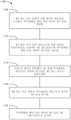
D2D 인터페이스를 사용하여 다중 엔드포인트 스위칭을 갖는 멀티-다이 ICMMulti-die ICM with multi-endpoint switching using D2D interface
도 3은 실시예들에 따른 멀티-다이 ICM(300)의 블록도이다. 도시된 바와 같이, ICM(300)은 제1 회로 다이(305)의 복수의 업스트림 의사-포트(PP)들에 대한 직렬 데이터 트랜시버들(SerDes, PHYs)의 세트를 포함하며, 각각의 업스트림 PP는 적어도 2개의 루트 컴플렉스 디바이스들(302 및 304) 중 개개의 루트 컴플렉스 디바이스에 대한 접속을 갖는다. 장치는 개개의 다운스트림 PP들의 PHY들의 개개의 세트들을 갖는 제2 회로 다이(310)를 더 포함하고, 각각의 다운스트림 PP는 적어도 2개의 엔드포인트들(315 및 320) 중 개개의 엔드포인트에 대한 접속을 갖는다.FIG. 3 is a block diagram of a multi-die ICM (300) according to embodiments. As illustrated, the ICM (300) includes a set of serial data transceivers (SerDes, PHYs) for a plurality of upstream pseudo-ports (PPs) of a first circuit die (305), each upstream PP having a connection to a respective one of at least two root complex devices (302 and 304). The device further includes a second circuit die (310) having respective sets of PHYs of respective downstream PPs, each downstream PP having a connection to a respective one of at least two endpoints (315 and 320).
도 3은 또한 제1 회로 다이(305)와 제2 회로 다이(310) 사이의 다이-간 데이터 인터페이스(D2D)를 포함한다. D2D 인터페이스는 적응 계층 프로토콜에 따라 각각의 회로 다이 상의 적응 계층 포트들을 통해 제1 및 제2 회로 다이들의 업스트림 PP들과 다운스트림 PP들 사이의 리타이머 데이터 흐름들을 확립하도록 구성된다. 적응 계층 프로토콜은 반대 타입(다운스트림/업스트림)의 의사-포트들의 PHY들로의 D2D 인터페이스를 통한 송신을 위해 하나의 타입(업스트림/다운스트림)의 의사-포트의 PHY들 상에서 수신된 원시 데이터를 포맷하도록 구성될 수 있다. D2D 인터페이스는 아래에서 직교 차동 벡터 시그널링 코드(ODVS)의 다수의 흐름들을 활용하는 도 7 및 도 8와 관련하여 더 상세히 설명된다. UCIe(Universal Chiplet Interconnect Express) 인터페이스와 같은 다른 D2D 인터페이스들이 또한 활용될 수 있다는 점에 유의해야 한다. 제1 및 제2 회로 다이들 각각은 업스트림 PP들의 세트들 중 적어도 하나 및 다운스트림 PP들의 대응하는 세트를 적응 계층 프로토콜에 따라 제1 및 제2 회로 다이들 상의 개개의 적응 계층 포트들에 맵핑하도록 구성된 레인 라우팅 로직(600)을 더 포함한다. 장치는, 제1 및 제2 회로 다이들 둘 모두에서 레인 라우팅 로직을 구성하기 위한 제1 및 제2 회로 다이들 중 하나 상의 프로세서, 예를 들어, CPU 코어를 더 포함한다. 멀티-다이 ICM(300)에서, 제1 및 제2 회로 다이들 중 하나는 리더 회로 다이이고, 회로 다이들 둘 모두가 회로 다이 상의 프로세서를 포함할 수 있지만, 리더 회로 다이 상의 프로세서만이 활성이다. 리더 회로 다이 상의 프로세서는 아래에서 도 9 및 도 10의 설명들에서 더 상세히 설명되는 타일-투-타일 직렬 주변 인터페이스(SPI)를 통해 팔로워 회로 다이 내의 레인 라우팅 로직을 구성할 수 있다.FIG. 3 also includes a die-to-die data interface (D2D) between the first circuit die (305) and the second circuit die (310). The D2D interface is configured to establish retimer data flows between upstream PPs and downstream PPs of the first and second circuit dies via adaptation layer ports on each circuit die in accordance with an adaptation layer protocol. The adaptation layer protocol may be configured to format raw data received on PHYs of one type (upstream/downstream) of pseudo-ports for transmission via the D2D interface to PHYs of the opposite type (downstream/upstream) of pseudo-ports. The D2D interface is described in more detail with respect to FIGS. 7 and 8 below utilizing multiple flows of orthogonal differential vector signaling code (ODVS). It should be noted that other D2D interfaces, such as the Universal Chiplet Interconnect Express (UCIe) interface, may also be utilized. Each of the first and second circuit dies further includes lane routing logic (600) configured to map at least one of the sets of upstream PPs and a corresponding set of downstream PPs to respective adaptation layer ports on the first and second circuit dies in accordance with an adaptation layer protocol. The device further includes a processor, e.g., a CPU core, on one of the first and second circuit dies for configuring the lane routing logic in both of the first and second circuit dies. In the multi-die ICM (300), one of the first and second circuit dies is a leader circuit die, and both circuit dies can include a processor on the circuit die, but only the processor on the leader circuit die is active. The processor on the leader circuit die can configure the lane routing logic in the follower circuit die via a tile-to-tile serial peripheral interface (SPI), as described in more detail in the descriptions of FIGS. 9 and 10 below.
도 3은 보드 관리 제어기(BMC)(325)를 포함한다. BMC들은 센서들을 활용하여 마더보드 상의 컴포넌트들 및 하드웨어 디바이스들의 상태를 모니터링하고, 이러한 디바이스들의 상태를 예를 들어 루트 컴플렉스에 통신하기 위해 예를 들어, 마더보드에 포함될 수 있다. BMC는 예를 들어, 서버 룸/데이터 센터 애플리케이션에 사용될 수 있고, 전체 시스템에 대한 정보에 액세스하기 위해 관리자들에 의해 원격으로 관리될 수 있다. BMC의 일부 모니터링 기능은 온도, 습도, 전원 전압, 팬 속도, 통신 파라미터들 및 운영 체제 기능들을 포함한다. BMC는 임의의 파라미터들이 임계치를 초과하면 관리자에게 통지하고 관리자가 조치를 취할 수 있다. 일부 실시예들에서, BMC는 1차 엔드포인트에서의 실패의 경우에 중복적 엔드포인트로 스위칭하기 위한 시퀀스를 실행하는 것(그러나 이에 제한되지 않음)과 같이, 파라미터가 임계치를 초과하는 경우에 특정 액션들을 취하도록 미리 구성될 수 있다. 일부 실시예들에서, BMC(325)는 루트 컴플렉스들(302/304)과 엔드포인트들(315/320) 사이의 PCIe 링크들의 상태를 모니터링한다. 이러한 실시예들에서, PCIe 링크의 상태를 모니터링하는 것은 업스트림 및 다운스트림 데이터 경로들에 대한 비트 에러 레이트 측정들을 포함한다. 이러한 측정들은 PCIe 링크들의 전체 상태를 모니터링하고 링크 리트레이닝 시퀀스들을 개시하는데 유용할 수 있다.FIG. 3 includes a board management controller (BMC) (325). BMCs may be embedded in, for example, a motherboard to monitor the status of components and hardware devices on the motherboard using sensors, and to communicate the status of these devices to, for example, a root complex. A BMC may be used, for example, in server room/data center applications, and may be remotely managed by administrators to access information about the overall system. Some of the monitoring functions of a BMC include temperature, humidity, power voltage, fan speed, communication parameters, and operating system functions. The BMC may notify an administrator when any of the parameters exceed a threshold, so that the administrator can take action. In some embodiments, the BMC may be pre-configured to take certain actions when a parameter exceeds a threshold, such as (but not limited to) executing a sequence to switch to a redundant endpoint in the event of a failure of a primary endpoint. In some embodiments, the BMC (325) monitors the status of the PCIe links between the root complexes (302/304) and the endpoints (315/320). In such embodiments, monitoring the status of the PCIe links includes bit error rate measurements for the upstream and downstream data paths. These measurements may be useful for monitoring the overall status of the PCIe links and initiating link retraining sequences.
이러한 모니터링에 더하여, BMC(325)는 도 3의 다수의 루트 컴플렉스들을 관리하도록 구성될 수 있다. 구체적으로, 엔드포인트들(315 및 320)은 다른 엔드포인트 디바이스들 중에서도, 인공 지능(AI), 하드 디스크 드라이브들(HDD들) 또는 솔리드 스테이트 드라이브들(SSD들)과 같은 공유가능한 컴퓨터 판독가능 매체들, 네트워크 인터페이스 카드들(NIC들)과 같은 고가의 기능들을 위한 공유가능한 자원들에 대응할 수 있다. 이러한 실시예들에서, BMC(325)는 루트 컴플렉스 디바이스들에 의한 엔드포인트들의 사용을 조정할 수 있어서, 즉, 루트 컴플렉스 디바이스들 둘 모두가 동일한 엔드포인트 디바이스와의 접속들을 동시에 확립하지는 않는다. 일부 실시예들에서, BMC는 다수의 루트 컴플렉스 디바이스들 사이에서 다수의 엔드포인트들을 공유하기 위해 크레딧-기반 기술들을 활용할 수 있다.In addition to this monitoring, the BMC (325) may be configured to manage multiple root complexes of FIG. 3. Specifically, the endpoints (315 and 320) may correspond to shareable resources for, among other endpoint devices, artificial intelligence (AI), shareable computer-readable media such as hard disk drives (HDDs) or solid-state drives (SSDs), expensive functions such as network interface cards (NICs). In such embodiments, the BMC (325) may coordinate usage of the endpoints by the root complex devices, i.e., not both root complex devices establish connections with the same endpoint device simultaneously. In some embodiments, the BMC may utilize credit-based techniques to share multiple endpoints among the multiple root complex devices.
BMC는 ICM(300)의 리더 타일 내의 CPU 코어에 명령들을 제공하도록 구성될 수 있다. 이러한 명령들은 예를 들어, SMBus 접속, 또는 다양한 다른 포인트-투-포인트 접속들을 통해 제공될 수 있다. 명령들은 루트 컴플렉스-투-엔드포인트 맵핑과 연관될 수 있고, 리더 타일의 CPU는 BMC에 의해 발행된 맵핑 명령과 연관된 다운스트림 의사-포트들에 업스트림 의사-포트들을 맵핑하도록 팔로워 타일뿐만 아니라 리더 타일 상에서 레인 라우팅 로직을 구성할 수 있다. 일부 실시예들에서, 레인 라우팅 로직을 구성하는 것은 회로 다이들 둘 모두에서 구성 레지스터 공간을 수정하는 것을 포함하고, 구성 레지스터 공간은 레인 라우팅 로직 내의 멀티플렉싱 디바이스들에 선택 신호들로서 제공되는 제어 신호 값들을 포함한다. 일부 실시예들에서, 아래에서 설명되는 바와 같이, 업스트림 의사-포트들의 로직 레인들은 적응 계층 포트들에 대한 정적 맵핑 구성들을 갖는다. 예를 들어, 도 6의 업스트림 의사-포트 PHY1은 리더 타일 상의 적응 계층의 Tx-부분의 적응 계층 포트 1에 정적으로 맵핑될 수 있다. 팔로워 타일 상의 다운스트림 의사-포트들은 루트 컴플렉스-투-엔드포인트 맵핑에 의존하여, 적응 계층 포트들 0-7 중 어느 하나에 선택적으로 접속될 수 있다. 일부 실시예들에서, 다운스트림 의사-포트들은 적응 계층 포트들에 정적으로 맵핑될 수 있는 반면, 업스트림 의사-포트들은 임의의 적응 계층 포트에 접속되도록 구성가능하고, 그 반대도 가능하다.The BMC may be configured to provide commands to the CPU cores within the leader tile of the ICM (300). These commands may be provided, for example, over an SMBus connection, or various other point-to-point connections. The commands may be associated with a root complex-to-endpoint mapping, and the CPU of the leader tile may configure lane routing logic on the leader tile as well as the follower tile to map the upstream pseudo-ports to the downstream pseudo-ports associated with the mapping command issued by the BMC. In some embodiments, configuring the lane routing logic includes modifying a configuration register space in both circuit dies, the configuration register space including control signal values that are provided as selection signals to the multiplexing devices within the lane routing logic. In some embodiments, as described below, the logic lanes of the upstream pseudo-ports have static mapping configurations for the adaptation layer ports. For example, the upstream pseudo-port PHY1 of FIG. 6 may be statically mapped to
도 4는 일부 실시예들에 따른, 제1 엔드포인트(315)에 대한 PCIe 데이터 링크를 위해 사용될 수 있는 데이터 흐름도이다. 도시된 바와 같이, 직렬 데이터는, 직렬 데이터 스트림을 예를 들어, 32-비트 역직렬화된 레인-특정 데이터 워드들로 변환하도록 구성된 역직렬화기를 포함하는 업스트림 의사-포트 내의 PHY에서 수신된다. 데이터 워드들은 레인 라우팅 로직을 통해 리타이머 코어 로직에 라우팅된다. 일부 실시예들에서, 코어 로직은 리타이머 FIFO에 저장되기 전에 예를 들어, 8b10b 또는 128b130b 디코딩을 수행하도록 구성된 PCS 디코딩 블록을 포함한다. 리타이머 FIFO는 주어진 회로 다이 내의 다수의 레인들에 걸칠 뿐만 아니라 다수의 상이한 회로 다이들에 걸친 레인들 사이에서 레인 디스큐잉 및 레이트 적응 기능들을 포함한다. 레인-특정 데이터 워드들은 리타이머 FIFO로부터 판독되고, 다운스트림 의사-포트의 PHY에서 송신기를 통해 다운스트림 직렬 데이터 트랜시버들 상에서 송신된다.FIG. 4 is a data flow diagram that may be used for a PCIe data link to a first endpoint (315) according to some embodiments. As illustrated, serial data is received from a PHY within an upstream pseudo-port that includes a deserializer configured to convert the serial data stream into, for example, 32-bit deserialized lane-specific data words. The data words are routed to the retimer core logic via lane routing logic. In some embodiments, the core logic includes a PCS decode block configured to perform, for example, 8b10b or 128b130b decoding before being stored in the retimer FIFO. The retimer FIFO includes lane deskewing and rate adaptation functions across lanes within a given circuit die as well as across multiple different circuit dies. Lane-specific data words are read from the retimer FIFO and transmitted on downstream serial data transceivers via the transmitter on the PHY of the downstream pseudo-port.
도 5는 D2D 인터페이스를 사용하여 제2 엔드포인트(320)에 대한 PCIe 데이터 링크를 위해 사용될 수 있는 데이터 흐름도이다. 구체적으로, 도 5는 직렬 데이터 트랜시버들의 세트를 통해 수신되고 다이-간 데이터 인터페이스(예를 들어, 적응 계층 및 다이-간 송신기)를 통해 제2 회로 다이에 제공되는 데이터를 예시한다. 도 5에서, 데이터는 제1 회로 다이의 PHY에서 수신된다. 데이터는 역직렬화되고 레인 라우팅 로직을 사용하여 제1 회로 다이 상의 적응 계층으로 라우팅되며, 이는 D2D 인터페이스를 사용하여 송신을 위한 원시 데이터를 포맷한다. 데이터는 제2 회로 다이 상의 적응 계층에서 수신되고, 이는 데이터를 제2 회로 다이 상의 목적지 레인들에 제공하기 위해 상호 포맷을 수행한다. 데이터는 제2 회로 다이의 엔드포인트까지의 직렬 데이터 트랜시버 PHY들 상에서 출력되기 전에 레이트 적응 및 레인-투-레인 디스큐(lane-to-lane deskew)를 수행하기 위해 RPCS 로직에 제공된다. 유사한 데이터 경로가 엔드포인트로부터 루트 컴플렉스까지 역방향으로 존재한다.FIG. 5 is a data flow diagram that may be used for a PCIe data link to a second endpoint (320) using a D2D interface. Specifically, FIG. 5 illustrates data received over a set of serial data transceivers and provided to a second circuit die via a die-to-die data interface (e.g., an adaptation layer and a die-to-die transmitter). In FIG. 5, data is received at a PHY of a first circuit die. The data is deserialized and routed using lane routing logic to an adaptation layer on the first circuit die, which formats the raw data for transmission using the D2D interface. The data is received at an adaptation layer on a second circuit die, which performs cross-formatting to provide the data to destination lanes on the second circuit die. The data is provided to RPCS logic to perform rate adaptation and lane-to-lane deskew before being output on the serial data transceiver PHYs to the endpoint of the second circuit die. A similar data path exists in the reverse direction from the endpoint to the root complex.
도 4 및 도 5에서, 예를 들어, PCIe 세대 1 및 2의 8b10b 인코딩/디코딩 기능들 및 PCIe 세대 3-5의 128b/130b 인코딩/디코딩 기능들을 포함할 수 있는 RPCS 로직이 도시된다. 본 명세서에 설명된 실시예들은 흐름 제어 유닛(FLIT) 방식을 활용하는 PCIe 세대 6을 추가로 고려하며, 따라서 8b10b 또는 128b130b는 구현되지 않는다. 이러한 실시예들에서, 인코딩/디코딩을 위한 기능들은 생략될 수 있지만, FEC 디코딩(부분적 또는 전체)과 같은 PCIe 6에 특정한 추가적인 기능들은 데이터 경로에 로직으로서 포함된다. FIFO에서의 레인-투-레인 디스큐잉 및 레이트 적응과 같은 리타이머 코어 로직의 일부 기능들은 공유된다.In FIGS. 4 and 5, RPCS logic is illustrated that may include, for example, 8b10b encoding/decoding functions of
도 6은 일부 실시예들에 따른, ICM의 리타이머 회로 다이에서의 레인 라우팅 로직(600)의 블록도이다. 도 6은 좌측의 블록도 및 우측의 다양한 레인 라우팅 구성들을 포함한다. 최상부 레인 라우팅 구성(605)에서, 데이터는 역직렬화기를 통해 공급되고, PHY로, 그리고 코어 라우팅 로직을 통해, 그리고 동일한 PHY를 통해 전달되고, 직렬화기를 통해 최하부로 출력된다. 중간 도면(610)에서, 데이터는 하나의 포트로 공급되고, 코어 라우팅 로직에서 프로세싱되고, 최하부 상의 반대 PHY에서 공급된다. 마지막으로, 최하부 도면(615)에서, 모든 데이터는 하나의 PCIe 리타이머 회로의 최상부 측에서 PHY들로 공급되고, 고속 다이-투-다이 상호접속부로 직접 포워딩된다. 데이터는 코어 레인 라우팅 로직을 통해 다른 PCIe 리타이머 다이 상의 PHY들에 공급된다. 이러한 모든 시나리오들에서, 또한 반대 방향의 데이터 경로들이 있다.FIG. 6 is a block diagram of lane routing logic (600) in a retimer circuit die of an ICM, according to some embodiments. FIG. 6 includes a block diagram on the left and various lane routing configurations on the right. In the top lane routing configuration (605), data is fed through a deserializer, to a PHY, through the core routing logic, and through the same PHY, and out through the serializer to the bottom. In the middle diagram (610), data is fed into one port, processed in the core routing logic, and fed out the opposite PHY on the bottom. Finally, in the bottom diagram (615), all data is fed from the top side of one PCIe retimer circuit to the PHYs and forwarded directly to the high-speed die-to-die interconnect. The data is fed through the core lane routing logic to the PHYs on the other PCIe retimer die. In all of these scenarios, there are also data paths in the opposite direction.
도 6의 좌측에는, 레인 라우팅 로직의 스케치가 도시되어 있다. 직렬 데이터 트랜시버 PHY들은 0부터 7까지의 번호를 가지며, 수신기 역직렬화기(DES)들 및 송신기 직렬화기(SER)들을 포함한다. 최상부 레인(PHY #0 및 #4)은 우측에 도시된 데이터 경로들과 매칭되는 3개의 상이한 데이터 경로들을 예시한다. 우측의 데이터 경로(605)는 도 6의 좌측 상의 동일한 PHY #0 상에서 떠나는 PCIe 리타이머 회로의 PHY 0에 들어오는 데이터에 대응한다. 경로(610)는 PHY 0 상에서 수신된 데이터가 도 6의 좌측에 도시된 바와 같이 PHY #4로 통과하는 피드-스루 경로를 도시한다. 마지막으로, 경로(615)는 모든 수신된 데이터가 다이-간 데이터 인터페이스를 통해 송신될 적응 계층으로 직접 포워딩된다는 것을 나타낸다. 제2 PCIe 리타이머 상에서, 다이-간 데이터 인터페이스로부터의 데이터는 코어 라우팅 로직으로 포워딩되고, 여기서 이것은 프로세싱되고 부착된 PHY 상에서 출력된다.On the left side of FIG. 6, a sketch of the lane routing logic is illustrated. The serial data transceiver PHYs are numbered 0 through 7 and include receiver deserializers (DESs) and transmitter serializers (SERs). The top lane (
제2 레인(PHY #1 및 #5)은 멀티플렉싱 능력들을 예시한다. 각각의 코어-로직/송신기 경로는 8개의 레인들 중 임의의 레인으로부터 데이터를 수신할 수 있다. 추가로, 데이터는 D2D 데이터 인터페이스의 적응 계층 포트들로부터 획득될 수 있다. 다른 레인들(#4를 갖는 PHY #0, #6을 갖는 PHY #2, #7을 갖는 PHY #3)은 동일한 스위칭 능력들을 갖는다. 최하부에서, 적응 계층 포트들에 대한 멀티플렉싱이 도시된다. 도시된 바와 같이, 임의의 입력 PHY는 주어진 적응 계층 포트에 대한 입력으로서 선택될 수 있다. 적응 계층 포트들은 도 7과 관련하여 아래에서 설명되는 바와 같이 D2D 흐름들에 대한 고정된 맵핑들을 가질 수 있다. 따라서, 일부 실시예들은 다수의 적응 계층 물리적 포트들에 대해 동일한 수신된 PHY 데이터를 선택함으로써 데이터를 미러링할 수 있다.The second lane (
라우팅 로직에서 데이터 경로를 스위칭하는 것은 역직렬화된 레인-특정 데이터 워드들, 수반되는 데이터 인에이블 라인들, 복구된 클록, 및 대응하는 리셋을 운반하는 32-비트 수신된 데이터 버스를 포함한다. 레인이 적응 계층으로 라우팅될 때, 클록 도메인 크로싱은 복구된 클록 신호를 사용하여 역직렬화된 데이터를 FIFO들로 판독함으로써 발생한다. 적응 계층은, 예를 들어, 각각의 D2D 데이터 흐름에서 송신기들에 150-비트 D2D 워드들을 출력할 뿐만 아니라 5b6w 인터페이스에 대한 25Gbd 클록 도메인으로의 변환을 위해 클록킹을 처리한다. 원시 데이터만이 멀티플렉싱되고, 수신된 데이터는 어떠한 방식으로도 프로세싱되지 않는다는 것에 유의하는 것이 중요하다. 원시 MUX 로직은 구성 비트들을 통해 정적으로 구성되며, 스위칭 자체는 비동기적으로 발생한다. 미션 모드 동안 원시 MUX 설정이 변경되는 경우, 클록 라인들에서의 무효 데이터 및 글리치(glitch)들이 발생할 가능성이 높다. 따라서, 멀티플렉싱 로직은 리셋 동안 셋업된다.Switching the data path in the routing logic involves a 32-bit received data bus carrying deserialized lane-specific data words, the accompanying data enable lines, the recovered clock, and the corresponding reset. When a lane is routed to the adaptation layer, clock domain crossing occurs by reading the deserialized data into the FIFOs using the recovered clock signal. The adaptation layer handles clocking for, for example, outputting 150-bit D2D words to the transmitters in each D2D data flow, as well as conversion to the 25Gbd clock domain for the 5b6w interface. It is important to note that only the raw data is multiplexed, and the received data is not processed in any way. The raw MUX logic is statically configured via configuration bits, and the switching itself occurs asynchronously. If the raw MUX configuration changes during mission mode, invalid data and glitches on the clock lines are likely to occur. Therefore, the multiplexing logic is set up during reset.
일부 실시예들에서, 각각의 회로 다이는 회로 다이들 사이에서 그리고 그 내에서 레인 라우팅을 위한 원시 MUX와 같은 레인 라우팅 로직을 포함한다. 이러한 실시예에서, "리더"로 또한 지칭되는 1차 회로 다이는, 예를 들어, 원시 MUX와 연관된 구성 레지스터들에 기록함으로써, 각각의 회로 다이에서 원시 MUX의 구성을 수행할 수 있다. 도 9 및 도 10은 이러한 타일-투-타일 통신들을 예시한다. 도 9는 4-타일 케이스에서 T2T SPI 버스의 구성에 대한 개략도를 제공한다. 본 명세서에 설명된 원리들이 하나의 리더 타일 및 N-1개의 팔로워 타일들(N ≥ 2)을 갖는 N개의 타일 리타이머로 확장될 수 있기 때문에 타일들의 이러한 특정 수는 제한되지 않는다.In some embodiments, each circuit die includes lane routing logic, such as a raw MUX, for lane routing between and within the circuit dies. In such embodiments, a primary circuit die, also referred to as a "leader," may perform configuration of the raw MUX in each circuit die, for example, by writing to configuration registers associated with the raw MUX. Figures 9 and 10 illustrate such tile-to-tile communications. Figure 9 provides a schematic diagram of a configuration of a T2T SPI bus in a 4-tile case. This particular number of tiles is not limited, as the principles described herein may be extended to N tile retimers having one leader tile and N-1 follower tiles (N ≥ 2).
T2T SPI 리더(985)는 T2T SPI 리더(985)에 의해 생성된 직렬 클록 신호를 운반하는 직렬 클록 라인 SCK를 포함한다. SCK 신호는 모든 T2T SPI 팔로워들에 의해 수신되고, T2T SPI 버스를 통해 데이터의 판독 및 기록을 조정하는데 사용된다.The T2T SPI Reader (985) includes a serial clock line SCK that carries a serial clock signal generated by the T2T SPI Reader (985). The SCK signal is received by all T2T SPI followers and is used to coordinate the reading and writing of data over the T2T SPI bus.
T2T SPI 리더(985)는 또한 MOSI 라인(Leader Out Follower In) 및 MISO 라인(Leader In Follower Out)을 포함한다. MOSI 라인은 리더로부터 팔로워로, 즉 기록 동작의 일부로서 데이터를 송신하기 위해 사용된다. MISO 라인은 팔로워로부터 리더로, 즉 판독 동작의 일부로서 데이터를 송신하기 위해 사용된다.The T2T SPI leader (985) also includes a MOSI (Leader Out Follower In) line and a MISO (Leader In Follower Out) line. The MOSI line is used to transmit data from the leader to the follower, i.e. as part of a write operation. The MISO line is used to transmit data from the follower to the leader, i.e. as part of a read operation.
T2T SPI 리더(985)는 라인(팔로워 선택)을 더 포함한다. 이는 어느 팔로워가 버스의 현재 동작에 참여하는지, 즉 버스 상에서 어느 팔로워 데이터 또는 커맨드가 의도되는지를 시그널링하기 위해 사용된다. 편의상, 도 9에서 팔로워 선택 라인에 대해 단일 와이어가 도시되어 있지만, 실제로 하나의 와이어가 각각의 라인에 대해 존재할 수 있는데, 즉 도 9의 경우에 3개의 별개의 팔로워 선택 와이어들이 존재할 수 있다.T2T SPI Leader (985) It further includes a line (Follower Select). This is used to signal which follower is participating in the current operation of the bus, i.e. which follower data or command is intended on the bus. For convenience, a single wire is shown for the Follower Select line in Fig. 9, but in reality there may be one wire for each line, i.e. in the case of Fig. 9 there may be three separate Follower Select wires.
T2T SPI 팔로워들(975a, 975b 및 975c)은 또한 T2T 리더와 팔로워 사이의 양방향 통신을 가능하게 하기 위해 상기에 논의된 모든 라인들에 각각 결합된다. 이러한 방식으로, 타일들 사이의 통신이 달성된다.T2T SPI followers (975a, 975b and 975c) are also coupled to all the lines discussed above to enable bidirectional communication between the T2T leader and followers. In this way, communication between tiles is achieved.
도 10은 멀티-칩 모듈의 다양한 타일들 상의 각각의 PHY와 CPU 코어(900) 사이의 완전한 신호 경로를 도시한다.Figure 10 illustrates the complete signal path between each PHY and a CPU core (900) on various tiles of a multi-chip module.
CPU 코어(900)는 리더 타일 APB 상호접속부(925)를 통해 리더 타일 상의 PHY들(970)에 접속되고, 따라서 APB 상호접속부(925)를 통해 PHY들(970)과 통신할 수 있다. CPU 코어(900)는 또한 리더 타일 APB 상호접속부(925)를 통해 T2T SPI 리더(985)에 접속된다. T2T SPI 리더(985)는 CPU 코어(900)가 다른 타일들과 통신할 수 있게 하는 T2T SPI 버스의 일부이다.The CPU core (900) is connected to the PHYs (970) on the leader tile via the leader tile APB interconnect (925) and can therefore communicate with the PHYs (970) via the APB interconnect (925). The CPU core (900) is also connected to a T2T SPI leader (985) via the leader tile APB interconnect (925). The T2T SPI leader (985) is part of the T2T SPI bus that allows the CPU core (900) to communicate with other tiles.
도 10에 도시된 바와 같이, 각각의 팔로워 타일은 개개의 T2T SPI 팔로워(975a, 975b, 975c)를 포함한다. 이들 SPI 팔로워들 각각은 타일들 사이의 시그널링을 가능하게 하기 위해 T2T SPI 리더(985)에 결합된다.As illustrated in FIG. 10, each follower tile includes an individual T2T SPI follower (975a, 975b, 975c). Each of these SPI followers is coupled to a T2T SPI leader (985) to enable signaling between the tiles.
각각의 SPI 팔로워(975a, 975b, 975c)는 개개의 팔로워 타일 APB 상호접속부들(926, 927, 928)을 통해 개개의 PHY들(970a, 970b, 970c)에 결합된다. 각각의 SPI 팔로워(975a, 975b, 975c)는 개개의 APB 상호접속부(926, 927, 928) 상의 리더이다. 이는, SPI 팔로워가 또한 위치한 타일 상에 위치하는 모든 레지스터들에 각각의 SPI 팔로워가 액세스할 수 있게 한다.Each SPI follower (975a, 975b, 975c) is coupled to individual PHYs (970a, 970b, 970c) via individual follower tile APB interconnects (926, 927, 928). Each SPI follower (975a, 975b, 975c) is a leader on its individual APB interconnect (926, 927, 928). This allows each SPI follower to access all registers located on the tile in which it is also located.
따라서 타일들 사이의 통신은 2개의 별개의 버스들과 프로토콜들을 사용한다. SPI 프로토콜은 어드레싱을 지원하지 않지만 APB 프로토콜은 이를 지원한다. CPU 코어(900)에 의해 T2T SPI 버스 상에 놓이는 데이터의 일부는 APB 어드레스 정보이며, 각각의 팔로워 타일 상의 로컬 APB 상호접속부가 메시지들을 의도된 수신자 PHY로 라우팅할 수 있게 한다.Communication between tiles therefore uses two separate buses and protocols. The SPI protocol does not support addressing, but the APB protocol does. Part of the data placed on the T2T SPI bus by the CPU core (900) is APB address information, which enables the local APB interconnect on each follower tile to route the messages to the intended recipient PHY.
각각의 PHY는 CPU 코어(900)가 임의의 타일 상의 하나의 특정 PHY에 기록 및/또는 그로부터 판독하는 것이 가능하도록 고유한 APB 어드레스 또는 APB 어드레스 범위를 할당받는다. CPU 코어(900)의 관점에서, 전체 멀티-타일 모듈은 각각의 PHY에 대한 별개의 영역들을 포함하는 단일 어드레스 공간을 갖는다.Each PHY is assigned a unique APB address or range of APB addresses that allows the CPU core (900) to write to and/or read from a specific PHY on any tile. From the perspective of the CPU core (900), the entire multi-tile module has a single address space that contains separate regions for each PHY.
예시를 위해 24-비트 APB 어드레스들 및 32-비트 데이터 워드 사이즈를 가정하면, SPI 버스에 입력된 제어 정보는 다음의 포맷일 수 있다. 이는 본 명세서에서 '제어 패킷'으로 지칭된다.For example, assuming 24-bit APB addresses and 32-bit data word size, control information input to the SPI bus may have the following format, referred to herein as a 'control packet'.
비트 0-23은 어드레스 비트('a')이고, 비트 24, 25 및 26은 팔로워 선택 비트이고, 비트 27-31은 예비 비트('r')이다. 이러한 특정 경우에, 이 예에서 3개의 팔로워 타일들(및 따라서 3개의 T2T SPI 팔로워들)이 있기 때문에 3개의 팔로워 선택 비트들이 존재한다. 예비 비트는 추가 팔로워 선택 비트를 위한 공간을 제공하는데, 이 경우, 최대 8개의 팔로워 선택 비트들이 제공되어 최대 8개의 팔로워 타일들을 지원할 수 있다. 여기서 확립된 원칙들은 워드 사이즈를 증가시킴으로써 임의의 수의 팔로워 타일들로 확장될 수 있다.Bits 0-23 are address bits ('a'),
어드레스 비트들은 APB 어드레스를 형성한다. T2T-SPI 팔로워들은 각각 개개의 로컬 APB 상호접속부들 상의 버스 리더로서 구성되어, 각각의 T2T-SPI 팔로워가 그 개개의 APB 상호접속부에게 APB 버스가 결합되는 개개의 PHY들 중 하나에 기록 또는 판독 동작을 수행하도록 명령할 수 있게 한다. 일부 경우들에서, T2T-SPI 버스는 데이터를 기록하거나 데이터를 판독할 어드레스를 이미 알 수 있도록 어드레스들을 자동으로 증분시킬 수 있기 때문에 어드레스 데이터는 생략될 수 있다. 어드레스 데이터는 개개의 T2T SPI 팔로워에 의해 제어 패킷의 수신 후에 로컬 APB 상호접속부에 제공될 수 있어서, 로컬 APB 상호접속부가 정확한 로컬 PHY에 커맨드들 및 데이터를 라우팅할 수 있게 한다.The address bits form an APB address. Each of the T2T-SPI followers is configured as a bus leader on its respective local APB interconnects, such that each T2T-SPI follower can command its respective APB interconnect to perform a write or read operation on one of the respective PHYs to which the APB bus is coupled. In some cases, the address data may be omitted, since the T2T-SPI bus may automatically increment the addresses so that it already knows the address to which to write or read data. The address data may be provided to the local APB interconnect after receipt of a control packet by the individual T2T SPI follower, such that the local APB interconnect can route the commands and data to the correct local PHY.
팔로워 선택 비트들은 어느 팔로워 선택 라인이 활성화되어야 하는지, 즉, 어느 타일 데이터가 기록 또는 판독되어야 하는지를 특정하기 위해, 제어 패킷을 인에이블한다. T2T SPI 버스는 팔로워 선택 비트들을 사용하여 팔로워 선택 라인들을 제어하며, 여기서, 예를 들어, 0은 대응하는 팔로워 선택 라인이 로우이어야 함을 나타내고, 1은 대응하는 팔로워 선택 라인이 하이이어야 함을 나타낸다.Follower select bits enable control packets to specify which follower select lines should be activated, i.e., which tile data should be written or read. The T2T SPI bus uses the follower select bits to specify which follower select lines should be activated. , where, for example, 0 indicates that the corresponding follower selection line should be low, and 1 indicates that the corresponding follower selection line should be high.
팔로워 선택 제어 정보는 대안적으로 APB 어드레스 데이터와 별개로 전송될 수 있다. 팔로워 선택 정보는 위에 설명된 바와 같이 대역-내 전송될 수 있거나, 또는 시스템 관리 버스(SMBus)와 같은 다른 채널이 사용될 수 있다. 어드레스 데이터는 데이터 패키지가 송신되기 전에 별개로 전송될 수 있다. 일부 경우들에서, T2T SPI 버스는 데이터를 기록할 어드레스를 이미 알 수 있도록 어드레스들을 자동으로 증분시킬 수 있기 때문에 어드레스 데이터는 생략될 수 있다.The follower selection control information may alternatively be transmitted separately from the APB address data. The follower selection information may be transmitted in-band as described above, or another channel, such as the system management bus (SMBus), may be used. The address data may be transmitted separately before the data package is transmitted. In some cases, the address data may be omitted because the T2T SPI bus can automatically increment addresses so that it already knows the address to which to write the data.
어느 경우이든, 팔로워 선택 및 어드레스 정보(필요한 경우)가 제공되면, 데이터가 송신될 수 있다. T2T SPI 리더(985)는 팔로워 선택 라인 구성에 관한 새로운 명령들을 수신할 때까지 팔로워 선택 라인(들)을 어서트(assert)된 상태로 유지할 수 있다. 유사하게, 관련 APB 상호접속부(들)는 새로운 어드레싱 정보가 제공될 때까지 (가능하게는 자동-증분에 의해) 특정된 어드레스(들)에 기록을 계속할 수 있다. 이러한 방식으로, 데이터 및 커맨드들은 임의의 타일 상의 임의의 PHY로 송신되고 그로부터 수신될 수 있다.In either case, once the follower selection and address information (if required) are provided, data may be transmitted. The T2T SPI reader (985) may keep the follower selection line(s) asserted until new commands regarding the follower selection line configuration are received. Similarly, the associated APB interconnect(s) may continue to write to the specified address(es) (possibly by auto-incrementing) until new addressing information is provided. In this manner, data and commands may be transmitted to and received from any PHY on any tile.
APB 어드레스 공간은 모든 타일들에 걸쳐 있는 글로벌 어드레스 공간이다. 이는, 글로벌 어드레스 공간을 통해 임의의 타일 상의 임의의 레지스터에 어드레스하는 것이 가능함을 의미한다. 하나의 특정 구성은 상수가 곱해진 타일 식별자에 의해 주어진 각각의 타일에 대한 기본 어드레스를 제공한다. 타일 식별자는 타일 번호일 수 있고, 상수는 리더 타일에 대한 기본 어드레스일 수 있다. 다른 메모리 공간 구성들이 가능하다. 각각의 타일 상의 각각의 레지스터는 이러한 글로벌 어드레스 공간 내에서 그에 할당된 고유 어드레스 또는 어드레스 범위를 갖는다. 따라서, PHY들(970, 970a, 970b, 970c)의 각각의 PHY는 그에 할당된 고유 어드레스 또는 어드레스 범위를 갖는다.The APB address space is a global address space that spans all tiles. This means that it is possible to address any register on any tile through the global address space. One particular configuration provides a base address for each tile given by a tile identifier multiplied by a constant. The tile identifier may be a tile number, and the constant may be a base address for the leader tile. Other memory space configurations are possible. Each register on each tile has a unique address or address range assigned to it within this global address space. Accordingly, each PHY of the PHYs (970, 970a, 970b, 970c) has a unique address or address range assigned to it.
리더 타일 상의 CPU 코어는 타일들 둘 모두에서의 레인 스위칭 회로들을 조정할 수 있다. 팔로워 타일 상의 CPU 코어는 저전력 상태에 있을 수 있다. 도시된 바와 같이, 2개의 타일들 사이의 SPI 통신 버스는 다운스트림 직렬 데이터 트랜시버 포트들의 제1 및 제2 세트들 사이에서 선택하기 위해 팔로워 타일 내의 스위칭 회로를 구성하는데 사용될 수 있다. 일부 실시예들에서, 다이-투-다이(D2D) 인터페이스가 존재할 수 있고, 리더 및 팔로워 타일들 사이의 레인 라우팅을 구성하도록 구성될 수 있다. 즉, 리더 타일의 업스트림 포트들 상에서 수신된 직렬 데이터 스트림들은 팔로워 타일의 다운스트림 포트들로 라우팅될 수 있고 그 반대도 마찬가지이다. 이러한 D2D 인터페이스는 또한, 예를 들어, 팔로워 타일의 구성 레지스터들을 구성하기 위해, 리더 타일로부터 팔로워 타일로 사이드밴드 정보로서 구성 정보를 전달하도록 구성될 수 있다. 다른 실시예에서, 원시 크로스바 MUX의 구성은 루트 컴플렉스에 추가로 접속될 수 있는 시스템 관리 버스를 통해 수행될 수 있다. 일부 실시예들에서, 루트 컴플렉스와 리타이머 칩 사이의 가상 채널이 구성 목적들을 위해 사용될 수 있다. 이러한 실시예들에서, 벤더-정의 메시지(VDM)들은 PCIe 데이터 송신의 특정 벤더-정의 패킷 필드들에 존재할 수 있다. 이러한 VDM들은 검출, 추출될 수 있고, 예를 들어, 인터럽트 프로토콜을 사용하여 리더 회로 다이의 CPU에 제공될 수 있다. 도 7은 단일 팔로워 타일을 포함하지만, 일부 실시예들에서, 최대 3개의 팔로워 타일들까지 추가적인 팔로워 타일들이 포함될 수 있다는 점에 유의해야 한다. 이러한 시나리오에서, 각각의 팔로워 타일은 특정 타일 ID를 가질 수 있고, 구성 레지스터 기록 커맨드들은 특정 타일 ID들에 할당될 수 있다.The CPU core on the leader tile may coordinate lane switching circuits in both tiles. The CPU core on the follower tile may be in a low power state. As illustrated, the SPI communication bus between the two tiles may be used to configure the switching circuitry in the follower tile to select between the first and second sets of downstream serial data transceiver ports. In some embodiments, a die-to-die (D2D) interface may be present and configured to configure lane routing between the leader and follower tiles. That is, serial data streams received on the upstream ports of the leader tile may be routed to the downstream ports of the follower tile and vice versa. This D2D interface may also be configured to pass configuration information as sideband information from the leader tile to the follower tile, for example, to configure configuration registers of the follower tile. In another embodiment, configuration of the raw crossbar MUX may be performed over a system management bus that may be additionally connected to the root complex. In some embodiments, a virtual channel between the root complex and the retimer chip may be used for configuration purposes. In such embodiments, vendor-defined messages (VDMs) may be present in specific vendor-defined packet fields of the PCIe data transmission. These VDMs may be detected, extracted, and provided to the CPU of the leader circuit die, for example, using an interrupt protocol. It should be noted that while FIG. 7 includes a single follower tile, in some embodiments, additional follower tiles may be included, up to three follower tiles. In such a scenario, each follower tile may have a specific tile ID, and configuration register write commands may be assigned to specific tile IDs.
일부 실시예들에서, 리더 타일은 RX 적응 계층 포트들이 중복적 엔드포인트에 대한 다운스트림 포트들에 정적으로 맵핑되도록 팔로워 타일의 원시 MUX의 구성 레지스터들을 초기화할 수 있다. 이러한 실시예에서, 리더 타일은 (i) 1차 엔드포인트에 대한 동일한 다이 상의 다운스트림 포트들과 (ii) D2D 인터페이스를 통해 라우팅될 적응 계층 사이에서 역직렬화된 레인-특정 데이터 워드들의 라우팅을 스위칭할 수 있다.In some embodiments, the leader tile may initialize configuration registers of the raw MUX of the follower tile such that the RX adaptation layer ports are statically mapped to the downstream ports for the redundant endpoint. In such embodiments, the leader tile may switch routing of deserialized lane-specific data words between (i) the downstream ports on the same die for the primary endpoint and (ii) the adaptation layer to be routed over the D2D interface.
도 7은 일부 실시예들에 따른 다이-간 데이터 인터페이스(본 명세서에서 고속 다이-투-다이(D2D) 상호접속부, "D2D 링크" 등으로 또한 지칭됨)의 블록도이다. 도시된 바와 같이, D2D 링크는 각각의 방향에서 4개씩 8개의 고속 다이-투-다이 데이터 흐름들을 활용하고, 각각의 데이터 흐름은 25GBd의 레이트로 동작하며, 총 125Gbps의 스루풋에 대해 6개의 와이어들을 통해 5비트를 송신한다. 또한, 인터페이스는 6.25 ㎓에서 동작하는 2개의 차동 클록 레인들을 포함한다. 대안적인 사이즈들, 스루풋들, 및/또는 인코딩 방법들을 갖는 상호접속부들이 또한 활용될 수 있음에 유의해야 한다.FIG. 7 is a block diagram of a die-to-die data interface (also referred to herein as a high-speed die-to-die (D2D) interconnect, a “D2D link,” etc.) according to some embodiments. As illustrated, the D2D link utilizes eight high-speed die-to-die data flows, four in each direction, each data flow operating at a rate of 25 Gbps, transmitting 5 bits over six wires for a total throughput of 125 Gbps. The interface also includes two differential clock lanes operating at 6.25 GHz. It should be noted that interconnects having alternative sizes, throughputs, and/or encoding methods may also be utilized.
각각의 데이터 흐름은 순방향 에러 정정(FEC)을 사용하지 않고 최대 125 Gbps의 원시 대역폭을 갖는다. FEC가 활성화된 경우, 대역폭은 125 Gbps * 150/160 = 117,1875 Gbps이다. 일부 실시예들에서, PCIe 리타이머는 저 레이턴시 FEC 및 스크램블링을 사용하여 고속 다이-투-다이 상호접속을 동작시킨다. 이 실시예에서, 150 비트의 데이터가 각각의 데이터 흐름에 대해 각각의 클록 주기에 송신된다. 클록 주파수는 링크 속도에 따라 달라질 수 있다. 125 Gbps에서, 코어 클록은 125 Gbps/(5*32) = 781.25 ㎒이다. 링크의 일 단부에서 전송되는 데이터의 150 비트는 수신 단부에서 정렬되며, 즉, TX bit0은 RX bit0으로서 수신된다. 클록 사이클에서 150 비트의 데이터가 '워드'로 지칭된다.Each data stream has a raw bandwidth of up to 125 Gbps without forward error correction (FEC). With FEC enabled, the bandwidth is 125 Gbps * 150/160 = 117,1875 Gbps. In some embodiments, the PCIe retimer operates a high-speed die-to-die interconnect using low-latency FEC and scrambling. In this embodiment, 150 bits of data are transmitted for each data stream in each clock cycle. The clock frequency may vary depending on the link speed. At 125 Gbps, the core clock is 125 Gbps/(5*32) = 781.25 MHz. The 150 bits of data transmitted at one end of the link are aligned at the receiving end, i.e., TX bit0 is received as RX bit0. The 150 bits of data in a clock cycle are referred to as a 'word'.
다이-간 데이터 인터페이스는 PHY들과 동일한 100 ㎒ 기준 클록을 사용하여 동작된다. 일부 실시예들에서, 인터페이스는 8-비트 폭 데이터 버스를 갖는 APB 인터페이스를 통해 구성된다. 일부 실시예들에서, 인터페이스는 전력을 감소시키기 위해 더 낮은 속도로 동작하도록 구성될 수 있다. 또한, 인에이블된 TX/RX 데이터 흐름들의 수는 통신에 필요한 대역폭의 양에 따라 조정될 수 있다.The die-to-die data interface operates using the same 100 MHz reference clock as the PHYs. In some embodiments, the interface is configured via an APB interface having an 8-bit wide data bus. In some embodiments, the interface can be configured to operate at a lower speed to reduce power. Additionally, the number of enabled TX/RX data flows can be adjusted depending on the amount of bandwidth required for communication.
도 8은 일부 실시예들에 따른, 다이-간 데이터 인터페이스를 위한 적응 계층(AL)의 블록도이다. 적응 계층은 고속 다이-투-다이 상호접속을 통해 전송 및 수신된 페이로드를 포맷한다. 도 8에 도시된 바와 같이, 적응 계층은 다음 타입들의 페이로드를 지원한다:Figure 8 is a block diagram of an adaptation layer (AL) for a die-to-die data interface according to some embodiments. The adaptation layer formats payloads transmitted and received over a high-speed die-to-die interconnect. As illustrated in Figure 8, the adaptation layer supports the following types of payloads:
1) 원시 SERDES RX 데이터 (최대 8개의 SERDES).1) Raw SERDES RX data (up to 8 SERDES).
2) 흐름 제어를 지원하는 링크 제어기들(최대 8개의 활성 인터페이스들)로부터의 프레임들/패킷들2) Frames/packets from link controllers supporting flow control (up to 8 active interfaces).
3) APB 버스를 통해 수행되는 간접적인 레지스터-기록 및 -판독 커맨드들.3) Indirect register-write and -read commands performed via the APB bus.
도 3의 실시예에서, 리타이머들(305 및 310)은 도 5에 도시된 리타이머 데이터 경로를 활용할 수 있다. 도 5에서, 데이터는 적응 계층을 사용하여 D2D 인터페이스를 통해 라우팅된다. 이러한 실시예에서, 원시 인코딩된 데이터는 레이턴시를 최소화하기 위해 원시 인터페이스를 사용하여 D2D 인터페이스를 통해 전송된다. 프레임 모드는 아래에서 더 상세히 설명되는 링크 제어기를 사용하여 인바운드 트래픽이 종료될 때 사용될 수 있다.In the embodiment of FIG. 3, the retimers (305 and 310) may utilize the retimer data path illustrated in FIG. 5. In FIG. 5, data is routed over the D2D interface using an adaptation layer. In this embodiment, raw encoded data is transmitted over the D2D interface using the raw interface to minimize latency. Frame mode may be used when inbound traffic is terminated using a link controller as described in more detail below.
원시 데이터 포맷Raw data format
8개의 원시 SERDES RX 데이터 인터페이스들은 병렬로 서비스된다. 8개의 프레임 인터페이스들은 프로토콜에 따라 라운드-로빈(Round-Robin) 또는 병렬로 서빙될 수 있다. 고속 링크는 원시 SERDES RX 데이터 또는 데이터의 프레임들을 송신하도록 정적으로 셋업된다. 간접 레지스터 액세스들은 위의 트래픽 타입들 둘 모두에서 인터리빙될 수 있다.The eight raw SERDES RX data interfaces are served in parallel. The eight frame interfaces can be served round-robin or in parallel, depending on the protocol. The high-speed link is statically set up to transmit raw SERDES RX data or frames of data. Indirect register accesses can be interleaved in both of the above traffic types.
도 8에 도시된 바와 같이, 원시 SERDES RX 데이터 흐름은 2개의 연속적인 수신 클록 사이클들에 걸쳐 SERDES로부터 2개의 32-비트 워드들의 데이터를 수집하고, 조합된 64 비트들의 데이터를 비동기 FIFO에 기록한다. 레인 라우팅 로직에 의해 데이터가 제공된 복구된 클록으로부터 적응 계층 클록 도메인으로 클록 도메인이 변하는 것은 비동기 FIFO들에서이다. 비동기 FIFO로부터의 판독 데이터는 고속 다이-투-다이 링크의 특정 데이터 흐름 상에서 전송된다. 2개의 RX SERDES 비동기 FIFO들로부터의 원시 데이터는 조합되어 고속 링크의 동일한 특정 데이터 흐름 상에서 전송된다. 적응 계층은 비동기 FIFO들로부터 판독하기 위한 클록뿐만 아니라, 150 비트(또는 FEC의 경우 160 비트)의 D2D 워드들을 D2D 데이터 흐름들 내의 송신기들에 대해 사용되는 25Gbd 클록으로 퍼널(funnel)하기 위한 클록을 제공한다.As illustrated in FIG. 8, the raw SERDES RX data flow collects two 32-bit words of data from the SERDES over two consecutive receive clock cycles and writes the assembled 64 bits of data to the asynchronous FIFO. It is at the asynchronous FIFOs that the clock domain changes from the recovered clock provided by the lane routing logic to the adaptation layer clock domain. The read data from the asynchronous FIFOs is transmitted on a specific data flow of the high-speed die-to-die link. The raw data from the two RX SERDES asynchronous FIFOs is combined and transmitted on the same specific data flow of the high-speed link. The adaptation layer provides a clock to funnel the 150-bit (or 160-bit for FEC) D2D words into the 25Gbps clock used for the transmitters in the D2D data flows as well as a clock to read from the asynchronous FIFOs.
원시 데이터 포맷(즉, 비-프레임 기반 프로토콜)은 각각의 데이터 흐름 클록 사이클 내에서 원시 32-비트 세트들의 SERDES 데이터를 전송하는데 사용되는 포맷이다. 비-프레임 기반 프로토콜은 멀티-칩 모듈이 리타이머 동작 모드에서 동작하는 동안 D2D 인터페이스를 통해 원시 데이터를 전송하는데 활용될 수 있다. 비-프레임 기반 프로토콜 워드는 다음과 같다:The raw data format (i.e., non-frame-based protocol) is the format used to transmit raw 32-bit sets of SERDES data within each data flow clock cycle. The non-frame-based protocol can be utilized to transmit raw data over the D2D interface while the multi-chip module is operating in retimer mode of operation. The non-frame-based protocol words are as follows:
여기서, 프로토콜 비트는 비-프레임 기반 프로토콜에 대해 1'b1로 어서트된다. 아래에서 표 1에 나타난 바와 같이, 페이로드 필드의 비트 148:0은 다음의 포맷을 갖는다:Here, the protocol bit is asserted as 1'b1 for non-frame-based protocols. As shown in Table 1 below, bits 148:0 of the Payload field have the following format:
[표 1][Table 1]
SERDES 페이로드는 우선순위가 높은 페이로드 타입이고, 레지스터 커맨드들은 중간 우선순위이며, 향후의 메시지들은 우선순위가 낮다. SERDES 페이로드는 항상 PAYLOAD0으로 시작하여 PAYLOAD1 등으로 이어지는 사용자 데이터 사이클에서 채워진다. 레지스터 커맨드는 데이터 흐름 사이클에서 준비된 4개 미만의 SERDES 페이로드 데이터가 있는 경우에만 삽입된다. 레지스터 커맨드는 PAYLOAD3 필드에만 삽입된다. 레지스터 기록 어드레스 커맨드는 새로운 레지스터 기록 어드레스 커맨드가 전송되기 전에 레지스터 기록 데이터 커맨드가 뒤따른다. 레지스터 기록 어드레스 커맨드와 레지스터 기록 데이터 커맨드 사이에는 레지스터 판독 어드레스 커맨드 또는 레지스터 판독 데이터 커맨드가 삽입될 수 있다.SERDES payload is a high priority payload type, register commands are medium priority, and future messages are low priority. SERDES payload is always filled in the user data cycle starting with PAYLOAD0 and continuing with PAYLOAD1, etc. Register commands are inserted only when there are less than four SERDES payload data ready in the data flow cycle. Register commands are inserted only in the PAYLOAD3 field. A register write address command is followed by a register write data command before a new register write address command is sent. A register read address command or a register read data command can be inserted between a register write address command and a register write data command.
상기 설명은 도 7 및 도 8에 도시된 바와 같이 특정 D2D 인터페이스를 상세히 설명하지만, 다른 D2D 인터페이스들이 회로 다이들 사이에서 PCIe 트래픽을 전달하기 위해 활용될 수 있다는 것에 유의해야 한다. 일부 실시예들에서, D2D 인터페이스는 UCIe(Universal Chiplet Interconnect Express) 인터페이스를 지칭할 수 있다. UCIe는 예를 들어, CXL/PCIe 프로토콜들을 구현하기 위한 다이-투-다이 어댑터를 포함하는 FLIT-인식 동작 모드를 포함하는 몇몇 동작 모드들을 포함한다. 또한, UCIe는 원시 데이터를 송신하기 위해 사용자 정의 프로토콜의 일반 모드들을 제공하는 스트리밍 프로토콜을 포함한다. 도 3과 관련하여 설명된 다중-엔드포인트 스위칭 실시예에서, 이러한 스트리밍 프로토콜은 리타이머 동작 모드에서 회로 다이들 사이에서 데이터를 전달하는데 활용될 수 있다. 일부 실시예들에서, 도 7에 도시된 특정 D2D 흐름들을 사용하여 각각의 업스트림 의사-포트의 PHY들을 다운스트림 의사-포트들 중 대응하는 의사-포트의 PHY들에 정적으로 맵핑하는 전술된 적응 계층과 유사하게, UCIe 접속을 통해 2개의 별개의 PCIe 링크들에 대한 트래픽을 파티셔닝하는 유사한 적응 계층이 활용될 수 있다.While the above description details a particular D2D interface as illustrated in FIGS. 7 and 8, it should be noted that other D2D interfaces may be utilized to convey PCIe traffic between circuit dies. In some embodiments, the D2D interface may refer to a Universal Chiplet Interconnect Express (UCIe) interface. UCIe includes several modes of operation, including a FLIT-aware mode of operation, including, for example, a die-to-die adapter for implementing CXL/PCIe protocols. UCIe also includes a streaming protocol that provides generic modes of user-defined protocols for transmitting raw data. In the multi-endpoint switching embodiment described with respect to FIG. 3, such a streaming protocol may be utilized to convey data between circuit dies in a retimer mode of operation. In some embodiments, a similar adaptation layer may be utilized to partition traffic over two separate PCIe links over a UCIe connection, similar to the adaptation layer described above that statically maps the PHYs of each upstream pseudo-port to the PHYs of the corresponding pseudo-ports among the downstream pseudo-ports using specific D2D flows illustrated in FIG. 7.
로드(load) 분산: 비-로드 밸런싱 모드Load distribution: Non-load balancing mode
로드 밸런싱 모드 또는 비-로드 밸런싱 모드에서 D2D 링크를 통해 페이로드를 송신하는 것은 구성가능하며 프로토콜에 의존한다. 모든 데이터 흐름들은 하나의 또는 다른 하나의 모드에서 동작한다. 비-로드 밸런싱 모드는 D2D 링크가 PCS 페이로드 데이터(원시 SERDES 데이터) 또는 비-PCS 페이로드 데이터를 커스텀 프레임 기반 모드에서 송신할 때 사용된다. 로드 밸런싱 모드는 프레임 기반 모드에서 비-PCS 페이로드 데이터를 송신할 때 사용된다. 로드 밸런싱 모드는 아래에서 더 상세히 설명된다.Transmitting payload over D2D link in load balancing mode or non-load balancing mode is configurable and protocol dependent. All data flows operate in one or the other mode. Non-load balancing mode is used when D2D link transmits PCS payload data (raw SERDES data) or non-PCS payload data in custom frame based mode. Load balancing mode is used when non-PCS payload data is transmitted in frame based mode. Load balancing modes are described in more detail below.
원시 SERDES 모드에서, 레인들의 고정된 세트로부터의 페이로드 데이터는 특정 D2D 데이터 흐름을 통한 송신을 위해 정적으로 셋업된다. 이러한 맥락에서 '로직 레인들'은 적응 계층 물리적 포트들, 즉, PHY들이 원시 MUX 크로스바 스위치를 통해 맵핑되는 포트들에 대응한다. 추가 멀티플렉싱 로직을 최소화하기 위해, 데이터 흐름들에 대한 로직 레인들의 고정된 맵핑이 사용될 수 있다. 일 예에서, 적응 계층 물리적 포트들로부터 4개의 다이-투-다이 데이터 흐름들로의 트래픽의 8개의 레인들에 대한 맵핑은 다음과 같이 주어진다:In raw SERDES mode, payload data from a fixed set of lanes is statically set up for transmission over a particular D2D data flow. In this context, 'logic lanes' correspond to the Adaptation Layer physical ports, i.e., the ports to which the PHYs are mapped via the raw MUX crossbar switch. To minimize additional multiplexing logic, a fixed mapping of logic lanes to data flows may be used. In one example, the mapping of traffic from Adaptation Layer physical ports to four die-to-die data flows over eight lanes is given by:
로직 레인 0-1은 데이터 흐름 0에 맵핑됨Logic lanes 0-1 are mapped to
로직 레인 2-3은 데이터 흐름 1에 맵핑됨Logic lanes 2-3 are mapped to
로직 레인 4-5는 데이터 흐름 2에 맵핑됨Logic lanes 4-5 are mapped to
로직 레인 6-7은 데이터 흐름 3에 맵핑됨Logic lanes 6-7 are mapped to data flow 3
이러한 맵핑은 또한 비-SERDES 페이로드 데이터에 적용될 수 있다. 레지스터 커맨드들 및 메시지 페이로드는 특정 데이터 흐름을 사용하여 하나의 사이클에서 하나의 커맨드만을 처리함으로써 로직을 최소화하도록 정적으로 셋업된다. 메시지 페이로드는 레지스터 커맨드들에 대한 것과 상이한 데이터 흐름을 사용하도록 구성될 수 있다.This mapping can also be applied to non-SERDES payload data. Register commands and message payloads are statically set up to minimize logic by processing only one command per cycle using a specific data flow. Message payloads can be configured to use a different data flow than that for register commands.
커스텀 프레임 기반 모드에서, 원시 SERDES 모드와 유사하게, 레인들은 상기 주어진 동일한 특정 D2D 데이터 흐름들로 정적으로 구성될 수 있다. D2D 링크 워드들은 D2D 데이터 흐름당 2개의 프레임 인터페이스들로부터 라운드-로빈으로 로드 분산된다. 일부 실시예들은 동일한 데이터 흐름 상의 동일한 프레임 인터페이스/포트에 대한 D2D 링크 워드들 사이의 최소 간격을 구현할 수 있다. 일부 실시예들에서, 최소 간격은 4 사이클일 수 있다.In custom frame based mode, similar to raw SERDES mode, lanes can be statically configured with the same specific D2D data flows given above. D2D link words are load-balanced round-robin across two frame interfaces per D2D data flow. Some embodiments can implement a minimum interval between D2D link words for the same frame interface/port on the same data flow. In some embodiments, the minimum interval can be 4 cycles.
일부 실시예들은 고정된 TDM 슬롯들을 실행하기 위한 프로그래밍 가능성을 가질 수 있다. 고정된 TDM 모드에서, 송신기는 4개의 지원되는 포트들, 예를 들어, 포트#0, 포트#1, 포트#2, 포트#3, 포트#0, 포트#1 등에 대한 워드들을 지속적으로 전송한다. 포트가 슬롯에서 전송할 페이로드를 갖지 않으면 유휴 사이클을 전송한다. 일부 실시예들은 또한 TDM 캘린더 내의 포트들의 수에 대한 프로그래밍 가능성을 구현할 수 있다. 레지스터 커맨드들 및 메시지 페이로드는 또한 원시 SERDES 모드와 유사하게, 특정 D2D 데이터 흐름을 사용하여 하나의 사이클에서 하나의 커맨드만을 처리함으로써 로직을 최소화하도록 정적으로 셋업될 수 있다. 메시지 페이로드는 레지스터 커맨드들과 상이한 데이터 흐름을 사용하도록 구성될 수 있다.Some embodiments may have programmability to execute fixed TDM slots. In fixed TDM mode, the transmitter continuously transmits words for the four supported ports, e.g.,
APB 리더/팔로워 인터페이스APB Leader/Follower Interface
D2D 인터페이스는 APB 팔로워 인터페이스 및 APB 리더 인터페이스를 포함한다. APB 팔로워 인터페이스는 타일-투-타일(T2T) 판독/기록 트랜잭션들을 셋업하기 위한 구성 레지스터들을 포함하는 적응 계층의 모든 구성 레지스터들에 대한 인터페이스이다. T2T 트랜잭션들은 D2D 링크를 통해 전송되는 간접 레지스터 판독 및 기록 커맨드들이다. T2T 트랜잭션들의 소스는 리더 타일 상의 적응 계층이다. T2T 트랜잭션들의 목적지는 수신된 T2T 판독/기록 커맨드들을 APB 판독/기록 트랜잭션으로 변환하는 팔로워 타일 상의 적응 계층이다. APB 팔로워 및 리더 인터페이스 둘 모두는 커맨드 FIFO들을 갖는 반면, APB 리더 인터페이스만이 판독 리턴 FIFO를 갖는다. 2개의 타입들의 FIFO들에서의 엔트리들의 수는 독립적일 수 있지만, 적어도 하나의 실시예는 이들을 동일한 사이즈로 구성한다.The D2D interface includes an APB follower interface and an APB leader interface. The APB follower interface is an interface to all configuration registers in the adaptation layer, including configuration registers for setting up tile-to-tile (T2T) read/write transactions. T2T transactions are indirect register read and write commands transmitted over the D2D link. The source of the T2T transactions is the adaptation layer on the leader tile. The destination of the T2T transactions is the adaptation layer on the follower tile, which converts the received T2T read/write commands into APB read/write transactions. Both the APB follower and leader interfaces have command FIFOs, while only the APB leader interface has a read return FIFO. The number of entries in the two types of FIFOs may be independent, but at least one embodiment configures them to be the same size.
APB 리더 인터페이스는 팔로워 타일 내의 APB 상에서 수신 T2T 판독/기록 커맨드들을 실행한다. 판독 커맨드들에 대해, 대응하는 판독 리턴 데이터는 D2D 링크 상의 리더 타일로 다시 송신된다. APB 리더 인터페이스의 커맨드 FIFO는 팔로워 타일 상에서 실행하는데 약간의 시간이 걸릴 수 있는 다수의 미해결 기록들을 허용한다. 펌웨어는 커맨드 FIFO가 오버런되지 않도록 보장한다. FIFO의 채움 레벨은 레지스터에서 판독될 수 있지만, 펌웨어는 T2T 기록 트랜잭션들 사이에 지연을 추가함으로써, 또는 최대 수의 백-투-백 T2T 기록 트랜잭션들을 전송한 후에 판독을 수행하고 판독 데이터를 대기함으로써 오버런이 발생하지 않는 것을 보장할 수 있으며, 여기서 최대 수는 커맨드 FIFO 엔트리들의 수에서 1을 뺀 수에 의해 정의된다. T2T 판독 트랜잭션은 커맨드들이 서로 겹치지 않기 때문에 커맨드 FIFO를 플러시하기 위해 사용된다. APB 리더 인터페이스는 리더 타일 상에서 유휴 상태인데, 즉, 팔로워 타일로부터 T2T 트랜잭션들을 결코 수신하지 않는다. 팔로워 타일 상의 APB 팔로워 인터페이스는 적응 레지스터들에 액세스하는데 사용되지만, 팔로워 타일로부터 어떠한 T2T 트랜잭션들도 개시되지 않는다.The APB reader interface executes incoming T2T read/write commands on the APB within the follower tile. For read commands, the corresponding read return data is transmitted back to the leader tile on the D2D link. The command FIFO of the APB reader interface allows for multiple outstanding writes that may take some time to execute on the follower tile. The firmware ensures that the command FIFO does not overrun. The fill level of the FIFO can be read from a register, but the firmware can ensure that overrun does not occur by adding a delay between T2T write transactions, or by performing a read and waiting for the read data after transmitting a maximum number of back-to-back T2T write transactions, where the maximum number is defined by the number of command FIFO entries minus 1. The T2T read transaction is used to flush the command FIFO since the commands do not overlap each other. The APB leader interface is idle on the leader tile, i.e., it never receives T2T transactions from the follower tile. The APB follower interface on the follower tile is used to access the adaptation registers, but no T2T transactions are initiated from the follower tile.
도 11은 일부 실시예들에 따른 방법(1100)의 흐름도이다. 도시된 바와 같이, 방법(1100)은, 멀티-다이 집적 회로 모듈(ICM)의 제1 회로 다이의 복수의 업스트림 직렬 데이터 트랜시버들에서, PCIe 데이터 링크와 연관된 복수의 직렬 데이터 레인들을 수신하는 단계, 및 이에 응답하여 개개의 역직렬화된 레인-특정 데이터 워드들을 생성하는 단계(1105)를 포함한다. 방법은 멀티-다이 ICM의 제1 회로 다이 상의 다운스트림 직렬 데이터 트랜시버들의 그룹을 통한 송신을 위해 역직렬화된 레인-특정 데이터 워드들을 제공하는 단계(1110)를 더 포함하고, 다운스트림 직렬 데이터 트랜시버들의 그룹은 제1 엔드포인트에 대한 PCIe 데이터 링크를 갖는다. 방법은 제1 엔드포인트로의 PCIe 데이터 링크에서의 실패에 응답하여, 멀티-다이 ICM의 제2 회로 다이에 대한 다이-간 적응 계층 프로토콜을 사용하여 다이-간 데이터 인터페이스를 통해 역직렬화된 레인-특정 데이터 워드들을 리라우팅하는 단계(1115)를 더 포함한다. 방법은 다이-간 데이터 인터페이스로부터 제2 회로 다이에서 역직렬화된 레인-특정 데이터 워드들을 복구하는 단계(1120)를 더 포함한다. 방법은 다운스트림 직렬 데이터 트랜시버들의 제2 그룹을 통해 역직렬화된 레인-특정 데이터 워드들을 제2 PCIe 데이터 링크를 통해 제2 엔드포인트에 송신하는 단계(1125)를 더 포함한다.FIG. 11 is a flow diagram of a method (1100) according to some embodiments. As illustrated, the method (1100) includes receiving, from a plurality of upstream serial data transceivers of a first circuit die of a multi-die integrated circuit module (ICM), a plurality of serial data lanes associated with a PCIe data link, and in response thereto, generating individual deserialized lane-specific data words (1105). The method further includes providing the deserialized lane-specific data words for transmission via a group of downstream serial data transceivers on the first circuit die of the multi-die ICM, the group of downstream serial data transceivers having a PCIe data link to a first endpoint (1110). The method further includes a step (1115) of rerouting deserialized lane-specific data words over the inter-die data interface to a second circuit die of the multi-die ICM using a die-to-die adaptation layer protocol in response to a failure in the PCIe data link to the first endpoint. The method further includes a step (1120) of recovering the deserialized lane-specific data words in the second circuit die from the die-to-die data interface. The method further includes a step (1125) of transmitting the deserialized lane-specific data words to the second endpoint over the second PCIe data link via a second group of downstream serial data transceivers.
Claims (20)
Translated fromKorean제1 회로 다이의 복수의 업스트림 의사-포트(pseudo-port; PP)들 - 각각의 업스트림 PP는 적어도 2개의 루트 컴플렉스 디바이스(root complex device)들 중 개개의 루트 컴플렉스 디바이스에 대한 접속을 가짐 -;
제2 회로 다이의 복수의 다운스트림 PP들 - 각각의 다운스트림 PP는 적어도 2개의 엔드포인트들 중 개개의 엔드포인트에 대한 접속을 가짐 -;
상기 제1 회로 다이와 상기 제2 회로 다이 사이의 다이-간 데이터 인터페이스 - 상기 다이-간 데이터 인터페이스는 적응 계층 프로토콜에 따라 각각의 회로 다이 상의 적응 계층 포트들을 통해 상기 제1 회로 다이 및 상기 제2 회로 다이의 업스트림 PP들과 다운스트림 PP들 사이의 리타이머(retimer) 데이터 흐름들을 교환하도록 구성됨 -;
업스트림 PP들의 세트들 중 적어도 하나와 다운스트림 PP들의 대응하는 세트 사이의 상기 리타이머 데이터 흐름을 상기 적응 계층 프로토콜에 따라 상기 제1 회로 다이 및 상기 제2 회로 다이 상의 개개의 적응 계층 포트들에 맵핑하도록 구성된 상기 제1 회로 다이 및 상기 제2 회로 다이 내의 레인 라우팅 로직(lane routing logic); 및
상기 제1 회로 다이 및 상기 제2 회로 다이 둘 모두에서 상기 레인 라우팅 로직을 구성하기 위한 상기 제1 회로 다이 및 상기 제2 회로 다이 중 하나 상의 프로세서를 포함하는, 장치.As a device,
A plurality of upstream pseudo-ports (PPs) of the first circuit die, each upstream PP having a connection to a respective one of at least two root complex devices;
A plurality of downstream PPs of the second circuit die, each downstream PP having a connection to a respective one of at least two endpoints;
A die-to-die data interface between the first circuit die and the second circuit die, the die-to-die data interface configured to exchange retimer data flows between upstream PPs and downstream PPs of the first circuit die and the second circuit die through adaptation layer ports on each of the circuit dies according to an adaptation layer protocol;
lane routing logic within the first circuit die and the second circuit die configured to map the retimer data flow between at least one of the sets of upstream PPs and a corresponding set of downstream PPs to individual adaptation layer ports on the first circuit die and the second circuit die according to the adaptation layer protocol; and
A device comprising a processor on one of the first circuit die and the second circuit die for configuring the lane routing logic on both the first circuit die and the second circuit die.
각각 복수의 루트 컴플렉스 디바이스들 중 개개의 루트 컴플렉스 디바이스에 대한 개개의 접속을 갖는 복수의 업스트림 PP들을 포함하는 제1 회로 다이 상의 제1 업스트림 의사-포트(PP)의 물리 계층 트랜시버(PHY)들의 세트에서 데이터를 수신하는 단계;
상기 수신된 데이터를 상기 제1 업스트림 PP의 PHY들의 세트로부터 다이-간 데이터 인터페이스를 통해, 각각 복수의 엔드포인트들의 개개의 엔드포인트에 대한 개개의 접속을 갖는 복수의 다운스트림 PP들을 포함하는 제2 회로 다이 상의 제1 다운스트림 PP의 PHY들의 대응하는 세트에 라우팅하는 단계; 및
상기 제1 회로 다이 및 상기 제2 회로 다이 중 하나에서 프로세서를 사용하여, 상기 제1 업스트림 PP의 PHY들의 세트 및 상기 제1 다운스트림 PP의 PHY들의 세트를 적응 계층 프로토콜의 일부로서 개개의 적응 계층 포트들에 맵핑하도록 상기 제1 회로 다이 및 상기 제2 회로 다이 둘 모두에서 레인 라우팅 로직을 구성하는 단계를 포함하는, 방법.As a method,
A step of receiving data from a set of physical layer transceivers (PHYs) of a first upstream pseudo-port (PP) on a first circuit die, each of the plurality of upstream PPs having individual connections to respective root complex devices among the plurality of root complex devices;
routing the received data from the set of PHYs of the first upstream PP through a die-to-die data interface to a corresponding set of PHYs of the first downstream PP on a second circuit die, the second circuit die including a plurality of downstream PPs each having individual connections to individual endpoints of the plurality of endpoints; and
A method comprising: configuring lane routing logic in both the first circuit die and the second circuit die to map a set of PHYs of the first upstream PP and a set of PHYs of the first downstream PP to individual adaptation layer ports as part of an adaptation layer protocol, using a processor in one of the first circuit die and the second circuit die.
상기 제1 회로 다이 상의 제2 업스트림 PP의 PHY들의 세트에서 데이터를 수신하는 단계;
상기 수신된 데이터를 상기 제1 업스트림 PP의 PHY들의 세트로부터 다이-간 데이터 인터페이스를 통해 상기 제2 회로 다이 상의 제2 다운스트림 PP의 PHY들의 대응하는 세트에 라우팅하는 단계; 및
상기 제2 업스트림 PP의 PHY들의 세트 및 상기 제2 다운스트림 PP의 PHY들의 세트를 상기 적응 계층 포트들에 맵핑하도록 상기 제1 회로 다이 및 상기 제2 회로 다이 둘 모두에서 레인 라우팅 로직을 구성하는 단계를 더 포함하는, 방법.In Article 11,
A step of receiving data from a set of PHYs of a second upstream PP on the first circuit die;
routing the received data from the set of PHYs of the first upstream PP to a corresponding set of PHYs of the second downstream PP on the second circuit die through a die-to-die data interface; and
A method further comprising configuring lane routing logic in both the first circuit die and the second circuit die to map a set of PHYs of the second upstream PP and a set of PHYs of the second downstream PP to the adaptation layer ports.
Applications Claiming Priority (3)
| Application Number | Priority Date | Filing Date | Title |
|---|---|---|---|
| US202263382901P | 2022-11-09 | 2022-11-09 | |
| US63/382,901 | 2022-11-09 | ||
| PCT/US2023/079244WO2024102916A1 (en) | 2022-11-09 | 2023-11-09 | Root complex switching across inter-die data interface to multiple endpoints |
Publications (1)
| Publication Number | Publication Date |
|---|---|
| KR20250095741Atrue KR20250095741A (en) | 2025-06-26 |
Family
ID=89222268
Family Applications (1)
| Application Number | Title | Priority Date | Filing Date |
|---|---|---|---|
| KR1020257018310APendingKR20250095741A (en) | 2022-11-09 | 2023-11-09 | Switching of root complexes to multiple endpoints via die-to-die data interfaces |
Country Status (4)
| Country | Link |
|---|---|
| EP (1) | EP4616297A1 (en) |
| KR (1) | KR20250095741A (en) |
| CN (1) | CN120457421A (en) |
| WO (1) | WO2024102916A1 (en) |
Family Cites Families (1)
| Publication number | Priority date | Publication date | Assignee | Title |
|---|---|---|---|---|
| NL2029396B1 (en)* | 2020-11-16 | 2022-11-09 | Intel Corp | Disaggregation of computing devices using enhanced retimers with circuit switching |
- 2023
- 2023-11-09KRKR1020257018310Apatent/KR20250095741A/enactivePending
- 2023-11-09WOPCT/US2023/079244patent/WO2024102916A1/ennot_activeCeased
- 2023-11-09EPEP23822510.6Apatent/EP4616297A1/enactivePending
- 2023-11-09CNCN202380090703.5Apatent/CN120457421A/enactivePending
Also Published As
| Publication number | Publication date |
|---|---|
| CN120457421A (en) | 2025-08-08 |
| WO2024102916A1 (en) | 2024-05-16 |
| EP4616297A1 (en) | 2025-09-17 |
Similar Documents
| Publication | Publication Date | Title |
|---|---|---|
| US7953074B2 (en) | Apparatus and method for port polarity initialization in a shared I/O device | |
| US7188209B2 (en) | Apparatus and method for sharing I/O endpoints within a load store fabric by encapsulation of domain information in transaction layer packets | |
| US7219183B2 (en) | Switching apparatus and method for providing shared I/O within a load-store fabric | |
| US7174413B2 (en) | Switching apparatus and method for providing shared I/O within a load-store fabric | |
| US7698483B2 (en) | Switching apparatus and method for link initialization in a shared I/O environment | |
| US7917658B2 (en) | Switching apparatus and method for link initialization in a shared I/O environment | |
| US8102843B2 (en) | Switching apparatus and method for providing shared I/O within a load-store fabric | |
| EP1454440B1 (en) | Method and apparatus for providing optimized high speed link utilization | |
| US7096310B2 (en) | Switch configurable for a plurality of communication protocols | |
| US8463881B1 (en) | Bridging mechanism for peer-to-peer communication | |
| US6665754B2 (en) | Network for increasing transmit link layer core speed | |
| KR20030085141A (en) | A communication system | |
| KR20250103762A (en) | PCIe retimer providing failover to redundant endpoints using die-to-die data interface | |
| JP3989376B2 (en) | Communications system | |
| US7218638B2 (en) | Switch operation scheduling mechanism with concurrent connection and queue scheduling | |
| US7313146B2 (en) | Transparent data format within host device supporting differing transaction types | |
| KR20250095741A (en) | Switching of root complexes to multiple endpoints via die-to-die data interfaces | |
| JP4432388B2 (en) | Input/Output Control Unit | |
| EP2300925B1 (en) | System to connect a serial scsi array controller to a storage area network | |
| US20040081158A1 (en) | Centralized switching fabric scheduler supporting simultaneous updates | |
| US7443788B2 (en) | Method and apparatus for improving performance of a loop network | |
| JP2009223918A (en) | Input-output control device |
Legal Events
| Date | Code | Title | Description |
|---|---|---|---|
| PA0105 | International application | Patent event date:20250602 Patent event code:PA01051R01D Comment text:International Patent Application | |
| PA0201 | Request for examination | ||
| PG1501 | Laying open of application |