KR20250091914A - Method of manufacturing semiconductor devices - Google Patents
Method of manufacturing semiconductor devicesDownload PDFInfo
- Publication number
- KR20250091914A KR20250091914AKR1020230182373AKR20230182373AKR20250091914AKR 20250091914 AKR20250091914 AKR 20250091914AKR 1020230182373 AKR1020230182373 AKR 1020230182373AKR 20230182373 AKR20230182373 AKR 20230182373AKR 20250091914 AKR20250091914 AKR 20250091914A
- Authority
- KR
- South Korea
- Prior art keywords
- wafer
- peripheral circuit
- cell wafer
- cell
- crystal orientation
- Prior art date
- Legal status (The legal status is an assumption and is not a legal conclusion. Google has not performed a legal analysis and makes no representation as to the accuracy of the status listed.)
- Pending
Links
Images


Classifications
- H—ELECTRICITY
- H01—ELECTRIC ELEMENTS
- H01L—SEMICONDUCTOR DEVICES NOT COVERED BY CLASS H10
- H01L25/00—Assemblies consisting of a plurality of semiconductor or other solid state devices
- H01L25/18—Assemblies consisting of a plurality of semiconductor or other solid state devices the devices being of the types provided for in two or more different main groups of the same subclass of H10B, H10D, H10F, H10H, H10K or H10N
- H—ELECTRICITY
- H10—SEMICONDUCTOR DEVICES; ELECTRIC SOLID-STATE DEVICES NOT OTHERWISE PROVIDED FOR
- H10B—ELECTRONIC MEMORY DEVICES
- H10B80/00—Assemblies of multiple devices comprising at least one memory device covered by this subclass
- G—PHYSICS
- G11—INFORMATION STORAGE
- G11C—STATIC STORES
- G11C5/00—Details of stores covered by group G11C11/00
- G11C5/06—Arrangements for interconnecting storage elements electrically, e.g. by wiring
- G11C5/063—Voltage and signal distribution in integrated semi-conductor memory access lines, e.g. word-line, bit-line, cross-over resistance, propagation delay
- H—ELECTRICITY
- H01—ELECTRIC ELEMENTS
- H01L—SEMICONDUCTOR DEVICES NOT COVERED BY CLASS H10
- H01L21/00—Processes or apparatus adapted for the manufacture or treatment of semiconductor or solid state devices or of parts thereof
- H01L21/02—Manufacture or treatment of semiconductor devices or of parts thereof
- H01L21/02002—Preparing wafers
- H01L21/02005—Preparing bulk and homogeneous wafers
- H01L21/02027—Setting crystal orientation
- H—ELECTRICITY
- H01—ELECTRIC ELEMENTS
- H01L—SEMICONDUCTOR DEVICES NOT COVERED BY CLASS H10
- H01L24/00—Arrangements for connecting or disconnecting semiconductor or solid-state bodies; Methods or apparatus related thereto
- H01L24/80—Methods for connecting semiconductor or other solid state bodies using means for bonding being attached to, or being formed on, the surface to be connected
- H01L24/82—Methods for connecting semiconductor or other solid state bodies using means for bonding being attached to, or being formed on, the surface to be connected by forming build-up interconnects at chip-level, e.g. for high density interconnects [HDI]
- H—ELECTRICITY
- H01—ELECTRIC ELEMENTS
- H01L—SEMICONDUCTOR DEVICES NOT COVERED BY CLASS H10
- H01L25/00—Assemblies consisting of a plurality of semiconductor or other solid state devices
- H01L25/03—Assemblies consisting of a plurality of semiconductor or other solid state devices all the devices being of a type provided for in a single subclass of subclasses H10B, H10D, H10F, H10H, H10K or H10N, e.g. assemblies of rectifier diodes
- H01L25/04—Assemblies consisting of a plurality of semiconductor or other solid state devices all the devices being of a type provided for in a single subclass of subclasses H10B, H10D, H10F, H10H, H10K or H10N, e.g. assemblies of rectifier diodes the devices not having separate containers
- H01L25/065—Assemblies consisting of a plurality of semiconductor or other solid state devices all the devices being of a type provided for in a single subclass of subclasses H10B, H10D, H10F, H10H, H10K or H10N, e.g. assemblies of rectifier diodes the devices not having separate containers the devices being of a type provided for in group H10D89/00
- H01L25/0657—Stacked arrangements of devices
- H—ELECTRICITY
- H01—ELECTRIC ELEMENTS
- H01L—SEMICONDUCTOR DEVICES NOT COVERED BY CLASS H10
- H01L25/00—Assemblies consisting of a plurality of semiconductor or other solid state devices
- H01L25/50—Multistep manufacturing processes of assemblies consisting of devices, the devices being individual devices of subclass H10D or integrated devices of class H10
- H—ELECTRICITY
- H10—SEMICONDUCTOR DEVICES; ELECTRIC SOLID-STATE DEVICES NOT OTHERWISE PROVIDED FOR
- H10B—ELECTRONIC MEMORY DEVICES
- H10B41/00—Electrically erasable-and-programmable ROM [EEPROM] devices comprising floating gates
- H10B41/10—Electrically erasable-and-programmable ROM [EEPROM] devices comprising floating gates characterised by the top-view layout
- H—ELECTRICITY
- H10—SEMICONDUCTOR DEVICES; ELECTRIC SOLID-STATE DEVICES NOT OTHERWISE PROVIDED FOR
- H10B—ELECTRONIC MEMORY DEVICES
- H10B41/00—Electrically erasable-and-programmable ROM [EEPROM] devices comprising floating gates
- H10B41/20—Electrically erasable-and-programmable ROM [EEPROM] devices comprising floating gates characterised by three-dimensional arrangements, e.g. with cells on different height levels
- H10B41/23—Electrically erasable-and-programmable ROM [EEPROM] devices comprising floating gates characterised by three-dimensional arrangements, e.g. with cells on different height levels with source and drain on different levels, e.g. with sloping channels
- H10B41/27—Electrically erasable-and-programmable ROM [EEPROM] devices comprising floating gates characterised by three-dimensional arrangements, e.g. with cells on different height levels with source and drain on different levels, e.g. with sloping channels the channels comprising vertical portions, e.g. U-shaped channels
- H—ELECTRICITY
- H10—SEMICONDUCTOR DEVICES; ELECTRIC SOLID-STATE DEVICES NOT OTHERWISE PROVIDED FOR
- H10B—ELECTRONIC MEMORY DEVICES
- H10B41/00—Electrically erasable-and-programmable ROM [EEPROM] devices comprising floating gates
- H10B41/40—Electrically erasable-and-programmable ROM [EEPROM] devices comprising floating gates characterised by the peripheral circuit region
- H—ELECTRICITY
- H10—SEMICONDUCTOR DEVICES; ELECTRIC SOLID-STATE DEVICES NOT OTHERWISE PROVIDED FOR
- H10B—ELECTRONIC MEMORY DEVICES
- H10B41/00—Electrically erasable-and-programmable ROM [EEPROM] devices comprising floating gates
- H10B41/50—Electrically erasable-and-programmable ROM [EEPROM] devices comprising floating gates characterised by the boundary region between the core region and the peripheral circuit region
- H—ELECTRICITY
- H10—SEMICONDUCTOR DEVICES; ELECTRIC SOLID-STATE DEVICES NOT OTHERWISE PROVIDED FOR
- H10B—ELECTRONIC MEMORY DEVICES
- H10B43/00—EEPROM devices comprising charge-trapping gate insulators
- H10B43/10—EEPROM devices comprising charge-trapping gate insulators characterised by the top-view layout
- H—ELECTRICITY
- H10—SEMICONDUCTOR DEVICES; ELECTRIC SOLID-STATE DEVICES NOT OTHERWISE PROVIDED FOR
- H10B—ELECTRONIC MEMORY DEVICES
- H10B43/00—EEPROM devices comprising charge-trapping gate insulators
- H10B43/20—EEPROM devices comprising charge-trapping gate insulators characterised by three-dimensional arrangements, e.g. with cells on different height levels
- H10B43/23—EEPROM devices comprising charge-trapping gate insulators characterised by three-dimensional arrangements, e.g. with cells on different height levels with source and drain on different levels, e.g. with sloping channels
- H10B43/27—EEPROM devices comprising charge-trapping gate insulators characterised by three-dimensional arrangements, e.g. with cells on different height levels with source and drain on different levels, e.g. with sloping channels the channels comprising vertical portions, e.g. U-shaped channels
- H—ELECTRICITY
- H10—SEMICONDUCTOR DEVICES; ELECTRIC SOLID-STATE DEVICES NOT OTHERWISE PROVIDED FOR
- H10B—ELECTRONIC MEMORY DEVICES
- H10B43/00—EEPROM devices comprising charge-trapping gate insulators
- H10B43/40—EEPROM devices comprising charge-trapping gate insulators characterised by the peripheral circuit region
- H—ELECTRICITY
- H10—SEMICONDUCTOR DEVICES; ELECTRIC SOLID-STATE DEVICES NOT OTHERWISE PROVIDED FOR
- H10B—ELECTRONIC MEMORY DEVICES
- H10B43/00—EEPROM devices comprising charge-trapping gate insulators
- H10B43/50—EEPROM devices comprising charge-trapping gate insulators characterised by the boundary region between the core and peripheral circuit regions
- H—ELECTRICITY
- H10—SEMICONDUCTOR DEVICES; ELECTRIC SOLID-STATE DEVICES NOT OTHERWISE PROVIDED FOR
- H10D—INORGANIC ELECTRIC SEMICONDUCTOR DEVICES
- H10D62/00—Semiconductor bodies, or regions thereof, of devices having potential barriers
- H10D62/40—Crystalline structures
- H10D62/405—Orientations of crystalline planes
- H—ELECTRICITY
- H01—ELECTRIC ELEMENTS
- H01L—SEMICONDUCTOR DEVICES NOT COVERED BY CLASS H10
- H01L2224/00—Indexing scheme for arrangements for connecting or disconnecting semiconductor or solid-state bodies and methods related thereto as covered by H01L24/00
- H01L2224/01—Means for bonding being attached to, or being formed on, the surface to be connected, e.g. chip-to-package, die-attach, "first-level" interconnects; Manufacturing methods related thereto
- H01L2224/02—Bonding areas; Manufacturing methods related thereto
- H01L2224/07—Structure, shape, material or disposition of the bonding areas after the connecting process
- H01L2224/08—Structure, shape, material or disposition of the bonding areas after the connecting process of an individual bonding area
- H01L2224/081—Disposition
- H01L2224/0812—Disposition the bonding area connecting directly to another bonding area, i.e. connectorless bonding, e.g. bumpless bonding
- H01L2224/08135—Disposition the bonding area connecting directly to another bonding area, i.e. connectorless bonding, e.g. bumpless bonding the bonding area connecting between different semiconductor or solid-state bodies, i.e. chip-to-chip
- H01L2224/08145—Disposition the bonding area connecting directly to another bonding area, i.e. connectorless bonding, e.g. bumpless bonding the bonding area connecting between different semiconductor or solid-state bodies, i.e. chip-to-chip the bodies being stacked
- H—ELECTRICITY
- H01—ELECTRIC ELEMENTS
- H01L—SEMICONDUCTOR DEVICES NOT COVERED BY CLASS H10
- H01L2224/00—Indexing scheme for arrangements for connecting or disconnecting semiconductor or solid-state bodies and methods related thereto as covered by H01L24/00
- H01L2224/80—Methods for connecting semiconductor or other solid state bodies using means for bonding being attached to, or being formed on, the surface to be connected
- H01L2224/80001—Methods for connecting semiconductor or other solid state bodies using means for bonding being attached to, or being formed on, the surface to be connected by connecting a bonding area directly to another bonding area, i.e. connectorless bonding, e.g. bumpless bonding
- H01L2224/8034—Bonding interfaces of the bonding area
- H01L2224/80357—Bonding interfaces of the bonding area being flush with the surface
- H—ELECTRICITY
- H01—ELECTRIC ELEMENTS
- H01L—SEMICONDUCTOR DEVICES NOT COVERED BY CLASS H10
- H01L2224/00—Indexing scheme for arrangements for connecting or disconnecting semiconductor or solid-state bodies and methods related thereto as covered by H01L24/00
- H01L2224/80—Methods for connecting semiconductor or other solid state bodies using means for bonding being attached to, or being formed on, the surface to be connected
- H01L2224/80001—Methods for connecting semiconductor or other solid state bodies using means for bonding being attached to, or being formed on, the surface to be connected by connecting a bonding area directly to another bonding area, i.e. connectorless bonding, e.g. bumpless bonding
- H01L2224/808—Bonding techniques
- H01L2224/80894—Direct bonding, i.e. joining surfaces by means of intermolecular attracting interactions at their interfaces, e.g. covalent bonds, van der Waals forces
- H01L2224/80895—Direct bonding, i.e. joining surfaces by means of intermolecular attracting interactions at their interfaces, e.g. covalent bonds, van der Waals forces between electrically conductive surfaces, e.g. copper-copper direct bonding, surface activated bonding
- H—ELECTRICITY
- H01—ELECTRIC ELEMENTS
- H01L—SEMICONDUCTOR DEVICES NOT COVERED BY CLASS H10
- H01L2224/00—Indexing scheme for arrangements for connecting or disconnecting semiconductor or solid-state bodies and methods related thereto as covered by H01L24/00
- H01L2224/80—Methods for connecting semiconductor or other solid state bodies using means for bonding being attached to, or being formed on, the surface to be connected
- H01L2224/80001—Methods for connecting semiconductor or other solid state bodies using means for bonding being attached to, or being formed on, the surface to be connected by connecting a bonding area directly to another bonding area, i.e. connectorless bonding, e.g. bumpless bonding
- H01L2224/808—Bonding techniques
- H01L2224/80894—Direct bonding, i.e. joining surfaces by means of intermolecular attracting interactions at their interfaces, e.g. covalent bonds, van der Waals forces
- H01L2224/80896—Direct bonding, i.e. joining surfaces by means of intermolecular attracting interactions at their interfaces, e.g. covalent bonds, van der Waals forces between electrically insulating surfaces, e.g. oxide or nitride layers
- H—ELECTRICITY
- H01—ELECTRIC ELEMENTS
- H01L—SEMICONDUCTOR DEVICES NOT COVERED BY CLASS H10
- H01L2224/00—Indexing scheme for arrangements for connecting or disconnecting semiconductor or solid-state bodies and methods related thereto as covered by H01L24/00
- H01L2224/93—Batch processes
- H01L2224/94—Batch processes at wafer-level, i.e. with connecting carried out on a wafer comprising a plurality of undiced individual devices
- H—ELECTRICITY
- H01—ELECTRIC ELEMENTS
- H01L—SEMICONDUCTOR DEVICES NOT COVERED BY CLASS H10
- H01L2225/00—Details relating to assemblies covered by the group H01L25/00 but not provided for in its subgroups
- H01L2225/03—All the devices being of a type provided for in the same main group of the same subclass of class H10, e.g. assemblies of rectifier diodes
- H01L2225/04—All the devices being of a type provided for in the same main group of the same subclass of class H10, e.g. assemblies of rectifier diodes the devices not having separate containers
- H01L2225/065—All the devices being of a type provided for in the same main group of the same subclass of class H10
- H01L2225/06503—Stacked arrangements of devices
- H01L2225/06527—Special adaptation of electrical connections, e.g. rewiring, engineering changes, pressure contacts, layout
- H—ELECTRICITY
- H01—ELECTRIC ELEMENTS
- H01L—SEMICONDUCTOR DEVICES NOT COVERED BY CLASS H10
- H01L24/00—Arrangements for connecting or disconnecting semiconductor or solid-state bodies; Methods or apparatus related thereto
- H01L24/01—Means for bonding being attached to, or being formed on, the surface to be connected, e.g. chip-to-package, die-attach, "first-level" interconnects; Manufacturing methods related thereto
- H01L24/02—Bonding areas ; Manufacturing methods related thereto
- H01L24/07—Structure, shape, material or disposition of the bonding areas after the connecting process
- H01L24/08—Structure, shape, material or disposition of the bonding areas after the connecting process of an individual bonding area
- H—ELECTRICITY
- H01—ELECTRIC ELEMENTS
- H01L—SEMICONDUCTOR DEVICES NOT COVERED BY CLASS H10
- H01L2924/00—Indexing scheme for arrangements or methods for connecting or disconnecting semiconductor or solid-state bodies as covered by H01L24/00
- H01L2924/0001—Technical content checked by a classifier
- H01L2924/00014—Technical content checked by a classifier the subject-matter covered by the group, the symbol of which is combined with the symbol of this group, being disclosed without further technical details
Landscapes
- Engineering & Computer Science (AREA)
- Microelectronics & Electronic Packaging (AREA)
- Power Engineering (AREA)
- Computer Hardware Design (AREA)
- Physics & Mathematics (AREA)
- Condensed Matter Physics & Semiconductors (AREA)
- General Physics & Mathematics (AREA)
- Manufacturing & Machinery (AREA)
- Chemical & Material Sciences (AREA)
- Crystallography & Structural Chemistry (AREA)
- Semiconductor Memories (AREA)
- Recrystallisation Techniques (AREA)
Abstract
Translated fromKoreanDescription
Translated fromKorean본 발명의 기술적 사상은 반도체 장치의 제조 방법에 관한 것으로, 더욱 상세하게는, 본딩 타입의 3차원 메모리 장치를 포함하는 반도체 장치의 제조 방법에 관한 것이다.The technical idea of the present invention relates to a method for manufacturing a semiconductor device, and more specifically, to a method for manufacturing a semiconductor device including a bonding type three-dimensional memory device.
데이터 저장을 필요로 하는 전자 시스템에서 고용량의 데이터를 저장할 수 있는 반도체 장치가 요구되고 있다. 반도체 장치의 데이터 저장 용량을 증가시키기 위한 방법 중 하나로써, 2차원적으로 배열되는 메모리 셀들 대신에 3차원적으로 배열되는 메모리 셀들을 포함하는 반도체 장치가 제안되었다. 또한 제1 기판 상에 반도체 장치의 일부분을 형성하고 제2 기판 상에 반도체 장치의 다른 일부분을 형성하고 제1 기판과 제2 기판을 본딩하는 방식의 반도체 장치가 제안되었다.In an electronic system requiring data storage, a semiconductor device capable of storing a large amount of data is required. As one of the methods for increasing the data storage capacity of a semiconductor device, a semiconductor device including memory cells arranged three-dimensionally instead of memory cells arranged two-dimensionally has been proposed. In addition, a semiconductor device has been proposed in which a part of the semiconductor device is formed on a first substrate, another part of the semiconductor device is formed on a second substrate, and the first substrate and the second substrate are bonded.
본 발명의 기술적 사상이 이루고자 하는 기술적 과제는 기판 워피지로 인한 본딩 공정에서의 불량 발생이 감소될 수 있는 반도체 장치를 제공하는 것이다.The technical problem to be achieved by the technical idea of the present invention is to provide a semiconductor device in which the occurrence of defects in a bonding process due to substrate warpage can be reduced.
상기 기술적 과제를 달성하기 위한 본 발명의 기술적 사상에 따른 반도체 장치의 제조 방법은, 셀 웨이퍼 상에 메모리 스택을 형성하는 단계로서, 상기 셀 웨이퍼는 실리콘 단결정 웨이퍼를 포함하고, 상기 셀 웨이퍼는 제1 상면과, 상기 셀 웨이퍼의 외주에서 상기 셀 웨이퍼의 중심부를 향하는 방향으로 소정의 깊이로 형성된 제1 노치부를 포함하고, 상기 셀 웨이퍼는 제1 결정 배향을 갖는, 메모리 스택을 형성하는 단계; 주변 회로 웨이퍼 상에 주변 회로 스택을 형성하는 단계로서, 상기 주변 회로 웨이퍼는 실리콘 단결정 웨이퍼를 포함하고, 상기 주변 회로 웨이퍼는 상기 제1 결정 배향과 다른 제2 결정 배향을 갖는, 주변 회로 스택을 형성하는 단계; 및 상기 메모리 스택과 상기 주변 회로 스택이 서로 접촉하도록 상기 셀 웨이퍼와 상기 주변 회로 웨이퍼를 본딩하는 단계를 포함하고, 상기 제1 결정 배향은 상기 제1 상면에서 상기 제1 상면에 수직한 방향을 기준으로 정의된 제1 결정면 지수와, 상기 중심부에서 상기 제1 노치부를 향하는 방향을 기준으로 정의된 제1 노치 방향으로 정의되고, 상기 제1 결정 배향은 {상기 제1 결정면 지수}<상기 제1 노치 방향>으로 표현되고, 상기 제1 결정 배향은 {110}<100>, {110}<112>, {111}<110>, {111}<112> 중 어느 하나를 포함한다.According to the technical idea of the present invention for achieving the above technical task, a method for manufacturing a semiconductor device comprises the steps of forming a memory stack on a cell wafer, wherein the cell wafer comprises a silicon single crystal wafer, and wherein the cell wafer comprises a first upper surface and a first notch portion formed at a predetermined depth in a direction from an outer periphery of the cell wafer toward a center of the cell wafer, and wherein the cell wafer has a first crystal orientation; The step of forming a peripheral circuit stack on a peripheral circuit wafer, wherein the peripheral circuit wafer comprises a silicon single crystal wafer, and wherein the peripheral circuit wafer has a second crystal orientation different from the first crystal orientation; And a step of bonding the cell wafer and the peripheral circuit wafer such that the memory stack and the peripheral circuit stack contact each other, wherein the first crystal orientation is defined by a first crystal plane index defined based on a direction perpendicular to the first upper surface on the first upper surface and a first notch direction defined based on a direction from the center toward the first notch portion, and the first crystal orientation is expressed by {the first crystal plane index}<the first notch direction>, and the first crystal orientation includes any one of {110}<100>, {110}<112>, {111}<110>, and {111}<112>.
상기 기술적 과제를 달성하기 위한 본 발명의 기술적 사상에 따른 반도체 장치의 제조 방법은, 셀 웨이퍼 상에 메모리 스택을 형성하는 단계로서, 상기 셀 웨이퍼는 실리콘 단결정 웨이퍼를 포함하고, 상기 셀 웨이퍼는 제1 상면과, 상기 셀 웨이퍼의 외주에서 상기 셀 웨이퍼의 중심부를 향하는 방향으로 소정의 깊이로 형성된 제1 노치부를 포함하고, 상기 셀 웨이퍼는 제1 결정 배향을 갖는, 메모리 스택을 형성하는 단계; 주변 회로 웨이퍼 상에 주변 회로 스택을 형성하는 단계로서, 상기 주변 회로 웨이퍼는 실리콘 단결정 웨이퍼를 포함하고, 상기 주변 회로 웨이퍼는 제2 상면과, 상기 주변 회로 웨이퍼의 외주에서 상기 주변 회로 웨이퍼의 중심부를 향하는 방향으로 소정의 깊이로 형성된 제2 노치부를 포함하고, 상기 주변 회로 웨이퍼는 상기 제1 결정 배향과 다른 제2 결정 배향을 갖는, 주변 회로 스택을 형성하는 단계; 및 상기 메모리 스택과 상기 주변 회로 스택이 서로 접촉하도록 상기 셀 웨이퍼와 상기 주변 회로 웨이퍼를 본딩하는 단계를 포함하고, 상기 제1 결정 배향은 상기 제1 상면에서 상기 제1 상면에 수직한 방향을 기준으로 정의된 제1 결정면 지수와, 상기 중심부에서 상기 제1 노치부를 향하는 방향을 기준으로 정의된 제1 노치 방향으로 정의되고, 상기 제1 결정 배향은 {상기 제1 결정면 지수}<상기 제1 노치 방향>으로 표현되고, 상기 제1 결정 배향은 {110}<100>, {110}<112> 중 어느 하나를 포함하고, 상기 제2 결정 배향은 상기 제2 상면에서 상기 제2 면에 수직한 방향을 기준으로 정의된 제2 결정면 지수와, 상기 중심부에서 상기 제2 노치부를 향하는 방향을 기준으로 정의된 제2 노치 방향으로 정의되고, 상기 제2 결정 배향은 {상기 제2 결정면 지수}<상기 제2 노치 방향>으로 표현되고, 상기 제2 결정 배향은 {100}<100> 또는 {100}<110>를 포함한다.According to the technical idea of the present invention for achieving the above technical task, a method for manufacturing a semiconductor device comprises the steps of forming a memory stack on a cell wafer, wherein the cell wafer comprises a silicon single crystal wafer, and wherein the cell wafer comprises a first upper surface and a first notch portion formed at a predetermined depth in a direction from an outer periphery of the cell wafer toward a center of the cell wafer, and wherein the cell wafer has a first crystal orientation; The step of forming a peripheral circuit stack on a peripheral circuit wafer, wherein the peripheral circuit wafer comprises a silicon single crystal wafer, and wherein the peripheral circuit wafer comprises a second upper surface and a second notch portion formed at a predetermined depth in a direction from an outer periphery of the peripheral circuit wafer toward a center of the peripheral circuit wafer, and wherein the peripheral circuit wafer has a second crystal orientation different from the first crystal orientation; And a step of bonding the cell wafer and the peripheral circuit wafer so that the memory stack and the peripheral circuit stack are in contact with each other, wherein the first crystal orientation is defined by a first crystal plane index defined based on a direction perpendicular to the first upper surface on the first upper surface and a first notch direction defined based on a direction from the center toward the first notch portion, and the first crystal orientation is expressed as {the first crystal plane index}<the first notch direction>, and the first crystal orientation includes one of {110}<100> and {110}<112>, and the second crystal orientation is defined by a second crystal plane index defined based on a direction perpendicular to the second surface on the second upper surface and a second notch direction defined based on a direction from the center toward the second notch portion, and the second crystal orientation is expressed as {the second crystal plane index}<the second notch direction>, and the second crystal orientation is {100}<100> or Contains {100}<110>.
상기 기술적 과제를 달성하기 위한 본 발명의 기술적 사상에 따른 반도체 장치의 제조 방법은, 실리콘 단결정 웨이퍼를 포함하는 셀 웨이퍼를 제공하는 단계로서, 상기 셀 웨이퍼는 제1 상면과, 상기 셀 웨이퍼의 외주에서 상기 셀 웨이퍼의 중심부를 향하는 방향으로 소정의 깊이로 형성된 제1 노치부를 포함하고, 상기 셀 웨이퍼는 제1 결정 배향을 갖고, 상기 제1 결정 배향은 상기 제1 상면에서 상기 제1 상면에 수직한 방향을 기준으로 정의된 제1 결정면 지수와, 상기 중심부에서 상기 제1 노치부를 향하는 방향을 기준으로 정의된 제1 노치 방향으로 정의되고, 상기 제1 결정 배향은 {상기 제1 결정면 지수}<상기 제1 노치 방향>으로 표현되고, 상기 제1 결정 배향은 {110}<100>, {110}<112>, {111}<110>, {111}<112> 중 어느 하나를 포함하는, 셀 웨이퍼를 제공하는 단계; 상기 셀 웨이퍼 상에 메모리 스택을 형성하는 단계로서, 상기 메모리 스택은, 제1 수평 방향으로 연장되고 수직 방향으로 이격되어 배치되는 복수의 게이트 전극; 및 복수의 채널로서, 각각의 채널이 상기 복수의 게이트 전극을 관통하여 상기 수직 방향으로 연장되는, 복수의 채널을 포함하는, 메모리 스택을 형성하는 단계; 실리콘 단결정 웨이퍼를 포함하는 주변 회로 웨이퍼를 제공하는 단계로서, 상기 주변 회로 웨이퍼는 제2 상면과, 상기 주변 회로 웨이퍼의 외주에서 상기 주변 회로 웨이퍼의 중심부를 향하는 방향으로 소정의 깊이로 형성된 제2 노치부를 포함하고, 상기 주변 회로 웨이퍼는 상기 제1 결정 배향과 다른 제2 결정 배향을 갖는, 주변 회로 웨이퍼를 제공하는 단계; 상기 주변 회로 웨이퍼 상에 주변 회로를 포함하는 주변 회로 스택을 형성하는 단계; 및 상기 메모리 스택과 상기 주변 회로 스택이 서로 접촉하도록 상기 셀 웨이퍼와 상기 주변 회로 웨이퍼를 본딩하는 단계를 포함한다.According to the technical idea of the present invention for achieving the above technical task, a method for manufacturing a semiconductor device comprises the steps of providing a cell wafer including a silicon single crystal wafer, wherein the cell wafer includes a first upper surface and a first notch portion formed at a predetermined depth in a direction from an outer periphery of the cell wafer toward a center of the cell wafer, the cell wafer having a first crystal orientation, the first crystal orientation being defined by a first crystal plane index defined on the first upper surface with reference to a direction perpendicular to the first upper surface and a first notch direction defined with reference to a direction from the center toward the first notch portion, the first crystal orientation being expressed by {the first crystal plane index}<the first notch direction>, and the first crystal orientation including any one of {110}<100>, {110}<112>, {111}<110>, and {111}<112>; A method for forming a memory stack on a cell wafer, the method comprising: forming a memory stack on the cell wafer, the memory stack including a plurality of gate electrodes extending in a first horizontal direction and spaced apart in a vertical direction; and forming a memory stack including a plurality of channels, each channel penetrating the plurality of gate electrodes and extending in the vertical direction; providing a peripheral circuit wafer including a silicon single crystal wafer, the peripheral circuit wafer including a second upper surface and a second notch portion formed at a predetermined depth in a direction from an outer periphery of the peripheral circuit wafer toward a center of the peripheral circuit wafer, the peripheral circuit wafer having a second crystal orientation different from the first crystal orientation; forming a peripheral circuit stack including a peripheral circuit on the peripheral circuit wafer; and bonding the cell wafer and the peripheral circuit wafer such that the memory stack and the peripheral circuit stack are in contact with each other.
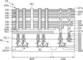
도 1은 예시적인 실시예들에 따른 반도체 장치의 블록도이다.
도 2a, 2b, 3a, 3b, 4a, 4b, 5 내지 도 7은 예시적인 실시예들에 따른 반도체 장치의 제조 방법을 나타내는 개략도들이다.
도 8a 및 도 8b는 예시적인 실시예들에 따른 셀 웨이퍼의 결정 배향에 따른 워피지 특성을 나타내는 그래프들이다.
도 9a 및 도 9b는 예시적인 실시예들에 따른 셀 웨이퍼의 결정 배향에 따른 워피지 특성을 나타내는 그래프들이다.
도 10은 예시적인 실시예들에 따른 셀 웨이퍼의 결정 배향에 따른 워피지 값의 시뮬레이션 결과 그래프이다.
도 11a 및 도 11b는 예시적인 실시예들에 따른 셀 웨이퍼 두께에 따른 워피지 특성을 나타내는 그래프들이다.
도 12a, 12b, 13a, 13b, 14a, 14b, 15 내지 도 20은 예시적인 실시예들에 따른 반도체 장치의 제조 방법을 나타내는 개략도들이다.FIG. 1 is a block diagram of a semiconductor device according to exemplary embodiments.
FIGS. 2a, 2b, 3a, 3b, 4a, 4b, 5 to 7 are schematic diagrams showing a method of manufacturing a semiconductor device according to exemplary embodiments.
FIGS. 8A and 8B are graphs showing warpage characteristics according to crystal orientation of a cell wafer according to exemplary embodiments.
FIGS. 9A and 9B are graphs showing warpage characteristics according to crystal orientation of a cell wafer according to exemplary embodiments.
Figure 10 is a graph showing the simulation results of warpage values according to crystal orientation of cell wafers according to exemplary embodiments.
FIGS. 11A and 11B are graphs showing warpage characteristics according to cell wafer thickness according to exemplary embodiments.
FIGS. 12a, 12b, 13a, 13b, 14a, 14b, 15 to 20 are schematic diagrams showing a method of manufacturing a semiconductor device according to exemplary embodiments.
이하, 첨부된 도면을 참조하여 본 발명의 기술적 사상의 바람직한 실시예를 상세히 설명하기로 한다.Hereinafter, preferred embodiments of the technical idea of the present invention will be described in detail with reference to the attached drawings.
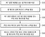
도 1은 예시적인 실시예들에 따른 반도체 장치의 제조 방법을 나타내는 플로우차트이다.FIG. 1 is a flowchart illustrating a method for manufacturing a semiconductor device according to exemplary embodiments.
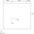
도 2a, 2b, 3a, 3b, 4a, 4b, 5 내지 도 7은 예시적인 실시예들에 따른 반도체 장치의 제조 방법을 나타내는 개략도들이다. 구체적으로, 도 2a, 3a, 4a, 5, 6, 7은 반도체 장치의 제조 방법을 공정 순서에 따라 도시한 개략적 사시도들이고, 도 2b는 도 2a의 평면도이고, 도 3b는 도 3a의 3B 부분의 확대도이고, 도 4b는 도 4a의 평면도이다.FIGS. 2a, 2b, 3a, 3b, 4a, 4b, 5 to 7 are schematic diagrams showing a method for manufacturing a semiconductor device according to exemplary embodiments. Specifically, FIGS. 2a, 3a, 4a, 5, 6, and 7 are schematic perspective views showing a method for manufacturing a semiconductor device in a process sequence, FIG. 2b is a plan view of FIG. 2a, FIG. 3b is an enlarged view of a
도 1, 도 2a 및 도 2b을 참조하면, 셀 웨이퍼(110)가 제공된다(S10 단계).Referring to FIG. 1, FIG. 2a and FIG. 2b, a cell wafer (110) is provided (step S10).
셀 웨이퍼(110)는 반도체 단결정 웨이퍼를 포함할 수 있다. 예를 들어, 셀 웨이퍼(110)는 실리콘 단결정 웨이퍼, 저머늄 단결정 웨이퍼, 실리콘 저머늄 단결정 웨이퍼 중 적어도 하나를 포함할 수 있다. 일부 예시들에서, 셀 웨이퍼(110)는 실리콘 단결정 웨이퍼일 수 있다.The cell wafer (110) may include a semiconductor single crystal wafer. For example, the cell wafer (110) may include at least one of a silicon single crystal wafer, a germanium single crystal wafer, and a silicon germanium single crystal wafer. In some examples, the cell wafer (110) may be a silicon single crystal wafer.
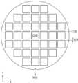
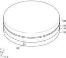
셀 웨이퍼(110)는 제1 상면(110U)과 외주(110P)를 포함할 수 있고, 셀 웨이퍼(110)의 외주에 정의된 제1 노치부(N1)를 포함할 수 있다. 제1 노치부(N1)는 셀 웨이퍼(110)의 외주(110P)에서 셀 웨이퍼(110)의 중심부(110C)를 향하는 방향으로 소정의 깊이로 형성될 수 있다. 제1 노치부(N1)는 셀 웨이퍼(110)의 제조 공정 중 셀 웨이퍼(110)를 얼라인시키기 위하여 제공될 수 있다.The cell wafer (110) may include a first upper surface (110U) and an outer periphery (110P), and may include a first notch portion (N1) defined on the outer periphery of the cell wafer (110). The first notch portion (N1) may be formed at a predetermined depth in a direction from the outer periphery (110P) of the cell wafer (110) toward the center (110C) of the cell wafer (110). The first notch portion (N1) may be provided to align the cell wafer (110) during a manufacturing process of the cell wafer (110).
셀 웨이퍼(110)는 제1 결정 배향을 가질 수 있다. 제1 결정 배향은 제1 결정면 지수(first surface orientation)(SO1)와 제1 노치 방향(first notch direction)(ND1)으로 정의될 수 있다. 제1 결정면 지수(SO1)는 셀 웨이퍼(110)의 제1 상면(110U)에서 제1 상면(110U)에 수직한 방향을 기준으로 정의될 수 있고, 제1 노치 방향(ND1)은 셀 웨이퍼(110)의 중심부(110C)에서 제1 노치부(N1)를 향하는 방향을 기준으로 정의될 수 있다.The cell wafer (110) may have a first crystal orientation. The first crystal orientation may be defined by a first crystal surface index (SO1) and a first notch direction (ND1). The first crystal surface index (SO1) may be defined based on a direction perpendicular to the first upper surface (110U) of the cell wafer (110) from the first upper surface (110U), and the first notch direction (ND1) may be defined based on a direction from the center (110C) of the cell wafer (110) toward the first notch portion (N1).
셀 웨이퍼(110)의 제1 상면(110U)은 제1 수평 방향(X) 및 제2 수평 방향(Y)으로 연장되어 배치될 수 있고, 제1 상면(110U)과 수직한 방향은 수직 방향(D3)과 평행할 수 있다. 제1 노치부(N1)의 제1 노치 방향은 제2 수평 방향(Y)과 평행할 수 있다.The first upper surface (110U) of the cell wafer (110) can be arranged to extend in the first horizontal direction (X) and the second horizontal direction (Y), and the direction perpendicular to the first upper surface (110U) can be parallel to the vertical direction (D3). The first notch direction of the first notch portion (N1) can be parallel to the second horizontal direction (Y).
제1 결정 배향은 제1 결정면 지수(SO1)와 제1 노치 방향(ND1)으로 정의되고, {제1 결정면 지수}<제1 노치 방향>으로 표현될 수 있다. 예시적인 실시예들에서, 셀 웨이퍼(110)의 제1 결정 배향은 {110}<100>, {110}<112>, {111}<110>, {111}<112> 중 어느 하나를 포함할 수 있다.The first crystal orientation is defined by the first crystal plane index (SO1) and the first notch direction (ND1), and may be expressed as {first crystal plane index}<first notch direction>. In exemplary embodiments, the first crystal orientation of the cell wafer (110) may include any one of {110}<100>, {110}<112>, {111}<110>, and {111}<112>.
일부 예시들에서, 셀 웨이퍼(110)의 제1 결정 배향이 {110}<100>일 수 있고, 제1 상면(110U)은 실리콘 단결정의 결정학적 {110} 면에 평행하게 배열되고, 제1 노치 방향(ND1)은 실리콘 단결정의 결정학적 <100> 방향과 평행할 수 있다. 일부 예시들에서, 셀 웨이퍼(110)의 제1 결정 배향이 {110}<112>일 수 있고, 제1 상면(110U)은 실리콘 단결정의 결정학적 {110} 면에 평행하게 배열되고, 제1 노치 방향(ND1)은 실리콘 단결정의 결정학적 <112> 방향과 평행할 수 있다.In some examples, the first crystal orientation of the cell wafer (110) may be {110}<100>, the first upper surface (110U) may be arranged parallel to the crystallographic {110} plane of the silicon single crystal, and the first notch direction (ND1) may be parallel to the crystallographic <100> direction of the silicon single crystal. In some examples, the first crystal orientation of the cell wafer (110) may be {110}<112>, the first upper surface (110U) may be arranged parallel to the crystallographic {110} plane of the silicon single crystal, and the first notch direction (ND1) may be parallel to the crystallographic <112> direction of the silicon single crystal.
일부 예시들에서, 셀 웨이퍼(110)의 제1 결정 배향이 {111}<110>일 수 있고, 제1 상면(110U)은 실리콘 단결정의 결정학적 {111} 면에 평행하게 배열되고, 제1 노치 방향(ND1)은 실리콘 단결정의 결정학적 <110> 방향과 평행할 수 있다. 일부 예시들에서, 셀 웨이퍼(110)의 제1 결정 배향이 {111}<112>일 수 있고, 제1 상면(110U)은 실리콘 단결정의 결정학적 {111} 면에 평행하게 배열되고, 제1 노치 방향(ND1)은 실리콘 단결정의 결정학적 <112> 방향과 평행할 수 있다.In some examples, the first crystal orientation of the cell wafer (110) may be {111}<110>, the first upper surface (110U) may be arranged parallel to the crystallographic {111} plane of the silicon single crystal, and the first notch direction (ND1) may be parallel to the crystallographic <110> direction of the silicon single crystal. In some examples, the first crystal orientation of the cell wafer (110) may be {111}<112>, the first upper surface (110U) may be arranged parallel to the crystallographic {111} plane of the silicon single crystal, and the first notch direction (ND1) may be parallel to the crystallographic <112> direction of the silicon single crystal.
예시적인 실시예들에서, 셀 웨이퍼(110)는 750 마이크로미터 내지 840 마이크로미터의 두께를 가질 수 있다.In exemplary embodiments, the cell wafer (110) may have a thickness of 750 micrometers to 840 micrometers.
예시적인 실시예들에서, 셀 웨이퍼(110)는 복수의 칩 형성 영역(CHR)을 포함할 수 있다. 복수의 칩 형성 영역(CHR)은 스크라이브 레인 영역(SLR)을 사이에 두고 이격되어 배치될 수 있다. 복수의 칩 형성 영역(CHR)은 후속 공정에서 그 상부에 반도체 장치가 형성되는 영역일 수 있고, 스크라이브 레인 영역(SLR)은 복수의 칩 형성 영역(CHR) 상에 형성된 반도체 장치를 복수의 반도체 칩으로 개별화하기 위하여 쏘잉되는 영역일 수 있다.In exemplary embodiments, the cell wafer (110) may include a plurality of chip formation regions (CHR). The plurality of chip formation regions (CHR) may be arranged spaced apart from each other with a scribe lane region (SLR) therebetween. The plurality of chip formation regions (CHR) may be regions on which semiconductor devices are formed in a subsequent process, and the scribe lane region (SLR) may be regions in which semiconductor devices formed on the plurality of chip formation regions (CHR) are sawed to individualize the semiconductor devices into a plurality of semiconductor chips.
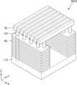
도 1, 도 3a 및 도 3b을 참조하면, 셀 웨이퍼(110) 상에 메모리 스택(120)이 형성된다(S20 단계).Referring to FIG. 1, FIG. 3a and FIG. 3b, a memory stack (120) is formed on a cell wafer (110) (step S20).
예시적인 실시예들에서, 메모리 스택(120)은 3차원으로 배열된 복수의 메모리 셀을 포함하는 메모리 셀 어레이(MCA)를 포함할 수 있다. 예시적인 실시예들에서, 메모리 셀 어레이(MCA)는 플래쉬 메모리 셀을 포함할 수 있고, 3차원 메모리 셀 어레이를 포함할 수 있다. 상기 3 차원 메모리 셀 어레이는 복수의 낸드(NAND) 스트링을 포함할 수 있으며, 각 낸드 스트링은 셀 웨이퍼(110) 상에 수직 방향(Z)으로 배치된 복수의 메모리 셀을 포함할 수 있다.In exemplary embodiments, the memory stack (120) may include a memory cell array (MCA) including a plurality of memory cells arranged in a three-dimensional manner. In exemplary embodiments, the memory cell array (MCA) may include flash memory cells and may include a three-dimensional memory cell array. The three-dimensional memory cell array may include a plurality of NAND strings, and each NAND string may include a plurality of memory cells arranged in a vertical direction (Z) on the cell wafer (110).
다른 예시적인 실시예들에서, 메모리 셀 어레이(MCA)는 셀 웨이퍼(110) 상에 수직 방향(Z)으로 배치된 복수의 가변 저항 메모리 셀을 포함할 수 있다. 다른 예시적인 실시예들에서, 메모리 셀 어레이(MCA)는 셀 웨이퍼(110) 상에 수직 방향(Z)으로 배치된 복수의 상변화 메모리 셀을 포함할 수 있다. 다른 예시적인 실시예들에서, 메모리 셀 어레이(MCA)는 셀 웨이퍼(110) 상에 수직 방향(Z)으로 배치된 복수의 강유전체 메모리 셀을 포함할 수 있다.In other exemplary embodiments, the memory cell array (MCA) may include a plurality of variable resistance memory cells arranged in a vertical direction (Z) on the cell wafer (110). In other exemplary embodiments, the memory cell array (MCA) may include a plurality of phase change memory cells arranged in a vertical direction (Z) on the cell wafer (110). In other exemplary embodiments, the memory cell array (MCA) may include a plurality of ferroelectric memory cells arranged in a vertical direction (Z) on the cell wafer (110).
예시적인 실시예들에서, 메모리 스택(120)은 셀 웨이퍼(110) 상에 배치되며 제1 수평 방향(X)으로 연장되고 수직 방향(Z)으로 이격되어 배치되는 복수의 워드 라인(WL)을 포함할 수 있고, 복수의 워드 라인(WL)을 관통하여 수직 방향(Z)으로 연장되는 복수의 채널(CH)을 포함할 수 있다. 또한 메모리 스택(120)은 복수의 채널(CH) 각각에 연결되고 제2 수평 방향(Y)으로 연장되는 복수의 비트 라인(BL)을 포함할 수 있다.In exemplary embodiments, the memory stack (120) may be disposed on the cell wafer (110) and may include a plurality of word lines (WL) extending in a first horizontal direction (X) and spaced apart in a vertical direction (Z), and may include a plurality of channels (CH) extending in the vertical direction (Z) through the plurality of word lines (WL). In addition, the memory stack (120) may include a plurality of bit lines (BL) connected to each of the plurality of channels (CH) and extending in a second horizontal direction (Y).
예시적인 실시예들에서, 복수의 워드 라인(WL)의 수직 방향(Z)을 따른 개수는 수십 내지 수백 개일 수 있다. 복수의 워드 라인(WL)의 수직 방향(Z)을 따른 개수가 클수록 메모리 셀 어레이(MCA)의 저장 용량이 클 수 있다.In exemplary embodiments, the number of word lines (WL) along the vertical direction (Z) may be tens to hundreds. The larger the number of word lines (WL) along the vertical direction (Z), the larger the storage capacity of the memory cell array (MCA).
복수의 워드 라인(WL)의 수직 방향(Z)을 따른 개수가 증가할수록 메모리 스택(120)의 응력 관점에서의 이방성(anisotropy)이 증가할 수 있다. 일반적으로 복수의 워드 라인(WL)이 제1 수평 방향(X)으로 연장되도록 형성됨에 따라 제1 수평 방향(X)으로의 응력 성분과 제2 수평 방향(Y)으로의 응력 성분의 불균형(imbalance)이 발생하는 경향이 있으나, 예시적인 실시예들에 따르면, 셀 웨이퍼(110)의 제1 결정 배향이 {110}<100>, {110}<112>, {111}<110>, {111}<112> 중 어느 하나이고, 셀 웨이퍼(110) 상에 배치되는 메모리 스택(120)의 응력 이방성이 현저히 감소될 수 있다. 또한 셀 웨이퍼(110)가 제1 결정 배향을 가지며 750 마이크로미터 내지 840 마이크로미터의 두께를 가짐에 따라, 셀 웨이퍼(110) 상에 배치되는 메모리 스택(120)의 응력 이방성이 현저히 감소될 수 있다.As the number of word lines (WL) along the vertical direction (Z) increases, the anisotropy of the memory stack (120) in terms of stress may increase. In general, as the word lines (WL) are formed to extend in the first horizontal direction (X), there is a tendency for an imbalance of a stress component in the first horizontal direction (X) and a stress component in the second horizontal direction (Y). However, according to exemplary embodiments, when the first crystal orientation of the cell wafer (110) is one of {110}<100>, {110}<112>, {111}<110>, and {111}<112>, the stress anisotropy of the memory stack (120) disposed on the cell wafer (110) may be significantly reduced. Additionally, since the cell wafer (110) has a first crystal orientation and a thickness of 750 micrometers to 840 micrometers, the stress anisotropy of the memory stack (120) disposed on the cell wafer (110) can be significantly reduced.
도 1, 도 4a 및 도 4b를 참조하면, 주변 회로 웨이퍼(130)가 제공된다(S30 단계).Referring to FIG. 1, FIG. 4a and FIG. 4b, a peripheral circuit wafer (130) is provided (step S30).
주변 회로 웨이퍼(130)는 반도체 단결정 웨이퍼를 포함할 수 있다. 예를 들어, 주변 회로 웨이퍼(130)는 실리콘 단결정 웨이퍼, 저머늄 단결정 웨이퍼, 실리콘 저머늄 단결정 웨이퍼 중 적어도 하나를 포함할 수 있다. 일부 예시들에서, 주변 회로 웨이퍼(130)는 실리콘 단결정 웨이퍼일 수 있다.The peripheral circuit wafer (130) may include a semiconductor single crystal wafer. For example, the peripheral circuit wafer (130) may include at least one of a silicon single crystal wafer, a germanium single crystal wafer, and a silicon germanium single crystal wafer. In some examples, the peripheral circuit wafer (130) may be a silicon single crystal wafer.
주변 회로 웨이퍼(130)는 제2 상면(130U)과 외주(130P)를 포함할 수 있고, 주변 회로 웨이퍼(130)의 외주에 정의된 제2 노치부(N2)를 포함할 수 있다. 제2 노치부(N2)는 주변 회로 웨이퍼(130)의 외주(130P)에서 주변 회로 웨이퍼(130)의 중심부(130C)를 향하는 방향으로 소정의 깊이로 형성될 수 있다. 제2 노치부(N2)는 주변 회로 웨이퍼(130)의 제조 공정 중 주변 회로 웨이퍼(130)를 얼라인시키기 위하여 제공될 수 있다.The peripheral circuit wafer (130) may include a second upper surface (130U) and an outer periphery (130P), and may include a second notch portion (N2) defined on the outer periphery of the peripheral circuit wafer (130). The second notch portion (N2) may be formed at a predetermined depth in a direction from the outer periphery (130P) of the peripheral circuit wafer (130) toward the center (130C) of the peripheral circuit wafer (130). The second notch portion (N2) may be provided to align the peripheral circuit wafer (130) during a manufacturing process of the peripheral circuit wafer (130).
주변 회로 웨이퍼(130)는 제2 결정 배향을 가질 수 있다. 제2 결정 배향은 제1 결정 배향과 다를 수 있다. 제2 결정 배향은 제2 결정면 지수(SO2)와 제2 노치 방향(ND2)으로 정의될 수 있다. 제2 결정면 지수(SO2)는 주변 회로 웨이퍼(130)의 제2 상면(130U)에서 제2 상면(130U)에 수직한 방향을 기준으로 정의될 수 있고, 제2 노치 방향(ND2)은 주변 회로 웨이퍼(130)의 중심부(130C)에서 제2 노치부(N2)를 향하는 방향을 기준으로 정의될 수 있다.The peripheral circuit wafer (130) may have a second crystal orientation. The second crystal orientation may be different from the first crystal orientation. The second crystal orientation may be defined by a second crystal plane index (SO2) and a second notch direction (ND2). The second crystal plane index (SO2) may be defined based on a direction perpendicular to the second upper surface (130U) of the peripheral circuit wafer (130) from the second upper surface (130U), and the second notch direction (ND2) may be defined based on a direction from the center (130C) of the peripheral circuit wafer (130) toward the second notch portion (N2).
주변 회로 웨이퍼(130)의 제2 상면(130U)은 제1 수평 방향(X) 및 제2 수평 방향(Y)으로 연장되어 배치될 수 있고, 제2 상면(130U)과 수직한 방향은 수직 방향(Z)과 평행할 수 있다. 제2 노치부(N2)의 제2 노치 방향(ND2)은 제2 수평 방향(Y)과 평행할 수 있다.The second upper surface (130U) of the peripheral circuit wafer (130) can be arranged to extend in the first horizontal direction (X) and the second horizontal direction (Y), and the direction perpendicular to the second upper surface (130U) can be parallel to the vertical direction (Z). The second notch direction (ND2) of the second notch portion (N2) can be parallel to the second horizontal direction (Y).
제2 결정 배향은 제2 결정면 지수(SO2)와 제2 노치 방향(ND2)으로 정의되고, {제2 결정면 지수}<제2 노치 방향>으로 표현될 수 있다. 예시적인 실시예들에서, 주변 회로 웨이퍼(130)의 제2 결정 배향은 {100}<100> 또는 {100}<110>를 포함할 수 있다.The second crystal orientation is defined by the second crystal plane index (SO2) and the second notch direction (ND2), and may be expressed as {second crystal plane index}<second notch direction>. In exemplary embodiments, the second crystal orientation of the peripheral circuit wafer (130) may include {100}<100> or {100}<110>.
일부 예시들에서, 주변 회로 웨이퍼(130)의 제2 결정 배향이 {100}<100>일 수 있고, 제2 상면(130U)은 실리콘 단결정의 결정학적 {100} 면에 평행하게 배열되고, 제2 노치 방향(ND2)은 실리콘 단결정의 결정학적 <100> 방향과 평행할 수 있다. 일부 예시들에서, 주변 회로 웨이퍼(130)의 제2 결정 배향이 {100}<110>일 수 있고, 제2 상면(130U)은 실리콘 단결정의 결정학적 {100} 면에 평행하게 배열되고, 제2 노치 방향(ND2)은 실리콘 단결정의 결정학적 <110> 방향과 평행할 수 있다.In some examples, the second crystal orientation of the peripheral circuit wafer (130) may be {100}<100>, the second upper surface (130U) may be arranged parallel to the crystallographic {100} plane of the silicon single crystal, and the second notch direction (ND2) may be parallel to the crystallographic <100> direction of the silicon single crystal. In some examples, the second crystal orientation of the peripheral circuit wafer (130) may be {100}<110>, the second upper surface (130U) may be arranged parallel to the crystallographic {100} plane of the silicon single crystal, and the second notch direction (ND2) may be parallel to the crystallographic <110> direction of the silicon single crystal.
예시적인 실시예들에서, 주변 회로 웨이퍼(130)는 750 마이크로미터 내지 840 마이크로미터의 두께를 가질 수 있다.In exemplary embodiments, the peripheral circuit wafer (130) may have a thickness of 750 micrometers to 840 micrometers.
예시적인 실시예들에서, 주변 회로 웨이퍼(130)는 복수의 칩 형성 영역(CHR)을 포함할 수 있다. 복수의 칩 형성 영역(CHR)은 스크라이브 레인 영역(SLR)을 사이에 두고 이격되어 배치될 수 있다. 복수의 칩 형성 영역(CHR)은 후속 공정에서 그 상부에 반도체 장치가 형성되는 영역일 수 있고, 스크라이브 레인 영역(SLR)은 복수의 칩 형성 영역(CHR) 상에 형성된 반도체 장치를 복수의 반도체 칩으로 개별화하기 위하여 쏘잉되는 영역일 수 있다.In exemplary embodiments, the peripheral circuit wafer (130) may include a plurality of chip formation regions (CHR). The plurality of chip formation regions (CHR) may be arranged spaced apart from each other with a scribe lane region (SLR) therebetween. The plurality of chip formation regions (CHR) may be regions on which semiconductor devices are formed in a subsequent process, and the scribe lane region (SLR) may be regions in which semiconductor devices formed on the plurality of chip formation regions (CHR) are sawed to individualize the semiconductor devices into a plurality of semiconductor chips.
도 1 및 도 5를 참조하면, 주변 회로 웨이퍼(130) 상에 주변 회로 스택(140)이 형성된다(S40 단계).Referring to FIG. 1 and FIG. 5, a peripheral circuit stack (140) is formed on a peripheral circuit wafer (130) (step S40).
예시적인 실시예들에서, 주변 회로 스택(140)은 주변 회로를 포함할 수 있다. 예시적인 실시예들에서, 주변 회로는 로우 디코더, 페이지 버퍼, 데이터 입출력 회로, 및 제어 로직을 포함할 수 있다. 예시적인 실시예들에서, 주변 회로는 입출력 인터페이스, 컬럼 로직, 전압 생성부, 프리-디코더, 온도 센서, 커맨드 디코더, 어드레스 디코더, 증폭 회로 등을 포함할 수 있다.In exemplary embodiments, the peripheral circuit stack (140) may include peripheral circuitry. In exemplary embodiments, the peripheral circuitry may include a row decoder, a page buffer, data input/output circuitry, and control logic. In exemplary embodiments, the peripheral circuitry may include an input/output interface, column logic, a voltage generator, a pre-decoder, a temperature sensor, a command decoder, an address decoder, an amplifier circuit, and the like.
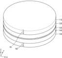
도 1 및 도 6을 참조하면, 메모리 스택(120)과 주변 회로 스택(140)이 접촉하도록 셀 웨이퍼(110)와 주변 회로 웨이퍼(130)가 본딩될 수 있다(S50 단계).Referring to FIG. 1 and FIG. 6, a cell wafer (110) and a peripheral circuit wafer (130) can be bonded so that the memory stack (120) and the peripheral circuit stack (140) come into contact (step S50).
예시적인 실시예들에서, 메모리 스택(120)과 주변 회로 스택(140) 사이에 본딩 구조(150)가 더 개재될 수 있다. 예를 들어, 본딩 구조(150)는 절연층 및/또는 본딩 패드를 포함할 수 있다. 예를 들어, 본딩 구조는 구리를 포함하는 본딩 패드와 산화물을 포함하는 절연층을 포함할 수 있고, 이러한 경우에 본딩 구조(150)는 금속-산화물 하이브리드 본딩(metal-oxide hybrid bonding) 방식으로 메모리 스택(120)과 주변 회로 스택(140)을 서로 본딩시킬 수 있다.In exemplary embodiments, a bonding structure (150) may be further interposed between the memory stack (120) and the peripheral circuit stack (140). For example, the bonding structure (150) may include an insulating layer and/or a bonding pad. For example, the bonding structure may include a bonding pad comprising copper and an insulating layer comprising oxide, in which case the bonding structure (150) may bond the memory stack (120) and the peripheral circuit stack (140) to each other in a metal-oxide hybrid bonding manner.
도 1 및 도 7을 참조하면, 선택적으로 셀 웨이퍼(110)를 제거할 수 있다. 예시적인 실시예들에서, 셀 웨이퍼(110)가 제거되고 메모리 스택(120)의 상면이 노출될 수 있다. 메모리 스택(120)의 상면 상에 채널(CH)(도 3b 참조)과 연결되는 공통 소스 플레이트, 공통 소스 플레이트를 커버하는 패시베이션층, 공통 소스 플레이트에 전기적으로 연결되는 입출력 비아 및/또는 입출력 패드 등을 더 형성할 수 있다.Referring to FIGS. 1 and 7, the cell wafer (110) may be optionally removed. In exemplary embodiments, the cell wafer (110) may be removed and the upper surface of the memory stack (120) may be exposed. A common source plate connected to a channel (CH) (see FIG. 3b), a passivation layer covering the common source plate, input/output vias and/or input/output pads electrically connected to the common source plate, etc. may be further formed on the upper surface of the memory stack (120).
다른 예시적인 실시예들에서, 셀 웨이퍼(110)를 완전히 제거하는 대신, 셀 웨이퍼(110)의 두께가 감소하도록 셀 웨이퍼(110)를 그라인딩할 수도 있다.In other exemplary embodiments, instead of completely removing the cell wafer (110), the cell wafer (110) may be ground to reduce the thickness of the cell wafer (110).
전술한 공정을 수행하여 반도체 장치가 완성될 수 있다.A semiconductor device can be completed by performing the above-described process.
일반적으로 셀 웨이퍼와 주변 회로 웨이퍼는 모두 {100}<100> 결정 배향을 가지며, 셀 웨이퍼 상에 형성되는 복수의 워드 라인의 개수가 증가할수록 응력 이방성이 증가하여 쉘 웨이퍼의 워피지가 발생한다. 셀 웨이퍼의 워피지 증가에 의해 셀 웨이퍼의 절단(breaking) 또는 칩핑(chipping)이 발생할 수 있거나, 메모리 스택의 형성 공정에서 패턴 오정렬과 같은 공정 불량이 발생할 수 있거나, 셀 웨이퍼와 주변 회로 웨이퍼를 본딩하는 공정에서 본딩 불량이 발생할 수 있다.In general, both the cell wafer and the peripheral circuit wafer have a {100}<100> crystal orientation, and as the number of multiple word lines formed on the cell wafer increases, stress anisotropy increases, which causes warpage of the shell wafer. The increase in the warpage of the cell wafer may cause breaking or chipping of the cell wafer, process defects such as pattern misalignment may occur in the formation process of the memory stack, or bonding defects may occur in the process of bonding the cell wafer and the peripheral circuit wafer.
예시적인 실시예들에 따르면, 셀 웨이퍼(110)의 제1 결정 배향이 {110}<100>, {110}<112>, {111}<110>, {111}<112> 중 어느 하나이고, 셀 웨이퍼(110) 상에 배치되는 메모리 스택(120)의 응력 이방성이 현저히 감소될 수 있다. 따라서 셀 웨이퍼의 절단 또는 칩핑 발생이 감소되거나, 메모리 스택의 형성 공정에서 패턴 오정렬과 같은 공정 불량 발생이 감소되거나, 셀 웨이퍼와 주변 회로 웨이퍼를 본딩하는 공정에서 본딩 불량 발생이 감소될 수 있다.According to exemplary embodiments, when the first crystal orientation of the cell wafer (110) is one of {110}<100>, {110}<112>, {111}<110>, and {111}<112>, the stress anisotropy of the memory stack (120) disposed on the cell wafer (110) can be significantly reduced. Accordingly, the occurrence of cutting or chipping of the cell wafer can be reduced, the occurrence of process defects such as pattern misalignment in the formation process of the memory stack can be reduced, or the occurrence of bonding defects in the process of bonding the cell wafer and the peripheral circuit wafer can be reduced.
아래에서는 도 8a 내지 도 11b를 참조로 하여 예시적인 실시예들에 따른 반도체 장치의 워피지 특성을 설명하도록 한다.Below, the warpage characteristics of semiconductor devices according to exemplary embodiments will be described with reference to FIGS. 8a to 11b.
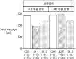
도 8a 및 도 8b는 예시적인 실시예들에 따른 셀 웨이퍼의 결정 배향에 따른 워피지 특성을 나타내는 그래프들이다.FIGS. 8A and 8B are graphs showing warpage characteristics according to crystal orientation of a cell wafer according to exemplary embodiments.
도 8a는 예시적인 실시예들에 따른 셀 웨이퍼 상에 인장 응력 상태의 단일막을 형성한 후 셀 웨이퍼의 제1 수평 방향 및 제2 수평 방향으로의 워피지 값을 측정한 결과를 나타낸다. 여기에서, "인장 응력 상태의 단일막"은 셀 웨이퍼의 에지 상에 배치되는 단일막의 일부분이 셀 웨이퍼의 중앙부 상에 배치되는 단일막의 일부분보다 더 높은 수직 레벨에 배치되도록 셀 웨이퍼와 단일막이 벤딩되는 상태의 단일막을 가리킬 수 있다. 즉, "인장 응력 상태의 단일막"은 셀 웨이퍼의 에지와 단일막의 에지가 상향으로 벤딩되는 상태의 단일막을 가리킬 수 있다.FIG. 8A shows the results of measuring warpage values of a cell wafer in the first horizontal direction and the second horizontal direction after forming a single film in a tensile stress state on a cell wafer according to exemplary embodiments. Here, the "single film in a tensile stress state" may refer to a single film in a state where the cell wafer and the single film are bent so that a portion of the single film disposed on an edge of the cell wafer is disposed at a higher vertical level than a portion of the single film disposed on a central portion of the cell wafer. That is, the "single film in a tensile stress state" may refer to a single film in a state where the edge of the cell wafer and the edge of the single film are bent upward.
도 8a에서, 실시예 11(EX11)은 {110}<100>의 제1 결정 배향을 갖는 셀 웨이퍼 상에 인장 응력 상태의 단일막이 형성된 셀 구조물을 가리킨다. 실시예 12(EX12)는 {111}<110>의 제1 결정 배향을 갖는 셀 웨이퍼 상에 인장 응력 상태의 단일막이 형성된 셀 구조물을 가리킨다. 반면, 비교예 11(CO11)은 {100}<100>의 결정 배향을 갖는 셀 웨이퍼 상에 인장 응력 상태의 단일막이 형성된 셀 구조물을 가리킨다.In FIG. 8a, Example 11 (EX11) refers to a cell structure in which a single film in a tensile stress state is formed on a cell wafer having a first crystal orientation of {110}<100>. Example 12 (EX12) refers to a cell structure in which a single film in a tensile stress state is formed on a cell wafer having a first crystal orientation of {111}<110>. On the other hand, Comparative Example 11 (CO11) refers to a cell structure in which a single film in a tensile stress state is formed on a cell wafer having a crystal orientation of {100}<100>.
도 8a를 참조하면, 실시예 11(EX11)의 제1 수평 방향으로의 워피지는 비교예 11(CO11)의 제1 수평 방향으로의 워피지와 비교하여 31.8% 감소하였고, 실시예 12(EX12)의 제1 수평 방향으로의 워피지는 비교예 11(CO11)의 제1 수평 방향으로의 워피지 값과 비교하여 21.2%만큼 감소하였다.Referring to FIG. 8a, the warpage in the first horizontal direction of Example 11 (EX11) was reduced by 31.8% compared to the warpage in the first horizontal direction of Comparative Example 11 (CO11), and the warpage in the first horizontal direction of Example 12 (EX12) was reduced by 21.2% compared to the warpage value in the first horizontal direction of Comparative Example 11 (CO11).
실시예 12(EX12)의 제2 수평 방향으로의 워피지는 비교예 11(CO11)의 제2 수평 방향으로의 워피지와 비교하여 대략 21.2%만큼 감소한 반면, 실시예 11(EX11 의 제2 수평 방향으로의 워피지는 비교예 11(CO11)의 제2 수평 방향으로의 워피지와 비교하여 대략 유사한 값을 나타냈다.The warpage in the second horizontal direction of Example 12 (EX12) was reduced by approximately 21.2% compared to the warpage in the second horizontal direction of Comparative Example 11 (CO11), whereas the warpage in the second horizontal direction of Example 11 (EX11) showed approximately a similar value compared to the warpage in the second horizontal direction of Comparative Example 11 (CO11).
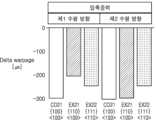
도 8b는 예시적인 실시예들에 따른 셀 웨이퍼 상에 압축 응력 상태의 단일막을 형성한 후 셀 웨이퍼의 제1 수평 방향 및 제2 수평 방향으로의 워피지 값을 측정한 결과를 나타낸다. 여기에서, "압축 응력 상태의 단일막"은 셀 웨이퍼의 에지 상에 배치되는 단일막의 일부분이 셀 웨이퍼의 중앙부 상에 배치되는 단일막의 일부분보다 더 낮은 수직 레벨에 배치되도록 셀 웨이퍼와 단일막이 벤딩되는 상태의 단일막을 가리킬 수 있다. 즉, "압축 응력 상태의 단일막"은 셀 웨이퍼의 에지와 단일막의 에지가 하향으로 벤딩되는 상태의 단일막을 가리킬 수 있다.FIG. 8b shows the results of measuring warpage values of the cell wafer in the first horizontal direction and the second horizontal direction after forming a single film in a compressive stress state on the cell wafer according to exemplary embodiments. Here, the "single film in a compressive stress state" may refer to a single film in a state where the cell wafer and the single film are bent so that a portion of the single film disposed on an edge of the cell wafer is disposed at a lower vertical level than a portion of the single film disposed on the center of the cell wafer. In other words, the "single film in a compressive stress state" may refer to a single film in a state where the edge of the cell wafer and the edge of the single film are bent downward.
도 8b에서, 실시예 21(EX21)은 {110}<100>의 제1 결정 배향을 갖는 셀 웨이퍼 상에 압축 응력 상태의 단일막이 형성된 셀 구조물을 가리킨다. 실시예 22(EX22)는 {111}<110>의 제1 결정 배향을 갖는 셀 웨이퍼 상에 압축 응력 상태의 단일막이 형성된 셀 구조물을 가리킨다. 반면, 비교예 21(CO21)은 {100}<100>의 결정 배향을 갖는 셀 웨이퍼 상에 압축 응력 상태의 단일막이 형성된 셀 구조물을 가리킨다.In FIG. 8b, Example 21 (EX21) refers to a cell structure in which a single film in a compressive stress state is formed on a cell wafer having a first crystal orientation of {110}<100>. Example 22 (EX22) refers to a cell structure in which a single film in a compressive stress state is formed on a cell wafer having a first crystal orientation of {111}<110>. On the other hand, Comparative Example 21 (CO21) refers to a cell structure in which a single film in a compressive stress state is formed on a cell wafer having a crystal orientation of {100}<100>.
도 8b를 참조하면, 실시예 21(EX21)의 제1 수평 방향으로의 워피지는 비교예 21(CO21)의 제1 수평 방향으로의 워피지와 비교하여 31.8% 감소하였고, 실시예 22(EX22)의 제1 수평 방향으로의 워피지는 비교예 21(CO21)의 제1 수평 방향으로의 워피지와 비교하여 21.2%만큼 감소하였다.Referring to FIG. 8b, the warpage in the first horizontal direction of Example 21 (EX21) was reduced by 31.8% compared to the warpage in the first horizontal direction of Comparative Example 21 (CO21), and the warpage in the first horizontal direction of Example 22 (EX22) was reduced by 21.2% compared to the warpage in the first horizontal direction of Comparative Example 21 (CO21).
실시예 22(EX22)의 제2 수평 방향으로의 워피지는 비교예 21(CO21)의 제2 수평 방향으로의 워피지와 비교하여 대략 21.2%만큼 감소한 반면, 실시예 21(EX211 의 제2 수평 방향으로의 워피지는 비교예 21(CO21)의 제2 수평 방향으로의 워피지 값과 비교하여 대략 유사한 값을 나타냈다.The warpage in the second horizontal direction of Example 22 (EX22) was reduced by approximately 21.2% compared to the warpage in the second horizontal direction of Comparative Example 21 (CO21), whereas the warpage in the second horizontal direction of Example 21 (EX211) showed a value that was approximately similar to the warpage value in the second horizontal direction of Comparative Example 21 (CO21).
도 9a 및 도 9b는 예시적인 실시예들에 따른 셀 웨이퍼의 결정 배향에 따른 워피지 특성을 나타내는 그래프들이다.FIGS. 9A and 9B are graphs showing warpage characteristics according to crystal orientation of a cell wafer according to exemplary embodiments.
도 9a는 예시적인 실시예들에 따른 셀 웨이퍼 상에 인장 응력 상태의 메모리 스택을 형성한 후 셀 웨이퍼의 제1 수평 방향 및 제2 수평 방향으로의 워피지 값을 측정한 결과를 나타낸다. 여기에서, "인장 응력 상태의 메모리 스택"은 셀 웨이퍼의 에지 상에 배치되는 메모리 스택의 일부분이 셀 웨이퍼의 중앙부 상에 배치되는 메모리 스택의 일부분보다 더 높은 수직 레벨에 배치되도록 셀 웨이퍼와 메모리 스택이 벤딩되는 상태의 메모리 스택을 가리킬 수 있다. 즉, "인장 응력 상태의 메모리 스택"은 셀 웨이퍼의 에지와 메모리 스택의 에지가 상향으로 벤딩되는 상태의 메모리 스택을 가리킬 수 있다.FIG. 9A illustrates the results of measuring warpage values of a cell wafer in the first horizontal direction and the second horizontal direction after forming a memory stack in a tensile stress state on a cell wafer according to exemplary embodiments. Here, the "memory stack in a tensile stress state" may refer to a memory stack in a state in which the cell wafer and the memory stack are bent so that a portion of the memory stack disposed on an edge of the cell wafer is disposed at a higher vertical level than a portion of the memory stack disposed on a center portion of the cell wafer. In other words, the "memory stack in a tensile stress state" may refer to a memory stack in a state in which the edge of the cell wafer and the edge of the memory stack are bent upward.
도 9a에서, 실시예 31(EX31)은 {110}<100>의 제1 결정 배향을 갖는 셀 웨이퍼 상에 복수의 워드 라인, 복수의 채널 구조물, 복수의 비트 라인을 포함하는 메모리 스택이 형성되되, 상기 메모리 스택이 인장 응력 상태를 갖는 셀 구조물을 가리킨다. 여기에서, 복수의 워드 라인은 제1 수평 방향으로 연장되고 복수의 채널 구조물은 수직 방향으로 연장된다. 실시예 32(EX32)는 {111}<110>의 제1 결정 배향을 갖는 셀 웨이퍼 상에 복수의 워드 라인, 복수의 채널 구조물, 복수의 비트 라인을 포함하는 메모리 스택이 형성되되, 상기 메모리 스택이 인장 응력 상태를 갖는 셀 구조물을 가리킨다. 반면, 비교예 31(CO31)은 {100}<100>의 결정 배향을 갖는 셀 웨이퍼 상에 복수의 워드 라인, 복수의 채널 구조물, 복수의 비트 라인을 포함하는 메모리 스택이 형성되되, 상기 메모리 스택이 인장 응력 상태를 갖는 셀 구조물을 가리킨다.In FIG. 9a, Embodiment 31 (EX31) refers to a cell structure in which a memory stack including a plurality of word lines, a plurality of channel structures, and a plurality of bit lines is formed on a cell wafer having a first crystal orientation of {110}<100>, wherein the memory stack has a tensile stress state. Here, the plurality of word lines extend in a first horizontal direction, and the plurality of channel structures extend in a vertical direction. Embodiment 32 (EX32) refers to a cell structure in which a memory stack including a plurality of word lines, a plurality of channel structures, and a plurality of bit lines is formed on a cell wafer having a first crystal orientation of {111}<110>, wherein the memory stack has a tensile stress state. On the other hand, Comparative Example 31 (CO31) refers to a cell structure in which a memory stack including a plurality of word lines, a plurality of channel structures, and a plurality of bit lines is formed on a cell wafer having a crystal orientation of {100}<100>, wherein the memory stack has a tensile stress state.
도 9a를 참조하면, 실시예 31(EX31) 및 실시예 32(EX32)의 제1 수평 방향으로의 워피지는 도 8a에 도시된 실시예 11(EX11) 및 실시예 12(EX12)의 제1 수평 방향으로의 워피지와 유사한 값을 나타낸다. 예를 들어, 실시예 31(EX31)의 제1 수평 방향으로의 워피지는 비교예 31(CO31)의 제1 수평 방향으로의 워피지와 비교하여 대략 30%만큼 감소하였고, 실시예 32(EX32)의 제1 수평 방향으로의 워피지는 비교예 31(CO31)의 제1 수평 방향으로의 워피지 값과 비교하여 대략 20%만큼 감소하였다.Referring to FIG. 9a, the warpage in the first horizontal direction of Examples 31 (EX31) and 32 (EX32) exhibits similar values to the warpage in the first horizontal direction of Examples 11 (EX11) and 12 (EX12) illustrated in FIG. 8a. For example, the warpage in the first horizontal direction of Example 31 (EX31) was reduced by approximately 30% compared to the warpage in the first horizontal direction of Comparative Example 31 (CO31), and the warpage in the first horizontal direction of Example 32 (EX32) was reduced by approximately 20% compared to the warpage value in the first horizontal direction of Comparative Example 31 (CO31).
실시예 32(EX32)의 제2 수평 방향으로의 워피지는 비교예 31(CO31)의 제2 수평 방향으로의 워피지와 비교하여 대략 20%만큼 감소한 반면, 실시예 11(EX11 의 제2 수평 방향으로의 워피지는 비교예 11(CO11)의 제2 수평 방향으로의 워피지 값과 비교하여 대략 유사한 값을 나타냈다.The warpage in the second horizontal direction of Example 32 (EX32) was reduced by approximately 20% compared to the warpage in the second horizontal direction of Comparative Example 31 (CO31), whereas the warpage in the second horizontal direction of Example 11 (EX11) showed a value that was approximately similar to the warpage value in the second horizontal direction of Comparative Example 11 (CO11).
도 9b는 예시적인 실시예들에 따른 셀 웨이퍼 상에 압축 응력 상태의 메모리 스택을 형성한 후 셀 웨이퍼의 제1 수평 방향 및 제2 수평 방향으로의 워피지 값을 측정한 결과를 나타낸다. 예시적인 실시예들에 따른 셀 웨이퍼 상에 압축 응력 상태의 메모리 스택을 형성한 후 셀 웨이퍼의 제1 수평 방향 및 제2 수평 방향으로의 워피지 값을 측정한 결과를 나타낸다. 여기에서, "압축 응력 상태의 메모리 스택"은 셀 웨이퍼의 에지 상에 배치되는 메모리 스택의 일부분이 셀 웨이퍼의 중앙부 상에 배치되는 메모리 스택의 일부분보다 더 낮은 수직 레벨에 배치되도록 셀 웨이퍼와 메모리 스택이 벤딩되는 상태의 메모리 스택을 가리킬 수 있다. 즉, "압축 응력 상태의 메모리 스택"은 셀 웨이퍼의 에지와 메모리 스택의 에지가 하향으로 벤딩되는 상태의 메모리 스택을 가리킬 수 있다.FIG. 9b shows the results of measuring warpage values of a cell wafer in the first horizontal direction and the second horizontal direction after forming a memory stack in a compressive stress state on a cell wafer according to exemplary embodiments. FIG. 9b shows the results of measuring warpage values of a cell wafer in the first horizontal direction and the second horizontal direction after forming a memory stack in a compressive stress state on a cell wafer according to exemplary embodiments. Here, the "memory stack in a compressive stress state" may refer to a memory stack in a state where the cell wafer and the memory stack are bent so that a portion of the memory stack disposed on an edge of the cell wafer is disposed at a lower vertical level than a portion of the memory stack disposed on a center portion of the cell wafer. That is, the "memory stack in a compressive stress state" may refer to a memory stack in a state where the edge of the cell wafer and the edge of the memory stack are bent downward.
도 9b에서, 실시예 41(EX41)은 {110}<100>의 제1 결정 배향을 갖는 셀 웨이퍼 상에 복수의 워드 라인, 복수의 채널 구조물, 복수의 비트 라인을 포함하는 메모리 스택이 형성되되, 상기 메모리 스택이 압축 응력 상태를 갖는 셀 구조물을 가리킨다. 여기에서, 복수의 워드 라인은 제1 수평 방향으로 연장되고 복수의 채널 구조물은 수직 방향으로 연장된다. 실시예 42(EX42)는 {111}<110>의 제1 결정 배향을 갖는 셀 웨이퍼 상에 복수의 워드 라인, 복수의 채널 구조물, 복수의 비트 라인을 포함하는 메모리 스택이 형성되되, 상기 메모리 스택이 압축 응력 상태를 갖는 셀 구조물을 가리킨다. 반면, 비교예 41(CO41)은 {100}<100>의 결정 배향을 갖는 셀 웨이퍼 상에 복수의 워드 라인, 복수의 채널 구조물, 복수의 비트 라인을 포함하는 메모리 스택이 형성되되, 상기 메모리 스택이 압축 응력 상태를 갖는 셀 구조물을 가리킨다.In FIG. 9b, Embodiment 41 (EX41) refers to a cell structure in which a memory stack including a plurality of word lines, a plurality of channel structures, and a plurality of bit lines is formed on a cell wafer having a first crystal orientation of {110}<100>, wherein the memory stack has a compressive stress state. Here, the plurality of word lines extend in a first horizontal direction, and the plurality of channel structures extend in a vertical direction. Embodiment 42 (EX42) refers to a cell structure in which a memory stack including a plurality of word lines, a plurality of channel structures, and a plurality of bit lines is formed on a cell wafer having a first crystal orientation of {111}<110>, wherein the memory stack has a compressive stress state. On the other hand, Comparative Example 41 (CO41) refers to a cell structure in which a memory stack including a plurality of word lines, a plurality of channel structures, and a plurality of bit lines is formed on a cell wafer having a crystal orientation of {100}<100>, wherein the memory stack has a compressive stress state.
도 9b를 참조하면, 실시예 41(EX41)의 제1 수평 방향으로의 워피지는 비교예 41(CO41)의 제1 수평 방향으로의 워피지 값과 비교하여 대략 30%만큼 감소하였고, 실시예 42(EX42)의 제1 수평 방향으로의 워피지는 비교예 41(CO41)의 제1 수평 방향으로의 워피지 값과 비교하여 대략 20만큼 감소하였다.Referring to FIG. 9b, the warpage in the first horizontal direction of Example 41 (EX41) was reduced by approximately 30% compared to the warpage value in the first horizontal direction of Comparative Example 41 (CO41), and the warpage in the first horizontal direction of Example 42 (EX42) was reduced by approximately 20% compared to the warpage value in the first horizontal direction of Comparative Example 41 (CO41).
실시예 42(EX42)의 제2 수평 방향으로의 워피지는 비교예 41(CO41)의 제2 수평 방향으로의 워피지와 비교하여 대략 20%만큼 감소한 반면, 실시예 41(EX41)의 제2 수평 방향으로의 워피지는 비교예 41(CO41)의 제2 수평 방향으로의 워피지 값과 비교하여 다소 증가된 값을 나타냈다.The warpage in the second horizontal direction of Example 42 (EX42) was reduced by approximately 20% compared to the warpage in the second horizontal direction of Comparative Example 41 (CO41), whereas the warpage in the second horizontal direction of Example 41 (EX41) showed a slightly increased value compared to the warpage value in the second horizontal direction of Comparative Example 41 (CO41).
도 8a, 8b, 9a, 9b에 도시된 그래프들에서 얻어진 워피지 측정 값들을 기초로 할 때, 본원 발명의 예시적인 실시예들에 따른 셀 웨이퍼, 즉 {110}<100>의 결정 배향을 갖는 실시예 11, 21, 31, 41(EX11, EX21, EX31, EX41)과 {111}<110>의 결정 배향을 갖는 실시예 12, 22, 32, 42(EX12, EX22, EX32, EX42)는 모두 비교예 11, 21, 31, 41(CO11, CO21, CO31, CO41)보다 현저히 더 감소된 워피지 값을 가짐을 알 수 있다.Based on the warpage measurement values obtained from the graphs illustrated in FIGS. 8a, 8b, 9a, and 9b, it can be seen that the cell wafers according to exemplary embodiments of the present invention, that is, Examples 11, 21, 31, and 41 (EX11, EX21, EX31, EX41) having a crystal orientation of {110}<100> and Examples 12, 22, 32, and 42 (EX12, EX22, EX32, EX42) having a crystal orientation of {111}<110>, all have warpage values that are significantly reduced compared to Comparative Examples 11, 21, 31, and 41 (CO11, CO21, CO31, CO41).
도 10은 예시적인 실시예들에 따른 셀 웨이퍼의 결정 배향에 따른 워피지 값의 시뮬레이션 결과 그래프이다.Figure 10 is a graph showing the simulation results of warpage values according to crystal orientation of cell wafers according to exemplary embodiments.
도 10에서 예시적인 실시예들에 따른 셀 웨이퍼의 결정 배향에 따른 x, y, 및 z 방향 모듈러스와 x, y, 및 z 방향 포아송비(Poisson's ratio)를 사용하여 스토니 수식(Stoney equation)을 통해 이론적인 워피지 값을 계산하였다. 본 발명의 예시적인 실시예들에 포함되는 실시예 51(EX51), 실시예 52(EX52), 실시예 53(EX53), 실시예 54(EX54)는 각각 {110}<100>, {110}<112>, {111}<110>, {111}<112>의 결정 배향을 갖는 단결정 실리콘 웨이퍼를 나타낸다.In Fig. 10, the theoretical warpage value was calculated through the Stoney equation using the x-, y-, and z-direction moduli and the x-, y-, and z-direction Poisson's ratio according to the crystal orientation of the cell wafer according to exemplary embodiments. Example 51 (EX51), Example 52 (EX52), Example 53 (EX53), and Example 54 (EX54) included in the exemplary embodiments of the present invention represent single crystal silicon wafers having crystal orientations of {110}<100>, {110}<112>, {111}<110>, and {111}<112>, respectively.
도 10을 참조하면, 실시예 51(EX51), 실시예 52(EX52), 실시예 53(EX53), 실시예 54(EX54)는 비교예 51(CO51) 및 비교예 52(CO52)와 비교하여 20%만큼 감소하거나 20%보다 더 많이 감소한 워피지를 나타낸다. 도 10에 도시된 기준선(RL)은 비교예 51(CO51)의 워피지 값보다 20%만큼 감소한 워피지 값, 즉 비교예 51(CO51)의 워피지 값의 80%에 해당하는 워피지 값을 갖는 지점을 나타낸다. 본 발명의 예시적인 실시예들에 포함되는 실시예 51(EX51), 실시예 52(EX52), 실시예 53(EX53), 실시예 54(EX54)는 모두 기준선(RL)보다 낮은 워피지 값을 나타내었으며, 이들 모두 비교예 51(CO51) 및 비교예 52(CO52)보다 현저히 감소된 워피지 값을 가짐을 확인할 수 있다.Referring to FIG. 10, Examples 51 (EX51), 52 (EX52), 53 (EX53), and 54 (EX54) show warpage that is reduced by 20% or more than 20% compared to Comparative Example 51 (CO51) and Comparative Example 52 (CO52). The reference line (RL) illustrated in FIG. 10 indicates a point having a warpage value that is reduced by 20% compared to the warpage value of Comparative Example 51 (CO51), that is, a warpage value that corresponds to 80% of the warpage value of Comparative Example 51 (CO51). It can be confirmed that Example 51 (EX51), Example 52 (EX52), Example 53 (EX53), and Example 54 (EX54), which are included in the exemplary embodiments of the present invention, all exhibited warpage values lower than the baseline (RL), and that all of them had warpage values that were significantly reduced compared to Comparative Example 51 (CO51) and Comparative Example 52 (CO52).
도 11a 및 도 11b는 예시적인 실시예들에 따른 셀 웨이퍼 두께에 따른 워피지 특성을 나타내는 그래프들이다.FIGS. 11A and 11B are graphs showing warpage characteristics according to cell wafer thickness according to exemplary embodiments.
도 11a에서 다양한 결정 배향을 갖는 셀 웨이퍼의 제1 수평 방향으로의 워피지 값이 비교예 611(CO611)의 워피지 값을 기준으로 정규화되어 도시되고, 도 11b에서 다양한 결정 배향을 갖는 셀 웨이퍼의 제2 수평 방향으로의 워피지 값이 비교예 611(CO611)의 워피지 값을 기준으로 정규화되어 도시된다.In FIG. 11a, the warpage values in the first horizontal direction of cell wafers having various crystal orientations are normalized based on the warpage value of Comparative Example 611 (CO611) and are shown, and in FIG. 11b, the warpage values in the second horizontal direction of cell wafers having various crystal orientations are normalized based on the warpage value of Comparative Example 611 (CO611).
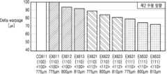
실시예 611 내지 실시예 633(EX611~EX633)과 비교예 611(CO611)의 결정 배향 및 셀 웨이퍼는 아래 표 1에 도시된다.The crystal orientations and cell wafers of Examples 611 to 633 (EX611 to EX633) and Comparative Example 611 (CO611) are shown in Table 1 below.
도 11a 및 도 11b를 참조하면, 실시예 611(EX611), 실시예 612(EX612), 및 실시예 613(EX613)은 모두 동일한 {110}<100>을 갖되 셀 웨이퍼의 두께가 775 ㎛, 800 ㎛, 및 810 ㎛로 서로 다르다. 실시예 611(EX611), 실시예 612(EX612), 및 실시예 613(EX613)은 모두 비교예 611(CO611)보다 현저히 감소된 워피지 값(예를 들어 비교예 611(CO611)의 워피지의 60% 내지 70%의 범위에 해당하는 워피지 값)을 나타낸다. 또한 동일한 결정 배향을 갖는 셀 웨이퍼들 중에서 셀 웨이퍼의 두께가 증가할수록 더욱 감소된 워피지 값을 가짐을 알 수 있다.Referring to FIGS. 11A and 11B, Example 611 (EX611), Example 612 (EX612), and Example 613 (EX613) all have the same {110}<100>, but the thicknesses of the cell wafers are different, such as 775 μm, 800 μm, and 810 μm. Example 611 (EX611), Example 612 (EX612), and Example 613 (EX613) all exhibit significantly reduced warpage values (for example, warpage values in the range of 60% to 70% of the warpage of Comparative Example 611 (CO611)) compared to Comparative Example 611 (CO611). In addition, it can be seen that among cell wafers having the same crystal orientation, the warpage value is further reduced as the thickness of the cell wafer increases.
도 8a 내지 도 11b를 참조로 설명된 것과 같이, 예시적인 실시예들에 따른 셀 웨이퍼는 775 내지 810 ㎛의 두께를 가질 수 있고, {110}<100>, {110}<112>, {111}<110>, {111}<112>의 결정 배향을 가질 수 있다. 이에 따라 예시적인 실시예들에 따른 셀 웨이퍼는 비교예에 따른 {100}<100> 또는 {100}<110>의 결정 배향을 갖는 셀 웨이퍼보다 현저히 감소된 워피지 값을 가질 수 있음을 확인할 수 있다.As described with reference to FIGS. 8A to 11B, the cell wafer according to the exemplary embodiments may have a thickness of 775 to 810 μm and may have a crystal orientation of {110}<100>, {110}<112>, {111}<110>, {111}<112>. Accordingly, it can be confirmed that the cell wafer according to the exemplary embodiments may have a significantly reduced warpage value than the cell wafer having a crystal orientation of {100}<100> or {100}<110> according to the comparative example.
도 12a, 12b, 13a, 13b, 14a, 14b, 15 내지 도 20은 예시적인 실시예들에 따른 반도체 장치(100)의 제조 방법을 나타내는 개략도들이다.FIGS. 12a, 12b, 13a, 13b, 14a, 14b, 15 to 20 are schematic diagrams showing a method of manufacturing a semiconductor device (100) according to exemplary embodiments.
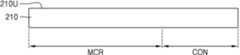
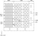
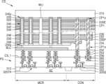
도 12a 및 도 12b를 참조하면, 셀 웨이퍼(210)가 제공될 수 있다. 셀 웨이퍼(210)는 셀 영역(MCR), 연결 영역(CON), 및 주변 회로 연결 영역(PR)을 포함할 수 있다. 셀 영역(MCR)은 수직 방향(Z)으로 연장되는 복수의 메모리 셀 스트링을 포함하는 메모리 셀 블록이 배치되는 영역일 수 있고, 연결 영역(CON)은 메모리 셀 스트링 각각의 워드 라인에 대한 전기적 연결부가 배치되는 영역일 수 있고, 주변 회로 연결 영역(PR)은 메모리 셀 블록을 주변 회로와 연결하기 위한 전기적 연결 성분이 배치되는 영역일 수 있다.Referring to FIGS. 12A and 12B, a cell wafer (210) may be provided. The cell wafer (210) may include a cell region (MCR), a connection region (CON), and a peripheral circuit connection region (PR). The cell region (MCR) may be a region in which a memory cell block including a plurality of memory cell strings extending in a vertical direction (Z) is arranged, the connection region (CON) may be a region in which an electrical connection portion for a word line of each memory cell string is arranged, and the peripheral circuit connection region (PR) may be a region in which an electrical connection component for connecting a memory cell block with a peripheral circuit is arranged.
예시적인 실시예들에서, 셀 웨이퍼(210)는 실리콘(Si), 게르마늄(Ge), 실리콘 게르마늄(SiGe) 중 적어도 하나를 포함할 수 있다. 셀 웨이퍼(210)는 도 2a 및 도 2b를 참조로 설명한 셀 웨이퍼(110)일 수 있다.In exemplary embodiments, the cell wafer (210) may include at least one of silicon (Si), germanium (Ge), and silicon germanium (SiGe). The cell wafer (210) may be the cell wafer (110) described with reference to FIGS. 2A and 2B.
셀 웨이퍼(210)는 제1 결정 배향을 가질 수 있고, 제1 결정 배향은 제1 결정면 지수와 제1 노치 방향으로 정의될 수 있다. 제1 결정 배향은 {제1 결정면 지수}<제1 노치 방향>으로 표현될 수 있다. 예시적인 실시예들에서, 셀 웨이퍼(210)의 제1 결정 배향은 {110}<100>, {110}<112>, {111}<110>, {111}<112> 중 어느 하나를 포함할 수 있다. 또한 셀 웨이퍼(210)는 750 마이크로미터 내지 840 마이크로미터의 두께를 가질 수 있다.The cell wafer (210) may have a first crystal orientation, and the first crystal orientation may be defined by a first crystal plane index and a first notch direction. The first crystal orientation may be expressed as {first crystal plane index}<first notch direction>. In exemplary embodiments, the first crystal orientation of the cell wafer (210) may include any one of {110}<100>, {110}<112>, {111}<110>, and {111}<112>. In addition, the cell wafer (210) may have a thickness of 750 micrometers to 840 micrometers.
도 13a 및 도 13b을 참조하면, 셀 웨이퍼(210)의 상면(210U) 상에 버퍼 절연층(220)을 형성하고, 버퍼 절연층(220) 상에 식각 정지층(222)을 형성할 수 있다.Referring to FIGS. 13a and 13b, a buffer insulating layer (220) can be formed on the upper surface (210U) of the cell wafer (210), and an etching stop layer (222) can be formed on the buffer insulating layer (220).
버퍼 절연층(220)은 실리콘 산화물을 사용하여 형성될 수 있다. 예시적인 실시예들에서, 식각 정지층(222)은 폴리실리콘을 사용하여 형성될 수 있다.The buffer insulating layer (220) may be formed using silicon oxide. In exemplary embodiments, the etch stop layer (222) may be formed using polysilicon.
이후, 셀 영역(MCR) 및 연결 영역(CON)에서 식각 정지층(222) 상에 희생층(231) 및 몰드 절연층들(232)을 교대로 포함하는 몰드 스택(MS)을 형성할 수 있다. 희생층(231)과 몰드 절연층들(232)은 서로 식각 선택비를 갖는 물질을 사용하여 형성할 수 있다.Thereafter, a mold stack (MS) including a sacrificial layer (231) and mold insulating layers (232) alternately on an etch stop layer (222) in the cell region (MCR) and the connection region (CON) can be formed. The sacrificial layer (231) and the mold insulating layers (232) can be formed using materials having an etch selectivity with respect to each other.
이후 연결 영역(CON)에서 몰드 스택(MS)의 일부분들을 패터닝하여 예비 패드부(SPAD)을 형성할 수 있다. 예비 패드부(SPAD)는 계단 형상을 가질 수 있고, 희생층(231)보다 더 큰 두께를 가지도록 형성될 수 있다.Thereafter, portions of the mold stack (MS) can be patterned in the connection area (CON) to form a spare pad portion (SPAD). The spare pad portion (SPAD) can have a step shape and can be formed to have a greater thickness than the sacrificial layer (231).
도 14a 및 도 14b를 참조하면, 셀 영역(MCR)에서 몰드 스택(MS)을 관통하여 수직 방향(Z)으로 연장되는 채널 구조물(240)을 형성할 수 있다. 채널 구조물(240)은 몰드 스택(MS)을 관통하여 수직 방향(Z)으로 연장되는 채널홀 내부에 배치될 수 있고, 게이트 절연층(242), 채널층(244), 절연 라이너(246), 및 드레인 영역(248)을 포함할 수 있다. 채널 구조물(240)의 제1 단부(240x)는 제2 단부(240y)보다 높은 수직 레벨에 배치되고, 제2 단부(240y)는 식각 정지층(222)을 관통하여 셀 웨이퍼(210) 내부로 연장되도록 형성될 수 있다.Referring to FIGS. 14a and 14b, a channel structure (240) extending in the vertical direction (Z) through the mold stack (MS) in the cell region (MCR) can be formed. The channel structure (240) can be arranged inside a channel hole extending in the vertical direction (Z) through the mold stack (MS) and can include a gate insulating layer (242), a channel layer (244), an insulating liner (246), and a drain region (248). A first end (240x) of the channel structure (240) is arranged at a higher vertical level than a second end (240y), and the second end (240y) can be formed to extend into the cell wafer (210) through the etch stop layer (222).
이후 몰드 스택(MS)을 관통하여 제1 수평 방향(X)으로 연장되는 스택 분리 개구부(WLH)를 형성하고, 스택 분리 개구부(WLH) 내벽 상에 노출되는 희생층(231) 및 예비 패드부(SPAD)를 제거할 수 있다. 이후 희생층(231) 및 예비 패드부(SPAD)가 제거된 공간에 게이트 전극(230) 및 패드부(230P)를 형성할 수 있다. 한편 연결 영역(CON)에 배치되는 게이트 전극(230)의 일부분은 연장부(230E)로 지칭할 수 있다. 이후 스택 분리 개구부(WLH) 내에 스택 분리 절연층(WLI)을 형성할 수 있다.Thereafter, a stack separation opening (WLH) extending in a first horizontal direction (X) through the mold stack (MS) may be formed, and the sacrificial layer (231) and the spare pad portion (SPAD) exposed on the inner wall of the stack separation opening (WLH) may be removed. Thereafter, a gate electrode (230) and a pad portion (230P) may be formed in the space from which the sacrificial layer (231) and the spare pad portion (SPAD) have been removed. Meanwhile, a part of the gate electrode (230) disposed in the connection region (CON) may be referred to as an extension portion (230E). Thereafter, a stack separation insulating layer (WLI) may be formed within the stack separation opening (WLH).
이후 게이트 전극(230) 및 패드부(230P)를 커버하는 스택 절연층(234)을 형성하고, 스택 절연층(234) 상에 채널 구조물(240)에 연결되는 비트 라인(BL)을 형성할 수 있다.Thereafter, a stack insulating layer (234) covering the gate electrode (230) and the pad portion (230P) can be formed, and a bit line (BL) connected to the channel structure (240) can be formed on the stack insulating layer (234).
또한 연결 영역(CON)에서 연장부들(230E) 및 패드부(230P)을 관통하는 제1 플러그(CP1)를 형성하고, 주변 회로 연결 영역(PRC)에서 스택 절연층(234)을 관통하는 제2 플러그(CP2)를 형성할 수 있다. 제1 플러그(CP1)의 제1 단부(CP1x)는 제2 단부(CP1y)보다 더 큰 폭으로 형성될 수 있고 제1 플러그(CP1)의 제2 단부(CP1y)는 식각 정지층(222)을 관통하여 셀 웨이퍼(210) 내부로 연장되도록 큰 높이로 형성될 수 있다.In addition, a first plug (CP1) penetrating the extensions (230E) and the pad portion (230P) in the connection area (CON) can be formed, and a second plug (CP2) penetrating the stack insulation layer (234) in the peripheral circuit connection area (PRC) can be formed. The first end (CP1x) of the first plug (CP1) can be formed to have a larger width than the second end (CP1y), and the second end (CP1y) of the first plug (CP1) can be formed to have a large height so as to extend into the cell wafer (210) by penetrating the etch stop layer (222).
예시적인 실시예들에서, 연결 영역(CON)에서 상기 몰드 스택을 관통하는 제1 플러그 홀을 형성하고, 상기 제1 플러그 홀 측벽에 노출되는 상기 희생층의 일부분을 측방향 식각에 의해 제거하고 상기 희생층이 제거된 부분에 절연 패턴(236)을 형성할 수 있다. 이후 제1 플러그 홀 내에 제1 플러그(CP1)를 형성할 수 있다.In exemplary embodiments, a first plug hole penetrating the mold stack in the connection area (CON) may be formed, a portion of the sacrificial layer exposed to a sidewall of the first plug hole may be removed by lateral etching, and an insulating pattern (236) may be formed in the portion from which the sacrificial layer is removed. Thereafter, a first plug (CP1) may be formed within the first plug hole.
도 15를 참조하면, 비트 라인(BL) 및 제1 플러그(CP1)에 전기적으로 연결되는 연결 비아(252) 및 연결 배선층(254), 및 층간 절연막(256)을 형성할 수 있다. 층간 절연막(256)의 상면에 접속 패드(260_U)가 형성될 수 있다.Referring to FIG. 15, a connection via (252) and a connection wiring layer (254) electrically connected to a bit line (BL) and a first plug (CP1), and an interlayer insulating film (256) can be formed. A connection pad (260_U) can be formed on an upper surface of the interlayer insulating film (256).
도 16을 참조하면, 주변 회로 구조물(PS)이 준비될 수 있다. 주변 회로 구조물(PS)은 주변 회로 웨이퍼(310) 상에 배치된 주변 회로 트랜지스터(320TR), 복수의 주변 회로 콘택(332)과 복수의 주변 회로 배선층(334), 층간 절연막(330)을 을 포함할 수 있다.Referring to FIG. 16, a peripheral circuit structure (PS) may be prepared. The peripheral circuit structure (PS) may include a peripheral circuit transistor (320TR) arranged on a peripheral circuit wafer (310), a plurality of peripheral circuit contacts (332), a plurality of peripheral circuit wiring layers (334), and an interlayer insulating film (330).
주변 회로 웨이퍼(310)는 실리콘(Si), 게르마늄(Ge), 실리콘 게르마늄(SiGe) 중 적어도 하나를 포함할 수 있다. 주변 회로 웨이퍼(310)는 도 4a 및 도 4b를 참조로 설명한 주변 회로 웨이퍼(130)일 수 있다.The peripheral circuit wafer (310) may include at least one of silicon (Si), germanium (Ge), and silicon germanium (SiGe). The peripheral circuit wafer (310) may be the peripheral circuit wafer (130) described with reference to FIGS. 4A and 4B.
주변 회로 웨이퍼(310)는 제2 결정 배향을 가질 수 있고, 제2 결정 배향은 제2 결정면 지수와 제2 노치 방향으로 정의될 수 있다. 제2 결정 배향은 {제2 결정면 지수}<제2 노치 방향>으로 표현될 수 있다. 예시적인 실시예들에서, 주변 회로 웨이퍼(310)의 제2 결정 배향은 {100}<100> 또는 {100}<110>를 포함할 수 있다.The peripheral circuit wafer (310) may have a second crystal orientation, and the second crystal orientation may be defined by a second crystal plane index and a second notch direction. The second crystal orientation may be expressed as {second crystal plane index}<second notch direction>. In exemplary embodiments, the second crystal orientation of the peripheral circuit wafer (310) may include {100}<100> or {100}<110>.
주변 회로 웨이퍼(310)에는 소자 분리막(312)에 의해 활성 영역(AC)이 정의될 수 있고, 활성 영역(AC) 상에 복수의 주변 회로 트랜지스터(320TR)가 형성될 수 있다. 복수의 주변 회로 트랜지스터(320TR)는 주변 회로 게이트(320G)와, 주변 회로 게이트(320G)의 양 측의 주변 회로 웨이퍼(310) 일부분에 배치되는 소스/드레인 영역(322)을 포함할 수 있다.An active area (AC) may be defined by a device isolation film (312) in a peripheral circuit wafer (310), and a plurality of peripheral circuit transistors (320TR) may be formed on the active area (AC). The plurality of peripheral circuit transistors (320TR) may include a peripheral circuit gate (320G) and source/drain areas (322) arranged in a portion of the peripheral circuit wafer (310) on both sides of the peripheral circuit gate (320G).
복수의 주변 회로 콘택(332)과 복수의 주변 회로 배선층(334)은 주변 회로 웨이퍼(310) 상에서 주변 회로 트랜지스터(320TR)에 전기적으로 연결될 수 있고, 주변 회로 웨이퍼(310) 상에서 주변 회로 트랜지스터(320TR), 복수의 주변 회로 콘택(332)과 복수의 주변 회로 배선층(334)을 커버하는 층간 절연막(330)이 배치될 수 있다. 복수의 주변 회로 배선층(334)은 서로 다른 수직 레벨에 배치되는 복수의 금속층들을 포함하는 다층 구조를 가질 수 있다. 주변 회로 구조물(PS)의 최상면에는 접속 패드(260_L)가 배치될 수 있다.A plurality of peripheral circuit contacts (332) and a plurality of peripheral circuit wiring layers (334) may be electrically connected to a peripheral circuit transistor (320TR) on a peripheral circuit wafer (310), and an interlayer insulating film (330) covering the peripheral circuit transistor (320TR), the plurality of peripheral circuit contacts (332), and the plurality of peripheral circuit wiring layers (334) may be disposed on the peripheral circuit wafer (310). The plurality of peripheral circuit wiring layers (334) may have a multilayer structure including a plurality of metal layers disposed at different vertical levels. A connection pad (260_L) may be disposed on a top surface of the peripheral circuit structure (PS).
도 17을 참조하면, 주변 회로 구조물(PS)을 셀 구조물(CS)에 부착할 수 있다. 주변 회로 구조물(PS)과 셀 구조물(CS)은 접속 패드(260) 및 층간 절연막(330, 254)을 통해 금속-산화물 하이브리드 본딩 방식으로 부착될 수 있으나, 이에 한정되는 것은 아니다.Referring to FIG. 17, a peripheral circuit structure (PS) can be attached to a cell structure (CS). The peripheral circuit structure (PS) and the cell structure (CS) can be attached by a metal-oxide hybrid bonding method through a connection pad (260) and an interlayer insulating film (330, 254), but are not limited thereto.
예시적인 실시예들에 따르면, 셀 웨이퍼(210)의 제1 결정 배향이 {110}<100>, {110}<112>, {111}<110>, {111}<112> 중 어느 하나이고, 셀 웨이퍼(210) 상에 배치되는 셀 구조물(CS)의 응력 이방성(예를 들어 게이트 전극(230)의 수직 방향 개수가 증가함에 따라 발생하는 응력의 이방성)에 의한 셀 웨이퍼(210)의 워피지 발생이 현저히 감소될 수 있다. 따라서 셀 웨이퍼(210)와 주변 회로 웨이퍼(310)를 본딩하는 공정에서 본딩 불량 발생이 감소될 수 있다.According to exemplary embodiments, when the first crystal orientation of the cell wafer (210) is one of {110}<100>, {110}<112>, {111}<110>, and {111}<112>, the occurrence of warpage of the cell wafer (210) due to stress anisotropy of the cell structure (CS) disposed on the cell wafer (210) (for example, stress anisotropy generated as the number of gate electrodes (230) in the vertical direction increases) can be significantly reduced. Accordingly, the occurrence of bonding defects can be reduced in the process of bonding the cell wafer (210) and the peripheral circuit wafer (310).
이후 셀 웨이퍼(210)가 위를 향하도록 주변 회로 구조물(PS)과 셀 구조물(CS)이 부착된 구조를 뒤집을 수 있다.Afterwards, the structure in which the peripheral circuit structure (PS) and the cell structure (CS) are attached can be flipped over so that the cell wafer (210) faces upward.
도 18을 참조하면, 셀 웨이퍼(210)(도 18 참조)가 제거될 수 있다. 셀 웨이퍼(210)는 그라인딩 공정 및 뒤따르는 식각 공정에 의해 제거될 수 있고, 버퍼 절연층(220)(도 18 참조)이 노출될 수 있다.Referring to FIG. 18, the cell wafer (210) (see FIG. 18) can be removed. The cell wafer (210) can be removed by a grinding process and a subsequent etching process, and the buffer insulating layer (220) (see FIG. 18) can be exposed.
이후 버퍼 절연층(220) 또한 제거되고 식각 정지층(222)의 상면이 노출될 수 있다. 버퍼 절연층(220)이 제거됨에 따라 식각 정지층(222)의 상면 상으로 채널 구조물(240)의 제2 단부(240y) 및 제1 플러그(CP1)의 제2 단부(CP1y)가 돌출할 수 있다.Thereafter, the buffer insulating layer (220) may also be removed, and the upper surface of the etching stop layer (222) may be exposed. As the buffer insulating layer (220) is removed, the second end (240y) of the channel structure (240) and the second end (CP1y) of the first plug (CP1) may protrude onto the upper surface of the etching stop layer (222).
셀 웨이퍼(210)과 버퍼 절연층(220)이 제거됨에 따라 스택 분리 절연층(WLI)의 상측 또한 노출되어 식각 정지층(222) 위로 돌출할 수 있다.As the cell wafer (210) and the buffer insulating layer (220) are removed, the upper side of the stack isolation insulating layer (WLI) is also exposed and can protrude above the etch stop layer (222).
이후, 채널 구조물(240)의 제2 단부(240y)에 노출된 게이트 절연층(242) 부분을 제거하여 채널층(244)의 상면을 노출할 수 있다. 게이트 절연층(242) 제거 공정에서 식각 정지층(222)의 상면이 노출될 때까지 게이트 절연층(242)의 제거 공정이 수행될 수 있다. 일부 실시예들에서, 게이트 절연층(242)이 채널층(244)의 상면보다 낮은 레벨에 배치되고 채널층(244)의 상면 및 측벽 일부분이 노출되도록 게이트 절연층(242)의 상측이 제거될 수 있다.Thereafter, a portion of the gate insulating layer (242) exposed to the second end (240y) of the channel structure (240) may be removed to expose the upper surface of the channel layer (244). In the gate insulating layer (242) removal process, the gate insulating layer (242) removal process may be performed until the upper surface of the etch stop layer (222) is exposed. In some embodiments, the gate insulating layer (242) may be disposed at a level lower than the upper surface of the channel layer (244) and the upper side of the gate insulating layer (242) may be removed so that the upper surface and a portion of the sidewall of the channel layer (244) are exposed.
도 19를 참조하면, 셀 영역(MCR), 연결 영역(CON), 주변 회로 연결 영역(PRC) 상에 공통 소스 층(270)을 형성할 수 있다. 공통 소스 층(270)은 폴리실리콘을 사용하여 형성될 수 있다. 예를 들어, 공통 소스 층(270)은 n형 불순물이 도핑된 폴리실리콘을 사용하여 형성될 수 있다. 셀 영역(MCR)에서 공통 소스 층(270)은 식각 정지층(222) 및 채널층(244)의 노출된 상면 상에 콘포말하게 형성될 수 있다.Referring to FIG. 19, a common source layer (270) may be formed on the cell region (MCR), the connection region (CON), and the peripheral circuit connection region (PRC). The common source layer (270) may be formed using polysilicon. For example, the common source layer (270) may be formed using polysilicon doped with n-type impurities. In the cell region (MCR), the common source layer (270) may be conformally formed on the exposed upper surfaces of the etch stop layer (222) and the channel layer (244).
이후, 연결 영역(CON) 및 주변 회로 연결 영역(PRC)에 배치되는 공통 소스 층(270) 부분 및 식각 정지층(222) 부분을 제거할 수 있다.Thereafter, the common source layer (270) portion and the etch stop layer (222) portion arranged in the connection area (CON) and the peripheral circuit connection area (PRC) can be removed.
예시적인 실시예들에서, 셀 영역(MCR)에서 공통 소스 층(270) 상에 마스크 패턴을 형성하고, 상기 마스크 패턴을 식각 마스크로 하여 연결 영역(CON) 및 주변 회로 연결 영역(PRC)에 배치되는 공통 소스 층(270) 및 식각 정지층(222) 부분을 제거할 수 있다.In exemplary embodiments, a mask pattern may be formed on the common source layer (270) in the cell region (MCR), and the common source layer (270) and etch stop layer (222) portions disposed in the connection region (CON) and the peripheral circuit connection region (PRC) may be removed using the mask pattern as an etching mask.
도 20을 참조하면, 셀 영역(MCR), 연결 영역(CON) 및 주변 회로 연결 영역(PRC)에서 공통 소스 층(270)과 최상부의 몰드 절연층(232) 상에 상부 절연층(272)을 형성할 수 있다. 상부 절연층(272)은 공통 소스 층(270)과 제1 플러그(CP1)의 제2 단부(CP1y)를 모두 커버하고 평탄한 상면 레벨을 갖도록 충분히 큰 높이로 형성될 수 있다.Referring to FIG. 20, an upper insulating layer (272) can be formed on the common source layer (270) and the uppermost mold insulating layer (232) in the cell region (MCR), the connection region (CON), and the peripheral circuit connection region (PRC). The upper insulating layer (272) can be formed to a sufficiently large height to cover both the common source layer (270) and the second end (CP1y) of the first plug (CP1) and have a flat upper surface level.
이후, 상부 절연층(272) 상에 마스크 패턴을 형성하고, 상기 마스크 패턴을 식각 마스크로 사용하여 상부 절연층(272)의 일부분을 제거하여 후면 콘택홀을 형성할 수 있다. 후면 콘택홀 내에 공통 소스 콘택(274)을 형성하고, 상부 절연층(272) 상에 공통 소스 콘택(274)과 전기적으로 연결되는 후면 배선층(276)을 형성할 수 있다.Thereafter, a mask pattern may be formed on the upper insulating layer (272), and a portion of the upper insulating layer (272) may be removed using the mask pattern as an etching mask to form a rear contact hole. A common source contact (274) may be formed in the rear contact hole, and a rear wiring layer (276) electrically connected to the common source contact (274) may be formed on the upper insulating layer (272).
이후 상부 절연층(272) 상에 후면 배선층(276)을 커버하는 패시베이션층(278)을 형성하고, 패시베이션층(278)에 후면 배선층(276)의 상면을 노출하도록 개구부(OP)를 형성할 수 있다.Thereafter, a passivation layer (278) covering the rear wiring layer (276) may be formed on the upper insulating layer (272), and an opening (OP) may be formed in the passivation layer (278) to expose the upper surface of the rear wiring layer (276).
전술한 공정들을 수행하여 반도체 장치(100)가 완성된다.By performing the above-described processes, a semiconductor device (100) is completed.
일반적으로 셀 웨이퍼와 주변 회로 웨이퍼는 모두 {100}<100> 결정 배향을 가지며, 셀 웨이퍼 상에 형성되는 복수의 워드 라인의 개수가 증가할수록 응력 이방성이 증가하여 쉘 웨이퍼의 워피지가 발생한다. 셀 웨이퍼의 워피지 증가에 의해 셀 웨이퍼의 절단(breaking) 또는 칩핑(chipping)이 발생할 수 있거나, 메모리 스택의 형성 공정에서 패턴 오정렬과 같은 공정 불량이 발생할 수 있거나, 셀 웨이퍼와 주변 회로 웨이퍼를 본딩하는 공정에서 본딩 불량이 발생할 수 있다.In general, both the cell wafer and the peripheral circuit wafer have a {100}<100> crystal orientation, and as the number of multiple word lines formed on the cell wafer increases, stress anisotropy increases, which causes warpage of the shell wafer. The increase in the warpage of the cell wafer may cause breaking or chipping of the cell wafer, process defects such as pattern misalignment may occur in the formation process of the memory stack, or bonding defects may occur in the process of bonding the cell wafer and the peripheral circuit wafer.
그러나 전술한 예시적인 실시예들에 따르면, 셀 웨이퍼(210)의 제1 결정 배향이 {110}<100>, {110}<112>, {111}<110>, {111}<112> 중 어느 하나이고, 셀 웨이퍼(210) 상에 배치되는 셀 구조물(CS)의 응력 이방성(예를 들어 게이트 전극(230)의 수직 방향 개수가 증가함에 따라 발생하는 응력의 이방성)이 현저히 감소될 수 있다. 따라서 셀 웨이퍼(210)의 절단 또는 칩핑 발생이 감소되거나, 셀 구조물(CS)의 형성 공정에서 패턴 오정렬과 같은 공정 불량 발생이 감소되거나, 셀 웨이퍼(210)와 주변 회로 웨이퍼(310)를 본딩하는 공정에서 본딩 불량 발생이 감소될 수 있다.However, according to the exemplary embodiments described above, if the first crystal orientation of the cell wafer (210) is one of {110}<100>, {110}<112>, {111}<110>, and {111}<112>, the stress anisotropy (for example, the stress anisotropy that occurs as the number of gate electrodes (230) in the vertical direction increases) of the cell structure (CS) disposed on the cell wafer (210) can be significantly reduced. Accordingly, the occurrence of cutting or chipping of the cell wafer (210) can be reduced, the occurrence of process defects such as pattern misalignment in the formation process of the cell structure (CS) can be reduced, or the occurrence of bonding defects in the process of bonding the cell wafer (210) and the peripheral circuit wafer (310) can be reduced.
한편 도 12a 내지 도 20에는 셀 구조물(CS)이 3차원으로 배열된 플래쉬 메모리 셀을 포함하는 실시예에 대하여 설명하였으나, 다른 실시예들에서, 셀 구조물(CS)은 수직 방향(Z)으로 배치된 복수의 가변 저항 메모리 셀을 포함할 수도 있다. 다른 예시적인 실시예들에서, 셀 구조물(CS)은 수직 방향(Z)으로 배치된 복수의 상변화 메모리 셀 또는 수직 방향(Z)으로 배치된 복수의 강유전체 메모리 셀을 포함할 수도 있다.Meanwhile, although FIGS. 12A to 20 describe embodiments in which the cell structure (CS) includes flash memory cells arranged three-dimensionally, in other embodiments, the cell structure (CS) may include a plurality of variable resistance memory cells arranged in the vertical direction (Z). In other exemplary embodiments, the cell structure (CS) may include a plurality of phase change memory cells arranged in the vertical direction (Z) or a plurality of ferroelectric memory cells arranged in the vertical direction (Z).
또한 도 18 및 도 19에서는 셀 웨이퍼(210)가 제거되고 이후 채널 구조물(240)과 연결되는 공통 소스층(270)이 형성되는 방법에 대하여 설명하였으나, 다른 실시예들에서 셀 웨이퍼(210)가 완전히 제거되지 않고 얇은 두께의 셀 웨이퍼(210)가 잔류할 때까지 셀 웨이퍼(210)의 상측이 그라인딩될 수도 있다. 이러한 경우에 두께가 감소된 셀 웨이퍼(210)의 일부분은 채널 구조물(240)과 연결되는 공통 소스 영역으로 기능할 수 있고, 두께가 감소된 셀 웨이퍼(210)의 상면 상에 패시베이션층, 입출력 패드 등이 더 형성될 수 있다.Also, although FIGS. 18 and 19 describe a method in which the cell wafer (210) is removed and a common source layer (270) connected to the channel structure (240) is formed thereafter, in other embodiments, the upper side of the cell wafer (210) may be ground until the cell wafer (210) is not completely removed and a thin cell wafer (210) remains. In this case, a portion of the cell wafer (210) with a reduced thickness may function as a common source region connected to the channel structure (240), and a passivation layer, input/output pads, etc. may be further formed on the upper surface of the cell wafer (210) with a reduced thickness.
이상에서와 같이 도면과 명세서에서 예시적인 실시예들이 개시되었다. 본 명세서에서 특정한 용어를 사용하여 실시예들을 설명되었으나, 이는 단지 본 개시의 기술적 사상을 설명하기 위한 목적에서 사용된 것이지 의미 한정이나 특허청구범위에 기재된 본 개시의 범위를 제한하기 위하여 사용된 것은 아니다. 그러므로 본 기술분야의 통상의 지식을 가진 자라면 이로부터 다양한 변형 및 균등한 타 실시예가 가능하다는 점을 이해할 것이다. 따라서, 본 개시의 진정한 기술적 보호범위는 첨부된 특허청구범위의 기술적 사상에 의해 정해져야 할 것이다.As described above, exemplary embodiments have been disclosed in the drawings and the specification. Although specific terms have been used in the specification to describe the embodiments, these have been used only for the purpose of explaining the technical idea of the present disclosure and have not been used to limit the meaning or the scope of the present disclosure described in the claims. Therefore, those skilled in the art will understand that various modifications and equivalent other embodiments are possible therefrom. Accordingly, the true technical protection scope of the present disclosure should be determined by the technical idea of the appended claims.
Claims (20)
Translated fromKorean주변 회로 웨이퍼 상에 주변 회로 스택을 형성하는 단계로서, 상기 주변 회로 웨이퍼는 실리콘 단결정 웨이퍼를 포함하고, 상기 주변 회로 웨이퍼는 상기 제1 결정 배향과 다른 제2 결정 배향을 갖는, 주변 회로 스택을 형성하는 단계; 및
상기 메모리 스택과 상기 주변 회로 스택이 서로 접촉하도록 상기 셀 웨이퍼와 상기 주변 회로 웨이퍼를 본딩하는 단계를 포함하고,
상기 제1 결정 배향은 상기 제1 상면에서 상기 제1 상면에 수직한 방향을 기준으로 정의된 제1 결정면 지수와, 상기 중심부에서 상기 제1 노치부를 향하는 방향을 기준으로 정의된 제1 노치 방향으로 정의되고,
상기 제1 결정 배향은 {상기 제1 결정면 지수}<상기 제1 노치 방향>으로 표현되고,
상기 제1 결정 배향은 {110}<100>, {110}<112>, {111}<110>, {111}<112> 중 어느 하나를 포함하는 반도체 장치의 제조 방법.A step of forming a memory stack on a cell wafer, wherein the cell wafer includes a silicon single crystal wafer, the cell wafer includes a first upper surface and a first notch portion formed to a predetermined depth in a direction from an outer periphery of the cell wafer toward a center of the cell wafer, and the cell wafer has a first crystal orientation;
A step of forming a peripheral circuit stack on a peripheral circuit wafer, wherein the peripheral circuit wafer includes a silicon single crystal wafer, and the peripheral circuit wafer has a second crystal orientation different from the first crystal orientation; and
Comprising a step of bonding the cell wafer and the peripheral circuit wafer so that the memory stack and the peripheral circuit stack are in contact with each other,
The above first decision orientation is defined by a first crystal plane index defined based on a direction perpendicular to the first upper surface on the first upper surface, and a first notch direction defined based on a direction from the center toward the first notch portion,
The above first decision orientation is expressed as {the first decision plane index}<the first notch direction>,
A method for manufacturing a semiconductor device wherein the first decision orientation includes any one of {110}<100>, {110}<112>, {111}<110>, and {111}<112>.
상기 주변 회로 웨이퍼는 제2 상면과, 상기 주변 회로 웨이퍼의 외주에서 상기 주변 회로 웨이퍼의 중심부를 향하는 방향으로 소정의 깊이로 형성된 제2 노치부를 포함하고,
상기 제2 결정 배향은 상기 제2 상면에서 상기 제2 면에 수직한 방향을 기준으로 정의된 제2 결정면 지수와, 상기 중심부에서 상기 제2 노치부를 향하는 방향을 기준으로 정의된 제2 노치 방향으로 정의되고,
상기 제2 결정 배향은 {상기 제2 결정면 지수}<상기 제2 노치 방향>으로 표현되고,
상기 제2 결정 배향은 {100}<100> 또는 {100}<110>를 포함하는 반도체 장치의 제조 방법.In the first paragraph,
The above peripheral circuit wafer includes a second upper surface and a second notch formed at a predetermined depth in a direction from the outer periphery of the peripheral circuit wafer toward the center of the peripheral circuit wafer,
The second crystal orientation is defined by a second crystal plane index defined based on a direction perpendicular to the second surface on the second upper surface, and a second notch direction defined based on a direction from the center toward the second notch portion.
The above second decision orientation is expressed as {the second decision plane index}<the second notch direction>,
A method for manufacturing a semiconductor device wherein the second crystal orientation comprises {100}<100> or {100}<110>.
상기 메모리 스택은,
상기 셀 웨이퍼 상에 배치되고, 제1 수평 방향으로 연장되고 수직 방향으로 이격되어 배치되는 복수의 게이트 전극;
복수의 채널로서, 각각의 채널이 상기 복수의 게이트 전극을 관통하여 상기 수직 방향으로 연장되는, 복수의 채널;
상기 복수의 채널 각각에 연결되고 제2 수평 방향으로 연장되는 복수의 비트 라인;을 포함하고,
상기 제1 노치 방향은 상기 제2 수평 방향과 평행한 것을 특징으로 하는 반도체 장치의 제조 방법.In the second paragraph,
The above memory stack is,
A plurality of gate electrodes arranged on the cell wafer, extending in a first horizontal direction and spaced apart in a vertical direction;
A plurality of channels, each channel extending in the vertical direction through the plurality of gate electrodes;
a plurality of bit lines connected to each of the plurality of channels and extending in a second horizontal direction;
A method for manufacturing a semiconductor device, characterized in that the first notch direction is parallel to the second horizontal direction.
상기 주변 회로 스택은,
상기 주변 회로 웨이퍼 상에 배치되는 주변 회로를 포함하고,
상기 제2 노치 방향은 상기 제2 수평 방향과 평행한 것을 특징으로 하는 반도체 장치의 제조 방법.In the third paragraph,
The above peripheral circuit stack is,
Comprising a peripheral circuit arranged on the above peripheral circuit wafer,
A method for manufacturing a semiconductor device, characterized in that the second notch direction is parallel to the second horizontal direction.
상기 메모리 스택은,
상기 복수의 비트 라인에 전기적으로 연결되는 제1 본딩 패드를 포함하고,
상기 주변 회로 스택은,
상기 주변 회로에 전기적으로 연결되고 상기 제1 본딩 패드에 본딩되는 제2 본딩 패드를 포함하는 것을 특징으로 하는 반도체 장치의 제조 방법.In paragraph 4,
The above memory stack is,
comprising a first bonding pad electrically connected to the plurality of bit lines;
The above peripheral circuit stack is,
A method for manufacturing a semiconductor device, characterized in that it includes a second bonding pad electrically connected to the peripheral circuit and bonded to the first bonding pad.
상기 셀 웨이퍼는 750 마이크로미터 내지 840 마이크로미터의 두께를 갖고,
상기 주변 회로 웨이퍼는 750 마이크로미터 내지 840 마이크로미터의 두께를 갖는 것을 특징으로 하는 반도체 장치의 제조 방법.In the first paragraph,
The above cell wafer has a thickness of 750 micrometers to 840 micrometers,
A method for manufacturing a semiconductor device, wherein the peripheral circuit wafer has a thickness of 750 micrometers to 840 micrometers.
상기 셀 웨이퍼와 상기 주변 회로 웨이퍼를 본딩하는 단계 이후에,
상기 셀 웨이퍼를 제거하는 단계를 더 포함하는 반도체 장치의 제조 방법.In the first paragraph,
After the step of bonding the above cell wafer and the above peripheral circuit wafer,
A method for manufacturing a semiconductor device further comprising the step of removing the cell wafer.
상기 셀 웨이퍼를 제거하는 단계 이후에,
상기 메모리 스택의 상면 상에 공통 소스 플레이트를 형성하는 단계; 및
상기 공통 소스 플레이트에 전기적으로 연결되는 입출력 패드를 형성하는 단계;를 더 포함하는 반도체 장치의 제조 방법.In Article 7,
After the step of removing the above cell wafer,
a step of forming a common source plate on the upper surface of the above memory stack; and
A method for manufacturing a semiconductor device further comprising: forming an input/output pad electrically connected to the common source plate.
상기 셀 웨이퍼와 상기 주변 회로 웨이퍼를 본딩하는 단계 이후에,
상기 셀 웨이퍼의 두께가 감소하도록 상기 셀 웨이퍼를 그라인딩하는 단계를 더 포함하는 반도체 장치의 제조 방법.In the first paragraph,
After the step of bonding the above cell wafer and the above peripheral circuit wafer,
A method for manufacturing a semiconductor device, further comprising the step of grinding the cell wafer so as to reduce the thickness of the cell wafer.
주변 회로 웨이퍼 상에 주변 회로 스택을 형성하는 단계로서, 상기 주변 회로 웨이퍼는 실리콘 단결정 웨이퍼를 포함하고, 상기 주변 회로 웨이퍼는 제2 상면과, 상기 주변 회로 웨이퍼의 외주에서 상기 주변 회로 웨이퍼의 중심부를 향하는 방향으로 소정의 깊이로 형성된 제2 노치부를 포함하고, 상기 주변 회로 웨이퍼는 상기 제1 결정 배향과 다른 제2 결정 배향을 갖는, 주변 회로 스택을 형성하는 단계; 및
상기 메모리 스택과 상기 주변 회로 스택이 서로 접촉하도록 상기 셀 웨이퍼와 상기 주변 회로 웨이퍼를 본딩하는 단계를 포함하고,
상기 제1 결정 배향은 상기 제1 상면에서 상기 제1 상면에 수직한 방향을 기준으로 정의된 제1 결정면 지수와, 상기 중심부에서 상기 제1 노치부를 향하는 방향을 기준으로 정의된 제1 노치 방향으로 정의되고,
상기 제1 결정 배향은 {상기 제1 결정면 지수}<상기 제1 노치 방향>으로 표현되고,
상기 제1 결정 배향은 {110}<100>, {110}<112> 중 어느 하나를 포함하고,
상기 제2 결정 배향은 상기 제2 상면에서 상기 제2 면에 수직한 방향을 기준으로 정의된 제2 결정면 지수와, 상기 중심부에서 상기 제2 노치부를 향하는 방향을 기준으로 정의된 제2 노치 방향으로 정의되고,
상기 제2 결정 배향은 {상기 제2 결정면 지수}<상기 제2 노치 방향>으로 표현되고,
상기 제2 결정 배향은 {100}<100> 또는 {100}<110>를 포함하는 반도체 장치의 제조 방법.A step of forming a memory stack on a cell wafer, wherein the cell wafer includes a silicon single crystal wafer, the cell wafer includes a first upper surface and a first notch portion formed to a predetermined depth in a direction from an outer periphery of the cell wafer toward a center of the cell wafer, and the cell wafer has a first crystal orientation;
A step of forming a peripheral circuit stack on a peripheral circuit wafer, wherein the peripheral circuit wafer includes a silicon single crystal wafer, the peripheral circuit wafer includes a second upper surface, and a second notch portion formed at a predetermined depth in a direction from an outer periphery of the peripheral circuit wafer toward a center of the peripheral circuit wafer, the peripheral circuit wafer having a second crystal orientation different from the first crystal orientation; and
Comprising a step of bonding the cell wafer and the peripheral circuit wafer so that the memory stack and the peripheral circuit stack are in contact with each other,
The above first decision orientation is defined by a first crystal plane index defined based on a direction perpendicular to the first upper surface on the first upper surface, and a first notch direction defined based on a direction from the center toward the first notch portion,
The above first decision orientation is expressed as {the first decision plane index}<the first notch direction>,
The above first decision orientation includes one of {110}<100> and {110}<112>,
The second crystal orientation is defined by a second crystal plane index defined based on a direction perpendicular to the second surface on the second upper surface, and a second notch direction defined based on a direction from the center toward the second notch portion.
The above second decision orientation is expressed as {the second decision plane index}<the second notch direction>,
A method for manufacturing a semiconductor device wherein the second crystal orientation comprises {100}<100> or {100}<110>.
상기 메모리 스택은,
상기 셀 웨이퍼 상에 배치되고, 제1 수평 방향으로 연장되고 수직 방향으로 이격되어 배치되는 복수의 게이트 전극;
복수의 채널로서, 각각의 채널이 상기 복수의 게이트 전극을 관통하여 상기 수직 방향으로 연장되는, 복수의 채널;
상기 복수의 채널 각각에 연결되고 제2 수평 방향으로 연장되는 복수의 비트 라인;을 포함하고,
상기 주변 회로 스택은,
상기 주변 회로 웨이퍼 상에 배치되는 주변 회로를 포함하고,
상기 제1 노치 방향은 상기 제2 수평 방향과 평행하고, 상기 제2 노치 방향은 상기 제2 수평 방향과 평행한 것을 특징으로 하는 반도체 장치의 제조 방법.In Article 10,
The above memory stack is,
A plurality of gate electrodes arranged on the cell wafer, extending in a first horizontal direction and spaced apart in a vertical direction;
A plurality of channels, each channel extending in the vertical direction through the plurality of gate electrodes;
a plurality of bit lines connected to each of the plurality of channels and extending in a second horizontal direction;
The above peripheral circuit stack is,
Comprising a peripheral circuit arranged on the above peripheral circuit wafer,
A method for manufacturing a semiconductor device, characterized in that the first notch direction is parallel to the second horizontal direction, and the second notch direction is parallel to the second horizontal direction.
상기 메모리 스택은,
상기 복수의 비트 라인에 전기적으로 연결되는 제1 본딩 패드를 포함하고,
상기 주변 회로 스택은,
상기 주변 회로에 전기적으로 연결되고 상기 제1 본딩 패드에 본딩되는 제2 본딩 패드를 포함하는 것을 특징으로 하는 반도체 장치의 제조 방법.In Article 11,
The above memory stack is,
comprising a first bonding pad electrically connected to the plurality of bit lines;
The above peripheral circuit stack is,
A method for manufacturing a semiconductor device, characterized in that it includes a second bonding pad electrically connected to the peripheral circuit and bonded to the first bonding pad.
상기 셀 웨이퍼와 상기 주변 회로 웨이퍼를 본딩하는 단계 이후에,
상기 셀 웨이퍼를 제거하는 단계를 더 포함하는 반도체 장치의 제조 방법.In Article 11,
After the step of bonding the above cell wafer and the above peripheral circuit wafer,
A method for manufacturing a semiconductor device further comprising the step of removing the cell wafer.
상기 셀 웨이퍼를 제거하는 단계 이후에,
상기 메모리 스택의 상면 상에 상기 복수의 채널의 단부와 연결되는 공통 소스 플레이트를 형성하는 단계; 및
상기 공통 소스 플레이트에 전기적으로 연결되는 입출력 패드를 형성하는 단계;를 더 포함하는 반도체 장치의 제조 방법.In Article 13,
After the step of removing the above cell wafer,
forming a common source plate connected to the ends of the plurality of channels on the upper surface of the memory stack; and
A method for manufacturing a semiconductor device further comprising: forming an input/output pad electrically connected to the common source plate.
상기 셀 웨이퍼는 750 마이크로미터 내지 840 마이크로미터의 두께를 갖고,
상기 주변 회로 웨이퍼는 750 마이크로미터 내지 840 마이크로미터의 두께를 갖는 것을 특징으로 하는 반도체 장치의 제조 방법.In Article 10,
The above cell wafer has a thickness of 750 micrometers to 840 micrometers,
A method for manufacturing a semiconductor device, wherein the peripheral circuit wafer has a thickness of 750 micrometers to 840 micrometers.
상기 셀 웨이퍼와 상기 주변 회로 웨이퍼를 본딩하는 단계 이후에,
상기 셀 웨이퍼의 두께가 감소하도록 상기 셀 웨이퍼를 그라인딩하는 단계를 더 포함하는 반도체 장치의 제조 방법.In Article 10,
After the step of bonding the above cell wafer and the above peripheral circuit wafer,
A method for manufacturing a semiconductor device, further comprising the step of grinding the cell wafer so as to reduce the thickness of the cell wafer.
상기 셀 웨이퍼 상에 메모리 스택을 형성하는 단계로서, 상기 메모리 스택은,
제1 수평 방향으로 연장되고 수직 방향으로 이격되어 배치되는 복수의 게이트 전극; 및
복수의 채널로서, 각각의 채널이 상기 복수의 게이트 전극을 관통하여 상기 수직 방향으로 연장되는, 복수의 채널을 포함하는, 메모리 스택을 형성하는 단계;
실리콘 단결정 웨이퍼를 포함하는 주변 회로 웨이퍼를 제공하는 단계로서, 상기 주변 회로 웨이퍼는 제2 상면과, 상기 주변 회로 웨이퍼의 외주에서 상기 주변 회로 웨이퍼의 중심부를 향하는 방향으로 소정의 깊이로 형성된 제2 노치부를 포함하고, 상기 주변 회로 웨이퍼는 상기 제1 결정 배향과 다른 제2 결정 배향을 갖는, 주변 회로 웨이퍼를 제공하는 단계;
상기 주변 회로 웨이퍼 상에 주변 회로를 포함하는 주변 회로 스택을 형성하는 단계; 및
상기 메모리 스택과 상기 주변 회로 스택이 서로 접촉하도록 상기 셀 웨이퍼와 상기 주변 회로 웨이퍼를 본딩하는 단계를 포함하는 반도체 장치의 제조 방법.A step of providing a cell wafer including a silicon single crystal wafer, wherein the cell wafer includes a first upper surface and a first notch portion formed at a predetermined depth in a direction from an outer periphery of the cell wafer toward a center of the cell wafer, the cell wafer having a first crystal orientation, the first crystal orientation being defined by a first crystal plane index defined on the first upper surface with reference to a direction perpendicular to the first upper surface and a first notch direction defined with reference to a direction from the center toward the first notch portion, the first crystal orientation being expressed by {the first crystal plane index}<the first notch direction>, and the first crystal orientation including any one of {110}<100>, {110}<112>, {111}<110>, and {111}<112>;
A step of forming a memory stack on the above cell wafer, wherein the memory stack comprises:
a plurality of gate electrodes extending in a first horizontal direction and spaced apart in a vertical direction; and
A step of forming a memory stack including a plurality of channels, each channel extending in the vertical direction through the plurality of gate electrodes, as a plurality of channels;
A step of providing a peripheral circuit wafer including a silicon single crystal wafer, wherein the peripheral circuit wafer includes a second upper surface and a second notch portion formed at a predetermined depth in a direction from an outer periphery of the peripheral circuit wafer toward a center of the peripheral circuit wafer, and wherein the peripheral circuit wafer has a second crystal orientation different from the first crystal orientation;
A step of forming a peripheral circuit stack including a peripheral circuit on the peripheral circuit wafer; and
A method for manufacturing a semiconductor device, comprising the step of bonding the cell wafer and the peripheral circuit wafer so that the memory stack and the peripheral circuit stack are in contact with each other.
상기 메모리 스택은,
상기 복수의 채널 각각에 연결되고 제2 수평 방향으로 연장되는 복수의 비트 라인;을 더 포함하고,
상기 제1 노치 방향은 상기 제2 수평 방향과 평행한 것을 특징으로 하는 반도체 장치의 제조 방법.In Article 17,
The above memory stack is,
Further comprising a plurality of bit lines connected to each of the plurality of channels and extending in a second horizontal direction;
A method for manufacturing a semiconductor device, characterized in that the first notch direction is parallel to the second horizontal direction.
상기 셀 웨이퍼와 상기 주변 회로 웨이퍼를 본딩하는 단계 이후에,
상기 셀 웨이퍼를 제거하는 단계를 더 포함하는 반도체 장치의 제조 방법.In Article 18,
After the step of bonding the above cell wafer and the above peripheral circuit wafer,
A method for manufacturing a semiconductor device further comprising the step of removing the cell wafer.
상기 셀 웨이퍼를 제거하는 단계 이후에,
상기 메모리 스택의 상면 상에 상기 복수의 채널의 단부와 연결되는 공통 소스 플레이트를 형성하는 단계; 및
상기 공통 소스 플레이트에 전기적으로 연결되는 입출력 패드를 형성하는 단계;를 더 포함하는 반도체 장치의 제조 방법.
In Article 19,
After the step of removing the above cell wafer,
forming a common source plate connected to the ends of the plurality of channels on the upper surface of the memory stack; and
A method for manufacturing a semiconductor device further comprising: forming an input/output pad electrically connected to the common source plate.
Priority Applications (4)
| Application Number | Priority Date | Filing Date | Title |
|---|---|---|---|
| KR1020230182373AKR20250091914A (en) | 2023-12-14 | 2023-12-14 | Method of manufacturing semiconductor devices |
| CN202411711061.9ACN120166715A (en) | 2023-12-14 | 2024-11-27 | Method for manufacturing semiconductor device |
| US18/968,834US20250203872A1 (en) | 2023-12-14 | 2024-12-04 | Method of manufacturing semiconductor devices |
| EP24218507.2AEP4583163A3 (en) | 2023-12-14 | 2024-12-09 | Method of manufacturing semiconductor devices |
Applications Claiming Priority (1)
| Application Number | Priority Date | Filing Date | Title |
|---|---|---|---|
| KR1020230182373AKR20250091914A (en) | 2023-12-14 | 2023-12-14 | Method of manufacturing semiconductor devices |
Publications (1)
| Publication Number | Publication Date |
|---|---|
| KR20250091914Atrue KR20250091914A (en) | 2025-06-23 |
Family
ID=93843636
Family Applications (1)
| Application Number | Title | Priority Date | Filing Date |
|---|---|---|---|
| KR1020230182373APendingKR20250091914A (en) | 2023-12-14 | 2023-12-14 | Method of manufacturing semiconductor devices |
Country Status (4)
| Country | Link |
|---|---|
| US (1) | US20250203872A1 (en) |
| EP (1) | EP4583163A3 (en) |
| KR (1) | KR20250091914A (en) |
| CN (1) | CN120166715A (en) |
Family Cites Families (4)
| Publication number | Priority date | Publication date | Assignee | Title |
|---|---|---|---|---|
| WO2020107452A1 (en)* | 2018-11-30 | 2020-06-04 | Yangtze Memory Technologies Co., Ltd. | Bonded memory device and fabrication methods thereof |
| JP2021150530A (en)* | 2020-03-19 | 2021-09-27 | キオクシア株式会社 | Semiconductor storage device and manufacturing method for the same |
| KR20220058042A (en)* | 2020-10-30 | 2022-05-09 | 삼성전자주식회사 | Semiconductor wafer and method for fabricating the same |
| US20220320046A1 (en)* | 2021-03-31 | 2022-10-06 | Taiwan Semiconductor Manufacturing Company Limited | Semiconductor package including semiconductor dies having different lattice directions and method of forming the same |
- 2023
- 2023-12-14KRKR1020230182373Apatent/KR20250091914A/enactivePending
- 2024
- 2024-11-27CNCN202411711061.9Apatent/CN120166715A/enactivePending
- 2024-12-04USUS18/968,834patent/US20250203872A1/enactivePending
- 2024-12-09EPEP24218507.2Apatent/EP4583163A3/enactivePending
Also Published As
| Publication number | Publication date |
|---|---|
| CN120166715A (en) | 2025-06-17 |
| EP4583163A3 (en) | 2025-09-10 |
| US20250203872A1 (en) | 2025-06-19 |
| EP4583163A2 (en) | 2025-07-09 |
Similar Documents
| Publication | Publication Date | Title |
|---|---|---|
| CN215220707U (en) | Semiconductor device with a plurality of semiconductor chips | |
| CN215834519U (en) | Semiconductor device with a plurality of transistors | |
| US11069647B2 (en) | Semiconductor wafer, bonding structure and wafer bonding method | |
| US11594514B2 (en) | Semiconductor device and method of manufacturing the same | |
| US12283547B2 (en) | Contact structures for three-dimensional memory devices and methods for forming the same | |
| TWI782400B (en) | Semiconductor device and method of manufacturing the same | |
| US12148666B2 (en) | Semiconductor device, method of manufacturing semiconductor device, and method of recycling substrate | |
| CN114156275A (en) | Semiconductor memory device and method of manufacturing the same | |
| CN114766060A (en) | Semiconductor die including silicon nitride stress compensation regions and method of making the same | |
| US20220302056A1 (en) | Semiconductor storage device and method for fabricating semiconductor storage device | |
| CN110265475A (en) | A kind of wafer and its manufacturing method, wafer dividing method | |
| US20230395547A1 (en) | Semiconductor device and method of manufacturing the same | |
| KR20250091914A (en) | Method of manufacturing semiconductor devices | |
| US11640943B2 (en) | Semiconductor wafer and method for fabricating the same | |
| US20250062284A1 (en) | Thin wafer, method of manufacturing the thin wafer, stack type semiconductor device including the thin wafer and method of manufacturing the stack type semiconductor device | |
| EP4288996B1 (en) | Contact structure and method of forming the same | |
| US20250300110A1 (en) | Semiconductor device and manufacturing method of semiconductor device | |
| US20250248038A1 (en) | Semiconductor memory device and electronic system including the same | |
| US12199066B2 (en) | Semiconductor device and method for producing the same | |
| US20240128198A1 (en) | Semiconductor wafer including alignment key pattern layer including contact pattern layer disposed thereon | |
| US20230411228A1 (en) | Semiconductor device and method of manufacturing the same | |
| US20240297117A1 (en) | Semiconductor devices and data storage systems including the same | |
| US20250120080A1 (en) | Semiconductor devices and data storage systems including the same | |
| JP2024129670A (en) | Semiconductor device and its manufacturing method | |
| JP2024130962A (en) | Semiconductor device and its manufacturing method |
Legal Events
| Date | Code | Title | Description |
|---|---|---|---|
| PA0109 | Patent application | Patent event code:PA01091R01D Comment text:Patent Application Patent event date:20231214 | |
| PG1501 | Laying open of application |