KR20250083577A - Electronic device - Google Patents
Electronic deviceDownload PDFInfo
- Publication number
- KR20250083577A KR20250083577AKR1020257017069AKR20257017069AKR20250083577AKR 20250083577 AKR20250083577 AKR 20250083577AKR 1020257017069 AKR1020257017069 AKR 1020257017069AKR 20257017069 AKR20257017069 AKR 20257017069AKR 20250083577 AKR20250083577 AKR 20250083577A
- Authority
- KR
- South Korea
- Prior art keywords
- layer
- display
- battery
- light
- transistor
- Prior art date
- Legal status (The legal status is an assumption and is not a legal conclusion. Google has not performed a legal analysis and makes no representation as to the accuracy of the status listed.)
- Pending
Links
Images


Classifications
- G—PHYSICS
- G06—COMPUTING OR CALCULATING; COUNTING
- G06F—ELECTRIC DIGITAL DATA PROCESSING
- G06F1/00—Details not covered by groups G06F3/00 - G06F13/00 and G06F21/00
- G06F1/16—Constructional details or arrangements
- G06F1/1613—Constructional details or arrangements for portable computers
- G06F1/1633—Constructional details or arrangements of portable computers not specific to the type of enclosures covered by groups G06F1/1615 - G06F1/1626
- G06F1/1635—Details related to the integration of battery packs and other power supplies such as fuel cells or integrated AC adapter
- G—PHYSICS
- G06—COMPUTING OR CALCULATING; COUNTING
- G06F—ELECTRIC DIGITAL DATA PROCESSING
- G06F1/00—Details not covered by groups G06F3/00 - G06F13/00 and G06F21/00
- G06F1/16—Constructional details or arrangements
- G06F1/1613—Constructional details or arrangements for portable computers
- G06F1/1633—Constructional details or arrangements of portable computers not specific to the type of enclosures covered by groups G06F1/1615 - G06F1/1626
- G06F1/1637—Details related to the display arrangement, including those related to the mounting of the display in the housing
- G06F1/1641—Details related to the display arrangement, including those related to the mounting of the display in the housing the display being formed by a plurality of foldable display components
- G—PHYSICS
- G06—COMPUTING OR CALCULATING; COUNTING
- G06F—ELECTRIC DIGITAL DATA PROCESSING
- G06F1/00—Details not covered by groups G06F3/00 - G06F13/00 and G06F21/00
- G06F1/16—Constructional details or arrangements
- G06F1/1613—Constructional details or arrangements for portable computers
- G06F1/1633—Constructional details or arrangements of portable computers not specific to the type of enclosures covered by groups G06F1/1615 - G06F1/1626
- G06F1/1637—Details related to the display arrangement, including those related to the mounting of the display in the housing
- G06F1/1643—Details related to the display arrangement, including those related to the mounting of the display in the housing the display being associated to a digitizer, e.g. laptops that can be used as penpads
- G—PHYSICS
- G06—COMPUTING OR CALCULATING; COUNTING
- G06F—ELECTRIC DIGITAL DATA PROCESSING
- G06F1/00—Details not covered by groups G06F3/00 - G06F13/00 and G06F21/00
- G06F1/16—Constructional details or arrangements
- G06F1/1613—Constructional details or arrangements for portable computers
- G06F1/1633—Constructional details or arrangements of portable computers not specific to the type of enclosures covered by groups G06F1/1615 - G06F1/1626
- G06F1/1637—Details related to the display arrangement, including those related to the mounting of the display in the housing
- G06F1/1652—Details related to the display arrangement, including those related to the mounting of the display in the housing the display being flexible, e.g. mimicking a sheet of paper, or rollable
- G—PHYSICS
- G06—COMPUTING OR CALCULATING; COUNTING
- G06F—ELECTRIC DIGITAL DATA PROCESSING
- G06F1/00—Details not covered by groups G06F3/00 - G06F13/00 and G06F21/00
- G06F1/16—Constructional details or arrangements
- G06F1/1613—Constructional details or arrangements for portable computers
- G06F1/1633—Constructional details or arrangements of portable computers not specific to the type of enclosures covered by groups G06F1/1615 - G06F1/1626
- G06F1/1675—Miscellaneous details related to the relative movement between the different enclosures or enclosure parts
- G06F1/1683—Miscellaneous details related to the relative movement between the different enclosures or enclosure parts for the transmission of signal or power between the different housings, e.g. details of wired or wireless communication, passage of cabling
- G—PHYSICS
- G06—COMPUTING OR CALCULATING; COUNTING
- G06F—ELECTRIC DIGITAL DATA PROCESSING
- G06F1/00—Details not covered by groups G06F3/00 - G06F13/00 and G06F21/00
- G06F1/26—Power supply means, e.g. regulation thereof
- G—PHYSICS
- G06—COMPUTING OR CALCULATING; COUNTING
- G06F—ELECTRIC DIGITAL DATA PROCESSING
- G06F1/00—Details not covered by groups G06F3/00 - G06F13/00 and G06F21/00
- G06F1/26—Power supply means, e.g. regulation thereof
- G06F1/263—Arrangements for using multiple switchable power supplies, e.g. battery and AC
- G—PHYSICS
- G06—COMPUTING OR CALCULATING; COUNTING
- G06F—ELECTRIC DIGITAL DATA PROCESSING
- G06F3/00—Input arrangements for transferring data to be processed into a form capable of being handled by the computer; Output arrangements for transferring data from processing unit to output unit, e.g. interface arrangements
- G06F3/01—Input arrangements or combined input and output arrangements for interaction between user and computer
- G06F3/03—Arrangements for converting the position or the displacement of a member into a coded form
- G06F3/041—Digitisers, e.g. for touch screens or touch pads, characterised by the transducing means
- G06F3/044—Digitisers, e.g. for touch screens or touch pads, characterised by the transducing means by capacitive means
- G06F3/0446—Digitisers, e.g. for touch screens or touch pads, characterised by the transducing means by capacitive means using a grid-like structure of electrodes in at least two directions, e.g. using row and column electrodes
- G—PHYSICS
- G06—COMPUTING OR CALCULATING; COUNTING
- G06F—ELECTRIC DIGITAL DATA PROCESSING
- G06F3/00—Input arrangements for transferring data to be processed into a form capable of being handled by the computer; Output arrangements for transferring data from processing unit to output unit, e.g. interface arrangements
- G06F3/01—Input arrangements or combined input and output arrangements for interaction between user and computer
- G06F3/048—Interaction techniques based on graphical user interfaces [GUI]
- G06F3/0487—Interaction techniques based on graphical user interfaces [GUI] using specific features provided by the input device, e.g. functions controlled by the rotation of a mouse with dual sensing arrangements, or of the nature of the input device, e.g. tap gestures based on pressure sensed by a digitiser
- G06F3/0488—Interaction techniques based on graphical user interfaces [GUI] using specific features provided by the input device, e.g. functions controlled by the rotation of a mouse with dual sensing arrangements, or of the nature of the input device, e.g. tap gestures based on pressure sensed by a digitiser using a touch-screen or digitiser, e.g. input of commands through traced gestures
- G—PHYSICS
- G09—EDUCATION; CRYPTOGRAPHY; DISPLAY; ADVERTISING; SEALS
- G09G—ARRANGEMENTS OR CIRCUITS FOR CONTROL OF INDICATING DEVICES USING STATIC MEANS TO PRESENT VARIABLE INFORMATION
- G09G3/00—Control arrangements or circuits, of interest only in connection with visual indicators other than cathode-ray tubes
- G09G3/20—Control arrangements or circuits, of interest only in connection with visual indicators other than cathode-ray tubes for presentation of an assembly of a number of characters, e.g. a page, by composing the assembly by combination of individual elements arranged in a matrix no fixed position being assigned to or needed to be assigned to the individual characters or partial characters
- G09G3/22—Control arrangements or circuits, of interest only in connection with visual indicators other than cathode-ray tubes for presentation of an assembly of a number of characters, e.g. a page, by composing the assembly by combination of individual elements arranged in a matrix no fixed position being assigned to or needed to be assigned to the individual characters or partial characters using controlled light sources
- G09G3/30—Control arrangements or circuits, of interest only in connection with visual indicators other than cathode-ray tubes for presentation of an assembly of a number of characters, e.g. a page, by composing the assembly by combination of individual elements arranged in a matrix no fixed position being assigned to or needed to be assigned to the individual characters or partial characters using controlled light sources using electroluminescent panels
- G09G3/32—Control arrangements or circuits, of interest only in connection with visual indicators other than cathode-ray tubes for presentation of an assembly of a number of characters, e.g. a page, by composing the assembly by combination of individual elements arranged in a matrix no fixed position being assigned to or needed to be assigned to the individual characters or partial characters using controlled light sources using electroluminescent panels semiconductive, e.g. using light-emitting diodes [LED]
- G09G3/3208—Control arrangements or circuits, of interest only in connection with visual indicators other than cathode-ray tubes for presentation of an assembly of a number of characters, e.g. a page, by composing the assembly by combination of individual elements arranged in a matrix no fixed position being assigned to or needed to be assigned to the individual characters or partial characters using controlled light sources using electroluminescent panels semiconductive, e.g. using light-emitting diodes [LED] organic, e.g. using organic light-emitting diodes [OLED]
- G09G3/3225—Control arrangements or circuits, of interest only in connection with visual indicators other than cathode-ray tubes for presentation of an assembly of a number of characters, e.g. a page, by composing the assembly by combination of individual elements arranged in a matrix no fixed position being assigned to or needed to be assigned to the individual characters or partial characters using controlled light sources using electroluminescent panels semiconductive, e.g. using light-emitting diodes [LED] organic, e.g. using organic light-emitting diodes [OLED] using an active matrix
- H—ELECTRICITY
- H02—GENERATION; CONVERSION OR DISTRIBUTION OF ELECTRIC POWER
- H02J—CIRCUIT ARRANGEMENTS OR SYSTEMS FOR SUPPLYING OR DISTRIBUTING ELECTRIC POWER; SYSTEMS FOR STORING ELECTRIC ENERGY
- H02J50/00—Circuit arrangements or systems for wireless supply or distribution of electric power
- H02J50/005—Mechanical details of housing or structure aiming to accommodate the power transfer means, e.g. mechanical integration of coils, antennas or transducers into emitting or receiving devices
- G—PHYSICS
- G06—COMPUTING OR CALCULATING; COUNTING
- G06F—ELECTRIC DIGITAL DATA PROCESSING
- G06F3/00—Input arrangements for transferring data to be processed into a form capable of being handled by the computer; Output arrangements for transferring data from processing unit to output unit, e.g. interface arrangements
- G06F3/01—Input arrangements or combined input and output arrangements for interaction between user and computer
- G06F3/03—Arrangements for converting the position or the displacement of a member into a coded form
- G06F3/041—Digitisers, e.g. for touch screens or touch pads, characterised by the transducing means
- G06F3/0416—Control or interface arrangements specially adapted for digitisers
- G06F3/0418—Control or interface arrangements specially adapted for digitisers for error correction or compensation, e.g. based on parallax, calibration or alignment
- G06F3/04184—Synchronisation with the driving of the display or the backlighting unit to avoid interferences generated internally
- G—PHYSICS
- G09—EDUCATION; CRYPTOGRAPHY; DISPLAY; ADVERTISING; SEALS
- G09G—ARRANGEMENTS OR CIRCUITS FOR CONTROL OF INDICATING DEVICES USING STATIC MEANS TO PRESENT VARIABLE INFORMATION
- G09G2300/00—Aspects of the constitution of display devices
- G09G2300/04—Structural and physical details of display devices
- G09G2300/0421—Structural details of the set of electrodes
- G09G2300/0426—Layout of electrodes and connections
- G—PHYSICS
- G09—EDUCATION; CRYPTOGRAPHY; DISPLAY; ADVERTISING; SEALS
- G09G—ARRANGEMENTS OR CIRCUITS FOR CONTROL OF INDICATING DEVICES USING STATIC MEANS TO PRESENT VARIABLE INFORMATION
- G09G2310/00—Command of the display device
- G09G2310/02—Addressing, scanning or driving the display screen or processing steps related thereto
- G09G2310/0202—Addressing of scan or signal lines
- G09G2310/0221—Addressing of scan or signal lines with use of split matrices
- G—PHYSICS
- G09—EDUCATION; CRYPTOGRAPHY; DISPLAY; ADVERTISING; SEALS
- G09G—ARRANGEMENTS OR CIRCUITS FOR CONTROL OF INDICATING DEVICES USING STATIC MEANS TO PRESENT VARIABLE INFORMATION
- G09G2330/00—Aspects of power supply; Aspects of display protection and defect management
- G09G2330/02—Details of power systems and of start or stop of display operation
- G—PHYSICS
- G09—EDUCATION; CRYPTOGRAPHY; DISPLAY; ADVERTISING; SEALS
- G09G—ARRANGEMENTS OR CIRCUITS FOR CONTROL OF INDICATING DEVICES USING STATIC MEANS TO PRESENT VARIABLE INFORMATION
- G09G2370/00—Aspects of data communication
- G09G2370/08—Details of image data interface between the display device controller and the data line driver circuit
- G—PHYSICS
- G09—EDUCATION; CRYPTOGRAPHY; DISPLAY; ADVERTISING; SEALS
- G09G—ARRANGEMENTS OR CIRCUITS FOR CONTROL OF INDICATING DEVICES USING STATIC MEANS TO PRESENT VARIABLE INFORMATION
- G09G3/00—Control arrangements or circuits, of interest only in connection with visual indicators other than cathode-ray tubes
- G09G3/20—Control arrangements or circuits, of interest only in connection with visual indicators other than cathode-ray tubes for presentation of an assembly of a number of characters, e.g. a page, by composing the assembly by combination of individual elements arranged in a matrix no fixed position being assigned to or needed to be assigned to the individual characters or partial characters
- G09G3/2092—Details of a display terminals using a flat panel, the details relating to the control arrangement of the display terminal and to the interfaces thereto
- G09G3/2096—Details of the interface to the display terminal specific for a flat panel
- Y—GENERAL TAGGING OF NEW TECHNOLOGICAL DEVELOPMENTS; GENERAL TAGGING OF CROSS-SECTIONAL TECHNOLOGIES SPANNING OVER SEVERAL SECTIONS OF THE IPC; TECHNICAL SUBJECTS COVERED BY FORMER USPC CROSS-REFERENCE ART COLLECTIONS [XRACs] AND DIGESTS
- Y02—TECHNOLOGIES OR APPLICATIONS FOR MITIGATION OR ADAPTATION AGAINST CLIMATE CHANGE
- Y02E—REDUCTION OF GREENHOUSE GAS [GHG] EMISSIONS, RELATED TO ENERGY GENERATION, TRANSMISSION OR DISTRIBUTION
- Y02E60/00—Enabling technologies; Technologies with a potential or indirect contribution to GHG emissions mitigation
- Y02E60/10—Energy storage using batteries
Landscapes
- Engineering & Computer Science (AREA)
- Theoretical Computer Science (AREA)
- Computer Hardware Design (AREA)
- General Engineering & Computer Science (AREA)
- Physics & Mathematics (AREA)
- General Physics & Mathematics (AREA)
- Human Computer Interaction (AREA)
- Power Engineering (AREA)
- Computer Networks & Wireless Communication (AREA)
- Devices For Indicating Variable Information By Combining Individual Elements (AREA)
- Charge And Discharge Circuits For Batteries Or The Like (AREA)
- Power Sources (AREA)
- Electroluminescent Light Sources (AREA)
- Thin Film Transistor (AREA)
- Battery Mounting, Suspending (AREA)
Abstract
Translated fromKorean
Description
Translated fromKorean본 발명의 일 형태는 물건, 방법, 또는 제작 방법에 관한 것이다. 본 발명은 공정(process), 기계(machine), 제품(manufacture), 또는 조성물(composition of matter)에 관한 것이다. 본 발명의 일 형태는 반도체 장치, 표시 장치, 발광 장치, 축전 장치, 조명 장치, 전자 기기, 또는 그 제작 방법에 관한 것이다. 본 발명의 일 형태는 전자 기기와 그 오퍼레이션 시스템에 관한 것이다.One embodiment of the present invention relates to a product, a method, or a manufacturing method. The present invention relates to a process, a machine, a manufacture, or a composition of matter. One embodiment of the present invention relates to a semiconductor device, a display device, a light-emitting device, a power storage device, a lighting device, an electronic device, or a manufacturing method thereof. One embodiment of the present invention relates to an electronic device and an operation system thereof.
또한, 본 명세서에서 전자 기기는 일반적으로, 이차 배터리를 포함하는 장치를 의미하고, 이차 배터리를 포함하는 전기 광학 장치 및 이차 배터리를 포함하는 정보 단말 장치 등은 모두 전자 기기이다.In addition, in this specification, an electronic device generally means a device including a secondary battery, and an electro-optical device including a secondary battery and an information terminal device including a secondary battery are all electronic devices.
휴대 전자 기기 및 웨어러블(wearable) 전자 기기가 활발히 개발되고 있다. 예를 들어, 특허문헌 1에 얇은 휴대 전자책이 개시(開示)되어 있다.Portable electronic devices and wearable electronic devices are being actively developed. For example, a thin portable electronic book is disclosed in
휴대 전자 기기 및 웨어러블 전자 기기는 전원으로서 배터리를 사용하여 동작하기 때문에 전력을 최대한 절약한다. 특히 전자 기기가 CPU(central processing unit)를 포함하는 경우, 동작 중에 많은 전력을 소비하는 CPU에 의한 처리는, 소비 전력에 크게 영향을 미친다.Portable electronic devices and wearable electronic devices operate using batteries as a power source, so they save power as much as possible. In particular, if the electronic device includes a central processing unit (CPU), processing by the CPU, which consumes a lot of power during operation, has a significant impact on power consumption.
휴대 전자 기기는 장시간에 걸친 사용에 견딜 필요가 있으므로, 고용량 배터리를 포함한다. 이 경우, 전자 기기의 크기 및 무게가 크다는 문제가 일어난다. 이 문제를 고려하여, 휴대 전자 기기에 포함될 수 있는 작고 얇은 고용량 배터리가 개발되고 있다. 또한, 본 명세서에서 "전자 기기에 포함되는 배터리"란, 제거하여 교체하지 못하게 포함된 배터리뿐만 아니라, 배터리 팩 등으로서 자유로이 떼어낼 수 있는 배터리를 의미한다.Portable electronic devices need to be able to withstand long-term use, so they include high-capacity batteries. In this case, the problem of large size and weight of the electronic devices arises. Considering this problem, small and thin high-capacity batteries that can be included in portable electronic devices are being developed. In addition, in this specification, the term "battery included in the electronic device" means not only a battery that is included but also a battery that can be freely removed as a battery pack or the like, as well as a battery that cannot be removed and replaced.
전자 기기를 소형화 및 박형화하면 그 소형화 및 박형화에 의하여 배터리가 제한을 받는다. 그러므로, 회로 및 배터리 등을 더 작은 공간에 제공할 필요가 있다. 그러나, 배터리의 용량은 체적의 감소에 따라 감소된다.As electronic devices become smaller and thinner, the battery becomes limited by the miniaturization and thinning. Therefore, it is necessary to provide circuits and batteries in a smaller space. However, the capacity of the battery decreases as the volume decreases.
또한, 배터리는 충전 또는 방전됨으로써 열을 발생시키고, 주변에 열적으로 영향을 미칠 수 있다.Additionally, batteries generate heat as they charge or discharge, which can thermally affect their surroundings.
전자 기기를 소형화하고, 보다 작은 공간에 회로 및 배터리 등을 제공하는 경우에, 어떻게 소비 전력 및 열의 발생을 제어하는지가 과제이다.As electronic devices become smaller and smaller, circuits and batteries are placed in smaller spaces, the challenge is how to control power consumption and heat generation.
신규 구조를 가지는 전자 기기, 구체적으로는 외관을 다양하게 바꿀 수 있는 신규 구조를 가지는 전자 기기를 제공한다.An electronic device having a novel structure, specifically an electronic device having a novel structure whose appearance can be changed in various ways, is provided.
또한, 이들 과제의 기재는 다른 과제의 존재를 방해하지 않는다. 본 발명의 일 형태에서는 모든 과제를 해결할 필요는 없다. 다른 과제는 명세서, 도면, 및 청구항 등의 기재로부터 명백해질 것이며 명세서, 도면, 및 청구항 등의 기재로부터 추출될 수 있다.Furthermore, the description of these tasks does not preclude the existence of other tasks. It is not necessary to solve all the tasks in one embodiment of the present invention. Other tasks will become apparent from the description of the specification, drawings, and claims, and can be extracted from the description of the specification, drawings, and claims, etc.
전자 기기의 각 부품에 배터리가 제공됨으로써, 전자 기기는 복수의 전원을 포함하게 된다. 사용할 부품만을 선택적으로 구동시키는 오퍼레이션 시스템에 의하여, 복수의 전원을 포함하는 전자 기기의 절전이 가능해진다.By providing batteries for each component of an electronic device, the electronic device includes multiple power sources. Power saving of an electronic device including multiple power sources is possible through an operating system that selectively drives only the components to be used.
전자 기기는 복수의 전원을 관리하기 위한 전원 관리 회로(전원 모니터 회로를 포함함)를 더 포함한다.The electronic device further includes a power management circuit (including a power monitor circuit) for managing multiple power sources.
본 명세서에 개시된 구조는 중앙 처리 유닛, 표시부, 터치 입력부, 제 1 수신부 및 제 2 수신부, 제 1 송신부 및 제 2 송신부, 및 전원 관리 회로를 포함하는 전자 기기이다. 중앙 처리 유닛은 제 1 배터리, 제 1 수신부, 및 제 1 송신부를 포함한다. 제 1 수신부는 제 1 배터리를 무선으로 충전하는 기능을 가진다. 표시부는 제 2 배터리, 제 2 수신부, 및 제 2 송신부를 포함한다. 제 2 수신부는 제 2 배터리를 무선으로 충전하는 기능을 가진다. 터치 입력부는 제 2 배터리에 전기적으로 접속된다. 전원 관리 회로는, 배터리가 충전되도록 제 1 배터리 및 제 2 배터리 중 하나의 전력을 다른 하나로 무선으로 송신하는 기능을 가진다.The structure disclosed in the present specification is an electronic device including a central processing unit, a display unit, a touch input unit, a first receiver unit and a second receiver unit, a first transmitter unit and a second transmitter unit, and a power management circuit. The central processing unit includes a first battery, a first receiver unit, and a first transmitter unit. The first receiver unit has a function of wirelessly charging the first battery. The display unit includes a second battery, a second receiver unit, and a second transmitter unit. The second receiver unit has a function of wirelessly charging the second battery. The touch input unit is electrically connected to the second battery. The power management circuit has a function of wirelessly transmitting power from one of the first battery and the second battery to the other so that the batteries are charged.
또 하나의 구조는 중앙 처리 유닛, 표시부, 터치 입력부, 제 1 수신부 및 제 2 수신부, 제 1 송신부 및 제 2 송신부, 및 전원 관리 회로를 포함하는 전자 기기이다. 중앙 처리 유닛은 제 1 배터리, 제 1 수신부, 및 제 1 송신부를 포함한다. 제 1 수신부는 제 1 배터리를 무선으로 충전하는 기능을 가진다. 표시부는 제 2 배터리, 제 2 수신부, 및 제 2 송신부를 포함한다. 제 2 수신부는 제 2 배터리를 무선으로 충전하는 기능을 가진다. 터치 입력부는 제 3 배터리, 제 3 수신부, 및 제 3 송신부를 포함한다. 전원 관리 회로는, 배터리가 충전되도록 제 1 배터리, 제 2 배터리, 및 제 3 배터리 중 어느 하나의 전력을 다른 배터리 중 어느 하나로 무선으로 송신하는 기능을 가진다.Another structure is an electronic device including a central processing unit, a display unit, a touch input unit, a first receiver unit and a second receiver unit, a first transmitter unit and a second transmitter unit, and a power management circuit. The central processing unit includes a first battery, a first receiver unit, and a first transmitter unit. The first receiver unit has a function of wirelessly charging the first battery. The display unit includes a second battery, a second receiver unit, and a second transmitter unit. The second receiver unit has a function of wirelessly charging the second battery. The touch input unit includes a third battery, a third receiver unit, and a third transmitter unit. The power management circuit has a function of wirelessly transmitting power from one of the first battery, the second battery, and the third battery to one of the other batteries so that the batteries are charged.
또한, 배터리가 무선으로 충전될 수 있도록, 각 배터리에 회로가 접속된다. 적어도 각 배터리는 대응하는 레귤레이터를 통하여 대응하는 무선 수신부에 전기적으로 접속된다.Additionally, circuitry is connected to each battery so that the batteries can be wirelessly charged. At least each battery is electrically connected to a corresponding wireless receiver through a corresponding regulator.
레귤레이터는 전자 회로의 일종이며, 출력 전압 또는 전류가 일정하게 유지되도록 제어하는 회로를 말한다. 레귤레이터는 전력 부하의 정도에 따라 선형 레귤레이터와 스위칭 레귤레이터로 분류된다. 또한, 스위칭 레귤레이터는 DC-DC 컨버터라고도 불린다.A regulator is a type of electronic circuit that controls the output voltage or current to remain constant. Regulators are classified into linear regulators and switching regulators depending on the degree of power load. Switching regulators are also called DC-DC converters.
배터리들 각각에는, 배터리가 충전되도록 하나의 배터리의 전력을 다른 어느 배터리로 송신할 수 있는 송신부를 더 제공하여도 좋다. 각 배터리의 전력량을 관리하는 전원 관리 회로는, 정기적으로 또는 끊임없이 배터리의 남은 전력량의 데이터를 취득하고 전력을 적절하게 조절한다.Each of the batteries may further be provided with a transmitter capable of transmitting power from one battery to another battery so that the batteries can be charged. A power management circuit that manages the amount of power of each battery periodically or continuously acquires data on the remaining amount of power of the battery and appropriately adjusts the power.
하나의 전원(배터리)이 제공된 휴대 전화 또는 정보 단말(예를 들어 스마트폰) 등의 장치에서는 전원을 오프로 하면 모든 기능이 정지된다. 전원이 온일 때는, 사용 중이 아닌 기능 회로가 있더라도 장치가 스탠바이 상태에 있기 때문에 미량의 전력이 소비된다. 사용 중이 아닌 기능 회로가 있으면, 사용 중이 아닌 기능 회로와 배터리 사이의 전기적인 접속을 차단하여 전력을 절약할 수 있다.In devices such as mobile phones or information terminals (e.g., smart phones) that are provided with a single power source (battery), all functions are stopped when the power is turned off. When the power is on, even if there are function circuits that are not in use, a small amount of power is consumed because the device is in a standby state. If there are function circuits that are not in use, power can be saved by cutting off the electrical connection between the function circuits that are not in use and the battery.
터치 입력부로서 예를 들어, 정전식 터치 센서를 사용할 수 있다. 정전식 터치 센서의 예에는 표면형 정전식 터치 센서 및 투영형 정전식 터치 센서가 포함된다. 투영형 정전식 터치 센서의 예에는 주로 구동 방식이 상이한 자기 정전식 터치 센서와 상호 정전식 터치 센서가 포함된다. 상호 정전식을 사용하면 여러 지점을 동시에 검지할 수 있으므로 바람직하다. 또한, 손가락 등 검지 대상의 근접 또는 접촉을 검지할 수 있는 다양한 센서(예를 들어 광전 변환 소자를 사용한 광학 센서, 압력 소자를 사용한 압력 센서)를 사용하여도 좋다. 본 명세서에서의 터치 입력부의 입력 조작은 반드시 손가락 등을 표시부에 대서 행해질 필요는 없다. 본 명세서에서의 터치 입력부는, 접촉하지 않고 손가락을 표시부에 가까이 함으로써 입력 조작을 행할 수 있는 장치를 그 범주에 포함한다.As a touch input unit, for example, a capacitive touch sensor can be used. Examples of the capacitive touch sensor include a surface-type capacitive touch sensor and a projective capacitive touch sensor. Examples of the projective capacitive touch sensor mainly include a self-capacitive touch sensor and a mutual capacitive touch sensor, which have different driving methods. Mutual capacitive touch is preferable because it can detect multiple points simultaneously. In addition, various sensors (for example, an optical sensor using a photoelectric conversion element, a pressure sensor using a pressure element) that can detect proximity or contact of a detection target such as a finger may be used. The input operation of the touch input unit in this specification does not necessarily have to be performed by placing a finger or the like on the display unit. The touch input unit in this specification includes in its category a device that can perform an input operation by bringing a finger close to the display unit without making contact.
커패시터, 및 산화물 반도체층을 사용한 트랜지스터(OS 트랜지스터라고도 함)를 포함하는 액티브 터치 센서를 터치 입력부로서 사용하여도 좋다. 특히, 액티브 터치 센서에 OS 트랜지스터를 사용하면 노드의 전위가 오랫동안 유지될 수 있게 되어 리프레시 동작의 빈도가 감소된다.An active touch sensor including a capacitor and a transistor using an oxide semiconductor layer (also called an OS transistor) may be used as a touch input unit. In particular, when an OS transistor is used in an active touch sensor, the voltage of a node can be maintained for a long time, thereby reducing the frequency of a refresh operation.
오퍼레이션 시스템은, 전자 기기에서의 복수의 배터리 중에서 사용할 부품의 배터리를 적절히 선택하고, 사용할 배터리를 결정하고, 사용하지 않을 배터리의 소비 전력을 저감한다. 그 결과, 한 번의 충전당 정보 단말을 사용 가능한 시간을 늘릴 수 있다.The operation system appropriately selects a battery for a component to be used among multiple batteries in an electronic device, determines a battery to be used, and reduces power consumption of a battery not to be used. As a result, the time for which the information terminal can be used per charge can be increased.
또한 전원 관리 회로는, 사용하고자 하는 기능에 접속된 배터리에, 사용하고 있지 않은 기능에 접속된 다른 어느 배터리로부터 전력이 공급되도록, 제어를 행하여도 좋다. 전자 기기에서의 복수의 배터리 중에서, 사용할 부품의 배터리를 적절히 선택하고, 각 배터리의 전력량을 조절하는 오퍼레이션 시스템에 의하여, 사용할 기능을 사용 가능한 시간의 길이를 늘릴 수 있다. 전원 관리 회로가 배터리들 중 어느 것을 전원 관리 회로에 의하여 비상 전원으로서 확보하면, 비상시에 전자 기기를 사용할 수 있다. 휴대 전화 등에는 예를 들어, 전원을 온으로 하면 표시부에 화상이 표시되기 때문에, 표시부에 화상을 표시하기에 충분한 전력이 없으면 전화를 걸 수 없는 경우가 있다. 전자 기기가, 전원 관리 회로에 의하여 하나를 비상 전원으로서 확보한 복수의 배터리를 가지고, 표시부에 대한 전력 공급이 정지되는 동안 통신 기능에만 비상 전원을 이용 가능한 경우, 표시부에 화상을 표시하지 않고 전화를 걸 수 있다.In addition, the power management circuit may control the battery connected to the function to be used to be supplied with power from another battery connected to the function that is not being used. By appropriately selecting the battery of the component to be used from among the plurality of batteries in the electronic device and by an operation system that controls the amount of power of each battery, the length of time for which the function to be used can be used can be increased. If the power management circuit secures one of the batteries as an emergency power source by the power management circuit, the electronic device can be used in an emergency. For example, in a mobile phone, since an image is displayed on the display when the power is turned on, there are cases where a phone call cannot be made if there is not enough power to display the image on the display. If the electronic device has multiple batteries, one of which is secured as an emergency power source by the power management circuit, and the emergency power can be used only for the communication function while the power supply to the display is stopped, the phone call can be made without displaying an image on the display.
또한, 곡면 또는 복잡한 형상을 가지는 전자 기기에 하나의 대형 배터리를 사용하는 경우, 배터리의 배치가 제한되고 대형 배터리에 의하여 디자인이 저하될 수 있다. 또한, 소형 배터리가 산재되어 있으면 폭발 등의 위험이 억제될 수 있기 때문에, 대형 배터리를 사용하는 경우보다 안전성이 높다.In addition, when using a single large battery in an electronic device with a curved or complex shape, the placement of the battery is limited and the design may be degraded due to the large battery. In addition, since the risk of explosion, etc. can be suppressed when small batteries are scattered, it is safer than when using a large battery.
구체적으로, 2개의 배터리와, 플렉시블 디스플레이라고 부를 수 있으며 복수의 접을 수 있는 부분을 가지는 표시부를 포함하는 전자 기기를 신규 장치로서 제안할 수 있다. 신규 장치는 중앙 처리 유닛, 표시부, 터치 입력부, 및 전원 관리 회로를 포함하는 전자 기기이다. 표시부는 구부릴 수 있으며, 제 1 영역, 제 2 영역, 및 제 3 영역을 포함한다. 제 1 영역은 중앙 처리 유닛과 중첩된다. 표시부가 펼쳐진 상태에서, 제 2 영역과 제 1 배터리는 서로 부분적으로 중첩된다. 표시부가 펼쳐진 상태에서, 제 3 영역과 제 2 배터리는 서로 부분적으로 중첩된다. 표시부가 구부러진 상태에서, 제 1 배터리는 제 2 배터리와 중첩되지 않는 영역을 가진다.Specifically, an electronic device including two batteries and a display portion, which can be called a flexible display and has a plurality of foldable portions, can be proposed as a novel device. The novel device is an electronic device including a central processing unit, a display portion, a touch input portion, and a power management circuit. The display portion is bendable and includes a first region, a second region, and a third region. The first region overlaps the central processing unit. In an unfolded state of the display portion, the second region and the first battery partially overlap each other. In an unfolded state of the display portion, the third region and the second battery partially overlap each other. In a bent state of the display portion, the first battery has a region that does not overlap the second battery.
이 신규 장치는 표시부를 S 형상으로 구부려서 작게 할 수 있다. 표시부가 구부러진 상태(표시부가 접힌 상태라고도 부름)에서 제 2 배터리와 중첩되지 않도록 제 1 배터리를 제공하면 신규 장치를 얇게 할 수 있다. 그 경우, 제 1 배터리의 크기는 제 2 배터리보다 크다.The novel device can be made smaller by bending the display portion into an S shape. The novel device can be made thinner by providing the first battery so that it does not overlap the second battery when the display portion is bent (also called the folded display portion). In that case, the size of the first battery is larger than that of the second battery.
하나의 대형 배터리만을 가지는 전자 기기를 사용자가 들고 다니다가 떨어뜨린 경우, 배터리의 파손에 의하여 전자 기기의 모든 기능이 사용 불능하게 된다. 복수의 소형 배터리가 포함되어 있으면, 그 중 하나가 파손되더라도 소형 배터리들 중 적어도 하나를 사용할 수 있는 한, 일부의 기능을 계속 이용 가능하다. 이와 같이, 각각 다른 부품에 사용되는 복수의 소형 배터리를 포함하는 전자 기기에서는 그 기능의 일부가 파손되더라도 그 기능의 일부는 이용 가능하다. 그러므로, 고장 나기 어려운 전자 기기를 얻을 수 있다.If a user carries an electronic device with only one large battery and drops it, all functions of the electronic device become unusable due to the damage of the battery. If multiple small batteries are included, even if one of them is damaged, some functions can still be used as long as at least one of the small batteries can be used. In this way, in an electronic device that includes multiple small batteries used for different parts, even if some of the functions are damaged, some of the functions can still be used. Therefore, an electronic device that is difficult to break down can be obtained.
또한, 소형 배터리들 중 하나가 파손되거나 또는 그 전력량이 제로가 되더라도, 전원 관리 회로에 의하여 다른 배터리를 대신으로 사용할 수 있고, 이에 의하여 전자 기기를 계속 사용할 수 있게 한다. 또한, 소형 배터리들 중 하나의 전력량이 제로가 되더라도, 전원 관리 회로에 의하여, 다른 배터리에 접속된 송신부로부터 무선 충전으로 전력을 공급할 수 있다. 이와 같이, 전자 기기를 오랫동안 사용할 수 있다. 바꿔 말하면, 복수의 배터리 간에서의 상호 전력 공급을 가능하게 하는 전원 관리 회로를 포함하는 전자 기기를 얻을 수 있다.In addition, even if one of the small batteries is damaged or its power amount becomes zero, another battery can be used as a substitute by the power management circuit, thereby enabling the electronic device to continue to be used. In addition, even if the power amount of one of the small batteries becomes zero, power can be supplied by wireless charging from a transmitter connected to the other battery by the power management circuit. In this way, the electronic device can be used for a long time. In other words, an electronic device including a power management circuit that enables mutual power supply between a plurality of batteries can be obtained.
배터리는 충전 횟수가 늘어날수록 열화되는 장치이다. 충전 횟수를 조절하거나 또는 사용할 배터리를 선택하는 전원 관리 회로에 의하여, 배터리의 사용 기간을 연장시킬 수 있다. 또한, 전원 관리 회로에 의하여 배터리의 열화 정도를 모니터링하고, 전원 관리 회로에 의하여 열화 정도에 따라 사용할 배터리를 적절히 선택함으로써, 전자 기기의 사용 기간을 연장시킬 수 있다.A battery is a device that deteriorates as the number of times it is charged increases. The life of the battery can be extended by a power management circuit that controls the number of times it is charged or selects the battery to be used. In addition, by monitoring the degree of deterioration of the battery by the power management circuit and appropriately selecting the battery to be used according to the degree of deterioration by the power management circuit, the life of the electronic device can be extended.
전자 기기에 제공되는 복수의 소형 배터리 중 적어도 하나는 무선으로 충전될 수 있는 이차 배터리인 것이 바람직하다.It is preferred that at least one of the multiple small batteries provided in the electronic device is a secondary battery that can be wirelessly recharged.
이차 배터리로서, 다음 중에서 선택되는 1종류 이상을 사용할 수 있다: 리튬 폴리머 배터리 등의 리튬 이온 이차 배터리, 리튬 이온 커패시터, 전기 이중층 커패시터, 및 산화 환원(redox) 커패시터이다. 전자 기기는 전력을 무선으로 수신하는 안테나, 및 수신된 전력을 기능 회로에 공급하는 제어 수단을 포함한다.As a secondary battery, one or more types selected from the following can be used: a lithium ion secondary battery such as a lithium polymer battery, a lithium ion capacitor, an electric double layer capacitor, and a redox capacitor. The electronic device includes an antenna for wirelessly receiving power, and a control means for supplying the received power to a functional circuit.
전자 기기에 포함되는 안테나는 무선 충전 기능을 실현하는 통신 모듈을 구성한다. 통신 모듈은 Qi 또는 Powermat 등의 규격에 대응하는 충전 방식을 사용하여도 좋다. 충전 시에, 복수의 배터리가 한번에 충전되어도 좋다. 전자 기기에 포함되는 안테나는 근거리 무선 통신 기능을 실현하는 통신 모듈을 구성하여도 좋다.The antenna included in the electronic device constitutes a communication module that realizes a wireless charging function. The communication module may use a charging method that corresponds to a standard such as Qi or Powermat. When charging, multiple batteries may be charged at once. The antenna included in the electronic device may constitute a communication module that realizes a short-range wireless communication function.
전자 기기에 복수 종류의 센서가 포함되는 경우, 사용할 각 부품에 배터리가 제공되기 때문에, 사용자는 사용자가 사용하고자 하는 센서를 선택적으로 부착하거나 또는 이 센서를 떼어낼 수 있다. 예를 들어, 펄스 센서, 온도 센서, 위치 정보 센서(예를 들어 GPS), 가속도 센서, 및 각속도 센서 등의 센서를 제어할 수 있는 제어 회로, 및 센서와 제어 회로를 접속시키기 위한 접속부(접속 소켓)를, 팔에 장착하여 사용되는 전자 기기에 제공하면, 사용자는 사용자가 사용하고자 하는 기능에 따라 센서를 선택할 수 있고, 이 센서를 전자 기기에 접속하여도 좋다. 이 경우, 각 센서는 소형 배터리 및 레귤레이터를 가지고, 많은 수의 기능을 사용할수록 더 많은 수의 소형 배터리가 접속된다. 이와 같이, 복수의 소형 배터리를 가지는 전자 기기가 얻어진다.When multiple types of sensors are included in an electronic device, since a battery is provided for each component to be used, the user can selectively attach or remove the sensor that the user wants to use. For example, if a control circuit capable of controlling sensors such as a pulse sensor, a temperature sensor, a position information sensor (e.g., GPS), an acceleration sensor, and an angular velocity sensor, and a connection portion (connection socket) for connecting the sensors and the control circuit are provided in an electronic device that is mounted on an arm and used, the user can select a sensor according to the function that the user wants to use, and may connect the sensor to the electronic device. In this case, each sensor has a small battery and a regulator, and the more functions are used, the more small batteries are connected. In this way, an electronic device having a plurality of small batteries is obtained.
산화물 반도체층을 사용한 트랜지스터를 레귤레이터에 사용하면, 오프 상태 전류가 작기 때문에 소비 전력의 저감을 달성할 수 있다. 특히, OS 트랜지스터를 사용한 제어 회로를 포함하는 레귤레이터(DC-DC 컨버터)는 150℃ 이상의 온도에서 동작할 수 있다. 그러므로, 실시형태에 따른 이와 같은 DC-DC 컨버터는 고온에서 동작할 가능성이 있는 전자 기기에 바람직하게 사용된다.When a transistor using an oxide semiconductor layer is used in a regulator, power consumption can be reduced because the off-state current is small. In particular, a regulator (DC-DC converter) including a control circuit using an OS transistor can operate at a temperature of 150°C or higher. Therefore, such a DC-DC converter according to the embodiment is preferably used in electronic devices that are likely to operate at high temperatures.
OS 트랜지스터의 채널 형성 영역이 되는 산화물 반도체층에 사용하는 산화물 반도체는 적어도 인듐(In) 또는 아연(Zn)을 함유하는 것이 바람직하다. 특히 In 및 Zn을 함유하는 것이 바람직하다. In 및 Zn에 더하여, 산소를 강하게 결합하는 스태빌라이저를 함유하는 것이 바람직하다. 스태빌라이저로서는 갈륨(Ga), 주석(Sn), 지르코늄(Zr), 하프늄(Hf), 및 알루미늄(Al) 중 적어도 하나를 함유하여도 좋다.It is preferable that the oxide semiconductor used in the oxide semiconductor layer which becomes the channel forming region of the OS transistor contains at least indium (In) or zinc (Zn). It is particularly preferable that it contains In and Zn. In addition to In and Zn, it is preferable that it contains a stabilizer which strongly binds oxygen. As the stabilizer, it is possible to contain at least one of gallium (Ga), tin (Sn), zirconium (Zr), hafnium (Hf), and aluminum (Al).
다른 스태빌라이저로서, 란타넘(La), 세륨(Ce), 프라세오디뮴(Pr), 네오디뮴(Nd), 사마륨(Sm), 유로퓸(Eu), 가돌리늄(Gd), 터븀(Tb), 디스프로슘(Dy), 홀뮴(Ho), 어븀(Er), 툴륨(Tm), 이터븀(Yb), 및 루테튬(Lu) 등의 란타노이드 중 1종류 이상을 함유하여도 좋다.As another stabilizer, it may contain at least one type of lanthanoid such as lanthanum (La), cerium (Ce), praseodymium (Pr), neodymium (Nd), samarium (Sm), europium (Eu), gadolinium (Gd), terbium (Tb), dysprosium (Dy), holmium (Ho), erbium (Er), thulium (Tm), ytterbium (Yb), and lutetium (Lu).
OS 트랜지스터에 사용하는 산화물 반도체층으로서, 예를 들어 다음 산화물 중 어느 것을 사용할 수 있다: 산화 인듐, 산화 주석, 산화 아연, In-Zn계 산화물, Sn-Zn계 산화물, Al-Zn계 산화물, Zn-Mg계 산화물, Sn-Mg계 산화물, In-Mg계 산화물, In-Ga계 산화물, In-Ga-Zn계 산화물(IGZO라고도 함), In-Al-Zn계 산화물, In-Sn-Zn계 산화물, Sn-Ga-Zn계 산화물, Al-Ga-Zn계 산화물, Sn-Al-Zn계 산화물, In-Hf-Zn계 산화물, In-Zr-Zn계 산화물, In-Ti-Zn계 산화물, In-Sc-Zn계 산화물, In-Y-Zn계 산화물, In-La-Zn계 산화물, In-Ce-Zn계 산화물, In-Pr-Zn계 산화물, In-Nd-Zn계 산화물, In-Sm-Zn계 산화물, In-Eu-Zn계 산화물, In-Gd-Zn계 산화물, In-Tb-Zn계 산화물, In-Dy-Zn계 산화물, In-Ho-Zn계 산화물, In-Er-Zn계 산화물, In-Tm-Zn계 산화물, In-Yb-Zn계 산화물, In-Lu-Zn계 산화물, In-Sn-Ga-Zn계 산화물, In-Hf-Ga-Zn계 산화물, In-Al-Ga-Zn계 산화물, In-Sn-Al-Zn계 산화물, In-Sn-Hf-Zn계 산화물, 및 In-Hf-Al-Zn계 산화물이다.As an oxide semiconductor layer used in an OS transistor, for example, any of the following oxides can be used: indium oxide, tin oxide, zinc oxide, In-Zn oxide, Sn-Zn oxide, Al-Zn oxide, Zn-Mg oxide, Sn-Mg oxide, In-Mg oxide, In-Ga oxide, In-Ga-Zn oxide (also called IGZO), In-Al-Zn oxide, In-Sn-Zn oxide, Sn-Ga-Zn oxide, Al-Ga-Zn oxide, Sn-Al-Zn oxide, In-Hf-Zn oxide, In-Zr-Zn oxide, In-Ti-Zn oxide, In-Sc-Zn oxide, In-Y-Zn oxide, In-La-Zn oxide, In-Ce-Zn oxide, In-Pr-Zn oxide, In-Nd-Zn oxide, In-Sm-Zn oxide, In-Eu-Zn oxides, In-Gd-Zn oxides, In-Tb-Zn oxides, In-Dy-Zn oxides, In-Ho-Zn oxides, In-Er-Zn oxides, In-Tm-Zn oxides, In-Yb-Zn oxides, In-Lu-Zn oxides, In-Sn-Ga-Zn oxides, In-Hf-Ga-Zn oxides, In-Al-Ga-Zn oxides, In-Sn-Al-Zn oxides, In-Sn-Hf-Zn oxides, and In-Hf-Al-Zn oxides.
예를 들어, 원자수비가 In:Ga:Zn=1:1:1, In:Ga:Zn=3:1:2, 또는 In:Ga:Zn=2:1:3인 In-Ga-Zn계 산화물, 또는 원자수비가 상술한 원자수비에 가까운 산화물을 사용할 수 있다.For example, an In-Ga-Zn oxide having an atomic ratio of In:Ga:Zn=1:1:1, In:Ga:Zn=3:1:2, or In:Ga:Zn=2:1:3, or an oxide having an atomic ratio close to the above-described atomic ratio can be used.
채널 형성 영역에 사용하는 산화물 반도체막이 대량의 수소를 함유하면, 수소와 산화물 반도체가 서로 결합됨으로써, 수소의 일부가 도너로서 작용하여 캐리어인 전자를 발생시킨다. 이 결과 트랜지스터의 문턱 전압이 음의 방향으로 시프트된다. 그러므로, 산화물 반도체막의 형성 후에 탈수화 처리(탈수소화 처리)를 행하여, 산화물 반도체막으로부터 수소 또는 수분을 제거함으로써 산화물 반도체막을 불순물이 가능한 한 함유되지 않도록 고순도화시키는 것이 바람직하다.When the oxide semiconductor film used in the channel formation region contains a large amount of hydrogen, the hydrogen and the oxide semiconductor combine with each other, and some of the hydrogen acts as a donor to generate electrons as carriers. As a result, the threshold voltage of the transistor shifts in the negative direction. Therefore, it is preferable to perform a dehydration treatment (dehydrogenation treatment) after the formation of the oxide semiconductor film to remove hydrogen or moisture from the oxide semiconductor film, thereby highly purifying the oxide semiconductor film so that it contains as few impurities as possible.
또한, 탈수화 처리(탈수소화 처리)에 의하여 산화물 반도체막에서의 산소도 감소되는 경우가 있다. 따라서, 탈수화 처리(탈수소화 처리)에 의하여 증가된 산소 빈자리를 채우기 위하여 산화물 반도체막에 산소를 첨가하는 것이 바람직하다. 본 명세서 등에서 산화물 반도체막에 산소를 공급하는 것을 산소 첨가 처리라고 표현할 수 있고, 산화물 반도체막의 산소 함유량을 화학량론적 조성을 초과하게 하기 위한 처리를 산소 과잉 상태로 하기 위한 처리라고 표현할 수 있다.In addition, there are cases where the oxygen in the oxide semiconductor film is reduced by the dehydration treatment (dehydrogenation treatment). Therefore, it is preferable to add oxygen to the oxide semiconductor film to fill the oxygen vacancies increased by the dehydration treatment (dehydrogenation treatment). In this specification and the like, supplying oxygen to the oxide semiconductor film can be expressed as oxygen addition treatment, and treatment for making the oxygen content of the oxide semiconductor film exceed the stoichiometric composition can be expressed as treatment for making it into an oxygen-excess state.
이와 같이 탈수화 처리(탈수소화 처리)에 의하여 산화물 반도체막으로부터 수소 또는 수분을 제거하고, 산소 첨가 처리에 의하여 안에 있는 산소 결손을 채움으로써, 산화물 반도체막을 i형(진성) 산화물 반도체막, 또는 i형 산화물 반도체막에 매우 가까운 실질적으로 i형(진성)인 산화물 반도체막으로 할 수 있다. 또한 "실질적으로 진성"이란, 산화물 반도체막이 도너에서 유래하는 캐리어를 매우 적게(제로에 가깝게) 함유하고, 1×10¹⁷/cm3 이하, 1×10¹⁶/cm3 이하, 1×10¹⁵/cm3 이하, 1×10¹⁴/cm3 이하, 또는 1×10¹³/cm3 이하의 캐리어 밀도를 가지는 것을 의미한다.In this way, by removing hydrogen or moisture from the oxide semiconductor film by dehydration treatment (dehydrogenation treatment) and filling oxygen vacancies therein by oxygen addition treatment, the oxide semiconductor film can be made into an i-type (intrinsic) oxide semiconductor film, or a substantially i-type (intrinsic) oxide semiconductor film very close to an i-type oxide semiconductor film. In addition, "substantially intrinsic" means that the oxide semiconductor film contains a very small amount (close to zero) of carriers derived from donors, and has a carrier density of 1×10¹⁷ /cm3 or less, 1×10¹⁶ /cm3 or less, 1×10¹⁵ /cm3 or less, 1×10¹⁴ /cm3 or less, or 1×10¹³ /cm3 or less.
그러므로, i형 또는 실질적으로 i형인 산화물 반도체막을 포함하는 트랜지스터는 매우 양호한 오프 상태 전류 특성을 가질 수 있다. 예를 들어, 산화물 반도체막을 포함하는 트랜지스터의 오프 상태 드레인 전류를, 실온(약 25℃)에서 1×10-18A 이하, 바람직하게는 1×10-21A 이하, 더 바람직하게는 1×10-24A 이하, 또는 85℃에서 1×10-15A 이하, 바람직하게는 1×10-18A 이하, 더 바람직하게는 1×10-21A 이하로 할 수 있다. n채널 트랜지스터에서 트랜지스터의 오프 상태란, 게이트 전압이 문턱 전압보다 매우 낮은 상태를 말한다. 구체적으로는, 게이트 전압이 문턱 전압보다 1V 이상, 2V 이상, 또는 3V 이상 낮으면 트랜지스터는 오프이다.Therefore, a transistor including an i-type or substantially i-type oxide semiconductor film can have very good off-state current characteristics. For example, the off-state drain current of the transistor including the oxide semiconductor film can be 1×10-18 A or less, preferably 1×10 -21 A or less, more preferably 1×10-24 A or less at room temperature (about 25°C), or 1×10-15 A or less, preferably 1×10-18 A or less, more preferably 1×10-21 A or less at 85°C. In an n-channel transistor, the off state of the transistor refers to a state in which the gate voltage is much lower than the threshold voltage. Specifically, when the gate voltage is 1 V or more, 2 V or more, or 3 V or more lower than the threshold voltage, the transistor is off.
형성되는 산화물 반도체는 예를 들어 비단결정을 포함하여도 좋다. 산화물 반도체는 예를 들어 CAAC를 포함하여도 좋다. 또한, CAAC를 포함하는 산화물 반도체를 CAAC-OS(c-axis aligned crystalline oxide semiconductor)라고 한다. CAAC-OS막은 복수의 c축 배향된 결정부를 가지는 산화물 반도체막 중 하나이다. TEM(transmission electron microscope)에 의하여, CAAC-OS막의 명시야상과 회절 패턴의 복합 해석상(고분해능 TEM 이미지라고도 함)을 관찰한다. 그 결과, 복수의 결정부가 명확히 관찰된다. 그러나, 고분해능 TEM 이미지에서 결정부들의 경계, 즉 결정립계는 명확히 관찰되지 않는다. 그러므로, CAAC-OS막에서는 결정립계로 인한 전자 이동도의 저하가 일어나기 어렵다. 샘플 표면에 실질적으로 평행한 방향으로 관찰한 CAAC-OS막의 단면의 고분해능 TEM 이미지에 따르면, 결정부에서 금속 원자가 층상으로 배열되어 있다. 각 금속 원자층은, CAAC-OS막이 형성되는 표면(이하, CAAC-OS막이 형성되는 표면을 형성 표면이라고 함) 또는 CAAC-OS막의 상면의 요철을 반영하며, 형성 표면 또는 CAAC-OS막의 상면에 평행하게 배열된다. 한편, 샘플 표면에 실질적으로 수직인 방향으로 관찰한 CAAC-OS막의 평면의 고분해능 TEM 이미지에 따르면, 결정부에서 금속 원자가 삼각형 또는 육각형의 배열로 배열되어 있다. 그러나, 상이한 결정부 간에서 금속 원자의 배열에 규칙성은 없다. 본 명세서에서 "평행"이라는 용어는 두 직선 사이에 형성되는 각이 -10° 이상 10° 이하인 것을 가리키기 때문에, 그 각이 -5° 이상 5° 이하인 경우도 포함한다. 또한, "수직"이라는 용어는 두 직선 사이에 형성되는 각이 80° 이상 100° 이하인 것을 가리키기 때문에, 그 각이 85° 이상 95° 이하인 경우도 포함한다.The formed oxide semiconductor may include, for example, amorphous crystals. The oxide semiconductor may include, for example, CAAC. In addition, an oxide semiconductor including CAAC is called a CAAC-OS (c-axis aligned crystalline oxide semiconductor). The CAAC-OS film is one of oxide semiconductor films having a plurality of c-axis aligned crystal parts. A composite analysis image (also called a high-resolution TEM image) of a bright-field image and a diffraction pattern of the CAAC-OS film is observed by a transmission electron microscope (TEM). As a result, a plurality of crystal parts are clearly observed. However, boundaries between the crystal parts, i.e., grain boundaries, are not clearly observed in the high-resolution TEM image. Therefore, a decrease in electron mobility due to grain boundaries is unlikely to occur in the CAAC-OS film. According to a high-resolution TEM image of a cross-section of the CAAC-OS film observed in a direction substantially parallel to the sample surface, metal atoms are arranged in layers in the crystal parts. Each metal atomic layer reflects the unevenness of the surface on which the CAAC-OS film is formed (hereinafter, the surface on which the CAAC-OS film is formed is referred to as the formation surface) or the upper surface of the CAAC-OS film, and is arranged parallel to the formation surface or the upper surface of the CAAC-OS film. Meanwhile, according to a high-resolution TEM image of a plane of the CAAC-OS film observed in a direction substantially perpendicular to the sample surface, metal atoms are arranged in a triangular or hexagonal arrangement in the crystal parts. However, there is no regularity in the arrangement of metal atoms between different crystal parts. Since the term "parallel" in this specification refers to an angle formed between two straight lines of -10° or more and 10° or less, it also includes a case where the angle is -5° or more and 5° or less. In addition, since the term "perpendicular" refers to an angle formed between two straight lines of 80° or more and 100° or less, it also includes a case where the angle is 85° or more and 95° or less.
사용할 각 부품에 배터리가 제공된, 복수의 전원을 가지는 전자 기기는, 특징적인 오퍼레이션 시스템도 가진다. 예를 들어, 오퍼레이션 시스템은 제 1 배터리, 제 2 배터리, 제 3 배터리, 및 제 1~제 3 배터리를 관리하는 제어부를 포함하며, 제 1~제 3 배터리를 무선으로 한번에 충전할 수 있다. 또한, 오퍼레이션 시스템은 적어도 복수의 전원(예를 들어 이차 배터리) 및 CPU 등의 제어부를 포함하고, 제어부는 복수의 전원의 전력을 관리한다. 전자 기기의 제어부의 수는 하나에 한정되지 않고, 복수의 전원의 수와 같아도 좋다.An electronic device having multiple power sources, each of which is provided with a battery for each component to be used, also has a characteristic operation system. For example, the operation system includes a first battery, a second battery, a third battery, and a control unit for managing the first to third batteries, and can wirelessly charge the first to third batteries at once. In addition, the operation system includes at least a plurality of power sources (e.g., secondary batteries) and a control unit such as a CPU, and the control unit manages power of the plurality of power sources. The number of control units of the electronic device is not limited to one, and may be equal to the number of the plurality of power sources.
또한, 복수의 전원을 가지는 전자 기기의 오퍼레이션 시스템은 제 1 배터리, 제 2 배터리, 제 3 배터리, 및 제 1~제 3 배터리를 관리하는 전원 관리 회로를 포함하고, 제 1 배터리는 제 2 배터리 또는 제 3 배터리에 무선으로 전력을 공급한다. 전원 관리 회로는 적절히, 각 배터리의 전력량을 모니터링하며, 자동적으로 또는 사용자의 조작에 의하여 하나의 배터리로부터 전력을 공급함으로써 다른 배터리를 무선으로 충전할 수 있다.In addition, an operating system of an electronic device having multiple power sources includes a first battery, a second battery, a third battery, and a power management circuit for managing the first to third batteries, wherein the first battery wirelessly supplies power to the second battery or the third battery. The power management circuit appropriately monitors the power amount of each battery, and can wirelessly charge another battery by supplying power from one battery automatically or by user operation.
사용할 각 부품의 배터리를 전자 기기에 제공하고, 오퍼레이션 시스템이 사용할 부품만을 선택적으로 구동시킴으로써, 소비 전력을 저감할 수 있다. 그러므로, 신규 구조를 가지는 전자 기기를 제공할 수 있다. 또한, 이들 효과의 기재는 다른 효과의 존재를 방해하지 않는다. 본 발명의 일 형태는 반드시 상술한 모든 효과를 가질 필요는 없다. 다른 효과는 명세서, 도면, 및 청구항 등의 기재로부터 명백해질 것이며 명세서, 도면, 및 청구항 등의 기재로부터 추출될 수 있다.By providing batteries for each component to be used in the electronic device and selectively driving only the components to be used by the operation system, power consumption can be reduced. Therefore, an electronic device having a novel structure can be provided. In addition, the description of these effects does not prevent the existence of other effects. One embodiment of the present invention does not necessarily have to have all the effects described above. Other effects will be apparent from the description of the specification, drawings, and claims, and can be extracted from the description of the specification, drawings, and claims, etc.
첨부 도면에 있어서:
도 1의 (A)~(G)는 본 발명의 일 형태에 따른 펼쳐진 전자 기기를 도시한 것: 도 1의 (A)는 상면도; 도 1의 (B)는 좌측면도; 도 1의 (C)는 정면도; 도 1의 (D)는 우측면도; 도 1의 (E)는 후면도; 도 1의 (F)는 저면도; 및 도 1의 (G)는 단면도;
도 2의 (A)~(C)는 본 발명의 일 형태를 도시한 평면도 및 단면도;
도 3의 (A)~(F)는 본 발명의 일 형태에 따른 전자 기기를 도시한 것;
도 4는 본 발명의 일 형태에 따른 전자 기기의 구조의 일부를 도시한 사시도;
도 5의 (A)~(C)는 본 발명의 일 형태를 도시한 평면도 및 단면도;
도 6은 본 발명의 일 형태에 따른 전자 기기의 블록도;
도 7의 (A)~(C)는 본 발명의 일 형태를 도시한 평면도 및 단면도;
도 8의 (A)~(D)는 본 발명의 일 형태의 공정 단면도;
도 9의 (A)~(D)는 본 발명의 일 형태의 공정 단면도;
도 10의 (A)~(D)는 본 발명의 일 형태의 공정 단면도;
도 11의 (A1), (A2), (B), 및 (C)는 본 발명의 일 형태를 도시한 평면도 및 단면도;
도 12의 (A) 및 (B)는 본 발명의 일 형태를 도시한 단면도;
도 13의 (A1), (A2), (B), 및 (C)는 본 발명의 일 형태를 도시한 평면도 및 단면도;
도 14의 (A)~(C)는 본 발명의 일 형태에 따른 입출력 장치의 구조를 도시한 투영도 및 사시도;
도 15의 (A)~(C)는 본 발명의 일 형태에 따른 입출력 장치의 구조를 도시한 단면도;
도 16의 (A), (B1), 및 (B2)는 본 발명의 일 형태에 따른 검지 회로(19) 및 컨버터(CONV)의 구성 및 구동 방법을 도시한 것;
도 17의 (A)~(C)는 면의 곡률 반경을 도시한 것;
도 18의 (A)~(D)는 곡률 중심을 도시한 것;
도 19의 (A)~(F)는 본 발명의 일 형태를 도시한 사시도, 단면도, 및 개략도;
도 20의 (A)~(C)는 본 발명의 일 형태를 도시한 평면도 및 단면도;
도 21은 본 발명의 일 형태에 따른 펼쳐진 전자 기기를 도시한 사시도;
도 22는 본 발명의 일 형태에 따른 접힌 전자 기기를 도시한 사시도;
도 23은 본 발명의 일 형태에 따른 전자 기기의 블록도;
도 24의 (A)~(C)는 본 발명의 일 형태를 도시한 평면도 및 단면도;
도 25의 (A) 및 (B)는 본 발명의 일 형태를 도시한 평면도 및 단면도;
도 26의 (A) 및 (B)는 터치 센서의 블록도 및 타이밍 차트;
도 27은 터치 센서의 회로도;
도 28의 (A) 및 (B)는 표시 장치의 블록도 및 타이밍 차트;
도 29의 (A)~(D)는 표시 장치 및 터치 센서의 동작을 도시한 것;
도 30의 (A)~(D)는 표시 장치 및 터치 센서의 동작을 도시한 것;
도 31은 터치 패널의 블록도;
도 32의 (A) 및 (B)는 화소 회로도; 및
도 33은 표시 장치의 동작을 나타낸 타이밍 차트.In the attached drawings:
FIGS. 1(A) to 1(G) illustrate an unfolded electronic device according to one embodiment of the present invention: FIG. 1(A) is a top view; FIG. 1(B) is a left side view; FIG. 1(C) is a front view; FIG. 1(D) is a right side view; FIG. 1(E) is a rear view; FIG. 1(F) is a bottom view; and FIG. 1(G) is a cross-sectional view;
Figures 2 (A) to (C) are a plan view and a cross-sectional view showing one embodiment of the present invention;
FIGS. 3(A) to 3(F) illustrate an electronic device according to one embodiment of the present invention;
FIG. 4 is a perspective view illustrating a part of the structure of an electronic device according to one embodiment of the present invention;
Figures 5 (A) to (C) are a plan view and a cross-sectional view showing one embodiment of the present invention;
FIG. 6 is a block diagram of an electronic device according to one embodiment of the present invention;
Figures 7 (A) to (C) are a plan view and a cross-sectional view showing one embodiment of the present invention;
Figures 8 (A) to (D) are cross-sectional views of one form of the process of the present invention;
(A) to (D) of FIG. 9 are cross-sectional views of one form of the process of the present invention;
(A) to (D) of FIG. 10 are cross-sectional views of one form of the process of the present invention;
(A1), (A2), (B), and (C) of FIG. 11 are plan views and cross-sectional views illustrating one embodiment of the present invention;
(A) and (B) of FIG. 12 are cross-sectional views showing one embodiment of the present invention;
(A1), (A2), (B), and (C) of FIG. 13 are plan views and cross-sectional views illustrating one embodiment of the present invention;
FIGS. 14A to 14C are projection and perspective views illustrating the structure of an input/output device according to one embodiment of the present invention;
(A) to (C) of FIG. 15 are cross-sectional views showing the structure of an input/output device according to one embodiment of the present invention;
Figures 16 (A), (B1), and (B2) illustrate the configuration and driving method of a detection circuit (19) and a converter (CONV) according to one embodiment of the present invention;
Figures 17 (A) to (C) illustrate the radius of curvature of the surface;
Figures 18 (A) to (D) illustrate the center of curvature;
FIGS. 19A to 19F are perspective views, cross-sectional views, and schematic views illustrating one embodiment of the present invention;
Figures 20 (A) to (C) are plan views and cross-sectional views showing one embodiment of the present invention;
FIG. 21 is a perspective view showing an unfolded electronic device according to one embodiment of the present invention;
FIG. 22 is a perspective view illustrating a folded electronic device according to one embodiment of the present invention;
FIG. 23 is a block diagram of an electronic device according to one embodiment of the present invention;
Figures 24 (A) to (C) are plan views and cross-sectional views showing one embodiment of the present invention;
(A) and (B) of FIG. 25 are a plan view and a cross-sectional view showing one embodiment of the present invention;
(A) and (B) of FIG. 26 are a block diagram and a timing chart of a touch sensor;
Fig. 27 is a circuit diagram of a touch sensor;
(A) and (B) of FIG. 28 are a block diagram and a timing chart of the display device;
Figures 29 (A) to (D) illustrate the operation of the display device and the touch sensor;
Figures 30 (A) to (D) illustrate the operation of the display device and the touch sensor;
Fig. 31 is a block diagram of a touch panel;
(A) and (B) of Fig. 32 are pixel circuit diagrams; and
Figure 33 is a timing chart showing the operation of the display device.
본 발명의 실시형태에 대하여 이하에서 도면을 참조하여 자세히 설명한다. 그러나, 본 발명은 이하의 설명에 한정되지 않고 여기에 개시된 형태 및 자세한 사항을 다양하게 변경할 수 있는 것은 당업자에 의하여 쉽게 이해된다. 또한, 본 발명은 실시형태의 기재에 한정하여 해석되지 않는다.Hereinafter, embodiments of the present invention will be described in detail with reference to the drawings. However, it will be readily understood by those skilled in the art that the present invention is not limited to the following description, and that the forms and details disclosed herein can be variously modified. In addition, the present invention is not construed as being limited to the description of the embodiments.
(실시형태 1)(Embodiment 1)
본 실시형태에서는 편리성 또는 신뢰성이 높은 신규 장치로서, 복수의 구부릴 수 있는 부분을 포함하는 표시부가 각각 제공된 전자 기기들의 예에 대하여 도 1의 (A)~(G), 도 2의 (A)~(C), 도 3의 (A)~(F), 도 4, 도 5의 (A)~(C), 도 6, 도 17의 (A)~(C), 및 도 18의 (A)~(D)를 참조하여 설명한다. 전자 기기의 구성 요소에 대하여 이하에서 설명한다. 또한, 이들 구성 요소는 명확히 구별될 수 없고, 하나의 구성 요소가 다른 구성 요소로서도 기능하거나 또는 다른 구성 요소의 일부를 포함하는 경우가 있다.In this embodiment, examples of electronic devices each provided with a display section including a plurality of bendable sections as novel devices having high convenience and reliability will be described with reference to (A) to (G) of FIGS. 1, (A) to (C) of FIGS. 2, (A) to (F) of FIGS. 3, 4, (A) to (C) of FIGS. 5, 6, (A) to (C) of FIGS. 17, and (A) to (D) of FIGS. 18. Components of the electronic devices will be described below. In addition, these components cannot be clearly distinguished, and there are cases where one component also functions as another component or includes a part of another component.
사용자는, 본 실시형태의 전자 기기의 다음 두 가지 모드 중 어느 것을 수동으로 선택할 수 있다: 표시부의 복수의 구부릴 수 있는 부분을 구부려 장치를 접어서 작게 하는 모드; 및 표시부를 펼치는 모드이다.The user can manually select one of the following two modes of the electronic device of the present embodiment: a mode in which the device is folded and made smaller by bending the plurality of bendable portions of the display portion; and a mode in which the display portion is unfolded.
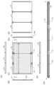
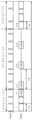
도 1의 (A)~(G)는 펼쳐진 전자 기기를 도시한 것이다. 도 1의 (A)는 상면도이다. 도 1의 (B)는 좌측면도이다. 도 1의 (C)는 사용자가 표시부를 보는 면을 도시한 정면도이다. 도 1의 (D)는 우측면도이다. 도 1의 (E)는 후면도이다. 도 1의 (F)는 저면도이다.Figures 1(A) to 1(G) illustrate an unfolded electronic device. Figure 1(A) is a top view. Figure 1(B) is a left side view. Figure 1(C) is a front view showing the side from which a user views the display unit. Figure 1(D) is a right side view. Figure 1(E) is a back view. Figure 1(F) is a bottom view.
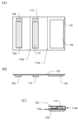
표시부(116)는, 도 1의 (C)에 도시된 바와 같이 주화면이 제 1 구부러진 영역(사이드 롤 부분(116a)이라고도 함)과 제 2 구부러진 영역(사이드 롤 부분(116b)이라고도 함) 사이에 배치되도록 제공된다.The display portion (116) is provided so that the main screen is positioned between the first curved area (also referred to as side roll portion (116a)) and the second curved area (also referred to as side roll portion (116b)), as shown in (C) of FIG. 1.
표시부(116)의 주화면의 단변의 길이 대 그 장변의 길이의 비는, 표시 영역의 단변의 길이 대 그 장변의 길이의 비의 0.9배 이상 1.1배 이하이다. 예를 들어, 단변의 길이 대 장변의 길이의 비는 약 9:16이다.The ratio of the length of the short side of the main screen of the display unit (116) to the length of its long side is 0.9 times or more and 1.1 times or less than the ratio of the length of the short side of the display area to the length of its long side. For example, the ratio of the length of the short side to the length of the long side is approximately 9:16.
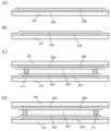
도 21은 전자 기기의 일례를 도시한 사시도이다. 전자 기기는 복수의 힌지(13)로 연결된 하우징들(10~12)을 포함한다. 하우징들 사이의 각 틈은 표시부(116)의 구부릴 수 있는 부분과 중첩되고, 표시부(116)는 이 부분을 따라 구부러질 수 있다. 도 22는 접어서 작게 한 전자 기기를 도시한 사시도이다.Fig. 21 is a perspective view illustrating an example of an electronic device. The electronic device includes housings (10 to 12) connected by a plurality of hinges (13). Each gap between the housings overlaps with a bendable portion of a display portion (116), and the display portion (116) can be bent along this portion. Fig. 22 is a perspective view illustrating an electronic device that has been folded and made small.
도 1의 (E)에 도시된 바와 같이, 표시부는 전자 기기의 측면의 일부 및 뒷면의 일부와 중첩되고, 이 중첩 부분은 항상 구부러져 있는 표시 영역이다. 표시부의 구부러진 영역은 곡률 반경 10mm 이하, 바람직하게는 8mm 이하, 더 바람직하게는 5mm 이하, 더욱 바람직하게는 4mm 이하로 구부러질 수 있다.As illustrated in (E) of Fig. 1, the display portion overlaps a portion of the side surface and a portion of the back surface of the electronic device, and this overlapping portion is a display area that is always curved. The curved area of the display portion can be curved with a radius of curvature of 10 mm or less, preferably 8 mm or less, more preferably 5 mm or less, and even more preferably 4 mm or less.
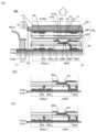
도 20의 (A)~(C)는 도 2의 (A)~(C)의 변형예이며 3개의 배터리를 도시하고 있다. 도 1의 (G)는 3개의 배터리를 포함하는 전자 기기의 도 1의 (C)에서의 A-A'를 따른 확대 단면도이다. 도 1의 (G)에 도시된 바와 같이 배터리들(112, 117, 및 153)이 각 하우징에 제공되어 있다.FIGS. 20(A) to (C) are modified examples of FIGS. 2(A) to (C) and illustrate three batteries. FIG. 1(G) is an enlarged cross-sectional view taken along line A-A' in FIG. 1(C) of an electronic device including three batteries. As illustrated in FIG. 1(G), batteries (112, 117, and 153) are provided in each housing.
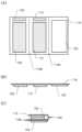
표시부(116)를 포함하는 상술한 구조의 표시 패널은, 곡률 반경 1mm 이상, 바람직하게는 30mm 이상으로 변형될 수 있다. 표시 소자를 포함하는 층이 2장의 필름 사이에 끼워져 있다. 단면에서는 구부러진 표시 패널이 2장의 필름의 2장의 곡선 사이에 끼워져 있다.The display panel having the above-described structure including the display portion (116) can be deformed to a radius of curvature of 1 mm or more, preferably 30 mm or more. The layer including the display element is sandwiched between two films. In a cross-section, the curved display panel is sandwiched between two curves of the two films.
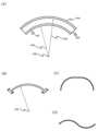
면의 곡률 반경에 대하여 도 17의 (A)~(C)를 참조하여 설명한다. 도 17의 (A)에서, 곡면(1700)을 절단하는 평면(1701)에 있어서, 곡면(1700)을 형성하는 곡선(1702)의 일부를 원호로 근사하고, 이 원의 반경을 곡률 반경(1703)이라고 하고, 이 원의 중심을 곡률 중심(1704)이라고 한다. 도 17의 (B)는 곡면(1700)의 상면도이다. 도 17의 (C)는 평면(1701)을 따른 곡면(1700)의 단면도이다. 평면을 따라 곡면을 절단할 때, 곡면 형상인 곡선의 곡률 반경은, 어느 평면을 따라 곡면을 절단하는지에 의존한다. 평면으로 곡면을 절단할 때, 단면에서의 곡선의 곡률 반경은, 곡면과 평면 사이의 각도 또는 절단 위치에 따라 달라지지만, 본 명세서 등에서는 가장 작은 곡률 반경을 면의 곡률 반경으로 정의한다.The radius of curvature of a surface will be described with reference to Figs. 17(A) to (C). In Fig. 17(A), in a plane (1701) that cuts a surface (1700), a part of a curve (1702) forming the surface (1700) is approximated by an arc, the radius of this circle is called the radius of curvature (1703), and the center of this circle is called the center of curvature (1704). Fig. 17(B) is a top view of the surface (1700). Fig. 17(C) is a cross-sectional view of the surface (1700) along the plane (1701). When cutting a surface along a plane, the radius of curvature of a curve, which is a curved shape, depends on which plane along which the surface is cut. When cutting a surface with a plane, the radius of curvature of the curve in the cross section varies depending on the angle between the surface and the plane or the cutting position, but in this specification and elsewhere, the smallest radius of curvature is defined as the radius of curvature of the surface.
표시 소자를 포함하는 층(1805)이 2장의 필름 사이에 끼워진 표시 패널을 구부리는 경우, 표시 패널의 곡률 중심(1800)에 가까운 필름(1801)의 곡률 반경(1802)은, 곡률 중심(1800)에서 떨어져 있는 필름(1803)의 곡률 반경(1804)보다 작다(도 18의 (A)). 표시 패널이 구부러지고 원호상의 단면을 가질 때, 곡률 중심(1800)에 더 가까운 쪽의 필름의 표면에 압축 응력이 가해지고, 곡률 중심(1800)에서 떨어져 있는 쪽의 필름의 표면에 인장 응력이 가해진다(도 18의 (B)).When a display panel including a layer (1805) including a display element is bent and sandwiched between two films, a radius of curvature (1802) of a film (1801) close to a center of curvature (1800) of the display panel is smaller than a radius of curvature (1804) of a film (1803) farther away from the center of curvature (1800) (Fig. 18(A)). When the display panel is bent and has an arc-shaped cross-section, a compressive stress is applied to a surface of the film closer to the center of curvature (1800), and a tensile stress is applied to a surface of the film farther away from the center of curvature (1800) (Fig. 18(B)).
또한, 표시 패널의 단면 형상은 단순한 원호 형상에 한정되지 않고 단면을 부분적으로 원호 형상으로 할 수 있고, 예를 들어, 도 18의 (C)에 도시된 형상, 도 18의 (D)에 도시된 물결 형상, 또는 S 형상을 사용할 수 있다. 표시 패널의 곡면이 복수의 곡률 중심을 가지는 형상인 경우, 표시 패널은, 곡률 중심에 가까운 쪽의 필름의 표면인, 복수의 곡률 중심에 대한 곡률 반경 중 가장 작은 곡률 반경을 가지는 곡면이 4mm 이상, 바람직하게는 30mm 이상의 곡률 반경을 가지도록, 변형할 수 있다.In addition, the cross-sectional shape of the display panel is not limited to a simple arc shape, and the cross-section can be partially made into an arc shape, and for example, the shape illustrated in (C) of Fig. 18, the wave shape illustrated in (D) of Fig. 18, or the S shape can be used. When the curved surface of the display panel has a shape having a plurality of centers of curvature, the display panel can be deformed so that the curved surface having the smallest radius of curvature among the radii of curvature for the plurality of centers of curvature, which is the surface of the film closer to the center of curvature, has a radius of curvature of 4 mm or more, preferably 30 mm or more.
도 2의 (A)는 배터리, 및 표시면이 아닌 뒷면의 표시부(116)의 배치를 도시한 개략도이다. 도 2의 (A)에서 점선으로 나타낸 표시부의 구부릴 수 있는 부분(116e)은 배터리(112)와 시스템부(125) 사이에 위치한다. 도 2의 (A)에서 점선으로 나타낸 표시부의 구부릴 수 있는 부분(116d)은 배터리들(112 및 153) 사이에 위치한다. 또한, 도 2의 (A)에서 표시부의 구부릴 수 있는 부분을 직선으로 나타내었다. 접기 선을 형성할 필요는 없고, 이 직선은 가장 작은 곡률 반경을 가질 수 있는 영역을 개략적으로 나타낸 것이다.Fig. 2(A) is a schematic diagram showing the arrangement of the battery and the display portion (116) on the back side, which is not the display surface. The bendable portion (116e) of the display portion, indicated by a dotted line in Fig. 2(A), is located between the battery (112) and the system portion (125). The bendable portion (116d) of the display portion, indicated by a dotted line in Fig. 2(A), is located between the batteries (112 and 153). In addition, the bendable portion of the display portion is indicated by a straight line in Fig. 2(A). It is not necessary to form a folding line, and this straight line is a schematic diagram showing an area that can have the smallest radius of curvature.
배터리(112)는 레귤레이터(113)에 전기적으로 접속되고, 레귤레이터(113)는 CPU를 포함하는 시스템부(125)에 전기적으로 접속된다. 레귤레이터(113)는 수신 회로 또는 송신 회로에 접속되어도 좋다. 도 2의 (A) 및 (B)는 배터리들이 실질적으로 동일한 크기인 예를 도시한 것이지만, 본 발명의 일 형태는 이 예에 특별히 한정되지 않는다. 예를 들어, 배터리(112)의 용량이 증대되도록, 소비 전력이 큰 CPU에 전기적으로 접속되는 배터리(112)의 두께를 다른 배터리보다 크게 하여도 좋다.The battery (112) is electrically connected to the regulator (113), and the regulator (113) is electrically connected to the system unit (125) including the CPU. The regulator (113) may be connected to a receiving circuit or a transmitting circuit. Although (A) and (B) of FIG. 2 illustrate an example in which the batteries are substantially the same size, one embodiment of the present invention is not particularly limited to this example. For example, in order to increase the capacity of the battery (112), the thickness of the battery (112) electrically connected to the CPU with high power consumption may be made larger than that of other batteries.
배터리(153)는 레귤레이터(154)에 전기적으로 접속된다. 레귤레이터(154)는 터치 입력부 및 표시부에 전기적으로 접속된다. 레귤레이터(154)는 수신 회로 또는 송신 회로에 접속되어도 좋다.The battery (153) is electrically connected to the regulator (154). The regulator (154) is electrically connected to the touch input unit and the display unit. The regulator (154) may be connected to the receiving circuit or the transmitting circuit.
도 2의 (B)는 도 2의 (A)에서의 전자 기기의 단면도이며, 펼쳐진 전자 기기의 CPU를 포함하는 시스템부(125)와 각 부분의 위치 관계를 도시한 것이다.Figure 2 (B) is a cross-sectional view of the electronic device in Figure 2 (A), showing the system unit (125) including the CPU of the unfolded electronic device and the positional relationship of each part.
도 2의 (C)는 구부러진 전자 기기의 CPU를 포함하는 시스템부(125)와 각 부분의 위치 관계를 도시한 것이다. 표시부의 구부릴 수 있는 부분(116d 및 116e)은 배터리와 중첩되지 않고, 전자 기기가 작게 되도록 구부러진다.Figure 2 (C) illustrates the system portion (125) including the CPU of the bent electronic device and the positional relationship of each portion. The bendable portions (116d and 116e) of the display portion do not overlap with the battery and are bent to make the electronic device smaller.
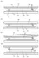
도 3의 (A)~(F)는 접어서 작게 한 전자 기기를 도시한 것이다. 도 22는 전자 기기의 사시도이다. 도 3의 (A)는 전자 기기의 상면도이다. 도 3의 (B)는 좌측면도이다. 도 3의 (C)는 사용자가 표시부를 보는 면을 도시한 정면도이다. 도 3의 (D)는 우측면도이다. 도 3의 (E)는 후면도이다. 도 3의 (F)는 저면도이다.Figs. 3(A) to (F) illustrate folded and small electronic devices. Fig. 22 is a perspective view of the electronic device. Fig. 3(A) is a top view of the electronic device. Fig. 3(B) is a left side view. Fig. 3(C) is a front view showing the side from which the user views the display unit. Fig. 3(D) is a right side view. Fig. 3(E) is a rear view. Fig. 3(F) is a bottom view.
전자 기기를 접어서 작게 하는 경우에도, 도 3의 (C)에 도시된 바와 같이 주화면이 제 1 구부러진 영역(사이드 롤 부분(116a)이라고도 함)과 구부릴 수 있는 영역(사이드 롤 부분(116c)이라고도 함) 사이에 배치되도록 제공된다.Even when the electronic device is folded to make it smaller, the main screen is provided to be positioned between the first bent region (also referred to as the side roll portion (116a)) and the bendable region (also referred to as the side roll portion (116c)), as shown in (C) of FIG. 3.
표시부(116)의 주화면의 단변의 길이 대 그 장변의 길이의 비는, 표시 영역의 단변의 길이 대 그 장변의 길이의 비의 0.9배 이상 1.1배 이하이다. 예를 들어, 단변의 길이 대 장변의 길이의 비는 약 9:16이다.The ratio of the length of the short side of the main screen of the display unit (116) to the length of its long side is 0.9 times or more and 1.1 times or less than the ratio of the length of the short side of the display area to the length of its long side. For example, the ratio of the length of the short side to the length of the long side is approximately 9:16.
이러한 구조에 의하여, 세로의 길이 대 가로의 길이의 비가, 접힌 표시부의 제 1 영역에 맞도록 표시될 수 있는 제 1 화상과 거의 동일한 제 2 화상을, 펼쳐진 표시부의 표시 영역에 맞도록 표시시킬 수 있다. 그러므로, 편리성 또는 신뢰성이 높은 신규 데이터 처리 장치로 할 수 있다.By this structure, a second image having a ratio of vertical length to horizontal length that is almost identical to a first image that can be displayed to fit the first area of the folded display section can be displayed to fit the display area of the unfolded display section. Therefore, a novel data processing device having high convenience and reliability can be achieved.
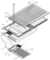
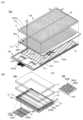
도 4는 터치 입력부 및 표시부가 하나의 FPC(4)에 의하여 하나의 배터리(117)에 전기적으로 접속되는 예를 도시한 것이다.Figure 4 illustrates an example in which a touch input unit and a display unit are electrically connected to one battery (117) by one FPC (4).
표시부(116)는 2장의 필름을 포함하고, 발광 소자, 표시 구동 회로의 일부, 터치 센서(152), 및 센서 구동 회로의 일부가 2장의 필름 사이에 제공된다. 유리 기판 위에 분리층을 제공하고, 그 위에 트랜지스터 및 발광 소자를 형성한다. 그 후, 유리 기판을 제거하고 제 1 플렉시블 필름(143)을 접합한다. 또한, 유리 기판 위에 분리층을 제공하고, 그 위에 트랜지스터 및 터치 센서(152)를 형성한다. 그 후, 유리 기판을 제거하고 제 2 플렉시블 필름(144)을 접합한다. 도 4의 구조에서 제 2 플렉시블 필름(144)은 제 1 플렉시블 필름(143)과 위치 맞춤되어 접합되고, 제 2 플렉시블 필름(144) 및 제 1 플렉시블 필름(143)은 발광 소자의 실란트로서 기능한다.The display portion (116) includes two films, and a light-emitting element, a part of the display driving circuit, a touch sensor (152), and a part of the sensor driving circuit are provided between the two films. A separation layer is provided on a glass substrate, and a transistor and a light-emitting element are formed thereon. Thereafter, the glass substrate is removed, and a first flexible film (143) is bonded. In addition, a separation layer is provided on the glass substrate, and a transistor and a touch sensor (152) are formed thereon. Thereafter, the glass substrate is removed, and a second flexible film (144) is bonded. In the structure of FIG. 4, the second flexible film (144) is bonded to the first flexible film (143) while being aligned with the position, and the second flexible film (144) and the first flexible film (143) function as a sealant of the light-emitting element.
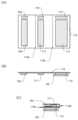
회로판(140) 상에서는 배터리(117)의 리드 전극(141)과 레귤레이터(118)가 서로 전기적으로 접속되고, FPC(4)가 회로판(140) 상의 커넥터에 접속된다. 배터리(117)로서 적층의 리튬 이온 이차 배터리가 사용된다. FPC(4)는 분기 및 3개의 단자를 가진다. 제 1 단자는 회로판(140) 상의 커넥터에 접속된다. 제 2 단자는 터치 패널의 단자에 접속된다. 제 3 단자는 표시부의 단자에 접속된다. 여기서는 하나의 FPC를 사용하는 예를 설명하지만, 접속에 2개 이상의 FPC를 사용하여도 좋다.On the circuit board (140), the lead electrode (141) of the battery (117) and the regulator (118) are electrically connected to each other, and the FPC (4) is connected to the connector on the circuit board (140). A laminated lithium ion secondary battery is used as the battery (117). The FPC (4) has a branch and three terminals. The first terminal is connected to the connector on the circuit board (140). The second terminal is connected to the terminal of the touch panel. The third terminal is connected to the terminal of the display section. An example using one FPC is described here, but two or more FPCs may be used for the connection.
구동 회로의 일부(142)는 FPC(4)에 탑재되며, 센서 구동 회로의 일부 및 표시부의 구동 회로의 일부를 포함한다. 터치 센서 구동 회로 및 표시부의 구동 회로에 의하여 부분적으로 공유되는 회로를 사용하여도 좋다. 표시부에 대한 비디오 신호 등은, FPC(5) 끝에 접속된 회로로부터 공급되거나, 또는 FPC(5) 끝에 제공된 수신 회로를 사용하여 무선 통신에 의하여 공급되어도 좋다. 터치 센서의 입력 신호는 FPC(5) 끝에 접속된 회로에 공급되거나, 또는 FPC(5) 끝에 제공된 송신 회로를 사용하여 무선 통신에 의하여 CPU 등에 공급되어도 좋다.A part of the driving circuit (142) is mounted on the FPC (4), and includes a part of the sensor driving circuit and a part of the driving circuit of the display unit. A circuit partially shared by the touch sensor driving circuit and the driving circuit of the display unit may be used. A video signal, etc. for the display unit may be supplied from a circuit connected to the end of the FPC (5), or may be supplied by wireless communication using a receiving circuit provided at the end of the FPC (5). An input signal of the touch sensor may be supplied to a circuit connected to the end of the FPC (5), or may be supplied to a CPU, etc. by wireless communication using a transmitting circuit provided at the end of the FPC (5).
본 발명의 일 형태는 도 2의 (A)~(C)와 같이 표시부의 2개의 부분을 따라 구부러질 수 있는 전자 기기에 한정되지 않고, 본 발명의 일 형태에 따른 전자 기기는 표시부의 3개 이상의 부분을 따라 구부러져도 좋다. 도 5의 (A)~(C)는 4개의 부분을 따라 구부러질 수 있는 전자 기기의 예를 도시한 것이다. 표시부의 구부릴 수 있는 부분(116g 및 116f)을 더 제공함으로써 표시부의 표시 면적을 확장시킬 수 있다. 도 5의 (B)는 도 5의 (A)에서의 전자 기기의 단면도이며, 펼쳐진 전자 기기의 CPU를 포함하는 시스템부(125)와 각 부분의 위치 관계를 도시한 것이다. 도 5의 (C)는 구부러진 전자 기기의 CPU를 포함하는 시스템부(125)와 각 부분의 위치 관계를 도시한 것이다. 표시부의 구부릴 수 있는 부분(116d, 116e, 116f, 및 116g)은 배터리와 중첩되지 않고, 전자 기기가 작게 되도록 구부러진다. 표시부의 각 단부에 배터리가 배치되기 때문에, 사용자는 펼쳐진 도 5의 (A)~(C)에 도시된 전자 기기를 양손에 쉽게 들 수 있다고 할 수 있다.One embodiment of the present invention is not limited to an electronic device that can be bent along two portions of a display portion as in (A) to (C) of Figs. 2, and an electronic device according to one embodiment of the present invention may be bent along three or more portions of the display portion. (A) to (C) of Figs. 5 show examples of an electronic device that can be bent along four portions. By further providing bendable portions (116g and 116f) of the display portion, the display area of the display portion can be expanded. (B) of Fig. 5 is a cross-sectional view of the electronic device in (A) of Fig. 5, and illustrates a system portion (125) including a CPU of the unfolded electronic device and the positional relationship of each portion. (C) of Fig. 5 shows a system portion (125) including a CPU of the bent electronic device and the positional relationship of each portion. The bendable portions (116d, 116e, 116f, and 116g) of the display portion do not overlap with the battery and are bent to make the electronic device small. Since the battery is placed at each end of the display portion, it can be said that the user can easily hold the electronic device shown in (A) to (C) of the unfolded FIG. 5 with both hands.
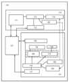
도 6은 장치(110)의 블록도이다. 도 6에서의 장치(110)는 도 2의 (A)~(C)에서의 2개의 배터리를 포함하며, 표시부를 접어서 작게 할 수 있는 전자 기기이다.Fig. 6 is a block diagram of a device (110). The device (110) in Fig. 6 is an electronic device that includes two batteries in (A) to (C) of Fig. 2 and can be made smaller by folding the display portion.
본 실시형태의 장치(110)는 제어 모듈(115), 표시 모듈(121), 및 전원 관리 회로(127)를 포함한다. 제어 모듈(115)은 장치(110) 전체, 통신, 및 표시부(116)에서의 데이터 표시를 제어하는 컨트롤러이다.The device (110) of the present embodiment includes a control module (115), a display module (121), and a power management circuit (127). The control module (115) is a controller that controls the entire device (110), communication, and data display on the display unit (116).
제어 모듈(115)은 CPU(111), 배터리(112), 레귤레이터(113), 무선 수신부(114), 및 무선 송신부(128)를 포함한다.The control module (115) includes a CPU (111), a battery (112), a regulator (113), a wireless receiver (114), and a wireless transmitter (128).
표시 모듈(121)은 표시부(116), 표시 구동 회로(119), 배터리(117), 레귤레이터(118), 터치 센서(152), 센서 구동 회로(159), 접힘 위치 센서(160), 무선 수신부(120), 및 무선 송신부(129)를 포함한다.The display module (121) includes a display unit (116), a display driving circuit (119), a battery (117), a regulator (118), a touch sensor (152), a sensor driving circuit (159), a folding position sensor (160), a wireless receiving unit (120), and a wireless transmitting unit (129).
장치(110)는 표시부(116)의 복수의 부분을 따라 구부러질 수 있다. 장치(110)를 구부림으로써 가려지는 표시 영역에서의 화상 표시는 행해지지 않고, 이에 의하여 소비 전력이 저감될 수 있다. 본 명세서에서 "화상"은 문자 및 기호 등, 시각적으로 인식될 수 있는 정보를 포함한다. 접힘 위치 센서(160)는 표시부가 접힌 위치를 판정하고 접힘 위치 데이터를 공급할 수 있다. 예를 들어, 접힘 위치가 미리 결정되어 있는 경우에는 그 위치에 센서를 제공한다. 장치(110)를 구부릴 수 있는 복수의 위치가 있는 경우, 복수의 센서를 선상 또는 매트릭스로 배치함으로써, 구부러짐 위치의 좌표를 특정할 수 있다. 예를 들어, 접힘 위치 센서(160)는 표시 영역의 주변을 따라 제공될 수 있다. 접힘 위치 센서(160)는 예를 들어, 스위치, MEMS 압력 센서, 또는 압력 센서 등으로 구성될 수 있다.The device (110) can be bent along a plurality of portions of the display portion (116). By bending the device (110), image display is not performed in the display area that is covered, and thereby power consumption can be reduced. In this specification, “image” includes visually recognizable information such as characters and symbols. The fold position sensor (160) can determine the folded position of the display portion and supply fold position data. For example, if the fold position is predetermined, a sensor is provided at that position. If there are a plurality of positions at which the device (110) can be bent, the coordinates of the folded positions can be specified by arranging the plurality of sensors in a line or matrix. For example, the fold position sensor (160) can be provided along the periphery of the display area. The fold position sensor (160) can be configured as, for example, a switch, a MEMS pressure sensor, or a pressure sensor.
구체적으로, 표시부가 펼쳐지거나 접힐 때에 펼치고 접히도록, 기계적 접촉 스위치 또는 자기 스위치 등을 표시부에 제공하여도 좋다.Specifically, a mechanical contact switch or a magnetic switch, etc. may be provided on the display portion so that it unfolds and folds when the display portion is unfolded or folded.
또는, 복수의 압력 센서를 표시부에 제공하여도 좋다. 구체적으로는, 필름상의 압전 소자를 표시부에 부착할 수 있다. 구부리는 동작에 따른 압력의 상승을 압력 센서로 검지함으로써, 접힘 위치를 알아낼 수 있다.Alternatively, a plurality of pressure sensors may be provided on the display portion. Specifically, a film-shaped piezoelectric element may be attached to the display portion. By detecting the increase in pressure due to the bending motion with the pressure sensor, the folding position can be determined.
압전 소자로서 예를 들어, 유기 압전 필름을 사용할 수 있다. 구체적으로는, 폴리아미노산을 함유하는 압전 필름, 폴리바이닐리덴 플루오라이드를 함유하는 압전 필름, 폴리에스터를 함유하는 압전 필름, 또는 키랄 폴리머를 함유하는 압전 필름 등을 포함하는 필름상의 압전 소자를 사용할 수 있다.As the piezoelectric element, for example, an organic piezoelectric film can be used. Specifically, a film-shaped piezoelectric element including a piezoelectric film containing a polyamino acid, a piezoelectric film containing a polyvinylidene fluoride, a piezoelectric film containing a polyester, or a piezoelectric film containing a chiral polymer can be used.
또한, 압전 소자는 접힘 위치 센서(160)를 위한 소자 및 압력 검지 터치 패널을 위한 소자의 양쪽 모두로서 기능할 수 있다.Additionally, the piezoelectric element can function as both an element for the fold position sensor (160) and an element for the pressure detection touch panel.
접힘 위치 센서(160)에 의하여, 하나의 표시 영역을 접힌 부분으로 분할된 2개의 영역으로서 사용할 수 있고, 표시 영역들 중 하나에 표시할 화상을 선택할 수 있다. 또한, 표시 영역이 어떻게 접혀 있는지에 따라 하나 또는 복수의 화상을 선택하여 표시할 수 있다. 하나의 표시 영역을 접힌 부분을 따라 2개의 영역으로 분할하기 위해서는, 표시부(116)의 표시 영역을 표시 구동 회로(119)에 의하여 따로따로 구동시키는 것이 바람직하다.By means of the folding position sensor (160), one display area can be used as two areas divided into folded portions, and an image to be displayed in one of the display areas can be selected. In addition, one or more images can be selected and displayed depending on how the display area is folded. In order to divide one display area into two areas along the folded portion, it is preferable to separately drive the display areas of the display portion (116) by means of the display driving circuit (119).
또한, 접힘 위치 센서(160)에 의하여, 터치 입력 영역을 접힌 부분으로 분할된 2개의 영역으로서 사용할 수 있게 되고, 터치 입력 영역들 중 하나를 사용 불가능하게 할 수 있다. 터치 입력 영역이란, 터치 센서에 의한 검지가 행해질 수 있으며, 크기가 표시 영역과 실질적으로 동일한 영역을 말한다. 하나의 터치 입력 영역을 접힌 부분으로 분할된 2개의 영역으로서 사용하기 위해서는, 터치 센서(152)의 터치 입력 영역을 센서 구동 회로(159)에 의하여 따로따로 구동시키는 것이 바람직하다.In addition, by means of the folding position sensor (160), the touch input area can be used as two areas divided into folded parts, and one of the touch input areas can be disabled. The touch input area refers to an area where detection by the touch sensor can be performed and whose size is substantially the same as the display area. In order to use one touch input area as two areas divided into folded parts, it is preferable to separately drive the touch input areas of the touch sensor (152) by means of the sensor driving circuit (159).
장치(110)는 표시부(116)의 복수의 부분을 따라 구부러질 수 있고, 장치(110)를 구부림으로써 가려지는 표시 영역에서의 화상 표시를 행하지 않음으로써, 소비 전력을 저감할 수 있다. 또한, 표시가 행해지지 않는 영역의 터치 센서를 사용 불가능하게 함으로써 오동작을 방지할 수 있다.The device (110) can be bent along multiple portions of the display portion (116), and power consumption can be reduced by not displaying images in a display area that is obscured by bending the device (110). In addition, malfunction can be prevented by disabling the touch sensor in an area where display is not performed.
본 실시형태에서는 표시부(116)의 대향 기판(밀봉 기판)이 터치 패널 기능을 가진다. 구체적으로는 산화물 반도체층을 사용한 트랜지스터 및 유기 EL 소자가 제공된 필름 기판과, 산화물 반도체층을 사용한 트랜지스터를 포함하는 터치 센서가 제공된 밀봉 기판을 서로 접합한 표시 패널을 사용한다. 본 실시형태에서, 표시부의 일부가 구부러질 수 있도록, 밀봉 기판도 플렉시블 재료를 사용하여 형성되는 것이 바람직하다.In this embodiment, the opposite substrate (sealing substrate) of the display portion (116) has a touch panel function. Specifically, a display panel is used in which a film substrate provided with a transistor using an oxide semiconductor layer and an organic EL element and a sealing substrate provided with a touch sensor including a transistor using an oxide semiconductor layer are joined to each other. In this embodiment, it is preferable that the sealing substrate is also formed using a flexible material so that a part of the display portion can be bent.
도 6의 예에 도시된 바와 같이, 센서 구동 회로(159)의 적어도 일부 및 표시 구동 회로(119)의 적어도 일부를 하나의 IC 칩에 포함시켜서 탑재되는 부품의 수를 줄여도 좋다.As shown in the example of Fig. 6, the number of components mounted may be reduced by including at least a part of the sensor driving circuit (159) and at least a part of the display driving circuit (119) in one IC chip.
각 레귤레이터는, 레귤레이터에 접속된 배터리로부터 각 기능 회로에 필요한 전력 또는 신호를 생성하여 공급한다. 배터리의 충전에 있어서 레귤레이터는 과충전 등을 방지할 수 있다. 또한, 도 6에서는 하나의 레귤레이터에 무선 수신부 및 무선 송신부가 접속되는 예를 도시하였지만, 무선 수신부와 무선 송신부는 서로 다른 레귤레이터에 접속되어도 좋다.Each regulator generates and supplies power or signals required for each functional circuit from the battery connected to the regulator. Regulators can prevent overcharging, etc., when charging the battery. In addition, although Fig. 6 illustrates an example in which a wireless receiving unit and a wireless transmitting unit are connected to one regulator, the wireless receiving unit and the wireless transmitting unit may be connected to different regulators.
장치(110)에서, 전원 관리 회로(127)는 제어 모듈(115)과 표시 모듈(121)의 배터리 간에서의 전력의 상호 공급을 가능하게 한다. 또한, 전원 관리 회로(127)는 배터리(112 및 117)의 전력량을 모니터링하며, 자동적으로 또는 사용자의 조작에 의하여 배터리들 중 하나로부터 다른 배터리에 대한 전력의 무선 공급을 적절히 실행함으로써, 상기 다른 배터리를 충전할 수 있다. 또는, 전원 관리 회로(127)는 배터리(112 및 117)의 전력량을 모니터링하며, 자동적으로 또는 사용자의 조작에 의하여 복수의 배터리 중 하나로부터 다른 배터리들 중 하나에 대한 전력의 무선 공급을 적절히 실행함으로써, 상기 배터리를 충전할 수 있다.In the device (110), the power management circuit (127) enables mutual power supply between the batteries of the control module (115) and the display module (121). In addition, the power management circuit (127) monitors the power amounts of the batteries (112 and 117) and automatically or by a user's operation, wirelessly supplies power from one of the batteries to the other battery, thereby charging the other battery. Alternatively, the power management circuit (127) monitors the power amounts of the batteries (112 and 117) and automatically or by a user's operation, wirelessly supplies power from one of the plurality of batteries to one of the other batteries, thereby charging the other battery.
또한, 장치(110)에서 모듈을 독립적으로 온 또는 오프로 할 수 있다. 사용할 모듈만을 선택적으로 구동시키는 오퍼레이션 시스템에 의하여 장치(110)의 절전이 가능해진다.Additionally, modules in the device (110) can be turned on or off independently. Power saving of the device (110) is possible by an operation system that selectively drives only the modules to be used.
표시 모듈(121) 및 제어 모듈(115)을 온으로 하여 표시부(116)에 정지 화상을 표시시킨 후, 정지 화상이 표시된 상태로 제어 모듈(115)을 오프로 하더라도 표시 모듈(121)만이 온인 상태로 정지 화상을 계속 표시할 수 있다. 또한, 표시부(116)의 트랜지스터가 낮은 오프 상태 전류를 가능하게 하는 산화물 반도체층(예를 들어 In, Ga, 및 Zn을 함유하는 산화물 재료)을 포함하는 경우, 또는 각 화소에 메모리가 포함되는 경우에는, 정지 화상을 표시시킨 후에 배터리(117)로부터의 전력 공급을 정지하더라도 정지 화상이 일정한 기간 계속 표시될 수 있다.After the display module (121) and the control module (115) are turned on to display a still image on the display section (116), even if the control module (115) is turned off while the still image is displayed, the still image can be continuously displayed with only the display module (121) turned on. In addition, if the transistor of the display section (116) includes an oxide semiconductor layer (e.g., an oxide material containing In, Ga, and Zn) that enables low off-state current, or if each pixel includes a memory, even if the power supply from the battery (117) is stopped after displaying the still image, the still image can be continuously displayed for a certain period of time.
본 실시형태에서는 표시 모듈(121) 및 제어 모듈(115) 각각이 무선 송신부 및 무선 수신부를 포함하는 예를 설명하지만, 본 발명의 일 형태는 이 예에 특별히 한정되지 않는다. 표시 모듈(121) 및 제어 모듈(115)의 배터리는 직렬로 접속되어도 좋고 병렬로 접속되어도 좋다. 이 경우 전자 기기는, 레귤레이터를 통하여 배터리들 중 어느 하나에 전기적으로 접속된, 비접촉으로 배터리를 충전하기 위한 수신 회로(무선 충전을 위한 안테나를 포함함)를 적어도 포함한다.In this embodiment, an example is described in which each of the display module (121) and the control module (115) includes a wireless transmitter and a wireless receiver, but one embodiment of the present invention is not particularly limited to this example. The batteries of the display module (121) and the control module (115) may be connected in series or in parallel. In this case, the electronic device includes at least a receiving circuit (including an antenna for wireless charging) for charging the battery in a non-contact manner, which is electrically connected to one of the batteries through a regulator.
도 23은 도 6과는 부분적으로 다른 장치(110)의 블록도이다. 도 23에서의 장치(110)는 도 20의 (A)~(C)에 도시된 3개의 배터리를 적어도 포함하며 표시부를 구부려서 작게 할 수 있는 전자 기기이다.Fig. 23 is a block diagram of a device (110) that is partially different from Fig. 6. The device (110) in Fig. 23 is an electronic device that includes at least three batteries as shown in (A) to (C) of Fig. 20 and can have a display portion that can be made small by bending it.
본 실시형태의 장치(110)는 제어 모듈(115), 표시 모듈(121), 터치 입력부(156), 및 전원 관리 회로(127)를 포함한다. 제어 모듈(115)은 장치(110) 전체, 통신, 및 표시부(116)에서의 데이터 표시를 제어하는 컨트롤러이다.The device (110) of the present embodiment includes a control module (115), a display module (121), a touch input unit (156), and a power management circuit (127). The control module (115) is a controller that controls the entire device (110), communication, and data display on the display unit (116).
제어 모듈(115)은 CPU(111), 배터리(112), 레귤레이터(113), 무선 수신부(114), 및 무선 송신부(128)를 포함한다.The control module (115) includes a CPU (111), a battery (112), a regulator (113), a wireless receiver (114), and a wireless transmitter (128).
표시 모듈(121)은 표시부(116), 표시 구동 회로(119), 배터리(117), 레귤레이터(118), 무선 수신부(120), 및 무선 송신부(129)를 포함한다.The display module (121) includes a display unit (116), a display driving circuit (119), a battery (117), a regulator (118), a wireless receiving unit (120), and a wireless transmitting unit (129).
터치 입력부(156)는 터치 센서(152), 배터리(153), 레귤레이터(154), 무선 수신부(155), 및 무선 송신부(150)를 포함한다.The touch input unit (156) includes a touch sensor (152), a battery (153), a regulator (154), a wireless receiver (155), and a wireless transmitter (150).
본 실시형태에서는 표시부(116)의 대향 기판(밀봉 기판)이 터치 패널 기능을 가진다. 구체적으로는 산화물 반도체층을 사용한 트랜지스터 및 유기 EL 소자가 제공된 필름 기판과, 산화물 반도체층을 사용한 트랜지스터를 포함하는 터치 센서가 제공된 밀봉 기판을 서로 접합한 표시 패널을 사용한다. 본 실시형태에서, 표시부의 일부가 구부러질 수 있도록, 밀봉 기판도 플렉시블 재료를 사용하여 형성되는 것이 바람직하다. 본 실시형태에서, 유기 EL 소자에 전력을 공급하는 FPC와, 터치 센서에 전력을 공급하는 FPC는 따로 제공되고 상이한 배터리에 접속된다.In this embodiment, the opposite substrate (sealing substrate) of the display portion (116) has a touch panel function. Specifically, a display panel is used in which a film substrate provided with a transistor using an oxide semiconductor layer and an organic EL element and a sealing substrate provided with a touch sensor including a transistor using an oxide semiconductor layer are joined to each other. In this embodiment, it is preferable that the sealing substrate is also formed using a flexible material so that a part of the display portion can be bent. In this embodiment, an FPC for supplying power to the organic EL element and an FPC for supplying power to the touch sensor are provided separately and connected to different batteries.
표시 패널(116)의 각 화소에 포토센서를 제공하여 광학식 터치 패널을 만들어도 좋다. 터치 입력부(156)로서 저항식 터치 패널 또는 정전식 터치 패널을, 표시부(116)와 중첩되도록 배치하여도 좋다.An optical touch panel may be created by providing a photosensor to each pixel of the display panel (116). A resistive touch panel or an electrostatic touch panel may be arranged as the touch input unit (156) so as to overlap the display unit (116).
각 레귤레이터는, 레귤레이터에 접속된 배터리로부터 각 기능 회로에 필요한 전력 또는 신호를 생성하여 공급한다. 배터리의 충전에 있어서 레귤레이터는 과충전 등을 방지할 수 있다. 또한, 도 23에서는 하나의 레귤레이터에 무선 수신부 및 무선 송신부가 접속되는 예를 도시하였지만, 무선 수신부와 무선 송신부는 서로 다른 레귤레이터에 접속되어도 좋다.Each regulator generates and supplies power or signals required for each functional circuit from a battery connected to the regulator. Regulators can prevent overcharging, etc., when charging the battery. In addition, although Fig. 23 illustrates an example in which a wireless receiving unit and a wireless transmitting unit are connected to one regulator, the wireless receiving unit and the wireless transmitting unit may be connected to different regulators.
장치(110)에서, 전원 관리 회로(127)는 제어 모듈(115), 표시 모듈(121), 및 터치 입력부(156)의 배터리 간에서의 전력의 상호 공급을 가능하게 한다. 또한, 전원 관리 회로(127)는 배터리들(112, 117, 및 153)의 전력량을 모니터링하며, 자동적으로 또는 사용자의 조작에 의하여 배터리들 중 하나로부터 다른 배터리들 중 어느 것에 대한 전력의 무선 공급을 적절히 실행함으로써, 상기 배터리를 충전할 수 있다. 또는, 전원 관리 회로(127)는 배터리들(112, 117, 및 153)의 전력량을 모니터링하며, 자동적으로 또는 사용자의 조작에 의하여 복수의 배터리 중 하나로부터 다른 배터리들 중 하나에 대한 전력의 무선 공급을 적절히 실행함으로써, 상기 배터리를 충전할 수 있다.In the device (110), the power management circuit (127) enables mutual power supply between the batteries of the control module (115), the display module (121), and the touch input unit (156). In addition, the power management circuit (127) monitors the power amounts of the batteries (112, 117, and 153) and automatically or by a user's operation, wirelessly supplies power from one of the batteries to any of the other batteries, thereby charging the battery. Alternatively, the power management circuit (127) monitors the power amounts of the batteries (112, 117, and 153) and automatically or by a user's operation, wirelessly supplies power from one of the plurality of batteries to any of the other batteries, thereby charging the battery.
또한, 장치(110)에서 모듈을 독립적으로 온 또는 오프로 할 수 있다. 사용할 모듈만을 선택적으로 구동시키는 오퍼레이션 시스템에 의하여 장치(110)의 저소비 전력화가 가능해진다.In addition, modules in the device (110) can be turned on or off independently. Low power consumption of the device (110) is possible by an operation system that selectively drives only the modules to be used.
예를 들어, 사용자가 디스플레이를 사용하지 않고, 디스플레이를 사용하지 않고 표시 화면을 오프로 하고 싶은 경우에는, 배터리(117)가 사용되지 않도록 표시부(116)에 대한 전력 공급을 정지하고, 터치 입력부(156) 및 제어 모듈(115)을 온으로 한다. 화면에 표시가 다시 행해지게 하고 싶을 때에는 화면을 터치함으로써 표시 화면을 온으로 할 수 있다.For example, if a user wants to turn off the display screen without using the display, the power supply to the display unit (116) is stopped so that the battery (117) is not used, and the touch input unit (156) and the control module (115) are turned on. When a user wants to display on the screen again, the display screen can be turned on by touching the screen.
표시 모듈(121) 및 제어 모듈(115)을 온으로 하여 표시부(116)에 정지 화상을 표시시킨 후, 정지 화상이 표시된 상태로 제어 모듈(115)을 오프로 하더라도 표시 모듈(121)만이 온인 상태로 정지 화상을 계속 표시할 수 있다. 또한, 표시부(116)의 트랜지스터가 낮은 오프 상태 전류를 가능하게 하는 산화물 반도체층(예를 들어 In, Ga, 및 Zn을 함유하는 산화물 재료)을 포함하는 경우, 또는 각 화소에 메모리가 포함되는 경우에는, 정지 화상을 표시시킨 후에 배터리(117)로부터의 전력 공급을 정지하더라도 정지 화상이 일정한 기간 계속 표시될 수 있다.After the display module (121) and the control module (115) are turned on to display a still image on the display section (116), even if the control module (115) is turned off while the still image is displayed, the still image can be continuously displayed with only the display module (121) turned on. In addition, if the transistor of the display section (116) includes an oxide semiconductor layer (e.g., an oxide material containing In, Ga, and Zn) that enables low off-state current, or if each pixel includes a memory, even if the power supply from the battery (117) is stopped after displaying the still image, the still image can be continuously displayed for a certain period of time.
본 실시형태에서는 표시 모듈(121), 제어 모듈(115), 및 터치 입력부(156)가 서로 다른 배터리를 포함하는 예를 설명하지만, 배터리의 수는 3개에 특별히 한정되지 않고, 전자 기기가 기능 모듈을 포함하며 기능 모듈의 배터리를 포함하는 4개 이상의 배터리를 포함하여도 좋다.In this embodiment, an example is described in which the display module (121), the control module (115), and the touch input unit (156) include different batteries, but the number of batteries is not particularly limited to three, and the electronic device may include four or more batteries including a function module and a battery of the function module.
본 실시형태에서는 표시 모듈(121), 제어 모듈(115), 및 터치 입력부(156) 각각이 무선 송신부 및 무선 수신부를 포함하는 예를 설명하지만, 본 발명의 일 형태는 이 예에 특별히 한정되지 않는다. 표시 모듈(121), 제어 모듈(115), 및 터치 입력부(156)의 배터리는 직렬로 접속되어도 좋고 병렬로 접속되어도 좋다. 이 경우 전자 기기는, 레귤레이터를 통하여 배터리들 중 어느 하나에 전기적으로 접속된, 비접촉으로 배터리를 충전하기 위한 수신 회로(무선 충전을 위한 안테나를 포함함)를 적어도 포함한다.In this embodiment, an example is described in which each of the display module (121), the control module (115), and the touch input unit (156) includes a wireless transmitter and a wireless receiver, but one embodiment of the present invention is not particularly limited to this example. The batteries of the display module (121), the control module (115), and the touch input unit (156) may be connected in series or in parallel. In this case, the electronic device includes at least a receiving circuit (including an antenna for wireless charging) for charging the battery without contact, which is electrically connected to one of the batteries through a regulator.
또한, 통신 기능으로서 통신 모듈을 제공하면, 전자 기기를 데이터 단말 장치로 할 수 있다. 또한, 전자 기기는 전화 등을 가능하게 하는 근거리 무선 통신 기능을 가지는 통신 모듈을 포함하여도 좋다. 이 경우, 통신 모듈도 배터리를 포함하여도 좋다. 전자 기기는 다른 어떤 기능을 가져도 좋고, 예를 들어 센서(힘, 변위, 위치, 속도, 가속도, 각속도, 회전수, 거리, 광, 액체, 자기, 온도, 화학 물질, 음성, 시간, 경도(硬度), 전기장, 전류, 전압, 전력, 방사선, 유량, 습도, 경사도, 진동, 냄새, 또는 적외선을 측정하는 기능을 가지는 센서), 또는 마이크로폰 등을 포함하여도 좋다.In addition, if a communication module is provided as a communication function, the electronic device can be used as a data terminal device. In addition, the electronic device may include a communication module having a short-range wireless communication function that enables a telephone, etc. In this case, the communication module may also include a battery. The electronic device may have any other function, and for example, may include a sensor (a sensor having a function of measuring force, displacement, position, speed, acceleration, angular velocity, rotational speed, distance, light, liquid, magnetism, temperature, chemical substance, voice, time, hardness, electric field, current, voltage, power, radiation, flow rate, humidity, inclination, vibration, odor, or infrared), or a microphone.
전자 기기에 SIM 카드를 삽입하기 위한 슬롯, USB 메모리 등 USB 장치를 접속하기 위한 커넥터부를 더 제공하여도 좋다.It may also be desirable to additionally provide a slot for inserting a SIM card into the electronic device and a connector for connecting a USB device such as a USB memory stick.
상술한 바와 같이 전자 기기는, 전자 기기에서 대응하는 유닛(모듈 또는 기능)에 제공되며 전원 관리 회로(127)에 의하여 관리되는 복수의 배터리를 포함한다. 복수의 배터리를 포함하는 전자 기기에서, 사용할 모듈만을 선택적으로 구동시키는 오퍼레이션 시스템은 절전을 가능하게 한다. 전원 관리 회로(127)는 배터리의 전력량을 모니터링하며, 자동적으로 또는 사용자의 조작에 의하여 배터리들 중 하나로부터 다른 배터리들 중 어느 것에 대한 전력의 무선 공급을 적절히 실행함으로써, 상기 배터리를 충전할 수 있다. 전자 기기에서의 복수의 배터리 중에서 사용할 부품의 배터리를 적절히 선택하고, 각 배터리의 전력량을 조절하는 오퍼레이션 시스템에 의하여, 사용할 기능을 사용 가능한 시간을 늘릴 수 있다.As described above, the electronic device includes a plurality of batteries that are provided to corresponding units (modules or functions) in the electronic device and are managed by a power management circuit (127). In the electronic device including the plurality of batteries, an operation system that selectively drives only the modules to be used enables power saving. The power management circuit (127) monitors the amount of power of the batteries, and automatically or by a user's operation, wirelessly supplies power from one of the batteries to any of the other batteries, thereby charging the batteries. By appropriately selecting a battery of a component to be used from among the plurality of batteries in the electronic device and controlling the amount of power of each battery, the time for which the function to be used can be used can be increased.
배터리들은 각각 비접촉 충전 기능을 가지는 통신 모듈을 포함하며, 동시에 충전되도록 제어될 수 있다. 또한, 배터리들은 각각 송수신부를 포함하며 전원 관리 회로에 의하여 전력량을 조절할 수 있기 때문에, 배터리 간에서 전력이 상호로 공급될 수 있다.The batteries each include a communication module having a non-contact charging function and can be controlled to be charged simultaneously. In addition, since the batteries each include a transceiver and can control the amount of power by a power management circuit, power can be supplied to each other between the batteries.
(실시형태 2)(Embodiment 2)
본 실시형태에서는, 도 7의 (A)~(C)를 참조하여, 실시형태 1과는 부분적으로 다른 예를 설명한다. 또한, 도 2의 (A)~(C)와 동일한 부분에는 동일한 부호를 사용하고, 여기서는 동일한 부호의 부분에 대한 설명을 생략한다.In this embodiment, an example that is partially different from
실시형태 1에서는 실질적으로 동일한 크기의 2개의 배터리를 사용하는 예를 설명하였지만, 도 7의 (A)는 배터리들의 크기 및 배치가 실시형태 1의 배터리와는 다른 예를 도시한 것이다. 표시부(116)의 표시 영역은 약 5.9인치의 크기를 가진다.In
도 7의 (A)는 배터리, 및 표시면이 아닌 뒷면의 표시부(116)의 배치를 도시한 개략도이다. 도 7의 (A)에서 점선으로 나타낸 표시부의 구부릴 수 있는 부분(116d)은 배터리(112)와 배터리(753) 사이에 위치한다.Fig. 7(A) is a schematic diagram showing the arrangement of the battery and the display portion (116) on the back side, which is not the display surface. The bendable portion (116d) of the display portion indicated by the dotted line in Fig. 7(A) is located between the battery (112) and the battery (753).
배터리(112)는 레귤레이터(113)에 전기적으로 접속되고, 레귤레이터(113)는 CPU를 포함하는 시스템부(125)에 전기적으로 접속된다. 레귤레이터(113)는 수신 회로 또는 송신 회로에 접속되어도 좋다.The battery (112) is electrically connected to the regulator (113), and the regulator (113) is electrically connected to the system unit (125) including the CPU. The regulator (113) may be connected to a receiving circuit or a transmitting circuit.
배터리(753)는 레귤레이터(754)에 전기적으로 접속된다. 레귤레이터(754)는 터치 입력부, 및 표시부(116)의 구동 회로에 전기적으로 접속된다. 레귤레이터(754)는 수신 회로 또는 송신 회로에 접속되어도 좋다.The battery (753) is electrically connected to the regulator (754). The regulator (754) is electrically connected to the driving circuit of the touch input unit and the display unit (116). The regulator (754) may be connected to the receiving circuit or the transmitting circuit.
도 7의 (B)는 도 7의 (A)에서의 전자 기기의 단면도이며, 펼쳐진 전자 기기의 CPU를 포함하는 시스템부(125)와 각 부분의 위치 관계를 도시한 것이다.Figure 7 (B) is a cross-sectional view of the electronic device in Figure 7 (A), showing the system unit (125) including the CPU of the unfolded electronic device and the positional relationship of each part.
도 7의 (C)는 구부러진 전자 기기의 CPU를 포함하는 시스템부(125)와 각 부분의 위치 관계를 도시한 것이다. 배터리(112)는 전자 기기가 구부러질 때에 배터리(753)와 중첩되지 않도록 배치된다. 이와 같이 작게 함으로써 전자 기기는, 작게 한 실시형태 1의 전자 기기보다 얇은 두께를 가질 수 있다. 표시부의 구부릴 수 있는 부분(116d 및 116e)은 배터리와 중첩되지 않고, 전자 기기가 작게 되도록 구부러진다.Fig. 7 (C) illustrates the positional relationship of each part and the system part (125) including the CPU of the bent electronic device. The battery (112) is positioned so as not to overlap with the battery (753) when the electronic device is bent. By making it small in this way, the electronic device can have a thinner thickness than the electronic device of the
전자 기기에 3개의 배터리를 제공하는 경우, 그 크기를 실질적으로 동일하게 할 필요는 없다. 도 24의 (A)는 2개의 배터리의 크기 및 배치가 상이한 예를 도시한 것이다. 표시부(116)의 표시 영역은 약 5.9인치의 크기를 가진다.When providing three batteries in an electronic device, their sizes do not need to be substantially the same. Fig. 24 (A) illustrates an example in which the sizes and arrangements of the two batteries are different. The display area of the display portion (116) has a size of about 5.9 inches.
도 24의 (A)는 배터리, 및 표시면이 아닌 뒷면의 표시부(116)의 배치를 도시한 개략도이다. 도 24의 (A)에서 점선으로 나타낸 표시부의 구부릴 수 있는 부분(116e)은 배터리(112)와 배터리(717) 사이에 위치한다. 도 24의 (A)에서 점선으로 나타낸 표시부의 구부릴 수 있는 부분(116d)은 배터리들(717 및 753) 사이에 위치한다.Fig. 24(A) is a schematic diagram showing the arrangement of the battery and the display portion (116) on the back side, which is not the display surface. The bendable portion (116e) of the display portion indicated by the dotted line in Fig. 24(A) is located between the battery (112) and the battery (717). The bendable portion (116d) of the display portion indicated by the dotted line in Fig. 24(A) is located between the batteries (717 and 753).
배터리(112)는 레귤레이터(113)에 전기적으로 접속되고, 레귤레이터(113)는 CPU를 포함하는 시스템부(125)에 전기적으로 접속된다. 레귤레이터(113)는 수신 회로 또는 송신 회로에 접속되어도 좋다.The battery (112) is electrically connected to the regulator (113), and the regulator (113) is electrically connected to the system unit (125) including the CPU. The regulator (113) may be connected to a receiving circuit or a transmitting circuit.
배터리(717)는 레귤레이터(718)에 전기적으로 접속된다. 레귤레이터(718)는 표시부(116)의 구동 회로에 전기적으로 접속된다. 레귤레이터(718)는 수신 회로 또는 송신 회로에 접속되어도 좋다.The battery (717) is electrically connected to the regulator (718). The regulator (718) is electrically connected to the driving circuit of the display unit (116). The regulator (718) may be connected to the receiving circuit or the transmitting circuit.
배터리(753)는 레귤레이터(754)에 전기적으로 접속된다. 레귤레이터(754)는 터치 입력부에 전기적으로 접속된다. 레귤레이터(754)는 수신 회로 또는 송신 회로에 접속되어도 좋다.The battery (753) is electrically connected to the regulator (754). The regulator (754) is electrically connected to the touch input unit. The regulator (754) may be connected to the receiving circuit or the transmitting circuit.
도 24의 (B)는 도 24의 (A)에서의 전자 기기의 단면도이며, 펼쳐진 전자 기기의 CPU를 포함하는 시스템부(125)와 각 부분의 위치 관계를 도시한 것이다.Figure 24 (B) is a cross-sectional view of the electronic device in Figure 24 (A), showing the system unit (125) including the CPU of the unfolded electronic device and the positional relationship of each part.
도 24의 (C)는 구부러진 전자 기기의 CPU를 포함하는 시스템부(125)와 각 부분의 위치 관계를 도시한 것이다. 전자 기기가 구부러질 때, 배터리(112)는 배터리(717 및 753)와 중첩되지만, 배터리(717)는 배터리(753)와 중첩되지 않는다. 이와 같이 작게 함으로써 전자 기기는, 작게 한 실시형태 1의 전자 기기보다 얇은 두께를 가질 수 있다. 표시부의 구부릴 수 있는 부분(116d 및 116e)은 배터리와 중첩되지 않고, 전자 기기가 작게 되도록 구부러진다.Fig. 24(C) illustrates the positional relationship of each part and the system part (125) including the CPU of the bent electronic device. When the electronic device is bent, the battery (112) overlaps with the batteries (717 and 753), but the battery (717) does not overlap with the battery (753). By making it small in this way, the electronic device can have a thinner thickness than the electronic device of the
본 실시형태는 다른 실시형태 중 어느 것과 자유로이 조합될 수 있다.This embodiment can be freely combined with any of the other embodiments.
(실시형태 3)(Embodiment 3)
실시형태 1에서는 제 1 플렉시블 필름(143) 및 제 2 플렉시블 필름(144)을 사용한 표시부를 설명하였지만, 본 실시형태에서는 분리법을 사용하여 플렉시블 표시 패널을 제작한다. 본 실시형태에서는 분리층을 사용하여 플렉시블 표시 패널을 제작하는 예를 이하에서 설명한다.In
먼저, 형성 기판(201) 위에 분리층(203)을 형성하고, 분리층(203) 위에 분리될 층(205)(이하, 층(205)이라고 함)을 형성한다(도 8의 (A)). 또한, 형성 기판(221) 위에 분리층(223)을 형성하고, 분리층(223) 위에 분리될 층(225)(이하, 층(225)이라고 함)을 형성한다(도 8의 (B)).First, a separation layer (203) is formed on a formation substrate (201), and a layer (205) to be separated (hereinafter, referred to as layer (205)) is formed on the separation layer (203) ((A) of FIG. 8). In addition, a separation layer (223) is formed on a formation substrate (221), and a layer (225) to be separated (hereinafter, referred to as layer (225)) is formed on the separation layer (223) ((B) of FIG. 8).
예를 들어, 분리층으로서 텅스텐막을 사용하는 경우, N2O 플라스마 처리에 의하여, 분리될 층과 텅스텐막 사이에 산화 텅스텐막을 형성할 수 있다. N2O 플라스마 처리에 의하여 산화 텅스텐막을 형성하면, 분리될 층을 약한 힘으로 분리할 수 있게 된다. 텅스텐막과 산화 텅스텐막의 계면에서 분리가 일어나는 경우, 분리될 층 측에 산화 텅스텐막이 잔존할 경우가 있다. 잔존한 산화 텅스텐막은 트랜지스터의 특성에 악영향을 미칠 수 있다. 그러므로, 잔존한 산화 텅스텐막을 제거하는 단계를, 분리층과 분리될 층의 분리 단계 후에 행하는 것이 바람직하다.For example, when a tungsten film is used as a separation layer, a tungsten oxide film can be formed between the layer to be separated and the tungsten film by N2 O plasma treatment. When the tungsten oxide film is formed by N2 O plasma treatment, the layer to be separated can be separated with a weak force. When separation occurs at the interface between the tungsten film and the tungsten oxide film, a tungsten oxide film may remain on the layer to be separated. The remaining tungsten oxide film may have a negative effect on the characteristics of the transistor. Therefore, it is preferable to perform a step of removing the remaining tungsten oxide film after the step of separating the separation layer and the layer to be separated.
본 발명의 일 형태에서는 기판 위에 두께 0.1nm 이상 200nm 미만의 텅스텐막을 형성한다.In one embodiment of the present invention, a tungsten film having a thickness of 0.1 nm or more and less than 200 nm is formed on a substrate.
다음에, 분리될 층이 형성된 면들이 대향하도록, 접합층(207) 및 프레임 형상의 접합층(211)을 사용하여 형성 기판(201)과 형성 기판(221)을 서로 접합한 다음, 접합층(207) 및 프레임 형상의 접합층(211)을 경화시킨다(도 8의 (C)). 여기서 층(225) 위에, 프레임 형상의 접합층(211), 및 프레임 형상의 접합층(211)으로 둘러싸인 영역 내의 접합층(207)을 제공한 후, 형성 기판(201)과 형성 기판(221)을 대향시키고 서로 접합한다.Next, the forming substrate (201) and the forming substrate (221) are bonded to each other using the bonding layer (207) and the frame-shaped bonding layer (211) so that the surfaces on which the layers to be separated are formed face each other, and then the bonding layer (207) and the frame-shaped bonding layer (211) are cured (Fig. 8 (C)). Here, after providing the frame-shaped bonding layer (211) and the bonding layer (207) within the area surrounded by the frame-shaped bonding layer (211) on the layer (225), the forming substrate (201) and the forming substrate (221) are made to face each other and bonded to each other.
또한, 형성 기판(201)과 형성 기판(221)을 감압 분위기에서 서로 접합하는 것이 바람직하다.Additionally, it is preferable to bond the forming substrate (201) and the forming substrate (221) to each other in a reduced pressure atmosphere.
또한, 도 8의 (C)는 분리층(203)과 분리층(223)의 크기가 다른 경우를 도시하고 있지만, 도 8의 (D)에 도시된 바와 같이 동일한 크기의 분리층을 사용하여도 좋다.In addition, although (C) of Fig. 8 illustrates a case where the sizes of the separation layer (203) and the separation layer (223) are different, separation layers of the same size may be used as illustrated in (D) of Fig. 8.
접합층(207)은 분리층(203), 층(205), 층(225), 및 분리층(223)과 중첩되도록 제공된다. 그리고, 접합층(207)의 가장자리는 분리층(203) 및 분리층(223) 중 적어도 어느 한쪽(먼저 분리하고자 하는 분리층)의 가장자리들 사이의 영역 내에 위치하는 것이 바람직하다. 이에 따라, 형성 기판(201)과 형성 기판(221)의 강한 접착을 억제할 수 있어, 나중의 분리 공정의 수율 저하를 억제할 수 있다.The bonding layer (207) is provided to overlap with the separation layer (203), the layer (205), the layer (225), and the separation layer (223). In addition, it is preferable that the edge of the bonding layer (207) is located within an area between the edges of at least one of the separation layer (203) and the separation layer (223) (the separation layer to be separated first). Accordingly, strong adhesion between the formation substrate (201) and the formation substrate (221) can be suppressed, thereby suppressing a decrease in the yield of the subsequent separation process.
다음에, 레이저 조사에 의하여 분리의 트리거를 형성한다(도 9의 (A) 및 (B)).Next, a trigger for separation is formed by laser irradiation (Fig. 9 (A) and (B)).
형성 기판(201) 및 형성 기판(221) 중 어느 쪽을 먼저 분리하여도 좋다. 분리층들의 크기가 상이한 경우, 큰 쪽의 분리층이 형성된 기판을 먼저 분리하여도 좋고, 또는 작은 쪽의 분리층이 형성된 기판을 먼저 분리하여도 좋다. 기판들 중 하나 위에만 반도체 소자, 발광 소자, 또는 표시 소자 등의 소자를 형성하는 경우, 소자가 형성된 쪽의 기판을 먼저 분리하여도 좋고, 다른 쪽 기판을 먼저 분리하여도 좋다. 여기서는 형성 기판(201)을 먼저 분리한다.Either the formation substrate (201) or the formation substrate (221) may be separated first. When the sizes of the separation layers are different, the substrate on which the larger separation layer is formed may be separated first, or the substrate on which the smaller separation layer is formed may be separated first. When a device such as a semiconductor element, a light-emitting element, or a display element is formed on only one of the substrates, the substrate on which the element is formed may be separated first, or the other substrate may be separated first. Here, the formation substrate (201) is separated first.
경화 상태의 접합층(207) 또는 경화 상태의 프레임 형상의 접합층(211), 층(205), 및 분리층(203)이 서로 중첩되는 영역에 레이저 광을 조사한다. 여기서는 접합층(207)이 경화 상태이고 프레임 형상의 접합층(211)이 경화 상태가 아니며, 경화 상태의 접합층(207)에 레이저 광을 조사한다(도 9의 (A)에서의 화살표 P3 참조).Laser light is irradiated to an area where a cured bonding layer (207) or a cured frame-shaped bonding layer (211), a layer (205), and a separation layer (203) overlap each other. Here, the bonding layer (207) is in a cured state and the frame-shaped bonding layer (211) is not in a cured state, and laser light is irradiated to the cured bonding layer (207) (see arrow P3 in (A) of Fig. 9).
층(205)의 일부를 제거하여 분리의 트리거를 형성할 수 있다(도 9의 (B)에서 파선으로 둘러싸인 영역 참조). 이때, 층(205)의 일부뿐만 아니라 분리층(203) 또는 접합층(207)도 부분적으로 제거하여도 좋다.A trigger for separation can be formed by removing a portion of the layer (205) (see the area surrounded by a dashed line in (B) of FIG. 9). At this time, not only a portion of the layer (205), but also the separation layer (203) or the bonding layer (207) may be partially removed.
레이저 광의 조사는 분리하고자 하는 분리층이 제공된 기판 측으로부터 행해지는 것이 바람직하다. 분리층(203)과 분리층(223)이 서로 중첩되는 영역에 레이저 광을 조사하는 경우에는 층들(205 및 225) 중 층(205)에만 금이 가게 함으로써, 형성 기판(201)과 분리층(203)을 선택적으로 분리할 수 있다(도 9의 (B)에서 점선으로 둘러싸인 영역 참조).It is preferable that the laser light irradiation is performed from the side of the substrate where the separation layer to be separated is provided. When the laser light is irradiated to the area where the separation layer (203) and the separation layer (223) overlap each other, the formation substrate (201) and the separation layer (203) can be selectively separated by cracking only the layer (205) among the layers (205 and 225) (see the area surrounded by a dotted line in (B) of Fig. 9).
분리층(203)과 분리층(223)이 서로 중첩되는 영역에 레이저 광을 조사하는 경우, 분리층(203) 측의 층(205)과 분리층(223) 측의 층(225) 양쪽 모두에 분리의 트리거를 형성하면, 형성 기판들 중 하나를 선택적으로 분리하기 어려워질 수 있다. 따라서, 분리될 층들 중 하나에만 금이 가도록 레이저 광의 조사 조건이 제한되는 경우가 있다.When laser light is irradiated to an area where the separation layer (203) and the separation layer (223) overlap each other, if a separation trigger is formed on both the layer (205) on the separation layer (203) side and the layer (225) on the separation layer (223) side, it may become difficult to selectively separate one of the formation substrates. Therefore, there are cases where the laser light irradiation conditions are limited so that only one of the layers to be separated is cracked.
그리고, 형성한 분리의 트리거로부터, 층(205)과 형성 기판(201)을 서로 분리한다(도 9의 (C) 및 (D)). 그 결과, 층(205)을 형성 기판(201)으로부터 형성 기판(221)에 옮길 수 있다.And, from the trigger of the formed separation, the layer (205) and the forming substrate (201) are separated from each other ((C) and (D) of FIG. 9). As a result, the layer (205) can be transferred from the forming substrate (201) to the forming substrate (221).
도 9의 (D)에서의 단계에서 형성 기판(201)으로부터 분리된 층(205)을, 접합층(233)으로 기판(231)에 접합하고, 접합층(233)을 경화시킨다(도 10의 (A)).In the step (D) of Fig. 9, a layer (205) separated from a forming substrate (201) is bonded to a substrate (231) using a bonding layer (233), and the bonding layer (233) is cured (Fig. 10 (A)).
다음에, 커터 등 날카로운 칼에 의하여 분리의 트리거를 형성한다(도 10의 (B) 및 (C)).Next, a trigger for separation is formed by a sharp knife such as a cutter ((B) and (C) of Fig. 10).
분리층(223)이 제공되지 않은 쪽의 기판(231)을 칼 등으로 절단할 수 있는 경우, 기판(231), 접합층(233), 및 층(225)에 칼금을 내어도 좋다(도 10의 (B)에서의 화살표 P5 참조). 그 결과, 층(225)의 일부를 제거할 수 있어, 분리의 트리거를 형성할 수 있다(도 10의 (C)에서 파선으로 둘러싸인 영역 참조).In a case where the substrate (231) on the side where the separation layer (223) is not provided can be cut with a knife or the like, the substrate (231), the bonding layer (233), and the layer (225) may be cut with a knife (see arrow P5 in (B) of Fig. 10). As a result, a part of the layer (225) can be removed, thereby forming a trigger for separation (see the area surrounded by a broken line in (C) of Fig. 10).
예를 들어 형성 기판(221)과 기판(231)이 분리층(223)과 중첩되지 않고 접합층(233)을 사용하여 서로 접합되어 있는 영역이 있는 경우, 형성 기판(221)과 기판(231)의 접착의 정도에 따라서는 나중의 분리 공정에서 분리가 행해지지 않는 부분이 있기 때문에, 나중의 분리 단계의 수율이 저하될 수 있다. 따라서, 경화 상태의 접합층(233)과 분리층(223)이 서로 중첩되는 영역에 프레임 형상으로 칼금을 내어, 실선 형태로 분리의 트리거를 형성하는 것이 바람직하다. 이에 의하여 분리 공정의 수율을 향상시킬 수 있다.For example, if there is a region where the formation substrate (221) and the substrate (231) do not overlap with the separation layer (223) and are bonded to each other using the bonding layer (233), there may be a part where separation is not performed in the later separation process depending on the degree of adhesion between the formation substrate (221) and the substrate (231), and thus the yield of the later separation step may be reduced. Therefore, it is preferable to form a separation trigger in the form of a solid line by cutting a frame shape in the region where the bonding layer (233) and the separation layer (223) in a cured state overlap each other. This can improve the yield of the separation process.
그리고, 층(225)을 형성 기판(221)으로부터 기판(231)에 옮길 수 있도록, 형성한 분리의 트리거로부터 층(225)과 형성 기판(221)을 서로 분리한다(도 10의 (D)).And, so that the layer (225) can be transferred from the formation substrate (221) to the substrate (231), the layer (225) and the formation substrate (221) are separated from each other by the formed separation trigger ((D) of FIG. 10).
분리층(223)과 층(225)의 계면을 물 등 액체로 채워서 형성 기판(221)과 층(225)을 서로 분리하여도 좋다. 모세관 현상으로 분리층(223)과 층(225) 사이의 부분이 액체를 흡수하여, 분리가 용이해진다. 또한, 분리에서 발생되는 정전기에 기인하는 층(225)에 포함되는 기능 소자에 대한 악영향(예를 들어 정전기에 의하여 반도체 소자가 손상되는 현상)을 억제할 수 있다. 또한, 액체를 안개 형태 또는 증기 형태로 분무하여도 좋다. 액체의 예에는 순수, 유기 용제, 중성 용액, 알칼리성 용액, 산성 용액, 및 염이 녹아 있는 수용액이 포함된다.The formation substrate (221) and the layer (225) may be separated from each other by filling the interface between the separation layer (223) and the layer (225) with a liquid such as water. The portion between the separation layer (223) and the layer (225) absorbs the liquid due to a capillary phenomenon, thereby facilitating separation. In addition, adverse effects on functional elements included in the layer (225) caused by static electricity generated during separation (for example, a phenomenon in which a semiconductor element is damaged by static electricity) can be suppressed. In addition, the liquid may be sprayed in the form of a mist or vapor. Examples of the liquid include pure water, an organic solvent, a neutral solution, an alkaline solution, an acidic solution, and an aqueous solution containing a dissolved salt.
상술한 본 발명의 일 형태에 따른 분리 방법에서는, 날카로운 칼 등에 의하여 분리의 트리거를 형성한 다음, 분리층과 분리될 층의 계면을 분리 가능한 상태로 하는 식으로 분리를 행한다. 이에 의하여 분리 공정의 수율을 향상시킬 수 있다.In the separation method according to one embodiment of the present invention described above, a trigger for separation is formed by a sharp knife or the like, and then separation is performed in such a way that the interface between the separation layer and the layer to be separated is in a separable state. As a result, the yield of the separation process can be improved.
또한, 제작하고자 하는 장치에 포함되는 기판의 접합은 다음 절차 후에 행해질 수 있다: 분리될 층이 각각 제공된 한 쌍의 형성 기판을 서로 접합한 다음, 분리를 행한다. 그러므로, 분리될 층들을 서로 접합할 때에 가요성이 낮은 형성 기판들을 서로 접합할 수 있고, 이에 의하여 플렉시블 기판들을 서로 접합하는 경우에 비하여 접합 시의 정렬 정확도(alignment accuracy)를 향상시킬 수 있다.In addition, the bonding of the substrates included in the device to be manufactured can be performed after the following procedure: a pair of forming substrates, each of which is provided with a layer to be separated, are bonded to each other, and then separation is performed. Therefore, when bonding the layers to be separated to each other, forming substrates having low flexibility can be bonded to each other, and thereby the alignment accuracy during bonding can be improved compared to the case of bonding flexible substrates to each other.
상술한 분리 방법을 사용하여 제작할 수 있는 플렉시블 발광 장치의 예에 대하여 이하에서 설명한다.Examples of flexible light-emitting devices that can be manufactured using the separation method described above are described below.
도 11의 (A1)~(C), 도 12의 (A) 및 (B), 그리고 도 13의 (A1)~(C)는 발광 소자로서 유기 EL 소자를 각각 포함하는 플렉시블 발광 장치의 예를 도시한 것이다. 본 실시형태의 플렉시블 발광 장치는 예를 들어, 곡률 반경 1mm 이상 150mm 이하로 어느 방향으로든 구부러질 수 있다. 구부러지는 부분의 수는 하나, 또는 하나보다 많아도 좋고, 예를 들어 발광 장치를 둘로 또는 셋으로 구부릴 수 있다.(A1) to (C) of Figs. 11, (A) and (B) of Figs. 12, and (A1) to (C) of Figs. 13 illustrate examples of flexible light-emitting devices each including an organic EL element as a light-emitting element. The flexible light-emitting device of the present embodiment can be bent in any direction with, for example, a radius of curvature of 1 mm to 150 mm. The number of bent portions may be one or more than one, and for example, the light-emitting device can be bent in two or three.
예를 들어, 본 발명의 일 형태에 따른 발광 장치는 제 1 플렉시블 기판, 제 2 플렉시블 기판, 제 1 플렉시블 기판과 제 2 플렉시블 기판 사이의 발광 소자, 제 1 플렉시블 기판과 발광 소자 사이의 제 1 절연층, 및 제 2 플렉시블 기판과 발광 소자 사이의 제 1 접합층을 포함한다. 발광 소자는 한 쌍의 전극 사이에 발광성 유기 화합물을 함유하는 층을 포함한다. 제 1 절연층의 수증기 투과율은 1×10⁻⁵g/m2·day 미만이다.For example, a light-emitting device according to one embodiment of the present invention includes a first flexible substrate, a second flexible substrate, a light-emitting element between the first flexible substrate and the second flexible substrate, a first insulating layer between the first flexible substrate and the light-emitting element, and a first bonding layer between the second flexible substrate and the light-emitting element. The light-emitting element includes a layer containing a light-emitting organic compound between a pair of electrodes. The water vapor transmission rate of the first insulating layer is less than 1×10⁻⁵ g/m2 ·day.
발광 장치는 제 2 플렉시블 기판과 제 1 접합층 사이의 제 2 절연층을 더 포함하는 것이 바람직하다. 제 2 절연층의 수증기 투과율은 1×10⁻⁵g/m2·day 미만인 것이 바람직하다. 발광 장치는 제 1 접합층을 프레임처럼 둘러싸는 제 2 접합층을 더 포함하는 것이 바람직하다.It is preferable that the light-emitting device further includes a second insulating layer between the second flexible substrate and the first bonding layer. It is preferable that the water vapor transmission rate of the second insulating layer is less than 1×10⁻⁵ g/m2 ·day. It is preferable that the light-emitting device further includes a second bonding layer surrounding the first bonding layer like a frame.
또한, 본 명세서에서 발광 소자는, 발광 소자를 사용한 표시 장치를 그 범주에 포함한다. 발광 장치의 범주에는 발광 소자에 ACF(anisotropic conductive film) 또는 TCP(tape carrier package) 등의 커넥터가 제공된 모듈; TCP 끝에 프린트 배선판이 제공된 모듈; 및 발광 소자에 COG(chip on glass) 방식에 의하여 IC(integrated circuit)가 직접 탑재된 모듈이 포함된다. 또한, 발광 장치의 범주에 조명 기구 등이 포함되어도 좋다.In addition, the light-emitting element in this specification includes a display device using a light-emitting element in its category. The category of the light-emitting device includes a module in which a connector such as an anisotropic conductive film (ACF) or a tape carrier package (TCP) is provided to the light-emitting element; a module in which a printed wiring board is provided at the end of the TCP; and a module in which an integrated circuit (IC) is directly mounted on the light-emitting element by the COG (chip on glass) method. In addition, the category of the light-emitting device may also include a lighting fixture, etc.
<구조예 1><Structure example 1>
도 11의 (A1)은 발광 장치의 평면도이고, 도 11의 (B)는 도 11의 (A1)에서의 일점쇄선 X3-Y3을 따른 단면도이다. 도 11의 (B)에 도시된 발광 장치는 사이드 바이 사이드(side-by-side) 방식을 사용하여 제작된 전면 발광(top-emission)의 발광 장치이다. 본 실시형태에서 발광 장치는 예를 들어, R(적색), G(녹색), 및 B(청색) 3색의 발광 유닛, 또는 R(적색), G(녹색), B(청색), 및 W(백색) 4색의 발광 유닛으로 하나의 색을 표현할 수 있지만, 황색, 시안, 및 마젠타 등의 R, G, 및 B 외의 색을 색 요소로서 사용하여도 좋다.Fig. 11(A1) is a plan view of a light-emitting device, and Fig. 11(B) is a cross-sectional view taken along the dashed-dotted line X3-Y3 in Fig. 11(A1). The light-emitting device illustrated in Fig. 11(B) is a top-emission light-emitting device manufactured using a side-by-side method. In the present embodiment, the light-emitting device can express one color, for example, with light-emitting units of three colors, R (red), G (green), and B (blue), or light-emitting units of four colors, R (red), G (green), B (blue), and W (white); however, colors other than R, G, and B, such as yellow, cyan, and magenta, may be used as color elements.
도 11의 (A1)에 도시된 발광 장치는 발광부(491), 구동 회로부(493), 및 FPC(flexible printed circuit)(495)를 포함한다. 발광부(491) 및 구동 회로부(493)에 포함되는 유기 EL 소자 및 트랜지스터는 플렉시블 기판(420), 플렉시블 기판(428), 프레임 형상의 접합층(404), 및 접합층(407)에 의하여 밀봉되어 있다. 도 11의 (B)는 도전층(457)과 커넥터(497)가 프레임 형상의 접합층(404)의 개구부를 통하여 서로 접속되는 예를 도시한 것이다.The light-emitting device illustrated in (A1) of Fig. 11 includes a light-emitting portion (491), a driving circuit portion (493), and a flexible printed circuit (FPC) (495). The organic EL elements and transistors included in the light-emitting portion (491) and the driving circuit portion (493) are sealed by a flexible substrate (420), a flexible substrate (428), a frame-shaped bonding layer (404), and a bonding layer (407). Fig. 11 (B) illustrates an example in which a conductive layer (457) and a connector (497) are connected to each other through an opening in the frame-shaped bonding layer (404).
도 11의 (B)에 도시된 발광 장치는 플렉시블 기판(420), 접합층(422), 절연층(424), 트랜지스터(455), 절연층(463), 절연층(465), 절연층(405), 유기 EL 소자(450)(제 1 전극(401), EL층(402), 및 제 2 전극(403)), 프레임 형상의 접합층(404), 접합층(407), 플렉시블 기판(428), 및 도전층(457)을 포함한다. 플렉시블 기판(428), 접합층(407), 및 제 2 전극(403)은 가시광을 투과시킨다.The light-emitting device illustrated in (B) of FIG. 11 includes a flexible substrate (420), a bonding layer (422), an insulating layer (424), a transistor (455), an insulating layer (463), an insulating layer (465), an insulating layer (405), an organic EL element (450) (a first electrode (401), an EL layer (402), and a second electrode (403)), a frame-shaped bonding layer (404), a bonding layer (407), a flexible substrate (428), and a conductive layer (457). The flexible substrate (428), the bonding layer (407), and the second electrode (403) transmit visible light.
도 11의 (B)에서의 발광 장치의 발광부(491)에서는 접합층(422) 및 절연층(424)을 개재(介在)하여 플렉시블 기판(420) 위에 트랜지스터(455) 및 유기 EL 소자(450)가 제공되어 있다. 유기 EL 소자(450)는 절연층(465) 위의 제 1 전극(401), 제 1 전극(401) 위의 EL층(402), 및 EL층(402) 위의 제 2 전극(403)을 포함한다. 제 1 전극(401)은 트랜지스터(455)의 소스 전극 또는 드레인 전극에 전기적으로 접속된다. 제 1 전극(401)은 가시광을 반사하는 것이 바람직하다. 제 1 전극(401)의 단부는 절연층(405)으로 덮여 있다.In the light-emitting portion (491) of the light-emitting device in Fig. 11 (B), a transistor (455) and an organic EL element (450) are provided on a flexible substrate (420) with a bonding layer (422) and an insulating layer (424) interposed therebetween. The organic EL element (450) includes a first electrode (401) on an insulating layer (465), an EL layer (402) on the first electrode (401), and a second electrode (403) on the EL layer (402). The first electrode (401) is electrically connected to a source electrode or a drain electrode of the transistor (455). It is preferable that the first electrode (401) reflects visible light. An end of the first electrode (401) is covered with an insulating layer (405).
구동 회로부(493)는 복수의 트랜지스터를 포함한다. 도 11의 (B)는 구동 회로부(493)에서의 트랜지스터들 중 하나를 도시한 것이다.The driving circuit (493) includes a plurality of transistors. Fig. 11 (B) illustrates one of the transistors in the driving circuit (493).
도전층(457)은 외부로부터의 신호(예를 들어 비디오 신호, 클럭 신호, 스타트 신호, 및 리셋 신호) 또는 전위를 구동 회로부(493)에 전송하는 외부 입력 단자에 전기적으로 접속된다. 여기서, 외부 입력 단자로서 FPC(495)가 제공되어 있다.The conductive layer (457) is electrically connected to an external input terminal that transmits an external signal (e.g., a video signal, a clock signal, a start signal, and a reset signal) or a potential to the driving circuit (493). Here, an FPC (495) is provided as an external input terminal.
제작 단계 수의 증가를 방지하기 위하여, 발광부 또는 구동 회로부에서의 전극 또는 배선과 동일한 재료 및 동일한 단계를 사용하여 도전층(457)을 형성하는 것이 바람직하다. 여기서는 트랜지스터의 전극과 동일한 재료 및 동일한 단계를 사용하여 도전층(457)을 형성하는 예를 설명한다.In order to prevent an increase in the number of manufacturing steps, it is preferable to form the conductive layer (457) using the same material and the same steps as the electrodes or wiring in the light-emitting portion or the driving circuit portion. An example of forming the conductive layer (457) using the same material and the same steps as the electrodes of the transistor is described herein.
절연층(463)은 트랜지스터에 포함되는 반도체로의 불순물의 확산을 억제하는 효과를 가진다. 절연층(465)으로서는 트랜지스터에 기인한 표면 요철을 저감하기 위하여 평탄화 기능을 가지는 절연층을 선택하는 것이 바람직하다.The insulating layer (463) has the effect of suppressing the diffusion of impurities into the semiconductor included in the transistor. As the insulating layer (465), it is preferable to select an insulating layer having a planarizing function in order to reduce surface unevenness caused by the transistor.
프레임 형상의 접합층(404)이 접합층(407)보다 우수한 가스 배리어 특성을 가지면, 외부로부터의 수분 및 산소가 발광 장치에 들어가는 것을 방지할 수 있으므로 바람직하다. 따라서, 신뢰성이 높은 발광 장치로 할 수 있다.It is preferable that the frame-shaped bonding layer (404) has a gas barrier property superior to that of the bonding layer (407), because it can prevent moisture and oxygen from the outside from entering the light-emitting device. Accordingly, a highly reliable light-emitting device can be obtained.
구조예 1에서는 유기 EL 소자(450)의 발광이 접합층(407)을 통하여 발광 장치로부터 추출된다. 이러한 이유로, 접합층(407)은 프레임 형상의 접합층(404)보다 투광성이 우수한 것이 바람직하다. 또한, 접합층(407)은 프레임 형상의 접합층(404)보다 굴절률이 높은 것이 바람직하다. 또한, 접합층(407)의 체적은, 프레임 형상의 접합층(404)보다 경화에 의하여 적게 수축되는 것이 바람직하다.In structural example 1, the light emission of the organic EL element (450) is extracted from the light-emitting device through the bonding layer (407). For this reason, the bonding layer (407) is preferably superior in light transmittance than the frame-shaped bonding layer (404). In addition, the bonding layer (407) is preferably higher in refractive index than the frame-shaped bonding layer (404). In addition, the volume of the bonding layer (407) is preferably reduced less by curing than the frame-shaped bonding layer (404).
상술한 분리 방법을 사용하여 구조예 1에 기재된 발광 장치를 높은 수율로 제작할 수 있다. 이 분리 방법에 따라, 절연층(424) 및 트랜지스터를 분리될 층으로서 형성 기판 위에 형성함으로써, 절연층(424) 및 트랜지스터를 고온에서 형성할 수 있다. 고온에서 형성한 절연층(424) 및 트랜지스터를 사용하면, 발광 장치가 높은 신뢰성을 가질 수 있다. 또한, 분리될 층으로서 유기 EL 소자(450) 등을 더 형성하여도 좋다.The light-emitting device described in Structural Example 1 can be manufactured with a high yield using the separation method described above. According to this separation method, by forming the insulating layer (424) and the transistor as layers to be separated on a formation substrate, the insulating layer (424) and the transistor can be formed at a high temperature. If the insulating layer (424) and the transistor formed at a high temperature are used, the light-emitting device can have high reliability. In addition, an organic EL element (450) or the like may be further formed as a layer to be separated.
<구조예 2><Structure example 2>
도 11의 (A2)는 발광 장치의 평면도이고, 도 11의 (C)는 도 11의 (A2)에서의 일점쇄선 X4-Y4를 따른 단면도이다. 도 11의 (C)에 도시된 발광 장치는 컬러 필터 방식을 사용한 배면 발광(bottom-emission)의 발광 장치이다.Fig. 11 (A2) is a plan view of a light-emitting device, and Fig. 11 (C) is a cross-sectional view taken along dashed-dotted line X4-Y4 in Fig. 11 (A2). The light-emitting device illustrated in Fig. 11 (C) is a bottom-emission light-emitting device using a color filter method.
도 11의 (C)에 도시된 발광 장치는 플렉시블 기판(420), 접합층(422), 절연층(424), 트랜지스터(454), 트랜지스터(455), 절연층(463), 착색층(432), 절연층(465), 도전층(435), 절연층(467), 절연층(405), 유기 EL 소자(450)(제 1 전극(401), EL층(402), 및 제 2 전극(403)), 접합층(407), 플렉시블 기판(428), 및 도전층(457)을 포함한다. 플렉시블 기판(420), 접합층(422), 절연층(424), 절연층(463), 절연층(465), 절연층(467), 및 제 1 전극(401)은 가시광을 투과시킨다.The light-emitting device illustrated in (C) of FIG. 11 includes a flexible substrate (420), a bonding layer (422), an insulating layer (424), a transistor (454), a transistor (455), an insulating layer (463), a coloring layer (432), an insulating layer (465), a conductive layer (435), an insulating layer (467), an insulating layer (405), an organic EL element (450) (a first electrode (401), an EL layer (402), and a second electrode (403)), a bonding layer (407), a flexible substrate (428), and a conductive layer (457). The flexible substrate (420), the bonding layer (422), the insulating layer (424), the insulating layer (463), the insulating layer (465), the insulating layer (467), and the first electrode (401) transmit visible light.
도 11의 (C)에 도시된 발광 장치의 발광부(491)에서는 접합층(422) 및 절연층(424)을 개재하여 플렉시블 기판(420) 위에 스위칭 트랜지스터(454), 전류 제어 트랜지스터(455), 및 유기 EL 소자(450)가 제공되어 있다. 유기 EL 소자(450)는 절연층(467) 위의 제 1 전극(401), 제 1 전극(401) 위의 EL층(402), 및 EL층(402) 위의 제 2 전극(403)을 포함한다. 제 1 전극(401)은 도전층(435)을 통하여 트랜지스터(455)의 소스 전극 또는 드레인 전극에 전기적으로 접속된다. 제 1 전극(401)의 단부는 절연층(405)으로 덮여 있다. 제 2 전극(403)은 가시광을 반사하는 것이 바람직하다. 또한, 발광 장치는 유기 EL 소자(450)와 중첩되도록 절연층(463) 위에 있는 착색층(432)을 포함한다.In the light-emitting portion (491) of the light-emitting device illustrated in (C) of Fig. 11, a switching transistor (454), a current control transistor (455), and an organic EL element (450) are provided on a flexible substrate (420) with a bonding layer (422) and an insulating layer (424) interposed therebetween. The organic EL element (450) includes a first electrode (401) on an insulating layer (467), an EL layer (402) on the first electrode (401), and a second electrode (403) on the EL layer (402). The first electrode (401) is electrically connected to a source electrode or a drain electrode of the transistor (455) through a conductive layer (435). An end of the first electrode (401) is covered with an insulating layer (405). It is preferable that the second electrode (403) reflect visible light. Additionally, the light emitting device includes a coloring layer (432) overlying an insulating layer (463) so as to overlap with the organic EL element (450).
구동 회로부(493)는 복수의 트랜지스터를 포함한다. 도 11의 (C)는 구동 회로부(493)에서의 트랜지스터들 중 2개를 도시한 것이다.The driving circuit (493) includes a plurality of transistors. Fig. 11 (C) illustrates two of the transistors in the driving circuit (493).
도전층(457)은 외부로부터의 신호 또는 전위를 구동 회로부(493)에 전송하는 외부 입력 단자에 전기적으로 접속된다. 여기서, 외부 입력 단자로서 FPC(495)가 제공되는 예를 설명한다. 또한, 여기서는 도전층(435)과 동일한 재료 및 동일한 단계를 사용하여 도전층(457)을 형성하는 예를 설명한다.The conductive layer (457) is electrically connected to an external input terminal that transmits a signal or potential from the outside to the driving circuit (493). Here, an example in which an FPC (495) is provided as an external input terminal is described. In addition, an example in which the conductive layer (457) is formed using the same material and the same steps as the conductive layer (435) is described here.
절연층(463)은 트랜지스터에 포함되는 반도체로의 불순물의 확산을 억제하는 효과를 가진다. 절연층(465) 및 절연층(467)으로서는 트랜지스터 및 배선에 기인한 표면 요철을 저감하기 위하여 평탄화 기능을 가지는 절연층을 선택하는 것이 바람직하다.The insulating layer (463) has the effect of suppressing the diffusion of impurities into the semiconductor included in the transistor. As the insulating layer (465) and the insulating layer (467), it is preferable to select an insulating layer having a planarizing function in order to reduce surface unevenness caused by the transistor and wiring.
또한, 도 12의 (A)에 도시된 바와 같이, 플렉시블 기판(420)과 중첩되도록 터치 센서를 제공하여도 좋다. 터치 센서는 도전층(441), 도전층(442), 및 절연층(443)을 포함한다. 도 12의 (B)에 도시된 바와 같이, 플렉시블 기판(420)과 터치 센서 사이에 플렉시블 기판(444)을 제공하여도 좋다. 또한, 플렉시블 기판(420)과 플렉시블 기판(444) 사이에 터치 센서를 제공하여도 좋다. 터치 센서를 위한 FPC(445)를 더 제공하여도 좋다.In addition, as illustrated in (A) of Fig. 12, a touch sensor may be provided so as to overlap with a flexible substrate (420). The touch sensor includes a conductive layer (441), a conductive layer (442), and an insulating layer (443). As illustrated in (B) of Fig. 12, a flexible substrate (444) may be provided between the flexible substrate (420) and the touch sensor. In addition, the touch sensor may be provided between the flexible substrate (420) and the flexible substrate (444). An FPC (445) for the touch sensor may further be provided.
상술한 분리 방법을 사용하여 구조예 2에 기재된 발광 장치를 높은 수율로 제작할 수 있다. 이 분리 방법에 따라, 절연층(424) 및 트랜지스터를 분리될 층으로서 형성 기판 위에 형성함으로써, 절연층(424) 및 트랜지스터를 고온에서 형성할 수 있다. 고온에서 형성한 절연층(424) 및 트랜지스터를 사용하면, 발광 장치가 높은 신뢰성을 가질 수 있다. 또한, 분리될 층으로서 유기 EL 소자(450) 등을 더 형성하여도 좋다.The light-emitting device described in Structural Example 2 can be manufactured with a high yield using the separation method described above. According to this separation method, by forming the insulating layer (424) and the transistor as layers to be separated on a formation substrate, the insulating layer (424) and the transistor can be formed at a high temperature. If the insulating layer (424) and the transistor formed at a high temperature are used, the light-emitting device can have high reliability. In addition, an organic EL element (450) or the like may be further formed as a layer to be separated.
<구조예 3><Structure example 3>
도 13의 (A1)은 발광 장치의 평면도이고, 도 13의 (B)는 도 13의 (A1)에서의 일점쇄선 X5-Y5를 따른 단면도이다. 도 13의 (A1)에 도시된 발광 장치는 컬러 필터 방식을 사용한 전면 발광의 발광 장치이다.Fig. 13 (A1) is a plan view of a light-emitting device, and Fig. 13 (B) is a cross-sectional view taken along dashed-dotted line X5-Y5 in Fig. 13 (A1). The light-emitting device illustrated in Fig. 13 (A1) is a front-emitting light-emitting device using a color filter method.
도 13의 (B)에 도시된 발광 장치는 플렉시블 기판(420), 접합층(422), 절연층(424), 트랜지스터(455), 절연층(463), 절연층(465), 절연층(405), 스페이서(496), 유기 EL 소자(450)(제 1 전극(401), EL층(402), 및 제 2 전극(403)), 접합층(407), 오버코트(453), 차광층(431), 착색층(432), 절연층(226), 접합층(426), 플렉시블 기판(428), 및 도전층(457)을 포함한다. 플렉시블 기판(428), 접합층(426), 절연층(226), 접합층(407), 오버코트(453), 및 제 2 전극(403)은 가시광을 투과시킨다.The light-emitting device illustrated in (B) of FIG. 13 includes a flexible substrate (420), a bonding layer (422), an insulating layer (424), a transistor (455), an insulating layer (463), an insulating layer (465), an insulating layer (405), a spacer (496), an organic EL element (450) (a first electrode (401), an EL layer (402), and a second electrode (403)), a bonding layer (407), an overcoat (453), a light-shielding layer (431), a coloring layer (432), an insulating layer (226), a bonding layer (426), a flexible substrate (428), and a conductive layer (457). The flexible substrate (428), the bonding layer (426), the insulating layer (226), the bonding layer (407), the overcoat (453), and the second electrode (403) transmit visible light.
도 13의 (B)에서의 발광 장치의 발광부(491)에서는 접합층(422) 및 절연층(424)을 개재하여 플렉시블 기판(420) 위에 트랜지스터(455) 및 유기 EL 소자(450)가 제공되어 있다. 유기 EL 소자(450)는 절연층(465) 위의 제 1 전극(401), 제 1 전극(401) 위의 EL층(402), 및 EL층(402) 위의 제 2 전극(403)을 포함한다. 제 1 전극(401)은 트랜지스터(455)의 소스 전극 또는 드레인 전극에 전기적으로 접속된다. 제 1 전극(401)의 단부는 절연층(405)으로 덮여 있다. 제 1 전극(401)은 가시광을 반사하는 것이 바람직하다. 스페이서(496)는 절연층(405) 위에 제공된다. 스페이서(496)에 의하여 플렉시블 기판(420)과 플렉시블 기판(428) 사이의 거리의 조정이 가능해진다.In the light-emitting portion (491) of the light-emitting device in (B) of Fig. 13, a transistor (455) and an organic EL element (450) are provided on a flexible substrate (420) with a bonding layer (422) and an insulating layer (424) interposed therebetween. The organic EL element (450) includes a first electrode (401) on an insulating layer (465), an EL layer (402) on the first electrode (401), and a second electrode (403) on the EL layer (402). The first electrode (401) is electrically connected to a source electrode or a drain electrode of the transistor (455). An end of the first electrode (401) is covered with an insulating layer (405). It is preferable that the first electrode (401) reflect visible light. A spacer (496) is provided on the insulating layer (405). The distance between the flexible substrate (420) and the flexible substrate (428) can be adjusted by the spacer (496).
또한, 발광 장치는 접합층(407)을 개재하여 유기 EL 소자(450)와 중첩되는 착색층(432), 및 접합층(407)을 개재하여 절연층(405)과 중첩되는 차광층(431)을 포함한다.In addition, the light-emitting device includes a coloring layer (432) overlapping the organic EL element (450) with the bonding layer (407) interposed therebetween, and a light-shielding layer (431) overlapping the insulating layer (405) with the bonding layer (407) interposed therebetween.
구동 회로부(493)는 복수의 트랜지스터를 포함한다. 도 13의 (B)는 구동 회로부(493)에서의 트랜지스터들 중 하나를 도시한 것이다.The driving circuit (493) includes a plurality of transistors. Fig. 13 (B) illustrates one of the transistors in the driving circuit (493).
도전층(457)은 외부로부터의 신호 또는 전위를 구동 회로부(493)에 전송하는 외부 입력 단자에 전기적으로 접속된다. 여기서, 외부 입력 단자로서 FPC(495)가 제공되는 예를 설명한다. 또한, 여기서는 트랜지스터(455)의 전극과 동일한 재료 및 동일한 단계를 사용하여 도전층(457)을 형성하는 예를 설명한다.The conductive layer (457) is electrically connected to an external input terminal that transmits a signal or potential from the outside to the driving circuit (493). Here, an example in which an FPC (495) is provided as an external input terminal is described. In addition, an example in which the conductive layer (457) is formed using the same material and the same steps as the electrode of the transistor (455) is described here.
도 13의 (B)에 도시된 발광 장치에서는 커넥터(497)가 절연층(226) 위에 위치한다. 커넥터(497)는 플렉시블 기판(428), 접합층(426), 절연층(226), 접합층(407), 절연층(465), 및 절연층(463)에 형성된 개구를 통하여 도전층(457)에 접속된다. 또한, 커넥터(497)는 FPC(495)에 접속된다. FPC(495)와 도전층(457)은 커넥터(497)를 통하여 서로 전기적으로 접속된다. 도전층(457)과 플렉시블 기판(428)이 서로 중첩되는 경우, 플렉시블 기판(428)에 개구를 형성(또는 개구를 가지는 플렉시블 기판을 사용)함으로써, 도전층(457), 커넥터(497), 및 FPC(495)를 서로 전기적으로 접속한다.In the light-emitting device illustrated in (B) of Fig. 13, a connector (497) is positioned on an insulating layer (226). The connector (497) is connected to a conductive layer (457) through an opening formed in a flexible substrate (428), a bonding layer (426), an insulating layer (226), a bonding layer (407), an insulating layer (465), and an insulating layer (463). In addition, the connector (497) is connected to an FPC (495). The FPC (495) and the conductive layer (457) are electrically connected to each other through the connector (497). When the conductive layer (457) and the flexible substrate (428) overlap each other, by forming an opening in the flexible substrate (428) (or using a flexible substrate having an opening), the conductive layer (457), the connector (497), and the FPC (495) are electrically connected to each other.
절연층(424)이 우수한 가스 배리어 특성을 가지면, 플렉시블 기판(420)으로부터의 수분 및 산소가 발광 장치에 들어가는 것을 방지할 수 있으므로 바람직하다. 마찬가지로, 절연층(226)이 우수한 가스 배리어 특성을 가지면, 플렉시블 기판(428)으로부터의 수분 및 산소가 발광 장치에 들어가는 것을 방지할 수 있으므로 바람직하다.If the insulating layer (424) has excellent gas barrier properties, it is preferable because it can prevent moisture and oxygen from the flexible substrate (420) from entering the light-emitting device. Similarly, if the insulating layer (226) has excellent gas barrier properties, it is preferable because it can prevent moisture and oxygen from the flexible substrate (428) from entering the light-emitting device.
상술한 분리 방법을 사용하여 구조예 3에 기재된 발광 장치를 높은 수율로 제작할 수 있다. 이 분리 방법에 따라, 절연층(424), 트랜지스터, 및 유기 EL 소자(450) 등을 분리될 층으로서 형성 기판 위에 형성한다. 그리고, 절연층(226), 착색층(432), 및 차광층(431) 등을 분리될 층으로서 다른 형성 기판 위에 형성한다. 2개의 형성 기판을 서로 접합한 후, 분리될 층과 형성 기판을 서로 분리한다. 그리고, 분리될 층과 플렉시블 기판을 접합층으로 서로 접합함으로써, 구조예 3에 기재된 발광 장치를 제작할 수 있다.The light-emitting device described in Structural Example 3 can be manufactured with a high yield using the separation method described above. According to this separation method, an insulating layer (424), a transistor, an organic EL element (450), and the like are formed as layers to be separated on a formation substrate. Then, an insulating layer (226), a coloring layer (432), a light-shielding layer (431), and the like are formed as layers to be separated on another formation substrate. After the two formation substrates are bonded to each other, the layers to be separated and the formation substrate are separated from each other. Then, by bonding the layers to be separated and the flexible substrate to each other with a bonding layer, the light-emitting device described in Structural Example 3 can be manufactured.
본 발명의 일 형태에 따른 분리 방법에 따라, 고온에서 형성 기판 위에 절연층 및 트랜지스터를 형성할 수 있다. 고온에서 형성한 절연층(424), 절연층(226), 및 트랜지스터를 사용하면, 발광 장치가 높은 신뢰성을 가질 수 있다. 유기 EL 소자(450) 위아래에, 고온에서 형성한 가스 배리어 특성이 우수한 절연층(절연층(226 및 424))을 제공할 수 있다. 이에 의하여 유기 EL 소자(450)에 수분 등 불순물이 들어가는 것을 방지할 수 있다.According to a separation method according to one embodiment of the present invention, an insulating layer and a transistor can be formed on a formation substrate at a high temperature. Using the insulating layer (424), the insulating layer (226), and the transistor formed at a high temperature, a light-emitting device can have high reliability. An insulating layer (insulating layer (226 and 424)) having excellent gas barrier properties formed at a high temperature can be provided above and below the organic EL element (450). This can prevent impurities such as moisture from entering the organic EL element (450).
<구조예 4><Structure example 4>
도 13의 (A2)는 발광 장치의 평면도이고, 도 13의 (C)는 도 13의 (A2)에서의 일점쇄선 X6-Y6을 따른 단면도이다. 도 13의 (A2)에 도시된 발광 장치는 컬러 필터 방식을 사용한 전면 발광의 발광 장치이다.Fig. 13 (A2) is a plan view of a light-emitting device, and Fig. 13 (C) is a cross-sectional view taken along dashed-dotted line X6-Y6 in Fig. 13 (A2). The light-emitting device illustrated in Fig. 13 (A2) is a front-emitting light-emitting device using a color filter method.
도 13의 (C)에 도시된 발광 장치는 플렉시블 기판(420), 접합층(422), 절연층(424), 트랜지스터(455), 절연층(463), 절연층(465), 절연층(405), 유기 EL 소자(450)(제 1 전극(401), EL층(402), 및 제 2 전극(403)), 프레임 형상의 접합층(404a), 프레임 형상의 접합층(404b), 접합층(407), 오버코트(453), 차광층(431), 착색층(432), 절연층(226), 접합층(426), 플렉시블 기판(428), 및 도전층(457)을 포함한다. 플렉시블 기판(428), 접합층(426), 절연층(226), 접합층(407), 오버코트(453), 및 제 2 전극(403)은 가시광을 투과시킨다.The light-emitting device illustrated in (C) of FIG. 13 includes a flexible substrate (420), a bonding layer (422), an insulating layer (424), a transistor (455), an insulating layer (463), an insulating layer (465), an insulating layer (405), an organic EL element (450) (a first electrode (401), an EL layer (402), and a second electrode (403)), a frame-shaped bonding layer (404a), a frame-shaped bonding layer (404b), a bonding layer (407), an overcoat (453), a light-shielding layer (431), a coloring layer (432), an insulating layer (226), a bonding layer (426), a flexible substrate (428), and a conductive layer (457). The flexible substrate (428), the bonding layer (426), the insulating layer (226), the bonding layer (407), the overcoat (453), and the second electrode (403) transmit visible light.
도 13의 (C)에서의 발광 장치의 발광부(491)에서는 접합층(422) 및 절연층(424)을 개재하여 플렉시블 기판(420) 위에 트랜지스터(455) 및 유기 EL 소자(450)가 제공되어 있다. 유기 EL 소자(450)는 절연층(465) 위의 제 1 전극(401), 제 1 전극(401) 위의 EL층(402), 및 EL층(402) 위의 제 2 전극(403)을 포함한다. 제 1 전극(401)은 트랜지스터(455)의 소스 전극 또는 드레인 전극에 전기적으로 접속된다. 제 1 전극(401)의 단부는 절연층(405)으로 덮여 있다. 제 1 전극(401)은 가시광을 반사하는 것이 바람직하다. 또한, 발광 장치는 접합층(407)을 개재하여 유기 EL 소자(450)와 중첩되는 착색층(432), 및 제 1 접합층(407)을 개재하여 절연층(405)과 중첩되는 차광층(431)을 포함한다.In the light-emitting portion (491) of the light-emitting device in (C) of Fig. 13, a transistor (455) and an organic EL element (450) are provided on a flexible substrate (420) with a bonding layer (422) and an insulating layer (424) interposed therebetween. The organic EL element (450) includes a first electrode (401) on an insulating layer (465), an EL layer (402) on the first electrode (401), and a second electrode (403) on the EL layer (402). The first electrode (401) is electrically connected to a source electrode or a drain electrode of the transistor (455). An end of the first electrode (401) is covered with an insulating layer (405). It is preferable that the first electrode (401) reflect visible light. In addition, the light-emitting device includes a coloring layer (432) overlapping the organic EL element (450) with the bonding layer (407) interposed therebetween, and a light-shielding layer (431) overlapping the insulating layer (405) with the first bonding layer (407) interposed therebetween.
구동 회로부(493)는 복수의 트랜지스터를 포함한다. 도 13의 (C)는 구동 회로부(493)에서의 트랜지스터들 중 하나를 도시한 것이다. 본 실시형태에서는 구동 회로부(493)가 프레임 형상의 접합층(404a 및 404b)으로 둘러싸인 영역에 배치되는 예를 설명하지만, 구동 회로부(493)는 프레임 형상의 접합층들(404a 및 404b) 중 하나 또는 양쪽 모두의 외측에 배치되어도 좋다.The driving circuit portion (493) includes a plurality of transistors. FIG. 13 (C) illustrates one of the transistors in the driving circuit portion (493). In the present embodiment, an example is described in which the driving circuit portion (493) is arranged in an area surrounded by frame-shaped bonding layers (404a and 404b), but the driving circuit portion (493) may be arranged outside one or both of the frame-shaped bonding layers (404a and 404b).
도전층(457)은 외부로부터의 신호 또는 전위를 구동 회로부(493)에 전송하는 외부 입력 단자에 전기적으로 접속된다. 여기서, 외부 입력 단자로서 FPC(495)가 제공되는 예를 설명한다. 또한, 여기서는 트랜지스터(455)의 전극과 동일한 재료 및 동일한 단계를 사용하여 도전층(457)을 형성하는 예를 설명한다. 절연층(226) 위의 커넥터(497)는 도전층(457)에 접속된다. 또한, 커넥터(497)는 FPC(495)에 접속된다. FPC(495)와 도전층(457)은 커넥터(497)를 통하여 서로 전기적으로 접속된다.The conductive layer (457) is electrically connected to an external input terminal that transmits a signal or potential from the outside to the driving circuit unit (493). Here, an example in which an FPC (495) is provided as the external input terminal is described. In addition, an example in which the conductive layer (457) is formed using the same material and the same steps as the electrode of the transistor (455) is described. A connector (497) on the insulating layer (226) is connected to the conductive layer (457). In addition, the connector (497) is connected to the FPC (495). The FPC (495) and the conductive layer (457) are electrically connected to each other through the connector (497).
도전층(457)이 프레임 형상의 접합층(404a) 외측에 배치되면, FPC(495)와 커넥터(497)의 접속부, 및 커넥터(497)와 도전층(457)의 접속부에 수분 등이 쉽게 들어가는 경우에도, 유기 EL 소자(450)에 수분 등 불순물이 들어가는 것을 방지할 수 있으므로 바람직하다.When the conductive layer (457) is placed on the outside of the frame-shaped bonding layer (404a), it is preferable to prevent impurities such as moisture from entering the organic EL element (450) even when moisture easily enters the connection portion between the FPC (495) and the connector (497), and the connection portion between the connector (497) and the conductive layer (457).
도 13의 (C)에 도시된 발광 장치는 절연층(465)이 발광 장치 측면에서 덮여 있는 점에서 도 13의 (B)와 다르다. 절연층(465)의 재료로서 가스 배리어 특성이 낮은 유기 절연 재료 등을 사용하는 경우, 절연층(465)은 발광 장치 측면에서 덮여 있는 것이 바람직하다. 또한, 가스 배리어 특성이 우수한 프레임 형상의 접합층을 발광 장치 측면에 배치하여 발광 장치의 신뢰성을 높이는 것이 바람직하다. 또한, 도 13의 (B)에 도시된 바와 같이 절연층(465)의 재료 등에 따라서는 절연층(465)이 반드시 발광 장치의 단부에서 덮여 있을 필요는 없다.The light-emitting device illustrated in (C) of Fig. 13 is different from (B) of Fig. 13 in that the insulating layer (465) covers the side of the light-emitting device. When an organic insulating material having low gas barrier properties, etc. is used as the material of the insulating layer (465), it is preferable that the insulating layer (465) covers the side of the light-emitting device. In addition, it is preferable that a frame-shaped bonding layer having excellent gas barrier properties is disposed on the side of the light-emitting device to increase the reliability of the light-emitting device. In addition, as illustrated in (B) of Fig. 13, depending on the material of the insulating layer (465), etc., the insulating layer (465) does not necessarily need to cover the end of the light-emitting device.
프레임 형상의 접합층(404a) 및 프레임 형상의 접합층(404b)이 각각 접합층(407)보다 우수한 가스 배리어 특성을 가지면, 발광 장치 측면으로부터의 수분 및 산소가 발광 장치에 들어가는 것을 방지할 수 있으므로 바람직하다. 따라서, 신뢰성이 높은 발광 장치로 할 수 있다.It is preferable that the frame-shaped bonding layer (404a) and the frame-shaped bonding layer (404b) each have gas barrier properties superior to those of the bonding layer (407), since moisture and oxygen from the side of the light-emitting device can be prevented from entering the light-emitting device. Accordingly, a highly reliable light-emitting device can be obtained.
예를 들어, 접합층(407), 프레임 형상의 접합층(404a), 및 프레임 형상의 접합층(404b) 중, 프레임 형상의 접합층(404a)은 수증기 투과율이 가장 낮다. 프레임 형상의 접합층(404b)이 수분을 흡착하는 건조제 등을 포함하는 경우, 프레임 형상의 접합층(404a)에 의하여 수분이 들어가는 것이 억제되고, 프레임 형상의 접합층(404a)을 통과한 수분이 프레임 형상의 접합층(404b)에 의하여 흡착됨으로써, 접합층(407), 나아가서는 유기 EL 소자(450)에 수분이 들어가는 것을 억제할 수 있다.For example, among the bonding layer (407), the frame-shaped bonding layer (404a), and the frame-shaped bonding layer (404b), the frame-shaped bonding layer (404a) has the lowest water vapor permeability. When the frame-shaped bonding layer (404b) includes a desiccant or the like that absorbs moisture, moisture is prevented from entering by the frame-shaped bonding layer (404a), and moisture passing through the frame-shaped bonding layer (404a) is absorbed by the frame-shaped bonding layer (404b), thereby preventing moisture from entering the bonding layer (407) and further the organic EL element (450).
구조예 4에서는 유기 EL 소자(450)의 발광이 접합층(407)을 통하여 발광 장치로부터 추출된다. 이러한 이유로, 접합층(407)은 프레임 형상의 접합층(404a 및 404b)보다 투광성이 우수한 것이 바람직하다. 또한, 접합층(407)은 프레임 형상의 접합층(404a 및 404b)보다 굴절률이 높은 것이 바람직하다. 또한, 접합층(407)의 체적은, 프레임 형상의 접합층(404a 및 404b)보다 경화에 의하여 적게 수축되는 것이 바람직하다.In structural example 4, the light emission of the organic EL element (450) is extracted from the light-emitting device through the bonding layer (407). For this reason, the bonding layer (407) is preferably superior in light transmittance than the frame-shaped bonding layers (404a and 404b). In addition, the bonding layer (407) is preferably higher in refractive index than the frame-shaped bonding layers (404a and 404b). In addition, the volume of the bonding layer (407) is preferably less shrinkable due to curing than the frame-shaped bonding layers (404a and 404b).
상술한 분리 방법을 사용하여 구조예 4에 기재된 발광 장치를 높은 수율로 제작할 수 있다. 이 분리 방법에 따라, 절연층(424), 트랜지스터, 및 유기 EL 소자(450) 등을 분리될 층으로서 형성 기판 위에 형성한다. 그리고, 절연층(226), 착색층(432), 및 차광층(431) 등을 분리될 층으로서 다른 형성 기판 위에 형성한다. 2개의 형성 기판을 서로 접합한 후, 분리될 층과 형성 기판을 서로 분리한다. 그리고, 분리될 층과 플렉시블 기판을 접합층으로 서로 접합함으로써, 구조예 4에 기재된 발광 장치를 제작할 수 있다.The light-emitting device described in Structural Example 4 can be manufactured with a high yield using the separation method described above. According to this separation method, an insulating layer (424), a transistor, an organic EL element (450), and the like are formed as layers to be separated on a formation substrate. Then, an insulating layer (226), a coloring layer (432), a light-shielding layer (431), and the like are formed as layers to be separated on another formation substrate. After the two formation substrates are bonded to each other, the layers to be separated and the formation substrate are separated from each other. Then, by bonding the layers to be separated and the flexible substrate to each other with a bonding layer, the light-emitting device described in Structural Example 4 can be manufactured.
상술한 분리 방법에 따라, 고온에서 형성 기판 위에 절연층 및 트랜지스터를 형성할 수 있다. 고온에서 형성한 절연층(424), 절연층(226), 및 트랜지스터를 사용하면, 발광 장치가 높은 신뢰성을 가질 수 있다. 유기 EL 소자(450) 위아래에, 고온에서 형성한 가스 배리어 특성이 우수한 절연층(절연층(226 및 424))을 제공할 수 있다. 이에 의하여 유기 EL 소자(450)에 수분 등 불순물이 들어가는 것을 방지할 수 있다.According to the above-described separation method, an insulating layer and a transistor can be formed on a formation substrate at a high temperature. When the insulating layer (424), the insulating layer (226), and the transistor formed at a high temperature are used, the light-emitting device can have high reliability. An insulating layer (insulating layer (226 and 424)) having excellent gas barrier properties formed at a high temperature can be provided above and below the organic EL element (450). This can prevent impurities such as moisture from entering the organic EL element (450).
상술한 바와 같이 구조예 4에서는 절연층(424), 절연층(226), 및 프레임 형상의 접합층(404a 및 404b)에 의하여 발광 장치의 앞면(표시면), 뒷면(표시면과는 반대의 면), 및 측면으로부터 수분 등 불순물이 유기 EL 소자(450)에 들어가는 것을 억제할 수 있다. 이에 의하여 발광 장치의 신뢰성이 높아진다.As described above, in structural example 4, the insulating layer (424), the insulating layer (226), and the frame-shaped bonding layers (404a and 404b) can prevent impurities such as moisture from entering the organic EL element (450) from the front surface (display surface), the back surface (the surface opposite to the display surface), and the side surface of the light-emitting device. As a result, the reliability of the light-emitting device is improved.
또한, 여기서는 표시 소자로서 유기 EL 소자를 사용하지만, 본 발명의 일 형태는 이에 한정되지 않는다.In addition, although an organic EL element is used as a display element here, one embodiment of the present invention is not limited to this.
또한, 본 발명의 일 형태에서는 화소에 능동 소자(비선형 소자)가 포함되는 액티브 매트릭스 방식, 또는 화소에 능동 소자가 포함되지 않는 패시브 매트릭스 방식을 사용할 수 있다.In addition, in one embodiment of the present invention, an active matrix method in which active elements (nonlinear elements) are included in pixels, or a passive matrix method in which active elements are not included in pixels can be used.
본 실시형태는 다른 실시형태 중 어느 것과 자유로이 조합될 수 있다.This embodiment can be freely combined with any of the other embodiments.
(실시형태 4)(Embodiment 4)
본 실시형태에서는 본 발명의 실시형태에 따른 입출력 장치의 구조에 대하여 도 14의 (A)~(C) 및 도 15의 (A)~(C)를 참조하여 설명한다.In this embodiment, the structure of an input/output device according to an embodiment of the present invention will be described with reference to (A) to (C) of FIGS. 14 and (A) to (C) of FIGS. 15.
도 14의 (A)~(C)는 본 발명의 일 형태에 따른 입출력 장치의 구조를 도시한 투영도이다.Figures 14 (A) to (C) are projection views showing the structure of an input/output device according to one embodiment of the present invention.
도 14의 (A)는 본 발명의 일 형태에 따른 입출력 장치(500)를 도시한 투영도이다. 도 14의 (B)는 입출력 장치(500)에 포함되는 검지 유닛(20U)의 구조를 도시한 투영도이다.Fig. 14 (A) is a projection diagram illustrating an input/output device (500) according to one embodiment of the present invention. Fig. 14 (B) is a projection diagram illustrating the structure of a detection unit (20U) included in the input/output device (500).
도 15의 (A)~(C)는 본 발명의 일 형태에 따른 입출력 장치(500)의 구조를 도시한 단면도이다.Figures 15 (A) to (C) are cross-sectional views illustrating the structure of an input/output device (500) according to one embodiment of the present invention.
도 15의 (A)는 도 14의 (A)~(C)에 도시된 본 발명의 일 형태에 따른 입출력 장치(500)의 Z1-Z2를 따른 단면도이다.Fig. 15 (A) is a cross-sectional view along line Z1-Z2 of an input/output device (500) according to one embodiment of the present invention illustrated in Figs. 14 (A) to (C).
또한, 입출력 장치(500)를 터치 패널이라고 할 수도 있다.Additionally, the input/output device (500) may be called a touch panel.
<입출력 장치의 구조예 1><Structure example 1 of input/output device>
본 실시형태에 기재된 입출력 장치(500)는, 플렉시블 입력 장치(100) 및 표시부(501)를 포함한다(도 14의 (A)~(C) 참조). 플렉시블 입력 장치(100)는, 매트릭스로 배치되며, 가시광을 투과시키는 창문부(window portion)(14)를 포함하는 복수의 검지 유닛(20U); 행 방향(도 14의 (A)에서 화살표 R로 나타냄)으로 배치되는 복수의 검지 유닛(20U)에 전기적으로 접속된 주사선(G1); 열 방향(도 14의 (A)에서 화살표 C로 나타냄)으로 배치되는 복수의 검지 유닛(20U)에 전기적으로 접속된 신호선(DL); 및 검지 유닛(20U), 주사선(G1), 및 신호선(DL)을 지지하는 제 1 플렉시블 기재(16)를 포함한다. 표시부(501)에는 창문부(14)와 중첩되며 매트릭스로 배치된 복수의 화소(502); 및 화소들(502)을 지지하는 제 2 플렉시블 기재(510)가 제공된다.The input/output device (500) described in the present embodiment includes a flexible input device (100) and a display portion (501) (see (A) to (C) of FIG. 14). The flexible input device (100) includes a plurality of detection units (20U) arranged in a matrix and including a window portion (14) that transmits visible light; a scan line (G1) electrically connected to a plurality of detection units (20U) arranged in a row direction (indicated by an arrow R in FIG. 14 (A)); a signal line (DL) electrically connected to a plurality of detection units (20U) arranged in a column direction (indicated by an arrow C in FIG. 14 (A)); and a first flexible substrate (16) that supports the detection units (20U), the scan line (G1), and the signal line (DL). The display portion (501) includes a plurality of pixels (502) arranged in a matrix and overlapping the window portion (14); A second flexible substrate (510) supporting the pixels (502) is provided.
검지 유닛(20U)은 창문부(14)와 중첩되는 검지 소자(C), 및 검지 소자(C)에 전기적으로 접속된 검지 회로(19)를 포함한다(도 14의 (B) 참조).The detection unit (20U) includes a detection element (C) overlapping the window portion (14) and a detection circuit (19) electrically connected to the detection element (C) (see (B) of FIG. 14).
검지 소자(C)는 절연층(23), 및 절연층(23)을 사이에 끼우는 제 1 전극(21)과 제 2 전극(22)을 포함한다(도 15의 (A) 참조).The detection element (C) includes an insulating layer (23), and a first electrode (21) and a second electrode (22) sandwiching the insulating layer (23) therebetween (see (A) of Fig. 15).
검지 회로(19)는 선택 신호를 공급받고, 검지 소자(C)의 용량의 변화에 따라 검지 신호(DATA)를 공급한다.The detection circuit (19) receives a selection signal and supplies a detection signal (DATA) according to the change in the capacity of the detection element (C).
주사선(G1)은 선택 신호를 공급할 수 있다. 신호선(DL)은 검지 신호(DATA)를 공급할 수 있다. 검지 회로(19)는 창문부들(14) 사이의 틈과 중첩되도록 제공된다.The scanning line (G1) can supply a selection signal. The signal line (DL) can supply a detection signal (DATA). The detection circuit (19) is provided so as to overlap the gap between the window parts (14).
본 실시형태에 기재된 입출력 장치(500)는 검지 유닛(20U)과, 검지 유닛(20U)의 창문부(14)와 중첩되는 화소(502) 사이의 착색층을 더 포함한다.The input/output device (500) described in the present embodiment further includes a detection unit (20U) and a coloring layer between a pixel (502) overlapping with a window portion (14) of the detection unit (20U).
본 실시형태에 기재된 입출력 장치(500)는, 가시광을 투과시키는 창문부(14)를 포함하는 복수의 검지 유닛(20U)이 제공된 플렉시블 입력 장치(100), 및 창문부(14)와 중첩되는 복수의 화소(502)가 제공된 플렉시블 표시부(501)를 포함한다. 또한, 창문부(14)와 화소(502) 사이에 착색층이 제공된다.The input/output device (500) described in the present embodiment includes a flexible input device (100) provided with a plurality of detection units (20U) including a window portion (14) that transmits visible light, and a flexible display portion (501) provided with a plurality of pixels (502) that overlap the window portion (14). In addition, a coloring layer is provided between the window portion (14) and the pixels (502).
이러한 구조에 의하여 입출력 장치는 용량의 변화에 따른 검지 신호, 및 검지 신호를 공급하는 검지 유닛의 위치 데이터를 공급할 수 있고, 검지 유닛의 위치 데이터와 연관된 화상 데이터를 표시할 수 있고, 구부러질 수 있다. 그러므로, 편리성 또는 신뢰성이 높은 신규 입출력 장치로 할 수 있다.By this structure, the input/output device can supply a detection signal according to a change in capacity, and position data of a detection unit that supplies the detection signal, and can display image data associated with the position data of the detection unit, and can be bent. Therefore, it can be a new input/output device with high convenience and reliability.
입출력 장치(500)에는, 입력 장치(100)로부터 공급되는 신호를 공급받는 FPC(1) 및/또는 화상 데이터를 함유하는 신호를 표시부(501)에 공급하는 FPC(2)를 제공하여도 좋다.The input/output device (500) may be provided with an FPC (1) that receives a signal supplied from an input device (100) and/or an FPC (2) that supplies a signal containing image data to a display unit (501).
입출력 장치(500)에, 손상을 입는 것으로부터 입출력 장치(500)를 보호하는 보호층(17p), 및/또는 입출력 장치(500)가 반사하는 외광의 강도를 줄이는 반사 방지층(567p)도 제공하여도 좋다.In the input/output device (500), a protective layer (17p) that protects the input/output device (500) from damage and/or an anti-reflection layer (567p) that reduces the intensity of external light reflected by the input/output device (500) may also be provided.
입출력 장치(500)는 선택 신호를 표시부(501)의 주사선에 공급하는 주사선 구동 회로(503g), 및 FPC(2) 및 신호를 공급하는 배선(511)에 전기적으로 접속된 단자(519)도 포함한다.The input/output device (500) also includes a scan line driving circuit (503g) that supplies a selection signal to a scan line of a display unit (501), and a terminal (519) electrically connected to an FPC (2) and a wiring (511) that supplies a signal.
이하에서 입출력 장치(500)에 포함되는 각 구성 요소에 대하여 설명한다. 또한, 이들 구성 요소는 명확히 구별될 수 없고, 하나의 구성 요소가 다른 구성 요소로서도 기능하거나 또는 다른 구성 요소의 일부를 포함하는 경우가 있다.Below, each component included in the input/output device (500) is described. In addition, these components cannot be clearly distinguished, and there are cases where one component functions as another component or includes a part of another component.
예를 들어, 복수의 창문부(14)와 중첩되는 착색층이 제공된 입력 장치(100)는 컬러 필터로서도 기능한다.For example, an input device (100) provided with a coloring layer overlapping a plurality of window sections (14) also functions as a color filter.
예를 들어 입력 장치(100)가 표시부(501)와 중첩되는 입출력 장치(500)는 입력 장치(100) 및 표시부(501)로서 기능한다.For example, an input/output device (500) in which an input device (100) overlaps a display unit (501) functions as an input device (100) and a display unit (501).
<<전체의 구조>><<Overall Structure>>
입출력 장치(500)는 입력 장치(100) 및 표시부(501)를 포함한다(도 14의 (A) 참조).The input/output device (500) includes an input device (100) and a display unit (501) (see (A) of FIG. 14).
<<입력 장치(100)>><<Input Device (100)>>
입력 장치(100)에는 복수의 검지 유닛(20U), 및 검지 유닛들을 지지하는 플렉시블 기재(16)가 제공된다. 예를 들어, 플렉시블 기재(16) 위에 복수의 검지 유닛(20U)이 40행 15열의 매트릭스로 배치된다.The input device (100) is provided with a plurality of detection units (20U) and a flexible substrate (16) supporting the detection units. For example, a plurality of detection units (20U) are arranged in a matrix of 40 rows and 15 columns on the flexible substrate (16).
<<창문부(14), 착색층, 및 차광층(BM)>><<Window part (14), coloring layer, and light-shielding layer (BM)>>
창문부(14)는 가시광을 투과시킬 수 있다.The window portion (14) can transmit visible light.
소정의 색의 광을 투과시키는 착색층을 창문부(14)와 중첩되도록 제공한다. 예를 들어, 청색의 광을 투과시키는 착색층(CFB), 녹색의 광을 투과시키는 착색층(CFG), 또는 적색의 광을 투과시키는 착색층(CFR)을 제공한다(도 14의 (B) 참조).A coloring layer that transmits light of a predetermined color is provided so as to overlap the window portion (14). For example, a coloring layer (CFB) that transmits blue light, a coloring layer (CFG) that transmits green light, or a coloring layer (CFR) that transmits red light is provided (see (B) of FIG. 14).
또한, 청색의 광을 투과시키는 착색층, 녹색의 광을 투과시키는 착색층, 및/또는 적색의 광을 투과시키는 착색층 외에 백색 및 황색 등의 다양한 색 중 어느 것의 광을 투과시키는 착색층을 제공할 수도 있다.In addition, in addition to a coloring layer that transmits blue light, a coloring layer that transmits green light, and/or a coloring layer that transmits red light, a coloring layer that transmits light of any of various colors, such as white and yellow, may be provided.
착색층에는 금속 재료, 안료, 또는 염료 등을 사용할 수 있다.The coloring layer can use metal materials, pigments, or dyes.
창문부(14)를 둘러싸도록 차광층(BM)을 제공한다. 차광층(BM)은 창문부(14)보다 광을 덜 쉽게 투과시킨다.A shading layer (BM) is provided to surround the window portion (14). The shading layer (BM) transmits light less easily than the window portion (14).
차광층(BM)에는 카본 블랙, 금속 산화물, 또는 복수의 금속 산화물의 고용체를 함유하는 복합 산화물 등을 사용할 수 있다.Carbon black, metal oxide, or a composite oxide containing a solid solution of multiple metal oxides can be used as the shading layer (BM).
차광층(BM)과 중첩되도록 주사선(G1), 신호선(DL), 배선(VPI), 배선(RES), 배선(VRES), 및 검지 회로(19)를 제공한다.A scanning line (G1), a signal line (DL), a wiring (VPI), a wiring (RES), a wiring (VRES), and a detection circuit (19) are provided to overlap with a light shielding layer (BM).
또한, 착색층 및 차광층(BM)을 덮도록 투광성 오버코트층을 제공할 수 있다.Additionally, a light-transmitting overcoat layer can be provided to cover the coloring layer and the light-shielding layer (BM).
<<검지 소자(C)>><<Detection element (C)>>
검지 소자(C)는 제 1 전극(21), 제 2 전극(22), 및 제 1 전극(21)과 제 2 전극(22) 사이의 절연층(23)을 포함한다(도 15의 (A) 참조).The detection element (C) includes a first electrode (21), a second electrode (22), and an insulating layer (23) between the first electrode (21) and the second electrode (22) (see (A) of FIG. 15).
제 1 전극(21)은 다른 영역으로부터 분리되도록, 예를 들어 섬 형상으로 형성된다. 입출력 장치(500)의 사용자가 제 1 전극(21)을 인식하지 않도록, 제 1 전극(21)과 동일한 공정에서 형성할 수 있는 층을 제 1 전극(21) 가까이에 제공하는 것이 바람직하다. 제 1 전극(21)과 제 1 전극(21) 가까이에 제공되는 층 사이의 틈에 제공되는 창문부(14)의 수는 가능한 한 적은 것이 더 바람직하다. 틈에 창문부(14)가 제공되지 않는 것이 특히 바람직하다.The first electrode (21) is formed in an island shape, for example, so as to be separated from other areas. It is preferable to provide a layer that can be formed in the same process as the first electrode (21) near the first electrode (21) so that the user of the input/output device (500) does not recognize the first electrode (21). It is more preferable that the number of window portions (14) provided in the gap between the first electrode (21) and the layer provided near the first electrode (21) is as small as possible. It is particularly preferable that no window portion (14) is provided in the gap.
제 2 전극(22)은 제 1 전극(21)과 중첩되도록 제공되고, 절연층(23)은 제 1 전극(21)과 제 2 전극(22) 사이에 제공된다.The second electrode (22) is provided to overlap the first electrode (21), and an insulating layer (23) is provided between the first electrode (21) and the second electrode (22).
대기 중에 놓인 검지 소자(C)의 제 1 전극(21) 또는 제 2 전극(22)에 대기와는 다른 유전율을 가지는 검지 대상(구체적으로는 손가락 등)이 근접하면, 검지 소자(C)의 용량이 변화된다. 그러므로, 검지 소자(C)를 근접 센서로서 사용할 수 있다.When a detection target (specifically, a finger, etc.) having a different permittivity from the atmosphere approaches the first electrode (21) or second electrode (22) of the detection element (C) placed in the atmosphere, the capacitance of the detection element (C) changes. Therefore, the detection element (C) can be used as a proximity sensor.
예를 들어, 변형 가능한 검지 소자(C)의 용량은, 검지 소자(C)의 형상의 변화에 따라 변화된다.For example, the capacity of a deformable detection element (C) changes depending on a change in the shape of the detection element (C).
구체적으로는 손가락 등의 검지 대상이 검지 소자(C)에 접촉되어 제 1 전극(21)과 제 2 전극(22) 사이의 틈이 좁아지면, 검지 소자(C)의 용량이 증가된다. 따라서, 검지 소자(C)를 촉각 센서로서 사용할 수 있다.Specifically, when a detection target such as a finger comes into contact with the detection element (C) and the gap between the first electrode (21) and the second electrode (22) narrows, the capacity of the detection element (C) increases. Therefore, the detection element (C) can be used as a tactile sensor.
또는, 검지 소자(C)가 접히면 제 1 전극(21)과 제 2 전극(22) 사이의 틈이 좁아진다. 그 결과, 검지 소자(C)의 용량이 증가된다. 그러므로, 검지 소자(C)를 접힘 센서로서 사용할 수 있다.Alternatively, when the detection element (C) is folded, the gap between the first electrode (21) and the second electrode (22) narrows. As a result, the capacity of the detection element (C) increases. Therefore, the detection element (C) can be used as a folding sensor.
제 1 전극(21) 및 제 2 전극(22)은 도전 재료를 사용하여 형성된다.The first electrode (21) and the second electrode (22) are formed using a conductive material.
예를 들어, 무기 도전 재료, 유기 도전 재료, 금속, 또는 도전성 세라믹 등을 제 1 전극(21) 및 제 2 전극(22)에 사용할 수 있다.For example, inorganic challenge materials, organic challenge materials, metals, or conductive ceramics can be used for the first electrode (21) and the second electrode (22).
구체적으로는, 알루미늄, 크로뮴, 구리, 탄탈럼, 타이타늄, 몰리브데넘, 텅스텐, 니켈, 은, 및 망가니즈 중에서 선택되는 금속 원소; 상술한 금속 원소 중 어느 것을 함유하는 합금; 또는 상술한 금속 원소 중 어느 것을 조합하여 함유하는 합금 등을 사용할 수 있다.Specifically, a metal element selected from aluminum, chromium, copper, tantalum, titanium, molybdenum, tungsten, nickel, silver, and manganese; an alloy containing any of the above-mentioned metal elements; or an alloy containing any combination of the above-mentioned metal elements may be used.
또는, 산화 인듐, 인듐 주석 산화물, 인듐 아연 산화물, 산화 아연, 또는 갈륨이 첨가된 산화 아연 등의 도전성 산화물을 사용할 수 있다.Alternatively, a conductive oxide such as indium oxide, indium tin oxide, indium zinc oxide, zinc oxide, or gallium-doped zinc oxide may be used.
또는, 그래핀 또는 그래파이트를 사용할 수 있다. 그래핀을 함유하는 막은, 예를 들어 산화 그래핀을 함유하는 막을 환원함으로써 형성될 수 있다. 환원 방법으로서는 열을 사용하는 방법 또는 환원제를 사용하는 방법 등을 채용할 수 있다.Alternatively, graphene or graphite may be used. A film containing graphene may be formed, for example, by reducing a film containing graphene oxide. As a reduction method, a method using heat or a method using a reducing agent may be employed.
또는, 도전성 고분자를 사용할 수 있다.Alternatively, a challenging polymer can be used.
<<검지 회로(19)>><<Detection Circuit (19)>>
검지 회로(19)는 예를 들어, 트랜지스터(M1~M3)를 포함한다. 검지 회로(19)는, 배선(VPI), 배선(CS), 주사선(G1), 배선(RES), 배선(VRES), 및 신호선(DL) 등, 전원 전위 및 신호를 공급하는 배선도 포함한다. 또한, 검지 회로(19)의 구체적인 구성에 대해서는 실시형태 5에서 자세히 설명한다.The detection circuit (19) includes, for example, transistors (M1 to M3). The detection circuit (19) also includes wiring for supplying power potential and signals, such as wiring (VPI), wiring (CS), scanning line (G1), wiring (RES), wiring (VRES), and signal line (DL). In addition, the specific configuration of the detection circuit (19) is described in detail in
또한, 검지 회로(19)를 창문부(14)와 중첩되지 않도록 제공하여도 좋다. 예를 들어, 창문부(14)와 중첩되지 않도록 배선을 제공함으로써 검지 유닛(20U)의 한쪽 측에 있는 물체를 다른 쪽 측으로부터 쉽게 볼 수 있게 된다.In addition, the detection circuit (19) may be provided so as not to overlap with the window portion (14). For example, by providing the wiring so as not to overlap with the window portion (14), an object on one side of the detection unit (20U) can be easily viewed from the other side.
트랜지스터들(M1~M3)은 예를 들어, 동일한 공정에서 형성될 수 있다.Transistors (M1 to M3) can be formed, for example, in the same process.
트랜지스터(M1)는 반도체층을 포함한다. 예를 들어, 반도체층에는 14족 원소, 화합물 반도체, 또는 산화물 반도체를 사용할 수 있다. 구체적으로는 실리콘 함유 반도체, 갈륨 비소 함유 반도체, 또는 인듐 함유 산화물 반도체 등을 사용할 수 있다.The transistor (M1) includes a semiconductor layer. For example, a
또한, 산화물 반도체를 사용한 반도체층을 포함하는 트랜지스터의 구조에 대해서는 실시형태 5에서 자세히 설명한다.In addition, the structure of a transistor including a semiconductor layer using an oxide semiconductor is described in detail in
배선에는 도전 재료를 사용할 수 있다.Wiring can use challenging materials.
예를 들어, 무기 도전 재료, 유기 도전 재료, 금속, 또는 도전성 세라믹 등을 배선에 사용할 수 있다. 구체적으로는 제 1 전극(21) 및 제 2 전극(22)에 사용 가능한 재료를 사용할 수 있다.For example, inorganic challenge materials, organic challenge materials, metals, or conductive ceramics can be used for wiring. Specifically, materials that can be used for the first electrode (21) and the second electrode (22) can be used.
알루미늄, 금, 백금, 은, 니켈, 타이타늄, 텅스텐, 크로뮴, 몰리브데넘, 철, 코발트, 구리, 또는 팔라듐 등의 금속 재료, 또는 이 금속 재료 중 어느 것을 함유하는 합금 재료를 주사선(G1), 신호선(DL), 배선(VPI), 배선(RES), 및 배선(VRES)에 사용할 수 있다.Metal materials such as aluminum, gold, platinum, silver, nickel, titanium, tungsten, chromium, molybdenum, iron, cobalt, copper, or palladium, or alloy materials containing any of these metal materials can be used for the scanning line (G1), signal line (DL), wiring (VPI), wiring (RES), and wiring (VRES).
기재(16) 위에 형성된 막을 가공하여 검지 회로(19)로 하여도 좋다.The film formed on the substrate (16) may be processed to form a detection circuit (19).
또는, 다른 어떤 기재에 형성된 검지 회로(19)를 기재(16)에 옮겨도 좋다.Alternatively, the detection circuit (19) formed on any other substrate may be transferred to the substrate (16).
또한, 검지 회로의 제작 방법에 대해서는 실시형태 5에서 자세히 설명한다.In addition, the method for manufacturing the detection circuit is described in detail in
<<기재(16)>><<Description (16)>>
기재(16)의 재료로서는 유기 재료, 무기 재료, 또는 유기 재료와 무기 재료의 복합 재료를 사용할 수 있다.As the material of the substrate (16), an organic material, an inorganic material, or a composite material of an organic material and an inorganic material can be used.
기재(16)는 5μm~2500μm, 바람직하게는 5μm~680μm, 더 바람직하게는 5μm~170μm, 더욱 바람직하게는 5μm~45μm, 더욱 바람직하게는 5μm~45μm, 더욱 바람직하게는 8μm~25μm의 범위의 두께를 가지는 재료를 사용하여 형성될 수 있다.The substrate (16) can be formed using a material having a thickness in the range of 5 μm to 2500 μm, preferably 5 μm to 680 μm, more preferably 5 μm to 170 μm, even more preferably 5 μm to 45 μm, even more preferably 5 μm to 45 μm, and even more preferably 8 μm to 25 μm.
불순물의 투과가 억제되는 재료를 기재(16)에 적합하게 사용할 수 있다. 예를 들어, 투습성이 10-5g/m2·day 이하, 바람직하게는 10-6g/m2·day 이하인 재료를 적합하게 사용할 수 있다.A material that suppresses the penetration of impurities can be suitably used as the substrate (16). For example, a material having a moisture permeability of 10-5 g/m2 ·day or less, preferably 10-6 g/m2 ·day or less can be suitably used.
기재(16)는 선팽창 계수가 제 2 기재(510)와 실질적으로 같은 재료를 적합하게 사용하여 형성될 수 있다. 예를 들어, 재료의 선팽창 계수는 1×10⁻³/K 이하, 바람직하게는 5×10⁻⁵/K 이하, 더 바람직하게는 1×10⁻⁵/K 이하인 것이 바람직하다.The substrate (16) can be suitably formed by using a material having a coefficient of linear expansion substantially the same as that of the second substrate (510). For example, the coefficient of linear expansion of the material is preferably 1×10⁻³ /K or less, preferably 5×10⁻⁵ /K or less, and more preferably 1×10⁻⁵ /K or less.
기재(16)의 재료의 예에는 수지, 수지 필름, 및 플라스틱 필름 등의 유기 재료가 포함된다.Examples of materials of the substrate (16) include organic materials such as resin, resin film, and plastic film.
기재(16)의 재료의 예에는 금속판 및 두께 10μm 이상 50μm 이하의 얇은 유리판 등의 무기 재료가 포함된다.Examples of materials of the substrate (16) include inorganic materials such as metal plates and thin glass plates having a thickness of 10 μm or more and 50 μm or less.
기재(16)의 재료의 예에는, 수지층을 사용하여 금속판, 얇은 유리판, 또는 무기 재료의 막을 접합한 수지 필름 등의 복합 재료가 포함된다.Examples of materials of the substrate (16) include composite materials such as a resin film that bonds a metal plate, a thin glass plate, or a film of an inorganic material using a resin layer.
기재(16)의 재료의 예에는 섬유상 또는 입자상의 금속, 유리, 또는 무기 재료를 분산시킨 수지 또는 수지 필름 등의 복합 재료가 포함된다.Examples of materials of the substrate (16) include composite materials such as resins or resin films in which fibrous or particulate metal, glass, or inorganic materials are dispersed.
예를 들어, 열경화성 수지 또는 자외선 경화성 수지를 수지층에 사용할 수 있다.For example, a thermosetting resin or an ultraviolet-curable resin can be used in the resin layer.
구체적으로는, 폴리에스터, 폴리올레핀, 폴리아마이드, 폴리이미드, 폴리카보네이트, 또는 아크릴 수지 등의 수지 필름 또는 수지판을 사용할 수 있다.Specifically, a resin film or resin plate such as polyester, polyolefin, polyamide, polyimide, polycarbonate, or acrylic resin can be used.
또는, 유리로서 무알칼리 유리, 소다 석회 유리, 칼리 유리(potash glass), 또는 크리스털 유리 등을 사용할 수 있다.Alternatively, non-alkali glass, soda-lime glass, potash glass, or crystal glass can be used as glass.
또는, 금속 산화물막, 금속 질화물막, 또는 금속 산화 질화물막 등을 사용할 수 있다. 예를 들어, 산화 실리콘, 질화 실리콘, 산화 질화 실리콘, 또는 알루미나막 등을 사용할 수 있다.Alternatively, a metal oxide film, a metal nitride film, or a metal oxide nitride film, etc. may be used. For example, a silicon oxide film, a silicon nitride film, a silicon oxide nitride film, or an alumina film, etc. may be used.
또는, 개구가 제공된 SUS 또는 알루미늄 등을 사용할 수 있다.Alternatively, SUS or aluminum with an opening provided can be used.
또는, 아크릴 수지, 우레탄 수지, 에폭시 수지, 또는 실록산 결합을 가지는 수지 등의 수지를 사용할 수 있다.Alternatively, a resin such as an acrylic resin, a urethane resin, an epoxy resin, or a resin having a siloxane bond may be used.
예를 들어, 플렉시블 기재(16b), 불순물의 확산을 방지하는 배리어막(16a), 및 배리어막(16a)을 기재(16b)에 접합하는 수지층(16c)이 적층된 적층을 기재(16)에 적합하게 사용할 수 있다(도 15의 (A) 참조).For example, a laminate in which a flexible substrate (16b), a barrier film (16a) that prevents diffusion of impurities, and a resin layer (16c) that bonds the barrier film (16a) to the substrate (16b) are laminated can be suitably used for the substrate (16) (see (A) of FIG. 15).
구체적으로, 600nm의 산화 질화 실리콘막과 200nm의 질화 실리콘막이 적층된 적층 재료를 포함하는 막을 배리어막(16a)으로서 사용할 수 있다.Specifically, a film including a laminated material in which a 600 nm thick silicon nitride film and a 200 nm thick silicon nitride film are laminated can be used as a barrier film (16a).
또는, 두께 600nm의 산화 질화 실리콘막, 두께 200nm의 질화 실리콘막, 두께 200nm의 산화 질화 실리콘막, 두께 140nm의 질화 산화 실리콘막, 및 두께 100nm의 산화 질화 실리콘막이 이 순서대로 적층된 적층 재료를 포함하는 막을 배리어막(16a)으로서 사용할 수 있다.Alternatively, a film including a layered material in which a 600 nm thick silicon nitride film, a 200 nm thick silicon nitride film, a 200 nm thick silicon nitride film, a 140 nm thick silicon nitride film, and a 100 nm thick silicon nitride film are laminated in this order can be used as the barrier film (16a).
구체적으로, 폴리에스터, 폴리올레핀, 폴리아마이드, 폴리이미드, 폴리카보네이트, 또는 아크릴 수지 등의 수지 필름, 수지판, 또는 적층을 기재(16b)로서 사용할 수 있다.Specifically, a resin film, resin plate, or laminate such as polyester, polyolefin, polyamide, polyimide, polycarbonate, or acrylic resin can be used as the substrate (16b).
예를 들어 폴리에스터, 폴리올레핀, 폴리아마이드(예를 들어 나일론 및 아라미드), 폴리이미드, 폴리카보네이트, 또는 아크릴 결합, 우레탄 결합, 에폭시 결합, 또는 실록산 결합을 가지는 수지를 함유하는 재료를 수지층(16c)에 사용할 수 있다.For example, a material containing polyester, polyolefin, polyamide (e.g., nylon and aramid), polyimide, polycarbonate, or a resin having an acrylic bond, a urethane bond, an epoxy bond, or a siloxane bond can be used for the resin layer (16c).
<<보호 기재(17), 보호층(17p)>><<Protective material (17), protective layer (17p)>>
플렉시블 보호 기재(17) 및/또는 보호층(17p)을 제공할 수 있다. 플렉시블 보호 기재(17) 또는 보호층(17p)은 입력 장치(100)를 손상을 입는 것으로부터 보호한다.A flexible protective substrate (17) and/or a protective layer (17p) may be provided. The flexible protective substrate (17) or the protective layer (17p) protects the input device (100) from damage.
예를 들어, 폴리에스터, 폴리올레핀, 폴리아마이드, 폴리이미드, 폴리카보네이트, 또는 아크릴 수지 등의 수지 필름, 수지판, 또는 적층 등을 보호 기재(17)로서 사용할 수 있다.For example, a resin film, resin plate, or laminate such as polyester, polyolefin, polyamide, polyimide, polycarbonate, or acrylic resin can be used as a protective substrate (17).
예를 들어, 보호층(17p)으로서 하드 코트층 또는 세라믹 코트층을 사용할 수 있다. 구체적으로는, UV 경화성 수지 또는 산화 알루미늄을 함유하는 층을 제 2 전극(22)과 중첩되도록 형성하여도 좋다.For example, a hard coat layer or a ceramic coat layer may be used as the protective layer (17p). Specifically, a layer containing a UV-curable resin or aluminum oxide may be formed so as to overlap the second electrode (22).
<<표시부(501)>><<Display section (501)>>
표시부(501)는 매트릭스로 배치된 복수의 화소(502)를 포함한다(도 14의 (C) 참조).The display unit (501) includes a plurality of pixels (502) arranged in a matrix (see (C) of FIG. 14).
예를 들어, 화소(502)는 부화소(502B), 부화소(502G), 및 부화소(502R)를 포함한다. 각 부화소는 표시 소자, 및 표시 소자를 구동시키는 화소 회로를 포함한다.For example, the pixel (502) includes a subpixel (502B), a subpixel (502G), and a subpixel (502R). Each subpixel includes a display element and a pixel circuit that drives the display element.
또한 화소(502)에 있어서 부화소(502B)는 착색층(CFB)과 중첩되도록 배치되고, 부화소(502G)는 착색층(CFG)과 중첩되도록 배치되고, 부화소(502R)는 착색층(CFR)과 중첩되도록 배치된다.Additionally, in the pixel (502), the subpixel (502B) is arranged to overlap with the coloring layer (CFB), the subpixel (502G) is arranged to overlap with the coloring layer (CFG), and the subpixel (502R) is arranged to overlap with the coloring layer (CFR).
본 실시형태에서는, 백색의 광을 방출하는 유기 EL 소자를 표시 소자로서 사용하는 예에 대하여 설명하지만, 표시 소자는 이러한 소자에 한정되지 않는다.In this embodiment, an example is described in which an organic EL element that emits white light is used as a display element, but the display element is not limited to such an element.
예를 들어, 각 부화소로부터 상이한 색의 광이 방출될 수 있도록, 상이한 색의 광을 방출하는 유기 EL 소자가 부화소에 포함되어도 좋다.For example, organic EL elements emitting light of different colors may be included in the subpixels so that light of different colors can be emitted from each subpixel.
표시부에서는, 화소에 능동 소자가 포함되는 액티브 매트릭스 방식 또는 화소에 능동 소자가 포함되지 않는 패시브 매트릭스 방식을 사용할 수 있다.In the display section, an active matrix method in which active elements are included in pixels or a passive matrix method in which active elements are not included in pixels can be used.
액티브 매트릭스 방식에서는 능동 소자(비선형 소자)로서 트랜지스터뿐만 아니라 다양한 능동 소자(비선형 소자)를 사용할 수 있다. 예를 들어, MIM(metal insulator metal) 또는 TFD(thin film diode) 등을 사용할 수도 있다. 이와 같은 소자는 제작 단계 수가 적기 때문에 제작 비용이 저감될 수 있거나 또는 수율이 향상될 수 있다. 또는, 소자의 크기가 작기 때문에 개구율을 향상시킬 수 있어, 소비 전력을 저감할 수 있거나 또는 높은 휘도를 실현할 수 있다.In the active matrix method, various active components (nonlinear components) can be used in addition to transistors. For example, MIM (metal insulator metal) or TFD (thin film diode) can be used. Since such components require fewer manufacturing steps, the manufacturing cost can be reduced or the yield can be improved. In addition, since the size of the component is small, the aperture ratio can be improved, so that power consumption can be reduced or high brightness can be realized.
액티브 매트릭스 방식 외의 방식으로서, 능동 소자(비선형 소자)를 사용하지 않는 패시브 매트릭스 방식을 사용할 수도 있다. 능동 소자(비선형 소자)를 사용하지 않기 때문에 제작 단계 수가 적어, 제작 비용이 저감될 수 있거나 또는 수율이 향상될 수 있다. 또는, 능동 소자(비선형 소자)를 사용하지 않기 때문에, 개구율을 향상시킬 수 있어, 예를 들어 소비 전력을 저감할 수 있거나 또는 높은 휘도를 실현할 수 있다.As a method other than the active matrix method, a passive matrix method that does not use active elements (nonlinear elements) can also be used. Since active elements (nonlinear elements) are not used, the number of manufacturing steps is reduced, so that manufacturing costs can be reduced or yields can be improved. Alternatively, since active elements (nonlinear elements) are not used, the aperture ratio can be improved, so that, for example, power consumption can be reduced or high brightness can be realized.
<<제 2 기재(510)>><<Second description (510)>>
제 2 기재(510)에 플렉시블 재료를 사용할 수 있다. 예를 들어, 기재(16)에 사용 가능한 재료를 제 2 기재(510)에 사용할 수 있다.A flexible material can be used for the second substrate (510). For example, a material that can be used for the substrate (16) can be used for the second substrate (510).
예를 들어 플렉시블 기재(510b), 불순물의 확산을 방지하는 배리어막(510a), 및 배리어막(510a)을 기재(510b)에 접합하는 수지층(510c)이 적층된 적층을 제 2 기재(510)에 적합하게 사용할 수 있다(도 15의 (A) 참조).For example, a laminate in which a flexible substrate (510b), a barrier film (510a) that prevents diffusion of impurities, and a resin layer (510c) that bonds the barrier film (510a) to the substrate (510b) are laminated can be suitably used for the second substrate (510) (see (A) of FIG. 15).
<<실란트(560)>><<Sealant (560)>>
실란트(560)는 기재(16)와 제 2 기재(510)를 서로 접합한다. 실란트(560)는 공기보다 굴절률이 높다. 실란트(560) 측으로 광을 추출하는 경우, 실란트(560)는 광학 접착의 기능을 가진다.The sealant (560) bonds the substrate (16) and the second substrate (510) to each other. The sealant (560) has a higher refractive index than air. When light is extracted toward the sealant (560), the sealant (560) has the function of optical adhesion.
화소 회로 및 발광 소자(예를 들어 발광 소자(550R))는 제 2 기재(510)와 기재(16) 사이에 제공된다.A pixel circuit and a light-emitting element (e.g., a light-emitting element (550R)) are provided between the second substrate (510) and the substrate (16).
<<화소의 구조>><<Pixel Structure>>
부화소(502R)는 발광 모듈(580R)을 포함한다.The subpixel (502R) includes a light emitting module (580R).
부화소(502R)는 제 1 발광 소자(550R), 및 제 1 발광 소자(550R)에 전력을 공급할 수 있으며 트랜지스터(502t)를 포함하는 화소 회로를 포함한다. 발광 모듈(580R)은 발광 소자(550R) 및 광학 소자(예를 들어 착색층(CFR))를 포함한다.The subpixel (502R) includes a first light-emitting element (550R) and a pixel circuit capable of supplying power to the first light-emitting element (550R) and including a transistor (502t). The light-emitting module (580R) includes a light-emitting element (550R) and an optical element (e.g., a coloring layer (CFR)).
제 1 발광 소자(550R)는 하부 전극, 상부 전극, 및 하부 전극과 상부 전극 사이의 발광성 유기 화합물을 함유하는 층을 포함한다.The first light-emitting element (550R) includes a lower electrode, an upper electrode, and a layer containing a light-emitting organic compound between the lower electrode and the upper electrode.
발광 모듈(580R)은 광 추출 측에 착색층(CFR)을 포함한다. 착색층은 특정의 파장의 광을 투과시키며, 예를 들어 적색, 녹색, 또는 청색의 광을 선택적으로 투과시키는 층이다. 또한, 발광 소자로부터의 광이 착색층을 통과하지 않고 방출될 수 있도록, 다른 부화소들을 착색층이 제공되지 않은 창문부와 중첩되도록 제공하여도 좋다.The light-emitting module (580R) includes a coloring layer (CFR) on the light extraction side. The coloring layer is a layer that transmits light of a specific wavelength, for example, selectively transmits red, green, or blue light. In addition, other subpixels may be provided to overlap with a window portion where the coloring layer is not provided so that light from the light-emitting element can be emitted without passing through the coloring layer.
실란트(560)가 광 추출 측에 제공되는 경우, 실란트(560)는 발광 소자(550R) 및 착색층(CFR)과 접촉된다.When the sealant (560) is provided on the light extraction side, the sealant (560) comes into contact with the light emitting element (550R) and the coloring layer (CFR).
착색층(CFR)은 발광 소자(550R)와 중첩되는 영역에 배치된다. 따라서, 발광 소자(550R)로부터 방출되는 광의 일부는 착색층(CFR)을 투과하여, 도 15의 (A)에서 화살표로 가리킨 바와 같이 발광 모듈(580R)의 외부로 방출된다.The coloring layer (CFR) is arranged in an area overlapping the light-emitting element (550R). Therefore, a portion of the light emitted from the light-emitting element (550R) passes through the coloring layer (CFR) and is emitted to the outside of the light-emitting module (580R), as indicated by the arrow in (A) of Fig. 15.
차광층(BM)은 착색층(예를 들어 착색층(CFR))을 둘러싸도록 위치한다.The shading layer (BM) is positioned to surround the coloring layer (e.g., the coloring layer (CFR)).
<<화소 회로의 구조>><<Structure of pixel circuit>>
화소 회로에 포함되는 트랜지스터(502t)를 덮는 절연막(521)이 제공된다. 또한, 절연막(521)은 화소 회로에 기인하는 요철을 평탄화하기 위한 층으로서 사용될 수 있다. 불순물의 확산을 방지할 수 있는 층을 포함하는 적층막을 절연막(521)으로서 사용할 수 있다. 이에 의하여, 불순물의 확산에 의하여 트랜지스터(502t) 등의 신뢰성이 저하되는 것을 방지할 수 있다.An insulating film (521) covering a transistor (502t) included in a pixel circuit is provided. In addition, the insulating film (521) can be used as a layer for flattening unevenness caused by the pixel circuit. A laminated film including a layer capable of preventing diffusion of impurities can be used as the insulating film (521). As a result, it is possible to prevent reliability of the transistor (502t) or the like from being lowered due to diffusion of impurities.
하부 전극은 절연막(521) 위에 제공되고, 하부 전극의 단부와 중첩되도록 절연막(521) 위에 격벽(528)이 제공된다.The lower electrode is provided on an insulating film (521), and a partition wall (528) is provided on the insulating film (521) so as to overlap with an end of the lower electrode.
하부 전극은 발광 소자(예를 들어 발광 소자(550R))에 포함되고; 상부 전극과 하부 전극 사이에 발광성 유기 화합물을 함유하는 층이 제공되어 있다. 화소 회로는 발광 소자에 전력을 공급한다.The lower electrode is included in a light-emitting element (e.g., light-emitting element (550R)); a layer containing a light-emitting organic compound is provided between the upper electrode and the lower electrode. The pixel circuit supplies power to the light-emitting element.
또한, 기재(16)와 제 2 기재(510) 사이의 틈을 조정하는 스페이서가 격벽(528) 위에 제공된다.Additionally, a spacer for adjusting the gap between the substrate (16) and the second substrate (510) is provided on the bulkhead (528).
<<주사선 구동 회로의 구성>><<Configuration of the injection line driving circuit>>
주사선 구동 회로(503g(1))는 트랜지스터(503t) 및 커패시터(503c)를 포함한다. 또한, 화소 회로에 사용되는 트랜지스터와 구동 회로에 사용되는 트랜지스터는 동일한 공정에서 동일한 기판 위에 형성될 수 있다.The injection line driving circuit (503g(1)) includes a transistor (503t) and a capacitor (503c). In addition, the transistor used in the pixel circuit and the transistor used in the driving circuit can be formed on the same substrate in the same process.
<<컨버터(CONV)>><<Converter(CONV)>>
검지 유닛(20U)으로부터 공급되는 검지 신호(DATA)를 변환하고, 변환에 의하여 얻어진 신호를 FPC(1)에 공급할 수 있는 다양한 회로 중 어느 것을 컨버터(CONV)에 사용할 수 있다(도 14의 (A) 및 도 15의 (A) 참조).Any of various circuits capable of converting a detection signal (DATA) supplied from a detection unit (20U) and supplying a signal obtained by conversion to the FPC (1) can be used for the converter (CONV) (see (A) of Fig. 14 and (A) of Fig. 15).
예를 들어, 트랜지스터(M4)를 컨버터(CONV)에 사용할 수 있다.For example, the transistor (M4) can be used in the converter (CONV).
<<다른 구성 요소>><<Other Components>>
표시부(501)는 화소와 중첩되는 영역에 배치된 반사 방지층(567p)을 포함한다. 반사 방지층(567p)으로서, 예를 들어 원편광판을 사용할 수 있다.The display portion (501) includes an anti-reflection layer (567p) arranged in an area overlapping the pixels. As the anti-reflection layer (567p), a circular polarizing plate can be used, for example.
표시부(501)는 신호를 공급하는 배선(511)을 포함한다. 배선(511)에는 단자(519)가 제공되어 있다. 또한 화상 신호 또는 동기 신호 등의 신호를 공급할 수 있는 FPC(2)가 단자(519)에 전기적으로 접속된다.The display unit (501) includes a wire (511) that supplies a signal. A terminal (519) is provided on the wire (511). In addition, an FPC (2) that can supply a signal such as an image signal or a synchronization signal is electrically connected to the terminal (519).
또한, 프린트 배선판(PWB)이 FPC(2)에 부착되어도 좋다.Additionally, a printed wiring board (PWB) may be attached to the FPC (2).
표시부(501)는 주사선, 신호선, 및 전원선 등의 배선을 포함한다. 다양한 도전막 중 어느 것을 배선에 사용할 수 있다.The display portion (501) includes wiring such as scanning lines, signal lines, and power lines. Any of a variety of conductive films can be used for the wiring.
구체적으로는, 알루미늄, 크로뮴, 구리, 탄탈럼, 타이타늄, 몰리브데넘, 텅스텐, 니켈, 이트륨, 지르코늄, 은, 및 망가니즈 중에서 선택되는 금속 원소; 상술한 금속 원소 중 어느 것을 함유하는 합금; 또는 상술한 금속 원소 중 어느 것을 조합하여 함유하는 합금 등을 사용할 수 있다. 특히, 알루미늄, 크로뮴, 구리, 탄탈럼, 타이타늄, 몰리브데넘, 및 텅스텐 중에서 선택되는 하나 이상의 원소를 함유하는 것이 바람직하다. 특히 구리와 망가니즈의 합금은 습식 에칭법을 사용한 미세 가공에 사용하기에 적합하다.Specifically, a metal element selected from aluminum, chromium, copper, tantalum, titanium, molybdenum, tungsten, nickel, yttrium, zirconium, silver, and manganese; an alloy containing any of the above-mentioned metal elements; or an alloy containing any combination of the above-mentioned metal elements, etc. can be used. In particular, it is preferable to contain at least one element selected from aluminum, chromium, copper, tantalum, titanium, molybdenum, and tungsten. In particular, an alloy of copper and manganese is suitable for use in microprocessing using a wet etching method.
구체적으로는 알루미늄막 위에 타이타늄막을 적층한 2층 구조, 질화 타이타늄막 위에 타이타늄막을 적층한 2층 구조, 질화 타이타늄막 위에 텅스텐막을 적층한 2층 구조, 질화 탄탈럼막 또는 질화 텅스텐막 위에 텅스텐막을 적층한 2층 구조, 또는 타이타늄막, 알루미늄막, 및 타이타늄막을 이 순서대로 적층한 3층 구조 등을 사용할 수 있다.Specifically, a two-layer structure in which a titanium film is laminated on an aluminum film, a two-layer structure in which a titanium film is laminated on a titanium nitride film, a two-layer structure in which a tungsten film is laminated on a titanium nitride film, a two-layer structure in which a tungsten film is laminated on a tantalum nitride film or a tungsten nitride film, or a three-layer structure in which a titanium film, an aluminum film, and a titanium film are laminated in that order, etc. can be used.
구체적으로는, 타이타늄, 탄탈럼, 텅스텐, 몰리브데넘, 크로뮴, 네오디뮴, 및 스칸듐 중에서 선택되는 원소의 막, 이들 원소의 일부를 함유하는 합금막, 또는 이들 원소 중 어느 것의 질화물막을 알루미늄막 위에 적층한 적층 구조를 사용할 수 있다.Specifically, a layered structure in which a film of an element selected from titanium, tantalum, tungsten, molybdenum, chromium, neodymium, and scandium, an alloy film containing some of these elements, or a nitride film of any of these elements is layered on an aluminum film can be used.
또는, 산화 인듐, 산화 주석, 또는 산화 아연을 함유하는 투광성 도전 재료를 사용하여도 좋다.Alternatively, a light-transmitting conductive material containing indium oxide, tin oxide, or zinc oxide may be used.
<표시부의 변형예><Variation of display section>
다양한 종류의 트랜지스터 중 어느 것을 표시부(501)에 사용할 수 있다.Any of a variety of transistors can be used in the display unit (501).
보텀 게이트 트랜지스터를 표시부(501)에 사용하는 경우의 구조를 도 15의 (A) 및 (B)에 도시하였다.The structure when a bottom gate transistor is used in the display portion (501) is illustrated in (A) and (B) of Fig. 15.
예를 들어, 산화물 반도체 또는 비정질 실리콘 등을 함유하는 반도체층을 도 15의 (A)에 도시된 트랜지스터(502t) 및 트랜지스터(503t)에 사용할 수 있다.For example, a semiconductor layer containing an oxide semiconductor or amorphous silicon, etc., can be used in the transistor (502t) and transistor (503t) illustrated in (A) of FIG. 15.
예를 들어, 레이저 어닐링 등의 결정화 처리에 의하여 얻는 다결정 실리콘을 함유하는 반도체층을, 도 15의 (B)에 도시된 트랜지스터(502t) 및 트랜지스터(503t)에 사용할 수 있다.For example, a semiconductor layer containing polycrystalline silicon obtained by a crystallization process such as laser annealing can be used in the transistor (502t) and transistor (503t) shown in (B) of Fig. 15.
톱 게이트 트랜지스터를 표시부(501)에 사용하는 경우의 구조를 도 15의 (C)에 도시하였다.The structure when a top gate transistor is used in the display portion (501) is illustrated in (C) of Fig. 15.
예를 들어, 다결정 실리콘, 또는 단결정 실리콘 기판 등으로부터 옮겨진 단결정 실리콘막 등을 함유하는 반도체층을, 도 15의 (C)에 도시된 트랜지스터(502t) 및 트랜지스터(503t)에 사용할 수 있다.For example, a semiconductor layer containing a single-crystal silicon film, etc. transferred from a polycrystalline silicon or single-crystal silicon substrate, etc. can be used in the transistor (502t) and transistor (503t) illustrated in (C) of Fig. 15.
본 실시형태는 본 명세서에서의 다른 실시형태 중 어느 것과 적절히 조합될 수 있다.This embodiment may be suitably combined with any of the other embodiments in this specification.
(실시형태 5)(Embodiment 5)
본 실시형태에서는 본 발명의 일 형태에 따른 입출력 장치의 검지 유닛에 사용 가능한 검지 회로의 구성 및 구동 방법에 대하여 도 16의 (A), (B1), 및 (B2)를 참조하여 설명한다.In this embodiment, the configuration and driving method of a detection circuit that can be used in a detection unit of an input/output device according to one embodiment of the present invention will be described with reference to Figs. 16 (A), (B1), and (B2).
도 16의 (A), (B1), 및 (B2)는 본 발명의 일 형태에 따른 검지 회로(19) 및 컨버터(CONV)의 구성 및 구동 방법을 도시한 것이다.Figures 16 (A), (B1), and (B2) illustrate the configuration and driving method of a detection circuit (19) and a converter (CONV) according to one embodiment of the present invention.
도 16의 (A)는 본 발명의 일 형태에 따른 검지 회로(19) 및 컨버터(CONV)의 구성을 도시한 회로도이다. 도 16의 (B1) 및 (B2)는 구동 방법을 도시한 타이밍 차트이다.Fig. 16 (A) is a circuit diagram showing the configuration of a detection circuit (19) and a converter (CONV) according to one embodiment of the present invention. Fig. 16 (B1) and (B2) are timing charts showing a driving method.
본 발명의 일 형태에 따른 검지 회로(19)는, 게이트가 검지 소자(C)의 제 1 전극(21)에 전기적으로 접속되고, 제 1 전극이 예를 들어 접지 전위를 공급할 수 있는 배선(VPI)에 전기적으로 접속된, 제 1 트랜지스터(M1)를 포함한다(도 16의 (A) 참조).A detection circuit (19) according to one embodiment of the present invention includes a first transistor (M1) whose gate is electrically connected to a first electrode (21) of a detection element (C) and whose first electrode is electrically connected to a wiring (VPI) capable of supplying, for example, a ground potential (see (A) of FIG. 16).
검지 회로(19)는, 게이트가 선택 신호를 공급할 수 있는 주사선(G1)에 전기적으로 접속되고, 제 1 전극이 제 1 트랜지스터(M1)의 제 2 전극에 전기적으로 접속되고, 제 2 전극이 예를 들어 검지 신호(DATA)를 공급할 수 있는 신호선(DL)에 전기적으로 접속된, 제 2 트랜지스터(M2)를 더 포함하여도 좋다.The detection circuit (19) may further include a second transistor (M2) having a gate electrically connected to a scanning line (G1) capable of supplying a selection signal, a first electrode electrically connected to a second electrode of the first transistor (M1), and a second electrode electrically connected to a signal line (DL) capable of supplying, for example, a detection signal (DATA).
검지 회로(19)는, 게이트가 리셋 신호를 공급할 수 있는 배선(RES)에 전기적으로 접속되고, 제 1 전극이 검지 소자(C)의 제 1 전극(21)에 전기적으로 접속되고, 제 2 전극이 예를 들어 접지 전위를 공급할 수 있는 배선(VRES)에 전기적으로 접속된, 제 3 트랜지스터(M3)를 더 포함하여도 좋다.The detection circuit (19) may further include a third transistor (M3) having a gate electrically connected to a wiring (RES) capable of supplying a reset signal, a first electrode electrically connected to a first electrode (21) of the detection element (C), and a second electrode electrically connected to a wiring (VRES) capable of supplying, for example, a ground potential.
검지 소자(C)의 용량은 예를 들어, 제 1 전극(21) 또는 제 2 전극(22)에 물체가 근접할 때 또는 제 1 전극(21)과 제 2 전극(22) 사이의 틈이 변화될 때에 변화된다. 그러므로, 센서(20B)는 검지 소자(C)의 용량의 변화에 따라 검지 신호(DATA)를 공급할 수 있다.The capacitance of the detection element (C) changes, for example, when an object approaches the first electrode (21) or the second electrode (22) or when the gap between the first electrode (21) and the second electrode (22) changes. Therefore, the sensor (20B) can supply a detection signal (DATA) according to the change in the capacitance of the detection element (C).
센서(20B)에는 검지 소자(C)의 제 2 전극(22)의 전위를 제어하기 위한 제어 신호를 공급할 수 있는 배선(CS)이 제공된다.The sensor (20B) is provided with a wiring (CS) capable of supplying a control signal for controlling the potential of the second electrode (22) of the detection element (C).
또한, 검지 소자(C)의 제 1 전극(21), 제 1 트랜지스터(M1)의 게이트, 및 제 3 트랜지스터의 제 1 전극이 전기적으로 접속되는 부분을 노드(A)라고 한다.Additionally, the part where the first electrode (21) of the detection element (C), the gate of the first transistor (M1), and the first electrode of the third transistor are electrically connected is called a node (A).
배선(VRES) 및 배선(VPI)은 예를 들어 접지 전위를 공급할 수 있다. 배선(VPO) 및 배선(BR)은 예를 들어 고전원 전위를 공급할 수 있다.Wiring (VRES) and wiring (VPI) can supply, for example, ground potential. Wiring (VPO) and wiring (BR) can supply, for example, high power potential.
배선(RES)은 리셋 신호를 공급할 수 있다. 주사선(G1)은 선택 신호를 공급할 수 있다. 배선(CS)은 검지 소자(C)의 제 2 전극(22)의 전위를 제어하기 위한 제어 신호를 공급할 수 있다.The wiring (RES) can supply a reset signal. The scanning line (G1) can supply a selection signal. The wiring (CS) can supply a control signal for controlling the potential of the second electrode (22) of the detection element (C).
신호선(DL)은 검지 신호(DATA)를 공급할 수 있다. 단자(OUT)는 검지 신호(DATA)에 기초한 변환에 의하여 얻어진 신호를 공급할 수 있다.The signal line (DL) can supply a detection signal (DATA). The terminal (OUT) can supply a signal obtained by conversion based on the detection signal (DATA).
또한, 검지 신호(DATA)를 변환하고, 변환에 의하여 얻어진 신호를 단자(OUT)에 공급할 수 있는 다양한 회로 중 어느 것을 컨버터(CONV)에 사용할 수 있다. 예를 들어, 컨버터(CONV)를 검지 회로(19)에 전기적으로 접속하여 소스 폴로어 회로 또는 전류 미러 회로 등을 형성하여도 좋다.In addition, any of various circuits capable of converting a detection signal (DATA) and supplying a signal obtained by conversion to a terminal (OUT) may be used for the converter (CONV). For example, the converter (CONV) may be electrically connected to the detection circuit (19) to form a source follower circuit or a current mirror circuit.
구체적으로는 트랜지스터(M4)를 포함하는 컨버터(CONV)를 사용하여 소스 폴로어 회로를 형성할 수 있다(도 16의 (A) 참조). 또한, 트랜지스터(M4)는 제 1~제 3 트랜지스터(M1~M3)와 동일한 공정에서 형성되어도 좋다.Specifically, a source follower circuit can be formed using a converter (CONV) including a transistor (M4) (see (A) of Fig. 16). In addition, the transistor (M4) may be formed in the same process as the first to third transistors (M1 to M3).
트랜지스터들(M1~M3)은 각각 반도체층을 포함한다. 예를 들어, 반도체층에는 4족 원소, 화합물 반도체, 또는 산화물 반도체를 사용할 수 있다. 구체적으로는 실리콘 함유 반도체, 갈륨 비소 함유 반도체, 또는 인듐 함유 산화물 반도체 등을 사용할 수 있다.Transistors (M1 to M3) each include a semiconductor layer. For example, a
또한, 반도체층에 산화물 반도체를 사용한 트랜지스터의 구조에 대해서는 실시형태 5에서 자세히 설명한다.In addition, the structure of a transistor using an oxide semiconductor in the semiconductor layer is described in detail in
<검지 회로(19)의 구동 방법><Method of driving the detection circuit (19)>
검지 회로(19)의 구동 방법에 대하여 설명한다.The driving method of the detection circuit (19) is described.
<<제 1 단계>><<
제 1 단계에서, 제 3 트랜지스터를 온으로 한 후, 제 3 트랜지스터를 오프로 하기 위한 리셋 신호를 제 3 트랜지스터의 게이트에 공급함으로써, 검지 소자(C)의 제 1 전극의 전위를 소정의 전위로 설정한다(도 16의 (B1)의 기간(T1) 참조).In the first step, by turning on the third transistor and then supplying a reset signal to the gate of the third transistor to turn off the third transistor, the potential of the first electrode of the detection element (C) is set to a predetermined potential (see period (T1) of (B1) of Fig. 16).
구체적으로는 배선(RES)으로 하여금 리셋 신호를 공급하게 한다. 리셋 신호를 공급받은 제 3 트랜지스터는 노드(A)의 전위를 예를 들어 접지 전위로 한다(도 16의 (A) 참조).Specifically, it causes the wiring (RES) to supply a reset signal. The third transistor that receives the reset signal sets the potential of the node (A) to, for example, ground potential (see (A) of Fig. 16).
<<제 2 단계>><<
제 2 단계에서, 제 2 트랜지스터(M2)를 온으로 하기 위한 선택 신호를 제 2 트랜지스터(M2)의 게이트에 공급함으로써, 제 1 트랜지스터의 제 2 전극을 신호선(DL)에 전기적으로 접속한다.In the second step, the second electrode of the first transistor is electrically connected to the signal line (DL) by supplying a selection signal to the gate of the second transistor (M2) to turn on the second transistor (M2).
구체적으로는 주사선(G1)으로 하여금 선택 신호를 공급하게 한다. 선택 신호를 공급받은 제 2 트랜지스터(M2)는, 제 1 트랜지스터의 제 2 전극을 신호선(DL)에 전기적으로 접속한다(도 16의 (B1)의 기간(T2) 참조).Specifically, it causes the scanning line (G1) to supply a selection signal. The second transistor (M2) that receives the selection signal electrically connects the second electrode of the first transistor to the signal line (DL) (see period (T2) of (B1) of Fig. 16).
<<제 3 단계>><<
제 3 단계에서, 제어 신호를 검지 소자(C)의 제 2 전극에 공급하고, 제어 신호, 및 검지 소자(C)의 용량에 따라 변화되는 전위를 제 1 트랜지스터(M1)의 게이트에 공급한다.In the third step, a control signal is supplied to the second electrode of the detection element (C), and a potential that changes according to the control signal and the capacitance of the detection element (C) is supplied to the gate of the first transistor (M1).
구체적으로는 직사각형의 제어 신호가 배선(CS)에 공급된다. 제 2 전극(22)에 직사각형의 제어 신호를 공급받은 검지 소자(C)는, 검지 소자(C)의 용량에 따라 노드(A)의 전위를 증가시킨다(도 16의 (B1)의 기간(T2) 후반 부분 참조).Specifically, a rectangular control signal is supplied to the wiring (CS). The detection element (C), which has received the rectangular control signal to the second electrode (22), increases the potential of the node (A) according to the capacity of the detection element (C) (see the latter half of the period (T2) of (B1) of Fig. 16).
예를 들어, 검지 소자(C)가 대기 중에 놓여 있고, 대기보다 유전율이 높은 물체가 검지 소자(C)의 제 2 전극(22)에 근접하여 배치될 때, 검지 소자(C)의 외견상 용량이 증가된다.For example, when the detection element (C) is placed in the air and an object having a higher permittivity than the air is placed close to the second electrode (22) of the detection element (C), the apparent capacitance of the detection element (C) increases.
그러므로, 직사각형의 제어 신호에 기인하는 노드(A)의 전위 변화는, 대기보다 유전율이 높은 물체가 검지 소자(C)의 제 2 전극(22)에 근접하여 배치되지 않을 때보다 작다(도 16의 (B2)의 실선 참조).Therefore, the potential change of node (A) due to the rectangular control signal is smaller than when an object having a higher permittivity than the atmosphere is not placed close to the second electrode (22) of the detection element (C) (see solid line in (B2) of Fig. 16).
<<제 4 단계>><<
제 4 단계에서, 제 1 트랜지스터(M1)의 게이트의 전위 변화에 기인하는 신호를 신호선(DL)에 공급한다.In the fourth step, a signal resulting from a change in the potential of the gate of the first transistor (M1) is supplied to the signal line (DL).
예를 들어, 제 1 트랜지스터(M1)의 게이트의 전위 변화에 기인하는 전류의 변화를 신호선(DL)에 공급한다.For example, a change in current caused by a change in the potential of the gate of the first transistor (M1) is supplied to the signal line (DL).
컨버터(CONV)는 신호선(DL)을 통하여 흐르는 전류의 변화를 전압의 변화로 변환하고, 이 전압의 변화를 공급한다.The converter (CONV) converts changes in current flowing through the signal line (DL) into changes in voltage and supplies these changes in voltage.
<<제 5 단계>><<
제 5 단계에서, 제 2 트랜지스터를 오프로 하기 위한 선택 신호를 제 2 트랜지스터의 게이트에 공급한다.In the fifth step, a selection signal for turning off the second transistor is supplied to the gate of the second transistor.
본 실시형태는 본 명세서에서의 다른 실시형태 중 어느 것과 적절히 조합될 수 있다.This embodiment may be suitably combined with any of the other embodiments in this specification.
(실시형태 6)(Embodiment 6)
본 실시형태에서는, 필름을 외장체로서 사용하여 래미네이트 리튬 이온 이차 배터리를 제작하는 예에 대하여 설명한다. 이 래미네이트 리튬 이온 이차 배터리는 실시형태 1의 도 4에 도시된 배터리(117)에 상당한다.In this embodiment, an example of manufacturing a laminated lithium ion secondary battery using a film as an outer body is described. This laminated lithium ion secondary battery corresponds to the battery (117) illustrated in FIG. 4 of
먼저, 플렉시블 재료로 만들어진 시트를 준비한다. 시트로서는, 접착층(히트실층(heat-seal layer)이라고도 함)이 제공된 금속 필름, 또는 접착층들 사이에 끼워진 금속 필름 등의 적층체를 사용한다. 접착층으로서는 예를 들어 폴리프로필렌 또는 폴리에틸렌을 함유하는 히트실 수지 필름을 사용한다. 본 실시형태에서는 금속 시트, 구체적으로는 상면에 나일론 수지가 제공되며 하면에 내산 폴리프로필렌막과 폴리프로필렌막을 포함하는 적층이 제공된 알루미늄박을 시트로서 사용한다. 이 시트를 잘라서 도 19의 (A)에 도시된 필름(31)을 얻는다.First, a sheet made of a flexible material is prepared. As the sheet, a metal film provided with an adhesive layer (also called a heat-seal layer) or a laminate of a metal film sandwiched between adhesive layers is used. As the adhesive layer, a heat-seal resin film containing polypropylene or polyethylene is used, for example. In the present embodiment, a metal sheet, specifically, an aluminum foil provided with a nylon resin on the upper surface and a laminate including an acid-resistant polypropylene film and a polypropylene film on the lower surface is used as the sheet. This sheet is cut to obtain a film (31) as shown in (A) of Fig. 19.
그리고, 시각적으로 패턴을 인식할 수 있도록 필름(31)을 엠보싱하여 요철을 형성하여도 좋다. 여기서는 시트를 자른 다음에 엠보싱을 행하는 예를 설명하지만, 순서는 특별히 한정되지 않고, 시트를 자르기 전에 엠보싱을 행한 다음 시트를 잘라도 좋다. 또는 시트가 구부러진 상태로 열압착을 행한 후에, 시트를 잘라도 좋다.And, the film (31) may be embossed to form a roughness so that the pattern can be visually recognized. Here, an example of embossing after cutting the sheet is described, but the order is not particularly limited, and the sheet may be cut after embossing is performed before cutting the sheet. Alternatively, the sheet may be cut after heat-pressing in a bent state.
또한, 엠보싱이란, 표면에 요철을 가지는 엠보싱 롤을 필름에 압접시킴으로써, 필름 표면에 요철을 형성하기 위한 처리를 말한다. 엠보싱 롤은 표면에 패턴이 있는 롤이다. 반드시 엠보싱 롤을 사용할 필요는 없고, 엠보싱 플레이트를 사용하여도 좋다. 또한, 반드시 엠보싱을 채용할 필요는 없고, 필름의 일부에 부조(relief)를 형성 가능한 어떤 방법을 채용한다.In addition, embossing refers to a process for forming unevenness on the surface of a film by pressing an embossing roll having unevenness on the surface onto the film. An embossing roll is a roll having a pattern on the surface. It is not necessary to use an embossing roll, and an embossing plate may be used. In addition, it is not necessary to use embossing, and any method capable of forming a relief on a part of the film may be used.
본 실시형태에서는, 필름(31)의 양면에 패턴을 가지도록 요철을 제공하고, 4개의 모서리 중 2개를 각각 포함하는 2개의 단부가 서로 중첩되도록 필름(31)을 반으로 접고, 접착층으로 세 변을 밀봉한다.In this embodiment, the film (31) is provided with a pattern on both sides to have a pattern, the film (31) is folded in half so that two ends, each including two of the four corners, overlap each other, and the three sides are sealed with an adhesive layer.
그리고, 필름(31)을 접어서 도 19의 (A)에 도시된 상태로 한다.Then, fold the film (31) into the state shown in (A) of Fig. 19.
도 19의 (B)에 도시된 바와 같이 적층되어 이차 배터리에 포함되는 양극 집전체(32), 세퍼레이터(33), 및 음극 집전체(34)를 준비한다. 양극 집전체(32) 및 음극 집전체(34)는, 각각 스테인리스 강, 금, 백금, 아연, 철, 니켈, 구리, 알루미늄, 타이타늄, 및 탄탈럼으로 대표되는 금속 또는 그 합금 등, 예를 들어 리튬의 캐리어 이온과 합금화하지 않는 도전성이 높은 재료를 사용하여 형성될 수 있다. 또는, 실리콘, 타이타늄, 네오디뮴, 스칸듐, 및 몰리브데넘 등, 내열성을 향상시키는 원소가 첨가된 알루미늄 합금을 사용할 수 있다. 또는, 실리콘과 반응하여 실리사이드를 형성하는 금속 원소를 사용할 수 있다. 실리콘과 반응하여 실리사이드를 형성하는 금속 원소의 예에는, 지르코늄, 타이타늄, 하프늄, 바나듐, 나이오븀, 탄탈럼, 크로뮴, 몰리브데넘, 텅스텐, 코발트, 및 니켈 등이 포함된다. 집전체는 각각 박 형상, 판 형상(시트 형상), 그물 형상, 원기둥 형상, 코일 형상, 펀칭 메탈(punching-metal) 형상, 또는 강망(expanded-metal) 형상 등을 적절히 가질 수 있다. 집전체는 각각 10μm 이상 30μm 이하의 두께를 가지는 것이 바람직하다. 또한, 여기서는 간략화를 위하여, 적층된 양극 집전체(32), 세퍼레이터(33), 및 음극 집전체(34)의 한 조합을 외장체에 넣는 예를 도시하였다. 이차 배터리의 용량을 증대시키기 위하여 복수의 조합을 적층하고 외장체에 넣어도 좋다. 이차 배터리에서의 세퍼레이터(33)는 접어서 또는 봉투 형상으로 이차 배터리에 사용하여도 좋다.As shown in (B) of Fig. 19, a positive electrode collector (32), a separator (33), and an negative electrode collector (34) are prepared, which are laminated and included in a secondary battery. The positive electrode collector (32) and the negative electrode collector (34) can be formed using, for example, a highly conductive material that does not alloy with lithium carrier ions, such as a metal or an alloy thereof, represented by stainless steel, gold, platinum, zinc, iron, nickel, copper, aluminum, titanium, and tantalum, respectively. Alternatively, an aluminum alloy to which an element that improves heat resistance, such as silicon, titanium, neodymium, scandium, and molybdenum, is added can be used. Alternatively, a metal element that reacts with silicon to form a silicide can be used. Examples of metal elements that react with silicon to form a silicide include zirconium, titanium, hafnium, vanadium, niobium, tantalum, chromium, molybdenum, tungsten, cobalt, and nickel. Each current collector may have an appropriate shape such as a foil shape, a plate shape (sheet shape), a mesh shape, a cylindrical shape, a coil shape, a punching-metal shape, or an expanded-metal shape. Each current collector preferably has a thickness of 10 μm or more and 30 μm or less. In addition, for simplicity, an example in which one combination of the laminated positive current collector (32), the separator (33), and the negative current collector (34) is placed in an outer body is illustrated here. In order to increase the capacity of the secondary battery, a plurality of combinations may be laminated and placed in an outer body. The separator (33) in the secondary battery may be used in the secondary battery by folding it or in an envelope shape.
또한, 도 19의 (C)에 도시된 밀봉층(35)을 가지는 2개의 리드 전극(36)을 준비한다. 리드 전극들(36)은 각각 리드 단자라고도 하며, 이차 배터리의 양극 또는 음극을 외장 필름의 외측으로 리드하기 위하여 제공된다.In addition, two lead electrodes (36) having a sealing layer (35) as shown in (C) of Fig. 19 are prepared. The lead electrodes (36) are each also called a lead terminal and are provided to lead the positive or negative electrode of the secondary battery to the outside of the outer film.
그리고, 초음파 용접 등에 의하여, 리드 전극들 중 하나를 양극 집전체(32)의 돌출부에 전기적으로 접속한다. 다른 리드 전극은 초음파 용접 등에 의하여, 음극 집전체(34)의 돌출부에 전기적으로 접속된다.Then, one of the lead electrodes is electrically connected to the protrusion of the positive electrode current collector (32) by ultrasonic welding or the like. The other lead electrode is electrically connected to the protrusion of the negative electrode current collector (34) by ultrasonic welding or the like.
그리고, 필름(31)의 두 변을 열압착에 의하여 밀봉하고, 전해액을 도입하기 위하여 한 변을 열어 둔다. 열압착에서는, 리드 전극에 제공된 밀봉층(35)도 녹이기 때문에, 리드 전극과 필름(31)이 서로 고정된다. 그 후, 감압 분위기 또는 불활성 분위기에서 원하는 양의 전해액을 봉투 형상의 필름(31) 안에 도입한다. 마지막으로, 열압착을 행하지 않고 열어둔 필름의 외측 가장자리를 열압착에 의하여 밀봉한다.Then, two sides of the film (31) are sealed by thermal compression, and one side is left open to introduce the electrolyte. In the thermal compression, the sealing layer (35) provided on the lead electrode is also melted, so that the lead electrode and the film (31) are fixed to each other. Thereafter, a desired amount of electrolyte is introduced into the envelope-shaped film (31) in a reduced pressure atmosphere or an inert atmosphere. Finally, the outer edge of the film, which is left open without thermal compression, is sealed by thermal compression.
이와 같이 도 19의 (D)에 도시된 이차 배터리(40)를 제작할 수 있다.In this way, the secondary battery (40) shown in (D) of Fig. 19 can be manufactured.
얻어진 이차 배터리(40)에서는 외장체로서 기능하는 필름(31) 표면이 요철을 포함하는 패턴을 가진다. 도 19의 (D)에서 점선으로 나타낸 단부 영역은 열압착된 영역(37)이다. 열압착된 영역(37) 표면도 요철을 포함하는 패턴을 가진다. 열압착된 영역(37)의 요철은 중앙부보다 작지만, 이차 배터리가 구부러질 때에 가해지는 응력을 완화시킬 수 있다. 응력에 기인하는 스트레인을 완화시킬 수 있는 이와 같은 구조에 의하여, 예를 들어 구부림에 의하여 변형될 때에 이차 배터리(예를 들어 외장체)가 손상되는 것을 방지할 수 있어, 장기 신뢰성을 얻을 수 있다.In the obtained secondary battery (40), the surface of the film (31) functioning as an outer body has a pattern including unevenness. The end region indicated by a dotted line in Fig. 19 (D) is a thermo-pressed region (37). The surface of the thermo-pressed region (37) also has a pattern including unevenness. Although the unevenness of the thermo-pressed region (37) is smaller than that of the central portion, it can relieve stress applied when the secondary battery is bent. By this structure capable of relieving strain due to stress, it is possible to prevent the secondary battery (e.g., outer body) from being damaged when deformed by, for example, bending, and thus long-term reliability can be obtained.
도 19의 (E)는 도 19의 (D)의 일점쇄선 A-B를 따른 단면의 예를 도시한 것이다.Fig. 19 (E) illustrates an example of a cross-section along the dashed-dotted line A-B of Fig. 19 (D).
도 19의 (E)에 도시된 바와 같이 양극 집전체(32)와 중첩되는 영역과, 열압착된 영역(37)에서 필름(31)의 요철이 다르다. 도 19의 (E)에 도시된 바와 같이, 양극 집전체(32), 양극 활물질층(38), 세퍼레이터(33), 음극 활물질층(39), 및 음극 집전체(34)를 이 순서대로 적층하고 접힌 필름(31) 안에 배치하고, 단부를 접착층(41)으로 밀봉하고, 이 외의 공간에 전해액(42)을 제공한다.As shown in (E) of Fig. 19, the unevenness of the film (31) is different in the area overlapping the positive electrode current collector (32) and the area subjected to thermal compression (37). As shown in (E) of Fig. 19, the positive electrode current collector (32), the positive electrode active material layer (38), the separator (33), the negative electrode active material layer (39), and the negative electrode current collector (34) are laminated in this order and placed in the folded film (31), the ends are sealed with an adhesive layer (41), and an electrolyte (42) is provided in the space other than this.
양극 활물질층(38)에 사용 가능한 양극 활물질의 예에는 올리빈 구조를 가지는 복합 산화물, 층상 암염형 구조를 가지는 복합 산화물, 및 스피넬 구조를 가지는 복합 산화물이 포함된다. 구체적으로는 LiFeO2, LiCoO2, LiNiO2, LiMn2O4, V2O5, Cr2O5, 또는 MnO2 등의 화합물을 사용할 수 있다.Examples of positive electrode active materials that can be used in the positive electrode active material layer (38) include composite oxides having an olivine structure, composite oxides having a layered rock salt structure, and composite oxides having a spinel structure. Specifically, compounds such as LiFeO2 , LiCoO2 , LiNiO2 , LiMn2 O4 , V2 O5 , Cr2 O5 , or MnO2 can be used.
또는, 복합 재료(LiMPO4(일반식)(M은 Fe(II), Mn(II), Co(II), 및 Ni(II) 중 하나 이상))를 사용할 수 있다. 재료로서 사용 가능한 일반식 LiMPO4의 대표적인 예에는 LiFePO4, LiNiPO4, LiCoPO4, LiMnPO4, LiFeaNibPO4, LiFeaCobPO4, LiFeaMnbPO4, LiNiaCobPO4, LiNiaMnbPO4(a+b≤1, 0<a<1, 및 0<b<1), LiFecNidCoePO4, LiFecNidMnePO4, LiNicCodMnePO4(c+d+e≤1, 0<c<1, 0<d<1, 및 0<e<1), 및 LiFefNigCohMniPO4(f+g+h+i≤1, 0<f<l, 0<g<l, 0<h<l, 및 0<i<1) 등의 리튬 화합물이 있다.Alternatively, a composite material (LiMPO4 (general formula) (M is one or more of Fe(II), Mn(II), Co(II), and Ni(II)) can be used. Representative examples of general formula LiMPO4 that can be used as a material include LiFePO4 , LiNiPO4 , LiCoPO4 , LiMnPO4 , LiFea Nib PO4 , LiFea Cob PO4 , LiFea Mnb PO4 , LiNia Cob PO4 , LiNia Mnb PO4 (a +b ≤1, 0<a <1, and 0<b <1), LiFec Nid Coe PO4 , LiFec Nid Mne PO4 , LiNic Cod Mne PO4 (c +d +e ≤1, 0<c <1, 0<d <1, and 0<e <1), and LiFef Nig Coh Mni PO4 (f +g +h +i ≤1, 0<f <l, 0<g <l, 0<h <l, and There are lithium compounds such as 0<i <1).
또는, Li(2-j)MSiO4(일반식)(M은 Fe(II), Mn(II), Co(II), 및 Ni(II) 중 하나 이상, 0≤j≤2) 등의 복합 재료를 사용하여도 좋다. 재료로서 사용 가능한 일반식 Li(2-j)MSiO4의 대표적인 예에는, Li(2-j)FeSiO4, Li(2-j)NiSiO4, Li(2-j)CoSiO4, Li(2-j)MnSiO4, Li(2-j)FekNilSiO4, Li(2-j)FekColSiO4, Li(2-j)FekMnlSiO4, Li(2-j)NikColSiO4, Li(2-j)NikMnlSiO4(k+l≤1, 0<k<1, 및 0<l<1), Li(2-j)FemNinCoqSiO4, Li(2-j)FemNinMnqSiO4, Li(2-j)NimConMnqSiO4(m+n+q≤1, 0<m<1, 0<n<1, 및 0<q<1), 및 Li(2-j)FerNisCotMnuSiO4(r+s+t+u≤1, 0<r<1, 0<s<1, 0<t<1, 및 0<u<1) 등의 리튬 화합물이 있다.Alternatively, a composite material such as Li(2-j)MSiO4 (general formula) (M is at least one of Fe(II), Mn(II), Co(II), and Ni(II), 0≤j≤2 ) may be used. Representative examples of general formula Li(2-j) MSiO4 that can be used as materials include Li(2-j) FeSiO4 , Li(2-j) NiSiO4 , Li(2-j) CoSiO4 , Li(2-j) MnSiO4 , Li(2-j) Fek Nil SiO4 , Li(2-j) Fek Col SiO4 , Li(2-j) Fek Mnl SiO4 , Li(2-j) Nik Col SiO4 , Li(2-j) Nik Mnl SiO4 (k +l ≤1, 0<k <1, and 0<l <1), Li(2-j) Fem Nin Coq SiO4 , Li(2-j) Fem Nin Mnq SiO4 , Li(2-j) Nim Con Mn There are lithium compounds such asq SiO4 (m +n +q ≤1, 0<m <1, 0<n <1, and 0<q <1), and Li(2-j) Fer Nis Cot Mnu SiO4 (r +s +t +u ≤1, 0<r <1, 0<s <1, 0<t <1, and 0<u <1).
또는, AxM2(XO4)3(일반식)(A=Li, Na, 또는 Mg, M=Fe, Mn, Ti, V, Nb, 또는 Al, X=S, P, Mo, W, As, 또는 Si)으로 표현되는 나시콘 화합물을 양극 활물질에 사용할 수 있다. 나시콘 화합물의 예에는 Fe2(MnO4)3, Fe2(SO4)3, 및 Li3Fe2(PO4)3이 있다. 또는, Li2MPO4F, Li2MP2O7, 또는 Li5MO4(일반식)(M=Fe 또는 Mn)로 표현되는 화합물, NaFeF3 및 FeF3등의 페로브스카이트(perovskite) 플루오린화물, TiS2 및 MoS2 등의 금속 칼코게나이드(chalcogenide)(황화물, 셀레늄화물, 또는 텔루륨화물), LiMVO4 등의 역스피넬 구조를 가지는 산화물, 바나듐 산화물(V2O5, V6O13, 또는 LiV3O8등), 망가니즈 산화물, 또는 유기 황 화합물 등을 양극 활물질로서 사용할 수 있다.Alternatively, a Nasicon compound represented by the general formula Ax M2 (XO4 )3 (A = Li, Na, or Mg, M = Fe, Mn, Ti, V, Nb, or Al, X = S, P, Mo, W, As, or Si) can be used as the cathode active material. Examples of Nasicon compounds include Fe2 (MnO4 )3 , Fe2 (SO4 )3 , and Li3 Fe2 (PO4 )3 . Alternatively, compounds represented by Li2 MPO4 F, Li2 MP2 O7 , or Li5 MO4 (general formula) (M = Fe or Mn), perovskite fluorides such as NaFeF3 and FeF3 , metal chalcogenides (sulfide, selenide, or telluride) such as TiS2 and MoS2 , oxides having an inverse spinel structure such as LiMVO4 , vanadium oxides (V2 O5 , V6 O13 , or LiV3 O8 , etc.), manganese oxides, or organic sulfur compounds can be used as positive electrode active materials.
캐리어 이온이 리튬 이온 외의 알칼리 금속 이온, 또는 알칼리 토금속 이온인 경우, 리튬 대신에 알칼리 금속(예를 들어 소듐 및 포타슘) 또는 알칼리 토금속(예를 들어, 칼슘, 스트론튬, 바륨, 베릴륨, 및 마그네슘)을 함유하는 재료를 양극 활물질로서 사용하여도 좋다.When the carrier ion is an alkali metal ion other than a lithium ion or an alkaline earth metal ion, a material containing an alkali metal (e.g., sodium and potassium) or an alkaline earth metal (e.g., calcium, strontium, barium, beryllium, and magnesium) instead of lithium may be used as the positive electrode active material.
세퍼레이터(33)로서, 셀룰로스(종이), 구멍(pore)을 가지는 폴리에틸렌, 구멍을 가지는 폴리프로필렌, 구멍을 가지는 폴리이미드, 또는 구멍을 가지는 세라믹 등의 절연체를 사용할 수 있다.As a separator (33), an insulator such as cellulose (paper), polyethylene having pores, polypropylene having pores, polyimide having pores, or ceramic having pores can be used.
전해액(42)의 전해질로서 캐리어 이온을 함유하는 재료를 사용한다. 전해질의 대표적인 예에는 LiPF6, LiClO4, LiAsF6, LiBF4, LiCF3SO3, Li(CF3SO2)2N, 및 Li(C2F5SO2)2N 등의 리튬염이 있다. 이들 전해질 중 하나를 단독으로 사용하여도 좋고, 이들 중 2개 이상을 적절한 조합 및 적절한 비로 사용하여도 좋다.A material containing carrier ions is used as the electrolyte of the electrolyte solution (42). Representative examples of the electrolyte include lithium salts such as LiPF6 , LiClO4 , LiAsF6 , LiBF4 , LiCF3 SO3 , Li(CF3 SO2 )2 N, and Li(C2 F5 SO2 )2 N. One of these electrolytes may be used alone, or two or more of them may be used in an appropriate combination and in an appropriate ratio.
또한, 캐리어 이온이 리튬 이온 외의 알칼리 금속 이온, 또는 알칼리 토금속 이온인 경우, 상술한 리튬염에서 리튬 대신에 알칼리 금속(예를 들어 소듐 및 포타슘), 알칼리 토금속(예를 들어 칼슘, 스트론튬, 바륨, 베릴륨, 및 마그네슘)을 전해질에 사용하여도 좋다.In addition, when the carrier ion is an alkali metal ion other than a lithium ion, or an alkaline earth metal ion, an alkali metal (e.g., sodium and potassium) or an alkaline earth metal (e.g., calcium, strontium, barium, beryllium, and magnesium) may be used in the electrolyte instead of lithium in the lithium salt described above.
전해액의 용매로서는 캐리어 이온 이동성을 가지는 재료를 사용한다. 전해액의 용매로서는 비양성자성 유기 용매를 사용하는 것이 바람직하다. 비양성자성 유기 용매의 대표적인 예에는, 에틸렌카보네이트(EC), 프로필렌카보네이트, 다이메틸카보네이트, 다이에틸카보네이트(DEC),-뷰티로락톤, 아세토나이트릴, 다이메톡시에테인, 및 테트라하이드로퓨란 등이 포함되고, 이들 재료 중 하나 이상을 사용할 수 있다. 전해액의 용매로서 겔화된 고분자 재료를 사용하면 액체 누출 등에 대한 안전성이 향상된다. 또한, 축전지를 더 얇고 가볍게 할 수 있다. 겔화된 고분자 재료의 대표적인 예에는, 실리콘(silicone) 겔, 아크릴 겔, 아크릴로나이트릴 겔, 폴리에틸렌옥사이드, 폴리프로필렌옥사이드, 및 플루오린계 폴리머 등이 포함된다. 또는, 전해액의 용매로서, 불연성 및 불휘발성의 특징을 가지는 이온 액체(상온 용융염)를 1종류 이상 사용함으로써, 축전지가 내부 단락되거나 또는 과충전 등으로 인하여 내부 온도가 상승되더라도, 축전지가 폭발하거나 발화하는 것을 방지할 수 있다. 이온 액체는 액체 상태의 염이며 이온 이동도(전도도)가 높다. 이온 액체는 양이온 및 음이온을 함유한다. 이온 액체의 예에는 에틸메틸이미다졸륨(EMI) 양이온을 함유하는 이온 액체, 및N-메틸-N-프로필피페리디늄(PP13) 양이온을 함유하는 이온 액체가 포함된다.As a solvent for the electrolyte, a material having carrier ion mobility is used. It is preferable to use an aprotic organic solvent as a solvent for the electrolyte. Representative examples of aprotic organic solvents include ethylene carbonate (EC), propylene carbonate, dimethyl carbonate, and diethyl carbonate (DEC). -butyrolactone, acetonitrile, dimethoxyethane, and tetrahydrofuran, etc. are included, and one or more of these materials can be used. If a gelled polymer material is used as a solvent for the electrolyte, safety against liquid leakage, etc. is improved. In addition, the battery can be made thinner and lighter. Representative examples of the gelled polymer material include silicone gel, acrylic gel, acrylonitrile gel, polyethylene oxide, polypropylene oxide, and fluorine-based polymers. Alternatively, by using one or more types of ionic liquids (room temperature molten salts) having the characteristics of nonflammability and nonvolatility as a solvent for the electrolyte, even if the internal temperature of the battery rises due to an internal short circuit or overcharge, etc., the battery can be prevented from exploding or igniting. The ionic liquid is a salt in a liquid state and has high ion mobility (conductivity). The ionic liquid contains cations and anions. Examples of ionic liquids include ionic liquids containing ethylmethylimidazolium (EMI) cations, and ionic liquids containingN -methyl-N -propylpiperidinium (PP13 ) cations.
또는 전해액 대신에, 황화물계 무기 재료 또는 산화물계 무기 재료 등의 무기 재료를 포함하는 고체 전해질, 또는 폴리에틸렌옥사이드(PEO)계 고분자 재료 등의 고분자 재료를 포함하는 고체 전해질을 사용하여도 좋다. 고체 전해질을 사용하는 경우, 세퍼레이터 및 스페이서는 불필요하다. 또한, 배터리를 전체적으로 고체화할 수 있기 때문에, 액체 누출의 가능성이 없으므로 배터리의 안전성이 극적으로 높아진다.Alternatively, instead of the electrolyte, a solid electrolyte containing an inorganic material such as a sulfide-based inorganic material or an oxide-based inorganic material, or a solid electrolyte containing a polymeric material such as a polyethylene oxide (PEO)-based polymeric material may be used. When a solid electrolyte is used, a separator and a spacer are unnecessary. In addition, since the battery can be solidified as a whole, there is no possibility of liquid leakage, so the safety of the battery is dramatically improved.
리튬을 용해 및 석출시킬 수 있는 재료, 또는 리튬 이온이 삽입 및 추출될 수 있는 재료를 음극 활물질층(39)의 음극 활물질에 사용할 수 있고; 예를 들어 리튬 금속, 탄소계 재료, 또는 합금계 재료 등을 사용할 수 있다.A material capable of dissolving and precipitating lithium, or a material into which lithium ions can be inserted and extracted, can be used as the negative electrode active material of the negative electrode active material layer (39); for example, lithium metal, a carbon-based material, or an alloy-based material can be used.
리튬 금속은, 산화 환원 전위가 낮고(표준 수소 전극보다 3.045V 낮음), 단위 중량당 및 단위 체적당 비용량이 높기(3860mAh/g 및 2062mAh/cm3) 때문에 바람직하다.Lithium metal is desirable because of its low redox potential (3.045 V lower than standard hydrogen electrode) and high specific capacity per unit weight and unit volume (3860 mAh/g and 2062 mAh/cm3 ).
탄소계 재료의 예에는, 흑연, 흑연화성 탄소(소프트 카본), 난흑연화성 탄소(하드 카본), 카본 나노튜브, 그래핀, 및 카본 블랙 등이 포함된다.Examples of carbon-based materials include graphite, graphitizable carbon (soft carbon), non-graphitizable carbon (hard carbon), carbon nanotubes, graphene, and carbon black.
흑연의 예에는 메소카본 마이크로비즈(MCMB), 코크스계 인조 흑연, 또는 피치계 인조 흑연 등의 인조 흑연, 및 구상 천연 흑연 등의 천연 흑연이 포함된다.Examples of graphite include artificial graphite such as mesocarbon microbeads (MCMB), coke-based artificial graphite, or pitch-based artificial graphite, and natural graphite such as spheroidal natural graphite.
흑연은 리튬 이온이 흑연에 삽입되었을 때(리튬-흑연 층간 화합물이 형성될 때)에 리튬 금속과 실질적으로 같은 낮은 전위를 가진다(0.1V~0.3V vs. Li/Li+). 이러한 이유로, 리튬 이온 이차 배터리는 높은 동작 전압을 가질 수 있다. 또한, 흑연은 단위 체적당 용량이 비교적 높고, 체적 팽창이 작고, 저렴하며, 리튬 금속보다 안전성이 높은 등의 이점이 있으므로 바람직하다.Graphite has a low potential that is practically the same as lithium metal when lithium ions are inserted into graphite (when lithium-graphite intercalation compounds are formed) (0.1 V to 0.3 V vs. Li/Li+ ). For this reason, lithium ion secondary batteries can have high operating voltages. In addition, graphite is preferable because it has the advantages of relatively high capacity per unit volume, small volume expansion, low cost, and higher safety than lithium metal.
리튬과의 합금화 반응 및 탈합금화 반응에 의하여 충방전 반응을 가능하게 하는 재료를 음극 활물질에 사용할 수 있다. 캐리어 이온이 리튬 이온인 경우, 이러한 재료로서 예를 들어 Al, Si, Ge, Sn, Pb, Sb, Bi, Ag, Au, Zn, Cd, In, 및 Ga 등 중 적어도 하나를 함유하는 재료를 사용할 수 있다. 이러한 원소는 탄소보다 용량이 높다. 특히, 실리콘은 이론 용량이 4200mAh/g로 매우 높다. 이러한 이유로, 음극 활물질로서 실리콘을 사용하는 것이 바람직하다. 이러한 원소를 사용한 재료의 예에는 Mg2Si, Mg2Ge, Mg2Sn, SnS2, V2Sn3, FeSn2, CoSn2, Ni3Sn2, Cu6Sn5, Ag3Sn, Ag3Sb, Ni2MnSb, CeSb3, LaSn3, La3Co2Sn7, CoSb3, InSb, 및 SbSn 등이 포함된다.A material that enables charge/discharge reactions by alloying and de-alloying reactions with lithium can be used as the negative electrode active material. When the carrier ion is a lithium ion, a material containing at least one of Al, Si, Ge, Sn, Pb, Sb, Bi, Ag, Au, Zn, Cd, In, and Ga can be used as the material. These elements have a higher capacity than carbon. In particular, silicon has a very high theoretical capacity of 4200 mAh/g. For this reason, it is preferable to use silicon as the negative electrode active material. Examples of materials using these elements include Mg2 Si, Mg2 Ge, Mg2 Sn, SnS2 , V2 Sn3 , FeSn2 , CoSn2 , Ni3 Sn2 , Cu6 Sn5 , Ag3 Sn, Ag3 Sb, Ni2 MnSb, CeSb3 , LaSn3 , La3 Co2 Sn7 , CoSb3 , InSb, and SbSn.
또는, SiO, SnO, SnO2, 산화 타이타늄(예를 들어 TiO2), 리튬 타이타늄 산화물(예를 들어 Li4Ti5O12), 리튬-흑연 층간 화합물(예를 들어 LixC6), 산화 나이오븀(예를 들어 Nb2O5), 산화 텅스텐(예를 들어 WO2), 또는 산화 몰리브데넘(예를 들어 MoO2) 등의 산화물을 음극 활물질에 사용할 수 있다.Alternatively, oxides such as SiO, SnO, SnO2 , titanium oxide (e.g., TiO2 ), lithium titanium oxide (e.g., Li4 Ti5 O12 ), lithium-graphite intercalation compound (e.g., Lix C6 ), niobium oxide (e.g., Nb2 O5 ), tungsten oxide (e.g., WO2 ), or molybdenum oxide (e.g., MoO2 ) can be used as the negative electrode active material.
또는, 리튬 및 전이 금속을 함유하는 질화물인 Li3N 구조를 가지는 Li3-xMxN(M=Co, Ni, 또는 Cu)을 음극 활물질에 사용할 수 있다. 예를 들어, Li2.6Co0.4N3은 높은 충전 및 방전 용량(900mAh/g 및 1890mAh/cm3)을 가지므로 바람직하다.Alternatively, Li3-x Mx N (M = Co, Ni, or Cu), which has a structure of Li3 N containing lithium and a transition metal, can be used as the negative active material. For example, Li2.6 Co0.4 N3 is preferable because it has high charge and discharge capacities (900 mAh/g and 1890 mAh/cm3 ).
리튬 및 전이 금속을 함유하는 질화물을 사용하면, 음극 활물질에 리튬 이온이 함유되기 때문에, 음극 활물질을 리튬 이온을 함유하지 않는 V2O5 또는 Cr3O8 등의 양극 활물질의 재료와 조합하여 사용할 수 있으므로 바람직하다. 양극 활물질로서 리튬 이온을 함유하는 재료를 사용하는 경우, 양극 활물질에 함유되는 리튬 이온을 미리 추출함으로써, 리튬과 전이 금속을 함유하는 질화물을 음극 활물질에 사용할 수 있다.When a nitride containing lithium and a transition metal is used, since the negative electrode active material contains lithium ions, the negative electrode active material can be used in combination with a positive electrode active material such as V2 O5 or Cr3 O8 that does not contain lithium ions, which is preferable. When a material containing lithium ions is used as the positive electrode active material, the nitride containing lithium and a transition metal can be used for the negative electrode active material by extracting the lithium ions contained in the positive electrode active material in advance.
또는, 컨버전 반응을 일으키는 재료를 음극 활물질에 사용할 수 있다; 예를 들어, 산화 코발트(CoO), 산화 니켈(NiO), 및 산화 철(FeO) 등, 리튬과 합금화 반응을 일으키지 않는 전이 금속 산화물을 사용하여도 좋다. 컨버전 반응을 일으키는 재료의 다른 예에는, Fe2O3, CuO, Cu2O, RuO2, 및 Cr2O3 등의 산화물, CoS0.89, NiS, 및 CuS 등의 황화물, Zn3N2, Cu3N, 및 Ge3N4 등의 질화물, NiP2, FeP2, 및 CoP3 등의 인화물, 및 FeF3 및 BiF3 등의 플루오린화물이 포함된다. 또한, 그 높은 전위 때문에, 이들 플루오린화물 중 어느 것을 양극 활물질로서 사용할 수 있다.Alternatively, a material which undergoes a conversion reaction can be used as the negative electrode active material; for example, transition metal oxides which do not undergo an alloying reaction with lithium, such as cobalt oxide (CoO), nickel oxide (NiO), and iron oxide (FeO), may be used. Other examples of materials which undergo a conversion reaction include oxides such as Fe2 O3 , CuO, Cu2 O, RuO2 , and Cr2 O3 , sulfides such as CoS0.89 , NiS, and CuS, nitrides such as Zn3 N2 , Cu3 N, and Ge3 N4 , phosphides such as NiP2 , FeP2 , and CoP3 , and fluorides such as FeF3 and BiF3 . Furthermore, because of their high potential, any of these fluorides can be used as the positive electrode active material.
음극 활물질층(39)은 상술한 음극 활물질에 더하여, 활물질의 밀착성을 높이기 위한 바인더, 및 음극 활물질층(39)의 도전성을 높이기 위한 도전조제 등을 더 포함하여도 좋다.In addition to the negative electrode active material described above, the negative electrode active material layer (39) may further include a binder to increase adhesion of the active material, and a conductive agent to increase conductivity of the negative electrode active material layer (39).
이차 배터리에서 예를 들어, 세퍼레이터(33)의 두께는 약 25μm, 양극 집전체(32)의 두께는 약 20μm~40μm, 양극 활물질층(38)의 두께는 약 100μm, 음극 활물질층(39)의 두께는 약 100μm, 음극 집전체(34)의 두께는 약 20μm~40μm이다. 필름(31)의 두께는 0.113mm이다. 도 19의 (E)에서는 접착층(41)을 부분적으로만 도시하였지만, 필름(31) 표면에 제공된 폴리프로필렌으로 만들어진 층의 열압착된 부분만이 접착층(41)이다.In a secondary battery, for example, the thickness of the separator (33) is about 25 μm, the thickness of the positive electrode current collector (32) is about 20 μm to 40 μm, the thickness of the positive electrode active material layer (38) is about 100 μm, the thickness of the negative electrode active material layer (39) is about 100 μm, and the thickness of the negative electrode current collector (34) is about 20 μm to 40 μm. The thickness of the film (31) is 0.113 mm. Although the adhesive layer (41) is only partially illustrated in (E) of Fig. 19, only the thermally pressed portion of the layer made of polypropylene provided on the surface of the film (31) is the adhesive layer (41).
도 19의 (E)는 필름(31)의 아래쪽을 고정하고 압착을 행하는 예를 도시한 것이다. 이 경우, 위쪽이 크게 구부러져서 단차가 형성된다. 그러므로, 접힌 필름(31) 안에 상술한 적층의 조합이 복수(예를 들어 조합이 8개 이상)로 제공되는 경우, 그 단차가 크고, 필름(31)의 위쪽에 응력이 지나치게 가해질 수 있다. 또한, 필름의 위쪽의 단부면(end face)이 필름의 아래쪽의 단부면과 어긋날 수 있다. 단부면의 어긋남을 방지하기 위하여, 열압착된 영역(37)이 이차 전자의 두께 방향에서 중앙 부분에 위치하도록, 필름의 아래쪽에도 단차를 제공하고 열압착을 행하여도 좋고, 이에 의하여 응력이 균일하게 가해지게 된다.Fig. 19 (E) illustrates an example of fixing the lower part of the film (31) and performing compression. In this case, the upper part is greatly bent to form a step. Therefore, when the above-described combination of laminations (for example, 8 or more combinations) is provided in the folded film (31), the step is large and excessive stress may be applied to the upper part of the film (31). In addition, the upper end face of the film may be misaligned with the lower end face of the film. In order to prevent the misalignment of the end faces, a step may be provided at the lower part of the film and thermal compression may be performed so that the thermally compressed region (37) is located at the central portion in the thickness direction of the secondary electrons, thereby allowing the stress to be applied uniformly.
여기서, 도 19의 (F)를 참조하여 이차 배터리의 충전에서의 전류의 흐름을 설명한다. 리튬을 사용한 이차 배터리를 폐회로로 간주할 때, 리튬 이온이 이동하고 같은 방향으로 전류가 흐른다. 또한, 리튬을 사용한 이차 배터리에서는, 충전과 방전에서 애노드와 캐소드가 바뀌고, 산화 반응과 환원 반응이 대응하는 쪽에서 일어나기 때문에, 산화 환원 전위가 높은 전극을 양극이라고 부르고, 산화 환원 전위가 낮은 전극을 음극이라고 부른다. 이러한 이유로, 본 명세서에서는 충전을 행하는 경우, 방전을 행하는 경우, 역 펄스 전류를 공급하는 경우, 및 충전 전류를 공급하는 경우의 모든 경우에서, 양극을 "양극"이라고 하고, 음극을 "음극"이라고 한다. 애노드와 캐소드는 충전 및 방전 시에 바뀌기 때문에, 산화 반응 및 환원 반응에 관련하여 "애노드" 및 "캐소드"라는 용어를 사용하는 것은 혼란을 초래할 수 있다. 그러므로, 본 명세서에서는 "애노드" 및 "캐소드"라는 용어를 사용하지 않는다. 만약에 "애노드" 또는 "캐소드"라는 용어를 사용하는 경우에는, 애노드 또는 캐소드가 충전 시의 것인지 또는 방전 시의 것인지, 그리고 양극 또는 음극 중 어느 쪽에 대응하는지를 언급하여야 한다.Here, the flow of current in charging a secondary battery is explained with reference to (F) of Fig. 19. When a secondary battery using lithium is considered as a closed circuit, lithium ions move and current flows in the same direction. In addition, in a secondary battery using lithium, the anode and the cathode are switched during charging and discharging, and the oxidation reaction and the reduction reaction occur on the corresponding side, so the electrode with a high redox potential is called the positive electrode, and the electrode with a low redox potential is called the negative electrode. For this reason, in this specification, the positive electrode is called the "positive electrode" and the negative electrode is called the "negative electrode" in all cases of charging, discharging, supplying a reverse pulse current, and supplying a charging current. Since the anode and cathode are switched during charging and discharging, using the terms "anode" and "cathode" in relation to the oxidation reaction and reduction reaction may cause confusion. Therefore, the terms "anode" and "cathode" are not used in this specification. When using the terms "anode" or "cathode", it must be stated whether the anode or cathode is the positive or negative electrode during charging or discharging, and whether it corresponds to the positive or negative electrode.
도 19의 (F)에서의 2개의 단자는 충전기에 접속되고, 이차 배터리(40)가 충전된다. 이차 배터리(40)의 충전이 진행될수록 전극간의 전위차가 커진다. 도 19의 (F)에서의 양의 방향은, 전류가 이차 배터리(40)의 외부의 하나의 단자로부터 양극 집전체(32)로 흐르고, 이차 배터리(40)에서 양극 집전체(32)로부터 음극 집전체(34)로 흐르고, 그리고 음극 집전체(34)로부터 이차 배터리(40)의 외부의 다른 단자로 흐르는 방향이다. 바꿔 말하면, 충전 전류의 흐름의 방향으로 전류가 흐른다.The two terminals in (F) of Fig. 19 are connected to a charger, and the secondary battery (40) is charged. As the charging of the secondary battery (40) progresses, the potential difference between the electrodes increases. The positive direction in (F) of Fig. 19 is the direction in which current flows from one terminal outside the secondary battery (40) to the positive current collector (32), from the positive current collector (32) to the negative current collector (34) in the secondary battery (40), and from the negative current collector (34) to the other terminal outside the secondary battery (40). In other words, current flows in the direction of the flow of the charging current.
본 실시형태에서는 리튬 이온 이차 배터리로의 적용예를 설명하지만, 본 발명의 일 형태는 이 예에 한정되지 않는다. 납 축전지, 리튬 이온 폴리머 이차 배터리, 니켈-수소 축전지, 니켈-카드뮴 축전지, 니켈-철 축전지, 니켈-아연 축전지, 산화 은-아연 축전지, 고체 배터리, 및 공기 배터리 등의 다양한 이차 배터리로의 적용도 가능하다. 일차 배터리, 커패시터, 및 리튬 이온 커패시터 등의 다양한 축전 장치로의 적용도 가능하다.In this embodiment, an application example to a lithium ion secondary battery is described, but one embodiment of the present invention is not limited to this example. Application to various secondary batteries such as a lead-acid battery, a lithium ion polymer secondary battery, a nickel-hydrogen battery, a nickel-cadmium battery, a nickel-iron battery, a nickel-zinc battery, a silver-zinc oxide battery, a solid battery, and an air battery is also possible. Application to various storage devices such as a primary battery, a capacitor, and a lithium ion capacitor is also possible.
(실시형태 7)(Embodiment 7)
본 실시형태에서는, 도 25의 (A) 및 (B)를 참조하여, 실시형태 1과는 부분적으로 다른 구조예를 설명한다.In this embodiment, a structural example that is partially different from
도 25의 (A)에 도시된 바와 같이 3개의 배터리의 크기 및 배치가 상이한 예를 설명한다.An example in which the sizes and arrangements of three batteries are different is described, as shown in (A) of Fig. 25.
도 25의 (A)는 표시부(816)와 배터리의 위치 관계의 예를 도시한 평면도이다.Figure 25 (A) is a plan view showing an example of the positional relationship between the display portion (816) and the battery.
도 25의 (A)에서 점선으로 나타낸 표시부의 구부릴 수 있는 부분(816e)은 배터리(812)와 배터리(817) 사이에 위치한다. 도 25의 (A)에서 점선으로 나타낸 표시부의 구부릴 수 있는 부분(816d), 및 힌지(813)는 배터리(817)와 배터리(853) 사이에 위치한다. 표시부(816)의 표시 영역은 약 9.2인치의 크기를 가진다.The bendable portion (816e) of the display portion indicated by a dotted line in FIG. 25 (A) is located between the battery (812) and the battery (817). The bendable portion (816d) of the display portion indicated by a dotted line in FIG. 25 (A) and the hinge (813) are located between the battery (817) and the battery (853). The display area of the display portion (816) has a size of about 9.2 inches.
본 실시형태에서, 배터리들(817 및 853) 사이의 틈은 배터리들(812 및 817) 사이의 틈보다 크다. 배터리(817)의 면적은 다른 배터리들보다 작다. 배터리(817 및 853)는 접착층 등으로 표시부(816)에 고정되며, 표시부(816)의 일부의 지지체로서도 기능한다. 배터리(812 및 817)가 표시부(816)에 고정되기 때문에, 전자 기기를 접을 때에, 표시부의 구부릴 수 있는 부분(816e)을 따라 원활하게 구부릴 수 있다. 배터리(853 및 817)가 표시부(816)에 고정되기 때문에, 전자 기기를 접을 때에, 표시부의 구부릴 수 있는 부분(816d)을 따라 원활하게 구부릴 수 있다.In the present embodiment, the gap between the batteries (817 and 853) is larger than the gap between the batteries (812 and 817). The area of the battery (817) is smaller than that of the other batteries. The batteries (817 and 853) are fixed to the display portion (816) with an adhesive layer or the like, and also function as a support for a part of the display portion (816). Since the batteries (812 and 817) are fixed to the display portion (816), when the electronic device is folded, it can be smoothly bent along the bendable portion (816e) of the display portion. Since the batteries (853 and 817) are fixed to the display portion (816), when the electronic device is folded, it can be smoothly bent along the bendable portion (816d) of the display portion.
본 실시형태는 표시부의 구조도 실시형태 1과는 다르다. 본 실시형태에서는 표시부의 양쪽 끝이, 항상 구부러져 있는 사이드 롤 부분을 가지지 않는다. 전자 기기를 표시부의 구부릴 수 있는 부분(816d)을 따라 구부려서 작게 할 때, 표시부의 구부릴 수 있는 부분(816d) 주변이 사이드 롤 부분이 된다.The structure of the display portion of this embodiment is also different from that of
구부려서 작게 한 전자 기기를 고정하기 위하여, 하우징의 복수의 부분에 마그넷을 제공한다.To secure a compact electronic device by bending it, magnets are provided at multiple parts of the housing.
도 25의 (B)는 도 25의 (A)의 단면도이며, 펼쳐진 전자 기기의 구성 요소의 위치 관계를 도시한 것이다.Figure 25(B) is a cross-sectional view of Figure 25(A), illustrating the positional relationship of components of an unfolded electronic device.
본 실시형태는 다른 실시형태 중 어느 것과 자유로이 조합될 수 있다.This embodiment can be freely combined with any of the other embodiments.
(실시형태 8)(Embodiment 8)
본 실시형태에서는 본 발명의 일 형태에 따른 전자 기기에 포함되는 표시 패널에 사용 가능한 터치 패널의 구동 방법의 예에 대하여 도면을 참조하여 설명한다.In this embodiment, an example of a method for driving a touch panel that can be used in a display panel included in an electronic device according to one embodiment of the present invention is described with reference to drawings.
[센서의 검지 방법의 예][Example of sensor detection method]
도 26의 (A)는 상호 정전식 터치 센서의 구조를 도시한 블록도이다. 도 26의 (A)는 펄스 전압 출력 회로(601) 및 전류 검지 회로(602)를 도시한 것이다. 또한, 도 26의 (A)에서, 6개의 배선(X1~X6)은 펄스 전압이 인가되는 전극들(621)을 나타내고, 6개의 배선(Y1~Y6)은 전류의 변화를 검출하는 전극들(622)을 나타낸다. 도 26의 (A)는 전극들(621 및 622)이 서로 중첩되는 곳에 형성되는 커패시터(603)도 도시하고 있다. 또한, 전극들(621 및 622)의 기능 교체가 가능하다.Fig. 26(A) is a block diagram illustrating the structure of a mutual electrostatic touch sensor. Fig. 26(A) illustrates a pulse voltage output circuit (601) and a current detection circuit (602). In addition, in Fig. 26(A), six wires (X1 to X6) represent electrodes (621) to which a pulse voltage is applied, and six wires (Y1 to Y6) represent electrodes (622) that detect a change in current. Fig. 26(A) also illustrates a capacitor (603) formed where the electrodes (621 and 622) overlap each other. In addition, the functions of the electrodes (621 and 622) can be replaced.
펄스 전압 출력 회로(601)는 배선들(X1~X6)에 순차적으로 펄스 전압을 인가하기 위한 회로이다. 배선들(X1~X6)에 펄스 전압을 인가함으로써 커패시터(603)의 전극들(621 및 622) 사이에 전계가 발생된다. 전극들 사이의 전계가 차폐되면, 예를 들어 커패시터(603)에서 변화가 일어난다(상호 용량). 이 변화를 이용함으로써 검지 대상의 근접 또는 접촉을 검지할 수 있다.The pulse voltage output circuit (601) is a circuit for sequentially applying a pulse voltage to the wires (X1 to X6). By applying the pulse voltage to the wires (X1 to X6), an electric field is generated between the electrodes (621 and 622) of the capacitor (603). When the electric field between the electrodes is shielded, for example, a change occurs in the capacitor (603) (mutual capacitance). By utilizing this change, the proximity or contact of a detection target can be detected.
전류 검지 회로(602)는 커패시터(603)에서의 상호 용량의 변화에 기인하는, 배선(Y1~Y6)을 통하여 흐르는 전류의 변화를 검출하기 위한 회로이다. 검지 대상의 근접 또는 접촉이 없을 때에는 배선(Y1~Y6)에서 전류값의 변화가 검출되지 않지만, 검지 대상의 근접 또는 접촉에 의하여 상호 용량이 감소되면, 전류값의 감소가 검출된다. 또한, 전류값의 검지에는 적분 회로 등을 사용한다.The current detection circuit (602) is a circuit for detecting a change in current flowing through the wiring (Y1 to Y6) due to a change in mutual capacitance in the capacitor (603). When there is no proximity or contact with the detection target, no change in the current value is detected in the wiring (Y1 to Y6), but when the mutual capacitance is reduced due to proximity or contact with the detection target, a decrease in the current value is detected. In addition, an integrating circuit or the like is used to detect the current value.
도 26의 (B)는 도 26의 (A)에 도시된 상호 정전식 터치 센서에서의 입출력 파형을 나타낸 타이밍 차트이다. 도 26의 (B)에서는 하나의 프레임 기간에 모든 행과 열에서 검지 대상의 검지를 행한다. 도 26의 (B)는 검지 대상이 검지되지 않은 기간(비(非)터치)과 검지 대상이 검지된 기간(터치)을 나타낸 것이다. 검지된 배선(Y1~Y6)의 전류값을 전압값의 파형으로서 나타내었다.Fig. 26(B) is a timing chart showing input/output waveforms in the mutual electrostatic touch sensor shown in Fig. 26(A). In Fig. 26(B), detection of detection targets is performed in all rows and columns in one frame period. Fig. 26(B) shows a period in which the detection target is not detected (non-touch) and a period in which the detection target is detected (touch). The current values of the detected wirings (Y1 to Y6) are shown as waveforms of voltage values.
배선들(X1~X6)에 순차적으로 펄스 전압이 인가되고, 펄스 전압에 따라 배선들(Y1~Y6)의 파형이 변화된다. 검지 대상의 근접 또는 접촉이 없을 때에는 배선(X1~X6)의 전압의 변화에 따라 배선(Y1~Y6)의 파형이 변화된다. 검지 대상의 근접 또는 접촉의 지점에서는 전류값이 감소되고, 이에 따라 전압값의 파형이 변화된다(도 26의 (B)에서 화살표로 가리킨 부분).A pulse voltage is sequentially applied to the wires (X1 to X6), and the waveforms of the wires (Y1 to Y6) change according to the pulse voltage. When there is no approach or contact with the detection target, the waveforms of the wires (Y1 to Y6) change according to the change in the voltage of the wires (X1 to X6). At the point of approach or contact with the detection target, the current value decreases, and accordingly, the waveform of the voltage value changes (the portion indicated by the arrow in (B) of Fig. 26).
이와 같이 상호 용량의 변화를 검출함으로써, 검지 대상의 근접 또는 접촉을 검지할 수 있다.By detecting changes in mutual capacitance in this way, proximity or contact with a detection target can be detected.
도 26의 (A)는 터치 센서로서 배선들의 교차부에 커패시터(603)만을 제공한 패시브 터치 센서이지만, 트랜지스터 및 커패시터를 포함하는 액티브 터치 센서를 사용하여도 좋다. 도 27은 액티브 터치 센서에 포함되는 검지 회로이다.Fig. 26 (A) is a passive touch sensor that provides only a capacitor (603) at the intersection of wires as a touch sensor, but an active touch sensor including a transistor and a capacitor may be used. Fig. 27 is a detection circuit included in an active touch sensor.
검지 회로는 커패시터(603) 및 트랜지스터(611, 612, 및 613)를 포함한다. 트랜지스터(613)의 게이트에 신호(G2)가 입력된다. 트랜지스터(613)의 소스 및 드레인 중 한쪽에 전압(VRES)이 인가되고, 커패시터(603)의 한쪽 전극 및 트랜지스터(611)의 게이트는 트랜지스터(613)의 소스 및 드레인 중 다른 쪽에 전기적으로 접속된다. 트랜지스터(611)의 소스 및 드레인 중 한쪽은 트랜지스터(612)의 소스 및 드레인 중 한쪽에 전기적으로 접속되고, 전압(VSS)이 트랜지스터(611)의 소스 및 드레인 중 다른 쪽에 인가된다. 트랜지스터(612)의 게이트에 신호(G2)가 입력되고, 배선(ML)은 트랜지스터(612)의 소스 및 드레인 중 다른 쪽에 전기적으로 접속된다. 전압(VSS)은 커패시터(603)의 다른 쪽 전극에 인가된다.The detection circuit includes a capacitor (603) and transistors (611, 612, and 613). A signal (G2) is input to a gate of the transistor (613). A voltage (VRES) is applied to one of the source and the drain of the transistor (613), and one electrode of the capacitor (603) and the gate of the transistor (611) are electrically connected to the other of the source and the drain of the transistor (613). One of the source and the drain of the transistor (611) is electrically connected to one of the source and the drain of the transistor (612), and a voltage (VSS) is applied to the other of the source and the drain of the transistor (611). A signal (G2) is input to the gate of the transistor (612), and a wiring (ML) is electrically connected to the other of the source and the drain of the transistor (612). The voltage (VSS) is applied to the other electrode of the capacitor (603).
다음에, 검지 회로의 동작에 대하여 설명한다. 먼저, 신호(G2)로서 트랜지스터(613)를 온으로 하기 위한 전위가 공급되고, 전압(VRES)에 대응하는 전위가 트랜지스터(611)의 게이트에 접속된 노드(n)에 인가된다. 그리고, 신호(G2)로서 트랜지스터(613)를 오프로 하기 위한 전위가 인가됨으로써, 노드(n)의 전위가 유지된다.Next, the operation of the detection circuit is described. First, a potential for turning on the transistor (613) is supplied as a signal (G2), and a potential corresponding to the voltage (VRES) is applied to the node (n) connected to the gate of the transistor (611). Then, by applying a potential for turning off the transistor (613) as a signal (G2), the potential of the node (n) is maintained.
그리고, 손가락 등 검지 대상의 근접 또는 접촉에 의하여 커패시터(603)의 상호 용량이 변화되고, 이에 따라 노드(n)의 전위가 VRES에서 변화된다.And, the mutual capacitance of the capacitor (603) changes due to the proximity or contact of the indexing target, such as a finger, and accordingly, the potential of the node (n) changes in VRES.
판독 동작에서는 트랜지스터(612)를 온으로 하기 위한 전위를 신호(G1)로서 공급한다. 트랜지스터(611)를 통하여 흐르는 전류, 즉 배선(ML)을 통하여 흐르는 전류가 노드(n)의 전위에 따라 변화된다. 이 전류를 검지함으로써 검지 대상의 근접 또는 접촉을 검지할 수 있다.In the reading operation, a potential for turning on the transistor (612) is supplied as a signal (G1). The current flowing through the transistor (611), i.e., the current flowing through the wiring (ML), changes according to the potential of the node (n). By detecting this current, the proximity or contact of the detection target can be detected.
트랜지스터들(611, 612, 및 613)은 각각 채널이 형성되는 반도체층에 산화물 반도체를 포함하는 것이 바람직하다. 특히 트랜지스터(613)의 채널이 형성되는 반도체층에 산화물 반도체를 사용함으로써, 노드(n)의 전위가 오랫동안 유지될 수 있고, 노드(n)에 VRES를 다시 공급하는 동작(리프레시 동작)의 빈도를 줄일 수 있다.It is preferable that each of the transistors (611, 612, and 613) include an oxide semiconductor in a semiconductor layer in which a channel is formed. In particular, by using an oxide semiconductor in a semiconductor layer in which a channel of the transistor (613) is formed, the potential of the node (n) can be maintained for a long time, and the frequency of an operation (refresh operation) for re-supplying VRES to the node (n) can be reduced.
[표시 장치의 구동 방법의 예][Example of how to drive a display device]
도 28의 (A)는 표시 장치의 구조의 예를 도시한 블록도이다. 도 28의 (A)는 게이트 구동 회로(GD), 소스 구동 회로(SD), 및 화소(pix)를 도시한 것이다. 도 28의 (A)에는 게이트 구동 회로(GD)에 전기적으로 접속된 게이트선(x_1~x_m(m은 자연수)) 및 소스 구동 회로(SD)에 전기적으로 접속된 소스선(y_1~y_n(n은 자연수))이 도시되어 있다. 이들 선에 대응하도록 화소(pix)를 (1,1)~(n,m)으로 표시하였다.Fig. 28(A) is a block diagram showing an example of the structure of a display device. Fig. 28(A) shows a gate driving circuit (GD), a source driving circuit (SD), and a pixel (pix). Fig. 28(A) shows gate lines (x_1 to x_m (m is a natural number)) electrically connected to the gate driving circuit (GD) and source lines (y_1 to y_n (n is a natural number)) electrically connected to the source driving circuit (SD). Pixels (pix) are indicated as (1,1) to (n ,m ) to correspond to these lines.
도 28의 (B)는 도 28의 (A)에 도시된 표시 장치에서 게이트선 및 소스선에 공급되는 신호의 타이밍 차트이다. 도 28의 (B)에서의 기간은 프레임 기간마다 데이터 신호를 재기록하는 경우와, 데이터 신호를 재기록하지 않는 경우를 나타내고 있다. 또한, 도 28의 (B)에서는 귀선 기간(retrace period) 등의 기간을 고려하지 않았다.Fig. 28(B) is a timing chart of signals supplied to the gate line and the source line in the display device illustrated in Fig. 28(A). The periods in Fig. 28(B) represent cases where data signals are rewritten for each frame period and cases where data signals are not rewritten. In addition, Fig. 28(B) does not take into consideration periods such as a retrace period.
프레임 기간마다 데이터 신호를 재기록하는 경우, 게이트선들(x_1~x_m)에 주사 신호가 순차적으로 입력된다. 주사 신호가 H 레벨인 수평 주사 기간 1H에는, 각 열의 소스선들(y_1~y_n)에 데이터 신호(D)가 입력된다.When rewriting data signals at each frame period, scan signals are sequentially input to the gate lines (x_1 to x_m ). During the
프레임 기간마다 데이터 신호를 재기록하지 않는 경우에는, 게이트선(x_1~x_m)에 대한 주사 신호의 공급을 정지한다. 수평 주사 기간 1H에는, 각 열의 소스선들(y_1~y_n)에 대한 데이터 신호의 공급을 정지한다.When the data signal is not rewritten for each frame period, the supply of the scan signal to the gate lines (x_1 to x_m ) is stopped. In the
프레임 기간마다 데이터 신호를 재기록하지 않는 구동 방법은, 화소에 포함되는 트랜지스터의 채널이 형성되는 반도체층에 산화물 반도체를 사용하는 경우에 특히 효과적이다. 산화물 반도체를 포함하는 트랜지스터는 실리콘 등의 반도체를 포함하는 트랜지스터보다 매우 낮은 오프 상태 전류를 가질 수 있다. 그러므로, 프레임 기간마다 데이터 신호를 재기록하지 않고 이전의 기간에 기록된 데이터 신호를 유지할 수 있고, 예를 들어 1초 이상, 바람직하게는 5초 이상 화소의 그레이 스케일을 유지할 수 있다.A driving method that does not rewrite a data signal for each frame period is particularly effective when an oxide semiconductor is used in a semiconductor layer in which a channel of a transistor included in a pixel is formed. A transistor including an oxide semiconductor can have a much lower off-state current than a transistor including a semiconductor such as silicon. Therefore, it is possible to maintain a data signal recorded in a previous period without rewriting the data signal for each frame period, and to maintain the gray scale of the pixel for, for example, 1 second or longer, preferably 5 seconds or longer.
[표시 장치 및 터치 센서의 구동 방법의 예][Example of driving method of display device and touch sensor]
도 29의 (A)~(D)는, 1sec(1초) 구동시키는 도 26의 (A) 및 (B)를 사용하여 설명한 터치 센서와 도 28의 (A) 및 (B)를 사용하여 설명한 표시 장치의, 연속된 프레임 기간에서의 동작의 예를 나타낸 것이다. 도 29의 (A)에서, 표시 장치의 하나의 프레임 기간은 16.7ms(프레임 주파수: 60Hz)이고, 터치 센서의 하나의 프레임 기간은 16.7ms(프레임 주파수: 60Hz)이다.(A) to (D) of Fig. 29 illustrate examples of operations in continuous frame periods of the touch sensor described using (A) and (B) of Fig. 26 and the display device described using (A) and (B) of Fig. 28, which are driven for 1 sec (1 second). In (A) of Fig. 29, one frame period of the display device is 16.7 ms (frame frequency: 60 Hz), and one frame period of the touch sensor is 16.7 ms (frame frequency: 60 Hz).
본 실시형태의 터치 패널에서는 표시 장치와 터치 센서가 서로 독립적으로 동작하고, 터치 센서는 표시 기간과 동시에 터치 검지 기간을 가질 수 있다. 이것이 도 29의 (A)에 나타낸 바와 같이 표시 장치의 하나의 프레임 기간과 터치 센서의 하나의 프레임 기간이 모두 16.7ms(프레임 주파수: 60Hz)일 수 있는 이유이다. 터치 센서의 프레임 기간이 표시 장치와 달라도 좋다. 예를 들어 도 29의 (B)에 나타낸 바와 같이 표시 장치의 하나의 프레임 기간을 8.3ms(프레임 주파수: 120Hz)로 하고, 터치 센서의 하나의 프레임 기간을 16.7ms(프레임 주파수: 60Hz)로 하여도 좋다. 표시 장치의 프레임 주파수를 33.3ms(프레임 주파수: 30Hz)로 하여도 좋다(미도시).In the touch panel of the present embodiment, the display device and the touch sensor operate independently of each other, and the touch sensor can have a touch detection period simultaneously with the display period. This is the reason why both the one frame period of the display device and the one frame period of the touch sensor can be 16.7 ms (frame frequency: 60 Hz) as shown in (A) of Fig. 29. The frame period of the touch sensor may be different from that of the display device. For example, as shown in (B) of Fig. 29, the one frame period of the display device may be 8.3 ms (frame frequency: 120 Hz) and the one frame period of the touch sensor may be 16.7 ms (frame frequency: 60 Hz). The frame frequency of the display device may be 33.3 ms (frame frequency: 30 Hz) (not shown).
표시 장치의 프레임 주파수를 변경 가능하게 하여도 좋고, 즉 동영상 표시에서의 프레임 주파수를 크게(예를 들어 60Hz 이상 또는 120Hz 이상) 하는 한편, 정지 화상 표시에서는 프레임 주파수를 작게(예를 들어 60Hz 이하, 30Hz 이하, 또는 1Hz 이하) 하여도 좋다. 이 구조에 의하여 표시 장치의 소비 전력을 저감할 수 있다. 대기(waiting)에서의 프레임 주파수가 터치 검지에서의 프레임 주파수와 다르게 되도록, 터치 센서의 프레임 주파수를 변경 가능하게 하여도 좋다.It is also possible to make it possible to change the frame frequency of the display device, that is, to make the frame frequency in moving image display large (for example, 60 Hz or more or 120 Hz or more), while making the frame frequency in still image display small (for example, 60 Hz or less, 30 Hz or less, or 1 Hz or less). By this structure, it is possible to reduce the power consumption of the display device. It is also possible to make it possible to change the frame frequency of the touch sensor so that the frame frequency in waiting becomes different from the frame frequency in touch detection.
본 실시형태의 터치 패널은 표시 장치에서 데이터 신호를 재기록하지 않고 이전의 기간에 재기록된 데이터 신호를 유지하기 때문에, 표시 장치의 하나의 프레임 기간을 16.7ms보다 길게 할 수 있다. 그러므로, 도 29의 (C)에 나타낸 바와 같이 표시 장치의 하나의 프레임 기간이 1sec(프레임 주파수: 1Hz)이고, 터치 센서의 하나의 프레임 기간이 16.7ms(프레임 주파수: 60Hz)가 되도록 동작을 전환할 수 있다.Since the touch panel of the present embodiment maintains the data signal rewritten in the previous period without rewriting the data signal in the display device, one frame period of the display device can be made longer than 16.7 ms. Therefore, as shown in (C) of Fig. 29, the operation can be switched so that one frame period of the display device is 1 sec (frame frequency: 1 Hz) and one frame period of the touch sensor is 16.7 ms (frame frequency: 60 Hz).
또한, 본 실시형태의 터치 패널은 도 29의 (C)에 나타낸 구동에서 터치 센서를 계속 동작시킬 수 있다. 그러므로 도 29의 (D)에 나타낸 바와 같이 터치 센서에 의하여 검지 대상의 근접 또는 접촉을 검지한 타이밍에서 표시 장치에서 데이터 신호를 재기록할 수 있다.In addition, the touch panel of the present embodiment can continuously operate the touch sensor in the driving shown in (C) of Fig. 29. Therefore, as shown in (D) of Fig. 29, the data signal can be rewritten in the display device at the timing when the proximity or contact of the detection target is detected by the touch sensor.
터치 센서의 검지 기간에 표시 장치에서 데이터 신호의 재기록을 행하면, 표시 장치의 구동에 기인하는 노이즈가 터치 센서를 통하여 전달되어 터치 센서의 감도가 저하될 수 있다. 이러한 이유로, 표시 장치에서의 데이터 신호의 재기록과 터치 센서에서의 검지는 상이한 기간에 행해지는 것이 바람직하다.If rewriting of a data signal in a display device is performed during a detection period of a touch sensor, noise resulting from the operation of the display device may be transmitted through the touch sensor, thereby reducing the sensitivity of the touch sensor. For this reason, it is preferable that rewriting of a data signal in a display device and detection by a touch sensor are performed at different periods.
도 30의 (A)는 표시 장치에서의 데이터 신호의 재기록과 터치 센서에서의 검지가 번갈아 행해지는 예를 나타낸 것이다. 도 30의 (B)는, 표시 장치에서의 데이터 신호의 재기록 동작을 두 번 할 때마다 한 번 터치 센서에서의 검지를 행하는 예를 나타낸 것이다. 또한, 재기록을 세 번 이상 할 때마다 한 번 터치 센서에서의 검지를 행하여도 좋다.Fig. 30(A) shows an example in which rewriting of a data signal in a display device and detection by a touch sensor are performed alternately. Fig. 30(B) shows an example in which detection by a touch sensor is performed once every time a rewriting operation of a data signal in a display device is performed twice. Additionally, detection by a touch sensor may be performed once every time a rewriting operation is performed three or more times.
표시 장치의 화소에 사용되는 트랜지스터의 채널이 형성되는 반도체층에 산화물 반도체를 사용하면, 오프 상태 전류를 크게 저감할 수 있고 데이터 신호의 재기록의 빈도를 충분히 줄일 수 있다. 구체적으로는 데이터 신호의 재기록들 사이에 충분히 긴 휴지 기간을 설정할 수 있다. 휴지 기간은 예를 들어, 0.5초 이상, 1초 이상, 또는 5초 이상이다. 휴지 기간의 상한은 트랜지스터에 접속되는 커패시터 또는 표시 소자의 누설 전류에 의존하며; 예를 들어 1분 이하, 10분 이하, 1시간 이하, 또는 하루 이하이다.By using an oxide semiconductor in a semiconductor layer in which a channel of a transistor used in a pixel of a display device is formed, the off-state current can be significantly reduced and the frequency of rewriting a data signal can be sufficiently reduced. Specifically, a sufficiently long idle period can be set between rewritings of a data signal. The idle period is, for example, 0.5 seconds or more, 1 second or more, or 5 seconds or more. The upper limit of the idle period depends on a capacitor connected to the transistor or a leakage current of a display element; for example, 1 minute or less, 10 minutes or less, 1 hour or less, or 1 day or less.
도 30의 (C)는 5초에 한 번 표시 장치에서의 데이터 신호의 재기록을 행하는 예를 나타낸 것이다. 도 30의 (C)에서는 데이터 신호의 재기록과 다음 재기록 사이에 표시 장치의 동작을 정지하는 휴지 기간이 설정되어 있다. 휴지 기간에는 터치 센서를 프레임 주파수iHz(i는 표시 장치의 프레임 주파수 이상; 여기서는 0.2Hz 이상)로 동작시킬 수 있다. 도 30의 (C)에 나타낸 바와 같이, 터치 센서에서의 검지를 휴지 기간에 행하고 표시 장치에서의 데이터 신호의 재기록 기간에는 행하지 않도록 하면, 터치 센서의 감도를 높일 수 있으므로 바람직하다. 도 30의 (D)에 나타낸 바와 같이 데이터 신호의 재기록과 검지를 동시에 행하면 구동 신호를 간략화할 수 있다.Fig. 30(C) shows an example of performing rewriting of a data signal in a display device once every 5 seconds. In Fig. 30(C), a rest period is set between the rewriting of a data signal and the next rewriting, in which the operation of the display device is stopped. During the rest period, the touch sensor can be operated at a frame frequency ofi Hz (i is the frame frequency of the display device or higher; here, 0.2 Hz or higher). As shown in Fig. 30(C), it is preferable to perform detection by the touch sensor during the rest period and not during the rewriting period of the data signal in the display device, because this can increase the sensitivity of the touch sensor. As shown in Fig. 30(D), if rewriting and detection of the data signal are performed simultaneously, the driving signal can be simplified.
표시 장치에서의 데이터 신호의 재기록을 행하지 않는 휴지 기간에는 구동 회로에 대한 신호의 공급만을 정지하여도 좋고, 아울러 전원 전위의 공급을 정지하여 소비 전력을 더 저감하여도 좋다.During a rest period in which data signals in the display device are not rewritten, only the supply of signals to the driving circuit may be stopped, and power consumption may be further reduced by also stopping the supply of power potential.
본 실시형태에 기재된 터치 패널은 2개의 플렉시블 기판 사이의 표시 장치 및 터치 센서를 포함한다. 이 구조에 의하여 표시 장치와 터치 센서 사이의 거리를 짧게 할 수 있다. 본 실시형태의 구동 방법을 채용함으로써 표시 장치의 구동에 의하여 생성되는 노이즈에 기인하는 터치 센서의 감도의 저하를 억제할 수 있고, 터치 패널의 두께의 축소와 높은 감도의 양쪽 모두를 달성할 수 있다.The touch panel described in this embodiment includes a display device and a touch sensor between two flexible substrates. By this structure, the distance between the display device and the touch sensor can be shortened. By adopting the driving method of this embodiment, it is possible to suppress a decrease in the sensitivity of the touch sensor caused by noise generated by driving the display device, and to achieve both a reduction in the thickness of the touch panel and high sensitivity.
(실시형태 9)(Embodiment 9)
본 실시형태에서는 본 발명의 일 형태에 따른 전자 기기에 포함되는 표시 패널에 사용 가능한 터치 패널의 구조예, 및 이 터치 패널의 구동 방법의 예에 대하여 도면을 참조하여 설명한다.In this embodiment, a structural example of a touch panel that can be used in a display panel included in an electronic device according to one embodiment of the present invention, and an example of a method for driving the touch panel are described with reference to the drawings.
[터치 패널의 구성][Touch panel configuration]
도 31은 이하에서 설명하는 터치 패널의 구성예를 도시한 블록도이다. 도 31에 도시된 바와 같이 터치 패널(90)은 표시 장치(900), 제어 회로(910), 카운터 회로(920), 및 터치 센서(950)를 포함한다.Fig. 31 is a block diagram illustrating an example configuration of a touch panel described below. As illustrated in Fig. 31, the touch panel (90) includes a display device (900), a control circuit (910), a counter circuit (920), and a touch sensor (950).
디지털 데이터인 화상 신호(Video), 및 표시 장치(900)의 화면의 재기록을 제어하기 위한 동기 신호(SYNC)가 터치 패널(90)에 입력된다. 동기 신호의 예에는 수평 동기 신호(Hsync), 수직 동기 신호(Vsync), 및 기준 클럭 신호(CLK)가 포함된다.A video signal (Video), which is digital data, and a synchronization signal (SYNC) for controlling rewriting of the screen of a display device (900) are input to the touch panel (90). Examples of the synchronization signal include a horizontal synchronization signal (Hsync), a vertical synchronization signal (Vsync), and a reference clock signal (CLK).
표시 장치(900)는 표시부(901), 게이트 드라이버(902), 및 소스 드라이버(903)를 포함한다. 표시부(901)는 복수의 화소(PIX)를 포함한다. 동일한 행의 화소들(PIX)은 공통의 게이트선(L_X)을 통하여 게이트 드라이버(902)에 접속되고, 동일한 열의 화소들(PIX)은 공통의 소스선(L_Y)을 통하여 소스 드라이버(903)에 접속되어 있다.The display device (900) includes a display portion (901), a gate driver (902), and a source driver (903). The display portion (901) includes a plurality of pixels (PIX). The pixels (PIX) in the same row are connected to the gate driver (902) through a common gate line (L_X), and the pixels (PIX) in the same column are connected to the source driver (903) through a common source line (L_Y).
하이 레벨 전압(VH), 로 레벨 전압(VL), 그리고 전원 전압으로서 작용하는 고전원 전압(VDD) 및 저전원 전압(VSS)이 표시 장치(900)에 인가된다. 하이 레벨 전압(이하에서 VH라고 함)은 공통의 배선(L_H)을 통하여 표시부(901)의 각 화소(PIX)에 인가된다. 로 레벨 전압(이하에서 VL이라고 함)은 배선(L_L)을 통하여 표시부(901)의 각 화소(PIX)에 인가된다.A high level voltage (VH), a low level voltage (VL), and a high power supply voltage (VDD) and a low power supply voltage (VSS) that serve as power supply voltages are applied to the display device (900). The high level voltage (hereinafter referred to as VH) is applied to each pixel (PIX) of the display portion (901) through a common wiring (L_H). The low level voltage (hereinafter referred to as VL) is applied to each pixel (PIX) of the display portion (901) through a wiring (L_L).
소스 드라이버(903)는 입력된 화상 신호를 처리하여 데이터 신호를 생성하고, 이 데이터 신호를 소스선(L_Y)에 출력한다. 게이트 드라이버(902)는 데이터 신호가 기록되는 화소(PIX)를 선택하기 위한 주사 신호를 게이트선(L_X)에 출력한다.The source driver (903) processes the input image signal to generate a data signal and outputs the data signal to the source line (L_Y). The gate driver (902) outputs a scan signal for selecting a pixel (PIX) in which the data signal is recorded to the gate line (L_X).
화소(PIX)는 주사 신호에 의하여 소스선(L_Y)과의 전기적 접속이 제어되는 스위칭 소자를 포함한다. 스위칭 소자가 온이 되면, 소스선(L_Y)을 통하여 화소(PIX)에 데이터 신호가 기록된다.A pixel (PIX) includes a switching element whose electrical connection to a source line (L_Y) is controlled by a scanning signal. When the switching element is turned on, a data signal is written to the pixel (PIX) through the source line (L_Y).
제어 회로(910)는 터치 패널(90) 전체를 제어하며, 터치 패널(90)에 포함되는 회로의 제어 신호를 생성하는 회로를 포함한다.The control circuit (910) controls the entire touch panel (90) and includes a circuit that generates a control signal for a circuit included in the touch panel (90).
제어 회로(910)는 동기 신호(SYNC)에 기초하여 게이트 드라이버(902) 및 소스 드라이버(903)의 제어 신호를 생성하는 제어 신호 생성 회로를 포함한다. 게이트 드라이버(902)의 제어 신호의 예에는, 스타트 펄스(GSP) 및 클럭 신호(GCLK)가 포함된다. 소스 드라이버(903)의 제어 신호의 예에는, 스타트 펄스(SSP) 및 클럭 신호(SCLK)가 포함된다. 예를 들어 제어 회로(910)는 클럭 신호들(GCLK 및 SCLK)로서, 주기가 동일하고 위상이 시프트된 복수의 클럭 신호를 생성한다.The control circuit (910) includes a control signal generation circuit that generates control signals of the gate driver (902) and the source driver (903) based on a synchronization signal (SYNC). Examples of the control signal of the gate driver (902) include a start pulse (GSP) and a clock signal (GCLK). Examples of the control signal of the source driver (903) include a start pulse (SSP) and a clock signal (SCLK). For example, the control circuit (910) generates a plurality of clock signals having the same period and a shifted phase as clock signals (GCLK and SCLK).
제어 회로(910)는 터치 패널(90) 외부로부터 소스 드라이버(903)에 입력되는 화상 신호(Video)의 출력을 제어한다.The control circuit (910) controls the output of an image signal (Video) input to the source driver (903) from outside the touch panel (90).
또한, 터치 센서부(950)로부터 제어 회로(910)에 센서 신호(S_touch)가 입력되고, 제어 회로(910)가 센서 신호에 따라 화상 신호를 보정한다. 화상 신호의 보정은 센서 신호에 의존하며, 터치 조작에 대응하는 화상 처리가 행해진다.In addition, a sensor signal (S_touch) is input from the touch sensor unit (950) to the control circuit (910), and the control circuit (910) corrects the image signal according to the sensor signal. The correction of the image signal depends on the sensor signal, and image processing corresponding to touch operation is performed.
소스 드라이버(903)는 디지털/아날로그 변환 회로(904)(이하에서 D-A 변환 회로(904)라고 함)를 포함한다. D-A 변환 회로는 화상 신호를 아날로그 신호로 변환하여 데이터 신호를 생성한다.The source driver (903) includes a digital/analog conversion circuit (904) (hereinafter referred to as a D-A conversion circuit (904)). The D-A conversion circuit converts an image signal into an analog signal to generate a data signal.
또한, 터치 패널(90)에 입력되는 화상 신호가 아날로그 신호인 경우, 화상 신호를 제어 회로(910)에서 디지털 신호로 변환하여, 표시 장치(900)에 출력한다.In addition, if the image signal input to the touch panel (90) is an analog signal, the image signal is converted into a digital signal in the control circuit (910) and output to the display device (900).
화상 신호는 각 프레임의 화상 데이터이다. 제어 회로(910)는 화상 데이터에 화상 처리를 행하고, 이 처리에 의하여 얻어진 데이터에 기초하여 소스 드라이버(903)에 대한 화상 신호의 출력을 제어하는 기능을 가진다. 이 기능을 위하여, 제어 회로(910)는 화상 데이터에 화상 처리를 행하여 각 프레임의 화상 데이터에서의 움직임을 검지하는 움직임 검지부(911)를 포함한다. 센서 신호가 입력되는 경우, 센서 신호에 따라 화상 데이터에 기초한 화상 신호를 보정한다.The image signal is image data of each frame. The control circuit (910) has a function of performing image processing on the image data and controlling the output of the image signal to the source driver (903) based on the data obtained by the processing. For this function, the control circuit (910) includes a motion detection unit (911) that performs image processing on the image data and detects movement in the image data of each frame. When a sensor signal is input, the image signal based on the image data is corrected according to the sensor signal.
움직임 검지부(911)가 움직임이 있는 것으로 판정하면, 제어 회로(910)는 계속해서 소스 드라이버(903)에 화상 신호를 출력한다. 움직임 검지부(911)가 움직임이 없는 것으로 판정하면, 제어 회로(910)는 소스 드라이버(903)에 대한 화상 신호의 출력을 정지하고, 움직임 검지부(911)가 움직임이 있는 것으로 판정하면 화상 신호의 출력을 재개한다.If the motion detection unit (911) determines that there is movement, the control circuit (910) continues to output an image signal to the source driver (903). If the motion detection unit (911) determines that there is no movement, the control circuit (910) stops outputting the image signal to the source driver (903), and if the motion detection unit (911) determines that there is movement, it resumes outputting the image signal.
제어 회로(910)는 움직임 검지부(911)에 의한 판정에 기초하여, 움직임이 있는 화상을 표시하기 위한 제 1 모드(동영상 표시)와, 움직임이 없는 화상을 표시하기 위한 제 2 모드(정지 화상 표시)를 전환하여 표시부(901)에서의 표시를 제어할 수 있다. 제 1 모드에서는 수직 동기 신호(Vsync)의 주파수가 60Hz일 때, 예를 들어 프레임 주파수를 60Hz 이상으로 설정한다. 제 2 모드에서는 수직 동기 신호(Vsync)가 60Hz일 때, 예를 들어 프레임 주파수를 60Hz 미만으로 설정한다.The control circuit (910) can control the display on the display unit (901) by switching between a first mode (moving image display) for displaying a moving image and a second mode (still image display) for displaying a stationary image based on the judgment by the motion detection unit (911). In the first mode, when the frequency of the vertical synchronization signal (Vsync) is 60 Hz, for example, the frame frequency is set to 60 Hz or higher. In the second mode, when the vertical synchronization signal (Vsync) is 60 Hz, for example, the frame frequency is set to less than 60 Hz.
제 2 모드에서의 프레임 주파수는 화소의 전압 유지 특성에 따라 미리 설정하는 것이 바람직하다. 예를 들어, 움직임 검지부(911)가 일정 기간 움직임이 없는 것으로 판정하고, 제어 회로(910)가 소스 드라이버(903)에 대한 화상 신호의 출력을 정지하는 경우, 화소(PIX)에 기록되는 화상 신호의 그레이 스케일에 대응하는 전압이 저하된다. 그러므로, 동일한 화상의 화상 신호의 그레이 스케일에 대응하는 전압을, 프레임 주파수에 따라 기록하는(이러한 동작을 리프레시 동작이라고도 함) 것이 바람직하다. 리프레시 동작의 타이밍(리프레시 레이트라고도 함)은, 리프레시 동작이 일정 기간마다 행해지도록 설정된다. 이 타이밍은 예를 들어, 카운터 회로(920)에서 수직 동기 신호(Vsync)의 H레벨을 카운트하여 얻어지는 신호에 기초한다.It is preferable that the frame frequency in the second mode be set in advance according to the voltage maintenance characteristics of the pixel. For example, when the motion detection unit (911) determines that there is no movement for a certain period of time and the control circuit (910) stops outputting the image signal to the source driver (903), the voltage corresponding to the gray scale of the image signal recorded in the pixel (PIX) decreases. Therefore, it is preferable to record the voltage corresponding to the gray scale of the image signal of the same image according to the frame frequency (this operation is also called a refresh operation). The timing of the refresh operation (also called a refresh rate) is set so that the refresh operation is performed at certain periods of time. This timing is based on a signal obtained by counting the H level of the vertical synchronization signal (Vsync) in the counter circuit (920), for example.
리프레시 레이트를 1초에 한 번으로 설정하는 경우, 수직 동기 신호(Vsync)의 주파수가 60Hz이면 예를 들어, 카운터 회로(920)가 수직 동기 신호(Vsync)의 H레벨을 60까지 카운트한 후에 출력되는 카운트 신호(Count)에 따라 리프레시 동작을 행한다. 리프레시 레이트를 5초에 한 번으로 설정하는 경우, 수직 동기 신호(Vsync)의 주파수가 60Hz이면 예를 들어, 카운터 회로(920)가 수직 동기 신호(Vsync)의 H레벨을 300까지 카운트한 후에 출력되는 카운트 신호(Count)에 따라 리프레시 동작을 행한다. 또한, 다음 동작이 가능하다: 터치 센서부(950)로부터 센서 신호가 입력될 때에 카운터 회로(920)가 센서 신호에 따라 제어 회로(910)를 제 2 모드로부터 제 1 모드로 강제적으로 전환한다.When the refresh rate is set to once per second, if the frequency of the vertical synchronization signal (Vsync) is 60 Hz, for example, the counter circuit (920) counts the H level of the vertical synchronization signal (Vsync) up to 60 and then performs a refresh operation according to the count signal (Count) output. When the refresh rate is set to once per 5 seconds, if the frequency of the vertical synchronization signal (Vsync) is 60 Hz, for example, the counter circuit (920) counts the H level of the vertical synchronization signal (Vsync) up to 300 and then performs a refresh operation according to the count signal (Count) output. In addition, the following operation is possible: When a sensor signal is input from the touch sensor unit (950), the counter circuit (920) forcibly switches the control circuit (910) from the second mode to the first mode according to the sensor signal.
또한, 움직임 검지부(911)에서 행하는 움직임 검지를 위한 화상 처리에 특별한 제한은 없다. 움직임을 검지하는 방법의 예로서는 연속된 2개의 프레임의 화상 데이터로부터 차분(差分) 데이터를 얻는 방법이 있다. 얻어진 차분 데이터로부터 움직임이 있는지 없는지를 판단할 수 있다. 다른 방법의 예로서 움직임 벡터를 검지하는 방법이 있다.In addition, there is no special limitation on the image processing for motion detection performed in the motion detection unit (911). As an example of a method for detecting motion, there is a method for obtaining differential data from image data of two consecutive frames. From the obtained differential data, it is possible to determine whether there is motion or not. As an example of another method, there is a method for detecting a motion vector.
상술한 실시형태에 기재된 동작 및 구조를 터치 센서(950)에 사용할 수 있다.The operations and structures described in the above-described embodiments can be used in a touch sensor (950).
본 실시형태의 표시 장치 및 터치 센서(950)는 서로 독립적으로 동작하기 때문에, 터치 센서부(950)는 표시 기간과 동시에 터치 검지 기간을 가질 수 있다. 그러므로, 제어 회로(910)가 제 1 모드와 제 2 모드로 전환하는 구조이더라도, 터치 센서의 동작을 이들 모드와는 독립적으로 제어할 수 있다. 표시 장치(900)의 동작과 터치 센서(950)의 동작을 동기시키고, 표시 장치(900)에서의 데이터 신호의 재기록과 터치 센서(950)에서의 검지를 상이한 기간에 행함으로써 검지의 감도를 높일 수 있다.Since the display device and the touch sensor (950) of the present embodiment operate independently of each other, the touch sensor portion (950) can have a touch detection period simultaneously with the display period. Therefore, even if the control circuit (910) has a structure that switches between the first mode and the second mode, the operation of the touch sensor can be controlled independently of these modes. By synchronizing the operation of the display device (900) and the operation of the touch sensor (950), and performing rewriting of data signals in the display device (900) and detection in the touch sensor (950) at different periods, the sensitivity of the detection can be increased.
[화소의 구성예][Example of pixel configuration]
도 32의 (A)는 화소(PIX)의 구성예를 도시한 회로도이다. 화소(PIX)는 트랜지스터(TR1), 트랜지스터(TR2), 발광 소자(EL), 및 커패시터(Cap)를 포함한다.Fig. 32 (A) is a circuit diagram showing an example of a configuration of a pixel (PIX). The pixel (PIX) includes a transistor (TR1), a transistor (TR2), a light-emitting element (EL), and a capacitor (Cap).
트랜지스터(TR1)는 소스선(L_Y)과 트랜지스터(TR2)의 게이트 사이의 전기적인 접속을 제어하는 스위칭 소자이다. 트랜지스터(TR1)는 게이트에 입력되는 주사 신호에 의하여 온 또는 오프가 된다. 트랜지스터(TR2)는 발광 소자(EL)에 공급되는 전류를 제어하는 스위칭 소자이다.The transistor (TR1) is a switching element that controls the electrical connection between the source line (L_Y) and the gate of the transistor (TR2). The transistor (TR1) is turned on or off by a scanning signal input to the gate. The transistor (TR2) is a switching element that controls the current supplied to the light-emitting element (EL).
또한, 트랜지스터(TR1 및 TR2)에서 채널이 형성되는 반도체층에 산화물 반도체를 사용하는 것이 바람직하다.Additionally, it is desirable to use an oxide semiconductor in the semiconductor layer where a channel is formed in the transistors (TR1 and TR2).
발광 소자(EL)는 2개의 전극 사이에 발광성 유기 화합물을 함유하는 EL층을 포함한다. 발광 소자의 발광 휘도는 전극을 통하여 흐르는 전류에 의존한다. 발광 소자의 한쪽 전극에는 배선(L_L)으로부터 로 레벨 전압이 인가되고, 다른 쪽 전극에는 트랜지스터(TR2)를 통하여 배선(L_H)으로부터 하이 레벨 전압이 인가된다.The light-emitting element (EL) includes an EL layer containing a light-emitting organic compound between two electrodes. The luminescence brightness of the light-emitting element depends on the current flowing through the electrodes. A low-level voltage is applied to one electrode of the light-emitting element from a wiring (L_L), and a high-level voltage is applied to the other electrode from a wiring (L_H) through a transistor (TR2).
커패시터(Cap)는 트랜지스터(TR2)의 게이트의 전위를 유지한다.The capacitor (Cap) maintains the potential of the gate of the transistor (TR2).
도 32의 (B)는 액정 소자를 포함하는 화소(PIX)의 예이다. 화소(PIX)는 트랜지스터(TR), 액정 소자(LC), 및 커패시터(Cap)를 포함한다.Fig. 32(B) is an example of a pixel (PIX) including a liquid crystal element. The pixel (PIX) includes a transistor (TR), a liquid crystal element (LC), and a capacitor (Cap).
트랜지스터(TR)는, 액정 소자(LC)와 소스선(L_Y) 사이의 전기적인 접속을 제어하는 스위칭 소자이다. 트랜지스터(TR)는 게이트에 입력되는 주사 신호에 의하여 온 또는 오프가 된다.A transistor (TR) is a switching element that controls the electrical connection between a liquid crystal element (LC) and a source line (L_Y). The transistor (TR) is turned on or off by a scanning signal input to the gate.
또한, 트랜지스터(TR)에서 채널이 형성되는 반도체층에 산화물 반도체를 사용하는 것이 바람직하다.Additionally, it is desirable to use an oxide semiconductor in the semiconductor layer where a channel is formed in a transistor (TR).
액정 소자(LC)는 2개의 전극 및 액정을 포함한다. 액정의 배향은 2개의 전극 사이의 전계의 작용에 의하여 변화된다. 액정 소자(LC)의 2개의 전극 중, 트랜지스터(TR)를 통하여 소스선(L_Y)에 접속되는 한쪽이 화소 전극이고, Vcom이 인가되는 다른 쪽이 공통선(L_com)에 접속된다.The liquid crystal element (LC) includes two electrodes and a liquid crystal. The orientation of the liquid crystal changes by the action of an electric field between the two electrodes. Among the two electrodes of the liquid crystal element (LC), one side connected to the source line (L_Y) through the transistor (TR) is a pixel electrode, and the other side to which Vcom is applied is connected to the common line (L_com).
커패시터(Cap)는 액정 소자(LC)와 병렬로 접속된다. 여기서, 커패시터의 한쪽 전극은 트랜지스터(TR)의 소스 또는 드레인에 접속되는 전극이고, 커패시터의 다른 쪽 전극은 용량선 전압이 인가되는 용량선(L_cap)에 접속된다.A capacitor (Cap) is connected in parallel with a liquid crystal element (LC). Here, one electrode of the capacitor is connected to the source or drain of the transistor (TR), and the other electrode of the capacitor is connected to a capacitance line (L_cap) to which a capacitance line voltage is applied.
또한, 여기서는 표시 소자로서 발광 소자(LC) 또는 발광 소자(EL)를 사용하지만, 본 발명의 일 형태는 이에 한정되지 않는다.In addition, although a light-emitting element (LC) or a light-emitting element (EL) is used as a display element here, one embodiment of the present invention is not limited thereto.
예를 들어, 본 명세서 등에서 표시 소자, 표시 소자를 포함하는 장치인 표시 장치, 발광 소자, 및 발광 소자를 포함하는 장치인 발광 장치는 다양한 형태를 채용할 수 있거나, 또는 다양한 소자를 포함할 수 있다. 표시 소자, 표시 장치, 발광 소자, 또는 발광 장치의 예에는 EL 소자(예를 들어 유기 재료 및 무기 재료를 포함하는 EL 소자, 유기 EL 소자, 및 무기 EL 소자), LED(예를 들어 백색 LED, 적색 LED, 녹색 LED, 및 청색 LED), 트랜지스터(전류에 따라 광을 방출하는 트랜지스터), 전자 방출체, 액정 소자, 전자 잉크, 전기 영동 소자, GLV(grating light valve), PDP(plasma display panel), MEMS(micro electro mechanical system)를 사용한 표시 소자, DMD(digital micromirror device), DMS(digital micro shutter), MIRASOL(등록상표), IMOD(간섭 변조) 소자, MEMS 셔터 표시 소자, 광 간섭형의 MEMS 표시 소자, 전기 습윤 소자, 압전 세라믹 디스플레이, 및 카본 나노튜브를 사용한 표시 소자 중 적어도 하나가 포함된다. 상술한 것 외에, 전기적 또는 자기적 작용에 의하여 콘트라스트, 휘도, 반사율, 또는 투과율 등이 변화되는 표시 매체가 포함되어도 좋다. 또한, EL 소자를 사용한 표시 장치의 예에는 EL 디스플레이가 포함된다. 전자 방출체를 포함하는 표시 장치의 예에는, FED(field emission display) 및 SED형 평판 디스플레이(SED: surface-conduction electron-emitter display)가 포함된다. 액정 소자를 사용한 표시 장치의 예에는 액정 디스플레이(예를 들어 투과형 액정 디스플레이, 반투과형 액정 디스플레이, 반사형 액정 디스플레이, 직시형 액정 디스플레이, 및 투사형 액정 디스플레이)가 포함된다. 전자 잉크 또는 전기 영동 소자를 포함하는 표시 장치의 예에는 전자 종이가 있다. 반투과형 액정 디스플레이 또는 반사형 액정 디스플레이의 경우, 화소 전극의 일부 또는 전부가 반사 전극으로서 기능한다. 예를 들어, 화소 전극의 일부 또는 전부는 알루미늄 또는 은 등을 함유하도록 형성된다. 이와 같은 경우에는 반사 전극 아래에 SRAM 등의 저장 회로를 제공할 수 있기 때문에, 소비 전력의 저감으로 이어진다.For example, in the present specification and the like, the display element, the display device which is a device including the display element, the light-emitting element, and the light-emitting device which is a device including the light-emitting element may adopt various forms or may include various elements. Examples of the display element, the display device, the light-emitting element, or the light-emitting device include at least one of an EL element (for example, an EL element including an organic material and an inorganic material, an organic EL element, and an inorganic EL element), an LED (for example, a white LED, a red LED, a green LED, and a blue LED), a transistor (a transistor that emits light according to an electric current), an electron emitter, a liquid crystal element, electronic ink, an electrophoretic element, a GLV (grating light valve), a PDP (plasma display panel), a display element using a MEMS (micro electro mechanical system), a DMD (digital micromirror device), a DMS (digital micro shutter), a MIRASOL (registered trademark), an IMOD (interference modulation) element, a MEMS shutter display element, an optical interference type MEMS display element, an electrowetting element, a piezoelectric ceramic display, and a display element using a carbon nanotube. In addition to those described above, a display medium whose contrast, brightness, reflectivity, or transmittance, etc., are changed by an electrical or magnetic action may be included. In addition, examples of display devices using EL elements include EL displays. Examples of display devices including electron emitters include FEDs (field emission displays) and SEDs (surface-conduction electron-emitter displays). Examples of display devices using liquid crystal elements include liquid crystal displays (e.g., transmissive liquid crystal displays, transflective liquid crystal displays, reflective liquid crystal displays, direct-view liquid crystal displays, and projection liquid crystal displays). Examples of display devices including electronic ink or electrophoretic elements include electronic paper. In the case of transflective liquid crystal displays or reflective liquid crystal displays, some or all of the pixel electrodes function as reflective electrodes. For example, some or all of the pixel electrodes are formed to contain aluminum or silver, etc. In such cases, since a storage circuit such as SRAM can be provided under the reflective electrode, it leads to a reduction in power consumption.
예를 들어, 본 명세서 등에서는, 화소에 능동 소자가 포함되는 액티브 매트릭스 방식 또는 화소에 능동 소자가 포함되지 않는 패시브 매트릭스 방식을 사용할 수 있다.For example, in the present specification and the like, an active matrix method in which active elements are included in pixels or a passive matrix method in which active elements are not included in pixels can be used.
액티브 매트릭스 방식에서는 능동 소자(비선형 소자)로서 트랜지스터뿐만 아니라 MIM(metal insulator metal) 및 TFD(thin film diode) 등의 다양한 능동 소자(비선형 소자)를 사용할 수도 있다. 이와 같은 소자는 제작 단계 수가 적기 때문에 제작 비용이 저감될 수 있거나 또는 수율이 향상될 수 있다. 또는, 소자의 크기가 작기 때문에 개구율을 향상시킬 수 있어, 소비 전력을 저감할 수 있거나 또는 높은 휘도를 실현할 수 있다.In the active matrix method, various active components (nonlinear components) such as not only transistors but also MIM (metal insulator metal) and TFD (thin film diode) can be used as active components (nonlinear components). Since such components require fewer manufacturing steps, the manufacturing cost can be reduced or the yield can be improved. In addition, since the size of the components is small, the aperture ratio can be improved, so that power consumption can be reduced or high brightness can be realized.
또한, 액티브 매트릭스 방식 외의 방식으로서, 능동 소자(비선형 소자)를 사용하지 않는 패시브 매트릭스 방식을 사용할 수도 있다. 능동 소자(비선형 소자)를 사용하지 않기 때문에 제작 단계 수가 적어, 제작 비용이 저감될 수 있거나 또는 수율이 향상될 수 있다. 또는, 능동 소자(비선형 소자)를 사용하지 않기 때문에, 개구율을 향상시킬 수 있어, 예를 들어 소비 전력을 저감할 수 있거나 또는 높은 휘도를 실현할 수 있다.In addition, as a method other than the active matrix method, a passive matrix method that does not use active elements (nonlinear elements) can be used. Since active elements (nonlinear elements) are not used, the number of manufacturing steps is reduced, so that the manufacturing cost can be reduced or the yield can be improved. Or, since active elements (nonlinear elements) are not used, the aperture ratio can be improved, so that, for example, power consumption can be reduced or high brightness can be realized.
[터치 패널의 구동 방법의 예][Example of how to drive a touch panel]
이하에서 도 33의 타이밍 차트를 참조하여 동영상 표시를 위한 제 1 모드와 정지 화상 표시를 위한 제 2 모드로 표시를 행하는 터치 패널(90)의 동작에 대하여 설명한다. 도 33은 수직 동기 신호(Vsync) 및 소스 드라이버(903)로부터 소스선(L_Y)에 출력되는 데이터 신호(Vdata)의 신호 파형을 나타낸 것이다.Hereinafter, the operation of the touch panel (90) for performing display in the first mode for displaying moving images and the second mode for displaying still images will be described with reference to the timing chart of Fig. 33. Fig. 33 shows the signal waveforms of a vertical synchronization signal (Vsync) and a data signal (Vdata) output from a source driver (903) to a source line (L_Y).
도 33은 터치 패널(90)의 타이밍 차트이다. 도 33에서, 예를 들어 동영상 표시, 정지 화상 표시, 및 동영상 표시가 이 순서대로 행해진다. 여기서는, 제 1~제k 프레임의 화상 데이터에 움직임이 있다. 제 (k+1)~제 (k+3) 프레임의 화상 데이터에 움직임이 없다. 제 (k+4) 프레임과 제 (k+4) 프레임 후의 프레임들의 화상 데이터에 움직임이 있다. 또한,k는 2 이상의 정수(整數)이다.Fig. 33 is a timing chart of the touch panel (90). In Fig. 33, for example, moving image display, still image display, and moving image display are performed in this order. Here, there is movement in the image data of the 1st tokth frames. There is no movement in the image data of the (k +1)th to (k +3)th frames. There is movement in the image data of the (k +4)th frame and the frames after the (k +4)th frame. In addition,k is an integer greater than or equal to 2.
제 1 동영상 표시 기간에는, 움직임 검지부(911)가 각 프레임의 화상 데이터에 움직임이 있는 것으로 판정하고, 터치 패널(90)이 제 1 모드로 동작한다. 제어 회로(910)는 수직 동기 신호의 주파수 이상의 프레임 주파수 f1로 소스 드라이버(903)에 화상 신호(Video)를 출력한다. 소스 드라이버(903)는 데이터 신호(Vdata)를 소스선(L_Y)에 연속적으로 출력한다. 또한 동영상 표시 기간에서의 하나의 프레임 기간의 길이를 1/f1(초)로 나타낸다.In the first video display period, the motion detection unit (911) determines that there is movement in the image data of each frame, and the touch panel (90) operates in the first mode. The control circuit (910) outputs an image signal (Video) to the source driver (903) at a frame frequency f1 higher than the frequency of the vertical synchronization signal. The source driver (903) continuously outputs a data signal (Vdata) to the source line (L_Y). In addition, the length of one frame period in the video display period is expressed as 1/f1 (second).
다음에, 정지 화상 표시 기간에는, 움직임 검지부(911)가 움직임을 검지하기 위한 화상 처리를 행하고, 제 (k+1) 프레임의 화상 데이터에 움직임이 없는 것으로 판정하고, 터치 패널(90)이 제 2 모드로 동작한다. 제어 회로(910)는 수직 동기 신호의 주파수보다 낮은 프레임 주파수 f2로 소스 드라이버(903)에 화상 신호(Video)를 출력한다. 소스 드라이버(903)는 데이터 신호(Vdata)를 소스선(L_Y)에 간헐적으로 출력한다. 또한 정지 화상 표시 기간에서의 하나의 프레임 기간의 길이를 1/f2(초)로 나타낸다.Next, during the still image display period, the motion detection unit (911) performs image processing to detect motion, determines that there is no motion in the image data of the (k +1)th frame, and the touch panel (90) operates in the second mode. The control circuit (910) outputs an image signal (Video) to the source driver (903) at a frame frequency f2 lower than the frequency of the vertical synchronization signal. The source driver (903) intermittently outputs a data signal (Vdata) to the source line (L_Y). In addition, the length of one frame period in the still image display period is expressed as 1/f2 (second).
소스 드라이버(903)가 데이터 신호(Vdata)를 간헐적으로 출력하기 때문에, 게이트 드라이버(902) 및 소스 드라이버(903)에 대한 제어 신호(예를 들어 스타트 펄스 신호 및 클럭 신호)의 공급도 간헐적으로 행해질 수 있으므로, 게이트 드라이버(902) 및 소스 드라이버(903)의 동작을 일정한 간격을 두고 정지할 수 있다.Since the source driver (903) intermittently outputs the data signal (Vdata), the supply of control signals (e.g., a start pulse signal and a clock signal) to the gate driver (902) and the source driver (903) can also be performed intermittently, so that the operations of the gate driver (902) and the source driver (903) can be stopped at regular intervals.
제 2 모드에서의 소스선(L_Y)에 대한 데이터 신호(Vdata)의 간헐적인 출력에 대하여 구체적으로 설명한다. 예를 들어 도 33에 나타낸 바와 같이, 제 (k+1) 프레임에서 제어 회로(910)는 게이트 드라이버(902) 및 소스 드라이버(903)에 제어 신호를 출력하고, 프레임 주파수 f2로 소스 드라이버(903)에 화상 신호(Video)를 출력한다. 소스 드라이버(903)는, 이전의 기간에 기록된 데이터 신호(Vdata), 즉 제k 프레임에서 소스선(L_Y)에 출력된 데이터 신호(Vdata)를 소스선(L_Y)에 출력한다. 이와 같이 정지 화상 표시 기간에는, 이전의 기간에 기록된 데이터 신호(Vdata)가, 1/f2초에 한 번 소스선(L_Y)에 반복적으로 기록된다. 그러므로 동일한 화상의 화상 신호의 그레이 스케일에 대응하는 전압이 기록될 수 있다(즉, 리프레시 동작이 행해질 수 있다). 일정한 간격을 두고 리프레시 동작을 행함으로써, 전압 강하에 기인하는 그레이 스케일의 시프트로 인한 플리커(flicker)를 저감할 수 있고, 터치 패널의 표시 품질을 향상시킬 수 있다.The intermittent output of the data signal (Vdata) to the source line (L_Y) in the second mode will be described in detail. For example, as shown in Fig. 33, in the (k +1)th frame, the control circuit (910) outputs a control signal to the gate driver (902) and the source driver (903), and outputs an image signal (Video) to the source driver (903) at the frame frequency f2 . The source driver (903) outputs the data signal (Vdata) recorded in the previous period, that is, the data signal (Vdata) output to the source line (L_Y) in thekth frame, to the source line (L_Y). In this way, in the still image display period, the data signal (Vdata) recorded in the previous period is repeatedly recorded to the source line (L_Y) once every 1/f2 seconds. Therefore, a voltage corresponding to the gray scale of the image signal of the same image can be recorded (i.e., a refresh operation can be performed). By performing a refresh operation at regular intervals, flicker caused by gray scale shift due to voltage drop can be reduced, and the display quality of the touch panel can be improved.
제어 회로(910)는, 움직임 검지부(911)가 화상 데이터에 움직임이 있는 것으로 판정할 때까지, 또는 센서 신호가 입력될 때까지, 제 2 모드로 동작한다.The control circuit (910) operates in the second mode until the motion detection unit (911) determines that there is movement in the image data or until a sensor signal is input.
그리고, 움직임 검지부(911)가 제 (k+4) 프레임과 제 (k+4) 프레임 후의 프레임들의 화상 데이터에 움직임이 있는 것으로 판정하면, 터치 패널(90)이 다시 제 1 모드로 동작한다. 제어 회로(910)는 수직 동기 신호의 주파수 이상의 프레임 주파수 f1로 소스 드라이버(903)에 화상 신호(Video)를 출력한다. 소스 드라이버(903)는 데이터 신호(Vdata)를 소스선(L_Y)에 연속적으로 출력한다.And, if the motion detection unit (911) determines that there is movement in the image data of the (k +4)th frame and the frames after the (k +4)th frame, the touch panel (90) operates in the first mode again. The control circuit (910) outputs an image signal (Video) to the source driver (903) at a frame frequency f1 higher than the frequency of the vertical synchronization signal. The source driver (903) continuously outputs a data signal (Vdata) to the source line (L_Y).
본 실시형태에 기재된 터치 패널은 예를 들어, 2개의 플렉시블 기판 사이의 표시 장치 및 터치 센서를 포함한다. 이 구조에 의하여 표시 장치와 터치 센서를 서로 매우 가깝게 할 수 있다. 본 실시형태의 구동 방법을 채용함으로써 표시 장치의 구동에 의하여 생성되는 노이즈에 기인하는 터치 센서의 감도의 저하를 억제할 수 있고, 터치 패널의 두께의 축소와 높은 감도의 양쪽 모두를 달성할 수 있다.The touch panel described in the present embodiment includes, for example, a display device and a touch sensor between two flexible substrates. By this structure, the display device and the touch sensor can be made very close to each other. By employing the driving method of the present embodiment, it is possible to suppress a decrease in the sensitivity of the touch sensor caused by noise generated by driving the display device, and to achieve both a reduction in the thickness of the touch panel and high sensitivity.
또한, 하나의 실시형태에 기재된 것(또는 그 일부)은 그 실시형태의 다른 내용, 및/또는 다른 하나의 실시형태 또는 다른 실시형태들에 기재된 것(또는 그 일부)에 적용, 조합, 또는 치환될 수 있다.Additionally, what is described in one embodiment (or a part thereof) may be applied, combined, or substituted for what is described in another embodiment of that embodiment, and/or what is described in another embodiment or other embodiments (or a part thereof).
또한 각 실시형태에서, 그 실시형태에 기재된 것은 다양한 도면을 참조하여 설명된 내용, 또는 본 명세서에 기재된 문장으로 기재된 내용이다.In addition, in each embodiment, what is described in the embodiment is the content described with reference to various drawings, or the content described in sentences described in this specification.
또한, 하나의 실시형태에서 도시된 도면(또는 그 도면의 일부라도 좋음)을 그 도면의 다른 부분, 그 실시형태에서 도시된 다른 도면(또는 그 다른 도면의 일부라도 좋음), 및/또는 다른 하나의 실시형태 또는 다른 실시형태들에서 도시된 도면(또는 그 도면의 일부라도 좋음)과 조합함으로써 더 많은 도면을 형성할 수 있다.Additionally, more drawings may be formed by combining a drawing (or a portion thereof) depicted in one embodiment with another part of that drawing, another drawing (or a portion thereof) depicted in that embodiment, and/or a drawing (or a portion thereof) depicted in another embodiment or other embodiments.
또한, 명세서에 있어서 어느 도면 또는 문장에도 특정되지 않은 내용은, 본 발명의 일 형태에서 제외될 수 있다. 또는, 상한 및 하한의 값으로 한정되는 어떤 값의 범위가 기재되어 있는 경우, 그 범위의 일부를 적절히 좁히거나 또는 그 범위의 일부를 삭제함으로써 그 범위의 일부를 제외한 발명의 일 형태를 구성할 수 있다. 이와 같이, 예를 들어 종래 기술이 제외되도록, 본 발명의 일 형태의 기술적 범위를 특정할 수 있다.In addition, contents that are not specified in any drawing or sentence in the specification may be excluded from one embodiment of the present invention. Or, if a range of values limited to upper and lower limits is described, a part of the range may be appropriately narrowed or a part of the range may be deleted, thereby excluding a part of the range, thereby configuring one embodiment of the invention. In this way, for example, the technical scope of one embodiment of the present invention may be specified so that prior art is excluded.
구체적인 예로서는, 제 1~제 5 트랜지스터를 포함하는 회로의 도면이 도시되어 있다. 이 경우, 그 발명에서 그 회로가 제 6 트랜지스터를 포함하지 않음을 명시할 수 있다. 그 발명에서 그 회로가 커패시터를 포함하지 않음을 명시할 수 있다. 그 발명에서 그 회로가 특정의 접속 구조를 가지는 제 6 트랜지스터를 포함하지 않음을 명시할 수 있다. 그 발명에서 그 회로가 특정의 접속 구조를 가지는 커패시터를 포함하지 않음을 명시할 수 있다. 예를 들어, 그 발명에 게이트가 제 3 트랜지스터의 게이트에 접속된 제 6 트랜지스터가 포함되지 않음을 명시할 수 있다. 예를 들어 그 발명에 제 1 전극이 제 3 트랜지스터의 게이트에 접속된 커패시터가 포함되지 않음을 명시할 수 있다.As a specific example, a diagram of a circuit including first to fifth transistors is shown. In this case, the invention may specify that the circuit does not include a sixth transistor. The invention may specify that the circuit does not include a capacitor. The invention may specify that the circuit does not include a sixth transistor having a specific connection structure. The invention may specify that the circuit does not include a capacitor having a specific connection structure. For example, it may specify that the invention does not include a sixth transistor having a gate connected to a gate of a third transistor. For example, it may specify that the invention does not include a capacitor having a first electrode connected to a gate of a third transistor.
다른 구체적인 예로서, "어떤 전압은 3V 이상 10V 이하인 것이 바람직하다"라는 어떤 값에 관한 기재를 든다. 이 경우, 예를 들어 그 전압이 -2V 이상 1V 이하인 경우를 발명의 일 형태에서 제외함을 명시할 수 있다. 예를 들어, 그 전압이 13V 이상인 경우를 발명의 일 형태에서 제외함을 명시할 수 있다. 또한, 예를 들어 그 발명에서 그 전압이 5V 이상 8V 이하임을 명시할 수 있다. 예를 들어, 그 발명에서 그 전압이 약 9V임을 명시할 수 있다. 예를 들어 그 발명에서 그 전압이 3V 이상 10V 이하이지만 9V가 아님을 명시할 수 있다. 또한, "어떤 값이 어떤 범위 내인 것이 바람직하다" 또는 "어떤 값이 어떤 조건을 만족시키는 것이 바람직하다"라는 기재가 있더라도, 그 값은 그 기재에 한정되지 않는다. 바꿔 말하면, "바람직하다" 또는 "바람직하게는" 등의 용어를 포함하는 값에 관한 기재는 반드시 그 값을 한정하지는 않는다.As another specific example, a description regarding a value such as "It is preferable that a certain voltage is 3 V or more and 10 V or less" is given. In this case, for example, it can be stated that a case where the voltage is -2 V or more and 1 V or less is excluded from one embodiment of the invention. For example, it can be stated that a case where the voltage is 13 V or more is excluded from one embodiment of the invention. In addition, for example, it can be stated that the voltage is 5 V or more and 8 V or less in the invention. For example, it can be stated that the voltage is about 9 V in the invention. For example, it can be stated that the voltage is 3 V or more and 10 V or less, but not 9 V in the invention. In addition, even if there is a description such as "It is preferable that a certain value is within a certain range" or "It is preferable that a certain value satisfies a certain condition", the value is not limited to the description. In other words, a description regarding a value that includes terms such as "preferable" or "preferably" does not necessarily limit the value.
다른 구체적인 예로서, "어떤 전압은 10V인 것이 바람직하다"라는 기재를 든다. 이 경우, 예를 들어 그 전압이 -2V 이상 1V 이하인 경우를 발명의 일 형태에서 제외함을 명시할 수 있다. 예를 들어, 그 전압이 13V 이상인 경우를 발명의 일 형태에서 제외함을 명시할 수 있다.As another specific example, a description such as "It is preferable that a certain voltage be 10 V" is given. In this case, it can be stated that, for example, a case where the voltage is -2 V or more and 1 V or less is excluded from one embodiment of the invention. For example, it can be stated that a case where the voltage is 13 V or more is excluded from one embodiment of the invention.
다른 구체적인 예로서, "어떤 막은, 절연막이다"라는 기재를 들어 재료의 성질을 설명한다. 이 경우, 예를 들어 그 절연막이 유기 절연막인 경우를 발명의 일 형태에서 제외함을 명시할 수 있다. 예를 들어 그 절연막이 무기 절연막인 경우를 발명의 일 형태에서 제외함을 명시할 수 있다. 예를 들어 그 절연막이 도전막인 경우를 발명의 일 형태에서 제외함을 명시할 수 있다. 예를 들어 그 절연막이 반도체막인 경우를 발명의 일 형태에서 제외함을 명시할 수 있다.As another specific example, the property of a material is explained by stating that "a certain film is an insulating film." In this case, for example, it can be stated that the case where the insulating film is an organic insulating film is excluded from one embodiment of the invention. For example, it can be stated that the case where the insulating film is an inorganic insulating film is excluded from one embodiment of the invention. For example, it can be stated that the case where the insulating film is a conductive film is excluded from one embodiment of the invention. For example, it can be stated that the case where the insulating film is a semiconductor film is excluded from one embodiment of the invention.
다른 구체적인 예로서, "A막과 B막 사이에 어떤 막이 제공되어 있다"라는 적층 구조에 관한 기재를 든다. 이 경우에는 예를 들어, 그 막이 4층 이상의 적층막인 경우를 그 발명에서 제외함을 명시할 수 있다. 예를 들어, A막과 그 막 사이에 도전막이 제공되어 있는 경우를 그 발명에서 제외함을 명시할 수 있다.As another specific example, a description of a laminated structure is given, such as "a film is provided between film A and film B." In this case, it can be stated that cases where the film is a laminated film of four or more layers are excluded from the invention, for example. For example, it can be stated that cases where a conductive film is provided between film A and the film are excluded from the invention.
또한, 다양한 사람들이 본 명세서 등에 기재된 발명의 일 형태를 실시할 수 있다. 그러나, 발명의 실시형태의 실시에는 다른 사람들이 관여할 수 있다. 예를 들어, 송수신 시스템의 경우, 다음 경우가 있을 수 있다: A사가 송신 장치를 제조 및 판매하고, B사가 수신 장치를 제조 및 판매한다. 다른 예로서는, 트랜지스터 및 발광 소자를 포함하는 발광 장치의 경우, 다음 경우가 있을 수 있다: A사가 트랜지스터를 포함하는 반도체 장치를 제조 및 판매하고, B사가 이 반도체 장치를 구매하고 이 반도체 장치에 발광 소자를 제공하고, 발광 장치를 완성시킨다.Furthermore, various persons may practice one form of the invention as described in this specification and the like. However, other persons may be involved in practicing an embodiment of the invention. For example, in the case of a transmission/reception system, the following case may exist: Company A manufactures and sells a transmission device, and Company B manufactures and sells a reception device. As another example, in the case of a light-emitting device including a transistor and a light-emitting element, the following case may exist: Company A manufactures and sells a semiconductor device including a transistor, and Company B purchases the semiconductor device, provides the light-emitting element to the semiconductor device, and completes the light-emitting device.
이러한 경우, A사 및 B사 각각에 대하여, 특허 침해를 주장할 수 있도록 발명의 일 형태를 구성할 수 있다. 바꿔 말하면, A사만이 하나의 실시형태를 실시하도록 발명의 일 형태를 구성할 수 있고, B사만이 다른 하나의 실시형태를 실시하도록 발명의 일 형태를 구성할 수 있다. A사 또는 B사에 대하여 특허 침해 소송을 제기할 수 있는 발명의 일 형태는 명확하고, 본 명세서 등에 개시되어 있는 것으로 간주할 수 있다. 예를 들어, 송수신 시스템의 경우, 본 명세서 등이 송신 장치를 단독으로 사용하는 경우 또는 수신 장치를 단독으로 사용하는 경우의 기재를 포함하지 않더라도, 송신 장치만으로 발명의 일 형태를 구성할 수 있고, 수신 장치만으로 발명의 다른 일 형태를 구성할 수 있다. 발명의 이들 실시형태는 명확하고, 본 명세서 등에 개시되어 있는 것으로 간주할 수 있다. 다른 예는 다음과 같다: 트랜지스터 및 발광 소자를 포함하는 발광 장치의 경우, 본 명세서 등이 트랜지스터를 포함하는 반도체 장치를 단독으로 사용하는 경우 또는 발광 소자를 포함하는 발광 장치를 단독으로 사용하는 경우의 기재를 포함하지 않더라도, 트랜지스터를 포함하는 반도체 장치만으로 발명의 일 형태를 구성할 수 있고, 발광 소자를 포함하는 발광 장치만으로 발명의 다른 일 형태를 구성할 수 있다. 발명의 이들 실시형태는 명확하고, 본 명세서 등에 개시되어 있는 것으로 간주할 수 있다.In this case, one embodiment of the invention can be constructed so that patent infringement can be claimed against each of Company A and Company B. In other words, one embodiment of the invention can be constructed so that only Company A implements one embodiment, and one embodiment of the invention can be constructed so that only Company B implements the other embodiment. One embodiment of the invention for which a patent infringement suit can be filed against Company A or Company B is clear and can be considered as disclosed in this specification, etc. For example, in the case of a transmission/reception system, even if this specification, etc. does not include a description of a case where a transmission device is used alone or a case where a reception device is used alone, one embodiment of the invention can be constructed using only the transmission device, and another embodiment of the invention can be constructed using only the reception device. These embodiments of the invention are clear and can be considered as disclosed in this specification, etc. Another example is as follows: In the case of a light-emitting device including a transistor and a light-emitting element, even if this specification, etc. does not include a description of a case where a semiconductor device including a transistor is used alone or a light-emitting device including a light-emitting element is used alone, one embodiment of the invention can be constructed using only a semiconductor device including a transistor, and another embodiment of the invention can be constructed using only a light-emitting device including a light-emitting element. These embodiments of the invention are clear and can be considered as disclosed in this specification and elsewhere.
또한, 본 명세서 등에서 능동 소자(예를 들어 트랜지스터 또는 다이오드) 및 수동 소자(예를 들어 커패시터 또는 레지스터) 등의 모든 단자가 접속되는 부분이 명시되지 않더라도, 당업자에게는 발명의 일 형태를 구성하는 것이 가능할 수 있다. 바꿔 말하면, 접속 부분이 명시되지 않더라도 발명의 일 형태가 명확하다. 또한 본 명세서 등에 접속 부분이 개시되어 있는 경우, 접속 부분이 명시되지 않은 발명의 일 형태가 본 명세서 등에 개시되어 있는 것으로 판단할 수 있는 경우가 있다. 특히, 단자가 접속되는 부분의 수는 하나보다 많아도 좋고, 단자가 접속되는 부분을 반드시 명시할 필요는 없다. 그러므로, 능동 소자(예를 들어 트랜지스터 또는 다이오드) 및 수동 소자(예를 들어 커패시터 또는 레지스터) 등의 일부의 단자가 접속되는 부분만을 명시함으로써 발명의 일 형태를 구성하는 것이 가능할 수 있다.In addition, even if all the terminals of active elements (e.g., transistors or diodes) and passive elements (e.g., capacitors or resistors) are not specified in this specification, etc., it may be possible for a person skilled in the art to constitute one embodiment of the invention. In other words, even if the connection portion is not specified, one embodiment of the invention is clear. Furthermore, if a connection portion is disclosed in this specification, etc., there are cases where it can be determined that one embodiment of the invention in which the connection portion is not specified is disclosed in this specification, etc. In particular, the number of portions to which terminals are connected may be more than one, and it is not necessary to specify the portions to which terminals are connected. Therefore, it may be possible to constitute one embodiment of the invention by specifying only the portions to which some terminals of active elements (e.g., transistors or diodes) and passive elements (e.g., capacitors or resistors) are connected.
또한, 본 명세서 등에서 적어도 회로의 접속 부분이 명시되어 있으면 당업자에게는 발명을 특정하는 것이 가능할 수 있다. 또는, 적어도 회로의 기능이 명시되어 있으면 당업자에게는 발명을 특정하는 것이 가능할 수 있다. 바꿔 말하면, 회로의 기능이 명시되어 있으면 본 발명의 일 형태는 명확하다. 또한, 기능이 명시된 본 발명의 일 형태가 본 명세서 등에 개시되어 있는 것으로 판단할 수 있다. 그러므로, 회로의 접속 부분이 명시되어 있으면, 기능이 명시되지 않더라도 발명의 일 형태로서 회로가 개시되어 있고, 발명의 일 형태를 구성할 수 있다. 또는, 회로의 기능이 명시되어 있으면, 접속 부분이 명시되지 않더라도 발명의 일 형태로서 회로가 개시되어 있고, 발명의 일 형태를 구성할 수 있다.In addition, if at least the connection portion of the circuit is specified in this specification, etc., it may be possible for a person skilled in the art to specify the invention. Or, if at least the function of the circuit is specified, it may be possible for a person skilled in the art to specify the invention. In other words, if the function of the circuit is specified, one embodiment of the present invention is clear. Furthermore, it may be determined that one embodiment of the present invention in which the function is specified is disclosed in this specification, etc. Therefore, if the connection portion of the circuit is specified, the circuit is disclosed as one embodiment of the invention even if the function is not specified, and can constitute one embodiment of the invention. Or, if the function of the circuit is specified, the circuit is disclosed as one embodiment of the invention even if the connection portion is not specified, and can constitute one embodiment of the invention.
또한, 본 명세서 등에서 하나의 실시형태에 기재된 도면 또는 문장의 일부를 추출하여 발명의 일 형태를 구성할 수 있다. 그러므로, 어떤 부분에 관한 도면 또는 문장이 기재되어 있는 경우, 그 도면 또는 문장의 일부를 추출한 내용도 발명의 일 형태로서 개시되어 있고, 발명의 일 형태를 구성할 수 있다. 본 발명의 실시형태는 명확하다. 그러므로 예를 들어, 하나 이상의 능동 소자(예를 들어 트랜지스터 또는 다이오드), 배선, 수동 소자(예를 들어 커패시터 또는 레지스터), 도전층, 절연층, 반도체층, 유기 재료, 무기 재료, 부품, 장치, 동작 방법, 또는 제작 방법 등이 기재된 도면 또는 문장에서, 그 도면 또는 문장의 일부를 추출하여 발명의 일 형태를 구성할 수 있다. 예를 들어,N개의 회로 소자(예를 들어 트랜지스터 또는 커패시터;N은 정수)가 제공된 회로도에서,M개의 회로 소자(예를 들어 트랜지스터 또는 커패시터;M은 정수이며M<N)를 추출하여 발명의 일 형태를 구성할 수 있다. 다른 예로서는,N개의 층(N은 정수)이 제공된 단면도에서M개의 층(M은 정수이며M<N)을 추출하여 발명의 일 형태를 구성할 수 있다. 다른 예로서는,N개의 요소(N은 정수)가 제공된 흐름도에서M개의 요소(M은 정수이며M<N)를 추출하여 발명의 일 형태를 구성할 수 있다. 다른 예로서는, "A는 B, C, D, E, 또는 F를 포함한다"라는 문장에서 일부의 어떤 요소를 추출하여, 예를 들어 "A는 B 및 E를 포함한다", "A는 E 및 F를 포함한다", "A는 C, E, 및 F를 포함한다", 또는 "A는 B, C, D, 및 E를 포함한다"라고 발명의 일 형태를 구성할 수 있다.In addition, a part of a drawing or sentence described in one embodiment in this specification, etc. can be extracted to constitute one embodiment of the invention. Therefore, if a drawing or sentence regarding a certain part is described, the content of extracting a part of the drawing or sentence is also disclosed as one embodiment of the invention and can constitute one embodiment of the invention. The embodiment of the present invention is clear. Therefore, for example, in a drawing or sentence describing one or more active elements (e.g., transistors or diodes), wiring, passive elements (e.g., capacitors or resistors), conductive layers, insulating layers, semiconductor layers, organic materials, inorganic materials, parts, devices, operating methods, or manufacturing methods, a part of the drawing or sentence can be extracted to constitute one embodiment of the invention. For example, in a circuit diagram in whichN circuit elements (e.g., transistors or capacitors;N is an integer),M circuit elements (e.g., transistors or capacitors;M is an integer andM <N ) can be extracted to constitute one embodiment of the invention. As another example, in a cross-sectional diagram in whichN layers (N is an integer) are provided,M layers (M is an integer andM <N ) can be extracted to constitute one embodiment of the invention. As another example, a flowchart provided withN elements (N is an integer) may be used to extractM elements (M is an integer andM <N ) to form one embodiment of the invention. As another example, a sentence "A includes B, C, D, E, or F" may be used to extract some elements to form one embodiment of the invention, for example, "A includes B and E", "A includes E and F", "A includes C, E, and F", or "A includes B, C, D, and E".
또한, 본 명세서 등에서 하나의 실시형태에 기재된 도면 또는 문장에 적어도 하나의 구체적인 예가 기재되어 있는 경우, 그 구체적인 예의 상위 개념을 도출 가능한 것은 당업자에게는 용이하게 이해된다. 그러므로, 하나의 실시형태에 기재된 도면 또는 문장에서 적어도 하나의 구체적인 예가 기재되어 있는 경우, 그 구체적인 예의 상위 개념이 발명의 일 형태로서 개시되어 있고, 발명의 일 형태를 구성할 수 있다. 본 발명의 실시형태는 명확하다.In addition, if at least one specific example is described in a drawing or sentence described in one embodiment of the present specification, etc., it is easily understood by those skilled in the art that a superior concept of the specific example can be derived. Therefore, if at least one specific example is described in a drawing or sentence described in one embodiment, the superior concept of the specific example is disclosed as one form of the invention and can constitute one form of the invention. The embodiment of the present invention is clear.
또한, 본 명세서 등에서 적어도 도면에 도시된 것(도면의 일부라도 좋음)은 발명의 일 형태로서 개시되어 있고, 발명의 일 형태를 구성할 수 있다. 그러므로, 어떤 내용이 도면에 기재되어 있으면, 그 내용이 문장으로 기재되지 않더라도 그 내용은 발명의 일 형태로서 개시되어 있고, 발명의 일 형태를 구성할 수 있다. 마찬가지로, 도면에서 추출한 도면의 일부는 발명의 일 형태로서 개시되어 있고, 발명의 일 형태를 구성할 수 있다. 본 발명의 실시형태는 명확하다.In addition, at least what is depicted in the drawings (even a part of the drawings may be) in this specification and the like is disclosed as one form of the invention and can constitute one form of the invention. Therefore, if some content is described in the drawings, even if the content is not described in sentences, the content is disclosed as one form of the invention and can constitute one form of the invention. Similarly, a part of the drawings extracted from the drawings is disclosed as one form of the invention and can constitute one form of the invention. The embodiments of the present invention are clear.
1: FPC, 2: FPC, 4: FPC, 5: FPC, 10: 하우징, 11: 하우징, 12: 하우징, 13: 힌지, 14: 창문부, 16: 기재, 16a: 배리어막, 16b: 기재, 16c: 수지층, 17: 보호 기재, 17p: 보호층, 19: 검지 회로, 20: 센서, 20U: 검지 유닛, 21: 전극, 22: 전극, 23: 절연층, 31: 필름, 32: 양극 집전체, 33: 세퍼레이터, 34: 음극 집전체, 35: 밀봉층, 36: 리드 전극, 37: 음극 활물질층, 38: 양극 활물질층, 39: 음극 활물질층, 40: 이차 배터리, 41: 접착층, 42: 전해액, 90: 터치 패널, 100: 입력 장치, 110: 장치, 111: CPU, 112: 배터리, 113: 레귤레이터, 114: 무선 수신부, 115: 제어 모듈, 116: 표시부, 116a: 사이드 롤 부분, 116b: 사이드 롤 부분, 116c: 사이드 롤 부분, 117: 배터리, 118: 레귤레이터, 119: 표시 구동 회로, 120: 무선 수신부, 121: 표시 모듈, 125: 시스템부, 127: 전원 관리 회로, 128: 무선 송신부, 129: 무선 송신부, 140: 회로판, 141: 리드 전극, 142: 구동 회로의 일부, 143: 플렉시블 필름, 144: 플렉시블 필름, 150: 무선 송신부, 152: 터치 센서, 153: 배터리, 154: 레귤레이터, 156: 터치 입력부, 159: 센서 구동 회로, 160: 접힘 위치 센서, 201: 형성 기판, 203: 분리층, 205: 분리될 층, 207: 접합층, 211: 접합층, 221: 형성 기판, 223: 분리층, 225: 분리될 층, 226: 절연층, 231: 기판, 233: 접합층, 401: 전극, 402: EL층, 403: 전극, 404: 접합층, 404a: 접합층, 404b: 접합층, 405: 절연층, 407: 접합층, 420: 플렉시블 기판, 422: 접착층, 424: 절연층, 426: 접착층, 428: 플렉시블 기판, 431: 차광층, 432: 착색층, 435: 도전층, 441: 도전층, 442: 도전층, 443: 절연층, 444: 플렉시블 기판, 445: FPC, 450: 유기 EL 소자, 453: 오버 코트, 454: 트랜지스터, 455: 트랜지스터, 457: 도전층, 463: 절연층, 465: 절연층, 467: 절연층, 491: 발광부, 493: 구동 회로부, 495: FPC, 496: 스페이서, 497: 커넥터, 500: 입출력 장치, 501: 표시부, 502: 화소, 502B: 부화소, 502G: 부화소, 502R: 부화소, 502t: 트랜지스터, 503c: 커패시터, 503g: 주사선 구동 회로, 503t: 트랜지스터, 510: 기재, 510a: 배리어막, 510b: 기재, 510c: 수지층, 511: 배선, 519: 단자, 521: 절연막, 528: 격벽, 550R: 발광 소자, 560: 실란트, 567p: 반사 방지층, 580R: 발광 모듈, 601: 펄스 전압 출력 회로, 602: 전류 검지 회로, 603: 커패시터, 611: 트랜지스터, 612: 트랜지스터, 613: 트랜지스터, 621: 전극, 622: 전극, 717: 배터리, 718: 레귤레이터, 753: 배터리, 754: 레귤레이터, 812: 배터리, 813: 힌지, 816: 표시부, 817: 배터리, 853: 배터리, 900: 표시 장치, 901: 표시부, 902: 게이트 드라이버, 903: 소스 드라이버, 904: 디지털/아날로그 변환 회로, 910: 제어 회로, 911: 움직임 검지부, 920: 카운터 회로, 950: 터치 센서, 1700: 곡면, 1701: 평면, 1702: 곡선, 1703: 곡률 반경, 1704: 곡률 중심, 1800: 곡률 중심, 1801: 필름, 1802: 곡률 반경, 1803: 필름, 1804: 곡률 반경, 및 1805: 층
본 출원은 2014년 2월 28일에 일본 특허청에 출원된 일련 번호 2014-039913의 일본 특허 출원 및 2014년 3월 7일에 일본 특허청에 출원된 일련 번호 2014-045237의 일본 특허 출원에 기초하고, 본 명세서에 그 전문이 참조로 통합된다.1: FPC, 2: FPC, 4: FPC, 5: FPC, 10: housing, 11: housing, 12: housing, 13: hinge, 14: window, 16: substrate, 16a: barrier film, 16b: substrate, 16c: resin layer, 17: protective substrate, 17p: protective layer, 19: detection circuit, 20: sensor, 20U: detection unit, 21: electrode, 22: electrode, 23: insulating layer, 31: film, 32: positive current collector, 33: separator, 34: negative current collector, 35: sealing layer, 36: lead electrode, 37: negative active material layer, 38: positive active material layer, 39: negative active material layer, 40: secondary battery, 41: adhesive layer, 42: electrolyte, 90: touch panel, 100: input device, 110: device, 111: CPU, 112: battery, 113: regulator, 114: wireless receiver, 115: control module, 116: display, 116a: side roll portion, 116b: side roll portion, 116c: side roll portion, 117: battery, 118: regulator, 119: display drive circuit, 120: wireless receiver, 121: display module, 125: system portion, 127: power management circuit, 128: wireless transmitter, 129: wireless transmitter, 140: circuit board, 141: lead electrode, 142: part of drive circuit, 143: flexible film, 144: flexible film, 150: wireless transmitter, 152: touch sensor, 153: battery, 154: regulator, 156: touch input unit, 159: sensor driving circuit, 160: folding position sensor, 201: forming substrate, 203: separation layer, 205: layer to be separated, 207: bonding layer, 211: bonding layer, 221: forming substrate, 223: separation layer, 225: layer to be separated, 226: insulating layer, 231: substrate, 233: bonding layer, 401: electrode, 402: EL layer, 403: electrode, 404: bonding layer, 404a: bonding layer, 404b: bonding layer, 405: insulating layer, 407: bonding layer, 420: flexible substrate, 422: adhesive layer, 424: insulating layer, 426: adhesive layer, 428: flexible substrate, 431: light-shielding layer, 432: Coloring layer, 435: conductive layer, 441: conductive layer, 442: conductive layer, 443: insulating layer, 444: flexible substrate, 445: FPC, 450: organic EL element, 453: overcoat, 454: transistor, 455: transistor, 457: conductive layer, 463: insulating layer, 465: insulating layer, 467: insulating layer, 491: light-emitting section, 493: driving circuit section, 495: FPC, 496: spacer, 497: connector, 500: input/output device, 501: display section, 502: pixel, 502B: subpixel, 502G: subpixel, 502R: subpixel, 502t: transistor, 503c: capacitor, 503g: scan line driving circuit, 503t: transistor, 510: substrate, 510a: barrier film, 510b: substrate, 510c: resin layer, 511: wiring, 519: terminal, 521: insulating film, 528: partition wall, 550R: light-emitting element, 560: sealant, 567p: anti-reflection layer, 580R: light-emitting module, 601: pulse voltage output circuit, 602: current detection circuit, 603: capacitor, 611: transistor, 612: transistor, 613: transistor, 621: electrode, 622: electrode, 717: battery, 718: regulator, 753: battery, 754: regulator, 812: battery, 813: hinge, 816: display unit, 817: battery, 853: battery, 900: display device, 901: Display section, 902: gate driver, 903: source driver, 904: digital/analog conversion circuit, 910: control circuit, 911: motion detection section, 920: counter circuit, 950: touch sensor, 1700: curved surface, 1701: flat surface, 1702: curved surface, 1703: radius of curvature, 1704: center of curvature, 1800: center of curvature, 1801: film, 1802: radius of curvature, 1803: film, 1804: radius of curvature, and 1805: layer
This application is based on Japanese patent application No. 2014-039913, filed with the Japan Patent Office on February 28, 2014, and Japanese patent application No. 2014-045237, filed with the Japan Patent Office on March 7, 2014, the entire contents of which are incorporated herein by reference.
Claims (1)
Translated fromKorean제 1 하우징;
제 1 힌지를 통하여 상기 제 1 하우징에 연결된 제 2 하우징;
제 2 힌지를 통하여 상기 제 2 하우징에 연결된 제 3 하우징; 및
상기 제 1 하우징, 상기 제 2 하우징, 및 상기 제 3 하우징과 중첩되는 표시 패널을 포함하고,
상기 전자 기기의 펼쳐진 상태에서, 상기 표시 패널은 상기 제 1 하우징과 중첩되는 제 1 영역, 상기 제 2 하우징과 중첩되는 제 2 영역, 상기 제 3 하우징과 중첩되는 제 3 영역, 상기 제 1 힌지와 중첩되고 상기 제 1 영역과 상기 제 2 영역 사이에 제공된 제 4 영역, 및 상기 제 2 힌지와 중첩되고 상기 제 2 영역과 상기 제 3 영역 사이에 제공된 제 5 영역을 포함하고,
상기 제 4 영역은 상기 전자 기기가 접힐 때 구부러지고,
상기 제 5 영역은 상기 전자 기기가 접힐 때 구부러지고,
상기 전자 기기의 상기 펼쳐진 상태에서, 상기 전자 기기는 상기 제 1 영역, 상기 제 2 영역, 상기 제 3 영역, 상기 제 4 영역, 및 상기 제 5 영역에 화상을 표시하고,
상기 전자 기기의 접힌 상태에서, 상기 제 1 영역은 상기 제 2 영역과 대향하고,
상기 전자 기기의 상기 접힌 상태에서, 상기 제 1 영역, 상기 제 2 영역, 및 상기 제 4 영역은 화상을 표시하지 않고,
상기 전자 기기의 상기 접힌 상태에서, 상기 제 3 영역은 화상을 표시하고,
상기 전자 기기의 상기 접힌 상태에서, 상기 제 3 영역 및 상기 제 5 영역은 사용자가 볼 수 있고,
상기 전자 기기의 상기 접힌 상태에서, 상기 제 1 영역, 상기 제 2 영역, 및 상기 제 3 영역은 서로 중첩되고,
상기 전자 기기의 상기 펼쳐진 상태에서, 상기 제 1 영역, 상기 제 2 영역, 및 상기 제 3 영역은 서로 중첩되지 않고,
상기 전자 기기의 상기 접힌 상태에서 및 상기 전자 기기의 상기 펼쳐진 상태에서, 상기 제 4 영역 및 상기 제 5 영역은 서로 중첩되지 않는, 전자 기기.In electronic devices,
1st housing;
A second housing connected to the first housing via a first hinge;
a third housing connected to the second housing via a second hinge; and
A display panel overlapping the first housing, the second housing, and the third housing,
In the unfolded state of the electronic device, the display panel includes a first region overlapping the first housing, a second region overlapping the second housing, a third region overlapping the third housing, a fourth region overlapping the first hinge and provided between the first region and the second region, and a fifth region overlapping the second hinge and provided between the second region and the third region.
The above fourth region is bent when the electronic device is folded,
The above fifth region is bent when the electronic device is folded,
In the unfolded state of the electronic device, the electronic device displays an image in the first area, the second area, the third area, the fourth area, and the fifth area,
In the folded state of the electronic device, the first region faces the second region,
In the folded state of the electronic device, the first region, the second region, and the fourth region do not display an image,
In the folded state of the above electronic device, the third area displays an image,
In the folded state of the electronic device, the third area and the fifth area are visible to the user,
In the folded state of the electronic device, the first region, the second region, and the third region overlap each other,
In the unfolded state of the electronic device, the first region, the second region, and the third region do not overlap each other,
An electronic device, wherein in the folded state of the electronic device and in the unfolded state of the electronic device, the fourth region and the fifth region do not overlap each other.
Applications Claiming Priority (6)
| Application Number | Priority Date | Filing Date | Title |
|---|---|---|---|
| JPJP-P-2014-039913 | 2014-02-28 | ||
| JP2014039913 | 2014-02-28 | ||
| JPJP-P-2014-045237 | 2014-03-07 | ||
| JP2014045237 | 2014-03-07 | ||
| KR1020247014880AKR102813882B1 (en) | 2014-02-28 | 2015-02-18 | Electronic device |
| PCT/IB2015/051210WO2015128778A1 (en) | 2014-02-28 | 2015-02-18 | Electronic device |
Related Parent Applications (1)
| Application Number | Title | Priority Date | Filing Date |
|---|---|---|---|
| KR1020247014880ADivisionKR102813882B1 (en) | 2014-02-28 | 2015-02-18 | Electronic device |
Publications (1)
| Publication Number | Publication Date |
|---|---|
| KR20250083577Atrue KR20250083577A (en) | 2025-06-10 |
Family
ID=54006744
Family Applications (6)
| Application Number | Title | Priority Date | Filing Date |
|---|---|---|---|
| KR1020257017069APendingKR20250083577A (en) | 2014-02-28 | 2015-02-18 | Electronic device |
| KR1020237012003AActiveKR102664996B1 (en) | 2014-02-28 | 2015-02-18 | Electronic device |
| KR1020247014880AActiveKR102813882B1 (en) | 2014-02-28 | 2015-02-18 | Electronic device |
| KR1020217026296AActiveKR102435833B1 (en) | 2014-02-28 | 2015-02-18 | Electronic device |
| KR1020227028157AActiveKR102521132B1 (en) | 2014-02-28 | 2015-02-18 | Electronic device |
| KR1020167024982AActiveKR102293958B1 (en) | 2014-02-28 | 2015-02-18 | Electronic device |
Family Applications After (5)
| Application Number | Title | Priority Date | Filing Date |
|---|---|---|---|
| KR1020237012003AActiveKR102664996B1 (en) | 2014-02-28 | 2015-02-18 | Electronic device |
| KR1020247014880AActiveKR102813882B1 (en) | 2014-02-28 | 2015-02-18 | Electronic device |
| KR1020217026296AActiveKR102435833B1 (en) | 2014-02-28 | 2015-02-18 | Electronic device |
| KR1020227028157AActiveKR102521132B1 (en) | 2014-02-28 | 2015-02-18 | Electronic device |
| KR1020167024982AActiveKR102293958B1 (en) | 2014-02-28 | 2015-02-18 | Electronic device |
Country Status (6)
| Country | Link |
|---|---|
| US (7) | US9710033B2 (en) |
| JP (5) | JP6499879B2 (en) |
| KR (6) | KR20250083577A (en) |
| CN (3) | CN106030451B (en) |
| TW (4) | TWI830108B (en) |
| WO (1) | WO2015128778A1 (en) |
Families Citing this family (112)
| Publication number | Priority date | Publication date | Assignee | Title |
|---|---|---|---|---|
| US9711994B2 (en)* | 2014-01-31 | 2017-07-18 | Semiconductor Energy Laboratory Co., Ltd. | Electronic device and its operation system |
| US9588549B2 (en) | 2014-02-28 | 2017-03-07 | Semiconductor Energy Laboratory Co., Ltd. | Electronic device |
| KR20250083577A (en) | 2014-02-28 | 2025-06-10 | 가부시키가이샤 한도오따이 에네루기 켄큐쇼 | Electronic device |
| US9363342B2 (en)* | 2014-03-05 | 2016-06-07 | Lg Electronics Inc. | Mobile terminal and arrangement to generate a bending force on a display |
| CN106463079B (en) | 2014-05-06 | 2019-05-14 | 株式会社半导体能源研究所 | Electronic equipment |
| JP6425114B2 (en) | 2014-07-02 | 2018-11-21 | Tianma Japan株式会社 | Foldable display device and electric device |
| DE102014214490A1 (en)* | 2014-07-24 | 2016-01-28 | Robert Bosch Gmbh | Switching converter and method for converting an input voltage into an output voltage |
| WO2016111790A1 (en)* | 2015-01-05 | 2016-07-14 | Intel Corporation | Unified chassis construction for all in one computer |
| KR102305572B1 (en)* | 2015-02-24 | 2021-09-28 | 삼성디스플레이 주식회사 | Foldable display apparatus |
| US10707526B2 (en) | 2015-03-27 | 2020-07-07 | New Dominion Enterprises Inc. | All-inorganic solvents for electrolytes |
| US11268565B2 (en)* | 2015-04-09 | 2022-03-08 | Samsung Electronics Co., Ltd. | Foldable device |
| US9431205B1 (en) | 2015-04-13 | 2016-08-30 | International Business Machines Corporation | Fold over emitter and collector field emission transistor |
| CN104851365B (en)* | 2015-05-28 | 2017-07-04 | 京东方科技集团股份有限公司 | Folding display device |
| US10133428B2 (en)* | 2015-05-29 | 2018-11-20 | Samsung Display Co., Ltd. | Flexible display device including a flexible substrate having a bending part and a conductive pattern at least partially disposed on the bending part |
| CN104869752A (en)* | 2015-06-02 | 2015-08-26 | 合肥京东方光电科技有限公司 | Flexible circuit board, detection device thereof, detection method and display device |
| CN104916230B (en)* | 2015-06-02 | 2017-05-03 | 京东方科技集团股份有限公司 | Flexible display device |
| CN104933985B (en)* | 2015-07-20 | 2021-01-15 | 京东方科技集团股份有限公司 | Display substrate, display device and display substrate driving method |
| JP6707836B2 (en)* | 2015-10-29 | 2020-06-10 | 大日本印刷株式会社 | Sensor electrode base material for touch panel integrated organic electroluminescence display device, touch panel integrated organic electroluminescence display device, and method for manufacturing touch panel integrated organic electroluminescence display device |
| US9912176B2 (en)* | 2015-12-03 | 2018-03-06 | Intel Corporation | Template battery and circuit design thereof |
| US10546835B2 (en)* | 2015-12-22 | 2020-01-28 | Intel Corporation | Microelectronic devices designed with efficient partitioning of high frequency communication devices integrated on a package fabric |
| US10224579B2 (en) | 2015-12-31 | 2019-03-05 | Robert Bosch Gmbh | Evaluating capacity fade in dual insertion batteries using potential and temperature measurements |
| JP6637766B2 (en)* | 2016-01-04 | 2020-01-29 | 株式会社ジャパンディスプレイ | Display device and method of manufacturing the same |
| PL3716005T3 (en) | 2016-01-06 | 2023-07-17 | Samsung Electronics Co., Ltd. | ELECTRONIC DEVICE WITH FLEXIBLE DISPLAY WINDOW |
| US10263447B2 (en) | 2016-01-29 | 2019-04-16 | Robert Bosch Gmbh | Secondary battery management system |
| US10686321B2 (en) | 2016-01-29 | 2020-06-16 | Robert Bosch Gmbh | Secondary battery management |
| US10243385B2 (en) | 2016-01-29 | 2019-03-26 | Robert Bosch Gmbh | Secondary battery management system |
| CN107175119B (en)* | 2016-03-11 | 2019-11-15 | 中国石油化工股份有限公司 | A kind of preparation method and applications of load-type vanadium phosphor oxide catalyst |
| WO2017156702A1 (en)* | 2016-03-15 | 2017-09-21 | 博立多媒体控股有限公司 | Composite display device |
| US9960625B2 (en)* | 2016-03-31 | 2018-05-01 | Robert Bosch Gmbh | Battery management system with multiple observers |
| CN105912093B (en)* | 2016-04-14 | 2019-03-15 | 捷开通讯(深圳)有限公司 | Method for battery life of mobile terminal and mobile terminal |
| JP6625933B2 (en)* | 2016-06-06 | 2019-12-25 | 株式会社ジャパンディスプレイ | Display device |
| KR102520552B1 (en) | 2016-06-24 | 2023-04-12 | 삼성전자주식회사 | Electronic device including a plurality of display |
| TWI709128B (en)* | 2016-06-30 | 2020-11-01 | 日商半導體能源研究所股份有限公司 | Information terminal |
| KR102474030B1 (en)* | 2016-08-23 | 2022-12-06 | 삼성전자주식회사 | Flexible Display Apparatus and Manufacturing Method of Flexible Display Apparatus |
| US20180070843A1 (en)* | 2016-09-12 | 2018-03-15 | Reflexion Interactive Technologies Llc | Portable rapid neurological and motor function screening apparatus |
| US10447046B2 (en) | 2016-09-22 | 2019-10-15 | Robert Bosch Gmbh | Secondary battery management system with remote parameter estimation |
| US10707531B1 (en) | 2016-09-27 | 2020-07-07 | New Dominion Enterprises Inc. | All-inorganic solvents for electrolytes |
| KR102568386B1 (en)* | 2016-09-30 | 2023-08-21 | 삼성디스플레이 주식회사 | Display device having touch sensing unit |
| JP6396385B2 (en)* | 2016-10-06 | 2018-09-26 | ファナック株式会社 | Display device, inspection method, and inspection program |
| KR102499027B1 (en)* | 2016-11-03 | 2023-02-10 | 가부시키가이샤 한도오따이 에네루기 켄큐쇼 | Manufacturing method of semiconductor device |
| KR102666273B1 (en)* | 2016-11-28 | 2024-05-17 | 엘지디스플레이 주식회사 | Display device having touch sensor using the same and driving method thereof |
| JP6765447B2 (en)* | 2017-01-05 | 2020-10-07 | 株式会社ソニー・インタラクティブエンタテインメント | Electrical equipment |
| US10409332B2 (en)* | 2017-01-10 | 2019-09-10 | Lenovo (Singapore) Pte. Ltd. | Portable information device |
| JP6535353B2 (en)* | 2017-01-10 | 2019-06-26 | レノボ・シンガポール・プライベート・リミテッド | Portable information equipment |
| JP6797042B2 (en)* | 2017-02-02 | 2020-12-09 | 株式会社ジャパンディスプレイ | Display device |
| CN106873717B (en)* | 2017-02-06 | 2019-11-26 | 武汉华星光电技术有限公司 | Flexible Displays mould group and electronic device with the Flexible Displays mould group |
| US9848502B1 (en)* | 2017-03-24 | 2017-12-19 | Shin Zu Shing Co., Ltd. | Hinge assembly and foldable display device using the same |
| KR102361436B1 (en)* | 2017-06-13 | 2022-02-11 | 삼성디스플레이 주식회사 | Display apparatus |
| US10082838B1 (en)* | 2017-06-21 | 2018-09-25 | Dell Products L.P. | Flexible information handling system display external hinge structure |
| US10082839B1 (en) | 2017-06-21 | 2018-09-25 | Dell Products L.P. | Flexible information handling system display hinge and ramp support structure |
| US9964995B1 (en)* | 2017-06-21 | 2018-05-08 | Dell Products L.P. | Dynamic antenna orientation with a flexible information handling system display |
| US10015897B1 (en) | 2017-06-21 | 2018-07-03 | Dell Products L.P. | Flexible information handling system display sliding frame |
| US10120421B1 (en) | 2017-06-21 | 2018-11-06 | Dell Products L.P. | Flexible information handling system display |
| JPWO2019048981A1 (en) | 2017-09-06 | 2020-11-12 | 株式会社半導体エネルギー研究所 | Semiconductor devices, battery units, battery modules |
| WO2019061390A1 (en)* | 2017-09-30 | 2019-04-04 | 深圳市柔宇科技有限公司 | Wearable apparatus |
| WO2019068213A1 (en)* | 2017-10-03 | 2019-04-11 | Intel Corporation | Display circuits |
| JP7198220B2 (en) | 2017-11-30 | 2022-12-28 | 株式会社半導体エネルギー研究所 | display panel |
| CN108287630B (en)* | 2018-01-03 | 2021-03-02 | 京东方科技集团股份有限公司 | Touch substrate, preparation method thereof and display device |
| CN111587411B (en)* | 2018-01-15 | 2024-01-30 | 凸版印刷株式会社 | Electronic equipment |
| JP2019168289A (en)* | 2018-03-22 | 2019-10-03 | 株式会社東芝 | Method for sensing gas, gas sensor, and gas sensing system |
| JP6591003B1 (en) | 2018-06-29 | 2019-10-16 | キヤノン株式会社 | Electronics |
| KR102577674B1 (en) | 2018-07-04 | 2023-09-15 | 삼성디스플레이 주식회사 | Electronic apparatus |
| US11963425B1 (en) | 2018-07-10 | 2024-04-16 | Apple Inc. | Electronic devices having displays with curved surfaces |
| CN110718944B (en)* | 2018-07-12 | 2023-08-04 | 中兴通讯股份有限公司 | Dual-battery charging and discharging method, device, terminal and storage medium |
| KR102606004B1 (en) | 2018-07-26 | 2023-11-27 | 삼성전자주식회사 | Electronic device and the method for Managing Battery thereof |
| CN108766249B (en)* | 2018-08-09 | 2020-12-29 | 武汉天马微电子有限公司 | Foldable display panel and foldable display device |
| US11126227B2 (en)* | 2018-09-17 | 2021-09-21 | Compal Electronics, Inc. | Electronic device |
| KR102706503B1 (en)* | 2018-10-08 | 2024-09-12 | 엘지디스플레이 주식회사 | Display Unit |
| US10642313B1 (en)* | 2018-12-13 | 2020-05-05 | Innolux Corporation | Foldable display device and operation method of electronic device |
| CN109639858A (en)* | 2018-12-15 | 2019-04-16 | 武汉华星光电半导体显示技术有限公司 | Mobile terminal |
| US10928863B2 (en) | 2019-01-14 | 2021-02-23 | Dell Products L.P. | Portable information handling system midframe to sliding frame assembly |
| US10817030B2 (en) | 2019-01-14 | 2020-10-27 | Dell Products L.P. | Portable information handling system flexible display with alternating slide support frame |
| US10754395B2 (en) | 2019-01-17 | 2020-08-25 | Dell Products L.P. | Multi-axis hinge translation to adjust housing position relative to flexible display position |
| JP6758442B2 (en)* | 2019-02-26 | 2020-09-23 | レノボ・シンガポール・プライベート・リミテッド | Portable information equipment |
| TWI869379B (en)* | 2019-03-26 | 2025-01-11 | 日商半導體能源研究所股份有限公司 | Display device and operating method thereof |
| TWI872058B (en) | 2019-04-19 | 2025-02-11 | 日商半導體能源研究所股份有限公司 | Flexible member support tool and display device |
| KR102829293B1 (en)* | 2019-06-14 | 2025-07-04 | 삼성디스플레이 주식회사 | Display module and display display device having the same |
| CN110297535B (en)* | 2019-07-05 | 2021-08-13 | Oppo(重庆)智能科技有限公司 | Mobile terminal power supply method, mobile terminal power supply device and mobile terminal |
| GB2585709A (en)* | 2019-07-15 | 2021-01-20 | Cambridge Touch Tech Ltd | Force sensing touch panel |
| TWI742519B (en)* | 2019-07-26 | 2021-10-11 | 友達光電股份有限公司 | Flexible display device and manufacturing method thereof |
| CN112309245B (en)* | 2019-07-26 | 2022-08-23 | 群创光电股份有限公司 | Foldable display device |
| CN110687991B (en)* | 2019-09-04 | 2021-01-26 | Oppo(重庆)智能科技有限公司 | Power supply method, device, equipment and storage medium |
| JP2021051399A (en)* | 2019-09-20 | 2021-04-01 | キオクシア株式会社 | Storage system and protection method |
| CN110660329B (en)* | 2019-09-29 | 2021-12-14 | 武汉天马微电子有限公司 | Flexible display module and flexible display device |
| KR102802476B1 (en)* | 2019-10-11 | 2025-04-29 | 삼성전기주식회사 | The electrolic device |
| GB2588426A (en) | 2019-10-23 | 2021-04-28 | Cambridge Touch Tech Ltd | Device for force input |
| KR102806287B1 (en)* | 2019-11-26 | 2025-05-14 | 삼성전자 주식회사 | Electronic device and method for controlling and operating of foldable display |
| TWI715379B (en)* | 2019-12-27 | 2021-01-01 | 宏碁股份有限公司 | Folding electronic device and method for detecting coverage state thereof |
| CN114945966A (en) | 2020-01-10 | 2022-08-26 | 株式会社半导体能源研究所 | Angle adjusting device, supporting tool and display device |
| TWI727637B (en)* | 2020-01-31 | 2021-05-11 | 友達光電股份有限公司 | Bendable display device |
| CN113436570B (en)* | 2020-03-23 | 2022-11-18 | 京东方科技集团股份有限公司 | Pixel circuit, driving method thereof, display substrate and display device |
| KR102826142B1 (en)* | 2020-05-04 | 2025-06-27 | 삼성전자주식회사 | Electronic device, and method for sharing battery in electronic device |
| DE112021003022T5 (en)* | 2020-05-29 | 2023-03-16 | Semiconductor Energy Laboratory Co., Ltd. | secondary battery and vehicle |
| CN114067673B (en)* | 2020-08-03 | 2025-01-24 | 群创光电股份有限公司 | Display device |
| KR102865725B1 (en)* | 2020-08-05 | 2025-09-30 | 삼성디스플레이 주식회사 | Flexible display apparatus and method of driving display panel using the same |
| JP2022067198A (en)* | 2020-10-20 | 2022-05-06 | レノボ・シンガポール・プライベート・リミテッド | Portable information device and display assembly |
| CN112527152B (en)* | 2020-12-18 | 2023-01-06 | Oppo(重庆)智能科技有限公司 | Touch area control method and device, touch system and electronic equipment |
| KR102333985B1 (en)* | 2021-01-12 | 2021-12-02 | 배현진 | Wearable smart device |
| JP7625446B2 (en)* | 2021-03-10 | 2025-02-03 | キオクシア株式会社 | MEMORY SYSTEM AND CONTROL METHOD - Patent application |
| KR20230012824A (en)* | 2021-07-16 | 2023-01-26 | 삼성전자주식회사 | Electronic device |
| EP4322139B1 (en)* | 2021-09-01 | 2025-10-01 | Samsung Electronics Co., Ltd. | Electronic device including foldable display |
| US11763703B2 (en) | 2021-11-03 | 2023-09-19 | Samsung Electronics Co., Ltd. | Electronic apparatus |
| KR20230064444A (en)* | 2021-11-03 | 2023-05-10 | 삼성전자주식회사 | Electronic apparatus |
| EP4432046A4 (en) | 2022-03-02 | 2025-03-19 | Samsung Electronics Co., Ltd. | ELECTRONIC DEVICE AND METHOD FOR DISPLAYING INFORMATION OF A PLURALITY OF BATTERIES USING SAME |
| CN115188341B (en)* | 2022-06-13 | 2023-04-28 | 惠科股份有限公司 | Array substrate, control method thereof and display panel |
| WO2024005300A1 (en)* | 2022-06-28 | 2024-01-04 | 삼성전자 주식회사 | Foldable electronic device including hinge lock structure |
| EP4506777A4 (en) | 2022-06-28 | 2025-07-09 | Samsung Electronics Co Ltd | FOLDABLE ELECTRONIC DEVICE WITH HINGE LOCKING STRUCTURE |
| US12321556B1 (en) | 2022-08-10 | 2025-06-03 | Apple Inc. | Touch sensor panel with reduced dimensions and cross-coupling |
| TWI836620B (en)* | 2022-09-22 | 2024-03-21 | 群創光電股份有限公司 | Electronic device and tiled electronic device thereof |
| WO2024262732A1 (en)* | 2023-06-23 | 2024-12-26 | 삼성전자 주식회사 | Method of controlling power and electronic apparatus supporting same |
| WO2025150168A1 (en)* | 2024-01-11 | 2025-07-17 | 日本碍子株式会社 | Led display device |
| WO2025198152A1 (en)* | 2024-03-22 | 2025-09-25 | 삼성전자주식회사 | Foldable electronic device comprising foldable housing |
Citations (1)
| Publication number | Priority date | Publication date | Assignee | Title |
|---|---|---|---|---|
| JPS6315796A (en) | 1986-07-07 | 1988-01-22 | 株式会社半導体エネルギー研究所 | Thin type portable book |
Family Cites Families (160)
| Publication number | Priority date | Publication date | Assignee | Title |
|---|---|---|---|---|
| JPS57133788A (en) | 1981-02-13 | 1982-08-18 | Victor Co Of Japan Ltd | Dropout compensating circuit |
| JPS62147022A (en) | 1985-12-23 | 1987-07-01 | Mazda Motor Corp | Control device for engine equipped with exhaust gas turbosupercharger |
| JPH0445049Y2 (en)* | 1986-03-10 | 1992-10-23 | ||
| US7864151B1 (en) | 1986-07-07 | 2011-01-04 | Semiconductor Energy Laboratory Co., Ltd. | Portable electronic device |
| EP0252646B1 (en) | 1986-07-07 | 1993-09-29 | Semiconductor Energy Laboratory Co., Ltd. | Paperless portable book |
| DE4496932T1 (en) | 1993-09-15 | 1997-10-02 | Ericsson Ge Mobile Inc | Energy systems for plug-in modules |
| US5596567A (en) | 1995-03-31 | 1997-01-21 | Motorola, Inc. | Wireless battery charging system |
| WO1997000493A2 (en) | 1995-06-16 | 1997-01-03 | Rohm Co., Ltd. | Semiconductor device, ic card utilizing the same and communication system |
| CN1143394C (en) | 1996-08-27 | 2004-03-24 | 精工爱普生株式会社 | Peeling method, thin film device transfer method and thin film device |
| JP3767030B2 (en)* | 1996-09-09 | 2006-04-19 | 三菱電機株式会社 | Foldable wireless communication device |
| JPH10307898A (en) | 1997-05-09 | 1998-11-17 | Toppan Printing Co Ltd | Rechargeable contactless IC card system |
| US5963012A (en) | 1998-07-13 | 1999-10-05 | Motorola, Inc. | Wireless battery charging system having adaptive parameter sensing |
| JP2000090220A (en) | 1998-09-09 | 2000-03-31 | Hitachi Maxell Ltd | Non-contact type IC card and non-contact type IC card system |
| US6837438B1 (en) | 1998-10-30 | 2005-01-04 | Hitachi Maxell, Ltd. | Non-contact information medium and communication system utilizing the same |
| US6127799A (en) | 1999-05-14 | 2000-10-03 | Gte Internetworking Incorporated | Method and apparatus for wireless powering and recharging |
| JP2001067446A (en) | 1999-08-27 | 2001-03-16 | Toppan Printing Co Ltd | Non-contact type IC card |
| US6509217B1 (en) | 1999-10-22 | 2003-01-21 | Damoder Reddy | Inexpensive, reliable, planar RFID tag structure and method for making same |
| JP2003520998A (en) | 2000-01-24 | 2003-07-08 | スポットウェア テクノロジーズ インコーポレイテッド | Miniaturizable / convolutable module PDA |
| US20020049714A1 (en) | 2000-05-11 | 2002-04-25 | Shunpei Yamazaki | Communication system |
| JP4304852B2 (en) | 2000-09-04 | 2009-07-29 | コニカミノルタホールディングス株式会社 | Non-flat liquid crystal display element and method for manufacturing the same |
| US6977482B2 (en) | 2003-02-11 | 2005-12-20 | O2Micro International Limited | Selector circuit for power management in multiple battery systems |
| TW522577B (en) | 2000-11-10 | 2003-03-01 | Semiconductor Energy Lab | Light emitting device |
| JP4152595B2 (en) | 2001-01-11 | 2008-09-17 | 横浜ゴム株式会社 | Transponder and its system |
| JP2003006592A (en) | 2001-06-21 | 2003-01-10 | Matsushita Electric Ind Co Ltd | Information transceiver |
| TW564471B (en) | 2001-07-16 | 2003-12-01 | Semiconductor Energy Lab | Semiconductor device and peeling off method and method of manufacturing semiconductor device |
| JP2003070187A (en) | 2001-08-27 | 2003-03-07 | Toshiba Eng Co Ltd | Non-contacting data carrier device and method for charging built-in secondary battery |
| US6737302B2 (en) | 2001-10-31 | 2004-05-18 | Semiconductor Energy Laboratory Co., Ltd. | Manufacturing method for field-effect transistor |
| JP2003299255A (en) | 2002-04-02 | 2003-10-17 | Nippon Telegr & Teleph Corp <Ntt> | Portable charging device |
| JP2003309490A (en) | 2002-04-12 | 2003-10-31 | Yuji Nishi | Rfid device |
| US7471062B2 (en) | 2002-06-12 | 2008-12-30 | Koninklijke Philips Electronics N.V. | Wireless battery charging |
| US7446757B2 (en) | 2002-09-17 | 2008-11-04 | Brother Kogyo Kabushiki Kaisha | Foldable display, input device provided with the display and foldable keyboard, and personal computer provided with the input device |
| AU2003275235A1 (en) | 2002-09-19 | 2004-04-08 | Quallion Llc | Battery charging system |
| JP4224846B2 (en) | 2002-10-11 | 2009-02-18 | 株式会社リニア・サーキット | Remote controller device |
| CN1706205B (en) | 2002-10-18 | 2012-04-25 | 赛宝技术公司 | System and method for minimizing unwanted re-negotiation of a passive RFID tag |
| US7652359B2 (en) | 2002-12-27 | 2010-01-26 | Semiconductor Energy Laboratory Co., Ltd. | Article having display device |
| US7206030B2 (en) | 2003-01-30 | 2007-04-17 | Texas Instruments Incorporated | Fast-convergence two-stage automatic gain control (AGC) |
| JP3816457B2 (en) | 2003-03-18 | 2006-08-30 | 株式会社東芝 | Display device |
| JP2004343410A (en) | 2003-05-15 | 2004-12-02 | Hitachi Maxell Ltd | Non-contact communication information carrier |
| JP3594030B1 (en) | 2003-06-12 | 2004-11-24 | タチバナジェネラルマネジメント株式会社 | Multi-fold electronic equipment |
| JP4845336B2 (en) | 2003-07-16 | 2011-12-28 | 株式会社半導体エネルギー研究所 | Display device with imaging function and bidirectional communication system |
| JP2005114759A (en) | 2003-10-02 | 2005-04-28 | Canon Inc | Display device, mobile phone, and electronic device |
| US7737658B2 (en) | 2003-10-27 | 2010-06-15 | Sony Corporation | Battery packs having a charging mode and a discharging mode |
| JP4501416B2 (en) | 2003-11-17 | 2010-07-14 | Tdk株式会社 | IC card charger and pass case |
| US7705565B2 (en) | 2003-12-31 | 2010-04-27 | Motorola, Inc. | Method and system for wireless charging |
| JP2005235615A (en) | 2004-02-20 | 2005-09-02 | Hitachi Maxell Ltd | Adapter panel, electronic device, and cable connector recognition system |
| US7288918B2 (en) | 2004-03-02 | 2007-10-30 | Distefano Michael Vincent | Wireless battery charger via carrier frequency signal |
| JP2005316724A (en) | 2004-04-28 | 2005-11-10 | Matsushita Electric Works Ltd | Active rfid tag |
| JP2005352434A (en) | 2004-05-11 | 2005-12-22 | Seiko Epson Corp | Electro-optical device, method of manufacturing electro-optical device, and electronic apparatus |
| JP4611093B2 (en) | 2004-05-12 | 2011-01-12 | セイコーインスツル株式会社 | Radio power generation circuit |
| WO2005122280A1 (en) | 2004-06-14 | 2005-12-22 | Semiconductor Energy Laboratory Co., Ltd. | Semiconductor device and communication system |
| JP2006004015A (en) | 2004-06-15 | 2006-01-05 | Ts Photon:Kk | Battery-less type program controllable rfid transponder with logic circuit |
| JP2006024087A (en) | 2004-07-09 | 2006-01-26 | Nec Corp | Radio device, its manufacturing method, its inspecting method and inspecting device, radio apparatus, and its manufacturing method |
| KR101221428B1 (en)* | 2004-07-20 | 2013-01-11 | 김시환 | Portable Display Device |
| US7479346B1 (en) | 2004-08-13 | 2009-01-20 | Quallion Llc | Battery pack |
| KR100657381B1 (en) | 2004-10-21 | 2006-12-14 | 주식회사 서비전자 | Battery modem using wireless short range communication technology |
| JP2006243621A (en)* | 2005-03-07 | 2006-09-14 | Canon Inc | Display device |
| US7610498B2 (en) | 2005-05-31 | 2009-10-27 | Marvell World Trade Ltd. | Very low voltage power distribution for mobile devices |
| US20060284593A1 (en) | 2005-06-21 | 2006-12-21 | Nagy Louis L | Wireless battery charging system and method |
| JP4649294B2 (en) | 2005-08-30 | 2011-03-09 | 株式会社東芝 | Nonaqueous electrolyte battery and portable information device |
| CN2862088Y (en)* | 2005-12-26 | 2007-01-24 | 鸿富锦精密工业(深圳)有限公司 | portable computer |
| US7782274B2 (en)* | 2006-06-09 | 2010-08-24 | Cfph, Llc | Folding multimedia display device |
| US7843169B1 (en) | 2006-07-06 | 2010-11-30 | Quallion Llc | Pack assembly having interconnected battery packs configured to be individually disconnected from assembly |
| US9022293B2 (en) | 2006-08-31 | 2015-05-05 | Semiconductor Energy Laboratory Co., Ltd. | Semiconductor device and power receiving device |
| US8463332B2 (en) | 2006-08-31 | 2013-06-11 | Semiconductor Energy Laboratory Co., Ltd. | Wireless communication device |
| WO2008066535A1 (en) | 2006-11-29 | 2008-06-05 | Agere Systems, Inc. | System for reducing the volume of a battery powered device using distributed battery technology |
| US7787917B2 (en)* | 2006-12-28 | 2010-08-31 | Intel Corporation | Folding electronic device with continuous display |
| JP2008293680A (en) | 2007-05-22 | 2008-12-04 | Konica Minolta Holdings Inc | Organic electroluminescent device and method of manufacturing the same |
| US8863038B2 (en) | 2008-09-08 | 2014-10-14 | Qualcomm Incorporated | Multi-panel electronic device |
| US8866840B2 (en) | 2008-09-08 | 2014-10-21 | Qualcomm Incorporated | Sending a parameter based on screen size or screen resolution of a multi-panel electronic device to a server |
| US8836611B2 (en)* | 2008-09-08 | 2014-09-16 | Qualcomm Incorporated | Multi-panel device with configurable interface |
| US8933874B2 (en) | 2008-09-08 | 2015-01-13 | Patrik N. Lundqvist | Multi-panel electronic device |
| US9009984B2 (en) | 2008-09-08 | 2015-04-21 | Qualcomm Incorporated | Multi-panel electronic device |
| US8860765B2 (en) | 2008-09-08 | 2014-10-14 | Qualcomm Incorporated | Mobile device with an inclinometer |
| US8860632B2 (en) | 2008-09-08 | 2014-10-14 | Qualcomm Incorporated | Multi-panel device with configurable interface |
| US8803816B2 (en)* | 2008-09-08 | 2014-08-12 | Qualcomm Incorporated | Multi-fold mobile device with configurable interface |
| US8947320B2 (en) | 2008-09-08 | 2015-02-03 | Qualcomm Incorporated | Method for indicating location and direction of a graphical user interface element |
| JP5323445B2 (en) | 2008-10-21 | 2013-10-23 | 富士フイルム株式会社 | Ultrasonic diagnostic equipment |
| KR20100091857A (en)* | 2009-02-11 | 2010-08-19 | 오창엽 | Display equipment and mobile eletronic device with the multiple folder pads |
| US20100238620A1 (en)* | 2009-03-23 | 2010-09-23 | Ram David Adva Fish | Magnetic Notebooks and Tablets |
| TWI411848B (en)* | 2009-04-30 | 2013-10-11 | Au Optronics Corp | Display device with multiple display modules |
| CN104597651B (en) | 2009-05-02 | 2017-12-05 | 株式会社半导体能源研究所 | Display device |
| US8890771B2 (en)* | 2010-01-06 | 2014-11-18 | Apple Inc. | Transparent electronic device |
| US20110210922A1 (en)* | 2010-02-26 | 2011-09-01 | Research In Motion Limited | Dual-screen mobile device |
| WO2012021525A1 (en) | 2010-08-10 | 2012-02-16 | Aniteal Laboratories | Reconfigurable touch screen computing device |
| US20140375530A1 (en)* | 2010-08-10 | 2014-12-25 | Stephen E. Delaporte | Reconfigurable touch screen computing device |
| KR101227644B1 (en) | 2010-08-10 | 2013-01-30 | 유상규 | Rollable flexible display device |
| JP5620779B2 (en) | 2010-10-12 | 2014-11-05 | 京セラ株式会社 | Mobile terminal device |
| DE102010048162A1 (en) | 2010-10-11 | 2012-04-12 | Osram Opto Semiconductors Gmbh | conversion component |
| KR102010429B1 (en) | 2011-02-25 | 2019-08-13 | 가부시키가이샤 한도오따이 에네루기 켄큐쇼 | Light-emitting device and electronic device using light-emitting device |
| KR101320384B1 (en) | 2011-06-30 | 2013-10-23 | 삼성디스플레이 주식회사 | Flexible display panel and the display apparatus comprising the flexible display panel |
| US8787016B2 (en)* | 2011-07-06 | 2014-07-22 | Apple Inc. | Flexible display devices |
| JP5887790B2 (en) | 2011-09-21 | 2016-03-16 | ソニー株式会社 | Display device and electronic device |
| US9182935B2 (en)* | 2011-09-27 | 2015-11-10 | Z124 | Secondary single screen mode activation through menu option |
| US8929085B2 (en)* | 2011-09-30 | 2015-01-06 | Apple Inc. | Flexible electronic devices |
| US20130100040A1 (en)* | 2011-10-21 | 2013-04-25 | Marcus Jerome Haynes | Multiform multiscreen electronic device |
| US9225185B2 (en) | 2011-10-21 | 2015-12-29 | Samsung Electronics Co., Ltd. | Method and apparatus for controlling charging in electronic device |
| TWI451384B (en) | 2011-12-30 | 2014-09-01 | Au Optronics Corp | Pixel structure, driving method thereof and self-emitting display using the same |
| KR101850818B1 (en)* | 2012-01-03 | 2018-04-23 | 삼성전자주식회사 | Mobile apparatus |
| CN103259339A (en)* | 2012-02-20 | 2013-08-21 | 联想(北京)有限公司 | Terminal device and method for wireless charging between terminal devices |
| JP2013257420A (en) | 2012-06-12 | 2013-12-26 | Sony Corp | Multi-layer film substrate and method of manufacturing multi-layer film substrate; and method of manufacturing semiconductor, method of manufacturing display device, and method of manufacturing electronic apparatus |
| US9143000B2 (en) | 2012-07-06 | 2015-09-22 | Energous Corporation | Portable wireless charging pad |
| US9711670B2 (en) | 2012-08-21 | 2017-07-18 | Fluxphoton Corporation | Self-charging electronic devices |
| JP2014068153A (en)* | 2012-09-25 | 2014-04-17 | Nec Casio Mobile Communications Ltd | Portable terminal device |
| US8804349B2 (en)* | 2012-10-19 | 2014-08-12 | Samsung Display Co., Ltd. | Foldable display device |
| CN103809792A (en)* | 2012-11-13 | 2014-05-21 | 瀚宇彩晶股份有限公司 | touch monitor |
| TWM453869U (en)* | 2012-11-15 | 2013-05-21 | Aiptek Int Inc | Portable projector |
| TWI790673B (en) | 2013-03-07 | 2023-01-21 | 日商半導體能源研究所股份有限公司 | Electronic device |
| US9502910B2 (en) | 2013-03-15 | 2016-11-22 | Samsung Electro-Mechanics Co., Ltd. | Power charging apparatus and battery apparatus |
| TWI692108B (en) | 2013-04-10 | 2020-04-21 | 日商半導體能源研究所股份有限公司 | Semiconductor device and manufacturing method thereof |
| KR20140123420A (en) | 2013-04-12 | 2014-10-22 | 가부시키가이샤 한도오따이 에네루기 켄큐쇼 | Display device |
| KR102345837B1 (en) | 2013-04-15 | 2021-12-30 | 가부시키가이샤 한도오따이 에네루기 켄큐쇼 | Light-emitting device |
| TWI647559B (en) | 2013-04-24 | 2019-01-11 | 日商半導體能源研究所股份有限公司 | Display device |
| KR102249715B1 (en) | 2013-04-24 | 2021-05-10 | 가부시키가이샤 한도오따이 에네루기 켄큐쇼 | Display device |
| US9310836B2 (en)* | 2013-05-02 | 2016-04-12 | Amazon Technologies, Inc. | Resin-encapsulated portable media device |
| US10628103B2 (en) | 2013-06-07 | 2020-04-21 | Semiconductor Energy Laboratory Co., Ltd. | Information processor and program |
| US9927840B2 (en) | 2013-06-21 | 2018-03-27 | Semiconductor Energy Laboratory Co., Ltd. | Information processor for processing and displaying image data on a bendable display unit |
| KR102398137B1 (en) | 2013-07-02 | 2022-05-17 | 가부시키가이샤 한도오따이 에네루기 켄큐쇼 | Data processing device |
| KR102790055B1 (en) | 2013-07-12 | 2025-04-03 | 가부시키가이샤 한도오따이 에네루기 켄큐쇼 | Light-emitting device |
| US9818763B2 (en) | 2013-07-12 | 2017-11-14 | Semiconductor Energy Laboratory Co., Ltd. | Display device and method for manufacturing display device |
| KR20250130688A (en) | 2013-07-16 | 2025-09-02 | 가부시키가이샤 한도오따이 에네루기 켄큐쇼 | Electronic device |
| TWI667644B (en) | 2013-07-19 | 2019-08-01 | 日商半導體能源研究所股份有限公司 | Data processing device |
| KR20220025259A (en) | 2013-07-19 | 2022-03-03 | 가부시키가이샤 한도오따이 에네루기 켄큐쇼 | Semiconductor device |
| US9395070B2 (en) | 2013-07-19 | 2016-07-19 | Semiconductor Energy Laboratory Co., Ltd. | Support of flexible component and light-emitting device |
| TWI643056B (en) | 2013-07-22 | 2018-12-01 | 日商半導體能源研究所股份有限公司 | Illuminating device |
| US9356049B2 (en) | 2013-07-26 | 2016-05-31 | Semiconductor Energy Laboratory Co., Ltd. | Display device with a transistor on an outer side of a bent portion |
| US9269914B2 (en) | 2013-08-01 | 2016-02-23 | Semiconductor Energy Laboratory Co., Ltd. | Light-emitting device, electronic device, and lighting device |
| CN105452981B (en) | 2013-08-02 | 2021-08-24 | 株式会社半导体能源研究所 | display device |
| KR20150021000A (en) | 2013-08-19 | 2015-02-27 | 가부시키가이샤 한도오따이 에네루기 켄큐쇼 | Display device |
| JP6603015B2 (en) | 2013-08-20 | 2019-11-06 | 株式会社半導体エネルギー研究所 | Display device |
| KR102190539B1 (en)* | 2013-08-30 | 2020-12-15 | 가부시키가이샤 한도오따이 에네루기 켄큐쇼 | Display device |
| KR102288238B1 (en) | 2013-09-03 | 2021-08-09 | 가부시키가이샤 한도오따이 에네루기 켄큐쇼 | Light-emitting device |
| EP3032525B1 (en)* | 2013-09-25 | 2023-07-26 | Sony Group Corporation | Display device and electronic equipment |
| TWI679575B (en) | 2013-10-11 | 2019-12-11 | 日商半導體能源研究所股份有限公司 | A driving method of a portable data-processing device |
| US20150140397A1 (en) | 2013-11-15 | 2015-05-21 | Semiconductor Energy Laboratory Co., Ltd. | Multilayer film, exterior material for secondary battery, secondary battery, and electronic device |
| KR20150061574A (en) | 2013-11-27 | 2015-06-04 | 가부시키가이샤 한도오따이 에네루기 켄큐쇼 | Display device and display device frame |
| KR102315659B1 (en) | 2013-11-27 | 2021-10-20 | 가부시키가이샤 한도오따이 에네루기 켄큐쇼 | Display device |
| KR102239367B1 (en) | 2013-11-27 | 2021-04-09 | 가부시키가이샤 한도오따이 에네루기 켄큐쇼 | Touch panel |
| TWI676125B (en) | 2013-11-28 | 2019-11-01 | 日商半導體能源研究所股份有限公司 | Electronic device and driving method thereof |
| JP2015129917A (en) | 2013-12-02 | 2015-07-16 | 株式会社半導体エネルギー研究所 | Information processing device |
| JP6851131B2 (en) | 2013-12-04 | 2021-03-31 | 株式会社半導体エネルギー研究所 | Flexible secondary battery |
| KR102306495B1 (en) | 2013-12-04 | 2021-09-28 | 가부시키가이샤 한도오따이 에네루기 켄큐쇼 | Power storage unit and electronic device |
| US9229481B2 (en) | 2013-12-20 | 2016-01-05 | Semiconductor Energy Laboratory Co., Ltd. | Semiconductor device |
| KR20150075367A (en) | 2013-12-25 | 2015-07-03 | 가부시키가이샤 한도오따이 에네루기 켄큐쇼 | Display device and electronic device |
| US9711994B2 (en) | 2014-01-31 | 2017-07-18 | Semiconductor Energy Laboratory Co., Ltd. | Electronic device and its operation system |
| KR102358935B1 (en) | 2014-02-12 | 2022-02-04 | 가부시키가이샤 한도오따이 에네루기 켄큐쇼 | Electronic device |
| WO2015121763A2 (en) | 2014-02-13 | 2015-08-20 | Semiconductor Energy Laboratory Co., Ltd. | Display panel and data processing device |
| TWI654736B (en) | 2014-02-14 | 2019-03-21 | 日商半導體能源研究所股份有限公司 | Illuminating device |
| US9941506B2 (en) | 2014-02-21 | 2018-04-10 | Semiconductor Energy Laboratory Co., Ltd. | Current collector, secondary battery, electronic device, and manufacturing method thereof |
| KR20250083577A (en)* | 2014-02-28 | 2025-06-10 | 가부시키가이샤 한도오따이 에네루기 켄큐쇼 | Electronic device |
| TWI656633B (en) | 2014-02-28 | 2019-04-11 | 日商半導體能源研究所股份有限公司 | Method for manufacturing display device and method for manufacturing electronic device |
| KR102234317B1 (en) | 2014-06-10 | 2021-03-31 | 삼성디스플레이 주식회사 | Flexible display device including folding area |
| US9129537B1 (en)* | 2014-08-22 | 2015-09-08 | Ann Louise Lorenzini | Display board for multimedia devices |
| KR102344282B1 (en)* | 2015-03-17 | 2021-12-30 | 삼성디스플레이 주식회사 | Display device |
| CN104867406B (en)* | 2015-04-08 | 2018-05-25 | 京东方科技集团股份有限公司 | Flexible panel, display device and wearable device |
| KR102595230B1 (en)* | 2016-10-13 | 2023-10-30 | 삼성전자주식회사 | Foldable electronic device including flexible display |
| US10365686B2 (en)* | 2016-10-28 | 2019-07-30 | Lenovo (Singapore) Pte. Ltd. | Geared housing assembly |
| WO2019210766A1 (en)* | 2018-05-02 | 2019-11-07 | Guangdong Oppo Mobile Telecommunications Corp., Ltd. | Foldable screen assembly and electronic device |
| KR102540815B1 (en)* | 2018-06-01 | 2023-06-08 | 삼성전자주식회사 | Electronic device including a foldable display |
| US11737223B2 (en)* | 2019-04-12 | 2023-08-22 | Samsung Electronics Co., Ltd | Foldable electronic device including a sliding-type hinge structure beneath a flexible display |
| EP4568234A3 (en)* | 2021-02-10 | 2025-07-30 | Samsung Electronics Co., Ltd. | Electronic device comprising waterproof structure |
- 2015
- 2015-02-18KRKR1020257017069Apatent/KR20250083577A/enactivePending
- 2015-02-18KRKR1020237012003Apatent/KR102664996B1/enactiveActive
- 2015-02-18KRKR1020247014880Apatent/KR102813882B1/enactiveActive
- 2015-02-18CNCN201580011003.8Apatent/CN106030451B/enactiveActive
- 2015-02-18KRKR1020217026296Apatent/KR102435833B1/enactiveActive
- 2015-02-18WOPCT/IB2015/051210patent/WO2015128778A1/enactiveApplication Filing
- 2015-02-18CNCN202110187443.6Apatent/CN112904941A/enactivePending
- 2015-02-18CNCN202110187437.0Apatent/CN112965640B/enactiveActive
- 2015-02-18KRKR1020227028157Apatent/KR102521132B1/enactiveActive
- 2015-02-18KRKR1020167024982Apatent/KR102293958B1/enactiveActive
- 2015-02-24JPJP2015034201Apatent/JP6499879B2/enactiveActive
- 2015-02-25TWTW110148405Apatent/TWI830108B/enactive
- 2015-02-25TWTW104106053Apatent/TWI665544B/enactive
- 2015-02-25USUS14/631,370patent/US9710033B2/enactiveActive
- 2015-02-25TWTW108112923Apatent/TWI752309B/enactive
- 2015-02-25TWTW112150215Apatent/TWI890239B/enactive
- 2017
- 2017-04-26USUS15/497,252patent/US10139879B2/enactiveActive
- 2018
- 2018-11-21USUS16/197,650patent/US10809784B2/enactiveActive
- 2019
- 2019-03-18JPJP2019049538Apatent/JP6705927B2/enactiveActive
- 2020
- 2020-05-14JPJP2020084962Apatent/JP2020161146A/ennot_activeWithdrawn
- 2020-08-27USUS17/004,476patent/US11474646B2/enactiveActive
- 2020-08-27USUS17/004,518patent/US11899886B2/enactiveActive
- 2022
- 2022-03-31JPJP2022058769Apatent/JP2022109913A/ennot_activeWithdrawn
- 2024
- 2024-02-05USUS18/432,393patent/US12197682B2/enactiveActive
- 2024-03-05JPJP2024032718Apatent/JP2024069294A/ennot_activeWithdrawn
- 2024-12-31USUS19/006,643patent/US20250138681A1/enactivePending
Patent Citations (1)
| Publication number | Priority date | Publication date | Assignee | Title |
|---|---|---|---|---|
| JPS6315796A (en) | 1986-07-07 | 1988-01-22 | 株式会社半導体エネルギー研究所 | Thin type portable book |
Also Published As
Similar Documents
| Publication | Publication Date | Title |
|---|---|---|
| US12197682B2 (en) | Electronic device | |
| KR102788484B1 (en) | Electronic device | |
| JP2025156379A (en) | electronic equipment |
Legal Events
| Date | Code | Title | Description |
|---|---|---|---|
| A107 | Divisional application of patent | ||
| PA0104 | Divisional application for international application | Comment text:Divisional Application for International Patent Patent event code:PA01041R01D Patent event date:20250523 Application number text:1020247014880 Filing date:20240502 | |
| PA0201 | Request for examination | ||
| PG1501 | Laying open of application |