KR20250046104A - Semiconductor package including dielectric material - Google Patents
Semiconductor package including dielectric materialDownload PDFInfo
- Publication number
- KR20250046104A KR20250046104AKR1020230150284AKR20230150284AKR20250046104AKR 20250046104 AKR20250046104 AKR 20250046104AKR 1020230150284 AKR1020230150284 AKR 1020230150284AKR 20230150284 AKR20230150284 AKR 20230150284AKR 20250046104 AKR20250046104 AKR 20250046104A
- Authority
- KR
- South Korea
- Prior art keywords
- redistribution
- insulating layer
- rewiring
- insulating
- semiconductor package
- Prior art date
- Legal status (The legal status is an assumption and is not a legal conclusion. Google has not performed a legal analysis and makes no representation as to the accuracy of the status listed.)
- Pending
Links
Images


Classifications
- H—ELECTRICITY
- H01—ELECTRIC ELEMENTS
- H01L—SEMICONDUCTOR DEVICES NOT COVERED BY CLASS H10
- H01L25/00—Assemblies consisting of a plurality of semiconductor or other solid state devices
- H01L25/03—Assemblies consisting of a plurality of semiconductor or other solid state devices all the devices being of a type provided for in a single subclass of subclasses H10B, H10D, H10F, H10H, H10K or H10N, e.g. assemblies of rectifier diodes
- H01L25/10—Assemblies consisting of a plurality of semiconductor or other solid state devices all the devices being of a type provided for in a single subclass of subclasses H10B, H10D, H10F, H10H, H10K or H10N, e.g. assemblies of rectifier diodes the devices having separate containers
- H01L25/105—Assemblies consisting of a plurality of semiconductor or other solid state devices all the devices being of a type provided for in a single subclass of subclasses H10B, H10D, H10F, H10H, H10K or H10N, e.g. assemblies of rectifier diodes the devices having separate containers the devices being integrated devices of class H10
- H—ELECTRICITY
- H01—ELECTRIC ELEMENTS
- H01L—SEMICONDUCTOR DEVICES NOT COVERED BY CLASS H10
- H01L23/00—Details of semiconductor or other solid state devices
- H01L23/28—Encapsulations, e.g. encapsulating layers, coatings, e.g. for protection
- H01L23/31—Encapsulations, e.g. encapsulating layers, coatings, e.g. for protection characterised by the arrangement or shape
- H01L23/3107—Encapsulations, e.g. encapsulating layers, coatings, e.g. for protection characterised by the arrangement or shape the device being completely enclosed
- H01L23/3121—Encapsulations, e.g. encapsulating layers, coatings, e.g. for protection characterised by the arrangement or shape the device being completely enclosed a substrate forming part of the encapsulation
- H01L23/3128—Encapsulations, e.g. encapsulating layers, coatings, e.g. for protection characterised by the arrangement or shape the device being completely enclosed a substrate forming part of the encapsulation the substrate having spherical bumps for external connection
- H—ELECTRICITY
- H01—ELECTRIC ELEMENTS
- H01L—SEMICONDUCTOR DEVICES NOT COVERED BY CLASS H10
- H01L23/00—Details of semiconductor or other solid state devices
- H01L23/48—Arrangements for conducting electric current to or from the solid state body in operation, e.g. leads, terminal arrangements ; Selection of materials therefor
- H01L23/488—Arrangements for conducting electric current to or from the solid state body in operation, e.g. leads, terminal arrangements ; Selection of materials therefor consisting of soldered or bonded constructions
- H01L23/498—Leads, i.e. metallisations or lead-frames on insulating substrates, e.g. chip carriers
- H01L23/49811—Additional leads joined to the metallisation on the insulating substrate, e.g. pins, bumps, wires, flat leads
- H01L23/49816—Spherical bumps on the substrate for external connection, e.g. ball grid arrays [BGA]
- H—ELECTRICITY
- H01—ELECTRIC ELEMENTS
- H01L—SEMICONDUCTOR DEVICES NOT COVERED BY CLASS H10
- H01L24/00—Arrangements for connecting or disconnecting semiconductor or solid-state bodies; Methods or apparatus related thereto
- H01L24/01—Means for bonding being attached to, or being formed on, the surface to be connected, e.g. chip-to-package, die-attach, "first-level" interconnects; Manufacturing methods related thereto
- H01L24/02—Bonding areas ; Manufacturing methods related thereto
- H—ELECTRICITY
- H01—ELECTRIC ELEMENTS
- H01L—SEMICONDUCTOR DEVICES NOT COVERED BY CLASS H10
- H01L24/00—Arrangements for connecting or disconnecting semiconductor or solid-state bodies; Methods or apparatus related thereto
- H01L24/01—Means for bonding being attached to, or being formed on, the surface to be connected, e.g. chip-to-package, die-attach, "first-level" interconnects; Manufacturing methods related thereto
- H01L24/10—Bump connectors ; Manufacturing methods related thereto
- H01L24/15—Structure, shape, material or disposition of the bump connectors after the connecting process
- H01L24/16—Structure, shape, material or disposition of the bump connectors after the connecting process of an individual bump connector
- H—ELECTRICITY
- H01—ELECTRIC ELEMENTS
- H01L—SEMICONDUCTOR DEVICES NOT COVERED BY CLASS H10
- H01L25/00—Assemblies consisting of a plurality of semiconductor or other solid state devices
- H01L25/18—Assemblies consisting of a plurality of semiconductor or other solid state devices the devices being of the types provided for in two or more different main groups of the same subclass of H10B, H10D, H10F, H10H, H10K or H10N
- H—ELECTRICITY
- H10—SEMICONDUCTOR DEVICES; ELECTRIC SOLID-STATE DEVICES NOT OTHERWISE PROVIDED FOR
- H10B—ELECTRONIC MEMORY DEVICES
- H10B80/00—Assemblies of multiple devices comprising at least one memory device covered by this subclass
- H—ELECTRICITY
- H01—ELECTRIC ELEMENTS
- H01L—SEMICONDUCTOR DEVICES NOT COVERED BY CLASS H10
- H01L2224/00—Indexing scheme for arrangements for connecting or disconnecting semiconductor or solid-state bodies and methods related thereto as covered by H01L24/00
- H01L2224/01—Means for bonding being attached to, or being formed on, the surface to be connected, e.g. chip-to-package, die-attach, "first-level" interconnects; Manufacturing methods related thereto
- H01L2224/02—Bonding areas; Manufacturing methods related thereto
- H01L2224/023—Redistribution layers [RDL] for bonding areas
- H01L2224/0233—Structure of the redistribution layers
- H01L2224/02331—Multilayer structure
- H—ELECTRICITY
- H01—ELECTRIC ELEMENTS
- H01L—SEMICONDUCTOR DEVICES NOT COVERED BY CLASS H10
- H01L2224/00—Indexing scheme for arrangements for connecting or disconnecting semiconductor or solid-state bodies and methods related thereto as covered by H01L24/00
- H01L2224/01—Means for bonding being attached to, or being formed on, the surface to be connected, e.g. chip-to-package, die-attach, "first-level" interconnects; Manufacturing methods related thereto
- H01L2224/02—Bonding areas; Manufacturing methods related thereto
- H01L2224/023—Redistribution layers [RDL] for bonding areas
- H01L2224/0237—Disposition of the redistribution layers
- H01L2224/02379—Fan-out arrangement
- H—ELECTRICITY
- H01—ELECTRIC ELEMENTS
- H01L—SEMICONDUCTOR DEVICES NOT COVERED BY CLASS H10
- H01L2224/00—Indexing scheme for arrangements for connecting or disconnecting semiconductor or solid-state bodies and methods related thereto as covered by H01L24/00
- H01L2224/01—Means for bonding being attached to, or being formed on, the surface to be connected, e.g. chip-to-package, die-attach, "first-level" interconnects; Manufacturing methods related thereto
- H01L2224/02—Bonding areas; Manufacturing methods related thereto
- H01L2224/023—Redistribution layers [RDL] for bonding areas
- H01L2224/0237—Disposition of the redistribution layers
- H01L2224/02381—Side view
- H—ELECTRICITY
- H01—ELECTRIC ELEMENTS
- H01L—SEMICONDUCTOR DEVICES NOT COVERED BY CLASS H10
- H01L2224/00—Indexing scheme for arrangements for connecting or disconnecting semiconductor or solid-state bodies and methods related thereto as covered by H01L24/00
- H01L2224/01—Means for bonding being attached to, or being formed on, the surface to be connected, e.g. chip-to-package, die-attach, "first-level" interconnects; Manufacturing methods related thereto
- H01L2224/02—Bonding areas; Manufacturing methods related thereto
- H01L2224/023—Redistribution layers [RDL] for bonding areas
- H01L2224/0239—Material of the redistribution layers
- H—ELECTRICITY
- H01—ELECTRIC ELEMENTS
- H01L—SEMICONDUCTOR DEVICES NOT COVERED BY CLASS H10
- H01L2224/00—Indexing scheme for arrangements for connecting or disconnecting semiconductor or solid-state bodies and methods related thereto as covered by H01L24/00
- H01L2224/01—Means for bonding being attached to, or being formed on, the surface to be connected, e.g. chip-to-package, die-attach, "first-level" interconnects; Manufacturing methods related thereto
- H01L2224/02—Bonding areas; Manufacturing methods related thereto
- H01L2224/023—Redistribution layers [RDL] for bonding areas
- H01L2224/024—Material of the insulating layers therebetween
- H—ELECTRICITY
- H01—ELECTRIC ELEMENTS
- H01L—SEMICONDUCTOR DEVICES NOT COVERED BY CLASS H10
- H01L2225/00—Details relating to assemblies covered by the group H01L25/00 but not provided for in its subgroups
- H01L2225/03—All the devices being of a type provided for in the same main group of the same subclass of class H10, e.g. assemblies of rectifier diodes
- H01L2225/10—All the devices being of a type provided for in the same main group of the same subclass of class H10, e.g. assemblies of rectifier diodes the devices having separate containers
- H01L2225/1005—All the devices being of a type provided for in the same main group of the same subclass of class H10, e.g. assemblies of rectifier diodes the devices having separate containers the devices being integrated devices of class H10
- H01L2225/1011—All the devices being of a type provided for in the same main group of the same subclass of class H10, e.g. assemblies of rectifier diodes the devices having separate containers the devices being integrated devices of class H10 the containers being in a stacked arrangement
- H01L2225/1041—Special adaptations for top connections of the lowermost container, e.g. redistribution layer, integral interposer
- H—ELECTRICITY
- H01—ELECTRIC ELEMENTS
- H01L—SEMICONDUCTOR DEVICES NOT COVERED BY CLASS H10
- H01L2225/00—Details relating to assemblies covered by the group H01L25/00 but not provided for in its subgroups
- H01L2225/03—All the devices being of a type provided for in the same main group of the same subclass of class H10, e.g. assemblies of rectifier diodes
- H01L2225/10—All the devices being of a type provided for in the same main group of the same subclass of class H10, e.g. assemblies of rectifier diodes the devices having separate containers
- H01L2225/1005—All the devices being of a type provided for in the same main group of the same subclass of class H10, e.g. assemblies of rectifier diodes the devices having separate containers the devices being integrated devices of class H10
- H01L2225/1011—All the devices being of a type provided for in the same main group of the same subclass of class H10, e.g. assemblies of rectifier diodes the devices having separate containers the devices being integrated devices of class H10 the containers being in a stacked arrangement
- H01L2225/1047—Details of electrical connections between containers
- H01L2225/1058—Bump or bump-like electrical connections, e.g. balls, pillars, posts
Landscapes
- Engineering & Computer Science (AREA)
- Microelectronics & Electronic Packaging (AREA)
- Power Engineering (AREA)
- Computer Hardware Design (AREA)
- Physics & Mathematics (AREA)
- Condensed Matter Physics & Semiconductors (AREA)
- General Physics & Mathematics (AREA)
- Production Of Multi-Layered Print Wiring Board (AREA)
Abstract
Translated fromKoreanDescription
Translated fromKorean본 발명의 기술분야는 반도체 패키지에 관한 것으로, 더욱 상세하게는, 재배선 구조물을 구성하는 절연 물질을 포함하는 반도체 패키지에 관한 것이다.The technical field of the present invention relates to a semiconductor package, and more specifically, to a semiconductor package including an insulating material constituting a redistribution structure.
최근 전자 제품 시장은 휴대 전자 장치의 수요가 급격하게 증가하고 있으며, 이로 인하여 휴대 전자 장치에 실장되는 전자 부품들의 소형화 및 경량화가 지속적으로 요구되고 있다. 전자 부품들의 소형화 및 경량화를 위하여 반도체 패키지의 전체적인 두께는 감소하고 있으나, 메모리의 용량 증가에 대한 요구는 계속하여 늘어나고 있다. 따라서, 한정적인 반도체 패키지의 구조 내에 반도체 칩을 효율적으로 배치하기 위하여 웨이퍼 레벨 패키지(Wafer Level Package)가 적용되고 있는 추세이다.Recently, the demand for portable electronic devices has been rapidly increasing in the electronic product market, and as a result, miniaturization and weight reduction of electronic components mounted on portable electronic devices are continuously required. In order to miniaturize and weight reduction of electronic components, the overall thickness of semiconductor packages is decreasing, but the demand for increased memory capacity continues to increase. Accordingly, wafer level packages are being applied in order to efficiently arrange semiconductor chips within the limited structure of semiconductor packages.
본 발명의 기술적 사상이 해결하고자 하는 과제는, 재배선 구조체에 포함되는 절연층을 물리적 손상을 방지할 수 있는 절연 물질로 구성하여, 신뢰성이 향상된 반도체 패키지를 제공하는 것이다.The problem that the technical idea of the present invention seeks to solve is to provide a semiconductor package with improved reliability by configuring an insulating layer included in a rewiring structure with an insulating material that can prevent physical damage.
본 발명의 기술적 사상이 해결하고자 하는 과제는, 이상에서 언급한 과제에 제한되지 않으며, 언급되지 않은 또 다른 과제들은 아래의 기재로부터 당업자에게 명확하게 이해될 수 있을 것이다.The problems to be solved by the technical idea of the present invention are not limited to the problems mentioned above, and other problems not mentioned will be clearly understood by those skilled in the art from the description below.
본 발명의 기술적 사상에 따른 반도체 패키지는, 복수의 제1 하면 연결 패드 및 복수의 제1 상면 연결 패드를 가지는 복수의 제1 재배선 패턴, 그리고 상기 복수의 제1 재배선 패턴을 포위하는 제1 재배선 절연층을 포함하는 제1 재배선 구조체; 상기 제1 재배선 구조체 상의 제1 칩 실장 영역에 실장되는 제1 반도체 칩; 상기 제1 재배선 구조체의 아래에서, 상기 복수의 제1 하면 연결 패드에 부착되는 복수의 제1 솔더 범프; 상기 제1 반도체 칩 및 상기 제1 재배선 구조체 상에 배치되며, 복수의 제2 하면 연결 패드 및 복수의 제2 상면 연결 패드를 가지는 복수의 제2 재배선 패턴, 그리고 상기 복수의 제2 재배선 패턴을 포위하는 제2 재배선 절연층을 포함하는 제2 재배선 구조체; 상기 제2 재배선 구조체 상의 제2 칩 실장 영역에 실장되는 제2 반도체 칩; 상기 제2 재배선 구조체와 상기 제2 반도체 칩의 사이에서, 상기 복수의 제2 상면 연결 패드에 부착되는 복수의 제2 솔더 범프; 상기 복수의 제1 상면 연결 패드의 일부와 상기 복수의 제2 하면 연결 패드의 일부를 연결하며 상기 제1 반도체 칩의 주위에 배치되는 복수의 도전 포스트; 및 상기 제1 재배선 구조체와 상기 제2 재배선 구조체 사이를 채우며, 상기 복수의 도전 포스트 및 상기 제1 반도체 칩을 감싸는 봉지재;를 포함하고, 상기 복수의 제1 재배선 패턴 및 상기 복수의 제2 재배선 패턴 각각은 도전 물질로 구성되고, 상기 제1 재배선 절연층 및 상기 제2 재배선 절연층 각각은, 아래의 TC 인덱스에서 K는 20 이상을 만족하는 절연 물질로 구성된다.A semiconductor package according to the technical idea of the present invention comprises: a first redistribution structure including a plurality of first redistribution patterns having a plurality of first lower surface connection pads and a plurality of first upper surface connection pads, and a first redistribution insulating layer surrounding the plurality of first redistribution patterns; a first semiconductor chip mounted in a first chip mounting area on the first redistribution structure; a plurality of first solder bumps attached to the plurality of first lower surface connection pads under the first redistribution structure; a second redistribution structure disposed on the first semiconductor chip and the first redistribution structure, the second redistribution patterns including a plurality of second lower surface connection pads and a plurality of second upper surface connection pads, and a second redistribution insulating layer surrounding the plurality of second redistribution patterns; a second semiconductor chip mounted in a second chip mounting area on the second redistribution structure; a plurality of second solder bumps attached to the plurality of second upper surface connection pads between the second redistribution structure and the second semiconductor chip; A plurality of conductive posts that connect a portion of the plurality of first upper surface connection pads and a portion of the plurality of second lower surface connection pads and are arranged around the first semiconductor chip; and an encapsulating material that fills a space between the first redistribution structure and the second redistribution structure and surrounds the plurality of conductive posts and the first semiconductor chip; wherein each of the plurality of first redistribution patterns and the plurality of second redistribution patterns is made of a conductive material, and each of the first redistribution insulating layer and the second redistribution insulating layer is made of an insulating material that satisfies K of 20 or more in the TC index below.
[TC 인덱스][TC Index]
여기서, UT는 절연 물질의 인성(toughness), α1은 절연 물질의 열팽창 계수(Coefficient of Thermal Expansion), α2는 절연 물질에 의해 둘러싸이는 도전 물질의 열팽창 계수, ΔT는 온도 변화, 및 E는 절연 물질의 탄성 계수를 의미한다.Here, UT represents the toughness of the insulating material, α1 represents the coefficient of thermal expansion of the insulating material, α2 represents the coefficient of thermal expansion of the conductive material surrounded by the insulating material, ΔT represents the temperature change, and E represents the elastic modulus of the insulating material.
본 발명의 기술적 사상에 따른 반도체 패키지는, 구리(Cu)를 포함하는 재배선층 및 상기 재배선층을 포위하는 절연층을 포함하는 재배선 구조체; 상기 재배선 구조체 상에 실장되며, 접속 패드를 포함하는 반도체 칩; 상기 재배선 구조체와 상기 반도체 칩의 사이에 배치되며, 상기 재배선층과 상기 접속 패드를 전기적으로 연결하는 내부 연결 단자; 상기 재배선 구조체 아래에 부착되며, 상기 재배선층과 전기적으로 연결되는 외부 연결 단자; 및 상기 재배선 구조체 상에서, 상기 반도체 칩 및 상기 내부 연결 단자를 감싸는 봉지재;를 포함하고, 상기 절연층은, 아래의 TC 인덱스에서 K는 20 이상을 만족하는 절연 물질로 구성된다.A semiconductor package according to the technical idea of the present invention comprises: a redistribution structure including a redistribution layer including copper (Cu) and an insulating layer surrounding the redistribution layer; a semiconductor chip mounted on the redistribution structure and including a connection pad; an internal connection terminal disposed between the redistribution structure and the semiconductor chip and electrically connecting the redistribution layer and the connection pad; an external connection terminal attached below the redistribution structure and electrically connected to the redistribution layer; and a sealing material surrounding the semiconductor chip and the internal connection terminal on the redistribution structure; wherein the insulating layer is composed of an insulating material that satisfies K of 20 or more in the following TC indexes.
[TC 인덱스][TC Index]
여기서, UT는 절연 물질의 인성, α1은 절연 물질의 열팽창 계수, α2는 구리(Cu)의 열팽창 계수, ΔT는 온도 변화, 및 E는 절연 물질의 탄성 계수를 의미한다.Here, UT represents the toughness of the insulating material, α1 represents the coefficient of thermal expansion of the insulating material, α2 represents the coefficient of thermal expansion of copper (Cu), ΔT represents the temperature change, and E represents the elastic modulus of the insulating material.
본 발명의 기술적 사상에 따른 반도체 패키지는, 제1 절연층 및 상기 제1 절연층 상의 적어도 한층의 제2 절연층과, 상기 제1 절연층 및 상기 적어도 한층의 제2 절연층 상에 각각 배치되며 서로 전기적으로 연결되는 복수의 재배선층을 포함하는 재배선 구조체; 상기 재배선 구조체 상에 실장되며, 접속 패드를 포함하는 반도체 칩; 상기 재배선 구조체와 상기 반도체 칩의 사이에 배치되며, 상기 복수의 재배선층과 상기 접속 패드를 전기적으로 연결하는 내부 연결 단자; 상기 재배선 구조체 아래에 부착되며, 상기 복수의 재배선층과 전기적으로 연결되는 외부 연결 단자; 및 상기 재배선 구조체 상에서, 상기 반도체 칩 및 상기 내부 연결 단자를 감싸는 봉지재;를 포함하고, 상기 제1 절연층 및 상기 적어도 한층의 제2 절연층 각각은, 아래의 TC 인덱스에서 K는 20 이상을 만족하는 절연 물질로 구성된다.A semiconductor package according to the technical idea of the present invention comprises: a redistribution structure including a first insulating layer, at least one second insulating layer on the first insulating layer, and a plurality of redistribution layers respectively disposed on the first insulating layer and the at least one second insulating layer and electrically connected to each other; a semiconductor chip mounted on the redistribution structure and including a connection pad; an internal connection terminal disposed between the redistribution structure and the semiconductor chip and electrically connecting the plurality of redistribution layers and the connection pad; an external connection terminal attached below the redistribution structure and electrically connected to the plurality of redistribution layers; and a sealing material encapsulating the semiconductor chip and the internal connection terminal on the redistribution structure; wherein each of the first insulating layer and the at least one second insulating layer is composed of an insulating material in which K satisfies 20 or more in the TC index below.
[TC 인덱스][TC Index]
여기서, UT는 절연 물질의 인성, α1은 절연 물질의 열팽창 계수, α2는 절연 물질에 의해 둘러싸이는 도전 물질의 열팽창 계수, ΔT는 온도 변화, E는 절연 물질의 탄성 계수, d1은 반도체 칩의 하면부터 외부 연결 단자의 상면까지 수직 거리, 및 d2는 반도체 칩의 하면부터 제1 절연층 또는 제2 절연층의 하면까지 수직 거리를 의미한다.Here, UT represents the toughness of the insulating material, α1 represents the thermal expansion coefficient of the insulating material, α2 represents the thermal expansion coefficient of the conductive material surrounded by the insulating material, ΔT represents the temperature change, E represents the elastic modulus of the insulating material, d1 represents the vertical distance from the lower surface of the semiconductor chip to the upper surface of the external connection terminal, and d2 represents the vertical distance from the lower surface of the semiconductor chip to the lower surface of the first insulating layer or the second insulating layer.
본 발명의 기술적 사상에 따른 반도체 패키지는, 재배선 구조체에 포함되는 절연층을, 여러 가지 물성을 고려하여 물리적 손상을 방지할 수 있는 최적의 절연 물질로 구성함으로써, 신뢰성이 향상되는 효과가 있다.A semiconductor package according to the technical idea of the present invention has the effect of improving reliability by configuring an insulating layer included in a rewiring structure with an optimal insulating material capable of preventing physical damage by considering various physical properties.
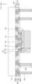
도 1은 본 발명의 기술적 사상의 일 실시예에 따른 반도체 패키지의 주요 구성을 나타내는 단면도이다.
도 2는 도 1의 AA 부분을 확대하여 나타내는 확대 단면도이다.
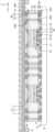
도 3은 도 2의 언더 범프 메탈의 주변 영역을 나타내는 주사 전자 현미경 사진이다.
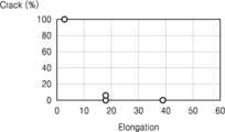
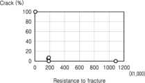
도 4 내지 도 6은 재배선 구조체에 포함되는 절연층을 구성하는 절연 물질의 여러 가지 물성에 따른 크랙의 발생 정도를 나타내는 그래프이다.
도 7은 본 발명의 기술적 사상의 다른 실시예에 따른 반도체 패키지의 주요 구성을 나타내는 단면도이다.
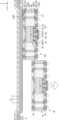
도 8은 도 7의 BB 부분을 확대하여 나타내는 확대 단면도이다.
도 9는 본 발명의 기술적 사상의 일 실시예에 따른 반도체 패키지의 제조 방법을 나타내는 흐름도이다.
도 10 내지 도 22는 본 발명의 기술적 사상의 일 실시예에 따른 반도체 패키지의 제조 방법을 공정 순서에 따라 나타내는 단면도들이다.
도 23은 본 발명의 기술적 사상의 실시예들에 따른 반도체 패키지의 구성을 개략적으로 나타내는 구성도이다.FIG. 1 is a cross-sectional view showing the main configuration of a semiconductor package according to one embodiment of the technical idea of the present invention.
Figure 2 is an enlarged cross-sectional view showing the AA portion of Figure 1 in an enlarged manner.
Figure 3 is a scanning electron microscope photograph showing the surrounding area of the under bump metal of Figure 2.
Figures 4 to 6 are graphs showing the degree of crack occurrence according to various properties of the insulating material constituting the insulating layer included in the rewiring structure.
FIG. 7 is a cross-sectional view showing the main configuration of a semiconductor package according to another embodiment of the technical idea of the present invention.
Fig. 8 is an enlarged cross-sectional view showing the BB portion of Fig. 7 in an enlarged manner.
FIG. 9 is a flowchart showing a method for manufacturing a semiconductor package according to one embodiment of the technical idea of the present invention.
FIGS. 10 to 22 are cross-sectional views showing a method for manufacturing a semiconductor package according to an embodiment of the technical idea of the present invention in the order of processes.
FIG. 23 is a schematic diagram showing the configuration of a semiconductor package according to embodiments of the technical idea of the present invention.
이하, 첨부한 도면들을 참조하여 본 발명의 기술적 사상의 실시예에 대해 상세히 설명하기로 한다.Hereinafter, embodiments of the technical idea of the present invention will be described in detail with reference to the attached drawings.
도 1은 본 발명의 기술적 사상의 일 실시예에 따른 반도체 패키지의 주요 구성을 나타내는 단면도이다. 도 2는 도 1의 AA 부분을 확대하여 나타내는 확대 단면도이다. 도 3은 도 2의 언더 범프 메탈의 주변 영역을 나타내는 주사 전자 현미경 사진이다.FIG. 1 is a cross-sectional view showing the main configuration of a semiconductor package according to one embodiment of the technical idea of the present invention. FIG. 2 is an enlarged cross-sectional view showing a portion AA of FIG. 1 in an enlarged manner. FIG. 3 is a scanning electron microscope photograph showing a peripheral area of the under bump metal of FIG. 2.
도 1 내지 도 3을 함께 참조하면, 반도체 패키지(1000)는, 제1 반도체 칩(100), 상기 제1 반도체 칩(100)의 주위에 배치되는 도전 포스트(200), 상기 제1 반도체 칩(100)의 하부에 배치되는 제1 재배선 구조체(300), 상기 제1 반도체 칩(100)의 상부에 배치되는 제2 재배선 구조체(400), 및 상기 제2 재배선 구조체(400)의 상부에 배치되는 제2 반도체 칩(500)을 포함할 수 있다.Referring to FIGS. 1 to 3 together, a semiconductor package (1000) may include a first semiconductor chip (100), a conductive post (200) arranged around the first semiconductor chip (100), a first redistribution structure (300) arranged below the first semiconductor chip (100), a second redistribution structure (400) arranged above the first semiconductor chip (100), and a second semiconductor chip (500) arranged above the second redistribution structure (400).
반도체 패키지(1000)는 패키지 온 패키지(Package-on-Package, PoP) 구조일 수 있다. 구체적으로, 반도체 패키지(1000)는, 제1 재배선 구조체(300)의 수평 폭 및 수평 면적이 제1 반도체 칩(100)이 구성하는 수평 폭 및 수평 면적보다 더 큰, 팬 아웃 반도체 패키지(Fan Out Semiconductor Package)일 수 있다. 일부 실시예들에서, 반도체 패키지(1000)는 팬 아웃 웨이퍼 레벨 패키지(Fan Out Wafer Level Package, FOWLP) 또는 팬 아웃 패널 레벨 패키지(Fan Out Panel Level Package, FOPLP)일 수 있다.The semiconductor package (1000) may have a package-on-package (PoP) structure. Specifically, the semiconductor package (1000) may be a fan out semiconductor package in which a horizontal width and a horizontal area of the first redistribution structure (300) are larger than the horizontal width and the horizontal area of the first semiconductor chip (100). In some embodiments, the semiconductor package (1000) may be a fan out wafer level package (FOWLP) or a fan out panel level package (FOPLP).
일부 실시예들에서, 제1 재배선 구조체(300) 및 제2 재배선 구조체(400)는 재배선 공정에 의하여 형성될 수 있다. 여기서, 제1 재배선 구조체(300) 및 제2 재배선 구조체(400)는 하부 재배선 구조체 및 상부 재배선 구조체로 지칭할 수 있다.In some embodiments, the first rewiring structure (300) and the second rewiring structure (400) may be formed by a rewiring process. Here, the first rewiring structure (300) and the second rewiring structure (400) may be referred to as a lower rewiring structure and an upper rewiring structure.
제1 재배선 구조체(300)는 제1 재배선 절연층(310) 및 복수의 제1 재배선 패턴(330)을 포함할 수 있다. 제1 재배선 절연층(310)은 복수의 제1 재배선 패턴(330)을 감쌀 수 있다. 일부 실시예들에서, 제1 재배선 구조체(300)는 적층된 복수의 제1 재배선 절연층(310)을 포함할 수 있다. 예를 들어, 복수의 제1 재배선 절연층(310)은 순차적으로 제1 절연층(312), 제2 절연층(314), 및 제3 절연층(316)을 포함할 수 있으나, 이에 한정되는 것은 아니다. 제1 절연층(312), 제2 절연층(314), 및 제3 절연층(316)은 서로 동일한 물질로 형성되거나, 서로 다른 물질로 형성될 수 있다. 제1 재배선 절연층(310)은 예를 들어, PID(Photo Imageable Dielectric) 물질로 형성될 수 있다. 예를 들어, 제1 절연층(312), 제2 절연층(314), 및 제3 절연층(316) 중 적어도 하나는, 아래의 TC 인덱스 1 또는 TC 인덱스 2에서 K값이 서로 다른 절연 물질을 포함하도록 구성될 수 있다. 이에 대한 자세한 설명은 후술한다.The first redistribution structure (300) may include a first redistribution insulating layer (310) and a plurality of first redistribution patterns (330). The first redistribution insulating layer (310) may surround the plurality of first redistribution patterns (330). In some embodiments, the first redistribution structure (300) may include a plurality of stacked first redistribution insulating layers (310). For example, the plurality of first redistribution insulating layers (310) may sequentially include, but are not limited to, a first insulating layer (312), a second insulating layer (314), and a third insulating layer (316). The first insulating layer (312), the second insulating layer (314), and the third insulating layer (316) may be formed of the same material or different materials. The first redistribution insulating layer (310) may be formed of, for example, a PID (Photo Imageable Dielectric) material. For example, at least one of the first insulating layer (312), the second insulating layer (314), and the third insulating layer (316) may be configured to include an insulating material having different K values in the TC index 1 or TC index 2 below. A detailed description thereof will be provided below.
복수의 제1 재배선 패턴(330)은 복수의 제1 재배선 라인 패턴(332) 및 복수의 제1 재배선 비아(334)로 이루어질 수 있다. 복수의 제1 재배선 패턴(330)은 예를 들어, 구리(Cu), 알루미늄(Al), 텅스텐(W), 티타늄(Ti), 탄탈륨(Ta), 인듐(In), 몰리브덴(Mo), 망간(Mn), 코발트(Co), 주석(Sn), 니켈(Ni), 마그네슘(Mg), 레늄(Re), 베릴륨(Be), 갈륨(Ga), 루테늄(Ru) 등과 같은 금속 또는 상기 금속의 합금일 수 있지만, 이에 한정되는 것은 아니다.The plurality of first redistribution patterns (330) may be formed of a plurality of first redistribution line patterns (332) and a plurality of first redistribution vias (334). The plurality of first redistribution patterns (330) may be, for example, a metal such as copper (Cu), aluminum (Al), tungsten (W), titanium (Ti), tantalum (Ta), indium (In), molybdenum (Mo), manganese (Mn), cobalt (Co), tin (Sn), nickel (Ni), magnesium (Mg), rhenium (Re), beryllium (Be), gallium (Ga), ruthenium (Ru), or an alloy of the above metals, but is not limited thereto.
복수의 제1 재배선 라인 패턴(332)은 제1 재배선 절연층(310)의 상면 및 하면 중 적어도 일면에 배치될 수 있다. 예를 들어, 제1 재배선 구조체(300)가 적층된 복수의 제1 재배선 절연층(310)을 포함하는 경우, 복수의 제1 재배선 라인 패턴(332)은 최상단의 제1 재배선 절연층(310)의 상면, 최하단의 제1 재배선 절연층(310)의 하면, 및 이웃하는 제1 재배선 절연층(310)의 사이에 배치될 수 있다.A plurality of first redistribution line patterns (332) may be arranged on at least one of the upper and lower surfaces of the first redistribution insulation layer (310). For example, when the first redistribution structure (300) includes a plurality of stacked first redistribution insulation layers (310), a plurality of first redistribution line patterns (332) may be arranged on the upper surface of the uppermost first redistribution insulation layer (310), the lower surface of the lowermost first redistribution insulation layer (310), and between adjacent first redistribution insulation layers (310).
복수의 제1 재배선 비아(334)는 제1 재배선 절연층(310)을 관통하여 복수의 제1 재배선 라인 패턴(332) 중 일부와 연결될 수 있다. 일부 실시예들에서, 복수의 제1 재배선 비아(334)는 하측으로부터 상측으로 수평 폭이 커지며 연장되는 테이퍼진(tapered) 형상을 가질 수 있다.A plurality of first redistribution vias (334) may penetrate the first redistribution insulating layer (310) and be connected to some of the plurality of first redistribution line patterns (332). In some embodiments, the plurality of first redistribution vias (334) may have a tapered shape that extends with a horizontal width that increases from the bottom to the top.
일부 실시예들에서, 복수의 제1 재배선 라인 패턴(332) 중 일부는 복수의 제1 재배선 비아(334) 중 일부와 함께 형성되어 일체를 이룰 수 있다. 예를 들어, 제1 재배선 라인 패턴(332)과 제1 재배선 라인 패턴(332)의 하면과 접촉하는 제1 재배선 비아(334)는 함께 형성되어 일체를 이룰 수 있다.In some embodiments, some of the plurality of first redistribution line patterns (332) may be formed together with some of the plurality of first redistribution vias (334) to form a single body. For example, the first redistribution line pattern (332) and the first redistribution via (334) in contact with the lower surface of the first redistribution line pattern (332) may be formed together to form a single body.
복수의 제1 재배선 패턴(330) 중, 제1 재배선 구조체(300)의 하면에 이웃하여 배치되는 일부를 복수의 제1 하면 연결 패드(330P1)로 지칭할 수 있고, 제1 재배선 구조체(300)의 상면에 이웃하여 배치되는 일부를 복수의 제1 상면 연결 패드(330P2)로 지칭할 수 있다. 즉, 복수의 제1 하면 연결 패드(330P1)는 복수의 제1 재배선 라인 패턴(332) 중 제1 재배선 구조체(300)의 하면에 이웃하여 배치되는 일부일 수 있고, 복수의 제1 상면 연결 패드(330P2)는 복수의 제1 재배선 라인 패턴(332) 중 제1 재배선 구조체(300)의 상면에 이웃하여 배치되는 일부일 수 있다.Among the plurality of first redistribution patterns (330), some of them arranged adjacent to the lower surface of the first redistribution structure (300) may be referred to as a plurality of first lower surface connection pads (330P1), and some of them arranged adjacent to the upper surface of the first redistribution structure (300) may be referred to as a plurality of first upper surface connection pads (330P2). That is, the plurality of first lower surface connection pads (330P1) may be some of the plurality of first redistribution line patterns (332) arranged adjacent to the lower surface of the first redistribution structure (300), and the plurality of first upper surface connection pads (330P2) may be some of the plurality of first redistribution line patterns (332) arranged adjacent to the upper surface of the first redistribution structure (300).
복수의 제1 하면 연결 패드(330P1)에는 복수의 외부 연결 단자(600)가 부착될 수 있다. 복수의 외부 연결 단자(600)는 반도체 패키지(1000)를 외부와 연결할 수 있다. 일부 실시예들에서, 복수의 외부 연결 단자(600)는 솔더 범프 또는 솔더 볼일 수 있다. 이와 달리, 복수의 제1 상면 연결 패드(330P2) 중 일부에는 복수의 칩 연결 부재(130)가 부착될 수 있고, 다른 일부에는 복수의 도전 포스트(200)가 부착될 수 있다.A plurality of external connection terminals (600) may be attached to a plurality of first lower surface connection pads (330P1). The plurality of external connection terminals (600) may connect the semiconductor package (1000) to the outside. In some embodiments, the plurality of external connection terminals (600) may be solder bumps or solder balls. Alternatively, a plurality of chip connection members (130) may be attached to some of the plurality of first upper surface connection pads (330P2), and a plurality of conductive posts (200) may be attached to other parts.
일부 실시예들에서, 복수의 제1 하면 연결 패드(330P1)와 복수의 외부 연결 단자(600) 사이에 복수의 언더 범프 메탈(under bump metal)(UBM)이 배치될 수 있다. 즉, 복수의 제1 하면 연결 패드(330P1)의 아래에 복수의 언더 범프 메탈(UBM)이 배치되고, 복수의 언더 범프 메탈(UBM)의 아래에 복수의 외부 연결 단자(600)가 배치될 수 있다. 이에 따라, 복수의 언더 범프 메탈(UBM)은 제1 재배선 절연층(310)의 최하면으로부터 아래로 돌출되도록 배치될 수 있다.In some embodiments, a plurality of under bump metals (UBMs) may be disposed between a plurality of first lower surface connection pads (330P1) and a plurality of external connection terminals (600). That is, a plurality of under bump metals (UBMs) may be disposed under a plurality of first lower surface connection pads (330P1), and a plurality of external connection terminals (600) may be disposed under the plurality of under bump metals (UBMs). Accordingly, the plurality of under bump metals (UBMs) may be disposed to protrude downward from a lowermost surface of the first rewiring insulating layer (310).
일부 실시예들에서, 복수의 제1 하면 연결 패드(330P1) 중 일부에 복수의 외부 연결 단자(600)가 부착되고, 복수의 제1 하면 연결 패드(330P1) 중 다른 일부에 수동 소자(610)가 부착될 수 있다.In some embodiments, a plurality of external connection terminals (600) may be attached to some of the plurality of first lower surface connection pads (330P1), and a passive component (610) may be attached to other some of the plurality of first lower surface connection pads (330P1).
복수의 외부 연결 단자(600)가 제1 재배선 구조체(300)의 상면 상에 형성될 수 있다. 복수의 외부 연결 단자(600)는 예를 들어, 솔더 볼, 도전성 범프, 도전성 페이스트, 비지에이(ball grid array, BGA), 엘지에이(lead grid array, LGA), 피지에이(pin grid array, PGA), 또는 이들의 조합을 포함할 수 있다.A plurality of external connection terminals (600) may be formed on an upper surface of the first rewiring structure (300). The plurality of external connection terminals (600) may include, for example, solder balls, conductive bumps, conductive paste, a ball grid array (BGA), a lead grid array (LGA), a pin grid array (PGA), or a combination thereof.
수동 소자(610)는 레지스터(resistor), 커패시터(capacitor), 인덕터(inductor), 써미스터(thermistor), 오실레이터(oscillator), 페라이트 비드(ferrite bead), 안테나(antenna), 및 배리스터(varistor) 중에서 선택되는 적어도 하나를 포함할 수 있다. 예를 들어, 수동 소자(610)는 MLCC(Multi Layer Ceramic Capacitor), LICC(Low Inductance Chip Capacitor), LSC(Land Side Capacitor), 집적 수동 소자(Integrated Passive Device, IPD) 등을 포함할 수 있으나, 이에 한정되는 것은 아니다.The passive component (610) may include at least one selected from a resistor, a capacitor, an inductor, a thermistor, an oscillator, a ferrite bead, an antenna, and a varistor. For example, the passive component (610) may include, but is not limited to, a multi layer ceramic capacitor (MLCC), a low inductance chip capacitor (LICC), a land side capacitor (LSC), an integrated passive device (IPD), etc.
외부 언더필층(650)은 수동 소자(610)의 아래에 배치되는 솔더 범프(630)의 측벽을 둘러싸며 서로 인접한 솔더 범프(630)의 틈을 채울 수 있다. 수동 소자(610)와 솔더 범프(630)의 전기적 연결 과정에서, 수동 소자(610)와 솔더 범프(630)의 사이에는 틈이 형성될 수 있다. 이러한 틈은 수동 소자(610)와 솔더 범프(630)의 접속 신뢰성에 문제를 야기할 수 있으므로, 접속을 보강하기 위해 외부 언더필층(650)을 주입하고 경화할 수 있다.The outer underfill layer (650) surrounds the sidewall of the solder bump (630) positioned below the passive component (610) and can fill the gap between the adjacent solder bumps (630). During the electrical connection process between the passive component (610) and the solder bump (630), a gap may be formed between the passive component (610) and the solder bump (630). Since such a gap may cause a problem in the connection reliability between the passive component (610) and the solder bump (630), the outer underfill layer (650) may be injected and cured to reinforce the connection.
외부 언더필층(650)에 의해 수동 소자(610)는 솔더 범프(630) 상에 더욱 안정적으로 고정되며, 수동 소자(610)와 솔더 범프(630) 사이의 열팽창 계수 차이에도, 수동 소자(610)와 솔더 범프(630)는 전기적으로 분리되지 않을 수 있다.The passive component (610) is more stably fixed on the solder bump (630) by the external underfill layer (650), and even if there is a difference in thermal expansion coefficient between the passive component (610) and the solder bump (630), the passive component (610) and the solder bump (630) may not be electrically separated.
복수의 제1 상면 연결 패드(330P2)는 제1 재배선 절연층(310)의 상면 상에 배치될 수 있다. 예를 들어, 제1 재배선 구조체(300)가 적층된 복수의 제1 재배선 절연층(310)을 포함하는 경우, 복수의 제1 상면 연결 패드(330P2)는 최상단의 제1 재배선 절연층(310)의 상면 상에 배치될 수 있다.A plurality of first upper surface connection pads (330P2) may be arranged on the upper surface of the first redistribution insulating layer (310). For example, when the first redistribution structure (300) includes a plurality of stacked first redistribution insulating layers (310), a plurality of first upper surface connection pads (330P2) may be arranged on the upper surface of the uppermost first redistribution insulating layer (310).
제1 재배선 구조체(300) 상에는 적어도 하나의 제1 반도체 칩(100)이 실장될 수 있다. 즉, 제1 반도체 칩(100)은 단수 개 또는 복수 개로 구성될 수 있다. 제1 반도체 칩(100)은 서로 대향하는 활성면과 비활성면을 가지는 반도체 기판(110), 반도체 기판(110)의 활성면에 형성되는 반도체 소자(112), 및 제1 반도체 칩(100)의 제1 면에 배치되는 복수의 칩 패드(120)를 포함할 수 있다. 예를 들어, 제1 반도체 칩(100)은 약 150㎛ 이상의 두께(100T)를 가질 수 있다.At least one first semiconductor chip (100) may be mounted on the first rewiring structure (300). That is, the first semiconductor chip (100) may be composed of a single or multiple pieces. The first semiconductor chip (100) may include a semiconductor substrate (110) having an active surface and an inactive surface facing each other, a semiconductor element (112) formed on the active surface of the semiconductor substrate (110), and a plurality of chip pads (120) arranged on the first surface of the first semiconductor chip (100). For example, the first semiconductor chip (100) may have a thickness (100T) of about 150 ㎛ or more.
여기서, 제1 반도체 칩(100)의 제1 면과 제2 면은 서로 대향하며, 제1 반도체 칩(100)의 상기 제2 면은 반도체 기판(110)의 상기 비활성면을 의미한다. 반도체 기판(110)의 상기 활성면은 제1 반도체 칩(100)의 상기 제1 면에 이웃하므로, 반도체 기판(110)의 상기 활성면과 제1 반도체 칩(100)의 상기 제1 면을 구분하는 도시는 생략하였다.Here, the first surface and the second surface of the first semiconductor chip (100) face each other, and the second surface of the first semiconductor chip (100) means the inactive surface of the semiconductor substrate (110). Since the active surface of the semiconductor substrate (110) is adjacent to the first surface of the first semiconductor chip (100), the drawing distinguishing between the active surface of the semiconductor substrate (110) and the first surface of the first semiconductor chip (100) is omitted.
일부 실시예들에서, 제1 반도체 칩(100)은 상기 제1 면이 제1 재배선 구조체(300)를 향하는 페이스 다운(face down) 배치를 가지며, 제1 재배선 구조체(300)의 상면에 실장될 수 있다. 이 경우, 제1 반도체 칩(100)의 상기 제1 면은 제1 반도체 칩(100)의 하면으로 지칭할 수 있고, 제1 반도체 칩(100)의 상기 제2 면은 제1 반도체 칩(100)의 상면으로 지칭할 수 있다.In some embodiments, the first semiconductor chip (100) has a face down arrangement in which the first surface faces the first redistribution structure (300) and may be mounted on the upper surface of the first redistribution structure (300). In this case, the first surface of the first semiconductor chip (100) may be referred to as the lower surface of the first semiconductor chip (100), and the second surface of the first semiconductor chip (100) may be referred to as the upper surface of the first semiconductor chip (100).
제1 반도체 칩(100)의 복수의 칩 패드(120)와 제1 재배선 구조체(300)의 복수의 제1 상면 연결 패드(330P2) 중 일부 사이에는 복수의 칩 연결 부재(130)가 개재될 수 있다. 예를 들어, 복수의 칩 연결 부재(130) 각각은 솔더 볼 또는 마이크로 범프일 수 있다. 제1 반도체 칩(100)과 제1 재배선 구조체(300)의 제1 재배선 패턴(330)은 복수의 칩 연결 부재(130)를 통하여 전기적으로 연결될 수 있다. 복수의 칩 연결 부재(130)는 복수의 칩 패드(120) 상에 배치되는 범프층(132) 및 범프층(132)을 덮는 내부 연결 단자(134)를 포함할 수 있다. 복수의 칩 연결 부재(130)는 예를 들어, 구리(Cu), 알루미늄(Al), 은(Ag), 주석(Tin), 금(Au), 또는 솔더(solder)로 형성될 수 있으나, 이에 한정되는 것은 아니다.A plurality of chip connection members (130) may be interposed between a plurality of chip pads (120) of a first semiconductor chip (100) and some of a plurality of first upper surface connection pads (330P2) of a first redistribution structure (300). For example, each of the plurality of chip connection members (130) may be a solder ball or a micro bump. The first semiconductor chip (100) and the first redistribution pattern (330) of the first redistribution structure (300) may be electrically connected through the plurality of chip connection members (130). The plurality of chip connection members (130) may include a bump layer (132) disposed on the plurality of chip pads (120) and an internal connection terminal (134) covering the bump layer (132). The plurality of chip connecting members (130) may be formed of, for example, copper (Cu), aluminum (Al), silver (Ag), tin (Tin), gold (Au), or solder, but are not limited thereto.
반도체 기판(110)은 예를 들어, 실리콘(Si) 또는 저머늄(Ge)과 같은 반도체 물질을 포함할 수 있다. 또는 반도체 기판(110)은 SiC(silicon carbide), GaAs(gallium arsenide), InAs(indium arsenide), 및 InP(indium phosphide)와 같은 화합물 반도체 물질을 포함할 수 있다. 반도체 기판(110)은 도전 영역인 불순물이 도핑된 웰(well)을 포함할 수 있다. 반도체 기판(110)은 STI(shallow trench isolation) 구조와 같은 다양한 소자 분리 구조를 가질 수 있다.The semiconductor substrate (110) may include a semiconductor material, such as silicon (Si) or germanium (Ge), for example. Alternatively, the semiconductor substrate (110) may include a compound semiconductor material, such as silicon carbide (SiC), gallium arsenide (GaAs), indium arsenide (InAs), and indium phosphide (InP). The semiconductor substrate (110) may include a well doped with an impurity, which is a conductive region. The semiconductor substrate (110) may have various device isolation structures, such as a shallow trench isolation (STI) structure.
반도체 기판(110)의 상기 활성면에는 다양한 종류의 복수의 개별 소자(individual devices)를 포함하는 반도체 소자(112)가 형성될 수 있다. 상기 복수의 개별 소자는 반도체 기판(110)의 상기 도전 영역에 전기적으로 연결될 수 있다. 반도체 소자(112)는 복수의 개별 소자와 반도체 기판(110)의 상기 도전 영역을 전기적으로 연결하는 도전성 배선 또는 도전성 플러그를 더 포함할 수 있다. 또한, 상기 복수의 개별 소자는 각각 절연막에 의하여 이웃하는 다른 개별 소자와 전기적으로 분리될 수 있다.A semiconductor device (112) including a plurality of individual devices of various types may be formed on the active surface of the semiconductor substrate (110). The plurality of individual devices may be electrically connected to the conductive region of the semiconductor substrate (110). The semiconductor device (112) may further include a conductive wire or a conductive plug that electrically connects the plurality of individual devices and the conductive region of the semiconductor substrate (110). In addition, each of the plurality of individual devices may be electrically separated from other neighboring individual devices by an insulating film.
일부 실시예들에서, 제1 반도체 칩(100)은 로직 소자를 포함할 수 있다. 예를 들어, 제1 반도체 칩(100)은 중앙 처리 장치 칩, 그래픽 처리 장치 칩, 또는 어플리케이션 프로세서 칩일 수 있다. 다른 실시예들에서, 반도체 패키지(1000)가 복수의 제1 반도체 칩(100)을 포함하는 경우, 복수의 제1 반도체 칩(100) 중 하나는 중앙 처리 장치 칩, 그래픽 처리 장치 칩, 또는 어플리케이션 프로세서 칩일 수 있고, 다른 하나는 메모리 소자를 포함하는 메모리 반도체 칩일 수 있다.In some embodiments, the first semiconductor chip (100) may include a logic element. For example, the first semiconductor chip (100) may be a central processing unit chip, a graphic processing unit chip, or an application processor chip. In other embodiments, when the semiconductor package (1000) includes a plurality of first semiconductor chips (100), one of the plurality of first semiconductor chips (100) may be a central processing unit chip, a graphic processing unit chip, or an application processor chip, and the other may be a memory semiconductor chip including a memory element.
예를 들어, 상기 메모리 소자는, 플래시 메모리(Flash Memory), PRAM(Phase-change Random Access Memory), MRAM(Magnetoresistive Random Access Memory), FeRAM(Ferroelectric Random Access Memory) 또는 RRAM(Resistive Random Access Memory)과 같은 비휘발성 메모리 소자일 수 있다. 일부 실시예들에서, 상기 메모리 소자는 DRAM(Dynamic Random Access Memory) 또는 SRAM(Static Random Access Memory)과 같은 휘발성 메모리 소자일 수 있다.For example, the memory device may be a non-volatile memory device, such as a flash memory, a phase-change random access memory (PRAM), a magnetoresistive random access memory (MRAM), a ferroelectric random access memory (FeRAM), or a resistive random access memory (RRAM). In some embodiments, the memory device may be a volatile memory device, such as a dynamic random access memory (DRAM) or a static random access memory (SRAM).
제2 재배선 구조체(400)는 제2 재배선 절연층(410) 및 복수의 제2 재배선 패턴(430)을 포함할 수 있다. 제2 재배선 절연층(410)은 복수의 제2 재배선 패턴(430)을 감쌀 수 있다. 일부 실시예들에서, 제2 재배선 구조체(400)는 적층된 복수의 제2 재배선 절연층(410)을 포함할 수 있다. 예를 들어, 복수의 제2 재배선 절연층(410)은 순차적으로 제4 절연층(412), 제5 절연층(414), 및 제6 절연층(416)을 포함할 수 있으나, 이에 한정되는 것은 아니다. 제4 절연층(412), 제5 절연층(414), 및 제6 절연층(416)은 서로 동일한 물질로 형성되거나, 서로 다른 물질로 형성될 수 있다. 제2 재배선 절연층(410)은 예를 들어, PID 물질로 형성될 수 있다. 예를 들어, 제4 절연층(412), 제5 절연층(414), 및 제6 절연층(416) 중 적어도 하나는, 아래의 TC 인덱스 1 또는 TC 인덱스 2에서 K값이 서로 다른 절연 물질을 포함하도록 구성될 수 있다. 이에 대한 자세한 설명은 후술한다.The second redistribution structure (400) may include a second redistribution insulating layer (410) and a plurality of second redistribution patterns (430). The second redistribution insulating layer (410) may surround the plurality of second redistribution patterns (430). In some embodiments, the second redistribution structure (400) may include a plurality of stacked second redistribution insulating layers (410). For example, the plurality of second redistribution insulating layers (410) may sequentially include, but are not limited to, a fourth insulating layer (412), a fifth insulating layer (414), and a sixth insulating layer (416). The fourth insulating layer (412), the fifth insulating layer (414), and the sixth insulating layer (416) may be formed of the same material or different materials. The second redistribution insulating layer (410) may be formed of, for example, a PID material. For example, at least one of the fourth insulating layer (412), the fifth insulating layer (414), and the sixth insulating layer (416) may be configured to include an insulating material having different K values in the TC index 1 or TC index 2 below. A detailed description thereof will be provided below.
일부 실시예들에서, 제2 재배선 구조체(400)는 적층된 복수의 제2 재배선 절연층(410)을 포함할 수 있다. 복수의 제2 재배선 패턴(430)은 복수의 제2 재배선 라인 패턴(432) 및 복수의 제2 재배선 비아(434)로 이루어질 수 있다. 복수의 제2 재배선 패턴(430)은 금속 또는 금속의 합금일 수 있다. 일부 실시예들에서, 복수의 제2 재배선 패턴(430)은 씨드층 상에 금속 또는 금속의 합금이 적층되어 형성될 수 있다.In some embodiments, the second redistribution structure (400) may include a plurality of stacked second redistribution insulating layers (410). The plurality of second redistribution patterns (430) may be formed of a plurality of second redistribution line patterns (432) and a plurality of second redistribution vias (434). The plurality of second redistribution patterns (430) may be a metal or an alloy of metals. In some embodiments, the plurality of second redistribution patterns (430) may be formed by stacking a metal or an alloy of metals on a seed layer.
복수의 제2 재배선 라인 패턴(432)은 제2 재배선 절연층(410)의 상면 및 하면 중 적어도 일면에 배치될 수 있다. 예를 들어, 제2 재배선 구조체(400)가 적층된 복수의 제2 재배선 절연층(410)을 포함하는 경우, 복수의 제2 재배선 라인 패턴(432)은 최상단의 제2 재배선 절연층(410)의 상면, 최하단의 제2 재배선 절연층(410)의 하면, 및 이웃하는 제2 재배선 절연층(410)의 사이에 배치될 수 있다.A plurality of second redistribution line patterns (432) may be arranged on at least one of the upper and lower surfaces of the second redistribution insulation layer (410). For example, when the second redistribution structure (400) includes a plurality of stacked second redistribution insulation layers (410), a plurality of second redistribution line patterns (432) may be arranged on the upper surface of the uppermost second redistribution insulation layer (410), the lower surface of the lowermost second redistribution insulation layer (410), and between adjacent second redistribution insulation layers (410).
복수의 제2 재배선 패턴(430) 중, 제2 재배선 구조체(400)의 하면에 이웃하여 배치되는 일부를 복수의 제2 하면 연결 패드(430P1)로 지칭할 수 있고, 제2 재배선 구조체(400)의 상면에 이웃하여 배치되는 일부는 복수의 제2 상면 연결 패드(430P2)로 지칭할 수 있다. 예를 들어, 복수의 제2 하면 연결 패드(430P1)는 복수의 제2 재배선 라인 패턴(432) 중 제2 재배선 구조체(400)의 하면에 이웃하여 배치되는 일부일 수 있고, 복수의 제2 상면 연결 패드(430P2)는 복수의 제2 재배선 라인 패턴(432) 중 제2 재배선 구조체(400)의 상면에 이웃하여 배치되는 일부일 수 있다. 다른 실시예들에서, 복수의 제2 하면 연결 패드(430P1)는 복수의 제2 재배선 비아(434) 중 제2 재배선 구조체(400)의 하면에 이웃하여 배치되는 일부일 수 있다.Among the plurality of second redistribution patterns (430), some of them arranged adjacent to the lower surface of the second redistribution structure (400) may be referred to as a plurality of second lower surface connection pads (430P1), and some of them arranged adjacent to the upper surface of the second redistribution structure (400) may be referred to as a plurality of second upper surface connection pads (430P2). For example, the plurality of second lower surface connection pads (430P1) may be some of the plurality of second redistribution line patterns (432) arranged adjacent to the lower surface of the second redistribution structure (400), and the plurality of second upper surface connection pads (430P2) may be some of the plurality of second redistribution line patterns (432) arranged adjacent to the upper surface of the second redistribution structure (400). In other embodiments, the plurality of second bottom-facing connection pads (430P1) may be some of the plurality of second redistribution vias (434) arranged adjacent to the bottom surface of the second redistribution structure (400).
제2 반도체 칩(500)은 제2 반도체 소자(512) 및 복수의 제2 패드(530)를 가질 수 있다. 제2 반도체 칩(500)은 복수의 제2 패드(530)와 복수의 제2 상면 연결 패드(430P2) 사이에 개재되는 복수의 내부 연결 단자(550)에 의하여 제2 재배선 구조체(400)와 전기적으로 연결될 수 있다. 제2 반도체 칩(500)은 복수의 제2 패드(530)가 제2 재배선 구조체(400)를 향하도록, 제2 재배선 구조체(400) 상에 실장될 수 있다.The second semiconductor chip (500) may have a second semiconductor element (512) and a plurality of second pads (530). The second semiconductor chip (500) may be electrically connected to the second redistribution structure (400) by a plurality of internal connection terminals (550) interposed between the plurality of second pads (530) and the plurality of second upper surface connection pads (430P2). The second semiconductor chip (500) may be mounted on the second redistribution structure (400) such that the plurality of second pads (530) face the second redistribution structure (400).
일부 실시예들에서, 제2 반도체 칩(500)은 복수의 제2 패드(530)에 부착되는 복수의 내부 연결 단자(550), 복수의 제2 재배선 패턴(430), 및 복수의 도전 포스트(200)를 통하여 제1 재배선 구조체(300)의 복수의 제1 재배선 패턴(330)과 전기적으로 연결될 수 있다.In some embodiments, the second semiconductor chip (500) may be electrically connected to a plurality of first redistribution patterns (330) of the first redistribution structure (300) through a plurality of internal connection terminals (550), a plurality of second redistribution patterns (430), and a plurality of conductive posts (200) attached to a plurality of second pads (530).
일부 실시예들에서, 제2 반도체 소자(512)는 메모리 소자일 수 있다. 예를 들어, 상기 메모리 소자는, 플래시 메모리, PRAM, MRAM, FeRAM, 또는 RRAM과 같은 비휘발성 메모리 소자일 수 있다. 일부 실시예들에서, 상기 메모리 소자는 DRAM 또는 SRAM과 같은 휘발성 메모리 소자일 수 있다.In some embodiments, the second semiconductor element (512) may be a memory element. For example, the memory element may be a non-volatile memory element, such as flash memory, PRAM, MRAM, FeRAM, or RRAM. In some embodiments, the memory element may be a volatile memory element, such as DRAM or SRAM.
복수의 제2 하면 연결 패드(430P1)는 제2 재배선 절연층(410)의 하면에 배치될 수 있다. 예를 들어, 제2 재배선 구조체(400)가 적층된 복수의 제2 재배선 절연층(410)을 포함하는 경우, 복수의 제2 하면 연결 패드(430P1)는 최하단의 제2 재배선 절연층(410)의 하면에 배치될 수 있다.A plurality of second bottom connection pads (430P1) may be arranged on the bottom surface of the second redistribution insulating layer (410). For example, when the second redistribution structure (400) includes a plurality of stacked second redistribution insulating layers (410), a plurality of second bottom connection pads (430P1) may be arranged on the bottom surface of the lowermost second redistribution insulating layer (410).
복수의 제2 상면 연결 패드(430P2)는 제2 재배선 절연층(410)의 상면에 배치될 수 있다. 예를 들어, 제2 재배선 구조체(400)가 적층된 복수의 제2 재배선 절연층(410)을 포함하는 경우, 복수의 제2 상면 연결 패드(430P2)는 최상단의 제2 재배선 절연층(410)의 상면에 배치될 수 있다.A plurality of second upper surface connection pads (430P2) may be arranged on the upper surface of the second redistribution insulating layer (410). For example, when the second redistribution structure (400) includes a plurality of stacked second redistribution insulating layers (410), a plurality of second upper surface connection pads (430P2) may be arranged on the upper surface of the uppermost second redistribution insulating layer (410).
복수의 제2 재배선 비아(434)는 제2 재배선 절연층(410)을 관통하여, 복수의 제2 재배선 라인 패턴(432) 중 일부와 접촉하여 연결될 수 있다. 일부 실시예들에서, 복수의 제2 재배선 라인 패턴(432) 중 일부는 복수의 제2 재배선 비아(434) 중 일부와 함께 형성되어 일체를 이룰 수 있다. 예를 들어, 제2 재배선 라인 패턴(432)과 제2 재배선 라인 패턴(432)의 하면과 접촉하는 제2 재배선 비아(434)는 함께 형성되어 일체를 이룰 수 있다.A plurality of second redistribution vias (434) may penetrate the second redistribution insulating layer (410) and may be connected to and in contact with some of the plurality of second redistribution line patterns (432). In some embodiments, some of the plurality of second redistribution line patterns (432) may be formed together with some of the plurality of second redistribution vias (434) to form a single body. For example, a second redistribution line pattern (432) and a second redistribution via (434) in contact with a lower surface of the second redistribution line pattern (432) may be formed together to form a single body.
일부 실시예들에서, 복수의 제2 재배선 비아(434)는 상측으로부터 하측으로 수평 폭이 좁아지며 연장되는 테이퍼진 형상을 가질 수 있다. 즉, 복수의 제1 재배선 비아(334)와 복수의 제2 재배선 비아(434)는 같은 방향을 향하여 연장되며 각각 수평 폭이 좁아질 수 있으나, 이에 한정되는 것은 아니다.In some embodiments, the plurality of second redistribution vias (434) may have a tapered shape that extends from top to bottom with a horizontal width that narrows. That is, the plurality of first redistribution vias (334) and the plurality of second redistribution vias (434) may extend in the same direction and each may have a horizontal width that narrows, but is not limited thereto.
여기서, 제1 재배선 절연층(310), 제1 재배선 패턴(330), 제1 재배선 라인 패턴(332), 및 제1 재배선 비아(334)는 제1 절연층, 제1 배선 패턴, 제1 배선 라인 패턴, 및 제1 배선 비아로 지칭할 수 있다. 또한, 제2 재배선 절연층(410), 제2 재배선 패턴(430), 제2 재배선 라인 패턴(432), 및 제2 재배선 비아(434)는 제2 절연층, 제2 배선 패턴, 제2 배선 라인 패턴, 및 제2 배선 비아로 지칭할 수 있다.Here, the first redistribution insulation layer (310), the first redistribution pattern (330), the first redistribution line pattern (332), and the first redistribution via (334) may be referred to as the first insulation layer, the first wiring pattern, the first wiring line pattern, and the first wiring via. In addition, the second redistribution insulation layer (410), the second redistribution pattern (430), the second redistribution line pattern (432), and the second redistribution via (434) may be referred to as the second insulation layer, the second wiring pattern, the second wiring line pattern, and the second wiring via.
봉지재(250)는 제1 재배선 구조체(300)의 상면 상에서 제1 반도체 칩(100)을 감쌀 수 있다. 봉지재(250)는 제1 재배선 구조체(300)와 제2 재배선 구조체(400) 사이의 공간을 채울 수 있다. 예를 들어, 봉지재(250)는 에폭시 몰드 컴파운드(epoxy mold compound, EMC)를 포함하는 몰딩 부재일 수 있다. 봉지재(250)는 필러(filler)를 더 포함할 수 있다.The encapsulating material (250) can surround the first semiconductor chip (100) on the upper surface of the first rewiring structure (300). The encapsulating material (250) can fill a space between the first rewiring structure (300) and the second rewiring structure (400). For example, the encapsulating material (250) can be a molding member including an epoxy mold compound (EMC). The encapsulating material (250) can further include a filler.
일부 실시예들에서, 제1 반도체 칩(100)과 제1 재배선 구조체(300) 사이에는 복수의 칩 연결 부재(130)를 감싸는 내부 언더필층(150)이 개재될 수 있다. 일부 실시예들에서, 내부 언더필층(150)은 제1 반도체 칩(100)과 제1 재배선 구조체(300) 사이의 공간을 채우며, 제1 반도체 칩(100)의 측면의 하측 일부를 덮을 수 있다. 내부 언더필층(150)은 예를 들어, 모세관 언더필(capillary underfill) 공정으로 형성되고, 에폭시 수지로 이루어질 수 있다.In some embodiments, an internal underfill layer (150) surrounding a plurality of chip connection members (130) may be interposed between the first semiconductor chip (100) and the first redistribution structure (300). In some embodiments, the internal underfill layer (150) may fill a space between the first semiconductor chip (100) and the first redistribution structure (300) and cover a portion of a lower side of the side surface of the first semiconductor chip (100). The internal underfill layer (150) may be formed, for example, by a capillary underfill process and may be made of an epoxy resin.
일부 실시예들에서, 제1 재배선 구조체(300)의 측면, 봉지재(250)의 측면, 및 제2 재배선 구조체(400)의 측면은 수직 방향으로 서로 정렬되어, 공면(coplanar)을 이룰 수 있다.In some embodiments, the side surface of the first rewiring structure (300), the side surface of the encapsulant (250), and the side surface of the second rewiring structure (400) may be aligned with each other in a vertical direction to form a coplanar plane.
복수의 도전 포스트(200)는 봉지재(250)를 관통하여 제1 재배선 구조체(300)와 제2 재배선 구조체(400) 사이를 전기적으로 연결할 수 있다. 봉지재(250)는 복수의 도전 포스트(200)를 감쌀 수 있다.A plurality of challenge posts (200) can electrically connect between the first rewiring structure (300) and the second rewiring structure (400) by penetrating the encapsulant (250). The encapsulant (250) can wrap around the plurality of challenge posts (200).
복수의 도전 포스트(200)는 제1 반도체 칩(100)과 수평 방향으로 이격되도록, 제1 재배선 구조체(300)와 제2 재배선 구조체(400) 사이에 개재될 수 있다. 예를 들어, 복수의 도전 포스트(200)는 수평 방향으로 제1 반도체 칩(100)과 이격되며, 제1 재배선 구조체(300)의 외곽 영역에서 상기 제1 반도체 칩(100) 주의에 배치될 수 있다.A plurality of challenge posts (200) may be interposed between the first rewiring structure (300) and the second rewiring structure (400) so as to be horizontally spaced apart from the first semiconductor chip (100). For example, the plurality of challenge posts (200) may be horizontally spaced apart from the first semiconductor chip (100) and may be arranged around the first semiconductor chip (100) in an outer region of the first rewiring structure (300).
복수의 도전 포스트(200)는 복수의 제1 상면 연결 패드(330P2)와 복수의 제2 하면 연결 패드(430P1) 사이에 개재될 수 있다. 복수의 도전 포스트(200)의 하면은 제1 재배선 구조체(300)의 복수의 제1 상면 연결 패드(330P2)와 접촉하여 복수의 제1 재배선 패턴(330)과 전기적으로 연결될 수 있고, 복수의 도전 포스트(200)의 상면은 제2 재배선 구조체(400)의 복수의 제2 하면 연결 패드(430P1)와 접촉하여 복수의 제2 재배선 패턴(430)과 전기적으로 연결될 수 있다. 일부 실시예들에서, 복수의 도전 포스트(200)는 구리(Cu) 또는 구리(Cu) 합금을 포함할 수 있으나, 이에 한정되는 것은 아니다.A plurality of challenge posts (200) may be interposed between a plurality of first upper surface connection pads (330P2) and a plurality of second lower surface connection pads (430P1). Lower surfaces of the plurality of challenge posts (200) may be in contact with a plurality of first upper surface connection pads (330P2) of the first redistribution structure (300) and electrically connected to a plurality of first redistribution patterns (330), and upper surfaces of the plurality of challenge posts (200) may be in contact with a plurality of second lower surface connection pads (430P1) of the second redistribution structure (400) and electrically connected to a plurality of second redistribution patterns (430). In some embodiments, the plurality of challenge posts (200) may include, but are not limited to, copper (Cu) or a copper (Cu) alloy.
복수의 도전 포스트(200) 각각의 하면은 제1 상면 연결 패드(330P2)의 상면과 접촉할 수 있다. 복수의 도전 포스트(200) 각각의 상면은 제2 하면 연결 패드(430P1)의 하면과 접촉할 수 있다.The lower surface of each of the plurality of challenge posts (200) can contact the upper surface of the first upper surface connection pad (330P2). The upper surface of each of the plurality of challenge posts (200) can contact the lower surface of the second lower surface connection pad (430P1).
최근 전자 제품 시장은 휴대 전자 장치의 수요가 급격하게 증가하고 있으며, 이로 인하여 휴대 전자 장치에 실장되는 전자 부품들의 소형화 및 경량화가 지속적으로 요구되고 있다. 전자 부품들의 소형화 및 경량화를 위하여 반도체 패키지(1000)의 전체적인 두께는 감소하고 있으나, 메모리의 용량 증가에 대한 요구는 계속하여 늘어나고 있다. 따라서, 한정적인 반도체 패키지(1000)의 구조 내에 제1 반도체 칩(100)을 효율적으로 배치하기 위하여 팬 아웃 웨이퍼 레벨 패키지가 적용되고 있는 추세이다.Recently, the demand for portable electronic devices has been rapidly increasing in the electronic product market, and as a result, miniaturization and weight reduction of electronic components mounted on portable electronic devices are continuously demanded. In order to miniaturize and weight reduction of electronic components, the overall thickness of the semiconductor package (1000) is decreasing, but the demand for increased memory capacity is continuously increasing. Accordingly, a fan-out wafer level package is being applied in order to efficiently arrange a first semiconductor chip (100) within a limited structure of the semiconductor package (1000).
이러한 한정적인 반도체 패키지(1000)의 구조 내에서 제1 반도체 칩(100)의 열 방출에 따라, 팬 아웃 웨이퍼 레벨 패키지를 구성하는 제1 재배선 구조체(300)에서, 절연 물질인 제1 재배선 절연층(310)과 도전 물질인 제1 재배선 패턴(330)의 열팽창 계수(Coefficient of Thermal Expansion)의 차이로 인하여, 상대적으로 강도가 낮은 제1 재배선 절연층(310)에 크랙(crack)이 발생할 수 있다.In the structure of such a limited semiconductor package (1000), due to heat dissipation of the first semiconductor chip (100), cracks may occur in the first redistribution insulating layer (310) having relatively low strength due to a difference in coefficient of thermal expansion between the first redistribution insulating layer (310) which is an insulating material and the first redistribution pattern (330) which is a conductive material in the first redistribution structure (300) constituting the fan-out wafer level package.
이와 마찬가지로, 팬 아웃 웨이퍼 레벨 패키지를 구성하는 제2 재배선 구조체(400)에서, 절연 물질인 제2 재배선 절연층(410)과 도전 물질인 제2 재배선 패턴(430)의 열팽창 계수의 차이로 인하여, 상대적으로 강도가 낮은 제2 재배선 절연층(410)에 크랙이 발생할 수 있다.Similarly, in the second redistribution structure (400) constituting the fan-out wafer level package, cracks may occur in the second redistribution insulation layer (410) having relatively low strength due to a difference in thermal expansion coefficients between the second redistribution insulation layer (410) which is an insulating material and the second redistribution pattern (430) which is a conductive material.
이와 같이, 크랙이 발생하는 문제점을 해결하기 위하여, 여러 가지의 절연 물질을 사용하여 제1 재배선 절연층(310) 및 제2 재배선 절연층(410)을 구성하고 있다. 그러나, 반도체 패키지(1000)를 구성하는 매우 다양한 물질의 서로 다른 특성으로 인하여, 상기 문제점을 사전에 파악하기는 어려운 실정이다.In this way, in order to solve the problem of crack occurrence, the first redistribution insulation layer (310) and the second redistribution insulation layer (410) are formed using various insulating materials. However, due to the different characteristics of the various materials forming the semiconductor package (1000), it is difficult to identify the problem in advance.
이에 따라, 발명자들은 신뢰성이 높은 절연 물질을 제1 재배선 절연층(310) 및 제2 재배선 절연층(410)에 적용하여, 크랙이 발생하는 문제점을 최소화 하기 위한 새로운 TC 인덱스를 발명하였다.Accordingly, the inventors invented a new TC index to minimize the problem of crack occurrence by applying a highly reliable insulating material to the first rewiring insulating layer (310) and the second rewiring insulating layer (410).
일부 실시예들에서, 제1 재배선 절연층(310) 및 제2 재배선 절연층(410) 각각은, 아래의 TC 인덱스 1에서 K는 20 이상을 만족하는 절연 물질을 포함할 수 있다.In some embodiments, each of the first rewiring insulation layer (310) and the second rewiring insulation layer (410) may include an insulating material that satisfies the TC index 1 below, where K is 20 or greater.
[TC 인덱스 1][TC Index 1]
여기서, UT는 절연 물질의 인성(toughness), α1은 절연 물질의 열팽창 계수(Coefficient of Thermal Expansion), α2는 절연 물질에 의해 둘러싸이는 도전 물질의 열팽창 계수, ΔT는 온도 변화, 및 E는 절연 물질의 탄성 계수인 영률(Young's modulus)을 의미한다.Here, UT represents the toughness of the insulating material, α1 represents the coefficient of thermal expansion of the insulating material, α2 represents the coefficient of thermal expansion of the conductive material surrounded by the insulating material, ΔT represents the temperature change, and E represents Young's modulus, which is the elastic coefficient of the insulating material.
상기 절연 물질로 제1 재배선 절연층(310) 및 제2 재배선 절연층(410) 각각을 구성하고, 상기 도전 물질로 제1 재배선 패턴(330) 및 제2 재배선 패턴(430) 각각을 구성하는 경우 상기 TC 인덱스 1에 의하여 크랙이 상당 수준으로 감소하는 결과를 발명자들은 알 수 있었다.The inventors were able to find out that when the first rewiring insulating layer (310) and the second rewiring insulating layer (410) are each formed with the insulating material, and the first rewiring pattern (330) and the second rewiring pattern (430) are each formed with the conductive material, the cracks are significantly reduced by the TC index 1.
여기서, 상기 절연 물질은, 예를 들어, PID(Photo Imageable Dielectric) 물질 또는 감광성 폴리이미드(photosensitive polyimide, PSPI)일 수 있다. 또한, 상기 PID 물질은, 예를 들어, PHS(Polyhydroxystyrene), PBO(Polybenzoxazole), 및 PI(Poly imide) 중에서 선택되는 어느 하나일 수 있다. 또한, 상기 PI(Poly imide)는 네거티브 감광성 절연 물질 또는 포지티브 감광성 절연 물질일 수 있다. 다만, 상기 절연 물질이 상기 열거된 물질에 한정되는 것은 아니다.Here, the insulating material may be, for example, a PID (Photo Imageable Dielectric) material or a photosensitive polyimide (PSPI). In addition, the PID material may be, for example, any one selected from PHS (Polyhydroxystyrene), PBO (Polybenzoxazole), and PI (Poly imide). In addition, the PI (Poly imide) may be a negative photosensitive insulating material or a positive photosensitive insulating material. However, the insulating material is not limited to the materials listed above.
여기서, 제1 재배선 패턴(330) 및 제2 재배선 패턴(430) 각각을 구성하는 상기 도전 물질은 예를 들어, 구리(Cu), 알루미늄(Al), 텅스텐(W), 티타늄(Ti), 탄탈륨(Ta), 인듐(In), 몰리브덴(Mo), 망간(Mn), 코발트(Co), 주석(Sn), 니켈(Ni), 마그네슘(Mg), 레늄(Re), 베릴륨(Be), 갈륨(Ga), 루테늄(Ru) 등과 같은 금속 또는 상기 금속의 합금일 수 있지만, 이에 한정되는 것은 아니다. 일반적으로, 제1 재배선 패턴(330) 및 제2 재배선 패턴(430) 각각은 구리(Cu)를 포함할 수 있다.Here, the conductive material constituting each of the first redistribution pattern (330) and the second redistribution pattern (430) may be, for example, a metal such as copper (Cu), aluminum (Al), tungsten (W), titanium (Ti), tantalum (Ta), indium (In), molybdenum (Mo), manganese (Mn), cobalt (Co), tin (Sn), nickel (Ni), magnesium (Mg), rhenium (Re), beryllium (Be), gallium (Ga), ruthenium (Ru), or an alloy of the above metals, but is not limited thereto. In general, each of the first redistribution pattern (330) and the second redistribution pattern (430) may include copper (Cu).
여기서, 상기 UT는 약 1mJ/mm3 내지 약 110mJ/mm3이고, 상기 α1은 약 40ppm/℃ 내지 약 70ppm/℃이고, 상기 α2는 구리(Cu)의 열팽창 계수인 약 16.7ppm/℃이고, 상기 ΔT는 175℃ 또는 215℃이고, 상기 E는 약 2Gpa 내지 약 4Gpa 일 수 있다.Here, the UT may be from about 1 mJ/mm3 to about 110 mJ/mm3 , the α1 may be from about 40 ppm/° C. to about 70 ppm/° C., the α2 may be from about 16.7 ppm/° C., which is a coefficient of thermal expansion of copper (Cu), the ΔT may be from 175° C. or 215° C., and the E may be from about 2 Gpa to about 4 Gpa.
상기 ΔT는 가혹 조건 및 극한 조건에서 그 수치가 달라질 수 있다. 예를 들어, 상기 가혹 조건은 -55℃ 내지 120℃에서 온도 변화에 따른 온도 특성 시험(temperature cycling)을 나타내고, 상기 극한 조건은 -65℃ 내지 150℃에서 온도 변화에 따른 온도 특성 시험을 나타낸다.The above ΔT may have different values under harsh conditions and extreme conditions. For example, the harsh conditions represent temperature cycling according to temperature changes from -55°C to 120°C, and the extreme conditions represent temperature cycling according to temperature changes from -65°C to 150°C.
다른 실시예들에서, 제1 재배선 절연층(310) 및 제2 재배선 절연층(410) 각각은, 아래의 TC 인덱스 2에서 K는 20 이상을 만족하는 절연 물질을 포함할 수 있다.In other embodiments, each of the first rewiring insulation layer (310) and the second rewiring insulation layer (410) may include an insulating material that satisfies a TC index of 2 below, where K is 20 or greater.
[TC 인덱스 2][TC Index 2]
여기서, UT는 절연 물질의 인성, α1은 절연 물질의 열팽창 계수, α2는 절연 물질에 의해 둘러싸이는 도전 물질의 열팽창 계수, ΔT는 온도 변화, E는 절연 물질의 탄성 계수, d1은 반도체 칩의 하면부터 외부 연결 단자의 상면까지 수직 거리, 및 d2는 반도체 칩의 하면부터 제1 절연층(312) 또는 제2 절연층(314)의 하면까지 수직 거리를 의미한다. 여기서, d2는 절연 물질이 복수의 절연층으로 이루어지는 경우, 각각의 절연층에서의 하면을 의미할 수 있다.Here, UT represents the toughness of the insulating material, α1 represents the coefficient of thermal expansion of the insulating material, α2 represents the coefficient of thermal expansion of the conductive material surrounded by the insulating material, ΔT represents the temperature change, E represents the elastic modulus of the insulating material, d1 represents the vertical distance from the lower surface of the semiconductor chip to the upper surface of the external connection terminal, and d2 represents the vertical distance from the lower surface of the semiconductor chip to the lower surface of the first insulating layer (312) or the second insulating layer (314). Here, d2 may represent the lower surface of each insulating layer when the insulating material is composed of a plurality of insulating layers.
구체적으로, 도 3에서 d1은 제1 반도체 칩(100)의 하면부터 외부 연결 단자(600)의 상면까지 수직 거리를 나타내고, d2는 제1 반도체 칩(100)의 하면부터 제1 절연층(312)의 하면까지 수직 거리를 나타내고, d3는 제1 반도체 칩(100)의 하면부터 제2 절연층(314)의 하면까지 수직 거리를 나타낸다. 즉, 상기 TC 인덱스 2에 d2를 대신하여 d3를 대입할 수 있다.Specifically, in FIG. 3, d1 represents a vertical distance from the lower surface of the first semiconductor chip (100) to the upper surface of the external connection terminal (600), d2 represents a vertical distance from the lower surface of the first semiconductor chip (100) to the lower surface of the first insulating layer (312), and d3 represents a vertical distance from the lower surface of the first semiconductor chip (100) to the lower surface of the second insulating layer (314). That is, d3 can be substituted for d2 in the TC index 2.
[표 1][Table 1]
일부 실시예들에서, 상기 표 1과 도 3에 따르면, 상기 TC 인덱스 2에서 K는 20 이상을 만족하는 절연 물질에서 크랙의 발생이 감소하는 것을 알 수 있다. 바람직하게는, 상기 TC 인덱스 2에서 K는 40 이상을 만족하는 절연 물질에서 크랙의 발생이 현저히 감소하는 것을 알 수 있다.In some embodiments, according to Table 1 and FIG. 3, it can be seen that the occurrence of cracks is reduced in an insulating material satisfying K of 20 or more at the TC index 2. Preferably, it can be seen that the occurrence of cracks is significantly reduced in an insulating material satisfying K of 40 or more at the TC index 2.
이러한 TC 인덱스 2에 따른 K를 기초로 절연 물질을 선정하면, 네거티브 감광성 PI를 사용하는 것이 바람직하다는 결론에 이를 수 있다. 즉, 네거티브 감광성 PI는 제1 재배선 절연층(310) 및 제2 재배선 절연층(410) 각각을 구성하는 물질로 높은 신뢰성을 가지는 결과를 알 수 있다.If an insulating material is selected based on K according to this TC index 2, it can be concluded that it is desirable to use a negative photosensitive PI. That is, it can be seen that the negative photosensitive PI is a material constituting each of the first redistribution insulating layer (310) and the second redistribution insulating layer (410) and has a high reliability.
이와 같이 제1 재배선 구조체(300) 및 제2 재배선 구조체(400)를 구성하는 여러 가지 물질에 대한 정량화된 수치를 통하여, TC 인덱스(TC 인덱스 1 및 2를 통칭, 이하 동일)에 따른 K를 얻을 수 있다.In this way, through quantified values for various materials constituting the first rewiring structure (300) and the second rewiring structure (400), K according to the TC index (TC index 1 and 2 collectively referred to, the same hereinafter) can be obtained.
궁극적으로, 본 발명의 기술적 사상에 따른 반도체 패키지(1000)는, 제1 재배선 구조체(300)에 포함되는 제1 재배선 절연층(310) 및 제2 재배선 구조체(400)에 포함되는 제2 재배선 절연층(410)을, TC 인덱스에 따른 여러 가지 물성을 고려하여 물리적 손상을 방지할 수 있는 최적의 절연 물질로 구성함으로써, 신뢰성이 향상되는 효과가 있다.Ultimately, the semiconductor package (1000) according to the technical idea of the present invention has the effect of improving reliability by configuring the first redistribution insulating layer (310) included in the first redistribution structure (300) and the second redistribution insulating layer (410) included in the second redistribution structure (400) with an optimal insulating material capable of preventing physical damage by considering various properties according to the TC index.
도 4 내지 도 6은 재배선 구조체에 포함되는 절연층을 구성하는 절연 물질의 여러 가지 물성에 따른 크랙의 발생 정도를 나타내는 그래프이다.Figures 4 to 6 are graphs showing the degree of crack occurrence according to various properties of the insulating material constituting the insulating layer included in the rewiring structure.
도 4 내지 도 6을 함께 참조하면, 연신율(elongation)에 따른 크랙(crack)의 발생 비율, 파괴 저항(resistance to fracture)에 따른 크랙의 발생 비율, 및 본 발명의 TC 인덱스(TC index)에 따른 크랙의 발생 비율을 각각 나타낸다.Referring to FIGS. 4 to 6 together, the crack occurrence rate according to elongation, the crack occurrence rate according to resistance to fracture, and the crack occurrence rate according to the TC index of the present invention are respectively shown.
도 4에서 절연 물질이 약 -55℃(가혹 조건의 최저 온도)인 조건에서, 연신율의 측정을 수행하였다. 연신율에 따른 크랙의 발생 비율을 살펴보면, 절연 물질의 물성인 연신율이 증가함에 따라 크랙의 발생 비율이 현저하게 줄어드는 것을 알 수 있다. 즉, 연신율(단위: %)이 약 38% 지점, 약 18% 지점, 및 약 40% 지점에서 크랙의 발생 빈도(단위: %)는 약 100%, 약 0% 내지 약 8%, 및 약 0%로 측정되었다.In Fig. 4, the elongation was measured under the condition that the insulating material was about -55℃ (the lowest temperature under harsh conditions). When examining the crack occurrence rate according to the elongation, it can be seen that the crack occurrence rate decreases significantly as the elongation, which is a property of the insulating material, increases. That is, the crack occurrence frequency (unit: %) at elongation (unit: %) of about 38%, about 18%, and about 40% was measured to be about 100%, about 0% to about 8%, and about 0%, respectively.
도 5에서 절연 물질이 약 -55℃(가혹 조건의 최저 온도)인 조건에서, 파괴 저항의 측정을 수행하였다. 파괴 저항에 따른 크랙의 발생 비율을 살펴보면, 절연 물질의 물성인 파괴 저항이 증가함에 따라 크랙의 발생 비율이 현저하게 줄어드는 것을 알 수 있다. 즉, 파괴 저항(단위: mJ/mm3)이 약 0mJ/mm3 지점, 약 200,000mJ/mm3 지점, 및 약 1,080,000mJ/mm3 지점에서 크랙의 발생 빈도(단위: %)는 약 100%, 약 0% 내지 약 10%, 및 약 0%로 측정되었다. 여기서, 파괴 저항은 인성과 실질적으로 동일한 물성으로 적용될 수 있다.In Fig. 5, the fracture resistance was measured under the condition that the insulating material was about -55℃ (the lowest temperature under harsh conditions). When looking at the crack occurrence rate according to the fracture resistance, it can be seen that the crack occurrence rate significantly decreases as the fracture resistance, which is a property of the insulating material, increases. That is, the crack occurrence frequency (unit: %) at the fracture resistance (unit: mJ/mm3 ) points of about 0 mJ/mm3 , about 200,000 mJ/mm3 , and about 1,080,000 mJ/mm3 was measured to be about 100%, about 0% to about 10%, and about 0%, respectively. Here, the fracture resistance can be applied as a property substantially identical to toughness.
도 6에서 절연 물질이 약 -55℃(가혹 조건의 최저 온도)인 조건에서, 본 발명의 TC 인덱스의 측정을 수행하였다. 본 발명의 TC 인덱스에 따른 크랙의 발생 비율을 살펴보면, 절연 물질에서 본 발명의 TC 인덱스가 증가함에 따라 크랙의 발생 비율이 현저하게 줄어드는 것을 알 수 있다. 즉, 본 발명의 TC 인덱스(단위: 임의단위)가 약 8 지점, 약 19 지점, 및 약 39 지점에서 크랙의 발생 빈도(단위: %)는 약 0% 내지 약 6%, 약 0% 내지 약 8%, 및 약 0%로 측정되었다.In Fig. 6, the TC index of the present invention was measured under the condition that the insulating material was about -55℃ (the lowest temperature under harsh conditions). When examining the crack occurrence rate according to the TC index of the present invention, it can be seen that the crack occurrence rate significantly decreases as the TC index of the present invention increases in the insulating material. That is, the crack occurrence frequency (unit: %) at about 8 points, about 19 points, and about 39 points of the TC index (unit: arbitrary unit) of the present invention was measured to be about 0% to about 6%, about 0% to about 8%, and about 0%, respectively.
즉, 본 발명의 TC 인덱스는, 제1 재배선 구조체(300)에 포함되는 제1 재배선 절연층(310) 및 제2 재배선 구조체(400)에 포함되는 제2 재배선 절연층(410)을, 여러 가지 물성을 고려하여 물리적 손상을 방지할 수 있는 최적의 절연 물질로 구성할 수 있는 개연성을 제공함으로써, 반도체 패키지(1000, 도 1 참조)의 신뢰성이 향상되는 효과가 있다.That is, the TC index of the present invention provides the possibility that the first rewiring insulation layer (310) included in the first rewiring structure (300) and the second rewiring insulation layer (410) included in the second rewiring structure (400) can be formed of an optimal insulating material capable of preventing physical damage by considering various physical properties, thereby improving the reliability of the semiconductor package (1000, see FIG. 1).
도 7은 본 발명의 기술적 사상의 다른 실시예에 따른 반도체 패키지의 주요 구성을 나타내는 단면도이다. 도 8은 도 7의 BB 부분을 확대하여 나타내는 확대 단면도이다.Fig. 7 is a cross-sectional view showing the main configuration of a semiconductor package according to another embodiment of the technical idea of the present invention. Fig. 8 is an enlarged cross-sectional view showing the BB portion of Fig. 7 in an enlarged manner.
이하에서 설명하는 반도체 패키지(1100)를 구성하는 대부분의 구성 요소 및 상기 구성 요소를 이루는 물질은, 앞서 도 1 내지 도 3에서 설명한 바와 실질적으로 동일하거나 유사하다. 따라서, 설명의 편의를 위하여, 앞서 설명한 집적회로 반도체 패키지(1000)와 차이점을 중심으로 설명하도록 한다.Most of the components and materials forming the components of the semiconductor package (1100) described below are substantially the same as or similar to those described above in FIGS. 1 to 3. Therefore, for convenience of explanation, the explanation will focus on differences from the integrated circuit semiconductor package (1000) described above.
도 7 및 도 8을 함께 참조하면, 반도체 패키지(1100)는, 제1 반도체 칩(100), 상기 제1 반도체 칩(100)의 하부에 배치되는 제1 재배선 구조체(300), 및 상기 제1 재배선 구조체(300)의 상면 상에서 상기 제1 반도체 칩(100)을 감싸는 봉지재(250)를 포함할 수 있다.Referring to FIGS. 7 and 8 together, a semiconductor package (1100) may include a first semiconductor chip (100), a first redistribution structure (300) disposed below the first semiconductor chip (100), and an encapsulating material (250) that surrounds the first semiconductor chip (100) on an upper surface of the first redistribution structure (300).
반도체 패키지(1100)는, 제1 재배선 구조체(300)의 수평 폭 및 수평 면적이 제1 반도체 칩(100)이 구성하는 수평 폭 및 수평 면적보다 더 큰, 팬 아웃 반도체 패키지일 수 있다. 일부 실시예들에서, 반도체 패키지(1100)는 팬 아웃 웨이퍼 레벨 패키지 또는 팬 아웃 패널 레벨 패키지일 수 있다.The semiconductor package (1100) may be a fan-out semiconductor package in which the horizontal width and horizontal area of the first rewiring structure (300) are larger than the horizontal width and horizontal area of the first semiconductor chip (100). In some embodiments, the semiconductor package (1100) may be a fan-out wafer level package or a fan-out panel level package.
제1 재배선 구조체(300)는 제1 재배선 절연층(310) 및 복수의 제1 재배선 패턴(330)을 포함할 수 있다. 제1 재배선 절연층(310)은 복수의 제1 재배선 패턴(330)을 감쌀 수 있다. 일부 실시예들에서, 제1 재배선 구조체(300)는 적층된 복수의 제1 재배선 절연층(310)을 포함할 수 있다. 예를 들어, 복수의 제1 재배선 절연층(310)은 순차적으로 제1 절연층(312), 제2 절연층(314), 및 제3 절연층(316)을 포함할 수 있으나, 이에 한정되는 것은 아니다. 제1 재배선 절연층(310)은 예를 들어, PID 물질로 형성될 수 있다.The first redistribution structure (300) may include a first redistribution insulating layer (310) and a plurality of first redistribution patterns (330). The first redistribution insulating layer (310) may surround the plurality of first redistribution patterns (330). In some embodiments, the first redistribution structure (300) may include a plurality of stacked first redistribution insulating layers (310). For example, the plurality of first redistribution insulating layers (310) may sequentially include, but are not limited to, a first insulating layer (312), a second insulating layer (314), and a third insulating layer (316). The first redistribution insulating layer (310) may be formed of, for example, a PID material.
복수의 제1 재배선 패턴(330)은 복수의 제1 재배선 라인 패턴(332) 및 복수의 제1 재배선 비아(334)로 이루어질 수 있다. 복수의 제1 재배선 라인 패턴(332)은 제1 재배선 절연층(310)의 상면 및 하면 중 적어도 일면에 배치될 수 있다. 복수의 제1 재배선 비아(334)는 제1 재배선 절연층(310)을 관통하여 복수의 제1 재배선 라인 패턴(332) 중 일부와 연결될 수 있다.The plurality of first redistribution patterns (330) may be composed of a plurality of first redistribution line patterns (332) and a plurality of first redistribution vias (334). The plurality of first redistribution line patterns (332) may be arranged on at least one of the upper and lower surfaces of the first redistribution insulating layer (310). The plurality of first redistribution vias (334) may penetrate the first redistribution insulating layer (310) and be connected to some of the plurality of first redistribution line patterns (332).
복수의 제1 재배선 패턴(330) 중, 제1 재배선 구조체(300)의 하면에 이웃하여 배치되는 일부를 복수의 제1 하면 연결 패드(330P1)로 지칭할 수 있고, 제1 재배선 구조체(300)의 상면에 이웃하여 배치되는 일부를 복수의 제1 상면 연결 패드(330P2)로 지칭할 수 있다.Among the plurality of first rewiring patterns (330), some of the first rewiring structures (300) arranged adjacent to the lower surface may be referred to as a plurality of first lower surface connection pads (330P1), and some of the first rewiring structures (300) arranged adjacent to the upper surface may be referred to as a plurality of first upper surface connection pads (330P2).
복수의 제1 하면 연결 패드(330P1)에는 복수의 외부 연결 단자(600)가 부착될 수 있다. 복수의 외부 연결 단자(600)는 반도체 패키지(1100)를 외부와 연결할 수 있다.A plurality of external connection terminals (600) can be attached to a plurality of first lower surface connection pads (330P1). The plurality of external connection terminals (600) can connect the semiconductor package (1100) to the outside.
일부 실시예들에서, 복수의 제1 하면 연결 패드(330P1)와 복수의 외부 연결 단자(600) 사이에 복수의 언더 범프 메탈(UBM)이 배치될 수 있다. 즉, 복수의 제1 하면 연결 패드(330P1)의 아래에 복수의 언더 범프 메탈(UBM)이 배치되고, 복수의 언더 범프 메탈(UBM)의 아래에 복수의 외부 연결 단자(600)가 배치될 수 있다.In some embodiments, a plurality of under bump metals (UBMs) may be disposed between a plurality of first lower surface connection pads (330P1) and a plurality of external connection terminals (600). That is, a plurality of under bump metals (UBMs) may be disposed under a plurality of first lower surface connection pads (330P1), and a plurality of external connection terminals (600) may be disposed under the plurality of under bump metals (UBMs).
일부 실시예들에서, 복수의 제1 하면 연결 패드(330P1) 중 일부에 복수의 외부 연결 단자(600)가 부착되고, 복수의 제1 하면 연결 패드(330P1) 중 다른 일부에 수동 소자(610)가 부착될 수 있다.In some embodiments, a plurality of external connection terminals (600) may be attached to some of the plurality of first lower surface connection pads (330P1), and a passive component (610) may be attached to other some of the plurality of first lower surface connection pads (330P1).
제1 재배선 구조체(300) 상에는 적어도 하나의 제1 반도체 칩(100)이 실장될 수 있다. 즉, 제1 반도체 칩(100)은 단수 개 또는 복수 개로 구성될 수 있다. 제1 반도체 칩(100)은 서로 대향하는 활성면과 비활성면을 가지는 반도체 기판(110), 반도체 기판(110)의 활성면에 형성되는 반도체 소자(112), 및 제1 반도체 칩(100)의 제1 면에 배치되는 복수의 칩 패드(120)를 포함할 수 있다.At least one first semiconductor chip (100) may be mounted on the first rewiring structure (300). That is, the first semiconductor chip (100) may be composed of a single or multiple pieces. The first semiconductor chip (100) may include a semiconductor substrate (110) having an active surface and an inactive surface facing each other, a semiconductor element (112) formed on the active surface of the semiconductor substrate (110), and a plurality of chip pads (120) arranged on the first surface of the first semiconductor chip (100).
제1 반도체 칩(100)의 복수의 칩 패드(120)와 제1 재배선 구조체(300)의 복수의 제1 상면 연결 패드(330P2) 중 일부 사이에는 복수의 칩 연결 부재(130)가 개재될 수 있다. 복수의 칩 연결 부재(130)는 복수의 칩 패드(120) 상에 배치되는 범프층(132) 및 범프층(132)을 덮는 내부 연결 단자(134)를 포함할 수 있다.A plurality of chip connection members (130) may be interposed between a plurality of chip pads (120) of a first semiconductor chip (100) and some of a plurality of first upper surface connection pads (330P2) of a first rewiring structure (300). The plurality of chip connection members (130) may include a bump layer (132) disposed on the plurality of chip pads (120) and an internal connection terminal (134) covering the bump layer (132).
봉지재(250)는 제1 재배선 구조체(300)의 상면 상에서 제1 반도체 칩(100)을 감쌀 수 있다. 봉지재(250)는 반도체 패키지(1100)의 외관을 구성할 수 있다. 예를 들어, 봉지재(250)는 에폭시 몰드 컴파운드를 포함하는 몰딩 부재일 수 있다. 봉지재(250)는 필러를 더 포함할 수 있다.The encapsulating material (250) can surround the first semiconductor chip (100) on the upper surface of the first rewiring structure (300). The encapsulating material (250) can form the outer appearance of the semiconductor package (1100). For example, the encapsulating material (250) can be a molding member including an epoxy mold compound. The encapsulating material (250) can further include a filler.
일부 실시예들에서, 제1 반도체 칩(100)과 제1 재배선 구조체(300) 사이에는 복수의 칩 연결 부재(130)를 감싸는 내부 언더필층(150)이 개재될 수 있다. 일부 실시예들에서, 내부 언더필층(150)은 제1 반도체 칩(100)과 제1 재배선 구조체(300) 사이의 공간을 채우며, 제1 반도체 칩(100)의 측면의 하측 일부를 덮을 수 있다.In some embodiments, an internal underfill layer (150) surrounding a plurality of chip connection members (130) may be interposed between the first semiconductor chip (100) and the first redistribution structure (300). In some embodiments, the internal underfill layer (150) may fill a space between the first semiconductor chip (100) and the first redistribution structure (300) and may cover a portion of a lower side of a side surface of the first semiconductor chip (100).
일부 실시예들에서, 제1 재배선 절연층(310)은 아래의 TC 인덱스 1에서 K는 20 이상을 만족하는 절연 물질을 포함할 수 있다.In some embodiments, the first rewiring insulation layer (310) may include an insulating material satisfying a TC index of 1 below where K is 20 or greater.
[TC 인덱스 1][TC Index 1]
여기서, UT는 절연 물질의 인성(toughness), α1은 절연 물질의 열팽창 계수(Coefficient of Thermal Expansion), α2는 절연 물질에 의해 둘러싸이는 도전 물질의 열팽창 계수, ΔT는 온도 변화, 및 E는 절연 물질의 탄성 계수를 의미한다.Here, UT represents the toughness of the insulating material, α1 represents the coefficient of thermal expansion of the insulating material, α2 represents the coefficient of thermal expansion of the conductive material surrounded by the insulating material, ΔT represents the temperature change, and E represents the elastic modulus of the insulating material.
상기 절연 물질로 제1 재배선 절연층(310)을 구성하고, 상기 도전 물질로 제1 재배선 패턴(330)을 구성하는 경우 상기 TC 인덱스 1에 의하여 크랙이 상당 수준으로 감소하는 결과를 발명자들은 알 수 있었다.The inventors were able to find out that when the first rewiring insulating layer (310) is formed with the above insulating material and the first rewiring pattern (330) is formed with the above conductive material, the cracks are significantly reduced by the TC index 1.
여기서, 상기 절연 물질은, 예를 들어, PID 물질 또는 감광성 폴리이미드일 수 있다. 또한, 상기 PID 물질은, 예를 들어, PHS, PBO, 및 PI 중에서 선택되는 어느 하나일 수 있다. 또한, 상기 PI는 네거티브 감광성 절연 물질 또는 포지티브 감광성 절연 물질일 수 있다. 다만, 상기 절연 물질이 상기 열거된 물질에 한정되는 것은 아니다.Here, the insulating material may be, for example, a PID material or a photosensitive polyimide. In addition, the PID material may be, for example, any one selected from PHS, PBO, and PI. In addition, the PI may be a negative photosensitive insulating material or a positive photosensitive insulating material. However, the insulating material is not limited to the materials listed above.
여기서, 제1 재배선 패턴(330)을 구성하는 상기 도전 물질은 예를 들어, 구리(Cu), 알루미늄(Al), 텅스텐(W), 티타늄(Ti), 탄탈륨(Ta), 인듐(In), 몰리브덴(Mo), 망간(Mn), 코발트(Co), 주석(Sn), 니켈(Ni), 마그네슘(Mg), 레늄(Re), 베릴륨(Be), 갈륨(Ga), 루테늄(Ru) 등과 같은 금속 또는 상기 금속의 합금일 수 있지만, 이에 한정되는 것은 아니다. 일반적으로, 제1 재배선 패턴(330)은 구리(Cu)를 포함할 수 있다.Here, the conductive material constituting the first rewiring pattern (330) may be, for example, a metal such as copper (Cu), aluminum (Al), tungsten (W), titanium (Ti), tantalum (Ta), indium (In), molybdenum (Mo), manganese (Mn), cobalt (Co), tin (Sn), nickel (Ni), magnesium (Mg), rhenium (Re), beryllium (Be), gallium (Ga), ruthenium (Ru), or an alloy of the above metals, but is not limited thereto. In general, the first rewiring pattern (330) may include copper (Cu).
여기서, 상기 UT는 약 1mJ/mm3 내지 약 110mJ/mm3이고, 상기 α1은 약 40ppm/℃ 내지 약 70ppm/℃이고, 상기 α2는 구리(Cu)의 열팽창 계수인 약 16.7ppm/℃이고, 상기 ΔT는 175℃ 또는 215℃이고, 상기 E는 약 2Gpa 내지 약 4Gpa 일 수 있다.Here, the UT may be from about 1 mJ/mm3 to about 110 mJ/mm3 , the α1 may be from about 40 ppm/° C. to about 70 ppm/° C., the α2 may be from about 16.7 ppm/° C., which is a coefficient of thermal expansion of copper (Cu), the ΔT may be from 175° C. or 215° C., and the E may be from about 2 Gpa to about 4 Gpa.
다른 실시예들에서, 제1 재배선 절연층(310)은 아래의 TC 인덱스 2에서 K는 20 이상을 만족하는 절연 물질을 포함할 수 있다.In other embodiments, the first rewiring insulation layer (310) may include an insulating material satisfying a TC index of 2 below where K is 20 or greater.
[TC 인덱스 2][TC Index 2]
여기서, UT는 절연 물질의 인성, α1은 절연 물질의 열팽창 계수, α2는 절연 물질에 의해 둘러싸이는 도전 물질의 열팽창 계수, ΔT는 온도 변화, E는 절연 물질의 탄성 계수, d1은 반도체 칩의 하면부터 외부 연결 단자의 상면까지 수직 거리, 및 d2는 반도체 칩의 하면부터 제1 절연층(312) 또는 제2 절연층(314)의 하면까지 수직 거리를 의미한다. 여기서, d2는 절연 물질이 복수의 절연층으로 이루어지는 경우, 각각의 절연층에서의 하면을 의미할 수 있다.Here, UT represents the toughness of the insulating material, α1 represents the coefficient of thermal expansion of the insulating material, α2 represents the coefficient of thermal expansion of the conductive material surrounded by the insulating material, ΔT represents the temperature change, E represents the elastic modulus of the insulating material, d1 represents the vertical distance from the lower surface of the semiconductor chip to the upper surface of the external connection terminal, and d2 represents the vertical distance from the lower surface of the semiconductor chip to the lower surface of the first insulating layer (312) or the second insulating layer (314). Here, d2 may represent the lower surface of each insulating layer when the insulating material is composed of a plurality of insulating layers.
구체적으로, 도 8에서 d1은 제1 반도체 칩(100)의 하면부터 외부 연결 단자(600)의 상면까지 수직 거리를 나타내고, d2는 제1 반도체 칩(100)의 하면부터 제1 절연층(312)의 하면까지 수직 거리를 나타내고, d3는 제1 반도체 칩(100)의 하면부터 제2 절연층(314)의 하면까지 수직 거리를 나타낸다. 즉, 상기 TC 인덱스 2에 d2를 대신하여 d3를 대입할 수 있다.Specifically, in FIG. 8, d1 represents a vertical distance from the lower surface of the first semiconductor chip (100) to the upper surface of the external connection terminal (600), d2 represents a vertical distance from the lower surface of the first semiconductor chip (100) to the lower surface of the first insulating layer (312), and d3 represents a vertical distance from the lower surface of the first semiconductor chip (100) to the lower surface of the second insulating layer (314). That is, d3 can be substituted for d2 in the TC index 2.
궁극적으로, 본 발명의 기술적 사상에 따른 반도체 패키지(1100)는, 제1 재배선 구조체(300)에 포함되는 제1 재배선 절연층(310)을, TC 인덱스에 따른 여러 가지 물성을 고려하여 물리적 손상을 방지할 수 있는 최적의 절연 물질로 구성함으로써, 신뢰성이 향상되는 효과가 있다.Ultimately, the semiconductor package (1100) according to the technical idea of the present invention has the effect of improving reliability by configuring the first redistribution insulating layer (310) included in the first redistribution structure (300) with an optimal insulating material capable of preventing physical damage by considering various properties according to the TC index.
도 9는 본 발명의 기술적 사상의 일 실시예에 따른 반도체 패키지의 제조 방법을 나타내는 흐름도이다.FIG. 9 is a flowchart showing a method for manufacturing a semiconductor package according to one embodiment of the technical idea of the present invention.
도 9를 참조하면, 반도체 패키지의 제조 방법(S1000)은 제1 내지 제7 단계(S110 내지 S170)의 공정 순서를 포함할 수 있다.Referring to FIG. 9, the method for manufacturing a semiconductor package (S1000) may include the process sequence of steps 1 to 7 (S110 to S170).
어떤 실시예가 달리 구현 가능한 경우에 특정한 공정 순서는 설명되는 순서와 다르게 수행될 수도 있다. 예를 들어, 연속하여 설명되는 두 공정이 실질적으로 동시에 수행될 수도 있고, 설명되는 순서와 반대의 순서로 수행될 수도 있다.In some embodiments, where the embodiments are otherwise feasible, a particular process sequence may be performed in a different order than the order described. For example, two processes described in succession may be performed substantially simultaneously, or may be performed in a reverse order from the order described.
본 발명의 기술적 사상에 따른 반도체 패키지의 제조 방법(S1000)은, TC 인덱스를 이용하여 절연 물질을 선정하는 제1 단계(S110), 선정된 절연 물질을 포함하는 제1 재배선 구조체를 형성하는 제2 단계(S120), 제1 재배선 구조체 상에 제1 반도체 칩을 실장하는 제3 단계(S130), 제1 반도체 칩을 덮도록 봉지재를 형성하는 제4 단계(S140), 봉지재 상에 선정된 절연 물질을 포함하는 제2 재배선 구조체를 형성하는 제5 단계(S150), 제2 재배선 구조체 상에 제2 반도체 칩을 실장하는 제6 단계(S160), 및 복수의 제1 및 제2 반도체 칩을 포함하는 기판 구조체를 절단하여 각각의 반도체 패키지를 형성하는 제7 단계(S170)를 포함할 수 있다.A method for manufacturing a semiconductor package (S1000) according to the technical idea of the present invention may include a first step (S110) of selecting an insulating material using a TC index, a second step (S120) of forming a first redistribution structure including the selected insulating material, a third step (S130) of mounting a first semiconductor chip on the first redistribution structure, a fourth step (S140) of forming an encapsulating material to cover the first semiconductor chip, a fifth step (S150) of forming a second redistribution structure including the selected insulating material on the encapsulating material, a sixth step (S160) of mounting a second semiconductor chip on the second redistribution structure, and a seventh step (S170) of cutting a substrate structure including a plurality of first and second semiconductor chips to form respective semiconductor packages.
상기 제1 내지 제7 단계(S110 내지 S170) 각각에 대한 기술적 특징은 후술하는 도 10 내지 도 22를 통하여 상세히 설명하도록 한다.The technical characteristics of each of the above steps 1 to 7 (S110 to S170) will be described in detail with reference to FIGS. 10 to 22 below.
도 10 내지 도 22는 본 발명의 기술적 사상의 일 실시예에 따른 반도체 패키지의 제조 방법을 공정 순서에 따라 나타내는 단면도들이다.FIGS. 10 to 22 are cross-sectional views showing a method for manufacturing a semiconductor package according to an embodiment of the technical idea of the present invention in the order of processes.
도 10을 참조하면, 캐리어 기판(CS) 상에 제1 재배선 절연층(310), 그리고 복수의 제1 재배선 라인 패턴(332)과 복수의 제1 재배선 비아(334)로 이루어지는 복수의 제1 재배선 패턴(330)을 포함하는 제1 재배선 구조체(300)를 형성한다.Referring to FIG. 10, a first redistribution structure (300) is formed on a carrier substrate (CS) including a first redistribution insulating layer (310), and a plurality of first redistribution patterns (330) formed of a plurality of first redistribution line patterns (332) and a plurality of first redistribution vias (334).
제1 재배선 절연층(310)을 구성하는 절연 물질은, 본 발명의 TC 인덱스에 따른 여러 가지 물성을 고려하여 물리적 손상을 방지할 수 있는 최적의 절연 물질로 선정될 수 있다.The insulating material constituting the first rewiring insulation layer (310) can be selected as an optimal insulating material capable of preventing physical damage by considering various physical properties according to the TC index of the present invention.
캐리어 기판(CS)은 반도체 기판, 유리 기판, 세라믹 기판, 또는 플라스틱 기판일 수 있다. 일부 실시예들에서, 상기 캐리어 기판(CS) 상에 이형 필름을 부착하고 제1 재배선 구조체(300)를 형성할 수 있다.The carrier substrate (CS) may be a semiconductor substrate, a glass substrate, a ceramic substrate, or a plastic substrate. In some embodiments, a release film may be attached on the carrier substrate (CS) to form the first rewiring structure (300).
상기 캐리어 기판(CS) 상에 제1 재배선 라인 패턴(332)을 형성할 수 있다. 상기 캐리어 기판(CS) 상에 형성되는 제1 재배선 라인 패턴(332)은 복수의 제1 하면 연결 패드(330P1)일 수 있다.A first redistribution line pattern (332) can be formed on the carrier substrate (CS). The first redistribution line pattern (332) formed on the carrier substrate (CS) can be a plurality of first lower surface connection pads (330P1).
다음으로, 상기 캐리어 기판(CS) 상에 제1 재배선 라인 패턴(332)을 덮는 제1 예비 재배선 절연층을 형성한 후, 노광 공정 및 현상 공정으로 상기 제1 예비 재배선 절연층의 일부를 제거하여 복수의 제1 비아홀을 가지는 제1 절연층(312)을 형성할 수 있다. 상기 복수의 제1 비아홀은 제1 절연층(312)의 상면으로부터 하면을 향하여 수평 폭이 좁아지도록 형성될 수 있다. 일부 실시예들에서, 복수의 제1 하면 연결 패드(330P1)와 제1 절연층(312)의 하면은 공면을 이루도록 형성될 수 있다.Next, after forming a first preliminary redistribution insulating layer covering a first redistribution line pattern (332) on the carrier substrate (CS), a part of the first preliminary redistribution insulating layer may be removed through an exposure process and a development process to form a first insulating layer (312) having a plurality of first via holes. The plurality of first via holes may be formed so that a horizontal width narrows from the upper surface to the lower surface of the first insulating layer (312). In some embodiments, the plurality of first lower surface connection pads (330P1) and the lower surface of the first insulating layer (312) may be formed to form a common plane.
다음으로, 제2 절연층(314) 상에 제1 재배선 도전층을 형성한 후, 상기 제1 재배선 도전층을 패터닝하여, 제1 재배선 라인 패턴(332)과 제1 재배선 비아(334)로 이루어지는 제1 재배선 패턴(330)을 형성할 수 있다. 제1 재배선 비아(334)는 제1 재배선 패턴(330) 중 상기 복수의 제1 비아홀을 채우는 부분일 수 있고, 제1 재배선 라인 패턴(332)은 제1 재배선 패턴(330) 중 제2 절연층(314)의 상면보다 상측 부분일 수 있다.Next, after forming a first redistribution conductive layer on the second insulating layer (314), the first redistribution conductive layer may be patterned to form a first redistribution pattern (330) composed of a first redistribution line pattern (332) and a first redistribution via (334). The first redistribution via (334) may be a portion of the first redistribution pattern (330) that fills the plurality of first via holes, and the first redistribution line pattern (332) may be a portion of the first redistribution pattern (330) that is above the upper surface of the second insulating layer (314).
다음으로, 제3 절연층(316)과 제1 재배선 패턴(330)을 형성하여 제1 재배선 구조체(300)를 형성할 수 있다. 제1 재배선 구조체(300)의 상면에 배치되는 제1 재배선 라인 패턴(332)은 복수의 제1 상면 연결 패드(330P2)일 수 있다. 일부 실시예들에서, 제1 재배선 절연층(310)은 순차적으로 제1 절연층(312), 제2 절연층(314), 및 제3 절연층(316)을 포함하도록 형성되는 경우, 복수의 제1 상면 연결 패드(330P2)는 제3 절연층(316)의 상면 상에 배치되도록 형성되는 제1 재배선 라인 패턴(332)일 수 있다.Next, a third insulating layer (316) and a first redistribution pattern (330) may be formed to form a first redistribution structure (300). The first redistribution line pattern (332) arranged on an upper surface of the first redistribution structure (300) may be a plurality of first upper surface connection pads (330P2). In some embodiments, when the first redistribution insulating layer (310) is formed to sequentially include the first insulating layer (312), the second insulating layer (314), and the third insulating layer (316), the plurality of first upper surface connection pads (330P2) may be the first redistribution line pattern (332) formed to be arranged on an upper surface of the third insulating layer (316).
도 11을 참조하면, 제1 재배선 구조체(300)의 외곽 영역에 배치되는 복수의 제1 상면 연결 패드(330P2)와 전기적으로 연결되는 복수의 도전 포스트(200)를 형성한다.Referring to FIG. 11, a plurality of conductive posts (200) are formed that are electrically connected to a plurality of first upper surface connection pads (330P2) arranged in an outer region of a first rewiring structure (300).
복수의 도전 포스트(200)는 전기 도금 방식으로 형성될 수 있다. 포토레지스트(미도시)를 이용한 노광 공정 및 현상 공정과 이에 따른 싱글(single) 도금 공정으로는 원하는 형상을 만족시키는 복수의 도전 포스트(200)를 형성할 수 있다. 일부 실시예들에서, 상기 도전 물질은 구리(Cu) 또는 구리(Cu) 합금을 포함할 수 있으나, 이에 한정되는 것은 아니다.A plurality of challenge posts (200) can be formed by an electroplating method. A plurality of challenge posts (200) satisfying a desired shape can be formed by an exposure process and a development process using a photoresist (not shown) and a single plating process according to the exposure process and the single plating process. In some embodiments, the challenge material may include, but is not limited to, copper (Cu) or a copper (Cu) alloy.
구체적으로, 복수의 제1 상면 연결 패드(330P2)는 복수의 도전 포스트(200)를 형성하기 위한 씨드층으로써 기능할 수 있다. 즉, 상기 복수의 제1 상면 연결 패드(330P2)는 상기 복수의 도전 포스트(200)를 전기 도금 공정으로 형성하는 경우, 전류가 흐를 수 있는 경로를 제공하여 상기 복수의 제1 상면 연결 패드(330P2) 상부에 상기 복수의 도전 포스트(200)가 형성될 수 있다.Specifically, the plurality of first upper surface connection pads (330P2) can function as seed layers for forming the plurality of conductive posts (200). That is, when the plurality of first upper surface connection pads (330P2) are formed by an electroplating process, the plurality of first upper surface connection pads (330P2) provide a path through which current can flow, so that the plurality of conductive posts (200) can be formed on the plurality of first upper surface connection pads (330P2).
도 12를 참조하면, 제1 재배선 구조체(300) 상에 복수의 칩 패드(120)를 포함하는 제1 반도체 칩(100)을 실장한다.Referring to FIG. 12, a first semiconductor chip (100) including a plurality of chip pads (120) is mounted on a first rewiring structure (300).
제1 반도체 칩(100)은, 복수의 칩 패드(120)와 제1 재배선 구조체(300)의 복수의 제1 상면 연결 패드(330P2) 중 일부 사이에 복수의 칩 연결 부재(130)가 개재되도록, 제1 재배선 구조체(300) 상에 실장될 수 있다.The first semiconductor chip (100) can be mounted on the first redistribution structure (300) such that a plurality of chip connection members (130) are interposed between a plurality of chip pads (120) and some of the plurality of first upper surface connection pads (330P2) of the first redistribution structure (300).
제1 반도체 칩(100)은 복수의 도전 포스트(200)와 수평 방향으로 이격되도록, 제1 재배선 구조체(300)의 칩 실장 영역 상에 실장될 수 있다. 구체적으로, 제1 반도체 칩(100)의 복수의 칩 패드(120) 상에 범프층(132) 및 범프층(132)을 덮는 내부 연결 단자(134)를 각각 포함하는 복수의 칩 연결 부재(130)를 형성하고, 복수의 칩 연결 부재(130)가 형성된 제1 반도체 칩(100)을 제1 재배선 구조체(300) 상에 실장할 수 있다.The first semiconductor chip (100) may be mounted on a chip mounting area of the first rewiring structure (300) so as to be horizontally spaced apart from a plurality of challenge posts (200). Specifically, a plurality of chip connection members (130), each including a bump layer (132) and an internal connection terminal (134) covering the bump layer (132), may be formed on a plurality of chip pads (120) of the first semiconductor chip (100), and the first semiconductor chip (100) on which the plurality of chip connection members (130) are formed may be mounted on the first rewiring structure (300).
내부 언더필층(150)은 제1 반도체 칩(100)과 제1 재배선 구조체(300) 사이의 공간을 채우도록 형성될 수 있다. 내부 언더필층(150)은 복수의 칩 연결 부재(130)를 감싸도록 형성될 수 있다.The inner underfill layer (150) may be formed to fill the space between the first semiconductor chip (100) and the first rewiring structure (300). The inner underfill layer (150) may be formed to surround a plurality of chip connecting members (130).
도 13을 참조하면, 제1 반도체 칩(100)과 복수의 도전 포스트(200)를 덮는 봉지재(250)를 형성한다.Referring to FIG. 13, a sealing material (250) covering a first semiconductor chip (100) and a plurality of challenge posts (200) is formed.
복수의 도전 포스트(200) 각각의 상면을 모두 덮도록, 봉지재(250)는 복수의 도전 포스트(200)의 최상단보다 높은 수직 레벨에 위치하는 상면을 가지도록 형성될 수 있다.In order to cover the entire upper surface of each of the plurality of challenge posts (200), the sealing material (250) can be formed to have an upper surface positioned at a vertical level higher than the uppermost ends of the plurality of challenge posts (200).
다음으로, 복수의 도전 포스트(200)가 노출되도록, 봉지재(250)의 일부를 제거한다. 즉, 봉지재(250)는 상부의 일부가 화학적 기계적 연마(Chemical Mechanical Polishing, CMP) 공정으로 제거될 수 있다. 봉지재(250)는 에폭시 몰드 컴파운드를 포함하는 몰딩 부재로 이루어질 수 있다.Next, a portion of the encapsulant (250) is removed so that multiple challenge posts (200) are exposed. That is, the upper portion of the encapsulant (250) may be removed by a chemical mechanical polishing (CMP) process. The encapsulant (250) may be formed of a molding member including an epoxy mold compound.
도 14를 참조하면, 복수의 도전 포스트(200) 및 봉지재(250) 상에 제2 재배선 절연층(410), 그리고 복수의 제2 재배선 라인 패턴(432)과 복수의 제2 재배선 비아(434)로 이루어지는 복수의 제2 재배선 패턴(430)을 포함하는 제2 재배선 구조체(400)를 형성한다.Referring to FIG. 14, a second redistribution structure (400) is formed on a plurality of challenge posts (200) and a sealing material (250), including a second redistribution insulating layer (410), and a plurality of second redistribution patterns (430) formed of a plurality of second redistribution line patterns (432) and a plurality of second redistribution vias (434).
제2 재배선 절연층(410)을 구성하는 절연 물질은, 본 발명의 TC 인덱스에 따른 여러 가지 물성을 고려하여 물리적 손상을 방지할 수 있는 최적의 절연 물질로 선정될 수 있다.The insulating material constituting the second rewiring insulation layer (410) can be selected as an optimal insulating material capable of preventing physical damage by considering various properties according to the TC index of the present invention.
복수의 도전 포스트(200) 및 봉지재(250) 상에 제2 예비 재배선 절연층을 형성한 후 노광 공정 및 현상 공정으로 상기 제2 예비 재배선 절연층의 일부를 제거하여, 복수의 제2 비아홀을 가지는 제4 절연층(412)을 형성할 수 있다. 일부 실시예들에서, 복수의 제2 하면 연결 패드(430P1)의 하면과 제4 절연층(412)의 하면은 공면을 이루도록 형성될 수 있다.After forming a second preliminary redistribution insulating layer on a plurality of challenge posts (200) and a sealing material (250), a portion of the second preliminary redistribution insulating layer may be removed through an exposure process and a development process to form a fourth insulating layer (412) having a plurality of second via holes. In some embodiments, the lower surfaces of the plurality of second lower surface connection pads (430P1) and the lower surface of the fourth insulating layer (412) may be formed to form a common plane.
상기 복수의 제2 비아홀은 제4 절연층(412)의 상면으로부터 하면을 향하여 수평 폭이 좁아지도록 형성될 수 있다. 제5 절연층(414) 상에 제2 재배선 도전층을 형성한 후, 상기 제2 재배선 도전층을 패터닝하여, 제2 재배선 라인 패턴(432)과 제2 재배선 비아(434)로 이루어지는 제2 재배선 패턴(430)을 형성할 수 있다.The above-described plurality of second via holes may be formed so that their horizontal widths become narrower from the upper surface to the lower surface of the fourth insulating layer (412). After forming a second redistribution conductive layer on the fifth insulating layer (414), the second redistribution conductive layer may be patterned to form a second redistribution pattern (430) composed of a second redistribution line pattern (432) and a second redistribution via (434).
복수의 도전 포스트(200) 상에 형성되는 제2 재배선 비아(434)는 복수의 제2 하면 연결 패드(430P1)일 수 있다. 제2 재배선 비아(434)는 제2 재배선 패턴(430) 중 상기 복수의 제2 비아홀을 채우는 부분일 수 있고, 제2 재배선 라인 패턴(432)은 제2 재배선 패턴(430) 중 제5 절연층(414)의 상면보다 상측 부분들일 수 있다.The second redistribution vias (434) formed on the plurality of challenge posts (200) may be a plurality of second bottom connection pads (430P1). The second redistribution vias (434) may be portions that fill the plurality of second via holes among the second redistribution patterns (430), and the second redistribution line patterns (432) may be portions that are higher than the upper surface of the fifth insulating layer (414) among the second redistribution patterns (430).
다음으로, 제6 절연층(416)과 제2 재배선 패턴(430)을 형성하여 제2 재배선 구조체(400)를 형성할 수 있다. 제2 재배선 구조체(400)의 상면에 배치되는 제2 재배선 라인 패턴(432)은 복수의 제2 상면 연결 패드(430P2)일 수 있다. 일부 실시예들에서, 제2 재배선 절연층(410)은 순차적으로 제4 절연층(412), 제5 절연층(414), 및 제6 절연층(416)을 포함하도록 형성되는 경우, 복수의 제2 상면 연결 패드(430P2)는 제6 절연층(416)의 상면 상에 배치되도록 형성되는 제2 재배선 라인 패턴(432)일 수 있다.Next, a sixth insulating layer (416) and a second redistribution pattern (430) may be formed to form a second redistribution structure (400). The second redistribution line pattern (432) arranged on an upper surface of the second redistribution structure (400) may be a plurality of second upper surface connection pads (430P2). In some embodiments, when the second redistribution insulating layer (410) is formed to sequentially include a fourth insulating layer (412), a fifth insulating layer (414), and a sixth insulating layer (416), the plurality of second upper surface connection pads (430P2) may be second redistribution line patterns (432) formed to be arranged on an upper surface of the sixth insulating layer (416).
도 15를 참조하면, 캐리어 기판(CS) 상에 형성된 기판 구조체(SS)를 준비할 수 있다.Referring to FIG. 15, a substrate structure (SS) formed on a carrier substrate (CS) can be prepared.
앞서 설명의 편의를 위하여, 1개의 제1 반도체 칩(100)에 대한 제조 공정을 중심으로 설명하였으나, 실질적으로, 캐리어 기판(CS) 상에는 복수의 제1 반도체 칩(100)이 수평 방향으로 나란히 또는 매트릭스 형태로 배치되는 기판 구조체(SS)로 형성될 수 있다. 즉, 도 15의 CC 부분을 중심으로 도 10 내지 도 14에서 제조 공정을 설명한 것이다.For convenience of explanation, the manufacturing process for one first semiconductor chip (100) has been described above, but in reality, a plurality of first semiconductor chips (100) may be formed as a substrate structure (SS) in which they are arranged horizontally side by side or in a matrix form on a carrier substrate (CS). That is, the manufacturing process is described in FIGS. 10 to 14 centered on the CC portion of FIG. 15.
따라서, 후속하는 제조 공정의 설명에서는, 복수의 제1 반도체 칩(100)을 포함하는 기판 구조체(SS)를 각각의 반도체 패키지(1000, 도 22 참조)로 제조하는 과정을 중심으로 설명하도록 한다.Therefore, in the description of the subsequent manufacturing process, the description will focus on the process of manufacturing a substrate structure (SS) including a plurality of first semiconductor chips (100) into each semiconductor package (1000, see FIG. 22).
도 16을 참조하면, 기판 구조체(SS)의 노출된 면을 다이싱 필름(10)에 부착할 수 있다.Referring to FIG. 16, the exposed surface of the substrate structure (SS) can be attached to the dicing film (10).
다이싱 필름(10)은 기재층(11), 상기 기재층(11) 상의 중간층(13), 및 상기 중간층(13) 상의 점착층(15)을 포함할 수 있다. 여기서, 다이싱 필름(10)은 제1 직경을 가질 수 있다. 상기 제1 직경은 기판 구조체(SS)의 제2 직경보다 더 클 수 있다. 상기 제2 직경은 기판 구조체(SS)를 구성하는 웨이퍼(wafer)의 직경으로, 예를 들어, 약 300㎜(12 인치) 또는 약 450㎜(18 인치)에 해당할 수 있다.The dicing film (10) may include a substrate layer (11), an intermediate layer (13) on the substrate layer (11), and an adhesive layer (15) on the intermediate layer (13). Here, the dicing film (10) may have a first diameter. The first diameter may be larger than a second diameter of the substrate structure (SS). The second diameter may correspond to a diameter of a wafer constituting the substrate structure (SS), for example, about 300 mm (12 inches) or about 450 mm (18 inches).
캐리어 기판(CS)이 부착된 기판 구조체(SS)의 노출된 면이 다이싱 필름(10)의 점착층(15) 상에 점착되도록 탑재될 수 있다. 도시된 바와 같이, 다이싱 필름(10)의 점착층(15)의 가장자리 부분이 프레임(20)의 하부에 고정될 수 있다. 프레임(20)은 원형의 링 형상을 가질 수 있으나, 이에 한정되는 것은 아니다. 캐리어 기판(CS)이 부착된 기판 구조체(SS)를 다이싱 필름(10)의 점착층(15) 상에 부착할 때, 기판 구조체(SS)에 형성된 제2 재배선 구조체(400)가 점착층(15)과 마주보도록 부착될 수 있다.The exposed surface of the substrate structure (SS) to which the carrier substrate (CS) is attached may be mounted so as to be adhered on the adhesive layer (15) of the dicing film (10). As illustrated, an edge portion of the adhesive layer (15) of the dicing film (10) may be fixed to the lower portion of the frame (20). The frame (20) may have a circular ring shape, but is not limited thereto. When the substrate structure (SS) to which the carrier substrate (CS) is attached is attached on the adhesive layer (15) of the dicing film (10), the second rewiring structure (400) formed on the substrate structure (SS) may be attached so as to face the adhesive layer (15).
도 17을 참조하면, 캐리어 기판(CS)을 기판 구조체(SS)로부터 분리할 수 있다.Referring to FIG. 17, the carrier substrate (CS) can be separated from the substrate structure (SS).
캐리어 기판(CS)을 분리하여 제거하기 위하여, 상기 캐리어 기판(CS)에 레이저(P1)를 조사할 수 있다. 상기 레이저(P1)의 조사에 의하여 기판 구조체(SS)와 캐리어 기판(CS) 사이의 결합력이 약화될 수 있고, 캐리어 기판(CS)을 완전히 분리할 수 있다.In order to separate and remove the carrier substrate (CS), a laser (P1) can be irradiated onto the carrier substrate (CS). By irradiating the laser (P1), the bonding force between the substrate structure (SS) and the carrier substrate (CS) can be weakened, and the carrier substrate (CS) can be completely separated.
캐리어 기판(CS)의 분리를 용이하게 하기 위하여, 캐리어 기판(CS)과 기판 구조체(SS)의 사이에 접착층(미도시)이 배치될 수 있다. 상기 접착층은 레이저(P1)의 조사에 따른 소정의 열에 의하여 용이하게 변형이 가능한 액체 형태 또는 젤 형태일 수 있다.In order to facilitate separation of the carrier substrate (CS), an adhesive layer (not shown) may be placed between the carrier substrate (CS) and the substrate structure (SS). The adhesive layer may be in a liquid or gel form that can be easily deformed by a predetermined amount of heat resulting from irradiation with a laser (P1).
도 18을 참조하면, 복수의 제1 하면 연결 패드(330P1) 중 일부에 복수의 외부 연결 단자(600)를 부착하고, 복수의 제1 하면 연결 패드(330P1) 중 다른 일부에 수동 소자(610)를 부착할 수 있다.Referring to FIG. 18, a plurality of external connection terminals (600) can be attached to some of the plurality of first lower surface connection pads (330P1), and a passive component (610) can be attached to other some of the plurality of first lower surface connection pads (330P1).
복수의 외부 연결 단자(600)와 수동 소자(610)를 복수의 제1 하면 연결 패드(330P1)에 부착하기 위하여, 리플로우 공정을 수행할 수 있다. 상기 리플로우 공정에 의하여 복수의 외부 연결 단자(600)를 구성하는 솔더가 녹은 후, 붕괴되지 않고 표면 장력에 의하여 복수의 제1 하면 연결 패드(330P1) 상에 볼 형상으로 배치될 수 있다. 일부 실시예들에서, 복수의 외부 연결 단자(600)와 복수의 제1 하면 연결 패드(330P1)의 경계면에는 금속간 화합물이 형성될 수 있다.In order to attach a plurality of external connection terminals (600) and passive components (610) to a plurality of first lower surface connection pads (330P1), a reflow process can be performed. Through the reflow process, the solder constituting the plurality of external connection terminals (600) is melted and then can be arranged in a ball shape on the plurality of first lower surface connection pads (330P1) by surface tension without collapsing. In some embodiments, an intermetallic compound can be formed at the interface between the plurality of external connection terminals (600) and the plurality of first lower surface connection pads (330P1).
다음으로, 수동 소자(610)와 제1 재배선 구조체(300)의 사이를 외부 언더필층(650)으로 충진할 수 있다. 외부 언더필층(650)은 수동 소자(610)의 아래에 배치되는 솔더 범프(630)의 측벽을 둘러싸며 서로 인접한 솔더 범프(630)의 틈을 채울 수 있다.Next, the space between the passive component (610) and the first rewiring structure (300) can be filled with an external underfill layer (650). The external underfill layer (650) can surround the sidewall of the solder bump (630) positioned below the passive component (610) and fill the gap between the adjacent solder bumps (630).
도 19를 참조하면, 기판 구조체(SS)의 제1 재배선 구조체(300)를 포함한 다양한 구성 요소를 다이싱 라인(DL)을 따라 절삭(P2)할 수 있다.Referring to FIG. 19, various components including the first rewiring structure (300) of the substrate structure (SS) can be cut (P2) along the dicing line (DL).
기판 구조체(SS)는 팬 아웃 웨이퍼 레벨 패키지 또는 팬 아웃 패널 레벨 패키지일 수 있으므로, 다이싱 라인(DL)을 따라서 제1 재배선 구조체(300)를 포함한 다양한 종류의 물질막 등을 절삭(P2)하여, 각각의 반도체 다이(die)로 물리적으로 분리할 수 있다. 도면에는 1개의 다이싱 라인(DL)만을 도시하였으나, 이에 한정되는 것은 아니다.Since the substrate structure (SS) can be a fan-out wafer level package or a fan-out panel level package, various types of material films, including the first redistribution structure (300), can be cut (P2) along the dicing line (DL) to physically separate them into individual semiconductor dies. Although only one dicing line (DL) is illustrated in the drawing, it is not limited thereto.
도 20을 참조하면, 다이싱 필름(10)의 표면적을 확장시키도록, 다이싱 필름(10)의 하부에 압력(P3)을 제공할 수 있다.Referring to FIG. 20, pressure (P3) can be applied to the lower portion of the dicing film (10) to expand the surface area of the dicing film (10).
일부 실시예들에서, 다이싱 필름(10)의 아래에 지그(미도시)를 부착하고, 상기 지그를 밀어올려 다이싱 필름(10)을 확장시킬 수 있다. 즉, 다이싱 필름(10)의 하부에 기계적 압력(P3)을 제공할 수 있다.In some embodiments, a jig (not shown) may be attached underneath the dicing film (10) and the jig may be pushed up to expand the dicing film (10). That is, mechanical pressure (P3) may be provided to the lower portion of the dicing film (10).
다이싱 필름(10)의 확장에 따라, 기판 구조체(SS, 도 19 참조)는 다이싱 라인(DL, 도 19 참조)을 기점으로 제1 및 제2 반도체 다이(SD1, SD2)로 물리적으로 분리될 수 있다. 도면에는 제1 및 제2 반도체 다이(SD1, SD2)만을 도시하였으나, 반도체 다이의 개수가 이에 한정되는 것은 아니다.As the dicing film (10) expands, the substrate structure (SS, see FIG. 19) can be physically separated into first and second semiconductor dies (SD1, SD2) based on the dicing line (DL, see FIG. 19). In the drawing, only the first and second semiconductor dies (SD1, SD2) are illustrated, but the number of semiconductor dies is not limited thereto.
도 21을 참조하면, 픽업 장치를 이용하여 다이싱 필름(10)으로부터 제1 반도체 다이(SD1)를 픽업(P4)할 수 있다.Referring to FIG. 21, a first semiconductor die (SD1) can be picked up (P4) from a dicing film (10) using a pickup device.
일부 실시예들에서, 제1 반도체 다이(SD1)에서 다이싱 필름(10)이 제거되어 노출된 면에 남아있을 수 있는 접착 잔사물을 제거하는 습식 세정 공정이 수행할 수 있다. 상기 습식 세정 공정은 다이싱 필름(10)을 구성하는 점착층(15)의 물질에 따라 유기 용매 또는 무기 용매를 이용하여 수행될 수 있다.In some embodiments, a wet cleaning process may be performed to remove adhesive residues that may remain on the exposed surface of the first semiconductor die (SD1) after the dicing film (10) is removed. The wet cleaning process may be performed using an organic solvent or an inorganic solvent depending on the material of the adhesive layer (15) constituting the dicing film (10).
도 22를 참조하면, 제1 반도체 다이(SD1)의 제2 재배선 구조체(400)와 전기적으로 연결되도록 제2 반도체 칩(500)을 실장할 수 있다.Referring to FIG. 22, a second semiconductor chip (500) can be mounted so as to be electrically connected to a second redistribution structure (400) of a first semiconductor die (SD1).
제2 반도체 칩(500)은 복수의 제2 패드(530)가 제2 재배선 구조체(400)를 향하도록, 제2 재배선 구조체(400) 상에 실장될 수 있다. 제2 반도체 칩(500)은 복수의 제2 패드(530)에 부착되는 복수의 내부 연결 단자(550), 복수의 제2 재배선 패턴(430), 및 복수의 도전 포스트(200)를 통하여 제1 재배선 구조체(300)의 복수의 제1 재배선 패턴(330)과 전기적으로 연결될 수 있다. 이와 같은 방식으로, 반도체 패키지(1000)를 완성할 수 있다.The second semiconductor chip (500) can be mounted on the second redistribution structure (400) such that the plurality of second pads (530) face the second redistribution structure (400). The second semiconductor chip (500) can be electrically connected to the plurality of first redistribution patterns (330) of the first redistribution structure (300) through the plurality of internal connection terminals (550), the plurality of second redistribution patterns (430), and the plurality of conductive posts (200) attached to the plurality of second pads (530). In this manner, the semiconductor package (1000) can be completed.
도 23은 본 발명의 기술적 사상의 실시예들에 따른 반도체 패키지의 구성을 개략적으로 나타내는 구성도이다.FIG. 23 is a schematic diagram showing the configuration of a semiconductor package according to embodiments of the technical idea of the present invention.
도 23을 참조하면, 반도체 패키지(1200)는 마이크로 처리 유닛(1210), 메모리(1220), 인터페이스(1230), 그래픽 처리 유닛(1240), 기능 블록들(1250), 및 이를 연결하는 버스(1260)를 포함할 수 있다.Referring to FIG. 23, a semiconductor package (1200) may include a micro processing unit (1210), a memory (1220), an interface (1230), a graphics processing unit (1240), functional blocks (1250), and a bus (1260) connecting them.
반도체 패키지(1200)는 마이크로 처리 유닛(1210) 및 그래픽 처리 유닛(1240)을 모두 포함할 수도 있고, 둘 중 하나만을 포함할 수도 있다.The semiconductor package (1200) may include both a microprocessing unit (1210) and a graphics processing unit (1240), or may include only one of the two.
상기 마이크로 처리 유닛(1210)은 코어(core) 및 캐시(cache)를 포함할 수 있다. 예를 들어, 상기 마이크로 처리 유닛(1210)은 멀티 코어를 포함할 수 있다. 멀티 코어의 각 코어는 성능이 서로 동일하거나 상이할 수 있다. 또한, 멀티 코어의 각 코어는 동시에 활성화되거나, 서로 활성화되는 시점을 달리할 수 있다.The above microprocessing unit (1210) may include a core and a cache. For example, the above microprocessing unit (1210) may include multiple cores. Each core of the multiple cores may have the same or different performances. In addition, each core of the multiple cores may be activated simultaneously or at different times.
상기 메모리(1220)는 상기 마이크로 처리 유닛(1210)의 제어에 의해 상기 기능 블록들(1250)에서 처리한 결과 등을 저장할 수 있다. 상기 인터페이스(1230)는 외부의 장치들과 정보나 신호를 주고 받을 수 있다. 상기 그래픽 처리 유닛(1240)은 그래픽 기능들을 수행할 수 있다. 예를 들어, 상기 그래픽 처리 유닛(1240)은 비디오 코덱을 수행하거나, 3D 그래픽을 처리할 수 있다. 상기 기능 블록들(1250)은 다양한 기능들을 수행할 수 있다. 예를 들어, 상기 반도체 패키지(1200)가 모바일 장치에 사용되는 애플리케이션 프로세서인 경우, 상기 기능 블록들(1250) 중 일부는 통신 기능을 수행할 수 있다.The above memory (1220) can store results processed by the above function blocks (1250) under the control of the above microprocessing unit (1210). The above interface (1230) can exchange information or signals with external devices. The above graphic processing unit (1240) can perform graphic functions. For example, the above graphic processing unit (1240) can perform a video codec or process 3D graphics. The above function blocks (1250) can perform various functions. For example, when the above semiconductor package (1200) is an application processor used in a mobile device, some of the above function blocks (1250) can perform a communication function.
상기 반도체 패키지(1200)는 앞서 도 1에서 설명된 반도체 패키지(1000) 및/또는 도 7에서 설명된 반도체 패키지(1100)를 포함할 수 있다.The above semiconductor package (1200) may include the semiconductor package (1000) described in FIG. 1 and/or the semiconductor package (1100) described in FIG. 7.
이상, 첨부된 도면들을 참조하여 본 발명의 기술적 사상의 실시예를 설명하였지만, 본 발명이 속하는 기술분야에서 통상의 지식을 가진 자는 본 발명이 그 기술적 사상이나 필수적인 특징을 변경하지 않고서 다른 구체적인 형상으로 실시될 수 있다는 것을 이해할 수 있을 것이다. 그러므로 이상에서 기술한 실시예는 모든 면에서 예시적인 것이며 한정적이 아닌 것으로 이해해야만 한다.Above, the technical idea of the present invention has been described with reference to the attached drawings, but those skilled in the art will understand that the present invention can be implemented in other specific forms without changing the technical idea or essential features thereof. Therefore, it should be understood that the above-described embodiments are exemplary in all respects and not restrictive.
1000, 1100: 반도체 패키지
100: 제1 반도체 칩110: 반도체 기판
120: 칩 패드130: 칩 연결 부재
150: 내부 언더필층200: 도전 포스트
250: 봉지재300: 제1 배선 구조체
310: 제1 재배선 절연층330: 제1 재배선 패턴
400: 제2 배선 구조체410: 제2 재배선 절연층
430: 제2 재배선 패턴500: 제2 반도체 칩
550: 내부 연결 단자600: 외부 연결 단자1000, 1100: Semiconductor Package
100: First semiconductor chip 110: Semiconductor substrate
120: Chip pad 130: Chip connection member
150: Inner underfill layer 200: Challenge post
250: Encapsulation material 300: First wiring structure
310: First redistribution insulation layer 330: First redistribution pattern
400: Second wiring structure 410: Second rewiring insulation layer
430: Second rewiring pattern 500: Second semiconductor chip
550: Internal connection terminal 600: External connection terminal
Claims (20)
Translated fromKorean상기 제1 재배선 구조체 상의 제1 칩 실장 영역에 실장되는 제1 반도체 칩;
상기 제1 재배선 구조체의 아래에서, 상기 복수의 제1 하면 연결 패드에 부착되는 복수의 제1 솔더 범프;
상기 제1 반도체 칩 및 상기 제1 재배선 구조체 상에 배치되며, 복수의 제2 하면 연결 패드 및 복수의 제2 상면 연결 패드를 가지는 복수의 제2 재배선 패턴, 그리고 상기 복수의 제2 재배선 패턴을 포위하는 제2 재배선 절연층을 포함하는 제2 재배선 구조체;
상기 제2 재배선 구조체 상의 제2 칩 실장 영역에 실장되는 제2 반도체 칩;
상기 제2 재배선 구조체와 상기 제2 반도체 칩의 사이에서, 상기 복수의 제2 상면 연결 패드에 부착되는 복수의 제2 솔더 범프;
상기 복수의 제1 상면 연결 패드의 일부와 상기 복수의 제2 하면 연결 패드의 일부를 연결하며 상기 제1 반도체 칩의 주위에 배치되는 복수의 도전 포스트; 및
상기 제1 재배선 구조체와 상기 제2 재배선 구조체 사이를 채우며, 상기 복수의 도전 포스트 및 상기 제1 반도체 칩을 감싸는 봉지재;를 포함하고,
상기 복수의 제1 재배선 패턴 및 상기 복수의 제2 재배선 패턴 각각은 도전 물질로 구성되고,
상기 제1 재배선 절연층 및 상기 제2 재배선 절연층 각각은, 아래의 TC 인덱스에서 K는 20 이상을 만족하는 절연 물질로 구성되는 반도체 패키지.
[TC 인덱스]
여기서,
UT는 절연 물질의 인성(toughness),
α1은 절연 물질의 열팽창 계수(Coefficient of Thermal Expansion),
α2는 절연 물질에 의해 둘러싸이는 도전 물질의 열팽창 계수,
ΔT는 온도 변화, 및
E는 절연 물질의 탄성 계수를 의미한다.A first redistribution structure including a plurality of first redistribution patterns having a plurality of first lower surface connection pads and a plurality of first upper surface connection pads, and a first redistribution insulating layer surrounding the plurality of first redistribution patterns;
A first semiconductor chip mounted in a first chip mounting area on the first rewiring structure;
Below the first rewiring structure, a plurality of first solder bumps attached to the plurality of first lower surface connection pads;
A second redistribution structure including a plurality of second redistribution patterns having a plurality of second lower surface connection pads and a plurality of second upper surface connection pads, and a second redistribution insulating layer surrounding the plurality of second redistribution patterns, wherein the second redistribution structure is disposed on the first semiconductor chip and the first redistribution structure;
A second semiconductor chip mounted in a second chip mounting area on the second rewiring structure;
A plurality of second solder bumps attached to the plurality of second upper surface connection pads between the second rewiring structure and the second semiconductor chip;
A plurality of conductive posts arranged around the first semiconductor chip, connecting a portion of the plurality of first upper surface connection pads and a portion of the plurality of second lower surface connection pads; and
A sealing material is included, which fills between the first rewiring structure and the second rewiring structure and surrounds the plurality of conductive posts and the first semiconductor chip;
Each of the plurality of first rewiring patterns and the plurality of second rewiring patterns is composed of a conductive material,
A semiconductor package in which each of the first rewiring insulating layer and the second rewiring insulating layer is composed of an insulating material that satisfies the following TC index, where K is 20 or more.
[TC Index]
Here,
UT is the toughness of the insulating material,
α1 is the coefficient of thermal expansion of the insulating material.
α2 is the coefficient of thermal expansion of the conductive material surrounded by the insulating material,
ΔT is the temperature change, and
E stands for the elastic modulus of the insulating material.
상기 제1 재배선 절연층 및 상기 제2 재배선 절연층 각각은 복수의 절연층을 포함하고, 상기 복수의 절연층 각각의 수직 방향에 따른 두께는 약 3㎛ 내지 약 10㎛인 것을 특징으로 하는 반도체 패키지.In the first paragraph,
A semiconductor package, characterized in that each of the first rewiring insulating layer and the second rewiring insulating layer includes a plurality of insulating layers, and the thickness of each of the plurality of insulating layers in the vertical direction is about 3 ㎛ to about 10 ㎛.
상기 절연 물질은, PID(Photo Imageable Dielectric) 물질인 것을 특징으로 하는 반도체 패키지.In the first paragraph,
A semiconductor package, characterized in that the above insulating material is a PID (Photo Imageable Dielectric) material.
상기 PID 물질은, PHS(Polyhydroxystyrene), PBO(Polybenzoxazole), 및 PI(Poly imide) 중에서 선택되는 어느 하나인 것을 특징으로 하는 반도체 패키지.In the third paragraph,
A semiconductor package, characterized in that the above PID material is any one selected from PHS (Polyhydroxystyrene), PBO (Polybenzoxazole), and PI (Poly imide).
상기 PI(Poly imide)는 네거티브 감광성 절연 물질 또는 포지티브 감광성 절연 물질인 것을 특징으로 하는 반도체 패키지.In paragraph 4,
A semiconductor package characterized in that the above PI (poly imide) is a negative photosensitive insulating material or a positive photosensitive insulating material.
상기 복수의 제1 재배선 패턴 및 상기 복수의 제2 재배선 패턴 각각을 구성하는 상기 도전 물질은 구리(Cu)인 것을 특징으로 하는 반도체 패키지.In the first paragraph,
A semiconductor package, characterized in that the conductive material constituting each of the plurality of first rewiring patterns and the plurality of second rewiring patterns is copper (Cu).
상기 반도체 패키지의 온도 특성 시험(temperature cycling)에서 상기 온도 변화는,
약 -55℃ 내지 약 120℃, 또는
약 -65℃ 내지 약 150℃인 것을 특징으로 하는 반도체 패키지.In the first paragraph,
In the temperature cycling test of the above semiconductor package, the temperature change is
about -55℃ to about 120℃, or
A semiconductor package characterized by a temperature of about -65℃ to about 150℃.
상기 절연 물질에서, 상기 ΔT는 175℃ 또는 215℃인 것을 특징으로 하는 반도체 패키지.In Article 7,
A semiconductor package characterized in that in the above insulating material, the ΔT is 175°C or 215°C.
상기 절연 물질에서, 상기 E는 약 2Gpa 내지 약 4Gpa인 것을 특징으로 하는 반도체 패키지.In the first paragraph,
A semiconductor package, characterized in that in the above insulating material, E is about 2 Gpa to about 4 Gpa.
상기 제1 재배선 절연층 및 상기 제2 재배선 절연층 각각은 수직 방향으로 적층된 복수의 절연층을 포함하고,
상기 복수의 절연층 중 적어도 일부는, 상기 TC 인덱스에서 K값이 서로 다른 절연 물질을 포함하는 것을 특징으로 하는 반도체 패키지.In the first paragraph,
Each of the first rewiring insulating layer and the second rewiring insulating layer includes a plurality of insulating layers laminated in a vertical direction,
A semiconductor package, characterized in that at least some of the plurality of insulating layers include insulating materials having different K values in the TC index.
상기 재배선 구조체 상에 실장되며, 접속 패드를 포함하는 반도체 칩;
상기 재배선 구조체와 상기 반도체 칩의 사이에 배치되며, 상기 재배선층과 상기 접속 패드를 전기적으로 연결하는 내부 연결 단자;
상기 재배선 구조체 아래에 부착되며, 상기 재배선층과 전기적으로 연결되는 외부 연결 단자; 및
상기 재배선 구조체 상에서, 상기 반도체 칩 및 상기 내부 연결 단자를 감싸는 봉지재;를 포함하고,
상기 절연층은, 아래의 TC 인덱스에서 K는 20 이상을 만족하는 절연 물질로 구성되는 반도체 패키지.
[TC 인덱스]
여기서,
UT는 절연 물질의 인성,
α1은 절연 물질의 열팽창 계수,
α2는 구리(Cu)의 열팽창 계수,
ΔT는 온도 변화, 및
E는 절연 물질의 탄성 계수를 의미한다.A redistribution structure comprising a redistribution layer including copper (Cu) and an insulating layer surrounding the redistribution layer;
A semiconductor chip mounted on the above-described rewiring structure and including a connection pad;
An internal connection terminal disposed between the above-described rewiring structure and the semiconductor chip, and electrically connecting the above-described rewiring layer and the above-described connection pad;
An external connection terminal attached below the above rewiring structure and electrically connected to the above rewiring layer; and
On the above rewiring structure, a sealing material is included that surrounds the semiconductor chip and the internal connection terminal;
A semiconductor package in which the above insulating layer is composed of an insulating material that satisfies K of 20 or more in the TC index below.
[TC Index]
Here,
UT is the toughness of the insulating material,
α1 is the coefficient of thermal expansion of the insulating material,
α2 is the coefficient of thermal expansion of copper (Cu),
ΔT is the temperature change, and
E stands for the elastic modulus of the insulating material.
상기 UT는 약 1mJ/mm3 내지 약 110mJ/mm3이고,
상기 α1은 약 40ppm/℃ 내지 약 70ppm/℃이고,
상기 α2는 약 16.7ppm/℃이고,
상기 ΔT는 175℃ 또는 215℃이고,
상기 E는 약 2Gpa 내지 약 4Gpa 인 것을 특징으로 하는 반도체 패키지.In Article 11,
The above UT is about 1 mJ/mm3 to about 110 mJ/mm3 ,
The above α1 is about 40 ppm/℃ to about 70 ppm/℃,
The above α2 is about 16.7 ppm/℃,
The above ΔT is 175℃ or 215℃,
A semiconductor package, characterized in that the above E is about 2 Gpa to about 4 Gpa.
상기 절연층은 복수의 층으로 구성되고, 상기 복수의 층 각각의 수직 방향에 따른 두께는 약 3㎛ 내지 약 10㎛인 것을 특징으로 하는 반도체 패키지.In Article 12,
A semiconductor package, characterized in that the insulating layer is composed of a plurality of layers, and the thickness of each of the plurality of layers in the vertical direction is about 3 ㎛ to about 10 ㎛.
상기 절연 물질은, PHS(Polyhydroxystyrene), PBO(Polybenzoxazole), 및 PI(Poly imide) 중에서 선택되는 어느 하나를 포함하는 PID 물질인 것을 특징으로 하는 반도체 패키지.In Article 11,
A semiconductor package, characterized in that the insulating material is a PID material including one selected from PHS (Polyhydroxystyrene), PBO (Polybenzoxazole), and PI (Poly imide).
상기 절연층은 수직 방향으로 적층된 복수의 층을 포함하고,
상기 복수의 층 중 적어도 일부는, 상기 TC 인덱스에서 K값이 서로 다른 절연 물질을 포함하는 것을 특징으로 하는 반도체 패키지.In Article 11,
The above insulating layer comprises a plurality of layers laminated in a vertical direction,
A semiconductor package, characterized in that at least some of the plurality of layers include insulating materials having different K values in the TC index.
상기 재배선 구조체 상에 실장되며, 접속 패드를 포함하는 반도체 칩;
상기 재배선 구조체와 상기 반도체 칩의 사이에 배치되며, 상기 복수의 재배선층과 상기 접속 패드를 전기적으로 연결하는 내부 연결 단자;
상기 재배선 구조체 아래에 부착되며, 상기 복수의 재배선층과 전기적으로 연결되는 외부 연결 단자; 및
상기 재배선 구조체 상에서, 상기 반도체 칩 및 상기 내부 연결 단자를 감싸는 봉지재;를 포함하고,
상기 제1 절연층 및 상기 적어도 한층의 제2 절연층 각각은, 아래의 TC 인덱스에서 K는 20 이상을 만족하는 절연 물질로 구성되는 반도체 패키지.
[TC 인덱스]
여기서,
UT는 절연 물질의 인성,
α1은 절연 물질의 열팽창 계수,
α2는 절연 물질에 의해 둘러싸이는 도전 물질의 열팽창 계수,
ΔT는 온도 변화,
E는 절연 물질의 탄성 계수,
d1은 반도체 칩의 하면부터 외부 연결 단자의 상면까지 수직 거리, 및
d2는 반도체 칩의 하면부터 제1 절연층 또는 제2 절연층의 하면까지 수직 거리를 의미한다.A redistribution structure including a first insulating layer, at least one second insulating layer on the first insulating layer, and a plurality of redistribution layers each disposed on the first insulating layer and at least one second insulating layer and electrically connected to one another;
A semiconductor chip mounted on the above-described rewiring structure and including a connection pad;
An internal connection terminal disposed between the above-described rewiring structure and the semiconductor chip, and electrically connecting the plurality of rewiring layers and the connection pad;
An external connection terminal attached below the above rewiring structure and electrically connected to the plurality of rewiring layers; and
On the above rewiring structure, a sealing material is included that surrounds the semiconductor chip and the internal connection terminal;
A semiconductor package, wherein each of the first insulating layer and the at least one second insulating layer is composed of an insulating material that satisfies the following TC index, where K is 20 or more.
[TC Index]
Here,
UT is the toughness of the insulating material,
α1 is the coefficient of thermal expansion of the insulating material,
α2 is the coefficient of thermal expansion of the conductive material surrounded by the insulating material,
ΔT is the temperature change,
E is the elastic modulus of the insulating material,
d1 is the vertical distance from the bottom of the semiconductor chip to the top surface of the external connection terminal, and
d2 refers to the vertical distance from the bottom of the semiconductor chip to the bottom of the first insulating layer or the second insulating layer.
상기 복수의 재배선층 중 최하층의 재배선층에 언더 범프 메탈(Under Bump Metal)이 배치되고, 상기 외부 연결 단자는 상기 언더 범프 메탈에 부착되는 것을 특징으로 하는 반도체 패키지.In Article 16,
A semiconductor package characterized in that an under bump metal is arranged on the lowest redistribution layer among the plurality of redistribution layers, and the external connection terminal is attached to the under bump metal.
상기 d1은 상기 d2와 같거나 더 큰 것을 특징으로 하는 반도체 패키지.In Article 17,
A semiconductor package, characterized in that the above d1 is equal to or greater than the above d2 .
상기 제1 절연층 및 상기 적어도 한층의 제2 절연층 각각의 수직 방향에 따른 두께는 약 3㎛ 내지 약 10㎛ 인 것을 특징으로 하는 반도체 패키지.In Article 16,
A semiconductor package, characterized in that the thickness of each of the first insulating layer and the at least one second insulating layer in the vertical direction is about 3 ㎛ to about 10 ㎛.
상기 절연 물질은, PHS(Polyhydroxystyrene), PBO(Polybenzoxazole), 및 PI(Poly imide) 중에서 선택되는 어느 하나를 포함하는 PID 물질이고,
상기 제1 절연층 및 상기 적어도 한층의 제2 절연층은 서로 다른 절연 물질로 구성되는 것을 특징으로 하는 반도체 패키지.In Article 19,
The above insulating material is a PID material including one selected from PHS (Polyhydroxystyrene), PBO (Polybenzoxazole), and PI (Poly imide).
A semiconductor package, characterized in that the first insulating layer and the at least one second insulating layer are composed of different insulating materials.
Priority Applications (3)
| Application Number | Priority Date | Filing Date | Title |
|---|---|---|---|
| CN202411243566.7ACN119695028A (en) | 2023-09-25 | 2024-09-05 | Semiconductor package including insulating material |
| US18/828,196US20250105133A1 (en) | 2023-09-25 | 2024-09-09 | Semiconductor package including insulating material |
| JP2024155441AJP2025054204A (en) | 2023-09-25 | 2024-09-10 | Semiconductor packages containing insulating materials |
Applications Claiming Priority (2)
| Application Number | Priority Date | Filing Date | Title |
|---|---|---|---|
| KR1020230128480 | 2023-09-25 | ||
| KR20230128480 | 2023-09-25 |
Publications (1)
| Publication Number | Publication Date |
|---|---|
| KR20250046104Atrue KR20250046104A (en) | 2025-04-02 |
Family
ID=95476262
Family Applications (1)
| Application Number | Title | Priority Date | Filing Date |
|---|---|---|---|
| KR1020230150284APendingKR20250046104A (en) | 2023-09-25 | 2023-11-02 | Semiconductor package including dielectric material |
Country Status (1)
| Country | Link |
|---|---|
| KR (1) | KR20250046104A (en) |
- 2023
- 2023-11-02KRKR1020230150284Apatent/KR20250046104A/enactivePending
Similar Documents
| Publication | Publication Date | Title |
|---|---|---|
| US11610865B2 (en) | Semiconductor package | |
| US11456251B2 (en) | Semiconductor structure, package structure, and manufacturing method thereof | |
| KR102863078B1 (en) | Semiconductor package | |
| US20190131261A1 (en) | Package on package structure and method for forming the same | |
| US9818720B2 (en) | Structure and formation method for chip package | |
| US20180040586A1 (en) | Chip Package Having Die Structures of Different Heights and Method of Forming Same | |
| CN110034106A (en) | Encapsulating structure and its manufacturing method | |
| US9831219B2 (en) | Manufacturing method of package structure | |
| TWI529873B (en) | Package on package structure, package structure and method of forming the same | |
| US8647924B2 (en) | Semiconductor package and method of packaging semiconductor devices | |
| KR101605600B1 (en) | Manufacturing method of semiconductor device and semiconductor device thereof | |
| US20210082894A1 (en) | Package structure and method of manufacturing the same | |
| US11855030B2 (en) | Package structure and method of manufacturing the same | |
| US20250105133A1 (en) | Semiconductor package including insulating material | |
| TWI534971B (en) | Strain reduced structure for ic packaging | |
| TWI381509B (en) | Semiconductor package and method for manufacturing the same | |
| US10950538B2 (en) | Semiconductor structure and manufacturing method thereof | |
| US20240072029A1 (en) | Semiconductor package and manufacturing method thereof | |
| KR20250046104A (en) | Semiconductor package including dielectric material | |
| US12027494B2 (en) | Semiconductor device and manufacturing method thereof | |
| US20250309075A1 (en) | Semiconductor device and method of manufacturing the same | |
| US20250300131A1 (en) | Package structure and method of fabricating the same | |
| KR20250039554A (en) | Semiconductor package | |
| KR20250027399A (en) | Semiconductor package and method for fabricating the same |
Legal Events
| Date | Code | Title | Description |
|---|---|---|---|
| PA0109 | Patent application | Patent event code:PA01091R01D Comment text:Patent Application Patent event date:20231102 | |
| PG1501 | Laying open of application |