KR20250039742A - Plasma polymerized thin film having high hardness and low dielectric constant and manufacturing method thereof - Google Patents
Plasma polymerized thin film having high hardness and low dielectric constant and manufacturing method thereofDownload PDFInfo
- Publication number
- KR20250039742A KR20250039742AKR1020230122585AKR20230122585AKR20250039742AKR 20250039742 AKR20250039742 AKR 20250039742AKR 1020230122585 AKR1020230122585 AKR 1020230122585AKR 20230122585 AKR20230122585 AKR 20230122585AKR 20250039742 AKR20250039742 AKR 20250039742A
- Authority
- KR
- South Korea
- Prior art keywords
- thin film
- polymer thin
- low
- strength
- plasma polymer
- Prior art date
- Legal status (The legal status is an assumption and is not a legal conclusion. Google has not performed a legal analysis and makes no representation as to the accuracy of the status listed.)
- Pending
Links
Images


Classifications
- H—ELECTRICITY
- H01—ELECTRIC ELEMENTS
- H01L—SEMICONDUCTOR DEVICES NOT COVERED BY CLASS H10
- H01L21/00—Processes or apparatus adapted for the manufacture or treatment of semiconductor or solid state devices or of parts thereof
- H01L21/02—Manufacture or treatment of semiconductor devices or of parts thereof
- H01L21/02104—Forming layers
- H01L21/02107—Forming insulating materials on a substrate
- H01L21/02109—Forming insulating materials on a substrate characterised by the type of layer, e.g. type of material, porous/non-porous, pre-cursors, mixtures or laminates
- H01L21/02205—Forming insulating materials on a substrate characterised by the type of layer, e.g. type of material, porous/non-porous, pre-cursors, mixtures or laminates the layer being characterised by the precursor material for deposition
- H01L21/02208—Forming insulating materials on a substrate characterised by the type of layer, e.g. type of material, porous/non-porous, pre-cursors, mixtures or laminates the layer being characterised by the precursor material for deposition the precursor containing a compound comprising Si
- H01L21/02214—Forming insulating materials on a substrate characterised by the type of layer, e.g. type of material, porous/non-porous, pre-cursors, mixtures or laminates the layer being characterised by the precursor material for deposition the precursor containing a compound comprising Si the compound comprising silicon and oxygen
- H01L21/02216—Forming insulating materials on a substrate characterised by the type of layer, e.g. type of material, porous/non-porous, pre-cursors, mixtures or laminates the layer being characterised by the precursor material for deposition the precursor containing a compound comprising Si the compound comprising silicon and oxygen the compound being a molecule comprising at least one silicon-oxygen bond and the compound having hydrogen or an organic group attached to the silicon or oxygen, e.g. a siloxane
- C—CHEMISTRY; METALLURGY
- C23—COATING METALLIC MATERIAL; COATING MATERIAL WITH METALLIC MATERIAL; CHEMICAL SURFACE TREATMENT; DIFFUSION TREATMENT OF METALLIC MATERIAL; COATING BY VACUUM EVAPORATION, BY SPUTTERING, BY ION IMPLANTATION OR BY CHEMICAL VAPOUR DEPOSITION, IN GENERAL; INHIBITING CORROSION OF METALLIC MATERIAL OR INCRUSTATION IN GENERAL
- C23C—COATING METALLIC MATERIAL; COATING MATERIAL WITH METALLIC MATERIAL; SURFACE TREATMENT OF METALLIC MATERIAL BY DIFFUSION INTO THE SURFACE, BY CHEMICAL CONVERSION OR SUBSTITUTION; COATING BY VACUUM EVAPORATION, BY SPUTTERING, BY ION IMPLANTATION OR BY CHEMICAL VAPOUR DEPOSITION, IN GENERAL
- C23C16/00—Chemical coating by decomposition of gaseous compounds, without leaving reaction products of surface material in the coating, i.e. chemical vapour deposition [CVD] processes
- C23C16/44—Chemical coating by decomposition of gaseous compounds, without leaving reaction products of surface material in the coating, i.e. chemical vapour deposition [CVD] processes characterised by the method of coating
- C23C16/50—Chemical coating by decomposition of gaseous compounds, without leaving reaction products of surface material in the coating, i.e. chemical vapour deposition [CVD] processes characterised by the method of coating using electric discharges
- C23C16/505—Chemical coating by decomposition of gaseous compounds, without leaving reaction products of surface material in the coating, i.e. chemical vapour deposition [CVD] processes characterised by the method of coating using electric discharges using radio frequency discharges
- C—CHEMISTRY; METALLURGY
- C23—COATING METALLIC MATERIAL; COATING MATERIAL WITH METALLIC MATERIAL; CHEMICAL SURFACE TREATMENT; DIFFUSION TREATMENT OF METALLIC MATERIAL; COATING BY VACUUM EVAPORATION, BY SPUTTERING, BY ION IMPLANTATION OR BY CHEMICAL VAPOUR DEPOSITION, IN GENERAL; INHIBITING CORROSION OF METALLIC MATERIAL OR INCRUSTATION IN GENERAL
- C23C—COATING METALLIC MATERIAL; COATING MATERIAL WITH METALLIC MATERIAL; SURFACE TREATMENT OF METALLIC MATERIAL BY DIFFUSION INTO THE SURFACE, BY CHEMICAL CONVERSION OR SUBSTITUTION; COATING BY VACUUM EVAPORATION, BY SPUTTERING, BY ION IMPLANTATION OR BY CHEMICAL VAPOUR DEPOSITION, IN GENERAL
- C23C16/00—Chemical coating by decomposition of gaseous compounds, without leaving reaction products of surface material in the coating, i.e. chemical vapour deposition [CVD] processes
- C23C16/56—After-treatment
- H—ELECTRICITY
- H01—ELECTRIC ELEMENTS
- H01L—SEMICONDUCTOR DEVICES NOT COVERED BY CLASS H10
- H01L21/00—Processes or apparatus adapted for the manufacture or treatment of semiconductor or solid state devices or of parts thereof
- H01L21/02—Manufacture or treatment of semiconductor devices or of parts thereof
- H01L21/02104—Forming layers
- H01L21/02107—Forming insulating materials on a substrate
- H01L21/02109—Forming insulating materials on a substrate characterised by the type of layer, e.g. type of material, porous/non-porous, pre-cursors, mixtures or laminates
- H01L21/02112—Forming insulating materials on a substrate characterised by the type of layer, e.g. type of material, porous/non-porous, pre-cursors, mixtures or laminates characterised by the material of the layer
- H01L21/02123—Forming insulating materials on a substrate characterised by the type of layer, e.g. type of material, porous/non-porous, pre-cursors, mixtures or laminates characterised by the material of the layer the material containing silicon
- H01L21/02126—Forming insulating materials on a substrate characterised by the type of layer, e.g. type of material, porous/non-porous, pre-cursors, mixtures or laminates characterised by the material of the layer the material containing silicon the material containing Si, O, and at least one of H, N, C, F, or other non-metal elements, e.g. SiOC, SiOC:H or SiONC
- H—ELECTRICITY
- H01—ELECTRIC ELEMENTS
- H01L—SEMICONDUCTOR DEVICES NOT COVERED BY CLASS H10
- H01L21/00—Processes or apparatus adapted for the manufacture or treatment of semiconductor or solid state devices or of parts thereof
- H01L21/02—Manufacture or treatment of semiconductor devices or of parts thereof
- H01L21/02104—Forming layers
- H01L21/02107—Forming insulating materials on a substrate
- H01L21/02225—Forming insulating materials on a substrate characterised by the process for the formation of the insulating layer
- H01L21/0226—Forming insulating materials on a substrate characterised by the process for the formation of the insulating layer formation by a deposition process
- H01L21/02263—Forming insulating materials on a substrate characterised by the process for the formation of the insulating layer formation by a deposition process deposition from the gas or vapour phase
- H01L21/02271—Forming insulating materials on a substrate characterised by the process for the formation of the insulating layer formation by a deposition process deposition from the gas or vapour phase deposition by decomposition or reaction of gaseous or vapour phase compounds, i.e. chemical vapour deposition
- H01L21/02274—Forming insulating materials on a substrate characterised by the process for the formation of the insulating layer formation by a deposition process deposition from the gas or vapour phase deposition by decomposition or reaction of gaseous or vapour phase compounds, i.e. chemical vapour deposition in the presence of a plasma [PECVD]
- H—ELECTRICITY
- H01—ELECTRIC ELEMENTS
- H01L—SEMICONDUCTOR DEVICES NOT COVERED BY CLASS H10
- H01L21/00—Processes or apparatus adapted for the manufacture or treatment of semiconductor or solid state devices or of parts thereof
- H01L21/02—Manufacture or treatment of semiconductor devices or of parts thereof
- H01L21/02104—Forming layers
- H01L21/02107—Forming insulating materials on a substrate
- H01L21/02296—Forming insulating materials on a substrate characterised by the treatment performed before or after the formation of the layer
- H01L21/02318—Forming insulating materials on a substrate characterised by the treatment performed before or after the formation of the layer post-treatment
Landscapes
- Engineering & Computer Science (AREA)
- Chemical & Material Sciences (AREA)
- Physics & Mathematics (AREA)
- Manufacturing & Machinery (AREA)
- Computer Hardware Design (AREA)
- Power Engineering (AREA)
- Microelectronics & Electronic Packaging (AREA)
- General Physics & Mathematics (AREA)
- Condensed Matter Physics & Semiconductors (AREA)
- Chemical Kinetics & Catalysis (AREA)
- Plasma & Fusion (AREA)
- Organic Chemistry (AREA)
- General Chemical & Material Sciences (AREA)
- Materials Engineering (AREA)
- Metallurgy (AREA)
- Mechanical Engineering (AREA)
- Spectroscopy & Molecular Physics (AREA)
- Formation Of Insulating Films (AREA)
Abstract
Translated fromKoreanDescription
Translated fromKorean본 발명은 고강도 저유전 플라즈마 중합체 박막 및 이의 제조방법에 관한 것으로서, 보다 상세하게는 사이클로알킬기를 포함하는 실리콘 전구체 물질을 증착하여 제조되어 고강도 저유전 특성을 갖는 플라즈마 중합체 박막 및 이의 제조방법에 관한 것이다.The present invention relates to a high-strength, low-k plasma polymer thin film and a method for producing the same, and more specifically, to a plasma polymer thin film having high-strength, low-k dielectric properties and a method for producing the same, which is produced by depositing a silicon precursor material containing a cycloalkyl group.
전자 기술이 발전함에 따라, 각종 전자 장치에 활용되는 반도체 소자의 미세화, 경량화에 대한 요구가 급증하고 있다. 미세한 반도체 소자를 형성하기 위해서 다양한 물리적, 화학적 증착 방법이 제안되었으며, 이러한 증착 방법으로 금속 함유 박막이나 유전체 박막 등을 형성하기 위한 다양한 연구가 진행 중이다.As electronic technology advances, the demand for miniaturization and weight reduction of semiconductor elements used in various electronic devices is rapidly increasing. Various physical and chemical deposition methods have been proposed to form microscopic semiconductor elements, and various studies are being conducted to form metal-containing thin films or dielectric thin films using these deposition methods.
반도체 소자의 제조에 있어서 금속 함유 박막이나 유전체 박막은 일반적으로 화학 기상 증착(Chemical Vapor Depostion; CVD) 공정을 이용하여 형성된다. 화학 기상 증착 공정에서는 기판 표면에서 전구체 물질과 반응성 가스가 열 유도 화학 반응에 의해 반응하여 박막이 형성될 수 있다. 이에 증착 공정은 고온의 조건에서 수행되는데, 이 경우 고온의 온도로 인해 기판 상에 형성된 층을 갖는 소자의 구조물이 손상되는 문제점이 있었다.In the manufacture of semiconductor devices, metal-containing thin films or dielectric thin films are generally formed using the chemical vapor deposition (CVD) process. In the chemical vapor deposition process, a precursor material and a reactive gas react on the substrate surface through a heat-induced chemical reaction to form a thin film. Accordingly, the deposition process is performed under high-temperature conditions, but in this case, there was a problem that the structure of the device having the layer formed on the substrate was damaged due to the high temperature.
이러한 문제를 해결하기 위해 상대적으로 저온에서 금속 및 유전체 박막 증착할 수 있는 플라즈마 보강 화학 기상 증착법(Plasma Enhanced Chemical Vapor Deposition; PECVD)이 제안되었다.To solve these problems, plasma enhanced chemical vapor deposition (PECVD) has been proposed, which can deposit metal and dielectric thin films at relatively low temperatures.
플라즈마 보강 CVD 공정에서는 반응 영역에 고주파(RF) 에너지를 가하여 반응성 가스의 여기 및/또는 해리를 촉진시켜, 높은 반응성 종의 플라즈마를 생성시킨다. 이와 같이 생성된 플라즈마의 높은 반응성으로 인해, 화학 반응이 발생하는데 요구되는 에너지가 감소된다. 따라서 이러한 플라즈마 보강 CVD 공정에서는 박막 형성에 요구되는 온도를 낮출 수 있다 이러한 장치 및 방법의 도입으로 인해 반도체 소자의 구조의 크기는 상당히 감소되어 왔다.In the plasma-enhanced CVD process, radiofrequency (RF) energy is applied to the reaction zone to promote excitation and/or dissociation of reactive gases, thereby generating plasma of highly reactive species. Due to the high reactivity of the plasma thus generated, the energy required for a chemical reaction to occur is reduced. Therefore, the temperature required for thin film formation can be lowered in this plasma-enhanced CVD process. The introduction of such devices and methods has led to a significant reduction in the size of semiconductor device structures.
한편, 지금까지 층간 절연막으로 주로 사용되고 있던 실리콘 다이옥사이드(silicon dioxide; SiO2) 또는 실리콘 옥시플루오라이드(silicon oxyfluoride; SiOF)는 0.5 ㎛ 이하의 초고집적 회로 제조 시 높은 캐패시턴스 (capacitance), 저항 캐패시턴스 신호 지연(Resistance Capacitance delay; RC delay) 등의 문제점이 있다. 이에 반도체 소자의 집적 회로에 사용되는 다층 금속 막의 저항 캐패시턴스 신호 지연을 줄이기 위해, 금속 배선에 사용되는 층간 절연막을 저유전 상수(상대유전상수, k ≤ 3.0)를 갖는 물질로 형성하는 연구가 최근 활발히 진행되고 있다. 이러한 저유전 박막을 Si, O, C, H 등이 섞인 SiCOH 막과 불소가 도핑된 비정질 탄소(a-C:F)막과 같이 무기 물질로 형성하거나 탄소(C)를 포함한 유기 물질로 형성하기도 한다.Meanwhile, silicon dioxide (SiO2 ) or silicon oxyfluoride (SiOF), which have been mainly used as interlayer insulating films so far, have problems such as high capacitance, resistance-capacitance delay (RC delay), etc., when manufacturing ultra-high-density circuits of 0.5 ㎛ or less. To reduce the resistance-capacitance signal delay of multilayer metal films used in integrated circuits of semiconductor devices, research has been actively conducted recently to form interlayer insulating films used in metal wiring with materials having low dielectric constants (relative dielectric constants, k ≤ 3.0). These low-k thin films are formed with inorganic materials, such as SiCOH films mixed with Si, O, C, and H, and amorphous carbon (aC:F) films doped with fluorine, or with organic materials containing carbon (C).
스핀 코팅한 뒤 경화시키는 스핀 캐스팅(spin casting) 공정으로 형성된 박막은 수 나노미터 크기의 기공이 형성되기 때문에 박막 밀도가 낮아 저유전 상수를 갖는 유전체로 형성된다. 스핀 코팅으로 형성되는 유기 중합체들은 유전 상수가 대체적으로 낮고, 평탄도가 우수한 장점이 있다. 그러나, 내열 한계 온도가 상대적으로 낮아(약 450℃ 이하), 열적 안정성이 열악하기 때문에 반도체 적용에 부적합하다. 특히, 박막 내 형성된 기공의 크기가 크고 균일하게 분포되지 않기 때문에 박막의 기계적 강도가 낮아 반도체 소자 제조 시 여러 가지 어려움을 가지고 있다. 또한, 상하부 배선 물질과의 접착이 불량하고, 유기 고분자 박막 특유의 열경화에 의한 고응력이 발생하며, 주위 수분의 흡착으로 인해 유전 상수가 변하여 소자의 신뢰성이 떨어지는 등의 문제점이 있다.The thin film formed by the spin casting process, which is spin-coated and then cured, has a low film density because pores of several nanometers in size are formed, so it is formed as a dielectric with a low dielectric constant. Organic polymers formed by spin coating generally have the advantages of low dielectric constants and excellent flatness. However, since the heat-resistant limit temperature is relatively low (about 450℃ or less), the thermal stability is poor, making it unsuitable for semiconductor applications. In particular, since the size of the pores formed in the thin film is large and not uniformly distributed, the mechanical strength of the thin film is low, which causes various difficulties in the manufacture of semiconductor devices. In addition, there are problems such as poor adhesion to the upper and lower wiring materials, high stress caused by heat curing unique to organic polymer thin films, and changes in the dielectric constant due to adsorption of surrounding moisture, which reduces the reliability of the device.
본 발명의 목적은 낮은 유전 상수를 가지면서도 기계적 강도가 우수한 고강도 저유전 박막 및 이의 제조방법을 제공하는 것이다.The purpose of the present invention is to provide a high-strength, low-k thin film having a low dielectric constant and excellent mechanical strength, and a method for manufacturing the same.
본 발명의 과제들은 이상에서 언급한 과제들로 제한되지 않으며, 언급되지 않은 또 다른 과제들은 아래의 기재로부터 당업자에게 명확하게 이해될 수 있을 것이다.The tasks of the present invention are not limited to the tasks mentioned above, and other tasks not mentioned will be clearly understood by those skilled in the art from the description below.
본 발명의 일 실시예에 따른 고강도 저유전 플라즈마 중합체 박막은 하기 화학식 1로 표시되는 실리콘 전구체 물질을 증착하여 제조된다.A high-strength, low-k plasma polymer thin film according to one embodiment of the present invention is manufactured by depositing a silicon precursor material represented by the following chemical formula 1.
[화학식 1][Chemical Formula 1]
화학식 1에서, A는 탄소수 4 내지 7의 사이클로알킬기이고, R1, R2 및 R3은 각각 독립적으로 수소 및 탄소수 1 내지 3의 알킬기 중에서 선택된다.In chemical formula 1, A is a cycloalkyl group having 4 to 7 carbon atoms, and R1 , R2 and R3 are each independently selected from hydrogen and an alkyl group having 1 to 3 carbon atoms.
본 발명의 일 실시예에 따른 고강도 저유전 플라즈마 중합체 박막의 제조방법은 상기 화학식 1로 표시되는 실리콘 전구체 물질을 플라즈마 보강 화학 기상 증착법(Plasma Enhanced Chemical Vapor Deposition; PECVD)으로 기판 상에 증착하는 단계를 포함한다.A method for manufacturing a high-strength, low-k plasma polymer thin film according to one embodiment of the present invention includes a step of depositing a silicon precursor material represented by the chemical formula 1 on a substrate using plasma enhanced chemical vapor deposition (PECVD).
기타 실시예의 구체적인 사항들은 상세한 설명 및 도면들에 포함되어 있다.Specific details of other embodiments are included in the detailed description and drawings.
본 발명의 일 실시예에 따른 플라즈마 중합체 박막은 사이클로알킬기를 포함하는 화학식 1의 실리콘 전구체 물질로 제조된다. 이는 종래 플라즈마 중합체 박막 제조시 사용되던 실리콘 전구체 물질과 구조적으로 다른 기공을 형성하여 반도체 공정에서 요구되는 기계적인 강도를 만족하면서도 보다 낮은 유전상수 값을 갖는 플라즈마 중합체 박막을 제공한다.A plasma polymer thin film according to one embodiment of the present invention is manufactured using a silicon precursor material of chemical formula 1 containing a cycloalkyl group. This forms pores structurally different from those of silicon precursor materials used in the manufacture of conventional plasma polymer thin films, thereby providing a plasma polymer thin film having a lower dielectric constant value while satisfying mechanical strength required in a semiconductor process.
이에 본 발명의 일 실시예에 따른 플라즈마 중합체 박막의 제조방법은 포로젠과 같은 보조 물질을 첨가하지 않고 실리콘 전구체 물질을 단일로 사용하여 고강도 저유전 플라즈마 중합체 박막을 제조할 수 있다.Accordingly, a method for manufacturing a plasma polymer thin film according to one embodiment of the present invention can manufacture a high-strength, low-k plasma polymer thin film by using a single silicon precursor material without adding an auxiliary material such as porogen.
또한, 본 발명에 따른 플라즈마 중합체 박막 제조에 사용되는 화학식 1의 실리콘 전구체 물질은 하나의 분자에 하나의 실리콘 원자가 포함된다. 이에 증기압이 낮아 반응물의 공급이 용이하고, 플라즈마 증착 공정에서 높은 증착률로 중합체 박막 형성이 가능한 이점이 있다.In addition, the silicon precursor material of chemical formula 1 used in the production of a plasma polymer thin film according to the present invention contains one silicon atom per molecule. Accordingly, it has the advantage of low vapor pressure, making it easy to supply reactants, and forming a polymer thin film at a high deposition rate in a plasma deposition process.
본 발명에 따른 효과는 이상에서 예시된 내용에 의해 제한되지 않으며, 더욱 다양한 효과들이 본 발명 내에 포함되어 있다.The effects according to the present invention are not limited to those exemplified above, and more diverse effects are included in the present invention.
도 1은 본 발명의 일 실시예에 따른 고강도 저유전 플라즈마 중합체 박막의 제조방법을 설명하기 위한 공정 순서도이다.
도 2는 본 발명의 일 실시예에 따라 제조된 저유전 플라즈마 중합체 박막의 증착률을 나타내는 그래프이다.
도 3은 본 발명의 실시예에 따라 제조된 플라즈마 중합체 박막의 상대유전 상수를 나타내는 그래프이다.
도 4는 본 발명의 일 실시예에 따라 제조된 플라즈마 중합체 박막의 FT-IR 스펙트럼이다.
도 5는 본 발명의 일 실시예에 따라 제조된 플라즈마 중합체 박막의 강도(Hardness) 및 탄성률(Modulus)을 측정한 그래프이다.
도 6은 본 발명의 일 실시예에 따라 제조된 플라즈마 중합체 박막의 누설전류밀도를 나타내는 그래프이다.FIG. 1 is a process flow diagram for explaining a method for manufacturing a high-strength, low-k plasma polymer thin film according to one embodiment of the present invention.
FIG. 2 is a graph showing the deposition rate of a low-k plasma polymer thin film manufactured according to one embodiment of the present invention.
FIG. 3 is a graph showing the relative dielectric constant of a plasma polymer thin film manufactured according to an embodiment of the present invention.
FIG. 4 is an FT-IR spectrum of a plasma polymer thin film manufactured according to one embodiment of the present invention.
FIG. 5 is a graph showing the measurement of the hardness and modulus of a plasma polymer thin film manufactured according to one embodiment of the present invention.
FIG. 6 is a graph showing the leakage current density of a plasma polymer thin film manufactured according to one embodiment of the present invention.
본 발명의 이점 및 특징, 그리고 그것들을 달성하는 방법은 첨부되는 도면과 함께 상세하게 후술되어 있는 실시예들을 참조하면 명확해질 것이다. 그러나, 본 발명은 이하에서 개시되는 실시예들에 제한되는 것이 아니라 서로 다른 다양한 형상으로 구현될 것이며, 단지 본 실시예들은 본 발명의 개시가 완전하도록 하며, 본 발명이 속하는 기술 분야에서 통상의 지식을 가진 자에게 발명의 범주를 완전하게 알려주기 위해 제공되는 것이며, 본 발명은 청구항의 범주에 의해 정의될 뿐이다.The advantages and features of the present invention, and the method for achieving them, will become clear with reference to the embodiments described in detail below together with the accompanying drawings. However, the present invention is not limited to the embodiments disclosed below, but may be implemented in various different forms, and these embodiments are provided only to make the disclosure of the present invention complete and to fully inform a person having ordinary skill in the art to which the present invention belongs of the scope of the invention, and the present invention is defined only by the scope of the claims.
본 발명을 설명함에 있어서, 관련된 공지 기술에 대한 구체적인 설명이 본 발명의 요지를 불필요하게 흐릴 수 있다고 판단되는 경우 그 상세한 설명은 생략한다. 본 발명 상에서 언급된 '포함한다', '갖는다', '이루어진다' 등이 사용되는 경우 '~만'이 사용되지 않는 이상 다른 부분이 추가될 수 있다. 구성 요소를 단수로 표현한 경우에 특별히 명시적인 기재 사항이 없는 한 복수를 포함하는 경우를 포함한다.In describing the present invention, if it is judged that a detailed description of a related known technology may unnecessarily obscure the gist of the present invention, the detailed description will be omitted. When the terms “includes,” “has,” and “consists of” are used in the present invention, other parts may be added unless “only” is used. When a component is expressed in the singular, it includes a case where the plural is included unless there is a specifically explicit description.
구성 요소를 해석함에 있어서, 별도의 명시적 기재가 없더라도 오차 범위를 포함하는 것으로 해석한다.When interpreting a component, it is interpreted as including the error range even if there is no separate explicit description.
본 발명의 일 실시예에 따른 고강도 저유전 플라즈마 중합체 박막은 하기 화학식 1로 표시되는 실리콘 전구체 물질을 증착하여 제조된다.A high-strength, low-k plasma polymer thin film according to one embodiment of the present invention is manufactured by depositing a silicon precursor material represented by the following chemical formula 1.
[화학식 1][Chemical Formula 1]
화학식 1에서 R1, R2 및 R3은 각각 독립적으로 수소 및 탄소수 1 내지 3의 알킬기 중에서 선택될 수 있다.In chemical formula 1, R1 , R2 , and R3 can each be independently selected from hydrogen and an alkyl group having 1 to 3 carbon atoms.
예를 들어, 화학식 1에서 R1, R2 및 R3은 각각 독립적으로 메틸기 또는 에틸기일 수 있다. 이 경우, 증기압이 낮아 증착 공정이 용이하고 증착률이 높은 중합체 박막이 형성될 수 있다.For example, in chemical formula 1, R1 , R2 , and R3 can each independently be a methyl group or an ethyl group. In this case, a polymer thin film having a low vapor pressure, an easy deposition process, and a high deposition rate can be formed.
화학식 1에서 R1, R2 및 R3이 탄소수 1 내지 3의 알킬기인 경우, 탄소수 1 내지 3의 알킬기는 치환기로 치환될 수 있다.In chemical formula 1, when R1 , R2 and R3 are alkyl groups having 1 to 3 carbon atoms, the alkyl groups having 1 to 3 carbon atoms may be substituted with a substituent.
예를 들어, 탄소수 1 내지 3의 알킬기는 아미노기, 수산화기, 시아노기, 할로겐기, 니트로기 및 알콕시기 중 하나 이상의 치환기로 치환될 수 있으나, 이에 제한되지 않는다.For example, an alkyl group having 1 to 3 carbon atoms may be substituted with one or more substituents selected from, but not limited to, an amino group, a hydroxyl group, a cyano group, a halogen group, a nitro group, and an alkoxy group.
화학식 1에서 A는 탄소수 4 내지 7의 사이클로알킬기이다. 사이클로알킬기는 고리형 포화 탄화수소 구조의 작용기로 플라즈마 증착 시 박막 내에 나노 기공을 형성하여 강도가 우수하면서도 유전상수가 낮은 박막을 제공한다. 또한, 고리형 포화탄화수소는 C-Hx 결합 구조를 다수 포함하여 기계적인 강도 및 탄성이 우수한 박막을 제공할 수 있다.In chemical formula 1, A is a cycloalkyl group having 4 to 7 carbon atoms. The cycloalkyl group is a functional group having a cyclic saturated hydrocarbon structure, which forms nanopores in the thin film during plasma deposition, thereby providing a thin film having excellent strength and low dielectric constant. In addition, the cyclic saturated hydrocarbon contains a large number of C-Hx bond structures, which can provide a thin film having excellent mechanical strength and elasticity.
구체적으로, 사이클로알킬기를 포함하는 실리콘 전구체 물질은 증착 공정에서 Si-O-Si 결합으로 이루어지는 네트워크 구조를 형성하고, 다수의 Si-O-Si 결합에 의해 형성된 프리볼륨이 미세 기공이 된다. 이때, 벌키한 구조의 사이클로알킬기가 프리볼륨의 생성을 용이하게 하고 보다 넓은 기공이 형성되도록 한다. 이로 인해 본 발명의 실리콘 전구체로 형성된 박막은 저유전 특성을 나타낼 수 있다.Specifically, a silicon precursor material including a cycloalkyl group forms a network structure composed of Si-O-Si bonds during a deposition process, and a free volume formed by a large number of Si-O-Si bonds becomes micropores. At this time, the cycloalkyl group having a bulky structure facilitates the creation of the free volume and allows wider pores to be formed. As a result, a thin film formed with the silicon precursor of the present invention can exhibit low dielectric properties.
종래에는 포로젠과 같은 물질을 실리콘 전구체와 함께 반응시켜 박막을 형성하였는데, 이 경우 포로젠에 의해 박막 내 사이즈가 큰 기공이 형성된다. 이에 저유전 특성을 가지나, 기계적인 강도가 낮은 문제가 있었다.In the past, a thin film was formed by reacting a substance such as porogen with a silicon precursor. In this case, large pores were formed in the thin film due to the porogen. This resulted in low dielectric properties, but there was a problem of low mechanical strength.
본 발명의 실리콘 전구체 물질은 플라즈마 증착 공정에서 플라즈마에 의해 일부 사이클로알킬기가 분해되어 Si-CHx-Si 결합을 형성한다. 이로 인해, 본 발명의 전구체 물질로 형성된 박막은 Si-O-Si 결합으로 이루어지는 네트워크 구조에 더하여 Si-CHx-Si 결합을 포함한다. 이는 Si-CHx-Si 결합에 의해 종래 Si-O-Si 결합으로 이루어지는 박막 대비 탄성 및 강도가 우수한 이점이 있다.The silicon precursor material of the present invention forms Si-CHx-Si bonds by decomposing some cycloalkyl groups by plasma during the plasma deposition process. Accordingly, a thin film formed with the precursor material of the present invention includes Si-CHx-Si bonds in addition to a network structure formed of Si-O-Si bonds. This has the advantage of superior elasticity and strength due to the Si-CHx-Si bonds compared to a thin film formed of a conventional Si-O-Si bond.
필요에 따라 선택적으로 탄소수 4 내지 7의 사이클로알킬기는 치환기를 더 포함할 수 있다. 예를 들어, 탄소수 4 내지 7의 사이클로알킬기는 탄소수 1 내지 6의 알킬기, 아미노기, 수산화기, 시아노기, 할로겐기, 니트로기 및 알콕시기 중 하나 이상의 치환기로 치환될 수 있으나, 이에 제한되지 않는다.Optionally, the cycloalkyl group having 4 to 7 carbon atoms may further include a substituent, if necessary. For example, the cycloalkyl group having 4 to 7 carbon atoms may be substituted with one or more substituents selected from an alkyl group having 1 to 6 carbon atoms, an amino group, a hydroxyl group, a cyano group, a halogen group, a nitro group, and an alkoxy group, but is not limited thereto.
예를 들어, 화학식 1에서 A는 사이클로펜틸기 또는 사이클로헥실기일 수 있다. 이 경우, 화학식 1로 표시되는 실리콘 전구체 물질로 형성되는 플라즈마 중합체 박막은 열적으로 안정적이고, 유전상수가 낮으면서도 강도가 우수한 이점이 있다.For example, in Chemical Formula 1, A can be a cyclopentyl group or a cyclohexyl group. In this case, the plasma polymer thin film formed from the silicon precursor material represented by Chemical Formula 1 has the advantages of being thermally stable, having a low dielectric constant, and having excellent strength.
예를 들면, 실리콘 전구체 물질은 하기 화학식 1a, 화학식 1b, 화학식 1c 및 화학식 1d로 표시되는 화합물 중에서 선택될 수 있다.For example, the silicon precursor material can be selected from compounds represented by the following chemical formulas 1a, 1b, 1c and 1d.
[화학식 1a] [화학식 1b][Chemical Formula 1a][Chemical Formula 1b]
[화학식 1c] [화학식 1d][Chemical Formula 1c][Chemical Formula 1d]
화학식 1a, 화학식 1b, 화학식 1c 및 화학식 1d에 따른 실리콘 전구체 물질은 Si에 벌키(bulky)한 구조의 사이클로펜틸기 또는 사이클로헥실기와 다수의 메톡시 또는 알콕시기가 결합되어 있다. 이에 기판 상에 나노 기공이 효과적으로 형성되고, 다수의 C-Hx 결합 구조를 갖는 박막이 형성된다. 이와 같이 형성된 플라즈마 중합체 박막은 SiO2 결합 구조를 가져 열적으로 안정하고, 벌키한 사이클로펜틸기 또는 사이클로헥실기에 의해 나노 기공이 형성되고, 다수의 C-Hx 결합 구조를 가져 저유전 특성이 우수한 이점이 있다. 이에 기계적인 강도가 우수하면서도 고강도 및 저유전 특성을 가져 반도체 소자에 적합한 이점이 있다.The silicon precursor materials according to Chemical Formula 1a, Chemical Formula 1b, Chemical Formula 1c and Chemical Formula 1d have a bulky cyclopentyl or cyclohexyl group and a plurality of methoxy or alkoxy groups bonded to Si. Accordingly, nano-pores are effectively formed on a substrate, and a thin film having a plurality of C-Hx bonding structures is formed. The plasma polymer thin film formed in this manner has an SiO2 bonding structure, so it is thermally stable, and nano-pores are formed by the bulky cyclopentyl or cyclohexyl groups, and it has a plurality of C-Hx bonding structures, so it has the advantage of excellent low-dielectric properties. Accordingly, it has the advantage of being suitable for semiconductor devices because it has excellent mechanical strength as well as high strength and low-dielectric properties.
바람직하게, 실리콘 전구체 물질은 상기 화학식 1a 및 화학식 1c 중에서 선택될 수 있다. 이 경우, 플라즈마 증착 공정 시 박막 내에 나노 기공이 형성되어 유전상수가 보다 낮으면서 강도가 우수한 박막이 형성될 수 있다. 이에 박막은 전력을 증가시켜도 유효한 저유전 특성을 유지할 수 있다.Preferably, the silicon precursor material may be selected from the chemical formulas 1a and 1c. In this case, nanopores are formed in the thin film during the plasma deposition process, so that a thin film with a lower dielectric constant and superior strength can be formed. Accordingly, the thin film can maintain effective low-k characteristics even when power is increased.
본 발명에 따르면 플라즈마 중합체 박막 제조 시, 포로젠 화합물 등의 보조 물질을 첨가하지 않고 화학식 1의 실리콘 전구체 물질만을 사용하여 고강도 저유전 플라즈마 중합체 박막을 형성할 수 있다.According to the present invention, when manufacturing a plasma polymer thin film, a high-strength, low-k plasma polymer thin film can be formed using only a silicon precursor material of chemical formula 1 without adding auxiliary materials such as a porogen compound.
또한, 본 발명에 따른 화학식 1의 실리콘 전구체 물질은 열적으로 안정적이어서 반도체 소자 제조 공정에 적합하다. 또한, 유전상수가 낮은 박막을 제공함에 따라 종래 반도체 소자의 금속 다층 배선에 사용되는 유전체층을 대체하여 사용될 수 있다. 이 경우, 금속 다층 배선의 미세화 및 집적화에 따라 증가하는 저항 캐패시턴스 신호 지연을 개선하여 소자의 성능을 향상시킬 수 있다.In addition, the silicon precursor material of chemical formula 1 according to the present invention is thermally stable and thus suitable for a semiconductor device manufacturing process. In addition, since it provides a thin film with a low dielectric constant, it can be used as a substitute for a dielectric layer used in a conventional metal multilayer wiring of a semiconductor device. In this case, the performance of the device can be improved by improving the resistance capacitance signal delay that increases with the miniaturization and integration of the metal multilayer wiring.
본 발명에 따른 화학식 1의 실리콘 전구체 물질은 하나의 분자에 하나의 실리콘 원자를 포함한다. 이에 화학식 1의 실리콘 전구체 물질은 증기압이 낮은 특성을 갖는다. 예를 들어, 화학식 1로 표시되는 실리콘 전구체 물질은 25℃에서 증기압이 0.03mmHg 내지 0.2mmHg일 수 있다.The silicon precursor material of chemical formula 1 according to the present invention contains one silicon atom in one molecule. Accordingly, the silicon precursor material of chemical formula 1 has a characteristic of low vapor pressure. For example, the silicon precursor material represented by chemical formula 1 may have a vapor pressure of 0.03 mmHg to 0.2 mmHg at 25°C.
이와 같이 증기압이 낮은 특성을 가짐에 따라 화학식 1의 실리콘 전구체 물질은 플라즈마 보강 화학 기상 증착(Plasma Enhanced Chemical Vapor Deposition; PECVD) 공정을 통해 박막 형성 시 반응기에 증기상으로 용이하게 공급이 가능하다. 특히, 본 발명의 화학식 1의 실리콘 전구체 물질은 거품기를 이용하여 반응기에 전구체 물질을 공급하는데 유리하게 사용될 수 있다. 나아가 증착률이 우수한 플라즈마 중합체 박막을 제공할 수 있다.As such, since it has the characteristic of low vapor pressure, the silicon precursor material of chemical formula 1 can be easily supplied to a reactor in a vapor phase when forming a thin film through a plasma enhanced chemical vapor deposition (PECVD) process. In particular, the silicon precursor material of chemical formula 1 of the present invention can be advantageously used to supply the precursor material to a reactor using a bubbler. Furthermore, a plasma polymer thin film having an excellent deposition rate can be provided.
또한, 화학식 1의 실리콘 전구체 물질은 고리형 포화 탄화수소 구조를 포함하며, 이는 C-Hx 구조를 다수 포함하여 기계적인 강도가 우수하면서도 탄성이 개선된 박막을 제공할 수 있다.In addition, the silicon precursor material of chemical formula 1 contains a cyclic saturated hydrocarbon structure, which can provide a thin film with excellent mechanical strength and improved elasticity by containing a large number of C-Hx structures.
상술한 바와 같이, 화학식 1의 실리콘 전구체 물질은 플라즈마 보강 화학 기상 증착 공정을 통해 기판 상에 증착될 수 있으며, 이에 따라 형성된 플라즈마 중합체 박막은 SiOCH 층을 포함할 수 있다. 예를 들어, 플라즈마 중합체 박막의 두께는 0.1㎛ 내지 0.5㎛일 수 있다. 또한, 플라즈마 중합체 박막은 강도가 우수하면서도 유전상수가 낮아 반도체 소자에서 다층 금속 배선들 사이의 유전체층으로 유리하게 사용될 수 있다.As described above, the silicon precursor material of Chemical Formula 1 can be deposited on a substrate through a plasma-enhanced chemical vapor deposition process, and the plasma polymer thin film formed thereby can include a SiOCH layer. For example, the thickness of the plasma polymer thin film can be 0.1 μm to 0.5 μm. In addition, the plasma polymer thin film has excellent strength and a low dielectric constant, and thus can be advantageously used as a dielectric layer between multilayer metal wirings in semiconductor devices.
이하에서는 화학식 1의 실리콘 전구체 물질을 사용하여 플라즈마 보강 화학 기상 증착법으로 기판 상에 플라즈마 중합체 박막을 증착하는 공정에 대해 구체적으로 설명하기로 한다.Hereinafter, a process for depositing a plasma polymer thin film on a substrate by plasma-enhanced chemical vapor deposition using a silicon precursor material of chemical formula 1 will be specifically described.
도 1은 본 발명의 일 실시예에 따른 고강도 저유전 플라즈마 중합체 박막의 제조방법을 설명하기 위한 공정 순서도이다.FIG. 1 is a process flow diagram for explaining a method for manufacturing a high-strength, low-k plasma polymer thin film according to one embodiment of the present invention.
도 1을 참조하면, 고강도 저유전 플라즈마 중합체 박막의 제조방법은 플라즈마 증착 반응기에 기판을 공급하고 안정화하는 단계(S110), 반응기에 화학식 1로 표시되는 실리콘 전구체 물질을 공급하는 단계(S120), 플라즈마를 이용하여 기판 상에 실리콘 전구체 물질을 증착하고, 반응시켜 플라즈마 중합체 박막을 형성하는 단계(S130) 및 중합체 박막을 후처리하는 단계(S140)를 포함한다.Referring to FIG. 1, a method for manufacturing a high-strength, low-k plasma polymer thin film includes a step of supplying and stabilizing a substrate to a plasma deposition reactor (S110), a step of supplying a silicon precursor material represented by chemical formula 1 to the reactor (S120), a step of depositing the silicon precursor material on a substrate using plasma and reacting it to form a plasma polymer thin film (S130), and a step of post-processing the polymer thin film (S140).
[화학식 1][Chemical Formula 1]
화학식 1에서, A는 탄소수 4 내지 7의 사이클로알킬기이고, R1, R2 및 R3은 각각 독립적으로 수소 및 탄소수 1 내지 3의 알킬기 중에서 선택된다.In chemical formula 1, A is a cycloalkyl group having 4 to 7 carbon atoms, and R1 , R2 and R3 are each independently selected from hydrogen and an alkyl group having 1 to 3 carbon atoms.
화학식 1로 표시되는 실리콘 전구체 물질은 앞서 설명한 것과 동일하므로 중복 설명을 생략한다.The silicon precursor material represented by chemical formula 1 is the same as that described above, so a duplicate description is omitted.
먼저, 플라즈마 증착 반응기에 기판을 공급하고 안정화하는 단계(S110)는 기판을 플라즈마 증착 반응기의 반응 챔버에 공급하고 기판 상부 및 챔버 내부의 불순물을 제거하는 단계이다. 예를 들어, 기판을 공급한 뒤, 아르곤, 헬륨과 같은 불활성 기체를 챔버 내부에 퍼지하여 불순물을 제거할 수 있다. 그러나, 이에 제한되지 않는다. 이와 같이 불순물을 제거함으로써 부반응에 의한 부산물 발생을 억제하여 고품질의 박막이 형성될 수 있다. 불순물을 제거한 뒤에는 반응을 위해 챔버 내부를 진공 상태로 유지한다.First, the step of supplying and stabilizing the substrate to the plasma deposition reactor (S110) is a step of supplying the substrate to the reaction chamber of the plasma deposition reactor and removing impurities on the substrate and inside the chamber. For example, after supplying the substrate, an inert gas such as argon or helium may be purged inside the chamber to remove impurities. However, the present invention is not limited thereto. By removing impurities in this manner, the generation of by-products due to side reactions can be suppressed, so that a high-quality thin film can be formed. After removing impurities, the inside of the chamber is maintained in a vacuum state for the reaction.
다음으로 반응기에 화학식 1로 표시되는 실리콘 전구체 물질을 공급한다(S120). 예를 들어, 실리콘 전구체 물질은 거품기를 사용하여 버블링 방식으로 공급될 수 있다.Next, a silicon precursor material represented by chemical formula 1 is supplied to the reactor (S120). For example, the silicon precursor material can be supplied in a bubbling manner using a bubbler.
구체적으로 화학식 1로 표시되는 실리콘 전구체 물질을 거품기 내로 공급하고, 거품기를 가열하면 거품기 내에서 실리콘 전구체 물질이 증발된다. 증발된 실리콘 전구체 물질을 운송관을 통해 흐르고 반응기에 분사된다.Specifically, a silicon precursor material represented by chemical formula 1 is supplied into a bubbler, and when the bubbler is heated, the silicon precursor material is evaporated inside the bubbler. The evaporated silicon precursor material flows through a transport pipe and is sprayed into a reactor.
실리콘 전구체 물질은 운반 가스(carrier gas) 또는 희석 가스와 함께 공급될 수 있다. 운반 가스는 실리콘 전구체 물질과의 반응성이 없고, 실리콘 전구체 물질 보다 가벼워 기화된 실리콘 전구체 물질을 반응 챔버까지 용이하게 이송시킬 수 있다. 희석가스는 실리콘 전구체 물질과의 반응성이 없어 부반응을 유발하지 않고, 이의 유량을 제어함으로써 박막의 성장 속도 등 반응을 용이하게 제어할 수 있도록 한다.The silicon precursor material can be supplied with a carrier gas or a dilution gas. The carrier gas is not reactive with the silicon precursor material and is lighter than the silicon precursor material, so that the vaporized silicon precursor material can be easily transported to the reaction chamber. The dilution gas is not reactive with the silicon precursor material, so that it does not cause side reactions, and by controlling the flow rate of the dilution gas, it is possible to easily control reactions such as the growth rate of the thin film.
예를 들어, 운반 가스(carrier gas) 또는 희석 가스는 아르곤(Ar), 헬륨(He) 및 네온(Ne) 중에서 선택되는 1종 이상을 포함할 수 있다.For example, the carrier gas or diluting gas may include one or more selected from argon (Ar), helium (He), and neon (Ne).
운반 가스(carrier gas) 또는 희석 가스 또한 거품기를 사용하여 버블링 방식으로 공급될 수 있다. 공급된 운반 가스(carrier gas) 또는 희석 가스는 증발된 실리콘 전구체 물질과 함께 운송관을 통해 이동하여 반응기에 분사될 수 있다. 이때, 반응기 내에서 운반 가스의 압력은 1×10⁻¹ Torr 내지 100×10-1 Torr일 수 있다. 이 범위 내에서 박막의 품질이 우수한 이점이 있다.A carrier gas or dilution gas can also be supplied in a bubbling manner using a bubbler. The supplied carrier gas or dilution gas can travel through a transport pipe together with the evaporated silicon precursor material and be injected into the reactor. At this time, the pressure of the carrier gas in the reactor can be 1×10⁻¹ Torr to 100×10-1 Torr. Within this range, there is an advantage of excellent thin film quality.
다음은 반응기에 반응 가스를 공급하는 단계(S130)이다. 예를 들어, 반응 가스는 일산화질소(N2O) 및 산소(O2) 중 1종 이상을 포함한다. 반응 가스는 화학식 1의 실리콘 전구체 물질과 반응하여 고품질의 박막이 형성되도록 할 수 있다.The following is a step (S130) of supplying a reaction gas to a reactor. For example, the reaction gas includes at least one of nitrogen monoxide (N2 O) and oxygen (O2 ). The reaction gas can react with the silicon precursor material of chemical formula 1 to form a high-quality thin film.
다음은 플라즈마를 이용하여 기판 상에 실리콘 전구체 물질을 증착하고, 반응시켜 플라즈마 중합체 박막을 형성하는 단계(S140)이다.The following is a step (S140) of depositing a silicon precursor material on a substrate using plasma and reacting it to form a plasma polymer thin film.
반응기 내에 실리콘 전구체 물질 및 반응 가스를 공급하고, 기판과 연결된 RF 전원을 통해 고주파 에너지를 가하면 플라즈마 입자가 형성된다. 이와 같이 활성화된 실리콘 전구체 물질과 반응 가스가 화학 반응하여 SiOCH 층을 포함하는 플라즈마 중합체 박막이 형성될 수 있다.When a silicon precursor material and a reaction gas are supplied into a reactor and high-frequency energy is applied through an RF power source connected to a substrate, plasma particles are formed. The activated silicon precursor material and the reaction gas can chemically react to form a plasma polymer thin film including a SiOCH layer.
플라즈마 중합체 박막을 형성하는 단계에서 기판의 온도는 300℃ 내지 400℃일 수 있다. 이 범위 내에서 활성화된 실리콘 전구체 물질과 반응 가스의 반응이 용이하고, 고품질의 플라즈마 중합체 박막이 형성될 수 있다.In the step of forming a plasma polymer thin film, the temperature of the substrate can be 300° C. to 400° C. Within this range, the reaction between the activated silicon precursor material and the reaction gas is easy, and a high-quality plasma polymer thin film can be formed.
플라즈마 중합체 박막을 형성하는 단계에서 반응기에 공급되는 전력은 10W 내지 40W일 수 있다. 이 범위 내에서 박막 형성이 가능하고, 전력이 10W 미만이거나, 40W를 초과하는 경우, 목적하는 수준의 고강도 저유전 특성을 갖는 박막이 형성되지 않을 수 있다.The power supplied to the reactor in the step of forming a plasma polymer thin film may be 10 W to 40 W. Thin film formation is possible within this range, and if the power is less than 10 W or exceeds 40 W, a thin film having the desired level of high strength and low dielectric properties may not be formed.
다음은 중합체 박막을 후처리하는 단계(S150)이다. 예를 들어 후처리는 유도결합 플라즈마(inductively coupled plasma; ICP) 처리 공정, 급속 열 처리(rapid thermal annealing; RTA) 공정 또는 이들의 조합 중 어느 하나의 방법으로 수행될 수 있다. 이와 같이 박막을 형성한 뒤 후처리하면 플라즈마 중합체 박막의 유전상수를 더욱 낮출 수 있다.The following is a step (S150) of post-processing the polymer thin film. For example, the post-processing may be performed by any one of an inductively coupled plasma (ICP) treatment process, a rapid thermal annealing (RTA) process, or a combination thereof. If the thin film is formed in this manner and then post-processed, the dielectric constant of the plasma polymer thin film can be further reduced.
본 발명의 일 실시예에 따른 고강도 저유전 플라즈마 중합체 박막의 제조방법은 높은 반응성 종의 플라즈마를 생성시켜 화학식 1의 실리콘 전구체 물질이 효과적으로 분해되고 여기될 수 있다. 이와 같이 분해 및 여기된 전구체 물질은 여러가지 화학반응을 수행할 수 있으며, 반응 가스와의 반응으로 플라즈마 중합체 박막이 형성될 수 있다. 이와 같이 제조된 플라즈마 중합체 박막은 실리콘 전구체 물질에 포함된 사이클로알킬기에 의해 나노 사이즈의 기공이 형성되어 낮은 유전 상수를 갖는다. 또한, 플라즈마 중합체 박막은 C-Hx 결합 구조를 다수 포함하여 기계적 강도가 우수하다.According to one embodiment of the present invention, a method for manufacturing a high-strength, low-k plasma polymer thin film generates plasma of highly reactive species so that a silicon precursor material of chemical formula 1 can be effectively decomposed and excited. The precursor material decomposed and excited in this manner can perform various chemical reactions, and a plasma polymer thin film can be formed by a reaction with a reaction gas. The plasma polymer thin film manufactured in this manner has a low dielectric constant because nano-sized pores are formed by a cycloalkyl group included in the silicon precursor material. In addition, the plasma polymer thin film has excellent mechanical strength because it contains a large number of C-Hx bonding structures.
이에 본 발명에 따르면, 포로젠과 같은 보조 물질을 첨가하지 않고 실리콘 전구체 물질을 단일로 사용하여 고강도 저유전 플라즈마 중합체 박막을 제조할 수 있다. 이에 종래 반도체 소자의 금속 다층 배선에 사용되는 유전체층을 대체하여 사용될 수 있다. 나아가, 금속 다층 배선의 미세화 및 집적화에 따라 증가하는 저항 캐패시턴스 신호 지연을 개선하여 소자의 성능을 향상시킬 수 있다.Accordingly, according to the present invention, a high-strength, low-k plasma polymer thin film can be manufactured using a single silicon precursor material without adding an auxiliary material such as porogen. Accordingly, it can be used as a replacement for a dielectric layer used in a conventional metal multilayer wiring of a semiconductor device. Furthermore, the resistance capacitance signal delay that increases with the miniaturization and integration of the metal multilayer wiring can be improved, thereby improving the performance of the device.
이하에서는 본 발명에 따른 영역 선택적 박막 형성 방법에 대하여 하기 실시예를 통하여 더 상세하게 설명한다. 그러나, 이는 본 발명의 이해를 돕기 위하여 제시되는 것일 뿐, 본 발명이 하기 실시예로 제한되는 것은 아니다.Hereinafter, the method for forming a region-selective thin film according to the present invention will be described in more detail through the following examples. However, these are presented only to help understand the present invention, and the present invention is not limited to the following examples.
[실시예 1][Example 1]
PECVD 장치를 이용하여, 반응기 내 RF 전극 상에 실리콘 웨이퍼를 올려놓고 10-2Torr 수준의 진공 상태를 유지한다. 다음으로, 실리콘 전구체 물질로서 화학식 1a의 사이클로펜틸 트리메톡시 실란 (Cyclopenyl trimethoxysilane; CPTMS)을 거품기(Bubbler canister) 안에 넣고, 75℃로 가열하여 전구체 용액을 기화시켰다. 운반 기체로서 99.999%의 초고순도 아르곤(Ar)과 헬륨(He) 기체를 이용하였다. 운반 기체는 거품기를 지나 운송관을 통하여 실리콘 전구체 물질을 반응기의 샤워헤드를 통해 반응기에 분사시켰다. 반응가스로서 산소(O2)를 투입하여 기판 상에 플라즈마 증착시켰다. 이때 플라즈마 발생을 위해 13.56Hz, 40W 이하의 교류 전원이 공급되었고, 1.0 Torr 이하의 압력 및 400℃ 이하의 온도에서 플라즈마 중합이 진행되었다.Using a PECVD device, a silicon wafer is placed on an RF electrode in a reactor and a vacuum state of 10-2 Torr is maintained. Next, cyclopentyl trimethoxysilane (CPTMS) of chemical formula 1a as a silicon precursor material is placed in a bubbler canister and heated to 75°C to vaporize the precursor solution. 99.999% ultra-high purity argon (Ar) and helium (He) gases were used as carrier gases. The carrier gas passed through the bubbler and the transport pipe, and the silicon precursor material was sprayed into the reactor through the showerhead of the reactor. Oxygen (O2 ) was introduced as a reaction gas to perform plasma deposition on the substrate. At this time, an AC power of 13.56 Hz and 40 W or less was supplied to generate plasma, and plasma polymerization was performed at a pressure of 1.0 Torr or less and a temperature of 400°C or less.
[화학식 1a][Chemical formula 1a]
[실험예][Experimental example]
도 2는 본 발명의 일 실시예에 따라 제조된 저유전 플라즈마 중합체 박막의 증착률을 나타내는 그래프이다.FIG. 2 is a graph showing the deposition rate of a low-k plasma polymer thin film manufactured according to one embodiment of the present invention.
도 2를 참조하면, 플라즈마 전력이 증가함에 따라서 증착률이 증가하는 경향을 보이는 것을 확인할 수 있다. 또한, 13W 보다 낮은 전력에서는 플라즈마 에너지가 기화된 실리콘 전구체에 비해 충분하지 않아 중합이 원할하게 일어나지 않기 때문에, 박막이 정상적으로 형성되지 않는 것을 확인할 수 있다.Referring to Fig. 2, it can be confirmed that the deposition rate tends to increase as the plasma power increases. In addition, it can be confirmed that at power lower than 13 W, the plasma energy is not sufficient compared to the vaporized silicon precursor, so that polymerization does not occur smoothly, and therefore the thin film is not formed normally.
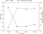
도 3은 본 발명의 실시예에 따라 제조된 플라즈마 중합체 박막의 상대유전 상수를 나타내는 그래프이다.FIG. 3 is a graph showing the relative dielectric constant of a plasma polymer thin film manufactured according to an embodiment of the present invention.
도 3을 참조하면, 전력이 13W 일때는 플라즈마 중합이 제대로 일어나지 않아 박막의 두께가 얇기 때문에 유전 손실값이 큰 것을 확인할 수 있다. 반면, 전력이 20W 이상인 경우에 충분한 플라즈마 중합이 이루어져 유전 손실각이 90도에 가까운 것을 확인할 수 있다. 이로부터 전력이 20W 이상인 경우에 고품질의 박막이 형성됨을 알 수 있다.Referring to Figure 3, it can be seen that when the power is 13 W, plasma polymerization does not occur properly, so the thickness of the thin film is thin and the dielectric loss value is large. On the other hand, when the power is 20 W or more, sufficient plasma polymerization occurs, so it can be seen that the dielectric loss angle is close to 90 degrees. From this, it can be seen that a high-quality thin film is formed when the power is 20 W or more.
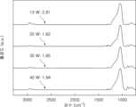
도 4는 본 발명의 일 실시예에 따라 제조된 플라즈마 중합체 박막의 FT-IR 스펙트럼이다.FIG. 4 is an FT-IR spectrum of a plasma polymer thin film manufactured according to one embodiment of the present invention.
도 4를 참조하면, 본 발명의 일 실시예에 따라 제조된 플라즈마 중합체 박막은 Si-O-Si 결합구조와 Si-(CH3)x 결합 구조가 다수를 차지하고 있음을 확인할 수 있다. 또한, 전력이 증가할수록 C-Hx 결합구조, Si-CH3 결합구조가 감소하는 반면, Si-O-Si 결합 구조는 크게 달라지지 않는 것을 확인할 수 있다. 특히 Si-O 결합 이외에 사이클로펜틸, 사이클로헥실과 같은 고리형 포화 탄화 수소의 분해로부터 Si-CH2-Si, Si-CH2-CH2-Si 구조가 형성되는데, 이는 Si-O-Si 결합은 물론 Si-CH3와 같은 일반적인 탄소 결합 구조보다도 우수한 기계적 강도를 제공할 수 있다.Referring to FIG. 4, it can be confirmed that the plasma polymer thin film manufactured according to one embodiment of the present invention has a majority of Si-O-Si bonding structures and Si-(CH3 )x bonding structures. In addition, it can be confirmed that as the power increases, the C-Hx bonding structure and the Si-CH3 bonding structure decrease, whereas the Si-O-Si bonding structure does not change significantly. In particular, in addition to the Si-O bond, Si-CH2 -Si and Si-CH2 -CH2 -Si structures are formed from the decomposition of cyclic saturated hydrocarbons such as cyclopentyl and cyclohexyl, which can provide superior mechanical strength to not only the Si-O-Si bond but also the general carbon bonding structure such as Si-CH3 .
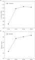
도 5는 본 발명의 일 실시예에 따라 제조된 플라즈마 중합체 박막의 강도(Hardness) 및 탄성률(Modulus)을 측정한 그래프이다. 구체적으로 도 5의 (a)는 플라즈마 중합체 박막의 강도(Hardness) 그래프이고, 도 5의 (b)는 플라즈마 중합체 박막의 탄성률(Modulus) 그래프이다.FIG. 5 is a graph measuring the hardness and modulus of a plasma polymer thin film manufactured according to one embodiment of the present invention. Specifically, (a) of FIG. 5 is a graph measuring the hardness of a plasma polymer thin film, and (b) of FIG. 5 is a graph measuring the modulus of a plasma polymer thin film.
도 5를 참조하면, 전력이 13W 인 경우에는 강도 및 탄성률이 낮은 반면에 전력이 20W 이상인 경우 강도 및 탄성률이 높은 것을 확인할 수 있다. 전력이 20W 이상인 경우 사이클로펜틸, 사이클로헥실과 같은 고리형 포화 탄화수소의 분해가 본격적으로 발생하여 Si-CH2-Si, Si-CH2-CH2-Si 구조가 다수 형성되고, 이로 인해 기계적 강도가 향상되는 것이다.Referring to Fig. 5, it can be seen that when the power is 13 W, the strength and elastic modulus are low, whereas when the power is 20 W or higher, the strength and elastic modulus are high. When the power is 20 W or higher, decomposition of cyclic saturated hydrocarbons such as cyclopentyl and cyclohexyl occurs in earnest, resulting in the formation of a large number of Si-CH2 -Si and Si-CH2 -CH2 -Si structures, which in turn improves the mechanical strength.
도 6은 본 발명의 일 실시예에 따라 제조된 플라즈마 중합체 박막의 누설전류밀도를 나타내는 그래프이다.FIG. 6 is a graph showing the leakage current density of a plasma polymer thin film manufactured according to one embodiment of the present invention.
도 6을 참조하면, 본 발명의 일 실시예에 따라 제조된 플라즈마 중합체 박막은 1 MV/cm 전기장 하에서 1.0x10⁻⁶ A/cm2 미만의 누설전류밀도를 갖는 것을 확인할 수 있다. 이때, 전기장 1 MV/cm인 조건은 반도체 다층 배선공정에 절연층으로서 적용되기 위한 기준이다. 이에 본 발명의 일 실시예에 따른 플라즈마 중합체 박막은 반도체 다층 배선의 유전체층으로 사용하기에 적합하다는 것을 알 수 있다.Referring to FIG. 6, it can be confirmed that the plasma polymer thin film manufactured according to one embodiment of the present invention has a leakage current density of less than 1.0x10⁻⁶ A/cm2 under an electric field of 1 MV/cm. At this time, the condition of an electric field of 1 MV/cm is a standard for application as an insulating layer in a semiconductor multilayer wiring process. Accordingly, it can be seen that the plasma polymer thin film according to one embodiment of the present invention is suitable for use as a dielectric layer in a semiconductor multilayer wiring.
본 발명의 다양한 실시예들에 따른 고강도 저유전 플라즈마 중합체 박막 및 이의 제조방법은 다음과 같이 설명될 수 있다.A high-strength, low-k plasma polymer thin film and a method for manufacturing the same according to various embodiments of the present invention can be described as follows.
본 발명의 일 실시예에 따른 고강도 저유전 플라즈마 중합체 박막의 제조방법은 하기 화학식 1로 표시되는 실리콘 전구체 물질을 증착하여 제조된다.A method for manufacturing a high-strength, low-k plasma polymer thin film according to one embodiment of the present invention is manufactured by depositing a silicon precursor material represented by the following chemical formula 1.
[화학식 1][Chemical Formula 1]
(화학식 1에서, A는 탄소수 4 내지 7의 사이클로알킬기이고, R1, R2 및 R3은 각각 독립적으로 수소 및 탄소수 1 내지 3의 알킬기 중에서 선택된다)(In chemical formula 1, A is a cycloalkyl group having 4 to 7 carbon atoms, and R1 , R2 and R3 are each independently selected from hydrogen and an alkyl group having 1 to 3 carbon atoms.)
본 발명의 다른 특징에 따르면, 탄소수 1 내지 3의 알킬기는 아미노기, 수산화기, 시아노기, 할로겐기, 니트로기 및 알콕시기 중 하나 이상의 치환기로 치환될 수 있다.According to another feature of the present invention, an alkyl group having 1 to 3 carbon atoms may be substituted with one or more substituents selected from an amino group, a hydroxyl group, a cyano group, a halogen group, a nitro group, and an alkoxy group.
본 발명의 또 다른 특징에 따르면, 화학식 1로 표시되는 실리콘 전구체 물질은 25℃에서 증기압이 0.03mmHg 내지 0.2mmHg일 수 있다.According to another feature of the present invention, the silicon precursor material represented by chemical formula 1 can have a vapor pressure of 0.03 mmHg to 0.2 mmHg at 25°C.
본 발명의 또 다른 특징에 따르면, 중합체 박막은 SiOCH 층을 포함할 수 있다.According to another feature of the present invention, the polymer thin film may include a SiOCH layer.
본 발명의 또 다른 특징에 따르면, 중합체 박막의 두께는 0.1㎛ 내지 0.5㎛일 수 있다.According to another feature of the present invention, the thickness of the polymer thin film can be 0.1 ㎛ to 0.5 ㎛.
본 발명의 또 다른 특징에 따르면, 화학식 1에서 A는 사이클로펜틸기 또는 사이클로헥실기일 수 있다.According to another feature of the present invention, in chemical formula 1, A may be a cyclopentyl group or a cyclohexyl group.
본 발명의 또 다른 특징에 따르면, 실리콘 전구체 물질은 하기 화학식 1a, 화학식 1b, 화학식 1c 및 화학식 1d로 표시되는 화합물 중에서 선택될 수 있다.According to another feature of the present invention, the silicon precursor material can be selected from compounds represented by the following chemical formulas 1a, 1b, 1c and 1d.
[화학식 1a] [화학식 1b][Chemical Formula 1a][Chemical Formula 1b]
[화학식 1c] [화학식 1d][Chemical Formula 1c][Chemical Formula 1d]
본 발명의 또 다른 특징에 따르면, 중합체 박막은 플라즈마 보강 화학 기상 증착법(Plasma Enhanced Chemical Vapor Deposition; PECVD)으로 형성된 것일 수 있다.According to another feature of the present invention, the polymer thin film may be formed by plasma enhanced chemical vapor deposition (PECVD).
본 발명의 일 실시예에 따른 고강도 저유전 플라즈마 중합체 박막의 제조방법은, 하기 화학식 1로 표시되는 실리콘 전구체 물질을 플라즈마 보강 화학 기상 증착법(Plasma Enhanced Chemical Vapor Deposition; PECVD)으로 기판 상에 증착하는 단계를 포함한다.A method for manufacturing a high-strength, low-k plasma polymer thin film according to one embodiment of the present invention includes a step of depositing a silicon precursor material represented by the following chemical formula 1 on a substrate by plasma enhanced chemical vapor deposition (PECVD).
[화학식 1][Chemical Formula 1]
(화학식 1에서, A는 탄소수 4 내지 7의 사이클로알킬기이고, R1, R2 및 R3은 각각 독립적으로 수소 및 탄소수 1 내지 3의 알킬기 중에서 선택된다)(In chemical formula 1, A is a cycloalkyl group having 4 to 7 carbon atoms, and R1 , R2 and R3 are each independently selected from hydrogen and an alkyl group having 1 to 3 carbon atoms.)
본 발명의 또 다른 특징에 따르면, 기판 상에 증착하는 단계는, 플라즈마 증착 반응기에 기판을 공급하고 안정화하는 단계, 반응기에 실리콘 전구체 물질을 공급하는 단계 및 플라즈마를 이용하여 기판 상에 실리콘 전구체 물질을 증착하고, SiOCH 층을 포함하는 플라즈마 중합체 박막을 형성하는 단계를 포함할 수 있다.According to another feature of the present invention, the step of depositing on a substrate may include the steps of supplying and stabilizing the substrate to a plasma deposition reactor, the step of supplying a silicon precursor material to the reactor, and the step of depositing the silicon precursor material on the substrate using plasma, thereby forming a plasma polymer thin film including a SiOCH layer.
본 발명의 또 다른 특징에 따르면, 실리콘 전구체 물질을 공급하는 단계와 플라즈마 중합체 박막을 형성하는 단계 사이에 반응기에 반응 가스를 공급하는 단계를 더 포함할 수 있다.According to another feature of the present invention, the step of supplying a reaction gas to the reactor may be further included between the step of supplying a silicon precursor material and the step of forming a plasma polymer thin film.
본 발명의 또 다른 특징에 따르면, 반응 가스는 일산화질소(N2O) 및 산소(O2) 중 1종 이상을 포함할 수 있다.According to another feature of the present invention, the reaction gas may include at least one of nitrogen monoxide (N2 O) and oxygen (O2 ).
본 발명의 또 다른 특징에 따르면, 실리콘 전구체 물질을 공급하는 단계는, 실리콘 전구체 물질을 거품기 내로 공급하고, 거품기 내에서 실리콘 전구체 물질을 증발시켜 반응기로 유입시키는 단계를 포함할 수 있다.According to another feature of the present invention, the step of supplying the silicon precursor material may include the step of supplying the silicon precursor material into a bubbler, and evaporating the silicon precursor material within the bubbler and introducing it into a reactor.
본 발명의 또 다른 특징에 따르면, 증발된 실리콘 전구체 물질은 운반 가스와 반응기에 유입되고, 운반 가스는 아르곤(Ar), 헬륨(He) 및 네온(Ne) 중에서 선택되는 1종 이상을 포함할 수 있다.According to another feature of the present invention, the evaporated silicon precursor material is introduced into a reactor with a carrier gas, and the carrier gas may include at least one selected from argon (Ar), helium (He), and neon (Ne).
본 발명의 또 다른 특징에 따르면, 반응기 내 운반 가스의 압력은 1×10⁻¹ Torr 내지 100×10-1 Torr 일 수 있다.According to another feature of the present invention, the pressure of the carrier gas inside the reactor can be 1×10⁻¹ Torr to 100×10-1 Torr.
본 발명의 또 다른 특징에 따르면, 플라즈마 중합체 박막을 형성하는 단계에서, 반응기 내 기판의 온도는 300℃ 내지 400℃일 수 있다.According to another feature of the present invention, in the step of forming a plasma polymer thin film, the temperature of the substrate inside the reactor can be 300°C to 400°C.
본 발명의 또 다른 특징에 따르면, 플라즈마 중합체 박막을 형성하는 단계에서, 반응기에 공급되는 전력은 10W 내지 40W일 수 있다.According to another feature of the present invention, in the step of forming a plasma polymer thin film, the power supplied to the reactor may be 10 W to 40 W.
본 발명의 또 다른 특징에 따르면, 플라즈마 중합체 박막을 형성하는 단계 이후에 중합체 박막을 후처리하는 단계를 더 포함하고, 후처리하는 단계는, 유도결합 플라즈마(inductively coupled plasma; ICP) 처리 공정, 급속 열 처리(rapid thermal annealing; RTA) 공정 또는 이들의 조합 중 어느 하나의 방법으로 수행될 수 있다.According to another feature of the present invention, the method further comprises a step of post-treating the polymer thin film after the step of forming the plasma polymer thin film, wherein the post-treating step can be performed by any one of an inductively coupled plasma (ICP) treatment process, a rapid thermal annealing (RTA) process, or a combination thereof.
이상에서 본 발명을 실시예를 통하여 상세하게 설명하였으나, 본 발명은 반드시 이러한 실시예로 국한되는 것은 아니고, 본 발명의 기술사상을 벗어나지 않는 범위 내에서 다양하게 변형실시될 수 있다. 따라서, 본 발명에 개시된 실시예들은 본 발명의 기술 사상을 제한하기 위한 것이 아니라 설명하기 위한 것이고, 이러한 실시예에 의하여 본 발명의 기술 사상의 범위가 제한되는 것은 아니다. 그러므로, 이상에서 기술한 실시예들은 모든 면에서 예시적인 것이며 제한적이 아닌 것으로 이해해야만 한다. 본 발명의 보호 범위는 아래의 청구범위에 의하여 해석되어야 하며, 그와 동등한 범위 내에 있는 모든 기술 사상은 본 발명의 권리범위에 포함되는 것으로 해석되어야 할 것이다.Although the present invention has been described in detail above through examples, the present invention is not necessarily limited to these examples, and various modifications may be made within a scope that does not depart from the technical idea of the present invention. Accordingly, the embodiments disclosed in the present invention are not intended to limit the technical idea of the present invention, but to explain it, and the scope of the technical idea of the present invention is not limited by these examples. Therefore, it should be understood that the embodiments described above are exemplary in all aspects and not restrictive. The protection scope of the present invention should be interpreted by the following claims, and all technical ideas within a scope equivalent thereto should be interpreted as being included in the scope of the rights of the present invention.
Claims (18)
Translated fromKorean[화학식 1]
상기 화학식 1에서,
A는 탄소수 4 내지 7의 사이클로알킬기이고,
R1, R2 및 R3은 각각 독립적으로 수소 및 탄소수 1 내지 3의 알킬기 중에서 선택된다.A high-strength, low-k plasma polymer thin film manufactured by depositing a silicon precursor material represented by the following chemical formula 1:
[Chemical Formula 1]
In the above chemical formula 1,
A is a cycloalkyl group having 4 to 7 carbon atoms,
R1 , R2 and R3 are each independently selected from hydrogen and an alkyl group having 1 to 3 carbon atoms.
상기 탄소수 1 내지 3의 알킬기는 아미노기, 수산화기, 시아노기, 할로겐기, 니트로기 및 알콕시기 중 하나 이상의 치환기로 치환된, 고강도 저유전 플라즈마 중합체 박막.In the first paragraph,
A high-strength, low-dielectric plasma polymer thin film, wherein the alkyl group having 1 to 3 carbon atoms is substituted with one or more substituents selected from the group consisting of an amino group, a hydroxyl group, a cyano group, a halogen group, a nitro group, and an alkoxy group.
상기 화학식 1로 표시되는 실리콘 전구체 물질은 25℃에서 증기압이 0.03mmHg 내지 0.2mmHg인, 고강도 저유전 플라즈마 중합체 박막.In the first paragraph,
A silicon precursor material represented by the above chemical formula 1 is a high-strength, low-dielectric plasma polymer thin film having a vapor pressure of 0.03 mmHg to 0.2 mmHg at 25°C.
상기 중합체 박막은 SiOCH 층을 포함하는, 고강도 저유전 플라즈마 중합체 박막.In the first paragraph,
The above polymer thin film is a high-strength, low-k plasma polymer thin film comprising a SiOCH layer.
상기 중합체 박막의 두께는 0.1㎛ 내지 0.5㎛인, 고강도 저유전 플라즈마 중합체 박막.In the first paragraph,
A high-strength, low-dielectric plasma polymer thin film having a thickness of 0.1 ㎛ to 0.5 ㎛.
상기 화학식 1에서, A는 사이클로펜틸기 또는 사이클로헥실기인, 고강도 저유전 플라즈마 중합체 박막.In the first paragraph,
A high-strength, low-dielectric plasma polymer thin film, wherein in the chemical formula 1, A is a cyclopentyl group or a cyclohexyl group.
상기 실리콘 전구체 물질은 하기 화학식 1a, 화학식 1b, 화학식 1c 및 화학식 1d로 표시되는 화합물 중에서 선택되는, 고강도 저유전 플라즈마 중합체 박막:
[화학식 1a] [화학식 1b]
[화학식 1c] [화학식 1d]
In the first paragraph,
The above silicon precursor material is a high-strength, low-k plasma polymer thin film selected from compounds represented by the following chemical formulas 1a, 1b, 1c and 1d:
[Chemical Formula 1a] [Chemical Formula 1b]
[Chemical Formula 1c] [Chemical Formula 1d]
상기 중합체 박막은 플라즈마 보강 화학 기상 증착법(Plasma Enhanced Chemical Vapor Deposition; PECVD)으로 형성된, 고강도 저유전 플라즈마 중합체 박막.In the first paragraph,
The above polymer thin film is a high-strength, low-k plasma polymer thin film formed by plasma enhanced chemical vapor deposition (PECVD).
[화학식 1]
상기 화학식 1에서,
A는 탄소수 4 내지 7의 사이클로알킬기이고,
R1, R2 및 R3은 각각 독립적으로 수소 및 탄소수 1 내지 3의 알킬기 중에서 선택된다.A method for manufacturing a high-strength, low-k plasma polymer thin film, comprising the step of depositing a silicon precursor material represented by the following chemical formula 1 on a substrate by plasma enhanced chemical vapor deposition (PECVD):
[Chemical Formula 1]
In the above chemical formula 1,
A is a cycloalkyl group having 4 to 7 carbon atoms,
R1 , R2 and R3 are each independently selected from hydrogen and an alkyl group having 1 to 3 carbon atoms.
상기 기판 상에 증착하는 단계는,
플라즈마 증착 반응기에 상기 기판을 공급하고 안정화하는 단계;
상기 반응기에 상기 실리콘 전구체 물질을 공급하는 단계; 및
플라즈마를 이용하여 상기 기판 상에 실리콘 전구체 물질을 증착하고, SiOCH 층을 포함하는 플라즈마 중합체 박막을 형성하는 단계를 포함하는, 고강도 저유전 플라즈마 중합체 박막의 제조방법.In Article 9,
The step of depositing on the above substrate is:
A step of supplying and stabilizing the substrate to a plasma deposition reactor;
a step of supplying the silicon precursor material to the reactor; and
A method for manufacturing a high-strength, low-k plasma polymer thin film, comprising the step of depositing a silicon precursor material on a substrate using plasma and forming a plasma polymer thin film including a SiOCH layer.
상기 실리콘 전구체 물질을 공급하는 단계와 상기 플라즈마 중합체 박막을 형성하는 단계 사이에 상기 반응기에 반응 가스를 공급하는 단계를 더 포함하는, 고강도 저유전 플라즈마 중합체 박막의 제조방법.In Article 10,
A method for producing a high-strength, low-k plasma polymer thin film, further comprising a step of supplying a reaction gas to the reactor between the step of supplying the silicon precursor material and the step of forming the plasma polymer thin film.
상기 반응 가스는 일산화질소(N2O) 및 산소(O2) 중 1종 이상을 포함하는, 고강도 저유전 플라즈마 중합체 박막의 제조방법.In Article 11,
A method for producing a high-strength, low-k plasma polymer thin film, wherein the above reaction gas contains at least one of nitrogen monoxide (N2 O) and oxygen (O2 ).
상기 실리콘 전구체 물질을 공급하는 단계는,
상기 실리콘 전구체 물질을 거품기 내로 공급하고, 상기 거품기 내에서 상기 실리콘 전구체 물질을 증발시켜 상기 반응기로 유입시키는 단계를 포함하는, 고강도 저유전 플라즈마 중합체 박막의 제조방법.In Article 10,
The step of supplying the above silicon precursor material is:
A method for producing a high-strength, low-k plasma polymer thin film, comprising the steps of supplying the silicon precursor material into a bubbler, evaporating the silicon precursor material within the bubbler, and introducing the silicon precursor material into the reactor.
증발된 상기 실리콘 전구체 물질은 운반 가스와 상기 반응기에 유입되고,
상기 운반 가스는 아르곤(Ar), 헬륨(He) 및 네온(Ne) 중에서 선택되는 1종 이상을 포함하는, 고강도 저유전 플라즈마 중합체 박막의 제조방법.In Article 13,
The evaporated silicon precursor material is introduced into the reactor together with the carrier gas,
A method for producing a high-strength, low-dielectric plasma polymer thin film, wherein the carrier gas comprises at least one selected from argon (Ar), helium (He), and neon (Ne).
상기 반응기 내 상기 운반 가스의 압력은 1×10⁻¹ Torr 내지 100×10-1 Torr 인, 고강도 저유전 플라즈마 중합체 박막의 제조방법.In Article 14,
A method for producing a high-strength, low-dielectric plasma polymer thin film, wherein the pressure of the carrier gas in the reactor is 1×10⁻¹ Torr to 100×10-1 Torr.
상기 플라즈마 중합체 박막을 형성하는 단계에서, 상기 반응기 내 상기 기판의 온도는 300℃ 내지 400℃인, 고강도 저유전 플라즈마 중합체 박막의 제조방법.In Article 10,
A method for producing a high-strength, low-dielectric plasma polymer thin film, wherein in the step of forming the plasma polymer thin film, the temperature of the substrate in the reactor is 300°C to 400°C.
상기 플라즈마 중합체 박막을 형성하는 단계에서, 상기 반응기에 공급되는 전력은 10W 내지 40W인, 고강도 저유전 플라즈마 중합체 박막의 제조방법.In Article 10,
A method for producing a high-strength, low-dielectric plasma polymer thin film, wherein in the step of forming the plasma polymer thin film, the power supplied to the reactor is 10 W to 40 W.
상기 플라즈마 중합체 박막을 형성하는 단계 이후에 상기 중합체 박막을 후처리하는 단계를 더 포함하고,
상기 후처리하는 단계는, 유도결합 플라즈마(inductively coupled plasma; ICP) 처리 공정, 급속 열 처리(rapid thermal annealing; RTA) 공정 또는 이들의 조합 중 어느 하나의 방법으로 수행되는, 고강도 저유전 플라즈마 중합체 박막의 제조방법.In Article 10,
After the step of forming the plasma polymer thin film, the step of post-processing the polymer thin film is further included.
A method for manufacturing a high-strength, low-k plasma polymer thin film, wherein the above post-processing step is performed by any one of an inductively coupled plasma (ICP) treatment process, a rapid thermal annealing (RTA) process, or a combination thereof.
Priority Applications (1)
| Application Number | Priority Date | Filing Date | Title |
|---|---|---|---|
| KR1020230122585AKR20250039742A (en) | 2023-09-14 | 2023-09-14 | Plasma polymerized thin film having high hardness and low dielectric constant and manufacturing method thereof |
Applications Claiming Priority (1)
| Application Number | Priority Date | Filing Date | Title |
|---|---|---|---|
| KR1020230122585AKR20250039742A (en) | 2023-09-14 | 2023-09-14 | Plasma polymerized thin film having high hardness and low dielectric constant and manufacturing method thereof |
Publications (1)
| Publication Number | Publication Date |
|---|---|
| KR20250039742Atrue KR20250039742A (en) | 2025-03-21 |
Family
ID=95198043
Family Applications (1)
| Application Number | Title | Priority Date | Filing Date |
|---|---|---|---|
| KR1020230122585APendingKR20250039742A (en) | 2023-09-14 | 2023-09-14 | Plasma polymerized thin film having high hardness and low dielectric constant and manufacturing method thereof |
Country Status (1)
| Country | Link |
|---|---|
| KR (1) | KR20250039742A (en) |
- 2023
- 2023-09-14KRKR1020230122585Apatent/KR20250039742A/enactivePending
Similar Documents
| Publication | Publication Date | Title |
|---|---|---|
| US6559520B2 (en) | Siloxan polymer film on semiconductor substrate | |
| JP3762304B2 (en) | Method for forming low dielectric constant interlayer insulating film | |
| TWI617693B (en) | Composition for depositing ruthenium containing film and method therefor | |
| JP3515074B2 (en) | Low-κ dielectric inorganic / organic hybrid film and method for producing the same | |
| TW574410B (en) | Low dielectric constant material and method of processing by CVD | |
| TWI388685B (en) | Novel silicon precursors to make ultra low-k films with high mechanical properties by plasma enhanced chemical vapor deposition | |
| US20040038514A1 (en) | Method for forming low-k hard film | |
| TWI388687B (en) | Novel silicon precursors to make ultra low-k films with high mechanical properties by plasma enhanced chemical vapor deposition | |
| CN103210479A (en) | Process for reducing adhesion layer thickness and increasing damage resistance of ultra low k dielectric films | |
| US20060258176A1 (en) | Method for forming insulation film | |
| JPH11288931A (en) | Insulation film and its manufacture | |
| JP4881153B2 (en) | Method for producing a hydrogenated silicon oxycarbide film. | |
| CN101450995B (en) | Low dielectric constant plasma polymerized thin film and manufacturing method thereof | |
| KR20110039556A (en) | A method of promoting adhesion between a barrier layer deposited from multiple liquid precursors and a porous low-k film | |
| JP2005072584A (en) | Method for forming silicon-based insulating film having low dielectric constant and low film stress | |
| US20150048487A1 (en) | Plasma polymerized thin film having high hardness and low dielectric constant and manufacturing method thereof | |
| KR102138102B1 (en) | Plasma polymerized thin film having low dielectric constant and preparing method thereof | |
| CN114616652A (en) | Monoalkoxysilanes and Dense Organic Silica Films Prepared Therefrom | |
| KR20250039742A (en) | Plasma polymerized thin film having high hardness and low dielectric constant and manufacturing method thereof | |
| KR100926722B1 (en) | The siloxane polymer film on a semiconductor substrate and its manufacturing method | |
| US9371430B2 (en) | Porous film with high hardness and a low dielectric constant and preparation method thereof | |
| US8926745B2 (en) | Method for preparing low K material and film thereof | |
| JP3814797B2 (en) | Method for forming a silicon polymer insulating film on a semiconductor substrate | |
| KR20250091848A (en) | Precursor for forming silicon-containing thin film with high hardness and low dielectric constant and manufacfuring method for silicon-containing thin film using thereof | |
| JP4651076B2 (en) | Method for forming an insulating film on a semiconductor substrate |
Legal Events
| Date | Code | Title | Description |
|---|---|---|---|
| PA0109 | Patent application | Patent event code:PA01091R01D Comment text:Patent Application Patent event date:20230914 | |
| PA0201 | Request for examination | Patent event code:PA02011R01I Patent event date:20230914 Comment text:Patent Application | |
| PE0902 | Notice of grounds for rejection | Comment text:Notification of reason for refusal Patent event date:20241119 Patent event code:PE09021S01D | |
| PG1501 | Laying open of application |