KR20250003712A - Integrated cleaning and selective molybdenum deposition processes - Google Patents
Integrated cleaning and selective molybdenum deposition processesDownload PDFInfo
- Publication number
- KR20250003712A KR20250003712AKR1020247037022AKR20247037022AKR20250003712AKR 20250003712 AKR20250003712 AKR 20250003712AKR 1020247037022 AKR1020247037022 AKR 1020247037022AKR 20247037022 AKR20247037022 AKR 20247037022AKR 20250003712 AKR20250003712 AKR 20250003712A
- Authority
- KR
- South Korea
- Prior art keywords
- deposition method
- paragraph
- molybdenum
- sidewalls
- situ
- Prior art date
- Legal status (The legal status is an assumption and is not a legal conclusion. Google has not performed a legal analysis and makes no representation as to the accuracy of the status listed.)
- Pending
Links
- ZOKXTWBITQBERF-UHFFFAOYSA-NMolybdenumChemical compound[Mo]ZOKXTWBITQBERF-UHFFFAOYSA-N0.000titleclaimsabstractdescription48
- 229910052750molybdenumInorganic materials0.000titleclaimsabstractdescription48
- 239000011733molybdenumSubstances0.000titleclaimsabstractdescription48
- 238000004140cleaningMethods0.000titleabstractdescription10
- 238000005137deposition processMethods0.000titleabstractdescription5
- 238000000034methodMethods0.000claimsabstractdescription91
- 238000011065in-situ storageMethods0.000claimsabstractdescription27
- 238000000151depositionMethods0.000claimsdescription64
- 239000000758substrateSubstances0.000claimsdescription62
- 239000007769metal materialSubstances0.000claimsdescription43
- 206010053487Exposure to toxic agentDiseases0.000claimsdescription30
- XKRFYHLGVUSROY-UHFFFAOYSA-NArgonChemical compound[Ar]XKRFYHLGVUSROY-UHFFFAOYSA-N0.000claimsdescription18
- 238000010926purgeMethods0.000claimsdescription15
- 238000007654immersionMethods0.000claimsdescription14
- VYPSYNLAJGMNEJ-UHFFFAOYSA-NSilicium dioxideChemical compoundO=[Si]=OVYPSYNLAJGMNEJ-UHFFFAOYSA-N0.000claimsdescription11
- 238000000231atomic layer depositionMethods0.000claimsdescription10
- 229910052786argonInorganic materials0.000claimsdescription9
- 238000009616inductively coupled plasmaMethods0.000claimsdescription9
- 239000002243precursorSubstances0.000claimsdescription8
- 238000004544sputter depositionMethods0.000claimsdescription8
- 229910052581Si3N4Inorganic materials0.000claimsdescription7
- 238000011066ex-situ storageMethods0.000claimsdescription7
- HQVNEWCFYHHQES-UHFFFAOYSA-Nsilicon nitrideChemical compoundN12[Si]34N5[Si]62N3[Si]51N64HQVNEWCFYHHQES-UHFFFAOYSA-N0.000claimsdescription7
- 229910052814silicon oxideInorganic materials0.000claimsdescription7
- 238000005229chemical vapour depositionMethods0.000claimsdescription5
- 239000010949copperSubstances0.000claimsdescription4
- 229910015275MoF 6Inorganic materials0.000claimsdescription3
- KJTLSVCANCCWHF-UHFFFAOYSA-NRutheniumChemical compound[Ru]KJTLSVCANCCWHF-UHFFFAOYSA-N0.000claimsdescription3
- 239000010941cobaltSubstances0.000claimsdescription3
- 229910017052cobaltInorganic materials0.000claimsdescription3
- GUTLYIVDDKVIGB-UHFFFAOYSA-Ncobalt atomChemical compound[Co]GUTLYIVDDKVIGB-UHFFFAOYSA-N0.000claimsdescription3
- 238000001312dry etchingMethods0.000claimsdescription3
- 239000001257hydrogenSubstances0.000claimsdescription3
- 229910052739hydrogenInorganic materials0.000claimsdescription3
- 229910052707rutheniumInorganic materials0.000claimsdescription3
- LIVNPJMFVYWSIS-UHFFFAOYSA-Nsilicon monoxideChemical compound[Si-]#[O+]LIVNPJMFVYWSIS-UHFFFAOYSA-N0.000claimsdescription3
- WFKWXMTUELFFGS-UHFFFAOYSA-NtungstenChemical compound[W]WFKWXMTUELFFGS-UHFFFAOYSA-N0.000claimsdescription3
- 229910052721tungstenInorganic materials0.000claimsdescription3
- 239000010937tungstenSubstances0.000claimsdescription3
- WSWMGHRLUYADNA-UHFFFAOYSA-N7-nitro-1,2,3,4-tetrahydroquinolineChemical compoundC1CCNC2=CC([N+](=O)[O-])=CC=C21WSWMGHRLUYADNA-UHFFFAOYSA-N0.000claimsdescription2
- RYGMFSIKBFXOCR-UHFFFAOYSA-NCopperChemical compound[Cu]RYGMFSIKBFXOCR-UHFFFAOYSA-N0.000claimsdescription2
- 229910052802copperInorganic materials0.000claimsdescription2
- NBJFDNVXVFBQDX-UHFFFAOYSA-Imolybdenum pentafluorideChemical compoundF[Mo](F)(F)(F)FNBJFDNVXVFBQDX-UHFFFAOYSA-I0.000claimsdescription2
- BQBYSLAFGRVJME-UHFFFAOYSA-Lmolybdenum(2+);dichlorideChemical compoundCl[Mo]ClBQBYSLAFGRVJME-UHFFFAOYSA-L0.000claimsdescription2
- QHIRVZBLPRTQQO-UHFFFAOYSA-IpentafluorotungstenChemical compoundF[W](F)(F)(F)FQHIRVZBLPRTQQO-UHFFFAOYSA-I0.000claimsdescription2
- KPGXUAIFQMJJFB-UHFFFAOYSA-Htungsten hexachlorideChemical compoundCl[W](Cl)(Cl)(Cl)(Cl)ClKPGXUAIFQMJJFB-UHFFFAOYSA-H0.000claimsdescription2
- NXHILIPIEUBEPD-UHFFFAOYSA-Htungsten hexafluorideChemical compoundF[W](F)(F)(F)(F)FNXHILIPIEUBEPD-UHFFFAOYSA-H0.000claimsdescription2
- FZFRVZDLZISPFJ-UHFFFAOYSA-Ntungsten(6+)Chemical compound[W+6]FZFRVZDLZISPFJ-UHFFFAOYSA-N0.000claimsdescription2
- 238000001039wet etchingMethods0.000claimsdescription2
- 239000013078crystalSubstances0.000claims3
- 125000004435hydrogen atomChemical class[H]*0.000claims1
- 238000012545processingMethods0.000description60
- 238000012546transferMethods0.000description27
- 239000000463materialSubstances0.000description25
- 239000007789gasSubstances0.000description21
- 235000012431wafersNutrition0.000description21
- 150000001875compoundsChemical class0.000description13
- 238000006243chemical reactionMethods0.000description8
- 239000000356contaminantSubstances0.000description8
- 230000008021depositionEffects0.000description8
- 230000015654memoryEffects0.000description8
- 229910052751metalInorganic materials0.000description8
- 239000002184metalSubstances0.000description8
- XUIMIQQOPSSXEZ-UHFFFAOYSA-NSiliconChemical compound[Si]XUIMIQQOPSSXEZ-UHFFFAOYSA-N0.000description7
- 229910052710siliconInorganic materials0.000description7
- 239000010703siliconSubstances0.000description7
- 239000000460chlorineSubstances0.000description5
- 229910044991metal oxideInorganic materials0.000description5
- 150000004706metal oxidesChemical class0.000description5
- 238000011282treatmentMethods0.000description5
- OKTJSMMVPCPJKN-UHFFFAOYSA-NCarbonChemical compound[C]OKTJSMMVPCPJKN-UHFFFAOYSA-N0.000description4
- 229910000577Silicon-germaniumInorganic materials0.000description4
- 229910052799carbonInorganic materials0.000description4
- 239000003638chemical reducing agentSubstances0.000description4
- 229910052732germaniumInorganic materials0.000description4
- GNPVGFCGXDBREM-UHFFFAOYSA-Ngermanium atomChemical compound[Ge]GNPVGFCGXDBREM-UHFFFAOYSA-N0.000description4
- 229940126062Compound ADrugs0.000description3
- NLDMNSXOCDLTTB-UHFFFAOYSA-NHeterophylliin ANatural productsO1C2COC(=O)C3=CC(O)=C(O)C(O)=C3C3=C(O)C(O)=C(O)C=C3C(=O)OC2C(OC(=O)C=2C=C(O)C(O)=C(O)C=2)C(O)C1OC(=O)C1=CC(O)=C(O)C(O)=C1NLDMNSXOCDLTTB-UHFFFAOYSA-N0.000description3
- 239000003989dielectric materialSubstances0.000description3
- 239000012535impuritySubstances0.000description3
- 150000004767nitridesChemical class0.000description3
- 239000004065semiconductorSubstances0.000description3
- 235000012239silicon dioxideNutrition0.000description3
- 239000000377silicon dioxideSubstances0.000description3
- JBRZTFJDHDCESZ-UHFFFAOYSA-NAsGaChemical compound[As]#[Ga]JBRZTFJDHDCESZ-UHFFFAOYSA-N0.000description2
- YCKRFDGAMUMZLT-UHFFFAOYSA-NFluorine atomChemical compound[F]YCKRFDGAMUMZLT-UHFFFAOYSA-N0.000description2
- 229910000530Gallium indium arsenideInorganic materials0.000description2
- 229910004298SiO 2Inorganic materials0.000description2
- KXNLCSXBJCPWGL-UHFFFAOYSA-N[Ga].[As].[In]Chemical compound[Ga].[As].[In]KXNLCSXBJCPWGL-UHFFFAOYSA-N0.000description2
- LEVVHYCKPQWKOP-UHFFFAOYSA-N[Si].[Ge]Chemical compound[Si].[Ge]LEVVHYCKPQWKOP-UHFFFAOYSA-N0.000description2
- QVGXLLKOCUKJST-UHFFFAOYSA-Natomic oxygenChemical compound[O]QVGXLLKOCUKJST-UHFFFAOYSA-N0.000description2
- WYEMLYFITZORAB-UHFFFAOYSA-NboscalidChemical compoundC1=CC(Cl)=CC=C1C1=CC=CC=C1NC(=O)C1=CC=CN=C1ClWYEMLYFITZORAB-UHFFFAOYSA-N0.000description2
- 238000010586diagramMethods0.000description2
- 239000011737fluorineSubstances0.000description2
- 229910052731fluorineInorganic materials0.000description2
- 239000011521glassSubstances0.000description2
- 238000011534incubationMethods0.000description2
- 239000011261inert gasSubstances0.000description2
- 238000012986modificationMethods0.000description2
- 230000004048modificationEffects0.000description2
- 238000003032molecular dockingMethods0.000description2
- 239000001301oxygenSubstances0.000description2
- 229910052760oxygenInorganic materials0.000description2
- 229920000642polymerPolymers0.000description2
- 239000011148porous materialSubstances0.000description2
- 239000011669seleniumSubstances0.000description2
- IJGRMHOSHXDMSA-UHFFFAOYSA-NAtomic nitrogenChemical compoundN#NIJGRMHOSHXDMSA-UHFFFAOYSA-N0.000description1
- ZAMOUSCENKQFHK-UHFFFAOYSA-NChlorine atomChemical compound[Cl]ZAMOUSCENKQFHK-UHFFFAOYSA-N0.000description1
- GYHNNYVSQQEPJS-UHFFFAOYSA-NGalliumChemical compound[Ga]GYHNNYVSQQEPJS-UHFFFAOYSA-N0.000description1
- 229910001218Gallium arsenideInorganic materials0.000description1
- UFHFLCQGNIYNRP-UHFFFAOYSA-NHydrogenChemical compound[H][H]UFHFLCQGNIYNRP-UHFFFAOYSA-N0.000description1
- GPXJNWSHGFTCBW-UHFFFAOYSA-NIndium phosphideChemical compound[In]#PGPXJNWSHGFTCBW-UHFFFAOYSA-N0.000description1
- OAICVXFJPJFONN-UHFFFAOYSA-NPhosphorusChemical compound[P]OAICVXFJPJFONN-UHFFFAOYSA-N0.000description1
- BUGBHKTXTAQXES-UHFFFAOYSA-NSeleniumChemical compound[Se]BUGBHKTXTAQXES-UHFFFAOYSA-N0.000description1
- 229910020177SiOFInorganic materials0.000description1
- 239000002253acidSubstances0.000description1
- AUCDRFABNLOFRE-UHFFFAOYSA-Nalumane;indiumChemical compound[AlH3].[In]AUCDRFABNLOFRE-UHFFFAOYSA-N0.000description1
- 229910021417amorphous siliconInorganic materials0.000description1
- 239000003708ampulSubstances0.000description1
- 238000000137annealingMethods0.000description1
- 239000006227byproductSubstances0.000description1
- 239000003990capacitorSubstances0.000description1
- 239000013043chemical agentSubstances0.000description1
- 229910052801chlorineInorganic materials0.000description1
- 239000004020conductorSubstances0.000description1
- 238000013480data collectionMethods0.000description1
- 230000001934delayEffects0.000description1
- 238000009792diffusion processMethods0.000description1
- 229910001873dinitrogenInorganic materials0.000description1
- 230000009977dual effectEffects0.000description1
- 230000005684electric fieldEffects0.000description1
- 229940104869fluorosilicateDrugs0.000description1
- 229910052733galliumInorganic materials0.000description1
- 150000002431hydrogenChemical class0.000description1
- 229910052738indiumInorganic materials0.000description1
- APFVFJFRJDLVQX-UHFFFAOYSA-Nindium atomChemical compound[In]APFVFJFRJDLVQX-UHFFFAOYSA-N0.000description1
- 239000012212insulatorSubstances0.000description1
- 239000007788liquidSubstances0.000description1
- 238000004519manufacturing processMethods0.000description1
- 150000001247metal acetylidesChemical class0.000description1
- 229910001092metal group alloyInorganic materials0.000description1
- 238000001465metallisationMethods0.000description1
- 150000002739metalsChemical class0.000description1
- 239000000203mixtureSubstances0.000description1
- 239000000615nonconductorSubstances0.000description1
- NJPPVKZQTLUDBO-UHFFFAOYSA-NnovaluronChemical compoundC1=C(Cl)C(OC(F)(F)C(OC(F)(F)F)F)=CC=C1NC(=O)NC(=O)C1=C(F)C=CC=C1FNJPPVKZQTLUDBO-UHFFFAOYSA-N0.000description1
- 230000005693optoelectronicsEffects0.000description1
- 150000002894organic compoundsChemical class0.000description1
- -1oxycarbidesChemical class0.000description1
- 230000000737periodic effectEffects0.000description1
- 229910052698phosphorusInorganic materials0.000description1
- 239000011574phosphorusSubstances0.000description1
- 239000005360phosphosilicate glassSubstances0.000description1
- 238000005240physical vapour depositionMethods0.000description1
- 238000009832plasma treatmentMethods0.000description1
- 229910021426porous siliconInorganic materials0.000description1
- 238000005086pumpingMethods0.000description1
- 239000000376reactantSubstances0.000description1
- 229910052711seleniumInorganic materials0.000description1
- 238000003860storageMethods0.000description1
- 238000000859sublimationMethods0.000description1
- 230000008022sublimationEffects0.000description1
- 230000003746surface roughnessEffects0.000description1
Images


Classifications
- C—CHEMISTRY; METALLURGY
- C23—COATING METALLIC MATERIAL; COATING MATERIAL WITH METALLIC MATERIAL; CHEMICAL SURFACE TREATMENT; DIFFUSION TREATMENT OF METALLIC MATERIAL; COATING BY VACUUM EVAPORATION, BY SPUTTERING, BY ION IMPLANTATION OR BY CHEMICAL VAPOUR DEPOSITION, IN GENERAL; INHIBITING CORROSION OF METALLIC MATERIAL OR INCRUSTATION IN GENERAL
- C23C—COATING METALLIC MATERIAL; COATING MATERIAL WITH METALLIC MATERIAL; SURFACE TREATMENT OF METALLIC MATERIAL BY DIFFUSION INTO THE SURFACE, BY CHEMICAL CONVERSION OR SUBSTITUTION; COATING BY VACUUM EVAPORATION, BY SPUTTERING, BY ION IMPLANTATION OR BY CHEMICAL VAPOUR DEPOSITION, IN GENERAL
- C23C30/00—Coating with metallic material characterised only by the composition of the metallic material, i.e. not characterised by the coating process
- C—CHEMISTRY; METALLURGY
- C23—COATING METALLIC MATERIAL; COATING MATERIAL WITH METALLIC MATERIAL; CHEMICAL SURFACE TREATMENT; DIFFUSION TREATMENT OF METALLIC MATERIAL; COATING BY VACUUM EVAPORATION, BY SPUTTERING, BY ION IMPLANTATION OR BY CHEMICAL VAPOUR DEPOSITION, IN GENERAL; INHIBITING CORROSION OF METALLIC MATERIAL OR INCRUSTATION IN GENERAL
- C23C—COATING METALLIC MATERIAL; COATING MATERIAL WITH METALLIC MATERIAL; SURFACE TREATMENT OF METALLIC MATERIAL BY DIFFUSION INTO THE SURFACE, BY CHEMICAL CONVERSION OR SUBSTITUTION; COATING BY VACUUM EVAPORATION, BY SPUTTERING, BY ION IMPLANTATION OR BY CHEMICAL VAPOUR DEPOSITION, IN GENERAL
- C23C16/00—Chemical coating by decomposition of gaseous compounds, without leaving reaction products of surface material in the coating, i.e. chemical vapour deposition [CVD] processes
- C23C16/04—Coating on selected surface areas, e.g. using masks
- C23C16/045—Coating cavities or hollow spaces, e.g. interior of tubes; Infiltration of porous substrates
- C—CHEMISTRY; METALLURGY
- C23—COATING METALLIC MATERIAL; COATING MATERIAL WITH METALLIC MATERIAL; CHEMICAL SURFACE TREATMENT; DIFFUSION TREATMENT OF METALLIC MATERIAL; COATING BY VACUUM EVAPORATION, BY SPUTTERING, BY ION IMPLANTATION OR BY CHEMICAL VAPOUR DEPOSITION, IN GENERAL; INHIBITING CORROSION OF METALLIC MATERIAL OR INCRUSTATION IN GENERAL
- C23C—COATING METALLIC MATERIAL; COATING MATERIAL WITH METALLIC MATERIAL; SURFACE TREATMENT OF METALLIC MATERIAL BY DIFFUSION INTO THE SURFACE, BY CHEMICAL CONVERSION OR SUBSTITUTION; COATING BY VACUUM EVAPORATION, BY SPUTTERING, BY ION IMPLANTATION OR BY CHEMICAL VAPOUR DEPOSITION, IN GENERAL
- C23C16/00—Chemical coating by decomposition of gaseous compounds, without leaving reaction products of surface material in the coating, i.e. chemical vapour deposition [CVD] processes
- C23C16/02—Pretreatment of the material to be coated
- C23C16/0227—Pretreatment of the material to be coated by cleaning or etching
- C23C16/0245—Pretreatment of the material to be coated by cleaning or etching by etching with a plasma
- C—CHEMISTRY; METALLURGY
- C23—COATING METALLIC MATERIAL; COATING MATERIAL WITH METALLIC MATERIAL; CHEMICAL SURFACE TREATMENT; DIFFUSION TREATMENT OF METALLIC MATERIAL; COATING BY VACUUM EVAPORATION, BY SPUTTERING, BY ION IMPLANTATION OR BY CHEMICAL VAPOUR DEPOSITION, IN GENERAL; INHIBITING CORROSION OF METALLIC MATERIAL OR INCRUSTATION IN GENERAL
- C23C—COATING METALLIC MATERIAL; COATING MATERIAL WITH METALLIC MATERIAL; SURFACE TREATMENT OF METALLIC MATERIAL BY DIFFUSION INTO THE SURFACE, BY CHEMICAL CONVERSION OR SUBSTITUTION; COATING BY VACUUM EVAPORATION, BY SPUTTERING, BY ION IMPLANTATION OR BY CHEMICAL VAPOUR DEPOSITION, IN GENERAL
- C23C16/00—Chemical coating by decomposition of gaseous compounds, without leaving reaction products of surface material in the coating, i.e. chemical vapour deposition [CVD] processes
- C23C16/04—Coating on selected surface areas, e.g. using masks
- C—CHEMISTRY; METALLURGY
- C23—COATING METALLIC MATERIAL; COATING MATERIAL WITH METALLIC MATERIAL; CHEMICAL SURFACE TREATMENT; DIFFUSION TREATMENT OF METALLIC MATERIAL; COATING BY VACUUM EVAPORATION, BY SPUTTERING, BY ION IMPLANTATION OR BY CHEMICAL VAPOUR DEPOSITION, IN GENERAL; INHIBITING CORROSION OF METALLIC MATERIAL OR INCRUSTATION IN GENERAL
- C23C—COATING METALLIC MATERIAL; COATING MATERIAL WITH METALLIC MATERIAL; SURFACE TREATMENT OF METALLIC MATERIAL BY DIFFUSION INTO THE SURFACE, BY CHEMICAL CONVERSION OR SUBSTITUTION; COATING BY VACUUM EVAPORATION, BY SPUTTERING, BY ION IMPLANTATION OR BY CHEMICAL VAPOUR DEPOSITION, IN GENERAL
- C23C16/00—Chemical coating by decomposition of gaseous compounds, without leaving reaction products of surface material in the coating, i.e. chemical vapour deposition [CVD] processes
- C23C16/06—Chemical coating by decomposition of gaseous compounds, without leaving reaction products of surface material in the coating, i.e. chemical vapour deposition [CVD] processes characterised by the deposition of metallic material
- C23C16/08—Chemical coating by decomposition of gaseous compounds, without leaving reaction products of surface material in the coating, i.e. chemical vapour deposition [CVD] processes characterised by the deposition of metallic material from metal halides
- C23C16/14—Deposition of only one other metal element
- C—CHEMISTRY; METALLURGY
- C23—COATING METALLIC MATERIAL; COATING MATERIAL WITH METALLIC MATERIAL; CHEMICAL SURFACE TREATMENT; DIFFUSION TREATMENT OF METALLIC MATERIAL; COATING BY VACUUM EVAPORATION, BY SPUTTERING, BY ION IMPLANTATION OR BY CHEMICAL VAPOUR DEPOSITION, IN GENERAL; INHIBITING CORROSION OF METALLIC MATERIAL OR INCRUSTATION IN GENERAL
- C23C—COATING METALLIC MATERIAL; COATING MATERIAL WITH METALLIC MATERIAL; SURFACE TREATMENT OF METALLIC MATERIAL BY DIFFUSION INTO THE SURFACE, BY CHEMICAL CONVERSION OR SUBSTITUTION; COATING BY VACUUM EVAPORATION, BY SPUTTERING, BY ION IMPLANTATION OR BY CHEMICAL VAPOUR DEPOSITION, IN GENERAL
- C23C16/00—Chemical coating by decomposition of gaseous compounds, without leaving reaction products of surface material in the coating, i.e. chemical vapour deposition [CVD] processes
- C23C16/44—Chemical coating by decomposition of gaseous compounds, without leaving reaction products of surface material in the coating, i.e. chemical vapour deposition [CVD] processes characterised by the method of coating
- C23C16/455—Chemical coating by decomposition of gaseous compounds, without leaving reaction products of surface material in the coating, i.e. chemical vapour deposition [CVD] processes characterised by the method of coating characterised by the method used for introducing gases into reaction chamber or for modifying gas flows in reaction chamber
- C23C16/45523—Pulsed gas flow or change of composition over time
- C23C16/45525—Atomic layer deposition [ALD]
- C23C16/45553—Atomic layer deposition [ALD] characterized by the use of precursors specially adapted for ALD
- C—CHEMISTRY; METALLURGY
- C23—COATING METALLIC MATERIAL; COATING MATERIAL WITH METALLIC MATERIAL; CHEMICAL SURFACE TREATMENT; DIFFUSION TREATMENT OF METALLIC MATERIAL; COATING BY VACUUM EVAPORATION, BY SPUTTERING, BY ION IMPLANTATION OR BY CHEMICAL VAPOUR DEPOSITION, IN GENERAL; INHIBITING CORROSION OF METALLIC MATERIAL OR INCRUSTATION IN GENERAL
- C23C—COATING METALLIC MATERIAL; COATING MATERIAL WITH METALLIC MATERIAL; SURFACE TREATMENT OF METALLIC MATERIAL BY DIFFUSION INTO THE SURFACE, BY CHEMICAL CONVERSION OR SUBSTITUTION; COATING BY VACUUM EVAPORATION, BY SPUTTERING, BY ION IMPLANTATION OR BY CHEMICAL VAPOUR DEPOSITION, IN GENERAL
- C23C16/00—Chemical coating by decomposition of gaseous compounds, without leaving reaction products of surface material in the coating, i.e. chemical vapour deposition [CVD] processes
- C23C16/56—After-treatment
- H—ELECTRICITY
- H01—ELECTRIC ELEMENTS
- H01L—SEMICONDUCTOR DEVICES NOT COVERED BY CLASS H10
- H01L21/00—Processes or apparatus adapted for the manufacture or treatment of semiconductor or solid state devices or of parts thereof
- H01L21/02—Manufacture or treatment of semiconductor devices or of parts thereof
- H01L21/04—Manufacture or treatment of semiconductor devices or of parts thereof the devices having potential barriers, e.g. a PN junction, depletion layer or carrier concentration layer
- H01L21/18—Manufacture or treatment of semiconductor devices or of parts thereof the devices having potential barriers, e.g. a PN junction, depletion layer or carrier concentration layer the devices having semiconductor bodies comprising elements of Group IV of the Periodic Table or AIIIBV compounds with or without impurities, e.g. doping materials
- H01L21/28—Manufacture of electrodes on semiconductor bodies using processes or apparatus not provided for in groups H01L21/20 - H01L21/268
- H01L21/283—Deposition of conductive or insulating materials for electrodes conducting electric current
- H01L21/285—Deposition of conductive or insulating materials for electrodes conducting electric current from a gas or vapour, e.g. condensation
- H01L21/28506—Deposition of conductive or insulating materials for electrodes conducting electric current from a gas or vapour, e.g. condensation of conductive layers
- H01L21/28512—Deposition of conductive or insulating materials for electrodes conducting electric current from a gas or vapour, e.g. condensation of conductive layers on semiconductor bodies comprising elements of Group IV of the Periodic Table
- H01L21/28556—Deposition of conductive or insulating materials for electrodes conducting electric current from a gas or vapour, e.g. condensation of conductive layers on semiconductor bodies comprising elements of Group IV of the Periodic Table by chemical means, e.g. CVD, LPCVD, PECVD, laser CVD
- H01L21/28562—Selective deposition
- H—ELECTRICITY
- H01—ELECTRIC ELEMENTS
- H01L—SEMICONDUCTOR DEVICES NOT COVERED BY CLASS H10
- H01L21/00—Processes or apparatus adapted for the manufacture or treatment of semiconductor or solid state devices or of parts thereof
- H01L21/70—Manufacture or treatment of devices consisting of a plurality of solid state components formed in or on a common substrate or of parts thereof; Manufacture of integrated circuit devices or of parts thereof
- H01L21/71—Manufacture of specific parts of devices defined in group H01L21/70
- H01L21/768—Applying interconnections to be used for carrying current between separate components within a device comprising conductors and dielectrics
- H01L21/76838—Applying interconnections to be used for carrying current between separate components within a device comprising conductors and dielectrics characterised by the formation and the after-treatment of the conductors
- H01L21/76877—Filling of holes, grooves or trenches, e.g. vias, with conductive material
- H01L21/76879—Filling of holes, grooves or trenches, e.g. vias, with conductive material by selective deposition of conductive material in the vias, e.g. selective C.V.D. on semiconductor material, plating
- H—ELECTRICITY
- H01—ELECTRIC ELEMENTS
- H01L—SEMICONDUCTOR DEVICES NOT COVERED BY CLASS H10
- H01L21/00—Processes or apparatus adapted for the manufacture or treatment of semiconductor or solid state devices or of parts thereof
- H01L21/70—Manufacture or treatment of devices consisting of a plurality of solid state components formed in or on a common substrate or of parts thereof; Manufacture of integrated circuit devices or of parts thereof
- H01L21/71—Manufacture of specific parts of devices defined in group H01L21/70
- H01L21/768—Applying interconnections to be used for carrying current between separate components within a device comprising conductors and dielectrics
- H01L21/76838—Applying interconnections to be used for carrying current between separate components within a device comprising conductors and dielectrics characterised by the formation and the after-treatment of the conductors
- H01L21/76877—Filling of holes, grooves or trenches, e.g. vias, with conductive material
- H01L21/76883—Post-treatment or after-treatment of the conductive material
Landscapes
- Chemical & Material Sciences (AREA)
- Engineering & Computer Science (AREA)
- Chemical Kinetics & Catalysis (AREA)
- Materials Engineering (AREA)
- Mechanical Engineering (AREA)
- Metallurgy (AREA)
- Organic Chemistry (AREA)
- General Chemical & Material Sciences (AREA)
- Physics & Mathematics (AREA)
- Plasma & Fusion (AREA)
- Condensed Matter Physics & Semiconductors (AREA)
- General Physics & Mathematics (AREA)
- Manufacturing & Machinery (AREA)
- Computer Hardware Design (AREA)
- Microelectronics & Electronic Packaging (AREA)
- Power Engineering (AREA)
- Chemical Vapour Deposition (AREA)
- Electrodes Of Semiconductors (AREA)
- Internal Circuitry In Semiconductor Integrated Circuit Devices (AREA)
Abstract
Translated fromKoreanDescription
Translated fromKorean본 개시내용의 실시예들은, 피쳐들 내의 몰리브데넘의 선택적 증착을 위한 방법들과 관련된다. 더 상세하게는, 본 개시내용의 실시예들은, 개선된 막 특성들을 위해 세정 및 증착 프로세스들을 통합하는 방법들에 관한 것이다.Embodiments of the present disclosure relate to methods for selective deposition of molybdenum within features. More particularly, embodiments of the present disclosure relate to methods for integrating cleaning and deposition processes for improved film properties.
상호연결부 금속화는 로직 및 메모리 디바이스들에서 널리 사용된다. 라이너 막과 그에 후속하는 벌크-증착된 CVD/PVD 막은 전형적으로, 비아/트렌치 갭 충전(fill) 응용들에 사용된다. 그러나, 피쳐 크기가 감소함에 따라, 비아/트렌치 구조들이 더 작아지고 라이너 막의 체적 비가 증가하여, 결함이 없고 비저항이 낮은 금속 갭 충전을 달성하는 것이 어렵게 된다.Interconnect metallization is widely used in logic and memory devices. Liner films followed by bulk-deposited CVD/PVD films are typically used in via/trench gap fill applications. However, as feature sizes decrease, via/trench structures become smaller and the volume fraction of the liner film increases, making it difficult to achieve defect-free, low-resistivity metal gap fill.
선택적 증착 프로세스는, 증착 동안의 다른 표면 물질 대비 하나의 표면 물질에 대한 인큐베이션 차이를 이용한다. 이러한 인큐베이션 지연은, 이음부(seam)/공극 및 라이너 막들이 없는 상향식(bottom-up) 갭 충전을 가능하게 하기 위해 활용될 수 있다. 그러나, 더 넓은 응용에서 이러한 기법을 막는 여러 난제들이 존재한다. 예컨대, 비아 최하부 및 유전체 표면 상의 불순물들은 유전체 필드 대비 금속 표면 상의 선택적 금속 성장의 선택도를 감소시킬 수 있다. 표면 오염물들(예컨대, 산소, 탄소, 플루오린, 염소)을 세정하기 위해 상이한 직접 플라즈마 처리(예컨대, H2 플라즈마 및 O2 플라즈마)를 이용하는 현재의 프로세스들은 종종, 세정 효율과 선택도 사이의 절충을 경험할 수 있는데, 즉, 불순물들 및 금속 산화물들이 완전히 제거될 때, 플라즈마에 의해 야기되는 손상은 후속 증착 동안의 선택도를 저하시킬 것이다.Selective deposition processes utilize the differential incubation of one surface material versus another during deposition. This incubation delay can be exploited to enable bottom-up gap fill without seams/voids and liner films. However, several challenges exist that hinder this technique from broader applications. For example, impurities on the via bottom and dielectric surface can reduce the selectivity of selective metal growth on the metal surface versus the dielectric field. Current processes that utilize different direct plasma treatments (e.g., H2 plasma and O2 plasma) to clean surface contaminants (e.g., oxygen, carbon, fluorine, chlorine) often experience a trade-off between cleaning efficiency and selectivity, i.e., when the impurities and metal oxides are completely removed, the damage induced by the plasma will reduce the selectivity during subsequent deposition.
일반적으로, 여전히 필드 상에 성장이 없게 또는 성장을 최소로 유지하면서 금속 표면을 효율적으로 세정하는 것은, 광범위한 사용을 막는 주요 난제이다. 또한, 상이한 식각 잔류물들 또는 오염물들을 갖는 상이한 표면 구조들은 선택적 성장을 가능하게 하기 위해 상이한 사전-세정 프로세스들을 필요로 할 수 있다.In general, efficiently cleaning metal surfaces while still maintaining no or minimal growth on the field is a major challenge that prevents widespread use. In addition, different surface structures with different etch residues or contaminants may require different pre-cleaning processes to enable selective growth.
이에 따라서, 개선된 막 특성들을 갖는 비아들 내의 통합된 세정 및 선택적 몰리브데넘 증착을 위한 개선된 방법들에 대한 필요성이 존재한다.Accordingly, there is a need for improved methods for integrated cleaning and selective molybdenum deposition within vias with improved film properties.
본 개시내용의 하나 이상의 실시예는, 적어도 하나의 피쳐를 포함하는 기판의 최상부 표면을 복수의 화학적 노출들에 노출시키는 단계를 포함하는 증착 방법에 관한 것이다. 적어도 하나의 피쳐는 비아를 정의하는 적어도 하나의 표면을 포함하고, 비아는, 금속 물질을 포함하는 최하부 표면 및 유전체를 포함하는 2개의 측벽을 포함한다. 복수의 화학적 노출들은, 최하부 표면 및 2개의 측벽을 세정하도록 구성된다. 증착은, 세정된 최하부 표면 상에 몰리브데넘 막을 인-시튜(in situ)로 선택적으로 증착하는 것을 포함한다.One or more embodiments of the present disclosure relate to a deposition method, comprising the step of exposing a top surface of a substrate including at least one feature to a plurality of chemical exposures. The at least one feature includes at least one surface defining a via, the via including a bottom surface including a metallic material and two sidewalls including a dielectric. The plurality of chemical exposures are configured to clean the bottom surface and the two sidewalls. The deposition includes selectively depositing a molybdenum film in situ on the cleaned bottom surface.
본 개시내용의 부가적인 실시예들은, 기판의 최상부 표면 상에 적어도 하나의 피쳐를 형성하기 위해 금속 물질의 라인을 함몰시키는 단계를 포함하는 증착 방법에 관한 것이다. 적어도 하나의 피쳐는, 최하부 표면 및 2개의 측벽을 갖는 비아를 정의하는 적어도 하나의 표면을 포함한다. 비아는, 함몰된 금속 물질을 포함하는 최하부 표면까지의 깊이, 및 유전체를 포함하는 2개의 측벽 사이의 폭을 갖는다. 증착 방법은, 최하부 표면 및 2개의 측벽을 세정하기 위해 비아를 복수의 화학적 노출들에 노출시키는 단계; 및 세정된 최하부 표면 상에 몰리브데넘 막을 인-시튜로 선택적으로 증착하는 단계를 포함한다.Additional embodiments of the present disclosure relate to a deposition method comprising the step of recessing a line of metal material to form at least one feature on a top surface of a substrate. The at least one feature comprises at least one surface defining a via having a bottom surface and two sidewalls. The via has a depth to the bottom surface comprising the recessed metal material and a width between the two sidewalls comprising a dielectric. The deposition method comprises the steps of exposing the via to a plurality of chemical exposures to clean the bottom surface and the two sidewalls; and selectively depositing a molybdenum film in-situ on the cleaned bottom surface.
본 개시내용의 상기 언급된 특징들이 상세하게 이해될 수 있는 방식으로, 위에서 간략하게 요약된 본 개시내용의 보다 구체적인 설명이 실시예들을 참조하여 이루어질 수 있으며, 이러한 실시예들 중 일부가 첨부된 도면들에 예시되어 있다. 그러나, 첨부된 도면들은 본 개시내용의 단지 전형적인 실시예들을 예시하는 것이므로 본 개시내용의 범위를 제한하는 것으로 간주되어서는 안 된다는 것이 유의되어야 하는데, 이는 본 개시내용이 다른 동등하게 유효한 실시예들을 허용할 수 있기 때문이다. 유사한 참조번호들이 유사한 요소들을 표시하는 첨부된 도면들의 도해들에서, 본원에서 설명된 바와 같은 실시예들이 제한으로서가 아니라 예로서 예시된다.
도 1은 하나 이상의 실시예에 따른 증착 방법의 프로세스 흐름도를 예시한다.
도 2a는 하나 이상의 실시예에 따른 기판의 단면도를 예시한다.
도 2b는 하나 이상의 실시예에 따른 기판의 단면도를 예시한다.
도 2c는 하나 이상의 실시예에 따른 기판의 단면도를 예시한다.
도 2d는 하나 이상의 실시예에 따른 기판의 단면도를 예시한다.
도 3은 하나 이상의 실시예에 따른 다중-챔버 처리 시스템의 개략적인 평면도를 예시한다.So that the above-mentioned features of the present disclosure may be understood in detail, a more particular description of the present disclosure, briefly summarized above, may be had by reference to embodiments, some of which are illustrated in the appended drawings. It is to be noted, however, that the appended drawings illustrate only typical embodiments of the present disclosure and are therefore not to be considered limiting of the scope of the present disclosure, for the disclosure may admit to other equally effective embodiments. In the drawings of the appended drawings, in which like reference numerals represent similar elements, embodiments as described herein are illustrated by way of example and not by way of limitation.
FIG. 1 illustrates a process flow diagram of a deposition method according to one or more embodiments.
FIG. 2a illustrates a cross-sectional view of a substrate according to one or more embodiments.
FIG. 2b illustrates a cross-sectional view of a substrate according to one or more embodiments.
FIG. 2c illustrates a cross-sectional view of a substrate according to one or more embodiments.
FIG. 2d illustrates a cross-sectional view of a substrate according to one or more embodiments.
FIG. 3 illustrates a schematic plan view of a multi-chamber processing system according to one or more embodiments.
본 개시내용의 몇몇 예시적인 실시예들을 설명하기 전에, 본 개시내용은 하기의 설명에서 기재되는 구성 또는 프로세스 단계들의 세부사항들로 제한되지 않는다는 것이 이해되어야 한다. 본 개시내용은 다른 실시예들이 가능하며, 다양한 방식들로 실시되거나 수행되는 것이 가능하다.Before describing some exemplary embodiments of the present disclosure, it is to be understood that the present disclosure is not limited to the details of the configurations or process steps set forth in the following description. The present disclosure is capable of other embodiments and of being practiced or carried out in various ways.
본원에서 사용되는 바와 같은 "약"이라는 용어는 대략적으로 또는 거의를 의미하며, 기재된 수치 값 또는 범위의 맥락에서, 수치 값의 ±15 % 이하의 변동을 의미한다. 예컨대, ±14 %, ±10 %, ±5 %, ±2 %, 또는 ±1 %만큼 상이한 값은 약의 정의를 충족시킬 것이다.The term "about" as used herein means approximately or nearly, and in the context of a stated numerical value or range means a variation of no more than ±15% of the numerical value. For example, values that differ by ±14%, ±10%, ±5%, ±2%, or ±1% would meet the definition of about.
본 명세서 및 첨부된 청구항들에서 사용되는 바와 같이, "기판" 또는 "웨이퍼"라는 용어는 프로세스가 작용하는 표면 또는 표면의 일부분을 지칭한다. 기판에 대한 언급은, 맥락이 명확히 달리 표시하지 않는 한, 기판의 일부분만을 지칭할 수 있다는 것이 관련 기술분야의 통상의 기술자들에 의해 또한 이해될 것이다. 부가적으로, 기판 상의 증착에 대한 언급은, 하나 이상의 막 또는 피쳐가 상부에 증착 또는 형성되어 있는 기판, 및 베어(bare) 기판 둘 모두를 의미할 수 있다.As used in this specification and the appended claims, the terms "substrate" or "wafer" refer to a surface or a portion of a surface upon which a process is performed. It will also be understood by those skilled in the art that reference to a substrate may refer to only a portion of the substrate, unless the context clearly indicates otherwise. Additionally, reference to a deposition on a substrate may mean both a substrate having one or more films or features deposited or formed thereon, and a bare substrate.
본원에서 사용되는 바와 같은 "기판"은, 제조 프로세스 동안 그 위에서 막 처리가 수행되는 임의의 기판 또는 기판 상에 형성된 물질 표면을 지칭한다. 예컨대, 처리가 수행될 수 있는 기판 표면은, 응용에 따라, 규소, 산화규소, 응력가해진 규소(strained silicon), 절연체 상 규소(silicon on insulator)(SOI), 탄소 도핑된 산화규소들, 비정질 규소, 도핑된 규소, 게르마늄, 갈륨 비소화물과 같은 물질들, 및 임의의 다른 물질들, 이를테면 금속들, 금속 질화물들, 금속 합금들, 및 다른 전도성 물질들을 포함한다. 기판들은, 비-제한적으로, 반도체 웨이퍼들을 포함한다. 기판들은, 기판 표면을 연마, 식각, 환원, 산화, 히드록실화, 어닐링, 및/또는 베이킹하기 위해 전처리 프로세스에 노출될 수 있다. 본 개시내용에서, 기판 자체의 표면 상에 직접적으로 막 처리를 하는 것에 부가하여, 개시되는 막 처리 단계들 중 임의의 막 처리 단계는 또한, 아래에서 더 상세히 개시되는 바와 같이, 기판 상에 형성된 하부층 상에 수행될 수 있으며, "기판 표면"이라는 용어는 맥락이 나타내는 바에 따라 그러한 하부층을 포함하도록 의도된다. 그에 따라, 예컨대, 막/층 또는 부분적인 막/층이 기판 표면 상에 증착된 경우, 새롭게 증착된 막/층의 노출된 표면이 기판 표면이 된다.As used herein, "substrate" refers to any substrate or material surface formed on a substrate upon which a film treatment is performed during a manufacturing process. For example, substrate surfaces on which the treatment may be performed include, depending on the application, materials such as silicon, silicon oxide, strained silicon, silicon on insulator (SOI), carbon doped silicon oxides, amorphous silicon, doped silicon, germanium, gallium arsenide, and any other materials, such as metals, metal nitrides, metal alloys, and other conductive materials. Substrates include, but are not limited to, semiconductor wafers. Substrates may be exposed to a pretreatment process to polish, etch, reduce, oxidize, hydroxylate, anneal, and/or bake the substrate surface. In the present disclosure, in addition to performing a film treatment directly on the surface of the substrate itself, any of the film treatment steps disclosed may also be performed on an underlying layer formed on the substrate, as described in more detail below, and the term "substrate surface" is intended to include such underlying layer as the context indicates. Thus, for example, when a film/layer or partial film/layer is deposited on the substrate surface, the exposed surface of the newly deposited film/layer becomes the substrate surface.
본원에서 사용되는 바와 같이, "기판 표면"이라는 용어는 상부에 층이 형성될 수 있는 임의의 기판 표면을 지칭한다. 기판 표면은, 기판 표면에 형성된 하나 이상의 피쳐, 기판 표면 상에 형성된 하나 이상의 층, 및 이들의 조합들을 가질 수 있다. 피쳐의 형상은, 피크들, 트렌치들, 및 원통형 비아들을 포함하지만 이에 제한되지 않는 임의의 적합한 형상일 수 있다. 이와 관련하여 사용되는 바와 같이, "피쳐"라는 용어는 임의의 의도적인 표면 불규칙성을 지칭한다. 피쳐들의 적합한 예들은, 최상부, 2개의 측벽, 및 최하부를 갖는 트렌치들, 최상부 및 표면으로부터 상향으로 연장되는 2개의 측벽을 갖는 피크들, 및 개방된 최하부와 함께, 표면으로부터 아래로 연장되는 측벽들을 갖는 비아들을 포함하지만 이에 제한되지 않는다.As used herein, the term "substrate surface" refers to any substrate surface on which a layer may be formed. The substrate surface may have one or more features formed on the substrate surface, one or more layers formed on the substrate surface, and combinations thereof. The shapes of the features may be any suitable shapes including, but not limited to, peaks, trenches, and cylindrical vias. As used herein, the term "feature" refers to any intentional surface irregularity. Suitable examples of features include, but are not limited to, trenches having a top, two sidewalls, and a bottom, peaks having two sidewalls extending upwardly from the top and the surface, and vias having sidewalls extending downwardly from the surface with an open bottom.
본 명세서 및 첨부된 청구항들에서 사용되는 바와 같이, "선택적으로"라는 용어는, 제1 표면에 대해 다른 제2 표면보다 더 큰 효과로 작용하는 프로세스를 지칭한다. 그러한 프로세스는 제2 표면에 비해 제1 표면에 대해 "선택적으로" 작용하는 것으로서 설명될 것이다. 이와 관련하여 사용되는 "비해(over)"라는 용어는, 다른 표면의 최상부 상의 하나의 표면의 물리적 배향을 의미하지 않으며, 오히려, 다른 표면에 대한 하나의 표면과의 화학 반응의 열역학적 또는 동역학적 특성들의 관계를 의미한다.As used in this specification and the appended claims, the term "selectively" refers to a process that acts more effectively on a first surface than on another second surface. Such a process will be described as acting "selectively" on the first surface relative to the second surface. The term "over" as used in this context does not refer to a physical orientation of one surface over the other surface, but rather to the relationship of the thermodynamic or kinetic properties of a chemical reaction with one surface relative to the other surface.
"상에(on)" 또는 "상의(on)"라는 용어는 요소들 사이에 직접 접촉이 존재한다는 것을 표시한다. "상에 직접(directly on)"이라는 용어는 어떠한 개재 요소들도 없이 요소들 사이에 직접 접촉이 존재한다는 것을 표시한다.The term "on" or "on" indicates that there is direct contact between elements. The term "directly on" indicates that there is direct contact between elements, without any intervening elements.
본 명세서 및 첨부된 청구항들에서 사용되는 바와 같이, "전구체", "반응물", "반응성 가스" 등의 용어들은, 기판 표면과 반응할 수 있는 임의의 가스상 종을 지칭하기 위해 상호교환가능하게 사용된다.As used in this specification and the appended claims, the terms “precursor,” “reactant,” “reactive gas,” and the like are used interchangeably to refer to any gaseous species capable of reacting with a substrate surface.
본원에서 사용되는 바와 같은 "원자 층 증착" 또는 "주기적 증착"은, 기판 표면 상에 물질의 층을 증착하기 위한, 2개 이상의 반응성 화합물의 순차적 노출을 지칭한다. 기판 또는 기판의 부분이, 처리 챔버의 반응 구역 내에 도입되는 2개 이상의 반응성 화합물에 개별적으로 노출된다. 시간-도메인 ALD 프로세스에서, 각각의 반응성 화합물에 대한 노출은, 시간 지연에 의해 분리되어 각각의 화합물이 기판 표면 상에 부착되고/거나 그와 반응된 다음 처리 챔버로부터 퍼징되는 것이 허용된다. 이러한 반응성 화합물들은 기판에 순차적으로 노출된다고 일컬어진다. 공간적 ALD 프로세스에서, 기판 표면의 상이한 부분들 또는 기판 표면 상의 물질은, 기판 상의 임의의 주어진 지점이 하나 초과의 반응성 화합물에 실질적으로 동시에 노출되지 않도록 2개 이상의 반응성 화합물에 동시에 노출된다. 본 명세서 및 첨부된 청구항들에서 사용되는 바와 같이, 이와 관련하여 사용되는 "실질적으로"라는 용어는, 관련 기술분야의 통상의 기술자들에 의해 이해될 바와 같이, 기판의 작은 부분이 확산으로 인해 다수의 반응성 가스들에 동시에 노출될 수도 있는 가능성이 존재하고, 그 동시의 노출은 의도치 않은 것임을 의미한다.As used herein, "atomic layer deposition" or "periodic deposition" refers to the sequential exposure of two or more reactive compounds to deposit a layer of material on a substrate surface. A substrate or portion of a substrate is individually exposed to two or more reactive compounds introduced into a reaction zone of a processing chamber. In a time-domain ALD process, the exposure to each reactive compound is separated by a time delay to allow each compound to adhere to and/or react with the substrate surface and then be purged from the processing chamber. These reactive compounds are said to be sequentially exposed to the substrate. In a spatial ALD process, different portions of a substrate surface or materials on the substrate surface are simultaneously exposed to two or more reactive compounds such that no given point on the substrate is substantially simultaneously exposed to more than one reactive compound. As used in this specification and the appended claims, the term "substantially" as used herein means that there exists a possibility that a small portion of a substrate may be exposed to multiple reactive gases simultaneously due to diffusion, and that such simultaneous exposure is unintentional, as would be understood by those skilled in the art.
시간-도메인 ALD 프로세스의 일 양상에서, 제1 반응성 가스(즉, 제1 전구체 또는 화합물 A)가 반응 구역 내로 펄싱되고 이어서 제1 시간 지연이 후속된다. 다음으로, 제2 전구체 또는 화합물 B가 반응 구역 내로 펄싱되고 이어서 제2 지연이 후속된다. 각각의 시간 지연 동안, 아르곤과 같은 퍼지 가스가 처리 챔버 내에 도입되어 반응 구역을 퍼징하거나, 그렇지 않으면, 임의의 잔류 반응성 화합물 또는 반응 부산물들을 반응 구역으로부터 제거한다. 대안적으로, 퍼지 가스는, 반응성 화합물들의 펄스들 사이의 시간 지연 동안 퍼지 가스만이 유동하도록, 증착 프로세스 전체에 결쳐 연속적으로 유동할 수 있다. 반응성 화합물들은, 요망되는 막 또는 막 두께가 기판 표면 상에 형성될 때까지 교번적으로 펄싱된다. 어느 시나리오에서든, 화합물 A, 퍼지 가스, 화합물 B, 및 퍼지 가스를 펄싱하는 ALD 프로세스가 한 사이클이다. 사이클은, 화합물 A 또는 화합물 B로 시작되어 미리 결정된 두께를 갖는 막이 달성될 때까지 사이클의 개개의 순서가 계속될 수 있다.In one aspect of a time-domain ALD process, a first reactive gas (i.e., a first precursor or compound A) is pulsed into the reaction zone followed by a first time delay. Next, a second precursor or compound B is pulsed into the reaction zone followed by a second delay. During each time delay, a purge gas, such as argon, is introduced into the processing chamber to purge the reaction zone or otherwise remove any residual reactive compound or reaction byproducts from the reaction zone. Alternatively, the purge gas may be flowed continuously throughout the deposition process such that only the purge gas flows during the time delays between pulses of the reactive compounds. The reactive compounds are alternately pulsed until the desired film or film thickness is formed on the substrate surface. In either scenario, the ALD process of pulsing compound A, the purge gas, compound B, and the purge gas is one cycle. The cycle may begin with compound A or compound B and the individual sequences of cycles may continue until a film having a predetermined thickness is achieved.
공간적 ALD 프로세스의 실시예에서, 제1 반응성 가스 및 제2 반응성 가스(예컨대, 질소 가스)는 동시에 반응 구역으로 전달되지만, 불활성 가스 커튼 및/또는 진공 커튼에 의해 분리된다. 기판은, 기판 상의 임의의 주어진 지점이 제1 반응성 가스 및 제2 반응성 가스에 노출되도록 가스 전달 장치에 대해 이동된다.In an embodiment of a spatial ALD process, a first reactive gas and a second reactive gas (e.g., nitrogen gas) are delivered simultaneously to a reaction zone, but separated by an inert gas curtain and/or a vacuum curtain. The substrate is moved relative to the gas delivery device such that any given point on the substrate is exposed to the first reactive gas and the second reactive gas.
본 개시내용의 실시예들은 유리하게, 선택적으로 증착된 몰리브데넘 층의 측방향 성장을 감소시키거나 제거하는 방법들을 제공한다. 부가적인 실시예들은, 비아에 인-시튜로 선택적으로 증착되는 몰리브데넘의 선택도를 개선하는 통합된 세정 및 증착을 제공한다. 추가적인 실시예들은 유리하게, 개선된 막 특성들을 갖는 비아들을 위해 상향식 갭 충전의 균일성 및 선택도를 개선하는 방법들을 제공한다.Embodiments of the present disclosure advantageously provide methods for reducing or eliminating the lateral growth of a selectively deposited molybdenum layer. Additional embodiments provide integrated cleaning and deposition that improves the selectivity of molybdenum selectively deposited in-situ in a via. Additional embodiments advantageously provide methods for improving the uniformity and selectivity of bottom-up gap fill for vias having improved film properties.
본 개시내용의 실시예들은, 본 개시내용의 하나 이상의 실시예에 따른 디바이스들(예컨대, 트랜지스터들), 및 트랜지스터들을 형성하기 위한 프로세스들을 예시하는 도면들에 의해 설명된다. 도시된 프로세스들은 개시된 프로세스들에 대한 예시적인 가능한 사용들일 뿐이며, 통상의 기술자는 개시된 프로세스들이 예시된 응용들로 제한되지 않는다는 것을 인식할 것이다.Embodiments of the present disclosure are described by way of drawings illustrating devices (e.g., transistors) and processes for forming the transistors according to one or more embodiments of the present disclosure. The illustrated processes are merely exemplary possible uses for the disclosed processes, and those skilled in the art will recognize that the disclosed processes are not limited to the illustrated applications.
도 1은 본 개시내용의 하나 이상의 실시예에 따른 증착 방법(200)의 프로세스 흐름도를 묘사한다. 증착 방법(200)은 임의적으로, 동작(210)에서, 기판의 최상부 표면 상에 적어도 하나의 피쳐를 형성하는 단계를 포함한다. 적어도 하나의 표면은, 최하부 표면 및 2개의 측벽을 갖는 비아를 정의하는 적어도 하나의 표면을 포함한다. 일부 실시예들에서, 동작(210)은, 기판의 최상부 표면 상에 비아를 정의하는 적어도 하나의 표면을 포함하는 적어도 하나의 피쳐를 형성하기 위해 금속 물질의 라인을 함몰시키는 것을 포함한다. 동작(220)에서, 증착 방법(200)은, 최하부 표면 및 2개의 측벽을 세정하기 위해 적어도 하나의 표면을 복수의 화학적 노출들에 노출시키는 것을 포함한다. 동작(230)에서, 증착 방법(200)은, 세정된 최하부 표면 상에 몰리브데넘 막을 인-시튜로 선택적으로 증착하는 단계를 포함한다.FIG. 1 depicts a process flow diagram of a deposition method (200) according to one or more embodiments of the present disclosure. The deposition method (200) optionally includes, at operation (210), forming at least one feature on a top surface of a substrate. The at least one surface includes at least one surface defining a via having a bottom surface and two sidewalls. In some embodiments, operation (210) includes sinking a line of metal material to form at least one feature including at least one surface defining a via on the top surface of the substrate. At operation (220), the deposition method (200) includes exposing the at least one surface to a plurality of chemical exposures to clean the bottom surface and the two sidewalls. At operation (230), the deposition method (200) includes selectively depositing a molybdenum film in-situ on the cleaned bottom surface.
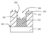
도 2a 내지 도 2d는 하나 이상의 실시예에 따른 기판(400)의 단면도들을 예시한다. 일부 실시예들에서, 도 2a 내지 도 2d는, 도 1에 예시된 증착 방법(200)에 의해 처리된 기판(400)을 예시한다. 도 2a는 증착 방법(200)의 임의적인 동작(210)을 예시하며, 이는, 기판(400)의 최상부 표면(405) 상에 함몰된 금속 물질(415) 및 적어도 하나의 피쳐를 형성하기 위해 금속 물질(140)의 라인을 함몰시키는 것을 포함하고, 적어도 하나의 피쳐는 최하부 표면(452) 및 2개의 측벽(456, 458)을 갖는 비아(450)를 정의하는 적어도 하나의 표면을 포함한다.FIGS. 2A-2D illustrate cross-sectional views of a substrate (400) according to one or more embodiments. In some embodiments, FIGS. 2A-2D illustrate a substrate (400) processed by the deposition method (200) illustrated in FIG. 1. FIG. 2A illustrates an optional operation (210) of the deposition method (200), which includes depositing a line of metal material (140) on a top surface (405) of the substrate (400) to form a recessed metal material (415) and at least one feature, the at least one feature including at least one surface defining a via (450) having a bottom surface (452) and two sidewalls (456, 458).
도 2a 내지 도 2d를 참조하면, 기판(400)은 임의의 적합한 기판 물질일 수 있다. 하나 이상의 실시예에서, 기판(400)은 반도체 물질, 예컨대, 규소(Si), 탄소(C), 게르마늄(Ge), 규소 게르마늄(SiGe), 갈륨 비소화물(GaAs), 인화인듐(InP), 인듐 갈륨 비소화물(InGaAs), 인듐 알루미늄 비소화물(InAlAs), 게르마늄(Ge), 규소 게르마늄(SiGe), 다른 반도체 물질들, 또는 이들의 임의의 조합물을 포함한다. 하나 이상의 실시예에서, 기판(400)은, 규소(Si), 게르마늄(Ge), 갈륨(Ga), 비소(As), 인듐(In), 인(P), 또는 셀레늄(Se) 중 하나 이상을 포함한다. 기판(400)을 형성할 수 있는 물질들의 몇몇 예들이 본원에서 설명되지만, 수동 및 능동 전자 디바이스들(예컨대, 트랜지스터들, 메모리들, 커패시터들, 인덕터들, 저항기들, 스위치들, 집적 회로들, 증폭기들, 광전자 디바이스들, 또는 임의의 다른 전자 디바이스들)이 구축될 수 있는 기초로서의 역할을 할 수 있는 임의의 물질이 본 개시내용의 사상 및 범위 내에 속한다.Referring to FIGS. 2A-2D , the substrate (400) can be any suitable substrate material. In one or more embodiments, the substrate (400) includes a semiconductor material, such as silicon (Si), carbon (C), germanium (Ge), silicon germanium (SiGe), gallium arsenide (GaAs), indium phosphide (InP), indium gallium arsenide (InGaAs), indium aluminum arsenide (InAlAs), germanium (Ge), silicon germanium (SiGe), other semiconductor materials, or any combination thereof. In one or more embodiments, the substrate (400) includes one or more of silicon (Si), germanium (Ge), gallium (Ga), arsenide (As), indium (In), phosphorus (P), or selenium (Se). Although several examples of materials that can form the substrate (400) are described herein, any material that can serve as a foundation on which passive and active electronic devices (e.g., transistors, memories, capacitors, inductors, resistors, switches, integrated circuits, amplifiers, optoelectronic devices, or any other electronic devices) can be constructed is within the spirit and scope of the present disclosure.
도 2a를 참조하면, 기판(400)은, 유전체(420)에 의해 경계 지어지는 금속 물질(410)의 적어도 하나의 라인을 포함한다. 일부 실시예들에서, 증착 방법(200)은 임의적으로, 동작(210)에서, 기판(400) 상에 함몰된 금속 물질(415) 및 적어도 하나의 피쳐를 형성하기 위해 금속 물질(410)을 함몰시키는 단계를 포함하며, 적어도 하나의 피쳐는, 함몰된 금속 물질(415)을 포함하는 최하부 표면(452) 및 유전체(420)를 포함하는 2개의 측벽(456, 458)을 갖는 비아(450)를 정의하는 적어도 하나의 표면을 포함한다. 일부 실시예들에서, 금속 물질(410)은 함몰된 금속 물질(415)을 형성하기 위해 습식 식각 프로세스에 의해 함몰된다. 일부 실시예들에서, 금속 물질(410)은 함몰된 금속 물질(415)을 형성하기 위해 건식 식각 프로세스에 의해 함몰된다.Referring to FIG. 2A, a substrate (400) includes at least one line of metal material (410) bounded by a dielectric (420). In some embodiments, the deposition method (200) optionally includes, at operation (210), recessing the metal material (410) to form a recessed metal material (415) and at least one feature on the substrate (400), the at least one feature including at least one surface defining a via (450) having a bottom surface (452) comprising the recessed metal material (415) and two sidewalls (456, 458) comprising the dielectric (420). In some embodiments, the metal material (410) is recessed by a wet etch process to form the recessed metal material (415). In some embodiments, the metal material (410) is sunken by a dry etching process to form a sunken metal material (415).
금속 물질(410)은 함몰된 금속 물질(415)을 형성하기 위해 임의의 적합한 깊이로 함몰될 수 있다. 하나 이상의 실시예에서, 금속 물질(410)은 유전체(420)의 최상부 표면으로부터 2 nm 내지 200 nm 범위 내의 깊이로 함몰된다. 그에 따라, 하나 이상의 실시예에서, 비아(450)는 2 nm 내지 200 nm의 범위 내의 깊이를 갖는다.The metal material (410) can be recessed to any suitable depth to form a recessed metal material (415). In one or more embodiments, the metal material (410) is recessed to a depth in the range of 2 nm to 200 nm from the top surface of the dielectric (420). Accordingly, in one or more embodiments, the via (450) has a depth in the range of 2 nm to 200 nm.
하나 이상의 실시예에서, 금속 물질(410)은 통상의 기술자에게 알려져 있는 임의의 적합한 방법에 의해 함몰될 수 있다. 하나 이상의 실시예에서, 금속 물질(410)은 습식 식각 및 건식 식각 중 하나 이상에 의해 함몰될 수 있다. 일부 실시예들에서, 건식 식각 프로세스는, 캘리포니아주 산타 클라라에 위치한 어플라이드 머티어리얼스 인코포레이티드(Applied Materials, Inc.)로부터 입수가능한 원격 플라즈마-보조 건식 식각 프로세스, 이를테면 시코니(SiCoNi™) 식각 프로세스, 또는 종래의 플라즈마 식각을 포함할 수 있다. 시코니™ 식각 프로세스에서, 디바이스는 H2, NF3, 및/또는 NH3 플라즈마 종들, 예컨대, 플라즈마-여기된 수소 및 플루오린 종들에 노출된다. 예컨대, 일부 실시예들에서, 디바이스는 H2, NF3, 및 NH3 플라즈마에 대한 동시적인 노출을 겪을 수 있다. 시코니™ 식각 프로세스는 시코니™ 사전세정 챔버(Preclean chamber)에서 수행될 수 있으며, 이는, 어플라이드 머티어리얼스®로부터 입수가능한 센츄라(Centura®), 듀얼 ACP(Dual ACP), 프로듀서(Producer®) GT, 및 엔듀라(Endura®) 플랫폼을 포함하는 다양한 다중-처리 플랫폼들 중 하나에 통합될 수 있다. 습식 식각 프로세스는, 플루오린화수소(HF) 산 최종 프로세스, 즉, 소위 "HF 최종" 프로세스를 포함할 수 있으며, 여기서, 표면을 수소-종결된 채로 남기는 표면의 HF 식각이 수행된다. 대안적으로, 임의의 다른 액체-기반 에피택셜-전 사전-세정 프로세스가 이용될 수 있다. 일부 실시예들에서, 프로세스는 자연 산화물 제거를 위한 승화 식각을 포함한다. 식각 프로세스는 플라즈마 또는 열 기반일 수 있다. 플라즈마 프로세스들은 임의의 적합한 플라즈마(예컨대, 전도성 결합된 플라즈마, 유도성 결합된 플라즈마, 마이크로파 플라즈마)일 수 있다.In one or more embodiments, the metal material (410) can be etched by any suitable method known to those of ordinary skill in the art. In one or more embodiments, the metal material (410) can be etched by one or more of a wet etch and a dry etch. In some embodiments, the dry etch process can include a remote plasma-assisted dry etch process available from Applied Materials, Inc., located in Santa Clara, Calif., such as the SiCoNi™ etch process, or a conventional plasma etch. In a SiCoNi™ etch process, the device is exposed to H2 , NF3 , and/or NH3 plasma species, such as plasma-excited hydrogen and fluorine species. For example, in some embodiments, the device can undergo simultaneous exposure to H2 , NF3 , and NH3 plasma. The Sikoni™ etch process can be performed in a Sikoni™ Preclean chamber, which can be integrated into one of a variety of multi-processing platforms available from Applied Materials® , including the Centura® , Dual ACP, Producer® GT, and Endura® platforms. The wet etch process can include a hydrofluoric (HF) acid final process, i.e., a so-called "HF final" process, in which an HF etch of the surface is performed leaving the surface hydrogen-terminated. Alternatively, any other liquid-based pre-epitaxial pre-clean process can be utilized. In some embodiments, the process includes a sublimation etch to remove native oxide. The etch process can be plasma or thermal based. The plasma processes can be any suitable plasma (e.g., conductively coupled plasma, inductively coupled plasma, microwave plasma).
하나 이상의 실시예에서, 금속 물질(410)은 임의의 적합한 금속을 포함할 수 있다. 일부 실시예들에서, 금속 물질(410)은, 구리(Cu), 코발트(Co), 텅스텐(W), 몰리브데넘(Mo), 및 루테늄(Ru) 중 하나 이상을 포함한다. 일부 실시예들에서, 금속 물질(410)은, 본질적으로 코발트로 이루어진다. 일부 실시예들에서, 금속 물질(410)은, 본질적으로 텅스텐으로 이루어진다. 일부 실시예들에서, 금속 물질(410)은, 본질적으로 루테늄으로 이루어진다. 일부 실시예들에서, 금속 물질(410)은, 본질적으로 몰리브데넘으로 이루어진다. 이와 관련하여 사용되는 바와 같이, "본질적으로 ~로 이루어진", 즉, 본질적으로 언급된 원소로 이루어진 금속 물질은, 원자 기준으로 언급된 원소를 95 % 이상, 98 % 이상, 99 % 이상, 또는 99.5 % 이상 포함한다. 도 2b 내지 도 2d를 참조하면, 일부 실시예들에서, 도 2a의 금속 물질(410)로부터 형성되는 함몰된 금속 물질(415)은 금속 물질(410)과 동일한 물질을 포함하고 동일한 특성들을 갖는다.In one or more embodiments, the metal material (410) may include any suitable metal. In some embodiments, the metal material (410) includes one or more of copper (Cu), cobalt (Co), tungsten (W), molybdenum (Mo), and ruthenium (Ru). In some embodiments, the metal material (410) consists essentially of cobalt. In some embodiments, the metal material (410) consists essentially of tungsten. In some embodiments, the metal material (410) consists essentially of ruthenium. In some embodiments, the metal material (410) consists essentially of molybdenum. As used herein, the phrase “consisting essentially of,” i.e., consisting essentially of a referenced element, includes at least 95%, at least 98%, at least 99%, or at least 99.5%, on an atomic basis, of the referenced element. Referring to FIGS. 2b to 2d , in some embodiments, the sunken metal material (415) formed from the metal material (410) of FIG. 2a comprises the same material and has the same properties as the metal material (410).
다시 도 2a 내지 도 2d를 참조하면, 유전체(420)는 통상의 기술자에게 알려져 있는 임의의 적합한 유전체 물질을 포함할 수 있다. 본원에서 사용되는 바와 같이, "유전체 물질"이라는 용어는, 전기장에서 분극될 수 있는 전기 절연체를 지칭한다. 일부 실시예들에서, 유전체 물질은, 산화물들, 탄소 도핑된 산화물들, 이산화규소(SiO2), 다공성 이산화규소(SiO2), 질화규소(SiN), 이산화규소/질화규소, 탄화물들, 산탄화물들, 질화물들, 산질화물들, 산탄질화물들, 중합체들, 포스포실리케이트 유리, 플루오로실리케이트(SiOF) 유리, 또는 유기실리케이트 유리(SiOCH) 중 하나 이상을 포함한다. 하나 이상의 실시예에서, 유전체(420)는 산화규소(SiOx), 질화규소(SiN), 또는 이들의 조합물들로부터 선택된다. 일부 실시예들에서, 유전체(420)는 본질적으로 산화규소로 이루어진다. 전술한 기술어(descriptor)들(예컨대, 산화규소)은 임의의 특정 화학량론적 비를 개시하는 것으로 해석되어서는 안 된다는 것이 유의된다. 이에 따라서, "산화규소" 등은 임의의 특정 화학량론적 비를 개시함이 없이도 본질적으로 규소 및 산소로 이루어진 물질로서 관련 기술분야의 통상의 기술자에 의해 이해될 것이다.Referring again to FIGS. 2A-2D , the dielectric (420) can comprise any suitable dielectric material known to those of ordinary skill in the art. As used herein, the term "dielectric material" refers to an electrical insulator that is polarizable in an electric field. In some embodiments, the dielectric material comprises one or more of oxides, carbon doped oxides, silicon dioxide (SiO2 ), porous silicon dioxide (SiO2 ), silicon nitride (SiN), silicon dioxide/silicon nitride, carbides, oxycarbides, nitrides, oxynitrides, oxycarbonitrides, polymers, phosphosilicate glasses, fluorosilicate (SiOF) glasses, or organosilicate glasses (SiOCH ). In one or more embodiments, the dielectric (420) is selected from silicon oxide (SiOx ), silicon nitride (SiN), or combinations thereof. In some embodiments, the dielectric (420) consists essentially of silicon oxide. It is noted that the above descriptors (e.g., silicon oxide) should not be construed as disclosing any particular stoichiometric ratio. Accordingly, "silicon oxide" and the like would be understood by one of ordinary skill in the art to be a material consisting essentially of silicon and oxygen, without disclosing any particular stoichiometric ratio.
도면들은 예시의 목적들을 위해 단일 피쳐(450)를 갖는 기판들을 도시하지만, 관련 기술분야의 통상의 기술자들은, 하나 초과의 피쳐(450)가 존재할 수 있다는 것을 이해할 것이다. 피쳐(450)의 형상은, 트렌치들 및 원통형 비아들을 포함하지만 이에 제한되지 않는 임의의 적합한 형상일 수 있다. 이와 관련하여 사용되는 바와 같이, "피쳐"라는 용어는 임의의 의도적인 표면 불규칙성을 의미한다. 피쳐들의 적합한 예들은, 최상부, 2개의 측벽, 및 최하부를 갖는 트렌치들 및 비아들, 최상부 및 2개의 측벽을 갖는 피크들을 포함하지만 이에 제한되지 않는다. 하나 이상의 실시예에서, 적어도 하나의 피쳐(450)는 트렌치 또는 비아 중 하나 이상을 포함한다. 특정 실시예들에서, 적어도 하나의 피쳐(450)는 비아를 포함한다. 더 추가적인 실시예들에서, "적어도 하나의 피쳐(450)" 및 "비아(450)"라는 용어는 상호교환가능하게 사용될 수 있다. 비아(450)는, 최하부 표면(452)까지의 깊이(D) 및 2개의 측벽(456, 458) 사이의 폭(W)을 갖는다. 일부 실시예들에서, 깊이(D)는 2 nm 내지 200 nm, 3 nm 내지 200 nm, 5 nm 내지 100 nm, 2 nm 내지 100 nm, 또는 50 nm 내지 100 nm의 범위 내에 있다. 일부 실시예들에서, 폭(W)은 10 nm 내지 100 nm, 10 nm 내지 20 nm, 10 nm 내지 50 nm, 또는 50 nm 내지 100 nm의 범위 내에 있다. 일부 실시예들에서, 비아(450)는 1:1 내지 20:1, 5:1 내지 20:1, 10:1 내지 20:1, 또는 15:1 내지 20:1 범위 내의 종횡비(D/W)를 갖는다.While the drawings illustrate substrates having a single feature (450) for illustrative purposes, those skilled in the art will appreciate that there may be more than one feature (450). The shape of the feature (450) may be any suitable shape, including but not limited to trenches and cylindrical vias. As used herein, the term “feature” means any intentional surface irregularity. Suitable examples of features include but are not limited to trenches and vias having a top, two sidewalls, and a bottom, and peaks having a top and two sidewalls. In one or more embodiments, at least one feature (450) comprises one or more of a trench or a via. In certain embodiments, at least one feature (450) comprises a via. In further embodiments, the terms “at least one feature (450)” and “via (450)” may be used interchangeably. The via (450) has a depth (D) to the bottom surface (452) and a width (W) between two sidewalls (456, 458). In some embodiments, the depth (D) is in a range from 2 nm to 200 nm, from 3 nm to 200 nm, from 5 nm to 100 nm, from 2 nm to 100 nm, or from 50 nm to 100 nm. In some embodiments, the width (W) is in a range from 10 nm to 100 nm, from 10 nm to 20 nm, from 10 nm to 50 nm, or from 50 nm to 100 nm. In some embodiments, the via (450) has an aspect ratio (D/W) in a range from 1:1 to 20:1, from 5:1 to 20:1, from 10:1 to 20:1, or from 15:1 to 20:1.
하나 이상의 실시예에서, 함몰된 금속 물질(415)(예컨대, 최하부 표면(452)) 및 유전체(420)(예컨대, 2개의 측벽(456, 458))의 표면들은, 도 2b에서 각각 O 및 X로 도시된 오염물들을 포함한다. 일부 실시예들에서, 오염물들은 유기 화합물들, 중합체성 화합물들, 금속 산화물들, 또는 금속 질화물들 중 하나 이상을 포함할 수 있지만 이에 제한되지 않는다. 일부 실시예들에서, 오염물들은, 함몰된 금속 물질(415)을 형성하기 위해 금속 물질(410)을 함몰시키는 프로세스(예컨대, 습식 식각 프로세스 또는 건식 식각 프로세스)에 의해, 함몰된 금속 물질(415)(예컨대, 최하부 표면(452)) 및 유전체(420)(예컨대, 2개의 측벽(456, 458))의 표면들 상에 생성된다.In one or more embodiments, surfaces of the recessed metal material (415) (e.g., the bottom surface (452)) and the dielectric (420) (e.g., the two sidewalls (456, 458)) include contaminants, illustrated as O and X in FIG. 2B , respectively. In some embodiments, the contaminants may include, but are not limited to, one or more of organic compounds, polymeric compounds, metal oxides, or metal nitrides. In some embodiments, the contaminants are created on surfaces of the recessed metal material (415) (e.g., the bottom surface (452)) and the dielectric (420) (e.g., the two sidewalls (456, 458)) by a process of recessing the metal material (410) to form the recessed metal material (415) (e.g., a wet etching process or a dry etching process).
동작(220)에서, 증착 방법(200)은, 함몰된 금속 물질(415)(예컨대, 최하부 표면(452)) 및 유전체(420)(예컨대, 2개의 측벽(456, 458))의 표면들을 세정하기 위해, 적어도 하나의 피쳐(450)를 포함하는 기판(400)의 최상부 표면(405)을 복수의 화학적 노출들에 노출시키는 단계를 포함한다. 일부 실시예들에서, 복수의 화학적 노출들 동안 기판(400)의 온도가 제어된다. 일부 실시예들에서, 복수의 화학적 노출들 중 하나 이상은, 20 ℃ 내지 550 ℃의 범위, 20 ℃ 내지 500 ℃의 범위, 20 ℃ 내지 450 ℃의 범위, 20 ℃ 내지 400 ℃의 범위, 20 ℃ 내지 350 ℃의 범위, 20 ℃ 내지 300 ℃의 범위, 20 ℃ 내지 250 ℃의 범위, 20 ℃ 내지 200 ℃의 범위, 20 ℃ 내지 150 ℃의 범위, 20 ℃ 내지 100 ℃의 범위, 100 ℃ 내지 500 ℃의 범위, 또는 300 ℃ 내지 550 ℃의 범위를 포함하여 20 ℃ 내지 600 ℃의 범위 내의 온도에서 수행된다.In operation (220), the deposition method (200) includes exposing a top surface (405) of a substrate (400) including at least one feature (450) to a plurality of chemical exposures to clean surfaces of a sunken metal material (415) (e.g., a bottom surface (452)) and a dielectric (420) (e.g., two sidewalls (456, 458)). In some embodiments, a temperature of the substrate (400) is controlled during the plurality of chemical exposures. In some embodiments, one or more of the plurality of chemical exposures are performed at a temperature within a range of 20 °C to 600 °C, including within a range of 20 °C to 550 °C, within a range of 20 °C to 500 °C, within a range of 20 °C to 450 °C, within a range of 20 °C to 400 °C, within a range of 20 °C to 350 °C, within a range of 20 °C to 300 °C, within a range of 20 °C to 250 °C, within a range of 20 °C to 200 °C, within a range of 20 °C to 150 °C, within a range of 20 °C to 100 °C, within a range of 100 °C to 500 °C, or within a range of 300 °C to 550 °C.
일부 실시예들에서, 증착 방법(200)의 프로세스들은 각각이 동일한 처리 챔버 내에서 수행된다. 일부 실시예들에서, 증착 방법(200)의 프로세스들은 각각이 상이한 처리 챔버 내에서 수행된다. 일부 실시예들에서, 상이한 처리 챔버들은 처리 시스템의 일부로서 연결된다. 일부 실시예들에서, 증착 방법(200)의 프로세스들은 중간에 진공 깨뜨림 없이 수행된다.In some embodiments, the processes of the deposition method (200) are each performed within the same processing chamber. In some embodiments, the processes of the deposition method (200) are each performed within different processing chambers. In some embodiments, the different processing chambers are connected as part of a processing system. In some embodiments, the processes of the deposition method (200) are performed without an intermediate vacuum break.
일부 실시예들에서, 복수의 화학적 노출들 중 하나 이상은 진공을 깨뜨림이 없이 인-시튜로 수행된다. 일부 실시예들에서, 복수의 화학적 노출들 중 하나 이상은 엑스-시튜(ex situ)로 수행된다. 본원에서 사용되는 바와 같이, "인-시튜"라는 용어는, 증착 방법(200)의 프로세스들 각각이 중간에 진공 깨뜨림 없이 수행되도록, 동일한 처리 챔버에서 또는 처리 시스템의 일부로서 연결되는 상이한 처리 챔버에서 각각이 수행되는 증착 방법(200)의 프로세스들을 지칭한다. 본원에서 사용되는 바와 같이, "엑스-시튜"라는 용어는, 증착 방법(200)의 프로세스들 중 하나 이상이 중간에 진공 깨뜨림이 있게 수행되도록, 동일한 처리 챔버 또는 상이한 처리 챔버에서 각각이 수행되는 증착 방법(200)의 프로세스들을 지칭한다.In some embodiments, one or more of the plurality of chemical exposures are performed in situ without breaking vacuum. In some embodiments, one or more of the plurality of chemical exposures are performed ex situ. As used herein, the term "in situ" refers to processes of the deposition method (200) that are each performed in the same processing chamber or in different processing chambers that are connected as part of a processing system, such that each of the processes of the deposition method (200) is performed without breaking vacuum interveningly. As used herein, the term "ex situ" refers to processes of the deposition method (200) that are each performed in the same processing chamber or in different processing chambers, such that one or more of the processes of the deposition method (200) is performed with a breaking vacuum interveningly.
일부 실시예들에서, 복수의 화학적 노출들은, 비아(450)로부터 수분을 제거하기 위한 펌프 및 퍼지 프로세스, 플라즈마 노출, 및 열 침지(thermal soak) 중 하나 이상을 포함한다. 복수의 화학적 노출들은 임의의 횟수 및 임의의 적합한 순서로 수행될 수 있다. 복수의 화학적 노출들은 개별적으로 또는 임의의 적합한 조합으로 함께 수행될 수 있다.In some embodiments, the multiple chemical exposures include one or more of a pump and purge process, a plasma exposure, and a thermal soak to remove moisture from the via (450). The multiple chemical exposures can be performed any number of times and in any suitable order. The multiple chemical exposures can be performed individually or together in any suitable combination.
일부 실시예들에서, 복수의 화학적 노출들은, 엑스-시튜 조합된 펌프 및 퍼지 프로세스 및 열 침지와 그에 후속되는 인-시튜 조합된 펌프 및 퍼지 프로세스 및 플라즈마 노출을 포함한다. 일부 실시예들에서, 복수의 화학적 노출들은, 인-시튜 조합된 펌프 및 퍼지 프로세스 및 열 침지와 그에 후속되는 인-시튜 플라즈마 노출을 포함한다. 일부 실시예들에서, 복수의 화학적 노출들은, 인-시튜 조합된 펌프 및 퍼지 프로세스 및 플라즈마 노출을 포함한다.In some embodiments, the multiple chemical exposures comprise an ex-situ combined pump and purge process and thermal immersion followed by an in-situ combined pump and purge process and plasma exposure. In some embodiments, the multiple chemical exposures comprise an in-situ combined pump and purge process and thermal immersion followed by an in-situ plasma exposure. In some embodiments, the multiple chemical exposures comprise an in-situ combined pump and purge process and plasma exposure.
하나 이상의 실시예에서, 펌프 및 퍼지 프로세스는 임의의 적합한 온도 및 압력에서 수행될 수 있다. 일부 실시예들에서, 펌프 및 퍼지 프로세스는, 300 ℃ 내지 500 ℃의 범위 내의 온도, 10 Torr 내지 300 Torr의 범위 내의 압력, 및 30 ℃ 내지 150 ℃의 범위 내의 앰풀(전구체를 포함하고 있음) 온도에서 페디스털 상에 기판(400)을 유지하는 것을 포함한다.In one or more embodiments, the pump and purge process can be performed at any suitable temperature and pressure. In some embodiments, the pump and purge process comprises maintaining the substrate (400) on the pedestal at a temperature within the range of 300 °C to 500 °C, a pressure within the range of 10 Torr to 300 Torr, and an ampoule (containing the precursor) temperature within the range of 30 °C to 150 °C.
일부 실시예들에서, 복수의 화학적 노출들 중 적어도 하나는 플라즈마 노출을 포함한다. 일부 실시예들에서, 플라즈마 노출은, H2 플라즈마 노출 또는 O2 플라즈마 노출 중 하나 이상을 포함한다. 일부 실시예들에서, H2 플라즈마 노출은, 함몰된 금속 물질(415)(예컨대, 최하부 표면(452)) 및 유전체(420)(예컨대, 2개의 측벽(456, 458))의 표면들로부터, 도 2b에서 각각 O 및 X로 도시된 오염물들을 제거한다.In some embodiments, at least one of the plurality of chemical exposures comprises a plasma exposure. In some embodiments, the plasma exposure comprises one or more of a H2 plasma exposure or an O2 plasma exposure. In some embodiments, the H2 plasma exposure removes contaminants, illustrated as O and X in FIG. 2B , from surfaces of the sunken metal material (415) (e.g., the lowermost surface (452)) and the dielectric (420) (e.g., the two sidewalls (456, 458)), respectively.
하나 이상의 실시예에서, H2 플라즈마 노출은, 비아(450)의 최하부 표면(452)에서 자연 금속 산화물의 양을 감소시키거나 자연 금속 산화물을 제거한다. 일부 실시예들에서, O2 플라즈마 노출은, 함몰된 금속 물질(415)(예컨대, 최하부 표면(452)) 및 유전체(420)(예컨대, 2개의 측벽(456, 458))의 표면들로부터, 도 2a에서 각각 O 및 X로 도시된 오염물들을 제거한다. 일부 실시예들에서, O2 플라즈마 노출은 상향식 갭 충전의 선택도를 증가시킨다.In one or more embodiments, the H2 plasma exposure reduces the amount of or removes native metal oxide at the bottom surface (452) of the via (450). In some embodiments, the O2 plasma exposure removes contaminants, illustrated as O and X in FIG. 2A, respectively, from surfaces of the recessed metal material (415) (e.g., the bottom surface (452)) and the dielectric (420) (e.g., the two sidewalls (456, 458)). In some embodiments, the O2 plasma exposure increases the selectivity of the bottom-up gap fill.
일부 실시예들에서, 플라즈마 노출은 유도성 결합된 플라즈마(ICP)를 포함한다. 일부 실시예들에서, 플라즈마 노출은, 아르곤(Ar) 스퍼터링을 이용한 방향성의 유도성 결합된 플라즈마(ICP)에 대한 노출을 포함한다. 일부 실시예들에서, 플라즈마는 용량성 결합된 플라즈마(CCP)이다. 일부 실시예들에서, 플라즈마는 원격으로 생성된다. 일부 실시예들에서, 플라즈마는 처리 챔버 내에서 생성된다(직접 플라즈마).In some embodiments, the plasma exposure comprises an inductively coupled plasma (ICP). In some embodiments, the plasma exposure comprises exposure to a directional inductively coupled plasma (ICP) using argon (Ar) sputtering. In some embodiments, the plasma is a capacitively coupled plasma (CCP). In some embodiments, the plasma is generated remotely. In some embodiments, the plasma is generated within the processing chamber (direct plasma).
일부 실시예들에서, 플라즈마 노출은, 아르곤(Ar) 스퍼터링을 이용한 방향성의 유도성 결합된 플라즈마(ICP)에 대한 인-시튜 플라즈마 노출을 포함한다. 하나 이상의 실시예에서, 아르곤(Ar) 스퍼터링을 이용한 방향성의 유도성 결합된 플라즈마(ICP)는, 5 Å 내지 40 Å의 범위 내의 두께를 갖는 아르곤(Ar) 층을 스퍼터링하는 것을 포함한다. 일부 실시예들에서, 아르곤(Ar) 스퍼터링을 이용한 방향성의 유도성 결합된 플라즈마(ICP)는 비아(450)의 최하부 표면(452)으로부터 자연 금속 산화물을 제거한다. 일부 실시예들에서, 아르곤(Ar) 스퍼터링을 이용한 방향성의 유도성 결합된 플라즈마(ICP)는 2개의 측벽(456, 458)으로부터 불순물들을 제거한다. 일부 실시예들에서, 아르곤(Ar) 스퍼터링을 이용한 방향성의 유도성 결합된 플라즈마(ICP)는, 함몰된 금속 물질(415)(예컨대, 최하부 표면(452)) 및 유전체(420)(예컨대, 2개의 측벽(456, 458))의 표면들로부터, 도 2a에서 각각 O 및 X로 도시된 오염물들을 제거한다.In some embodiments, the plasma exposure comprises in-situ plasma exposure to a directional inductively coupled plasma (ICP) using argon (Ar) sputtering. In one or more embodiments, the directional inductively coupled plasma (ICP) using argon (Ar) sputtering comprises sputtering an argon (Ar) layer having a thickness in the range of 5 Å to 40 Å. In some embodiments, the directional inductively coupled plasma (ICP) using argon (Ar) sputtering removes native metal oxide from the bottom surface (452) of the via (450). In some embodiments, the directional inductively coupled plasma (ICP) using argon (Ar) sputtering removes impurities from the two sidewalls (456, 458). In some embodiments, a directional inductively coupled plasma (ICP) using argon (Ar) sputtering removes contaminants, illustrated as O and X in FIG. 2a , from surfaces of the sunken metal material (415) (e.g., the lowermost surface (452)) and the dielectric (420) (e.g., the two sidewalls (456, 458)), respectively.
하나 이상의 실시예에서, 복수의 화학적 노출들 중 적어도 하나는 열 침지를 포함한다. 열 침지는, 플라즈마 또는 다른 라디칼들의 사용 없이 비아(450)를 화학 작용제에 노출시키는 것을 포함하는 것으로 관련 기술분야의 통상의 기술자에 의해 이해될 것이다. 하나 이상의 실시예에서, 열 침지는, 비아(450)의 최하부 표면(452)으로부터 자연 금속 산화물을 제거한다. 일부 실시예들에서, 열 침지는, 비아(450)를 육플루오린화텅스텐(WF6), 육염화텅스텐(WCl6), 텅스텐(VI) 옥시사염화물(WOCl4), 오염화텅스텐(WCl5), 오염화몰리브데넘(MoCl5), 몰리브데넘 옥시사염화물(MoOCl4), 이염화이산화몰리브데넘(MoO2Cl2), 및 육플루오린화몰리브데넘(MoF6) 중 하나 이상에 노출시키는 것을 포함한다.In one or more embodiments, at least one of the plurality of chemical exposures comprises thermal immersion. Thermal immersion will be understood by those skilled in the art to include exposing the via (450) to a chemical agent without the use of plasma or other radicals. In one or more embodiments, the thermal immersion removes native metal oxide from the lowermost surface (452) of the via (450). In some embodiments, the thermal immersion comprises exposing the via (450) to one or more of tungsten hexafluoride (WF6 ), tungsten hexachloride (WCl6 ), tungsten(VI) oxytetrachloride (WOCl4 ), tungsten pentafluoride (WCl5 ), molybdenum pentafluoride (MoCl5 ), molybdenum oxytetrachloride (MoOCl4 ), molybdenum dichloride (MoO2 Cl2 ), and molybdenum hexafluoride (MoF6 ).
일부 실시예들에서, 열 침지는 엑스-시튜로 수행되고, 비아(450)를 WCl5에 노출시키는 것을 포함한다. 일부 실시예들에서, 열 침지는 인-시튜로 수행되고, 비아(450)를 WCl5에 노출시키는 것을 포함한다. 하나 이상의 실시예에서, 열 침지는 인-시튜로 수행되고, 비아를 MoCl5에 노출시키는 것을 포함한다. 일부 실시예들에서, 열 침지는 엑스-시튜로 수행되고, 비아를 MoCl5에 노출시키는 것을 포함한다. 일부 실시예들에서, 열 침지는 인-시튜이고, 비아를 MoO2Cl2에 노출시키는 것을 포함한다. 일부 실시예들에서, 열 침지는 엑스-시튜이고, 비아를 MoO2Cl2에 노출시키는 것을 포함한다.In some embodiments, the thermal immersion is performed ex-situ and comprises exposing the via (450) to WCl5 . In some embodiments, the thermal immersion is performed in-situ and comprises exposing the via (450) to WCl5 . In one or more embodiments, the thermal immersion is performed in-situ and comprises exposing the via to MoCl5 . In some embodiments, the thermal immersion is performed ex-situ and comprises exposing the via to MoCl5 . In some embodiments, the thermal immersion is in-situ and comprises exposing the via to MoO2 Cl2 . In some embodiments, the thermal immersion is ex-situ and comprises exposing the via to MoO2 Cl2 .
동작(230)에서, 함몰된 금속 물질(415)의 세정된 표면 상에 몰리브데넘 막(430)이 인-시튜로 선택적으로 증착된다. 일부 실시예들에서, 몰리브데넘 막(430)은 적어도 하나의 피쳐(450)의 2개의 측벽(456, 458)에 의해 측방향으로 경계 지어진다. 이와 관련하여 사용되는 바와 같이, "측방향으로 경계 지어진다"는, 증착된 물질이 최상부 표면과 2개의 측벽(456, 458) 사이의 교차점을 넘어 연장되지 않는다는 것을 의미한다. 일부 실시예들에서, 몰리브데넘 막(430)은 적어도 하나의 피쳐(450) 위로 연장된다. 일부 실시예들에서, 도 2c에 도시된 바와 같이, 몰리브데넘 막(430)은 전적으로 비아(450) 내에 있다. 이와 관련하여 사용되는 바와 같이, "전적으로 ~ 내에 있는", 즉, 전적으로 비아 내에 있는 물질은, 비아(450) 위로 연장되지 않고, 비아(450)의 2개의 측벽(456, 458)에 의해 측방향으로 경계 지어진다. 일부 실시예들에서, 몰리브데넘 막(430)은 비아(450)를 충전한다. 이와 관련하여 사용되는 바와 같이, "비아를 충전"하는 막은, 비아(450)의 체적의 적어도 95 %, 적어도 98 %, 또는 적어도 99 %를 점유하는 체적을 갖는다. 일부 실시예들에서, 비아를 충전하는 막은, 40 nm 내지 60 nm의 범위를 포함하여 30 nm 내지 75 nm의 범위 내의 충전 높이를 갖는다.In operation (230), a molybdenum film (430) is selectively deposited in-situ on the cleaned surface of the recessed metal material (415). In some embodiments, the molybdenum film (430) is laterally bounded by two sidewalls (456, 458) of at least one feature (450). As used herein, “laterwise bounded” means that the deposited material does not extend beyond the intersection between the top surface and the two sidewalls (456, 458). In some embodiments, the molybdenum film (430) extends over at least one feature (450). In some embodiments, as illustrated in FIG. 2C , the molybdenum film (430) is entirely within the via (450). As used herein, the material “entirely within”, i.e., entirely within the via, does not extend beyond the via (450) and is laterally bounded by the two sidewalls (456, 458) of the via (450). In some embodiments, the molybdenum film (430) fills the via (450). As used herein, the film that “fills the via” has a volume that occupies at least 95%, at least 98%, or at least 99% of the volume of the via (450). In some embodiments, the film that fills the via has a fill height within a range of from 30 nm to 75 nm, including from 40 nm to 60 nm.
본 개시내용의 실시예들은 유리하게, 본원에서 설명된 것들(예컨대, 증착 방법(200)) 이외의 프로세스들에 의해 증착된 몰리브데넘 막들과 비교하여 감소된 비저항을 갖는 인-시튜로 선택적으로 증착된 몰리브데넘 막들(430)을 제공한다. 본 개시내용의 실시예들은 유리하게, 공극들 및 이음부들이 없거나 실질적으로 없는 인-시튜로 선택적으로 증착된 몰리브데넘 막들(430)을 제공한다. 이와 관련하여 사용되는 바와 같이, "실질적으로 없다" 또는 "실질적으로 없는"이라는 것은, 인-시튜로 선택적으로 증착된 몰리브데넘 막(430)의 총 조성 중 원자 기준으로 약 4 % 미만, 약 3 % 미만, 약 2 % 미만, 약 1 % 미만, 약 0.5 % 미만, 및 약 0.1 % 미만을 포함하여 약 5 % 미만이 공극들 및/또는 이음부들을 포함한다는 것을 의미한다.Embodiments of the present disclosure advantageously provide in-situ selectively deposited molybdenum films (430) having reduced resistivity compared to molybdenum films deposited by processes other than those described herein (e.g., the deposition method (200)). Embodiments of the present disclosure advantageously provide in-situ selectively deposited molybdenum films (430) that are substantially free of pores and seams. As used herein, “substantially free” or “substantially free” means that less than about 5 percent, on an atomic basis, of the total composition of the in-situ selectively deposited molybdenum film (430) includes pores and/or seams, including less than about 4 percent, less than about 3 percent, less than about 2 percent, less than about 1 percent, less than about 0.5 percent, and less than about 0.1 percent.
이론에 얽매이도록 의도함이 없이, 복수의 화학적 노출들은 증착된 몰리브데넘 막(430)의 품질을 개선하는 것으로 생각된다. 일부 실시예들에서, 본원에서 설명된 방법들에 의해 증착된 몰리브데넘 막(430)은, 증가된 선택도, 감소된 표면 거칠기, 및/또는 감소된 결정립 크기 중 하나 이상을 나타낸다.Without intending to be bound by theory, it is believed that multiple chemical exposures improve the quality of the deposited molybdenum film (430). In some embodiments, the molybdenum film (430) deposited by the methods described herein exhibits one or more of increased selectivity, reduced surface roughness, and/or reduced grain size.
하나 이상의 실시예에서, 몰리브데넘 막(430)을 인-시튜로 선택적으로 증착하는 것은, 비아(450)를 몰리브데넘 전구체 및 환원제에 노출시키는 것을 포함한다. 일부 실시예들에서, 몰리브데넘 전구체는 MoCl5, MoOCl4, MoO2Cl2, 또는 MoF6 중 하나 이상을 포함한다. 환원제는 통상의 기술자에게 알려져 있는 임의의 적합한 환원 작용제일 수 있다. 일부 실시예들에서, 환원제는 H2를 포함한다.In one or more embodiments, selectively depositing the molybdenum film (430) in-situ comprises exposing the via (450) to a molybdenum precursor and a reducing agent. In some embodiments, the molybdenum precursor comprises one or more of MoCl5 , MoOCl4 , MoO2 Cl2 , or MoF6 . The reducing agent can be any suitable reducing agent known to those skilled in the art. In some embodiments, the reducing agent comprises H2 .
하나 이상의 실시예에서, 몰리브데넘 막(430)을 인-시튜로 선택적으로 증착하는 것은, 300 ℃ 내지 550 ℃의 범위 내의 온도에서 수행된다. 일부 실시예들에서, 몰리브데넘 막(430)을 선택적으로 증착하는 것은, 10 Torr 내지 300 Torr의 범위 내의 압력에서 수행된다.In one or more embodiments, selectively depositing the molybdenum film (430) in-situ is performed at a temperature in the range of 300 °C to 550 °C. In some embodiments, selectively depositing the molybdenum film (430) is performed at a pressure in the range of 10 Torr to 300 Torr.
몰리브데넘 막(430)은, 통상의 기술자에게 알려져 있는 임의의 적합한 프로세스에 의해 인-시튜로 선택적으로 증착될 수 있다. 하나 이상의 실시예에서, 몰리브데넘 막(430)을 선택적으로 증착하는 것은, 원자 층 증착(ALD), 몰리브데넘 전구체 및 수소(H2)를 공동-유동시키는 것, 또는 화학 기상 증착(CVD) 중 하나 이상을 포함한다.The molybdenum film (430) can be selectively deposited in-situ by any suitable process known to those of ordinary skill in the art. In one or more embodiments, selectively depositing the molybdenum film (430) includes one or more of atomic layer deposition (ALD), co-flowing a molybdenum precursor and hydrogen (H2 ), or chemical vapor deposition (CVD).
하나 이상의 실시예에서, 몰리브데넘 막(430)은, 복수의 화학적 노출들 없이 수행된 유사한 프로세스보다 적어도 20배 더 크거나, 적어도 50배 더 크거나, 적어도 100배 더 크거나, 적어도 200배 더 크거나, 적어도 500배 더 크거나, 적어도 1,000배 더 크거나, 적어도 2,000배 더 크거나, 또는 적어도 5,000배 더 큰 선택도로 선택적으로 증착된다.In one or more embodiments, the molybdenum film (430) is selectively deposited with a selectivity that is at least 20 times greater, at least 50 times greater, at least 100 times greater, at least 200 times greater, at least 500 times greater, at least 1,000 times greater, at least 2,000 times greater, or at least 5,000 times greater than a similar process performed without the multiple chemical exposures.
일부 실시예들에서, 몰리브데넘 막(430)은, 몰리브데넘 막(430)이 10 nm의 두께를 가질 때 1 nm 이하의 거칠기를 갖는다. 일부 실시예들에서, 몰리브데넘 막(430)은 복수의 결정립들을 가지며, 각각의 결정립은 10 nm 이하 및 5 nm 이하를 포함하여 15 nm 이하의 결정립 크기를 갖는다.In some embodiments, the molybdenum film (430) has a roughness of 1 nm or less when the molybdenum film (430) has a thickness of 10 nm. In some embodiments, the molybdenum film (430) has a plurality of grains, each grain having a grain size of 15 nm or less, including 10 nm or less and 5 nm or less.
도 3은 본 개시내용의 실시예들에 따른 다중-챔버 처리 시스템(100)의 예의 개략적인 평면도이다. 처리 시스템(100)은 일반적으로, 팩토리 인터페이스(102), 로드 록 챔버들(104, 106), 개개의 이송 로봇들(112, 114)을 갖는 이송 챔버들(108, 110), 홀딩 챔버들(116, 118), 및 처리 챔버들(120, 122, 124, 126, 128, 130)을 포함한다. 본원에서 상세히 설명되는 바와 같이, 처리 시스템(100) 내의 웨이퍼들은, 웨이퍼들을 처리 시스템(100) 외부의 주변 환경(예컨대, 이를테면 팹(fab)에 존재할 수 있는 대기 주변 환경)에 노출시킴이 없이 다양한 챔버들에서 처리되고 그 챔버들 사이에서 이송될 수 있다. 예컨대, 웨이퍼들은, 처리 시스템(100) 내의 웨이퍼들에 대해 수행되는 다양한 프로세스들 사이에서, 저압(예컨대, 약 300 Torr 이하) 또는 진공 환경의 다양한 챔버들에서 처리되고, 그 저압 또는 진공 환경을 깨뜨림이 없이 그 다양한 챔버들 사이에서 이송될 수 있다. 이에 따라서, 처리 시스템(100)은 웨이퍼들의 일부 처리에 대한 통합 솔루션을 제공할 수 있다.FIG. 3 is a schematic plan view of an example of a multi-chamber processing system (100) according to embodiments of the present disclosure. The processing system (100) generally includes a factory interface (102), load lock chambers (104, 106), transfer chambers (108, 110) having individual transfer robots (112, 114), holding chambers (116, 118), and processing chambers (120, 122, 124, 126, 128, 130). As described in detail herein, wafers within the processing system (100) can be processed in and transferred between the various chambers without exposing the wafers to an ambient environment outside the processing system (100), such as an atmospheric ambient environment that may be present in a fab. For example, wafers may be processed in various chambers in low pressure (e.g., less than about 300 Torr) or vacuum environments between various processes performed on the wafers within the processing system (100), and may be transferred between the various chambers without breaking the low pressure or vacuum environment. Accordingly, the processing system (100) may provide an integrated solution for some processing of wafers.
본원에서 제공되는 교시들에 따라 적합하게 수정될 수 있는 처리 시스템의 예들은, 캘리포니아주 산타 클라라에 위치한 어플라이드 머티어리얼스, 인코포레이티드로부터 상업적으로 입수가능한, 엔듀라®, 프로듀서®, 또는 센츄라® 통합 처리 시스템들 또는 다른 적합한 처리 시스템들을 포함한다. (다른 제조자들로부터의 처리 시스템들을 포함하는) 다른 처리 시스템들이 본원에서 설명된 양상들로부터 이익을 얻도록 적응될 수 있는 것으로 고려된다.Examples of processing systems that may be suitably modified in accordance with the teachings provided herein include the Endura®, Producer®, or Centura® integrated processing systems, commercially available from Applied Materials, Inc., located in Santa Clara, Calif., or other suitable processing systems. It is contemplated that other processing systems (including processing systems from other manufacturers) may be adapted to benefit from the aspects described herein.
도 3의 예시된 예에서, 팩토리 인터페이스(102)는 웨이퍼들의 이송을 용이하게 하기 위해 도킹 스테이션(140) 및 팩토리 인터페이스 로봇들(142)을 포함한다. 도킹 스테이션(140)은 하나 이상의 전방 개방 통합 포드(front opening unified pod)(FOUP)(144)를 수용하도록 구성된다. 일부 예들에서, 각각의 팩토리 인터페이스 로봇(142)은 일반적으로, 웨이퍼들을 팩토리 인터페이스(102)로부터 로드 록 챔버들(104, 106)로 이송하도록 구성되는 개개의 팩토리 인터페이스 로봇(142)의 하나의 단부 상에 배치되는 블레이드(148)를 포함한다.In the illustrated example of FIG. 3, the factory interface (102) includes a docking station (140) and factory interface robots (142) to facilitate transfer of wafers. The docking station (140) is configured to receive one or more front opening unified pods (FOUPs) (144). In some examples, each factory interface robot (142) generally includes a blade (148) disposed on one end of the individual factory interface robots (142) that is configured to transfer wafers from the factory interface (102) to the load lock chambers (104, 106).
로드 록 챔버들(104, 106)은, 팩토리 인터페이스(102)에 결합되는 개개의 포트들(150, 152) 및 이송 챔버(108)에 결합되는 개개의 포트들(154, 156)을 갖는다. 이송 챔버(108)는 추가로, 홀딩 챔버들(116, 118)에 결합되는 개개의 포트들(158, 160) 및 처리 챔버들(120, 122)에 결합되는 개개의 포트들(162, 164)을 갖는다. 유사하게, 이송 챔버(110)는, 홀딩 챔버들(116, 118)에 결합되는 개개의 포트들(166, 168) 및 처리 챔버들(124, 126, 128, 130)에 결합되는 개개의 포트들(170, 172, 174, 176)을 갖는다. 포트들(154, 156, 158, 160, 162, 164, 166, 168, 170, 172, 174, 176)은, 예컨대, 이송 로봇들(112, 114)에 의해 자신을 통해 웨이퍼들을 통과시키고, 가스가 개개의 챔버들 사이를 통과하는 것을 방지하기 위해 개개의 챔버들 사이에 밀봉을 제공하기 위한, 슬릿 밸브들을 갖는 슬릿 밸브 개구들일 수 있다. 일반적으로, 임의의 포트는 그 포트를 통해 웨이퍼를 이송하기 위해 개방된다. 그렇지 않으면, 포트는 폐쇄된다.The load lock chambers (104, 106) have individual ports (150, 152) that couple to the factory interface (102) and individual ports (154, 156) that couple to the transfer chamber (108). The transfer chamber (108) additionally has individual ports (158, 160) that couple to the holding chambers (116, 118) and individual ports (162, 164) that couple to the processing chambers (120, 122). Similarly, the transfer chamber (110) has individual ports (166, 168) that couple to the holding chambers (116, 118) and individual ports (170, 172, 174, 176) that couple to the processing chambers (124, 126, 128, 130). The ports (154, 156, 158, 160, 162, 164, 166, 168, 170, 172, 174, 176) may be slit valve openings having slit valves to allow wafers to pass therethrough, for example, by transfer robots (112, 114), and to provide a seal between the individual chambers to prevent gas from passing between the individual chambers. Typically, any port is open to transfer a wafer therethrough. Otherwise, the port is closed.
로드 록 챔버들(104, 106), 이송 챔버들(108, 110), 홀딩 챔버들(116, 118), 및 처리 챔버들(120, 122, 124, 126, 128, 130)은 가스 및 압력 제어 시스템(구체적으로 예시되지 않음)에 유체유동가능하게(fluidly) 결합될 수 있다. 가스 및 압력 제어 시스템은, 하나 이상의 가스 펌프(예컨대, 터보 펌프들, 크라이오 펌프(cryo-pump)들, 러핑 펌프(roughing pump)들), 가스 소스들, 다양한 밸브들, 및 다양한 챔버들에 유체유동가능하게 결합되는 도관들을 포함할 수 있다. 동작 시, 팩토리 인터페이스 로봇(142)이 웨이퍼를 FOUP(144)로부터 포트(150 또는 152)를 통해 로드 록 챔버(104 또는 106)로 이송한다. 이어서, 가스 및 압력 제어 시스템은 로드 록 챔버(104 또는 106)를 펌핑 다운한다. 가스 및 압력 제어 시스템은 추가로, 이송 챔버들(108, 110) 및 홀딩 챔버들(116, 118)을, 내부가 저압 또는 진공 환경(불활성 가스를 포함할 수 있음)이게 유지한다. 그러므로, 로드 록 챔버(104 또는 106)의 펌핑 다운은, 예컨대, 팩토리 인터페이스(102)의 대기 환경과 이송 챔버(108)의 저압 또는 진공 환경 사이에서 웨이퍼를 전달하는 것을 용이하게 한다.The load lock chambers (104, 106), transfer chambers (108, 110), holding chambers (116, 118), and treatment chambers (120, 122, 124, 126, 128, 130) may be fluidly coupled to a gas and pressure control system (not specifically illustrated). The gas and pressure control system may include one or more gas pumps (e.g., turbo pumps, cryo-pumps, roughing pumps), gas sources, various valves, and conduits fluidly coupled to the various chambers. In operation, a factory interface robot (142) transfers a wafer from a FOUP (144) through a port (150 or 152) into the load lock chamber (104 or 106). The gas and pressure control system then pumps down the load lock chamber (104 or 106). The gas and pressure control system additionally maintains the transfer chambers (108, 110) and the holding chambers (116, 118) within a low pressure or vacuum environment (which may include an inert gas). Thus, pumping down the load lock chamber (104 or 106) facilitates transferring wafers between, for example, the atmospheric environment of the factory interface (102) and the low pressure or vacuum environment of the transfer chamber (108).
펌핑 다운된 로드 록 챔버(104 또는 106) 내에 웨이퍼가 있는 상태에서, 이송 로봇(112)은 웨이퍼를 로드 록 챔버(104 또는 106)로부터 포트(154 또는 156)를 통해 이송 챔버(108) 내로 이송한다. 이어서, 이송 로봇(112)은, 웨이퍼를, 처리를 위해 개개의 포트들(162, 164)을 통해 처리 챔버들(120, 122) 중 임의의 처리 챔버로 그리고 추가적인 이송을 대기하도록 홀딩하기 위해 개개의 포트들(158, 160)을 통해 홀딩 챔버들(116, 118)로 이송하고/거나 그 임의의 처리 챔버와 그 홀딩 챔버들 사이에서 이송하는 것이 가능하다. 유사하게, 이송 로봇(114)은 포트(166 또는 168)를 통해 홀딩 챔버(116 또는 118) 내의 웨이퍼에 액세스하는 것이 가능하며, 웨이퍼를, 처리를 위해 개개의 포트들(170, 172, 174, 176)을 통해 처리 챔버들(124, 126, 128, 130) 중 임의의 처리 챔버로 그리고 추가적인 이송을 대기하도록 홀딩하기 위해 개개의 포트들(166, 168)을 통해 홀딩 챔버들(116, 118)로 이송하고/거나 그 임의의 처리 챔버와 그 홀딩 챔버들 사이에서 이송하는 것이 가능하다. 다양한 챔버들 내에서의 그리고 그 챔버들 간의 웨이퍼의 이송 및 홀딩은, 가스 및 압력 제어 시스템에 의해 제공되는 저압 또는 진공 환경에서 이루어질 수 있다.With the wafer in the pumped down load lock chamber (104 or 106), the transfer robot (112) transfers the wafer from the load lock chamber (104 or 106) through the port (154 or 156) into the transfer chamber (108). The transfer robot (112) can then transfer the wafer to any of the processing chambers (120, 122) for processing through the individual ports (162, 164) and to the holding chambers (116, 118) for holding to await further transfer through the individual ports (158, 160) and/or between any of the processing chambers and the holding chambers. Similarly, the transfer robot (114) is capable of accessing a wafer within a holding chamber (116 or 118) via a port (166 or 168), transferring the wafer via individual ports (170, 172, 174, 176) to any of the processing chambers (124, 126, 128, 130) for processing and/or transferring the wafer between any of the processing chambers and the holding chambers via individual ports (166, 168). The transfer and holding of the wafer within and between the various chambers can be accomplished in a low pressure or vacuum environment provided by a gas and pressure control system.
처리 챔버들(120, 122, 124, 126, 128, 130)은 웨이퍼를 처리하기 위한 임의의 적절한 챔버일 수 있다. 일부 실시예들에서, 처리 챔버(120)는 어닐링 프로세스를 수행하는 것이 가능할 수 있고, 처리 챔버(122)는 세정 프로세스를 수행하는 것이 가능할 수 있으며, 처리 챔버들(124, 126, 128, 130)은 에피택셜 성장 프로세스들을 수행하는 것이 가능할 수 있다. 일부 실시예들에서, 처리 챔버(122)는 세정 프로세스를 수행하는 것이 가능할 수 있고, 처리 챔버(120)는 식각 프로세스를 수행하는 것이 가능할 수 있으며, 처리 챔버들(124, 126, 128, 130)은 개개의 에피택셜 성장 프로세스들을 수행하는 것이 가능할 수 있다. 처리 챔버(122)는, 캘리포니아주 산타 클라라의 어플라이드 머티어리얼스로부터 입수가능한 시코니™ 사전세정 챔버일 수 있다. 처리 챔버(120)는, 캘리포니아주 산타 클라라의 어플라이드 머티어리얼스로부터 입수가능한 셀렉트라(Selectra™) 식각 챔버(Etch chamber)일 수 있다.The processing chambers (120, 122, 124, 126, 128, 130) may be any suitable chamber for processing a wafer. In some embodiments, the processing chamber (120) may be capable of performing an annealing process, the processing chamber (122) may be capable of performing a cleaning process, and the processing chambers (124, 126, 128, 130) may be capable of performing epitaxial growth processes. In some embodiments, the processing chamber (122) may be capable of performing a cleaning process, the processing chamber (120) may be capable of performing an etch process, and the processing chambers (124, 126, 128, 130) may be capable of performing individual epitaxial growth processes. The processing chamber (122) may be a SICONI™ pre-clean chamber available from Applied Materials, Santa Clara, Calif. The processing chamber (120) may be a Selectra™ Etch chamber available from Applied Materials, Santa Clara, California.
시스템 제어기(190)는 처리 시스템(100) 또는 그의 구성요소들을 제어하기 위해 처리 시스템(100)에 결합된다. 예컨대, 시스템 제어기(190)는, 처리 시스템(100)의 챔버들(104, 106, 108, 116, 118, 110, 120, 122, 124, 126, 128, 130)의 직접 제어를 사용하거나 챔버들(104, 106, 108, 116, 118, 110, 120, 122, 124, 126, 128, 130)과 연관된 제어기들을 제어함으로써 처리 시스템(100)의 동작을 제어할 수 있다. 동작 시, 시스템 제어기(190)는, 처리 시스템(100)의 성능을 조정하기 위해, 개개의 챔버들로부터의 데이터 수집 및 피드백을 가능하게 한다.A system controller (190) is coupled to the processing system (100) to control the processing system (100) or components thereof. For example, the system controller (190) may control the operation of the processing system (100) by directly controlling the chambers (104, 106, 108, 116, 118, 110, 120, 122, 124, 126, 128, 130) of the processing system (100) or by controlling controllers associated with the chambers (104, 106, 108, 116, 118, 110, 120, 122, 124, 126, 128, 130). In operation, the system controller (190) enables data collection and feedback from individual chambers to adjust the performance of the processing system (100).
시스템 제어기(190)는 일반적으로, 중앙 처리 유닛(CPU)(192), 메모리(194), 및 지원 회로들(196)을 포함한다. CPU(192)는 산업 현장에서 사용될 수 있는 임의의 형태의 범용 프로세서 중 하나일 수 있다. 메모리(194) 또는 비-일시적인 컴퓨터 판독가능 매체는 CPU(192)에 의해 액세스가능하고, 메모리, 이를테면, 랜덤 액세스 메모리(RAM), 판독 전용 메모리(ROM), 플로피 디스크, 하드 디스크, 또는 임의의 다른 형태의 로컬 또는 원격 디지털 저장소 중 하나 이상일 수 있다. 지원 회로들(196)은 CPU(192)에 결합되고, 캐시, 클록 회로들, 입력/출력 서브시스템들, 전력 공급부들 등을 포함할 수 있다. 본원에 개시된 다양한 방법들은 일반적으로, CPU(192)가, 예컨대, 소프트웨어 루틴으로서 메모리(194)(또는 특정 프로세스 챔버의 메모리)에 저장된 컴퓨터 명령어 코드를 실행하는 것에 의해 CPU(192)의 제어 하에서 구현될 수 있다. 컴퓨터 명령어 코드가 CPU(192)에 의해 실행될 때, CPU(192)는 다양한 방법들에 따른 프로세스들을 수행하도록 챔버들을 제어한다.The system controller (190) generally includes a central processing unit (CPU) (192), memory (194), and support circuits (196). The CPU (192) may be any form of general-purpose processor that can be used in an industrial setting. The memory (194) or non-transitory computer-readable medium is accessible to the CPU (192) and may be one or more of memory, such as random access memory (RAM), read-only memory (ROM), a floppy disk, a hard disk, or any other form of local or remote digital storage. The support circuits (196) are coupled to the CPU (192) and may include cache, clock circuits, input/output subsystems, power supplies, and the like. The various methods disclosed herein may generally be implemented under the control of the CPU (192) by the CPU (192) executing computer instruction code stored in the memory (194) (or in the memory of a particular process chamber), for example, as software routines. When the computer instruction code is executed by the CPU (192), the CPU (192) controls the chambers to perform processes according to various methods.
다른 처리 시스템들은 다른 구성들로 있을 수 있다. 예컨대, 더 많거나 더 적은 처리 챔버들이 이송 장치에 결합될 수 있다. 예시된 예에서, 이송 장치는 이송 챔버들(108, 110) 및 홀딩 챔버들(116, 118)을 포함한다. 다른 예들에서, 더 많거나 더 적은 이송 챔버(예컨대, 하나의 이송 챔버) 및/또는 더 많거나 더 적은 홀딩 챔버들(예컨대, 홀딩 챔버들이 없음)이 처리 시스템의 이송 장치로서 구현될 수 있다.Other processing systems may have different configurations. For example, more or fewer processing chambers may be coupled to the transfer device. In the illustrated example, the transfer device includes transfer chambers (108, 110) and holding chambers (116, 118). In other examples, more or fewer transfer chambers (e.g., one transfer chamber) and/or more or fewer holding chambers (e.g., no holding chambers) may be implemented as the transfer device of the processing system.
프로세스들은 일반적으로, 프로세서에 의해 실행될 때, 프로세스 챔버로 하여금 본 개시내용의 프로세스들을 수행하게 하는 소프트웨어 루틴으로서 시스템 제어기(190)의 메모리에 저장될 수 있다. 소프트웨어 루틴은 또한, 프로세서에 의해 제어되는 하드웨어로부터 원격으로 위치되는 제2 프로세서(도시되지 않음)에 의해 저장 및/또는 실행될 수 있다. 본 개시내용의 방법 중 일부 또는 전부는 또한 하드웨어로 수행될 수 있다. 그러므로, 프로세스는 소프트웨어로 구현될 수 있고, 컴퓨터 시스템을 사용하여 하드웨어로, 예컨대 주문형 집적 회로 또는 다른 유형의 하드웨어 구현으로서, 또는 소프트웨어와 하드웨어의 조합으로서 실행될 수 있다. 소프트웨어 루틴은, 프로세서에 의해 실행될 때, 범용 컴퓨터를, 프로세스들이 수행되도록 챔버 동작을 제어하는 특정 목적 컴퓨터(제어기)로 변환한다.The processes may generally be stored in the memory of the system controller (190) as software routines that, when executed by the processor, cause the process chamber to perform the processes of the present disclosure. The software routines may also be stored and/or executed by a second processor (not shown) located remotely from the hardware controlled by the processor. Some or all of the methods of the present disclosure may also be implemented in hardware. Thus, the processes may be implemented in software and may be implemented in hardware using a computer system, such as as an application-specific integrated circuit or other type of hardware implementation, or as a combination of software and hardware. The software routines, when executed by the processor, transform a general-purpose computer into a special-purpose computer (controller) that controls the chamber operation so that the processes are performed.
본 개시내용의 실시예들은 비-일시적인 컴퓨터 판독가능 매체에 관한 것이다. 하나 이상의 실시예에서, 비-일시적인 컴퓨터 판독가능 매체는 명령어들을 포함하며, 명령어들은, 처리 챔버의 제어기에 의해 실행될 때, 처리 챔버로 하여금, 본원에서 설명된 방법들(예컨대, 증착 방법(200)) 중 임의의 방법의 동작들을 수행하게 한다. 하나 이상의 실시예에서, 제어기가 처리 챔버로 하여금 증착 방법(200)의 동작들을 수행하게 한다. 하나 이상의 실시예에서, 제어기는, 처리 챔버로 하여금, 기판의 최상부 표면 상에 적어도 하나의 피쳐를 형성하는 동작들(동작(210))을 수행하게 한다. 적어도 하나의 피쳐는, 예컨대, 기판의 최상부 표면 상에 비아를 정의하는 적어도 하나의 표면을 포함하는 적어도 하나의 피쳐를 형성하기 위해 금속 물질의 라인을 함몰시킴으로써, 최하부 표면 및 2개의 측벽을 갖는 비아를 정의하는 적어도 하나의 표면을 포함한다(동작(210)). 하나 이상의 실시예에서, 제어기는, 처리 챔버로 하여금, 최하부 표면 및 2개의 측벽을 세정하기 위해 비아를 복수의 화학적 노출들에 노출시키는 동작(동작(220)), 및 세정된 최하부 표면 상에 몰리브데넘 막을 인-시튜로 선택적으로 증착하는 동작(동작(230))을 수행하게 한다.Embodiments of the present disclosure relate to a non-transitory computer-readable medium. In one or more embodiments, the non-transitory computer-readable medium includes instructions that, when executed by a controller of a processing chamber, cause the processing chamber to perform operations of any of the methods described herein (e.g., the deposition method (200)). In one or more embodiments, the controller causes the processing chamber to perform operations of the deposition method (200). In one or more embodiments, the controller causes the processing chamber to perform operations (operation (210)) of forming at least one feature on a top surface of a substrate. The at least one feature includes at least one surface defining a via having a bottom surface and two sidewalls, for example, by sinking a line of metal material to form at least one feature defining a via on the top surface of the substrate (operation (210)). In one or more embodiments, the controller causes the processing chamber to perform operations (operation (220)) of exposing the via to a plurality of chemical exposures to clean the bottom surface and two sidewalls, and (operation (230)) selectively depositing a molybdenum film in-situ on the cleaned bottom surface.
"아래", "밑", "하부", "위", "상부" 등과 같은 공간적으로 상대적인 용어들은, 도면들에서 예시된 바와 같은 하나의 요소 또는 특징의 다른 요소(들) 또는 특징(들)에 대한 관계를 설명하기 위한 설명의 용이성을 위해 본원에서 사용될 수 있다. 공간적으로 상대적인 용어들은, 도면들에 도시된 배향에 부가하여, 사용 중이거나 동작 중인 디바이스의 상이한 배향들을 포괄하도록 의도된다는 것이 이해될 것이다. 예컨대, 도면들에서의 디바이스가 뒤집힌 경우, 다른 요소들 또는 피쳐들 "아래" 또는 "밑"으로서 설명된 요소들은, 다른 요소들 또는 피쳐들 "위"에 배향될 것이다. 그에 따라, "아래"라는 예시적인 용어는 위 및 아래의 배향 둘 모두를 포괄할 수 있다. 디바이스는 다른 방식으로 배향(90도로 회전 또는 다른 배향들)될 수 있고, 본원에서 사용된 공간적으로 상대적인 기술어들은 그에 따라 해석된다.Spatially relative terms, such as "below," "under," "lower," "above," "top," and the like, may be used herein for ease of description to describe the relationship of one element or feature to other element(s) or feature(s), as illustrated in the drawings. It will be understood that the spatially relative terms are intended to encompass different orientations of the device in use or operation, in addition to the orientation depicted in the drawings. For example, if the device in the drawings were flipped over, elements described as "below" or "beneath" other elements or features would then be oriented "above" the other elements or features. Accordingly, the exemplary term "below" can encompass both orientations above and below. The device may be oriented in other ways (such as rotated 90 degrees or in other orientations) and the spatially relative descriptors used herein are to be interpreted accordingly.
본원에서 논의된 물질들 및 방법들을 설명하는 맥락에서(특히, 하기의 청구항들의 맥락에서) 단수형 용어들 및 유사한 지시대상들의 사용은, 본원에 달리 표시되거나 맥락에 의해 명확히 부정되지 않는 한, 단수형 및 복수형 둘 모두를 망라하는 것으로 해석된다. 본원에 달리 표시되지 않는 한, 본원에서의 값들의 범위들에 대한 언급은 단지, 그 범위 내에 속하는 각각의 별개의 값을 개별적으로 언급하는 약칭 방법으로서의 역할을 하도록 의도되며, 각각의 별개의 값은 그들이 본원에 개별적으로 언급된 것처럼 본 명세서 내에 포함된다. 본원에 달리 표시되거나 맥락에 의해 달리 명확히 부정되지 않는 한, 본원에서 설명된 모든 방법들은 임의의 적합한 순서로 수행될 수 있다. 본원에 제공된 임의의 그리고 모든 예들, 또는 예시적인 어휘(예컨대, "이를테면" 및 "~와 같은")의 사용은, 단지 물질들 및 방법들을 더 명확히 하도록 의도되고, 달리 주장하지 않는 한, 범위를 제한하지 않는다. 본 명세서의 어떠한 어휘도, 임의의 주장되지 않는 요소를 개시된 물질들 및 방법들을 실시하는 데 필수적인 것으로 표시하는 것으로서 해석되어서는 안 된다.The use of the singular terms and similar referents in the context of describing the materials and methods discussed herein (especially in the context of the claims below) are to be construed to encompass both the singular and the plural, unless otherwise indicated herein or clearly contradicted by context. References to ranges of values herein are merely intended to serve as a shorthand method of referring individually to each separate value falling within the range, unless otherwise indicated herein or clearly contradicted by context, and each separate value is incorporated into the specification as if it were individually recited herein. All methods described herein can be performed in any suitable order, unless otherwise indicated herein or clearly contradicted by context. The use of any and all examples, or exemplary language (e.g., “such as” and “such as”) provided herein is intended merely to better illuminate the materials and methods and does not, unless otherwise asserted, pose a limitation on the scope. No language in this specification should be construed as indicating any non-claimed element as essential to practicing the disclosed materials and methods.
본 명세서 전반에 걸쳐 "일 실시예", "특정 실시예들", "하나 이상의 실시예" 또는 "실시예"에 대한 언급은, 실시예와 관련하여 설명되는 특정 특징, 구조, 물질, 또는 특성이 본 개시내용의 적어도 하나의 실시예에 포함된다는 것을 의미한다. 따라서, 본 명세서 전반에 걸쳐 다양한 위치들에서의 "하나 이상의 실시예에서", "특정 실시예들에서", "일 실시예에서" 또는 "실시예에서"와 같은 문구들의 출현들이 반드시 본 개시내용의 동일한 실시예를 지칭하는 것은 아니다. 하나 이상의 실시예에서, 특정 특징들, 구조들, 물질들, 또는 특성들은 임의의 적합한 방식으로 조합된다.Reference throughout this specification to “one embodiment,” “certain embodiments,” “one or more embodiments,” or “an embodiment” means that a particular feature, structure, material, or characteristic described in connection with the embodiment is included in at least one embodiment of the disclosure. Thus, the appearances of the phrases “in one or more embodiments,” “in certain embodiments,” “in one embodiment,” or “in an embodiment” in various places throughout this specification are not necessarily all referring to the same embodiment of the disclosure. In one or more embodiments, the particular features, structures, materials, or characteristics are combined in any suitable manner.
본원에서의 개시내용이 특정 실시예들을 참조하여 설명되었지만, 이러한 실시예들은 단지 본 개시내용의 원리들 및 응용들을 예시하는 것임이 이해되어야 한다. 본 개시내용의 사상 및 범위를 벗어나지 않으면서 본 개시내용의 방법 및 장치에 대해 다양한 수정들 및 변형들이 이루어질 수 있다는 것이 관련 기술분야의 통상의 기술자들에게 명백할 것이다. 따라서, 본 개시내용은 첨부된 청구항들 및 그 등가물들의 범위 내에 있는 수정들 및 변형들을 포함하는 것으로 의도된다.Although the disclosure herein has been described with reference to specific embodiments, it should be understood that these embodiments are merely illustrative of the principles and applications of the disclosure. It will be apparent to those skilled in the art that various modifications and variations can be made to the methods and apparatus of the disclosure without departing from the spirit and scope of the disclosure. Accordingly, it is intended that the disclosure cover such modifications and variations as come within the scope of the appended claims and their equivalents.
Claims (20)
Translated fromKorean적어도 하나의 피쳐를 포함하는 기판의 최상부 표면을 복수의 화학적 노출들에 노출시키는 단계 ― 상기 적어도 하나의 피쳐는 비아를 정의하는 적어도 하나의 표면을 포함하고, 상기 비아는, 금속 물질을 포함하는 최하부 표면 및 유전체를 포함하는 2개의 측벽을 포함하고, 상기 복수의 화학적 노출은, 상기 최하부 표면 및 상기 2개의 측벽을 세정하도록 구성됨 ―; 및
세정된 최하부 표면 상에 몰리브데넘 막을 인-시튜(in situ)로 선택적으로 증착하는 단계
를 포함하는, 증착 방법.As a deposition method,
A step of exposing a top surface of a substrate including at least one feature to a plurality of chemical exposures, wherein the at least one feature includes at least one surface defining a via, the via including a bottom surface comprising a metallic material and two sidewalls comprising a dielectric, the plurality of chemical exposures being configured to clean the bottom surface and the two sidewalls; and
A step of selectively depositing a molybdenum film in situ on a cleaned lowermost surface.
A deposition method comprising:
상기 비아는 1:1 내지 20:1의 범위 내의 종횡비를 갖는, 증착 방법.In the first paragraph,
A deposition method wherein the above via has an aspect ratio within a range of 1:1 to 20:1.
상기 금속 물질은, 구리(Cu), 코발트(Co), 텅스텐(W), 몰리브데넘(Mo), 및 루테늄(Ru) 중 하나 이상을 포함하는, 증착 방법.In the first paragraph,
A deposition method wherein the metal material comprises at least one of copper (Cu), cobalt (Co), tungsten (W), molybdenum (Mo), and ruthenium (Ru).
상기 유전체는 산화규소(SiOx), 질화규소(SiN), 또는 이들의 조합물들을 포함하는, 증착 방법.In the first paragraph,
A deposition method wherein the dielectric comprises silicon oxide (SiOx ), silicon nitride (SiN), or combinations thereof.
상기 복수의 화학적 노출들은, 상기 비아로부터 수분을 제거하기 위한 펌프 및 퍼지 프로세스, 플라즈마 노출, 및 열 침지(thermal soak) 중 하나 이상을 포함하는, 증착 방법.In the first paragraph,
A deposition method wherein said multiple chemical exposures include one or more of a pump and purge process, a plasma exposure, and a thermal soak to remove moisture from the via.
상기 복수의 화학적 노출들은 플라즈마 노출을 포함하는, 증착 방법.In the first paragraph,
A deposition method wherein said plurality of chemical exposures include plasma exposure.
상기 플라즈마 노출은, H2 플라즈마 노출 또는 O2 플라즈마 노출 중 하나 이상을 포함하는, 증착 방법.In Article 6,
A deposition method wherein the plasma exposure comprises at least one of H2 plasma exposure and O2 plasma exposure.
상기 열 침지는, 상기 비아를 육플루오린화텅스텐(WF6), 육염화텅스텐(WCl6), 텅스텐(VI) 옥시사염화물(WOCl4), 오염화텅스텐(WCl5), 오염화몰리브데넘(MoCl5), 몰리브데넘 옥시사염화물(MoOCl4), 이염화이산화몰리브데넘(MoO2Cl2), 및 육플루오린화몰리브데넘(MoF6) 중 하나 이상에 노출시키는 것을 포함하는, 증착 방법.In paragraph 5,
A deposition method wherein the heat immersion comprises exposing the via to one or more of tungsten hexafluoride (WF6 ), tungsten hexachloride (WCl6 ), tungsten(VI) oxytetrachloride (WOCl4 ), tungsten pentafluoride (WCl5 ), molybdenum pentafluoride (MoCl5 ), molybdenum oxytetrachloride (MoOCl4 ), molybdenum dichloride (MoO2 Cl2 ), and molybdenum hexafluoride (MoF6 ).
상기 플라즈마 노출은, 아르곤(Ar) 스퍼터링을 이용한 방향성의 유도성 결합된 플라즈마(ICP)에 대한 노출을 포함하는, 증착 방법.In paragraph 5,
A deposition method wherein the above plasma exposure comprises exposure to a directional inductively coupled plasma (ICP) using argon (Ar) sputtering.
상기 복수의 화학적 노출들은 20 ℃ 내지 600 ℃의 범위 내의 온도에서 수행되는, 증착 방법.In the first paragraph,
A deposition method wherein the above multiple chemical exposures are performed at a temperature in the range of 20° C. to 600° C.
상기 복수의 화학적 노출들 중 하나 이상은 진공을 깨뜨림이 없이 인-시튜로 수행되는, 증착 방법.In the first paragraph,
A deposition method wherein one or more of the above multiple chemical exposures are performed in-situ without breaking vacuum.
상기 복수의 화학적 노출들 중 하나 이상은 엑스-시튜(ex situ)로 수행되는, 증착 방법.In the first paragraph,
A deposition method wherein at least one of the plurality of chemical exposures is performed ex situ.
상기 몰리브데넘 막은, 상기 복수의 화학적 노출들 없이 수행되는 유사한 프로세스보다 적어도 1000배 더 큰 선택도로 증착되는, 증착 방법.In the first paragraph,
A deposition method wherein the molybdenum film is deposited with a selectivity at least 1000 times greater than a similar process performed without the plurality of chemical exposures.
상기 몰리브데넘 막을 선택적으로 증착하는 것은, 원자 층 증착(ALD), 몰리브데넘 전구체 및 수소(H2)를 공동-유동시키는 것, 또는 화학 기상 증착(CVD) 중 하나 이상을 포함하는, 증착 방법.In the first paragraph,
A deposition method for selectively depositing the molybdenum film comprises at least one of atomic layer deposition (ALD), co-flowing a molybdenum precursor and hydrogen (H2 ), or chemical vapor deposition (CVD).
상기 몰리브데넘 막은 1 nm 이하의 거칠기를 갖는, 증착 방법.In the first paragraph,
A deposition method wherein the above molybdenum film has a roughness of 1 nm or less.
상기 몰리브데넘 막은 복수의 결정립들을 가지며, 각각의 결정립은 15 nm 이하의 결정립 크기를 갖는, 증착 방법.In the first paragraph,
A deposition method wherein the above molybdenum film has a plurality of crystal grains, each crystal grain having a crystal grain size of 15 nm or less.
기판의 최상부 표면 상에 적어도 하나의 피쳐를 형성하기 위해 금속 물질의 라인을 함몰시키는 단계 ― 상기 적어도 하나의 피쳐는, 최하부 표면 및 2개의 측벽을 갖는 비아를 정의하는 적어도 하나의 표면을 포함하고, 상기 비아는, 함몰된 금속 물질을 포함하는 상기 최하부 표면까지의 깊이, 및 유전체를 포함하는 상기 2개의 측벽 사이의 폭을 가짐 ―;
상기 최하부 표면 및 상기 2개의 측벽을 세정하기 위해 상기 비아를 복수의 화학적 노출들에 노출시키는 단계; 및
세정된 최하부 표면 상에 몰리브데넘 막을 인-시튜로 선택적으로 증착하는 단계
를 포함하는, 증착 방법.As a deposition method,
A step of recessing a line of metal material to form at least one feature on a top surface of a substrate, wherein the at least one feature comprises at least one surface defining a via having a bottom surface and two sidewalls, the via having a depth to the bottom surface comprising the recessed metal material and a width between the two sidewalls comprising a dielectric;
exposing the via to a plurality of chemical exposures to clean the lowermost surface and the two sidewalls; and
Step of selectively depositing a molybdenum film in-situ on a cleaned lowermost surface
A deposition method comprising:
상기 금속 물질의 라인은 습식 식각 프로세스 또는 건식 식각 프로세스에 의해 함몰되는, 증착 방법.In Article 17,
A deposition method in which the lines of the above metal material are sunken by a wet etching process or a dry etching process.
상기 몰리브데넘 막은 전적으로 상기 비아 내에 증착되는, 증착 방법.In Article 17,
A deposition method wherein the above molybdenum film is deposited entirely within the via.
상기 복수의 화학적 노출들은, 상기 비아로부터 수분을 제거하기 위한 펌프 및 퍼지 프로세스, 플라즈마 노출, 및 열 침지 중 하나 이상을 포함하는, 증착 방법.In Article 17,
A deposition method wherein said plurality of chemical exposures comprises one or more of a pump and purge process, a plasma exposure, and a thermal immersion to remove moisture from the via.
Applications Claiming Priority (3)
| Application Number | Priority Date | Filing Date | Title |
|---|---|---|---|
| US17/714,513 | 2022-04-06 | ||
| US17/714,513US20230323543A1 (en) | 2022-04-06 | 2022-04-06 | Integrated cleaning and selective molybdenum deposition processes |
| PCT/US2023/017077WO2023196180A1 (en) | 2022-04-06 | 2023-03-31 | Integrated cleaning and selective molybdenum deposition processes |
Publications (1)
| Publication Number | Publication Date |
|---|---|
| KR20250003712Atrue KR20250003712A (en) | 2025-01-07 |
Family
ID=88239999
Family Applications (1)
| Application Number | Title | Priority Date | Filing Date |
|---|---|---|---|
| KR1020247037022APendingKR20250003712A (en) | 2022-04-06 | 2023-03-31 | Integrated cleaning and selective molybdenum deposition processes |
Country Status (4)
| Country | Link |
|---|---|
| US (1) | US20230323543A1 (en) |
| KR (1) | KR20250003712A (en) |
| TW (1) | TW202407133A (en) |
| WO (1) | WO2023196180A1 (en) |
Families Citing this family (2)
| Publication number | Priority date | Publication date | Assignee | Title |
|---|---|---|---|---|
| TW202419657A (en)* | 2022-07-20 | 2024-05-16 | 美商應用材料股份有限公司 | Conformal molybdenum deposition |
| US20250157856A1 (en)* | 2023-11-15 | 2025-05-15 | Applied Materials, Inc. | Low-temperature molybdenum capping processes |
Family Cites Families (19)
| Publication number | Priority date | Publication date | Assignee | Title |
|---|---|---|---|---|
| JPH0722416A (en)* | 1993-07-01 | 1995-01-24 | Kawasaki Steel Corp | Aluminum wiring formation method |
| US6107192A (en)* | 1997-12-30 | 2000-08-22 | Applied Materials, Inc. | Reactive preclean prior to metallization for sub-quarter micron application |
| US6905773B2 (en)* | 2002-10-22 | 2005-06-14 | Schlage Lock Company | Corrosion-resistant coatings and methods of manufacturing the same |
| KR20210118981A (en)* | 2011-11-04 | 2021-10-01 | 인텔 코포레이션 | Methods and apparatuses to form self-aligned caps |
| GB201316446D0 (en)* | 2013-09-16 | 2013-10-30 | Spts Technologies Ltd | Pre-cleaning a semiconductor structure |
| US9633941B2 (en)* | 2015-08-21 | 2017-04-25 | Taiwan Semiconductor Manufacturing Co., Ltd. | Semiconductor device structure and method for forming the same |
| US10378105B2 (en)* | 2016-05-31 | 2019-08-13 | Tokyo Electron Limited | Selective deposition with surface treatment |
| US9806018B1 (en)* | 2016-06-20 | 2017-10-31 | International Business Machines Corporation | Copper interconnect structures |
| TWI760540B (en)* | 2017-08-13 | 2022-04-11 | 美商應用材料股份有限公司 | Self-aligned high aspect ratio structures and methods of making |
| US11049719B2 (en)* | 2017-08-30 | 2021-06-29 | Applied Materials, Inc. | Epitaxy system integrated with high selectivity oxide removal and high temperature contaminant removal |
| US10714329B2 (en)* | 2018-09-28 | 2020-07-14 | Taiwan Semiconductor Manufacturing Co., Ltd. | Pre-clean for contacts |
| US11075276B2 (en)* | 2018-10-08 | 2021-07-27 | Applied Materials, Inc. | Methods and apparatus for n-type metal oxide semiconductor (NMOS) metal gate materials using atomic layer deposition (ALD) processes with metal based precursors |
| JP2022536793A (en)* | 2019-06-18 | 2022-08-18 | ザ・リサーチ・ファウンデーション・フォー・ザ・ステイト・ユニヴァーシティ・オブ・ニューヨーク | Fabrication of conductive pathways in photonic structures |
| WO2021046058A1 (en)* | 2019-09-03 | 2021-03-11 | Lam Research Corporation | Molybdenum deposition |
| US12327762B2 (en)* | 2019-10-15 | 2025-06-10 | Lam Research Corporation | Molybdenum fill |
| US11227794B2 (en)* | 2019-12-19 | 2022-01-18 | Taiwan Semiconductor Manufacturing Co., Ltd. | Method for making self-aligned barrier for metal vias In-Situ during a metal halide pre-clean and associated interconnect structure |
| US12054823B2 (en)* | 2020-09-17 | 2024-08-06 | Taiwan Semiconductor Manufacturing Co., Ltd. | Apparatus and method for manufacturing metal gate structures |
| US20240047269A1 (en)* | 2021-01-05 | 2024-02-08 | Lam Research Corporation | Molybdenum deposition in features |
| US11658215B2 (en)* | 2021-02-19 | 2023-05-23 | Taiwan Semiconductor Manufacturing Company, Ltd. | Method of forming contact structures |
- 2022
- 2022-04-06USUS17/714,513patent/US20230323543A1/enactivePending
- 2023
- 2023-03-23TWTW112110840Apatent/TW202407133A/enunknown
- 2023-03-31WOPCT/US2023/017077patent/WO2023196180A1/ennot_activeCeased
- 2023-03-31KRKR1020247037022Apatent/KR20250003712A/enactivePending
Also Published As
| Publication number | Publication date |
|---|---|
| TW202407133A (en) | 2024-02-16 |
| US20230323543A1 (en) | 2023-10-12 |
| WO2023196180A1 (en) | 2023-10-12 |
Similar Documents
| Publication | Publication Date | Title |
|---|---|---|
| US10395916B2 (en) | In-situ pre-clean for selectivity improvement for selective deposition | |
| KR20250003712A (en) | Integrated cleaning and selective molybdenum deposition processes | |
| KR102118580B1 (en) | Chemical vapor deposition (cvd) of ruthenium films and applications for same | |
| US20240175120A1 (en) | Low resistivity gapfill | |
| US12272551B2 (en) | Selective metal removal with flowable polymer | |
| KR20220113516A (en) | Low-temperature plasma pre-clean for selective gap filling | |
| US20240035149A1 (en) | Bottom up molybdenum gapfill | |
| US20230326744A1 (en) | Field suppressed metal gapfill | |
| US20240290655A1 (en) | Selective via-fill with conformal sidewall coverage | |
| US20240240314A1 (en) | Low resistivity gapfill for logic devices | |
| US20250006552A1 (en) | Bottom-up gap fill processes for semiconductor substrates | |
| US20240355673A1 (en) | Hybrid molybdenum fill scheme for low resistivity semiconductor applications | |
| US20240371654A1 (en) | Silicon nitride damage-free dry etch method for tungsten removal in middle of line bottom-up tungsten integration | |
| US20250006555A1 (en) | Flexible monomer for smooth polymer surface | |
| US20250006518A1 (en) | Bottom etch process for contact plug anchoring | |
| US20250006485A1 (en) | Selective deposition processes on semiconductor substrates | |
| US20250157824A1 (en) | Selective metal Capping with Metal Halide enhancement | |
| WO2025080499A1 (en) | Oligomer film for bottom-up gap fill processes |
Legal Events
| Date | Code | Title | Description |
|---|---|---|---|
| PA0105 | International application | Patent event date:20241106 Patent event code:PA01051R01D Comment text:International Patent Application | |
| PA0201 | Request for examination | ||
| PG1501 | Laying open of application |