KR20240169711A - semiconductor devices - Google Patents
semiconductor devicesDownload PDFInfo
- Publication number
- KR20240169711A KR20240169711AKR1020247037054AKR20247037054AKR20240169711AKR 20240169711 AKR20240169711 AKR 20240169711AKR 1020247037054 AKR1020247037054 AKR 1020247037054AKR 20247037054 AKR20247037054 AKR 20247037054AKR 20240169711 AKR20240169711 AKR 20240169711A
- Authority
- KR
- South Korea
- Prior art keywords
- oxide semiconductor
- oxide
- layer
- semiconductor layer
- crystal region
- Prior art date
- Legal status (The legal status is an assumption and is not a legal conclusion. Google has not performed a legal analysis and makes no representation as to the accuracy of the status listed.)
- Pending
Links
Images


Classifications
- H01L29/7869—
- H—ELECTRICITY
- H10—SEMICONDUCTOR DEVICES; ELECTRIC SOLID-STATE DEVICES NOT OTHERWISE PROVIDED FOR
- H10D—INORGANIC ELECTRIC SEMICONDUCTOR DEVICES
- H10D30/00—Field-effect transistors [FET]
- H10D30/60—Insulated-gate field-effect transistors [IGFET]
- H10D30/67—Thin-film transistors [TFT]
- H10D30/6704—Thin-film transistors [TFT] having supplementary regions or layers in the thin films or in the insulated bulk substrates for controlling properties of the device
- H—ELECTRICITY
- H10—SEMICONDUCTOR DEVICES; ELECTRIC SOLID-STATE DEVICES NOT OTHERWISE PROVIDED FOR
- H10D—INORGANIC ELECTRIC SEMICONDUCTOR DEVICES
- H10D30/00—Field-effect transistors [FET]
- H10D30/60—Insulated-gate field-effect transistors [IGFET]
- H10D30/67—Thin-film transistors [TFT]
- H10D30/6729—Thin-film transistors [TFT] characterised by the electrodes
- H10D30/673—Thin-film transistors [TFT] characterised by the electrodes characterised by the shapes, relative sizes or dispositions of the gate electrodes
- H10D30/6733—Multi-gate TFTs
- H10D30/6734—Multi-gate TFTs having gate electrodes arranged on both top and bottom sides of the channel, e.g. dual-gate TFTs
- H01L29/04—
- H01L29/78606—
- H01L29/78696—
- H—ELECTRICITY
- H10—SEMICONDUCTOR DEVICES; ELECTRIC SOLID-STATE DEVICES NOT OTHERWISE PROVIDED FOR
- H10D—INORGANIC ELECTRIC SEMICONDUCTOR DEVICES
- H10D30/00—Field-effect transistors [FET]
- H10D30/60—Insulated-gate field-effect transistors [IGFET]
- H10D30/67—Thin-film transistors [TFT]
- H10D30/674—Thin-film transistors [TFT] characterised by the active materials
- H10D30/6755—Oxide semiconductors, e.g. zinc oxide, copper aluminium oxide or cadmium stannate
- H—ELECTRICITY
- H10—SEMICONDUCTOR DEVICES; ELECTRIC SOLID-STATE DEVICES NOT OTHERWISE PROVIDED FOR
- H10D—INORGANIC ELECTRIC SEMICONDUCTOR DEVICES
- H10D30/00—Field-effect transistors [FET]
- H10D30/60—Insulated-gate field-effect transistors [IGFET]
- H10D30/67—Thin-film transistors [TFT]
- H10D30/6757—Thin-film transistors [TFT] characterised by the structure of the channel, e.g. transverse or longitudinal shape or doping profile
- H—ELECTRICITY
- H10—SEMICONDUCTOR DEVICES; ELECTRIC SOLID-STATE DEVICES NOT OTHERWISE PROVIDED FOR
- H10D—INORGANIC ELECTRIC SEMICONDUCTOR DEVICES
- H10D62/00—Semiconductor bodies, or regions thereof, of devices having potential barriers
- H10D62/40—Crystalline structures
- H—ELECTRICITY
- H10—SEMICONDUCTOR DEVICES; ELECTRIC SOLID-STATE DEVICES NOT OTHERWISE PROVIDED FOR
- H10D—INORGANIC ELECTRIC SEMICONDUCTOR DEVICES
- H10D99/00—Subject matter not provided for in other groups of this subclass
- G—PHYSICS
- G02—OPTICS
- G02F—OPTICAL DEVICES OR ARRANGEMENTS FOR THE CONTROL OF LIGHT BY MODIFICATION OF THE OPTICAL PROPERTIES OF THE MEDIA OF THE ELEMENTS INVOLVED THEREIN; NON-LINEAR OPTICS; FREQUENCY-CHANGING OF LIGHT; OPTICAL LOGIC ELEMENTS; OPTICAL ANALOGUE/DIGITAL CONVERTERS
- G02F1/00—Devices or arrangements for the control of the intensity, colour, phase, polarisation or direction of light arriving from an independent light source, e.g. switching, gating or modulating; Non-linear optics
- G02F1/01—Devices or arrangements for the control of the intensity, colour, phase, polarisation or direction of light arriving from an independent light source, e.g. switching, gating or modulating; Non-linear optics for the control of the intensity, phase, polarisation or colour
- G02F1/13—Devices or arrangements for the control of the intensity, colour, phase, polarisation or direction of light arriving from an independent light source, e.g. switching, gating or modulating; Non-linear optics for the control of the intensity, phase, polarisation or colour based on liquid crystals, e.g. single liquid crystal display cells
- G02F1/133—Constructional arrangements; Operation of liquid crystal cells; Circuit arrangements
- G02F1/136—Liquid crystal cells structurally associated with a semi-conducting layer or substrate, e.g. cells forming part of an integrated circuit
- G02F1/1362—Active matrix addressed cells
- G02F1/1368—Active matrix addressed cells in which the switching element is a three-electrode device
- H—ELECTRICITY
- H10—SEMICONDUCTOR DEVICES; ELECTRIC SOLID-STATE DEVICES NOT OTHERWISE PROVIDED FOR
- H10K—ORGANIC ELECTRIC SOLID-STATE DEVICES
- H10K59/00—Integrated devices, or assemblies of multiple devices, comprising at least one organic light-emitting element covered by group H10K50/00
- H10K59/10—OLED displays
- H10K59/12—Active-matrix OLED [AMOLED] displays
- H10K59/121—Active-matrix OLED [AMOLED] displays characterised by the geometry or disposition of pixel elements
- H10K59/1213—Active-matrix OLED [AMOLED] displays characterised by the geometry or disposition of pixel elements the pixel elements being TFTs
Landscapes
- Thin Film Transistor (AREA)
- Chemical & Material Sciences (AREA)
- Crystallography & Structural Chemistry (AREA)
Abstract
Translated fromKoreanDescription
Translated fromKorean본 발명의 일 실시 형태는 반도체 장치에 관한 것이다. 특히, 본 발명의 일 실시 형태는, 산화물 반도체가 채널에 사용된 반도체 장치에 관한 것이다.One embodiment of the present invention relates to a semiconductor device. In particular, one embodiment of the present invention relates to a semiconductor device in which an oxide semiconductor is used in a channel.
근년, 아몰퍼스 실리콘, 저온 폴리실리콘 및 단결정 실리콘 대신에, 산화물 반도체가 채널에 사용된 반도체 장치의 개발이 진행되고 있다(예를 들어, 특허문헌 1 내지 6 참조). 산화물 반도체가 채널에 사용된 반도체 장치는, 아몰퍼스 실리콘이 채널에 사용된 반도체 장치와 마찬가지로, 단순한 구조를 갖고, 저온 프로세스로 제조할 수 있다. 또한, 산화물 반도체가 채널에 사용된 반도체 장치는, 아몰퍼스 실리콘이 채널에 사용된 반도체 장치보다도 높은 이동도를 갖는 것이 알려져 있다.In recent years, instead of amorphous silicon, low-temperature polysilicon, and single-crystal silicon, semiconductor devices using oxide semiconductors for channels have been developed (see, for example,
산화물 반도체가 채널에 사용된 반도체 장치가 안정된 동작을 하기 위해, 그 제조 공정에 있어서 산화물 반도체층에 산소를 공급하고, 산화물 반도체층에 형성된 산소 결손을 저감시키는 것이 중요하다. 예를 들어, 산화물 반도체층에 산소를 공급하는 방법의 하나로서, 절연층이 산소를 보다 많이 포함하는 조건에서, 산화물 반도체층을 형성하는 기술이 개시되어 있다.In order for a semiconductor device using an oxide semiconductor in a channel to operate stably, it is important to supply oxygen to the oxide semiconductor layer and reduce oxygen vacancies formed in the oxide semiconductor layer during the manufacturing process. For example, as one method of supplying oxygen to the oxide semiconductor layer, a technique is disclosed for forming an oxide semiconductor layer under conditions in which the insulating layer contains more oxygen.
그러나, 산소를 보다 많이 포함하는 조건에서 형성된 절연층은 결함을 많이 포함한다. 이 경우, 절연층 중의 결함에 전자가 포획되기 때문에, 반도체 장치의 전기 특성 또는 신뢰성 시험에 있어서의 특성 변동이 발생한다. 한편, 결함이 적은 절연층에서는, 절연층에 포함되는 산소가 많지 않아, 절연층으로부터 산화물 반도체층에 충분히 산소를 공급할 수 없다. 그로 인해, 반도체 장치의 특성 변동의 원인이 되는 절연층 중의 결함을 저감시키면서, 산화물 반도체층에 형성된 산소 결손을 수복할 수 있는 구조를 실현하는 것이 요구되고 있다.However, the insulating layer formed under conditions containing more oxygen contains many defects. In this case, since electrons are captured by defects in the insulating layer, fluctuations in electrical characteristics or reliability tests of semiconductor devices occur. On the other hand, in an insulating layer with few defects, the amount of oxygen contained in the insulating layer is not large, so oxygen cannot be sufficiently supplied from the insulating layer to the oxide semiconductor layer. Therefore, it is desired to realize a structure capable of repairing oxygen vacancies formed in the oxide semiconductor layer while reducing defects in the insulating layer that cause fluctuations in the characteristics of the semiconductor device.
또한, 산화물 반도체층에 포함되는 인듐의 비율을 상대적으로 높게 함으로써, 고이동도를 갖는 반도체 장치를 얻을 수 있는 것이 알려져 있다. 단, 산화물 반도체층에 포함되는 인듐의 비율이 높은 경우, 산화물 반도체층은 산소 결손이 형성되기 쉽다. 따라서, 고신뢰성을 유지한 상태에서 고이동도를 실현하기 위해서는, 산화물 반도체층 및 산화물 반도체층 주위의 절연층의 구성을 연구할 필요가 있다.In addition, it is known that a semiconductor device having high mobility can be obtained by making the ratio of indium included in the oxide semiconductor layer relatively high. However, when the ratio of indium included in the oxide semiconductor layer is high, the oxide semiconductor layer is prone to forming oxygen vacancies. Therefore, in order to realize high mobility while maintaining high reliability, it is necessary to study the composition of the oxide semiconductor layer and the insulating layer around the oxide semiconductor layer.
본 발명의 일 실시 형태는, 고이동도이면서 또한 고신뢰성을 갖는 반도체 장치를 제공하는 것을 목적의 하나로 한다.One embodiment of the present invention aims to provide a semiconductor device having both high mobility and high reliability.
본 발명의 일 실시 형태에 관한 반도체 장치는, 절연 표면 위의 알루미늄을 포함하는 산화 금속층과, 산화 금속층 위의 산화물 반도체층을 포함하고, 산화물 반도체층은, 산화 금속층과 접하는 제1 결정 영역과, 제1 결정 영역과 접하고, 산화물 반도체층의 단면에서 볼 때에 있어서 제1 결정 영역보다도 큰 면적을 갖는 제2 결정 영역을 포함하고, 제1 결정 영역과 제2 결정 영역은, 결정 구조 및 결정 방위 중 적어도 하나가 다르다.A semiconductor device according to one embodiment of the present invention includes a metal oxide layer including aluminum on an insulating surface, and an oxide semiconductor layer on the metal oxide layer, wherein the oxide semiconductor layer includes a first crystal region in contact with the metal oxide layer, and a second crystal region in contact with the first crystal region and having a larger area than the first crystal region when viewed in a cross-section of the oxide semiconductor layer, wherein the first crystal region and the second crystal region differ in at least one of a crystal structure and a crystal orientation.
도 1은 본 발명의 일 실시 형태에 관한 반도체 장치의 구성을 도시하는 단면도이다.
도 2는 본 발명의 일 실시 형태에 관한 반도체 장치의 구성을 도시하는 평면도이다.
도 3은 본 발명의 일 실시 형태에 관한 반도체 장치의 산화물 반도체층의 결정 구조를 설명하는 모식적인 단면도이다.
도 4는 본 발명의 일 실시 형태에 관한 반도체 장치의 산화물 반도체층의 결정 구조를 설명하는 모식적인 단면도이다.
도 5는 본 발명의 일 실시 형태에 관한 반도체 장치의 제조 방법을 나타내는 시퀀스도이다.
도 6은 본 발명의 일 실시 형태에 관한 반도체 장치의 제조 방법을 나타내는 단면도이다.
도 7은 본 발명의 일 실시 형태에 관한 반도체 장치의 제조 방법을 나타내는 단면도이다.
도 8은 본 발명의 일 실시 형태에 관한 반도체 장치의 제조 방법을 나타내는 단면도이다.
도 9는 본 발명의 일 실시 형태에 관한 반도체 장치의 제조 방법을 나타내는 단면도이다.
도 10은 본 발명의 일 실시 형태에 관한 반도체 장치의 제조 방법을 나타내는 단면도이다.
도 11은 본 발명의 일 실시 형태에 관한 반도체 장치의 제조 방법을 나타내는 단면도이다.
도 12는 본 발명의 일 실시 형태에 관한 반도체 장치의 제조 방법을 나타내는 단면도이다.
도 13은 본 발명의 일 실시 형태에 관한 반도체 장치의 제조 방법을 나타내는 단면도이다.
도 14는 본 발명의 일 실시 형태에 관한 반도체 장치의 제조 방법을 나타내는 단면도이다.
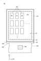
도 15는 본 발명의 일 실시 형태에 관한 표시 장치의 개요를 도시하는 평면도이다.
도 16은 본 발명의 일 실시 형태에 관한 표시 장치의 회로 구성을 도시하는 블록도이다.
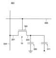
도 17은 본 발명의 일 실시 형태에 관한 표시 장치의 화소 회로를 도시하는 회로도이다.
도 18은 본 발명의 일 실시 형태에 관한 표시 장치의 개요를 도시하는 단면도이다.
도 19는 본 발명의 일 실시 형태에 관한 표시 장치의 화소 전극 및 공통 전극의 평면도이다.
도 20은 본 발명의 일 실시 형태에 관한 표시 장치의 화소 회로를 도시하는 회로도이다.
도 21은 본 발명의 일 실시 형태에 관한 표시 장치의 개요를 도시하는 단면도이다.
도 22는 실시예의 반도체 장치의 전기 특성을 나타내는 그래프이다.
도 23은 실시예의 반도체 장치의 신뢰성 시험을 나타내는 그래프이다.
도 24a는 실시예의 반도체 장치의 단면 TEM상이다.
도 24b는 도 24a의 단면 TEM상을 설명하기 위한 모식도이다.
도 25는 실시예의 반도체 장치의 전자선 회절상이다.
도 26은 실시예의 반도체 장치의 전자선 회절상이다.
도 27은 비교예의 반도체 장치의 전기 특성을 나타내는 그래프이다.
도 28은 비교예의 반도체 장치의 신뢰성 시험을 나타내는 그래프이다.
도 29는 비교예의 반도체 장치의 단면 TEM상이다.
도 30은 비교예의 반도체 장치의 전자선 회절상이다.
도 31은 비교예의 반도체 장치의 전자선 회절상이다.FIG. 1 is a cross-sectional view showing the configuration of a semiconductor device according to one embodiment of the present invention.
FIG. 2 is a plan view illustrating the configuration of a semiconductor device according to one embodiment of the present invention.
FIG. 3 is a schematic cross-sectional view illustrating the crystal structure of an oxide semiconductor layer of a semiconductor device according to one embodiment of the present invention.
FIG. 4 is a schematic cross-sectional view illustrating the crystal structure of an oxide semiconductor layer of a semiconductor device according to one embodiment of the present invention.
FIG. 5 is a sequence diagram showing a method for manufacturing a semiconductor device according to one embodiment of the present invention.
FIG. 6 is a cross-sectional view showing a method for manufacturing a semiconductor device according to one embodiment of the present invention.
Fig. 7 is a cross-sectional view showing a method for manufacturing a semiconductor device according to one embodiment of the present invention.
Fig. 8 is a cross-sectional view showing a method for manufacturing a semiconductor device according to one embodiment of the present invention.
FIG. 9 is a cross-sectional view showing a method for manufacturing a semiconductor device according to one embodiment of the present invention.
Fig. 10 is a cross-sectional view showing a method for manufacturing a semiconductor device according to one embodiment of the present invention.
Fig. 11 is a cross-sectional view showing a method for manufacturing a semiconductor device according to one embodiment of the present invention.
Fig. 12 is a cross-sectional view showing a method for manufacturing a semiconductor device according to one embodiment of the present invention.
Fig. 13 is a cross-sectional view showing a method for manufacturing a semiconductor device according to one embodiment of the present invention.
Fig. 14 is a cross-sectional view showing a method for manufacturing a semiconductor device according to one embodiment of the present invention.
Fig. 15 is a plan view illustrating an outline of a display device according to one embodiment of the present invention.
Fig. 16 is a block diagram showing the circuit configuration of a display device according to one embodiment of the present invention.
Fig. 17 is a circuit diagram showing a pixel circuit of a display device according to one embodiment of the present invention.
Fig. 18 is a cross-sectional view illustrating an outline of a display device according to one embodiment of the present invention.
FIG. 19 is a plan view of a pixel electrode and a common electrode of a display device according to one embodiment of the present invention.
Fig. 20 is a circuit diagram showing a pixel circuit of a display device according to one embodiment of the present invention.
Fig. 21 is a cross-sectional view illustrating an outline of a display device according to one embodiment of the present invention.
Figure 22 is a graph showing the electrical characteristics of a semiconductor device of the embodiment.
Figure 23 is a graph showing a reliability test of a semiconductor device of an embodiment.
Fig. 24a is a cross-sectional TEM image of a semiconductor device of the embodiment.
Figure 24b is a schematic diagram explaining the cross-sectional TEM image of Figure 24a.
Fig. 25 is an electron diffraction image of a semiconductor device of the embodiment.
Fig. 26 is an electron diffraction image of a semiconductor device of the embodiment.
Figure 27 is a graph showing the electrical characteristics of a semiconductor device of a comparative example.
Figure 28 is a graph showing the reliability test of a semiconductor device of a comparative example.
Figure 29 is a cross-sectional TEM image of a semiconductor device of a comparative example.
Figure 30 is an electron diffraction image of a semiconductor device of a comparative example.
Figure 31 is an electron diffraction image of a semiconductor device of a comparative example.
이하에, 본 발명의 각 실시 형태에 대해, 도면을 참조하면서 설명한다. 이하의 개시는 어디까지나 일례에 지나지 않는다. 당업자가, 발명의 주지를 유지하면서, 실시 형태의 구성을 적절하게 변경함으로써 용이하게 상도할 수 있는 구성은 당연히 본 발명의 범위에 함유된다. 설명을 보다 명확히 하기 위해, 도면은, 실제의 양태에 비해, 각 부의 폭, 두께, 형상 등에 대해 모식적으로 표현되는 경우가 있다. 그러나, 도시된 형상은 어디까지나 일례이며, 본 발명의 해석을 한정하지 않는다. 본 명세서와 각 도면에 있어서, 기출 도면에 관하여 전술한 구성과 마찬가지의 구성에는 동일한 부호를 부여하고, 상세한 설명을 적절하게 생략하는 경우가 있다.Hereinafter, each embodiment of the present invention will be described with reference to the drawings. The following disclosure is merely an example. A configuration that a person skilled in the art can easily conceive by appropriately changing the configuration of the embodiment while maintaining the gist of the invention is naturally included in the scope of the present invention. In order to make the description clearer, the drawings sometimes schematically express the width, thickness, shape, etc. of each part compared to the actual state. However, the depicted shape is merely an example and does not limit the interpretation of the present invention. In this specification and each drawing, the same reference numerals are given to the same configuration as the configuration described above with respect to the previous drawing, and a detailed description is sometimes omitted as appropriate.
본 발명의 각 실시 형태에 있어서, 기판으로부터 산화물 반도체층을 향하는 방향을 위 또는 상방이라고 한다. 반대로, 산화물 반도체층으로부터 기판을 향하는 방향을 아래 또는 하방이라고 한다. 이와 같이, 설명의 편의상, 상방 또는 하방이라는 어구를 사용하여 설명하지만, 예를 들어 기판과 산화물 반도체층의 상하 관계가 도시와 다른 방향으로 배치되어도 된다. 이하의 설명에서, 예를 들어 기판 상의 산화물 반도체층이라는 표현은, 상기한 바와 같이 기판과 산화물 반도체층의 상하 관계를 설명하고 있는 데 지나지 않고, 기판과 산화물 반도체층 사이에 다른 부재가 배치되어 있어도 된다. 상방 또는 하방은, 복수의 층이 적층된 구조에 있어서의 적층순을 의미하는 것이며, 트랜지스터의 상방의 화소 전극이라고 표현하는 경우, 평면으로 볼 때에 있어서, 트랜지스터와 화소 전극이 겹치지 않는 위치 관계여도 된다. 한편, 트랜지스터의 연직 상방의 화소 전극이라고 표현하는 경우에는, 평면으로 볼 때에 있어서, 트랜지스터와 화소 전극이 겹치는 위치 관계를 의미한다.In each embodiment of the present invention, the direction from the substrate toward the oxide semiconductor layer is referred to as top or upward. Conversely, the direction from the oxide semiconductor layer toward the substrate is referred to as bottom or downward. In this way, for the convenience of explanation, the terms top or downward are used in the explanation, but, for example, the upper-lower relationship between the substrate and the oxide semiconductor layer may be arranged in a direction different from that illustrated. In the following explanation, for example, the expression “oxide semiconductor layer on the substrate” merely describes the upper-lower relationship between the substrate and the oxide semiconductor layer as described above, and another member may be arranged between the substrate and the oxide semiconductor layer. Top or downward refers to the stacking order in a structure in which a plurality of layers are stacked, and when expressed as a pixel electrode above a transistor, it may be a positional relationship in which the transistor and the pixel electrode do not overlap when viewed in a plan view. On the other hand, when expressed as a pixel electrode vertically above a transistor, it refers to a positional relationship in which the transistor and the pixel electrode overlap when viewed in a plan view.
「표시 장치」란, 전기 광학층을 사용하여 영상을 표시하는 구조체를 가리킨다. 예를 들어, 표시 장치라는 용어는, 전기 광학층을 포함하는 표시 패널을 가리키는 경우도 있고, 또는 표시 셀에 대해 다른 광학 부재(예를 들어, 편광 부재, 백라이트, 터치 패널 등)를 장착한 구조체를 가리키는 경우도 있다. 「전기 광학층」에는, 기술적인 모순이 발생하지 않는 한, 액정층, 일렉트로루미네센스(EL)층, 일렉트로크로믹(EC)층, 전기 영동층이 포함될 수 있다. 따라서, 후술하는 실시 형태에 대해, 표시 장치로서, 액정층을 포함하는 액정 표시 장치 및 유기 EL층을 포함하는 유기 EL 표시 장치를 예시하여 설명하지만, 본 실시 형태에 있어서의 구조는, 상술한 다른 전기 광학층을 포함하는 표시 장치에 적용할 수 있다.The term "display device" refers to a structure that displays an image using an electro-optical layer. For example, the term "display device" may refer to a display panel including an electro-optical layer, or may refer to a structure in which other optical members (e.g., a polarizing member, a backlight, a touch panel, etc.) are mounted on display cells. The "electro-optical layer" may include a liquid crystal layer, an electroluminescent (EL) layer, an electrochromic (EC) layer, or an electrophoretic layer, unless there is a technical contradiction. Therefore, in the embodiments described below, a liquid crystal display device including a liquid crystal layer and an organic EL display device including an organic EL layer are exemplified and described as display devices, but the structure in the present embodiment can be applied to a display device including the other electro-optical layers described above.
본 명세서에 있어서 「α는 A, B 또는 C를 포함한다」, 「α는 A, B 및 C 중 어느 것을 포함한다」, 「α는 A, B 및 C로 이루어지는 군에서 선택되는 하나를 포함한다」와 같은 표현은, 특별히 명시가 없는 한, α가 A 내지 C의 복수의 조합을 포함하는 경우를 배제하지 않는다. 또한, 이들의 표현은, α가 다른 요소를 포함하는 경우도 배제하지 않는다.In this specification, expressions such as “α includes A, B or C,” “α includes any one of A, B and C,” and “α includes one selected from the group consisting of A, B and C” do not exclude the case where α includes multiple combinations of A to C, unless specifically stated otherwise. Furthermore, these expressions do not exclude the case where α includes other elements.
또한, 이하의 각 실시 형태는, 기술적인 모순이 발생하지 않는 한, 서로 조합할 수 있다.In addition, the following embodiments can be combined with each other as long as no technical contradiction occurs.
<제1 실시 형태><First embodiment>
도 1 내지 도 14를 참조하여, 본 발명의 일 실시 형태에 관한 반도체 장치에 대해 설명한다. 예를 들어, 이하에 기재하는 실시 형태의 반도체 장치는, 표시 장치에 사용되는 트랜지스터 외에, 마이크로프로세서(Micro-Processing Unit: MPU) 등의 집적 회로(Integrated Circuit: IC), 또는 메모리 회로에 사용되어도 된다.Referring to FIGS. 1 to 14, a semiconductor device according to an embodiment of the present invention will be described. For example, the semiconductor device according to an embodiment described below may be used in an integrated circuit (IC) such as a microprocessor (Micro-Processing Unit: MPU), or a memory circuit, in addition to a transistor used in a display device.
[반도체 장치(10)의 구성][Composition of semiconductor device (10)]
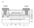
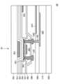
도 1 및 도 2를 참조하여, 본 발명의 일 실시 형태에 관한 반도체 장치(10)의 구성에 대해 설명한다. 도 1은, 본 발명의 일 실시 형태에 관한 반도체 장치(10)의 구성을 도시하는 단면도이다. 또한, 도 2는, 본 발명의 일 실시 형태에 관한 반도체 장치(10)의 구성을 도시하는 평면도이다.Referring to FIGS. 1 and 2, the configuration of a semiconductor device (10) according to one embodiment of the present invention will be described. FIG. 1 is a cross-sectional view showing the configuration of a semiconductor device (10) according to one embodiment of the present invention. In addition, FIG. 2 is a plan view showing the configuration of a semiconductor device (10) according to one embodiment of the present invention.
도 1에 도시하는 바와 같이, 반도체 장치(10)는 기판(100) 위에 마련되어 있다. 반도체 장치(10)는 게이트 전극(105), 게이트 절연층(110, 120), 산화 금속층(130), 산화물 반도체층(140), 게이트 절연층(150), 게이트 전극(160), 절연층(170, 180), 소스 전극(201) 및 드레인 전극(203)을 포함한다. 또한, 소스 전극(201) 및 드레인 전극(203)을 특별히 구별하지 않는 경우, 이것들을 아울러 소스·드레인 전극(200)이라고 하는 경우가 있다.As illustrated in Fig. 1, a semiconductor device (10) is provided on a substrate (100). The semiconductor device (10) includes a gate electrode (105), a gate insulating layer (110, 120), an oxide metal layer (130), an oxide semiconductor layer (140), a gate insulating layer (150), a gate electrode (160), an insulating layer (170, 180), a source electrode (201), and a drain electrode (203). In addition, when the source electrode (201) and the drain electrode (203) are not specifically distinguished, they may be collectively referred to as a source/drain electrode (200).
게이트 전극(105)은 기판(100) 위에 마련되어 있다. 게이트 절연층(110) 및 게이트 절연층(120)은 기판(100) 및 게이트 전극(105) 위에 마련되어 있다. 산화 금속층(130)은 게이트 절연층(120) 위에 마련되어 있다. 산화 금속층(130)은 게이트 절연층(120)에 접하고 있다. 산화물 반도체층(140)은 산화 금속층(130) 위에 마련되어 있다. 산화물 반도체층(140)은 산화 금속층(130)에 접하고 있다. 산화물 반도체층(140)의 주면 중, 산화 금속층(130)에 접하는 면을 하면(142)이라고 한다. 산화 금속층(130)의 측면은, 산화물 반도체층(140)의 측면과 대략 일치하고 있다.A gate electrode (105) is provided on a substrate (100). A gate insulating layer (110) and a gate insulating layer (120) are provided on the substrate (100) and the gate electrode (105). An oxide metal layer (130) is provided on the gate insulating layer (120). The oxide metal layer (130) is in contact with the gate insulating layer (120). An oxide semiconductor layer (140) is provided on the oxide metal layer (130). The oxide semiconductor layer (140) is in contact with the oxide metal layer (130). Among the main surfaces of the oxide semiconductor layer (140), a surface that is in contact with the oxide metal layer (130) is referred to as a lower surface (142). The side surface of the oxide metal layer (130) approximately coincides with the side surface of the oxide semiconductor layer (140).
본 실시 형태에서는, 산화 금속층(130)과 기판(100) 사이에, 반도체층 또는 산화물 반도체층은 마련되어 있지 않다.In this embodiment, a semiconductor layer or oxide semiconductor layer is not provided between the oxide metal layer (130) and the substrate (100).
도 1에서는, 산화 금속층(130)의 측면과 산화물 반도체층(140)의 측면이 직선 상에 배열되어 있지만, 이 구성에 한정되지 않는다. 기판(100)의 주면에 대한 산화 금속층(130)의 측면 각도가 산화물 반도체층(140)의 측면 각도와 다르게 되어 있어도 된다. 산화 금속층(130) 및 산화물 반도체층(140) 중 적어도 어느 한쪽의 측면이 만곡되어 있어도 된다.In Fig. 1, the side surface of the oxide metal layer (130) and the side surface of the oxide semiconductor layer (140) are arranged in a straight line, but this configuration is not limited. The side surface angle of the oxide metal layer (130) with respect to the main surface of the substrate (100) may be different from the side surface angle of the oxide semiconductor layer (140). The side surface of at least one of the oxide metal layer (130) and the oxide semiconductor layer (140) may be curved.
게이트 전극(160)은 산화물 반도체층(140)에 대향하고 있다. 게이트 절연층(150)은 산화물 반도체층(140)과 게이트 전극(160) 사이에 마련되어 있다. 게이트 절연층(150)은 산화물 반도체층(140)에 접하고 있다. 산화물 반도체층(140)의 주면 중, 게이트 절연층(150)에 접하는 면을 상면(141)이라고 한다. 상면(141)과 하면(142) 사이의 면을 측면(143)이라고 한다. 절연층(170, 180)은 게이트 절연층(150) 및 게이트 전극(160) 위에 마련되어 있다. 절연층(170, 180)에는, 산화물 반도체층(140)에 달하는 개구(171, 173)가 마련되어 있다. 소스 전극(201)은 개구(171)의 내부에 마련되어 있다. 소스 전극(201)은 개구(171)의 저부에서 산화물 반도체층(140)에 접하고 있다. 드레인 전극(203)은 개구(173)의 내부에 마련되어 있다. 드레인 전극(203)은 개구(173)의 저부에서 산화물 반도체층(140)에 접하고 있다.The gate electrode (160) faces the oxide semiconductor layer (140). The gate insulating layer (150) is provided between the oxide semiconductor layer (140) and the gate electrode (160). The gate insulating layer (150) is in contact with the oxide semiconductor layer (140). Among the main surfaces of the oxide semiconductor layer (140), the surface in contact with the gate insulating layer (150) is referred to as the upper surface (141). The surface between the upper surface (141) and the lower surface (142) is referred to as the side surface (143). The insulating layers (170, 180) are provided on the gate insulating layer (150) and the gate electrode (160). An opening (171, 173) reaching the oxide semiconductor layer (140) is provided in the insulating layers (170, 180). The source electrode (201) is provided inside the opening (171). The source electrode (201) is in contact with the oxide semiconductor layer (140) at the bottom of the opening (171). The drain electrode (203) is provided inside the opening (173). The drain electrode (203) is in contact with the oxide semiconductor layer (140) at the bottom of the opening (173).
게이트 전극(105)은 반도체 장치(10)의 보텀 게이트로서의 기능 및 산화물 반도체층(140)에 대한 차광막으로서의 기능을 구비한다. 게이트 절연층(110)은 기판(100)으로부터 산화물 반도체층(140)을 향해 확산되는 불순물을 차폐하는 배리어막으로서의 기능을 구비한다. 게이트 절연층(110, 120)은 보텀 게이트에 대한 게이트 절연층으로서의 기능을 구비한다. 산화 금속층(130)은 알루미늄을 주성분으로 하는 산화 금속을 포함하는 층이며, 산소나 수소 등의 가스를 차폐하는 가스 배리어 막으로서의 기능을 구비한다.The gate electrode (105) has a function as a bottom gate of the semiconductor device (10) and a function as a light-shielding film for the oxide semiconductor layer (140). The gate insulating layer (110) has a function as a barrier film that shields impurities that diffuse from the substrate (100) toward the oxide semiconductor layer (140). The gate insulating layers (110, 120) have a function as a gate insulating layer for the bottom gate. The oxide metal layer (130) is a layer containing an oxide metal mainly composed of aluminum, and has a function as a gas barrier film that shields gases such as oxygen and hydrogen.
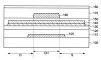
산화물 반도체층(140)은 소스 영역(S), 드레인 영역(D) 및 채널 영역(CH)으로 구분된다. 채널 영역(CH)은 산화물 반도체층(140) 중 게이트 전극(160)의 연직 하방의 영역이다. 소스 영역(S)은 산화물 반도체층(140) 중 게이트 전극(160)과 겹치지 않는 영역이며, 채널 영역(CH)보다도 소스 전극(201)에 가까운 측의 영역이다. 드레인 영역(D)은 산화물 반도체층(140) 중 게이트 전극(160)과 겹치지 않는 영역이며, 채널 영역(CH)보다도 드레인 전극(203)에 가까운 측의 영역이다. 채널 영역(CH)에 있어서의 산화물 반도체층(140)은 반도체로서의 물성을 구비하고 있다. 소스 영역(S) 및 드레인 영역(D)에 있어서의 산화물 반도체층(140)은 도전체로서의 물성을 구비하고 있다.The oxide semiconductor layer (140) is divided into a source region (S), a drain region (D), and a channel region (CH). The channel region (CH) is a region of the oxide semiconductor layer (140) vertically below the gate electrode (160). The source region (S) is a region of the oxide semiconductor layer (140) that does not overlap with the gate electrode (160) and is a region closer to the source electrode (201) than the channel region (CH). The drain region (D) is a region of the oxide semiconductor layer (140) that does not overlap with the gate electrode (160) and is a region closer to the drain electrode (203) than the channel region (CH). The oxide semiconductor layer (140) in the channel region (CH) has properties as a semiconductor. The oxide semiconductor layer (140) in the source region (S) and the drain region (D) has properties as a conductor.
게이트 전극(160)은 반도체 장치(10)의 톱 게이트 및 산화물 반도체층(140)에 대한 차광막으로서의 기능을 구비한다. 게이트 절연층(150)은 톱 게이트에 대한 게이트 절연층으로서의 기능을 구비하고, 제조 프로세스에 있어서의 열처리에 의해 산소를 방출하는 기능을 구비한다. 절연층(170, 180)은 게이트 전극(160)과 소스·드레인 전극(200)을 절연하고, 양자간의 기생 용량을 저감시키는 기능을 구비한다. 반도체 장치(10)의 동작은, 주로 게이트 전극(160)에 공급되는 전압에 의해 제어된다. 게이트 전극(105)에는 보조적인 전압이 공급된다. 단, 게이트 전극(105)을 단순히 차광막으로서 사용하는 경우, 게이트 전극(105)에 특정 전압이 공급되지 않고, 게이트 전극(105)이 플로팅 상태여도 된다. 즉, 게이트 전극(105)은 단순히 「차광막」이라고 불려도 된다.The gate electrode (160) has a function as a light-shielding film for the top gate and the oxide semiconductor layer (140) of the semiconductor device (10). The gate insulating layer (150) has a function as a gate insulating layer for the top gate, and has a function of releasing oxygen by heat treatment in the manufacturing process. The insulating layers (170, 180) insulate the gate electrode (160) and the source/drain electrodes (200) and have a function of reducing parasitic capacitance between them. The operation of the semiconductor device (10) is mainly controlled by the voltage supplied to the gate electrode (160). An auxiliary voltage is supplied to the gate electrode (105). However, when the gate electrode (105) is simply used as a light-shielding film, a specific voltage may not be supplied to the gate electrode (105), and the gate electrode (105) may be in a floating state. In other words, the gate electrode (105) may simply be called a “light-shielding film.”
본 실시 형태에서는, 반도체 장치(10)로서, 게이트 전극이 산화물 반도체층의 상방 및 하방의 양쪽에 마련된 듀얼 게이트형 트랜지스터가 사용된 구성을 예시하지만, 이 구성에 한정되지 않는다. 예를 들어, 반도체 장치(10)로서, 게이트 전극이 산화물 반도체층의 하방에만 마련된 보텀 게이트형 트랜지스터, 또는 게이트 전극이 산화물 반도체층의 상방에만 마련된 톱 게이트형 트랜지스터가 사용되어도 된다. 상기한 구성은 어디까지나 일 실시 형태에 지나지 않고, 본 발명은 상기한 구성에 한정되지 않는다.In this embodiment, a configuration is exemplified in which a dual gate type transistor in which gate electrodes are provided on both the upper and lower sides of an oxide semiconductor layer is used as a semiconductor device (10), but the present invention is not limited to this configuration. For example, a bottom gate type transistor in which the gate electrode is provided only on the lower side of an oxide semiconductor layer, or a top gate type transistor in which the gate electrode is provided only on the upper side of an oxide semiconductor layer may be used as the semiconductor device (10). The above configuration is merely one embodiment, and the present invention is not limited to the above configuration.
도 2에 도시하는 바와 같이, 평면으로 볼 때에 있어서, 산화 금속층(130)의 평면 패턴은 산화물 반도체층(140)의 평면 패턴과 대략 동일하다. 도 1 및 도 2를 참조하면, 산화물 반도체층(140)의 하면(142)은 산화 금속층(130)에 의해 덮여 있다. 특히, 본 실시 형태에서는, 산화물 반도체층(140)의 하면(142) 모두가 산화 금속층(130)에 의해 덮여 있다. D1 방향에 있어서, 게이트 전극(105)의 폭은 게이트 전극(160)의 폭보다 크다. D1 방향은, 소스 전극(201)과 드레인 전극(203)을 연결하는 방향이며, 반도체 장치(10)의 채널 길이(L)를 나타내는 방향이다. 구체적으로는, 산화물 반도체층(140)과 게이트 전극(160)이 겹치는 영역(채널 영역(CH))에 있어서의 D1 방향의 길이가 채널 길이(L)이며, 당해 채널 영역(CH)의 D2 방향의 폭이 채널 폭(W)이다.As shown in FIG. 2, when viewed in a plan view, the planar pattern of the oxide metal layer (130) is approximately the same as the planar pattern of the oxide semiconductor layer (140). Referring to FIGS. 1 and 2, the lower surface (142) of the oxide semiconductor layer (140) is covered by the oxide metal layer (130). In particular, in the present embodiment, the entire lower surface (142) of the oxide semiconductor layer (140) is covered by the oxide metal layer (130). In the D1 direction, the width of the gate electrode (105) is larger than the width of the gate electrode (160). The D1 direction is a direction connecting the source electrode (201) and the drain electrode (203), and is a direction indicating the channel length (L) of the semiconductor device (10). Specifically, the length in the D1 direction in the region (channel region (CH)) where the oxide semiconductor layer (140) and the gate electrode (160) overlap is the channel length (L), and the width in the D2 direction of the channel region (CH) is the channel width (W).
본 실시 형태에서는, 산화물 반도체층(140)의 하면(142) 전체가 산화 금속층(130)에 의해 덮인 구성을 예시하였지만, 이 구성에 한정되지 않는다. 예를 들어, 산화물 반도체층(140)의 하면(142)의 일부가 산화 금속층(130)과 접하고 있지 않아도 된다. 예를 들어, 채널 영역(CH)에 있어서의 산화물 반도체층(140)의 하면(142) 전체가 산화 금속층(130)에 의해 덮이고, 소스 영역(S) 및 드레인 영역(D)에 있어서의 산화물 반도체층(140)의 하면(142) 전체 또는 일부가 산화 금속층(130)에 의해 덮여 있지 않아도 된다. 즉, 소스 영역(S) 및 드레인 영역(D)에 있어서의 산화물 반도체층(140)의 하면(142) 전체 또는 일부가 산화 금속층(130)과 접하고 있지 않아도 된다. 단, 상기한 구성에 있어서, 채널 영역(CH)에 있어서의 산화물 반도체층(140)의 하면(142)의 일부가 산화 금속층(130)에 의해 덮여 있지 않고, 당해 하면(142)의 그 외의 부분이 산화 금속층(130)과 접하고 있어도 된다.In this embodiment, a configuration in which the entire lower surface (142) of the oxide semiconductor layer (140) is covered by the oxide metal layer (130) is exemplified, but the present invention is not limited to this configuration. For example, a part of the lower surface (142) of the oxide semiconductor layer (140) does not have to be in contact with the oxide metal layer (130). For example, the entire lower surface (142) of the oxide semiconductor layer (140) in the channel region (CH) is covered by the oxide metal layer (130), and the entire or part of the lower surface (142) of the oxide semiconductor layer (140) in the source region (S) and the drain region (D) does not have to be covered by the oxide metal layer (130). That is, the entire or part of the lower surface (142) of the oxide semiconductor layer (140) in the source region (S) and the drain region (D) does not have to be in contact with the oxide metal layer (130). However, in the above configuration, a part of the lower surface (142) of the oxide semiconductor layer (140) in the channel region (CH) may not be covered by the oxide metal layer (130), and the remaining part of the lower surface (142) may be in contact with the oxide metal layer (130).
본 실시 형태에서는, 게이트 절연층(150)이 전체면에 형성되고, 게이트 절연층(150)에 개구(171, 173)가 마련된 구성을 예시하였지만, 이 구성에 한정되지 않는다. 게이트 절연층(150)이 패터닝되어 있어도 된다. 예를 들어, 소스 영역(S) 및 드레인 영역(D)의 산화물 반도체층(140)을 노출시키도록 게이트 절연층(150)이 패터닝되어 있어도 된다. 즉, 소스 영역(S) 및 드레인 영역(D)의 게이트 절연층(150)이 제거되고, 이들 영역에서 산화물 반도체층(140)과 절연층(170)이 접하고 있어도 된다.In this embodiment, a configuration in which a gate insulating layer (150) is formed over the entire surface and openings (171, 173) are provided in the gate insulating layer (150) is exemplified, but the present invention is not limited to this configuration. The gate insulating layer (150) may be patterned. For example, the gate insulating layer (150) may be patterned so as to expose the oxide semiconductor layer (140) of the source region (S) and the drain region (D). That is, the gate insulating layer (150) of the source region (S) and the drain region (D) may be removed, and the oxide semiconductor layer (140) and the insulating layer (170) may be in contact with each other in these regions.
도 2에서는, 평면으로 볼 때에 있어서, 소스·드레인 전극(200)이 게이트 전극(105) 및 게이트 전극(160)과 겹치지 않는 구성이 예시되어 있지만, 이 구성에 한정되지 않는다. 예를 들어, 평면으로 볼 때에 있어서, 소스·드레인 전극(200)이 게이트 전극(105) 및 게이트 전극(160) 중 적어도 어느 한쪽과 겹쳐 있어도 된다. 상기한 구성은 어디까지나 일 실시 형태에 지나지 않고, 본 발명은 상기한 구성에 한정되지 않는다.In Fig. 2, a configuration is exemplified in which the source/drain electrode (200) does not overlap the gate electrode (105) and the gate electrode (160) when viewed in a plan view, but it is not limited to this configuration. For example, when viewed in a plan view, the source/drain electrode (200) may overlap at least one of the gate electrode (105) and the gate electrode (160). The above configuration is merely one embodiment, and the present invention is not limited to the above configuration.
[반도체 장치(10)의 각 부재의 재질][Material of each component of the semiconductor device (10)]
기판(100)으로서, 유리 기판, 석영 기판 및 사파이어 기판 등, 투광성을 갖는 강성 기판이 사용된다. 기판(100)이 가요성을 구비할 필요가 있는 경우, 기판(100)으로서, 폴리이미드 기판, 아크릴 기판, 실록산 기판, 불소 수지 기판 등, 수지를 포함하는 기판이 사용된다. 기판(100)으로서 수지를 포함하는 기판이 사용되는 경우, 기판(100)의 내열성을 향상시키기 위해, 상기한 수지에 불순물이 도입되어도 된다. 특히, 반도체 장치(10)가 톱 에미션형의 디스플레이인 경우, 기판(100)이 투명할 필요는 없기 때문에, 기판(100)의 투명도를 저하시키는 불순물이 사용되어도 된다. 표시 장치가 아닌 집적 회로에 반도체 장치(10)가 사용되는 경우에는, 기판(100)으로서 실리콘 기판, 탄화 실리콘 기판, 화합물 반도체 기판 등의 반도체 기판, 또는 스테인리스 기판 등의 도전성 기판과 같이, 투광성을 구비하지 않는 기판이 사용된다.As the substrate (100), a rigid substrate having light-transmitting properties, such as a glass substrate, a quartz substrate, and a sapphire substrate, is used. When the substrate (100) needs to have flexibility, a substrate containing resin, such as a polyimide substrate, an acrylic substrate, a siloxane substrate, and a fluororesin substrate, is used as the substrate (100). When a substrate containing resin is used as the substrate (100), impurities may be introduced into the resin in order to improve the heat resistance of the substrate (100). In particular, when the semiconductor device (10) is a top emission type display, since the substrate (100) does not need to be transparent, an impurity that reduces the transparency of the substrate (100) may be used. When the semiconductor device (100) is used in an integrated circuit rather than a display device, a substrate not having light-transmitting properties, such as a semiconductor substrate such as a silicon substrate, a silicon carbide substrate, a compound semiconductor substrate, or a conductive substrate such as a stainless steel substrate, is used as the substrate (100).
게이트 전극(105), 게이트 전극(160) 및 소스·드레인 전극(200)으로서, 일반적인 금속 재료가 사용된다. 예를 들어, 이들의 부재로서, 알루미늄(Al), 티타늄(Ti), 크롬(Cr), 코발트(Co), 니켈(Ni), 몰리브덴(Mo), 하프늄(Hf), 탄탈(Ta), 텅스텐(W), 비스무트(Bi), 은(Ag), 구리(Cu), 및 이들의 합금 또는 이들 화합물이 사용된다. 게이트 전극(105), 게이트 전극(160) 및 소스·드레인 전극(200)으로서, 상기한 재료가 단층으로 사용되어도 되고 적층으로 사용되어도 된다.As the gate electrode (105), the gate electrode (160), and the source/drain electrodes (200), general metal materials are used. For example, as their absence, aluminum (Al), titanium (Ti), chromium (Cr), cobalt (Co), nickel (Ni), molybdenum (Mo), hafnium (Hf), tantalum (Ta), tungsten (W), bismuth (Bi), silver (Ag), copper (Cu), and alloys or compounds thereof are used. As the gate electrode (105), the gate electrode (160), and the source/drain electrodes (200), the above-mentioned materials may be used as a single layer or as a laminate.
또한, 게이트 전극(160)과 소스·드레인 전극(200)은, 동일한 금속 재료가 사용되어도 되고, 다른 금속 재료가 사용되어도 된다. 예를 들어, 게이트 전극(160)이 알루미늄을 포함하지 않고, 소스·드레인 전극(200)이 알루미늄을 포함하고 있어도 된다.In addition, the gate electrode (160) and the source/drain electrode (200) may use the same metal material, or may use different metal materials. For example, the gate electrode (160) may not contain aluminum, and the source/drain electrode (200) may contain aluminum.
게이트 절연층(110, 120) 및 절연층(170, 180)으로서, 일반적인 절연성 재료가 사용된다. 예를 들어, 이들의 절연층으로서, 산화실리콘(SiOx), 산화질화실리콘(SiOxNy), 질화실리콘(SiNx), 질화산화실리콘(SiNxOy), 산화알루미늄(AlOx), 산화질화 알루미늄(AlOxNy), 질화산화알루미늄(AlNxOy), 질화알루미늄(AlNx) 등의 무기 절연층이 사용된다.As the gate insulating layer (110, 120) and the insulating layer (170, 180), general insulating materials are used. For example, as these insulating layers, inorganic insulating layers such as silicon oxide (SiOx ), silicon oxynitride (SiOx Ny ), silicon nitride (SiNx ), silicon nitride oxide (SiNx Oy ), aluminum oxide (AlOx ), aluminum oxynitride (AlOx Ny ), aluminum nitride oxide (AlNx Oy ), and aluminum nitride (AlNx ) are used.
상기한 SiOxNy 및 AlOxNy는, 산소(O)보다도 적은 비율(x>y)의 질소(N)를 함유하는 실리콘 화합물 및 알루미늄 화합물이다. SiNxOy 및 AlNxOy는, 질소보다도 적은 비율(x>y)의 산소를 함유하는 실리콘 화합물 및 알루미늄 화합물이다.The above SiOx Ny and AlOx Ny are silicon compounds and aluminum compounds containing nitrogen (N) in a smaller proportion (x>y) than oxygen (O). SiNx Oy and AlNx Oy are silicon compounds and aluminum compounds containing oxygen in a smaller proportion (x>y) than nitrogen.
게이트 절연층(150)으로서, 상기한 절연층 중 산소를 포함하는 절연층이 사용된다. 예를 들어, 게이트 절연층(150)으로서, 산화실리콘(SiOx), 산화질화실리콘(SiOxNy) 등의 무기 절연층이 사용된다.As the gate insulating layer (150), an insulating layer containing oxygen among the above-mentioned insulating layers is used. For example, as the gate insulating layer (150), an inorganic insulating layer such as silicon oxide (SiOx ), silicon oxynitride (SiOx Ny ), etc. is used.
게이트 절연층(120)으로서, 열처리에 의해 산소를 방출하는 기능을 구비하는 절연층이 사용된다. 예를 들어, 게이트 절연층(120)이 산소를 방출하는 열처리의 온도는, 600℃ 이하, 500℃ 이하, 450℃ 이하, 또는 400℃ 이하이다. 즉, 예를 들어 게이트 절연층(120)은, 기판(100)으로서 유리 기판이 사용된 경우에 있어서, 반도체 장치(10)의 제조 공정에서 행해지는 열처리 온도에서 산소를 방출한다.As the gate insulating layer (120), an insulating layer having a function of releasing oxygen by heat treatment is used. For example, the temperature of the heat treatment at which the gate insulating layer (120) releases oxygen is 600°C or less, 500°C or less, 450°C or less, or 400°C or less. That is, for example, the gate insulating layer (120) releases oxygen at the heat treatment temperature performed in the manufacturing process of the semiconductor device (10) when a glass substrate is used as the substrate (100).
게이트 절연층(150)으로서, 결함이 적은 절연층이 사용된다. 예를 들어, 게이트 절연층(150)에 있어서의 산소의 조성비와, 게이트 절연층(150)과 마찬가지의 조성의 절연층(이하,「다른 절연층」이라고 함)에 있어서의 산소의 조성비를 비교한 경우, 게이트 절연층(150)에 있어서의 산소의 조성비 쪽이 당해 다른 절연층에 있어서의 산소의 조성비보다도 당해 절연층에 대한 화학양론비에 가깝다. 구체적으로는, 게이트 절연층(150) 및 절연층(180)의 각각에 산화실리콘(SiOx)이 사용되는 경우, 게이트 절연층(150)으로서 사용되는 산화실리콘에 있어서의 산소의 조성비는, 절연층(180)으로서 사용되는 산화실리콘에 있어서의 산소의 조성비에 비해, 산화실리콘의 화학양론비에 가깝다. 예를 들어, 게이트 절연층(150)으로서, 전자 스핀 공명법(ESR)으로 평가했을 때에 결함이 관측되지 않는 층이 사용되어도 된다.As the gate insulating layer (150), an insulating layer with few defects is used. For example, when the oxygen composition ratio in the gate insulating layer (150) is compared with the oxygen composition ratio in an insulating layer (hereinafter referred to as “another insulating layer”) having the same composition as the gate insulating layer (150), the oxygen composition ratio in the gate insulating layer (150) is closer to the stoichiometric ratio for the insulating layer than the oxygen composition ratio in the other insulating layer. Specifically, when silicon oxide (SiOx ) is used for each of the gate insulating layer (150) and the insulating layer (180), the oxygen composition ratio in the silicon oxide used as the gate insulating layer (150) is closer to the stoichiometric ratio of the silicon oxide than the oxygen composition ratio in the silicon oxide used as the insulating layer (180). For example, as a gate insulating layer (150), a layer in which no defects are observed when evaluated by electron spin resonance (ESR) may be used.
산화 금속층(130) 및 후술하는 바와 같이 제조 공정에서 사용되는 산화 금속층(190)으로서, 알루미늄을 주성분으로 하는 산화 금속이 사용된다. 예를 들어, 산화 금속층(130)(또는 산화 금속층(190))으로서, 산화알루미늄(AlOx), 산화질화알루미늄(AlOxNy), 질화산화알루미늄(AlNxOy), 질화알루미늄(AlNx) 등의 무기 절연층이 사용된다. 「알루미늄을 주성분으로 하는 산화 금속층」이란, 산화 금속층(130)(또는 산화 금속층(190))에 포함되는 알루미늄의 비율이 산화 금속층(130)(또는 산화 금속층(190)) 전체의 1% 이상인 것을 의미한다. 산화 금속층(130)(또는 산화 금속층(190))에 포함되는 알루미늄의 비율은, 산화 금속층(130) 전체의 5% 이상 70% 이하, 10% 이상 60% 이하, 또는 30% 이상 50% 이하여도 된다. 상기한 비율은, 질량비여도 되고, 중량비여도 된다.As the oxide metal layer (130) and the oxide metal layer (190) used in the manufacturing process as described below, an oxide metal layer containing aluminum as a main component is used. For example, as the oxide metal layer (130) (or oxide metal layer (190)), an inorganic insulating layer such as aluminum oxide (AlOx ), aluminum oxynitride (AlOx Ny ), aluminum nitride oxide (AlNx Oy ), or aluminum nitride (AlNx ) is used. The “oxide metal layer containing aluminum as a main component” means that the proportion of aluminum included in the oxide metal layer (130) (or oxide metal layer (190)) is 1% or more of the entire oxide metal layer (130) (or oxide metal layer (190)). The proportion of aluminum included in the oxide metal layer (130) (or oxide metal layer (190)) may be 5% or more and 70% or less, 10% or more and 60% or less, or 30% or more and 50% or less of the entire oxide metal layer (130). The above-mentioned proportion may be a mass ratio or a weight ratio.
산화물 반도체층(140)의 적어도 일부는, 산화 금속층(130)과 접하고 있다. 그로 인해, 상세는 후술하지만, OS 어닐이 행해지면, 산화 금속층(130)에 포함되는 알루미늄이 산화물 반도체층(140)으로 확산된다. 따라서, 산화물 반도체층(140)은, 산화 금속층(130)과 산화물 반도체층(140)의 계면 근방에 있어서, 알루미늄 농도가 높은 영역을 포함한다. 알루미늄 농도는, 예를 들어 SIMS(Secondary Ion Mass Spectrometry) 분석 등에 의해 검출할 수 있다.At least a part of the oxide semiconductor layer (140) is in contact with the oxide metal layer (130). Therefore, as will be described in detail later, when OS annealing is performed, aluminum included in the oxide metal layer (130) diffuses into the oxide semiconductor layer (140). Therefore, the oxide semiconductor layer (140) includes a region with a high aluminum concentration near the interface between the oxide metal layer (130) and the oxide semiconductor layer (140). The aluminum concentration can be detected by, for example, SIMS (Secondary Ion Mass Spectrometry) analysis.
또한, 상세는 후술하지만, 게이트 절연층(150) 위에 산화 금속층(190)이 성막되고, 산화 어닐이 행해지면, 산화 금속층(190)에 포함되는 알루미늄이 게이트 절연층(150)으로 확산된다. 따라서, 산화 금속층(190)이 제거되어도, 게이트 절연층(150)의 표면 근방(산화물 반도체층(140)과 반대측 표면 근방)에 있어서, 알루미늄 농도가 높은 영역을 포함한다.In addition, as will be described in detail later, when an oxide metal layer (190) is formed on a gate insulating layer (150) and an oxidation annealing is performed, aluminum included in the oxide metal layer (190) diffuses into the gate insulating layer (150). Therefore, even if the oxide metal layer (190) is removed, a region with a high aluminum concentration is included near the surface of the gate insulating layer (150) (near the surface on the opposite side to the oxide semiconductor layer (140)).
산화물 반도체층(140)으로서, 반도체의 특성을 갖는 산화 금속이 사용된다. 예를 들어, 산화물 반도체층(140)으로서, 인듐(In)을 포함하는 2 이상의 금속을 포함하는 산화물 반도체가 사용된다. 산화물 반도체층(140)에 있어서, 2 이상의 금속에 대한 인듐의 비율은 50% 이상이다. 산화물 반도체층(140)으로서, 인듐에 더하여, 갈륨(Ga), 아연(Zn), 알루미늄(Al), 하프늄(Hf), 이트륨(Y), 지르코니아(Zr), 란타노이드가 사용된다. 산화물 반도체층(140)으로서, 상기 이외의 원소가 사용되어도 된다.As the oxide semiconductor layer (140), an oxide metal having semiconductor properties is used. For example, as the oxide semiconductor layer (140), an oxide semiconductor including two or more metals including indium (In) is used. In the oxide semiconductor layer (140), the ratio of indium to the two or more metals is 50% or more. As the oxide semiconductor layer (140), in addition to indium, gallium (Ga), zinc (Zn), aluminum (Al), hafnium (Hf), yttrium (Y), zirconia (Zr), and lanthanide are used. As the oxide semiconductor layer (140), elements other than the above may be used.
산화물 반도체층(140)은 결정성을 갖는다. 결정성의 산화물 반도체층(140)은 아몰퍼스의 산화물 반도체층보다도 산소 결손이 적다. 결정성의 산화물 반도체층(140)은 아몰퍼스 영역을 포함하고 있어도 되지만, 산화물 반도체층(140)에 있어서의 아몰퍼스 영역의 비율은, 산화물 반도체층(140)에 있어서의 결정 영역의 비율보다도 작다. 예를 들어, 산화물 반도체층(140)에 있어서의 결정 영역의 비율은 70% 이상, 바람직하게는 80% 이상, 더욱 바람직하게는 90% 이상이다.The oxide semiconductor layer (140) is crystalline. The crystalline oxide semiconductor layer (140) has fewer oxygen vacancies than the amorphous oxide semiconductor layer. The crystalline oxide semiconductor layer (140) may include an amorphous region, but the ratio of the amorphous region in the oxide semiconductor layer (140) is smaller than the ratio of the crystalline region in the oxide semiconductor layer (140). For example, the ratio of the crystalline region in the oxide semiconductor layer (140) is 70% or more, preferably 80% or more, and more preferably 90% or more.
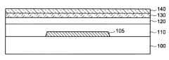
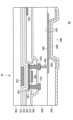
여기서, 도 3을 참조하여, 본 발명의 일 실시 형태에 관한 반도체 장치(10)의 산화물 반도체층(140)의 결정 구조에 대해 설명한다. 도 3은, 본 발명의 일 실시 형태에 관한 반도체 장치(10)의 산화물 반도체층(140)의 결정 구조를 설명하는 모식적인 단면도이다.Here, with reference to FIG. 3, the crystal structure of the oxide semiconductor layer (140) of the semiconductor device (10) according to one embodiment of the present invention will be described. FIG. 3 is a schematic cross-sectional view explaining the crystal structure of the oxide semiconductor layer (140) of the semiconductor device (10) according to one embodiment of the present invention.
도 3에 도시하는 바와 같이, 산화물 반도체층(140)은 제1 결정 구조를 갖는 제1 결정 영역(144) 및 제2 결정 구조를 갖는 제2 결정 영역(145)을 포함한다. 제1 결정 영역(144)은 산화 금속층(130)과 산화물 반도체층(140)의 계면 근방에만 형성되어 있다. 즉, 제1 결정 영역(144)은 산화 금속층(130)과 접하여 형성되고, 산화 금속층(130)으로부터 이격된 위치에는 존재하지 않는다. 산화물 반도체층(140)에는, 하나의 제1 결정 영역(144)이 형성되어 있어도 되고, 복수의 제1 결정 영역(144)이 형성되어 있어도 된다. 제2 결정 영역(145)은 산화 금속층(130) 및 제1 결정 영역(144)과 접하고, 제1 결정 영역(144)을 덮도록 형성되어 있다. 환언하면, 산화물 반도체층(140)의 단면으로 볼 때에 있어서, 제1 결정 영역(144)은 산화 금속층(130) 및 제2 결정 영역(145)에 의해 둘러싸이고, 제1 결정 영역(144)과 제2 결정 영역(145) 사이에 결정립계가 형성되어 있다.As illustrated in FIG. 3, the oxide semiconductor layer (140) includes a first crystal region (144) having a first crystal structure and a second crystal region (145) having a second crystal structure. The first crystal region (144) is formed only near the interface between the oxide metal layer (130) and the oxide semiconductor layer (140). That is, the first crystal region (144) is formed in contact with the oxide metal layer (130), and does not exist at a position spaced apart from the oxide metal layer (130). In the oxide semiconductor layer (140), one first crystal region (144) may be formed, or a plurality of first crystal regions (144) may be formed. The second crystal region (145) is formed in contact with the oxide metal layer (130) and the first crystal region (144), and covers the first crystal region (144). In other words, when looking at the cross-section of the oxide semiconductor layer (140), the first crystal region (144) is surrounded by the oxide metal layer (130) and the second crystal region (145), and a crystal grain boundary is formed between the first crystal region (144) and the second crystal region (145).
상술한 바와 같이, 제1 결정 영역(144)은 산화 금속층(130)과 산화물 반도체층(140)의 계면 근방에만 형성되고, 산화 금속층(130)으로부터 이격된 위치에는 존재하지 않기 때문에, 산화물 반도체층(140)에 있어서의 제1 결정 영역(144)의 비율은, 산화물 반도체층(140)에 있어서의 제2 결정 영역(145)의 비율보다도 대폭 작다. 환언하면, 산화물 반도체층(140)의 단면으로 볼 때에 있어서, 제1 결정 영역(144)의 면적은 제2 결정 영역의 면적보다도 대폭 작다. 즉, 산화물 반도체층(140)의 대부분은 제2 결정 영역(145)에 의해 형성되어 있고, 산화물 반도체층(140)의 결정 구조는 제2 결정 영역(145)의 제2 결정 구조와 동일하다.As described above, since the first crystal region (144) is formed only near the interface between the oxide metal layer (130) and the oxide semiconductor layer (140) and does not exist at a location spaced apart from the oxide metal layer (130), the proportion of the first crystal region (144) in the oxide semiconductor layer (140) is significantly smaller than the proportion of the second crystal region (145) in the oxide semiconductor layer (140). In other words, when viewing the cross-section of the oxide semiconductor layer (140), the area of the first crystal region (144) is significantly smaller than the area of the second crystal region. That is, most of the oxide semiconductor layer (140) is formed by the second crystal region (145), and the crystal structure of the oxide semiconductor layer (140) is the same as the second crystal structure of the second crystal region (145).
제2 결정 영역(145)의 제2 결정 구조는, 예를 들어 빅스바이트 구조, 커런덤 구조, 스피넬 구조 또는 호몰로거스 구조 등이다. 빅스바이트 구조는, 산화인듐의 안정된 결정 구조 중 하나이다. 또한, 커런덤 구조 및 스피넬 구조는, 산화알루미늄 또는 산화갈륨 구조의 안정된 결정 구조 중 하나이다. 또한, 호몰로거스 구조는, 산화인듐갈륨아연이 안정된 결정 구조 중 하나이다. 제2 결정 구조는 제2 결정 영역(145)에 포함되는 원소의 조성에 따라 변화한다. 또한, 호몰로거스 구조는, 조성식이 있는 지수 m(m은 자연수)을 사용하여 표현되고, 다양한 주기 구조를 취할 수 있다. 그로 인해, 제2 결정 구조는 호몰로거스 구조보다도, 빅스바이트 구조, 커런덤 구조, 또는 스피넬 구조인 것이 바람직하다. 제1 결정 영역(144)의 제1 결정 구조는 제2 결정 영역(145)의 제2 결정 구조와 동일해도 되고, 달라도 된다. 단, 제1 결정 구조가 제2 결정 구조와 동일할 때, 산화물 반도체층(140)의 단면으로 볼 때에 있어서, 제1 결정 영역(144)의 결정 방위는 제2 결정 영역(145)의 결정 방위와 다르다. 즉, 산화물 반도체층(140)은, 적어도 결정성이 다른 2개의 영역(제1 결정 영역(144) 및 제2 결정 영역(145))을 포함하고, 제1 결정 영역(144)과 제2 결정 영역(145) 사이에는 결정립계가 형성된다.The second crystal structure of the second crystal region (145) is, for example, a bixbite structure, a corundum structure, a spinel structure, or a homologous structure. The bixbite structure is one of the stable crystal structures of indium oxide. In addition, the corundum structure and the spinel structure are one of the stable crystal structures of the aluminum oxide or gallium oxide structure. In addition, the homologous structure is one of the stable crystal structures of indium gallium zinc oxide. The second crystal structure changes depending on the composition of the elements included in the second crystal region (145). In addition, the homologous structure is expressed using an index m (m is a natural number) having a composition formula, and can take on various periodic structures. Therefore, the second crystal structure is preferably a bixbite structure, a corundum structure, or a spinel structure rather than a homologous structure. The first crystal structure of the first crystal region (144) may be the same as or different from the second crystal structure of the second crystal region (145). However, when the first crystal structure is the same as the second crystal structure, when viewing the cross-section of the oxide semiconductor layer (140), the crystal orientation of the first crystal region (144) is different from the crystal orientation of the second crystal region (145). That is, the oxide semiconductor layer (140) includes at least two regions (the first crystal region (144) and the second crystal region (145)) having different crystallinities, and a crystal grain boundary is formed between the first crystal region (144) and the second crystal region (145).
산화물 반도체층(140) 중에 제1 결정 영역(144)이 형성되는 이유는 다음과 같다. 상술한 바와 같이, 산화 금속층(130)과 접하는 산화물 반도체층(140)에 대해 OS 어닐이 행해지면, 산화 금속층(130)에 포함되는 알루미늄이 산화물 반도체층(140)으로 확산된다. 산화 금속층(130)과 산화물 반도체층(140)의 계면 근방에서는, 확산된 알루미늄을 결정핵으로 하여 제1 결정 영역(144)이 형성된다. 그러나, 산화물 반도체층(140)에 있어서의 확산된 알루미늄의 확산 속도는 그다지 크지 않기 때문에, 제1 결정 영역(144)은 크게 결정 성장할 일은 없다. 그로 인해, 어느 정도의 크기까지 결정 성장한 제1 결정 영역(144)을 결정핵으로 하여 제2 결정 영역(145)이 형성된다. 따라서, 제1 결정 영역(144)은 산화 금속층(130)으로부터 확산되는 알루미늄을 포함하기 때문에, 제1 결정 영역(144)의 알루미늄 농도는, 제2 결정 영역(145)의 알루미늄 농도보다도 크다. 또한, 확산되는 알루미늄은 산소와 결합하기 쉽기 때문에, 제1 결정 영역(144)의 전기 전도도는 제2 결정 영역의 전기 전도도보다도 작아도 된다.The reason why the first crystal region (144) is formed in the oxide semiconductor layer (140) is as follows. As described above, when OS annealing is performed on the oxide semiconductor layer (140) in contact with the oxide metal layer (130), aluminum included in the oxide metal layer (130) diffuses into the oxide semiconductor layer (140). Near the interface between the oxide metal layer (130) and the oxide semiconductor layer (140), the first crystal region (144) is formed with the diffused aluminum as a crystal nucleus. However, since the diffusion speed of the diffused aluminum in the oxide semiconductor layer (140) is not very large, the first crystal region (144) does not grow significantly. Therefore, the second crystal region (145) is formed with the first crystal region (144) that has grown to a certain size as a crystal nucleus. Therefore, since the first crystal region (144) includes aluminum diffused from the oxide metal layer (130), the aluminum concentration of the first crystal region (144) is greater than the aluminum concentration of the second crystal region (145). In addition, since the diffused aluminum easily combines with oxygen, the electrical conductivity of the first crystal region (144) may be smaller than the electrical conductivity of the second crystal region.
결정성의 산화물 반도체층은 아몰퍼스의 산화물 반도체층보다도 산소 결손이 적지만, 산화물 반도체층의 결정 영역도 적지 않게 산소 결손을 포함한다. 그로 인해, 결정성의 산화물 반도체층이라도 산소 결손이 더욱 저감되는 것이 바람직하다. 산화물 반도체층(140)에서는, 제2 결정 영역(145)이 제1 결정 영역(144)을 결정핵으로서 결정 성장하고, 제1 결정 영역(144)이 소위 버퍼 영역으로서 기능한다. 그로 인해, 산화 금속층(130) 또는 게이트 절연층(120)으로부터 직접 결정 성장한 결정 영역과 비교하면, 산화물 반도체층(140)의 제2 결정 영역(145)에서는 산소 결손이 보다 저감된다. 또한, 제1 결정 영역(144)은 산화 금속층(130)과 제2 결정 영역(145) 사이의 버퍼 영역으로서 기능하기 때문에, 산화물 반도체층(140)의 계면 준위 밀도가 저감된다.Although a crystalline oxide semiconductor layer has fewer oxygen vacancies than an amorphous oxide semiconductor layer, the crystal region of the oxide semiconductor layer also contains a considerable amount of oxygen vacancies. Therefore, it is desirable that even in a crystalline oxide semiconductor layer, the oxygen vacancies be further reduced. In the oxide semiconductor layer (140), the second crystal region (145) is crystal-grown using the first crystal region (144) as a crystal nucleus, and the first crystal region (144) functions as a so-called buffer region. Therefore, compared to a crystal region directly crystal-grown from the oxide metal layer (130) or the gate insulating layer (120), the oxygen vacancies are further reduced in the second crystal region (145) of the oxide semiconductor layer (140). In addition, since the first crystal region (144) functions as a buffer region between the oxide metal layer (130) and the second crystal region (145), the interface state density of the oxide semiconductor layer (140) is reduced.
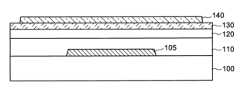
또한, 산화물 반도체층(140)의 결정 구조의 구성은, 도 3에 도시하는 구성에 한정되지 않는다. 여기서, 도 4를 참조하여, 본 발명의 일 실시 형태에 관한 반도체 장치(10)의 산화물 반도체층(140)의 다른 결정 구조에 대해 설명한다. 도 4는, 본 발명의 일 실시 형태에 관한 반도체 장치(10)의 산화물 반도체층(140A)의 결정 구조를 설명하는 모식적인 단면도이다.In addition, the composition of the crystal structure of the oxide semiconductor layer (140) is not limited to the composition illustrated in Fig. 3. Here, with reference to Fig. 4, another crystal structure of the oxide semiconductor layer (140) of the semiconductor device (10) according to one embodiment of the present invention will be described. Fig. 4 is a schematic cross-sectional view illustrating the crystal structure of the oxide semiconductor layer (140A) of the semiconductor device (10) according to one embodiment of the present invention.
도 4에 도시하는 바와 같이, 산화물 반도체층(140A)은 제1 결정 구조를 갖는 제1 결정 영역(144A) 및 제2 결정 구조를 갖는 제2 결정 영역(145A)을 포함한다. 제1 결정 영역(144A)은 산화 금속층(130)으로부터 확산된 알루미늄을 포함하고, 산화 금속층(130)과 산화물 반도체층(140)의 계면에 있어서 층으로서 형성되어 있다. 즉, 제2 결정 영역(145A)은 산화 금속층(130)과 접하고 있지 않다. 또한, 산화물 반도체층의 막 두께 방향에 있어서, 제2 결정 영역(145A)의 막 두께는 제1 결정 영역(144A)의 막 두께보다도 크다. 이 경우에도, 제1 결정 영역(144A)이 버퍼 영역(버퍼층)으로서 기능하기 때문에, 제2 결정 영역(145A)의 산소 결손이 저감됨과 함께, 산화물 반도체층(140A)의 계면 준위 밀도가 저감된다.As illustrated in FIG. 4, the oxide semiconductor layer (140A) includes a first crystal region (144A) having a first crystal structure and a second crystal region (145A) having a second crystal structure. The first crystal region (144A) includes aluminum diffused from the oxide metal layer (130) and is formed as a layer at the interface between the oxide metal layer (130) and the oxide semiconductor layer (140). That is, the second crystal region (145A) is not in contact with the oxide metal layer (130). In addition, in the film thickness direction of the oxide semiconductor layer, the film thickness of the second crystal region (145A) is larger than the film thickness of the first crystal region (144A). In this case as well, since the first crystal region (144A) functions as a buffer region (buffer layer), the oxygen vacancy of the second crystal region (145A) is reduced, and the interface state density of the oxide semiconductor layer (140A) is reduced.
산화물 반도체층에 있어서의 인듐의 비율이 50% 이상인 것에 의해, 산화물 반도체층이 결정성을 갖는다. 그러나, 결정성의 산화물 반도체층이라도, 산화물 반도체층의 결정 영역에 산소 결손이 형성되어 있으면, 충분한 전기 특성 및 신뢰성을 얻을 수 없다. 본 실시 형태에서는, 산화물 반도체층(140)이 버퍼층으로서 기능하는 제1 결정 영역(144)과 함께, 산소 결손이 저감된 제2 결정 영역(145)을 포함한다. 그로 인해, 산화물 반도체층(140)의 산소 결손 및 계면 준위 밀도가 저감되어, 반도체 장치(10)는 고이동도 및 고신뢰성을 갖는다.Since the ratio of indium in the oxide semiconductor layer is 50% or more, the oxide semiconductor layer has crystallinity. However, even in a crystalline oxide semiconductor layer, if oxygen vacancies are formed in the crystal region of the oxide semiconductor layer, sufficient electrical characteristics and reliability cannot be obtained. In the present embodiment, the oxide semiconductor layer (140) includes a first crystal region (144) that functions as a buffer layer, and a second crystal region (145) in which oxygen vacancies are reduced. As a result, the oxygen vacancies and interface state density of the oxide semiconductor layer (140) are reduced, and the semiconductor device (10) has high mobility and high reliability.
또한, 산화물 반도체층(140)의 제2 결정 영역(145)의 산소 결손을 저감시키기 위해서는, OS 어닐뿐만 아니라, 산화 어닐도 중요하기 때문에, 이하에서는, 반도체 장치(10)의 제조 방법에 대해 상세하게 설명한다.In addition, in order to reduce oxygen vacancies in the second crystal region (145) of the oxide semiconductor layer (140), not only the OS anneal but also the oxide anneal is important, so below, a method for manufacturing a semiconductor device (10) will be described in detail.
[반도체 장치(10)의 제조 방법][Method for manufacturing semiconductor device (10)]
도 5 내지 도 14를 참조하여, 본 발명의 일 실시 형태에 관한 반도체 장치의 제조 방법에 대해 설명한다. 도 5는, 본 발명의 일 실시 형태에 관한 반도체 장치의 제조 방법을 나타내는 시퀀스도이다. 도 6 내지 도 14는, 본 발명의 일 실시 형태에 관한 반도체 장치의 제조 방법을 나타내는 단면도이다. 이하의 제조 방법의 설명에서는, 산화 금속층(130, 190)으로서 산화알루미늄이 사용된 반도체 장치(10)의 제조 방법에 대해 설명한다.Referring to FIGS. 5 to 14, a method for manufacturing a semiconductor device according to an embodiment of the present invention will be described. FIG. 5 is a sequence diagram showing a method for manufacturing a semiconductor device according to an embodiment of the present invention. FIGS. 6 to 14 are cross-sectional views showing a method for manufacturing a semiconductor device according to an embodiment of the present invention. In the following description of the manufacturing method, a method for manufacturing a semiconductor device (10) in which aluminum oxide is used as the oxide metal layer (130, 190) will be described.
도 5 및 도 6에 도시하는 바와 같이, 기판(100) 위에 보텀 게이트로서 게이트 전극(105)이 형성되고, 게이트 전극(105) 위에 게이트 절연층(110, 120)이 형성된다(도 3의 스텝 S2001의 「Bottom GI/GE 형성」). 예를 들어, 게이트 절연층(110)으로서, 질화실리콘이 형성된다. 예를 들어, 게이트 절연층(120)으로서, 산화실리콘이 형성된다. 게이트 절연층(110, 120)은 CVD(Chemical Vapor Deposition)법에 의해 성막된다. 게이트 절연층(110, 120)의 한쪽 또는 양쪽을 「제1 절연층」이라고 하는 경우가 있다.As shown in FIGS. 5 and 6, a gate electrode (105) is formed as a bottom gate on a substrate (100), and a gate insulating layer (110, 120) is formed on the gate electrode (105) (“Bottom GI/GE formation” of step S2001 of FIG. 3). For example, silicon nitride is formed as the gate insulating layer (110). For example, silicon oxide is formed as the gate insulating layer (120). The gate insulating layers (110, 120) are formed by a CVD (Chemical Vapor Deposition) method. One or both sides of the gate insulating layers (110, 120) are sometimes referred to as a “first insulating layer.”
게이트 절연층(110)으로서 질화실리콘이 사용됨으로써, 게이트 절연층(110)은, 예를 들어 기판(100)측으로부터 산화물 반도체층(140)을 향해 확산되는 불순물을 블록할 수 있다. 게이트 절연층(120)으로서 사용되는 산화실리콘은 열처리에 의해 산소를 방출하는 물성을 구비한 산화실리콘이다.Since silicon nitride is used as the gate insulating layer (110), the gate insulating layer (110) can block impurities that diffuse from, for example, the substrate (100) side toward the oxide semiconductor layer (140). The silicon oxide used as the gate insulating layer (120) is silicon oxide that has a property of releasing oxygen by heat treatment.
도 5 및 도 7에 도시하는 바와 같이, 게이트 절연층(120) 위에 산화 금속층(130) 및 산화물 반도체층(140)을 형성한다(도 5의 스텝 S2002의 「OS/AlOx 성막」). 이 공정에 대해서, 기판(100) 위에 게이트 절연층(110, 120)을 형성하고, 게이트 절연층(110, 120) 위에 산화 금속층(130)을 형성하는 경우가 있다. 또는, 기판(100) 위에 산화 금속층(130)을 형성하고, 산화 금속층(130) 위에 산화물 반도체층(140)을 형성하는 경우가 있다. 구체적으로는, 산화물 반도체층(140)은 산화 금속층(130)에 접하도록 형성된다. 산화 금속층(130) 및 산화물 반도체층(140)은 스퍼터링법 또는 원자층 퇴적법(ALD: Atomic Layer Deposition)에 의해 성막된다.As shown in FIG. 5 and FIG. 7, an oxide metal layer (130) and an oxide semiconductor layer (140) are formed on the gate insulating layer (120) (“OS/AlOx film formation” of step S2002 of FIG. 5). In this process, there are cases where a gate insulating layer (110, 120) is formed on a substrate (100), and an oxide metal layer (130) is formed on the gate insulating layer (110, 120). Alternatively, there are cases where an oxide metal layer (130) is formed on a substrate (100), and an oxide semiconductor layer (140) is formed on the oxide metal layer (130). Specifically, the oxide semiconductor layer (140) is formed so as to be in contact with the oxide metal layer (130). The oxide metal layer (130) and the oxide semiconductor layer (140) are formed by a sputtering method or an atomic layer deposition (ALD) method.
예를 들어, 산화 금속층(130)의 두께는 1㎚ 이상 100㎚ 이하, 1㎚ 이상 50㎚ 이하, 1㎚ 이상 30㎚ 이하, 또는 1㎚ 이상 10㎚ 이하이다. 본 실시 형태에서는, 산화 금속층(130)으로서 산화알루미늄이 사용된다. 산화알루미늄은 가스에 대한 높은 배리어성을 구비하고 있다. 본 실시 형태에 있어서, 산화 금속층(130)으로서 사용된 산화알루미늄은 게이트 절연층(120)으로부터 방출된 수소 및 산소를 블록하여, 방출된 수소 및 산소가 산화물 반도체층(140)에 도달하는 것을 억제한다.For example, the thickness of the oxide metal layer (130) is 1 nm or more and 100 nm or less, 1 nm or more and 50 nm or less, 1 nm or more and 30 nm or less, or 1 nm or more and 10 nm or less. In the present embodiment, aluminum oxide is used as the oxide metal layer (130). Aluminum oxide has a high barrier property against gas. In the present embodiment, the aluminum oxide used as the oxide metal layer (130) blocks hydrogen and oxygen released from the gate insulating layer (120), thereby suppressing the released hydrogen and oxygen from reaching the oxide semiconductor layer (140).
예를 들어, 산화물 반도체층(140)의 두께는 10㎚ 이상 100㎚ 이하, 15㎚ 이상 70㎚ 이하, 또는 20㎚ 이상 40㎚ 이하이다. 본 실시 형태에서는, 산화물 반도체층(140)으로서, 인듐(In) 및 갈륨(Ga)을 포함하는 산화물이 사용된다. 후술하는 열처리(OS 어닐) 전의 산화물 반도체층(140)은 아몰퍼스이다.For example, the thickness of the oxide semiconductor layer (140) is 10 nm or more and 100 nm or less, 15 nm or more and 70 nm or less, or 20 nm or more and 40 nm or less. In the present embodiment, an oxide containing indium (In) and gallium (Ga) is used as the oxide semiconductor layer (140). The oxide semiconductor layer (140) before the heat treatment (OS annealing) described below is amorphous.
후술하는 OS 어닐에 의해, 산화물 반도체층(140)을 결정화하는 경우, 성막 후이면서 또한 OS 어닐 전의 산화물 반도체층(140)은 아몰퍼스 상태(산화물 반도체의 결정 성분이 적은 상태)인 것이 바람직하다. 즉, 산화물 반도체층(140)의 성막 조건은, 성막 직후의 산화물 반도체층(140)이 가능한 한 결정화되지 않는 조건인 것이 바람직하다. 예를 들어, 스퍼터링법에 의해 산화물 반도체층(140)이 성막되는 경우, 피성막 대상물(기판(100) 및 그 위에 형성된 구조물)의 온도가 제어된 상태에서 산화물 반도체층(140)이 성막된다.When crystallizing the oxide semiconductor layer (140) by the OS anneal described below, it is preferable that the oxide semiconductor layer (140) after the film formation and before the OS anneal be in an amorphous state (a state in which the crystal component of the oxide semiconductor is small). In other words, it is preferable that the film formation conditions of the oxide semiconductor layer (140) be conditions in which the oxide semiconductor layer (140) immediately after the film formation is not crystallized as much as possible. For example, when the oxide semiconductor layer (140) is formed by a sputtering method, the oxide semiconductor layer (140) is formed while the temperature of the film-forming target object (substrate (100) and the structure formed thereon) is controlled.
스퍼터링법에 의해 피성막 대상물에 대해 성막을 행하면, 플라스마 중에서 발생한 이온 및 스퍼터링 타깃에 의해 리바운드된 원자가 피성막 대상물에 충돌한다. 그로 인해, 성막 처리에 수반하여 피성막 대상물의 온도가 상승한다. 성막 처리 중의 피성막 대상물의 온도가 상승하면, 성막 직후의 상태에서 산화물 반도체층(140)에 미결정이 포함된다. 당해 미결정에 의해, 그 후의 OS 어닐에 의한 결정화가 저해된다. 상기한 바와 같이 피성막 대상물의 온도를 제어하기 위해, 예를 들어 피성막 대상물을 냉각하면서 성막을 행해도 된다. 예를 들어, 피성막 대상물의 피성막면(표면)의 온도(이하, 「성막 온도」라고 함)가 100℃ 이하, 70℃ 이하, 50℃ 이하, 또는 30℃ 이하로 되도록, 피성막 대상물을 당해 피성막면의 반대측 면으로부터 냉각해도 된다. 상기한 바와 같이, 피성막 대상물을 냉각하면서 산화물 반도체층(140)의 성막을 행함으로써, 성막 직후의 상태에서 결정 성분이 적은 산화물 반도체층(140)을 성막할 수 있다.When a film is formed on a film-forming target by sputtering, ions generated in the plasma and atoms rebounded by the sputtering target collide with the film-forming target. Therefore, the temperature of the film-forming target increases with the film-forming process. If the temperature of the film-forming target increases during the film-forming process, crystallites are included in the oxide semiconductor layer (140) immediately after the film-forming process. The crystallites inhibit subsequent crystallization by the OS annealing. In order to control the temperature of the film-forming target as described above, the film-forming process may be performed while cooling the film-forming target, for example. For example, the film-forming target may be cooled from the opposite side of the film-forming surface so that the temperature of the film-forming surface (surface) of the film-forming target (hereinafter referred to as the “film-forming temperature”) becomes 100°C or less, 70°C or less, 50°C or less, or 30°C or less. As described above, by forming an oxide semiconductor layer (140) while cooling the film-forming target, an oxide semiconductor layer (140) with a low crystal component can be formed immediately after the film-forming.
도 5 및 도 8에 도시하는 바와 같이, 산화물 반도체층(140)의 패턴을 형성한다(도 5의 스텝 S2003의 「OS 패턴 형성」). 도시하지 않지만, 산화물 반도체층(140) 위에 레지스트 마스크를 형성하고, 당해 레지스트 마스크를 사용하여 산화물 반도체층(140)을 에칭한다. 산화물 반도체층(140)의 에칭으로서, 습식 에칭이 사용되어도 되고, 건식 에칭이 사용되어도 된다. 습식 에칭으로서, 산성의 에천트를 사용하여 에칭을 행해도 된다. 예를 들어, 에천트로서, 옥살산 또는 불산을 사용해도 된다.As shown in FIG. 5 and FIG. 8, a pattern of an oxide semiconductor layer (140) is formed (“OS pattern formation” of step S2003 of FIG. 5). Although not shown, a resist mask is formed over the oxide semiconductor layer (140), and the oxide semiconductor layer (140) is etched using the resist mask. As the etching of the oxide semiconductor layer (140), wet etching or dry etching may be used. As the wet etching, etching may be performed using an acidic etchant. For example, oxalic acid or hydrofluoric acid may be used as the etchant.
산화물 반도체층(140)의 패턴 형성 후에 산화물 반도체층(140)에 대해 열처리(OS 어닐)가 행해진다(도 5의 스텝 S2004의 「OS 어닐」). 본 실시 형태에서는, 이 OS 어닐에 의해, 산화물 반도체층(140)이 결정화된다. OS 어닐이 행해지면, 산화 금속층(130)에 포함되는 알루미늄이 산화물 반도체층(140)으로 확산되어, 산화 금속층(130)과 산화물 반도체층(140)의 계면 근방에 제1 결정 영역(144)이 형성된다. 또한, 제1 결정 영역(144)을 결정핵으로 하여 제2 결정 영역(145)이 형성된다.After the pattern formation of the oxide semiconductor layer (140), heat treatment (OS anneal) is performed on the oxide semiconductor layer (140) (“OS anneal” of step S2004 of FIG. 5). In the present embodiment, the oxide semiconductor layer (140) is crystallized by the OS anneal. When the OS anneal is performed, aluminum included in the oxide metal layer (130) diffuses into the oxide semiconductor layer (140), and a first crystal region (144) is formed near the interface between the oxide metal layer (130) and the oxide semiconductor layer (140). In addition, a second crystal region (145) is formed using the first crystal region (144) as a crystal nucleus.
도 5 및 도 9에 도시하는 바와 같이, 산화 금속층(130)의 패턴을 형성한다(도 5의 스텝 S2005의 「AlOx 패턴 형성」). 산화 금속층(130)은 상기한 공정에서 패터닝된 산화물 반도체층(140)을 마스크로 하여 에칭된다. 산화 금속층(130)의 에칭으로서, 습식 에칭이 사용되어도 되고, 건식 에칭이 사용되어도 된다. 예를 들어, 습식 에칭으로서, 희석 불산(DHF)이 사용된다. 상기한 바와 같이 산화물 반도체층(140)을 마스크로 하여 산화 금속층(130)을 에칭함으로써, 포토리소그래피 공정을 생략할 수 있다.As shown in FIG. 5 and FIG. 9, a pattern of an oxide metal layer (130) is formed ("AlOx pattern formation" of step S2005 of FIG. 5). The oxide metal layer (130) is etched using the oxide semiconductor layer (140) patterned in the above-described process as a mask. As the etching of the oxide metal layer (130), wet etching or dry etching may be used. For example, diluted hydrofluoric acid (DHF) is used as the wet etching. By etching the oxide metal layer (130) using the oxide semiconductor layer (140) as a mask as described above, the photolithography process can be omitted.
도 5 및 도 10에 도시하는 바와 같이, 산화물 반도체층(140) 위에 게이트 절연층(150)을 성막한다(도 5의 스텝 S2006의 「GI 형성」). 예를 들어, 게이트 절연층(150)으로서, 산화실리콘이 형성된다. 게이트 절연층(150)은 CVD법에 의해 형성된다. 예를 들어, 게이트 절연층(150)으로서 상기한 바와 같이 결함이 적은 절연층을 형성하기 위해, 350℃ 이상의 성막 온도에서 게이트 절연층(150)을 성막해도 된다. 예를 들어, 게이트 절연층(150)의 두께는 50㎚ 이상 300㎚ 이하, 60㎚ 이상 200㎚ 이하, 또는 70㎚ 이상 150㎚ 이하이다. 게이트 절연층(150)을 성막한 후에, 게이트 절연층(150)의 일부에 산소를 타입하는 처리를 행해도 된다. 게이트 절연층(150)을 「제2 절연층」이라고 하는 경우가 있다. 게이트 절연층(150) 위에 산화 금속층(190)을 성막한다(도 22의 스텝 S2007의 「AlOx 성막」). 산화 금속층(190)은 스퍼터링법에 의해 성막된다. 산화 금속층(190)의 성막에 의해, 게이트 절연층(150)에 산소가 타입된다.As shown in FIG. 5 and FIG. 10, a gate insulating layer (150) is formed on an oxide semiconductor layer (140) (“GI formation” of step S2006 of FIG. 5). For example, silicon oxide is formed as the gate insulating layer (150). The gate insulating layer (150) is formed by a CVD method. For example, in order to form an insulating layer with fewer defects as described above as the gate insulating layer (150), the gate insulating layer (150) may be formed at a deposition temperature of 350° C. or higher. For example, the thickness of the gate insulating layer (150) is 50 nm or more and 300 nm or less, 60 nm or more and 200 nm or less, or 70 nm or more and 150 nm or less. After forming the gate insulating layer (150), a treatment for introducing oxygen into a part of the gate insulating layer (150) may be performed. The gate insulating layer (150) is sometimes referred to as a “second insulating layer.” An oxide metal layer (190) is formed on the gate insulating layer (150) (“AlOx formation” of step S2007 in Fig. 22). The oxide metal layer (190) is formed by a sputtering method. By forming the oxide metal layer (190), oxygen is introduced into the gate insulating layer (150).
예를 들어, 산화 금속층(190)의 두께는 5㎚ 이상 100㎚ 이하, 5㎚ 이상 50㎚ 이하, 5㎚ 이상 30㎚ 이하, 또는 7㎚ 이상 15㎚ 이하이다. 본 실시 형태에서는, 산화 금속층(190)으로서 산화알루미늄이 사용된다. 산화알루미늄은 가스에 대한 높은 배리어성을 구비하고 있다. 본 실시 형태에 있어서, 산화 금속층(190)으로서 사용된 산화알루미늄은 산화 금속층(190)의 성막 시에 게이트 절연층(150)에 타입된 산소가 외측으로 확산되는 것을 억제한다.For example, the thickness of the oxide metal layer (190) is 5 nm or more and 100 nm or less, 5 nm or more and 50 nm or less, 5 nm or more and 30 nm or less, or 7 nm or more and 15 nm or less. In the present embodiment, aluminum oxide is used as the oxide metal layer (190). Aluminum oxide has a high barrier property against gas. In the present embodiment, the aluminum oxide used as the oxide metal layer (190) suppresses oxygen formed in the gate insulating layer (150) from diffusing to the outside during the deposition of the oxide metal layer (190).
예를 들어, 산화 금속층(190)을 스퍼터링법으로 형성한 경우, 산화 금속층(190)의 막 중에는 스퍼터링에서 사용된 프로세스 가스가 잔존한다. 예를 들어, 스퍼터링의 프로세스 가스로서 Ar이 사용된 경우, 산화 금속층(190)의 막 중에는 Ar이 잔존하는 경우가 있다. 잔존한 Ar은 산화 금속층(190)에 대한 SIMS 분석으로 검출할 수 있다.For example, when the oxide metal layer (190) is formed by a sputtering method, the process gas used in the sputtering remains in the film of the oxide metal layer (190). For example, when Ar is used as the process gas for sputtering, there are cases where Ar remains in the film of the oxide metal layer (190). The remaining Ar can be detected by SIMS analysis of the oxide metal layer (190).
산화물 반도체층(140) 위에 게이트 절연층(150)이 성막되고, 게이트 절연층(150) 위에 산화 금속층(190)이 성막된 상태에서, 산화물 반도체층(140)에 산소를 공급하기 위한 열처리(산화 어닐)가 행해진다(도 5의 스텝 S2008의 「산화 어닐」). 환언하면, 상기한 바와 같이 패터닝된 산화 금속층(130) 및 산화물 반도체층(140)에 대해 열처리(산화 어닐)가 행해진다. 산화물 반도체층(140)이 성막되고 나서 산화물 반도체층(140) 위에 게이트 절연층(150)이 성막될 때까지 동안의 공정에서, 산화물 반도체층(140)의 상면(141) 및 측면(143)에는 많은 산소 결손이 발생한다. 상기한 산화 어닐에 의해, 게이트 절연층(120, 150)으로부터 방출된 산소가 산화물 반도체층(140)에 공급되어, 산소 결손이 수복된다.A gate insulating layer (150) is formed over an oxide semiconductor layer (140), and a metal oxide layer (190) is formed over the gate insulating layer (150), and then heat treatment (oxidation annealing) is performed to supply oxygen to the oxide semiconductor layer (140) (“oxidation annealing” of step S2008 in FIG. 5). In other words, heat treatment (oxidation annealing) is performed on the oxide metal layer (130) and the oxide semiconductor layer (140) that have been patterned as described above. In the process from when the oxide semiconductor layer (140) is formed until the gate insulating layer (150) is formed over the oxide semiconductor layer (140), many oxygen vacancies occur on the upper surface (141) and the side surface (143) of the oxide semiconductor layer (140). By the above-mentioned oxidation annealing, oxygen released from the gate insulating layer (120, 150) is supplied to the oxide semiconductor layer (140), thereby repairing the oxygen vacancies.
산화 어닐에 의해, 게이트 절연층(120)으로부터 방출된 산소는 산화 금속층(130)에 의해 블록된다. 따라서, 산화물 반도체층(140)의 하면(142)에는 산소가 공급되기 어렵다. 게이트 절연층(120)으로부터 방출된 산소는, 산화 금속층(130)이 형성되어 있지 않은 영역으로부터 게이트 절연층(120) 위에 마련된 게이트 절연층(150)으로 확산되어, 게이트 절연층(150)을 통해 산화물 반도체층(140)에 도달한다. 그 결과, 게이트 절연층(120)으로부터 방출된 산소는, 산화물 반도체층(140)의 하면(142)에는 공급되기 어렵고, 주로 산화물 반도체층(140)의 측면(143) 및 상면(141)에 공급된다. 또한, 산화 어닐에 의해, 게이트 절연층(150)으로부터 방출된 산소가 산화물 반도체층(140)의 상면(141) 및 측면(143)에 공급된다. 상기한 산화 어닐에 의해, 게이트 절연층(110, 120)으로부터 수소가 방출되는 경우가 있지만, 당해 수소는 산화 금속층(130)에 의해 블록된다.By the oxidation annealing, the oxygen released from the gate insulating layer (120) is blocked by the oxide metal layer (130). Therefore, it is difficult for oxygen to be supplied to the lower surface (142) of the oxide semiconductor layer (140). The oxygen released from the gate insulating layer (120) diffuses from the region where the oxide metal layer (130) is not formed to the gate insulating layer (150) provided on the gate insulating layer (120) and reaches the oxide semiconductor layer (140) through the gate insulating layer (150). As a result, the oxygen released from the gate insulating layer (120) is difficult to be supplied to the lower surface (142) of the oxide semiconductor layer (140), and is mainly supplied to the side surface (143) and the upper surface (141) of the oxide semiconductor layer (140). In addition, by the oxidation annealing, the oxygen released from the gate insulating layer (150) is supplied to the upper surface (141) and the side surface (143) of the oxide semiconductor layer (140). By the above-mentioned oxidation annealing, there are cases where hydrogen is released from the gate insulating layer (110, 120), but the hydrogen is blocked by the oxide metal layer (130).
상기한 바와 같이, 산화 어닐의 공정에 의해, 산소 결손의 양이 적은 산화물 반도체층(140)의 하면(142)으로의 산소의 공급을 억제하면서, 산소 결손의 양이 많은 산화물 반도체층(140)의 상면(141) 및 측면(143)으로의 산소 공급을 행할 수 있다.As described above, by the oxidation annealing process, it is possible to suppress the supply of oxygen to the lower surface (142) of the oxide semiconductor layer (140) having a small amount of oxygen vacancies, while supplying oxygen to the upper surface (141) and side surface (143) of the oxide semiconductor layer (140) having a large amount of oxygen vacancies.
마찬가지로, 상기한 산화 어닐에 있어서, 게이트 절연층(150)에 타입된 산소는, 산화 금속층(190)에 의해 블록되기 때문에, 대기 중에 방출되는 것이 억제된다. 따라서, 당해 산화 어닐에 의해, 당해 산소가 효율적으로 산화물 반도체층(140)에 공급되어, 산소 결손이 수복된다.Likewise, in the above-described oxidation annealing, the oxygen formed in the gate insulating layer (150) is blocked by the oxide metal layer (190), and thus is suppressed from being released into the atmosphere. Accordingly, by the oxidation annealing, the oxygen is efficiently supplied to the oxide semiconductor layer (140), and the oxygen vacancies are repaired.
도 5 및 도 11에 도시한 바와 같이, 산화 어닐의 후에, 산화 금속층(190)은에칭(제거)된다(도 5의 스텝 S2009의 「AlOx 제거」). 산화 금속층(190)의 에칭으로서, 습식 에칭이 사용되어도 되고, 건식 에칭이 사용되어도 된다. 예를 들어, 습식 에칭으로서, 희석 불산(DHF)이 사용된다. 당해 에칭에 의해, 전체면에 형성된 산화 금속층(190)이 제거된다. 환언하면, 산화 금속층(190)의 제거는 마스크를 사용하지 않고 행해진다. 다시 환언하면, 당해 에칭에 의해, 적어도 평면으로 볼 때에 있어서, 어느 하나의 패턴으로 형성된 산화물 반도체층(140)과 겹치는 영역의 모든 산화 금속층(190)이 제거된다.As shown in FIG. 5 and FIG. 11, after the oxidation annealing, the oxide metal layer (190) is etched (removed) (“AlOx removal” of step S2009 of FIG. 5). As the etching of the oxide metal layer (190), wet etching or dry etching may be used. For example, diluted hydrofluoric acid (DHF) is used as the wet etching. By the etching, the oxide metal layer (190) formed on the entire surface is removed. In other words, the removal of the oxide metal layer (190) is performed without using a mask. In other words, by the etching, at least when viewed in a planar view, all of the oxide metal layers (190) in the region overlapping with the oxide semiconductor layer (140) formed in a certain pattern are removed.
산화 어닐이 행해지면, 산화 금속층(190)에 포함되는 알루미늄이 게이트 절연층(150)으로 확산된다. 그로 인해, 산화 금속층(190)이 제거되어도, 게이트 절연층(150) 중에는 산화 금속층(190)으로부터 확산된 알루미늄이 잔류하고 있다.When the oxidation annealing is performed, aluminum included in the oxide metal layer (190) diffuses into the gate insulating layer (150). Therefore, even if the oxide metal layer (190) is removed, aluminum diffused from the oxide metal layer (190) remains in the gate insulating layer (150).
도 5 및 도 12에 도시하는 바와 같이, 게이트 절연층(150) 위에 게이트 전극(160)을 성막한다(도 5의 스텝 S2010의 「GE 형성」). 게이트 전극(160)은 스퍼터링법 또는 원자층 퇴적법에 의해 성막되고, 포토리소그래피 공정을 거쳐서 패터닝된다. 상기한 바와 같이, 게이트 전극(160)은 산화 금속층(190)이 제거됨으로써 노출된 게이트 절연층(150)과 접하도록 형성된다.As shown in FIG. 5 and FIG. 12, a gate electrode (160) is formed on a gate insulating layer (150) (“GE formation” of step S2010 of FIG. 5). The gate electrode (160) is formed by a sputtering method or an atomic layer deposition method, and is patterned through a photolithography process. As described above, the gate electrode (160) is formed to be in contact with the gate insulating layer (150) exposed by removing the oxide metal layer (190).
게이트 전극(160)의 에칭 시, 게이트 절연층(150)의 일부도 에칭되는 경우가 있다. 즉, 게이트 절연층(150)은 막 두께가 다른 영역을 포함한다. 구체적으로는, 게이트 절연층(150)은 게이트 전극(160)과 중첩되는 제1 영역 및 게이트 전극(160)과 중첩되지 않는 제2 영역을 포함한다. 제1 영역은, 산화물 반도체층(140)의 채널 영역(CH)과 중첩하고 있다. 제2 영역은, 산화물 반도체층(140)의 소스 영역(S) 또는 드레인 영역(D)과 중첩하고 있다. 제2 영역의 막 두께는, 제1 영역의 막 두께보다도 작다.When etching the gate electrode (160), there are cases where a part of the gate insulating layer (150) is also etched. That is, the gate insulating layer (150) includes regions having different film thicknesses. Specifically, the gate insulating layer (150) includes a first region that overlaps the gate electrode (160) and a second region that does not overlap the gate electrode (160). The first region overlaps the channel region (CH) of the oxide semiconductor layer (140). The second region overlaps the source region (S) or the drain region (D) of the oxide semiconductor layer (140). The film thickness of the second region is smaller than that of the first region.
게이트 전극(160)이 패터닝된 상태에서, 산화물 반도체층(140)의 소스 영역(S) 및 드레인 영역(D)의 저저항화가 행해진다(도 5의 스텝 S2011의 「SD 저저항화」). 구체적으로는, 이온 주입에 의해, 게이트 전극(160)측으로부터 게이트 절연층(150)을 통해 산화물 반도체층(140)에 불순물이 주입된다. 예를 들어, 이온 주입에 의해 아르곤(Ar), 인(P), 보론(B)이 산화물 반도체층(140)에 주입된다. 이온 주입에 의해, 산화물 반도체층(140)에 산소 결손이 형성됨으로써, 산화물 반도체층(140)이 저저항화된다. 반도체 장치(10)의 채널 영역(CH)으로서 기능하는 산화물 반도체층(140)의 상방에는 게이트 전극(160)이 마련되어 있기 때문에, 채널 영역(CH)의 산화물 반도체층(140)에는 불순물은 주입되지 않는다.In a state where the gate electrode (160) is patterned, the resistance of the source region (S) and the drain region (D) of the oxide semiconductor layer (140) is reduced (“SD reduction of resistance” in step S2011 of FIG. 5). Specifically, impurities are injected into the oxide semiconductor layer (140) from the gate electrode (160) side through the gate insulating layer (150) by ion injection. For example, argon (Ar), phosphorus (P), and boron (B) are injected into the oxide semiconductor layer (140) by ion injection. By forming oxygen vacancies in the oxide semiconductor layer (140) by ion injection, the resistance of the oxide semiconductor layer (140) is reduced. Since the gate electrode (160) is provided above the oxide semiconductor layer (140) that functions as the channel region (CH) of the semiconductor device (10), impurities are not injected into the oxide semiconductor layer (140) of the channel region (CH).
도 5 및 도 13에 도시하는 바와 같이, 게이트 절연층(150) 및 게이트 전극(160) 위에 층간막으로서 절연층(170, 180)을 성막한다(도 5의 스텝 S2012의 「층간막 성막」). 절연층(170, 180)은 CVD법에 의해 성막된다. 예를 들어, 절연층(170)으로서 질화실리콘이 형성되고, 절연층(180)으로서 산화실리콘이 형성된다. 절연층(170, 180)으로서 사용되는 재료는 상기에 한정되지 않는다. 절연층(170)의 두께는 50㎚ 이상 500㎚ 이하이다. 절연층(180)의 두께는 50㎚ 이상 500㎚ 이하이다.As shown in FIG. 5 and FIG. 13, an insulating layer (170, 180) is formed as an interlayer film on the gate insulating layer (150) and the gate electrode (160) (“Interlayer film formation” of step S2012 of FIG. 5). The insulating layers (170, 180) are formed by the CVD method. For example, silicon nitride is formed as the insulating layer (170), and silicon oxide is formed as the insulating layer (180). The materials used as the insulating layers (170, 180) are not limited to the above. The thickness of the insulating layer (170) is 50 nm or more and 500 nm or less. The thickness of the insulating layer (180) is 50 nm or more and 500 nm or less.
도 5 및 도 14에 도시하는 바와 같이, 게이트 절연층(150) 및 절연층(170, 180)에 개구(171, 173)를 형성한다(도 5의 스텝 S2013의 「콘택트 개공」). 개구(171)에 의해 소스 영역(S)의 산화물 반도체층(140)이 노출되어 있다. 개구(173)에 의해 드레인 영역(D)의 산화물 반도체층(140)이 노출되어 있다. 개구(171, 173)에 의해 노출된 산화물 반도체층(140) 위 및 절연층(180) 위에 소스·드레인 전극(200)을 형성함으로써(도 5의 스텝 S2014의 「SD 형성」), 도 1에 도시하는 반도체 장치(10)가 완성된다.As illustrated in FIG. 5 and FIG. 14, openings (171, 173) are formed in the gate insulating layer (150) and the insulating layers (170, 180) (“Contact opening” of step S2013 of FIG. 5). The oxide semiconductor layer (140) of the source region (S) is exposed by the opening (171). The oxide semiconductor layer (140) of the drain region (D) is exposed by the opening (173). By forming source/drain electrodes (200) on the oxide semiconductor layers (140) exposed by the openings (171, 173) and on the insulating layer (180) (“SD formation” of step S2014 of FIG. 5), the semiconductor device (10) illustrated in FIG. 1 is completed.
상기한 제조 방법으로 제작한 반도체 장치(10)에 대해, 채널 영역(CH)의 채널 길이(L)가 2㎛ 이상 4㎛ 이하이면서, 또한 채널 영역(CH)의 채널 폭이 2㎛ 이상 25㎛ 이하인 범위에 있어서, 이동도가 50㎠/Vs 이상, 55㎠/Vs 이상, 또는 60㎠/Vs 이상의 전기 특성을 얻을 수 있다. 본 실시 형태에 있어서의 이동도란 반도체 장치(10)의 포화 영역에 있어서의 전계 효과 이동도이며, 소스 전극과 드레인 전극 사이의 전위차(Vd)가, 게이트 전극에 공급되는 전압(Vg)으로부터 반도체 장치(10)의 역치 전압(Vth)을 뺀 값(Vg-Vth)보다 큰 영역에 있어서의 전계 효과 이동도의 최댓값을 의미한다.For the semiconductor device (10) manufactured by the above-described manufacturing method, when the channel length (L) of the channel region (CH) is in the range of 2 µm or more and 4 µm or less and the channel width of the channel region (CH) is in the range of 2 µm or more and 25 µm or less, an electrical characteristic of a mobility of 50 ㎠/Vs or more, 55 ㎠/Vs or more, or 60 ㎠/Vs or more can be obtained. The mobility in the present embodiment is a field-effect mobility in a saturation region of the semiconductor device (10), and means the maximum value of the field-effect mobility in a region where the potential difference (Vd) between the source electrode and the drain electrode is greater than the value (Vg-Vth) obtained by subtracting the threshold voltage (Vth) of the semiconductor device (10) from the voltage (Vg) supplied to the gate electrode.
<제2 실시 형태><Second embodiment>
도 15 내지 도 19를 참조하여, 본 발명의 일 실시 형태에 관한 반도체 장치를 사용한 표시 장치에 대해 설명한다. 이하에 나타내는 실시 형태에서는, 상기한 제1 실시 형태에서 설명한 반도체 장치(10)가 액정 표시 장치의 회로에 적용된 구성에 대해 설명한다.Referring to FIGS. 15 to 19, a display device using a semiconductor device according to one embodiment of the present invention will be described. In the embodiment shown below, a configuration in which the semiconductor device (10) described in the first embodiment described above is applied to a circuit of a liquid crystal display device will be described.
[표시 장치(20)의 개요][Overview of display device (20)]
도 15는, 본 발명의 일 실시 형태에 관한 표시 장치의 개요를 도시하는 평면도이다. 도 15에 도시하는 바와 같이, 표시 장치(20)는 어레이 기판(300), 시일부(310), 대향 기판(320), 플렉시블 프린트 회로 기판(330)(FPC(330)) 및 IC 칩(340)을 갖는다. 어레이 기판(300) 및 대향 기판(320)은 시일부(310)에 의해 접합되어 있다. 시일부(310)에 둘러싸인 액정 영역(22)에는, 복수의 화소 회로(301)가 매트릭스 형상으로 배치되어 있다. 액정 영역(22)은 후술하는 액정 소자(311)와 평면으로 볼 때에 있어서 겹치는 영역이다.Fig. 15 is a plan view showing an outline of a display device according to one embodiment of the present invention. As shown in Fig. 15, the display device (20) has an array substrate (300), a sealing portion (310), a counter substrate (320), a flexible printed circuit board (330) (FPC (330)), and an IC chip (340). The array substrate (300) and the counter substrate (320) are joined by the sealing portion (310). In a liquid crystal region (22) surrounded by the sealing portion (310), a plurality of pixel circuits (301) are arranged in a matrix shape. The liquid crystal region (22) is an area overlapping with a liquid crystal element (311) described later when viewed in a plan view.
시일부(310)가 마련된 시일 영역(24)은 액정 영역(22)의 주위의 영역이다. FPC(330)는 단자 영역(26)에 마련되어 있다. 단자 영역(26)은 어레이 기판(300)이 대향 기판(320)으로부터 노출된 영역이며, 시일 영역(24)의 외측에 마련되어 있다. 시일 영역(24)의 외측이란, 시일부(310)가 마련된 영역 및 시일부(310)에 의해 둘러싸인 영역의 외측을 의미한다. IC 칩(340)은 FPC(330) 위에 마련되어 있다. IC 칩(340)은 각 화소 회로(301)를 구동시키기 위한 신호를 공급한다.The seal area (24) provided with the seal portion (310) is an area around the liquid crystal area (22). The FPC (330) is provided in the terminal area (26). The terminal area (26) is an area where the array substrate (300) is exposed from the opposing substrate (320), and is provided on the outside of the seal area (24). The outside of the seal area (24) means the outside of the area where the seal portion (310) is provided and the area surrounded by the seal portion (310). The IC chip (340) is provided on the FPC (330). The IC chip (340) supplies a signal for driving each pixel circuit (301).
[표시 장치(20)의 회로 구성][Circuit configuration of display device (20)]
도 16은, 본 발명의 일 실시 형태에 관한 표시 장치의 회로 구성을 도시하는 블록도이다. 도 16에 도시하는 바와 같이, 화소 회로(301)가 배치된 액정 영역(22)에 대해 D1 방향(열 방향)에 인접하는 위치에는 소스 드라이버 회로(302)가 마련되어 있고, 액정 영역(22)에 대해 D2 방향(행 방향)에 인접하는 위치에는 게이트 드라이버 회로(303)가 마련되어 있다. 소스 드라이버 회로(302) 및 게이트 드라이버 회로(303)는, 상기한 시일 영역(24)에 마련되어 있다. 단, 소스 드라이버 회로(302) 및 게이트 드라이버 회로(303)가 마련되는 영역은 시일 영역(24)에 한정되지 않고, 화소 회로(301)가 마련된 영역의 외측이면, 어느 영역이어도 좋다.Fig. 16 is a block diagram showing a circuit configuration of a display device according to one embodiment of the present invention. As shown in Fig. 16, a source driver circuit (302) is provided at a position adjacent to the D1 direction (column direction) with respect to a liquid crystal region (22) in which a pixel circuit (301) is arranged, and a gate driver circuit (303) is provided at a position adjacent to the D2 direction (row direction) with respect to the liquid crystal region (22). The source driver circuit (302) and the gate driver circuit (303) are provided in the seal region (24) described above. However, the region in which the source driver circuit (302) and the gate driver circuit (303) are provided is not limited to the seal region (24), and any region may be provided as long as it is outside the region in which the pixel circuit (301) is provided.
소스 드라이버 회로(302)로부터 소스 배선(304)이 D1 방향으로 연장되어 있고, D1 방향으로 배열된 복수의 화소 회로(301)에 접속되어 있다. 게이트 드라이버 회로(303)로부터 게이트 배선(305)이 D2 방향으로 연장되어 있고, D2 방향으로 배열된 복수의 화소 회로(301)에 접속되어 있다.From the source driver circuit (302), a source wiring (304) extends in the D1 direction and is connected to a plurality of pixel circuits (301) arranged in the D1 direction. From the gate driver circuit (303), a gate wiring (305) extends in the D2 direction and is connected to a plurality of pixel circuits (301) arranged in the D2 direction.
단자 영역(26)에는 단자부(306)가 마련되어 있다. 단자부(306)와 소스 드라이버 회로(302)는 접속 배선(307)에 의해 접속되어 있다. 마찬가지로, 단자부(306)와 게이트 드라이버 회로(303)는 접속 배선(307)에 의해 접속되어 있다. FPC(330)가 단자부(306)에 접속됨으로써, FPC(330)가 접속된 외부 기기와 표시 장치(20)가 접속되고, 외부 기기로부터의 신호에 의해 표시 장치(20)에 마련된 각 화소 회로(301)가 구동한다.A terminal section (306) is provided in the terminal area (26). The terminal section (306) and the source driver circuit (302) are connected by a connection wire (307). Similarly, the terminal section (306) and the gate driver circuit (303) are connected by a connection wire (307). By connecting the FPC (330) to the terminal section (306), the external device to which the FPC (330) is connected and the display device (20) are connected, and each pixel circuit (301) provided in the display device (20) is driven by a signal from the external device.
제1 실시 형태에 나타내는 반도체 장치(10)는 화소 회로(301), 소스 드라이버 회로(302) 및 게이트 드라이버 회로(303)에 포함되는 트랜지스터로서 사용된다.The semiconductor device (10) shown in the first embodiment is used as a transistor included in a pixel circuit (301), a source driver circuit (302), and a gate driver circuit (303).
[표시 장치(20)의 화소 회로(301)][Pixel circuit (301) of display device (20)]
도 17은, 본 발명의 일 실시 형태에 관한 표시 장치의 화소 회로를 도시하는 회로도이다. 도 17에 도시하는 바와 같이, 화소 회로(301)는 반도체 장치(10), 유지 용량(350) 및 액정 소자(311) 등의 소자를 포함한다. 반도체 장치(10)는 게이트 전극(160), 소스 전극(201) 및 드레인 전극(203)을 갖는다. 게이트 전극(160)은 게이트 배선(305)에 접속되어 있다. 소스 전극(201)은 소스 배선(304)에 접속되어 있다. 드레인 전극(203)은 유지 용량(350) 및 액정 소자(311)에 접속되어 있다. 본 실시 형태에서는, 설명의 편의상, 부호 「201」로 나타내어진 전극을 소스 전극이라 하고, 부호 「203」으로 나타내어진 전극을 드레인 전극이라고 하지만, 부호 「201」로 나타내어진 전극이 드레인 전극으로서 기능하고, 부호 「203」으로 나타내어진 전극이 소스 전극으로서 기능해도 된다.Fig. 17 is a circuit diagram showing a pixel circuit of a display device according to one embodiment of the present invention. As shown in Fig. 17, the pixel circuit (301) includes elements such as a semiconductor device (10), a storage capacitor (350), and a liquid crystal element (311). The semiconductor device (10) has a gate electrode (160), a source electrode (201), and a drain electrode (203). The gate electrode (160) is connected to a gate wiring (305). The source electrode (201) is connected to a source wiring (304). The drain electrode (203) is connected to the storage capacitor (350) and the liquid crystal element (311). In this embodiment, for convenience of explanation, the electrode indicated by symbol “201” is referred to as a source electrode, and the electrode indicated by symbol “203” is referred to as a drain electrode. However, the electrode indicated by symbol “201” may function as a drain electrode, and the electrode indicated by symbol “203” may function as a source electrode.
[표시 장치(20)의 단면 구조][Cross-sectional structure of display device (20)]
도 18은, 본 발명의 일 실시 형태에 관한 표시 장치의 단면도이다. 도 18에 도시하는 바와 같이, 표시 장치(20)는 반도체 장치(10)가 사용된 표시 장치이다. 본 실시 형태에서는, 반도체 장치(10)가 화소 회로(301)에 사용된 구성을 예시하지만, 반도체 장치(10)가 소스 드라이버 회로(302) 및 게이트 드라이버 회로(303)를 포함하는 주변 회로에 사용되어도 된다. 이하의 설명에 있어서, 반도체 장치(10)의 구성은 도 1에 도시하는 반도체 장치(10)와 마찬가지이므로, 설명을 생략한다.Fig. 18 is a cross-sectional view of a display device according to one embodiment of the present invention. As shown in Fig. 18, the display device (20) is a display device in which a semiconductor device (10) is used. In this embodiment, a configuration in which a semiconductor device (10) is used in a pixel circuit (301) is exemplified, but the semiconductor device (10) may be used in a peripheral circuit including a source driver circuit (302) and a gate driver circuit (303). In the following description, the configuration of the semiconductor device (10) is the same as that of the semiconductor device (10) shown in Fig. 1, and therefore, the description is omitted.
소스 전극(201) 및 드레인 전극(203) 위에 절연층(360)이 마련되어 있다. 절연층(360) 위에 복수의 화소에 공통으로 마련되는 공통 전극(370)이 마련되어 있다. 공통 전극(370) 위에 절연층(380)이 마련되어 있다. 절연층(360, 380)에는 개구(381)가 마련되어 있다. 절연층(380) 위 및 개구(381)의 내부에 화소 전극(390)이 마련되어 있다. 화소 전극(390)은 드레인 전극(203)에 접속되어 있다.An insulating layer (360) is provided on the source electrode (201) and the drain electrode (203). A common electrode (370) that is provided in common to a plurality of pixels is provided on the insulating layer (360). An insulating layer (380) is provided on the common electrode (370). An opening (381) is provided in the insulating layers (360, 380). A pixel electrode (390) is provided on the insulating layer (380) and inside the opening (381). The pixel electrode (390) is connected to the drain electrode (203).
표시 장치(20)에서는, 게이트 전극(160)과 동일한 층으로서, 배선층(162)이 마련되어 있다. 배선층(162)은 게이트 전극(160)과 동일한 재료를 포함한다. 배선층(162)은 게이트 절연층(150)에 대응하는 절연층 위에 마련되어 있다. 당해 절연층 위에도 산화 금속층(190)이 성막되고, 산화 어닐이 행해지고 있다. 배선층(162)과 중첩되지 않는 절연층 영역의 알루미늄 농도는, 배선층(162)과 중첩하는 절연층 영역의 알루미늄 농도보다도 작다.In the display device (20), a wiring layer (162) is provided as the same layer as the gate electrode (160). The wiring layer (162) includes the same material as the gate electrode (160). The wiring layer (162) is provided on an insulating layer corresponding to the gate insulating layer (150). An oxide metal layer (190) is also formed on the insulating layer, and oxidation annealing is performed. The aluminum concentration in the insulating layer region that does not overlap with the wiring layer (162) is lower than the aluminum concentration in the insulating layer region that overlaps with the wiring layer (162).
도 19는, 본 발명의 일 실시 형태에 관한 표시 장치의 화소 전극 및 공통 전극의 평면도이다. 도 19에 도시하는 바와 같이, 공통 전극(370)은 평면으로 볼 때에 있어서 화소 전극(390)과 겹치는 중첩 영역과, 화소 전극(390)과 겹치지 않는 비중첩 영역을 갖는다. 화소 전극(390)과 공통 전극(370) 사이에 전압을 공급하면, 중첩 영역의 화소 전극(390)으로부터 비중첩 영역의 공통 전극(370)을 향해 횡전계가 형성된다. 이 횡전계에 의해 액정 소자(311)에 포함되는 액정 분자가 동작함으로써, 화소의 계조가 결정된다.Fig. 19 is a plan view of a pixel electrode and a common electrode of a display device according to one embodiment of the present invention. As shown in Fig. 19, the common electrode (370) has an overlapping region that overlaps with the pixel electrode (390) when viewed in a plan view, and a non-overlapping region that does not overlap with the pixel electrode (390). When voltage is supplied between the pixel electrode (390) and the common electrode (370), a transverse electric field is formed from the pixel electrode (390) in the overlapping region toward the common electrode (370) in the non-overlapping region. The liquid crystal molecules included in the liquid crystal element (311) operate due to this transverse electric field, thereby determining the grayscale of the pixel.
<제3 실시 형태><Third embodiment>
도 20 및 도 21을 참조하여, 본 발명의 일 실시 형태에 관한 반도체 장치를 사용한 표시 장치에 대해 설명한다. 본 실시 형태에서는, 상기한 제1 실시 형태에서 설명한 반도체 장치(10)가 유기 EL 표시 장치의 회로에 적용된 구성에 대해 설명한다. 표시 장치(20)의 개요 및 회로 구성은 도 15 및 도 16에 나타내는 개요 및 구성과 마찬가지이므로, 설명을 생략한다.Referring to FIGS. 20 and 21, a display device using a semiconductor device according to one embodiment of the present invention will be described. In this embodiment, a configuration in which the semiconductor device (10) described in the first embodiment described above is applied to a circuit of an organic EL display device will be described. The outline and circuit configuration of the display device (20) are the same as the outline and configuration shown in FIGS. 15 and 16, and therefore, a description thereof will be omitted.
[표시 장치(20)의 화소 회로(301)][Pixel circuit (301) of display device (20)]
도 20은, 본 발명의 일 실시 형태에 관한 표시 장치의 화소 회로를 도시하는 회로도이다. 도 20에 도시하는 바와 같이, 화소 회로(301)는 구동 트랜지스터(11), 선택 트랜지스터(12), 유지 용량(210) 및 발광 소자(DO) 등의 소자를 포함한다. 구동 트랜지스터(11) 및 선택 트랜지스터(12)는 반도체 장치(10)와 마찬가지의 구성을 구비하고 있다. 선택 트랜지스터(12)의 소스 전극은 신호선(211)에 접속되고, 선택 트랜지스터(12)의 게이트 전극은 게이트선(212)에 접속되어 있다. 구동 트랜지스터(11)의 소스 전극은 애노드 전원선(213)에 접속되고, 구동 트랜지스터(11)의 드레인 전극은 발광 소자(DO)의 일단부에 접속되어 있다. 발광 소자(DO)의 타단부는 캐소드 전원선(214)에 접속되어 있다. 구동 트랜지스터(11)의 게이트 전극은 선택 트랜지스터(12)의 드레인 전극에 접속되어 있다. 유지 용량(210)은 구동 트랜지스터(11)의 게이트 전극 및 드레인 전극에 접속되어 있다. 신호선(211)에는, 발광 소자(DO)의 발광 강도를 정하는 계조 신호가 공급된다. 게이트선(212)에는, 상기한 계조 신호를 기입하는 화소행을 선택하는 신호가 공급된다.Fig. 20 is a circuit diagram showing a pixel circuit of a display device according to one embodiment of the present invention. As shown in Fig. 20, the pixel circuit (301) includes elements such as a driving transistor (11), a selection transistor (12), a holding capacitor (210), and a light-emitting element (DO). The driving transistor (11) and the selection transistor (12) have the same configuration as the semiconductor device (10). The source electrode of the selection transistor (12) is connected to a signal line (211), and the gate electrode of the selection transistor (12) is connected to a gate line (212). The source electrode of the driving transistor (11) is connected to an anode power line (213), and the drain electrode of the driving transistor (11) is connected to one end of the light-emitting element (DO). The other end of the light-emitting element (DO) is connected to a cathode power line (214). The gate electrode of the driving transistor (11) is connected to the drain electrode of the selection transistor (12). The maintenance capacitor (210) is connected to the gate electrode and drain electrode of the driving transistor (11). A gray scale signal that determines the light emission intensity of the light emitting element (DO) is supplied to the signal line (211). A signal for selecting a pixel row in which the above-mentioned gray scale signal is written is supplied to the gate line (212).
[표시 장치(20)의 단면 구조][Cross-sectional structure of display device (20)]
도 21은, 본 발명의 일 실시 형태에 관한 표시 장치의 단면도이다. 도 21에 도시하는 표시 장치(20)의 구성은, 도 18에 도시하는 표시 장치(20)와 유사하지만, 도 21의 표시 장치(20)의 절연층(360)보다도 상방의 구조가 도 18의 표시 장치(20)의 절연층(360)보다도 상방의 구조와 상이하다. 이하, 도 21의 표시 장치(20)의 구성 중, 도 18의 표시 장치(20)와 마찬가지의 구성에 대해서는 설명을 생략하고, 양자의 상위점에 대해 설명한다.Fig. 21 is a cross-sectional view of a display device according to one embodiment of the present invention. The configuration of the display device (20) illustrated in Fig. 21 is similar to the display device (20) illustrated in Fig. 18, but the structure above the insulating layer (360) of the display device (20) illustrated in Fig. 21 is different from the structure above the insulating layer (360) of the display device (20) illustrated in Fig. 18. Hereinafter, among the configurations of the display device (20) illustrated in Fig. 21, descriptions of the configurations similar to those of the display device (20) illustrated in Fig. 18 will be omitted, and differences between the two will be described.
도 21에 도시하는 바와 같이, 표시 장치(20)는 절연층(360) 상방에 화소 전극(390), 발광층(392) 및 공통 전극(394)(발광 소자(DO))을 갖는다. 화소 전극(390)은 절연층(360) 위 및 개구(381)의 내부에 마련되어 있다. 화소 전극(390) 위에 절연층(362)이 마련되어 있다. 절연층(362)에는 개구(363)가 마련되어 있다. 개구(363)는 발광 영역에 대응한다. 즉, 절연층(362)은 화소를 획정한다. 개구(363)에 의해 노출된 화소 전극(390) 위에 발광층(392) 및 공통 전극(394)이 마련되어 있다. 화소 전극(390) 및 발광층(392)은 각 화소에 대해 개별로 마련되어 있다. 한편, 공통 전극(394)은 복수의 화소에 공통으로 마련되어 있다. 발광층(392)은 화소의 표시색에 따라서 다른 재료가 사용된다.As shown in Fig. 21, the display device (20) has a pixel electrode (390), a light-emitting layer (392), and a common electrode (394) (light-emitting element (DO)) above an insulating layer (360). The pixel electrode (390) is provided on the insulating layer (360) and inside the opening (381). An insulating layer (362) is provided on the pixel electrode (390). An opening (363) is provided in the insulating layer (362). The opening (363) corresponds to a light-emitting area. That is, the insulating layer (362) defines a pixel. An light-emitting layer (392) and a common electrode (394) are provided on the pixel electrode (390) exposed by the opening (363). The pixel electrode (390) and the light-emitting layer (392) are provided individually for each pixel. Meanwhile, the common electrode (394) is provided in common for a plurality of pixels. The light-emitting layer (392) uses different materials depending on the display color of the pixel.
제2 실시 형태 및 제3 실시 형태에서는, 제1 실시 형태에서 설명한 반도체 장치를 액정 표시 장치 및 유기 EL 표시 장치에 적용한 구성에 대해 예시하였지만, 이들 표시 장치 이외의 표시 장치(예를 들어, 유기 EL 표시 장치 이외의 자발광형 표시 장치 또는 전자 페이퍼형 표시 장치)에 당해 반도체 장치를 적용해도 된다. 또한, 중소형 표시 장치로부터 대형 표시 장치까지, 특별히 한정되지 않고 상기 반도체 장치의 적용이 가능하다.In the second embodiment and the third embodiment, the semiconductor device described in the first embodiment is exemplified as a configuration in which the semiconductor device is applied to a liquid crystal display device and an organic EL display device, but the semiconductor device may be applied to display devices other than these display devices (for example, a self-luminous display device or an electronic paper-type display device other than an organic EL display device). In addition, the semiconductor device can be applied to any display device from a small- to medium-sized display device to a large-sized display device without any particular limitation.
실시예Example
실시예로서, 제1 실시 형태에서 설명한 반도체 장치(10)를 제작하여, 반도체 장치(10)의 평가를 행하였다. 또한, 비교예로서, 산화물 반도체층(140)에 접하는 산화 금속층(130)이 마련되어 있지 않은 반도체 장치, 즉, 게이트 절연층(120)에 산화물 반도체층(140)이 접하는 반도체 장치를 제작하였다.As an example, a semiconductor device (10) described in the first embodiment was manufactured, and the semiconductor device (10) was evaluated. In addition, as a comparative example, a semiconductor device in which an oxide metal layer (130) in contact with an oxide semiconductor layer (140) is not provided, that is, a semiconductor device in which an oxide semiconductor layer (140) is in contact with a gate insulating layer (120), was manufactured.
또한, 실시예의 반도체 장치(10) 및 비교예의 반도체 장치 모두, 게이트 전극(160)을 형성하기 전에, 산화 금속층(190)으로서 산화알루미늄층을 스퍼터링법에 의해 성막하고, 산화 어닐을 행한 후에 산화알루미늄층을 제거하였다.In addition, in both the semiconductor device of the embodiment (10) and the semiconductor device of the comparative example, before forming the gate electrode (160), an aluminum oxide layer was formed as an oxide metal layer (190) by sputtering, and after performing an oxidation annealing, the aluminum oxide layer was removed.
[1. 전기 특성][1. Electrical characteristics]
도 22는, 실시예의 반도체 장치(10)의 전기 특성을 나타내는 그래프이다. 또한, 도 27은, 비교예의 반도체 장치의 전기 특성을 나타내는 그래프이다. 도 22 및 도 27에 나타내는 전기 특성의 측정 조건은 표 1과 같다.Fig. 22 is a graph showing the electrical characteristics of a semiconductor device (10) of an embodiment. In addition, Fig. 27 is a graph showing the electrical characteristics of a semiconductor device of a comparative example. The measurement conditions of the electrical characteristics shown in Figs. 22 and 27 are as shown in Table 1.
[표 1][Table 1]
도 22 및 도 27에는, 전기 특성(Id-Vg 특성)뿐만 아니라, 이동도도 나타내어지고 있다(도 22 및 도 27의 점선을 참조). 도 22 및 도 27에서는, 드레인 전류(Id)에 대한 종축은 그래프의 좌측에 나타내어지고 있고, 당해 드레인 전류로부터 계산된 이동도에 대한 종축은 그래프의 우측에 나타내어지고 있다.In Figs. 22 and 27, not only the electrical characteristics (Id-Vg characteristics) but also the mobility are shown (see the dotted lines in Figs. 22 and 27). In Figs. 22 and 27, the vertical axis for the drain current (Id) is shown on the left side of the graph, and the vertical axis for the mobility calculated from the drain current is shown on the right side of the graph.
도 22에 도시하는 바와 같이, 실시예의 반도체 장치(10)의 전기 특성은, 게이트 전압(Vg)이 0V보다도 높은 전압에서 드레인 전류(Id)가 흐르기 시작하는, 소위 노멀리 오프(인핸스먼트형)의 특성을 나타낸다. 당해 전기 특성으로부터 계산된 이동도는 59㎠/Vs이다.As shown in Fig. 22, the electrical characteristics of the semiconductor device (10) of the embodiment exhibit so-called normally-off (enhanced type) characteristics in which the drain current (Id) starts to flow at a voltage higher than 0 V when the gate voltage (Vg) is higher. The mobility calculated from the electrical characteristics is 59㎠/Vs.
도 27에 도시하는 바와 같이, 비교예의 반도체 장치의 전기 특성도, 소위 노멀리 오프(인핸스먼트형)의 특성을 나타낸다. 당해 전기 특성으로부터 계산된 이동도는 34㎠/Vs이다.As shown in Fig. 27, the electrical characteristics of the semiconductor device of the comparative example also show the so-called normally-off (enhancement type) characteristics. The mobility calculated from the electrical characteristics is 34㎠/Vs.
이상으로부터 알 수 있는 바와 같이, 실시예의 반도체 장치(10)의 이동도는 비교예의 반도체 장치의 이동도의 약 2배이며, 실시예의 반도체 장치(10)는 고이동도를 갖는 것을 알 수 있었다.As can be seen from the above, the mobility of the semiconductor device (10) of the embodiment is approximately twice that of the semiconductor device of the comparative example, and it was found that the semiconductor device (10) of the embodiment has high mobility.
[2. 신뢰성 시험][2. Reliability Test]
도 23은, 실시예의 반도체 장치(10)의 신뢰성 시험을 나타내는 그래프이다. 또한, 도 28은, 비교예의 반도체 장치의 신뢰성을 나타내는 그래프이다. 도 23 및 도 28에 나타내는 신뢰성 시험의 측정 조건은 표 2와 같다. 즉, 신뢰성 시험으로서, Negative Bias Temperature Illumination Stress(NBTIS)에 의한 신뢰성의 평가를 행하였다.Fig. 23 is a graph showing a reliability test of a semiconductor device (10) of an embodiment. In addition, Fig. 28 is a graph showing the reliability of a semiconductor device of a comparative example. The measurement conditions of the reliability tests shown in Figs. 23 and 28 are as shown in Table 2. That is, as a reliability test, reliability was evaluated by Negative Bias Temperature Illumination Stress (NBTIS).
[표 2][Table 2]
도 23 및 도 28에는, 스트레스 시간이 0sec, 100sec, 500sec, 1000sec, 1500sec, 2000sec 및 3600sec에 있어서 측정된 전기 특성이 겹쳐 표시되어 있다. 여기서, 스트레스 인가 전을 0sec라고 하고, 스트레스 인가 후를 3600sec라고 한다. 도 23 및 도 28에 있어서, 스트레스 인가 전(0sec)의 전기 특성은 굵은 점선으로 나타내고 있고, 스트레스 인가 후(3600sec)의 전기 특성은 굵은 실선으로 나타내고 있다.In FIGS. 23 and 28, electrical characteristics measured at stress times of 0 sec, 100 sec, 500 sec, 1000 sec, 1500 sec, 2000 sec, and 3600 sec are superimposed and displayed. Here, the time before stress application is referred to as 0 sec, and the time after stress application is referred to as 3600 sec. In FIGS. 23 and 28, the electrical characteristics before stress application (0 sec) are represented by a thick dotted line, and the electrical characteristics after stress application (3600 sec) are represented by a thick solid line.
또한, 스트레스 인가 전 및 스트레스 인가 후의 전기 특성의 측정 조건은 표 3과 같다.Additionally, the measurement conditions of electrical characteristics before and after stress application are as shown in Table 3.
[표 3][Table 3]
도 23에 도시하는 바와 같이, 실시예의 반도체 장치(10)에서는, NBTIS 시험에 있어서, 스트레스 인가 전후의 전기 특성이 거의 변화하지 않는다. 스트레스 인가 전후에 있어서의 역치 전압의 변화는 -0.05V였다. 즉, 스트레스 인가 후에 있어서, 역치 전압이 음의 방향으로 0.05V밖에 이동하지 않았다. 또한, 스트레스 인가 후에 있어서도 노멀리 오프의 특성을 나타냈다.As shown in Fig. 23, in the semiconductor device (10) of the embodiment, in the NBTIS test, the electrical characteristics before and after the stress application hardly changed. The change in the threshold voltage before and after the stress application was -0.05 V. That is, after the stress application, the threshold voltage moved only 0.05 V in the negative direction. In addition, the normally-off characteristic was exhibited even after the stress application.
도 28에 도시하는 바와 같이, 비교예의 반도체 장치에서는, NBTIS 시험에 있어서, 스트레스 인가 전후의 전기 특성에 변화가 보여진다. 스트레스 인가 전후에 있어서의 역치 변화는 -1.14V였다. 즉, 스트레스 인가 후에 있어서, 역치 전압이 음의 방향으로 1.14V나 이동하였다.As shown in Fig. 28, in the semiconductor device of the comparative example, changes in the electrical characteristics before and after stress application are observed in the NBTIS test. The threshold change before and after stress application was -1.14 V. That is, after stress application, the threshold voltage shifted in the negative direction by 1.14 V.
이상으로부터 알 수 있는 바와 같이, 실시예의 반도체 장치(10)의 신뢰성은 안정되어 있고, 실시예의 반도체 장치(10)는 고신뢰성을 갖는 것을 알 수 있었다.As can be seen from the above, the reliability of the semiconductor device (10) of the embodiment is stable, and it can be seen that the semiconductor device (10) of the embodiment has high reliability.
[3. 단면 TEM 관찰][3. Cross-sectional TEM observation]
도 24a는, 실시예의 반도체 장치(10)의 단면 TEM상이다. 도 24b는, 도 24a의 단면 TEM상을 설명하기 위한 모식도이다. 또한, 도 29는, 비교예의 반도체 장치의 단면 TEM상이다. 도 24a에는, 실시예의 반도체 장치(10)에 있어서의 산화 금속층(130)과 산화물 반도체층(140)의 계면 근방의 단면 TEM상이 도시되어 있다. 한편, 도 29에는, 비교예의 반도체 장치에 있어서의 게이트 절연막(120)과 산화물 반도체층(140)의 계면 근방의 단면 TEM상이 도시되어 있다.Fig. 24a is a cross-sectional TEM image of a semiconductor device (10) of an embodiment. Fig. 24b is a schematic diagram for explaining the cross-sectional TEM image of Fig. 24a. In addition, Fig. 29 is a cross-sectional TEM image of a semiconductor device of a comparative example. Fig. 24a shows a cross-sectional TEM image of the vicinity of the interface between the oxide metal layer (130) and the oxide semiconductor layer (140) in the semiconductor device (10) of the embodiment. On the other hand, Fig. 29 shows a cross-sectional TEM image of the vicinity of the interface between the gate insulating film (120) and the oxide semiconductor layer (140) in the semiconductor device of the comparative example.
도 24a에 도시하는 바와 같이, 실시예의 반도체 장치(10)에서는, 2개의 다른 결정 영역을 확인할 수 있다. 구체적으로는, 도 24b에 도시하는 바와 같이, 산화 금속층(130)과 산화물 반도체층(140)의 계면 근방에 있어서, 산화 금속층(130)과 접하는 제1 결정 영역(144) 및 제1 결정 영역(144)을 덮는 제2 결정 영역(145)을 확인할 수 있다.As shown in Fig. 24a, in the semiconductor device (10) of the embodiment, two different crystal regions can be confirmed. Specifically, as shown in Fig. 24b, near the interface between the oxide metal layer (130) and the oxide semiconductor layer (140), a first crystal region (144) in contact with the oxide metal layer (130) and a second crystal region (145) covering the first crystal region (144) can be confirmed.
도 29에 도시하는 바와 같이, 비교예의 반도체 장치에서는, 산화물 반도체층(140)은 결정성을 갖지만, 게이트 절연층(120)과 산화물 반도체층(140)의 계면 근방에, 산화물 반도체층(140)의 대부분을 차지하는 결정 영역과 다른 결정 영역은 보이지 않았다.As shown in Fig. 29, in the semiconductor device of the comparative example, the oxide semiconductor layer (140) has crystallinity, but no crystal region other than the crystal region occupying most of the oxide semiconductor layer (140) was observed near the interface between the gate insulating layer (120) and the oxide semiconductor layer (140).
[4. 전자선 회절 측정][4. Electron diffraction measurement]
도 25 및 도 26은, 실시예의 반도체 장치(10)의 전자선 회절상이다. 도 25에는, 산화 금속층(130)과 산화물 반도체층(140)의 계면으로부터 이격된 위치에 있어서의 산화물 반도체층(140)의 전자선 회절상이 도시되고, 도 26에는, 산화 금속층(130)과 산화물 반도체층(140)의 계면 근방에 있어서의 전자선 회절상이 도시되어 있다. 또한, 도 30 및 도 31은, 비교예의 반도체 장치의 전자선 회절상이다. 도 30에는, 게이트 절연층(120)과 산화물 반도체층(140)의 계면으로부터 이격된 위치에 있어서의 산화물 반도체층(140)의 전자선 회절상이 도시되고, 도 31에는, 게이트 절연층(120)과 산화물 반도체층(140)의 계면 근방에 있어서의 전자선 회절상이 도시되어 있다.FIG. 25 and FIG. 26 are electron diffraction images of a semiconductor device (10) of an embodiment. FIG. 25 shows an electron diffraction image of an oxide semiconductor layer (140) at a position spaced apart from the interface between the oxide metal layer (130) and the oxide semiconductor layer (140), and FIG. 26 shows an electron diffraction image near the interface between the oxide metal layer (130) and the oxide semiconductor layer (140). In addition, FIG. 30 and FIG. 31 are electron diffraction images of a semiconductor device of a comparative example. FIG. 30 shows an electron diffraction image of an oxide semiconductor layer (140) at a position spaced apart from the interface between the gate insulating layer (120) and the oxide semiconductor layer (140), and FIG. 31 shows an electron diffraction image near the interface between the gate insulating layer (120) and the oxide semiconductor layer (140).
도 25에는, 결정 구조에 기인하는 명료한 스폿을 확인할 수 있다. 그로 인해, 실시예의 반도체 장치(10)에 있어서의 산화물 반도체층(140)(제2 결정 영역(145))은, 결정 구조를 갖는 것을 알 수 있었다. 한편, 도 26에는, 도 25에서 확인된 스폿과는 다른 스폿을 확인할 수 있다. 도 26에서 확인된 스폿은, 제1 결정 영역(144)의 결정 구조에 기인하는 것으로 추측된다. 그로 인해, 실시예의 반도체 장치(10)에서는, 산화 금속층(130)과 산화물 반도체층(140)의 계면 근방의 제1 결정 영역(144)은, 제2 결정 영역(145)과는 결정 구조 또는 결정 방위와 다른 것을 알 수 있었다.In Fig. 25, a clear spot due to the crystal structure can be confirmed. Therefore, it was found that the oxide semiconductor layer (140) (second crystal region (145)) in the semiconductor device (10) of the embodiment has a crystal structure. On the other hand, in Fig. 26, a spot different from the spot confirmed in Fig. 25 can be confirmed. It is presumed that the spot confirmed in Fig. 26 is due to the crystal structure of the first crystal region (144). Therefore, in the semiconductor device (10) of the embodiment, it was found that the first crystal region (144) near the interface between the oxide metal layer (130) and the oxide semiconductor layer (140) has a different crystal structure or crystal orientation from the second crystal region (145).
도 30에는, 결정 구조에 기인하는 명료한 스폿을 확인할 수 있다. 그로 인해, 비교예의 반도체 장치에 있어서의 산화물 반도체층(140)도 결정 구조를 갖는 것을 알 수 있었다. 또한, 도 31에도, 도 30에서 확인된 스폿과 동일한 스폿을 확인할 수 있다. 그로 인해, 비교예의 반도체 장치에서는, 도 29의 단면 TEM상과 마찬가지로, 게이트 절연층(120)과 산화물 반도체층(140)의 계면 근방에 있어서, 산화물 반도체층(140)의 대부분을 차지하는 결정 영역과 다른 결정 영역은 확인할 수 없었다.In Fig. 30, a clear spot due to the crystal structure can be confirmed. Therefore, it was found that the oxide semiconductor layer (140) in the semiconductor device of the comparative example also had a crystal structure. In addition, in Fig. 31, the same spot as the spot confirmed in Fig. 30 can be confirmed. Therefore, in the semiconductor device of the comparative example, similar to the cross-sectional TEM image of Fig. 29, a crystal region different from the crystal region occupying most of the oxide semiconductor layer (140) could not be confirmed near the interface between the gate insulating layer (120) and the oxide semiconductor layer (140).
이상, 단면 TEM 관찰 및 전자선 회절의 결과로부터 알 수 있는 바와 같이, 실시예의 반도체 장치(10)에서는, 산화 금속층(130)과 산화물 반도체층(140)의 계면 근방에, 산화물 반도체층(140)의 대부분을 차지하는 제2 결정 영역(145)은 다른 결정성을 갖는 제1 결정 영역(144)이 형성되어 있다. 그리고, 제1 결정 영역(144)이 형성된 반도체 장치(10)는, 상술한 바와 같이, 고이동도이면서 또한 고신뢰성을 갖는다.As can be seen from the results of cross-sectional TEM observation and electron diffraction, in the semiconductor device (10) of the embodiment, a first crystal region (144) having a different crystallinity from the second crystal region (145) occupying most of the oxide semiconductor layer (140) is formed near the interface between the oxide metal layer (130) and the oxide semiconductor layer (140). And, the semiconductor device (10) in which the first crystal region (144) is formed has, as described above, high mobility and high reliability.
본 발명의 실시 형태로서 상술한 각 실시 형태는, 서로 모순되지 않는 범위에 있어서, 적절하게 조합하여 실시할 수 있다. 또한, 각 실시 형태를 기초로 하여, 당업자가 적절하게 구성 요소의 추가, 삭제 혹은 설계 변경을 행한 것, 또는 공정의 추가, 생략 혹은 조건 변경을 행한 것도, 본 발명의 요지를 구비하고 있는 한, 본 발명의 범위에 포함된다.Each of the embodiments described above as embodiments of the present invention can be appropriately combined and implemented within a range that is not contradictory to each other. In addition, based on each embodiment, even if a person skilled in the art appropriately adds, deletes, or changes the design of a component, or adds, omits, or changes conditions of a process, it is also included in the scope of the present invention as long as it has the gist of the present invention.
상술한 각 실시 형태의 양태에 의해 초래되는 작용 효과와는 상이한 다른 작용 효과라도, 본 명세서의 기재로부터 명확한 것, 또는 당업자에게 있어서 용이하게 예측할 수 있는 것에 대해서는, 당연히 본 발명에 의해 초래되는 것으로 해석된다.Even if there are other effects different from the effects brought about by the aspects of each embodiment described above, those that are clear from the description of this specification or can be easily predicted by a person skilled in the art are naturally interpreted as being brought about by the present invention.
10: 반도체 장치, 11: 구동 트랜지스터, 12: 선택 트랜지스터, 20: 표시 장치, 22: 액정 영역, 24: 시일 영역, 26: 단자 영역, 100: 기판, 105, 160: 게이트 전극, 110, 120, 150: 게이트 절연층, 130, 190: 산화 금속층, 140: 산화물 반도체층, 141: 상면, 142: 하면, 143: 측면, 144, 144A: 제1 결정 영역, 145, 145A: 제2 결정 영역, 162: 배선층, 170, 180: 절연층, 171, 173: 개구, 200: 소스·드레인 전극, 201: 소스 전극, 203: 드레인 전극, 210: 유지 용량, 211: 신호선, 212: 게이트선, 213: 애노드 전원선, 214: 캐소드 전원선, 220: 레지스트 마스크, 300: 어레이 기판, 301: 화소 회로, 302: 소스 드라이버 회로, 303: 게이트 드라이버 회로, 304: 소스 배선, 305: 게이트 배선, 306: 단자부, 307: 접속 배선, 310: 시일부, 311: 액정 소자, 320: 대향 기판, 330: 플렉시블 프린트 회로 기판(FPC), 340: IC 칩, 350: 유지 용량, 360, 362: 절연층, 363, 381: 개구, 370: 공통 전극, 380: 절연층, 390: 화소 전극, 392: 발광층, 394: 공통 전극10: semiconductor device, 11: driving transistor, 12: selection transistor, 20: display device, 22: liquid crystal region, 24: seal region, 26: terminal region, 100: substrate, 105, 160: gate electrode, 110, 120, 150: gate insulating layer, 130, 190: oxide metal layer, 140: oxide semiconductor layer, 141: upper surface, 142: lower surface, 143: side surface, 144, 144A: first crystal region, 145, 145A: second crystal region, 162: wiring layer, 170, 180: insulating layer, 171, 173: opening, 200: source/drain electrode, 201: source electrode, 203: drain electrode, 210: holding capacitor, 211: Signal line, 212: gate line, 213: anode power line, 214: cathode power line, 220: resist mask, 300: array substrate, 301: pixel circuit, 302: source driver circuit, 303: gate driver circuit, 304: source wiring, 305: gate wiring, 306: terminal portion, 307: connection wiring, 310: seal portion, 311: liquid crystal element, 320: counter substrate, 330: flexible printed circuit board (FPC), 340: IC chip, 350: holding capacitor, 360, 362: insulating layer, 363, 381: aperture, 370: common electrode, 380: insulating layer, 390: pixel electrode, 392: light-emitting layer, 394: common electrode
Claims (7)
Translated fromKorean상기 산화 금속층 위의 산화물 반도체층을 포함하고,
상기 산화물 반도체층은,
상기 산화 금속층과 접하는 제1 결정 영역과,
상기 제1 결정 영역과 접하고, 상기 산화물 반도체층의 단면으로 볼 때에 있어서 상기 제1 결정 영역보다도 큰 면적을 갖는 제2 결정 영역을 포함하고,
상기 제1 결정 영역과 상기 제2 결정 영역은, 결정 구조 및 결정 방위의 적어도 하나가 다른, 반도체 장치.An oxide metal layer containing aluminum on the insulating surface,
Comprising an oxide semiconductor layer on the above oxide metal layer,
The above oxide semiconductor layer is,
A first crystal region in contact with the above oxide metal layer,
A second crystal region is included, which is in contact with the first crystal region and has a larger area than the first crystal region when viewed in the cross-section of the oxide semiconductor layer.
A semiconductor device, wherein the first crystal region and the second crystal region differ in at least one of a crystal structure and a crystal orientation.
상기 산화물 반도체층은 인듐을 포함하는 2 이상의 금속을 포함하고,
상기 산화물 반도체층에 있어서, 상기 2 이상의 금속에 대한 상기 인듐의 비율은 50% 이상인, 반도체 장치.In the first paragraph,
The above oxide semiconductor layer comprises two or more metals including indium,
A semiconductor device, wherein in the oxide semiconductor layer, the ratio of indium to the two or more metals is 50% or more.
상기 제1 결정 영역의 알루미늄 농도는 상기 제2 결정 영역의 알루미늄 농도보다도 큰, 반도체 장치.In the first paragraph,
A semiconductor device, wherein the aluminum concentration in the first crystal region is greater than the aluminum concentration in the second crystal region.
상기 산화물 반도체층의 막 두께 방향에 있어서, 상기 제2 결정 영역의 막 두께는 상기 제1 결정 영역의 막 두께보다도 큰, 반도체 장치.In the first paragraph,
A semiconductor device, wherein, in the film thickness direction of the oxide semiconductor layer, the film thickness of the second crystal region is greater than the film thickness of the first crystal region.
상기 산화물 반도체층의 상기 단면으로 볼 때에 있어서, 상기 제1 결정 영역과 상기 제2 결정 영역 사이에 결정립계가 존재하는, 반도체 장치.In the first paragraph,
A semiconductor device, wherein, when viewing the cross-section of the oxide semiconductor layer, a crystal grain boundary exists between the first crystal region and the second crystal region.
상기 제1 결정 영역의 전기 전도도는 상기 제2 결정 영역의 전기 전도도보다도 작은, 반도체 장치.In the first paragraph,
A semiconductor device, wherein the electrical conductivity of the first crystal region is smaller than the electrical conductivity of the second crystal region.
상기 산화물 반도체층의 상기 단면으로 볼 때에 있어서, 상기 제1 결정 영역은 상기 산화 금속층 및 상기 제2 결정 영역에 의해 둘러싸여 있는, 반도체 장치.In the first paragraph,
A semiconductor device, wherein when viewing the cross-section of the oxide semiconductor layer, the first crystal region is surrounded by the oxide metal layer and the second crystal region.
Applications Claiming Priority (3)
| Application Number | Priority Date | Filing Date | Title |
|---|---|---|---|
| JPJP-P-2022-085858 | 2022-05-26 | ||
| JP2022085858 | 2022-05-26 | ||
| PCT/JP2023/014850WO2023228616A1 (en) | 2022-05-26 | 2023-04-12 | Semiconductor device |
Publications (1)
| Publication Number | Publication Date |
|---|---|
| KR20240169711Atrue KR20240169711A (en) | 2024-12-03 |
Family
ID=88919105
Family Applications (1)
| Application Number | Title | Priority Date | Filing Date |
|---|---|---|---|
| KR1020247037054APendingKR20240169711A (en) | 2022-05-26 | 2023-04-12 | semiconductor devices |
Country Status (6)
| Country | Link |
|---|---|
| US (1) | US20250063761A1 (en) |
| JP (1) | JPWO2023228616A1 (en) |
| KR (1) | KR20240169711A (en) |
| CN (1) | CN119137750A (en) |
| DE (1) | DE112023001478T5 (en) |
| WO (1) | WO2023228616A1 (en) |
Citations (6)
| Publication number | Priority date | Publication date | Assignee | Title |
|---|---|---|---|---|
| JP2014099601A (en) | 2012-10-19 | 2014-05-29 | Semiconductor Energy Lab Co Ltd | Multilayer film including oxide semiconductor film and manufacturing method for semiconductor device |
| JP2016184771A (en) | 2012-08-03 | 2016-10-20 | 株式会社半導体エネルギー研究所 | Semiconductor device |
| JP2018006730A (en) | 2016-02-12 | 2018-01-11 | 株式会社半導体エネルギー研究所 | Semiconductor device and display device having semiconductor device |
| JP2021108405A (en) | 2010-09-13 | 2021-07-29 | 株式会社半導体エネルギー研究所 | Semiconductor device manufacturing method |
| JP2021141338A (en) | 2012-09-14 | 2021-09-16 | 株式会社半導体エネルギー研究所 | Manufacturing method of semiconductor device |
| JP2021153196A (en) | 2013-09-23 | 2021-09-30 | 株式会社半導体エネルギー研究所 | Semiconductor device |
Family Cites Families (3)
| Publication number | Priority date | Publication date | Assignee | Title |
|---|---|---|---|---|
| US9385238B2 (en)* | 2011-07-08 | 2016-07-05 | Semiconductor Energy Laboratory Co., Ltd. | Transistor using oxide semiconductor |
| SG10201912585TA (en)* | 2014-05-30 | 2020-02-27 | Semiconductor Energy Lab | Semiconductor device and method for manufacturing the same |
| US20160240563A1 (en)* | 2015-02-13 | 2016-08-18 | Electronics And Telecommunications Research Institute | Semiconductor device and method of fabricating the same |
- 2023
- 2023-04-12KRKR1020247037054Apatent/KR20240169711A/enactivePending
- 2023-04-12WOPCT/JP2023/014850patent/WO2023228616A1/ennot_activeCeased
- 2023-04-12DEDE112023001478.7Tpatent/DE112023001478T5/enactivePending
- 2023-04-12CNCN202380038114.2Apatent/CN119137750A/enactivePending
- 2023-04-12JPJP2024522967Apatent/JPWO2023228616A1/jaactivePending
- 2024
- 2024-11-01USUS18/934,397patent/US20250063761A1/enactivePending
Patent Citations (6)
| Publication number | Priority date | Publication date | Assignee | Title |
|---|---|---|---|---|
| JP2021108405A (en) | 2010-09-13 | 2021-07-29 | 株式会社半導体エネルギー研究所 | Semiconductor device manufacturing method |
| JP2016184771A (en) | 2012-08-03 | 2016-10-20 | 株式会社半導体エネルギー研究所 | Semiconductor device |
| JP2021141338A (en) | 2012-09-14 | 2021-09-16 | 株式会社半導体エネルギー研究所 | Manufacturing method of semiconductor device |
| JP2014099601A (en) | 2012-10-19 | 2014-05-29 | Semiconductor Energy Lab Co Ltd | Multilayer film including oxide semiconductor film and manufacturing method for semiconductor device |
| JP2021153196A (en) | 2013-09-23 | 2021-09-30 | 株式会社半導体エネルギー研究所 | Semiconductor device |
| JP2018006730A (en) | 2016-02-12 | 2018-01-11 | 株式会社半導体エネルギー研究所 | Semiconductor device and display device having semiconductor device |
Also Published As
| Publication number | Publication date |
|---|---|
| US20250063761A1 (en) | 2025-02-20 |
| JPWO2023228616A1 (en) | 2023-11-30 |
| DE112023001478T5 (en) | 2025-01-09 |
| CN119137750A (en) | 2024-12-13 |
| WO2023228616A1 (en) | 2023-11-30 |
Similar Documents
| Publication | Publication Date | Title |
|---|---|---|
| KR102801339B1 (en) | Semiconductor device | |
| KR20240169711A (en) | semiconductor devices | |
| KR102733354B1 (en) | Method of manufacturing semiconductor device | |
| KR102870475B1 (en) | Semiconductor device | |
| TWI841307B (en) | Semiconductor device manufacturing method | |
| US20240312999A1 (en) | Semiconductor device | |
| US20250022965A1 (en) | Semiconductor device | |
| US20240088302A1 (en) | Semiconductor device | |
| US20250015189A1 (en) | Semiconductor device | |
| US20250048680A1 (en) | Semiconductor device | |
| US20230317834A1 (en) | Method for manufacturing semiconductor device | |
| US20250022964A1 (en) | Semiconductor device and display device | |
| US20250022966A1 (en) | Semiconductor device | |
| KR20240133589A (en) | Semiconductor device | |
| KR20240164424A (en) | Semiconductor device and manufacturing method of the same | |
| KR20240147489A (en) | Semiconductor device and manufacturing method of the same | |
| WO2023189550A1 (en) | Semiconductor device | |
| JPWO2023189487A5 (en) | ||
| KR20240147486A (en) | Semiconductor device and manufacturing method of semiconductor device | |
| KR20250136388A (en) | semiconductor devices | |
| KR20250047631A (en) | Semiconductor device and method of manufacturing the same | |
| KR20240151197A (en) | Thin film transistors and electronic devices | |
| WO2023189549A1 (en) | Semiconductor device and method for producing semiconductor device |
Legal Events
| Date | Code | Title | Description |
|---|---|---|---|
| PA0105 | International application | St.27 status event code:A-0-1-A10-A15-nap-PA0105 | |
| PA0201 | Request for examination | St.27 status event code:A-1-2-D10-D11-exm-PA0201 | |
| PG1501 | Laying open of application | St.27 status event code:A-1-1-Q10-Q12-nap-PG1501 | |
| P22-X000 | Classification modified | St.27 status event code:A-2-2-P10-P22-nap-X000 | |
| E902 | Notification of reason for refusal | ||
| PE0902 | Notice of grounds for rejection | St.27 status event code:A-1-2-D10-D21-exm-PE0902 | |
| PN2301 | Change of applicant | St.27 status event code:A-3-3-R10-R11-asn-PN2301 | |
| P11-X000 | Amendment of application requested | St.27 status event code:A-2-2-P10-P11-nap-X000 |