KR20240169080A - Effect of electromagnetic pulsing on PVD step coverage - Google Patents
Effect of electromagnetic pulsing on PVD step coverageDownload PDFInfo
- Publication number
- KR20240169080A KR20240169080AKR1020247036089AKR20247036089AKR20240169080AKR 20240169080 AKR20240169080 AKR 20240169080AKR 1020247036089 AKR1020247036089 AKR 1020247036089AKR 20247036089 AKR20247036089 AKR 20247036089AKR 20240169080 AKR20240169080 AKR 20240169080A
- Authority
- KR
- South Korea
- Prior art keywords
- substrate
- electromagnet
- vapor deposition
- physical vapor
- substrate support
- Prior art date
- Legal status (The legal status is an assumption and is not a legal conclusion. Google has not performed a legal analysis and makes no representation as to the accuracy of the status listed.)
- Pending
Links
- 230000000694effectsEffects0.000titledescription4
- 239000000758substrateSubstances0.000claimsabstractdescription172
- 238000000034methodMethods0.000claimsabstractdescription97
- 238000012545processingMethods0.000claimsabstractdescription59
- 150000002500ionsChemical class0.000claimsabstractdescription40
- 239000000463materialSubstances0.000claimsabstractdescription37
- 238000005240physical vapour depositionMethods0.000claimsabstractdescription36
- 238000004544sputter depositionMethods0.000claimsabstractdescription18
- 230000005672electromagnetic fieldEffects0.000claimsabstractdescription9
- 238000003672processing methodMethods0.000claims3
- 230000008569processEffects0.000description62
- 239000007789gasSubstances0.000description15
- 239000002826coolantSubstances0.000description12
- 230000002093peripheral effectEffects0.000description11
- 210000002381plasmaAnatomy0.000description10
- 238000000151depositionMethods0.000description8
- 230000008021depositionEffects0.000description7
- 150000001455metallic ionsChemical class0.000description6
- 239000010936titaniumSubstances0.000description6
- 238000012546transferMethods0.000description6
- 239000010949copperSubstances0.000description5
- 239000012212insulatorSubstances0.000description5
- RTAQQCXQSZGOHL-UHFFFAOYSA-NTitaniumChemical compound[Ti]RTAQQCXQSZGOHL-UHFFFAOYSA-N0.000description4
- 229910052782aluminiumInorganic materials0.000description4
- XAGFODPZIPBFFR-UHFFFAOYSA-NaluminiumChemical compound[Al]XAGFODPZIPBFFR-UHFFFAOYSA-N0.000description4
- 229910052715tantalumInorganic materials0.000description4
- GUVRBAGPIYLISA-UHFFFAOYSA-Ntantalum atomChemical compound[Ta]GUVRBAGPIYLISA-UHFFFAOYSA-N0.000description4
- 229910052719titaniumInorganic materials0.000description4
- RYGMFSIKBFXOCR-UHFFFAOYSA-NCopperChemical compound[Cu]RYGMFSIKBFXOCR-UHFFFAOYSA-N0.000description3
- PXHVJJICTQNCMI-UHFFFAOYSA-NNickelChemical compound[Ni]PXHVJJICTQNCMI-UHFFFAOYSA-N0.000description3
- 229910052802copperInorganic materials0.000description3
- 230000009977dual effectEffects0.000description3
- 230000004907fluxEffects0.000description3
- 230000007935neutral effectEffects0.000description3
- MZLGASXMSKOWSE-UHFFFAOYSA-Ntantalum nitrideChemical compound[Ta]#NMZLGASXMSKOWSE-UHFFFAOYSA-N0.000description3
- 239000013077target materialSubstances0.000description3
- 229910052721tungstenInorganic materials0.000description3
- 239000010937tungstenSubstances0.000description3
- XKRFYHLGVUSROY-UHFFFAOYSA-NArgonChemical compound[Ar]XKRFYHLGVUSROY-UHFFFAOYSA-N0.000description2
- 238000013459approachMethods0.000description2
- 229910052751metalInorganic materials0.000description2
- 239000002184metalSubstances0.000description2
- WFKWXMTUELFFGS-UHFFFAOYSA-NtungstenChemical compound[W]WFKWXMTUELFFGS-UHFFFAOYSA-N0.000description2
- XLYOFNOQVPJJNP-UHFFFAOYSA-NwaterSubstancesOXLYOFNOQVPJJNP-UHFFFAOYSA-N0.000description2
- IJGRMHOSHXDMSA-UHFFFAOYSA-NAtomic nitrogenChemical compoundN#NIJGRMHOSHXDMSA-UHFFFAOYSA-N0.000description1
- MYMOFIZGZYHOMD-UHFFFAOYSA-NDioxygenChemical compoundO=OMYMOFIZGZYHOMD-UHFFFAOYSA-N0.000description1
- 238000013019agitationMethods0.000description1
- 239000000956alloySubstances0.000description1
- 229910045601alloyInorganic materials0.000description1
- WYTGDNHDOZPMIW-RCBQFDQVSA-NalstonineNatural productsC1=CC2=C3C=CC=CC3=NC2=C2N1C[C@H]1[C@H](C)OC=C(C(=O)OC)[C@H]1C2WYTGDNHDOZPMIW-RCBQFDQVSA-N0.000description1
- 229910052786argonInorganic materials0.000description1
- 230000008901benefitEffects0.000description1
- 239000010941cobaltSubstances0.000description1
- 229910017052cobaltInorganic materials0.000description1
- GUTLYIVDDKVIGB-UHFFFAOYSA-Ncobalt atomChemical compound[Co]GUTLYIVDDKVIGB-UHFFFAOYSA-N0.000description1
- 238000004891communicationMethods0.000description1
- 239000004020conductorSubstances0.000description1
- 238000007796conventional methodMethods0.000description1
- 238000001816coolingMethods0.000description1
- 238000012937correctionMethods0.000description1
- 230000003247decreasing effectEffects0.000description1
- 238000010586diagramMethods0.000description1
- 239000003989dielectric materialSubstances0.000description1
- 229910001873dinitrogenInorganic materials0.000description1
- 229910001882dioxygenInorganic materials0.000description1
- 238000010494dissociation reactionMethods0.000description1
- 230000005593dissociationsEffects0.000description1
- 230000005684electric fieldEffects0.000description1
- 230000006870functionEffects0.000description1
- 238000010438heat treatmentMethods0.000description1
- 239000001307heliumSubstances0.000description1
- 229910052734heliumInorganic materials0.000description1
- SWQJXJOGLNCZEY-UHFFFAOYSA-Nhelium atomChemical compound[He]SWQJXJOGLNCZEY-UHFFFAOYSA-N0.000description1
- 239000011261inert gasSubstances0.000description1
- 238000010849ion bombardmentMethods0.000description1
- 230000013011matingEffects0.000description1
- 150000002739metalsChemical class0.000description1
- 239000000203mixtureSubstances0.000description1
- 229910052754neonInorganic materials0.000description1
- GKAOGPIIYCISHV-UHFFFAOYSA-Nneon atomChemical compound[Ne]GKAOGPIIYCISHV-UHFFFAOYSA-N0.000description1
- 229910052759nickelInorganic materials0.000description1
- 230000003287optical effectEffects0.000description1
- TWNQGVIAIRXVLR-UHFFFAOYSA-Noxo(oxoalumanyloxy)alumaneChemical compoundO=[Al]O[Al]=OTWNQGVIAIRXVLR-UHFFFAOYSA-N0.000description1
- 238000005086pumpingMethods0.000description1
- 239000004065semiconductorSubstances0.000description1
- 238000001228spectrumMethods0.000description1
- 238000003756stirringMethods0.000description1
- 230000007704transitionEffects0.000description1
- -1tungsten nitrideChemical class0.000description1
Images


Classifications
- C—CHEMISTRY; METALLURGY
- C23—COATING METALLIC MATERIAL; COATING MATERIAL WITH METALLIC MATERIAL; CHEMICAL SURFACE TREATMENT; DIFFUSION TREATMENT OF METALLIC MATERIAL; COATING BY VACUUM EVAPORATION, BY SPUTTERING, BY ION IMPLANTATION OR BY CHEMICAL VAPOUR DEPOSITION, IN GENERAL; INHIBITING CORROSION OF METALLIC MATERIAL OR INCRUSTATION IN GENERAL
- C23C—COATING METALLIC MATERIAL; COATING MATERIAL WITH METALLIC MATERIAL; SURFACE TREATMENT OF METALLIC MATERIAL BY DIFFUSION INTO THE SURFACE, BY CHEMICAL CONVERSION OR SUBSTITUTION; COATING BY VACUUM EVAPORATION, BY SPUTTERING, BY ION IMPLANTATION OR BY CHEMICAL VAPOUR DEPOSITION, IN GENERAL
- C23C14/00—Coating by vacuum evaporation, by sputtering or by ion implantation of the coating forming material
- C23C14/22—Coating by vacuum evaporation, by sputtering or by ion implantation of the coating forming material characterised by the process of coating
- C23C14/34—Sputtering
- C23C14/35—Sputtering by application of a magnetic field, e.g. magnetron sputtering
- C23C14/351—Sputtering by application of a magnetic field, e.g. magnetron sputtering using a magnetic field in close vicinity to the substrate
- H—ELECTRICITY
- H01—ELECTRIC ELEMENTS
- H01J—ELECTRIC DISCHARGE TUBES OR DISCHARGE LAMPS
- H01J37/00—Discharge tubes with provision for introducing objects or material to be exposed to the discharge, e.g. for the purpose of examination or processing thereof
- H01J37/32—Gas-filled discharge tubes
- H01J37/34—Gas-filled discharge tubes operating with cathodic sputtering
- H01J37/3464—Operating strategies
- H01J37/3467—Pulsed operation, e.g. HIPIMS
- C—CHEMISTRY; METALLURGY
- C23—COATING METALLIC MATERIAL; COATING MATERIAL WITH METALLIC MATERIAL; CHEMICAL SURFACE TREATMENT; DIFFUSION TREATMENT OF METALLIC MATERIAL; COATING BY VACUUM EVAPORATION, BY SPUTTERING, BY ION IMPLANTATION OR BY CHEMICAL VAPOUR DEPOSITION, IN GENERAL; INHIBITING CORROSION OF METALLIC MATERIAL OR INCRUSTATION IN GENERAL
- C23C—COATING METALLIC MATERIAL; COATING MATERIAL WITH METALLIC MATERIAL; SURFACE TREATMENT OF METALLIC MATERIAL BY DIFFUSION INTO THE SURFACE, BY CHEMICAL CONVERSION OR SUBSTITUTION; COATING BY VACUUM EVAPORATION, BY SPUTTERING, BY ION IMPLANTATION OR BY CHEMICAL VAPOUR DEPOSITION, IN GENERAL
- C23C14/00—Coating by vacuum evaporation, by sputtering or by ion implantation of the coating forming material
- C23C14/04—Coating on selected surface areas, e.g. using masks
- C23C14/046—Coating cavities or hollow spaces, e.g. interior of tubes; Infiltration of porous substrates
- C—CHEMISTRY; METALLURGY
- C23—COATING METALLIC MATERIAL; COATING MATERIAL WITH METALLIC MATERIAL; CHEMICAL SURFACE TREATMENT; DIFFUSION TREATMENT OF METALLIC MATERIAL; COATING BY VACUUM EVAPORATION, BY SPUTTERING, BY ION IMPLANTATION OR BY CHEMICAL VAPOUR DEPOSITION, IN GENERAL; INHIBITING CORROSION OF METALLIC MATERIAL OR INCRUSTATION IN GENERAL
- C23C—COATING METALLIC MATERIAL; COATING MATERIAL WITH METALLIC MATERIAL; SURFACE TREATMENT OF METALLIC MATERIAL BY DIFFUSION INTO THE SURFACE, BY CHEMICAL CONVERSION OR SUBSTITUTION; COATING BY VACUUM EVAPORATION, BY SPUTTERING, BY ION IMPLANTATION OR BY CHEMICAL VAPOUR DEPOSITION, IN GENERAL
- C23C14/00—Coating by vacuum evaporation, by sputtering or by ion implantation of the coating forming material
- C23C14/22—Coating by vacuum evaporation, by sputtering or by ion implantation of the coating forming material characterised by the process of coating
- C23C14/34—Sputtering
- C23C14/3435—Applying energy to the substrate during sputtering
- C23C14/345—Applying energy to the substrate during sputtering using substrate bias
- C—CHEMISTRY; METALLURGY
- C23—COATING METALLIC MATERIAL; COATING MATERIAL WITH METALLIC MATERIAL; CHEMICAL SURFACE TREATMENT; DIFFUSION TREATMENT OF METALLIC MATERIAL; COATING BY VACUUM EVAPORATION, BY SPUTTERING, BY ION IMPLANTATION OR BY CHEMICAL VAPOUR DEPOSITION, IN GENERAL; INHIBITING CORROSION OF METALLIC MATERIAL OR INCRUSTATION IN GENERAL
- C23C—COATING METALLIC MATERIAL; COATING MATERIAL WITH METALLIC MATERIAL; SURFACE TREATMENT OF METALLIC MATERIAL BY DIFFUSION INTO THE SURFACE, BY CHEMICAL CONVERSION OR SUBSTITUTION; COATING BY VACUUM EVAPORATION, BY SPUTTERING, BY ION IMPLANTATION OR BY CHEMICAL VAPOUR DEPOSITION, IN GENERAL
- C23C14/00—Coating by vacuum evaporation, by sputtering or by ion implantation of the coating forming material
- C23C14/22—Coating by vacuum evaporation, by sputtering or by ion implantation of the coating forming material characterised by the process of coating
- C23C14/34—Sputtering
- C23C14/3485—Sputtering using pulsed power to the target
- C—CHEMISTRY; METALLURGY
- C23—COATING METALLIC MATERIAL; COATING MATERIAL WITH METALLIC MATERIAL; CHEMICAL SURFACE TREATMENT; DIFFUSION TREATMENT OF METALLIC MATERIAL; COATING BY VACUUM EVAPORATION, BY SPUTTERING, BY ION IMPLANTATION OR BY CHEMICAL VAPOUR DEPOSITION, IN GENERAL; INHIBITING CORROSION OF METALLIC MATERIAL OR INCRUSTATION IN GENERAL
- C23C—COATING METALLIC MATERIAL; COATING MATERIAL WITH METALLIC MATERIAL; SURFACE TREATMENT OF METALLIC MATERIAL BY DIFFUSION INTO THE SURFACE, BY CHEMICAL CONVERSION OR SUBSTITUTION; COATING BY VACUUM EVAPORATION, BY SPUTTERING, BY ION IMPLANTATION OR BY CHEMICAL VAPOUR DEPOSITION, IN GENERAL
- C23C14/00—Coating by vacuum evaporation, by sputtering or by ion implantation of the coating forming material
- C23C14/22—Coating by vacuum evaporation, by sputtering or by ion implantation of the coating forming material characterised by the process of coating
- C23C14/34—Sputtering
- C23C14/35—Sputtering by application of a magnetic field, e.g. magnetron sputtering
- C—CHEMISTRY; METALLURGY
- C23—COATING METALLIC MATERIAL; COATING MATERIAL WITH METALLIC MATERIAL; CHEMICAL SURFACE TREATMENT; DIFFUSION TREATMENT OF METALLIC MATERIAL; COATING BY VACUUM EVAPORATION, BY SPUTTERING, BY ION IMPLANTATION OR BY CHEMICAL VAPOUR DEPOSITION, IN GENERAL; INHIBITING CORROSION OF METALLIC MATERIAL OR INCRUSTATION IN GENERAL
- C23C—COATING METALLIC MATERIAL; COATING MATERIAL WITH METALLIC MATERIAL; SURFACE TREATMENT OF METALLIC MATERIAL BY DIFFUSION INTO THE SURFACE, BY CHEMICAL CONVERSION OR SUBSTITUTION; COATING BY VACUUM EVAPORATION, BY SPUTTERING, BY ION IMPLANTATION OR BY CHEMICAL VAPOUR DEPOSITION, IN GENERAL
- C23C14/00—Coating by vacuum evaporation, by sputtering or by ion implantation of the coating forming material
- C23C14/22—Coating by vacuum evaporation, by sputtering or by ion implantation of the coating forming material characterised by the process of coating
- C23C14/50—Substrate holders
- C—CHEMISTRY; METALLURGY
- C23—COATING METALLIC MATERIAL; COATING MATERIAL WITH METALLIC MATERIAL; CHEMICAL SURFACE TREATMENT; DIFFUSION TREATMENT OF METALLIC MATERIAL; COATING BY VACUUM EVAPORATION, BY SPUTTERING, BY ION IMPLANTATION OR BY CHEMICAL VAPOUR DEPOSITION, IN GENERAL; INHIBITING CORROSION OF METALLIC MATERIAL OR INCRUSTATION IN GENERAL
- C23C—COATING METALLIC MATERIAL; COATING MATERIAL WITH METALLIC MATERIAL; SURFACE TREATMENT OF METALLIC MATERIAL BY DIFFUSION INTO THE SURFACE, BY CHEMICAL CONVERSION OR SUBSTITUTION; COATING BY VACUUM EVAPORATION, BY SPUTTERING, BY ION IMPLANTATION OR BY CHEMICAL VAPOUR DEPOSITION, IN GENERAL
- C23C14/00—Coating by vacuum evaporation, by sputtering or by ion implantation of the coating forming material
- C23C14/22—Coating by vacuum evaporation, by sputtering or by ion implantation of the coating forming material characterised by the process of coating
- C23C14/54—Controlling or regulating the coating process
- C23C14/542—Controlling the film thickness or evaporation rate
- C—CHEMISTRY; METALLURGY
- C23—COATING METALLIC MATERIAL; COATING MATERIAL WITH METALLIC MATERIAL; CHEMICAL SURFACE TREATMENT; DIFFUSION TREATMENT OF METALLIC MATERIAL; COATING BY VACUUM EVAPORATION, BY SPUTTERING, BY ION IMPLANTATION OR BY CHEMICAL VAPOUR DEPOSITION, IN GENERAL; INHIBITING CORROSION OF METALLIC MATERIAL OR INCRUSTATION IN GENERAL
- C23C—COATING METALLIC MATERIAL; COATING MATERIAL WITH METALLIC MATERIAL; SURFACE TREATMENT OF METALLIC MATERIAL BY DIFFUSION INTO THE SURFACE, BY CHEMICAL CONVERSION OR SUBSTITUTION; COATING BY VACUUM EVAPORATION, BY SPUTTERING, BY ION IMPLANTATION OR BY CHEMICAL VAPOUR DEPOSITION, IN GENERAL
- C23C14/00—Coating by vacuum evaporation, by sputtering or by ion implantation of the coating forming material
- C23C14/22—Coating by vacuum evaporation, by sputtering or by ion implantation of the coating forming material characterised by the process of coating
- C23C14/56—Apparatus specially adapted for continuous coating; Arrangements for maintaining the vacuum, e.g. vacuum locks
- C23C14/564—Means for minimising impurities in the coating chamber such as dust, moisture, residual gases
- H—ELECTRICITY
- H01—ELECTRIC ELEMENTS
- H01J—ELECTRIC DISCHARGE TUBES OR DISCHARGE LAMPS
- H01J37/00—Discharge tubes with provision for introducing objects or material to be exposed to the discharge, e.g. for the purpose of examination or processing thereof
- H01J37/32—Gas-filled discharge tubes
- H01J37/34—Gas-filled discharge tubes operating with cathodic sputtering
- H01J37/3402—Gas-filled discharge tubes operating with cathodic sputtering using supplementary magnetic fields
- H01J37/3405—Magnetron sputtering
- H—ELECTRICITY
- H01—ELECTRIC ELEMENTS
- H01J—ELECTRIC DISCHARGE TUBES OR DISCHARGE LAMPS
- H01J37/00—Discharge tubes with provision for introducing objects or material to be exposed to the discharge, e.g. for the purpose of examination or processing thereof
- H01J37/32—Gas-filled discharge tubes
- H01J37/34—Gas-filled discharge tubes operating with cathodic sputtering
- H01J37/3411—Constructional aspects of the reactor
- H01J37/345—Magnet arrangements in particular for cathodic sputtering apparatus
- H01J37/3458—Electromagnets in particular for cathodic sputtering apparatus
Landscapes
- Chemical & Material Sciences (AREA)
- Engineering & Computer Science (AREA)
- Chemical Kinetics & Catalysis (AREA)
- Materials Engineering (AREA)
- Mechanical Engineering (AREA)
- Metallurgy (AREA)
- Organic Chemistry (AREA)
- Physics & Mathematics (AREA)
- Plasma & Fusion (AREA)
- Analytical Chemistry (AREA)
- Electromagnetism (AREA)
- Physical Vapour Deposition (AREA)
Abstract
Translated fromKoreanDescription
Translated fromKorean본 개시내용의 실시예들은 일반적으로, 기판을 처리하기 위한 방법들 및 장치에 관한 것으로, 예컨대, 이온 방향성을 제어하기 위해 물리 기상 증착(PVD) 동안 전자석(EM) 펄싱을 사용하는 방법들 및 장치에 관한 것이다.Embodiments of the present disclosure generally relate to methods and apparatus for processing a substrate, for example, methods and apparatus using electromagnetic (EM) pulsing during physical vapor deposition (PVD) to control ion directionality.
물리 기상 증착(PVD)으로 또한 알려져 있는 스퍼터링은, 집적 회로들에 금속성 피쳐들을 형성하는 방법이다. 스퍼터링은 기판 상에 물질 층을 증착한다. 전기장에 의해 강하게 가속되는 이온들에 의해 소스 물질, 이를테면 타겟이 충격을 받는다. 충격은 타겟으로부터 물질을 방출시키고, 그 물질(예컨대, 금속)은 이어서 기판 상에 증착된다(예컨대, 기판의 표면 상에 금속 막을 생성함). 이온들은 또한, 접착을 위한 양호한 텍스처를 생성하고 막을 치밀화하기 위해, 증착된 금속들의 표면들에 충격을 가하는 데 사용된다. 그러나, 이온들은 기판 자기-바이어스(self-bias)에 의해 쉽게 영향을 받고, 지향성(수직)이 될 수 있으며, 그에 따라, 최하부 커버리지(coverage)를 증가시키는 한편 측벽 커버리지는 부족해진다. 이에 따라서, 이온화된 PVD 플라즈마에서, 측벽 커버리지는 종종, 최하부 커버리지와 비교하여 획득하기가 어렵다.Sputtering, also known as physical vapor deposition (PVD), is a method for forming metallic features on integrated circuits. Sputtering deposits a layer of material on a substrate. A source material, such as a target, is bombarded by ions that are strongly accelerated by an electric field. The bombardment ejects material from the target, which is then deposited on the substrate (e.g., forming a metal film on the surface of the substrate). The ions are also used to bombard the surfaces of the deposited metals to create a good texture for adhesion and to densify the film. However, the ions are easily influenced by substrate self-bias and can be directional (vertical), which increases bottom coverage while decreasing sidewall coverage. Thus, in ionized PVD plasmas, sidewall coverage is often difficult to obtain compared to bottom coverage.
그에 따라, 본 발명자들은, 제어된 이온 방향성을 갖는 PVD를 위한 개선된 방법들 및 장치를 제공한다.Accordingly, the present inventors provide improved methods and apparatus for PVD with controlled ion directionality.
기판을 처리하기 위한 방법들 및 장치가 본원에서 제공된다. 예컨대, 적어도 일부 실시예들에서, 물리 기상 증착 처리 챔버는, 처리 용적을 정의하는 챔버 몸체, 처리 용적 내에 배치되며 기판을 지지하도록 구성되는 기판 지지 표면을 포함하는 기판 지지부, 기판을 향해 물질을 스퍼터링하기 위해 타겟을 에너자이징(energize)하도록 구성되는 전력 공급부, 챔버 몸체에 동작가능하게 결합되고, 스퍼터링된 물질을 기판을 향해 지향시키기 위해 스퍼터링 동안 기판 위의 시스(sheath)를 통해 전자기장 선들을 형성하도록 위치되는 전자석, 및 기판 상의 피쳐에 대한 이온들의 방향성을 제어하기 위해 동작 동안 전자석을 펄싱하기 위한 펄싱 스케줄을 포함하는 처리법에 기반하여 전자석을 제어하기 위한, 물리 기상 증착 처리 챔버에 동작가능하게 결합되는 제어기를 포함한다.Methods and apparatus for processing a substrate are provided herein. For example, in at least some embodiments, a physical vapor deposition processing chamber includes a chamber body defining a processing volume, a substrate support comprising a substrate support surface disposed within the processing volume and configured to support a substrate, a power supply configured to energize a target to sputter material toward the substrate, an electromagnet operatively coupled to the chamber body and positioned to form electromagnetic field lines through a sheath over the substrate during sputtering to direct the sputtered material toward the substrate, and a controller operatively coupled to the physical vapor deposition processing chamber to control the electromagnet based on a processing regimen, the controller including a pulsing schedule for pulsing the electromagnet during the operation to control the directionality of the ions relative to a feature on the substrate.
적어도 일부 실시예들에 따르면, 물리 기상 증착을 수행하기 위한 방법은, 기판 지지부의 기판 표면 상에 배치된 기판을 향해 물질을 스퍼터링하기 위해 전력 공급부를 사용하여 타겟을 에너자이징하는 단계, 스퍼터링된 물질을 기판을 향해 지향시키기 위해 스퍼터링 동안 전자석을 사용하여 기판 위의 시스를 통해 전자기장 선들을 형성하는 단계, 및 기판 상의 피쳐에 대한 이온들의 방향성을 제어하기 위해 동작 동안 전자석을 펄싱하기 위한 펄싱 스케줄을 포함하는 처리법에 기반하여 전자석을 제어하는 단계를 포함한다.According to at least some embodiments, a method for performing physical vapor deposition comprises energizing a target using a power supply to sputter material toward a substrate disposed on a substrate surface of a substrate support, forming electromagnetic field lines through a sheath over the substrate using electromagnets during sputtering to direct the sputtered material toward the substrate, and controlling the electromagnets based on a processing regimen including a pulsing schedule to pulse the electromagnets during the operation to control the directionality of the ions relative to features on the substrate.
적어도 일부 실시예들에 따르면, 명령어들이 저장된 비-일시적인 컴퓨터 판독가능 저장 매체로서, 명령어들은, 프로세서에 의해 실행될 때, 물리 기상 증착을 수행하기 위한 방법을 수행한다. 방법은, 기판 지지부의 기판 표면 상에 배치된 기판을 향해 물질을 스퍼터링하기 위해 전력 공급부를 사용하여 타겟을 에너자이징하는 단계, 스퍼터링된 물질을 기판을 향해 지향시키기 위해 스퍼터링 동안 전자석을 사용하여 기판 위의 시스를 통해 전자기장 선들을 형성하는 단계, 및 기판 상의 피쳐에 대한 이온들의 방향성을 제어하기 위해 동작 동안 전자석을 펄싱하기 위한 펄싱 스케줄을 포함하는 처리법에 기반하여 전자석을 제어하는 단계를 포함한다.According to at least some embodiments, a non-transitory computer-readable storage medium having instructions stored thereon, the instructions, when executed by a processor, perform a method for performing physical vapor deposition. The method includes energizing a target using a power supply to sputter material toward a substrate disposed on a substrate surface of a substrate support, forming electromagnetic field lines through a sheath over the substrate using electromagnets during the sputtering to direct the sputtered material toward the substrate, and controlling the electromagnets based on a processing regimen including a pulsing schedule for pulsing the electromagnets during the operation to control the directionality of the ions relative to features on the substrate.
본 개시내용의 다른 그리고 추가적인 실시예들이 아래에서 설명된다.Other and additional embodiments of the present disclosure are described below.
위에서 간략히 요약되고 아래에서 더 상세히 논의되는 본 개시내용의 실시예들은 첨부된 도면들에 묘사된 본 개시내용의 예시적인 실시예들을 참조하여 이해될 수 있다. 그러나, 첨부된 도면들은 본 개시내용의 단지 전형적인 실시예들을 예시하는 것이므로 범위를 제한하는 것으로 간주되지 않아야 하는데, 이는 본 개시내용이 다른 균등하게 유효한 실시예들을 허용할 수 있기 때문이다.
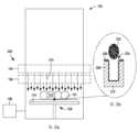
도 1은 본 개시내용의 일부 실시예들에 따른 처리 챔버의 개략적인 단면도를 묘사한다.
도 2a는 본 개시내용의 일부 실시예들에 따른, 도 1의 처리 챔버와 함께 사용하도록 구성되는 전자기 구성의 도면이다.
도 2b는 본 개시내용의 일부 실시예들에 따른, 도 2a의 확대된 세부 영역(2b)이다.
도 3은 본 개시내용의 일부 실시예들에 따른, 기판을 처리하는 방법을 묘사하는 흐름도이다.
이해를 용이하게 하기 위해서, 도면들에 공통된 동일한 요소들을 지정하기 위해 가능한 경우 동일한 참조 번호들이 사용되었다. 도면들은 실척으로 도시되지 않았으며, 명확성을 위해 단순화될 수 있다. 일 실시예의 요소들 및 특징들은 추가적인 언급이 없이도 다른 실시예들에 유익하게 포함될 수 있다.The embodiments of the present disclosure, briefly summarized above and discussed in more detail below, may be understood by reference to the illustrative embodiments of the present disclosure that are illustrated in the appended drawings. It should be noted, however, that the appended drawings illustrate only typical embodiments of the present disclosure and are therefore not to be considered limiting of its scope, for the present disclosure may admit to other equally effective embodiments.
FIG. 1 depicts a schematic cross-sectional view of a processing chamber according to some embodiments of the present disclosure.
FIG. 2A is a diagram of an electromagnetic configuration configured for use with the processing chamber of FIG. 1, according to some embodiments of the present disclosure.
FIG. 2b is an enlarged detailed area (2b) of FIG. 2a, according to some embodiments of the present disclosure.
FIG. 3 is a flowchart depicting a method of processing a substrate according to some embodiments of the present disclosure.
To facilitate understanding, identical reference numerals have been used, where possible, to designate identical elements that are common to the drawings. The drawings are not drawn to scale and may be simplified for clarity. Elements and features of one embodiment may be beneficially incorporated into other embodiments without further recitation.
스텝 커버리지 동안 이온 방향성을 제어하기 위해 물리 기상 증착(PVD) 동안 (EM) 펄싱을 사용하는 방법들 및 장치의 실시예들이 본원에 개시된다. 예컨대, 적어도 일부 실시예들에서, 물리 기상 증착 처리 챔버는, 처리 용적을 정의하는 챔버 몸체, 처리 용적 내에 배치되며 기판을 지지하도록 구성되는 기판 지지 표면을 포함하는 기판 지지부를 포함할 수 있다. 전력 공급부는, 기판을 향해 물질을 스퍼터링하기 위해 타겟을 에너자이징하도록 구성될 수 있다. 전자석은 스퍼터링된 물질을 기판 지지부를 향해 지향시키기 위해 챔버 몸체에 동작가능하게 결합될 수 있고, 제어기는, 기판 상의 피쳐에 대한 이온들의 방향성을 제어하기 위해 동작 동안 전자석을 펄싱하기 위한 펄싱 스케줄을 포함하는 처리법에 기반하여 전자석을 제어하기 위해서 물리 기상 증착 처리 챔버에 동작가능하게 결합될 수 있다.Methods and embodiments of an apparatus using (EM) pulsing during physical vapor deposition (PVD) to control ion directionality during step coverage are disclosed herein. For example, in at least some embodiments, a physical vapor deposition processing chamber can include a chamber body defining a processing volume, a substrate support comprising a substrate support surface disposed within the processing volume and configured to support a substrate. A power supply can be configured to energize a target to sputter material toward the substrate. An electromagnet can be operatively coupled to the chamber body to direct the sputtered material toward the substrate support, and a controller can be operatively coupled to the physical vapor deposition processing chamber to control the electromagnet based on a processing regimen including a pulsing schedule for pulsing the electromagnet during operation to control the directionality of the ions relative to features on the substrate.
본 발명의 방법들 및 장치는 유리하게, PVD 프로세스들(예컨대, 스텝 커버리지)에서 이온들에 대한 더 큰 제어를 제공하고, 그에 따라, 추가로 유리하게, 기판에 있는 피쳐들에서의 증착과 같은 증착 결과들에 대한 제어를 용이하게 한다. 예컨대, 전자기(EM) 펄싱은 기판의 표면에서의 이온들의 교반(agitation)의 결과를 가져올 수 있고, 그에 따라, 이온들이 시스에 접근할 때 입사 이온들의 각도 분포를 효과적으로 넓힐 수 있다. 이에 따라서, 높은 최하부 커버리지 및 낮은 측벽 커버리지를 초래하는 이온들의 수직 방향을 생성하는 시스의 효과가, 제거되지는 않더라도 감소된다.The methods and apparatus of the present invention advantageously provide greater control over the ions in PVD processes (e.g., step coverage), and thus, further advantageously, facilitate control over the deposition results, such as deposition on features in a substrate. For example, electromagnetic (EM) pulsing can result in agitation of the ions at the surface of the substrate, thereby effectively broadening the angular distribution of the incident ions as they approach the sheath. As a result, the sheath effect of creating a vertical orientation of the ions, which results in high bottom coverage and low sidewall coverage, is reduced, if not eliminated.
본 개시내용의 실시예들은, PVD 챔버(또는 다른 플라즈마 처리 챔버)와 관련하여 본원에서 예시적으로 설명된다. 그러나, 본 발명의 방법은, 본원에 개시된 교시들에 따라 수정된 임의의 프로세스 챔버에서 사용될 수 있다. 도 1은, 주어진 직경을 갖는 기판 상에 물질들을 스퍼터 증착하기에 적합한, 본 개시내용의 실시예들에 따른 프로세스 챔버(100), 예컨대 스퍼터 프로세스 챔버를 예시한다. 일부 실시예들에서, PVD 챔버는, 그 PVD 챔버에 배치되고 프로세스 툴 어댑터(138)에 의해 지지되는 시준기(118)를 더 포함한다. 도 1에 예시된 실시예에서, 프로세스 툴 어댑터(138)는 냉각식 프로세스 툴 어댑터이다. 본 개시내용으로부터 이익을 얻도록 적응될 수 있는 적합한 PVD 챔버들의 예시적인 예들은 캘리포니아주 산타클라라의 어플라이드 머티어리얼스 인코포레이티드(Applied Materials, Inc.)로부터 상업적으로 입수가능한 PVD 처리 챔버들을 포함한다. 어플라이드 머티어리얼스 인코포레이티드뿐만 아니라 다른 제조자들로부터 입수가능한 다른 처리 챔버들이 또한 본원에서 설명된 실시예들에 따라 적응될 수 있다.Embodiments of the present disclosure are illustratively described herein in connection with a PVD chamber (or other plasma processing chamber). However, the methods of the present disclosure may be used in any process chamber modified in accordance with the teachings disclosed herein. FIG. 1 illustrates a process chamber (100), such as a sputter process chamber, suitable for sputter depositing materials on a substrate having a given diameter, according to embodiments of the present disclosure. In some embodiments, the PVD chamber further includes a collimator (118) disposed in the PVD chamber and supported by a process tool adapter (138). In the embodiment illustrated in FIG. 1 , the process tool adapter (138) is a cooled process tool adapter. Illustrative examples of suitable PVD chambers that may be adapted to benefit from the present disclosure include PVD processing chambers commercially available from Applied Materials, Inc. of Santa Clara, Calif. Other processing chambers available from Applied Materials, Inc. as well as other manufacturers may also be adapted according to the embodiments described herein.
프로세스 챔버(100)는 일반적으로, 상부 측벽(102)(예컨대, 챔버 몸체), 하부 측벽(103), 접지 어댑터(104), 및 덮개 조립체(111)를 포함하며, 이들은 내부 용적(106)(처리 용적)을 에워싸는 몸체(105)를 정의한다. 내부 용적(106)은, 대략, 처리될 기판의 주어진 직경을 갖는 중앙 부분, 및 중앙 부분을 둘러싸는 주변 부분을 포함한다. 게다가, 내부 용적(106)은 기판 위의 그리고 타겟에 근접한 환형 구역을 포함하며, 여기서, 환형 구역의 내경은 기판의 직경과 실질적으로 동일하거나 그보다 크며, 이에 따라, 플라즈마의 주된 부분이 기판 위 및 기판의 반경방향 외측 둘 모두의 위치에 배치된다.The process chamber (100) generally includes an upper sidewall (102) (e.g., a chamber body), a lower sidewall (103), a ground adapter (104), and a cover assembly (111), which define a body (105) enclosing an interior volume (106) (a processing volume). The interior volume (106) includes a central portion having approximately a given diameter of a substrate to be processed, and a peripheral portion surrounding the central portion. In addition, the interior volume (106) includes an annular region above the substrate and proximate the target, wherein the inner diameter of the annular region is substantially equal to or greater than the diameter of the substrate, such that a major portion of the plasma is located both above the substrate and radially outside the substrate.
어댑터 플레이트(107)는 상부 측벽(102)과 하부 측벽(103) 사이에 배치될 수 있다. 기판 지지부(108)는 프로세스 챔버(100)의 내부 용적(106) 내에 배치된다. 기판 지지부(108)는 기판 지지 표면(119)을 포함하며, 주어진 직경(예컨대, 150 mm, 200 mm, 300 mm, 450 mm 등)을 갖는 기판을 지지하도록 구성된다. 기판 이송 포트(109)는, 기판들을 내부 용적(106) 안팎으로 이송하기 위해 하부 측벽(103)에 형성된다.An adapter plate (107) may be disposed between the upper sidewall (102) and the lower sidewall (103). A substrate support (108) is disposed within the internal volume (106) of the process chamber (100). The substrate support (108) includes a substrate support surface (119) and is configured to support a substrate having a given diameter (e.g., 150 mm, 200 mm, 300 mm, 450 mm, etc.). A substrate transfer port (109) is formed in the lower sidewall (103) for transferring substrates into and out of the internal volume (106).
일부 실시예들에서, 프로세스 챔버(100)는 기판, 이를테면 기판(101) 상에, 예컨대, 티타늄, 산화알루미늄, 알루미늄, 산질화알루미늄, 구리, 탄탈럼, 질화탄탈럼, 산질화탄탈럼, 산질화티타늄, 텅스텐, 또는 질화텅스텐을 증착하도록 구성된다. 적합한 응용들의 비-제한적인 예들은 비아들, 트렌치들, 이중 상감 구조들 등에서의 시드 층 증착을 포함한다.In some embodiments, the process chamber (100) is configured to deposit, for example, titanium, aluminum oxide, aluminum, aluminum oxynitride, copper, tantalum, tantalum nitride, tantalum oxynitride, titanium oxynitride, tungsten, or tungsten nitride on a substrate, such as a substrate (101). Non-limiting examples of suitable applications include seed layer deposition in vias, trenches, dual damascene structures, and the like.
가스 소스(110)는 내부 용적(106) 내로 프로세스 가스들을 공급하기 위해 프로세스 챔버(100)에 결합된다. 일부 실시예들에서, 프로세스 가스들은, 필요한 경우, 불활성 가스들, 비-반응성 가스들, 및 반응성 가스들을 포함할 수 있다. 가스 소스(110)에 의해 제공될 수 있는 프로세스 가스들의 예들은, 다른 것들 중에서도, 아르곤 가스(Ar), 헬륨(He), 네온 가스(Ne), 질소 가스(N2), 산소 가스(O2), 및 물(H2O) 증기를 포함하지만 이에 제한되지 않는다.A gas source (110) is coupled to the process chamber (100) to supply process gases into the internal volume (106). In some embodiments, the process gases may include inert gases, non-reactive gases, and reactive gases, as desired. Examples of process gases that may be provided by the gas source (110) include, but are not limited to, argon gas (Ar), helium (He), neon gas (Ne), nitrogen gas (N2 ), oxygen gas (O2 ), and water (H2 O) vapor, among others.
펌핑 디바이스(112)는, 내부 용적(106)의 압력을 제어하기 위해 내부 용적(106)과 연통하게 프로세스 챔버(100)에 결합된다. 일부 실시예들에서, 증착 동안, 프로세스 챔버(100)의 압력 수준은 약 1 Torr 이하로 유지될 수 있다. 일부 실시예들에서, 프로세스 챔버(100)의 압력 수준은 증착 동안 약 500 mTorr 이하로 유지될 수 있다. 일부 실시예들에서, 프로세스 챔버(100)의 압력 수준은 증착 동안 약 1 mTorr 내지 약 300 mTorr로 유지될 수 있다.The pumping device (112) is coupled to the process chamber (100) in communication with the internal volume (106) to control the pressure of the internal volume (106). In some embodiments, during the deposition, the pressure level of the process chamber (100) can be maintained at about 1 Torr or less. In some embodiments, the pressure level of the process chamber (100) can be maintained at about 500 mTorr or less during the deposition. In some embodiments, the pressure level of the process chamber (100) can be maintained at about 1 mTorr to about 300 mTorr during the deposition.
접지 어댑터(104)는 타겟, 이를테면 타겟(114)을 지지할 수 있다. 타겟(114)은 기판 상에 증착될 물질로 제조된다. 일부 실시예들에서, 타겟(114)은, 티타늄(Ti), 탄탈럼(Ta), 텅스텐(W), 코발트(Co), 니켈(Ni), 구리(Cu), 알루미늄(Al), 이들의 합금들, 이들의 조합물들 등으로 제조될 수 있다. 일부 실시예들에서, 타겟(114)은, 구리(Cu), 티타늄(Ti), 탄탈럼(Ta), 또는 알루미늄(Al)으로 제조될 수 있다.The ground adapter (104) can support a target, such as a target (114). The target (114) is fabricated from a material to be deposited on the substrate. In some embodiments, the target (114) can be fabricated from titanium (Ti), tantalum (Ta), tungsten (W), cobalt (Co), nickel (Ni), copper (Cu), aluminum (Al), alloys thereof, combinations thereof, and the like. In some embodiments, the target (114) can be fabricated from copper (Cu), titanium (Ti), tantalum (Ta), or aluminum (Al).
타겟(114)은, 타겟(114)에 대한 전력 공급부(117)를 포함하는 소스 조립체에 결합될 수 있다. 일부 실시예들에서, 전력 공급부(117)는 매치 네트워크(116)를 통해 타겟(114)에 결합될 수 있는 RF 전력 공급부일 수 있다. 일부 실시예들에서, 전력 공급부(117)는 대안적으로 DC 전원일 수 있으며, 이 경우에, 매치 네트워크(116)는 생략된다. 일부 실시예들에서, 전력 공급부(117)는 DC 전원 및 RF 전원 둘 모두를 포함할 수 있다.The target (114) can be coupled to a source assembly that includes a power supply (117) for the target (114). In some embodiments, the power supply (117) can be an RF power supply that can be coupled to the target (114) via a match network (116). In some embodiments, the power supply (117) can alternatively be a DC power source, in which case the match network (116) is omitted. In some embodiments, the power supply (117) can include both a DC power source and an RF power source.
마그네트론(170)이 타겟(114) 위에 위치된다. 마그네트론(170)은, 프로세스 챔버(100) 및 기판(101)의 중심 축과 축방향으로 정렬될 수 있는 샤프트(176)에 연결된 베이스 플레이트(174)에 의해 지지되는 복수의 자석들(172)을 포함할 수 있다. 자석들(172)이 타겟(114)의 전면 근처에서 프로세스 챔버(100) 내에 자기장을 생성하여 플라즈마를 생성함에 따라 상당한 이온 플럭스가 타겟(114)에 부딪힘으로써, 타겟 물질의 스퍼터 방출이 야기된다. 자석들(172)은, 타겟(114)의 표면에 걸친 자기장의 균일성을 증가시키기 위해 샤프트(176)를 중심으로 회전될 수 있다. 마그네트론의 예들은, 다른 것들 중에서도, 전자기 선형 마그네트론, 사행형(serpentine) 마그네트론, 나선형 마그네트론, 이중-손가락 모양 돌기형(double-digitated) 마그네트론, 직사각형화된(rectangularized) 나선형 마그네트론, 이중 모션 마그네트론을 포함한다. 자석들(172)은, 대략 기판의 외경과 대략 내부 용적(106)의 외경 사이에서 연장되는 환형 구역 내에서 프로세스 챔버(100)의 중심 축을 중심으로 회전된다. 일반적으로, 자석들(172)은, 자석들(172)의 회전 동안의 최내측 자석 위치가 처리되고 있는 기판의 직경 위에 또는 그 외부에 배치되도록 회전될 수 있다(예컨대, 회전 축으로부터 자석들(172)의 최내측 위치까지의 거리는 처리되고 있는 기판의 직경과 동일하거나 그보다 큼).A magnetron (170) is positioned over the target (114). The magnetron (170) may include a plurality of magnets (172) supported by a base plate (174) connected to a shaft (176) that may be axially aligned with the central axis of the process chamber (100) and the substrate (101). As the magnets (172) generate a magnetic field within the process chamber (100) near the front surface of the target (114), a significant ion flux impinges on the target (114), causing sputter emission of target material. The magnets (172) may be rotated about the shaft (176) to increase the uniformity of the magnetic field across the surface of the target (114). Examples of magnetrons include, among others, electromagnetic linear magnetrons, serpentine magnetrons, spiral magnetrons, double-digitated magnetrons, rectangularized spiral magnetrons, and dual motion magnetrons. The magnets (172) are rotated about a central axis of the process chamber (100) within an annular region extending between approximately an outer diameter of the substrate and approximately an outer diameter of the interior volume (106). Typically, the magnets (172) can be rotated such that the innermost magnet positions during rotation of the magnets (172) are positioned above or outside the diameter of the substrate being processed (e.g., the distance from the axis of rotation to the innermost positions of the magnets (172) is equal to or greater than the diameter of the substrate being processed).
마그네트론(170)은, 마그네트론의 자석들이 대략 기판의 외경과 처리 용적의 내경 사이의 환형 구역 내에서 회전되는 임의의 적합한 모션 패턴을 가질 수 있다. 일부 실시예들에서, 마그네트론(170)은, 프로세스 챔버(100)의 중심 축을 중심으로 자석들(172)의 고정된 회전 반경을 갖는다. 일부 실시예들에서, 마그네트론(170)은, 프로세스 챔버(100)의 중심 축을 중심으로 자석들(172)의 다수의 반경들 또는 조정가능한 회전 반경들을 갖도록 구성된다. 예컨대, 일부 실시예들에서, 마그네트론은 (예컨대, 300 mm 기판을 처리하기 위해) 약 5.5 인치 내지 약 7 인치로 조정가능한 회전 반경을 가질 수 있다. 예컨대, 일부 실시예들에서, 마그네트론은, 자석들(172)이 제1 미리 결정된 시간 기간 동안 제1 반경(예컨대, 300 mm 기판들을 처리할 때 약 6.7 인치)으로 그리고 제2 미리 결정된 시간 기간 동안 제2 반경(예컨대, 300 mm 기판들을 처리할 때 약 6.0 인치)으로 회전되는 이중 모션을 갖는다. 일부 실시예들에서, 제1 및 제2 미리 결정된 시간 기간들은 실질적으로 동일하다(예컨대, 마그네트론은 처리 시간의 약 절반 동안 제1 반경으로 그리고 처리 시간의 약 절반 동안 제2 반경으로 회전됨). 일부 실시예들에서, 마그네트론은, 별개의 시간 기간들 동안 이산적으로 설정될 수 있거나 처리 전반에 걸쳐 연속적으로 변하는 복수의 반경들(예컨대, 단지 2개 초과)로 회전할 수 있다.The magnetron (170) can have any suitable motion pattern in which the magnets of the magnetron rotate within an annular region approximately between the outer diameter of the substrate and the inner diameter of the processing volume. In some embodiments, the magnetron (170) has a fixed radius of rotation of the magnets (172) about a central axis of the process chamber (100). In some embodiments, the magnetron (170) is configured to have a plurality of radii or adjustable radii of rotation of the magnets (172) about the central axis of the process chamber (100). For example, in some embodiments, the magnetron can have an adjustable radius of rotation from about 5.5 inches to about 7 inches (e.g., to process 300 mm substrates). For example, in some embodiments, the magnetron has a dual motion in which the magnets (172) are rotated a first radius (e.g., about 6.7 inches when processing 300 mm substrates) for a first predetermined time period and a second radius (e.g., about 6.0 inches when processing 300 mm substrates) for a second predetermined time period. In some embodiments, the first and second predetermined time periods are substantially identical (e.g., the magnetron is rotated at the first radius for about half of the processing time and at the second radius for about half of the processing time). In some embodiments, the magnetron can be rotated at a plurality of radii (e.g., more than just two) that can be discretely set for separate time periods or can vary continuously throughout the processing.
동작 시, 자석들(172)은 타겟(114)을 스퍼터링하기 위해 내부 용적(106)의 환형 부분에 플라즈마(165)를 형성하도록 회전된다. 적어도 일부 실시예들에서, 시준기(118)가 주변 구역(133) 위의 타겟(114)을 스퍼터링하도록 존재할 때, 플라즈마(165)는 시준기의 주변 구역(133) 위에 형성될 수 있다. 본 개시내용에 따른, 적합한 반경 또는 반경들의 범위로 회전하도록 수정될 수 있는 적합한 마그네트론들의 비-제한적인 예들은, 2012년 2월 14일자로 창(Chang) 등에게 허여된 "Control of Arbitrary Scan Path of a Rotating Magnetron"이라는 명칭의 미국 특허 제8,114,256호, 및 2017년 2월 28일자로 밀러(Miller) 등에게 허여된 "Sputter Source for Use in a Semiconductor Process Chamber"라는 명칭의 미국 특허 제9,580,795호에 개시된 마그네트론을 포함한다.In operation, the magnets (172) are rotated to form a plasma (165) in an annular portion of the internal volume (106) to sputter the target (114). In at least some embodiments, when the collimator (118) is present to sputter the target (114) above the peripheral region (133), the plasma (165) may be formed above the peripheral region (133) of the collimator. Non-limiting examples of suitable magnetrons that can be modified to rotate over a suitable radius or range of radii according to the present disclosure include the magnetrons disclosed in U.S. Pat. No. 8,114,256, issued to Chang et al. on Feb. 14, 2012, entitled “Control of Arbitrary Scan Path of a Rotating Magnetron,” and U.S. Pat. No. 9,580,795, issued to Miller et al. on Feb. 28, 2017, entitled “Sputter Source for Use in a Semiconductor Process Chamber.”
프로세스 챔버(100)는 상부 차폐부(113) 및 하부 차폐부(120)를 더 포함한다. 일부 실시예들에서, 시준기(118)는, 내부 용적(106)에서 타겟(114)과 기판 지지부(108) 사이에 위치될 수 있다. 일부 실시예들에서, 시준기(118)는, 두께(T1)를 갖는 중앙 구역(135) 및 T1 미만의 두께(T2)를 갖는 주변 구역(133)을 갖는다. 중앙 구역(135)은 일반적으로, 처리되고 있는 기판의 직경에 대응한다(예컨대, 기판의 직경과 동일하거나 실질적으로 동일함). 그에 따라, 주변 구역(133)은 일반적으로, 처리되고 있는 기판의 반경방향 외측의 환형 구역에 대응한다(예컨대, 주변 구역(133)의 내경은 기판의 직경과 실질적으로 동일하거나 그보다 큼). 대안적으로, 시준기(118)의 중앙 구역은 처리되고 있는 기판의 직경보다 큰 직경을 가질 수 있다. 일부 실시예들에서, 시준기(118)는, 별개의 중앙 구역 및 주변 구역 없이 전체 시준기에 걸쳐 균일한 두께를 가질 수 있다. 시준기(118)는, 임의의 고정 수단을 사용하여 상부 차폐부(113)에 결합된다. 일부 실시예들에서, 시준기(118)는 상부 차폐부(113)와 일체로 형성될 수 있다. 일부 실시예들에서, 시준기(118)는 프로세스 챔버 내의 일부 다른 구성요소에 결합될 수 있고, 상부 차폐부(113)에 대해 제 위치에 있는 것을 도울 수 있다.The process chamber (100) further includes an upper shield (113) and a lower shield (120). In some embodiments, the collimator (118) can be positioned between the target (114) and the substrate support (108) in the internal volume (106). In some embodiments, the collimator (118) has a central region (135) having a thickness (T1 ) and a peripheral region (133) having a thickness (T2 ) less than T1 . The central region (135) generally corresponds to a diameter of the substrate being processed (e.g., equal to or substantially equal to the diameter of the substrate). Accordingly, the peripheral region (133) generally corresponds to an annular region radially outer of the substrate being processed (e.g., an inner diameter of the peripheral region (133) is substantially equal to or greater than the diameter of the substrate). Alternatively, the central region of the collimator (118) may have a diameter larger than the diameter of the substrate being processed. In some embodiments, the collimator (118) may have a uniform thickness across the entire collimator without a separate central region and peripheral region. The collimator (118) is coupled to the upper shield (113) using any securing means. In some embodiments, the collimator (118) may be formed integrally with the upper shield (113). In some embodiments, the collimator (118) may be coupled to some other component within the process chamber to assist in holding it in place relative to the upper shield (113).
일부 실시예들에서, 시준기(118)는, 기판으로의 이온 플럭스 및 기판에서의 중립적(neutral) 각도 분포를 제어할 뿐만 아니라 부가된 DC 바이어스에 기인하여 증착률을 증가시키도록 전기적으로 바이어싱될 수 있다. 시준기를 전기적으로 바이어싱하는 것은 시준기에 대한 감소된 이온 손실의 결과를 가져오며, 이는 유리하게, 기판에서의 더 큰 이온/중성자(neutral) 비들을 제공한다. 시준기(118)의 바이어싱을 용이하게 하기 위해 시준기 전원(도시되지 않음)이 시준기(118)에 결합될 수 있다.In some embodiments, the collimator (118) can be electrically biased to control the ion flux to the substrate and the neutral angular distribution at the substrate, as well as to increase the deposition rate due to the added DC bias. Electrically biasing the collimator results in reduced ion loss to the collimator, which advantageously provides higher ion/neutral ratios at the substrate. A collimator power supply (not shown) can be coupled to the collimator (118) to facilitate biasing of the collimator (118).
일부 실시예들에서, 시준기(118)는, 접지 어댑터(104)와 같은 접지된 챔버 구성요소들로부터 전기적으로 격리될 수 있다. 예컨대, 도 1에 묘사된 바와 같이, 시준기(118)는 상부 차폐부(113)에 결합되며, 이 상부 차폐부는 차례로, 프로세스 툴 어댑터(138)에 결합된다. 프로세스 툴 어댑터(138)는, 프로세스 챔버(100)에서의 처리 조건들과 양립가능한 적합한 전도성 물질들로 만들어질 수 있다. 프로세스 툴 어댑터(138)를 접지 어댑터(104)로부터 전기적으로 격리시키기 위해 프로세스 툴 어댑터(138)의 양 측 상에 절연체 링(156) 및 절연체 링(157)이 배치된다. 절연체 링들(156, 157)은 적합한 프로세스 양립가능 유전체 물질들로 만들어질 수 있다.In some embodiments, the collimator (118) can be electrically isolated from grounded chamber components, such as the ground adapter (104). For example, as depicted in FIG. 1, the collimator (118) is coupled to the upper shield (113), which in turn is coupled to the process tool adapter (138). The process tool adapter (138) can be made of suitable conductive materials that are compatible with the processing conditions in the process chamber (100). An insulator ring (156) and an insulator ring (157) are disposed on opposite sides of the process tool adapter (138) to electrically isolate the process tool adapter (138) from the ground adapter (104). The insulator rings (156, 157) can be made of suitable process compatible dielectric materials.
일부 실시예들에서, 타겟(114)으로부터의 이탈된 이온들을 주변 구역(133)을 통해 안내하도록 자기장을 생성하는 것을 돕기 위해 접지 어댑터(104)에 인접하게 제1 세트의 자석들(196)이 배치될 수 있다. 제1 세트의 자석들(196)에 의해 형성되는 자기장은 대안적으로 또는 조합되어, 이온들이 챔버의 측벽들(또는 상부 차폐부(113)의 측벽들)에 부딪히는 것을 방지하고 이온들을 시준기(118)를 통해 지향시킬 수 있다. 예컨대, 제1 세트의 자석들(196)은 자기장 선들을 갖는 자기장을 주변 부분에 형성하도록 구성된다. 자기장 선들은 유리하게, 내부 용적의 주변 부분을 통해, 그리고 존재할 때, 시준기(118)의 주변 구역(133)을 통해 이온들을 안내한다.In some embodiments, a first set of magnets (196) may be positioned adjacent the ground adapter (104) to help generate a magnetic field to guide ions dislodged from the target (114) through the peripheral region (133). The magnetic field formed by the first set of magnets (196) may alternatively or in combination prevent the ions from striking the sidewalls of the chamber (or the sidewalls of the upper shield (113)) and direct the ions through the collimator (118). For example, the first set of magnets (196) are configured to form a magnetic field having magnetic field lines in the peripheral portion. The magnetic field lines advantageously guide the ions through the peripheral portion of the internal volume and, when present, through the peripheral region (133) of the collimator (118).
일부 실시예들에서, 타겟(114)으로부터 이탈된 금속성 이온들을 안내하고 이온들을 기판(101)에 걸쳐 더 균일하게 분배하도록 기판 및 (사용될 때) 시준기(118)의 최하부 사이에 자기장을 형성하기 위한 위치에 제2 세트의 자석들(194)이 배치될 수 있다. 예컨대, 일부 실시예들에서, 제2 세트의 자석들은 어댑터 플레이트(107)와 상부 측벽(102) 사이에 배치될 수 있다. 예컨대, 제2 세트의 자석들(194)은, 이온들을 기판 상의 피쳐를 향해 안내하는 자기장 선들을 갖는 자기장을 형성하도록 구성된다.In some embodiments, a second set of magnets (194) may be positioned to form a magnetic field between the substrate and the lowermost portion of the collimator (118) (when used) to guide metallic ions displaced from the target (114) and more evenly distribute the ions across the substrate (101). For example, in some embodiments, the second set of magnets may be positioned between the adapter plate (107) and the upper sidewall (102). For example, the second set of magnets (194) are configured to form a magnetic field having magnetic field lines that guide the ions toward features on the substrate.
일부 실시예들에서, 기판(101)의 중심을 향해 금속성 이온들을 추가로 안내하기 위해, 제3 세트의 자석들(154)이 제1 및 제2 세트의 자석들(196, 194) 사이에 그리고 시준기(118)의 중앙 구역(135)의 기판-대면 표면과 거의 중심이 맞춰지게 또는 그 표현 아래에 배치될 수 있다. 예컨대, 제3 세트의 자석들(154)은, 중앙 부분을 향해 그리고 지지 표면의 중심을 향해 내측 및 하향으로 지향되는 자기장 선들을 갖는 자기장을 생성하도록 구성된다.In some embodiments, to further guide the metallic ions toward the center of the substrate (101), a third set of magnets (154) can be positioned between the first and second sets of magnets (196, 194) and approximately centered with or beneath the substrate-facing surface of the central region (135) of the collimator (118). For example, the third set of magnets (154) are configured to generate a magnetic field having magnetic field lines oriented inwardly and downwardly toward the central portion and toward the center of the support surface.
프로세스 챔버(100) 주위에 배치되는 자석들의 수는 플라즈마 해리, 스퍼터링 효율, 및 이온 제어를 제어하도록 선택될 수 있다. 제1, 제2, 및 제3 세트들의 자석들(196, 194, 154)은, 요망되는 궤적을 따라, 타겟으로부터(그리고 일부 실시예들에서는 시준기(118)를 통해) 시스를 통해 그리고 기판 지지부(108) 상의 피쳐를 향해 금속성 이온들을 안내하도록 구성되는 전자석들일 수 있다. 제1, 제2, 및 제3 세트들의 자석들(196, 194, 154)은 고정식이거나 챔버의 중심 축과 평행한 방향으로 자석들의 세트의 위치를 조정하도록 이동가능할 수 있다. 적어도 일부 실시예들에서, 제1, 제2, 및 제3 세트들의 자석들(196, 194, 154) 중 하나 이상은, 요망되는 궤적을 따라, 타겟으로부터(그리고 일부 실시예들에서는 시준기(118)를 통해) 그리고 기판 지지부(108) 상의 피쳐를 향해 금속성 이온들을 안내하는 것을 용이하게 하도록 구성되는 영구 자석들일 수 있다. 제1, 제2, 및 제3 세트들의 자석들(196, 194, 154)의 정확한 구성의 전자석 및 영구 자석들은 사용자 요구들, 플라즈마 프로세스의 유형, 제조자 선호도 등에 기반할 수 있다.The number of magnets arranged around the process chamber (100) can be selected to control plasma dissociation, sputtering efficiency, and ion control. The first, second, and third sets of magnets (196, 194, 154) can be electromagnets configured to guide metallic ions from the target (and in some embodiments through the collimator (118)) through the sheath and toward the feature on the substrate support (108) along a desired trajectory. The first, second, and third sets of magnets (196, 194, 154) can be stationary or can be moveable to adjust the position of the sets of magnets in a direction parallel to the central axis of the chamber. In at least some embodiments, one or more of the first, second, and third sets of magnets (196, 194, 154) can be permanent magnets configured to facilitate guiding metallic ions from the target (and in some embodiments through the collimator (118)) along a desired trajectory and toward a feature on the substrate support (108). The exact configuration of the electromagnets and permanent magnets of the first, second, and third sets of magnets (196, 194, 154) can depend on user requirements, the type of plasma process, manufacturer preferences, and the like.
타겟(114)과 기판 지지부(108) 사이에 바이어스 전력을 제공하기 위해 RF 전원(180)이 기판 지지부(108)를 통해 프로세스 챔버(100)에 결합될 수 있다. 일부 실시예들에서, RF 전원(180)은 약 400 Hz 내지 약 60 MHz, 이를테면 약 13.56 MHz의 주파수를 가질 수 있다. 일부 실시예들에서, 제3 세트의 자석들(154)은 배제될 수 있고, 금속성 이온들을 기판(101)의 중심을 향해 끌어당기는 데 바이어스 전력이 사용될 수 있다.A RF power source (180) may be coupled to the process chamber (100) through the substrate support (108) to provide bias power between the target (114) and the substrate support (108). In some embodiments, the RF power source (180) may have a frequency of about 400 Hz to about 60 MHz, such as about 13.56 MHz. In some embodiments, the third set of magnets (154) may be omitted and the bias power may be used to attract the metallic ions toward the center of the substrate (101).
프로세스 툴 어댑터(138)는, 내부 용적(106) 내에서 프로세스 툴, 이를테면 시준기(118)를 지지하는 것을 용이하게 하기 위한 하나 이상의 피쳐를 포함한다. 예컨대, 도 1에 도시된 바와 같이, 프로세스 툴 어댑터(138)는, 상부 차폐부(113)를 지지하기 위해 반경방향 내측 방향으로 연장되는 장착 링 또는 쉘프(164)를 포함한다. 일부 실시예들에서, 장착 링 또는 쉘프(164)는, 프로세스 툴 어댑터(138)에 장착된 상부 차폐부(113)와의 더 균일한 열 접촉을 용이하게 하기 위한, 프로세스 툴 어댑터(138)의 내경 주위의 연속적인 링이다.The process tool adapter (138) includes one or more features to facilitate supporting a process tool, such as a collimator (118), within the internal volume (106). For example, as illustrated in FIG. 1 , the process tool adapter (138) includes a mounting ring or shelf (164) extending radially inwardly to support the upper shield (113). In some embodiments, the mounting ring or shelf (164) is a continuous ring around the inner diameter of the process tool adapter (138) to facilitate more uniform thermal contact with the upper shield (113) mounted on the process tool adapter (138).
일부 실시예들에서, 처리 동안 생성된 열을 제거하기 위해 프로세스 툴 어댑터(138)를 통해 냉각제를 유동시키는 것을 용이하게 하기 위해서, 냉각제 채널(166)이 프로세스 툴 어댑터(138)에 제공될 수 있다. 예컨대, 냉각제 채널(166)은 적합한 냉각제, 이를테면 물을 제공하기 위해 냉각제 소스(153)에 결합될 수 있다. 냉각제 채널(166)은 유리하게, 접지 어댑터(104)와 같은 다른 냉각식 챔버 구성요소들로 쉽게 전달되지 않는 열을 프로세스 툴(예컨대, 시준기(118))로부터 제거한다. 예컨대, 프로세스 툴 어댑터(138)와 접지 어댑터(104) 사이에 배치되는 절연체 링들(156, 157)은 전형적으로, 불량한 열 전도율을 갖는 물질들로 만들어진다. 그에 따라, 절연체 링들(156, 157)은 시준기(118)로부터 접지 어댑터(104)로의 열 전달률을 감소시키고, 프로세스 툴 어댑터(138)는 유리하게, 시준기(118)의 냉각률을 유지하거나 증가시킨다. 프로세스 툴 어댑터(138)에 제공되는 냉각제 채널(166)에 부가하여, 접지 어댑터(104)가 또한, 처리 동안 생성되는 열을 제거하는 것을 추가로 용이하게 하기 위해 냉각제 채널을 포함할 수 있다.In some embodiments, a coolant channel (166) may be provided in the process tool adapter (138) to facilitate the flow of coolant through the process tool adapter (138) to remove heat generated during processing. For example, the coolant channel (166) may be coupled to a coolant source (153) to provide a suitable coolant, such as water. The coolant channel (166) advantageously removes heat from the process tool (e.g., the collimator (118)) that would otherwise not be readily transferred to other cooled chamber components, such as the grounding adapter (104). For example, insulator rings (156, 157) disposed between the process tool adapter (138) and the grounding adapter (104) are typically made of materials having poor thermal conductivity. Accordingly, the insulator rings (156, 157) reduce the heat transfer rate from the collimator (118) to the grounding adapter (104), and the process tool adapter (138) advantageously maintains or increases the cooling rate of the collimator (118). In addition to the coolant channels (166) provided in the process tool adapter (138), the grounding adapter (104) may also include coolant channels to further facilitate removal of heat generated during processing.
프로세스 챔버(100)의 내부 용적(106) 내의 중앙 개구 내에서 상부 차폐부(113)를 지지하기 위해 반경방향 내측으로 연장되는 렛지(ledge)(예컨대, 장착 링 또는 쉘프(164))가 제공된다. 일부 실시예들에서, 쉘프(164)는, 사용 동안 시준기(118)로부터 냉각제 채널(166) 내에 유동하는 냉각제로의 열 전달을 최대화하는 것을 용이하게 하기 위해 냉각제 채널(166)에 근접한 위치에 배치된다.A ledge (e.g., a mounting ring or shelf (164)) extending radially inwardly is provided to support the upper shield (113) within a central opening within the interior volume (106) of the process chamber (100). In some embodiments, the shelf (164) is positioned proximate the coolant channel (166) to facilitate maximizing heat transfer from the collimator (118) to the coolant flowing within the coolant channel (166) during use.
일부 실시예들에서, 하부 차폐부(120)는 상부 측벽(102) 또는 접지 어댑터(104) 내부에 그리고 시준기(118)에 근접하게 제공될 수 있다. 시준기(118)는, 내부 용적(106) 내에서 가스 및/또는 물질 플럭스를 지향시키기 위한 복수의 애퍼쳐들을 포함한다. 시준기(118)는 프로세스 툴 어댑터(138)를 통해 시준기 전원에 결합될 수 있다.In some embodiments, the lower shield (120) may be provided within the upper sidewall (102) or the ground adapter (104) and proximate the collimator (118). The collimator (118) includes a plurality of apertures for directing a gas and/or material flux within the internal volume (106). The collimator (118) may be coupled to a collimator power source via a process tool adapter (138).
하부 차폐부(120)는 튜브형 몸체(121)를 포함할 수 있으며, 그 튜브형 몸체는, 튜브형 몸체(121)의 상부 표면에 배치된 반경방향 외측으로 연장되는 플랜지(122)를 갖는다. 플랜지(122)는 상부 측벽(102)의 상부 표면과의 짝맞춤 인터페이스를 제공한다. 일부 실시예들에서, 하부 차폐부(120)의 튜브형 몸체(121)는, 튜브형 몸체(121)의 나머지의 내경 미만인 내경을 갖는 숄더 구역(123)을 포함할 수 있다. 일부 실시예들에서, 튜브형 몸체(121)의 내측 표면은, 테이퍼형 표면(124)을 따라 숄더 구역(123)의 내측 표면으로 반경방향 내측으로 전이된다. 프로세스 챔버(100)에서 하부 차폐부(120)에 인접하게 그리고 하부 차폐부(120) 및 어댑터 플레이트(107)의 중간에 차폐 링(126)이 배치될 수 있다. 차폐 링(126)은, 어댑터 플레이트(107)의 내부 측벽 및 하부 차폐부(120)의 숄더 구역(123)의 대향하는 측에 의해 형성되는 함몰부(128) 내에 적어도 부분적으로 배치될 수 있다.The lower shield (120) can include a tubular body (121) having a radially outwardly extending flange (122) disposed on an upper surface of the tubular body (121). The flange (122) provides a mating interface with an upper surface of the upper sidewall (102). In some embodiments, the tubular body (121) of the lower shield (120) can include a shoulder region (123) having an inner diameter less than an inner diameter of the remainder of the tubular body (121). In some embodiments, the inner surface of the tubular body (121) transitions radially inwardly to the inner surface of the shoulder region (123) along a tapered surface (124). A shielding ring (126) may be positioned adjacent to the lower shield (120) in the process chamber (100) and intermediate the lower shield (120) and the adapter plate (107). The shielding ring (126) may be positioned at least partially within a recess (128) formed by an inner side wall of the adapter plate (107) and an opposing side of a shoulder region (123) of the lower shield (120).
일부 실시예들에서, 차폐 링(126)은, 하부 차폐부(120)의 숄더 구역(123)의 외경보다 큰 내경을 갖는 축방향 돌출 환형 측벽(127)을 포함할 수 있다. 반경방향 플랜지(130)가 환형 측벽(127)으로부터 연장된다. 반경방향 플랜지(130)는, 차폐 링(126)의 환형 측벽(127)의 내경 표면에 대해 약 90도(90°)보다 큰 각도로 형성될 수 있다. 반경방향 플랜지(130)는, 반경방향 플랜지(130)의 하부 표면 상에 형성되는 돌출부(132)를 포함한다. 돌출부(132)는, 차폐 링(126)의 환형 측벽(127)의 내경 표면과 실질적으로 평행한 배향으로 반경방향 플랜지(130)의 표면으로부터 연장되는 원형 융기부(ridge)일 수 있다. 돌출부(132)는 일반적으로, 기판 지지부(108) 상에 배치된 에지 링(136)에 형성된 함몰부(134)와 짝맞춤되도록 적응된다. 함몰부(134)는 에지 링(136)에 형성된 원형 홈일 수 있다. 돌출부(132)와 함몰부(134)의 맞물림은 기판 지지부(108)의 길이방향 축에 대해 차폐 링(126)의 중심을 맞춘다. 기판(101)(리프트 핀들(140) 상에 지지된 것으로 도시됨)은 기판 지지부(108)와 로봇 블레이드(도시되지 않음) 사이의 조정된 위치지정 교정에 의해 기판 지지부(108)의 길이방향 축에 대해 중심이 맞춰진다. 그에 따라, 기판(101)은 프로세스 챔버(100) 내에 중심이 맞춰질 수 있고, 차폐 링(126)은 처리 동안 기판(101)을 중심으로 반경방향으로 중심이 맞춰질 수 있다.In some embodiments, the shielding ring (126) can include an axially protruding annular sidewall (127) having an inner diameter greater than an outer diameter of a shoulder region (123) of the lower shielding portion (120). A radial flange (130) extends from the annular sidewall (127). The radial flange (130) can be formed at an angle greater than about ninety degrees (90°) with respect to an inner diameter surface of the annular sidewall (127) of the shielding ring (126). The radial flange (130) includes a protrusion (132) formed on a lower surface of the radial flange (130). The protrusion (132) can be a circular ridge extending from the surface of the radial flange (130) in a substantially parallel orientation with the inner diameter surface of the annular sidewall (127) of the shielding ring (126). The protrusion (132) is generally adapted to mate with a recess (134) formed in an edge ring (136) disposed on the substrate support (108). The recess (134) may be a circular groove formed in the edge ring (136). The engagement of the protrusion (132) and the recess (134) centers the shielding ring (126) relative to the longitudinal axis of the substrate support (108). The substrate (101) (illustrated as supported on the lift pins (140)) is centered relative to the longitudinal axis of the substrate support (108) by the coordinated positioning correction between the substrate support (108) and the robot blade (not shown). Accordingly, the substrate (101) can be centered within the process chamber (100), and the shielding ring (126) can be centered radially about the substrate (101) during processing.
제어기(198)가 프로세스 챔버(100)에 결합된다. 제어기(198)는 중앙 처리 유닛(160), 메모리(158)(비-일시적인 컴퓨터 판독가능 저장 매체), 및 지원 회로들(162)을 포함한다. 제어기(198)는, 가스 소스(110)로부터 프로세스 챔버(100) 내로의 가스 유동들을 조절하고 타겟(114)의 이온 충격을 제어하는 프로세스 시퀀스를 제어하는 데 활용된다. 중앙 처리 유닛(160)은 산업 현장에서 사용될 수 있는 범용 컴퓨터 프로세서의 임의의 형태일 수 있다. 소프트웨어 루틴들은 메모리(158), 이를테면, 랜덤 액세스 메모리, 판독 전용 메모리, 플로피 또는 하드 디스크 드라이브, 또는 다른 형태의 디지털 저장소에 저장될 수 있다. 지원 회로들(162)은 통상적으로 중앙 처리 유닛(160)에 결합되고, 캐시, 클록 회로들, 입력/ 출력 서브시스템들, 전력 공급부들 등을 포함할 수 있다. 소프트웨어 루틴들은, 중앙 처리 유닛(160)에 의해 실행될 때, 중앙 처리 유닛을, 아래에 개시된 플라즈마 점화 프로세스들을 포함하는 프로세스들이 본 개시내용의 실시예들에 따라 수행되도록 프로세스 챔버(100)를 제어하는 특수 목적 컴퓨터(예컨대, 제어기(198))로 변환한다. 소프트웨어 루틴들은 또한, 프로세스 챔버(100)로부터 원격으로 위치되는 제2 제어기(도시되지 않음)에 의해 저장 및/또는 실행될 수 있다.A controller (198) is coupled to the process chamber (100). The controller (198) includes a central processing unit (160), a memory (158) (a non-transitory computer readable storage medium), and support circuits (162). The controller (198) is utilized to control a process sequence that regulates gas flows from a gas source (110) into the process chamber (100) and controls ion bombardment of a target (114). The central processing unit (160) may be any form of general purpose computer processor that can be used in an industrial setting. Software routines may be stored in the memory (158), such as a random access memory, a read-only memory, a floppy or hard disk drive, or other form of digital storage. The support circuits (162) are typically coupled to the central processing unit (160) and may include cache, clock circuits, input/output subsystems, power supplies, etc. The software routines, when executed by the central processing unit (160), transform the central processing unit into a special purpose computer (e.g., a controller (198)) that controls the process chamber (100) such that processes, including the plasma ignition processes described below, are performed in accordance with embodiments of the present disclosure. The software routines may also be stored and/or executed by a second controller (not shown) located remotely from the process chamber (100).
도 2a는 도 1의 처리 챔버와 함께 사용하도록 구성되는 전자기 구성(200)의 도면이고, 도 2b는 도 2a의 확대된 세부 영역(2b)이며, 도 3은 본 개시내용의 일부 실시예들에 따른, 기판을 처리하는 방법(300)을 묘사하는 흐름도이다.FIG. 2a is a drawing of an electromagnetic configuration (200) configured for use with the processing chamber of FIG. 1, FIG. 2b is an enlarged detail area (2b) of FIG. 2a, and FIG. 3 is a flow chart depicting a method (300) of processing a substrate according to some embodiments of the present disclosure.
동작 시, 기판(101)이 자신 상에 배치된 로봇 블레이드(도시되지 않음)가 기판 이송 포트(109)를 통해 연장된다. 기판 지지부(108)는, 기판(101)이 기판 지지부(108)로부터 연장되는 리프트 핀들(140)로 이송될 수 있게 하도록 하강될 수 있다. 기판 지지부(108) 및/또는 리프트 핀들(140)의 상승 및 하강은 기판 지지부(108)에 결합된 드라이브(142)에 의해 제어될 수 있다. 기판(101)은 기판 지지부(108)의 기판 수용 표면(144) 상으로 하강될 수 있다. 기판(101)이 기판 지지부(108)의 기판 수용 표면(144) 상에 위치되어 있는 채로, 기판(101)에 대해 스퍼터 증착이 수행될 수 있다. 적어도 일부 실시예들에서, 스퍼터 증착 동안, 기판 지지부(108)에 배치된 열 제어 채널들(146)을 활용함으로써 기판(101)의 온도가 제어될 수 있다.In operation, a robot blade (not shown) having a substrate (101) positioned thereon extends through a substrate transfer port (109). The substrate support (108) can be lowered to allow the substrate (101) to be transferred to lift pins (140) extending from the substrate support (108). The raising and lowering of the substrate support (108) and/or the lift pins (140) can be controlled by a drive (142) coupled to the substrate support (108). The substrate (101) can be lowered onto a substrate receiving surface (144) of the substrate support (108). Sputter deposition can be performed on the substrate (101) while the substrate (101) remains positioned on the substrate receiving surface (144) of the substrate support (108). In at least some embodiments, the temperature of the substrate (101) can be controlled during sputter deposition by utilizing thermal control channels (146) disposed in the substrate support (108).
처리 동안, 물질이 타겟(114)으로부터 스퍼터링되고 기판(101)의 표면 상에 증착된다. 예컨대, 플라즈마(165)로부터의 이온들이 타겟(114)을 향해 가속되어 그에 부딪힘으로써, 타겟 물질이 타겟(114)으로부터 이탈되게 될 수 있다. 이탈된 타겟 물질 및 프로세스 가스들은 요망되는 조성들로 기판(101) 상에 층을 형성한다. 이에 따라서, 302에서, 방법(300)은, 기판 지지부의 기판 표면 상에 배치된 기판을 향해 물질을 스퍼터링하기 위해 전력 공급부를 사용하여 타겟을 에너자이징하는 단계를 포함한다. 예컨대, 적어도 일부 실시예들에서, 전력 공급부(117)는, 타겟(114)에 전력을 제공하도록 구성되는 DC 전원일 수 있다. 예컨대, DC 전원은, 스퍼터링 동안 타겟(114)에 약 0 kW 내지 약 100 kW를 제공하도록 구성될 수 있다. 적어도 일부 실시예들에서, DC 전원은, 약 1 kW 내지 약 100 kW(예컨대, 약 25 kW)를 제공하도록 구성될 수 있다.During processing, material is sputtered from the target (114) and deposited on the surface of the substrate (101). For example, ions from the plasma (165) may be accelerated toward and collide with the target (114), thereby causing the target material to be ejected from the target (114). The ejected target material and process gases form a layer on the substrate (101) with desired compositions. Accordingly, at 302, the method (300) includes energizing the target using a power supply to sputter the material toward the substrate disposed on the substrate surface of the substrate support. For example, in at least some embodiments, the power supply (117) may be a DC power source configured to provide power to the target (114). For example, the DC power source may be configured to provide from about 0 kW to about 100 kW to the target (114) during sputtering. In at least some embodiments, the DC power source can be configured to provide from about 1 kW to about 100 kW (e.g., about 25 kW).
위에서 언급된 바와 같이, 본 발명의 방법들 및 장치는 유리하게, PVD 프로세스들에서 이온들에 대한 더 큰 제어를 제공한다. 예컨대, EM 펄싱은 기판의 표면에서의 이온들의 교반의 결과를 가져올 수 있고, 그에 따라, 이온들이 시스에 접근할 때 입사 이온들의 각도 분포(202)(예컨대, 도 2b 참조)를 효과적으로 넓힐 수 있다. 이에 따라서, 높은 최하부 커버리지 및 낮은 측벽 커버리지를 초래하는 이온들의 수직 방향을 생성하는 시스의 효과가, 제거되지는 않더라도 감소된다. 적어도 일부 실시예들에서, 방법(300)은, 아래에서 설명되는 바와 같이, 질화탄탈럼(TaN) 스텝 커버리지 개선에 사용될 수 있다.As noted above, the methods and apparatus of the present invention advantageously provide greater control over the ions in PVD processes. For example, EM pulsing can result in stirring of the ions at the surface of the substrate, thereby effectively broadening the angular distribution (202) of the incident ions as they approach the sheath (e.g., see FIG. 2B ). Accordingly, the effect of the sheath creating a vertical orientation of the ions resulting in high bottom coverage and low sidewall coverage is reduced, if not eliminated. In at least some embodiments, the method (300) can be used to improve tantalum nitride (TaN) step coverage, as described below.
이에 따라서, 다음으로, 단계(304)에서, 방법(300)은, 스퍼터링된 물질을 기판을 향해 지향시키기 위해 스퍼터링 동안 전자석을 사용하여 기판 위의 시스를 통해 전자기장 선들을 형성하는 단계를 포함한다. 예컨대, 위에 언급된 바와 같이, 제1 세트의 자석들(196), 제2 세트의 자석들(194), 및/또는 제3 세트의 자석들(154)이 전자석들 또는 영구 자석들로서 구성될 수 있다. 적어도 일부 실시예들에서, 제1 세트의 자석들(196)은 영구 자석으로서 구성될 수 있으며, 요망되는 궤적을 따라 타겟으로부터(그리고 일부 실시예들에서, 시준기(118)가 사용될 때에는 그 시준기를 통해) 기판(101) 상의 피쳐(204)를 향해 금속성 이온들을 안내하는 것을 용이하게 하는 데 사용될 수 있다. 추가로, 제2 세트의 자석들(194)(예컨대, 제1 또는 최하부 자석) 및 제3 세트의 자석들(154)(예컨대, 제2 또는 최상부 자석)은 EM 자석들일 수 있다. 제2 세트의 자석들(194) 및/또는 제3 세트의 자석들(154)은 상부 측벽(102)에 결합될 수 있으며, 스퍼터링된 물질을 기판을 향해 지향시키기 위해 스퍼터링 동안 기판(101) 위의 시스(212)를 통해 전자기장 선들을 형성하도록 위치될 수 있다(예컨대, 도 2b 참조). 적어도 일부 실시예들에서, 제3 세트의 자석들(154)은 제2 세트의 자석들(194) 위에 위치될 수 있고, 제3 세트의 자석들(154) 및 제2 세트의 자석들(194) 각각은 기판(101) 위의 시스(212)를 통해 자기장 선들(214)을 형성할 수 있다.Accordingly, next, in step (304), the method (300) includes forming electromagnetic field lines through the sheath above the substrate using electromagnets during sputtering to direct the sputtered material toward the substrate. For example, as noted above, the first set of magnets (196), the second set of magnets (194), and/or the third set of magnets (154) can be configured as electromagnets or permanent magnets. In at least some embodiments, the first set of magnets (196) can be configured as permanent magnets and can be used to facilitate guiding metallic ions from the target (and in some embodiments, through the collimator (118), when used) along a desired trajectory toward the feature (204) on the substrate (101). Additionally, the second set of magnets (194) (e.g., the first or bottom magnets) and the third set of magnets (154) (e.g., the second or top magnets) can be EM magnets. The second set of magnets (194) and/or the third set of magnets (154) can be coupled to the upper sidewall (102) and positioned to form electromagnetic field lines through the sheath (212) over the substrate (101) during sputtering to direct the sputtered material toward the substrate (e.g., see FIG. 2B ). In at least some embodiments, the third set of magnets (154) can be positioned over the second set of magnets (194), such that each of the third set of magnets (154) and the second set of magnets (194) can form magnetic field lines (214) through the sheath (212) over the substrate (101).
적어도 일부 실시예들에서, 제1 세트의 자석들(196), 제2 세트의 자석들(194), 및/또는 제3 세트의 자석들(154) 중 하나 이상은 처리 챔버(100) 밑에, 기판 지지부 아래에, 또는 처리 챔버(100)를 따른 다른 특정 위치들에 배치될 수 있다.In at least some embodiments, one or more of the first set of magnets (196), the second set of magnets (194), and/or the third set of magnets (154) may be positioned beneath the processing chamber (100), beneath the substrate support, or at other specific locations along the processing chamber (100).
다음으로, 단계(306)에서, 방법(306)은, 기판 상의 피쳐에 대한 이온들의 방향성을 제어하기 위해 동작 동안 전자석을 펄싱하기 위한 펄싱 스케줄을 포함하는 처리법에 기반하여 전자석을 제어하는 단계를 포함한다. 예컨대, 적어도 일부 실시예들에서, 제3 세트의 자석들(154) 및 제2 세트의 자석들(194)에 대한 펄스는 정현파, 비-정현파, 또는 구형파 중 하나일 수 있다. 적어도 일부 실시예들에서, 제어기(198)는, 제3 세트의 자석들(154) 및/또는 제2 세트의 자석들(194)을 제어하기 위해, 메모리(158)에 저장된 처리법을 사용하도록 구성될 수 있다. 예컨대, 펄싱 스케줄에 기반하여, 제어기(195)는 약 -25 A 내지 약 25 A(예컨대, 약 -23.6 A 내지 약 23.6)의 전류를 제3 세트의 자석들(194)에 공급하고 약 -25 A 내지 약 25 A(예컨대, 약 -8.75 A 내지 약 8.75 A)의 전류를 제2 세트의 자석들에 공급하도록 구성될 수 있다. 적어도 일부 실시예들에서, 펄스 동안, 제3 세트의 자석들은 약 -23.6 A 내지 약 -5.6 A, 적어도 일부 실시예들에서는 약 5.6 A 내지 약 23.6 A의 전류를 공급받을 수 있다. 적어도 일부 실시예들에서, 펄스 동안, 제2 세트의 자석들은 약 -8.75 A 내지 약 -0.75 A, 적어도 일부 실시예들에서는 약 0.75 A 내지 약 8.75 A의 전류를 공급받을 수 있다. 부가적으로, 적어도 일부 실시예들에서, 제3 세트의 자석들(154) 및 제2 세트의 자석들(196)에 송신되는 펄스의 주파수는 약 0 Hz 내지 약 2000 Hz(예컨대, 약 0 Hz 내지 약 50 Hz)일 수 있고, 제2 전자석에 송신되는 펄스의 주파수는 약 0 Hz 내지 약 2000 Hz(예컨대, 약 2 Hz 내지 약 50 Hz)이다. 본 발명자들은, 본원에서 설명된 펄싱 방식들을 사용하여 TaN 스텝 커버리지 동안 이온 방향성을 제어하는 것이 비교적 낮은 k의 손상으로 측벽 커버리지 대 최하부 커버리지의 비 및 오버행을 개선한다는 것을 알게 되었다.Next, at step (306), the method (306) includes controlling the electromagnets based on a processing regimen including a pulsing schedule for pulsing the electromagnets during the operation to control the directionality of the ions relative to the features on the substrate. For example, in at least some embodiments, the pulses for the third set of magnets (154) and the second set of magnets (194) can be one of sinusoidal, non-sinusoidal, or square wave. In at least some embodiments, the controller (198) can be configured to use the processing regimen stored in the memory (158) to control the third set of magnets (154) and/or the second set of magnets (194). For example, based on the pulsing schedule, the controller (195) can be configured to supply a current of about -25 A to about 25 A (e.g., about -23.6 A to about 23.6) to the third set of magnets (194) and a current of about -25 A to about 25 A (e.g., about -8.75 A to about 8.75 A) to the second set of magnets. In at least some embodiments, during a pulse, the third set of magnets can be supplied with a current of about -23.6 A to about -5.6 A, and in at least some embodiments, from about 5.6 A to about 23.6 A. In at least some embodiments, during a pulse, the second set of magnets can be supplied with a current of about -8.75 A to about -0.75 A, and in at least some embodiments, from about 0.75 A to about 8.75 A. Additionally, in at least some embodiments, the frequency of the pulses transmitted to the third set of magnets (154) and the second set of magnets (196) can be from about 0 Hz to about 2000 Hz (e.g., from about 0 Hz to about 50 Hz), and the frequency of the pulses transmitted to the second electromagnet can be from about 0 Hz to about 2000 Hz (e.g., from about 2 Hz to about 50 Hz). The inventors have found that controlling ion directionality during TaN step coverage using the pulsing schemes described herein improves the ratio of sidewall coverage to bottom coverage and overhang with relatively low k damage.
적어도 일부 실시예들에서, 방법(300)은, 기판 지지부에 AC 바이어스 전력을 제공하는 단계를 포함할 수 있다. 예컨대, 타겟(114) 및 기판 지지부(108)는, 가스 소스(110)에 의해 공급된 프로세스 가스들로부터 형성되는 플라즈마를 유지하기 위해 전력 공급부(117) 및/또는 RF 전원(180)에 의해 서로에 대해 바이어싱될 수 있다. 부가적으로, 일부 실시예들에서, (사용될 때) 시준기(118)를 통과하는 이온들 및 중성자들의 비를 제어하는 것을 보조하기 위해 DC 펄스형 바이어스 전력이 시준기(118)에 인가될 수 있으며, 이는 유리하게, 트렌치 측벽 및 최하부 충전(fill-up) 능력을 향상시킨다. 그에 따라, 방법(300)은, 기판 지지부(108)의 중심 또는 기판 지지부(108)의 에지 중 적어도 하나에서 AC 바이어스 전력을 제공하는 단계를 포함할 수 있다. 적어도 일부 실시예들에서, AC 바이어스 전력은 약 영(zero) W 내지 약 1000 W(예컨대, 약 영 W 내지 약 150 W)일 수 있다.In at least some embodiments, the method (300) may include providing AC bias power to the substrate support. For example, the target (114) and the substrate support (108) may be biased relative to each other by the power supply (117) and/or the RF power source (180) to maintain a plasma formed from process gases supplied by the gas source (110). Additionally, in some embodiments, a DC pulsed bias power may be applied to the collimator (118) to assist in controlling the ratio of ions and neutrals passing through the collimator (118) (when used), which advantageously enhances trench sidewall and bottom fill-up capabilities. Accordingly, the method (300) may include providing AC bias power at at least one of the center of the substrate support (108) or an edge of the substrate support (108). In at least some embodiments, the AC bias power can be from about zero W to about 1000 W (e.g., from about zero W to about 150 W).
306 이후, AC 바이어스 전력 없이 피쳐(204)의 측벽(208) 및 피쳐(204)의 최하부(210) 상에 증착되는 스퍼터링된 물질(206)의 비는 약 0.65 내지 약 0.67이고, AC 바이어스 전력을 이용하여 기판 상의 피쳐의 측벽 및 최하부 상에 증착되는 스퍼터링된 물질의 비는 약 0.36 내지 약 0.38이다. 즉, 통상의 방법들 및 장치와 비교하여, 본원에서 설명된 방법들 및 장치는, 높은 최하부 커버리지 및 낮은 측벽 커버리지를 초래할 수 있는 이온들의 수직 방향을 생성하는 시스의 효과를 제거하지는 않더라도 감소시킨다(예컨대, 도 2a를 참조하며, 이는, 이온들의 요망되는 각도 분포(202) 및 측벽(208) 및 최하부(210) 상의 스퍼터링된 물질의 커버리지를 도시함). 적어도 일부 실시예들에서, 본원에서 설명된 방법들 및 장치는, 펄싱이 없는 것과 비교하여, 펄싱을 이용하여, 최하부 커버리지보다 약 30 % 더 많은 측벽 커버리지를 제공할 수 있다.After 306, the ratio of sputtered material (206) deposited on the sidewalls (208) of the feature (204) and the bottom (210) of the feature (204) without AC bias power is about 0.65 to about 0.67, and the ratio of sputtered material deposited on the sidewalls and the bottom (210) of the feature on the substrate with AC bias power is about 0.36 to about 0.38. That is, compared to conventional methods and apparatus, the methods and apparatus described herein reduce, if not eliminate, the effect of the sheath that creates a vertical orientation of ions that can result in high bottom coverage and low sidewall coverage (see, e.g., FIG. 2A , which illustrates a desired angular distribution of ions (202) and coverage of sputtered material on the sidewalls (208) and the bottom (210). In at least some embodiments, the methods and devices described herein can provide about 30% more sidewall coverage than bottom coverage using pulsing as compared to no pulsing.
스퍼터 증착 이후에, 기판(101)은, 리프트 핀들(140)을 활용하여, 기판 지지부(108)로부터 이격되는 위치로 상승될 수 있다. 상승된 위치는, 어댑터 플레이트(107)에 인접한 반사기 링(148) 및 차폐 링(126) 중 하나 또는 둘 모두에 근접할 수 있다. 어댑터 플레이트(107)는, 어댑터 플레이트(107)의 오목한 표면(152)과 반사기 링(148)의 하부 표면의 중간의 위치에서 어댑터 플레이트(107)에 결합되는 하나 이상의 램프(150)를 포함한다. 램프들(150)은 가시 파장 또는 가시 파장 근처, 이를테면, 적외선(IR) 및/또는 자외선(UV) 스펙트럼의 광학 및/또는 방사 에너지를 제공한다. 램프들(150)로부터의 에너지는 기판(101)의 후면측(예컨대, 하부 표면)을 향하여 반경방향 내측으로 포커싱되어 기판(101) 및 그 기판 상의 증착된 물질을 가열한다. 기판(101)을 둘러싸는 챔버 구성요소들 상의 반사성 표면들은, 에너지를 기판(101)의 후면측을 향해 그리고 에너지가 손실되고/거나 활용되지 않을 다른 챔버 구성요소들로부터 멀어지게 포커싱하도록 기능한다. 어댑터 플레이트(107)는 가열 동안 어댑터 플레이트(107)의 온도를 제어하기 위해 냉각제 소스(153)에 결합될 수 있다.After sputter deposition, the substrate (101) can be raised to a position away from the substrate support (108) utilizing the lift pins (140). The raised position can be proximate one or both of the reflector ring (148) and the shielding ring (126) adjacent the adapter plate (107). The adapter plate (107) includes one or more lamps (150) coupled to the adapter plate (107) at a position intermediate the concave surface (152) of the adapter plate (107) and the lower surface of the reflector ring (148). The lamps (150) provide optical and/or radiant energy in the visible or near visible wavelengths, such as the infrared (IR) and/or ultraviolet (UV) spectrum. Energy from the lamps (150) is focused radially inward toward the backside (e.g., the lower surface) of the substrate (101) to heat the substrate (101) and deposited material thereon. The reflective surfaces on the chamber components surrounding the substrate (101) function to focus the energy toward the backside of the substrate (101) and away from other chamber components where the energy would be lost and/or unutilized. The adapter plate (107) may be coupled to a coolant source (153) to control the temperature of the adapter plate (107) during heating.
기판(101)을 미리 결정된 온도로 제어한 후에, 기판(101)은 기판 지지부(108)의 기판 수용 표면(144) 상의 위치로 하강된다. 기판(101)은, 기판 지지부(108)의 열 제어 채널들(146)을 활용하여 전도를 통해 급속하게 냉각될 수 있다. 기판(101)의 온도는 수 초 내지 약 1분 내에 제1 온도로부터 제2 온도로 램핑 다운될 수 있다. 기판(101)은, 추가적인 처리를 위해 기판 이송 포트(109)를 통해 프로세스 챔버(100)로부터 제거될 수 있다. 기판(101)은, 미리 결정된 온도 범위, 이를테면 섭씨 250도 미만으로 유지될 수 있다.After the substrate (101) is controlled to a predetermined temperature, the substrate (101) is lowered to a position on the substrate receiving surface (144) of the substrate support (108). The substrate (101) can be rapidly cooled via conduction utilizing the thermal control channels (146) of the substrate support (108). The temperature of the substrate (101) can be ramped down from the first temperature to the second temperature within several seconds to about one minute. The substrate (101) can be removed from the process chamber (100) via the substrate transfer port (109) for further processing. The substrate (101) can be maintained at a predetermined temperature range, such as less than 250 degrees Celsius.
그 후, 기판(101)은 로봇 블레이드를 통해 기판 이송 포트(109)를 통해서 연장될 수 있다.Thereafter, the substrate (101) can be extended through the substrate transfer port (109) via the robot blade.
전술한 내용들이 본 개시내용의 실시예들에 관한 것이지만, 본 개시내용의 다른 그리고 추가적인 실시예들이 그의 기본적인 범위로부터 벗어나지 않으면서 안출될 수 있다.While the foregoing is directed to embodiments of the present disclosure, other and additional embodiments of the present disclosure may be devised without departing from the basic scope thereof.
Claims (20)
Translated fromKorean처리 용적을 정의하는 챔버 몸체;
상기 처리 용적 내에 배치되며 기판을 지지하도록 구성되는 기판 지지 표면을 포함하는 기판 지지부;
상기 기판을 향해 물질을 스퍼터링하기 위해 타겟을 에너자이징(energize)하도록 구성되는 전력 공급부;
상기 챔버 몸체에 동작가능하게 결합되고, 스퍼터링된 물질을 상기 기판을 향해 지향시키기 위해 스퍼터링 동안 상기 기판 위의 시스(sheath)를 통해 전자기장 선들을 형성하도록 위치되는 전자석; 및
상기 기판 상의 피쳐에 대한 이온들의 방향성을 제어하기 위해 동작 동안 상기 전자석을 펄싱하기 위한 펄싱 스케줄을 포함하는 처리법에 기반하여 상기 전자석을 제어하기 위한, 상기 물리 기상 증착 처리 챔버에 동작가능하게 결합되는 제어기
를 포함하는, 물리 기상 증착 처리 챔버.As a physical vapor deposition treatment chamber,
A chamber body defining the processing volume;
A substrate support comprising a substrate support surface disposed within the processing volume and configured to support a substrate;
A power supply configured to energize a target to sputter material toward the substrate;
an electromagnet operably coupled to the chamber body and positioned to form electromagnetic field lines through the sheath over the substrate during sputtering to direct the sputtered material toward the substrate; and
A controller operatively coupled to the physical vapor deposition processing chamber for controlling the electromagnet based on a processing method including a pulsing schedule for pulsing the electromagnet during operation to control the directionality of ions relative to features on the substrate.
A physical vapor deposition treatment chamber comprising:
상기 기판 지지부에 AC 바이어스 전력을 제공하도록 구성되는 RF 전원을 더 포함하는, 물리 기상 증착 처리 챔버.In the first paragraph,
A physical vapor deposition processing chamber further comprising an RF power source configured to provide AC bias power to the substrate support.
상기 AC 바이어스 전력은 상기 기판 지지부의 중심 또는 상기 기판 지지부의 에지 중 적어도 하나에서 제공되며, 영(zero)보다 크고 최대 약 1000 W인, 물리 기상 증착 처리 챔버.In paragraph 1 or 2,
A physical vapor deposition processing chamber, wherein the AC bias power is provided at least at the center of the substrate support or at an edge of the substrate support and is greater than zero and up to about 1000 W.
AC 바이어스 전력 없이 상기 피쳐의 측벽 및 상기 피쳐의 최하부 상에 증착되는 스퍼터링된 물질의 비는 약 0.65 내지 약 0.67이고, 상기 AC 바이어스 전력을 이용하여 상기 기판 상의 상기 피쳐의 측벽 및 최하부 상에 증착되는 스퍼터링된 물질의 비는 약 0.36 내지 약 0.38인, 물리 기상 증착 처리 챔버.In paragraph 1 or 2,
A physical vapor deposition processing chamber, wherein a ratio of sputtered material deposited on the sidewalls and the bottom of the feature without AC bias power is about 0.65 to about 0.67, and wherein a ratio of sputtered material deposited on the sidewalls and the bottom of the feature on the substrate with AC bias power is about 0.36 to about 0.38.
상기 전력 공급부는, 스퍼터링 동안 상기 타겟에 약 영 내지 약 100 kW를 제공하도록 구성되는 DC 전원인, 물리 기상 증착 처리 챔버.In the first paragraph,
A physical vapor deposition processing chamber, wherein the power supply unit is a DC power source configured to provide about 0 to about 100 kW to the target during sputtering.
상기 전자석 아래에 배치되는 제2 전자석을 더 포함하는, 물리 기상 증착 처리 챔버.In the first paragraph,
A physical vapor deposition treatment chamber further comprising a second electromagnet disposed below the electromagnet.
상기 펄싱 스케줄은, 상기 전자석에 약 -25 A 내지 약 25 A의 전류를 공급하고 제2 전자석에 약 -25 A 내지 약 25 A의 전류를 공급하는, 물리 기상 증착 처리 챔버.In any one of paragraphs 1, 2, 5, and 6,
A physical vapor deposition processing chamber wherein the above pulsing schedule supplies a current of about -25 A to about 25 A to the electromagnet and a current of about -25 A to about 25 A to the second electromagnet.
상기 전자석에 대한 펄스의 주파수는 약 0 Hz 내지 약 2000 Hz이고, 제2 전자석에 대한 펄스의 주파수는 약 0 Hz 내지 약 2000 Hz인, 물리 기상 증착 처리 챔버.In any one of paragraphs 1, 2, 5, and 6,
A physical vapor deposition treatment chamber, wherein the frequency of the pulses for the above electromagnet is from about 0 Hz to about 2000 Hz, and the frequency of the pulses for the second electromagnet is from about 0 Hz to about 2000 Hz.
상기 펄싱 스케줄은 정현파, 비-정현파, 또는 구형파 중 하나로 상기 전자석에 송신될 복수의 펄스들을 포함하는, 물리 기상 증착 처리 챔버.In any one of paragraphs 1, 2, 5 and 6,
A physical vapor deposition processing chamber, wherein the pulsing schedule comprises a plurality of pulses to be transmitted to the electromagnet as either a sinusoidal, non-sinusoidal, or square wave.
기판 지지부의 기판 표면 상에 배치된 기판을 향해 물질을 스퍼터링하기 위해 전력 공급부를 사용하여 타겟을 에너자이징하는 단계;
스퍼터링된 물질을 상기 기판을 향해 지향시키기 위해 스퍼터링 동안 전자석을 사용하여 상기 기판 위의 시스를 통해 전자기장 선들을 형성하는 단계; 및
상기 기판 상의 피쳐에 대한 이온들의 방향성을 제어하기 위해 동작 동안 상기 전자석을 펄싱하기 위한 펄싱 스케줄을 포함하는 처리법에 기반하여 상기 전자석을 제어하는 단계
를 포함하는, 방법.A method for performing physical vapor deposition,
A step of energizing a target using a power supply to sputter a material toward a substrate disposed on a substrate surface of a substrate support;
A step of forming electromagnetic field lines through the sheath over the substrate using an electromagnet during sputtering to direct the sputtered material toward the substrate; and
A step of controlling the electromagnet based on a processing method including a pulsing schedule for pulsing the electromagnet during operation to control the directionality of ions with respect to features on the substrate.
A method comprising:
상기 기판 지지부에 AC 바이어스 전력을 제공하는 단계를 더 포함하는, 방법.In Article 10,
A method further comprising the step of providing AC bias power to the substrate support.
상기 기판 지지부의 중심 또는 상기 기판 지지부의 에지 중 적어도 하나에 영 초과 내지 약 1000 W의 AC 바이어스 전력을 제공하는 단계를 더 포함하는, 방법.In clause 10 or 11,
A method further comprising the step of providing an AC bias power of greater than or equal to about 1000 W to at least one of the center of the substrate support or an edge of the substrate support.
AC 바이어스 전력 없이 상기 피쳐의 측벽 및 상기 피쳐의 최하부 상에 증착되는 스퍼터링된 물질의 비는 약 0.65 내지 약 0.67이고, 상기 AC 바이어스 전력을 이용하여 상기 기판 상의 상기 피쳐의 측벽 및 최하부 상에 증착되는 스퍼터링된 물질의 비는 약 0.36 내지 약 0.38인, 방법.In clause 10 or 11,
A method wherein a ratio of sputtered material deposited on the sidewalls and the bottom of the feature without AC bias power is about 0.65 to about 0.67, and wherein a ratio of sputtered material deposited on the sidewalls and the bottom of the feature on the substrate with AC bias power is about 0.36 to about 0.38.
상기 전력 공급부는, 스퍼터링 동안 상기 타겟에 약 1 kW 내지 약 100 kW를 제공하도록 구성되는 DC 전원인, 방법.In Article 10,
A method according to claim 1, wherein the power supply is a DC power source configured to provide about 1 kW to about 100 kW to the target during sputtering.
상기 전자석 아래에 배치되는 제2 전자석을 제공하는 단계를 더 포함하는, 방법.In Article 10,
A method further comprising the step of providing a second electromagnet disposed below the electromagnet.
상기 전자석에 약 -25 A 내지 약 25 A의 전류를 공급하고 제2 전자석에 약 -25 A 내지 약 25 A의 전류를 공급하는 단계를 더 포함하는, 방법.In any one of Articles 10, 11, 14, and 15,
A method further comprising the step of supplying a current of about -25 A to about 25 A to the electromagnet and supplying a current of about -25 A to about 25 A to the second electromagnet.
상기 전자석에 대한 펄스의 주파수는 약 0 Hz 내지 약 2000 Hz이고, 제2 전자석에 대한 펄스의 주파수는 약 0 Hz 내지 약 2000 Hz인, 방법.In any one of Articles 10, 11, 14, and 15,
A method wherein the frequency of the pulses for the above electromagnet is from about 0 Hz to about 2000 Hz, and the frequency of the pulses for the second electromagnet is from about 0 Hz to about 2000 Hz.
상기 펄싱 스케줄은 정현파, 비-정현파, 또는 구형파 중 하나로 상기 전자석에 송신될 복수의 펄스들을 포함하는, 방법.In any one of Articles 10, 11, 14 and 15,
A method wherein the pulsing schedule comprises a plurality of pulses to be transmitted to the electromagnet as either a sinusoidal wave, a non-sinusoidal wave, or a square wave.
상기 명령어들은, 프로세서에 의해 실행될 때, 물리 기상 증착을 수행하기 위한 방법을 수행하며, 상기 방법은,
기판 지지부의 기판 표면 상에 배치된 기판을 향해 물질을 스퍼터링하기 위해 전력 공급부를 사용하여 타겟을 에너자이징하는 것;
스퍼터링된 물질을 상기 기판을 향해 지향시키기 위해 스퍼터링 동안 전자석을 사용하여 상기 기판 위의 시스를 통해 전자기장 선들을 형성하는 것; 및
상기 기판 상의 피쳐에 대한 이온들의 방향성을 제어하기 위해 동작 동안 상기 전자석을 펄싱하기 위한 펄싱 스케줄을 포함하는 처리법에 기반하여 상기 전자석을 제어하는 것
을 포함하는, 비-일시적인 컴퓨터 판독가능 저장 매체.A non-transitory computer-readable storage medium having instructions stored thereon,
The above instructions, when executed by a processor, perform a method for performing physical vapor deposition, the method comprising:
Energizing a target using a power supply to sputter material toward a substrate disposed on a substrate surface of a substrate support;
Forming electromagnetic field lines through the sheath over the substrate using an electromagnet during sputtering to direct the sputtered material toward the substrate; and
Controlling said electromagnet based on a processing method including a pulsing schedule for pulsing said electromagnet during operation to control the directionality of ions with respect to features on said substrate.
A non-transitory computer-readable storage medium comprising:
상기 기판 지지부에 AC 바이어스 전력을 제공하는 것을 더 포함하는, 비-일시적인 컴퓨터 판독가능 저장 매체.In Article 19,
A non-transitory computer-readable storage medium further comprising providing AC bias power to the substrate support.
Applications Claiming Priority (5)
| Application Number | Priority Date | Filing Date | Title |
|---|---|---|---|
| US202263324944P | 2022-03-29 | 2022-03-29 | |
| US63/324,944 | 2022-03-29 | ||
| US17/737,361 | 2022-05-05 | ||
| US17/737,361US11952655B2 (en) | 2022-03-29 | 2022-05-05 | Electromagnet pulsing effect on PVD step coverage |
| PCT/US2022/036071WO2023191835A1 (en) | 2022-03-29 | 2022-07-05 | Electromagnet pulsing effect on pvd step coverage |
Publications (1)
| Publication Number | Publication Date |
|---|---|
| KR20240169080Atrue KR20240169080A (en) | 2024-12-02 |
Family
ID=88194930
Family Applications (1)
| Application Number | Title | Priority Date | Filing Date |
|---|---|---|---|
| KR1020247036089APendingKR20240169080A (en) | 2022-03-29 | 2022-07-05 | Effect of electromagnetic pulsing on PVD step coverage |
Country Status (4)
| Country | Link |
|---|---|
| US (1) | US11952655B2 (en) |
| KR (1) | KR20240169080A (en) |
| TW (1) | TW202338128A (en) |
| WO (1) | WO2023191835A1 (en) |
Families Citing this family (1)
| Publication number | Priority date | Publication date | Assignee | Title |
|---|---|---|---|---|
| US20250101575A1 (en)* | 2023-09-22 | 2025-03-27 | Applied Materials, Inc. | Methods for Depositing Film Layers |
Family Cites Families (11)
| Publication number | Priority date | Publication date | Assignee | Title |
|---|---|---|---|---|
| US6368469B1 (en) | 1996-05-09 | 2002-04-09 | Applied Materials, Inc. | Coils for generating a plasma and for sputtering |
| US6579421B1 (en) | 1999-01-07 | 2003-06-17 | Applied Materials, Inc. | Transverse magnetic field for ionized sputter deposition |
| US6344419B1 (en)* | 1999-12-03 | 2002-02-05 | Applied Materials, Inc. | Pulsed-mode RF bias for sidewall coverage improvement |
| US6488822B1 (en) | 2000-10-20 | 2002-12-03 | Veecoleve, Inc. | Segmented-target ionized physical-vapor deposition apparatus and method of operation |
| US6440831B1 (en) | 2000-12-06 | 2002-08-27 | Koninklijke Philips Electronics N.V. | Ionized metal plasma deposition process having enhanced via sidewall coverage |
| US7504006B2 (en)* | 2002-08-01 | 2009-03-17 | Applied Materials, Inc. | Self-ionized and capacitively-coupled plasma for sputtering and resputtering |
| US7556718B2 (en) | 2004-06-22 | 2009-07-07 | Tokyo Electron Limited | Highly ionized PVD with moving magnetic field envelope for uniform coverage of feature structure and wafer |
| US20110011737A1 (en) | 2009-07-17 | 2011-01-20 | Institute Of Nuclear Energy Research Atomic Energy Council, Executive Yuan | High-power pulse magnetron sputtering apparatus and surface treatment apparatus using the same |
| JP2016526271A (en) | 2013-06-07 | 2016-09-01 | マイクロマス ユーケー リミテッド | Electric field generation method for manipulating charged particles |
| KR102383703B1 (en) | 2016-03-05 | 2022-04-08 | 어플라이드 머티어리얼스, 인코포레이티드 | Methods and apparatus for controlling ion fraction in physical vapor deposition processes |
| US10312065B2 (en) | 2016-07-20 | 2019-06-04 | Applied Materials, Inc. | Physical vapor deposition (PVD) plasma energy control per dynamic magnetron control |
- 2022
- 2022-05-05USUS17/737,361patent/US11952655B2/enactiveActive
- 2022-07-01TWTW111124684Apatent/TW202338128A/enunknown
- 2022-07-05KRKR1020247036089Apatent/KR20240169080A/enactivePending
- 2022-07-05WOPCT/US2022/036071patent/WO2023191835A1/ennot_activeCeased
Also Published As
| Publication number | Publication date |
|---|---|
| US20230313364A1 (en) | 2023-10-05 |
| US11952655B2 (en) | 2024-04-09 |
| WO2023191835A1 (en) | 2023-10-05 |
| TW202338128A (en) | 2023-10-01 |
Similar Documents
| Publication | Publication Date | Title |
|---|---|---|
| US12094699B2 (en) | Methods and apparatus for controlling ion fraction in physical vapor deposition processes | |
| US10312065B2 (en) | Physical vapor deposition (PVD) plasma energy control per dynamic magnetron control | |
| US9953813B2 (en) | Methods and apparatus for improved metal ion filtering | |
| US10157733B2 (en) | Methods for igniting a plasma in a substrate processing chamber | |
| US11952655B2 (en) | Electromagnet pulsing effect on PVD step coverage | |
| US20230017383A1 (en) | Methods and apparatus for processing a substrate | |
| US20240384396A1 (en) | Biased or floating process shield to reduce ion loss to control film deposition and improve step coverage | |
| US11784033B2 (en) | Methods and apparatus for processing a substrate |
Legal Events
| Date | Code | Title | Description |
|---|---|---|---|
| PA0105 | International application | Patent event date:20241029 Patent event code:PA01051R01D Comment text:International Patent Application | |
| PG1501 | Laying open of application |