KR20240155458A - Semiconductor memory device - Google Patents
Semiconductor memory deviceDownload PDFInfo
- Publication number
- KR20240155458A KR20240155458AKR1020230051746AKR20230051746AKR20240155458AKR 20240155458 AKR20240155458 AKR 20240155458AKR 1020230051746 AKR1020230051746 AKR 1020230051746AKR 20230051746 AKR20230051746 AKR 20230051746AKR 20240155458 AKR20240155458 AKR 20240155458A
- Authority
- KR
- South Korea
- Prior art keywords
- contact
- bit line
- region
- memory device
- semiconductor memory
- Prior art date
- Legal status (The legal status is an assumption and is not a legal conclusion. Google has not performed a legal analysis and makes no representation as to the accuracy of the status listed.)
- Pending
Links
Images


Classifications
- H—ELECTRICITY
- H10—SEMICONDUCTOR DEVICES; ELECTRIC SOLID-STATE DEVICES NOT OTHERWISE PROVIDED FOR
- H10B—ELECTRONIC MEMORY DEVICES
- H10B12/00—Dynamic random access memory [DRAM] devices
- H10B12/30—DRAM devices comprising one-transistor - one-capacitor [1T-1C] memory cells
- H10B12/31—DRAM devices comprising one-transistor - one-capacitor [1T-1C] memory cells having a storage electrode stacked over the transistor
- H10B12/315—DRAM devices comprising one-transistor - one-capacitor [1T-1C] memory cells having a storage electrode stacked over the transistor with the capacitor higher than a bit line
- H—ELECTRICITY
- H10—SEMICONDUCTOR DEVICES; ELECTRIC SOLID-STATE DEVICES NOT OTHERWISE PROVIDED FOR
- H10B—ELECTRONIC MEMORY DEVICES
- H10B12/00—Dynamic random access memory [DRAM] devices
- H10B12/30—DRAM devices comprising one-transistor - one-capacitor [1T-1C] memory cells
- H10B12/48—Data lines or contacts therefor
- H10B12/482—Bit lines
- H—ELECTRICITY
- H10—SEMICONDUCTOR DEVICES; ELECTRIC SOLID-STATE DEVICES NOT OTHERWISE PROVIDED FOR
- H10B—ELECTRONIC MEMORY DEVICES
- H10B12/00—Dynamic random access memory [DRAM] devices
- H10B12/01—Manufacture or treatment
- H10B12/02—Manufacture or treatment for one transistor one-capacitor [1T-1C] memory cells
- H10B12/03—Making the capacitor or connections thereto
- H10B12/033—Making the capacitor or connections thereto the capacitor extending over the transistor
- H10B12/0335—Making a connection between the transistor and the capacitor, e.g. plug
- H—ELECTRICITY
- H10—SEMICONDUCTOR DEVICES; ELECTRIC SOLID-STATE DEVICES NOT OTHERWISE PROVIDED FOR
- H10B—ELECTRONIC MEMORY DEVICES
- H10B12/00—Dynamic random access memory [DRAM] devices
- H10B12/01—Manufacture or treatment
- H10B12/02—Manufacture or treatment for one transistor one-capacitor [1T-1C] memory cells
- H10B12/05—Making the transistor
- H10B12/053—Making the transistor the transistor being at least partially in a trench in the substrate
- H—ELECTRICITY
- H10—SEMICONDUCTOR DEVICES; ELECTRIC SOLID-STATE DEVICES NOT OTHERWISE PROVIDED FOR
- H10B—ELECTRONIC MEMORY DEVICES
- H10B12/00—Dynamic random access memory [DRAM] devices
- H10B12/30—DRAM devices comprising one-transistor - one-capacitor [1T-1C] memory cells
- H10B12/34—DRAM devices comprising one-transistor - one-capacitor [1T-1C] memory cells the transistor being at least partially in a trench in the substrate
- H—ELECTRICITY
- H10—SEMICONDUCTOR DEVICES; ELECTRIC SOLID-STATE DEVICES NOT OTHERWISE PROVIDED FOR
- H10B—ELECTRONIC MEMORY DEVICES
- H10B12/00—Dynamic random access memory [DRAM] devices
- H10B12/30—DRAM devices comprising one-transistor - one-capacitor [1T-1C] memory cells
- H10B12/36—DRAM devices comprising one-transistor - one-capacitor [1T-1C] memory cells the transistor being a FinFET
- H—ELECTRICITY
- H10—SEMICONDUCTOR DEVICES; ELECTRIC SOLID-STATE DEVICES NOT OTHERWISE PROVIDED FOR
- H10B—ELECTRONIC MEMORY DEVICES
- H10B12/00—Dynamic random access memory [DRAM] devices
- H10B12/30—DRAM devices comprising one-transistor - one-capacitor [1T-1C] memory cells
- H10B12/48—Data lines or contacts therefor
- H10B12/485—Bit line contacts
Landscapes
- Engineering & Computer Science (AREA)
- Manufacturing & Machinery (AREA)
- Semiconductor Memories (AREA)
Abstract
Translated fromKoreanDescription
Translated fromKorean본 발명은 반도체 메모리 장치에 관한 것이다.The present invention relates to a semiconductor memory device.
반도체 소자가 점점 고집적화됨에 따라, 동일한 면적에 보다 많은 반도체 소자를 구현하기 위해 개별 회로 패턴들은 더욱 미세화 되고 있다. 즉, 반도체 소자의 집적도가 증가함에 따라 반도체 소자의 구성 요소들에 대한 디자인 룰이 감소하고 있다.As semiconductor devices become more highly integrated, individual circuit patterns are becoming finer to implement more semiconductor devices in the same area. In other words, as the integration of semiconductor devices increases, the design rules for the components of semiconductor devices are decreasing.
반도체 소자는 워드 라인 및 비트 라인 구조체들을 포함할 수 있다. 반도체 소자가 점점 고집적화됨에 따라 비트 라인 구조체들의 종횡비가 증가될 수 있다. 이 경우, 비트 라인 구조체들의 종횡비 증가에 의한 문제점을 개선할 필요성이 증가하고 있다.Semiconductor devices may include word line and bit line structures. As semiconductor devices become more highly integrated, the aspect ratio of the bit line structures may increase. In this case, there is an increasing need to improve problems caused by the increase in the aspect ratio of the bit line structures.
본 발명이 해결하려는 과제는, 신뢰성 및 성능을 개선할 수 있는 반도체 메모리 장치를 제공하는 것이다.The problem to be solved by the present invention is to provide a semiconductor memory device capable of improving reliability and performance.
본 발명이 해결하려는 과제들은 이상에서 언급한 과제들로 제한되지 않으며, 언급되지 않은 또 다른 과제들은 아래의 기재로부터 당업자에게 명확하게 이해될 수 있을 것이다.The problems to be solved by the present invention are not limited to the problems mentioned above, and other problems not mentioned will be clearly understood by those skilled in the art from the description below.
상기 과제를 해결하기 위한 본 발명의 반도체 메모리 장치의 일 태양(aspect)은 복수의 활성 패턴들을 포함하는 기판, 상기 기판 내에, 상기 활성 패턴들과 교차하도록 제1 방향으로 연장되는 게이트 구조체, 상기 기판 상에, 상기 제1 방향과 다른 제2 방향을 따라 연장되는 비트 라인 구조체, 상기 비트 라인 구조체와 상기 제1 방향을 따라 서로 교대로 배치되는 제1 콘택, 상기 비트 라인 구조체 상에, 상기 제1 콘택의 측벽 및 상기 게이트 구조체의 적어도 일부를 노출시키는 제1 트렌치를 채우는 절연 패턴, 및 상기 제1 콘택 상에, 상기 절연 패턴의 측벽 및 상기 제1 콘택의 상면을 노출시키는 제2 트렌치를 채우는 제2 콘택을 포함하되, 상기 절연 패턴은, 상기 비트 라인 구조체의 상면 전체를 덮고, 상기 제1 및 제2 콘택과 접촉하도록 상기 제1 및 제2 트렌치의 측벽을 따라 연장된다.An aspect of a semiconductor memory device of the present invention for solving the above problem comprises: a substrate including a plurality of active patterns; a gate structure extending in a first direction within the substrate so as to intersect the active patterns; a bit line structure extending along a second direction different from the first direction on the substrate; a first contact alternately arranged with the bit line structure along the first direction; an insulating pattern filling a first trench on the bit line structure, which exposes a sidewall of the first contact and at least a portion of the gate structure; and a second contact filling a second trench on the first contact, which exposes a sidewall of the insulating pattern and a top surface of the first contact, wherein the insulating pattern covers the entire top surface of the bit line structure and extends along the sidewalls of the first and second trenches so as to be in contact with the first and second contacts.
상기 과제를 해결하기 위한 본 발명의 반도체 메모리 장치의 다른 태양은 소오스/드레인 영역이 형성된 활성 패턴들을 포함하는 기판, 상기 기판 내에, 상기 활성 패턴들과 교차하도록 제1 방향으로 연장되는 게이트 구조체들, 상기 기판 상에, 상기 제1 방향과 다른 제2 방향을 따라 연장되는 비트 라인 구조체들, 상기 비트 라인 구조체들 사이에 배치되고, 상기 소오스/드레인 영역과 연결되는 제1 콘택, 상기 비트 라인 구조체 상에, 상기 제1 콘택의 측벽 및 상기 게이트 구조체의 적어도 일부를 노출시키는 제1 트렌치를 채우는 절연 패턴, 및 상기 제1 콘택 상에, 상기 절연 패턴의 측벽 및 상기 제1 콘택의 상면을 노출시키는 제2 트렌치를 채우는 제2 콘택을 포함하되, 상기 절연 패턴은, 상기 제1 콘택과 접촉하는 제1 영역 및 상기 제1 영역 상에 배치되고 상기 제2 콘택과 접촉하는 제2 영역을 포함하고, 상기 제2 영역은 상기 비트 라인 구조체의 상면 전체와 접촉하고, 상기 제1 및 제2 영역은 상기 제1 및 제2 트렌치의 측벽 상에 상기 제1 및 제2 트렌치의 측벽을 따라 연장된다.Another aspect of the semiconductor memory device of the present invention for solving the above problem comprises a substrate including active patterns having source/drain regions formed thereon, gate structures extending in a first direction intersecting the active patterns within the substrate, bit line structures extending along a second direction different from the first direction on the substrate, a first contact disposed between the bit line structures and connected to the source/drain regions, an insulating pattern filling a first trench on the bit line structure exposing a sidewall of the first contact and at least a portion of the gate structure, and a second contact filling a second trench on the first contact exposing a sidewall of the insulating pattern and a top surface of the first contact, wherein the insulating pattern includes a first region in contact with the first contact and a second region disposed on the first region and in contact with the second contact, the second region being in contact with the entire top surface of the bit line structure, and the first and second regions being formed on the sidewalls of the first and second trenches. It extends along the side walls of the first and second trenches.
상기 과제를 해결하기 위한 본 발명의 반도체 메모리 장치의 또 다른 태양은 제1 및 제2 소오스/드레인 영역이 형성된 복수의 활성 패턴들을 포함하는 기판, 상기 기판 상의 절연막, 상기 기판 내에, 상기 활성 패턴들과 교차하도록 제1 방향으로 연장되는 게이트 구조체, 상기 절연막 상에, 상기 제1 방향과 다른 제2 방향을 따라 연장되고, 상기 절연막을 관통하여 상기 제1 소오스/드레인 영역과 전기적으로 연결되는 비트 라인 구조체, 상기 비트 라인 구조체와 상기 제1 방향을 따라 이격 배치되고, 상기 제2 소오스/드레인 영역과 전기적으로 연결되는 제1 콘택, 상기 비트 라인 구조체의 상부 및 상기 게이트 구조체의 상부를 덮는 절연 패턴, 및 상기 제1 콘택 상에, 상기 제1 콘택과 전기적으로 연결되는 제2 콘택을 포함하되, 상기 절연 패턴은, 상기 비트 라인 구조체와 수직 방향으로 정렬되고, 상기 제1 및 제2 콘택과 접촉하도록 상기 게이트 구조체의 상부까지 연장된다.Another aspect of the semiconductor memory device of the present invention for solving the above problem includes a substrate including a plurality of active patterns having first and second source/drain regions formed therein, an insulating film on the substrate, a gate structure extending in a first direction within the substrate so as to intersect the active patterns, a bit line structure extending in a second direction different from the first direction on the insulating film and penetrating the insulating film to be electrically connected to the first source/drain region, a first contact spaced apart from the bit line structure along the first direction and electrically connected to the second source/drain region, an insulating pattern covering an upper portion of the bit line structure and an upper portion of the gate structure, and a second contact on the first contact and electrically connected to the first contact, wherein the insulating pattern is aligned in a direction perpendicular to the bit line structure and extends to an upper portion of the gate structure so as to be in contact with the first and second contacts.
본 발명의 기타 구체적인 사항들은 상세한 설명 및 도면들에 포함되어 있다.Other specific details of the present invention are included in the detailed description and drawings.
도 1은 몇몇 실시예들에 따른 반도체 메모리 장치의 개략적인 레이아웃도이다.
도 2a는 도 1의 A - A'를 따라 절단한 예시적인 단면도이다.
도 2b는 도 1의 B - B'를 따라 절단한 예시적인 단면도이다.
도 3은 몇몇 실시예들에 따른 반도체 메모리 장치를 상부에서 바라본 평면도이다.
도 4, 도 6, 도 8, 도 10, 도 12, 도 14, 도 16, 도 18, 도 20, 도 22 및 도 24는 몇몇 실시예들에 따른 반도체 메모리 장치의 제조 방법을 설명하기 위한 평면도들이다.
도 5a, 도 7a, 도 9a, 도 11a, 도 13a, 도 15a, 도 17a, 도 19a, 도 21a, 도 23a 및 도 25a는 각각 도 4, 도 6, 도 8, 도 10, 도 12, 도 14, 도 16, 도 18, 도 20, 도 22 및 도 24의 A-A'선에 따른 단면도들이다.
도 5b, 도 7b, 도 9b, 도 11b, 도 13b, 도 15b, 도 17b, 도 19b, 도 21b, 도 23b 및 도 25b는 각각 도 4, 도 6, 도 8, 도 10, 도 12, 도 14, 도 16, 도 18, 도 20, 도 22 및 도 24의 B-B'선에 따른 단면도들이다.
도 26은 몇몇 실시예들에 따른 반도체 메모리 장치의 개략적인 레이아웃도이다.
도 27a는 도 26의 A - A'를 따라 절단한 예시적인 단면도이다.
도 27b는 도 26의 B - B'를 따라 절단한 예시적인 단면도이다.
도 28은 몇몇 실시예들에 따른 반도체 메모리 장치를 상부에서 바라본 평면도이다.
도 29, 도 31 및 도 33은 몇몇 실시예들에 따른 반도체 메모리 장치의 제조 방법을 설명하기 위한 평면도들이다.
도 30a, 도 32a 및 도 34a는 각각 도 29, 도 31 및 도 33의 A-A'선에 따른 단면도들이다.
도 30b, 도 32b 및 도 34b는 각각 도 29, 도 31 및 도 33의 B-B'선에 따른 단면도들이다.FIG. 1 is a schematic layout diagram of a semiconductor memory device according to some embodiments.
Fig. 2a is an exemplary cross-sectional view taken along line A-A' of Fig. 1.
Fig. 2b is an exemplary cross-sectional view taken along line B-B' of Fig. 1.
FIG. 3 is a plan view from above of a semiconductor memory device according to some embodiments.
FIGS. 4, 6, 8, 10, 12, 14, 16, 18, 20, 22, and 24 are plan views illustrating a method of manufacturing a semiconductor memory device according to some embodiments.
FIG. 5a, FIG. 7a, FIG. 9a, FIG. 11a, FIG. 13a, FIG. 15a, FIG. 17a, FIG. 19a, FIG. 21a, FIG. 23a and FIG. 25a are cross-sectional views taken along line A-A' of FIG. 4, FIG. 6, FIG. 8, FIG. 10, FIG. 12, FIG. 14, FIG. 16, FIG. 18, FIG. 20, FIG. 22 and FIG. 24, respectively.
FIG. 5b, FIG. 7b, FIG. 9b, FIG. 11b, FIG. 13b, FIG. 15b, FIG. 17b, FIG. 19b, FIG. 21b, FIG. 23b and FIG. 25b are cross-sectional views taken along line B-B' of FIG. 4, FIG. 6, FIG. 8, FIG. 10, FIG. 12, FIG. 14, FIG. 16, FIG. 18, FIG. 20, FIG. 22 and FIG. 24, respectively.
FIG. 26 is a schematic layout diagram of a semiconductor memory device according to some embodiments.
Fig. 27a is an exemplary cross-sectional view taken along line A-A' of Fig. 26.
Fig. 27b is an exemplary cross-sectional view taken along line B-B' of Fig. 26.
FIG. 28 is a plan view from above of a semiconductor memory device according to some embodiments.
FIGS. 29, 31, and 33 are plan views illustrating a method of manufacturing a semiconductor memory device according to some embodiments.
Figures 30a, 32a, and 34a are cross-sectional views taken along lines A-A' of Figures 29, 31, and 33, respectively.
Figures 30b, 32b, and 34b are cross-sectional views taken along lines B-B' of Figures 29, 31, and 33, respectively.
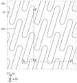
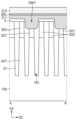
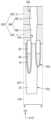
도 1은 몇몇 실시예들에 따른 반도체 메모리 장치의 개략적인 레이아웃도이다. 도 2a는 도 1의 A - A'를 따라 절단한 예시적인 단면도이다. 도 2b는 도 1의 B - B'를 따라 절단한 예시적인 단면도이다. 도 3은 몇몇 실시예들에 따른 반도체 메모리 장치를 상부에서 바라본 평면도이다. 참고적으로, 도 3은 도 27a 및 도 27b의 반도체 메모리 장치를 상부에서 바라본 평면도일 수 있다.FIG. 1 is a schematic layout diagram of a semiconductor memory device according to some embodiments. FIG. 2a is an exemplary cross-sectional view taken along line A-A' of FIG. 1. FIG. 2b is an exemplary cross-sectional view taken along line B-B' of FIG. 1. FIG. 3 is a top plan view of a semiconductor memory device according to some embodiments. For reference, FIG. 3 may be a top plan view of the semiconductor memory device of FIGS. 27a and 27b.
몇몇 실시예들에 따른 반도체 메모리 장치에 관한 도면에서, 예시적으로 DRAM(Dynamic Random Access Memory)이 도시되었지만, 이에 제한되는 것은 아니다.In the drawings relating to a semiconductor memory device according to some embodiments, a dynamic random access memory (DRAM) is illustrated as an example, but is not limited thereto.
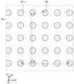
도 1 내지 도 3을 참조하면, 기판(100) 상에 활성 패턴들(ACT)을 정의하는 소자 분리막(ST)이 제공될 수 있다. 예를 들어, 기판(100)은 실리콘, 게르마늄 또는 실리콘-게르마늄을 포함하는 반도체 기판일 수 있다. 소자 분리막(ST)은 실리콘 산화막을 포함할 수 있다.Referring to FIGS. 1 to 3, a device isolation film (ST) defining active patterns (ACT) may be provided on a substrate (100). For example, the substrate (100) may be a semiconductor substrate including silicon, germanium, or silicon-germanium. The device isolation film (ST) may include a silicon oxide film.
활성 패턴들(ACT)은 기판(100)의 상부가 패터닝되어 형성된 것일 수 있다. 반도체 메모리 장치의 디자인 룰의 감소에 따라, 활성 패턴들(ACT)은 사선(diagonal line or oblique line)의 바(bar) 형태로 배치될 수 있다. 활성 패턴들(ACT) 각각은, 기판(100)의 상면에 평행한 제3 방향(D3)으로 연장될 수 있다. 다시 말하면 활성 패턴들(ACT) 각각은 제3 방향(D3)으로의 장축을 가질 수 있다. 평면적 관점에서, 활성 패턴들(ACT)은 제1 방향(D1) 및 제2 방향(D2)을 따라 2차원적으로 배열될 수 있다. 활성 패턴들(ACT)은 제3 방향(D3)으로 서로 이격될 수 있다.The active patterns (ACT) may be formed by patterning the upper portion of the substrate (100). As the design rule of the semiconductor memory device decreases, the active patterns (ACT) may be arranged in a bar shape of a diagonal line or an oblique line. Each of the active patterns (ACT) may extend in a third direction (D3) parallel to the upper surface of the substrate (100). In other words, each of the active patterns (ACT) may have a long axis in the third direction (D3). In a planar view, the active patterns (ACT) may be two-dimensionally arranged along the first direction (D1) and the second direction (D2). The active patterns (ACT) may be spaced apart from each other in the third direction (D3).
활성 패턴들(ACT) 각각은, 기판(100)의 상면에 수직한 방향(즉, 제4 방향(D4))으로 갈수록 그 폭이 줄어들 수 있다. 다시 말하면, 활성 패턴들(ACT) 각각은, 기판(100)의 하면으로부터 멀어질수록 그 폭이 줄어들 수 있다.Each of the active patterns (ACT) may have a width that decreases as it goes in the direction perpendicular to the upper surface of the substrate (100) (i.e., the fourth direction (D4)). In other words, each of the active patterns (ACT) may have a width that decreases as it goes away from the lower surface of the substrate (100).
활성 패턴들(ACT) 사이에 제1 및 제2 트렌치들(TR1, TR2)이 정의될 수 있다. 소자 분리막(ST)은 활성 패턴들(ACT) 사이의 제1 및 제2 트렌치들(TR1, TR2)을 채울 수 있다. 제2 방향(D2)으로 서로 인접하는 한 쌍의 활성 패턴들(ACT) 사이에 제1 트렌치(TR1)가 정의될 수 있다. 제3 방향(D3)으로 서로 인접하는 한 쌍의 활성 패턴들(ACT) 사이에 제2 트렌치(TR2)가 정의될 수 있다.First and second trenches (TR1, TR2) may be defined between active patterns (ACT). A device isolation film (ST) may fill the first and second trenches (TR1, TR2) between the active patterns (ACT). A first trench (TR1) may be defined between a pair of active patterns (ACT) adjacent to each other in a second direction (D2). A second trench (TR2) may be defined between a pair of active patterns (ACT) adjacent to each other in a third direction (D3).
제2 방향(D2)으로 서로 인접하는 한 쌍의 활성 패턴들(ACT) 사이의 거리는 제3 방향(D3)으로 서로 인접하는 한 쌍의 활성 패턴들(ACT) 사이의 거리보다 작을 수 있다. 이로써, 제2 트렌치(TR2)는 제1 트렌치(TR1)보다 더 깊을 수 있다. 다시 말하면, 제2 트렌치(TR2)의 하면은 제1 트렌치(TR1)의 하면보다 더 낮을 수 있다.A distance between a pair of active patterns (ACT) adjacent to each other in the second direction (D2) may be smaller than a distance between a pair of active patterns (ACT) adjacent to each other in the third direction (D3). Accordingly, the second trench (TR2) may be deeper than the first trench (TR1). In other words, a bottom surface of the second trench (TR2) may be lower than a bottom surface of the first trench (TR1).
각각의 활성 패턴들(ACT)의 상부는, 제1 소오스/드레인 영역(SD1) 및 한 쌍의 제2 소오스/드레인 영역들(SD2)을 포함할 수 있다. 제1 소오스/드레인 영역(SD1)은 한 쌍의 제2 소오스/드레인 영역들(SD2) 사이에 위치할 수 있다. 다시 말하면, 평면적 관점에서, 제2 소오스/드레인 영역(SD2), 제1 소오스/드레인 영역(SD1) 및 제2 소오스/드레인 영역(SD2)이 제3 방향(D3)을 따라 순차적으로 배열될 수 있다.The upper portion of each of the active patterns (ACT) may include a first source/drain region (SD1) and a pair of second source/drain regions (SD2). The first source/drain region (SD1) may be located between the pair of second source/drain regions (SD2). In other words, in a planar view, the second source/drain region (SD2), the first source/drain region (SD1), and the second source/drain region (SD2) may be sequentially arranged along the third direction (D3).
각각의 활성 패턴들(ACT)에 한 쌍의 제3 트렌치들(TR3)이 정의될 수 있다. 각각의 제3 트렌치들(TR3)은, 제1 소오스/드레인 영역(SD1)과 제2 소오스/드레인 영역(SD2) 사이에 정의될 수 있다. 제3 트렌치(TR3)는 활성 패턴(ACT)의 상부를 관통하면서, 활성 패턴(ACT)의 상면으로부터 기판(100)의 하면을 향해 아래로 연장될 수 있다. 제3 트렌치(TR3)의 하면은 제1 및 제2 트렌치들(TR1, TR2)의 하면들보다 더 높을 수 있다.A pair of third trenches (TR3) may be defined in each of the active patterns (ACT). Each of the third trenches (TR3) may be defined between the first source/drain region (SD1) and the second source/drain region (SD2). The third trench (TR3) may extend downward from the upper surface of the active pattern (ACT) toward the lower surface of the substrate (100) while penetrating the upper portion of the active pattern (ACT). The lower surface of the third trench (TR3) may be higher than the lower surfaces of the first and second trenches (TR1, TR2).
구체적으로 도시되지는 않았으나, 각각의 활성 패턴들(ACT)의 상부는, 한 쌍의 채널 영역들을 더 포함할 수 있다. 평면적 관점에서, 채널 영역은 제1 소오스/드레인 영역(SD1)과 제2 소오스/드레인 영역(SD2) 사이에 개재될 수 있다.Although not specifically shown, the upper portion of each of the active patterns (ACT) may further include a pair of channel regions. In a planar view, the channel region may be interposed between the first source/drain region (SD1) and the second source/drain region (SD2).
활성 패턴들(ACT) 및 소자 분리막(ST)을 가로지르는 게이트 전극들(GE)이 제공될 수 있다. 게이트 전극(GE)은 '워드 라인'으로도 지칭될 수 있다. 워드 라인의 폭이나 워드 라인 사이의 간격은 디자인 룰에 따라 결정될 수 있다. 구체적으로 도시되지는 않았으나, 워드 라인은 제2 방향(D2)으로 길게 연장되어 활성 패턴(ACT)을 가로지르는 워드 라인 트렌치 내에 배치될 수 있다.Gate electrodes (GE) may be provided across active patterns (ACT) and a device isolation layer (ST). The gate electrodes (GE) may also be referred to as 'word lines'. The width of the word lines or the spacing between the word lines may be determined according to a design rule. Although not specifically shown, the word lines may be arranged within word line trenches that extend in the second direction (D2) and cross the active patterns (ACT).
제2 방향(D2)으로 연장되는 2개의 워드 라인에 의해, 각각의 활성 패턴(ACT)은 3개의 부분으로 나뉠 수 있다. 활성 패턴(ACT)의 제1 부분은 활성 패턴(ACT)의 가운데 부분에 위치하고, 활성 패턴(ACT)의 제2 부분은 상기 제1 부분의 양측에 정의되어 활성 패턴(ACT)의 단부에 위치할 수 있다. 워드 라인은 활성 패턴(ACT)의 제1 부분과, 활성 패턴(ACT)의 제2 부분 사이를 가로지를 수 있다.Each active pattern (ACT) can be divided into three parts by two word lines extending in the second direction (D2). A first part of the active pattern (ACT) is located at a center part of the active pattern (ACT), and a second part of the active pattern (ACT) can be defined on both sides of the first part and located at an end of the active pattern (ACT). A word line can cross between the first part of the active pattern (ACT) and the second part of the active pattern (ACT).
예를 들어, 활성 패턴(ACT)의 제1 영역은 비트 라인과 연결되고, 제2 영역은 후술하는 캐패시터와 연결될 수 있다. 즉, 제1 영역은 비트 라인 구조체(LST)와 연결되고, 제2 영역은 콘택(CNT)과 연결될 수 있다. 다르게 설명하면, 활성 패턴(ACT)의 제1 부분은 공통 드레인 영역에 해당되고, 활성 패턴(ACT)의 제2 부분은 소오스 영역에 해당될 수 있다. 각 워드 라인 및 이에 인접한 제1 및 제2 부분 트랜지스터를 구성할 수 있다.For example, a first region of an active pattern (ACT) may be connected to a bit line, and a second region may be connected to a capacitor described later. That is, the first region may be connected to a bit line structure (LST), and the second region may be connected to a contact (CNT). In other words, a first portion of the active pattern (ACT) may correspond to a common drain region, and a second portion of the active pattern (ACT) may correspond to a source region. Each word line and first and second portion transistors adjacent thereto may be configured.
하나의 활성 패턴(ACT)의 단부는 이에 이웃하는 다른 활성 패턴(ACT)의 중심에 인접하도록 배열될 수 있다. 하나의 활성 패턴(ACT)의 단부는 다른 활성 패턴(ACT)의 중심과 제2 방향(D2)으로 인접할 수 있다. 구체적으로, 콘택(CNT)과 연결되는 하나의 활성 패턴의 단부는 비트 라인과 연결되는 하나의 활성 패턴의 중심과 제2 방향(D2)으로 이격될 수 있다.An end of one active pattern (ACT) may be arranged adjacent to a center of another adjacent active pattern (ACT). An end of one active pattern (ACT) may be adjacent to a center of another active pattern (ACT) in a second direction (D2). Specifically, an end of one active pattern connected to a contact (CNT) may be spaced apart from a center of one active pattern connected to a bit line in the second direction (D2).
게이트 전극(GE)은 제1 방향(D1)을 기준으로, 서로 인접하는 하나의 활성 패턴(ACT)의 단부와 다른 하나의 활성 패턴(ACT)의 단부 사이에 배치될 수 있다. 비트 라인 구조체(LST)는 제2 방향(D2)을 기준으로, 하나의 활성 패턴(ACT)의 단부와 다른 하나의 활성 패턴(ACT)의 단부 사이에 배치될 수 있다.A gate electrode (GE) may be arranged between an end of one active pattern (ACT) and an end of another active pattern (ACT) that are adjacent to each other in a first direction (D1). A bit line structure (LST) may be arranged between an end of one active pattern (ACT) and an end of another active pattern (ACT) in a second direction (D2).
게이트 전극들(GE)은 제3 트렌치들(TR3) 내에 각각 제공될 수 있다. 게이트 전극들(GE)은 제2 방향(D2)으로 서로 평행하게 연장될 수 있다. 평면적 관점에서, 게이트 전극(GE)은 제1 소오스/드레인 영역(SD1)과 제2 소오스/드레인 영역(SD2) 사이에 개재될 수 있다. 게이트 전극(GE)의 상면은 활성 패턴(ACT)의 상면(예를 들어, 제1 소오스/드레인 영역(SD1)의 상면 또는 제2 소오스/드레인 영역(SD2)의 상면)보다 더 낮을 수 있다.Gate electrodes (GE) may be provided in each of the third trenches (TR3). The gate electrodes (GE) may extend parallel to each other in the second direction (D2). In a planar view, the gate electrode (GE) may be interposed between the first source/drain region (SD1) and the second source/drain region (SD2). An upper surface of the gate electrode (GE) may be lower than an upper surface of the active pattern (ACT) (for example, an upper surface of the first source/drain region (SD1) or an upper surface of the second source/drain region (SD2)).
게이트 전극(GE)과 활성 패턴(ACT) 사이에 게이트 유전막(GI)이 개재될 수 있다. 게이트 전극(GE) 상에 게이트 캐핑막(GP)이 제공될 수 있다. 게이트 캐핑막(GP)은 게이트 전극(GE)의 상면을 덮을 수 있다. 게이트 캐핑막(GP)의 상면은 활성 패턴(ACT)의 상면과 공면(共面)을 이룰 수 있다.A gate dielectric film (GI) may be interposed between the gate electrode (GE) and the active pattern (ACT). A gate capping film (GP) may be provided on the gate electrode (GE). The gate capping film (GP) may cover an upper surface of the gate electrode (GE). An upper surface of the gate capping film (GP) may be coplanar with an upper surface of the active pattern (ACT).
게이트 전극(GE)은 도전성 금속 질화물(예를 들어, 티타늄 질화물 또는 탄탈륨 질화물) 및/또는 금속 물질(예를 들어, 티타늄, 탄탈륨, 텅스텐, 구리 또는 알루미늄)을 포함할 수 있다. 게이트 유전막(GI)은 실리콘 산화막, 실리콘 질화막, 실리콘 산질화막 및/또는 고유전율 물질을 포함할 수 있다. 예를 들어, 상기 고유전율 물질은 하프늄 산화물, 하프늄 실리콘 산화물, 란탄 산화물, 지르코늄 산화물, 지르코늄 실리콘 산화물, 탄탈 산화물, 티타늄 산화물, 바륨 스트론튬 티타늄 산화물, 바륨 티타늄 산화물, 스트론튬 티타늄 산화물, 리튬 산화물, 알루미늄 산화물, 납 스칸듐 탄탈 산화물, 납 아연 니오브산염 또는 이들의 조합을 포함할 수 있다. 게이트 캐핑막(GP)은 실리콘 산화막, 실리콘 질화막 및/또는 실리콘 산질화막을 포함할 수 있다.The gate electrode (GE) may include a conductive metal nitride (e.g., titanium nitride or tantalum nitride) and/or a metal material (e.g., titanium, tantalum, tungsten, copper or aluminum). The gate dielectric film (GI) may include a silicon oxide film, a silicon nitride film, a silicon oxynitride film and/or a high-k material. For example, the high-k material may include hafnium oxide, hafnium silicon oxide, lanthanum oxide, zirconium oxide, zirconium silicon oxide, tantalum oxide, titanium oxide, barium strontium titanium oxide, barium titanium oxide, strontium titanium oxide, lithium oxide, aluminum oxide, lead scandium tantalum oxide, lead zinc niobate or a combination thereof. The gate capping film (GP) may include a silicon oxide film, a silicon nitride film and/or a silicon oxynitride film.
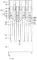
기판(100) 상에 절연막(IL)이 제공될 수 있다. 절연막(IL)은 활성 패턴들(ACT)의 제1 소오스/드레인 영역들(SD1)을 노출하는 제1 콘택홀들(CNH1)을 포함할 수 있다. 예를 들어, 절연막(IL)은 순차적으로 적층된 실리콘 산화막 및 실리콘 산질화막을 포함할 수 있다.An insulating film (IL) may be provided on the substrate (100). The insulating film (IL) may include first contact holes (CNH1) exposing first source/drain regions (SD1) of the active patterns (ACT). For example, the insulating film (IL) may include a silicon oxide film and a silicon oxynitride film that are sequentially stacked.
절연막(IL) 상에 제1 방향(D1)으로 서로 평행하게 연장되는 비트 라인 구조체들(LST)이 제공될 수 있다. 비트 라인 구조체들(LST)은 제2 방향(D2)을 따라 이격되어 배열될 수 있다. 평면적 관점에서, 비트 라인 구조체들(LST)은 게이트 전극들(GE)과 수직하게 교차할 수 있다. 비트 라인 구조체들(LST) 각각의 양 측벽들 상에 한 쌍의 스페이서들(SP)이 제공될 수 있다. 스페이서들(SP)은 실리콘 산화막, 실리콘 질화막 및/또는 실리콘 산질화막을 포함할 수 있다.Bit line structures (LST) extending parallel to each other in a first direction (D1) may be provided on an insulating film (IL). The bit line structures (LST) may be arranged to be spaced apart from each other along a second direction (D2). In a planar view, the bit line structures (LST) may perpendicularly intersect the gate electrodes (GE). A pair of spacers (SP) may be provided on both sidewalls of each of the bit line structures (LST). The spacers (SP) may include a silicon oxide film, a silicon nitride film, and/or a silicon oxynitride film.
각각의 비트 라인 구조체들(LST)은, 순차적으로 적층된 도전 패턴(CP), 배리어 패턴(BP), 비트 라인(BL) 및 마스크 패턴(MP)을 포함할 수 있다. 도전 패턴(CP)은, 제1 콘택홀(CNH1) 안에 배치되며 제1 소오스/드레인 영역(SD1)에 접속하는 비트 라인 콘택(CNP)을 포함할 수 있다. 보다 구체적으로, 비트 라인 콘택(CNP)은 절연막(IL)을 관통하여 기판(100)의 하면을 향해 연장될 수 있다. 비트 라인 콘택(CNP)은 제1 소오스/드레인 영역(SD1)에 직접 접촉할 수 있다.Each of the bit line structures (LST) may include a conductive pattern (CP), a barrier pattern (BP), a bit line (BL), and a mask pattern (MP) that are sequentially stacked. The conductive pattern (CP) may include a bit line contact (CNP) that is arranged in a first contact hole (CNH1) and is connected to a first source/drain region (SD1). More specifically, the bit line contact (CNP) may extend toward a lower surface of the substrate (100) through an insulating film (IL). The bit line contact (CNP) may be in direct contact with the first source/drain region (SD1).
배리어 패턴(BP)은 비트 라인(BL) 내의 금속 물질이 도전 패턴(CP)으로 확산되는 것을 억제할 수 있다. 비트 라인(BL)은 배리어 패턴(BP) 및 도전 패턴(CP)을 통하여 제1 소오스/드레인 영역(SD1)과 전기적으로 연결될 수 있다.The barrier pattern (BP) can suppress the metal material within the bit line (BL) from diffusing into the conductive pattern (CP). The bit line (BL) can be electrically connected to the first source/drain region (SD1) through the barrier pattern (BP) and the conductive pattern (CP).
도전 패턴(CP)은 도핑된 반도체 물질(예를 들어, 도핑된 실리콘, 도핑된 게르마늄 등)을 포함할 수 있다. 배리어 패턴(BP)은 도전성 금속질화물(예를 들어, 티타늄 질화물 또는 탄탈륨 질화물)을 포함할 수 있다. 비트 라인(BL)은 금속 물질을 포함할 수 있다. 예를 들어, 비트 라인(BL)은 몰리브데늄(Mo) 및 루테늄(Ru) 중 적어도 어느 하나를 포함할 수 있다. 다른 예로, 비트 라인(BL)은 티타늄, 탄탈륨, 텅스텐, 구리 또는 알루미늄 중 어느 하나를 포함할 수 있다.The conductive pattern (CP) may include a doped semiconductor material (e.g., doped silicon, doped germanium, etc.). The barrier pattern (BP) may include a conductive metal nitride (e.g., titanium nitride or tantalum nitride). The bit line (BL) may include a metal material. For example, the bit line (BL) may include at least one of molybdenum (Mo) and ruthenium (Ru). As another example, the bit line (BL) may include one of titanium, tantalum, tungsten, copper, or aluminum.
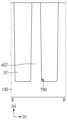
마스크 패턴(MP)이 비트 라인(BL) 상에 제공될 수 있다. 마스크 패턴(MP)의 상면은 평평할 수 있다. 도 2a 및 도 17a를 함께 참조하면, 마스크 패턴(MP)의 제4 방향(D4)으로의 두께(T1)는 예를 들어, 150 내지 450일 수 있으나, 이에 제한되지 않는다.A mask pattern (MP) may be provided on a bit line (BL). The upper surface of the mask pattern (MP) may be flat. Referring to FIG. 2A and FIG. 17A together, the thickness (T1) of the mask pattern (MP) in the fourth direction (D4) may be, for example, 150 450 inland This may include, but is not limited to:
몇몇 실시예에서, 게이트 전극(GE), 게이트 유전막(GI) 및 게이트 캐핑막(GP)은 게이트 구조체로 포괄하여 지칭될 수 있다.In some embodiments, the gate electrode (GE), the gate dielectric film (GI), and the gate capping film (GP) may be collectively referred to as a gate structure.
도 2a, 도 2b 및 도 3을 참조하면, 게이트 캐핑막(GP) 상에 절연 패턴(INP)이 제공될 수 있다. 절연 패턴(INP)은 게이트 캐핑막(GP)의 상부까지 연장될 수 있다.Referring to FIGS. 2A, 2B, and 3, an insulating pattern (INP) may be provided on a gate capping film (GP). The insulating pattern (INP) may extend to an upper portion of the gate capping film (GP).
콘택들(CNT)은 제1 방향(D1) 및 제2 방향(D2)을 따라 2차원적으로 배열될 수 있다. 절연 패턴(INP)은 콘택들(CNT)이 배치되지 않은 게이트 캐핑막(GP) 상에 배치될 수 있다.The contacts (CNT) can be two-dimensionally arranged along the first direction (D1) and the second direction (D2). The insulating pattern (INP) can be arranged on the gate capping film (GP) where the contacts (CNT) are not arranged.
도 2a 및 도 2b를 다시 참조하면, 절연막(IL)을 관통하여 제2 소오스/드레인 영역들(SD2)에 각각 접속하는 콘택들(CNT)이 제공될 수 있다. 콘택들(CNT) 및 비트 라인 구조체들(LST)은, 제2 방향(D2)을 따라 서로 교대로 배열될 수 있다. 콘택들(CNT) 및 절연 패턴들(INP)은, 제1 방향(D1) 및 제2 방향(D2)을 따라 서로 교대로 배열될 수 있다.Referring again to FIGS. 2A and 2B, contacts (CNT) may be provided that penetrate the insulating film (IL) and are respectively connected to the second source/drain regions (SD2). The contacts (CNT) and the bit line structures (LST) may be arranged alternately along the second direction (D2). The contacts (CNT) and the insulating patterns (INP) may be arranged alternately along the first direction (D1) and the second direction (D2).
콘택(CNT)은 '스토리지 노드 콘택'으로도 명명될 수 있다. 각각의 콘택들(CNT)은, 제1 콘택(CNT_1) 및 제1 콘택(CNT_1) 상의 제2 콘택(CNT_2)을 포함할 수 있다.The contacts (CNT) may also be referred to as 'storage node contacts'. Each of the contacts (CNT) may include a first contact (CNT_1) and a second contact (CNT_2) on the first contact (CNT_1).
제1 콘택(CNT_1)은, 제2 소오스/드레인 영역(SD2)의 상부가 부분적으로 식각되어 형성된 제2 콘택홀(CNH2)을 채울 수 있다. 도 2a를 다시 참조하면, 제1 콘택(CNT_1)은, 제2 콘택홀(CNH2)에 의해 노출된 제2 소오스/드레인 영역(SD2)에 직접 접촉할 수 있다. 또한, 제1 콘택(CNT_1)은 스페이서(SP)의 측벽 및 소자 분리막(ST)의 상면과 접촉할 수 있다. 제1 콘택(CNT_1)은 스페이서(SP)에 의해 그와 인접하는 비트 라인(BL)으로부터 이격될 수 있다. 제1 콘택(CNT_1)은 도핑된 반도체 물질(예를 들어, 도핑된 실리콘, 도핑된 게르마늄 등) 또는 금속(예를 들어, 티타늄, 탄탈륨, 텅스텐, 구리 또는 알루미늄)을 포함할 수 있다.The first contact (CNT_1) can fill the second contact hole (CNH2) formed by partially etching the upper portion of the second source/drain region (SD2). Referring again to FIG. 2A, the first contact (CNT_1) can directly contact the second source/drain region (SD2) exposed by the second contact hole (CNH2). In addition, the first contact (CNT_1) can contact a sidewall of the spacer (SP) and an upper surface of the device isolation film (ST). The first contact (CNT_1) can be spaced from the bit line (BL) adjacent thereto by the spacer (SP). The first contact (CNT_1) can include a doped semiconductor material (e.g., doped silicon, doped germanium, etc.) or a metal (e.g., titanium, tantalum, tungsten, copper, or aluminum).
제1 콘택(CNT_1) 상에, 제1 콘택(CNT_1)에 각각 접속하는 제2 콘택(CNT_2)이 제공될 수 있다. 제2 콘택(CNT_2)은 제1 콘택(CNT_1)을 통해 제2 소오스/드레인 영역들(SD2)과 각각 전기적으로 연결될 수 있다. 제2 콘택(CNT_2)는 제1 콘택(CNT_1)과 정렬될 수 있다. 제2 콘택(CNT_2)은 도핑된 반도체 물질(예를 들어, 도핑된 실리콘, 도핑된 게르마늄 등) 또는 금속(예를 들어, 티타늄, 탄탈륨, 텅스텐, 구리 또는 알루미늄)을 포함할 수 있다.On the first contact (CNT_1), a second contact (CNT_2) may be provided, each of which is connected to the first contact (CNT_1). The second contact (CNT_2) may be electrically connected to the second source/drain regions (SD2) via the first contact (CNT_1), respectively. The second contact (CNT_2) may be aligned with the first contact (CNT_1). The second contact (CNT_2) may include a doped semiconductor material (e.g., doped silicon, doped germanium, etc.) or a metal (e.g., titanium, tantalum, tungsten, copper, or aluminum).
마스크 패턴들(MP) 상에 절연 패턴(INP)이 제공될 수 있다. 절연 패턴(INP)은 제2 콘택(CNT_2)의 평면적 형태를 정의할 수 있다. 절연 패턴(INP)에 의해, 인접하는 제2 콘택들(CNT_2)이 서로 분리될 수 있다.An insulating pattern (INP) may be provided on the mask patterns (MP). The insulating pattern (INP) may define a planar shape of the second contact (CNT_2). By the insulating pattern (INP), adjacent second contacts (CNT_2) may be separated from each other.
구체적으로 도시되지는 않았으나, 제2 콘택(CNT_2) 상에 정보 저장 요소가 제공될 수 있다. 구체적으로, 정보 저장 요소는 제2 콘택(CNT_2) 상에 각각 제공된 제1 전극들을 포함할 수 있다. 제1 전극들은 제2 콘택들(CNT_2)과 각각 연결될 수 있다. 정보 저장 요소는, 제1 전극들 상의 제2 전극 및 제1 전극들과 제2 전극 사이의 유전막을 더 포함할 수 있다. 제1 전극, 유전막 및 제2 전극은 데이터를 저장하는 캐패시터를 구성할 수 있다.Although not specifically shown, an information storage element may be provided on the second contact (CNT_2). Specifically, the information storage element may include first electrodes respectively provided on the second contact (CNT_2). The first electrodes may be respectively connected to the second contacts (CNT_2). The information storage element may further include a second electrode on the first electrodes and a dielectric film between the first electrodes and the second electrode. The first electrode, the dielectric film, and the second electrode may form a capacitor for storing data.
제1 전극들 각각은 내부가 채워진 기둥(pillar) 형태를 가질 수 있으나, 이에 제한되지 않는다. 다른 예로, 제1 전극들 각각은 하부가 폐쇄된 실린더 형태를 가질 수 있다. 복수의 제1 전극들은 제1 방향(D1) 또는 제2 방향(D2)을 따라 지그재그로 배열되어, 벌집(honeycomb) 모양의 배치를 가질 수 있다. 다른 예로, 복수의 제1 전극들은 제1 방향(D1) 및 제2 방향(D2)을 따라 매트릭스 형태로 배치될 수 있다.Each of the first electrodes may have a pillar shape with an internally filled portion, but is not limited thereto. As another example, each of the first electrodes may have a cylindrical shape with a closed bottom. The plurality of first electrodes may be arranged in a zigzag manner along the first direction (D1) or the second direction (D2), thereby having a honeycomb-shaped arrangement. As another example, the plurality of first electrodes may be arranged in a matrix shape along the first direction (D1) and the second direction (D2).
예를 들어, 제1 전극들 각각은 불순물이 도핑된 실리콘, 텅스텐과 같은 금속, 또는 티타늄 질화물과 같은 도전성 금속 화합물로 이루어질 수 있다. 유전막은 고유전율 물질, 예를 들어, 하프늄 산화물, 하프늄 실리콘 산화물, 란탄 산화물, 지르코늄 산화물, 지르코늄 실리콘 산화물, 탄탈 산화물, 티타늄 산화물, 바륨 스트론튬 티타늄 산화물, 바륨 티타늄 산화물, 스트론튬 티타늄 산화물, 리튬 산화물, 알루미늄 산화물, 납 스칸듐 탄탈 산화물, 납 아연 니오브산염 또는 이들의 조합을 포함할 수 있다. 제2 전극은 도핑된 실리콘, Ru, RuO, Pt, PtO, Ir, IrO, SRO(SrRuO), BSRO((Ba,Sr)RuO), CRO(CaRuO), BaRuO, La(Sr,Co)O, Ti, TiN, W, WN, Ta, TaN, TiAlN, TiSiN, TaAlN, TaSiN, 또는 이들의 조합을 포함할 수 있으나, 이에 제한되지 않는다.For example, each of the first electrodes can be made of a metal such as silicon, tungsten, or a conductive metal compound such as titanium nitride doped with an impurity. The dielectric film can include a high-k material, such as hafnium oxide, hafnium silicon oxide, lanthanum oxide, zirconium oxide, zirconium silicon oxide, tantalum oxide, titanium oxide, barium strontium titanium oxide, barium titanium oxide, strontium titanium oxide, lithium oxide, aluminum oxide, lead scandium tantalum oxide, lead zinc niobate, or combinations thereof. The second electrode may include, but is not limited to, doped silicon, Ru, RuO, Pt, PtO, Ir, IrO, SRO(SrRuO), BSRO((Ba,Sr)RuO), CRO(CaRuO), BaRuO, La(Sr,Co)O, Ti, TiN, W, WN, Ta, TaN, TiAlN, TiSiN, TaAlN, TaSiN, or combinations thereof.
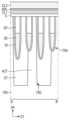
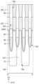
도 2a 및 도 2b를 참조하여, 콘택(CNT) 및 절연 패턴(INP)에 대해 보다 상세히 설명한다.Referring to FIGS. 2a and 2b, the contact (CNT) and the insulating pattern (INP) are described in more detail.
절연 패턴(INP)은 비트 라인 구조체(LST) 상에 배치될 수 있다. 절연 패턴(INP)은 제1 콘택(CNT_1)의 측벽 및 게이트 캐핑막(GP)의 적어도 일부를 노출시키는 제4 트렌치(TR4)를 채울 수 있다.An insulating pattern (INP) can be arranged on the bit line structure (LST). The insulating pattern (INP) can fill a fourth trench (TR4) exposing a sidewall of the first contact (CNT_1) and at least a portion of the gate capping film (GP).
제2 콘택(CNT_2)은 제1 콘택(CNT_1) 상에 배치될 수 있다. 제2 콘택(CNT_2)은 절연 패턴(INP)의 측벽 및 제1 콘택(CNT_1)의 상면을 노출시키는 제5 트렌치(TR5)를 채울 수 있다. 도 2a 및 도 2b를 참조하면, 제5 트렌치(TR5)의 제1 및 제2 방향(D1, D2)을 따른 폭은 기판(100)으로부터 멀어질수록 증가할 수 있다. 제2 콘택(CNT_2)은 제1 콘택(CNT_1)과 전기적으로 연결될 수 있다.The second contact (CNT_2) may be arranged on the first contact (CNT_1). The second contact (CNT_2) may fill the fifth trench (TR5) exposing the sidewall of the insulating pattern (INP) and the top surface of the first contact (CNT_1). Referring to FIGS. 2A and 2B, the width of the fifth trench (TR5) along the first and second directions (D1, D2) may increase as it moves away from the substrate (100). The second contact (CNT_2) may be electrically connected to the first contact (CNT_1).
절연 패턴(INP)은, 제1 콘택(CNT_1)과 접촉하는 제1 영역(INP_1) 및 제1 영역(INP_1) 상에 배치되고 제2 콘택(CNT_2)과 접촉하는 제2 영역(INP_2)을 포함할 수 있다. 제1 영역(INP_1)과 제2 영역(INP_2)은 제4 방향(D4), 즉 수직 방향으로 서로 중첩될 수 있다.The insulating pattern (INP) may include a first region (INP_1) in contact with the first contact (CNT_1) and a second region (INP_2) disposed on the first region (INP_1) and in contact with the second contact (CNT_2). The first region (INP_1) and the second region (INP_2) may overlap each other in the fourth direction (D4), i.e., the vertical direction.
비트 라인 구조체(LST)와 절연 패턴(INP)은 제4 방향(D4), 즉 수직 방향으로 서로 중첩될 수 있다. 다시 말해, 비트 라인 구조체(LST)와 절연 패턴(INP)은 제4 방향(D4), 즉 수직 방향으로 정렬될 수 있다. 이에 따라, 제2 영역(INP_2)은 비트 라인 구조체(LST)의 상면을 덮을 수 있다. 제2 영역(INP_2)은 비트 라인 구조체(LST)의 상면 전체와 접촉할 수 있다. 제1 및 제2 영역(INP_1, INP_2) 각각은, 제4 및 제5 트렌치(TR4, TR5)의 측벽 상에 제4 및 제5 트렌치(TR4, TR5)의 측벽 각각을 따라 연장될 수 있다.The bit line structure (LST) and the insulating pattern (INP) may overlap each other in the fourth direction (D4), i.e., the vertical direction. In other words, the bit line structure (LST) and the insulating pattern (INP) may be aligned in the fourth direction (D4), i.e., the vertical direction. Accordingly, the second region (INP_2) may cover the upper surface of the bit line structure (LST). The second region (INP_2) may be in contact with the entire upper surface of the bit line structure (LST). Each of the first and second regions (INP_1, INP_2) may extend along the sidewalls of the fourth and fifth trenches (TR4, TR5), respectively, on the sidewalls of the fourth and fifth trenches (TR4, TR5).
제2 트렌치(TR4)의 측벽의 기울기와 제3 트렌치(TR5)의 측벽의 기울기는 서로 다를 수 있다. 이에 따라, 제1 영역(INP_1)의 측벽의 프로파일은 제2 영역(INP_2)의 측벽의 프로파일과 다를 수 있다.The slope of the sidewall of the second trench (TR4) and the slope of the sidewall of the third trench (TR5) may be different from each other. Accordingly, the profile of the sidewall of the first region (INP_1) may be different from the profile of the sidewall of the second region (INP_2).
구체적으로, 제2 영역(INP_2)의 하면의 폭(W31)은 제1 영역(INP_1)의 상면의 폭(W21)보다 클 수 있다. 제1 영역(INP_1)의 상면의 폭(W21)은 제1 영역(INP_1)의 하면의 폭(W11)보다 크거나 실질적으로 동일하고, 제2 영역(INP_2)의 상면의 폭(W41)은 제2 영역(INP_2)의 하면의 폭(W31)보다 작을 수 있다.Specifically, the width (W31) of the lower surface of the second region (INP_2) may be greater than the width (W21) of the upper surface of the first region (INP_1). The width (W21) of the upper surface of the first region (INP_1) may be greater than or substantially equal to the width (W11) of the lower surface of the first region (INP_1), and the width (W41) of the upper surface of the second region (INP_2) may be less than the width (W31) of the lower surface of the second region (INP_2).
제2 영역(INP_2)의 제1 및 제2 방향(D1, D2)을 따른 폭(W41, W42)은 기판(100)으로부터 멀어질수록 감소할 수 있다.The width (W41, W42) along the first and second directions (D1, D2) of the second region (INP_2) may decrease as it moves away from the substrate (100).
제1 영역(INP_1) 및 제2 영역(INP_2)은 서로 동일한 물질을 포함할 수 있다. 예를 들어 제1 영역(INP_1) 및 제2 영역(INP_2)은, 실리콘 질화물, 실리콘 탄질화물 또는 실리콘 산탄질화물을 포함할 수 있으나, 이에 제한되지 않는다. 제1 영역(INP_1) 및 제2 영역(INP_2)은 제4 및 제5 트렌치(TR4, TR5)의 측벽을 따라 일체로 형성될 수 있으므로, 제1 영역(INP_1)과 제2 영역(INP_2) 사이에 경계면이 존재하지 않을 수 있다.The first region (INP_1) and the second region (INP_2) may include the same material. For example, the first region (INP_1) and the second region (INP_2) may include, but are not limited to, silicon nitride, silicon carbonitride, or silicon oxycarbonitride. The first region (INP_1) and the second region (INP_2) may be integrally formed along the sidewalls of the fourth and fifth trenches (TR4, TR5), so that no interface may exist between the first region (INP_1) and the second region (INP_2).
제1 콘택(CNT_1)의 측벽의 기울기와 제2 콘택(CNT_2)의 측벽의 기울기는 서로 다를 수 있다.The slope of the side wall of the first contact (CNT_1) and the slope of the side wall of the second contact (CNT_2) may be different from each other.
구체적으로, 제2 콘택(CNT_2)의 폭은 기판(100)으로부터 멀어질수록 증가할 수 있다. 이에 따라, 제2 콘택(CNT_2)의 하면의 폭(WC1)은 제2 콘택(CNT_2)의 상면(WC2)의 폭보다 작을 수 있다.Specifically, the width of the second contact (CNT_2) may increase as it moves away from the substrate (100). Accordingly, the width (WC1) of the lower surface of the second contact (CNT_2) may be smaller than the width of the upper surface (WC2) of the second contact (CNT_2).
이하에서, 도 4 내지 도 25b를 이용하여 몇몇 실시예들에 따른 반도체 메모리 장치의 제조 방법을 설명한다. 설명의 편의상 도 1 내지 도 3을 이용하여 설명한 것과 다른 점을 중심으로 설명한다.Hereinafter, a method for manufacturing a semiconductor memory device according to some embodiments will be described using FIGS. 4 to 25b. For convenience of explanation, the description will focus on differences from the description using FIGS. 1 to 3.
도 4, 도 6, 도 8, 도 10, 도 12, 도 14, 도 16, 도 18, 도 20, 도 22 및 도 24는 몇몇 실시예들에 따른 반도체 메모리 장치의 제조 방법을 설명하기 위한 평면도들이다. 도 5a, 도 7a, 도 9a, 도 11a, 도 13a, 도 15a, 도 17a, 도 19a, 도 21a, 도 23a 및 도 25a는 각각 도 4, 도 6, 도 8, 도 10, 도 12, 도 14, 도 16, 도 18, 도 20, 도 22 및 도 24의 A-A'선에 따른 단면도들이다. 도 5b, 도 7b, 도 9b, 도 11b, 도 13b, 도 15b, 도 17b, 도 19b, 도 21b, 도 23b 및 도 25b는 각각 도 4, 도 6, 도 8, 도 10, 도 12, 도 14, 도 16, 도 18, 도 20, 도 22 및 도 24의 B-B'선에 따른 단면도들이다.FIGS. 4, 6, 8, 10, 12, 14, 16, 18, 20, 22, and 24 are plan views illustrating a method of manufacturing a semiconductor memory device according to some embodiments. FIGS. 5a, 7a, 9a, 11a, 13a, 15a, 17a, 19a, 21a, 23a, and 25a are cross-sectional views taken along line A-A' of FIGS. 4, 6, 8, 10, 12, 14, 16, 18, 20, 22, and 24, respectively. FIG. 5b, FIG. 7b, FIG. 9b, FIG. 11b, FIG. 13b, FIG. 15b, FIG. 17b, FIG. 19b, FIG. 21b, FIG. 23b and FIG. 25b are cross-sectional views taken along line B-B' of FIG. 4, FIG. 6, FIG. 8, FIG. 10, FIG. 12, FIG. 14, FIG. 16, FIG. 18, FIG. 20, FIG. 22 and FIG. 24, respectively.
도 4, 도 5a 및 도 5b를 참조하면, 기판(100)의 상부를 패터닝하여, 활성 패턴들(ACT)이 형성될 수 있다. 활성 패턴들(ACT) 각각은, 기판(100)의 상면에 평행한 제3 방향(D3)으로 연장될 수 있다. 활성 패턴들(ACT)은 제1 방향(D1) 및 제2 방향(D2)을 따라 2차원적으로 배열될 수 있다. 활성 패턴들(ACT)은 제3 방향(D3)으로 서로 이격될 수 있다.Referring to FIGS. 4, 5A, and 5B, active patterns (ACT) may be formed by patterning an upper portion of a substrate (100). Each of the active patterns (ACT) may extend in a third direction (D3) parallel to an upper surface of the substrate (100). The active patterns (ACT) may be two-dimensionally arranged along the first direction (D1) and the second direction (D2). The active patterns (ACT) may be spaced apart from each other in the third direction (D3).
활성 패턴들(ACT) 사이에 제1 및 제2 트렌치들(TR1, TR2)이 정의될 수 있다. 제1 및 제2 트렌치들(TR1, TR2)을 채우는 소자 분리막(ST)이 형성될 수 있다. 소자 분리막(ST)은 제1 및 제2 트렌치들(TR1, TR2)을 완전히 채우면서 활성 패턴들(ACT)을 덮도록 형성될 수 있다. 활성 패턴들(ACT)의 상면들이 노출될 때까지 소자 분리막(ST) 상에 평탄화 공정이 수행될 수 있다.First and second trenches (TR1, TR2) may be defined between active patterns (ACT). A device isolation film (ST) may be formed to fill the first and second trenches (TR1, TR2). The device isolation film (ST) may be formed to completely fill the first and second trenches (TR1, TR2) and cover the active patterns (ACT). A planarization process may be performed on the device isolation film (ST) until upper surfaces of the active patterns (ACT) are exposed.
도 6, 도 7a 및 도 7b를 참조하면, 활성 패턴들(ACT) 및 소자 분리막(ST)을 패터닝하여, 제3 트렌치들(TR3)이 형성될 수 있다. 평면적 관점에서, 제3 트렌치들(TR3) 각각은 제2 방향(D2)으로 연장되는 라인 형태를 가질 수 있다.Referring to FIGS. 6, 7a, and 7b, third trenches (TR3) may be formed by patterning active patterns (ACT) and a device isolation film (ST). In a planar view, each of the third trenches (TR3) may have a line shape extending in the second direction (D2).
제3 트렌치들(TR3)을 형성하는 것은, 개구부들을 포함하는 하드 마스크 패턴을 형성하는 것 및 상기 하드 마스크 패턴을 식각 마스크로 노출된 활성 패턴들(ACT) 및 소자 분리막(ST)을 식각하는 것을 포함할 수 있다. 제3 트렌치(TR3)는 제1 트렌치(TR1)보다 얕게 형성될 수 있다.Forming the third trenches (TR3) may include forming a hard mask pattern including openings and etching the active patterns (ACT) and the device isolation film (ST) exposed by the hard mask pattern as an etch mask. The third trench (TR3) may be formed shallower than the first trench (TR1).
도 8, 도 9a 및 도 9b를 참조하면, 각각의 제3 트렌치들(TR3) 내에 게이트 유전막(GI), 게이트 전극(GE) 및 게이트 캐핑막(GP)이 순차적으로 형성될 수 있다. 구체적으로, 제3 트렌치(TR3) 내에 게이트 유전막(GI)이 컨포멀하게 형성될 수 있다. 게이트 유전막(GI)은 실리콘 산화막, 실리콘 질화막, 실리콘 산질화막 및/또는 고유전율 물질을 포함할 수 있다.Referring to FIGS. 8, 9a, and 9b, a gate dielectric film (GI), a gate electrode (GE), and a gate capping film (GP) may be sequentially formed within each of the third trenches (TR3). Specifically, the gate dielectric film (GI) may be conformally formed within the third trench (TR3). The gate dielectric film (GI) may include a silicon oxide film, a silicon nitride film, a silicon oxynitride film, and/or a high-k material.
게이트 유전막(GI) 상에 제3 트렌치(TR3)를 채우는 도전막을 형성하여, 게이트 전극(GE)이 형성될 수 있다. 상기 도전막은 도전성 금속 질화물 및/또는 금속 물질을 포함할 수 있다.A gate electrode (GE) can be formed by forming a conductive film filling a third trench (TR3) on a gate dielectric film (GI). The conductive film can include a conductive metal nitride and/or a metal material.
게이트 유전막(GI) 및 게이트 전극(GE)을 리세스하고, 리세스된 게이트 전극(GE) 상에 게이트 캐핑막(GP)이 형성될 수 있다. 게이트 캐핑막(GP)의 상면은 활성 패턴(ACT)의 상면과 공면(共面)을 이룰 수 있다The gate dielectric film (GI) and the gate electrode (GE) can be recessed, and a gate capping film (GP) can be formed on the recessed gate electrode (GE). The upper surface of the gate capping film (GP) can be coplanar with the upper surface of the active pattern (ACT).
활성 패턴들(ACT) 상에 이온 주입 공정을 수행하여, 활성 패턴(ACT)의 상부에 제1 소오스/드레인 영역(SD1) 및 한 쌍의 제2 소오스/드레인 영역들(SD2)이 형성될 수 있다. 한 쌍의 제2 소오스/드레인 영역들(SD2)은 제1 소오스/드레인 영역(SD1)을 사이에 두고 제3 방향(D3)으로 서로 이격될 수 있다. 예를 들어, 제1 및 제2 소오스/드레인 영역들(SD1, SD2)은 동일한 불순물로 도핑될 수 있다.An ion implantation process may be performed on active patterns (ACT) to form a first source/drain region (SD1) and a pair of second source/drain regions (SD2) on an upper portion of the active pattern (ACT). The pair of second source/drain regions (SD2) may be spaced apart from each other in a third direction (D3) with the first source/drain region (SD1) interposed therebetween. For example, the first and second source/drain regions (SD1, SD2) may be doped with the same impurity.
구체적으로 도시되지는 않았으나, 게이트 전극(GE)의 아래에 위치하는 활성 패턴(ACT)에 채널 영역이 정의될 수 있다. 평면적 관점에서, 채널 영역은 제1 소오스/드레인 영역(SD1)과 제2 소오스/드레인 영역(SD2) 사이에 개재될 수 있다. 게이트 전극(GE)은 채널 영역의 상면 및 양 측벽들 상에 제공될 수 있다.Although not specifically illustrated, a channel region may be defined in an active pattern (ACT) positioned below a gate electrode (GE). In a planar view, the channel region may be interposed between a first source/drain region (SD1) and a second source/drain region (SD2). The gate electrode (GE) may be provided on an upper surface and both sidewalls of the channel region.
도 10, 도 11a 및 도 11b를 참조하면, 기판(100)의 전면 상에 절연막(IL)이 형성될 수 있다. 예를 들어, 절연막(IL)은 실리콘 산화막 및 실리콘 산질화막이 적층된 다층 구조일 수 있다. 절연막(IL)을 패터닝하여, 활성 패턴들(ACT)의 제1 소오스/드레인 영역들(SD1)을 각각 노출하는 제1 콘택홀들(CNH1)이 형성될 수 있다. 제1 콘택홀(CNH1)이 형성될 때, 제1 소오스/드레인 영역(SD1)의 상부가 리세스될 수 있다. 제1 콘택홀(CNH1)이 형성될 때, 제1 소오스/드레인 영역(SD1) 주변의 소자 분리막(ST)의 상부가 리세스될 수 있다.Referring to FIGS. 10, 11A, and 11B, an insulating film (IL) may be formed on the entire surface of the substrate (100). For example, the insulating film (IL) may have a multilayer structure in which a silicon oxide film and a silicon oxynitride film are laminated. By patterning the insulating film (IL), first contact holes (CNH1) may be formed to expose first source/drain regions (SD1) of the active patterns (ACT), respectively. When the first contact hole (CNH1) is formed, an upper portion of the first source/drain region (SD1) may be recessed. When the first contact hole (CNH1) is formed, an upper portion of the device isolation film (ST) around the first source/drain region (SD1) may be recessed.
도 12, 도 13a 및 도 13b를 참조하면, 절연막(IL) 상에 제1 도전막(CL1)이 형성될 수 있다. 제1 도전막(CL1)은 제1 콘택홀들(CNH1)을 채울 수 있다. 다시 말하면, 제1 도전막(CL1)은 활성 패턴들(ACT)의 제1 소오스/드레인 영역들(SD1)과 접촉할 수 있다. 제1 도전막(CL1)은 절연막(IL)에 의해 활성 패턴들(ACT)의 제2 소오스/드레인 영역들(SD2)과는 수직적으로 이격될 수 있다. 제1 도전막(CL1)은 도핑된 반도체 물질을 포함할 수 있다.Referring to FIG. 12, FIG. 13a, and FIG. 13b, a first conductive film (CL1) may be formed on an insulating film (IL). The first conductive film (CL1) may fill the first contact holes (CNH1). In other words, the first conductive film (CL1) may be in contact with the first source/drain regions (SD1) of the active patterns (ACT). The first conductive film (CL1) may be vertically spaced from the second source/drain regions (SD2) of the active patterns (ACT) by the insulating film (IL). The first conductive film (CL1) may include a doped semiconductor material.
도 14, 도 15a 및 도 15b를 참조하면, 제1 도전막(CL1) 상에 배리어 막(BAL) 및 제2 도전막(CL2)이 순차적으로 형성될 수 있다. 배리어 막(BAL)은 제1 도전막(CL1)과 제2 도전막(CL2) 사이에 개재되도록 형성될 수 있다. 배리어 막(BAL)은 도전성 금속질화물을 포함할 수 있다. 제2 도전막(CL2)은 금속 물질을 포함할 수 있다. 배리어 막(BAL)은 제2 도전막(CL2) 내의 금속 물질이 제1 도전막(CL1)으로 확산되는 것을 억제할 수 있다.Referring to FIGS. 14, 15a, and 15b, a barrier film (BAL) and a second conductive film (CL2) may be sequentially formed on a first conductive film (CL1). The barrier film (BAL) may be formed to be interposed between the first conductive film (CL1) and the second conductive film (CL2). The barrier film (BAL) may include a conductive metal nitride. The second conductive film (CL2) may include a metal material. The barrier film (BAL) may suppress a metal material in the second conductive film (CL2) from diffusing into the first conductive film (CL1).
도 16, 도 17a 및 도 17b를 참조하면, 절연막(IL) 상에 제1 방향(D1)으로 서로 평행하게 연장되는 비트 라인 구조체들(LST)이 형성될 수 있다. 비트 라인 구조체들(LST)은 제2 방향(D2)을 따라 배열될 수 있다.Referring to FIGS. 16, 17a, and 17b, bit line structures (LST) extending parallel to each other in a first direction (D1) may be formed on an insulating film (IL). The bit line structures (LST) may be arranged along a second direction (D2).
구체적으로, 제2 도전막(CL2) 상에 마스크 패턴들(MP)이 형성될 수 있다. 마스크 패턴들(MP)은 제1 방향(D1)으로 연장되는 라인 형태를 갖도록 형성될 수 있다. 예를 들어, 마스크 패턴(MP)의 제4 방향(D4)으로의 두께(T1)는 150 내지 450일 수 있으나, 이에 제한되지 않는다. 예를 들어, 마스크 패턴들(MP)은 실리콘 질화막 또는 실리콘 산질화막을 포함할 수 있다.Specifically, mask patterns (MP) can be formed on the second challenge film (CL2). The mask patterns (MP) can be formed to have a line shape extending in the first direction (D1). For example, the thickness (T1) of the mask pattern (MP) in the fourth direction (D4) is 150 450 inland may be, but is not limited thereto. For example, the mask patterns (MP) may include a silicon nitride film or a silicon oxynitride film.
몇몇 실시예에 따르면, 마스크 패턴(MP)의 제4 방향(D4)으로의 두께(T1)를 종래보다 작게 형성할 수 있어, 마스크 패턴(MP)의 높은 높이로 인한 비트 라인 구조체(LST)의 휨 현상을 최소화할 수 있다.According to some embodiments, the thickness (T1) of the mask pattern (MP) in the fourth direction (D4) can be formed smaller than before, thereby minimizing warpage of the bit line structure (LST) due to the high height of the mask pattern (MP).
마스크 패턴들(MP)을 마스크로 제2 도전막(CL2), 배리어 막(BAL) 및 제1 도전막(CL1)을 순차적으로 패터닝하여, 비트 라인(BL), 배리어 패턴(BP) 및 도전 패턴(CP)이 각각 형성될 수 있다. 마스크 패턴(MP), 비트 라인(BL), 배리어 패턴(BP) 및 도전 패턴(CP)은 서로 수직적으로 중첩될 수 있다. 마스크 패턴(MP), 비트 라인(BL), 배리어 패턴(BP) 및 도전 패턴(CP)은 라인 구조체(LST)를 구성할 수 있다. 평면적 관점에서, 비트 라인들(BL)은 게이트 전극들(GE)과 교차하며 연장될 수 있다.A bit line (BL), a barrier pattern (BP), and a conductive pattern (CP) can be formed, respectively, by sequentially patterning a second conductive film (CL2), a barrier film (BAL), and a first conductive film (CL1) using mask patterns (MP) as a mask. The mask pattern (MP), the bit line (BL), the barrier pattern (BP), and the conductive pattern (CP) can be vertically overlapped with each other. The mask pattern (MP), the bit line (BL), the barrier pattern (BP), and the conductive pattern (CP) can form a line structure (LST). In a planar view, the bit lines (BL) can extend to intersect the gate electrodes (GE).
활성 패턴들(ACT)의 제2 소오스/드레인 영역(SD2)의 상부를 노출시키는 제2 콘택홀들(CNH2)이 형성될 수 있다.Second contact holes (CNH2) can be formed to expose the upper portion of the second source/drain region (SD2) of the active patterns (ACT).
도 18, 도 19a 및 도 19b를 참조하면, 제2 콘택홀들(CNH2)에 도전 물질을 채워, 제2 콘택홀들(CNH2) 내에 제1 콘택들(CNT_1)이 각각 형성될 수 있다. 제1 콘택들(CNT_1)은 제2 소오스/드레인 영역들(SD2)에 연결될 수 있다. 기판(100)의 전면 상에 상기 도전 물질을 형성한 후, 상기 도전 물질을 리세스할 수 있다.Referring to FIGS. 18, 19a, and 19b, a conductive material may be filled in the second contact holes (CNH2), and first contacts (CNT_1) may be formed in each of the second contact holes (CNH2). The first contacts (CNT_1) may be connected to the second source/drain regions (SD2). After forming the conductive material on the front surface of the substrate (100), the conductive material may be recessed.
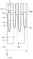
제2 콘택홀들(CNH2)에 채워지는 도전 물질은 예를 들어, 폴리실리콘 또는 금속 물질일 수 있다.The conductive material filled in the second contact holes (CNH2) may be, for example, polysilicon or a metal material.
몇몇 실시예에 따르면, 마스크 패턴(MP)의 높이를 종래보다 낮게 형성함에 따라, 제1 콘택(CNT_1)을 보다 신뢰성있게 형성할 수 있다.According to some embodiments, the first contact (CNT_1) can be formed more reliably by forming the height of the mask pattern (MP) lower than conventionally.
제1 콘택들(CNT_1)을 식각하여, 제1 콘택들(CNT_1)의 측벽 및 게이트 캐핑막(GP)의 상면을 노출시키는 제4 트렌치(TR4)를 형성할 수 있다. 예를 들어, 제4 트렌치(TR4)의 제4 방향(D4)을 따른 깊이(T2)는 300보다 작을 수 있으나, 이에 제한되지 않는다.The first contacts (CNT_1) can be etched to form a fourth trench (TR4) exposing the sidewalls of the first contacts (CNT_1) and the upper surface of the gate capping film (GP). For example, the depth (T2) of the fourth trench (TR4) along the fourth direction (D4) is 300 It may be smaller than, but is not limited to, this.
몇몇 실시예에 따르면, 마스크 패턴(MP)의 높이를 종래보다 낮게 형성함에 따라, 제4 트렌치(TR4)의 깊이를 종래보다 작게 형성할 수 있다. 이에 따라, 제1 콘택(CNT_1)을 에칭하기 위한 공정에 소요되는 비용 및 공정의 난이도가 감소될 수 있다.According to some embodiments, by forming the height of the mask pattern (MP) lower than conventionally, the depth of the fourth trench (TR4) can be formed smaller than conventionally. Accordingly, the cost and difficulty of the process for etching the first contact (CNT_1) can be reduced.
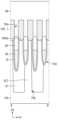
도 20, 도 21a 및 도 21b를 참조하면, 제2 트렌치(TR4)를 채우고, 제1 콘택들(CNT_1)의 상면을 덮는 몰드층(TM)을 형성할 수 있다.Referring to FIG. 20, FIG. 21a, and FIG. 21b, a mold layer (TM) can be formed to fill the second trench (TR4) and cover the upper surface of the first contacts (CNT_1).
도 21a를 참조하면, 몰드층(TM)은 비트 라인 구조체(LST)의 상면을 함께 덮어, 비트 라인 구조체(LST)의 상면 전체와 접촉할 수 있다. 또한 몰드층(TM)은 비트 라인 구조체(LST)의 측면 일부를 덮어 비트 라인 구조체(LST)의 측면 일부와 접촉할 수 있으나, 이에 제한되지 않는다.Referring to FIG. 21a, the mold layer (TM) may cover the upper surface of the bit line structure (LST) together and may be in contact with the entire upper surface of the bit line structure (LST). In addition, the mold layer (TM) may cover a portion of a side surface of the bit line structure (LST) and may be in contact with a portion of the side surface of the bit line structure (LST), but is not limited thereto.
도 21b를 참조하면, 몰드층(TM)은 제1 콘택들(CNT_1)의 측벽과 상면 및 게이트 캐핑막(GP)의 상면과 접촉할 수 있다. 예를 들어, 몰드층(TM)은 실리콘 질화물을 포함할 수 있으나, 이에 제한되지 않는다.Referring to FIG. 21b, the mold layer (TM) may be in contact with the sidewalls and upper surfaces of the first contacts (CNT_1) and the upper surface of the gate capping film (GP). For example, the mold layer (TM) may include, but is not limited to, silicon nitride.
도 22, 도 23a 및 도 23b를 참조하면, 몰드층(TM)을 식각하여, 몰드층(TM)의 측벽 및 제1 콘택들(CNT_1)의 상면을 노출시키는 제5 트렌치(TR5)를 형성할 수 있다. 예를 들어, 제5 트렌치(TR5)는 역사다리꼴 형상일 수 있다. 이에 따라, 식각된 몰드층(TM)은 사다리꼴 형상이고, 후술하는 제2 콘택들(CNT_2)은 역사다리꼴 형상으로 형성될 수 있으나, 이에 제한되지 않는다.Referring to FIGS. 22, 23a, and 23b, a fifth trench (TR5) may be formed by etching the mold layer (TM) to expose a sidewall of the mold layer (TM) and an upper surface of the first contacts (CNT_1). For example, the fifth trench (TR5) may have an inverted trapezoidal shape. Accordingly, the etched mold layer (TM) may have a trapezoidal shape, and the second contacts (CNT_2) described below may be formed in an inverted trapezoidal shape, but are not limited thereto.
제4 및 제5 트렌치(TR4, TR5)는 서로 다른 공정에 의해 형성되므로, 제5 트렌치(TR5)의 측벽의 프로파일은 제4 트렌치(TR4)의 측벽의 프로파일과 다를 수 있다. 제5 트렌치(TR5)의 측벽의 기울기는 제4 트렌치(TR4)의 측벽의 기울기와 다를 수 있다.Since the fourth and fifth trenches (TR4, TR5) are formed by different processes, the profile of the sidewall of the fifth trench (TR5) may be different from the profile of the sidewall of the fourth trench (TR4). The slope of the sidewall of the fifth trench (TR5) may be different from the slope of the sidewall of the fourth trench (TR4).
도 24, 도 25a 및 도 25b를 참조하면, 제1 콘택들(CNT_1) 상에, 제5 트렌치(TR5)를 채우는 제2 콘택들(CNT_2)을 형성할 수 있다. 이로써, 도전 물질이 몰드층(TM)에 의해 분리될 수 있다. 이에 따라, 도 1 내지 도 3에 도시된 것과 같이, 콘택들(CNT) 및 절연 패턴들(INP)은 제1 방향(D1) 및 제2 방향(D2)을 따라 서로 교대로 배열될 수 있다.Referring to FIGS. 24, 25a, and 25b, second contacts (CNT_2) filling the fifth trenches (TR5) can be formed on the first contacts (CNT_1). As a result, the conductive material can be separated by the mold layer (TM). Accordingly, as illustrated in FIGS. 1 to 3, the contacts (CNT) and the insulating patterns (INP) can be alternately arranged along the first direction (D1) and the second direction (D2).
구체적으로 도시되지는 않았으나, 콘택들(CNT) 상에 제1 전극들, 유전막 및 제2 전극들이 각각 형성될 수 있다. 제1 전극들, 유전막 및 제2 전극들은 정보 저장 요소, 예를 들어, 캐패시터를 구성할 수 있다.Although not specifically shown, first electrodes, a dielectric film and second electrodes may be formed on the contacts (CNTs), respectively. The first electrodes, the dielectric film and the second electrodes may form an information storage element, for example, a capacitor.
이에 따라, 도 1 및 도 2a 내지 도 2b에 도시된 것과 같은 반도체 메모리 장치가 형성될 수 있다.Accordingly, a semiconductor memory device such as that illustrated in FIG. 1 and FIGS. 2a to 2b can be formed.
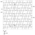
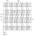
도 26은 몇몇 실시예들에 따른 반도체 메모리 장치의 개략적인 레이아웃도이다. 도 27a는 도 26의 A - A'를 따라 절단한 예시적인 단면도이다. 도 27b는 도 26의 B - B'를 따라 절단한 예시적인 단면도이다. 도 28은 몇몇 실시예들에 따른 반도체 메모리 장치를 상부에서 바라본 평면도이다. 참고적으로, 도 28은 도 27a 및 도 27b의 반도체 메모리 장치를 상부에서 바라본 평면도일 수 있다. 설명의 편의상 도 1 내지 도 25b를 이용하여 설명한 것과 다른 점을 중심으로 설명한다.FIG. 26 is a schematic layout diagram of a semiconductor memory device according to some embodiments. FIG. 27a is an exemplary cross-sectional view taken along line A-A' of FIG. 26. FIG. 27b is an exemplary cross-sectional view taken along line B-B' of FIG. 26. FIG. 28 is a top plan view of a semiconductor memory device according to some embodiments. For reference, FIG. 28 may be a top plan view of the semiconductor memory devices of FIGS. 27a and 27b. For convenience of explanation, the description will focus on differences from those described using FIGS. 1 to 25b.
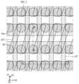
도 26을 참조하면, 평면적 관점에서, 활성 패턴들(ACT)은 복수의 행들 및 복수의 열들을 따라 2차원적으로 배열될 수 있다. 활성 패턴들(ACT) 각각은, 기판(100)의 상면에 평행한 제3 방향(D3)으로 연장될 수 있다. 활성 패턴들(ACT) 각각은 제3 방향(D3)으로의 장축을 가질 수 있다.Referring to FIG. 26, in a planar view, the active patterns (ACT) can be two-dimensionally arranged along a plurality of rows and a plurality of columns. Each of the active patterns (ACT) can extend in a third direction (D3) parallel to the upper surface of the substrate (100). Each of the active patterns (ACT) can have a long axis in the third direction (D3).
하나의 활성 패턴(ACT)의 단부는 이웃하는 다른 활성 패턴(ACT)의 단부에 인접하도록 배열될 수 있다. 하나의 활성 패턴(ACT)의 단부는 이웃하는 다른 활성 패턴(ACT)의 단부와 제2 방향(D2)으로 인접할 수 있다. 콘택(CNT)은 활성 패턴(ACT)의 중심에 인접하게 배치되지 않을 수 있다.An end of one active pattern (ACT) may be arranged adjacent to an end of another adjacent active pattern (ACT). An end of one active pattern (ACT) may be adjacent to an end of another adjacent active pattern (ACT) in a second direction (D2). The contact (CNT) may not be arranged adjacent to the center of the active pattern (ACT).
게이트 전극(GE)은, 제2 방향(D2)으로 연장되는 하나의 행을 따라 배열되어 서로 인접하는 활성 패턴들(ACT)과 교차할 수 있다. 게이트 전극(GE)은 제1 방향(D1) 또는 제3 방향(D3)을 기준으로, 서로 인접하는 하나의 활성 패턴(ACT)의 단부와 다른 하나의 활성 패턴(ACT)의 단부 사이에 배치되지 않을 수 있다.The gate electrode (GE) may be arranged along one row extending in the second direction (D2) and may intersect adjacent active patterns (ACT). The gate electrode (GE) may not be arranged between an end of one adjacent active pattern (ACT) and an end of another adjacent active pattern (ACT) with respect to the first direction (D1) or the third direction (D3).
비트 라인 구조체(LST)는, 제1 방향(D1)으로 연장되는 하나의 열을 따라 배열되고 서로 인접하는 활성 패턴들(ACT)과 교차할 수 있다.The bit line structures (LSTs) are arranged along one column extending in the first direction (D1) and can intersect with adjacent active patterns (ACTs).
콘택들(CNT)은 제1 방향(D1) 및 제2 방향(D2)을 따라 2차원적으로 배열될 수 있다. 절연 패턴(INP)은 콘택들(CNT)이 배치되지 않은 게이트 캐핑막(GP) 사이에 배치될 수 있다.Contacts (CNT) can be two-dimensionally arranged along the first direction (D1) and the second direction (D2). An insulating pattern (INP) can be arranged between gate capping films (GP) where contacts (CNT) are not arranged.
이하에서, 도 29 내지 도 34b를 이용하여 몇몇 실시예들에 따른 반도체 메모리 장치의 제조 방법을 설명한다. 설명의 편의상 도 4 내지 도 25b 및 도 26 내지 도 28을 이용하여 설명한 것과 다른 점을 중심으로 설명한다.Hereinafter, a method for manufacturing a semiconductor memory device according to some embodiments will be described using FIGS. 29 to 34b. For convenience of explanation, the description will focus on differences from those described using FIGS. 4 to 25b and FIGS. 26 to 28.
도 29, 도 31 및 도 33은 몇몇 실시예들에 따른 반도체 메모리 장치의 제조 방법을 설명하기 위한 평면도들이다. 도 30a, 도 32a 및 도 34a는 각각 도 29, 도 31 및 도 33의 A-A'선에 따른 단면도들이다. 도 30b, 도 32b 및 도 34b는 각각 도 29, 도 31 및 도 33의 B-B'선에 따른 단면도들이다.FIGS. 29, 31, and 33 are plan views for explaining a method of manufacturing a semiconductor memory device according to some embodiments. FIGS. 30a, 32a, and 34a are cross-sectional views taken along line A-A' of FIGS. 29, 31, and 33, respectively. FIGS. 30b, 32b, and 34b are cross-sectional views taken along line B-B' of FIGS. 29, 31, and 33, respectively.
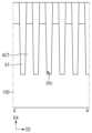
도 29, 도 30a 및 도 30b를 참조하면, 제1 콘택들(CNT_1)을 식각하여, 제1 콘택들(CNT_1)의 측벽 및 게이트 캐핑막(GP)의 적어도 일부를 노출시키는 제4 트렌치(TR4)를 형성할 수 있다. 예를 들어, 제4 트렌치(TR4)의 제4 방향(D4)을 따른 깊이(T2)는 300보다 작을 수 있으나, 이에 제한되지 않는다.Referring to FIGS. 29, 30A, and 30B, the first contacts (CNT_1) may be etched to form a fourth trench (TR4) exposing at least a portion of the sidewall of the first contacts (CNT_1) and the gate capping film (GP). For example, the depth (T2) of the fourth trench (TR4) along the fourth direction (D4) may be 300 It may be smaller than, but is not limited to, this.
도 31, 도 32a 및 도 32b를 참조하면, 제2 트렌치(TR4)를 채우고, 제1 콘택들(CNT_1)의 상면을 덮는 몰드층(TM)을 형성할 수 있다.Referring to FIG. 31, FIG. 32a, and FIG. 32b, a mold layer (TM) can be formed to fill the second trench (TR4) and cover the upper surface of the first contacts (CNT_1).
도 32a를 참조하면, 몰드층(TM)은 비트 라인 구조체(LST)의 상면을 함께 덮어, 비트 라인 구조체(LST)의 상면 전체와 접촉할 수 있다. 도시된 것과 달리, 몰드층(TM)은 비트 라인 구조체(LST)의 측면 일부를 덮어 비트 라인 구조체(LST)의 측면 일부와 접촉할 수도 있다.Referring to FIG. 32a, the mold layer (TM) may cover the upper surface of the bit line structure (LST) together and may be in contact with the entire upper surface of the bit line structure (LST). Unlike what is illustrated, the mold layer (TM) may cover a portion of the side surface of the bit line structure (LST) and may be in contact with a portion of the side surface of the bit line structure (LST).
도 32b를 참조하면, 몰드층(TM)은 제1 콘택들(CNT_1)의 측벽과 상면 및 게이트 캐핑막(GP)의 상면의 일부와 접촉할 수 있다. 예를 들어, 몰드층(TM)은 실리콘 질화물을 포함할 수 있으나, 이에 제한되지 않는다.Referring to FIG. 32b, the mold layer (TM) may be in contact with the sidewalls and upper surfaces of the first contacts (CNT_1) and a portion of the upper surface of the gate capping film (GP). For example, the mold layer (TM) may include, but is not limited to, silicon nitride.
도 33, 도 34a 및 도 34b를 참조하면, 몰드층(TM)을 식각하여, 몰드층(TM)의 측벽 및 제1 콘택들(CNT_1)의 상면을 노출시키는 제5 트렌치(TR5)를 형성할 수 있다.Referring to FIGS. 33, 34a, and 34b, the mold layer (TM) can be etched to form a fifth trench (TR5) exposing the sidewall of the mold layer (TM) and the upper surface of the first contacts (CNT_1).
제4 및 제5 트렌치(TR4, TR5)는 서로 다른 공정에 의해 형성되므로, 제5 트렌치(TR5)의 측벽의 프로파일은 제4 트렌치(TR4)의 측벽의 프로파일과 다를 수 있다. 제5 트렌치(TR5)의 측벽의 기울기는 제4 트렌치(TR4)의 측벽의 기울기와 다를 수 있다.Since the fourth and fifth trenches (TR4, TR5) are formed by different processes, the profile of the sidewall of the fifth trench (TR5) may be different from the profile of the sidewall of the fourth trench (TR4). The slope of the sidewall of the fifth trench (TR5) may be different from the slope of the sidewall of the fourth trench (TR4).
예를 들어, 노출된 제1 콘택들(CNT_1) 각각의 제2 방향(D2)을 따른 폭(W5)은 제5 트렌치(TR5) 각각의 제2 방향(D2)을 따른 폭보다 작거나 같을 수 있다.For example, the width (W5) of each of the exposed first contacts (CNT_1) along the second direction (D2) may be smaller than or equal to the width of each of the fifth trenches (TR5) along the second direction (D2).
이후, 제1 콘택들(CNT_1) 상에, 제5 트렌치(TR5)를 채우는 제2 콘택들(CNT_2)을 형성할 수 있다. 이로써, 도전 물질이 몰드층(TM)에 의해 분리될 수 있다. 이에 따라, 도 26 내지 도 28에 도시된 것과 같은 반도체 메모리 장치가 형성될 수 있다.Thereafter, second contacts (CNT_2) filling the fifth trench (TR5) can be formed on the first contacts (CNT_1). As a result, the conductive material can be separated by the mold layer (TM). Accordingly, a semiconductor memory device such as that illustrated in FIGS. 26 to 28 can be formed.
이상 첨부된 도면을 참조하여 본 발명의 실시예를 설명하였지만, 본 발명이 속하는 기술분야에서 통상의 지식을 가진 자는 본 발명이 그 기술적 사상이나 필수적인 특징을 변경하지 않고서 다른 구체적인 형태로 실시될 수 있다는 것을 이해할 수 있을 것이다. 그러므로 이상에서 기술한 실시예들은 모든 면에서 예시적인 것이며 한정적이 아닌 것으로 이해해야만 한다.Although the embodiments of the present invention have been described with reference to the attached drawings, those skilled in the art will understand that the present invention can be implemented in other specific forms without changing the technical idea or essential features thereof. Therefore, it should be understood that the embodiments described above are exemplary in all respects and not restrictive.
100: 기판ACT: 활성 패턴
IL: 절연막GE: 게이트 전극
GI: 게이트 유전막GP: 게이트 캐핑막
LST: 비트 라인 구조체 CP: 도전 패턴
BP: 배리어 패턴BL: 비트 라인
MP: 마스크 패턴CNP: 비트 라인 콘택
CNT_1: 제1 콘택CNT_2: 제2 콘택
INP: 절연 패턴100: Substrate ACT: Active Pattern
IL: Insulator GE: Gate electrode
GI: Gate dielectric film GP: Gate capping film
LST: Bit line structure CP: Challenge pattern
BP: Barrier Pattern BL: Bit Line
MP: Mask pattern CNP: Bit line contact
CNT_1: First contact CNT_2: Second contact
INP: Insulation pattern
Claims (10)
Translated fromKorean상기 기판 내에, 상기 활성 패턴들과 교차하도록 제1 방향으로 연장되는 게이트 구조체;
상기 기판 상에, 상기 제1 방향과 다른 제2 방향을 따라 연장되는 비트 라인 구조체;
상기 비트 라인 구조체와 상기 제1 방향을 따라 서로 교대로 배치되는 제1 콘택;
상기 비트 라인 구조체 상에, 상기 제1 콘택의 측벽 및 상기 게이트 구조체의 적어도 일부를 노출시키는 제1 트렌치를 채우는 절연 패턴; 및
상기 제1 콘택 상에, 상기 절연 패턴의 측벽 및 상기 제1 콘택의 상면을 노출시키는 제2 트렌치를 채우는 제2 콘택을 포함하되,
상기 절연 패턴은, 상기 비트 라인 구조체의 상면 전체를 덮고, 상기 제1 및 제2 콘택과 접촉하도록 상기 제1 및 제2 트렌치의 측벽을 따라 연장되는 반도체 메모리 장치.A substrate comprising a plurality of active patterns;
A gate structure extending in a first direction so as to intersect the active patterns within the substrate;
A bit line structure extending along a second direction different from the first direction on the substrate;
The bit line structure and the first contact alternately arranged along the first direction;
An insulating pattern filling a first trench on the bit line structure, the first trench exposing a sidewall of the first contact and at least a portion of the gate structure; and
A second contact is included on the first contact, filling a second trench exposing a sidewall of the insulating pattern and an upper surface of the first contact,
A semiconductor memory device in which the insulating pattern covers the entire upper surface of the bit line structure and extends along sidewalls of the first and second trenches so as to make contact with the first and second contacts.
상기 절연 패턴은, 상기 제1 콘택과 접촉하는 제1 영역 및 상기 제1 영역 상에 배치되고 상기 제2 콘택과 접촉하는 제2 영역을 포함하고,
상기 제1 영역의 측벽의 프로파일은 상기 제2 영역의 측벽의 프로파일과 다른 반도체 메모리 장치.In the first paragraph,
The insulating pattern includes a first region in contact with the first contact and a second region disposed on the first region and in contact with the second contact,
A semiconductor memory device wherein the profile of the sidewall of the first region is different from the profile of the sidewall of the second region.
상기 제1 및 제2 영역은 서로 동일한 물질을 포함하는 반도체 메모리 장치.In the second paragraph,
A semiconductor memory device wherein the first and second regions include the same material.
상기 제2 콘택의 하면의 폭은 상기 제2 콘택의 상면의 폭보다 작은 반도체 메모리 장치.In the first paragraph,
A semiconductor memory device wherein the width of the lower surface of the second contact is smaller than the width of the upper surface of the second contact.
상기 제1 트렌치의 측벽의 기울기와 상기 제2 트렌치의 측벽의 기울기는 서로 다르고,
상기 제1 콘택의 측벽의 기울기와 상기 제2 콘택의 측벽의 기울기는 서로 다른 반도체 메모리 장치.In the first paragraph,
The slope of the side wall of the first trench and the slope of the side wall of the second trench are different from each other,
A semiconductor memory device wherein the slope of the sidewall of the first contact and the slope of the sidewall of the second contact are different from each other.
상기 절연 패턴은, 상기 제1 및 제2 트렌치의 측벽을 따라 일체로 형성되는 반도체 메모리 장치.In the first paragraph,
A semiconductor memory device in which the above insulating pattern is integrally formed along the sidewalls of the first and second trenches.
평면적 관점에서, 상기 활성 패턴들은 복수의 행들 및 복수의 열들을 따라 배열되는 반도체 메모리 장치.In the first paragraph,
A semiconductor memory device in which, in a planar view, the active patterns are arranged along a plurality of rows and a plurality of columns.
상기 기판 내에, 상기 활성 패턴들과 교차하도록 제1 방향으로 연장되는 게이트 구조체들;
상기 기판 상에, 상기 제1 방향과 다른 제2 방향을 따라 연장되는 비트 라인 구조체들;
상기 비트 라인 구조체들 사이에 배치되고, 상기 소오스/드레인 영역과 연결되는 제1 콘택;
상기 비트 라인 구조체 상에, 상기 제1 콘택의 측벽 및 상기 게이트 구조체의 적어도 일부를 노출시키는 제1 트렌치를 채우는 절연 패턴; 및
상기 제1 콘택 상에, 상기 절연 패턴의 측벽 및 상기 제1 콘택의 상면을 노출시키는 제2 트렌치를 채우는 제2 콘택을 포함하되,
상기 절연 패턴은, 상기 제1 콘택과 접촉하는 제1 영역 및 상기 제1 영역 상에 배치되고 상기 제2 콘택과 접촉하는 제2 영역을 포함하고,
상기 제2 영역은 상기 비트 라인 구조체의 상면 전체와 접촉하고,
상기 제1 및 제2 영역은 상기 제1 및 제2 트렌치의 측벽 상에 상기 제1 및 제2 트렌치의 측벽을 따라 연장되는 반도체 메모리 장치.A substrate comprising active patterns having source/drain regions formed therein;
Within the substrate, gate structures extending in a first direction so as to intersect the active patterns;
On the above substrate, bit line structures extending along a second direction different from the first direction;
A first contact disposed between the bit line structures and connected to the source/drain region;
An insulating pattern filling a first trench on the bit line structure, the first trench exposing a sidewall of the first contact and at least a portion of the gate structure; and
A second contact is included on the first contact, filling a second trench exposing a sidewall of the insulating pattern and an upper surface of the first contact,
The insulating pattern includes a first region in contact with the first contact and a second region disposed on the first region and in contact with the second contact,
The second region is in contact with the entire upper surface of the bit line structure,
A semiconductor memory device wherein the first and second regions extend along the sidewalls of the first and second trenches on the sidewalls of the first and second trenches.
상기 비트 라인 구조체와 상기 절연 패턴은 수직 방향으로 서로 중첩되고,
상기 제1 영역과 상기 제2 영역은 수직 방향으로 서로 중첩되는 반도체 메모리 장치.In Article 8,
The above bit line structure and the above insulating pattern overlap each other in the vertical direction,
A semiconductor memory device in which the first region and the second region overlap each other in the vertical direction.
상기 기판 상의 절연막;
상기 기판 내에, 상기 활성 패턴들과 교차하도록 제1 방향으로 연장되는 게이트 구조체;
상기 절연막 상에, 상기 제1 방향과 다른 제2 방향을 따라 연장되고, 상기 절연막을 관통하여 상기 제1 소오스/드레인 영역과 전기적으로 연결되는 비트 라인 구조체;
상기 비트 라인 구조체와 상기 제1 방향을 따라 이격 배치되고, 상기 제2 소오스/드레인 영역과 전기적으로 연결되는 제1 콘택;
상기 비트 라인 구조체의 상부 및 상기 게이트 구조체의 상부를 덮는 절연 패턴; 및
상기 제1 콘택 상에, 상기 제1 콘택과 전기적으로 연결되는 제2 콘택을 포함하되,
상기 절연 패턴은, 상기 비트 라인 구조체와 수직 방향으로 정렬되고, 상기 제1 및 제2 콘택과 접촉하도록 상기 게이트 구조체의 상부까지 연장되는 반도체 메모리 장치.
A substrate comprising a plurality of active patterns having first and second source/drain regions formed thereon;
An insulating film on the above substrate;
A gate structure extending in a first direction so as to intersect the active patterns within the substrate;
A bit line structure extending along a second direction different from the first direction on the insulating film, penetrating the insulating film and electrically connected to the first source/drain region;
A first contact spaced apart from the bit line structure along the first direction and electrically connected to the second source/drain region;
An insulating pattern covering the upper portion of the bit line structure and the upper portion of the gate structure; and
On the first contact, a second contact electrically connected to the first contact is included,
A semiconductor memory device wherein the insulating pattern is aligned in a vertical direction with respect to the bit line structure and extends to an upper portion of the gate structure so as to be in contact with the first and second contacts.
Priority Applications (3)
| Application Number | Priority Date | Filing Date | Title |
|---|---|---|---|
| KR1020230051746AKR20240155458A (en) | 2023-04-20 | 2023-04-20 | Semiconductor memory device |
| US18/525,235US20240357802A1 (en) | 2023-04-20 | 2023-11-30 | Semiconductor memory devices |
| CN202410272188.9ACN118829208A (en) | 2023-04-20 | 2024-03-11 | Semiconductor memory devices |
Applications Claiming Priority (1)
| Application Number | Priority Date | Filing Date | Title |
|---|---|---|---|
| KR1020230051746AKR20240155458A (en) | 2023-04-20 | 2023-04-20 | Semiconductor memory device |
Publications (1)
| Publication Number | Publication Date |
|---|---|
| KR20240155458Atrue KR20240155458A (en) | 2024-10-29 |
Family
ID=93083176
Family Applications (1)
| Application Number | Title | Priority Date | Filing Date |
|---|---|---|---|
| KR1020230051746APendingKR20240155458A (en) | 2023-04-20 | 2023-04-20 | Semiconductor memory device |
Country Status (3)
| Country | Link |
|---|---|
| US (1) | US20240357802A1 (en) |
| KR (1) | KR20240155458A (en) |
| CN (1) | CN118829208A (en) |
Families Citing this family (2)
| Publication number | Priority date | Publication date | Assignee | Title |
|---|---|---|---|---|
| US12317571B2 (en)* | 2022-06-21 | 2025-05-27 | Nanya Technology Corporation | Semiconductor device and method for manufacturing the same |
| US12268029B2 (en)* | 2022-06-21 | 2025-04-01 | Nanya Technology Corporation | Method for manufacturing semiconductor device |
- 2023
- 2023-04-20KRKR1020230051746Apatent/KR20240155458A/enactivePending
- 2023-11-30USUS18/525,235patent/US20240357802A1/enactivePending
- 2024
- 2024-03-11CNCN202410272188.9Apatent/CN118829208A/enactivePending
Also Published As
| Publication number | Publication date |
|---|---|
| US20240357802A1 (en) | 2024-10-24 |
| CN118829208A (en) | 2024-10-22 |
Similar Documents
| Publication | Publication Date | Title |
|---|---|---|
| KR102813671B1 (en) | Semiconductor memory device and Method of fabricating the same | |
| US12279415B2 (en) | Method of fabricating semiconductor memory device having protruding contact portion | |
| US12238920B2 (en) | Semiconductor devices having air spacer | |
| KR102779204B1 (en) | Semiconductor memory device and method for manufacturing the same | |
| KR20240155458A (en) | Semiconductor memory device | |
| JP4871514B2 (en) | Semiconductor device having capacitor and method for manufacturing the same | |
| US12426340B2 (en) | Semiconductor memory device | |
| US20220181326A1 (en) | Semiconductor memory device | |
| KR102794650B1 (en) | Semiconductor memory device and method of manufaturing the semiconductor memory device | |
| TWI812387B (en) | Semiconductor device | |
| US20250227925A1 (en) | Semiconductor device | |
| US20240389308A1 (en) | Semiconductor device | |
| KR20250041462A (en) | Semiconductor devices | |
| KR20250120827A (en) | Etchant composition, method of manufacturing semiconductor device using the same, and semiconductor device | |
| KR20230106422A (en) | Semiconductor device | |
| KR20230013683A (en) | Semiconductor device | |
| KR20250108404A (en) | Semiconductor memory device | |
| KR20230107027A (en) | Semiconductor device | |
| KR20250028034A (en) | Semiconductor device |
Legal Events
| Date | Code | Title | Description |
|---|---|---|---|
| PA0109 | Patent application | Patent event code:PA01091R01D Comment text:Patent Application Patent event date:20230420 | |
| PG1501 | Laying open of application |