KR20240144710A - Display apparatus and method for manufacturing display apparatus - Google Patents
Display apparatus and method for manufacturing display apparatusDownload PDFInfo
- Publication number
- KR20240144710A KR20240144710AKR1020230084506AKR20230084506AKR20240144710AKR 20240144710 AKR20240144710 AKR 20240144710AKR 1020230084506 AKR1020230084506 AKR 1020230084506AKR 20230084506 AKR20230084506 AKR 20230084506AKR 20240144710 AKR20240144710 AKR 20240144710A
- Authority
- KR
- South Korea
- Prior art keywords
- layer
- area
- resin layer
- display device
- corner
- Prior art date
- Legal status (The legal status is an assumption and is not a legal conclusion. Google has not performed a legal analysis and makes no representation as to the accuracy of the status listed.)
- Pending
Links
Images


Classifications
- G—PHYSICS
- G06—COMPUTING OR CALCULATING; COUNTING
- G06F—ELECTRIC DIGITAL DATA PROCESSING
- G06F1/00—Details not covered by groups G06F3/00 - G06F13/00 and G06F21/00
- G06F1/16—Constructional details or arrangements
- G06F1/1613—Constructional details or arrangements for portable computers
- G06F1/1633—Constructional details or arrangements of portable computers not specific to the type of enclosures covered by groups G06F1/1615 - G06F1/1626
- G06F1/1656—Details related to functional adaptations of the enclosure, e.g. to provide protection against EMI, shock, water, or to host detachable peripherals like a mouse or removable expansions units like PCMCIA cards, or to provide access to internal components for maintenance or to removable storage supports like CDs or DVDs, or to mechanically mount accessories
- B—PERFORMING OPERATIONS; TRANSPORTING
- B32—LAYERED PRODUCTS
- B32B—LAYERED PRODUCTS, i.e. PRODUCTS BUILT-UP OF STRATA OF FLAT OR NON-FLAT, e.g. CELLULAR OR HONEYCOMB, FORM
- B32B27/00—Layered products comprising a layer of synthetic resin
- B32B27/06—Layered products comprising a layer of synthetic resin as the main or only constituent of a layer, which is next to another layer of the same or of a different material
- B32B27/08—Layered products comprising a layer of synthetic resin as the main or only constituent of a layer, which is next to another layer of the same or of a different material of synthetic resin
- G—PHYSICS
- G06—COMPUTING OR CALCULATING; COUNTING
- G06F—ELECTRIC DIGITAL DATA PROCESSING
- G06F1/00—Details not covered by groups G06F3/00 - G06F13/00 and G06F21/00
- G06F1/16—Constructional details or arrangements
- G06F1/1613—Constructional details or arrangements for portable computers
- G06F1/1626—Constructional details or arrangements for portable computers with a single-body enclosure integrating a flat display, e.g. Personal Digital Assistants [PDAs]
- G—PHYSICS
- G06—COMPUTING OR CALCULATING; COUNTING
- G06F—ELECTRIC DIGITAL DATA PROCESSING
- G06F1/00—Details not covered by groups G06F3/00 - G06F13/00 and G06F21/00
- G06F1/16—Constructional details or arrangements
- G06F1/1613—Constructional details or arrangements for portable computers
- G06F1/1633—Constructional details or arrangements of portable computers not specific to the type of enclosures covered by groups G06F1/1615 - G06F1/1626
- G06F1/1637—Details related to the display arrangement, including those related to the mounting of the display in the housing
- G06F1/1652—Details related to the display arrangement, including those related to the mounting of the display in the housing the display being flexible, e.g. mimicking a sheet of paper, or rollable
- G—PHYSICS
- G09—EDUCATION; CRYPTOGRAPHY; DISPLAY; ADVERTISING; SEALS
- G09F—DISPLAYING; ADVERTISING; SIGNS; LABELS OR NAME-PLATES; SEALS
- G09F9/00—Indicating arrangements for variable information in which the information is built-up on a support by selection or combination of individual elements
- G09F9/30—Indicating arrangements for variable information in which the information is built-up on a support by selection or combination of individual elements in which the desired character or characters are formed by combining individual elements
- G09F9/301—Indicating arrangements for variable information in which the information is built-up on a support by selection or combination of individual elements in which the desired character or characters are formed by combining individual elements flexible foldable or roll-able electronic displays, e.g. thin LCD, OLED
- B—PERFORMING OPERATIONS; TRANSPORTING
- B32—LAYERED PRODUCTS
- B32B—LAYERED PRODUCTS, i.e. PRODUCTS BUILT-UP OF STRATA OF FLAT OR NON-FLAT, e.g. CELLULAR OR HONEYCOMB, FORM
- B32B2457/00—Electrical equipment
- B32B2457/20—Displays, e.g. liquid crystal displays, plasma displays
- G—PHYSICS
- G06—COMPUTING OR CALCULATING; COUNTING
- G06F—ELECTRIC DIGITAL DATA PROCESSING
- G06F2200/00—Indexing scheme relating to G06F1/04 - G06F1/32
- G06F2200/16—Indexing scheme relating to G06F1/16 - G06F1/18
- G06F2200/163—Indexing scheme relating to constructional details of the computer
- G06F2200/1635—Stackable modules
Landscapes
- Engineering & Computer Science (AREA)
- Theoretical Computer Science (AREA)
- Computer Hardware Design (AREA)
- Physics & Mathematics (AREA)
- General Physics & Mathematics (AREA)
- General Engineering & Computer Science (AREA)
- Human Computer Interaction (AREA)
- Devices For Indicating Variable Information By Combining Individual Elements (AREA)
- Electroluminescent Light Sources (AREA)
Abstract
Translated fromKoreanDescription
Translated fromKorean본 발명의 실시예들은 표시 장치 및 표시 장치의 제조 방법에 관한 것이다.Embodiments of the present invention relate to a display device and a method for manufacturing the display device.
최근 전자 기기가 폭 넓게 사용되고 있다. 전자 기기는 이동형 전자 기기와 고정형 전자 기기와 같이 다양하게 이용되고 있으며, 이러한 전자 기기는 다양한 기능을 지원하기 위해 이미지 또는 영상과 같은 시각 정보를 사용자에게 제공할 수 있는 표시 장치를 포함한다.Electronic devices have been widely used recently. Electronic devices are used in various ways, such as mobile electronic devices and fixed electronic devices, and these electronic devices include display devices that can provide visual information, such as images or videos, to users to support various functions.
최근 표시 장치를 구동하기 위한 기타 부품들이 소형화됨에 따라, 표시 장치가 전자 기기에서 차지하는 비중이 점차 증가하고 있는 추세이며 편평한 상태에서 소정의 각도를 갖도록 구부리거나 축을 중심으로 폴딩 또는 벤딩되는 구조도 개발되고 있다.As other components for driving display devices have become smaller in recent years, the proportion of display devices in electronic devices is gradually increasing, and structures that bend from a flat state to a certain angle or fold or bend around an axis are also being developed.
소정의 각도를 갖도록 구부리는 표시 장치는 표시 장치를 구부리는 과정에서 표시 장치, 예컨대 표시 패널에 크랙이 발생할 수 있는 문제점이 있었다.A display device that is bent to have a predetermined angle has a problem in that cracks may occur in the display device, such as the display panel, during the process of bending the display device.
본 발명의 실시예들은 상기와 같은 문제점을 포함하여 여러 문제점들을 해결하기 위한 것으로, 크랙과 같은 불량을 방지할 수 있는 표시 장치 및 표시 장치의 제조 방법을 제공하는 것을 목적으로 한다. 다만 이러한 과제는 예시적인 것으로, 본 발명의 해결하고자 하는 과제는 이에 한정되지 않는다.Embodiments of the present invention are intended to solve various problems including the above-mentioned problems, and to provide a display device and a method for manufacturing the display device capable of preventing defects such as cracks. However, these problems are exemplary, and the problems to be solved by the present invention are not limited thereto.
본 발명의 일 관점에서는, 중심영역, 상기 중심영역의 코너에 배치된 코너영역을 포함하는 기판을 포함하는 표시 패널; 및 상기 표시 패널 상에 배치되는 수지층;을 구비하고, 상기 코너영역은 상기 중심영역으로부터 멀어지는 방향으로 연장되는 복수 개의 연장영역 및 상기 복수 개의 연장영역 사이의 이격영역을 포함하고, 상기 수지층은 상기 복수 개의 연장영역과 중첩하는 복수 개의 수지층 연장영역을 포함하는, 표시 장치를 개시한다.In one aspect of the present invention, a display device is disclosed, comprising: a display panel including a substrate including a central region, corner regions arranged at corners of the central region; and a resin layer arranged on the display panel; wherein the corner regions include a plurality of extension regions extending away from the central region and a separation region between the plurality of extension regions, and the resin layer includes a plurality of resin layer extension regions overlapping the plurality of extension regions.
일 실시예에서, 상기 수지층의 측면은 상기 기판의 상면에 대하여 80도 내지 100도의 각도를 가질 수 있다.In one embodiment, the side of the resin layer can have an angle of 80 to 100 degrees with respect to the upper surface of the substrate.
일 실시예에서, 상기 수지층은, 우레탄 아크릴레이트 올리고머, 에폭시 아크릴레이트 올리고머, 다관능기 아크릴레이트 모노머, 비스페놀 모노머, 저분자 에틸렌글리콜 모노머, 및 광 개시제를 포함하는, 수지 조성물의 경화물일 수 있다.In one embodiment, the resin layer may be a cured product of a resin composition comprising a urethane acrylate oligomer, an epoxy acrylate oligomer, a multifunctional acrylate monomer, a bisphenol monomer, a low molecular weight ethylene glycol monomer, and a photoinitiator.
일 실시예에서, 상기 다관능기 아크릴레이트 모노머는 3개 또는 4개의 관능기를 가질 수 있다.In one embodiment, the multifunctional acrylate monomer may have three or four functional groups.
일 실시예에서, 상기 수지 조성물은, 상기 수지 조성물 전체 중량을 기준으로, 상기 우레탄 아크릴레이트 올리고머 5 중량% 내지 15 중량%, 상기 에폭시 아크릴레이트 올리고머 5 중량% 내지 15 중량%, 상기 다관능기 아크릴레이트 모노머 20 중량% 내지 35 중량%, 상기 비스페놀 모노머 20 중량% 내지 25 중량%, 상기 저분자 에틸렌글리콜 모노머 15 중량% 내지 25 중량%, 및 상기 광 개시제 3 중량% 내지 5 중량%를 포함할 수 있다.In one embodiment, the resin composition may include, based on the total weight of the resin composition, 5 wt% to 15 wt% of the urethane acrylate oligomer, 5 wt% to 15 wt% of the epoxy acrylate oligomer, 20 wt% to 35 wt% of the multifunctional acrylate monomer, 20 wt% to 25 wt% of the bisphenol monomer, 15 wt% to 25 wt% of the low-molecular-weight ethylene glycol monomer, and 3 wt% to 5 wt% of the photoinitiator.
일 실시예에서, 상기 수지 조성물은 상기 수지 조성물 전체 중량을 기준으로, 첨가제 2 중량% 내지 5 중량%를 더 포함할 수 있다.In one embodiment, the resin composition may further comprise 2 to 5 wt% of an additive, based on the total weight of the resin composition.
일 실시예에서, 상기 수지층은 0.7 GPa 이상 1.5 GPa 이하의 모듈러스를 가질 수 있다.In one embodiment, the resin layer can have a modulus of greater than or equal to 0.7 GPa and less than or equal to 1.5 GPa.
일 실시예에서, 상기 수지층은 130 ㎛ 이상 170 ㎛ 이하의 두께를 가질 수 있다.In one embodiment, the resin layer can have a thickness of 130 μm or more and 170 μm or less.
일 실시예에서, 상기 표시 패널은, 표시요소, 및 상기 표시요소를 덮도록 배치되고, 적어도 하나의 무기봉지층 및 유기봉지층을 포함하는 봉지층을 더 포함하고, 상기 수지층은 상기 봉지층 상에 배치될 수 있다.In one embodiment, the display panel further includes a display element, and an encapsulation layer arranged to cover the display element and including at least one inorganic encapsulation layer and an organic encapsulation layer, wherein the resin layer can be arranged on the encapsulation layer.
일 실시예에서, 상기 표시 장치는, 상기 수지층 상에 배치된 커버윈도우, 및 상기 수지층과 상기 커버윈도우 사이에 배치되는 접착층을 더 포함하고, 상기 커버윈도우 및 상기 접착층은 상기 이격영역과 중첩되고, 상기 수지층은 상기 이격영역과 중첩되지 않을 수 있다.In one embodiment, the display device further includes a cover window disposed on the resin layer, and an adhesive layer disposed between the resin layer and the cover window, wherein the cover window and the adhesive layer overlap the separation area, and the resin layer may not overlap the separation area.
본 발명의 다른 일 관점에서는, 중심영역, 상기 중심영역의 코너에 배치되고 상기 중심영역으로부터 멀어지는 방향으로 연장되는 복수 개의 연장영역, 및 상기 복수 개의 연장영역 사이의 이격영역을 포함하는 기판층을 지지기판 상에 형성하는 단계; 상기 기판층 상에 표시요소를 형성하는 단계; 상기 표시요소를 덮도록 봉지층을 형성하는 단계; 및 상기 봉지층 상에 130 ㎛ 이상 170 ㎛ 이하의 두께를 갖는 수지층을 형성하는 단계;를 포함하는, 표시 장치의 제조 방법을 개시한다.In another aspect of the present invention, a method for manufacturing a display device is disclosed, comprising: forming a substrate layer on a supporting substrate, the substrate layer including a central region, a plurality of extension regions arranged at corners of the central region and extending in a direction away from the central region, and a separation region between the plurality of extension regions; forming a display element on the substrate layer; forming an encapsulating layer to cover the display element; and forming a resin layer having a thickness of 130 ㎛ or more and 170 ㎛ or less on the encapsulating layer.
일 실시예에서, 상기 수지층을 형성하는 단계는, 평면도 상에서 상기 수지층이 상기 복수 개의 연장영역 내에 배치되도록 형성하는 단계를 포함할 수 있다.In one embodiment, the step of forming the resin layer may include the step of forming the resin layer so that it is arranged within the plurality of extended areas on a planar surface.
일 실시예에서, 상기 수지층을 형성하는 단계는, 수지 조성물을 도포하는 단계; 및 광을 조사하여 상기 수지 조성물을 경화시키는 단계;를 포함할 수 있다.In one embodiment, the step of forming the resin layer may include the steps of: applying a resin composition; and curing the resin composition by irradiating light.
일 실시예에서, 상기 수지 조성물을 경화시키는 단계는, 제1영역 및 제2영역을 구비한 마스크를 준비하는 단계; 상기 제1영역이 상기 이격영역에 대응하고 상기 제2영역이 상기 연장영역에 대응하도록 마스크를 정렬하는 단계; 및 광을 조사하는 단계;를 포함할 수 있다.In one embodiment, the step of curing the resin composition may include the steps of: preparing a mask having a first region and a second region; aligning the mask such that the first region corresponds to the separation region and the second region corresponds to the extension region; and irradiating light.
일 실시예에서, 상기 수지 조성물은, 우레탄 아크릴레이트 올리고머, 에폭시 아크릴레이트 올리고머, 다관능기 아크릴레이트 모노머, 비스페놀 모노머, 저분자 에틸렌글리콜 모노머, 및 광 개시제를 포함할 수 있다.In one embodiment, the resin composition may include a urethane acrylate oligomer, an epoxy acrylate oligomer, a multifunctional acrylate monomer, a bisphenol monomer, a low molecular weight ethylene glycol monomer, and a photoinitiator.
일 실시예에서, 상기 수지 조성물은, 상기 수지 조성물 전체 중량을 기준으로, 상기 우레탄 아크릴레이트 올리고머 5 중량% 내지 15 중량%, 상기 에폭시 아크릴레이트 올리고머 5 중량% 내지 15 중량%, 상기 다관능기 아크릴레이트 모노머 20 중량% 내지 35 중량%, 상기 비스페놀 모노머 20 중량% 내지 25 중량%, 상기 저분자 에틸렌글리콜 모노머 15 중량% 내지 25 중량%, 및 상기 광 개시제 3 중량% 내지 5 중량%를 포함할 수 있다.In one embodiment, the resin composition may include, based on the total weight of the resin composition, 5 wt% to 15 wt% of the urethane acrylate oligomer, 5 wt% to 15 wt% of the epoxy acrylate oligomer, 20 wt% to 35 wt% of the multifunctional acrylate monomer, 20 wt% to 25 wt% of the bisphenol monomer, 15 wt% to 25 wt% of the low-molecular-weight ethylene glycol monomer, and 3 wt% to 5 wt% of the photoinitiator.
일 실시예에서, 상기 방법은, 상기 이격영역에서 상기 기판층을 적어도 일부 제거하는 단계;를 더 포함할 수 있다.In one embodiment, the method may further comprise the step of removing at least a portion of the substrate layer from the separation region.
일 실시예에서, 상기 방법은, 상기 기판층을 상기 지지기판으로부터 탈착시키는 단계; 상기 복수 개의 연장영역을 구부리는 단계; 및 커버윈도우를 상기 복수 개의 연장영역의 상기 수지층 상에 배치하는 단계;를 더 포함할 수 있다.In one embodiment, the method may further include the steps of detaching the substrate layer from the support substrate; bending the plurality of extended areas; and arranging a cover window on the resin layer of the plurality of extended areas.
일 실시예에서, 상기 방법은, 상기 커버윈도우와 상기 수지층 사이에 접착층을 배치하는 단계;를 더 포함하고, 상기 커버윈도우 및 상기 접착층은 상기 이격영역과 중첩되고, 상기 수지층은 상기 이격영역과 중첩되지 않을 수 있다.In one embodiment, the method further includes the step of disposing an adhesive layer between the cover window and the resin layer, wherein the cover window and the adhesive layer overlap the separation area, and the resin layer may not overlap the separation area.
일 실시예에서, 상기 수지층은 0.7 GPa 이상 1.5 GPa 이하의 모듈러스를 가질 수 있다.In one embodiment, the resin layer can have a modulus of greater than or equal to 0.7 GPa and less than or equal to 1.5 GPa.
본 발명의 일 실시예들에 따르면, 크랙과 같은 불량을 방지할 수 있는 표시 장치 및 표시 장치의 제조 방법을 구현할 수 있다. 물론 이러한 효과에 의해 본 발명의 범위가 한정되는 것은 아니다.According to one embodiment of the present invention, a display device and a method of manufacturing the display device capable of preventing defects such as cracks can be implemented. Of course, the scope of the present invention is not limited by these effects.
도 1은 본 발명의 일 실시예에 따른 표시 장치를 개략적으로 나타낸 사시도이다.
도 2a는 도 1의 A-A'선에 따른 단면도이고, 도 2b는 도 1의 B-B'선에 따른 단면도이고, 도 2c는 도 1의 C-C'선에 따른 단면도이다.
도 3은 본 발명의 일 실시예에 따른 표시 장치에 포함될 수 있는 표시 패널을 개략적으로 나타낸 평면도이다.
도 4는 본 발명의 일 실시예에 따른 표시 장치의 표시요소 및 이에 전기적으로 연결된 부화소회로를 개략적으로 나타낸 등가회로도이다.
도 5는 도 3의 D 부분을 확대하여 나타낸 평면도이다.
도 6은 도 5의 E-E'선에 따른 단면도이다.
도 7은 도 5의 F-F'선에 따른 단면도이다.
도 8은 도 5의 G-G'선에 따른 단면도이다.
도 9a는 본 발명의 일 실시예에 따른 표시 장치의 제조 방법을 개략적으로 나타내는 평면도이다.
도 9b는 도 9a의 H-H'선에 따른 단면도이다.
도 10은 본 발명의 일 실시예에 따른 표시 장치의 제조 방법을 개략적으로 나타낸 단면도이다.
도 11은 본 발명의 일 실시예에 따른 표시 장치의 제조 방법을 개략적으로 나타낸 단면도이다.
도 12a는 본 발명의 일 실시예에 따른 표시 장치의 제조 방법을 개략적으로 나타낸 단면도이다.
도 12b는 도 12a의 I-I'선에 따른 단면도이다.
도 13은 본 발명의 일 실시예에 따른 표시 장치의 제조 방법을 개략적으로 나타낸 단면도이다.
도 14는 본 발명의 일 실시예에 따른 표시 장치의 제조 방법을 개략적으로 나타낸 단면도이다.
도 15는 본 발명의 일 실시예에 따른 표시 장치의 제조 방법을 개략적으로 나타낸 단면도이다.
도 16은 본 발명의 일 실시예에 따른 표시 장치의 제조 방법을 개략적으로 나타낸 단면도이다.
도 17은 본 발명의 일 실시예에 따른 표시 장치의 제조 방법을 개략적으로 나타낸 단면도이다.
도 18은 본 발명의 일 실시예에 따른 표시 장치의 제조 방법을 개략적으로 나타낸 단면도이다.FIG. 1 is a perspective view schematically illustrating a display device according to one embodiment of the present invention.
Fig. 2a is a cross-sectional view taken along line A-A' of Fig. 1, Fig. 2b is a cross-sectional view taken along line B-B' of Fig. 1, and Fig. 2c is a cross-sectional view taken along line C-C' of Fig. 1.
FIG. 3 is a plan view schematically illustrating a display panel that may be included in a display device according to one embodiment of the present invention.
FIG. 4 is an equivalent circuit diagram schematically showing a display element of a display device and a subpixel circuit electrically connected thereto according to one embodiment of the present invention.
Figure 5 is a plan view showing an enlarged view of part D of Figure 3.
Figure 6 is a cross-sectional view taken along line E-E' of Figure 5.
Figure 7 is a cross-sectional view taken along line F-F' of Figure 5.
Figure 8 is a cross-sectional view taken along line G-G' of Figure 5.
FIG. 9a is a plan view schematically illustrating a method for manufacturing a display device according to one embodiment of the present invention.
Figure 9b is a cross-sectional view taken along line H-H' of Figure 9a.
FIG. 10 is a cross-sectional view schematically illustrating a method for manufacturing a display device according to one embodiment of the present invention.
FIG. 11 is a cross-sectional view schematically illustrating a method for manufacturing a display device according to one embodiment of the present invention.
FIG. 12a is a cross-sectional view schematically illustrating a method for manufacturing a display device according to one embodiment of the present invention.
Figure 12b is a cross-sectional view taken along line I-I' of Figure 12a.
FIG. 13 is a cross-sectional view schematically illustrating a method for manufacturing a display device according to one embodiment of the present invention.
FIG. 14 is a cross-sectional view schematically illustrating a method for manufacturing a display device according to one embodiment of the present invention.
FIG. 15 is a cross-sectional view schematically illustrating a method for manufacturing a display device according to one embodiment of the present invention.
FIG. 16 is a cross-sectional view schematically illustrating a method for manufacturing a display device according to one embodiment of the present invention.
Figure 17 is a cross-sectional view schematically illustrating a method for manufacturing a display device according to one embodiment of the present invention.
Figure 18 is a cross-sectional view schematically illustrating a method for manufacturing a display device according to one embodiment of the present invention.
본 발명은 다양한 변환을 가할 수 있고 여러 가지 실시예를 가질 수 있는 바, 특정 실시예들을 도면에 예시하고 상세한 설명에 상세하게 설명하고자 한다. 본 발명의 효과 및 특징, 그리고 그것들을 달성하는 방법은 도면과 함께 상세하게 후술되어 있는 실시예들을 참조하면 명확해질 것이다. 그러나 본 발명은 이하에서 개시되는 실시예들에 한정되는 것이 아니라 다양한 형태로 구현될 수 있다.The present invention can be modified in various ways and has various embodiments, and specific embodiments are illustrated in the drawings and described in detail in the detailed description. The effects and features of the present invention and the methods for achieving them will become clear with reference to the embodiments described in detail below together with the drawings. However, the present invention is not limited to the embodiments disclosed below, and can be implemented in various forms.
이하의 실시예에서, 제1, 제2 등의 용어는 한정적인 의미가 아니라 하나의 구성 요소를 다른 구성 요소와 구별하는 목적으로 사용되었다.In the examples below, the terms first, second, etc. are not used in a limiting sense but are used for the purpose of distinguishing one component from another.
이하의 실시예에서, 단수의 표현은 문맥상 명백하게 다르게 뜻하지 않는 한, 복수의 표현을 포함한다.In the examples below, singular expressions include plural expressions unless the context clearly indicates otherwise.
이하의 실시예에서, 포함하다 또는 가지다 등의 용어는 명세서 상에 기재된 특징, 또는 구성요소가 존재함을 의미하는 것이고, 하나 이상의 다른 특징들 또는 구성요소가 부가될 가능성을 미리 배제하는 것은 아니다.In the examples below, terms such as “include” or “have” mean that a feature or component described in the specification is present, and do not exclude in advance the possibility that one or more other features or components may be added.
이하의 실시예에서, 막, 영역, 구성 요소 등의 부분이 다른 부분 위에 또는 상에 있다고 할 때, 다른 부분의 바로 위에 있는 경우뿐만 아니라, 그 중간에 다른 막, 영역, 구성 요소 등이 개재되어 있는 경우도 포함한다.In the following examples, when a part such as a film, region, component, etc. is said to be on or above another part, it includes not only the case where it is directly on top of the other part, but also the case where another film, region, component, etc. is interposed in between.
본 명세서에서 "A 및/또는 B"는 A이거나, B이거나, A와 B인 경우를 나타낸다. 또한, 본 명세서에서 "A 및 B 중 적어도 어느 하나"는 A이거나, B이거나, A와 B인 경우를 나타낸다.In this specification, "A and/or B" refers to the case where it is A, or B, or both A and B. Additionally, in this specification, "at least one of A and B" refers to the case where it is A, or B, or both A and B.
이하의 실시예에서, 배선이 "제1방향 또는 제2방향으로 연장된다"는 의미는 직선 형상으로 연장되는 것뿐 아니라, 제1방향 또는 제2방향을 따라 지그재그 또는 곡선으로 연장되는 것도 포함한다.In the embodiments below, the meaning of the wiring "extending in the first direction or the second direction" includes not only extending in a straight shape, but also extending in a zigzag or curved shape along the first direction or the second direction.
이하의 실시예에서, "평면상"이라 할 때, 이는 대상 부분을 위에서 보았을 때를 의미하며, "단면상"이라 할 때, 이는 대상 부분을 수직으로 자른 단면을 옆에서 보았을 때를 의미한다. 이하의 실시예들에서, "중첩"이라 할 때, 이는 "평면상" 및 "단면상" 중첩을 포함한다.In the following embodiments, when referring to "planar", this means when the target portion is viewed from above, and when referring to "cross-sectional", this means when the cross-section cut vertically through the target portion is viewed from the side. In the following embodiments, when referring to "overlapping", this includes "planar" and "cross-sectional" overlapping.
이하, 첨부된 도면을 참조하여 본 발명의 실시예들을 상세히 설명하기로 하며, 도면을 참조하여 설명할 때 동일하거나 대응하는 구성 요소는 동일한 도면부호를 부여하기로 한다.Hereinafter, embodiments of the present invention will be described in detail with reference to the attached drawings. When describing with reference to the drawings, identical or corresponding components will be given the same drawing reference numerals.
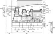
도 1은 본 발명의 일 실시예에 따른 표시 장치를 개략적으로 나타낸 사시도이고, 도 2a는 도 1의 표시 장치를 A-A'선에 따라 나타낸 단면도이고, 도 2b는 도 1의 표시 장치를 B-B'선에 따라 나타낸 단면도이고, 도 2c는 도 1의 표시 장치를 C-C'선에 따라 나타낸 단면도이다.FIG. 1 is a perspective view schematically illustrating a display device according to one embodiment of the present invention, FIG. 2a is a cross-sectional view of the display device of FIG. 1 taken along line A-A', FIG. 2b is a cross-sectional view of the display device of FIG. 1 taken along line B-B', and FIG. 2c is a cross-sectional view of the display device of FIG. 1 taken along line C-C'.
도 1 및 도 2a 내지 도 2c를 참조하면, 표시 장치(1)는 제1방향의 가장자리와 제2방향의 가장자리를 가질 수 있다. 여기서 제1방향 및 제2방향은 서로 교차하는 방향일 수 있다. 예를 들어, 제1방향 및 제2방향은 서로 예각을 이룰 수 있다. 다른 예로, 제1방향 및 제2방향은 서로 둔각을 이루거나, 직교할 수 있다. 이하에서는 제1방향 및 제2방향이 서로 직교하는 경우를 중심으로 상세히 설명하기로 한다. 예를 들어, 제1방향은 x 방향 또는 -x 방향일 수 있으며, 제2방향은 y 방향 또는 -y 방향일 수 있다.Referring to FIG. 1 and FIG. 2A to FIG. 2C, the display device (1) may have an edge in a first direction and an edge in a second direction. Here, the first direction and the second direction may be directions that intersect each other. For example, the first direction and the second direction may form an acute angle with each other. As another example, the first direction and the second direction may form an obtuse angle with each other or may be orthogonal to each other. Hereinafter, a detailed description will be given focusing on a case where the first direction and the second direction are orthogonal to each other. For example, the first direction may be the x direction or the -x direction, and the second direction may be the y direction or the -y direction.
일 실시예에서, 제1방향(예를 들어, 도 1의 x 방향 또는 -x 방향)의 가장자리 및 제2방향(예를 들어, 도 1의 y 방향 또는 -y 방향)의 가장자리가 만나는 코너(corner, CN)는 소정의 곡률을 가질 수 있다.In one embodiment, a corner (CN) where an edge in a first direction (e.g., the x direction or -x direction of FIG. 1) and an edge in a second direction (e.g., the y direction or -y direction of FIG. 1) meet can have a predetermined curvature.
표시 장치(1)는 커버윈도우(CW) 및 표시 패널(10)을 포함할 수 있다. 커버윈도우(CW)는 표시 패널(10)을 보호하는 기능을 할 수 있다. 일 실시예에서, 커버윈도우(CW)는 표시 패널(10) 상에 배치될 수 있다. 일 실시예에서, 커버윈도우(CW)는 플렉서블 윈도우일 수 있다. 커버윈도우(CW)는 크랙(crack) 등의 발생 없이 외력에 따라 용이하게 휘면서 표시 패널(10)을 보호할 수 있다. 커버윈도우(CW)는 유리, 사파이어, 또는 플라스틱을 포함할 수 있다. 커버윈도우(CW)는 예를 들어, 강화 유리(Ultra Thin Glass), 투명폴리이미드(Colorless Polyimide, CPI)일 수 있다. 일 실시예에서, 커버윈도우(CW)는 유리 기판의 일면에 가요성이 있는 고분자 층이 배치된 구조를 갖는 것일 수 있고, 또는, 고분자층으로만 구성된 것일 수 있다.The display device (1) may include a cover window (CW) and a display panel (10). The cover window (CW) may have a function of protecting the display panel (10). In one embodiment, the cover window (CW) may be disposed on the display panel (10). In one embodiment, the cover window (CW) may be a flexible window. The cover window (CW) may be easily bent according to an external force without occurrence of cracks or the like, while protecting the display panel (10). The cover window (CW) may include glass, sapphire, or plastic. The cover window (CW) may be, for example, tempered glass (Ultra Thin Glass) or colorless polyimide (CPI). In one embodiment, the cover window (CW) may have a structure in which a flexible polymer layer is disposed on one surface of a glass substrate, or may be composed only of a polymer layer.
표시 패널(10)은 커버윈도우(CW)의 하부에 배치될 수 있다. 표시 패널(10)은 도시하지 않았지만 광학 투명 접착제(Optically clear adhesive, OCA) 필름과 같은 투명 접착 부재에 의해 커버윈도우(CW)에 부착될 수 있다.The display panel (10) may be placed at the bottom of the cover window (CW). Although not shown, the display panel (10) may be attached to the cover window (CW) by a transparent adhesive material such as an optically clear adhesive (OCA) film.
표시 패널(10)은 화상을 표시할 수 있다. 표시 패널(10)은 기판(100) 및 부화소(PX)를 포함할 수 있다. 기판(100)은 중심영역(CA), 제1측면영역(SA1), 제2측면영역(SA2), 코너영역(CNA), 중간영역(MA), 및 주변영역(PA)을 포함할 수 있다. 일 실시예에서, 기판(100)의 형상은 표시 장치(1)의 형상을 정의할 수 있다.The display panel (10) can display an image. The display panel (10) can include a substrate (100) and a subpixel (PX). The substrate (100) can include a center area (CA), a first side area (SA1), a second side area (SA2), a corner area (CNA), a middle area (MA), and a peripheral area (PA). In one embodiment, the shape of the substrate (100) can define the shape of the display device (1).
중심영역(CA)은 편평한 영역일 수 있다. 일 실시예에서, 표시 장치(1)는 중심영역(CA)에서 대부분의 화상을 제공할 수 있다.The central area (CA) may be a flat area. In one embodiment, the display device (1) may provide most of the image in the central area (CA).
제1측면영역(SA1)은 제1방향(예를 들어, 도 1의 x 방향 또는 -x 방향)으로 중심영역(CA)과 인접하며 구부러질 수 있다. 제1측면영역(SA1)은 제1방향(예를 들어, x 방향 또는 -x 방향)으로의 단면(예를 들어, xz 단면)에서 중심영역(CA)으로부터 구부러진 영역으로 정의할 수 있다. 제1측면영역(SA1)은 제2방향(예를 들어, y 방향 또는 -y 방향)으로 연장될 수 있다. 이를 다시 말하면, 제1측면영역(SA1)은 제2방향(예를 들어, y 방향 또는 -y 방향)으로의 단면(예를 들어, yz 단면)에서 구부러지지 않을 수 있다. 제1측면영역(SA1)은 중심영역(CA)으로부터 제1방향(예를 들어, x 방향 또는 -x 방향)으로 연장될 수 있다. 도 2a에서 중심영역(CA)으로부터 x 방향으로 연장되며 구부러진 제1측면영역(SA1) 및 중심영역(CA)으로부터 -x 방향으로 연장되며 구부러진 제1측면영역(SA1)은 서로 동일한 곡률을 가지는 것으로 도시하고 있으나, 다른 실시예에서, 중심영역(CA)으로부터 x 방향으로 연장되며 구부러진 제1측면영역(SA1) 및 중심영역(CA)으로부터 -x 방향으로 연장되며 구부러진 제1측면영역(SA1)은 서로 상이한 곡률을 가질 수 있다.The first side area (SA1) can be adjacent to the center area (CA) in a first direction (e.g., the x direction or the -x direction of FIG. 1) and can be bent. The first side area (SA1) can be defined as an area bent from the center area (CA) in a cross-section (e.g., an xz cross-section) in the first direction (e.g., the x direction or the -x direction). The first side area (SA1) can extend in a second direction (e.g., the y direction or the -y direction). In other words, the first side area (SA1) may not be bent in a cross-section (e.g., a yz cross-section) in the second direction (e.g., the y direction or the -y direction). The first side area (SA1) can extend from the center area (CA) in the first direction (e.g., the x direction or the -x direction). In FIG. 2A, the first side area (SA1) extending in the x direction from the central area (CA) and being bent and the first side area (SA1) extending in the -x direction from the central area (CA) and being bent are illustrated as having the same curvature, but in other embodiments, the first side area (SA1) extending in the x direction from the central area (CA) and being bent and the first side area (SA1) extending in the -x direction from the central area (CA) and being bent may have different curvatures.
제2측면영역(SA2)은 제2방향(예를 들어, y 방향 또는 -y 방향)으로 중심영역(CA)과 인접하며 구부러질 수 있다. 제2측면영역(SA2)은 제2방향(예를 들어, y 방향 또는 -y 방향)으로의 단면(예를 들어, yz 단면)에서 중심영역(CA)으로부터 구부러진 영역으로 정의할 수 있다. 제2측면영역(SA2)은 제1방향(예를 들어, x 방향 또는 -x 방향)으로 연장될 수 있다. 제2측면영역(SA2)은 제1방향(예를 들어, x 방향 또는 -x 방향)과 직교하는 단면(예를 들어, xz 단면)에서 구부러지지 않을 수 있다. 도 2b에서 중심영역(CA)으로부터 y 방향으로 연장되며 구부러진 제2측면영역(SA2) 및 중심영역(CA)으로부터 -y 방향으로 연장되며 구부러진 제2측면영역(SA2)은 서로 동일한 곡률을 가지는 것으로 도시하고 있으나, 다른 실시예에서, 중심영역(CA)으로부터 y 방향으로 연장되며 구부러진 제2측면영역(SA2) 및 중심영역(CA)으로부터 -y 방향으로 연장되며 구부러진 제2측면영역(SA2)은 서로 상이한 곡률을 가질 수 있다.The second side area (SA2) may be adjacent to the center area (CA) in a second direction (e.g., the y direction or the -y direction) and may be bent. The second side area (SA2) may be defined as an area bent from the center area (CA) in a cross-section (e.g., a yz cross-section) in the second direction (e.g., the y direction or the -y direction). The second side area (SA2) may extend in the first direction (e.g., the x direction or the -x direction). The second side area (SA2) may not be bent in a cross-section (e.g., an xz cross-section) orthogonal to the first direction (e.g., the x direction or the -x direction). In FIG. 2b, the second side area (SA2) extending in the y direction from the center area (CA) and being bent and the second side area (SA2) extending in the -y direction from the center area (CA) and being bent are illustrated as having the same curvature, but in other embodiments, the second side area (SA2) extending in the y direction from the center area (CA) and being bent and the second side area (SA2) extending in the -y direction from the center area (CA) and being bent may have different curvatures.
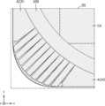
코너영역(CNA)은 코너(CN)에 배치되는 영역일 수 있다. 일 실시예에서, 코너영역(CNA)은 표시 장치(1)의 제1방향(예를 들어, x 방향 또는 -x 방향)의 가장자리 및 제2방향(예를 들어, y 방향 또는 -y 방향)의 가장자리가 만나는 영역일 수 있다. 일 실시예에서, 코너영역(CNA)은 중심영역(CA), 제1측면영역(SA1), 및 제2측면영역(SA2)을 적어도 일부 둘러쌀 수 있다. 또는, 코너영역(CNA)은 중심영역(CA), 제1측면영역(SA1), 제2측면영역(SA2), 및 중간영역(MA)을 적어도 일부 둘러쌀 수 있다. 제1측면영역(SA1)이 제1방향(예를 들어, x 방향 또는 -x 방향)으로 연장되며 구부러지고 제2측면영역(SA2)이 제2방향(예를 들어, y 방향 또는 -y 방향)으로 연장되며 구부러지는 경우, 코너영역(CNA)의 적어도 일부는 제1방향(예를 들어, x 방향 또는 -x 방향)으로 연장되며 구부러지는 동시에 제2방향(예를 들어, y 방향 또는 -y 방향)으로 연장되며 구부러질 수 있다. 이를 다시 말하면, 코너영역(CNA)의 적어도 일부는 복수의 방향으로의 복수의 곡률들이 중첩하는 복곡영역일 수 있다. 일 실시예에서, 코너영역(CNA)은 복수 개로 구비될 수 있다.The corner area (CNA) may be an area disposed at a corner (CN). In one embodiment, the corner area (CNA) may be an area where an edge in a first direction (e.g., an x direction or a -x direction) and an edge in a second direction (e.g., a y direction or a -y direction) of the display device (1) meet. In one embodiment, the corner area (CNA) may surround at least a portion of the center area (CA), the first side area (SA1), and the second side area (SA2). Alternatively, the corner area (CNA) may surround at least a portion of the center area (CA), the first side area (SA1), the second side area (SA2), and the middle area (MA). When the first side area (SA1) extends and bends in a first direction (e.g., the x direction or the -x direction) and the second side area (SA2) extends and bends in a second direction (e.g., the y direction or the -y direction), at least a portion of the corner area (CNA) may extend and bend in the first direction (e.g., the x direction or the -x direction) and extend and bend in the second direction (e.g., the y direction or the -y direction) at the same time. In other words, at least a portion of the corner area (CNA) may be a convex area in which a plurality of curvatures in a plurality of directions overlap. In one embodiment, the corner area (CNAs) may be provided in multiple numbers.
중간영역(MA)은 중심영역(CA) 및 코너영역(CNA) 사이에 배치될 수 있다. 일 실시예에서, 중간영역(MA)은 제1측면영역(SA1) 및 코너영역(CNA) 사이에서 연장될 수 있다. 일 실시예에서, 중간영역(MA)은 제2측면영역(SA2) 및 코너영역(CNA) 사이에서 연장될 수 있다. 일 실시예에서, 중간영역(MA)은 구부러질 수 있다. 중간영역(MA)에는 부화소(PX)에 전기적 신호를 제공하기 위한 구동회로 및/또는 전원을 제공하기 위한 전원배선이 배치될 수 있다. 이러한 경우, 중간영역(MA)에 배치된 부화소(PX)는 구동회로 및/또는 전원배선과 중첩될 수 있다. 일부 실시예에서, 중간영역(MA)에 배치된 구동회로 및/또는 전원배선은 생략될 수 있다. 이러한 경우, 중간영역(MA)에 배치된 부화소(PX)는 구동회로 및/또는 전원배선과 중첩되지 않을 수 있다.The intermediate region (MA) may be disposed between the center region (CA) and the corner region (CNA). In one embodiment, the intermediate region (MA) may extend between the first side region (SA1) and the corner region (CNA). In one embodiment, the intermediate region (MA) may extend between the second side region (SA2) and the corner region (CNA). In one embodiment, the intermediate region (MA) may be bent. A driving circuit for providing an electrical signal to a subpixel (PX) and/or a power supply line for providing power may be disposed in the intermediate region (MA). In this case, the subpixel (PX) disposed in the intermediate region (MA) may overlap with the driving circuit and/or the power supply line. In some embodiments, the driving circuit and/or the power supply line disposed in the intermediate region (MA) may be omitted. In this case, the subpixel (PX) disposed in the intermediate region (MA) may not overlap with the driving circuit and/or the power supply line.
주변영역(PA)은 중심영역(CA)의 외측에 배치될 수 있다. 일 실시예에서, 주변영역(PA)은 제1측면영역(SA1)의 외측에 배치될 수 있다. 주변영역(PA)은 제1측면영역(SA1)으로부터 연장될 수 있다. 일 실시예에서, 주변영역(PA)은 제2측면영역(SA2)의 외측에 배치될 수 있다. 주변영역(PA)은 제2측면영역(SA2)으로부터 연장될 수 있다. 주변영역(PA)에는 부화소(PX)가 배치되지 않을 수 있다. 따라서, 주변영역(PA)은 화상을 표시하지 않는 비표시영역일 수 있다. 주변영역(PA)에는 부화소(PX)에 전기적 신호를 제공하기 위한 구동회로 및/또는 전원을 제공하기 위한 전원배선이 배치될 수 있다.The peripheral area (PA) may be arranged outside the central area (CA). In one embodiment, the peripheral area (PA) may be arranged outside the first side area (SA1). The peripheral area (PA) may extend from the first side area (SA1). In one embodiment, the peripheral area (PA) may be arranged outside the second side area (SA2). The peripheral area (PA) may extend from the second side area (SA2). A subpixel (PX) may not be arranged in the peripheral area (PA). Accordingly, the peripheral area (PA) may be a non-display area that does not display an image. A driving circuit for providing an electrical signal to the subpixel (PX) and/or a power supply line for providing power may be arranged in the peripheral area (PA).
도 2a를 참조하면, 제1측면영역(SA1), 중간영역(MA), 및 코너영역(CNA)의 일부는 제1곡률반지름(R1)을 가지며 구부러질 수 있다. 도 2b를 참조하면, 제2측면영역(SA2), 중간영역(MA), 및 코너영역(CNA)의 다른 일부는 제2곡률반지름(R2)을 가지며 구부러질 수 있다. 도 2c를 참조하면, 중간영역(MA) 및 코너영역(CNA)의 또 다른 일부는 제3곡률반지름(R3)을 가지며 구부러질 수 있다.Referring to FIG. 2a, a portion of the first side area (SA1), the middle area (MA), and the corner area (CNA) may be bent with a first radius of curvature (R1). Referring to FIG. 2b, another portion of the second side area (SA2), the middle area (MA), and the corner area (CNA) may be bent with a second radius of curvature (R2). Referring to FIG. 2c, another portion of the middle area (MA) and the corner area (CNA) may be bent with a third radius of curvature (R3).
부화소(PX)는 기판(100) 상에 배치될 수 있다. 일 실시예에서, 부화소(PX)는 복수 개로 구비될 수 있으며, 복수의 부화소(PX)들은 빛을 방출하여 화상을 표시할 수 있다. 일 실시예에서, 복수의 부화소(PX)들은 각각 적색 부화소, 녹색 부화소, 및 청색 부화소를 포함할 수 있다. 또는 복수의 부화소(PX)들은 각각 적색 부화소, 녹색 부화소, 청색 부화소, 및 백색 부화소를 포함할 수 있다.The subpixels (PX) may be arranged on the substrate (100). In one embodiment, the subpixels (PX) may be provided in multiple numbers, and the multiple subpixels (PX) may emit light to display an image. In one embodiment, the multiple subpixels (PX) may each include a red subpixel, a green subpixel, and a blue subpixel. Alternatively, the multiple subpixels (PX) may each include a red subpixel, a green subpixel, a blue subpixel, and a white subpixel.
부화소(PX)는 중심영역(CA), 제1측면영역(SA1), 제2측면영역(SA2), 및 코너영역(CNA) 중 적어도 하나에 배치될 수 있다. 일 실시예에서, 복수의 부화소(PX)들은 중심영역(CA), 제1측면영역(SA1), 제2측면영역(SA2), 코너영역(CNA), 및 중간영역(MA)에 배치될 수 있다. 이러한 경우, 표시 장치(1)는 중심영역(CA), 제1측면영역(SA1), 제2측면영역(SA2), 코너영역(CNA), 및 중간영역(MA)에서 화상을 표시할 수 있다. 일 실시예에서, 중심영역(CA), 제1측면영역(SA1), 제2측면영역(SA2), 코너영역(CNA), 및 중간영역(MA)에 배치된 복수의 부화소(PX)들은 각각 독립적인 화상을 제공할 수 있다. 다른 실시예에서, 중심영역(CA), 제1측면영역(SA1), 제2측면영역(SA2), 코너영역(CNA), 및 중간영역(MA)에 배치된 복수의 부화소(PX)들은 각각 어느 하나의 화상의 일부분들을 제공할 수 있다.The subpixels (PX) can be arranged in at least one of the center area (CA), the first side area (SA1), the second side area (SA2), and the corner area (CNA). In one embodiment, the plurality of subpixels (PX) can be arranged in the center area (CA), the first side area (SA1), the second side area (SA2), the corner area (CNA), and the middle area (MA). In this case, the display device (1) can display an image in the center area (CA), the first side area (SA1), the second side area (SA2), the corner area (CNA), and the middle area (MA). In one embodiment, the plurality of subpixels (PX) arranged in the center area (CA), the first side area (SA1), the second side area (SA2), the corner area (CNA), and the middle area (MA) can each provide an independent image. In another embodiment, a plurality of sub-pixels (PX) arranged in the center area (CA), the first side area (SA1), the second side area (SA2), the corner area (CNA), and the middle area (MA) can each provide portions of one image.
표시 장치(1)는 중심영역(CA)뿐만 아니라 제1측면영역(SA1), 제2측면영역(SA2), 중간영역(MA), 및 코너영역(CNA)에서도 화상을 표시할 수 있다. 따라서, 표시 장치(1) 중 화상을 표시하는 영역인 표시영역이 차지하는 비중이 늘어날 수 있다. 또한, 표시 장치(1)는 코너(CN)에서 구부러지며 화상을 표시할 수 있으므로 심미감이 향상될 수 있다.The display device (1) can display an image not only in the center area (CA), but also in the first side area (SA1), the second side area (SA2), the middle area (MA), and the corner area (CNA). Accordingly, the proportion of the display area, which is the area of the display device (1) where the image is displayed, can increase. In addition, since the display device (1) can display an image by being bent at the corner (CN), the aesthetics can be improved.
도 3은 본 발명의 일 실시예에 따른 표시 장치에 포함될 수 있는 표시 패널을 개략적으로 나타낸 평면도이다.FIG. 3 is a plan view schematically illustrating a display panel that may be included in a display device according to one embodiment of the present invention.
도 3을 참조하면, 표시 패널(10)은 기판(100), 부화소(PX) 및 구동회로(DC)를 포함할 수 있다. 기판(100)은 중심영역(CA), 제1측면영역(SA1), 제2측면영역(SA2), 코너영역(CNA), 중간영역(MA), 및 주변영역(PA)을 포함할 수 있다.Referring to FIG. 3, the display panel (10) may include a substrate (100), a subpixel (PX), and a driving circuit (DC). The substrate (100) may include a center area (CA), a first side area (SA1), a second side area (SA2), a corner area (CNA), a middle area (MA), and a peripheral area (PA).
주변영역(PA)은 중심영역(CA)의 외측에 배치될 수 있다. 주변영역(PA)은 제1인접영역(AA1), 제2인접영역(AA2), 제3인접영역(AA3), 벤딩영역(BA), 및 패드영역(PADA)을 포함할 수 있다.The peripheral area (PA) may be positioned outside the central area (CA). The peripheral area (PA) may include a first adjacent area (AA1), a second adjacent area (AA2), a third adjacent area (AA3), a bending area (BA), and a pad area (PADA).
제1인접영역(AA1)은 제1측면영역(SA1)의 외측에 배치될 수 있다. 이를 다시 말하면, 제1측면영역(SA1)은 제1인접영역(AA1) 및 중심영역(CA) 사이에 배치될 수 있다. 제1인접영역(AA1)은 제1측면영역(SA1)으로부터 연장될 수 있다. 일 실시예에서, 제1인접영역(AA1)은 제1측면영역(SA1)으로부터 제1방향(예를 들어, x 방향 또는 -x 방향)으로 연장될 수 있다. 일 실시예에서, 제1인접영역(AA1)에는 구동회로(DC)가 배치될 수 있다.The first adjacent area (AA1) may be arranged on the outside of the first side area (SA1). In other words, the first side area (SA1) may be arranged between the first adjacent area (AA1) and the center area (CA). The first adjacent area (AA1) may extend from the first side area (SA1). In one embodiment, the first adjacent area (AA1) may extend in a first direction (for example, the x direction or the -x direction) from the first side area (SA1). In one embodiment, a driving circuit (DC) may be arranged in the first adjacent area (AA1).
제2인접영역(AA2) 및 제3인접영역(AA3)은 제2측면영역(SA2)의 외측에 배치될 수 있다. 이를 다시 말하면, 제2측면영역(SA2)은 제2인접영역(AA2) 및 중심영역(CA) 사이에 배치될 수 있다. 또한, 제2측면영역(SA2)은 제3인접영역(AA3) 및 중심영역(CA) 사이에 배치될 수 있다. 제2인접영역(AA2) 및 제3인접영역(AA3)은 제2측면영역(SA2)으로부터 연장될 수 있다. 일 실시예에서, 제2인접영역(AA2) 및 제3인접영역(AA3)은 제2방향(예를 들어, y 방향 또는 -y 방향)으로 연장될 수 있다. 제2인접영역(AA2) 및 제3인접영역(AA3) 사이에는 중심영역(CA)이 배치될 수 있다.The second adjacent area (AA2) and the third adjacent area (AA3) may be arranged on the outside of the second side area (SA2). In other words, the second side area (SA2) may be arranged between the second adjacent area (AA2) and the central area (CA). In addition, the second side area (SA2) may be arranged between the third adjacent area (AA3) and the central area (CA). The second adjacent area (AA2) and the third adjacent area (AA3) may extend from the second side area (SA2). In one embodiment, the second adjacent area (AA2) and the third adjacent area (AA3) may extend in the second direction (for example, the y direction or the -y direction). The central area (CA) may be arranged between the second adjacent area (AA2) and the third adjacent area (AA3).
벤딩영역(BA)은 제3인접영역(AA3)의 외측에 배치될 수 있다. 이를 다시 말하면, 제3인접영역(AA3)은 벤딩영역(BA) 및 제2측면영역(SA2) 사이에 배치될 수 있다. 벤딩영역(BA)에서 표시 패널(10)은 벤딩될 수 있다. 이러한 경우, 패드영역(PADA)은 화상을 표시하는 상면과 반대되는 표시 패널(10)의 후면을 마주볼 수 있다. 따라서, 사용자에게 보이는 주변영역(PA)의 면적을 줄일 수 있다.The bending area (BA) may be arranged on the outside of the third adjacent area (AA3). In other words, the third adjacent area (AA3) may be arranged between the bending area (BA) and the second side area (SA2). The display panel (10) may be bent at the bending area (BA). In this case, the pad area (PADA) may face the rear surface of the display panel (10) opposite to the upper surface that displays the image. Therefore, the area of the peripheral area (PA) visible to the user may be reduced.
패드영역(PADA)은 벤딩영역(BA)의 외측에 배치될 수 있다. 이를 다시 말하면, 벤딩영역(BA)은 제3인접영역(AA3) 및 패드영역(PADA) 사이에 배치될 수 있다. 패드영역(PADA)에는 패드(미도시)가 배치될 수 있다. 표시 패널(10)은 패드를 통해 전기적 신호 및/또는 전원전압을 전달받을 수 있다.The pad area (PADA) may be arranged outside the bending area (BA). In other words, the bending area (BA) may be arranged between the third adjacent area (AA3) and the pad area (PADA). A pad (not shown) may be arranged in the pad area (PADA). The display panel (10) may receive an electrical signal and/or a power voltage through the pad.
제1측면영역(SA1), 제2측면영역(SA2), 코너영역(CNA), 및 중간영역(MA) 중 적어도 하나는 구부러질 수 있다. 예컨대, 전술한 바와 같이, 제1측면영역(SA1) 및 코너영역(CNA)의 일부는 제1방향(예를 들어, x 방향 또는 -x 방향)으로의 단면(예를 들어, xz 단면)에서 구부러질 수 있다. 제2측면영역(SA2) 및 코너영역(CNA)의 다른 일부는 제2방향(예를 들어, y 방향 또는 -y 방향)으로의 단면(예를 들어, yz 단면)에서 구부러질 수 있다. 코너영역(CNA)의 또 다른 일부는 제1방향(예를 들어, x 방향 또는 -x 방향)으로의 단면(예를 들어, xz 단면)에서 구부러지고 제2방향(예를 들어, y 방향 또는 -y 방향)으로의 단면(예를 들어, yz 단면)에서 구부러질 수 있다.At least one of the first side area (SA1), the second side area (SA2), the corner area (CNA), and the middle area (MA) can be bent. For example, as described above, a portion of the first side area (SA1) and the corner area (CNA) can be bent in a cross-section (e.g., an xz cross-section) in a first direction (e.g., an x-direction or a -x-direction). Another portion of the second side area (SA2) and the corner area (CNA) can be bent in a cross-section (e.g., an yz cross-section) in a second direction (e.g., an y-direction or a -y-direction). Another portion of the corner area (CNA) can be bent in a cross-section (e.g., an xz cross-section) in the first direction (e.g., an x-direction or a -x-direction) and in a cross-section (e.g., an yz cross-section) in a second direction (e.g., an y-direction or a -y-direction).
코너영역(CNA)이 구부러질 때 코너영역(CNA)에는 인장 변형(tensile strain)보다 압축 변형(compressive strain)이 더 크게 발생할 수 있다. 이러한 경우, 코너영역(CNA)의 적어도 일부에는 수축 가능한 기판(100) 및 기판(100) 상의 다층막 구조가 적용될 필요가 있다. 일 실시예에서, 코너영역(CNA)에서 표시 패널(10)의 구조는 중심영역(CA)에서 표시 패널(10)의 구조와 상이할 수 있다.When the corner area (CNA) is bent, a compressive strain may occur in the corner area (CNA) greater than a tensile strain. In this case, a contractible substrate (100) and a multilayer film structure on the substrate (100) need to be applied to at least a portion of the corner area (CNA). In one embodiment, the structure of the display panel (10) in the corner area (CNA) may be different from the structure of the display panel (10) in the center area (CA).
부화소(PX) 및 구동회로(DC)는 기판(100) 상에 배치될 수 있다. 부화소(PX)는 중심영역(CA), 제1측면영역(SA1), 제2측면영역(SA2), 코너영역(CNA), 및 중간영역(MA) 중 적어도 하나에 배치될 수 있다. 부화소(PX)는 표시요소를 포함할 수 있다. 일 실시예에서, 표시요소는 유기 발광층을 포함하는 유기발광다이오드(organic light emitting diode)일 수 있다. 또는, 표시요소는 무기 발광층을 포함하는 발광다이오드일 수 있다. 발광다이오드의 크기는 마이크로(micro) 스케일 또는 나노(nano) 스케일일 수 있다. 예를 들어, 발광다이오드는 마이크로(micro) 발광다이오드일 수 있다. 또는, 발광다이오드는 나노로드(nanorod) 발광다이오드일 수 있다. 나노로드 발광다이오드는 갈륨나이트라이드(GaN)를 포함할 수 있다. 일 실시예에서, 나노로드 발광다이오드 상에 색변환층을 배치할 수 있다. 상기 색변환층은 양자점을 포함할 수 있다. 또는, 표시요소는 양자점 발광층을 포함하는 양자점 발광다이오드(Quantum dot Light Emitting Diode)일 수 있다.The subpixel (PX) and the driving circuit (DC) may be arranged on the substrate (100). The subpixel (PX) may be arranged in at least one of the center area (CA), the first side area (SA1), the second side area (SA2), the corner area (CNA), and the middle area (MA). The subpixel (PX) may include a display element. In one embodiment, the display element may be an organic light emitting diode (OLED) including an organic light emitting layer. Alternatively, the display element may be a light emitting diode including an inorganic light emitting layer. The size of the light emitting diode may be a micro scale or a nano scale. For example, the light emitting diode may be a micro light emitting diode. Alternatively, the light emitting diode may be a nanorod light emitting diode. The nanorod light emitting diode may include gallium nitride (GaN). In one embodiment, a color conversion layer can be disposed on a nanorod light emitting diode. The color conversion layer can include quantum dots. Alternatively, the display element can be a quantum dot light emitting diode (QLED) including a quantum dot light emitting layer.
부화소(PX)는 복수의 부화소들을 포함할 수 있으며, 복수의 부화소들 각각은 표시요소를 이용하여 소정의 색상의 빛을 방출할 수 있다. 본 명세서에서 부화소는 이미지를 구현하는 최소 단위로 발광영역을 의미한다.A subpixel (PX) may include a plurality of subpixels, and each of the plurality of subpixels may emit light of a predetermined color using a display element. In this specification, a subpixel is the smallest unit that implements an image and means a light-emitting area.
구동회로(DC)는 스캔선(SL)을 통해 각 부화소(PX)에 스캔 신호를 제공하는 스캔 구동회로일 수 있다. 또는, 데이터선(DL)을 통해 각 부화소(PX)에 데이터 신호를 제공하는 데이터 구동회로일 수 있다. 일 실시예에서, 데이터 구동회로는 제3인접영역(AA3) 또는 패드영역(PADA)에 배치될 수 있다. 또는, 데이터 구동회로는 상기 패드를 통해 연결된 표시 회로 보드 상에 배치될 수 있다.The driving circuit (DC) may be a scan driving circuit that provides a scan signal to each subpixel (PX) through a scan line (SL). Alternatively, it may be a data driving circuit that provides a data signal to each subpixel (PX) through a data line (DL). In one embodiment, the data driving circuit may be arranged in the third adjacent area (AA3) or the pad area (PADA). Alternatively, the data driving circuit may be arranged on a display circuit board connected through the pad.
도 4는 본 발명의 일 실시예에 따른 표시 장치의 표시요소 및 이에 전기적으로 연결된 부화소회로를 개략적으로 나타낸 등가회로도이다.FIG. 4 is an equivalent circuit diagram schematically showing a display element of a display device and a subpixel circuit electrically connected thereto according to one embodiment of the present invention.
도 4를 참조하면, 부화소회로(PC)는 표시요소(DPE)와 전기적으로 연결될 수 있다. 부화소회로(PC)는 제1박막트랜지스터(T1), 제2박막트랜지스터(T2), 및 스토리지 커패시터(Cst)를 포함할 수 있다.Referring to FIG. 4, the subpixel circuit (PC) may be electrically connected to the display element (DPE). The subpixel circuit (PC) may include a first thin-film transistor (T1), a second thin-film transistor (T2), and a storage capacitor (Cst).
제2박막트랜지스터(T2)는 스위칭 박막트랜지스터로서, 스캔선(SL) 및 데이터선(DL)에 연결되며, 스캔선(SL)으로부터 입력되는 스캔 신호 또는 스위칭 전압에 기초하여 데이터선(DL)으로부터 입력된 데이터 신호 또는 데이터 전압을 제1박막트랜지스터(T1)로 전달할 수 있다.The second thin film transistor (T2) is a switching thin film transistor, connected to the scan line (SL) and the data line (DL), and can transmit a data signal or data voltage input from the data line (DL) to the first thin film transistor (T1) based on a scan signal or switching voltage input from the scan line (SL).
스토리지 커패시터(Cst)는 제2박막트랜지스터(T2)와 구동전압선(PL)에 연결되며, 제2박막트랜지스터(T2)로부터 전달받은 전압과 구동전압선(PL)에 공급되는 구동전압(ELVDD)의 차이에 해당하는 전압을 저장할 수 있다.The storage capacitor (Cst) is connected to the second thin-film transistor (T2) and the driving voltage line (PL), and can store a voltage corresponding to the difference between the voltage received from the second thin-film transistor (T2) and the driving voltage (ELVDD) supplied to the driving voltage line (PL).
제1박막트랜지스터(T1)는 구동 박막트랜지스터로서, 구동전압선(PL)과 스토리지 커패시터(Cst)에 연결되며, 스토리지 커패시터(Cst)에 저장된 전압 값에 대응하여 구동전압선(PL)으로부터 표시요소(DPE)로 흐르는 구동 전류를 제어할 수 있다. 표시요소(DPE)는 구동 전류에 의해 소정의 휘도를 갖는 빛을 방출할 수 있다. 표시요소(DPE)의 부화소전극(예, 애노드)은 부화소회로(PC)에 연결되고, 대향전극(예, 캐소드)은 공통전압(ELVSS)을 공급받을 수 있다.The first thin film transistor (T1) is a driving thin film transistor, which is connected to a driving voltage line (PL) and a storage capacitor (Cst), and can control a driving current flowing from the driving voltage line (PL) to the display element (DPE) in response to a voltage value stored in the storage capacitor (Cst). The display element (DPE) can emit light having a predetermined brightness by the driving current. A subpixel electrode (e.g., anode) of the display element (DPE) is connected to a subpixel circuit (PC), and a counter electrode (e.g., cathode) can be supplied with a common voltage (ELVSS).
도 4는 부화소회로(PC)가 2개의 박막트랜지스터와 1개의 스토리지 커패시터를 포함하는 것을 설명하고 있으나, 다른 실시예에서 박막트랜지스터의 개수 또는 스토리지 커패시터의 개수는 부화소회로(PC)의 설계에 따라 다양하게 변경될 수 있음은 물론이다.Although FIG. 4 illustrates that the subpixel circuit (PC) includes two thin film transistors and one storage capacitor, it is to be understood that in other embodiments, the number of thin film transistors or the number of storage capacitors may vary depending on the design of the subpixel circuit (PC).
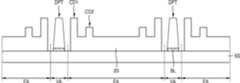
도 5은 도 3의 표시 패널(10)의 D 부분을 확대한 확대도이다.Figure 5 is an enlarged view of part D of the display panel (10) of Figure 3.
도 5을 참조하면, 기판(100)은 중심영역(CA), 제1측면영역(SA1), 제2측면영역(SA2) 및 코너영역(CNA)을 포함할 수 있다.Referring to FIG. 5, the substrate (100) may include a center area (CA), a first side area (SA1), a second side area (SA2), and a corner area (CNA).
코너영역(CNA)은 표시 패널(10)의 코너(CN)에 배치되는 영역일 수 있다. 코너영역(CNA)은 중심코너영역(CCA), 제1인접코너영역(ACA1), 및 제2인접코너영역(ACA2)을 포함할 수 있다.The corner area (CNA) may be an area positioned at a corner (CN) of the display panel (10). The corner area (CNA) may include a center corner area (CCA), a first adjacent corner area (ACA1), and a second adjacent corner area (ACA2).
중심코너영역(CCA)은 연장영역(EA)을 포함할 수 있다. 연장영역(EA)은 중심영역(CA)으로부터 멀어지는 방향으로 연장될 수 있다. 연장영역(EA)은 복수 개로 구비될 수 있다. 복수 개의 연장영역(EA)들 각각은 중심영역(CA)으로부터 멀어지는 방향으로 연장될 수 있다. 예를 들어 복수 개의 연장영역(EA)들은 제1방향(예컨대 x방향 또는 -x방향) 및 제2방향(y방향 또는 -y방향)과 교차하는 방향으로 연장될 수 있다.The central corner area (CCA) may include an extension area (EA). The extension area (EA) may extend in a direction away from the central area (CA). The extension areas (EA) may be provided in multiple numbers. Each of the multiple extension areas (EA) may extend in a direction away from the central area (CA). For example, the multiple extension areas (EA) may extend in a direction intersecting a first direction (e.g., an x-direction or a -x-direction) and a second direction (a y-direction or a -y-direction).
인접한 연장영역(EA)들 사이에는 이격영역(VA)이 정의될 수 있다. 이격영역(VA)은 표시 패널(10)의 구성요소가 배치되지 않는 영역일 수 있다. 코너(CN)에서 중심코너영역(CCA)이 구부러질 때, 중심코너영역(CCA)에는 인장 변형(tensile strain)보다 압축 변형(compressive strain)이 더 크게 발생할 수 있다. 하지만 인접한 연장영역(EA)들 사이에 이격영역(VA)이 정의되어 있으므로, 표시 패널(10)이 중심코너영역(CCA)에서 손상되지 않고 구부러질 수 있다.A separation area (VA) may be defined between adjacent extended areas (EA). The separation area (VA) may be an area where components of the display panel (10) are not arranged. When the center corner area (CCA) is bent at a corner (CN), a compressive strain greater than a tensile strain may occur in the center corner area (CCA). However, since the separation area (VA) is defined between adjacent extended areas (EA), the display panel (10) may be bent without being damaged in the center corner area (CCA).
제1인접코너영역(ACA1)은 중심코너영역(CCA)과 인접할 수 있다. 제1측면영역(SA1)의 적어도 일부 및 제1인접코너영역(ACA1)은 제1방향(예컨대 x방향 또는 -x방향)을 따라 위치할 수 있다. 제1인접코너영역(ACA1)의 중심코너영역(CCA) 방향의 단부와 중심코너영역(CCA)의 제1인접코너영역(ACA1) 방향의 단부는 서로 이격될 수 있다. 제1인접코너영역(ACA1)은 제1방향으로의 단면(zx 단면)에서 구부러지는 것으로 나타나고 제2방향으로의 단면(yz 단면)에서는 구부러지지 않는 것으로 나타날 수 있다. 이러한 제1인접코너영역(ACA1)의 내부에는 이격영역(VA)이 정의되지 않을 수 있다.The first adjacent corner area (ACA1) may be adjacent to the center corner area (CCA). At least a portion of the first side area (SA1) and the first adjacent corner area (ACA1) may be positioned along a first direction (e.g., the x direction or the -x direction). An end of the first adjacent corner area (ACA1) in the direction of the center corner area (CCA) and an end of the center corner area (CCA) in the direction of the first adjacent corner area (ACA1) may be spaced apart from each other. The first adjacent corner area (ACA1) may appear to be bent in a cross-section in the first direction (zx cross-section) and may appear not to be bent in a cross-section in the second direction (yz cross-section). A separation area (VA) may not be defined inside the first adjacent corner area (ACA1).
제2인접코너영역(ACA2)도 중심코너영역(CCA)과 인접할 수 있다. 제2측면영역(A2)의 적어도 일부 및 제2인접코너영역(ACA2)은 제2방향(y방향 또는 -y방향)을 따라 위치할 수 있다. 제2인접코너영역(ACA2)의 중심코너영역(CCA) 방향의 단부와 중심코너영역(CCA)의 제2인접코너영역(ACA2) 방향의 단부는 서로 이격될 수 있다. 제2인접코너영역(ACA2)은 제1방향으로의 단면(zx 단면)에서는 구부러지지 않는 것으로 나타나고 제2방향으로의 단면(yz 단면)에서는 구부러지는 것으로 나타날 수 있다. 이러한 제2인접코너영역(ACA2)의 내부에는 이격영역(VA)이 정의되지 않을 수 있다.The second adjacent corner area (ACA2) may also be adjacent to the central corner area (CCA). At least a portion of the second side area (A2) and the second adjacent corner area (ACA2) may be positioned along the second direction (y direction or -y direction). An end of the second adjacent corner area (ACA2) in the direction of the central corner area (CCA) and an end of the central corner area (CCA) in the direction of the second adjacent corner area (ACA2) may be spaced apart from each other. The second adjacent corner area (ACA2) may appear not to be bent in a cross-section in the first direction (zx cross-section) and may appear to be bent in a cross-section in the second direction (yz cross-section). A separation area (VA) may not be defined inside the second adjacent corner area (ACA2).
중간영역(MA)은 중심영역(CA)과 코너영역(CNA) 사이에 위치할 수 있다. 중간영역(MA)은 중심영역(CA)과 제1인접코너영역(ACA1) 사이로 연장될 수 있다. 또한 중간영역(MA)은 중심영역(CA)과 제2인접코너영역(ACA2) 사이로 연장될 수 있다. 이러한 중간영역(MA)은 중심영역(CA), 제1측면영역(SA1) 및 제2측면영역(SA2)을 적어도 일부 둘러쌀 수 있다.The intermediate area (MA) can be located between the central area (CA) and the corner area (CNA). The intermediate area (MA) can extend between the central area (CA) and the first adjacent corner area (ACA1). Furthermore, the intermediate area (MA) can extend between the central area (CA) and the second adjacent corner area (ACA2). The intermediate area (MA) can at least partially surround the central area (CA), the first side area (SA1), and the second side area (SA2).
도 5에 도시된 것과 같이, 복수 개의 부화소(PX)들은 중심영역(CA), 제1측면영역(SA1), 제2측면영역(SA2), 코너영역(CNA) 및 중간영역(MA)에 배치될 수 있다. 따라서, 표시 패널(10)은 중심영역(CA), 제1측면영역(SA1), 제2측면영역(SA2), 코너영역(CNA) 및 중간영역(MA)에서 화상을 표시할 수 있다. 한편, 복수 개의 연장영역(EA)들 복수 개의 부화소(PX)들을 포함할 수 있다. 복수 개의 연장영역(EA)들 각각에서, 복수 개의 부화소(PX)들은 연장영역(EA)의 연장 방향을 따라 배열될 수 있다. 부화소(PX)는 표시요소(DPE, 도 4 참조)를 포함할 수 있다.As illustrated in FIG. 5, a plurality of sub-pixels (PX) can be arranged in a center area (CA), a first side area (SA1), a second side area (SA2), a corner area (CNA), and a middle area (MA). Accordingly, the display panel (10) can display an image in the center area (CA), the first side area (SA1), the second side area (SA2), the corner area (CNA), and the middle area (MA). Meanwhile, a plurality of extended areas (EA) can include a plurality of sub-pixels (PX). In each of the plurality of extended areas (EA), the plurality of sub-pixels (PX) can be arranged along an extension direction of the extended area (EA). The sub-pixels (PX) can include a display element (DPE, see FIG. 4).
일 실시예에서, 중간영역(MA)은 부화소(PX)에 전기적 신호를 제공하기 위한 구동회로(DC) 및/또는 전원을 제공하기 위한 전원배선이 배치될 수 있다. 구동회로(DC)는 복수 개로 구비될 수 있다. 구동회로(DC)는 중간영역(MA)이 연장된 방향으로 연장될 수 있다. 구동회로(DC)는 중심영역(CA), 제1측면영역(SA1) 및 제2측면영역(SA2)을 적어도 일부 둘러쌀 수 있다.In one embodiment, the intermediate region (MA) may be provided with a driving circuit (DC) for providing an electrical signal to the subpixel (PX) and/or a power supply wiring for providing power. The driving circuit (DC) may be provided in multiple units. The driving circuit (DC) may extend in a direction in which the intermediate region (MA) extends. The driving circuit (DC) may surround at least a portion of the central region (CA), the first side region (SA1), and the second side region (SA2).
중간영역(MA)에 배치된 부화소(PX)는 구동회로(DC) 및/또는 전원배선과 중첩될 수 있다. 이러한 경우, 중간영역(MA)은 구동회로(DC) 및/또는 전원배선이 배치되더라도 표시영역으로 기능할 수 있다. 다만, 본 발명이 이에 한정되는 것은 아니다. 예컨대, 중간영역(MA)에는 구동회로(DC) 및/또는 전원배선이 배치되지 않을 수 있다.The subpixel (PX) arranged in the intermediate area (MA) may overlap with the driving circuit (DC) and/or the power wiring. In this case, the intermediate area (MA) may function as a display area even if the driving circuit (DC) and/or the power wiring are arranged. However, the present invention is not limited thereto. For example, the driving circuit (DC) and/or the power wiring may not be arranged in the intermediate area (MA).
도 6은 본 발명의 일 실시예에 따른 표시 패널을 개략적으로 나타낸 단면도로, 도 5의 E-E' 선을 따른 단면도이다.FIG. 6 is a cross-sectional view schematically illustrating a display panel according to one embodiment of the present invention, taken along line E-E' of FIG. 5.
도 6을 참조하면, 표시 패널(10)은 기판(100), 부화소회로층(PCL), 표시요소층(DEL), 및 봉지층(300)을 포함할 수 있다.Referring to FIG. 6, the display panel (10) may include a substrate (100), a subpixel circuit layer (PCL), a display element layer (DEL), and an encapsulation layer (300).
기판(100)은 유리, 금속 또는 유기물과 같이 다양한 소재를 포함할 수 있다. 선택적 실시예로서, 기판(100)은 플렉서블 소재를 포함할 수 있다. 예를 들어, 기판(100)은 초박형 플렉서블 유리(예를 들어, 수십 마이크로미터 내지 수백 마이크로미터의 두께) 또는 고분자 수지를 포함할 수 있다. 기판(100)이 고분자 수지를 포함하는 경우, 기판(100)은 폴리이미드(polyimide)를 포함할 수 있다. 또는, 기판(100)은 폴리에테르술폰(polyethersulfone), 폴리아릴레이트(polyarylate), 폴리에테르 이미드(polyetherimide), 폴리에틸렌 나프탈레이트(polyethyelenene napthalate), 폴리에틸렌 테레프탈레이드(polyethyeleneterepthalate), 폴리페닐렌 설파이드(polyphenylene sulfide), 폴리카보네이트(polycarbonate), 셀룰로오스 트리 아세테이트(TAC), 또는/및 셀룰로오스 아세테이트 프로피오네이트(cellulose acetate propionate) 등을 포함할 수 있다.The substrate (100) may include various materials such as glass, metal, or organic matter. As an optional embodiment, the substrate (100) may include a flexible material. For example, the substrate (100) may include ultra-thin flexible glass (e.g., having a thickness of tens of micrometers to hundreds of micrometers) or a polymer resin. When the substrate (100) includes a polymer resin, the substrate (100) may include polyimide. Alternatively, the substrate (100) may include polyethersulfone, polyarylate, polyetherimide, polyethyelenene napthalate, polyethyeleneterepthalate, polyphenylene sulfide, polycarbonate, cellulose triacetate (TAC), or/and cellulose acetate propionate.
일 실시예에서, 기판(100)은 제1베이스층(100a), 제1배리어층(100b), 제2베이스층(100c) 및 제2배리어층(100d)을 포함할 수 있다. 일 실시예에서, 제1베이스층(100a), 제1배리어층(100b), 제2베이스층(100c), 및 제2배리어층(100d)은 차례로 적층될 수 있다. 또는, 기판(100)은 글라스를 포함할 수 있다.In one embodiment, the substrate (100) may include a first base layer (100a), a first barrier layer (100b), a second base layer (100c), and a second barrier layer (100d). In one embodiment, the first base layer (100a), the first barrier layer (100b), the second base layer (100c), and the second barrier layer (100d) may be sequentially laminated. Alternatively, the substrate (100) may include glass.
제1베이스층(100a) 및 제2베이스층(100c) 중 적어도 하나는 폴리에테르술폰, 폴리아릴레이트, 폴리에테르 이미드, 폴리에틸렌 나프탈레이트, 폴리에틸렌 테레프탈레이트, 폴리페닐렌 설파이드, 폴리이미드, 폴리카보네이트, 셀룰로오스 트리 아세테이트, 셀룰로오스 아세테이트 프로피오네이트 등과 같은 고분자 수지를 포함할 수 있다.At least one of the first base layer (100a) and the second base layer (100c) may include a polymer resin such as polyethersulfone, polyarylate, polyether imide, polyethylene naphthalate, polyethylene terephthalate, polyphenylene sulfide, polyimide, polycarbonate, cellulose triacetate, cellulose acetate propionate, or the like.
제1배리어층(100b) 및 제2배리어층(100d)은 외부 이물질의 침투를 방지하는 배리어층으로, 실리콘질화물, 실리콘산화물, 및/또는 실리콘산질화물 등과 같은 무기물을 포함하는 단일층 또는 다층일 수 있다.The first barrier layer (100b) and the second barrier layer (100d) are barrier layers that prevent the penetration of external foreign substances, and may be a single layer or multiple layers including inorganic materials such as silicon nitride, silicon oxide, and/or silicon oxynitride.
부화소회로층(PCL)은 기판(100) 상에 배치될 수 있다. 부화소회로층(PCL)은 부화소회로(PC)를 포함할 수 있다. 부화소회로(PC)는 중심영역(CA) 상에 배치될 수 있다. 일 실시예에서, 부화소회로(PC)는 적어도 하나의 박막트랜지스터를 포함할 수 있다. 부화소회로(PC)는 제1박막트랜지스터(T1), 제2박막트랜지스터(T2) 및 스토리지 커패시터(Cst)를 포함할 수 있다.A subpixel circuit layer (PCL) may be disposed on a substrate (100). The subpixel circuit layer (PCL) may include a subpixel circuit (PC). The subpixel circuit (PC) may be disposed on a central area (CA). In one embodiment, the subpixel circuit (PC) may include at least one thin-film transistor. The subpixel circuit (PC) may include a first thin-film transistor (T1), a second thin-film transistor (T2), and a storage capacitor (Cst).
부화소회로층(PCL)은 제1박막트랜지스터(T1)의 구성요소들 아래 또는/및 위에 배치되는 무기절연층(IIL), 제1절연층(115), 및 제2절연층(116)을 더 포함할 수 있다. 무기절연층(IIL)은 버퍼층(111), 제1게이트절연층(112), 제2게이트절연층(113), 및 층간절연층(114)을 포함할 수 있다. 제1박막트랜지스터(T1)는 제1반도체층(Act1), 제1게이트전극(GE1), 제1소스전극(SE1), 및 제1드레인전극(DE1)을 포함할 수 있다.The subpixel circuit layer (PCL) may further include an inorganic insulating layer (IIL), a first insulating layer (115), and a second insulating layer (116) disposed below and/or above the components of the first thin-film transistor (T1). The inorganic insulating layer (IIL) may include a buffer layer (111), a first gate insulating layer (112), a second gate insulating layer (113), and an interlayer insulating layer (114). The first thin-film transistor (T1) may include a first semiconductor layer (Act1), a first gate electrode (GE1), a first source electrode (SE1), and a first drain electrode (DE1).
버퍼층(111)은 기판(100) 상에 배치될 수 있다. 버퍼층(111)은 실리콘질화물, 실리콘산질화물 및 실리콘산화물과 같은 무기절연물을 포함할 수 있으며, 전술한 무기절연물을 포함하는 단층 또는 다층일 수 있다.A buffer layer (111) may be disposed on a substrate (100). The buffer layer (111) may include an inorganic insulating material such as silicon nitride, silicon oxynitride, and silicon oxide, and may be a single layer or multilayer including the aforementioned inorganic insulating material.
제1반도체층(Act1)은 버퍼층(111) 상에 배치될 수 있다. 제1반도체층(Act1)은 폴리 실리콘을 포함할 수 있다. 또는, 제1반도체층(Act1)은 비정질(amorphous) 실리콘을 포함하거나, 산화물 반도체를 포함하거나, 유기 반도체 등을 포함할 수 있다. 제1반도체층(Act1)은 채널영역 및 채널영역의 양측에 각각 배치된 드레인영역 및 소스영역을 포함할 수 있다.The first semiconductor layer (Act1) may be disposed on the buffer layer (111). The first semiconductor layer (Act1) may include polysilicon. Alternatively, the first semiconductor layer (Act1) may include amorphous silicon, an oxide semiconductor, an organic semiconductor, or the like. The first semiconductor layer (Act1) may include a channel region and a drain region and a source region respectively disposed on both sides of the channel region.
제1게이트전극(GE1)은 채널영역과 중첩할 수 있다. 제1게이트전극(GE1)은 저저항 금속 물질을 포함할 수 있다. 제1게이트전극(GE1)은 몰리브덴(Mo), 알루미늄(Al), 구리(Cu), 티타늄(Ti) 등을 포함하는 도전 물질을 포함할 수 있고, 상기의 재료를 포함하는 다층 또는 단층으로 형성될 수 있다.The first gate electrode (GE1) may overlap with the channel region. The first gate electrode (GE1) may include a low-resistance metal material. The first gate electrode (GE1) may include a conductive material including molybdenum (Mo), aluminum (Al), copper (Cu), titanium (Ti), or the like, and may be formed as a multilayer or single layer including the above materials.
제1게이트절연층(112)은 제1반도체층(Act1)과 제1게이트전극(GE1) 사이에 배치될 수 있다. 제1게이트절연층(112)은 실리콘산화물, 실리콘질화물, 실리콘산질화물, 알루미늄산화물, 티타늄산화물, 탄탈산화물, 하프늄산화물, 및/또는 징크산화물 등과 같은 무기 절연물을 포함할 수 있다. 일 실시예에서, 징크산화물은 산화아연 및/또는 과산화아연을 포함할 수 있다.The first gate insulating layer (112) may be disposed between the first semiconductor layer (Act1) and the first gate electrode (GE1). The first gate insulating layer (112) may include an inorganic insulating material, such as silicon oxide, silicon nitride, silicon oxynitride, aluminum oxide, titanium oxide, tantalum oxide, hafnium oxide, and/or zinc oxide. In one embodiment, the zinc oxide may include zinc oxide and/or zinc peroxide.
제2게이트절연층(113)은 제1게이트전극(GE1)을 덮을 수 있다. 제2게이트절연층(113)은 제1게이트절연층(112)과 유사하게 실리콘산화물, 실리콘질화물, 실리콘산질화물, 알루미늄산화물, 티타늄산화물, 탄탈산화물, 하프늄산화물, 및/또는 징크산화물 등과 같은 무기 절연물을 포함할 수 있다. 일 실시예에서, 징크산화물은 산화아연 및/또는 과산화아연을 포함할 수 있다.The second gate insulating layer (113) may cover the first gate electrode (GE1). The second gate insulating layer (113) may include an inorganic insulating material, such as silicon oxide, silicon nitride, silicon oxynitride, aluminum oxide, titanium oxide, tantalum oxide, hafnium oxide, and/or zinc oxide, similarly to the first gate insulating layer (112). In one embodiment, the zinc oxide may include zinc oxide and/or zinc peroxide.
제2게이트절연층(113) 상부에는 스토리지 커패시터(Cst)의 상부전극(CE2)이 배치될 수 있다. 상부전극(CE2)은 그 아래의 제1게이트전극(GE1)과 중첩할 수 있다. 이 때, 제2게이트절연층(113)을 사이에 두고 중첩하는 제1박막트랜지스터(T1)의 제1게이트전극(GE1) 및 상부전극(CE2)은 스토리지 커패시터(Cst)를 형성할 수 있다. 즉, 제1박막트랜지스터(T1)의 제1게이트전극(GE1)은 스토리지 커패시터(Cst)의 하부전극(CE1)으로 기능할 수 있다. 이를 다시 말하면, 스토리지 커패시터(Cst)와 제1박막트랜지스터(T1)가 중첩될 수 있다. 일부 실시예에서, 스토리지 커패시터(Cst)는 제1박막트랜지스터(T1)와 중첩되지 않을 수 있다. 상부전극(CE2)은 알루미늄(Al), 백금(Pt), 팔라듐(Pd), 은(Ag), 마그네슘(Mg), 금(Au), 니켈(Ni), 네오디뮴(Nd), 이리듐(Ir), 크롬(Cr), 칼슘(Ca), 몰리브덴(Mo), 티타늄(Ti), 텅스텐(W), 및/또는 구리(Cu)를 포함할 수 있으며, 전술한 물질의 단일층 또는 다층일 수 있다.An upper electrode (CE2) of a storage capacitor (Cst) may be arranged on the second gate insulating layer (113). The upper electrode (CE2) may overlap the first gate electrode (GE1) therebelow. At this time, the first gate electrode (GE1) and the upper electrode (CE2) of the first thin-film transistor (T1) overlapping with the second gate insulating layer (113) therebetween may form a storage capacitor (Cst). That is, the first gate electrode (GE1) of the first thin-film transistor (T1) may function as the lower electrode (CE1) of the storage capacitor (Cst). In other words, the storage capacitor (Cst) and the first thin-film transistor (T1) may overlap. In some embodiments, the storage capacitor (Cst) may not overlap the first thin-film transistor (T1). The upper electrode (CE2) may include aluminum (Al), platinum (Pt), palladium (Pd), silver (Ag), magnesium (Mg), gold (Au), nickel (Ni), neodymium (Nd), iridium (Ir), chromium (Cr), calcium (Ca), molybdenum (Mo), titanium (Ti), tungsten (W), and/or copper (Cu), and may be a single layer or multiple layers of the aforementioned materials.
층간절연층(114)은 상부전극(CE2)을 덮을 수 있다. 층간절연층(114)은 실리콘산화물, 실리콘질화물, 실리콘산질화물, 알루미늄산화물, 티타늄산화물, 탄탈산화물, 하프늄산화물, 또는 징크산화물 등을 포함할 수 있다. 일 실시예에서, 징크산화물은 산화아연 및/또는 과산화아연을 포함할 수 있다. 층간절연층(114)은 전술한 무기 절연물을 포함하는 단일층 또는 다층일 수 있다.The interlayer insulating layer (114) may cover the upper electrode (CE2). The interlayer insulating layer (114) may include silicon oxide, silicon nitride, silicon oxynitride, aluminum oxide, titanium oxide, tantalum oxide, hafnium oxide, or zinc oxide. In one embodiment, the zinc oxide may include zinc oxide and/or zinc peroxide. The interlayer insulating layer (114) may be a single layer or multiple layers including the aforementioned inorganic insulator.
제1드레인전극(DE1) 및 제1소스전극(SE1)은 각각 층간절연층(114) 상에 배치될 수 있다. 제1드레인전극(DE1) 및 제1소스전극(SE1)은 전도성이 좋은 재료를 포함할 수 있다. 제1드레인전극(DE1) 및 제1소스전극(SE1)은 몰리브덴(Mo), 알루미늄(Al), 구리(Cu), 티타늄(Ti) 등을 포함하는 도전 물질을 포함할 수 있고, 상기의 재료를 포함하는 다층 또는 단일층으로 형성될 수 있다. 일 실시예로, 제1드레인전극(DE1) 및 제1소스전극(SE1)은 Ti/Al/Ti의 다층 구조를 가질 수 있다.The first drain electrode (DE1) and the first source electrode (SE1) may be respectively disposed on the interlayer insulating layer (114). The first drain electrode (DE1) and the first source electrode (SE1) may include a material having good conductivity. The first drain electrode (DE1) and the first source electrode (SE1) may include a conductive material including molybdenum (Mo), aluminum (Al), copper (Cu), titanium (Ti), or the like, and may be formed as a multilayer or single layer including the above materials. In one embodiment, the first drain electrode (DE1) and the first source electrode (SE1) may have a multilayer structure of Ti/Al/Ti.
제2박막트랜지스터(T2)는 제2반도체층(Act2), 제2게이트전극(GE2), 제2드레인전극(DE2), 및 제2소스전극(SE2)을 포함할 수 있다. 제2반도체층(Act2), 제2게이트전극(GE2), 제2드레인전극(DE2), 및 제2소스전극(SE2)은 각각 제1반도체층(Act1), 제1게이트전극(GE1), 제1드레인전극(DE1), 및 제1소스전극(SE1)과 유사하므로 상세한 설명은 생략하기로 한다.The second thin film transistor (T2) may include a second semiconductor layer (Act2), a second gate electrode (GE2), a second drain electrode (DE2), and a second source electrode (SE2). The second semiconductor layer (Act2), the second gate electrode (GE2), the second drain electrode (DE2), and the second source electrode (SE2) are similar to the first semiconductor layer (Act1), the first gate electrode (GE1), the first drain electrode (DE1), and the first source electrode (SE1), respectively, and therefore a detailed description thereof will be omitted.
제1절연층(115)은 적어도 하나의 박막트랜지스터 상에 배치될 수 있다. 일 실시예에서, 제1절연층(115)은 제1드레인전극(DE1) 및 제1소스전극(SE1)을 덮으며 배치될 수 있다. 제1절연층(115)은 유기물질을 포함할 수 있다. 예를 들어, 제1절연층(115)은 Polymethylmethacrylate(PMMA)나 Polystyrene(PS)과 같은 일반 범용고분자, 페놀계 그룹을 갖는 고분자 유도체, 아크릴계 고분자, 이미드계 고분자, 아릴에테르계 고분자, 아마이드계 고분자, 불소계고분자, p-자일렌계 고분자, 비닐알콜계 고분자, 및 이들의 블렌드와 같은 유기 절연물을 포함할 수 있다.The first insulating layer (115) may be disposed on at least one thin film transistor. In one embodiment, the first insulating layer (115) may be disposed to cover the first drain electrode (DE1) and the first source electrode (SE1). The first insulating layer (115) may include an organic material. For example, the first insulating layer (115) may include an organic insulator, such as a general-purpose polymer such as polymethylmethacrylate (PMMA) or polystyrene (PS), a polymer derivative having a phenol group, an acrylic polymer, an imide polymer, an aryl ether polymer, an amide polymer, a fluorinated polymer, a p-xylene polymer, a vinyl alcohol polymer, and a blend thereof.
연결전극(CML)은 제1절연층(115) 상에 배치될 수 있다. 이 때, 연결전극(CML)은 제1절연층(115)의 컨택홀을 통해 각각 제1드레인전극(DE1) 또는 제1소스전극(SE1)과 연결될 수 있다. 연결전극(CML)은 전도성이 좋은 재료를 포함할 수 있다. 연결전극(CML)은 몰리브덴(Mo), 알루미늄(Al), 구리(Cu), 티타늄(Ti) 등을 포함하는 도전 물질을 포함할 수 있고, 상기의 재료를 포함하는 다층 또는 단층으로 형성될 수 있다. 일 실시예로, 연결전극(CML)은 Ti/Al/Ti의 다층 구조를 가질 수 있다.The connection electrode (CML) may be arranged on the first insulating layer (115). At this time, the connection electrode (CML) may be connected to the first drain electrode (DE1) or the first source electrode (SE1) through the contact hole of the first insulating layer (115), respectively. The connection electrode (CML) may include a material having good conductivity. The connection electrode (CML) may include a conductive material including molybdenum (Mo), aluminum (Al), copper (Cu), titanium (Ti), etc., and may be formed as a multilayer or single layer including the above materials. In one embodiment, the connection electrode (CML) may have a multilayer structure of Ti/Al/Ti.
제2절연층(116)은 연결전극(CML) 및 제1절연층(115)을 덮으며 배치될 수 있다. 제2절연층(116)은 유기물질을 포함할 수 있다. 제2절연층(116)은 Polymethylmethacrylate(PMMA)나 Polystyrene(PS)과 같은 일반 범용고분자, 페놀계 그룹을 갖는 고분자 유도체, 아크릴계 고분자, 이미드계 고분자, 아릴에테르계 고분자, 아마이드계 고분자, 불소계고분자, p-자일렌계 고분자, 비닐알콜계 고분자, 및 이들의 블렌드와 같은 유기 절연물을 포함할 수 있다.The second insulating layer (116) may be arranged to cover the connection electrode (CML) and the first insulating layer (115). The second insulating layer (116) may include an organic material. The second insulating layer (116) may include an organic insulator such as a general-purpose polymer such as polymethylmethacrylate (PMMA) or polystyrene (PS), a polymer derivative having a phenol group, an acrylic polymer, an imide polymer, an aryl ether polymer, an amide polymer, a fluorinated polymer, a p-xylene polymer, a vinyl alcohol polymer, and a blend thereof.
표시요소층(DEL)은 부화소회로층(PCL) 상에 배치될 수 있다. 표시요소층(DEL)은 표시요소(DPE), 뱅크층(220), 및 스페이서(230)를 포함할 수 있다. 표시요소(DPE)는 유기발광다이오드를 포함할 수 있다. 표시요소(DPE)는 제2절연층(116)의 컨택홀을 통해 연결전극(CML)과 전기적으로 연결될 수 있다. 표시요소(DPE)는 부화소전극(211), 중간층(212) 및 대향전극(213)을 포함할 수 있다.A display element layer (DEL) may be arranged on a subpixel circuit layer (PCL). The display element layer (DEL) may include a display element (DPE), a bank layer (220), and a spacer (230). The display element (DPE) may include an organic light-emitting diode. The display element (DPE) may be electrically connected to a connection electrode (CML) through a contact hole of a second insulating layer (116). The display element (DPE) may include a subpixel electrode (211), an intermediate layer (212), and a counter electrode (213).
부화소전극(211)은 제2절연층(116) 상에 배치될 수 있다. 부화소전극(211)은 제2절연층(116)의 컨택홀을 통해 연결전극(CML)과 전기적으로 연결될 수 있다. 부화소전극(211)은 인듐틴산화물(ITO; indium tin oxide), 인듐징크산화물(IZO; indium zinc oxide), 산화아연(ZnO), 인듐산화물(In2O3: indium oxide), 인듐갈륨산화물(IGO; indium gallium oxide) 또는 알루미늄징크산화물(AZO; aluminum zinc oxide)와 같은 도전성 산화물을 포함할 수 있다. 다른 실시예로, 부화소전극(211)은 은(Ag), 마그네슘(Mg), 알루미늄(Al), 백금(Pt), 팔라듐(Pd), 금(Au), 니켈(Ni), 네오디뮴(Nd), 이리듐(Ir), 크롬(Cr) 또는 이들의 화합물을 포함하는 반사막을 포함할 수 있다. 또 다른 실시예로, 부화소전극(211)은 전술한 반사막의 위/아래에 ITO, IZO, ZnO 또는 In2O3로 형성된 막을 더 포함할 수 있다.The subpixel electrode (211) may be arranged on the second insulating layer (116). The subpixel electrode (211) may be electrically connected to the connection electrode (CML) through a contact hole of the second insulating layer (116). The subpixel electrode (211) may include a conductive oxide such as indium tin oxide (ITO), indium zinc oxide (IZO), zinc oxide (ZnO), indium oxide (In2O3), indium gallium oxide (IGO), or aluminum zinc oxide (AZO). In another embodiment, the subpixel electrode (211) may include a reflective film including silver (Ag), magnesium (Mg), aluminum (Al), platinum (Pt), palladium (Pd), gold (Au), nickel (Ni), neodymium (Nd), iridium (Ir), chromium (Cr), or a compound thereof. In yet another embodiment, the subpixel electrode (211) may further include a film formed of ITO, IZO, ZnO, or In2O3 on/under the aforementioned reflective film.
부화소전극(211) 상에는 부화소전극(211)의 중앙부를 노출하는 개구(220OP)를 갖는 뱅크층(220)이 배치될 수 있다. 뱅크층(220)의 개구(220OP)는 유기발광다이오드(OLED)에서 방출되는 빛의 발광영역(이하, 발광영역이라 함)을 정의할 수 있다. 예를 들어, 뱅크층(220)의 개구(220OP)의 폭이 발광영역의 폭에 해당할 수 있다. 또한, 뱅크층(220)의 개구(220OP)의 폭은 부화소의 폭에 해당될 수 있다.A bank layer (220) having an opening (220OP) exposing the central portion of the subpixel electrode (211) may be arranged on the subpixel electrode (211). The opening (220OP) of the bank layer (220) may define an emission area (hereinafter, referred to as an emission area) of light emitted from an organic light-emitting diode (OLED). For example, the width of the opening (220OP) of the bank layer (220) may correspond to the width of the emission area. In addition, the width of the opening (220OP) of the bank layer (220) may correspond to the width of the subpixel.
일 실시예에서, 뱅크층(220)은 유기절연물을 포함할 수 있다. 다른 실시예에서, 뱅크층(220)은 실리콘질화물나 실리콘산질화물, 또는 실리콘산화물과 같은 무기절연물을 포함할 수 있다. 또 다른 실시예에서, 뱅크층(220)은 유기절연물 및 무기절연물을 포함할 수 있다. 일부 실시예에서, 뱅크층(220)은 광차단 물질을 포함하며, 블랙으로 구비될 수 있다. 광차단 물질은 카본 블랙, 탄소나노튜브, 블랙 염료를 포함하는 수지 또는 페이스트, 금속 입자, 예를 들어 니켈, 알루미늄, 몰리브덴 및 그의 합금, 금속 산화물 입자(예를 들어, 크롬 산화물), 또는 금속 질화물 입자(예를 들어, 크롬 질화물) 등을 포함할 수 있다. 뱅크층(220)이 광차단 물질을 포함하는 경우, 뱅크층(220)의 하부에 배치된 금속 구조물들에 의한 외광 반사를 줄일 수 있다.In one embodiment, the bank layer (220) may include an organic insulator. In another embodiment, the bank layer (220) may include an inorganic insulator such as silicon nitride, silicon oxynitride, or silicon oxide. In yet another embodiment, the bank layer (220) may include an organic insulator and an inorganic insulator. In some embodiments, the bank layer (220) includes a light-blocking material and may be formed in a black color. The light-blocking material may include carbon black, carbon nanotubes, a resin or paste containing a black dye, metal particles such as nickel, aluminum, molybdenum, and alloys thereof, metal oxide particles (e.g., chromium oxide), or metal nitride particles (e.g., chromium nitride), and the like. When the bank layer (220) includes a light-blocking material, reflection of external light by metal structures disposed under the bank layer (220) may be reduced.
스페이서(230)는 뱅크층(220) 상에 배치될 수 있다. 스페이서(230)는 표시 장치를 제조하는 과정에서, 기판(100) 및/또는 기판(100) 상의 다층막의 파손을 방지하기 위한 것일 수 있다. 표시 패널을 제조 과정에서 마스크 시트가 사용될 수 있는데, 이 때 마스크 시트가 뱅크층(220)의 개구(220OP) 내부로 진입하거나 뱅크층(220)에 밀착할 수 있다. 스페이서(230)는 기판(100)에 증착물질을 증착 시 마스크 시트에 의해 기판(100) 및 상기 다층막의 일부가 손상되거나 파손되는 것을 방지할 수 있다.The spacer (230) may be placed on the bank layer (220). The spacer (230) may be used to prevent damage to the substrate (100) and/or the multilayer film on the substrate (100) during the process of manufacturing the display device. A mask sheet may be used during the process of manufacturing the display panel, and at this time, the mask sheet may enter the opening (220OP) of the bank layer (220) or be in close contact with the bank layer (220). The spacer (230) may prevent the substrate (100) and a portion of the multilayer film from being damaged or broken by the mask sheet when a deposition material is deposited on the substrate (100).
스페이서(230)는 폴리이미드와 같은 유기물질을 포함할 수 있다. 또는, 스페이서(230)는 실리콘질화물나 실리콘산화물과 같은 무기절연물을 포함하거나, 유기절연물 및 무기절연물을 포함할 수 있다. 일 실시예에서, 스페이서(230)는 뱅크층(220)과 다른 물질을 포함할 수 있다. 또는 다른 실시예에서, 스페이서(230)는 뱅크층(220)과 동일한 물질을 포함할 수 있으며, 이 경우 뱅크층(220)과 스페이서(230)는 하프톤 마스크 등을 이용한 마스크 공정에서 함께 형성될 수 있다.The spacer (230) may include an organic material such as polyimide. Alternatively, the spacer (230) may include an inorganic insulator such as silicon nitride or silicon oxide, or may include an organic insulator and an inorganic insulator. In one embodiment, the spacer (230) may include a different material from the bank layer (220). Alternatively, in another embodiment, the spacer (230) may include the same material as the bank layer (220), in which case the bank layer (220) and the spacer (230) may be formed together in a mask process using a halftone mask or the like.
뱅크층(220) 상에는 중간층(212)이 배치될 수 있다. 중간층(212)은 뱅크층(220)의 개구(220OP)에 대응하여 배치되는 발광층(212b)을 포함할 수 있다. 발광층(212b)은 소정의 색상의 빛을 방출하는 고분자 또는 저분자 유기물을 포함할 수 있다.An intermediate layer (212) may be arranged on the bank layer (220). The intermediate layer (212) may include a light-emitting layer (212b) arranged corresponding to the opening (220OP) of the bank layer (220). The light-emitting layer (212b) may include a polymer or low-molecular organic material that emits light of a predetermined color.
중간층(212)은 부화소전극(211)과 발광층(212b) 사이에 개재되는 제1기능층(212a) 및 발광층(212b)과 대향전극(213) 사이에 개재되는 제2기능층(212c) 중 적어도 하나를 포함할 수 있다. 일 실시예에서, 발광층(212b)의 아래와 위에는 각각 제1기능층(212a) 및 제2기능층(212c)이 배치될 수 있다. 제1기능층(212a)은 예를 들어, 홀 수송층(HTL: Hole Transport Layer)을 포함하거나, 홀 수송층 및 홀 주입층(HIL: Hole Injection Layer)을 포함할 수 있다. 제2기능층(212c)은 전자 수송층(ETL: Electron Transport Layer) 및/또는 전자 주입층(EIL: Electron Injection Layer)을 포함할 수 있다. 제1기능층(212a) 및/또는 제2기능층(212c)은 후술할 대향전극(213)과 마찬가지로 기판(100)을 전체적으로 커버하도록 형성되는 공통층일 수 있다.The intermediate layer (212) may include at least one of a first functional layer (212a) interposed between the subpixel electrode (211) and the light-emitting layer (212b) and a second functional layer (212c) interposed between the light-emitting layer (212b) and the counter electrode (213). In one embodiment, the first functional layer (212a) and the second functional layer (212c) may be arranged below and above the light-emitting layer (212b), respectively. The first functional layer (212a) may include, for example, a hole transport layer (HTL) or a hole transport layer and a hole injection layer (HIL). The second functional layer (212c) may include an electron transport layer (ETL) and/or an electron injection layer (EIL). The first functional layer (212a) and/or the second functional layer (212c) may be a common layer formed to cover the entire substrate (100), similar to the counter electrode (213) described later.
대향전극(213)은 중간층(212) 상에 배치될 수 있다. 대향전극(213)은 일함수가 낮은 도전성 물질로 이루어질 수 있다. 예를 들어, 대향전극(213)은 은(Ag), 마그네슘(Mg), 알루미늄(Al), 백금(Pt), 팔라듐(Pd), 금(Au), 니켈(Ni), 네오디뮴(Nd), 이리듐(Ir), 크롬(Cr), 리튬(Li), 칼슘(Ca) 또는 이들의 합금 등을 포함하는 (반)투명층을 포함할 수 있다. 또는, 대향전극(213)은 전술한 물질을 포함하는 (반)투명층 상에 ITO, IZO, ZnO 또는 In2O3과 같은 층을 더 포함할 수 있다.The counter electrode (213) may be disposed on the intermediate layer (212). The counter electrode (213) may be made of a conductive material having a low work function. For example, the counter electrode (213) may include a (semi-)transparent layer including silver (Ag), magnesium (Mg), aluminum (Al), platinum (Pt), palladium (Pd), gold (Au), nickel (Ni), neodymium (Nd), iridium (Ir), chromium (Cr), lithium (Li), calcium (Ca), or an alloy thereof. Alternatively, the counter electrode (213) may further include a layer such as ITO, IZO, ZnO, or In2O3 on the (semi-)transparent layer including the above-described material.
일부 실시예에서, 대향전극(213) 상에는 캡핑층이 더 배치될 수 있다. 캡핍층은 실리콘나이트라이드와 같은 무기 절연물을 포함하거나, 및/또는 유기 절연물을 포함할 수 있다. 캡핑층이 유기 절연물을 포함하는 경우, 캡핑층은 예를 들어 트리아민(triamine) 유도체, 카르바졸(carbazole biphenyl) 유도체, 아릴렌디아민(arylenediamine) 유도체, 알루미 키노륨 복합체(Alq3), 아크릴(acrylic), 폴리이미드(polyimide), 폴리아미드(polyamide) 등의 유기절연물을 포함할 수 있다.In some embodiments, a capping layer may be further disposed on the counter electrode (213). The capping layer may include an inorganic insulator such as silicon nitride, and/or an organic insulator. When the capping layer includes an organic insulator, the capping layer may include an organic insulator such as, for example, a triamine derivative, a carbazole biphenyl derivative, an arylenediamine derivative, an aluminosilicate complex (Alq3), acrylic, polyimide, or polyamide.
봉지층(300)은 대향전극(213) 상에 배치될 수 있다. 또한 캡핑층이 배치되는 경우 봉지층(300)은 캡핑층 상에 배치될 수 있다. 일 실시예에 있어서, 봉지층(300)은 적어도 하나의 무기봉지층 및 적어도 하나의 유기봉지층을 포함할 수 있다. 일 실시예에서, 봉지층(300)은 순차적으로 적층된 제1무기봉지층(310), 유기봉지층(320) 및 제2무기봉지층(330)을 포함할 수 있다.The encapsulating layer (300) may be disposed on the counter electrode (213). In addition, when a capping layer is disposed, the encapsulating layer (300) may be disposed on the capping layer. In one embodiment, the encapsulating layer (300) may include at least one inorganic encapsulating layer and at least one organic encapsulating layer. In one embodiment, the encapsulating layer (300) may include a first inorganic encapsulating layer (310), an organic encapsulating layer (320), and a second inorganic encapsulating layer (330) that are sequentially laminated.
제1무기봉지층(310) 및 제2무기봉지층(330)은 알루미늄산화물, 티타늄산화물, 탄탈산화물, 하프늄산화물, 징크산화물, 실리콘산화물, 실리콘질화물, 및 실리콘산질화물 중 하나 이상의 무기물을 포함할 수 있다. 일 실시예에서, 징크산화물은 산화아연 및/또는 과산화아연을 포함할 수 있다. 유기봉지층(320)은 폴리머(polymer) 계열의 물질을 포함할 수 있다. 폴리머 계열의 소재로는 아크릴계 수지, 에폭시계 수지, 폴리이미드 및 폴리에틸렌 등을 포함할 수 있다. 일 실시예로, 유기봉지층(320)은 아크릴레이트(acrylate)를 포함할 수 있다.The first inorganic sealing layer (310) and the second inorganic sealing layer (330) may include one or more inorganic materials selected from aluminum oxide, titanium oxide, tantalum oxide, hafnium oxide, zinc oxide, silicon oxide, silicon nitride, and silicon oxynitride. In one embodiment, the zinc oxide may include zinc oxide and/or zinc peroxide. The organic sealing layer (320) may include a polymer-based material. The polymer-based material may include an acrylic resin, an epoxy resin, polyimide, and polyethylene. In one embodiment, the organic sealing layer (320) may include an acrylate.
수지층(500)은 표시 패널(10) 상에 배치될 수 있다. 수지층(500)은 봉지층(300)을 덮도록 배치될 수 있다. 수지층(500)은 표시 패널(10)과 커버윈도우(CW, 도 2) 사이에 배치될 수 있다. 수지층(500)은 표시 패널(10)의 전면을 커버하도록 배치될 수 있다. 수지층(500)은 후술하는 바와 같이, 높은 모듈러스를 가질 수 있다. 수지층(500)은 표시 패널(10)의 강성을 강화할 수 있다.The resin layer (500) may be disposed on the display panel (10). The resin layer (500) may be disposed to cover the sealing layer (300). The resin layer (500) may be disposed between the display panel (10) and the cover window (CW, FIG. 2). The resin layer (500) may be disposed to cover the front surface of the display panel (10). The resin layer (500) may have a high modulus, as described below. The resin layer (500) may reinforce the rigidity of the display panel (10).
도시되지는 않았으나, 봉지층(300)과 수지층(500) 사이에는 터치센서층이 더 배치될 수 있다. 터치센서층은 외부의 입력, 예를 들어, 터치 이벤트에 따른 좌표정보를 획득할 수 있다. 터치센서층은 감지전극(sensing electrode 또는 touch electrode) 및 감지전극과 연결된 신호라인(trace line)들을 포함할 수 있다. 터치센서층은 뮤추얼 캡 방식 또는/및 셀프 캡 방식으로 외부 입력을 감지할 수 있다.Although not shown, a touch sensor layer may be further arranged between the sealing layer (300) and the resin layer (500). The touch sensor layer may obtain coordinate information according to an external input, for example, a touch event. The touch sensor layer may include a sensing electrode (or touch electrode) and signal lines (trace lines) connected to the sensing electrode. The touch sensor layer may detect an external input using a mutual capping method or/and a self capping method.
터치센서층 상에는 반사방지층이 더 배치될 수 있다. 반사방지층은 표시 패널(10)을 향해 입사하는 빛의 반사율을 감소시킬 수 있다. 일 실시예에서, 반사방지층은 위상지연자(retarder) 및/또는 편광자(polarizer)를 포함할 수 있다. 위상지연자는 필름타입 또는 액정 코팅타입일 수 있고, λ/2 위상지연자 및/또는 λ/4 위상지연자를 포함할 수 있다. 편광자 역시 필름타입 또는 액정 코팅타입일 수 있다. 필름타입은 연신형 합성수지 필름을 포함하고, 액정 코팅타입은 소정의 배열로 배열된 액정들을 포함할 수 있다. 위상지연자 및 편광자는 보호필름을 더 포함할 수 있다.An anti-reflection layer may be further disposed on the touch sensor layer. The anti-reflection layer may reduce the reflectivity of light incident on the display panel (10). In one embodiment, the anti-reflection layer may include a phase retarder and/or a polarizer. The phase retarder may be a film type or a liquid crystal coating type, and may include a λ/2 phase retarder and/or a λ/4 phase retarder. The polarizer may also be a film type or a liquid crystal coating type. The film type may include a stretchable synthetic resin film, and the liquid crystal coating type may include liquid crystals arranged in a predetermined array. The phase retarder and the polarizer may further include a protective film.
또는, 반사방지층은 블랙매트릭스와 컬러필터들을 포함할 수 있다. 컬러필터들은 표시 패널(10)의 복수의 표시요소(DPE)들 각각에서 방출되는 빛의 색상을 고려하여 배열될 수 있다. 컬러필터들 각각은 적색, 녹색, 또는 청색의 안료나 염료를 포함할 수 있다. 또는, 컬러필터들 각각은 전술한 안료나 염료 외에 양자점을 더 포함할 수 있다. 또는, 컬러필터들 중 일부는 전술한 안료나 염료를 포함하지 않을 수 있으며, 산화티타늄과 같은 산란입자들을 포함할 수 있다.Alternatively, the anti-reflection layer may include a black matrix and color filters. The color filters may be arranged in consideration of the color of light emitted from each of the plurality of display elements (DPEs) of the display panel (10). Each of the color filters may include a red, green, or blue pigment or dye. Alternatively, each of the color filters may further include quantum dots in addition to the aforementioned pigment or dye. Alternatively, some of the color filters may not include the aforementioned pigment or dye and may include scattering particles such as titanium oxide.
또는, 반사방지층은 상쇄간섭 구조물을 포함할 수 있다. 상쇄간섭 구조물은 서로 다른 층 상에 배치된 제1반사층과 제2반사층을 포함할 있다. 제1반사층 및 제2반사층에서 각각 반사된 제1반사광과 제2반사광은 상쇄 간섭될 수 있고, 그에 따라 외부광 반사율이 감소될 수 있다.Alternatively, the antireflection layer may include a destructive interference structure. The destructive interference structure may include a first reflective layer and a second reflective layer arranged on different layers. The first reflected light and the second reflected light reflected by the first reflective layer and the second reflective layer, respectively, may destructively interfere, thereby reducing the external light reflectance.
도 7은 본 발명의 일 실시예에 따른 표시 패널을 개략적으로 나타낸 단면도로, 도 5의 F-F'선에 따른 단면도이다.FIG. 7 is a cross-sectional view schematically illustrating a display panel according to one embodiment of the present invention, and is a cross-sectional view taken along line F-F' of FIG. 5.
앞서 도 6에서는 중심영역(CA)에 위치하는 부화소(PX)에 대해 설명하였는바, 이하에서는 도 7에서는 이격영역(VA)에 인접한 연장영역(EA)의 구조 및 연장영역(EA)에 위치하는 부화소(PX)에 대해 설명한다.As previously described in FIG. 6, the subpixel (PX) located in the central area (CA) is described. Below, FIG. 7 describes the structure of the extended area (EA) adjacent to the separation area (VA) and the subpixel (PX) located in the extended area (EA).
도 7을 참조하면, 부화소회로층(PCL)은 부화소회로(PC), 버퍼층(111), 제1게이트절연층(112), 제2게이트절연층(113), 층간절연층(114), 제1절연층(115), 제2절연층(116) 및 연결전극(CML)을 포함할 수 있다. 부화소회로층(PCL)은 하부배선(LWL) 및 전원공급배선(ELVSSL)을 더 포함할 수 있다.Referring to FIG. 7, the subpixel circuit layer (PCL) may include a subpixel circuit (PC), a buffer layer (111), a first gate insulating layer (112), a second gate insulating layer (113), an interlayer insulating layer (114), a first insulating layer (115), a second insulating layer (116), and a connection electrode (CML). The subpixel circuit layer (PCL) may further include a lower wiring (LWL) and a power supply wiring (ELVSSL).
하부배선(LWL)은 코너영역(CNA)에 배치된 부화소로 전원전압 및/또는 전기적 신호를 전달할 수 있다. 하부배선(LWL)은 제1하부배선(LWL1) 및 제2하부배선(LWL2)을 포함할 수 있다. 제1하부배선(LWL1)은 제1게이트절연층(112) 및 제2게이트절연층(113) 사이에 개재될 수 있으며, 제2하부배선(LWL2)은 제2게이트절연층(113) 및 층간절연층(114) 사이에 개재될 수 있다.The lower wiring (LWL) can transmit a power voltage and/or an electrical signal to a subpixel arranged in a corner area (CNA). The lower wiring (LWL) can include a first lower wiring (LWL1) and a second lower wiring (LWL2). The first lower wiring (LWL1) can be interposed between the first gate insulating layer (112) and the second gate insulating layer (113), and the second lower wiring (LWL2) can be interposed between the second gate insulating layer (113) and the interlayer insulating layer (114).
전원공급배선(ELVSSL)은 연결전극(CML)과 마찬가지로 제1절연층(115) 상에 배치될 수 있으며, 연결전극(CML)과 동일한 물질로 동시에 형성될 수 있다. 이 전원공급배선(ELVSSL)은 표시요소(DPE)인 유기발광다이오드가 포함하는 대향전극(213)에 전기적으로 연결되어, 대향전극(213)에 전기적 신호를 인가할 수 있다.The power supply wiring (ELVSSL) can be arranged on the first insulating layer (115) like the connecting electrode (CML), and can be formed simultaneously with the same material as the connecting electrode (CML). The power supply wiring (ELVSSL) is electrically connected to the counter electrode (213) included in the organic light-emitting diode, which is the display element (DPE), and can apply an electrical signal to the counter electrode (213).
제2절연층(116)은 전원공급배선(ELVSSL)과 연결전극(CML)을 덮을 수 있다. 도 7에 도시된 것과 같이 제2절연층(116)은 제1코너홀(CH1) 및 제2코너홀(CH2)을 가질 수 있다. 제2절연층(116)은 컨택홀을 가질 수 있다. 제2절연층(116) 상에 위치하는 부화소전극(211)은 상기 컨택홀을 통해 연결전극(CML)에 연결될 수 있다. 제1코너홀(CH1), 제2코너홀(CH2) 및 컨택홀은 동시에 형성될 수 있다.The second insulating layer (116) can cover the power supply wiring (ELVSSL) and the connection electrode (CML). As illustrated in FIG. 7, the second insulating layer (116) can have a first corner hole (CH1) and a second corner hole (CH2). The second insulating layer (116) can have a contact hole. The subpixel electrode (211) positioned on the second insulating layer (116) can be connected to the connection electrode (CML) through the contact hole. The first corner hole (CH1), the second corner hole (CH2), and the contact hole can be formed simultaneously.
제1코너홀(CH1)과 제2코너홀(CH2)은 전원공급배선(ELVSSL)과 중첩될 수 있는데, 전원공급배선(ELVSSL) 상에 위치하는 하부코너무기패턴(LCIP)은 제1코너홀(CH1)과 제2코너홀(CH2)을 형성하는 과정에서 전원공급배선(ELVSSL)이 손상되는 것을 방지하거나 최소화할 수 있다. 구체적으로, 하부코너무기패턴(LCIP)은 제1하부코너무기패턴(LCIP1)과 제2하부코너무기패턴(LCIP2)을 포함하고, 제1하부코너무기패턴(LCIP1)은 제1코너홀(CH1)과 중첩하고 제2하부코너무기패턴(LCIP2)은 제2코너홀(CH2)과 중첩할 수 있다. 하부코너무기패턴(LCIP)은 제1코너홀(CH1)과 제2코너홀(CH2)을 형성하는 과정에서, 전원공급배선(ELVSSL)이 노출되지 않도록 하거나 노출되는 정도를 최소화하여, 전원공급배선(ELVSSL)이 손상되는 것을 방지하거나 최소화할 수 있다. 하부코너무기패턴(LCIP)은 실리콘산화물, 실리콘질화물, 실리콘산질화물, 알루미늄산화물, 티타늄산화물, 탄탈륨산화물, 하프늄산화물 또는 징크산화물 등을 포함할 수 있다. 일 실시예에서, 징크산화물은 산화아연 및/또는 과산화아연을 포함할 수 있다.The first corner hole (CH1) and the second corner hole (CH2) can overlap with the power supply wiring (ELVSSL), and the lower corner odd pattern (LCIP) positioned on the power supply wiring (ELVSSL) can prevent or minimize damage to the power supply wiring (ELVSSL) during the process of forming the first corner hole (CH1) and the second corner hole (CH2). Specifically, the lower corner odd pattern (LCIP) includes a first lower corner odd pattern (LCIP1) and a second lower corner odd pattern (LCIP2), and the first lower corner odd pattern (LCIP1) can overlap with the first corner hole (CH1), and the second lower corner odd pattern (LCIP2) can overlap with the second corner hole (CH2). The lower corner dielectric pattern (LCIP) can prevent or minimize damage to the power supply wiring (ELVSSL) by preventing the power supply wiring (ELVSSL) from being exposed or minimizing the extent to which the power supply wiring (ELVSSL) is exposed during the process of forming the first corner hole (CH1) and the second corner hole (CH2). The lower corner dielectric pattern (LCIP) can include silicon oxide, silicon nitride, silicon oxynitride, aluminum oxide, titanium oxide, tantalum oxide, hafnium oxide, or zinc oxide. In one embodiment, the zinc oxide can include zinc oxide and/or zinc peroxide.
제2절연층(116) 상에는 중첩무기패턴(COP), 코너무기패턴(CIP) 및 무기패턴라인(IPL)이 위치할 수 있다. 중첩무기패턴(COP), 코너무기패턴(CIP) 및 무기패턴라인(IPL)은 동일한 물질로 동시에 형성될 수 있다. 중첩무기패턴(COP), 코너무기패턴(CIP) 및 무기패턴라인(IPL)은 실리콘산화물, 실리콘질화물, 실리콘산질화물, 알루미늄산화물, 티타늄산화물, 탄탈륨산화물, 하프늄산화물 또는 징크산화물 등을 포함할 수 있다. 일 실시예에서, 징크산화물은 산화아연 및/또는 과산화아연을 포함할 수 있다.A overlapped inorganic pattern (COP), a corner inorganic pattern (CIP), and an inorganic pattern line (IPL) may be positioned on the second insulating layer (116). The overlapped inorganic pattern (COP), the corner inorganic pattern (CIP), and the inorganic pattern line (IPL) may be simultaneously formed of the same material. The overlapped inorganic pattern (COP), the corner inorganic pattern (CIP), and the inorganic pattern line (IPL) may include silicon oxide, silicon nitride, silicon oxynitride, aluminum oxide, titanium oxide, tantalum oxide, hafnium oxide, or zinc oxide. In one embodiment, the zinc oxide may include zinc oxide and/or zinc peroxide.
중첩무기패턴(COP)은 제2절연층(116) 상에 위치하되, 컨택홀 근방에 위치할 수 있다. 물론 도 7에 도시된 것과 같이, 중첩무기패턴(COP)은 컨택홀의 내측면 에도 위치할 수 있다. 이 경우, 제2절연층(116) 상에 위치하는 부화소전극(211)은 중첩무기패턴(COP) 상에 위치하면서 컨택홀을 통해 연결전극(CML)에 연결될 수 있다.The overlapping inorganic pattern (COP) may be positioned on the second insulating layer (116) and may be positioned near the contact hole. Of course, as illustrated in FIG. 7, the overlapping inorganic pattern (COP) may also be positioned on the inner side of the contact hole. In this case, the subpixel electrode (211) positioned on the second insulating layer (116) may be positioned on the overlapping inorganic pattern (COP) and connected to the connection electrode (CML) through the contact hole.
코너무기패턴(CIP)은 제1코너홀(CH1)에 의해 중첩무기패턴(COP)으로부터 이격될 수 있다. 코너무기패턴(CIP)은 평면도 상에서 중첩무기패턴(COP)을 적어도 일부 둘러싸는 형상을 가질 수 있다. 무기패턴라인(IPL)은 제2코너홀(CH2)에 의해 코너무기패턴(CIP)으로부터 이격될 수 있다. 무기패턴라인(IPL)은 평면도 상에서 코너무기패턴(CIP)을 적어도 일부 둘러싸는 형상을 가질 수 있다.The corner weapon pattern (CIP) can be spaced apart from the overlapping weapon pattern (COP) by a first corner hole (CH1). The corner weapon pattern (CIP) can have a shape that at least partially surrounds the overlapping weapon pattern (COP) in a plan view. The weapon pattern line (IPL) can be spaced apart from the corner weapon pattern (CIP) by a second corner hole (CH2). The weapon pattern line (IPL) can have a shape that at least partially surrounds the corner weapon pattern (CIP) in a plan view.
코너무기패턴(CIP)은 제1코너홀(CH1) 및 제2코너홀(CH2) 중 적어도 어느 하나의 중심 방향으로 돌출된 코너돌출팁(CPT)을 가질 수 있다. 도 7에서는 코너무기패턴(CIP)이 제1코너홀(CH1) 및 제2코너홀(CH2) 각각의 중심 방향으로 돌출되는 것으로 도시하고 있다. 무기패턴라인(IPL)은 제2코너홀(CH2)의 중심 방향으로 돌출된 중간돌출팁(MPT)을 가질 수 있다. 또한 무기패턴라인(IPL)은 이격영역(VA) 방향으로 돌출된 외측코너돌출팁(OCPT)을 가질 수 있다. 도 7에 도시된 것과 같이 중첩무기패턴(COP)도 제1코너홀(CH1)의 중심 방향으로 돌출되는 돌출팁을 가질 수 있다.The corner weapon pattern (CIP) may have a corner protrusion tip (CPT) protruding toward the center of at least one of the first corner hole (CH1) and the second corner hole (CH2). FIG. 7 illustrates that the corner weapon pattern (CIP) protrudes toward the center of each of the first corner hole (CH1) and the second corner hole (CH2). The weapon pattern line (IPL) may have a middle protrusion tip (MPT) protruding toward the center of the second corner hole (CH2). In addition, the weapon pattern line (IPL) may have an outer corner protrusion tip (OCPT) protruding toward the separation area (VA). As illustrated in FIG. 7, the overlapping weapon pattern (COP) may also have a protrusion tip protruding toward the center of the first corner hole (CH1).
연장영역(EA)에는 코너댐이 배치될 수 있다. 일 실시예에서, 연장영역(EA)에는 서로 이격된 제1코너댐(CD1) 및 제2코너댐(CD2)이 배치될 수 있다. 제1코너댐(CD1)은 이격영역(VA)과 제2코너댐(CD2) 사이에 배치될 수 있다. 도 7은 2개의 코너댐을 도시하고 있으나, 본 발명은 이에 한정되지 않는다. 예컨대, 코너댐이 1개 구비되거나 3개 이상 구비될 수도 있다.Corner dams may be arranged in the extension area (EA). In one embodiment, a first corner dam (CD1) and a second corner dam (CD2) spaced apart from each other may be arranged in the extension area (EA). The first corner dam (CD1) may be arranged between the spaced area (VA) and the second corner dam (CD2). Although Fig. 7 illustrates two corner dams, the present invention is not limited thereto. For example, one corner dam may be provided, or three or more corner dams may be provided.
일 실시예에서, 제1코너댐(CD1)은 제1패턴(220P) 및 제2패턴(230P)을 포함할 수 있다. 제1패턴(220P)은 무기패턴라인(IPL) 상에 배치될 수 있다. 제1패턴(220P)은 뱅크층(220)을 형성할 시 동시에 형성되고, 뱅크층(220)과 동일한 물질을 포함할 수 있다. 제1패턴(220P)은 무기패턴라인(IPL) 상에 위치할 수 있다. 제2패턴(230P)은 제1패턴(220P) 상에 배치될 수 있다. 제2패턴(230P)은 스페이서(230)를 형성할 시 동시에 형성되고, 스페이서(230)와 동일한 물질을 포함할 수 있다. 이 경우, 제1패턴(220P)과 제2패턴(230P)이 무기패턴라인(IPL)과 함께 제1코너댐(CD1)을 형성할 수 있다. 일 실시예에서, 제2코너댐(CD2)은 코너무기패턴(CIP) 위치할 수 있다. 제2코너댐(CD2)은 뱅크층(220)을 형성할 시 동시에 형성되고, 뱅크층(220)과 동일한 물질을 포함할 수 있다. 다만, 본 발명은 이에 한정되지 않는다. 제1코너댐(CD1) 및 제2코너댐(CD2)의 구조는 설계에 따라 달라질 수 있다. 예컨대, 제1코너댐(CD1)에서 제2패턴(230P)이 생략될 수도 있다.In one embodiment, the first corner dam (CD1) may include a first pattern (220P) and a second pattern (230P). The first pattern (220P) may be arranged on an inorganic pattern line (IPL). The first pattern (220P) may be formed simultaneously with the formation of the bank layer (220) and may include the same material as the bank layer (220). The first pattern (220P) may be located on the inorganic pattern line (IPL). The second pattern (230P) may be arranged on the first pattern (220P). The second pattern (230P) may be formed simultaneously with the formation of the spacer (230) and may include the same material as the spacer (230). In this case, the first pattern (220P) and the second pattern (230P) may form the first corner dam (CD1) together with the inorganic pattern line (IPL). In one embodiment, the second corner dam (CD2) may be located at the corner inorganic pattern (CIP). The second corner dam (CD2) may be formed simultaneously with the formation of the bank layer (220) and may include the same material as the bank layer (220). However, the present invention is not limited thereto. The structures of the first corner dam (CD1) and the second corner dam (CD2) may vary depending on the design. For example, the second pattern (230P) may be omitted from the first corner dam (CD1).
뱅크층(220) 상에 중간층(212)이 배치될 수 있다. 중간층(212)은 뱅크층(220)의 개구에 배치되어 부화소전극(211)과 중첩하는 발광층(212b)을 포함할 수 있다. 중간층(212)은 부화소전극(211)과 발광층(212b) 사이에 위치하는 제1기능층(212a)과, 발광층(212b) 상에 위치하는 제2기능층(212c) 중 적어도 하나를 더 포함할 수 있다.An intermediate layer (212) may be arranged on the bank layer (220). The intermediate layer (212) may include an emitting layer (212b) arranged in the opening of the bank layer (220) and overlapping the subpixel electrode (211). The intermediate layer (212) may further include at least one of a first functional layer (212a) positioned between the subpixel electrode (211) and the emitting layer (212b), and a second functional layer (212c) positioned on the emitting layer (212b).
전술한 바와 같이, 중첩무기패턴(COP)은 제1코너홀(CH1)의 중심 방향으로 돌출되는 돌출팁을 가질 수 있다. 코너무기패턴(CIP)은 제1코너홀(CH1)의 중심 방향으로 돌출된 코너돌출팁(CPT)을 가질 수 있다. 이에 따라 제1기능층(212a)과 제2기능층(212c)을 형성할 시, 중첩무기패턴(COP)의 돌출팁과 코너무기패턴(CIP)의 코너돌출팁(CPT)에 의해 제1기능층(212a)과 제2기능층(212c)으로부터 분리되고 제1코너홀(CH1) 내에 위치하는 기능층패턴(212P)이 형성될 수 있다. 또한, 무기패턴라인(IPL)은 제2코너홀(CH2)의 중심 방향으로 돌출된 중간돌출팁(MPT)을 가질 수 있다. 이에 따라 제1기능층(212a)과 제2기능층(212c)을 형성할 시, 코너돌출팁(CPT)과 중간돌출팁(MPT)에 의해 제2코너홀(CH2) 내에 위치하는 기능층패턴(212P)이 형성될 수 있다.As described above, the overlapping weapon pattern (COP) may have a protruding tip protruding toward the center of the first corner hole (CH1). The corner weapon pattern (CIP) may have a corner protruding tip (CPT) protruding toward the center of the first corner hole (CH1). Accordingly, when the first functional layer (212a) and the second functional layer (212c) are formed, a functional layer pattern (212P) may be formed that is separated from the first functional layer (212a) and the second functional layer (212c) by the protruding tip of the overlapping weapon pattern (COP) and the corner protruding tip (CPT) of the corner weapon pattern (CIP) and is positioned within the first corner hole (CH1). In addition, the weapon pattern line (IPL) may have a middle protruding tip (MPT) protruding toward the center of the second corner hole (CH2). Accordingly, when forming the first functional layer (212a) and the second functional layer (212c), a functional layer pattern (212P) positioned within the second corner hole (CH2) can be formed by the corner protrusion tip (CPT) and the middle protrusion tip (MPT).
대향전극(213)은 복수 개의 부화소전극(211)들에 대응하도록 뱅크층(220)과 중간층(212) 상에 형성된다. 제1코너홀(CH1)과 제2코너홀(CH2) 내에 위치하는 기능층패턴(212P)이 형성되는 것과 동일한 원리로, 제1코너홀(CH1)과 제2코너홀(CH2) 내에 위치하는 공통전극패턴(213P)이 형성될 수 있다.The counter electrode (213) is formed on the bank layer (220) and the intermediate layer (212) to correspond to a plurality of subpixel electrodes (211). By the same principle as that of forming the functional layer pattern (212P) located within the first corner hole (CH1) and the second corner hole (CH2), the common electrode pattern (213P) located within the first corner hole (CH1) and the second corner hole (CH2) can be formed.
제1무기봉지층(310)은 대향전극(213) 상에 위치할 수 있다. 제1무기봉지층(310)은 중첩무기패턴(COP)의 돌출팁, 코너무기패턴(CIP)의 코너돌출팁(CPT) 및 무기패턴라인(IPL)의 중간돌출팁(MPT)과 직접 접촉할 수 있다. 경우에 따라, 제1무기봉지층(310)은 제1코너홀(CH1)과 제2코너홀(CH2) 내에서 공통전극패턴(213P)과 접촉하고, 제1코너홀(CH1)과 제2코너홀(CH2)의 내측면을 덮을 수 있다.The first inorganic sealing layer (310) may be positioned on the counter electrode (213). The first inorganic sealing layer (310) may be in direct contact with the protruding tip of the overlapping inorganic pattern (COP), the corner protruding tip (CPT) of the corner inorganic pattern (CIP), and the middle protruding tip (MPT) of the inorganic pattern line (IPL). In some cases, the first inorganic sealing layer (310) may be in contact with the common electrode pattern (213P) within the first corner hole (CH1) and the second corner hole (CH2), and may cover the inner surfaces of the first corner hole (CH1) and the second corner hole (CH2).
일 실시예에서, 유기봉지층(320)은 제1무기봉지층(310) 상에 위치하며, 제1코너홀(CH1) 및 제2코너홀(CH2)을 채울 수 있다. 제1코너댐(CD1)은 제조 과정에서 유기봉지층(320) 형성용 물질이 외측으로 흘러나가는 것을 방지할 수 있다. 제2무기봉지층(330)은 유기봉지층(320) 상에 위치할 수 있다. 일 실시예에서, 제2무기봉지층(330)은 제1코너댐(CD1) 상에서 제1무기봉지층(310)과 직접 접촉할 수 있다.In one embodiment, the organic encapsulating layer (320) is positioned on the first inorganic encapsulating layer (310) and can fill the first corner hole (CH1) and the second corner hole (CH2). The first corner dam (CD1) can prevent a material for forming the organic encapsulating layer (320) from flowing outward during the manufacturing process. The second inorganic encapsulating layer (330) can be positioned on the organic encapsulating layer (320). In one embodiment, the second inorganic encapsulating layer (330) can be in direct contact with the first inorganic encapsulating layer (310) on the first corner dam (CD1).
봉지층(300) 상에는 수지층(500)이 배치될 수 있다. 구체적으로, 수지층(500)은 연장영역(EA)에서 봉지층(300)을 덮도록 배치될 수 있다. 수지층(500)은 연장영역(EA)에서 제1코너댐(CD1)의 상면과 접촉할 수 있다. 연장영역(EA)에서 수지층(500)의 측면은 기판(100)의 상면에 대해서 80도 내지 100도의 각도를 가질 수 있다. 일 실시예에서, 연장영역(EA)에서 수지층(500)의 측면은 기판(100)의 상면에 대해서 직각일 수 있다.A resin layer (500) may be arranged on the encapsulation layer (300). Specifically, the resin layer (500) may be arranged to cover the encapsulation layer (300) in the extension area (EA). The resin layer (500) may be in contact with the upper surface of the first corner dam (CD1) in the extension area (EA). A side surface of the resin layer (500) in the extension area (EA) may have an angle of 80 degrees to 100 degrees with respect to the upper surface of the substrate (100). In one embodiment, the side surface of the resin layer (500) in the extension area (EA) may be perpendicular to the upper surface of the substrate (100).
도 8은 본 발명의 일 실시예에 따른 표시 패널 및 표시 패널의 상부에 배치되는 층들을 개략적으로 나타낸 단면도로, 도 5의 G-G' 선을 따른 단면도이다.FIG. 8 is a cross-sectional view schematically illustrating a display panel and layers arranged on an upper portion of the display panel according to one embodiment of the present invention, and is a cross-sectional view taken along line G-G' of FIG. 5.
도 5 및 도 8을 참조하면, 표시 패널(10)은 연장영역(EA) 및 이격영역(VA)을 포함할 수 있다. 표시 패널(10)은 연장영역(EA)의 폭 방향으로의 양 단부에 각각 하나의 제1코너댐(CD1)을 포함할 수 있다. 일 실시예에서, 제1코너댐(CD1)은 연장영역(EA)의 둘레를 따라 연장되도록 배치될 수 있다. 또한 표시 패널(10)은 연장영역(EA)의 폭 방향으로의 양 단부에 각각 하나의 제2코너댐(CD2)을 포함할 수 있다. 일 실시예에서, 제2코너댐(CD2)은 연장영역(EA)의 둘레를 따라 연장되도록 배치될 수 있다. 또한, 일 실시예에서, 제2코너댐(CD2)은 연장영역(EA)의 폭 방향에서 제1코너댐(CD1)의 내측에 배치될 수 있다. 다르게 말하면 제1코너댐(CD1)은 제2코너댐(CD2)을 둘러싸도록 배치될 수 있다.Referring to FIGS. 5 and 8, the display panel (10) may include an extension area (EA) and a separation area (VA). The display panel (10) may include one first corner dam (CD1) at each of two ends in the width direction of the extension area (EA). In one embodiment, the first corner dam (CD1) may be arranged to extend along the perimeter of the extension area (EA). In addition, the display panel (10) may include one second corner dam (CD2) at each of two ends in the width direction of the extension area (EA). In one embodiment, the second corner dam (CD2) may be arranged to extend along the perimeter of the extension area (EA). In addition, in one embodiment, the second corner dam (CD2) may be arranged on the inner side of the first corner dam (CD1) in the width direction of the extension area (EA). In other words, the first corner dam (CD1) may be arranged to surround the second corner dam (CD2).
일 실시예에서, 봉지층(300), 구체적으로 유기봉지층(320)은 2개의 제1코너댐(CD1) 사이에 배치될 수 있다. 제1무기봉지층(310)은 유기봉지층(320)의 하부에 배치되며, 제2코너댐(CD2) 및 제1코너댐(CD1)을 넘어서 표시 패널(10)의 측면을 덮도록 배치될 수 있다. 제2무기봉지층(330)은 유기봉지층(320)의 상부에 배치되며, 제2코너댐(CD2) 및 제1코너댐(CD1)을 넘어서 표시 패널(10)의 측면을 덮도록 배치될 수 있다.In one embodiment, the encapsulating layer (300), specifically, the organic encapsulating layer (320), may be disposed between two first corner dams (CD1). The first inorganic encapsulating layer (310) may be disposed below the organic encapsulating layer (320) and may be disposed to cover a side surface of the display panel (10) beyond the second corner dam (CD2) and the first corner dam (CD1). The second inorganic encapsulating layer (330) may be disposed above the organic encapsulating layer (320) and may be disposed to cover a side surface of the display panel (10) beyond the second corner dam (CD2) and the first corner dam (CD1).
표시 패널(10)을 포함하는 적층구조물을 구부리는 경우, 적층구조물의 부분들은 적층된 위치에 따라 압축 응력 또는 인장 응력을 받을 수 있다. 이러한 적층구조물 내에는 압축 응력과 인장 응력이 0(zero)이 되는 위치에 중립면(Neutral plane)이 존재할 수 있다. 표시 패널(10)을 포함하는 적층구조물을 구부리는 경우, 중립면을 기준으로 그 내측에는 압축 응력이 가해지며, 그 외측에는 인장 응력이 가해질 수 있다. 이러한 중립면으로부터 멀어질수록 적층구조물의 부분에는 보다 더 큰 압축 응력 또는 인장 응력이 가해질 수 있다. 수지층(500)은 표시 패널(10)에 배치되어 적층구조물 내 중립면의 위치를 이동시킬 수 있다.When the laminated structure including the display panel (10) is bent, parts of the laminated structure may receive compressive stress or tensile stress depending on the laminated position. A neutral plane may exist in the laminated structure at a position where the compressive stress and the tensile stress become zero. When the laminated structure including the display panel (10) is bent, compressive stress may be applied to the inner side thereof based on the neutral plane, and tensile stress may be applied to the outer side thereof. The farther away from the neutral plane, the greater compressive stress or tensile stress may be applied to the part of the laminated structure. The resin layer (500) may be arranged on the display panel (10) to move the position of the neutral plane in the laminated structure.
수지층(500)의 두께 및/또는 모듈러스를 적절히 조절함으로써 표시 패널(10)에 가해지는 응력을 조절할 수 있다. 구체적으로, 수지층(500)이 표시 패널(10)에 배치됨으로써, 중립면은 봉지층(300), 특히 제2무기봉지층(330)에 인접하도록 상부로 이동될 수 있다. 이에 따라 표시 패널(10), 특히 제2무기봉지층(330)에 가해지는 응력이 감소하거나 없을 수 있다. 구부러지는 연장영역(EA)에서 표시 패널(10), 특히 제2무기봉기층(330)에 발생할 수 있는 크랙을 방지할 수 있다.By appropriately controlling the thickness and/or modulus of the resin layer (500), the stress applied to the display panel (10) can be controlled. Specifically, by disposing the resin layer (500) on the display panel (10), the neutral plane can be moved upward so as to be adjacent to the encapsulation layer (300), particularly the second inorganic encapsulation layer (330). Accordingly, the stress applied to the display panel (10), particularly the second inorganic encapsulation layer (330), can be reduced or eliminated. Cracks that may occur in the display panel (10), particularly the second inorganic encapsulation layer (330), in the bending extension area (EA) can be prevented.
수지층(500)은 연장영역(EA)에서 봉지층(300)을 덮도록 배치될 수 있다. 수지층(500)은 연장영역(EA)의 폭 방향으로의 양 단부에 각각 위치한 제1코너댐(CD1)의 상면과 접촉할 수 있다. 수지층(500)은 봉지층(300)의 상부에 배치되어, 표시 패널(10)의 강성을 강화할 수 있다. 이를 위해 일 실시예에서 수지층(500)은 높은 모듈러스를 가질 수 있다. 일 실시예에서, 수지층(500)의 모듈러스는 약 0.5 GPa 이상 약 3 GPa 이하, 바람직하게는 약 0.7 GPa 이상 약 1.5 GPa 이하일 수 있다. 일 실시예에서, 수지층(500)의 모듈러스는 약 0.9 GPa 일 수 있다.The resin layer (500) may be arranged to cover the sealing layer (300) in the extension area (EA). The resin layer (500) may be in contact with the upper surface of the first corner dam (CD1) located at each end in the width direction of the extension area (EA). The resin layer (500) may be arranged on the upper portion of the sealing layer (300) to enhance the rigidity of the display panel (10). For this purpose, in one embodiment, the resin layer (500) may have a high modulus. In one embodiment, the modulus of the resin layer (500) may be about 0.5 GPa or more and about 3 GPa or less, preferably about 0.7 GPa or more and about 1.5 GPa or less. In one embodiment, the modulus of the resin layer (500) may be about 0.9 GPa.
일 실시예에서 수지층(500)의 두께(T)는 약 100 ㎛ 이상 약 200 ㎛ 이하, 바람직하게는 약 130 ㎛ 이상 약 170 ㎛ 이하일 수 있다. 일 실시예에서, 수지층(500)의 두께(T)는 약 150 ㎛ 일 수 있다. 본 명세서에서 수지층(500)의 두께(T)는 표시 패널(10) 상의 수지층(500)의 평균 두께를 의미할 수 있다.In one embodiment, the thickness (T) of the resin layer (500) may be about 100 ㎛ or more and about 200 ㎛ or less, preferably about 130 ㎛ or more and about 170 ㎛ or less. In one embodiment, the thickness (T) of the resin layer (500) may be about 150 ㎛. In the present specification, the thickness (T) of the resin layer (500) may mean the average thickness of the resin layer (500) on the display panel (10).
일 실시예에서, 수지층(500)은 수지 조성물을 포함할 수 있다. 수지층(500)은 수지 조성물의 경화물일 수 있다. 후술할 바와 같이, 수지층(500)은 수지 조성물을 도포한 뒤, 광을 조사하여 경화시켜 형성할 수 있다. 수지층(500)은 노광 및 현상 공정을 통해 패터닝될 수 있다.In one embodiment, the resin layer (500) may include a resin composition. The resin layer (500) may be a cured product of the resin composition. As described below, the resin layer (500) may be formed by applying the resin composition and then curing it by irradiating it with light. The resin layer (500) may be patterned through an exposure and development process.
일 실시예에서, 수지 조성물은 고형분 90% 이상으로 구비될 수 있다. 예컨대, 수지 조성물은 별도의 용매를 포함하지 않고, 고형분 100%로 구비될 수 있다.In one embodiment, the resin composition may have a solid content of 90% or more. For example, the resin composition may have a solid content of 100% without including a separate solvent.
일 실시예에서, 수지 조성물은 아크릴레이트 올리고머, 모노머, 및 광 개시제를 포함할 수 있다. 일 실시예에서, 아크릴레이트 올리고머는 우레탄 아크릴레이트 올리고머 및 에폭시 아크릴레이트 올리고머를 포함할 수 있다. 일 실시예에서, 모노머는 다관능기 아크릴레이트 모노머, 저분자 에틸렌글리콜 모노머, 비스페놀 모노머, 및 광 개시제를 포함할 수 있다. 또한, 수지 조성물은 첨가제를 더 포함할 수 있다.In one embodiment, the resin composition can include an acrylate oligomer, a monomer, and a photoinitiator. In one embodiment, the acrylate oligomer can include a urethane acrylate oligomer and an epoxy acrylate oligomer. In one embodiment, the monomer can include a multifunctional acrylate monomer, a low molecular weight ethylene glycol monomer, a bisphenol monomer, and a photoinitiator. In addition, the resin composition can further include an additive.
일 실시예에서, 수지 조성물은 아크릴레이트 올리고머 약 10 중량% 내지 30 중량%, 모노머 약 55 중량% 내지 85 중량%, 및 광 개시제 3 중량% 내지 5 중량%를 포함할 수 있다.In one embodiment, the resin composition can include about 10 wt % to 30 wt % of an acrylate oligomer, about 55 wt % to 85 wt % of a monomer, and 3 wt % to 5 wt % of a photoinitiator.
일 실시예에서, 수지 조성물은 우레탄 아크릴레이트 올리고머 약 5 중량% 내지 약 15 중량%, 에폭시 아크릴레이트 올리고머 약 5 중량% 내지 약 15 중량%, 다관능기 아크릴레이트 모노머 약 20 중량% 내지 약 35 중량%, 비스페놀 모노머 약 20 중량% 내지 약 25 중량%, 저분자 에틸렌글리콜 모노머 약 15 중량% 내지 약 25 중량%, 및 광 개시제 약 3 중량% 내지 약 5 중량%를 포함할 수 있다.In one embodiment, the resin composition can include from about 5 wt % to about 15 wt % of a urethane acrylate oligomer, from about 5 wt % to about 15 wt % of an epoxy acrylate oligomer, from about 20 wt % to about 35 wt % of a multifunctional acrylate monomer, from about 20 wt % to about 25 wt % of a bisphenol monomer, from about 15 wt % to about 25 wt % of a low molecular weight ethylene glycol monomer, and from about 3 wt % to about 5 wt % of a photoinitiator.
본 명세서에서, 수지 조성물에 포함된 각 성분의 함량은 수지 조성물 전체 성분 중량을 기준으로 할 수 있다.In this specification, the content of each component included in the resin composition may be based on the weight of the entire components of the resin composition.
아크릴레이트 올리고머는 수지층(500)을 이루는 수지 조성물의 전체적인 물성을 조절하는 주요 성분일 수 있다. 상기 아크릴레이트 올리고머는 우레탄 아크릴레이트 올리고머 및 에폭시 아크릴레이트 올리고머를 포함할 수 있다. 우레탄 아크릴레이트 올리고머는 수지층(500)의 유연성(flexibility)을 증가시키고, 에폭시 아크릴레이트 올리고머는 수지층(500)의 경도(rigidity)를 증가시킬 수 있다.The acrylate oligomer may be a main component that controls the overall properties of the resin composition forming the resin layer (500). The acrylate oligomer may include a urethane acrylate oligomer and an epoxy acrylate oligomer. The urethane acrylate oligomer may increase the flexibility of the resin layer (500), and the epoxy acrylate oligomer may increase the rigidity of the resin layer (500).
우레탄 아크릴레이트 올리고머는 약 5 중량% 내지 약 15 중량%, 바람직하게는 약 8 중량% 내지 약 12 중량%로 포함될 수 있다. 에폭시 아크릴레이트 올리고머는 약 5 중량% 내지 약 15 중량%, 바람직하게는 약 8 중량% 내지 약 12 중량%로 포함될 수 있다. 우레탄 아크릴레이트 올리고머와 에폭시 아크릴레이트 올리고머의 혼합비는 1:3 내지 3:1일 수 있다. 수지 조성물이 상기 범위를 만족하는 우레탄 아크릴레이트 올리고머 및 에폭시 아크릴레이트 올리고머를 포함함으로써, 수지층(500)의 모듈러스 상승 효과를 얻을 수 있고 깨짐(brittle) 현상이 발생하지 않을 수 있다.The urethane acrylate oligomer may be included in an amount of about 5 wt% to about 15 wt%, preferably about 8 wt% to about 12 wt%. The epoxy acrylate oligomer may be included in an amount of about 5 wt% to about 15 wt%, preferably about 8 wt% to about 12 wt%. The mixing ratio of the urethane acrylate oligomer and the epoxy acrylate oligomer may be 1:3 to 3:1. When the resin composition includes the urethane acrylate oligomer and the epoxy acrylate oligomer satisfying the above range, the effect of increasing the modulus of the resin layer (500) can be obtained and a brittle phenomenon can be prevented.
다관능기 아크릴레이트 모노머는 3개 또는 4개의 관능기를 가질 수 있다. 예컨대, 다관능기 아크릴레이트 모노머는 펜타에리트리톨 테트라아크릴레이트(Pentaerythritol tetraacrylate, PETRA)일 수 있다. 다관능기 아크릴레이트 모노머는 약 20 중량% 내지 약 35 중량%, 바람직하게는 약 25 중량% 내지 약 30 중량%로 포함될 수 있다. 상기 개수를 초과하는 관능기를 갖는 아크릴레이트 모노머를 사용하는 경우, 수지 조성물의 점도가 높고 경화시 수축률이 높아 수지층(500)의 부착력 저하되고, 깨짐 현상이 발생하는 등의 문제가 발생할 수 있다. 상기 개수 미만의 관응기를 갖는 아크릴레이트 모노머를 사용하는 경우, 수지 조성물의 점도가 낮아 수지층(500)의 두께가 낮게 형성될 수 있다. 상기 개수의 관능기를 갖는 아크릴레이트 모노머를 상기 범위로 포함하면, 수지 조성물의 점도를 조절하여 수지층(500)의 두께를 높게 형성할 수 있다. 또한, 수지층(500)의 모듈러스 상승 효과를 얻을 수 있고 깨짐(brittle) 현상이 발생하지 않을 수 있다.The multifunctional acrylate monomer may have three or four functional groups. For example, the multifunctional acrylate monomer may be pentaerythritol tetraacrylate (PETRA). The multifunctional acrylate monomer may be included in an amount of about 20 wt% to about 35 wt%, preferably about 25 wt% to about 30 wt%. When an acrylate monomer having a functional group exceeding the above number is used, the viscosity of the resin composition may be high and the shrinkage rate during curing may be high, which may cause problems such as reduced adhesion of the resin layer (500) and occurrence of breakage. When an acrylate monomer having a functional group less than the above number is used, the viscosity of the resin composition may be low, so that the thickness of the resin layer (500) may be formed low. When an acrylate monomer having the above number of functional groups is included in the above range, the thickness of the resin layer (500) may be formed high by controlling the viscosity of the resin composition. In addition, the effect of increasing the modulus of the resin layer (500) can be obtained and a brittle phenomenon may not occur.
비스페놀 모노머는 수지층(500)의 표면 경도를 향상시키고, 내화학성을 증가시키는 성분일 수 있다. 비스페놀 모노머는 예컨대, 비스페놀 A 디아크릴레이트(Bisphenol A diacrylate)일 수 있다. 비스페놀 모노머는 약 20 중량% 내지 약 25 중량%, 바람직하게는 약 21.5 중량% 내지 약 23.5 중량%로 포함될 수 있다.The bisphenol monomer may be a component that improves the surface hardness of the resin layer (500) and increases chemical resistance. The bisphenol monomer may be, for example, bisphenol A diacrylate. The bisphenol monomer may be included in an amount of about 20 wt% to about 25 wt%, preferably about 21.5 wt% to about 23.5 wt%.
저분자 에틸렌글리콜 모노머는 수지 조성물의 점도를 희석시키고, 수지층(500)의 부착력(adhesion), 유연성(flexibility), 인성(toughness)을 조절하는 성분일 수 있다. 저분자 에틸렌글리콜 모노머는 예컨대, 에틸렌글리콜 디아크릴레이트(Ethylene glycol diacrylate)일 수 있다. 저분자 에틸렌글리콜 모노머는 약 15 중량% 내지 약 25 중량%, 바람직하게는 약 17 중량% 내지 약 23 중량%로 포함될 수 있다.The low molecular weight ethylene glycol monomer may be a component that dilutes the viscosity of the resin composition and controls the adhesion, flexibility, and toughness of the resin layer (500). The low molecular weight ethylene glycol monomer may be, for example, ethylene glycol diacrylate. The low molecular weight ethylene glycol monomer may be included in an amount of about 15 wt% to about 25 wt%, preferably about 17 wt% to about 23 wt%.
광 개시제는 예컨대, 2,4,6-트리메틸벤조일-디페닐 포스핀 옥사이드(2,4,6-trimethylbenzoyl-diphenyl phosphine oxide, TPO) 및 하이드록시-사이클로헥실-페닐 케톤(Hydroxy-cyclohexyl-phenyl ketone, Ciba Geigy사의 Irgacure 184)를 포함할 수 있다. 일 실시예에서, 광 개시제는 약 3 중량% 내지 약 5 중량%로 포함될 수 있다.The photoinitiator may include, for example, 2,4,6-trimethylbenzoyl-diphenyl phosphine oxide (TPO) and hydroxy-cyclohexyl-phenyl ketone (Irgacure 184, Ciba Geigy). In one embodiment, the photoinitiator may be present at about 3 wt % to about 5 wt %.
첨가제는 표면 경화제, 레벨링제(levelling), 부착 증진제, 이형제 중 적어도 하나를 포함할 수 있다. 일 실시예에서, 첨가제는 약 2 중량% 내지 5 중량%로 포함될 수 있다.The additive may include at least one of a surface hardener, a leveling agent, an adhesion promoter, and a release agent. In one embodiment, the additive may be included at about 2 wt % to about 5 wt %.
일 실시예에 따른 수지 조성물은 우레탄 아크릴레이트 올리고머 10 중량%, 에폭시 아크릴레이트 올리고머 10중량%, 펜타에리트리톨 테트라아크릴레이트(Pentaerythritol tetraacrylate, PETRA) 27.5 중량%, 비스페놀 A 디아크릴레이트(Bisphenol A diacrylate) 22.5 중량%, 광 개시제로 2,4,6-트리메틸벤조일-디페닐 포스핀 옥사이드(2,4,6-trimethylbenzoyl-diphenyl phosphine oxide, TPO) 및 하이드록시-사이클로헥실-페닐 케톤(Hydroxy-cyclohexyl-phenyl ketone, Ciba Geigy사의 Irgacure 184) 4 중량%, 및 첨가제 3.5 중량%를 포함할 수 있다.According to one embodiment, a resin composition may include 10 wt% of a urethane acrylate oligomer, 10 wt% of an epoxy acrylate oligomer, 27.5 wt% of pentaerythritol tetraacrylate (PETRA), 22.5 wt% of bisphenol A diacrylate, 4 wt% of 2,4,6-trimethylbenzoyl-diphenyl phosphine oxide (TPO) and hydroxy-cyclohexyl-phenyl ketone (Irgacure 184, Ciba Geigy) as photoinitiators, and 3.5 wt% of an additive.
일 실시예에서, 수지 조성물의 점도(viscosity)는 25℃의 온도에서 약 900 cp 내지 약 1100 cp일 수 있다.In one embodiment, the viscosity of the resin composition can be from about 900 cps to about 1100 cps at a temperature of 25° C.
수지층(500)은 투명한 물질을 포함하여 투명하게 형성될 수 있다. 따라서, 수지층(500)을 형성하는 노광 공정에서, 수지층(500)의 상부에서 하부까지 광이 용이하게 도달할 수 있다. 또한, 수지층(500)은 표시요소(DPE, 도 7) 상에 배치되는데, 표시요소(DPE, 도 7 참조)에서 방출된 광이 수지층(500)을 통과하여 외부로 용이하게 방출될 수 있다.The resin layer (500) can be formed transparently by including a transparent material. Therefore, in the exposure process of forming the resin layer (500), light can easily reach from the upper part to the lower part of the resin layer (500). In addition, the resin layer (500) is arranged on the display element (DPE, FIG. 7), and light emitted from the display element (DPE, see FIG. 7) can easily pass through the resin layer (500) and be emitted to the outside.
한편, 일 실시예에서 수지층(500)은 수지층 중심영역(미도시), 및 수지층 연장영역(500EA)을 포함할 수 있다. 구체적으로, 수지층 중심영역은 중심영역(CA, 도 5 참조)에 대응되는 영역으로, 평면도 상에서 중심영역(CA)과 중첩되는 영역일 수 있다. 수지층 연장영역(500EA)은 연장영역(EA, 도 5 참조)에 대응되는 영역으로, 평면도 상에서 연장영역(EA)과 중첩되는 영역일 수 있다. 수지층 연장영역(500EA)은 수지층 중심영역으로부터 멀어지는 방향으로 연장될 수 있다. 즉, 수지층 연장영역(500EA)은 연장영역(EA)의 길이방향을 따라 연장될 수 있다.Meanwhile, in one embodiment, the resin layer (500) may include a resin layer central region (not shown) and a resin layer extension region (500EA). Specifically, the resin layer central region is a region corresponding to the central region (CA, see FIG. 5) and may be a region overlapping the central region (CA) on a plan view. The resin layer extension region (500EA) is a region corresponding to the extension region (EA, see FIG. 5) and may be a region overlapping the extension region (EA) on a plan view. The resin layer extension region (500EA) may extend in a direction away from the resin layer central region. That is, the resin layer extension region (500EA) may extend along the longitudinal direction of the extension region (EA).
유사하게, 수지층(500)은 중간영역(MA, 도 5 참조)에 대응되는 수지층 중간영역, 측면영역(SA1, SA2, 도 5 참조)에 대응되는 수지층 측면영역을 포함할 수 있다. 이하에서는, 수지층 연장영역(500EA)을 중심으로 설명하도록 한다.Similarly, the resin layer (500) may include a resin layer middle region corresponding to the middle region (MA, see FIG. 5) and a resin layer side region corresponding to the side region (SA1, SA2, see FIG. 5). Hereinafter, the description will be centered on the resin layer extension region (500EA).
일 실시예에서, 수지층 연장영역(500EA)은 복수 개로 구비될 수 있다. 복수 개의 수지층 연장영역(500EA) 각각은 복수 개의 연장영역(EA) 각각과 평면도 상에서 중첩될 수 있다. 일 실시예에서 수지층 연장영역(500EA)은 연장영역(EA)의 폭 방향으로의 2개의 제1코너댐(CD1) 사이에서 봉지층(300)과 중첩될 수 있다.In one embodiment, the resin layer extension areas (500EA) may be provided in multiple numbers. Each of the multiple resin layer extension areas (500EA) may overlap each of the multiple extension areas (EA) in a plan view. In one embodiment, the resin layer extension area (500EA) may overlap the sealing layer (300) between two first corner dams (CD1) in the width direction of the extension area (EA).
수지층(500)의 상부에는 커버윈도우(CW)가 배치될 수 있다. 또한 수지층(500)과 커버윈도우(CW) 사이에는 접착층(600)이 개재될 수 있다. 일 실시예에서 접착층(600)은 광학 투명 접착제(optically clear adhesive, OCA) 필름과 같은 투명 접착 부재일 수 있다.A cover window (CW) may be placed on the upper portion of the resin layer (500). Additionally, an adhesive layer (600) may be interposed between the resin layer (500) and the cover window (CW). In one embodiment, the adhesive layer (600) may be a transparent adhesive material such as an optically clear adhesive (OCA) film.
일 실시예에서, 커버윈도우(CW) 및 접착층(600)은 연장영역(EA) 및 이격영역(VA)을 덮도록 배치될 수 있다. 다르게 말하면, 커버윈도우(CW) 및 접착층(600)은 연장영역(EA)에서 수지층(500)과 중첩될 수 있다. 또한 커버윈도우(CW) 및 접착층(600)은 이격영역(VA)에서 수지층(500)과 중첩되지 않을 수 있다. 커버윈도우(CW) 및 접착층(600)은 수지층(500)에 의해 수지층(500)의 두께(T)만큼 표시 패널(10)과 소정 간격으로 이격되어 배치될 수 있다. 수지층(500)은 이와 같이 표시 장치의 중립면을 상부로 이동시킬 수 있다.In one embodiment, the cover window (CW) and the adhesive layer (600) may be arranged to cover the extended area (EA) and the separated area (VA). In other words, the cover window (CW) and the adhesive layer (600) may overlap the resin layer (500) in the extended area (EA). Additionally, the cover window (CW) and the adhesive layer (600) may not overlap the resin layer (500) in the separated area (VA). The cover window (CW) and the adhesive layer (600) may be arranged to be spaced apart from the display panel (10) by a predetermined distance by the thickness (T) of the resin layer (500) by the resin layer (500). The resin layer (500) may move the neutral plane of the display device upward in this way.
도 9a는 본 발명의 일 실시예에 따른 표시 장치의 제조 방법을 개략적으로 나타내는 평면도이다. 도 9b는 도 9a의 H-H' 선에 따른 단면도이다. 본 실시예에 따른 표시 장치의 제조 방법은 전술한 표시 장치를 제조하는 방법일 수 있다.FIG. 9A is a plan view schematically illustrating a method for manufacturing a display device according to one embodiment of the present invention. FIG. 9B is a cross-sectional view taken along line H-H' of FIG. 9A. The method for manufacturing a display device according to the present embodiment may be a method for manufacturing the display device described above.
도 9a 및 도 9b을 참조하면, 차단층(BL)을 지지기판(SS) 상에 형성할 수 있다. 지지기판(SS)은 표시 패널 및/또는 표시 장치를 지지할 수 있을 정도의 경도와 강성을 갖는 물질로, 예를 들어 글래스재를 포함할 수 있다. 차단층(BL)은 표시 패널 및/또는 표시 장치의 코너(CN)에 대응하도록 형성될 수 있다.Referring to FIGS. 9A and 9B, a blocking layer (BL) may be formed on a supporting substrate (SS). The supporting substrate (SS) may be a material having a hardness and rigidity sufficient to support a display panel and/or a display device, and may include, for example, a glass material. The blocking layer (BL) may be formed to correspond to a corner (CN) of the display panel and/or the display device.
차단층(BL)은 표시 패널 및/또는 표시 장치를 지지기판(SS)으로부터 분리시키는 단계에서 사용되는 레이저를 차단하는 물질을 포함할 수 있다. 일 실시예에서, 차단층(BL)은 약 300 nm의 파장대역 근방에서 약 90% 이상의 흡수율(즉, 약 10% 이하의 투과율)을 구비하는 물질을 포함할 수 있다. 차단층(BL)은 예컨대, 비정질실리콘(a-Si), 폴리실리콘(Poly-Si), 결정질실리콘(Crystalline-Si), ZnO, IZO 등 중 적어도 하나를 포함할 수 있다. 일 실시예에서, 약 308 nm 파장의 엑시머 레이저를 사용하는 경우, 차단층(BL)은 비정질실리콘(a-Si)을 포함하는 것이 바람직할 수 있다.The blocking layer (BL) may include a material that blocks a laser used in a step of separating the display panel and/or the display device from the support substrate (SS). In one embodiment, the blocking layer (BL) may include a material having an absorption rate of about 90% or more (i.e., a transmittance of about 10% or less) in the vicinity of a wavelength band of about 300 nm. The blocking layer (BL) may include, for example, at least one of amorphous silicon (a-Si), polysilicon (Poly-Si), crystalline silicon (Crystalline-Si), ZnO, IZO, and the like. In one embodiment, when an excimer laser having a wavelength of about 308 nm is used, it may be preferable that the blocking layer (BL) include amorphous silicon (a-Si).
차단층(BL)은 포토레지스트 물질을 이용하는 노광 및 현상 공정을 통해 패터닝하여 형성될 수 있다. 일 실시예에서, 차단층(BL)은 복수의 연장부들을 포함할 수 있다. 일 실시예에서 차단층(BL)은 이격영역(VA)과 중첩되어 배치될 수 있다. 차단층(BL)은 복수 개의 연장영역(EA), 제1인접코너영역(ACA1) 및 제2인접코너영역(ACA2)의 외측에 배치될 수 있다.The blocking layer (BL) can be formed by patterning through an exposure and development process using a photoresist material. In one embodiment, the blocking layer (BL) can include a plurality of extensions. In one embodiment, the blocking layer (BL) can be arranged to overlap the separation area (VA). The blocking layer (BL) can be arranged on the outer side of the plurality of extension areas (EA), the first adjacent corner area (ACA1), and the second adjacent corner area (ACA2).
도 10은 본 발명의 일 실시예에 따른 표시 장치의 제조 방법을 개략적으로 나타내는 단면도이다. 도 10에서는 제조 중에 있는 표시 패널(10)로, 봉지층(300)의 하부에 배치되는 층들을 적층물(20)로 개략적으로 나타내었다. 적층물(20)은 봉지층(300)을 제외한 표시 패널(10)을 나타낸다.Fig. 10 is a cross-sectional view schematically showing a method for manufacturing a display device according to one embodiment of the present invention. In Fig. 10, a display panel (10) being manufactured is schematically shown with layers arranged below an encapsulating layer (300) as a laminate (20). The laminate (20) represents the display panel (10) excluding the encapsulating layer (300).
도 10을 참조하면, 지지기판(SS) 상에 복수 개의 층들이 적층하여 적층물(20)을 형성할 수 있다. 예컨대, 지지기판(SS) 상에 기판(100, 도 7 참조), 부화소회로층(PCL, 도 7 참조), 및 표시요소층(DEL, 도 7 참조)이 적층될 수 있다.Referring to FIG. 10, a plurality of layers may be laminated on a support substrate (SS) to form a laminate (20). For example, a substrate (100, see FIG. 7), a subpixel circuit layer (PCL, see FIG. 7), and a display element layer (DEL, see FIG. 7) may be laminated on the support substrate (SS).
이 때, 적층물(20)은 복수 개의 연장영역(EA) 사이의 이격영역(VA)과 중첩되는 부분 중 적어도 일부가 제거될 수 있다. 구체적으로 적층물(20) 중 이격영역(VA)과 복수 개의 연장영역(EA)의 경계에 배치된 부분은 제거되고 이격영역(VA)의 중앙에 배치된 부분은 제거되지 않을 수 있다. 이에 따라, 이격영역(VA)과 중첩하는 더미패턴(DPT)이 형성될 수 있다.At this time, at least a portion of the laminate (20) overlapping with the separation area (VA) between the plurality of extended areas (EA) may be removed. Specifically, a portion of the laminate (20) arranged at the boundary between the separation area (VA) and the plurality of extended areas (EA) may be removed, and a portion arranged at the center of the separation area (VA) may not be removed. Accordingly, a dummy pattern (DPT) overlapping with the separation area (VA) may be formed.
일 실시예에서, 적층물(20)은 연장영역(EA)에서 폭 방향으로의 양 단부에 각각 하나의 제1코너댐(CD1)을 포함할 수 있다. 또한 적층물(20)은 연장영역(EA)의 폭 방향으로의 양 단부에 각각 하나의 제2코너댐(CD2)을 포함할 수 있다. 제2코너댐(CD2)은 연장영역(EA)의 폭 방향에서 제1코너댐(CD1)의 내측에 배치되도록 형성될 수 있다.In one embodiment, the laminate (20) may include one first corner dam (CD1) at each of two ends in the width direction of the extension area (EA). In addition, the laminate (20) may include one second corner dam (CD2) at each of two ends in the width direction of the extension area (EA). The second corner dam (CD2) may be formed to be arranged inside the first corner dam (CD1) in the width direction of the extension area (EA).
도 11은 본 발명의 일 실시예에 따른 표시 장치의 제조 방법을 개략적으로 나타내는 단면도이다.FIG. 11 is a cross-sectional view schematically illustrating a method for manufacturing a display device according to one embodiment of the present invention.
도 11을 참조하면, 봉지층(300)은 적층물(200) 상에 형성될 수 있다. 먼저, 제1무기봉지층(310)은 적층물(20)을 덮도록 형성될 수 있다. 제1무기봉지층(310)은 연장영역(EA)과 이격영역(VA)의 경계에서부터 적층물(20)의 측면까지 커버하도록 연속적으로 형성될 수 있다.Referring to FIG. 11, the sealing layer (300) can be formed on the laminate (200). First, the first inorganic sealing layer (310) can be formed to cover the laminate (20). The first inorganic sealing layer (310) can be formed continuously to cover from the boundary between the extension area (EA) and the separation area (VA) to the side of the laminate (20).
제1무기봉지층(310) 상에는 유기봉지층(320)이 형성될 수 있다. 유기봉지층(320)은 예를 들어 잉크젯 방식으로 형성될 수 있다. 일 실시예에서, 유기봉지층(320)은 제1코너댐(CD1) 사이에 도포될 수 있다.An organic encapsulation layer (320) may be formed on the first inorganic encapsulation layer (310). The organic encapsulation layer (320) may be formed, for example, by an inkjet method. In one embodiment, the organic encapsulation layer (320) may be applied between the first corner dams (CD1).
유기봉지층(320) 상에는 제2무기봉지층(330)이 형성될 수 있다. 제2무기봉지층(330)은 제1무기봉지층(310)과 유사하게, 연장영역(EA)과 이격영역(VA)의 경계에서부터 적층물(20)의 측면까지 커버하도록 연속적으로 형성될 수 있다.A second inorganic encapsulating layer (330) may be formed on the organic encapsulating layer (320). The second inorganic encapsulating layer (330) may be formed continuously to cover from the boundary between the extended area (EA) and the separated area (VA) to the side of the laminate (20), similar to the first inorganic encapsulating layer (310).
도 12a는 본 발명의 일 실시예에 따른 표시 장치의 제조 방법을 개략적으로 나타내는 평면도이다. 도 12b는 도 12a의 I-I'에 따른 단면도이다.Fig. 12a is a plan view schematically illustrating a method for manufacturing a display device according to one embodiment of the present invention. Fig. 12b is a cross-sectional view taken along line I-I' of Fig. 12a.
도 12a 및 도 12b를 참조하면, 예비 수지층(500')은 봉지층(300), 예컨대 제2무기봉지층(330) 상에 형성될 수 있다. 예비 수지층(500')은 전술한 수지 조성물을 도포하여 형성할 수 있다. 예비 수지층(500')은 연장영역(EA)의 제1코너댐(CD1)을 넘어 이격영역(VA)에도 도포될 수 있다. 예비 수지층(500')은 복수 개의 연장영역(EA) 및 이격영역(VA)에서 연속적으로 배치될 수 있다.Referring to FIGS. 12a and 12b, the preliminary resin layer (500') may be formed on the sealing layer (300), for example, the second inorganic sealing layer (330). The preliminary resin layer (500') may be formed by applying the resin composition described above. The preliminary resin layer (500') may be applied beyond the first corner dam (CD1) of the extension area (EA) and also to the separation area (VA). The preliminary resin layer (500') may be arranged continuously in a plurality of extension areas (EA) and separation areas (VA).
예비 수지층(500')을 구성하는 수지 조성물은 네가티브(negative) 포토레지스트 물질 또는 포지티브(positive) 포토레지스트 물질을 포함할 수 있다. 일 실시예에서, 수지 조성물은 네가티브 포토레지스트 물질을 포함할 수 있다.The resin composition constituting the preliminary resin layer (500') may include a negative photoresist material or a positive photoresist material. In one embodiment, the resin composition may include a negative photoresist material.
도 13 및 도 14는 본 발명의 일 실시예에 따른 표시 장치의 제조 방법을 개략적으로 나타내는 단면도들이다.FIGS. 13 and 14 are cross-sectional views schematically illustrating a method for manufacturing a display device according to one embodiment of the present invention.
도 13 및 도 14를 참조하면, 예비 수지층(500')을 마스크(GM)를 이용하여 노광한 후 현상하여 수지층(500)을 형성할 수 있다.Referring to FIGS. 13 and 14, a preliminary resin layer (500') can be exposed using a mask (GM) and then developed to form a resin layer (500).
먼저, 예비 수지층(500') 상에 마스크(GM)를 정렬할 수 있다. 일 실시예에서, 마스크(GM)는 유리 마스크 또는 금속 마스크를 이용할 수 있다. 예컨대, 마스크(GM)가 유리 마스크인 경우, 예비 수지층(500') 상에 마스크를 부착하여 노광 공정을 수행하고, 이후 예비 수지층(500')으로부터 마스크(GM)를 제거할 수 있다.First, a mask (GM) can be aligned on the preliminary resin layer (500'). In one embodiment, the mask (GM) can use a glass mask or a metal mask. For example, when the mask (GM) is a glass mask, the mask can be attached on the preliminary resin layer (500') to perform an exposure process, and then the mask (GM) can be removed from the preliminary resin layer (500').
마스크(GM)는 제1영역(AR1) 및 제2영역(AR2)을 포함할 수 있다. 일 실시예에서, 제1영역(AR1)은 차광영역, 제2영역(AR2)은 투광영역일 수 있다. 제1영역(AR1) 및 제2영역(AR2)은 복수 개로 구비될 수 있다. 마스크(GM)의 제1영역(AR1)은 이격영역(VA)에 대응하고, 제2영역(AR2)은 연장영역(EA)에 대응하도록 정렬할 수 있다.The mask (GM) may include a first region (AR1) and a second region (AR2). In one embodiment, the first region (AR1) may be a light-shielding region and the second region (AR2) may be a light-transmitting region. The first region (AR1) and the second region (AR2) may be provided in multiple numbers. The first region (AR1) of the mask (GM) may be aligned to correspond to the separation region (VA) and the second region (AR2) may be aligned to correspond to the extension region (EA).
이후, 마스크(GM)의 상측에서 광(예컨대, 자외선)을 조사하여 예비 수지층(500')을 경화시킬 수 있다. 일 실시예에서, 예비 수지층(500')을 경화시키는 노광 량(dose)은 약 10 mJ 내지 약 20 mJ 일 수 있다. 일 실시예에서 광 경화를 위해 약 300 nm 내지 약 400 nm의 파장을 가진 자외선이 사용될 수 있다.Thereafter, light (e.g., ultraviolet light) may be irradiated from the upper side of the mask (GM) to cure the preliminary resin layer (500'). In one embodiment, the exposure dose for curing the preliminary resin layer (500') may be about 10 mJ to about 20 mJ. In one embodiment, ultraviolet light having a wavelength of about 300 nm to about 400 nm may be used for light curing.
이후, 노광된 예비 수지층(500')을 현상액을 이용하여 현상할 수 있다. 일 실시예에서, 현상액은 유기 용매(solvent)가 사용될 수 있다. 일 실시예에서, 예비 수지층(500'), 즉 수지 조성물이 네거티브 포토레지스트 물질을 포함하는 경우, 현상 과정에서, 제1영역(AR1)에 의해 노광된 부분(P1)은 남고, 제2영역(AR2)에 대응되는 부분(P2)은 제거될 수 있다. 이에 따라, 수지층(500)이 형성될 수 있다.Thereafter, the exposed preliminary resin layer (500') can be developed using a developer. In one embodiment, an organic solvent can be used as the developer. In one embodiment, when the preliminary resin layer (500'), i.e., the resin composition, includes a negative photoresist material, during the developing process, a portion (P1) exposed by the first region (AR1) can remain, and a portion (P2) corresponding to the second region (AR2) can be removed. Accordingly, the resin layer (500) can be formed.
일 비교예에서, 연장영역의 폭 방향으로의 양 단부에 배치된 코너댐들 사이에 수지 조성물을 잉크젯 방식으로 도포하고 경화하여 수지층을 형성할 수 있다. 다만, 잉크젯 방식은 탄착 오차가 발생할 수 있고, 이에 따라 수지층 패턴의 해상도가 제약될 수 있다. 또한, 수지층에 요구되는 높은 모듈러스 및 큰 두께를 구현하기 어려울 수 있다.In one comparative example, a resin composition may be applied and cured between corner dams arranged at both ends in the width direction of the extended area by an inkjet method to form a resin layer. However, the inkjet method may cause an adhesion error, and thus the resolution of the resin layer pattern may be limited. In addition, it may be difficult to implement a high modulus and a large thickness required for the resin layer.
다만, 본 실시예에서는, 수지 조성물을 전체적으로 도포하고, 노광 및 현상 공정을 통해 패터닝하여 수지층(500)을 형성할 수 있다. 이 경우, 잉크젯 방식을 사용한 경우와 비교하여 수지층(500) 패턴을 높은 해상도로 구현할 수 있다. 또한, 수지 조성물이 도 8에서 전술한 아크릴레이트 올리고머, 모노머, 및 광 개시제를 포함함으로써, 높은 모듈러스 및 큰 두께를 갖는 수지층(500)을 형성할 수 있다.However, in this embodiment, the resin composition may be applied to the entire surface and patterned through exposure and development processes to form a resin layer (500). In this case, the resin layer (500) pattern may be implemented with a high resolution compared to a case where an inkjet method is used. In addition, since the resin composition includes the acrylate oligomer, monomer, and photoinitiator described above in FIG. 8, a resin layer (500) having a high modulus and a large thickness may be formed.
일 실시예에서, 수지층(500)은 높은 모듈러스를 가질 수 있다. 예컨대, 수지층(500)은 약 0.5 GPa 이상 약 3 GPa 이하, 바람직하게는 약 0.7 GPa 이상 약 1.5 GPa, 보다 바람직하게는 약 0.9 GPa 이상 약 1.2 GPa 이하의 모듈러스를 가질 수 있다.In one embodiment, the resin layer (500) can have a high modulus. For example, the resin layer (500) can have a modulus of greater than or equal to about 0.5 GPa and less than or equal to about 3 GPa, preferably greater than or equal to about 0.7 GPa and less than or equal to about 1.5 GPa, more preferably greater than or equal to about 0.9 GPa and less than or equal to about 1.2 GPa.
또한, 일 실시예에서, 수지층(500)의 두께(T)는 약 100 ㎛ 이상 약 200 ㎛ 이하, 바람직하게는 약 130 ㎛ 이상 약 170 ㎛ 이하일 수 있다. 예컨대, 수지층(500)의 두께(T)는 약 150 ㎛ 일 수 있다.Additionally, in one embodiment, the thickness (T) of the resin layer (500) may be about 100 ㎛ or more and about 200 ㎛ or less, preferably about 130 ㎛ or more and about 170 ㎛ or less. For example, the thickness (T) of the resin layer (500) may be about 150 ㎛.
수지층(500)은 연장영역(EA)에서 봉지층(300)을 덮도록 배치될 수 있다. 수지층(500)은 연장영역(EA)의 폭 방향으로의 양 단부에 각각 위치한 제1코너댐(CD1)의 상면과 접촉할 수 있다.The resin layer (500) can be arranged to cover the sealing layer (300) in the extension area (EA). The resin layer (500) can be in contact with the upper surface of the first corner dam (CD1) located at each end in the width direction of the extension area (EA).
수지층(500)이 표시 패널(10)에 배치됨으로써, 중립면은 봉지층(300), 특히 제2무기봉지층(330)에 인접하도록 상부로 이동될 수 있다. 이에 따라 표시 패널(10), 특히 제2무기봉지층(330)에 가해지는 응력이 감소하거나 없을 수 있다. 구부러지는 연장영역(EA)에서 표시 패널(10), 특히 제2무기봉기층(330)에 발생할 수 있는 크랙을 방지할 수 있다.By arranging the resin layer (500) on the display panel (10), the neutral surface can be moved upward so as to be adjacent to the sealing layer (300), particularly the second inorganic sealing layer (330). Accordingly, the stress applied to the display panel (10), particularly the second inorganic sealing layer (330), can be reduced or eliminated. Cracks that may occur in the display panel (10), particularly the second inorganic sealing layer (330), in the bending extension area (EA) can be prevented.
도 15 및 도 16은 본 발명의 일 실시예에 따른 표시 장치의 제조 방법을 개략적으로 나타내는 평면도들이다.FIGS. 15 and 16 are plan views schematically illustrating a method for manufacturing a display device according to one embodiment of the present invention.
도 15 및 도 16을 참조하면, 적층물(20), 봉지층(300) 및 수지층(500)은 적어도 일부가 레이저에 의해 커팅될 수 있다. 구체적으로, 적층물(20), 봉지층(300) 및 수지층(500)은 제1인접코너영역(ACA1), 중심코너영역(CCA) 및 제2인접코너영역(ACA2)의 둘레를 따라 연장되는 커팅라인(CL)을 따라 커팅될 수 있다. 이에 따라, 적층물(20), 봉지층(300) 및 수지층(500)은 셀(cell)의 크기로 커팅될 수 있다. 이 때, 제1인접코너영역(ACA1), 중심코너영역(CCA) 및 제2인접코너영역(ACA2)의 외측에 배치된 더미패턴(DPT)들은 제거될 수 있으며, 이격영역(VA)과 중첩되는 더미패턴(DPT)의 일부는 제거되지 않을 수 있다.Referring to FIGS. 15 and 16, the laminate (20), the encapsulating layer (300), and the resin layer (500) can be at least partially cut by a laser. Specifically, the laminate (20), the encapsulating layer (300), and the resin layer (500) can be cut along a cutting line (CL) extending along the perimeter of the first adjacent corner area (ACA1), the center corner area (CCA), and the second adjacent corner area (ACA2). Accordingly, the laminate (20), the encapsulating layer (300), and the resin layer (500) can be cut to the size of a cell. At this time, the dummy patterns (DPT) arranged on the outer side of the first adjacent corner area (ACA1), the center corner area (CCA), and the second adjacent corner area (ACA2) can be removed, and a part of the dummy pattern (DPT) overlapping the separation area (VA) may not be removed.
도 17은 본 발명의 일 실시예에 따른 표시 장치의 제조 방법을 개략적으로 나타낸 단면도이다.Figure 17 is a cross-sectional view schematically illustrating a method for manufacturing a display device according to one embodiment of the present invention.
도 17을 참조하면, 이 후, 적층물(20)을 지지기판(SS)으로부터 분리시킬 수 있다. 일 실시예에서, 적층물(20)은 레이저를 이용한 레이저 분리 방식(laser release)에 따라 지지기판(SS)으로부터 분리할 수 있다. 레이저는 지지기판(SS)의 하면에서 지지기판(SS)의 상면으로의 방향으로 조사될 수 있다. 레이저는 예를 들어, 파장이 308 nm 인 엑시머 레이저, 파장이 343 nm, 또는 파장이 355 nm인 고체 UV 레이저 등을 사용할 수 있다.Referring to FIG. 17, thereafter, the laminate (20) can be separated from the support substrate (SS). In one embodiment, the laminate (20) can be separated from the support substrate (SS) according to a laser release method using a laser. The laser can be irradiated in a direction from the lower surface of the support substrate (SS) to the upper surface of the support substrate (SS). For example, the laser can be an excimer laser having a wavelength of 308 nm, a solid UV laser having a wavelength of 343 nm, or a wavelength of 355 nm.
더미패턴(DPT)의 하부에는 차단층(BL)이 배치되어 있어, 상기 레이저를 흡수할 수 있다. 따라서 레이저가 조사되더라도 더미패턴(DPT)은 지지기판(SS)으로부터 분리되지 않을 수 있다. 더미패턴(DPT)은 지지기판(SS)의 분리 시 지지기판(SS)과 함께 제거될 수 있다. 이에 따라, 더미패턴(DPT)이 위치하던 영역은 빈 공간으로 이격영역(VA)을 형성할 수 있고, 전술한 바와 같은 표시 패널(10)이 형성될 수 있다.A blocking layer (BL) is arranged under the dummy pattern (DPT) so as to absorb the laser. Therefore, even if the laser is irradiated, the dummy pattern (DPT) may not be separated from the supporting substrate (SS). The dummy pattern (DPT) may be removed together with the supporting substrate (SS) when the supporting substrate (SS) is separated. Accordingly, the area where the dummy pattern (DPT) was located may form a spaced area (VA) as an empty space, and the display panel (10) as described above may be formed.
본 실시예에서는 도 15 및 도 16을 참조하여 셀의 크기로 지지기판(SS) 및 적층물(20)을 커팅한 후에, 지지기판(SS)을 분리하는 것을 중심으로 설명하였으나, 다른 실시예에서 지지기판(SS)을 적층물(20)로부터 먼저 분리한 뒤, 남겨진 적층물(20)을 셀의 크기로 커팅할 수도 있다.In this embodiment, the description is centered on cutting the support substrate (SS) and the laminate (20) to the size of the cell with reference to FIGS. 15 and 16, and then separating the support substrate (SS). However, in another embodiment, the support substrate (SS) may be first separated from the laminate (20), and then the remaining laminate (20) may be cut to the size of the cell.
도 18은 본 발명의 일 실시예에 따른 표시 장치의 제조 방법을 개략적으로 나타내는 단면도이다.FIG. 18 is a cross-sectional view schematically illustrating a method for manufacturing a display device according to one embodiment of the present invention.
도 15을 참조하면, 커버윈도우(CW)가 표시 패널(10)과 합착될 수 있다. 이 때, 커버윈도우(CW)는 커버윈도우(CW)와 수지층(500) 사이에 개재되는 접착층(600)에 의해 수지층(500)에 합착될 수 있다.Referring to FIG. 15, a cover window (CW) can be bonded to a display panel (10). At this time, the cover window (CW) can be bonded to a resin layer (500) by an adhesive layer (600) interposed between the cover window (CW) and the resin layer (500).
일 실시예에서 커버윈도우(CW) 및 접착층(600)은 연장영역(EA) 및 이격영역(VA)을 덮도록 배치될 수 있다. 다르게 말하면, 커버윈도우(CW) 및 접착층(600)은 연장영역(EA)에서 수지층(500)과 중첩될 수 있다. 또한 커버윈도우(CW) 및 접착층(600)은 이격영역(VA)에서 수지층(500)과 중첩되지 않을 수 있다.In one embodiment, the cover window (CW) and the adhesive layer (600) may be arranged to cover the extended area (EA) and the separated area (VA). In other words, the cover window (CW) and the adhesive layer (600) may overlap the resin layer (500) in the extended area (EA). Additionally, the cover window (CW) and the adhesive layer (600) may not overlap the resin layer (500) in the separated area (VA).
커버윈도우(CW) 및 접착층(600)과 수지층(500)을 합착하는 과정에서, 복수 개의 연장영역(EA) 및 복수 개의 수지층 연장영역(500EA)은 구부러질 수 있다. 이 때, 복수 개의 연장영역(EA) 사이 및 복수 개의 수지층 연장영역(500EA) 사이에는 이격영역(VA)이 위치되므로, 복수 개의 연장영역(EA) 및 복수 개의 수지층 연장영역(500EA)은 서로 간섭없이 용이하게 구부질 수 있다.In the process of bonding the cover window (CW) and the adhesive layer (600) and the resin layer (500), the plurality of extension areas (EA) and the plurality of resin layer extension areas (500EA) can be bent. At this time, since a separation area (VA) is positioned between the plurality of extension areas (EA) and between the plurality of resin layer extension areas (500EA), the plurality of extension areas (EA) and the plurality of resin layer extension areas (500EA) can be easily bent without interfering with each other.
본 발명의 일 실시예에 따른 표시 장치는, 수지층(500), 구체적으로 수지층 연장영역(500EA)을 포함할 수 있으며, 수지층(500)에 의해 중립면이 봉지층(300)에 인접하도록 상부로 이동할 수 있다. 이에 따라, 표시 장치, 특히 표시 장치의 코너(CN)에서 벤딩 시 크랙 등의 불량 발생이 감소할 수 있다.A display device according to one embodiment of the present invention may include a resin layer (500), specifically, a resin layer extension region (500EA), and the neutral surface may be moved upwards by the resin layer (500) so as to be adjacent to the sealing layer (300). Accordingly, occurrence of defects such as cracks when bending the display device, particularly at a corner (CN) of the display device, may be reduced.
이와 같은 본 발명은 도면에 도시된 일 실시예를 참고로 하여 설명하였으나 이는 예시적인 것에 불과하며 당해 분야에서 통상의 지식을 가진 자라면 이로부터 다양한 변형 및 실시예의 변형이 가능하다는 점을 이해할 것이다. 따라서, 본 발명의 진정한 기술적 보호 범위는 첨부된 특허청구범위의 기술적 사상에 의하여 정해져야 할 것이다.Although the present invention has been described with reference to one embodiment shown in the drawings, this is merely exemplary, and those skilled in the art will understand that various modifications and variations of embodiments are possible from this. Therefore, the true technical protection scope of the present invention should be determined by the technical idea of the appended patent claims.
1: 표시 장치
10: 표시 패널
20: 적층물
300: 봉지층
500: 수지층
600: 접착층
CW: 커버윈도우
SS: 지지기판1: Display device
10: Display Panel
20: Laminate
300: Bag layer
500: Resin layer
600: Adhesive layer
CW: Cover Window
SS: Supporting plate
Claims (20)
Translated fromKorean상기 표시 패널 상에 배치되는 수지층;을 구비하고,
상기 코너영역은 상기 중심영역으로부터 멀어지는 방향으로 연장되는 복수 개의 연장영역 및 상기 복수 개의 연장영역 사이의 이격영역을 포함하고,
상기 수지층은 상기 복수 개의 연장영역과 중첩하는 복수 개의 수지층 연장영역을 포함하는, 표시 장치.A display panel comprising a substrate including a central region and corner regions arranged at corners of the central region; and
A resin layer disposed on the above display panel;
The above corner region includes a plurality of extension regions extending in a direction away from the center region and a separation region between the plurality of extension regions,
A display device, wherein the resin layer includes a plurality of resin layer extension regions overlapping the plurality of extension regions.
상기 수지층의 측면은 상기 기판의 상면에 대하여 80도 내지 100도의 각도를 갖는, 표시 장치.In the first paragraph,
A display device, wherein the side surface of the resin layer has an angle of 80 to 100 degrees with respect to the upper surface of the substrate.
상기 수지층은,
우레탄 아크릴레이트 올리고머, 에폭시 아크릴레이트 올리고머, 다관능기 아크릴레이트 모노머, 비스페놀 모노머, 저분자 에틸렌글리콜 모노머, 및 광 개시제를 포함하는, 수지 조성물의 경화물인, 표시 장치.In the first paragraph,
The above resin layer is,
A display device, which is a cured product of a resin composition comprising a urethane acrylate oligomer, an epoxy acrylate oligomer, a multifunctional acrylate monomer, a bisphenol monomer, a low molecular weight ethylene glycol monomer, and a photoinitiator.
상기 다관능기 아크릴레이트 모노머는 3개 또는 4개의 관능기를 갖는, 표시 장치.In the third paragraph,
The above multifunctional acrylate monomer has three or four functional groups, the display device.
상기 수지 조성물은,
상기 수지 조성물 전체 중량을 기준으로, 상기 우레탄 아크릴레이트 올리고머 5 중량% 내지 15 중량%, 상기 에폭시 아크릴레이트 올리고머 5 중량% 내지 15 중량%, 상기 다관능기 아크릴레이트 모노머 20 중량% 내지 35 중량%, 상기 비스페놀 모노머 20 중량% 내지 25 중량%, 상기 저분자 에틸렌글리콜 모노머 15 중량% 내지 25 중량%, 및 상기 광 개시제 3 중량% 내지 5 중량%를 포함하는, 표시 장치.In the third paragraph,
The above resin composition,
A display device comprising, based on the total weight of the resin composition, 5 to 15 wt% of the urethane acrylate oligomer, 5 to 15 wt% of the epoxy acrylate oligomer, 20 to 35 wt% of the multifunctional acrylate monomer, 20 to 25 wt% of the bisphenol monomer, 15 to 25 wt% of the low-molecular-weight ethylene glycol monomer, and 3 to 5 wt% of the photoinitiator.
상기 수지 조성물은 상기 수지 조성물 전체 중량을 기준으로, 첨가제 2 중량% 내지 5 중량%를 더 포함하는, 표시 장치.In paragraph 5,
A display device, wherein the resin composition further comprises 2 to 5 wt% of an additive based on the total weight of the resin composition.
상기 수지층은 0.7 GPa 이상 1.5 GPa 이하의 모듈러스를 갖는, 표시 장치.In the first paragraph,
A display device, wherein the resin layer has a modulus of 0.7 GPa or more and 1.5 GPa or less.
상기 수지층은 130 ㎛ 이상 170 ㎛ 이하의 두께를 갖는, 표시 장치.In the first paragraph,
A display device, wherein the resin layer has a thickness of 130 ㎛ or more and 170 ㎛ or less.
상기 표시 패널은,
표시요소, 및
상기 표시요소를 덮도록 배치되고, 적어도 하나의 무기봉지층 및 유기봉지층을 포함하는 봉지층을 더 포함하고,
상기 수지층은 상기 봉지층 상에 배치된, 표시 장치.In the first paragraph,
The above display panel,
display elements, and
further comprising an encapsulating layer arranged to cover the above-mentioned display element and including at least one inorganic encapsulating layer and an organic encapsulating layer;
A display device, wherein the resin layer is disposed on the sealing layer.
상기 수지층 상에 배치된 커버윈도우, 및
상기 수지층과 상기 커버윈도우 사이에 배치되는 접착층을 더 포함하고,
상기 커버윈도우 및 상기 접착층은 상기 이격영역과 중첩되고, 상기 수지층은 상기 이격영역과 중첩되지 않는, 표시 장치.In the first paragraph,
A cover window disposed on the above resin layer, and
Further comprising an adhesive layer disposed between the resin layer and the cover window,
A display device, wherein the cover window and the adhesive layer overlap with the separation area, and the resin layer does not overlap with the separation area.
상기 기판층 상에 표시요소를 형성하는 단계;
상기 표시요소를 덮도록 봉지층을 형성하는 단계; 및
상기 봉지층 상에 130 ㎛ 이상 170 ㎛ 이하의 두께를 갖는 수지층을 형성하는 단계;를 포함하는, 표시 장치의 제조 방법.A step of forming a substrate layer on a support substrate, the substrate layer including a central region, a plurality of extension regions arranged at corners of the central region and extending in a direction away from the central region, and a separation region between the plurality of extension regions;
A step of forming a display element on the above substrate layer;
A step of forming a sealing layer to cover the above display element; and
A method for manufacturing a display device, comprising: a step of forming a resin layer having a thickness of 130 ㎛ to 170 ㎛ on the sealing layer.
상기 수지층을 형성하는 단계는,
평면도 상에서 상기 수지층이 상기 복수 개의 연장영역 내에 배치되도록 형성하는 단계를 포함하는, 표시 장치의 제조 방법.In Article 11,
The step of forming the above resin layer is:
A method for manufacturing a display device, comprising the step of forming the resin layer so as to be arranged within the plurality of extended areas on a flat surface.
상기 수지층을 형성하는 단계는,
수지 조성물을 도포하는 단계; 및
광을 조사하여 상기 수지 조성물을 경화시키는 단계;를 포함하는, 표시 장치의 제조 방법.In Article 12,
The step of forming the above resin layer is:
a step of applying a resin composition; and
A method for manufacturing a display device, comprising: a step of curing the resin composition by irradiating it with light.
상기 수지 조성물을 경화시키는 단계는,
제1영역 및 제2영역을 구비한 마스크를 준비하는 단계;
상기 제1영역이 상기 이격영역에 대응하고 상기 제2영역이 상기 연장영역에 대응하도록 마스크를 정렬하는 단계; 및
광을 조사하는 단계;를 포함하는, 표시 장치의 제조 방법.In Article 13,
The step of curing the above resin composition is:
A step of preparing a mask having a first region and a second region;
A step of aligning the mask so that the first region corresponds to the separation region and the second region corresponds to the extension region; and
A method for manufacturing a display device, comprising: a step of irradiating light.
상기 수지 조성물은,
우레탄 아크릴레이트 올리고머, 에폭시 아크릴레이트 올리고머, 다관능기 아크릴레이트 모노머, 비스페놀 모노머, 저분자 에틸렌글리콜 모노머, 및 광 개시제를 포함하는, 표시 장치의 제조 방법.In Article 13,
The above resin composition,
A method for manufacturing a display device, comprising a urethane acrylate oligomer, an epoxy acrylate oligomer, a multifunctional acrylate monomer, a bisphenol monomer, a low molecular weight ethylene glycol monomer, and a photoinitiator.
상기 수지 조성물은,
상기 수지 조성물 전체 중량을 기준으로, 상기 우레탄 아크릴레이트 올리고머 5 중량% 내지 15 중량%, 상기 에폭시 아크릴레이트 올리고머 5 중량% 내지 15 중량%, 상기 다관능기 아크릴레이트 모노머 20 중량% 내지 35 중량%, 상기 비스페놀 모노머 20 중량% 내지 25 중량%, 상기 저분자 에틸렌글리콜 모노머 15 중량% 내지 25 중량%, 및 상기 광 개시제 3 중량% 내지 5 중량%를 포함하는, 표시 장치의 제조 방법.In Article 15,
The above resin composition,
A method for manufacturing a display device, comprising, based on the total weight of the resin composition, 5 to 15 wt% of the urethane acrylate oligomer, 5 to 15 wt% of the epoxy acrylate oligomer, 20 to 35 wt% of the multifunctional acrylate monomer, 20 to 25 wt% of the bisphenol monomer, 15 to 25 wt% of the low-molecular-weight ethylene glycol monomer, and 3 to 5 wt% of the photoinitiator.
상기 이격영역에서 상기 기판층을 적어도 일부 제거하는 단계;를 더 포함하는, 표시 장치의 제조 방법.In Article 11,
A method for manufacturing a display device, further comprising: a step of removing at least a portion of the substrate layer in the separation region.
상기 기판층을 상기 지지기판으로부터 탈착시키는 단계;
상기 복수 개의 연장영역을 구부리는 단계; 및
커버윈도우를 상기 복수 개의 연장영역의 상기 수지층 상에 배치하는 단계;를 더 포함하는, 표시 장치의 제조 방법.In Article 17,
A step of detaching the substrate layer from the support substrate;
a step of bending the above plurality of extension areas; and
A method for manufacturing a display device, further comprising: a step of arranging a cover window on the resin layer of the plurality of extended areas.
상기 커버윈도우와 상기 수지층 사이에 접착층을 배치하는 단계;를 더 포함하고,
상기 커버윈도우 및 상기 접착층은 상기 이격영역과 중첩되고, 상기 수지층은 상기 이격영역과 중첩되지 않는, 표시 장치의 제조 방법.In Article 18,
Further comprising a step of placing an adhesive layer between the cover window and the resin layer;
A method for manufacturing a display device, wherein the cover window and the adhesive layer overlap with the separation area, and the resin layer does not overlap with the separation area.
상기 수지층은 0.7 GPa 이상 1.5 GPa 이하의 모듈러스를 갖는, 표시 장치의 제조 방법.
In Article 11,
A method for manufacturing a display device, wherein the resin layer has a modulus of 0.7 GPa or more and 1.5 GPa or less.
Priority Applications (2)
| Application Number | Priority Date | Filing Date | Title |
|---|---|---|---|
| CN202410335699.0ACN118695750A (en) | 2023-03-24 | 2024-03-22 | Display device and method of manufacturing the same |
| US18/614,456US20240324402A1 (en) | 2023-03-24 | 2024-03-22 | Display apparatus and method of manufacturing display apparatus |
Applications Claiming Priority (2)
| Application Number | Priority Date | Filing Date | Title |
|---|---|---|---|
| KR1020230039133 | 2023-03-24 | ||
| KR20230039133 | 2023-03-24 |
Publications (1)
| Publication Number | Publication Date |
|---|---|
| KR20240144710Atrue KR20240144710A (en) | 2024-10-02 |
Family
ID=93116921
Family Applications (1)
| Application Number | Title | Priority Date | Filing Date |
|---|---|---|---|
| KR1020230084506APendingKR20240144710A (en) | 2023-03-24 | 2023-06-29 | Display apparatus and method for manufacturing display apparatus |
Country Status (1)
| Country | Link |
|---|---|
| KR (1) | KR20240144710A (en) |
- 2023
- 2023-06-29KRKR1020230084506Apatent/KR20240144710A/enactivePending
Similar Documents
| Publication | Publication Date | Title |
|---|---|---|
| US10916592B2 (en) | Organic light-emitting diode display device | |
| EP3410275B1 (en) | Display device | |
| KR102587768B1 (en) | Display device | |
| KR20200120845A (en) | Display device | |
| KR102553875B1 (en) | Display device and manufacturing method the same | |
| KR20170140458A (en) | Display device and fabricating method thereof | |
| KR20150020438A (en) | Flexible display device and method for fabricating the same | |
| CN119894252A (en) | Display device and electronic apparatus | |
| US11749615B2 (en) | Display device including alignment pattern | |
| CN113257856B (en) | Display device and manufacturing method thereof | |
| KR102853564B1 (en) | Display device and method of fabricating the same | |
| CN111584545B (en) | Display device | |
| CN114078937A (en) | Display device and method for manufacturing the same | |
| US20210066652A1 (en) | Display apparatus | |
| KR20220166403A (en) | Display apparatus | |
| KR20220023284A (en) | Display device and Method of manufacturing of the display device | |
| KR20220021081A (en) | Display panel and display apparatus including the same | |
| US12310175B2 (en) | Display panel and display device having center and adjacent corner areas spaced apart from each other by a penetration area | |
| CN114520254A (en) | Display panel and method of manufacturing the same | |
| KR102797268B1 (en) | Display device | |
| US20240032393A1 (en) | Display apparatus and method of manufacturing the display apparatus | |
| KR20220125902A (en) | Display apparatus | |
| CN112542491A (en) | Display device | |
| KR20240144710A (en) | Display apparatus and method for manufacturing display apparatus | |
| US20240324402A1 (en) | Display apparatus and method of manufacturing display apparatus |
Legal Events
| Date | Code | Title | Description |
|---|---|---|---|
| PA0109 | Patent application | Patent event code:PA01091R01D Comment text:Patent Application Patent event date:20230629 | |
| PG1501 | Laying open of application |