KR20240129192A - Semiconductor devices, memory devices, and methods for manufacturing semiconductor devices - Google Patents
Semiconductor devices, memory devices, and methods for manufacturing semiconductor devicesDownload PDFInfo
- Publication number
- KR20240129192A KR20240129192AKR1020247025040AKR20247025040AKR20240129192AKR 20240129192 AKR20240129192 AKR 20240129192AKR 1020247025040 AKR1020247025040 AKR 1020247025040AKR 20247025040 AKR20247025040 AKR 20247025040AKR 20240129192 AKR20240129192 AKR 20240129192A
- Authority
- KR
- South Korea
- Prior art keywords
- insulator
- conductor
- oxide
- addition
- region
- Prior art date
- Legal status (The legal status is an assumption and is not a legal conclusion. Google has not performed a legal analysis and makes no representation as to the accuracy of the status listed.)
- Pending
Links
- 239000004065semiconductorSubstances0.000titleclaimsabstractdescription388
- 238000000034methodMethods0.000titleclaimsdescription253
- 238000004519manufacturing processMethods0.000titleclaimsdescription66
- 239000012212insulatorSubstances0.000claimsabstractdescription1360
- 239000004020conductorSubstances0.000claimsabstractdescription856
- 239000003990capacitorSubstances0.000claimsabstractdescription57
- 229910052760oxygenInorganic materials0.000claimsdescription314
- 239000001301oxygenSubstances0.000claimsdescription311
- QVGXLLKOCUKJST-UHFFFAOYSA-Natomic oxygenChemical compound[O]QVGXLLKOCUKJST-UHFFFAOYSA-N0.000claimsdescription303
- 230000015572biosynthetic processEffects0.000claimsdescription93
- 229910052782aluminiumInorganic materials0.000claimsdescription52
- XAGFODPZIPBFFR-UHFFFAOYSA-NaluminiumChemical compound[Al]XAGFODPZIPBFFR-UHFFFAOYSA-N0.000claimsdescription52
- 239000013078crystalSubstances0.000claimsdescription42
- 239000011701zincSubstances0.000claimsdescription42
- 230000015654memoryEffects0.000claimsdescription37
- 238000005530etchingMethods0.000claimsdescription23
- 229910052738indiumInorganic materials0.000claimsdescription23
- 229910052733galliumInorganic materials0.000claimsdescription22
- APFVFJFRJDLVQX-UHFFFAOYSA-Nindium atomChemical compound[In]APFVFJFRJDLVQX-UHFFFAOYSA-N0.000claimsdescription21
- GYHNNYVSQQEPJS-UHFFFAOYSA-NGalliumChemical compound[Ga]GYHNNYVSQQEPJS-UHFFFAOYSA-N0.000claimsdescription20
- 239000011810insulating materialSubstances0.000claimsdescription15
- 229910052725zincInorganic materials0.000claimsdescription12
- HCHKCACWOHOZIP-UHFFFAOYSA-NZincChemical compound[Zn]HCHKCACWOHOZIP-UHFFFAOYSA-N0.000claimsdescription8
- ATJFFYVFTNAWJD-UHFFFAOYSA-NTinChemical compound[Sn]ATJFFYVFTNAWJD-UHFFFAOYSA-N0.000claimsdescription7
- 229910052718tinInorganic materials0.000claimsdescription7
- 230000010354integrationEffects0.000abstractdescription8
- 239000010408filmSubstances0.000description445
- 239000010410layerSubstances0.000description250
- 229910052739hydrogenInorganic materials0.000description179
- 239000001257hydrogenSubstances0.000description179
- 230000006870functionEffects0.000description172
- UFHFLCQGNIYNRP-UHFFFAOYSA-NHydrogenChemical compound[H][H]UFHFLCQGNIYNRP-UHFFFAOYSA-N0.000description159
- 239000000758substrateSubstances0.000description156
- IJGRMHOSHXDMSA-UHFFFAOYSA-NAtomic nitrogenChemical compoundN#NIJGRMHOSHXDMSA-UHFFFAOYSA-N0.000description116
- 238000010438heat treatmentMethods0.000description114
- 230000002829reductive effectEffects0.000description108
- 239000012535impuritySubstances0.000description105
- 238000004544sputter depositionMethods0.000description101
- 239000007789gasSubstances0.000description83
- 239000000463materialSubstances0.000description82
- 150000004706metal oxidesChemical class0.000description66
- 229910044991metal oxideInorganic materials0.000description65
- 229910052581Si3N4Inorganic materials0.000description60
- HQVNEWCFYHHQES-UHFFFAOYSA-Nsilicon nitrideChemical compoundN12[Si]34N5[Si]62N3[Si]51N64HQVNEWCFYHHQES-UHFFFAOYSA-N0.000description60
- VYPSYNLAJGMNEJ-UHFFFAOYSA-NSilicium dioxideChemical compoundO=[Si]=OVYPSYNLAJGMNEJ-UHFFFAOYSA-N0.000description58
- 238000000231atomic layer depositionMethods0.000description58
- 239000012298atmosphereSubstances0.000description55
- 229910052751metalInorganic materials0.000description53
- 238000009792diffusion processMethods0.000description52
- XLYOFNOQVPJJNP-UHFFFAOYSA-NwaterSubstancesOXLYOFNOQVPJJNP-UHFFFAOYSA-N0.000description50
- 229910001868waterInorganic materials0.000description50
- 229910052757nitrogenInorganic materials0.000description49
- 238000012545processingMethods0.000description48
- 229910052715tantalumInorganic materials0.000description47
- GUVRBAGPIYLISA-UHFFFAOYSA-Ntantalum atomChemical compound[Ta]GUVRBAGPIYLISA-UHFFFAOYSA-N0.000description47
- 229910052814silicon oxideInorganic materials0.000description45
- 239000002184metalSubstances0.000description43
- 150000004767nitridesChemical class0.000description42
- 230000008569processEffects0.000description41
- XUIMIQQOPSSXEZ-UHFFFAOYSA-NSiliconChemical compound[Si]XUIMIQQOPSSXEZ-UHFFFAOYSA-N0.000description40
- 238000005229chemical vapour depositionMethods0.000description40
- TWNQGVIAIRXVLR-UHFFFAOYSA-Noxo(oxoalumanyloxy)alumaneChemical compoundO=[Al]O[Al]=OTWNQGVIAIRXVLR-UHFFFAOYSA-N0.000description40
- 229910052710siliconInorganic materials0.000description40
- 239000010703siliconSubstances0.000description40
- 229910052735hafniumInorganic materials0.000description37
- 230000004888barrier functionEffects0.000description35
- VBJZVLUMGGDVMO-UHFFFAOYSA-Nhafnium atomChemical compound[Hf]VBJZVLUMGGDVMO-UHFFFAOYSA-N0.000description33
- 238000004549pulsed laser depositionMethods0.000description27
- 239000000203mixtureSubstances0.000description26
- 238000001451molecular beam epitaxyMethods0.000description26
- PXHVJJICTQNCMI-UHFFFAOYSA-NNickelChemical compound[Ni]PXHVJJICTQNCMI-UHFFFAOYSA-N0.000description24
- -1element MChemical compound0.000description24
- 238000000151depositionMethods0.000description23
- OKTJSMMVPCPJKN-UHFFFAOYSA-NCarbonChemical compound[C]OKTJSMMVPCPJKN-UHFFFAOYSA-N0.000description22
- 125000004429atomChemical group0.000description22
- 230000008021depositionEffects0.000description22
- 229910052721tungstenInorganic materials0.000description22
- 239000010937tungstenSubstances0.000description22
- RTAQQCXQSZGOHL-UHFFFAOYSA-NTitaniumChemical compound[Ti]RTAQQCXQSZGOHL-UHFFFAOYSA-N0.000description21
- 229910052719titaniumInorganic materials0.000description21
- 239000010936titaniumSubstances0.000description21
- WFKWXMTUELFFGS-UHFFFAOYSA-NtungstenChemical compound[W]WFKWXMTUELFFGS-UHFFFAOYSA-N0.000description21
- MYMOFIZGZYHOMD-UHFFFAOYSA-NDioxygenChemical compoundO=OMYMOFIZGZYHOMD-UHFFFAOYSA-N0.000description20
- 229910052799carbonInorganic materials0.000description20
- 150000002431hydrogenChemical class0.000description20
- 239000011261inert gasSubstances0.000description20
- 238000004140cleaningMethods0.000description19
- 229910001882dioxygenInorganic materials0.000description19
- 238000001312dry etchingMethods0.000description19
- 239000002356single layerSubstances0.000description19
- 230000007547defectEffects0.000description18
- 230000003647oxidationEffects0.000description18
- 238000007254oxidation reactionMethods0.000description18
- RYGMFSIKBFXOCR-UHFFFAOYSA-NCopperChemical compound[Cu]RYGMFSIKBFXOCR-UHFFFAOYSA-N0.000description17
- 229910000449hafnium oxideInorganic materials0.000description17
- WIHZLLGSGQNAGK-UHFFFAOYSA-Nhafnium(4+);oxygen(2-)Chemical compound[O-2].[O-2].[Hf+4]WIHZLLGSGQNAGK-UHFFFAOYSA-N0.000description17
- 230000007423decreaseEffects0.000description16
- 238000010586diagramMethods0.000description16
- 229910001873dinitrogenInorganic materials0.000description16
- NRTOMJZYCJJWKI-UHFFFAOYSA-NTitanium nitrideChemical compound[Ti]#NNRTOMJZYCJJWKI-UHFFFAOYSA-N0.000description15
- 229910052802copperInorganic materials0.000description14
- 239000010949copperSubstances0.000description14
- XEEYBQQBJWHFJM-UHFFFAOYSA-NIronChemical compound[Fe]XEEYBQQBJWHFJM-UHFFFAOYSA-N0.000description12
- 238000002441X-ray diffractionMethods0.000description12
- 229910052759nickelInorganic materials0.000description12
- 230000035515penetrationEffects0.000description12
- 238000001039wet etchingMethods0.000description12
- KRHYYFGTRYWZRS-UHFFFAOYSA-NFluoraneChemical compoundFKRHYYFGTRYWZRS-UHFFFAOYSA-N0.000description11
- ZOKXTWBITQBERF-UHFFFAOYSA-NMolybdenumChemical compound[Mo]ZOKXTWBITQBERF-UHFFFAOYSA-N0.000description11
- 230000005669field effectEffects0.000description11
- 230000002401inhibitory effectEffects0.000description11
- 239000011229interlayerSubstances0.000description11
- 229910052750molybdenumInorganic materials0.000description11
- 239000011733molybdenumSubstances0.000description11
- 229910052707rutheniumInorganic materials0.000description11
- MZLGASXMSKOWSE-UHFFFAOYSA-Ntantalum nitrideChemical compound[Ta]#NMZLGASXMSKOWSE-UHFFFAOYSA-N0.000description11
- XKRFYHLGVUSROY-UHFFFAOYSA-NArgonChemical compound[Ar]XKRFYHLGVUSROY-UHFFFAOYSA-N0.000description10
- MWUXSHHQAYIFBG-UHFFFAOYSA-NNitric oxideChemical compoundO=[N]MWUXSHHQAYIFBG-UHFFFAOYSA-N0.000description10
- CPLXHLVBOLITMK-UHFFFAOYSA-Nmagnesium oxideInorganic materials[Mg]=OCPLXHLVBOLITMK-UHFFFAOYSA-N0.000description10
- 239000010453quartzSubstances0.000description10
- 238000007789sealingMethods0.000description10
- QCWXUUIWCKQGHC-UHFFFAOYSA-NZirconiumChemical compound[Zr]QCWXUUIWCKQGHC-UHFFFAOYSA-N0.000description9
- 229910052746lanthanumInorganic materials0.000description9
- FZLIPJUXYLNCLC-UHFFFAOYSA-Nlanthanum atomChemical compound[La]FZLIPJUXYLNCLC-UHFFFAOYSA-N0.000description9
- 239000000395magnesium oxideSubstances0.000description9
- 229910052726zirconiumInorganic materials0.000description9
- YCKRFDGAMUMZLT-UHFFFAOYSA-NFluorine atomChemical compound[F]YCKRFDGAMUMZLT-UHFFFAOYSA-N0.000description8
- KJTLSVCANCCWHF-UHFFFAOYSA-NRutheniumChemical compound[Ru]KJTLSVCANCCWHF-UHFFFAOYSA-N0.000description8
- XLOMVQKBTHCTTD-UHFFFAOYSA-NZinc monoxideChemical compound[Zn]=OXLOMVQKBTHCTTD-UHFFFAOYSA-N0.000description8
- 230000009471actionEffects0.000description8
- 230000000694effectsEffects0.000description8
- 229910052731fluorineInorganic materials0.000description8
- 239000011737fluorineSubstances0.000description8
- AXZKOIWUVFPNLO-UHFFFAOYSA-Nmagnesium;oxygen(2-)Chemical compound[O-2].[Mg+2]AXZKOIWUVFPNLO-UHFFFAOYSA-N0.000description8
- 230000007246mechanismEffects0.000description8
- 238000002156mixingMethods0.000description8
- 230000001590oxidative effectEffects0.000description8
- 230000002093peripheral effectEffects0.000description8
- 238000001228spectrumMethods0.000description8
- 239000000126substanceSubstances0.000description8
- FYYHWMGAXLPEAU-UHFFFAOYSA-NMagnesiumChemical compound[Mg]FYYHWMGAXLPEAU-UHFFFAOYSA-N0.000description7
- 239000002156adsorbateSubstances0.000description7
- AJNVQOSZGJRYEI-UHFFFAOYSA-Ndigallium;oxygen(2-)Chemical compound[O-2].[O-2].[O-2].[Ga+3].[Ga+3]AJNVQOSZGJRYEI-UHFFFAOYSA-N0.000description7
- 229910001195gallium oxideInorganic materials0.000description7
- 229910052749magnesiumInorganic materials0.000description7
- 239000011777magnesiumSubstances0.000description7
- 125000004430oxygen atomChemical groupO*0.000description7
- RVTZCBVAJQQJTK-UHFFFAOYSA-Noxygen(2-);zirconium(4+)Chemical compound[O-2].[O-2].[Zr+4]RVTZCBVAJQQJTK-UHFFFAOYSA-N0.000description7
- 239000002243precursorSubstances0.000description7
- 230000009467reductionEffects0.000description7
- 229920005989resinPolymers0.000description7
- 239000011347resinSubstances0.000description7
- 239000010409thin filmSubstances0.000description7
- 229910001928zirconium oxideInorganic materials0.000description7
- VHUUQVKOLVNVRT-UHFFFAOYSA-NAmmonium hydroxideChemical compound[NH4+].[OH-]VHUUQVKOLVNVRT-UHFFFAOYSA-N0.000description6
- ZOXJGFHDIHLPTG-UHFFFAOYSA-NBoronChemical compound[B]ZOXJGFHDIHLPTG-UHFFFAOYSA-N0.000description6
- 239000000956alloySubstances0.000description6
- 235000011114ammonium hydroxideNutrition0.000description6
- 229910052796boronInorganic materials0.000description6
- 239000000470constituentSubstances0.000description6
- 238000013461designMethods0.000description6
- 230000005684electric fieldEffects0.000description6
- 238000010894electron beam technologyMethods0.000description6
- 229910052732germaniumInorganic materials0.000description6
- GNPVGFCGXDBREM-UHFFFAOYSA-Ngermanium atomChemical compound[Ge]GNPVGFCGXDBREM-UHFFFAOYSA-N0.000description6
- 229910052742ironInorganic materials0.000description6
- MRELNEQAGSRDBK-UHFFFAOYSA-Nlanthanum(3+);oxygen(2-)Chemical compound[O-2].[O-2].[O-2].[La+3].[La+3]MRELNEQAGSRDBK-UHFFFAOYSA-N0.000description6
- 238000001459lithographyMethods0.000description6
- PLDDOISOJJCEMH-UHFFFAOYSA-Nneodymium(3+);oxygen(2-)Chemical compound[O-2].[O-2].[O-2].[Nd+3].[Nd+3]PLDDOISOJJCEMH-UHFFFAOYSA-N0.000description6
- SIWVEOZUMHYXCS-UHFFFAOYSA-Noxo(oxoyttriooxy)yttriumChemical compoundO=[Y]O[Y]=OSIWVEOZUMHYXCS-UHFFFAOYSA-N0.000description6
- 229910001925ruthenium oxideInorganic materials0.000description6
- WOCIAKWEIIZHES-UHFFFAOYSA-Nruthenium(iv) oxideChemical compoundO=[Ru]=OWOCIAKWEIIZHES-UHFFFAOYSA-N0.000description6
- 239000000523sampleSubstances0.000description6
- JBQYATWDVHIOAR-UHFFFAOYSA-NtellanylidenegermaniumChemical compound[Te]=[Ge]JBQYATWDVHIOAR-UHFFFAOYSA-N0.000description6
- 238000002230thermal chemical vapour depositionMethods0.000description6
- 229910052727yttriumInorganic materials0.000description6
- VWQVUPCCIRVNHF-UHFFFAOYSA-Nyttrium atomChemical compound[Y]VWQVUPCCIRVNHF-UHFFFAOYSA-N0.000description6
- VYZAMTAEIAYCRO-UHFFFAOYSA-NChromiumChemical compound[Cr]VYZAMTAEIAYCRO-UHFFFAOYSA-N0.000description5
- 229910052779NeodymiumInorganic materials0.000description5
- OAICVXFJPJFONN-UHFFFAOYSA-NPhosphorusChemical compound[P]OAICVXFJPJFONN-UHFFFAOYSA-N0.000description5
- WGLPBDUCMAPZCE-UHFFFAOYSA-NTrioxochromiumChemical compoundO=[Cr](=O)=OWGLPBDUCMAPZCE-UHFFFAOYSA-N0.000description5
- 229910052784alkaline earth metalInorganic materials0.000description5
- 229910045601alloyInorganic materials0.000description5
- 239000007864aqueous solutionSubstances0.000description5
- 229910052786argonInorganic materials0.000description5
- 229910052804chromiumInorganic materials0.000description5
- 239000011651chromiumSubstances0.000description5
- 229910000423chromium oxideInorganic materials0.000description5
- 230000003247decreasing effectEffects0.000description5
- 238000009826distributionMethods0.000description5
- 238000002003electron diffractionMethods0.000description5
- 125000004435hydrogen atomChemical group[H]*0.000description5
- 229910003437indium oxideInorganic materials0.000description5
- PJXISJQVUVHSOJ-UHFFFAOYSA-Nindium(iii) oxideChemical compound[O-2].[O-2].[O-2].[In+3].[In+3]PJXISJQVUVHSOJ-UHFFFAOYSA-N0.000description5
- 238000005259measurementMethods0.000description5
- 239000002159nanocrystalSubstances0.000description5
- QEFYFXOXNSNQGX-UHFFFAOYSA-Nneodymium atomChemical compound[Nd]QEFYFXOXNSNQGX-UHFFFAOYSA-N0.000description5
- 230000036961partial effectEffects0.000description5
- 229910052698phosphorusInorganic materials0.000description5
- 239000011574phosphorusSubstances0.000description5
- 239000000376reactantSubstances0.000description5
- 238000001004secondary ion mass spectrometryMethods0.000description5
- 229910052712strontiumInorganic materials0.000description5
- OGIDPMRJRNCKJF-UHFFFAOYSA-Ntitanium oxideInorganic materials[Ti]=OOGIDPMRJRNCKJF-UHFFFAOYSA-N0.000description5
- GWEVSGVZZGPLCZ-UHFFFAOYSA-NTitan oxideChemical compoundO=[Ti]=OGWEVSGVZZGPLCZ-UHFFFAOYSA-N0.000description4
- 229910052783alkali metalInorganic materials0.000description4
- 150000001340alkali metalsChemical class0.000description4
- 150000001342alkaline earth metalsChemical class0.000description4
- 238000000137annealingMethods0.000description4
- 239000000969carrierSubstances0.000description4
- 150000004770chalcogenidesChemical class0.000description4
- 230000008859changeEffects0.000description4
- 150000001875compoundsChemical class0.000description4
- YBMRDBCBODYGJE-UHFFFAOYSA-Ngermanium oxideInorganic materialsO=[Ge]=OYBMRDBCBODYGJE-UHFFFAOYSA-N0.000description4
- 238000001341grazing-angle X-ray diffractionMethods0.000description4
- 150000002500ionsChemical class0.000description4
- SHXXPRJOPFJRHA-UHFFFAOYSA-Kiron(iii) fluorideChemical compoundF[Fe](F)FSHXXPRJOPFJRHA-UHFFFAOYSA-K0.000description4
- 238000010030laminatingMethods0.000description4
- PVADDRMAFCOOPC-UHFFFAOYSA-NoxogermaniumChemical compound[Ge]=OPVADDRMAFCOOPC-UHFFFAOYSA-N0.000description4
- BPUBBGLMJRNUCC-UHFFFAOYSA-Noxygen(2-);tantalum(5+)Chemical compound[O-2].[O-2].[O-2].[O-2].[O-2].[Ta+5].[Ta+5]BPUBBGLMJRNUCC-UHFFFAOYSA-N0.000description4
- 230000003071parasitic effectEffects0.000description4
- BASFCYQUMIYNBI-UHFFFAOYSA-NplatinumChemical compound[Pt]BASFCYQUMIYNBI-UHFFFAOYSA-N0.000description4
- 239000011241protective layerSubstances0.000description4
- 230000005855radiationEffects0.000description4
- 238000004151rapid thermal annealingMethods0.000description4
- 239000002994raw materialSubstances0.000description4
- 238000009751slip formingMethods0.000description4
- CIOAGBVUUVVLOB-UHFFFAOYSA-Nstrontium atomChemical compound[Sr]CIOAGBVUUVVLOB-UHFFFAOYSA-N0.000description4
- 229910001936tantalum oxideInorganic materials0.000description4
- 229910052723transition metalInorganic materials0.000description4
- 229910052720vanadiumInorganic materials0.000description4
- GPPXJZIENCGNKB-UHFFFAOYSA-NvanadiumChemical compound[V]#[V]GPPXJZIENCGNKB-UHFFFAOYSA-N0.000description4
- 239000011787zinc oxideSubstances0.000description4
- 229910052684CeriumInorganic materials0.000description3
- ZAMOUSCENKQFHK-UHFFFAOYSA-NChlorine atomChemical compound[Cl]ZAMOUSCENKQFHK-UHFFFAOYSA-N0.000description3
- MUBZPKHOEPUJKR-UHFFFAOYSA-NOxalic acidChemical compoundOC(=O)C(O)=OMUBZPKHOEPUJKR-UHFFFAOYSA-N0.000description3
- 229910052790berylliumInorganic materials0.000description3
- ATBAMAFKBVZNFJ-UHFFFAOYSA-Nberyllium atomChemical compound[Be]ATBAMAFKBVZNFJ-UHFFFAOYSA-N0.000description3
- 239000006227byproductSubstances0.000description3
- ZMIGMASIKSOYAM-UHFFFAOYSA-NceriumChemical compound[Ce][Ce][Ce][Ce][Ce][Ce][Ce][Ce][Ce][Ce][Ce][Ce][Ce][Ce][Ce][Ce][Ce][Ce][Ce][Ce][Ce][Ce][Ce][Ce][Ce][Ce][Ce][Ce][Ce][Ce][Ce][Ce][Ce][Ce][Ce][Ce][Ce][Ce]ZMIGMASIKSOYAM-UHFFFAOYSA-N0.000description3
- 238000006243chemical reactionMethods0.000description3
- 229910052801chlorineInorganic materials0.000description3
- 239000000460chlorineSubstances0.000description3
- 238000002524electron diffraction dataMethods0.000description3
- 238000002149energy-dispersive X-ray emission spectroscopyMethods0.000description3
- 238000000605extractionMethods0.000description3
- KQHQLIAOAVMAOW-UHFFFAOYSA-Nhafnium(4+) oxygen(2-) zirconium(4+)Chemical compound[O--].[O--].[O--].[O--].[Zr+4].[Hf+4]KQHQLIAOAVMAOW-UHFFFAOYSA-N0.000description3
- 125000005843halogen groupChemical group0.000description3
- AMGQUBHHOARCQH-UHFFFAOYSA-Nindium;oxotinChemical compound[In].[Sn]=OAMGQUBHHOARCQH-UHFFFAOYSA-N0.000description3
- 239000011159matrix materialSubstances0.000description3
- 239000013081microcrystalSubstances0.000description3
- 125000004433nitrogen atomChemical groupN*0.000description3
- QGLKJKCYBOYXKC-UHFFFAOYSA-NnonaoxidotritungstenChemical compoundO=[W]1(=O)O[W](=O)(=O)O[W](=O)(=O)O1QGLKJKCYBOYXKC-UHFFFAOYSA-N0.000description3
- 239000007800oxidant agentSubstances0.000description3
- 239000002245particleSubstances0.000description3
- 238000000623plasma-assisted chemical vapour depositionMethods0.000description3
- 229910052714telluriumInorganic materials0.000description3
- PORWMNRCUJJQNO-UHFFFAOYSA-Ntellurium atomChemical compound[Te]PORWMNRCUJJQNO-UHFFFAOYSA-N0.000description3
- 229910001930tungsten oxideInorganic materials0.000description3
- YVTHLONGBIQYBO-UHFFFAOYSA-Nzinc indium(3+) oxygen(2-)Chemical compound[O--].[Zn++].[In+3]YVTHLONGBIQYBO-UHFFFAOYSA-N0.000description3
- QGZKDVFQNNGYKY-UHFFFAOYSA-NAmmoniaChemical compoundNQGZKDVFQNNGYKY-UHFFFAOYSA-N0.000description2
- JBRZTFJDHDCESZ-UHFFFAOYSA-NAsGaChemical compound[As]#[Ga]JBRZTFJDHDCESZ-UHFFFAOYSA-N0.000description2
- 229910001218Gallium arsenideInorganic materials0.000description2
- DGAQECJNVWCQMB-PUAWFVPOSA-MIlexoside XXIXChemical compoundC[C@@H]1CC[C@@]2(CC[C@@]3(C(=CC[C@H]4[C@]3(CC[C@@H]5[C@@]4(CC[C@@H](C5(C)C)OS(=O)(=O)[O-])C)C)[C@@H]2[C@]1(C)O)C)C(=O)O[C@H]6[C@@H]([C@H]([C@@H]([C@H](O6)CO)O)O)O.[Na+]DGAQECJNVWCQMB-PUAWFVPOSA-M0.000description2
- BPQQTUXANYXVAA-UHFFFAOYSA-NOrthosilicateChemical compound[O-][Si]([O-])([O-])[O-]BPQQTUXANYXVAA-UHFFFAOYSA-N0.000description2
- CBENFWSGALASAD-UHFFFAOYSA-NOzoneChemical compound[O-][O+]=OCBENFWSGALASAD-UHFFFAOYSA-N0.000description2
- NBIIXXVUZAFLBC-UHFFFAOYSA-NPhosphoric acidChemical compoundOP(O)(O)=ONBIIXXVUZAFLBC-UHFFFAOYSA-N0.000description2
- BQCADISMDOOEFD-UHFFFAOYSA-NSilverChemical compound[Ag]BQCADISMDOOEFD-UHFFFAOYSA-N0.000description2
- 229910001080W alloyInorganic materials0.000description2
- 238000004833X-ray photoelectron spectroscopyMethods0.000description2
- 238000004380ashingMethods0.000description2
- 229910052800carbon group elementInorganic materials0.000description2
- 229910052798chalcogenInorganic materials0.000description2
- 150000001787chalcogensChemical class0.000description2
- 239000011248coating agentSubstances0.000description2
- 238000000576coating methodMethods0.000description2
- 229910017052cobaltInorganic materials0.000description2
- 239000010941cobaltSubstances0.000description2
- GUTLYIVDDKVIGB-UHFFFAOYSA-Ncobalt atomChemical compound[Co]GUTLYIVDDKVIGB-UHFFFAOYSA-N0.000description2
- 239000002131composite materialSubstances0.000description2
- 230000002950deficientEffects0.000description2
- 239000011521glassSubstances0.000description2
- PCHJSUWPFVWCPO-UHFFFAOYSA-NgoldChemical compound[Au]PCHJSUWPFVWCPO-UHFFFAOYSA-N0.000description2
- 229910052737goldInorganic materials0.000description2
- 239000010931goldSubstances0.000description2
- 238000009413insulationMethods0.000description2
- 238000010884ion-beam techniqueMethods0.000description2
- 238000003475laminationMethods0.000description2
- 229910052451lead zirconate titanateInorganic materials0.000description2
- 239000007788liquidSubstances0.000description2
- WPBNNNQJVZRUHP-UHFFFAOYSA-Lmanganese(2+);methyl n-[[2-(methoxycarbonylcarbamothioylamino)phenyl]carbamothioyl]carbamate;n-[2-(sulfidocarbothioylamino)ethyl]carbamodithioateChemical compound[Mn+2].[S-]C(=S)NCCNC([S-])=S.COC(=O)NC(=S)NC1=CC=CC=C1NC(=S)NC(=O)OCWPBNNNQJVZRUHP-UHFFFAOYSA-L0.000description2
- MGRWKWACZDFZJT-UHFFFAOYSA-Nmolybdenum tungstenChemical compound[Mo].[W]MGRWKWACZDFZJT-UHFFFAOYSA-N0.000description2
- RUFLMLWJRZAWLJ-UHFFFAOYSA-Nnickel silicideChemical compound[Ni]=[Si]=[Ni]RUFLMLWJRZAWLJ-UHFFFAOYSA-N0.000description2
- 229910021334nickel silicideInorganic materials0.000description2
- 229910052758niobiumInorganic materials0.000description2
- 239000010955niobiumSubstances0.000description2
- GUCVJGMIXFAOAE-UHFFFAOYSA-Nniobium atomChemical compound[Nb]GUCVJGMIXFAOAE-UHFFFAOYSA-N0.000description2
- 239000012299nitrogen atmosphereSubstances0.000description2
- 239000012466permeateSubstances0.000description2
- 230000000704physical effectEffects0.000description2
- 238000005268plasma chemical vapour depositionMethods0.000description2
- 238000009832plasma treatmentMethods0.000description2
- 229910052697platinumInorganic materials0.000description2
- 238000005498polishingMethods0.000description2
- 229910021420polycrystalline siliconInorganic materials0.000description2
- 238000001552radio frequency sputter depositionMethods0.000description2
- 238000000682scanning probe acoustic microscopyMethods0.000description2
- 229910021332silicideInorganic materials0.000description2
- FVBUAEGBCNSCDD-UHFFFAOYSA-Nsilicide(4-)Chemical compound[Si-4]FVBUAEGBCNSCDD-UHFFFAOYSA-N0.000description2
- 229910052709silverInorganic materials0.000description2
- 239000004332silverSubstances0.000description2
- 229910052708sodiumInorganic materials0.000description2
- 239000011734sodiumSubstances0.000description2
- 239000000243solutionSubstances0.000description2
- 238000012916structural analysisMethods0.000description2
- 238000004506ultrasonic cleaningMethods0.000description2
- 235000012431wafersNutrition0.000description2
- SDDGNMXIOGQCCH-UHFFFAOYSA-N3-fluoro-n,n-dimethylanilineChemical compoundCN(C)C1=CC=CC(F)=C1SDDGNMXIOGQCCH-UHFFFAOYSA-N0.000description1
- FIPWRIJSWJWJAI-UHFFFAOYSA-NButyl carbitol 6-propylpiperonyl etherChemical compoundC1=C(CCC)C(COCCOCCOCCCC)=CC2=C1OCO2FIPWRIJSWJWJAI-UHFFFAOYSA-N0.000description1
- 206010021143HypoxiaDiseases0.000description1
- GPXJNWSHGFTCBW-UHFFFAOYSA-NIndium phosphideChemical compound[In]#PGPXJNWSHGFTCBW-UHFFFAOYSA-N0.000description1
- 108010083687Ion PumpsProteins0.000description1
- WHXSMMKQMYFTQS-UHFFFAOYSA-NLithiumChemical compound[Li]WHXSMMKQMYFTQS-UHFFFAOYSA-N0.000description1
- 229910016001MoSeInorganic materials0.000description1
- 239000004677NylonSubstances0.000description1
- 239000004952PolyamideSubstances0.000description1
- 239000004642PolyimideSubstances0.000description1
- BUGBHKTXTAQXES-UHFFFAOYSA-NSeleniumChemical compound[Se]BUGBHKTXTAQXES-UHFFFAOYSA-N0.000description1
- 229910000577Silicon-germaniumInorganic materials0.000description1
- 229910002367SrTiOInorganic materials0.000description1
- NINIDFKCEFEMDL-UHFFFAOYSA-NSulfurChemical compound[S]NINIDFKCEFEMDL-UHFFFAOYSA-N0.000description1
- 238000003917TEM imageMethods0.000description1
- 238000005411Van der Waals forceMethods0.000description1
- LEVVHYCKPQWKOP-UHFFFAOYSA-N[Si].[Ge]Chemical compound[Si].[Ge]LEVVHYCKPQWKOP-UHFFFAOYSA-N0.000description1
- NIXOWILDQLNWCW-UHFFFAOYSA-Nacrylic acid groupChemical groupC(C=C)(=O)ONIXOWILDQLNWCW-UHFFFAOYSA-N0.000description1
- 230000002411adverseEffects0.000description1
- AZDRQVAHHNSJOQ-UHFFFAOYSA-NalumaneChemical group[AlH3]AZDRQVAHHNSJOQ-UHFFFAOYSA-N0.000description1
- PNEYBMLMFCGWSK-UHFFFAOYSA-Naluminium oxideInorganic materials[O-2].[O-2].[O-2].[Al+3].[Al+3]PNEYBMLMFCGWSK-UHFFFAOYSA-N0.000description1
- 229910000147aluminium phosphateInorganic materials0.000description1
- 229910021529ammoniaInorganic materials0.000description1
- 238000004458analytical methodMethods0.000description1
- 239000004760aramidSubstances0.000description1
- 229920003235aromatic polyamidePolymers0.000description1
- 230000002146bilateral effectEffects0.000description1
- 230000005540biological transmissionEffects0.000description1
- LNMGXZOOXVAITI-UHFFFAOYSA-Nbis(selanylidene)hafniumChemical compound[Se]=[Hf]=[Se]LNMGXZOOXVAITI-UHFFFAOYSA-N0.000description1
- WVMYSOZCZHQCSG-UHFFFAOYSA-Nbis(sulfanylidene)zirconiumChemical compoundS=[Zr]=SWVMYSOZCZHQCSG-UHFFFAOYSA-N0.000description1
- 229910000416bismuth oxideInorganic materials0.000description1
- 229910052795boron group elementInorganic materials0.000description1
- 238000004364calculation methodMethods0.000description1
- PMHQVHHXPFUNSP-UHFFFAOYSA-Mcopper(1+);methylsulfanylmethane;bromideChemical compoundBr[Cu].CSCPMHQVHHXPFUNSP-UHFFFAOYSA-M0.000description1
- 238000005520cutting processMethods0.000description1
- 238000011161developmentMethods0.000description1
- TYIXMATWDRGMPF-UHFFFAOYSA-Ndibismuth;oxygen(2-)Chemical compound[O-2].[O-2].[O-2].[Bi+3].[Bi+3]TYIXMATWDRGMPF-UHFFFAOYSA-N0.000description1
- 238000007599dischargingMethods0.000description1
- 238000010891electric arcMethods0.000description1
- 230000005685electric field effectEffects0.000description1
- 238000005516engineering processMethods0.000description1
- 239000000446fuelSubstances0.000description1
- 238000005247getteringMethods0.000description1
- 229910021389grapheneInorganic materials0.000description1
- 229910002804graphiteInorganic materials0.000description1
- 239000010439graphiteSubstances0.000description1
- NRJVMVHUISHHQB-UHFFFAOYSA-Nhafnium(4+);disulfideChemical compound[S-2].[S-2].[Hf+4]NRJVMVHUISHHQB-UHFFFAOYSA-N0.000description1
- 229910052736halogenInorganic materials0.000description1
- 150000002367halogensChemical class0.000description1
- 238000002173high-resolution transmission electron microscopyMethods0.000description1
- 229910000040hydrogen fluorideInorganic materials0.000description1
- 238000003384imaging methodMethods0.000description1
- 238000007654immersionMethods0.000description1
- 238000009616inductively coupled plasmaMethods0.000description1
- 230000003993interactionEffects0.000description1
- 238000011835investigationMethods0.000description1
- 229910052741iridiumInorganic materials0.000description1
- GKOZUEZYRPOHIO-UHFFFAOYSA-Niridium atomChemical compound[Ir]GKOZUEZYRPOHIO-UHFFFAOYSA-N0.000description1
- 230000001788irregularEffects0.000description1
- HFGPZNIAWCZYJU-UHFFFAOYSA-Nlead zirconate titanateChemical compound[O-2].[O-2].[O-2].[O-2].[O-2].[Ti+4].[Zr+4].[Pb+2]HFGPZNIAWCZYJU-UHFFFAOYSA-N0.000description1
- 239000004973liquid crystal related substanceSubstances0.000description1
- 229910052744lithiumInorganic materials0.000description1
- 238000013507mappingMethods0.000description1
- 239000012528membraneSubstances0.000description1
- QSHDDOUJBYECFT-UHFFFAOYSA-NmercuryChemical compound[Hg]QSHDDOUJBYECFT-UHFFFAOYSA-N0.000description1
- 229910052753mercuryInorganic materials0.000description1
- 239000005435mesosphereSubstances0.000description1
- 150000001247metal acetylidesChemical class0.000description1
- 229910001507metal halideInorganic materials0.000description1
- 150000005309metal halidesChemical class0.000description1
- 239000007769metal materialSubstances0.000description1
- 238000002488metal-organic chemical vapour depositionMethods0.000description1
- 238000012986modificationMethods0.000description1
- 230000004048modificationEffects0.000description1
- MHWZQNGIEIYAQJ-UHFFFAOYSA-Nmolybdenum diselenideChemical compound[Se]=[Mo]=[Se]MHWZQNGIEIYAQJ-UHFFFAOYSA-N0.000description1
- CWQXQMHSOZUFJS-UHFFFAOYSA-Nmolybdenum disulfideChemical compoundS=[Mo]=SCWQXQMHSOZUFJS-UHFFFAOYSA-N0.000description1
- 229910000484niobium oxideInorganic materials0.000description1
- URLJKFSTXLNXLG-UHFFFAOYSA-Nniobium(5+);oxygen(2-)Chemical compound[O-2].[O-2].[O-2].[O-2].[O-2].[Nb+5].[Nb+5]URLJKFSTXLNXLG-UHFFFAOYSA-N0.000description1
- 239000003758nuclear fuelSubstances0.000description1
- 229920001778nylonPolymers0.000description1
- 230000001151other effectEffects0.000description1
- 235000006408oxalic acidNutrition0.000description1
- 238000006213oxygenation reactionMethods0.000description1
- 238000005192partitionMethods0.000description1
- 238000002161passivationMethods0.000description1
- 230000000149penetrating effectEffects0.000description1
- 230000035699permeabilityEffects0.000description1
- 235000011007phosphoric acidNutrition0.000description1
- 238000001020plasma etchingMethods0.000description1
- 238000007747platingMethods0.000description1
- 229910052696pnictogenInorganic materials0.000description1
- 229910052699poloniumInorganic materials0.000description1
- HZEBHPIOVYHPMT-UHFFFAOYSA-Npolonium atomChemical compound[Po]HZEBHPIOVYHPMT-UHFFFAOYSA-N0.000description1
- 229920002647polyamidePolymers0.000description1
- 239000004417polycarbonateSubstances0.000description1
- 229920000515polycarbonatePolymers0.000description1
- 229920000728polyesterPolymers0.000description1
- 229920001721polyimidePolymers0.000description1
- 229920000098polyolefinPolymers0.000description1
- 239000011148porous materialSubstances0.000description1
- 238000003672processing methodMethods0.000description1
- 238000011002quantificationMethods0.000description1
- 239000012857radioactive materialSubstances0.000description1
- 239000002901radioactive wasteSubstances0.000description1
- 238000005546reactive sputteringMethods0.000description1
- 230000006798recombinationEffects0.000description1
- 238000005215recombinationMethods0.000description1
- 229910052594sapphireInorganic materials0.000description1
- 239000010980sapphireSubstances0.000description1
- 229920006395saturated elastomerPolymers0.000description1
- 229910052711seleniumInorganic materials0.000description1
- 239000011669seleniumSubstances0.000description1
- HVEIXSLGUCQTMP-UHFFFAOYSA-Nselenium(2-);zirconium(4+)Chemical compound[Se-2].[Se-2].[Zr+4]HVEIXSLGUCQTMP-UHFFFAOYSA-N0.000description1
- 238000004904shorteningMethods0.000description1
- 229910021428siliceneInorganic materials0.000description1
- HBMJWWWQQXIZIP-UHFFFAOYSA-Nsilicon carbideChemical compound[Si+]#[C-]HBMJWWWQQXIZIP-UHFFFAOYSA-N0.000description1
- 229910010271silicon carbideInorganic materials0.000description1
- 238000005477sputtering targetMethods0.000description1
- 229910002076stabilized zirconiaInorganic materials0.000description1
- 238000003860storageMethods0.000description1
- 239000005437stratosphereSubstances0.000description1
- VEALVRVVWBQVSL-UHFFFAOYSA-Nstrontium titanateChemical compound[Sr+2].[O-][Ti]([O-])=OVEALVRVVWBQVSL-UHFFFAOYSA-N0.000description1
- 238000000859sublimationMethods0.000description1
- 230000008022sublimationEffects0.000description1
- 238000006467substitution reactionMethods0.000description1
- 229910052717sulfurInorganic materials0.000description1
- 239000011593sulfurSubstances0.000description1
- 230000003746surface roughnessEffects0.000description1
- 239000005439thermosphereSubstances0.000description1
- 230000008719thickeningEffects0.000description1
- 150000003624transition metalsChemical class0.000description1
- ITRNXVSDJBHYNJ-UHFFFAOYSA-Ntungsten disulfideChemical compoundS=[W]=SITRNXVSDJBHYNJ-UHFFFAOYSA-N0.000description1
- 229910052724xenonInorganic materials0.000description1
- FHNFHKCVQCLJFQ-UHFFFAOYSA-Nxenon atomChemical compound[Xe]FHNFHKCVQCLJFQ-UHFFFAOYSA-N0.000description1
- 229910001233yttria-stabilized zirconiaInorganic materials0.000description1
- RUDFQVOCFDJEEF-UHFFFAOYSA-Nyttrium(III) oxideInorganic materials[O-2].[O-2].[O-2].[Y+3].[Y+3]RUDFQVOCFDJEEF-UHFFFAOYSA-N0.000description1
Images


Classifications
- H—ELECTRICITY
- H10—SEMICONDUCTOR DEVICES; ELECTRIC SOLID-STATE DEVICES NOT OTHERWISE PROVIDED FOR
- H10B—ELECTRONIC MEMORY DEVICES
- H10B12/00—Dynamic random access memory [DRAM] devices
- H10B12/30—DRAM devices comprising one-transistor - one-capacitor [1T-1C] memory cells
- H10B12/31—DRAM devices comprising one-transistor - one-capacitor [1T-1C] memory cells having a storage electrode stacked over the transistor
- H—ELECTRICITY
- H10—SEMICONDUCTOR DEVICES; ELECTRIC SOLID-STATE DEVICES NOT OTHERWISE PROVIDED FOR
- H10B—ELECTRONIC MEMORY DEVICES
- H10B12/00—Dynamic random access memory [DRAM] devices
- H—ELECTRICITY
- H01—ELECTRIC ELEMENTS
- H01L—SEMICONDUCTOR DEVICES NOT COVERED BY CLASS H10
- H01L21/00—Processes or apparatus adapted for the manufacture or treatment of semiconductor or solid state devices or of parts thereof
- H01L21/70—Manufacture or treatment of devices consisting of a plurality of solid state components formed in or on a common substrate or of parts thereof; Manufacture of integrated circuit devices or of parts thereof
- H01L21/71—Manufacture of specific parts of devices defined in group H01L21/70
- H01L21/768—Applying interconnections to be used for carrying current between separate components within a device comprising conductors and dielectrics
- H01L21/8234—
- H—ELECTRICITY
- H01—ELECTRIC ELEMENTS
- H01L—SEMICONDUCTOR DEVICES NOT COVERED BY CLASS H10
- H01L23/00—Details of semiconductor or other solid state devices
- H01L23/52—Arrangements for conducting electric current within the device in operation from one component to another, i.e. interconnections, e.g. wires, lead frames
- H01L23/522—Arrangements for conducting electric current within the device in operation from one component to another, i.e. interconnections, e.g. wires, lead frames including external interconnections consisting of a multilayer structure of conductive and insulating layers inseparably formed on the semiconductor body
- H01L27/088—
- H01L29/66477—
- H01L29/786—
- H—ELECTRICITY
- H10—SEMICONDUCTOR DEVICES; ELECTRIC SOLID-STATE DEVICES NOT OTHERWISE PROVIDED FOR
- H10B—ELECTRONIC MEMORY DEVICES
- H10B12/00—Dynamic random access memory [DRAM] devices
- H10B12/01—Manufacture or treatment
- H10B12/02—Manufacture or treatment for one transistor one-capacitor [1T-1C] memory cells
- H10B12/05—Making the transistor
- H—ELECTRICITY
- H10—SEMICONDUCTOR DEVICES; ELECTRIC SOLID-STATE DEVICES NOT OTHERWISE PROVIDED FOR
- H10B—ELECTRONIC MEMORY DEVICES
- H10B41/00—Electrically erasable-and-programmable ROM [EEPROM] devices comprising floating gates
- H10B41/70—Electrically erasable-and-programmable ROM [EEPROM] devices comprising floating gates the floating gate being an electrode shared by two or more components
- H—ELECTRICITY
- H10—SEMICONDUCTOR DEVICES; ELECTRIC SOLID-STATE DEVICES NOT OTHERWISE PROVIDED FOR
- H10B—ELECTRONIC MEMORY DEVICES
- H10B99/00—Subject matter not provided for in other groups of this subclass
- H—ELECTRICITY
- H10—SEMICONDUCTOR DEVICES; ELECTRIC SOLID-STATE DEVICES NOT OTHERWISE PROVIDED FOR
- H10D—INORGANIC ELECTRIC SEMICONDUCTOR DEVICES
- H10D30/00—Field-effect transistors [FET]
- H10D30/01—Manufacture or treatment
- H10D30/021—Manufacture or treatment of FETs having insulated gates [IGFET]
- H—ELECTRICITY
- H10—SEMICONDUCTOR DEVICES; ELECTRIC SOLID-STATE DEVICES NOT OTHERWISE PROVIDED FOR
- H10D—INORGANIC ELECTRIC SEMICONDUCTOR DEVICES
- H10D30/00—Field-effect transistors [FET]
- H10D30/60—Insulated-gate field-effect transistors [IGFET]
- H10D30/67—Thin-film transistors [TFT]
- H—ELECTRICITY
- H10—SEMICONDUCTOR DEVICES; ELECTRIC SOLID-STATE DEVICES NOT OTHERWISE PROVIDED FOR
- H10D—INORGANIC ELECTRIC SEMICONDUCTOR DEVICES
- H10D84/00—Integrated devices formed in or on semiconductor substrates that comprise only semiconducting layers, e.g. on Si wafers or on GaAs-on-Si wafers
- H10D84/01—Manufacture or treatment
- H10D84/0123—Integrating together multiple components covered by H10D12/00 or H10D30/00, e.g. integrating multiple IGBTs
- H10D84/0126—Integrating together multiple components covered by H10D12/00 or H10D30/00, e.g. integrating multiple IGBTs the components including insulated gates, e.g. IGFETs
- H—ELECTRICITY
- H10—SEMICONDUCTOR DEVICES; ELECTRIC SOLID-STATE DEVICES NOT OTHERWISE PROVIDED FOR
- H10D—INORGANIC ELECTRIC SEMICONDUCTOR DEVICES
- H10D84/00—Integrated devices formed in or on semiconductor substrates that comprise only semiconducting layers, e.g. on Si wafers or on GaAs-on-Si wafers
- H10D84/01—Manufacture or treatment
- H10D84/02—Manufacture or treatment characterised by using material-based technologies
- H10D84/03—Manufacture or treatment characterised by using material-based technologies using Group IV technology, e.g. silicon technology or silicon-carbide [SiC] technology
- H10D84/038—Manufacture or treatment characterised by using material-based technologies using Group IV technology, e.g. silicon technology or silicon-carbide [SiC] technology using silicon technology, e.g. SiGe
- H—ELECTRICITY
- H10—SEMICONDUCTOR DEVICES; ELECTRIC SOLID-STATE DEVICES NOT OTHERWISE PROVIDED FOR
- H10D—INORGANIC ELECTRIC SEMICONDUCTOR DEVICES
- H10D84/00—Integrated devices formed in or on semiconductor substrates that comprise only semiconducting layers, e.g. on Si wafers or on GaAs-on-Si wafers
- H10D84/80—Integrated devices formed in or on semiconductor substrates that comprise only semiconducting layers, e.g. on Si wafers or on GaAs-on-Si wafers characterised by the integration of at least one component covered by groups H10D12/00 or H10D30/00, e.g. integration of IGFETs
- H10D84/82—Integrated devices formed in or on semiconductor substrates that comprise only semiconducting layers, e.g. on Si wafers or on GaAs-on-Si wafers characterised by the integration of at least one component covered by groups H10D12/00 or H10D30/00, e.g. integration of IGFETs of only field-effect components
- H10D84/83—Integrated devices formed in or on semiconductor substrates that comprise only semiconducting layers, e.g. on Si wafers or on GaAs-on-Si wafers characterised by the integration of at least one component covered by groups H10D12/00 or H10D30/00, e.g. integration of IGFETs of only field-effect components of only insulated-gate FETs [IGFET]
Landscapes
- Engineering & Computer Science (AREA)
- Manufacturing & Machinery (AREA)
- Physics & Mathematics (AREA)
- Condensed Matter Physics & Semiconductors (AREA)
- General Physics & Mathematics (AREA)
- Computer Hardware Design (AREA)
- Microelectronics & Electronic Packaging (AREA)
- Power Engineering (AREA)
- Semiconductor Memories (AREA)
- Thin Film Transistor (AREA)
Abstract
Translated fromKorean
Description
Translated fromKorean본 발명의 일 형태는 금속 산화물의 제조 방법에 관한 것이다. 또는 본 발명의 일 형태는 트랜지스터, 반도체 장치, 및 전자 기기에 관한 것이다. 또는 본 발명의 일 형태는 반도체 장치의 제작 방법에 관한 것이다. 또는 본 발명의 일 형태는 반도체 웨이퍼 및 모듈에 관한 것이다.One embodiment of the present invention relates to a method for producing a metal oxide. Or, one embodiment of the present invention relates to a transistor, a semiconductor device, and an electronic device. Or, one embodiment of the present invention relates to a method for producing a semiconductor device. Or, one embodiment of the present invention relates to a semiconductor wafer and a module.
또한 본 명세서 등에서 반도체 장치란, 반도체 특성을 이용함으로써 기능할 수 있는 장치 전반을 가리킨다. 트랜지스터 등의 반도체 소자를 비롯하여, 반도체 회로, 연산 장치, 기억 장치는 반도체 장치의 일 형태이다. 표시 장치(액정 표시 장치, 발광 표시 장치 등), 투영 장치, 조명 장치, 전기 광학 장치, 축전 장치, 기억 장치, 반도체 회로, 촬상 장치, 전자 기기 등은 반도체 장치를 포함한다고 할 수 있는 경우가 있다.In addition, in this specification and the like, a semiconductor device refers to all devices that can function by utilizing semiconductor characteristics. Semiconductor elements such as transistors, as well as semiconductor circuits, calculation devices, and memory devices are types of semiconductor devices. Display devices (liquid crystal display devices, light-emitting display devices, etc.), projection devices, lighting devices, electro-optical devices, storage devices, memory devices, semiconductor circuits, imaging devices, electronic devices, etc. may be said to include semiconductor devices.
또한 본 발명의 일 형태는 상기 기술분야에 한정되지 않는다. 본 명세서 등에서 개시(開示)하는 발명의 일 형태는 물건, 방법, 또는 제조 방법에 관한 것이다. 또한 본 발명의 일 형태는 공정(process), 기계(machine), 제품(manufacture), 또는 조성물(composition of matter)에 관한 것이다.In addition, one embodiment of the present invention is not limited to the above technical field. One embodiment of the invention disclosed in this specification and the like relates to an article, a method, or a manufacturing method. In addition, one embodiment of the present invention relates to a process, a machine, a manufacture, or a composition of matter.
근년, 반도체 장치의 개발이 진행되고 있고, LSI, CPU, 메모리 등이 주로 반도체 장치에 사용되고 있다. CPU는 반도체 웨이퍼를 가공하여 칩으로 형성한 반도체 집적 회로(적어도 트랜지스터 및 메모리)를 포함하고, 접속 단자인 전극이 형성된 반도체 소자의 집합체이다.In recent years, the development of semiconductor devices has been in progress, and LSI, CPU, memory, etc. are mainly used in semiconductor devices. CPU includes semiconductor integrated circuits (at least transistors and memory) formed into chips by processing semiconductor wafers, and is an assembly of semiconductor elements with electrodes formed as connection terminals.
LSI, CPU, 메모리 등의 반도체 회로(IC칩)는 회로 기판, 예를 들어 인쇄 배선 기판에 실장되고, 다양한 전자 기기의 부품 중 하나로서 사용된다.Semiconductor circuits (IC chips), such as LSI, CPU, and memory, are mounted on circuit boards, such as printed wiring boards, and are used as one of the components of various electronic devices.
또한 절연 표면을 가지는 기판 위에 형성된 반도체 박막을 사용하여 트랜지스터를 구성하는 기술이 주목받고 있다. 상기 트랜지스터는 집적 회로(IC), 화상 표시 장치(단순히 표시 장치라고도 표기함)와 같은 전자 디바이스에 널리 응용되고 있다. 트랜지스터에 적용할 수 있는 반도체 박막의 재료로서는 실리콘계 반도체 재료가 널리 알려져 있지만, 그 외의 재료로서 산화물 반도체가 주목받고 있다.Also, a technology for forming a transistor using a semiconductor thin film formed on a substrate having an insulating surface is attracting attention. The transistor is widely used in electronic devices such as integrated circuits (ICs) and image display devices (also simply referred to as display devices). Silicon-based semiconductor materials are widely known as materials for semiconductor thin films that can be applied to transistors, but oxide semiconductors are attracting attention as other materials.
또한 산화물 반도체를 사용한 트랜지스터는 비도통 상태에서 누설 전류가 매우 낮은 것이 알려져 있다. 예를 들어 특허문헌 1에는 산화물 반도체를 사용한 트랜지스터의 누설 전류가 낮다는 특성을 응용한 저소비 전력의 CPU 등이 개시되어 있다. 또한 예를 들어 특허문헌 2에는 산화물 반도체를 사용한 트랜지스터의 누설 전류가 낮다는 특성을 응용하여, 장기간에 걸쳐 기억 내용을 유지할 수 있는 기억 장치 등이 개시되어 있다.It is also known that transistors using oxide semiconductors have very low leakage current in the non-conducting state. For example,
또한 근년에는 전자 기기가 소형화, 경량화되면서, 밀도가 더 높아진 집적 회로에 대한 요구가 높아지고 있다. 또한 집적 회로를 포함하는 반도체 장치의 생산성 향상이 요구되고 있다.In addition, as electronic devices have become smaller and lighter in recent years, the demand for integrated circuits with higher density has increased. In addition, the productivity of semiconductor devices including integrated circuits has also been increased.
본 발명의 일 형태는 미세화 또는 고집적화가 가능한 반도체 장치를 제공하는 것을 과제 중 하나로 한다. 또는 본 발명의 일 형태는 동작 속도가 빠른 반도체 장치를 제공하는 것을 과제 중 하나로 한다. 또는 본 발명의 일 형태는 전기 특성이 양호한 반도체 장치를 제공하는 것을 과제 중 하나로 한다. 또는 본 발명의 일 형태는 트랜지스터의 전기 특성의 편차가 적은 반도체 장치를 제공하는 것을 과제 중 하나로 한다. 또는 본 발명의 일 형태는 신뢰성이 양호한 반도체 장치를 제공하는 것을 과제 중 하나로 한다. 또는 본 발명의 일 형태는 온 전류가 높은 반도체 장치를 제공하는 것을 과제 중 하나로 한다. 또는 본 발명의 일 형태는 소비 전력이 낮은 반도체 장치를 제공하는 것을 과제 중 하나로 한다. 또는 본 발명의 일 형태는 공정수가 삭감된 반도체 장치의 제작 방법을 제공하는 것을 과제 중 하나로 한다.One embodiment of the present invention has as one object the provision of a semiconductor device capable of miniaturization or high integration. Or one embodiment of the present invention has as one object the provision of a semiconductor device having a high operating speed. Or one embodiment of the present invention has as one object the provision of a semiconductor device having good electrical characteristics. Or one embodiment of the present invention has as one object the provision of a semiconductor device having little variation in the electrical characteristics of a transistor. Or one embodiment of the present invention has as one object the provision of a semiconductor device having good reliability. Or one embodiment of the present invention has as one object the provision of a semiconductor device having a high on-state current. Or one embodiment of the present invention has as one object the provision of a semiconductor device having low power consumption. Or one embodiment of the present invention has as one object the provision of a method for manufacturing a semiconductor device in which the number of processes is reduced.
또한 이들 과제의 기재는 다른 과제의 존재를 방해하는 것이 아니다. 또한 본 발명의 일 형태는 이들 과제 모두를 해결할 필요는 없는 것으로 한다. 또한 이들 외의 과제는 명세서, 도면, 청구항 등의 기재에서 저절로 명백해지는 것이며 명세서, 도면, 청구항 등의 기재에서 이들 외의 과제를 추출할 수 있다.In addition, the description of these tasks does not prevent the existence of other tasks. In addition, it is not necessary for one embodiment of the present invention to solve all of these tasks. In addition, tasks other than these are automatically apparent from the description of the specification, drawings, claims, etc., and tasks other than these can be extracted from the description of the specification, drawings, claims, etc.
본 발명의 일 형태는 트랜지스터와 용량 소자를 포함하는 반도체 장치이고, 트랜지스터는 산화물과, 산화물 위의 제 1 도전체 및 제 2 도전체와, 제 1 도전체 및 제 2 도전체 위에 배치되고 제 1 개구 및 제 2 개구를 포함하는 제 1 절연체와, 제 1 절연체의 제 1 개구 내의 제 2 절연체와, 제 2 절연체 위의 제 3 도전체를 포함하고, 제 1 절연체에 포함되는 제 1 개구는 산화물과 중첩되는 영역을 포함하고, 제 3 도전체는 제 2 절연체를 사이에 두고 산화물과 중첩되는 영역을 포함하고, 제 2 절연체는 산화물의 상면 및 제 1 절연체에 포함되는 제 1 개구의 측벽과 각각 접하는 영역을 포함하고, 용량 소자는 제 2 도전체, 제 2 도전체 위의 제 3 절연체, 및 제 3 절연체 위의 제 4 도전체를 포함하고, 제 3 절연체 및 제 4 도전체는 제 2 개구 내에 배치되고, 트랜지스터를 채널 길이 방향의 단면에서 볼 때, 제 1 도전체와 제 2 도전체 사이의 거리는 제 1 개구의 폭보다 작은 반도체 장치이다.One embodiment of the present invention is a semiconductor device including a transistor and a capacitor, wherein the transistor includes an oxide, a first conductor and a second conductor on the oxide, a first insulator disposed on the first conductor and the second conductor and including a first opening and a second opening, a second insulator within the first opening of the first insulator, and a third conductor over the second insulator, wherein the first opening included in the first insulator includes a region overlapping with the oxide, the third conductor includes a region overlapping with the oxide with the second insulator interposed therebetween, and the second insulator includes a region in contact with a top surface of the oxide and a sidewall of the first opening included in the first insulator, respectively, and the capacitor includes the second conductor, the third insulator over the second conductor, and the fourth conductor over the third insulator, wherein the third insulator and the fourth conductor are disposed within the second opening, and when the transistor is viewed in a cross-section in the channel length direction, the first A semiconductor device in which the distance between the conductor and the second conductor is smaller than the width of the first opening.
상기 반도체 장치에 있어서, 제 1 절연체에 포함되는 제 2 개구는 제 2 도전체와 중첩되는 영역을 포함하고, 제 4 도전체는 제 3 절연체를 사이에 두고 제 2 도전체와 중첩되는 영역을 포함하고, 제 3 절연체는 제 2 도전체의 상면 및 제 1 절연체에 포함되는 제 1 개구의 측벽과 각각 접하는 영역을 포함하는 것이 바람직하다.In the above semiconductor device, it is preferable that the second opening included in the first insulator includes a region overlapping with the second conductor, the fourth conductor includes a region overlapping with the second conductor with the third insulator interposed therebetween, and the third insulator includes a region in contact with the upper surface of the second conductor and the sidewall of the first opening included in the first insulator, respectively.
또한 상기 반도체 장치에 있어서, 제 2 절연체는 제 4 절연체와, 제 4 절연체 위의 제 5 절연체와, 제 5 절연체 위의 제 6 절연체를 포함하고, 제 3 절연체는 제 7 절연체와, 제 7 절연체 위의 제 8 절연체와, 제 8 절연체 위의 제 9 절연체를 포함하고, 제 4 절연체의 막 두께는 제 5 절연체의 막 두께보다 작은 영역을 포함하고, 제 6 절연체는 제 5 절연체보다 산소를 투과시키기 어렵고, 제 7 절연체의 막 두께는 제 8 절연체의 막 두께보다 작은 영역을 포함하고, 제 9 절연체는 제 8 절연체보다 산소를 투과시키기 어려운 것이 바람직하다.In addition, in the semiconductor device, it is preferable that the second insulator includes a fourth insulator, a fifth insulator on the fourth insulator, and a sixth insulator on the fifth insulator, the third insulator includes a seventh insulator, an eighth insulator on the seventh insulator, and a ninth insulator on the eighth insulator, the film thickness of the fourth insulator includes a region smaller than the film thickness of the fifth insulator, the sixth insulator is less oxygen permeable than the fifth insulator, the film thickness of the seventh insulator includes a region smaller than the film thickness of the eighth insulator, and the ninth insulator is less oxygen permeable than the eighth insulator.
또한 상기 반도체 장치에 있어서, 제 4 절연체는 제 7 절연체와 같은 절연성 재료를 포함하고, 제 5 절연체는 제 8 절연체와 같은 절연성 재료를 포함하고, 제 6 절연체는 제 9 절연체와 같은 절연성 재료를 포함하고, 제 3 도전체는 제 4 도전체와 같은 도전성 재료를 포함하는 것이 바람직하다.In addition, in the semiconductor device, it is preferable that the fourth insulator includes an insulating material such as the seventh insulator, the fifth insulator includes an insulating material such as the eighth insulator, the sixth insulator includes an insulating material such as the ninth insulator, and the third conductor includes a conductive material such as the fourth conductor.
또한 상기 반도체 장치에 있어서, 제 1 도전체 및 제 2 도전체와, 제 1 절연체 사이에 제 10 절연체를 포함하고, 제 10 절연체는 제 1 개구와 중첩되는 제 3 개구 및 제 2 개구와 중첩되는 제 4 개구를 포함하고, 제 10 절연체는 제 4 절연체 및 제 7 절연체보다 산소를 투과시키기 어렵고, 제 10 절연체는 산화물의 측면, 제 1 도전체의 측면, 및 제 2 도전체의 측면과 각각 접하는 영역을 포함하고, 트랜지스터를 채널 길이 방향의 단면에서 볼 때, 제 1 도전체와 제 2 도전체 사이의 거리는 제 3 개구의 폭보다 작은 것이 바람직하다.In addition, in the semiconductor device, a 10th insulator is included between the first conductor and the second conductor and the first insulator, the 10th insulator includes a third opening overlapping the first opening and a fourth opening overlapping the second opening, the 10th insulator is less able to transmit oxygen than the 4th insulator and the 7th insulator, and the 10th insulator includes regions in contact with each of a side surface of the oxide, a side surface of the first conductor, and a side surface of the second conductor, and when the transistor is viewed in a cross-section in the channel length direction, it is preferable that a distance between the first conductor and the second conductor is smaller than a width of the third opening.
또한 상기 반도체 장치에 있어서, 제 1 도전체는 제 5 도전체와, 제 5 도전체 위의 제 6 도전체를 포함하고, 제 2 도전체는 제 7 도전체와, 제 7 도전체 위의 제 8 도전체를 포함하고, 트랜지스터를 채널 길이 방향의 단면에서 볼 때, 제 5 도전체와 제 7 도전체 사이의 거리는 제 6 도전체와 제 8 도전체 사이의 거리보다 작은 것이 바람직하다.In addition, in the semiconductor device, the first conductor includes a fifth conductor and a sixth conductor on the fifth conductor, the second conductor includes a seventh conductor and an eighth conductor on the seventh conductor, and when the transistor is viewed in a cross-section in the channel length direction, it is preferable that the distance between the fifth conductor and the seventh conductor is smaller than the distance between the sixth conductor and the eighth conductor.
또한 상기 반도체 장치에 있어서, 제 1 도전체와 제 2 도전체의 서로 대향하는 측면은 산화물의 상면에 대하여 실질적으로 수직인 것이 바람직하다.Additionally, in the semiconductor device, it is preferable that the opposing sides of the first conductor and the second conductor are substantially perpendicular to the upper surface of the oxide.
또한 상기 반도체 장치에 있어서, 산화물은 인듐과, 아연과, 갈륨, 알루미늄, 및 주석 중에서 선택되는 하나 또는 복수를 포함하는 것이 바람직하다.Additionally, in the semiconductor device, it is preferable that the oxide includes one or more selected from indium, zinc, gallium, aluminum, and tin.
또한 상기 반도체 장치에 있어서, 산화물은 결정을 포함하고, 결정의 c축은 산화물의 표면 또는 피형성면에 대하여 실질적으로 수직인 것이 바람직하다.In addition, in the semiconductor device, it is preferable that the oxide includes a crystal, and the c-axis of the crystal is substantially perpendicular to the surface or formation plane of the oxide.
또한 상기 반도체 장치에 있어서, 산화물 아래에 제 9 도전체를 포함하고, 제 9 도전체는 산화물 및 제 3 도전체와 중첩되는 것이 바람직하다.In addition, in the semiconductor device, it is preferable that a ninth conductor be included under the oxide, and that the ninth conductor overlaps the oxide and the third conductor.
본 발명의 다른 일 형태는 상기 반도체 장치가 제공된 메모리 어레이를 포함하는 복수의 층을 포함하고, 층은 각각 제 1 도전체에 전기적으로 접속되는 제 1 배선과, 제 3 도전체에 전기적으로 접속되는 제 2 배선과, 제 4 도전체에 전기적으로 접속되는 제 3 배선을 포함하고, 연속된 층에 있어서 위층에 있는 제 9 도전체는 아래층에 있는 제 3 배선에 전기적으로 접속되고, 연속된 층에 있어서 아래층에 있는 제 2 배선은 위층에 있는 제 3 배선과 중첩되는 위치에 제공되는 기억 장치이다.Another aspect of the present invention is a memory device including a plurality of layers including a memory array provided with the semiconductor device, each layer including a first wiring electrically connected to a first conductor, a second wiring electrically connected to a third conductor, and a third wiring electrically connected to a fourth conductor, wherein in successive layers, a ninth conductor in an upper layer is electrically connected to the third wiring in a lower layer, and in successive layers, the second wiring in the lower layer is provided at a position overlapping the third wiring in the upper layer.
또한 상기 기억 장치에 있어서, 홀수 번째 층에 포함되는 제 1 배선은 서로 전기적으로 접속되고, 짝수 번째 층에 포함되는 제 1 배선은 서로 전기적으로 접속되는 것이 바람직하다.In addition, in the above memory device, it is preferable that the first wirings included in odd-numbered layers are electrically connected to each other, and the first wirings included in even-numbered layers are electrically connected to each other.
또한 상기 기억 장치에 있어서, 구동 회로를 포함하고, 복수의 층은 구동 회로 위에 중첩시켜 제공되는 것이 바람직하다.In addition, in the above memory device, it is preferable that a driving circuit be included, and that a plurality of layers be provided by overlapping the driving circuit.
또한 본 발명의 일 형태는 트랜지스터와 용량 소자를 포함하고, 트랜지스터는 산화물과, 제 1 도전체 내지 제 3 도전체와, 제 1 절연체 및 제 2 절연체를 포함하고, 용량 소자는 제 2 도전체와, 제 3 절연체와, 제 4 도전체를 포함하는 반도체 장치의 제작 방법에 있어서, 산화물 및 산화물 위의 도전층을 덮어 제 1 절연체를 형성하고, 제 1 절연체에 도전층의 상면 및 측면, 그리고 산화물의 측면이 노출되는 제 1 개구 및 제 2 개구를 형성하고, 제 1 절연체, 제 2 개구를 덮는 마스크층을 형성하고, 마스크층은 제 1 개구의 일부와 중첩되는 제 3 개구를 포함하고, 트랜지스터를 채널 길이 방향의 단면에서 볼 때, 제 3 개구의 폭은 제 1 개구의 폭보다 작고, 마스크층을 사용하여 도전층을 에칭함으로써 제 1 도전체 및 제 2 도전체를 형성하고, 제 1 절연체, 제 1 개구, 및 제 2 개구를 덮어 절연막을 성막하고, 절연막 위에 도전막을 성막하고, 절연막 및 도전막 중 제 1 개구 및 제 2 개구에서 노출된 부분을 제거하여, 제 1 개구 내에 제 2 절연체 및 제 3 도전체를 형성하고, 제 2 개구 내에 제 3 절연체 및 제 4 도전체를 형성하는 반도체 장치의 제작 방법이다.In addition, one embodiment of the present invention comprises a transistor and a capacitor, the transistor comprises an oxide, first to third conductors, a first insulator and a second insulator, and the capacitor comprises a second conductor, a third insulator, and a fourth conductor, in a method for manufacturing a semiconductor device, the method comprising: forming a first insulator by covering the oxide and a conductive layer over the oxide, forming a first opening and a second opening in which the upper surface and side surfaces of the conductive layer and the side surface of the oxide are exposed in the first insulator, forming a mask layer covering the first insulator and the second opening, the mask layer including a third opening overlapping a part of the first opening, and when the transistor is viewed in a cross-section in the channel length direction, the width of the third opening is smaller than the width of the first opening, forming the first conductor and the second conductor by etching the conductive layer using the mask layer, forming an insulating film covering the first insulator, the first opening, and the second opening, and forming a conductive film over the insulating film. A method for manufacturing a semiconductor device, comprising: forming a film, and removing exposed portions of an insulating film and a conductive film in a first opening and a second opening, thereby forming a second insulator and a third conductor in the first opening, and forming a third insulator and a fourth conductor in the second opening.
본 발명의 일 형태에 의하여 미세화 또는 고집적화가 가능한 반도체 장치를 제공할 수 있다. 또는 본 발명의 일 형태에 의하여 동작 속도가 빠른 반도체 장치를 제공할 수 있다. 또는 본 발명의 일 형태에 의하여 신뢰성이 양호한 반도체 장치를 제공할 수 있다. 또는 본 발명의 일 형태에 의하여 트랜지스터의 전기 특성의 편차가 적은 반도체 장치를 제공할 수 있다. 또는 본 발명의 일 형태에 의하여 전기 특성이 양호한 반도체 장치를 제공할 수 있다. 또는 본 발명의 일 형태에 의하여 온 전류가 높은 반도체 장치를 제공할 수 있다. 또는 본 발명의 일 형태에 의하여 소비 전력이 낮은 반도체 장치를 제공할 수 있다. 또는 본 발명의 일 형태에 의하여 공정수가 삭감된 반도체 장치의 제작 방법을 제공할 수 있다.According to one embodiment of the present invention, a semiconductor device capable of miniaturization or high integration can be provided. Alternatively, according to one embodiment of the present invention, a semiconductor device with a high operating speed can be provided. Alternatively, according to one embodiment of the present invention, a semiconductor device with good reliability can be provided. Alternatively, according to one embodiment of the present invention, a semiconductor device with little variation in the electrical characteristics of a transistor can be provided. Alternatively, according to one embodiment of the present invention, a semiconductor device with good electrical characteristics can be provided. Alternatively, according to one embodiment of the present invention, a semiconductor device with high on-state current can be provided. Alternatively, according to one embodiment of the present invention, a semiconductor device with low power consumption can be provided. Alternatively, according to one embodiment of the present invention, a method for manufacturing a semiconductor device with a reduced number of processes can be provided.
또한 이들 효과의 기재는 다른 효과의 존재를 방해하는 것이 아니다. 또한 본 발명의 일 형태는 이들 효과 모두를 가질 필요는 없다. 또한 이들 외의 효과는 명세서, 도면, 청구항 등의 기재에서 저절로 명백해지는 것이며 명세서, 도면, 청구항 등의 기재에서 이들 외의 효과를 추출할 수 있다.In addition, the description of these effects does not preclude the existence of other effects. In addition, one embodiment of the present invention does not need to have all of these effects. In addition, effects other than these are automatically apparent from the description of the specification, drawings, claims, etc., and effects other than these can be extracted from the description of the specification, drawings, claims, etc.
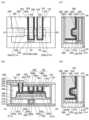
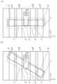
도 1의 (A)는 본 발명의 일 형태인 반도체 장치의 상면도이다. 도 1의 (B) 내지 (D)는 본 발명의 일 형태인 반도체 장치의 단면도이다.
도 2의 (A) 및 (B)는 본 발명의 일 형태인 반도체 장치의 단면도이다.
도 3의 (A) 및 (B)는 본 발명의 일 형태인 반도체 장치의 단면도이다.
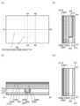
도 4의 (A)는 본 발명의 일 형태인 반도체 장치의 상면도이다. 도 4의 (B) 내지 (D)는 본 발명의 일 형태인 반도체 장치의 단면도이다.
도 5의 (A)는 본 발명의 일 형태인 반도체 장치의 제작 방법을 나타낸 상면도이다. 도 5의 (B) 내지 (D)는 본 발명의 일 형태인 반도체 장치의 제작 방법을 나타낸 단면도이다.
도 6의 (A)는 본 발명의 일 형태인 반도체 장치의 제작 방법을 나타낸 상면도이다. 도 6의 (B) 내지 (D)는 본 발명의 일 형태인 반도체 장치의 제작 방법을 나타낸 단면도이다.
도 7의 (A)는 본 발명의 일 형태인 반도체 장치의 제작 방법을 나타낸 상면도이다. 도 7의 (B) 내지 (D)는 본 발명의 일 형태인 반도체 장치의 제작 방법을 나타낸 단면도이다.
도 8의 (A)는 본 발명의 일 형태인 반도체 장치의 제작 방법을 나타낸 상면도이다. 도 8의 (B) 내지 (D)는 본 발명의 일 형태인 반도체 장치의 제작 방법을 나타낸 단면도이다.
도 9의 (A)는 본 발명의 일 형태인 반도체 장치의 제작 방법을 나타낸 상면도이다. 도 9의 (B) 내지 (D)는 본 발명의 일 형태인 반도체 장치의 제작 방법을 나타낸 단면도이다.
도 10의 (A)는 본 발명의 일 형태인 반도체 장치의 제작 방법을 나타낸 상면도이다. 도 10의 (B) 내지 (D)는 본 발명의 일 형태인 반도체 장치의 제작 방법을 나타낸 단면도이다.
도 11의 (A)는 본 발명의 일 형태인 반도체 장치의 제작 방법을 나타낸 상면도이다. 도 11의 (B) 내지 (D)는 본 발명의 일 형태인 반도체 장치의 제작 방법을 나타낸 단면도이다.
도 12의 (A)는 본 발명의 일 형태인 반도체 장치의 제작 방법을 나타낸 상면도이다. 도 12의 (B) 내지 (D)는 본 발명의 일 형태인 반도체 장치의 제작 방법을 나타낸 단면도이다.
도 13의 (A)는 본 발명의 일 형태인 반도체 장치의 제작 방법을 나타낸 상면도이다. 도 13의 (B) 내지 (D)는 본 발명의 일 형태인 반도체 장치의 제작 방법을 나타낸 단면도이다.
도 14의 (A)는 본 발명의 일 형태인 반도체 장치의 제작 방법을 나타낸 상면도이다. 도 14의 (B) 내지 (D)는 본 발명의 일 형태인 반도체 장치의 제작 방법을 나타낸 단면도이다.
도 15의 (A)는 본 발명의 일 형태인 반도체 장치의 제작 방법을 나타낸 상면도이다. 도 15의 (B) 내지 (D)는 본 발명의 일 형태인 반도체 장치의 제작 방법을 나타낸 단면도이다.
도 16의 (A)는 본 발명의 일 형태인 반도체 장치의 제작 방법을 나타낸 상면도이다. 도 16의 (B) 내지 (D)는 본 발명의 일 형태인 반도체 장치의 제작 방법을 나타낸 단면도이다.
도 17의 (A)는 본 발명의 일 형태인 반도체 장치의 제작 방법을 나타낸 상면도이다. 도 17의 (B) 내지 (D)는 본 발명의 일 형태인 반도체 장치의 제작 방법을 나타낸 단면도이다.
도 18은 본 발명의 일 형태에 따른 마이크로파 처리 장치를 설명하는 상면도이다.
도 19는 본 발명의 일 형태에 따른 마이크로파 처리 장치를 설명하는 단면도이다.
도 20은 본 발명의 일 형태에 따른 마이크로파 처리 장치를 설명하는 단면도이다.
도 21은 본 발명의 일 형태에 따른 마이크로파 처리 장치를 설명하는 단면도이다.
도 22의 (A)는 본 발명의 일 형태에 따른 반도체 장치의 평면도이다. 도 22의 (B) 및 (C)는 본 발명의 일 형태인 반도체 장치의 단면도이다.
도 23의 (A)는 본 발명의 일 형태에 따른 반도체 장치의 평면도이다. 도 23의 (B)는 본 발명의 일 형태에 따른 반도체 장치의 단면도이다.
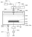
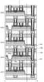
도 24는 본 발명의 일 형태에 따른 기억 장치의 구성을 나타낸 단면도이다.
도 25의 (A) 내지 (C)는 본 발명의 일 형태에 따른 기억 장치의 구성을 설명하기 위한 블록도, 모식도, 및 회로도이다.
도 26의 (A) 및 (B)는 본 발명의 일 형태에 따른 기억 장치의 구성을 설명하기 위한 모식도이다.
도 27의 (A) 및 (B)는 본 발명의 일 형태에 따른 기억 장치의 구성을 설명하기 위한 모식도 및 회로도이다.
도 28은 본 발명의 일 형태에 따른 기억 장치의 구성을 설명하기 위한 모식도이다.
도 29의 (A) 및 (B)는 본 발명의 일 형태에 따른 기억 장치의 구성을 설명하기 위한 레이아웃도이다.
도 30의 (A) 및 (B)는 본 발명의 일 형태에 따른 기억 장치의 구성을 설명하기 위한 레이아웃도 및 단면 모식도이다.
도 31은 본 발명의 일 형태에 따른 기억 장치의 구성을 나타낸 단면도이다.
도 32는 본 발명의 일 형태에 따른 기억 장치의 구성을 나타낸 단면도이다.
도 33은 본 발명의 일 형태에 따른 기억 장치의 구성을 나타낸 단면도이다.
도 34의 (A) 및 (B)는 본 발명의 일 형태에 따른 반도체 장치의 모식도이다.
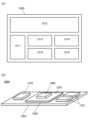
도 35의 (A) 및 (B)는 전자 부품의 일례를 설명하는 도면이다.
도 36의 (A) 내지 (E)는 본 발명의 일 형태에 따른 기억 장치의 모식도이다.
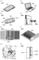
도 37의 (A) 내지 (H)는 본 발명의 일 형태에 따른 전자 기기를 나타낸 도면이다.
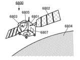
도 38은 우주용 기기의 일례를 나타낸 도면이다.Fig. 1 (A) is a top view of a semiconductor device which is one embodiment of the present invention. Figs. 1 (B) to (D) are cross-sectional views of the semiconductor device which is one embodiment of the present invention.
Figures 2 (A) and (B) are cross-sectional views of a semiconductor device which is one embodiment of the present invention.
Figures 3 (A) and (B) are cross-sectional views of a semiconductor device which is one embodiment of the present invention.
Fig. 4(A) is a top view of a semiconductor device which is one embodiment of the present invention. Figs. 4(B) to 4(D) are cross-sectional views of the semiconductor device which is one embodiment of the present invention.
Fig. 5 (A) is a top view showing a method for manufacturing a semiconductor device, which is one embodiment of the present invention. Figs. 5 (B) to (D) are cross-sectional views showing a method for manufacturing a semiconductor device, which is one embodiment of the present invention.
Fig. 6(A) is a top view showing a method for manufacturing a semiconductor device which is one embodiment of the present invention. Figs. 6(B) to (D) are cross-sectional views showing a method for manufacturing a semiconductor device which is one embodiment of the present invention.
Fig. 7(A) is a top view showing a method for manufacturing a semiconductor device, which is one embodiment of the present invention. Figs. 7(B) to (D) are cross-sectional views showing a method for manufacturing a semiconductor device, which is one embodiment of the present invention.
Fig. 8 (A) is a top view showing a method for manufacturing a semiconductor device which is one embodiment of the present invention. Figs. 8 (B) to (D) are cross-sectional views showing a method for manufacturing a semiconductor device which is one embodiment of the present invention.
Fig. 9 (A) is a top view showing a method for manufacturing a semiconductor device which is one embodiment of the present invention. Figs. 9 (B) to (D) are cross-sectional views showing a method for manufacturing a semiconductor device which is one embodiment of the present invention.
Fig. 10(A) is a top view showing a method for manufacturing a semiconductor device which is one embodiment of the present invention. Figs. 10(B) to (D) are cross-sectional views showing a method for manufacturing a semiconductor device which is one embodiment of the present invention.
Fig. 11(A) is a top view showing a method for manufacturing a semiconductor device which is one embodiment of the present invention. Figs. 11(B) to (D) are cross-sectional views showing a method for manufacturing a semiconductor device which is one embodiment of the present invention.
Fig. 12(A) is a top view showing a method for manufacturing a semiconductor device which is one embodiment of the present invention. Figs. 12(B) to (D) are cross-sectional views showing a method for manufacturing a semiconductor device which is one embodiment of the present invention.
Fig. 13(A) is a top view showing a method for manufacturing a semiconductor device which is one embodiment of the present invention. Figs. 13(B) to (D) are cross-sectional views showing a method for manufacturing a semiconductor device which is one embodiment of the present invention.
Fig. 14(A) is a top view showing a method for manufacturing a semiconductor device which is one embodiment of the present invention. Figs. 14(B) to (D) are cross-sectional views showing a method for manufacturing a semiconductor device which is one embodiment of the present invention.
Fig. 15(A) is a top view showing a method for manufacturing a semiconductor device which is one embodiment of the present invention. Figs. 15(B) to (D) are cross-sectional views showing a method for manufacturing a semiconductor device which is one embodiment of the present invention.
Fig. 16(A) is a top view showing a method for manufacturing a semiconductor device which is one embodiment of the present invention. Figs. 16(B) to (D) are cross-sectional views showing a method for manufacturing a semiconductor device which is one embodiment of the present invention.
Fig. 17(A) is a top view showing a method for manufacturing a semiconductor device which is one embodiment of the present invention. Figs. 17(B) to (D) are cross-sectional views showing a method for manufacturing a semiconductor device which is one embodiment of the present invention.
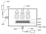
Fig. 18 is a top view illustrating a microwave processing device according to one embodiment of the present invention.
Fig. 19 is a cross-sectional view illustrating a microwave processing device according to one embodiment of the present invention.
Fig. 20 is a cross-sectional view illustrating a microwave processing device according to one embodiment of the present invention.
Fig. 21 is a cross-sectional view illustrating a microwave processing device according to one embodiment of the present invention.
Fig. 22(A) is a plan view of a semiconductor device according to one embodiment of the present invention. Figs. 22(B) and (C) are cross-sectional views of a semiconductor device according to one embodiment of the present invention.
Fig. 23(A) is a plan view of a semiconductor device according to one embodiment of the present invention. Fig. 23(B) is a cross-sectional view of a semiconductor device according to one embodiment of the present invention.
Figure 24 is a cross-sectional view showing the configuration of a memory device according to one embodiment of the present invention.
Figures 25 (A) to (C) are block diagrams, schematic diagrams, and circuit diagrams for explaining the configuration of a memory device according to one embodiment of the present invention.
Figures 26 (A) and (B) are schematic diagrams for explaining the configuration of a memory device according to one embodiment of the present invention.
Figures 27 (A) and (B) are schematic diagrams and circuit diagrams for explaining the configuration of a memory device according to one embodiment of the present invention.
Figure 28 is a schematic diagram for explaining the configuration of a memory device according to one embodiment of the present invention.
Figures 29 (A) and (B) are layout diagrams for explaining the configuration of a memory device according to one embodiment of the present invention.
Figures 30(A) and (B) are a layout diagram and a cross-sectional schematic diagram for explaining the configuration of a memory device according to one embodiment of the present invention.
Figure 31 is a cross-sectional view showing the configuration of a memory device according to one embodiment of the present invention.
Figure 32 is a cross-sectional view showing the configuration of a memory device according to one embodiment of the present invention.
Figure 33 is a cross-sectional view showing the configuration of a memory device according to one embodiment of the present invention.
Figures 34(A) and (B) are schematic diagrams of a semiconductor device according to one embodiment of the present invention.
Figures 35 (A) and (B) are drawings explaining examples of electronic components.
Figures 36 (A) to (E) are schematic diagrams of a memory device according to one embodiment of the present invention.
Figures 37(A) to (H) are drawings showing an electronic device according to one embodiment of the present invention.
Figure 38 is a drawing showing an example of a space device.
이하에서, 실시형태에 대하여 도면을 참조하여 설명한다. 다만 실시형태는 많은 상이한 형태로 실시할 수 있고, 취지 및 그 범위에서 벗어남이 없이 그 형태 및 자세한 사항을 다양하게 변경할 수 있다는 것은 통상의 기술자라면 용이하게 이해할 수 있다. 따라서 본 발명은 이하의 실시형태의 기재 내용에 한정하여 해석되는 것이 아니다.Hereinafter, embodiments will be described with reference to the drawings. However, it will be readily understood by those skilled in the art that the embodiments may be implemented in many different forms, and that the forms and details thereof may be variously changed without departing from the spirit and scope thereof. Accordingly, the present invention should not be interpreted as being limited to the description of the embodiments below.
또한 도면에서 크기, 층의 두께, 또는 영역은 명료화를 위하여 과장되어 있는 경우가 있다. 따라서 그 스케일에 반드시 한정되는 것은 아니다. 또한 도면은 이상적인 예를 모식적으로 나타낸 것이고, 도면에 나타난 형상 또는 값 등에 한정되지 않는다. 예를 들어 실제의 제조 공정에서, 에칭 등의 처리에 의하여 층 또는 레지스트 마스크 등이 의도하지 않게 감소되는 경우가 있지만, 이해를 용이하게 하기 위하여 도면에 반영하지 않은 경우가 있다. 또한 도면에서 동일한 부분 또는 같은 기능을 가지는 부분에는 동일한 부호를 상이한 도면 사이에서 공통적으로 사용하고, 이에 대한 반복적인 설명은 생략하는 경우가 있다. 또한 같은 기능을 가지는 부분을 가리키는 경우에는, 해치 패턴을 동일하게 하고, 특별히 부호를 붙이지 않는 경우가 있다.In addition, the size, layer thickness, or area in the drawing may be exaggerated for clarity. Therefore, it is not necessarily limited to that scale. In addition, the drawing schematically shows an ideal example, and is not limited to the shapes or values shown in the drawing. For example, in an actual manufacturing process, there are cases where layers or resist masks, etc. are unintentionally reduced by processes such as etching, but this may not be reflected in the drawing in order to facilitate understanding. In addition, in the drawing, the same symbol is commonly used in different drawings for the same part or part having the same function, and repeated explanations for this are sometimes omitted. In addition, when indicating a part having the same function, the hatch pattern is the same and no special symbol is sometimes attached.
또한 특히 상면도("평면도"라고도 함) 또는 사시도 등에서, 발명의 이해를 용이하게 하기 위하여 일부의 구성 요소의 기재를 생략하는 경우가 있다. 또한 일부의 숨은선의 기재를 생략하는 경우가 있다.In addition, in particular, in top views (also called "plan views") or perspective views, etc., descriptions of some components may be omitted to facilitate understanding of the invention. In addition, descriptions of some hidden lines may be omitted.
또한 본 명세서 등에서 제 1, 제 2 등으로 붙여지는 서수사는 편의상 사용되는 것이며, 공정 순서 또는 적층 순서를 나타내는 것이 아니다. 그러므로 예를 들어 "제 1"을 "제 2" 또는 "제 3" 등으로 적절히 바꿔 설명할 수 있다. 또한 본 명세서 등에 기재되는 서수사와, 본 발명의 일 형태를 특정하기 위하여 사용되는 서수사는 일치하지 않는 경우가 있다.In addition, ordinal numbers such as first, second, etc. in this specification and the like are used for convenience and do not indicate the process order or the stacking order. Therefore, for example, "first" may be appropriately replaced with "second" or "third". In addition, there are cases where ordinal numbers described in this specification and the like do not match with ordinal numbers used to specify one embodiment of the present invention.
또한 본 명세서 등에서 "위에", "아래에" 등의 배치를 나타내는 어구는 구성끼리의 위치 관계를 도면을 참조하여 설명하기 위하여 편의상 사용하고 있다. 또한 구성끼리의 위치 관계는 각 구성을 묘사하는 방향에 따라 적절히 변화된다. 따라서 명세서에서 설명된 어구에 한정되지 않고, 상황에 따라 적절히 바꿔 말할 수 있다.In addition, phrases indicating arrangement such as "above" and "below" in this specification and others are used for convenience in explaining the positional relationship between components with reference to drawings. In addition, the positional relationship between components changes appropriately depending on the direction in which each component is described. Therefore, it is not limited to the phrases described in the specification, and can be appropriately changed depending on the situation.
예를 들어 본 명세서 등에서, X와 Y가 접속되어 있다는 것은 X와 Y가 전기적으로 접속되는 경우를 말한다. 여기서, X와 Y가 전기적으로 접속되어 있다는 것은 X와 Y 간에 대상물(스위치, 트랜지스터 소자, 또는 다이오드 등의 소자, 혹은 상기 소자 및 배선을 포함하는 회로 등을 가리킴)이 존재하는 경우에 X와 Y 간에서 전기 신호를 전달할 수 있는 접속을 말한다. 또한 X와 Y가 전기적으로 접속되어 있는 경우에는 X와 Y가 직접 접속되어 있는 경우가 포함된다. 여기서 X와 Y가 직접 접속되어 있다는 것은 상기 대상물을 통하지 않고, 배선(또는 전극) 등을 통하여 X와 Y 간에서 전기 신호를 전달할 수 있는 접속을 말한다. 바꿔 말하면, 직접 접속이란, 등가 회로로 나타낸 경우에 같은 회로도로 간주할 수 있는 접속을 말한다.For example, in this specification, etc., when X and Y are connected, it means that X and Y are electrically connected. Here, when X and Y are electrically connected, it means a connection that can transmit an electric signal between X and Y when an object (an element such as a switch, a transistor element, or a diode, or a circuit including the element and wiring, etc.) exists between X and Y. In addition, when X and Y are electrically connected, it includes a case where X and Y are directly connected. Here, when X and Y are directly connected, it means a connection that can transmit an electric signal between X and Y without going through the object, but through wiring (or electrodes). In other words, a direct connection means a connection that can be regarded as the same circuit diagram when represented as an equivalent circuit.
또한 본 명세서 등에서 트랜지스터란 게이트와, 드레인과, 소스를 포함하는 적어도 3개의 단자를 포함하는 소자이다. 그리고 드레인(드레인 단자, 드레인 영역, 또는 드레인 전극)과 소스(소스 단자, 소스 영역, 또는 소스 전극) 사이에 채널이 형성되는 영역(이하, 채널 형성 영역이라고도 함)을 포함하고, 채널 형성 영역을 통하여 소스와 드레인 사이에 전류를 흘릴 수 있다. 또한 본 명세서 등에서 채널 형성 영역이란 전류가 주로 흐르는 영역을 말한다.In addition, in this specification and the like, a transistor is a device including at least three terminals including a gate, a drain, and a source. And it includes a region (hereinafter, also referred to as a channel formation region) in which a channel is formed between the drain (drain terminal, drain region, or drain electrode) and the source (source terminal, source region, or source electrode), and current can flow between the source and the drain through the channel formation region. In addition, in this specification and the like, the channel formation region refers to a region through which current mainly flows.
또한 소스 또는 드레인의 기능은 상이한 극성의 트랜지스터를 채용하는 경우 또는 회로 동작에서 전류의 방향이 변화되는 경우 등에는 서로 바뀌는 경우가 있다. 그러므로 본 명세서 등에서는 소스 또는 드레인이라는 용어는 서로 바꿔 사용할 수 있는 경우가 있다.In addition, the functions of the source and drain may be interchanged when transistors of different polarities are used or when the direction of current changes in circuit operation. Therefore, in this specification and elsewhere, the terms source and drain may be used interchangeably.
또한 채널 길이란, 예를 들어 트랜지스터의 상면도에서, 반도체(또는 트랜지스터가 온 상태일 때 반도체 내에서 전류가 흐르는 부분)와 게이트 전극이 서로 중첩되는 영역, 또는 채널 형성 영역에서의 소스(소스 영역 또는 소스 전극)와 드레인(드레인 영역 또는 드레인 전극) 사이의 거리를 말한다. 또한 하나의 트랜지스터에서, 채널 길이가 모든 영역에서 같은 값을 취한다고 할 수는 없다. 즉 하나의 트랜지스터의 채널 길이는 하나의 값으로 정해지지 않는 경우가 있다. 따라서 본 명세서에서 채널 길이는 채널 형성 영역에서의 어느 하나의 값, 최댓값, 최솟값, 또는 평균값으로 한다.In addition, the channel length refers to, for example, the distance between the source (source region or source electrode) and the drain (drain region or drain electrode) in the region where the semiconductor (or the portion of the semiconductor through which current flows when the transistor is on) and the gate electrode overlap each other in the top view of the transistor, or in the channel formation region. In addition, in one transistor, the channel length cannot be said to have the same value in all regions. That is, in some cases, the channel length of one transistor is not determined by one value. Therefore, in this specification, the channel length is set to one value, maximum value, minimum value, or average value in the channel formation region.
채널 폭이란, 예를 들어 트랜지스터의 상면도에서, 반도체(또는 트랜지스터가 온 상태일 때 반도체 내에서 전류가 흐르는 부분)와 게이트 전극이 서로 중첩되는 영역, 또는 채널 형성 영역에서의 채널 길이 방향에 수직인 방향의 채널 형성 영역의 길이를 말한다. 또한 하나의 트랜지스터에서, 채널 폭이 모든 영역에서 같은 값을 취한다고 할 수는 없다. 즉 하나의 트랜지스터의 채널 폭은 하나의 값으로 정해지지 않는 경우가 있다. 따라서 본 명세서에서 채널 폭은 채널 형성 영역에서의 어느 하나의 값, 최댓값, 최솟값, 또는 평균값으로 한다.Channel width refers to, for example, the length of a channel formation region in a direction perpendicular to the channel length direction in a region where a semiconductor (or a portion of the semiconductor through which current flows when the transistor is on) and a gate electrode overlap each other in a top view of a transistor, or a channel formation region. In addition, in one transistor, the channel width cannot be said to have the same value in all regions. In other words, the channel width of one transistor is not always determined by one value. Therefore, in this specification, the channel width is defined as one value, a maximum value, a minimum value, or an average value in the channel formation region.
또한 본 명세서 등에서 트랜지스터의 구조에 따라서는 실제로 채널이 형성되는 영역에서의 채널 폭(이하, "실효적인 채널 폭"이라고도 함)과 트랜지스터의 상면도에서 나타내는 채널 폭(이하, "외관상 채널 폭"이라고도 함)이 상이한 경우가 있다. 예를 들어 게이트 전극이 반도체의 측면을 덮는 경우, 실효적인 채널 폭이 외관상 채널 폭보다 커져, 그 영향을 무시할 수 없는 경우가 있다. 예를 들어 미세하고 게이트 전극이 반도체의 측면을 덮는 트랜지스터에서는, 반도체의 측면에 형성되는 채널 형성 영역의 비율이 높아지는 경우가 있다. 이 경우에는 외관상 채널 폭보다 실효적인 채널 폭이 더 크다.In addition, depending on the structure of the transistor in this specification and the like, there are cases where the channel width in the area where the channel is actually formed (hereinafter also referred to as the "effective channel width") and the channel width shown in the top view of the transistor (hereinafter also referred to as the "apparent channel width") are different. For example, when the gate electrode covers the side surface of the semiconductor, the effective channel width is larger than the apparent channel width, and the influence thereof may not be negligible. For example, in a transistor where the gate electrode is fine and covers the side surface of the semiconductor, the ratio of the channel formation area formed on the side surface of the semiconductor may be high. In this case, the effective channel width is larger than the apparent channel width.
이러한 경우, 실효적인 채널 폭을 실측에 의하여 추정하기 어려운 경우가 있다. 예를 들어 설곗값으로부터 실효적인 채널 폭을 추정하기 위해서는, 반도체의 형상이 이미 알려져 있다는 가정이 필요하다. 따라서 반도체의 형상을 정확하게 알 수 없는 경우에는 실효적인 채널 폭을 정확하게 측정하기 어렵다.In such cases, it is sometimes difficult to estimate the effective channel width by actual measurement. For example, in order to estimate the effective channel width from the design value, it is necessary to assume that the shape of the semiconductor is already known. Therefore, if the shape of the semiconductor is not known accurately, it is difficult to accurately measure the effective channel width.
본 명세서에서 단순히 채널 폭이라고 기재한 경우에는 외관상 채널 폭을 가리키는 경우가 있다. 또는 본 명세서에서 단순히 채널 폭이라고 기재한 경우에는 실효적인 채널 폭을 가리키는 경우가 있다. 또한 채널 길이, 채널 폭, 실효적인 채널 폭, 또는 외관상 채널 폭 등은 예를 들어 단면 TEM 이미지를 해석하는 것에 의하여 값을 결정할 수 있다.In this specification, when it is simply described as channel width, it may refer to the apparent channel width. Or, when it is simply described as channel width in this specification, it may refer to the effective channel width. In addition, the values of channel length, channel width, effective channel width, or apparent channel width can be determined, for example, by analyzing a cross-sectional TEM image.
또한 반도체의 불순물이란, 예를 들어 반도체를 구성하는 주성분 외의 것을 말한다. 예를 들어 농도가 0.1atomic% 미만인 원소는 불순물이라고 할 수 있다. 불순물이 포함됨으로써, 예를 들어 반도체의 결함 준위 밀도가 높아지거나, 결정성의 저하 등이 일어나는 경우가 있다. 반도체가 산화물 반도체인 경우, 반도체의 특성을 변화시키는 불순물로서는, 예를 들어 1족 원소, 2족 원소, 13족 원소, 14족 원소, 15족 원소, 산화물 반도체의 주성분 외의 전이 금속(transition metal) 등이 있고, 예를 들어 수소, 리튬, 소듐, 실리콘, 붕소, 인, 탄소, 질소 등이 있다. 또한 물도 불순물로서 기능하는 경우가 있다. 또한 예를 들어 불순물의 혼입으로 인하여 산화물 반도체에 산소 결손(VO: oxygen vacancy라고도 함)이 형성되는 경우가 있다.Also, the impurity of a semiconductor refers to, for example, something other than the main component that constitutes the semiconductor. For example, an element with a concentration of less than 0.1 atomic% can be considered an impurity. When an impurity is included, for example, the density of defect states of the semiconductor may increase, or the crystallinity may deteriorate. When the semiconductor is an oxide semiconductor, impurities that change the characteristics of the semiconductor include, for example,
또한 본 명세서 등에서 산화질화 실리콘이란 그 조성에서 질소보다 산소의 함유량이 많은 것을 말한다. 또한 질화산화 실리콘이란 그 조성에서 산소보다 질소의 함유량이 많은 것을 말한다. 또한 산화질화 알루미늄이란 그 조성에서 질소보다 산소의 함유량이 많은 것을 말한다. 또한 질화산화 알루미늄이란 그 조성에서 산소보다 질소의 함유량이 많은 것을 말한다. 또한 산화질화 하프늄이란 그 조성에서 질소보다 산소의 함유량이 많은 것을 말한다. 또한 질화산화 하프늄이란 그 조성에서 산소보다 질소의 함유량이 많은 것을 말한다.In addition, as used herein, silicon oxynitride refers to a composition having a higher oxygen content than nitrogen. In addition, silicon nitride refers to a composition having a higher nitrogen content than oxygen. In addition, aluminum oxynitride refers to a composition having a higher oxygen content than nitrogen. In addition, aluminum oxynitride refers to a composition having a higher nitrogen content than oxygen. In addition, hafnium oxynitride refers to a composition having a higher oxygen content than nitrogen. In addition, hafnium oxynitride refers to a composition having a higher nitrogen content than oxygen.
또한 본 명세서 등에서 "절연체"라는 용어를 절연막 또는 절연층이라고 바꿔 말할 수 있다. 또한 "도전체"라는 용어를 도전막 또는 도전층이라고 바꿔 말할 수 있다. 또한 "반도체"라는 용어를 반도체막 또는 반도체층이라고 바꿔 말할 수 있다.In addition, the term "insulator" in this specification and elsewhere may be replaced with insulating film or insulating layer. In addition, the term "conductor" may be replaced with conductive film or conductive layer. In addition, the term "semiconductor" may be replaced with semiconductor film or semiconductor layer.
또한 본 명세서 등에서 "평행"이란, 2개의 직선이 -10° 이상 10° 이하의 각도로 배치되어 있는 상태를 말한다. 따라서 -5° 이상 5° 이하의 경우도 포함된다. 또한 "실질적으로 평행"이란, 2개의 직선이 -30° 이상 30° 이하의 각도로 배치되어 있는 상태를 말한다. 또한 "수직"이란, 2개의 직선이 80° 이상 100° 이하의 각도로 배치되어 있는 상태를 말한다. 따라서 85° 이상 95° 이하의 경우도 포함된다. 또한 "실질적으로 수직"이란, 2개의 직선이 60° 이상 120° 이하의 각도로 배치되어 있는 상태를 말한다.In addition, in this specification and the like, "parallel" means a state in which two straight lines are arranged at an angle of -10° or more and 10° or less. Therefore, a case of -5° or more and 5° or less is also included. In addition, "substantially parallel" means a state in which two straight lines are arranged at an angle of -30° or more and 30° or less. In addition, "perpendicular" means a state in which two straight lines are arranged at an angle of 80° or more and 100° or less. Therefore, a case of 85° or more and 95° or less is also included. In addition, "substantially perpendicular" means a state in which two straight lines are arranged at an angle of 60° or more and 120° or less.
본 명세서 등에서 금속 산화물(metal oxide)이란, 넓은 의미로의 금속의 산화물이다. 금속 산화물은 산화물 절연체, 산화물 도전체(투명 산화물 도전체를 포함함), 산화물 반도체(Oxide Semiconductor 또는 단순히 OS라고도 함) 등으로 분류된다. 예를 들어 트랜지스터의 반도체층에 금속 산화물을 사용한 경우, 상기 금속 산화물을 산화물 반도체라고 하는 경우가 있다. 즉 OS 트랜지스터라고 기재하는 경우에는, 금속 산화물 또는 산화물 반도체를 포함하는 트랜지스터라고 바꿔 말할 수 있다.In this specification and elsewhere, metal oxide refers to a metal oxide in a broad sense. Metal oxides are classified into oxide insulators, oxide conductors (including transparent oxide conductors), oxide semiconductors (also called oxide semiconductors or simply OS), etc. For example, when a metal oxide is used in the semiconductor layer of a transistor, the metal oxide is sometimes referred to as an oxide semiconductor. In other words, when describing an OS transistor, it can be rephrased as a transistor including a metal oxide or oxide semiconductor.
또한 본 명세서 등에서 노멀리 오프란 게이트에 전위를 인가하지 않거나, 게이트에 접지 전위를 인가하였을 때, 트랜지스터를 흐르는 채널 폭 1μm당 드레인 전류가 실온에서 1×10-20A 이하, 85℃에서 1×10-18A 이하, 또는 125℃에서 1×10-16A 이하인 것을 말한다.In addition, in this specification and the like, normally-off means that when no potential is applied to the gate or a ground potential is applied to the gate, the drain current per 1 μm of channel width flowing through the transistor is 1×10-20 A or less at room temperature, 1×10-18 A or less at 85°C, or 1×10-16 A or less at 125°C.
또한 본 명세서 등에서 "전압"과 "전위"는 적절히 바꿔 말할 수 있다. "전압"은 기준이 되는 전위와의 전위차를 말하고, 예를 들어 기준이 되는 전위를 그라운드 전위(접지 전위)로 하면, "전압"을 "전위"로 바꿔 말할 수 있다. 또한 그라운드 전위는 반드시 0V를 의미하는 것은 아니다. 또한 전위는 상대적인 것이고, 기준이 되는 전위가 변화됨으로써, 배선에 공급되는 전위, 회로 등에 인가되는 전위, 회로 등으로부터 출력되는 전위 등도 변화된다.In addition, in this specification and elsewhere, "voltage" and "potential" can be appropriately interchanged. "Voltage" refers to the potential difference from a reference potential, and for example, if the reference potential is the ground potential (ground potential), "voltage" can be interchanged with "potential." In addition, the ground potential does not necessarily mean 0 V. In addition, potential is relative, and as the reference potential changes, the potential supplied to wiring, the potential applied to circuits, etc., the potential output from circuits, etc. also change.
본 명세서 등에서 복수의 요소에 같은 부호를 사용하고, 이들을 특별히 구별할 필요가 있는 경우에는, 부호에 "_1", "[n]", 또는 "[m, n]" 등의 식별용 부호를 붙여서 기재하는 경우가 있다.In cases where the same symbol is used for multiple elements in this specification and there is a need to specifically distinguish them, the symbol may be described by adding an identifying symbol such as “_1”, "[n]", or "[m, n]".
또한 본 명세서 등에서 "높이가 일치하거나 실질적으로 일치"란, 단면에서 볼 때, 기준이 되는 면(예를 들어 기판 표면 등의 평탄한 면)으로부터의 높이가 같은 구성을 말한다. 예를 들어 반도체 장치의 제조 공정에서 평탄화 처리(대표적으로는 CMP 처리)를 수행함으로써 단층 또는 복수의 층의 표면이 노출되는 경우가 있다. 이 경우, CMP 처리가 수행된 피처리면은 기준이 되는 면과 높이가 같다. 다만 CMP 처리에 사용되는 처리 장치, 처리 방법, 또는 피처리면의 재료에 따라서는 복수의 층의 높이가 서로 달라지는 경우가 있다. 본 명세서 등에서는 이 경우도 "높이가 일치하거나 실질적으로 일치"에 포함시킨다. 예를 들어 기준이 되는 면에 대하여 2개의 높이를 가지는 층(여기서는 제 1 층과 제 2 층)을 포함하고, 제 1 층의 상면의 높이와 제 2 층의 상면의 높이의 차이가 20nm 이하인 경우도 "높이가 일치하거나 실질적으로 일치"라고 한다.In addition, in this specification and the like, "the heights are the same or substantially the same" means a configuration in which, when viewed in cross-section, the heights from a reference surface (e.g., a flat surface such as a substrate surface) are the same. For example, in a semiconductor device manufacturing process, there are cases where a surface of a single layer or multiple layers is exposed by performing a flattening process (typically, a CMP process). In this case, the surface to be processed on which the CMP process is performed has the same height as the reference surface. However, depending on the processing device, processing method, or material of the surface to be processed used for the CMP process, there are cases where the heights of the multiple layers are different from each other. In this specification and the like, this case is also included in "the heights are the same or substantially the same." For example, a case in which two layers (here, a first layer and a second layer) are included with respect to a reference surface and the difference in the height of the upper surface of the first layer and the height of the upper surface of the second layer is 20 nm or less is also referred to as "the heights are the same or substantially the same."
또한 본 명세서 등에서 "단부가 정렬되거나 실질적으로 정렬"이란, 상면에서 볼 때, 적층된 층과 층 사이에서 적어도 윤곽의 일부가 중첩되는 것을 말한다. 예를 들어 위층과 아래층이 동일한 마스크 패턴 또는 일부가 동일한 마스크 패턴을 사용하여 가공된 경우를 그 범주에 포함한다. 다만 엄밀하게 말하면 윤곽이 중첩되지 않고 위층의 윤곽이 아래층의 윤곽보다 내측에 위치하거나 위층의 윤곽이 아래층의 윤곽보다 외측에 위치하는 경우도 있고, 이 경우도 "단부가 정렬되거나 실질적으로 정렬"이라고 한다.In addition, in this specification and the like, "the ends are aligned or substantially aligned" means that, when viewed from above, at least a portion of the outlines overlap between the laminated layers. For example, this category includes cases where the upper and lower layers are processed using the same mask pattern or partly the same mask pattern. However, strictly speaking, there are cases where the outlines do not overlap and the outline of the upper layer is located inside the outline of the lower layer, or the outline of the upper layer is located outside the outline of the lower layer, and in these cases, "the ends are aligned or substantially aligned" is also referred to.
(실시형태 1)(Embodiment 1)
본 실시형태에서는, 도 1의 (A) 내지 도 23의 (B)를 사용하여 본 발명의 일 형태인 반도체 장치의 일례 및 그 제작 방법에 대하여 설명한다. 본 발명의 일 형태인 반도체 장치는 트랜지스터 및 용량 소자를 포함한다.In this embodiment, an example of a semiconductor device according to one embodiment of the present invention and a method for manufacturing the same will be described using FIG. 1 (A) to FIG. 23 (B). The semiconductor device according to one embodiment of the present invention includes a transistor and a capacitor.
<반도체 장치의 구성예><Example of semiconductor device configuration>
도 1을 사용하여 트랜지스터(200) 및 용량 소자(100)를 포함하는 반도체 장치의 구성에 대하여 설명한다. 도 1의 (A) 내지 (D)는 트랜지스터(200) 및 용량 소자(100)를 포함하는 반도체 장치의 상면도 및 단면도이다. 도 1의 (A)는 상기 반도체 장치의 상면도이다. 또한 도 1의 (B) 내지 (D)는 상기 반도체 장치의 단면도이다. 여기서 도 1의 (B)는 도 1의 (A)의 일점쇄선 A1-A2로 자른 부분의 단면도이고, 트랜지스터(200) 및 용량 소자(100)의 채널 길이 방향의 단면도이기도 하다. 또한 도 1의 (C)는 도 1의 (A)의 일점쇄선 A3-A4로 자른 부분의 단면도이고, 트랜지스터(200)의 채널 폭 방향의 단면도이기도 하다. 또한 도 1의 (D)는 도 1의 (A)의 일점쇄선 A5-A6으로 자른 부분의 단면도이고, 용량 소자(100)의 채널 폭 방향의 단면도이기도 하다. 또한 도 1의 (A)의 상면도에서는, 도면의 명료화를 위하여 일부의 요소를 생략하였다.Hereinafter, a configuration of a semiconductor device including a transistor (200) and a capacitor (100) will be described using FIG. 1. FIGS. 1(A) to 1(D) are a top view and a cross-sectional view of a semiconductor device including a transistor (200) and a capacitor (100). FIG. 1(A) is a top view of the semiconductor device. In addition, FIGS. 1(B) to 1(D) are cross-sectional views of the semiconductor device. Here, FIG. 1(B) is a cross-sectional view taken along dashed-dotted line A1-A2 in FIG. 1(A), and is also a cross-sectional view in the channel length direction of the transistor (200) and the capacitor (100). In addition, FIG. 1(C) is a cross-sectional view taken along dashed-dotted line A3-A4 in FIG. 1(A), and is also a cross-sectional view in the channel width direction of the transistor (200). In addition, (D) of Fig. 1 is a cross-sectional view of a portion cut along the dashed-dotted line A5-A6 of (A) of Fig. 1, and is also a cross-sectional view in the channel width direction of the capacitor element (100). In addition, in the top view of (A) of Fig. 1, some elements are omitted for clarity of the drawing.
본 발명의 일 형태인 반도체 장치는 기판(도시하지 않았음) 위의 절연체(212)와, 절연체(212) 위의 절연체(214)와, 절연체(214) 위의 트랜지스터(200) 및 용량 소자(100)와, 트랜지스터(200)에 제공된 절연체(275) 및 절연체(271)(절연체(271a), 절연체(271b)) 위의 절연체(280)와, 절연체(280) 위의 절연체(282)와, 절연체(282) 위의 절연체(283)와, 절연체(283) 위의 절연체(274)와, 절연체(283) 위 및 절연체(274) 위의 절연체(285)를 포함한다. 절연체(212), 절연체(214), 절연체(280), 절연체(282), 절연체(283), 절연체(285), 절연체(274), 및 절연체(285)는 층간막으로서 기능한다. 또한 절연체(283)는 절연체(214)의 상면의 일부, 절연체(280)의 측면, 그리고 절연체(282)의 측면 및 상면과 접한다. 도 1에 나타낸 바와 같이 트랜지스터(200) 및 용량 소자(100)는 적어도 일부가 절연체(280)에 매립되어 배치된다.A semiconductor device according to one embodiment of the present invention includes an insulator (212) on a substrate (not shown), an insulator (214) on the insulator (212), a transistor (200) and a capacitor (100) on the insulator (214), an insulator (275) provided on the transistor (200) and an insulator (271) (insulator (271a), insulator (271b)), an insulator (280) on the insulator (280), an insulator (283) on the insulator (282), an insulator (274) on the insulator (283), and an insulator (285) on the insulator (283) and on the insulator (274). The insulator (212), the insulator (214), the insulator (280), the insulator (282), the insulator (283), the insulator (285), the insulator (274), and the insulator (285) function as interlayer films. In addition, the insulator (283) is in contact with a part of the upper surface of the insulator (214), the side surface of the insulator (280), and the side surface and the upper surface of the insulator (282). As shown in Fig. 1, the transistor (200) and the capacitor (100) are disposed with at least a part of the insulator (280) embedded in the insulator.
여기서 트랜지스터(200)는 반도체층으로서 기능하는 산화물(230)과, 제 1 게이트로서 기능하는 도전체(260)와, 제 2 게이트로서 기능하는 도전체(205)와, 소스 및 드레인 중 한쪽으로서 기능하는 도전체(242a)와, 소스 및 드레인 중 다른 쪽으로서 기능하는 도전체(242b)를 포함한다. 또한 제 1 게이트 절연막으로서 기능하는 절연체(252), 절연체(250), 및 절연체(254)를 포함한다. 또한 제 2 게이트 절연막으로서 기능하는 절연체(222) 및 절연체(224)를 포함한다.Here, the transistor (200) includes an oxide (230) functioning as a semiconductor layer, a conductor (260) functioning as a first gate, a conductor (205) functioning as a second gate, a conductor (242a) functioning as one of a source and a drain, and a conductor (242b) functioning as the other of the source and the drain. It also includes an insulator (252), an insulator (250), and an insulator (254) functioning as a first gate insulating film. It also includes an insulator (222) and an insulator (224) functioning as a second gate insulating film.
트랜지스터(200)의 제 1 게이트 및 제 1 게이트 절연막은 절연체(280), 절연체(275), 및 절연체(271)에 형성된 개구(258) 내에 배치된다. 즉 도전체(260), 절연체(252), 절연체(250), 및 절연체(254)는 개구(258) 내에 배치된다.The first gate and the first gate insulating film of the transistor (200) are disposed within an opening (258) formed in an insulator (280), an insulator (275), and an insulator (271). That is, the conductor (260), the insulator (252), the insulator (250), and the insulator (254) are disposed within the opening (258).
또한 용량 소자(100)는 하부 전극으로서 기능하는 도전체(242b)와, 유전체로서 기능하는 절연체(152), 절연체(150), 및 절연체(154)와, 상부 전극으로서 기능하는 도전체(160)를 포함한다. 즉 용량 소자(100)는 MIM(Metal-Insulator-Metal) 용량을 구성한다. 또한 도전체(242b)는 용량 소자(100)의 하부 전극과, 트랜지스터(200)의 소스 및 드레인 중 다른 쪽을 겸할 수 있다. 따라서 용량 소자(100)의 제작 공정에 있어서 트랜지스터(200)의 제작 공정의 일부를 겸용할 수 있기 때문에 생산성이 높은 반도체 장치로 할 수 있다.In addition, the capacitor (100) includes a conductor (242b) functioning as a lower electrode, an insulator (152), an insulator (150), and an insulator (154) functioning as a dielectric, and a conductor (160) functioning as an upper electrode. That is, the capacitor (100) constitutes a MIM (Metal-Insulator-Metal) capacitor. In addition, the conductor (242b) can serve as the lower electrode of the capacitor (100) and the other of the source and drain of the transistor (200). Therefore, since a part of the manufacturing process of the transistor (200) can be used in the manufacturing process of the capacitor (100), a semiconductor device with high productivity can be obtained.
용량 소자(100)의 상부 전극 및 유전체는 절연체(280), 절연체(275), 및 절연체(271)에 형성된 개구(158) 내에 배치된다. 즉 도전체(160), 절연체(152), 절연체(150), 및 절연체(154)는 개구(158) 내에 배치된다.The upper electrode and dielectric of the capacitor (100) are placed within the opening (158) formed in the insulator (280), the insulator (275), and the insulator (271). That is, the conductor (160), the insulator (152), the insulator (150), and the insulator (154) are placed within the opening (158).
또한 본 발명의 일 형태의 반도체 장치는 트랜지스터(200)에 전기적으로 접속되고, 플러그로서 기능하는 도전체(240)를 포함한다. 또한 도전체(240)의 측면과 접촉하여 절연체(241)가 제공된다. 또한 도전체(240)는 도전체(242a)에 전기적으로 접속되어 있다. 또한 절연체(285) 및 도전체(240) 위에는 도전체(240)에 전기적으로 접속되고, 배선으로서 기능하는 도전체(246)가 제공된다.In addition, a semiconductor device of one embodiment of the present invention includes a conductor (240) that is electrically connected to a transistor (200) and functions as a plug. In addition, an insulator (241) is provided in contact with a side surface of the conductor (240). In addition, the conductor (240) is electrically connected to the conductor (242a). In addition, a conductor (246) that is electrically connected to the conductor (240) and functions as a wiring is provided on the insulator (285) and the conductor (240).
도전체(240) 및 도전체(246)는 스위치, 트랜지스터, 용량 소자, 인덕터, 저항 소자, 및 다이오드 등의 회로 소자, 배선, 전극, 또는 단자와, 트랜지스터(200)를 전기적으로 접속하기 위한 플러그 또는 배선으로서 기능한다.The conductor (240) and conductor (246) function as a plug or wire for electrically connecting a circuit element, wiring, electrode, or terminal such as a switch, transistor, capacitive element, inductor, resistive element, and diode, and the transistor (200).
본 실시형태에 나타내는 트랜지스터(200) 및 용량 소자(100)를 포함하는 반도체 장치는 기억 장치의 메모리 셀로서 사용할 수 있다. 이때 도전체(246)는 감지 증폭기에 전기적으로 접속되는 경우가 있다. 여기서 도 1의 (A)에 나타낸 바와 같이 트랜지스터(200) 및 용량 소자(100)는 모두 산화물(230) 위에 형성된다. 따라서 평면에서 볼 때, 점유 면적을 크게 증가시키지 않고 용량 소자(100)를 제공할 수 있기 때문에 본 실시형태에 따른 반도체 장치를 미세화 또는 고집적화시킬 수 있다.The semiconductor device including the transistor (200) and the capacitor (100) shown in this embodiment can be used as a memory cell of a memory device. At this time, the conductor (246) may be electrically connected to a sense amplifier. Here, as shown in (A) of Fig. 1, both the transistor (200) and the capacitor (100) are formed on an oxide (230). Therefore, since the capacitor (100) can be provided without significantly increasing the occupied area when viewed in a plan view, the semiconductor device according to this embodiment can be miniaturized or highly integrated.
[트랜지스터(200)][Transistor (200)]
도 1의 (A) 내지 (D)에 나타낸 바와 같이 트랜지스터(200)는 절연체(214) 위의 절연체(216)와, 절연체(216)에 매립되도록 배치된 도전체(205)(도전체(205a) 및 도전체(205b))와, 절연체(216) 위 및 도전체(205) 위의 절연체(222)와, 절연체(222) 위의 절연체(224)와, 절연체(224) 위의 산화물(230a)과, 산화물(230a) 위의 산화물(230b)과, 산화물(230b) 위의 도전체(242a)와, 도전체(242a) 위의 절연체(271a)와, 산화물(230b) 위의 도전체(242b)와, 도전체(242b) 위의 절연체(271b)와, 산화물(230b) 위의 절연체(252)와, 절연체(252) 위의 절연체(250)와, 절연체(250) 위의 절연체(254)와, 절연체(254) 위에 위치하고 산화물(230b)의 일부와 중첩되는 도전체(260)(도전체(260a) 및 도전체(260b))와, 절연체(222), 절연체(224), 산화물(230a), 산화물(230b), 도전체(242a), 도전체(242b), 절연체(271a), 및 절연체(271b) 위에 배치되는 절연체(275)를 포함한다. 여기서 도 1의 (B) 및 (C)에 나타낸 바와 같이 절연체(252)는 절연체(222)의 상면, 절연체(224)의 측면, 산화물(230a)의 측면, 산화물(230b)의 측면 및 상면, 도전체(242a) 및 도전체(242b)의 측면, 절연체(271a) 및 절연체(271b)의 측면, 절연체(275)의 측면, 절연체(280)의 측면, 그리고 절연체(250)의 하면 각각의 적어도 일부와 접한다. 또한 도전체(260)의 상면은 절연체(254)의 최상부, 절연체(250)의 최상부, 절연체(252)의 최상부, 및 절연체(280)의 상면과 높이가 실질적으로 일치하도록 배치된다. 또한 절연체(282)는 도전체(260), 절연체(252), 절연체(250), 절연체(254), 및 절연체(280) 각각의 상면의 적어도 일부와 접한다.As shown in (A) to (D) of FIG. 1, the transistor (200) includes an insulator (216) on an insulator (214), a conductor (205) (conductor (205a) and conductor (205b)) arranged to be embedded in the insulator (216), an insulator (222) on the insulator (216) and the conductor (205), an insulator (224) on the insulator (222), an oxide (230a) on the insulator (224), an oxide (230b) on the oxide (230a), a conductor (242a) on the oxide (230b), an insulator (271a) on the conductor (242a), a conductor (242b) on the oxide (230b), an insulator (271b) on the conductor (242b), and an oxide (230b). It includes an insulator (252), an insulator (250) on the insulator (252), an insulator (254) on the insulator (250), a conductor (260) (conductor (260a) and conductor (260b)) positioned on the insulator (254) and overlapping a part of the oxide (230b), and an insulator (222), an insulator (224), an oxide (230a), an oxide (230b), a conductor (242a), a conductor (242b), an insulator (271a), and an insulator (275) positioned on the insulator (271b). Here, as shown in (B) and (C) of FIG. 1, the insulator (252) is in contact with at least a portion of each of the upper surface of the insulator (222), the side surface of the insulator (224), the side surface of the oxide (230a), the side surface and the upper surface of the oxide (230b), the side surfaces of the conductor (242a) and the conductor (242b), the side surfaces of the insulator (271a) and the insulator (271b), the side surface of the insulator (275), the side surface of the insulator (280), and the lower surface of the insulator (250). In addition, the upper surface of the conductor (260) is arranged so that its height is substantially the same as that of the uppermost portion of the insulator (254), the uppermost portion of the insulator (250), the uppermost portion of the insulator (252), and the upper surface of the insulator (280). Additionally, the insulator (282) is in contact with at least a portion of the upper surface of each of the conductor (260), the insulator (252), the insulator (250), the insulator (254), and the insulator (280).
또한 본 명세서 등에 있어서, 산화물(230a)과 산화물(230b)을 통틀어 산화물(230)이라고 부르는 경우가 있다. 또한 도전체(242a)와 도전체(242b)를 통틀어 도전체(242)라고 부르는 경우가 있다. 또한 절연체(271a)와 절연체(271b)를 통틀어 절연체(271)라고 부르는 경우가 있다.In addition, in this specification and the like, the oxide (230a) and the oxide (230b) are sometimes collectively referred to as oxide (230). In addition, the conductor (242a) and the conductor (242b) are sometimes collectively referred to as conductor (242). In addition, the insulator (271a) and the insulator (271b) are sometimes collectively referred to as insulator (271).
절연체(280), 절연체(271), 및 절연체(275)에는 산화물(230b)에 도달하는 개구(258)가 제공된다. 즉 개구(258)는 산화물(230b)과 중첩되는 영역을 포함한다고 할 수 있다. 또한 절연체(275)는 절연체(280)에 포함되는 개구(258)와 중첩되는 개구를 포함한다고 할 수 있다. 또한 개구(258) 내에 절연체(252), 절연체(250), 절연체(254), 및 도전체(260)가 배치되어 있다. 즉 도전체(260)는 절연체(252), 절연체(250), 및 절연체(254)를 개재(介在)하여 산화물(230b)과 중첩되는 영역을 포함한다. 또한 트랜지스터(200)의 채널 길이 방향에서, 절연체(271a)와 절연체(271b) 사이 및 도전체(242a)와 도전체(242b) 사이에 도전체(260), 절연체(252), 절연체(250), 및 절연체(254)가 제공되어 있다. 절연체(254)는 도전체(260)의 측면과 접하는 영역과 도전체(260)의 밑면과 접하는 영역을 포함한다. 또한 도 1의 (C)에 나타낸 바와 같이 개구(258)는 산화물(230)과 중첩되지 않는 영역에서는 절연체(222)에 도달한다.An opening (258) that reaches the oxide (230b) is provided in the insulator (280), the insulator (271), and the insulator (275). That is, it can be said that the opening (258) includes a region that overlaps with the oxide (230b). In addition, it can be said that the insulator (275) includes an opening that overlaps with the opening (258) included in the insulator (280). In addition, the insulator (252), the insulator (250), the insulator (254), and the conductor (260) are arranged in the opening (258). That is, the conductor (260) includes a region that overlaps with the oxide (230b) by interposing the insulator (252), the insulator (250), and the insulator (254). In addition, in the channel length direction of the transistor (200), a conductor (260), an insulator (252), an insulator (250), and an insulator (254) are provided between the insulator (271a) and the insulator (271b) and between the conductor (242a) and the conductor (242b). The insulator (254) includes a region in contact with a side surface of the conductor (260) and a region in contact with a bottom surface of the conductor (260). In addition, as shown in (C) of FIG. 1, the opening (258) reaches the insulator (222) in a region that does not overlap with the oxide (230).
산화물(230)은 절연체(224) 위에 배치된 산화물(230a)과, 산화물(230a) 위에 배치된 산화물(230b)을 포함하는 것이 바람직하다. 산화물(230b) 아래에 산화물(230a)을 포함함으로써, 산화물(230a)보다 아래쪽에 형성된 구조물로부터 산화물(230b)로 불순물이 확산되는 것을 억제할 수 있다.It is preferable that the oxide (230) includes an oxide (230a) disposed on an insulator (224) and an oxide (230b) disposed on the oxide (230a). By including the oxide (230a) below the oxide (230b), it is possible to suppress diffusion of impurities from a structure formed below the oxide (230a) to the oxide (230b).
또한 트랜지스터(200)에서 산화물(230)은 산화물(230a)과 산화물(230b)의 2층이 적층된 구성을 가지지만, 본 발명은 이에 한정되지 않는다. 예를 들어 산화물(230)은 산화물(230b)의 단층 구조 또는 3층 이상의 층의 적층 구조를 가져도 좋고, 산화물(230a) 및 산화물(230b) 각각이 적층 구조를 가져도 좋다.In addition, in the transistor (200), the oxide (230) has a structure in which two layers of oxide (230a) and oxide (230b) are laminated, but the present invention is not limited thereto. For example, the oxide (230) may have a single-layer structure of oxide (230b) or a laminated structure of three or more layers, and each of the oxide (230a) and oxide (230b) may have a laminated structure.
도전체(260)는 제 1 게이트(톱 게이트라고도 함) 전극으로서 기능하고, 도전체(205)는 제 2 게이트(백 게이트라고도 함) 전극으로서 기능한다. 또한 절연체(252), 절연체(250), 및 절연체(254)는 제 1 게이트 절연체로서 기능하고, 절연체(222) 및 절연체(224)는 제 2 게이트 절연체로서 기능한다. 또한 게이트 절연체를 게이트 절연층 또는 게이트 절연막이라고 부르는 경우도 있다. 또한 도전체(242a)는 소스 및 드레인 중 한쪽으로서 기능하고, 도전체(242b)는 소스 및 드레인 중 다른 쪽으로서 기능한다. 또한 산화물(230)에서 도전체(260)와 중첩되는 영역의 적어도 일부는 채널 형성 영역으로서 기능한다.The conductor (260) functions as a first gate (also called a top gate) electrode, and the conductor (205) functions as a second gate (also called a back gate) electrode. In addition, the insulator (252), the insulator (250), and the insulator (254) function as first gate insulators, and the insulators (222 and 224) function as second gate insulators. In addition, the gate insulator is sometimes called a gate insulating layer or a gate insulating film. In addition, the conductor (242a) functions as one of the source and the drain, and the conductor (242b) functions as the other of the source and the drain. In addition, at least a portion of a region in the oxide (230) that overlaps with the conductor (260) functions as a channel forming region.
여기서 도 1의 (B)에서의 채널 형성 영역 근방의 확대도를 도 2의 (A)에 나타내었다. 도 2의 (A)에 나타낸 바와 같이 트랜지스터(200)를 채널 길이 방향의 단면에서 볼 때, 도전체(242a)와 도전체(242b) 사이의 거리 L2는 개구(258)의 폭보다 작은 것이 바람직하다. 여기서 개구(258)의 폭은 도 2의 (A)에 나타낸 절연체(280)와 절연체(252)의 도전체(242a) 측의 계면과, 절연체(280)와 절연체(252)의 도전체(242b) 측의 계면 사이의 거리 L1에 대응한다. 자세한 사항에 대해서는 후술하지만, 본 실시형태에 있어서 도전체(242a)와 도전체(242b)의 채널 에칭은 개구(258)를 형성한 후에 수행된다. 이와 같은 구성으로 함으로써 도전체(242a)와 도전체(242b) 사이의 거리 L2를 비교적 쉽게 매우 미세한 구조(예를 들어 60nm 이하, 50nm 이하, 40nm 이하, 30nm 이하, 20nm 이하, 또는 10nm 이하이고, 1nm 이상 또는 5nm 이상)로 할 수 있다.Here, an enlarged view of the vicinity of the channel formation region in (B) of Fig. 1 is shown in (A) of Fig. 2. As shown in (A) of Fig. 2, when the transistor (200) is viewed in the cross-section in the channel length direction, the distance L2 between the conductor (242a) and the conductor (242b) is preferably smaller than the width of the opening (258). Here, the width of the opening (258) corresponds to the distance L1 between the interface of the insulator (280) and the insulator (252) on the conductor (242a) side, and the interface of the insulator (280) and the insulator (252) on the conductor (242b) side, as shown in (A) of Fig. 2. As described in detail later, in the present embodiment, the channel etching of the conductor (242a) and the conductor (242b) is performed after the opening (258) is formed. By forming the structure in this manner, the distance L2 between the conductor (242a) and the conductor (242b) can be made into a relatively easy and very fine structure (for example, 60 nm or less, 50 nm or less, 40 nm or less, 30 nm or less, 20 nm or less, or 10 nm or less, and 1 nm or more or 5 nm or more).
또한 개구(258)는 도 2의 (A) 및 도 1의 (C)에 나타낸 바와 같이 절연체(222)를 밑면으로 하고 절연체(280), 절연체(275), 및 절연체(271)를 측면으로 하는 개구 내에 절연체(224), 산화물(230), 및 도전체(242)로 이루어지는 구조체의 일부가 돌출된 형상인 것으로 간주할 수도 있다. 또한 절연체(224), 산화물(230), 및 도전체(242)로 이루어지는 구조체에서 도전체(242a)와 도전체(242b)에 끼워지는 산화물(230)의 영역이 노출되어 있다고 간주할 수 있다.In addition, the opening (258) may be considered as a part of a structure formed of an insulator (224), an oxide (230), and a conductor (242) protruding within the opening, which has an insulator (222) as a bottom surface and an insulator (280), an insulator (275), and an insulator (271) as sides, as shown in (A) of FIG. 2 and (C) of FIG. 1. In addition, it may be considered that an area of an oxide (230) sandwiched between a conductor (242a) and a conductor (242b) in the structure formed of an insulator (224), an oxide (230), and a conductor (242) is exposed.
도 2의 (A) 및 도 1의 (C)에 나타낸 바와 같이 개구(258)의 밑면 및 내벽에 접하여 절연체(252)가 제공된다. 따라서 절연체(252)는 절연체(222)의 상면, 절연체(224)의 측면, 산화물(230a)의 측면, 산화물(230b)의 상면 및 측면, 도전체(242a)의 상면의 일부 및 측면, 도전체(242b)의 상면의 일부 및 측면, 절연체(271a)의 측면, 절연체(271b)의 측면, 절연체(275)의 측면, 그리고 절연체(280)의 측면에 접한다. 또한 절연체(252) 위에는 절연체(250), 절연체(254), 및 도전체(260)가 적층되어 있다. 그러므로 개구(258) 내에 일부가 돌출된 도전체(242a) 및 도전체(242b)를 덮어 절연체(252), 절연체(250), 절연체(254), 및 도전체(260)가 제공되어 있다.As shown in (A) of FIG. 2 and (C) of FIG. 1, an insulator (252) is provided in contact with the bottom and inner wall of the opening (258). Accordingly, the insulator (252) is in contact with the upper surface of the insulator (222), the side surface of the insulator (224), the side surface of the oxide (230a), the upper surface and the side surface of the oxide (230b), a part of the upper surface and the side surface of the conductor (242a), a part of the upper surface and the side surface of the conductor (242b), the side surface of the insulator (271a), the side surface of the insulator (271b), the side surface of the insulator (275), and the side surface of the insulator (280). In addition, the insulator (250), the insulator (254), and the conductor (260) are laminated on the insulator (252). Therefore, an insulator (252), an insulator (250), an insulator (254), and a conductor (260) are provided to cover the conductor (242a) and the conductor (242b) that partially protrude within the opening (258).
산화물(230b)에 산소가 공급됨으로써 도전체(242a)와 도전체(242b) 사이의 거리 L2의 영역에 채널 형성 영역이 형성된다. 따라서 트랜지스터(200)의 채널 형성 영역은 매우 미세한 구조가 된다. 이에 의하여 트랜지스터(200)의 온 전류가 크게 되어, 주파수 특성의 향상을 도모할 수 있다.By supplying oxygen to the oxide (230b), a channel formation region is formed in the region of the distance L2 between the conductor (242a) and the conductor (242b). Accordingly, the channel formation region of the transistor (200) becomes a very fine structure. As a result, the on-state current of the transistor (200) increases, and the frequency characteristics can be improved.
도 2의 (A)에 나타낸 바와 같이 산화물(230b)은 트랜지스터(200)의 채널 형성 영역으로서 기능하는 영역(230bc)과, 영역(230bc)을 사이에 두고 제공되고 소스 영역 또는 드레인 영역으로서 기능하는 영역(230ba) 및 영역(230bb)을 포함한다. 영역(230bc)은 적어도 일부가 도전체(260)와 중첩되어 있다. 바꿔 말하면, 영역(230bc)은 도전체(242a)와 도전체(242b) 사이의 영역에 제공되어 있다. 영역(230ba)은 도전체(242a)와 중첩하여 제공되고, 영역(230bb)은 도전체(242b)와 중첩하여 제공되어 있다.As shown in (A) of FIG. 2, the oxide (230b) includes a region (230bc) that functions as a channel forming region of the transistor (200), and a region (230ba) and a region (230bb) that are provided with the region (230bc) interposed therebetween and function as a source region or a drain region. At least a portion of the region (230bc) overlaps the conductor (260). In other words, the region (230bc) is provided in a region between the conductor (242a) and the conductor (242b). The region (230ba) is provided to overlap the conductor (242a), and the region (230bb) is provided to overlap the conductor (242b).
채널 형성 영역으로서 기능하는 영역(230bc)은 영역(230ba) 및 영역(230bb)보다 산소 결손이 적거나 불순물 농도가 낮기 때문에 캐리어 농도가 낮고 저항이 높은 영역이다. 따라서 영역(230bc)은 i형(진성) 또는 실질적으로 i형이라고 할 수 있다.The region (230bc) that functions as a channel forming region is a region with low carrier concentration and high resistance because it has fewer oxygen vacancies or lower impurity concentration than the regions (230ba) and (230bb). Therefore, the region (230bc) can be said to be i-type (intrinsic) or substantially i-type.
또한 소스 영역 또는 드레인 영역으로서 기능하는 영역(230ba) 및 영역(230bb)은 산소 결손이 많거나, 수소, 질소, 금속 원소 등의 불순물의 농도가 높기 때문에, 캐리어 농도가 증가하여 저항이 감소된 영역이다. 즉 영역(230ba) 및 영역(230bb)은 영역(230bc)보다 캐리어 농도가 높고 저항이 낮은 n형 영역이다.In addition, the region (230ba) and the region (230bb) that function as the source region or the drain region are regions in which the carrier concentration increases and the resistance decreases because they have many oxygen vacancies or high concentrations of impurities such as hydrogen, nitrogen, and metal elements. In other words, the region (230ba) and the region (230bb) are n-type regions with higher carrier concentration and lower resistance than the region (230bc).
여기서, 도 2의 (A)에 나타낸 바와 같이 도전체(242a) 및 도전체(242b)의 서로 대향하는 측면은 산화물(230b)의 상면에 대하여 실질적으로 수직인 것이 바람직하다. 이와 같은 구성으로 함으로써 도전체(242a)의 아래에 형성되는 영역(230ba)의 영역(230bc) 측의 측단부가 도전체(242a)의 영역(230bc) 측의 측단부보다 과잉으로 후퇴하는 것을 억제할 수 있다. 이와 마찬가지로 도전체(242b)의 아래에 형성되는 영역(230bb)의 영역(230bc) 측의 측단부가 도전체(242b)의 영역(230bc) 측의 측단부보다 과잉으로 후퇴하는 것을 억제할 수 있다. 이에 의하여 영역(230ba)과 영역(230bc) 사이 및 영역(230bb)과 영역(230bc) 사이에 오프셋 영역(소위 Loff 영역)이 형성되는 것을 억제할 수 있다.Here, as shown in (A) of Fig. 2, it is preferable that the opposing side surfaces of the conductor (242a) and the conductor (242b) are substantially perpendicular to the upper surface of the oxide (230b). By forming it in this manner, it is possible to suppress the side edge of the region (230ba) formed under the conductor (242a) on the region (230bc) side from excessively retracting compared to the side edge of the region (230bc) side of the conductor (242a). Similarly, it is possible to suppress the side edge of the region (230bb) formed under the conductor (242b) on the region (230bc) side from excessively retracting compared to the side edge of the region (230bc) side of the conductor (242b). This can suppress the formation of an offset region (so-called Loff region) between the region (230ba) and the region (230bc) and between the region (230bb) and the region (230bc).
상술한 바와 같이 하여 트랜지스터(200)의 주파수 특성을 향상시켜 본 발명의 일 형태에 따른 반도체 장치의 동작 속도 향상을 도모할 수 있다. 예를 들어 본 발명의 일 형태에 따른 반도체 장치를 기억 장치의 메모리 셀로서 사용하는 경우, 기록 속도 및 판독 속도 향상을 도모할 수 있다.As described above, by improving the frequency characteristics of the transistor (200), it is possible to improve the operating speed of the semiconductor device according to one embodiment of the present invention. For example, when the semiconductor device according to one embodiment of the present invention is used as a memory cell of a memory device, it is possible to improve the writing speed and the reading speed.
또한 채널 형성 영역으로서 기능하는 영역(230bc)의 캐리어 농도는 1×1018cm-3 이하인 것이 바람직하고, 1×1017cm-3 미만인 것이 더 바람직하고, 1×1016cm-3 미만인 것이 더 바람직하고, 1×1013cm-3 미만인 것이 더 바람직하고, 1×1012cm-3 미만인 것이 더 바람직하다. 또한 채널 형성 영역으로서 기능하는 영역(230bc)의 캐리어 농도의 하한값은 특별히 한정되지 않지만, 예를 들어 1×10⁻⁹cm-3로 할 수 있다.In addition, the carrier concentration of the region (230bc) functioning as a channel forming region is preferably 1×1018 cm-3 or less, more preferably less than 1×1017 cm-3 , more preferably less than 1×1016 cm-3 , more preferably less than 1×1013 cm-3 , and more preferably less than 1×1012 cm-3 . In addition, the lower limit of the carrier concentration of the region (230bc) functioning as a channel forming region is not particularly limited, but can be, for example, 1×10⁻⁹ cm-3 .
또한 캐리어 농도가 영역(230ba) 및 영역(230bb)의 캐리어 농도와 동등하거나 이보다 낮으며, 영역(230bc)의 캐리어 농도와 동등하거나 이보다 높은 영역이 영역(230bc)과 영역(230ba) 또는 영역(230bb) 사이에 형성되어도 좋다. 즉 상기 영역은 영역(230bc)과 영역(230ba) 또는 영역(230bb)의 접합 영역으로서 기능한다. 상기 접합 영역에서는 수소 농도가 영역(230ba) 및 영역(230bb)의 수소 농도와 동등하거나 이보다 낮으며, 영역(230bc)의 수소 농도와 동등하거나 이보다 높은 경우가 있다. 또한 상기 접합 영역에서는 산소 결손이 영역(230ba) 및 영역(230bb)의 산소 결손과 동등하거나 이보다 적으며, 영역(230bc)의 산소 결손과 동등하거나 이보다 많은 경우가 있다.In addition, a region in which the carrier concentration is equal to or lower than the carrier concentrations of the region (230ba) and the region (230bb), and equal to or higher than the carrier concentration of the region (230bc), may be formed between the region (230bc) and the region (230ba) or the region (230bb). That is, the region functions as a junction region of the region (230bc) and the region (230ba) or the region (230bb). In the junction region, the hydrogen concentration may be equal to or lower than the hydrogen concentrations of the region (230ba) and the region (230bb), and equal to or higher than the hydrogen concentration of the region (230bc). In addition, in the junction region, the oxygen vacancy may be equal to or less than the oxygen vacancy of the region (230ba) and the region (230bb), and equal to or higher than the oxygen vacancy of the region (230bc).
또한 도 2의 (A)에는 영역(230ba), 영역(230bb), 및 영역(230bc)이 산화물(230b)에 형성되는 예를 나타내었지만, 본 발명은 이에 한정되지 않는다. 예를 들어 상기 각 영역은 산화물(230b)뿐만 아니라 산화물(230a)에도 형성되어도 좋다.In addition, although (A) of Fig. 2 shows an example in which regions (230ba), (230bb), and (230bc) are formed in oxide (230b), the present invention is not limited thereto. For example, each of the regions may be formed in oxide (230a) as well as oxide (230b).
또한 산화물(230)에서는 각 영역의 경계를 명확하게 검출하기가 어려운 경우가 있다. 각 영역 내에서 검출되는 금속 원소, 그리고 수소 및 질소 등의 불순물 원소의 농도는 영역마다 단계적으로 변화되는 것에 한정되지 않고, 각 영역 내에서도 연속적으로 변화되어도 좋다. 즉 채널 형성 영역에 가까운 영역일수록 금속 원소, 그리고 수소 및 질소 등의 불순물 원소의 농도가 감소되면 좋다.In addition, in oxide (230), it is sometimes difficult to clearly detect the boundary of each region. The concentration of metal elements and impurity elements such as hydrogen and nitrogen detected within each region is not limited to changing stepwise within each region, and may also change continuously within each region. In other words, it is preferable that the concentration of metal elements and impurity elements such as hydrogen and nitrogen decrease as the region gets closer to the channel formation region.
트랜지스터(200)에서는 채널 형성 영역을 포함하는 산화물(230)(산화물(230a) 및 산화물(230b))로서, 반도체로서 기능하는 금속 산화물(이하, 산화물 반도체라고도 함)을 사용하는 것이 바람직하다.In the transistor (200), it is preferable to use a metal oxide (hereinafter, also referred to as an oxide semiconductor) that functions as a semiconductor as an oxide (230) (oxide (230a) and oxide (230b)) including a channel forming region.
또한 반도체로서 기능하는 금속 산화물은 밴드 갭이 2eV 이상인 것이 바람직하고, 2.5eV 이상인 것이 더 바람직하다. 밴드 갭이 큰 금속 산화물을 사용함으로써 트랜지스터의 오프 전류를 저감할 수 있다.In addition, the metal oxide that functions as a semiconductor preferably has a band gap of 2 eV or more, and more preferably 2.5 eV or more. By using a metal oxide with a large band gap, the off-state current of the transistor can be reduced.
산화물(230)로서는 예를 들어 인듐, 원소 M, 및 아연을 포함하는 In-M-Zn 산화물(원소 M은 알루미늄, 갈륨, 이트륨, 주석, 구리, 바나듐, 베릴륨, 붕소, 타이타늄, 철, 니켈, 저마늄, 지르코늄, 몰리브데넘, 란타넘, 세륨, 네오디뮴, 하프늄, 탄탈럼, 텅스텐, 및 마그네슘 등 중에서 선택된 1종류 또는 복수 종류) 등의 금속 산화물을 사용하는 것이 좋다. 또한 산화물(230)로서 In-Ga 산화물, In-Zn 산화물, 또는 인듐 산화물을 사용하여도 좋다.As the oxide (230), it is preferable to use a metal oxide such as In-M-Zn oxide (wherein the element M is one or more types selected from aluminum, gallium, yttrium, tin, copper, vanadium, beryllium, boron, titanium, iron, nickel, germanium, zirconium, molybdenum, lanthanum, cerium, neodymium, hafnium, tantalum, tungsten, and magnesium) containing indium, element M, and zinc. In addition, In-Ga oxide, In-Zn oxide, or indium oxide may be used as the oxide (230).
산화물(230)은 화학 조성이 다른 복수의 산화물층의 적층 구조를 가지는 것이 바람직하다. 예를 들어 산화물(230a)로서 사용하는 금속 산화물에서의 주성분인 금속 원소에 대한 원소 M의 원자수비가 산화물(230b)로서 사용하는 금속 산화물에서의 주성분인 금속 원소에 대한 원소 M의 원자수비보다 큰 것이 바람직하다. 또한 산화물(230a)로서 사용하는 금속 산화물에서의 In에 대한 원소 M의 원자수비가 산화물(230b)로서 사용하는 금속 산화물에서의 In에 대한 원소 M의 원자수비보다 큰 것이 바람직하다. 상기 구성으로 함으로써, 산화물(230a)보다 아래쪽에 형성된 구조물로부터 산화물(230b)로 불순물 및 산소가 확산되는 것을 억제할 수 있다.It is preferable that the oxide (230) has a laminated structure of a plurality of oxide layers having different chemical compositions. For example, it is preferable that the atomic ratio of the element M to the metal element which is the main component in the metal oxide used as the oxide (230a) is larger than the atomic ratio of the element M to the metal element which is the main component in the metal oxide used as the oxide (230b). In addition, it is preferable that the atomic ratio of the element M to In in the metal oxide used as the oxide (230a) is larger than the atomic ratio of the element M to In in the metal oxide used as the oxide (230b). By forming it with the above configuration, it is possible to suppress diffusion of impurities and oxygen from a structure formed below the oxide (230a) to the oxide (230b).
또한 산화물(230b)로서 사용하는 금속 산화물에서의 원소 M에 대한 In의 원자수비는 산화물(230a)로서 사용하는 금속 산화물에서의 원소 M에 대한 In의 원자수비보다 큰 것이 바람직하다. 상기 구성으로 함으로써, 트랜지스터(200)는 높은 온 전류 및 높은 주파수 특성을 얻을 수 있다.In addition, it is preferable that the atomic ratio of In to the element M in the metal oxide used as the oxide (230b) is greater than the atomic ratio of In to the element M in the metal oxide used as the oxide (230a). By having the above configuration, the transistor (200) can obtain high on-state current and high frequency characteristics.
또한 산화물(230a) 및 산화물(230b)이 산소 이외에 공통의 원소를 주성분으로서 포함함으로써, 산화물(230a)과 산화물(230b)의 계면에서의 결함 준위 밀도를 낮출 수 있다. 산화물(230a) 및 산화물(230b)의 계면에서의 결함 준위 밀도를 낮출 수 있다. 그러므로 계면 산란으로 인한 캐리어 전도에 대한 영향이 작아지고, 트랜지스터(200)는 높은 온 전류 및 높은 주파수 특성을 얻을 수 있다.In addition, since the oxide (230a) and the oxide (230b) contain a common element other than oxygen as a main component, the density of defect states at the interface between the oxide (230a) and the oxide (230b) can be reduced. The density of defect states at the interface between the oxide (230a) and the oxide (230b) can be reduced. Therefore, the influence on carrier conduction due to interface scattering is reduced, and the transistor (200) can obtain high on-state current and high frequency characteristics.
구체적으로는 산화물(230a)로서 In:M:Zn=1:3:4[원자수비] 또는 그 근방의 조성, In:M:Zn=1:3:2[원자수비] 또는 그 근방의 조성, 혹은 In:M:Zn=1:1:0.5[원자수비] 또는 그 근방의 조성을 가지는 금속 산화물을 사용하면 좋다. 또한 산화물(230b)로서, In:M:Zn=1:1:1[원자수비] 또는 그 근방의 조성, In:M:Zn=1:1:1.2[원자수비] 또는 그 근방의 조성, In:M:Zn=1:1:2[원자수비] 또는 그 근방의 조성, 혹은 In:M:Zn=4:2:3[원자수비] 또는 그 근방의 조성을 가지는 금속 산화물을 사용하면 좋다. 또한 근방의 조성이란, 원하는 원자수비의 ±30%의 범위를 포함한 것이다. 또한 원소 M으로서 갈륨을 사용하는 것이 바람직하다. 또한 산화물(230)로서 단층의 산화물(230b)을 제공하는 경우에는, 산화물(230b)에는 산화물(230a)로서 사용할 수 있는 금속 산화물을 적용하여도 좋다.Specifically, as the oxide (230a), it is preferable to use a metal oxide having a composition of In:M:Zn=1:3:4 [atomic ratio] or nearby, In:M:Zn=1:3:2 [atomic ratio] or nearby, or In:M:Zn=1:1:0.5 [atomic ratio] or nearby. In addition, as the oxide (230b), it is preferable to use a metal oxide having a composition of In:M:Zn=1:1:1 [atomic ratio] or nearby, In:M:Zn=1:1:1.2 [atomic ratio] or nearby, In:M:Zn=1:1:2 [atomic ratio] or nearby, or In:M:Zn=4:2:3 [atomic ratio] or nearby. In addition, the nearby composition includes a range of ±30% of the desired atomic ratio. It is also preferable to use gallium as the element M. In addition, when providing a single-layer oxide (230b) as the oxide (230), a metal oxide that can be used as the oxide (230a) may be applied to the oxide (230b).
또한 금속 산화물을 스퍼터링법으로 성막하는 경우, 상기 원자수비는 성막된 금속 산화물의 원자수비에 한정되지 않고, 금속 산화물의 성막에 사용하는 스퍼터링 타깃의 원자수비이어도 좋다.In addition, when a metal oxide is formed into a film by a sputtering method, the atomic ratio is not limited to the atomic ratio of the formed metal oxide, and may be the atomic ratio of the sputtering target used for forming the metal oxide film.
산화물(230b)은 결정성을 가지는 것이 바람직하다. 특히 산화물(230b)로서 CAAC-OS(c-axis aligned crystalline oxide semiconductor)를 사용하는 것이 바람직하다.It is preferable that the oxide (230b) has crystallinity. In particular, it is preferable to use a CAAC-OS (c-axis aligned crystalline oxide semiconductor) as the oxide (230b).
CAAC-OS는 결정성이 높고 치밀한 구조를 가지고, 불순물 및 결함(예를 들어 산소 결손 등)이 적은 금속 산화물이다. 특히 금속 산화물의 형성 후에, 금속 산화물이 다결정화되지 않을 정도의 온도(예를 들어 400℃ 이상 600℃ 이하)에서 가열 처리를 수행함으로써, 결정성이 더 높고 치밀한 구조를 가지는 CAAC-OS로 할 수 있다. 이러한 식으로 CAAC-OS의 밀도를 더 높임으로써, 상기 CAAC-OS에서의 불순물 또는 산소의 확산을 더 저감할 수 있다.CAAC-OS is a metal oxide having a high crystallinity, a dense structure, and few impurities and defects (e.g., oxygen vacancies). In particular, by performing a heat treatment at a temperature (e.g., 400° C. or higher and 600° C. or lower) at which the metal oxide does not polycrystallize after formation of the metal oxide, a CAAC-OS having a higher crystallinity and a dense structure can be obtained. By further increasing the density of the CAAC-OS in this way, diffusion of impurities or oxygen in the CAAC-OS can be further reduced.
또한 CAAC-OS에서는 명확한 결정립계를 확인하기 어렵기 때문에, 결정립계에 기인하는 전자 이동도의 저하가 일어나기 어렵다고 할 수 있다. 따라서 CAAC-OS를 포함하는 금속 산화물은 물리적 성질이 안정된다. 그러므로 CAAC-OS를 포함하는 금속 산화물은 열에 강하고 신뢰성이 높다.In addition, since it is difficult to confirm clear grain boundaries in CAAC-OS, it can be said that it is difficult for a decrease in electron mobility due to grain boundaries to occur. Therefore, the metal oxide containing CAAC-OS has stable physical properties. Therefore, the metal oxide containing CAAC-OS is heat-resistant and has high reliability.
또한 산화물(230b)로서 CAAC-OS 등의 결정성을 가지는 산화물을 사용함으로써, 소스 전극 또는 드레인 전극에 의하여 산화물(230b)로부터 산소가 추출되는 것을 억제할 수 있다. 이에 의하여, 가열 처리를 수행한 경우에도 산화물(230b)로부터 산소가 추출되는 것을 저감할 수 있기 때문에, 트랜지스터(200)는 제조 공정에서의 높은 온도(소위 thermal budget)에 대하여 안정적이다.In addition, by using an oxide having crystallinity such as CAAC-OS as the oxide (230b), it is possible to suppress extraction of oxygen from the oxide (230b) by the source electrode or the drain electrode. Accordingly, even when heat treatment is performed, extraction of oxygen from the oxide (230b) can be reduced, so the transistor (200) is stable against high temperatures (so-called thermal budget) in the manufacturing process.
산화물 반도체를 사용한 트랜지스터는 산화물 반도체 내의 채널이 형성되는 영역에 불순물 및 산소 결손이 존재하면 전기 특성이 변동되기 쉬워 신뢰성이 떨어지는 경우가 있다. 또한 산소 결손 근방의 수소가 산소 결손에 들어가 결함(이하, VOH라고 부르는 경우가 있음)을 형성하여, 캐리어가 되는 전자를 생성하는 경우가 있다. 그러므로 산화물 반도체 내의 채널이 형성되는 영역에 산소 결손이 포함되면, 트랜지스터는 노멀리 온 특성(게이트 전극에 전압을 인가하지 않아도 채널이 존재하고, 트랜지스터에 전류가 흐르는 특성)을 가지기 쉽다. 따라서 산화물 반도체 내의 채널이 형성되는 영역에서는 불순물, 산소 결손, 및 VOH는 가능한 한 저감되어 있는 것이 바람직하다. 바꿔 말하면, 산화물 반도체 내의 채널이 형성되는 영역은 캐리어 농도가 감소되고, i형(진성화) 또는 실질적으로 i형인 것이 바람직하다.In a transistor using an oxide semiconductor, if impurities and oxygen vacancies exist in the region where a channel is formed in the oxide semiconductor, the electrical characteristics tend to fluctuate, and the reliability may be reduced. In addition, there are cases where hydrogen near the oxygen vacancy enters the oxygen vacancy and forms a defect (hereinafter, sometimes referred to as VO H) to generate electrons that become carriers. Therefore, if an oxygen vacancy is included in the region where a channel is formed in the oxide semiconductor, the transistor tends to have normally-on characteristics (a characteristic in which a channel exists and current flows in the transistor even without voltage being applied to the gate electrode). Therefore, it is desirable that impurities, oxygen vacancies, and VO H be reduced as much as possible in the region where a channel is formed in the oxide semiconductor. In other words, it is desirable that the region where a channel is formed in the oxide semiconductor has a reduced carrier concentration and is i-type (intrinsic) or substantially i-type.
한편 가열에 의하여 이탈되는 산소(이하, 과잉 산소라고 부르는 경우가 있음)를 포함하는 절연체를 산화물 반도체 근방에 제공하고 열처리를 수행함으로써, 상기 절연체로부터 산화물 반도체에 산소를 공급하여 산소 결손 및 VOH를 저감할 수 있다. 다만 소스 영역 또는 드레인 영역에 과잉량의 산소가 공급되면, 트랜지스터(200)의 온 전류의 저하 또는 전계 효과 이동도의 저하가 일어날 우려가 있다. 또한 소스 영역 또는 드레인 영역에 공급되는 산소의 양의 편차가 기판면 내에서 생김으로써, 트랜지스터를 포함하는 반도체 장치의 특성에 편차가 생긴다. 또한 상기 절연체로부터 산화물 반도체에 공급되는 산소가 게이트 전극, 소스 전극, 및 드레인 전극 등의 도전체로 확산되면, 예를 들어 상기 도전체가 산화되어 도전성이 손상된 결과, 트랜지스터의 전기 특성 및 신뢰성에 악영향을 주는 경우가 있다.Meanwhile, by providing an insulator containing oxygen released by heating (hereinafter, sometimes referred to as excess oxygen) near the oxide semiconductor and performing heat treatment, oxygen is supplied from the insulator to the oxide semiconductor, thereby reducing oxygen vacancies and VO H. However, if an excessive amount of oxygen is supplied to the source region or the drain region, there is a concern that the on-state current of the transistor (200) may decrease or the field-effect mobility may decrease. In addition, since a variation in the amount of oxygen supplied to the source region or the drain region occurs within the substrate surface, a variation occurs in the characteristics of the semiconductor device including the transistor. In addition, if the oxygen supplied from the insulator to the oxide semiconductor diffuses to conductors such as the gate electrode, the source electrode, and the drain electrode, for example, the conductor may be oxidized and its conductivity may be damaged, which may adversely affect the electrical characteristics and reliability of the transistor.
따라서 산화물 반도체 내에서 채널 형성 영역으로서 기능하는 영역(230bc)은 캐리어 농도가 감소되고, i형 또는 실질적으로 i형인 것이 바람직하지만, 소스 영역 또는 드레인 영역으로서 기능하는 영역(230ba) 및 영역(230bb)은 캐리어 농도가 높고, n형인 것이 바람직하다. 즉 산화물 반도체의 영역(230bc)의 산소 결손 및 VOH를 저감하고, 영역(230ba) 및 영역(230bb)에 과잉량의 산소가 공급되지 않도록 하는 것이 바람직하다. 또한 도전체(260), 도전체(242a), 및 도전체(242b) 등의 산화를 억제하는 것이 바람직하다.Therefore, it is preferable that the region (230bc) functioning as a channel forming region in the oxide semiconductor has a reduced carrier concentration and is i-type or substantially i-type, whereas the region (230ba) and the region (230bb) functioning as a source region or a drain region have a high carrier concentration and are n-type. That is, it is preferable to reduce oxygen vacancies and VO H in the region (230bc) of the oxide semiconductor and prevent excessive oxygen from being supplied to the region (230ba) and the region (230bb). In addition, it is preferable to suppress oxidation of the conductor (260), the conductor (242a), the conductor (242b), and the like.
그래서 본 실시형태에서는 영역(230bc)에 산소를 효율적으로 공급하고, 도전체(242a), 도전체(242b), 및 도전체(260)의 산화를 억제하는 구성을 반도체 장치에 적용한다.Therefore, in the present embodiment, a configuration that efficiently supplies oxygen to the region (230bc) and suppresses oxidation of the conductor (242a), the conductor (242b), and the conductor (260) is applied to the semiconductor device.
영역(230bc)에 산소를 공급하기 위하여, 절연체(250)로서 산소를 투과시키기 쉬운 절연체를 사용하는 것이 바람직하다. 또한 절연체(280)로서 과잉 산소를 포함하는 절연체를 사용하는 것이 바람직하다. 상기 구성으로 함으로써, 절연체(280)에 포함되는 산소를 절연체(250)를 통하여 영역(230bc)에 공급할 수 있다.In order to supply oxygen to the region (230bc), it is preferable to use an insulator that is easily permeable to oxygen as the insulator (250). In addition, it is preferable to use an insulator that contains excess oxygen as the insulator (280). By using the above configuration, oxygen contained in the insulator (280) can be supplied to the region (230bc) through the insulator (250).
또한 도전체(242a), 도전체(242b), 및 도전체(260)의 산화를 억제하기 위하여, 도전체(242a), 도전체(242b), 및 도전체(260) 각각의 근방에 산소의 확산을 억제하는 기능을 가지는 절연체를 제공하는 것이 바람직하다. 본 실시형태에서 설명하는 반도체 장치에서, 상기 절연체는 예를 들어 절연체(252), 절연체(254), 및 절연체(275)이다.In addition, in order to suppress oxidation of the conductor (242a), the conductor (242b), and the conductor (260), it is preferable to provide an insulator having a function of suppressing diffusion of oxygen in the vicinity of each of the conductor (242a), the conductor (242b), and the conductor (260). In the semiconductor device described in the present embodiment, the insulator is, for example, an insulator (252), an insulator (254), and an insulator (275).
절연체(252)는 산소에 대한 배리어성을 가지는 것이 바람직하다. 절연체(252)는 절연체(250)와 도전체(242a) 사이 및 절연체(250)와 도전체(242b) 사이에 제공되어 있다. 따라서 절연체(250)에 포함되는 산소가 도전체(242a) 및 도전체(242b)로 확산되는 것이 방지되어, 도전체(242a) 및 도전체(242b)의 산화를 억제할 수 있다. 또는 도전체(242a) 및 도전체(242b)로 확산되는 절연체(250)에 포함되는 산소의 양이 감소되어, 도전체(242a) 및 도전체(242b)의 측면에 형성되는 산화물의 층을 얇게 할 수 있다. 또한 절연체(252)는 절연체(250)와 산화물(230b) 사이에 제공되어 있다. 따라서 가열 처리 등을 수행한 경우에 산화물(230b)의 영역(230bc)으로부터 산소가 이탈되는 것을 억제할 수 있다.It is preferable that the insulator (252) have a barrier property against oxygen. The insulator (252) is provided between the insulator (250) and the conductor (242a) and between the insulator (250) and the conductor (242b). Therefore, oxygen contained in the insulator (250) is prevented from diffusing into the conductor (242a) and the conductor (242b), thereby suppressing oxidation of the conductor (242a) and the conductor (242b). Alternatively, the amount of oxygen contained in the insulator (250) that diffuses into the conductor (242a) and the conductor (242b) is reduced, thereby thinning the layer of oxide formed on the side surfaces of the conductor (242a) and the conductor (242b). In addition, the insulator (252) is provided between the insulator (250) and the oxide (230b). Therefore, when heat treatment, etc. is performed, it is possible to suppress oxygen from being released from the region (230bc) of the oxide (230b).
또한 절연체(252)의 막 두께는 얇은 것이 바람직하다. 예를 들어 절연체(252)의 막 두께는 절연체(250)의 막 두께보다 작은 영역을 가지는 것이 바람직하다. 절연체(250)는 산화물(230b)의 상면과 접하는 영역을 포함한다. 절연체(252)의 막 두께를 얇게 함으로써 금속 산화물(230b)의 영역(230bc)에 절연체(250)에 포함되는 산소를 공급하고, 절연체(250)에 포함되는 산소가 과잉으로 공급되는 것을 억제할 수 있다. 또한 절연체(252)는 절연체(280)와 절연체(250) 사이에 제공되고, 절연체(280)의 개구의 측벽과 접하는 영역을 포함한다. 절연체(252)의 막 두께를 얇게 함으로써 절연체(280)에 포함되는 산소를 절연체(250)에 공급하고, 절연체(280)에 포함되는 산소가 과잉으로 공급되는 것을 억제할 수 있다.In addition, it is preferable that the film thickness of the insulator (252) is thin. For example, it is preferable that the film thickness of the insulator (252) has a region smaller than the film thickness of the insulator (250). The insulator (250) includes a region in contact with the upper surface of the oxide (230b). By making the film thickness of the insulator (252) thin, it is possible to supply oxygen included in the insulator (250) to the region (230bc) of the metal oxide (230b), and suppress excessive supply of oxygen included in the insulator (250). In addition, the insulator (252) is provided between the insulator (280) and the insulator (250), and includes a region in contact with the side wall of the opening of the insulator (280). By making the film thickness of the insulator (252) thin, the oxygen contained in the insulator (280) can be supplied to the insulator (250), and excessive supply of oxygen contained in the insulator (280) can be suppressed.
절연체(254)는 산소에 대한 배리어성을 가지는 것이 바람직하다. 절연체(254)는 절연체(250)와 도전체(260) 사이에 제공되어 있다. 따라서 절연체(250)에 포함되는 산소가 도전체(260)로 확산되는 것이 방지되어, 도전체(260)의 산화를 억제할 수 있다. 또한 절연체(254)는 적어도 절연체(250)보다 산소를 투과시키기 어려운 것이 좋다.It is preferable that the insulator (254) has a barrier property against oxygen. The insulator (254) is provided between the insulator (250) and the conductor (260). Therefore, oxygen contained in the insulator (250) is prevented from diffusing into the conductor (260), thereby suppressing oxidation of the conductor (260). In addition, it is preferable that the insulator (254) is at least less difficult to permeate oxygen than the insulator (250).
절연체(275)로서는 산소의 투과를 억제하는 기능을 가지는 절연체를 사용하는 것이 바람직하다. 절연체(275)는 절연체(280)와 도전체(242a) 사이 및 절연체(280)와 도전체(242b) 사이에 제공되어 있다. 상기 구성으로 함으로써 절연체(280)에 포함되는 산소가 도전체(242a) 및 도전체(242b)로 확산되는 것을 억제할 수 있다. 따라서 절연체(280)에 포함되는 산소에 의하여 도전체(242a) 및 도전체(242b)가 산화되어 저항률이 증대되고 온 전류가 저감되는 것을 억제할 수 있다. 또한 절연체(275)는 적어도 절연체(250)보다 산소를 투과시키기 어려운 것이 좋다.As the insulator (275), it is preferable to use an insulator having a function of inhibiting oxygen permeation. The insulator (275) is provided between the insulator (280) and the conductor (242a) and between the insulator (280) and the conductor (242b). By forming it with the above configuration, it is possible to inhibit oxygen contained in the insulator (280) from diffusing into the conductor (242a) and the conductor (242b). Accordingly, it is possible to inhibit oxidation of the conductor (242a) and the conductor (242b) by the oxygen contained in the insulator (280), thereby increasing the resistivity and reducing the on-state current. In addition, it is preferable that the insulator (275) is at least less difficult to permeate oxygen than the insulator (250).
상기 구성으로 함으로써, 채널 형성 영역으로서 기능하는 영역(230bc)을 i형 또는 실질적으로 i형으로 하고, 소스 영역 또는 드레인 영역으로서 기능하는 영역(230ba) 및 영역(230bb)을 n형으로 할 수 있어, 전기 특성이 양호한 반도체 장치를 제공할 수 있다. 또한 상기 구성으로 함으로써, 미세화 또는 고집적화하여도 반도체 장치는 양호한 전기 특성을 가질 수 있다. 예를 들어 도 2의 (A)에 나타낸 거리 L2가 20nm 이하, 15nm 이하, 10nm 이하, 또는 7nm 이하이고 2nm 이상, 3nm 이상, 또는 5nm 이상인 경우에도 양호한 전기 특성을 얻을 수 있다.By forming the above configuration, the region (230bc) functioning as the channel forming region can be made of an i-type or substantially i-type, and the region (230ba) and the region (230bb) functioning as the source region or the drain region can be made of an n-type, so that a semiconductor device having good electrical characteristics can be provided. In addition, by forming the above configuration, even if the semiconductor device is miniaturized or highly integrated, it can have good electrical characteristics. For example, even when the distance L2 shown in (A) of Fig. 2 is 20 nm or less, 15 nm or less, 10 nm or less, or 7 nm or less, and 2 nm or more, 3 nm or more, or 5 nm or more, good electrical characteristics can be obtained.
또한 트랜지스터(200)를 미세화함으로써 고주파 특성을 향상시킬 수 있다. 구체적으로는, 차단 주파수를 향상시킬 수 있다. 게이트 길이가 상기 범위 내에 있는 경우, 트랜지스터의 차단 주파수를 예를 들어 실온 환경하에서 50GHz 이상 또는 100GHz 이상으로 할 수 있다.In addition, by miniaturizing the transistor (200), high-frequency characteristics can be improved. Specifically, the cutoff frequency can be improved. When the gate length is within the above range, the cutoff frequency of the transistor can be, for example, 50 GHz or higher or 100 GHz or higher in a room temperature environment.
또한 도전체(242a), 도전체(242b), 및 도전체(260)에는 산화되기 어려운 도전성 재료 또는 산소의 확산을 억제하는 기능을 가지는 도전성 재료 등을 사용하는 것이 바람직하다. 상기 도전성 재료로서는 예를 들어 질소를 포함하는 도전성 재료 및 산소를 포함하는 도전성 재료 등이 있다. 이에 의하여 도전체(242a), 도전체(242b), 및 도전체(260)의 도전율이 저하되는 것을 억제할 수 있다. 도전체(242a), 도전체(242b), 및 도전체(260)에 금속 및 질소를 포함하는 도전성 재료를 사용하는 경우, 도전체(242a), 도전체(242b), 및 도전체(260)는 적어도 금속과 질소를 포함하는 도전체가 된다.In addition, it is preferable to use a conductive material that is difficult to oxidize or a conductive material having a function of suppressing the diffusion of oxygen for the conductor (242a), the conductor (242b), and the conductor (260). Examples of the conductive material include a conductive material containing nitrogen and a conductive material containing oxygen. As a result, it is possible to suppress a decrease in the conductivity of the conductor (242a), the conductor (242b), and the conductor (260). When a conductive material containing metal and nitrogen is used for the conductor (242a), the conductor (242b), and the conductor (260), the conductor (242a), the conductor (242b), and the conductor (260) become conductors containing at least metal and nitrogen.
도전체(242a), 도전체(242b), 및 도전체(260) 중 어느 하나 또는 복수는 적층 구조를 가져도 좋다. 예를 들어 도전체(242a) 및 도전체(242b)가 적층 구조를 가지는 경우, 산화물(230b)과 접하는 층에는 산화되기 어려운 도전성 재료 또는 산소의 확산을 억제하는 기능을 가지는 도전성 재료 등을 사용하는 것이 좋다. 또한 예를 들어 도 1의 (B)에 나타낸 바와 같이 도전체(260)가 도전체(260a)와 도전체(260b)의 적층 구조를 가지는 경우에는, 도전체(260a)에는 산화되기 어려운 도전성 재료 또는 산소의 확산을 억제하는 기능을 가지는 도전성 재료 등을 사용하는 것이 좋다.One or more of the conductors (242a), the conductors (242b), and the conductors (260) may have a laminated structure. For example, when the conductors (242a) and the conductors (242b) have a laminated structure, it is preferable to use a conductive material that is difficult to oxidize or a conductive material that has a function of suppressing the diffusion of oxygen, etc., for the layer in contact with the oxide (230b). In addition, for example, when the conductor (260) has a laminated structure of the conductors (260a) and the conductors (260b) as shown in (B) of Fig. 1, it is preferable to use a conductive material that is difficult to oxidize or a conductive material that has a function of suppressing the diffusion of oxygen, etc., for the conductor (260a).
산화물(230b)로서는 CAAC-OS 등의 결정성을 가지는 산화물을 사용하는 것이 바람직하다. 상기 산화물로서는, 상술한 산화물(230)에 적용할 수 있는 금속 산화물을 사용하는 것이 바람직하다. 특히 갈륨, 알루미늄, 및 주석 중에서 선택되는 하나 또는 복수와, 인듐과, 아연을 포함하는 금속 산화물을 사용하는 것이 바람직하다. 또한 CAAC-OS는 결정을 가지는 산화물이고, 상기 결정의 c축은 상기 산화물의 표면 또는 피형성면에 대하여 실질적으로 수직이다. 이에 의하여 도전체(242a) 또는 도전체(242b)에 의하여 금속 산화물(230b)로부터 산소가 추출되는 것을 억제할 수 있다. 또한 도전체(242a) 및 도전체(242b)의 도전율이 저하되는 것을 억제할 수 있다.As the oxide (230b), it is preferable to use an oxide having crystallinity such as CAAC-OS. As the oxide, it is preferable to use a metal oxide applicable to the above-described oxide (230). In particular, it is preferable to use a metal oxide containing one or more selected from gallium, aluminum, and tin, indium, and zinc. In addition, CAAC-OS is an oxide having a crystal, and the c-axis of the crystal is substantially perpendicular to the surface or formation plane of the oxide. Thereby, it is possible to suppress extraction of oxygen from the metal oxide (230b) by the conductor (242a) or the conductor (242b). In addition, it is possible to suppress reduction in the conductivity of the conductor (242a) and the conductor (242b).
또한 절연체(280) 위에 제공되는 절연체(282)는 절연체(280)에 산소를 첨가할 수 있는 방법으로 형성되는 것이 바람직하다. 이에 의하여, 절연체(280)에 과잉 산소를 포함시킬 수 있다.In addition, it is preferable that the insulator (282) provided on the insulator (280) is formed in a manner capable of adding oxygen to the insulator (280). As a result, excess oxygen can be included in the insulator (280).
또한 본 실시형태의 반도체 장치는 상기 구성에 더하여 수소가 트랜지스터(200)에 혼입되는 것을 억제하는 구성을 가진다. 예를 들어 수소의 확산을 억제하는 기능을 가지는 절연체를 트랜지스터(200)를 덮도록 제공한다. 본 실시형태에서 설명하는 반도체 장치에서 상기 절연체는 예를 들어 절연체(212) 및 절연체(283)이다.In addition, the semiconductor device of the present embodiment has a configuration that suppresses hydrogen from being mixed into the transistor (200) in addition to the above configuration. For example, an insulator having a function of suppressing diffusion of hydrogen is provided to cover the transistor (200). In the semiconductor device described in the present embodiment, the insulator is, for example, an insulator (212) and an insulator (283).
절연체(212)로서는 수소의 확산을 억제하는 기능을 가지는 절연체를 사용하는 것이 바람직하다. 이에 의하여 절연체(212)의 아래쪽으로부터 트랜지스터(200)로 수소가 확산되는 것을 억제할 수 있다.As the insulator (212), it is preferable to use an insulator having a function of suppressing diffusion of hydrogen. As a result, diffusion of hydrogen from the bottom of the insulator (212) to the transistor (200) can be suppressed.
절연체(283)로서는 수소의 확산을 억제하는 기능을 가지는 절연체를 사용하는 것이 바람직하다. 이에 의하여 절연체(283)의 위쪽으로부터 트랜지스터(200)로 수소가 확산되는 것을 억제할 수 있다. 또한 절연체(274)에 포함되는 수소가 트랜지스터(200)로 확산되는 것을 억제할 수 있다.As the insulator (283), it is preferable to use an insulator having a function of suppressing the diffusion of hydrogen. As a result, it is possible to suppress the diffusion of hydrogen from above the insulator (283) to the transistor (200). In addition, it is possible to suppress the diffusion of hydrogen contained in the insulator (274) to the transistor (200).
또한 본 실시형태에서는 산화물(230b) 위에 도전체(242a) 및 도전체(242b)를 제공한 상태로, 산소를 포함하는 분위기에서 마이크로파 처리를 수행하여, 영역(230bc)의 산소 결손 및 VOH를 저감한다. 여기서, 마이크로파 처리란, 예를 들어 마이크로파를 사용하여 고밀도 플라스마를 발생시키는 전원을 포함하는 장치를 사용한 처리를 말한다.In addition, in the present embodiment, a conductor (242a) and a conductor (242b) are provided on an oxide (230b), and microwave treatment is performed in an atmosphere containing oxygen to reduce oxygen vacancies and VO H in the region (230bc). Here, microwave treatment refers to treatment using a device including a power source that generates high-density plasma using microwaves, for example.
산소를 포함하는 분위기에서 마이크로파 처리를 수행함으로써, 마이크로파 또는 RF 등의 고주파를 사용하여 산소 가스를 플라스마화하고, 상기 산소 플라스마를 작용시킬 수 있다. 이때 마이크로파 또는 RF 등의 고주파를 영역(230bc)에 조사할 수도 있다. 플라스마, 마이크로파 등의 작용에 의하여, 영역(230bc)의 VOH를 산소 결손과 수소로 분단하고, 상기 수소를 영역(230bc)으로부터 제거하고, 상기 산소 결손을 산소로 보상할 수 있다. 따라서 영역(230bc) 내의 수소 농도, 산소 결손, 및 VOH를 저감하여 캐리어 농도를 감소시킬 수 있다.By performing microwave treatment in an atmosphere containing oxygen, oxygen gas can be converted into plasma using high frequency such as microwave or RF, and the oxygen plasma can be acted upon. At this time, high frequency such as microwave or RF can also be irradiated to the region (230bc). By the action of plasma, microwave, etc., VO H in the region (230bc) can be divided into oxygen vacancies and hydrogen, the hydrogen can be removed from the region (230bc), and the oxygen vacancies can be compensated for with oxygen. Therefore, the hydrogen concentration, oxygen vacancies, and VO H in the region (230bc) can be reduced, thereby reducing the carrier concentration.
또한 산소를 포함하는 분위기에서 마이크로파 처리를 수행하는 경우, 마이크로파 또는 RF 등의 고주파, 산소 플라스마 등은 도전체(242a) 및 도전체(242b)에 의하여 차폐되므로, 영역(230ba) 및 영역(230bb)에는 작용되지 않는다. 또한 산소 플라스마의 작용은 산화물(230b) 및 도전체(242)를 덮어 제공된 절연체(271) 및 절연체(280)에 의하여 저감할 수 있다. 이에 의하여, 마이크로파 처리를 수행하는 경우에 영역(230ba) 및 영역(230bb)에서 VOH가 저감되지 않고 과잉량의 산소가 공급되지 않기 때문에, 캐리어 농도가 감소되는 것을 방지할 수 있다.In addition, when performing microwave treatment in an atmosphere containing oxygen, high frequency such as microwave or RF, oxygen plasma, etc. are shielded by the conductor (242a) and the conductor (242b), and therefore do not act on the region (230ba) and the region (230bb). In addition, the action of the oxygen plasma can be reduced by the insulator (271) and the insulator (280) that are provided to cover the oxide (230b) and the conductor (242). Accordingly, when performing microwave treatment, VO H is not reduced in the region (230ba) and the region (230bb) and an excessive amount of oxygen is not supplied, so that the carrier concentration can be prevented from decreasing.
또한 절연체(252)가 되는 절연막의 성막 후 또는 절연체(250)가 되는 절연막의 성막 후에 산소를 포함하는 분위기에서 마이크로파 처리를 수행하는 것이 바람직하다. 이와 같이 절연체(252) 또는 절연체(250)를 통하여 산소를 포함하는 분위기에서 마이크로파 처리를 수행함으로써, 영역(230bc) 내에 산소를 효율적으로 주입할 수 있다. 또한 절연체(252)를 도전체(242)의 측면 및 영역(230bc)의 표면과 접하도록 배치함으로써, 영역(230bc)에 필요 이상의 산소가 주입되는 것을 억제하여, 도전체(242)의 측면이 산화되는 것을 억제할 수 있다. 또한 절연체(250)가 되는 절연막의 성막 시에 도전체(242)의 측면이 산화되는 것을 억제할 수 있다.In addition, it is preferable to perform microwave treatment in an atmosphere containing oxygen after the formation of an insulating film to become an insulator (252) or after the formation of an insulating film to become an insulator (250). By performing microwave treatment in an atmosphere containing oxygen through the insulator (252) or the insulator (250) in this way, oxygen can be efficiently injected into the region (230bc). In addition, by arranging the insulator (252) so as to be in contact with the side surface of the conductor (242) and the surface of the region (230bc), it is possible to suppress excessive oxygen from being injected into the region (230bc), thereby suppressing oxidation of the side surface of the conductor (242). In addition, it is possible to suppress oxidation of the side surface of the conductor (242) during the formation of an insulating film to become an insulator (250).
또한 영역(230bc) 내에 주입되는 산소는 산소 원자, 산소 분자, 및 산소 라디칼(O 라디칼이라고도 하고, 홀전자(unpaired electron)를 포함하는 원자 또는 분자, 혹은 이온임) 등의 다양한 형태를 가진다. 또한 영역(230bc) 내에 주입되는 산소는 상술한 형태 중 어느 하나 또는 복수를 가지면 좋고, 특히 산소 라디칼인 것이 적합하다. 또한 절연체(252) 및 절연체(250)의 막질을 향상시킬 수 있기 때문에, 트랜지스터(200)의 신뢰성이 향상된다.In addition, the oxygen injected into the region (230bc) has various forms such as an oxygen atom, an oxygen molecule, and an oxygen radical (also called an O radical, an atom or molecule including an unpaired electron, or an ion). In addition, the oxygen injected into the region (230bc) preferably has one or more of the above-described forms, and is particularly preferably an oxygen radical. In addition, since the film qualities of the insulator (252) and the insulator (250) can be improved, the reliability of the transistor (200) is improved.
이러한 식으로, 산화물 반도체의 영역(230bc)에서 산소 결손 및 VOH를 선택적으로 제거하여, 영역(230bc)을 i형 또는 실질적으로 i형으로 할 수 있다. 또한 소스 영역 또는 드레인 영역으로서 기능하는 영역(230ba) 및 영역(230bb)에 과잉량의 산소가 공급되는 것을 억제하고, 마이크로파 처리를 수행하기 전의 n형 영역의 상태를 유지할 수 있다. 이에 의하여, 트랜지스터(200)의 전기 특성의 변동이 억제되므로, 기판면 내에서 트랜지스터(200)의 전기 특성에 편차가 생기는 것을 억제할 수 있다.In this way, by selectively removing oxygen vacancies and VO H in the region (230bc) of the oxide semiconductor, the region (230bc) can be made i-type or substantially i-type. In addition, it is possible to suppress excessive oxygen from being supplied to the region (230ba) and the region (230bb) functioning as a source region or a drain region, and to maintain the state of the n-type region before performing microwave treatment. Thereby, since variation in the electrical characteristics of the transistor (200) is suppressed, variation in the electrical characteristics of the transistor (200) can be suppressed within the substrate surface.
상기 구성으로 함으로써, 트랜지스터 특성의 편차가 적은 반도체 장치를 제공할 수 있다. 또한 주파수 특성이 양호한 반도체 장치를 제공할 수 있다. 또한 동작 속도가 빠른 반도체 장치를 제공할 수 있다. 또한 신뢰성이 양호한 반도체 장치를 제공할 수 있다. 또한 전기 특성이 양호한 반도체 장치를 제공할 수 있다. 또한 미세화 또는 고집적화가 가능한 반도체 장치를 제공할 수 있다.By forming the above configuration, a semiconductor device with a small deviation in transistor characteristics can be provided. In addition, a semiconductor device with good frequency characteristics can be provided. In addition, a semiconductor device with a fast operating speed can be provided. In addition, a semiconductor device with good reliability can be provided. In addition, a semiconductor device with good electrical characteristics can be provided. In addition, a semiconductor device capable of miniaturization or high integration can be provided.
또한 도 1의 (C)에 나타낸 바와 같이 트랜지스터(200)를 채널 폭 방향의 단면에서 볼 때, 산화물(230b)의 측면과 산화물(230b)의 상면 사이에 만곡면을 가져도 좋다. 즉 상기 측면의 단부와 상기 상면의 단부는 만곡되어도 좋다(이하, 라운드 형상이라고도 함).In addition, as shown in (C) of Fig. 1, when the transistor (200) is viewed in cross section in the channel width direction, a curved surface may be formed between the side surface of the oxide (230b) and the upper surface of the oxide (230b). That is, the end portion of the side surface and the end portion of the upper surface may be curved (hereinafter, also referred to as a round shape).
상기 만곡면의 곡률 반경은 0nm보다 크고, 도전체(242)와 중첩되는 영역에서의 산화물(230b)의 막 두께보다 작거나 상기 만곡면을 가지지 않는 영역의 길이의 절반보다 작은 것이 바람직하다. 상기 만곡면의 곡률 반경은 구체적으로는 0nm보다 크고 20nm 이하, 바람직하게는 1nm 이상 15nm 이하, 더 바람직하게는 2nm 이상 10nm 이하로 한다. 이와 같은 형상으로 함으로써, 산화물(230b)에 대한 절연체(252), 절연체(250), 절연체(254), 및 도전체(260)의 피복성을 높일 수 있다.The radius of curvature of the above-mentioned curved surface is preferably larger than 0 nm and smaller than the film thickness of the oxide (230b) in the region overlapping with the conductor (242) or smaller than half the length of the region not having the above-mentioned curved surface. Specifically, the radius of curvature of the above-mentioned curved surface is larger than 0 nm and smaller than 20 nm, preferably larger than 1 nm and smaller than 15 nm, and more preferably larger than 2 nm and smaller than 10 nm. By forming it into such a shape, the covering properties of the insulator (252), the insulator (250), the insulator (254), and the conductor (260) for the oxide (230b) can be increased.
또한 도 1의 (C) 등에 나타낸 바와 같이 산화물(230)의 상면 및 측면과 접하여 산화 알루미늄 등으로 형성되는 절연체(252)를 제공함으로써, 산화물(230)과 절연체(252)의 계면 및 그 근방에 산화물(230)에 포함되는 인듐이 편재되는 경우가 있다. 이 경우, 산화물(230)의 표면 근방이 인듐 산화물 또는 In-Zn 산화물과 유사한 원자수비를 가진다. 이와 같이 산화물(230), 특히 산화물(230b)의 표면 근방의 인듐의 원자수비가 커짐으로써, 트랜지스터(200)의 전계 효과 이동도를 향상시킬 수 있다.In addition, as shown in (C) of Fig. 1, by providing an insulator (252) formed of aluminum oxide or the like in contact with the upper surface and side surface of the oxide (230), indium included in the oxide (230) may be distributed unevenly at the interface between the oxide (230) and the insulator (252) and its vicinity. In this case, the vicinity of the surface of the oxide (230) has a similar atomic ratio to that of indium oxide or In-Zn oxide. In this way, by increasing the atomic ratio of indium near the surface of the oxide (230), particularly the oxide (230b), the field-effect mobility of the transistor (200) can be improved.
절연체(212), 절연체(214), 절연체(271), 절연체(275), 절연체(282), 절연체(283), 및 절연체(285) 중 적어도 하나는 물, 수소 등의 불순물이 기판 측으로부터 또는 트랜지스터(200)의 위쪽으로부터 트랜지스터(200)로 확산되는 것을 억제하는 배리어 절연막으로서 기능하는 것이 바람직하다. 따라서 절연체(212), 절연체(214), 절연체(271), 절연체(275), 절연체(282), 절연체(283), 및 절연체(285) 중 적어도 하나에는 수소 원자, 수소 분자, 물 분자, 질소 원자, 질소 분자, 산화 질소 분자(N2O, NO, NO2 등), 구리 원자 등의 불순물의 확산을 억제하는 기능을 가지는(상기 불순물이 투과하기 어려운) 절연성 재료를 사용하는 것이 바람직하다. 또는 산소(예를 들어 산소 원자 및 산소 분자 등 중 적어도 하나)의 확산을 억제하는 기능을 가지는(상기 산소가 투과하기 어려운) 절연성 재료를 사용하는 것이 바람직하다.It is preferable that at least one of the insulator (212), the insulator (214), the insulator (271), the insulator (275), the insulator (282), the insulator (283), and the insulator (285) functions as a barrier insulating film that suppresses diffusion of impurities such as water and hydrogen from the substrate side or from above the transistor (200) into the transistor (200). Therefore, it is preferable to use an insulating material (through which it is difficult for the impurities to penetrate) for at least one of the insulator (212), the insulator (214), the insulator (271), the insulator (275), the insulator (282), the insulator (283), and the insulator (285) that has a function of suppressing diffusion of impurities such as hydrogen atoms, hydrogen molecules, water molecules, nitrogen atoms, nitrogen molecules, nitrogen oxide molecules (N2 O, NO, NO2 , etc.), and copper atoms. Or, it is preferable to use an insulating material having a function of inhibiting the diffusion of oxygen (e.g., at least one of oxygen atoms and oxygen molecules, etc.) (which is difficult for the oxygen to penetrate).
또한 본 명세서에서 배리어 절연막이란, 배리어성을 가지는 절연막을 가리킨다. 본 명세서에서 배리어성이란, 대응하는 물질의 확산을 억제하는 기능(투과성이 낮다고도 함)을 말한다. 또는 대응하는 물질을 포획 및 고착하는(게터링이라고도 함) 기능을 말한다.In addition, in this specification, the barrier insulating film refers to an insulating film having barrier properties. In this specification, the barrier properties refer to a function of inhibiting the diffusion of a corresponding substance (also referred to as low permeability). Or, it refers to a function of capturing and fixing a corresponding substance (also referred to as gettering).
절연체(212), 절연체(214), 절연체(271), 절연체(275), 절연체(282), 절연체(283), 및 절연체(285)로서는 물, 수소 등의 불순물 및 산소의 확산을 억제하는 기능을 가지는 절연체를 사용하는 것이 바람직하고, 예를 들어 산화 알루미늄, 산화 마그네슘, 산화 하프늄, 산화 갈륨, 인듐 갈륨 아연 산화물, 질화 실리콘, 또는 질화산화 실리콘 등을 사용할 수 있다. 예를 들어 절연체(212), 절연체(275), 및 절연체(283)에, 보다 수소 배리어성이 높은 질화 실리콘 등을 사용하는 것이 바람직하다. 또한 예를 들어 절연체(214), 절연체(271), 절연체(282), 및 절연체(285)에, 수소를 포획 및 고착하는 기능이 높은 산화 알루미늄 또는 산화 마그네슘 등을 사용하는 것이 바람직하다. 이에 의하여, 물, 수소 등의 불순물이 절연체(212) 및 절연체(214)를 통하여 기판 측으로부터 트랜지스터(200) 측으로 확산되는 것을 억제할 수 있다. 또는 물, 수소 등의 불순물이 절연체(285)보다 외측에 배치되는 층간 절연막 등으로부터 트랜지스터(200) 측으로 확산되는 것을 억제할 수 있다. 또는 절연체(224) 등에 포함되는 산소가 절연체(212) 및 절연체(214)를 통하여 기판 측으로 확산되는 것을 억제할 수 있다. 또는 절연체(280) 등에 포함되는 산소가 절연체(282) 등을 통하여 트랜지스터(200)보다 위쪽으로 확산되는 것을 억제할 수 있다. 이와 같이, 트랜지스터(200)를 물, 수소 등의 불순물 및 산소의 확산을 억제하는 기능을 가지는 절연체(212), 절연체(214), 절연체(271), 절연체(275), 절연체(282), 절연체(283), 및 절연체(285)로 둘러싸는 것이 바람직하다.As the insulator (212), the insulator (214), the insulator (271), the insulator (275), the insulator (282), the insulator (283), and the insulator (285), it is preferable to use an insulator having a function of suppressing diffusion of water, impurities such as hydrogen, and oxygen, and for example, aluminum oxide, magnesium oxide, hafnium oxide, gallium oxide, indium gallium zinc oxide, silicon nitride, or silicon nitride oxide can be used. For example, it is preferable to use silicon nitride or the like having a higher hydrogen barrier property for the insulator (212), the insulator (275), and the insulator (283). In addition, for example, it is preferable to use aluminum oxide or magnesium oxide or the like having a high function of capturing and fixing hydrogen for the insulator (214), the insulator (271), the insulator (282), and the insulator (285). Accordingly, it is possible to suppress impurities such as water and hydrogen from diffusing through the insulator (212) and the insulator (214) from the substrate side to the transistor (200). Alternatively, it is possible to suppress impurities such as water and hydrogen from diffusing from an interlayer insulating film, etc., which is arranged outside the insulator (285) to the transistor (200). Alternatively, it is possible to suppress oxygen included in the insulator (224), etc. from diffusing through the insulator (212) and the insulator (214) to the substrate side. Alternatively, it is possible to suppress oxygen included in the insulator (280), etc. from diffusing upward from the transistor (200) through the insulator (282), etc. In this way, it is preferable to surround the transistor (200) with an insulator (212), an insulator (214), an insulator (271), an insulator (275), an insulator (282), an insulator (283), and an insulator (285) that have a function of suppressing diffusion of impurities such as water, hydrogen, and oxygen.
여기서 절연체(212), 절연체(214), 절연체(271), 절연체(275), 절연체(282), 절연체(283), 및 절연체(285)에 비정질 구조를 가지는 산화물을 사용하는 것이 바람직하다. 예를 들어 AlOx(x는 0보다 큰 임의의 수) 또는 MgOy(y는 0보다 큰 임의의 수) 등의 금속 산화물을 사용하는 것이 바람직하다. 이와 같은 비정질 구조를 가지는 금속 산화물에서는, 산소 원자가 댕글링 본드(dangling bond)를 가지고, 상기 댕글링 본드로 수소를 포획 또는 고착하는 성질을 가지는 경우가 있다. 이와 같은 비정질 구조를 가지는 금속 산화물을 트랜지스터(200)의 구성 요소로서 사용하거나 트랜지스터(200)의 주위에 제공함으로써, 트랜지스터(200)에 포함되는 수소 또는 트랜지스터(200)의 주위에 존재하는 수소를 포획 또는 고착할 수 있다. 특히 트랜지스터(200)의 채널 형성 영역에 포함되는 수소를 포획 또는 고착하는 것이 바람직하다. 비정질 구조를 가지는 금속 산화물을 트랜지스터(200)의 구성 요소로서 사용하거나 트랜지스터(200)의 주위에 제공함으로써, 특성이 양호하고 신뢰성이 높은 트랜지스터(200) 및 반도체 장치를 제작할 수 있다.Here, it is preferable to use an oxide having an amorphous structure for the insulator (212), the insulator (214), the insulator (271), the insulator (275), the insulator (282), the insulator (283), and the insulator (285). For example, it is preferable to use a metal oxide such as AlOx (x is any number greater than 0) or MgOy (y is any number greater than 0). In such a metal oxide having an amorphous structure, there are cases where the oxygen atom has a dangling bond and has a property of capturing or fixing hydrogen with the dangling bond. By using a metal oxide having such an amorphous structure as a component of the transistor (200) or providing it around the transistor (200), hydrogen included in the transistor (200) or hydrogen existing around the transistor (200) can be captured or fixed. In particular, it is preferable to capture or fix hydrogen included in the channel forming region of the transistor (200). By using a metal oxide having an amorphous structure as a component of a transistor (200) or providing it around a transistor (200), a transistor (200) and semiconductor device having good characteristics and high reliability can be manufactured.
또한 절연체(212), 절연체(214), 절연체(271), 절연체(275), 절연체(282), 절연체(283), 및 절연체(285)는 비정질 구조를 가지는 것이 바람직하지만, 일부에 다결정 구조의 영역이 형성되어도 좋다. 또한 절연체(212), 절연체(214), 절연체(271), 절연체(275), 절연체(282), 절연체(283), 및 절연체(285)는 비정질 구조의 층과 다결정 구조의 층이 적층된 다층 구조를 가져도 좋다. 예를 들어 비정질 구조의 층 위에 다결정 구조의 층이 형성된 적층 구조이어도 좋다.In addition, it is preferable that the insulator (212), the insulator (214), the insulator (271), the insulator (275), the insulator (282), the insulator (283), and the insulator (285) have an amorphous structure, but a region of a polycrystalline structure may be formed in some portions. In addition, the insulator (212), the insulator (214), the insulator (271), the insulator (275), the insulator (282), the insulator (283), and the insulator (285) may have a multilayer structure in which a layer of an amorphous structure and a layer of a polycrystalline structure are laminated. For example, it may be a laminated structure in which a layer of a polycrystalline structure is formed on a layer of an amorphous structure.
절연체(212), 절연체(214), 절연체(271), 절연체(275), 절연체(282), 절연체(283), 및 절연체(285)의 성막은 예를 들어 스퍼터링법을 사용하여 수행하면 좋다. 스퍼터링법은 수소를 포함하는 분자를 성막 가스로서 사용하지 않아도 되기 때문에, 절연체(212), 절연체(214), 절연체(271), 절연체(275), 절연체(282), 절연체(283), 및 절연체(285)의 수소 농도를 감소시킬 수 있다. 또한 성막 방법은 스퍼터링법에 한정되지 않고, 화학 기상 성장(CVD: Chemical Vapor Deposition)법, 분자선 에피택시(MBE: Molecular Beam Epitaxy)법, 펄스 레이저 퇴적(PLD: Pulsed Laser Deposition)법, 원자층 퇴적(ALD: Atomic Layer Deposition)법 등을 적절히 사용하여도 좋다.The deposition of the insulator (212), the insulator (214), the insulator (271), the insulator (275), the insulator (282), the insulator (283), and the insulator (285) may be performed, for example, using a sputtering method. Since the sputtering method does not require the use of a molecule containing hydrogen as a deposition gas, the hydrogen concentration of the insulator (212), the insulator (214), the insulator (271), the insulator (275), the insulator (282), the insulator (283), and the insulator (285) can be reduced. In addition, the deposition method is not limited to the sputtering method, and a chemical vapor deposition (CVD) method, a molecular beam epitaxy (MBE) method, a pulsed laser deposition (PLD) method, an atomic layer deposition (ALD) method, or the like may be appropriately used.
또한 절연체(212), 절연체(275), 및 절연체(283)의 저항률을 낮게 하는 것이 바람직한 경우가 있다. 예를 들어 절연체(212), 절연체(275), 및 절연체(283)의 저항률을 대략 1×10¹³Ωcm로 함으로써, 반도체 장치 제작 공정의 플라스마 등을 사용하는 처리에서 절연체(212), 절연체(275), 및 절연체(283)가 도전체(205), 도전체(242), 도전체(260), 또는 도전체(246)의 차지 업을 완화할 수 있는 경우가 있다. 절연체(212), 절연체(275), 및 절연체(283)의 저항률은 바람직하게는 1×10¹⁰Ωcm 이상 1×10¹⁵Ωcm 이하로 한다.In addition, there are cases where it is desirable to lower the resistivity of the insulator (212), the insulator (275), and the insulator (283). For example, by setting the resistivity of the insulator (212), the insulator (275), and the insulator (283) to approximately 1×10¹³ Ωcm, there are cases where the insulator (212), the insulator (275), and the insulator (283) can alleviate charge-up of the conductor (205), the conductor (242), the conductor (260), or the conductor (246) in a process using plasma or the like in a semiconductor device manufacturing process. The resistivity of the insulator (212), the insulator (275), and the insulator (283) is preferably 1×10¹⁰ Ωcm or more and 1×10¹⁵ Ωcm or less.
또한 절연체(216), 절연체(274), 절연체(280), 및 절연체(285)는 절연체(214)보다 유전율이 낮은 것이 바람직하다. 유전율이 낮은 재료를 층간막에 사용함으로써, 배선 사이에 발생하는 기생 용량을 저감할 수 있다. 예를 들어 절연체(216), 절연체(274), 절연체(280), 및 절연체(285)에, 산화 실리콘, 산화질화 실리콘, 플루오린을 첨가한 산화 실리콘, 탄소를 첨가한 산화 실리콘, 탄소 및 질소를 첨가한 산화 실리콘, 공공(空孔)을 가지는 산화 실리콘 등을 적절히 사용하면 좋다.In addition, it is preferable that the insulator (216), the insulator (274), the insulator (280), and the insulator (285) have lower permittivity than the insulator (214). By using a material with low permittivity for the interlayer film, it is possible to reduce parasitic capacitance occurring between the wirings. For example, it is preferable to appropriately use silicon oxide, silicon oxynitride, silicon oxide with fluorine added, silicon oxide with carbon added, silicon oxide with carbon and nitrogen added, silicon oxide having pores, or the like for the insulator (216), the insulator (274), the insulator (280), and the insulator (285).
도전체(205)는 산화물(230) 및 도전체(260)와 중첩되도록 배치된다. 여기서 도전체(205)는 절연체(216)에 형성된 개구에 매립되어 제공되는 것이 바람직하다. 또한 도전체(205)의 일부가 절연체(214)에 매립되는 경우가 있다.The conductor (205) is arranged to overlap with the oxide (230) and the conductor (260). Here, it is preferable that the conductor (205) is provided by being embedded in an opening formed in the insulator (216). In addition, there are cases where a part of the conductor (205) is embedded in the insulator (214).
도전체(205)는 도전체(205a) 및 도전체(205b)를 포함한다. 도전체(205a)는 상기 개구의 밑면 및 측벽과 접하여 제공된다. 도전체(205b)는 도전체(205a)에 형성된 오목부에 매립되도록 제공된다. 여기서 도전체(205b)의 상면의 높이는 도전체(205a)의 상면의 높이 및 절연체(216)의 상면의 높이와 실질적으로 일치한다.The conductor (205) includes a conductor (205a) and a conductor (205b). The conductor (205a) is provided to be in contact with the bottom and side walls of the opening. The conductor (205b) is provided to be embedded in a concave portion formed in the conductor (205a). Here, the height of the upper surface of the conductor (205b) substantially matches the height of the upper surface of the conductor (205a) and the height of the upper surface of the insulator (216).
여기서 도전체(205a)에는 수소 원자, 수소 분자, 물 분자, 질소 원자, 질소 분자, 산화 질소 분자(N2O, NO, NO2 등), 구리 원자 등의 불순물의 확산을 억제하는 기능을 가지는 도전성 재료를 사용하는 것이 바람직하다. 또는 산소(예를 들어 산소 원자 및 산소 분자 등 중 적어도 하나)의 확산을 억제하는 기능을 가지는 도전성 재료를 사용하는 것이 바람직하다.Here, it is preferable to use a conductive material having a function of suppressing diffusion of impurities such as hydrogen atoms, hydrogen molecules, water molecules, nitrogen atoms, nitrogen molecules, nitrogen oxide molecules (N2 O, NO, NO2 , etc.), copper atoms, etc., as the conductor (205a). Or, it is preferable to use a conductive material having a function of suppressing diffusion of oxygen (for example, at least one of oxygen atoms and oxygen molecules, etc.).
도전체(205a)에 수소의 확산을 저감하는 기능을 가지는 도전성 재료를 사용함으로써, 도전체(205b)에 포함되는 수소 등의 불순물이 절연체(216) 및 절연체(224) 등을 통하여 산화물(230)로 확산되는 것을 방지할 수 있다. 또한 도전체(205a)에 산소의 확산을 억제하는 기능을 가지는 도전성 재료를 사용함으로써, 도전체(205b)가 산화되어 도전율이 저하되는 것을 억제할 수 있다. 산소의 확산을 억제하는 기능을 가지는 도전성 재료로서는, 예를 들어 타이타늄, 질화 타이타늄, 탄탈럼, 질화 탄탈럼, 루테늄, 산화 루테늄 등을 사용하는 것이 바람직하다. 따라서 도전체(205a)는 상기 도전성 재료의 단층 구조 또는 적층 구조를 가지면 좋다. 예를 들어 도전체(205a)에는 질화 타이타늄을 사용하면 좋다.By using a conductive material having a function of reducing the diffusion of hydrogen in the conductor (205a), it is possible to prevent impurities such as hydrogen contained in the conductor (205b) from diffusing into the oxide (230) through the insulator (216) and the insulator (224). In addition, by using a conductive material having a function of suppressing the diffusion of oxygen in the conductor (205a), it is possible to suppress the conductor (205b) from being oxidized and its conductivity from decreasing. As the conductive material having the function of suppressing the diffusion of oxygen, it is preferable to use, for example, titanium, titanium nitride, tantalum, tantalum nitride, ruthenium, ruthenium oxide, or the like. Therefore, it is preferable that the conductor (205a) have a single-layer structure or a laminated structure of the conductive material. For example, it is preferable to use titanium nitride for the conductor (205a).
또한 도전체(205b)에는 텅스텐, 구리, 또는 알루미늄을 주성분으로서 포함하는 도전성 재료를 사용하는 것이 바람직하다. 예를 들어 도전체(205b)에는 텅스텐을 사용하면 좋다.In addition, it is preferable to use a conductive material containing tungsten, copper, or aluminum as a main component for the conductor (205b). For example, it is preferable to use tungsten for the conductor (205b).
도전체(205)는 제 2 게이트 전극으로서 기능하는 경우가 있다. 이 경우, 도전체(205)에 인가하는 전위를 도전체(260)에 인가하는 전위와 연동시키지 않고 독립적으로 변화시킴으로써, 트랜지스터(200)의 문턱 전압(Vth)을 제어할 수 있다. 특히 도전체(205)에 음의 전위를 인가함으로써, 트랜지스터(200)의 Vth를 더 크게 하고, 오프 전류를 저감할 수 있다. 따라서 도전체(205)에 음의 전위를 인가하는 경우에는 인가하지 않는 경우보다 도전체(260)에 인가하는 전위가 0V일 때의 드레인 전류를 저감할 수 있다.The conductor (205) may function as a second gate electrode. In this case, the threshold voltage (Vth) of the transistor (200) can be controlled by independently changing the potential applied to the conductor (205) without linking it with the potential applied to the conductor (260). In particular, by applying a negative potential to the conductor (205), the Vth of the transistor (200) can be increased and the off-state current can be reduced. Therefore, when a negative potential is applied to the conductor (205), the drain current when the potential applied to the conductor (260) is 0 V can be reduced compared to when no negative potential is applied.
또한 도전체(205)의 전기 저항률은 상기 도전체(205)에 인가하는 전위를 고려하여 설정되고, 도전체(205)의 막 두께는 상기 전기 저항률에 따라 설정된다. 또한 절연체(216)의 막 두께는 도전체(205)와 거의 같다. 여기서, 도전체(205)의 설계상 허용되는 범위에서 도전체(205) 및 절연체(216)의 막 두께를 얇게 하는 것이 바람직하다. 절연체(216)의 막 두께를 얇게 함으로써, 절연체(216) 내에 포함되는 수소 등의 불순물의 절대량을 감소시킬 수 있기 때문에, 상기 불순물이 산화물(230)로 확산되는 것을 저감할 수 있다.In addition, the electrical resistivity of the conductor (205) is set in consideration of the potential applied to the conductor (205), and the film thickness of the conductor (205) is set according to the electrical resistivity. In addition, the film thickness of the insulator (216) is almost the same as that of the conductor (205). Here, it is preferable to make the film thicknesses of the conductor (205) and the insulator (216) thin within a range allowable in the design of the conductor (205). By making the film thickness of the insulator (216) thin, the absolute amount of impurities such as hydrogen contained in the insulator (216) can be reduced, and therefore, diffusion of the impurities into the oxide (230) can be reduced.
또한 도 1의 (A)에 나타낸 바와 같이 도전체(205)는 산화물(230)에서 도전체(242a) 및 도전체(242b)와 중첩되지 않는 영역의 크기보다 크게 제공되는 것이 좋다. 특히 도 1의 (C)에 나타낸 바와 같이 도전체(205)는 산화물(230a) 및 산화물(230b)의 채널 폭 방향의 단부보다 외측의 영역으로도 연장되어 있는 것이 바람직하다. 즉 산화물(230)의 채널 폭 방향에서의 측면의 외측에서 도전체(205)와 도전체(260)는 절연체를 개재하여 중첩되어 있는 것이 바람직하다. 상기 구성을 가짐으로써, 제 1 게이트 전극으로서 기능하는 도전체(260)의 전계와 제 2 게이트 전극으로서 기능하는 도전체(205)의 전계에 의하여, 산화물(230)의 채널 형성 영역을 전기적으로 둘러쌀 수 있다. 본 명세서에서는, 제 1 게이트 및 제 2 게이트의 전계에 의하여 채널 형성 영역을 전기적으로 둘러싸는 트랜지스터의 구조를 surrounded channel(S-channel) 구조라고 부른다.In addition, as shown in (A) of FIG. 1, it is preferable that the conductor (205) be provided to be larger than the size of the region in which the conductor (242a) and the conductor (242b) do not overlap in the oxide (230). In particular, as shown in (C) of FIG. 1, it is preferable that the conductor (205) extends to a region outside the end portions of the oxide (230a) and the oxide (230b) in the channel width direction. That is, it is preferable that the conductor (205) and the conductor (260) overlap each other with an insulator interposed outside the side surface in the channel width direction of the oxide (230). By having the above configuration, the channel formation region of the oxide (230) can be electrically surrounded by the electric field of the conductor (260) functioning as the first gate electrode and the electric field of the conductor (205) functioning as the second gate electrode. In this specification, a structure of a transistor in which a channel formation region is electrically surrounded by electric fields of a first gate and a second gate is called a surrounded channel (S-channel) structure.
또한 본 명세서 등에서 S-channel 구조의 트랜지스터란, 한 쌍의 게이트 전극 중 한쪽 및 다른 쪽의 전계에 의하여 채널 형성 영역을 전기적으로 둘러싸는 트랜지스터의 구조를 말한다. 또한 본 명세서 등에 개시되는 S-channel 구조는 Fin형 구조 및 플레이너형 구조와는 상이하다. 한편으로 본 명세서 등에 개시되는 S-channel 구조는 Fin형 구조의 일종으로 간주할 수도 있다. 또한 본 명세서 등에서 Fin형 구조란, 게이트 전극이 적어도 채널의 2면 이상(구체적으로는 2면, 3면, 또는 4면 등)을 감싸도록 배치되는 구조를 가리킨다. Fin형 구조 및 S-channel 구조를 채용함으로써, 단채널 효과에 대한 내성을 높일 수 있고, 바꿔 말하면 단채널 효과가 발생하기 어려운 트랜지스터로 할 수 있다.In addition, the transistor of the S-channel structure in this specification and the like refers to the structure of a transistor in which a channel formation region is electrically surrounded by electric fields of one and the other of a pair of gate electrodes. In addition, the S-channel structure disclosed in this specification and the like is different from the Fin type structure and the planar type structure. On the other hand, the S-channel structure disclosed in this specification and the like can be regarded as a type of Fin type structure. In addition, the Fin type structure in this specification and the like refers to a structure in which the gate electrodes are arranged to surround at least two sides (specifically, two sides, three sides, or four sides, etc.) of the channel. By adopting the Fin type structure and the S-channel structure, the resistance to the single-channel effect can be increased, or in other words, a transistor in which the single-channel effect is unlikely to occur can be made.
트랜지스터(200)가 노멀리 오프가 되고 상기 S-channel 구조를 가지는 경우, 채널 형성 영역을 전기적으로 둘러쌀 수 있다. 또한 S-channel 구조는 채널 형성 영역을 전기적으로 둘러싼 구조이기 때문에, GAA(Gate All Around) 구조 또는 LGAA(Lateral Gate All Around) 구조와 실질적으로 같은 구조라고도 할 수 있다. 트랜지스터(200)를 S-channel 구조, GAA 구조, 또는 LGAA 구조로 함으로써, 산화물(230)과 게이트 절연체의 계면 또는 계면 근방에 형성되는 채널 형성 영역을, 산화물(230)의 벌크 전체에 형성할 수 있다. 따라서 트랜지스터에 흐르는 전류 밀도를 향상시킬 수 있기 때문에, 트랜지스터의 온 전류 향상 또는 트랜지스터의 전계 효과 이동도 향상이 기대된다.When the transistor (200) is normally off and has the S-channel structure, the channel formation region can be electrically surrounded. In addition, since the S-channel structure is a structure that electrically surrounds the channel formation region, it can also be said to be substantially the same structure as the GAA (Gate All Around) structure or the LGAA (Lateral Gate All Around) structure. By forming the transistor (200) into the S-channel structure, the GAA structure, or the LGAA structure, the channel formation region formed at the interface or near the interface between the oxide (230) and the gate insulator can be formed over the entire bulk of the oxide (230). Accordingly, since the current density flowing in the transistor can be improved, the on-state current of the transistor or the field-effect mobility of the transistor is expected to be improved.
또한 도 1의 (C)에 나타낸 바와 같이 도전체(205)는 연장되어 배선으로서도 기능한다. 다만 이에 한정되지 않고, 도전체(205) 아래에 배선으로서 기능하는 도전체를 제공하여도 좋다. 또한 도전체(205)는 반드시 각 트랜지스터에 하나씩 제공될 필요는 없다. 예를 들어 도전체(205)를 복수의 트랜지스터로 공유하여도 좋다.In addition, as shown in (C) of Fig. 1, the conductor (205) is extended and functions as a wiring. However, the present invention is not limited thereto, and a conductor functioning as a wiring may be provided under the conductor (205). In addition, the conductor (205) does not necessarily need to be provided for each transistor. For example, the conductor (205) may be shared by multiple transistors.
또한 트랜지스터(200)에서 도전체(205)는 도전체(205a)와 도전체(205b)가 적층된 구성을 가지지만, 본 발명은 이에 한정되지 않는다. 예를 들어 도전체(205)는 단층 구조 또는 3층 이상의 적층 구조를 가져도 좋다.In addition, in the transistor (200), the conductor (205) has a configuration in which the conductor (205a) and the conductor (205b) are laminated, but the present invention is not limited thereto. For example, the conductor (205) may have a single-layer structure or a laminated structure of three or more layers.
절연체(222) 및 절연체(224)는 게이트 절연체로서 기능한다.The insulator (222) and the insulator (224) function as gate insulators.
절연체(222)는 수소(예를 들어 수소 원자 및 수소 분자 등 중 적어도 하나)의 확산을 억제하는 기능을 가지는 것이 바람직하다. 또한 절연체(222)는 산소(예를 들어 산소 원자 및 산소 분자 등 중 적어도 하나)의 확산을 억제하는 기능을 가지는 것이 바람직하다. 예를 들어 절연체(222)는 절연체(224)보다 수소 및 산소 중 한쪽 또는 양쪽의 확산을 억제하는 기능을 가지는 것이 바람직하다.It is preferable that the insulator (222) has a function of inhibiting the diffusion of hydrogen (for example, at least one of hydrogen atoms and hydrogen molecules). In addition, it is preferable that the insulator (222) has a function of inhibiting the diffusion of oxygen (for example, at least one of oxygen atoms and oxygen molecules). For example, it is preferable that the insulator (222) has a function of inhibiting the diffusion of one or both of hydrogen and oxygen more than the insulator (224).
절연체(222)로서는 절연성 재료인 알루미늄 및 하프늄 중 한쪽 또는 양쪽의 산화물을 포함하는 절연체를 사용하는 것이 좋다. 상기 절연체로서는 산화 알루미늄, 산화 하프늄, 알루미늄 및 하프늄을 포함하는 산화물(하프늄 알루미네이트) 등을 사용하는 것이 바람직하다. 또는 하프늄 및 지르코늄을 포함하는 산화물, 예를 들어 하프늄 지르코늄 산화물을 사용하는 것이 바람직하다. 이와 같은 재료를 사용하여 절연체(222)를 형성한 경우, 절연체(222)는 산화물(230)로부터 기판 측으로의 산소의 방출 및 트랜지스터(200)의 주변부로부터 산화물(230)로의 수소 등의 불순물의 확산을 억제하는 층으로서 기능한다. 따라서 절연체(222)를 제공함으로써, 수소 등의 불순물이 트랜지스터(200)의 내측으로 확산되는 것을 억제하고, 산화물(230) 내에 산소 결손이 생성되는 것을 억제할 수 있다. 또한 절연체(224) 및 산화물(230)에 포함되는 산소와 도전체(205)가 반응하는 것을 억제할 수 있다.As the insulator (222), it is preferable to use an insulator containing an oxide of one or both of aluminum and hafnium, which are insulating materials. As the insulator, it is preferable to use aluminum oxide, hafnium oxide, an oxide containing aluminum and hafnium (hafnium aluminate), etc. Or it is preferable to use an oxide containing hafnium and zirconium, for example, hafnium zirconium oxide. When the insulator (222) is formed using such a material, the insulator (222) functions as a layer that suppresses the release of oxygen from the oxide (230) to the substrate side and the diffusion of impurities such as hydrogen from the periphery of the transistor (200) to the oxide (230). Therefore, by providing the insulator (222), it is possible to suppress diffusion of impurities such as hydrogen into the inside of the transistor (200) and suppress the generation of oxygen vacancies in the oxide (230). In addition, it is possible to suppress the reaction between oxygen contained in the insulator (224) and oxide (230) and the conductor (205).
또는 상기 절연체에, 예를 들어 산화 알루미늄, 산화 비스무트, 산화 저마늄, 산화 나이오븀, 산화 실리콘, 산화 타이타늄, 산화 텅스텐, 산화 이트륨, 산화 지르코늄을 첨가하여도 좋다. 또는 이들 절연체를 질화 처리하여도 좋다. 또한 절연체(222)로서는 이들 절연체에 산화 실리콘, 산화질화 실리콘, 또는 질화 실리콘을 적층시킨 것을 사용하여도 좋다.Alternatively, for example, aluminum oxide, bismuth oxide, germanium oxide, niobium oxide, silicon oxide, titanium oxide, tungsten oxide, yttrium oxide, or zirconium oxide may be added to the above insulator. Alternatively, these insulators may be nitrided. In addition, as the insulator (222), a layer of silicon oxide, silicon oxynitride, or silicon nitride may be used on these insulators.
또한 절연체(222)로서는 예를 들어 산화 알루미늄, 산화 하프늄, 산화 탄탈럼, 산화 지르코늄, 하프늄 지르코늄 산화물 등의 소위 high-k 재료를 포함하는 절연체를 단층으로 또는 적층으로 사용하여도 좋다. 트랜지스터의 미세화 및 고집적화가 진행되면, 게이트 절연체가 박막화됨으로써 누설 전류 등의 문제가 발생하는 경우가 있다. 게이트 절연체로서 기능하는 절연체에 high-k 재료를 사용함으로써, 물리적 막 두께를 유지하면서 트랜지스터 동작 시의 게이트 전위를 저감할 수 있다. 또한 절연체(222)에는 타이타늄산 지르콘산 연(PZT), 타이타늄산 스트론튬(SrTiO3, Ba,Sr)TiO3(BST) 등의 유전율이 높은 물질을 사용할 수 있는 경우도 있다.In addition, as the insulator (222), an insulator including a so-called high-k material such as aluminum oxide, hafnium oxide, tantalum oxide, zirconium oxide, or hafnium zirconium oxide may be used in a single layer or in a laminated manner. As the transistor becomes more miniaturized and highly integrated, problems such as leakage current may occur as the gate insulator becomes thinner. By using a high-k material for the insulator functioning as the gate insulator, the gate potential during transistor operation can be reduced while maintaining the physical film thickness. In addition, a material having a high permittivity such as lead zirconate titanate (PZT), strontium titanate (SrTiO3 , Ba,Sr)TiO3 (BST) may be used as the insulator (222).
산화물(230)과 접하는 절연체(224)에는 예를 들어 산화 실리콘, 산화질화 실리콘 등을 적절히 사용하면 좋다.For the insulator (224) in contact with the oxide (230), it is good to use, for example, silicon oxide, silicon nitride oxide, etc., appropriately.
또한 트랜지스터(200)의 제작 공정 중에서, 산화물(230)의 표면이 노출된 상태에서 가열 처리를 수행하는 것이 적합하다. 상기 가열 처리는 예를 들어 100℃ 이상 600℃ 이하, 바람직하게는 350℃ 이상 550℃ 이하에서 수행하면 좋다. 또한 가열 처리는 질소 가스 또는 불활성 가스 분위기, 혹은 산화성 가스를 10ppm 이상, 1% 이상, 또는 10% 이상 포함하는 분위기에서 수행한다. 예를 들어 가열 처리는 산소 분위기에서 수행하는 것이 바람직하다. 이로써, 산화물(230)에 산소가 공급되므로 산소 결손을 저감할 수 있다. 또한 가열 처리는 감압 상태에서 수행하여도 좋다. 또는 가열 처리는 질소 가스 또는 불활성 가스 분위기에서 가열 처리를 수행한 후에, 이탈된 산소를 보전하기 위하여 산화성 가스를 10ppm 이상, 1% 이상, 또는 10% 이상 포함하는 분위기에서 수행하여도 좋다. 또는 산화성 가스를 10ppm 이상, 1% 이상, 또는 10% 이상 포함하는 분위기에서 가열 처리를 수행한 후에, 연속하여 질소 가스 또는 불활성 가스 분위기에서 가열 처리를 수행하여도 좋다.In addition, during the manufacturing process of the transistor (200), it is suitable to perform heat treatment in a state where the surface of the oxide (230) is exposed. The heat treatment may be performed at, for example, 100°C or more and 600°C or less, preferably 350°C or more and 550°C or less. In addition, the heat treatment is performed in a nitrogen gas or inert gas atmosphere, or an atmosphere containing 10 ppm or more, 1% or more, or 10% or more of an oxidizing gas. For example, the heat treatment is preferably performed in an oxygen atmosphere. Thereby, since oxygen is supplied to the oxide (230), oxygen vacancies can be reduced. In addition, the heat treatment may be performed under a reduced pressure. Alternatively, the heat treatment may be performed in an atmosphere containing 10 ppm or more, 1% or more, or 10% or more of an oxidizing gas after performing the heat treatment in a nitrogen gas or inert gas atmosphere in order to preserve the released oxygen. Alternatively, after performing the heat treatment in an atmosphere containing 10 ppm or more, 1% or more, or 10% or more of an oxidizing gas, the heat treatment may be performed continuously in a nitrogen gas or inert gas atmosphere.
또한 산화물(230)에 대하여 가산소화 처리를 수행함으로써, 공급된 산소에 의하여 산화물(230) 내의 산소 결손을 수복(修復)할 수 있다. 또한 산화물(230) 내에 잔존한 수소와 공급된 산소가 반응함으로써, 상기 수소를 H2O로서 제거(탈수화)할 수 있다. 이에 의하여, 산화물(230) 내에 잔존한 수소가 산소 결손과 재결합되어 VOH가 형성되는 것을 억제할 수 있다.In addition, by performing an oxygenation treatment on the oxide (230), the oxygen vacancy in the oxide (230) can be repaired by the supplied oxygen. In addition, the hydrogen remaining in the oxide (230) can be removed (dehydrated) as H2 O by reacting with the supplied oxygen. As a result, the hydrogen remaining in the oxide (230) can be suppressed from being recombined with the oxygen vacancy to form VO H.
또한 절연체(222) 및 절연체(224)는 2층 이상의 적층 구조를 가져도 좋다. 이 경우, 같은 재료로 이루어진 적층 구조에 한정되지 않고, 서로 다른 재료로 이루어진 적층 구조로 하여도 좋다. 또한 절연체(224)는 산화물(230a)과 중첩하여 섬 형상으로 형성되어도 좋다. 이 경우, 절연체(275)는 절연체(224)의 측면 및 절연체(222)의 상면과 접한다. 또한 본 명세서 등에서 섬 형상이란, 동일한 공정에서 동일한 재료를 사용하여 형성된 2개 이상의 층이 물리적으로 분리된 상태를 의미한다.In addition, the insulator (222) and the insulator (224) may have a laminated structure of two or more layers. In this case, it is not limited to a laminated structure made of the same material, and may be a laminated structure made of different materials. In addition, the insulator (224) may be formed in an island shape by overlapping with the oxide (230a). In this case, the insulator (275) is in contact with the side surface of the insulator (224) and the upper surface of the insulator (222). In addition, in this specification and the like, the island shape means a state in which two or more layers formed using the same material in the same process are physically separated.
도전체(242a) 및 도전체(242b)는 산화물(230b)의 상면과 접하여 제공된다. 도전체(242a) 및 도전체(242b)는 각각 트랜지스터(200)의 소스 전극 또는 드레인 전극으로서 기능한다.The conductor (242a) and the conductor (242b) are provided in contact with the upper surface of the oxide (230b). The conductor (242a) and the conductor (242b) function as a source electrode or a drain electrode of the transistor (200), respectively.
도전체(242)(도전체(242a) 및 도전체(242b))에는, 예를 들어 탄탈럼을 포함하는 질화물, 타이타늄을 포함하는 질화물, 몰리브데넘을 포함하는 질화물, 텅스텐을 포함하는 질화물, 탄탈럼 및 알루미늄을 포함하는 질화물, 타이타늄 및 알루미늄을 포함하는 질화물 등을 사용하는 것이 바람직하다. 본 발명의 일 형태에서는 탄탈럼을 포함하는 질화물이 특히 바람직하다. 또한 예를 들어 산화 루테늄, 질화 루테늄, 스트론튬과 루테늄을 포함하는 산화물, 란타넘과 니켈을 포함하는 산화물 등을 사용하여도 좋다. 이들 재료는 산화되기 어려운 도전성 재료 또는 산소를 흡수하여도 도전성을 유지하는 재료이기 때문에 바람직하다.For the conductor (242) (conductor (242a) and conductor (242b)), it is preferable to use, for example, a nitride containing tantalum, a nitride containing titanium, a nitride containing molybdenum, a nitride containing tungsten, a nitride containing tantalum and aluminum, a nitride containing titanium and aluminum, or the like. In one embodiment of the present invention, a nitride containing tantalum is particularly preferable. In addition, for example, ruthenium oxide, ruthenium nitride, an oxide containing strontium and ruthenium, an oxide containing lanthanum and nickel, or the like may be used. These materials are preferable because they are conductive materials that are difficult to oxidize or materials that maintain conductivity even when absorbing oxygen.
또한 산화물(230b) 등에 포함되는 수소가 도전체(242a) 또는 도전체(242b)로 확산되는 경우가 있다. 특히 도전체(242a) 및 도전체(242b)에 탄탈럼을 포함하는 질화물을 사용함으로써, 산화물(230b) 등에 포함되는 수소는 도전체(242a) 또는 도전체(242b)로 확산되기 쉽고, 확산된 수소는 도전체(242a) 또는 도전체(242b)에 포함되는 질소와 결합되는 경우가 있다. 즉 산화물(230b) 등에 포함되는 수소는 도전체(242a) 또는 도전체(242b)에 흡수되는 경우가 있다.In addition, there are cases where hydrogen included in the oxide (230b) or the like diffuses into the conductor (242a) or the conductor (242b). In particular, by using a nitride including tantalum for the conductor (242a) and the conductor (242b), hydrogen included in the oxide (230b) or the like easily diffuses into the conductor (242a) or the conductor (242b), and the diffused hydrogen may combine with nitrogen included in the conductor (242a) or the conductor (242b). In other words, hydrogen included in the oxide (230b) or the like may be absorbed into the conductor (242a) or the conductor (242b).
또한 도전체(242)의 측면과 도전체(242)의 상면 사이에 만곡면이 형성되지 않는 것이 바람직하다. 상기 만곡면이 형성되지 않는 도전체(242)로 함으로써, 도 1의 (D)에 나타낸 바와 같이 채널 폭 방향의 단면에서의 도전체(242)의 단면적을 크게 할 수 있다. 이에 의하여, 도전체(242)의 도전율을 증가시켜, 트랜지스터(200)의 온 전류를 높일 수 있다.In addition, it is preferable that no curved surface is formed between the side surface of the conductor (242) and the upper surface of the conductor (242). By forming the conductor (242) with no curved surface, the cross-sectional area of the conductor (242) in the cross-section in the channel width direction can be increased as shown in (D) of Fig. 1. As a result, the conductivity of the conductor (242) can be increased, and the on-state current of the transistor (200) can be increased.
또한 도전체(242a)(도전체(242b))와 산화물(230b)이 접한 상태로 가열 처리를 수행하는 경우, 도전체(242a)(도전체(242b))와 중첩되는 영역의 산화물(230b)은 시트 저항이 감소되는 경우가 있다. 또한 캐리어 농도가 증가하는 경우가 있다. 따라서 도전체(242a)(도전체(242b))와 중첩되는 영역의 산화물(230b)의 저항을 자기 정합(self-aligned)적으로 감소시킬 수 있다.In addition, when heat treatment is performed while the conductor (242a) (conductor (242b)) and the oxide (230b) are in contact, the sheet resistance of the oxide (230b) in the region overlapping the conductor (242a) (conductor (242b)) may decrease. In addition, the carrier concentration may increase. Therefore, the resistance of the oxide (230b) in the region overlapping the conductor (242a) (conductor (242b)) may be self-alignedly decreased.
도전체(242a) 및 도전체(242b)는 압축 응력을 가지는 도전막을 사용하여 형성되는 것이 바람직하다. 이에 의하여, 영역(230ba) 및 영역(230bb)에 인장 방향으로 확장되는 변형(이하 인장 변형이라고 부르는 경우가 있음)을 형성할 수 있다. 인장 변형에 의하여 VOH를 안정적으로 형성함으로써, 영역(230ba) 및 영역(230bb)을 안정된 n형 영역으로 할 수 있다. 또한 도전체(242a)가 가지는 압축 응력이란, 도전체(242a)의 압축 형상을 완화하고자 하는 응력이고, 도전체(242a)의 중앙부로부터 단부를 향하는 방향의 벡터를 가지는 응력이다. 도전체(242b)가 가지는 압축 응력에 대해서도 마찬가지이다.It is preferable that the conductor (242a) and the conductor (242b) are formed using a conductive film having compressive stress. Thereby, a strain (hereinafter sometimes referred to as tensile strain) that extends in the tensile direction can be formed in the region (230ba) and the region (230bb). By stably forming VO H by the tensile strain, the region (230ba) and the region (230bb) can be made into stable n-type regions. In addition, the compressive stress that the conductor (242a) has is a stress that seeks to alleviate the compressed shape of the conductor (242a), and is a stress that has a vector in the direction from the center to the end of the conductor (242a). The same applies to the compressive stress that the conductor (242b) has.
도전체(242a)가 가지는 압축 응력의 크기는 예를 들어 500MPa 이상, 바람직하게는 1000MPa 이상, 더 바람직하게는 1500MPa 이상, 더 바람직하게는 2000MPa 이상으로 하면 좋다. 또한 도전체(242a)가 가지는 응력의 크기는 도전체(242a)에 사용하는 도전막을 기판 위에 성막한 샘플을 제작하고, 이 샘플의 응력의 측정값으로 규정하여도 좋다. 도전체(242b)가 가지는 압축 응력의 크기에 대해서도 마찬가지이다.The magnitude of the compressive stress of the conductor (242a) may be, for example, 500 MPa or more, preferably 1000 MPa or more, more preferably 1500 MPa or more, and even more preferably 2000 MPa or more. In addition, the magnitude of the stress of the conductor (242a) may be determined by producing a sample in which a conductive film used for the conductor (242a) is formed on a substrate and measuring the stress of this sample. The same applies to the magnitude of the compressive stress of the conductor (242b).
도전체(242a) 및 도전체(242b)가 가지는 압축 응력의 작용에 의하여 영역(230ba) 및 영역(230bb) 각각에 변형이 형성된다. 상기 변형은 도전체(242a) 및 도전체(242b)가 가지는 압축 응력의 작용에 의하여 각각 인장 방향으로 확장된 변형(인장 변형)이다. 영역(230ba) 및 영역(230bb)이 CAAC 구조를 가지는 경우, 상기 변형은 CAAC 구조의 c축에 수직인 방향으로의 신장에 상당한다. CAAC 구조가 상기 CAAC 구조의 c축에 대하여 수직인 방향으로 신장됨으로써 상기 변형에서는 산소 결손이 형성되기 쉬워진다. 또한 상기 변형에 수소가 들어가기 쉽기 때문에 VOH가 형성되기 쉽다. 따라서 상기 변형에서는 산소 결손 및 VOH가 형성되기 쉽고 이들이 안정된 구조를 가지기 쉽다. 이에 의하여 영역(230ba) 및 영역(230bb)은 캐리어 농도가 높은 안정된 n형 영역이 된다.A strain is formed in each of the regions (230ba) and (230bb) by the action of the compressive stresses of the conductors (242a) and (242b). The strain is a strain (tensile strain) extended in the tensile direction by the action of the compressive stresses of the conductors (242a) and (242b). When the regions (230ba) and (230bb) have a CAAC structure, the strain corresponds to elongation in a direction perpendicular to the c-axis of the CAAC structure. Since the CAAC structure elongates in a direction perpendicular to the c-axis of the CAAC structure, an oxygen vacancy is easily formed in the strain. In addition, since hydrogen is easily introduced into the strain, VO H is easily formed. Therefore, in the strain, an oxygen vacancy and VO H are easily formed and they are easily formed in a stable structure. As a result, the regions (230ba) and (230bb) become stable n-type regions having a high carrier concentration.
또한 위에서는 산화물(230b)에 형성된 변형에 대하여 설명하였지만 본 발명은 이에 한정되지 않는다. 산화물(230a)에 같은 변형이 형성되는 경우가 있다.In addition, although the deformation formed in the oxide (230b) has been described above, the present invention is not limited thereto. There are cases where the same deformation is formed in the oxide (230a).
본 발명의 일 형태에 있어서는 도전체(242a) 및 도전체(242b)로서 탄탈럼을 포함하는 질화물 또는 타이타늄을 포함하는 질화물을 사용하는 것이 특히 바람직하다. 이 경우, 도전체(242a) 및 도전체(242b)는 탄탈럼 또는 타이타늄과, 질소를 포함하는 도전체가 된다.In one embodiment of the present invention, it is particularly preferable to use a nitride containing tantalum or a nitride containing titanium as the conductor (242a) and the conductor (242b). In this case, the conductor (242a) and the conductor (242b) are conductors containing tantalum or titanium and nitrogen.
도 1의 (A) 내지 (D) 등에서는 도전체(242)가 단층 구조를 가지는 구성을 나타내었지만, 본 발명은 이에 한정되지 않고, 2층 이상의 적층 구조를 가져도 좋다. 예를 들어 도 3의 (A)에 나타낸 바와 같이 도전체(242a)는 도전체(242a1)와, 도전체(242a1) 위의 도전체(242a2)의 2층의 적층 구조를 가지고, 도전체(242b)는 도전체(242b1)와, 도전체(242b1) 위의 도전체(242b2)의 2층의 적층 구조를 가져도 좋다. 이때 도전체(242a1) 및 도전체(242b1)는 산화물(230b)과 접하는 측에 배치된다.In Figs. 1(A) to (D), the conductor (242) has a single-layer structure, but the present invention is not limited thereto, and may have a laminated structure of two or more layers. For example, as shown in Fig. 3(A), the conductor (242a) may have a two-layer laminated structure of a conductor (242a1) and a conductor (242a2) on the conductor (242a1), and the conductor (242b) may have a two-layer laminated structure of a conductor (242b1) and a conductor (242b2) on the conductor (242b1). At this time, the conductor (242a1) and the conductor (242b1) are arranged on the side in contact with the oxide (230b).
또한 이하에서 도전체(242a1)와 도전체(242b1)를 통틀어 도전체(242)의 아래층이라고 부르는 경우가 있다. 또한 도전체(242a2)와 도전체(242b2)를 통틀어 도전체(242)의 위층이라고 부르는 경우가 있다.In addition, in the following, the conductor (242a1) and the conductor (242b1) are collectively referred to as the lower layer of the conductor (242). In addition, the conductor (242a2) and the conductor (242b2) are collectively referred to as the upper layer of the conductor (242).
도전체(242)의 아래층(도전체(242a1) 및 도전체(242b1))은 산화되기 어려운 특성을 가지는 도전성 재료로 구성되는 것이 바람직하다. 이에 의하여 도전체(242)의 아래층이 산화되어 도전체(242)의 도전율이 저하되는 것을 억제할 수 있다. 또한 도전체(242)의 아래층은 수소를 흡수하기 쉬운(추출하기 쉬운) 특성을 가져도 좋다. 이에 의하여, 산화물(230)의 수소가 도전체(242)의 아래층으로 확산되므로, 산화물(230)의 수소 농도를 감소시킬 수 있다. 따라서 트랜지스터(200)에 안정된 전기 특성을 부여할 수 있다. 또한 도전체(242)의 아래층은 상술한 바와 같이 압축 응력이 큰 것이 바람직하고, 도전체(242)의 위층보다 큰 압축 응력을 가지는 것이 바람직하다. 이에 의하여 상술한 바와 같이 도전체(242)의 아래층에 접한 영역(230ba) 및 영역(230bb)을 캐리어 농도가 높은 안정된 n형 영역으로 할 수 있다.The lower layer of the conductor (242) (conductor (242a1) and conductor (242b1)) is preferably composed of a conductive material having a property of being difficult to be oxidized. This can prevent the lower layer of the conductor (242) from being oxidized and the conductivity of the conductor (242) from decreasing. In addition, the lower layer of the conductor (242) may have a property of being easy to absorb (easy to extract) hydrogen. In addition, since the hydrogen of the oxide (230) diffuses into the lower layer of the conductor (242), the hydrogen concentration of the oxide (230) can be reduced. Accordingly, stable electrical characteristics can be provided to the transistor (200). In addition, as described above, the lower layer of the conductor (242) preferably has a large compressive stress, and preferably has a larger compressive stress than the upper layer of the conductor (242). As described above, the region (230ba) and region (230bb) in contact with the lower layer of the conductor (242) can be made into a stable n-type region with a high carrier concentration.
또한 도전체(242)의 위층(도전체(242a2) 및 도전체(242b2))은 도전체(242)의 아래층(도전체(242a1) 및 도전체(242b1))보다 도전성이 높은 것이 바람직하다. 예를 들어 도전체(242)의 위층의 막 두께를 도전체(242)의 아래층의 막 두께보다 두껍게 하면 좋다. 또한 도전체(242)의 위층은 적어도 일부에서 도전체(242)의 아래층보다 도전성이 높은 영역을 포함하면 좋다. 또는 도전체(242)의 위층은 도전체(242)의 아래층보다 저항률이 낮은 도전성 재료로 구성되는 것이 바람직하다. 이에 의하여, 배선 지연이 억제된 반도체 장치를 제작할 수 있다.In addition, it is preferable that the upper layer (conductor (242a2) and conductor (242b2)) of the conductor (242) has higher conductivity than the lower layer (conductor (242a1) and conductor (242b1)) of the conductor (242). For example, it is preferable that the film thickness of the upper layer of the conductor (242) is thicker than the film thickness of the lower layer of the conductor (242). In addition, it is preferable that the upper layer of the conductor (242) includes a region having higher conductivity than the lower layer of the conductor (242) at least in part. Alternatively, it is preferable that the upper layer of the conductor (242) is composed of a conductive material having lower resistivity than the lower layer of the conductor (242). Thereby, a semiconductor device with suppressed wiring delay can be manufactured.
또한 도전체(242)의 위층은 수소를 흡수하기 쉬운 특성을 가져도 좋다. 이에 의하여, 도전체(242)의 아래층에 흡수된 수소가 도전체(242)의 위층으로도 확산되므로, 산화물(230) 내의 수소 농도를 더 감소시킬 수 있다. 따라서 트랜지스터(200)에 안정된 전기 특성을 부여할 수 있다.In addition, the upper layer of the conductor (242) may have a property that is easy to absorb hydrogen. Accordingly, hydrogen absorbed in the lower layer of the conductor (242) is diffused to the upper layer of the conductor (242), so that the hydrogen concentration in the oxide (230) can be further reduced. Accordingly, stable electrical characteristics can be provided to the transistor (200).
여기서, 도전체(242)의 아래층 및 도전체(242)의 위층에는, 구성 원소가 동일하고, 화학 조성이 서로 다른 도전성 재료를 사용하는 것이 바람직하다. 이 경우, 도전체(242)의 아래층과 도전체(242)의 위층을 대기 환경에 노출시키지 않고 연속하여 성막할 수 있다. 대기에 노출시키지 않고 성막을 수행함으로써, 도전체(242)의 아래층 표면에 대기 환경으로부터의 불순물 또는 수분이 부착되는 것을 방지할 수 있기 때문에, 도전체(242)의 아래층과 도전체(242)의 위층의 계면 근방을 청정하게 유지할 수 있다.Here, it is preferable to use conductive materials having the same constituent elements and different chemical compositions for the lower layer of the conductor (242) and the upper layer of the conductor (242). In this case, the lower layer of the conductor (242) and the upper layer of the conductor (242) can be successively formed without being exposed to the atmospheric environment. By performing the film formation without exposing to the atmosphere, it is possible to prevent impurities or moisture from the atmospheric environment from adhering to the surface of the lower layer of the conductor (242), and therefore, the vicinity of the interface between the lower layer of the conductor (242) and the upper layer of the conductor (242) can be kept clean.
또한 탄탈럼에 대한 질소의 원자수비가 큰 탄탈럼을 포함하는 질화물을 도전체(242)의 아래층에 사용하고, 탄탈럼에 대한 질소의 원자수비가 작은 탄탈럼을 포함하는 질화물을 도전체(242)의 위층에 사용하는 것이 바람직하다. 예를 들어 도전체(242)의 아래층에는, 탄탈럼에 대한 질소의 원자수비가 1.0 이상 2.0 이하, 바람직하게는 1.1 이상 1.8 이하, 더 바람직하게는 1.2 이상 1.5 이하인 탄탈럼을 포함하는 질화물을 사용한다. 또한 예를 들어 도전체(242)의 위층에는, 탄탈럼에 대한 질소의 원자수비가 0.3 이상 1.5 이하, 바람직하게는 0.5 이상 1.3 이하, 더 바람직하게는 0.6 이상 1.0 이하인 탄탈럼을 포함하는 질화물을 사용한다.In addition, it is preferable to use a nitride including tantalum having a large atomic ratio of nitrogen to tantalum in the lower layer of the conductor (242), and to use a nitride including tantalum having a small atomic ratio of nitrogen to tantalum in the upper layer of the conductor (242). For example, in the lower layer of the conductor (242), a nitride including tantalum having a nitrogen atomic ratio of tantalum of 1.0 or more and 2.0 or less, preferably 1.1 or more and 1.8 or less, and more preferably 1.2 or more and 1.5 or less is used. In addition, for example, in the upper layer of the conductor (242), a nitride including tantalum having a nitrogen atomic ratio of tantalum of 0.3 or more and 1.5 or less, preferably 0.5 or more and 1.3 or less, and more preferably 0.6 or more and 1.0 or less is used.
탄탈럼을 포함하는 질화물에서, 탄탈럼에 대한 질소의 원자수비를 크게 함으로써, 탄탈럼을 포함하는 질화물의 산화를 억제할 수 있다. 또한 탄탈럼을 포함하는 질화물의 내산화성을 높일 수 있다. 또한 탄탈럼을 포함하는 질화물 내로 산소가 확산되는 것을 억제할 수 있다. 따라서 탄탈럼에 대한 질소의 원자수비가 큰 탄탈럼을 포함하는 질화물을 도전체(242)의 아래층에 사용하는 것이 바람직하다. 이에 의하여, 도전체(242)의 아래층과 산화물(230) 사이에 산화층이 형성되는 것을 방지하거나 산화층의 막 두께를 얇게 할 수 있다.In a nitride containing tantalum, by increasing the atomic ratio of nitrogen to tantalum, the oxidation of the nitride containing tantalum can be suppressed. In addition, the oxidation resistance of the nitride containing tantalum can be increased. In addition, the diffusion of oxygen into the nitride containing tantalum can be suppressed. Therefore, it is preferable to use a nitride containing tantalum having a large atomic ratio of nitrogen to tantalum in the lower layer of the conductor (242). As a result, the formation of an oxide layer between the lower layer of the conductor (242) and the oxide (230) can be prevented, or the film thickness of the oxide layer can be made thin.
또한 탄탈럼을 포함하는 질화물에서, 탄탈럼에 대한 질소의 원자수비를 작게 함으로써, 상기 질화물의 저항률을 낮출 수 있다. 따라서 탄탈럼에 대한 질소의 원자수비가 작은 탄탈럼을 포함하는 질화물을 도전체(242)의 위층에 사용하는 것이 바람직하다. 이에 의하여, 배선 지연이 억제된 반도체 장치를 제작할 수 있다.In addition, in a nitride containing tantalum, the resistivity of the nitride can be lowered by reducing the atomic ratio of nitrogen to tantalum. Therefore, it is preferable to use a nitride containing tantalum having a small atomic ratio of nitrogen to tantalum in the upper layer of the conductor (242). As a result, a semiconductor device with suppressed wiring delay can be manufactured.
또한 도전체(242)에서, 위층과 아래층의 경계를 명확하게 검출하기 어려운 경우가 있다. 탄탈럼을 포함하는 질화물을 도전체(242)에 사용하는 경우, 각 층 내에서 검출되는 탄탈럼 및 질소의 농도는 각 층에서 단계적으로 변화되는 것에 한정되지 않고, 위층과 아래층 사이의 영역에서 연속적으로 변화(그러데이션이라고도 함)되어도 좋다. 즉 탄탈럼에 대한 질소의 원자수비는 도전체(242)에서 산화물(230)에 가까운 영역일수록 큰 것이 바람직하다. 따라서 도전체(242)의 아래쪽에 위치하는 영역에서의 탄탈럼에 대한 질소의 원자수비는 도전체(242)의 위쪽에 위치하는 영역에서의 탄탈럼에 대한 질소의 원자수비보다 큰 것이 바람직하다.Also, in the conductor (242), there are cases where it is difficult to clearly detect the boundary between the upper and lower layers. When a nitride including tantalum is used for the conductor (242), the concentrations of tantalum and nitrogen detected within each layer are not limited to changing stepwise in each layer, and may continuously change (also called gradation) in the region between the upper and lower layers. That is, the atomic ratio of nitrogen to tantalum is preferably larger in the region closer to the oxide (230) in the conductor (242). Therefore, the atomic ratio of nitrogen to tantalum in the region located below the conductor (242) is preferably larger than the atomic ratio of nitrogen to tantalum in the region located above the conductor (242).
도전체(242)의 아래층의 막 두께는 0.1nm 이상 5.0nm 이하, 바람직하게는 0.5nm 이상 3.0nm 이하, 더 바람직하게는 1.0nm 이상 3.0nm 이하로 한다. 이 경우, 도전체(242)의 아래층은 적어도 일부에서 상술한 막 두께를 가지는 영역을 포함하면 좋다. 또한 도전체(242)의 아래층의 막 두께는 도전체(242)의 위층의 막 두께보다 얇은 것이 바람직하다. 이 경우, 도전체(242)의 아래층은 적어도 일부에서 도전체(242)의 위층보다 막 두께가 얇은 영역을 가지면 좋다.The film thickness of the lower layer of the conductor (242) is 0.1 nm or more and 5.0 nm or less, preferably 0.5 nm or more and 3.0 nm or less, more preferably 1.0 nm or more and 3.0 nm or less. In this case, the lower layer of the conductor (242) may include a region having the film thickness described above at least in part. In addition, the film thickness of the lower layer of the conductor (242) is preferably thinner than the film thickness of the upper layer of the conductor (242). In this case, the lower layer of the conductor (242) may have a region having a film thickness thinner than the upper layer of the conductor (242) at least in part.
또한 도전체(242)의 아래층 및 도전체(242)의 위층에, 구성 원소가 동일하고, 화학 조성이 서로 다른 도전성 재료를 사용하는 예에 대하여 설명하였지만, 이에 한정되지 않고, 도전체(242)의 아래층과 도전체(242)의 위층은 서로 다른 도전성 재료를 사용하여 형성되어도 좋다.In addition, an example of using conductive materials having the same constituent elements and different chemical compositions in the lower layer of the conductor (242) and the upper layer of the conductor (242) has been described, but is not limited thereto, and the lower layer of the conductor (242) and the upper layer of the conductor (242) may be formed using different conductive materials.
예를 들어 도전체(242)의 아래층 및 도전체(242)의 위층 사이에서, 구성 원소, 화학 조성, 및 성막 조건 중에서 선택되는 하나 또는 복수를 다르게 하여도 좋다. 예를 들어 도전체(242)의 아래층에 탄탈럼을 포함하는 질화물(예를 들어 질화 탄탈럼)을 사용하고, 도전체(242)의 위층에 타이타늄을 포함하는 질화물(예를 들어 질화 타이타늄)을 사용하여도 좋다. 질화 타이타늄은 질화 탄탈럼보다 도전성을 높게 할 수 있기 때문에, 도전체(242)의 위층의 도전성을 도전체(242)의 아래층보다 높게 할 수 있다. 따라서 도전체(242)의 상면에 접하여 제공되는 도전체(240)와의 콘택트 저항을 저감할 수 있기 때문에, 배선 지연이 억제된 반도체 장치를 제작할 수 있다.For example, between the lower layer of the conductor (242) and the upper layer of the conductor (242), one or more selected from among the constituent elements, the chemical composition, and the film formation conditions may be made different. For example, a nitride including tantalum (for example, tantalum nitride) may be used in the lower layer of the conductor (242), and a nitride including titanium (for example, titanium nitride) may be used in the upper layer of the conductor (242). Since titanium nitride can have higher conductivity than tantalum nitride, the conductivity of the upper layer of the conductor (242) can be made higher than that of the lower layer of the conductor (242). Therefore, since the contact resistance with the conductor (240) provided in contact with the upper surface of the conductor (242) can be reduced, a semiconductor device with suppressed wiring delay can be manufactured.
여기서 도전체(242a2)와 도전체(242b2) 사이의 거리는 개구(258)의 채널 길이 방향의 폭의 거리 L1과 실질적으로 일치한다. 도 3의 (A)에 나타낸 바와 같이 트랜지스터(200)를 채널 길이 방향의 단면에서 볼 때, 도전체(242a1)와 도전체(242b1) 사이의 거리 L2는 도전체(242a2)와 도전체(242b2) 사이의 거리 L1보다 작은 것이 바람직하다. 이러한 구성으로 함으로써 도전체(260)의 일부와 산화물(230b) 사이에 끼워지는 도전체(242)의 부분(도전체(242a1) 및 도전체(242b1))의 막 두께를 얇게 하여 도전체(260)의 일부와 산화물(230b) 사이의 거리를 가깝게 할 수 있다. 이에 의하여 산화물(230b)에 대한 도전체(260)의 전계 효과를 크게 할 수 있다.Here, the distance between the conductor (242a2) and the conductor (242b2) substantially matches the distance L1 of the width of the opening (258) in the channel length direction. As shown in (A) of Fig. 3, when the transistor (200) is viewed in cross-section in the channel length direction, the distance L2 between the conductor (242a1) and the conductor (242b1) is preferably smaller than the distance L1 between the conductor (242a2) and the conductor (242b2). By forming it in this way, the film thickness of the portion of the conductor (242) (the conductor (242a1) and the conductor (242b1)) sandwiched between a portion of the conductor (260) and the oxide (230b) can be thinned, thereby shortening the distance between a portion of the conductor (260) and the oxide (230b). As a result, the electric field effect of the conductor (260) on the oxide (230b) can be increased.
이때 절연체(252)는 도전체(242a1)의 측면, 도전체(242a1)의 상면의 일부, 도전체(242b1)의 측면, 도전체(242b1)의 상면의 일부, 도전체(242a2)의 측면, 및 도전체(242b2)의 측면에 접한다.At this time, the insulator (252) is in contact with the side surface of the conductor (242a1), a part of the upper surface of the conductor (242a1), the side surface of the conductor (242b1), a part of the upper surface of the conductor (242b1), the side surface of the conductor (242a2), and the side surface of the conductor (242b2).
또한 도 3의 (A)에 나타낸 트랜지스터(200)에서는 도전체(242a1)와 도전체(242b1)의 서로 대향하는 측면이 상단에서 하단까지 평탄한 면을 가지고, 상기 평탄한 면은 산화물(230b)의 상면에 대하여 실질적으로 수직이지만, 본 발명은 이에 한정되지 않는다. 예를 들어 도 3의 (B)에 나타낸 바와 같이 도전체(242a1)와 도전체(242b1)의 서로 대향하는 측면의 상단부가 곡면을 가지는 형상이어도 좋다. 다만, 이 경우에도 도전체(242a1)와 도전체(242b1)의 서로 대향하는 측면의 하단부에서는 상기 측면이 산화물(230b)의 상면에 대하여 실질적으로 수직인 것이 바람직하다.In addition, in the transistor (200) shown in (A) of Fig. 3, the opposing side surfaces of the conductor (242a1) and the conductor (242b1) have flat surfaces from top to bottom, and the flat surfaces are substantially perpendicular to the upper surface of the oxide (230b), but the present invention is not limited thereto. For example, as shown in (B) of Fig. 3, the upper portions of the opposing side surfaces of the conductor (242a1) and the conductor (242b1) may have a shape in which they have curved surfaces. However, even in this case, it is preferable that the lower portions of the opposing side surfaces of the conductor (242a1) and the conductor (242b1) are substantially perpendicular to the upper surface of the oxide (230b).
절연체(271a)는 도전체(242a)의 상면과 접하여 제공되고, 절연체(271b)는 도전체(242b)의 상면과 접하여 제공되어 있다. 절연체(271)는 적어도 산소에 대한 배리어 절연막으로서 기능하는 것이 바람직하다. 따라서 절연체(271)는 산소의 확산을 억제하는 기능을 가지는 것이 바람직하다. 예를 들어 절연체(271)는 절연체(280)보다 산소의 확산을 억제하는 기능을 가지는 것이 바람직하다. 절연체(271)로서는, 예를 들어 질화 실리콘, 산화 알루미늄, 및 산화 마그네슘 등의 절연체를 사용하면 좋다.The insulator (271a) is provided in contact with the upper surface of the conductor (242a), and the insulator (271b) is provided in contact with the upper surface of the conductor (242b). It is preferable that the insulator (271) functions as a barrier insulating film for at least oxygen. Therefore, it is preferable that the insulator (271) has a function of suppressing the diffusion of oxygen. For example, it is preferable that the insulator (271) has a function of suppressing the diffusion of oxygen more than the insulator (280). As the insulator (271), it is preferable to use an insulator such as silicon nitride, aluminum oxide, or magnesium oxide, for example.
절연체(275)는 절연체(224), 산화물(230a), 산화물(230b), 도전체(242), 및 절연체(271)를 덮도록 제공된다. 구체적으로 절연체(275)는 산화물(230b)의 측면, 도전체(242a)의 측면, 및 도전체(242b)의 측면 각각과 접하는 영역을 포함한다. 절연체(275)는 수소를 포획 및 고착하는 기능을 가지는 것이 바람직하다. 그 경우, 절연체(275)로서는 질화 실리콘, 또는 비정질 구조를 가지는 금속 산화물, 예를 들어 산화 알루미늄 또는 산화 마그네슘 등의 절연체를 포함하는 것이 바람직하다. 또한 예를 들어 절연체(275)로서, 산화 알루미늄과, 상기 산화 알루미늄 위의 질화 실리콘의 적층막을 사용하여도 좋다.The insulator (275) is provided to cover the insulator (224), the oxide (230a), the oxide (230b), the conductor (242), and the insulator (271). Specifically, the insulator (275) includes a region in contact with each of the side surface of the oxide (230b), the side surface of the conductor (242a), and the side surface of the conductor (242b). It is preferable that the insulator (275) have a function of capturing and fixing hydrogen. In that case, it is preferable that the insulator (275) includes an insulator such as silicon nitride, or a metal oxide having an amorphous structure, for example, aluminum oxide or magnesium oxide. In addition, for example, as the insulator (275), a laminated film of aluminum oxide and silicon nitride on the aluminum oxide may be used.
상술한 바와 같은 절연체(271) 및 절연체(275)를 제공함으로써, 산소에 대한 배리어성을 가지는 절연체로 도전체(242)를 감쌀 수 있다. 즉 절연체(224) 및 절연체(280)에 포함되는 산소가 도전체(242)로 확산되는 것을 방지할 수 있다. 따라서 절연체(224) 및 절연체(280)에 포함되는 산소에 의하여 도전체(242)가 직접 산화되므로, 저항률이 증대되고 온 전류가 저감되는 것을 억제할 수 있다.By providing the insulator (271) and the insulator (275) as described above, the conductor (242) can be wrapped with an insulator having a barrier property against oxygen. That is, the oxygen contained in the insulator (224) and the insulator (280) can be prevented from diffusing into the conductor (242). Accordingly, since the conductor (242) is directly oxidized by the oxygen contained in the insulator (224) and the insulator (280), the increase in resistivity and the decrease in the on-state current can be suppressed.
절연체(252)는 게이트 절연체의 일부로서 기능한다. 절연체(252)로서는 산소에 대한 배리어 절연막을 사용하는 것이 바람직하다. 절연체(252)로서는 상술한 절연체(282)로서 사용할 수 있는 절연체를 사용하면 좋다. 절연체(252)로서는 알루미늄 및 하프늄 중 한쪽 또는 양쪽의 산화물을 포함하는 절연체를 사용하는 것이 좋다. 상기 절연체로서는, 산화 알루미늄, 산화 하프늄, 알루미늄 및 하프늄을 포함하는 산화물(하프늄 알루미네이트), 하프늄 및 실리콘을 포함하는 산화물(하프늄 실리케이트) 등을 사용할 수 있다. 본 실시형태에서는 절연체(252)에 산화 알루미늄을 사용한다. 이 경우, 절연체(252)는 적어도 산소와 알루미늄을 포함한다.The insulator (252) functions as a part of the gate insulator. It is preferable to use a barrier insulating film for oxygen as the insulator (252). As the insulator (252), it is preferable to use an insulator that can be used as the above-described insulator (282). As the insulator (252), it is preferable to use an insulator that includes an oxide of one or both of aluminum and hafnium. As the insulator, aluminum oxide, hafnium oxide, an oxide including aluminum and hafnium (hafnium aluminate), an oxide including hafnium and silicon (hafnium silicate), or the like can be used. In the present embodiment, aluminum oxide is used for the insulator (252). In this case, the insulator (252) includes at least oxygen and aluminum.
도 1의 (C)에 나타낸 바와 같이 절연체(252)는 산화물(230b)의 상면 및 측면, 산화물(230a)의 측면, 절연체(224)의 측면, 그리고 절연체(222)의 상면과 접하여 제공된다. 즉 산화물(230a), 산화물(230b), 및 절연체(224)에서 도전체(260)와 중첩되는 영역은 채널 폭 방향의 단면에서 절연체(252)로 덮여 있다. 이에 의하여, 가열 처리 등을 수행하였을 때, 산화물(230a) 및 산화물(230b)로부터 산소가 이탈되는 것을, 산소에 대한 배리어성을 가지는 절연체(252)로 막을 수 있다. 그러므로 산화물(230a) 및 산화물(230b)에 산소 결손이 형성되는 것을 저감할 수 있다. 이에 의하여, 영역(230bc)에 형성되는 산소 결손 및 VOH를 저감할 수 있다. 따라서 트랜지스터(200)의 전기 특성을 양호하게 하고 신뢰성을 향상시킬 수 있다.As shown in (C) of Fig. 1, the insulator (252) is provided in contact with the upper surface and side surface of the oxide (230b), the side surface of the oxide (230a), the side surface of the insulator (224), and the upper surface of the insulator (222). That is, the region of the oxide (230a), the oxide (230b), and the insulator (224) overlapping with the conductor (260) is covered with the insulator (252) in the cross section in the channel width direction. Accordingly, when heat treatment, etc. is performed, the insulator (252) having a barrier property against oxygen can prevent oxygen from being released from the oxide (230a) and the oxide (230b). Therefore, the formation of oxygen vacancies in the oxide (230a) and the oxide (230b) can be reduced. Accordingly, the oxygen vacancies and VO H formed in the region (230bc) can be reduced. Therefore, the electrical characteristics of the transistor (200) can be improved and the reliability can be improved.
또한 절연체(280) 및 절연체(250) 등에 과잉량의 산소가 포함되는 경우에도, 상기 산소가 산화물(230a) 및 산화물(230b)에 과잉으로 공급되는 것을 억제할 수 있다. 따라서 영역(230bc)을 통하여 영역(230ba) 및 영역(230bb)이 과잉으로 산화되어 트랜지스터(200)의 온 전류가 저하되거나 전계 효과 이동도가 저하되는 것을 억제할 수 있다.In addition, even when an excessive amount of oxygen is included in the insulator (280) and the insulator (250), the oxygen can be prevented from being excessively supplied to the oxide (230a) and the oxide (230b). Accordingly, it is possible to prevent the region (230ba) and the region (230bb) from being excessively oxidized through the region (230bc), thereby reducing the on-state current of the transistor (200) or reducing the field effect mobility.
또한 도 1의 (B)에 나타낸 바와 같이 절연체(252)는 도전체(242), 절연체(271), 절연체(275), 및 절연체(280) 각각의 측면과 접하여 제공된다. 또한 절연체(252)는 도전체(242)의 상면의 일부에도 접한다. 따라서 도전체(242)의 상면의 일부 및 측면이 산화되어, 상기 상면의 일부 및 상기 측면에 산화막이 형성되는 것을 저감할 수 있다. 이에 의하여 트랜지스터(200)의 온 전류가 저하되거나 전계 효과 이동도가 저하되는 것을 억제할 수 있다.In addition, as shown in (B) of Fig. 1, the insulator (252) is provided in contact with the side surfaces of each of the conductor (242), the insulator (271), the insulator (275), and the insulator (280). In addition, the insulator (252) also contacts a part of the upper surface of the conductor (242). Therefore, it is possible to reduce oxidation of a part of the upper surface and the side surface of the conductor (242), thereby forming an oxide film on a part of the upper surface and the side surface. As a result, it is possible to suppress reduction in the on-state current of the transistor (200) or reduction in the field-effect mobility.
또한 절연체(252)는 절연체(254), 절연체(250), 및 도전체(260)와 함께, 절연체(280) 등에 형성된 개구에 제공될 필요가 있다. 트랜지스터(200)의 미세화를 도모하기 위하여 절연체(252)의 막 두께는 얇은 것이 바람직하다. 절연체(252)의 막 두께는 0.1nm 이상 5.0nm 이하, 바람직하게는 0.5nm 이상 3.0nm 이하, 더 바람직하게는 1.0nm 이상 3.0nm 미만으로 한다. 이 경우, 절연체(252)는 적어도 일부에서 상술한 바와 같은 막 두께의 영역을 포함하면 좋다. 또한 절연체(252)의 막 두께는 절연체(250)의 막 두께보다 얇은 것이 바람직하다. 이 경우, 절연체(252)는 적어도 일부에서 절연체(250)보다 막 두께가 얇은 영역을 포함하면 좋다.In addition, the insulator (252) needs to be provided in an opening formed in the insulator (280), etc., together with the insulator (254), the insulator (250), and the conductor (260). In order to promote miniaturization of the transistor (200), the film thickness of the insulator (252) is preferably thin. The film thickness of the insulator (252) is 0.1 nm or more and 5.0 nm or less, preferably 0.5 nm or more and 3.0 nm or less, more preferably 1.0 nm or more and less than 3.0 nm. In this case, the insulator (252) preferably includes a region having the film thickness as described above at least in a portion. In addition, the film thickness of the insulator (252) is preferably thinner than the film thickness of the insulator (250). In this case, the insulator (252) preferably includes a region having a film thickness thinner than that of the insulator (250) at least in a portion.
절연체(252)의 막 두께를 상술한 바와 같이 얇게 하기 위해서는 ALD법을 사용하여 성막을 하는 것이 바람직하다. ALD법으로서는 전구체 및 반응제의 반응을 열 에너지만으로 수행하는 열 ALD(Thermal ALD)법, 플라스마 여기된 반응제를 사용하는 PEALD(Plasma Enhanced ALD)법 등이 있다. PEALD법에서는 플라스마를 이용함으로써 더 낮은 온도에서 성막을 할 수 있기 때문에 바람직한 경우가 있다.In order to make the film thickness of the insulator (252) thin as described above, it is preferable to form a film using the ALD method. As the ALD method, there are thermal ALD (Thermal ALD) methods in which the reaction of the precursor and the reactant is performed using only heat energy, and PEALD (Plasma Enhanced ALD) methods using plasma-excited reactants. In the PEALD method, film formation can be performed at a lower temperature by using plasma, so it is preferable in some cases.
ALD법에서는 한 층씩 원자를 퇴적할 수 있기 때문에, 매우 얇은 성막이 가능하고, 종횡비가 높은 구조에 대한 성막이 가능하고, 핀홀 등의 결함이 적은 성막이 가능하고, 피복성이 우수한 성막이 가능하고, 저온에서의 성막이 가능하다는 등의 효과가 있다. 따라서 절연체(280) 등에 형성된 개구의 측면 및 도전체(242)의 측단부 등에 상술한 바와 같은 얇은 막 두께로 절연체(252)를 피복성 좋게 성막할 수 있다.Since the ALD method can deposit atoms one layer at a time, it has the following effects: very thin film formation is possible, film formation for structures with a high aspect ratio is possible, film formation with fewer defects such as pinholes is possible, film formation with excellent coverage is possible, and film formation at low temperatures is possible. Accordingly, the insulator (252) can be formed with a thin film thickness and good coverage on the side surface of the opening formed in the insulator (280), etc., and the side edge portion of the conductor (242) as described above.
또한 ALD법에서 사용하는 전구체에는 탄소 등이 포함되는 경우가 있다. 그러므로 ALD법으로 제공된 막은 다른 성막법으로 제공된 막보다 탄소 등의 불순물을 많이 포함하는 경우가 있다. 또한 불순물의 정량은 이차 이온 질량 분석법(SIMS: Secondary Ion Mass Spectrometry), X선 광전자 분광법(XPS: X-ray Photoelectron Spectroscopy), 또는 오제 전자 분광법(AES: Auger Electron Spectroscopy)을 사용하여 수행할 수 있다.In addition, precursors used in the ALD method sometimes contain carbon, etc. Therefore, films provided by the ALD method sometimes contain more impurities such as carbon than films provided by other film forming methods. In addition, the quantification of impurities can be performed using secondary ion mass spectrometry (SIMS), X-ray photoelectron spectroscopy (XPS), or Auger electron spectroscopy (AES).
또한 절연체(250)가 되는 절연막의 성막 조건, 산소를 포함하는 분위기에서의 마이크로파 처리 조건, 절연체(282)의 성막에 의하여 절연체(280)에 첨가되는 산소의 양 등을 적절히 조정함으로써, 영역(230bc)에 형성되는 산소 결손 및 VOH를 저감하고, 영역(230ba) 및 영역(230bb)이 과잉으로 산화되는 것을 억제할 수 있는 경우가 있다. 이러한 경우에는, 절연체(252)를 제공하지 않는 구성을 적용하면, 반도체 장치의 제작 공정을 간략화하고, 생산성을 향상시킬 수 있다.In addition, by appropriately adjusting the conditions for forming an insulating film to become an insulator (250), the microwave treatment conditions in an atmosphere containing oxygen, the amount of oxygen added to the insulator (280) by forming the insulator (282), etc., there are cases where it is possible to reduce oxygen vacancies and VO H formed in the region (230bc) and suppress excessive oxidation of the region (230ba) and the region (230bb). In such a case, if a configuration that does not provide an insulator (252) is applied, the manufacturing process of the semiconductor device can be simplified and productivity can be improved.
절연체(250)는 게이트 절연체의 일부로서 기능한다. 절연체(250)는 절연체(252)의 상면과 접하여 배치되는 것이 바람직하다. 절연체(250)에는 산화 실리콘, 산화질화 실리콘, 질화산화 실리콘, 질화 실리콘, 플루오린을 첨가한 산화 실리콘, 탄소를 첨가한 산화 실리콘, 탄소 및 질소를 첨가한 산화 실리콘, 공공을 포함하는 산화 실리콘 등을 사용할 수 있다. 특히 산화 실리콘 및 산화질화 실리콘은 열에 대하여 안정적이므로 바람직하다. 이 경우, 절연체(250)는 적어도 산소와 실리콘을 포함한다.The insulator (250) functions as a part of the gate insulator. It is preferable that the insulator (250) be placed in contact with the upper surface of the insulator (252). The insulator (250) may be silicon oxide, silicon oxynitride, silicon nitride oxide, silicon nitride, silicon oxide with fluorine added, silicon oxide with carbon added, silicon oxide with carbon and nitrogen added, silicon oxide including vacancies, etc. In particular, silicon oxide and silicon oxynitride are preferable because they are stable to heat. In this case, the insulator (250) includes at least oxygen and silicon.
절연체(250)는 절연체(224)와 마찬가지로 절연체(250) 내의 물, 수소 등의 불순물의 농도가 감소되어 있는 것이 바람직하다. 절연체(250)의 막 두께는 0.5nm 이상 20nm 이하로 하는 것이 바람직하고, 0.5nm 이상 15nm 이하로 하는 것이 더 바람직하다. 특히 미세한 트랜지스터(예를 들어 거리 L2가 20nm 이하의 트랜지스터)를 제작하기 위해서는 절연체(250)의 막 두께는 0.5nm 이상 10nm 이하로 하는 것이 바람직하고, 0.5nm 이상 5nm 이하로 하는 것이 더 바람직하다. 상기 경우, 절연체(250)는 적어도 일부에서, 상술한 바와 같은 막 두께의 영역을 포함하면 좋다.It is preferable that the insulator (250) has a reduced concentration of impurities such as water and hydrogen in the insulator (250), similar to the insulator (224). The film thickness of the insulator (250) is preferably 0.5 nm or more and 20 nm or less, and more preferably 0.5 nm or more and 15 nm or less. In particular, in order to manufacture a fine transistor (for example, a transistor having a distance L2 of 20 nm or less), the film thickness of the insulator (250) is preferably 0.5 nm or more and 10 nm or less, and more preferably 0.5 nm or more and 5 nm or less. In the above case, the insulator (250) may include a region having the film thickness as described above, at least in a portion.
도 1의 (A) 내지 (D) 등에서는 절연체(250)가 단층 구조를 가지는 구성을 나타내었지만, 본 발명은 이에 한정되지 않고, 2층 이상의 적층 구조를 가져도 좋다. 예를 들어 도 2의 (B)에 나타낸 바와 같이 절연체(250)는 절연체(250a)와, 절연체(250a) 위의 절연체(250b)의 2층의 적층 구조를 가져도 좋다.In Figs. 1 (A) to (D), etc., the insulator (250) is configured to have a single-layer structure, but the present invention is not limited thereto, and may have a laminated structure of two or more layers. For example, as shown in Fig. 2 (B), the insulator (250) may have a two-layer laminated structure of an insulator (250a) and an insulator (250b) over the insulator (250a).
도 2의 (B)에 나타낸 바와 같이 절연체(250)가 2층의 적층 구조를 가지는 경우, 아래층인 절연체(250a)는 산소가 투과하기 쉬운 절연체를 사용하여 형성되고, 위층인 절연체(250b)는 산소의 확산을 억제하는 기능을 가지는 절연체를 사용하여 형성되는 것이 바람직하다. 이와 같은 구성으로 함으로써, 절연체(250a)에 포함되는 산소가 도전체(260)로 확산되는 것을 억제할 수 있다. 즉 산화물(230)에 공급하는 산소량의 감소를 억제할 수 있다. 또한 절연체(250a)에 포함되는 산소로 인한 도전체(260)의 산화를 억제할 수 있다. 예를 들어 절연체(250a)는 상술한 절연체(250)에 사용할 수 있는 재료를 사용하여 제공되고, 절연체(250b)로서는 알루미늄 및 하프늄 중 한쪽 또는 양쪽의 산화물을 포함하는 절연체를 사용하는 것이 좋다. 상기 절연체로서는, 산화 알루미늄, 산화 하프늄, 알루미늄 및 하프늄을 포함하는 산화물(하프늄 알루미네이트), 하프늄 및 실리콘을 포함하는 산화물(하프늄 실리케이트) 등을 사용할 수 있다. 본 실시형태에서는 절연체(250b)에 산화 하프늄을 사용한다. 이 경우, 절연체(250b)는 적어도 산소와 하프늄을 포함한다. 또한 절연체(250b)의 막 두께는 0.5nm 이상 5.0nm 이하, 바람직하게는 1.0nm 이상 5.0nm 이하, 더 바람직하게는 1.0nm 이상 3.0nm 이하로 한다. 이 경우, 절연체(250b)는 적어도 일부에서, 상술한 바와 같은 막 두께의 영역을 포함하면 좋다.As shown in (B) of Fig. 2, when the insulator (250) has a two-layer laminated structure, it is preferable that the lower layer, the insulator (250a), is formed using an insulator that is easily permeable to oxygen, and the upper layer, the insulator (250b), is formed using an insulator that has a function of suppressing the diffusion of oxygen. By having such a configuration, it is possible to suppress the oxygen contained in the insulator (250a) from diffusing into the conductor (260). In other words, it is possible to suppress the decrease in the amount of oxygen supplied to the oxide (230). In addition, it is possible to suppress the oxidation of the conductor (260) due to the oxygen contained in the insulator (250a). For example, the insulator (250a) is provided using a material that can be used in the above-described insulator (250), and it is preferable that the insulator (250b) be an insulator that includes an oxide of one or both of aluminum and hafnium. As the above insulator, aluminum oxide, hafnium oxide, an oxide containing aluminum and hafnium (hafnium aluminate), an oxide containing hafnium and silicon (hafnium silicate), etc. can be used. In the present embodiment, hafnium oxide is used for the insulator (250b). In this case, the insulator (250b) contains at least oxygen and hafnium. In addition, the film thickness of the insulator (250b) is 0.5 nm or more and 5.0 nm or less, preferably 1.0 nm or more and 5.0 nm or less, more preferably 1.0 nm or more and 3.0 nm or less. In this case, the insulator (250b) may include a region having the film thickness as described above at least in a portion.
또한 절연체(250a)에 산화 실리콘 또는 산화질화 실리콘 등을 사용하는 경우, 절연체(250b)에는 비유전율이 높은 high-k 재료인 절연성 재료를 사용하여도 좋다. 절연체(250a)와 절연체(250b)의 적층 구조를 가지는 게이트 절연체는 열에 대하여 안정적이고 비유전율이 높다. 따라서 게이트 절연체의 물리적 막 두께를 유지하면서 트랜지스터 동작 시에 인가되는 게이트 전위를 저감할 수 있다. 또한 게이트 절연체로서 기능하는 절연체의 등가 산화막 두께(EOT)를 저감할 수 있다. 따라서 절연체(250)의 절연 내압을 높일 수 있다.In addition, when using silicon oxide or silicon nitride as the insulator (250a), an insulating material, which is a high-k material with a high dielectric constant, may be used as the insulator (250b). The gate insulator having a laminated structure of the insulator (250a) and the insulator (250b) is stable against heat and has a high dielectric constant. Therefore, the gate potential applied during transistor operation can be reduced while maintaining the physical film thickness of the gate insulator. In addition, the equivalent oxide thickness (EOT) of the insulator functioning as the gate insulator can be reduced. Therefore, the insulation withstand voltage of the insulator (250) can be increased.
절연체(254)는 게이트 절연체의 일부로서 기능한다. 절연체(254)로서는 수소에 대한 배리어 절연막을 사용하는 것이 바람직하다. 이에 의하여, 도전체(260)에 포함되는 수소 등의 불순물이 절연체(250) 및 산화물(230b)로 확산되는 것을 방지할 수 있다. 절연체(254)로서는, 상술한 절연체(283)로서 사용할 수 있는 절연체를 사용하면 좋다. 예를 들어 절연체(254)에는 PEALD법으로 성막한 질화 실리콘을 사용하면 좋다. 이 경우, 절연체(254)는 적어도 질소와 실리콘을 포함한다.The insulator (254) functions as a part of the gate insulator. It is preferable to use a barrier insulating film for hydrogen as the insulator (254). This prevents impurities such as hydrogen contained in the conductor (260) from diffusing into the insulator (250) and the oxide (230b). As the insulator (254), it is preferable to use an insulator that can be used as the insulator (283) described above. For example, it is preferable to use silicon nitride formed by the PEALD method as the insulator (254). In this case, the insulator (254) contains at least nitrogen and silicon.
또한 절연체(254)는 산소에 대한 배리어성을 더 가져도 좋다. 이에 의하여, 절연체(250)에 포함되는 산소가 도전체(260)로 확산되는 것을 억제할 수 있다.In addition, the insulator (254) may further have a barrier property against oxygen. As a result, oxygen contained in the insulator (250) can be prevented from diffusing into the conductor (260).
또한 절연체(254)는 절연체(252), 절연체(250), 및 도전체(260)와 함께, 절연체(280) 등에 형성된 개구에 제공될 필요가 있다. 트랜지스터(200)의 미세화를 도모하기 위하여 절연체(254)의 막 두께는 얇은 것이 바람직하다. 절연체(254)의 막 두께는 0.1nm 이상 5.0nm 이하, 바람직하게는 0.5nm 이상 3.0nm 이하, 더 바람직하게는 1.0nm 이상 3.0nm 이하로 한다. 이 경우, 절연체(254)는 적어도 일부에서 상술한 바와 같은 막 두께의 영역을 포함하면 좋다. 또한 절연체(254)의 막 두께는 절연체(250)의 막 두께보다 얇은 것이 바람직하다. 이 경우, 절연체(254)는 적어도 일부에서 절연체(250)보다 막 두께가 얇은 영역을 포함하면 좋다.In addition, the insulator (254) needs to be provided in an opening formed in the insulator (280), etc., together with the insulator (252), the insulator (250), and the conductor (260). In order to promote miniaturization of the transistor (200), the film thickness of the insulator (254) is preferably thin. The film thickness of the insulator (254) is 0.1 nm or more and 5.0 nm or less, preferably 0.5 nm or more and 3.0 nm or less, more preferably 1.0 nm or more and 3.0 nm or less. In this case, the insulator (254) preferably includes a region having the film thickness as described above at least in a portion. In addition, the film thickness of the insulator (254) is preferably thinner than the film thickness of the insulator (250). In this case, the insulator (254) preferably includes a region having a film thickness thinner than that of the insulator (250) at least in a portion.
또한 도 2의 (B)에 나타낸 바와 같이 절연체(250)가 2층의 적층 구조를 가지는 경우, 절연체(250b)로서 산화 하프늄 등, 수소 등의 불순물 및 산소의 투과를 억제하는 기능을 가지는 절연체를 사용함으로써, 절연체(250b)는 절연체(254)의 기능도 가질 수 있다. 이러한 경우에는, 절연체(254)를 제공하지 않는 구성을 적용하면, 반도체 장치의 제작 공정을 간략화하고, 생산성을 향상시킬 수 있다.In addition, as shown in (B) of Fig. 2, when the insulator (250) has a two-layer laminated structure, by using an insulator having a function of suppressing the penetration of oxygen and impurities such as hydrogen, such as hafnium oxide, as the insulator (250b), the insulator (250b) can also have the function of the insulator (254). In this case, by applying a configuration that does not provide the insulator (254), the manufacturing process of the semiconductor device can be simplified and productivity can be improved.
도전체(260)는 트랜지스터(200)의 제 1 게이트 전극으로서 기능한다. 도전체(260)는 도전체(260a)와, 도전체(260a) 위에 배치된 도전체(260b)를 포함하는 것이 바람직하다. 예를 들어 도전체(260a)는 도전체(260b)의 밑면 및 측면을 감싸도록 배치되는 것이 바람직하다. 또한 도 1의 (B) 및 (C)에 나타낸 바와 같이 도전체(260)의 상면은 절연체(250)의 상면과 실질적으로 일치한다. 또한 도 1의 (B) 및 (C)에서 도전체(260)는 도전체(260a)와 도전체(260b)의 2층 구조를 가지지만, 단층 구조를 가져도 좋고, 3층 이상의 적층 구조를 가져도 좋다.The conductor (260) functions as a first gate electrode of the transistor (200). It is preferable that the conductor (260) includes a conductor (260a) and a conductor (260b) disposed on the conductor (260a). For example, it is preferable that the conductor (260a) is disposed so as to surround the bottom and side surfaces of the conductor (260b). In addition, as shown in (B) and (C) of FIG. 1, the upper surface of the conductor (260) substantially coincides with the upper surface of the insulator (250). In addition, in (B) and (C) of FIG. 1, the conductor (260) has a two-layer structure of the conductor (260a) and the conductor (260b), but it may have a single-layer structure or a laminated structure of three or more layers.
도전체(260a)에는 수소 원자, 수소 분자, 물 분자, 질소 원자, 질소 분자, 산화 질소 분자, 구리 원자 등의 불순물의 확산을 억제하는 기능을 가지는 도전성 재료를 사용하는 것이 바람직하다. 또는 산소(예를 들어 산소 원자 및 산소 분자 등 중 적어도 하나)의 확산을 억제하는 기능을 가지는 도전성 재료를 사용하는 것이 바람직하다.It is preferable to use a conductive material having a function of suppressing diffusion of impurities such as hydrogen atoms, hydrogen molecules, water molecules, nitrogen atoms, nitrogen molecules, nitrogen oxide molecules, copper atoms, etc., for the conductor (260a). Or, it is preferable to use a conductive material having a function of suppressing diffusion of oxygen (for example, at least one of oxygen atoms and oxygen molecules).
또한 도전체(260a)가 산소의 확산을 억제하는 기능을 가짐으로써, 절연체(250)에 포함되는 산소로 인하여 도전체(260b)가 산화되어 도전율이 저하되는 것을 억제할 수 있다. 산소의 확산을 억제하는 기능을 가지는 도전성 재료로서는, 예를 들어 타이타늄, 질화 타이타늄, 탄탈럼, 질화 탄탈럼, 루테늄, 산화 루테늄 등을 사용하는 것이 바람직하다.In addition, since the conductor (260a) has a function of suppressing the diffusion of oxygen, it is possible to suppress the oxidation of the conductor (260b) due to oxygen contained in the insulator (250) and the reduction in conductivity. As a conductive material having a function of suppressing the diffusion of oxygen, it is preferable to use, for example, titanium, titanium nitride, tantalum, tantalum nitride, ruthenium, ruthenium oxide, or the like.
또한 도전체(260)는 채널 폭 방향으로 연장되어 제공된 개구(258)를 매립하도록 형성되고, 도전체(260)도 채널 폭 방향으로 연장되어 제공된다. 이에 의하여 복수의 트랜지스터(200)를 제공하는 경우에 도전체(260)가 배선으로서 기능할 수 있다. 또한 이 경우, 도전체(260)와 함께 절연체(252), 절연체(250), 및 절연체(254)도 연장되어 제공된다.In addition, the conductor (260) is formed to fill the provided opening (258) by extending in the channel width direction, and the conductor (260) is also provided by extending in the channel width direction. Accordingly, when a plurality of transistors (200) are provided, the conductor (260) can function as a wiring. In addition, in this case, the insulator (252), the insulator (250), and the insulator (254) are also provided by extending together with the conductor (260).
또한 도전체(260)는 배선으로서도 기능하기 때문에, 도전성이 높은 도전체를 사용하는 것이 바람직하다. 예를 들어 도전체(260b)에는 텅스텐, 구리, 또는 알루미늄을 주성분으로서 포함하는 도전성 재료를 사용할 수 있다. 또한 도전체(260b)는 적층 구조를 가져도 좋고, 예를 들어 타이타늄 또는 질화 타이타늄과 상기 도전성 재료의 적층 구조를 가져도 좋다.In addition, since the conductor (260) also functions as a wiring, it is preferable to use a conductor with high conductivity. For example, a conductive material containing tungsten, copper, or aluminum as a main component can be used for the conductor (260b). In addition, the conductor (260b) may have a laminated structure, and for example, may have a laminated structure of titanium or titanium nitride and the conductive material.
또한 트랜지스터(200)에서 도전체(260)는 절연체(280) 등에 형성된 개구(258)를 매립하도록 자기 정합적으로 형성된다. 도전체(260)를 이와 같이 형성함으로써, 도전체(242a)와 도전체(242b) 사이의 영역에 도전체(260)를 위치 맞춤 없이 확실하게 배치할 수 있다.In addition, in the transistor (200), the conductor (260) is formed in a self-aligning manner to fill an opening (258) formed in an insulator (280), etc. By forming the conductor (260) in this manner, the conductor (260) can be reliably placed in the area between the conductor (242a) and the conductor (242b) without positioning.
또한 도 1의 (C)에 나타낸 바와 같이 트랜지스터(200)의 채널 폭 방향에서 절연체(222)의 밑면을 기준으로 하였을 때, 도전체(260)에서 산화물(230b)과 중첩되지 않는 영역의 밑면의 높이는 산화물(230b)의 밑면의 높이보다 낮은 것이 바람직하다. 게이트 전극으로서 기능하는 도전체(260)가 절연체(250) 등을 개재하여 산화물(230b)의 채널 형성 영역의 측면 및 상면을 덮음으로써, 도전체(260)의 전계를 산화물(230b)의 채널 형성 영역 전체에 작용시키기 쉬워진다. 따라서 트랜지스터(200)의 온 전류를 증대시켜 주파수 특성을 향상시킬 수 있다. 절연체(222)의 밑면을 기준으로 하였을 때, 산화물(230a) 및 산화물(230b)과 도전체(260)가 중첩되지 않는 영역에서의 도전체(260)의 밑면의 높이와 산화물(230b)의 밑면의 높이의 차이는 0nm 이상 100nm 이하, 바람직하게는 3nm 이상 50nm 이하, 더 바람직하게는 5nm 이상 20nm 이하이다.In addition, as shown in (C) of Fig. 1, when the bottom of the insulator (222) in the channel width direction of the transistor (200) is taken as the standard, it is preferable that the height of the bottom of the region of the conductor (260) that does not overlap with the oxide (230b) is lower than the height of the bottom of the oxide (230b). Since the conductor (260) functioning as a gate electrode covers the side and upper surface of the channel formation region of the oxide (230b) with the insulator (250) or the like interposed therebetween, it becomes easy to apply the electric field of the conductor (260) to the entire channel formation region of the oxide (230b). Therefore, the on current of the transistor (200) can be increased, thereby improving the frequency characteristics. When the bottom surface of the insulator (222) is taken as a reference, the difference between the height of the bottom surface of the conductor (260) and the height of the bottom surface of the oxide (230b) in the region where the oxide (230a) and the oxide (230b) and the conductor (260) do not overlap is 0 nm or more and 100 nm or less, preferably 3 nm or more and 50 nm or less, and more preferably 5 nm or more and 20 nm or less.
절연체(280)는 절연체(275) 위에 제공되고, 절연체(250) 및 도전체(260)가 제공되는 영역에 개구가 형성되어 있다. 또한 절연체(280)의 상면은 평탄화되어도 좋다.An insulator (280) is provided on top of the insulator (275), and an opening is formed in the area where the insulator (250) and the conductor (260) are provided. Additionally, the upper surface of the insulator (280) may be flat.
층간막으로서 기능하는 절연체(280)는 유전율이 낮은 것이 바람직하다. 유전율이 낮은 재료를 층간막에 사용함으로써, 배선 사이에 발생하는 기생 용량을 저감할 수 있다. 절연체(280)는 예를 들어 절연체(216)와 같은 재료를 사용하여 제공되는 것이 바람직하다. 특히 산화 실리콘 및 산화질화 실리콘은 열적으로 안정적이므로 바람직하다. 특히 산화 실리콘, 산화질화 실리콘, 공공을 포함하는 산화 실리콘 등의 재료는 가열에 의하여 이탈되는 산소를 포함하는 영역을 용이하게 형성할 수 있기 때문에 바람직하다.The insulator (280) functioning as an interlayer film preferably has a low dielectric constant. By using a material with a low dielectric constant for the interlayer film, parasitic capacitance occurring between the wirings can be reduced. The insulator (280) is preferably provided using, for example, the same material as the insulator (216). In particular, silicon oxide and silicon oxynitride are preferable because they are thermally stable. In particular, materials such as silicon oxide, silicon oxynitride, and silicon oxide containing vacancies are preferable because they can easily form a region containing oxygen that is released by heating.
절연체(280)는 절연체(280) 내의 물, 수소 등의 불순물의 농도가 감소되어 있는 것이 바람직하다. 예를 들어 절연체(280)에는 산화 실리콘, 산화질화 실리콘 등의 실리콘을 포함하는 산화물을 적절히 사용하면 좋다.It is preferable that the insulator (280) has a reduced concentration of impurities such as water and hydrogen within the insulator (280). For example, it is preferable to appropriately use an oxide containing silicon such as silicon oxide or silicon oxynitride for the insulator (280).
절연체(282)는 물, 수소 등의 불순물이 위쪽으로부터 절연체(280)로 확산되는 것을 억제하는 배리어 절연막으로서 기능하는 것이 바람직하고, 수소 등의 불순물을 포획하는 기능을 가지는 것이 바람직하다. 또한 절연체(282)는 산소의 투과를 억제하는 배리어 절연막으로서 기능하는 것이 바람직하다. 절연체(282)로서는, 비정질 구조를 가지는 금속 산화물, 예를 들어 산화 알루미늄 등의 절연체를 사용하면 좋다. 이 경우, 절연체(282)는 적어도 산소와 알루미늄을 포함한다. 절연체(212)와 절연체(283) 사이에 끼워진 영역 내에서, 절연체(280)와 접하여, 수소 등의 불순물을 포획하는 기능을 가지는 절연체(282)를 제공함으로써, 절연체(280) 등에 포함되는 수소 등의 불순물을 포획하고, 상기 영역 내에서의 수소의 양을 일정값으로 할 수 있다. 특히 절연체(282)에 비정질 구조를 가지는 산화 알루미늄을 사용함으로써, 수소를 더 효과적으로 포획 또는 고착할 수 있는 경우가 있기 때문에 바람직하다. 이에 의하여, 특성이 양호하고 신뢰성이 높은 트랜지스터(200) 및 반도체 장치를 제작할 수 있다.The insulator (282) preferably functions as a barrier insulating film that suppresses impurities such as water and hydrogen from diffusing into the insulator (280) from above, and preferably has a function of capturing impurities such as hydrogen. In addition, the insulator (282) preferably functions as a barrier insulating film that suppresses the permeation of oxygen. As the insulator (282), it is preferable to use an insulator such as a metal oxide having an amorphous structure, for example, aluminum oxide. In this case, the insulator (282) contains at least oxygen and aluminum. By providing an insulator (282) that has a function of capturing impurities such as hydrogen by coming into contact with the insulator (280) within a region sandwiched between the insulator (212) and the insulator (283), it is possible to capture impurities such as hydrogen contained in the insulator (280), etc., and to make the amount of hydrogen within the region a constant value. In particular, it is preferable to use aluminum oxide having an amorphous structure in the insulator (282), because hydrogen can be captured or fixed more effectively. As a result, a transistor (200) and a semiconductor device having good characteristics and high reliability can be manufactured.
절연체(282)로서 스퍼터링법으로 산화 알루미늄을 성막하는 것이 바람직하고, 산소 가스를 포함하는 분위기에서 알루미늄 타깃을 사용하여 펄스 DC 스퍼터링법으로 산화 알루미늄을 성막하는 것이 더 바람직하다. 펄스 DC 스퍼터링법을 사용함으로써, 막 두께 분포를 더 균일하게 하고 스퍼터링 레이트 및 막질을 향상시킬 수 있다. 여기서 기판에 RF(Radio Frequency) 전력을 인가하여도 좋다. 기판에 인가하는 RF 전력의 크기를 바꿈으로써, 절연체(282)보다 아래층에 주입되는 산소의 양을 제어할 수 있다. 예를 들어 RF 전력이 작을수록 절연체(282)보다 아래층에 주입되는 산소의 양이 감소되므로, 절연체(282)의 막 두께가 얇아도 상기 산소의 양은 포화되기 쉬워진다. 또한 RF 전력이 클수록 절연체(282)보다 아래층에 주입되는 산소의 양이 증가한다.It is preferable to form a film of aluminum oxide as the insulator (282) by sputtering, and it is more preferable to form a film of aluminum oxide by pulse DC sputtering using an aluminum target in an atmosphere containing oxygen gas. By using the pulse DC sputtering, the film thickness distribution can be made more uniform and the sputtering rate and film quality can be improved. Here, RF (Radio Frequency) power may be applied to the substrate. By changing the size of the RF power applied to the substrate, the amount of oxygen injected into the layer lower than the insulator (282) can be controlled. For example, the smaller the RF power, the less the amount of oxygen injected into the layer lower than the insulator (282), so even if the film thickness of the insulator (282) is thin, the amount of oxygen tends to be saturated. In addition, the larger the RF power, the more the amount of oxygen injected into the layer lower than the insulator (282) increases.
RF 전력은 예를 들어 0W/cm2 이상 1.86W/cm2 이하로 한다. 즉 절연체(282)의 형성 시의 RF 전력을 바꿈으로써, 트랜지스터 특성에 적합한 산소량을 변화시켜 주입할 수 있다. 따라서 트랜지스터의 신뢰성을 향상시키는 데 적합한 양의 산소를 주입할 수 있다.The RF power is, for example, set to 0 W/cm2 or more and 1.86 W/cm2 or less. That is, by changing the RF power at the time of forming the insulator (282), the amount of oxygen suitable for the transistor characteristics can be changed and injected. Accordingly, an amount of oxygen suitable for improving the reliability of the transistor can be injected.
또한 RF의 주파수는 10MHz 이상이 바람직하다. 대표적으로는 13.56MHz이다. RF의 주파수가 높을수록 기판에 주는 대미지를 작게 할 수 있다.Also, the RF frequency is preferably 10MHz or higher. Typically, it is 13.56MHz. The higher the RF frequency, the less damage can be done to the substrate.
도 1의 (A) 내지 (D) 등에서는 절연체(282)가 단층 구조를 가지는 구성을 나타내었지만, 본 발명은 이에 한정되지 않고, 2층 이상의 적층 구조를 가져도 좋다. 예를 들어 절연체(282)를 2층의 적층 구조로 하여도 좋다.In Figures 1 (A) to (D), etc., the insulator (282) is configured to have a single-layer structure, but the present invention is not limited thereto, and may have a laminated structure of two or more layers. For example, the insulator (282) may have a two-layer laminated structure.
절연체(282)의 위층과 아래층은 같은 재료를 다른 방법으로 형성하는 것이 좋다. 예를 들어 절연체(282)로서 산소 가스를 포함하는 분위기에서 알루미늄 타깃을 사용하여 펄스 DC 스퍼터링법으로 산화 알루미늄을 성막하는 경우, 절연체(282)의 아래층을 성막할 때 기판에 인가하는 RF 전력과, 절연체(282)의 위층을 성막할 때 기판에 인가하는 RF 전력은 다른 것이 바람직하고, 절연체(282)의 아래층을 성막할 때 기판에 인가하는 RF 전력은 절연체(282)의 위층을 성막할 때 기판에 인가하는 RF 전력보다 낮은 것이 더 바람직하다. 구체적으로는, 기판에 인가하는 RF 전력을 0W/cm2 이상 0.62W/cm2 이하로 하여 절연체(282)의 아래층을 성막하고, 기판에 인가하는 RF 전력을 1.86W/cm2 이하로 하여 절연체(282)의 위층을 성막한다. 더 구체적으로는, 기판에 인가하는 RF 전력을 0W/cm2로 하여 절연체(282)의 아래층을 성막하고, 기판에 인가하는 RF 전력을 0.31W/cm2로 하여 절연체(282)의 위층을 성막한다. 상기 구성으로 함으로써, 절연체(282)를 비정질 구조로 하고, 절연체(280)에 공급되는 산소의 양을 조정할 수 있다.It is preferable that the upper and lower layers of the insulator (282) be formed of the same material by different methods. For example, when forming a film of aluminum oxide by a pulsed DC sputtering method using an aluminum target in an atmosphere containing oxygen gas as the insulator (282), it is preferable that the RF power applied to the substrate when forming the lower layer of the insulator (282) and the RF power applied to the substrate when forming the upper layer of the insulator (282) are different, and it is more preferable that the RF power applied to the substrate when forming the lower layer of the insulator (282) is lower than the RF power applied to the substrate when forming the upper layer of the insulator (282). Specifically, the lower layer of the insulator (282) is formed by setting the RF power applied to the substrate to be 0 W/cm2 or more and 0.62 W/cm2 or less, and the upper layer of the insulator (282) is formed by setting the RF power applied to the substrate to be 1.86 W/cm2 or less. More specifically, the lower layer of the insulator (282) is formed by applying RF power of 0 W/cm2 to the substrate, and the upper layer of the insulator (282) is formed by applying RF power of 0.31 W/cm2 to the substrate. By using the above configuration, the insulator (282) has an amorphous structure, and the amount of oxygen supplied to the insulator (280) can be adjusted.
또한 절연체(282)의 아래층을 성막할 때 기판에 인가하는 RF 전력은 절연체(282)의 위층을 성막할 때 기판에 인가하는 RF 전력보다 높아도 좋다. 구체적으로는 기판에 인가하는 RF 전력을 1.86W/cm2 이하로 하여 절연체(282)의 아래층을 성막하고, 기판에 인가하는 RF 전력을 0W/cm2 이상 0.62W/cm2 이하로 하여 절연체(282)의 위층을 성막한다. 더 구체적으로는 기판에 인가하는 RF 전력을 1.86W/cm2로 하여 절연체(282)의 아래층을 성막하고, 기판에 인가하는 RF 전력을 0.62W/cm2로 하여 절연체(282)의 위층을 성막한다. 상기 구성으로 함으로써, 절연체(280)에 공급되는 산소의 양을 증가시킬 수 있다.In addition, the RF power applied to the substrate when forming a film on the lower layer of the insulator (282) may be higher than the RF power applied to the substrate when forming a film on the upper layer of the insulator (282). Specifically, the lower layer of the insulator (282) is formed with the RF power applied to the substrate of 1.86 W/cm2 or less, and the upper layer of the insulator (282) is formed with the RF power applied to the substrate of 0 W/cm2 or more and 0.62 W/cm2 or less. More specifically, the lower layer of the insulator (282) is formed with the RF power applied to the substrate of 1.86 W/cm2 , and the upper layer of the insulator (282) is formed with the RF power applied to the substrate of 0.62 W/cm2. By forming the above configuration, the amount of oxygen supplied to the insulator (280) can be increased.
또한 절연체(282)의 아래층의 막 두께는 1nm 이상 20nm 이하, 바람직하게는 1.5nm 이상 15nm 이하, 더 바람직하게는 2nm 이상 10nm 이하, 더 바람직하게는 3nm 이상 8nm 이하로 한다. 상기 구성으로 함으로써, RF 전력에 상관없이 절연체(282)의 아래층을 비정질 구조로 할 수 있다. 또한 절연체(282)의 아래층을 비정질 구조로 함으로써, 절연체(282)의 위층이 비정질 구조를 가지기 쉽기 때문에 절연체(282)를 비정질 구조로 할 수 있다.In addition, the film thickness of the lower layer of the insulator (282) is set to 1 nm or more and 20 nm or less, preferably 1.5 nm or more and 15 nm or less, more preferably 2 nm or more and 10 nm or less, and even more preferably 3 nm or more and 8 nm or less. By forming the above configuration, the lower layer of the insulator (282) can have an amorphous structure regardless of the RF power. In addition, by forming the lower layer of the insulator (282) into an amorphous structure, the upper layer of the insulator (282) is likely to have an amorphous structure, so the insulator (282) can have an amorphous structure.
상기 절연체(282)의 아래층 및 절연체(282)의 위층은 같은 재료로 이루어진 적층 구조를 가지지만, 본 발명은 이에 한정되지 않는다. 절연체(282)의 아래층 및 절연체(282)의 위층은 서로 다른 재료로 이루어진 적층 구조를 가져도 좋다.The lower layer of the insulator (282) and the upper layer of the insulator (282) have a laminated structure made of the same material, but the present invention is not limited thereto. The lower layer of the insulator (282) and the upper layer of the insulator (282) may have a laminated structure made of different materials.
절연체(283)는 절연체(214)의 상면의 일부, 절연체(216)의 측면, 절연체(222)의 측면, 절연체(275)의 측면, 절연체(280)의 측면, 그리고 절연체(282)의 측면 및 상면의 각각과 접한다.The insulator (283) is in contact with a portion of the upper surface of the insulator (214), a side surface of the insulator (216), a side surface of the insulator (222), a side surface of the insulator (275), a side surface of the insulator (280), and the side surface and upper surface of the insulator (282), respectively.
절연체(283)는 물, 수소 등의 불순물이 위쪽으로부터 절연체(280)로 확산되는 것을 억제하는 배리어 절연막으로서 기능한다. 절연체(283)는 절연체(282) 위에 배치된다. 절연체(283)에는 질화 실리콘 또는 질화산화 실리콘 등의 실리콘을 포함하는 질화물을 사용하는 것이 바람직하다. 예를 들어 절연체(283)로서 스퍼터링법으로 성막된 질화 실리콘을 사용하면 좋다. 절연체(283)를 스퍼터링법으로 성막함으로써, 밀도가 높은 질화 실리콘막을 형성할 수 있다. 또한 절연체(283)로서, 스퍼터링법으로 성막된 질화 실리콘 위에 PEALD법 또는 CVD법으로 성막된 질화 실리콘을 더 적층하여도 좋다.The insulator (283) functions as a barrier insulating film that suppresses impurities such as water and hydrogen from diffusing from above into the insulator (280). The insulator (283) is placed on the insulator (282). It is preferable to use a nitride containing silicon, such as silicon nitride or silicon nitride oxide, for the insulator (283). For example, it is preferable to use silicon nitride formed by a sputtering method as the insulator (283). By forming the insulator (283) by a sputtering method, a high-density silicon nitride film can be formed. In addition, as the insulator (283), silicon nitride formed by a PEALD method or a CVD method may be further laminated on the silicon nitride formed by a sputtering method.
절연체(280), 절연체(282), 절연체(283), 및 절연체(285)의 개구의 내벽에 접하여 절연체(241)가 제공되고, 절연체(241)의 측면에 접하여 도전체(240)가 제공되어 있다. 도전체(240)에는 텅스텐, 구리, 또는 알루미늄을 주성분으로 하는 도전성 재료를 사용하는 것이 바람직하다. 또한 도전체(240)는 적층 구조를 가져도 좋다. 예를 들어 도 1의 (B) 등에 나타낸 바와 같이 도전체(240)는 제 1 도전체가 절연체(241)의 측면과 접하여 제공되고, 그 내측에 제 2 도전체가 제공된 구조를 가질 수 있다.An insulator (241) is provided in contact with the inner wall of the opening of the insulator (280), the insulator (282), the insulator (283), and the insulator (285), and a conductor (240) is provided in contact with the side surface of the insulator (241). It is preferable to use a conductive material mainly composed of tungsten, copper, or aluminum for the conductor (240). In addition, the conductor (240) may have a laminated structure. For example, as shown in (B) of Fig. 1, the conductor (240) may have a structure in which a first conductor is provided in contact with the side surface of the insulator (241), and a second conductor is provided on the inner surface thereof.
또한 도전체(240)가 적층 구조를 가지는 경우, 절연체(285), 절연체(283), 절연체(282), 절연체(280), 절연체(275), 및 절연체(271)의 근방에 배치되는 제 1 도전체에는 물, 수소 등의 불순물의 투과를 억제하는 기능을 가지는 도전성 재료를 사용하는 것이 바람직하다. 예를 들어 탄탈럼, 질화 탄탈럼, 타이타늄, 질화 타이타늄, 루테늄, 산화 루테늄 등을 사용하는 것이 바람직하다. 또한 물, 수소 등의 불순물의 투과를 억제하는 기능을 가지는 도전성 재료를 단층으로 또는 적층으로 사용하여도 좋다. 또한 절연체(283)보다 위층에 포함되는 물, 수소 등의 불순물이 도전체(240)를 통하여 산화물(230)에 혼입되는 것을 억제할 수 있다.In addition, when the conductor (240) has a laminated structure, it is preferable to use a conductive material having a function of suppressing the penetration of impurities such as water and hydrogen for the first conductor arranged near the insulator (285), the insulator (283), the insulator (282), the insulator (280), the insulator (275), and the insulator (271). For example, it is preferable to use tantalum, tantalum nitride, titanium, titanium nitride, ruthenium, ruthenium oxide, or the like. In addition, the conductive material having a function of suppressing the penetration of impurities such as water and hydrogen may be used in a single layer or in a laminated form. In addition, it is possible to suppress impurities such as water and hydrogen contained in a layer above the insulator (283) from being mixed into the oxide (230) through the conductor (240).
또한 트랜지스터(200)에서 도전체(240)의 제 1 도전체 및 제 2 도전체를 적층하는 구성에 대하여 설명하였지만, 본 발명은 이에 한정되지 않는다. 예를 들어 도전체(240)를 단층 또는 3층 이상의 적층 구조로 하여도 좋다. 구조체가 적층 구조를 가지는 경우, 형성 순서로 서수를 붙여 구별하는 경우가 있다. 또한 도 1의 (B)에는 나타내지 않았지만 도전체(240)의 상면 높이가 도전체(246)와 중첩되는 영역의 절연체(285)의 상면 높이보다 높아지는 경우가 있다.In addition, although the configuration of laminating the first conductor and the second conductor of the conductor (240) in the transistor (200) has been described, the present invention is not limited thereto. For example, the conductor (240) may be a single-layer or three or more-layer lamination structure. When the structure has a lamination structure, there are cases where the formation order is distinguished by adding an ordinal number. In addition, although not shown in Fig. 1 (B), there are cases where the upper surface height of the conductor (240) is higher than the upper surface height of the insulator (285) in the area overlapping the conductor (246).
절연체(241)로서는 절연체(275) 등에 사용할 수 있는 배리어 절연막을 사용하면 좋다. 예를 들어 절연체(241)로서는 질화 실리콘, 산화 알루미늄, 질화산화 실리콘 등의 절연체를 사용하면 좋다. 절연체(241)는 절연체(283), 절연체(282), 및 절연체(271)에 접하여 제공되기 때문에, 절연체(280) 등에 포함되는 물, 수소 등의 불순물이 도전체(240)를 통하여 산화물(230)에 혼입되는 것을 억제할 수 있다. 특히, 질화 실리콘은 수소에 대한 차단성이 높기 때문에 적합하다. 또한 절연체(280)에 포함되는 산소가 도전체(240)에 흡수되는 것을 방지할 수 있다.As the insulator (241), it is preferable to use a barrier insulating film that can be used for the insulator (275), etc. For example, as the insulator (241), it is preferable to use an insulator such as silicon nitride, aluminum oxide, or silicon nitride oxide. Since the insulator (241) is provided in contact with the insulator (283), the insulator (282), and the insulator (271), it is possible to suppress impurities such as water and hydrogen contained in the insulator (280), etc. from being mixed into the oxide (230) through the conductor (240). In particular, silicon nitride is suitable because it has a high barrier property against hydrogen. In addition, it is possible to prevent oxygen contained in the insulator (280) from being absorbed into the conductor (240).
도 1의 (B)에 나타낸 바와 같이 절연체(241)를 적층 구조로 하는 경우, 절연체(280) 등의 개구의 내벽에 접하는 제 1 절연체와, 그 내측의 제 2 절연체로서는 산소에 대한 배리어 절연막과, 수소에 대한 배리어 절연막을 조합한 것을 사용하는 것이 바람직하다.As shown in (B) of Fig. 1, when the insulator (241) is formed into a laminated structure, it is preferable to use a combination of a first insulator in contact with the inner wall of the opening of the insulator (280) and a second insulator on the inner side thereof, which comprises a barrier insulating film against oxygen and a barrier insulating film against hydrogen.
예를 들어 제 1 절연체로서 ALD법으로 성막된 산화 알루미늄을 사용하고, 제 2 절연체로서 PEALD법으로 성막된 질화 실리콘을 사용하면 좋다. 이러한 구성으로 함으로써, 도전체(240)의 산화를 억제하고, 도전체(240)에 수소가 혼입되는 것을 저감할 수 있다.For example, it is preferable to use aluminum oxide formed by the ALD method as the first insulator and silicon nitride formed by the PEALD method as the second insulator. By using this configuration, oxidation of the conductor (240) can be suppressed and hydrogen mixed into the conductor (240) can be reduced.
또한 트랜지스터(200)에서 절연체(241)의 제 1 절연체 및 제 2 절연체를 적층하는 구성에 대하여 설명하였지만, 본 발명은 이에 한정되지 않는다. 예를 들어 절연체(241)를 단층 또는 3층 이상의 적층 구조로 하여도 좋다. 구조체가 적층 구조를 가지는 경우, 형성 순서로 서수를 붙여 구별하는 경우가 있다.In addition, although the configuration of laminating the first insulator and the second insulator of the insulator (241) in the transistor (200) has been described, the present invention is not limited thereto. For example, the insulator (241) may be a single-layer or a laminated structure of three or more layers. When the structure has a laminated structure, there are cases where an ordinal number is added in the order of formation to distinguish it.
또한 도전체(240)의 상면에 접하여 배선으로서 기능하는 도전체(246)를 배치하여도 좋다. 도전체(246)에는 텅스텐, 구리, 또는 알루미늄을 주성분으로서 포함하는 도전성 재료를 사용하는 것이 바람직하다. 또한 도전체(246)는 적층 구조를 가져도 좋고, 예를 들어 타이타늄 또는 질화 타이타늄과 상기 도전성 재료의 적층으로 하여도 좋다. 또한 도전체(246)는 절연체에 제공된 개구에 매립되도록 형성하여도 좋다.In addition, a conductor (246) that functions as a wiring by coming into contact with the upper surface of the conductor (240) may be placed. It is preferable to use a conductive material containing tungsten, copper, or aluminum as a main component for the conductor (246). In addition, the conductor (246) may have a laminated structure, and for example, may be a laminate of titanium or titanium nitride and the conductive material. In addition, the conductor (246) may be formed so as to be embedded in an opening provided in the insulator.
[용량 소자(100)][Capacitor element (100)]
용량 소자(100)는 절연체(280), 절연체(275), 및 절연체(271)에 제공된 개구(158) 내에 절연체(152), 절연체(150), 절연체(154), 도전체(160a), 및 도전체(160b)가 배치되어 있다. 절연체(150)는 절연체(152) 위에 제공되고, 절연체(154)는 절연체(150) 위에 제공되고, 도전체(160a)는 절연체(154) 위에 제공되고, 도전체(160b)는 도전체(160a) 위에 제공된다. 또한 본 명세서 등에서 도전체(160a)와 도전체(160b)를 통틀어 도전체(160)라고 하는 경우가 있다.The capacitance element (100) has an insulator (152), an insulator (150), an insulator (154), a conductor (160a), and a conductor (160b) arranged in an opening (158) provided in an insulator (280), an insulator (275), and an insulator (271). The insulator (150) is provided on the insulator (152), the insulator (154) is provided on the insulator (150), the conductor (160a) is provided on the insulator (154), and the conductor (160b) is provided on the conductor (160a). In addition, in this specification and elsewhere, the conductor (160a) and the conductor (160b) are sometimes collectively referred to as the conductor (160).
자세한 사항에 대해서는 후술하지만, 용량 소자(100)를 구성하는 절연체(152), 절연체(150), 절연체(154), 도전체(160a), 및 도전체(160b)는 트랜지스터(200)를 구성하는 절연체(252), 절연체(250), 절연체(254), 도전체(260a), 및 도전체(260b)와 같은 재료 및 같은 공정으로 형성할 수 있다. 따라서 절연체(152)는 절연체(252)와 같은 절연성 재료를 포함하는 것이 바람직하고, 자세한 사항에 대해서는 절연체(252)의 기재를 참작할 수 있다. 절연체(150)는 절연체(250)와 같은 절연성 재료를 포함하는 것이 바람직하고, 자세한 사항에 대해서는 절연체(250)의 기재를 참작할 수 있다. 절연체(154)는 절연체(254)와 같은 절연성 재료를 포함하는 것이 바람직하고, 자세한 사항에 대해서는 절연체(254)의 기재를 참작할 수 있다. 도전체(160a)는 도전체(260a)와 같은 도전성 재료를 포함하는 것이 바람직하고, 자세한 사항에 대해서는 도전체(260a)의 기재를 참조할 수 있다. 도전체(160b)는 도전체(260b)와 같은 도전성 재료를 포함하는 것이 바람직하고, 자세한 사항에 대해서는 도전체(260b)의 기재를 참조할 수 있다.Although the details will be described later, the insulator (152), the insulator (150), the insulator (154), the conductor (160a), and the conductor (160b) constituting the capacitor element (100) can be formed using the same materials and the same process as the insulator (252), the insulator (250), the insulator (254), the conductor (260a), and the conductor (260b) constituting the transistor (200). Therefore, the insulator (152) preferably includes an insulating material such as the insulator (252), and for details, reference may be made to the description of the insulator (252). The insulator (150) preferably includes an insulating material such as the insulator (250), and for details, reference may be made to the description of the insulator (250). The insulator (154) preferably includes an insulating material such as the insulator (254), and for details, reference may be made to the description of the insulator (254). The conductor (160a) preferably includes a conductive material such as the conductor (260a), and for details, reference may be made to the description of the conductor (260a). The conductor (160b) preferably includes a conductive material such as the conductor (260b), and for details, reference may be made to the description of the conductor (260b).
절연체(152), 절연체(150), 절연체(154), 도전체(160a), 및 도전체(160b)를 절연체(252), 절연체(250), 절연체(254), 도전체(260a), 및 도전체(260b)와 같은 재료 및 같은 공정으로 형성함으로써, 반도체 장치의 제작 공정에서 공정수의 삭감을 도모할 수 있다.By forming the insulator (152), the insulator (150), the insulator (154), the conductor (160a), and the conductor (160b) using the same material and the same process as the insulator (252), the insulator (250), the insulator (254), the conductor (260a), and the conductor (260b), it is possible to reduce the number of processes in the manufacturing process of the semiconductor device.
또한 도 2의 (B)에 나타낸 바와 같이 절연체(250)를 적층 구조로 하는 경우, 절연체(150)도 마찬가지로 적층 구조로 할 수 있다. 절연체(250b)에 사용할 수 있는 알루미늄 및 하프늄 중 한쪽 또는 양쪽의 산화물을 포함하는 절연체는 고유전율(high-k) 재료로서 기능한다. 이러한 high-k 재료를 사용함으로써, 절연체(152), 절연체(150), 및 절연체(154)를 두껍게 하여도 용량 소자(100)의 정전 용량을 충분히 확보할 수 있다. 절연체(152), 절연체(150), 및 절연체(154)를 두껍게 함으로써 도전체(242b)와 도전체(160) 사이에 발생하는 누설 전류를 억제할 수 있다.In addition, when the insulator (250) is formed into a laminated structure as shown in (B) of FIG. 2, the insulator (150) can also be formed into a laminated structure. An insulator including an oxide of one or both of aluminum and hafnium that can be used for the insulator (250b) functions as a high-k material. By using such a high-k material, even if the insulator (152), the insulator (150), and the insulator (154) are thickened, the electrostatic capacitance of the capacitor element (100) can be sufficiently secured. By thickening the insulator (152), the insulator (150), and the insulator (154), the leakage current occurring between the conductor (242b) and the conductor (160) can be suppressed.
개구(158)는 도전체(242b) 및 절연체(222)에 도달하도록 절연체(280), 절연체(271), 및 절연체(275)에 제공되어 있다. 즉 개구(158)는 도전체(242b)와 중첩되는 영역을 포함한다고 할 수 있다. 또한 절연체(275)는 절연체(280)에 포함되는 개구(158)와 중첩되는 개구를 포함한다고 할 수 있다.An opening (158) is provided in the insulator (280), the insulator (271), and the insulator (275) to reach the conductor (242b) and the insulator (222). That is, the opening (158) can be said to include an area overlapping with the conductor (242b). In addition, the insulator (275) can be said to include an opening overlapping with the opening (158) included in the insulator (280).
도 1의 (A)에 나타낸 바와 같이 평면에서 볼 때, 개구(158) 내의 도전체(160)와, 도전체(242b)가 교차되는 영역이 용량 소자(100)로서 기능한다. 상기 영역은 트랜지스터(200)로서 기능하는 산화물(230b)과 중첩된다. 즉 트랜지스터(200)의 점유 면적과 비교하여 점유 면적을 과잉으로 증가시키지 않고 용량 소자(100)를 제공할 수 있다. 이로써 반도체 장치의 미세화 또는 고집적화를 도모할 수 있다. 예를 들어 본 발명의 일 형태에 따른 반도체 장치를, 기억 장치의 메모리 셀로서 사용하는 경우, 단위 면적당 기억 용량의 증가를 도모할 수 있다.As shown in (A) of Fig. 1, when viewed in a plan view, an area where the conductor (160) and the conductor (242b) intersect within the opening (158) functions as a capacitor (100). The area overlaps with the oxide (230b) that functions as a transistor (200). That is, the capacitor (100) can be provided without excessively increasing the occupied area compared to the occupied area of the transistor (200). This makes it possible to achieve miniaturization or high integration of the semiconductor device. For example, when the semiconductor device according to one embodiment of the present invention is used as a memory cell of a memory device, it is possible to achieve an increase in the memory capacity per unit area.
또한 개구(158)는 도 1의 (B) 및 (D)에 나타낸 바와 같이 절연체(222)를 밑면으로 하고 절연체(280), 절연체(275), 및 절연체(271)를 측면으로 하는 개구 내에 절연체(224), 산화물(230), 및 도전체(242)로 이루어지는 구조체의 일부가 돌출된 형상인 것으로 간주할 수도 있다. 또한 개구(158)에서는 개구(258)와 달리 산화물(230b)의 상면이 도전체(242b)로 덮여 있기 때문에 산화물(230b)의 상면이 개구(158) 내에 노출되지 않는다.In addition, the opening (158) may be considered as a part of a structure formed of an insulator (224), an oxide (230), and a conductor (242) protruding within the opening, which has an insulator (222) as a bottom surface and an insulator (280), an insulator (275), and an insulator (271) as sides, as shown in (B) and (D) of Fig. 1. In addition, in the opening (158), unlike the opening (258), since the upper surface of the oxide (230b) is covered with the conductor (242b), the upper surface of the oxide (230b) is not exposed within the opening (158).
도 1의 (B) 및 (D)에 나타낸 바와 같이 개구(158)의 밑면 및 내벽에 접하여 절연체(152)가 제공된다. 따라서 절연체(152)는 절연체(222)의 상면, 절연체(224)의 측면, 산화물(230a)의 측면, 산화물(230b)의 측면, 도전체(242b)의 상면의 일부 및 측면, 절연체(271b)의 측면, 절연체(275)의 측면, 그리고 절연체(280)의 측면에 접한다. 또한 절연체(152) 위에는 절연체(152)의 상면에 접하여 절연체(150)가 제공되고, 절연체(150)의 상면에 접하여 절연체(154)가 제공되고, 절연체(154)의 상면에 접하여 도전체(160)가 제공되어 있다. 그러므로 개구(158) 내에 일부가 돌출된 도전체(242b)를 덮어 절연체(152), 절연체(150), 절연체(154), 및 도전체(160)가 제공되어 있다.As shown in (B) and (D) of FIG. 1, an insulator (152) is provided in contact with the bottom surface and inner wall of the opening (158). Accordingly, the insulator (152) is in contact with the upper surface of the insulator (222), the side surface of the insulator (224), the side surface of the oxide (230a), the side surface of the oxide (230b), a part of the upper surface and the side surface of the conductor (242b), the side surface of the insulator (271b), the side surface of the insulator (275), and the side surface of the insulator (280). In addition, on the insulator (152), an insulator (150) is provided in contact with the upper surface of the insulator (152), an insulator (154) is provided in contact with the upper surface of the insulator (150), and a conductor (160) is provided in contact with the upper surface of the insulator (154). Therefore, an insulator (152), an insulator (150), an insulator (154), and a conductor (160) are provided to cover a conductor (242b) partially protruding within the opening (158).
용량 소자(100)가 상술한 바와 같은 구조를 가짐으로써 도 1의 (D)에 나타낸 바와 같이 도전체(242b)의 상면, 도전체(242b)의 A5 측의 측면, 및 도전체(242b)의 A6 측의 측면 각각에 대하여, 도전체(160)가 절연체(152), 절연체(150), 및 절연체(154)를 사이에 두고 대향하여 제공된다. 이에 의하여 도전체(242b)의 상기 3개의 면으로 용량 소자(100)를 형성할 수 있기 때문에 용량 소자(100)의 단위 면적당 정전 용량을 크게 할 수 있다. 따라서 반도체 장치의 미세화 또는 고집적화를 도모할 수 있다.Since the capacitor (100) has the structure as described above, as shown in (D) of Fig. 1, the conductor (160) is provided facing each other with the insulator (152), the insulator (150), and the insulator (154) interposed between the upper surface of the conductor (242b), the side surface on the A5 side of the conductor (242b), and the side surface on the A6 side of the conductor (242b). Accordingly, since the capacitor (100) can be formed with the three surfaces of the conductor (242b), the electrostatic capacitance per unit area of the capacitor (100) can be increased. Therefore, miniaturization or high integration of the semiconductor device can be achieved.
또한 도전체(160)는 트랜지스터(200)의 채널 폭 방향으로 연장하여 제공된 개구(158)를 매립하도록 형성되고, 도전체(160)도 트랜지스터(200)의 채널 폭 방향으로 연장되어 제공되어 있다. 이에 의하여 복수의 트랜지스터(200) 및 복수의 용량 소자(100)를 제공하는 경우에 도전체(160)를 배선으로서 기능시킬 수도 있다. 또한 이 경우 도전체(160)와 함께 절연체(152), 절연체(150), 및 절연체(154)도 연장되어 제공된다.In addition, the conductor (160) is formed to fill the opening (158) provided by extending in the channel width direction of the transistor (200), and the conductor (160) is also provided by extending in the channel width direction of the transistor (200). Accordingly, in the case where a plurality of transistors (200) and a plurality of capacitive elements (100) are provided, the conductor (160) can also function as a wiring. In addition, in this case, the insulator (152), the insulator (150), and the insulator (154) are also provided by extending together with the conductor (160).
<반도체 장치의 구성 재료><Materials for semiconductor devices>
이하에서는 반도체 장치에 사용할 수 있는 구성 재료에 대하여 설명한다.Below, we describe the constituent materials that can be used in semiconductor devices.
<<기판>><<Board>>
트랜지스터(200)를 형성하는 기판으로서는 예를 들어 절연체 기판, 반도체 기판, 또는 도전체 기판을 사용하면 좋다. 절연체 기판으로서는 예를 들어 유리 기판, 석영 기판, 사파이어 기판, 안정화 지르코니아 기판(이트리아 안정화 지르코니아 기판 등), 수지 기판 등이 있다. 또한 반도체 기판으로서는 예를 들어 실리콘, 저마늄을 재료로서 사용한 반도체 기판, 또는 탄소화 실리콘, 실리콘 저마늄, 비소화 갈륨, 인화 인듐, 산화 아연, 산화 갈륨으로 이루어지는 화합물 반도체 기판 등이 있다. 또한 상술한 반도체 기판 내부에 절연체 영역을 포함하는 반도체 기판, 예를 들어 SOI(Silicon On Insulator) 기판 등이 있다. 도전체 기판으로서는 흑연 기판, 금속 기판, 합금 기판, 도전성 수지 기판 등이 있다. 또는 금속의 질화물을 포함하는 기판, 금속의 산화물을 포함하는 기판 등이 있다. 또한 절연체 기판에 도전체 또는 반도체가 제공된 기판, 반도체 기판에 도전체 또는 절연체가 제공된 기판, 도전체 기판에 반도체 또는 절연체가 제공된 기판 등이 있다. 또는 이들 기판에 소자가 제공된 것을 사용하여도 좋다. 기판에 제공되는 소자로서는 용량 소자, 저항 소자, 스위칭 소자, 발광 소자, 기억 소자 등이 있다.As a substrate forming the transistor (200), for example, an insulating substrate, a semiconductor substrate, or a conductive substrate may be used. As an insulating substrate, for example, a glass substrate, a quartz substrate, a sapphire substrate, a stabilized zirconia substrate (such as an yttria-stabilized zirconia substrate), a resin substrate, etc. In addition, as a semiconductor substrate, for example, a semiconductor substrate using silicon or germanium as a material, or a compound semiconductor substrate composed of silicon carbide, silicon germanium, gallium arsenide, indium phosphide, zinc oxide, or gallium oxide, etc. In addition, a semiconductor substrate including an insulating region inside the above-described semiconductor substrate, for example, an SOI (Silicon On Insulator) substrate, etc. In addition, as a conductive substrate, a graphite substrate, a metal substrate, an alloy substrate, a conductive resin substrate, etc. In addition, a substrate including a nitride of a metal, a substrate including an oxide of a metal, etc. In addition, a substrate including a conductor or a semiconductor on an insulating substrate, a substrate including a conductor or an insulator on a semiconductor substrate, a substrate including a semiconductor or an insulator on a conductive substrate, etc. In addition, a substrate including an element on these substrates may be used. The elements provided on the substrate include capacitive elements, resistive elements, switching elements, light-emitting elements, and memory elements.
<<절연체>><<Insulator>>
절연체로서는 절연성을 가지는 산화물, 질화물, 산화질화물, 질화산화물, 금속 산화물, 금속 산화질화물, 금속 질화산화물 등이 있다.As insulators, there are oxides, nitrides, oxynitrides, nitride oxides, metal oxides, metal oxynitrides, and metal nitride oxides that have insulating properties.
예를 들어 트랜지스터의 미세화 및 고집적화가 진행되면, 게이트 절연체가 박막화됨으로써 누설 전류 등의 문제가 발생하는 경우가 있다. 게이트 절연체로서 기능하는 절연체에 high-k 재료를 사용함으로써, 물리적 막 두께를 유지하면서 트랜지스터 동작 시의 전압을 저감할 수 있다. 한편, 층간막으로서 기능하는 절연체에는 비유전율이 낮은 재료를 사용함으로써, 배선 사이에서 발생하는 기생 용량을 저감할 수 있다. 따라서 절연체의 기능에 따라 재료를 선택하는 것이 좋다.For example, as transistors become more miniaturized and highly integrated, problems such as leakage current may occur as the gate insulator becomes thinner. By using a high-k material for the insulator that functions as the gate insulator, the voltage during transistor operation can be reduced while maintaining the physical film thickness. On the other hand, by using a material with low dielectric constant for the insulator that functions as the interlayer film, the parasitic capacitance that occurs between the wiring can be reduced. Therefore, it is advisable to select a material according to the function of the insulator.
또한 비유전율이 높은 절연체로서는 산화 갈륨, 산화 하프늄, 산화 지르코늄, 알루미늄 및 하프늄을 포함하는 산화물, 알루미늄 및 하프늄을 포함하는 산화질화물, 실리콘 및 하프늄을 포함하는 산화물, 실리콘 및 하프늄을 포함하는 산화질화물, 또는 실리콘 및 하프늄을 포함하는 질화물 등이 있다.In addition, as insulators having a high dielectric constant, there are gallium oxide, hafnium oxide, zirconium oxide, oxides containing aluminum and hafnium, oxynitrides containing aluminum and hafnium, oxides containing silicon and hafnium, oxynitrides containing silicon and hafnium, or nitrides containing silicon and hafnium.
또한 비유전율이 낮은 절연체로서는 산화 실리콘, 산화질화 실리콘, 질화산화 실리콘, 질화 실리콘, 플루오린을 첨가한 산화 실리콘, 탄소를 첨가한 산화 실리콘, 탄소 및 질소를 첨가한 산화 실리콘, 공공을 포함하는 산화 실리콘, 또는 수지 등이 있다.In addition, as insulators with low dielectric constant, there are silicon oxide, silicon oxynitride, silicon nitride oxide, silicon nitride, silicon oxide with added fluorine, silicon oxide with added carbon, silicon oxide with added carbon and nitrogen, silicon oxide containing vacancies, or resins.
또한 금속 산화물을 사용한 트랜지스터는 수소 등의 불순물 및 산소의 투과를 억제하는 기능을 가지는 절연체로 둘러쌈으로써, 트랜지스터의 전기 특성을 안정적으로 할 수 있다. 수소 등의 불순물 및 산소의 투과를 억제하는 기능을 가지는 절연체로서는, 예를 들어 붕소, 탄소, 질소, 산소, 플루오린, 마그네슘, 알루미늄, 실리콘, 인, 염소, 아르곤, 갈륨, 저마늄, 이트륨, 지르코늄, 란타넘, 네오디뮴, 하프늄, 또는 탄탈럼을 포함하는 절연체를 단층으로 또는 적층으로 사용하면 좋다. 구체적으로는, 수소 등의 불순물 및 산소의 투과를 억제하는 기능을 가지는 절연체로서, 산화 알루미늄, 산화 마그네슘, 산화 갈륨, 산화 저마늄, 산화 이트륨, 산화 지르코늄, 산화 란타넘, 산화 네오디뮴, 산화 하프늄, 산화 탄탈럼 등의 금속 산화물, 질화 알루미늄, 질화산화 실리콘, 질화 실리콘 등의 금속 질화물을 사용할 수 있다.In addition, a transistor using a metal oxide can have stable electrical characteristics of the transistor by surrounding it with an insulator having a function of suppressing the penetration of oxygen and impurities such as hydrogen. As an insulator having a function of suppressing the penetration of oxygen and impurities such as hydrogen, for example, an insulator containing boron, carbon, nitrogen, oxygen, fluorine, magnesium, aluminum, silicon, phosphorus, chlorine, argon, gallium, germanium, yttrium, zirconium, lanthanum, neodymium, hafnium, or tantalum can be used in a single layer or laminated form. Specifically, as an insulator having a function of suppressing the penetration of oxygen and impurities such as hydrogen, metal oxides such as aluminum oxide, magnesium oxide, gallium oxide, germanium oxide, yttrium oxide, zirconium oxide, lanthanum oxide, neodymium oxide, hafnium oxide, and tantalum, and metal nitrides such as aluminum nitride, silicon nitride, and silicon nitride can be used.
또한 게이트 절연체로서 기능하는 절연체는, 가열에 의하여 이탈되는 산소를 포함하는 영역을 포함하는 절연체인 것이 바람직하다. 예를 들어 가열에 의하여 이탈되는 산소를 포함하는 영역을 포함하는 산화 실리콘 또는 산화질화 실리콘이 산화물(230)과 접함으로써, 산화물(230)에 포함되는 산소 결손을 보상할 수 있다.In addition, it is preferable that the insulator functioning as a gate insulator be an insulator including a region containing oxygen that is released by heating. For example, silicon oxide or silicon oxynitride including a region containing oxygen that is released by heating can compensate for oxygen vacancies contained in the oxide (230) by coming into contact with the oxide (230).
<<도전체>><<Challenge Full Story>>
도전체에는 알루미늄, 크로뮴, 구리, 은, 금, 백금, 탄탈럼, 니켈, 타이타늄, 몰리브데넘, 텅스텐, 하프늄, 바나듐, 나이오븀, 망가니즈, 마그네슘, 지르코늄, 베릴륨, 인듐, 루테늄, 이리듐, 스트론튬, 란타넘 등 중에서 선택된 금속 원소, 또는 상술한 금속 원소를 성분으로 하는 합금이나, 상술한 금속 원소를 조합한 합금 등을 사용하는 것이 바람직하다. 예를 들어 질화 탄탈럼, 질화 타이타늄, 텅스텐, 타이타늄과 알루미늄을 포함하는 질화물, 탄탈럼과 알루미늄을 포함하는 질화물, 산화 루테늄, 질화 루테늄, 스트론튬과 루테늄을 포함하는 산화물, 란타넘과 니켈을 포함하는 산화물 등을 사용하는 것이 바람직하다. 또한 질화 탄탈럼, 질화 타이타늄, 타이타늄과 알루미늄을 포함하는 질화물, 탄탈럼과 알루미늄을 포함하는 질화물, 산화 루테늄, 질화 루테늄, 스트론튬과 루테늄을 포함하는 산화물, 란타넘과 니켈을 포함하는 산화물은 산화되기 어려운 도전성 재료 또는 산소를 흡수하여도 도전성을 유지하는 재료이기 때문에 바람직하다. 또한 인 등의 불순물 원소를 함유시킨 다결정 실리콘으로 대표되는, 전기 전도도가 높은 반도체, 니켈 실리사이드 등의 실리사이드를 사용하여도 좋다.For the conductor, it is preferable to use a metal element selected from among aluminum, chromium, copper, silver, gold, platinum, tantalum, nickel, titanium, molybdenum, tungsten, hafnium, vanadium, niobium, manganese, magnesium, zirconium, beryllium, indium, ruthenium, iridium, strontium, lanthanum, etc., or an alloy containing the above-mentioned metal elements as a component, or an alloy combining the above-mentioned metal elements, etc. For example, it is preferable to use tantalum nitride, titanium nitride, a nitride containing tungsten, titanium, and aluminum, a nitride containing tantalum and aluminum, ruthenium oxide, ruthenium nitride, an oxide containing strontium and ruthenium, an oxide containing lanthanum and nickel, etc. In addition, tantalum nitride, titanium nitride, nitrides containing titanium and aluminum, nitrides containing tantalum and aluminum, ruthenium oxide, ruthenium nitride, oxides containing strontium and ruthenium, and oxides containing lanthanum and nickel are preferable because they are conductive materials that are difficult to oxidize or materials that maintain conductivity even when absorbing oxygen. In addition, a semiconductor with high electrical conductivity, represented by polycrystalline silicon containing impurity elements such as phosphorus, and a silicide such as nickel silicide may be used.
또한 상기 재료로 형성되는 도전층을 복수 적층하여 사용하여도 좋다. 예를 들어 상술한 금속 원소를 포함하는 재료와 산소를 포함하는 도전성 재료를 조합한 적층 구조로 하여도 좋다. 또한 상술한 금속 원소를 포함하는 재료와 질소를 포함하는 도전성 재료를 조합한 적층 구조로 하여도 좋다. 또한 상술한 금속 원소를 포함하는 재료와, 산소를 포함하는 도전성 재료와, 질소를 포함하는 도전성 재료를 조합한 적층 구조로 하여도 좋다.In addition, it is also possible to use a plurality of conductive layers formed of the above materials by laminating them. For example, it is also possible to use a laminated structure combining a material containing the above-described metal element and a conductive material containing oxygen. It is also possible to use a laminated structure combining a material containing the above-described metal element and a conductive material containing nitrogen. It is also possible to use a laminated structure combining a material containing the above-described metal element, a conductive material containing oxygen, and a conductive material containing nitrogen.
또한 트랜지스터의 채널 형성 영역에 산화물을 사용하는 경우, 게이트 전극으로서 기능하는 도전체에는 상술한 금속 원소를 포함하는 재료와 산소를 포함하는 도전성 재료를 조합한 적층 구조를 사용하는 것이 바람직하다. 이 경우에는, 산소를 포함하는 도전성 재료를 채널 형성 영역 측에 제공하는 것이 좋다. 산소를 포함하는 도전성 재료를 채널 형성 영역 측에 제공함으로써, 상기 도전성 재료로부터 이탈된 산소가 채널 형성 영역에 공급되기 쉬워진다.In addition, when using an oxide in the channel formation region of the transistor, it is preferable to use a laminated structure combining a material containing the above-described metal element and a conductive material containing oxygen for the conductor functioning as the gate electrode. In this case, it is preferable to provide the conductive material containing oxygen on the channel formation region side. By providing the conductive material containing oxygen on the channel formation region side, oxygen released from the conductive material becomes easy to be supplied to the channel formation region.
특히 게이트 전극으로서 기능하는 도전체에, 채널이 형성되는 금속 산화물에 포함되는 금속 원소 및 산소를 포함하는 도전성 재료를 사용하는 것이 바람직하다. 또한 상술한 금속 원소 및 질소를 포함하는 도전성 재료를 사용하여도 좋다. 예를 들어 질화 타이타늄, 질화 탄탈럼 등의 질소를 포함하는 도전성 재료를 사용하여도 좋다. 또한 인듐 주석 산화물, 산화 텅스텐을 포함하는 인듐 산화물, 산화 텅스텐을 포함하는 인듐 아연 산화물, 산화 타이타늄을 포함하는 인듐 산화물, 산화 타이타늄을 포함하는 인듐 주석 산화물, 인듐 아연 산화물, 실리콘을 첨가한 인듐 주석 산화물을 사용하여도 좋다. 또한 질소를 포함하는 인듐 갈륨 아연 산화물을 사용하여도 좋다. 이와 같은 재료를 사용함으로써, 채널이 형성되는 금속 산화물에 포함되는 수소를 포획할 수 있는 경우가 있다. 또는 외부의 절연체 등으로부터 혼입되는 수소를 포획할 수 있는 경우가 있다.In particular, for the conductor functioning as the gate electrode, it is preferable to use a conductive material containing a metal element and oxygen contained in the metal oxide in which the channel is formed. In addition, a conductive material containing the above-mentioned metal element and nitrogen may be used. For example, a conductive material containing nitrogen such as titanium nitride or tantalum nitride may be used. In addition, indium tin oxide, indium oxide containing tungsten oxide, indium zinc oxide containing tungsten oxide, indium oxide containing titanium oxide, indium tin oxide containing titanium oxide, indium zinc oxide, and indium tin oxide to which silicon has been added may be used. In addition, indium gallium zinc oxide containing nitrogen may be used. By using such a material, there are cases where hydrogen contained in the metal oxide in which the channel is formed can be captured. Or, there are cases where hydrogen mixed in from an external insulator, etc. can be captured.
<<금속 산화물>><<Metal oxide>>
산화물(230)로서는, 반도체로서 기능하는 금속 산화물(산화물 반도체)을 사용하는 것이 바람직하다. 이하에서는, 본 발명에 따른 산화물(230)에 적용할 수 있는 금속 산화물에 대하여 설명한다.As the oxide (230), it is preferable to use a metal oxide (oxide semiconductor) that functions as a semiconductor. Hereinafter, a metal oxide that can be applied to the oxide (230) according to the present invention will be described.
금속 산화물은 적어도 인듐 또는 아연을 포함하는 것이 바람직하다. 특히 인듐 및 아연을 포함하는 것이 바람직하다. 또한 이들에 더하여 알루미늄, 갈륨, 이트륨, 주석 등이 포함되는 것이 바람직하다. 또한 붕소, 타이타늄, 철, 니켈, 저마늄, 지르코늄, 몰리브데넘, 란타넘, 세륨, 네오디뮴, 하프늄, 탄탈럼, 텅스텐, 마그네슘, 코발트 등 중에서 선택된 1종류 또는 복수 종류가 포함되어도 좋다.It is preferable that the metal oxide contains at least indium or zinc. It is particularly preferable that it contains indium and zinc. In addition to these, it is also preferable that it contains aluminum, gallium, yttrium, tin, etc. In addition, it may contain one or more kinds selected from boron, titanium, iron, nickel, germanium, zirconium, molybdenum, lanthanum, cerium, neodymium, hafnium, tantalum, tungsten, magnesium, cobalt, etc.
여기서는, 금속 산화물이 인듐, 원소 M, 및 아연을 포함하는 In-M-Zn 산화물인 경우를 생각한다. 또한 원소 M은 알루미늄, 갈륨, 이트륨, 또는 주석으로 한다. 이들 외의 원소 M에 적용할 수 있는 원소로서는 붕소, 타이타늄, 철, 니켈, 저마늄, 지르코늄, 몰리브데넘, 란타넘, 세륨, 네오디뮴, 하프늄, 탄탈럼, 텅스텐, 마그네슘, 코발트 등이 있다. 다만 원소 M으로서 상술한 원소를 복수 조합하여도 되는 경우가 있다. 특히 원소 M은 갈륨, 알루미늄, 이트륨, 및 주석 중에서 선택된 1종류 또는 복수 종류인 것이 바람직하다.Here, we consider a case where the metal oxide is an In-M-Zn oxide containing indium, element M, and zinc. In addition, the element M is aluminum, gallium, yttrium, or tin. Elements that can be applied to element M other than these include boron, titanium, iron, nickel, germanium, zirconium, molybdenum, lanthanum, cerium, neodymium, hafnium, tantalum, tungsten, magnesium, cobalt, etc. However, there are cases where a plurality of the above-described elements may be combined as element M. In particular, it is preferable that the element M is one or more kinds selected from gallium, aluminum, yttrium, and tin.
특히 트랜지스터의 반도체층에는 인듐(In), 갈륨(Ga), 및 아연(Zn)을 포함하는 산화물(IGZO라고도 표기함)을 사용하는 것이 바람직하다. 또는 트랜지스터의 반도체층에는 인듐(In), 알루미늄(Al), 및 아연(Zn)을 포함하는 산화물(IAZO라고도 표기함)을 사용하여도 좋다. 또는 반도체층에는 인듐(In), 알루미늄(Al), 갈륨(Ga), 및 아연(Zn)을 포함하는 산화물(IAGZO 또는 IGAZO)을 사용하여도 좋다.In particular, it is preferable to use an oxide containing indium (In), gallium (Ga), and zinc (Zn) (also referred to as IGZO) for the semiconductor layer of the transistor. Alternatively, an oxide containing indium (In), aluminum (Al), and zinc (Zn) (also referred to as IAZO) may be used for the semiconductor layer of the transistor. Alternatively, an oxide containing indium (In), aluminum (Al), gallium (Ga), and zinc (Zn) (IAGZO or IGAZO) may be used for the semiconductor layer.
또한 본 명세서 등에서는, 질소를 포함하는 금속 산화물도 금속 산화물(metal oxide)이라고 총칭하는 경우가 있다. 또한 질소를 포함하는 금속 산화물을 금속 산질화물(metal oxynitride)이라고 불러도 좋다.In addition, in this specification and elsewhere, metal oxides containing nitrogen are sometimes collectively referred to as metal oxides. Additionally, metal oxides containing nitrogen may also be referred to as metal oxynitrides.
이하에서는, 금속 산화물의 일례로서 인듐(In), 갈륨(Ga), 및 아연(Zn)을 포함하는 산화물에 대하여 설명한다. 또한 인듐(In), 갈륨(Ga), 및 아연(Zn)을 포함하는 산화물을 In-Ga-Zn 산화물이라고 부르는 경우가 있다.Hereinafter, oxides containing indium (In), gallium (Ga), and zinc (Zn) will be described as examples of metal oxides. In addition, oxides containing indium (In), gallium (Ga), and zinc (Zn) are sometimes called In-Ga-Zn oxides.
<결정 구조의 분류><Classification of crystal structures>
산화물 반도체의 결정 구조로서는 비정질(completely amorphous를 포함함), CAAC(c-axis-aligned crystalline), nc(nanocrystalline), CAC(cloud-aligned composite), 단결정(single crystal), 및 다결정(poly crystal) 등을 들 수 있다.The crystal structures of oxide semiconductors include amorphous (including completely amorphous), c-axis-aligned crystalline (CAAC), nanocrystalline (nc), cloud-aligned composite (CAC), single crystal, and polycrystalline.
또한 막 또는 기판의 결정 구조는 X선 회절(XRD: X-Ray Diffraction) 스펙트럼을 사용하여 평가할 수 있다. 예를 들어 GIXD(Grazing-Incidence XRD) 측정에 의하여 얻어지는 XRD 스펙트럼을 사용하여 평가할 수 있다. 또한 GIXD법은 박막법 또는 Seemann-Bohlin법이라고도 한다. 또한 이하에서는 GIXD 측정에 의하여 얻어지는 XRD 스펙트럼을 단순히 XRD 스펙트럼이라고 기재하는 경우가 있다.In addition, the crystal structure of a film or substrate can be evaluated using an X-ray diffraction (XRD) spectrum. For example, it can be evaluated using an XRD spectrum obtained by a GIXD (Grazing-Incidence XRD) measurement. The GIXD method is also called a thin film method or a Seemann-Bohlin method. In addition, in the following, the XRD spectrum obtained by a GIXD measurement is sometimes simply referred to as an XRD spectrum.
예를 들어 석영 유리 기판에서는 XRD 스펙트럼의 피크의 형상이 거의 좌우 대칭이다. 한편, 결정 구조를 가지는 In-Ga-Zn 산화물막에서는 XRD 스펙트럼의 피크의 형상이 좌우 비대칭이다. XRD 스펙트럼의 피크의 형상이 좌우 비대칭이라는 것은, 막 내 또는 기판 내의 결정의 존재를 명시한다. 바꿔 말하면, XRD 스펙트럼의 피크의 형상이 좌우 대칭이 아니면, 막 또는 기판은 비정질 상태라고 할 수 없다.For example, in a quartz glass substrate, the shape of the peak of the XRD spectrum is almost bilaterally symmetrical. On the other hand, in an In-Ga-Zn oxide film having a crystal structure, the shape of the peak of the XRD spectrum is bilaterally asymmetrical. The bilateral asymmetrical shape of the peak of the XRD spectrum indicates the presence of crystals in the film or the substrate. In other words, if the shape of the peak of the XRD spectrum is not bilaterally symmetrical, the film or the substrate cannot be said to be in an amorphous state.
또한 막 또는 기판의 결정 구조는 나노빔 전자 회절법(NBED: Nano Beam Electron Diffraction)으로 관찰되는 회절 패턴(나노빔 전자 회절 패턴이라고도 함)으로 평가할 수 있다. 예를 들어 석영 유리 기판의 회절 패턴에서는 헤일로(halo)가 관찰되므로, 석영 유리 기판이 비정질 상태인 것을 확인할 수 있다. 또한 실온에서 성막한 In-Ga-Zn 산화물막의 회절 패턴에서는 헤일로가 아니라 스폿 형상의 패턴이 관찰된다. 그러므로 실온에서 성막한 In-Ga-Zn 산화물은 단결정도 다결정도 아니고 비정질 상태도 아닌 중간 상태이고, 비정질 상태라고 결론을 내릴 수 없는 것으로 추정된다.In addition, the crystal structure of a film or substrate can be evaluated by a diffraction pattern (also called a nanobeam electron diffraction pattern) observed by a nanobeam electron diffraction (NBED) method. For example, a halo is observed in the diffraction pattern of a quartz glass substrate, so it can be confirmed that the quartz glass substrate is in an amorphous state. In addition, a spot-shaped pattern, not a halo, is observed in the diffraction pattern of an In-Ga-Zn oxide film formed at room temperature. Therefore, it is presumed that the In-Ga-Zn oxide film formed at room temperature is in an intermediate state that is neither a single crystal nor a polycrystalline nor an amorphous state, and that it cannot be concluded that it is in an amorphous state.
<<산화물 반도체의 구조>><<Structure of oxide semiconductor>>
또한 산화물 반도체는 구조에 주목한 경우, 상기와는 다른 식으로 분류되는 경우가 있다. 예를 들어 산화물 반도체는 단결정 산화물 반도체와, 그 외의 비단결정 산화물 반도체로 분류된다. 비단결정 산화물 반도체로서는, 예를 들어 상술한 CAAC-OS 및 nc-OS가 있다. 또한 비단결정 산화물 반도체에는 다결정 산화물 반도체, a-like OS(amorphous-like oxide semiconductor), 비정질 산화물 반도체 등이 포함된다.In addition, oxide semiconductors are sometimes classified in a different way from the above when focusing on the structure. For example, oxide semiconductors are classified into single-crystal oxide semiconductors and other non-single-crystal oxide semiconductors. Non-single-crystal oxide semiconductors include, for example, the CAAC-OS and nc-OS described above. In addition, non-single-crystal oxide semiconductors include polycrystalline oxide semiconductors, a-like OS (amorphous-like oxide semiconductors), amorphous oxide semiconductors, etc.
여기서 상술한 CAAC-OS, nc-OS, 및 a-like OS에 대하여 자세히 설명한다.Here we describe in detail the CAAC-OS, nc-OS, and a-like OS described above.
[CAAC-OS][CAAC-OS]
CAAC-OS는 복수의 결정 영역을 포함하고, 상기 복수의 결정 영역은 c축이 특정 방향으로 배향되는 산화물 반도체이다. 또한 특정 방향이란, CAAC-OS막의 두께 방향, CAAC-OS막의 피형성면의 법선 방향, 또는 CAAC-OS막의 표면의 법선 방향을 말한다. 또한 결정 영역이란, 원자 배열에 주기성을 가지는 영역을 말한다. 또한 원자 배열을 격자 배열로 간주하면, 결정 영역은 격자 배열이 정렬된 영역이기도 하다. 또한 CAAC-OS는 a-b면 방향에서 복수의 결정 영역이 연결되는 영역을 포함하고, 상기 영역은 변형을 가지는 경우가 있다. 또한 변형이란, 복수의 결정 영역이 연결되는 영역에서, 격자 배열이 정렬된 영역과, 격자 배열이 정렬된 다른 영역 사이에서 격자 배열의 방향이 변화되는 부분을 가리킨다. 즉 CAAC-OS는 c축 배향을 가지고, a-b면 방향으로는 명확한 배향을 가지지 않는 산화물 반도체이다.A CAAC-OS includes a plurality of crystal regions, and the plurality of crystal regions are oxide semiconductors whose c-axis is oriented in a specific direction. In addition, the specific direction refers to the thickness direction of the CAAC-OS film, the normal direction of the formation surface of the CAAC-OS film, or the normal direction of the surface of the CAAC-OS film. In addition, the crystal region refers to a region having periodicity in the atomic arrangement. In addition, if the atomic arrangement is regarded as a lattice arrangement, the crystal region is also a region where the lattice arrangement is aligned. In addition, the CAAC-OS includes a region where a plurality of crystal regions are connected in the a-b plane direction, and the region may have strain. In addition, strain refers to a part where the direction of the lattice arrangement changes between a region where the lattice arrangement is aligned and another region where the lattice arrangement is aligned in a region where the plurality of crystal regions are connected. In other words, the CAAC-OS is an oxide semiconductor that has a c-axis orientation and does not have a clear orientation in the a-b plane direction.
또한 상기 복수의 결정 영역은 각각 하나 또는 복수의 미소한 결정(최대 직경이 10nm 미만인 결정)으로 구성된다. 결정 영역이 하나의 미소한 결정으로 구성되는 경우, 상기 결정 영역의 최대 직경은 10nm 미만이 된다. 또한 결정 영역이 다수의 미소한 결정으로 구성되는 경우, 상기 결정 영역의 최대 직경은 수십nm 정도가 되는 경우가 있다.In addition, each of the plurality of crystal regions is composed of one or more microcrystals (crystals having a maximum diameter of less than 10 nm). When the crystal region is composed of one microcrystal, the maximum diameter of the crystal region is less than 10 nm. In addition, when the crystal region is composed of a plurality of microcrystals, the maximum diameter of the crystal region may be on the order of several tens of nm.
또한 In-Ga-Zn 산화물에서, CAAC-OS는 인듐(In) 및 산소를 포함하는 층(이하, In층)과, 갈륨(Ga), 아연(Zn), 및 산소를 포함하는 층(이하, (Ga,Zn)층)이 적층된 층상의 결정 구조(층상 구조라고도 함)를 가지는 경향이 있다. 또한 인듐과 갈륨은 서로 치환될 수 있다. 따라서 (Ga,Zn)층에는 인듐이 포함되는 경우가 있다. 또한 In층에는 갈륨이 포함되는 경우가 있다. 또한 In층에는 아연이 포함되는 경우도 있다. 상기 층상 구조는 예를 들어 고분해능 TEM(Transmission Electron Microscope) 이미지에서, 격자상(格子像)으로 관찰된다.Also in In-Ga-Zn oxide, CAAC-OS tends to have a layered crystal structure (also referred to as a layered structure) in which a layer containing indium (In) and oxygen (hereinafter, In layer) and a layer containing gallium (Ga), zinc (Zn), and oxygen (hereinafter, (Ga,Zn) layer) are stacked. Also, indium and gallium can substitute for each other. Therefore, indium may be included in the (Ga,Zn) layer. Also, gallium may be included in the In layer. Also, zinc may be included in the In layer. The layered structure is observed as a lattice pattern, for example, in a high-resolution TEM (Transmission Electron Microscope) image.
예를 들어 XRD 장치를 사용하여 CAAC-OS막의 구조 해석을 수행할 때, θ/2θ 스캔을 사용한 Out-of-plane XRD 측정에서는, c축 배향을 나타내는 피크가 2θ=31° 또는 그 근방에서 검출된다. 또한 c축 배향을 나타내는 피크의 위치(2θ의 값)는 CAAC-OS를 구성하는 금속 원소의 종류, 조성 등에 따라 변동되는 경우가 있다.For example, when performing structural analysis of a CAAC-OS film using an XRD device, in an out-of-plane XRD measurement using a θ/2θ scan, a peak indicating the c-axis orientation is detected at or near 2θ=31°. In addition, the position (value of 2θ) of the peak indicating the c-axis orientation may vary depending on the type and composition of the metal elements constituting the CAAC-OS.
또한 예를 들어 CAAC-OS막의 전자 회절 패턴에서 복수의 휘점(스폿)이 관측된다. 또한 어떤 스폿과 다른 스폿은 시료를 투과한 입사 전자선의 스폿(디렉트 스폿이라고도 함)을 대칭 중심으로 하여 점대칭의 위치에서 관측된다.In addition, for example, multiple bright points (spots) are observed in the electron diffraction pattern of the CAAC-OS film. In addition, some spots and other spots are observed at positions that are point-symmetrical with the spot of the incident electron beam that has passed through the sample (also called a direct spot) as the center of symmetry.
상기 특정 방향에서 결정 영역을 관찰한 경우, 상기 결정 영역 내의 격자 배열은 기본적으로 육방 격자이지만, 단위 격자는 정육각형에 한정되지 않고, 비정육각형인 경우가 있다. 또한 오각형, 칠각형 등의 격자 배열이 상기 변형에 포함되는 경우가 있다. 또한 CAAC-OS에서는, 변형 근방에서도 명확한 결정립계(그레인 바운더리)를 확인할 수는 없다. 즉 격자 배열의 변형에 의하여 결정립계의 형성이 억제되는 것을 알 수 있다. 이는, a-b면 방향에서 산소 원자의 배열이 조밀하지 않은 것, 금속 원자가 치환됨으로써 원자 사이의 결합 거리가 변화되는 것 등에 의하여 CAAC-OS가 변형을 허용할 수 있기 때문이라고 생각된다.When the crystal region is observed from the above-mentioned specific direction, the lattice arrangement within the crystal region is basically a hexagonal lattice, but the unit cell is not limited to a regular hexagon and may be an irregular hexagon. In addition, there are cases where a lattice arrangement such as a pentagon or a heptagon is included in the above-mentioned deformation. In addition, in CAAC-OS, a clear grain boundary cannot be confirmed even in the vicinity of the deformation. In other words, it can be seen that the formation of the grain boundary is suppressed by the deformation of the lattice arrangement. This is thought to be because CAAC-OS can tolerate deformation due to the fact that the arrangement of oxygen atoms in the a-b plane direction is not dense and the bonding distance between atoms changes due to the substitution of metal atoms.
또한 명확한 결정립계가 확인되는 결정 구조는 소위 다결정이다. 결정립계는 재결합 중심이 되고, 캐리어가 포획되어 트랜지스터의 온 전류의 저하, 전계 효과 이동도의 저하 등을 일으킬 가능성이 높다. 따라서 명확한 결정립계가 확인되지 않는 CAAC-OS는 트랜지스터의 반도체층에 적합한 결정 구조를 가지는 결정성의 산화물의 하나이다. 또한 CAAC-OS를 구성하기 위해서는, Zn을 포함하는 구성이 바람직하다. 예를 들어 In-Zn 산화물 및 In-Ga-Zn 산화물은 In 산화물보다 결정립계의 발생을 더 억제할 수 있기 때문에 적합하다.Also, a crystal structure in which clear grain boundaries are identified is a so-called polycrystal. The grain boundaries become recombination centers, and there is a high possibility that carriers will be captured, causing a decrease in the on-state current of the transistor, a decrease in the field-effect mobility, etc. Therefore, CAAC-OS in which clear grain boundaries are not identified is one of the crystalline oxides having a crystal structure suitable for the semiconductor layer of the transistor. Also, in order to form a CAAC-OS, a composition including Zn is preferable. For example, In-Zn oxide and In-Ga-Zn oxide are suitable because they can suppress the occurrence of grain boundaries more than In oxide.
CAAC-OS는 결정성이 높고, 명확한 결정립계가 확인되지 않는 산화물 반도체이다. 따라서 CAAC-OS는 결정립계에 기인하는 전자 이동도의 저하가 일어나기 어렵다고 할 수 있다. 또한 산화물 반도체의 결정성은 불순물의 혼입, 결함의 생성 등으로 인하여 저하되는 경우가 있기 때문에, CAAC-OS는 불순물 및 결함(산소 결손 등)이 적은 산화물 반도체라고 할 수도 있다. 따라서 CAAC-OS를 포함하는 산화물 반도체는 물리적 성질이 안정된다. 그러므로 CAAC-OS를 포함하는 산화물 반도체는 열에 강하고 신뢰성이 높다. 또한 CAAC-OS는 제조 공정에서의 높은 온도(thermal budget)에 대해서도 안정적이다. 따라서 채널 형성 영역에 금속 산화물을 포함하는 트랜지스터(OS 트랜지스터라고 부르는 경우가 있음)에 CAAC-OS를 사용하면, 제조 공정의 자유도를 높일 수 있다.CAAC-OS is an oxide semiconductor with high crystallinity and no clear grain boundaries. Therefore, it can be said that CAAC-OS is unlikely to experience a decrease in electron mobility due to grain boundaries. In addition, since the crystallinity of oxide semiconductors can be reduced due to the mixing of impurities, the creation of defects, etc., CAAC-OS can also be said to be an oxide semiconductor with few impurities and defects (oxygen vacancies, etc.). Therefore, oxide semiconductors including CAAC-OS have stable physical properties. Therefore, oxide semiconductors including CAAC-OS are resistant to heat and have high reliability. In addition, CAAC-OS is stable against high temperatures (thermal budget) in the manufacturing process. Therefore, if CAAC-OS is used in a transistor including a metal oxide in the channel formation region (sometimes called an OS transistor), the degree of freedom in the manufacturing process can be increased.
[nc-OS][nc-OS]
nc-OS는 미소한 영역(예를 들어 1nm 이상 10nm 이하의 영역, 특히 1nm 이상 3nm 이하의 영역)에서 원자 배열에 주기성을 가진다. 바꿔 말하면, nc-OS는 미소한 결정을 포함한다. 또한 상기 미소한 결정은 크기가 예를 들어 1nm 이상 10nm 이하, 특히 1nm 이상 3nm 이하이기 때문에 나노 결정이라고도 한다. 또한 nc-OS에서는 상이한 나노 결정 간에서 결정 방위에 규칙성이 보이지 않는다. 그러므로 막 전체에서 배향성이 보이지 않는다. 따라서 nc-OS는 분석 방법에 따라서는 a-like OS 또는 비정질 산화물 반도체와 구별할 수 없는 경우가 있다. 예를 들어 XRD 장치를 사용하여 nc-OS막의 구조 해석을 수행할 때, θ/2θ 스캔을 사용한 Out-of-plane XRD 측정에서는, 결정성을 나타내는 피크가 검출되지 않는다. 또한 nc-OS막에 대하여 나노 결정보다 큰 프로브 직경(예를 들어 50nm 이상)의 전자선을 사용하는 전자 회절(제한 시야 전자 회절이라고도 함)을 수행하면, 헤일로 패턴과 같은 회절 패턴이 관측된다. 한편, nc-OS막에 대하여 나노 결정의 크기와 가깝거나 나노 결정보다 작은 프로브 직경(예를 들어 1nm 이상 30nm 이하)의 전자선을 사용하는 전자 회절(나노빔 전자 회절이라고도 함)을 수행하면, 디렉트 스폿을 중심으로 하는 링 형상의 영역 내에서 복수의 스폿이 관측되는 전자 회절 패턴이 취득되는 경우가 있다.nc-OS has periodicity in the atomic arrangement in a microscopic region (for example, a region of 1 nm to 10 nm, particularly a region of 1 nm to 3 nm). In other words, nc-OS includes microscopic crystals. In addition, since the microscopic crystals have a size of, for example, 1 nm to 10 nm, particularly 1 nm to 3 nm, they are also called nanocrystals. In addition, in nc-OS, there is no regularity in the crystal orientation between different nanocrystals. Therefore, no orientation is observed throughout the film. Therefore, nc-OS may not be distinguished from a-like OS or an amorphous oxide semiconductor depending on the analysis method. For example, when performing structural analysis of an nc-OS film using an XRD device, no peak indicating crystallinity is detected in an out-of-plane XRD measurement using a θ/2θ scan. In addition, when electron diffraction (also called limited-field electron diffraction) is performed on an nc-OS film using an electron beam with a probe diameter larger than the nanocrystal (for example, 50 nm or more), a diffraction pattern such as a halo pattern is observed. On the other hand, when electron diffraction (also called nanobeam electron diffraction) is performed on an nc-OS film using an electron beam with a probe diameter close to the size of the nanocrystal or smaller than the nanocrystal (for example, 1 nm or more and 30 nm or less), an electron diffraction pattern in which multiple spots are observed within a ring-shaped region centered on a direct spot may be acquired.
[a-like OS][a-like OS]
a-like OS는 nc-OS와 비정질 산화물 반도체의 중간의 구조를 가지는 산화물 반도체이다. a-like OS는 공동 또는 저밀도 영역을 포함한다. 즉 a-like OS는 nc-OS 및 CAAC-OS보다 결정성이 낮다. 또한 a-like OS는 nc-OS 및 CAAC-OS보다 막 내의 수소 농도가 높다.a-like OS is an oxide semiconductor having a structure intermediate between nc-OS and amorphous oxide semiconductor. a-like OS contains a cavity or low-density region. That is, a-like OS has lower crystallinity than nc-OS and CAAC-OS. In addition, a-like OS has a higher hydrogen concentration in the film than nc-OS and CAAC-OS.
<<산화물 반도체의 구성>><<Composition of oxide semiconductors>>
다음으로 상술한 CAC-OS에 대하여 자세히 설명한다. 또한 CAC-OS는 재료 구성에 관한 것이다.Next, the CAC-OS described above will be explained in detail. Also, CAC-OS is about material composition.
[CAC-OS][CAC-OS]
CAC-OS란, 예를 들어 금속 산화물을 구성하는 원소가 0.5nm 이상 10nm 이하, 바람직하게는 1nm 이상 3nm 이하, 또는 그 근방의 크기로 편재된 재료의 한 구성이다. 또한 이하에서는 금속 산화물에서 하나 또는 복수의 금속 원소가 편재되고, 상기 금속 원소를 포함하는 영역이 0.5nm 이상 10nm 이하, 바람직하게는 1nm 이상 3nm 이하, 또는 그 근방의 크기로 혼합된 상태를 모자이크 패턴 또는 패치 패턴이라고도 한다.CAC-OS is a composition of a material in which elements constituting a metal oxide are distributed in a size of 0.5 nm to 10 nm, preferably 1 nm to 3 nm, or in the vicinity thereof. In addition, in the following, a state in which one or more metal elements are distributed in a metal oxide and a region containing the metal elements is mixed in a size of 0.5 nm to 10 nm, preferably 1 nm to 3 nm, or in the vicinity thereof is also called a mosaic pattern or a patch pattern.
또한 CAC-OS란, 재료가 제 1 영역과 제 2 영역으로 분리되어 모자이크 패턴을 형성하고, 상기 제 1 영역이 막 내에 분포된 구성(이하, 클라우드상이라고도 함)이다. 즉 CAC-OS는 상기 제 1 영역과 상기 제 2 영역이 혼합된 구성을 가지는 복합 금속 산화물이다.In addition, CAC-OS is a configuration in which the material is separated into a first region and a second region to form a mosaic pattern, and the first region is distributed within the film (hereinafter also referred to as a cloud phase). In other words, CAC-OS is a composite metal oxide having a configuration in which the first region and the second region are mixed.
여기서, In-Ga-Zn 산화물에서의 CAC-OS를 구성하는 금속 원소에 대한 In, Ga, 및 Zn의 원자수비를 각각 [In], [Ga], 및 [Zn]이라고 표기한다. 예를 들어 In-Ga-Zn 산화물에서의 CAC-OS에서, 제 1 영역은 [In]이 CAC-OS막의 조성에서의 [In]보다 큰 영역이다. 또한 제 2 영역은 [Ga]이 CAC-OS막의 조성에서의 [Ga]보다 큰 영역이다. 또는 예를 들어 제 1 영역은 [In]이 제 2 영역에서의 [In]보다 크고, [Ga]이 제 2 영역에서의 [Ga]보다 작은 영역이다. 또한 제 2 영역은 [Ga]이 제 1 영역에서의 [Ga]보다 크고, [In]이 제 1 영역에서의 [In]보다 작은 영역이다.Here, the atomic ratios of In, Ga, and Zn for the metal elements constituting the CAC-OS in the In-Ga-Zn oxide are represented as [In], [Ga], and [Zn], respectively. For example, in the CAC-OS in the In-Ga-Zn oxide, the first region is a region where [In] is greater than [In] in the composition of the CAC-OS film. Furthermore, the second region is a region where [Ga] is greater than [Ga] in the composition of the CAC-OS film. Or, for example, the first region is a region where [In] is greater than [In] in the second region and [Ga] is smaller than [Ga] in the second region. Furthermore, the second region is a region where [Ga] is greater than [Ga] in the first region and [In] is smaller than [In] in the first region.
구체적으로는, 상기 제 1 영역은 인듐 산화물, 인듐 아연 산화물 등을 주성분으로서 포함한다. 또한 상기 제 2 영역은 갈륨 산화물, 갈륨 아연 산화물 등을 주성분으로서 포함한다. 즉 상기 제 1 영역은 In을 주성분으로서 포함하는 영역이라고 할 수 있다. 또한 상기 제 2 영역은 Ga을 주성분으로서 포함하는 영역이라고 할 수 있다.Specifically, the first region includes indium oxide, indium zinc oxide, etc. as main components. In addition, the second region includes gallium oxide, gallium zinc oxide, etc. as main components. That is, the first region can be said to be a region including In as a main component. In addition, the second region can be said to be a region including Ga as a main component.
또한 상기 제 1 영역과 상기 제 2 영역 사이에서 명확한 경계를 관찰할 수 없는 경우가 있다.Additionally, there are cases where a clear boundary cannot be observed between the first area and the second area.
또한 In-Ga-Zn 산화물에서의 CAC-OS란, In, Ga, Zn, 및 O를 포함하는 재료 구성에서, Ga을 주성분으로서 포함하는 영역이 일부에 존재하고, In을 주성분으로서 포함하는 영역이 일부에 존재하고, 이들 영역이 각각 무작위로 존재하여 모자이크 패턴을 형성하는 구성을 말한다. 따라서 CAC-OS는 금속 원소가 불균일하게 분포된 구조를 가지는 것으로 추측된다.In addition, CAC-OS in In-Ga-Zn oxide refers to a configuration in which, in a material composition including In, Ga, Zn, and O, some regions include Ga as a main component, some regions include In as a main component, and these regions exist randomly to form a mosaic pattern. Therefore, CAC-OS is presumed to have a structure in which metal elements are unevenly distributed.
CAC-OS는 예를 들어 기판을 가열하지 않는 조건에서 스퍼터링법에 의하여 형성할 수 있다. 또한 CAC-OS를 스퍼터링법에 의하여 형성하는 경우, 성막 가스로서 불활성 가스(대표적으로는 아르곤), 산소 가스, 및 질소 가스 중에서 선택된 어느 하나 또는 복수를 사용하면 좋다. 또한 성막 시의 성막 가스의 총유량에 대한 산소 가스의 유량비는 낮을수록 바람직하다. 예를 들어 성막 시의 성막 가스의 총유량에 대한 산소 가스의 유량비는 0% 이상 30% 미만, 바람직하게는 0% 이상 10% 이하로 한다.CAC-OS can be formed, for example, by sputtering under conditions where the substrate is not heated. In addition, when forming CAC-OS by sputtering, it is preferable to use one or more selected from an inert gas (typically argon), oxygen gas, and nitrogen gas as the deposition gas. In addition, the lower the flow rate ratio of oxygen gas to the total flow rate of the deposition gas during deposition, the more preferable. For example, the flow rate ratio of oxygen gas to the total flow rate of the deposition gas during deposition is 0% or more and less than 30%, and preferably 0% or more and less than 10%.
또한 예를 들어 In-Ga-Zn 산화물에서의 CAC-OS에서는, 에너지 분산형 X선 분광법(EDX: Energy Dispersive X-ray spectroscopy)을 사용하여 취득한 EDX 매핑으로부터, In을 주성분으로서 포함하는 영역(제 1 영역)과 Ga을 주성분으로서 포함하는 영역(제 2 영역)이 편재되고 혼합된 구조를 가지는 것을 확인할 수 있다.In addition, in CAC-OS in In-Ga-Zn oxide, for example, it can be confirmed from EDX mapping acquired using energy dispersive X-ray spectroscopy (EDX) that the region containing In as a main component (first region) and the region containing Ga as a main component (second region) have a structure in which they are distributed and mixed.
여기서, 제 1 영역은 제 2 영역보다 도전성이 높은 영역이다. 즉 제 1 영역을 캐리어가 흐름으로써, 금속 산화물의 도전성이 발현된다. 따라서 제 1 영역이 금속 산화물 내에서 클라우드상으로 분포됨으로써, 높은 전계 효과 이동도(μ)를 실현할 수 있다.Here, the first region is a region having higher conductivity than the second region. That is, the conductivity of the metal oxide is expressed by the carrier flowing through the first region. Therefore, by distributing the first region in a cloud shape within the metal oxide, a high field-effect mobility (μ) can be realized.
한편, 제 2 영역은 제 1 영역보다 절연성이 높은 영역이다. 즉 제 2 영역이 금속 산화물 내에 분포됨으로써 누설 전류를 억제할 수 있다.Meanwhile, the second region is a region with higher insulating properties than the first region. That is, the second region can suppress leakage current by being distributed within the metal oxide.
따라서 CAC-OS를 트랜지스터에 사용하는 경우에는, 제 1 영역에 기인하는 도전성과 제 2 영역에 기인하는 절연성이 상보적으로 작용함으로써, 스위칭 기능(On/Off 기능)을 CAC-OS에 부여할 수 있다. 즉 CAC-OS는 재료의 일부에서는 도전성의 기능을 가지고, 재료의 다른 일부에서는 절연성의 기능을 가지고, 재료의 전체에서는 반도체로서의 기능을 가진다. 도전성의 기능과 절연성의 기능을 분리함으로써, 양쪽의 기능을 최대한 높일 수 있다. 따라서 CAC-OS를 트랜지스터에 사용함으로써, 높은 온 전류(Ion), 높은 전계 효과 이동도(μ), 및 양호한 스위칭 동작을 실현할 수 있다.Therefore, when CAC-OS is used in a transistor, the conductivity due to the first region and the insulation due to the second region work complementarily to provide the CAC-OS with a switching function (On/Off function). That is, the CAC-OS has a conductive function in some part of the material, an insulating function in another part of the material, and a semiconductor function in the entire material. By separating the conductive function and the insulating function, both functions can be maximized. Therefore, by using CAC-OS in a transistor, high on-state current (Ion ), high field-effect mobility (μ), and good switching operation can be realized.
또한 CAC-OS를 사용한 트랜지스터는 신뢰성이 높다. 따라서 CAC-OS는 표시 장치를 비롯한 다양한 반도체 장치에 최적이다.Additionally, transistors using CAC-OS have high reliability. Therefore, CAC-OS is optimal for various semiconductor devices including display devices.
산화물 반도체는 다양한 구조를 취하고, 각각이 다른 특성을 가진다. 본 발명의 일 형태의 산화물 반도체에는 비정질 산화물 반도체, 다결정 산화물 반도체, a-like OS, CAC-OS, nc-OS, CAAC-OS 중 2종류 이상이 포함되어도 좋다.Oxide semiconductors take on various structures, each of which has different characteristics. An oxide semiconductor of one embodiment of the present invention may include two or more types of an amorphous oxide semiconductor, a polycrystalline oxide semiconductor, an a-like OS, a CAC-OS, a nc-OS, or a CAAC-OS.
<산화물 반도체를 포함하는 트랜지스터><Transistor including oxide semiconductor>
이어서, 상기 산화물 반도체를 트랜지스터에 사용하는 경우에 대하여 설명한다.Next, a case where the above oxide semiconductor is used in a transistor will be described.
상기 산화물 반도체를 트랜지스터에 사용함으로써, 전계 효과 이동도가 높은 트랜지스터를 실현할 수 있다. 또한 신뢰성이 높은 트랜지스터를 실현할 수 있다.By using the above oxide semiconductor in a transistor, a transistor with high field effect mobility can be realized. In addition, a highly reliable transistor can be realized.
트랜지스터에는 캐리어 농도가 낮은 산화물 반도체를 사용하는 것이 바람직하다. 예를 들어 산화물 반도체의 캐리어 농도는 1×1017cm-3 이하, 바람직하게는 1×1015cm-3 이하, 더 바람직하게는 1×1013cm-3 이하, 더 바람직하게는 1×1011cm-3 이하, 더 바람직하게는 1×1010cm-3 미만이고, 1×10⁻⁹cm-3 이상이다. 또한 산화물 반도체막의 캐리어 농도를 낮추는 경우에는, 산화물 반도체막 내의 불순물 농도를 낮추고, 결함 준위 밀도를 낮추면 좋다. 본 명세서 등에서, 불순물 농도가 낮고, 결함 준위 밀도가 낮은 것을 고순도 진성 또는 실질적으로 고순도 진성이라고 한다. 또한 캐리어 농도가 낮은 산화물 반도체를 고순도 진성 또는 실질적으로 고순도 진성인 산화물 반도체라고 하는 경우가 있다.It is preferable to use an oxide semiconductor having a low carrier concentration for the transistor. For example, the carrier concentration of the oxide semiconductor is 1×1017 cm-3 or less, preferably 1×1015 cm-3 or less, more preferably 1×1013 cm-3 or less, more preferably 1×1011 cm-3 or less, more preferably less than 1×1010 cm-3 and 1×10⁻⁹ cm-3 or more. Furthermore, when lowering the carrier concentration of the oxide semiconductor film, it is preferable to lower the impurity concentration in the oxide semiconductor film and lower the defect state density. In this specification and the like, a semiconductor having a low impurity concentration and a low defect state density is referred to as a high-purity intrinsic or substantially high-purity intrinsic oxide semiconductor. Furthermore, an oxide semiconductor having a low carrier concentration is sometimes referred to as a high-purity intrinsic or substantially high-purity intrinsic oxide semiconductor.
또한 고순도 진성 또는 실질적으로 고순도 진성인 산화물 반도체막은 결함 준위 밀도가 낮기 때문에, 트랩 준위 밀도도 낮아지는 경우가 있다.In addition, since high-purity intrinsic or substantially high-purity intrinsic oxide semiconductor films have a low defect state density, the trap state density may also be low.
또한 산화물 반도체의 트랩 준위에 포획된 전하는 소실되는 데 걸리는 시간이 길고, 마치 고정 전하처럼 작용하는 경우가 있다. 그러므로 트랩 준위 밀도가 높은 산화물 반도체에 채널 형성 영역이 형성되는 트랜지스터는 전기 특성이 불안정해지는 경우가 있다.In addition, charges captured in the trap states of oxide semiconductors take a long time to dissipate and sometimes act like fixed charges. Therefore, transistors in which a channel formation region is formed in an oxide semiconductor with a high trap state density may have unstable electrical characteristics.
따라서 트랜지스터의 전기 특성을 안정적으로 하기 위해서는, 산화물 반도체 내의 불순물 농도를 감소시키는 것이 유효하다. 또한 산화물 반도체 내의 불순물 농도를 감소시키기 위해서는, 근접한 막 내의 불순물 농도도 감소시키는 것이 바람직하다. 불순물로서는 수소, 질소, 알칼리 금속, 알칼리 토금속, 철, 니켈, 실리콘 등이 있다. 또한 산화물 반도체 내의 불순물이란 예를 들어 산화물 반도체를 구성하는 주성분 외의 것을 말한다. 예를 들어 농도가 0.1atomic% 미만인 원소는 불순물이라고 할 수 있다.Therefore, in order to stabilize the electrical characteristics of the transistor, it is effective to reduce the impurity concentration in the oxide semiconductor. In addition, in order to reduce the impurity concentration in the oxide semiconductor, it is also desirable to reduce the impurity concentration in the adjacent film. Impurities include hydrogen, nitrogen, alkali metals, alkaline earth metals, iron, nickel, silicon, etc. In addition, an impurity in the oxide semiconductor refers to, for example, a substance other than the main component that constitutes the oxide semiconductor. For example, an element with a concentration of less than 0.1 atomic% can be called an impurity.
<불순물><Impurity>
여기서, 산화물 반도체 내에서의 각 불순물의 영향에 대하여 설명한다.Here, the influence of each impurity within the oxide semiconductor is explained.
산화물 반도체에 14족 원소 중 하나인 실리콘 또는 탄소가 포함되면, 산화물 반도체에서 결함 준위가 형성된다. 그러므로 산화물 반도체에서의 실리콘 또는 탄소의 농도(이차 이온 질량 분석법(SIMS: Secondary Ion Mass Spectrometry)에 의하여 얻어지는 농도)를 2×10¹⁸atoms/cm3 이하, 바람직하게는 2×10¹⁷atoms/cm3 이하로 한다.When silicon or carbon, which is one of the Group 14 elements, is included in an oxide semiconductor, a defect level is formed in the oxide semiconductor. Therefore, the concentration of silicon or carbon in the oxide semiconductor (the concentration obtained by secondary ion mass spectrometry (SIMS)) is set to 2×10¹⁸ atoms/cm3 or less, preferably 2×10¹⁷ atoms/cm3 or less.
또한 산화물 반도체에 알칼리 금속 또는 알칼리 토금속이 포함되면, 결함 준위가 형성되고 캐리어가 생성되는 경우가 있다. 따라서 알칼리 금속 또는 알칼리 토금속이 포함되는 산화물 반도체를 사용한 트랜지스터는 노멀리 온 특성을 가지기 쉽다. 그러므로 SIMS에 의하여 얻어지는 산화물 반도체 내의 알칼리 금속 또는 알칼리 토금속의 농도를 1×10¹⁸atoms/cm3 이하, 바람직하게는 2×10¹⁶atoms/cm3 이하로 한다.In addition, when an alkali metal or alkaline earth metal is included in an oxide semiconductor, a defect state may be formed and a carrier may be generated. Therefore, a transistor using an oxide semiconductor containing an alkali metal or alkaline earth metal tends to have normally-on characteristics. Therefore, the concentration of the alkali metal or alkaline earth metal in the oxide semiconductor obtained by SIMS is set to 1×10¹⁸ atoms/cm3 or less, preferably 2×10¹⁶ atoms/cm3 or less.
또한 산화물 반도체에 질소가 포함되면, 캐리어인 전자가 발생하고 캐리어 농도가 증가되어 n형화되기 쉽다. 그러므로 질소가 포함되는 산화물 반도체를 반도체로서 사용한 트랜지스터는 노멀리 온 특성을 가지기 쉽다. 또는 산화물 반도체에 질소가 포함되면, 트랩 준위가 형성되는 경우가 있다. 이 결과, 트랜지스터의 전기 특성이 불안정해지는 경우가 있다. 그러므로 SIMS에 의하여 얻어지는 산화물 반도체 내의 질소 농도를 5×10¹⁹atoms/cm3 미만, 바람직하게는 5×10¹⁸atoms/cm3 이하, 더 바람직하게는 1×10¹⁸atoms/cm3 이하, 더 바람직하게는 5×10¹⁷atoms/cm3 이하로 한다.In addition, when nitrogen is included in the oxide semiconductor, carrier electrons are generated and the carrier concentration increases, making it easy to become n-type. Therefore, a transistor that uses an oxide semiconductor containing nitrogen as a semiconductor tends to have normally-on characteristics. Or, when nitrogen is included in the oxide semiconductor, a trap level may be formed. As a result, the electrical characteristics of the transistor may become unstable. Therefore, the nitrogen concentration in the oxide semiconductor obtained by SIMS is set to less than 5×10¹⁹ atoms/cm3 , preferably 5×10¹⁸ atoms/cm3 or less, more preferably 1×10¹⁸ atoms/cm3 or less, and more preferably 5×10¹⁷ atoms/cm3 or less.
또한 산화물 반도체에 포함되는 수소는 금속 원자와 결합되는 산소와 반응하여 물이 되기 때문에, 산소 결손을 형성하는 경우가 있다. 상기 산소 결손에 수소가 들어감으로써, 캐리어인 전자가 생성되는 경우가 있다. 또한 수소의 일부가 금속 원자와 결합되는 산소와 결합되어, 캐리어인 전자가 생성되는 경우가 있다. 따라서 수소가 포함되는 산화물 반도체를 사용한 트랜지스터는 노멀리 온 특성을 가지기 쉽다. 그러므로 산화물 반도체 내의 수소는 가능한 한 저감되어 있는 것이 바람직하다. 구체적으로는, SIMS에 의하여 얻어지는 산화물 반도체 내의 수소 농도를 1×10²⁰atoms/cm3 미만, 바람직하게는 1×10¹⁹atoms/cm3 미만, 더 바람직하게는 5×10¹⁸atoms/cm3 미만, 더 바람직하게는 1×10¹⁸atoms/cm3 미만으로 한다.In addition, since hydrogen contained in an oxide semiconductor reacts with oxygen bonded to a metal atom to become water, there are cases where an oxygen vacancy is formed. When hydrogen enters the oxygen vacancy, there are cases where electrons, which are carriers, are generated. In addition, there are cases where some of the hydrogen bonds with oxygen bonded to a metal atom, and electrons, which are carriers, are generated. Therefore, a transistor using an oxide semiconductor containing hydrogen tends to have normally-on characteristics. Therefore, it is desirable that the hydrogen in the oxide semiconductor be reduced as much as possible. Specifically, the hydrogen concentration in the oxide semiconductor obtained by SIMS is set to less than 1×10²⁰ atoms/cm3 , preferably less than 1×10¹⁹ atoms/cm3 , more preferably less than 5×10¹⁸ atoms/cm3 , and even more preferably less than 1×10¹⁸ atoms/cm3 .
불순물이 충분히 저감된 산화물 반도체를 트랜지스터의 채널 형성 영역에 사용함으로써, 안정된 전기 특성을 부여할 수 있다.By using an oxide semiconductor with sufficiently reduced impurities in the channel formation region of a transistor, stable electrical characteristics can be imparted.
<<기타 반도체 재료>><<Other semiconductor materials>>
산화물(230)에 사용할 수 있는 반도체 재료는 상술한 금속 산화물에 한정되지 않는다. 산화물(230)에는 밴드 갭을 가지는 반도체 재료(제로 갭 반도체가 아닌 반도체 재료)를 사용하여도 좋다. 예를 들어 실리콘 등의 단일 원소의 반도체, 비소화 갈륨 등의 화합물 반도체, 반도체로서 기능하는 층상 물질(원자층 물질, 2차원 재료 등이라고도 함) 등을 반도체 재료로서 사용하는 것이 바람직하다. 특히 반도체로서 기능하는 층상 물질을 반도체 재료로서 사용하는 것이 적합하다.The semiconductor material that can be used for the oxide (230) is not limited to the metal oxide described above. A semiconductor material having a band gap (a semiconductor material other than a zero gap semiconductor) may be used for the oxide (230). For example, it is preferable to use a single-element semiconductor such as silicon, a compound semiconductor such as gallium arsenide, a layered material (also called an atomic layer material, a two-dimensional material, etc.) that functions as a semiconductor, etc. as the semiconductor material. In particular, it is suitable to use a layered material that functions as a semiconductor as the semiconductor material.
여기서, 본 명세서 등에서 층상 물질이란, 층상의 결정 구조를 가지는 재료군의 총칭이다. 층상의 결정 구조에서는, 공유 결합 또는 이온 결합에 의하여 형성되는 층이 반데르발스의 힘(Van der Waals force)과 같은 공유 결합 또는 이온 결합보다 약한 결합에 의하여 적층되어 있다. 층상 물질은 단위 층(monolayer) 내에서의 전기 전도성이 높고, 즉 2차원 전기 전도성이 높다. 반도체로서 기능하고, 2차원 전기 전도성이 높은 재료를 채널 형성 영역에 사용함으로써, 온 전류가 높은 트랜지스터를 제공할 수 있다.Here, in this specification and the like, the layered material is a general term for a group of materials having a layered crystal structure. In the layered crystal structure, layers formed by covalent bonds or ionic bonds are laminated by bonds weaker than covalent bonds or ionic bonds, such as van der Waals forces. The layered material has high electrical conductivity within a unit layer (monolayer), that is, high two-dimensional electrical conductivity. By using a material that functions as a semiconductor and has high two-dimensional electrical conductivity in a channel forming region, a transistor with high on-state current can be provided.
층상 물질로서는 그래핀, 실리센, 칼코젠화물 등이 있다. 칼코젠화물은 칼코젠을 포함하는 화합물이다. 또한 칼코젠은 16족에 속하는 원소의 총칭이고, 산소, 황, 셀레늄, 텔루륨, 폴로늄, 리버모륨이 포함된다. 또한 칼코젠화물로서는 전이 금속 칼코제나이드, 13족 칼코제나이드 등을 들 수 있다.Layered materials include graphene, silicene, and chalcogenides. Chalcogenides are compounds containing chalcogen. Chalcogen is a general term for elements belonging to Group 16, including oxygen, sulfur, selenium, tellurium, polonium, and livermorium. Chalcogenides include transition metal chalcogenides and Group 13 chalcogenides.
산화물(230)에는, 예를 들어 반도체로서 기능하는 전이 금속 칼코제나이드를 사용하는 것이 바람직하다. 산화물(230)에 적용할 수 있는 전이 금속 칼코제나이드로서, 구체적으로는 황화 몰리브데넘(대표적으로는 MoS2), 셀레늄화 몰리브데넘(대표적으로는 MoSe2), 몰리브데넘 텔루륨(대표적으로는 MoTe2), 황화 텅스텐(대표적으로는 WS2), 셀레늄화 텅스텐(대표적으로는 WSe2), 텅스텐 텔루륨(대표적으로는 WTe2), 황화 하프늄(대표적으로는 HfS2), 셀레늄화 하프늄(대표적으로는 HfSe2), 황화 지르코늄(대표적으로는 ZrS2), 셀레늄화 지르코늄(대표적으로는 ZrSe2) 등을 들 수 있다.For the oxide (230), it is preferable to use, for example, a transition metal chalcogenide that functions as a semiconductor. Specific examples of the transition metal chalcogenide that can be applied to the oxide (230) include molybdenum sulfide (typically MoS2 ), molybdenum selenide (typically MoSe2 ), molybdenum tellurium (typically MoTe2 ), tungsten sulfide (typically WS2 ), tungsten selenide (typically WSe2 ), tungsten tellurium (typically WTe2 ), hafnium sulfide (typically HfS2 ), hafnium selenide (typically HfSe2 ), zirconium sulfide (typically ZrS2 ), and zirconium selenide (typically ZrSe2 ).
<반도체 장치의 제작 방법><Method for manufacturing semiconductor devices>
다음으로 도 1의 (A) 내지 (D)에 나타낸 본 발명의 일 형태인 반도체 장치의 제작 방법에 대하여 도 5의 (A) 내지 도 17의 (D)를 참조하여 설명한다.Next, a method for manufacturing a semiconductor device, which is one embodiment of the present invention, shown in (A) to (D) of FIGS. 1 will be described with reference to (A) of FIG. 5 to (D) of FIG. 17.
각 도면의 (A)는 상면도이다. 또한 각 도면의 (B)는 각 도면의 (A)의 일점쇄선 A1-A2로 자른 부분에 대응하는 단면도이고, 트랜지스터(200)의 채널 길이 방향의 단면도이기도 하다. 또한 각 도면의 (C)는 각 도면의 (A)의 일점쇄선 A3-A4로 자른 부분에 대응하는 단면도이고, 트랜지스터(200)의 채널 폭 방향의 단면도이기도 하다. 또한 각 도면의 (D)는 각 도면의 (A)의 일점쇄선 A5-A6으로 자른 부분의 단면도이고, 용량 소자(100)의 채널 폭 방향의 단면도이기도 하다. 또한 각 도면의 (A)의 상면도에서는, 도면의 명료화를 위하여 일부의 요소를 생략하였다.In each drawing, (A) is a top view. In addition, (B) of each drawing is a cross-sectional view corresponding to a section cut along dashed-dotted line A1-A2 of (A) of each drawing, and is also a cross-sectional view in the channel length direction of the transistor (200). In addition, (C) of each drawing is a cross-sectional view corresponding to a section cut along dashed-dotted line A3-A4 of (A) of each drawing, and is also a cross-sectional view in the channel width direction of the transistor (200). In addition, (D) of each drawing is a cross-sectional view of a section cut along dashed-dotted line A5-A6 of (A) of each drawing, and is also a cross-sectional view in the channel width direction of the capacitor element (100). In addition, in the top view of (A) of each drawing, some elements are omitted for clarity of the drawing.
이하에서, 절연체를 형성하기 위한 절연성 재료, 도전체를 형성하기 위한 도전성 재료, 또는 반도체를 형성하기 위한 반도체 재료는 스퍼터링법, CVD법, MBE법, PLD법, ALD법 등을 적절히 사용하여 성막할 수 있다.Hereinafter, an insulating material for forming an insulator, a conductive material for forming a conductor, or a semiconductor material for forming a semiconductor can be formed into a film by appropriately using a sputtering method, a CVD method, an MBE method, a PLD method, an ALD method, or the like.
또한 스퍼터링법으로서는, 스퍼터링용 전원에 고주파 전원을 사용하는 RF 스퍼터링법, 직류 전원을 사용하는 DC 스퍼터링법, 그리고 전극에 인가하는 전압을 펄스적으로 변화시키는 펄스 DC 스퍼터링법이 있다. RF 스퍼터링법은 주로 절연막을 성막하는 경우에 사용되고, DC 스퍼터링법은 주로 금속 도전막을 성막하는 경우에 사용된다. 또한 펄스 DC 스퍼터링법은 주로 산화물, 질화물, 탄화물 등의 화합물을 반응성 스퍼터링법으로 성막하는 경우에 사용된다.In addition, as a sputtering method, there are RF sputtering method that uses high-frequency power as a power source for sputtering, DC sputtering method that uses direct current power, and pulse DC sputtering method that changes the voltage applied to the electrode in a pulsed manner. RF sputtering method is mainly used when forming an insulating film, and DC sputtering method is mainly used when forming a metal conductive film. In addition, pulse DC sputtering method is mainly used when forming a film of compounds such as oxides, nitrides, and carbides by a reactive sputtering method.
또한 CVD법은 플라스마를 이용하는 플라스마 CVD(PECVD)법, 열을 이용하는 열 CVD(TCVD: Thermal CVD)법, 광을 이용하는 광 CVD(Photo CVD)법 등으로 분류할 수 있다. 또한 사용하는 원료 가스에 따라 금속 CVD(MCVD: Metal CVD)법, 유기 금속 CVD(MOCVD: Metal Organic CVD)법으로 분류할 수 있다.In addition, the CVD method can be classified into the plasma CVD (PECVD) method that uses plasma, the thermal CVD (TCVD: Thermal CVD) method that uses heat, and the photo CVD (Photo CVD) method that uses light. In addition, depending on the raw material gas used, it can be classified into the metal CVD (MCVD: Metal CVD) method and the organic metal CVD (MOCVD: Metal Organic CVD) method.
플라스마 CVD법에 의하여, 비교적 낮은 온도에서 고품질의 막을 얻을 수 있다. 또한 열 CVD법은 플라스마를 사용하지 않기 때문에, 피처리물에 대한 플라스마 대미지를 작게 할 수 있는 성막 방법이다. 예를 들어 반도체 장치에 포함되는 배선, 전극, 소자(트랜지스터, 용량 소자 등) 등은 플라스마로부터 전하를 받아 차지 업하는 경우가 있다. 이때 축적된 전하로 인하여 반도체 장치에 포함되는 배선, 전극, 소자 등이 파괴되는 경우가 있다. 한편, 플라스마를 사용하지 않는 열 CVD법의 경우, 이와 같은 플라스마 대미지가 생기지 않기 때문에, 반도체 장치의 수율을 높일 수 있다. 또한 열 CVD법에서는 성막 시에 플라스마 대미지가 생기지 않기 때문에, 결함이 적은 막을 얻을 수 있다.By the plasma CVD method, a high-quality film can be obtained at a relatively low temperature. In addition, since the thermal CVD method does not use plasma, it is a film-forming method that can reduce plasma damage to the object to be processed. For example, wiring, electrodes, elements (transistors, capacitor elements, etc.) included in a semiconductor device may receive charges from plasma and be charged up. At this time, the accumulated charges may cause the wiring, electrodes, elements, etc. included in the semiconductor device to be destroyed. On the other hand, in the case of the thermal CVD method that does not use plasma, since such plasma damage does not occur, the yield of the semiconductor device can be increased. In addition, since the thermal CVD method does not cause plasma damage during film-forming, a film with fewer defects can be obtained.
또한 ALD법으로서는, 전구체 및 반응제의 반응을 열 에너지만으로 수행하는 열 ALD법, 플라스마 여기된 반응제를 사용하는 PEALD법 등을 사용할 수 있다.In addition, as ALD methods, thermal ALD methods that perform the reaction of precursors and reactants using only thermal energy, and PEALD methods that use plasma-excited reactants can be used.
CVD법 및 ALD법은 타깃 등으로부터 방출되는 입자가 퇴적되는 스퍼터링법과는 다르다. 따라서 피처리물의 형상의 영향을 받기 어렵고, 단차 피복성이 양호한 성막 방법이다. 특히 ALD법은 단차 피복성과 두께 균일성이 우수하기 때문에, 종횡비가 높은 개구부의 표면을 피복하는 경우 등에 적합하다. 다만 ALD법은 성막 속도가 비교적 느리기 때문에, 성막 속도가 빠른 CVD법 등의 다른 성막 방법과 조합하여 사용하는 것이 바람직한 경우도 있다.The CVD method and the ALD method are different from the sputtering method in which particles emitted from a target, etc. are deposited. Therefore, they are film-forming methods that are less affected by the shape of the object to be processed and have good step coverage. In particular, the ALD method is excellent in step coverage and thickness uniformity, so it is suitable for covering the surface of an opening with a high aspect ratio. However, since the ALD method has a relatively slow film-forming speed, it is sometimes desirable to use it in combination with other film-forming methods such as the CVD method that has a fast film-forming speed.
또한 CVD법은 원료 가스의 유량비를 변화시킴으로써, 임의의 조성을 가지는 막을 성막할 수 있다. 예를 들어 CVD법은 성막하면서 원료 가스의 유량비를 변화시킴으로써, 조성이 연속적으로 변화된 막을 성막할 수 있다. 원료 가스의 유량비를 변화시키면서 성막을 하는 경우, 반송 또는 압력 조정에 걸리는 시간이 생략되기 때문에, 복수의 성막실을 사용하여 성막을 하는 경우보다 성막에 걸리는 시간을 단축할 수 있다. 따라서 반도체 장치의 생산성을 높일 수 있는 경우가 있다.In addition, the CVD method can form a film having an arbitrary composition by changing the flow rate ratio of the raw material gas. For example, the CVD method can form a film with a continuously changed composition by changing the flow rate ratio of the raw material gas while forming a film. When forming a film while changing the flow rate ratio of the raw material gas, the time required for return or pressure adjustment is omitted, so the time required for forming a film can be shortened compared to when forming a film using multiple film forming chambers. Therefore, there are cases where the productivity of semiconductor devices can be increased.
또한 ALD법에서는, 복수 종류의 상이한 전구체를 동시에 도입함으로써, 임의의 조성을 가지는 막을 성막할 수 있다. 또는 복수 종류의 상이한 전구체를 도입하는 경우, 전구체 각각의 사이클 수를 제어함으로써, 임의의 조성을 가지는 막을 성막할 수 있다.In addition, in the ALD method, a film having an arbitrary composition can be formed by simultaneously introducing multiple types of different precursors. Or, when multiple types of different precursors are introduced, a film having an arbitrary composition can be formed by controlling the number of cycles for each precursor.
우선, 기판(도시하지 않았음)을 준비하고, 상기 기판 위에 절연체(212)를 성막한다(도 5의 (A) 내지 (D) 참조). 절연체(212)의 성막은 스퍼터링법을 사용하여 수행하는 것이 바람직하다. 수소를 포함하는 분자를 성막 가스로서 사용하지 않아도 되는 스퍼터링법을 사용함으로써, 절연체(212) 내의 수소 농도를 감소시킬 수 있다. 다만 절연체(212)의 성막은 스퍼터링법에 한정되지 않고, CVD법, MBE법, PLD법, ALD법 등을 적절히 사용하여도 좋다.First, a substrate (not shown) is prepared, and an insulator (212) is deposited on the substrate (see (A) to (D) of FIG. 5). It is preferable to perform the deposition of the insulator (212) using a sputtering method. By using a sputtering method that does not require the use of molecules containing hydrogen as a deposition gas, the hydrogen concentration in the insulator (212) can be reduced. However, the deposition of the insulator (212) is not limited to a sputtering method, and a CVD method, an MBE method, a PLD method, an ALD method, or the like may be appropriately used.
본 실시형태에서는 절연체(212)로서, 질소 가스를 포함하는 분위기에서 실리콘 타깃을 사용하여, 펄스 DC 스퍼터링법으로 질화 실리콘을 성막한다. 펄스 DC 스퍼터링법을 사용함으로써 타깃 표면의 아크 방전으로 인한 파티클의 발생을 억제할 수 있기 때문에, 막 두께 분포를 더 균일하게 할 수 있다. 또한 펄스 전압을 사용함으로써 고주파 전압보다 방전의 상승, 하강을 가파르게 할 수 있다. 이에 의하여, 전극에 전력을 더 효율적으로 공급하여 스퍼터링 레이트 및 막질을 향상시킬 수 있다.In this embodiment, a silicon nitride film is formed by using a silicon target as an insulator (212) in an atmosphere containing nitrogen gas by a pulse DC sputtering method. By using the pulse DC sputtering method, the generation of particles due to arc discharge on the target surface can be suppressed, so that the film thickness distribution can be made more uniform. In addition, by using a pulse voltage, the rise and fall of the discharge can be made steeper than with a high-frequency voltage. Thereby, power can be supplied to the electrode more efficiently, so that the sputtering rate and film quality can be improved.
질화 실리콘과 같은, 물, 수소 등의 불순물이 투과하기 어려운 절연체를 사용함으로써, 절연체(212)보다 아래층에 포함되는 물, 수소 등의 불순물의 확산을 억제할 수 있다. 또한 절연체(212)로서 질화 실리콘 등 구리를 투과시키기 어려운 절연체를 사용함으로써 절연체(212)보다 아래층(도시하지 않았음)의 도전체에 구리 등 확산되기 쉬운 금속을 사용하여도, 상기 금속이 절연체(212)를 통하여 위쪽으로 확산되는 것을 억제할 수 있다.By using an insulator, such as silicon nitride, through which impurities such as water and hydrogen are difficult to penetrate, diffusion of impurities such as water and hydrogen contained in a layer lower than the insulator (212) can be suppressed. In addition, by using an insulator, such as silicon nitride, through which copper is difficult to penetrate, as the insulator (212), even if a metal that is easy to diffuse, such as copper, is used as a conductor in a layer lower than the insulator (not shown), diffusion of the metal upward through the insulator (212) can be suppressed.
다음으로 절연체(212) 위에 절연체(214)를 성막한다(도 5의 (A) 내지 (D) 참조). 절연체(214)의 성막은 스퍼터링법을 사용하여 수행하는 것이 바람직하다. 수소를 포함하는 분자를 성막 가스로서 사용하지 않아도 되는 스퍼터링법을 사용함으로써, 절연체(214) 내의 수소 농도를 감소시킬 수 있다. 다만 절연체(214)의 성막은 스퍼터링법에 한정되지 않고, CVD법, MBE법, PLD법, ALD법 등을 적절히 사용하여도 좋다.Next, an insulator (214) is formed on the insulator (212) (see (A) to (D) of FIG. 5). It is preferable to perform the formation of the insulator (214) using a sputtering method. By using a sputtering method that does not require the use of molecules containing hydrogen as a formation gas, the hydrogen concentration in the insulator (214) can be reduced. However, the formation of the insulator (214) is not limited to the sputtering method, and a CVD method, an MBE method, a PLD method, an ALD method, or the like may be appropriately used.
본 실시형태에서는 절연체(214)로서, 산소 가스를 포함하는 분위기에서 알루미늄 타깃을 사용하여, 펄스 DC 스퍼터링법으로 산화 알루미늄을 성막한다. 펄스 DC 스퍼터링법을 사용함으로써, 막 두께 분포를 더 균일하게 하고 스퍼터링 레이트 및 막질을 향상시킬 수 있다. 여기서 기판에 RF 전력을 인가하여도 좋다. 기판에 인가하는 RF 전력의 크기를 바꿈으로써, 절연체(214)보다 아래층에 주입하는 산소의 양을 제어할 수 있다. RF 전력은 0W/cm2 이상 1.86W/cm2 이하로 한다. 즉 절연체(214)의 형성 시의 RF 전력을 바꿈으로써, 트랜지스터 특성에 적합한 산소량을 변화시켜 주입할 수 있다. 따라서 트랜지스터의 신뢰성을 향상시키는 데 적합한 양의 산소를 주입할 수 있다. 또한 RF의 주파수는 10MHz 이상이 바람직하다. 대표적으로는 13.56MHz이다. RF의 주파수가 높을수록 기판에 주는 대미지를 작게 할 수 있다.In this embodiment, as an insulator (214), an aluminum target is used in an atmosphere containing oxygen gas, and aluminum oxide is formed by a pulse DC sputtering method. By using the pulse DC sputtering method, the film thickness distribution can be made more uniform, and the sputtering rate and film quality can be improved. Here, RF power may be applied to the substrate. By changing the size of the RF power applied to the substrate, the amount of oxygen injected into the layer below the insulator (214) can be controlled. The RF power is set to 0 W/cm2 or more and 1.86 W/cm2 or less. That is, by changing the RF power at the time of forming the insulator (214), the amount of oxygen suitable for the transistor characteristics can be changed and injected. Therefore, an amount of oxygen suitable for improving the reliability of the transistor can be injected. In addition, the RF frequency is preferably 10 MHz or more. Typically, it is 13.56 MHz. The higher the RF frequency, the smaller the damage to the substrate can be.
절연체(214)에는, 수소를 포획 및 고착하는 기능이 높은 비정질 구조를 가지는 금속 산화물, 예를 들어 산화 알루미늄을 사용하는 것이 바람직하다. 이에 의하여, 절연체(216) 등에 포함되는 수소를 포획 또는 고착하고, 상기 수소가 산화물(230)로 확산되는 것을 방지할 수 있다. 특히 절연체(214)에 비정질 구조를 가지는 산화 알루미늄 또는 비정질 구조의 산화 알루미늄을 사용함으로써, 수소를 더 효과적으로 포획 또는 고착할 수 있는 경우가 있기 때문에 바람직하다. 이에 의하여, 특성이 양호하고 신뢰성이 높은 트랜지스터(200) 및 반도체 장치를 제작할 수 있다.For the insulator (214), it is preferable to use a metal oxide having an amorphous structure with a high function of capturing and fixing hydrogen, such as aluminum oxide. As a result, hydrogen contained in the insulator (216) or the like can be captured or fixed, and the hydrogen can be prevented from diffusing into the oxide (230). In particular, by using aluminum oxide having an amorphous structure or aluminum oxide having an amorphous structure for the insulator (214), hydrogen can be captured or fixed more effectively, which is preferable. As a result, a transistor (200) and a semiconductor device having good characteristics and high reliability can be manufactured.
다음으로 절연체(214) 위에 절연체(216)를 성막한다. 절연체(216)의 성막은 스퍼터링법을 사용하여 수행하는 것이 바람직하다. 수소를 포함하는 분자를 성막 가스로서 사용하지 않아도 되는 스퍼터링법을 사용함으로써, 절연체(216) 내의 수소 농도를 감소시킬 수 있다. 다만 절연체(216)의 성막은 스퍼터링법에 한정되지 않고, CVD법, MBE법, PLD법, ALD법 등을 적절히 사용하여도 좋다.Next, an insulator (216) is formed on the insulator (214). It is preferable to form the insulator (216) using a sputtering method. By using a sputtering method that does not require the use of molecules containing hydrogen as a film forming gas, the hydrogen concentration in the insulator (216) can be reduced. However, the film forming of the insulator (216) is not limited to the sputtering method, and a CVD method, an MBE method, a PLD method, an ALD method, or the like may be appropriately used.
본 실시형태에서는 절연체(216)로서, 산소 가스를 포함하는 분위기에서 실리콘 타깃을 사용하여, 펄스 DC 스퍼터링법으로 산화 실리콘을 성막한다. 펄스 DC 스퍼터링법을 사용함으로써, 막 두께 분포를 더 균일하게 하고 스퍼터링 레이트 및 막질을 향상시킬 수 있다.In this embodiment, a silicon target is used as an insulator (216) in an atmosphere containing oxygen gas, and silicon oxide is formed as a film by a pulse DC sputtering method. By using the pulse DC sputtering method, the film thickness distribution can be made more uniform and the sputtering rate and film quality can be improved.
절연체(212), 절연체(214), 및 절연체(216)는 대기에 노출시키지 않고 연속하여 성막하는 것이 바람직하다. 예를 들어 멀티 체임버 방식의 성막 장치를 사용하면 좋다. 이로써, 절연체(212), 절연체(214), 및 절연체(216)를 막 내의 수소를 저감하여 성막하고, 이에 더하여 각 성막 공정 사이에서 막 내에 수소가 혼입되는 것을 저감할 수 있다.It is preferable that the insulator (212), the insulator (214), and the insulator (216) are formed successively without being exposed to the atmosphere. For example, a multi-chamber type film forming device may be used. As a result, the insulator (212), the insulator (214), and the insulator (216) are formed while reducing hydrogen in the film, and in addition, the mixing of hydrogen in the film between each film forming process can be reduced.
다음으로 절연체(216)에, 절연체(214)에 도달하는 개구를 형성한다. 개구에는 예를 들어 홈, 슬릿 등도 포함된다. 또한 개구가 형성된 영역을 가리켜 개구부라고 하는 경우가 있다. 개구의 형성에는 웨트 에칭을 사용하여도 좋지만, 드라이 에칭을 사용하는 것이 미세 가공을 하기 위해서는 더 바람직하다. 또한 절연체(214)로서는, 절연체(216)를 에칭하여 홈을 형성할 때 에칭 스토퍼막으로서 기능하는 절연체를 선택하는 것이 바람직하다. 예를 들어 홈을 형성하는 절연체(216)에 산화 실리콘 또는 산화질화 실리콘을 사용한 경우에는, 절연체(214)에 질화 실리콘, 산화 알루미늄, 산화 하프늄을 사용하는 것이 좋다.Next, an opening that reaches the insulator (214) is formed in the insulator (216). The opening includes, for example, a groove, a slit, etc. Also, the area where the opening is formed is sometimes referred to as an opening. Wet etching may be used to form the opening, but dry etching is more preferable for fine processing. Also, as the insulator (214), it is preferable to select an insulator that functions as an etching stopper film when etching the insulator (216) to form a groove. For example, when silicon oxide or silicon oxynitride is used for the insulator (216) forming the groove, it is preferable to use silicon nitride, aluminum oxide, or hafnium oxide for the insulator (214).
드라이 에칭 장치로서는 평행 평판형 전극을 포함하는 용량 결합형 플라스마(CCP: Capacitively Coupled Plasma) 에칭 장치를 사용할 수 있다. 평행 평판형 전극을 포함하는 용량 결합형 플라스마 에칭 장치는, 평행 평판형 전극 중 한쪽에 고주파 전압을 인가하는 구성을 가져도 좋다. 또는 평행 평판형 전극 중 한쪽에 복수의 상이한 고주파 전압을 인가하는 구성을 가져도 좋다. 또는 평행 평판형 전극의 각각에 주파수가 같은 고주파 전압을 인가하는 구성을 가져도 좋다. 또는 평행 평판형 전극 각각에 주파수가 상이한 고주파 전압을 인가하는 구성을 가져도 좋다. 또는 고밀도 플라스마원을 포함하는 드라이 에칭 장치를 사용할 수 있다. 고밀도 플라스마원을 포함하는 드라이 에칭 장치로서는, 예를 들어 유도 결합형 플라스마(ICP: Inductively Coupled Plasma) 에칭 장치 등을 사용할 수 있다.As the dry etching device, a capacitively coupled plasma (CCP) etching device including parallel plate electrodes can be used. The capacitively coupled plasma etching device including parallel plate electrodes may have a configuration that applies a high-frequency voltage to one of the parallel plate electrodes. Or it may have a configuration that applies a plurality of different high-frequency voltages to one of the parallel plate electrodes. Or it may have a configuration that applies high-frequency voltages having the same frequency to each of the parallel plate electrodes. Or it may have a configuration that applies high-frequency voltages having different frequencies to each of the parallel plate electrodes. Or a dry etching device including a high-density plasma source can be used. As the dry etching device including a high-density plasma source, for example, an inductively coupled plasma (ICP) etching device can be used.
개구의 형성 후에 도전체(205a)가 되는 도전막을 성막한다. 도전체(205a)가 되는 도전막은 산소의 투과를 억제하는 기능을 가지는 도전체를 포함하는 것이 바람직하다. 예를 들어 질화 탄탈럼, 질화 텅스텐, 질화 타이타늄 등을 사용할 수 있다. 또는 산소의 투과를 억제하는 기능을 가지는 도전체와 탄탈럼, 텅스텐, 타이타늄, 몰리브데넘, 알루미늄, 구리, 몰리브데넘 텅스텐 합금과의 적층막으로 할 수 있다. 도전체(205a)가 되는 도전막의 성막은 스퍼터링법, CVD법, MBE법, PLD법, ALD법 등을 사용하여 수행할 수 있다.After the opening is formed, a conductive film to become a conductor (205a) is deposited. It is preferable that the conductive film to become the conductor (205a) include a conductor having a function of inhibiting oxygen permeation. For example, tantalum nitride, tungsten nitride, titanium nitride, or the like can be used. Alternatively, it can be a laminated film of a conductor having a function of inhibiting oxygen permeation and tantalum, tungsten, titanium, molybdenum, aluminum, copper, or a molybdenum tungsten alloy. The deposition of the conductive film to become the conductor (205a) can be performed using a sputtering method, a CVD method, an MBE method, a PLD method, an ALD method, or the like.
본 실시형태에서는, 도전체(205a)가 되는 도전막으로서 질화 타이타늄을 성막한다. 이와 같은 금속 질화물을 도전체(205b)의 아래층에 사용함으로써, 절연체(216) 등으로 인하여 도전체(205b)가 산화되는 것을 억제할 수 있다. 또한 도전체(205b)에 구리 등 확산되기 쉬운 금속을 사용하여도, 상기 금속이 도전체(205a)로부터 외부로 확산되는 것을 방지할 수 있다.In this embodiment, titanium nitride is formed as a conductive film that becomes the conductor (205a). By using such a metal nitride in the lower layer of the conductor (205b), the conductor (205b) can be prevented from being oxidized by the insulator (216), etc. In addition, even if a metal that is easy to diffuse, such as copper, is used for the conductor (205b), the metal can be prevented from diffusing to the outside from the conductor (205a).
다음으로 도전체(205b)가 되는 도전막을 성막한다. 도전체(205b)가 되는 도전막에는 탄탈럼, 텅스텐, 타이타늄, 몰리브데넘, 알루미늄, 구리, 몰리브데넘 텅스텐 합금 등을 사용할 수 있다. 상기 도전막의 성막은 도금법, 스퍼터링법, CVD법, MBE법, PLD법, ALD법 등을 사용하여 수행할 수 있다. 본 실시형태에서는 도전체(205b)가 되는 도전막으로서 텅스텐을 성막한다.Next, a conductive film to become a conductor (205b) is formed. Tantalum, tungsten, titanium, molybdenum, aluminum, copper, molybdenum tungsten alloy, etc. can be used as the conductive film to become the conductor (205b). The formation of the conductive film can be performed using a plating method, a sputtering method, a CVD method, an MBE method, a PLD method, an ALD method, etc. In the present embodiment, tungsten is formed as the conductive film to become the conductor (205b).
다음으로 CMP 처리를 수행함으로써 도전체(205a)가 되는 도전막 및 도전체(205b)가 되는 도전막의 일부를 제거하여, 절연체(216)를 노출시킨다(도 5의 (A) 내지 (D) 참조). 그 결과, 개구부에만 도전체(205a) 및 도전체(205b)가 잔존한다. 또한 상기 CMP 처리에 의하여 절연체(216)의 일부가 제거되는 경우가 있다.Next, by performing CMP processing, a portion of the conductive film that becomes the conductor (205a) and a portion of the conductive film that becomes the conductor (205b) are removed, thereby exposing the insulator (216) (see (A) to (D) of FIG. 5). As a result, the conductor (205a) and the conductor (205b) remain only in the opening. In addition, there are cases where a portion of the insulator (216) is removed by the CMP processing.
다음으로 절연체(216) 및 도전체(205) 위에 절연체(222)를 성막한다(도 6의 (A) 내지 (D) 참조). 절연체(222)로서는, 알루미늄 및 하프늄 중 한쪽 또는 양쪽의 산화물을 포함하는 절연체를 성막하는 것이 좋다. 또한 알루미늄 및 하프늄 중 한쪽 또는 양쪽의 산화물을 포함하는 절연체로서, 산화 알루미늄, 산화 하프늄, 알루미늄 및 하프늄을 포함하는 산화물(하프늄 알루미네이트) 등을 사용하는 것이 바람직하다. 또는 하프늄 지르코늄 산화물을 사용하는 것이 바람직하다. 알루미늄 및 하프늄 중 한쪽 또는 양쪽의 산화물을 포함하는 절연체는 산소, 수소, 및 물에 대한 배리어성을 가진다. 절연체(222)가 수소 및 물에 대한 배리어성을 가짐으로써, 트랜지스터(200)의 주변에 제공된 구조체에 포함되는 수소 및 물이 절연체(222)를 통하여 트랜지스터(200)의 내측으로 확산되는 것을 억제하고, 산화물(230) 내에 산소 결손이 생성되는 것을 억제할 수 있다.Next, an insulator (222) is formed over the insulator (216) and the conductor (205) (see (A) to (D) of FIG. 6). As the insulator (222), it is preferable to form an insulator including an oxide of one or both of aluminum and hafnium. In addition, as the insulator including an oxide of one or both of aluminum and hafnium, it is preferable to use aluminum oxide, hafnium oxide, an oxide including aluminum and hafnium (hafnium aluminate), or the like. Alternatively, it is preferable to use hafnium zirconium oxide. The insulator including an oxide of one or both of aluminum and hafnium has a barrier property against oxygen, hydrogen, and water. Since the insulator (222) has a barrier property against hydrogen and water, it is possible to suppress hydrogen and water included in the structure provided around the transistor (200) from diffusing into the transistor (200) through the insulator (222) and suppress the generation of oxygen vacancies in the oxide (230).
절연체(222)의 성막은 스퍼터링법, CVD법, MBE법, PLD법, ALD법 등을 사용하여 수행할 수 있다. 본 실시형태에서는 절연체(222)로서 ALD법을 사용하여 산화 하프늄을 성막한다. 특히 본 발명의 일 형태인 수소 농도가 감소된 산화 하프늄의 형성 방법을 사용하는 것이 바람직하다.The film formation of the insulator (222) can be performed using a sputtering method, a CVD method, an MBE method, a PLD method, an ALD method, etc. In the present embodiment, a film of hafnium oxide is formed using an ALD method as the insulator (222). In particular, it is preferable to use a method of forming hafnium oxide with a reduced hydrogen concentration, which is one embodiment of the present invention.
이어서 가열 처리를 수행하는 것이 바람직하다. 가열 처리는 250℃ 이상 650℃ 이하, 바람직하게는 300℃ 이상 500℃ 이하, 더 바람직하게는 320℃ 이상 450℃ 이하에서 수행하면 좋다. 또한 가열 처리는 질소 가스 또는 불활성 가스 분위기, 혹은 산화성 가스를 10ppm 이상, 1% 이상, 또는 10% 이상 포함하는 분위기에서 수행한다. 예를 들어 질소 가스와 산소 가스의 혼합 분위기에서 가열 처리를 수행하는 경우, 산소 가스를 20% 정도로 하면 좋다. 또한 가열 처리는 감압 상태에서 수행하여도 좋다. 또는 가열 처리는 질소 가스 또는 불활성 가스 분위기에서 가열 처리를 수행한 후에, 이탈된 산소를 보전하기 위하여 산화성 가스를 10ppm 이상, 1% 이상, 또는 10% 이상 포함하는 분위기에서 수행하여도 좋다.Next, it is preferable to perform heat treatment. The heat treatment may be performed at 250°C or more and 650°C or less, preferably 300°C or more and 500°C or less, and more preferably 320°C or more and 450°C or less. In addition, the heat treatment is performed in a nitrogen gas or inert gas atmosphere, or an atmosphere containing 10 ppm or more, 1% or more, or 10% or more of an oxidizing gas. For example, when performing the heat treatment in a mixed atmosphere of nitrogen gas and oxygen gas, it is preferable to use about 20% of oxygen gas. In addition, the heat treatment may be performed under a reduced pressure. Alternatively, the heat treatment may be performed in an atmosphere containing 10 ppm or more, 1% or more, or 10% or more of an oxidizing gas in order to preserve the released oxygen after performing the heat treatment in a nitrogen gas or inert gas atmosphere.
또한 상기 가열 처리에서 사용하는 가스는 고순도화되어 있는 것이 바람직하다. 예를 들어 상기 가열 처리에서 사용하는 가스에 포함되는 수분량을 1ppb 이하, 바람직하게는 0.1ppb 이하, 더 바람직하게는 0.05ppb 이하로 하면 좋다. 고순도화된 가스를 사용하여 가열 처리를 수행함으로써, 절연체(222) 등에 수분 등이 들어가는 것을 최대한 방지할 수 있다.In addition, it is preferable that the gas used in the above heat treatment be highly purified. For example, it is preferable that the moisture content contained in the gas used in the above heat treatment be 1 ppb or less, preferably 0.1 ppb or less, and more preferably 0.05 ppb or less. By performing the heat treatment using a highly purified gas, moisture, etc. can be prevented from entering the insulator (222), etc., to the greatest extent possible.
본 실시형태에서는, 가열 처리로서 절연체(222)의 성막 후에 질소 가스와 산소 가스의 유량비를 4:1로 하여 400℃의 온도에서 1시간의 처리를 수행한다. 상기 가열 처리에 의하여, 절연체(222)에 포함되는 물, 수소 등의 불순물을 제거하는 것 등이 가능하다. 또한 하프늄을 포함하는 산화물을 절연체(222)에 사용하는 경우, 상기 가열 처리에 의하여 절연체(222)의 일부가 결정화되는 경우가 있다. 또한 가열 처리는 절연체(224) 성막 후 등의 타이밍에 수행할 수도 있다.In this embodiment, after the film formation of the insulator (222), the heat treatment is performed at a temperature of 400° C. for 1 hour with a flow rate ratio of nitrogen gas and oxygen gas of 4:1. By the heat treatment, it is possible to remove impurities such as water and hydrogen contained in the insulator (222). In addition, when an oxide containing hafnium is used for the insulator (222), there are cases where a part of the insulator (222) is crystallized by the heat treatment. In addition, the heat treatment may also be performed at a timing such as after the film formation of the insulator (224).
다음으로 절연체(222) 위에 절연막(224A)을 성막한다(도 6의 (A) 내지 (D) 참조). 절연막(224A)의 성막은 스퍼터링법, CVD법, MBE법, PLD법, ALD법 등을 사용하여 수행할 수 있다. 본 실시형태에서는 절연막(224A)으로서 스퍼터링법을 사용하여 산화 실리콘을 성막한다. 수소를 포함하는 분자를 성막 가스로서 사용하지 않아도 되는 스퍼터링법을 사용함으로써, 절연막(224A) 내의 수소 농도를 감소시킬 수 있다. 절연막(224A)은 나중의 공정에서 산화물(230a)과 접하기 때문에, 이와 같이 수소 농도가 감소되어 있는 것이 적합하다.Next, an insulating film (224A) is formed on the insulator (222) (see (A) to (D) of FIG. 6). The formation of the insulating film (224A) can be performed using a sputtering method, a CVD method, an MBE method, a PLD method, an ALD method, or the like. In the present embodiment, a silicon oxide film is formed as the insulating film (224A) using a sputtering method. By using a sputtering method that does not require the use of a molecule containing hydrogen as a film formation gas, the hydrogen concentration in the insulating film (224A) can be reduced. Since the insulating film (224A) comes into contact with the oxide (230a) in a later process, it is suitable that the hydrogen concentration is reduced in this way.
다음으로 절연막(224A) 위에 산화막(230A), 산화막(230B)을 이 순서대로 성막한다(도 6의 (A) 내지 (D) 참조). 또한 산화막(230A) 및 산화막(230B)은 대기 환경에 노출시키지 않고 연속하여 성막하는 것이 바람직하다. 대기에 노출시키지 않고 성막함으로써, 산화막(230A) 및 산화막(230B) 위에 대기 환경으로부터의 불순물 또는 수분이 부착되는 것을 방지할 수 있어, 산화막(230A)과 산화막(230B)의 계면 근방을 청정하게 유지할 수 있다.Next, an oxide film (230A) and an oxide film (230B) are formed in this order on an insulating film (224A) (see (A) to (D) of FIG. 6). In addition, it is preferable that the oxide film (230A) and the oxide film (230B) are formed continuously without being exposed to the atmospheric environment. By forming the film without being exposed to the atmosphere, it is possible to prevent impurities or moisture from the atmospheric environment from adhering to the oxide film (230A) and the oxide film (230B), and thus the area near the interface between the oxide film (230A) and the oxide film (230B) can be kept clean.
산화막(230A) 및 산화막(230B)의 성막은 스퍼터링법, CVD법, MBE법, PLD법, ALD법 등을 사용하여 수행할 수 있다. 산화막(230A) 및 산화막(230B)의 성막에서는, ALD법을 사용함으로써, 종횡비가 큰 홈 또는 개구부에 대해서도 두께가 균일한 막을 형성할 수 있기 때문에 바람직하다. 또한 PEALD법을 사용하는 경우, 열 ALD법보다 낮은 온도에서 산화막(230A) 및 산화막(230B)을 형성할 수 있기 때문에 바람직하다. 본 실시형태에서는, 산화막(230A) 및 산화막(230B)의 성막에는 스퍼터링법을 사용한다.The formation of the oxide film (230A) and the oxide film (230B) can be performed using a sputtering method, a CVD method, an MBE method, a PLD method, an ALD method, etc. In the formation of the oxide film (230A) and the oxide film (230B), the use of the ALD method is preferable because a film having a uniform thickness can be formed even for a groove or opening having a large aspect ratio. In addition, the use of the PEALD method is preferable because the oxide film (230A) and the oxide film (230B) can be formed at a lower temperature than the thermal ALD method. In the present embodiment, the sputtering method is used for the formation of the oxide film (230A) and the oxide film (230B).
예를 들어 산화막(230A) 및 산화막(230B)을 스퍼터링법으로 성막하는 경우에는, 스퍼터링 가스로서 산소 또는 산소와 비활성 기체의 혼합 가스를 사용한다. 스퍼터링 가스에 포함되는 산소의 비율을 높임으로써, 성막되는 산화막 내의 과잉 산소를 증가시킬 수 있다. 또한 상기 산화막을 스퍼터링법으로 성막하는 경우에는, 상기 In-M-Zn 산화물 타깃 등을 사용할 수 있다.For example, when forming an oxide film (230A) and an oxide film (230B) by sputtering, oxygen or a mixed gas of oxygen and an inert gas is used as a sputtering gas. By increasing the ratio of oxygen contained in the sputtering gas, the excess oxygen in the oxide film to be formed can be increased. In addition, when forming the oxide film by sputtering, the In-M-Zn oxide target, etc. can be used.
특히 산화막(230A)의 성막 시에 스퍼터링 가스에 포함되는 산소의 일부가 절연체(224)에 공급되는 경우가 있다. 따라서 상기 스퍼터링 가스에 포함되는 산소의 비율은 70% 이상, 바람직하게는 80% 이상, 더 바람직하게는 100%로 하면 좋다.In particular, when forming an oxide film (230A), there are cases where some of the oxygen contained in the sputtering gas is supplied to the insulator (224). Therefore, the ratio of oxygen contained in the sputtering gas is preferably 70% or more, preferably 80% or more, and more preferably 100%.
또한 산화막(230B)을 스퍼터링법으로 형성하는 경우, 스퍼터링 가스에 포함되는 산소의 비율을 30% 초과 100% 이하, 바람직하게는 70% 이상 100% 이하로 하여 성막하면, 산소 과잉형 산화물 반도체가 형성된다. 산소 과잉형 산화물 반도체를 채널 형성 영역에 사용한 트랜지스터에서는 비교적 높은 신뢰성을 얻을 수 있다. 다만 본 발명의 일 형태는 이에 한정되지 않는다. 산화막(230B)을 스퍼터링법으로 형성하는 경우, 스퍼터링 가스에 포함되는 산소의 비율을 1% 이상 30% 이하, 바람직하게는 5% 이상 20% 이하로 하여 성막하면, 산소 결핍형 산화물 반도체가 형성된다. 산소 결핍형 산화물 반도체를 채널 형성 영역에 사용한 트랜지스터에서는 비교적 높은 전계 효과 이동도를 얻을 수 있다. 또한 기판을 가열하면서 성막을 수행함으로써, 상기 산화막의 결정성을 향상시킬 수 있다.In addition, when the oxide film (230B) is formed by a sputtering method, if the film is formed by setting the ratio of oxygen contained in the sputtering gas to be more than 30% and less than or equal to 100%, preferably more than or equal to 70% and less than or equal to 100%, an oxygen-excessive oxide semiconductor is formed. A transistor using an oxygen-excessive oxide semiconductor in a channel formation region can obtain relatively high reliability. However, one embodiment of the present invention is not limited thereto. When the oxide film (230B) is formed by a sputtering method, if the film is formed by setting the ratio of oxygen contained in the sputtering gas to be more than or equal to 1% and less than or equal to 30%, preferably more than or equal to 5% and less than or equal to 20%, an oxygen-deficient oxide semiconductor is formed. A transistor using an oxygen-deficient oxide semiconductor in a channel formation region can obtain relatively high field-effect mobility. In addition, by performing film formation while heating the substrate, the crystallinity of the oxide film can be improved.
본 실시형태에서는 In:Ga:Zn=1:3:4[원자수비]의 산화물 타깃을 사용하여 스퍼터링법으로 산화막(230A)을 성막한다. 또한 In:Ga:Zn=4:2:4.1[원자수비]의 산화물 타깃, In:Ga:Zn=1:1:1[원자수비]의 산화물 타깃, In:Ga:Zn=1:1:1.2[원자수비]의 산화물 타깃, 또는 In:Ga:Zn=1:1:2[원자수비]의 산화물 타깃을 사용하여 스퍼터링법으로 산화막(230B)을 성막한다. 또한 각 산화막은, 산화물(230a) 및 산화물(230b)에 요구되는 특성을 가지도록 성막 조건 및 원자수비를 적절히 선택함으로써 형성되는 것이 좋다.In this embodiment, an oxide film (230A) is formed by sputtering using an oxide target of In:Ga:Zn=1:3:4 [atomic ratio]. In addition, an oxide film (230B) is formed by sputtering using an oxide target of In:Ga:Zn=4:2:4.1 [atomic ratio], an oxide target of In:Ga:Zn=1:1:1 [atomic ratio], an oxide target of In:Ga:Zn=1:1:1.2 [atomic ratio], or an oxide target of In:Ga:Zn=1:1:2 [atomic ratio]. In addition, it is preferable that each oxide film be formed by appropriately selecting the deposition conditions and the atomic ratio so as to have the characteristics required for the oxide (230a) and the oxide (230b).
또한 절연막(224A), 산화막(230A), 및 산화막(230B)을 대기에 노출시키지 않고 스퍼터링법으로 성막하는 것이 바람직하다. 예를 들어 멀티 체임버 방식의 성막 장치를 사용하면 좋다. 이에 의하여, 각 성막 공정 사이에 절연막(224A), 산화막(230A), 및 산화막(230B)에 수소가 혼입되는 것을 저감할 수 있다.In addition, it is preferable to form films by sputtering without exposing the insulating film (224A), the oxide film (230A), and the oxide film (230B) to the atmosphere. For example, it is preferable to use a multi-chamber type film forming device. As a result, it is possible to reduce the mixing of hydrogen into the insulating film (224A), the oxide film (230A), and the oxide film (230B) between each film forming process.
다음으로 가열 처리를 수행하는 것이 바람직하다. 가열 처리는 산화막(230A) 및 산화막(230B)이 다결정화되지 않는 온도 범위에서 수행하면 좋고, 250℃ 이상 650℃ 이하, 바람직하게는 400℃ 이상 600℃ 이하에서 수행하면 좋다. 또한 가열 처리는 질소 가스 또는 불활성 가스 분위기, 혹은 산화성 가스를 10ppm 이상, 1% 이상, 또는 10% 이상 포함하는 분위기에서 수행한다. 예를 들어 질소 가스와 산소 가스의 혼합 분위기에서 가열 처리를 수행하는 경우, 산소 가스를 20% 정도로 하면 좋다. 또한 가열 처리는 감압 상태에서 수행하여도 좋다. 또는 가열 처리는 질소 가스 또는 불활성 가스 분위기에서 가열 처리를 수행한 후에, 이탈된 산소를 보전하기 위하여 산화성 가스를 10ppm 이상, 1% 이상, 또는 10% 이상 포함하는 분위기에서 수행하여도 좋다.Next, it is preferable to perform a heat treatment. The heat treatment is preferably performed in a temperature range where the oxide film (230A) and the oxide film (230B) do not polycrystallize, and is preferably performed at a temperature of 250°C or more and 650°C or less, and preferably 400°C or more and 600°C or less. In addition, the heat treatment is performed in a nitrogen gas or inert gas atmosphere, or an atmosphere containing 10 ppm or more, 1% or more, or 10% or more of an oxidizing gas. For example, when performing the heat treatment in a mixed atmosphere of nitrogen gas and oxygen gas, it is preferable to use about 20% of oxygen gas. In addition, the heat treatment may be performed under a reduced pressure. Alternatively, the heat treatment may be performed in an atmosphere containing 10 ppm or more, 1% or more, or 10% or more of an oxidizing gas in order to preserve the released oxygen after performing the heat treatment in a nitrogen gas or inert gas atmosphere.
또한 상기 가열 처리에서 사용하는 가스는 고순도화되어 있는 것이 바람직하다. 예를 들어 상기 가열 처리에서 사용하는 가스에 포함되는 수분량을 1ppb 이하, 바람직하게는 0.1ppb 이하, 더 바람직하게는 0.05ppb 이하로 하면 좋다. 고순도화된 가스를 사용하여 가열 처리를 수행함으로써, 산화막(230A) 및 산화막(230B) 등에 수분 등이 들어가는 것을 최대한 방지할 수 있다.In addition, it is preferable that the gas used in the above heat treatment be highly purified. For example, it is preferable that the moisture content contained in the gas used in the above heat treatment be 1 ppb or less, preferably 0.1 ppb or less, and more preferably 0.05 ppb or less. By performing the heat treatment using a highly purified gas, it is possible to prevent moisture, etc. from entering the oxide film (230A) and the oxide film (230B) as much as possible.
본 실시형태에서는, 가열 처리로서 질소 가스와 산소 가스의 유량비를 4:1로 하여 400℃의 온도에서 1시간의 처리를 수행한다. 이러한 산소 가스를 포함하는 가열 처리에 의하여, 산화막(230A) 및 산화막(230B) 내의 탄소, 물, 수소 등의 불순물을 저감하는 것 등이 가능하다. 이와 같이 막 내의 불순물을 저감함으로써, 산화막(230B)의 결정성을 향상시켜, 밀도가 더 높고 치밀한 구조를 제공할 수 있다. 이에 의하여, 산화막(230A) 및 산화막(230B) 내의 결정 영역을 증대시켜, 산화막(230A) 및 산화막(230B)에서의 결정 영역의 면내 편재를 저감할 수 있다. 따라서 트랜지스터(200)의 전기 특성의 면내 편차를 저감할 수 있다.In this embodiment, the heat treatment is performed at a temperature of 400° C. for 1 hour with a flow rate ratio of nitrogen gas and oxygen gas of 4:1. By the heat treatment including such oxygen gas, it is possible to reduce impurities such as carbon, water, and hydrogen in the oxide film (230A) and the oxide film (230B). By reducing the impurities in the film in this way, the crystallinity of the oxide film (230B) can be improved, thereby providing a structure with a higher density and a denser structure. Thereby, the crystal region in the oxide film (230A) and the oxide film (230B) can be increased, thereby reducing the in-plane unevenness of the crystal region in the oxide film (230A) and the oxide film (230B). Therefore, the in-plane variation of the electrical characteristics of the transistor (200) can be reduced.
또한 가열 처리를 수행함으로써, 절연체(216), 절연막(224A), 산화막(230A), 및 산화막(230B) 내의 수소가 절연체(222)로 이동하고, 절연체(222) 내에 흡수된다. 바꿔 말하면, 절연체(216), 절연막(224A), 산화막(230A), 및 산화막(230B) 내의 수소가 절연체(222)로 확산된다. 따라서 절연체(222)의 수소 농도는 증가되지만, 절연체(216), 절연막(224A), 산화막(230A), 및 산화막(230B) 각각의 수소 농도는 감소된다.In addition, by performing the heat treatment, hydrogen within the insulator (216), the insulating film (224A), the oxide film (230A), and the oxide film (230B) moves to the insulator (222) and is absorbed into the insulator (222). In other words, hydrogen within the insulator (216), the insulating film (224A), the oxide film (230A), and the oxide film (230B) diffuses into the insulator (222). Accordingly, the hydrogen concentration of the insulator (222) increases, but the hydrogen concentrations of each of the insulator (216), the insulating film (224A), the oxide film (230A), and the oxide film (230B) decrease.
특히 절연막(224A)은 트랜지스터(200)의 게이트 절연체로서 기능하고, 산화막(230A) 및 산화막(230B)은 트랜지스터(200)의 채널 형성 영역으로서 기능한다. 그러므로 수소 농도가 감소된 절연막(224A), 산화막(230A), 및 산화막(230B)을 포함하는 트랜지스터(200)는 신뢰성이 양호하므로 바람직하다.In particular, the insulating film (224A) functions as a gate insulator of the transistor (200), and the oxide film (230A) and the oxide film (230B) function as a channel forming region of the transistor (200). Therefore, a transistor (200) including the insulating film (224A), the oxide film (230A), and the oxide film (230B) with reduced hydrogen concentration is preferable because it has good reliability.
다음으로 산화막(230B) 위에 도전막(242A)을 성막한다(도 6의 (A) 내지 (D) 참조). 도전막(242A)의 성막은 스퍼터링법, CVD법, MBE법, PLD법, ALD법 등을 사용하여 수행할 수 있다. 예를 들어 도전막(242A)으로서, 스퍼터링법을 사용하여 질화 탄탈럼을 성막하면 좋다. 또한 도전막(242A)을 성막하기 전에 가열 처리를 수행하여도 좋다. 상기 가열 처리는 감압하에서 수행하고, 대기에 노출시키지 않고 연속하여 도전막(242A)을 성막하여도 좋다. 이러한 처리를 수행함으로써, 산화막(230B)의 표면에 흡착된 수분 및 수소를 제거하고, 산화막(230A) 및 산화막(230B) 내의 수분 농도 및 수소 농도를 감소시킬 수 있다. 가열 처리의 온도는 100℃ 이상 400℃ 이하가 바람직하다. 본 실시형태에서는 가열 처리의 온도를 200℃로 한다.Next, a conductive film (242A) is formed on the oxide film (230B) (see (A) to (D) of FIG. 6). The formation of the conductive film (242A) can be performed using a sputtering method, a CVD method, an MBE method, a PLD method, an ALD method, etc. For example, as the conductive film (242A), it is preferable to form a film of tantalum nitride using a sputtering method. In addition, a heat treatment may be performed before forming the conductive film (242A). The heat treatment may be performed under reduced pressure, and the conductive film (242A) may be continuously formed without being exposed to the atmosphere. By performing such a treatment, moisture and hydrogen adsorbed on the surface of the oxide film (230B) can be removed, and the moisture concentration and hydrogen concentration in the oxide film (230A) and the oxide film (230B) can be reduced. The temperature of the heat treatment is preferably 100°C or higher and 400°C or lower. In this embodiment, the temperature of the heat treatment is set to 200°C.
다음으로 도전막(242A) 위에 절연막(271A)을 성막한다(도 6의 (A) 내지 (D) 참조). 절연막(271A)의 성막은 스퍼터링법, CVD법, MBE법, PLD법, 또는 ALD법 등을 사용하여 수행할 수 있다. 절연막(271A)으로서는 산소의 투과를 억제하는 기능을 가지는 절연막을 사용하는 것이 바람직하다. 예를 들어 절연막(271A)으로서는 스퍼터링법으로 산화 알루미늄막 또는 질화 실리콘막을 성막하면 좋다. 또는 예를 들어 절연막(271A)으로서, 스퍼터링법을 사용하여 질화 실리콘막과, 상기 질화 실리콘막 위의 산화 실리콘막을 성막하여도 좋다.Next, an insulating film (271A) is formed on the conductive film (242A) (see (A) to (D) of FIG. 6). The formation of the insulating film (271A) can be performed using a sputtering method, a CVD method, an MBE method, a PLD method, an ALD method, or the like. As the insulating film (271A), it is preferable to use an insulating film having a function of suppressing oxygen permeation. For example, as the insulating film (271A), an aluminum oxide film or a silicon nitride film may be formed by a sputtering method. Alternatively, for example, as the insulating film (271A), a silicon nitride film and a silicon oxide film on the silicon nitride film may be formed by a sputtering method.
또한 도전막(242A) 및 절연막(271A)을 대기에 노출시키지 않고 스퍼터링법으로 성막하는 것이 바람직하다. 예를 들어 멀티 체임버 방식의 성막 장치를 사용하면 좋다. 이로써, 도전막(242A) 및 절연막(271A)을 막 내의 수소를 저감하여 성막하고, 이에 더하여 각 성막 공정 사이에서 막 내에 수소가 혼입되는 것을 저감할 수 있다. 또한 절연막(271A) 위에 하드 마스크를 제공하는 경우, 상기 하드 마스크가 되는 막도 대기에 노출시키지 않고 연속하여 성막하면 좋다.In addition, it is preferable to form the conductive film (242A) and the insulating film (271A) by sputtering without exposing them to the atmosphere. For example, it is preferable to use a multi-chamber type film forming device. As a result, the conductive film (242A) and the insulating film (271A) can be formed by reducing hydrogen in the film, and furthermore, the mixing of hydrogen in the film between each film forming process can be reduced. In addition, when a hard mask is provided on the insulating film (271A), it is preferable to form the film to be the hard mask continuously without exposing it to the atmosphere.
다음으로 리소그래피법을 사용하여 절연막(224A), 산화막(230A), 산화막(230B), 도전막(242A), 및 절연막(271A)을 섬 형상으로 가공하여 절연체(224), 산화물(230a), 산화물(230b), 도전층(242B), 및 절연층(271B)을 형성한다(도 7의 (A) 내지 (D) 참조). 여기서, 절연체(224), 산화물(230a), 산화물(230b), 도전층(242B), 및 절연층(271B)은 적어도 일부가 도전체(205)와 중첩되도록 형성된다. 상기 가공에는 드라이 에칭법 또는 웨트 에칭법을 사용할 수 있다. 드라이 에칭법에 의한 가공은 미세 가공에 적합하다. 또한 절연막(224A), 산화막(230A), 산화막(230B), 도전막(242A), 및 절연막(271A)의 가공은 각각 다른 조건으로 수행하여도 좋다.Next, using a lithography method, an insulating film (224A), an oxide film (230A), an oxide film (230B), a conductive film (242A), and an insulating film (271A) are processed into an island shape to form an insulator (224), an oxide (230a), an oxide (230b), a conductive layer (242B), and an insulating layer (271B) (see (A) to (D) of FIGS. 7A to 7D). Here, the insulator (224), the oxide (230a), the oxide (230b), the conductive layer (242B), and the insulating layer (271B) are formed so that at least a portion overlaps the conductor (205). A dry etching method or a wet etching method can be used for the processing. Processing by a dry etching method is suitable for micro-processing. Additionally, the processing of the insulating film (224A), the oxide film (230A), the oxide film (230B), the conductive film (242A), and the insulating film (271A) may be performed under different conditions.
또한 리소그래피법에서는, 먼저 마스크를 통하여 레지스트를 노광한다. 다음으로 노광된 영역을 현상액을 사용하여 제거 또는 잔존시켜 레지스트 마스크를 형성한다. 그리고 상기 레지스트 마스크를 사용하여 에칭 처리를 수행함으로써, 도전체, 반도체, 또는 절연체 등을 원하는 형상으로 가공할 수 있다. 예를 들어 KrF 엑시머 레이저 광, ArF 엑시머 레이저 광, EUV(Extreme Ultraviolet) 광 등을 사용하여 레지스트를 노광함으로써 레지스트 마스크를 형성하면 좋다. 또한 기판과 투영 렌즈 사이에 액체(예를 들어 물)를 채우고 노광하는 액침 기술을 사용하여도 좋다. 또한 상술한 광 대신에 전자 빔 또는 이온 빔을 사용하여도 좋다. 또한 전자 빔 또는 이온 빔을 사용하는 경우에는 마스크는 불필요하다. 또한 레지스트 마스크는 애싱 등의 드라이 에칭 처리를 수행하거나, 웨트 에칭 처리를 수행하거나, 드라이 에칭 처리 후에 웨트 에칭 처리를 수행하거나, 웨트 에칭 처리 후에 드라이 에칭 처리를 수행함으로써 제거할 수 있다.In addition, in the lithography method, first, a resist is exposed through a mask. Next, the exposed area is removed or left using a developer to form a resist mask. Then, by performing an etching process using the resist mask, a conductor, a semiconductor, or an insulator can be processed into a desired shape. For example, it is preferable to form a resist mask by exposing the resist using KrF excimer laser light, ArF excimer laser light, EUV (Extreme Ultraviolet) light, etc. In addition, an immersion technique may be used in which a liquid (e.g., water) is filled between the substrate and the projection lens and the exposure is performed. In addition, an electron beam or an ion beam may be used instead of the light described above. In addition, a mask is unnecessary when an electron beam or an ion beam is used. In addition, the resist mask can be removed by performing a dry etching process such as ashing, performing a wet etching process, performing a wet etching process after a dry etching process, or performing a dry etching process after a wet etching process.
또한 레지스트 마스크 아래에 절연체 또는 도전체로 이루어지는 하드 마스크를 사용하여도 좋다. 하드 마스크를 사용하는 경우, 도전막(242A) 위에 하드 마스크 재료인 절연막 또는 도전막을 형성하고, 그 위에 레지스트 마스크를 형성하고, 하드 마스크 재료를 에칭함으로써 원하는 형상의 하드 마스크를 형성할 수 있다. 도전막(242A) 등의 에칭은 레지스트 마스크를 제거한 후에 수행하여도 좋고, 레지스트 마스크를 남긴 채 수행하여도 좋다. 후자의 경우, 에칭 중에 레지스트 마스크가 소실되는 경우가 있다. 도전막(242A) 등의 에칭 후에 하드 마스크를 에칭에 의하여 제거하여도 좋다. 한편, 하드 마스크의 재료가 후공정에 영향을 미치지 않거나, 후공정에서 이용될 수 있는 경우에는 하드 마스크를 반드시 제거할 필요는 없다. 본 실시형태에서는 절연층(271B)을 하드 마스크로서 사용한다.Also, a hard mask made of an insulator or a conductor may be used under the resist mask. When a hard mask is used, an insulating film or a conductive film, which is a hard mask material, is formed on the conductive film (242A), a resist mask is formed thereon, and the hard mask material is etched to form a hard mask of a desired shape. The etching of the conductive film (242A) and the like may be performed after the resist mask is removed, or may be performed while the resist mask is left. In the latter case, the resist mask may be lost during etching. The hard mask may be removed by etching after the etching of the conductive film (242A) and the like. On the other hand, if the material of the hard mask does not affect the subsequent process or can be used in the subsequent process, it is not necessarily necessary to remove the hard mask. In the present embodiment, the insulating layer (271B) is used as the hard mask.
여기서 절연층(271B)이 도전층(242B)의 마스크로서 기능하기 때문에, 도 7의 (B) 내지 (D)에 나타낸 바와 같이 도전층(242B)은 측면과 상면 사이에 만곡면을 가지지 않는다. 따라서 도 1의 (B) 및 (D)에 나타낸 도전체(242a) 및 도전체(242b)는 측면과 상면이 교차되는 단부가 각진 형상이 된다. 도전체(242)의 측면과 상면이 교차되는 단부가 각진 형상을 가지는 경우, 상기 단부가 곡면을 가지는 경우에 비하여 도전체(242)의 단면적이 커진다. 이에 의하여, 도전체(242)의 저항이 저감되기 때문에, 트랜지스터(200)의 온 전류를 높일 수 있다.Here, since the insulating layer (271B) functions as a mask for the conductive layer (242B), the conductive layer (242B) does not have a curved surface between the side surface and the upper surface, as shown in (B) to (D) of Fig. 7. Accordingly, the conductors (242a) and (242b) shown in (B) and (D) of Fig. 1 have an end portion where the side surface and the upper surface intersect each other in an angular shape. When the end portion where the side surface and the upper surface of the conductor (242) intersect each other has an angular shape, the cross-sectional area of the conductor (242) increases compared to when the end portion has a curved surface. Accordingly, since the resistance of the conductor (242) is reduced, the on-state current of the transistor (200) can be increased.
또한 도 7의 (B) 내지 (D)에 나타낸 바와 같이 절연체(224), 산화물(230a), 산화물(230b), 도전층(242B), 및 절연층(271B)의 측면이 테이퍼 형상을 가져도 좋다. 또한 본 명세서 등에서 테이퍼 형상이란, 구조의 측면의 적어도 일부가 기판면에 대하여 경사져 있는 형상을 말한다. 예를 들어 경사진 측면과 기판면이 이루는 각(이하, 테이퍼 각이라고 부르는 경우가 있음)이 90° 미만인 것이 바람직하다. 절연체(224), 산화물(230a), 산화물(230b), 도전층(242B), 및 절연층(271B)은 예를 들어 테이퍼 각이 60° 이상 90° 미만이 되도록 하면 좋다. 이와 같이 측면을 테이퍼 형상으로 함으로써, 추후 공정에서 절연체(275) 등의 피복성이 향상되어 공동 등의 결함을 저감할 수 있다.In addition, as shown in (B) to (D) of FIG. 7, the side surfaces of the insulator (224), the oxide (230a), the oxide (230b), the conductive layer (242B), and the insulating layer (271B) may have a tapered shape. In addition, in this specification and the like, the tapered shape refers to a shape in which at least a part of the side surface of the structure is inclined with respect to the substrate plane. For example, it is preferable that the angle formed by the inclined side surface and the substrate plane (hereinafter, sometimes referred to as a taper angle) is less than 90°. The insulator (224), the oxide (230a), the oxide (230b), the conductive layer (242B), and the insulating layer (271B) may have a taper angle of, for example, 60° or more and less than 90°. By making the side surfaces tapered in this way, the covering property of the insulator (275), etc. is improved in a subsequent process, and defects such as cavities can be reduced.
다만 상기에 한정되지 않고, 절연체(224), 산화물(230a), 산화물(230b), 도전층(242B), 및 절연층(271B)의 측면을 절연체(222)의 상면에 대하여 실질적으로 수직으로 하여도 좋다. 이와 같은 구성으로 함으로써, 복수의 트랜지스터(200)를 제공할 때 면적 감소, 밀도 증가가 가능하다.However, without being limited to the above, the side surfaces of the insulator (224), the oxide (230a), the oxide (230b), the conductive layer (242B), and the insulating layer (271B) may be substantially perpendicular to the upper surface of the insulator (222). By forming a configuration like this, it is possible to reduce the area and increase the density when providing a plurality of transistors (200).
또한 상기 에칭 공정에서 발생한 부생성물이 절연체(224), 산화물(230a), 산화물(230b), 도전층(242B), 및 절연층(271B)의 측면에 층상으로 형성되는 경우가 있다. 이 경우, 상기 층상의 부생성물은 절연체(224), 산화물(230a), 산화물(230b), 도전층(242B), 및 절연층(271B)과 절연체(275) 사이에 형성된다. 따라서 절연체(222)의 상면과 접하여 형성된 상기 층상의 부생성물은 제거되는 것이 바람직하다.In addition, there are cases where by-products generated in the etching process are formed in layers on the side surfaces of the insulator (224), the oxide (230a), the oxide (230b), the conductive layer (242B), and the insulating layer (271B). In this case, the layered by-products are formed between the insulator (224), the oxide (230a), the oxide (230b), the conductive layer (242B), and the insulating layer (271B) and the insulator (275). Therefore, it is preferable that the layered by-products formed in contact with the upper surface of the insulator (222) be removed.
다음으로 절연체(224), 산화물(230a), 산화물(230b), 도전층(242B), 및 절연층(271B)을 덮어 절연체(275)를 성막한다(도 8의 (A) 내지 (D) 참조). 여기서, 절연체(275)는 절연체(222)의 상면 및 절연체(224)의 측면과 밀접한 것이 바람직하다. 절연체(275)의 성막은 스퍼터링법, CVD법, MBE법, PLD법, ALD법 등을 사용하여 수행할 수 있다. 절연체(275)로서는 산소의 투과를 억제하는 기능을 가지는 절연막을 사용하는 것이 바람직하다. 예를 들어 절연체(275)로서 ALD법을 사용하여 질화 실리콘을 성막하면 좋다. 또는 절연체(275)로서 스퍼터링법을 사용하여 산화 알루미늄을 성막하고, 그 위에 PEALD법을 사용하여 질화 실리콘을 성막하면 좋다. 절연체(275)에 이러한 적층 구조를 적용함으로써 물, 수소 등의 불순물 및 산소의 확산을 억제하는 기능이 향상되는 경우가 있다.Next, an insulator (224), an oxide (230a), an oxide (230b), a conductive layer (242B), and an insulating layer (271B) are covered to form an insulator (275) (see (A) to (D) of FIG. 8). Here, it is preferable that the insulator (275) be in close contact with the upper surface of the insulator (222) and the side surface of the insulator (224). The formation of the insulator (275) can be performed using a sputtering method, a CVD method, an MBE method, a PLD method, an ALD method, or the like. It is preferable to use an insulating film having a function of suppressing oxygen permeation as the insulator (275). For example, it is preferable to form a silicon nitride film using the ALD method as the insulator (275). Alternatively, it is preferable to form a silicon nitride film using the sputtering method as the insulator (275), and then form a silicon nitride film thereon using the PEALD method. By applying this laminated structure to the insulator (275), the function of suppressing the diffusion of impurities such as water, hydrogen, and oxygen may be improved.
이러한 식으로, 산화물(230a), 산화물(230b), 및 도전층(242B)을 산소의 확산을 억제하는 기능을 가지는 절연체(275) 및 절연층(271B)으로 덮을 수 있다. 이에 의하여, 나중의 공정에서 절연체(280) 등으로부터 절연체(224), 산화물(230a), 산화물(230b), 및 도전층(242B)으로 산소가 직접 확산되는 것을 저감할 수 있다.In this way, the oxide (230a), the oxide (230b), and the conductive layer (242B) can be covered with an insulator (275) and an insulating layer (271B) having a function of suppressing the diffusion of oxygen. As a result, direct diffusion of oxygen from the insulator (280) or the like to the insulator (224), the oxide (230a), the oxide (230b), and the conductive layer (242B) can be reduced in a later process.
다음으로 절연체(275) 위에 절연체(280)가 되는 절연막을 성막한다. 상기 절연막의 성막은 스퍼터링법, CVD법, MBE법, PLD법, ALD법 등을 사용하여 수행할 수 있다. 예를 들어 상기 절연막으로서 스퍼터링법을 사용하여 산화 실리콘막을 성막하면 좋다. 상기 절연막을 산소를 포함하는 분위기에서 스퍼터링법으로 성막함으로써, 과잉 산소를 포함하는 절연체(280)를 형성할 수 있다. 또한 수소를 포함하는 분자를 성막 가스로서 사용하지 않아도 되는 스퍼터링법을 사용함으로써, 절연체(280) 내의 수소 농도를 감소시킬 수 있다. 또한 상기 절연막을 성막하기 전에 가열 처리를 수행하여도 좋다. 가열 처리는 감압하에서 수행하고, 대기에 노출시키지 않고 연속하여 상기 절연막을 성막하여도 좋다. 이러한 처리를 수행함으로써, 절연체(275)의 표면 등에 흡착된 수분 및 수소를 제거하고, 산화물(230a), 산화물(230b), 및 절연체(224) 내의 수분 농도 및 수소 농도를 감소시킬 수 있다. 상기 가열 처리에는 상술한 가열 처리 조건을 사용할 수 있다.Next, an insulating film to become an insulator (280) is formed on the insulator (275). The formation of the insulating film can be performed using a sputtering method, a CVD method, an MBE method, a PLD method, an ALD method, etc. For example, it is preferable to form a silicon oxide film as the insulating film using a sputtering method. By forming the insulating film by a sputtering method in an atmosphere containing oxygen, an insulator (280) containing excess oxygen can be formed. In addition, by using a sputtering method that does not require using a molecule containing hydrogen as a film formation gas, the hydrogen concentration in the insulator (280) can be reduced. In addition, a heat treatment may be performed before forming the insulating film. The heat treatment may be performed under reduced pressure, and the insulating film may be continuously formed without exposure to the atmosphere. By performing this treatment, moisture and hydrogen adsorbed on the surface of the insulator (275), etc. can be removed, and the moisture concentration and hydrogen concentration in the oxide (230a), the oxide (230b), and the insulator (224) can be reduced. The above-described heating treatment conditions can be used for the above-described heating treatment.
다음으로 절연체(280)가 되는 절연막에 대하여 CMP 처리를 수행하여, 상면이 평탄한 절연체(280)를 형성한다(도 8의 (A) 내지 (D) 참조). 또한 절연체(280) 위에 예를 들어 스퍼터링법으로 질화 실리콘을 성막하고, 상기 질화 실리콘에 대하여 절연체(280)에 도달할 때까지 CMP 처리를 수행하여도 좋다.Next, CMP treatment is performed on the insulating film to become the insulator (280) to form an insulator (280) with a flat upper surface (see (A) to (D) of FIG. 8). In addition, silicon nitride may be formed as a film on the insulator (280) by, for example, a sputtering method, and CMP treatment may be performed on the silicon nitride until it reaches the insulator (280).
다음으로 절연체(280)의 일부, 절연체(275)의 일부, 및 절연층(271B)의 일부를 가공하여 도전층(242B) 및 절연체(222)에 도달하는 개구(258) 및 개구(158)를 형성한다(도 9의 (A) 내지 (D) 참조). 도 9의 (C) 및 (D)에 나타낸 바와 같이 개구(258) 및 개구(158) 각각에서 절연체(224)의 측면, 산화물(230a)의 측면, 산화물(230b)의 측면, 그리고 도전층(242B)의 상면 및 측면이 노출된다. 또한 개구(258)를 형성함으로써 절연체(271a) 및 절연체(271b)를 형성한다.Next, a part of the insulator (280), a part of the insulator (275), and a part of the insulating layer (271B) are processed to form an opening (258) and an opening (158) that reach the conductive layer (242B) and the insulator (222) (see (A) to (D) of FIGS. 9A to 9D). As shown in (C) and (D) of FIGS. 9A to 9D, the side surface of the insulator (224), the side surface of the oxide (230a), the side surface of the oxide (230b), and the upper surface and the side surface of the conductive layer (242B) are exposed in each of the openings (258) and the openings (158). In addition, by forming the openings (258), the insulator (271a) and the insulator (271b) are formed.
여기서 도 9의 (B)에 나타낸 바와 같이 트랜지스터를 채널 길이 방향의 단면에서 볼 때의 개구(258)의 폭을 거리 L1로 한다.Here, as shown in (B) of Fig. 9, the width of the opening (258) when viewing the transistor in the cross-section in the channel length direction is set as the distance L1.
개구(258) 및 개구(158)는 도 9의 (A)에 나타낸 바와 같이 직선 A3-A4에 평행한 방향(트랜지스터의 채널 폭 방향)으로 연장되어 형성되는 구성을 가지는 것이 바람직하다. 이러한 식으로 개구(258) 및 개구(158)를 형성함으로써, 나중에 형성되는 도전체(260) 및 도전체(160)를 연장시켜 제공하고, 배선으로서 기능시킬 수 있다. 또한 개구(258)는 도전체(205)와 중첩되도록 형성되는 것이 바람직하다.It is preferable that the opening (258) and the opening (158) have a configuration in which they are formed to extend in a direction parallel to the straight line A3-A4 (in the channel width direction of the transistor) as shown in (A) of Fig. 9. By forming the opening (258) and the opening (158) in this manner, the conductor (260) and the conductor (160) formed later can be extended and provided, and can function as a wiring. In addition, it is preferable that the opening (258) is formed to overlap the conductor (205).
도 9의 (B) 내지 (D)에 나타낸 바와 같이 개구(258) 및 개구(158)의 내벽을 구성하는 절연체(280), 절연체(275), 및 절연체(271)의 측면은 실질적으로 수직이고, 테이퍼 형상을 가지지 않는 것이 바람직하다.As shown in (B) to (D) of FIG. 9, the side surfaces of the insulator (280), the insulator (275), and the insulator (271) constituting the inner wall of the opening (258) and the opening (158) are preferably substantially vertical and do not have a tapered shape.
또한 절연체(280)의 일부, 절연체(275)의 일부, 및 절연층(271B)의 일부의 가공에는 드라이 에칭법 또는 웨트 에칭법을 사용할 수 있다. 드라이 에칭법에 의한 가공은 미세 가공에 적합하다. 또한 상기 가공은 각각 다른 조건으로 수행하여도 좋다. 예를 들어 절연체(280)의 일부를 드라이 에칭법으로 가공하고, 절연체(275)의 일부 및 절연층(271B)의 일부를 웨트 에칭법으로 가공하여도 좋다.In addition, a dry etching method or a wet etching method can be used for processing a part of the insulator (280), a part of the insulator (275), and a part of the insulating layer (271B). Processing by the dry etching method is suitable for micro-processing. In addition, the processing may be performed under different conditions. For example, a part of the insulator (280) may be processed by the dry etching method, and a part of the insulator (275) and a part of the insulating layer (271B) may be processed by the wet etching method.
다음으로 절연체(280) 및 개구(158)를 덮어, 마스크층(259)을 형성한다(도 10의 (A) 내지 (D) 참조). 마스크층(259)은 개구(258)의 일부와 중첩되는 개구(263)를 포함한다. 마스크층(259)으로서는 예를 들어 레지스트를 사용하면 좋다. 이 경우, 레지스트의 밀착성을 향상시키기 위하여 SOG(Spin On Glass)막 또는 SOC(Spin On Carbon)막 등의 유기 도포막을 상기 레지스트 아래에 제공하는 것이 바람직하다. 또한 레지스트 아래에 절연체 또는 도전체로 이루어지는 하드 마스크를 사용하여도 좋다.Next, the insulator (280) and the opening (158) are covered to form a mask layer (259) (see (A) to (D) of FIG. 10). The mask layer (259) includes an opening (263) that overlaps a portion of the opening (258). As the mask layer (259), for example, a resist may be used. In this case, in order to improve the adhesion of the resist, it is preferable to provide an organic coating film such as a SOG (Spin On Glass) film or a SOC (Spin On Carbon) film under the resist. In addition, a hard mask made of an insulator or a conductor may be used under the resist.
여기서 도 10의 (B)에 나타낸 바와 같이 트랜지스터를 채널 길이 방향의 단면에서 볼 때의 개구(263)의 폭을 거리 L2로 한다. 도 10의 (B)에 나타낸 바와 같이 트랜지스터를 채널 길이 방향의 단면에서 볼 때, 거리 L2는 거리 L1보다 작고, 개구(263)는 개구(258)의 내부에 형성된다. 따라서 마스크층(259)의 하면의 일부는 개구(258)의 내부에서 도전층(242B)의 상면에 접한다.Here, as shown in (B) of Fig. 10, the width of the opening (263) when viewing the transistor in the cross-section in the channel length direction is set to distance L2. As shown in (B) of Fig. 10, when viewing the transistor in the cross-section in the channel length direction, the distance L2 is smaller than the distance L1, and the opening (263) is formed inside the opening (258). Therefore, a part of the lower surface of the mask layer (259) comes into contact with the upper surface of the conductive layer (242B) inside the opening (258).
개구(263)의 폭은 도전체(242a)와 도전체(242b) 사이의 거리에 반영되기 때문에 거리 L2는 미세한 것이 바람직하다. 예를 들어 거리 L2가 60nm 이하, 50nm 이하, 40nm 이하, 30nm 이하, 20nm 이하, 또는 10nm 이하이고, 1nm 이상 또는 5nm 이상인 것이 바람직하다.Since the width of the opening (263) is reflected in the distance between the conductor (242a) and the conductor (242b), it is preferable that the distance L2 be fine. For example, it is preferable that the distance L2 is 60 nm or less, 50 nm or less, 40 nm or less, 30 nm or less, 20 nm or less, or 10 nm or less, and 1 nm or more or 5 nm or more.
이러한 식으로 개구(263)를 미세하게 가공하기 위해서는 EUV 광 등의 단파장 광 또는 전자 빔을 사용한 리소그래피법을 이용하는 것이 바람직하다.In order to finely process the opening (263) in this manner, it is preferable to use a lithography method using short-wavelength light such as EUV light or an electron beam.
상술한 바와 같이 거리 L1의 폭의 개구(258) 내부에 거리 L2의 폭의 개구(263)를 포함하는 마스크층(259)을 제공함으로써, 마진을 확보하여 개구(263)를 제공할 수 있다. 이에 의하여 미세한 구조의 채널을 비교적 용이하게 형성할 수 있다.As described above, by providing a mask layer (259) including an opening (263) with a width of distance L2 inside an opening (258) with a width of distance L1, a margin can be secured to provide the opening (263). As a result, a channel with a fine structure can be formed relatively easily.
다음으로 마스크층(259)을 사용하여 도전층(242B) 중 마스크층(259)에서 노출된 부분을 제거하여 산화물(230b)을 노출시킨다. 이에 의하여 도전체(242a) 및 도전체(242b)를 형성할 수 있다(도 11의 (A) 내지 (D) 참조).Next, the oxide (230b) is exposed by removing the portion of the conductive layer (242B) exposed by the mask layer (259) using the mask layer (259). As a result, the conductor (242a) and the conductor (242b) can be formed (see (A) to (D) of FIG. 11).
도전층(242B)의 일부의 가공은 이방성 에칭을 사용하여 수행하는 것이 바람직하다. 특히, 드라이 에칭법에 의한 가공은 미세 가공에 적합하므로 바람직하다. 이방성 에칭을 사용하여 도전층(242B)을 가공함으로써, 도전체(242a) 및 도전체(242b)의 서로 대향하는 측면이 각각 산화물(230b)의 상면에 대하여 실질적으로 수직이 되도록 형성할 수 있다. 이러한 구성으로 함으로써 영역(230ba)과 영역(230bc) 사이 및 영역(230bb)과 영역(230bc) 사이에 소위 Loff 영역이 형성되는 것을 억제할 수 있다. 따라서 트랜지스터(200)의 주파수 특성을 향상시켜 본 발명의 일 형태에 따른 반도체 장치의 동작 속도를 향상시킬 수 있다.It is preferable to perform processing of a part of the conductive layer (242B) using anisotropic etching. In particular, processing by a dry etching method is preferable because it is suitable for micro-processing. By processing the conductive layer (242B) using anisotropic etching, the opposite side surfaces of the conductor (242a) and the conductor (242b) can be formed so that they are each substantially perpendicular to the upper surface of the oxide (230b). By forming it in this configuration, it is possible to suppress the formation of a so-called Loff region between the region (230ba) and the region (230bc) and between the region (230bb) and the region (230bc). Therefore, the frequency characteristics of the transistor (200) can be improved, and the operating speed of the semiconductor device according to one embodiment of the present invention can be improved.
도전체(242a) 및 도전체(242b)를 형성한 후 마스크층(259)을 제거하면 좋다. 마스크층(259)으로서 레지스트 마스크를 사용한 경우, 애싱 등의 드라이 에칭 처리를 수행하거나, 웨트 에칭 처리를 수행하거나, 드라이 에칭 처리 후에 웨트 에칭 처리를 수행하거나, 웨트 에칭 처리 후에 드라이 에칭 처리를 수행함으로써, 마스크층(259)을 제거할 수 있다.After forming the conductor (242a) and the conductor (242b), it is preferable to remove the mask layer (259). When a resist mask is used as the mask layer (259), the mask layer (259) can be removed by performing a dry etching treatment such as ashing, performing a wet etching treatment, performing a wet etching treatment after the dry etching treatment, or performing a dry etching treatment after the wet etching treatment.
상기 에칭 처리에 의하여, 산화물(230a)의 측면, 산화물(230b)의 상면 및 측면, 도전체(242)의 측면, 절연체(280)의 측면 등에 불순물이 부착되거나 이들 내부로 상기 불순물이 확산되는 경우가 있다. 이러한 불순물을 제거하는 공정을 수행하여도 좋다. 또한 상기 드라이 에칭에 의하여 산화물(230b)의 표면에 손상 영역이 형성되는 경우가 있다. 이러한 손상 영역을 제거하여도 좋다. 상기 불순물로서는, 절연체(280), 절연체(275), 절연층(271B)의 일부, 및 도전층(242B)에 포함되는 성분, 상기 개구의 형성 시에 사용하는 장치에 사용되는 부재에 포함되는 성분, 에칭에 사용하는 가스 또는 액체에 포함되는 성분 등에 기인한 것을 들 수 있다. 상기 불순물로서는 예를 들어 하프늄, 알루미늄, 실리콘, 탄탈럼, 플루오린, 염소 등이 있다.By the etching treatment described above, impurities may be attached to the side surface of the oxide (230a), the upper surface and side surface of the oxide (230b), the side surface of the conductor (242), the side surface of the insulator (280), or the impurities may diffuse into them. A process for removing such impurities may be performed. In addition, a damaged area may be formed on the surface of the oxide (230b) by the dry etching described above. The damaged area may be removed. Examples of the impurities include those resulting from components included in the insulator (280), the insulator (275), a part of the insulating layer (271B), and the conductive layer (242B), components included in a member used in a device used when forming the opening, components included in a gas or liquid used for etching, and the like. Examples of the impurities include hafnium, aluminum, silicon, tantalum, fluorine, chlorine, and the like.
특히 알루미늄, 실리콘 등의 불순물은 산화물(230b)의 결정성을 저하시키는 경우가 있다. 따라서 산화물(230b)의 표면 및 그 근방에서 알루미늄, 실리콘 등의 불순물은 제거되는 것이 바람직하다. 또한 상기 불순물의 농도는 감소되어 있는 것이 바람직하다. 예를 들어 산화물(230b)의 표면 및 그 근방에서의 알루미늄 원자의 농도를 5.0atomic% 이하로 하면 좋고, 2.0atomic% 이하가 바람직하고, 1.5atomic% 이하가 더 바람직하고, 1.0atomic% 이하가 더 바람직하고, 0.3atomic% 미만이 더 바람직하다.In particular, impurities such as aluminum and silicon may lower the crystallinity of the oxide (230b). Therefore, it is preferable that impurities such as aluminum and silicon be removed from the surface of the oxide (230b) and its vicinity. In addition, it is preferable that the concentration of the impurities be reduced. For example, it is preferable that the concentration of aluminum atoms on the surface of the oxide (230b) and its vicinity be 5.0 atomic% or less, preferably 2.0 atomic% or less, more preferably 1.5 atomic% or less, more preferably 1.0 atomic% or less, and more preferably less than 0.3 atomic%.
또한 산화물(230b)의 결정성이 낮은 영역에서는 알루미늄, 실리콘 등의 불순물로 인하여 결정 구조의 치밀성이 저하되어 있기 때문에, VOH가 다량으로 형성되어 트랜지스터가 노멀리 온이 되기 쉽다. 따라서 산화물(230b)의 결정성이 낮은 영역은 저감 또는 제거되어 있는 것이 바람직하다.In addition, in the region of low crystallinity of the oxide (230b), the density of the crystal structure is reduced due to impurities such as aluminum and silicon, so that a large amount of VO H is formed, making it easy for the transistor to be normally on. Therefore, it is desirable to reduce or eliminate the region of low crystallinity of the oxide (230b).
한편, 산화물(230b)은 층상의 CAAC 구조를 가지는 것이 바람직하다. 특히 산화물(230b)의 드레인 하단부까지 CAAC 구조를 가지는 것이 바람직하다. 여기서, 트랜지스터(200)에서 도전체(242a) 또는 도전체(242b) 및 그 근방이 드레인으로서 기능한다. 즉 도전체(242a)(도전체(242b))의 하단부 근방의 산화물(230b)이 CAAC 구조를 가지는 것이 바람직하다. 이와 같이, 드레인 내압에 현저하게 영향을 미치는 드레인 단부에서도 산화물(230b)의 결정성이 낮은 영역이 제거되고 CAAC 구조를 가짐으로써, 트랜지스터(200)의 전기 특성의 변동을 더 억제할 수 있다. 또한 트랜지스터(200)의 신뢰성을 향상시킬 수 있다.Meanwhile, it is preferable that the oxide (230b) has a layered CAAC structure. In particular, it is preferable that the oxide (230b) has a CAAC structure up to the drain bottom. Here, in the transistor (200), the conductor (242a) or the conductor (242b) and its vicinity function as a drain. That is, it is preferable that the oxide (230b) near the bottom of the conductor (242a) (conductor (242b)) has a CAAC structure. In this way, even in the drain end portion that significantly affects the drain internal pressure, the low crystallinity region of the oxide (230b) is removed, and by having the CAAC structure, the variation in the electrical characteristics of the transistor (200) can be further suppressed. In addition, the reliability of the transistor (200) can be improved.
상기 에칭 공정에서 산화물(230b)의 표면에 부착된 불순물 등을 제거하기 위하여 세정 처리를 수행한다. 세정 방법으로서는, 세정액 등을 사용한 웨트 세정(웨트 에칭 처리라고 할 수도 있음), 플라스마를 사용한 플라스마 처리, 가열 처리에 의한 세정 등이 있고, 상기 세정을 적절히 조합하여 수행하여도 좋다. 또한 상기 세정 처리에 의하여, 상기 홈부가 깊어지는 경우가 있다.In the above etching process, a cleaning treatment is performed to remove impurities, etc. attached to the surface of the oxide (230b). As the cleaning method, there are wet cleaning using a cleaning solution, etc. (which may also be referred to as wet etching treatment), plasma treatment using plasma, cleaning by heat treatment, etc., and the above cleaning may be performed by appropriately combining them. In addition, the groove portion may become deeper by the above cleaning treatment.
웨트 세정으로서는, 암모니아수, 옥살산, 인산, 플루오린화 수소산 등을 탄산수 또는 순수(純水)로 희석한 수용액, 순수, 탄산수 등을 사용하여 세정 처리를 수행하여도 좋다. 또는 이들 수용액, 순수, 또는 탄산수를 사용한 초음파 세정을 수행하여도 좋다. 또는 이들 세정을 적절히 조합하여 수행하여도 좋다.For wet cleaning, cleaning treatment may be performed using aqueous solutions of ammonia water, oxalic acid, phosphoric acid, hydrofluoric acid, etc. diluted with carbonated water or pure water, pure water, carbonated water, etc. Alternatively, ultrasonic cleaning may be performed using these aqueous solutions, pure water, or carbonated water. Alternatively, these cleaning methods may be appropriately combined and performed.
또한 본 명세서 등에서는, 플루오린화 수소산을 순수로 희석한 수용액을 희석 플루오린화 수소산이라고 부르고, 암모니아수를 순수로 희석한 수용액을 희석 암모니아수라고 부르는 경우가 있다. 또한 상기 수용액의 농도, 온도 등은 제거하려고 하는 불순물, 세정되는 반도체 장치의 구성 등에 따라 적절히 조정하면 좋다. 희석 암모니아수의 암모니아 농도는 0.01% 이상 5% 이하, 바람직하게는 0.1% 이상 0.5% 이하로 하면 좋다. 또한 희석 플루오린화 수소산의 플루오린화 수소 농도는 0.01ppm 이상 100ppm 이하, 바람직하게는 0.1ppm 이상 10ppm 이하로 하면 좋다.In addition, in this specification and the like, an aqueous solution in which hydrofluoric acid is diluted with pure water is sometimes called diluted hydrofluoric acid, and an aqueous solution in which ammonia water is diluted with pure water is sometimes called diluted ammonia water. In addition, the concentration, temperature, etc. of the aqueous solution may be appropriately adjusted depending on the impurities to be removed, the configuration of the semiconductor device to be cleaned, etc. The ammonia concentration of the diluted ammonia water may be 0.01% or more and 5% or less, and preferably 0.1% or more and 0.5% or less. In addition, the hydrogen fluoride concentration of the diluted hydrofluoric acid may be 0.01 ppm or more and 100 ppm or less, and preferably 0.1 ppm or more and 10 ppm or less.
또한 초음파 세정에서 주파수는 바람직하게는 200kHz 이상이고, 더 바람직하게는 900kHz 이상이다. 상기 주파수를 사용함으로써, 산화물(230b) 등에 대한 대미지를 저감할 수 있다.In addition, in ultrasonic cleaning, the frequency is preferably 200 kHz or higher, and more preferably 900 kHz or higher. By using the above frequency, damage to oxides (230b), etc. can be reduced.
또한 상기 세정 처리를 여러 번 수행하여도 좋고, 세정 처리마다 세정액을 변경하여도 좋다. 예를 들어 제 1 세정 처리로서 희석 플루오린화 수소산 또는 희석 암모니아수를 사용한 처리를 수행하고, 제 2 세정 처리로서 순수 또는 탄산수를 사용한 처리를 수행하여도 좋다.In addition, the above cleaning treatment may be performed multiple times, and the cleaning solution may be changed for each cleaning treatment. For example, the first cleaning treatment may be performed using diluted hydrofluoric acid or diluted ammonia water, and the second cleaning treatment may be performed using pure water or carbonated water.
상기 세정 처리로서, 본 실시형태에서는 희석 암모니아수를 사용하여 웨트 세정을 수행한다. 상기 세정 처리를 수행함으로써, 산화물(230a), 산화물(230b) 등의 표면에 부착되거나 내부로 확산된 불순물을 제거할 수 있다. 또한 산화물(230b)의 결정성을 높일 수 있다.As the above cleaning treatment, in this embodiment, wet cleaning is performed using diluted ammonia water. By performing the above cleaning treatment, impurities attached to the surface of oxide (230a), oxide (230b), etc. or diffused into the interior can be removed. In addition, the crystallinity of oxide (230b) can be increased.
상기 에칭 후 또는 상기 세정 후에 가열 처리를 수행하여도 좋다. 가열 처리는 100℃ 이상 450℃ 이하, 바람직하게는 350℃ 이상 400℃ 이하에서 수행하면 좋다. 또한 가열 처리는 질소 가스 또는 불활성 가스 분위기, 혹은 산화성 가스를 10ppm 이상, 1% 이상, 또는 10% 이상 포함하는 분위기에서 수행한다. 예를 들어 가열 처리는 산소 분위기에서 수행하는 것이 바람직하다. 이로써, 산화물(230a) 및 산화물(230b)에 산소가 공급되므로 산소 결손을 저감할 수 있다. 또한 이러한 가열 처리를 수행함으로써, 산화물(230b)의 결정성을 향상시킬 수 있다. 또한 가열 처리는 감압 상태에서 수행하여도 좋다. 또는 산소 분위기에서 가열 처리를 수행한 후에, 대기에 노출시키지 않고 연속하여 질소 분위기에서 가열 처리를 수행하여도 좋다.Heat treatment may be performed after the above etching or the above cleaning. The heat treatment may be performed at 100°C or more and 450°C or less, preferably 350°C or more and 400°C or less. In addition, the heat treatment is performed in a nitrogen gas or inert gas atmosphere, or an atmosphere containing 10 ppm or more, 1% or more, or 10% or more of an oxidizing gas. For example, the heat treatment is preferably performed in an oxygen atmosphere. Thereby, since oxygen is supplied to the oxide (230a) and the oxide (230b), oxygen deficiency can be reduced. In addition, by performing such heat treatment, the crystallinity of the oxide (230b) can be improved. In addition, the heat treatment may be performed under a reduced pressure. Alternatively, after performing the heat treatment in an oxygen atmosphere, the heat treatment may be continuously performed in a nitrogen atmosphere without exposure to the atmosphere.
다음으로 절연막(252A)을 성막한다(도 12의 (A) 내지 (D) 참조). 절연막(252A)은 나중의 공정에서 절연체(252) 및 절연체(152)가 되는 절연막이다. 절연막(252A)은 스퍼터링법, CVD법, MBE법, PLD법, ALD법 등을 사용하여 성막할 수 있다. 절연막(252A)은 ALD법을 사용하여 성막하는 것이 바람직하다. 상술한 바와 같이 절연막(252A)은 얇은 막 두께로 성막하는 것이 바람직하고, 막 두께의 편차는 저감될 필요가 있다. ALD법은 전구체와 반응제(예를 들어 산화제 등)를 교대로 도입하는 성막 방법이고, 이 사이클을 반복하는 횟수를 바꿈으로써 막 두께를 조절할 수 있기 때문에, 막 두께를 정밀하게 조절할 수 있다. 또한 도 12의 (B) 및 (C)에 나타낸 바와 같이 절연막(252A)은 개구(258) 및 개구(158)의 밑면 및 측면에 피복성 좋게 성막될 필요가 있다. 특히, 개구(258)에서 산화물(230)의 상면 및 측면, 도전체(242)의 측면에는 피복성 좋게 성막되는 것이 바람직하다. 또한 개구(158)에서 도전체(242b)의 측면 및 상면에는 피복성 좋게 성막되는 것이 바람직하다. 상기 개구의 밑면 및 측면에서 원자의 층을 한 층씩 퇴적할 수 있기 때문에, 상기 개구에 대하여 피복성 좋게 절연막(252A)을 성막할 수 있다.Next, an insulating film (252A) is formed (see (A) to (D) of FIG. 12). The insulating film (252A) is an insulating film that becomes the insulator (252) and the insulator (152) in a later process. The insulating film (252A) can be formed using a sputtering method, a CVD method, an MBE method, a PLD method, an ALD method, or the like. It is preferable that the insulating film (252A) be formed using an ALD method. As described above, it is preferable that the insulating film (252A) be formed with a thin film thickness, and the variation in the film thickness needs to be reduced. The ALD method is a film forming method that alternately introduces a precursor and a reactant (e.g., an oxidizer, etc.), and since the film thickness can be controlled by changing the number of times this cycle is repeated, the film thickness can be precisely controlled. In addition, as shown in (B) and (C) of Fig. 12, the insulating film (252A) needs to be formed with good coverage on the bottom and side surfaces of the opening (258) and the opening (158). In particular, it is preferable that the top and side surfaces of the oxide (230) and the side surfaces of the conductor (242) in the opening (258) be formed with good coverage. In addition, it is preferable that the side and top surfaces of the conductor (242b) in the opening (158) be formed with good coverage. Since the layers of atoms can be deposited one by one on the bottom and side surfaces of the opening, the insulating film (252A) can be formed with good coverage on the opening.
또한 절연막(252A)을 ALD법으로 성막하는 경우, 산화제로서 오존(O3), 산소(O2), 물(H2O) 등을 사용할 수 있다. 수소를 포함하지 않는 오존(O3), 산소(O2) 등을 산화제로서 사용함으로써, 산화물(230b)로 확산되는 수소를 저감할 수 있다.In addition, when forming an insulating film (252A) using the ALD method, ozone (O3 ), oxygen (O2 ), water (H2 O), etc. can be used as an oxidizing agent. By using ozone (O3 ), oxygen (O2 ), etc. that do not contain hydrogen as an oxidizing agent, hydrogen that diffuses into the oxide (230b) can be reduced.
본 실시형태에서는 절연막(252A)으로서 산화 알루미늄을 열 ALD법으로 성막한다.In this embodiment, aluminum oxide is formed as an insulating film (252A) using a thermal ALD method.
다음으로 절연막(250A)을 성막한다(도 12의 (A) 내지 (D) 참조). 절연막(250A)은 나중의 공정에서 절연체(250) 및 절연체(150)가 되는 절연막이다. 절연막(250A)을 성막하기 전에 가열 처리를 수행하여도 좋고, 상기 가열 처리는 감압하에서 수행하고, 대기에 노출시키지 않고 연속하여 절연막(250A)을 성막하여도 좋다. 또한 상기 가열 처리는 산소를 포함하는 분위기에서 수행하는 것이 바람직하다. 이러한 처리를 수행함으로써, 절연막(252A)의 표면 등에 흡착된 수분 및 수소를 제거하고, 산화물(230a) 및 산화물(230b) 내의 수분 농도 및 수소 농도를 감소시킬 수 있다. 가열 처리의 온도는 100℃ 이상 400℃ 이하가 바람직하다.Next, an insulating film (250A) is formed (see (A) to (D) of FIG. 12). The insulating film (250A) is an insulating film that becomes an insulator (250) and an insulator (150) in a later process. Heat treatment may be performed before forming the insulating film (250A), and the heat treatment may be performed under reduced pressure and the insulating film (250A) may be continuously formed without exposure to the atmosphere. In addition, the heat treatment is preferably performed in an atmosphere containing oxygen. By performing such treatment, moisture and hydrogen adsorbed on the surface of the insulating film (252A), etc. can be removed, and the moisture concentration and hydrogen concentration in the oxide (230a) and the oxide (230b) can be reduced. The temperature of the heat treatment is preferably 100°C or higher and 400°C or lower.
절연막(250A)은 스퍼터링법, CVD법, PECVD법, MBE법, PLD법, ALD법 등을 사용하여 성막할 수 있다. 또한 절연막(250A)은 수소 원자가 저감되거나 제거된 가스를 사용한 성막 방법으로 성막하는 것이 바람직하다. 이로써, 절연막(250A)의 수소 농도를 감소시킬 수 있다. 절연막(250A)은 나중의 공정에서 막 두께가 얇은 절연체(252)를 사이에 두고 산화물(230b)과 대향하는 절연체(250)가 되기 때문에, 이와 같이 수소 농도가 감소되어 있는 것이 적합하다.The insulating film (250A) can be formed using a sputtering method, a CVD method, a PECVD method, an MBE method, a PLD method, an ALD method, etc. In addition, it is preferable to form the insulating film (250A) using a film forming method using a gas in which hydrogen atoms are reduced or removed. This allows the hydrogen concentration of the insulating film (250A) to be reduced. Since the insulating film (250A) becomes an insulator (250) facing an oxide (230b) with a thin insulator (252) interposed therebetween in a later process, it is suitable for the hydrogen concentration to be reduced in this way.
본 실시형태에서는 절연막(250A)으로서 산화질화 실리콘을 PECVD법으로 성막한다.In this embodiment, silicon nitride is formed as an insulating film (250A) using the PECVD method.
다음으로 산소를 포함하는 분위기에서 마이크로파 처리를 수행하는 것이 바람직하다(도 12의 (A) 내지 (D) 참조). 여기서, 마이크로파 처리란, 예를 들어 마이크로파를 사용하여 고밀도 플라스마를 발생시키는 전원을 포함하는 장치를 사용한 처리를 말한다. 또한 본 명세서 등에서 마이크로파란, 300MHz 이상 300GHz 이하의 주파수를 가지는 전자기파를 가리키는 것으로 한다.Next, it is preferable to perform microwave treatment in an atmosphere containing oxygen (see (A) to (D) of Fig. 12). Here, microwave treatment refers to treatment using a device including a power source that generates high-density plasma using microwaves, for example. In addition, in this specification and the like, microwave refers to an electromagnetic wave having a frequency of 300 MHz or more and 300 GHz or less.
도 12의 (B) 내지 (D)에 나타낸 점선은 마이크로파, RF 등의 고주파, 산소 플라스마, 또는 산소 라디칼 등을 나타낸다. 마이크로파 처리에는, 예를 들어 마이크로파를 사용하여 고밀도 플라스마를 발생시키는 전원을 포함하는 마이크로파 처리 장치를 사용하는 것이 바람직하다. 여기서 마이크로파 처리 장치의 주파수는 300MHz 이상 300GHz 이하, 바람직하게는 2.4GHz 이상 2.5GHz 이하, 예를 들어 2.45GHz로 하면 좋다. 고밀도 플라스마를 사용함으로써, 고밀도의 산소 라디칼을 생성할 수 있다. 또한 마이크로파 처리 장치의 마이크로파를 인가하는 전원의 전력은 1000W 이상 10000W 이하, 바람직하게는 2000W 이상 5000W 이하로 하면 좋다. 또한 마이크로파 처리 장치는 기판 측에 RF를 인가하는 전원을 포함하여도 좋다. 또한 기판 측에 RF를 인가함으로써, 고밀도 플라스마에 의하여 생성된 산소 이온을 산화물(230b) 내에 효율적으로 도입할 수 있다.The dotted lines shown in (B) to (D) of Fig. 12 represent high frequencies such as microwaves, RF, oxygen plasma, or oxygen radicals. For microwave treatment, it is preferable to use a microwave treatment device including a power source that generates high-density plasma using, for example, microwaves. Here, the frequency of the microwave treatment device may be 300 MHz or more and 300 GHz or less, preferably 2.4 GHz or more and 2.5 GHz or less, for example, 2.45 GHz. By using high-density plasma, high-density oxygen radicals can be generated. In addition, the power of the power source that applies microwaves to the microwave treatment device may be 1000 W or more and 10000 W or less, preferably 2000 W or more and 5000 W or less. In addition, the microwave treatment device may also include a power source that applies RF to the substrate side. In addition, by applying RF to the substrate side, oxygen ions generated by the high-density plasma can be efficiently introduced into the oxide (230b).
또한 상기 마이크로파 처리는 감압하에서 수행하는 것이 바람직하고, 압력은 10Pa 이상 1000Pa 이하, 바람직하게는 300Pa 이상 700Pa 이하로 하면 좋다. 또한 처리 온도는 750℃ 이하, 바람직하게는 500℃ 이하, 예를 들어 250℃ 정도로 하면 좋다. 또한 산소 플라스마 처리를 수행한 후에, 외기에 노출시키지 않고 연속하여 가열 처리를 수행하여도 좋다. 예를 들어 가열 처리는 100℃ 이상 750℃ 이하, 바람직하게는 300℃ 이상 500℃ 이하에서 수행하면 좋다.In addition, the microwave treatment is preferably performed under reduced pressure, and the pressure is preferably 10 Pa or more and 1000 Pa or less, and preferably 300 Pa or more and 700 Pa or less. In addition, the treatment temperature is preferably 750°C or less, and preferably 500°C or less, for example, approximately 250°C. In addition, after performing the oxygen plasma treatment, the heat treatment may be performed continuously without exposure to the outside air. For example, the heat treatment may be performed at 100°C or more and 750°C or less, and preferably 300°C or more and 500°C or less.
또한 예를 들어 상기 마이크로파 처리는 산소 가스와 아르곤 가스를 사용하여 수행하면 좋다. 여기서 산소 유량비(O2/(O2+Ar))는 0%보다 크고 100% 이하로 하면 좋다. 바람직하게는 산소 유량비(O2/(O2+Ar))는 0%보다 크고 50% 이하로 한다. 더 바람직하게는 산소 유량비(O2/(O2+Ar))는 10% 이상 40% 이하로 한다. 더 바람직하게는 산소 유량비(O2/(O2+Ar))는 10% 이상 30% 이하로 한다. 이와 같이 산소를 포함하는 분위기에서 마이크로파 처리를 수행함으로써, 영역(230bc) 중의 캐리어 농도를 감소시킬 수 있다. 또한 마이크로파 처리에서 체임버에 과잉량의 산소가 도입되지 않도록 함으로써, 영역(230ba) 및 영역(230bb)에서 캐리어 농도가 지나치게 감소되는 것을 방지할 수 있다.Also, for example, the microwave treatment may be performed using oxygen gas and argon gas. Here, the oxygen flow ratio (O2 /(O2 +Ar)) may be greater than 0% and less than or equal to 100%. Preferably, the oxygen flow ratio (O2 /(O2 +Ar)) is greater than 0% and less than or equal to 50%. More preferably, the oxygen flow ratio (O2 /(O2 +Ar)) is greater than or equal to 10% and less than or equal to 40%. More preferably, the oxygen flow ratio (O2 /(O2 +Ar)) is greater than or equal to 10% and less than or equal to 30%. By performing the microwave treatment in an atmosphere containing oxygen in this way, the carrier concentration in the region (230bc) can be reduced. In addition, by preventing an excessive amount of oxygen from being introduced into the chamber during the microwave treatment, it is possible to prevent the carrier concentration in the region (230ba) and the region (230bb) from being excessively reduced.
도 12의 (B) 내지 (D)에 나타낸 바와 같이 산소를 포함하는 분위기에서 마이크로파 처리를 수행함으로써, 마이크로파 또는 RF 등의 고주파를 사용하여 산소 가스를 플라스마화하고, 상기 산소 플라스마를 산화물(230b) 중 도전체(242a)와 도전체(242b) 사이의 영역에 작용시킬 수 있다. 이때 마이크로파 또는 RF 등의 고주파를 영역(230bc)에 조사할 수도 있다. 즉 도 2의 (A)에 나타낸 영역(230bc)에 마이크로파 또는 RF 등의 고주파, 산소 플라스마 등을 작용시킬 수 있다. 플라스마, 마이크로파 등의 작용에 의하여, 영역(230bc)의 VOH를 분단하고, 수소를 영역(230bc)에서 제거할 수 있다. 즉 영역(230bc)에 포함되는 VOH를 저감할 수 있다. 따라서 영역(230bc) 내의 산소 결손 및 VOH를 저감하여 캐리어 농도를 감소시킬 수 있다. 또한 영역(230bc)에서 형성된 산소 결손에, 상기 산소 플라스마에서 발생한 산소 라디칼 또는 절연체(250)에 포함되는 산소를 공급함으로써, 영역(230bc) 내의 산소 결손을 더 저감하고, 캐리어 농도를 더 감소시킬 수 있다.As shown in (B) to (D) of Fig. 12, by performing microwave treatment in an atmosphere containing oxygen, oxygen gas can be converted to plasma using a high frequency such as a microwave or RF, and the oxygen plasma can be applied to a region between a conductor (242a) and a conductor (242b) among oxides (230b). At this time, the high frequency such as a microwave or RF can also be irradiated to the region (230bc). That is, a high frequency such as a microwave or RF, oxygen plasma, etc. can be applied to the region (230bc) shown in (A) of Fig. 2. By the action of the plasma, microwave, etc., VO H of the region (230bc) can be divided, and hydrogen can be removed from the region (230bc). That is, VO H included in the region (230bc) can be reduced. Therefore, oxygen vacancies and VO H in the region (230bc) can be reduced, thereby reducing the carrier concentration. In addition, by supplying oxygen radicals generated from the oxygen plasma or oxygen included in the insulator (250) to the oxygen vacancies formed in the region (230bc), the oxygen vacancies in the region (230bc) can be further reduced and the carrier concentration can be further reduced.
한편, 도 2의 (A)에 나타낸 영역(230ba) 및 영역(230bb) 위에는 도전체(242a) 및 도전체(242b)가 제공되어 있다. 여기서, 도전체(242)는 산소를 포함하는 분위기에서 마이크로파 처리를 수행할 때, 마이크로파, RF 등의 고주파, 산소 플라스마 등의 작용에 대한 차폐막으로서 기능하는 것이 바람직하다. 그러므로 도전체(242)는 300MHz 이상 300GHz 이하, 예를 들어 2.4GHz 이상 2.5GHz 이하의 전자기파를 차폐하는 기능을 가지는 것이 바람직하다.Meanwhile, conductors (242a) and conductors (242b) are provided on regions (230ba) and regions (230bb) shown in (A) of Fig. 2. Here, it is preferable that the conductor (242) functions as a shielding film against the action of high-frequency waves such as microwaves, RF, and oxygen plasma when performing microwave processing in an atmosphere containing oxygen. Therefore, it is preferable that the conductor (242) has a function of shielding electromagnetic waves of 300 MHz or more and 300 GHz or less, for example, 2.4 GHz or more and 2.5 GHz or less.
도 12의 (B) 내지 (D)에 나타낸 바와 같이 도전체(242a) 및 도전체(242b)가 마이크로파 또는 RF 등의 고주파, 산소 플라스마 등의 작용을 차폐하므로, 이들 작용은 영역(230ba) 및 영역(230bb)에는 미치지 않는다. 따라서 마이크로파 처리에 의한 VOH의 저감 및 과잉량의 산소 공급이 영역(230ba) 및 영역(230bb)에서 발생하지 않기 때문에, 캐리어 농도의 감소를 방지할 수 있다.As shown in (B) to (D) of Fig. 12, since the conductors (242a) and (242b) shield the action of high frequency such as microwave or RF, oxygen plasma, etc., these actions do not reach the region (230ba) and the region (230bb). Accordingly, since the reduction of VO H and the supply of excessive oxygen due to microwave treatment do not occur in the region (230ba) and the region (230bb), the decrease in carrier concentration can be prevented.
또한 도전체(242a) 및 도전체(242b)의 측면과 접하여 산소에 대한 배리어성을 가지는 절연체(252)가 제공되어 있다. 이에 의하여, 마이크로파 처리에 의하여 도전체(242a) 및 도전체(242b)의 측면에 산화막이 형성되는 것을 억제할 수 있다.In addition, an insulator (252) having a barrier property against oxygen is provided in contact with the side surfaces of the conductor (242a) and the conductor (242b). As a result, it is possible to suppress the formation of an oxide film on the side surfaces of the conductor (242a) and the conductor (242b) by microwave treatment.
또한 절연체(252) 및 절연체(250a)의 막질을 향상시킬 수 있기 때문에 트랜지스터(200)의 신뢰성이 향상된다.In addition, the reliability of the transistor (200) is improved because the film quality of the insulator (252) and the insulator (250a) can be improved.
이러한 식으로, 산화물 반도체의 영역(230bc)에서 산소 결손 및 VOH를 선택적으로 제거하여, 영역(230bc)을 i형 또는 실질적으로 i형으로 할 수 있다. 또한 소스 영역 또는 드레인 영역으로서 기능하는 영역(230ba) 및 영역(230bb)에 과잉량의 산소가 공급되는 것을 억제하고, 도전성을 유지할 수 있다. 이에 의하여, 트랜지스터(200)의 전기 특성의 변동이 억제되므로, 기판면 내에서 트랜지스터(200)의 전기 특성에 편차가 생기는 것을 억제할 수 있다.In this way, by selectively removing oxygen vacancies and VO H in the region (230bc) of the oxide semiconductor, the region (230bc) can be made i-type or substantially i-type. In addition, it is possible to suppress excessive oxygen supply to the region (230ba) and the region (230bb) functioning as a source region or a drain region, and maintain conductivity. Thereby, since variation in the electrical characteristics of the transistor (200) is suppressed, variation in the electrical characteristics of the transistor (200) can be suppressed within the substrate surface.
또한 마이크로파 처리에서는, 마이크로파와 산화물(230b) 내의 분자의 전자기적인 상호 작용에 의하여 산화물(230b)에 열 에너지가 직접 전달되는 경우가 있다. 이 열 에너지에 의하여 산화물(230b)이 가열되는 경우가 있다. 이러한 가열 처리를 마이크로파 어닐링이라고 부르는 경우가 있다. 마이크로파 처리를 산소를 포함하는 분위기에서 수행함으로써, 산소 어닐링과 동등한 효과가 얻어지는 경우가 있다. 또한 산화물(230b)에 수소가 포함되는 경우, 이 열 에너지가 산화물(230b) 내의 수소에 전달되고, 이에 의하여 활성화된 수소가 산화물(230b)로부터 방출될 수 있다.In addition, in microwave treatment, there are cases where heat energy is directly transferred to the oxide (230b) by electromagnetic interaction between microwaves and molecules in the oxide (230b). The oxide (230b) is sometimes heated by this heat energy. This heating treatment is sometimes called microwave annealing. By performing the microwave treatment in an atmosphere containing oxygen, an effect equivalent to oxygen annealing is sometimes obtained. In addition, when the oxide (230b) contains hydrogen, this heat energy is transferred to the hydrogen in the oxide (230b), and thereby the activated hydrogen can be released from the oxide (230b).
상기 마이크로파 처리는 절연막(252A)의 성막 후에 수행하여도 좋다. 또한 절연막(250A)의 성막 후에 수행하는 마이크로파 처리는 수행하지 않고, 절연막(252A)의 성막 후에 마이크로파 처리를 수행하여도 좋다.The above microwave treatment may be performed after the formation of the insulating film (252A). Also, the microwave treatment may not be performed after the formation of the insulating film (250A), and may be performed after the formation of the insulating film (252A).
절연체(250)에 도 2의 (B)에 나타낸 2층 적층 구조를 적용하는 경우, 상기 절연막(250A)의 성막 후에 절연체(250b)가 되는 절연막을 성막하면 좋다. 이때, 절연체(250b)가 되는 절연막은 개구(258) 및 개구(258) 내에 성막된다. 절연체(250b)가 되는 절연막의 성막은 스퍼터링법, CVD법, MBE법, PLD법, ALD법 등을 사용하여 수행할 수 있다. 절연체(250b)가 되는 절연막은 산소의 확산을 억제하는 기능을 가지는 절연체를 사용하여 형성되는 것이 바람직하다. 이와 같은 구성으로 함으로써, 절연체(250a)에 포함되는 산소가 도전체(260)로 확산되는 것을 억제할 수 있다. 즉 산화물(230)에 공급하는 산소량의 감소를 억제할 수 있다. 또한 절연체(250a)에 포함되는 산소로 인한 도전체(260)의 산화를 억제할 수 있다. 절연체(250b)가 되는 절연막은 절연체(222)와 같은 재료를 사용하여 제공할 수 있다. 예를 들어 절연체(250b)가 되는 절연막으로서 산화 하프늄을 열 ALD법으로 성막하면 좋다.When applying the two-layer laminated structure shown in (B) of Fig. 2 to the insulator (250), it is preferable to form an insulating film to become the insulator (250b) after the formation of the insulating film (250A). At this time, the insulating film to become the insulator (250b) is formed in the opening (258) and the opening (258). The formation of the insulating film to become the insulator (250b) can be performed using a sputtering method, a CVD method, an MBE method, a PLD method, an ALD method, or the like. It is preferable that the insulating film to become the insulator (250b) is formed using an insulator having a function of suppressing the diffusion of oxygen. By forming it with such a configuration, it is possible to suppress the oxygen contained in the insulator (250a) from being diffused into the conductor (260). In other words, it is possible to suppress the decrease in the amount of oxygen supplied to the oxide (230). In addition, it is possible to suppress oxidation of the conductor (260) due to oxygen contained in the insulator (250a). The insulating film that becomes the insulator (250b) can be provided using the same material as the insulator (222). For example, it is preferable to form hafnium oxide as the insulating film that becomes the insulator (250b) using a thermal ALD method.
또한 절연체(250)에, 도 2의 (B)에 나타낸 2층 적층 구조를 적용하는 경우, 절연막(250A)의 성막 후에 상기 마이크로파 처리를 수행하는 것이 좋다. 또는 절연막(250A)의 성막 후에 수행하는 마이크로파 처리는 수행하지 않고, 절연체(250b)가 되는 절연막의 성막 후에 마이크로파 처리를 수행하여도 좋다.In addition, when applying the two-layer laminated structure shown in (B) of Fig. 2 to the insulator (250), it is preferable to perform the microwave treatment after the formation of the insulating film (250A). Alternatively, the microwave treatment performed after the formation of the insulating film (250A) may not be performed, and the microwave treatment may be performed after the formation of the insulating film that becomes the insulator (250b).
또한 절연막(252A), 절연막(250A)의 성막 후에 수행되는 마이크로파 처리, 및 절연체(250b)가 되는 절연막의 성막 후에 수행되는 마이크로파 처리 후에, 감압 상태를 유지한 채 가열 처리를 수행하여도 좋다. 이러한 처리를 수행함으로써, 절연막(252A) 내, 절연막(250A) 내, 절연체(250b)가 되는 절연막 내, 산화물(230b) 내, 및 산화물(230a) 내의 수소를 효율적으로 제거할 수 있다. 또한 수소의 일부는 도전체(242)(도전체(242a) 및 도전체(242b))에 게터링되는 경우가 있다. 또는 마이크로파 처리 후에 감압 상태를 유지한 채 가열 처리를 수행하는 단계를 여러 번 반복적으로 수행하여도 좋다. 가열 처리를 반복적으로 수행함으로써, 절연막(252A) 내, 절연막(250A) 내, 절연체(250b)가 되는 절연막 내, 산화물(230b) 내, 및 산화물(230a) 내의 수소를 더 효율적으로 제거할 수 있다. 또한 가열 처리의 온도는 300℃ 이상 500℃ 이하로 하는 것이 바람직하다. 또한 상기 마이크로파 처리, 즉 마이크로파 어닐링이 상기 가열 처리의 역할을 하여도 좋다. 마이크로파 어닐링에 의하여 산화물(230b) 등이 충분히 가열되는 경우에는, 상기 가열 처리는 수행하지 않아도 된다.In addition, after the microwave treatment performed after the formation of the insulating film (252A), the insulating film (250A), and the microwave treatment performed after the formation of the insulating film to become the insulator (250b), the heat treatment may be performed while maintaining the reduced pressure state. By performing this treatment, hydrogen within the insulating film (252A), within the insulating film (250A), within the insulating film to become the insulator (250b), within the oxide (230b), and within the oxide (230a) can be efficiently removed. In addition, some of the hydrogen may be gettered to the conductor (242) (the conductor (242a) and the conductor (242b)). Alternatively, the step of performing the heat treatment while maintaining the reduced pressure state after the microwave treatment may be repeatedly performed multiple times. By repeatedly performing the heat treatment, hydrogen within the insulating film (252A), the insulating film (250A), the insulating film that becomes the insulator (250b), the oxide (230b), and the oxide (230a) can be removed more efficiently. In addition, the temperature of the heat treatment is preferably 300°C or higher and 500°C or lower. In addition, the microwave treatment, i.e., microwave annealing, may serve as the heat treatment. In the case where the oxide (230b), etc., is sufficiently heated by the microwave annealing, the heat treatment does not need to be performed.
또한 마이크로파 처리를 수행하여 절연막(252A), 절연막(250A), 및 절연체(250b)가 되는 절연막의 막질을 개선함으로써, 수소, 물, 불순물 등의 확산을 억제할 수 있다. 따라서 도전체(260)가 되는 도전막의 성막 등의 후공정 또는 가열 처리 등의 후처리에서 절연체(252)를 통하여 수소, 물, 불순물 등이 산화물(230b), 산화물(230a) 등으로 확산되는 것을 억제할 수 있다.In addition, by performing microwave treatment to improve the film quality of the insulating film (252A), the insulating film (250A), and the insulating film (250b), diffusion of hydrogen, water, impurities, etc. can be suppressed. Accordingly, in a post-process such as film formation of the conductive film to become the conductor (260) or a post-process such as heat treatment, diffusion of hydrogen, water, impurities, etc. into the oxide (230b), the oxide (230a), etc. through the insulator (252) can be suppressed.
다음으로 절연막(254A)을 성막한다(도 13의 (A) 내지 (D) 참조). 절연막(254A)은 나중의 공정에서 절연체(254) 및 절연체(154)가 되는 절연막이다. 절연막(254A)은 스퍼터링법, CVD법, MBE법, PLD법, ALD법 등을 사용하여 성막할 수 있다. 절연막(254A)은 절연막(252A)과 마찬가지로 ALD법을 사용하여 성막하는 것이 바람직하다. ALD법을 사용함으로써, 절연막(254A)을 얇은 막 두께로 피복성 좋게 성막할 수 있다. 본 실시형태에서는 절연막(254A)으로서 질화 실리콘을 PEALD법으로 성막한다.Next, an insulating film (254A) is formed (see (A) to (D) of FIG. 13). The insulating film (254A) is an insulating film that becomes the insulator (254) and the insulator (154) in a later process. The insulating film (254A) can be formed using a sputtering method, a CVD method, an MBE method, a PLD method, an ALD method, or the like. It is preferable that the insulating film (254A) be formed using an ALD method, similar to the insulating film (252A). By using the ALD method, the insulating film (254A) can be formed into a thin film with good covering properties. In the present embodiment, silicon nitride is formed as the insulating film (254A) using a PEALD method.
다음으로 도전체(260a) 및 도전체(160a)가 되는 도전막, 도전체(260b) 및 도전체(160b)가 되는 도전막을 순차적으로 성막한다. 도전체(260a) 및 도전체(160a)가 되는 도전막, 그리고 도전체(260b) 및 도전체(160b)가 되는 도전막의 성막은 스퍼터링법, CVD법, MBE법, PLD법, ALD법 등을 사용하여 수행할 수 있다. 본 실시형태에서는 ALD법을 사용하여 도전체(260a) 및 도전체(160a)가 되는 도전막으로서 질화 타이타늄을 성막하고, CVD법을 사용하여 도전체(260b) 및 도전체(160b)가 되는 도전막으로서 텅스텐을 성막한다.Next, the conductive films that become the conductor (260a) and the conductor (160a), the conductor (260b) and the conductor (160b) are sequentially formed. The formation of the conductive films that become the conductor (260a) and the conductor (160a), and the conductor (260b) and the conductor (160b) can be performed using a sputtering method, a CVD method, an MBE method, a PLD method, an ALD method, or the like. In the present embodiment, the ALD method is used to form titanium nitride as the conductive films that become the conductor (260a) and the conductor (160a), and the CVD method is used to form tungsten as the conductive films that become the conductor (260b) and the conductor (160b).
다음으로 CMP 처리에 의하여 절연막(252A), 절연막(250A), 절연막(254A), 도전체(260a) 및 도전체(160a)가 되는 도전막, 그리고 도전체(260b) 및 도전체(160b)가 되는 도전막을 절연체(280)가 노출될 때까지 연마한다. 즉 절연막(252A), 절연막(250A), 절연막(254A), 도전체(260a) 및 도전체(160a)가 되는 도전막, 그리고 도전체(260b) 및 도전체(160b)가 되는 도전막에서의 개구(258) 및 개구(158)에서 노출된 부분을 제거한다. 이에 의하여 개구(258) 내에 절연체(252), 절연체(250), 절연체(254), 및 도전체(260)(도전체(260a) 및 도전체(260b))를 형성하고, 개구(158) 내에 절연체(152), 절연체(150), 절연체(154), 및 도전체(160)(도전체(160a) 및 도전체(160b))를 형성한다(도 14의 (A) 내지 (D) 참조).Next, the insulating film (252A), the insulating film (250A), the insulating film (254A), the conductor (260a) and the conductive film that becomes the conductor (160a), and the conductive film that becomes the conductor (260b) and the conductor (160b) are polished until the insulator (280) is exposed by the CMP treatment. That is, the exposed portions in the opening (258) and the opening (158) of the insulating film (252A), the insulating film (250A), the insulating film (254A), the conductor (260a) and the conductive film that becomes the conductor (160a), and the conductor (260b) and the conductive film that becomes the conductor (160b) are removed. Accordingly, an insulator (252), an insulator (250), an insulator (254), and a conductor (260) (conductor (260a) and conductor (260b)) are formed within the opening (258), and an insulator (152), an insulator (150), an insulator (154), and a conductor (160) (conductor (160a) and conductor (160b)) are formed within the opening (158) (see (A) to (D) of FIG. 14).
이에 의하여 절연체(252)는 산화물(230b)에 중첩되는 개구(258)의 내벽 및 측면에 접하여 제공된다. 또한 도전체(260)는 절연체(252), 절연체(250), 및 절연체(254)를 사이에 두고 개구(258)를 매립하도록 배치된다. 이러한 식으로 트랜지스터(200)가 형성된다.In this way, the insulator (252) is provided in contact with the inner wall and side surface of the opening (258) overlapping the oxide (230b). In addition, the conductor (260) is arranged to fill the opening (258) with the insulator (252), the insulator (250), and the insulator (254) interposed therebetween. In this manner, the transistor (200) is formed.
또한 절연체(152)는 도전체(242b)에 중첩되는 개구(158)의 내벽 및 측면에 접하여 제공된다. 또한 도전체(160)는 절연체(152), 절연체(150), 및 절연체(154)를 사이에 두고 개구(158)를 매립하도록 배치된다. 이러한 식으로 용량 소자(100)가 형성된다.In addition, the insulator (152) is provided in contact with the inner wall and side surface of the opening (158) overlapping the conductor (242b). In addition, the conductor (160) is arranged to fill the opening (158) with the insulator (152), the insulator (150), and the insulator (154) interposed therebetween. In this manner, the capacitive element (100) is formed.
여기까지에 나타낸 바와 같이 트랜지스터(200)와 용량 소자(100)는 같은 공정으로 병행하여 제작할 수 있다. 상술한 바와 같이 절연체(252)와 절연체(152), 절연체(250)와 절연체(150), 절연체(254)와 절연체(154), 도전체(260a)와 도전체(160a), 및 도전체(260b)와 도전체(160b)는 각각 동일한 재료를 사용하여 형성할 수 있다. 이에 의하여, 트랜지스터(200) 및 용량 소자(100)를 포함하는 반도체 장치의 제작 공정에서의 공정수를 삭감할 수 있다.As shown so far, the transistor (200) and the capacitor (100) can be manufactured in parallel using the same process. As described above, the insulator (252) and the insulator (152), the insulator (250) and the insulator (150), the insulator (254) and the insulator (154), the conductor (260a) and the conductor (160a), and the conductor (260b) and the conductor (160b) can each be formed using the same material. As a result, the number of processes in the manufacturing process of the semiconductor device including the transistor (200) and the capacitor (100) can be reduced.
다음으로 상기 가열 처리와 같은 조건으로 가열 처리를 수행하여도 좋다. 본 실시형태에서는, 질소 분위기에 있어서 400℃의 온도에서 1시간의 처리를 수행한다. 상기 가열 처리에 의하여 절연체(250) 및 절연체(280) 내의 수분 농도 및 수소 농도를 감소시킬 수 있다. 또한 상기 가열 처리 후, 대기에 노출시키지 않고 연속하여 절연체(282)를 성막하여도 좋다.Next, heat treatment may be performed under the same conditions as the above heat treatment. In the present embodiment, treatment is performed for 1 hour at a temperature of 400° C. in a nitrogen atmosphere. The moisture concentration and hydrogen concentration in the insulator (250) and the insulator (280) can be reduced by the heat treatment. In addition, after the heat treatment, the insulator (282) may be continuously formed without exposure to the atmosphere.
다음으로 절연체(252) 위, 절연체(250) 위, 도전체(260) 위, 절연체(152) 위, 절연체(150) 위, 도전체(160) 위, 및 절연체(280) 위에, 절연체(282)를 형성한다(도 14의 (A) 내지 (D) 참조). 절연체(282)의 성막은 스퍼터링법, CVD법, MBE법, PLD법, ALD법 등을 사용하여 수행할 수 있다. 절연체(282)의 성막은 스퍼터링법을 사용하여 수행하는 것이 바람직하다. 수소를 포함하는 분자를 성막 가스로서 사용하지 않아도 되는 스퍼터링법을 사용함으로써, 절연체(282) 내의 수소 농도를 감소시킬 수 있다.Next, an insulator (282) is formed on the insulator (252), on the insulator (250), on the conductor (260), on the insulator (152), on the insulator (150), on the conductor (160), and on the insulator (280) (see (A) to (D) of FIG. 14). The deposition of the insulator (282) can be performed using a sputtering method, a CVD method, an MBE method, a PLD method, an ALD method, or the like. The deposition of the insulator (282) is preferably performed using a sputtering method. By using a sputtering method that does not require using a molecule containing hydrogen as a deposition gas, the hydrogen concentration in the insulator (282) can be reduced.
본 실시형태에서는 절연체(282)로서, 산소 가스를 포함하는 분위기에서 알루미늄 타깃을 사용하여, 펄스 DC 스퍼터링법으로 산화 알루미늄을 성막한다. 펄스 DC 스퍼터링법을 사용함으로써, 막 두께 분포를 더 균일하게 하고 스퍼터링 레이트 및 막질을 향상시킬 수 있다. 또한 기판에 인가하는 RF 전력은 1.86W/cm2 이하로 한다. 바람직하게는 0W/cm2 이상 0.62W/cm2 이하로 한다. RF 전력을 작게 함으로써, 절연체(280)에 주입되는 산소의 양을 억제할 수 있다. 또는 절연체(282)는 2층의 적층 구조를 가져도 좋다. 이때 기판에 인가하는 RF 전력을 0W/cm2로 하여 절연체(282)의 아래층을 성막하고, 기판에 인가하는 RF 전력을 0.62W/cm2로 하여 절연체(282)의 위층을 성막한다.In this embodiment, as an insulator (282), an aluminum target is used in an atmosphere containing oxygen gas, and aluminum oxide is formed by a pulse DC sputtering method. By using the pulse DC sputtering method, the film thickness distribution can be made more uniform, and the sputtering rate and film quality can be improved. In addition, the RF power applied to the substrate is set to 1.86 W/cm2 or less. Preferably, it is set to 0 W/cm2 or more and 0.62 W/cm2 or less. By reducing the RF power, the amount of oxygen injected into the insulator (280) can be suppressed. Alternatively, the insulator (282) may have a two-layer laminated structure. At this time, the lower layer of the insulator (282) is formed by applying 0 W/cm2 of the RF power applied to the substrate, and the upper layer of the insulator (282) is formed by applying 0.62 W/cm2 of the RF power applied to the substrate.
또한 스퍼터링법을 사용하여 산소를 포함하는 분위기에서 절연체(282)의 성막을 수행함으로써, 성막하면서 절연체(280)에 산소를 첨가할 수 있다. 이에 의하여, 절연체(280)에 과잉 산소를 포함시킬 수 있다. 이때 기판을 가열하면서 절연체(282)를 성막하는 것이 바람직하다.In addition, by performing the film formation of the insulator (282) in an atmosphere containing oxygen using the sputtering method, oxygen can be added to the insulator (280) during the film formation. As a result, excess oxygen can be included in the insulator (280). At this time, it is preferable to form the film of the insulator (282) while heating the substrate.
다음으로 리소그래피법으로 절연체(282) 위에 에칭 마스크를 형성하고, 절연체(282)의 일부, 절연체(280)의 일부, 절연체(275)의 일부, 절연체(222)의 일부, 및 절연체(216)의 일부를 절연체(214)의 상면이 노출될 때까지 가공한다(도 15의 (A) 내지 (D) 참조). 상기 가공에는 웨트 에칭을 사용하여도 좋지만, 드라이 에칭을 사용하는 것이 미세 가공을 하기 위해서는 더 바람직하다.Next, an etching mask is formed on the insulator (282) by a lithography method, and a part of the insulator (282), a part of the insulator (280), a part of the insulator (275), a part of the insulator (222), and a part of the insulator (216) are processed until the upper surface of the insulator (214) is exposed (see (A) to (D) of FIG. 15). Wet etching may be used for the processing, but dry etching is more preferable for fine processing.
다음으로 가열 처리를 수행하여도 좋다. 가열 처리는 250℃ 이상 650℃ 이하, 바람직하게는 350℃ 이상 600℃ 이하에서 수행하면 좋다. 또한 상기 가열 처리의 온도는 산화막(230B)의 성막 후에 수행하는 가열 처리의 온도보다 낮은 것이 바람직하다. 또한 가열 처리는 질소 가스 또는 불활성 가스 분위기에서 수행한다. 상기 가열 처리를 수행함으로써, 절연체(280)에 첨가된 산소의 일부가 절연체(250) 등을 통하여 산화물(230)로 확산된다.Next, heat treatment may be performed. The heat treatment may be performed at a temperature of 250°C or higher and 650°C or lower, preferably 350°C or higher and 600°C or lower. In addition, the temperature of the heat treatment is preferably lower than the temperature of the heat treatment performed after the deposition of the oxide film (230B). In addition, the heat treatment is performed in a nitrogen gas or inert gas atmosphere. By performing the heat treatment, some of the oxygen added to the insulator (280) diffuses into the oxide (230) through the insulator (250), etc.
또한 상기 가열 처리를 수행함으로써, 절연체(282), 절연체(280), 절연체(275), 절연체(222), 및 절연체(216)의 가공에 의하여 형성된 절연체(280)의 측면으로부터, 절연체(280)에 포함되는 산소 및 상기 산소와 결합된 수소를 외부로 방출할 수 있다. 또한 산소와 결합된 수소는 물로서 방출된다. 따라서 절연체(280)에 포함되는 불필요한 산소 및 수소를 저감할 수 있다.In addition, by performing the above heat treatment, oxygen contained in the insulator (280) and hydrogen combined with the oxygen can be released to the outside from the side of the insulator (280) formed by processing the insulator (282), the insulator (280), the insulator (275), the insulator (222), and the insulator (216). In addition, the hydrogen combined with the oxygen is released as water. Therefore, unnecessary oxygen and hydrogen contained in the insulator (280) can be reduced.
또한 산화물(230)에서 도전체(260)와 중첩되는 영역에서, 산화물(230)의 상면 및 측면과 접하여 절연체(252)가 제공되어 있다. 절연체(252)는 산소에 대한 배리어성을 가지기 때문에, 과잉량의 산소가 산화물(230)로 확산되는 것을 저감할 수 있다. 따라서 영역(230bc) 및 그 근방에 과잉량의 산소가 공급되지 않도록 산소를 공급할 수 있다. 이에 의하여, 과잉량의 산소로 인하여 도전체(242)의 측면이 산화되는 것을 억제하면서, 영역(230bc)에 형성되는 산소 결손 및 VOH를 저감할 수 있다. 따라서 트랜지스터(200)의 전기 특성을 양호하게 하고 신뢰성을 향상시킬 수 있다.In addition, in a region overlapping the conductor (260) in the oxide (230), an insulator (252) is provided in contact with the upper surface and side surfaces of the oxide (230). Since the insulator (252) has a barrier property against oxygen, it can reduce diffusion of an excessive amount of oxygen into the oxide (230). Therefore, oxygen can be supplied so that an excessive amount of oxygen is not supplied to the region (230bc) and its vicinity. Accordingly, while suppressing oxidation of the side surface of the conductor (242) due to the excessive amount of oxygen, it is possible to reduce oxygen vacancies and VO H formed in the region (230bc). Therefore, the electrical characteristics of the transistor (200) can be improved and the reliability can be enhanced.
한편, 트랜지스터(200)가 높은 밀도로 집적되는 경우, 하나의 트랜지스터(200)에 대한 절연체(280)의 체적이 지나치게 작아지는 경우가 있다. 이 경우, 상기 가열 처리에서 산화물(230)로 확산되는 산소의 양이 현저히 적어진다. 산소가 충분히 포함되지 않는 산화 절연체(예를 들어 절연체(250) 등)가 접한 상태로 산화물(230)을 가열하면, 산화물(230)을 구성하는 산소가 이탈될 우려가 있다. 그러나 본 실시형태에서 설명하는 트랜지스터(200)에서는, 산화물(230)에서 도전체(260)와 중첩되는 영역에서 산화물(230)의 상면 및 측면과 접하여 절연체(252)가 제공되어 있다. 절연체(252)는 산소에 대한 배리어성을 가지기 때문에, 상기 가열 처리에서도 산화물(230)로부터 산소가 이탈되는 것을 저감할 수 있다. 이에 의하여, 영역(230bc)에 형성되는 산소 결손 및 VOH를 저감할 수 있다. 따라서 트랜지스터(200)의 전기 특성을 양호하게 하고 신뢰성을 향상시킬 수 있다.Meanwhile, when the transistor (200) is integrated at a high density, the volume of the insulator (280) for one transistor (200) may become excessively small. In this case, the amount of oxygen that diffuses into the oxide (230) in the heat treatment is significantly reduced. When the oxide (230) is heated in a state in which it is in contact with an oxide insulator (e.g., an insulator (250)) that does not sufficiently contain oxygen, there is a concern that the oxygen that constitutes the oxide (230) may be released. However, in the transistor (200) described in the present embodiment, the insulator (252) is provided in contact with the upper surface and side surface of the oxide (230) in a region where the oxide (230) overlaps with the conductor (260). Since the insulator (252) has a barrier property against oxygen, it can reduce the release of oxygen from the oxide (230) even in the heat treatment. As a result, the oxygen vacancy and VO H formed in the region (230bc) can be reduced. Therefore, the electrical characteristics of the transistor (200) can be improved and the reliability can be improved.
상술한 바와 같이 본 실시형태에 따른 반도체 장치에서는 절연체(280)로부터 공급되는 산소의 양이 많고 적음에 상관없이, 전기 특성 및 신뢰성이 양호한 트랜지스터를 형성할 수 있다. 따라서 기판면 내에서 트랜지스터(200)의 전기 특성에 편차가 생기는 것을 억제한 반도체 장치를 제공할 수 있다.As described above, in the semiconductor device according to the present embodiment, regardless of the amount of oxygen supplied from the insulator (280), a transistor having good electrical characteristics and reliability can be formed. Accordingly, a semiconductor device that suppresses variation in the electrical characteristics of the transistor (200) within the substrate surface can be provided.
다음으로 절연체(282) 위에 절연체(283)를 형성한다(도 16의 (A) 내지 (D) 참조). 절연체(283)의 성막은 스퍼터링법, CVD법, MBE법, PLD법, 또는 ALD법 등을 사용하여 수행할 수 있다. 절연체(283)의 성막은 스퍼터링법을 사용하여 수행하는 것이 바람직하다. 수소를 포함하는 분자를 성막 가스로서 사용하지 않아도 되는 스퍼터링법을 사용함으로써, 절연체(283) 내의 수소 농도를 감소시킬 수 있다. 또한 절연체(283)는 다층으로 하여도 좋다. 예를 들어 스퍼터링법을 사용하여 질화 실리콘을 성막하고, 상기 질화 실리콘 위에 ALD법을 사용하여 질화 실리콘을 성막하여도 좋다. 배리어성이 높은 절연체(283) 및 절연체(214)로 트랜지스터(200)를 감쌈으로써, 외부로부터 수분 및 수소가 침입하는 것을 방지할 수 있다.Next, an insulator (283) is formed on the insulator (282) (see (A) to (D) of FIG. 16). The deposition of the insulator (283) can be performed using a sputtering method, a CVD method, an MBE method, a PLD method, an ALD method, or the like. It is preferable that the deposition of the insulator (283) is performed using a sputtering method. By using a sputtering method that does not require the use of a molecule containing hydrogen as a deposition gas, the hydrogen concentration in the insulator (283) can be reduced. In addition, the insulator (283) may be formed as a multilayer. For example, a silicon nitride film may be formed using a sputtering method, and a silicon nitride film may be formed on the silicon nitride using an ALD method. By covering the transistor (200) with the insulator (283) and the insulator (214) having high barrier properties, moisture and hydrogen can be prevented from penetrating from the outside.
다음으로 절연체(283) 위에 절연체(274)가 되는 절연막을 형성한다. 상기 절연막의 성막은 스퍼터링법, CVD법, MBE법, PLD법, 또는 ALD법 등을 사용하여 수행할 수 있다. 본 실시형태에서는, 상기 절연막으로서 CVD법으로 산화 실리콘을 성막한다.Next, an insulating film to become an insulator (274) is formed on the insulator (283). The formation of the insulating film can be performed using a sputtering method, a CVD method, an MBE method, a PLD method, an ALD method, or the like. In the present embodiment, silicon oxide is formed as the insulating film using a CVD method.
다음으로 CMP 처리에 의하여 절연체(274)가 되는 절연막을 절연체(283)가 노출될 때까지 연마함으로써, 상기 절연막의 상면을 평탄화하여 절연체(274)를 형성한다(도 16의 (A) 내지 (D) 참조). 상기 CMP 처리에 의하여 절연체(283)의 상면의 일부가 제거되는 경우가 있다.Next, the upper surface of the insulating film, which becomes the insulator (274) through CMP treatment, is polished until the insulator (283) is exposed, thereby flattening the upper surface of the insulating film to form the insulator (274) (see (A) to (D) of FIG. 16). In some cases, a part of the upper surface of the insulator (283) is removed through the CMP treatment.
다음으로 절연체(274) 위 및 절연체(283) 위에 절연체(285)를 형성한다(도 17의 (A) 내지 (D) 참조). 절연체(285)의 성막은 스퍼터링법, CVD법, MBE법, PLD법, 또는 ALD법 등을 사용하여 수행할 수 있다. 절연체(285)의 성막은 스퍼터링법을 사용하여 수행하는 것이 바람직하다. 수소를 포함하는 분자를 성막 가스로서 사용하지 않아도 되는 스퍼터링법을 사용함으로써, 절연체(285) 내의 수소 농도를 감소시킬 수 있다.Next, an insulator (285) is formed on the insulator (274) and on the insulator (283) (see (A) to (D) of FIG. 17). The deposition of the insulator (285) can be performed using a sputtering method, a CVD method, an MBE method, a PLD method, an ALD method, or the like. It is preferable that the deposition of the insulator (285) is performed using a sputtering method. By using a sputtering method that does not require using a molecule containing hydrogen as a deposition gas, the hydrogen concentration in the insulator (285) can be reduced.
본 실시형태에서는 절연체(285)로서 스퍼터링법으로 산화 실리콘을 성막한다.In this embodiment, silicon oxide is formed as an insulator (285) by sputtering.
다음으로 절연체(271), 절연체(275), 절연체(280), 절연체(282), 절연체(283), 및 절연체(285)에, 도전체(242a)에 도달하는 개구를 형성한다(도 17의 (A) 및 (B) 참조). 상기 개구의 형성은 리소그래피법을 사용하여 수행하면 좋다. 또한 도 17의 (A)에서 상기 개구의 형상은 상면에서 볼 때 원형이지만, 이에 한정되지 않는다. 예를 들어 상기 개구는, 상면에서 볼 때 타원 등의 대략 원형, 사각형 등의 다각형, 사각형 등의 다각형의 모서리 부분을 둥글게 한 형상이어도 좋다.Next, an opening that reaches the conductor (242a) is formed in the insulator (271), the insulator (275), the insulator (280), the insulator (282), the insulator (283), and the insulator (285) (see (A) and (B) of FIG. 17). The formation of the opening may be performed using a lithography method. In addition, although the shape of the opening in FIG. 17 (A) is circular when viewed from the top, it is not limited thereto. For example, the opening may have a shape that is approximately circular, such as an ellipse, a polygon, such as a square, or a polygon with rounded corners, such as a square, when viewed from the top.
다음으로 절연체(241)가 되는 절연막을 성막하고, 상기 절연막을 이방성 에칭하여 절연체(241)를 형성한다(도 17의 (B) 참조). 상기 절연막의 성막은 스퍼터링법, CVD법, MBE법, PLD법, 또는 ALD법 등을 사용하여 수행할 수 있다. 상기 절연막으로서는, 산소의 투과를 억제하는 기능을 가지는 절연막을 사용하는 것이 바람직하다. 예를 들어 ALD법을 사용하여 산화 알루미늄을 성막하고, 그 위에 PEALD법을 사용하여 질화 실리콘을 성막하는 것이 바람직하다. 질화 실리콘은 수소에 대한 차단성이 높기 때문에 바람직하다.Next, an insulating film to become an insulator (241) is formed, and the insulating film is anisotropically etched to form the insulator (241) (see (B) of FIG. 17). The formation of the insulating film can be performed using a sputtering method, a CVD method, an MBE method, a PLD method, an ALD method, or the like. As the insulating film, it is preferable to use an insulating film having a function of inhibiting oxygen permeation. For example, it is preferable to form a film of aluminum oxide using an ALD method, and to form a film of silicon nitride thereon using a PEALD method. Silicon nitride is preferable because it has a high barrier property against hydrogen.
또한 절연체(241)가 되는 절연막의 이방성 에칭에는, 예를 들어 드라이 에칭법 등을 사용하면 좋다. 개구의 측벽부에 절연체(241)를 제공함으로써 외부로부터의 산소의 투과를 억제하고, 다음으로 형성하는 도전체(240)의 산화를 방지할 수 있다. 또한 절연체(280) 등에 포함되는 물, 수소 등의 불순물이 도전체(240)로 확산되는 것을 방지할 수 있다.In addition, for anisotropic etching of the insulating film that becomes the insulator (241), a dry etching method, for example, may be used. By providing the insulator (241) on the side wall of the opening, it is possible to suppress the penetration of oxygen from the outside and prevent oxidation of the conductor (240) formed next. In addition, it is possible to prevent impurities such as water and hydrogen contained in the insulator (280) from diffusing into the conductor (240).
다음으로 도전체(240)가 되는 도전막을 성막한다. 상기 도전막은 물, 수소 등의 불순물의 투과를 억제하는 기능을 가지는 도전체를 포함하는 적층 구조를 가지는 것이 바람직하다. 예를 들어 질화 탄탈럼, 질화 타이타늄 등과, 텅스텐, 몰리브데넘, 구리 등과의 적층으로 할 수 있다. 상기 도전막의 성막은 스퍼터링법, CVD법, MBE법, PLD법, 또는 ALD법 등을 사용하여 수행할 수 있다.Next, a conductive film to be a conductor (240) is formed. It is preferable that the conductive film has a laminated structure including a conductor having a function of suppressing penetration of impurities such as water and hydrogen. For example, it can be formed by laminating tantalum nitride, titanium nitride, etc., and tungsten, molybdenum, copper, etc. The formation of the conductive film can be performed using a sputtering method, a CVD method, an MBE method, a PLD method, an ALD method, etc.
다음으로 CMP 처리를 수행함으로써 도전체(240)가 되는 도전막의 일부를 제거하여 절연체(285)의 상면을 노출시킨다. 그 결과, 개구에만 상기 도전막이 잔존하므로, 상면이 평탄한 도전체(240)를 형성할 수 있다(도 17의 (A) 내지 (D) 참조). 또한 상기 CMP 처리에 의하여 절연체(285)의 상면의 일부가 제거되는 경우가 있다.Next, by performing CMP treatment, a part of the conductive film that becomes the conductor (240) is removed to expose the upper surface of the insulator (285). As a result, since the conductive film remains only in the opening, a conductor (240) with a flat upper surface can be formed (see (A) to (D) of FIG. 17). In addition, there are cases where a part of the upper surface of the insulator (285) is removed by the CMP treatment.
다음으로 도전체(246)가 되는 도전막을 성막한다. 상기 도전막의 성막은 스퍼터링법, CVD법, MBE법, PLD법, 또는 ALD법 등을 사용하여 수행할 수 있다.Next, a conductive film to become a conductor (246) is formed. The formation of the conductive film can be performed using a sputtering method, a CVD method, an MBE method, a PLD method, an ALD method, or the like.
다음으로 도전체(246)가 되는 도전막을 리소그래피법으로 가공하여 도전체(240)의 상면과 접하는 도전체(246)를 형성한다. 이때, 도전체(246)와 절연체(285)가 중첩되지 않는 영역에서의 절연체(285)의 일부가 제거되는 경우가 있다.Next, a conductive film that becomes a conductor (246) is processed using a lithography method to form a conductor (246) that comes into contact with the upper surface of the conductor (240). At this time, there are cases where a part of the insulator (285) in an area where the conductor (246) and the insulator (285) do not overlap is removed.
이러한 식으로, 도 1의 (A) 내지 (D)에 나타낸 트랜지스터(200)를 포함하는 반도체 장치를 제작할 수 있다. 도 5의 (A) 내지 도 17의 (D)에 나타낸 바와 같이 본 실시형태에서 설명하는 반도체 장치의 제작 방법을 사용함으로써, 용량 소자(100)와 트랜지스터(200)를 동일한 공정으로 제작할 수 있다. 이에 의하여 용량 소자(100)와 트랜지스터(200)를 포함하는 반도체 장치의 제작 공정을 삭감할 수 있다.In this way, a semiconductor device including a transistor (200) as shown in (A) to (D) of Fig. 1 can be manufactured. By using the semiconductor device manufacturing method described in the present embodiment as shown in (A) to (D) of Fig. 5, the capacitor (100) and the transistor (200) can be manufactured by the same process. As a result, the manufacturing process of the semiconductor device including the capacitor (100) and the transistor (200) can be reduced.
<마이크로파 처리 장치><Microwave processing device>
이하에서는, 상기 반도체 장치의 제작 방법에 사용할 수 있는 마이크로파 처리 장치에 대하여 설명한다.Below, a microwave processing device that can be used in the method for manufacturing the semiconductor device is described.
먼저, 반도체 장치 등의 제조 시에 들어가는 불순물이 적은 제조 장치의 구성에 대하여 도 18 내지 도 21을 참조하여 설명한다.First, the configuration of a manufacturing device with a small amount of impurities used in the manufacture of semiconductor devices, etc. will be described with reference to FIGS. 18 to 21.
도 18은 매엽식(枚葉式) 멀티 체임버의 제조 장치(2700)를 모식적으로 나타낸 상면도이다. 제조 장치(2700)는 기판을 수용하는 카세트 포트(2761)와 기판의 얼라인먼트를 수행하는 얼라인먼트 포트(2762)를 포함하는 대기 측 기판 공급실(2701)과, 대기 측 기판 공급실(2701)로부터 기판을 반송하는 대기 측 기판 반송실(2702)과, 기판을 반입하며 실내의 압력을 대기압으로부터 감압 또는 감압으로부터 대기압으로 전환하는 로드록실(2703a)과, 기판을 반출하며 실내의 압력을 감압으로부터 대기압 또는 대기압으로부터 감압으로 전환하는 언로드록실(2703b)과, 진공 중에서 기판을 반송하는 반송실(2704)과, 체임버(2706a)와, 체임버(2706b)와, 체임버(2706c)와, 체임버(2706d)를 가진다.Figure 18 is a top view schematically showing a manufacturing device (2700) of a sheet-type multi-chamber. The manufacturing device (2700) has an atmosphere-side substrate supply room (2701) including a cassette port (2761) for receiving a substrate and an alignment port (2762) for performing alignment of the substrate, an atmosphere-side substrate return room (2702) for returning a substrate from the atmosphere-side substrate supply room (2701), a load-lock room (2703a) for bringing in a substrate and switching the pressure in the room from atmospheric pressure to reduced pressure or from reduced pressure to atmospheric pressure, an unload-lock room (2703b) for removing a substrate and switching the pressure in the room from reduced pressure to atmospheric pressure or from atmospheric pressure to reduced pressure, a return room (2704) for returning a substrate in a vacuum, a chamber (2706a), a chamber (2706b), a chamber (2706c), and a chamber (2706d).
또한 대기 측 기판 반송실(2702)은 로드록실(2703a) 및 언로드록실(2703b)에 접속되고, 로드록실(2703a) 및 언로드록실(2703b)은 반송실(2704)에 접속되고, 반송실(2704)은 체임버(2706a), 체임버(2706b), 체임버(2706c), 및 체임버(2706d)에 접속된다.In addition, the atmosphere side substrate return room (2702) is connected to the load lock room (2703a) and the unload lock room (2703b), the load lock room (2703a) and the unload lock room (2703b) are connected to the return room (2704), and the return room (2704) is connected to the chamber (2706a), the chamber (2706b), the chamber (2706c), and the chamber (2706d).
또한 각 실의 접속부에는 게이트 밸브(GV)가 제공되어 있고, 대기 측 기판 공급실(2701)과 대기 측 기판 반송실(2702)을 제외하고, 각 실을 독립적으로 진공 상태로 유지할 수 있다. 또한 대기 측 기판 반송실(2702)에는 반송 로봇(2763a)이 제공되어 있고, 반송실(2704)에는 반송 로봇(2763b)이 제공되어 있다. 반송 로봇(2763a) 및 반송 로봇(2763b)에 의하여, 제조 장치(2700) 내에서 기판을 반송할 수 있다.In addition, a gate valve (GV) is provided at the connection part of each room, and each room can be independently maintained in a vacuum state, except for the atmosphere-side substrate supply room (2701) and the atmosphere-side substrate return room (2702). In addition, a return robot (2763a) is provided in the atmosphere-side substrate return room (2702), and a return robot (2763b) is provided in the return room (2704). By means of the return robot (2763a) and the return robot (2763b), the substrate can be returned within the manufacturing device (2700).
반송실(2704) 및 각 체임버의 배압(전체 압력)은, 예를 들어 1×10⁻⁴Pa 이하, 바람직하게는 3×10⁻⁵Pa 이하, 더 바람직하게는 1×10⁻⁵Pa 이하로 한다. 또한 반송실(2704) 및 각 체임버의 질량 전하비(m/z)가 18인 기체 분자(원자)의 부분 압력은, 예를 들어 3×10⁻⁵Pa 이하, 바람직하게는 1×10⁻⁵Pa 이하, 더 바람직하게는 3×10⁻⁶Pa 이하로 한다. 또한 반송실(2704) 및 각 체임버의 m/z가 28인 기체 분자(원자)의 부분 압력은, 예를 들어 3×10⁻⁵Pa 이하, 바람직하게는 1×10⁻⁵Pa 이하, 더 바람직하게는 3×10⁻⁶Pa 이하로 한다. 또한 반송실(2704) 및 각 체임버의 m/z가 44인 기체 분자(원자)의 부분 압력은, 예를 들어 3×10⁻⁵Pa 이하, 바람직하게는 1×10⁻⁵Pa 이하, 더 바람직하게는 3×10⁻⁶Pa 이하로 한다.The back pressure (total pressure) of the return room (2704) and each chamber is, for example, 1×10⁻⁴ Pa or less, preferably 3×10⁻⁵ Pa or less, more preferably 1×10⁻⁵ Pa or less. In addition, the partial pressure of gas molecules (atoms) having a mass-to-charge ratio (m/z) of 18 in the return room (2704) and each chamber is, for example, 3×10⁻⁵ Pa or less, preferably 1×10⁻⁵ Pa or less, more preferably 3×10⁻⁶ Pa or less. In addition, the partial pressure of gas molecules (atoms) having an m/z of 28 in the return room (2704) and each chamber is, for example, 3×10⁻⁵ Pa or less, preferably 1×10⁻⁵ Pa or less, more preferably 3×10⁻⁶ Pa or less. In addition, the partial pressure of gas molecules (atoms) having m/z of 44 in the return chamber (2704) and each chamber is, for example, 3×10⁻⁵ Pa or less, preferably 1×10⁻⁵ Pa or less, more preferably 3×10⁻⁶ Pa or less.
또한 반송실(2704) 및 각 체임버 내의 전체 압력 및 부분 압력은 이온화 진공 게이지, 질량 분석계 등을 사용하여 측정할 수 있다.Additionally, the total pressure and partial pressure within the return chamber (2704) and each chamber can be measured using an ionization vacuum gauge, a mass spectrometer, etc.
또한 반송실(2704) 및 각 체임버에서는 외부 누설 또는 내부 누설이 적은 것이 바람직하다. 예를 들어 반송실(2704)의 누설 레이트는 1×100Pa/분 이하, 바람직하게는 5×10⁻¹Pa/분 이하로 한다. 또한 각 체임버의 누설 레이트는 1×10⁻¹Pa/분 이하, 바람직하게는 5×10⁻²Pa/분 이하로 한다.In addition, it is desirable that the return room (2704) and each chamber have less external leakage or internal leakage. For example, the leakage rate of the return room (2704) is 1×100 Pa/min or less, preferably 5×10⁻¹ Pa/min or less. In addition, the leakage rate of each chamber is 1×10⁻¹ Pa/min or less, preferably 5×10⁻² Pa/min or less.
또한 누설 레이트는 이온화 진공 게이지, 질량 분석계 등을 사용하여 측정한 전체 압력 및 부분 압력으로부터 도출하면 좋다. 예를 들어 터보 분자 펌프 등의 진공 펌프를 사용하여 진공 배기를 시작한 지 10분이 경과하였을 때의 전체 압력과, 밸브를 닫은 지 10분이 경과하였을 때의 전체 압력으로부터 도출하면 좋다. 또한 상기 진공 배기를 시작한 지 10분이 경과하였을 때의 전체 압력은 상기 전체 압력을 여러 번 측정한 경우의 평균값으로 하면 좋다.In addition, the leakage rate may be derived from the total pressure and partial pressure measured using an ionization vacuum gauge, a mass spectrometer, etc. For example, it may be derived from the total pressure when 10 minutes have passed since starting the vacuum evacuation using a vacuum pump such as a turbo molecular pump, and the total pressure when 10 minutes have passed since the valve has been closed. In addition, the total pressure when 10 minutes have passed since starting the vacuum evacuation may be the average value of the total pressure measured several times.
누설 레이트는 외부 누설 및 내부 누설에 의존한다. 외부 누설이란, 미소한 구멍, 밀봉 불량 등으로 인하여 진공 시스템 외부로부터 기체가 유입되는 것을 말한다. 내부 누설은 진공 시스템 내의 밸브 등의 칸막이로부터의 누설 또는 내부의 부재로부터 방출되는 가스에 기인한다. 누설 레이트를 상술한 값 이하로 하기 위해서는, 외부 누설 및 내부 누설의 양면에서 대책을 세울 필요가 있다.The leakage rate depends on external leakage and internal leakage. External leakage refers to gas flowing in from outside the vacuum system due to microscopic holes, poor sealing, etc. Internal leakage is caused by leakage from partitions such as valves within the vacuum system or gas released from internal components. In order to keep the leakage rate below the above-mentioned value, it is necessary to take measures for both external leakage and internal leakage.
예를 들어 반송실(2704) 및 각 체임버의 개폐 부분은 메탈 개스킷으로 밀봉되는 것이 좋다. 메탈 개스킷에는 플루오린화 철, 산화 알루미늄, 또는 산화 크로뮴으로 피복된 금속을 사용하는 것이 바람직하다. 메탈 개스킷은 O링에 비하여 밀착성이 높고, 외부 누설을 저감할 수 있다. 또한 플루오린화 철, 산화 알루미늄, 산화 크로뮴 등으로 피복된 금속의 부동태를 사용함으로써, 메탈 개스킷으로부터 방출되는 불순물을 포함하는 가스의 방출이 억제되므로, 내부 누설을 저감할 수 있다.For example, it is preferable that the return room (2704) and the opening and closing parts of each chamber be sealed with a metal gasket. It is preferable to use a metal coated with iron fluoride, aluminum oxide, or chromium oxide for the metal gasket. The metal gasket has higher sealing properties than an O-ring and can reduce external leakage. In addition, by using the passivation of a metal coated with iron fluoride, aluminum oxide, chromium oxide, or the like, the emission of gas containing impurities emitted from the metal gasket is suppressed, so that internal leakage can be reduced.
또한 제조 장치(2700)를 구성하는 부재에는, 불순물을 포함하는 가스의 방출이 적은 알루미늄, 크로뮴, 타이타늄, 지르코늄, 니켈, 또는 바나듐을 사용한다. 또한 철, 크로뮴, 및 니켈 등을 포함하는 합금을 상술한 불순물을 포함하는 가스의 방출이 적은 금속으로 피복하여 사용하여도 좋다. 철, 크로뮴, 및 니켈 등을 포함하는 합금은 강성이 있고, 열에 강하고, 가공에 적합하다. 여기서, 표면적을 축소하기 위하여 부재의 표면 요철을 연마 등에 의하여 저감하면, 가스의 방출을 저감할 수 있다.In addition, aluminum, chromium, titanium, zirconium, nickel, or vanadium, which emit less gas containing impurities, are used as the components constituting the manufacturing device (2700). In addition, an alloy containing iron, chromium, nickel, etc. may be used by coating it with a metal containing the above-described impurities and having less gas emission. An alloy containing iron, chromium, nickel, etc. is rigid, heat-resistant, and suitable for processing. Here, if the surface roughness of the component is reduced by polishing or the like in order to reduce the surface area, the emission of gas can be reduced.
또는 상술한 제조 장치(2700)의 부재를 플루오린화 철, 산화 알루미늄, 산화 크로뮴 등으로 피복하여도 좋다.Alternatively, the absence of the above-described manufacturing device (2700) may be coated with iron fluoride, aluminum oxide, chromium oxide, or the like.
제조 장치(2700)의 부재는 가능하면 금속만으로 구성되는 것이 바람직하고, 예를 들어 석영 등으로 구성되는 관찰 창 등을 설치하는 경우에도, 가스의 방출을 억제하기 위하여 표면을 플루오린화 철, 산화 알루미늄, 산화 크로뮴 등으로 얇게 피복하는 것이 좋다.It is preferable that the member of the manufacturing device (2700) be composed of only metal, if possible. Even when installing an observation window made of quartz or the like, it is preferable to thinly coat the surface with iron fluoride, aluminum oxide, chromium oxide, or the like to suppress the emission of gas.
반송실(2704) 및 각 체임버에 존재하는 흡착물은 내벽 등에 흡착되어 있기 때문에 반송실(2704) 및 각 체임버의 압력에 영향을 미치지 않지만, 반송실(2704) 및 각 체임버를 배기한 경우에 가스 방출의 원인이 된다. 그러므로 누설 레이트와 배기 속도에 상관성은 없지만, 배기 능력이 높은 펌프를 사용하여 반송실(2704) 및 각 체임버에 존재하는 흡착물을 가능한 한 이탈시키고, 미리 배기를 하는 것이 중요하다. 또한 흡착물의 이탈을 촉진시키기 위하여, 반송실(2704) 및 각 체임버에 대하여 베이킹을 실시하여도 좋다. 베이킹을 실시함으로써, 흡착물의 이탈 속도를 10배 정도 높일 수 있다. 베이킹은 100℃ 이상 450℃ 이하에서 실시하면 좋다. 이때 불활성 가스를 반송실(2704) 및 각 체임버에 도입하면서 흡착물을 제거하면, 배기만으로는 이탈되기 어려운 물 등의 이탈 속도를 더 높일 수 있다. 또한 도입하는 불활성 가스를 베이킹의 온도와 같은 정도로 가열함으로써, 흡착물의 이탈 속도를 더 높일 수 있다. 여기서 불활성 가스로서는 비활성 기체를 사용하는 것이 바람직하다.The adsorbates present in the return room (2704) and each chamber do not affect the pressure of the return room (2704) and each chamber because they are adsorbed on the inner wall, etc., but they cause gas emission when the return room (2704) and each chamber are exhausted. Therefore, although there is no correlation between the leakage rate and the exhaust speed, it is important to use a pump with a high exhaust capacity to remove the adsorbates present in the return room (2704) and each chamber as much as possible and to exhaust in advance. In addition, in order to promote the detachment of the adsorbates, baking may be performed on the return room (2704) and each chamber. By performing baking, the detachment speed of the adsorbates can be increased by about 10 times. It is preferable to perform the baking at a temperature of 100°C or higher and 450°C or lower. At this time, if an inert gas is introduced into the return room (2704) and each chamber while removing the adsorbates, the detachment speed of water, etc. that is difficult to remove by exhaust alone can be further increased. In addition, by heating the introduced inert gas to the same temperature as the baking temperature, the rate of detachment of the adsorbate can be further increased. Here, it is preferable to use an inert gas as the inert gas.
또는 가열한 비활성 기체 등의 불활성 가스 또는 산소 등을 도입하여 반송실(2704) 및 각 체임버 내의 압력을 높이고 일정한 시간이 경과한 후에, 반송실(2704) 및 각 체임버를 다시 배기하는 처리를 수행하는 것이 바람직하다. 가열된 가스를 도입하면 반송실(2704) 및 각 체임버 내의 흡착물을 이탈시킬 수 있고, 반송실(2704) 및 각 체임버 내에 존재하는 불순물을 저감할 수 있다. 또한 이 처리는 2번 이상 30번 이하, 바람직하게는 5번 이상 15번 이하의 범위에서 반복적으로 수행하는 것이 효과적이다. 구체적으로는, 온도가 40℃ 이상 400℃ 이하, 바람직하게는 50℃ 이상 200℃ 이하인 불활성 가스 또는 산소 등을 도입하여 반송실(2704) 및 각 체임버 내의 압력을 0.1Pa 이상 10kPa 이하, 바람직하게는 1Pa 이상 1kPa 이하, 더 바람직하게는 5Pa 이상 100Pa 이하로 하고, 압력을 유지하는 기간을 1분 이상 300분 이하, 바람직하게는 5분 이상 120분 이하로 하면 좋다. 그 후, 반송실(2704) 및 각 체임버를 5분 이상 300분 이하, 바람직하게는 10분 이상 120분 이하의 기간 배기한다.Alternatively, it is preferable to perform a treatment in which an inert gas such as a heated inert gas or oxygen is introduced to increase the pressure in the return room (2704) and each chamber, and then the return room (2704) and each chamber are exhausted again after a certain period of time has elapsed. By introducing a heated gas, the adsorbate in the return room (2704) and each chamber can be removed, and the impurities present in the return room (2704) and each chamber can be reduced. In addition, it is effective to perform this treatment repeatedly in a range of 2 to 30 times, preferably 5 to 15 times. Specifically, an inert gas or oxygen, etc. having a temperature of 40°C or more and 400°C or less, preferably 50°C or more and 200°C or less, is introduced to set the pressure in the return room (2704) and each chamber to 0.1 Pa or more and 10 kPa or less, preferably 1 Pa or more and 1 kPa or less, more preferably 5 Pa or more and 100 Pa or less, and the period for maintaining the pressure is 1 minute or more and 300 minutes or less, preferably 5 minutes or more and 120 minutes or less. Thereafter, the return room (2704) and each chamber are evacuated for a period of 5 minutes or more and 300 minutes or less, preferably 10 minutes or more and 120 minutes or less.
다음으로 체임버(2706b) 및 체임버(2706c)에 대하여 도 19의 단면 모식도를 참조하여 설명한다.Next, the chamber (2706b) and chamber (2706c) will be described with reference to the cross-sectional schematic diagram of Fig. 19.
체임버(2706b) 및 체임버(2706c)는 예를 들어 피처리물에 대하여 마이크로파 처리를 수행할 수 있는 체임버이다. 또한 체임버(2706b)와 체임버(2706c)는 마이크로파 처리를 수행할 때의 분위기만이 다르다. 그 외의 구성은 공통되기 때문에, 이하에서는 통틀어 설명한다.Chamber (2706b) and chamber (2706c) are chambers that can perform microwave treatment on, for example, a subject to be treated. Also, chamber (2706b) and chamber (2706c) differ only in the atmosphere when performing microwave treatment. Since the other configurations are common, they are described collectively below.
체임버(2706b) 및 체임버(2706c)는 슬롯 안테나판(2808)과, 유전체판(2809)과, 기판 홀더(2812)와, 배기구(2819)를 포함한다. 또한 체임버(2706b) 및 체임버(2706c)의 외부 등에는 가스 공급원(2801)과, 밸브(2802)와, 고주파 발생기(2803)와, 도파관(2804)과, 모드 변환기(2805)와, 가스관(2806)과, 도파관(2807)과, 매칭 박스(2815)와, 고주파 전원(2816)과, 진공 펌프(2817)와, 밸브(2818)가 제공된다.The chamber (2706b) and the chamber (2706c) include a slot antenna plate (2808), a dielectric plate (2809), a substrate holder (2812), and an exhaust port (2819). In addition, a gas supply source (2801), a valve (2802), a high-frequency generator (2803), a waveguide (2804), a mode converter (2805), a gas pipe (2806), a waveguide (2807), a matching box (2815), a high-frequency power source (2816), a vacuum pump (2817), and a valve (2818) are provided on the outside of the chamber (2706b) and the chamber (2706c).
고주파 발생기(2803)는 도파관(2804)을 통하여 모드 변환기(2805)에 접속되어 있다. 모드 변환기(2805)는 도파관(2807)을 통하여 슬롯 안테나판(2808)에 접속되어 있다. 슬롯 안테나판(2808)은 유전체판(2809)과 접하여 배치된다. 또한 가스 공급원(2801)은 밸브(2802)를 통하여 모드 변환기(2805)에 접속되어 있다. 그리고 모드 변환기(2805), 도파관(2807), 및 유전체판(2809)을 지나가는 가스관(2806)을 통하여 체임버(2706b) 및 체임버(2706c)에 가스가 공급된다. 또한 진공 펌프(2817)는 밸브(2818) 및 배기구(2819)를 통하여 체임버(2706b) 및 체임버(2706c)로부터 가스 등을 배기하는 기능을 가진다. 또한 고주파 전원(2816)은 매칭 박스(2815)를 통하여 기판 홀더(2812)에 접속되어 있다.A high-frequency generator (2803) is connected to a mode converter (2805) through a waveguide (2804). The mode converter (2805) is connected to a slot antenna plate (2808) through a waveguide (2807). The slot antenna plate (2808) is arranged in contact with a dielectric plate (2809). In addition, a gas supply source (2801) is connected to the mode converter (2805) through a valve (2802). And gas is supplied to the chamber (2706b) and the chamber (2706c) through a gas pipe (2806) passing through the mode converter (2805), the waveguide (2807), and the dielectric plate (2809). In addition, the vacuum pump (2817) has a function of exhausting gas, etc. from the chamber (2706b) and the chamber (2706c) through the valve (2818) and the exhaust port (2819). In addition, the high-frequency power supply (2816) is connected to the substrate holder (2812) through the matching box (2815).
기판 홀더(2812)는 기판(2811)을 유지하는 기능을 가진다. 예를 들어 기판(2811)의 정전 척(electrostatic chuck) 또는 기계 척(mechanical chuck)으로서의 기능을 가진다. 또한 고주파 전원(2816)으로부터 전력을 공급받는 전극으로서의 기능을 가진다. 또한 내부에 가열 기구(2813)를 포함하고, 기판(2811)을 가열하는 기능을 가진다.The substrate holder (2812) has a function of holding the substrate (2811). For example, it has a function as an electrostatic chuck or a mechanical chuck of the substrate (2811). It also has a function as an electrode that receives power from a high-frequency power source (2816). It also includes a heating mechanism (2813) inside and has a function of heating the substrate (2811).
진공 펌프(2817)로서는, 예를 들어 드라이 펌프, 메커니컬 부스터 펌프, 이온 펌프, 타이타늄 서블리메이션 펌프, 크라이오펌프(cryopump), 또는 터보 분자 펌프 등을 사용할 수 있다. 또한 진공 펌프(2817)에 더하여 크라이오트랩(cryotrap)을 사용하여도 좋다. 크라이오펌프 및 크라이오트랩을 사용하면, 물을 효율적으로 배기할 수 있어 특히 바람직하다.As the vacuum pump (2817), for example, a dry pump, a mechanical booster pump, an ion pump, a titanium sublimation pump, a cryopump, or a turbo molecular pump can be used. In addition to the vacuum pump (2817), a cryotrap may also be used. The use of a cryopump and a cryotrap is particularly preferable because water can be exhausted efficiently.
또한 가열 기구(2813)는, 예를 들어 저항 발열체 등을 사용하여 가열하는 가열 기구로 하면 좋다. 또는 가열된 가스 등의 매체로부터의 열전도 또는 열복사에 의하여 가열하는 가열 기구로 하여도 좋다. 예를 들어 GRTA(Gas Rapid Thermal Annealing) 또는 LRTA(Lamp Rapid Thermal Annealing) 등의 RTA(Rapid Thermal Annealing)를 사용할 수 있다. GRTA에서는 고온 가스를 사용하여 가열 처리를 수행한다. 가스로서는 불활성 가스가 사용된다.In addition, the heating mechanism (2813) may be a heating mechanism that heats using, for example, a resistance heating element, or may be a heating mechanism that heats by heat conduction or heat radiation from a medium such as a heated gas. For example, RTA (Rapid Thermal Annealing) such as GRTA (Gas Rapid Thermal Annealing) or LRTA (Lamp Rapid Thermal Annealing) can be used. In GRTA, a heat treatment is performed using a high-temperature gas. An inert gas is used as the gas.
또한 가스 공급원(2801)은 질량 유량 제어기를 통하여 정제기에 접속되어도 좋다. 가스로서는 이슬점이 -80℃ 이하, 바람직하게는 -100℃ 이하인 가스를 사용하는 것이 바람직하다. 예를 들어 산소 가스, 질소 가스, 및 비활성 기체(아르곤 가스 등)를 사용하면 좋다.In addition, the gas supply source (2801) may be connected to the purifier through a mass flow controller. As the gas, it is preferable to use a gas having a dew point of -80°C or lower, preferably -100°C or lower. For example, oxygen gas, nitrogen gas, and inert gas (such as argon gas) may be used.
유전체판(2809)으로서는, 예를 들어 산화 실리콘(석영), 산화 알루미늄(알루미나), 또는 산화 이트륨(이트리아) 등을 사용하면 좋다. 또한 유전체판(2809)의 표면에 다른 보호층이 더 형성되어도 좋다. 보호층에는 산화 마그네슘, 산화 타이타늄, 산화 크로뮴, 산화 지르코늄, 산화 하프늄, 산화 탄탈럼, 산화 실리콘, 산화 알루미늄, 또는 산화 이트륨 등을 사용하면 좋다. 유전체판(2809)은 후술하는 고밀도 플라스마(2810)에서 특히 밀도가 높은 영역에 노출되기 때문에, 보호층을 제공하면 손상을 완화시킬 수 있다. 그 결과, 처리 시의 파티클 증가 등을 억제할 수 있다.As the dielectric plate (2809), for example, silicon oxide (quartz), aluminum oxide (alumina), or yttrium oxide (yttria) may be used. In addition, another protective layer may be further formed on the surface of the dielectric plate (2809). Magnesium oxide, titanium oxide, chromium oxide, zirconium oxide, hafnium oxide, tantalum oxide, silicon oxide, aluminum oxide, or yttrium oxide may be used as the protective layer. Since the dielectric plate (2809) is exposed to a particularly high-density region in the high-density plasma (2810) described below, providing a protective layer can alleviate damage. As a result, it is possible to suppress an increase in particles during processing, etc.
고주파 발생기(2803)는 예를 들어 0.3GHz 이상 3.0GHz 이하, 0.7GHz 이상 1.1GHz 이하, 또는 2.2GHz 이상 2.8GHz 이하의 마이크로파를 발생시키는 기능을 가진다. 고주파 발생기(2803)에 의하여 발생시킨 마이크로파는, 도파관(2804)을 통하여 모드 변환기(2805)로 전달된다. 모드 변환기(2805)는 TE 모드로서 전달된 마이크로파를 TEM 모드로 변환시킨다. 그리고 마이크로파는 도파관(2807)을 통하여 슬롯 안테나판(2808)에 전달된다. 슬롯 안테나판(2808)에는 복수의 슬롯 구멍이 제공되어 있고, 마이크로파는 상기 슬롯 구멍 및 유전체판(2809)을 통과한다. 그리고 유전체판(2809)의 아래쪽에 전계를 발생시키고, 고밀도 플라스마(2810)를 생성할 수 있다. 고밀도 플라스마(2810)에는, 가스 공급원(2801)으로부터 공급된 가스 종류에 따른 이온 및 라디칼이 존재한다. 예를 들어 산소 라디칼 등이 존재한다.The high-frequency generator (2803) has a function of generating microwaves of, for example, 0.3 GHz or more and 3.0 GHz or less, 0.7 GHz or more and 1.1 GHz or less, or 2.2 GHz or more and 2.8 GHz or less. The microwaves generated by the high-frequency generator (2803) are transmitted to a mode converter (2805) through a waveguide (2804). The mode converter (2805) converts the microwaves transmitted as a TE mode into a TEM mode. Then, the microwaves are transmitted to a slot antenna plate (2808) through a waveguide (2807). A plurality of slot holes are provided in the slot antenna plate (2808), and the microwaves pass through the slot holes and the dielectric plate (2809). Then, an electric field is generated below the dielectric plate (2809), and a high-density plasma (2810) can be generated. In the high-density plasma (2810), ions and radicals exist according to the type of gas supplied from the gas supply source (2801). For example, oxygen radicals exist.
이때 고밀도 플라스마(2810)에서 생성된 이온 및 라디칼에 의하여, 기판(2811) 위의 막 등을 개질할 수 있다. 또한 고주파 전원(2816)을 사용하여 기판(2811) 측에 바이어스를 인가하는 것이 바람직한 경우가 있다. 고주파 전원(2816)으로서는, 예를 들어 13.56MHz, 27.12MHz 등의 주파수의 RF(Radio Frequency) 전원을 사용하면 좋다. 기판 측에 바이어스를 인가함으로써, 고밀도 플라스마(2810) 내의 이온을 기판(2811) 위의 막 등의 개구부의 깊은 부분까지 효율적으로 도달시킬 수 있다.At this time, the film, etc. on the substrate (2811) can be modified by the ions and radicals generated in the high-density plasma (2810). In addition, there are cases where it is desirable to apply a bias to the substrate (2811) side using a high-frequency power supply (2816). As the high-frequency power supply (2816), for example, an RF (Radio Frequency) power supply having a frequency of 13.56 MHz, 27.12 MHz, etc. can be used. By applying a bias to the substrate side, the ions in the high-density plasma (2810) can be efficiently made to reach the deep part of the opening of the film, etc. on the substrate (2811).
예를 들어 체임버(2706b) 또는 체임버(2706c)에서는 가스 공급원(2801)으로부터 산소를 도입함으로써, 고밀도 플라스마(2810)를 사용한 산소 라디칼 처리를 수행할 수 있다.For example, in chamber (2706b) or chamber (2706c), oxygen radical treatment using high-density plasma (2810) can be performed by introducing oxygen from a gas supply source (2801).
다음으로 체임버(2706a) 및 체임버(2706d)에 대하여 도 20의 단면 모식도를 참조하여 설명한다.Next, the chamber (2706a) and chamber (2706d) will be described with reference to the cross-sectional schematic diagram of Fig. 20.
체임버(2706a) 및 체임버(2706d)는 예를 들어 피처리물에 전자기파를 조사할 수 있는 체임버이다. 또한 체임버(2706a)와 체임버(2706d)는 전자기파의 종류만이 다르다. 그 외의 구성은 공통되는 부분이 많기 때문에, 이하에서는 통틀어 설명한다.Chamber (2706a) and chamber (2706d) are chambers that can irradiate electromagnetic waves to a subject to be treated, for example. Also, chamber (2706a) and chamber (2706d) differ only in the type of electromagnetic waves. Since other configurations have many parts in common, they are described collectively below.
체임버(2706a) 및 체임버(2706d)는 하나 또는 복수의 램프(2820)와, 기판 홀더(2825)와, 가스 도입구(2823)와, 배기구(2830)를 포함한다. 또한 체임버(2706a) 및 체임버(2706d)의 외부 등에는, 가스 공급원(2821)과, 밸브(2822)와, 진공 펌프(2828)와, 밸브(2829)가 제공된다.The chamber (2706a) and the chamber (2706d) include one or more lamps (2820), a substrate holder (2825), a gas inlet (2823), and an exhaust port (2830). In addition, a gas supply source (2821), a valve (2822), a vacuum pump (2828), and a valve (2829) are provided on the outside of the chamber (2706a) and the chamber (2706d).
가스 공급원(2821)은 밸브(2822)를 통하여 가스 도입구(2823)에 접속되어 있다. 진공 펌프(2828)는 밸브(2829)를 통하여 배기구(2830)에 접속되어 있다. 램프(2820)는 기판 홀더(2825)와 대향하여 배치되어 있다. 기판 홀더(2825)는 기판(2824)을 유지하는 기능을 가진다. 또한 기판 홀더(2825)는 내부에 가열 기구(2826)를 포함하고, 기판(2824)을 가열하는 기능을 가진다.A gas supply source (2821) is connected to a gas inlet (2823) through a valve (2822). A vacuum pump (2828) is connected to an exhaust port (2830) through a valve (2829). A lamp (2820) is arranged opposite a substrate holder (2825). The substrate holder (2825) has a function of holding a substrate (2824). In addition, the substrate holder (2825) includes a heating mechanism (2826) therein and has a function of heating the substrate (2824).
램프(2820)로서는 예를 들어 가시광, 자외광, 또는 적외광 등의 전자기파를 방사하는 기능을 가지는 광원을 사용하면 좋다. 예를 들어 파장 10nm 이상 2500nm 이하, 500nm 이상 2000nm 이하, 또는 40nm 이상 340nm 이하에 피크를 가지는 전자기파를 방사하는 기능을 가지는 광원을 사용하면 좋다.As the lamp (2820), it is preferable to use a light source having a function of emitting electromagnetic waves such as visible light, ultraviolet light, or infrared light. For example, it is preferable to use a light source having a function of emitting electromagnetic waves having a peak at a wavelength of 10 nm to 2500 nm, 500 nm to 2000 nm, or 40 nm to 340 nm.
예를 들어 램프(2820)로서는, 할로젠 램프, 메탈 할라이드 램프, 제논 아크 램프, 카본 아크 램프, 고압 소듐 램프, 또는 고압 수은 램프 등의 광원을 사용하면 좋다.For example, as a lamp (2820), it is good to use a light source such as a halogen lamp, a metal halide lamp, a xenon arc lamp, a carbon arc lamp, a high-pressure sodium lamp, or a high-pressure mercury lamp.
예를 들어 램프(2820)로부터 방사되는 전자기파는, 그 일부 또는 전부가 기판(2824)에 흡수됨으로써 기판(2824) 위의 막 등을 개질할 수 있다. 예를 들어 결함의 생성 또는 저감, 혹은 불순물의 제거 등을 수행할 수 있다. 또한 기판(2824)을 가열하면서 수행하면, 결함의 생성 또는 저감, 혹은 불순물의 제거 등을 효율적으로 수행할 수 있다.For example, electromagnetic waves radiated from a lamp (2820) can modify a film or the like on the substrate (2824) by being absorbed in part or all of the electromagnetic waves by the substrate (2824). For example, the generation or reduction of defects, or the removal of impurities, can be performed. In addition, if the process is performed while heating the substrate (2824), the generation or reduction of defects, or the removal of impurities, can be performed efficiently.
또는 예를 들어 램프(2820)로부터 방사되는 전자기파에 의하여, 기판 홀더(2825)를 발열시켜 기판(2824)을 가열하여도 좋다. 그 경우, 기판 홀더(2825) 내부에 가열 기구(2826)를 포함하지 않아도 된다.Alternatively, the substrate (2824) may be heated by heating the substrate holder (2825) by electromagnetic waves radiated from the lamp (2820), for example. In that case, the heating mechanism (2826) may not be included inside the substrate holder (2825).
진공 펌프(2828)에 대해서는 진공 펌프(2817)에 대한 기재를 참조한다. 또한 가열 기구(2826)에 대해서는 가열 기구(2813)에 대한 기재를 참조한다. 또한 가스 공급원(2821)에 대해서는 가스 공급원(2801)에 대한 기재를 참조한다.For the vacuum pump (2828), see the description for the vacuum pump (2817). Also, for the heating mechanism (2826), see the description for the heating mechanism (2813). Also, for the gas supply source (2821), see the description for the gas supply source (2801).
본 실시형태에서 사용할 수 있는 마이크로파 처리 장치는 상기에 한정되지 않는다. 도 21에 나타낸 마이크로파 처리 장치(2900)를 사용할 수 있다. 마이크로파 처리 장치(2900)는 석영관(2901), 배기구(2819), 가스 공급원(2801), 밸브(2802), 고주파 발생기(2803), 도파관(2804), 가스관(2806), 진공 펌프(2817), 및 밸브(2818)를 포함한다. 또한 마이크로파 처리 장치(2900)는 석영관(2901) 내에 복수의 기판(2811)(2811_1 내지 2811_n, n은 2 이상의 정수(整數))을 유지하는 기판 홀더(2902)를 포함한다. 또한 마이크로파 처리 장치(2900)는 석영관(2901)의 외측에 가열 수단(2903)을 포함하여도 좋다.The microwave processing device that can be used in the present embodiment is not limited to the above. The microwave processing device (2900) shown in Fig. 21 can be used. The microwave processing device (2900) includes a quartz tube (2901), an exhaust port (2819), a gas supply source (2801), a valve (2802), a high-frequency generator (2803), a waveguide (2804), a gas tube (2806), a vacuum pump (2817), and a valve (2818). In addition, the microwave processing device (2900) includes a substrate holder (2902) that holds a plurality of substrates (2811) (2811_1 to 2811_n, where n is an integer of 2 or more) inside the quartz tube (2901). In addition, the microwave processing device (2900) may also include a heating means (2903) on the outside of the quartz tube (2901).
고주파 발생기(2803)로 발생시킨 마이크로파는 도파관(2804)을 통하여 석영관(2901) 내에 제공된 기판에 조사된다. 진공 펌프(2817)는 밸브(2818)를 통하여 배기구(2819)에 접속되어 있고, 석영관(2901) 내부의 압력을 조정할 수 있다. 또한 가스 공급원(2801)은 밸브(2802)를 통하여 가스관(2806)에 접속되어 있고, 석영관(2901) 내에 원하는 가스를 도입할 수 있다. 또한 가열 수단(2903)에 의하여, 석영관(2901) 내의 기판(2811)을 원하는 온도로 가열할 수 있다. 또는 가열 수단(2903)에 의하여, 가스 공급원(2801)으로부터 공급되는 가스를 가열하여도 좋다. 마이크로파 처리 장치(2900)에 의하여, 기판(2811)에 대하여 가열 처리와 마이크로파 처리를 동시에 수행할 수 있다. 또한 기판(2811)을 가열한 후에 마이크로파 처리를 수행할 수 있다. 또한 기판(2811)에 대하여 마이크로파 처리를 수행한 후에 가열 처리를 수행할 수 있다.Microwaves generated by a high-frequency generator (2803) are irradiated onto a substrate provided in a quartz tube (2901) through a waveguide (2804). A vacuum pump (2817) is connected to an exhaust port (2819) through a valve (2818) and can adjust the pressure inside the quartz tube (2901). In addition, a gas supply source (2801) is connected to a gas pipe (2806) through a valve (2802) and can introduce a desired gas into the quartz tube (2901). In addition, the substrate (2811) in the quartz tube (2901) can be heated to a desired temperature by a heating means (2903). Alternatively, the gas supplied from the gas supply source (2801) may be heated by the heating means (2903). By the microwave processing device (2900), heat processing and microwave processing can be performed simultaneously on the substrate (2811). Additionally, microwave treatment can be performed after heating the substrate (2811). Additionally, heat treatment can be performed after performing microwave treatment on the substrate (2811).
기판(2811_1) 내지 기판(2811_n)은 모두가 반도체 장치 또는 기억 장치가 형성되는 처리 기판이어도 좋고, 일부가 더미 기판이어도 좋다. 예를 들어 기판(2811_1) 및 기판(2811_n)을 더미 기판으로 하고, 기판(2811_2) 내지 기판(2811_n-1)을 처리 기판으로 하여도 좋다. 또한 기판(2811_1), 기판(2811_2), 기판(2811_n-1), 및 기판(2811_n)을 더미 기판으로 하고, 기판(2811_3) 내지 기판(2811_n-2)을 처리 기판으로 하여도 좋다. 더미 기판을 사용함으로써, 마이크로파 처리 또는 가열 처리를 수행할 때 복수의 처리 기판이 균일하게 처리되어, 처리 기판 간의 편차를 저감할 수 있기 때문에 바람직하다. 예를 들어 고주파 발생기(2803) 및 도파관(2804)에 가장 가까운 처리 기판 위에 더미 기판을 배치함으로써, 상기 처리 기판이 직접 마이크로파에 노출되는 것을 억제할 수 있기 때문에 바람직하다.The substrates (2811_1) to (2811_n) may all be processing substrates on which semiconductor devices or memory devices are formed, or some may be dummy substrates. For example, the substrates (2811_1) and (2811_n) may be dummy substrates, and the substrates (2811_2) to (2811_n-1) may be processing substrates. In addition, the substrates (2811_1), (2811_2), (2811_n-1), and (2811_n) may be dummy substrates, and the substrates (2811_3) to (2811_n-2) may be processing substrates. By using dummy substrates, when performing microwave processing or heat processing, a plurality of processing substrates can be uniformly processed, which is preferable because the deviation between the processing substrates can be reduced. For example, it is preferable to place a dummy substrate on the processing substrate closest to the high-frequency generator (2803) and waveguide (2804), because this can prevent the processing substrate from being directly exposed to microwaves.
상술한 제조 장치를 사용함으로써, 피처리물에 대한 불순물의 혼입을 억제하면서 막의 개질 등을 할 수 있다.By using the above-described manufacturing device, it is possible to modify the membrane, etc. while suppressing the mixing of impurities into the material to be treated.
<반도체 장치의 변형예><Variations of semiconductor devices>
이하에서는, 도 4의 (A) 내지 (D)를 사용하여 본 발명의 일 형태인 반도체 장치의 일례에 대하여 설명한다.Hereinafter, an example of a semiconductor device according to one embodiment of the present invention will be described using FIGS. 4 (A) to (D).
도 4의 (A)에는 반도체 장치의 상면도를 나타내었다. 또한 도 4의 (B)는 도 4의 (A)의 일점쇄선 A1-A2로 자른 부분에 대응하는 단면도이다. 또한 도 4의 (C)는 도 4의 (A)의 일점쇄선 A3-A4로 자른 부분에 대응하는 단면도이다. 또한 도 4의 (D)는 도 4의 (A)의 일점쇄선 A5-A6으로 자른 부분에 대응하는 단면도이다. 도 4의 (A)의 상면도에서는 도면의 명료화를 위하여 일부의 요소를 생략하였다.Fig. 4(A) shows a top view of a semiconductor device. In addition, Fig. 4(B) is a cross-sectional view corresponding to a section cut along dashed-dotted line A1-A2 in Fig. 4(A). In addition, Fig. 4(C) is a cross-sectional view corresponding to a section cut along dashed-dotted line A3-A4 in Fig. 4(A). In addition, Fig. 4(D) is a cross-sectional view corresponding to a section cut along dashed-dotted line A5-A6 in Fig. 4(A). In the top view of Fig. 4(A), some elements are omitted for clarity of the drawing.
또한 도 4의 (A) 내지 (D)에 나타낸 반도체 장치에 있어서, <반도체 장치의 구성예>에 나타낸 반도체 장치를 구성하는 구조와 같은 기능을 가지는 구조에는, 같은 부호를 부기한다. 또한 본 항목에서도 반도체 장치의 구성 재료로서는 <반도체 장치의 구성예>에서 자세히 설명한 재료를 사용할 수 있다.In addition, in the semiconductor devices shown in (A) to (D) of Fig. 4, structures having the same function as the structures constituting the semiconductor devices shown in <Configuration Examples of Semiconductor Devices> are given the same symbols. In addition, in this item, as the constituent materials of the semiconductor devices, the materials described in detail in <Configuration Examples of Semiconductor Devices> can be used.
도 4의 (A) 내지 (D)에 나타낸 반도체 장치는 도 1의 (A) 내지 (D)에 나타낸 반도체 장치의 변형예이다. 도 4의 (A) 내지 (D)에 나타낸 반도체 장치는 절연체(283)가 절연체(212)의 상면의 일부와 접한다는 점이 도 1의 (A) 내지 (D)에 나타낸 반도체 장치와 다르다. 따라서 트랜지스터(200)는 절연체(283) 및 절연체(212)로 밀봉된 영역 내에 배치된다. 상기 구성으로 함으로써, 상기 밀봉된 영역의 외부에 포함되는 수소가, 상기 밀봉된 영역 내에 혼입되는 것을 억제할 수 있다. 또한 도 4의 (A) 내지 (D)에서는 반도체 장치의 절연체(212) 및 절연체(283)를 단층으로 제공하는 구성을 나타내었지만, 본 발명은 이에 한정되지 않는다. 예를 들어 절연체(212) 및 절연체(283)는 각각 2층 이상의 적층 구조를 가져도 좋다.The semiconductor devices shown in (A) to (D) of Figs. 4 are modifications of the semiconductor devices shown in (A) to (D) of Figs. 1. The semiconductor devices shown in (A) to (D) of Figs. 4 are different from the semiconductor devices shown in (A) to (D) of Figs. 1 in that the insulator (283) is in contact with a part of the upper surface of the insulator (212). Therefore, the transistor (200) is placed in a region sealed by the insulator (283) and the insulator (212). By having the above configuration, it is possible to suppress hydrogen contained outside the sealed region from being mixed into the sealed region. In addition, although Figs. 4 (A) to (D) show a configuration in which the insulator (212) and the insulator (283) of the semiconductor device are provided as a single layer, the present invention is not limited thereto. For example, the insulator (212) and the insulator (283) may each have a laminated structure of two or more layers.
예를 들어 절연체(283)를 2층의 적층 구조로 하는 경우, 절연체(283)의 아래층으로서 스퍼터링법을 사용하여 질화 실리콘을 성막하고, 절연체(283)의 위층으로서 ALD법을 사용하여 질화 실리콘을 성막하여도 좋다. 수소를 포함한 분자를 성막 가스에 사용하지 않아도 되는 스퍼터링법을 사용함으로써, 절연체(282)의 아래층 내의 수소 농도를 저감할 수 있다. 또한 스퍼터링법으로 성막한 막에 핀홀 또는 절단 등이 형성된 경우, 피복성이 양호한 ALD법으로 성막한 막을 사용하여, 핀홀 또는 절단 등과 중첩되는 부분을 막을 수 있다.For example, when the insulator (283) is formed as a two-layer laminated structure, a silicon nitride film may be formed using a sputtering method as the lower layer of the insulator (283), and a silicon nitride film may be formed using an ALD method as the upper layer of the insulator (283). By using a sputtering method that does not require the use of molecules including hydrogen in the film forming gas, the hydrogen concentration in the lower layer of the insulator (282) can be reduced. In addition, when pinholes or cuts, etc. are formed in the film formed using the sputtering method, the portion overlapping the pinholes or cuts, etc. can be prevented by using a film formed using an ALD method with good covering properties.
또한 절연체(283)를 2층의 적층 구조로 하는 경우, 절연체(283)의 위층의 상면의 일부가 제거되는 경우가 있다. 또한 절연체(283)의 위층과 아래층의 경계는 명확하게 검출하기 어려운 경우가 있다.In addition, when the insulator (283) is made of a two-layer laminated structure, there are cases where a part of the upper surface of the upper layer of the insulator (283) is removed. In addition, there are cases where it is difficult to clearly detect the boundary between the upper and lower layers of the insulator (283).
또한 도 4의 (B) 및 (C)에 나타낸 바와 같이 도전체(205)를, 도전체(205a), 도전체(205b), 및 도전체(205c)의 3층 적층 구조로 하여도 좋다. 도전체(205c)는 도전체(205b)의 상면에 접하여 제공된다. 도전체(205c)의 측면이 도전체(205a)에 접하는 구성으로 하여도 좋다. 또한 도전체(205c)의 상면과 도전체(205a)의 최상부가 실질적으로 일치하는 구성으로 하여도 좋다.In addition, as shown in (B) and (C) of Fig. 4, the conductor (205) may be formed as a three-layer laminated structure of the conductor (205a), the conductor (205b), and the conductor (205c). The conductor (205c) is provided in contact with the upper surface of the conductor (205b). It may be formed in such a way that the side surface of the conductor (205c) is in contact with the conductor (205a). It may also be formed in such a way that the upper surface of the conductor (205c) and the uppermost part of the conductor (205a) substantially coincide with each other.
도전체(205c)는 도전체(205a)와 마찬가지로 수소의 확산을 저감하는 기능을 가지는 도전성 재료를 사용하는 것이 바람직하다. 이에 의하여 도전체(205b)를 도전체(205a) 및 도전체(205c)로 감쌀 수 있기 때문에, 도전체(205b)에 포함된 수소 등의 불순물이 절연체(216) 및 절연체(224) 등을 통하여 산화물(230)로 확산되는 것을 방지할 수 있다. 또한 도전체(205a) 및 도전체(205c)에 산소의 확산을 억제하는 기능을 가지는 도전성 재료를 사용함으로써, 도전체(205b)가 산화되어 도전율이 저하되는 것을 억제할 수 있다.It is preferable that the conductor (205c) uses a conductive material having a function of reducing the diffusion of hydrogen, similar to the conductor (205a). Accordingly, since the conductor (205b) can be wrapped with the conductor (205a) and the conductor (205c), it is possible to prevent impurities such as hydrogen contained in the conductor (205b) from diffusing into the oxide (230) through the insulator (216) and the insulator (224). In addition, by using a conductive material having a function of suppressing the diffusion of oxygen in the conductor (205a) and the conductor (205c), it is possible to suppress the conductor (205b) from being oxidized and its conductivity from decreasing.
또한 절연체(271a) 및 절연체(271b)를, 각각 2층의 적층 구조로 하여도 좋다. 절연체(271a) 및 절연체(271b)의 아래층은 적어도 산소에 대한 배리어 절연막으로서 기능하는 것이 바람직하다. 따라서 절연체(271a) 및 절연체(271b)의 아래층은 산소의 확산을 억제하는 기능을 가지는 것이 바람직하다. 이에 의하여, 절연체(280)에 포함되는 산소가 도전체(242a) 및 도전체(242b)로 확산되는 것을 방지할 수 있다. 따라서 절연체(280)에 포함되는 산소에 의하여 도전체(242a) 및 도전체(242b)가 산화되어 저항률이 증대되고 온 전류가 저감되는 것을 억제할 수 있다.In addition, the insulator (271a) and the insulator (271b) may each have a two-layer laminated structure. It is preferable that the lower layer of the insulator (271a) and the insulator (271b) function as a barrier insulating film for at least oxygen. Therefore, it is preferable that the lower layer of the insulator (271a) and the insulator (271b) have a function of suppressing the diffusion of oxygen. Thereby, it is possible to prevent the oxygen contained in the insulator (280) from diffusing into the conductor (242a) and the conductor (242b). Therefore, it is possible to suppress the conductor (242a) and the conductor (242b) from being oxidized by the oxygen contained in the insulator (280), thereby increasing the resistivity and reducing the on-state current.
절연체(271a) 및 절연체(271b)의 위층은 절연체(271a) 및 절연체(271b)의 아래층을 잔존시키기 위한 보호층으로서 기능한다. 도전체(242a) 및 도전체(242b)가 되는 도전막, 그리고 산화물(230b)이 되는 산화막 등을 섬 형상으로 가공한 후에 하드 마스크를 제거하는 경우, 절연체(271a) 및 절연체(271b)의 아래층이 되는 절연층이 제거될 우려가 있다. 그래서 절연체(271a) 및 절연체(271b)의 위층이 되는 절연층을, 상기 하드 마스크와 절연체(271a) 및 절연체(271b)의 아래층이 되는 절연층 사이에 제공함으로써 절연체(271a) 및 절연체(271b)의 아래층이 되는 절연층을 잔존시킬 수 있다. 예를 들어 상기 하드 마스크에 텅스텐을 사용하는 경우, 절연체(271a) 및 절연체(271b)의 위층으로서 산화 실리콘 등을 사용하는 것이 좋다.The upper layer of the insulator (271a) and the insulator (271b) functions as a protective layer for allowing the lower layer of the insulator (271a) and the insulator (271b) to remain. When the conductive film that becomes the conductor (242a) and the conductor (242b), and the oxide film that becomes the oxide (230b) are processed into an island shape and then the hard mask is removed, there is a concern that the insulating layer that becomes the lower layer of the insulator (271a) and the insulator (271b) may be removed. Therefore, by providing the insulating layer that becomes the upper layer of the insulator (271a) and the insulator (271b) between the hard mask and the insulating layer that becomes the lower layer of the insulator (271a) and the insulator (271b), the insulating layer that becomes the lower layer of the insulator (271a) and the insulator (271b) can be allowed to remain. For example, when using tungsten in the above hard mask, it is recommended to use silicon oxide or the like as the upper layer of the insulator (271a) and the insulator (271b).
트랜지스터(200) 등의 OS 트랜지스터는 방사선 조사로 인한 전기 특성의 변동이 작고, 즉 방사선에 대한 내성이 높기 때문에, 방사선이 입사할 수 있는 환경에서도 적합하게 사용할 수 있다. 예를 들어 OS 트랜지스터는 우주 공간에서 적합하게 사용할 수 있다. 구체적으로는, OS 트랜지스터는 우주 왕복선, 인공위성, 우주 탐사기 등에 제공되는 반도체 장치를 구성하는 트랜지스터로서 사용할 수 있다. 방사선으로서는 예를 들어 X선 및 중성자선 등이 있다. 또한 우주 공간이란, 예를 들어 고도 100km 이상을 가리키지만, 본 명세서에 기재되는 우주 공간에는 열권, 중간권, 및 성층권이 포함되어도 좋다.Since the OS transistors such as the transistor (200) have small fluctuations in electrical characteristics due to radiation exposure, that is, high resistance to radiation, they can be suitably used even in environments where radiation may be incident. For example, the OS transistor can be suitably used in space. Specifically, the OS transistor can be used as a transistor constituting a semiconductor device provided to a space shuttle, an artificial satellite, a space probe, etc. Examples of the radiation include X-rays and neutron rays. In addition, space refers to, for example, an altitude of 100 km or more, but the space described in this specification may include the thermosphere, the mesosphere, and the stratosphere.
또는 예를 들어 OS 트랜지스터는 원자력 발전소 및 방사성 폐기물의 처리장 또는 처분장의 작업용 로봇에 제공되는 반도체 장치를 구성하는 트랜지스터로서 사용할 수 있다. 특히 원자로 시설의 해체, 핵연료 또는 연료 데브리를 꺼내는 작업, 방사성 물질이 많은 공간의 실지 조사 등을 원격 조종되는 원격 조종 로봇에 제공되는 반도체 장치를 구성하는 트랜지스터로서 적합하게 사용할 수 있다.Or, for example, the OS transistor can be used as a transistor constituting a semiconductor device provided to a robot for working at a nuclear power plant and a treatment or disposal site for radioactive waste. In particular, it can be suitably used as a transistor constituting a semiconductor device provided to a remotely controlled robot for work such as dismantling a nuclear reactor facility, removing nuclear fuel or fuel debris, or conducting an on-site investigation of a space containing a large amount of radioactive material.
<반도체 장치의 응용예 1><Application example 1 of semiconductor devices>
이하에서는, 도 22를 사용하여 본 발명의 일 형태인 반도체 장치의 일례에 대하여 설명한다.Hereinafter, an example of a semiconductor device, which is one embodiment of the present invention, will be described using FIG. 22.
도 22의 (A)는 반도체 장치(500)의 상면도이다. 도 22의 (A)에서 x축은 트랜지스터(200)의 채널 길이 방향에 대하여 평행하고, y축은 x축에 대하여 수직이다. 또한 도 22의 (B)는 도 22의 (A)의 일점쇄선 A1-A2로 자른 부분에 대응하는 단면도이고, 트랜지스터(200)의 채널 길이 방향의 단면도이기도 하다. 도 22의 (C)는 도 22의 (A)의 일점쇄선 A3-A4로 자른 부분에 대응하는 단면도이고, 개구 영역(400) 및 그 근방의 단면도이기도 하다. 또한 도 22의 (A)의 상면도에서는, 도면의 명료화를 위하여 일부의 요소를 생략하였다.Fig. 22(A) is a top view of a semiconductor device (500). In Fig. 22(A), the x-axis is parallel to the channel length direction of the transistor (200), and the y-axis is perpendicular to the x-axis. In addition, Fig. 22(B) is a cross-sectional view corresponding to a portion cut along dashed-dotted line A1-A2 in Fig. 22(A), and is also a cross-sectional view in the channel length direction of the transistor (200). Fig. 22(C) is a cross-sectional view corresponding to a portion cut along dashed-dotted line A3-A4 in Fig. 22(A), and is also a cross-sectional view of an opening region (400) and its vicinity. In addition, in the top view of Fig. 22(A), some elements are omitted for clarity of the drawing.
또한 도 22의 (A) 내지 (C)에 나타낸 반도체 장치에서, <반도체 장치의 구성예>에서 설명한 반도체 장치를 구성하는 구조와 같은 기능을 가지는 구조에는 같은 부호를 부기하였다. 또한 본 항목에서도 반도체 장치의 구성 재료로서는 <반도체 장치의 구성예>에서 자세히 설명한 재료를 사용할 수 있다.In addition, in the semiconductor devices shown in (A) to (C) of Fig. 22, the same symbol is given to the structure having the same function as the structure constituting the semiconductor device described in <Configuration Example of Semiconductor Device>. In addition, in this item, the materials described in detail in <Configuration Example of Semiconductor Device> can be used as the constituent materials of the semiconductor device.
도 22의 (A) 내지 (C)에 나타낸 반도체 장치(500)는 도 1의 (A) 내지 (D)에 나타낸 반도체 장치의 변형예이다. 도 22의 (A) 내지 (C)에 나타낸 반도체 장치(500)는 절연체(282) 및 절연체(280)에 개구 영역(400)이 형성되어 있다는 점이 도 1의 (A) 내지 (D)에 나타낸 반도체 장치와 다르다. 또한 복수의 트랜지스터(200) 및 용량 소자(100)를 둘러싸도록 밀봉부(265)가 형성되어 있는 점에서, 도 1의 (A) 내지 (D)에 나타낸 반도체 장치와 다르다.The semiconductor device (500) shown in (A) to (C) of Fig. 22 is a modified example of the semiconductor device shown in (A) to (D) of Fig. 1. The semiconductor device (500) shown in (A) to (C) of Fig. 22 is different from the semiconductor device shown in (A) to (D) of Fig. 1 in that an opening region (400) is formed in an insulator (282) and an insulator (280). In addition, the semiconductor device (500) is different from the semiconductor device shown in (A) to (D) of Fig. 1 in that a sealing portion (265) is formed to surround a plurality of transistors (200) and capacitor elements (100).
반도체 장치(500)는 매트릭스 형태로 배열된 복수의 트랜지스터(200), 복수의 용량 소자(100), 및 복수의 개구 영역(400)을 포함한다. 또한 트랜지스터(200)의 게이트 전극으로서 기능하는 복수의 도전체(260)가 y축 방향으로 연장되어 제공되어 있다. 또한 용량 소자(100)의 상부 전극으로서 기능하는 복수의 도전체(160)가 y축 방향으로 연장되어 제공되어 있다. 개구 영역(400)은 산화물(230), 도전체(260), 및 도전체(160)와 중첩되지 않는 영역에 형성되어 있다. 또한 복수의 트랜지스터(200), 복수의 도전체(260), 복수의 용량 소자(100), 복수의 도전체(160), 및 복수의 개구 영역(400)을 둘러싸도록 밀봉부(265)가 형성되어 있다. 또한 트랜지스터(200), 도전체(260), 용량 소자(100), 도전체(160), 및 개구 영역(400)의 개수, 배치, 및 크기는 도 22에 나타낸 구조에 한정되지 않고, 반도체 장치(500)의 설계에 맞추어 적절히 설정하면 좋다.A semiconductor device (500) includes a plurality of transistors (200), a plurality of capacitors (100), and a plurality of aperture regions (400) arranged in a matrix form. In addition, a plurality of conductors (260) functioning as gate electrodes of the transistors (200) are provided to extend in the y-axis direction. In addition, a plurality of conductors (160) functioning as upper electrodes of the capacitors (100) are provided to extend in the y-axis direction. The aperture regions (400) are formed in regions that do not overlap with the oxide (230), the conductors (260), and the conductors (160). In addition, a sealing portion (265) is formed to surround the plurality of transistors (200), the plurality of conductors (260), the plurality of capacitors (100), the plurality of conductors (160), and the plurality of aperture regions (400). In addition, the number, arrangement, and size of the transistor (200), conductor (260), capacitive element (100), conductor (160), and opening area (400) are not limited to the structure shown in Fig. 22, and may be appropriately set according to the design of the semiconductor device (500).
도 22의 (B) 및 (C)에 나타낸 바와 같이 밀봉부(265)는 복수의 트랜지스터(200), 복수의 용량 소자(100), 절연체(216), 절연체(222), 절연체(275), 절연체(280), 및 절연체(282)를 둘러싸도록 제공되어 있다. 바꿔 말하면, 절연체(283)는 절연체(216), 절연체(222), 절연체(275), 절연체(280), 및 절연체(282)를 덮도록 제공되어 있다. 또한 밀봉부(265)에서는 절연체(283)가 절연체(214)의 상면과 접한다. 또한 밀봉부(265)의 위쪽에서는 절연체(283)와 절연체(285) 사이에 절연체(274)가 제공되어 있다. 절연체(274)의 상면은 절연체(283)의 최상면과 높이가 실질적으로 일치한다. 또한 절연체(274)로서는 절연체(280)와 같은 절연체를 사용할 수 있다.As shown in (B) and (C) of FIG. 22, the sealing portion (265) is provided to surround a plurality of transistors (200), a plurality of capacitors (100), an insulator (216), an insulator (222), an insulator (275), an insulator (280), and an insulator (282). In other words, the insulator (283) is provided to cover the insulator (216), the insulator (222), the insulator (275), the insulator (280), and the insulator (282). In addition, in the sealing portion (265), the insulator (283) is in contact with the upper surface of the insulator (214). In addition, an insulator (274) is provided between the insulator (283) and the insulator (285) above the sealing portion (265). The upper surface of the insulator (274) substantially coincides in height with the uppermost surface of the insulator (283). Additionally, an insulator such as an insulator (280) can be used as the insulator (274).
이러한 구조로 함으로써, 복수의 트랜지스터(200) 및 복수의 용량 소자(100)를 절연체(283), 절연체(214), 및 절연체(212)로 감쌀 수 있다. 여기서, 절연체(283), 절연체(214), 및 절연체(212) 중 하나 또는 복수는 수소에 대한 배리어 절연막으로서 기능하는 것이 바람직하다. 이에 의하여, 밀봉부(265)의 영역 외부에 포함되는 수소가 밀봉부(265)의 영역 내에 혼입되는 것을 억제할 수 있다.By forming this structure, a plurality of transistors (200) and a plurality of capacitor elements (100) can be wrapped with an insulator (283), an insulator (214), and an insulator (212). Here, it is preferable that one or more of the insulators (283), the insulators (214), and the insulators (212) function as a barrier insulating film for hydrogen. Thereby, it is possible to suppress hydrogen included outside the area of the sealing portion (265) from being mixed into the area of the sealing portion (265).
도 22의 (C)에 나타낸 바와 같이 개구 영역(400)에서 절연체(282)는 개구부를 가진다. 또한 개구 영역(400)에서 절연체(280)는 절연체(282)의 개구부와 중첩되어 홈부를 가져도 좋다. 절연체(280)의 홈부의 깊이는 깊어도 절연체(275)의 상면이 노출되는 깊이 이하로 하면 좋고, 예를 들어 절연체(280)의 최대 막 두께의 1/4 이상 1/2 이하 정도로 하면 좋다.As shown in (C) of Fig. 22, the insulator (282) has an opening in the opening region (400). In addition, the insulator (280) in the opening region (400) may have a groove that overlaps the opening of the insulator (282). The depth of the groove of the insulator (280) may be deep, but may be less than or equal to a depth at which the upper surface of the insulator (275) is exposed. For example, it may be greater than or equal to 1/4 and less than or equal to 1/2 of the maximum film thickness of the insulator (280).
또한 도 22의 (C)에 나타낸 바와 같이 절연체(283)는 개구 영역(400)의 내측에서 절연체(282)의 측면, 절연체(280)의 측면, 및 절연체(280)의 상면과 접한다. 또한 개구 영역(400) 내에서 절연체(283)에 형성된 오목부를 매립하도록 절연체(274)의 일부가 형성되는 경우가 있다. 이때 개구 영역(400) 내에 형성된 절연체(274)의 상면은 절연체(283)의 최상면과 높이가 실질적으로 일치하는 경우가 있다.In addition, as shown in (C) of Fig. 22, the insulator (283) is in contact with the side surface of the insulator (282), the side surface of the insulator (280), and the upper surface of the insulator (280) inside the opening area (400). In addition, there are cases where a part of the insulator (274) is formed to fill the concave portion formed in the insulator (283) within the opening area (400). At this time, there are cases where the upper surface of the insulator (274) formed within the opening area (400) substantially matches the height of the uppermost surface of the insulator (283).
이와 같이 개구 영역(400)이 형성되고 절연체(282)의 개구부에서 절연체(280)가 노출된 상태에서 가열 처리를 수행함으로써, 산화물(230)에 산소를 공급하면서, 절연체(280)에 포함되는 산소의 일부를 개구 영역(400)으로부터 외부로 확산시킬 수 있다. 이에 의하여, 가열에 의하여 이탈되는 산소를 포함하는 절연체(280)로부터, 산화물 반도체층에서 채널 형성 영역으로서 기능하는 영역 및 그 근방에 산소를 충분히 공급하되 과잉량의 산소는 공급되지 않도록 할 수 있다.In this way, by performing a heat treatment while the opening region (400) is formed and the insulator (280) is exposed at the opening of the insulator (282), oxygen can be supplied to the oxide (230) while some of the oxygen contained in the insulator (280) can be diffused to the outside from the opening region (400). As a result, from the insulator (280) containing oxygen released by heating, oxygen can be sufficiently supplied to the region functioning as the channel forming region in the oxide semiconductor layer and its vicinity, but an excessive amount of oxygen can not be supplied.
이때 절연체(280)에 포함되는 수소를 산소와 결합시켜 개구 영역(400)을 통하여 외부로 방출할 수 있다. 산소와 결합된 수소는 물로서 방출된다. 따라서 절연체(280)에 포함되는 수소를 저감하고, 절연체(280)에 포함되는 수소가 산화물(230)에 혼입되는 것을 저감할 수 있다.At this time, hydrogen included in the insulator (280) can be combined with oxygen and released to the outside through the opening area (400). Hydrogen combined with oxygen is released as water. Accordingly, hydrogen included in the insulator (280) can be reduced, and hydrogen included in the insulator (280) can be reduced from being mixed into the oxide (230).
또한 도 22의 (A)에서 개구 영역(400)을 상면에서 볼 때의 형상은 대략 직사각형이지만, 본 발명은 이에 한정되지 않는다. 예를 들어 개구 영역(400)을 상면에서 볼 때의 형상은 직사각형, 타원형, 원형, 마름모형, 또는 이들을 조합한 형상이어도 좋다. 또한 개구 영역(400)의 면적 및 배치 간격은 트랜지스터(200)와 용량 소자(100)를 포함하는 반도체 장치의 설계에 맞추어 적절히 설정할 수 있다. 예를 들어 트랜지스터(200)의 밀도가 낮은 영역에서는 개구 영역(400)의 면적을 넓히거나 개구 영역(400)의 배치 간격을 좁히면 좋다. 또한 예를 들어 트랜지스터(200)의 밀도가 높은 영역에서는 개구 영역(400)의 면적을 좁히거나 또는 개구 영역의 배치 간격을 넓히면 좋다.In addition, although the shape of the opening region (400) when viewed from the top in (A) of Fig. 22 is approximately rectangular, the present invention is not limited thereto. For example, the shape of the opening region (400) when viewed from the top may be rectangular, oval, circular, diamond-shaped, or a combination thereof. In addition, the area and spacing between the opening regions (400) may be appropriately set according to the design of the semiconductor device including the transistor (200) and the capacitor element (100). For example, in an area where the density of transistors (200) is low, it is preferable to increase the area of the opening region (400) or narrow the spacing between the opening regions (400). In addition, for example, in an area where the density of transistors (200) is high, it is preferable to decrease the area of the opening region (400) or widen the spacing between the opening regions.
<반도체 장치의 응용 예 2><Application example 2 of semiconductor devices>
이하에서는, 도 23의 (A) 및 (B)를 사용하여 본 발명의 일 형태인 반도체 장치의 일례에 대하여 설명한다.Hereinafter, an example of a semiconductor device according to one embodiment of the present invention will be described using (A) and (B) of FIG. 23.
도 23의 (A)는 반도체 장치(600)의 상면도이다. 반도체 장치(600)는 본 발명의 일 형태에 따른 트랜지스터(200a), 트랜지스터(200b), 용량 소자(100a), 및 용량 소자(100b)를 포함한다. 도 23의 (B)는 도 23의 (A)의 일점쇄선 A1-A2로 자른 부분에 대응하는 단면도이고, 트랜지스터(200a) 및 트랜지스터(200b)의 채널 길이 방향의 단면도이기도 하다. 또한 도 23의 (A)의 상면도에서는 도면의 명료화를 위하여 일부 요소를 생략하였다.Fig. 23(A) is a top view of a semiconductor device (600). The semiconductor device (600) includes a transistor (200a), a transistor (200b), a capacitor (100a), and a capacitor (100b) according to one embodiment of the present invention. Fig. 23(B) is a cross-sectional view corresponding to a portion cut along the dashed-dotted line A1-A2 of Fig. 23(A), and is also a cross-sectional view in the channel length direction of the transistor (200a) and the transistor (200b). In addition, some elements are omitted in the top view of Fig. 23(A) for clarity of the drawing.
반도체 장치(600)에서 트랜지스터(200a) 및 트랜지스터(200b)는 절연체(224), 산화물(230a), 산화물(230b), 도전체(242c), 절연체(271c), 도전체(240), 절연체(241), 및 도전체(246)가 트랜지스터(200a)와 트랜지스터(200b)에서 공유되어 있는 것을 제외하면 각각 트랜지스터(200)와 같은 구조를 가진다. 따라서 자세한 사항은 상기를 참작할 수 있다. 또한 용량 소자(100a) 및 용량 소자(100b)는 각각 용량 소자(100)와 같은 구조를 가진다. 따라서 자세한 사항은 상기를 참작할 수 있다.In the semiconductor device (600), the transistor (200a) and the transistor (200b) have the same structure as the transistor (200), except that the insulator (224), the oxide (230a), the oxide (230b), the conductor (242c), the insulator (271c), the conductor (240), the insulator (241), and the conductor (246) are shared between the transistor (200a) and the transistor (200b). Therefore, the details can be referred to the above. In addition, the capacitive element (100a) and the capacitive element (100b) have the same structure as the capacitive element (100), respectively. Therefore, the details can be referred to the above.
반도체 장치(600)는 도 23의 (A) 및 (B)에 나타낸 바와 같이 일점쇄선 A3-A4를 대칭축으로 한 선대칭의 구성을 가진다. 도전체(242c)는 트랜지스터(200a)의 소스 전극 및 드레인 전극 중 한쪽과, 트랜지스터(200b)의 소스 전극 및 드레인 전극 중 한쪽으로서 기능한다. 또한 도전체(242c) 위에는 절연체(271c)가 제공된다. 또한 배선으로서 기능하는 도전체(246)와, 플러그로서 기능하는 도전체(240)도 트랜지스터(200a)와 트랜지스터(200b)에서 공유되어 있다. 이러한 식으로 2개의 트랜지스터와 2개의 용량 소자에서 배선 및 플러그 등이 공유되는 구성으로 함으로써, 상면에서 볼 때의 트랜지스터 1소자 및 용량 소자 1소자당 점유 면적을 저감할 수 있다. 따라서 미세화 또는 고집적화가 가능한 반도체 장치를 제공할 수 있다.The semiconductor device (600) has a line-symmetric configuration with the dashed-dotted line A3-A4 as the axis of symmetry as shown in (A) and (B) of Fig. 23. The conductor (242c) functions as one of the source electrode and the drain electrode of the transistor (200a) and one of the source electrode and the drain electrode of the transistor (200b). In addition, an insulator (271c) is provided on the conductor (242c). In addition, the conductor (246) functioning as a wiring and the conductor (240) functioning as a plug are also shared between the transistor (200a) and the transistor (200b). By configuring the wiring and the plug, etc. to be shared by two transistors and two capacitive elements in this way, the area occupied by one transistor element and one capacitive element when viewed from the top can be reduced. Therefore, a semiconductor device capable of miniaturization or high integration can be provided.
본 발명의 일 형태에 의하여 신규 트랜지스터를 제공할 수 있다. 또는 본 발명의 일 형태에 의하여 미세화 또는 고집적화가 가능한 반도체 장치를 제공할 수 있다. 또는 본 발명의 일 형태에 의하여 주파수 특성이 양호한 반도체 장치를 제공할 수 있다. 또는 본 발명의 일 형태에 의하여 동작 속도가 빠른 반도체 장치를 제공할 수 있다. 또는 본 발명의 일 형태에 의하여 트랜지스터 특성의 편차가 적은 반도체 장치를 제공할 수 있다. 또는 본 발명의 일 형태에 의하여 전기 특성이 양호한 반도체 장치를 제공할 수 있다. 또는 본 발명의 일 형태에 의하여 신뢰성이 양호한 반도체 장치를 제공할 수 있다. 또는 본 발명의 일 형태에 의하여 온 전류가 높은 반도체 장치를 제공할 수 있다. 또는 본 발명의 일 형태에 의하여 전계 효과 이동도가 높은 반도체 장치를 제공할 수 있다. 또는 본 발명의 일 형태에 의하여 소비 전력이 낮은 반도체 장치를 제공할 수 있다.According to one embodiment of the present invention, a novel transistor can be provided. Or, according to one embodiment of the present invention, a semiconductor device capable of miniaturization or high integration can be provided. Or, according to one embodiment of the present invention, a semiconductor device having good frequency characteristics can be provided. Or, according to one embodiment of the present invention, a semiconductor device having a high operating speed can be provided. Or, according to one embodiment of the present invention, a semiconductor device having little variation in transistor characteristics can be provided. Or, according to one embodiment of the present invention, a semiconductor device having good electrical characteristics can be provided. Or, according to one embodiment of the present invention, a semiconductor device having good reliability can be provided. Or, according to one embodiment of the present invention, a semiconductor device having high on-state current can be provided. Or, according to one embodiment of the present invention, a semiconductor device having high field-effect mobility can be provided. Or, according to one embodiment of the present invention, a semiconductor device having low power consumption can be provided.
본 실시형태에 기재된 구성, 방법 등은 적어도 그 일부를 본 명세서에 기재된 다른 실시형태, 다른 실시예 등과 적절히 조합하여 실시할 수 있다.The configurations, methods, etc. described in this embodiment can be implemented by appropriately combining at least some of them with other embodiments, examples, etc. described in this specification.
(실시형태 2)(Embodiment 2)
본 실시형태에서는 반도체 장치의 일 형태를 도 24를 참조하여 설명한다.In this embodiment, one form of a semiconductor device is described with reference to FIG. 24.
[기억 장치][store]
본 발명의 일 형태에 따른 반도체 장치(기억 장치)의 일례를 도 24에 나타내었다. 도 24에 나타낸 반도체 장치는 산화물을 반도체에 사용한 트랜지스터(이하, OS 트랜지스터라고 하는 경우가 있음), 및 용량 소자가 적용되어 있는 기억 장치이다. 상기 기억 장치는 적어도 용량 소자와, 용량 소자의 충방전을 제어하는 OS 트랜지스터를 포함한다.An example of a semiconductor device (memory device) according to one embodiment of the present invention is shown in Fig. 24. The semiconductor device shown in Fig. 24 is a memory device to which a transistor using an oxide as a semiconductor (hereinafter, sometimes referred to as an OS transistor) and a capacitor element are applied. The memory device includes at least a capacitor element and an OS transistor that controls charging and discharging of the capacitor element.
본 발명의 일 형태의 반도체 장치는 도 24에 나타낸 바와 같이 트랜지스터(200) 및 용량 소자(100)가 트랜지스터(300)의 위쪽에 제공되어 있다. 또한 트랜지스터(200)로서는 앞의 실시형태에서 설명한 트랜지스터(200)를 사용할 수 있다. 또한 용량 소자(100)로서 앞의 실시형태에서 설명한 용량 소자(100)를 사용할 수 있다.In one embodiment of the semiconductor device of the present invention, as shown in Fig. 24, a transistor (200) and a capacitor (100) are provided above a transistor (300). In addition, as the transistor (200), the transistor (200) described in the preceding embodiment can be used. In addition, as the capacitor (100), the capacitor (100) described in the preceding embodiment can be used.
트랜지스터(200)는 산화물 반도체를 포함하는 반도체층에 채널이 형성되는 트랜지스터이다. 트랜지스터(200)는 오프 전류가 낮기 때문에, 이를 기억 장치에 사용함으로써 장기간에 걸쳐 기억 내용을 유지할 수 있다. 즉 리프레시 동작이 불필요하거나 리프레시 동작의 빈도가 매우 낮기 때문에, 기억 장치의 소비 전력을 충분히 감소시킬 수 있다. 또한 앞의 실시형태에서 설명한 바와 같이 트랜지스터(200)의 주파수 특성이 높기 때문에, 기억 장치의 판독 및 기록을 고속으로 수행할 수 있다.The transistor (200) is a transistor in which a channel is formed in a semiconductor layer including an oxide semiconductor. Since the transistor (200) has a low off-state current, it is possible to retain memory contents for a long period of time by using it in a memory device. That is, since a refresh operation is unnecessary or the frequency of the refresh operation is very low, the power consumption of the memory device can be sufficiently reduced. In addition, since the frequency characteristic of the transistor (200) is high as described in the above embodiment, reading and writing of the memory device can be performed at high speed.
도 24에 나타낸 반도체 장치에서, 배선(1001)은 트랜지스터(300)의 소스에 전기적으로 접속되고, 배선(1002)은 트랜지스터(300)의 드레인에 전기적으로 접속되고, 배선(1007)은 트랜지스터(300)의 게이트에 전기적으로 접속되어 있다. 또한 배선(1003)은 트랜지스터(200)의 소스 및 드레인 중 한쪽에 전기적으로 접속되고, 배선(1004)은 트랜지스터(200)의 제 1 게이트에 전기적으로 접속되고, 배선(1006)은 트랜지스터(200)의 제 2 게이트에 전기적으로 접속되어 있다. 그리고 트랜지스터(200)의 소스 및 드레인 중 다른 쪽은 용량 소자(100)의 한쪽 전극에 전기적으로 접속되고, 배선(1005)은 용량 소자(100)의 다른 쪽 전극에 전기적으로 접속되어 있다.In the semiconductor device shown in Fig. 24, the wiring (1001) is electrically connected to the source of the transistor (300), the wiring (1002) is electrically connected to the drain of the transistor (300), and the wiring (1007) is electrically connected to the gate of the transistor (300). In addition, the wiring (1003) is electrically connected to one of the source and the drain of the transistor (200), the wiring (1004) is electrically connected to the first gate of the transistor (200), and the wiring (1006) is electrically connected to the second gate of the transistor (200). In addition, the other of the source and the drain of the transistor (200) is electrically connected to one electrode of the capacitor (100), and the wiring (1005) is electrically connected to the other electrode of the capacitor (100).
또한 도 24에 나타낸 기억 장치를 매트릭스 형태로 배치함으로써 메모리 셀 어레이를 구성할 수 있다.Additionally, a memory cell array can be configured by arranging the memory devices shown in Fig. 24 in a matrix form.
<트랜지스터(300)><Transistor (300)>
트랜지스터(300)는 기판(311) 위에 제공되고, 게이트로서 기능하는 도전체(316), 게이트 절연체로서 기능하는 절연체(315), 기판(311)의 일부로 이루어지는 반도체 영역(313), 및 소스 영역 또는 드레인 영역으로서 기능하는 저저항 영역(314a) 및 저저항 영역(314b)을 포함한다. 트랜지스터(300)는 p채널형 및 n채널형 중 어느 쪽이어도 좋다.A transistor (300) is provided on a substrate (311) and includes a conductor (316) functioning as a gate, an insulator (315) functioning as a gate insulator, a semiconductor region (313) formed as a part of the substrate (311), and a low-resistance region (314a) and a low-resistance region (314b) functioning as a source region or a drain region. The transistor (300) may be either a p-channel type or an n-channel type.
여기서, 도 24에 나타낸 트랜지스터(300)에서는 채널이 형성되는 반도체 영역(313)(기판(311)의 일부)이 볼록 형상을 가진다. 또한 절연체(315)를 개재하여 반도체 영역(313)의 측면 및 상면을 덮도록 도전체(316)가 제공되어 있다. 또한 도전체(316)에는 일함수를 조정하는 재료를 사용하여도 좋다. 이와 같은 트랜지스터(300)는 반도체 기판의 볼록부를 이용하기 때문에 FIN형 트랜지스터라고도 불린다. 또한 볼록부의 상부와 접하여, 볼록부를 형성하기 위한 마스크로서 기능하는 절연체가 제공되어도 좋다. 또한 여기서는 반도체 기판의 일부를 가공하여 볼록부를 형성하는 경우에 대하여 설명하였지만, SOI 기판을 가공하여 볼록 형상을 가지는 반도체막을 형성하여도 좋다.Here, in the transistor (300) shown in Fig. 24, the semiconductor region (313) (part of the substrate (311)) where the channel is formed has a convex shape. In addition, a conductor (316) is provided to cover the side and upper surface of the semiconductor region (313) with an insulator (315) interposed therebetween. In addition, a material that adjusts the work function may be used for the conductor (316). Since such a transistor (300) utilizes the convex portion of the semiconductor substrate, it is also called a FIN type transistor. In addition, an insulator that comes into contact with the upper portion of the convex portion and functions as a mask for forming the convex portion may be provided. In addition, although the case where the convex portion is formed by processing a part of the semiconductor substrate has been described here, a semiconductor film having a convex shape may be formed by processing an SOI substrate.
또한 도 24에 나타낸 트랜지스터(300)는 일례이고, 그 구조에 한정되지 않고, 회로 구성 또는 구동 방법에 따라 적절한 트랜지스터를 사용하면 좋다.In addition, the transistor (300) shown in Fig. 24 is an example, and is not limited to its structure, and an appropriate transistor may be used depending on the circuit configuration or driving method.
<배선층><Wiring layer>
각 구조체 사이에는 층간막, 배선, 및 플러그 등이 제공된 배선층이 제공되어도 좋다. 또한 배선층은 설계에 따라 여러 개 제공할 수 있다. 여기서, 플러그 또는 배선으로서의 기능을 가지는 도전체에는, 복수의 구조를 합쳐서 동일한 부호를 부여하는 경우가 있다. 또한 본 명세서 등에서 배선과, 배선에 전기적으로 접속되는 플러그는 일체가 되어 있어도 좋다. 즉 도전체의 일부가 배선으로서 기능하는 경우, 그리고 도전체의 일부가 플러그로서 기능하는 경우도 있다.Between each structure, a wiring layer provided with an interlayer film, wiring, and a plug, etc. may be provided. In addition, multiple wiring layers may be provided depending on the design. Here, in the case of a conductor having a function as a plug or wiring, there are cases where multiple structures are combined and given the same symbol. In addition, in this specification and the like, the wiring and the plug electrically connected to the wiring may be integrated. That is, there are cases where a part of the conductor functions as a wiring, and cases where a part of the conductor functions as a plug.
예를 들어 트랜지스터(300) 위에는 층간막으로서 절연체(320), 절연체(322), 절연체(324), 및 절연체(326)가 순차적으로 적층되어 제공되어 있다. 또한 절연체(320), 절연체(322), 절연체(324), 및 절연체(326)에는 용량 소자(100) 또는 트랜지스터(200)에 전기적으로 접속되는 도전체(328) 및 도전체(330) 등이 매립되어 있다. 또한 도전체(328) 및 도전체(330)는 플러그 또는 배선으로서 기능한다.For example, on the transistor (300), an insulator (320), an insulator (322), an insulator (324), and an insulator (326) are sequentially laminated and provided as interlayer films. In addition, a conductor (328) and a conductor (330), which are electrically connected to the capacitive element (100) or the transistor (200), are embedded in the insulator (320), the insulator (322), the insulator (324), and the insulator (326). In addition, the conductor (328) and the conductor (330) function as a plug or wiring.
또한 층간막으로서 기능하는 절연체는 그 아래쪽의 요철 형상을 피복하는 평탄화막으로서 기능하여도 좋다. 예를 들어 절연체(322)의 상면은 평탄성을 높이기 위하여 화학 기계 연마(CMP)법 등을 사용한 평탄화 처리에 의하여 평탄화되어도 좋다.In addition, the insulator functioning as an interlayer film may function as a flattening film covering the uneven shape underneath. For example, the upper surface of the insulator (322) may be flattened by a flattening treatment using a chemical mechanical polishing (CMP) method or the like to increase flatness.
절연체(326) 및 도전체(330) 위에 배선층을 제공하여도 좋다. 예를 들어 도 24에서는 절연체(350), 절연체(352), 및 절연체(354)가 순차적으로 적층되어 제공되어 있다. 또한 절연체(350), 절연체(352), 및 절연체(354)에는 도전체(356)가 형성되어 있다. 도전체(356)는 플러그 또는 배선으로서 기능한다.A wiring layer may be provided on the insulator (326) and the conductor (330). For example, in FIG. 24, the insulator (350), the insulator (352), and the insulator (354) are sequentially laminated and provided. In addition, the conductor (356) is formed on the insulator (350), the insulator (352), and the insulator (354). The conductor (356) functions as a plug or a wiring.
마찬가지로, 절연체(210), 절연체(212), 절연체(214), 및 절연체(216)에는 도전체(218) 및 트랜지스터(200)를 구성하는 도전체(도전체(205)) 등이 매립되어 있다. 또한 도전체(218)는 용량 소자(100) 또는 트랜지스터(300)에 전기적으로 접속되는 플러그 또는 배선으로서의 기능을 가진다.Likewise, a conductor (218) and a conductor (conductor (205)) constituting a transistor (200) are embedded in the insulator (210), the insulator (212), the insulator (214), and the insulator (216). In addition, the conductor (218) has a function as a plug or wiring electrically connected to the capacitive element (100) or the transistor (300).
여기서, 앞의 실시형태에서 설명한 절연체(241)와 마찬가지로, 플러그로서 기능하는 도전체(218)의 측면과 접하여 절연체(217)가 제공된다. 절연체(217)는 절연체(210), 절연체(212), 절연체(214), 및 절연체(216)에 형성된 개구의 내벽과 접하여 제공되어 있다. 즉 절연체(217)는 도전체(218)와, 절연체(210), 절연체(212), 절연체(214), 및 절연체(216) 사이에 제공되어 있다. 또한 도전체(205)는 도전체(218)와 병행하여 형성할 수 있기 때문에, 도전체(205)의 측면과 접하여 절연체(217)가 형성되는 경우도 있다.Here, similarly to the insulator (241) described in the preceding embodiment, the insulator (217) is provided in contact with the side surface of the conductor (218) functioning as a plug. The insulator (217) is provided in contact with the inner wall of the opening formed in the insulator (210), the insulator (212), the insulator (214), and the insulator (216). That is, the insulator (217) is provided between the conductor (218), the insulator (210), the insulator (212), the insulator (214), and the insulator (216). In addition, since the conductor (205) can be formed in parallel with the conductor (218), there are also cases where the insulator (217) is formed in contact with the side surface of the conductor (205).
절연체(217)로서는, 예를 들어 질화 실리콘, 산화 알루미늄, 또는 질화산화 실리콘 등의 절연체를 사용하면 좋다. 절연체(217)는 절연체(210), 절연체(212), 절연체(214), 및 절연체(222)와 접하여 제공되기 때문에, 절연체(210) 또는 절연체(216) 등으로부터 물 또는 수소 등의 불순물이 도전체(218)를 통하여 산화물(230)에 혼입되는 것을 억제할 수 있다. 특히, 질화 실리콘은 수소에 대한 차단성이 높기 때문에 적합하다. 또한 절연체(210) 또는 절연체(216)에 포함되는 산소가 도전체(218)에 흡수되는 것을 방지할 수 있다.As the insulator (217), an insulator such as silicon nitride, aluminum oxide, or silicon nitride oxide may be used, for example. Since the insulator (217) is provided in contact with the insulator (210), the insulator (212), the insulator (214), and the insulator (222), it can suppress impurities such as water or hydrogen from the insulator (210) or the insulator (216) from being mixed into the oxide (230) through the conductor (218). In particular, silicon nitride is suitable because it has high hydrogen barrier properties. In addition, it can prevent oxygen contained in the insulator (210) or the insulator (216) from being absorbed into the conductor (218).
절연체(217)는 절연체(241)와 같은 방법으로 형성할 수 있다. 예를 들어 PEALD법을 사용하여 질화 실리콘을 성막하고, 이방성 에칭을 사용하여 도전체(356)에 도달하는 개구를 형성하면 좋다.The insulator (217) can be formed in the same manner as the insulator (241). For example, it is preferable to form a silicon nitride film using the PEALD method and use anisotropic etching to form an opening that reaches the conductor (356).
층간막으로서 사용할 수 있는 절연체로서는, 절연성을 가지는 산화물, 질화물, 산화질화물, 질화산화물, 금속 산화물, 금속 산화질화물, 금속 질화산화물 등이 있다.Insulators that can be used as interlayer films include insulating oxides, nitrides, oxynitrides, nitride oxides, metal oxides, metal oxynitrides, and metal nitride oxides.
예를 들어 층간막으로서 기능하는 절연체에는 비유전율이 낮은 재료를 사용함으로써, 배선 사이에 발생하는 기생 용량을 저감할 수 있다. 따라서 절연체의 기능에 따라 재료를 선택하는 것이 좋다.For example, by using a material with a low dielectric constant as an insulator that functions as an interlayer film, the parasitic capacitance that occurs between wires can be reduced. Therefore, it is advisable to select a material according to the function of the insulator.
예를 들어 절연체(210), 절연체(352), 및 절연체(354) 등은 비유전율이 낮은 절연체인 것이 바람직하다. 예를 들어 상기 절연체는 플루오린을 첨가한 산화 실리콘, 탄소를 첨가한 산화 실리콘, 탄소 및 질소를 첨가한 산화 실리콘, 공공을 가지는 산화 실리콘, 수지 등을 포함하는 것이 바람직하다. 또는 상기 절연체는 산화 실리콘, 산화질화 실리콘, 질화산화 실리콘, 질화 실리콘, 플루오린을 첨가한 산화 실리콘, 탄소를 첨가한 산화 실리콘, 탄소 및 질소를 첨가한 산화 실리콘, 또는 공공을 가지는 산화 실리콘과, 수지의 적층 구조를 가지는 것이 바람직하다. 산화 실리콘 및 산화질화 실리콘은 열적으로 안정적이기 때문에, 수지와 조합함으로써 열적으로 안정적이며 비유전율이 낮은 적층 구조로 할 수 있다. 수지로서는, 예를 들어 폴리에스터, 폴리올레핀, 폴리아마이드(나일론, 아라미드 등), 폴리이미드, 폴리카보네이트, 또는 아크릴 등이 있다.For example, the insulator (210), the insulator (352), and the insulator (354) are preferably insulators with low dielectric constants. For example, the insulator preferably includes silicon oxide with added fluorine, silicon oxide with added carbon, silicon oxide with added carbon and nitrogen, silicon oxide having vacancies, a resin, etc. Alternatively, the insulator preferably has a laminated structure of silicon oxide, silicon oxynitride, silicon nitride oxide, silicon nitride, silicon oxide with added fluorine, silicon oxide with added carbon, silicon oxide with added carbon and nitrogen, or silicon oxide having vacancies, and a resin. Since silicon oxide and silicon oxynitride are thermally stable, a laminated structure with low dielectric constants can be formed by combining them with a resin. Examples of the resin include polyester, polyolefin, polyamide (nylon, aramid, etc.), polyimide, polycarbonate, or acrylic.
또한 산화물 반도체를 사용한 트랜지스터는, 수소 등의 불순물 및 산소의 투과를 억제하는 기능을 가지는 절연체로 둘러쌈으로써, 트랜지스터의 전기 특성을 안정적으로 할 수 있다. 따라서 절연체(214), 절연체(212), 및 절연체(350) 등으로서는 수소 등의 불순물 및 산소의 투과를 억제하는 기능을 가지는 절연체를 사용하면 좋다.In addition, a transistor using an oxide semiconductor can have its electrical characteristics stabilized by surrounding it with an insulator having a function of suppressing the penetration of oxygen and impurities such as hydrogen. Therefore, it is preferable to use an insulator having a function of suppressing the penetration of oxygen and impurities such as hydrogen as the insulator (214), the insulator (212), and the insulator (350).
수소 등의 불순물 및 산소의 투과를 억제하는 기능을 가지는 절연체로서는, 예를 들어 붕소, 탄소, 질소, 산소, 플루오린, 마그네슘, 알루미늄, 실리콘, 인, 염소, 아르곤, 갈륨, 저마늄, 이트륨, 지르코늄, 란타넘, 네오디뮴, 하프늄, 또는 탄탈럼을 포함하는 절연체를 단층으로 또는 적층으로 사용하면 좋다. 구체적으로는, 수소 등의 불순물 및 산소의 투과를 억제하는 기능을 가지는 절연체로서, 산화 알루미늄, 산화 마그네슘, 산화 갈륨, 산화 저마늄, 산화 이트륨, 산화 지르코늄, 산화 란타넘, 산화 네오디뮴, 산화 하프늄, 또는 산화 탄탈럼 등의 금속 산화물, 질화산화 실리콘, 또는 질화 실리콘 등을 사용할 수 있다.As an insulator having a function of inhibiting the penetration of impurities such as hydrogen and oxygen, for example, an insulator containing boron, carbon, nitrogen, oxygen, fluorine, magnesium, aluminum, silicon, phosphorus, chlorine, argon, gallium, germanium, yttrium, zirconium, lanthanum, neodymium, hafnium, or tantalum may be used in a single layer or laminated form. Specifically, as an insulator having a function of inhibiting the penetration of impurities such as hydrogen and oxygen, metal oxides such as aluminum oxide, magnesium oxide, gallium oxide, germanium oxide, yttrium oxide, zirconium oxide, lanthanum oxide, neodymium oxide, hafnium oxide, or tantalum oxide, silicon nitride, or silicon nitride can be used.
배선, 플러그에 사용할 수 있는 도전체에는 알루미늄, 크로뮴, 구리, 은, 금, 백금, 탄탈럼, 니켈, 타이타늄, 몰리브데넘, 텅스텐, 하프늄, 바나듐, 나이오븀, 망가니즈, 마그네슘, 지르코늄, 베릴륨, 인듐, 루테늄 등 중에서 선택된 금속 원소를 1종류 이상 포함하는 재료를 사용할 수 있다. 또한 인 등의 불순물 원소를 함유시킨 다결정 실리콘으로 대표되는, 전기 전도도가 높은 반도체, 니켈 실리사이드 등의 실리사이드를 사용하여도 좋다.Conductors that can be used for wiring and plugs may include materials containing at least one metal element selected from among aluminum, chromium, copper, silver, gold, platinum, tantalum, nickel, titanium, molybdenum, tungsten, hafnium, vanadium, niobium, manganese, magnesium, zirconium, beryllium, indium, and ruthenium. In addition, a semiconductor with high electrical conductivity, represented by polycrystalline silicon containing impurity elements such as phosphorus, and a silicide such as nickel silicide may be used.
예를 들어 도전체(328), 도전체(330), 도전체(356), 도전체(218), 및 도전체(112) 등에는, 상기 재료로 형성되는 금속 재료, 합금 재료, 금속 질화물 재료, 또는 금속 산화물 재료 등의 도전성 재료를 단층으로 또는 적층으로 사용할 수 있다. 내열성과 도전성을 양립하는 텅스텐, 몰리브데넘 등의 고융점 재료를 사용하는 것이 바람직하고, 텅스텐을 사용하는 것이 바람직하다. 또는 알루미늄, 구리 등의 저저항 도전성 재료로 형성하는 것이 바람직하다. 저저항 도전성 재료를 사용함으로써, 배선 저항을 감소시킬 수 있다.For example, conductors (328), conductors (330), conductors (356), conductors (218), and conductors (112) may use conductive materials such as metal materials, alloy materials, metal nitride materials, or metal oxide materials formed from the above materials in a single layer or in a laminated manner. It is preferable to use high-melting-point materials such as tungsten and molybdenum that have both heat resistance and conductivity, and it is preferable to use tungsten. Alternatively, it is preferable to form with low-resistance conductive materials such as aluminum and copper. By using low-resistance conductive materials, wiring resistance can be reduced.
<산화물 반도체가 제공된 층의 배선 또는 플러그><Wiring or plug of a layer provided with oxide semiconductor>
또한 트랜지스터(200)에 산화물 반도체를 사용하는 경우, 산화물 반도체 근방에 과잉 산소 영역을 포함하는 절연체를 제공하는 경우가 있다. 그 경우, 상기 과잉 산소 영역을 포함하는 절연체와, 상기 과잉 산소 영역을 포함하는 절연체에 제공하는 도전체 사이에 배리어성을 가지는 절연체를 제공하는 것이 바람직하다.In addition, when using an oxide semiconductor in a transistor (200), there are cases where an insulator including an excess oxygen region is provided near the oxide semiconductor. In that case, it is preferable to provide an insulator having a barrier property between the insulator including the excess oxygen region and the conductor provided to the insulator including the excess oxygen region.
예를 들어 도 24에서는 과잉 산소를 포함하는 절연체(224) 및 절연체(280)와 도전체(240) 사이에 절연체(241)를 제공하는 것이 좋다. 절연체(241)와, 절연체(222), 절연체(282), 및 절연체(283)가 접하여 제공되면, 절연체(224) 및 트랜지스터(200)는 배리어성을 가지는 절연체로 밀봉되는 구조를 가질 수 있다.For example, in Fig. 24, it is preferable to provide an insulator (241) between an insulator (224) containing excess oxygen and an insulator (280) and a conductor (240). When the insulator (241), the insulator (222), the insulator (282), and the insulator (283) are provided in contact, the insulator (224) and the transistor (200) can have a structure in which they are sealed with an insulator having barrier properties.
즉 절연체(241)를 제공함으로써, 절연체(224) 및 절연체(280)에 포함되는 과잉 산소가 도전체(240)로 흡수되는 것을 억제할 수 있다. 또한 절연체(241)를 제공함으로써, 불순물인 수소가 도전체(240)를 통하여 트랜지스터(200)로 확산되는 것을 억제할 수 있다.That is, by providing the insulator (241), it is possible to suppress excess oxygen contained in the insulator (224) and the insulator (280) from being absorbed into the conductor (240). In addition, by providing the insulator (241), it is possible to suppress hydrogen, which is an impurity, from diffusing into the transistor (200) through the conductor (240).
또한 절연체(241)에는, 물 또는 수소 등의 불순물 및 산소의 확산을 억제하는 기능을 가지는 절연성 재료를 사용하는 것이 좋다. 예를 들어 질화 실리콘, 질화산화 실리콘, 산화 알루미늄, 또는 산화 하프늄 등을 사용하는 것이 바람직하다. 특히 질화 실리콘은 수소에 대한 차단성이 높기 때문에 바람직하다. 또한 이들 외에도, 예를 들어 산화 마그네슘, 산화 갈륨, 산화 저마늄, 산화 이트륨, 산화 지르코늄, 산화 란타넘, 산화 네오디뮴, 또는 산화 탄탈럼 등의 금속 산화물 등을 사용할 수 있다.In addition, for the insulator (241), it is preferable to use an insulating material having a function of suppressing diffusion of impurities such as water or hydrogen and oxygen. For example, it is preferable to use silicon nitride, silicon nitride oxide, aluminum oxide, or hafnium oxide. In particular, silicon nitride is preferable because it has high barrier properties against hydrogen. In addition to these, metal oxides such as magnesium oxide, gallium oxide, germanium oxide, yttrium oxide, zirconium oxide, lanthanum oxide, neodymium oxide, or tantalum oxide can also be used.
또한 앞의 실시형태에서 설명한 바와 같이 트랜지스터(200)는 절연체(212), 절연체(214), 절연체(282), 및 절연체(283)로 밀봉되어도 좋다. 이와 같은 구성으로 함으로써, 절연체(274) 등에 포함되는 수소가 절연체(280) 등에 혼입되는 것을 저감할 수 있다.In addition, as described in the above embodiment, the transistor (200) may be sealed with an insulator (212), an insulator (214), an insulator (282), and an insulator (283). By forming it in this manner, it is possible to reduce the mixing of hydrogen contained in the insulator (274), etc., into the insulator (280), etc.
여기서, 절연체(283) 및 절연체(282)에는 도전체(240)가 관통되고, 절연체(214) 및 절연체(212)에는 도전체(218)가 관통되어 있지만, 상술한 바와 같이 절연체(241)가 도전체(240)와 접하여 제공되고, 절연체(217)가 도전체(218)와 접하여 제공되어 있다. 이에 의하여, 도전체(240) 및 도전체(218)를 통하여 절연체(212), 절연체(214), 절연체(282), 및 절연체(283)의 내측에 혼입되는 수소를 저감할 수 있다. 이러한 식으로, 절연체(212), 절연체(214), 절연체(282), 절연체(283), 절연체(241), 및 절연체(217)로 트랜지스터(200)를 밀봉하여, 절연체(274) 등에 포함되는 수소 등의 불순물이 외측으로부터 혼입되는 것을 저감할 수 있다.Here, the conductor (240) penetrates the insulator (283) and the insulator (282), and the conductor (218) penetrates the insulator (214) and the insulator (212), but as described above, the insulator (241) is provided in contact with the conductor (240), and the insulator (217) is provided in contact with the conductor (218). Accordingly, hydrogen mixed into the inside of the insulator (212), the insulator (214), the insulator (282), and the insulator (283) through the conductor (240) and the conductor (218) can be reduced. In this way, by sealing the transistor (200) with the insulator (212), the insulator (214), the insulator (282), the insulator (283), the insulator (241), and the insulator (217), it is possible to reduce the mixing of impurities such as hydrogen contained in the insulator (274) from the outside.
도전체(240) 위에 도전체(112)가 제공된다. 도전체(112)는 도 1의 (B) 등에 나타낸 도전체(246)에 대응한다. 즉 도전체(112)는 배선으로서 기능한다. 도 24에서는 도전체(112)를 단층 구조로 나타내었지만, 상기 구성에 한정되지 않고, 2층 이상의 적층 구조로 하여도 좋다. 예를 들어 배리어성을 가지는 도전체와 도전성이 높은 도전체 사이에, 배리어성을 가지는 도전체 및 도전성이 높은 도전체에 대하여 밀착성이 높은 도전체를 형성하여도 좋다.A conductor (112) is provided on a conductor (240). The conductor (112) corresponds to the conductor (246) shown in (B) of Fig. 1, etc. That is, the conductor (112) functions as a wiring. In Fig. 24, the conductor (112) is shown as a single-layer structure, but it is not limited to the above configuration and may have a laminated structure of two or more layers. For example, a conductor having high adhesion to the conductor having barrier properties and the conductor having high conductivity may be formed between the conductor having barrier properties and the conductor having high conductivity.
도전체(112)를 덮어 절연체(130)가 제공되고, 절연체(130) 위에 절연체(146)가 제공된다. 절연체(130)에는 앞의 실시형태에서 설명한 절연체(283)로서 사용할 수 있는 절연체를 사용하는 것이 바람직하다. 또한 절연체(146)에는 절연체(210), 절연체(352), 및 절연체(354) 등에 사용할 수 있는 절연체를 사용하는 것이 바람직하다.An insulator (130) is provided to cover the conductor (112), and an insulator (146) is provided on the insulator (130). It is preferable to use an insulator that can be used as the insulator (283) described in the preceding embodiment as the insulator (130). In addition, it is preferable to use an insulator that can be used as the insulator (210), the insulator (352), the insulator (354), etc. as the insulator (146).
<다이싱 라인><Dicing Line>
이하에서는, 대면적 기판을 반도체 소자마다 분단함으로써 복수의 반도체 장치를 칩 형상으로 얻는 경우에 제공되는 다이싱 라인(스크라이브 라인, 분단 라인, 또는 절단 라인이라고 부르는 경우가 있음)에 대하여 설명한다. 분단 방법으로서는, 예를 들어 먼저 기판에 반도체 소자를 분단하기 위한 홈(다이싱 라인)을 형성한 후, 다이싱 라인을 따라 절단하여, 복수의 반도체 장치로 분단(분할)하는 경우가 있다.Hereinafter, a dicing line (sometimes called a scribe line, a dividing line, or a cutting line) provided when dividing a large-area substrate into semiconductor elements to obtain a plurality of semiconductor devices in a chip shape will be described. As a dividing method, for example, there is a case where a groove (dicing line) for dividing a semiconductor element is first formed on the substrate, and then the substrate is cut along the dicing line to divide (split) into a plurality of semiconductor devices.
여기서, 예를 들어 도 24에 나타낸 바와 같이 절연체(283)와 절연체(214)가 접하는 영역이 다이싱 라인과 중첩되도록 설계하는 것이 바람직하다. 즉 복수의 트랜지스터(200)를 포함하는 메모리 셀의 가장자리에 제공되는 다이싱 라인이 되는 영역 근방에서, 절연체(282), 절연체(280), 절연체(275), 절연체(224), 절연체(222), 및 절연체(216)에 개구를 제공한다.Here, it is preferable to design so that the area where the insulator (283) and the insulator (214) come into contact overlaps with the dicing line, as shown in Fig. 24, for example. That is, in the vicinity of the area that becomes the dicing line provided at the edge of the memory cell including a plurality of transistors (200), an opening is provided in the insulator (282), the insulator (280), the insulator (275), the insulator (224), the insulator (222), and the insulator (216).
즉 절연체(282), 절연체(280), 절연체(275), 절연체(224), 절연체(222), 및 절연체(216)에 제공된 개구에서 절연체(214)와 절연체(283)가 접한다.That is, the insulator (214) and the insulator (283) come into contact at the openings provided in the insulator (282), the insulator (280), the insulator (275), the insulator (224), the insulator (222), and the insulator (216).
또한 예를 들어 절연체(282), 절연체(280), 절연체(275), 절연체(224), 절연체(222), 절연체(216), 및 절연체(214)에 개구를 제공하여도 좋다. 이와 같은 구성으로 함으로써, 절연체(282), 절연체(280), 절연체(275), 절연체(224), 절연체(222), 절연체(216), 및 절연체(214)에 제공된 개구에서 절연체(212)와 절연체(283)가 접한다. 이때 절연체(212)와 절연체(283)를 같은 재료 및 같은 방법을 사용하여 형성하여도 좋다. 절연체(212) 및 절연체(283)를 같은 재료 및 같은 방법을 사용하여 제공함으로써, 밀착성을 높일 수 있다. 예를 들어 질화 실리콘을 사용하는 것이 바람직하다.Also, for example, openings may be provided in the insulator (282), the insulator (280), the insulator (275), the insulator (224), the insulator (222), the insulator (216), and the insulator (214). By forming the insulator in this manner, the insulator (212) and the insulator (283) come into contact at the openings provided in the insulator (282), the insulator (280), the insulator (275), the insulator (224), the insulator (222), the insulator (216), and the insulator (214). At this time, the insulator (212) and the insulator (283) may be formed using the same material and the same method. By providing the insulator (212) and the insulator (283) using the same material and the same method, the adhesion can be improved. For example, it is preferable to use silicon nitride.
상기 구조로 함으로써, 절연체(212), 절연체(214), 절연체(282), 및 절연체(283)로 트랜지스터(200)를 감쌀 수 있다. 절연체(212), 절연체(214), 절연체(282), 및 절연체(283) 중 적어도 하나는 산소, 수소, 및 물의 확산을 억제하는 기능을 가지기 때문에, 본 실시형태에서의 반도체 소자가 형성된 회로 영역마다 기판을 분단함으로써, 복수의 칩으로 가공하여도, 분단된 기판의 측면 방향으로부터 수소 또는 물 등의 불순물이 혼입되고 트랜지스터(200)로 확산되는 것을 방지할 수 있다.By forming the structure as described above, the transistor (200) can be surrounded by the insulator (212), the insulator (214), the insulator (282), and the insulator (283). Since at least one of the insulator (212), the insulator (214), the insulator (282), and the insulator (283) has a function of suppressing the diffusion of oxygen, hydrogen, and water, by dividing the substrate for each circuit area where the semiconductor element in the present embodiment is formed, even when processed into a plurality of chips, it is possible to prevent impurities such as hydrogen or water from being mixed in from the side direction of the divided substrate and from diffusing into the transistor (200).
또한 상기 구조에 의하여, 절연체(280) 및 절연체(224)의 과잉 산소가 외부로 확산되는 것을 방지할 수 있다. 따라서 절연체(280) 및 절연체(224)의 과잉 산소는 트랜지스터(200)에서 채널이 형성되는 산화물에 효율적으로 공급된다. 상기 산소에 의하여 트랜지스터(200)에서 채널이 형성되는 산화물의 산소 결손을 저감할 수 있다. 따라서 트랜지스터(200)에서 채널이 형성되는 산화물을 결함 준위 밀도가 낮고 안정적인 특성을 가지는 산화물 반도체로 할 수 있다. 즉 트랜지스터(200)의 전기 특성의 변동을 억제하면서 신뢰성을 향상시킬 수 있다.In addition, by the above structure, it is possible to prevent the excess oxygen of the insulator (280) and the insulator (224) from diffusing to the outside. Therefore, the excess oxygen of the insulator (280) and the insulator (224) is efficiently supplied to the oxide in which the channel is formed in the transistor (200). The oxygen can reduce the oxygen vacancy of the oxide in which the channel is formed in the transistor (200). Therefore, the oxide in which the channel is formed in the transistor (200) can be an oxide semiconductor having a low defect state density and stable characteristics. In other words, it is possible to improve the reliability while suppressing the fluctuation of the electrical characteristics of the transistor (200).
본 실시형태에 기재된 구성, 방법 등은 적어도 그 일부를 본 명세서에 기재된 다른 실시형태, 다른 실시예 등과 적절히 조합하여 실시할 수 있다.The configurations, methods, etc. described in this embodiment can be implemented by appropriately combining at least some of them with other embodiments, examples, etc. described in this specification.
(실시형태 3)(Embodiment 3)
본 실시형태에서는 앞의 실시형태에서 설명한 반도체 장치를 메모리 셀로서 사용한 기억 장치의 구성예에 대하여 설명한다.In this embodiment, an example of a configuration of a memory device using the semiconductor device described in the previous embodiment as a memory cell is described.
[기억 장치의 구성예][Example of memory device configuration]
도 25의 (A)는 본 발명의 일 형태에 따른 기억 장치(50)의 구성예를 나타내는 블록도이다. 도 25의 (A)에 나타낸 기억 장치(50)는 구동 회로(21)와 메모리 어레이(20)를 포함한다. 메모리 어레이(20)는 복수의 메모리 셀(10)을 포함한다. 도 25의 (A)에서는 메모리 어레이(20)가 m행 n열(m 및 n은 2 이상의 정수임)의 매트릭스 형태로 배치된 복수의 메모리 셀(10)을 포함하는 예를 나타내었다.Fig. 25(A) is a block diagram showing an example of a configuration of a memory device (50) according to one embodiment of the present invention. The memory device (50) shown in Fig. 25(A) includes a driving circuit (21) and a memory array (20). The memory array (20) includes a plurality of memory cells (10). Fig. 25(A) shows an example in which the memory array (20) includes a plurality of memory cells (10) arranged in a matrix form of m rows and n columns (m and n are integers greater than or equal to 2).
또한 행과 열은 서로 직교하는 방향으로 연장된다. 본 실시형태에서는 X방향(X축을 따른 방향)을 "행"으로 하고 Y방향(Y축을 따른 방향)을 "열"로 하였지만, X방향을 "열"로 하고 Y방향을 "행"으로 하여도 좋다.In addition, rows and columns extend in directions orthogonal to each other. In the present embodiment, the X direction (the direction along the X-axis) is referred to as a "row" and the Y direction (the direction along the Y-axis) is referred to as a "column", but the X direction may be referred to as a "column" and the Y direction as a "row".
도 25의 (A)에서는 1행 1열의 메모리 셀(10)을 메모리 셀(10[1, 1])이라고 나타내고, m행 n열의 메모리 셀(10)을 메모리 셀(10[m, n])이라고 나타내었다. 또한 본 실시형태 등에서는 임의의 행을 가리키는 경우에 i행이라고 기재하는 경우가 있다. 또한 임의의 열을 나타내는 경우에 j열이라고 기재하는 경우가 있다. 따라서 i는 1 이상 m 이하의 정수이고, j는 1 이상 n 이하의 정수이다. 또한 본 실시형태 등에서는 i행 j열의 메모리 셀(10)을 메모리 셀(10[i, j])로 나타낸다. 또한 본 실시형태 등에서 "i+α"(α는 양 또는 음의 정수)라고 나타내는 경우에는, "i+α"는 1을 밑돌지 않고 m을 웃돌지 않는다. 마찬가지로, "j+α"라고 나타내는 경우에는, "j+α"는 1을 밑돌지 않고 n을 웃돌지 않는다.In (A) of Fig. 25, a memory cell (10) of
또한 메모리 어레이(20)는 행 방향으로 연장되는 m개의 배선(WL)과, 행 방향으로 연장되는 m개의 배선(PL)과, 열 방향으로 연장되는 n개의 배선(BL)을 가진다. 본 실시형태 등에서는, 첫 번째(첫 번째 행)에 제공된 배선(WL)을 배선(WL[1])이라고 나타내고, m번째(m번째 행)에 제공된 배선(WL)을 배선(WL[m])이라고 나타낸다. 마찬가지로 첫 번째(첫 번째 행)에 제공된 배선(PL)을 배선(PL[1])이라고 나타내고, m번째(m번째 행)에 제공된 배선(PL)을 배선(PL[m])이라고 나타낸다. 마찬가지로 첫 번째(첫 번째 열)에 제공된 배선(BL)을 배선(BL[1])이라고 나타내고, n번째(n번째 열)에 제공된 배선(BL)을 배선(BL[n])이라고 나타낸다.In addition, the memory array (20) has m wirings (WL) extending in the row direction, m wirings (PL) extending in the row direction, and n wirings (BL) extending in the column direction. In the present embodiment, the wiring (WL) provided in the first (first row) is represented as wiring (WL[1]), and the wiring (WL) provided in the mth (mth row) is represented as wiring (WL[m]). Similarly, the wiring (PL) provided in the first (first row) is represented as wiring (PL[1]), and the wiring (PL) provided in the mth (mth row) is represented as wiring (PL[m]). Similarly, the wiring (BL) provided in the first (first column) is represented as wiring (BL[1]), and the wiring (BL) provided in the nth (nth column) is represented as wiring (BL[n]).
i번째 행에 제공된 복수의 메모리 셀(10)은 i번째 행의 배선(WL)(배선(WL[i])) 및 i번째 행의 배선(PL)(배선(PL[i]))에 전기적으로 접속된다. j번째 열에 제공된 복수의 메모리 셀(10)은 j번째 열의 배선(BL)(배선(BL[j]))과 전기적으로 접속된다.A plurality of memory cells (10) provided in the ith row are electrically connected to the wiring (WL) of the ith row (wiring (WL[i])) and the wiring (PL) of the ith row (wiring (PL[i])). A plurality of memory cells (10) provided in the jth column are electrically connected to the wiring (BL) of the jth column (wiring (BL[j])).
메모리 어레이(20)에는 DOSRAM(등록 상표)(Dynamic Oxide Semiconductor Random Access Memory)을 적용할 수 있다. DOSRAM은 1T(트랜지스터)1C(용량 소자)형 메모리 셀을 포함하는 RAM이고, 액세스 트랜지스터가 채널 형성 영역에 산화물 반도체를 포함하는 트랜지스터(이하, "OS 트랜지스터"라고 함)인 메모리를 말한다. OS 트랜지스터는 오프 상태에서 소스와 드레인 사이를 흐르는 전류, 즉 누설 전류가 매우 작다. DOSRAM은 액세스 트랜지스터를 오프(비도통 상태)로 함으로써, 용량 소자(커패시터)에 유지된 데이터에 따른 전하를 장시간 유지할 수 있다. 그러므로 DOSRAM은 채널 형성 영역에 실리콘을 포함하는 트랜지스터(이하, "Si 트랜지스터"라고도 함)로 구성되는 DRAM에 비하여 리프레시 동작의 빈도를 저감할 수 있다. 그 결과, 저소비 전력화를 도모할 수 있다.The memory array (20) can be applied with DOSRAM (registered trademark) (Dynamic Oxide Semiconductor Random Access Memory). DOSRAM is a RAM including a 1T (transistor) 1C (capacitor) type memory cell, and refers to a memory in which an access transistor is a transistor (hereinafter referred to as an "OS transistor") including an oxide semiconductor in a channel formation region. The OS transistor has a very small leakage current, i.e., a current flowing between the source and the drain in the off state. DOSRAM can maintain a charge according to data maintained in a capacitance element (capacitor) for a long time by turning the access transistor off (non-conducting state). Therefore, DOSRAM can reduce the frequency of refresh operations compared to DRAM configured with a transistor (hereinafter also referred to as a "Si transistor") including silicon in a channel formation region. As a result, low power consumption can be achieved.
배선(BL)은 데이터의 기록 및 판독을 수행하기 위한 비트선으로서 기능한다. 배선(WL)은 스위치로서 기능하는 액세스 트랜지스터의 온 또는 오프(도통 상태 또는 비도통 상태)를 제어하기 위한 워드선으로서 기능한다. 배선(PL)은 용량 소자에 접속되는 정전위선으로서의 기능에 더하여, 액세스 트랜지스터인 OS 트랜지스터의 백 게이트에 백 게이트 전위를 전달하는 기능을 가진다. 또한 백 게이트 전위를 전달하는 배선으로서는 배선(BGL)(도시하지 않았음)을 별도로 제공할 수 있다.The wiring (BL) functions as a bit line for performing data recording and reading. The wiring (WL) functions as a word line for controlling the on or off (conductive state or non-conductive state) of the access transistor functioning as a switch. In addition to its function as a positive potential line connected to the capacitive element, the wiring (PL) has a function of transmitting a back gate potential to the back gate of the OS transistor, which is an access transistor. In addition, a wiring (BGL) (not shown) can be provided separately as a wiring for transmitting the back gate potential.
구동 회로(21)는 PSW(파워 스위치)(22), PSW(23), 및 주변 회로(31)를 포함한다. 주변 회로(31)는 주변 회로(41), 컨트롤 회로(Control Circuit)(32), 및 전압 생성 회로(33)를 포함한다.The driving circuit (21) includes a PSW (power switch) (22), a PSW (23), and a peripheral circuit (31). The peripheral circuit (31) includes a peripheral circuit (41), a control circuit (32), and a voltage generation circuit (33).
기억 장치(50)에서 각 회로, 각 신호, 및 각 전압은 필요에 따라 적절히 취사할 수 있다. 또는 다른 회로 또는 다른 신호를 추가하여도 좋다. 신호(BW), 신호(CE), 신호(GW), 신호(CLK), 신호(WAKE), 신호(ADDR), 신호(WDA), 신호(PON1), 신호(PON2)는 외부로부터의 입력 신호이고, 신호(RDA)는 외부로의 출력 신호이다. 신호(CLK)는 클록 신호이다.In the memory device (50), each circuit, each signal, and each voltage can be appropriately selected as needed. Or, other circuits or other signals may be added. Signal (BW), signal (CE), signal (GW), signal (CLK), signal (WAKE), signal (ADDR), signal (WDA), signal (PON1), and signal (PON2) are input signals from the outside, and signal (RDA) is an output signal to the outside. Signal (CLK) is a clock signal.
또한 신호(BW), 신호(CE), 및 신호(GW)는 제어 신호이다. 신호(CE)는 칩 인에이블 신호이고, 신호(GW)는 글로벌 기록 인에이블 신호이고, 신호(BW)는 바이트 기록 인에이블 신호이다. 신호(ADDR)는 어드레스 신호이다. 신호(WDA)는 기록 데이터이고, 신호(RDA)는 판독 데이터이다. 신호(PON1), 신호(PON2)는 파워 게이팅 제어용 신호이다. 또한 신호(PON1), 신호(PON2)는 컨트롤 회로(32)에서 생성하여도 좋다.In addition, signals (BW), (CE), and (GW) are control signals. Signal (CE) is a chip enable signal, signal (GW) is a global write enable signal, and signal (BW) is a byte write enable signal. Signal (ADDR) is an address signal. Signal (WDA) is write data, and signal (RDA) is read data. Signal (PON1) and signal (PON2) are signals for power gating control. In addition, signal (PON1) and signal (PON2) may be generated in the control circuit (32).
컨트롤 회로(32)는 기억 장치(50)의 동작 전반을 제어하는 기능을 가지는 로직 회로이다. 예를 들어 컨트롤 회로는 신호(CE), 신호(GW), 및 신호(BW)를 논리 연산하여 기억 장치(50)의 동작 모드(예를 들어 기록 동작, 판독 동작)를 결정한다. 또는 컨트롤 회로(32)는 이 동작 모드가 실행되도록 주변 회로(41)의 제어 신호를 생성한다.The control circuit (32) is a logic circuit that has a function of controlling the overall operation of the memory device (50). For example, the control circuit determines the operation mode (e.g., write operation, read operation) of the memory device (50) by performing a logic operation on the signal (CE), the signal (GW), and the signal (BW). Alternatively, the control circuit (32) generates a control signal of the peripheral circuit (41) so that this operation mode is executed.
전압 생성 회로(33)는 음의 전압을 생성하는 기능을 가진다. 신호(WAKE)는 전압 생성 회로(33)에 대한 신호(CLK)의 입력을 제어하는 기능을 가진다. 예를 들어 신호(WAKE)에 H레벨의 신호가 공급되면, 신호(CLK)가 전압 생성 회로(33)에 입력되고, 전압 생성 회로(33)는 음의 전압을 생성한다.The voltage generation circuit (33) has a function of generating a negative voltage. The signal (WAKE) has a function of controlling the input of the signal (CLK) to the voltage generation circuit (33). For example, when a signal of H level is supplied to the signal (WAKE), the signal (CLK) is input to the voltage generation circuit (33), and the voltage generation circuit (33) generates a negative voltage.
주변 회로(41)는 메모리 셀(10)에 대한 데이터의 기록 및 판독을 수행하기 위한 회로이다. 주변 회로(41)는 행 디코더(Row Decoder)(42), 열 디코더(Column Decoder)(44), 행 드라이버(Row Driver)(43), 열 드라이버(Column Driver)(45), 입력 회로(Input Cir.)(47), 출력 회로(Output Cir.)(48), 감지 증폭기(Sense Amplifier)(46)를 포함한다.The peripheral circuit (41) is a circuit for performing recording and reading of data for the memory cell (10). The peripheral circuit (41) includes a row decoder (42), a column decoder (44), a row driver (43), a column driver (45), an input circuit (Input Cir.) (47), an output circuit (Output Cir.) (48), and a sense amplifier (Sense Amplifier) (46).
행 디코더(42) 및 열 디코더(44)는 신호(ADDR)를 디코딩하는 기능을 가진다. 행 디코더(42)는 액세스하는 행을 지정하기 위한 회로이고, 열 디코더(44)는 액세스하는 열을 지정하기 위한 회로이다. 행 드라이버(43)는 행 디코더(42)가 지정하는 배선(WL)을 선택하는 기능을 가진다. 열 드라이버(45)는 데이터를 메모리 셀(10)에 기록하는 기능, 메모리 셀(10)로부터 데이터를 판독하는 기능, 판독한 데이터를 유지하는 기능 등을 가진다.The row decoder (42) and the column decoder (44) have a function of decoding a signal (ADDR). The row decoder (42) is a circuit for specifying a row to be accessed, and the column decoder (44) is a circuit for specifying a column to be accessed. The row driver (43) has a function of selecting a wiring (WL) specified by the row decoder (42). The column driver (45) has a function of writing data to a memory cell (10), a function of reading data from a memory cell (10), a function of maintaining the read data, etc.
입력 회로(47)는 신호(WDA)를 유지하는 기능을 가진다. 입력 회로(47)가 유지하는 데이터는 열 드라이버(45)에 출력된다. 입력 회로(47)의 출력 데이터는 메모리 셀(10)에 기록되는 데이터(Din)이다. 열 드라이버(45)가 메모리 셀(10)로부터 판독한 데이터(Dout)는 출력 회로(48)에 출력된다. 출력 회로(48)는 Dout를 유지하는 기능을 가진다. 또한 출력 회로(48)는 Dout를 기억 장치(50)의 외부에 출력하는 기능을 가진다. 출력 회로(48)로부터 출력되는 데이터는 신호(RDA)이다.The input circuit (47) has a function of maintaining a signal (WDA). The data maintained by the input circuit (47) is output to the column driver (45). The output data of the input circuit (47) is data (Din) written to the memory cell (10). The data (Dout) read by the column driver (45) from the memory cell (10) is output to the output circuit (48). The output circuit (48) has a function of maintaining Dout. In addition, the output circuit (48) has a function of outputting Dout to the outside of the memory device (50). The data output from the output circuit (48) is a signal (RDA).
PSW(22)는 주변 회로(31)에 대한 VDD의 공급을 제어하는 기능을 가진다. PSW(23)는 행 드라이버(43)에 대한 VHM의 공급을 제어하는 기능을 가진다. 여기서는, 기억 장치(50)의 고전원 전압이 VDD이고, 저전원 전압이 GND(접지 전위)이다. 또한 VHM은 워드선을 고레벨로 하기 위하여 사용되는 고전원 전압이고, VDD보다 높다. 신호(PON1)에 의하여 PSW(22)의 온/오프가 제어되고, 신호(PON2)에 의하여 PSW(23)의 온/오프가 제어된다. 도 25의 (A)에서는 주변 회로(31)에서 VDD가 공급되는 전원 도메인의 개수를 하나로 하였지만, 복수로 할 수도 있다. 이 경우, 각 전원 도메인에 파워 스위치를 제공하면 좋다.PSW (22) has a function of controlling the supply of VDD to the peripheral circuit (31). PSW (23) has a function of controlling the supply of VHM to the row driver (43). Here, the high power voltage of the memory device (50) is VDD, and the low power voltage is GND (ground potential). Also, VHM is a high power voltage used to make the word line high level, and is higher than VDD. The on/off of PSW (22) is controlled by signal (PON1), and the on/off of PSW (23) is controlled by signal (PON2). In Fig. 25 (A), the number of power domains to which VDD is supplied from the peripheral circuit (31) is set to one, but may be set to multiple. In this case, it is preferable to provide a power switch for each power domain.
메모리 어레이(20)는 구동 회로(21) 위에 중첩시켜 제공할 수 있다. 구동 회로(21)와 메모리 어레이(20)를 중첩시켜 제공함으로써 구동 회로(21)와 메모리 어레이(20) 사이의 신호 전반 거리를 짧게 할 수 있다. 따라서 구동 회로(21)와 메모리 어레이(20) 사이의 저항 및 기생 용량이 저감되어, 소비 전력 및 신호 지연의 저감을 실현할 수 있다. 또한 기억 장치(50)의 소형화를 실현할 수 있다.The memory array (20) can be provided by overlapping the driving circuit (21). By overlapping the driving circuit (21) and the memory array (20), the signal transmission distance between the driving circuit (21) and the memory array (20) can be shortened. Accordingly, the resistance and parasitic capacitance between the driving circuit (21) and the memory array (20) are reduced, thereby realizing reduction in power consumption and signal delay. In addition, miniaturization of the memory device (50) can be realized.
메모리 어레이(20)는 구동 회로(21) 위에 복수 층의 메모리 어레이(20)를 중첩시켜 제공할 수 있다. 복수 층의 메모리 어레이(20)를 중첩시켜 제공함으로써, 메모리 셀(10)의 메모리 밀도를 높일 수 있다. 도 25의 (B)에 구동 회로(21) 위에 k층(k는 2 이상의 정수)의 메모리 어레이(20)를 중첩시켜 제공하는 예를 나타내었다. 도 25의 (B) 등에서는 첫 번째 층에 제공된 메모리 어레이(20)를 메모리 어레이(20[1])라고 나타내고, 두 번째 층에 제공된 메모리 어레이(20)를 메모리 어레이(20[2])라고 나타내고, k번째 층에 제공된 메모리 어레이(20)를 메모리 어레이(20[k])라고 나타내었다.The memory array (20) can be provided by overlapping multiple layers of memory arrays (20) on the driving circuit (21). By overlapping multiple layers of memory arrays (20) and providing them, the memory density of the memory cell (10) can be increased. An example of providing a k-layer (k is an integer greater than or equal to 2) memory array (20) by overlapping the driving circuit (21) is shown in (B) of Fig. 25. In (B) of Fig. 25, the memory array (20) provided on the first layer is referred to as a memory array (20[1]), the memory array (20) provided on the second layer is referred to as a memory array (20[2]), and the memory array (20) provided on the kth layer is referred to as a memory array (20[k]).
도 25의 (C)는 상이한 층의 메모리 어레이(20)에 제공되는 메모리 셀(10)의 회로도의 일례를 나타낸 것이다. 도 25의 (C)에는 첫 번째 층의 메모리 어레이(20[1])에 제공되는 메모리 셀(10[1])과, 두 번째 층의 메모리 어레이(20[2])에 제공되는 메모리 셀(10[2])을 나타내었다.Fig. 25 (C) shows an example of a circuit diagram of a memory cell (10) provided to a memory array (20) of different layers. Fig. 25 (C) shows a memory cell (10 [1]) provided to a memory array (20 [1]) of the first layer, and a memory cell (10 [2]) provided to a memory array (20 [2]) of the second layer.
메모리 셀(10[1])은 트랜지스터(Tr1) 및 용량 소자(Cp1)를 포함한다. 메모리 셀(10[2])은 트랜지스터(Tr2) 및 용량 소자(Cp2)를 포함한다. 또한 각 층의 메모리 어레이에 공통된 사항의 경우, 각 층의 메모리 셀은 메모리 셀(10)이라고 하는 경우가 있다. 트랜지스터(Tr), 용량 소자(Cp), 및 각 배선(BL 및 WL 등)에 대해서도 예를 들어 배선(BL[1]) 및 배선(WL[1])을 배선(BL) 및 배선(WL) 등이라고 하는 경우가 있다.The memory cell (10[1]) includes a transistor (Tr1) and a capacitor (Cp1). The memory cell (10[2]) includes a transistor (Tr2) and a capacitor (Cp2). In addition, in the case of common matters in the memory arrays of each layer, the memory cell of each layer may be referred to as a memory cell (10). For the transistor (Tr), the capacitor (Cp), and each wiring (BL and WL, etc.), for example, the wiring (BL[1]) and the wiring (WL[1]) may be referred to as the wiring (BL) and the wiring (WL), etc.
메모리 셀(10[1])에서 트랜지스터(Tr1)의 소스 및 드레인 중 한쪽은 배선(BL[1])에 접속된다. 트랜지스터(Tr1)의 소스 및 드레인 중 다른 쪽은 용량 소자(Cp1)의 한쪽 전극에 접속된다. 용량 소자(Cp1)의 다른 쪽 전극은 배선(PL[1])에 접속된다. 트랜지스터(Tr1)의 게이트는 배선(WL[1])에 접속된다. 트랜지스터(Tr1)의 백 게이트는 배선(BGL)에 접속된다.In the memory cell (10[1]), one of the source and the drain of the transistor (Tr1) is connected to the wiring (BL[1]). The other of the source and the drain of the transistor (Tr1) is connected to one electrode of the capacitor element (Cp1). The other electrode of the capacitor element (Cp1) is connected to the wiring (PL[1]). The gate of the transistor (Tr1) is connected to the wiring (WL[1]). The back gate of the transistor (Tr1) is connected to the wiring (BGL).
메모리 셀(10[2])에서 트랜지스터(Tr2)의 소스 및 드레인 중 한쪽은 배선(BL[2])에 접속된다. 트랜지스터(Tr2)의 소스 및 드레인 중 다른 쪽은 용량 소자(Cp2)의 한쪽 전극에 접속된다. 용량 소자(Cp2)의 다른 쪽 전극은 배선(PL[2])에 접속된다. 트랜지스터(Tr2)의 게이트는 배선(WL[2])에 접속된다. 트랜지스터(Tr2)의 백 게이트는 배선(PL[1])에 접속된다.In the memory cell (10[2]), one of the source and the drain of the transistor (Tr2) is connected to the wiring (BL[2]). The other of the source and the drain of the transistor (Tr2) is connected to one electrode of the capacitor element (Cp2). The other electrode of the capacitor element (Cp2) is connected to the wiring (PL[2]). The gate of the transistor (Tr2) is connected to the wiring (WL[2]). The back gate of the transistor (Tr2) is connected to the wiring (PL[1]).
도시하지 않았지만, 세 번째 층 이후에 대해서도 두 번째 층과 같은 구성이 반복된다. 예를 들어 j번째 층(j는 2≤j<k를 만족시키는 정수)의 메모리 어레이(20[j])에 제공되는 메모리 셀(10[j])에서 트랜지스터(Trj)의 소스 및 드레인 중 한쪽은 배선(BL[j])에 접속된다. 트랜지스터(Trj)의 소스 및 드레인 중 다른 쪽은 용량 소자(Cpj)의 한쪽 전극에 접속된다. 용량 소자(Cpj)의 다른 쪽 전극은 배선(PL[j])에 접속된다. 트랜지스터(Trj)의 게이트는 배선(WL[j])에 접속된다. 트랜지스터(Trj)의 백 게이트는 배선(PL[j-1])에 접속된다.Although not illustrated, the same configuration as the second layer is repeated for the third layer and beyond. For example, in a memory cell (10[j]) provided in a memory array (20[j]) of the jth layer (j is an integer satisfying 2≤j<k), one of the source and drain of the transistor (Trj) is connected to the wiring (BL[j]). The other of the source and drain of the transistor (Trj) is connected to one electrode of a capacitor (Cpj). The other electrode of the capacitor (Cpj) is connected to the wiring (PL[j]). The gate of the transistor (Trj) is connected to the wiring (WL[j]). The back gate of the transistor (Trj) is connected to the wiring (PL[j-1]).
배선(PL)은 용량 소자(Cp)의 전위를 유지하기 위한 정전위를 공급하는 배선이다. 배선(PL)에 공급하는 정전위는 배선(BGL)에 공급하는 트랜지스터(Tr)의 문턱 전압을 제어하기 위한 정전위(VBG)로 한다. 이로써 각 층의 메모리 어레이(20)에 포함되는 트랜지스터(Tr)의 문턱 전압을 제어하면서 용량 소자(Cp)에 인가되는 전압의 변동을 저감할 수 있다. 이에 더하여 두 번째 층 이후의 메모리 어레이(20)에서 배선(PL)이 배선(BGL)의 기능을 겸하는 구성으로 할 수 있기 때문에 배선(BGL)을 삭감하는 구성으로 할 수 있다.The wiring (PL) is a wiring that supplies a constant potential to maintain the potential of the capacitor element (Cp). The constant potential supplied to the wiring (PL) is a constant potential (VBG ) for controlling the threshold voltage of the transistor (Tr) supplied to the wiring (BGL). As a result, it is possible to reduce the fluctuation of the voltage applied to the capacitor element (Cp) while controlling the threshold voltage of the transistor (Tr) included in the memory array (20) of each layer. In addition, since the wiring (PL) in the memory array (20) of the second layer and thereafter can be configured to have the function of the wiring (BGL), it is possible to have a configuration in which the wiring (BGL) is reduced.
도 26의 (A), (B)는 복수 층에 제공되는 메모리 어레이(20[1]) 내지 메모리 어레이(20[k])에서 배선(BL)에 접속되는 메모리 셀(10)의 구성예를 설명하는 모식도이다. 또한 하나의 배선(BL)에 복수의 메모리 셀(메모리 셀(10))이 전기적으로 접속되는 구성을 "메모리 스트링"이라고도 한다.Figures 26(A) and (B) are schematic diagrams illustrating an example of a configuration of a memory cell (10) connected to a wiring (BL) in a memory array (20[1]) to a memory array (20[k]) provided in multiple layers. In addition, a configuration in which a plurality of memory cells (memory cells (10)) are electrically connected to a single wiring (BL) is also referred to as a “memory string.”
도 26의 (A)에는 일례로서 홀수 번째 층, 예를 들어 첫 번째 층, 세 번째 층, 및 다섯 번째 층 등의 메모리 어레이(20)에 포함되는 메모리 셀(10)에 접속되는 배선(BL[OD])을 나타내었다. 배선(BL[OD])은 홀수 번째 층에 있는 복수의 메모리 셀(10)을 접속하고, 구동 회로(21)에 포함되는 감지 증폭기(46)에 접속된다. 각 층의 메모리 어레이(20)(일례로서 메모리 어레이(20[1]), 메모리 어레이(20[3]), 메모리 어레이(20[5])를 나타내었음)는 각각이 매트릭스 형태로 배치된 복수의 메모리 셀(메모리 셀(10[1]), 메모리 셀(10[3]), 메모리 셀(10[5]))과, X 방향으로 연장되는 배선(WL) 및 배선(PL)을 포함한다. 또한 도면을 보기 쉽게 하기 위하여 각 층의 메모리 어레이(20) 각각에 포함되는 배선(WL) 및 배선(PL)의 도시를 생략하였다.As an example, (A) of Fig. 26 shows wiring (BL[OD]) connected to memory cells (10) included in a memory array (20) of odd-numbered layers, for example, a first layer, a third layer, and a fifth layer. The wiring (BL[OD]) connects a plurality of memory cells (10) in odd-numbered layers and is connected to a sense amplifier (46) included in a driving circuit (21). The memory array (20) of each layer (as an example, memory array (20[1]), memory array (20[3]), and memory array (20[5])) includes a plurality of memory cells (memory cell (10[1]), memory cell (10[3]), memory cell (10[5])) arranged in a matrix form, and wiring (WL) and wiring (PL) extending in the X direction. In addition, to make the drawing easier to view, the illustration of the wiring (WL) and wiring (PL) included in each memory array (20) of each layer is omitted.
또한 도 26의 (A)에는 배선(BL[OD])에 접속되는 메모리 셀(10[1]) 및 메모리 셀(10[3])의 회로도를 나타내었다. 배선(BL[OD])에는 짝수 번째 층의 메모리 어레이(20)에 있는 메모리 셀(10)이 접속되지 않기 때문에, 대응하는 메모리 어레이(20[2]), 메모리 어레이(20[4])를 공백으로 나타내었다.In addition, Fig. 26 (A) shows a circuit diagram of a memory cell (10 [1]) and a memory cell (10 [3]) connected to a wiring (BL [OD]). Since the memory cell (10) in the memory array (20) of an even layer is not connected to the wiring (BL [OD]), the corresponding memory array (20 [2]) and the memory array (20 [4]) are shown as blanks.
도 26의 (A)에 메모리 셀(10[1]) 및 메모리 셀(10[3])의 회로도를 나타내었다. 메모리 셀(10[1])에 포함되는 트랜지스터(Tr1)의 백 게이트는 배선(BGL)에 접속되고, 메모리 셀(10[3])에 포함되는 트랜지스터(Tr3)의 백 게이트는 배선(PL[2])에 접속된다.A circuit diagram of a memory cell (10[1]) and a memory cell (10[3]) is shown in (A) of Fig. 26. The back gate of a transistor (Tr1) included in the memory cell (10[1]) is connected to a wiring (BGL), and the back gate of a transistor (Tr3) included in the memory cell (10[3]) is connected to a wiring (PL[2]).
배선(PL[2])에 공급되는 정전위는 배선(BGL)에 공급되는 트랜지스터(Tr1)의 문턱 전압을 제어하기 위한 정전위(VBG)이다. 그러므로 메모리 어레이(20[3])에 포함되는 트랜지스터(Tr3)의 문턱 전압을 제어하면서 용량 소자(Cp2)(도시하지 않았음)에 인가되는 전압의 변동을 저감할 수 있다. 이에 더하여 메모리 어레이(20[3])에서 배선(PL[2])이 배선(BGL)의 기능을 겸하는 구성으로 할 수 있기 때문에 메모리 어레이(20[3])에서의 배선(BGL)을 삭감하는 구성으로 할 수 있다.The constant voltage supplied to the wiring (PL[2]) is a constant voltage (VBG ) for controlling the threshold voltage of the transistor (Tr1) supplied to the wiring (BGL). Therefore, while controlling the threshold voltage of the transistor (Tr3) included in the memory array (20[3]), it is possible to reduce the fluctuation of the voltage applied to the capacitive element (Cp2) (not shown). In addition, since the wiring (PL[2]) in the memory array (20[3]) can be configured to also function as the wiring (BGL), it is possible to configure the wiring (BGL) in the memory array (20[3]) to be reduced.
도 26의 (B)에는 일례로서 짝수 번째 층, 예를 들어 두 번째 층, 네 번째 층, 및 여섯 번째 층 등의 메모리 어레이(20)에 포함되는 메모리 셀(10)에 접속되는 배선(BL[EV])을 나타내었다. 배선(BL[EV])은 짝수 번째 층에 있는 복수의 메모리 셀(10)을 접속하고, 구동 회로(21)에 포함되는 감지 증폭기(46)에 접속된다. 각 층의 메모리 어레이(20)(일례로서 메모리 어레이(20[2]), 메모리 어레이(20[4]), 메모리 어레이(20[6])를 나타내었음)는 각각이 매트릭스 형태로 배치된 복수의 메모리 셀(10[2]), 메모리 셀(10[4]), 메모리 셀(10[6])과 X 방향으로 연장되는 배선(WL) 및 배선(PL)을 포함한다. 또한 도면을 보기 쉽게 하기 위하여 각 층의 메모리 어레이(20) 각각에 포함되는 배선(WL) 및 배선(PL)의 도시를 생략하였다.As an example, (B) of Fig. 26 illustrates a wiring (BL[EV]) connected to a memory cell (10) included in a memory array (20) of even-numbered layers, for example, a second layer, a fourth layer, a sixth layer, etc. The wiring (BL[EV]) connects a plurality of memory cells (10) in even-numbered layers and is connected to a sense amplifier (46) included in a driving circuit (21). The memory array (20) of each layer (as an example, a memory array (20[2]), a memory array (20[4]), and a memory array (20[6]) are each illustrated) includes a plurality of memory cells (10[2]), memory cells (10[4]), and memory cells (10[6]) arranged in a matrix form, and wirings (WL) and wirings (PL) extending in the X direction. In addition, in order to make the drawing easier to read, the illustration of the wirings (WL) and wirings (PL) included in each of the memory arrays (20) of each layer is omitted.
또한 도 26의 (B)에는 배선(BL[EV])에 접속되는 메모리 셀(10[2]) 및 메모리 셀(10[4])의 회로도를 나타내었다. 배선(BL[EV])에는 홀수 번째 층의 메모리 어레이(20)에 있는 메모리 셀(10)은 접속되지 않기 때문에 메모리 어레이(20[1]), 메모리 어레이(20[3])를 공백으로 나타내었다.In addition, Fig. 26 (B) shows a circuit diagram of a memory cell (10 [2]) and a memory cell (10 [4]) connected to a wiring (BL [EV]). Since the memory cell (10) in the memory array (20) of odd layers is not connected to the wiring (BL [EV]), the memory array (20 [1]) and the memory array (20 [3]) are shown as blanks.
메모리 셀(10[2]) 및 메모리 셀(10[4])은 도 26의 (B)에 나타낸 회로도이다. 메모리 셀(10[2])에 포함되는 트랜지스터(Tr2)의 백 게이트는 배선(PL[1])에 접속되고, 메모리 셀(10[4])에 포함되는 트랜지스터(Tr4)의 백 게이트는 배선(PL[3])에 접속된다.Memory cell (10[2]) and memory cell (10[4]) are circuit diagrams shown in (B) of Fig. 26. The back gate of transistor (Tr2) included in memory cell (10[2]) is connected to wiring (PL[1]), and the back gate of transistor (Tr4) included in memory cell (10[4]) is connected to wiring (PL[3]).
배선(PL[1])에 공급되는 정전위는 배선(BGL)에 공급되는 트랜지스터(Tr1)의 문턱 전압을 제어하기 위한 정전위(VBG)이다. 그러므로 메모리 어레이(20[2])에 포함되는 트랜지스터(Tr2)의 문턱 전압을 제어하면서 용량 소자(Cp1)(도시하지 않았음)에 인가되는 전압의 변동을 저감할 수 있다. 이에 더하여 메모리 어레이(20[2])에서 배선(PL[1])이 배선(BGL)의 기능을 겸하는 구성으로 할 수 있기 때문에 메모리 어레이(20[2])에서의 배선(BGL)을 삭감하는 구성으로 할 수 있다. 네 번째 층에 있는 메모리 셀(10[4])에서도 마찬가지이다.The voltage supplying to the wiring (PL[1]) is a voltage supplying (VBG ) for controlling the threshold voltage of the transistor (Tr1) supplied to the wiring (BGL). Therefore, the threshold voltage of the transistor (Tr2) included in the memory array (20[2]) can be controlled while reducing the fluctuation of the voltage applied to the capacitive element (Cp1) (not shown). In addition, since the wiring (PL[1]) in the memory array (20[2]) can be configured to also function as the wiring (BGL), the wiring (BGL) in the memory array (20[2]) can be reduced. The same applies to the memory cell (10[4]) in the fourth layer.
도 27의 (A)에는 도 26의 (A)에 나타낸 배선(BL[OD])에 접속되는 메모리 셀(10[1]), 메모리 셀(10[3]), 메모리 셀(10[5])을 포함하는 메모리 스트링과, 도 26의 (B)에 나타낸 배선(BL[EV])에 접속되는 메모리 셀(10[2]), 메모리 셀(10[4]), 메모리 셀(10[6])을 포함하는 메모리 스트링을 조합한 것을 나타내었다. 도 27의 (A)에는 구성의 일례로서 6층의 메모리 어레이(메모리 어레이(20[1]) 내지 메모리 어레이(20[6]))를 나타내었다.Fig. 27(A) shows a combination of a memory string including a memory cell (10[1]), a memory cell (10[3]), and a memory cell (10[5]) connected to a wiring (BL[OD]) shown in Fig. 26(A), and a memory string including a memory cell (10[2]), a memory cell (10[4]), and a memory cell (10[6]) connected to a wiring (BL[EV]) shown in Fig. 26(B). Fig. 27(A) shows a six-layer memory array (memory array (20[1]) to memory array (20[6])) as an example of a configuration.
도 27의 (A)에 나타낸 각 메모리 스트링은 Z 방향으로 연장되는 배선(BL[OD]) 및 배선(BL[EV])을 포함한다. 배선(BL[OD])를 사이에 두고 쌍을 이루는 메모리 셀(10[1]), 메모리 셀(10[3]), 메모리 셀(10[5]) 중 어느 한쪽은, Z 방향에서 볼 때 배선(BL[EV])를 사이에 두고 쌍을 이루는 메모리 셀(10[2]), 메모리 셀(10[4]), 메모리 셀(10[6]) 중 어느 한쪽과 중첩되도록 제공되는 구성을 가진다. 즉, 배선(BL[OD]) 및 배선(BL[EV])에 접속되는 메모리 셀(10[1]) 내지 메모리 셀(10[6])은 Z 방향에서 볼 때 적층으로 제공할 수 있다. 또한 메모리 셀(10[1]) 내지 메모리 셀(10[6])에서는 메모리 어레이(20)의 단부에 있는 메모리 셀(10)을 제외하고 각 층에서 적층으로 제공되는 구성을 가진다.Each memory string shown in (A) of Fig. 27 includes a wiring (BL[OD]) and a wiring (BL[EV]) extending in the Z direction. One of the memory cell (10[1]), the memory cell (10[3]), and the memory cell (10[5]), which are paired with the wiring (BL[OD]) therebetween, has a configuration provided so as to overlap one of the memory cell (10[2]), the memory cell (10[4]), and the memory cell (10[6]), which are paired with the wiring (BL[EV]) therebetween when viewed in the Z direction. That is, the memory cell (10[1]) to the memory cell (10[6]) connected to the wiring (BL[OD]) and the wiring (BL[EV]) can be provided in a stacked manner when viewed in the Z direction. In addition, the memory cell (10[1]) to the memory cell (10[6]) have a configuration provided in a stacked manner in each layer, except for the memory cell (10) at an end of the memory array (20).
또한 배선(BL[OD]) 또는 배선(BL[EV])에 접속되고, 중첩되도록 배치되는 메모리 셀(10[1]) 내지 메모리 셀(10[6])은 도 27의 (B)에 나타낸 바와 같이 아래층에 있는 메모리 셀(10)에 접속되는 배선(PL)이 위층의 메모리 셀(10)의 트랜지스터(Tr)의 백 게이트에 접속된다. 예를 들어 도 27의 (B)에 나타낸 바와 같이 세 번째 층에 있는 메모리 셀(10[3])에 접속되는 배선(PL3)이 위층의 메모리 셀(10[4])의 트랜지스터(Tr4)의 백 게이트에 접속된다.In addition, the memory cells (10[1]) to (10[6]) that are connected to the wiring (BL[OD]) or the wiring (BL[EV]) and arranged to overlap each other are connected such that the wiring (PL) connected to the memory cell (10) in the lower layer is connected to the back gate of the transistor (Tr) of the memory cell (10) in the upper layer, as shown in (B) of FIG. 27. For example, as shown in (B) of FIG. 27, the wiring (PL3) connected to the memory cell (10[3]) in the third layer is connected to the back gate of the transistor (Tr4) of the memory cell (10[4]) in the upper layer.
배선(PL)에 공급되는 정전위는 트랜지스터(Tr)의 문턱 전압을 제어하기 위한 정전위(VBG)로 함으로써, 두 번째 층 이후의 각 층의 메모리 어레이(20)에 포함되는 트랜지스터(Tr)의 문턱 전압을 제어하면서 용량 소자(Cp)에 인가되는 전압의 변동을 저감할 수 있다. 이에 더하여 두 번째 층 이후의 메모리 어레이(20)에서 배선(PL)이 배선(BGL)의 기능을 겸하는 구성으로 할 수 있기 때문에, 배선(BGL)을 삭감하는 구성으로 할 수 있다.The voltage supply to the wiring (PL) is set as the voltage supply (VBG ) for controlling the threshold voltage of the transistor (Tr), thereby controlling the threshold voltage of the transistor (Tr) included in the memory array (20) of each layer subsequent to the second layer, while reducing the fluctuation of the voltage applied to the capacitance element (Cp). In addition, since the wiring (PL) in the memory array (20) of the second layer or subsequent layers can be configured to also function as the wiring (BGL), it is possible to configure the wiring (BGL) to be reduced.
도 28은 도 27의 (A)에 나타낸 홀수 번째 층에 제공되는 메모리 셀(10)이 접속된 배선(BL[OD])과, 짝수 번째 층에 제공되는 메모리 셀(10)이 접속된 배선(BL[EV])이 구동 회로(21) 위에 제공되는 상태를 나타낸 기억 장치(50)의 사시도이다. 또한 도면을 보기 쉽게 하기 위하여 메모리 어레이(20) 각각에 포함되는 배선(WL) 및 배선(PL)의 기재를 일부 생략하였다.Fig. 28 is a perspective view of a memory device (50) showing a state in which a wiring (BL[OD]) to which a memory cell (10) provided in an odd layer as shown in (A) of Fig. 27 is connected, and a wiring (BL[EV]) to which a memory cell (10) provided in an even layer is connected are provided on a driving circuit (21). In addition, in order to make the drawing easier to read, some descriptions of wiring (WL) and wiring (PL) included in each memory array (20) are omitted.
도 28에 나타낸 바와 같이 본 발명의 일 형태의 기억 장치에서는 홀수 번째 층에 제공되는 메모리 셀(10)이 접속된 배선(BL[OD])과, 짝수 번째 층에 제공되는 메모리 셀(10)이 접속된 배선(BL[EV])을 교대로 배치함으로써, 메모리 셀(10)을 고밀도로 배치할 수 있다. 또한 Z 방향에서 볼 때 중첩되도록 배치되는 메모리 셀(10) 사이에서는 배선(PL)이 공유되고, 배선(BGL)에 상당하는 배선을 생략할 수 있기 때문에 기억 장치에서의 전기 특성의 안정을 도모하면서, 기억 장치의 소형화 등을 도모할 수 있다.As shown in Fig. 28, in one form of a memory device of the present invention, by alternately arranging the wiring (BL[OD]) to which the memory cells (10) provided in odd layers are connected, and the wiring (BL[EV]) to which the memory cells (10) provided in even layers are connected, the memory cells (10) can be arranged at a high density. In addition, since the wiring (PL) is shared between the memory cells (10) arranged to overlap when viewed in the Z direction, and the wiring corresponding to the wiring (BGL) can be omitted, it is possible to promote miniaturization of the memory device, etc. while promoting stability of the electrical characteristics in the memory device.
[메모리 어레이의 배치의 예][Example of memory array layout]
도 29의 (A)는 앞에서 설명한 메모리 셀(10)에서의 각 배선 및 반도체층의 배치의 예에 대하여 설명하기 위한 레이아웃도이다. 도 29의 (A)에는 X 방향으로 연장되어 제공되는 배선(WL) 및 배선(PL)과, 반도체층(11)과, Z 방향으로 연장되어 제공되는 배선(BL)을 나타내었다. 도 29의 (A)에서는 반도체층(11)이 2개의 배선(WL) 및 2개의 배선(PL)과 교차하도록 제공되고, 하나의 배선(BL)에 접속됨으로써, 2개의 메모리 셀(10)이 배치되어 있다.Fig. 29 (A) is a layout diagram for explaining an example of the arrangement of each wiring and semiconductor layer in the memory cell (10) described above. Fig. 29 (A) shows wiring (WL) and wiring (PL) provided to extend in the X direction, a semiconductor layer (11), and a wiring (BL) provided to extend in the Z direction. In Fig. 29 (A), the semiconductor layer (11) is provided to intersect two wirings (WL) and two wirings (PL), and is connected to one wiring (BL), whereby two memory cells (10) are arranged.
메모리 셀(10)에서 반도체층(11) 위에 배선(WL), 배선(PL), 및 도전층(12)이 중첩되도록 제공된다. 배선(WL)과 반도체층(11)이 중첩되는 영역에 트랜지스터(Tr)가 제공된다. 배선(PL)과 반도체층(11)이 중첩되는 영역에 용량 소자(Cp)가 제공된다. 도전층(12)은 트랜지스터(Tr)를 배선(BL)에 접속하기 위한 도전층이다. 또한 메모리 셀(10)의 단면도에 대한 자세한 설명은 실시형태 1에서의 설명과 같기 때문에 앞의 설명을 원용하기로 한다.In a memory cell (10), a wiring (WL), a wiring (PL), and a conductive layer (12) are provided to overlap on a semiconductor layer (11). A transistor (Tr) is provided in a region where the wiring (WL) and the semiconductor layer (11) overlap. A capacitive element (Cp) is provided in a region where the wiring (PL) and the semiconductor layer (11) overlap. The conductive layer (12) is a conductive layer for connecting the transistor (Tr) to the wiring (BL). In addition, since a detailed description of a cross-sectional view of the memory cell (10) is the same as that in
도 29의 (A)에 나타낸 메모리 셀(10)을 포함하는 메모리 어레이(20)를 적층하는 경우, 위층의 배선(PL) 및 아래층의 배선(WL)이 중첩되도록 제공되는 구성, 그리고 위층의 배선(WL) 및 아래층의 배선(PL)이 중첩되도록 제공되는 구성으로 하는 것이 바람직하다. 즉 중첩되어 제공되는 2층의 메모리 어레이(20)의 레이아웃도는 중첩되지 않는 구성으로 하는 것이 바람직하다. 상기 구성으로 함으로써, 아래층의 배선(WL)에 신호를 공급한 경우에, 위층의 배선(PL)은 정전위가 공급되는 배선으로 할 수 있기 때문에, 위층의 메모리 셀(10)의 동작에 대한 영향을 작게 할 수 있다.When stacking a memory array (20) including a memory cell (10) as shown in (A) of Fig. 29, it is preferable to have a configuration in which the wiring (PL) of the upper layer and the wiring (WL) of the lower layer are provided to overlap, and a configuration in which the wiring (WL) of the upper layer and the wiring (PL) of the lower layer are provided to overlap. In other words, it is preferable to have a layout diagram of a two-layer memory array (20) that is provided to overlap so as not to overlap. By having the above configuration, when a signal is supplied to the wiring (WL) of the lower layer, the wiring (PL) of the upper layer can be a wiring to which a constant potential is supplied, so that the influence on the operation of the memory cell (10) of the upper layer can be reduced.
또한 도 29의 (A)에는 Y 방향으로 연장되어 제공되는 반도체층(11)이 배선(WL) 및 배선(PL)에 대하여 직각으로 교차하도록 제공되는 구성을 나타내었지만, 이에 한정되지 않는다. 예를 들어 도 29의 (B)에 나타낸 바와 같이 Y 방향으로 연장되어 제공되는 반도체층(11)의 한쪽 단부를 X 방향으로 기울여 배치하고, 배선(WL) 및 배선(PL)과 교차하도록 제공하는 구성으로 하여도 좋다. 상기 구성으로 함으로써 메모리 셀(10)의 메모리 밀도를 더 높일 수 있다.In addition, although Fig. 29 (A) shows a configuration in which a semiconductor layer (11) provided to extend in the Y direction is provided to intersect the wiring (WL) and the wiring (PL) at a right angle, it is not limited thereto. For example, as shown in Fig. 29 (B), one end of a semiconductor layer (11) provided to extend in the Y direction may be arranged to be tilted in the X direction, and may be provided to intersect the wiring (WL) and the wiring (PL). By using the above configuration, the memory density of the memory cell (10) can be further increased.
도 30의 (A)는 도 29에 나타낸 레이아웃도를 2×2로 나란히 배치한 메모리 어레이(20[3])와 메모리 어레이(20[4])를 중첩시켜 적층할 때의 평면 모식도이다. 또한 도 30의 (B)는 도 30의 (A)에 나타낸 굵은 점선 A-B를 포함한 절단면에서의 위층과 아래층의 배선(PL[3]), 배선(PL[4]), 배선(WL[3]), 및 배선(WL[4])의 배치를 설명하기 위한 단면 모식도이다.Fig. 30 (A) is a planar schematic diagram of a memory array (20 [3]) and a memory array (20 [4]) that are arranged side by side in a 2x2 layout as shown in Fig. 29 when they are stacked. In addition, Fig. 30 (B) is a cross-sectional schematic diagram for explaining the arrangement of wiring (PL [3]), wiring (PL [4]), wiring (WL [3]), and wiring (WL [4]) of the upper and lower layers in the cross-section including the thick dotted line A-B shown in Fig. 30 (A).
도 30의 (B)에 나타낸 바와 같이 메모리 어레이(20[3])에서의 배선(WL[3])은 메모리 어레이(20[4])에서의 배선(PL[4])과 중첩시켜 배치할 수 있다. 또한 도시하지 않았지만, 메모리 어레이(20[4])에서의 배선(WL[4])은 위층에 있는 메모리 어레이(20[5])(도시하지 않았음)에서의 배선(PL[5])(도시하지 않았음)과 중첩시켜 배치할 수 있다. 즉 본 발명의 일 형태의 기억 장치(50)에 포함되는 적층된 메모리 어레이(20)는 배선(WL)과 배선(PL)을 중첩시켜 배치하는 구성으로 할 수 있기 때문에, 아래층의 메모리 어레이(20)의 배선(WL)이 동작하여도 위층의 메모리 어레이(20)의 배선(PL)은 정전위가 공급되는 배선이므로, 위층의 메모리 셀(10)의 동작에 대한 영향을 작게 할 수 있다.As shown in (B) of FIG. 30, the wiring (WL[3]) in the memory array (20[3]) can be arranged to overlap the wiring (PL[4]) in the memory array (20[4]). Also, although not shown, the wiring (WL[4]) in the memory array (20[4]) can be arranged to overlap the wiring (PL[5]) (not shown) in the memory array (20[5]) (not shown) in the upper layer. That is, since the stacked memory array (20) included in one form of the memory device (50) of the present invention can have a configuration in which the wiring (WL) and the wiring (PL) are arranged to overlap each other, even if the wiring (WL) of the memory array (20) in the lower layer operates, the wiring (PL) of the memory array (20) in the upper layer is a wiring to which a positive potential is supplied, and therefore, the influence on the operation of the memory cell (10) in the upper layer can be reduced.
여기서 도 30의 (A)에 나타낸 굵은 점선 A-B를 포함한 절단면을 메모리 어레이(20[1]) 내지 메모리 어레이(20[5])로 확장하고, 각 메모리 어레이에 앞의 실시형태에서 설명한 트랜지스터(200) 및 용량 소자(100)를 제공한 단면도를 도 31에 나타내었다. 또한 이와 마찬가지로 도 30의 (A)에 나타낸 굵은 점선 A-C-D를 포함한 절단면을 메모리 어레이(20[1]) 내지 메모리 어레이(20[5])로 확장하고, 각 메모리 어레이에 앞의 실시형태에서 설명한 트랜지스터(200) 및 용량 소자(100)를 제공한 단면도를 도 32에 나타내었다.Here, a cross-sectional view showing that the cross-section including the thick dotted line A-B shown in (A) of FIG. 30 is extended to the memory array (20[1]) to the memory array (20[5]), and that the transistor (200) and the capacitor (100) described in the preceding embodiment are provided to each memory array is shown in FIG. 31. Similarly, a cross-sectional view showing that the cross-section including the thick dotted line A-C-D shown in (A) of FIG. 30 is extended to the memory array (20[1]) to the memory array (20[5]), and that the transistor (200) and the capacitor (100) described in the preceding embodiment are provided to each memory array is shown in FIG. 32.
도 31 및 도 32에서는 동일한 산화물(230) 위에 제공되는 2세트의 트랜지스터(200) 및 용량 소자(100)를 도 23에 나타낸 반도체 장치(600)와 마찬가지로 트랜지스터(200a), 트랜지스터(200b), 용량 소자(100a), 및 용량 소자(100b)라고 기재한다.In FIG. 31 and FIG. 32, two sets of transistors (200) and capacitors (100) provided on the same oxide (230) are described as transistors (200a), transistors (200b), capacitors (100a), and capacitors (100b), similarly to the semiconductor device (600) shown in FIG. 23.
도 31 및 도 32에서 트랜지스터(200a)와 용량 소자(100a)의 조합 또는 트랜지스터(200b)와 용량 소자(100b)의 조합이 메모리 셀(10)에 대응한다. 또한 도전체(260)가 배선(WL)에 대응하고, 도전체(160)가 배선(PL)에 대응한다. 또한 산화물(230)이 반도체층(11)에 대응한다.In FIG. 31 and FIG. 32, a combination of a transistor (200a) and a capacitor (100a) or a combination of a transistor (200b) and a capacitor (100b) corresponds to a memory cell (10). In addition, a conductor (260) corresponds to a wiring (WL), and a conductor (160) corresponds to a wiring (PL). In addition, an oxide (230) corresponds to a semiconductor layer (11).
도 31에 나타낸 바와 같이 아래층의 용량 소자(100a)의 도전체(160) 위에 중첩되어 위층의 트랜지스터(200b)의 도전체(260)가 제공되고, 아래층의 트랜지스터(200a)의 도전체(260) 위에 중첩되어 위층의 용량 소자(100b)의 도전체(160)가 제공되어 있다. 이러한 식으로 도 30의 (B)와 마찬가지로 배선(WL)과 배선(PL)이 중첩되어 배치되고, 아래층의 트랜지스터(200)의 동작이 위층의 트랜지스터(200)의 동작에 대하여 영향을 미치기 어렵게 되어 있다.As shown in Fig. 31, the conductor (260) of the transistor (200b) of the upper layer is provided so as to overlap the conductor (160) of the capacitive element (100a) of the lower layer, and the conductor (160) of the capacitive element (100b) of the upper layer is provided so as to overlap the conductor (260) of the transistor (200a) of the lower layer. In this way, the wiring (WL) and the wiring (PL) are arranged so as to overlap each other, similar to (B) of Fig. 30, and the operation of the transistor (200) of the lower layer is made difficult to affect the operation of the transistor (200) of the upper layer.
또한 도 31 및 도 32에 나타낸 반도체 장치에는 도 23에 나타낸 반도체 장치와 달리 도전체(246) 대신에 도전체(206)가 제공되어 있다. 도전체(206)는 트랜지스터(200)의 백 게이트로서 기능하는 도전체(205)와 같은 층에 제공되어 있다. 즉 트랜지스터(200a) 및 트랜지스터(200b)의 플러그로서 기능하는 도전체(240)는 위층의 백 게이트와 같은 층에 제공된 도전체(206)에 전기적으로 접속되어 있다.Also, in the semiconductor devices illustrated in FIGS. 31 and 32, unlike the semiconductor device illustrated in FIG. 23, a conductor (206) is provided instead of a conductor (246). The conductor (206) is provided in the same layer as the conductor (205) functioning as the back gate of the transistor (200). That is, the conductor (240) functioning as the plug of the transistor (200a) and the transistor (200b) is electrically connected to the conductor (206) provided in the same layer as the back gate of the upper layer.
또한 도전체(160)와 중첩되어, 도전체(240)와 같은 식으로 제공된 도전체(247)가 배치되어 있다. 도전체(247)는 위층의 백 게이트로서 기능하는 도전체(205)에 전기적으로 접속되어 있다. 이에 의하여 두 번째 층 이후의 도전체(205)는 도전체(160)와 같은 전위가 되기 때문에 배선(PL)에 공급하는 정전위로 트랜지스터(Tr)의 문턱 전압을 제어하면서 용량 소자(Cp)에 인가되는 전압의 변동을 저감할 수 있다. 또한 이러한 구성으로 하는 경우, 도전체(160)가 배선으로서 기능하기 때문에 두 번째 층 이후의 도전체(205)는 연장하여 제공하지 않아도 된다.In addition, a conductor (247) is arranged, which is provided in the same manner as the conductor (240), overlapping the conductor (160). The conductor (247) is electrically connected to the conductor (205) which functions as a back gate of the upper layer. Accordingly, the conductor (205) of the second layer and thereafter becomes the same potential as the conductor (160), so that the threshold voltage of the transistor (Tr) can be controlled by the static potential supplied to the wiring (PL), while reducing the fluctuation of the voltage applied to the capacitive element (Cp). In addition, in the case of this configuration, since the conductor (160) functions as the wiring, the conductor (205) of the second layer and thereafter does not need to be provided in an extended manner.
또한 도 32에 나타낸 바와 같이 도전체(206)는 도전체(240)와 같은 식으로 제공된 도전체(248)에 전기적으로 접속된다. 또한 도전체(248)는 도전체(205)와 같은 층에 제공된 도전체(207)에 접속된다. 여기서 도전체(206), 도전체(248), 및 도전체(207)는 메모리 어레이의 각 층에 제공되고, 각 층의 도전체(206), 도전체(248), 및 도전체(207)가 연결되어 배선(BL)으로서 기능한다. 도 32에서는 메모리 어레이(20[2]) 및 메모리 어레이(20[4])의 도전체(240)가 배선(BL)에 접속되고, 배선(BL)은 짝수 번째 층의 메모리 어레이(20)에 접속되어 있다. 도시하지 않았지만, 홀수 번째 층의 메모리 어레이(20)에 접속되는 배선(BL)도 같은 식으로 제공된다.Also, as shown in Fig. 32, the conductor (206) is electrically connected to the conductor (248) provided in the same manner as the conductor (240). Also, the conductor (248) is connected to the conductor (207) provided in the same layer as the conductor (205). Here, the conductor (206), the conductor (248), and the conductor (207) are provided in each layer of the memory array, and the conductor (206), the conductor (248), and the conductor (207) of each layer are connected to function as a wiring (BL). In Fig. 32, the conductor (240) of the memory array (20 [2]) and the memory array (20 [4]) is connected to the wiring (BL), and the wiring (BL) is connected to the memory array (20) of the even layer. Although not shown, the wiring (BL) connected to the memory array (20) of the odd layer is also provided in the same manner.
또한 도 33에 나타낸 바와 같이 메모리 어레이(20[1]) 아래에 제공되는 구동 회로(21)에는, 도 24에 나타낸 트랜지스터(300)를 제공할 수 있다.In addition, as shown in Fig. 33, a driving circuit (21) provided below a memory array (20[1]) may be provided with a transistor (300) shown in Fig. 24.
상술한 바와 같이 복수의 메모리 어레이 및 구동 회로를 적층하여 제공함으로써 기억 장치의 고집적화 및 기억 용량의 대용량화를 도모할 수 있다.As described above, by providing a plurality of memory arrays and driving circuits in a stacked manner, it is possible to achieve high integration of the memory device and increase in memory capacity.
본 실시형태는 본 명세서에서 설명하는 다른 실시형태 등과 적절히 조합할 수 있다.This embodiment can be appropriately combined with other embodiments described in this specification.
(실시형태 4)(Embodiment 4)
본 실시형태에서는 도 34의 (A) 및 (B)를 사용하여 본 발명의 반도체 장치가 실장된 칩(1200)의 일례에 대하여 설명한다. 칩(1200)에는 복수의 회로(시스템)가 실장되어 있다. 이와 같이, 복수의 회로(시스템)를 하나의 칩에 집적하는 기술을 시스템 온 칩(System on Chip: SoC)이라고 부르는 경우가 있다.In this embodiment, an example of a chip (1200) on which a semiconductor device of the present invention is mounted will be described using (A) and (B) of FIG. 34. A plurality of circuits (systems) are mounted on the chip (1200). In this way, a technology for integrating a plurality of circuits (systems) into a single chip is sometimes called a system on chip (SoC).
도 34의 (A)에 나타낸 바와 같이 칩(1200)은 CPU(1211), GPU(1212), 하나 또는 복수의 아날로그 연산부(1213), 하나 또는 복수의 메모리 컨트롤러(1214), 하나 또는 복수의 인터페이스(1215), 하나 또는 복수의 네트워크 회로(1216) 등을 가진다.As shown in (A) of Fig. 34, the chip (1200) has a CPU (1211), a GPU (1212), one or more analog operation units (1213), one or more memory controllers (1214), one or more interfaces (1215), one or more network circuits (1216), etc.
칩(1200)에는 범프(도시하지 않았음)가 제공되고, 도 34의 (B)에 나타낸 바와 같이 패키지 기판(1201)의 제 1 면에 접속된다. 또한 패키지 기판(1201)의 제 1 면의 뒷면에는 복수의 범프(1202)가 제공되고, 머더보드(1203)에 접속된다.The chip (1200) is provided with bumps (not shown) and connected to a first surface of a package substrate (1201) as shown in (B) of Fig. 34. In addition, a plurality of bumps (1202) are provided on the back surface of the first surface of the package substrate (1201) and connected to a motherboard (1203).
머더보드(1203)에는 DRAM(1221), 플래시 메모리(1222) 등의 기억 장치가 제공되어도 좋다. 예를 들어 DRAM(1221)으로서 앞의 실시형태에서 설명한 DOSRAM을 사용할 수 있다. 이에 의하여 DRAM(1221)의 저소비 전력화, 고속화, 및 대용량화가 가능하다.The motherboard (1203) may be provided with a memory device such as a DRAM (1221) or a flash memory (1222). For example, the DOSRAM described in the preceding embodiment may be used as the DRAM (1221). This makes it possible to reduce power consumption, increase speed, and increase capacity of the DRAM (1221).
CPU(1211)는 복수의 CPU 코어를 포함하는 것이 바람직하다. 또한 GPU(1212)는 복수의 GPU 코어를 포함하는 것이 바람직하다. 또한 CPU(1211) 및 GPU(1212)는 각각 데이터를 일시적으로 저장하는 메모리를 포함하여도 좋다. 또는 CPU(1211) 및 GPU(1212)에 공통된 메모리가 칩(1200)에 제공되어도 좋다. 상기 메모리로서는 상술한 DOSRAM을 사용할 수 있다. 또한 GPU(1212)는 다수의 데이터의 병렬 계산에 적합하고, 화상 처리 또는 적화 연산(product-sum operation)에 사용할 수 있다. GPU(1212)에 본 발명의 산화물 반도체를 사용한 화상 처리 회로 또는 적화 연산 회로를 제공함으로써, 화상 처리 및 적화 연산을 저소비 전력으로 실행할 수 있다.It is preferable that the CPU (1211) includes a plurality of CPU cores. In addition, the GPU (1212) preferably includes a plurality of GPU cores. In addition, the CPU (1211) and the GPU (1212) may each include a memory for temporarily storing data. Alternatively, a memory common to the CPU (1211) and the GPU (1212) may be provided in the chip (1200). The above-described DOSRAM can be used as the memory. In addition, the GPU (1212) is suitable for parallel calculation of a plurality of data, and can be used for image processing or a product-sum operation. By providing the GPU (1212) with an image processing circuit or a product-sum operation circuit using the oxide semiconductor of the present invention, image processing and a product-sum operation can be performed with low power consumption.
또한 CPU(1211) 및 GPU(1212)가 동일한 칩에 제공되면, CPU(1211)와 GPU(1212) 간의 배선을 짧게 할 수 있기 때문에, CPU(1211)로부터 GPU(1212)로의 데이터 전송(轉送), CPU(1211) 및 GPU(1212)에 포함되는 메모리 간의 데이터 전송, 그리고 GPU(1212)에서의 연산 후의, GPU(1212)로부터 CPU(1211)로의 연산 결과의 전송을 고속으로 수행할 수 있다.In addition, if the CPU (1211) and the GPU (1212) are provided on the same chip, the wiring between the CPU (1211) and the GPU (1212) can be shortened, so that data transfer from the CPU (1211) to the GPU (1212), data transfer between memories included in the CPU (1211) and the GPU (1212), and transfer of the operation result from the GPU (1212) to the CPU (1211) after the operation in the GPU (1212) can be performed at high speed.
아날로그 연산부(1213)는 A/D(아날로그/디지털) 변환 회로 및 D/A(디지털/아날로그) 변환 회로 중 한쪽 또는 양쪽을 포함한다. 또한 아날로그 연산부(1213)에 상기 적화 연산 회로를 제공하여도 좋다.The analog operation unit (1213) includes one or both of an A/D (analog/digital) conversion circuit and a D/A (digital/analog) conversion circuit. In addition, the analog operation unit (1213) may be provided with the above-described integrated operation circuit.
메모리 컨트롤러(1214)는 DRAM(1221)의 컨트롤러로서 기능하는 회로 및 플래시 메모리(1222)의 인터페이스로서 기능하는 회로를 포함한다.The memory controller (1214) includes a circuit that functions as a controller of DRAM (1221) and a circuit that functions as an interface of flash memory (1222).
인터페이스(1215)는 표시 장치, 스피커, 마이크로폰, 카메라, 컨트롤러 등의 외부 접속 기기와의 인터페이스 회로를 포함한다. 컨트롤러에는 마우스, 키보드, 게임용 컨트롤러 등이 포함된다. 이와 같은 인터페이스로서, USB(Universal Serial Bus), HDMI(등록 상표)(High-Definition Multimedia Interface) 등을 사용할 수 있다.The interface (1215) includes an interface circuit with external connection devices such as a display device, a speaker, a microphone, a camera, and a controller. The controller includes a mouse, a keyboard, a game controller, and the like. As such an interface, a USB (Universal Serial Bus), HDMI (registered trademark) (High-Definition Multimedia Interface), and the like can be used.
네트워크 회로(1216)는 LAN(Local Area Network) 등의 네트워크 회로를 포함한다. 또한 네트워크 보안용 회로를 포함하여도 좋다.The network circuit (1216) includes a network circuit such as a LAN (Local Area Network). It may also include a circuit for network security.
칩(1200)에는 상기 회로(시스템)를 동일한 제조 공정으로 형성할 수 있다. 그러므로 칩(1200)에 필요한 회로의 개수가 증가하여도 제조 공정을 증가시킬 필요가 없어, 칩(1200)을 적은 비용으로 제작할 수 있다.The chip (1200) can form the above circuit (system) using the same manufacturing process. Therefore, even if the number of circuits required for the chip (1200) increases, there is no need to increase the manufacturing process, so the chip (1200) can be manufactured at a low cost.
GPU(1212)를 포함하는 칩(1200)이 제공된 패키지 기판(1201), DRAM(1221), 및 플래시 메모리(1222)가 제공된 머더보드(1203)를 GPU 모듈(1204)이라고 부를 수 있다.A package substrate (1201) provided with a chip (1200) including a GPU (1212), a motherboard (1203) provided with a DRAM (1221), and a flash memory (1222) may be referred to as a GPU module (1204).
GPU 모듈(1204)은 SoC 기술을 사용한 칩(1200)을 포함하기 때문에, 그 크기를 작게 할 수 있다. 또한 화상 처리 능력이 높기 때문에, 스마트폰, 태블릿 단말기, 랩톱 PC, 휴대용(들고 다닐 수 있는) 게임기 등의 휴대용 전자 기기에 사용하는 것이 적합하다. 또한 GPU(1212)를 사용한 적화 연산 회로에 의하여, 심층 신경망(DNN), 합성곱 신경망(CNN), 순환 신경망(RNN), 자기 부호화기, 심층 볼츠만 머신(DBM), 심층 신뢰 신경망(DBN) 등의 방법을 실행할 수 있기 때문에, 칩(1200)을 AI 칩으로서, 또는 GPU 모듈(1204)을 AI 시스템 모듈로서 사용할 수 있다.Since the GPU module (1204) includes a chip (1200) using SoC technology, its size can be reduced. In addition, since it has high image processing capability, it is suitable for use in portable electronic devices such as smartphones, tablet terminals, laptop PCs, and portable (carry-on) game consoles. In addition, since a deep neural network (DNN), a convolutional neural network (CNN), a recurrent neural network (RNN), a self-encoder, a deep Boltzmann machine (DBM), a deep belief neural network (DBN), etc. can be executed by an integrated computation circuit using the GPU (1212), the chip (1200) can be used as an AI chip, or the GPU module (1204) can be used as an AI system module.
본 실시형태에 기재된 구성, 방법 등은 적어도 그 일부를 본 명세서에 기재된 다른 실시형태, 다른 실시예 등과 적절히 조합하여 실시할 수 있다.The configurations, methods, etc. described in this embodiment can be implemented by appropriately combining at least some of them with other embodiments, examples, etc. described in this specification.
(실시형태 5)(Embodiment 5)
본 실시형태에서는, 앞의 실시형태에서 설명한 기억 장치 등이 제공된 전자 부품 및 전자 기기의 일례에 대하여 설명한다.In this embodiment, an example of an electronic component and an electronic device provided with a memory device, etc., as described in the preceding embodiment is described.
<전자 부품><Electronic components>
우선, 기억 장치(720)가 제공된 전자 부품의 예에 대하여 도 35의 (A) 및 (B)를 참조하여 설명한다.First, examples of electronic components provided with a memory device (720) are described with reference to (A) and (B) of FIG. 35.
도 35의 (A)에 전자 부품(700) 및 전자 부품(700)이 실장된 기판(실장 기판(704))의 사시도를 나타내었다. 도 35의 (A)에 나타낸 전자 부품(700)은 몰드(711) 내에 기억 장치(720)를 포함한다. 도 35의 (A)는 전자 부품(700)의 내부를 나타내기 위하여 일부를 생략하였다. 전자 부품(700)은 몰드(711) 외측에 랜드(712)를 포함한다. 랜드(712)는 전극 패드(713)에 전기적으로 접속되고, 전극 패드(713)는 와이어(714)를 통하여 기억 장치(720)에 전기적으로 접속되어 있다. 전자 부품(700)은 예를 들어 인쇄 회로 기판(702)에 실장된다. 이와 같은 전자 부품이 복수 조합되고, 각각이 인쇄 회로 기판(702) 위에서 전기적으로 접속됨으로써, 실장 기판(704)이 완성된다.Fig. 35(A) shows a perspective view of an electronic component (700) and a substrate (mounting substrate (704)) on which the electronic component (700) is mounted. The electronic component (700) shown in Fig. 35(A) includes a memory device (720) within a mold (711). Part of Fig. 35(A) is omitted to show the inside of the electronic component (700). The electronic component (700) includes a land (712) on the outside of the mold (711). The land (712) is electrically connected to an electrode pad (713), and the electrode pad (713) is electrically connected to the memory device (720) via a wire (714). The electronic component (700) is mounted on, for example, a printed circuit board (702). A plurality of such electronic components are combined and each is electrically connected on a printed circuit board (702), thereby completing a mounting board (704).
기억 장치(720)는 구동 회로층(721)과 기억 회로층(722)을 포함한다.The memory device (720) includes a driving circuit layer (721) and a memory circuit layer (722).
도 35의 (B)에 전자 부품(730)의 사시도를 나타내었다. 전자 부품(730)은 SiP(System in package) 또는 MCM(Multi Chip Module)의 일례이다. 전자 부품(730)에서는 패키지 기판(732)(인쇄 회로 기판) 위에 인터포저(731)가 제공되고, 인터포저(731) 위에 반도체 장치(735) 및 복수의 기억 장치(720)가 제공되어 있다.A perspective view of an electronic component (730) is shown in (B) of Fig. 35. The electronic component (730) is an example of a SiP (System in package) or an MCM (Multi Chip Module). In the electronic component (730), an interposer (731) is provided on a package substrate (732) (printed circuit board), and a semiconductor device (735) and a plurality of memory devices (720) are provided on the interposer (731).
반도체 장치(735)로서는 CPU, GPU, FPGA 등의 집적 회로(반도체 장치)를 사용할 수 있다.As a semiconductor device (735), an integrated circuit (semiconductor device) such as a CPU, GPU, or FPGA can be used.
패키지 기판(732)으로서는 세라믹 기판, 플라스틱 기판, 유리 에폭시 기판 등을 사용할 수 있다. 인터포저(731)로서는 실리콘 인터포저, 수지 인터포저 등을 사용할 수 있다.As the package substrate (732), a ceramic substrate, a plastic substrate, a glass epoxy substrate, etc. can be used. As the interposer (731), a silicon interposer, a resin interposer, etc. can be used.
인터포저(731)는 복수의 배선을 포함하고, 단자 피치가 다른 복수의 집적 회로를 전기적으로 접속하는 기능을 가진다. 복수의 배선은 단층 또는 다층으로 제공된다. 또한 인터포저(731)는 인터포저(731) 위에 제공된 집적 회로를 패키지 기판(732)에 제공된 전극에 전기적으로 접속하는 기능을 가진다. 그러므로 인터포저를 "재배선 기판" 또는 "중간 기판"이라고 하는 경우가 있다. 또한 인터포저(731)에 관통 전극을 제공하고, 상기 관통 전극을 사용하여 집적 회로와 패키지 기판(732)을 전기적으로 접속하는 경우도 있다. 또한 실리콘 인터포저에서는 관통 전극으로서 TSV(Through Silicon Via)를 사용할 수도 있다.The interposer (731) includes a plurality of wires and has a function of electrically connecting a plurality of integrated circuits having different terminal pitches. The plurality of wires are provided in a single layer or multiple layers. In addition, the interposer (731) has a function of electrically connecting an integrated circuit provided on the interposer (731) to an electrode provided on a package substrate (732). Therefore, the interposer is sometimes called a “rewiring substrate” or an “intermediate substrate.” In addition, a through electrode is provided on the interposer (731), and the integrated circuit and the package substrate (732) are electrically connected using the through electrode. In addition, in a silicon interposer, a TSV (Through Silicon Via) may be used as the through electrode.
인터포저(731)로서 실리콘 인터포저를 사용하는 것이 바람직하다. 실리콘 인터포저는 능동 소자가 제공될 필요가 없기 때문에, 집적 회로보다 적은 비용으로 제작할 수 있다. 또한 실리콘 인터포저의 배선은 반도체 공정으로 형성할 수 있기 때문에, 수지 인터포저에서는 어려운 미세 배선의 형성이 쉽다.It is preferable to use a silicon interposer as the interposer (731). Since a silicon interposer does not need to provide an active component, it can be manufactured at a lower cost than an integrated circuit. In addition, since the wiring of a silicon interposer can be formed through a semiconductor process, it is easy to form fine wiring that is difficult with a resin interposer.
기억 장치(720)에서는 넓은 메모리 밴드 폭을 실현하기 위하여 많은 배선을 접속할 필요가 있다. 그러므로 기억 장치(720)를 실장하는 인터포저에는 미세하고 밀도가 높은 배선의 형성이 요구된다. 따라서 기억 장치(720)를 실장하는 인터포저로서는 실리콘 인터포저를 사용하는 것이 바람직하다.In order to realize a wide memory bandwidth in the memory device (720), it is necessary to connect many wires. Therefore, the interposer mounting the memory device (720) requires the formation of fine and high-density wires. Therefore, it is preferable to use a silicon interposer as the interposer mounting the memory device (720).
또한 실리콘 인터포저를 사용한 SiP, MCM 등에서는, 집적 회로와 인터포저 사이의 팽창 계수의 차이로 인한 신뢰성 저하가 발생하기 어렵다. 또한 실리콘 인터포저는 표면의 평탄성이 높기 때문에, 실리콘 인터포저 위에 제공하는 집적 회로와 실리콘 인터포저 사이의 접속 불량이 발생하기 어렵다. 특히 복수의 집적 회로를 인터포저 위에 옆으로 나란히 배치하는 2.5D 패키지(2.5차원 실장)에서는 실리콘 인터포저를 사용하는 것이 바람직하다.In addition, in SiP, MCM, etc. using silicon interposers, it is difficult for reliability degradation due to differences in expansion coefficients between the integrated circuit and the interposer to occur. In addition, since the silicon interposer has a high surface flatness, it is difficult for a connection failure to occur between the integrated circuit provided on the silicon interposer and the silicon interposer. In particular, it is desirable to use a silicon interposer in a 2.5D package (2.5-dimensional mounting) in which multiple integrated circuits are arranged side by side on the interposer.
또한 전자 부품(730)과 중첩시켜 히트 싱크(방열판)를 제공하여도 좋다. 히트 싱크를 제공하는 경우에는, 인터포저(731) 위에 제공하는 집적 회로의 높이를 같게 하는 것이 바람직하다. 예를 들어 본 실시형태에서 설명하는 전자 부품(730)에서는, 기억 장치(720)와 반도체 장치(735)의 높이를 같게 하는 것이 바람직하다.It is also possible to provide a heat sink (heat dissipation plate) by overlapping the electronic component (730). When providing a heat sink, it is preferable to make the height of the integrated circuit provided on the interposer (731) the same. For example, in the electronic component (730) described in this embodiment, it is preferable to make the height of the memory device (720) and the semiconductor device (735) the same.
전자 부품(730)을 다른 기판에 실장하기 위하여, 패키지 기판(732)의 바닥 부분에 전극(733)을 제공하여도 좋다. 도 35의 (B)에서는 전극(733)을 땜납 볼로 형성하는 예를 나타내었다. 패키지 기판(732)의 바닥 부분에 땜납 볼을 매트릭스 형태로 제공함으로써, BGA(Ball Grid Array) 실장을 실현할 수 있다. 또한 전극(733)을 도전성의 핀으로 형성하여도 좋다. 패키지 기판(732)의 바닥 부분에 도전성의 핀을 매트릭스 형태로 제공함으로써, PGA(Pin Grid Array) 실장을 실현할 수 있다.In order to mount the electronic component (730) on another substrate, an electrode (733) may be provided on the bottom portion of the package substrate (732). Fig. 35 (B) shows an example in which the electrode (733) is formed as a solder ball. By providing solder balls in a matrix form on the bottom portion of the package substrate (732), BGA (Ball Grid Array) mounting can be realized. In addition, the electrode (733) may be formed as a conductive pin. By providing conductive pins in a matrix form on the bottom portion of the package substrate (732), PGA (Pin Grid Array) mounting can be realized.
전자 부품(730)은 BGA 및 PGA에 한정되지 않고, 다양한 실장 방법을 사용하여 다른 기판에 실장할 수 있다. 예를 들어 SPGA(Staggered Pin Grid Array), LGA(Land Grid Array), QFP(Quad Flat Package), QFJ(Quad Flat J-leaded package), 또는 QFN(Quad Flat Non-leaded package) 등의 실장 방법을 사용할 수 있다.The electronic component (730) is not limited to BGA and PGA, and can be mounted on other substrates using various mounting methods. For example, a mounting method such as SPGA (Staggered Pin Grid Array), LGA (Land Grid Array), QFP (Quad Flat Package), QFJ (Quad Flat J-leaded package), or QFN (Quad Flat Non-leaded package) can be used.
본 실시형태에 기재된 구성, 방법 등은 본 실시형태에 기재된 다른 구성, 방법, 다른 실시형태에 기재된 구성, 방법 등과 적절히 조합하여 사용할 수 있다.The configurations, methods, etc. described in this embodiment can be used in appropriate combination with other configurations, methods, etc. described in this embodiment, and configurations, methods, etc. described in other embodiments.
(실시형태 6)(Embodiment 6)
본 실시형태에서는, 앞의 실시형태에서 설명한 반도체 장치를 사용한 기억 장치의 응용예에 대하여 설명한다. 앞의 실시형태에서 설명한 반도체 장치는, 예를 들어 각종 전자 기기(예를 들어 정보 단말기, 컴퓨터, 스마트폰, 전자책 단말기, 디지털 카메라(비디오 카메라도 포함함), 녹화 재생 장치, 내비게이션 시스템 등)의 기억 장치에 적용할 수 있다. 또한 여기서 컴퓨터에는, 태블릿 컴퓨터, 노트북 컴퓨터, 데스크톱 컴퓨터뿐만 아니라, 서버 시스템과 같은 대형 컴퓨터도 포함된다. 또는 앞의 실시형태에서 설명한 반도체 장치는, 메모리 카드(예를 들어 SD 카드), USB 메모리, SSD(Solid State Drive) 등의 각종 리무버블 기억 장치에 적용된다. 도 36의 (A) 내지 (E)에 리무버블 기억 장치의 몇 가지 구성예를 모식적으로 나타내었다. 예를 들어 앞의 실시형태에서 설명한 반도체 장치는 패키징된 메모리 칩으로 가공되고, 다양한 기억 장치, 리무버블 메모리에 사용된다.In this embodiment, an application example of a memory device using the semiconductor device described in the preceding embodiment is described. The semiconductor device described in the preceding embodiment can be applied to, for example, a memory device of various electronic devices (for example, an information terminal, a computer, a smart phone, an e-book terminal, a digital camera (including a video camera), a recording and playback device, a navigation system, etc.). In addition, the computer herein includes not only a tablet computer, a notebook computer, a desktop computer, but also a large computer such as a server system. Alternatively, the semiconductor device described in the preceding embodiment is applied to various removable memory devices such as a memory card (for example, an SD card), a USB memory, and an SSD (Solid State Drive). Several configuration examples of removable memory devices are schematically shown in Fig. 36 (A) to (E). For example, the semiconductor device described in the preceding embodiment is processed into a packaged memory chip and used in various memory devices and removable memories.
도 36의 (A)는 USB 메모리의 모식도이다. USB 메모리(1100)는 하우징(1101), 캡(1102), USB 커넥터(1103), 및 기판(1104)을 포함한다. 기판(1104)은 하우징(1101)에 수납되어 있다. 예를 들어 기판(1104)에는 메모리 칩(1105), 컨트롤러 칩(1106)이 장착되어 있다. 메모리 칩(1105) 등에 앞의 실시형태에서 설명한 반도체 장치를 제공할 수 있다.Fig. 36(A) is a schematic diagram of a USB memory. The USB memory (1100) includes a housing (1101), a cap (1102), a USB connector (1103), and a substrate (1104). The substrate (1104) is housed in the housing (1101). For example, a memory chip (1105) and a controller chip (1106) are mounted on the substrate (1104). The semiconductor device described in the preceding embodiment can be provided to the memory chip (1105), etc.
도 36의 (B)는 SD 카드의 외관의 모식도이고, 도 36의 (C)는 SD 카드의 내부 구조의 모식도이다. SD 카드(1110)는 하우징(1111), 커넥터(1112), 및 기판(1113)을 포함한다. 기판(1113)은 하우징(1111)에 수납되어 있다. 예를 들어 기판(1113)에는 메모리 칩(1114), 컨트롤러 칩(1115)이 장착되어 있다. 기판(1113)의 뒷면 측에도 메모리 칩(1114)을 제공함으로써, SD 카드(1110)의 용량을 증가시킬 수 있다. 또한 무선 통신 기능을 가지는 무선 칩을 기판(1113)에 제공하여도 좋다. 이로써, 호스트 장치와 SD 카드(1110) 사이의 무선 통신에 의하여 메모리 칩(1114)의 데이터의 판독, 기록이 가능하게 된다. 메모리 칩(1114) 등에 앞의 실시형태에서 설명한 반도체 장치를 제공할 수 있다.Fig. 36 (B) is a schematic diagram of the appearance of the SD card, and Fig. 36 (C) is a schematic diagram of the internal structure of the SD card. The SD card (1110) includes a housing (1111), a connector (1112), and a substrate (1113). The substrate (1113) is housed in the housing (1111). For example, a memory chip (1114) and a controller chip (1115) are mounted on the substrate (1113). By providing the memory chip (1114) on the back side of the substrate (1113), the capacity of the SD card (1110) can be increased. In addition, a wireless chip having a wireless communication function may be provided on the substrate (1113). This enables reading and writing of data of the memory chip (1114) by wireless communication between the host device and the SD card (1110). The semiconductor device described in the preceding embodiment can be provided on the memory chip (1114), etc.
도 36의 (D)는 SSD의 외관의 모식도이고, 도 36의 (E)는 SSD의 내부 구조의 모식도이다. SSD(1150)는 하우징(1151), 커넥터(1152), 및 기판(1153)을 포함한다. 기판(1153)은 하우징(1151)에 수납되어 있다. 예를 들어 기판(1153)에는 메모리 칩(1154), 메모리 칩(1155), 컨트롤러 칩(1156)이 장착되어 있다. 메모리 칩(1155)은 컨트롤러 칩(1156)의 작업 메모리이고, 예를 들어 DOSRAM 칩을 사용하면 좋다. 기판(1153)의 뒷면 측에도 메모리 칩(1154)을 제공함으로써, SSD(1150)의 용량을 증가시킬 수 있다. 메모리 칩(1154) 등에 앞의 실시형태에서 설명한 반도체 장치를 제공할 수 있다.Fig. 36(D) is a schematic diagram of the appearance of the SSD, and Fig. 36(E) is a schematic diagram of the internal structure of the SSD. The SSD (1150) includes a housing (1151), a connector (1152), and a substrate (1153). The substrate (1153) is housed in the housing (1151). For example, a memory chip (1154), a memory chip (1155), and a controller chip (1156) are mounted on the substrate (1153). The memory chip (1155) is a working memory of the controller chip (1156), and, for example, a DOSRAM chip may be used. By also providing the memory chip (1154) on the back side of the substrate (1153), the capacity of the SSD (1150) can be increased. The semiconductor device described in the preceding embodiment can be provided on the memory chip (1154), etc.
본 실시형태에 기재된 구성, 방법 등은 적어도 그 일부를 본 명세서에 기재된 다른 실시형태, 다른 실시예 등과 적절히 조합하여 실시할 수 있다.The configurations, methods, etc. described in this embodiment can be implemented by appropriately combining at least some of them with other embodiments, examples, etc. described in this specification.
(실시형태 7)(Embodiment 7)
본 발명의 일 형태에 따른 반도체 장치는 CPU, GPU 등의 프로세서 또는 칩에 사용할 수 있다. 도 37의 (A) 내지 (H)에 본 발명의 일 형태에 따른 CPU, GPU 등의 프로세서 또는 칩을 가지는 전자 기기의 구체적인 예를 나타내었다.A semiconductor device according to one embodiment of the present invention can be used in a processor or chip such as a CPU or GPU. Specific examples of electronic devices having a processor or chip such as a CPU or GPU according to one embodiment of the present invention are shown in (A) to (H) of FIGS. 37A to 37H.
<전자 기기·시스템><Electronic devices/systems>
본 발명의 일 형태에 따른 GPU 또는 칩은 다양한 전자 기기에 탑재할 수 있다. 전자 기기의 예로서는 텔레비전 장치, 데스크톱형 또는 노트북형 정보 단말기용 등의 모니터, 디지털 사이니지(Digital Signage: 전자 간판), 파친코기 등의 대형 게임기 등 비교적 큰 화면을 가지는 전자 기기 외에, 디지털 카메라, 디지털 비디오 카메라, 디지털 액자, 전자책 단말기, 휴대 전화기, 휴대용 게임기, 휴대 정보 단말기, 음향 재생 장치 등을 들 수 있다. 또한 본 발명의 일 형태에 따른 GPU 또는 칩을 전자 기기에 제공함으로써, 전자 기기에 인공 지능을 탑재할 수 있다.A GPU or chip according to one embodiment of the present invention can be mounted on various electronic devices. Examples of the electronic devices include, in addition to electronic devices having relatively large screens, such as televisions, monitors for desktop or notebook-type information terminals, digital signage, and large game machines such as pachinko machines, digital cameras, digital video cameras, digital picture frames, e-book terminals, mobile phones, portable game machines, portable information terminals, and audio reproduction devices. In addition, by providing a GPU or chip according to one embodiment of the present invention to an electronic device, artificial intelligence can be mounted on the electronic device.
본 발명의 일 형태의 전자 기기는 안테나를 포함하여도 좋다. 안테나로 신호를 수신함으로써, 표시부에서 영상, 정보 등을 표시할 수 있다. 또한 전자 기기가 안테나 및 이차 전지를 포함하는 경우, 안테나를 비접촉 전력 전송에 사용하여도 좋다.An electronic device of one embodiment of the present invention may include an antenna. By receiving a signal through the antenna, an image, information, etc. can be displayed on the display section. In addition, when the electronic device includes an antenna and a secondary battery, the antenna may be used for non-contact power transmission.
본 발명의 일 형태의 전자 기기는 센서(힘, 변위, 위치, 속도, 가속도, 각속도, 회전수, 거리, 광, 액체, 자기, 온도, 화학 물질, 음성, 시간, 경도(硬度), 전기장, 전류, 전압, 전력, 방사선, 유량, 습도, 경사도, 진동, 냄새, 또는 적외선을 측정하는 기능을 가지는 것)를 포함하여도 좋다.An electronic device of one embodiment of the present invention may include a sensor (having the function of measuring force, displacement, position, velocity, acceleration, angular velocity, rotational speed, distance, light, liquid, magnetism, temperature, chemical, sound, time, hardness, electric field, current, voltage, power, radiation, flow rate, humidity, gradient, vibration, odor, or infrared).
본 발명의 일 형태의 전자 기기는 다양한 기능을 가질 수 있다. 예를 들어 다양한 정보(정지 화상, 동영상, 텍스트 화상 등)를 표시부에 표시하는 기능, 터치 패널 기능, 달력, 날짜, 또는 시각 등을 표시하는 기능, 다양한 소프트웨어(프로그램)를 실행하는 기능, 무선 통신 기능, 기록 매체에 저장된 프로그램 또는 데이터를 판독하는 기능 등을 가질 수 있다. 도 37의 (A) 내지 (H)에 전자 기기의 예를 나타내었다.An electronic device of one embodiment of the present invention may have various functions. For example, it may have a function for displaying various information (still images, moving images, text images, etc.) on a display unit, a touch panel function, a function for displaying a calendar, date, or time, a function for executing various software (programs), a wireless communication function, a function for reading a program or data stored in a recording medium, etc. Examples of electronic devices are shown in (A) to (H) of FIG. 37.
[정보 단말기][Information Terminal]
도 37의 (A)에는 정보 단말기의 1종류인 휴대 전화기(스마트폰)를 나타내었다. 정보 단말기(5100)는 하우징(5101)과 표시부(5102)를 포함하고, 입력용 인터페이스로서 터치 패널이 표시부(5102)에 제공되고, 버튼이 하우징(5101)에 제공되어 있다.Fig. 37 (A) shows a mobile phone (smartphone), which is one type of information terminal. The information terminal (5100) includes a housing (5101) and a display portion (5102), and as an input interface, a touch panel is provided on the display portion (5102), and a button is provided on the housing (5101).
정보 단말기(5100)는, 본 발명의 일 형태의 칩을 적용함으로써, 인공 지능을 이용한 애플리케이션을 실행할 수 있다. 인공 지능을 이용한 애플리케이션으로서는, 예를 들어 회화를 인식하고 그 회화 내용을 표시부(5102)에 표시하는 애플리케이션, 표시부(5102)에 제공된 터치 패널에 사용자가 입력한 문자, 도형 등을 인식하고 표시부(5102)에 표시하는 애플리케이션, 지문, 성문 등의 생체 인증을 수행하는 애플리케이션 등이 있다.The information terminal (5100) can execute an application utilizing artificial intelligence by applying a type of chip of the present invention. Examples of applications utilizing artificial intelligence include an application that recognizes a conversation and displays the contents of the conversation on a display unit (5102), an application that recognizes characters, figures, etc. input by a user on a touch panel provided on the display unit (5102) and displays them on the display unit (5102), an application that performs biometric authentication such as fingerprints or voice prints, etc.
도 37의 (B)에는 노트북형 정보 단말기(5200)를 나타내었다. 노트북형 정보 단말기(5200)는 정보 단말기의 본체(5201)와, 표시부(5202)와, 키보드(5203)를 포함한다.Fig. 37 (B) shows a notebook-type information terminal (5200). The notebook-type information terminal (5200) includes a main body (5201) of the information terminal, a display portion (5202), and a keyboard (5203).
노트북형 정보 단말기(5200)는 상술한 정보 단말기(5100)와 마찬가지로, 본 발명의 일 형태의 칩을 적용함으로써, 인공 지능을 이용한 애플리케이션을 실행할 수 있다. 인공 지능을 이용한 애플리케이션으로서는, 예를 들어 설계 지원 소프트웨어, 문장 첨삭 소프트웨어, 식단 자동 생성 소프트웨어 등이 있다. 또한 노트북형 정보 단말기(5200)를 사용함으로써 신규 인공 지능을 개발할 수 있다.The notebook-type information terminal (5200) can execute applications utilizing artificial intelligence by applying a type of chip of the present invention, similar to the above-described information terminal (5100). Examples of applications utilizing artificial intelligence include design support software, sentence editing software, and automatic menu generation software. In addition, new artificial intelligence can be developed by using the notebook-type information terminal (5200).
한 앞에서는 전자 기기로서 스마트폰 및 노트북형 정보 단말기를 예로 들어 각각 도 37의 (A), (B)에 나타내었지만, 스마트폰 및 노트북형 정보 단말기 이외의 정보 단말기를 적용할 수도 있다. 스마트폰 및 노트북형 정보 단말기 이외의 정보 단말기로서는 예를 들어 PDA(Personal Digital Assistant), 데스크톱형 정보 단말기, 워크스테이션 등이 있다.In the first embodiment, a smartphone and a laptop-type information terminal are shown as examples of electronic devices in Fig. 37 (A) and (B), respectively, but information terminals other than smartphones and laptop-type information terminals may also be applied. Information terminals other than smartphones and laptop-type information terminals include, for example, PDAs (Personal Digital Assistants), desktop-type information terminals, and workstations.
[게임기][Game console]
도 37의 (C)는 게임기의 일례인 휴대용 게임기(5300)를 나타낸 것이다. 휴대용 게임기(5300)는 하우징(5301), 하우징(5302), 하우징(5303), 표시부(5304), 접속부(5305), 조작 키(5306) 등을 포함한다. 하우징(5302) 및 하우징(5303)은 하우징(5301)에서 떼어낼 수 있다. 하우징(5301)에 제공된 접속부(5305)를 다른 하우징(도시하지 않았음)에 장착함으로써, 표시부(5304)에 출력되는 영상을 다른 영상 기기(도시하지 않았음)에 출력할 수 있다. 이때 하우징(5302) 및 하우징(5303)은 각각 조작부로서 기능할 수 있다. 이에 의하여, 복수의 플레이어가 동시에 게임을 할 수 있다. 하우징(5301), 하우징(5302), 및 하우징(5303)의 기판에 제공된 칩 등에 앞의 실시형태에서 설명한 칩을 포함시킬 수 있다.Fig. 37(C) illustrates a portable game machine (5300) which is an example of a game machine. The portable game machine (5300) includes a housing (5301), a housing (5302), a housing (5303), a display portion (5304), a connection portion (5305), operation keys (5306), etc. The housing (5302) and the housing (5303) can be removed from the housing (5301). By attaching the connection portion (5305) provided on the housing (5301) to another housing (not shown), an image output to the display portion (5304) can be output to another image device (not shown). At this time, the housing (5302) and the housing (5303) can each function as an operation portion. Thereby, multiple players can play the game simultaneously. The chips provided on the substrates of the housing (5301), the housing (5302), and the housing (5303) may include the chips described in the preceding embodiments.
또한 도 37의 (D)는 게임기의 일례인 거치형 게임기(5400)를 나타낸 것이다. 거치형 게임기(5400)에는 무선 또는 유선으로 컨트롤러(5402)가 접속되어 있다.Also, Fig. 37 (D) shows a stationary game machine (5400), which is an example of a game machine. A controller (5402) is connected wirelessly or by wire to the stationary game machine (5400).
휴대용 게임기(5300), 거치형 게임기(5400) 등의 게임기에 본 발명의 일 형태의 GPU 또는 칩을 적용함으로써, 저소비 전력의 게임기를 실현할 수 있다. 또한 소비 전력이 낮으면 회로로부터의 발열을 저감할 수 있기 때문에, 발열로 인한 그 회로 자체, 주변 회로, 및 모듈에 대한 영향을 줄일 수 있다.By applying a GPU or chip of one form of the present invention to a game machine such as a portable game machine (5300) or a home game machine (5400), a game machine with low power consumption can be realized. In addition, since low power consumption can reduce heat generation from a circuit, the impact of heat generation on the circuit itself, peripheral circuits, and modules can be reduced.
또한 휴대용 게임기(5300)에 본 발명의 일 형태의 GPU 또는 칩을 적용함으로써, 인공 지능을 가지는 휴대용 게임기(5300)를 실현할 수 있다.In addition, by applying a type of GPU or chip of the present invention to a portable game console (5300), a portable game console (5300) having artificial intelligence can be realized.
원래, 게임의 진행, 게임에 등장하는 생물의 언동, 게임에서 발생하는 현상 등의 표현은 그 게임이 가지는 프로그램에 의하여 정해져 있지만, 휴대용 게임기(5300)에 인공 지능을 적용함으로써, 게임의 프로그램에 의하여 한정되지 않는 표현이 가능하게 된다. 예를 들어 플레이어가 질문하는 내용, 게임의 진행 상황, 시각, 게임에 등장하는 인물의 언동을 변화시켜 표현할 수 있다.Originally, the expression of the game's progress, the behavior of creatures appearing in the game, and phenomena occurring in the game were determined by the program of the game, but by applying artificial intelligence to a portable game console (5300), expressions that are not limited by the game's program become possible. For example, the content of the player's questions, the game's progress, the time, and the behavior of characters appearing in the game can be expressed by changing them.
또한 휴대용 게임기(5300)로 복수의 플레이어를 필요로 하는 게임을 하는 경우에는, 인공 지능이 의인적으로 게임 플레이어를 구성할 수 있기 때문에, 인공 지능이 구성한 게임 플레이어를 상대로 설정함으로써, 혼자서도 게임을 할 수 있다.In addition, when playing a game requiring multiple players on a portable game console (5300), since the artificial intelligence can human-likely configure the game players, the game can be played alone by setting up the game players configured by the artificial intelligence as the opponent.
도 37의 (C), (D)에서는, 게임기의 일례로서 휴대용 게임기 및 거치형 게임기를 나타내었지만, 본 발명의 일 형태의 GPU 또는 칩을 적용하는 게임기는 이들에 한정되지 않는다. 본 발명의 일 형태의 GPU 또는 칩을 적용하는 게임기로서는, 예를 들어 오락 시설(오락실, 놀이공원 등)에 설치되는 아케이드 게임기, 스포츠 시설에 설치되는 배팅 연습용 피칭 머신 등이 있다.In Fig. 37 (C) and (D), a portable game machine and a home game machine are shown as examples of game machines, but game machines applying a GPU or chip of one embodiment of the present invention are not limited to these. Examples of game machines applying a GPU or chip of one embodiment of the present invention include arcade game machines installed in entertainment facilities (game rooms, amusement parks, etc.) and pitching machines for batting practice installed in sports facilities.
[대형 컴퓨터][large computer]
본 발명의 일 형태의 GPU 또는 칩은 대형 컴퓨터에 적용될 수 있다.A GPU or chip of one form of the present invention can be applied to large computers.
도 37의 (E)는 대형 컴퓨터의 일례인 슈퍼컴퓨터(5500)를 나타낸 것이다. 도 37의 (F)는 슈퍼컴퓨터(5500)에 포함되는 랙 마운트형 계산기(5502)를 나타낸 것이다.Fig. 37 (E) illustrates a supercomputer (5500), which is an example of a large computer. Fig. 37 (F) illustrates a rack-mounted calculator (5502) included in the supercomputer (5500).
슈퍼컴퓨터(5500)는 랙(5501)과, 복수의 랙 마운트형 계산기(5502)를 포함한다. 또한 복수의 계산기(5502)는 랙(5501)에 격납되어 있다. 또한 계산기(5502)에는 복수의 기판(5504)이 제공되고, 상기 기판 위에 앞의 실시형태에서 설명한 GPU 또는 칩을 탑재할 수 있다.A supercomputer (5500) includes a rack (5501) and a plurality of rack-mounted calculators (5502). In addition, the plurality of calculators (5502) are stored in the rack (5501). In addition, the calculator (5502) is provided with a plurality of substrates (5504), and a GPU or chip described in the preceding embodiment can be mounted on the substrate.
슈퍼컴퓨터(5500)는 주로 과학 기술 계산에 이용되는 대형 컴퓨터이다. 과학 기술 계산에서는 방대한 연산을 고속으로 처리할 필요가 있기 때문에, 소비 전력이 높고, 칩의 발열이 크다. 슈퍼컴퓨터(5500)에 본 발명의 일 형태의 GPU 또는 칩을 적용함으로써, 저소비 전력의 슈퍼컴퓨터를 실현할 수 있다. 또한 소비 전력이 낮으면 회로로부터의 발열을 저감할 수 있기 때문에, 발열로 인한 그 회로 자체, 주변 회로, 및 모듈에 대한 영향을 줄일 수 있다.The supercomputer (5500) is a large computer mainly used for scientific and technological calculations. Since scientific and technological calculations require high-speed processing of massive calculations, power consumption is high and chip heat generation is large. By applying one form of the GPU or chip of the present invention to the supercomputer (5500), a low-power supercomputer can be realized. In addition, since low power consumption can reduce heat generation from the circuit, the impact on the circuit itself, peripheral circuits, and modules due to heat generation can be reduced.
도 37의 (E), (F)에서는 대형 컴퓨터의 일례로서 슈퍼컴퓨터를 나타내었지만, 본 발명의 일 형태의 GPU 또는 칩이 적용되는 대형 컴퓨터는 이들에 한정되지 않는다. 본 발명의 일 형태의 GPU 또는 칩이 적용되는 대형 컴퓨터로서는, 예를 들어 서비스를 제공하는 컴퓨터(서버), 대형 범용 컴퓨터(메인 프레임) 등이 있다.In Fig. 37 (E) and (F), a supercomputer is shown as an example of a large computer, but the large computer to which one type of GPU or chip of the present invention is applied is not limited to these. Examples of the large computer to which one type of GPU or chip of the present invention is applied include a computer providing a service (server), a large general-purpose computer (mainframe), etc.
[이동체][Moving Object]
본 발명의 일 형태의 GPU 또는 칩은 이동체인 자동차, 및 자동차의 운전석 주변에 적용할 수 있다.A GPU or chip of one form of the present invention can be applied to a mobile vehicle, and to the area around the driver's seat of the vehicle.
도 37의 (G)는 이동체의 일례인 자동차의 실내에서의 앞유리 주변을 나타낸 것이다. 도 37의 (G)에서는 대시 보드에 장착된 표시 패널(5701), 표시 패널(5702), 표시 패널(5703) 외에, 필러에 장착된 표시 패널(5704)을 도시하였다.Fig. 37(G) illustrates the area around the windshield in the interior of an automobile, which is an example of a mobile body. Fig. 37(G) illustrates a display panel (5701), a display panel (5702), and a display panel (5703) mounted on a dashboard, as well as a display panel (5704) mounted on a pillar.
표시 패널(5701) 내지 표시 패널(5703)은, 속도계, 회전 속도계, 주행 거리, 연료계, 기어 상태, 에어컨디셔너의 설정 등을 표시함으로써, 다양한 정보를 제공할 수 있다. 또한 표시 패널에 표시되는 표시 항목, 레이아웃 등은 사용자의 취향에 따라 적절히 변경할 수 있기 때문에, 디자인성을 높일 수 있다. 표시 패널(5701) 내지 표시 패널(5703)은 조명 장치로서 사용할 수도 있다.The display panel (5701) to the display panel (5703) can provide various information by displaying a speedometer, a tachometer, a driving distance, a fuel gauge, a gear status, air conditioner settings, etc. In addition, since the display items, layout, etc. displayed on the display panel can be appropriately changed according to the user's preference, the designability can be improved. The display panel (5701) to the display panel (5703) can also be used as a lighting device.
표시 패널(5704)은 자동차에 제공된 촬상 장치(도시하지 않았음)로부터의 영상을 표시함으로써, 필러로 가려진 시계(사각(死角))를 보완할 수 있다. 즉 자동차의 외측에 제공된 촬상 장치로부터의 화상을 표시함으로써, 사각을 보완하여 안전성을 높일 수 있다. 또한 보이지 않는 부분을 보완하는 영상을 표시함으로써, 더 자연스럽고 위화감 없이 안전을 확인할 수 있다. 표시 패널(5704)은 조명 장치로서 사용할 수도 있다.The display panel (5704) can compensate for blind spots (blind spots) covered by fillers by displaying images from an imaging device (not shown) provided in the vehicle. That is, by displaying images from an imaging device provided on the outside of the vehicle, blind spots can be compensated for, thereby improving safety. In addition, by displaying images that compensate for invisible parts, safety can be confirmed more naturally and without discomfort. The display panel (5704) can also be used as a lighting device.
본 발명의 일 형태의 GPU 또는 칩은 인공 지능의 구성 요소로서 적용할 수 있기 때문에, 예를 들어 상기 칩을 자동차의 자율 주행 시스템에 사용할 수 있다. 또한 상기 칩을 도로 안내, 위험 예측 등을 하는 시스템에 사용할 수 있다. 표시 패널(5701) 내지 표시 패널(5704)에는 도로 안내, 위험 예측 등의 정보를 표시하는 구성을 적용하여도 좋다.Since the GPU or chip of one form of the present invention can be applied as a component of artificial intelligence, for example, the chip can be used in an autonomous driving system of an automobile. In addition, the chip can be used in a system for providing road guidance, risk prediction, etc. A configuration for displaying information such as road guidance, risk prediction, etc. may be applied to the display panel (5701) to the display panel (5704).
또한 앞에서는 이동체의 일례로서 자동차에 대하여 설명하였지만, 이동체는 자동차에 한정되지 않는다. 예를 들어 이동체로서는 전철, 모노레일, 선박, 비행체(헬리콥터, 무인 항공기(드론), 비행기, 로켓) 등도 있고, 이들 이동체에 본 발명의 일 형태의 칩을 적용하여 인공 지능을 이용한 시스템을 부여할 수 있다.In addition, although an automobile was described above as an example of a mobile body, the mobile body is not limited to an automobile. For example, there are also trains, monorails, ships, and aircraft (helicopters, unmanned aerial vehicles (drones), airplanes, rockets), etc. as mobile bodies, and by applying a type of chip of the present invention to these mobile bodies, a system utilizing artificial intelligence can be provided.
[전자 제품][Electronics]
도 37의 (H)는 전자 제품의 일례인 전기 냉동 냉장고(5800)를 나타낸 것이다. 전기 냉동 냉장고(5800)는 하우징(5801), 냉장실용 문(5802), 냉동실용 문(5803) 등을 포함한다.Fig. 37 (H) illustrates an electric refrigerator (5800), which is an example of an electronic product. The electric refrigerator (5800) includes a housing (5801), a refrigerator door (5802), a freezer door (5803), etc.
전기 냉동 냉장고(5800)에 본 발명의 일 형태의 칩을 적용함으로써, 인공 지능을 가지는 전기 냉동 냉장고(5800)를 실현할 수 있다. 인공 지능을 이용함으로써, 전기 냉동 냉장고(5800)는 전기 냉동 냉장고(5800)에 보관되어 있는 식재료, 그 식재료의 소비 기한 등을 바탕으로 식단을 자동 생성하는 기능, 전기 냉동 냉장고(5800)에 보관되어 있는 식재료에 적합한 온도로 자동으로 조절하는 기능 등을 가질 수 있다.By applying one type of chip of the present invention to an electric refrigerator-freezer (5800), an electric refrigerator-freezer (5800) having artificial intelligence can be realized. By utilizing artificial intelligence, the electric refrigerator-freezer (5800) can have a function of automatically generating a menu based on ingredients stored in the electric refrigerator-freezer (5800), the expiration date of the ingredients, etc., a function of automatically adjusting the temperature to an appropriate temperature for ingredients stored in the electric refrigerator-freezer (5800), etc.
전자 제품의 일례로서 전기 냉동 냉장고에 대하여 설명하였지만, 그 외의 전자 제품으로서는 예를 들어 청소기, 전자레인지, 전기 오븐, 밥솥, 온수기, IH 조리기, 생수기, 에어컨디셔너를 포함하는 냉난방 기구, 세탁기, 건조기, 오디오 비주얼 기기(audio visual appliance) 등이 있다.As an example of an electronic product, an electric refrigerator has been described, but other electronic products include, for example, vacuum cleaners, microwave ovens, electric ovens, rice cookers, water heaters, IH cookers, water purifiers, air conditioners, heating and cooling appliances, washing machines, dryers, and audio visual appliances.
본 실시형태에서 설명한 전자 기기, 그 전자 기기의 기능, 인공 지능의 응용예, 그 효과 등은 다른 전자 기기에 관한 기재와 적절히 조합할 수 있다.The electronic device described in this embodiment, the functions of the electronic device, the application examples of artificial intelligence, the effects thereof, etc. can be appropriately combined with descriptions of other electronic devices.
본 실시형태에 기재된 구성, 방법 등은 적어도 그 일부를 본 명세서에 기재된 다른 실시형태, 다른 실시예 등과 적절히 조합하여 실시할 수 있다.The configurations, methods, etc. described in this embodiment can be implemented by appropriately combining at least some of them with other embodiments, examples, etc. described in this specification.
(실시형태 8)(Embodiment 8)
본 발명의 일 형태의 반도체 장치는 OS 트랜지스터를 포함한다. 상기 OS 트랜지스터는 방사선 조사로 인한 전기 특성의 변동이 작다. 즉 방사선에 대한 내성이 높기 때문에, 방사선이 입사할 수 있는 환경에서 적합하게 사용할 수 있다. 예를 들어 OS 트랜지스터는 우주 공간에서 적합하게 사용할 수 있다. 본 실시형태에서는 본 발명의 일 형태의 반도체 장치를 우주용 기기에 적용하는 경우의 구체적인 예에 대하여, 도 38을 참조하여 설명한다.A semiconductor device of one embodiment of the present invention includes an OS transistor. The OS transistor has a small fluctuation in electrical characteristics due to radiation exposure. That is, since it has high resistance to radiation, it can be suitably used in an environment where radiation may be incident. For example, the OS transistor can be suitably used in space. In this embodiment, a specific example of applying a semiconductor device of one embodiment of the present invention to a space device will be described with reference to FIG. 38.
도 38에는 우주용 기기의 일례로서 인공위성(6800)을 나타내었다. 인공위성(6800)은 기체(6801)와, 태양 전지판(6802)과, 안테나(6803)와, 이차 전지(6805)와, 제어 장치(6807)를 가진다. 또한 도 38에서는 우주 공간에 행성(6804)을 예시하였다. 또한 우주 공간이란 예를 들어 고도 100km 이상을 가리키지만, 본 명세서에 기재된 우주 공간은 열권, 중간권, 및 성층권을 포함하여도 좋다.Fig. 38 shows an artificial satellite (6800) as an example of a space device. The artificial satellite (6800) has a body (6801), a solar panel (6802), an antenna (6803), a secondary battery (6805), and a control device (6807). Also, Fig. 38 shows a planet (6804) in space as an example. In addition, space refers to, for example, an altitude of 100 km or higher, but the space described in this specification may include the thermosphere, the mesosphere, and the stratosphere.
또한 우주 공간은 지상에 비하여 방사선량이 100배 이상 많은 환경이다. 또한 방사선으로서, 예를 들어 X선 및 감마선으로 대표되는 전자기파(전자기 방사선), 그리고 알파선, 베타선, 중성자선, 양자선, 중이온선, 중간자선 등으로 대표되는 입자 방사선이 있다.Also, space is an environment with 100 times more radiation than the ground. In addition, as radiation, there are electromagnetic waves (electromagnetic radiation) such as X-rays and gamma rays, and particle radiation such as alpha rays, beta rays, neutron rays, proton rays, heavy ion rays, and meson rays.
태양 전지판(6802)에 태양광이 조사됨으로써, 인공위성(6800)이 동작하기 위하여 필요한 전력이 생성된다. 하지만 예를 들어 태양 전지판에 태양광이 조사되지 않는 상황, 또는 태양 전지판에 조사되는 태양광의 광량이 적은 상황에서는 생성되는 전력이 낮아진다. 따라서 인공위성(6800)이 동작하기 위하여 필요한 전력이 생성되지 않을 가능성이 있다. 생성되는 전력이 작은 상황에서도 인공위성(6800)을 동작시키기 위하여 인공위성(6800)에 이차 전지(6805)를 제공하는 것이 좋다. 또한 태양 전지판은 태양 전지 모듈이라고 불리는 경우가 있다.When sunlight is irradiated onto the solar panel (6802), the power required for the operation of the satellite (6800) is generated. However, for example, in a situation where sunlight is not irradiated onto the solar panel, or in a situation where the amount of sunlight irradiated onto the solar panel is small, the generated power is low. Therefore, there is a possibility that the power required for the operation of the satellite (6800) may not be generated. In order to operate the satellite (6800) even in a situation where the generated power is small, it is preferable to provide a secondary battery (6805) to the satellite (6800). In addition, the solar panel is sometimes called a solar cell module.
인공위성(6800)은 신호를 생성할 수 있다. 상기 신호는 안테나(6803)를 통하여 송신되고, 예를 들어 지상에 제공된 수신기 또는 다른 인공위성이 상기 신호를 수신할 수 있다. 인공위성(6800)이 송신한 신호를 수신함으로써, 상기 신호를 수신한 수신기의 위치를 측정할 수 있다. 이상에 의하여 인공위성(6800)은 위성 측위 시스템을 구성할 수 있다.The satellite (6800) can generate a signal. The signal is transmitted through the antenna (6803), and, for example, a receiver provided on the ground or another satellite can receive the signal. By receiving the signal transmitted by the satellite (6800), the position of the receiver that received the signal can be measured. In this way, the satellite (6800) can constitute a satellite positioning system.
또한 제어 장치(6807)는 인공위성(6800)을 제어하는 기능을 가진다. 제어 장치(6807)는 예를 들어 CPU, GPU, 및 기억 장치에서 선택되는 어느 하나 또는 복수를 사용하여 구성된다. 또한 제어 장치(6807)에는 본 발명의 일 형태인 OS 트랜지스터를 포함하는 반도체 장치를 사용하는 것이 적합하다. OS 트랜지스터는 Si 트랜지스터에 비하여 방사선 조사로 인한 전기 특성의 변동이 작다. 즉 방사선이 입사할 수 있는 환경에서도 신뢰성이 높아 적합하게 사용할 수 있다.In addition, the control device (6807) has a function of controlling the artificial satellite (6800). The control device (6807) is configured by using, for example, one or more selected from a CPU, a GPU, and a memory device. In addition, it is suitable to use a semiconductor device including an OS transistor, which is one embodiment of the present invention, for the control device (6807). The OS transistor has a smaller fluctuation in electrical characteristics due to radiation exposure than a Si transistor. In other words, it can be suitably used because it has high reliability even in an environment where radiation may be incident.
또한 인공위성(6800)은 센서를 포함하는 구성으로 할 수 있다. 예를 들어 가시광 센서를 포함하는 구성으로 함으로써, 인공위성(6800)은 지상에 제공된 물체에 부딪혀 반사된 태양광을 검출하는 기능을 가질 수 있다. 또는 열 적외 센서를 포함하는 구성으로 함으로써, 인공위성(6800)은 지표로부터 방출되는 열 적외선을 검출하는 기능을 가질 수 있다. 이러한 식으로 인공위성(6800)은 예를 들어 지구 관측 위성으로서의 기능을 가질 수 있다.In addition, the satellite (6800) may be configured to include a sensor. For example, by including a visible light sensor, the satellite (6800) may have a function of detecting sunlight reflected by an object provided on the ground. Or, by including a thermal infrared sensor, the satellite (6800) may have a function of detecting thermal infrared emitted from the ground. In this way, the satellite (6800) may have a function as an earth observation satellite, for example.
또한 본 실시형태에서는 우주용 기기의 일례로서 인공위성에 대하여 예시하였지만 이에 한정되지 않는다. 예를 들어 본 발명의 일 형태의 반도체 장치는 우주선, 우주 캡슐, 우주 탐사선 등의 우주용 기기에 적합하게 사용할 수 있다.In addition, in this embodiment, an artificial satellite is exemplified as an example of a space device, but it is not limited thereto. For example, a semiconductor device of one embodiment of the present invention can be suitably used in space devices such as spacecraft, space capsules, and space probes.
BGL: 배선, BL[1]: 배선, BL[2]: 배선, BL[EV]: 배선, BL[j]: 배선, BL[n]: 배선, BL[OD]: 배선, BL: 배선, BW: 신호, CE: 신호, CLK: 신호, Cp: 용량 소자, Cpj: 용량 소자, GW: 신호, PL[1]: 배선, PL[2]: 배선, PL[3]: 배선, PL[4]: 배선, PL[5]: 배선, PL[i]: 배선, PL[j-1]: 배선, PL[j]: 배선, PL[m]: 배선, PL: 배선, RDA: 신호, Tr: 트랜지스터, Trj: 트랜지스터, WAKE: 신호, WDA: 신호, WL[1]: 배선, WL[2]: 배선, WL[3]: 배선, WL[4]: 배선, WL[i]: 배선, WL[j]: 배선, WL[m]: 배선, WL: 배선, 10[1, 1]: 메모리 셀, 10[1]: 메모리 셀, 10[2]: 메모리 셀, 10[3]: 메모리 셀, 10[4]: 메모리 셀, 10[5]: 메모리 셀, 10[6]: 메모리 셀, 10[i, j]: 메모리 셀, 10[j]: 메모리 셀, 10[m, n]: 메모리 셀, 10: 메모리 셀, 11: 반도체층, 12: 도전층, 20[1]: 메모리 어레이, 20[2]: 메모리 어레이, 20[3]: 메모리 어레이, 20[4]: 메모리 어레이, 20[5]: 메모리 어레이, 20[6]: 메모리 어레이, 20[j]: 메모리 어레이, 20[k]: 메모리 어레이, 20: 메모리 어레이, 21: 구동 회로, 22: PSW, 23: PSW, 31: 주변 회로, 32: 컨트롤 회로, 33: 전압 생성 회로, 41: 주변 회로, 42: 행 디코더, 43: 행 드라이버, 44: 열 디코더, 45: 열 드라이버, 46: 감지 증폭기, 47: 입력 회로, 48: 출력 회로, 50: 기억 장치, 100a: 용량 소자, 100b: 용량 소자, 100: 용량 소자, 112: 도전체, 130: 절연체, 146: 절연체, 150: 절연체, 152: 절연체, 154: 절연체, 158: 개구, 160a: 도전체, 160b: 도전체, 160: 도전체, 200a: 트랜지스터, 200b: 트랜지스터, 200: 트랜지스터, 205a: 도전체, 205b: 도전체, 205c: 도전체, 205: 도전체, 206: 도전체, 207: 도전체, 210: 절연체, 212: 절연체, 214: 절연체, 216: 절연체, 217: 절연체, 218: 도전체, 222: 절연체, 224A: 절연막, 224: 절연체, 230a: 산화물, 230A: 산화막, 230b: 산화물, 230B: 산화막, 230ba: 영역, 230bb: 영역, 230bc: 영역, 230: 산화물, 240: 도전체, 241: 절연체, 242a: 도전체, 242A: 도전막, 242b: 도전체, 242B: 도전층, 242c: 도전체, 242: 도전체, 246: 도전체, 247: 도전체, 248: 도전체, 250a: 절연체, 250A: 절연막, 250b: 절연체, 250: 절연체, 252A: 절연막, 252: 절연체, 254A: 절연막, 254: 절연체, 258: 개구, 259: 마스크층, 260a: 도전체, 260b: 도전체, 260: 도전체, 263: 개구, 265: 밀봉부, 271a: 절연체, 271A: 절연막, 271b: 절연체, 271B: 절연층, 271c: 절연체, 271: 절연체, 274: 절연체, 275: 절연체, 280: 절연체, 282: 절연체, 283: 절연체, 285: 절연체, 300: 트랜지스터, 311: 기판, 313: 반도체 영역, 314a: 저저항 영역, 314b: 저저항 영역, 315: 절연체, 316: 도전체, 320: 절연체, 322: 절연체, 324: 절연체, 326: 절연체, 328: 도전체, 330: 도전체, 350: 절연체, 352: 절연체, 354: 절연체, 356: 도전체, 400: 개구 영역, 500: 반도체 장치, 600: 반도체 장치, 700: 전자 부품, 702: 프린트 기판, 704: 실장 기판, 711: 몰드, 712: 랜드, 713: 전극 패드, 714: 와이어, 720: 기억 장치, 721: 구동 회로층, 722: 기억 회로층, 730: 전자 부품, 731: 인터포저, 732: 패키지 기판, 733: 전극, 735: 반도체 장치, 1001: 배선, 1002: 배선, 1003: 배선, 1004: 배선, 1005: 배선, 1006: 배선, 1007: 배선, 1100: USB 메모리, 1101: 하우징, 1102: 캡, 1103: USB 커넥터, 1104: 기판, 1105: 메모리 칩, 1106: 컨트롤러 칩, 1110: SD 카드, 1111: 하우징, 1112: 커넥터, 1113: 기판, 1114: 메모리 칩, 1115: 컨트롤러 칩, 1150: SSD, 1151: 하우징, 1152: 커넥터, 1153: 기판, 1154: 메모리 칩, 1155: 메모리 칩, 1156: 컨트롤러 칩, 1200: 칩, 1201: 패키지 기판, 1202: 범프, 1203: 머더보드, 1204: GPU 모듈, 1211: CPU, 1212: GPU, 1213: 아날로그 연산부, 1214: 메모리 컨트롤러, 1215: 인터페이스, 1216: 네트워크 회로, 1221: DRAM, 1222: 플래시 메모리, 2700: 제조 장치, 2701: 대기 측 기판 공급실, 2702: 대기 측 기판 반송실, 2703a: 로드록실, 2703b: 언로드록실, 2704: 반송실, 2706a: 체임버, 2706b: 체임버, 2706c: 체임버, 2706d: 체임버, 2761: 카세트 포트, 2762: 얼라인먼트 포트, 2763a: 반송 로봇, 2763b: 반송 로봇, 2801: 가스 공급원, 2802: 밸브, 2803: 고주파 발생기, 2804: 도파관, 2805: 모드 변환기, 2806: 가스관, 2807: 도파관, 2808: 슬롯 안테나판, 2809: 유전체판, 2810: 고밀도 플라스마, 2811_1: 기판, 2811_2: 기판, 2811_3: 기판, 2811_n: 기판, 2811: 기판, 2812: 기판 홀더, 2813: 가열 기구, 2815: 매칭 박스, 2816: 고주파 전원, 2817: 진공 펌프, 2818: 밸브, 2819: 배기구, 2820: 램프, 2821: 가스 공급원, 2822: 밸브, 2823: 가스 도입구, 2824: 기판, 2825: 기판 홀더, 2826: 가열 기구, 2828: 진공 펌프, 2829: 밸브, 2830: 배기구, 2900: 마이크로파 처리 장치, 2901: 석영관, 2902: 기판 홀더, 2903: 가열 수단, 5100: 정보 단말기, 5101: 하우징, 5102: 표시부, 5200: 노트북형 정보 단말기, 5201: 본체, 5202: 표시부, 5203: 키보드, 5300: 휴대 게임기, 5301: 하우징, 5302: 하우징, 5303: 하우징, 5304: 표시부, 5305: 접속부, 5306: 조작 키, 5400: 거치형 게임기, 5402: 컨트롤러, 5500: 슈퍼컴퓨터, 5501: 랙, 5502: 계산기, 5504: 기판, 5701: 표시 패널, 5702: 표시 패널, 5703: 표시 패널, 5704: 표시 패널, 5800: 전기 냉동 냉장고, 5801: 하우징, 5802: 냉장실용 문, 5803: 냉동실용 문, 6800: 인공위성, 6801: 기체, 6802: 태양 전지판, 6803: 안테나, 6804: 행성, 6805: 이차 전지, 6807: 제어 장치BGL: wiring, BL[1]: wiring, BL[2]: wiring, BL[EV]: wiring, BL[j]: wiring, BL[n]: wiring, BL[OD]: wiring, BL: wiring, BW: signal, CE: signal, CLK: signal, Cp: capacitive element, Cpj: capacitive element, GW: signal, PL[1]: wiring, PL[2]: wiring, PL[3]: wiring, PL[4]: wiring, PL[5]: wiring, PL[i]: wiring, PL[j-1]: wiring, PL[j]: wiring, PL[m]: wiring, PL: wiring, RDA: signal, Tr: transistor, Trj: transistor, WAKE: signal, WDA: signal, WL[1]: wiring, WL[2]: wiring, WL[3]: wiring, WL[4]: wiring, WL[i]: wiring, WL[j]: wiring, WL[m]: wiring, WL: Wiring, 10[1, 1]: memory cell, 10[1]: memory cell, 10[2]: memory cell, 10[3]: memory cell, 10[4]: memory cell, 10[5]: memory cell, 10[6]: memory cell, 10[i, j]: memory cell, 10[j]: memory cell, 10[m, n]: memory cell, 10: memory cell, 11: semiconductor layer, 12: conductive layer, 20[1]: memory array, 20[2]: memory array, 20[3]: memory array, 20[4]: memory array, 20[5]: memory array, 20[6]: memory array, 20[j]: memory array, 20[k]: memory array, 20: memory array, 21: driving circuit, 22: PSW, 23: PSW, 31: peripheral circuit, 32: control circuit, 33: voltage generation circuit, 41: peripheral circuit, 42: row decoder, 43: row driver, 44: column decoder, 45: column driver, 46: sense amplifier, 47: input circuit, 48: output circuit, 50: memory device, 100a: capacitive element, 100b: capacitive element, 100: capacitive element, 112: conductor, 130: insulator, 146: insulator, 150: insulator, 152: insulator, 154: insulator, 158: aperture, 160a: conductor, 160b: conductor, 160: conductor, 200a: transistor, 200b: transistor, 200: transistor, 205a: conductor, 205b: conductor, 205c: conductor, 205: conductor, 206: conductor, 207: conductor, 210: insulator, 212: insulator, 214: insulator, 216: insulator, 217: insulator, 218: conductor, 222: insulator, 224A: insulating film, 224: insulator, 230a: oxide, 230A: oxide film, 230b: oxide, 230B: oxide film, 230ba: region, 230bb: region, 230bc: region, 230: oxide, 240: conductor, 241: insulator, 242a: conductor, 242A: conductive film, 242b: conductor, 242B: conductive layer, 242c: conductor, 242: conductor, 246: conductor, 247: conductor, 248: conductor, 250a: insulator, 250A: insulating film, 250b: insulator, 250: insulator, 252A: insulating film, 252: insulator, 254A: insulating film, 254: insulator, 258: opening, 259: mask layer, 260a: conductor, 260b: conductor, 260: conductor, 263: opening, 265: sealing part, 271a: insulator, 271A: insulating film, 271b: insulator, 271B: insulating layer, 271c: insulator, 271: insulator, 274: insulator, 275: insulator, 280: insulator, 282: insulator, 283: insulator, 285: insulator, 300: transistor, 311: substrate, 313: semiconductor region, 314a: low resistance region, 314b: low resistance region, 315: insulator, 316: conductor, 320: insulator, 322: insulator, 324: insulator, 326: insulator, 328: conductor, 330: conductor, 350: insulator, 352: insulator, 354: insulator, 356: conductor, 400: opening region, 500: semiconductor device, 600: semiconductor device, 700: electronic component, 702: printed circuit board, 704: mounting board, 711: mold, 712: land, 713: electrode pad, 714: wire, 720: memory device, 721: drive circuit layer, 722: memory circuit layer, 730: electronic Components, 731: interposer, 732: package substrate, 733: electrode, 735: semiconductor device, 1001: wiring, 1002: wiring, 1003: wiring, 1004: wiring, 1005: wiring, 1006: wiring, 1007: wiring, 1100: USB memory, 1101: housing, 1102: cap, 1103: USB connector, 1104: substrate, 1105: memory chip, 1106: controller chip, 1110: SD card, 1111: housing, 1112: connector, 1113: substrate, 1114: memory chip, 1115: controller chip, 1150: SSD, 1151: housing, 1152: connector, 1153: substrate, 1154: memory chip, 1155: memory chip, 1156: controller chip, 1200: chip, 1201: package substrate, 1202: bump, 1203: motherboard, 1204: GPU module, 1211: CPU, 1212: GPU, 1213: analog operation unit, 1214: memory controller, 1215: interface, 1216: network circuit, 1221: DRAM, 1222: flash memory, 2700: manufacturing device, 2701: standby side substrate supply room, 2702: standby side substrate return room, 2703a: load lock room, 2703b: unload lock room, 2704: return room, 2706a: chamber, 2706b: chamber, 2706c: chamber, 2706d: chamber, 2761: cassette port, 2762: alignment port, 2763a: transfer robot, 2763b: transfer robot, 2801: gas supply source, 2802: valve, 2803: high frequency generator, 2804: waveguide, 2805: mode converter, 2806: gas tube, 2807: waveguide, 2808: slot antenna plate, 2809: dielectric plate, 2810: high density plasma, 2811_1: substrate, 2811_2: substrate, 2811_3: substrate, 2811_n: substrate, 2811: substrate, 2812: substrate holder, 2813: heating mechanism, 2815: matching box, 2816: high frequency power source, 2817: vacuum pump, 2818: valve, 2819: exhaust port, 2820: lamp, 2821: gas supply source, 2822: valve, 2823: gas inlet, 2824: substrate, 2825: substrate holder, 2826: heating mechanism, 2828: vacuum pump, 2829: valve, 2830: exhaust port, 2900: microwave processing device, 2901: quartz tube, 2902: substrate holder, 2903: heating means, 5100: information terminal, 5101: housing, 5102: display unit, 5200: notebook-type information terminal, 5201: main body, 5202: display unit, 5203: keyboard, 5300: portable game device, 5301: housing, 5302: housing, 5303: housing, 5304: display unit, 5305: connection part, 5306: operating key, 5400: stationary game machine, 5402: controller, 5500: supercomputer, 5501: rack, 5502: calculator, 5504: board, 5701: display panel, 5702: display panel, 5703: display panel, 5704: display panel, 5800: electric refrigerator-freezer, 5801: housing, 5802: door for refrigerator, 5803: door for freezer, 6800: satellite, 6801: airframe, 6802: solar panel, 6803: antenna, 6804: planet, 6805: secondary battery, 6807: control device
Claims (14)
Translated fromKorean상기 트랜지스터는,
산화물과,
상기 산화물 위의 제 1 도전체 및 제 2 도전체와,
상기 제 1 도전체 및 상기 제 2 도전체 위에 배치되고 제 1 개구 및 제 2 개구를 포함하는 제 1 절연체와,
상기 제 1 절연체의 상기 제 1 개구 내의 제 2 절연체와,
상기 제 2 절연체 위의 제 3 도전체를 포함하고,
상기 제 1 절연체에 포함되는 상기 제 1 개구는 상기 산화물과 중첩되는 영역을 포함하고,
상기 제 3 도전체는 상기 제 2 절연체를 사이에 두고 상기 산화물과 중첩되는 영역을 포함하고,
상기 제 2 절연체는 상기 산화물의 상면 및 상기 제 1 절연체에 포함되는 상기 제 1 개구의 측벽과 각각 접하는 영역을 포함하고,
상기 용량 소자는 상기 제 2 도전체, 상기 제 2 도전체 위의 제 3 절연체, 및 상기 제 3 절연체 위의 제 4 도전체를 포함하고,
상기 제 3 절연체 및 상기 제 4 도전체는 상기 제 2 개구 내에 배치되고,
상기 트랜지스터를 채널 길이 방향의 단면에서 볼 때, 상기 제 1 도전체와 상기 제 2 도전체 사이의 거리는 상기 제 1 개구의 폭보다 작은, 반도체 장치.A semiconductor device comprising a transistor and a capacitor,
The above transistor,
Oxides and,
A first conductor and a second conductor on the above oxide, and
A first insulator disposed over the first conductor and the second conductor and including a first opening and a second opening;
A second insulator within the first opening of the first insulator, and
A third conductor is included on the second insulator,
The first opening included in the first insulator includes a region overlapping with the oxide,
The third conductor comprises a region overlapping the oxide with the second insulator interposed therebetween,
The second insulator includes a region in contact with the upper surface of the oxide and the side wall of the first opening included in the first insulator, respectively;
The capacitive element comprises a second conductor, a third insulator over the second conductor, and a fourth conductor over the third insulator,
The third insulator and the fourth conductor are placed within the second opening,
A semiconductor device, wherein when the transistor is viewed in cross-section in the channel length direction, the distance between the first conductor and the second conductor is smaller than the width of the first opening.
상기 제 1 절연체에 포함되는 상기 제 2 개구는 상기 제 2 도전체와 중첩되는 영역을 포함하고,
상기 제 4 도전체는 상기 제 3 절연체를 사이에 두고 상기 제 2 도전체와 중첩되는 영역을 포함하고,
상기 제 3 절연체는 상기 제 2 도전체의 상면 및 상기 제 1 절연체에 포함되는 상기 제 1 개구의 측벽과 각각 접하는 영역을 포함하는, 반도체 장치.In the first paragraph,
The second opening included in the first insulator includes an area overlapping with the second conductor,
The fourth conductor comprises a region overlapping the second conductor with the third insulator therebetween,
A semiconductor device, wherein the third insulator includes a region in contact with the upper surface of the second conductor and the sidewall of the first opening included in the first insulator, respectively.
상기 제 2 절연체는 제 4 절연체와, 상기 제 4 절연체 위의 제 5 절연체와, 상기 제 5 절연체 위의 제 6 절연체를 포함하고,
상기 제 3 절연체는 제 7 절연체와, 상기 제 7 절연체 위의 제 8 절연체와, 상기 제 8 절연체 위의 제 9 절연체를 포함하고,
상기 제 4 절연체의 막 두께는 상기 제 5 절연체의 막 두께보다 작은 영역을 포함하고,
상기 제 6 절연체는 상기 제 5 절연체보다 산소를 투과시키기 어렵고,
상기 제 7 절연체의 막 두께는 상기 제 8 절연체의 막 두께보다 작은 영역을 포함하고,
상기 제 9 절연체는 상기 제 8 절연체보다 산소를 투과시키기 어려운, 반도체 장치.In the second paragraph,
The second insulator comprises a fourth insulator, a fifth insulator on the fourth insulator, and a sixth insulator on the fifth insulator,
The third insulator comprises a seventh insulator, an eighth insulator on the seventh insulator, and a ninth insulator on the eighth insulator,
The film thickness of the fourth insulator includes a region smaller than the film thickness of the fifth insulator,
The above sixth insulator is less permeable to oxygen than the above fifth insulator,
The film thickness of the above seventh insulator includes a region smaller than the film thickness of the above eighth insulator,
A semiconductor device, wherein the ninth insulator is less oxygen permeable than the eighth insulator.
상기 제 4 절연체는 상기 제 7 절연체와 같은 절연성 재료를 포함하고,
상기 제 5 절연체는 상기 제 8 절연체와 같은 절연성 재료를 포함하고,
상기 제 6 절연체는 상기 제 9 절연체와 같은 절연성 재료를 포함하고,
상기 제 3 도전체는 상기 제 4 도전체와 같은 도전성 재료를 포함하는, 반도체 장치.In the third paragraph,
The fourth insulator comprises an insulating material similar to the seventh insulator,
The fifth insulator comprises an insulating material similar to the eighth insulator,
The sixth insulator comprises an insulating material similar to that of the ninth insulator,
A semiconductor device, wherein the third conductor comprises a conductive material similar to that of the fourth conductor.
상기 제 1 도전체 및 상기 제 2 도전체와, 상기 제 1 절연체 사이에 제 10 절연체를 포함하고,
상기 제 10 절연체는 상기 제 1 개구와 중첩되는 제 3 개구 및 상기 제 2 개구와 중첩되는 제 4 개구를 포함하고,
상기 제 10 절연체는 상기 제 4 절연체 및 상기 제 7 절연체보다 산소를 투과시키기 어렵고,
상기 제 10 절연체는 상기 산화물의 측면, 상기 제 1 도전체의 측면, 및 상기 제 2 도전체의 측면과 각각 접하는 영역을 포함하고,
상기 트랜지스터를 채널 길이 방향의 단면에서 볼 때, 상기 제 1 도전체와 상기 제 2 도전체 사이의 거리는 상기 제 3 개구의 폭보다 작은, 반도체 장치.In paragraph 4,
A 10th insulator is included between the first conductor and the second conductor and the first insulator,
The above tenth insulator comprises a third opening overlapping the first opening and a fourth opening overlapping the second opening,
The above 10th insulator is less oxygen permeable than the above 4th and above 7th insulators,
The above 10th insulator includes a region in contact with each of the side of the oxide, the side of the first conductor, and the side of the second conductor,
A semiconductor device, wherein when the transistor is viewed in cross-section in the channel length direction, the distance between the first conductor and the second conductor is smaller than the width of the third opening.
상기 제 1 도전체와 상기 제 2 도전체의 서로 대향하는 측면은 상기 산화물의 상면에 대하여 실질적으로 수직인, 반도체 장치.In paragraph 5,
A semiconductor device, wherein the opposing sides of the first conductor and the second conductor are substantially perpendicular to the upper surface of the oxide.
상기 제 1 도전체는 제 5 도전체와, 상기 제 5 도전체 위의 제 6 도전체를 포함하고,
상기 제 2 도전체는 제 7 도전체와, 상기 제 7 도전체 위의 제 8 도전체를 포함하고,
상기 트랜지스터를 채널 길이 방향의 단면에서 볼 때, 상기 제 5 도전체와 상기 제 7 도전체 사이의 거리는 상기 제 6 도전체와 상기 제 8 도전체 사이의 거리보다 작은, 반도체 장치.In paragraph 5,
The first conductor comprises a fifth conductor and a sixth conductor above the fifth conductor,
The second conductor comprises a seventh conductor and an eighth conductor above the seventh conductor,
A semiconductor device, wherein when the transistor is viewed in cross-section in the channel length direction, the distance between the fifth conductor and the seventh conductor is smaller than the distance between the sixth conductor and the eighth conductor.
상기 산화물은 인듐과, 아연과, 갈륨, 알루미늄, 및 주석 중에서 선택되는 하나 또는 복수를 포함하는, 반도체 장치.In paragraph 5,
A semiconductor device, wherein the oxide comprises one or more selected from indium, zinc, gallium, aluminum, and tin.
상기 산화물은 결정을 포함하고,
상기 결정의 c축은 상기 산화물의 표면 또는 피형성면에 실질적으로 수직인, 반도체 장치.In Article 8,
The above oxide comprises a crystal,
A semiconductor device, wherein the c-axis of the above decision is substantially perpendicular to the surface or formation plane of the oxide.
상기 산화물 아래에 제 9 도전체를 포함하고,
상기 제 9 도전체는 상기 산화물 및 상기 제 3 도전체와 중첩되는, 반도체 장치.In any one of claims 1 to 9,
Containing a ninth conductor under the above oxide,
A semiconductor device, wherein the ninth conductor overlaps the oxide and the third conductor.
제 10 항에 기재된 반도체 장치가 제공된 메모리 어레이를 포함하는 복수의 층을 포함하고,
상기 층은 각각 상기 제 1 도전체에 전기적으로 접속되는 제 1 배선과, 상기 제 3 도전체에 전기적으로 접속되는 제 2 배선과, 상기 제 4 도전체에 전기적으로 접속되는 제 3 배선을 포함하고,
연속된 상기 층에 있어서, 위층에 있는 상기 제 9 도전체는 아래층에 있는 제 3 배선에 전기적으로 접속되고,
연속된 상기 층에 있어서, 아래층에 있는 상기 제 2 배선은 위층에 있는 상기 제 3 배선과 중첩되는 위치에 제공되는, 기억 장치.As a memory device,
A semiconductor device as described in claim 10 comprises a plurality of layers including a memory array,
Each of the above layers includes a first wiring electrically connected to the first conductor, a second wiring electrically connected to the third conductor, and a third wiring electrically connected to the fourth conductor,
In the above sequential layers, the ninth conductor in the upper layer is electrically connected to the third wiring in the lower layer,
A memory device, wherein in the above consecutive layers, the second wiring in the lower layer is provided at a position overlapping the third wiring in the upper layer.
홀수 번째의 상기 층에 포함되는 상기 제 1 배선은 서로 전기적으로 접속되고,
짝수 번째의 상기 층에 포함되는 상기 제 1 배선은 서로 전기적으로 접속되는, 기억 장치.In Article 11,
The first wirings included in the odd-numbered layers are electrically connected to each other,
A memory device, wherein the first wirings included in the even-numbered layers are electrically connected to each other.
구동 회로를 포함하고,
복수의 상기 층은 상기 구동 회로 위에 중첩시켜 제공되는, 기억 장치.In Article 11,
Contains a driving circuit,
A memory device wherein a plurality of said layers are provided by overlapping the said driving circuit.
상기 트랜지스터는 산화물과, 제 1 도전체 내지 제 3 도전체와, 제 1 절연체 및 제 2 절연체를 포함하고,
상기 용량 소자는 상기 제 2 도전체와, 제 3 절연체와, 제 4 도전체를 포함하는 반도체 장치의 제작 방법으로서,
상기 산화물 및 상기 산화물 위의 도전층을 덮어, 상기 제 1 절연체를 형성하고,
상기 제 1 절연체에 상기 도전층의 상면 및 측면, 그리고 상기 산화물의 측면이 노출되는 제 1 개구 및 제 2 개구를 형성하고,
상기 제 1 절연체 및 상기 제 2 개구를 덮는 마스크층을 형성하고,
상기 마스크층은 상기 제 1 개구의 일부와 중첩되는 제 3 개구를 포함하고,
상기 트랜지스터를 채널 길이 방향의 단면에서 볼 때, 상기 제 3 개구의 폭은 상기 제 1 개구의 폭보다 작고,
상기 마스크층을 사용하여 상기 도전층을 에칭함으로써 상기 제 1 도전체 및 상기 제 2 도전체를 형성하고,
상기 제 1 절연체, 상기 제 1 개구, 및 상기 제 2 개구를 덮어 절연막을 성막하고,
상기 절연막 위에 도전막을 성막하고,
상기 절연막 및 상기 도전막 중 상기 제 1 개구 및 상기 제 2 개구에서 노출된 부분을 제거하여, 상기 제 1 개구 내에 상기 제 2 절연체 및 상기 제 3 도전체를 형성하고, 상기 제 2 개구 내에 상기 제 3 절연체 및 상기 제 4 도전체를 형성하는, 반도체 장치의 제작 방법.Contains transistors and capacitors,
The transistor comprises an oxide, first to third conductors, a first insulator and a second insulator,
The above capacitive element is a method for manufacturing a semiconductor device including the second conductor, the third insulator, and the fourth conductor,
Covering the above oxide and the conductive layer on the above oxide, forming the first insulator,
Forming a first opening and a second opening in which the upper surface and side surface of the conductive layer and the side surface of the oxide are exposed in the first insulator,
Forming a mask layer covering the first insulator and the second opening,
The mask layer includes a third opening overlapping a portion of the first opening,
When the transistor is viewed in cross-section in the channel length direction, the width of the third opening is smaller than the width of the first opening,
The first conductor and the second conductor are formed by etching the conductive layer using the mask layer,
An insulating film is formed by covering the first insulator, the first opening, and the second opening,
A conductive film is formed on the above insulating film,
A method for manufacturing a semiconductor device, wherein the exposed portions of the insulating film and the conductive film in the first opening and the second opening are removed to form the second insulator and the third conductor in the first opening, and to form the third insulator and the fourth conductor in the second opening.
Applications Claiming Priority (5)
| Application Number | Priority Date | Filing Date | Title |
|---|---|---|---|
| JPJP-P-2021-215431 | 2021-12-29 | ||
| JP2021215431 | 2021-12-29 | ||
| JPJP-P-2021-215429 | 2021-12-29 | ||
| JP2021215429 | 2021-12-29 | ||
| PCT/IB2022/062263WO2023126741A1 (en) | 2021-12-29 | 2022-12-15 | Semiconductor device, storage device, and method for manufacturing semiconductor device |
Publications (1)
| Publication Number | Publication Date |
|---|---|
| KR20240129192Atrue KR20240129192A (en) | 2024-08-27 |
Family
ID=86998283
Family Applications (1)
| Application Number | Title | Priority Date | Filing Date |
|---|---|---|---|
| KR1020247025040APendingKR20240129192A (en) | 2021-12-29 | 2022-12-15 | Semiconductor devices, memory devices, and methods for manufacturing semiconductor devices |
Country Status (5)
| Country | Link |
|---|---|
| US (1) | US20250056786A1 (en) |
| JP (1) | JPWO2023126741A1 (en) |
| KR (1) | KR20240129192A (en) |
| TW (1) | TW202335184A (en) |
| WO (1) | WO2023126741A1 (en) |
Families Citing this family (2)
| Publication number | Priority date | Publication date | Assignee | Title |
|---|---|---|---|---|
| US20250098187A1 (en)* | 2023-09-18 | 2025-03-20 | Taiwan Semiconductor Manufacturing Company, Ltd. | Semiconductor memory cell structure including a hydrogen absorption layer |
| WO2025078928A1 (en)* | 2023-10-13 | 2025-04-17 | 株式会社半導体エネルギー研究所 | Semiconductor device |
Citations (2)
| Publication number | Priority date | Publication date | Assignee | Title |
|---|---|---|---|---|
| JP2011151383A (en) | 2009-12-25 | 2011-08-04 | Semiconductor Energy Lab Co Ltd | Semiconductor device |
| JP2012257187A (en) | 2010-08-06 | 2012-12-27 | Semiconductor Energy Lab Co Ltd | Semiconductor integrated circuit |
Family Cites Families (5)
| Publication number | Priority date | Publication date | Assignee | Title |
|---|---|---|---|---|
| JP6607681B2 (en)* | 2014-03-07 | 2019-11-20 | 株式会社半導体エネルギー研究所 | Semiconductor device |
| JP2019047020A (en)* | 2017-09-05 | 2019-03-22 | 株式会社半導体エネルギー研究所 | Semiconductor device and semiconductor device manufacturing method |
| WO2019049013A1 (en)* | 2017-09-06 | 2019-03-14 | 株式会社半導体エネルギー研究所 | SEMICONDUCTOR DEVICE |
| WO2019197946A1 (en)* | 2018-04-12 | 2019-10-17 | 株式会社半導体エネルギー研究所 | Semiconductor device, and semiconductor device manufacturing method |
| JP7483606B2 (en)* | 2018-07-06 | 2024-05-15 | 株式会社半導体エネルギー研究所 | Semiconductor Device |
- 2022
- 2022-12-15KRKR1020247025040Apatent/KR20240129192A/enactivePending
- 2022-12-15USUS18/723,731patent/US20250056786A1/enactivePending
- 2022-12-15JPJP2023570483Apatent/JPWO2023126741A1/jaactivePending
- 2022-12-15WOPCT/IB2022/062263patent/WO2023126741A1/ennot_activeCeased
- 2022-12-23TWTW111149806Apatent/TW202335184A/enunknown
Patent Citations (2)
| Publication number | Priority date | Publication date | Assignee | Title |
|---|---|---|---|---|
| JP2011151383A (en) | 2009-12-25 | 2011-08-04 | Semiconductor Energy Lab Co Ltd | Semiconductor device |
| JP2012257187A (en) | 2010-08-06 | 2012-12-27 | Semiconductor Energy Lab Co Ltd | Semiconductor integrated circuit |
Also Published As
| Publication number | Publication date |
|---|---|
| WO2023126741A1 (en) | 2023-07-06 |
| JPWO2023126741A1 (en) | 2023-07-06 |
| US20250056786A1 (en) | 2025-02-13 |
| TW202335184A (en) | 2023-09-01 |
Similar Documents
| Publication | Publication Date | Title |
|---|---|---|
| JP7741277B2 (en) | Semiconductor Devices | |
| JP7730973B2 (en) | Method for manufacturing a semiconductor device | |
| KR20220031020A (en) | Semiconductor device and method of manufacturing semiconductor device | |
| KR20220124700A (en) | Semiconductor device and method of manufacturing semiconductor device | |
| KR20220160579A (en) | Semiconductor device and manufacturing method of the semiconductor device | |
| JP2025061922A (en) | Semiconductor Device | |
| KR20240129192A (en) | Semiconductor devices, memory devices, and methods for manufacturing semiconductor devices | |
| KR20220052972A (en) | semiconductor device | |
| KR20220092517A (en) | semiconductor device | |
| KR20220020831A (en) | Semiconductor device and method of manufacturing semiconductor device | |
| KR20230050353A (en) | Method for modifying an insulating film and method for manufacturing a semiconductor device | |
| KR20230053616A (en) | Manufacturing method of semiconductor device | |
| KR20220120577A (en) | Semiconductor device, manufacturing method of semiconductor device | |
| WO2021070007A1 (en) | Semiconductor device | |
| WO2021090106A1 (en) | Transistor and electronic device | |
| US20250159935A1 (en) | Storage device | |
| WO2023166377A1 (en) | Storage device | |
| KR20240141735A (en) | semiconductor devices, memory devices | |
| KR20230052894A (en) | Methods for producing metal oxides | |
| KR20220119606A (en) | Semiconductor device and method of manufacturing semiconductor device | |
| WO2021053450A1 (en) | Semiconductor device | |
| KR20240146020A (en) | store | |
| KR20240141777A (en) | Electronic devices, methods for manufacturing electronic devices, semiconductor devices, methods for manufacturing semiconductor devices, memory devices | |
| US20240063028A1 (en) | Manufacturing Method Of Semiconductor Device | |
| CN118402329A (en) | Semiconductor device, storage device, and method for manufacturing semiconductor device |
Legal Events
| Date | Code | Title | Description |
|---|---|---|---|
| PA0105 | International application | Patent event date:20240724 Patent event code:PA01051R01D Comment text:International Patent Application | |
| PG1501 | Laying open of application |