KR20240123120A - Memory device, operating method of memory device, and memory system - Google Patents
Memory device, operating method of memory device, and memory systemDownload PDFInfo
- Publication number
- KR20240123120A KR20240123120AKR1020230015669AKR20230015669AKR20240123120AKR 20240123120 AKR20240123120 AKR 20240123120AKR 1020230015669 AKR1020230015669 AKR 1020230015669AKR 20230015669 AKR20230015669 AKR 20230015669AKR 20240123120 AKR20240123120 AKR 20240123120A
- Authority
- KR
- South Korea
- Prior art keywords
- program
- latch
- verification
- voltage
- verification result
- Prior art date
- Legal status (The legal status is an assumption and is not a legal conclusion. Google has not performed a legal analysis and makes no representation as to the accuracy of the status listed.)
- Pending
Links
Images


Classifications
- G—PHYSICS
- G11—INFORMATION STORAGE
- G11C—STATIC STORES
- G11C16/00—Erasable programmable read-only memories
- G11C16/02—Erasable programmable read-only memories electrically programmable
- G11C16/06—Auxiliary circuits, e.g. for writing into memory
- G11C16/10—Programming or data input circuits
- G11C16/12—Programming voltage switching circuits
- G—PHYSICS
- G11—INFORMATION STORAGE
- G11C—STATIC STORES
- G11C11/00—Digital stores characterised by the use of particular electric or magnetic storage elements; Storage elements therefor
- G11C11/56—Digital stores characterised by the use of particular electric or magnetic storage elements; Storage elements therefor using storage elements with more than two stable states represented by steps, e.g. of voltage, current, phase, frequency
- G11C11/5621—Digital stores characterised by the use of particular electric or magnetic storage elements; Storage elements therefor using storage elements with more than two stable states represented by steps, e.g. of voltage, current, phase, frequency using charge storage in a floating gate
- G11C11/5628—Programming or writing circuits; Data input circuits
- G—PHYSICS
- G11—INFORMATION STORAGE
- G11C—STATIC STORES
- G11C16/00—Erasable programmable read-only memories
- G11C16/02—Erasable programmable read-only memories electrically programmable
- G11C16/04—Erasable programmable read-only memories electrically programmable using variable threshold transistors, e.g. FAMOS
- G11C16/0483—Erasable programmable read-only memories electrically programmable using variable threshold transistors, e.g. FAMOS comprising cells having several storage transistors connected in series
- G—PHYSICS
- G11—INFORMATION STORAGE
- G11C—STATIC STORES
- G11C16/00—Erasable programmable read-only memories
- G11C16/02—Erasable programmable read-only memories electrically programmable
- G11C16/06—Auxiliary circuits, e.g. for writing into memory
- G11C16/08—Address circuits; Decoders; Word-line control circuits
- G—PHYSICS
- G11—INFORMATION STORAGE
- G11C—STATIC STORES
- G11C16/00—Erasable programmable read-only memories
- G11C16/02—Erasable programmable read-only memories electrically programmable
- G11C16/06—Auxiliary circuits, e.g. for writing into memory
- G11C16/10—Programming or data input circuits
- G—PHYSICS
- G11—INFORMATION STORAGE
- G11C—STATIC STORES
- G11C16/00—Erasable programmable read-only memories
- G11C16/02—Erasable programmable read-only memories electrically programmable
- G11C16/06—Auxiliary circuits, e.g. for writing into memory
- G11C16/24—Bit-line control circuits
- G—PHYSICS
- G11—INFORMATION STORAGE
- G11C—STATIC STORES
- G11C16/00—Erasable programmable read-only memories
- G11C16/02—Erasable programmable read-only memories electrically programmable
- G11C16/06—Auxiliary circuits, e.g. for writing into memory
- G11C16/30—Power supply circuits
- G—PHYSICS
- G11—INFORMATION STORAGE
- G11C—STATIC STORES
- G11C16/00—Erasable programmable read-only memories
- G11C16/02—Erasable programmable read-only memories electrically programmable
- G11C16/06—Auxiliary circuits, e.g. for writing into memory
- G11C16/34—Determination of programming status, e.g. threshold voltage, overprogramming or underprogramming, retention
- G11C16/3436—Arrangements for verifying correct programming or erasure
- G11C16/3454—Arrangements for verifying correct programming or for detecting overprogrammed cells
- G11C16/3459—Circuits or methods to verify correct programming of nonvolatile memory cells
Landscapes
- Engineering & Computer Science (AREA)
- Microelectronics & Electronic Packaging (AREA)
- Computer Hardware Design (AREA)
- Read Only Memory (AREA)
Abstract
Translated fromKorean
Description
Translated fromKorean본 발명은 메모리 장치, 메모리 장치의 동작 방법 및 메모리 시스템에 관한 것이다.The present invention relates to a memory device, an operating method of the memory device, and a memory system.
불휘발성 메모리 장치는 프로그램을 위해 프로그램 전압이 인가된 후, 메모리 셀이 요구되는 데이터 값을 갖도록 프로그램되었는지의 여부가 판별되어야 할 것이다. 그러한 동작은 검증 동작이라 불린다. 일반적으로, 프로그램 전압 인가 동작과 검증 동작은 하나의 루프(사이클)를 구성하며, 그러한 루프는 정해진 횟수 내에서 반복될 것이다. 예를 들면, 메모리 셀이 프로그램된 후, 선택된 워드 라인으로 검증 전압이 인가된 상태에서, 프로그램된 메모리 셀의 문턱 전압이 검증 전압보다 높은지의 여부가 판별될 것이다. 만약 프로그램된 메모리 셀의 문턱 전압이 검증 읽기 전압보다 높은 것으로 판별되면, 메모리 셀의 프로그램 동작은 다음의 루프에서 수행되지 않을 것이다. 이후, 그러한 메모리 셀은 프로그램 종료 셀이라 칭할 것이다. 이에 반해서, 만약 프로그램된 메모리 셀의 문턱 전압이 검증 읽기 전압보다 낮은 것으로 판별되면, 메모리 셀의 프로그램 전압 인가 동작은 다음의 루프에서 수행될 것이다. 프로그램 루프의 반복에 따라 프로그램 종료 셀들의 수는 점차 적으로 증가할 것이다. 다시 말해서, 프로그램 루프의 반복에 따라 프로그램될 메모리 셀들의 수(또는 프로그램 될 비트들의 수)는 점차적으로 감소할 것이다. 다만, 검증 동작은 여러 가지 원인으로 인해 오류가 발생하거나, 프로그램 종료 셀들이 열화됨으로써 문턱 전압이 낮아질 수 있다. 이에 따라, 불휘발성 메모리 장치의 검증 동작의 오류 또는 프로그램 종료 셀들의 열화를 개선하기 위한 방안이 요구되고 있는 실정이다.In a nonvolatile memory device, after a program voltage is applied for a program, it must be determined whether the memory cell is programmed to have the required data value. Such an operation is called a verification operation. In general, the program voltage application operation and the verification operation constitute one loop (cycle), and such a loop will be repeated within a predetermined number of times. For example, after a memory cell is programmed, a verification voltage is applied to a selected word line, and it will be determined whether the threshold voltage of the programmed memory cell is higher than the verification voltage. If the threshold voltage of the programmed memory cell is determined to be higher than the verification read voltage, the program operation of the memory cell will not be performed in the next loop. Hereinafter, such a memory cell will be called a program-ended cell. On the other hand, if the threshold voltage of the programmed memory cell is determined to be lower than the verification read voltage, the program voltage application operation of the memory cell will be performed in the next loop. The number of program-ended cells will gradually increase as the program loop is repeated. In other words, the number of memory cells to be programmed (or the number of bits to be programmed) will gradually decrease as the program loop is repeated. However, the verification operation may have errors due to various causes, or the threshold voltage may be lowered due to deterioration of the program termination cells. Accordingly, a method for improving errors in the verification operation of a nonvolatile memory device or deterioration of the program termination cells is required.
본 개시의 실시 예들은 검증 동작의 오류 또는 프로그램 종료 셀들의 열화가 개선된 메모리 장치, 메모리 장치의 동작 방법 및 메모리 시스템을 제공한다.Embodiments of the present disclosure provide a memory device, a method of operating the memory device, and a memory system in which errors in verification operations or deterioration of program termination cells are improved.
본 개시의 실시 예에 따른 메모리 장치는, 복수의 메모리 셀들을 포함하는 메모리 셀 어레이; 복수의 비트 라인들을 통해 상기 복수의 메모리 셀들과 각각 연결되는 복수의 페이지 버퍼들 및 프로그램 전압 및 검증 전압을 선택적으로 출력하는 전압 생성 회로를 포함하는 주변 회로; 및 상기 메모리 셀들 중 선택된 메모리 셀들에 상기 프로그램 전압을 인가하는 프로그램 전압 인가 동작 및 상기 검증 전압을 기초로 상기 선택된 메모리 셀들의 프로그램 상태를 검증하는 검증 동작을 포함하는 복수의 프로그램 루프들을 수행하도록 상기 주변 회로를 제어하는 제어 회로;를 포함하고, 상기 페이지 버퍼들 각각은, 상기 복수의 프로그램 루프들 중 제n 프로그램 루프의 검증 동작에 따른 검증 결과를 저장하는 제1 래치; 및 상기 복수의 프로그램 루프들 중 제n-1 프로그램 루프의 검증 동작에 따른 검증 결과를 저장하는 제2 래치;를 포함하고, 상기 제어 회로는, 상기 제1 래치 및 제2 래치에 저장된 검증 결과를 기초로, 상기 복수의 프로그램 루프들 중 제n+1 프로그램 루프에서 상기 비트 라인들에 각각 인가될 비트 라인 전압을 결정할 수 있다.A memory device according to an embodiment of the present disclosure includes: a memory cell array including a plurality of memory cells; a peripheral circuit including a plurality of page buffers, each connected to the plurality of memory cells via a plurality of bit lines, and a voltage generation circuit selectively outputting a program voltage and a verification voltage; and a control circuit controlling the peripheral circuit to perform a plurality of program loops including a program voltage applying operation for applying the program voltage to selected memory cells among the memory cells and a verification operation for verifying a program state of the selected memory cells based on the verification voltage; wherein each of the page buffers includes a first latch for storing a verification result according to a verification operation of an n-th program loop among the plurality of program loops; and a second latch for storing a verification result according to a verification operation of an n-1-th program loop among the plurality of program loops; and wherein the control circuit can determine a bit line voltage to be applied to each of the bit lines in an n+1-th program loop among the plurality of program loops based on the verification results stored in the first latch and the second latch.
본 개시의 실시 예에 따른 메모리 장치의 동작 방법은, 복수의 메모리 셀들 중 선택된 메모리 셀에 프로그램 전압 인가 동작 및 검증 동작을 포함하는 제n 프로그램 루프를 수행하는 단계; 상기 선택된 메모리 셀에 비트 라인을 통해 연결되는 페이지 버퍼의 제1 래치에 상기 제n 프로그램 루프의 검증 동작에 따른 검증 결과를 저장하는 단계; 및 상기 페이지 버퍼의 제2 래치에 기 저장된 제n-1 프로그램 루프의 검증 동작에 따른 검증 결과 및 상기 제1 래치에 저장된 상기 제n 프로그램 루프의 검증 동작에 따른 검증 결과를 기초로 결정되는 비트 라인 전압을 상기 비트 라인에 인가하면서 제n+1 프로그램 루프를 수행하는 단계;를 포함할 수 있다.A method of operating a memory device according to an embodiment of the present disclosure may include: performing an nth program loop including a program voltage application operation and a verification operation on a selected memory cell among a plurality of memory cells; storing a verification result according to the verification operation of the nth program loop in a first latch of a page buffer connected to the selected memory cell through a bit line; and performing an n+1th program loop while applying a bit line voltage to the bit line, the bit line voltage being determined based on the verification result according to the verification operation of the n-1th program loop stored in a second latch of the page buffer and the verification result according to the verification operation of the nth program loop stored in the first latch.
본 개시의 실시 예에 따른 메모리 시스템은, 복수의 메모리 셀들을 포함하고, 복수의 비트 라인들을 통해 상기 복수의 메모리 셀들과 각각 연결되는 복수의 페이지 버퍼들을 포함하는 메모리 장치; 및 외부로부터 쓰기 요청을 수신하면, 프로그램 동작을 수행하도록 상기 메모리 장치를 제어하는 메모리 컨트롤러;를 포함하고, 상기 프로그램 동작은, 상기 메모리 셀들 중 선택된 메모리 셀들에 프로그램 전압을 인가하는 전압 인가 동작 및 상기 선택된 메모리 셀들의 프로그램 상태를 검증하는 검증 동작을 포함하는 복수의 프로그램 루프들을 포함하고, 상기 페이지 버퍼들 각각은, 상기 복수의 프로그램 루프들 중 제n 프로그램 루프의 검증 동작에 따른 검증 결과를 저장하는 제1 래치; 및 상기 복수의 프로그램 루프들 중 제n-1 프로그램 루프의 검증 동작에 따른 검증 결과를 저장하는 제2 래치;를 포함하며, 상기 복수의 프로그램 루프들 중 제n+1 프로그램 루프에서 상기 비트 라인들에 각각 인가될 비트 라인 전압들은, 상기 제1 래치 및 제2 래치에 저장된 검증 결과를 기초로 결정될 수 있다.A memory system according to an embodiment of the present disclosure includes: a memory device including a plurality of memory cells, and a plurality of page buffers each connected to the plurality of memory cells via a plurality of bit lines; and a memory controller controlling the memory device to perform a program operation when a write request is received from an external source, wherein the program operation includes a plurality of program loops including a voltage applying operation for applying a program voltage to selected memory cells among the memory cells and a verification operation for verifying a program state of the selected memory cells, and each of the page buffers includes: a first latch for storing a verification result according to a verification operation of an n-th program loop among the plurality of program loops; and a second latch for storing a verification result according to a verification operation of an n-1-th program loop among the plurality of program loops; wherein bit line voltages to be applied to each of the bit lines in an n+1-th program loop among the plurality of program loops can be determined based on the verification results stored in the first latch and the second latch.
본 개시에 따르면 검증 동작의 오류 또는 프로그램 종료 셀들의 열화가 개선된 메모리 장치, 메모리 장치의 동작 방법 및 메모리 시스템이 제공된다.According to the present disclosure, a memory device, an operating method of the memory device, and a memory system are provided in which errors in verification operations or deterioration of program termination cells are improved.
도 1은 본 개시의 일 실시 예에 따른 메모리 장치를 설명하기 위한 블록도이다.
도 2는 본 개시의 일 실시 예에 따른 메모리 장치의 페이지 버퍼 그룹을 설명하기 위한 도면이다.
도 3은 본 개시의 일 실시 예에 따른 메모리 셀의 프로그램 상태를 설명하기 위한 도면이다.
도 4는 본 개시의 일 실시 예에 따른 프로그램 동작을 설명하기 위한 도면이다.
도 5는 도 2의 페이지 버퍼 그룹에 포함된 페이지 버퍼를 설명하기 위한 도면이다.
도 6 내지 도 15는 도 5의 페이지 버퍼 동작의 일 예시를 설명하기 위한 도면이다.
도 16 및 도 17은 본 개시의 일 실시 예에 따른 더블 프로그램(Double Program) 동작을 설명하기 위한 도면이다.
도 18은 본 개시의 일 실시 예에 따른 메모리 시스템을 설명하기 위한 블록도이다.
도 19는 도 18의 메모리 컨트롤러의 다른 일 실시 예를 설명하기 위한 도면이다.
도 20은 본 개시의 일 실시 예에 따른 메모리 장치의 동작 방법을 설명하기 위한 순서도이다.
도 21은 도 20의 일부 동작을 보다 상세히 설명하기 위한 순서도이다.
도 22는 도 20의 다른 일부 동작을 보다 상세히 설명하기 위한 순서도이다.FIG. 1 is a block diagram illustrating a memory device according to one embodiment of the present disclosure.
FIG. 2 is a diagram illustrating a page buffer group of a memory device according to one embodiment of the present disclosure.
FIG. 3 is a diagram for explaining a program state of a memory cell according to one embodiment of the present disclosure.
FIG. 4 is a diagram for explaining program operation according to one embodiment of the present disclosure.
FIG. 5 is a drawing for explaining a page buffer included in the page buffer group of FIG. 2.
FIGS. 6 to 15 are drawings for explaining an example of the page buffer operation of FIG. 5.
FIG. 16 and FIG. 17 are drawings for explaining a double program operation according to one embodiment of the present disclosure.
FIG. 18 is a block diagram illustrating a memory system according to one embodiment of the present disclosure.
FIG. 19 is a drawing for explaining another embodiment of the memory controller of FIG. 18.
FIG. 20 is a flowchart for explaining an operating method of a memory device according to an embodiment of the present disclosure.
Figure 21 is a flowchart for explaining some operations of Figure 20 in more detail.
Figure 22 is a flowchart for explaining some other operations of Figure 20 in more detail.
본 명세서 또는 출원에 개시되어 있는 본 발명의 개념에 따른 실시 예들에 대해서 특정한 구조적 내지 기능적 설명들은 단지 본 발명의 개념에 따른 실시 예를 설명하기 위한 목적으로 예시된 것으로, 본 발명의 개념에 따른 실시 예들은 다양한 형태로 실시될 수 있으며 본 명세서 또는 출원에 설명된 실시 예들에 한정되는 것으로 해석되어서는 아니 된다.Specific structural and functional descriptions of embodiments according to the concept of the present invention disclosed in this specification or application are merely exemplified for the purpose of explaining embodiments according to the concept of the present invention, and embodiments according to the concept of the present invention may be implemented in various forms and should not be construed as limited to the embodiments described in this specification or application.
도 1은 본 개시의 일 실시 예에 따른 메모리 장치를 설명하기 위한 블록도이다.FIG. 1 is a block diagram illustrating a memory device according to one embodiment of the present disclosure.
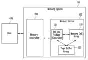
도 1을 참조하면, 메모리 장치(100)는 메모리 셀 어레이(110), 주변 회로(120) 및 제어 로직(130)을 포함할 수 있다.Referring to FIG. 1, a memory device (100) may include a memory cell array (110), a peripheral circuit (120), and control logic (130).
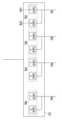
메모리 셀 어레이(110)는 복수의 메모리 블록들(BLK1~BLKz)을 포함할 수 있다. 복수의 메모리 블록들(BLK1~BLKz)은 행 라인들(RL)을 통해 로우 디코더(121)에 연결될 수 있다. 여기서, 행 라인들(RL)은 적어도 하나 이상의 소스 선택 라인, 복수의 워드 라인들 및 적어도 하나 이상의 드레인 선택 라인을 포함할 수 있다. 복수의 메모리 블록들(BLK1~BLKz)은 비트 라인들(BL1 내지 BLn)을 통해 페이지 버퍼 그룹(123)에 연결될 수 있다. 복수의 메모리 블록들(BLK1~BLKz) 각각은 복수의 메모리 셀들을 포함할 수 있다. 실시 예로서, 복수의 메모리 셀들은 불휘발성 메모리 셀일 수 있다. 같은 워드 라인에 연결된 메모리 셀들은 하나의 페이지로 정의될 수 있다. 따라서, 하나의 메모리 블록은 복수의 페이지들을 포함할 수 있다.The memory cell array (110) may include a plurality of memory blocks (BLK1 to BLKz). The plurality of memory blocks (BLK1 to BLKz) may be connected to a row decoder (121) via row lines (RL). Here, the row lines (RL) may include at least one source select line, a plurality of word lines, and at least one drain select line. The plurality of memory blocks (BLK1 to BLKz) may be connected to a page buffer group (123) via bit lines (BL1 to BLn). Each of the plurality of memory blocks (BLK1 to BLKz) may include a plurality of memory cells. As an example, the plurality of memory cells may be nonvolatile memory cells. Memory cells connected to the same word line may be defined as one page. Therefore, one memory block may include a plurality of pages.
복수의 메모리 블록들 중 어느 하나의 메모리 블록(BLKi)은 제1 셀렉트 라인과 제2 셀렉트 라인 사이에 서로 평행하게 배열된 다수의 워드 라인들이 연결될 수 있다. 여기서, 제1 셀렉트 라인은 소스 셀렉트 라인(SSL)일 수 있고, 제2 셀렉트 라인은 드레인 셀렉트 라인(DSL)일 수 있다. 보다 구체적으로 설명하면, 메모리 블록(BLKi)은 비트 라인들(BL1~BLn)과 소스 라인(SL) 사이에 연결된 다수의 스트링들(strings; ST)을 포함할 수 있다. 비트 라인들(BL1~BLn)은 스트링들(ST)에 각각 연결될 수 있고, 소스 라인(SL)은 스트링들(ST)에 공통으로 연결될 수 있다. 스트링들(ST)은 서로 동일하게 구성될 수 있으므로, 제1 비트 라인(BL1)에 연결된 스트링(ST)을 예를 들어 구체적으로 설명하도록 한다.Among the plurality of memory blocks, a memory block (BLKi) may have a plurality of word lines connected in parallel between a first select line and a second select line. Here, the first select line may be a source select line (SSL), and the second select line may be a drain select line (DSL). More specifically, the memory block (BLKi) may include a plurality of strings (strings; ST) connected between the bit lines (BL1 to BLn) and the source line (SL). The bit lines (BL1 to BLn) may be respectively connected to the strings (ST), and the source line (SL) may be commonly connected to the strings (ST). Since the strings (ST) may be configured identically to each other, a string (ST) connected to the first bit line (BL1) will be specifically described as an example.
스트링(ST)은 소스 라인(SL)과 제1 비트 라인(BL1) 사이에서 서로 직렬로 연결된 소스 셀렉트 트랜지스터(SST), 다수의 메모리 셀들(MC1~MC6) 및 드레인 셀렉트 트랜지스터(DST)를 포함할 수 있다. 하나의 스트링(ST)에는 소스 셀렉트 트랜지스터(SST)와 드레인 셀렉트 트랜지스터(DST)가 적어도 하나 이상씩 포함될 수 있으며, 메모리 셀들(MC1~MC16) 또한 도면에 도시된 개수보다 더 많이 포함될 수 있다.A string (ST) may include a source select transistor (SST), a plurality of memory cells (MC1 to MC6), and a drain select transistor (DST) that are connected in series between a source line (SL) and a first bit line (BL1). One string (ST) may include at least one source select transistor (SST) and one drain select transistor (DST), and may also include more memory cells (MC1 to MC16) than the number shown in the drawing.
소스 셀렉트 트랜지스터(SST)의 소스(source) 단자는 소스 라인(SL)에 연결될 수 있고, 드레인 셀렉트 트랜지스터(DST)의 드레인(drain) 단자는 제1 비트 라인(BL1)에 연결될 수 있다. 메모리 셀들(MC1~MC16)은 소스 셀렉트 트랜지스터(SST)와 드레인 셀렉트 트랜지스터(DST) 사이에서 직렬로 연결될 수 있다. 서로 다른 스트링들(ST)에 포함된 소스 셀렉트 트랜지스터들(SST)의 게이트들은 소스 셀렉트 라인(SSL)에 연결될 수 있고, 드레인 셀렉트 트랜지스터들(DST)의 게이트들은 드레인 셀렉트 라인(DSL)에 연결될 수 있고, 메모리 셀들(MC1~MC16)의 게이트들은 다수의 워드 라인들(WL1~WL16)에 연결될 수 있다. 서로 다른 스트링들(ST)에 포함된 메모리 셀들 중에서 동일한 워드 라인에 연결된 메모리 셀들의 그룹을 물리 페이지(physical page; PG)라 할 수 있다. 따라서, 메모리 블록(BLKi)에는 워드 라인들(WL1~WL16)의 개수만큼의 물리 페이지들(PG)이 포함될 수 있다.A source terminal of a source select transistor (SST) may be connected to a source line (SL), and a drain terminal of a drain select transistor (DST) may be connected to a first bit line (BL1). Memory cells (MC1 to MC16) may be connected in series between the source select transistor (SST) and the drain select transistor (DST). Gates of the source select transistors (SST) included in different strings (ST) may be connected to a source select line (SSL), gates of the drain select transistors (DST) may be connected to a drain select line (DSL), and gates of the memory cells (MC1 to MC16) may be connected to a plurality of word lines (WL1 to WL16). A group of memory cells connected to the same word line among memory cells included in different strings (ST) can be called a physical page (PG). Accordingly, a memory block (BLKi) can include as many physical pages (PG) as the number of word lines (WL1 to WL16).
메모리 셀들은 각각 하나의 데이터 비트를 저장하는 싱글 레벨 셀(Single Level Cell; SLC), 두 개의 데이터 비트들을 저장하는 멀티 레벨 셀(Multi Level Cell; MLC), 세 개의 데이터 비트들을 저장하는 트리플 레벨 셀(Triple Level Cell; TLC) 또는 네 개의 데이터 비트들을 저장할 수 있는 쿼드 레벨 셀(Quad Level Cell; QLC)로 구성될 수 있다.Memory cells can be configured as single-level cells (SLC) that store one data bit each, multi-level cells (MLC) that store two data bits, triple-level cells (TLC) that store three data bits, or quad-level cells (QLC) that can store four data bits.
싱글 레벨 셀(single level cell; SLC)은 1비트의 데이터를 저장할 수 있다. 싱글 레벨 셀의 하나의 물리 페이지(PG)는 하나의 논리 페이지(logical page) 데이터를 저장할 수 있다. 하나의 논리 페이지 데이터는 하나의 물리 페이지(PG)에 포함된 셀 개수만큼의 데이터 비트들을 포함할 수 있다.A single-level cell (SLC) can store 1 bit of data. One physical page (PG) of a single-level cell can store one logical page of data. One logical page of data can contain as many data bits as the number of cells contained in one physical page (PG).
멀티 레벨셀(Multi Level Cell; MLC), 트리플 레벨 셀(Triple Level Cell; TLC) 및 쿼드 레벨 셀(Quad Level Cell; QLC)는 2 비트 이상의 데이터를 저장할 수 있다. 이 경우 하나의 물리 페이지(PG)는 2 이상의 논리 페이지 데이터를 저장할 수 있다.Multi-Level Cell (MLC), Triple-Level Cell (TLC), and Quad-Level Cell (QLC) can store more than two bits of data. In this case, one physical page (PG) can store more than two logical pages of data.
주변 회로(120)는 제어 로직(130)의 제어에 따라 메모리 셀 어레이(110)의 선택된 영역에 프로그램 동작, 리드 동작 또는 소거 동작을 수행하도록 구성될 수 있다. 즉, 주변 회로(120)는 제어 로직(130)의 제어에 따라 메모리 셀 어레이(110)를 구동할 수 있다. 예를 들어, 주변 회로(120)는 제어 로직(130)의 제어에 따라 행 라인들(RL) 및 비트 라인들(BL1~BLn)에 다양한 동작 전압들을 인가하거나, 인가된 전압들을 디스차지 할 수 있다.The peripheral circuit (120) may be configured to perform a program operation, a read operation, or an erase operation on a selected area of the memory cell array (110) under the control of the control logic (130). That is, the peripheral circuit (120) may drive the memory cell array (110) under the control of the control logic (130). For example, the peripheral circuit (120) may apply various operating voltages to the row lines (RL) and bit lines (BL1 to BLn) or discharge the applied voltages under the control of the control logic (130).
구체적으로, 주변 회로(120)는 로우 디코더(121), 전압 생성부(122), 페이지 버퍼 그룹(123), 컬럼 디코더(124), 입출력 회로(125) 및 센싱 회로(126)를 포함할 수 있다.Specifically, the peripheral circuit (120) may include a row decoder (121), a voltage generator (122), a page buffer group (123), a column decoder (124), an input/output circuit (125), and a sensing circuit (126).
로우 디코더(121)는 행 라인들(RL)을 통해 메모리 셀 어레이(110)에 연결될 수 있다. 행 라인들(RL)은 적어도 하나 이상의 소스 선택 라인, 복수의 워드 라인들 및 적어도 하나 이상의 드레인 선택 라인을 포함할 수 있다. 실시 예에서, 워드 라인들은 노멀 워드 라인들과 더미 워드 라인들을 포함할 수 있다. 그리고, 행 라인들(RL)은 파이프 선택 라인을 더 포함할 수 있다.The row decoder (121) may be connected to the memory cell array (110) via row lines (RL). The row lines (RL) may include at least one source select line, a plurality of word lines, and at least one drain select line. In an embodiment, the word lines may include normal word lines and dummy word lines. In addition, the row lines (RL) may further include a pipe select line.
로우 디코더(121)는 제어 로직(130)의 제어에 응답하여 동작하도록 구성될 수 있다. 로우 디코더(121)는 제어 로직(130)으로부터 로우 어드레스(RADD)를 수신할 수 있다. 구체적으로, 로우 디코더(121)는 로우 어드레스(RADD)를 디코딩하도록 구성될 수 있다. 로우 디코더(121)는 디코딩된 로우 어드레스(RADD)에 따라 메모리 블록들(BLK1~BLKz) 중 적어도 하나의 메모리 블록을 선택할 수 있다. 그리고, 로우 디코더(121)는 디코딩된 어드레스에 따라 전압 생성부(122)가 생성한 전압들을 적어도 하나의 워드 라인에 인가하도록 선택된 메모리 블록의 적어도 하나의 워드 라인을 선택할 수 있다.The row decoder (121) may be configured to operate in response to the control of the control logic (130). The row decoder (121) may receive a row address (RADD) from the control logic (130). Specifically, the row decoder (121) may be configured to decode the row address (RADD). The row decoder (121) may select at least one memory block among the memory blocks (BLK1 to BLKz) according to the decoded row address (RADD). In addition, the row decoder (121) may select at least one word line of the selected memory block to apply voltages generated by the voltage generator (122) to at least one word line according to the decoded address.
예를 들어, 프로그램 동작 시에, 로우 디코더(121)는 선택된 워드 라인에 프로그램 전압을 인가하고 비선택된 워드 라인들에 프로그램 전압보다 낮은 레벨의 프로그램 패스 전압을 인가할 수 있다. 프로그램 검증 동작 시에, 로우 디코더(121)는 선택된 워드 라인에 검증 전압을 인가하고 비선택된 워드 라인들에 검증 전압보다 높은 검증 패스 전압을 인가할 수 있다. 리드 동작 시에, 로우 디코더(121)는 선택된 워드 라인에 리드 전압을 인가하고, 비선택된 워드 라인들에 리드 전압보다 높은 리드 패스 전압을 인가할 수 있다.For example, during a program operation, the row decoder (121) can apply a program voltage to a selected word line and apply a program pass voltage of a lower level than the program voltage to unselected word lines. During a program verify operation, the row decoder (121) can apply a verify voltage to a selected word line and apply a verify pass voltage higher than the verify voltage to unselected word lines. During a read operation, the row decoder (121) can apply a read voltage to a selected word line and apply a read pass voltage higher than the read voltage to unselected word lines.
실시 예에서, 메모리 셀 어레이(110)의 소거 동작은 메모리 블록 단위로 수행될 수 있다. 소거 동작 시에 로우 디코더(121)는 디코딩된 어드레스에 따라 하나의 메모리 블록을 선택할 수 있고, 로우 디코더(121)는 선택된 메모리 블록에 연결되는 워드 라인들에 접지 전압을 인가할 수 있다.In an embodiment, an erase operation of a memory cell array (110) may be performed in memory block units. During an erase operation, a row decoder (121) may select one memory block according to a decoded address, and the row decoder (121) may apply a ground voltage to word lines connected to the selected memory block.
전압 생성부(122)는 제어 로직(130)의 제어에 응답하여 동작할 수 있다. 구체적으로, 전압 생성부(122)는 제어 로직(130)의 제어에 응답하여 메모리 장치(100)로 공급되는 외부 전원 전압을 이용하여 복수의 전압들을 생성하도록 구성될 수 있다. 예를 들어, 전압 생성부(122)는 제어 로직(130)의 제어에 응답하여 프로그램 전압, 검증 전압, 패스 전압, 리드 전압 및 소거 전압 등을 생성할 수 있다. 즉, 전압 생성부(122)는 동작 신호(OPSIG)에 응답하여 프로그램, 리드 및 소거 동작들에 사용되는 다양한 동작 전압들(Vop)을 생성할 수 있다.The voltage generation unit (122) can operate in response to the control of the control logic (130). Specifically, the voltage generation unit (122) can be configured to generate a plurality of voltages using an external power voltage supplied to the memory device (100) in response to the control of the control logic (130). For example, the voltage generation unit (122) can generate a program voltage, a verification voltage, a pass voltage, a read voltage, an erase voltage, etc. in response to the control of the control logic (130). That is, the voltage generation unit (122) can generate various operating voltages (Vop) used for program, read, and erase operations in response to the operation signal (OPSIG).
실시 예로서, 전압 생성부(122)는 외부 전원 전압을 레귤레이팅하여 내부 전원 전압을 생성할 수 있다. 전압 생성부(122)에서 생성된 내부 전원 전압은 메모리 셀 어레이(110)의 동작 전압으로서 사용될 수 있다.As an example, the voltage generation unit (122) can generate an internal power voltage by regulating an external power voltage. The internal power voltage generated by the voltage generation unit (122) can be used as an operating voltage of the memory cell array (110).
실시 예로서, 전압 생성부(122)는 외부 전원 전압 또는 내부 전원 전압을 이용하여 복수의 전압들을 생성할 수 있다. 예를 들면, 전압 생성부(122)는 내부 전원 전압을 수신하는 복수의 펌핑 커패시터들을 포함하고, 제어 로직(130)의 제어에 응답하여 복수의 펌핑 커패시터들을 선택적으로 활성화하여 복수의 전압들을 생성할 수 있다. 그리고, 생성된 복수의 전압들은 로우 디코더(121)에 의해 메모리 셀 어레이(110)에 공급될 수 있다.As an example, the voltage generation unit (122) may generate a plurality of voltages using an external power supply voltage or an internal power supply voltage. For example, the voltage generation unit (122) may include a plurality of pumping capacitors that receive an internal power supply voltage, and may selectively activate the plurality of pumping capacitors in response to the control of the control logic (130) to generate a plurality of voltages. Then, the generated plurality of voltages may be supplied to the memory cell array (110) by the row decoder (121).
페이지 버퍼 그룹(123)은 제1 내지 제n 페이지 버퍼들(PB1~PBn)을 포함할 수 있다. 제1 내지 제n 페이지 버퍼들(PB1~PBn)은 각각 제1 내지 제n 비트 라인들(BL1~BLn)을 통해 메모리 셀 어레이(110)에 연결될 수 있다. 그리고, 제1 내지 제n 페이지 버퍼들(PB1~PBn)은 제어 로직(130)의 제어에 응답하여 동작할 수 있다. 구체적으로, 제1 내지 제n 페이지 버퍼들(PB1~PBn)은 페이지 버퍼 제어 신호들(PBSIGNALS)에 응답하여 동작할 수 있다. 예를 들면, 제1 내지 제n 페이지 버퍼들(PB1~PBn)은 제1 내지 제n 비트 라인들(BL1~BLn)을 통해 수신된 데이터를 임시로 저장하거나, 리드 또는 검증 동작 시, 비트 라인들(BL1~BLn)의 전압 또는 전류를 센싱(sensing)할 수 있다.The page buffer group (123) may include first to nth page buffers (PB1 to PBn). The first to nth page buffers (PB1 to PBn) may be connected to the memory cell array (110) via first to nth bit lines (BL1 to BLn), respectively. In addition, the first to nth page buffers (PB1 to PBn) may operate in response to the control of the control logic (130). Specifically, the first to nth page buffers (PB1 to PBn) may operate in response to page buffer control signals (PBSIGNALS). For example, the first to nth page buffers (PB1 to PBn) may temporarily store data received via the first to nth bit lines (BL1 to BLn), or sense the voltage or current of the bit lines (BL1 to BLn) during a read or verify operation.
구체적으로, 프로그램 동작 시, 제1 내지 제n 페이지 버퍼들(PB1~PBn)은 선택된 워드 라인에 프로그램 펄스가 인가될 때, 입출력 회로(125)를 통해 수신한 데이터(DATA)를 제1 내지 제n 비트 라인들(BL1~BLn)을 통해 선택된 메모리 셀들에 전달할 수 있다. 전달된 데이터(DATA)에 따라 선택된 페이지의 메모리 셀들은 프로그램될 수 있다. 프로그램 허용 전압(예를 들면, 접지 전압)이 인가되는 비트 라인과 연결된 메모리 셀은 상승된 문턱전압을 가질 수 있다. 프로그램 금지 전압(예를 들면, 전원 전압)이 인가되는 비트 라인과 연결된 메모리 셀의 문턱전압은 유지될 수 있다.Specifically, during a program operation, the first to nth page buffers (PB1 to PBn) can transmit data (DATA) received through the input/output circuit (125) to the selected memory cells through the first to nth bit lines (BL1 to BLn) when a program pulse is applied to the selected word line. The memory cells of the selected page can be programmed according to the transmitted data (DATA). A memory cell connected to a bit line to which a program allowance voltage (e.g., a ground voltage) is applied can have an elevated threshold voltage. A threshold voltage of a memory cell connected to a bit line to which a program inhibit voltage (e.g., a power supply voltage) is applied can be maintained.
프로그램 검증 동작 시, 제1 내지 제n 페이지 버퍼들(PB1~PBn)은 선택된 메모리 셀들로부터 제1 내지 제n 비트 라인들(BL1~BLn)을 통해 페이지 데이터를 읽을 수 있다. 실시 예에서, 페이지 버퍼들(PB1~PBn) 각각은, 검증 동작 시 비트 라인들(BL1~BLn)들을 통해 연결된 메모리 셀들에 대해 센싱된 검증 결과들을 저장할 수 있다. 실시 예에서, 페이지 버퍼들(PB1~PBn) 각각은 현재 프로그램 루프에서의 검증 결과뿐만 아니라, 이전 프로그램 루프에서의 검증 결과 또한 저장할 수 있다.During a program verification operation, the first to nth page buffers (PB1 to PBn) can read page data from selected memory cells through the first to nth bit lines (BL1 to BLn). In an embodiment, each of the page buffers (PB1 to PBn) can store verification results sensed for memory cells connected through the bit lines (BL1 to BLn) during the verification operation. In an embodiment, each of the page buffers (PB1 to PBn) can store not only a verification result in a current program loop but also a verification result in a previous program loop.
컬럼 디코더(124)는 컬럼 어드레스(CADD)에 응답하여 입출력 회로(125)와 페이지 버퍼 그룹(123) 사이에서 데이터를 전달할 수 있다. 예를 들면, 컬럼 디코더(124)는 데이터 라인들(DL)을 통해 제1 내지 제n 페이지 버퍼들(PB1~PBn)과 데이터를 주고받거나, 컬럼 라인들(CL)을 통해 입출력 회로(125)와 데이터를 주고받을 수 있다.The column decoder (124) can transmit data between the input/output circuit (125) and the page buffer group (123) in response to the column address (CADD). For example, the column decoder (124) can transmit and receive data with the first to nth page buffers (PB1 to PBn) through data lines (DL), or transmit and receive data with the input/output circuit (125) through column lines (CL).
입출력 회로(125)는 메모리 컨트롤러(200)로부터 전달받은 커맨드(CMD) 및 어드레스(ADDR)를 제어 로직(130)에 전달하거나, 데이터(DATA)를 컬럼 디코더(124)와 주고받을 수 있다.The input/output circuit (125) can transmit a command (CMD) and an address (ADDR) received from the memory controller (200) to the control logic (130) or exchange data (DATA) with the column decoder (124).
센싱 회로(126)는 리드 동작(read operation) 또는 검증 동작(verify operation)시, 허용 비트 신호(VRYBIT)에 응답하여 기준 전류를 생성하고, 페이지 버퍼 그룹(123)으로부터 수신된 센싱 전압(VPB)과 기준 전류에 의해 생성된 기준 전압을 비교하여 패스 신호(PASS) 또는 페일 신호(FAIL)를 출력할 수 있다.The sensing circuit (126) can generate a reference current in response to an allowable bit signal (VRYBIT) during a read operation or a verify operation, and compare a sensing voltage (VPB) received from a page buffer group (123) with a reference voltage generated by the reference current to output a pass signal (PASS) or a fail signal (FAIL).
제어 로직(130)은 커맨드(CMD) 및 어드레스(ADDR)에 응답하여 동작 신호(OPSIG), 로우 어드레스(RADD), 페이지 버퍼 제어 신호들(PBSIGNALS) 및 허용 비트 신호(VRYBIT)를 출력하여 주변 회로(120)를 제어할 수 있다. 실시 예에서, 제어 로직(130)은 프로그램 루프들을 수행하도록 주변 회로(120)를 제어할 수 있다. 제어 로직(130)은 전압 생성부(122)가 적절한 전압을 생성하도록 제어할 수 있으며, 선택된 메모리 셀들과 연결된 워드 라인들 및 비트 라인들에 적절한 전압이 인가되도록 로우 디코더(121) 및 컬럼 디코더(124)를 제어할 수 있다. 실시 예에서, 제어 로직(130)은 페이지 버퍼들(PB1~PBn) 각각에 저장된 검증 결과를 기초로, 프로그램 루프 수행 시 비트 라인들(BL1~BLn)들에 각각 인가될 비트 라인 전압을 결정할 수 있다.The control logic (130) can control the peripheral circuit (120) by outputting an operation signal (OPSIG), a row address (RADD), page buffer control signals (PBSIGNALS), and an allow bit signal (VRYBIT) in response to a command (CMD) and an address (ADDR). In an embodiment, the control logic (130) can control the peripheral circuit (120) to perform program loops. The control logic (130) can control the voltage generation unit (122) to generate an appropriate voltage, and can control the row decoder (121) and the column decoder (124) to apply an appropriate voltage to word lines and bit lines connected to selected memory cells. In an embodiment, the control logic (130) can determine a bit line voltage to be applied to each of the bit lines (BL1 to BLn) when performing a program loop based on a verification result stored in each of the page buffers (PB1 to PBn).
도 2는 본 개시의 일 실시 예에 따른 메모리 장치의 페이지 버퍼 그룹을 설명하기 위한 도면이다.FIG. 2 is a diagram illustrating a page buffer group of a memory device according to one embodiment of the present disclosure.
도 2를 참조하면, 페이지 버퍼 그룹(123)은 복수의 페이지 버퍼들(PB1~PBn)을 포함할 수 있다. 페이지 버퍼들(PB1~PBn)은 각각 제1 내지 제n 비트 라인들(BL1~BLn)을 통해 메모리 셀 어레이(110)에 연결될 수 있다.Referring to FIG. 2, the page buffer group (123) may include a plurality of page buffers (PB1 to PBn). The page buffers (PB1 to PBn) may be connected to the memory cell array (110) through first to n-th bit lines (BL1 to BLn), respectively.
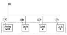
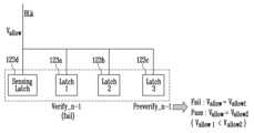
페이지 버퍼들(PB1~PBn) 각각은 제1 래치(123a) 및 제2 래치(123b)를 포함할 수 있다. 일 실시 예에서, 래치들 각각은 하나 이상의 NMOS 트랜지스터들, 하나 이상의 PMOS 트랜지스터들 및 하나 이상의 인버터들을 포함하는 회로로 구성될 수 있으나, 특정 형태로 제한되는 것은 아니다.Each of the page buffers (PB1 to PBn) may include a first latch (123a) and a second latch (123b). In one embodiment, each of the latches may be configured as a circuit including one or more NMOS transistors, one or more PMOS transistors, and one or more inverters, but is not limited to a specific form.
실시 예에서, 제1 래치(123a)는 최신 검증 결과를 저장할 수 있다. 예를 들어, 현재 수행 중인 제n 프로그램 루프의 검증 동작이 완료된 이후라면, 제n 프로그램 루프의 검증 동작에 따른 검증 결과가 제1 래치(123a)에 저장될 수 있다. 현재 수행 중인 제n 프로그램 루프의 검증 동작이 완료되기 이전이라면, 제n-1 프로그램 루프의 검증 동작에 따른 검증 결과가 제1 래치(123a)에 저장될 수 있다.In an embodiment, the first latch (123a) can store the latest verification result. For example, if the verification operation of the currently executing nth program loop is completed, the verification result according to the verification operation of the nth program loop can be stored in the first latch (123a). If the verification operation of the currently executing nth program loop is completed, the verification result according to the verification operation of the n-1th program loop can be stored in the first latch (123a).
실시 예에서, 제2 래치(123b)는 이전 검증 결과를 저장할 수 있다. 예를 들어, 현재 수행 중인 제n 프로그램 루프의 검증 동작이 완료된 이후라면, 제n-1 프로그램 루프의 검증 동작에 따른 검증 결과가 제2 래치(123b)에 저장될 수 있다. 현재 수행 중인 제n 프로그램 루프의 검증 동작이 완료되기 이전이라면, 제n-2 프로그램 루프의 검증 동작에 따른 검증 결과가 제2 래치(123b)에 저장될 수 있다.In an embodiment, the second latch (123b) may store a previous verification result. For example, after the verification operation of the currently executing nth program loop is completed, the verification result according to the verification operation of the n-1th program loop may be stored in the second latch (123b). Before the verification operation of the currently executing nth program loop is completed, the verification result according to the verification operation of the n-2th program loop may be stored in the second latch (123b).
본 명세서에서 n은 임의의 자연수를 의미할 수 있다. 그 구체적인 실시 예에 따라 n은 1 이상의 자연수, 2 이상의 자연수 또는 3 이상의 자연수 등일 수 있으나 이에 제한되는 것은 아니다.In this specification, n may mean any natural number. Depending on the specific embodiment, n may be a natural number greater than or equal to 1, a natural number greater than or equal to 2, a natural number greater than or equal to 3, etc., but is not limited thereto.
도 3은 본 개시의 일 실시 예에 따른 메모리 셀의 프로그램 상태를 설명하기 위한 도면이다.FIG. 3 is a diagram for explaining a program state of a memory cell according to one embodiment of the present disclosure.
도 3을 참조하면, 메모리 셀은 문턱 전압에 따라 소거 상태(E) 또는 제1 내지 제7 프로그램 상태(P1 내지 P7)로 프로그램될 수 있다. 도 3의 메모리 셀은 1개의 소거 상태 및 7개의 프로그램 상태로 프로그램될 수 있는 트리플 레벨 셀(Triple Level Cell, TLC)로 도시되었으나, 이는 설명의 편의를 위한 일 실시 예에 불과할 뿐, 구현시에는 멀티 레벨 셀(Multi Level Cell, MLC), 싱글 레벨 셀(Single Level Cell, SLC), 쿼드 레벨 셀(Quad Level Cell, QLC) 등으로 구현될 수 있다. 그리고, 설명의 편의를 위해 소거 상태와 프로그램 상태를 구분하였으나, 소거 상태는 제0 프로그램 상태(P0)로 표현할 수 있다. 따라서, 도 3에 도시된 소거 상태(E)와 제1 내지 제7 프로그램 상태(P1 내지 P7)는 제0 내지 제7의 프로그램 상태들로 표현될 수도 있다.Referring to FIG. 3, a memory cell can be programmed into an erase state (E) or first to seventh program states (P1 to P7) depending on a threshold voltage. Although the memory cell of FIG. 3 is illustrated as a triple level cell (TLC) that can be programmed into one erase state and seven program states, this is only an example for convenience of explanation, and the memory cell may be implemented as a multi level cell (MLC), a single level cell (SLC), a quad level cell (QLC), etc., when implemented. In addition, although the erase state and the program state are distinguished for convenience of explanation, the erase state can be expressed as the 0th program state (P0). Therefore, the erase state (E) and the first to seventh program states (P1 to P7) illustrated in FIG. 3 may also be expressed as the 0th to seventh program states.
선택된 메모리 셀들은 소거 상태(E) 또는 제1 내지 제7 프로그램 상태(P1 내지 P7) 중 어느 하나의 상태에 포함된 문턱 전압을 가질 수 있다. 즉, 메모리 셀들은 소거 상태(E) 또는 제1 내지 제7 프로그램 상태(P1 내지 P7) 중 어느 하나의 상태에 포함된 문턱 전압을 갖도록 프로그램될 수 있다. 프로그램 동작이 수행되기 전에 메모리 셀들은 소거 상태(E)일 수 있다. 프로그램 동작 시, 소거 상태(E)인 메모리 셀들은 선택된 워드 라인에 프로그램 전압이 인가됨에 따라 7개의 프로그램 상태 중 어느 하나의 프로그램 상태로 프로그램될 수 있다.The selected memory cells can have a threshold voltage included in the erase state (E) or one of the first to seventh program states (P1 to P7). That is, the memory cells can be programmed to have a threshold voltage included in the erase state (E) or one of the first to seventh program states (P1 to P7). Before a program operation is performed, the memory cells can be in the erase state (E). During the program operation, the memory cells in the erase state (E) can be programmed to one of the seven program states as a program voltage is applied to the selected word line.
그리고, 메모리 셀들의 소거 상태(E) 또는 제1 내지 제7 프로그램 상태(P1 내지 P7)은 검증 전압을 이용하여 구분될 수 있다. 구체적으로, 메모리 셀들의 인접하는 프로그램 상태들은 검증 전압으로 구분될 수 있다. 예를 들어, 소거 상태(E)와 제1 프로그램 상태(P1)는 제1 검증 전압(Vvfy1)에 의해 구분될 수 있다. 제1 프로그램 상태(P1)와 제2 프로그램 상태(P2)는 제2 검증 전압(Vvfy2)에 의해 구분될 수 있다. 제2 프로그램 상태(P2)와 제3 프로그램 상태(P3)는 제3 검증 전압(Vvfy3)에 의해 구분될 수 있다. 제3 프로그램 상태(P3)와 제4 프로그램 상태(P4)는 제4 검증 전압(Vvfy4)에 의해 구분될 수 있다. 제4 프로그램 상태(P4)와 제5 프로그램 상태(P5)는 제5 검증 전압(Vvfy5)에 의해 구분될 수 있다. 제5 프로그램 상태(P5)와 제6 프로그램 상태(P6)는 제6 검증 전압(Vvfy6)에 의해 구분될 수 있다. 제6 프로그램 상태(P6)와 제7 프로그램 상태(P7)는 제7 검증 전압(Vvfy7)에 의해 구분될 수 있다. 예를 들어, 제1 프로그램 상태(PV1)에 대응하는 메모리 셀들의 문턱 전압 분포는 검증 전압(Vvfy1)과 같거나 높고 검증 전압(Vvfy2) 보다 낮으며, 제2 프로그램 상태(PV2)에 대응하는 메모리 셀들의 문턱 전압 분포는 검증 전압(Vvfy2)과 같거나 높고 검증 전압(Vvfy3) 보다 낮다.And, the erase state (E) or the first to seventh program states (P1 to P7) of the memory cells can be distinguished using the verify voltage. Specifically, adjacent program states of the memory cells can be distinguished by the verify voltage. For example, the erase state (E) and the first program state (P1) can be distinguished by the first verify voltage (Vvfy1). The first program state (P1) and the second program state (P2) can be distinguished by the second verify voltage (Vvfy2). The second program state (P2) and the third program state (P3) can be distinguished by the third verify voltage (Vvfy3). The third program state (P3) and the fourth program state (P4) can be distinguished by the fourth verify voltage (Vvfy4). The fourth program state (P4) and the fifth program state (P5) can be distinguished by the fifth verify voltage (Vvfy5). The fifth program state (P5) and the sixth program state (P6) can be distinguished by the sixth verification voltage (Vvfy6). The sixth program state (P6) and the seventh program state (P7) can be distinguished by the seventh verification voltage (Vvfy7). For example, the threshold voltage distribution of memory cells corresponding to the first program state (PV1) is equal to or higher than the verification voltage (Vvfy1) and lower than the verification voltage (Vvfy2), and the threshold voltage distribution of memory cells corresponding to the second program state (PV2) is equal to or higher than the verification voltage (Vvfy2) and lower than the verification voltage (Vvfy3).
일 실시 예에서, 소거 상태(E)는 데이터 '111'과 대응되고, 제1 프로그램 상태(P1)는 데이터 '110'과 대응되고, 제2 프로그램 상태(P2)는 데이터 '101'과 대응되고, 제3 프로그램 상태(P3)는 데이터 '100'과 대응되고, 제4 프로그램 상태(P4)는 데이터 '011'과 대응되고, 제5 프로그램 상태(P5)는 데이터 '010'과 대응되고, 제6 프로그램 상태(P6)는 '데이터 '001'과 대응되고, 제7 프로그램 상태(P7)는 데이터 '000'과 대응될 수 있다. 다만, 각각의 프로그램 상태에 대응하는 데이터는 예시적인 것이며, 다양하게 변형될 수 있다.In one embodiment, the erase state (E) may correspond to data '111', the first program state (P1) may correspond to data '110', the second program state (P2) may correspond to data '101', the third program state (P3) may correspond to data '100', the fourth program state (P4) may correspond to data '011', the fifth program state (P5) may correspond to data '010', the sixth program state (P6) may correspond to 'data '001', and the seventh program state (P7) may correspond to data '000'. However, the data corresponding to each program state is exemplary and may be variously modified.
도 4는 본 개시의 일 실시 예에 따른 프로그램 동작을 설명하기 위한 도면이다.FIG. 4 is a diagram for explaining program operation according to one embodiment of the present disclosure.
도 4를 참조하면, 프로그램 동작은 복수의 프로그램 루프들(PL1~PLn)을 포함할 수 있다. 도 4에서는 설명의 편의를 위해, 복수의 메모리 셀들 각각은 2-비트의 데이터를 저장하는 멀티 레벨 셀(MLC)인 것으로 가정한다. 그러나 본 발명의 범위가 이에 한정되는 것은 아니며, 복수의 메모리 셀들 각각은 3-비트의 데이터를 저장하는 트리플 레벨 셀(Triple Level Cell; TLC) 또는 4-비트의 데이터를 저장하는 쿼드 레벨 셀(Quad Level Cell; QLC)일 수 있다.Referring to FIG. 4, a program operation may include a plurality of program loops (PL1 to PLn). In FIG. 4, for convenience of explanation, it is assumed that each of the plurality of memory cells is a multi-level cell (MLC) that stores 2-bit data. However, the scope of the present invention is not limited thereto, and each of the plurality of memory cells may be a triple-level cell (TLC) that stores 3-bit data or a quad-level cell (QLC) that stores 4-bit data.
즉, 메모리 장치는 복수의 프로그램 루프들(PL1~PLn)을 수행하여 선택된 메모리 셀들이 복수의 프로그램 상태들 중 어느 하나의 상태에 해당하는 문턱전압을 갖도록 프로그램 할 수 있다. 복수의 프로그램 루프들(PL1~PLn) 각각은 프로그램 전압을 인가하는 프로그램 전압 인가 단계(PGM Step)와 검증 전압들을 인가하여 메모리 셀들이 프로그램 되었는지 여부를 판단하는 검증 단계(Verify Step)를 포함할 수 있다.That is, the memory device can program selected memory cells to have a threshold voltage corresponding to one of a plurality of program states by performing a plurality of program loops (PL1 to PLn). Each of the plurality of program loops (PL1 to PLn) can include a program voltage application step (PGM Step) that applies a program voltage and a verification step (Verify Step) that applies verification voltages to determine whether the memory cells have been programmed.
예를 들어, 제1 프로그램 루프(PL1)가 수행될 때, 제1 프로그램 펄스(Vpgm1)가 인가된 후에 복수의 메모리 셀들의 프로그램 상태를 검증하기 위하여 제1 내지 제3 검증 전압들(Vvfy1~Vvfy3)이 순차적으로 인가될 수 있다. 이 때, 목표 프로그램 상태가 제1 프로그램 상태(P1)인 메모리 셀들은 제1 검증 전압(Vvfy1)에 의해 검증이 수행되고, 목표 프로그램 상태가 제2 프로그램 상태(P2)인 메모리 셀들은 제2 검증 전압(Vvfy2)에 의해 검증이 수행되고, 목표 프로그램 상태가 제3 프로그램 상태(P3)인 메모리 셀들은 제3 검증 전압(Vvfy3)에 의해 검증이 수행될 수 있다.For example, when the first program loop (PL1) is performed, after the first program pulse (Vpgm1) is applied, first to third verification voltages (Vvfy1 to Vvfy3) may be sequentially applied to verify the program states of a plurality of memory cells. At this time, memory cells whose target program state is the first program state (P1) may be verified by the first verification voltage (Vvfy1), memory cells whose target program state is the second program state (P2) may be verified by the second verification voltage (Vvfy2), and memory cells whose target program state is the third program state (P3) may be verified by the third verification voltage (Vvfy3).
각 검증 전압들(Vvfy1~Vvfy3)에 의해 검증 통과(verify pass)된 메모리 셀들은 목표 프로그램 상태를 갖는 것으로 판별되며, 이후 제2 프로그램 루프(PL2)에서 프로그램 금지(program inhibit)될 수 있다. 일 실시 예에서, 제2 프로그램 루프(PL2)에서 프로그램 금지된 메모리 셀들을 제외한 나머지 메모리 셀들을 프로그램 하기 위하여 제1 프로그램 펄스(Vpgm1)보다 단위 전압(△Vpgm)만큼 높은 제2 프로그램 펄스(Vpgm2)가 인가될 수 있으나, 이에 제한되는 것은 아니다. 이 후, 제1 프로그램 루프(PL1)의 검증 동작과 동일하게 검증 동작이 수행된다. 예시적으로, 검증 통과(verify pass)는 대응하는 검증 전압에 의해 메모리 셀이 오프-셀(off-cell)로 판독된 것을 가리킨다.Memory cells that pass verification by each of the verification voltages (Vvfy1 to Vvfy3) are determined to have a target program state, and can then be program inhibited in a second program loop (PL2). In one embodiment, a second program pulse (Vpgm2) that is higher by a unit voltage (△Vpgm) than the first program pulse (Vpgm1) may be applied to program the remaining memory cells except for the memory cells that are program inhibited in the second program loop (PL2), but is not limited thereto. Thereafter, a verification operation is performed in the same manner as the verification operation of the first program loop (PL1). For example, a verification pass indicates that a memory cell is read as an off-cell by a corresponding verification voltage.
상술된 바와 같이, 메모리 장치(100)가 2-비트를 저장하는 멀티 레벨 셀(MLC)을 프로그램할 때, 메모리 장치(100)는 제1 내지 제3 검증 전압들(Vvfy1~Vvfy3)을 사용하여 각각의 프로그램 상태를 목표 프로그램 상태로 하는 메모리 셀들을 각각 검증하게 된다.As described above, when the memory device (100) programs a multi-level cell (MLC) storing 2 bits, the memory device (100) uses the first to third verification voltages (Vvfy1 to Vvfy3) to verify each memory cell that makes each program state a target program state.
검증 동작 시에, 선택된 메모리 셀들이 연결된 워드 라인인 선택된 워드 라인에는 검증 전압이 인가되고, 페이지 버퍼는 선택된 메모리 셀들에 각각 연결되는 비트 라인들을 통해 흐르는 전류나 전압을 기초로 메모리 셀들의 검증 패스 여부를 판단할 수 있다.During a verification operation, a verification voltage is applied to a selected word line, which is a word line to which the selected memory cells are connected, and the page buffer can determine whether the memory cells pass verification based on the current or voltage flowing through the bit lines respectively connected to the selected memory cells.
상술한 바와 같이, 검증 통과(verify pass)된 메모리 셀들은 목표 프로그램 상태를 갖는 것으로 판별되며, 이후 제2 프로그램 루프(PL2)에서 프로그램 금지(program inhibit)될 수 있다. 다만, 목표 프로그램 상태를 갖는 것으로 판별된 메모리 셀들의 플로팅 게이트(floating gate)에 저장된 전자들이 빠져나가는 등의 이유로 메모리 셀들의 문턱 전압이 검증 동작 수행 시보다 낮아질 수 있다. 또는, 랜덤 텔레그래프 노이즈(random telegraph noise, RTN) 등의 이유로 실제 메모리 셀들의 문턱 전압이 목표 프로그램 상태에 도달하지 않았음에도 문턱 전압이 높게 센싱되는 경우가 발생할 수 있다.As described above, memory cells that have passed the verification pass are determined to have the target program state, and can then be program inhibited in the second program loop (PL2). However, the threshold voltage of the memory cells may become lower than when the verification operation is performed due to reasons such as leakage of electrons stored in the floating gate of the memory cells determined to have the target program state. Alternatively, there may occur cases where the threshold voltage of the actual memory cells is sensed as high even though it has not reached the target program state due to reasons such as random telegraph noise (RTN).
이와 같은 검증 통과된 메모리 셀들의 열화 또는 검증 동작의 오류를 개선할 수 있는 메모리 장치 및 메모리 장치의 동작방법이 요구된다. 따라서, 본 개시의 실시 예에 따른 메모리 장치 및 메모리 장치의 동작 방법은 검증 통과(verify pass)된 메모리 셀들을 목표 프로그램 상태를 갖는 것으로 판별하여 바로 다음 프로그램 루프 전체에서 프로그램 금지시키는 것이 아니라, 이후 프로그램 루프에서 한 번 더 검증 동작을 수행한 후, 이를 기초로 프로그램이 완료된 메모리 셀들인지 판별할 수 있다.A memory device and an operating method of the memory device that can improve the deterioration of memory cells that have passed verification or errors in the verification operation are required. Therefore, the memory device and the operating method of the memory device according to the embodiment of the present disclosure determine that memory cells that have passed verification have a target program state and, instead of immediately prohibiting programming in the entire next program loop, perform a verification operation once more in a subsequent program loop and, based on this, determine whether the memory cells are programmed.
도 5는 도 2의 페이지 버퍼 그룹에 포함된 페이지 버퍼를 설명하기 위한 도면이다.FIG. 5 is a drawing for explaining a page buffer included in the page buffer group of FIG. 2.
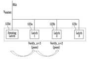
도 5를 참조하면, 도 5의 페이지 버퍼는 도 2에 개시된 페이지 버퍼 그룹에 포함된 페이지 버퍼의 다른 일 예시일 수 있다.Referring to FIG. 5, the page buffer of FIG. 5 may be another example of a page buffer included in the page buffer group disclosed in FIG. 2.
페이지 버퍼는 제1 래치(123a) 및 제2 래치(123b)를 포함할 수 있다.The page buffer may include a first latch (123a) and a second latch (123b).
실시 예에서, 제1 래치(123a)는 최신 검증 결과를 저장할 수 있다. 예를 들어, 현재 수행 중인 제n 프로그램 루프의 검증 동작이 완료된 이후라면, 제n 프로그램 루프의 검증 동작에 따른 검증 결과가 제1 래치(123a)에 저장될 수 있다. 현재 수행 중인 제n 프로그램 루프의 검증 동작이 완료되기 이전이라면, 제n-1 프로그램 루프의 검증 동작에 따른 검증 결과가 제1 래치(123a)에 저장될 수 있다.In an embodiment, the first latch (123a) can store the latest verification result. For example, if the verification operation of the currently executing nth program loop is completed, the verification result according to the verification operation of the nth program loop can be stored in the first latch (123a). If the verification operation of the currently executing nth program loop is completed, the verification result according to the verification operation of the n-1th program loop can be stored in the first latch (123a).
실시 예에서, 제2 래치(123b)는 이전 검증 결과를 저장할 수 있다. 예를 들어, 현재 수행 중인 제n 프로그램 루프의 검증 동작이 완료된 이후라면, 제n-1 프로그램 루프의 검증 동작에 따른 검증 결과가 제2 래치(123b)에 저장될 수 있다. 현재 수행 중인 제n 프로그램 루프의 검증 동작이 완료되기 이전이라면, 제n-2 프로그램 루프의 검증 동작에 따른 검증 결과가 제2 래치(123b)에 저장될 수 있다.In an embodiment, the second latch (123b) may store a previous verification result. For example, after the verification operation of the currently executing nth program loop is completed, the verification result according to the verification operation of the n-1th program loop may be stored in the second latch (123b). Before the verification operation of the currently executing nth program loop is completed, the verification result according to the verification operation of the n-2th program loop may be stored in the second latch (123b).
즉, 제1 래치(123a) 및 제2 래치(123b)는 도 2에서 설명한 제1 래치(123a) 및 제2 래치(123b)와 동일할 수 있다.That is, the first latch (123a) and the second latch (123b) may be identical to the first latch (123a) and the second latch (123b) described in FIG. 2.
또한, 페이지 버퍼는 센싱 래치(123d)를 더 포함할 수 있다. 센싱 래치(123d)는 검증 동작 시에 메모리 셀로부터 센싱된 데이터가 최초로 저장되는 래치일 수 있다. 즉, 센싱 래치(123d)는 현재 수행 중인 프로그램 루프의 프로그램 검증 결과를 저장할 수 있다. 실시 예에서, 프로그램 검증이 패스되면 센싱 래치(123d)는 제1 논리 값을 저장할 수 있다. 프로그램 검증이 페일되면 센싱 래치(123d)는 반전된 제1 논리 값을 저장할 수 있다.In addition, the page buffer may further include a sensing latch (123d). The sensing latch (123d) may be a latch in which data sensed from a memory cell is first stored during a verification operation. That is, the sensing latch (123d) may store a program verification result of a currently executing program loop. In an embodiment, if the program verification passes, the sensing latch (123d) may store a first logic value. If the program verification fails, the sensing latch (123d) may store an inverted first logic value.
센싱 래치(123d)에 저장된 데이터, 즉 검증 결과는 제1 래치(123a)로 이동할 수 있으며, 제1 래치(123a)에 저장된 검증 결과는 제2 래치(123b)로 이동할 수 있다.The data stored in the sensing latch (123d), i.e., the verification result, can be moved to the first latch (123a), and the verification result stored in the first latch (123a) can be moved to the second latch (123b).
또한, 페이지 버퍼는 제3 래치(123c)를 더 포함할 수 있다. 제3 래치(123c)는 더블 프로그램(Double Program) 동작을 위한 보조 검증 전압에 따른 검증 결과를 저장할 수 있다.Additionally, the page buffer may further include a third latch (123c). The third latch (123c) may store a verification result according to an auxiliary verification voltage for a double program operation.
제1 래치(123a), 제2 래치(123b), 제3 래치(123c) 및 센싱 래치(123d)의 구체적인 동작은 이하의 도 6 내지 도 17을 통해 보다 상세히 설명하도록 한다.The specific operations of the first latch (123a), the second latch (123b), the third latch (123c), and the sensing latch (123d) will be described in more detail with reference to FIGS. 6 to 17 below.
도 6 내지 도 15는 도 5의 페이지 버퍼 동작의 일 예시를 설명하기 위한 도면이다.FIGS. 6 to 15 are drawings for explaining an example of the page buffer operation of FIG. 5.
도 6을 참조하면, 제n 프로그램 루프의 프로그램 전압 인가 동작이 수행될 수 있다. 이 때, 제n-1 프로그램 루프의 검증 결과(Verify_n-1)가 제1 래치(123a)에 저장되어 있을 수 있다. 제n-1 프로그램 루프의 검증 결과(Verify_n-1)는 페일을 나타낼 수 있다. 제1 래치(123a)에 저장된 검증 결과가 페일을 나타냄에 따라, 페이지 버퍼와 연결된 비트 라인(BLk)에는 프로그램 허용 전압(Vallow)이 인가될 수 있다. 선택된 워드 라인에는 프로그램 전압(Vpgm_n)이 인가될 수 있다. 이에 따라, 프로그램 허용 전압(Vallow)이 인가된 비트 라인(BLk)을 통해 페이지 버퍼와 연결된 메모리 셀은 프로그램 전압(Vpgm_n)에 의해 문턱 전압이 변경될 수 있다.Referring to FIG. 6, a program voltage application operation of the nth program loop may be performed. At this time, a verification result (Verify_n-1) of the n-1th program loop may be stored in the first latch (123a). The verification result (Verify_n-1) of the n-1th program loop may indicate fail. As the verification result stored in the first latch (123a) indicates fail, a program allowance voltage (Vallow ) may be applied to a bit line (BLk) connected to a page buffer. A program voltage (Vpgm_n ) may be applied to a selected word line. Accordingly, a memory cell connected to a page buffer through a bit line (BLk) to which the program allowance voltage (Vallow ) is applied may have a threshold voltage changed by the program voltage (Vpgm_n ).
도 7을 참조하면, 페이지 버퍼와 비트 라인(BLk)을 통해 연결된 메모리 셀에 대해서 제n 프로그램 루프의 검증 동작을 수행할 수 있다. 제1 래치(123a) 및 제2 래치(123b) 중 적어도 하나에 저장된 검증 결과가 페일임을 나타냄에 따라, 비트 라인(BLk)을 통해 페이지 버퍼와 연결된 메모리 셀에 대하여 제n 프로그램 루프의 검증 동작이 수행될 수 있다. 이에 따라, 비트 라인(BLk)에는 검증 허용 전압이 인가될 수 있다. 검증 허용 전압은 프로그램 허용 전압(Vallow)과 동일한 값으로 설정되거나, 프로그램 허용 전압(Vallow)과 상이한 값으로 설정될 수도 있다. 선택된 워드 라인에는 검증 전압(Vvfy_n)이 인가될 수 있다. 그 결과, 제n 프로그램 동작의 검증 결과(Verify_n)가 센싱 래치(123d)에 저장될 수 있다. 제n 프로그램 동작의 검증 결과(Verify_n)는 패스를 나타낼 수 있다.Referring to FIG. 7, a verification operation of an nth program loop can be performed on a memory cell connected to a page buffer through a bit line (BLk). Since a verification result stored in at least one of the first latch (123a) and the second latch (123b) indicates fail, a verification operation of an nth program loop can be performed on a memory cell connected to the page buffer through the bit line (BLk). Accordingly, a verification allowance voltage can be applied to the bit line (BLk). The verification allowance voltage may be set to a value that is the same as the program allowance voltage (Vallow ) or may be set to a value that is different from the program allowance voltage (Vallow ). A verification voltage (Vvfy_n ) can be applied to a selected word line. As a result, a verification result (Verify_n) of the nth program operation can be stored in the sensing latch (123d). The verification result (Verify_n) of the nth program operation can indicate pass.
도 8을 참조하면, 제n+1 프로그램 루프의 프로그램 전압 인가 동작이 수행될 수 있다. 이 때, 제n 프로그램 루프의 검증 결과(Verify_n)가 제1 래치(123a) 저장되어 있을 수 있으며, 제n-1 프로그램 루프의 검증 결과(Verify_n-1)가 제2 래치(123b)에 저장되어 있을 수 있다. 즉, 제n+1 프로그램 루프의 프로그램 전압 인가 동작이 수행되기 전, 제1 래치(123a)에 저장되어 있던 제n-1 프로그램 루프의 검증 결과(Verify_n-1)는 제2 래치(123b)로 이동할 수 있고, 센싱 래치(123d)에 저장되어 있던 제n 프로그램 루프의 검증 결과(Verify_n)는 제1 래치(123a)로 이동할 수 있다. 구체적으로, 제1 래치(123a)에 저장되어 있던 제n-1 프로그램 루프의 검증 결과(Verify_n-1)가 제2 래치(123b)로 이동하는 동작은 제n 프로그램 루프의 검증 동작 전 또는 검증 동작 후에 수행될 수 있으며, 센싱 래치(123d)에 저장되어 있던 제n 프로그램 루프의 검증 결과(Verify_n)가 제1 래치(123a)로 이동하는 동작은 제n-1 프로그램 루프의 검증 결과(Verify_n-1)가 제2 래치(123b)로 이동한 후부터 제n+1 프로그램 루프의 프로그램 전압 인가 동작이 수행되기 전 사이에 수행될 수 있다. 제n 프로그램 루프의 검증 결과(Verify_n)는 패스를 나타낼 수 있다. 즉, 제1 래치(123a)에 저장된 검증 결과가 패스를 나타냄에 따라, 페이지 버퍼와 연결된 비트 라인(BLk)에는 프로그램 금지 전압(Vinhibit)이 인가될 수 있다. 페이지 버퍼와 연결된 비트 라인(BLk)에는 프로그램 금지 전압(Vinhibit)이 인가됨에 따라, 선택된 워드 라인에 프로그램 전압(Vpgm_n+1)이 인가되더라도, 비트 라인(BLk)을 통해 페이지 버퍼와 연결된 메모리 셀은 문턱 전압이 변경되지 않을 수 있다.Referring to FIG. 8, a program voltage application operation of the n+1th program loop can be performed. At this time, the verification result (Verify_n) of the nth program loop can be stored in the first latch (123a), and the verification result (Verify_n-1) of the n-1th program loop can be stored in the second latch (123b). That is, before the program voltage application operation of the n+1th program loop is performed, the verification result (Verify_n-1) of the n-1th program loop stored in the first latch (123a) can be moved to the second latch (123b), and the verification result (Verify_n) of the nth program loop stored in the sensing latch (123d) can be moved to the first latch (123a). Specifically, the operation of moving the verification result (Verify_n-1) of the n-1th program loop stored in the first latch (123a) to the second latch (123b) can be performed before or after the verification operation of the nth program loop, and the operation of moving the verification result (Verify_n) of the nth program loop stored in the sensing latch (123d) to the first latch (123a) can be performed between after the verification result (Verify_n-1) of the n-1th program loop moves to the second latch (123b) and before the program voltage application operation of the n+1th program loop is performed. The verification result (Verify_n) of the nth program loop can indicate a pass. That is, since the verification result stored in the first latch (123a) indicates a pass, a program inhibit voltage (Vinhibit ) can be applied to the bit line (BLk) connected to the page buffer. Since a program inhibit voltage (Vinhibit ) is applied to a bit line (BLk) connected to a page buffer, even if a program voltage (Vpgm_n+1 ) is applied to a selected word line, a threshold voltage of a memory cell connected to a page buffer through the bit line (BLk) may not change.
도 9를 참조하면, 페이지 버퍼와 비트 라인(BLk)을 통해 연결된 메모리 셀에 대해서 제n+1 프로그램 루프의 검증 동작을 수행할 수 있다. 제1 래치(123a) 및 제2 래치(123b) 중 적어도 하나에 저장된 검증 결과가 페일임을 나타냄에 따라, 비트 라인(BLk)을 통해 페이지 버퍼와 연결된 메모리 셀에 대하여 제n+1 프로그램 루프의 검증 동작이 수행될 수 있다. 이에 따라, 비트 라인(BLk)에는 검증 허용 전압이 인가될 수 있다. 검증 허용 전압은 프로그램 허용 전압(Vallow)과 동일한 값으로 설정되거나, 프로그램 허용 전압(Vallow)과 상이한 값으로 설정될 수도 있다. 선택된 워드 라인에는 검증 전압(Vvfy_n+1)이 인가될 수 있다. 그 결과, 제n+1 프로그램 동작의 검증 결과(Verify_n+1)가 센싱 래치(123d)에 저장될 수 있다. 제n+1 프로그램 동작의 검증 결과(Verify_n+1)는 페일을 나타낼 수 있다.Referring to FIG. 9, a verification operation of an n+1-th program loop can be performed on a memory cell connected to a page buffer through a bit line (BLk). Since a verification result stored in at least one of the first latch (123a) and the second latch (123b) indicates fail, a verification operation of an n+1-th program loop can be performed on a memory cell connected to the page buffer through the bit line (BLk). Accordingly, a verification allowance voltage can be applied to the bit line (BLk). The verification allowance voltage may be set to a value equal to the program allowance voltage (Vallow ) or may be set to a value different from the program allowance voltage (Vallow ). A verification voltage (Vvfy_n+1 ) can be applied to a selected word line. As a result, a verification result (Verify_n+1) of the n+1-th program operation can be stored in the sensing latch (123d). The verification result of the n+1th program operation (Verify_n+1) may indicate a fail.
도 10을 참조하면, 제n+2 프로그램 루프의 프로그램 전압 인가 동작이 수행될 수 있다. 이 때, 제n+1 프로그램 루프의 검증 결과(Verify_n+1)가 제1 래치(123a) 저장되어 있을 수 있으며, 제n 프로그램 루프의 검증 결과(Verify_n)가 제2 래치(123b)에 저장되어 있을 수 있다. 즉, 제n+2 프로그램 루프의 프로그램 전압 인가 동작이 수행되기 전, 제1 래치(123a)에 저장되어 있던 제n 프로그램 루프의 검증 결과(Verify_n)는 제2 래치(123b)로 이동할 수 있고, 센싱 래치(123d)에 저장되어 있던 제n+1 프로그램 루프의 검증 결과(Verify_n+1)는 제1 래치(123a)로 이동할 수 있다. 이에 따라, 제1 래치(123a)에 저장된 검증 결과는 제n+1 프로그램 루프의 검증 결과(Verify_n+1)로 갱신될 수 있으며, 제2 래치(123b)에 저장된 검증 결과는 제n 프로그램 루프의 검증 결과(Verify_n)로 갱신될 수 있다. 구체적으로, 제1 래치(123a)에 저장되어 있던 제n 프로그램 루프의 검증 결과(Verify_n)가 제2 래치(123b)로 이동하는 동작은 제n+1 프로그램 루프의 검증 동작 전 또는 검증 동작 후에 수행될 수 있으며, 센싱 래치(123d)에 저장되어 있던 제n+1 프로그램 루프의 검증 결과(Verify_n+1)가 제1 래치(123a)로 이동하는 동작은 제n 프로그램 루프의 검증 결과(Verify_n)가 제2 래치(123b)로 이동한 후부터 제n+2 프로그램 루프의 프로그램 전압 인가 동작이 수행되기 전 사이에 수행될 수 있다. 제n+1 프로그램 루프의 검증 결과(Verify_n+1)는 페일을 나타낼 수 있다. 즉, 제1 래치(123a)에 저장된 검증 결과가 페일을 나타냄에 따라, 페이지 버퍼와 연결된 비트 라인(BLk)에는 프로그램 허용 전압(Vallow)이 인가될 수 있다. 선택된 워드 라인에는 프로그램 전압(Vpgm_n+2)이 인가될 수 있다. 이에 따라, 프로그램 허용 전압(Vallow)이 인가된 비트 라인(BLk)을 통해 페이지 버퍼와 연결된 메모리 셀은 프로그램 전압(Vpgm)에 의해 문턱 전압이 변경될 수 있다.Referring to FIG. 10, a program voltage application operation of the n+2-th program loop can be performed. At this time, the verification result (Verify_n+1) of the n+1-th program loop can be stored in the first latch (123a), and the verification result (Verify_n) of the n-th program loop can be stored in the second latch (123b). That is, before the program voltage application operation of the n+2-th program loop is performed, the verification result (Verify_n) of the n-th program loop stored in the first latch (123a) can be moved to the second latch (123b), and the verification result (Verify_n+1) of the n+1-th program loop stored in the sensing latch (123d) can be moved to the first latch (123a). Accordingly, the verification result stored in the first latch (123a) can be updated with the verification result (Verify_n+1) of the n+1th program loop, and the verification result stored in the second latch (123b) can be updated with the verification result (Verify_n) of the nth program loop. Specifically, the operation of moving the verification result (Verify_n) of the nth program loop stored in the first latch (123a) to the second latch (123b) can be performed before or after the verification operation of the n+1th program loop, and the operation of moving the verification result (Verify_n+1) of the n+1th program loop stored in the sensing latch (123d) to the first latch (123a) can be performed between after the verification result (Verify_n) of the nth program loop moves to the second latch (123b) and before the program voltage application operation of the n+2th program loop is performed. The verification result (Verify_n+1) of the n+1th program loop may indicate fail. That is, since the verification result stored in the first latch (123a) indicates fail, a program allowance voltage (Vallow ) may be applied to a bit line (BLk) connected to a page buffer. A program voltage (Vpgm_n+2 ) may be applied to a selected word line. Accordingly, a memory cell connected to a page buffer through a bit line (BLk) to which the program allowance voltage (Vallow ) is applied may have its threshold voltage changed by the program voltage (Vpgm ).
도 11을 참조하면, 페이지 버퍼와 비트 라인(BLk)을 통해 연결된 메모리 셀에 대해서 제n+2 프로그램 루프의 검증 동작을 수행할 수 있다. 제1 래치(123a) 및 제2 래치(123b) 중 적어도 하나에 저장된 검증 결과가 페일임을 나타냄에 따라, 비트 라인(BLk)을 통해 페이지 버퍼와 연결된 메모리 셀에 대하여 제n+2 프로그램 루프의 검증 동작이 수행될 수 있다. 이에 따라, 비트 라인(BLk)에는 검증 허용 전압이 인가될 수 있다 검증 허용 전압은 프로그램 허용 전압(Vallow)과 동일한 값으로 설정되거나, 프로그램 허용 전압(Vallow)과 상이한 값으로 설정될 수도 있다. 선택된 워드 라인에는 검증 전압(Vvfy_n+2)이 인가될 수 있다. 그 결과, 제n+2 프로그램 동작의 검증 결과(Verify_n+2)가 센싱 래치(123d)에 저장될 수 있다. 제n+2 프로그램 동작의 검증 결과(Verify_n+2)는 패스를 나타낼 수 있다.Referring to FIG. 11, a verification operation of an n+2-th program loop can be performed on a memory cell connected to a page buffer through a bit line (BLk). Since a verification result stored in at least one of the first latch (123a) and the second latch (123b) indicates fail, a verification operation of an n+2-th program loop can be performed on a memory cell connected to the page buffer through the bit line (BLk). Accordingly, a verification allowance voltage can be applied to the bit line (BLk). The verification allowance voltage may be set to a value identical to the program allowance voltage (Vallow ) or may be set to a value different from the program allowance voltage (Vallow ). A verification voltage (Vvfy_n+2 ) can be applied to a selected word line. As a result, a verification result (Verify_n+2) of the n+2-th program operation can be stored in the sensing latch (123d). The verification result of the n+2 program operation (Verify_n+2) can indicate a pass.
도 12를 참조하면, 제n+3 프로그램 루프의 프로그램 전압 인가 동작이 수행될 수 있다. 이 때, 제n+2 프로그램 루프의 검증 결과(Verify_n+2)가 제1 래치(123a) 저장되어 있을 수 있으며, 제n+1 프로그램 루프의 검증 결과(Verify_n+1)가 제2 래치(123b)에 저장되어 있을 수 있다. 즉, 제n+3 프로그램 루프의 프로그램 전압 인가 동작이 수행되기 전, 제1 래치(123a)에 저장되어 있던 제n+1 프로그램 루프의 검증 결과(Verify_n+1)는 제2 래치(123b)로 이동할 수 있고, 센싱 래치(123d)에 저장되어 있던 제n+2 프로그램 루프의 검증 결과(Verify_n+2)는 제1 래치(123a)로 이동할 수 있다. 이에 따라, 제1 래치(123a)에 저장된 검증 결과는 제n+2 프로그램 루프의 검증 결과(Verify_n+2)로 갱신될 수 있으며, 제2 래치(123b)에 저장된 검증 결과는 제n+1 프로그램 루프의 검증 결과(Verify_n+1)로 갱신될 수 있다. 구체적으로, 제1 래치(123a)에 저장되어 있던 제n+1 프로그램 루프의 검증 결과(Verify_n+1)가 제2 래치(123b)로 이동하는 동작은 제n+2 프로그램 루프의 검증 동작 전 또는 검증 동작 후에 수행될 수 있으며, 센싱 래치(123d)에 저장되어 있던 제n+2 프로그램 루프의 검증 결과(Verify_n+2)가 제1 래치(123a)로 이동하는 동작은 제n+1 프로그램 루프의 검증 결과(Verify_n+1)가 제2 래치(123b)로 이동한 후부터 제n+3 프로그램 루프의 프로그램 전압 인가 동작이 수행되기 전 사이에 수행될 수 있다. 제n+2 프로그램 루프의 검증 결과(Verify_n+2)는 패스를 나타낼 수 있다. 즉, 제1 래치(123a)에 저장된 검증 결과가 패스를 나타냄에 따라, 페이지 버퍼와 연결된 비트 라인(BLk)에는 프로그램 금지 전압(Vinhibit)이 인가될 수 있다. 페이지 버퍼와 연결된 비트 라인(BLk)에는 프로그램 금지 전압(Vinhibit)이 인가됨에 따라, 선택된 워드 라인에 프로그램 전압(Vpgm_n+3)이 인가되더라도, 비트 라인(BLk)을 통해 페이지 버퍼와 연결된 메모리 셀은 문턱 전압이 변경되지 않을 수 있다.Referring to FIG. 12, a program voltage application operation of the n+3-th program loop can be performed. At this time, the verification result (Verify_n+2) of the n+2-th program loop can be stored in the first latch (123a), and the verification result (Verify_n+1) of the n+1-th program loop can be stored in the second latch (123b). That is, before the program voltage application operation of the n+3-th program loop is performed, the verification result (Verify_n+1) of the n+1-th program loop stored in the first latch (123a) can be moved to the second latch (123b), and the verification result (Verify_n+2) of the n+2-th program loop stored in the sensing latch (123d) can be moved to the first latch (123a). Accordingly, the verification result stored in the first latch (123a) can be updated with the verification result (Verify_n+2) of the n+2-th program loop, and the verification result stored in the second latch (123b) can be updated with the verification result (Verify_n+1) of the n+1-th program loop. Specifically, the operation of moving the verification result (Verify_n+1) of the n+1th program loop stored in the first latch (123a) to the second latch (123b) can be performed before or after the verification operation of the n+2th program loop, and the operation of moving the verification result (Verify_n+2) of the n+2th program loop stored in the sensing latch (123d) to the first latch (123a) can be performed between after the verification result (Verify_n+1) of the n+1th program loop moves to the second latch (123b) and before the program voltage application operation of the n+3th program loop is performed. The verification result (Verify_n+2) of the n+2th program loop can indicate a pass. That is, since the verification result stored in the first latch (123a) indicates a pass, a program inhibit voltage (Vinhibit ) can be applied to the bit line (BLk) connected to the page buffer. Since a program inhibit voltage (Vinhibit ) is applied to a bit line (BLk) connected to a page buffer, even if a program voltage (Vpgm_n+3 ) is applied to a selected word line, a threshold voltage of a memory cell connected to the page buffer through the bit line (BLk) may not change.
도 13을 참조하면, 페이지 버퍼와 비트 라인(BLk)을 통해 연결된 메모리 셀에 대해서 제n+3 프로그램 루프의 검증 동작을 수행할 수 있다. 제1 래치(123a) 및 제2 래치(123b) 중 적어도 하나에 저장된 검증 결과가 페일임을 나타냄에 따라, 비트 라인(BLk)을 통해 페이지 버퍼와 연결된 메모리 셀에 대하여 제n+3 프로그램 루프의 검증 동작이 수행될 수 있다. 이에 따라, 비트 라인(BLk)에는 검증 허용 전압이 인가될 수 있다. 검증 허용 전압은 프로그램 허용 전압(Vallow)과 동일한 값으로 설정되거나, 프로그램 허용 전압(Vallow)과 상이한 값으로 설정될 수도 있다. 선택된 워드 라인에는 검증 전압(Vvfy_n+3)이 인가될 수 있다. 그 결과, 제n+3 프로그램 동작의 검증 결과(Verify_n+3)가 센싱 래치(123d)에 저장될 수 있다. 제n+3 프로그램 동작의 검증 결과(Verify_n+3)는 패스를 나타낼 수 있다.Referring to FIG. 13, a verification operation of an n+3-th program loop can be performed on a memory cell connected to a page buffer through a bit line (BLk). Since a verification result stored in at least one of the first latch (123a) and the second latch (123b) indicates fail, a verification operation of an n+3-th program loop can be performed on a memory cell connected to the page buffer through the bit line (BLk). Accordingly, a verification allowance voltage can be applied to the bit line (BLk). The verification allowance voltage may be set to a value identical to the program allowance voltage (Vallow ) or may be set to a value different from the program allowance voltage (Vallow ). A verification voltage (Vvfy_n+3 ) can be applied to a selected word line. As a result, a verification result (Verify_n+3) of the n+3-th program operation can be stored in the sensing latch (123d). The verification result of the n+3 program operation (Verify_n+3) can indicate a pass.
도 14를 참조하면, 제n+4 프로그램 루프의 프로그램 전압 인가 동작이 수행될 수 있다. 이 때, 제n+3 프로그램 루프의 검증 결과(Verify_n+3)가 제1 래치(123a) 저장되어 있을 수 있으며, 제n+2 프로그램 루프의 검증 결과(Verify_n+2)가 제2 래치(123b)에 저장되어 있을 수 있다. 즉, 제n+4 프로그램 루프의 프로그램 전압 인가 동작이 수행되기 전, 제1 래치(123a)에 저장되어 있던 제n+2 프로그램 루프의 검증 결과(Verify_n+2)는 제2 래치(123b)로 이동할 수 있고, 센싱 래치(123d)에 저장되어 있던 제n+3 프로그램 루프의 검증 결과(Verify_n+3)는 제1 래치(123a)로 이동할 수 있다. 이에 따라, 제1 래치(123a)에 저장된 검증 결과는 제n+3 프로그램 루프의 검증 결과(Verify_n+3)로 갱신될 수 있으며, 제2 래치(123b)에 저장된 검증 결과는 제n+2 프로그램 루프의 검증 결과(Verify_n+2)로 갱신될 수 있다. 구체적으로, 제1 래치(123a)에 저장되어 있던 제n+2 프로그램 루프의 검증 결과(Verify_n+2)가 제2 래치(123b)로 이동하는 동작은 제n+3 프로그램 루프의 검증 동작 전 또는 검증 동작 후에 수행될 수 있으며, 센싱 래치(123d)에 저장되어 있던 제n+3 프로그램 루프의 검증 결과(Verify_n+3)가 제1 래치(123a)로 이동하는 동작은 제n+2 프로그램 루프의 검증 결과(Verify_n+2)가 제2 래치(123b)로 이동한 후부터 제n+4 프로그램 루프의 프로그램 전압 인가 동작이 수행되기 전 사이에 수행될 수 있다. 제n+3 프로그램 루프의 검증 결과(Verify_n+3)는 패스를 나타낼 수 있다. 즉, 제1 래치(123a)에 저장된 검증 결과가 패스를 나타냄에 따라, 페이지 버퍼와 연결된 비트 라인(BLk)에는 프로그램 금지 전압(Vinhibit)이 인가될 수 있다. 페이지 버퍼와 연결된 비트 라인(BLk)에는 프로그램 금지 전압(Vinhibit)이 인가됨에 따라, 선택된 워드 라인에 프로그램 전압(Vpgm_n+4)이 인가되더라도, 비트 라인(BLk)을 통해 페이지 버퍼와 연결된 메모리 셀은 문턱 전압이 변경되지 않을 수 있다.Referring to FIG. 14, a program voltage application operation of the n+4th program loop can be performed. At this time, the verification result (Verify_n+3) of the n+3th program loop can be stored in the first latch (123a), and the verification result (Verify_n+2) of the n+2th program loop can be stored in the second latch (123b). That is, before the program voltage application operation of the n+4th program loop is performed, the verification result (Verify_n+2) of the n+2th program loop stored in the first latch (123a) can be moved to the second latch (123b), and the verification result (Verify_n+3) of the n+3th program loop stored in the sensing latch (123d) can be moved to the first latch (123a). Accordingly, the verification result stored in the first latch (123a) can be updated with the verification result (Verify_n+3) of the n+3-th program loop, and the verification result stored in the second latch (123b) can be updated with the verification result (Verify_n+2) of the n+2-th program loop. Specifically, the operation of moving the verification result (Verify_n+2) of the n+2-th program loop stored in the first latch (123a) to the second latch (123b) can be performed before or after the verification operation of the n+3-th program loop, and the operation of moving the verification result (Verify_n+3) of the n+3-th program loop stored in the sensing latch (123d) to the first latch (123a) can be performed between after the verification result (Verify_n+2) of the n+2-th program loop moves to the second latch (123b) and before the program voltage application operation of the n+4-th program loop is performed. The verification result (Verify_n+3) of the n+3-th program loop can indicate a pass. That is, since the verification result stored in the first latch (123a) indicates a pass, a program inhibit voltage (Vinhibit ) can be applied to the bit line (BLk) connected to the page buffer. Since a program inhibit voltage (Vinhibit ) is applied to a bit line (BLk) connected to a page buffer, even if a program voltage (Vpgm_n+4 ) is applied to a selected word line, a threshold voltage of a memory cell connected to a page buffer through the bit line (BLk) may not change.
도 15를 참조하면, 페이지 버퍼와 비트 라인(BLk)을 통해 연결된 메모리 셀에 대해서 제n+4 프로그램 루프의 검증 동작은 수행되지 않을 수 있다. 제1 래치(123a) 및 제2 래치(123b)에 저장된 검증 결과가 모두 패스임을 나타냄에 따라, 비트 라인(BLk)을 통해 페이지 버퍼와 연결된 메모리 셀에 대하여 제n+4 프로그램 루프의 검증 동작이 수행되지 않을 수 있다. 이에 따라, 비트 라인(BLk)에는 검증 금지 전압이 인가될 수 있다. 검증 금지 전압은 프로그램 금지 전압(Vinhibit)과 동일한 값으로 설정되거나, 프로그램 금지 전압(Vinhibit)과 상이한 값으로 설정될 수도 있다. 선택된 워드 라인에는 검증 전압(Vvfy_n+4)이 인가될 수 있다. 페이지 버퍼와 연결된 비트 라인(BLk)에는 프로그램 금지 전압(Vinhibit)이 인가됨에 따라, 선택된 워드 라인에 검증 전압(Vvfy_n+4)이 인가되더라도, 비트 라인(BLk)을 통해 페이지 버퍼와 연결된 메모리 셀의 문턱 전압은 센싱되지 않을 수 있다. 이에 따라, 센싱 래치(123d)에는 검증 결과가 저장되지 않을 수 있다.Referring to FIG. 15, the verification operation of the n+4th program loop may not be performed on the memory cell connected to the page buffer through the bit line (BLk). Since the verification results stored in the first latch (123a) and the second latch (123b) both indicate pass, the verification operation of the n+4th program loop may not be performed on the memory cell connected to the page buffer through the bit line (BLk). Accordingly, a verification inhibit voltage may be applied to the bit line (BLk). The verification inhibit voltage may be set to the same value as the program inhibit voltage (Vinhibit ) or may be set to a different value from the program inhibit voltage (Vinhibit ). A verification voltage (Vvfy_n+4 ) may be applied to the selected word line. Since a program inhibit voltage (Vinhibit ) is applied to a bit line (BLk) connected to a page buffer, even if a verification voltage (Vvfy_n+4 ) is applied to a selected word line, a threshold voltage of a memory cell connected to the page buffer through the bit line (BLk) may not be sensed. Accordingly, a verification result may not be stored in the sensing latch (123d).
도 16 및 도 17은 본 개시의 일 실시 예에 따른 더블 프로그램(Double Program) 동작을 설명하기 위한 도면이다.FIG. 16 and FIG. 17 are drawings for explaining a double program operation according to one embodiment of the present disclosure.
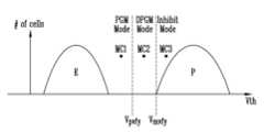
도 16을 참조하면, 더블 프로그램(Double Program, DPGM) 동작은 프로그램 동작에 대한 검증 동작 시 두 개의 검증 전압 레벨로 검증 동작을 수행할 수 있다. 두 개의 검증 전압은 보조 검증 전압(Vpvfy) 및 메인 검증 전압(Vmvfy)일 수 있다. 메인 검증 전압(Vmvfy)은 프로그램 동작의 목표 상태에 대응되는 검증 전압으로, 도 3 내지 도 15에서 언급한 검증 전압(Vvfy)과 동일한 전압을 의미할 수 있다. 보조 검증 전압(Vpvfy)은 메인 검증 전압(Vmvfy)보다 낮은 레벨에서, 메모리 셀에 대한 프로그램 동작이 진행된 정도를 검증하는 전압일 수 있다.Referring to FIG. 16, a double program (DPGM) operation can perform a verification operation with two verification voltage levels during a verification operation for a program operation. The two verification voltages can be an auxiliary verification voltage (Vpvfy ) and a main verification voltage (Vmvfy ). The main verification voltage (Vmvfy ) is a verification voltage corresponding to a target state of the program operation and can mean the same voltage as the verification voltage (Vvfy ) mentioned in FIGS. 3 to 15. The auxiliary verification voltage (Vpvfy ) can be a voltage that verifies the degree to which a program operation for a memory cell has progressed at a level lower than the main verification voltage (Vmvfy ).
도 16에서 메모리 셀은 하나의 데이터 비트를 저장하는 싱글 레벨 셀(SLC)로 가정하여 설명한다. 메모리 셀에 대한 프로그램 동작의 목표 상태는 제1 프로그램 상태(P)일 수 있다. 상태 모드는 메모리 셀에 대한 프로그램 동작의 검증 결과에 따라 결정될 수 있다. 상태 모드는 제1 프로그램 모드(PGM Mode), 제2 프로그램 모드(DPGM Mode) 및 프로그램 금지 모드(Inhibit Mode)를 포함할 수 있다.In Fig. 16, the memory cell is explained assuming a single-level cell (SLC) that stores one data bit. The target state of the program operation for the memory cell may be a first program state (P). The state mode may be determined according to the verification result of the program operation for the memory cell. The state mode may include a first program mode (PGM Mode), a second program mode (DPGM Mode), and a program inhibit mode (Inhibit Mode).
제1 메모리 셀(MC1)의 문턱 전압은 보조 검증 전압(Vpvfy)보다 낮으므로, 제1 메모리 셀(MC1)의 상태 모드는 제1 프로그램 모드(PGM Mode)일 수 있다. 제2 메모리 셀(MC2)의 문턱 전압은 보조 검증 전압(Vpvfy)보다 높고 메인 검증 전압(Vmvfy)보다 낮으므로, 제2 메모리 셀(MC2)의 상태 모드는 제2 프로그램 모드(DPGM Mode)일 수 있다. 제3 메모리 셀(MC3)의 문턱 전압은 메인 검증 전압(Vmvfy)보다 높으므로, 제3 메모리 셀(MC3)의 상태 모드는 프로그램 금지 모드(Inhibit Mode)일 수 있다.Since the threshold voltage of the first memory cell (MC1) is lower than the auxiliary verification voltage (Vpvfy ), the status mode of the first memory cell (MC1) may be the first program mode (PGM Mode). Since the threshold voltage of the second memory cell (MC2) is higher than the auxiliary verification voltage (Vpvfy ) and lower than the main verification voltage (Vmvfy ), the status mode of the second memory cell (MC2) may be the second program mode (DPGM Mode). Since the threshold voltage of the third memory cell (MC3) is higher than the main verification voltage (Vmvfy ), the status mode of the third memory cell (MC3) may be the program inhibit mode (Inhibit Mode).
제1 메모리 셀(MC1)은 목표 상태인 제1 프로그램 상태(P)에 도달하기 위해, 프로그램 동작이 빠르게 수행될 필요가 있다. 제2 메모리 셀(MC2)은 목표 상태인 제1 프로그램 상태(P)에 도달하기 위해, 프로그램 동작이 천천히 수행될 필요가 있다. 제3 메모리 셀(MC3)은 목표 상태인 제1 프로그램 상태(P)로 프로그램이 완료된 상태이므로, 프로그램 동작은 금지될 필요가 있다.The first memory cell (MC1) needs to perform a program operation quickly in order to reach the first program state (P), which is the target state. The second memory cell (MC2) needs to perform a program operation slowly in order to reach the first program state (P), which is the target state. Since the third memory cell (MC3) has completed programming in the first program state (P), which is the target state, the program operation needs to be inhibited.
따라서, 제2 메모리 셀(MC2)에 대해 제1 메모리 셀(MC1)보다 더 낮은 강도의 프로그램 동작이 수행될 수 있다. 프로그램 강도는 프로그램 펄스가 인가되는 시간, 프로그램 펄스가 인가되는 횟수 및 프로그램 펄스의 전위차에 따라 결정될 수 있다.Therefore, a program operation with lower intensity can be performed on the second memory cell (MC2) than on the first memory cell (MC1). The program intensity can be determined depending on the time for which the program pulse is applied, the number of times the program pulse is applied, and the potential difference of the program pulse.
예를 들어, 선택된 워드 라인에 프로그램 펄스가 인가되는 구간 동안, 제1 메모리 셀(MC1)과 연결된 비트 라인에 제1 프로그램 허용 전압(Vallow1)이 인가되고, 제2 메모리 셀(MC2)과 연결된 비트 라인에 제1 프로그램 허용 전압보다 높은 제2 프로그램 허용 전압(Vallow2)이 인가될 수 있다. 이 경우, 제2 메모리 셀(MC2)은 제1 메모리 셀(MC1)보다 인가되는 프로그램 펄스의 전위차가 작으므로, 제2 메모리 셀(MC2)에 대해 더 낮은 강도로 프로그램 동작이 수행될 수 있다.For example, during a period in which a program pulse is applied to a selected word line, a first program allowance voltage (Vallow1 ) may be applied to a bit line connected to a first memory cell (MC1), and a second program allowance voltage (Vallow2 ) higher than the first program allowance voltage may be applied to a bit line connected to a second memory cell (MC2). In this case, since the second memory cell (MC2) has a smaller potential difference of the program pulse applied to it than the first memory cell (MC1), a program operation may be performed with a lower intensity for the second memory cell (MC2).
제3 메모리 셀(MC3)에 대한 프로그램 동작은 제한될 수 있다. 예를 들어, 워드 라인에 프로그램 펄스가 인가되는 동안, 제3 메모리 셀(MC3)과 연결된 비트 라인에 프로그램 금지 전압(Vinhibit)이 인가될 수 있다. 이 경우, 제3 메모리 셀(MC3)에 인가되는 프로그램 펄스의 전위차가 메모리 셀의 문턱 전압을 상승시키기 위한 전위차보다 낮아지므로, 제3 메모리 셀(MC3)의 문턱 전압을 상승시키는 프로그램 동작이 제한될 수 있다.The program operation for the third memory cell (MC3) may be restricted. For example, while a program pulse is applied to a word line, a program inhibit voltage (Vinhibit ) may be applied to a bit line connected to the third memory cell (MC3). In this case, since the potential difference of the program pulse applied to the third memory cell (MC3) is lower than the potential difference for raising the threshold voltage of the memory cell, the program operation for raising the threshold voltage of the third memory cell (MC3) may be restricted.
도 17을 참조하면, 제n 프로그램 루프의 프로그램 전압 인가 동작이 수행될 수 있다. 이 때, 제n-1 프로그램 루프의 검증 결과(Verify_n-1)가 제1 래치(123a)에 저장되어 있을 수 있다. 제n-1 프로그램 루프의 검증 결과(Verify_n-1)는 페일을 나타낼 수 있다. 제1 래치(123a)에 저장된 검증 결과가 페일을 나타냄에 따라, 페이지 버퍼와 연결된 비트 라인(BLk)에는 프로그램 허용 전압(Vallow)이 인가될 수 있다. 선택된 워드 라인에는 프로그램 전압(Vpgm)이 인가될 수 있다. 이에 따라, 프로그램 허용 전압(Vallow)이 인가된 비트 라인(BLk)을 통해 페이지 버퍼와 연결된 메모리 셀은 프로그램 전압(Vpgm_n)에 의해 문턱 전압이 변경될 수 있다.Referring to FIG. 17, a program voltage application operation of the nth program loop may be performed. At this time, a verification result (Verify_n-1) of the n-1th program loop may be stored in the first latch (123a). The verification result (Verify_n-1) of the n-1th program loop may indicate fail. As the verification result stored in the first latch (123a) indicates fail, a program allowance voltage (Vallow ) may be applied to a bit line (BLk) connected to a page buffer. A program voltage (Vpgm ) may be applied to a selected word line. Accordingly, a memory cell connected to a page buffer through a bit line (BLk) to which the program allowance voltage (Vallow ) is applied may have its threshold voltage changed by the program voltage (Vpgm_n ).
이 때, 제3 래치(123c)에는 제n-1 프로그램 루프의 보조 검증 결과(Preverify_n-1)가 저장되어 있을 수 있다. 제3 래치(123c)에 저장된 제n-1 프로그램 루프의 보조 검증 결과(Preverify_n-1)가 페일을 나타내는 경우, 비트 라인(BLk)을 통해 페이지 버퍼와 연결된 메모리 셀은 도 16에서 설명한 제1 프로그램 모드(PGM Mode)일 수 있다. 이에 따라, 페이지 버퍼와 연결된 비트 라인(BLk)에는 프로그램 허용 전압(Vallow)은 제1 프로그램 허용 전압(Vallow1)일 수 있다.At this time, the auxiliary verification result (Preverify_n-1) of the n-1th program loop may be stored in the third latch (123c). If the auxiliary verification result (Preverify_n-1) of the n-1th program loop stored in the third latch (123c) indicates fail, the memory cell connected to the page buffer through the bit line (BLk) may be in the first program mode (PGM Mode) described in Fig. 16. Accordingly, the program allowance voltage (Vallow ) of the bit line (BLk) connected to the page buffer may be the first program allowance voltage (Vallow1 ).
제3 래치(123c)에 저장된 제n-1 프로그램 루프의 보조 검증 결과(Preverify_n-1)가 패스를 나타내는 경우, 비트 라인(BLk)을 통해 페이지 버퍼와 연결된 메모리 셀은 도 16에서 설명한 제2 프로그램 모드(DPGM Mode)일 수 있다. 이에 따라, 페이지 버퍼와 연결된 비트 라인(BLk)에는 프로그램 허용 전압(Vallow)은 제2 프로그램 허용 전압(Vallow2)일 수 있다. 즉, 본 발명의 일 실시 예에 따른 페이지 버퍼는 보조 검증 동작에 따른 보조 검증 결과를 저장하는 제3 래치를 더 포함하며, 이를 기초로 메모리 셀들에 연결된 비트 라인들에 연결되는 전압을 제어할 수 있으며, 이에 따라 메모리 셀들의 문턱 전압 분포가 더욱 개선될 수 있다.If the auxiliary verification result (Preverify_n-1) of the n-1th program loop stored in the third latch (123c) indicates a pass, the memory cell connected to the page buffer through the bit line (BLk) may be in the second program mode (DPGM Mode) described in FIG. 16. Accordingly, the program allowance voltage (Vallow ) of the bit line (BLk) connected to the page buffer may be the second program allowance voltage (Vallow2 ). That is, the page buffer according to an embodiment of the present invention further includes a third latch that stores the auxiliary verification result according to the auxiliary verification operation, and based on the same, the voltage connected to the bit lines connected to the memory cells can be controlled, and accordingly, the threshold voltage distribution of the memory cells can be further improved.
도 18은 본 개시의 일 실시 예에 따른 메모리 시스템을 설명하기 위한 블록도이다.FIG. 18 is a block diagram illustrating a memory system according to one embodiment of the present disclosure.
도 18을 참조하면, 메모리 시스템(50)은 메모리 장치(100) 및 메모리 컨트롤러(200)를 포함할 수 있다.Referring to FIG. 18, the memory system (50) may include a memory device (100) and a memory controller (200).
메모리 시스템(50)은 휴대폰, 스마트폰, MP3 플레이어, 랩탑 컴퓨터, 데스크탑 컴퓨터, 게임기, 디스플레이 장치, 테블릿 PC 또는 차량용 인포테인먼트(in-vehicle infotainment) 시스템 등과 같이 호스트(400)의 제어에 따라 데이터를 저장하는 장치일 수 있다. 메모리 시스템(50)은 호스트(400)와의 통신 방식인 호스트 인터페이스에 따라서 다양한 종류의 저장 장치들 중 어느 하나로 구현될 수 있다. 메모리 시스템(50)은 다양한 종류의 패키지(package) 형태들 중 어느 하나로 구현될 수 있다.The memory system (50) may be a device that stores data under the control of a host (400), such as a mobile phone, a smart phone, an MP3 player, a laptop computer, a desktop computer, a game console, a display device, a tablet PC, or an in-vehicle infotainment system. The memory system (50) may be implemented as any one of various types of storage devices depending on a host interface, which is a method of communication with the host (400). The memory system (50) may be implemented as any one of various types of package forms.
메모리 장치(100)는 데이터를 저장하거나 저장된 데이터를 이용할 수 있다. 실시 예에서 메모리 장치(100)는 도 1의 메모리 장치(100)일 수 있다. 구체적으로, 메모리 장치(100)는 메모리 컨트롤러(200)의 제어에 응답하여 동작할 수 있다. 메모리 장치(100)는 불휘발성 메모리 장치 또는 휘발성 메모리 장치일 수 있다.The memory device (100) can store data or use stored data. In an embodiment, the memory device (100) may be the memory device (100) of FIG. 1. Specifically, the memory device (100) may operate in response to the control of the memory controller (200). The memory device (100) may be a nonvolatile memory device or a volatile memory device.
메모리 장치(100)는 복수의 메모리 셀들을 포함하는 메모리 셀 어레이(110)를 포함할 수 있다. 메모리 셀 어레이(110)는 복수의 메모리 블록들을 포함할 수 있다. 각 메모리 블록은 복수의 메모리 셀들을 포함할 수 있고, 하나의 메모리 블록은 복수의 페이지들을 포함할 수 있다. 여기서, 페이지는 메모리 장치(100)에 데이터를 저장하거나, 메모리 장치(100)에 저장된 데이터를 리드하는 하나의 단위일 수 있다.The memory device (100) may include a memory cell array (110) including a plurality of memory cells. The memory cell array (110) may include a plurality of memory blocks. Each memory block may include a plurality of memory cells, and one memory block may include a plurality of pages. Here, a page may be a unit that stores data in the memory device (100) or reads data stored in the memory device (100).
또한, 메모리 장치(100)는 페이지 버퍼 그룹(123)을 포함할 수 있다. 실시 예에 따르면, 페이지 버퍼 그룹(123)은 복수의 페이지 버퍼들을 포함할 수 있으며, 복수의 페이지 버퍼들은 각각 복수의 비트 라인들을 통해 메모리 셀 어레이(110)와 연결될 수 있다. 페이지 버퍼들은 각각 복수의 프로그램 루프들 중 제n 프로그램 루프의 검증 동작에 따른 검증 결과를 저장하는 제1 래치 및 제n-1 프로그램 루프의 검증 동작에 따른 검증 결과를 저장하는 제2 래치를 포함할 수 있다. 페이지 버퍼는 도 1 내지 도 17을 통해 설명한 페이지 버퍼 그룹 또는 페이지 버퍼와 동일할 수 있다.In addition, the memory device (100) may include a page buffer group (123). According to an embodiment, the page buffer group (123) may include a plurality of page buffers, and the plurality of page buffers may be connected to the memory cell array (110) via a plurality of bit lines, respectively. The page buffers may include a first latch that stores a verification result according to a verification operation of an n-th program loop among a plurality of program loops, and a second latch that stores a verification result according to a verification operation of an n-1-th program loop, respectively. The page buffer may be the same as the page buffer group or the page buffer described with reference to FIGS. 1 to 17.
또한, 메모리 장치(100)는 비트 라인 전압 제어부(131)를 포함할 수 있다. 비트 라인 전압 제어부(131)는 제1 래치 및 제2 래치에 저장된 검증 결과를 기초로 각 메모리 셀들에 연결된 비트 라인들에 각각 인가될 비트 라인 전압을 결정할 수 있다. 비트 라인 전압 제어부(131)는 도 1의 제어 로직(130)에 포함될 수 있다.In addition, the memory device (100) may include a bit line voltage control unit (131). The bit line voltage control unit (131) may determine a bit line voltage to be applied to each bit line connected to each memory cell based on the verification results stored in the first latch and the second latch. The bit line voltage control unit (131) may be included in the control logic (130) of FIG. 1.
메모리 장치(100)는 메모리 컨트롤러(200)로부터 커맨드 및 어드레스를 수신할 수 있다. 메모리 장치(100)는 메모리 셀 어레이 중 수신된 어드레스에 의해 선택된 영역을 액세스하도록 구성될 수 있다. 선택된 영역을 액세스 한다는 것은 선택된 영역에 대해서 수신된 커맨드에 해당하는 동작을 수행함을 의미할 수 있다. 예를 들면, 메모리 장치(100)는 쓰기 동작(프로그램 동작), 리드 동작 및 소거 동작을 수행할 수 있다. 여기서, 프로그램 동작은 메모리 장치(100)가 어드레스에 의해 선택된 영역에 데이터를 기록하는 동작일 수 있다. 리드 동작은 메모리 장치(100)가 어드레스에 의해 선택된 영역으로부터 데이터를 읽는 동작을 의미할 수 있다. 소거 동작은 메모리 장치(100)가 어드레스에 의해 선택된 영역에 저장된 데이터를 소거하는 동작을 의미할 수 있다.The memory device (100) can receive a command and an address from the memory controller (200). The memory device (100) can be configured to access an area selected by the received address among the memory cell array. Accessing the selected area may mean performing an operation corresponding to the received command for the selected area. For example, the memory device (100) can perform a write operation (program operation), a read operation, and an erase operation. Here, the program operation may be an operation in which the memory device (100) writes data to an area selected by the address. The read operation may mean an operation in which the memory device (100) reads data from an area selected by the address. The erase operation may mean an operation in which the memory device (100) erases data stored in an area selected by the address.
메모리 컨트롤러(200)는 메모리 시스템(50)의 전반적인 동작을 제어할 수 있다. 구체적으로, 메모리 컨트롤러(200)는 메모리 시스템(50)에 전원이 인가되면 펌웨어(FW: firmware)를 실행할 수 있다. 펌웨어(FW)는 호스트(400)로부터 입력된 요청을 수신하거나 호스트(400)로 응답을 출력하는 호스트 인터페이스 레이어(HIL: Host Interface Layer), 호스트(400)의 인터페이스와 메모리 장치(100)의 인터페이스 사이의 동작의 관리하는 플래시 변환 레이어(FTL: Flash Translation Layer) 및 메모리 장치(100)에 커맨드를 제공하거나, 메모리 장치(100)로부터 응답을 수신하는 플래시 인터페이스 레이어(FIL: Flash Interface Layer)를 포함할 수 있다.The memory controller (200) can control the overall operation of the memory system (50). Specifically, the memory controller (200) can execute firmware (FW) when power is supplied to the memory system (50). The firmware (FW) can include a host interface layer (HIL) that receives a request input from a host (400) or outputs a response to the host (400), a flash translation layer (FTL) that manages operations between the interface of the host (400) and the interface of the memory device (100), and a flash interface layer (FIL) that provides a command to the memory device (100) or receives a response from the memory device (100).
메모리 컨트롤러(200)는 호스트(400)로부터 데이터와 논리 어드레스(LA: Logical Address)를 입력 받고, 논리 어드레스를 메모리 장치(100)에 포함된 데이터가 저장될 메모리 셀들의 주소를 나타내는 물리 어드레스(PA: Physical Address)에 맵핑할 수 있다. 논리 어드레스는 논리 블록 어드레스(LBA: Logical Block Address)일 수 있고, 물리 어드레스는 물리 블록 어드레스(PBA: Physical Block Address)일 수 있다.The memory controller (200) can receive data and a logical address (LA) from the host (400), and map the logical address to a physical address (PA) that indicates the address of memory cells in which data included in the memory device (100) will be stored. The logical address may be a logical block address (LBA), and the physical address may be a physical block address (PBA).
메모리 컨트롤러(200)는 호스트(400)의 요청에 따라 프로그램 동작, 리드 동작 또는 소거 동작 등을 수행하도록 메모리 장치(100)를 제어할 수 있다. 프로그램 동작 시, 메모리 컨트롤러(200)는 호스트(400)로부터 쓰기 요청을 수신하면, 쓰기 요청에 대응되는 프로그램 동작을 수행하도록 메모리 장치(100)를 제어할 수 있다. 보다 상세하게는 메모리 컨트롤러(200)는 프로그램 커맨드, 물리 블록 어드레스 및 데이터를 메모리 장치(100)에 제공할 수 있다.The memory controller (200) can control the memory device (100) to perform a program operation, a read operation, or an erase operation, etc., according to a request from the host (400). During the program operation, when the memory controller (200) receives a write request from the host (400), it can control the memory device (100) to perform a program operation corresponding to the write request. More specifically, the memory controller (200) can provide a program command, a physical block address, and data to the memory device (100).
메모리 컨트롤러(200)는 호스트(400)로부터의 요청과 무관하게 자체적으로 프로그램 동작, 리드 동작 또는 소거 동작을 수행하도록 메모리 장치(100)를 제어할 수 있다. 예를 들면, 메모리 컨트롤러(200)는 웨어 레벨링(wear leveling), 가비지 컬렉션(garbage collection), 리드 리클레임(read reclaim) 등의 배경 동작(background operation)을 수행하기 위해 사용되는 프로그램 동작, 리드 동작 또는 소거 동작을 수행하도록 메모리 장치(100)를 제어할 수 있다.The memory controller (200) can control the memory device (100) to perform a program operation, a read operation, or an erase operation independently of a request from the host (400). For example, the memory controller (200) can control the memory device (100) to perform a program operation, a read operation, or an erase operation used to perform background operations such as wear leveling, garbage collection, and read reclaim.
호스트(400)는 다양한 통신 방식들 중 적어도 하나를 이용하여 메모리 시스템(50)과 통신할 수 있다.The host (400) can communicate with the memory system (50) using at least one of various communication methods.
도 19는 도 18의 메모리 컨트롤러의 다른 일 실시 예를 설명하기 위한 도면이다.FIG. 19 is a drawing for explaining another embodiment of the memory controller of FIG. 18.
도 19를 참조하면, 메모리 컨트롤러(1000)는 프로세서(1010), 내부 메모리(1020), 에러 정정 회로(1030), 호스트 인터페이스(1040), 버퍼 메모리 인터페이스(1050) 및 메모리 인터페이스(1060)를 포함할 수 있다.Referring to FIG. 19, the memory controller (1000) may include a processor (1010), internal memory (1020), an error correction circuit (1030), a host interface (1040), a buffer memory interface (1050), and a memory interface (1060).
프로세서(1010)는 메모리 장치(100)를 제어하기 위한 각종 연산을 수행하거나, 다양한 커맨드들(commands)을 생성할 수 있다. 프로세서(1010)는 호스트(400)로부터 요청(request)을 수신하면, 수신된 요청에 따라 커맨드를 생성하고, 생성된 커맨드를 큐 컨트롤러(미도시)로 전송할 수 있다. 프로세서(1010)는 메모리 장치(100)에 대한 이후의 동작을 메모리 인터페이스(1060)가 메모리 장치(100)로부터 수신한 검증 결과를 기초로 제어할 수 있다.The processor (1010) may perform various operations to control the memory device (100) or generate various commands. When the processor (1010) receives a request from the host (400), it may generate a command according to the received request and transmit the generated command to a queue controller (not shown). The processor (1010) may control subsequent operations for the memory device (100) based on the verification result received from the memory device (100) by the memory interface (1060).
내부 메모리(1020)는 메모리 컨트롤러(1000)의 동작에 필요한 다양한 정보들을 저장할 수 있다. 예를 들면, 내부 메모리(1020)는 논리(logical), 물리(physical) 어드레스 맵 테이블들(address map tables)을 포함할 수 있다.The internal memory (1020) can store various information required for the operation of the memory controller (1000). For example, the internal memory (1020) can include logical and physical address map tables.
에러 정정 코드 회로(1030)는 에러 정정 코드(ECC, Error Correcting Code)를 이용하여 메모리 장치(100)로부터 수신된 데이터의 에러를 검출하고, 정정하도록 구성된다. 프로세서(1010)는 에러 정정 코드 회로(1030)의 에러 검출 결과에 따라 읽기 전압을 조절하고, 재 읽기를 수행하도록 메모리 장치(100)를 제어할 수 있다. 예시적인 실시 예로서, 에러 정정 블록은 메모리 컨트롤러(1000)의 구성 요소로서 제공될 수 있다.The error correction code circuit (1030) is configured to detect and correct errors in data received from the memory device (100) using an error correction code (ECC). The processor (1010) may control the memory device (100) to adjust a read voltage and perform a re-read according to an error detection result of the error correction code circuit (1030). As an exemplary embodiment, the error correction block may be provided as a component of the memory controller (1000).
호스트 인터페이스(1040)는 메모리 컨트롤러(1000)와 호스트(400) 사이에서 커맨드, 어드레스 및 데이터 등을 주고받을 수 있다. 예를 들면, 호스트 인터페이스(1040)는 호스트(400)로부터 요청(request), 어드레스 및 데이터 등을 수신할 수 있고, 메모리 장치(100)로부터 리드된 데이터를 호스트(400)로 출력할 수 있다. 호스트 인터페이스(1040)는 다양한 프로토콜을 사용하여 호스트(400)와 통신할 수 있다.The host interface (1040) can exchange commands, addresses, and data, etc. between the memory controller (1000) and the host (400). For example, the host interface (1040) can receive requests, addresses, and data, etc. from the host (400), and output data read from the memory device (100) to the host (400). The host interface (1040) can communicate with the host (400) using various protocols.
버퍼 메모리 인터페이스(1050)는 프로세서(1010)와 버퍼 메모리(미도시) 사이에서 데이터를 전송할 수 있다. 버퍼 메모리(미도시)는 메모리 컨트롤러(1000)의 동작 메모리 또는 캐시 메모리로 사용될 수 있으며, 메모리 시스템(50) 내에서 사용되는 데이터를 저장할 수 있다. 프로세서(1010)에 의해 버퍼 메모리는 리드 버퍼, 라이트 버퍼, 맵 버퍼 등으로 사용될 수 있다.The buffer memory interface (1050) can transmit data between the processor (1010) and the buffer memory (not shown). The buffer memory (not shown) can be used as an operating memory or cache memory of the memory controller (1000) and can store data used within the memory system (50). The buffer memory can be used as a read buffer, a write buffer, a map buffer, etc. by the processor (1010).
메모리 인터페이스(1060)는 메모리 컨트롤러(1000)와 메모리 장치(100) 사이에서 커맨드, 어드레스 및 데이터 등을 주고받을 수 있다. 예를 들면, 메모리 인터페이스(1060)는 채널(channel)을 통해 메모리 장치(100)에 커맨드, 어드레스 및 데이터 등을 전송할 수 있고, 메모리 장치(100)로부터 데이터 등을 수신할 수 있다. 메모리 인터페이스(1060)는 프로세서(1010)의 지시에 따라 메모리 장치(100)에 대해 프로그램 동작을 수행할 수 있다. 프로그램 동작은 복수의 프로그램 루프들을 포함할 수 있으며, 프로그램 루프들은 각각 프로그램 전압 인가 동작 및 검증 동작을 포함할 수 있다. 또한 메모리 인터페이스(1060)는 메모리 장치(100)로부터 프로그램 동작에 대한 결과를 수신할 수 있다.The memory interface (1060) can transmit and receive commands, addresses, and data, etc. between the memory controller (1000) and the memory device (100). For example, the memory interface (1060) can transmit commands, addresses, and data, etc. to the memory device (100) through a channel, and can receive data, etc. from the memory device (100). The memory interface (1060) can perform a program operation on the memory device (100) according to instructions from the processor (1010). The program operation can include a plurality of program loops, and each of the program loops can include a program voltage application operation and a verification operation. In addition, the memory interface (1060) can receive a result of the program operation from the memory device (100).
도 20은 본 개시의 일 실시 예에 따른 메모리 장치의 동작 방법을 설명하기 위한 순서도이다.FIG. 20 is a flowchart for explaining an operating method of a memory device according to an embodiment of the present disclosure.
도 20을 참조하면, S2001 동작에서 제n-1 프로그램 루프의 프로그램 전압 인가 동작을 수행할 수 있으며, S2003 동작에서 제n-1 프로그램 루프의 검증 동작을 수행할 수 있다. 프로그램 루프는 이와 같이 프로그램 전압 인가 동작 및 검증 동작을 포함할 수 있다. 프로그램 전압 인가 동작은 선택된 메모리 셀들에 상기 프로그램 전압을 인가하는 동작일 수 있다. 검증 동작은 검증 전압을 기초로 선택된 메모리 셀들의 프로그램 상태를 검증하는 동작일 수 있다.Referring to FIG. 20, a program voltage application operation of the n-1th program loop can be performed in operation S2001, and a verification operation of the n-1th program loop can be performed in operation S2003. The program loop can include the program voltage application operation and the verification operation as described above. The program voltage application operation can be an operation of applying the program voltage to selected memory cells. The verification operation can be an operation of verifying the program status of selected memory cells based on the verification voltage.
S2005 동작에서 기 수행된 검증 결과를 기초로 제n 프로그램 루프의 전압 인가 동작을 수행할 수 있다. 기 수행된 검증 결과는 메모리 장치 내의 페이지 버퍼에 저장되어 있을 수 있으며, 보다 상세하게는 페이지 버퍼 내에 포함된 래치들에 저장되어 있을 수 있다. 일 실시 예에서, 제n 프로그램 루프의 전압 인가 동작은 제1 래치에 저장된 검증 결과를 기초로 수행될 수 있다. 여기서, 제1 래치에는 제n-1 프로그램 루프의 검증 결과가 저장되어 있을 수 있다.In the S2005 operation, a voltage application operation of the nth program loop can be performed based on the verification result previously performed. The verification result previously performed may be stored in a page buffer within a memory device, and more specifically, may be stored in latches included in the page buffer. In one embodiment, the voltage application operation of the nth program loop can be performed based on the verification result stored in the first latch. Here, the verification result of the n-1th program loop may be stored in the first latch.
S2007 동작에서 기 수행된 검증 결과를 기초로 제n 프로그램 루프의 검증 동작을 수행할 수 있다. 기 수행된 검증 결과는 메모리 장치 내의 페이지 버퍼에 저장되어 있을 수 있으며, 보다 상세하게는 페이지 버퍼 내에 포함된 래치들에 저장되어 있을 수 있다. 일 실시 예에서, 제n 프로그램 루프의 검증 동작은 제1 래치에 저장된 검증 결과 및 제2 래치에 저장된 검증 결과를 기초로 수행될 수 있다. 여기서, 제1 래치에는 제n 프로그램 루프의 검증 결과가 저장되어 있을 수 있으며, 제2 래치에는 제n-1 프로그램 루프의 검증 결과가 저장되어 있을 수 있다.In the S2007 operation, a verification operation of the nth program loop can be performed based on a previously performed verification result. The previously performed verification result may be stored in a page buffer within a memory device, and more specifically, may be stored in latches included in the page buffer. In one embodiment, the verification operation of the nth program loop can be performed based on a verification result stored in a first latch and a verification result stored in a second latch. Here, a verification result of the nth program loop may be stored in the first latch, and a verification result of the n-1th program loop may be stored in the second latch.
S2009 동작에서 제n 프로그램 루프가 마지막 프로그램 루프인지 확인할 수 있다. 예를 들어, 모든 프로그램 상태에 대한 검증 동작의 센싱 결과가 패스인 경우, 제n 프로그램 루프가 마지막 프로그램 루프일 수 있다. 제n 프로그램 루프가 마지막 프로그램 루프이면, 프로그램 동작이 종료될 수 있다. 제n 프로그램 루프가 마지막 프로그램 루프가 아니면, 다음 프로그램 루프를 반복하여 수행할 수 있다.In the S2009 operation, it can be determined whether the nth program loop is the last program loop. For example, if the sensing result of the verification operation for all program states is pass, the nth program loop may be the last program loop. If the nth program loop is the last program loop, the program operation may be terminated. If the nth program loop is not the last program loop, the next program loop may be repeated and performed.
도 21은 도 20의 일부 동작을 보다 상세히 설명하기 위한 순서도이다.Figure 21 is a flowchart for explaining some operations of Figure 20 in more detail.
도 21을 참조하면, 제n 프로그램 루프의 전압 인가 동작까지의 동작 과정을 보다 상세히 확인할 수 있다. 즉, 도 21은 도 20의 S2001 동작 내지 S2005 동작을 보다 상세히 나타낸 것일 수 있다.Referring to Fig. 21, the operation process up to the voltage application operation of the nth program loop can be confirmed in more detail. That is, Fig. 21 may show the S2001 operation to the S2005 operation of Fig. 20 in more detail.
S2101 동작에서 선택된 메모리 셀이 연결된 선택된 워드 라인에 제n-1 프로그램 루프의 프로그램 전압(Vpgm_n-1)이 인가될 수 있다. 이는 도 20의 S2001 동작에 대응될 수 있다.In operation S2101, the program voltage (Vpgm_n-1 ) of the n-1th program loop may be applied to the selected word line to which the selected memory cell is connected. This may correspond to operation S2001 of Fig. 20.
S2103 동작에서 선택된 메모리 셀에 대하여 제n-1 프로그램 루프의 검증 동작을 수행할 수 있으며, 이에 따른 검증 결과를 S2105 동작에서 선택된 메모리 셀에 비트 라인을 통해 연결된 페이지 버퍼 내의 제1 래치에 저장할 수 있다. S2103 동작 및 S2105 동작은 도 20의 S2003 동작에 대응될 수 있다.In operation S2103, a verification operation of the n-1th program loop can be performed on the selected memory cell, and a verification result thereof can be stored in a first latch in a page buffer connected to the selected memory cell via a bit line in operation S2105. Operations S2103 and S2105 may correspond to operation S2003 of FIG. 20.
S2107 동작에서 제1 래치에 저장된 검증 결과가 패스인지 여부를 확인할 수 있다. 제1 래치에 저장된 검증 결과는 제n-1 프로그램 루프의 검증 동작에 따른 선택된 메모리 셀에 대한 검증 결과일 수 있다.In operation S2107, it can be checked whether the verification result stored in the first latch is a pass. The verification result stored in the first latch may be a verification result for a selected memory cell according to the verification operation of the n-1th program loop.
제1 래치에 저장된 검증 결과가 패스이면, S2109 동작에서 선택된 메모리 셀에 대응되는 비트 라인에 프로그램 금지 전압(Vinhibit)이 인가될 수 있다. 제1 래치에 저장된 검증 결과가 페일이면, S2111 동작에서 선택된 메모리 셀에 대응되는 비트 라인에 프로그램 허용 전압(Vallow)이 인가될 수 있다.If the verification result stored in the first latch is PASS, a program inhibit voltage (Vinhibit ) may be applied to a bit line corresponding to the memory cell selected in operation S2109. If the verification result stored in the first latch is FAIL, a program allow voltage (Vallow ) may be applied to a bit line corresponding to the memory cell selected in operation S2111.
S2113 동작에서, 선택된 워드 라인에 제n 프로그램 루프의 프로그램 전압(Vpgm_n)이 인가될 수 있다. 여기서, 선택된 메모리 셀이 연결된 비트 라인에는 S2109 동작 또는 S2111 동작에 따른 비트 라인 전압이 인가된 상태일 수 있다. S2107 동작 내지 S2113 동작은 도 20의 S2005 동작에 대응될 수 있다.In operation S2113, the program voltage (Vpgm_n ) of the nth program loop may be applied to the selected word line. Here, the bit line voltage according to operation S2109 or operation S2111 may be applied to the bit line to which the selected memory cell is connected. Operations S2107 to S2113 may correspond to operation S2005 of FIG. 20.
도 22는 도 20의 다른 일부 동작을 보다 상세히 설명하기 위한 순서도이다.Figure 22 is a flowchart for explaining some other operations of Figure 20 in more detail.
도 22를 참조하면, 제n 프로그램 루프의 검증 동작부터의 동작 과정을 보다 상세히 확인할 수 있다. 즉, 도 22는 도 20의 S2007 동작 이후를 보다 상세히 나타낸 것일 수 있다.Referring to Fig. 22, the operation process from the verification operation of the nth program loop can be confirmed in more detail. That is, Fig. 22 may show in more detail the operation after S2007 of Fig. 20.
S2201 동작에서, 제1 래치에 저장된 검증 결과 및 제2 래치에 저장된 검증 결과가 모두 패스인지 여부를 확인할 수 있다. 제1 래치에 저장된 검증 결과는 제n-1 프로그램 루프의 검증 동작에 따른 선택된 메모리 셀에 대한 검증 결과일 수 있으며, 제2 래치에 저장된 검증 결과는 제n-2 프로그램 루프의 검증 동작에 따른 선택된 메모리 셀에 대한 검증 결과일 수 있다.In operation S2201, it can be checked whether both the verification result stored in the first latch and the verification result stored in the second latch pass. The verification result stored in the first latch may be a verification result for a selected memory cell according to the verification operation of the n-1th program loop, and the verification result stored in the second latch may be a verification result for a selected memory cell according to the verification operation of the n-2th program loop.
제1 래치에 저장된 검증 결과 및 제2 래치에 저장된 검증 결과가 모두 패스는 아닌 것으로 판단된 경우, 즉, 제1 래치에 저장된 검증 결과 및 제2 래치에 저장된 검증 결과 중 하나 이상이 페일인 경우, S2203 동작에서 제n 프로그램 루프의 검증 동작을 수행할 수 있다.If it is determined that neither the verification result stored in the first latch nor the verification result stored in the second latch is a pass, that is, if at least one of the verification result stored in the first latch and the verification result stored in the second latch is a fail, the verification operation of the nth program loop can be performed in operation S2203.
제n 프로그램 루프의 검증 동작이 수행되기 전, 또는 제n 프로그램 루프의 검증 동작이 수행된 후, S2205 동작에서 제1 래치에 저장되어 있던 제n-1 프로그램 루프의 검증 결과가 제2 래치에 갱신될 수 있다. 또한, S2203 동작 및 S2205 동작이 모두 수행된 이후, 제n 프로그램 루프의 검증 결과가 제1 래치에 갱신될 수 있다.Before the verification operation of the nth program loop is performed, or after the verification operation of the nth program loop is performed, the verification result of the n-1th program loop stored in the first latch in operation S2205 may be updated to the second latch. Additionally, after both operations S2203 and S2205 are performed, the verification result of the nth program loop may be updated to the first latch.
만약, S2201 동작에서, 제1 래치에 저장된 검증 결과 및 제2 래치에 저장된 검증 결과가 모두 패스인 것으로 판단된 경우, S2209 동작에서 제n 프로그램 루프의 검증 동작을 수행하지 않을 수 있다. 예를 들어, 선택된 메모리 셀에 연결된 비트 라인에 검증 금지 전압을 인가함으로써 제n 프로그램 루프의 검증 동작을 수행하지 않을 수 있다. S2201 동작 내지 S2209 동작은 도 20의 S2007 동작에 대응될 수 있다.If, in operation S2201, both the verification result stored in the first latch and the verification result stored in the second latch are determined to be pass, the verification operation of the nth program loop may not be performed in operation S2209. For example, the verification operation of the nth program loop may not be performed by applying a verification inhibit voltage to a bit line connected to the selected memory cell. Operations S2201 to S2209 may correspond to operation S2007 of FIG. 20.
S2211 동작에서 제n 프로그램 루프가 마지막 프로그램 루프인지 확인할 수 있다. 제n 프로그램 루프가 마지막 프로그램 루프이면, 프로그램 동작이 종료될 수 있다. S2211 동작은 도 20의 S2009 동작에 대응될 수 있다.In operation S2211, it can be determined whether the nth program loop is the last program loop. If the nth program loop is the last program loop, the program operation can be terminated. Operation S2211 can correspond to operation S2009 of Fig. 20.
S2211 동작에서 제n 프로그램 루프가 마지막 프로그램 루프가 아니면, S2213 동작에서 제1 래치에 저장된 검증 결과가 패스인지 여부를 확인할 수 있다. 제1 래치에 저장된 검증 결과는 제n 프로그램 루프의 검증 동작에 따른 선택된 메모리 셀에 대한 검증 결과일 수 있다.In operation S2211, if the nth program loop is not the last program loop, it can be checked in operation S2213 whether the verification result stored in the first latch is a pass. The verification result stored in the first latch may be a verification result for a selected memory cell according to the verification operation of the nth program loop.
제1 래치에 저장된 검증 결과가 패스이면, S2215 동작에서 선택된 메모리 셀에 대응되는 비트 라인에 프로그램 금지 전압(Vinhibit)이 인가될 수 있다. 제1 래치에 저장된 검증 결과가 페일이면, S2217 동작에서 선택된 메모리 셀에 대응되는 비트 라인에 프로그램 허용 전압(Vallow)이 인가될 수 있다.If the verification result stored in the first latch is PASS, a program inhibit voltage (Vinhibit ) may be applied to a bit line corresponding to the memory cell selected in operation S2215. If the verification result stored in the first latch is FAIL, a program allowance voltage (Vallow ) may be applied to a bit line corresponding to the memory cell selected in operation S2217.
S2219 동작에서, 선택된 워드 라인에 제n+1 프로그램 루프의 프로그램 전압(Vpgm_n+1)이 인가될 수 있다. 여기서, 선택된 메모리 셀이 연결된 비트 라인에는 S2215 동작 또는 S2217 동작에 따른 비트 라인 전압이 인가된 상태일 수 있다. S2213 동작 내지 S2219 동작은 도 20의 S2009 동작 이후에 수행되는 S2005 동작에 대응될 수 있다.In operation S2219, the program voltage (Vpgm_n+1 ) of the n+1th program loop may be applied to the selected word line. Here, the bit line voltage according to operation S2215 or operation S2217 may be applied to the bit line to which the selected memory cell is connected. Operations S2213 to S2219 may correspond to operation S2005 performed after operation S2009 of FIG. 20.
이 후, 다시 S2201 동작으로 돌아가 제n+1 프로그램 루프의 검증 동작 및 그 이후의 프로그램 루프들이 반복되어 수행할 수 있다.After this, the verification operation of the n+1th program loop and subsequent program loops can be repeated and performed by returning to the S2201 operation.
50: 메모리 시스템
100: 메모리 장치
110: 메모리 셀 어레이
120: 주변 회로
123: 페이지 버퍼 그룹
123a: 제1 래치
123b: 제2 래치
123c: 제3 래치
123d: 센싱 래치
130: 제어 로직
131: 비트 라인 전압 제어부
200: 메모리 컨트롤러50: Memory System
100: Memory device
110: Memory cell array
120: Peripheral circuit
123: Page Buffer Group
123a: 1st latch
123b: 2nd latch
123c: 3rd latch
123d: Sensing Latch
130: Control logic
131: Bit line voltage control unit
200: Memory Controller
Claims (19)
Translated fromKorean복수의 비트 라인들을 통해 상기 복수의 메모리 셀들과 각각 연결되는 복수의 페이지 버퍼들 및 프로그램 전압 및 검증 전압을 선택적으로 출력하는 전압 생성 회로를 포함하는 주변 회로; 및
상기 메모리 셀들 중 선택된 메모리 셀들에 상기 프로그램 전압을 인가하는 프로그램 전압 인가 동작 및 상기 검증 전압을 기초로 상기 선택된 메모리 셀들의 프로그램 상태를 검증하는 검증 동작을 포함하는 복수의 프로그램 루프들을 수행하도록 상기 주변 회로를 제어하는 제어 회로;를 포함하고,
상기 페이지 버퍼들 각각은,
상기 복수의 프로그램 루프들 중 제n 프로그램 루프의 검증 동작에 따른 검증 결과를 저장하는 제1 래치; 및
상기 복수의 프로그램 루프들 중 제n-1 프로그램 루프의 검증 동작에 따른 검증 결과를 저장하는 제2 래치;를 포함하고,
상기 제어 회로는,
상기 제1 래치 및 제2 래치에 저장된 검증 결과를 기초로, 상기 복수의 프로그램 루프들 중 제n+1 프로그램 루프에서 상기 비트 라인들에 각각 인가될 비트 라인 전압을 결정하는 메모리 장치.
A memory cell array comprising a plurality of memory cells;
A peripheral circuit including a plurality of page buffers, each connected to the plurality of memory cells through a plurality of bit lines, and a voltage generation circuit selectively outputting a program voltage and a verification voltage; and
A control circuit for controlling the peripheral circuit to perform a plurality of program loops including a program voltage application operation for applying the program voltage to selected memory cells among the memory cells and a verification operation for verifying the program state of the selected memory cells based on the verification voltage;
Each of the above page buffers,
A first latch storing a verification result according to a verification operation of the nth program loop among the above plurality of program loops; and
A second latch for storing a verification result according to a verification operation of the n-1th program loop among the above plurality of program loops;
The above control circuit,
A memory device that determines a bit line voltage to be applied to each of the bit lines in an n+1-th program loop among the plurality of program loops based on the verification results stored in the first latch and the second latch.
상기 제n+1 프로그램 루프의 프로그램 전압 인가 동작 수행 시, 상기 제1 래치에 저장된 검증 결과가 페일을 나타내는 페이지 버퍼에 연결된 비트 라인에 프로그램 허용 전압이 인가되도록 상기 주변 회로를 제어하는 메모리 장치.
In the first paragraph, the control circuit,
A memory device that controls the peripheral circuit so that, when the program voltage application operation of the above n+1th program loop is performed, a program allowance voltage is applied to a bit line connected to a page buffer in which the verification result stored in the first latch indicates fail.
상기 제n+1 프로그램 루프의 프로그램 전압 인가 동작 수행 시, 상기 제1 래치에 저장된 검증 결과가 패스를 나타내는 페이지 버퍼에 연결된 비트 라인에 프로그램 금지 전압이 인가되도록 상기 주변 회로를 제어하는 메모리 장치.
In the first paragraph, the control circuit,
A memory device that controls the peripheral circuit so that, when the program voltage application operation of the above n+1th program loop is performed, a program inhibit voltage is applied to a bit line connected to a page buffer in which the verification result stored in the first latch indicates a pass.
상기 제1 래치에 저장된 검증 결과가 패스를 나타내고, 상기 제2 래치에 저장된 검증 결과가 페일을 나타내는 페이지 버퍼에 연결된 메모리 셀에 대해, 상기 제n+1 프로그램 루프의 검증 동작을 수행하도록 상기 주변 회로를 제어하는 메모리 장치.
In the first paragraph, the control circuit,
A memory device that controls the peripheral circuit to perform a verification operation of the n+1th program loop for a memory cell connected to a page buffer in which the verification result stored in the first latch indicates pass and the verification result stored in the second latch indicates fail.
상기 제1 래치에 저장된 검증 결과가 패스를 나타내고, 상기 제2 래치에 저장된 검증 결과가 패스를 나타내는 페이지 버퍼에 연결된 메모리 셀에 대해, 상기 제n+1 프로그램 루프의 검증 동작을 수행하지 않도록 상기 주변 회로를 제어하는 메모리 장치.
In the first paragraph, the control circuit,
A memory device that controls the peripheral circuit so as not to perform a verification operation of the n+1th program loop for a memory cell connected to a page buffer in which the verification result stored in the first latch indicates pass and the verification result stored in the second latch indicates pass.
상기 제n+1 프로그램 루프의 프로그램 전압 인가 동작이 종료된 후, 상기 제1 래치에 저장된 제n 프로그램 루프의 검증 결과가 상기 제2 래치에 갱신되는 메모리 장치.
In paragraph 1,
A memory device in which, after the program voltage application operation of the n+1th program loop is terminated, the verification result of the nth program loop stored in the first latch is updated to the second latch.
상기 제1 래치에 저장된 제n 프로그램 루프의 검증 결과가 상기 제2 래치에 갱신된 후, 상기 제n+1 프로그램 루프의 검증 결과가 상기 제1 래치에 갱신되는 메모리 장치.
In paragraph 6,
A memory device in which the verification result of the nth program loop stored in the first latch is updated to the second latch, and then the verification result of the n+1th program loop is updated to the first latch.
상기 검증 전압과 상이한 보조 검증 전압을 더 출력하는 메모리 장치.
In the first paragraph, the voltage generation circuit,
A memory device that further outputs an auxiliary verification voltage different from the above verification voltage.
상기 보조 검증 전압을 기초로 상기 선택된 메모리 셀들의 프로그램 상태를 검증하는 보조 검증 동작을 더 포함하는 메모리 장치.
In the 8th paragraph, the program loops,
A memory device further comprising an auxiliary verification operation for verifying a program state of the selected memory cells based on the auxiliary verification voltage.
상기 제n 프로그램 루프의 보조 검증 동작에 따른 보조 검증 결과를 저장하는 제3 래치;를 더 포함하는 메모리 장치.
In the 9th paragraph, each of the page buffers,
A memory device further comprising a third latch for storing the auxiliary verification result according to the auxiliary verification operation of the nth program loop.
상기 제3 래치에 저장된 보조 검증 결과를 기초로 상기 제n+1 프로그램 루프의 프로그램 전압을 결정하는 메모리 장치.
In the 10th paragraph, the control circuit,
A memory device that determines the program voltage of the n+1th program loop based on the auxiliary verification result stored in the third latch.
상기 선택된 메모리 셀에 비트 라인을 통해 연결되는 페이지 버퍼의 제1 래치에 상기 제n 프로그램 루프의 검증 동작에 따른 검증 결과를 저장하는 단계; 및
상기 페이지 버퍼의 제2 래치에 기 저장된 제n-1 프로그램 루프의 검증 동작에 따른 검증 결과 및 상기 제1 래치에 저장된 상기 제n 프로그램 루프의 검증 동작에 따른 검증 결과를 기초로 결정되는 비트 라인 전압을 상기 비트 라인에 인가하면서 제n+1 프로그램 루프를 수행하는 단계;를 포함하는 메모리 장치의 동작 방법.
A step of performing an nth program loop including a program voltage application operation and a verification operation to a selected memory cell among a plurality of memory cells;
A step of storing a verification result according to the verification operation of the nth program loop in a first latch of a page buffer connected to the selected memory cell through a bit line; and
A method of operating a memory device, comprising: performing an n+1-th program loop while applying a bit line voltage to the bit line, the bit line voltage being determined based on a verification result according to a verification operation of the n-1-th program loop stored in the second latch of the page buffer and a verification result according to a verification operation of the n-th program loop stored in the first latch;
상기 제1 래치에 저장된 검증 결과가 페일을 나타내면, 상기 비트 라인에 프로그램 허용 전압이 인가되는 메모리 장치의 동작 방법.
In the 12th paragraph, when performing the program voltage application operation of the n+1st program loop,
An operating method of a memory device in which a program allowance voltage is applied to the bit line when the verification result stored in the first latch indicates fail.
상기 제1 래치에 저장된 검증 결과가 패스를 나타내면, 상기 비트 라인에 프로그램 금지 전압이 인가되는 메모리 장치의 동작 방법.
In the 12th paragraph, when performing the program voltage application operation of the n+1st program loop,
An operating method of a memory device in which a program inhibit voltage is applied to the bit line when the verification result stored in the first latch indicates a pass.
상기 선택된 메모리 셀에 대해 상기 제n+1 프로그램 루프의 검증 동작이 수행되는 메모리 장치의 동작 방법.
In the 12th paragraph, if the verification result stored in the first latch indicates pass and the verification result stored in the second latch indicates fail,
An operating method of a memory device in which a verification operation of the n+1th program loop is performed for the selected memory cell.
상기 선택된 메모리 셀에 대해 상기 제n+1 프로그램 루프의 검증 동작이 수행되지 않는 메모리 장치의 동작 방법.
In the 12th paragraph, if the verification result stored in the first latch indicates a pass and the verification result stored in the second latch indicates a pass,
An operating method of a memory device in which a verification operation of the n+1th program loop is not performed for the selected memory cell.
상기 제1 래치에 저장된 제n 프로그램 루프의 검증 결과를 상기 제2 래치에 갱신하는 단계;를 더 포함하는 메모리 장치의 동작 방법.
In the 12th paragraph, after the program voltage application operation of the n+1st program loop,
An operating method of a memory device further comprising: a step of updating the verification result of the nth program loop stored in the first latch to the second latch.
상기 제n+1 프로그램 루프의 검증 결과를 상기 제1 래치에 갱신하는 단계;를 더 포함하는 메모리 장치의 동작 방법.
In the 17th paragraph, after the step of updating the verification result of the nth program loop stored in the first latch to the second latch,
A method of operating a memory device, further comprising: a step of updating the verification result of the n+1th program loop to the first latch.
외부로부터 쓰기 요청을 수신하면, 프로그램 동작을 수행하도록 상기 메모리 장치를 제어하는 메모리 컨트롤러;를 포함하고,
상기 프로그램 동작은,
상기 메모리 셀들 중 선택된 메모리 셀들에 프로그램 전압을 인가하는 전압 인가 동작 및 상기 선택된 메모리 셀들의 프로그램 상태를 검증하는 검증 동작을 포함하는 복수의 프로그램 루프들을 포함하고,
상기 페이지 버퍼들 각각은,
상기 복수의 프로그램 루프들 중 제n 프로그램 루프의 검증 동작에 따른 검증 결과를 저장하는 제1 래치; 및
상기 복수의 프로그램 루프들 중 제n-1 프로그램 루프의 검증 동작에 따른 검증 결과를 저장하는 제2 래치;를 포함하며,
상기 복수의 프로그램 루프들 중 제n+1 프로그램 루프에서 상기 비트 라인들에 각각 인가될 비트 라인 전압들은,
상기 제1 래치 및 제2 래치에 저장된 검증 결과를 기초로 결정되는 메모리 시스템.
A memory device including a plurality of memory cells and a plurality of page buffers each connected to the plurality of memory cells via a plurality of bit lines; and
A memory controller for controlling the memory device to perform a program operation when a write request is received from an external source;
The above program operation is,
It includes a plurality of program loops including a voltage application operation for applying a program voltage to selected memory cells among the above memory cells and a verification operation for verifying a program state of the selected memory cells,
Each of the above page buffers,
A first latch storing a verification result according to a verification operation of the nth program loop among the above plurality of program loops; and
A second latch for storing a verification result according to a verification operation of the n-1th program loop among the above plurality of program loops;
The bit line voltages to be applied to each of the bit lines in the n+1th program loop among the above plurality of program loops are:
A memory system determined based on the verification results stored in the first latch and the second latch.
Priority Applications (3)
| Application Number | Priority Date | Filing Date | Title |
|---|---|---|---|
| KR1020230015669AKR20240123120A (en) | 2023-02-06 | 2023-02-06 | Memory device, operating method of memory device, and memory system |
| US18/365,035US20240265974A1 (en) | 2023-02-06 | 2023-08-03 | Memory device, operating method of memory device, and memory system |
| CN202311396720.XACN118447900A (en) | 2023-02-06 | 2023-10-25 | Memory device, memory device operation method, and memory system |
Applications Claiming Priority (1)
| Application Number | Priority Date | Filing Date | Title |
|---|---|---|---|
| KR1020230015669AKR20240123120A (en) | 2023-02-06 | 2023-02-06 | Memory device, operating method of memory device, and memory system |
Publications (1)
| Publication Number | Publication Date |
|---|---|
| KR20240123120Atrue KR20240123120A (en) | 2024-08-13 |
Family
ID=92047191
Family Applications (1)
| Application Number | Title | Priority Date | Filing Date |
|---|---|---|---|
| KR1020230015669APendingKR20240123120A (en) | 2023-02-06 | 2023-02-06 | Memory device, operating method of memory device, and memory system |
Country Status (3)
| Country | Link |
|---|---|
| US (1) | US20240265974A1 (en) |
| KR (1) | KR20240123120A (en) |
| CN (1) | CN118447900A (en) |
Family Cites Families (12)
| Publication number | Priority date | Publication date | Assignee | Title |
|---|---|---|---|---|
| KR101855169B1 (en)* | 2011-10-13 | 2018-05-09 | 삼성전자주식회사 | Nonvolatile memory device, programming method of nonvolatile memory device and memory system including nonvolatile memory device |
| US11114173B2 (en)* | 2016-12-29 | 2021-09-07 | SK Hynix Inc. | Semiconductor memory device and method of operating the same |
| US12027209B2 (en)* | 2019-06-17 | 2024-07-02 | SK Hynix Inc. | Memory device and method of operating the same |
| KR102706422B1 (en)* | 2020-06-16 | 2024-09-13 | 에스케이하이닉스 주식회사 | Memory device and operating method thereof |
| KR102753223B1 (en)* | 2020-07-24 | 2025-01-14 | 에스케이하이닉스 주식회사 | Page buffer and operating method thereof |
| KR102800354B1 (en)* | 2020-07-29 | 2025-04-25 | 에스케이하이닉스 주식회사 | Semiconductor memory device and method for operating thereof |
| KR20220104514A (en)* | 2021-01-18 | 2022-07-26 | 에스케이하이닉스 주식회사 | Page buffer, semiconductor memory device having the same, and operating method thereof |
| KR102829313B1 (en)* | 2021-02-25 | 2025-07-04 | 에스케이하이닉스 주식회사 | Memory device and operating method thereof |
| KR20230045334A (en)* | 2021-09-28 | 2023-04-04 | 에스케이하이닉스 주식회사 | Memory device and operating method thereof |
| EP4449416A1 (en)* | 2022-03-14 | 2024-10-23 | Yangtze Memory Technologies Co., Ltd. | Page buffer, memory device, and method for programming thereof |
| KR20230136482A (en)* | 2022-03-18 | 2023-09-26 | 에스케이하이닉스 주식회사 | Semiconductor memory device maintaining verification data during program suspend, and method for operating thereof |
| KR20240077007A (en)* | 2022-11-24 | 2024-05-31 | 에스케이하이닉스 주식회사 | Semiconductor device performing program operation and operating method thereof |
- 2023
- 2023-02-06KRKR1020230015669Apatent/KR20240123120A/enactivePending
- 2023-08-03USUS18/365,035patent/US20240265974A1/enactivePending
- 2023-10-25CNCN202311396720.XApatent/CN118447900A/enactivePending
Also Published As
| Publication number | Publication date |
|---|---|
| US20240265974A1 (en) | 2024-08-08 |
| CN118447900A (en) | 2024-08-06 |
Similar Documents
| Publication | Publication Date | Title |
|---|---|---|
| US10971234B2 (en) | Page buffer, a memory device having page buffer, and a method of operating the memory device | |
| KR102774150B1 (en) | Storage device and operating method thereof | |
| KR102862938B1 (en) | Memory device and operating method thereof | |
| US11238952B2 (en) | Memory system, memory controller, and method of operating memory system | |
| US11335421B2 (en) | Memory device and method of operating the same | |
| KR102846056B1 (en) | Memory device and operating method thereof | |
| US12118239B2 (en) | Memory system and operating method supporting fast boot using host memory buffer and default enabled information | |
| US11216208B1 (en) | Memory system, memory controller, and operation method of memory system | |
| KR20230037296A (en) | Memory device and operating method thereof | |
| KR102753223B1 (en) | Page buffer and operating method thereof | |
| KR102804497B1 (en) | Memory device and operating method thereof | |
| KR102736250B1 (en) | Storage device and operating method thereof | |
| US11656790B2 (en) | Memory system, memory controller, and operation method of memory system | |
| US20210407607A1 (en) | Memory system, memory controller, and method of operating memory system | |
| US11709610B2 (en) | Memory system, memory controller and operating method | |
| US12204764B2 (en) | Memory system including memory die dedicated for metadata and operating method thereof | |
| KR102857582B1 (en) | Memory device and operating method thereof | |
| US11848054B2 (en) | Memory device determining precharge time based on a number of times that a program voltage is applied to word line and operating method of memory device | |
| KR20240066720A (en) | Memory device for verifying memory cells in erase state and operating method thereof | |
| US10978161B2 (en) | Memory system, memory controller and memory device | |
| KR20240123120A (en) | Memory device, operating method of memory device, and memory system | |
| CN114078542A (en) | Memory device and operation method thereof | |
| US12436685B2 (en) | Memory device for performing program operation according to incremental step pulse programming method, storage device including the same, and operating method of the memory device | |
| US12387801B2 (en) | Memory device and method of operating the memory device | |
| US12197770B2 (en) | Memory system, memory controller, and operation method of memory system |
Legal Events
| Date | Code | Title | Description |
|---|---|---|---|
| PA0109 | Patent application | Patent event code:PA01091R01D Comment text:Patent Application Patent event date:20230206 | |
| PG1501 | Laying open of application |