KR20240120400A - Display device - Google Patents
Display deviceDownload PDFInfo
- Publication number
- KR20240120400A KR20240120400AKR1020230013023AKR20230013023AKR20240120400AKR 20240120400 AKR20240120400 AKR 20240120400AKR 1020230013023 AKR1020230013023 AKR 1020230013023AKR 20230013023 AKR20230013023 AKR 20230013023AKR 20240120400 AKR20240120400 AKR 20240120400A
- Authority
- KR
- South Korea
- Prior art keywords
- inclined surface
- light
- display device
- opening
- convex portion
- Prior art date
- Legal status (The legal status is an assumption and is not a legal conclusion. Google has not performed a legal analysis and makes no representation as to the accuracy of the status listed.)
- Pending
Links
Images


Classifications
- H—ELECTRICITY
- H10—SEMICONDUCTOR DEVICES; ELECTRIC SOLID-STATE DEVICES NOT OTHERWISE PROVIDED FOR
- H10K—ORGANIC ELECTRIC SOLID-STATE DEVICES
- H10K59/00—Integrated devices, or assemblies of multiple devices, comprising at least one organic light-emitting element covered by group H10K50/00
- H10K59/80—Constructional details
- H10K59/875—Arrangements for extracting light from the devices
- H—ELECTRICITY
- H10—SEMICONDUCTOR DEVICES; ELECTRIC SOLID-STATE DEVICES NOT OTHERWISE PROVIDED FOR
- H10H—INORGANIC LIGHT-EMITTING SEMICONDUCTOR DEVICES HAVING POTENTIAL BARRIERS
- H10H29/00—Integrated devices, or assemblies of multiple devices, comprising at least one light-emitting semiconductor element covered by group H10H20/00
- H10H29/10—Integrated devices comprising at least one light-emitting semiconductor component covered by group H10H20/00
- H10H29/14—Integrated devices comprising at least one light-emitting semiconductor component covered by group H10H20/00 comprising multiple light-emitting semiconductor components
- H10H29/142—Two-dimensional arrangements, e.g. asymmetric LED layout
- H01L27/156—
- H—ELECTRICITY
- H01—ELECTRIC ELEMENTS
- H01L—SEMICONDUCTOR DEVICES NOT COVERED BY CLASS H10
- H01L25/00—Assemblies consisting of a plurality of semiconductor or other solid state devices
- H01L25/03—Assemblies consisting of a plurality of semiconductor or other solid state devices all the devices being of a type provided for in a single subclass of subclasses H10B, H10D, H10F, H10H, H10K or H10N, e.g. assemblies of rectifier diodes
- H01L25/04—Assemblies consisting of a plurality of semiconductor or other solid state devices all the devices being of a type provided for in a single subclass of subclasses H10B, H10D, H10F, H10H, H10K or H10N, e.g. assemblies of rectifier diodes the devices not having separate containers
- H01L25/075—Assemblies consisting of a plurality of semiconductor or other solid state devices all the devices being of a type provided for in a single subclass of subclasses H10B, H10D, H10F, H10H, H10K or H10N, e.g. assemblies of rectifier diodes the devices not having separate containers the devices being of a type provided for in group H10H20/00
- H01L25/0753—Assemblies consisting of a plurality of semiconductor or other solid state devices all the devices being of a type provided for in a single subclass of subclasses H10B, H10D, H10F, H10H, H10K or H10N, e.g. assemblies of rectifier diodes the devices not having separate containers the devices being of a type provided for in group H10H20/00 the devices being arranged next to each other
- H01L27/1214—
- H01L33/38—
- H01L33/405—
- H01L33/42—
- H01L33/486—
- H—ELECTRICITY
- H10—SEMICONDUCTOR DEVICES; ELECTRIC SOLID-STATE DEVICES NOT OTHERWISE PROVIDED FOR
- H10D—INORGANIC ELECTRIC SEMICONDUCTOR DEVICES
- H10D86/00—Integrated devices formed in or on insulating or conducting substrates, e.g. formed in silicon-on-insulator [SOI] substrates or on stainless steel or glass substrates
- H10D86/40—Integrated devices formed in or on insulating or conducting substrates, e.g. formed in silicon-on-insulator [SOI] substrates or on stainless steel or glass substrates characterised by multiple TFTs
- H—ELECTRICITY
- H10—SEMICONDUCTOR DEVICES; ELECTRIC SOLID-STATE DEVICES NOT OTHERWISE PROVIDED FOR
- H10H—INORGANIC LIGHT-EMITTING SEMICONDUCTOR DEVICES HAVING POTENTIAL BARRIERS
- H10H20/00—Individual inorganic light-emitting semiconductor devices having potential barriers, e.g. light-emitting diodes [LED]
- H10H20/80—Constructional details
- H10H20/83—Electrodes
- H10H20/831—Electrodes characterised by their shape
- H—ELECTRICITY
- H10—SEMICONDUCTOR DEVICES; ELECTRIC SOLID-STATE DEVICES NOT OTHERWISE PROVIDED FOR
- H10H—INORGANIC LIGHT-EMITTING SEMICONDUCTOR DEVICES HAVING POTENTIAL BARRIERS
- H10H20/00—Individual inorganic light-emitting semiconductor devices having potential barriers, e.g. light-emitting diodes [LED]
- H10H20/80—Constructional details
- H10H20/83—Electrodes
- H10H20/832—Electrodes characterised by their material
- H10H20/833—Transparent materials
- H—ELECTRICITY
- H10—SEMICONDUCTOR DEVICES; ELECTRIC SOLID-STATE DEVICES NOT OTHERWISE PROVIDED FOR
- H10H—INORGANIC LIGHT-EMITTING SEMICONDUCTOR DEVICES HAVING POTENTIAL BARRIERS
- H10H20/00—Individual inorganic light-emitting semiconductor devices having potential barriers, e.g. light-emitting diodes [LED]
- H10H20/80—Constructional details
- H10H20/83—Electrodes
- H10H20/832—Electrodes characterised by their material
- H10H20/835—Reflective materials
- H—ELECTRICITY
- H10—SEMICONDUCTOR DEVICES; ELECTRIC SOLID-STATE DEVICES NOT OTHERWISE PROVIDED FOR
- H10H—INORGANIC LIGHT-EMITTING SEMICONDUCTOR DEVICES HAVING POTENTIAL BARRIERS
- H10H20/00—Individual inorganic light-emitting semiconductor devices having potential barriers, e.g. light-emitting diodes [LED]
- H10H20/80—Constructional details
- H10H20/85—Packages
- H10H20/8506—Containers
- H—ELECTRICITY
- H10—SEMICONDUCTOR DEVICES; ELECTRIC SOLID-STATE DEVICES NOT OTHERWISE PROVIDED FOR
- H10K—ORGANIC ELECTRIC SOLID-STATE DEVICES
- H10K50/00—Organic light-emitting devices
- H10K50/80—Constructional details
- H10K50/805—Electrodes
- H10K50/81—Anodes
- H10K50/813—Anodes characterised by their shape
- H—ELECTRICITY
- H10—SEMICONDUCTOR DEVICES; ELECTRIC SOLID-STATE DEVICES NOT OTHERWISE PROVIDED FOR
- H10K—ORGANIC ELECTRIC SOLID-STATE DEVICES
- H10K50/00—Organic light-emitting devices
- H10K50/80—Constructional details
- H10K50/805—Electrodes
- H10K50/81—Anodes
- H10K50/818—Reflective anodes, e.g. ITO combined with thick metallic layers
- H—ELECTRICITY
- H10—SEMICONDUCTOR DEVICES; ELECTRIC SOLID-STATE DEVICES NOT OTHERWISE PROVIDED FOR
- H10K—ORGANIC ELECTRIC SOLID-STATE DEVICES
- H10K50/00—Organic light-emitting devices
- H10K50/80—Constructional details
- H10K50/805—Electrodes
- H10K50/82—Cathodes
- H10K50/822—Cathodes characterised by their shape
- H—ELECTRICITY
- H10—SEMICONDUCTOR DEVICES; ELECTRIC SOLID-STATE DEVICES NOT OTHERWISE PROVIDED FOR
- H10K—ORGANIC ELECTRIC SOLID-STATE DEVICES
- H10K50/00—Organic light-emitting devices
- H10K50/80—Constructional details
- H10K50/85—Arrangements for extracting light from the devices
- H10K50/856—Arrangements for extracting light from the devices comprising reflective means
- H—ELECTRICITY
- H10—SEMICONDUCTOR DEVICES; ELECTRIC SOLID-STATE DEVICES NOT OTHERWISE PROVIDED FOR
- H10K—ORGANIC ELECTRIC SOLID-STATE DEVICES
- H10K59/00—Integrated devices, or assemblies of multiple devices, comprising at least one organic light-emitting element covered by group H10K50/00
- H10K59/10—OLED displays
- H10K59/12—Active-matrix OLED [AMOLED] displays
- H10K59/122—Pixel-defining structures or layers, e.g. banks
- H—ELECTRICITY
- H10—SEMICONDUCTOR DEVICES; ELECTRIC SOLID-STATE DEVICES NOT OTHERWISE PROVIDED FOR
- H10K—ORGANIC ELECTRIC SOLID-STATE DEVICES
- H10K59/00—Integrated devices, or assemblies of multiple devices, comprising at least one organic light-emitting element covered by group H10K50/00
- H10K59/10—OLED displays
- H10K59/12—Active-matrix OLED [AMOLED] displays
- H10K59/124—Insulating layers formed between TFT elements and OLED elements
- H—ELECTRICITY
- H10—SEMICONDUCTOR DEVICES; ELECTRIC SOLID-STATE DEVICES NOT OTHERWISE PROVIDED FOR
- H10K—ORGANIC ELECTRIC SOLID-STATE DEVICES
- H10K59/00—Integrated devices, or assemblies of multiple devices, comprising at least one organic light-emitting element covered by group H10K50/00
- H10K59/30—Devices specially adapted for multicolour light emission
- H10K59/38—Devices specially adapted for multicolour light emission comprising colour filters or colour changing media [CCM]
- H—ELECTRICITY
- H10—SEMICONDUCTOR DEVICES; ELECTRIC SOLID-STATE DEVICES NOT OTHERWISE PROVIDED FOR
- H10K—ORGANIC ELECTRIC SOLID-STATE DEVICES
- H10K59/00—Integrated devices, or assemblies of multiple devices, comprising at least one organic light-emitting element covered by group H10K50/00
- H10K59/80—Constructional details
- H10K59/875—Arrangements for extracting light from the devices
- H10K59/878—Arrangements for extracting light from the devices comprising reflective means
- H—ELECTRICITY
- H10—SEMICONDUCTOR DEVICES; ELECTRIC SOLID-STATE DEVICES NOT OTHERWISE PROVIDED FOR
- H10K—ORGANIC ELECTRIC SOLID-STATE DEVICES
- H10K2102/00—Constructional details relating to the organic devices covered by this subclass
- H10K2102/301—Details of OLEDs
- H10K2102/302—Details of OLEDs of OLED structures
- H10K2102/3023—Direction of light emission
- H—ELECTRICITY
- H10—SEMICONDUCTOR DEVICES; ELECTRIC SOLID-STATE DEVICES NOT OTHERWISE PROVIDED FOR
- H10K—ORGANIC ELECTRIC SOLID-STATE DEVICES
- H10K59/00—Integrated devices, or assemblies of multiple devices, comprising at least one organic light-emitting element covered by group H10K50/00
- H10K59/30—Devices specially adapted for multicolour light emission
- H10K59/35—Devices specially adapted for multicolour light emission comprising red-green-blue [RGB] subpixels
- H10K59/351—Devices specially adapted for multicolour light emission comprising red-green-blue [RGB] subpixels comprising more than three subpixels, e.g. red-green-blue-white [RGBW]
Landscapes
- Engineering & Computer Science (AREA)
- Microelectronics & Electronic Packaging (AREA)
- Physics & Mathematics (AREA)
- Optics & Photonics (AREA)
- Power Engineering (AREA)
- Condensed Matter Physics & Semiconductors (AREA)
- General Physics & Mathematics (AREA)
- Computer Hardware Design (AREA)
- Electroluminescent Light Sources (AREA)
- Devices For Indicating Variable Information By Combining Individual Elements (AREA)
Abstract
Translated fromKoreanDescription
Translated fromKorean본 개시의 실시예들은 표시장치에 관한 것이다.Embodiments of the present disclosure relate to display devices.
다양한 정보를 화면에 표시하는 표시장치는 정보 통신 기술시대의 핵심 기술로 사용자에게 다양한 정보를 전달하는 역할을 수행한다.Display devices that display various information on the screen are a core technology in the information and communication technology era and play the role of delivering various information to users.
표시장치는 우수한 표시품질 및 발광효율 등이 요구될 수 있다. 특히, 표시장치는 사용자가 화면을 바라보는 각도가 변경되어도 우수한 표시품질을 유지하는 것이 요구될 수 있다. 즉, 표시장치는 넓은 시야각에서도 우수한 표시품질이 유지되는 것이 요구된다.Display devices may require excellent display quality and luminous efficiency. In particular, display devices may be required to maintain excellent display quality even when the angle at which the user views the screen changes. In other words, the display device is required to maintain excellent display quality even at a wide viewing angle.
표시장치는 다양한 색상을 표현하기 위해서 서로 다른 색상의 빛을 방출하는 발광소자를 포함할 수 있다. 그러나, 서로 다른 색상의 빛을 방출하는 발광소자들은 서로 상이한 소자특성을 가지므로, 넓은 시야각에서도 균일한 표시품질을 유지하기 어려운 문제가 있다.A display device may include light emitting elements that emit light of different colors to express various colors. However, since light-emitting devices that emit light of different colors have different device characteristics, it is difficult to maintain uniform display quality even at a wide viewing angle.
표시장치는 빛을발생시키는 발광소자를 포함할 수 있다. 표시장치에 포함된 발광소자에서 발생된 빛이 표시장치 외부로 추출되어 사용자에게 인식될 수 있다. 그러나, 발생한 빛 중 일부는 표시장치 외부로 추출되지 못하는 문제가 있었다. 발광소자를 사용하는 표시장치는 발광소자에서 생성된 빛을 어느 방향으로 추출하느냐에 따라서 전면발광형과 배면발광형으로 분류될 수 있다. 배면발광형 표시장치의 경우 발광소자에서 생성된 빛이 트랜지스터 등의 각종 회로소자와 배선이 위치하는 트랜지스터 형성부를 통과해야 한다. 특히, 트랜지스터 형성부에는 트랜지스터를 보호하기 위한 하부보호메탈이 위치할 수 있는데 하부보호메탈에 의해 측면 시야각 방향에서 휘도가 저하되는 문제점이 있었다. 이에, 본 명세서의 발명자들은 평탄화층이 볼록부, 경사면 및 슬릿부를 포함하여 표시장치 외부로 빛을 효과적으로 추출하여 향상된 광효율을 가지고, 하부보호메탈이 경사면과 중첩하지 않도록 배치하여 측면 시야각 방향에서 휘도가 저하되는 것을 경감할 수 있는 표시장치를 발명하였다.The display device emits lightIt may include a light emitting element that generates light. Light generated from a light-emitting element included in the display device can be extracted to the outside of the display device and recognized by the user. However, there was a problem that some of the generated light could not be extracted outside the display device. Display devices using light-emitting devices can be classified into front-emitting and bottom-emitting types depending on the direction in which the light generated from the light-emitting devices is extracted. In the case of a bottom-emitting display device, the light generated from the light-emitting element must pass through the transistor forming part where various circuit elements such as transistors and wiring are located. In particular, a lower protection metal to protect the transistor may be located in the transistor forming part, but there was a problem in that the luminance was lowered in the side viewing angle direction due to the lower protection metal. Accordingly, the inventors of the present specification have improved luminous efficiency by effectively extracting light to the outside of the display device by including a planarization layer including a convex portion, an inclined surface, and a slit portion, and arranged the lower protective metal so that it does not overlap the inclined surface to increase the luminance in the side viewing angle direction. A display device that can reduce degradation has been invented.
본 개시의 실시예들은 평탄화층이 볼록부, 경사면 및 슬릿부를 포함하여 표시장치 외부로 빛을 효과적으로 추출하여 향상된 광효율을 가지고, 하부보호메탈이 경사면과 중첩하지 않도록 배치하여 측면 시야각 방향에서 휘도가 저하되는 것을 경감할 수 있는 표시장치를 제공할 수 있다.In embodiments of the present disclosure, the planarization layer includes convex portions, inclined surfaces, and slits to effectively extract light to the outside of the display device to improve light efficiency, and the lower protective metal is arranged so as not to overlap the inclined surface, so that luminance decreases in the side viewing angle direction. It is possible to provide a display device that can reduce this.
본 개시의 실시예들은 제1 서브픽셀, 기판, 평탄화층, 제1 전극, 무기뱅크, 발광층 및 제2 전극을 포함하는 표시장치를 제공할 수 있다.Embodiments of the present disclosure may provide a display device including a first subpixel, a substrate, a planarization layer, a first electrode, an inorganic bank, a light emitting layer, and a second electrode.
평탄화층은 기판 상에 위치할 수 있다. 평탄화층은 제1 서브픽셀에서 제1 볼록부, 제2 볼록부, 슬릿부, 제1 경사면 및 제2 경사면을 포함할 수 있다. 슬릿부는 제1 볼록부와 제2 볼록부 사이에 위치할 수 있다. 제1 경사면은 제1 볼록부의 외곽에 위치할 수 있다. 제2 경사면은 제2 볼록부의 외곽에 위치할 수 있다.A planarization layer may be located on the substrate. The planarization layer may include a first convex portion, a second convex portion, a slit portion, a first inclined surface, and a second inclined surface in the first subpixel. The slit portion may be located between the first convex portion and the second convex portion. The first inclined surface may be located outside the first convex portion. The second inclined surface may be located outside the second convex portion.
제1 전극은 제1 볼록부, 제2 볼록부, 슬릿부, 제1 경사면 및 제2 경사면 상에 위치할 수 있다.The first electrode may be located on the first convex portion, the second convex portion, the slit portion, the first inclined surface, and the second inclined surface.
무기뱅크는 제1 전극 상에 위치할 수 있다. 무기뱅크는 제1 개구부 및 제2 개구부를 포함할 수 있다. 제1 개구부는 제1 볼록부에 대응하여 위치하고, 제2 개구부는 제2 볼록부에 대응하여 위치할 수 있다.The inorganic bank may be located on the first electrode. The inorganic bank may include a first opening and a second opening. The first opening may be positioned corresponding to the first convex part, and the second opening may be positioned corresponding to the second convex part.
발광층은 제1 개구부 및 제2 개구부에 의해 노출된 제1 전극 및 무기뱅크 상에 위치할 수 있다.The light emitting layer may be located on the first electrode and the inorganic bank exposed by the first opening and the second opening.
제2 전극은 발광층 상에 위치할 수 있다. 제2 전극은 제1 볼록부, 제2 볼록부, 슬릿부, 제1 경사면 및 제2 경사면과 중첩하여 위치할 수 있다.The second electrode may be located on the light emitting layer. The second electrode may be positioned overlapping the first convex portion, the second convex portion, the slit portion, the first inclined surface, and the second inclined surface.
본 개시의 실시예들에 의하면, 평탄화층이 볼록부, 경사면 및 슬릿부를 포함하여 표시장치 외부로 빛을 효과적으로 추출하여 향상된 광효율을 가지고, 하부보호메탈이 경사면과 중첩하지 않도록 배치하여 측면 시야각 방향에서 휘도가 저하되는 것을 경감할 수 있는 표시장치를 제공할 수 있다.According to embodiments of the present disclosure, the planarization layer includes a convex portion, an inclined surface, and a slit portion to effectively extract light to the outside of the display device to have improved luminous efficiency, and the lower protective metal is arranged so as not to overlap the inclined surface in the side viewing angle direction. A display device capable of reducing a decrease in luminance can be provided.
본 개시의 실시예들에 의하면, 표시장치에서 빛을 효과적으로 추출할 수 있어 저전력 구동이 가능한 표시장치를 제공할 수 있다.According to embodiments of the present disclosure, it is possible to provide a display device that can be driven at low power by effectively extracting light from the display device.
도 1은 본 개시의 실시예들에 따른 표시장치의 시스템 구성도이다.
도 2는 본 개시의 실시예들에 따른 표시장치의 단면도 및 서브픽셀의 회로도이다.
도 3 내지 도 6은 본 개시의 실시예들에 따른 표시장치의 단면도이다.
도 7은 본 개시의 실시예들에 따른 표시장치의 단면도 및 평면도이다.
도 8은 본 개시의 실시예들에 따른 표시장치의 단면도 및 평면도이다.1 is a system configuration diagram of a display device according to embodiments of the present disclosure.
2 is a cross-sectional view and a circuit diagram of a subpixel of a display device according to embodiments of the present disclosure.
3 to 6 are cross-sectional views of display devices according to embodiments of the present disclosure.
7 is a cross-sectional view and a top view of a display device according to embodiments of the present disclosure.
8 is a cross-sectional view and a top view of a display device according to embodiments of the present disclosure.
이하, 본 개시의 일부 실시예들을 예시적인 도면을 참조하여 상세하게 설명한다. 각 도면의 구성 요소들에 참조부호를 부가함에 있어서, 동일한 구성 요소들에 대해서는 비록 다른 도면상에 표시되더라도 가능한 한 동일한 부호를 가질 수 있다. 또한, 본 개시를 설명함에 있어, 관련된 공지 구성 또는 기능에 대한 구체적인 설명이 본 개시의 요지를 흐릴 수 있다고 판단되는 경우에는 그 상세한 설명은 생략할 수 있다. 본 명세서 상에서 언급된 "포함한다", "갖는다", "이루어진다" 등이 사용되는 경우 "~만"이 사용되지 않는 이상 다른 부분이 추가될 수 있다. 구성 요소를 단수로 표현한 경우에 특별한 명시적인 기재 사항이 없는 한 복수를 포함하는 경우를 포함할 수 있다.Hereinafter, some embodiments of the present disclosure will be described in detail with reference to illustrative drawings. In adding reference numerals to components in each drawing, identical components may have the same reference numerals as much as possible even if they are shown in different drawings. Additionally, in describing the present disclosure, if it is determined that a detailed description of a related known configuration or function may obscure the gist of the present disclosure, the detailed description may be omitted. When “comprises,” “has,” “consists of,” etc. mentioned in the specification are used, other parts may be added unless “only” is used. When a component is expressed in the singular, it can also include the plural, unless specifically stated otherwise.
또한, 본 개시의 구성 요소를 설명하는 데 있어서, 제1, 제2, A, B, (a), (b) 등의 용어를 사용할 수 있다. 이러한 용어는 그 구성 요소를 다른 구성 요소와 구별하기 위한 것일 뿐, 그 용어에 의해 해당 구성 요소의 본질, 차례, 순서 또는 개수 등이 한정되지 않는다.Additionally, in describing the components of the present disclosure, terms such as first, second, A, B, (a), and (b) may be used. These terms are only used to distinguish the component from other components, and the nature, sequence, order, or number of the components are not limited by the term.
구성 요소들의 위치 관계에 대한 설명에 있어서, 둘 이상의 구성 요소가 "연결", "결합" 또는 "접속" 등이 된다고 기재된 경우, 둘 이상의 구성 요소가 직접적으로 "연결", "결합" 또는 "접속" 될 수 있지만, 둘 이상의 구성 요소와 다른 구성 요소가 더 "개재"되어 "연결", "결합" 또는 "접속"될 수도 있다고 이해되어야 할 것이다. 여기서, 다른 구성 요소는 서로 "연결", "결합" 또는 "접속" 되는 둘 이상의 구성 요소 중 하나 이상에 포함될 수도 있다.In the description of the positional relationship of components, when two or more components are described as being “connected,” “coupled,” or “connected,” the two or more components are directly “connected,” “coupled,” or “connected.” ", but it should be understood that two or more components and other components may be further "interposed" and "connected," "combined," or "connected." Here, other components may be included in one or more of two or more components that are “connected,” “coupled,” or “connected” to each other.
구성 요소들이나, 동작 방법이나 제작 방법 등과 관련한 시간적 흐름 관계에 대한 설명에 있어서, 예를 들어, "~후에", "~에 이어서", "~다음에", "~전에" 등으로 시간적 선후 관계 또는 흐름적 선후 관계가 설명되는 경우, "바로" 또는 "직접"이 사용되지 않는 이상 연속적이지 않은 경우도 포함할 수 있다.In the explanation of temporal flow relationships related to components, operation methods, production methods, etc., for example, temporal precedence relationships such as “after”, “after”, “after”, “before”, etc. Or, when a sequential relationship is described, non-continuous cases may be included unless “immediately” or “directly” is used.
한편, 구성 요소에 대한 수치 또는 그 대응 정보(예: 레벨 등)가 언급된 경우, 별도의 명시적 기재가 없더라도, 수치 또는 그 대응 정보는 각종 요인(예: 공정상의 요인, 내부 또는 외부 충격, 노이즈 등)에 의해 발생할 수 있는 오차 범위를 포함하는 것으로 해석될 수 있다.On the other hand, when a numerical value or corresponding information (e.g. level, etc.) for a component is mentioned, even if there is no separate explicit description, the numerical value or corresponding information is related to various factors (e.g. process factors, internal or external shocks, It can be interpreted as including the error range that may occur due to noise, etc.).
이하, 첨부된 도면을 참조하여 본 개시의 다양한 실시예들을 상세히 설명한다.Hereinafter, various embodiments of the present disclosure will be described in detail with reference to the attached drawings.
도 1은 본 개시의 실시예들에 따른 유기발광 표시장치(100)의 시스템 구성도이다.1 is a system configuration diagram of an organic light
도 1을 참조하면, 본 실시예들에 따른 유기발광 표시장치(100)는, 다수의 데이터라인(DL) 및 다수의 게이트라인(GL)이 배치되고, 다수의 데이터라인(DL) 및 다수의 게이트라인(GL)과 연결되는 다수의 서브픽셀(SP)이 액티브영역(AA)에 배열된 표시패널(PNL)과, 표시패널(PNL)을 구동하기 위한 구동회로를 포함할 수 있다.Referring to FIG. 1, the organic light
구동회로는, 기능적으로 볼 때, 다수의 데이터라인(DL)을 구동하는 데이터 구동회로(DDC)와, 다수의 게이트라인(GL)을 구동하는 게이트 구동회로(GDC)와, 데이터 구동회로(DDC) 및 게이트 구동회로(GDC)를 제어하는 컨트롤러(CTR) 등을 포함할 수 있다.Functionally, the driving circuit consists of a data driving circuit (DDC) that drives a plurality of data lines (DL), a gate driving circuit (GDC) that drives a plurality of gate lines (GL), and a data driving circuit (DDC). ) and a controller (CTR) that controls the gate driving circuit (GDC).
표시패널(PNL)에서 다수의 데이터라인(DL) 및 다수의 게이트라인(GL)은 서로 교차하여 배치될 수 있다. 예를 들어, 다수의 데이터라인(DL)은 행(Row) 또는 열(Column)으로 배치될 수 있고, 다수의 게이트라인(GL)은 열(Column) 또는 행(Row)으로 배치될 수 있다. 아래에서는, 설명의 편의를 위하여, 다수의 데이터라인(DL)은 행(Row)으로 배치되고, 다수의 게이트라인(GL)은 열(Column)로 배치되는 것으로 가정한다.In the display panel (PNL), a plurality of data lines (DL) and a plurality of gate lines (GL) may be arranged to cross each other. For example, multiple data lines DL may be arranged in rows or columns, and multiple gate lines GL may be arranged in columns or rows. Below, for convenience of explanation, it is assumed that the plurality of data lines DL are arranged in rows and the plurality of gate lines GL are arranged in columns.
컨트롤러(CTR)는, 데이터 구동회로(DDC) 및 게이트 구동회로(GDC)의 구동 동작에 필요한 각종 제어신호(DCS, GCS)를 공급하여, 데이터 구동회로(DDC) 및 게이트 구동회로(GDC)를 제어한다.The controller (CTR) supplies various control signals (DCS, GCS) necessary for the driving operation of the data driving circuit (DDC) and the gate driving circuit (GDC), and operates the data driving circuit (DDC) and the gate driving circuit (GDC). Control.
이러한 컨트롤러(CTR)는, 각 프레임에서 구현하는 타이밍에 따라 스캔을 시작하고, 외부에서 입력되는 입력 영상 데이터를 데이터 구동회로(DDC)에서 사용하는 데이터 신호 형식에 맞게 전환하여 전환된 영상 데이터(DATA)를 출력하고, 스캔에 맞춰 적당한 시간에 데이터 구동을 통제한다.This controller (CTR) starts scanning according to the timing implemented in each frame, converts the input video data input from the outside to the data signal format used in the data driving circuit (DDC), and converts the converted video data (DATA) ) is output, and data operation is controlled at an appropriate time according to the scan.
이러한 컨트롤러(CTR)는 통상의 디스플레이 기술에서 이용되는 타이밍 컨트롤러(Timing Controller)이거나, 타이밍 컨트롤러(Timing Controller)를 포함하여 다른 제어 기능도 더 수행할 수 있는 제어장치일 수 있다.This controller (CTR) may be a timing controller used in typical display technology, or a control device that can perform other control functions, including a timing controller.
컨트롤러(CTR)는, 데이터 구동회로(DDC)와 별도의 부품으로 구현될 수도 있고, 데이터 구동회로(DDC)와 함께 통합되어 집적회로로 구현될 수 있다.The controller (CTR) may be implemented as a separate component from the data driving circuit (DDC), or may be integrated with the data driving circuit (DDC) and implemented as an integrated circuit.
데이터 구동회로(DDC)는, 컨트롤러(CTR)로부터 영상 데이터(DATA)를 입력 받아 다수의 데이터라인(DL)로 데이터 전압을 공급함으로써, 다수의 데이터라인(DL)을 구동한다. 여기서, 데이터 구동회로(DDC)는 소스 구동회로라고도 한다.The data driving circuit (DDC) receives image data (DATA) from the controller (CTR) and supplies data voltage to the plurality of data lines (DL), thereby driving the plurality of data lines (DL). Here, the data driving circuit (DDC) is also called a source driving circuit.
데이터 구동회로(DDC)는, 적어도 하나의 소스-드라이버 집적회로(S-DIC: Source-Driver Integrated Circuit)를 포함하여 구현될 수 있다. 각 소스-드라이버 집적회로(S-DIC)는, 시프트 레지스터(Shift Register), 래치 회로(Latch Circuit), 디지털 아날로그 컨버터(DAC: Digital to Analog Converter), 출력 버퍼(Output Buffer) 등을 포함할 수 있다. 각 소스-드라이버 집적회로(S-DIC)는, 경우에 따라서, 아날로그-디지털 컨버터(ADC: Analog to Digital Converter)를 더 포함할 수 있다.The data driving circuit (DDC) may be implemented including at least one source-driver integrated circuit (S-DIC). Each source-driver integrated circuit (S-DIC) may include a shift register, a latch circuit, a digital to analog converter (DAC), an output buffer, etc. there is. Each source-driver integrated circuit (S-DIC) may, in some cases, further include an analog to digital converter (ADC).
각 소스-드라이버 집적회로(S-DIC)는, 테이프 오토메티드 본딩(TAB: Tape Automated Bonding) 방식 또는 칩 온 글래스(COG: Chip On Glass) 방식으로 표시패널(PNL)의 본딩 패드(Bonding Pad)에 연결되거나, 표시패널(PNL)에 직접 배치될 수도 있으며, 경우에 따라서, 표시패널(PNL)에 집적화되어 배치될 수도 있다. 또한, 각 소스-드라이버 집적회로(S-DIC)는, 표시패널(PNL)에 연결된 소스-회로필름 상에 실장 되는 칩 온 필름(COF: Chip On Film) 방식으로 구현될 수도 있다.Each source-driver integrated circuit (S-DIC) is connected to the bonding pad of the display panel (PNL) using Tape Automated Bonding (TAB) or Chip On Glass (COG) method. It may be connected to or placed directly on the display panel (PNL), or in some cases, may be integrated and placed on the display panel (PNL). Additionally, each source-driver integrated circuit (S-DIC) may be implemented using a chip on film (COF) method that is mounted on a source-circuit film connected to the display panel (PNL).
게이트 구동회로(GDC)는, 다수의 게이트라인(GL)로 스캔신호를 순차적으로 공급함으로써, 다수의 게이트라인(GL)을 순차적으로 구동한다. 여기서, 게이트 구동회로(GDC)는 스캔 구동회로라고도 한다.The gate driving circuit (GDC) sequentially drives a plurality of gate lines (GL) by sequentially supplying scan signals to the plurality of gate lines (GL). Here, the gate driving circuit (GDC) is also called a scan driving circuit.
게이트 구동회로(GDC)는, 테이프 오토메티드 본딩(TAB) 방식 또는 칩 온 글래스(COG) 방식으로 표시패널(PNL)의 본딩 패드(Bonding Pad)에 연결되거나, GIP(Gate In Panel) 타입으로 구현되어 표시패널(PNL)에 직접 배치될 수도 있으며, 경우에 따라서, 표시패널(PNL)에 집적화되어 배치될 수도 있다. 또한, 게이트 구동회로(GDC)는 다수의 게이트 드라이버 집적회로(G-DIC)로 구현되어 표시패널(PNL)과 연결된 게이트-회로필름 상에 실장 되는 칩 온 필름(COF) 방식으로 구현될 수도 있다.The gate driving circuit (GDC) is connected to the bonding pad of the display panel (PNL) using the tape automated bonding (TAB) method or chip-on-glass (COG) method, or is implemented as the GIP (Gate In Panel) type. It may be placed directly on the display panel (PNL), or in some cases, may be integrated and placed on the display panel (PNL). In addition, the gate driving circuit (GDC) may be implemented using a chip-on-film (COF) method that is implemented with multiple gate driver integrated circuits (G-DIC) and mounted on a gate-circuit film connected to the display panel (PNL). .
게이트 구동회로(GDC)는, 컨트롤러(CTR)의 제어에 따라, 온(On) 전압 또는 오프(Off) 전압의 스캔신호를 다수의 게이트라인(GL)로 순차적으로 공급한다.The gate driving circuit (GDC) sequentially supplies scan signals of on voltage or off voltage to a plurality of gate lines (GL) under the control of the controller (CTR).
데이터 구동회로(DDC)는, 게이트 구동회로(GDC)에 의해 특정 게이트라인이 열리면, 컨트롤러(CTR)로부터 수신한 영상 데이터(DATA)를 아날로그 형태의 데이터 전압으로 변환하여 다수의 데이터라인(DL)로 공급한다.When a specific gate line is opened by the gate driving circuit (GDC), the data driving circuit (DDC) converts the image data (DATA) received from the controller (CTR) into an analog data voltage and connects a plurality of data lines (DL). supplied by
데이터 구동회로(DDC)는, 표시패널(PNL)의 일 측(예: 상측 또는 하측)에만 위치할 수도 있고, 경우에 따라서는, 구동 방식, 패널 설계 방식 등에 따라 표시패널(PNL)의 양측(예: 상 측과 하 측)에 모두 위치할 수도 있다.The data driving circuit (DDC) may be located only on one side (e.g., upper or lower) of the display panel (PNL), and in some cases, both sides (e.g., upper or lower) of the display panel (PNL) depending on the driving method, panel design method, etc. For example, it may be located on both the upper and lower sides.
게이트 구동회로(GDC)는, 표시패널(PNL)의 일 측(예: 좌측 또는 우측)에만 위치할 수도 있고, 경우에 따라서는, 구동 방식, 패널 설계 방식 등에 따라 표시패널(PNL)의 양측(예: 좌 측과 우 측)에 모두 위치할 수도 있다.The gate driving circuit (GDC) may be located only on one side (e.g., left or right) of the display panel (PNL), and in some cases, both sides (e.g., left or right) of the display panel (PNL) depending on the driving method, panel design method, etc. For example, it can be located on both the left and right sides.
표시패널(PNL)에 배치된 다수의 게이트라인(GL)은 다수의 스캔라인(SCL), 다수의 센스라인(SCL) 및 다수의 발광제어라인(EML)을 포함할 수 있다. 스캔라인(SCL), 센스라인(SCL) 및 발광제어라인(EML)은 서로 다른 종류의 트랜지스터들(스캔 트랜지스터, 센스 트랜지스터, 발광제어 트랜지스터)의 게이트 노드로 서로 다른 종류의 게이트 신호(스캔신호, 센스신호, 발광제어신호)를 전달하는 배선들이다.The plurality of gate lines GL disposed on the display panel PNL may include a plurality of scan lines SCL, a plurality of sense lines SCL, and a plurality of emission control lines EML. The scan line (SCL), sense line (SCL), and emission control line (EML) are the gate nodes of different types of transistors (scan transistor, sense transistor, and emission control transistor) and transmit different types of gate signals (scan signal, These are wires that transmit sense signals and light emission control signals.
도 2는 본 개시의 실시예들에 따른 표시장치의 대략적인 단면 구조와 서브픽셀의 회로도이다.2 is a schematic cross-sectional structure and a circuit diagram of a subpixel of a display device according to embodiments of the present disclosure.
도 2를 참조하면, 표시 영역(DA)에는 복수의 서브 픽셀(SP)이 배치될 수 있다. 복수의 서브 픽셀(SP)은 표시 영역(DA)에 포함된 일반 영역(NA), 제1 광학 영역(OA1) 및 제2 광학 영역(OA2)에 배치될 수 있다.Referring to FIG. 2 , a plurality of subpixels SP may be disposed in the display area DA. A plurality of subpixels SP may be disposed in the general area NA, the first optical area OA1, and the second optical area OA2 included in the display area DA.
도 2를 참조하면, 복수의 서브 픽셀(SP) 각각은, 발광 소자(ED) 및 발광 소자(ED)를 구동하기 위해 구성된 서브 픽셀 회로부(SPC)를 포함할 수 있다.Referring to FIG. 2 , each of the plurality of subpixels SP may include a light emitting element ED and a subpixel circuit unit SPC configured to drive the light emitting element ED.
도 2를 참조하면, 서브 픽셀 회로부(SPC)는 발광 소자(ED)를 구동하기 위한 구동 트랜지스터(DT), 구동 트랜지스터(DT)의 제1 노드(N1)로 데이터 전압(Vdata)을 전달해주기 위한 스캔 트랜지스터(ST), 및 한 프레임 동안 일정 전압을 유지해주기 위한 스토리지 캐패시터(Cst) 등을 포함할 수 있다.Referring to FIG. 2, the subpixel circuit unit (SPC) includes a driving transistor (DT) for driving the light emitting element (ED) and a data voltage (Vdata) for transferring the data voltage (Vdata) to the first node (N1) of the driving transistor (DT). It may include a scan transistor (ST) and a storage capacitor (Cst) to maintain a constant voltage for one frame.
구동 트랜지스터(DT)는 데이터 전압이 인가될 수 있는 제1 노드(N1), 발광 소자(ED)와 전기적으로 연결되는 제2 노드(N2) 및 구동 전압 라인(DVL)으로부터 구동 전압(ELVDD)이 인가되는 제3 노드(N3)를 포함할 수 있다. 구동 트랜지스터(DT)에서, 제1 노드(N1)는 게이트 노드이고, 제2 노드(N2)는 소스 노드 또는 드레인 노드일 수 있고, 제3 노드(N3)는 드레인 노드 또는 소스 노드일 수 있다. 이하에서는, 설명의 편의를 위하여, 구동 트랜지스터(DT)에서, 제1 노드(N1)는 게이트 노드이고, 제2 노드(N2)는 소스 노드일 수 있고, 제3 노드(N3)는 드레인 노드인 경우를 예로 든다.The driving transistor (DT) receives the driving voltage (ELVDD) from the first node (N1) to which the data voltage can be applied, the second node (N2) electrically connected to the light emitting element (ED), and the driving voltage line (DVL). It may include an authorized third node (N3). In the driving transistor DT, the first node N1 is a gate node, the second node N2 is a source node or a drain node, and the third node N3 is a drain node or a source node. Hereinafter, for convenience of explanation, in the driving transistor DT, the first node N1 may be a gate node, the second node N2 may be a source node, and the third node N3 may be a drain node. Take the case as an example.
발광 소자(ED)는 애노드 전극(AE), 발광층(EL) 및 캐소드 전극(CE)을 포함할 수 있다. 애노드 전극(AE)은 각 서브 픽셀(SP)에 배치되는 픽셀 전극일 수 있으며, 각 서브 픽셀(SP)의 구동 트랜지스터(DT)의 제2 노드(N2)와 전기적으로 연결될 수 있다. 캐소드 전극(CE)은 복수의 서브 픽셀(SP)에 공통으로 배치되는 공통 전극일 수 있으며, 기저 전압(ELVSS)이 인가될 수 있다.The light emitting device (ED) may include an anode electrode (AE), a light emitting layer (EL), and a cathode electrode (CE). The anode electrode AE may be a pixel electrode disposed in each subpixel SP, and may be electrically connected to the second node N2 of the driving transistor DT of each subpixel SP. The cathode electrode CE may be a common electrode commonly disposed in the plurality of subpixels SP, and a base voltage ELVSS may be applied.
예를 들어, 애노드 전극(AE)은 픽셀 전극일 수 있고, 캐소드 전극(CE)은 공통 전극일 수 있다. 이와 반대로, 애노드 전극(AE)은 공통 전극일 수 있고, 캐소드 전극(CE)은 픽셀 전극일 수 있다. 아래에서는, 설명의 편의를 위하여, 애노드 전극(AE)은 픽셀 전극이고, 캐소드 전극(CE)은 공통 전극인 것으로 가정한다.For example, the anode electrode (AE) may be a pixel electrode, and the cathode electrode (CE) may be a common electrode. Conversely, the anode electrode (AE) may be a common electrode, and the cathode electrode (CE) may be a pixel electrode. Below, for convenience of explanation, it is assumed that the anode electrode (AE) is a pixel electrode and the cathode electrode (CE) is a common electrode.
발광 소자(ED)는 소정의 발광 영역(EA)을 가질 수 있고, 발광 소자(ED)의 발광 영역(EA)은 애노드 전극(AE), 발광층(EL) 및 캐소드 전극(CE)이 중첩되는 영역으로 정의될 수 있다.The light emitting device (ED) may have a predetermined light emitting area (EA), and the light emitting area (EA) of the light emitting device (ED) is an area where the anode electrode (AE), the light emitting layer (EL), and the cathode electrode (CE) overlap. It can be defined as:
예를 들어, 발광 소자(ED)는 유기 발광 다이오드(OLED: Organic Light Emitting Diode), 무기 발광 다이오드, 또는 퀀텀닷 발광 소자 등일 수 있다. 발광 소자(ED)가 유기 발광 다이오드인 경우, 발광 소자(ED)에서 발광층(EL)은 유기물이 포함된 유기 발광층(EL)을 포함할 수 있다.For example, the light emitting device (ED) may be an organic light emitting diode (OLED), an inorganic light emitting diode, or a quantum dot light emitting device. When the light emitting device (ED) is an organic light emitting diode, the light emitting layer (EL) in the light emitting device (ED) may include an organic light emitting layer (EL) containing an organic material.
스캔 트랜지스터(ST)는, 게이트 라인(GL)을 통해 인가되는 게이트 신호인 스캔 신호(SCAN)에 의해 온-오프가 제어되며, 구동 트랜지스터(DT)의 제1 노드(N1)와 데이터 라인(DL) 사이에 전기적으로 연결될 수 있다.The scan transistor (ST) is controlled on-off by the scan signal (SCAN), which is a gate signal applied through the gate line (GL), and the first node (N1) of the driving transistor (DT) and the data line (DL) ) can be electrically connected between.
스토리지 캐패시터(Cst)는 구동 트랜지스터(DT)의 제1 노드(N1)와 제2 노드(N2) 사이에 전기적으로 연결될 수 있다.The storage capacitor Cst may be electrically connected between the first node N1 and the second node N2 of the driving transistor DT.
서브 픽셀 회로부(SPC)는 도 2에 도시된 바와 같이 2개의 트랜지스터(DT, ST)와 1개의 캐패시터(Cst)를 포함하는 2T(Transistor)1C(Capacitor) 구조를 가질 수 있으며, 경우에 따라서, 1개 이상의 트랜지스터를 더 포함하거나, 1개 이상의 캐패시터를 더 포함할 수도 있다.As shown in FIG. 2, the subpixel circuit unit (SPC) may have a 2T (Transistor) 1C (Capacitor) structure including two transistors (DT, ST) and one capacitor (Cst), and in some cases, It may further include one or more transistors or one or more capacitors.
스토리지 캐패시터(Cst)는, 구동 트랜지스터(DT)의 제1 노드(N1)와 제2 노드(N2) 사이에 존재할 수 있는 내부 캐패시터(Internal Capacitor)인 기생 캐패시터(예: Cgs, Cgd)가 아니라, 구동 트랜지스터(DT)의 외부에 의도적으로 설계한 외부 캐패시터(External Capacitor)일 수 있다. 구동 트랜지스터(DT) 및 스캔 트랜지스터(ST) 각각은 n 타입 트랜지스터이거나 p 타입 트랜지스터일 수 있다.The storage capacitor Cst is not a parasitic capacitor (e.g. Cgs, Cgd), which is an internal capacitor that may exist between the first node N1 and the second node N2 of the driving transistor DT. It may be an external capacitor intentionally designed outside the driving transistor (DT). Each of the driving transistor (DT) and scan transistor (ST) may be an n-type transistor or a p-type transistor.
각 서브 픽셀(SP) 내 회로 소자들(특히, 유기물을 포함하는 유기 발광 다이오드(OLED)로 구현된 발광 소자(ED))은 외부의 수분이나 산소 등에 취약하기 때문에, 외부의 수분이나 산소가 회로 소자들(특히, 발광 소자(ED))로 침투되는 것을 방지하기 위한 봉지층(ENCAP)이 배치될 수 있다. 봉지층(ENCAP)은 발광 소자들(ED)을 덮는 형태로 배치될 수 있다.The circuit elements within each subpixel (SP) (in particular, the light emitting element (ED) implemented as an organic light emitting diode (OLED) containing organic materials) are vulnerable to external moisture or oxygen, so external moisture or oxygen can damage the circuit. An encapsulation layer (ENCAP) may be disposed to prevent penetration into the devices (in particular, the light emitting device (ED)). The encapsulation layer (ENCAP) may be disposed to cover the light emitting elements (ED).
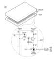
도 3은 본 개시의 실시예들에 따른 표시장치의 단면도이다. 보다 구체적으로, 도 3은 제1 서브픽셀(SP1)을 포함하는 영역의 단면도일 수 있다.3 is a cross-sectional view of a display device according to embodiments of the present disclosure. More specifically, FIG. 3 may be a cross-sectional view of an area including the first subpixel SP1.
도 3을 참고하면, 표시장치는 제1 서브픽셀(SP1), 기판(SUB), 평탄화층(PLN), 제1 전극(AE), 무기뱅크(BK), 발광층(EL) 및 제2 전극(CE)을 포함할 수 있다.Referring to FIG. 3, the display device includes a first subpixel (SP1), a substrate (SUB), a planarization layer (PLN), a first electrode (AE), an inorganic bank (BK), a light emitting layer (EL), and a second electrode ( CE) may be included.
제1 서브픽셀(SP1)은 도 1 및 도 2를 참고하여 설명한 표시영역(DA)에 위치하는 복수의 서브픽셀(SP) 중 하나일 수 있다. 제1 서브픽셀(SP1)은 제1 색상에 대응할 수 있다. 제1 서브픽셀(SP1)이 제1 색상에 대응한다는 것은, 제1 서브픽셀(SP1)이 제1 색상을 가지는 빛을 방출하는 것을 의미할 수 있다.The first subpixel SP1 may be one of a plurality of subpixels SP located in the display area DA described with reference to FIGS. 1 and 2 . The first subpixel SP1 may correspond to the first color. That the first subpixel SP1 corresponds to the first color may mean that the first subpixel SP1 emits light having the first color.
기판(SUB)은 트랜지스터 기판일 수 있다. 기판(SUB) 상에는 표시장치의 트랜지스터 형성부(transistor forming part)를 구성하는 다수의 절연막, 회로 소자 및 신호 배선이 위치할 수 있다.The substrate (SUB) may be a transistor substrate. A plurality of insulating films, circuit elements, and signal wires constituting a transistor forming part of the display device may be located on the substrate SUB.
기판(SUB) 상에는 버퍼층(BUF)이 위치하고, 버퍼층(BUF) 상에는 층간 절연막(ILD)이 위치할 수 있다.A buffer layer (BUF) may be located on the substrate (SUB), and an interlayer insulating layer (ILD) may be located on the buffer layer (BUF).
도 3에는 도시하지 않았으나, 버퍼층(BUF) 상에는 트랜지스터 등의 각종 회로소자와 신호배선이 위치할 수 있다. 버퍼층(BUF) 상에는 트랜지스터 등의 회로소자나 신호배선을 구성하는 메탈층(ML)이 위치할 수 있다. 기판(SUB) 상에는 트랜지스터와 중첩하여 트랜지스터의 하부에 위치하고, 트랜지스터의 액티브층을 보호할 수 있는 하부보호메탈(BSM)이 위치할 수 있다. 트랜지스터와 중첩하지 않고 위치하는 하부보호메탈(BSM)은 각종 회로소자나 신호배선을 구성할 수 있다.Although not shown in FIG. 3, various circuit elements such as transistors and signal wires may be located on the buffer layer (BUF). A metal layer (ML) constituting circuit elements such as transistors or signal wiring may be located on the buffer layer (BUF). A bottom protection metal (BSM) may be located on the substrate (SUB), overlapping with the transistor, located below the transistor, and protecting the active layer of the transistor. The bottom protection metal (BSM), which is located without overlapping the transistor, can form various circuit elements or signal wiring.
하부보호메탈(BSM)은 제1 개구부(OPN1) 및 제2 개구부(OPN2)와 중첩하지 않도록 위치할 수 있다. 하부보호메탈(BSM)이 제1 개구부(OPN1) 및 제2 개구부(OPN2)와 중첩하지 않도록 위치한다는 것은, 표시장치의 수직 단면 상에서 하부보호메탈(BSM)이 제1 개구부(OPN1) 및 제2 개구부(OPN2)와 수직적으로 중첩하지 않도록 위치한다는 것을 의미할 수 있다. 하부보호메탈(BSM)이 제1 개구부(OPN1) 및 제2 개구부(OPN2)와 중첩하지 않도록 위치함으로써, 표시장치가 더욱 우수한 효율 및 휘도를 가질 수 있다.The lower protection metal BSM may be positioned so as not to overlap the first opening OPN1 and the second opening OPN2. The fact that the lower protection metal (BSM) is positioned so as not to overlap the first opening (OPN1) and the second opening (OPN2) means that the lower protection metal (BSM) is located between the first opening (OPN1) and the second opening (OPN2) on the vertical cross-section of the display device. This may mean that it is positioned so as not to vertically overlap the opening (OPN2). By positioning the lower protection metal BSM so as not to overlap the first opening OPN1 and the second opening OPN2, the display device can have better efficiency and brightness.
평탄화층(PLN)은 기판(SUB) 상에 위치할 수 있다. 평탄화층(PLN)은 단일층 또는 다중층 구조일 수 있다. 예를 들어, 평탄화층(PLN)은, 제1 평탄화층(PLN1) 및 제1 평탄화층(PLN1) 상에 위치하는 제2 평탄화층(PLN2)을 포함할 수 있다.The planarization layer (PLN) may be located on the substrate (SUB). The planarization layer (PLN) may have a single-layer or multi-layer structure. For example, the planarization layer (PLN) may include a first planarization layer (PLN1) and a second planarization layer (PLN2) located on the first planarization layer (PLN1).
평탄화층(PLN)은 제1 서브픽셀(SP1)에서 제1 볼록부(CNV1), 제2 볼록부(CNV2), 슬릿부(SLT), 제1 경사면(SL1) 및 제2 경사면(SL2)을 포함할 수 있다.The planarization layer (PLN) includes a first convex portion (CNV1), a second convex portion (CNV2), a slit portion (SLT), a first inclined surface (SL1), and a second inclined surface (SL2) in the first subpixel (SP1). It can be included.
제1 볼록부(CNV1)는, 평탄화층(PLN)이 기판(SUB)으로부터 볼록하게 돌출된 부분으로서, 평탄화층(PLN)이 제1 서브픽셀(SP1)에서 포함하는 어느 하나의 볼록부를 의미할 수 있다. 보다 구체적으로, 제1 볼록부(CNV1)는 제1 서브픽셀(SP1)에서 평탄화층(PLN)의 돌출된 어느 한 평면을 의미할 수 있다.The first convex portion (CNV1) is a portion of the planarization layer (PLN) that protrudes convexly from the substrate (SUB), and may refer to any one of the convex portions that the planarization layer (PLN) includes in the first subpixel (SP1). You can. More specifically, the first convex portion CNV1 may refer to a plane that protrudes from the planarization layer PLN in the first subpixel SP1.
제2 볼록부(CNV2)는, 평탄화층(PLN)이 기판(SUB)으로부터 볼록하게 돌출된 부분으로서, 평탄화층(PLN)이 제1 서브픽셀(SP1)에서 포함하고 제1 볼록부(CNV1)와는 다른 하나의 볼록부를 의미할 수 있다. 보다 구체적으로, 제2 볼록부(CNV2)는 제1 서브픽셀(SP1)에서 평탄화층(PLN)의 돌출된 어느 한 평면으로서 제1 볼록부(CNV1)와는 이격한 평면을 의미할 수 있다.The second convex portion CNV2 is a portion of the planarization layer PLN that protrudes convexly from the substrate SUB. The planarization layer PLN includes the first subpixel SP1 and the first convex portion CNV1 It may mean a convex part different from the above. More specifically, the second convex part CNV2 may mean a plane that protrudes from the planarization layer PLN in the first subpixel SP1 and is spaced apart from the first convex part CNV1.
슬릿부(SLT)는 제1 볼록부(CNV1)와 제2 볼록부(CNV2) 사이에 위치할 수 있다. 슬릿부(SLT)는, 제1 볼록부(CNV1)와 제2 볼록부(CNV2) 사이에서 제1 볼록부(CNV1)와 제2 볼록부(CNV2)가 구분되도록 함몰된 평탄화층(PLN)의 일부분을 의미할 수 있다.The slit portion SLT may be located between the first convex portion CNV1 and the second convex portion CNV2. The slit portion (SLT) is a flattening layer (PLN) that is recessed between the first and second convex portions (CNV1) and the second convex portion (CNV2) to distinguish the first and second convex portions (CNV1) and It may mean part of it.
슬릿부(SLT)는, 제3 경사면(SL3)을 포함할 수 있다. 제3 경사면(SL3)은, 발광층(EL)에서 생성된 빛(L1, L2) 중 일부(L2)를 표시장치의 외부로 추출할 수 있게 하는 각도를 가질 수 있다. 예를 들면, 제3 경사면(SL3)은 제1 볼록부(CNV1) 및 제2 볼록부(CNV2)가 기판(SUB)에서 멀어질수록 가늘어지는 형태를 가지도록 하는 각도를 가질 수 있다. 상술한 제3 경사면(SL3)의 각도는, 제1 볼록부(CNV1) 또는 제2 볼록부(CNV2)와 제3 경사면(SL3)이 이루는 각도로 정의될 수 있다. 슬릿부(SLT)가 제3 경사면을 포함함으로써, 제1 서브픽셀(SP1)이 이른바 내부 미러 구조를 가질 수 있어 표시장치가 우수한 광 효율을 가질 수 있다.The slit portion SLT may include a third inclined surface SL3. The third inclined surface SL3 may have an angle that allows some (L2) of the light (L1, L2) generated in the light emitting layer (EL) to be extracted to the outside of the display device. For example, the third inclined surface SL3 may have an angle such that the first and second convex portions CNV1 and CNV2 become thinner as they move away from the substrate SUB. The angle of the third inclined surface SL3 described above may be defined as the angle formed by the first or second convex part CNV1 or CNV2 and the third inclined surface SL3. Since the slit portion SLT includes a third inclined surface, the first subpixel SP1 can have a so-called internal mirror structure, so that the display device can have excellent light efficiency.
제3 경사면(SL3)은 제1 개구부(OPN1)와 제2 개구부(OPN2) 사이에 위치할 수 있다. 제3 경사면(SL3)이 제1 개구부(OPN1)와 제2 개구부(OPN2) 사이에 위치함으로써, 제3 경사면(SL3) 상에 위치하는 제2 전극(CE)이 제1 개구부(OPN1) 및 제2 개구부(OPN2)를 통해 방출되는 빛의 일부를 표시장치 외부로 추출할 수 있다.The third inclined surface SL3 may be located between the first opening OPN1 and the second opening OPN2. Since the third inclined surface SL3 is located between the first opening OPN1 and the second opening OPN2, the second electrode CE located on the third inclined surface SL3 is positioned between the first opening OPN1 and the second opening OPN2. 2 Part of the light emitted through the opening (OPN2) can be extracted to the outside of the display device.
제1 경사면(SL1)은 제1 볼록부(CNV1)의 외곽에 위치할 수 있다. 제1 경사면(SL1)은, 제1 볼록부(CNV1)의 일부분을 둘러싸고 위치할 수 있다. 예를 들어, 제1 경사면(SL1)과 슬릿부(SLT)는 제1 볼록부(CNV1)의 전부를 둘러싸고 위치할 수 있다. 제1 경사면(SL1)이 상술한 것처럼 위치함으로써, 제1 경사면(SL1) 상에 위치하는 제2 전극(CE)이 발광층(EL)에서 생성된 빛을 표시장치 외부로 효과적으로 추출할 수 있다.The first inclined surface SL1 may be located outside the first convex portion CNV1. The first inclined surface SL1 may be located surrounding a portion of the first convex portion CNV1. For example, the first inclined surface SL1 and the slit portion SLT may be located surrounding the entire first convex portion CNV1. When the first inclined surface SL1 is positioned as described above, the second electrode CE located on the first inclined surface SL1 can effectively extract light generated in the light emitting layer EL to the outside of the display device.
제2 경사면(SL2)은 제2 볼록부(CNV2)의 외곽에 위치할 수 있다. 제2 경사면(SL2)은 제2 볼록부(CNV2)의 일부분을 둘러싸고 위치할 수 있다. 예를 들어, 제2 경사면(SL2)과 슬릿부(SLT)는 제2 볼록부(CNV2)의 전부를 둘러싸고 위치할 수 있다. 제2 경사면(SL2)이 상술한 것처럼 위치함으로써, 제2 경사면(SL2) 상에 위치하는 제2 전극(CE)이 발광층(EL)에서 생성된 빛을 표시장치 외부로 효과적으로 추출할 수 있다.The second inclined surface SL2 may be located outside the second convex portion CNV2. The second inclined surface SL2 may be located surrounding a portion of the second convex portion CNV2. For example, the second inclined surface SL2 and the slit portion SLT may be located surrounding the entire second convex portion CNV2. By positioning the second inclined surface SL2 as described above, the second electrode CE located on the second inclined surface SL2 can effectively extract light generated in the light emitting layer EL to the outside of the display device.
본 개시의 실시예들이 개구부의 외곽에 위치하는 경사면에서 빛을 반사하여 표시장치의 외부로 빛을 추출하는 구조를 본 개시에서는 측면 미러 구조라고 지칭할 수 있다. 또한, 본 개시의 실시예들에서 상술한 슬릿부가 복수의 개구부들 사이에 위치하고 슬릿부의 경사면이 빛을 반사하여 표시장치의 외부로 빛을 추출하는 구조를 본 개시에서는 분할된 측면 미러 구조라고 지칭할 수 있다.In embodiments of the present disclosure, a structure that reflects light on an inclined surface located on the outside of the opening and extracts light to the outside of the display device may be referred to as a side mirror structure in the present disclosure. In addition, in the embodiments of the present disclosure, the structure in which the above-described slit is located between a plurality of openings and the inclined surface of the slit reflects light to extract light to the outside of the display device is referred to as a divided side mirror structure in the present disclosure. You can.
제1 전극(AE)은 평탄화층(PLN) 상에 위치할 수 있다. 제1 전극(AE)은 애노드 전극일 수 있다. 또한, 제1 전극(AE)은 투명 전극일 수 있다.The first electrode (AE) may be located on the planarization layer (PLN). The first electrode (AE) may be an anode electrode. Additionally, the first electrode AE may be a transparent electrode.
제1 전극(AE)은, 제1 볼록부(CNV1), 제2 볼록부(CNV2), 슬릿부(SLT), 제1 경사면(SL1) 및 제2 경사면(SL2) 상에 위치할 수 있다. 이러한 예시에서, 제1 전극(AE)이 위치하는 영역은 슬릿부(SLT)에 의해 분할될 수 있다.The first electrode AE may be located on the first convex part CNV1, the second convex part CNV2, the slit part SLT, the first inclined surface SL1, and the second inclined surface SL2. In this example, the area where the first electrode AE is located may be divided by the slit portion SLT.
무기뱅크(BK)는 제1 개구부(OPN1) 및 제2 개구부(OPN2)를 포함할 수 있다. 무기뱅크(BK)는, 복수의 홀(hole)을 포함할 수 있다. 제1 개구부(OPN1) 및 제2 개구부(OPN2)는, 각각 무기뱅크(BK)가 포함하는 복수의 홀 중 어느 하나로서 제1 서브픽셀(SP1)에서 포함하는 홀일 수 있다.The inorganic bank BK may include a first opening OPN1 and a second opening OPN2. The inorganic bank BK may include a plurality of holes. The first opening OPN1 and the second opening OPN2 may each be one of a plurality of holes included in the inorganic bank BK and may be a hole included in the first subpixel SP1.
제1 개구부(OPN1)는 제1 볼록부(CNV1)에 대응하여 위치할 수 있다. 이러한 예시에서, 제1 개구부(OPN1)는 제1 볼록부(CNV1)와 중첩하여 위치할 수 있다.The first opening OPN1 may be located corresponding to the first convex part CNV1. In this example, the first opening OPN1 may be positioned overlapping the first convex part CNV1.
제2 개구부(OPN2)는 제2 볼록부(CNV2)에 대응하여 위치할 수 있다. 이러한 예시에서, 제2 개구부(OPN2)는 제2 볼록부(CNV2)와 중첩하여 위치할 수 있다.The second opening OPN2 may be located corresponding to the second convex part CNV2. In this example, the second opening OPN2 may be positioned overlapping the second convex part CNV2.
무기뱅크(BK)는 제1 전극(AE) 상에 위치할 수 있다. 무기뱅크(BK)가 제1 전극(AE) 상에 위치함으로써, 제1 개구부(OPN1) 및 제2 개구부(OPN2)에 의해 제1 전극(AE)의 일부가 노출될 수 있다.The inorganic bank (BK) may be located on the first electrode (AE). As the inorganic bank BK is positioned on the first electrode AE, a portion of the first electrode AE may be exposed through the first opening OPN1 and the second opening OPN2.
무기뱅크(BK)는 제1 볼록부(CNV1)의 일부와 중첩하여 위치하고, 제2 볼록부(CNV2)의 일부와 중첩하여 위치할 수 있다. 즉, 무기뱅크(BK)는 제1 경사면(SL1), 제2 경사면(SL2) 및 제3 경사면(SL3)과 중첩하여 위치하되, 제1 볼록부(CNV1) 및 제2 볼록부(CNV2)와 중첩하는 약간의 마진을 두고 위치할 수 있다. 무기뱅크(BK)는 제1 볼록부(CNV1) 및 제2 볼록부(CNV2)의 상면의 일부에 위치하고, 각각 제1 경사면(SL1) 및 제2 경사면(SL2)의 방향으로 연장되어, 제2 평탄화층(PLN2)의 상부에 위치할 수 있다. 슬릿부(SLT)에 배치되는 무기뱅크(BK)는 제1 볼록부(CNV1)의 상면의 일부에서부터 제3 경사면(SL3)을 따라 위치하고, 제2 볼록부(CNV2)의 상면의 일부에까지 연속적으로 연장된다. 무기뱅크(BK)가 제1 볼록부(CNV1) 및 제2 볼록부(CNV2) 일부와 중첩하여 위치할 경우, 발광층(EL)의 두께 편차로 인한 전류 쏠림 현상에 의해 발광소자가 열화되는 것을 경감할 수 있다. 또한, 슬릿부(SLT)에 의한 비발광영역을 최소화하기 위하여, 제3 경사면(SL3) 상에 배치되는 무기뱅크(BK)의 폭, 즉 슬릿부(SLT)의 폭은 제1 경사면(SL1) 및 제2 경사면(SL2)에 배치되는 무기뱅크(BK)의 폭 보다 크기가 작다. 제1 평탄화층(PLN1)과 접하는 슬릿부(SLT)의 폭은 제3 경사면(SL3)의 폭과 크기가 동일하거나 작을 수 있다.The inorganic bank BK may be positioned overlapping a portion of the first convex portion CNV1 and may be positioned overlapping a portion of the second convex portion CNV2. That is, the weapon bank BK is located overlapping the first inclined surface SL1, the second inclined surface SL2, and the third inclined surface SL3, and includes the first convex portion CNV1 and the second convex portion CNV2. They can be positioned with a slight margin of overlap. The inorganic bank BK is located on a portion of the upper surface of the first convex portion CNV1 and the second convex portion CNV2, extends in the direction of the first inclined surface SL1 and the second inclined surface SL2, respectively, and It may be located on top of the planarization layer (PLN2). The inorganic bank (BK) disposed in the slit portion (SLT) is located along the third inclined surface (SL3) from a portion of the upper surface of the first convex portion (CNV1) and continuously extends to a portion of the upper surface of the second convex portion (CNV2). It is extended. When the inorganic bank (BK) is located overlapping with a portion of the first convex portion (CNV1) and the second convex portion (CNV2), deterioration of the light emitting device due to current concentration due to thickness deviation of the light emitting layer (EL) is reduced. can do. In addition, in order to minimize the non-emission area caused by the slit portion (SLT), the width of the inorganic bank (BK) disposed on the third inclined surface (SL3), that is, the width of the slit portion (SLT) is determined by the first inclined surface (SL1). And the size is smaller than the width of the weapon bank (BK) disposed on the second inclined surface (SL2). The width of the slit portion (SLT) in contact with the first planarization layer (PLN1) may be the same or smaller than the width of the third inclined surface (SL3).
무기뱅크(BK)의 재질은 특별히 제한되는 것은 아니며, 뱅크(BK) 또는 화소정의막으로 사용될 수 있는 무기재료를 사용할 수 있다. 예를 들면, 무기뱅크(BK)는 산화규소(SiO2)를 포함할 수 있다. 표시장치가 무기뱅크(BK)를 포함할 경우, 유기물을 포함하는 뱅크보다 뱅크를 더욱 얇게 형성할 수 있으므로, 무기뱅크(BK)를 통과하여 방출되는 빛의 파장이 쉬프트되는 것을 경감할 수 있다. 제1 전극(AE)이 3중층, 즉 ITO/Ag/ITO로 형성되는 경우, 무기뱅크(BK)를 형성하거나 패터닝하는 dry etch 공정 중에 dry etch gas 침투에 의하여 제1 전극(AE)의 Ag층에 damage를 가할 수 있다. 하지만 본 개시의 실시예서와 같은 ITO 단일층으로 이루어지는 제1 전극(AE) 상에는 무기뱅크(BK)를 형성해도 damage가 없거나 최소화 가능하다.The material of the inorganic bank (BK) is not particularly limited, and any inorganic material that can be used as the bank (BK) or the pixel defining layer can be used. For example, the inorganic bank (BK) may include silicon oxide (SiO2 ). When the display device includes an inorganic bank (BK), the bank can be formed to be thinner than a bank containing organic materials, thereby reducing the shift of the wavelength of light emitted through the inorganic bank (BK). When the first electrode (AE) is formed of a triple layer, that is, ITO/Ag/ITO, the Ag layer of the first electrode (AE) is damaged by dry etch gas penetration during the dry etch process of forming or patterning the inorganic bank (BK). Can cause damage. However, even if an inorganic bank (BK) is formed on the first electrode (AE) made of a single layer of ITO as in the embodiment of the present disclosure, no damage or damage can be minimized.
발광층(EL)은 제1 개구부(OPN1) 및 제2 개구부(OPN2)에 의해 노출된 제1 전극(AE) 상에 위치할 수 있다. 이러한 예시에서, 발광층(EL)은 제1 개구부(OPN1)에 의해 노출된 제1 전극(AE)의 일부분과 제2 개구부(OPN2)에 의해 노출된 제1 전극(AE)의 일부분에 접촉할 수 있다. 또한, 발광층(EL)은 무기뱅크(BK) 상에 위치할 수 있다.The light emitting layer EL may be located on the first electrode AE exposed by the first opening OPN1 and the second opening OPN2. In this example, the light emitting layer EL may contact the portion of the first electrode AE exposed by the first opening OPN1 and the portion of the first electrode AE exposed by the second opening OPN2. there is. Additionally, the light emitting layer (EL) may be located on the inorganic bank (BK).
제2 전극(CE)은 발광층(EL) 상에 위치할 수 있다. 제2 전극(CE)은 제1 볼록부(CNV1), 제2 볼록부(CNV2), 슬릿부(SLT), 제1 경사면(SL1) 및 제2 경사면(SL2)과 중첩하여 위치할 수 있다. 이러한 예시에서, 제2 전극(CE)은 반사전극일 수 있다. 제2 전극(CE)이 경사면(SL1, SL2)과 중첩하여 위치함으로써, 발광층(EL)에서 생성된 빛을 제2 전극(CE)이 반사하여 표시장치 외부로 더욱 효과적으로 추출할 수 있다. 제2 전극(CE)은, 표시영역 전체에 공통적으로 증착될 수 있다.The second electrode (CE) may be located on the light emitting layer (EL). The second electrode CE may be positioned overlapping the first convex part CNV1, the second convex part CNV2, the slit part SLT, the first inclined surface SL1, and the second inclined surface SL2. In this example, the second electrode CE may be a reflective electrode. Since the second electrode CE is positioned overlapping the slopes SL1 and SL2, the light generated in the light emitting layer EL can be reflected by the second electrode CE to be more effectively extracted to the outside of the display device. The second electrode CE may be commonly deposited over the entire display area.
표시장치는 컬러필터(CF)를 추가로 포함할 수 있다. 컬러필터(CF)는 기판(SUB)과 평탄화층(PLN) 사이에 위치할 수 있다. 표시장치가 컬러필터(CF)를 포함함으로써, 표시장치가 보다 우수한 색상 재현력을 가질 수 있다.The display device may additionally include a color filter (CF). The color filter (CF) may be located between the substrate (SUB) and the planarization layer (PLN). When the display device includes a color filter (CF), the display device can have better color reproduction.
도 4는 본 개시의 실시예들에 따른 표시장치의 단면도이다. 보다 구체적으로, 도 4는 본 개시의 실시예들에 따른 표시장치의 표시영역, 비표시영역과 패드부(PAD)의 단면도이다. 도 4에 도시한 표시장치에 대한 사항은 특별히 달리 설명하지 않는 한 앞서 도 3을 참고하여 설명한 표시장치의 대응되는 사항과 동일할 수 있다.4 is a cross-sectional view of a display device according to embodiments of the present disclosure. More specifically, FIG. 4 is a cross-sectional view of a display area, a non-display area, and a pad portion (PAD) of a display device according to embodiments of the present disclosure. Details of the display device shown in FIG. 4 may be the same as the corresponding details of the display device previously described with reference to FIG. 3 unless otherwise specified.
도 4를 참고하면, 버퍼층(BUF) 상에 제1 층간절연막(ILD1)이 위치하고, 제1 층간절연막(ILD1) 상에 제2 층간절연막(ILD2)이 위치할 수 있다.Referring to FIG. 4 , a first interlayer insulating film (ILD1) may be located on the buffer layer (BUF), and a second interlayer insulating film (ILD2) may be located on the first interlayer insulating film (ILD1).
표시장치는 트랜지스터(TR) 및 하부보호메탈(BSM)을 포함할 수 있다.The display device may include a transistor (TR) and a bottom protection metal (BSM).
트랜지스터(TR)는 기판(SUB)과 평탄화층(PLN) 사이에 위치할 수 있다. 트랜지스터(TR)는 버퍼층(BUF) 상에가 위치할 수 있다. 트랜지스터(TR)는, 소스-드레인 전극(SD), 게이트 전극(G) 및 액티브층(ACT)을 포함할 수 있다. 게이트 절연막(GI)은 액티브층(ACT)과 게이트 전극(G) 사이에 위치할 수 있다.The transistor TR may be located between the substrate SUB and the planarization layer PLN. The transistor TR may be located on the buffer layer BUF. The transistor TR may include a source-drain electrode (SD), a gate electrode (G), and an active layer (ACT). The gate insulating film (GI) may be located between the active layer (ACT) and the gate electrode (G).
하부보호메탈(BSM)은 기판(SUB) 상에 위치할 수 있다. 하부보호메탈(BSM)은 트랜지스터(TR) 하부에 위치할 수 있다. 하부보호메탈(BSM)은 트랜지스터(TR)와 중첩하여 위치할 수 있다. 보다 구체적으로, 하부보호메탈(BSM)은 트랜지스터(TR)의 액티브층(ACT)과 중첩하여 위치할 수 있다. 하부보호메탈(BSM)이 트랜지스터(TR)와 중첩하여 위치함으로써, 액티브층(ACT)이 표시장치 외부의 빛에 의해 열화되는 것을 예방할 수 있다.The bottom protection metal (BSM) may be located on the substrate (SUB). The bottom protection metal (BSM) may be located below the transistor (TR). The bottom protection metal (BSM) may be positioned overlapping the transistor (TR). More specifically, the bottom protection metal (BSM) may be positioned to overlap the active layer (ACT) of the transistor (TR). By positioning the lower protection metal (BSM) overlapping with the transistor (TR), the active layer (ACT) can be prevented from being deteriorated by light from outside the display device.
도 5는 본 개시의 실시예들에 따른 표시장치다. 보다 구체적으로, 도 5는 인접하여 위치하는 제1 서브픽셀(SP1), 제2 서브픽셀(SP2), 제3 서브픽셀(SP3) 및 제4 서브픽셀(SP4) 부분의 단면도이다. 도 5에 도시한 표시장치에 대한 사항은 특별히 달리 설명하지 않는 한 앞서 도 3을 참고하여 설명한 표시장치의 대응되는 사항과 동일할 수 있다.5 shows a display device according to embodiments of the present disclosure. More specifically, FIG. 5 is a cross-sectional view of the adjacent first subpixel (SP1), second subpixel (SP2), third subpixel (SP3), and fourth subpixel (SP4). Details of the display device shown in FIG. 5 may be the same as the corresponding details of the display device previously described with reference to FIG. 3 unless otherwise specified.
도 5를 참고하면, 제1 서브픽셀(SP1), 제2 서브픽셀(SP2), 제3 서브픽셀(SP3) 및 제4 서브픽셀(SP4)은 서로 다른 색상에 대응할 수 있다. 예를 들어, 제1 서브픽셀(SP1)은 적색에 대응하고, 제2 서브픽셀(SP2)은 녹색에 대응하고, 제3 서브픽셀(SP3)은 청색에 대응하며, 제4 서브픽셀(SP4)은 백색에 대응할 수 있다. 이러한 예시에서, 발광층(EL)은 제1 서브픽셀(SP1), 제2 서브픽셀(SP2), 제3 서브픽셀(SP3) 및 제4 서브픽셀(SP4)에서 모두 흰색 빛을 방출할 수 있다. 제1 서브픽셀(SP1)에는 제1 컬러필터(CF1)가 위치하고, 제2 서브픽셀(SP2)에는 제2 컬러필터(CF2)가 위치하며, 제3 서브픽셀(SP3)에는 제3 컬러필터가 위치할 수 있다. 제4 서브픽셀(SP4)에는 컬러필터가 위치하지 않을 수 있다. 이러한 예시에서, 제1 컬러필터(CF1)는 적색에 대응하고, 제2 컬러필터(CF2)는 녹색에 대응하고, 제3 컬러필터(CF3)는 청색에 대응할 수 있다. 즉, 제1 컬러필터(CF1)는 발광층(EL)에서 형성된 백색광을 적색으로 변환할 수 있으며, 제2 컬러필터(CF2)는 발광층(EL)에서 형성된 백색광을 녹색으로 변환할 수 있고, 제3 컬러필터(CF3)는 발광층(EL)에서 형성된 백색광을 청색으로 변환할 수 있다.Referring to FIG. 5, the first subpixel (SP1), the second subpixel (SP2), the third subpixel (SP3), and the fourth subpixel (SP4) may correspond to different colors. For example, the first subpixel (SP1) corresponds to red, the second subpixel (SP2) corresponds to green, the third subpixel (SP3) corresponds to blue, and the fourth subpixel (SP4) can correspond to white. In this example, the light emitting layer EL may emit white light in all of the first subpixel SP1, the second subpixel SP2, the third subpixel SP3, and the fourth subpixel SP4. The first color filter (CF1) is located in the first subpixel (SP1), the second color filter (CF2) is located in the second subpixel (SP2), and the third color filter is located in the third subpixel (SP3). can be located A color filter may not be located in the fourth subpixel SP4. In this example, the first color filter CF1 may correspond to red, the second color filter CF2 may correspond to green, and the third color filter CF3 may correspond to blue. That is, the first color filter CF1 can convert the white light formed in the light emitting layer EL into red, the second color filter CF2 can convert the white light formed in the light emitting layer EL into green, and the third color filter CF2 can convert the white light formed in the light emitting layer EL into green. The color filter (CF3) can convert white light formed in the light emitting layer (EL) into blue.
제1 서브픽셀(SP1), 제2 서브픽셀(SP2), 제3 서브픽셀(SP3) 및 제4 서브픽셀(SP4)은 모두 상술한 측면 미러 구조를 가질 수 있다. 또한, 제1 서브픽셀(SP1), 제2 서브픽셀(SP2), 제3 서브픽셀(SP3) 및 제4 서브픽셀(SP4)은 모두 상술한 분할된 측면 미러 구조를 가질 수 있다. 서로 상이한 색상에 대응하는 서브픽셀들이 모두 분할된 측면 미러 구조를 가질 경우, 표시장치가 보다 우수한 효율을 가질 수 있다.The first subpixel (SP1), the second subpixel (SP2), the third subpixel (SP3), and the fourth subpixel (SP4) may all have the above-described side mirror structure. Additionally, the first subpixel (SP1), the second subpixel (SP2), the third subpixel (SP3), and the fourth subpixel (SP4) may all have the above-described divided side mirror structure. When subpixels corresponding to different colors all have a divided side mirror structure, the display device can have better efficiency.
도 6은 본 개시의 실시예들에 따른 표시장치의 단면도이다. 보다 구체적으로, 도 6은 표시장치의 제1 서브픽셀 부분의 단면도이다. 도 6에 도시한 표시장치에 대한 사항은 특별히 달리 설명하지 않는 한 앞서 도 3을 참고하여 설명한 표시장치의 대응되는 사항과 동일할 수 있다.6 is a cross-sectional view of a display device according to embodiments of the present disclosure. More specifically, Figure 6 is a cross-sectional view of the first subpixel portion of the display device. Matters regarding the display device shown in FIG. 6 may be the same as the corresponding matters of the display device previously described with reference to FIG. 3 unless otherwise specified.
도 6을 참고하면, 하부보호메탈(BSM)은 제1 개구부(OPN1) 및 제2 개구부(OPN2)와 중첩하지 않도록 위치할 수 있다. 또한, 하부보호메탈(BSM)은 제1 경사면(SL1) 및 제2 경사면(SL2)과 중첩하지 않도록 위치할 수 있다. 도 6에서 하부보호메탈(BSM)은 제1 경사면(SL1)과는 제1 거리(d1)만큼 이격하여 위치하고, 제2 경사면(SL2)과는 제2 거리(d2)만큼 이격하여 위치할 수 있다. 하부보호메탈(BSM)이 제1 경사면(SL1) 및 제2 경사면(SL2)과 중첩하지 않도록 위치함으로써, 표시장치가 측면 시야각 방향에서 휘도가 저하되는 것을 경감할 수 있다. 또한, 하부보호메탈(BSM)이 제1 경사면(SL1) 및 제2 경사면(SL2)과 특정한 거리만큼 이격하여 위치할 경우, 경사면에 의해 형성되는 측면 미러 구조에 의해 추출되는 빛이 하부보호메탈(BSM)에 의해 차단되는 것을 예방할 수 있으므로, 측면 시야각 방향에서 휘도가 저하되는 것을 보다 더 경감할 수 있다.Referring to FIG. 6 , the lower protection metal BSM may be positioned so as not to overlap the first opening OPN1 and the second opening OPN2. Additionally, the lower protection metal BSM may be positioned so as not to overlap the first slope SL1 and the second slope SL2. In FIG. 6, the lower protection metal BSM may be positioned at a first distance d1 from the first inclined surface SL1 and a second distance d2 from the second inclined surface SL2. . By positioning the lower protection metal BSM so as not to overlap the first inclined surface SL1 and the second inclined surface SL2, a decrease in luminance of the display device in the side viewing angle direction can be reduced. In addition, when the lower protection metal (BSM) is positioned at a certain distance from the first inclined surface (SL1) and the second inclined surface (SL2), the light extracted by the side mirror structure formed by the inclined surface is transmitted to the lower protective metal (SL1) and the second inclined surface (SL2). Since blocking by the BSM can be prevented, the decrease in luminance in the side viewing angle direction can be further reduced.
도 7은 본 개시의 실시예들에 따른 표시장치의 단면도 및 평면도이다. 보다 구체적으로, 도 7은 표시장치의 제1 서브픽셀(SP1) 부분의 단면도 및 제1 서브픽셀(SP1)이 발광할 때의 평면도이다. 도 7에 도시한 표시장치에 대한 사항은 특별히 달리 설명하지 않는 한 앞서 도 6을 참고하여 설명한 표시장치의 대응되는 사항과 동일할 수 있다.7 is a cross-sectional view and a top view of a display device according to embodiments of the present disclosure. More specifically, FIG. 7 is a cross-sectional view of the first subpixel SP1 of the display device and a top view when the first subpixel SP1 emits light. Details of the display device shown in FIG. 7 may be the same as the corresponding details of the display device previously described with reference to FIG. 6 unless otherwise specified.
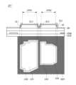
도 7을 참고하면, 표시장치는 제1 발광영역(EA1), 제2 발광영역(EA2), 제3 발광영역(EA3), 제4 발광영역(EA4) 및 비발광영역(NEA)을 포함할 수 있다. 제1 발광영역(EA1), 제2 발광영역(EA2), 제3 발광영역(EA3) 및 제4 발광영역(EA4)은 제1 서브픽셀(SP1)에 위치하므로, 서로 동일하거나 유사한 색상을 방출할 수 있다. 아울러, 좌우 시야각 개선 효과를 위하여, 제1 서브픽셀(SP1)을 길이가 긴 장변 방향으로 가로지르는 적어도 하나의 슬릿부(SLT)를 형성 할 수 있다. 이에 적어도 하나의 슬릿부(SLT)로 나뉘는 제1 서브픽셀(SP1)은 서로 다른 크기이거나 비대칭의 면적을 갖는 제1 개구부(OPN1)와 제2 개구부(OPN2)를 가질 수 있다. 도 7에서와 같이, 제1 개구부(OPN1) 및 제2 개구부(OPN2)의 각각의 폭은 제1 서브픽셀의 중간영역에서는 동일 할 수 있으나, 상부영역 또는 하부영역에서는 상이할 수 있다.Referring to FIG. 7, the display device may include a first light-emitting area (EA1), a second light-emitting area (EA2), a third light-emitting area (EA3), a fourth light-emitting area (EA4), and a non-light-emitting area (NEA). Since the first light-emitting area (EA1), the second light-emitting area (EA2), the third light-emitting area (EA3), and the fourth light-emitting area (EA4) are located in the first subpixel (SP1), they may emit the same or similar colors. In addition, in order to improve the left and right viewing angles, at least one slit portion (SLT) may be formed that crosses the first subpixel (SP1) in a long side direction. Accordingly, the first subpixel (SP1) divided by at least one slit portion (SLT) may have a first opening (OPN1) and a second opening (OPN2) having different sizes or asymmetrical areas. As in Fig. 7, the widths of each of the first opening (OPN1) and the second opening (OPN2) may be the same in the middle region of the first subpixel, but may be different in the upper region or the lower region.
제1 발광영역(EA1) 및 제2 발광영역(EA2)은 제1 서브픽셀(SP1)에 위치할 수 있다. 제1 발광영역(EA1) 및 제2 발광영역(EA2)은 제1 서브픽셀(SP1)의 주요 발광영역일 수 있다.The first emission area EA1 and the second emission area EA2 may be located in the first subpixel SP1. The first emission area EA1 and the second emission area EA2 may be the main emission areas of the first subpixel SP1.
제3 발광영역(EA3)은 제1 발광영역(EA1)의 외곽에 위치할 수 있다. 제4 발광영역(EA4)은 제2 발광영역(EA2)의 외곽에 위치할 수 있다. 제3 발광영역(EA3) 및 제4 발광영역(EA4)은 제1 서브픽셀(SP1)의 보조 발광영역일 수 있다.The third emission area EA3 may be located outside the first emission area EA1. The fourth emission area EA4 may be located outside the second emission area EA2. The third emission area EA3 and the fourth emission area EA4 may be auxiliary emission areas of the first subpixel SP1.
제1 발광영역(EA1)은 제1 개구부(OPN1)에 대응하여 위치하고, 제2 발광영역(EA2)은 제2 개구부(OPN2)에 대응하여 위치할 수 있다. 제3 발광영역(EA3)은 제1 경사면(SL1) 및 제3 경사면(SL3)에 대응하여 위치하고, 제4 발광영역(EA4)은 제2 경사면(SL2) 및 제3 경사면(SL3)에 대응하여 위치할 수 있다.The first light-emitting area EA1 may be located in correspondence with the first opening OPN1, and the second light-emitting area EA2 may be located in correspondence with the second opening OPN2. The third light-emitting area EA3 is located corresponding to the first slope SL1 and the third slope SL3, and the fourth light-emitting area EA4 is located corresponding to the second slope SL2 and the third slope SL3. can be located
제1 발광영역(EA1) 및 제2 발광영역(EA2)은 발광층(EL)에서 생성된 빛이 경사면과 중첩하여 위치하는 제2 전극에서 반사되지 않고 표시장치 외부로 방출되어 형성되는 발광영역일 수 있다. 제3 발광영역(EA3)은 발광층(EL)에서 생성된 빛이 제1 경사면(SL1) 또는 제3 경사면(SL3)과 중첩하여 위치하는 제2 전극에서 반사된 후 표시장치 외부로 방출되어 형성되는 발광영역일 수 있다. 제4 발광영역(EA4)은 발광층(EL)에서 생성된 빛이 제2 경사면(SL1) 또는 제3 경사면(SL3)과 중첩하여 위치하는 제2 전극에서 반사된 후 표시장치 외부로 방출되어 형성되는 발광영역일 수 있다.The first light-emitting area EA1 and the second light-emitting area EA2 may be light-emitting areas formed by the light generated in the light-emitting layer EL being emitted to the outside of the display device without being reflected by the second electrode located overlapping the inclined surface. there is. The third light-emitting area EA3 is formed by the light generated in the light-emitting layer EL being reflected from the second electrode positioned overlapping the first slope SL1 or the third slope SL3 and then emitted to the outside of the display device. It may be a light emitting area. The fourth light-emitting area EA4 is formed by the light generated in the light-emitting layer EL being reflected from the second electrode positioned overlapping the second slope SL1 or the third slope SL3 and then emitted to the outside of the display device. It may be a light emitting area.
제1 발광영역(EA1)과 제3 발광영역(EA3)은 색좌표 및 휘도 중 하나 이상이 서로 상이할 수 있다. 이는 제1 발광영역(EA1)에 도달하는 빛의 광경로와 제3 발광영역(EA3)에 도달하는 빛의 광경로는 무기뱅크(BK)의 통과 여부 측면에서 차이가 있기 때문이다.The first emission area EA1 and the third emission area EA3 may differ from each other in at least one of color coordinates and luminance. This is because there is a difference between the optical path of the light reaching the first emission area (EA1) and the optical path of the light reaching the third emission area (EA3) in terms of whether or not it passes through the inorganic bank (BK).
제2 발광영역(EA2)과 제4 발광영역(EA4)은 색좌표 및 휘도 중 하나 이상이 서로 상이할 수 있다. 이는 제2 발광영역(EA2)에 도달하는 빛의 광경로와 제4 발광영역(EA4)에 도달하는 빛의 광경로는 무기뱅크(BK)의 통과 여부 측면에서 차이가 있기 때문이다.The second emission area EA2 and the fourth emission area EA4 may differ from each other in at least one of color coordinates and luminance. This is because the optical path of the light reaching the second emission area EA2 and the optical path of the light reaching the fourth emission area EA4 are different in terms of whether or not the light passes through the inorganic bank BK.
제3 발광영역(EA3)은 제1 발광영역(EA1)과 접촉하여 연속적으로 위치할 수 있다. 또한, 제4 발광영역(EA4)은 제2 발광영역(EA2)과 접촉하여 연속적으로 위치할 수 있다. 본 개시의 실시예들에 따른 표시장치는 측면 미러 구조가 유기뱅크에 비해 두께가 얇은 무기뱅크(BK)를 포함하고, 하부보호메탈(BSM)이 개구부(OPN1, OPN2) 및 경사면(SLO1, SLO2)과 중첩하지 않도록 위치하므로, 보조 발광영역인 제3 발광영역(EA3) 및 제4 발광영역(EA4)이 주요 발광영역인 제1 발광영역(EA1) 및 제2 발광영역(EA2)과 이격하지 않고 접촉하여 연속적으로 위치할 수 있다.The third light-emitting area EA3 may be continuously positioned in contact with the first light-emitting area EA1. Additionally, the fourth light-emitting area EA4 may be continuously positioned in contact with the second light-emitting area EA2. The display device according to embodiments of the present disclosure includes an inorganic bank (BK) whose side mirror structure is thinner than the organic bank, and a lower protective metal (BSM) having openings (OPN1, OPN2) and inclined surfaces (SLO1, SLO2). ), so the auxiliary light-emitting areas, the third light-emitting area (EA3) and the fourth light-emitting area (EA4), are not separated from the main light-emitting areas, the first light-emitting area (EA1) and the second light-emitting area (EA2). It can be positioned continuously without contact.
도 8은 본 개시의 실시예들에 따른 표시장치의 단면도 및 평면도이다.8 is a cross-sectional view and a top view of a display device according to embodiments of the present disclosure.
도 8을 참고하면, 무기뱅크(BK)는 슬릿부(SLT)에서 하나의 컬러필터(CF1, CF2, CF3)와 중첩할 수 있다. 달리 말해서, 무기뱅크(BK)는 제1 서브픽셀(SP1), 제2 서브픽셀(SP2) 및 제3 서브픽셀(SP3)의 슬릿부(SLT)에서 컬러필터들(CF1, CF2, CF3) 중 하나와 중첩하여 위치할 수 있다. 백색에 대응하는 제4 서브픽셀(SP4)에서는 컬러필터가 위치하지 않으므로, 제4 서브픽셀(SP4)의 슬릿부(SLT)에서는 무기뱅크(BK)가 컬러필터와 중첩하지 않을 수 있다.Referring to FIG. 8, the inorganic bank (BK) may overlap one color filter (CF1, CF2, CF3) in the slit portion (SLT). In other words, the weapon bank (BK) is selected from among the color filters (CF1, CF2, CF3) in the slit portion (SLT) of the first subpixel (SP1), the second subpixel (SP2), and the third subpixel (SP3). It can be positioned overlapping with one other. Since the color filter is not located in the fourth subpixel SP4 corresponding to white, the inorganic bank BK may not overlap the color filter in the slit portion SLT of the fourth subpixel SP4.
제1 서브픽셀(SP1), 제2 서브픽셀(SP3), 제3 서브픽셀(SP3) 및 제4 서브픽셀(SP4) 에서 슬릿부(SLT)의 무기뱅크(BK)는 하부 배선과 중첩하지 않을 수 있다. 즉, 슬릿부(SLT)의 무기뱅크(BK)는 하부 배선인 하부보호메탈(BSM) 및 메탈층(ML)과는 중첩하지 않도록 위치할 수 있다.In the first subpixel (SP1), second subpixel (SP3), third subpixel (SP3) and fourth subpixel (SP4), the inorganic bank (BK) of the slit portion (SLT) does not overlap the lower wiring. You can. That is, the inorganic bank (BK) of the slit portion (SLT) may be positioned so as not to overlap with the lower protection metal (BSM) and metal layer (ML), which are lower wiring.
제1 경사면(SL1) 및 제2 경사면(SL2) 상에 위치하는 무기뱅크(BK)는 하부 배선과 중첩하여 위치할 수 있다. 또한, 제1 경사면(SL2) 및 제2 경사면(SL2) 상에 위치하는 무기뱅크(BK)는 적어도 하나의 컬러필터(CF1, CF2, CF3)와 중첩하여 위치할 수 있다.The inorganic bank BK located on the first inclined surface SL1 and the second inclined surface SL2 may be located overlapping the lower wiring. Additionally, the inorganic bank BK located on the first inclined surface SL2 and the second inclined surface SL2 may be located overlapping with at least one color filter CF1, CF2, and CF3.
이상에서 설명한 본 개시의 실시예들을 간략하게 설명하면 아래와 같다.The embodiments of the present disclosure described above are briefly described as follows.
표시장치(100)는 제1 서브픽셀(SP1), 기판(SUB), 평탄화층(PLN), 제1 전극(AE), 발광층(EL) 및 제2 전극(CE)을 포함할 수 있다.The
평탄화층(PLN)은 기판(SUB) 상에 위치할 수 있다. 평탄화층(PLN)은 제1 서브픽셀(SP1)에서 제1 볼록부(CNV1), 제2 볼록부(CNV2), 슬릿부(SLT), 제1 경사면(SL1) 및 제2 경사면(SL2)을 포함할 수 있다. 슬릿부(SLT)는 제1 볼록부(CNV1)와 제2 볼록부(CNV2) 사이에 위치할 수 있다. 제1 경사면(SL1)은 제1 볼록부(CNV1)의 외곽에 위치할 수 있다. 제2 경사면(SL2)은 제2 볼록부(CNV2)의 외곽에 위치할 수 있다.The planarization layer (PLN) may be located on the substrate (SUB). The planarization layer (PLN) includes a first convex portion (CNV1), a second convex portion (CNV2), a slit portion (SLT), a first inclined surface (SL1), and a second inclined surface (SL2) in the first subpixel (SP1). It can be included. The slit portion SLT may be located between the first convex portion CNV1 and the second convex portion CNV2. The first inclined surface SL1 may be located outside the first convex portion CNV1. The second inclined surface SL2 may be located outside the second convex portion CNV2.
제1 전극(AE)은 제1 볼록부(CNV1) 제2 볼록부(CNV2), 슬릿부(SLT), 제1 경사면(SL1) 및 제2 경사면(SL2) 상에 위치할 수 있다.The first electrode AE may be located on the first convex portion CNV1, the second convex portion CNV2, the slit portion SLT, the first inclined surface SL1, and the second inclined surface SL2.
무기뱅크(BK)는 제1 전극(AE) 상에 위치할 수 있다. 무기뱅크(BK)는 제1 개구부(OPN1) 및 제2 개구부(OPN2)를 포함할 수 있다. 제1 개구부(OPN1)는 제1 볼록부(CNV1)에 대응하여 위치할 수 있다. 제2 개구부(OPN2)는 제2 볼록부(CNV2)에 대응하여 위치할 수 있다.The inorganic bank (BK) may be located on the first electrode (AE). The inorganic bank BK may include a first opening OPN1 and a second opening OPN2. The first opening OPN1 may be located corresponding to the first convex part CNV1. The second opening OPN2 may be located corresponding to the second convex part CNV2.
발광층(EL)은 제1 개구부(OPN1) 및 제2 개구부(OPN2)에 의해 노출된 제1 전극(CE) 상에 위치할 수 있다. 또한, 발광층(EL)은 무기뱅크(BK) 상에 위치할 수 있다.The light emitting layer EL may be located on the first electrode CE exposed by the first opening OPN1 and the second opening OPN2. Additionally, the light emitting layer (EL) may be located on the inorganic bank (BK).
제2 전극(CE)은 발광층(EL) 상에 위치할 수 있다. 또한, 제2 전극(CE)은 제1 볼록부(CNV1) 제2 볼록부(CNV2), 슬릿부(SLT), 제1 경사면(SL1) 및 제2 경사면(SL2)과 중첩하여 위치할 수 있다.The second electrode (CE) may be located on the light emitting layer (EL). In addition, the second electrode CE may be positioned to overlap the first convex part CNV1, the second convex part CNV2, the slit part SLT, the first inclined surface SL1, and the second inclined surface SL2. .
제1 경사면(SL1)은 제1 개구부(OPN1)의 외곽에 위치할 수 있다. 제2 경사면(SL2)은 제2 개구부(OPN2)의 외곽에 위치할 수 있다.The first inclined surface SL1 may be located outside the first opening OPN1. The second inclined surface SL2 may be located outside the second opening OPN2.
슬릿부(SLT)는 제3 경사면(SL3)을 포함할 수 있다.The slit portion SLT may include a third inclined surface SL3.
제3 경사면(SL3)은 제1 개구부(OPN1)와 제2 개구부(OPN2) 사이에 위치할 수 있다.The third inclined surface SL3 may be located between the first opening OPN1 and the second opening OPN2.
무기뱅크(BK)는 제3 경사면(SL3)과 중첩하여 위치할 수 있다.The inorganic bank (BK) may be positioned overlapping the third slope (SL3).
무기뱅크(BK)는 제1 경사면(SL1) 및 제2 경사면(SL2)과 중첩하여 위치할 수 있다.The inorganic bank BK may be positioned overlapping the first inclined surface SL1 and the second inclined surface SL2.
제1 전극(AE)은 투명 전극이고, 제2 전극(CE)은 반사 전극일 수 있다.The first electrode (AE) may be a transparent electrode, and the second electrode (CE) may be a reflective electrode.
표시장치(100)는 컬러필터(CF)를 포함할 수 있다. 컬러필터(CF)는 기판(SUB)과 평탄화층(PLN) 사이에 위치할 수 있다.The
표시장치(100)는 트랜지스터(TR) 및 하부보호메탈(BSM)을 포함할 수 있다. 트랜지스터(TR)는 기판(SUB)과 평탄화층(PLN) 사이에 위치할 수 있다. 하부보호메탈(BSM)은 기판(SUB) 상에 위치하고, 트랜지스터(TR) 하부에 위치할 수 있다. 하부보호메탈(BSM)은 트랜지스터(TR)와 중첩하여 위치할 수 있다.The
하부보호메탈(BSM)은 제1 개구부(OPN1) 및 제2 개구부(OPN2)와 중첩하지 않도록 위치할 수 있다. 또한, 하부보호메탈(BSM)은 제1 경사면(SL1) 및 제2 경사면(SL2)과 중첩하지 않도록 위치할 수 있다.The lower protection metal BSM may be positioned so as not to overlap the first opening OPN1 and the second opening OPN2. Additionally, the lower protection metal BSM may be positioned so as not to overlap the first slope SL1 and the second slope SL2.
표시장치는 제1 발광영역(EA1), 제2 발광영역(EA2), 제3 발광영역(EA3), 제4 발광영역(EA4) 및 비발광영역(NEA)을 포함할 수 있다. 제1 발광영역(EA1) 및 제2 발광영역(EA2)은 제1 서브픽셀(SP1)에 위치할 수 있다.The display device may include a first emission area (EA1), a second emission area (EA2), a third emission area (EA3), a fourth emission area (EA4), and a non-emission area (NEA). The first emission area EA1 and the second emission area EA2 may be located in the first subpixel SP1.
제3 발광영역(EA3)은 제1 발광영역(EA1)의 외곽에 위치할 수 있다. 제4 발광영역(EA4)은 제2 발광영역(EA2)의 외곽에 위치할 수 있다.The third emission area EA3 may be located outside the first emission area EA1. The fourth emission area EA4 may be located outside the second emission area EA2.
제1 발광영역(EA1)은 제1 개구부(OPN1)에 대응하여 위치하고, 제2 발광영역(EA2)은 제2 개구부(OPN2)에 대응하여 위치할 수 있다. 제3 발광영역(EA3)은 제1 경사면(SL1) 및 제3 경사면(SL3)에 대응하여 위치하고, 제4 발광영역(EA4)은 제2 경사면(SL2) 및 제3 경사면(SL3)에 대응하여 위치할 수 있다.The first light-emitting area EA1 may be located in correspondence with the first opening OPN1, and the second light-emitting area EA2 may be located in correspondence with the second opening OPN2. The third light-emitting area EA3 is located corresponding to the first slope SL1 and the third slope SL3, and the fourth light-emitting area EA4 is located corresponding to the second slope SL2 and the third slope SL3. can be located
제3 발광영역(EA3)은 제1 발광영역(EA1)과 접촉하여 연속적으로 위치할 수 있다. 또한, 제4 발광영역(EA4)은 제2 발광영역(EA2)과 접촉하여 연속적으로 위치할 수 있다.The third light-emitting area EA3 may be continuously positioned in contact with the first light-emitting area EA1. Additionally, the fourth light-emitting area EA4 may be continuously positioned in contact with the second light-emitting area EA2.
이상의 설명은 본 개시의 기술 사상을 예시적으로 설명한 것에 불과한 것으로서, 본 개시가 속하는 기술 분야에서 통상의 지식을 가진 자라면 본 개시의 본질적인 특성에서 벗어나지 않는 범위에서 다양한 수정 및 변형이 가능할 것이다. 또한, 본 개시에 개시된 실시예들은 본 개시의 기술 사상을 한정하기 위한 것이 아니라 설명하기 위한 것이므로 이러한 실시예에 의하여 본 개시의 기술 사상의 범위가 한정되는 것은 아니다.The above description is merely an illustrative explanation of the technical idea of the present disclosure, and those skilled in the art will be able to make various modifications and variations without departing from the essential characteristics of the present disclosure. In addition, the embodiments disclosed in the present disclosure are not intended to limit the technical idea of the present disclosure, but rather are for explanation, and therefore the scope of the technical idea of the present disclosure is not limited by these embodiments.
100: 표시장치100: display device
Claims (14)
Translated fromKorean기판;
상기 기판 상에 위치하고, 상기 제1 서브픽셀에서 제1 볼록부, 제2 볼록부, 상기 제1 볼록부와 상기 제2 볼록부 사이에 위치하는 슬릿부, 상기 제1 볼록부의 외곽에 위치하는 제1 경사면 및 상기 제2 볼록부의 외곽에 위치하는 제2 경사면을 포함하는 평탄화층;
상기 제1 볼록부, 상기 제2 볼록부, 상기 슬릿부, 상기 제1 경사면 및 상기 제2 경사면 상에 위치하는 제1 전극;
상기 제1 전극 상에 위치하고, 상기 제1 볼록부에 대응하여 위치하는 제1 개구부 및 상기 제2 볼록부에 대응하여 위치하는 제2 개구부를 포함하는 무기뱅크;
상기 제1 개구부 및 상기 제2 개구부에 의해 노출된 상기 제1 전극 및 상기 무기뱅크 상에 위치하는 발광층; 및
상기 발광층 상에 위치하고, 상기 제1 볼록부, 상기 제2 볼록부, 상기 슬릿부, 상기 제1 경사면 및 상기 제2 경사면과 중첩하여 위치하는 제2 전극;을 포함하는 표시장치.
first subpixel;
Board;
Located on the substrate, a first convex portion, a second convex portion, a slit portion located between the first convex portion and the second convex portion in the first subpixel, and a second convex portion located outside the first convex portion. A planarization layer including one inclined surface and a second inclined surface located outside the second convex portion;
a first electrode positioned on the first convex portion, the second convex portion, the slit portion, the first inclined surface, and the second inclined surface;
an inorganic bank located on the first electrode and including a first opening located corresponding to the first convex portion and a second opening located corresponding to the second convex portion;
a light emitting layer located on the first electrode and the inorganic bank exposed by the first opening and the second opening; and
A display device comprising: a second electrode located on the light emitting layer and overlapping with the first convex portion, the second convex portion, the slit portion, the first inclined surface, and the second inclined surface.
상기 제1 경사면은 상기 제1 개구부의 외곽에 위치하고, 상기 제2 경사면은 상기 제2 개구부의 외곽에 위치하는 표시장치.
According to clause 1,
The first inclined surface is located on the outside of the first opening, and the second inclined surface is located on the outside of the second opening.
상기 슬릿부는 제3 경사면을 포함하는 표시장치.
According to clause 1,
A display device wherein the slit portion includes a third inclined surface.
상기 제3 경사면은 상기 제1 개구부와 상기 제2 개구부 사이에 위치하는 표시장치.
According to clause 3,
The third inclined surface is located between the first opening and the second opening.
상기 무기뱅크는 상기 제3 경사면과 중첩하여 위치하는 표시장치.
According to clause 3,
The weapon bank is a display device positioned to overlap the third inclined surface.
상기 무기뱅크는 상기 제1 경사면 및 상기 제2 경사면과 중첩하여 위치하는 표시장치.
According to clause 1,
A display device wherein the weapon bank is positioned overlapping the first inclined surface and the second inclined surface.
상기 제1 전극은 투명 전극이고,
상기 제2 전극은 반사 전극인 표시장치.
According to clause 1,
The first electrode is a transparent electrode,
A display device wherein the second electrode is a reflective electrode.
상기 기판과 상기 평탄화층 사이에 위치하는 컬러필터를 추가로 포함하는 표시장치.
According to clause 1,
A display device further comprising a color filter positioned between the substrate and the planarization layer.
상기 기판과 상기 평탄화층 사이에 위치하는 트랜지스터; 및
상기 기판 상에 위치하고 상기 트랜지스터 하부에 위치하며, 상기 트랜지스터와 중첩하여 위치하는 하부보호메탈을 추가로 포함하는 표시장치.
According to clause 1,
a transistor positioned between the substrate and the planarization layer; and
A display device located on the substrate and below the transistor, and further comprising a lower protection metal located overlapping with the transistor.
상기 하부보호메탈은 상기 제1 개구부 및 상기 제2 개구부와 중첩하지 않도록 위치하는 표시장치.
According to clause 9,
The display device wherein the lower protection metal is positioned so as not to overlap the first opening and the second opening.
상기 하부보호메탈은 상기 제1 경사면 및 상기 제2 경사면과 중첩하지 않도록 위치하는 표시장치.
According to clause 10,
The display device wherein the lower protection metal is positioned so as not to overlap the first inclined surface and the second inclined surface.
상기 제1 서브픽셀에 위치하는 제1 발광영역;
상기 제1 서브픽셀에 위치하는 제2 발광영역;
상기 제1 발광영역의 외곽에 위치하는 제3 발광영역;
상기 제2 발광영역의 외곽에 위치하는 제4 발광영역; 및
비발광영역을 포함하는 표시장치.
According to clause 1,
a first light emitting area located in the first subpixel;
a second light emitting area located in the first subpixel;
a third light-emitting area located outside the first light-emitting area;
a fourth light-emitting area located outside the second light-emitting area; and
A display device that includes a non-emissive area.
상기 제1 발광영역은 상기 제1 개구부에 대응하여 위치하고,
상기 제2 발광영역은 상기 제2 개구부에 대응하여 위치하며,
상기 제3 발광영역은 상기 제1 경사면 및 상기 제3 경사면에 대응하여 위치하고,
상기 제4 발광영역은 상기 제2 경사면 및 상기 제3 경사면에 대응하여 위치하는 표시장치.
According to clause 12,
The first light emitting area is located corresponding to the first opening,
The second light-emitting area is located corresponding to the second opening,
The third light emitting area is located corresponding to the first inclined surface and the third inclined surface,
The fourth light emitting area is located in correspondence with the second inclined surface and the third inclined surface.
상기 제3 발광영역은 상기 제1 발광영역과 접촉하여 연속적으로 위치하고,
상기 제4 발광영역은 상기 제2 발광영역과 접촉하여 연속적으로 위치하는 표시장치.
According to clause 12,
The third light-emitting area is continuously positioned in contact with the first light-emitting area,
The fourth light-emitting area is continuously positioned in contact with the second light-emitting area.
Priority Applications (3)
| Application Number | Priority Date | Filing Date | Title |
|---|---|---|---|
| KR1020230013023AKR20240120400A (en) | 2023-01-31 | 2023-01-31 | Display device |
| US18/510,280US20240260418A1 (en) | 2023-01-31 | 2023-11-15 | Display device |
| CN202311589350.1ACN118434231A (en) | 2023-01-31 | 2023-11-27 | Display device |
Applications Claiming Priority (1)
| Application Number | Priority Date | Filing Date | Title |
|---|---|---|---|
| KR1020230013023AKR20240120400A (en) | 2023-01-31 | 2023-01-31 | Display device |
Publications (1)
| Publication Number | Publication Date |
|---|---|
| KR20240120400Atrue KR20240120400A (en) | 2024-08-07 |
Family
ID=91963115
Family Applications (1)
| Application Number | Title | Priority Date | Filing Date |
|---|---|---|---|
| KR1020230013023APendingKR20240120400A (en) | 2023-01-31 | 2023-01-31 | Display device |
Country Status (3)
| Country | Link |
|---|---|
| US (1) | US20240260418A1 (en) |
| KR (1) | KR20240120400A (en) |
| CN (1) | CN118434231A (en) |
- 2023
- 2023-01-31KRKR1020230013023Apatent/KR20240120400A/enactivePending
- 2023-11-15USUS18/510,280patent/US20240260418A1/enactivePending
- 2023-11-27CNCN202311589350.1Apatent/CN118434231A/enactivePending
Also Published As
| Publication number | Publication date |
|---|---|
| US20240260418A1 (en) | 2024-08-01 |
| CN118434231A (en) | 2024-08-02 |
Similar Documents
| Publication | Publication Date | Title |
|---|---|---|
| JP7612736B2 (en) | Display Panel | |
| US10541385B2 (en) | Display device and method of manufacturing a display device | |
| KR102087102B1 (en) | Organic light emitting pannel and including organic light emitting display | |
| US11751437B2 (en) | Organic light emitting display panel and organic light emitting display device including the same | |
| KR20240120400A (en) | Display device | |
| KR20190080281A (en) | Display device | |
| US20240224735A1 (en) | Display device | |
| KR20240108072A (en) | Display device | |
| KR20240108080A (en) | Display device | |
| US20250280689A1 (en) | Display Device | |
| US20250017061A1 (en) | Light emitting display device | |
| KR20240076040A (en) | Display device | |
| JP2025078073A (en) | display device | |
| KR20240110424A (en) | Display device | |
| KR20240108054A (en) | Display apparatus | |
| KR20240105811A (en) | Displny panel and displny device | |
| KR20240120391A (en) | Display device | |
| CN120239480A (en) | Display device | |
| KR20240119763A (en) | Display panel and display device | |
| KR20240110124A (en) | Display panel and display device | |
| KR20240117707A (en) | Display device and display panel | |
| KR20240108055A (en) | Display apparatus | |
| KR20240102570A (en) | Display apparatus | |
| KR20250034705A (en) | Display device | |
| KR20250071953A (en) | Display device, and method of manufacturing the same |
Legal Events
| Date | Code | Title | Description |
|---|---|---|---|
| PA0109 | Patent application | Patent event code:PA01091R01D Comment text:Patent Application Patent event date:20230131 | |
| PG1501 | Laying open of application |