KR20240107995A - Display device including gate driving circuit - Google Patents
Display device including gate driving circuitDownload PDFInfo
- Publication number
- KR20240107995A KR20240107995AKR1020220191160AKR20220191160AKR20240107995AKR 20240107995 AKR20240107995 AKR 20240107995AKR 1020220191160 AKR1020220191160 AKR 1020220191160AKR 20220191160 AKR20220191160 AKR 20220191160AKR 20240107995 AKR20240107995 AKR 20240107995A
- Authority
- KR
- South Korea
- Prior art keywords
- scan
- voltage
- signal
- clock signal
- display device
- Prior art date
- Legal status (The legal status is an assumption and is not a legal conclusion. Google has not performed a legal analysis and makes no representation as to the accuracy of the status listed.)
- Pending
Links
Images


Classifications
- G—PHYSICS
- G09—EDUCATION; CRYPTOGRAPHY; DISPLAY; ADVERTISING; SEALS
- G09G—ARRANGEMENTS OR CIRCUITS FOR CONTROL OF INDICATING DEVICES USING STATIC MEANS TO PRESENT VARIABLE INFORMATION
- G09G3/00—Control arrangements or circuits, of interest only in connection with visual indicators other than cathode-ray tubes
- G09G3/20—Control arrangements or circuits, of interest only in connection with visual indicators other than cathode-ray tubes for presentation of an assembly of a number of characters, e.g. a page, by composing the assembly by combination of individual elements arranged in a matrix no fixed position being assigned to or needed to be assigned to the individual characters or partial characters
- G09G3/22—Control arrangements or circuits, of interest only in connection with visual indicators other than cathode-ray tubes for presentation of an assembly of a number of characters, e.g. a page, by composing the assembly by combination of individual elements arranged in a matrix no fixed position being assigned to or needed to be assigned to the individual characters or partial characters using controlled light sources
- G09G3/30—Control arrangements or circuits, of interest only in connection with visual indicators other than cathode-ray tubes for presentation of an assembly of a number of characters, e.g. a page, by composing the assembly by combination of individual elements arranged in a matrix no fixed position being assigned to or needed to be assigned to the individual characters or partial characters using controlled light sources using electroluminescent panels
- G09G3/32—Control arrangements or circuits, of interest only in connection with visual indicators other than cathode-ray tubes for presentation of an assembly of a number of characters, e.g. a page, by composing the assembly by combination of individual elements arranged in a matrix no fixed position being assigned to or needed to be assigned to the individual characters or partial characters using controlled light sources using electroluminescent panels semiconductive, e.g. using light-emitting diodes [LED]
- G09G3/3208—Control arrangements or circuits, of interest only in connection with visual indicators other than cathode-ray tubes for presentation of an assembly of a number of characters, e.g. a page, by composing the assembly by combination of individual elements arranged in a matrix no fixed position being assigned to or needed to be assigned to the individual characters or partial characters using controlled light sources using electroluminescent panels semiconductive, e.g. using light-emitting diodes [LED] organic, e.g. using organic light-emitting diodes [OLED]
- G09G3/3266—Details of drivers for scan electrodes
- G—PHYSICS
- G09—EDUCATION; CRYPTOGRAPHY; DISPLAY; ADVERTISING; SEALS
- G09G—ARRANGEMENTS OR CIRCUITS FOR CONTROL OF INDICATING DEVICES USING STATIC MEANS TO PRESENT VARIABLE INFORMATION
- G09G3/00—Control arrangements or circuits, of interest only in connection with visual indicators other than cathode-ray tubes
- G09G3/20—Control arrangements or circuits, of interest only in connection with visual indicators other than cathode-ray tubes for presentation of an assembly of a number of characters, e.g. a page, by composing the assembly by combination of individual elements arranged in a matrix no fixed position being assigned to or needed to be assigned to the individual characters or partial characters
- G09G3/34—Control arrangements or circuits, of interest only in connection with visual indicators other than cathode-ray tubes for presentation of an assembly of a number of characters, e.g. a page, by composing the assembly by combination of individual elements arranged in a matrix no fixed position being assigned to or needed to be assigned to the individual characters or partial characters by control of light from an independent source
- G09G3/36—Control arrangements or circuits, of interest only in connection with visual indicators other than cathode-ray tubes for presentation of an assembly of a number of characters, e.g. a page, by composing the assembly by combination of individual elements arranged in a matrix no fixed position being assigned to or needed to be assigned to the individual characters or partial characters by control of light from an independent source using liquid crystals
- G09G3/3611—Control of matrices with row and column drivers
- G09G3/3674—Details of drivers for scan electrodes
- G—PHYSICS
- G09—EDUCATION; CRYPTOGRAPHY; DISPLAY; ADVERTISING; SEALS
- G09G—ARRANGEMENTS OR CIRCUITS FOR CONTROL OF INDICATING DEVICES USING STATIC MEANS TO PRESENT VARIABLE INFORMATION
- G09G2310/00—Command of the display device
- G09G2310/02—Addressing, scanning or driving the display screen or processing steps related thereto
- G09G2310/0264—Details of driving circuits
- G09G2310/0267—Details of drivers for scan electrodes, other than drivers for liquid crystal, plasma or OLED displays
- G—PHYSICS
- G09—EDUCATION; CRYPTOGRAPHY; DISPLAY; ADVERTISING; SEALS
- G09G—ARRANGEMENTS OR CIRCUITS FOR CONTROL OF INDICATING DEVICES USING STATIC MEANS TO PRESENT VARIABLE INFORMATION
- G09G2310/00—Command of the display device
- G09G2310/02—Addressing, scanning or driving the display screen or processing steps related thereto
- G09G2310/0264—Details of driving circuits
- G09G2310/0289—Details of voltage level shifters arranged for use in a driving circuit
- G—PHYSICS
- G09—EDUCATION; CRYPTOGRAPHY; DISPLAY; ADVERTISING; SEALS
- G09G—ARRANGEMENTS OR CIRCUITS FOR CONTROL OF INDICATING DEVICES USING STATIC MEANS TO PRESENT VARIABLE INFORMATION
- G09G2310/00—Command of the display device
- G09G2310/08—Details of timing specific for flat panels, other than clock recovery
- G—PHYSICS
- G09—EDUCATION; CRYPTOGRAPHY; DISPLAY; ADVERTISING; SEALS
- G09G—ARRANGEMENTS OR CIRCUITS FOR CONTROL OF INDICATING DEVICES USING STATIC MEANS TO PRESENT VARIABLE INFORMATION
- G09G2320/00—Control of display operating conditions
- G09G2320/02—Improving the quality of display appearance
- G09G2320/0233—Improving the luminance or brightness uniformity across the screen
- G—PHYSICS
- G09—EDUCATION; CRYPTOGRAPHY; DISPLAY; ADVERTISING; SEALS
- G09G—ARRANGEMENTS OR CIRCUITS FOR CONTROL OF INDICATING DEVICES USING STATIC MEANS TO PRESENT VARIABLE INFORMATION
- G09G2320/00—Control of display operating conditions
- G09G2320/04—Maintaining the quality of display appearance
- G09G2320/043—Preventing or counteracting the effects of ageing
Landscapes
- Engineering & Computer Science (AREA)
- Physics & Mathematics (AREA)
- Computer Hardware Design (AREA)
- General Physics & Mathematics (AREA)
- Theoretical Computer Science (AREA)
- Chemical & Material Sciences (AREA)
- Crystallography & Structural Chemistry (AREA)
- Control Of Indicators Other Than Cathode Ray Tubes (AREA)
Abstract
Description
Translated fromKorean본 발명은 게이트 구동 회로를 포함하는 표시 장치에 관한 것이다.The present invention relates to a display device including a gate driving circuit.
정보화 사회가 발전함에 따라 표시 장치에 대한 요구가 다양한 형태로 증가하고 있으며, 근래에는 액정 표시 장치, 유기 발광 표시 장치 등과 같은 다양한 표시 장치가 활용되고 있다.As the information society develops, the demand for display devices in various forms is increasing, and in recent years, various display devices such as liquid crystal displays and organic light emitting display devices have been used.
일반적인 표시 장치는 화소 각각에 배치된 스토리지 커패시터를 영상 신호에 대응하여 충전시키고 이를 통해 영상을 표시하도록 구동될 수 있다. 이러한 화소에서의 충전이 부족한 현상이 발생하면 영상 품질이 저하되는 문제가 초래될 수 있다.A typical display device can be driven to display an image by charging a storage capacitor placed in each pixel in response to an image signal. If insufficient charging occurs in these pixels, image quality may deteriorate.
최근에는 표시 장치의 베젤 영역(비표시 영역)의 크기를 최소화하여 디자인 설계의 자유도를 높이고 휴대성을 향상시키려는 노력이 증가하고 있다. 일 예로, 화소들에 스캔 신호를 인가하는 게이트 구동 회로의 사이즈를 줄이는 기술이 개발되고 있다. 이를 통해, 하나의 스테이지 회로에서 복수 개의 게이트 라인들로 스캔 신호들을 출력할 수 있다. 그러나 이러한 구조에서, 스캔 신호들의 출력 특성 편차로 인해 화소들의 충전 시간이 부족해질 수 있고, 상술한 영상 품질 저하 문제가 발생할 수 있다.Recently, efforts have been increasing to increase freedom of design and improve portability by minimizing the size of the bezel area (non-display area) of display devices. For example, technology is being developed to reduce the size of a gate driving circuit that applies scan signals to pixels. Through this, scan signals can be output from a single stage circuit to a plurality of gate lines. However, in this structure, the charging time of the pixels may be insufficient due to variations in the output characteristics of the scan signals, and the above-described image quality degradation problem may occur.
실시 예들은, 스캔 신호들 간의 출력 특성 편차를 감소시킬 수 있도록 스캔 클럭 신호를 제어하는 게이트 구동 회로를 포함하는 표시 장치를 제공한다.Embodiments provide a display device including a gate driving circuit that controls a scan clock signal to reduce output characteristic deviation between scan signals.
또한, 실시 예들은, 스캔 신호들 간의 출력 특성 편차를 감소시키면서, 오버랩 게이트 구동 및 Q 노드 공유 구조를 갖는 게이트 구동 회로를 포함하는 표시 장치를 제공한다.Additionally, embodiments provide a display device including a gate driving circuit having an overlap gate driving and Q node sharing structure while reducing output characteristic deviation between scan signals.
일 실시 예에 따른 표시 장치는,복수의 화소들을 포함하여 영상을 표시하는 표시 패널, 상기 복수의 화소들로 데이터 전압을 인가하는 데이터 구동 회로, 상기 표시 패널의 게이트 라인들로 스캔 신호들을 출력하는 게이트 구동 회로, 상기 스캔 신호들을 생성하기 위한 스캔 클럭 신호들을 출력하는 레벨 시프터 및 상기 스캔 클럭 신호들의 펄스 폭을 제어하기 위한 제어 클럭 신호를 출력하는 컨트롤러를 포함할 수 있다.A display device according to an embodiment includes a display panel that displays an image including a plurality of pixels, a data driving circuit that applies a data voltage to the plurality of pixels, and a device that outputs scan signals to gate lines of the display panel. It may include a gate driving circuit, a level shifter outputting scan clock signals for generating the scan signals, and a controller outputting a control clock signal for controlling pulse widths of the scan clock signals.
상기 컨트롤러는, 상기 복수의 화소들의 전압 충전율을 센싱하는 센싱부 및 상기 센싱 결과를 기초로 상기 제어 클럭 신호를 변조하기 위한 제어 신호를 생성하는 보상부 및 상기 제어 신호에 따라 변조된 상기 제어 클럭 신호를 상기 레벨 시프터로 출력하는 신호 출력부를 포함할 수 있다.The controller includes a sensing unit that senses the voltage charging rate of the plurality of pixels, a compensation unit that generates a control signal for modulating the control clock signal based on the sensing result, and the control clock signal modulated according to the control signal. It may include a signal output unit that outputs to the level shifter.
상기 게이트 구동 회로는, 공통의 Q 노드 및 QB 노드에 연결되고, 상기 스캔 클럭 신호들을 상기 스캔 신호들로서 상기 게이트 라인들에 각각 출력하는 복수 개의 버퍼 회로들 및 상기 Q 노드 및 상기 QB 노드의 전압을 제어하는 제어 회로를 포함할 수 있다.The gate driving circuit includes a plurality of buffer circuits connected to a common Q node and QB node, respectively outputting the scan clock signals to the gate lines as the scan signals, and voltages of the Q node and the QB node. It may include a control circuit that controls.
상기 제어 클럭 신호는, 상기 스캔 클럭 신호들의 라이징 타이밍을 지시하기 위한 온 클럭들을 포함하는 제1 제어 클럭 신호 및 상기 스캔 클럭 신호들의 폴링 타이밍을 지시하기 위한 오프 클럭들을 포함하는 제2 제어 클럭 신호를 포함할 수 있다.The control clock signal includes a first control clock signal including on clocks for indicating rising timing of the scan clock signals and a second control clock signal including off clocks for indicating falling timing of the scan clock signals. It can be included.
상기 보상부는, 상기 제1 제어 클럭 신호의 상기 온 클럭의 타이밍을 앞당기거나 상기 제2 제어 클럭 신호의 상기 오프 클럭의 타이밍을 지연하도록 상기 제어 신호를 출력할 수 있다.The compensator may output the control signal to advance the timing of the on-clock of the first control clock signal or delay the timing of the off-clock of the second control clock signal.
상기 보상부는, 상기 복수 개의 버퍼 회로들 중 마지막 단에 연결된 버퍼 회로로 인가될 스캔 클럭 신호의 상기 펄스 폭을 증가하도록 조정할 수 있다.The compensation unit may adjust to increase the pulse width of the scan clock signal to be applied to the buffer circuit connected to the last stage among the plurality of buffer circuits.
상기 보상부는, 상기 센싱부를 통해 센싱되는 인접한 화소 행들 사이의 전압 충전율 차이를 기초로 상기 스캔 신호들의 편차 보상이 필요한지 여부를 판단하고, 상기 편차 보상이 필요하다고 판단되면, 상기 편차 보상이 요구되는 스캔 신호에 대응하여, 상기 제1 제어 클럭 신호의 상기 온 클럭의 타이밍 및 상기 제2 제어 클럭 신호의 상기 오프 클럭의 타이밍 중 적어도 하나를 조정도록 상기 제어 신호를 생성할 수 있다.The compensation unit determines whether deviation compensation of the scan signals is necessary based on the difference in voltage charging rate between adjacent pixel rows sensed through the sensing unit, and if it is determined that deviation compensation is necessary, the scan for which deviation compensation is required is performed. In response to the signal, the control signal may be generated to adjust at least one of the timing of the on clock of the first control clock signal and the timing of the off clock of the second control clock signal.
상기 데이터 구동 회로는, 상기 복수의 화소들로 충전율 센싱 구동용 데이터 전압을 인가하고, 상기 센싱부는, 상기 충전율 센싱 구동용 데이터 전압에 따라 상기 복수의 화소들에 충전된 전압을 센싱하여 상기 보상부로 센싱 데이터를 전달하고, 상기 보상부는, 상기 센싱 데이터를 기초로 상기 화소 행들 사이의 전압 충전율이 기설정된 임계값보다 큰 지 판단할 수 있다.The data driving circuit applies a data voltage for driving charge rate sensing to the plurality of pixels, and the sensing unit senses the voltage charged in the plurality of pixels according to the data voltage for driving charge rate sensing and sends the data voltage to the compensation unit. Sensing data is transmitted, and the compensation unit may determine whether the voltage charging rate between the pixel rows is greater than a preset threshold based on the sensing data.
상기 충전율 센싱 구동용 데이터 전압은, 상기 화소들의 회로 소자 특성을 보상한 전압일 수 있다.The data voltage for driving the charge rate sensing may be a voltage that compensates for circuit element characteristics of the pixels.
상기 임계값은, 상기 표시 패널의 주변 온도 및 구동 기간 중 적어도 하나에 따라 상이하게 설정될 수 있다.The threshold may be set differently depending on at least one of the ambient temperature and driving period of the display panel.
상기 보상부는, 상기 전압 충전율이 상대적으로 낮은 화소 행으로 인가될 스캔 신호에 대하여, 상기 펄스 폭을 증가하도록 조정할 수 있다.The compensator may adjust the pulse width to increase for a scan signal to be applied to a pixel row where the voltage charging rate is relatively low.
상기 보상부는, 상기 전압 충전율이 상대적으로 높은 화소 행으로 인가될 스캔 신호에 대하여, 상기 펄스 폭을 감소하도록 조정할 수 있다.The compensation unit may adjust the pulse width to decrease for a scan signal to be applied to a pixel row where the voltage charging rate is relatively high.
상기 복수 개의 버퍼 회로들은, 상기 Q 노드가 게이트 온 전압으로 충전된 동안, 상기 펄스 폭이 제어된 스캔 클럭 신호들을 상기 게이트 라인들에 상기 스캔 신호로서 각각 출력할 수 있다.The plurality of buffer circuits may each output scan clock signals with controlled pulse widths as the scan signals to the gate lines while the Q node is charged with the gate-on voltage.
일 실시 예에 따른 표시 장치는, 제어 클럭 신호를 출력하는 컨트롤러, 상기 제어 클럭 신호에 기초하여 스캔 클럭 신호들을 생성하는 레벨 시프터, 상기 스캔 클럭 신호들에 기초하여 스캔 신호들을 생성하는 게이트 구동 회로 및 상기 스캔 신호들에 동기되어 인가되는 데이터 전압에 대응하여 발광하는 화소들이 배치된 표시 패널을 포함할 수 있다.A display device according to an embodiment includes a controller that outputs a control clock signal, a level shifter that generates scan clock signals based on the control clock signal, a gate driving circuit that generates scan signals based on the scan clock signals, and It may include a display panel in which pixels that emit light in response to a data voltage applied in synchronization with the scan signals are arranged.
상기 컨트롤러는, 상기 화소들의 전압 충전율을 센싱하는 센싱부, 상기 센싱 결과에 기초하여 상기 제어 클럭 신호를 생성하는 보상부 및 상기 생성된 제어 클럭 신호를 출력하는 신호 출력부를 포함할 수 있다.The controller may include a sensing unit that senses the voltage charging rate of the pixels, a compensation unit that generates the control clock signal based on the sensing result, and a signal output unit that outputs the generated control clock signal.
상기 보상부는, 상기 스캔 클럭 신호들에 대하여 상기 제어 클럭 신호의 클럭 타이밍을 개별적으로 조정할 수 있다.The compensator may individually adjust the clock timing of the control clock signal with respect to the scan clock signals.
상기 제어 클럭 신호는, 상기 스캔 클럭 신호들의 라이징 타이밍을 지시하는 제1 제어 클럭 신호 및 상기 스캔 클럭 신호들의 폴링 타이밍을 지시하는 제2 제어 클럭 신호를 포함할 수 있다.The control clock signal may include a first control clock signal indicating rising timing of the scan clock signals and a second control clock signal indicating falling timing of the scan clock signals.
상기 스캔 클럭 신호들 각각은, 상기 제1 제어 클럭 신호의 온 클럭에 동기하여 순차적으로 라이징되고, 상기 제2 제어 클럭 신호의 오프 클럭에 동기하여 순차적으로 폴링될 수 있다.Each of the scan clock signals may be sequentially rising in synchronization with the on-clock of the first control clock signal and sequentially polled in synchronization with the off-clock of the second control clock signal.
상기 보상부는, 상기 제어 클럭 신호의 상기 온 클럭 또는 상기 오프 클럭의 타이밍을 개별적으로 조정할 수 있다.The compensation unit may individually adjust the timing of the on clock or the off clock of the control clock signal.
상기 보상부는, 상기 전압 충전율이 상대적으로 낮은 화소들로 인가될 스캔 신호에 대하여, 펄스 폭을 증가하도록 조정할 수 있다.The compensator may adjust the pulse width to increase for a scan signal to be applied to pixels where the voltage charging rate is relatively low.
상기 보상부는, 상기 전압 충전율이 상대적으로 높은 화소들로 인가될 스캔 신호에 대하여, 펄스 폭을 감소하도록 조정할 수 있다.The compensator may adjust the pulse width to decrease for a scan signal to be applied to pixels where the voltage charging rate is relatively high.
또한, 실시 예들에 따른 게이트 구동 회로를 포함하는 표시 장치는, 게이트 라인들로 스캔 신호들을 균일하게 출력하여 표시 패널의 화질 저하를 방지할 수 있다.Additionally, a display device including a gate driving circuit according to embodiments can prevent deterioration of image quality of the display panel by uniformly outputting scan signals to gate lines.
도 1은 일 실시 예에 따른 표시 장치의 구성을 나타낸 블록도이다.
도 2는 일 실시 예에 따른 표시 장치를 구현한 예시도이다.
도 3은 도 1에 도시된 화소의 일 실시 예에 따른 회로도이다.
도 4는 일 실시 예에 따른 보상 회로를 나타낸 도면이다.
도 5는 구동 트랜지스터의 문턱 전압 센싱 방법을 설명하기 위한 도면이다.
도 6은 구동 트랜지스터의 이동도 센싱 방법을 설명하기 위한 도면이다.
도 7은 센싱 타이밍을 나타낸 다이어그램이다.
도 8은 일 실시 예에 따른 게이트 구동 회로를 간략히 나타낸 회로도이다.
도 9는 일 실시 예에 따른 컨트롤러, 레벨 시프터, 및 표시 패널 사이의 연결 구조를 나타낸 도면이다.
도 10은 도 9의 실시 예에 따른 스캔 클럭 신호들의 파형을 나타낸 타이밍도이다.
도 11은 도 10의 스캔 클럭 신호들에 기초한 스캔 신호들의 파형을 나타낸 타이밍도이다.1 is a block diagram showing the configuration of a display device according to an embodiment.
Figure 2 is an example diagram of a display device implemented according to an embodiment.
FIG. 3 is a circuit diagram of the pixel shown in FIG. 1 according to an exemplary embodiment.
Figure 4 is a diagram showing a compensation circuit according to one embodiment.
Figure 5 is a diagram for explaining a method of sensing the threshold voltage of a driving transistor.
Figure 6 is a diagram for explaining a method for sensing the mobility of a driving transistor.
Figure 7 is a diagram showing sensing timing.
Figure 8 is a circuit diagram briefly showing a gate driving circuit according to an embodiment.
FIG. 9 is a diagram illustrating a connection structure between a controller, a level shifter, and a display panel according to an embodiment.
FIG. 10 is a timing diagram showing waveforms of scan clock signals according to the embodiment of FIG. 9.
FIG. 11 is a timing diagram showing waveforms of scan signals based on the scan clock signals of FIG. 10.
이하, 도면을 참조하여 실시 예들을 설명한다. 본 명세서에서, 어떤 구성 요소(또는 영역, 층, 부분 등)가 다른 구성 요소 "상에 있다.", "연결된다.", 또는 "결합된다."고 언급되는 경우에 그것은 다른 구성 요소 상에 직접 연결/결합될 수 있거나 또는 그들 사이에 제3의 구성 요소가 배치될 수도 있다는 것을 의미한다.Hereinafter, embodiments will be described with reference to the drawings. In this specification, when a component (or region, layer, portion, etc.) is referred to as “on,” “connected,” or “coupled to” another component, it means that it is on the other component. This means that they can be directly connected/combined or a third component can be placed between them.
동일한 도면 부호는 동일한 구성 요소를 지칭한다. 또한, 도면들에 있어서, 구성요소들의 두께, 비율, 및 치수는 기술적 내용의 효과적인 설명을 위해 과장된 것이다. "및/또는"은 연관된 구성들이 정의할 수 있는 하나 이상의 조합을 모두 포함한다.Like reference numerals refer to like elements. Additionally, in the drawings, the thickness, proportions, and dimensions of components are exaggerated for effective explanation of technical content. “And/or” includes all combinations of one or more that the associated configurations may define.
제1, 제2 등의 용어는 다양한 구성 요소들을 설명하는데 사용될 수 있지만, 상기 구성 요소들은 상기 용어들에 의해 한정되지 않는다. 상기 용어들은 하나의 구성요소를 다른 구성요소로부터 구별하는 목적으로만 사용된다. 예를 들어, 본 실시 예들의 권리 범위를 벗어나지 않으면서 제1 구성 요소는 제2 구성 요소로 명명될 수 있고, 유사하게 제2 구성 요소도 제1 구성 요소로 명명될 수 있다. 단수의 표현은 문맥상 명백하게 다르게 뜻하지 않는 한, 복수의 표현을 포함한다.Terms such as first, second, etc. may be used to describe various components, but the components are not limited by the terms. The above terms are used only for the purpose of distinguishing one component from another. For example, a first component may be named a second component without departing from the scope of the present embodiments, and similarly, the second component may also be named a first component. Singular expressions include plural expressions unless the context clearly dictates otherwise.
"아래에", "하측에", "위에", "상측에" 등의 용어는 도면에 도시된 구성들의 연관관계를 설명하기 위해 사용된다. 상기 용어들은 상대적인 개념으로, 도면에 표시된 방향을 기준으로 설명된다.Terms such as “below,” “on the lower side,” “above,” and “on the upper side” are used to describe the relationship between the components shown in the drawings. The above terms are relative concepts and are explained based on the direction indicated in the drawings.
"포함하다." 또는 "가지다." 등의 용어는 명세서 상에 기재된 특징, 숫자, 단계, 동작, 구성요소, 부품 또는 이들을 조합한 것이 존재함을 지정하려는 것이지, 하나 또는 그 이상의 다른 특징들이나 숫자, 단계, 동작, 구성 요소, 부품 또는 이들을 조합한 것들의 존재 또는 부가 가능성을 미리 배제하지 않는 것으로 이해되어야 한다."include." Or “to have.” Terms such as are intended to designate the presence of features, numbers, steps, operations, components, parts, or a combination thereof described in the specification, but are intended to indicate the presence of one or more other features, numbers, steps, operations, components, parts, or It should be understood that the existence or addition possibility of combinations of these is not excluded in advance.
도 1은 일 실시 예에 따른 표시 장치의 구성을 나타낸 블록도이다.1 is a block diagram showing the configuration of a display device according to an embodiment.
도 1을 참조하면, 일 실시 예에 따른 표시 장치(100)는 표시 패널(110)과, 표시 패널(110)을 구동하기 위한 구동 회로를 포함할 수 있다. 구동 회로는 데이터 구동 회로(120) 및 게이트 구동 회로(130) 등을 포함할 수 있으며, 데이터 구동 회로(120) 및 게이트 구동 회로(130)를 제어하는 컨트롤러(140)를 더 포함할 수 있다.Referring to FIG. 1 , a
표시 패널(110)은 기판(SUB)과, 기판(SUB) 상에 배치되는 복수의 데이터 라인(DL) 및 복수의 게이트 라인(GL) 등의 신호 배선들을 포함할 수 있다. 표시 패널(110)은 복수의 데이터 라인(DL) 및 복수의 게이트 라인(GL)과 연결된 복수의 화소(P)들을 포함할 수 있다.The
표시 패널(110)은 영상이 표시되는 표시 영역(DA)과, 표시 영역(DA) 주변의 영상이 표시되지 않는 비표시 영역(NDA)을 포함할 수 있다. 표시 영역(DA)에는 이미지를 표시하기 위한 복수의 화소(P)들이 배치되고, 비표시 영역(NDA)에는 구동 회로들(120, 130, 140)이 실장될 수 있다. 비표시 영역(NDA)에는 집적 회로 또는 인쇄 회로 등이 연결되는 패드부가 더 배치될 수 있다.The
데이터 구동 회로(120)는 복수의 데이터 라인(DL)들을 구동하기 위한 회로로서, 복수의 데이터 라인(DL)들로 데이터 신호들을 공급할 수 있다. 게이트 구동 회로(130)는 복수의 게이트 라인(GL)들을 구동하기 위한 회로로서, 복수의 게이트 라인(GL)들로 스캔 신호들을 공급할 수 있다. 컨트롤러(140)는 데이터 구동 회로(120)의 동작 타이밍을 제어하기 위하여 데이터 제어 신호(DCS)를 데이터 구동 회로(120)에 공급할 수 있다.The
컨트롤러(140)는 게이트 구동 회로(130)의 동작 타이밍을 제어하기 위한 게이트 제어 신호(GCS)를 게이트 구동 회로(130)에 공급할 수 있다. 컨트롤러(140)는 각 프레임에서, 지정된 타이밍에 따라 스캔을 수행하고, 외부에서 입력되는 입력 영상 데이터를 데이터 구동 회로(120)에서 사용하는 데이터 신호 형식에 맞게 전환하여, 스캔 타이밍에 알맞게 데이터 구동 회로(120)에 공급할 수 있다.The
컨트롤러(140)는 입력 영상 데이터와 함께, 수직 동기 신호(VSYNC), 수평 동기 신호(HSYNC), 입력 데이터 인에이블 신호(DE: Data Enable), 클럭 신호 등을 포함하는 각종 타이밍 신호들을 외부(예: 호스트 시스템(150))로부터 수신한다. 컨트롤러(140)는 데이터 구동 회로(120) 및 게이트 구동 회로(130)를 제어하기 위하여, 타이밍 신호로부터 각종 제어 신호들(DCS, GCS)을 생성하여 데이터 구동 회로(120) 및 게이트 구동 회로(130)로 출력한다.The
컨트롤러(140)는 데이터 구동 회로(120)와 별도의 부품으로 구현될 수도 있고, 데이터 구동 회로(120)와 함께 통합되어 집적 회로로 구현될 수 있다.The
컨트롤러(140)는 통상의 디스플레이 기술에서 이용되는 타이밍 컨트롤러(Timing Controller)이거나, 타이밍 컨트롤러(Timing Controller)를 포함하여 다른 제어 기능을 더 수행할 수 있는 제어 장치일 수 있다. 컨트롤러(140)는 타이밍 컨트롤러와 다른 제어 장치일 수도 있으며, 제어 장치 내부의 회로일 수도 있다. 컨트롤러(140)는, IC(Integrate Circuit), FPGA(Field Programmable Gate Array), ASIC(Application Specific Integrated Circuit), 또는 프로세서(Processor) 등의 다양한 회로나 전자 부품으로 구현될 수 있다.The
컨트롤러(140)는 인쇄 회로 기판, 가요성 인쇄 회로 등에 실장되고, 인쇄 회로 기판, 가요성 인쇄 회로 등을 통해 데이터 구동 회로(120) 및 게이트 구동 회로(130)와 전기적으로 연결될 수 있다.The
컨트롤러(140)는, 미리 정해진 하나 이상의 인터페이스에 따라 데이터 구동 회로(120)와 신호를 송수신할 수 있다. 예를 들어, 인터페이스는 LVDS(Low Voltage Differential Signaling) 인터페이스, EPI 인터페이스, SPI(Serial Peripheral Interface) 등을 포함할 수 있다. 컨트롤러(140)는 하나 이상의 메모리, 레지스터 등의 기억 매체를 포함할 수 있다.The
데이터 구동 회로(120)는, 컨트롤러(140)로부터 영상 데이터(Data)를 입력 받아 복수의 데이터 라인(DL)로 데이터 전압을 공급함으로써, 복수의 데이터 라인(DL)을 구동한다. 여기서, 데이터 구동 회로(120)는 소스 구동 회로라고도 한다.The
이러한 데이터 구동 회로(120)는 하나 이상의 소스 드라이버 집적 회로(SDIC: Source Driver Integrated Circuit)를 포함할 수 있다. 각 소스 드라이버 집적 회로(SDIC)는 시프트 레지스터(Shift Register), 래치 회로(Latch Circuit), 디지털 아날로그 컨버터(DAC: Digital to Analog Converter), 출력 버퍼(Output Buffer) 등을 포함할 수 있다. 각 소스 드라이버 집적 회로(SDIC)는, 경우에 따라서, 아날로그 디지털 컨버터(ADC: Analog to Digital Converter)를 더 포함할 수 있다.This
예를 들어, 각 소스 드라이버 집적 회로(SDIC)는 테이프 오토메티드 본딩(TAB: Tape Automated Bonding) 방식으로 표시 패널(110)과 연결되거나, 칩 온 글래스(COG: Chip On Glass) 또는 칩 온 패널(COP: Chip On Panel) 방식으로 표시 패널(110)의 본딩 패드(Bonding Pad)에 연결되거나, 칩 온 필름(COF: Chip On Film) 방식으로 구현되어 표시 패널(110)과 연결될 수 있다.For example, each source driver integrated circuit (SDIC) is connected to the
데이터 구동 회로(120)는 표시 패널(110)의 일측(예: 상측 또는 하측)에 연결될 수도 있다. 구동 방식, 패널 설계 방식 등에 따라, 데이터 구동 회로(120)는 표시 패널(110)의 양측(예: 상측과 하측)에 모두 연결되거나, 표시 패널(110)의 4 측면 중 둘 이상의 측면에 연결될 수도 있다.The
게이트 구동 회로(130)는 컨트롤러(140)의 제어에 따라, 턴-온 레벨 전압의 스캔 신호를 출력하거나 턴-오프 레벨 전압의 스캔 신호를 출력할 수 있다. 게이트 구동 회로(130)는 복수의 게이트 라인(GL)으로 턴-온 레벨 전압의 스캔 신호를 공급함으로써, 복수의 게이트 라인(GL)을 순차적으로 구동할 수 있다.The
게이트 구동 회로(130)는 테이프 오토메티드 본딩(TAB) 방식으로 표시 패널(110)과 연결되거나, 칩 온 글래스(COG) 또는 칩 온 패널(COP) 방식으로 표시 패널(110)의 본딩 패드(Bonding Pad)에 연결되거나, 칩 온 필름(COF) 방식에 따라 표시 패널(110)과 연결될 수 있다. 또는, 게이트 구동 회로(130)는 게이트 인 패널(GIP: Gate In Panel) 타입으로 표시 패널(110)의 비표시 영역(NDA)에 형성될 수 있다.The
게이트 구동 회로(130)는 기판(SUB) 상에 배치되거나 기판(SUB)에 연결될 수 있다. 즉, 게이트 구동 회로(130)가 GIP 타입인 경우, 게이트 구동 회로(130)는 기판(SUB)의 비표시 영역(NDA)에 배치될 수 있다. 게이트 구동 회로(130)가 칩 온 글래스(COG) 타입, 칩 온 필름(COF) 타입 등인 경우, 게이트 구동 회로(130)는 기판(SUB)에 연결될 수 있다.The
게이트 구동 회로(130)는 표시 패널(110)의 일측(예: 좌측 또는 우측)에 연결될 수 있다. 구동 방식, 패널 설계 방식 등에 따라, 게이트 구동 회로(130)는 표시 패널(110)의 양측(예: 좌측과 우측)에 모두 연결되거나, 표시 패널(110)의 4 측면 중 둘 이상의 측면에 연결될 수도 있다.The
한편, 데이터 구동 회로(120) 및 게이트 구동 회로(130) 중 적어도 하나의 구동 회로는 표시 영역(DA)에 배치될 수도 있다. 예를 들어, 데이터 구동 회로(120) 및 게이트 구동 회로(130) 중 적어도 하나는 화소(P)들과 중첩하지 않게 배치되거나, 화소(P)들과 일부 또는 전체가 중첩되게 배치될 수도 있다.Meanwhile, at least one of the
데이터 구동 회로(120)는, 게이트 구동 회로(130)에 의해 특정 게이트 라인(GL)이 구동되면, 컨트롤러(140)로부터 수신한 영상 데이터(Data)를 아날로그 형태의 데이터 전압으로 변환하여 복수의 데이터 라인(DL)으로 공급할 수 있다.When the specific gate line GL is driven by the
일 실시 예에 따른 표시 장치(100)는, 액정표시장치 등의 백 라이트 유닛을 포함하는 디스플레이일 수도 있고, OLED(Organic Light Emitting Diode) 디스플레이, 퀀텀닷(Quantum Dot) 디스플레이, 마이크로 LED(Micro Light Emitting Diode) 디스플레이 등의 자발광 디스플레이일 수 있다.The
표시 장치(100)가 OLED 디스플레이인 경우, 각 화소(P)는 스스로 빛을 내는 유기 발광 다이오드(OLED)를 발광 소자로서 포함할 수 있다. 표시 장치(100)가 퀀텀닷 디스플레이인 경우, 각 화소(P)는 스스로 빛을 내는 반도체 결정인 퀀텀닷(Quantum Dot)으로 만들어진 발광 소자를 포함할 수 있다. 표시 장치(100)가 마이크로 LED 디스플레이인 경우, 각 화소(P)는 스스로 빛을 내고 무기물을 기반으로 만들어진 마이크로 LED(Micro Light Emitting Diode)를 발광소자로서 포함할 수 있다.When the
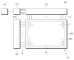
도 2는 일 실시 예에 따른 표시 장치를 구현한 예시도이다.Figure 2 is an example diagram of a display device implemented according to an embodiment.
도 2를 참조하면, 표시 패널(110)은 영상이 표시되는 표시 영역(DA)과 영상이 표시되지 않는 비표시 영역(NDA)을 포함할 수 있다.Referring to FIG. 2 , the
데이터 구동 회로(120)는 하나 이상의 소스 드라이버 집적 회로(SDIC)를 포함하고 칩 온 필름(COF) 방식으로 구현될 수 있다. 이때, 각 소스 드라이버 집적 회로(SDIC)는 표시 패널(110)의 비표시 영역(NDA)에 연결된 회로 필름(SF) 상에 실장 될 수 있다.The
게이트 구동 회로(130)는 게이트 인 패널(GIP) 타입으로 구현될 수 있다. 이 경우, 게이트 구동 회로(130)는 표시 패널(110)의 비표시 영역(NDA)에 배치될 수 있다. 다른 실시 예에서, 게이트 구동 회로(130)는 COF(Chip On Film) 타입으로 구현될 수도 있다.The
표시 장치(100)는, 하나 이상의 소스 드라이버 집적 회로(SDIC)와 다른 장치들 간의 전기적인 연결을 위해, 적어도 하나의 소스 인쇄 회로 기판(SPCB: Source Printed Circuit Board) 및 제어 부품들과 각종 전기 장치들을 실장 하기 위한 컨트롤 인쇄 회로 기판(CPCB: Control Printed Circuit Board)을 포함할 수 있다.The
적어도 하나의 소스 인쇄 회로 기판(SPCB)에는 소스 드라이버 집적 회로(SDIC)가 실장된 필름(SF)이 연결될 수 있다. 즉, 소스 드라이버 집적 회로(SDIC)가 실장된 필름(SF)은 일 측이 표시 패널(110)과 전기적으로 연결되고 타 측이 소스 인쇄 회로 기판(SPCB)과 전기적으로 연결될 수 있다.A film (SF) on which a source driver integrated circuit (SDIC) is mounted may be connected to at least one source printed circuit board (SPCB). That is, one side of the film SF on which the source driver integrated circuit (SDIC) is mounted may be electrically connected to the
컨트롤 인쇄 회로 기판(CPCB)에는 컨트롤러(140) 및 파워 관리 집적 회로(PMIC: Power Management IC, 310) 등이 실장될 수 있다. 컨트롤러(140)는 표시 패널(110)의 구동과 관련한 전반적인 제어 기능을 수행할 수 있으며, 데이터 구동 회로(120) 및 게이트 구동 회로(130)의 동작을 제어할 수 있다. 파워 관리 집적 회로(310)는 데이터 구동 회로(120) 및 게이트 구동 회로(130) 등으로 각종 전압 또는 전류를 공급해주거나 공급할 각종 전압 또는 전류를 제어할 수 있다.A
적어도 하나의 소스 인쇄 회로 기판(SPCB)과 컨트롤 인쇄 회로 기판(CPCB)은 적어도 하나의 연결 케이블(CBL)을 통해 전기적으로 연결될 수 있다. 여기서, 연결 케이블(CBL)은, 일 예로, 가요성 인쇄 회로(FPC: Flexible Printed Circuit), 가요성 플랫 케이블(FFC: Flexible Flat Cable) 등일 수 있다.At least one source printed circuit board (SPCB) and a control printed circuit board (CPCB) may be electrically connected through at least one connection cable (CBL). Here, the connection cable (CBL) may be, for example, a flexible printed circuit (FPC), a flexible flat cable (FFC), or the like.
적어도 하나의 소스 인쇄 회로 기판(SPCB)과 컨트롤 인쇄 회로 기판(CPCB)은 하나의 인쇄 회로 기판으로 통합되어 구현될 수도 있다.At least one source printed circuit board (SPCB) and a control printed circuit board (CPCB) may be integrated and implemented as one printed circuit board.
표시 장치(100)는 전압 레벨을 조정하기 위한 레벨 시프터(Level Shifter, 300)를 더 포함할 수 있다. 예를 들어, 레벨 시프터(300)는 컨트롤 인쇄 회로 기판(CPCB) 또는 소스 인쇄 회로 기판(SPCB)에 배치될 수 있다.The
레벨 시프터(300)는 게이트 구동에 필요한 신호들을 게이트 구동 회로(130)로 공급할 수 있다. 예를 들어, 레벨 시프터(300)는 복수의 스캔 클럭 신호를 게이트 구동 회로(130)로 공급할 수 있다. 게이트 구동 회로(130)는 레벨 시프터(300)로부터 입력된 복수의 스캔 클럭 신호를 기초로 복수의 스캔 신호를 복수의 게이트 라인(GL, 도 1)으로 출력할 수 있다. 여기서, 복수의 게이트 라인(GL)은 기판(SUB, 도 1)의 표시 영역(DA)에 배치된 화소(P, 도 1)들로 복수의 스캔 신호를 전달할 수 있다.The
도 3는 도 1에 도시된 화소의 일 실시 예에 따른 회로도이다.FIG. 3 is a circuit diagram of the pixel shown in FIG. 1 according to an embodiment.
도 3을 참조하면, 화소(P)는 유기 발광 다이오드(OLED), 유기 발광 다이오드(OLED)를 구동하는 구동 트랜지스터(DRT), 구동 트랜지스터(DRT)의 게이트 전극에 연결된 제1 노드(N1)로 데이터 전압을 전달해주기 위한 제1 트랜지스터(T1), 영상 신호 전압에 해당하는 데이터 전압 또는 이에 대응되는 전압을 한 프레임 시간 동안 유지하는 스토리지 캐패시터(Cst)를 포함하여 구성될 수 있다.Referring to FIG. 3, the pixel P is an organic light emitting diode (OLED), a driving transistor (DRT) that drives the organic light emitting diode (OLED), and a first node (N1) connected to the gate electrode of the driving transistor (DRT). It may be configured to include a first transistor (T1) for transmitting the data voltage, and a storage capacitor (Cst) for maintaining the data voltage corresponding to the image signal voltage or the voltage corresponding thereto for one frame time.
유기 발광 다이오드(OLED)는 제1 전극(예: 애노드 전극 또는 캐소드 전극), 유기층 및 제2 전극(예: 캐소드 전극 또는 애노드 전극) 등으로 이루어질 수 있다. 유기 발광 다이오드(OLED)의 제2 전극에는 기저 전압(EVSS)이 인가될 수 있다.An organic light emitting diode (OLED) may be composed of a first electrode (eg, an anode electrode or cathode electrode), an organic layer, and a second electrode (eg, a cathode electrode or anode electrode). A base voltage (EVSS) may be applied to the second electrode of the organic light emitting diode (OLED).
구동 트랜지스터(DRT)는 유기 발광 다이오드(OLED)로 구동 전류를 공급하여 유기 발광 다이오드(OLED)를 구동한다. 구동 트랜지스터(DRT)의 게이트 전극은 제1 노드(N1)에 전기적으로 연결될 수 있다. 구동 트랜지스터(DRT)의 일 전극은 제2 노드(N2), 즉 유기 발광 다이오드(OLED)의 제1 전극과 전기적으로 연결될 수 있으며, 소스 전극 또는 드레인 전극일 수 있다. 구동 트랜지스터(DRT)의 다른 전극은 제3 노드(N3), 즉 구동 전압(EVDD)이 인가되는 노드에 연결되며, 드레인 전극 또는 소스 전극일 수 있다.The driving transistor (DRT) supplies driving current to the organic light emitting diode (OLED) to drive the organic light emitting diode (OLED). The gate electrode of the driving transistor DRT may be electrically connected to the first node N1. One electrode of the driving transistor (DRT) may be electrically connected to the second node (N2), that is, the first electrode of the organic light emitting diode (OLED), and may be a source electrode or a drain electrode. The other electrode of the driving transistor DRT is connected to the third node N3, that is, a node to which the driving voltage EVDD is applied, and may be a drain electrode or a source electrode.
제1 트랜지스터(T1)는 데이터 라인(DL)과 제1 노드(N1) 사이에 전기적으로 연결되고, 게이트 전극으로 스캔 신호(SCAN)를 인가받는다. 제1 트랜지스터(T1)는 스캔 신호(SCAN)에 의해 턴-온 되어 데이터 라인(DL)으로부터 공급된 데이터 전압(Vdata)을 제1 노드(N1)로 전달해줄 수 있다.The first transistor T1 is electrically connected between the data line DL and the first node N1, and receives a scan signal SCAN through its gate electrode. The first transistor T1 may be turned on by the scan signal SCAN to transmit the data voltage Vdata supplied from the data line DL to the first node N1.
스토리지 캐패시터(Cst)는 구동 트랜지스터(DRT)의 제1 노드(N1)와 제2 노드(N2) 사이에 전기적으로 연결될 수 있다.The storage capacitor Cst may be electrically connected between the first node N1 and the second node N2 of the driving transistor DRT.
화소(P)의 구동 시간이 길어짐에 따라, 유기 발광 다이오드(OLED), 구동 트랜지스터(DRT) 등의 회로 소자에 대한 열화(Degradation)가 진행될 수 있다. 그에 따라, 유기 발광 다이오드(OLED), 구동 트랜지스터(DRT) 등의 회로 소자가 갖는 고유한 특성값이 변할 수 있다. 여기서, 특성값은 유기 발광 다이오드(OLED)의 문턱 전압, 구동 트랜지스터(DRT)의 문턱 전압, 구동 트랜지스터(DRT)의 이동도 등을 포함할 수 있다.As the driving time of the pixel P increases, degradation of circuit elements such as the organic light emitting diode (OLED) and driving transistor (DRT) may progress. Accordingly, the unique characteristic values of circuit elements such as organic light-emitting diodes (OLEDs) and driving transistors (DRTs) may change. Here, the characteristic values may include the threshold voltage of the organic light emitting diode (OLED), the threshold voltage of the driving transistor (DRT), and the mobility of the driving transistor (DRT).
회로 소자의 특성값 변화는 해당 화소의 휘도 변화를 야기할 수 있다. 또한, 회로 소자 간의 특성값 변화의 정도는 화소의 열화 정도에 따라 상이할 수 있다. 특성값의 차이는 화소 간 휘도 편차를 야기할 수 있다.A change in the characteristic value of a circuit element may cause a change in the luminance of the corresponding pixel. Additionally, the degree of change in characteristic values between circuit elements may vary depending on the degree of deterioration of the pixel. Differences in characteristic values may cause luminance deviation between pixels.
이러한 문제를 방지하기 위해, 일 실시 예에 따른 화소(P)는 화소(P)에 대한 특성값을 센싱하고, 특성값 변화를 보상할 수 있는 보상 회로를 포함할 수 있다.To prevent this problem, the pixel P according to one embodiment may include a compensation circuit capable of sensing characteristic values of the pixel P and compensating for changes in characteristic values.
도 3을 참조하면, 화소(P)는 제2 트랜지스터(T2)를 더 포함할 수 있다. 제2 트랜지스터(T2)는 제2 노드(N2)와 기준 전압(Vref)을 공급하는 기준 전압 라인(RVL) 사이에 전기적으로 연결되고, 게이트 전극으로 스캔 신호의 일종인 센싱 신호(SENSE)를 인가받아 제어될 수 있다. 제2 트랜지스터(T2)는 센싱 신호(SENSE)에 의해 턴-온 되어 기준 전압 라인(RVL)을 통해 공급되는 기준 전압(Vref)을 제2 노드(N2)에 인가해준다. 또한, 제2 트랜지스터(T2)는 구동 트랜지스터(DRT) 에 대한 전압 센싱 경로 중 하나로 활용될 수 있다.Referring to FIG. 3, the pixel P may further include a second transistor T2. The second transistor (T2) is electrically connected between the second node (N2) and the reference voltage line (RVL) that supplies the reference voltage (Vref), and applies a sensing signal (SENSE), a type of scan signal, to the gate electrode. can be received and controlled. The second transistor T2 is turned on by the sensing signal SENSE and applies the reference voltage Vref supplied through the reference voltage line RVL to the second node N2. Additionally, the second transistor (T2) can be used as one of the voltage sensing paths for the driving transistor (DRT).
일 실시 예에서, 스캔 신호(SCAN) 및 센싱 신호(SENSE)는 별개의 스캔 신호일 수 있다. 이 경우, 스캔 신호(SCAN) 및 센싱 신호(SENSE)는, 서로 다른 게이트 라인을 통해, 제1 트랜지스터(T1)의 게이트 전극 및 제2 트랜지스터(T2)의 게이트 전극으로 각각 인가될 수도 있다.In one embodiment, the scan signal (SCAN) and the sensing signal (SENSE) may be separate scan signals. In this case, the scan signal SCAN and the sensing signal SENSE may be applied to the gate electrode of the first transistor T1 and the gate electrode of the second transistor T2, respectively, through different gate lines.
다른 실시 예에서, 스캔 신호(SCAN) 및 센싱 신호(SENSE)는 동일한 스캔 신호일 수도 있다. 이 경우, 스캔 신호(SCAN) 및 센싱 신호(SENSE)는 동일한 게이트 라인을 통해 제1 트랜지스터(T1)의 게이트 전극 및 제2 트랜지스터(T2)의 게이트 전극에 공통으로 인가될 수도 있다.In another embodiment, the scan signal SCAN and the sensing signal SENSE may be the same scan signal. In this case, the scan signal SCAN and the sensing signal SENSE may be commonly applied to the gate electrode of the first transistor T1 and the gate electrode of the second transistor T2 through the same gate line.
도 4는 일 실시 예에 따른 보상 회로를 나타낸 도면이다.Figure 4 is a diagram showing a compensation circuit according to one embodiment.
도 4를 참조하면, 표시 장치(100)는 화소(P)의 전압 센싱을 통해 센싱 데이터(Vsen)를 생성하여 출력하는 센싱부(410), 센싱 데이터(Vsen)를 이용하여 화소(P)의 특성값을 판단하고 이를 보상하기 위한 보상 프로세스를 수행하는 보상부(420) 및 기설정된 초기 보상 데이터(또는 초기 보상값)과 보상부(420)에서 생성된 보상값을 저장하는 메모리부(430) 등을 포함할 수 있다.Referring to FIG. 4, the
센싱부(410)는 적어도 하나의 아날로그 디지털 컨버터(Analog to Digital Converter)를 포함하여 구현될 수 있다. 이러한 센싱부(410)는 도시된 것과 같이 데이터 드라이버(120)의 내부 또는 외부에 마련될 수 있다. 센싱부(410)에서 출력되는 센싱 데이터(Vsen)는, 일 예로, LVDS(Low Voltage Differential Signaling) 데이터 포맷을 가질 수 있다.The sensing unit 410 may be implemented by including at least one analog to digital converter. This sensing unit 410 may be provided inside or outside the
보상부(420)와 메모리부(430)는 컨트롤러(140)의 내부 또는 외부에 마련될 수 있다. 메모리부(430)는 센싱부(410)로부터 센싱 데이터(Vsen)를 인가받아 저장하고, 저장된 센싱 데이터(Vsen)를 보상부(420)으로 전달할 수 있다. 다른 실시 예에서, 보상부(420)가 직접 센싱 데이터(Vsen)를 인가받아 보상값을 연산한 후, 보상값과 센싱 데이터(Vsen)를 메모리부(430)에 저장할 수 있다.The compensation unit 420 and the memory unit 430 may be provided inside or outside the
메모리부(430)에는 미리 설정된 초기 보상 데이터가 저장될 수 있고, 센싱부(410)로부터 인가되는 센싱 데이터(Vsen) 또는 보상부(420)에서 연산된 보상값이 저장될 수 있다.In the memory unit 430, preset initial compensation data may be stored, and sensing data (Vsen) applied from the sensing unit 410 or compensation value calculated by the compensation unit 420 may be stored.
표시 장치(100)는, 기준 전압 라인(RVL)의 온/오프를 제어하는 초기화 스위치(SPRE), 기준 전압 라인(RVL)과 센싱부(410) 간의 연결 제어하는 샘플링 스위치(SAM)를 포함할 수 있다.The
초기화 스위치(SPRE)는, 화소(P) 내 제2 노드(N2)가 원하는 회로 소자의 특성값을 반영하는 전압 상태가 되도록, 제2 노드(N2)의 전압 인가 상태를 제어할 수 있다. 초기화 스위치(SPRE)가 턴-온 되면, 기준 전압(Vref)이 기준 전압 라인(RVL)으로 공급되어 턴-온 되어 있는 제2 트랜지스터(T2)를 통해 제2 노드(N2)로 인가될 수 있다.The initialization switch SPRE may control the voltage application state of the second node N2 in the pixel P so that the second node N2 is in a voltage state that reflects the desired characteristic value of the circuit element. When the initialization switch (SPRE) is turned on, the reference voltage (Vref) is supplied to the reference voltage line (RVL) and can be applied to the second node (N2) through the second transistor (T2) that is turned on. .
샘플링 스위치(SAM)는, 턴-온 되어, 기준 전압 라인(RVL)과 센싱부(410)를 전기적으로 연결해준다. 샘플링 스위치(SAM)는, 화소(P) 내 제2 노드(N2)가 원하는 회로 소자의 특성값을 반영하는 전압 상태가 되었을 때 턴-온 되도록 제어될 수 있다. 샘플링 스위치(SAM)가 턴-온 되면, 센싱부(410)는 연결된 기준 전압 라인(RVL)의 전압을 센싱할 수 있다.The sampling switch (SAM) is turned on and electrically connects the reference voltage line (RVL) and the sensing unit 410. The sampling switch SAM may be controlled to turn on when the second node N2 in the pixel P is in a voltage state that reflects the desired characteristic value of the circuit element. When the sampling switch (SAM) is turned on, the sensing unit 410 can sense the voltage of the connected reference voltage line (RVL).
센싱부(410)가 기준 전압 라인(RVL)의 전압을 센싱할 때, 제2 트랜지스터(T2)가 턴-온 되어 있는 경우, 구동 트랜지스터(DRT)의 저항 성분을 무시할 수 있다면, 센싱부(410)에 의해 센싱되는 전압은, 제2 노드(N2)의 전압에 해당할 수 있다. 센싱부(410)에 의해 센싱되는 전압은, 기준 전압 라인(RVL)의 전압, 즉, 제2 노드(N2)의 전압일 수 있다.When the sensing unit 410 senses the voltage of the reference voltage line RVL, if the second transistor T2 is turned on and the resistance component of the driving transistor DRT can be ignored, the sensing unit 410 ) may correspond to the voltage of the second node (N2). The voltage sensed by the sensing unit 410 may be the voltage of the reference voltage line RVL, that is, the voltage of the second node N2.
기준 전압 라인(RVL) 상에 라인 캐패시터가 존재한다면, 센싱부(410)에 의해 센싱되는 전압은, 기준 전압 라인(RVL) 상의 라인 캐패시터에 충전된 전압일 수도 있다. 일 예로, 센싱부(410)에 의해 센싱되는 전압은, 구동 트랜지스터(DRT)의 문턱 전압(Vth) 또는 문턱 전압 편차(*?*Vth)를 포함하는 전압 값(Vdata-Vth 또는 Vdata-Vth, 여기서, Vdata는 센싱 구동용 데이터 전압임)이거나, 구동 트랜지스터(DRT)의 이동도를 센싱하기 위한 전압 값일 수도 있다.If a line capacitor exists on the reference voltage line RVL, the voltage sensed by the sensing unit 410 may be the voltage charged in the line capacitor on the reference voltage line RVL. As an example, the voltage sensed by the sensing unit 410 is a voltage value (Vdata-Vth or Vdata-) including the threshold voltage (Vth) or threshold voltage deviation (*?*Vth) of the driving transistor (DRT). Vth (here, Vdata is the data voltage for sensing driving) or may be a voltage value for sensing the mobility of the driving transistor (DRT).
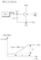
도 5는 구동 트랜지스터의 문턱 전압 센싱 방법을 설명하기 위한 도면이다.Figure 5 is a diagram for explaining a method of sensing the threshold voltage of a driving transistor.
도 4와 도 5를 함께 참조하면, 구동 트랜지스터(DRT)에 대한 문턱 전압 센싱 구동은 초기화 단계, 트래킹 단계 및 샘플링 단계를 포함하는 센싱 프로세스로 진행될 수 있다.Referring to FIGS. 4 and 5 together, the threshold voltage sensing drive for the driving transistor (DRT) may be performed through a sensing process including an initialization step, a tracking step, and a sampling step.
초기화 단계는, 제1 노드(N1)와 제2 노드(N2)를 초기화 시키는 단계이다. 초기화 단계에서는, 초기화 스위치(SPRE)가 턴-온 된다. 이후에 스캔 신호(SCAN) 및 센싱 신호(SENSE)가 인가되어 제1 트랜지스터(T1) 및 제2 트랜지스터(T2)가 턴-온 될 수 있다. 이에 따라, 제1 노드(N1)와 제2 노드(N2) 각각은, 문턱 전압 센싱 구동용 데이터 전압(Vdata)과 기준 전압(Vref)으로 초기화된다(V1=Vdata, V2=Vref).The initialization step is a step of initializing the first node (N1) and the second node (N2). In the initialization phase, the initialization switch (SPRE) is turned on. Afterwards, the scan signal (SCAN) and the sensing signal (SENSE) may be applied to turn on the first transistor (T1) and the second transistor (T2). Accordingly, each of the first node (N1) and the second node (N2) is initialized with a data voltage (Vdata) and a reference voltage (Vref) for threshold voltage sensing driving (V1 = Vdata, V2 = Vref).
트래킹 단계는, 제2 노드(N2)의 전압이 문턱 전압 또는 그 변화를 반영하는 전압 상태가 될 때까지 제2 노드(N2)의 전압(V2)을 변화시키는 단계이다. 즉, 트래킹 단계는, 문턱 전압 또는 그 변화를 반영할 수 있는 제2 노드(N2)의 전압을 트래킹하는 단계이다. 트래킹 단계에서는, 초기화 스위치(SPRE)가 턴-오프 또는 제2 트랜지스터(T2)가 턴-오프 되어, 제2 노드(N2)가 플로팅(Floating) 된다. 이에 따라, 제2 노드(N2)의 전압(V2)이 상승한다.The tracking step is a step of changing the voltage V2 of the second node N2 until the voltage of the second node N2 becomes the threshold voltage or a voltage state reflecting the change. That is, the tracking step is a step of tracking the voltage of the second node N2 that can reflect the threshold voltage or its change. In the tracking stage, the initialization switch (SPRE) is turned off or the second transistor (T2) is turned off, so that the second node (N2) is floating. Accordingly, the voltage V2 of the second node N2 increases.
제2 노드(N2)의 전압(V2)은 상승이 이루어지다가 상승 폭이 서서히 줄어들어 포화하게 된다. 제2 노드(N2)의 포화된 전압은 데이터 전압(Vdata)과 문턱 전압(Vth)의 차이 또는 데이터 전압(Vdata)과 문턱 전압 편차(Vth)의 차이에 해당할 수 있다.The voltage V2 of the second node N2 increases, then gradually decreases and becomes saturated. The saturated voltage of the second node (N2) is the difference between the data voltage (Vdata) and the threshold voltage (Vth) or the difference between the data voltage (Vdata) and the threshold voltage ( This may correspond to the difference in Vth).
제2 노드(N2)의 전압(V2)이 포화되면, 샘플링 단계가 진행될 수 있다. 샘플링 단계는, 구동 트랜지스터(DRT)의 문턱 전압 또는 그 변화를 반영하는 전압을 측정하는 단계로서, 센싱부(410)가 기준 전압 라인(RVL)의 전압, 즉, 제2 노드(N2)의 전압을 센싱하는 단계이다. 이러한 샘플링 단계에서, 샘플링 스위치(SAM)가 턴-온 되어, 센싱부(410)는 기준 전압 라인(RVL)과 연결되어, 기준 전압 라인(RVL)의 전압, 즉, 제2 노드(N2)의 전압(V2)을 센싱한다.When the voltage V2 of the second node N2 is saturated, the sampling step may proceed. The sampling step is a step of measuring the threshold voltage of the driving transistor (DRT) or a voltage reflecting its change, and the sensing unit 410 measures the voltage of the reference voltage line (RVL), that is, the voltage of the second node (N2). This is the sensing step. In this sampling step, the sampling switch (SAM) is turned on, and the sensing unit 410 is connected to the reference voltage line (RVL), so that the voltage of the reference voltage line (RVL), that is, the voltage of the second node (N2) Sensing voltage (V2).
센싱부(410)에 의해 센싱된 전압(Vsen)은 데이터 전압(Vdata)에서 문턱 전압(Vth)을 뺀 전압(Vdata-Vth) 또는 데이터 전압(Vdata)에서 문턱 전압 편차(Vth)를 뺀 전압(Vdata-Vth)일 수 있다. 여기서, Vth는 포지티브 문턱 전압 또는 네거티브 문턱 전압일 수 있다.The voltage (Vsen) sensed by the sensing unit 410 is a voltage (Vdata-Vth) obtained by subtracting the threshold voltage (Vth) from the data voltage (Vdata) or a threshold voltage deviation from the data voltage (Vdata) ( Voltage (Vdata-) minus Vth Vth). Here, Vth may be a positive threshold voltage or a negative threshold voltage.
도 6은 구동 트랜지스터의 이동도 센싱 방법을 설명하기 위한 도면이다.Figure 6 is a diagram for explaining a method for sensing the mobility of a driving transistor.
도 4와 도 6을 함께 참조하면, 구동 트랜지스터(DRT)에 대한 이동도 센싱 구동은 초기화 단계, 트래킹 단계 및 샘플링 단계를 포함하는 센싱 프로세스로 진행될 수 있다.Referring to FIGS. 4 and 6 together, the mobility sensing drive for the driving transistor (DRT) may be performed through a sensing process including an initialization step, a tracking step, and a sampling step.
초기화 단계에서는, 초기화 스위치(SPRE)가 턴-온 된다. 이후에 스캔 신호(SCAN) 및 센싱 신호(SENSE)가 인가되어 제1 트랜지스터(T1) 및 제2 트랜지스터(T2)가 턴-온 될 수 있다. 이에 따라, 제1 노드(N1)와 제2 노드(N2) 각각은 이동도 센싱 구동용 데이터 전압(Vdata)과 기준 전압(Vref)으로 초기화된다(V1=Vdata, V2=Vref).In the initialization phase, the initialization switch (SPRE) is turned on. Afterwards, the scan signal (SCAN) and the sensing signal (SENSE) may be applied to turn on the first transistor (T1) and the second transistor (T2). Accordingly, each of the first node (N1) and the second node (N2) is initialized with a data voltage (Vdata) and a reference voltage (Vref) for mobility sensing driving (V1 = Vdata, V2 = Vref).
트래킹 단계는, 제2 노드(N2)의 전압이 이동도 또는 그 변화를 반영하는 전압 상태가 될 때까지 제2 노드(N2)의 전압(V2)을 변화시키는 단계이다. 즉, 트래킹 단계는, 이동도 또는 그 변화를 반영할 수 있는 제2 노드(N2)의 전압을 트래킹하는 단계이다. 이러한 트래킹 단계에서는, 초기화 스위치(SPRE)가 턴-오프 되어 또는 제2 트랜지스터(T2)가 턴-오프 되어, 제2 노드(N2)가 플로팅 된다. 이때, 제1 트랜지스터(T1)가 턴-오프 되어, 제1 노드(N1)도 함께 플로팅 될 수 있다. 이에 따라, 제2 노드(N2)의 전압(V2)이 상승하기 시작한다.The tracking step is a step of changing the voltage V2 of the second node N2 until the voltage of the second node N2 becomes a voltage state that reflects the mobility or its change. That is, the tracking step is a step of tracking the voltage of the second node N2, which can reflect the mobility or its change. In this tracking step, the initialization switch (SPRE) is turned off or the second transistor (T2) is turned off, so that the second node (N2) is floating. At this time, the first transistor T1 is turned off, and the first node N1 can also be floated. Accordingly, the voltage V2 of the second node N2 begins to rise.
제2 노드(N2)의 전압(V2)의 상승 속도는 구동 트랜지스터(DRT)의 전류 능력(즉, 이동도)에 따라 달라진다. 전류 능력(이동도)이 큰 구동 트랜지스터(DRT)일 수록, 제2 노드(N2)의 전압(V2)이 더욱 가파르게 상승한다.The rate at which the voltage V2 of the second node N2 increases varies depending on the current capability (i.e., mobility) of the driving transistor DRT. As the driving transistor (DRT) has a higher current capability (mobility), the voltage (V2) of the second node (N2) rises more steeply.
트래킹 단계가 일정 시간(t) 동안 진행된 이후, 즉, 제2 노드(N2)의 전압(V2)이 미리 정해진 일정 시간(t) 동안 상승한 이후, 샘플링 단계가 진행될 수 있다. 트래킹 단계 동안, 제2 노드(N2)의 전압(V2)의 상승 속도는, 일정 시간(t) 동안의 전압 변화량(V)에 해당한다.The tracking phase lasts for a certain amount of time ( After progressing for t), that is, the voltage (V2) of the second node (N2) is reduced for a predetermined period of time ( After rising for t), the sampling phase can proceed. During the tracking phase, the rate of rise of the voltage V2 of the second node N2 is constant for a certain period of time ( Voltage change during t) ( corresponds to V).
샘플링 단계에서는, 샘플링 스위치(SAM)가 턴-온 되어, 센싱부(410)와 기준 전압 라인(RVL)이 전기적으로 연결된다. 이에 따라, 센싱부(410)는 기준 전압 라인(RVL)의 전압, 즉, 제2 노드(N2)의 전압(V2)을 센싱한다. 센싱부(410)에 의해 센싱된 전압(Vsen)은, 초기화 전압(Vref)에서 일정 시간(t) 동안 전압 변화량(V)만큼 상승된 전압으로서, 이동도에 대응되는 전압이다.In the sampling stage, the sampling switch (SAM) is turned on, and the sensing unit 410 and the reference voltage line (RVL) are electrically connected. Accordingly, the sensing unit 410 senses the voltage of the reference voltage line RVL, that is, the voltage V2 of the second node N2. The voltage (Vsen) sensed by the sensing unit 410 is maintained at the initialization voltage (Vref) for a certain period of time ( Voltage change during t) ( It is a voltage raised by V), and is a voltage corresponding to mobility.
도 5 및 도 6을 참조하여 전술한 바와 같은 문턱 전압 또는 이동도 센싱 구동에 따라 센싱부(410)는 문턱 전압 센싱 또는 이동도 센싱을 위해 센싱된 전압(Vsen)을 디지털 값으로 변환하고, 변환된 디지털 값(센싱 값)을 포함하는 센싱 데이터(Vsen)를 생성하여 출력한다. 센싱부(410)에서 출력된 센싱 데이터(Vsen)는 보상부(420)로 제공될 수 있다. 경우에 따라서 센싱 데이터(Vsen)는 메모리부(430)를 통해 보상부(420)로 제공될 수도 있다.According to the threshold voltage or mobility sensing drive as described above with reference to FIGS. 5 and 6, the sensing unit 410 converts the sensed voltage (Vsen) into a digital value for threshold voltage sensing or mobility sensing, and converts Sensing data (Vsen) containing the digital value (sensing value) is generated and output. Sensing data (Vsen) output from the sensing unit 410 may be provided to the compensation unit 420. In some cases, the sensing data Vsen may be provided to the compensation unit 420 through the memory unit 430.
보상부(420)는 센싱부(410)에서 제공된 센싱 데이터(Vsen)를 토대로 해당 화소 내 구동 트랜지스터(DRT)의 특성값(예: 문턱 전압, 이동도) 또는 구동 트랜지스터(DRT)의 특성값 변화(예: 문턱 전압 변화, 이동도 변화)를 파악하고, 특성값 보상 프로세스를 수행할 수 있다. 여기서, 구동 트랜지스터(DRT)의 특성값 변화는 이전 센싱 데이터(Vsen)를 기준으로 현재 센싱 데이터(Vsen)가 변화된 것을 의미하거나, 초기 보상 데이터를 기준으로 현재 센싱 데이터(Vsen)가 변화된 것을 의미할 수도 있다.The compensation unit 420 changes the characteristic value (e.g., threshold voltage, mobility) or the characteristic value of the driving transistor (DRT) in the corresponding pixel based on the sensing data (Vsen) provided by the sensing unit 410. (e.g. threshold voltage change, mobility change) can be identified and a characteristic value compensation process can be performed. Here, a change in the characteristic value of the driving transistor (DRT) may mean that the current sensing data (Vsen) has changed based on the previous sensing data (Vsen), or it may mean that the current sensing data (Vsen) has changed based on the initial compensation data. It may be possible.
따라서 구동 트랜지스터(DRT) 간의 특성값 또는 특성값 변화를 비교해보면, 구동 트랜지스터(DRT) 간의 특성값 편차를 파악할 수 있다. 구동 트랜지스터(DRT)의 특성값 변화가 초기 보상 데이터를 기준으로 현재 센싱 데이터(Vsen)가 변화된 것을 의미하는 경우, 구동 트랜지스터(DRT)의 특성값 변화로부터 구동 트랜지스터(DRT) 간의 특성값 편차(즉, 화소 휘도 편차)를 파악할 수도 있다. 여기서 초기 보상 데이터는 표시 장치 제조 시에 설정되어 저장된 초기 설정 데이터일 수 있다.Therefore, by comparing the characteristic values or changes in characteristic values between the driving transistors (DRT), the deviation in characteristic values between the driving transistors (DRT) can be identified. If a change in the characteristic value of the driving transistor (DRT) means that the current sensing data (Vsen) has changed based on the initial compensation data, the characteristic value deviation between the driving transistors (DRT) from the change in the characteristic value of the driving transistor (DRT) (i.e. , pixel luminance deviation) can also be determined. Here, the initial compensation data may be initial setting data set and stored when manufacturing the display device.
특성값 보상 프로세스는, 구동 트랜지스터(DRT)의 문턱 전압을 보상하는 문턱 전압 보상 처리와, 구동 트랜지스터(DRT)의 이동도를 보상하는 이동도 보상 처리를 포함할 수 있다. 문턱 전압 보상 처리는 문턱 전압 또는 문턱 전압 편차(문턱 전압 변화)를 보상하기 위한 보상값을 연산하고, 연산된 보상값을 메모리부(430)에 저장하거나, 연산된 보상값으로 해당 영상데이터(Data)를 변경하는 처리를 포함할 수 있다. 이동도 보상 처리는 이동도 또는 이동도 편차(이동도 변화)를 보상하기 위한 보상값을 연산하고, 연산된 보상값을 메모리부(430)에 저장하거나, 연산된 보상값으로 해당 영상데이터(Data)를 변경하는 처리를 포함할 수 있다. The characteristic value compensation process may include a threshold voltage compensation process that compensates for the threshold voltage of the driving transistor (DRT) and a mobility compensation process that compensates for the mobility of the driving transistor (DRT). The threshold voltage compensation process calculates a compensation value to compensate for the threshold voltage or threshold voltage deviation (threshold voltage change), stores the calculated compensation value in the memory unit 430, or stores the corresponding image data (Data) with the calculated compensation value. ) may include processing to change. Mobility compensation processing calculates a compensation value to compensate for mobility or mobility deviation (mobility change), stores the calculated compensation value in the memory unit 430, or stores the corresponding image data (Data) with the calculated compensation value. ) may include processing to change.
보상부(420)는 문턱 전압 보상 처리 또는 이동도 보상 처리를 통해 영상데이터(Data)를 변경하여 변경된 데이터를 데이터 드라이버(120) 내 해당 소스 드라이버 집적회로로 공급해줄 수 있다. 소스 드라이버 집적회로는, 보상부(420)에서 변경된 데이터를 디지털 아날로그 컨버터를 통해 데이터 전압으로 변환하여 해당 화소로 공급해줌으로써, 화소 특성값 보상(문턱 전압 보상, 이동도 보상)이 실제로 이루어지게 된다.The compensator 420 may change image data (Data) through threshold voltage compensation processing or mobility compensation processing and supply the changed data to the corresponding source driver integrated circuit within the
이와 같은 화소 특성값 보상이 이루어짐에 따라, 화소 간의 휘도 편차를 줄여주거나 방지해줌으로써, 화상 품질을 향상시켜줄 수 있다.As such pixel characteristic value compensation is performed, image quality can be improved by reducing or preventing luminance deviation between pixels.
도 7은 센싱 타이밍을 나타낸 다이어그램이다.Figure 7 is a diagram showing sensing timing.
도 7을 참조하면, 일 실시 예에 따른 표시 장치(100)는 파워 온 신호(Power On Signal)가 발생하면, 표시 패널(110)에 배치된 각 화소 내 구동 트랜지스터(DRT)의 특성값을 센싱할 수 있다. 이러한 센싱 프로세스를 "온-센싱 프로세스(On-Sensing Process)"라고 한다.Referring to FIG. 7, when a power on signal is generated, the
또한, 표시 장치(100)는 파워 오프 신호(Power Off Signal)가 발생하면, 전원 차단 등의 오프 시퀀스(Off-Sequence)가 진행되기 이전에, 표시 패널(110)에 배치된 각 화소 내 구동 트랜지스터(DRT)의 특성값을 센싱할 수도 있다. 이러한 센싱 프로세스를 "오프-센싱 프로세스(Off-Sensing Process) "라고 한다.In addition, when a power-off signal is generated, the
또한, 파워 온 신호가 발생한 이후 파워 오프 신호가 발생되기 전까지, 디스플레이 구동 중에서 블랭크(Blank) 시간 마다 표시 패널(110)에 배치된 각 화소 내 구동 트랜지스터(DRT)의 특성값을 센싱할 수도 있다. 이러한 센싱 프로세스를 "실시간 센싱 프로세스(Real-time Sensing Process)" 라고 한다. 이러한 실시간 센싱 프로세스는, 수직 동기 신호를 기준으로 액티브 시간 사이의 블랭크 시간 마다 진행될 수 있다.In addition, the characteristic value of the driving transistor (DRT) in each pixel disposed on the
구동 트랜지스터(DRT)의 이동도 센싱은 짧은 시간만이 필요하기 때문에, 파워 온 신호가 발생한 이후에 표시 구동이 시작하기 이전에 진행될 수도 있고, 파워 오프 신호가 발생한 이후에 표시 구동이 되지 않을 때 수행될 수 있다. 또한, 구동 트랜지스터(DRT)의 이동도 센싱은 디스플레이 구동 중에도 짧은 블랭크 시간을 활용하여 실시간으로 진행될 수 있다.Since sensing the mobility of the driving transistor (DRT) requires only a short period of time, it may be performed after the power-on signal is generated but before display driving begins, or may be performed when display driving is not performed after the power-off signal is generated. It can be. Additionally, sensing the mobility of the driving transistor (DRT) can be performed in real time by utilizing a short blank time even while the display is driving.
구동 트랜지스터(DRT)의 문턱전압 센싱은, 제2 노드(N2)의 긴 전압 포화 시간이 필요하기 때문에, 구동 트랜지스터(DRT)의 이동도 센싱에 비해, 상대적으로 오랜 시간이 걸린다. 따라서, 구동 트랜지스터(DRT)의 문턱 전압 센싱은 사용자 입력 등에 따라 파워 오프 신호가 발생한 이후, 표시 구동이 되지 않는 동안, 즉, 사용자가 시청 의사가 없는 상황에서 진행될 수 있다. 그러나 경우에 따라 구동 트랜지스터(DRT)의 문턱 전압 센싱도 온-센싱 프로세스 또는 실시간-센싱 프로세스로 진행될 수도 있다.Because sensing the threshold voltage of the driving transistor (DRT) requires a long voltage saturation time of the second node (N2), it takes a relatively long time compared to sensing the mobility of the driving transistor (DRT). Accordingly, sensing the threshold voltage of the driving transistor (DRT) may be performed after a power-off signal is generated according to a user input, etc., while the display is not driven, that is, in a situation where the user has no intention of viewing. However, in some cases, sensing the threshold voltage of the driving transistor (DRT) may also be performed through an on-sensing process or a real-time-sensing process.
도 8은 일 실시 예에 따른 게이트 구동 회로를 간략히 나타낸 회로도이다.Figure 8 is a circuit diagram briefly showing a gate driving circuit according to an embodiment.
도 8을 참조하면, 게이트 구동 회로(130)는 복수 개의 스캔 클럭 신호들(SCCLKk~SCCLK(k+3))을 이용하여 복수 개의 스캔 신호들(SCOUTk~SCOUT(k+3))을 출력하는 하나 이상의 스테이지 회로(STG)를 포함할 수 있다(k는 1 내지 n 사이의 임의의 자연수). 게이트 구동 회로(130)로 인가되는 스캔 클럭 신호들(SCCLKk~SCCLK(k+3))은 레벨 시프터(300)로부터 제공될 수 있다. 도시된 실시 예에서는, 하나의 스테이지 회로(STG)가 4개의 스캔 클럭 신호들(SCCLKk~SCCLK(k+3))을 입력 받아 4개의 스캔 신호들(SCOUT(n)~SCOUT(k+3))을 출력하는 실시 예가 도시되지만, 본 실시 예가 이로써 한정되지 않는다.Referring to FIG. 8, the
이러한 게이트 구동 회로(130)는 공통의 Q 노드(Q) 및 QB 노드(QB)에 연결되고, 복수 개의 스캔 클럭 신호들(SCCLKk~SCCLK(k+3))을 입력받아 복수 개의 스캔 신호들(SCOUT(n)~SCOUT(k+3))을 출력하는 복수 개의 버퍼 회로들(GBUF1~GBUF4)과, 버퍼 회로들(GBUF1~GBUF4)을 제어하는 제어 회로(131)를 포함할 수 있다.This
제어 회로(131)는 스타트 신호(VST) 및 리셋 신호(RST) 등을 입력 받고, 입력된 신호들을 이용하여 버퍼 회로들(GBUF1~GBUF4)의 동작을 제어할 수 있다. 예를 들어, 제어 회로(131)는 버퍼 회로들(GBUF1~GBUF4)에 연결되는 Q 노드(Q) 및 QB 노드(QB)의 전압을 제어할 수 있다.The control circuit 131 may receive a start signal (VST), a reset signal (RST), etc., and control the operation of the buffer circuits (GBUF1 to GBUF4) using the input signals. For example, the control circuit 131 may control the voltage of the Q node (Q) and QB node (QB) connected to the buffer circuits (GBUF1 to GBUF4).
버퍼 회로들(GBUF1~GBUF4) 각각은 풀-업 트랜지스터(Tu) 및 풀-다운 트랜지스터(Td)를 포함할 수 있다. 풀-업 트랜지스터(Tu) 및 풀-다운 트랜지스터(Td)는 스캔 클럭 신호들(SCCLKk~SCCLK(k+3))이 인가되는 노드와 기저 전압(GVSS0)이 인가되는 노드 사이에 직렬로 연결될 수 있다. 풀-업 트랜지스터(Tu) 및 풀-다운 트랜지스터(Td)의 사이에는 대응되는 게이트 라인(GL)이 연결되어 스캔 신호(SCOUT(n)~SCOUT(k+3))가 출력된다.Each of the buffer circuits GBUF1 to GBUF4 may include a pull-up transistor (Tu) and a pull-down transistor (Td). The pull-up transistor (Tu) and the pull-down transistor (Td) can be connected in series between the node to which scan clock signals (SCCLKk to SCCLK(k+3)) are applied and the node to which the base voltage (GVSS0) is applied. there is. A corresponding gate line (GL) is connected between the pull-up transistor (Tu) and the pull-down transistor (Td), and scan signals (SCOUT(n) to SCOUT(k+3)) are output.
버퍼 회로들(GBUF1~GBUF4) 각각의 풀-업 트랜지스터(Tu)들은 하나의 Q 노드(Q)에 공통적으로 연결될 수 있다. 풀-업 트랜지스터(Tu)들은 제어 회로(131)에 의해 제어되는 Q 노드(Q)의 전압에 따라 턴-온되어 대응되는 스캔 클럭 신호들(SCCLKk~SCCLK(k+3))을 스캔 신호(SCOUT(n)~SCOUT(k+3))로 출력할 수 있다.The pull-up transistors (Tu) of each of the buffer circuits (GBUF1 to GBUF4) may be commonly connected to one Q node (Q). The pull-up transistors (Tu) are turned on according to the voltage of the Q node (Q) controlled by the control circuit 131 and send the corresponding scan clock signals (SCCLKk to SCCLK(k+3)) to the scan signal ( It can be output as SCOUT(n)~SCOUT(k+3)).
버퍼 회로들(GBUF1~GBUF4) 각각의 풀-다운 트랜지스터(Td)들은 하나의 QB 노드(QB)에 공통적으로 연결될 수 있다. 풀-다운 트랜지스터(Td)들은 제어 회로(131)에 의해 제어되는 QB 노드(QB)의 전압에 따라 턴-온되어 기저 전압(GVSS0)을 스캔 신호(SCOUT(n)~SCOUT(k+3))로 출력할 수 있다.The pull-down transistors (Td) of each of the buffer circuits (GBUF1 to GBUF4) may be commonly connected to one QB node (QB). The pull-down transistors (Td) are turned on according to the voltage of the QB node (QB) controlled by the control circuit 131, and the base voltage (GVSS0) is converted to a scan signal (SCOUT(n) to SCOUT(k+3). ) can be output.
일 실시 예에서, 게이트 구동 회로(130)는 캐리 신호(Ck)를 출력하기 위한 캐리 버퍼 회로(CBUF)를 더 포함할 수 있다. 캐리 버퍼 회로(CBUF)는 레벨 시프터(300) 등으로부터 인가되는 캐리 클럭 신호(CRCLKk)에 기초하여 캐리 신호(Ck)를 생성하고, 이를 출력할 수 있다. 캐리 신호(Ck)는 다음 스테이지 회로에, 스타트 신호(VST)를 대신하여 인가될 수 있다. 예를 들어, 첫 번째 스테이지 회로에는 스타트 신호(VST)가 인가되고, 두 번째 내지 n번째 스테이지 회로에는 이전 스테이지의 캐리 신호(Ck)가 인가될 수 있다.In one embodiment, the
도 9는 일 실시 예에 따른 컨트롤러, 레벨 시프터, 및 표시 패널 사이의 연결 구조를 나타낸 도면이다.FIG. 9 is a diagram illustrating a connection structure between a controller, a level shifter, and a display panel according to an embodiment.
도 9를 참조하면, 컨트롤러(140)와 레벨 시프터(300) 사이에는 2개의 제어 클럭 신호(GCLK, MCLK)를 각각 전송하는 2개의 전송 라인(LA1, LA2)이 연결될 수 있다. 레벨 시프터(300)는 컨트롤러(140)로부터 전송되는 제1 및 제2 제어 클럭 신호(GCLK, MCLK)를 논리 연산하여 위상이 순차적으로 쉬프트되는 스캔 클럭 신호들(SCCLK1~SCCLKn)을 생성할 수 있다(n은 1보다 큰 자연수).Referring to FIG. 9, two transmission lines LA1 and LA2 that transmit two control clock signals GCLK and MCLK, respectively, may be connected between the
레벨 시프터(300)와 게이트 구동 회로(130) 사이에는 레벨 시프터(300)로부터 생성된 스캔 클럭 신호들(SCCLK1~SCCLKn)을 각각 전송하는 복수의 전송 라인들(LB1~LBn)이 구비된다. 전송 라인들(LB1~LBn)의 개수는 스캔 클럭 신호들(SCCLK1~SCCLKn)의 개수에 대응할 수 있다.A plurality of transmission lines LB1 to LBn are provided between the
게이트 구동 회로(130)는 레벨 시프터(300)로부터 수신되는 스캔 클럭 신호들(SCCLK1~SCCLKn)을 이용하여 스캔 신호들(SCOUT1~SCOUTn, 도 8)을 생성하고, 생성된 스캔 신호들(SCOUT1~SCOUTn)을 게이트 라인(GL)들을 통해 표시 패널(110)로 출력할 수 있다.The
도시된 실시 예에서, 컨트롤러(140)는 표시 패널(110)로 인가되는 스캔 신호들(SCOUT1~SCOUTn) 사이의 편차를 판단하고, 편차가 기설정된 임계값보다 크다고 판단되는 경우, 레벨 시프터(300)에 제공되는 제어 신호들(MCLK, GCLK)의 펄스 타이밍을 조절한다. 이를 위해, 컨트롤러(140)는 센싱부(410), 보상부(420) 및 신호 출력부(440)를 포함할 수 있다.In the illustrated embodiment, the
센싱부(410)는 도 3 내지 도 6을 참조하여 설명한 바에 따라 표시 패널(110)에 대한 센싱을 수행할 수 있다. 또한, 센싱부(410)는 표시 패널(110)로 소정의 전압을 인가했을 때, 표시 패널(110)에 배치된 화소(P)들의 충전율 차이를 센싱할 수 있다.The sensing unit 410 may perform sensing on the
이를 위해, 데이터 구동 회로(120)는 표시 패널(110)의 화소(P)들로 소정의 충전율 센싱 구동용 데이터 전압(Vdata')을 인가할 수 있다.To this end, the
스캔 신호 편차를 센싱하기 위해 인가되는 충전율 센싱 구동용 데이터 전압(Vdata')은 화소(P) 내 회로 소자의 특성 변화 보상이 반영된 전압으로, 하기의 수학식 1에 따른 전압일 수 있다.The charge rate sensing driving data voltage Vdata' applied to sense the scan signal deviation is a voltage reflecting compensation for changes in characteristics of circuit elements within the pixel P, and may be a voltage according to

수학식 1에서 aREF/a는 게인 보상 파라미터, Vdata'는 보상 전 전압, ΦCOMP는 오프셋 보상 파라미터이다. 게인 및 오프셋 보상 파라미터는 화소(P)들 각각의 전류-전압 곡선 특성이 하나의 평균 전류-전압 곡선에 일치하도록 적용되는 소정의 파라미터 값으로, 화소(P)들의 특성 변화 상태에 따라 결정될 수 있다.In
센싱부(410)는 도 3 내지 도 5를 참조하여 설명한 센싱 방법에 따라 기준 전압 라인(RVL)의 전압을 센싱할 수 있다. 충전율 센싱 구동용 데이터 전압(Vdata')이 화소(P) 각각의 특성 변화를 반영한 값이기 때문에, 센싱부(410)를 통해 센싱되는 전압은 오로지 화소(P)들의 충전율만을 반영할 수 있다.The sensing unit 410 may sense the voltage of the reference voltage line RVL according to the sensing method described with reference to FIGS. 3 to 5 . Since the data voltage (Vdata') for charge rate sensing driving is a value that reflects the change in characteristics of each pixel (P), the voltage sensed through the sensing unit 410 can only reflect the charge rate of the pixels (P).
센싱부(410)는 센싱된 전압에 기초하여 센싱 데이터(Vsen)를 생성하고, 이를 보상부(420)로 전송할 수 있다. 보상부(420)는 수신된 센싱 데이터(Vsen)를 메모리부(430, 도 4)에 저장할 수 있다. 일 실시 예에서, 보상부(420)는 센싱부(410)를 통해 화소 행들의 충전율이 순차적으로 센싱될 때, 순차적으로 생성되는 센싱 데이터(Vsen)를 테이블 형태로 저장할 수 있다.The sensing unit 410 may generate sensing data (Vsen) based on the sensed voltage and transmit it to the compensation unit 420. The compensation unit 420 may store the received sensing data (Vsen) in the memory unit 430 (FIG. 4). In one embodiment, when the charging rates of pixel rows are sequentially sensed through the sensing unit 410, the compensation unit 420 may store sequentially generated sensing data Vsen in a table form.
보상부(420)는 저장된 센싱 데이터(Vsen)를 기초로, 인접한 화소 행들 사이의 충전율 차이를 판단할 수 있다. 예를 들어, 보상부(420)는 임의의 n번째 화소 행에 배치된 화소(P)들의 충전율의 평균값(또는 총합)을 n+1번째 화소 행에 배치된 화소(P)들의 충전율의 평균값(또는 총합)과 비교하여, 이들간의 편차를 판단할 수 있다.The compensation unit 420 may determine the difference in charging rate between adjacent pixel rows based on the stored sensing data (Vsen). For example, the compensator 420 may calculate the average value (or total sum) of the charging rates of the pixels (P) arranged in any nth pixel row to the average value (or total sum) of the charging rates of the pixels (P) arranged in the n+1th pixel row ( or total), the deviation between them can be determined.
보상부(420)는 판단된 충전율 차이에 기초하여, 스캔 신호들(SCOUT1~SCOUTn)의 편차 보상이 요구되는지 판단할 수 있다. 예를 들어, 보상부(420)는 판단된 충전율 차이가 기설정된 임계값 이상인지 여부를 판단할 수 있다. 임계값은, 미리 설정되어 메모리, 레지스터 등의 기억 매체에 룩 업 테이블 등의 형태로 저장될 수 있다.The compensation unit 420 may determine whether compensation for the deviation of the scan signals SCOUT1 to SCOUTn is required based on the determined charging rate difference. For example, the compensation unit 420 may determine whether the determined charging rate difference is greater than or equal to a preset threshold. The threshold may be set in advance and stored in a storage medium such as memory or register in the form of a look-up table or the like.
일 실시 예에서 임계값은 표시 패널(110)의 구동 조건에 따라 상이하게 설정되어 저장될 수 있다. 예를 들어, 임계값은 표시 패널(110)의 주변 온도 및/또는 구동 기간 등에 따라 상이하게 설정될 수 있다. 이러한 실시 예에서, 보상부(420)는 표시 패널(110)의 구동 조건에 대응하는 임계값을 선택하기 위하여, 표시 패널(110)의 주변 온도 및/또는 구동 기간 등과 같이 추가로 측정된 데이터를 더 이용할 수 있다.In one embodiment, the threshold value may be set and stored differently depending on the driving conditions of the
편차 보상이 요구된다고 판단된 경우. 보상부(420)는 그에 대응하는 제어 신호를 발생시킬 수 있다. 그러면, 제어 신호를 수신한 신호 출력부(440)는 레벨 시프터(300)로 전송되는 제어 클럭 신호들(GCLK, MCLK)의 펄스 타이밍을 조절하여, 스캔 클럭 신호들(SCCLK1~SCCLKn)의 게이트 온 전압 기간의 길이를 독립적으로 제어할 수 있다.When it is determined that compensation for deviation is required. The compensator 420 may generate a corresponding control signal. Then, the signal output unit 440, which has received the control signal, adjusts the pulse timing of the control clock signals (GCLK and MCLK) transmitted to the
한편, 상기와 같은 센싱 및 보상은 오프-센싱 프로세스에 수행될 수 있으나, 이로써 한정되지 않으며, 온-센싱 프로세스 및/또는 실시간 센싱 프로세스에 수행될 수도 있다.Meanwhile, the above-described sensing and compensation may be performed in an off-sensing process, but are not limited thereto, and may also be performed in an on-sensing process and/or a real-time sensing process.
도 10은 도 9의 실시 예에 따른 스캔 클럭 신호들의 파형을 나타낸 타이밍도이다.Figure 10 is a timing diagram showing waveforms of scan clock signals according to the embodiment of Figure 9.
상술한 바와 같이 레벨 시프터(300)는 제1 및 제2 제어 클럭 신호(GCLK, MCLK)를 기초로 복수 개의 스캔 클럭 신호들(SCCLK1~SCCLKn)을 생성한다.As described above, the
도 10을 참조하면, 제1 제어 클럭 신호(GCLK)는 동일한 진폭을 가지며 일정한 간격으로 쉬프트된 온-클럭들(ON_CLK)을 포함하고, 제2 제어 클럭 신호(MCLK)는 동일한 진폭을 가지며 일정한 간격으로 쉬프트된 오프-클럭들(OFF_CLK)을 포함할 수 있다. 이러한 제1 및 제2 제어 클럭 신호(GCLK, MCLK)의 논리 연산에 의해 복수 개의 스캔 클럭 신호들(SCCLK1~SCCLKn)이 생성된다.Referring to FIG. 10, the first control clock signal (GCLK) has the same amplitude and includes on-clocks (ON_CLK) shifted at regular intervals, and the second control clock signal (MCLK) has the same amplitude and includes shifts at regular intervals. It may include off-clocks (OFF_CLK) shifted to . A plurality of scan clock signals (SCCLK1 to SCCLKn) are generated by logical operations of the first and second control clock signals (GCLK and MCLK).
보다 구체적으로, 제1 제어 클럭 신호(GCLK)에서 공급되는 온-클럭들(ON_CLK)은 스캔 클럭 신호들(SCCLK1~SCCLKn)의 라이징 타이밍을 지시하고, 제2 제어 클럭 신호(MCLK)에서 공급되는 오프-클럭들(OFF_CLK)은 스캔 클럭 신호들(SCCLK1~SCCLKn)의 폴링 타이밍을 지시할 수 있다. 그에 따라, 제1 제어 클럭 신호(GCLK)의 온-클럭(ON_CLK)에 동기하여 순차적으로 라이징되고, 제2 제어 클럭 신호(MCLK)의 오프-클럭(OFF_CLK)에 동기하여 순차적으로 폴링되는 스캔 클럭 신호들(SCCLK1~SCCLKn)이 생성될 수 있다.More specifically, the on-clocks (ON_CLK) supplied from the first control clock signal (GCLK) indicate the rising timing of the scan clock signals (SCCLK1 to SCCLKn), and the on-clocks supplied from the second control clock signal (MCLK) Off-clocks (OFF_CLK) may indicate the polling timing of scan clock signals (SCCLK1 to SCCLKn). Accordingly, the scan clock is sequentially rising in synchronization with the on-clock (ON_CLK) of the first control clock signal (GCLK) and is sequentially polled in synchronization with the off-clock (OFF_CLK) of the second control clock signal (MCLK) Signals (SCCLK1 to SCCLKn) may be generated.
생성된 스캔 클럭 신호들(SCCLK1~SCCLKn)은 스캔 신호들(SCOUT1~SCOUTn)을 인가받는 화소(P)들의 트랜지스터(예를 들어, 스위칭 트랜지스터(SWT))를 턴-온시키는 게이트 온 전압(예를 들어, P타입 트랜지스터들에 대하여 로우 레벨의 전압, N타입 트랜지스터들에 대하여 하이 레벨의 전압)과 트랜지스터를 턴-오프시키는 게이트 오프 전압(예를 들어, P타입 트랜지스터들에 대하여 하이 레벨의 전압, N타입 트랜지스터들에 대하여 로우 레벨의 전압)이 반복되는 구형파 신호일 수 있다.The generated scan clock signals (SCCLK1 to SCCLKn) are gate-on voltages (e.g., turning on the transistors (e.g., switching transistors (SWT)) of the pixels (P) that receive the scan signals (SCOUT1 to SCOUTn). For example, a low-level voltage for P-type transistors, a high-level voltage for N-type transistors) and a gate-off voltage that turns off the transistor (e.g., a high-level voltage for P-type transistors). , low level voltage for N-type transistors) may be a repetitive square wave signal.
일 실시 예에서, 스캔 클럭 신호들(SCCLK1~SCCLKn)은 한 주기에서 게이트 온 전압 기간은 게이트 오프 전압 기간보다 짧게 설정될 수 있다. 예를 들어, 스캔 클럭 신호들(SCCLK1~SCCLKn)은 4 수평 기간의 주기를 가지며, 게이트 온 전압 기간은 1 수평 기간 내지 2 수평 기간 사이의 기간을 가질 수 있다. 그러나 본 실시 예가 이로써 한정되지 않는다.In one embodiment, the gate-on voltage period of the scan clock signals SCCLK1 to SCCLKn may be set to be shorter than the gate-off voltage period in one cycle. For example, the scan clock signals SCCLK1 to SCCLKn have a period of 4 horizontal periods, and the gate-on voltage period may have a period between 1 horizontal period and 2 horizontal periods. However, this embodiment is not limited thereto.
제1 제어 클럭 신호(GCLK)와 제2 제어 클럭 신호(MCLK)의 펄스들이 동일한 진폭을 가지며 일정한 간격으로 쉬프트되어 있으므로, 이에 기초하여 생성된 스캔 클럭 신호들(SCCLK1~SCCLKn)는 각각 동일한 진폭을 갖고 일정한 간격으로 쉬프트된다. 즉, 스캔 클럭 신호들(SCCLK1~SCCLKn)은 동일한 파형을 가지며 서로 위상이 쉬프트된 신호들일 수 있다.Since the pulses of the first control clock signal (GCLK) and the second control clock signal (MCLK) have the same amplitude and are shifted at regular intervals, the scan clock signals (SCCLK1 to SCCLKn) generated based thereon each have the same amplitude. and is shifted at regular intervals. That is, the scan clock signals SCCLK1 to SCCLKn may have the same waveform and may be phase-shifted signals.
일 실시 예에서, 스캔 클럭 신호들(SCCLK1~SCCLKn)은 1/4 주기만큼 위상이 쉬프트된 신호들일 수 있다. 예를 들어, 제2 스캔 클럭 신호(SCCLK2)는 제1 스캔 클럭 신호(SCCLK1)에 대해 동일한 파형을 가지며 1/4 주기만큼 위상이 쉬프트된 신호일 수 있다.In one embodiment, the scan clock signals SCCLK1 to SCCLKn may be signals whose phase is shifted by 1/4 period. For example, the second scan clock signal SCCLK2 may have the same waveform as the first scan clock signal SCCLK1 and may be a signal whose phase is shifted by 1/4 period.
일 실시 예에서, 게이트 구동 회로(130)는 오버랩 게이트 구동을 수행할 수 있다. 즉, 제1 스캔 클럭 신호(SCCLK1)의 게이트 온 전압 기간과 제2 스캔 클럭 신호(SCCLK2)의 게이트 온 전압 기간은 적어도 일부가 중첩될 수 있다. 또한, 제2 스캔 클럭 신호(SCCLK2)의 게이트 온 전압 기간과 제3 스캔 클럭 신호(SCCLK3)의 게이트 온 전압 기간은 적어도 일부가 중첩될 수 있다.In one embodiment, the
상술한 바와 같이 제1 제어 클럭 신호(GCLK)의 온-클럭(ON_CLK)들은 대응되는 스캔 클럭 신호(SCCLK1~SCCLKn)의 게이트 온 전압 기간의 라이징 타이밍을 결정하고, 제2 제어 클럭 신호(MCLK)의 오프-클럭(OFF_CLK)들은 대응되는 스캔 클럭 신호(SCCLK1~SCCLKn)의 게이트 온 전압 기간의 폴링 타이밍을 결정한다. 따라서, 제어 클럭 신호들(GCLK, MCLK)의 펄스 타이밍을 조절하면, 스캔 클럭 신호(SCCLK1~SCCLKn)의 게이트 온 전압 기간의 길이, 즉 펄스 폭을 개별적으로 제어할 수 있다.As described above, the on-clocks (ON_CLK) of the first control clock signal (GCLK) determine the rising timing of the gate-on voltage period of the corresponding scan clock signals (SCCLK1 to SCCLKn), and the second control clock signal (MCLK) The off-clocks (OFF_CLK) of determine the polling timing of the gate-on voltage period of the corresponding scan clock signals (SCCLK1 to SCCLKn). Accordingly, by adjusting the pulse timing of the control clock signals GCLK and MCLK, the length of the gate-on voltage period of the scan clock signals SCCLK1 to SCCLKn, that is, the pulse width, can be individually controlled.
예를 들어, 보상부(420)는 도 10에 도시된 것과 같이 제1 제어 클럭 신호(GCLK)의 펄스 타이밍을 앞당기도록 신호 출력부(440)를 제어함으로써 대응되는 스캔 클럭 신호(SCCLK1~SCCLKn)의 펄스 폭을 증가시킬 수 있다. 예를 들어, 보상부(420)는 제3 스캔 클럭 신호(SCCLK3)에 대응하는 제1 제어 클럭(GCLK)의 펄스 타이밍을 Δt1만큼 앞당길 수 있다. 또한, 보상부(420)는 제4 스캔 클럭 신호(SCCLK4)에 대응하는 제1 제어 클럭(GCLK)의 펄스 타이밍을 Δt2만큼 앞당길 수 있다. 그에 따라, 제3 및 제4 스캔 클럭 신호들(SCCLK3, SCCLK4)의 펄스 폭(W3, W4)은 제1 및 제2 스캔 클럭 신호들(SCCLK1, SCCLK2)의 펄스 폭(W1, W2)보다 크다.For example, the compensator 420 controls the signal output unit 440 to advance the pulse timing of the first control clock signal (GCLK) as shown in FIG. 10, thereby increasing the corresponding scan clock signals (SCCLK1 to SCCLKn). The pulse width can be increased. For example, the compensator 420 may advance the pulse timing of the first control clock GCLK corresponding to the third scan clock signal SCCLK3 by Δt1. Additionally, the compensator 420 may advance the pulse timing of the first control clock GCLK corresponding to the fourth scan clock signal SCCLK4 by Δt2. Accordingly, the pulse widths W3 and W4 of the third and fourth scan clock signals SCCLK3 and SCCLK4 are greater than the pulse widths W1 and W2 of the first and second scan clock signals SCCLK1 and SCCLK2. .
여기서 t1과 t2는 상이하게 독립적으로 제어될 수 있으며, 각 스캔 클럭 신호가 인가되는 출력 버퍼의 Q 노드 전압 차이(즉, 대응하는 화소 행의 충전율 편차)에 대응하여 그 크기가 결정될 수 있다.Here, t1 and t2 may be controlled differently and independently, and their sizes may be determined in response to the Q node voltage difference (i.e., charge rate deviation of the corresponding pixel row) of the output buffer to which each scan clock signal is applied.
또는, 보상부(420)는 제2 제어 클럭 신호(MCLK)의 펄스 타이밍을 지연시키도록 신호 출력부(440)를 제어함으로써 대응되는 스캔 클럭 신호(SCCLK1~SCCLKn)의 펄스 폭을 증가시킬 수 있다. 보상부(420)는 제1 제어 클럭 신호(GCLK)의 펄스 타이밍을 앞당김과 동시에 제2 제어 클럭 신호(MCLK)의 펄스 타이밍을 지연시킴으로써 대응되는 스캔 클럭 신호(SCCLK1~SCCLKn)의 펄스 폭을 증가시킬 수도 있다.Alternatively, the compensator 420 may control the signal output unit 440 to delay the pulse timing of the second control clock signal MCLK, thereby increasing the pulse width of the corresponding scan clock signals SCCLK1 to SCCLKn. . The compensator 420 advances the pulse timing of the first control clock signal (GCLK) and simultaneously delays the pulse timing of the second control clock signal (MCLK), thereby increasing the pulse width of the corresponding scan clock signals (SCCLK1 to SCCLKn). It can also be increased.
또는, 예를 들어, 보상부(420)는 제1 제어 클럭 신호(GCLK)의 펄스 타이밍을 지연시킴으로써 대응되는 스캔 클럭 신호(SCCLK1~SCCLKn)의 펄스 폭을 감소시킬 수 있다. 또는, 보상부(420)는 제2 제어 클럭 신호(MCLK)의 펄스 타이밍을 앞당김으로써 대응되는 스캔 클럭 신호(SCCLK1~SCCLKn)의 펄스 폭을 감소시킬 수 있다. 보상부(420)는 제1 제어 클럭 신호(GCLK)의 펄스 타이밍을 지연시킴과 동시에 제2 제어 클럭 신호(MCLK)의 펄스 타이밍을 앞당김으로써 대응되는 스캔 클럭 신호(SCCLK1~SCCLKn)의 펄스 폭을 감소시킬 수도 있다.Alternatively, for example, the compensator 420 may delay the pulse timing of the first control clock signal GCLK, thereby reducing the pulse width of the corresponding scan clock signals SCCLK1 to SCCLKn. Alternatively, the compensator 420 may reduce the pulse width of the corresponding scan clock signals SCCLK1 to SCCLKn by advancing the pulse timing of the second control clock signal MCLK. The compensator 420 delays the pulse timing of the first control clock signal (GCLK) and simultaneously advances the pulse timing of the second control clock signal (MCLK), thereby reducing the pulse width of the corresponding scan clock signals (SCCLK1 to SCCLKn). can also be reduced.
일 실시 예에서, 보상부(420)는 화소(P)의 충전율이 낮게 센싱된 화소 행으로 출력되는 스캔 신호(SCOUT1~SCOUTn)의 펄스 폭을 증가시킬 수 있다. 반대로, 보상부(420)는 화소(P)의 충전율이 높게 센싱된 화소 행으로 출력되는 스캔 신호(SCOUT1~SCOUTn)의 펄스 폭을 감소시킬 수 있다. 일 실시 예에서, 보상부(420)에 의해 펄스 폭이 증가되는 스캔 클럭 신호는 하나의 스테이지 회로(STG)의 마지막 단에 연결된 버퍼 회로로 인가되는 스캔 클럭 신호일 수 있다. 그러나 본 실시 예가 이로써 한정되지 않는다.In one embodiment, the compensator 420 may increase the pulse width of the scan signals SCOUT1 to SCOUTn output to the pixel row in which the charging rate of the pixel P is sensed to be low. Conversely, the compensator 420 may reduce the pulse width of the scan signals (SCOUT1 to SCOUTn) output to the pixel row in which the charging rate of the pixel (P) is sensed to be high. In one embodiment, the scan clock signal whose pulse width is increased by the compensator 420 may be a scan clock signal applied to a buffer circuit connected to the last stage of one stage circuit (STG). However, this embodiment is not limited thereto.
보상부(420)에 의해 펄스 타이밍이 조정된 스캔 클럭 신호(SCCLK1~SCCLKn)는 신호 출력부(440)를 통해 게이트 구동 회로(130)로 출력될 수 있다.The scan clock signals SCCLK1 to SCCLKn, the pulse timing of which has been adjusted by the compensator 420, may be output to the
게이트 구동 회로(130)의 각 출력 버퍼들(BUF1~BUF4)은 Q 노드(Q)가 게이트 온 전압 레벨로 충전될 때, 스캔 클럭 신호들(SCCLK1~SCCLKn)을 스캔 신호(SCOUT1~SCOUTn)로써 순차적으로 출력할 수 있다. 이때, 조정된 스캔 클럭 신호들(SCCLK1~SCCLKn)의 펄스 폭에 대응하여 스캔 신호들(SCOUT1~SCOUTn)의 펄스 폭 또한 조절될 수 있다.When the Q node (Q) is charged to the gate-on voltage level, each output buffer (BUF1 to BUF4) of the
도 11은 도 10의 스캔 클럭 신호들에 기초한 스캔 신호들의 파형을 나타낸 타이밍도이다.FIG. 11 is a timing diagram showing waveforms of scan signals based on the scan clock signals of FIG. 10.
도 8 및 도 10을 함께 참조하면, 첫 번째 스캔 클럭 신호(SCCLK1)가 입력되기 이전에, Q 노드(Q)는 제1 전압 레벨로 충전된 상태일 수 있다. 예를 들어, 제어 회로(131)에 인가되는 스타트 신호(VST, 또는 이전 스테이지 회로로부터 출력되는 캐리 신호)에 응답하여, Q 노드(Q)가 제1 전압 레벨로 충전될 수 있다. 제1 전압 레벨은 예를 들어 고전위 전압(GVDD)일 수 있다.Referring to FIGS. 8 and 10 together, before the first scan clock signal SCCLK1 is input, the Q node Q may be charged to the first voltage level. For example, in response to a start signal (VST, or a carry signal output from a previous stage circuit) applied to the control circuit 131, the Q node Q may be charged to the first voltage level. The first voltage level may be, for example, a high potential voltage (GVDD).
제1 기간(t1)에 하이 레벨의 제1 스캔 클럭 신호(SCCLK1)가 입력되면 부스팅 커패시터에 의해서 Q 노드(Q)의 전압이 고전위 전압(GVDD) 보다 높은 제1 부스팅 전압(BL1) 레벨로 부트스트래핑된다. 제1 부스팅 전압(BL1)은 게이트 온 전압보다 높은 전압일 수 있다. 그에 따라 제1 기간(t1)에 제1 버퍼 회로(BUF1)를 통해 제1 스캔 신호(SCOUT1)가 출력된다.When the high-level first scan clock signal (SCCLK1) is input in the first period (t1), the voltage of the Q node (Q) is increased to the first boosting voltage (BL1) level higher than the high potential voltage (GVDD) by the boosting capacitor. It is bootstrapped. The first boosting voltage BL1 may be a voltage higher than the gate-on voltage. Accordingly, the first scan signal (SCOUT1) is output through the first buffer circuit (BUF1) in the first period (t1).
제2 기간(t2)에 하이 레벨의 제2 스캔 클럭 신호(SCCLK2)가 입력되면 부스팅 커패시터에 의해서 Q 노드(Q)의 전압이 제1 부스팅 전압(BL1) 레벨 보다 높은 제2 부스팅 전압(BL2) 레벨로 부트스트래핑된다. 그에 따라 제2 기간(t2)에 제2 버퍼 회로(BUF2)를 통해 제2 스캔 신호(SCOUT2)가 출력된다.When the high level second scan clock signal SCCLK2 is input in the second period t2, the voltage of the Q node Q is increased to a second boosting voltage BL2 higher than the level of the first boosting voltage BL1 due to the boosting capacitor. It is bootstrapped to the level. Accordingly, the second scan signal SCOUT2 is output through the second buffer circuit BUF2 in the second period t2.
제3 기간(t3)에 하이 레벨의 제3 스캔 클럭 신호(SCCLK3)가 입력될 수 있다. 일 실시 예에서, 제3 기간(t3)에 제1 스캔 클럭 신호(SCCLK1)가 로우 레벨로 제어되고, 하이 레벨의 캐리 클럭 신호(CRCLK1)가 더 입력될 수도 있다. 그러면, 부스팅 커패시터에 의해서 Q 노드(Q)의 전압이 제2 부스팅 전압(BL2) 레벨 보다 높은 제3 부스팅 전압(BL3) 레벨로 부트스트래핑된다. 그에 따라 제3 기간(t3)에 제3 버퍼 회로(BUF3)를 통해 제3 스캔 신호(SCOUT3)가 출력된다.A high-level third scan clock signal SCCLK3 may be input in the third period t3. In one embodiment, in the third period t3, the first scan clock signal SCCLK1 may be controlled to a low level, and a high level carry clock signal CRCLK1 may be further input. Then, the voltage of the Q node (Q) is bootstrapped to the third boosting voltage (BL3) level higher than the second boosting voltage (BL2) level by the boosting capacitor. Accordingly, the third scan signal SCOUT3 is output through the third buffer circuit BUF3 in the third period t3.
제4 기간(t4)에 하이 레벨의 제4 스캔 클럭 신호(SCCLK4)가 입력될 수 있다. 일 실시 예에서, 제4 기간(t4)에 제2 스캔 클럭 신호(SCCLK2)가 로우 레벨로 제어될 수 있다. 그러면, Q 노드(Q)의 전압은 제1 부스팅 전압(BL1) 레벨로 유지되고 제4 버퍼 회로(BUF4)를 통해 제4 스캔 신호(SCOUT4)가 출력된다.A high-level fourth scan clock signal SCCLK4 may be input in the fourth period t4. In one embodiment, the second scan clock signal SCCLK2 may be controlled to a low level in the fourth period t4. Then, the voltage of the Q node (Q) is maintained at the first boosting voltage (BL1) level and the fourth scan signal (SCOUT4) is output through the fourth buffer circuit (BUF4).
제5 기간(t5)에 제3 스캔 클럭 신호(SCCLK3)와 캐리 클럭 신호(CRCLK1)가 로우 레벨로 제어된다. 그러면, Q 노드(Q)의 전압이 제1 부스팅 전압(BL1) 레벨로 제어될 수 있다.In the fifth period t5, the third scan clock signal SCCLK3 and the carry clock signal CRCLK1 are controlled to low level. Then, the voltage of the Q node (Q) can be controlled to the level of the first boosting voltage (BL1).
제6 기간(t6)에 제4 스캔 클럭 신호(SCCLK4)가 로우 레벨로 제어된다. 그러면, Q 노드(Q)의 전압이 고전위 전압(GVDD) 레벨로 제어될 수 있다.In the sixth period t6, the fourth scan clock signal SCCLK4 is controlled to a low level. Then, the voltage of the Q node (Q) can be controlled to the high potential voltage (GVDD) level.
도 10의 실시 예에서, 펄스 타이밍이 앞당겨진 제3 및 제4 스캔 클럭 신호들(SCCLK3, SCCLK4)에 대응하여 제3 스캔 신호(SCOUT3) 및 제4 스캔 신호(SCOUT4)의 게이트 온 전압 타이밍이 앞당겨 지고, 제3 및 제4 스캔 클럭 신호들(SCCLK3, SCCLK4)의 증가된 펄스 폭(W3, W4)에 대응하여 제3 스캔 신호(SCOUT3) 및 제4 스캔 신호(SCOUT4)의 게이트 온 전압 기간이 길어진다. 그에 따라, 제3 스캔 신호(SCOUT3) 및 제4 스캔 신호(SCOUT4)를 수신하는 화소 행에서의 전압 충전 시간이 증가될 수 있다.In the embodiment of FIG. 10, the gate-on voltage timing of the third scan signal (SCOUT3) and the fourth scan signal (SCOUT4) is advanced in response to the third and fourth scan clock signals (SCCLK3 and SCCLK4) whose pulse timing is advanced. In response to the increased pulse widths W3 and W4 of the third and fourth scan clock signals SCCLK3 and SCCLK4, the gate-on voltage period of the third and fourth scan signals SCOUT3 and SCOUT4 increases. It gets longer. Accordingly, the voltage charging time in the pixel row receiving the third scan signal SCOUT3 and the fourth scan signal SCOUT4 may be increased.
상기와 같이, 본 실시 예는 스캔 클럭 신호들(SCCLK1~SCCLKn)의 편차만큼 제1 제어 클럭 신호(GCLK)의 펄스 타이밍을 앞당기거나 제2 제어 클럭 신호(MCLK)의 펄스 타이밍을 지연시킴으로써, 스캔 클럭 신호들(SCCLK1~SCCLKn)을 기초로 생성되는 스캔 신호들(SCOUT1~SCOUTn)의 편차를 보상할 수 있도록 한다.As described above, this embodiment scans by advancing the pulse timing of the first control clock signal (GCLK) or delaying the pulse timing of the second control clock signal (MCLK) by the deviation of the scan clock signals (SCCLK1 to SCCLKn). It is possible to compensate for the deviation of the scan signals (SCOUT1 to SCOUTn) generated based on the clock signals (SCCLK1 to SCCLKn).
이를 통해, 각각의 게이트 라인(GL)에 연결된 화소 행들에 대하여, 데이터 전압이 충전되는 시간을 충분히 확보할 수 있도록 함으로써, 표시 패널(110)에서 위치에 따라 발생하는 휘도 편차를 방지할 수 있다.Through this, sufficient time is secured for the data voltage to be charged for the pixel rows connected to each gate line GL, thereby preventing luminance deviation that occurs depending on the position in the
상기와 같은 보상 이후에, 컨트롤러(140)의 센싱부(410)를 통해 편차 해소 여부가 추가로 센싱될 수 있다.After compensation as described above, whether the deviation is resolved may be additionally sensed through the sensing unit 410 of the
이상 첨부된 도면을 참조하여 본 발명의 실시 예를 설명하였지만, 상술한 본 발명의 기술적 구성은 본 발명이 속하는 기술 분야의 당업자가 본 발명의 그 기술적 사상이나 필수적 특징을 변경하지 않고서 다른 구체적인 형태로 실시될 수 있다는 것을 이해할 수 있을 것이다. 그러므로 이상에서 기술한 실시 예들은 모든 면에서 예시적인 것이며 한정적인 것이 아닌 것으로서 이해되어야 한다. 아울러, 본 발명의 범위는 상기 상세한 설명보다는 후술하는 특허청구범위에 의하여 나타내어진다. 또한, 특허청구범위의 의미 및 범위 그리고 그 등가 개념으로부터 도출되는 모든 변경 또는 변형된 형태가 본 발명의 범위에 포함되는 것으로 해석되어야 한다.Although embodiments of the present invention have been described with reference to the attached drawings, the technical configuration of the present invention described above can be modified by those skilled in the art in the technical field to which the present invention belongs in other specific forms without changing the technical idea or essential features of the present invention. You will understand that it can be done. Therefore, the embodiments described above should be understood in all respects as illustrative and not restrictive. In addition, the scope of the present invention is indicated by the claims described later rather than the detailed description above. In addition, the meaning and scope of the patent claims and all changes or modified forms derived from the equivalent concept should be construed as being included in the scope of the present invention.
100: 표시 장치
110: 표시 패널
120: 데이터 구동 회로
130: 게이트 구동 회로
140: 컨트롤러
410: 센싱부
420: 보상부
440: 신호 출력부
150: 호스트 시스템
300: 레벨 시프터
310: 파워 관리 집적 회로
500: 센싱부100: display device
110: display panel
120: data driving circuit
130: Gate driving circuit
140: controller
410: Sensing unit
420: Compensation unit
440: signal output unit
150: host system
300: Level shifter
310: Power management integrated circuit
500: Sensing unit
Claims (19)
Translated fromKorean상기 복수의 화소들로 데이터 전압을 인가하는 데이터 구동 회로;
상기 표시 패널의 게이트 라인들로 스캔 신호들을 출력하는 게이트 구동 회로;
상기 스캔 신호들을 생성하기 위한 스캔 클럭 신호들을 출력하는 레벨 시프터; 및
상기 스캔 클럭 신호들의 펄스 폭을 제어하기 위한 제어 클럭 신호를 출력하는 컨트롤러를 포함하되,
상기 컨트롤러는,
상기 복수의 화소들의 전압 충전율을 센싱하는 센싱부; 및
상기 센싱 결과를 기초로 상기 제어 클럭 신호를 변조하기 위한 제어 신호를 생성하는 보상부; 및
상기 제어 신호에 따라 변조된 상기 제어 클럭 신호를 상기 레벨 시프터로 출력하는 신호 출력부를 포함하는, 표시 장치.A display panel that displays an image including a plurality of pixels;
a data driving circuit that applies a data voltage to the plurality of pixels;
a gate driving circuit that outputs scan signals to gate lines of the display panel;
a level shifter outputting scan clock signals for generating the scan signals; and
A controller that outputs a control clock signal to control the pulse width of the scan clock signals,
The controller is,
A sensing unit that senses the voltage charging rate of the plurality of pixels; and
a compensation unit generating a control signal for modulating the control clock signal based on the sensing result; and
A display device comprising a signal output unit that outputs the control clock signal modulated according to the control signal to the level shifter.
공통의 Q 노드 및 QB 노드에 연결되고, 상기 스캔 클럭 신호들을 상기 스캔 신호들로서 상기 게이트 라인들에 각각 출력하는 복수 개의 버퍼 회로들; 및
상기 Q 노드 및 상기 QB 노드의 전압을 제어하는 제어 회로를 포함하는, 표시 장치.The method of claim 1, wherein the gate driving circuit is:
a plurality of buffer circuits connected to a common Q node and a QB node and respectively outputting the scan clock signals to the gate lines as the scan signals; and
A display device comprising a control circuit that controls voltages of the Q node and the QB node.
상기 스캔 클럭 신호들의 라이징 타이밍을 지시하기 위한 온 클럭들을 포함하는 제1 제어 클럭 신호; 및
상기 스캔 클럭 신호들의 폴링 타이밍을 지시하기 위한 오프 클럭들을 포함하는 제2 제어 클럭 신호를 포함하는, 표시 장치.The method of claim 2, wherein the control clock signal is:
a first control clock signal including on clocks for indicating rising timing of the scan clock signals; and
A display device comprising a second control clock signal including off clocks for indicating polling timing of the scan clock signals.
상기 제1 제어 클럭 신호의 상기 온 클럭의 타이밍을 앞당기거나 상기 제2 제어 클럭 신호의 상기 오프 클럭의 타이밍을 지연하도록 상기 제어 신호를 출력하는, 표시 장치.The method of claim 3, wherein the compensation unit,
A display device that outputs the control signal to advance the timing of the on-clock of the first control clock signal or delay the timing of the off-clock of the second control clock signal.
상기 복수 개의 버퍼 회로들 중 마지막 단에 연결된 버퍼 회로로 인가될 스캔 클럭 신호의 상기 펄스 폭을 증가하도록 조정하는, 표시 장치.The method of claim 4, wherein the compensation unit,
A display device that adjusts to increase the pulse width of a scan clock signal to be applied to a buffer circuit connected to a last stage among the plurality of buffer circuits.
상기 센싱부를 통해 센싱되는 인접한 화소 행들 사이의 전압 충전율 차이를 기초로 상기 스캔 신호들의 편차 보상이 필요한지 여부를 판단하고,
상기 편차 보상이 필요하다고 판단되면, 상기 편차 보상이 요구되는 스캔 신호에 대응하여, 상기 제1 제어 클럭 신호의 상기 온 클럭의 타이밍 및 상기 제2 제어 클럭 신호의 상기 오프 클럭의 타이밍 중 적어도 하나를 조정도록 상기 제어 신호를 생성하는, 표시 장치.The method of claim 4, wherein the compensation unit,
Determine whether compensation for deviation of the scan signals is necessary based on the difference in voltage charging rate between adjacent pixel rows sensed through the sensing unit,
When it is determined that the deviation compensation is necessary, at least one of the timing of the on clock of the first control clock signal and the timing of the off clock of the second control clock signal is set in response to the scan signal for which the deviation compensation is required. A display device that generates the control signal to adjust.
상기 복수의 화소들로 충전율 센싱 구동용 데이터 전압을 인가하고,
상기 센싱부는,
상기 충전율 센싱 구동용 데이터 전압에 따라 상기 복수의 화소들에 충전된 전압을 센싱하여 상기 보상부로 센싱 데이터를 전달하고,
상기 보상부는,
상기 센싱 데이터를 기초로 상기 화소 행들 사이의 전압 충전율이 기설정된 임계값보다 큰 지 판단하는, 표시 장치.The method of claim 6, wherein the data driving circuit:
Applying a data voltage for charge rate sensing driving to the plurality of pixels,
The sensing unit,
Sensing the voltage charged in the plurality of pixels according to the charge rate sensing driving data voltage and transmitting the sensing data to the compensation unit,
The compensation department,
A display device that determines whether a voltage charging rate between the pixel rows is greater than a preset threshold based on the sensing data.
상기 화소들의 회로 소자 특성을 보상한 전압인, 표시 장치.The method of claim 7, wherein the data voltage for driving charge rate sensing is:
A display device that is a voltage that compensates for circuit element characteristics of the pixels.
상기 표시 패널의 주변 온도 및 구동 기간 중 적어도 하나에 따라 상이하게 설정되는, 표시 장치.The method of claim 7, wherein the threshold is:
A display device that is set differently depending on at least one of an ambient temperature and a driving period of the display panel.
상기 전압 충전율이 상대적으로 낮은 화소 행으로 인가될 스캔 신호에 대하여, 상기 펄스 폭을 증가하도록 조정하는, 표시 장치.The method of claim 7, wherein the compensation unit,
A display device that adjusts the pulse width to increase for a scan signal to be applied to a pixel row where the voltage charging rate is relatively low.
상기 전압 충전율이 상대적으로 높은 화소 행으로 인가될 스캔 신호에 대하여, 상기 펄스 폭을 감소하도록 조정하는, 표시 장치.The method of claim 7, wherein the compensation unit,
A display device that adjusts the pulse width to decrease for a scan signal to be applied to a pixel row where the voltage charging rate is relatively high.
상기 Q 노드가 게이트 온 전압으로 충전된 동안, 상기 펄스 폭이 제어된 스캔 클럭 신호들을 상기 게이트 라인들에 상기 스캔 신호로서 각각 출력하는, 표시 장치.The method of claim 7, wherein the plurality of buffer circuits are:
While the Q node is charged with the gate-on voltage, the display device outputs scan clock signals with controlled pulse widths to the gate lines as the scan signals, respectively.
상기 제어 클럭 신호에 기초하여 스캔 클럭 신호들을 생성하는 레벨 시프터;
상기 스캔 클럭 신호들에 기초하여 스캔 신호들을 생성하는 게이트 구동 회로; 및
상기 스캔 신호들에 동기되어 인가되는 데이터 전압에 대응하여 발광하는 화소들이 배치된 표시 패널을 포함하되,
상기 컨트롤러는,
상기 화소들의 전압 충전율을 센싱하는 센싱부;
상기 센싱 결과에 기초하여 상기 제어 클럭 신호를 생성하는 보상부; 및
상기 생성된 제어 클럭 신호를 출력하는 신호 출력부를 포함하는, 표시 장치.A controller that outputs a control clock signal;
a level shifter generating scan clock signals based on the control clock signal;
a gate driving circuit that generates scan signals based on the scan clock signals; and
A display panel including pixels arranged to emit light in response to a data voltage applied in synchronization with the scan signals,
The controller is,
A sensing unit that senses the voltage charging rate of the pixels;
a compensation unit that generates the control clock signal based on the sensing result; and
A display device comprising a signal output unit that outputs the generated control clock signal.
상기 스캔 클럭 신호들에 대하여 상기 제어 클럭 신호의 클럭 타이밍을 개별적으로 조정하는, 표시 장치.The method of claim 13, wherein the compensation unit,
A display device that individually adjusts clock timing of the control clock signal with respect to the scan clock signals.
상기 스캔 클럭 신호들의 라이징 타이밍을 지시하는 제1 제어 클럭 신호; 및
상기 스캔 클럭 신호들의 폴링 타이밍을 지시하는 제2 제어 클럭 신호를 포함하는, 표시 장치.The method of claim 13, wherein the control clock signal is:
a first control clock signal indicating rising timing of the scan clock signals; and
A display device comprising a second control clock signal indicating polling timing of the scan clock signals.
상기 제1 제어 클럭 신호의 온 클럭에 동기하여 순차적으로 라이징되고, 상기 제2 제어 클럭 신호의 오프 클럭에 동기하여 순차적으로 폴링되는, 표시 장치.16. The method of claim 15, wherein each of the scan clock signals is:
The display device is sequentially rising in synchronization with the on-clock of the first control clock signal and sequentially polling in synchronization with the off-clock of the second control clock signal.
상기 제어 클럭 신호의 상기 온 클럭 또는 상기 오프 클럭의 타이밍을 개별적으로 조정하는, 표시 장치.The method of claim 16, wherein the compensation unit,
A display device that individually adjusts the timing of the on clock or the off clock of the control clock signal.
상기 전압 충전율이 상대적으로 낮은 화소들로 인가될 스캔 신호에 대하여, 펄스 폭을 증가하도록 조정하는, 표시 장치.The method of claim 17, wherein the compensation unit,
A display device that adjusts the pulse width to increase for a scan signal to be applied to pixels with a relatively low voltage charging rate.
상기 전압 충전율이 상대적으로 높은 화소들로 인가될 스캔 신호에 대하여, 펄스 폭을 감소하도록 조정하는, 표시 장치.The method of claim 17, wherein the compensation unit,
A display device that adjusts the pulse width to decrease for a scan signal to be applied to pixels where the voltage charging rate is relatively high.
Priority Applications (1)
| Application Number | Priority Date | Filing Date | Title |
|---|---|---|---|
| KR1020220191160AKR20240107995A (en) | 2022-12-30 | 2022-12-30 | Display device including gate driving circuit |
Applications Claiming Priority (1)
| Application Number | Priority Date | Filing Date | Title |
|---|---|---|---|
| KR1020220191160AKR20240107995A (en) | 2022-12-30 | 2022-12-30 | Display device including gate driving circuit |
Publications (1)
| Publication Number | Publication Date |
|---|---|
| KR20240107995Atrue KR20240107995A (en) | 2024-07-09 |
Family
ID=91948116
Family Applications (1)
| Application Number | Title | Priority Date | Filing Date |
|---|---|---|---|
| KR1020220191160APendingKR20240107995A (en) | 2022-12-30 | 2022-12-30 | Display device including gate driving circuit |
Country Status (1)
| Country | Link |
|---|---|
| KR (1) | KR20240107995A (en) |
- 2022
- 2022-12-30KRKR1020220191160Apatent/KR20240107995A/enactivePending
Similar Documents
| Publication | Publication Date | Title |
|---|---|---|
| KR102622873B1 (en) | Display device and method for driving it | |
| CN108257551B (en) | Electroluminescent display and driving device thereof | |
| CN109308864B (en) | Gate driving circuit and display device comprising same | |
| KR102609494B1 (en) | Display Device For External Compensation And Driving Method Of The Same | |
| CN103050083B (en) | Oganic light-emitting display device | |
| US10991302B1 (en) | Gate driving circuit and display device using the same | |
| KR20190020549A (en) | Gate driving circuit, display device and method of driving the display device using the gate driving circuit | |
| KR20190018982A (en) | Gate driving circuit and display device using the same | |
| KR102126546B1 (en) | Interface apparatus and method of display device | |
| CN113781962B (en) | Light emitting display device and method of sensing degradation thereof | |
| CN111052216A (en) | Display device and driving method thereof | |
| KR102401937B1 (en) | Gate driving circuit and display device using the same | |
| US11842694B2 (en) | Display device | |
| KR102379393B1 (en) | Organic light emitting display device | |
| US11100870B2 (en) | Display device | |
| KR20170064142A (en) | Organic light emitting display panel, organic light emitting display device, image driving method, and sensing method | |
| KR102813026B1 (en) | Display device and driving method | |
| KR102598361B1 (en) | Organic light emitting display device and method for driving it | |
| KR20190018804A (en) | Display panel using gate driving circuit | |
| JP7548978B2 (en) | Gate drive circuit and display device | |
| KR20170081043A (en) | Organic light emitting display device and method for driving the organic light emitting display device | |
| KR20190037749A (en) | Level shifter device using serial interface and display device having the same | |
| KR102526241B1 (en) | Controller, organic light emitting display device and the method for driving the same | |
| CN116386506A (en) | Display device including pixel driving circuit | |
| KR102680694B1 (en) | Display device |
Legal Events
| Date | Code | Title | Description |
|---|---|---|---|
| PA0109 | Patent application | Patent event code:PA01091R01D Comment text:Patent Application Patent event date:20221230 | |
| PG1501 | Laying open of application |