KR20240106496A - Display device - Google Patents
Display deviceDownload PDFInfo
- Publication number
- KR20240106496A KR20240106496AKR1020220189378AKR20220189378AKR20240106496AKR 20240106496 AKR20240106496 AKR 20240106496AKR 1020220189378 AKR1020220189378 AKR 1020220189378AKR 20220189378 AKR20220189378 AKR 20220189378AKR 20240106496 AKR20240106496 AKR 20240106496A
- Authority
- KR
- South Korea
- Prior art keywords
- electrode
- touch
- electrodes
- sub
- touch sensing
- Prior art date
- Legal status (The legal status is an assumption and is not a legal conclusion. Google has not performed a legal analysis and makes no representation as to the accuracy of the status listed.)
- Pending
Links
Images


Classifications
- H—ELECTRICITY
- H10—SEMICONDUCTOR DEVICES; ELECTRIC SOLID-STATE DEVICES NOT OTHERWISE PROVIDED FOR
- H10K—ORGANIC ELECTRIC SOLID-STATE DEVICES
- H10K59/00—Integrated devices, or assemblies of multiple devices, comprising at least one organic light-emitting element covered by group H10K50/00
- H10K59/40—OLEDs integrated with touch screens
- H01L27/156—
- H—ELECTRICITY
- H10—SEMICONDUCTOR DEVICES; ELECTRIC SOLID-STATE DEVICES NOT OTHERWISE PROVIDED FOR
- H10H—INORGANIC LIGHT-EMITTING SEMICONDUCTOR DEVICES HAVING POTENTIAL BARRIERS
- H10H29/00—Integrated devices, or assemblies of multiple devices, comprising at least one light-emitting semiconductor element covered by group H10H20/00
- H10H29/10—Integrated devices comprising at least one light-emitting semiconductor component covered by group H10H20/00
- H10H29/14—Integrated devices comprising at least one light-emitting semiconductor component covered by group H10H20/00 comprising multiple light-emitting semiconductor components
- H10H29/142—Two-dimensional arrangements, e.g. asymmetric LED layout
- G—PHYSICS
- G02—OPTICS
- G02F—OPTICAL DEVICES OR ARRANGEMENTS FOR THE CONTROL OF LIGHT BY MODIFICATION OF THE OPTICAL PROPERTIES OF THE MEDIA OF THE ELEMENTS INVOLVED THEREIN; NON-LINEAR OPTICS; FREQUENCY-CHANGING OF LIGHT; OPTICAL LOGIC ELEMENTS; OPTICAL ANALOGUE/DIGITAL CONVERTERS
- G02F1/00—Devices or arrangements for the control of the intensity, colour, phase, polarisation or direction of light arriving from an independent light source, e.g. switching, gating or modulating; Non-linear optics
- G02F1/01—Devices or arrangements for the control of the intensity, colour, phase, polarisation or direction of light arriving from an independent light source, e.g. switching, gating or modulating; Non-linear optics for the control of the intensity, phase, polarisation or colour
- G02F1/13—Devices or arrangements for the control of the intensity, colour, phase, polarisation or direction of light arriving from an independent light source, e.g. switching, gating or modulating; Non-linear optics for the control of the intensity, phase, polarisation or colour based on liquid crystals, e.g. single liquid crystal display cells
- G02F1/133—Constructional arrangements; Operation of liquid crystal cells; Circuit arrangements
- G02F1/1333—Constructional arrangements; Manufacturing methods
- G02F1/13338—Input devices, e.g. touch panels
- G—PHYSICS
- G02—OPTICS
- G02F—OPTICAL DEVICES OR ARRANGEMENTS FOR THE CONTROL OF LIGHT BY MODIFICATION OF THE OPTICAL PROPERTIES OF THE MEDIA OF THE ELEMENTS INVOLVED THEREIN; NON-LINEAR OPTICS; FREQUENCY-CHANGING OF LIGHT; OPTICAL LOGIC ELEMENTS; OPTICAL ANALOGUE/DIGITAL CONVERTERS
- G02F1/00—Devices or arrangements for the control of the intensity, colour, phase, polarisation or direction of light arriving from an independent light source, e.g. switching, gating or modulating; Non-linear optics
- G02F1/01—Devices or arrangements for the control of the intensity, colour, phase, polarisation or direction of light arriving from an independent light source, e.g. switching, gating or modulating; Non-linear optics for the control of the intensity, phase, polarisation or colour
- G02F1/13—Devices or arrangements for the control of the intensity, colour, phase, polarisation or direction of light arriving from an independent light source, e.g. switching, gating or modulating; Non-linear optics for the control of the intensity, phase, polarisation or colour based on liquid crystals, e.g. single liquid crystal display cells
- G02F1/133—Constructional arrangements; Operation of liquid crystal cells; Circuit arrangements
- G02F1/1333—Constructional arrangements; Manufacturing methods
- G02F1/1343—Electrodes
- G02F1/134309—Electrodes characterised by their geometrical arrangement
- G—PHYSICS
- G06—COMPUTING OR CALCULATING; COUNTING
- G06F—ELECTRIC DIGITAL DATA PROCESSING
- G06F3/00—Input arrangements for transferring data to be processed into a form capable of being handled by the computer; Output arrangements for transferring data from processing unit to output unit, e.g. interface arrangements
- G06F3/01—Input arrangements or combined input and output arrangements for interaction between user and computer
- G06F3/03—Arrangements for converting the position or the displacement of a member into a coded form
- G06F3/041—Digitisers, e.g. for touch screens or touch pads, characterised by the transducing means
- G06F3/0412—Digitisers structurally integrated in a display
- G—PHYSICS
- G06—COMPUTING OR CALCULATING; COUNTING
- G06F—ELECTRIC DIGITAL DATA PROCESSING
- G06F3/00—Input arrangements for transferring data to be processed into a form capable of being handled by the computer; Output arrangements for transferring data from processing unit to output unit, e.g. interface arrangements
- G06F3/01—Input arrangements or combined input and output arrangements for interaction between user and computer
- G06F3/03—Arrangements for converting the position or the displacement of a member into a coded form
- G06F3/041—Digitisers, e.g. for touch screens or touch pads, characterised by the transducing means
- G06F3/0416—Control or interface arrangements specially adapted for digitisers
- G06F3/04164—Connections between sensors and controllers, e.g. routing lines between electrodes and connection pads
- G—PHYSICS
- G06—COMPUTING OR CALCULATING; COUNTING
- G06F—ELECTRIC DIGITAL DATA PROCESSING
- G06F3/00—Input arrangements for transferring data to be processed into a form capable of being handled by the computer; Output arrangements for transferring data from processing unit to output unit, e.g. interface arrangements
- G06F3/01—Input arrangements or combined input and output arrangements for interaction between user and computer
- G06F3/03—Arrangements for converting the position or the displacement of a member into a coded form
- G06F3/041—Digitisers, e.g. for touch screens or touch pads, characterised by the transducing means
- G06F3/044—Digitisers, e.g. for touch screens or touch pads, characterised by the transducing means by capacitive means
- G06F3/0443—Digitisers, e.g. for touch screens or touch pads, characterised by the transducing means by capacitive means using a single layer of sensing electrodes
- G—PHYSICS
- G06—COMPUTING OR CALCULATING; COUNTING
- G06F—ELECTRIC DIGITAL DATA PROCESSING
- G06F3/00—Input arrangements for transferring data to be processed into a form capable of being handled by the computer; Output arrangements for transferring data from processing unit to output unit, e.g. interface arrangements
- G06F3/01—Input arrangements or combined input and output arrangements for interaction between user and computer
- G06F3/03—Arrangements for converting the position or the displacement of a member into a coded form
- G06F3/041—Digitisers, e.g. for touch screens or touch pads, characterised by the transducing means
- G06F3/044—Digitisers, e.g. for touch screens or touch pads, characterised by the transducing means by capacitive means
- G06F3/0446—Digitisers, e.g. for touch screens or touch pads, characterised by the transducing means by capacitive means using a grid-like structure of electrodes in at least two directions, e.g. using row and column electrodes
- G—PHYSICS
- G06—COMPUTING OR CALCULATING; COUNTING
- G06F—ELECTRIC DIGITAL DATA PROCESSING
- G06F3/00—Input arrangements for transferring data to be processed into a form capable of being handled by the computer; Output arrangements for transferring data from processing unit to output unit, e.g. interface arrangements
- G06F3/01—Input arrangements or combined input and output arrangements for interaction between user and computer
- G06F3/03—Arrangements for converting the position or the displacement of a member into a coded form
- G06F3/041—Digitisers, e.g. for touch screens or touch pads, characterised by the transducing means
- G06F3/044—Digitisers, e.g. for touch screens or touch pads, characterised by the transducing means by capacitive means
- G06F3/0448—Details of the electrode shape, e.g. for enhancing the detection of touches, for generating specific electric field shapes, for enhancing display quality
- H01L33/52—
- H—ELECTRICITY
- H10—SEMICONDUCTOR DEVICES; ELECTRIC SOLID-STATE DEVICES NOT OTHERWISE PROVIDED FOR
- H10H—INORGANIC LIGHT-EMITTING SEMICONDUCTOR DEVICES HAVING POTENTIAL BARRIERS
- H10H20/00—Individual inorganic light-emitting semiconductor devices having potential barriers, e.g. light-emitting diodes [LED]
- H10H20/80—Constructional details
- H10H20/85—Packages
- H10H20/852—Encapsulations
- H—ELECTRICITY
- H10—SEMICONDUCTOR DEVICES; ELECTRIC SOLID-STATE DEVICES NOT OTHERWISE PROVIDED FOR
- H10K—ORGANIC ELECTRIC SOLID-STATE DEVICES
- H10K59/00—Integrated devices, or assemblies of multiple devices, comprising at least one organic light-emitting element covered by group H10K50/00
- H10K59/10—OLED displays
- H10K59/12—Active-matrix OLED [AMOLED] displays
- H10K59/131—Interconnections, e.g. wiring lines or terminals
- G—PHYSICS
- G06—COMPUTING OR CALCULATING; COUNTING
- G06F—ELECTRIC DIGITAL DATA PROCESSING
- G06F2203/00—Indexing scheme relating to G06F3/00 - G06F3/048
- G06F2203/041—Indexing scheme relating to G06F3/041 - G06F3/045
- G06F2203/04102—Flexible digitiser, i.e. constructional details for allowing the whole digitising part of a device to be flexed or rolled like a sheet of paper
- G—PHYSICS
- G06—COMPUTING OR CALCULATING; COUNTING
- G06F—ELECTRIC DIGITAL DATA PROCESSING
- G06F2203/00—Indexing scheme relating to G06F3/00 - G06F3/048
- G06F2203/041—Indexing scheme relating to G06F3/041 - G06F3/045
- G06F2203/04103—Manufacturing, i.e. details related to manufacturing processes specially suited for touch sensitive devices
- G—PHYSICS
- G06—COMPUTING OR CALCULATING; COUNTING
- G06F—ELECTRIC DIGITAL DATA PROCESSING
- G06F2203/00—Indexing scheme relating to G06F3/00 - G06F3/048
- G06F2203/041—Indexing scheme relating to G06F3/041 - G06F3/045
- G06F2203/04111—Cross over in capacitive digitiser, i.e. details of structures for connecting electrodes of the sensing pattern where the connections cross each other, e.g. bridge structures comprising an insulating layer, or vias through substrate
- G—PHYSICS
- G06—COMPUTING OR CALCULATING; COUNTING
- G06F—ELECTRIC DIGITAL DATA PROCESSING
- G06F2203/00—Indexing scheme relating to G06F3/00 - G06F3/048
- G06F2203/041—Indexing scheme relating to G06F3/041 - G06F3/045
- G06F2203/04112—Electrode mesh in capacitive digitiser: electrode for touch sensing is formed of a mesh of very fine, normally metallic, interconnected lines that are almost invisible to see. This provides a quite large but transparent electrode surface, without need for ITO or similar transparent conductive material
Landscapes
- Engineering & Computer Science (AREA)
- General Engineering & Computer Science (AREA)
- Theoretical Computer Science (AREA)
- Physics & Mathematics (AREA)
- General Physics & Mathematics (AREA)
- Human Computer Interaction (AREA)
- Quality & Reliability (AREA)
- Nonlinear Science (AREA)
- Mathematical Physics (AREA)
- Chemical & Material Sciences (AREA)
- Crystallography & Structural Chemistry (AREA)
- Optics & Photonics (AREA)
- Geometry (AREA)
- Microelectronics & Electronic Packaging (AREA)
- Computer Networks & Wireless Communication (AREA)
- Devices For Indicating Variable Information By Combining Individual Elements (AREA)
Abstract
Description
Translated fromKorean본 명세서는 표시 장치에 관한 것으로서, 보다 상세하게는 터치 성능을 개선할 수 있는 표시 장치에 관한 것이다.This specification relates to a display device, and more specifically, to a display device capable of improving touch performance.
최근 정보화 시대로 접어듦에 따라 전기적 정보신호를 시각적으로 표현하는 디스플레이(display) 분야가 급속도로 발전해 왔고, 이에 부응하여 박형화, 경량화, 저소비전력화의 우수한 성능을 지닌 여러 가지 다양한 표시장치(Display Device)가 개발되고 있다. 이러한 표시 장치의 구체적인 예로 액정 표시 장치(Liquid Crystal Display; LCD), 플라즈마 표시장치(Plasma Display Panel device: PDP), 전계 방출 표시장치(Field Emission Display device: FED), 유기 발광 표시장치(Organic Light Emitting Display Device: OLED) 등을 들 수 있다.Recently, as we have entered the information age, the field of displays that visually express electrical information signals has developed rapidly, and in response to this, a variety of display devices with excellent performance such as thinner, lighter, and lower power consumption have been developed. is being developed. Specific examples of such display devices include Liquid Crystal Display (LCD), Plasma Display Panel device (PDP), Field Emission Display device (FED), and Organic Light Emitting display device. Display Device: OLED), etc.
표시 장치는 사용자가 디스플레이 화면을 보면서 손가락이나 펜 등으로 화면을 터치하여 정보를 입력할 수 있도록 입력 장치를 구비할 수 있다. 일예로, 터치 입력을 감지하기 위한 터치 센서가 표시 장치의 일면에 부착되거나, 표시 장치와 일체로 형성되어 사용될 수 있다. 또한, 표시 장치는 카메라, 스피커 및 센서 등을 추가하여 발전하고 있다.The display device may be equipped with an input device so that the user can input information by touching the screen with a finger or a pen while looking at the display screen. For example, a touch sensor for detecting touch input may be attached to one surface of the display device or may be formed integrally with the display device. Additionally, display devices are evolving by adding cameras, speakers, and sensors.
본 명세서가 해결하고자 하는 과제는 일부 서브 터치 감지 전극 또는 일부 서브 터치 구동 전극의 면적비를 변경함으로써, 관통홀에 의하여 유실된 터치 전극의 면적을 보상할 수 있는 표시 장치를 제공하는 것이다.The problem to be solved by this specification is to provide a display device that can compensate for the area of the touch electrode lost by the through hole by changing the area ratio of some sub-touch sensing electrodes or some sub-touch driving electrodes.
본 명세서가 해결하고자 하는 다른 과제는 일부 서브 터치 감지 전극 또는 일부 서브 터치 구동 전극의 유효 면적을 증가시킴으로써, 관통홀에 의하여 유실된 터치 전극의 면적을 보상할 수 있는 표시 장치를 제공하는 것이다.Another problem that the present specification aims to solve is to provide a display device that can compensate for the area of the touch electrode lost by the through hole by increasing the effective area of some sub-touch sensing electrodes or some sub-touch driving electrodes.
본 명세서의 과제들은 이상에서 언급한 과제들로 제한되지 않으며, 언급되지 않은 또 다른 과제들은 아래의 기재로부터 당업자에게 명확하게 이해될 수 있을 것이다.The tasks of this specification are not limited to the tasks mentioned above, and other tasks not mentioned will be clearly understood by those skilled in the art from the description below.
본 명세서의 일 실시예에 따른 표시 장치는 표시 영역 및 상기 표시 영역 내의 비표시 영역을 포함하는 기판; 상기 표시 영역에 배치되는 복수의 발광 소자; 상기 복수의 발광 소자를 커버하는 봉지부; 상기 표시 영역에서 상기 봉지부 상에 배치되며, 제1 방향으로 연장되는 복수의 터치 감지 전극; 및 상기 표시 영역에서 상기 봉지부 상에 배치되며, 상기 제1 방향과 상이한 제2 방향으로 연장되는 복수의 터치 구동 전극을 포함하고, 상기 복수의 터치 감지 전극 각각은 서로 이격된 복수의 서브 터치 감지 전극을 포함하고, 상기 복수의 서브 터치 감지 전극 중 상기 비표시 영역과 인접하는 적어도 하나의 서브 터치 감지 전극은 나머지 서브 터치 감지 전극과 상이한 형상의 제1 이형 전극으로 구성된다.A display device according to an embodiment of the present specification includes a substrate including a display area and a non-display area within the display area; a plurality of light emitting elements disposed in the display area; an encapsulation portion covering the plurality of light emitting devices; a plurality of touch sensing electrodes disposed on the encapsulation part in the display area and extending in a first direction; and a plurality of touch driving electrodes disposed on the encapsulation part in the display area and extending in a second direction different from the first direction, wherein each of the plurality of touch sensing electrodes detects a plurality of sub-touches spaced apart from each other. and an electrode, wherein at least one sub-touch sensing electrode adjacent to the non-display area among the plurality of sub-touch sensing electrodes is configured as a first special type electrode having a different shape from the remaining sub-touch sensing electrodes.
기타 실시예의 구체적인 사항들은 상세한 설명 및 도면들에 포함되어 있다.Specific details of other embodiments are included in the detailed description and drawings.
본 명세서는 터치 전극에 포함된 복수의 서브 터치 감지 전극 또는 복수의 서브 터치 구동 전극 중 일부를 이형 전극으로 구성함으로써 터치 센싱 감도 저하를 방지할 수 있다.In the present specification, a decrease in touch sensing sensitivity can be prevented by configuring a plurality of sub-touch sensing electrodes or some of the plurality of sub-touch driving electrodes included in the touch electrode as heterogeneous electrodes.
본 명세서는 복수의 서브 터치 감지 전극 또는 복수의 서브 터치 구동 전극 중 일부에만 플로팅 전극이 형성됨으로써, 터치 센싱 감도를 향상시킬 수 있다.In this specification, touch sensing sensitivity can be improved by forming floating electrodes only on some of the plurality of sub-touch sensing electrodes or the plurality of sub-touch driving electrodes.
본 명세서에 따른 효과는 이상에서 예시된 내용에 의해 제한되지 않으며, 더욱 다양한 효과들이 본 명세서 내에 포함되어 있다.The effects according to the present specification are not limited to the contents exemplified above, and further various effects are included within the present specification.
도 1은 본 명세서의 일 실시예에 따른 표시 장치의 개략적인 평면도이다.
도 2a는 도 1의 A의 확대도이다.
도 2b은 도 2a의 메쉬 구조를 도시한 평면도이다.
도 2c는 도 2b의 IIc-IIc'의 단면도이다.
도 3a는 도 1의 B의 확대도이다.
도 3b는 도 3a의 IIIb-IIIb'의 단면도이다.
도 4는 본 명세서의 다른 실시예에 따른 표시 장치의 평면도이다.
도 5는 본 명세서의 또 다른 실시예에 따른 표시 장치의 평면도이다.1 is a schematic plan view of a display device according to an embodiment of the present specification.
FIG. 2A is an enlarged view of A in FIG. 1.
FIG. 2B is a plan view showing the mesh structure of FIG. 2A.
FIG. 2C is a cross-sectional view taken along line IIc-IIc' of FIG. 2B.
FIG. 3A is an enlarged view of B in FIG. 1.
FIG. 3B is a cross-sectional view taken along line IIIb-IIIb' of FIG. 3A.
4 is a plan view of a display device according to another embodiment of the present specification.
Figure 5 is a plan view of a display device according to another embodiment of the present specification.
본 명세서의 이점 및 특징, 그리고 그것들을 달성하는 방법은 첨부되는 도면과 함께 상세하게 후술되어 있는 실시예들을 참조하면 명확해질 것이다. 그러나, 본 명세서는 이하에서 개시되는 실시예들에 제한되는 것이 아니라 서로 다른 다양한 형상으로 구현될 것이며, 단지 본 실시예들은 본 명세서의 개시가 완전하도록 하며, 본 명세서가 속하는 기술 분야에서 통상의 지식을 가진 자에게 명세서의 범주를 완전하게 알려주기 위해 제공되는 것이다.The advantages and features of the present specification and methods for achieving them will become clear by referring to the embodiments described in detail below along with the accompanying drawings. However, the present specification is not limited to the embodiments disclosed below and will be implemented in various different forms, but the present embodiments only serve to ensure that the disclosure of the present specification is complete and are within the scope of common knowledge in the technical field to which the present specification pertains. It is provided to fully inform those who have the scope of the specification.
본 명세서의 실시예를 설명하기 위한 도면에 개시된 형상, 면적, 비율, 각도, 개수 등은 예시적인 것이므로 본 명세서가 도시된 사항에 제한되는 것은 아니다. 명세서 전체에 걸쳐 동일 참조 부호는 동일 구성 요소를 지칭한다. 또한, 본 명세서를 설명함에 있어서, 관련된 공지 기술에 대한 구체적인 설명이 본 명세서의 요지를 불필요하게 흐릴 수 있다고 판단되는 경우 그 상세한 설명은 생략한다. 본 명세서 상에서 언급된 '포함한다', '갖는다', '이루어진다' 등이 사용되는 경우 '~만'이 사용되지 않는 이상 다른 부분이 추가될 수 있다. 구성 요소를 단수로 표현한 경우에 특별히 명시적인 기재 사항이 없는 한 복수를 포함하는 경우를 포함한다.The shape, area, ratio, angle, number, etc. disclosed in the drawings for explaining the embodiments of the present specification are illustrative, and the present specification is not limited to the matters shown. Like reference numerals refer to like elements throughout the specification. Additionally, in describing the present specification, if it is determined that a detailed description of related known technologies may unnecessarily obscure the gist of the present specification, the detailed description will be omitted. When 'includes', 'has', 'consists of', etc. mentioned in this specification are used, other parts may be added unless 'only' is used. When a component is expressed in the singular, the plural is included unless specifically stated otherwise.
구성 요소를 해석함에 있어서, 별도의 명시적 기재가 없더라도 오차 범위를 포함하는 것으로 해석한다.When interpreting a component, it is interpreted to include the margin of error even if there is no separate explicit description.
위치 관계에 대한 설명일 경우, 예를 들어, '~상에', '~상부에', '~하부에', '~옆에' 등으로 두 부분의 위치 관계가 설명되는 경우, '바로' 또는 '직접'이 사용되지 않는 이상 두 부분 사이에 하나 이상의 다른 부분이 위치할 수도 있다.In the case of a description of a positional relationship, for example, if the positional relationship of two parts is described as 'on top', 'on the top', 'on the bottom', 'next to', etc., 'immediately' Alternatively, there may be one or more other parts placed between the two parts, unless 'directly' is used.
소자 또는 층이 다른 소자 또는 층 "위 (on)"로 지칭되는 것은 다른 소자 바로 위에 또는 중간에 다른 층 또는 다른 소자를 개재한 경우를 모두 포함한다.When an element or layer is referred to as “on” another element or layer, it includes all cases where the other layer or other element is interposed or directly on top of the other element.
또한 제 1, 제 2 등이 다양한 구성 요소들을 서술하기 위해서 사용되나, 이들 구성 요소들은 이들 용어에 의해 제한되지 않는다. 이들 용어들은 단지 하나의 구성 요소를 다른 구성 요소와 구별하기 위하여 사용하는 것이다. 따라서, 이하에서 언급되는 제 1 구성 요소는 본 명세서의 기술적 사상 내에서 제 2 구성 요소일 수도 있다.Additionally, first, second, etc. are used to describe various components, but these components are not limited by these terms. These terms are merely used to distinguish one component from another. Accordingly, the first component mentioned below may also be the second component within the technical idea of the present specification.
명세서 전체에 걸쳐 동일 참조 부호는 동일 구성 요소를 지칭한다.Like reference numerals refer to like elements throughout the specification.
도면에서 나타난 각 구성의 면적 및 두께는 설명의 편의를 위해 도시된 것이며, 본 명세서가 도시된 구성의 면적 및 두께에 반드시 한정되는 것은 아니다.The area and thickness of each component shown in the drawings are shown for convenience of explanation, and the present specification is not necessarily limited to the area and thickness of the components shown.
본 명세서의 여러 실시예들의 각각 특징들이 부분적으로 또는 전체적으로 서로 결합 또는 조합 가능하고, 기술적으로 다양한 연동 및 구동이 가능하며, 각 실시예들이 서로에 대하여 독립적으로 실시 가능할 수도 있고 연관 관계로 함께 실시할 수도 있다.Each feature of the various embodiments of the present specification can be combined or combined with each other, partially or entirely, and various technological interconnections and operations are possible, and each embodiment may be implemented independently of each other or together in a related relationship. It may be possible.
이하에서는 도면을 참조하여 본 명세서에 대해 설명하기로 한다.Hereinafter, the present specification will be described with reference to the drawings.
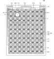
도 1은 본 명세서의 일 실시예에 따른 표시 장치의 개략적인 평면도이다. 도 1에서는 표시 장치(100)의 구성 요소 중 기판(110), 복수의 터치 전극(160, 170), 복수의 터치 라우팅 배선(RL1, RL2) 및 복수의 터치 패드(TP1, TP2)만을 도시하였다.1 is a schematic plan view of a display device according to an embodiment of the present specification. FIG. 1 shows only the
도 1을 참조하면, 본 명세서의 일 실시예에 따른 표시 장치(100)는 기판(110), 복수의 터치 전극(160, 170), 복수의 터치 라우팅 배선(RL1, RL2) 및 복수의 터치 패드(TP1, TP2)를 포함한다.Referring to FIG. 1, the
기판(110)은 표시 장치(100)의 다른 구성 요소를 지지하기 위한 지지 부재로, 절연 물질로 이루어질 수 있다. 예를 들어, 기판(110)은 유리 또는 수지 등으로 이루어질 수 있다. 또한, 기판(110)은 고분자 또는 폴리이미드(Polyimide, PI) 등과 같은 플라스틱을 포함하여 이루어질 수도 있고, 플렉서빌리티(flexibility)를 갖는 물질로 이루어질 수도 있다.The
기판(110)은 표시 영역(AA), 제1 비표시 영역(NA1) 및 제2 비표시 영역(NA2)을 포함한다.The
표시 영역(AA)은 영상을 표시하는 영역이다. 표시 영역(AA)에는 영상을 표시하기 위한 복수의 서브 화소 및 복수의 서브 화소를 구동하기 위한 구동 회로가 배치될 수 있다. 복수의 서브 화소 각각은 빛을 발광하는 개별 단위로, 복수의 서브 화소 각각에는 후술할 발광 소자(130)가 배치될 수 있다. 복수의 서브 화소는 적색 서브 화소, 녹색 서브 화소, 청색 서브 화소 및 백색 서브 화소를 포함할 수 있으나, 이에 제한되지 않는다. 구동 회로는 복수의 서브 화소를 구동하기 위한 다양한 트랜지스터, 스토리지 커패시터 및 배선 등을 포함할 수 있다. 예를 들어, 구동 회로는 구동 트랜지스터, 스위칭 트랜지스터, 센싱 트랜지스터, 스토리지 커패시터, 게이트 배선, 데이터 배선 등과 같은 다양한 구성 요소로 이루어질 수 있으나, 이에 제한되지 않는다.The display area (AA) is an area that displays an image. A plurality of sub-pixels for displaying an image and a driving circuit for driving the plurality of sub-pixels may be disposed in the display area AA. Each of the plurality of sub-pixels is an individual unit that emits light, and a light-emitting
제1 비표시 영역(NA1)은 영상이 표시되지 않는 영역으로, 표시 영역(AA)을 둘러싸도록 배치된다. 제1 비표시 영역(NA1)은 표시 영역(AA)에 배치된 복수의 서브 화소와 복수의 터치 전극(160, 170)을 구동하기 위한 다양한 배선, 패드, 구동 IC 등이 배치되는 영역이다. 예를 들어, 제1 비표시 영역(NA1)에는 게이트 구동부, 데이터 구동부, 터치 구동부와 같은 다양한 구동 IC 등이 배치될 수 있다.The first non-display area NA1 is an area where an image is not displayed and is arranged to surround the display area AA. The first non-display area NA1 is an area where various wiring, pads, driving ICs, etc. for driving the plurality of sub-pixels and the plurality of
제2 비표시 영역(NA2)은 영상이 표시되지 않는 영역으로, 표시 영역(AA) 내에 배치된다. 제2 비표시 영역(NA2)은 발광 소자(130) 및 복수의 터치 전극(160, 170)이 배치되지 않는 영역일 수 있다. 제2 비표시 영역(NA2)은 관통홀(TH)을 포함할 수 있다. 관통홀(TH)은 기판(110)을 관통하는 홀일 수 있다. 관통홀(TH)은 카메라 또는 광센서와 대응되도록 형성될 수 있다.The second non-display area NA2 is an area where an image is not displayed and is located within the display area AA. The second non-display area NA2 may be an area where the
복수의 터치 전극(160, 170)은 표시 영역(AA)에 배치된다. 복수의 터치 전극(160, 170)은 복수의 터치 감지 전극(160) 및 복수의 터치 구동 전극(170)을 포함할 수 있다. 복수의 터치 감지 전극(160)과 복수의 터치 구동 전극(170)은 일부가 교차하도록 배치될 수 있다. 즉, 복수의 터치 감지 전극(160)과 복수의 터치 구동 전극(170)은 일부가 중첩하도록 배치될 수 있다.A plurality of
복수의 터치 감지 전극(160)과 복수의 터치 구동 전극(170)은 표시 장치(100)에 입력되는 터치 입력을 감지할 수 있다. 이때, 터치 입력은 사용자의 손가락 또는 터치 펜에 의한 입력일 수 있다. 구체적으로, 표시 장치(100)의 특정 영역에 터치 동작이 이루어질 경우, 특정 영역과 인접한 복수의 터치 감지 전극(160)과 복수의 터치 구동 전극(170) 사이에는 정전 용량(capacitance) 변화가 발생할 수 있다. 표시 장치(100)는 이러한 정전 용량 변화를 감지하여 터치 좌표를 검출할 수 있다.The plurality of
복수의 터치 감지 전극(160) 각각은 제1 방향을 따라 연장된다. 복수의 터치 감지 전극(160)은 제1 방향과 상이한 제2 방향에서 일정 간격을 갖도록 이격될 수 있다. 이에, 제2 방향에서 서로 이격된 복수의 터치 감지 전극(160)은 서로 전기적으로 절연될 수 있다. 여기서, 제1 방향과 제2 방향은 서로 교차하는 방향일 수 있다. 제1 방향은 도 1을 기준으로 가로 방향일 수 있고, 제2 방향은 도 1을 기준으로 세로 방향일 수 있으나, 이에 제한되지 않는다. 제1 방향으로 연장된 터치 감지 전극(160)은 특정 영역에서 분리될 수 있다. 구체적으로, 복수의 터치 감지 전극(160) 각각은 터치 감지 전극(160)과 터치 구동 전극(170)의 중첩 영역에서 분리되도록 형성될 수 있다. 분리된 터치 감지 전극(160)은 브릿지 전극(162)에 의하여 연결될 수 있다.Each of the plurality of
복수의 터치 구동 전극(170)은 제2 방향을 따라 연장된다. 복수의 터치 구동 전극(170)은 제2 방향에서 끊어지지 않고 연속적으로 형성될 수 있다. 복수의 터치 구동 전극(170)은 제1 방향에서 일정 간격을 갖도록 이격될 수 있다. 이에, 제1 방향에서 서로 이격된 복수의 터치 구동 전극(170)은 서로 전기적으로 절연될 수 있다.The plurality of
복수의 터치 감지 전극(160)과 복수의 터치 구동 전극(170)은 서로 일정 간격을 갖도록 이격되어 배치될 수 있다. 이에, 복수의 터치 감지 전극(160)과 복수의 터치 구동 전극(170)은 서로 전기적으로 분리될 수 있다. 복수의 터치 감지 전극(160)과 복수의 터치 구동 전극(170)은 메탈 메쉬 구조를 가질 수 있다. 복수의 터치 감지 전극(160)과 복수의 터치 구동 전극(170)의 구체적 구조에 대해서는 도 2a 및 도 2b를 참조하여 후술하도록 한다. 한편, 본 발명에서는 복수의 터치 감지 전극(160)이 제1 방향으로 연장되고, 복수의 터치 구동 전극(170)이 제2 방향으로 연장되는 것을 기준으로 설명하였으나, 그 반대로 형성되어도 무방하다.The plurality of
복수의 터치 라우팅 배선(RL1, RL2)은 제1 비표시 영역(NA)에 배치된다. 복수의 터치 라우팅 배선(RL1, RL2)은 복수의 제1 터치 라우팅 배선(RL1) 및 복수의 제2 터치 라우팅 배선(RL2)을 포함한다. 복수의 제1 터치 라우팅 배선(RL1)은 복수의 터치 감지 전극(160)과 전기적으로 연결될 수 있다. 복수의 제2 터치 라우팅 배선(RL2)은 복수의 터치 구동 전극(170)과 전기적으로 연결될 수 있다. 복수의 터치 라우팅 배선(RL1, RL2) 각각의 일단은 복수의 터치 전극(160, 170)과 연결되고, 타단은 복수의 터치 패드(TP1, TP2)와 연결될 수 있다.A plurality of touch routing wires RL1 and RL2 are disposed in the first non-display area NA. The plurality of touch routing wires RL1 and RL2 include a plurality of first touch routing wires RL1 and a plurality of second touch routing wires RL2. The plurality of first touch routing wires RL1 may be electrically connected to the plurality of
복수의 터치 패드(TP1, TP2)는 제1 비표시 영역(NA)에 배치된다. 복수의 터치 패드(TP1, TP2)는 복수의 제1 터치 패드(TP1) 및 복수의 제2 터치 패드(TP2)를 포함한다. 복수의 제1 터치 패드(TP1)는 복수의 제1 터치 라우팅 배선(RL1)을 통해 복수의 터치 감지 전극(160)과 전기적으로 연결될 수 있다. 복수의 제2 터치 패드(TP2)는 복수의 제2 터치 라우팅 배선(RL2)을 통해 복수의 터치 구동 전극(170)과 전기적으로 연결될 수 있다. 복수의 터치 패드(TP1, TP2)에는 터치 구동부가 연결될 수 있다. 이에, 복수의 터치 패드(TP1, TP2)는 터치 구동부로부터 터치 신호를 전달받거나 터치 감지 신호를 터치 구동부에 전달할 수 있다.A plurality of touch pads TP1 and TP2 are disposed in the first non-display area NA. The plurality of touch pads TP1 and TP2 include a plurality of first touch pads TP1 and a plurality of second touch pads TP2. The plurality of first touch pads TP1 may be electrically connected to the plurality of
터치 구동부는 복수의 터치 전극(160, 170)과 연결되어 신호를 전송하거나 수신받을 수 있다. 예를 들어, 터치 구동부는 복수의 터치 감지 전극(160)으로부터 터치 감지 신호를 수신할 수 있다. 또한, 터치 구동부는 복수의 터치 구동 전극(170)으로 터치 구동 신호를 전송할 수 있다. 터치 구동부는 복수의 터치 감지 전극(160)과 복수의 터치 구동 전극(170) 사이의 상호 정전 용량(mutual capacitance)을 이용하여 터치를 감지할 수 있다. 즉, 표시 장치(100)에 터치 동작이 이루어질 경우, 복수의 터치 감지 전극(160)과 복수의 터치 구동 전극(170) 사이에는 정전 용량 변화가 발생할 수 있다. 터치 구동부는 이러한 정전 용량 변화를 감지하여 터치 좌표를 검출할 수 있다.The touch driver may be connected to a plurality of
이하에서는 도 2a 내지 도 2c를 참조하여 표시 장치(100)의 표시 영역(AA)에 대하여 구체적으로 설명하도록 한다.Hereinafter, the display area AA of the
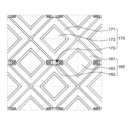
도 2a는 도 1의 A의 확대도이다. 도 2b은 도 2a의 메쉬 구조를 도시한 평면도이다.FIG. 2A is an enlarged view of A in FIG. 1. FIG. 2B is a plan view showing the mesh structure of FIG. 2A.
도 2a 및 도 2b를 참조하면, 복수의 터치 감지 전극(160)은 제1 방향으로 연장되고, 복수의 터치 구동 전극(170)은 제2 방향으로 연장된다. 복수의 터치 감지 전극(160)과 복수의 터치 구동 전극(170)은 서로 교차하도록 배치된다. 복수의 터치 감지 전극(160) 각각은 복수의 서브 터치 감지 전극(161), 복수의 브릿지 전극(162) 및 복수의 제1 플로팅 전극(163)을 포함한다. 복수의 터치 구동 전극(170) 각각은 복수의 서브 터치 구동 전극(171), 복수의 연결부(172) 및 복수의 제2 플로팅 전극(173)을 포함한다.Referring to FIGS. 2A and 2B , the plurality of
복수의 서브 터치 감지 전극(161)은 서로 이격되어 배치된다. 이때, 제1 방향을 따라 동일 행에 배치된 복수의 서브 터치 감지 전극(161)은 복수의 브릿지 전극(162)에 의하여 서로 전기적으로 연결될 수 있다. 복수의 브릿지 전극(162)은 복수의 서브 터치 감지 전극(161)과 상이한 층 상에 배치되어 서로 이격된 복수의 서브 터치 감지 전극(161)을 전기적으로 연결할 수 있다. 동일 행에 배치된 복수의 서브 터치 감지 전극(161)과 복수의 브릿지 전극(162)은 복수의 제1 터치 라우팅 배선(RL1) 중 어느 하나와 전기적으로 연결될 수 있다.The plurality of
복수의 서브 터치 구동 전극(171)은 서로 이격되어 배치된다. 이때, 제2 방향을 따라 동일 열에 배치된 복수의 서브 터치 구동 전극(171)은 복수의 연결부(172)에 의하여 서로 전기적으로 연결될 수 있다. 동일 열 내에 배치된 복수의 서브 터치 구동 전극(171)과 복수의 연결부(172)는 일체로 형성될 수 있다. 즉, 복수의 연결부(172)는 복수의 서브 터치 구동 전극(171)과 동일 층 상에서 복수의 서브 터치 구동 전극(171)으로부터 연장될 수 있다. 동일 열에 배치된 복수의 서브 터치 구동 전극(171)과 복수의 연결부(172)는 복수의 제2 터치 라우팅 배선(RL2) 중 어느 하나와 전기적으로 연결될 수 있다.The plurality of
복수의 서브 터치 감지 전극(161)과 복수의 서브 터치 구동 전극(171)은 동일 층 상에서 서로 이격되도록 배치된다. 복수의 브릿지 전극(162)과 복수의 연결부(172)는 서로 다른 층 상에서 서로 중첩하도록 배치된다. 복수의 터치 감지 전극(160)과 복수의 터치 구동 전극(170)의 교차 영역에는 복수의 브릿지 전극(162)과 복수의 연결부(172)가 배치된다. 이에, 복수의 터치 감지 전극(160)과 복수의 터치 구동 전극(170)은 서로 전기적으로 절연될 수 있다.The plurality of
복수의 제1 플로팅 전극(163) 각각은 복수의 서브 터치 감지 전극(161) 내에 배치된다. 복수의 제1 플로팅 전극(163)은 복수의 서브 터치 감지 전극(161)과 전기적으로 분리된다. 즉, 복수의 제1 플로팅 전극(163)은 복수의 서브 터치 감지 전극(161)으로부터 전기적으로 플로팅(floating)된다. 이에, 복수의 제1 플로팅 전극(163)은 복수의 제1 터치 라우팅 배선(RL1)과 전기적으로 분리된다. 복수의 제1 플로팅 전극(163)은 전기적으로 접지(ground)될 수 있다.Each of the plurality of first floating
복수의 제2 플로팅 전극(173) 각각은 복수의 서브 터치 구동 전극(171) 내에 배치된다. 복수의 제2 플로팅 전극(173)은 복수의 서브 터치 구동 전극(171)과 전기적으로 분리된다. 즉, 복수의 제2 플로팅 전극(173)은 복수의 서브 터치 구동 전극(171)으로부터 전기적으로 플로팅된다. 이에, 복수의 제2 플로팅 전극(173)은 복수의 제2 터치 라우팅 배선(RL2)과 전기적으로 분리된다. 복수의 제2 플로팅 전극(173)은 전기적으로 접지될 수 있다.Each of the plurality of second floating
복수의 서브 터치 감지 전극(161)은 복수의 제1 플로팅 전극(163)을 둘러싸도록 배치된다. 복수의 서브 터치 구동 전극(171)은 복수의 제2 플로팅 전극(173)을 둘러싸도록 배치된다. 복수의 서브 터치 감지 전극(161), 복수의 제1 플로팅 전극(163), 복수의 서브 터치 구동 전극(171) 및 복수의 제2 플로팅 전극(173)은 외곽이 모두 마름모 형상을 갖도록 형성될 수 있다. 그러나, 본 명세서가 이에 제한되지 않는다. 즉, 복수의 서브 터치 감지 전극(161)과 복수의 제1 플로팅 전극(163)이 전기적으로 분리되고, 복수의 서브 터치 구동 전극(171)과 복수의 제2 플로팅 전극(173)이 전기적으로 분리된다면, 이들의 형상 및 배치 구조는 변경될 수도 있다.The plurality of
표시 장치는 손가락과 같은 정전기를 띈 물체가 표시 장치에 접촉될 때, 접촉점에서 터치 감지 전극과 터치 구동 전극 사이의 뮤추얼 커패시턴스가 변화되는 현상을 감지함으로써, 터치 입력을 감지한다. 한편, 표시 장치의 소형화, 박형화 등에 의해 터치 전극들 사이의 간격과 손가락과 터치 전극들 사이의 간격이 줄어들 수 있다. 이 경우, 손가락은 접촉점 이외의 다른 부분에서 기생 커패시턴스를 발생시킬 수 있으며, 기생 커패시턴스는 접촉점 이외의 다른 부분에서 뮤추얼 커패시턴스를 변화시키는 리트랜스미션 현상을 유발할 수 있다. 결국, 접촉점 이외의 다른 부분에서 터치 신호가 발생되거나, 다른 부분에서 발생된 터치 신호가 접촉점의 터치 신호와 서로 상쇄되어 터치를 인식하지 못하는 문제가 발생될 수 있다.The display device detects a touch input by detecting a change in mutual capacitance between the touch sensing electrode and the touch driving electrode at the point of contact when a statically charged object such as a finger touches the display device. Meanwhile, the spacing between touch electrodes and the spacing between fingers and touch electrodes may be reduced due to miniaturization and thinning of the display device. In this case, the finger may generate parasitic capacitance in parts other than the contact point, and the parasitic capacitance can cause a retransmission phenomenon that changes the mutual capacitance in parts other than the contact point. Ultimately, a touch signal may be generated from a part other than the contact point, or a touch signal generated from another part may cancel each other out with the touch signal from the contact point, resulting in a problem of not recognizing the touch.
복수의 제1 플로팅 전극(163)과 복수의 제2 플로팅 전극(173)은 상술한 리트랜스미션 현상을 최소화할 수 있다. 즉, 복수의 제1 플로팅 전극(163)과 복수의 제2 플로팅 전극(173)은 손가락과 터치 감지 전극(160) 사이 및 손가락과 터치 구동 전극(170) 사이의 기생 커패시턴스를 감소시킬 수 있다. 커패시턴스는 서로 대향하는 2개의 도전체 사이의 거리에 반비례하고, 도전체의 면적에 비례한다. 서브 터치 감지 전극(161) 내에는 서브 터치 감지 전극(161)과 전기적으로 분리된 제1 플로팅 전극(163)이 배치된다. 서브 터치 구동 전극(171) 내에는 서브 터치 구동 전극(171)과 전기적으로 분리된 제2 플로팅 전극(173)이 배치된다. 이에, 복수의 터치 감지 전극(160)과 복수의 터치 구동 전극(170) 각각의 유효 전극 면적은 감소될 수 있다. 즉, 복수의 터치 감지 전극(160)의 유효 전극 면적은 복수의 제1 플로팅 전극(163)의 면적을 제외한 만큼 감소되고, 복수의 터치 구동 전극(170)의 유효 전극 면적은 복수의 제2 플로팅 전극(173)의 면적을 제외한 만큼 감소될 수 있다. 따라서, 손가락과 터치 감지 전극(160) 사이 및 손가락과 터치 구동 전극(170) 사이의 기생 커패시턴스가 감소되고, 리트랜스미션 현상이 최소화될 수 있다.The plurality of first floating
한편, 도 2a를 참조하면, 복수의 터치 감지 전극(160)과 복수의 터치 구동 전극(170)이 교차하는 지점을 노드(node)로 정의할 수 있다. 예를 들어, 하나의 노드는 도 2a의 점선들 사이의 영역으로 설정될 수 있다. 구체적으로, 복수의 서브 터치 감지 전극(161)의 상단부를 연결하는 가상의 연결선, 복수의 서브 터치 감지 전극(161)의 하단부를 연결하는 가상의 연결선, 복수의 서브 터치 구동 전극(171)의 일측 단부를 연결하는 가상의 연결선 및 복수의 서브 터치 구동 전극(171)의 타측 단부를 연결하는 가상의 연결선에 의하여 형성되는 복수의 영역 각각을 노드로 설정할 수 있다. 이에, 하나의 노드에는 서로 인접하는 2개의 서브 터치 감지 전극(161) 각각이 절반씩 배치되고, 서로 인접하는 2개의 서브 터치 구동 전극(171) 각각이 절반씩 배치될 수 있다. 또한, 노드의 중앙에는 브릿지 전극(162) 및 연결부(172)가 배치될 수 있다. 다만, 노드의 정의가 이에 제한되는 것은 아니다.Meanwhile, referring to FIG. 2A, a point where a plurality of
표시 장치(100)에는 복수의 노드가 제1 방향 및 제2 방향을 따라 연속적으로 나열되어 있다. 표시 장치(100)는 복수의 노드에 나타나는 전압 변화를 감지하여 터치 좌표를 판단할 수 있다. 구체적으로, 특정 영역에 터치 동작이 이루어지면, 특정 영역과 인접하는 일부 서브 터치 감지 전극(161)과 일부 서브 터치 구동 전극(171) 사이의 정전 용량 변화가 발생한다. 그리고 특정 영역과 인접하는 일부 노드 별로 정전 용량 변화값을 산출하고, 이를 조합하여 터치 위치를 판단할 수 있다.In the
도 2b를 참조하면, 복수의 터치 감지 전극(160)과 복수의 터치 구동 전극(170)은 메탈 메쉬 구조를 가질 수 있다. 구체적으로, 복수의 터치 감지 전극(160)과 복수의 터치 구동 전극(170)은 매우 얇은 선폭을 갖는 메탈 라인들이 서로 교차하여 이루어진 메쉬 패턴(mesh pattern)을 포함할 수 있다. 메쉬 패턴은 몰리브덴(Mo), 은(Ag), 티타늄(Ti), 구리(Cu), 알루미늄(Ti), 티타늄/알루미늄/티타늄(Ti/Al/Ti), 몰리브덴/알루미늄/몰리브덴(Mo/Al/Mo) 등의 메탈 물질로 이루어진 단층 또는 다층 구조를 가질 수 있으나, 이에 제한되지 않는다.Referring to FIG. 2B, the plurality of
복수의 터치 감지 전극(160)과 복수의 터치 구동 전극(170)의 메쉬 패턴 내부에는 개구부(OP)가 형성될 수 있다. 개구부(OP)는 서브 화소와 대응될 수 있다. 즉, 개구부(OP) 내에는 발광 소자(130)가 배치될 수 있다. 이하에서는 도 2c를 참조하여 표시 장치(100)의 구체적인 구조에 대하여 설명하도록 한다.An opening OP may be formed inside the mesh pattern of the plurality of
도 2c는 도 2b의 IIc-IIc'의 단면도이다.FIG. 2C is a cross-sectional view taken along line IIc-IIc' of FIG. 2B.
도 2c를 참조하면, 표시 장치(100)는 기판(110), 트랜지스터(120), 발광 소자(130), 봉지부(140), 터치 감지 전극(160) 및 터치 구동 전극(170)을 포함한다.Referring to FIG. 2C, the
트랜지스터(120)는 기판(110) 상에 배치되어 발광 소자(130)를 구동시키도록 구성된다. 트랜지스터(120)는 액티브층(121), 게이트 전극(122), 소스 전극(123) 및 드레인 전극(124)을 포함할 수 있다. 한편, 도시되지는 않았으나, 기판(110)과 트랜지스터(120) 사이에는 버퍼층이 배치될 수도 있다. 버퍼층은 기판(110)을 통해 수분 또는 불순물이 침투되는 것을 저감할 수 있다. 버퍼층은 예를 들어, 실리콘 산화물(SiOx) 또는 실리콘 질화물(SiNx)의 단일층 또는 복층으로 구성될 수 있으나, 이에 제한되지 않는다.The
액티브층(121)은 기판(110) 상에 배치된다. 액티브층(121)은 트랜지스터(120) 구동 시 채널이 형성되는 영역이다. 액티브층(121)은 채널 영역, 소스 영역 및 드레인 영역을 포함할 수 있다. 액티브층(121)은 산화물 반도체, 비정질 실리콘 또는 폴리 실리콘 등과 같은 반도체 물질로 이루어질 수 있으나, 이에 제한되지 않는다.The
액티브층(121) 상에는 게이트 절연층(111)이 배치된다. 게이트 절연층(111)은 액티브층(121)과 게이트 전극(122)을 절연시키기 위한 절연층으로, 실리콘 산화물(SiOx) 또는 실리콘 질화물(SiNx)의 단일층 또는 복층으로 구성될 수 있으나, 이에 제한되지 않는다.A
게이트 전극(122)은 게이트 절연층(111) 상에 배치된다. 게이트 전극(122)은 액티브층(121)의 채널 영역과 중첩하도록 게이트 절연층(111) 상에 배치된다. 게이트 전극(122)은 도전성 물질, 예를 들어, 구리(Cu), 알루미늄(Al), 몰리브덴(Mo), 니켈(Ni), 티타늄(Ti), 크롬(Cr) 또는 이에 대한 합금으로 구성될 수 있으나, 이에 제한되지 않는다.The
게이트 전극(122) 상에는 제1 층간 절연층(112) 및 제2 층간 절연층(113)이 배치된다. 제1 층간 절연층(112) 및 제2 층간 절연층(113)에는 소스 전극(123) 및 드레인 전극(124) 각각이 액티브층(121)에 접속하기 위한 컨택홀이 형성된다. 제1 층간 절연층(112)은 실리콘 산화물(SiOx) 또는 실리콘 질화물(SiNx)의 단일층 또는 복층으로 구성될 수 있으나, 이에 제한되지 않는다. 제2 층간 절연층(113)은 유기 물질로 이루어질 수 있고, 예를 들어, 폴리이미드(Polyimide) 또는 포토아크릴(Photo Acryl)의 단일층 또는 복층으로 구성될 수 있으나, 이에 제한되지 않는다.A first
소스 전극(123) 및 드레인 전극(124)은 제2 층간 절연층(113) 상에 서로 이격되어 배치된다. 소스 전극(123) 및 드레인 전극(124)은 게이트 절연층(111), 제1 층간 절연층(112) 및 제2 층간 절연층(113)의 컨택홀을 통해 액티브층(121)과 전기적으로 연결된다. 소스 전극(123) 및 드레인 전극(124)은 도전성 물질, 예를 들어, 구리(Cu), 알루미늄(Al), 몰리브덴(Mo), 니켈(Ni), 티타늄(Ti), 크롬(Cr) 또는 이에 대한 합금으로 구성될 수 있으나, 이에 제한되지 않는다.The
트랜지스터(120) 상에는 평탄화층(114)이 배치된다. 평탄화층(114)은 기판(110)의 상부를 평탄화하는 절연층이다. 평탄화층(114)에는 트랜지스터(120)의 소스 전극(123)을 노출시키기 위한 컨택홀이 형성된다. 그러나, 평탄화층(114)에는 드레인 전극(124)을 노출시키기 위한 컨택홀이 형성될 수도 있다. 평탄화층(114)은 유기 물질로 이루어질 수 있고, 예를 들어, 폴리이미드(Polyimide) 또는 포토아크릴(Photo Acryl)의 단일층 또는 복층으로 구성될 수 있으나, 이에 제한되지 않는다.A
발광 소자(130)는 평탄화층(114) 상에 배치된다. 발광 소자(130)는 트랜지스터(120)로부터 공급되는 데이터 신호에 의해 광을 방출한다. 발광 소자(130)는 복수의 터치 감지 전극(160)과 복수의 터치 구동 전극(170)의 메쉬 패턴에 의하여 형성되는 개구부(OP)와 대응되도록 배치될 수 있다. 발광 소자(130)는 제1 전극(131), 발광층(132) 및 제2 전극(133)을 포함한다. 여기서, 제1 전극(131)은 애노드 전극이고, 제2 전극(133)은 캐소드 전극일 수 있다.The
한편, 표시 장치(100)는 탑 에미션(Top Emission) 또는 바텀 에미션(Bottom Emission) 방식으로 구현될 수 있다. 탑 에미션 방식인 경우, 제1 전극(131)의 하부에는 발광층(132)에서 발광된 광을 제2 전극(133) 측으로 반사시키기 위한 반사층이 배치될 수 있다. 예를 들어, 반사층은 알루미늄(Al) 또는 은(Ag)과 같은 반사성이 우수한 물질을 포함할 수 있으나, 이에 제한되지 않는다. 반대로, 바텀 에미션 방식인 경우, 제1 전극(131)은 투명 도전성 물질로만 이루어질 수 있다. 이하에서는 본 발명의 일 실시예에 따른 표시 장치(100)가 탑 에미션 방식인 것으로 가정하여 설명하기로 한다.Meanwhile, the
제1 전극(131)은 평탄화층(114) 상에 배치된다. 제1 전극(131)은 복수의 서브 화소 각각과 대응될 수 있다. 즉, 제1 전극(131)은 개구부(OP)와 대응되도록 배치될 수 있다. 제1 전극(131)은 평탄화층(114)에 형성된 컨택홀을 통해 트랜지스터(120)의 소스 전극(123)과 전기적으로 연결될 수 있다. 제1 전극(131)은 발광층(132)에 정공을 공급하기 위하여 일함수가 높은 도전성 물질로 이루어질 수 있다. 예를 들어, 제1 전극(131)은 인듐 주석 산화물(Indium Tin Oxide, ITO), 인듐 아연 산화물(Indium Zin Oxide, IZO) 등과 같은 투명 도전성 물질로 형성될 수 있으나, 이에 제한되지 않는다.The
제1 전극(131) 및 평탄화층(114) 상에는 뱅크(115)가 배치된다. 뱅크(115)는 제1 전극(131)의 가장자리를 덮도록 평탄화층(114) 상에 형성될 수 있다. 뱅크(115)는 복수의 서브 화소를 구분하기 위해, 복수의 서브 화소 사이에 배치된 절연층이다. 뱅크(115)는 유기 절연 물질일 수 있다. 예를 들어, 뱅크(115)는 폴리이미드(polyimide), 아크릴(acryl) 또는 벤조사이클로부텐(benzocyclobutene, BCB)계 수지로 이루어질 수 있으나, 이에 제한되는 것은 아니다.A
발광층(132)은 제1 전극(131) 및 뱅크(115) 상에 배치된다. 발광층(132)은 기판(110)의 전면에 걸쳐서 형성될 수 있다. 즉, 발광층(132)은 복수의 서브 화소에 공통적으로 형성되는 공통층일 수 있다. 발광층(132)은 특정 색의 광을 발광하기 위한 유기층일 수 있다. 발광층(132)은 정공 수송층, 정공 주입층, 정공 저지층, 전자 주입층, 전자 저지층, 전자 수송층 등과 같은 다양한 층을 더 포함할 수도 있다.The
제2 전극(133)은 발광층(132) 상에 배치된다. 제2 전극(133)은 기판(110)의 전면에 걸쳐서 하나의 층으로 형성될 수 있다. 즉, 제2 전극(133)은 복수의 서브 화소에 공통적으로 형성되는 공통층일 수 있다. 제2 전극(133)은 발광층(132)으로 전자를 공급하므로, 일함수가 낮은 도전성 물질로 이루어질 수 있다. 제2 전극(133)은 예를 들어, 인듐 주석 산화물(Indium Tin Oxide, ITO), 인듐 아연 산화물(Indium Zin Oxide, IZO) 등과 같은 투명 도전성 물질, MgAg와 같은 금속 합금이나 이테르븀(Yb) 합금 등으로 형성될 수 있고, 금속 도핑층이 더 포함될 수도 있으며, 이에 제한되지 않는다.The
봉지부(140)는 발광 소자(130) 상에 배치된다. 봉지부(140)는 표시 장치(100) 외부로부터 침투하는 수분 등으로부터 발광 소자(130)를 보호한다. 봉지부(140)는 제1 봉지층(141), 이물 커버층(142) 및 제2 봉지층(143)을 포함한다.The
제1 봉지층(141)은 제2 전극(133) 상에 배치되어 수분이나 산소의 침투를 억제할 수 있다. 제1 봉지층(141)은 질화 실리콘(SiNx), 산질화 실리콘(SiNxOy) 또는 산화알루미늄(AlyOz) 등과 같은 무기물로 이루어질 수 있으나, 이에 제한되는 것은 아니다.The
이물 커버층(142)은 제1 봉지층(141) 상에 배치되어 표면을 평탄화한다. 또한 이물 커버층(142)은 제조 공정 상 발생할 수 있는 이물 또는 파티클을 커버할 수 있다. 이물 커버층(142)은 유기물, 예를 들어, 실리콘옥시카본(SiOxCz), 아크릴 또는 에폭시 계열의 수지 등으로 이루어질 수 있으나, 이에 제한되는 것은 아니다.The foreign
제2 봉지층(143)은 이물 커버층(142) 상에 배치되고, 제1 봉지층(141)과 같이 수분이나 산소의 침투를 억제할 수 있다. 이때, 제2 봉지층(143)과 제1 봉지층(141)은 이물 커버층(142)을 밀봉하도록 형성될 수 있다. 따라서, 제2 봉지층(143)에 의하여 발광 소자(130)로 침투하는 수분이나 산소가 보다 효과적으로 감소될 수 있다. 제2 봉지층(143)은 실리콘 산화물(SiOx), 실리콘 질화물(SiNx), 실리콘 산질화물(SiNxOy) 또는 산화알루미늄(AlyOz) 등과 같은 무기물로 이루어질 수 있으나, 이에 제한되는 것은 아니다.The
봉지부(140) 상에는 터치 버퍼층(152)이 배치된다. 즉, 터치 버퍼층(152)은 제2 봉지층(143) 상에 배치된다. 터치 버퍼층(152)은 수분 또는 불순물의 침투를 저감할 수 있다. 터치 버퍼층(152)은 실리콘 산화물(SiOx) 또는 실리콘 질화물(SiNx)의 단일층 또는 복층으로 구성될 수 있으나, 이에 제한되지 않는다.A
복수의 서브 터치 감지 전극(161) 및 복수의 서브 터치 구동 전극(171)은 터치 버퍼층(152) 상에 배치된다. 복수의 서브 터치 감지 전극(161)과 복수의 서브 터치 구동 전극(171)은 터치 버퍼층(152) 상에서 일정 간격 이격되어 배치될 수 있다. 제1 방향으로 인접하는 복수의 서브 터치 감지 전극(161)은 복수의 브릿지 전극(162)에 의하여 전기적으로 연결될 수 있다. 이때, 복수의 서브 터치 감지 전극(161)과 복수의 브릿지 전극(162)은 서로 다른 층에 배치될 수 있다. 제2 방향으로 인접하는 복수의 서브 터치 구동 전극(171)은 복수의 연결부(172)에 의하여 전기적으로 연결될 수 있다. 이때, 복수의 서브 터치 구동 전극(171)과 복수의 연결부(172)는 터치 버퍼층(152) 상에서 일체로 형성될 수 있다.A plurality of
한편, 도 2c에는 도시되지 않았으나, 복수의 제1 플로팅 전극(163)과 복수의 제2 플로팅 전극(173)은 터치 버퍼층(152) 상에 배치된다. 복수의 제1 플로팅 전극(163)은 터치 버퍼층(152) 상에서 복수의 서브 터치 감지 전극(161)과 이격되도록 배치된다. 복수의 제2 플로팅 전극(173)은 터치 버퍼층(152) 상에서 복수의 서브 터치 구동 전극(171)과 이격되도록 배치된다.Meanwhile, although not shown in FIG. 2C, a plurality of first floating
터치 버퍼층(152), 복수의 서브 터치 감지 전극(161), 복수의 제1 플로팅 전극(163), 복수의 서브 터치 구동 전극(171), 복수의 연결부(172) 및 복수의 제2 플로팅 전극(173) 상에는 터치 절연층(153)이 배치된다. 터치 절연층(153)은 복수의 연결부(172)와 복수의 브릿지 전극(162)을 전기적으로 절연시킬 수 있다. 터치 절연층(153)은 복수의 서브 터치 감지 전극(161)과 복수의 브릿지 전극(162)이 서로 연결되기 위한 컨택홀을 포함할 수 있다. 터치 절연층(153)은 실리콘 산화물(SiOx) 또는 실리콘 질화물(SiNx)의 단일층 또는 복층으로 구성될 수 있으나, 이에 제한되지 않는다.A
복수의 브릿지 전극(162)은 터치 절연층(153) 상에 배치된다. 복수의 브릿지 전극(162)은 제1 방향으로 인접하는 복수의 서브 터치 감지 전극(161) 사이에 배치된다. 이에, 복수의 브릿지 전극(162)은 서로 이격된 복수의 서브 터치 감지 전극(161)을 전기적으로 연결할 수 있다. 또한, 복수의 브릿지 전극(162)은 복수의 연결부(172)와 중첩하도록 배치될 수 있다. 이때, 복수의 브릿지 전극(162)과 복수의 연결부(172)는 서로 다른 층에 형성되므로, 전기적으로 절연될 수 있다.A plurality of
터치 절연층(153) 및 복수의 브릿지 전극(162) 상에는 제2 터치 평탄화층(154)이 배치된다. 제2 터치 평탄화층(154)은 복수의 터치 감지 전극(160) 및 복수의 터치 구동 전극(170)의 상부를 평탄화할 수 있다. 제2 터치 평탄화층(154)은 유기 물질로 이루어질 수 있고, 예를 들어, 폴리이미드(Polyimide) 또는 포토아크릴(Photo Acryl)의 단일층 또는 복층으로 구성될 수 있으나, 이에 제한되지 않는다.A second
이하에서는 도 3a 및 도 3b를 참조하여 표시 장치(100)의 제2 비표시 영역(NA2)에 대하여 구체적으로 설명하도록 한다.Hereinafter, the second non-display area NA2 of the
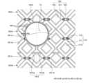
도 3a는 도 1의 B의 확대도이다. 도 3b는 도 3a의 IIIb-IIIb'의 단면도이다.FIG. 3A is an enlarged view of B in FIG. 1. FIG. 3B is a cross-sectional view taken along line IIIb-IIIb' of FIG. 3A.
도 3a 및 도 3b를 참조하면, 표시 영역(AA) 내에는 제2 비표시 영역(NA2)이 배치된다. 제2 비표시 영역(NA2)은 관통홀(TH), 복수의 댐(DM1, DM2) 및 연결 라인(180)을 포함한다. 제2 비표시 영역(NA2)은 관통홀(TH) 및 관통홀(TH)과 인접하는 주변 영역을 의미할 수 있다. 관통홀(TH)에 의하여 제2 비표시 영역(NA2)에는 발광 소자(130)와 터치 전극(160, 170)이 배치되지 않을 수 있다. 다만, 제2 비표시 영역(NA2)의 외곽에는 터치 전극(160, 170)으로부터 연장되어 연결 라인(180)과 연결되기 위한 메탈 라인들의 일부가 배치될 수도 있다.Referring to FIGS. 3A and 3B , a second non-display area NA2 is disposed within the display area AA. The second non-display area NA2 includes a through hole TH, a plurality of dams DM1 and DM2, and a
관통홀(TH)은 제2 비표시 영역(NA2) 내에 형성된다. 관통홀(TH)은 기판(110), 게이트 절연층(111), 제1 층간 절연층(112), 제1 봉지층(141), 제2 봉지층(143), 제1 터치 평탄화층(151), 터치 버퍼층(152), 터치 절연층(153) 및 제2 터치 평탄화층(154)을 물리적으로 관통하도록 형성될 수 있다. 관통홀(TH)은 카메라 또는 광센서와 대응되도록 형성될 수 있다. 관통홀(TH)에 의하여 카메라 또는 광센서의 상부에서 빛이 용이하게 투과될 수 있다.The through hole TH is formed in the second non-display area NA2. The through hole (TH) includes a
복수의 댐(DM1, DM2)은 관통홀(TH)을 둘러싸도록 배치된다. 복수의 댐(DM1, DM2)은 제1 댐(DM1) 및 제2 댐(DM2)을 포함한다.A plurality of dams (DM1, DM2) are arranged to surround the through hole (TH). The plurality of dams DM1 and DM2 include a first dam DM1 and a second dam DM2.
제1 댐(DM1)은 관통홀(TH)의 외곽을 둘러싸는 폐곡선 형상으로 형성될 수 있다. 제1 댐(DM1)은 제2 층간 절연층(113)으로 이루어진 제1 층, 평탄화층(114)으로 이루어진 제2 층 및 뱅크(115)로 이루어진 제3 층을 포함할 수 있다. 도 3b에서는 제1 댐(DM1)이 하나인 것으로 도시되었으나, 이에 제한되지 않는다. 제1 댐(DM1)은 이물 커버층(142)이 관통홀(TH)로 흘러 넘치는 것을 방지할 수 있다. 즉, 이물 커버층(142)은 제1 댐(DM1)에 의하여 표시 영역(AA)으로부터 제1 댐(DM1)의 내측까지 형성될 수 있다.The first dam DM1 may be formed in a closed curve shape surrounding the outside of the through hole TH. The first dam DM1 may include a first layer made of a second
제2 댐(DM2)은 관통홀(TH)의 외곽을 둘러싸는 폐곡선 형상으로 형성될 수 있다. 제2 댐(DM2)은 제1 댐(DM1)과 관통홀(TH) 사이 및 제1 댐(DM1)과 표시 영역(AA) 사이에 복수로 배치될 수 있다. 복수의 제2 댐(DM2)은 서로 일정 거리를 갖도록 이격될 수 있다. 제2 댐(DM2)은 제2 층간 절연층(113)으로 이루어진 제1 층 및 평탄화층(114)으로 이루어진 제2 층을 포함할 수 있다. 도 3b에서는 제2 댐(DM2)이 제1 댐(DM1)을 기준으로 양측에 3개씩 배치된 것으로 도시되었으나, 이에 제한되지 않는다.The second dam DM2 may be formed in a closed curve shape surrounding the outside of the through hole TH. A plurality of second dams DM2 may be arranged between the first dam DM1 and the through hole TH and between the first dam DM1 and the display area AA. The plurality of second dams DM2 may be spaced apart from each other at a certain distance. The second dam DM2 may include a first layer made of a second
제2 댐(DM2)은 발광층(132)을 통해 수분이 표시 영역(AA)으로 침투하는 것을 방지할 수 있다. 즉, 수분 침투에 취약한 발광층(132)은 제2 댐(DM2)에 의하여 단선(disconnection) 구조를 가질 수 있다. 구체적으로, 제2 댐(DM2)의 제2 층간 절연층(113)의 상면은 평탄화층(114)의 하면보다 작은 폭을 가질 수 있다. 이에, 제2 댐(DM2)의 상부에 배치되는 발광층(132)은 제2 댐(DM2)에 의하여 연속되지 않고 단절될 수 있다. 이때, 발광층(132) 상의 제2 전극(133)도 발광층(132)과 유사하게 단절된 구조를 가지며 발광층(132)을 커버할 수 있다. 또한, 제2 전극(133) 상의 제1 봉지층(141)은 단절된 발광층(132) 및 제2 전극(133)을 완전히 커버하도록 배치될 수 있다. 따라서, 관통홀(TH)의 측면으로 노출된 발광층(132)을 통해 수분이 침투하더라도, 복수의 제2 댐(DM2)에 의하여 침투된 수분이 표시 영역(AA)으로 이동하는 것이 방지될 수 있다. 또한, 제1 봉지층(141)이 단절된 발광층(132) 및 제2 전극(133)을 완전히 커버하므로, 수분 침투가 보다 효과적으로 방지될 수 있다.The second dam DM2 may prevent moisture from penetrating into the display area AA through the
제1 댐(DM1)의 상부에서 제1 봉지층(141)과 제2 봉지층(143)은 서로 접촉할 수 있다. 즉, 제1 댐(DM1)과 관통홀(TH) 사이에서 제1 봉지층(141)과 제2 봉지층(143)은 완전히 접촉할 수 있다. 이에, 관통홀(TH)을 통한 수분의 침투가 보다 효과적으로 방지될 수 있다.At the top of the first dam DM1, the
제2 비표시 영역(NA2)에서 복수의 댐(DM1, DM2) 상에는 제1 터치 평탄화층(151)이 배치될 수 있다. 제1 터치 평탄화층(151)은 제2 봉지층(143) 상에 배치될 수 있다. 또한, 제1 터치 평탄화층(151)은 관통홀(TH)과 표시 영역(AA) 사이와 대응되는 영역에 배치될 수 있다. 제1 터치 평탄화층(151)은 관통홀(TH)을 통한 수분의 침투를 방지할 수 있다. 제1 터치 평탄화층(151)은 유기 물질로 이루어질 수 있고, 예를 들어, 폴리이미드(Polyimide) 또는 포토아크릴(Photo Acryl)의 단일층 또는 복층으로 구성될 수 있으나, 이에 제한되지 않는다.The first
제1 터치 평탄화층(151) 상에서 터치 버퍼층(152), 터치 절연층(153) 및 제2 터치 평탄화층(154)은 서로 접하며 순차적으로 배치될 수 있다. 이에, 관통홀(TH)을 통한 수분의 침투가 최소화될 수 있다.On the first
연결 라인(180)은 터치 절연층(153) 상에서 관통홀(TH)을 둘러싸도록 배치된다. 연결 라인(180)은 복수의 댐(DM1, DM2)의 외곽에 배치될 수 있다. 연결 라인(180)은 관통홀(TH)에 의하여 분리된 터치 감지 전극(160) 또는 분리된 터치 구동 전극(170)을 전기적으로 연결한다. 구체적으로, 관통홀(TH)은 기판(110) 및 그 상부의 구성들을 관통하도록 구성되므로, 관통홀(TH) 내에는 복수의 터치 전극(160, 170)이 형성될 수 없다. 이에, 연결 라인(180)은 관통홀(TH)을 사이에 둔 2개의 서브 터치 감지 전극(161)을 연결할 수 있다. 또는, 연결 라인(180)은 관통홀(TH)을 사이에 둔 2개의 서브 터치 구동 전극(171)을 연결할 수 있다. 도 3a 및 도 3b에서는 연결 라인(180)이 3개로 구비되는 것으로 도시되었으나, 이에 제한되지 않는다. 즉, 분리된 터치 감지 전극(160) 또는 분리된 터치 구동 전극(170)을 서로 연결할 수만 있다면 연결 라인(180)의 개수 및 형상은 제한되지 않는다.The
한편, 도 3a를 참조하면, 복수의 서브 터치 감지 전극(161) 중 제2 비표시 영역(NA2)과 인접하는 적어도 하나의 서브 터치 감지 전극(161)은 나머지 서브 터치 감지 전극(161)과 상이한 형상을 갖는다. 이하에서는 설명의 편의를 위하여 나머지 서브 터치 감지 전극(161)을 일반 서브 터치 감지 전극(161)으로 지칭하고, 일반 서브 터치 감지 전극(161)과 상이한 형상을 가진 서브 터치 감지 전극(161)을 제1 이형 전극(HE1)으로 지칭하도록 한다. 일반 서브 터치 감지 전극(161)은 도 2a와 같은 형상을 가진 서브 터치 감지 전극(161)을 의미할 수 있다. 또한, 제1 이형 전극(HE1)은 도 3a에 도시된 바와 같이 일반 서브 터치 감지 전극(161)과 상이한 형상을 가진 서브 터치 감지 전극(161)을 의미할 수 있다. 여기서, 제1 이형 전극(HE1)은 관통홀(TH)에 의하여 잘림으로써 형상이 변경된 전극을 의미하지는 않는다. 즉, 제1 이형 전극(HE1)은 관통홀(TH)에 의하여 형상이 변경된 것이 아닌, 제2 비표시 영역(NA2)과 접하지 않는 부분에서 의도적으로 형상이 변경되어 일반 서브 터치 감지 전극(161)과 상이한 형상을 가진 전극을 의미할 수 있다.Meanwhile, referring to FIG. 3A, among the plurality of
또한, 복수의 서브 터치 구동 전극(171) 중 제2 비표시 영역(NA2)과 인접하는 적어도 하나의 서브 터치 구동 전극(171)은 나머지 서브 터치 구동 전극(171)과 상이한 형상을 갖는다. 이하에서는 설명의 편의를 위하여 나머지 서브 터치 구동 전극(171)을 일반 서브 터치 구동 전극(171)으로 지칭하고, 일반 서브 터치 구동 전극(171)과 상이한 형상을 가진 서브 터치 구동 전극(171)을 제2 이형 전극(HE2)으로 지칭하도록 한다. 일반 서브 터치 구동 전극(171)은 도 2a와 같은 형상을 가진 서브 터치 구동 전극(171)을 의미할 수 있다. 또한, 제2 이형 전극(HE2)은 도 3a에 도시된 바와 같이 일반 서브 터치 구동 전극(171)과 상이한 형상을 가진 서브 터치 구동 전극(171)을 의미할 수 있다. 여기서, 제2 이형 전극(HE2)은 관통홀(TH)에 의하여 잘림으로써 형상이 변경된 전극을 의미하지는 않는다. 즉, 제2 이형 전극(HE2)은 관통홀(TH)에 의하여 형상이 변경된 것이 아닌, 제2 비표시 영역(NA2)과 접하지 않는 부분에서 의도적으로 형상이 변경되어 일반 서브 터치 구동 전극(171)과 상이한 형상을 가진 전극을 의미할 수 있다.Additionally, among the plurality of
복수의 터치 감지 전극(160) 중 일부와 복수의 터치 구동 전극(170) 중 일부는 관통홀(TH)을 포함하는 제2 비표시 영역(NA2)에 의하여 일부 영역이 잘리게 된다. 이에, 본 명세서에서는 제2 비표시 영역(NA2)과 인접한 일부 서브 터치 감지 전극(161)과 일부 서브 터치 구동 전극(171)의 형상을 변경하여 이형 전극(HE1, HE2)으로 구성한다. 이에, 관통홀(TH)에 의하여 손실된 터치 전극(160, 170)의 면적을 보상할 수 있다.Some of the plurality of
정전 용량 방식의 터치 센서는 터치 감지 전극과 터치 구동 전극 사이의 상호 정전 용량에 의하여 터치 입력을 감지할 수 있다. 일반적으로, 전극의 면적이 클수록 상호 정전 용량이 증가하고, 터치의 센싱 감도가 향상될 수 있다. 그러나, 카메라 또는 광센서 등을 배치하기 위하여 표시 영역 내부에 관통홀을 형성할 경우, 관통홀과 인접하는 전극의 면적이 손실되어 센싱 감도가 저하되는 문제가 발생할 수 있다. 즉, 전극의 면적 감소에 의하여 터치 동작 시 발생하는 정전 용량 변화량이 감소된다. 따라서, 면적이 손실된 전극이 포함된 노드에서 검출되는 정전 용량 변화량이 감소되어 터치 성능이 저하될 수 있다.A capacitive touch sensor can detect a touch input by mutual capacitance between a touch sensing electrode and a touch driving electrode. In general, the larger the area of the electrode, the greater the mutual capacitance and the improved touch sensing sensitivity. However, when a through hole is formed inside the display area to place a camera or an optical sensor, the area of the electrode adjacent to the through hole is lost, which may cause a problem of reduced sensing sensitivity. In other words, the amount of change in capacitance that occurs during a touch operation is reduced by reducing the area of the electrode. Accordingly, the amount of capacitance change detected in the node containing the electrode with the loss of area is reduced, which may deteriorate touch performance.
이에, 본 명세서에 따른 표시 장치(100)는 제2 비표시 영역(NA2)과 인접한 일부 서브 터치 감지 전극(161)과 일부 서브 터치 구동 전극(171)을 이형 전극(HE1, HE2)으로 구성할 수 있다. 따라서, 이형 전극(HE1, HE2)에 의하여 관통홀(TH)에 의한 노드의 면적 손실을 보상할 수 있다. 이에, 표시 장치(100)의 터치 감도가 저하되는 것을 방지할 수 있다.Accordingly, the
구체적으로, 도 3a를 참조하면, 복수의 터치 감지 전극(160)은 제2 비표시 영역(NA2)과 인접하는 제1 터치 감지 전극(160A)과 제2 터치 감지 전극(160B)을 포함할 수 있다. 제1 터치 감지 전극(160A)과 제2 터치 감지 전극(160B)은 서로 이웃하도록 배치될 수 있다. 여기서, 제1 터치 감지 전극(160A)은 관통홀(TH)에 의하여 일부 면적이 손실된 터치 감지 전극(160)이고, 제2 터치 감지 전극(160B)은 관통홀(TH)에 의한 면적 손실이 없는 터치 감지 전극(160)일 수 있으나, 이에 제한되지 않는다.Specifically, referring to FIG. 3A, the plurality of
제1 터치 감지 전극(160A)의 복수의 서브 터치 감지 전극(161) 중 일부는 제1 이형 전극(HE1)으로 구성된다. 제2 터치 감지 전극(160B)의 복수의 서브 터치 감지 전극(161) 중 일부는 제1 이형 전극(HE1)으로 구성된다. 이하에서는 관통홀(TH)의 좌측과 우측 각각에 배치된 제1 터치 감지 전극(160A)의 제1 이형 전극(HE1)을 제1a 이형 전극(HE1a)과 제1b 이형 전극(HE1b)으로 정의하도록 한다. 또한, 제1a 이형 전극(HE1a) 및 제1b 이형 전극(HE1b)과 제2 방향으로 서로 이웃하는 제2 터치 감지 전극(160B)의 제1 이형 전극(HE1)을 제1c 이형 전극(HE1c) 및 제1d 이형 전극(HE1d)으로 정의하도록 한다. 서로 이웃하는 제1a 이형 전극(HE1a)과 제1c 이형 전극(HE1c) 사이의 경계는 일반 서브 터치 감지 전극(161) 사이의 경계와 상이하게 이루어질 수 있다.Some of the plurality of
복수의 제1 이형 전극(HE1)의 제2 방향에 대한 길이는 일반 서브 터치 감지 전극(161)의 제2 방향에 대한 길이와 상이하게 이루어진다. 예를 들어, 제1 터치 감지 전극(160A)의 제1a 이형 전극(HE1a)과 제1b 이형 전극(HE1b)의 제2 방향에 대한 길이는 일반 서브 터치 감지 전극(161)의 제2 방향에 대한 길이보다 길다. 또한, 제2 터치 감지 전극(160B)의 제1c 이형 전극(HE1c)과 제1d 이형 전극(HE1d)의 제2 방향에 대한 길이는 일반 서브 터치 감지 전극(161)의 제2 방향에 대한 길이보다 짧다. 특히, 제2 방향을 기준으로, 제1a 이형 전극(HE1a)의 길이와 제1c 이형 전극(HE1c)의 길이의 합은 일반 서브 터치 감지 전극(161) 2개의 길이의 합과 동일하다. 즉, 제1a 이형 전극(HE1a)의 길이를 상대적으로 길게 형성하고, 제1c 이형 전극(HE1c)의 길이를 상대적으로 짧게 형성할 수 있다. 여기서, 길이는 제2 방향의 양측 끝단 사이의 거리를 의미할 수 있다.The length of the plurality of first special electrodes HE1 in the second direction is different from the length of the general
한편, 제1a 이형 전극(HE1a)과 제1b 이형 전극(HE1b)의 사이 및 제1c 이형 전극(HE1c)과 제1d 이형 전극(HE1d)의 사이에도 제1 이형 전극(HE1)이 존재할 수 있다. 제1a 이형 전극(HE1a)과 제1b 이형 전극(HE1b)의 사이에 배치된 제1 이형 전극(HE1)은 관통홀(TH)에 의하여 대부분이 손실된 상태일 수 있다. 제1c 이형 전극(HE1c)과 제1d 이형 전극(HE1d)의 사이에 배치된 제1 이형 전극(HE1)은 제1c 이형 전극(HE1c) 및 제1d 이형 전극(HE1d)와 유사한 형상을 갖도록 형성될 수 있다. 그러나, 본 발명이 이에 제한되지 않는다.Meanwhile, the first special electrode HE1 may be present between the 1a special electrode HE1a and the 1b special electrode HE1b and between the 1c special electrode HE1c and the 1d special electrode HE1d. Most of the first release electrode HE1 disposed between the 1a release electrode HE1a and the 1b release electrode HE1b may be lost due to the through hole TH. The first release electrode HE1 disposed between the 1c release electrode HE1c and the 1d release electrode HE1d may be formed to have a shape similar to the 1c release electrode HE1c and the 1d release electrode HE1d. You can. However, the present invention is not limited thereto.
노드는 복수의 터치 감지 전극(160)과 복수의 터치 구동 전극(170)이 교차하는 지점을 의미할 수 있다. 또한, 노드는 복수의 서브 터치 감지 전극(161)의 상단부를 연결하는 가상의 연결선, 복수의 서브 터치 감지 전극(161)의 하단부를 연결하는 가상의 연결선, 복수의 서브 터치 구동 전극(171)의 일측 단부를 연결하는 가상의 연결선 및 복수의 서브 터치 구동 전극(171)의 타측 단부를 연결하는 가상의 연결선에 의하여 형성되는 영역으로 설정될 수 있다. 예를 들어, 노드는 도 3a의 점선들 사이의 영역으로 설정될 수 있다. 이하에서는 설명의 편의를 위하여 관통홀(TH)에 의하여 면적 손실이 발생된 노드를 손실 발생 노드로 지칭하고, 면적 손실이 발생되지 않은 노드를 일반 노드로 지칭하도록 한다.A node may refer to a point where a plurality of
도 3a를 참조하면, 관통홀(TH)이 형성된 일부 노드의 경계선은 인접한 다른 노드의 경계선과 상이하게 이루어질 수 있다. 구체적으로, 제1a 이형 전극(HE1a)의 길이가 길어짐에 따라, 제1a 이형 전극(HE1a)이 포함된 노드의 길이는 일반 서브 터치 감지 전극(161)이 포함된 노드의 길이보다 확장될 수 있다. 이때, 제1a 이형 전극(HE1a)이 포함된 노드는 손실 발생 노드일 수 있다. 즉, 제1a 이형 전극(HE1a)의 길이를 상대적으로 길게 형성함으로써, 제1a 이형 전극(HE1a)이 포함된 노드의 면적이 확장되고, 관통홀(TH)에 의한 면적 손실이 보상될 수 있다. 특히, 노드의 면적이 확장됨에 따라 노드에 포함된 터치 감지 전극(160)과 터치 구동 전극(170)의 면적이 증가될 수 있다. 이때, 정전 용량은 전극의 면적이 증가할수록 커진다. 따라서, 손실 발생 노드에서도 터치가 발생했음을 인지할 만큼 충분한 정전 용량 변화량이 감지될 수 있다.Referring to FIG. 3A, the boundary lines of some nodes where through holes (TH) are formed may be different from the boundary lines of other adjacent nodes. Specifically, as the length of the 1a heterogeneous electrode HE1a increases, the length of the node containing the 1a heterogeneous electrode HE1a may be extended than the length of the node containing the general
손실 발생 노드의 면적은 일반 노드의 면적의 60% 이상이 되도록 구성될 수 있다. 여기서, 손실 발생 노드는 도 3a에 도시된 바와 같이 제2 비표시 영역(NA2)과 접하는 노드일 수 있다. 일반 노드는 도 2a에 도시된 바와 같이 제2 비표시 영역(NA2)과 완전히 이격된 노드일 수 있다. 만약, 손실 발생 노드의 면적이 일반 노드의 면적의 60%보다 작을 경우, 손실 발생 노드에서의 터치 센싱 감도가 저하될 수 있다. 즉, 손실 발생 노드의 면적이 작아진 만큼, 손실 발생 노드에 포함된 터치 감지 전극(160)과 터치 구동 전극(170)의 면적은 작아질 수 있다. 따라서, 해당 노드 주변에서 터치 동작이 이루어지더라도, 터치 감지 전극(160)과 터치 구동 전극(170)의 정전 용량 변화가 매우 작을 수 있다. 이러한 경우, 터치 좌표의 정확한 검출이 어려워질 수 있다.The area of the node where loss occurs may be configured to be more than 60% of the area of a normal node. Here, the loss-generating node may be a node in contact with the second non-display area NA2, as shown in FIG. 3A. The general node may be a node that is completely spaced apart from the second non-display area NA2, as shown in FIG. 2A. If the area of the node where the loss occurs is smaller than 60% of the area of the general node, the touch sensing sensitivity at the node where the loss occurs may deteriorate. That is, as the area of the loss-generating node becomes smaller, the areas of the
제1a 이형 전극(HE1a)의 길이가 확장됨에 따라, 제1a 이형 전극(HE1a)과 인접하는 제1c 이형 전극(HE1c)의 길이는 축소된다. 이때, 제1c 이형 전극(HE1c)이 포함된 노드는 면적 손실이 없는 노드일 수 있다. 또한, 제1c 이형 전극(HE1c)이 포함된 노드의 면적은 일반 노드의 면적의 60% 이상이 되도록 구성될 수 있다. 이에, 제1c 이형 전극(HE1c)의 길이가 상대적으로 짧아지더라도, 터치 센싱 감도가 저하되는 것을 방지할 수 있다.As the length of the 1a special electrode HE1a is extended, the length of the 1c special electrode HE1c adjacent to the 1a special electrode HE1a is reduced. At this time, the node including the 1c heterogeneous electrode HE1c may be a node with no area loss. Additionally, the area of the node including the 1c heterogeneous electrode HE1c may be configured to be more than 60% of the area of the general node. Accordingly, even if the length of the 1c unusual electrode HE1c is relatively short, touch sensing sensitivity can be prevented from being deteriorated.
제1b 이형 전극(HE1b)은 제1a 이형 전극(HE1a)과 유사하게 구성되고, 제1d 이형 전극(HE1d)은 제1 c 이형 전극(HE1c)과 유사하게 구성된다. 이에, 제1b 이형 전극(HE1b) 및 제1d 이형 전극(HE1d)에 대한 중복 설명은 생략한다. 한편, 제1b 이형 전극(HE1b)이 배치된 일부 노드는 면적 손실이 없는 노드일 수 있다. 즉, 제1b 이형 전극(HE1b)의 일측에 해당되는 노드는 관통홀(TH)에 의하여 면적이 손실되나, 타측에 해당되는 노드는 면적 손실이 없다. 이에, 제1b 이형 전극(HE1b)의 타측에 해당되는 노드는 일반 노드로 설정될 수 있다.The 1b special electrode HE1b is configured similarly to the 1a special electrode HE1a, and the 1d special electrode HE1d is configured similarly to the 1c special electrode HE1c. Accordingly, redundant description of the 1b special type electrode HE1b and the 1d special electrode HE1d will be omitted. Meanwhile, some nodes where the 1b heterogeneous electrode HE1b is disposed may be nodes without area loss. That is, the node corresponding to one side of the 1b heterogeneous electrode HE1b loses area due to the through hole TH, but the node corresponding to the other side does not lose area. Accordingly, the node corresponding to the other side of the 1b heterogeneous electrode HE1b may be set as a normal node.
제1 터치 감지 전극(160A)의 상부에는 제3 터치 감지 전극(160C)이 배치될 수 있다. 또한, 제3 터치 감지 전극(160C)에도 관통홀(TH)에 의한 면적 손실이 발생할 수 있다. 다만, 제3 터치 감지 전극(160C) 내에서의 면적 손실은 제1 터치 감지 전극(160A) 내에서의 면적 손실보다 작을 수 있다. 또한, 제3 터치 감지 전극(160C) 상의 손실 발생 노드의 면적은 일반 노드의 면적의 60% 이상일 수 있다. 이에, 제3 터치 감지 전극(160C) 및 이와 교차하는 복수의 터치 구동 전극(170)의 노드들은 이형 전극에 의한 면적 보상 없이도 용이하게 터치 동작을 검출할 수 있다.A third
도 3a를 참조하면, 복수의 터치 구동 전극(170)의 복수의 서브 터치 구동 전극(171) 중 일부는 제2 이형 전극(HE2)으로 구성된다. 이하에서는 관통홀(TH)의 좌측 하부 및 우측 하부에 각각 배치된 제2 이형 전극(HE2)을 제2a 이형 전극(HE2a) 및 제2b 이형 전극(HE2b)으로 정의하도록 한다.Referring to FIG. 3A , some of the plurality of
제2a 이형 전극(HE2a)은 제1a 이형 전극(HE1a)과 이웃하게 배치된다. 특히, 제2a 이형 전극(HE2a)의 외곽 형상은 제1a 이형 전극(HE1a)의 외곽 형상과 대응될 수 있다. 즉, 제1a 이형 전극(HE1a)의 형상이 변경됨에 따라, 이와 인접하는 제2a 이형 전극(HE2a)의 형상도 함께 변경될 수 있다. 제2b 이형 전극(HE2b)은 제1b 이형 전극(HE1b)과 이웃하게 배치된다. 특히, 제2b 이형 전극(HE2b)의 외곽 형상은 제1b 이형 전극(HE1b)의 외곽 형상과 대응될 수 있다. 즉, 제1b 이형 전극(HE1b)의 형상이 변경됨에 따라, 이와 인접하는 제2b 이형 전극(HE2b)의 형상도 함께 변경될 수 있다.The 2a unusual electrode HE2a is disposed adjacent to the 1a unusual electrode HE1a. In particular, the outer shape of the 2a special electrode HE2a may correspond to the outer shape of the first a special electrode HE1a. That is, as the shape of the 1st atypical electrode HE1a changes, the shape of the 2a atypical electrode HE2a adjacent to it may also change. The 2b special electrode HE2b is disposed adjacent to the 1b special electrode HE1b. In particular, the outer shape of the 2b special electrode HE2b may correspond to the outer shape of the 1b special electrode HE1b. That is, as the shape of the 1b special electrode HE1b changes, the shape of the adjacent 2b special electrode HE2b may also change.
한편, 도 3a 도시된 관통홀(TH), 제2 비표시 영역(NA2), 이형 전극(HE1, HE2) 등의 위치 및 구조는 본 명세서를 설명하기 위한 하나의 예일 뿐이며, 이것으로 본 명세서가 제한되는 것은 아니다. 즉, 표시 장치(100)의 설계에 따라 이들의 위치 및 구조는 다양하게 수 있다.Meanwhile, the positions and structures of the through hole TH, second non-display area NA2, and special electrodes HE1 and HE2 shown in FIG. 3A are only one example for explaining the present specification, which constitutes the scope of the present specification. It is not limited. That is, their positions and structures may vary depending on the design of the
본 명세서에 따른 표시 장치(100)는 제2 비표시 영역(NA2)과 인접하는 복수의 서브 터치 감지 전극(161) 중 적어도 하나를 제1 이형 전극(HE1)으로 구성한다. 또한, 제2 비표시 영역(NA2)과 인접하는 복수의 서브 터치 구동 전극(171) 중 적어도 하나를 제2 이형 전극(HE2)으로 구성한다. 이에, 관통홀(TH)에 의한 면적 손실이 발생된 노드에서 터치 센싱 감도가 저하되는 것을 방지할 수 있다.The
구체적으로, 서로 이웃하는 제1 이형 전극(HE1) 중 하나의 길이를 상대적으로 길게 구성하고, 그 대신 다른 하나의 길이를 상대적으로 짧게 구성할 수 있다. 이때, 상대적으로 길게 형성된 제1 이형 전극(HE1)을 포함하는 터치 감지 전극(160)은 관통홀(TH)에 의하여 면적 손실이 발생한 전극일 수 있다. 또한, 상대적으로 짧게 형성된 제1 이형 전극(HE1)을 포함하는 터치 감지 전극(160)은 관통홀(TH)에 의한 면적 손실이 없거나 면적 손실이 상대적으로 적은 전극일 수 있다. 즉, 도 3a에 도시된 바와 같이, 제1 터치 감지 전극(160A)의 일부 서브 터치 감지 전극(161)의 면적을 이웃하는 제2 터치 감지 전극(160B)의 영역까지 확장할 수 있다. 따라서, 제1 터치 감지 전극(160A)에 발생한 면적 손실을 보상할 수 있다. 특히, 관통홀(TH)과 인접하는 노드에서의 서브 터치 감지 전극(161)의 면적이 확장됨에 따라 해당 노드에서 검출될 수 있는 정전 용량 변화량이 증가될 수 있다. 따라서, 표시 장치(100)의 터치 센싱의 정확도를 향상시킬 수 있다.Specifically, the length of one of the adjacent first heterogeneous electrodes HE1 may be configured to be relatively long, and instead, the length of the other electrode may be configured to be relatively short. At this time, the
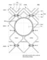
도 4는 본 명세서의 다른 실시예에 따른 표시 장치의 평면도이다. 도 4는 제2 비표시 영역(NA2)이 포함된 일부 영역에 대한 확대 평면도일 수 있다. 도 4의 표시 장치(400)는 도 1 내지 도 3b의 표시 장치(100)와 비교하여 플로팅 전극(163, 173)만이 상이하고 나머지는 실질적으로 동일하므로, 중복 설명은 생략하도록 한다.4 is a plan view of a display device according to another embodiment of the present specification. FIG. 4 may be an enlarged plan view of a partial area including the second non-display area NA2. Since the
도 4를 참조하면, 표시 장치(400)는 제1 방향으로 연장되는 복수의 터치 감지 전극(160) 및 제2 방향으로 연장되는 복수의 터치 구동 전극(170)을 포함한다.Referring to FIG. 4 , the
복수의 터치 감지 전극(160)은 서로 이웃하는 제1 터치 감지 전극(460A) 및 제2 터치 감지 전극(460B)을 포함할 수 있다. 여기서, 제1 터치 감지 전극(460A)은 관통홀(TH)에 의하여 일부 면적이 손실된 터치 감지 전극(160)이고, 제2 터치 감지 전극(460B)은 관통홀(TH)에 의한 면적 손실이 없는 터치 감지 전극(160)일 수 있으나, 이에 제한되지 않는다.The plurality of
제1 터치 감지 전극(460A)의 복수의 서브 터치 감지 전극(161) 중 일부는 제1 이형 전극(HE1)으로 구성된다. 제2 터치 감지 전극(460B)의 복수의 서브 터치 감지 전극(161) 중 일부는 제1 이형 전극(HE1)으로 구성된다. 구체적으로, 제1 터치 감지 전극(460A)은 제1a 이형 전극(HE1a)과 제1b 이형 전극(HE1b)을 포함하고, 제2 터치 감지 전극(460B)은 제1c 이형 전극(HE1c)과 제1d 이형 전극(HE1d)을 포함한다. 또한, 제1 터치 감지 전극(460A)은 제1a 이형 전극(HE1a)과 제1b 이형 전극(HE1b) 사이의 또 다른 제1 이형 전극(HE1)을 더 포함할 수도 있다. 또한, 제2 터치 감지 전극(460B)은 제1c 이형 전극(HE1c)과 제1d 이형 전극(HE1d) 사이의 또 다른 제1 이형 전극(HE1)을 더 포함할 수도 있다.Some of the plurality of
복수의 터치 구동 전극(170)은 서로 이웃하는 제1 터치 구동 전극(470A) 및 제2 터치 구동 전극(470B)을 포함할 수 있다. 제1 터치 구동 전극(470A)과 제2 터치 구동 전극(470B)은 모두 관통홀(TH)에 의하여 일부 면적이 손실된 터치 구동 전극(170)일 수 있으나, 이에 제한되지 않는다.The plurality of
제1 터치 구동 전극(470A)의 복수의 서브 터치 구동 전극(171) 중 일부는 제2 이형 전극(HE2)으로 구성된다. 제2 터치 구동 전극(470B)의 복수의 서브 터치 구동 전극(171) 중 일부는 제2 이형 전극(HE2)으로 구성된다. 구체적으로, 제1 터치 구동 전극(470A)은 제2a 이형 전극(HE2a)을 포함하고, 제2 터치 구동 전극(470B)은 제2b 이형 전극(HE2b)을 포함한다.Some of the plurality of
제1 플로팅 전극(163)은 복수의 서브 터치 감지 전극(161) 중 일부에만 배치된다. 예를 들어, 제1 플로팅 전극(163)은 복수의 서브 터치 감지 전극(161) 중 제1 이형 전극(HE1) 외의 일반 서브 터치 감지 전극(161)에만 배치될 수 있다. 또한, 제1 플로팅 전극(163)은 일반 서브 터치 감지 전극(161) 중 일부에만 배치될 수도 있다. 구체적으로, 제1 플로팅 전극(163)은 일반 서브 터치 감지 전극(161) 중 면적 손실이 전혀 발생하지 않은 서브 터치 감지 전극(161) 또는 면적 손실이 적은 서브 터치 감지 전극(161)에만 배치될 수 있다.The first floating
제2 플로팅 전극(173)은 복수의 서브 터치 구동 전극(171) 중 일부에만 배치된다. 예를 들어, 제2 플로팅 전극(173)은 복수의 서브 터치 구동 전극(171) 중 제2 이형 전극(HE2) 외의 일반 서브 터치 구동 전극(171)에만 배치될 수 있다. 또한, 제2 플로팅 전극(173)은 일반 서브 터치 구동 전극(171) 중 일부에만 배치될 수도 있다. 구체적으로, 제2 플로팅 전극(173)은 일반 서브 터치 구동 전극(171) 중 면적 손실이 전혀 발생하지 않은 서브 터치 감지 전극(171) 또는 면적 손실이 적은 서브 터치 감지 전극(171)에만 배치될 수 있다.The second floating
본 명세서의 다른 실시예에 따른 표시 장치(400)는 제2 비표시 영역(NA2)과 인접하는 복수의 서브 터치 감지 전극(161) 중 적어도 하나를 제1 이형 전극(HE1)으로 구성한다. 또한, 제2 비표시 영역(NA2)과 인접하는 복수의 서브 터치 구동 전극(171) 중 적어도 하나를 제2 이형 전극(HE2)으로 구성한다. 이에, 관통홀(TH)에 의한 면적 손실을 보상하고, 터치 센싱 감도가 저하되는 것을 방지할 수 있다.The
제1 플로팅 전극(163)은 복수의 서브 터치 감지 전극(161) 중 일부에만 배치되고, 제2 플로팅 전극(173)은 복수의 서브 터치 구동 전극(171) 중 일부에만 배치된다. 이에, 플로팅 전극(163, 173)이 배치되지 않은 서브 터치 감지 전극(161) 또는 서브 터치 구동 전극(171)의 유효 면적을 증가시킬 수 있다. 따라서, 표시 장치(400)의 터치 센싱 감도를 향상시킬 수 있다.The first floating
구체적으로, 도 4에 도시된 바와 같이, 제1 이형 전극(HE1)은 제1 플로팅 전극(163)을 포함하지 않는다. 이때, 정전 용량은 면적이 커질수록 증가한다. 따라서, 제1 이형 전극(HE1)의 유효 면적이 증가되고, 정전 용량 변화량이 증가될 수 있다. 특히, 제1 이형 전극(HE1)은 관통홀(TH)에 의하여 면적 손실이 발생된 터치 감지 전극(160) 또는 이웃한 터치 감지 전극(160)의 면적 보상을 위하여 일부 면적이 축소된 터치 감지 전극(160)에 배치된다. 따라서, 제1 이형 전극(HE1)의 유효 면적 증가에 따라, 관통홀(TH)에 의한 면적 손실이 보다 효과적으로 보상될 수 있다. 또한, 제1 이형 전극(HE1)의 유효 면적 증가에 따라, 터치 감지 전극(160)의 일부 면적이 축소되는 것이 보상될 수 있다.Specifically, as shown in FIG. 4, the first special electrode HE1 does not include the first floating
제2 이형 전극(HE2)은 제2 플로팅 전극(173)을 포함하지 않는다. 따라서, 제2 이형 전극(HE2)의 유효 면적이 증가되고, 정전 용량 변화량이 증가될 수 있다. 특히, 제2 이형 전극(HE2)은 관통홀(TH)에 의하여 면적 손실이 발생된 터치 구동 전극(170)에 배치된다. 따라서, 제2 이형 전극(HE2)의 유효 면적 증가에 따라, 관통홀(TH)에 의한 면적 손실이 보다 효과적으로 보상될 수 있다.The second special electrode HE2 does not include the second floating
특히, 도 4에 도시된 바와 같이, 관통홀(TH)의 좌측 상단 및 우측 상단에 배치된 서브 터치 구동 전극(171)에는 제2 플로팅 전극(173)이 형성되지 않는다. 즉, 관통홀(TH)에 의하여 면적 손실이 크게 발생한 서브 터치 구동 전극(171)에는 제2 플로팅 전극(173)이 형성되지 않는다. 따라서, 해당 서브 터치 구동 전극(171)의 유효 면적 증가에 따라, 관통홀(TH)에 의한 면적 손실이 보상될 수 있다. 또한, 제1c 이형 전극(HE1c)과 동일 노드 및 제1d 이형 전극(HE1d)과 동일 노드에 배치된 서브 터치 구동 전극(171)에는 제2 플로팅 전극(173)이 형성되지 않는다. 이때, 제1c 이형 전극(HE1c)과 제1d 이형 전극(HE1d)이 배치된 노드는 축소된 노드일 수 있다. 따라서, 일반 노드 대비 면적이 축소된 노드에 포함된 서브 터치 구동 전극(171)의 유효 면적을 증가시키고, 노드의 면적 축소를 보상할 수 있다.In particular, as shown in FIG. 4, the second floating
도 5는 본 명세서의 또 다른 실시예에 따른 표시 장치의 평면도이다. 도 5는 제2 비표시 영역(NA2)이 포함된 일부 영역에 대한 확대 평면도일 수 있다. 도 5의 표시 장치(500)는 도 4의 표시 장치(400)와 비교하여 이형 전극(HE1, HE2)만이 상이하고 나머지는 실질적으로 동일하므로, 중복 설명은 생략하도록 한다.Figure 5 is a plan view of a display device according to another embodiment of the present specification. FIG. 5 may be an enlarged plan view of a partial area including the second non-display area NA2. Since the
도 5를 참조하면, 표시 장치(500)는 제1 방향으로 연장되는 복수의 터치 감지 전극(160) 및 제2 방향으로 연장되는 복수의 터치 구동 전극(170)을 포함한다.Referring to FIG. 5 , the
복수의 터치 감지 전극(160)은 서로 이웃하는 제1 터치 감지 전극(560A) 및 제2 터치 감지 전극(560B)을 포함할 수 있다. 여기서, 제1 터치 감지 전극(560A)은 관통홀(TH)에 의하여 일부 면적이 손실된 터치 감지 전극(160)이고, 제2 터치 감지 전극(560B)은 관통홀(TH)에 의한 면적 손실이 없는 터치 감지 전극(160)일 수 있으나, 이에 제한되지 않는다.The plurality of
제1 터치 감지 전극(560A)의 복수의 서브 터치 감지 전극(161) 중 일부는 제1 이형 전극(HE1)으로 구성된다. 제2 터치 감지 전극(560B)의 복수의 서브 터치 감지 전극(161) 중 일부는 제1 이형 전극(HE1)으로 구성된다. 구체적으로, 제1 터치 감지 전극(560A)은 제1a 이형 전극(HE1a), 제1b 이형 전극(HE1b) 및 제1c 이형 전극(HE1c)을 포함하고, 제2 터치 감지 전극(560B)은 제1d 이형 전극(HE1d), 제1e 이형 전극(HE1e) 및 제1f 이형 전극(HE1f)을 포함한다. 제1 이형 전극(HE1)은 모두 제1 플로팅 전극(163)을 포함하지 않는다.Some of the plurality of
복수의 터치 구동 전극(170)은 서로 이웃하는 제1 터치 구동 전극(570A) 및 제2 터치 구동 전극(570B)을 포함할 수 있다. 제1 터치 구동 전극(570A)과 제2 터치 구동 전극(570B)은 모두 관통홀(TH)에 의하여 일부 면적이 손실된 터치 구동 전극(170)일 수 있으나, 이에 제한되지 않는다.The plurality of
제1 터치 구동 전극(570A)의 복수의 서브 터치 구동 전극(171) 중 일부는 제2 이형 전극(HE2)으로 구성된다. 제2 터치 구동 전극(570B)의 복수의 서브 터치 구동 전극(171) 중 일부는 제2 이형 전극(HE2)으로 구성된다. 구체적으로, 제1 터치 구동 전극(570A)은 제2a 이형 전극(HE2a), 제2b 이형 전극(HE2b), 제2c 이형 전극(HE2c)을 포함하고, 제2 터치 구동 전극(570B)은 제2d 이형 전극(HE2d), 제2e 이형 전극(HE2e), 제2f 이형 전극(HE2f)을 포함한다. 제2 이형 전극(HE2)은 모두 제2 플로팅 전극(173)을 포함하지 않는다.Some of the plurality of
본 명세서의 또 다른 실시예에 따른 표시 장치(500)는 제2 비표시 영역(NA2)과 인접하는 복수의 서브 터치 감지 전극(161) 중 적어도 하나를 제1 이형 전극(HE1)으로 구성한다. 또한, 제2 비표시 영역(NA2)과 인접하는 복수의 서브 터치 구동 전극(171) 중 적어도 하나를 제2 이형 전극(HE2)으로 구성한다. 이에, 관통홀(TH)에 의한 면적 손실을 보상하고, 터치 센싱 감도가 저하되는 것을 방지할 수 있다.The
이웃하는 제1 이형 전극(HE1)과 제2 이형 전극(HE2)의 외곽의 형상은 서로 대응될 수 있다. 특히, 제1 이형 전극(HE1)과 제2 이형 전극(HE2)은 모두 일반 서브 터치 감지 전극(161) 및 일반 서브 터치 구동 전극(171)과 완전히 상이한 형상을 갖도록 구성될 수 있다. 이에, 하나의 노드에서의 제1 이형 전극(HE1)과 제2 이형 전극(HE2)의 면적비를 유사하게 구성할 수 있다. 따라서, 터치 센싱의 정확도가 보다 향상될 수 있다.The outer shapes of the neighboring first and second unusual electrodes HE1 and HE2 may correspond to each other. In particular, both the first special electrode HE1 and the second special electrode HE2 may be configured to have completely different shapes from the general
이형 전극(HE1, HE2)은 모두 플로팅 전극(163, 173)을 포함하지 않는다. 이에, 이형 전극(HE1, HE2)의 유효 면적을 증가시킬 수 있다. 따라서, 표시 장치(500)의 터치 센싱 감도를 향상시킬 수 있다.Neither of the heterogeneous electrodes HE1 and HE2 includes the floating
본 명세서의 다양한 실시예들에 따른 표시 장치는 다음과 같이 설명될 수 있다.A display device according to various embodiments of the present specification may be described as follows.
본 명세서의 일 실시예에 따른 표시 장치는 표시 영역 및 상기 표시 영역 내의 비표시 영역을 포함하는 기판; 상기 표시 영역에 배치되는 복수의 발광 소자; 상기 복수의 발광 소자를 커버하는 봉지부; 상기 표시 영역에서 상기 봉지부 상에 배치되며, 제1 방향으로 연장되는 복수의 터치 감지 전극; 및 상기 표시 영역에서 상기 봉지부 상에 배치되며, 상기 제1 방향과 상이한 제2 방향으로 연장되는 복수의 터치 구동 전극을 포함하고, 상기 복수의 터치 감지 전극 각각은 서로 이격된 복수의 서브 터치 감지 전극을 포함하고, 상기 복수의 서브 터치 감지 전극 중 상기 비표시 영역과 인접하는 적어도 하나의 서브 터치 감지 전극은 나머지 서브 터치 감지 전극과 상이한 형상의 제1 이형 전극으로 구성된다.A display device according to an embodiment of the present specification includes a substrate including a display area and a non-display area within the display area; a plurality of light emitting elements disposed in the display area; an encapsulation portion covering the plurality of light emitting devices; a plurality of touch sensing electrodes disposed on the encapsulation part in the display area and extending in a first direction; and a plurality of touch driving electrodes disposed on the encapsulation part in the display area and extending in a second direction different from the first direction, wherein each of the plurality of touch sensing electrodes detects a plurality of sub-touches spaced apart from each other. and an electrode, wherein at least one sub-touch sensing electrode adjacent to the non-display area among the plurality of sub-touch sensing electrodes is configured as a first special type electrode having a different shape from the remaining sub-touch sensing electrodes.
본 명세서의 다른 특징에 따르면, 상기 제1 이형 전극과 상기 나머지 서브 터치 감지 전극은 상기 제2 방향에 대하여 상이한 길이를 가질 수 있다.According to another feature of the present specification, the first release electrode and the remaining sub-touch sensing electrode may have different lengths with respect to the second direction.
본 명세서의 또 다른 특징에 따르면, 상기 복수의 터치 감지 전극은 상기 비표시 영역과 인접하는 영역에서 서로 이웃하게 배치된 제1 터치 감지 전극 및 제2 터치 감지 전극을 포함하고, 상기 제1 터치 감지 전극의 상기 제1 이형 전극과 상기 제2 터치 감지 전극의 상기 제1 이형 전극은 상기 제2 방향으로 서로 이웃하게 배치될 수 있다.According to another feature of the present specification, the plurality of touch sensing electrodes include a first touch sensing electrode and a second touch sensing electrode disposed adjacent to each other in an area adjacent to the non-display area, and the first touch sensing electrode The first special electrode of the electrode and the first special electrode of the second touch sensing electrode may be arranged adjacent to each other in the second direction.
본 명세서의 또 다른 특징에 따르면, 상기 제1 터치 감지 전극의 상기 제1 이형 전극의 상기 제2 방향에 대한 길이는 상기 나머지 서브 터치 감지 전극의 상기 제2 방향에 대한 길이보다 길고, 상기 제2 터치 감지 전극의 상기 제1 이형 전극의 상기 제2 방향에 대한 길이는 상기 나머지 서브 터치 감지 전극의 상기 제2 방향에 대한 길이보다 짧을 수 있다.According to another feature of the present specification, the length of the first touch sensing electrode in the second direction is longer than the length of the remaining sub-touch sensing electrode in the second direction, and the second The length of the first special electrode of the touch sensing electrode in the second direction may be shorter than the length of the remaining sub-touch sensing electrode in the second direction.
본 명세서의 또 다른 특징에 따르면, 상기 복수의 터치 구동 전극 각각은 서로 이격된 복수의 서브 터치 구동 전극을 포함하고, 상기 복수의 서브 터치 구동 전극 중 상기 비표시 영역과 인접하는 적어도 하나의 서브 터치 구동 전극은 나머지 서브 터치 구동 전극과 상이한 형상의 제2 이형 전극으로 구성될 수 있다.According to another feature of the present specification, each of the plurality of touch driving electrodes includes a plurality of sub-touch driving electrodes spaced apart from each other, and at least one sub-touch adjacent to the non-display area among the plurality of sub-touch driving electrodes The driving electrode may be composed of a second special electrode having a different shape from the remaining sub-touch driving electrodes.
본 명세서의 또 다른 특징에 따르면, 상기 복수의 터치 감지 전극은 상기 복수의 서브 터치 감지 전극을 전기적으로 연결하는 복수의 브릿지 전극을 더 포함하고, 상기 복수의 터치 구동 전극은 상기 복수의 서브 터치 구동 전극을 연결하며 상기 복수의 서브 터치 구동 전극과 일체로 이루어진 복수의 연결부를 더 포함하고, 상기 복수의 브릿지 전극과 상기 복수의 연결부는 서로 중첩하도록 배치될 수 있다.According to another feature of the present specification, the plurality of touch sensing electrodes further include a plurality of bridge electrodes electrically connecting the plurality of sub-touch sensing electrodes, and the plurality of touch driving electrodes drive the plurality of sub-touch It may further include a plurality of connection parts that connect electrodes and are integrated with the plurality of sub-touch driving electrodes, and the plurality of bridge electrodes and the plurality of connection parts may be arranged to overlap each other.
본 명세서의 또 다른 특징에 따르면, 상기 복수의 터치 감지 전극의 상기 제1 이형 전극과 상기 복수의 터치 구동 전극의 상기 제2 이형 전극은 서로 이웃하게 배치될 수 있다.According to another feature of the present specification, the first special electrode of the plurality of touch sensing electrodes and the second special electrode of the plurality of touch driving electrodes may be arranged adjacent to each other.
본 명세서의 또 다른 특징에 따르면, 상기 제1 이형 전극의 외곽의 형상은 상기 제1 이형 전극과 이웃하는 상기 제2 이형 전극의 외곽의 형상과 대응될 수 있다.According to another feature of the present specification, the outer shape of the first special electrode may correspond to the outer shape of the second special electrode adjacent to the first special electrode.
본 명세서의 또 다른 특징에 따르면, 상기 복수의 서브 터치 감지 전극 내에서 상기 복수의 서브 터치 감지 전극과 전기적으로 분리되는 복수의 제1 플로팅 전극; 및 상기 복수의 서브 터치 구동 전극 내에서 상기 복수의 서브 터치 구동 전극과 전기적으로 분리되는 복수의 제2 플로팅 전극을 더 포함할 수 있다.According to another feature of the present specification, a plurality of first floating electrodes are electrically separated from the plurality of sub-touch sensing electrodes within the plurality of sub-touch sensing electrodes; And it may further include a plurality of second floating electrodes within the plurality of sub-touch driving electrodes that are electrically separated from the plurality of sub-touch driving electrodes.
본 명세서의 또 다른 특징에 따르면, 상기 복수의 제1 플로팅 전극은 상기 복수의 서브 터치 감지 전극 중 일부에만 배치되고, 상기 복수의 제2 플로팅 전극은 상기 복수의 서브 터치 구동 전극 중 일부에만 배치될 수 있다.According to another feature of the present specification, the plurality of first floating electrodes may be disposed only on some of the plurality of sub-touch detection electrodes, and the plurality of second floating electrodes may be disposed on only some of the plurality of sub-touch driving electrodes. You can.
본 명세서의 또 다른 특징에 따르면, 상기 복수의 제1 플로팅 전극은 상기 복수의 서브 터치 감지 전극 중 상기 제1 이형 전극 외의 상기 나머지 서브 터치 감지 전극에 배치될 수 있다.According to another feature of the present specification, the plurality of first floating electrodes may be disposed on the remaining sub-touch sensing electrodes other than the first special electrode among the plurality of sub-touch sensing electrodes.
본 명세서의 또 다른 특징에 따르면, 상기 복수의 제2 플로팅 전극은 상기 복수의 서브 터치 구동 전극 중 상기 제2 이형 전극 외의 상기 나머지 서브 터치 구동 전극에 배치될 수 있다.According to another feature of the present specification, the plurality of second floating electrodes may be disposed on the remaining sub-touch driving electrodes other than the second special electrode among the plurality of sub-touch driving electrodes.
본 명세서의 또 다른 특징에 따르면, 상기 비표시 영역에서 상기 기판을 관통하도록 배치되는 관통홀을 더 포함할 수 있다.According to another feature of the present specification, the non-display area may further include a through hole disposed to penetrate the substrate.
본 명세서의 또 다른 특징에 따르면, 상기 복수의 터치 감지 전극 및 상기 복수의 터치 구동 전극 중 적어도 하나는 상기 관통홀에 의하여 분리되고, 분리된 터치 감지 전극 또는 분리된 터치 구동 전극은 상기 관통홀의 외곽을 따라 배치된 연결 라인에 의하여 전기적으로 연결될 수 있다.According to another feature of the present specification, at least one of the plurality of touch sensing electrodes and the plurality of touch driving electrodes is separated by the through hole, and the separated touch sensing electrode or the separated touch driving electrode is located on the outside of the through hole. It can be electrically connected by a connection line arranged along.
이상 첨부된 도면을 참조하여 본 명세서의 실시예들을 더욱 상세하게 설명하였으나, 본 명세서는 반드시 이러한 실시예로 국한되는 것은 아니고, 본 명세서의 기술사상을 벗어나지 않는 범위 내에서 다양하게 변형실시될 수 있다. 따라서, 본 명세서에 개시된 실시예들은 본 명세서의 기술 사상을 제한하기 위한 것이 아니라 설명하기 위한 것이고, 이러한 실시예에 의하여 본 명세서의 기술 사상의 범위가 제한되는 것은 아니다. 그러므로, 이상에서 기술한 실시예들은 모든 면에서 예시적인 것이며 제한적이 아닌 것으로 이해해야만 한다. 본 명세서의 보호 범위는 아래의 청구범위에 의하여 해석되어야 하며, 그와 동등한 범위 내에 있는 모든 기술 사상은 본 명세서의 권리범위에 포함되는 것으로 해석되어야 할 것이다.Although the embodiments of the present specification have been described in more detail with reference to the attached drawings, the present specification is not necessarily limited to these embodiments, and various modifications may be made without departing from the technical spirit of the present specification. . Accordingly, the embodiments disclosed in this specification are not intended to limit the technical idea of the present specification, but are for illustrative purposes, and the scope of the technical idea of the present specification is not limited by these embodiments. Therefore, the embodiments described above should be understood in all respects as illustrative and not restrictive. The scope of protection of this specification should be interpreted in accordance with the claims below, and all technical ideas within the equivalent scope should be interpreted as being included in the scope of rights of this specification.
100, 400, 500: 표시 장치
110: 기판
111: 게이트 절연층
112, 113: 층간 절연층
114: 평탄화층
115: 뱅크
120: 트랜지스터
121: 액티브층
122: 게이트 전극
123: 소스 전극
124: 드레인 전극
130: 발광 소자
131: 제1 전극
132: 발광층
133: 제2 전극
140: 봉지부
141: 제1 봉지층
142: 이물 커버층
143: 제2 봉지층
151, 154: 터치 평탄화층
152: 터치 버퍼층
153: 터치 절연층
160, 160A, 160B, 160C, 460A, 460B, 560A, 560B: 터치 감지 전극
161: 서브 터치 감지 전극
162: 브릿지 전극
163: 제1 플로팅 전극
170, 470A, 470B, 570A, 570B: 터치 구동 전극
171: 서브 터치 구동 전극
172: 연결부
173: 제2 플로팅 전극
180: 연결 라인
AA: 표시 영역
NA1: 제1 비표시 영역
NA2: 제2 비표시 영역
TH: 관통홀
OP: 개구부
RL1, RL2: 터치 라우팅 배선
TP1, TP2: 터치 패드
HE1, HE2: 이형 전극
DM1, DM2: 댐100, 400, 500: display device
110: substrate
111: Gate insulating layer
112, 113: Interlayer insulating layer
114: Flattening layer
115: bank
120: transistor
121: active layer
122: Gate electrode
123: source electrode
124: drain electrode
130: light emitting element
131: first electrode
132: light emitting layer
133: second electrode
140: Encapsulation part
141: first encapsulation layer
142: Foreign matter cover layer
143: Second encapsulation layer
151, 154: Touch planarization layer
152: Touch buffer layer
153: Touch insulation layer
160, 160A, 160B, 160C, 460A, 460B, 560A, 560B: Touch sensing electrodes
161: Sub-touch detection electrode
162: Bridge electrode
163: first floating electrode
170, 470A, 470B, 570A, 570B: Touch actuation electrode
171: Sub-touch driving electrode
172: connection part
173: second floating electrode
180: connection line
AA: display area
NA1: first non-display area
NA2: Second non-display area
TH: Through hole
OP: opening
RL1, RL2: Touch routing wiring
TP1, TP2: Touchpad
HE1, HE2: Heterogeneous electrodes
DM1, DM2: Dam
Claims (14)
Translated fromKorean상기 표시 영역에 배치되는 복수의 발광 소자;
상기 복수의 발광 소자를 커버하는 봉지부;
상기 표시 영역에서 상기 봉지부 상에 배치되며, 제1 방향으로 연장되는 복수의 터치 감지 전극; 및
상기 표시 영역에서 상기 봉지부 상에 배치되며, 상기 제1 방향과 상이한 제2 방향으로 연장되는 복수의 터치 구동 전극을 포함하고,
상기 복수의 터치 감지 전극 각각은 서로 이격된 복수의 서브 터치 감지 전극을 포함하고,
상기 복수의 서브 터치 감지 전극 중 상기 비표시 영역과 인접하는 적어도 하나의 서브 터치 감지 전극은 나머지 서브 터치 감지 전극과 상이한 형상의 제1 이형 전극으로 구성되는, 표시 장치.A substrate including a display area and a non-display area within the display area;
a plurality of light emitting elements disposed in the display area;
an encapsulation portion covering the plurality of light emitting devices;
a plurality of touch sensing electrodes disposed on the encapsulation part in the display area and extending in a first direction; and
a plurality of touch driving electrodes disposed on the encapsulation part in the display area and extending in a second direction different from the first direction;
Each of the plurality of touch sensing electrodes includes a plurality of sub-touch sensing electrodes spaced apart from each other,
At least one sub-touch sensing electrode adjacent to the non-display area among the plurality of sub-touch sensing electrodes is configured as a first special type electrode having a different shape from the remaining sub-touch sensing electrodes.
상기 제1 이형 전극과 상기 나머지 서브 터치 감지 전극은 상기 제2 방향에 대하여 상이한 길이를 갖는, 표시 장치.According to paragraph 1,
The first release electrode and the remaining sub-touch sensing electrode have different lengths in the second direction.
상기 복수의 터치 감지 전극은 상기 비표시 영역과 인접하는 영역에서 서로 이웃하게 배치된 제1 터치 감지 전극 및 제2 터치 감지 전극을 포함하고,
상기 제1 터치 감지 전극의 상기 제1 이형 전극과 상기 제2 터치 감지 전극의 상기 제1 이형 전극은 상기 제2 방향으로 서로 이웃하게 배치되는, 표시 장치.According to paragraph 2,
The plurality of touch sensing electrodes include a first touch sensing electrode and a second touch sensing electrode disposed adjacent to each other in an area adjacent to the non-display area,
The first unusual electrode of the first touch sensing electrode and the first unusual electrode of the second touch sensing electrode are disposed adjacent to each other in the second direction.
상기 제1 터치 감지 전극의 상기 제1 이형 전극의 상기 제2 방향에 대한 길이는 상기 나머지 서브 터치 감지 전극의 상기 제2 방향에 대한 길이보다 길고,
상기 제2 터치 감지 전극의 상기 제1 이형 전극의 상기 제2 방향에 대한 길이는 상기 나머지 서브 터치 감지 전극의 상기 제2 방향에 대한 길이보다 짧은, 표시 장치.According to paragraph 3,
The length of the first touch sensing electrode in the second direction is longer than the length of the remaining sub-touch sensing electrode in the second direction,
The display device wherein the length of the first special electrode of the second touch sensing electrode in the second direction is shorter than the length of the remaining sub-touch sensing electrode in the second direction.
상기 복수의 터치 구동 전극 각각은 서로 이격된 복수의 서브 터치 구동 전극을 포함하고,
상기 복수의 서브 터치 구동 전극 중 상기 비표시 영역과 인접하는 적어도 하나의 서브 터치 구동 전극은 나머지 서브 터치 구동 전극과 상이한 형상의 제2 이형 전극으로 구성되는, 표시 장치.According to paragraph 1,
Each of the plurality of touch driving electrodes includes a plurality of sub-touch driving electrodes spaced apart from each other,
At least one sub-touch driving electrode adjacent to the non-display area among the plurality of sub-touch driving electrodes is configured as a second special type electrode having a different shape from the remaining sub-touch driving electrodes.
상기 복수의 터치 감지 전극은 상기 복수의 서브 터치 감지 전극을 전기적으로 연결하는 복수의 브릿지 전극을 더 포함하고,
상기 복수의 터치 구동 전극은 상기 복수의 서브 터치 구동 전극을 연결하며 상기 복수의 서브 터치 구동 전극과 일체로 이루어진 복수의 연결부를 더 포함하고,
상기 복수의 브릿지 전극과 상기 복수의 연결부는 서로 중첩하도록 배치되는, 표시 장치.According to clause 5,
The plurality of touch sensing electrodes further include a plurality of bridge electrodes electrically connecting the plurality of sub-touch sensing electrodes,
The plurality of touch driving electrodes connect the plurality of sub-touch driving electrodes and further include a plurality of connection parts integral with the plurality of sub-touch driving electrodes,
A display device wherein the plurality of bridge electrodes and the plurality of connection parts are arranged to overlap each other.
상기 복수의 터치 감지 전극의 상기 제1 이형 전극과 상기 복수의 터치 구동 전극의 상기 제2 이형 전극은 서로 이웃하게 배치되는, 표시 장치.According to clause 5,
The first unusual electrode of the plurality of touch sensing electrodes and the second unusual electrode of the plurality of touch driving electrodes are disposed adjacent to each other.
상기 제1 이형 전극의 외곽의 형상은 상기 제1 이형 전극과 이웃하는 상기 제2 이형 전극의 외곽의 형상과 대응되는, 표시 장치.In clause 7,
The display device wherein the outer shape of the first special electrode corresponds to the outer shape of the second special electrode adjacent to the first special electrode.
상기 복수의 서브 터치 감지 전극 내에서 상기 복수의 서브 터치 감지 전극과 전기적으로 분리되는 복수의 제1 플로팅 전극; 및
상기 복수의 서브 터치 구동 전극 내에서 상기 복수의 서브 터치 구동 전극과 전기적으로 분리되는 복수의 제2 플로팅 전극을 더 포함하는, 표시 장치.According to clause 5,
a plurality of first floating electrodes electrically separated from the plurality of sub-touch sensing electrodes within the plurality of sub-touch sensing electrodes; and
The display device further includes a plurality of second floating electrodes within the plurality of sub-touch driving electrodes that are electrically separated from the plurality of sub-touch driving electrodes.
상기 복수의 제1 플로팅 전극은 상기 복수의 서브 터치 감지 전극 중 일부에만 배치되고,
상기 복수의 제2 플로팅 전극은 상기 복수의 서브 터치 구동 전극 중 일부에만 배치되는, 표시 장치.According to clause 9,
The plurality of first floating electrodes are disposed only on some of the plurality of sub-touch sensing electrodes,
The display device wherein the plurality of second floating electrodes are disposed only on some of the plurality of sub-touch driving electrodes.
상기 복수의 제1 플로팅 전극은 상기 복수의 서브 터치 감지 전극 중 상기 제1 이형 전극 외의 상기 나머지 서브 터치 감지 전극에 배치되는, 표시 장치.According to clause 9,
The display device wherein the plurality of first floating electrodes are disposed on the remaining sub-touch sensing electrodes other than the first unusual electrode among the plurality of sub-touch sensing electrodes.
상기 복수의 제2 플로팅 전극은 상기 복수의 서브 터치 구동 전극 중 상기 제2 이형 전극 외의 상기 나머지 서브 터치 구동 전극에 배치되는, 표시 장치.According to clause 9,
The display device wherein the plurality of second floating electrodes are disposed on the remaining sub-touch driving electrodes other than the second special type electrode among the plurality of sub-touch driving electrodes.
상기 비표시 영역에서 상기 기판을 관통하도록 배치되는 관통홀을 더 포함하는, 표시 장치.According to paragraph 1,
The display device further includes a through hole disposed to penetrate the substrate in the non-display area.
상기 복수의 터치 감지 전극 및 상기 복수의 터치 구동 전극 중 적어도 하나는 상기 관통홀에 의하여 분리되고,
분리된 터치 감지 전극 또는 분리된 터치 구동 전극은 상기 관통홀의 외곽을 따라 배치된 연결 라인에 의하여 전기적으로 연결되는, 표시 장치.
According to clause 13,
At least one of the plurality of touch sensing electrodes and the plurality of touch driving electrodes is separated by the through hole,
A display device wherein the separated touch sensing electrode or the separated touch driving electrode is electrically connected by a connection line disposed along the outer edge of the through hole.
Priority Applications (3)
| Application Number | Priority Date | Filing Date | Title |
|---|---|---|---|
| KR1020220189378AKR20240106496A (en) | 2022-12-29 | 2022-12-29 | Display device |
| CN202311447805.6ACN118284207A (en) | 2022-12-29 | 2023-11-02 | Display device |
| US18/520,139US12153754B2 (en) | 2022-12-29 | 2023-11-27 | Display device |
Applications Claiming Priority (1)
| Application Number | Priority Date | Filing Date | Title |
|---|---|---|---|
| KR1020220189378AKR20240106496A (en) | 2022-12-29 | 2022-12-29 | Display device |
Publications (1)
| Publication Number | Publication Date |
|---|---|
| KR20240106496Atrue KR20240106496A (en) | 2024-07-08 |
Family
ID=91647605
Family Applications (1)
| Application Number | Title | Priority Date | Filing Date |
|---|---|---|---|
| KR1020220189378APendingKR20240106496A (en) | 2022-12-29 | 2022-12-29 | Display device |
Country Status (3)
| Country | Link |
|---|---|
| US (1) | US12153754B2 (en) |
| KR (1) | KR20240106496A (en) |
| CN (1) | CN118284207A (en) |
Families Citing this family (1)
| Publication number | Priority date | Publication date | Assignee | Title |
|---|---|---|---|---|
| CN116991264A (en)* | 2023-08-04 | 2023-11-03 | 武汉天马微电子有限公司 | Display panel and display device |
Family Cites Families (11)
| Publication number | Priority date | Publication date | Assignee | Title |
|---|---|---|---|---|
| US8937607B2 (en)* | 2012-03-30 | 2015-01-20 | Sharp Kabushiki Kaisha | Capacitive touch panel with dynamically allocated electrodes |
| US20140225859A1 (en)* | 2013-02-14 | 2014-08-14 | Broadcom Corporation | Mutual capacitive touch sensor pattern |
| JP6539190B2 (en)* | 2015-11-20 | 2019-07-03 | 株式会社ジャパンディスプレイ | Touch detection device and display device with touch detection function |
| KR102653262B1 (en) | 2018-10-16 | 2024-04-01 | 삼성전자 주식회사 | apparatus having a touch layer with openings |
| KR20210027712A (en)* | 2019-09-02 | 2021-03-11 | 삼성디스플레이 주식회사 | Touch sensing unit, display device, and method for driving the same |
| KR20220070664A (en) | 2020-11-23 | 2022-05-31 | 엘지디스플레이 주식회사 | Display device |
| KR20220102186A (en)* | 2021-01-12 | 2022-07-20 | 삼성디스플레이 주식회사 | Display device |
| KR20240003021A (en)* | 2022-06-29 | 2024-01-08 | 삼성디스플레이 주식회사 | Touch detection module and display device including the same |
| KR20240049705A (en)* | 2022-10-07 | 2024-04-17 | 삼성디스플레이 주식회사 | Display dvice |
| CN115599243A (en)* | 2022-10-25 | 2023-01-13 | 武汉天马微电子有限公司上海分公司(Cn) | Touch display panel and touch display device |
| US20240168583A1 (en)* | 2022-11-23 | 2024-05-23 | Hideep Inc. | Touch input device |
- 2022
- 2022-12-29KRKR1020220189378Apatent/KR20240106496A/enactivePending
- 2023
- 2023-11-02CNCN202311447805.6Apatent/CN118284207A/enactivePending
- 2023-11-27USUS18/520,139patent/US12153754B2/enactiveActive
Also Published As
| Publication number | Publication date |
|---|---|
| US20240220040A1 (en) | 2024-07-04 |
| US12153754B2 (en) | 2024-11-26 |
| CN118284207A (en) | 2024-07-02 |
Similar Documents
| Publication | Publication Date | Title |
|---|---|---|
| US11914822B2 (en) | Electroluminescent display including touch sensor | |
| JP7523507B2 (en) | Touch Display Device | |
| US10811472B2 (en) | Organic light emitting display and method of fabricating the same | |
| KR101939479B1 (en) | Display device | |
| KR101967290B1 (en) | In cell-touch type touch organic light-emitting diode display device | |
| KR102362188B1 (en) | Organic Light Emitting Device and Method of manufacturing the same | |
| US11625115B2 (en) | Touch display device | |
| KR20180124613A (en) | Display device | |
| KR102603603B1 (en) | Touch display device | |
| CN112385313B (en) | Display apparatus | |
| KR20150061851A (en) | Display device | |
| KR102473220B1 (en) | Electro-luminescence display apparatus with touch sensor | |
| KR102437182B1 (en) | Electro-luminescence display apparatus with touch sensor | |
| KR20230103388A (en) | Transparent touch display device | |
| US12153754B2 (en) | Display device | |
| US20240172520A1 (en) | Display device | |
| KR102861437B1 (en) | Touch display device | |
| KR20210074549A (en) | Organic light emitting display device | |
| KR20220070664A (en) | Display device | |
| KR102745726B1 (en) | Touch display device | |
| KR20190073919A (en) | Organic light emitting display device | |
| KR20220001837A (en) | Display Apparatus | |
| JP2025130663A (en) | display device | |
| KR20230082802A (en) | Display device |
Legal Events
| Date | Code | Title | Description |
|---|---|---|---|
| PA0109 | Patent application | Patent event code:PA01091R01D Comment text:Patent Application Patent event date:20221229 | |
| PG1501 | Laying open of application |