KR20240093990A - Atomic Layer Deposition Seam Reduction - Google Patents
Atomic Layer Deposition Seam ReductionDownload PDFInfo
- Publication number
- KR20240093990A KR20240093990AKR1020247017989AKR20247017989AKR20240093990AKR 20240093990 AKR20240093990 AKR 20240093990AKR 1020247017989 AKR1020247017989 AKR 1020247017989AKR 20247017989 AKR20247017989 AKR 20247017989AKR 20240093990 AKR20240093990 AKR 20240093990A
- Authority
- KR
- South Korea
- Prior art keywords
- oxide material
- depositing
- sputtering
- plasma
- oxide
- Prior art date
- Legal status (The legal status is an assumption and is not a legal conclusion. Google has not performed a legal analysis and makes no representation as to the accuracy of the status listed.)
- Pending
Links
- 238000000231atomic layer depositionMethods0.000titleclaimsdescription63
- 238000000034methodMethods0.000claimsabstractdescription259
- 230000008569processEffects0.000claimsabstractdescription204
- 239000000463materialSubstances0.000claimsabstractdescription115
- 238000004544sputter depositionMethods0.000claimsabstractdescription86
- 238000000151depositionMethods0.000claimsabstractdescription65
- 239000000758substrateSubstances0.000claimsdescription81
- 239000002243precursorSubstances0.000claimsdescription43
- 239000007789gasSubstances0.000claimsdescription41
- 238000012545processingMethods0.000claimsdescription39
- 239000011261inert gasSubstances0.000claimsdescription35
- QVGXLLKOCUKJST-UHFFFAOYSA-Natomic oxygenChemical compound[O]QVGXLLKOCUKJST-UHFFFAOYSA-N0.000claimsdescription29
- 239000001301oxygenSubstances0.000claimsdescription29
- 229910052760oxygenInorganic materials0.000claimsdescription29
- XKRFYHLGVUSROY-UHFFFAOYSA-NArgonChemical compound[Ar]XKRFYHLGVUSROY-UHFFFAOYSA-N0.000claimsdescription16
- 239000004065semiconductorSubstances0.000claimsdescription16
- 238000010926purgeMethods0.000claimsdescription11
- 229910052786argonInorganic materials0.000claimsdescription8
- 230000009977dual effectEffects0.000claimsdescription7
- 125000000217alkyl groupChemical group0.000claimsdescription6
- 125000003277amino groupChemical group0.000claimsdescription6
- 125000000623heterocyclic groupChemical group0.000claimsdescription6
- 125000004435hydrogen atomChemical group[H]*0.000claimsdescription5
- KPUWHANPEXNPJT-UHFFFAOYSA-NdisiloxaneChemical class[SiH3]O[SiH3]KPUWHANPEXNPJT-UHFFFAOYSA-N0.000claimsdescription4
- 125000004429atomChemical group0.000claimsdescription2
- 150000002391heterocyclic compoundsChemical class0.000claimsdescription2
- 229920006395saturated elastomerPolymers0.000claimsdescription2
- 210000002381plasmaAnatomy0.000description83
- 239000010408filmSubstances0.000description45
- 235000012431wafersNutrition0.000description33
- 230000008021depositionEffects0.000description29
- NJPPVKZQTLUDBO-UHFFFAOYSA-NnovaluronChemical compoundC1=C(Cl)C(OC(F)(F)C(OC(F)(F)F)F)=CC=C1NC(=O)NC(=O)C1=C(F)C=CC=C1FNJPPVKZQTLUDBO-UHFFFAOYSA-N0.000description27
- 239000012071phaseSubstances0.000description20
- 239000000376reactantSubstances0.000description19
- XUIMIQQOPSSXEZ-UHFFFAOYSA-NSiliconChemical compound[Si]XUIMIQQOPSSXEZ-UHFFFAOYSA-N0.000description18
- 238000005137deposition processMethods0.000description18
- 239000007788liquidSubstances0.000description18
- 229910052710siliconInorganic materials0.000description18
- 239000010703siliconSubstances0.000description17
- 238000004519manufacturing processMethods0.000description16
- 238000012546transferMethods0.000description16
- 238000005229chemical vapour depositionMethods0.000description14
- -1GeO 2Chemical class0.000description12
- VYPSYNLAJGMNEJ-UHFFFAOYSA-NSilicium dioxideChemical compoundO=[Si]=OVYPSYNLAJGMNEJ-UHFFFAOYSA-N0.000description12
- 230000008016vaporizationEffects0.000description11
- 238000010586diagramMethods0.000description10
- 150000002500ionsChemical class0.000description10
- 229910052814silicon oxideInorganic materials0.000description10
- 238000009834vaporizationMethods0.000description10
- 238000002156mixingMethods0.000description9
- 239000000203mixtureSubstances0.000description9
- 238000006243chemical reactionMethods0.000description8
- 238000000623plasma-assisted chemical vapour depositionMethods0.000description7
- MWUXSHHQAYIFBG-UHFFFAOYSA-NNitric oxideChemical compoundO=[N]MWUXSHHQAYIFBG-UHFFFAOYSA-N0.000description6
- FZHAPNGMFPVSLP-UHFFFAOYSA-NsilanamineChemical compound[SiH3]NFZHAPNGMFPVSLP-UHFFFAOYSA-N0.000description5
- 239000000126substanceSubstances0.000description5
- IJGRMHOSHXDMSA-UHFFFAOYSA-NAtomic nitrogenChemical compoundN#NIJGRMHOSHXDMSA-UHFFFAOYSA-N0.000description4
- CURLTUGMZLYLDI-UHFFFAOYSA-NCarbon dioxideChemical compoundO=C=OCURLTUGMZLYLDI-UHFFFAOYSA-N0.000description4
- JJWKPURADFRFRB-UHFFFAOYSA-Ncarbonyl sulfideChemical compoundO=C=SJJWKPURADFRFRB-UHFFFAOYSA-N0.000description4
- 238000004891communicationMethods0.000description4
- 230000007246mechanismEffects0.000description4
- 230000001590oxidative effectEffects0.000description4
- 230000002829reductive effectEffects0.000description4
- UGFAIRIUMAVXCW-UHFFFAOYSA-NCarbon monoxideChemical compound[O+]#[C-]UGFAIRIUMAVXCW-UHFFFAOYSA-N0.000description3
- WSFSSNUMVMOOMR-UHFFFAOYSA-NFormaldehydeChemical compoundO=CWSFSSNUMVMOOMR-UHFFFAOYSA-N0.000description3
- 238000001636atomic emission spectroscopyMethods0.000description3
- 230000015572biosynthetic processEffects0.000description3
- 229910002091carbon monoxideInorganic materials0.000description3
- KOPOQZFJUQMUML-UHFFFAOYSA-NchlorosilaneChemical classCl[SiH3]KOPOQZFJUQMUML-UHFFFAOYSA-N0.000description3
- 150000001875compoundsChemical class0.000description3
- 230000007423decreaseEffects0.000description3
- 230000000694effectsEffects0.000description3
- 238000005530etchingMethods0.000description3
- 238000011049fillingMethods0.000description3
- 238000010849ion bombardmentMethods0.000description3
- 229910052757nitrogenInorganic materials0.000description3
- 238000000678plasma activationMethods0.000description3
- 238000003860storageMethods0.000description3
- 238000011144upstream manufacturingMethods0.000description3
- 239000005046ChlorosilaneSubstances0.000description2
- 229910005793GeO 2Inorganic materials0.000description2
- GQPLMRYTRLFLPF-UHFFFAOYSA-NNitrous OxideChemical compound[O-][N+]#NGQPLMRYTRLFLPF-UHFFFAOYSA-N0.000description2
- BLRPTPMANUNPDV-UHFFFAOYSA-NSilaneChemical compound[SiH4]BLRPTPMANUNPDV-UHFFFAOYSA-N0.000description2
- RAHZWNYVWXNFOC-UHFFFAOYSA-NSulphur dioxideChemical compoundO=S=ORAHZWNYVWXNFOC-UHFFFAOYSA-N0.000description2
- 230000008901benefitEffects0.000description2
- 239000006227byproductSubstances0.000description2
- 229910052799carbonInorganic materials0.000description2
- 229910002092carbon dioxideInorganic materials0.000description2
- 239000001569carbon dioxideSubstances0.000description2
- 239000012159carrier gasSubstances0.000description2
- 230000008859changeEffects0.000description2
- CRIVIYPBVUGWSC-UHFFFAOYSA-Nchloro(propan-2-yl)silaneChemical compoundCC(C)[SiH2]ClCRIVIYPBVUGWSC-UHFFFAOYSA-N0.000description2
- 238000004590computer programMethods0.000description2
- DDSWIYVVHBOISO-UHFFFAOYSA-Nctk0i1982Chemical classN[SiH](N)NDDSWIYVVHBOISO-UHFFFAOYSA-N0.000description2
- FIRQYUPQXNPTKO-UHFFFAOYSA-Nctk0i2755Chemical classN[SiH2]NFIRQYUPQXNPTKO-UHFFFAOYSA-N0.000description2
- 230000001351cycling effectEffects0.000description2
- 230000003247decreasing effectEffects0.000description2
- 230000001419dependent effectEffects0.000description2
- MROCJMGDEKINLD-UHFFFAOYSA-NdichlorosilaneChemical compoundCl[SiH2]ClMROCJMGDEKINLD-UHFFFAOYSA-N0.000description2
- 239000003989dielectric materialSubstances0.000description2
- ZWWCURLKEXEFQT-UHFFFAOYSA-Ndinitrogen pentaoxideChemical compound[O-][N+](=O)O[N+]([O-])=OZWWCURLKEXEFQT-UHFFFAOYSA-N0.000description2
- WFPZPJSADLPSON-UHFFFAOYSA-Ndinitrogen tetraoxideChemical compound[O-][N+](=O)[N+]([O-])=OWFPZPJSADLPSON-UHFFFAOYSA-N0.000description2
- LZDSILRDTDCIQT-UHFFFAOYSA-Ndinitrogen trioxideChemical compound[O-][N+](=O)N=OLZDSILRDTDCIQT-UHFFFAOYSA-N0.000description2
- 238000009826distributionMethods0.000description2
- 239000012530fluidSubstances0.000description2
- 150000004820halidesChemical class0.000description2
- 229910052734heliumInorganic materials0.000description2
- 239000001307heliumSubstances0.000description2
- SWQJXJOGLNCZEY-UHFFFAOYSA-Nhelium atomChemical compound[He]SWQJXJOGLNCZEY-UHFFFAOYSA-N0.000description2
- 238000011065in-situ storageMethods0.000description2
- 230000000670limiting effectEffects0.000description2
- 238000005259measurementMethods0.000description2
- 239000002184metalSubstances0.000description2
- 229910052751metalInorganic materials0.000description2
- 229910044991metal oxideInorganic materials0.000description2
- 150000004706metal oxidesChemical class0.000description2
- UIUXUFNYAYAMOE-UHFFFAOYSA-NmethylsilaneChemical compound[SiH3]CUIUXUFNYAYAMOE-UHFFFAOYSA-N0.000description2
- 230000003647oxidationEffects0.000description2
- 238000007254oxidation reactionMethods0.000description2
- 239000002245particleSubstances0.000description2
- 238000005240physical vapour depositionMethods0.000description2
- 229910000077silaneInorganic materials0.000description2
- 238000010408sweepingMethods0.000description2
- KNSVRQSOPKYFJN-UHFFFAOYSA-Ntert-butylsiliconChemical compoundCC(C)(C)[Si]KNSVRQSOPKYFJN-UHFFFAOYSA-N0.000description2
- 229910052724xenonInorganic materials0.000description2
- FHNFHKCVQCLJFQ-UHFFFAOYSA-Nxenon atomChemical compound[Xe]FHNFHKCVQCLJFQ-UHFFFAOYSA-N0.000description2
- BEEYLGLWYXWFAG-UHFFFAOYSA-N2-aminosilyl-2-methylpropaneChemical compoundCC(C)(C)[SiH2]NBEEYLGLWYXWFAG-UHFFFAOYSA-N0.000description1
- MAYUMUDTQDNZBD-UHFFFAOYSA-N2-chloroethylsilaneChemical compound[SiH3]CCClMAYUMUDTQDNZBD-UHFFFAOYSA-N0.000description1
- LPBQIUQQXJVKHU-UHFFFAOYSA-N2-methyl-N-silyloxysilylpropan-2-amineChemical compoundC(C)(C)(C)N[SiH2]O[SiH3]LPBQIUQQXJVKHU-UHFFFAOYSA-N0.000description1
- VUGMARFZKDASCX-UHFFFAOYSA-N2-methyl-N-silylpropan-2-amineChemical compoundCC(C)(C)N[SiH3]VUGMARFZKDASCX-UHFFFAOYSA-N0.000description1
- MNTMWHBQGOKGDD-UHFFFAOYSA-N3-methylbutylsilaneChemical compoundCC(C)CC[SiH3]MNTMWHBQGOKGDD-UHFFFAOYSA-N0.000description1
- MGWGWNFMUOTEHG-UHFFFAOYSA-N4-(3,5-dimethylphenyl)-1,3-thiazol-2-amineChemical compoundCC1=CC(C)=CC(C=2N=C(N)SC=2)=C1MGWGWNFMUOTEHG-UHFFFAOYSA-N0.000description1
- PEYWKNBZRIRJHT-UHFFFAOYSA-NC(C)N([SiH2]O[SiH3])CCChemical compoundC(C)N([SiH2]O[SiH3])CCPEYWKNBZRIRJHT-UHFFFAOYSA-N0.000description1
- RARUKDQVKUYICA-UHFFFAOYSA-NCC(C)(C)N[Si](C)(C)O[SiH3]Chemical compoundCC(C)(C)N[Si](C)(C)O[SiH3]RARUKDQVKUYICA-UHFFFAOYSA-N0.000description1
- BPVZRVWGBHTLMM-UHFFFAOYSA-NCC(C)N(C(C)C)[Si](C)(C)O[SiH3]Chemical compoundCC(C)N(C(C)C)[Si](C)(C)O[SiH3]BPVZRVWGBHTLMM-UHFFFAOYSA-N0.000description1
- IBUYGOMEXIMZQF-UHFFFAOYSA-NCCC(C)N(C(C)CC)[Si](C)(C)O[SiH3]Chemical compoundCCC(C)N(C(C)CC)[Si](C)(C)O[SiH3]IBUYGOMEXIMZQF-UHFFFAOYSA-N0.000description1
- OYRLAWIXLZXXOX-UHFFFAOYSA-NCCCCN(CCCC)[Si](C)(C)O[SiH3]Chemical compoundCCCCN(CCCC)[Si](C)(C)O[SiH3]OYRLAWIXLZXXOX-UHFFFAOYSA-N0.000description1
- QBNHROHJUPLHAB-UHFFFAOYSA-NCCCN(CCC)[SiH2]O[SiH3]Chemical compoundCCCN(CCC)[SiH2]O[SiH3]QBNHROHJUPLHAB-UHFFFAOYSA-N0.000description1
- ZDPUNXRYWSBAOD-UHFFFAOYSA-NCCCN(CCC)[Si](C)(C)O[SiH3]Chemical compoundCCCN(CCC)[Si](C)(C)O[SiH3]ZDPUNXRYWSBAOD-UHFFFAOYSA-N0.000description1
- FOYWTUPTUHEKJS-UHFFFAOYSA-NCCN(CC)[Si](C)(C)O[SiH3]Chemical compoundCCN(CC)[Si](C)(C)O[SiH3]FOYWTUPTUHEKJS-UHFFFAOYSA-N0.000description1
- RCWJGPLGZKRSOS-UHFFFAOYSA-NCCN[SiH](C)O[SiH3]Chemical compoundCCN[SiH](C)O[SiH3]RCWJGPLGZKRSOS-UHFFFAOYSA-N0.000description1
- DDCAFLLWWCSYTJ-UHFFFAOYSA-NCN([SiH2]O[SiH3])CChemical compoundCN([SiH2]O[SiH3])CDDCAFLLWWCSYTJ-UHFFFAOYSA-N0.000description1
- DTXDADXPMMBMSN-UHFFFAOYSA-NC[Si](C)(N1CCCCC1)O[SiH3]Chemical compoundC[Si](C)(N1CCCCC1)O[SiH3]DTXDADXPMMBMSN-UHFFFAOYSA-N0.000description1
- OKTJSMMVPCPJKN-UHFFFAOYSA-NCarbonChemical group[C]OKTJSMMVPCPJKN-UHFFFAOYSA-N0.000description1
- UFHFLCQGNIYNRP-UHFFFAOYSA-NHydrogenChemical compound[H][H]UFHFLCQGNIYNRP-UHFFFAOYSA-N0.000description1
- DBYCZDRUUYHXEF-UHFFFAOYSA-NN-[dimethyl(silyloxy)silyl]-N-methylmethanamineChemical compoundC[Si](O[SiH3])(N(C)C)CDBYCZDRUUYHXEF-UHFFFAOYSA-N0.000description1
- SFLARCZJKUXPCE-UHFFFAOYSA-NN-butan-2-yl-N-silylbutan-2-amineChemical compoundCCC(C)N([SiH3])C(C)CCSFLARCZJKUXPCE-UHFFFAOYSA-N0.000description1
- ZPMYDSQTWPGRMS-UHFFFAOYSA-NN-butan-2-yl-N-silyloxysilylbutan-2-amineChemical compoundC(C)(CC)N([SiH2]O[SiH3])C(C)CCZPMYDSQTWPGRMS-UHFFFAOYSA-N0.000description1
- YONGRYCGTBLADJ-UHFFFAOYSA-NN-propan-2-yl-N-silyloxysilylpropan-2-amineChemical compoundC(C)(C)N([SiH2]O[SiH3])C(C)CYONGRYCGTBLADJ-UHFFFAOYSA-N0.000description1
- BIVNKSDKIFWKFA-UHFFFAOYSA-NN-propan-2-yl-N-silylpropan-2-amineChemical compoundCC(C)N([SiH3])C(C)CBIVNKSDKIFWKFA-UHFFFAOYSA-N0.000description1
- CBENFWSGALASAD-UHFFFAOYSA-NOzoneChemical compound[O-][O+]=OCBENFWSGALASAD-UHFFFAOYSA-N0.000description1
- 229910052581Si3N4Inorganic materials0.000description1
- YRAXLXRSBOUPSG-UHFFFAOYSA-N[SiH3]O[SiH2]N1CCCCC1Chemical compound[SiH3]O[SiH2]N1CCCCC1YRAXLXRSBOUPSG-UHFFFAOYSA-N0.000description1
- 238000001994activationMethods0.000description1
- 230000004913activationEffects0.000description1
- 238000013459approachMethods0.000description1
- 238000003491arrayMethods0.000description1
- 230000001174ascending effectEffects0.000description1
- VQPFDLRNOCQMSN-UHFFFAOYSA-NbromosilaneChemical classBr[SiH3]VQPFDLRNOCQMSN-UHFFFAOYSA-N0.000description1
- AUOLYXZHVVMFPD-UHFFFAOYSA-Nbutan-2-yl(chloro)silaneChemical compoundCCC(C)[SiH2]ClAUOLYXZHVVMFPD-UHFFFAOYSA-N0.000description1
- VBLDUBUUQYXSCG-UHFFFAOYSA-Nbutan-2-ylsilaneChemical compoundCCC(C)[SiH3]VBLDUBUUQYXSCG-UHFFFAOYSA-N0.000description1
- 238000004422calculation algorithmMethods0.000description1
- 230000015556catabolic processEffects0.000description1
- 239000003638chemical reducing agentSubstances0.000description1
- KIGALSBMRYYLFJ-UHFFFAOYSA-Nchloro-(2,3-dimethylbutan-2-yl)-dimethylsilaneChemical compoundCC(C)C(C)(C)[Si](C)(C)ClKIGALSBMRYYLFJ-UHFFFAOYSA-N0.000description1
- YGHUUVGIRWMJGE-UHFFFAOYSA-NchlorodimethylsilaneChemical compoundC[SiH](C)ClYGHUUVGIRWMJGE-UHFFFAOYSA-N0.000description1
- AZFVLHQDIIJLJG-UHFFFAOYSA-NchloromethylsilaneChemical compound[SiH3]CClAZFVLHQDIIJLJG-UHFFFAOYSA-N0.000description1
- 238000004140cleaningMethods0.000description1
- 230000003750conditioning effectEffects0.000description1
- 239000004020conductorSubstances0.000description1
- 238000011109contaminationMethods0.000description1
- 238000001816coolingMethods0.000description1
- 239000000112cooling gasSubstances0.000description1
- 230000006866deteriorationEffects0.000description1
- UWGIJJRGSGDBFJ-UHFFFAOYSA-NdichloromethylsilaneChemical compound[SiH3]C(Cl)ClUWGIJJRGSGDBFJ-UHFFFAOYSA-N0.000description1
- UCXUKTLCVSGCNR-UHFFFAOYSA-NdiethylsilaneChemical compoundCC[SiH2]CCUCXUKTLCVSGCNR-UHFFFAOYSA-N0.000description1
- UBHZUDXTHNMNLD-UHFFFAOYSA-NdimethylsilaneChemical compoundC[SiH2]CUBHZUDXTHNMNLD-UHFFFAOYSA-N0.000description1
- PZPGRFITIJYNEJ-UHFFFAOYSA-NdisilaneChemical compound[SiH3][SiH3]PZPGRFITIJYNEJ-UHFFFAOYSA-N0.000description1
- 239000006185dispersionSubstances0.000description1
- OGWXFZNXPZTBST-UHFFFAOYSA-Nditert-butyl(chloro)silaneChemical compoundCC(C)(C)[SiH](Cl)C(C)(C)COGWXFZNXPZTBST-UHFFFAOYSA-N0.000description1
- LFLMSLJSSVNEJH-UHFFFAOYSA-Nditert-butyl(silyl)silaneChemical compoundCC(C)(C)[SiH]([SiH3])C(C)(C)CLFLMSLJSSVNEJH-UHFFFAOYSA-N0.000description1
- JTGAUXSVQKWNHO-UHFFFAOYSA-Nditert-butylsiliconChemical compoundCC(C)(C)[Si]C(C)(C)CJTGAUXSVQKWNHO-UHFFFAOYSA-N0.000description1
- 238000005516engineering processMethods0.000description1
- KCWYOFZQRFCIIE-UHFFFAOYSA-NethylsilaneChemical compoundCC[SiH3]KCWYOFZQRFCIIE-UHFFFAOYSA-N0.000description1
- 230000006870functionEffects0.000description1
- 239000007792gaseous phaseSubstances0.000description1
- 229910052732germaniumInorganic materials0.000description1
- GNPVGFCGXDBREM-UHFFFAOYSA-Ngermanium atomChemical compound[Ge]GNPVGFCGXDBREM-UHFFFAOYSA-N0.000description1
- 229910052736halogenInorganic materials0.000description1
- 125000005843halogen groupChemical group0.000description1
- 150000002367halogensChemical class0.000description1
- 238000010438heat treatmentMethods0.000description1
- 229930195733hydrocarbonNatural products0.000description1
- 150000002430hydrocarbonsChemical class0.000description1
- 239000001257hydrogenSubstances0.000description1
- 229910052739hydrogenInorganic materials0.000description1
- 238000009616inductively coupled plasmaMethods0.000description1
- 238000002347injectionMethods0.000description1
- 239000007924injectionSubstances0.000description1
- IDIOJRGTRFRIJL-UHFFFAOYSA-NiodosilaneChemical classI[SiH3]IDIOJRGTRFRIJL-UHFFFAOYSA-N0.000description1
- 238000005468ion implantationMethods0.000description1
- 239000010410layerSubstances0.000description1
- 238000011068loading methodMethods0.000description1
- 230000001404mediated effectEffects0.000description1
- 150000002739metalsChemical class0.000description1
- IFVRUKGTKXWWQF-UHFFFAOYSA-NmethylaminosiliconChemical compoundCN[Si]IFVRUKGTKXWWQF-UHFFFAOYSA-N0.000description1
- 238000012986modificationMethods0.000description1
- 230000004048modificationEffects0.000description1
- 238000012544monitoring processMethods0.000description1
- VYIRVGYSUZPNLF-UHFFFAOYSA-Nn-(tert-butylamino)silyl-2-methylpropan-2-amineChemical compoundCC(C)(C)N[SiH2]NC(C)(C)CVYIRVGYSUZPNLF-UHFFFAOYSA-N0.000description1
- 125000004433nitrogen atomChemical groupN*0.000description1
- JCXJVPUVTGWSNB-UHFFFAOYSA-Nnitrogen dioxideInorganic materialsO=[N]=OJCXJVPUVTGWSNB-UHFFFAOYSA-N0.000description1
- 239000001272nitrous oxideSubstances0.000description1
- 150000001282organosilanesChemical class0.000description1
- 239000007800oxidant agentSubstances0.000description1
- 230000036961partial effectEffects0.000description1
- 238000007747platingMethods0.000description1
- 238000005498polishingMethods0.000description1
- 229920000548poly(silane) polymerPolymers0.000description1
- 229920001296polysiloxanePolymers0.000description1
- 238000011112process operationMethods0.000description1
- DNAJDTIOMGISDS-UHFFFAOYSA-Nprop-2-enylsilaneChemical compound[SiH3]CC=CDNAJDTIOMGISDS-UHFFFAOYSA-N0.000description1
- YYVGYULIMDRZMJ-UHFFFAOYSA-Npropan-2-ylsilaneChemical compoundCC(C)[SiH3]YYVGYULIMDRZMJ-UHFFFAOYSA-N0.000description1
- 150000003254radicalsChemical group0.000description1
- 238000002407reformingMethods0.000description1
- 230000004044responseEffects0.000description1
- 230000000284resting effectEffects0.000description1
- 239000000523sampleSubstances0.000description1
- 238000012163sequencing techniqueMethods0.000description1
- 150000004756silanesChemical class0.000description1
- 239000000377silicon dioxideSubstances0.000description1
- 235000012239silicon dioxideNutrition0.000description1
- HQVNEWCFYHHQES-UHFFFAOYSA-Nsilicon nitrideChemical compoundN12[Si]34N5[Si]62N3[Si]51N64HQVNEWCFYHHQES-UHFFFAOYSA-N0.000description1
- FDNAPBUWERUEDA-UHFFFAOYSA-Nsilicon tetrachlorideChemical compoundCl[Si](Cl)(Cl)ClFDNAPBUWERUEDA-UHFFFAOYSA-N0.000description1
- 239000002210silicon-based materialSubstances0.000description1
- 238000001179sorption measurementMethods0.000description1
- 230000006641stabilisationEffects0.000description1
- 238000011105stabilizationMethods0.000description1
- XTQHKBHJIVJGKJ-UHFFFAOYSA-Nsulfur monoxideChemical compoundS=OXTQHKBHJIVJGKJ-UHFFFAOYSA-N0.000description1
- 238000006557surface reactionMethods0.000description1
- UTYRQCFTOYUATF-UHFFFAOYSA-Ntert-butyl(chloro)silaneChemical compoundCC(C)(C)[SiH2]ClUTYRQCFTOYUATF-UHFFFAOYSA-N0.000description1
- IPGXXWZOPBFRIZ-UHFFFAOYSA-Ntert-butyl(silyl)silaneChemical compoundCC(C)(C)[SiH2][SiH3]IPGXXWZOPBFRIZ-UHFFFAOYSA-N0.000description1
- BCNZYOJHNLTNEZ-UHFFFAOYSA-Ntert-butyldimethylsilyl chlorideChemical compoundCC(C)(C)[Si](C)(C)ClBCNZYOJHNLTNEZ-UHFFFAOYSA-N0.000description1
- QIMILRIEUVPAMG-UHFFFAOYSA-Ntert-butylsilyl carbamateChemical compoundC(N)(O[SiH2]C(C)(C)C)=OQIMILRIEUVPAMG-UHFFFAOYSA-N0.000description1
- 238000000427thin-film depositionMethods0.000description1
- ZDHXKXAHOVTTAH-UHFFFAOYSA-NtrichlorosilaneChemical compoundCl[SiH](Cl)ClZDHXKXAHOVTTAH-UHFFFAOYSA-N0.000description1
- 239000005052trichlorosilaneSubstances0.000description1
- VOSJXMPCFODQAR-UHFFFAOYSA-Ntrisilylamine groupChemical group[SiH3]N([SiH3])[SiH3]VOSJXMPCFODQAR-UHFFFAOYSA-N0.000description1
- WFKWXMTUELFFGS-UHFFFAOYSA-NtungstenChemical compound[W]WFKWXMTUELFFGS-UHFFFAOYSA-N0.000description1
- 229910052721tungstenInorganic materials0.000description1
- 239000010937tungstenSubstances0.000description1
- 239000006200vaporizerSubstances0.000description1
- 238000013022ventingMethods0.000description1
- XLYOFNOQVPJJNP-UHFFFAOYSA-NwaterSubstancesOXLYOFNOQVPJJNP-UHFFFAOYSA-N0.000description1
Images


Classifications
- H—ELECTRICITY
- H01—ELECTRIC ELEMENTS
- H01L—SEMICONDUCTOR DEVICES NOT COVERED BY CLASS H10
- H01L21/00—Processes or apparatus adapted for the manufacture or treatment of semiconductor or solid state devices or of parts thereof
- H01L21/02—Manufacture or treatment of semiconductor devices or of parts thereof
- H01L21/02104—Forming layers
- H01L21/02107—Forming insulating materials on a substrate
- H01L21/02225—Forming insulating materials on a substrate characterised by the process for the formation of the insulating layer
- H01L21/0226—Forming insulating materials on a substrate characterised by the process for the formation of the insulating layer formation by a deposition process
- H01L21/02263—Forming insulating materials on a substrate characterised by the process for the formation of the insulating layer formation by a deposition process deposition from the gas or vapour phase
- H01L21/02266—Forming insulating materials on a substrate characterised by the process for the formation of the insulating layer formation by a deposition process deposition from the gas or vapour phase deposition by physical ablation of a target, e.g. sputtering, reactive sputtering, physical vapour deposition or pulsed laser deposition
- C—CHEMISTRY; METALLURGY
- C23—COATING METALLIC MATERIAL; COATING MATERIAL WITH METALLIC MATERIAL; CHEMICAL SURFACE TREATMENT; DIFFUSION TREATMENT OF METALLIC MATERIAL; COATING BY VACUUM EVAPORATION, BY SPUTTERING, BY ION IMPLANTATION OR BY CHEMICAL VAPOUR DEPOSITION, IN GENERAL; INHIBITING CORROSION OF METALLIC MATERIAL OR INCRUSTATION IN GENERAL
- C23C—COATING METALLIC MATERIAL; COATING MATERIAL WITH METALLIC MATERIAL; SURFACE TREATMENT OF METALLIC MATERIAL BY DIFFUSION INTO THE SURFACE, BY CHEMICAL CONVERSION OR SUBSTITUTION; COATING BY VACUUM EVAPORATION, BY SPUTTERING, BY ION IMPLANTATION OR BY CHEMICAL VAPOUR DEPOSITION, IN GENERAL
- C23C14/00—Coating by vacuum evaporation, by sputtering or by ion implantation of the coating forming material
- C23C14/06—Coating by vacuum evaporation, by sputtering or by ion implantation of the coating forming material characterised by the coating material
- C23C14/08—Oxides
- C—CHEMISTRY; METALLURGY
- C23—COATING METALLIC MATERIAL; COATING MATERIAL WITH METALLIC MATERIAL; CHEMICAL SURFACE TREATMENT; DIFFUSION TREATMENT OF METALLIC MATERIAL; COATING BY VACUUM EVAPORATION, BY SPUTTERING, BY ION IMPLANTATION OR BY CHEMICAL VAPOUR DEPOSITION, IN GENERAL; INHIBITING CORROSION OF METALLIC MATERIAL OR INCRUSTATION IN GENERAL
- C23C—COATING METALLIC MATERIAL; COATING MATERIAL WITH METALLIC MATERIAL; SURFACE TREATMENT OF METALLIC MATERIAL BY DIFFUSION INTO THE SURFACE, BY CHEMICAL CONVERSION OR SUBSTITUTION; COATING BY VACUUM EVAPORATION, BY SPUTTERING, BY ION IMPLANTATION OR BY CHEMICAL VAPOUR DEPOSITION, IN GENERAL
- C23C14/00—Coating by vacuum evaporation, by sputtering or by ion implantation of the coating forming material
- C23C14/22—Coating by vacuum evaporation, by sputtering or by ion implantation of the coating forming material characterised by the process of coating
- C23C14/34—Sputtering
- C—CHEMISTRY; METALLURGY
- C23—COATING METALLIC MATERIAL; COATING MATERIAL WITH METALLIC MATERIAL; CHEMICAL SURFACE TREATMENT; DIFFUSION TREATMENT OF METALLIC MATERIAL; COATING BY VACUUM EVAPORATION, BY SPUTTERING, BY ION IMPLANTATION OR BY CHEMICAL VAPOUR DEPOSITION, IN GENERAL; INHIBITING CORROSION OF METALLIC MATERIAL OR INCRUSTATION IN GENERAL
- C23C—COATING METALLIC MATERIAL; COATING MATERIAL WITH METALLIC MATERIAL; SURFACE TREATMENT OF METALLIC MATERIAL BY DIFFUSION INTO THE SURFACE, BY CHEMICAL CONVERSION OR SUBSTITUTION; COATING BY VACUUM EVAPORATION, BY SPUTTERING, BY ION IMPLANTATION OR BY CHEMICAL VAPOUR DEPOSITION, IN GENERAL
- C23C16/00—Chemical coating by decomposition of gaseous compounds, without leaving reaction products of surface material in the coating, i.e. chemical vapour deposition [CVD] processes
- C23C16/04—Coating on selected surface areas, e.g. using masks
- C23C16/045—Coating cavities or hollow spaces, e.g. interior of tubes; Infiltration of porous substrates
- C—CHEMISTRY; METALLURGY
- C23—COATING METALLIC MATERIAL; COATING MATERIAL WITH METALLIC MATERIAL; CHEMICAL SURFACE TREATMENT; DIFFUSION TREATMENT OF METALLIC MATERIAL; COATING BY VACUUM EVAPORATION, BY SPUTTERING, BY ION IMPLANTATION OR BY CHEMICAL VAPOUR DEPOSITION, IN GENERAL; INHIBITING CORROSION OF METALLIC MATERIAL OR INCRUSTATION IN GENERAL
- C23C—COATING METALLIC MATERIAL; COATING MATERIAL WITH METALLIC MATERIAL; SURFACE TREATMENT OF METALLIC MATERIAL BY DIFFUSION INTO THE SURFACE, BY CHEMICAL CONVERSION OR SUBSTITUTION; COATING BY VACUUM EVAPORATION, BY SPUTTERING, BY ION IMPLANTATION OR BY CHEMICAL VAPOUR DEPOSITION, IN GENERAL
- C23C16/00—Chemical coating by decomposition of gaseous compounds, without leaving reaction products of surface material in the coating, i.e. chemical vapour deposition [CVD] processes
- C23C16/22—Chemical coating by decomposition of gaseous compounds, without leaving reaction products of surface material in the coating, i.e. chemical vapour deposition [CVD] processes characterised by the deposition of inorganic material, other than metallic material
- C23C16/30—Deposition of compounds, mixtures or solid solutions, e.g. borides, carbides, nitrides
- C23C16/40—Oxides
- C23C16/401—Oxides containing silicon
- C—CHEMISTRY; METALLURGY
- C23—COATING METALLIC MATERIAL; COATING MATERIAL WITH METALLIC MATERIAL; CHEMICAL SURFACE TREATMENT; DIFFUSION TREATMENT OF METALLIC MATERIAL; COATING BY VACUUM EVAPORATION, BY SPUTTERING, BY ION IMPLANTATION OR BY CHEMICAL VAPOUR DEPOSITION, IN GENERAL; INHIBITING CORROSION OF METALLIC MATERIAL OR INCRUSTATION IN GENERAL
- C23C—COATING METALLIC MATERIAL; COATING MATERIAL WITH METALLIC MATERIAL; SURFACE TREATMENT OF METALLIC MATERIAL BY DIFFUSION INTO THE SURFACE, BY CHEMICAL CONVERSION OR SUBSTITUTION; COATING BY VACUUM EVAPORATION, BY SPUTTERING, BY ION IMPLANTATION OR BY CHEMICAL VAPOUR DEPOSITION, IN GENERAL
- C23C16/00—Chemical coating by decomposition of gaseous compounds, without leaving reaction products of surface material in the coating, i.e. chemical vapour deposition [CVD] processes
- C23C16/44—Chemical coating by decomposition of gaseous compounds, without leaving reaction products of surface material in the coating, i.e. chemical vapour deposition [CVD] processes characterised by the method of coating
- C23C16/4401—Means for minimising impurities, e.g. dust, moisture or residual gas, in the reaction chamber
- C23C16/4408—Means for minimising impurities, e.g. dust, moisture or residual gas, in the reaction chamber by purging residual gases from the reaction chamber or gas lines
- C—CHEMISTRY; METALLURGY
- C23—COATING METALLIC MATERIAL; COATING MATERIAL WITH METALLIC MATERIAL; CHEMICAL SURFACE TREATMENT; DIFFUSION TREATMENT OF METALLIC MATERIAL; COATING BY VACUUM EVAPORATION, BY SPUTTERING, BY ION IMPLANTATION OR BY CHEMICAL VAPOUR DEPOSITION, IN GENERAL; INHIBITING CORROSION OF METALLIC MATERIAL OR INCRUSTATION IN GENERAL
- C23C—COATING METALLIC MATERIAL; COATING MATERIAL WITH METALLIC MATERIAL; SURFACE TREATMENT OF METALLIC MATERIAL BY DIFFUSION INTO THE SURFACE, BY CHEMICAL CONVERSION OR SUBSTITUTION; COATING BY VACUUM EVAPORATION, BY SPUTTERING, BY ION IMPLANTATION OR BY CHEMICAL VAPOUR DEPOSITION, IN GENERAL
- C23C16/00—Chemical coating by decomposition of gaseous compounds, without leaving reaction products of surface material in the coating, i.e. chemical vapour deposition [CVD] processes
- C23C16/44—Chemical coating by decomposition of gaseous compounds, without leaving reaction products of surface material in the coating, i.e. chemical vapour deposition [CVD] processes characterised by the method of coating
- C23C16/455—Chemical coating by decomposition of gaseous compounds, without leaving reaction products of surface material in the coating, i.e. chemical vapour deposition [CVD] processes characterised by the method of coating characterised by the method used for introducing gases into reaction chamber or for modifying gas flows in reaction chamber
- C23C16/45523—Pulsed gas flow or change of composition over time
- C23C16/45525—Atomic layer deposition [ALD]
- C23C16/45527—Atomic layer deposition [ALD] characterized by the ALD cycle, e.g. different flows or temperatures during half-reactions, unusual pulsing sequence, use of precursor mixtures or auxiliary reactants or activations
- C23C16/45536—Use of plasma, radiation or electromagnetic fields
- C23C16/4554—Plasma being used non-continuously in between ALD reactions
- C—CHEMISTRY; METALLURGY
- C23—COATING METALLIC MATERIAL; COATING MATERIAL WITH METALLIC MATERIAL; CHEMICAL SURFACE TREATMENT; DIFFUSION TREATMENT OF METALLIC MATERIAL; COATING BY VACUUM EVAPORATION, BY SPUTTERING, BY ION IMPLANTATION OR BY CHEMICAL VAPOUR DEPOSITION, IN GENERAL; INHIBITING CORROSION OF METALLIC MATERIAL OR INCRUSTATION IN GENERAL
- C23C—COATING METALLIC MATERIAL; COATING MATERIAL WITH METALLIC MATERIAL; SURFACE TREATMENT OF METALLIC MATERIAL BY DIFFUSION INTO THE SURFACE, BY CHEMICAL CONVERSION OR SUBSTITUTION; COATING BY VACUUM EVAPORATION, BY SPUTTERING, BY ION IMPLANTATION OR BY CHEMICAL VAPOUR DEPOSITION, IN GENERAL
- C23C16/00—Chemical coating by decomposition of gaseous compounds, without leaving reaction products of surface material in the coating, i.e. chemical vapour deposition [CVD] processes
- C23C16/56—After-treatment
- C—CHEMISTRY; METALLURGY
- C23—COATING METALLIC MATERIAL; COATING MATERIAL WITH METALLIC MATERIAL; CHEMICAL SURFACE TREATMENT; DIFFUSION TREATMENT OF METALLIC MATERIAL; COATING BY VACUUM EVAPORATION, BY SPUTTERING, BY ION IMPLANTATION OR BY CHEMICAL VAPOUR DEPOSITION, IN GENERAL; INHIBITING CORROSION OF METALLIC MATERIAL OR INCRUSTATION IN GENERAL
- C23C—COATING METALLIC MATERIAL; COATING MATERIAL WITH METALLIC MATERIAL; SURFACE TREATMENT OF METALLIC MATERIAL BY DIFFUSION INTO THE SURFACE, BY CHEMICAL CONVERSION OR SUBSTITUTION; COATING BY VACUUM EVAPORATION, BY SPUTTERING, BY ION IMPLANTATION OR BY CHEMICAL VAPOUR DEPOSITION, IN GENERAL
- C23C28/00—Coating for obtaining at least two superposed coatings either by methods not provided for in a single one of groups C23C2/00 - C23C26/00 or by combinations of methods provided for in subclasses C23C and C25C or C25D
- C23C28/04—Coating for obtaining at least two superposed coatings either by methods not provided for in a single one of groups C23C2/00 - C23C26/00 or by combinations of methods provided for in subclasses C23C and C25C or C25D only coatings of inorganic non-metallic material
- C—CHEMISTRY; METALLURGY
- C23—COATING METALLIC MATERIAL; COATING MATERIAL WITH METALLIC MATERIAL; CHEMICAL SURFACE TREATMENT; DIFFUSION TREATMENT OF METALLIC MATERIAL; COATING BY VACUUM EVAPORATION, BY SPUTTERING, BY ION IMPLANTATION OR BY CHEMICAL VAPOUR DEPOSITION, IN GENERAL; INHIBITING CORROSION OF METALLIC MATERIAL OR INCRUSTATION IN GENERAL
- C23C—COATING METALLIC MATERIAL; COATING MATERIAL WITH METALLIC MATERIAL; SURFACE TREATMENT OF METALLIC MATERIAL BY DIFFUSION INTO THE SURFACE, BY CHEMICAL CONVERSION OR SUBSTITUTION; COATING BY VACUUM EVAPORATION, BY SPUTTERING, BY ION IMPLANTATION OR BY CHEMICAL VAPOUR DEPOSITION, IN GENERAL
- C23C28/00—Coating for obtaining at least two superposed coatings either by methods not provided for in a single one of groups C23C2/00 - C23C26/00 or by combinations of methods provided for in subclasses C23C and C25C or C25D
- C23C28/40—Coatings including alternating layers following a pattern, a periodic or defined repetition
- H—ELECTRICITY
- H01—ELECTRIC ELEMENTS
- H01L—SEMICONDUCTOR DEVICES NOT COVERED BY CLASS H10
- H01L21/00—Processes or apparatus adapted for the manufacture or treatment of semiconductor or solid state devices or of parts thereof
- H01L21/02—Manufacture or treatment of semiconductor devices or of parts thereof
- H01L21/02104—Forming layers
- H01L21/02107—Forming insulating materials on a substrate
- H01L21/02109—Forming insulating materials on a substrate characterised by the type of layer, e.g. type of material, porous/non-porous, pre-cursors, mixtures or laminates
- H01L21/02112—Forming insulating materials on a substrate characterised by the type of layer, e.g. type of material, porous/non-porous, pre-cursors, mixtures or laminates characterised by the material of the layer
- H01L21/02123—Forming insulating materials on a substrate characterised by the type of layer, e.g. type of material, porous/non-porous, pre-cursors, mixtures or laminates characterised by the material of the layer the material containing silicon
- H01L21/02164—Forming insulating materials on a substrate characterised by the type of layer, e.g. type of material, porous/non-porous, pre-cursors, mixtures or laminates characterised by the material of the layer the material containing silicon the material being a silicon oxide, e.g. SiO2
- H—ELECTRICITY
- H01—ELECTRIC ELEMENTS
- H01L—SEMICONDUCTOR DEVICES NOT COVERED BY CLASS H10
- H01L21/00—Processes or apparatus adapted for the manufacture or treatment of semiconductor or solid state devices or of parts thereof
- H01L21/02—Manufacture or treatment of semiconductor devices or of parts thereof
- H01L21/02104—Forming layers
- H01L21/02107—Forming insulating materials on a substrate
- H01L21/02109—Forming insulating materials on a substrate characterised by the type of layer, e.g. type of material, porous/non-porous, pre-cursors, mixtures or laminates
- H01L21/02205—Forming insulating materials on a substrate characterised by the type of layer, e.g. type of material, porous/non-porous, pre-cursors, mixtures or laminates the layer being characterised by the precursor material for deposition
- H01L21/02208—Forming insulating materials on a substrate characterised by the type of layer, e.g. type of material, porous/non-porous, pre-cursors, mixtures or laminates the layer being characterised by the precursor material for deposition the precursor containing a compound comprising Si
- H01L21/02219—Forming insulating materials on a substrate characterised by the type of layer, e.g. type of material, porous/non-porous, pre-cursors, mixtures or laminates the layer being characterised by the precursor material for deposition the precursor containing a compound comprising Si the compound comprising silicon and nitrogen
- H—ELECTRICITY
- H01—ELECTRIC ELEMENTS
- H01L—SEMICONDUCTOR DEVICES NOT COVERED BY CLASS H10
- H01L21/00—Processes or apparatus adapted for the manufacture or treatment of semiconductor or solid state devices or of parts thereof
- H01L21/02—Manufacture or treatment of semiconductor devices or of parts thereof
- H01L21/02104—Forming layers
- H01L21/02107—Forming insulating materials on a substrate
- H01L21/02225—Forming insulating materials on a substrate characterised by the process for the formation of the insulating layer
- H01L21/0226—Forming insulating materials on a substrate characterised by the process for the formation of the insulating layer formation by a deposition process
- H01L21/02263—Forming insulating materials on a substrate characterised by the process for the formation of the insulating layer formation by a deposition process deposition from the gas or vapour phase
- H01L21/02271—Forming insulating materials on a substrate characterised by the process for the formation of the insulating layer formation by a deposition process deposition from the gas or vapour phase deposition by decomposition or reaction of gaseous or vapour phase compounds, i.e. chemical vapour deposition
- H01L21/02274—Forming insulating materials on a substrate characterised by the process for the formation of the insulating layer formation by a deposition process deposition from the gas or vapour phase deposition by decomposition or reaction of gaseous or vapour phase compounds, i.e. chemical vapour deposition in the presence of a plasma [PECVD]
- H—ELECTRICITY
- H01—ELECTRIC ELEMENTS
- H01L—SEMICONDUCTOR DEVICES NOT COVERED BY CLASS H10
- H01L21/00—Processes or apparatus adapted for the manufacture or treatment of semiconductor or solid state devices or of parts thereof
- H01L21/02—Manufacture or treatment of semiconductor devices or of parts thereof
- H01L21/02104—Forming layers
- H01L21/02107—Forming insulating materials on a substrate
- H01L21/02225—Forming insulating materials on a substrate characterised by the process for the formation of the insulating layer
- H01L21/0226—Forming insulating materials on a substrate characterised by the process for the formation of the insulating layer formation by a deposition process
- H01L21/02263—Forming insulating materials on a substrate characterised by the process for the formation of the insulating layer formation by a deposition process deposition from the gas or vapour phase
- H01L21/02271—Forming insulating materials on a substrate characterised by the process for the formation of the insulating layer formation by a deposition process deposition from the gas or vapour phase deposition by decomposition or reaction of gaseous or vapour phase compounds, i.e. chemical vapour deposition
- H01L21/0228—Forming insulating materials on a substrate characterised by the process for the formation of the insulating layer formation by a deposition process deposition from the gas or vapour phase deposition by decomposition or reaction of gaseous or vapour phase compounds, i.e. chemical vapour deposition deposition by cyclic CVD, e.g. ALD, ALE, pulsed CVD
- H—ELECTRICITY
- H01—ELECTRIC ELEMENTS
- H01L—SEMICONDUCTOR DEVICES NOT COVERED BY CLASS H10
- H01L21/00—Processes or apparatus adapted for the manufacture or treatment of semiconductor or solid state devices or of parts thereof
- H01L21/02—Manufacture or treatment of semiconductor devices or of parts thereof
- H01L21/04—Manufacture or treatment of semiconductor devices or of parts thereof the devices having potential barriers, e.g. a PN junction, depletion layer or carrier concentration layer
- H01L21/18—Manufacture or treatment of semiconductor devices or of parts thereof the devices having potential barriers, e.g. a PN junction, depletion layer or carrier concentration layer the devices having semiconductor bodies comprising elements of Group IV of the Periodic Table or AIIIBV compounds with or without impurities, e.g. doping materials
- H01L21/30—Treatment of semiconductor bodies using processes or apparatus not provided for in groups H01L21/20 - H01L21/26
- H01L21/31—Treatment of semiconductor bodies using processes or apparatus not provided for in groups H01L21/20 - H01L21/26 to form insulating layers thereon, e.g. for masking or by using photolithographic techniques; After treatment of these layers; Selection of materials for these layers
- H01L21/3105—After-treatment
- H01L21/311—Etching the insulating layers by chemical or physical means
- H01L21/31105—Etching inorganic layers
- H01L21/31111—Etching inorganic layers by chemical means
- H01L21/31116—Etching inorganic layers by chemical means by dry-etching
Landscapes
- Chemical & Material Sciences (AREA)
- Engineering & Computer Science (AREA)
- Chemical Kinetics & Catalysis (AREA)
- Physics & Mathematics (AREA)
- Organic Chemistry (AREA)
- Metallurgy (AREA)
- Mechanical Engineering (AREA)
- Materials Engineering (AREA)
- General Chemical & Material Sciences (AREA)
- Manufacturing & Machinery (AREA)
- Power Engineering (AREA)
- Microelectronics & Electronic Packaging (AREA)
- Computer Hardware Design (AREA)
- General Physics & Mathematics (AREA)
- Condensed Matter Physics & Semiconductors (AREA)
- Plasma & Fusion (AREA)
- Inorganic Chemistry (AREA)
- Electromagnetism (AREA)
- Optics & Photonics (AREA)
- Formation Of Insulating Films (AREA)
- Physical Vapour Deposition (AREA)
Abstract
Translated fromKorean
Description
Translated fromKorean많은 반도체 디바이스 제조 프로세스들은 실리콘 옥사이드와 같은 옥사이드 막들 (films) 을 포함하는 막들을 형성하는 것을 수반한다. 실리콘 옥사이드 막들의 증착은 화학적 기상 증착 (chemical vapor deposition; CVD) 또는 원자 층 증착 (atomic layer deposition; ALD) 뿐만 아니라 플라즈마 강화 증착들을 수반할 수도 있지만, 일부 경우들에서 고 품질 막을 달성하기 어려울 수도 있다. 이는 갭들 (gaps) 내에 막들을 증착할 때 특정한 과제가 될 수 있다.Many semiconductor device manufacturing processes involve forming films containing oxide films, such as silicon oxide. Deposition of silicon oxide films may involve chemical vapor deposition (CVD) or atomic layer deposition (ALD) as well as plasma enhanced depositions, but in some cases high quality films may be difficult to achieve. . This can be a particular challenge when depositing films within gaps.
본 명세서에 제공된 배경기술 기술 (description) 은 본 개시의 맥락을 일반적으로 제시할 목적이다. 이 배경기술 섹션에 기술된 정도의 본 명세서에 명명된 발명자들의 업적 뿐만 아니라 출원 시 종래 기술로서 달리 인증되지 않을 수도 있는 본 기술의 양태들은 본 개시에 대한 종래 기술로서 명시적으로나 암시적으로 인정되지 않는다.The background description provided herein is intended to generally present the context of the disclosure. The work of the inventors named herein to the extent described in this Background section, as well as aspects of the technology that may not otherwise be recognized as prior art at the time of filing, are not expressly or implicitly acknowledged as prior art to the present disclosure. No.
참조로서 인용Cited as Reference
PCT 신청 양식은 본 출원의 일부로서 본 명세서와 동시에 제출되었다. 본 출원이 동시에 제출된 PCT 신청 양식에서 식별된 바와 같이 우선권 또는 이익을 주장하는 출원 각각은 전체가 모든 목적들을 위해 참조로서 인용되었다.The PCT application form was filed concurrently with this specification as part of this application. Each of the applications claiming priority or interest as identified in the PCT application form with which this application was filed concurrently is hereby incorporated by reference in its entirety for all purposes.
기판의 피처들 내로 옥사이드 재료를 증착하기 위한 다양한 방법들 및 시스템들이 본 명세서에 제시된다. 본 명세서의 실시 예들의 일 양태에서, 옥사이드 재료를 증착하는 방법에 있어서, 프로세스 챔버 내에 반도체 기판을 수용하는 단계; 반도체 기판의 층의 패터닝된 피처들 내로 옥사이드 재료의 컨포멀한 (conformal) 시드 층 (seed layer) 을 증착하는 단계; 및 고 주파수 (high frequency; HF) 컴포넌트 및 저 주파수 (low frequench; LF) 컴포넌트를 포함하는 듀얼 무선 주파수 (dual radio frequency; RF) 플라즈마 소스에 의해 생성된 플라즈마의 존재 시 불활성 가스를 사용하여 옥사이드 재료를 스퍼터링하는 단계; 및 원자 층 증착 (atomic layer deposition; ALD) 프로세스에 의해 패터닝된 피처 내로 옥사이드 재료를 증착하는 단계를 포함하는 하나 이상의 사이클들을 포함하는, 옥사이드 재료를 증착하는 방법이 제공된다.Various methods and systems for depositing oxide material into features of a substrate are presented herein. In one aspect of the embodiments herein, a method of depositing an oxide material includes receiving a semiconductor substrate in a process chamber; Depositing a conformal seed layer of oxide material into the patterned features of the layer of the semiconductor substrate; and an oxide material using an inert gas in the presence of a plasma generated by a dual radio frequency (RF) plasma source comprising a high frequency (HF) component and a low frequency (LF) component. sputtering; and depositing the oxide material into the patterned feature by an atomic layer deposition (ALD) process.
일부 실시 예들에서, 하나 이상의 사이클들의 사이클 각각은 옥사이드 재료를 스터퍼링하는 단계; 및 ALD 프로세스의 복수의 사이클들에 의해 옥사이드 재료를 컨포멀하게 (conformally) 증착하는 단계를 포함한다. 일부 실시 예들에서, 하나 이상의 사이클들의 사이클 각각은 프로세스 챔버 내로 옥사이드 전구체를 흘리는 단계; 프로세스 챔버 내로 퍼지 가스를 흘리는 단계; 프로세스 챔버 내로 산소 함유 종 및 불활성 가스를 흘리는 단계; 및 프로세스 챔버 내로 퍼지 가스를 흘리는 단계를 더 포함한다. 일부 실시 예들에서, 옥사이드 전구체는 아미노기 함유 실록산이다. 일부 실시 예들에서, 옥사이드 전구체는 X(R1)aSi-O-Si(R2)bY의 화학식을 갖는 디실록산이고, a 및 b는 0 내지 2의 정수들이고, X 및 Y는 독립적으로 H 또는 NR3R4일 수 있고, 그리고 R1, R2, R3 및 R4 각각은 수소기, 비분지형 알킬기, 분지형 알킬기, 포화된 헤테로사이클릭기, 불포화된 헤테로사이클릭기, 또는 이들의 조합들이다. 일부 실시 예들에서, X, Y, 또는 X 및 Y 모두가 NR3R4이고, 그리고 R3, R4, 및 이들이 부착되는 원자는 포화된 헤테로사이클릭 화합물을 형성한다. 일부 실시 예들에서, 플라즈마 소스는 산소 함유 종 및 불활성 가스를 흘리는 동안 0이 아닌 LF 컴포넌트 전력을 갖는다. 일부 실시 예들에서, 불활성 가스와 산소 함유 종 사이의 체적 플로우 비는 적어도 약 1:1이다. 일부 실시 예들에서, 불활성 가스와 산소 함유 종 사이의 체적 플로우 비는 약 1:1 내지 6:1이다.In some embodiments, each of one or more cycles includes stuffing an oxide material; and conformally depositing the oxide material by a plurality of cycles of an ALD process. In some embodiments, each of the one or more cycles includes flowing an oxide precursor into the process chamber; flowing a purge gas into the process chamber; flowing oxygen-containing species and an inert gas into the process chamber; and flowing a purge gas into the process chamber. In some embodiments, the oxide precursor is an amino group-containing siloxane. Insome embodiments, the oxide precursoris a disiloxane withthe formula It may be H or NR3 R4 , and each of R1 , R2 , R3 and R4 may be a hydrogen group, an unbranched alkyl group, a branched alkyl group, a saturated heterocyclic group, an unsaturated heterocyclic group, or These are combinations of these. In some embodiments, X, Y, or both X and Y are NR3 R4 , and R3 , R4 , and the atoms to which they are attached form a saturated heterocyclic compound. In some embodiments, the plasma source has non-zero LF component power while flowing oxygen-containing species and inert gas. In some embodiments, the volumetric flow ratio between the inert gas and the oxygen-containing species is at least about 1:1. In some embodiments, the volumetric flow ratio between the inert gas and oxygen-containing species is about 1:1 to 6:1.
일부 실시 예들에서, 방법은 하나 이상의 사이클들의 제 1 사이클 및 하나 이상의 사이클들의 제 2 사이클을 더 포함하고, LF 컴포넌트 전력, 프로세스 챔버 압력, 불활성 가스와 산소 함유 종 사이의 비, 또는 이들의 임의의 조합은 제 2 사이클과 제 1 사이클 사이에서 상이하다. 일부 실시 예들에서, 프로세스 챔버 압력은 제 1 사이클 동안보다 제 2 사이클 동안 더 낮다. 일부 실시 예들에서, 불활성 가스와 산소 함유 종 사이의 비는 제 1 사이클 동안보다 제 2 사이클 동안 더 높다. 일부 실시 예들에서, LF 컴포넌트 전력은 제 1 사이클 동안보다 제 2 사이클 동안 더 높다.In some embodiments, the method further comprises a first cycle of one or more cycles and a second cycle of one or more cycles, wherein LF component power, process chamber pressure, ratio between inert gas and oxygen-containing species, or any of these The combination is different between the second cycle and the first cycle. In some embodiments, the process chamber pressure is lower during the second cycle than during the first cycle. In some embodiments, the ratio between the inert gas and oxygen-containing species is higher during the second cycle than during the first cycle. In some embodiments, the LF component power is higher during the second cycle than during the first cycle.
일부 실시 예들에서, 옥사이드 재료는 스퍼터링 전에 적어도 약 6.5 ㎚ 두께이다. 일부 실시 예들에서, 스퍼터링 동안 프로세스 챔버 내로 산소 함유 종을 흘리는 단계를 더 포함한다. 일부 실시 예들에서, 하나 이상의 사이클들은 적어도 약 100 사이클들을 포함한다. 일부 실시 예들에서, 스퍼터링 동안 LF 컴포넌트 전력은 적어도 약 500 W이다. 일부 실시 예들에서, 스퍼터링 동안 LF 컴포넌트 전력은 약 500 W 내지 5 ㎾이다. 일부 실시 예들에서, HF 컴포넌트 전력은 약 500 W 내지 약 6.5 ㎾이다. 일부 실시 예들에서, 프로세스 챔버의 압력은 약 10 mTorr 내지 약 20 Torr이다. 일부 실시 예들에서, ALD 프로세스는 플라즈마의 존재 시 수행된다. 일부 실시 예들에서, ALD 프로세스 동안 LF 컴포넌트 전력은 0 W이고 LF 컴포넌트 전력은 스퍼터링 동안 적어도 약 1000 ㎾이다. 일부 실시 예들에서, 불활성 가스는 아르곤을 포함한다. 일부 실시 예들에서, 옥사이드 재료는 패터닝된 피처들의 상단부의 적어도 약 50 ㎚ 아래에 심 (seam) 을 갖지 않는다. 일부 실시 예들에서, 패터닝된 피처는 약 1:1 내지 약 10:1 의 종횡비를 갖는다.In some embodiments, the oxide material is at least about 6.5 nm thick before sputtering. In some embodiments, the method further includes flowing oxygen-containing species into the process chamber during sputtering. In some embodiments, one or more cycles include at least about 100 cycles. In some embodiments, the LF component power during sputtering is at least about 500 W. In some embodiments, the LF component power during sputtering is about 500 W to 5 kW. In some embodiments, the HF component power is about 500 W to about 6.5 kW. In some embodiments, the pressure in the process chamber is between about 10 mTorr and about 20 Torr. In some embodiments, the ALD process is performed in the presence of a plasma. In some embodiments, the LF component power is 0 W during the ALD process and the LF component power is at least about 1000 kW during sputtering. In some embodiments, the inert gas includes argon. In some embodiments, the oxide material has no seam at least about 50 nm below the top of the patterned features. In some embodiments, the patterned features have an aspect ratio of about 1:1 to about 10:1.
본 명세서의 실시 예들의 또 다른 양태에서, 또 다른 옥사이드 재료를 증착하는 방법에 있어서, 프로세스 챔버 내에 반도체 기판을 수용하는 단계; 반도체 기판의 층의 패터닝된 피처들 내로 옥사이드 재료의 컨포멀한 시드 층을 증착하는 단계; 플라즈마 강화 원자 층 증착 (plasma enhanced atomic layer deposition; PEALD) 프로세스에 의해 옥사이드 재료를 증착하는 단계로서, 프로세스는 고 주파수 (HF) 컴포넌트 및 저 주파수 (LF) 컴포넌트를 포함하는 듀얼 무선 주파수 (RF) 플라즈마 소스에 의해 생성된 플라즈마를 점화하는 (ignite) 단계, 프로세스 챔버 내로 옥사이드 전구체를 흘리는 단계, 프로세스 챔버 내로 퍼지 가스를 흘리는 단계, 프로세스 챔버 내로 산소 함유 종 및 불활성 가스를 흘리는 단계, 및 프로세스 챔버 내로 퍼지 가스를 흘리는 단계를 포함하는, 옥사이드 재료를 증착하는 단계를 포함하고, 그리고 LF 컴포넌트 전력은 산소 함유 종 및 불활성 가스를 흘리는 단계 동안 상승되는, 옥사이드 재료를 증착하는 방법이 개시된다.In another aspect of the embodiments herein, there is provided a method of depositing another oxide material, comprising: receiving a semiconductor substrate in a process chamber; Depositing a conformal seed layer of oxide material into the patterned features of the layer of the semiconductor substrate; Depositing an oxide material by a plasma enhanced atomic layer deposition (PEALD) process, the process comprising a dual radio frequency (RF) plasma comprising a high frequency (HF) component and a low frequency (LF) component. Igniting the plasma generated by the source, flowing an oxide precursor into the process chamber, flowing a purge gas into the process chamber, flowing oxygen-containing species and an inert gas into the process chamber, and purging into the process chamber. A method of depositing an oxide material is disclosed, comprising the step of flowing a gas, and wherein the LF component power is raised during the step of flowing the oxygen-containing species and the inert gas.
개시된 실시 예들의 이들 및 다른 특징들은 연관된 도면들을 참조하여 이하에 상세히 기술될 것이다.These and other features of the disclosed embodiments will be described in detail below with reference to the associated drawings.
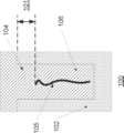
도 1a는 피처 내의 심의 예시를 제시한다.
도 1b는 예시적인 실시 예에 따른 스퍼터링 동작을 사용하여 옥사이드 재료를 증착하기 위한 프로세스의 예시들을 제시한다.
도 2는 일 예시적인 실시 예를 위한 동작들의 흐름도를 제시한다.
도 3은 원자 층 증착 (atomic layer deposition; ALD) 사이클에 대한 흐름도를 제시한다.
도 4는 본 명세서의 실시 예들에 따른 복수의 스퍼터링 동작들을 사용하여 옥사이드 재료를 증착하기 위한 프로세스의 예시들을 제시한다.
도 5는 또 다른 예시적인 실시 예를 위한 동작들의 흐름도를 제시한다.
도 6 내지 도 9는 개시된 실시 예들에 따른 방법들을 수행하기 위한 프로세스 챔버들의 예들의 개략도들이다.Figure 1A presents an example of deliberation within a feature.
1B presents examples of a process for depositing an oxide material using a sputtering operation according to an example embodiment.
Figure 2 presents a flow diagram of operations for one example embodiment.
Figure 3 presents a flow diagram for the atomic layer deposition (ALD) cycle.
4 presents examples of a process for depositing oxide material using multiple sputtering operations in accordance with embodiments herein.
Figure 5 presents a flow diagram of operations for another example embodiment.
6-9 are schematic diagrams of examples of process chambers for performing methods according to disclosed embodiments.
본 개시는 반도체 기판 상의 층의 피처들 내로 옥사이드를 증착하기 위한 기법들을 기술한다. 반도체 제조 프로세스들은 종종 피처들을 충진하기 (fill) 위해 화학적 기상 증착 (chemical vapor deposition; CVD) 방법 및/또는 원자 층 증착 (atomic layer deposition; ALD) 방법을 사용하는 유전체 갭 충진을 포함한다. 실리콘 옥사이드를 포함하지만 이로 제한되지 않는 유전체 재료로 피처들을 충진하는 방법들, 및 관련된 시스템들 및 장치들이 본 명세서에 기술된다. 본 명세서에 기술된 방법들은 기판 내에 형성된 수직으로 배향된 피처들을 충진하도록 사용될 수 있다. 이러한 피처들은 갭들, 리세스된 (recessed) 피처들, 네거티브 피처들, 충진되지 않은 피처들, 또는 단순히 피처들로 지칭될 수도 있다. 이러한 피처들을 충진하는 것은 갭 충진 (gapfill) 으로 지칭될 수도 있다. 기판 내에 형성된 피처들은 좁은 개구부들 및/또는 재차 들어간 (re-entrant) 개구부들, 피처 내의 협착부들 (constrictions), 및 고 종횡비들 중 하나 이상을 특징으로 할 수 있다. 일부 구현 예들에서, 피처는 적어도 약 2:1, 적어도 약 4:1, 적어도 약 6:1, 적어도 약 10:1, 적어도 약 30:1, 적어도 약 50:1, 또는 더 큰 종횡비를 가질 수도 있다. 일부 실시 예들에서, 본 명세서의 기법들은 최소/감소된 보이드들로 트렌치들을 충진하도록 사용될 수도 있다. 다른 실시 예들에서, 본 명세서의 기법들은 피처의 상단부로부터 특정한 깊이까지, 그리고 증착된 재료의 성능에 상당한 영향을 주지 않고 심이 형성될 수도 있는 깊이 아래로 증착된 재료의 부분이 감소된 보이드들을 갖고/심이 없는 (seam-free) 피처들을 충진하도록 사용될 수도 있다. 기판은 유전체, 도전성 또는 반도전성 재료와 같은 재료의 하나 이상의 층들이 그 위에 증착된 웨이퍼들을 포함하는, 예를 들어, 200 ㎜ 웨이퍼, 300 ㎜ 웨이퍼, 또는 450 ㎜ 웨이퍼인, 실리콘 웨이퍼일 수도 있다.This disclosure describes techniques for depositing oxide into features of a layer on a semiconductor substrate. Semiconductor manufacturing processes often involve dielectric gap filling using chemical vapor deposition (CVD) methods and/or atomic layer deposition (ALD) methods to fill features. Methods for filling features with dielectric materials, including but not limited to silicon oxide, and related systems and devices are described herein. The methods described herein can be used to fill vertically oriented features formed in a substrate. These features may be referred to as gaps, recessed features, negative features, unfilled features, or simply features. Filling these features may be referred to as gapfill. Features formed within the substrate may be characterized by one or more of narrow openings and/or re-entrant openings, constrictions within the feature, and high aspect ratios. In some implementations, a feature may have an aspect ratio of at least about 2:1, at least about 4:1, at least about 6:1, at least about 10:1, at least about 30:1, at least about 50:1, or greater. there is. In some embodiments, the techniques herein may be used to fill trenches with minimal/reduced voids. In other embodiments, the techniques herein have reduced voids from the top of the feature to a certain depth, and/or a portion of the deposited material below the depth at which a seam may be formed without significantly affecting the performance of the deposited material. It can also be used to fill seam-free features. The substrate may be a silicon wafer, eg, a 200 mm wafer, a 300 mm wafer, or a 450 mm wafer, comprising wafers with one or more layers of material, such as a dielectric, conductive or semiconducting material, deposited thereon.
옥사이드 막들을 위한 갭 충진 증착 프로세스는 증착된 막 내에 심들을 생성할 수도 있다. 막이 피처 내에서 컨포멀하게 (conformally) 성장함에 따라, 피처의 측벽들로부터 각각을 향해 성장하기 때문에 막들 사이의 접합부에서 심이 형성될 수도 있다. 심들은 옥사이드 막의 덜 치밀한 영역들일 수도 있고 막 품질들을 저하시키는 원인이 될 수도 있다. 심들은 발생되는 (resulting) 반도체 디바이스의 고장 가능성을 증가시키기 때문에 일반적으로 바람직하지 않다.The gap fill deposition process for oxide films may create seams within the deposited film. As the film grows conformally within the feature, seams may form at the junctions between the films as they grow toward each other from the side walls of the feature. Seams may be less dense regions of the oxide film and may cause deterioration of film qualities. Shims are generally undesirable because they increase the likelihood of resulting semiconductor device failure.
옥사이드 갭 충진 재료의 증착 동안 달리 형성될 수도 있는 심들을 처리하기 위한 기법들이 본 명세서에 기술된다. 특히, 증착 동안 옥사이드 재료의 스퍼터링은 심 형성을 감소시킬 수도 있다. 옥사이드 갭 충진 재료, 옥사이드 막, 및 옥사이드 재료는 본 명세서에서 상호 교환가능하게 (interchangeably) 사용될 수도 있다.Techniques for processing seams that may otherwise be formed during deposition of oxide gap fill material are described herein. In particular, sputtering of oxide material during deposition may reduce seam formation. Oxide gap fill material, oxide film, and oxide material may be used interchangeably herein.
도 1a는 충진된 피처 내의 심의 예시를 제공한다. 도면 (100) 에서, 패터닝된 층 (102), 패터닝된 층 (102) 내의 피처 (104), 및 피처 (104) 내에 증착된 옥사이드 재료 (106) 를 갖는 기판이 제시된다. 옥사이드 재료는 심 (105) 을 갖는다. 도 1a의 실시 예에서, 심 (105) 은 또한 심 (105) 과 패터닝된 층 (102) 의 상단부 및/또는 피처 (104) 의 상단부 사이의 깊이 (101) 를 특징으로 할 수도 있다.Figure 1A provides an example of a seam within a filled feature. In drawing 100, a substrate is shown having a patterned
일부 실시 예들에서, 본 명세서에 기술된 기법들은 심들을 형성하지 않고 피처들을 충진할 수도 있다. 다른 실시 예들에서, 심이 형성될 수도 있지만 감소된 정도이다. 이러한 실시 예들에서, 심은 적어도 약 40 ㎚, 적어도 약 50 ㎚, 또는 적어도 약 60 ㎚의 깊이 (도 1a에 기술됨) 를 특징으로 할 수도 있다.In some embodiments, the techniques described herein may fill features without forming seams. In other embodiments, a seam may be formed but to a reduced extent. In these embodiments, the shim may feature a depth of at least about 40 nm, at least about 50 nm, or at least about 60 nm (described in Figure 1A).
도 1b는 심들을 감소시키기 위한 프로세스의 예시들을 제공한다. 도면 (110) 에서, 패터닝된 층 (112) 및 피처 (114) 를 갖는 기판이 제시된다. 도면 (120) 에서, 옥사이드 재료 (126) 는 패터닝된 층 (112) 상에 그리고 피처 (114) 내에 증착된다. 옥사이드 재료가 피처를 완전히 충진하지 않았기 때문에, 갭 (127) 이 피처 (114) 내에 존재하고 옥사이드 재료에 의해 규정된다. 옥사이드 재료 (126) 가 패터닝된 층 (112) 위에 증착되는 것으로 도시되지만, 일부 실시 예들에서 패터닝된 층 (112) 의 상단부 상에 증착이 없고, 옥사이드 재료 (126) 는 피처 (114) 내에만 증착된다는 것이 이해되어야 한다.Figure 1B provides examples of a process for reducing seams. In drawing 110 , a substrate with patterned
도면 (130) 에서, 옥사이드 재료 (126) 는 스퍼터링되었다. 스퍼터링은 옥사이드 재료와 같은 재료의 에칭 및 재증착을 포함할 수도 있다. 일부 실시 예들에서, 에칭되는 재료의 일부는 기판 상에 다시 재증착된다. 스퍼터링의 결과는 피처의 하단부에 재증착되는 피처의 상단부 근방의 옥사이드 재료를 포함할 수도 있고, 이는 심들의 형성을 감소시키는 보텀-업 (bottom-up) 충진 메커니즘을 용이하게 한다.In drawing 130,
스퍼터링의 또 다른 결과는 피처 (114) 의 상단부로부터 갭의 테이퍼링이다. 도면 (130) 에 도시된 바와 같이, 형상이 다소 직사각형일 수도 있는 갭 (127) 은 피처의 상단부에서 더 넓고 피처의 하단부를 향해 테이퍼진 더 삼각형 형상을 갖는 갭 (137) 이 된다. 상기 주지된 바와 같이, 컨포멀한 막 증착은 막들이 피처의 측벽들로부터 서로를 향해 성장함에 따라 심을 발생시킬 수도 있다. 예를 들어, 갭 (127) 은 반응 물질들이 갭 내에서 흡착 및/또는 반응하지 못할 때까지 계속해서 축소될 수도 있고, 심으로서 기술된 덜 치밀한 영역을 발생시킨다. 도 1b의 예에서, 옥사이드 재료를 스퍼터링하는 것은 갭의 형상을 변화시키고 피처의 하단부에 옥사이드 재료를 재증착한다. 이는 갭 (137) 내에 옥사이드 재료를 증착하기 위해 차후의 증착 프로세스들이 심을 생성할 위험을 감소시킨다. 이는 또한 차후의 증착 프로세스들이 옥사이드 재료에 보이드를 발생시킬 위험을 감소시킨다.Another result of sputtering is tapering of the gap from the top of
도면 (140) 에서, 부가적인 옥사이드 재료 (146) 가 피처 내로 증착된다. 옥사이드 재료 (126 및 146) 는 동일하거나 상이한 옥사이드 재료일 수도 있다 (즉, 도 1b의 음영은 예시를 위한 것이고 옥사이드 재료 (136 및 146) 의 화학적 조성 사이의 차이를 요구하는 것으로 해석되지 않아야 한다). 일부 실시 예들에서, 옥사이드 재료 (146) 는 옥사이드 재료 (126) 와 유사한 프로세스에 의해 증착될 수도 있지만, 다른 실시 예들에서 상이한 프로세스가 수행될 수도 있다. 일부 실시 예들에서, 옥사이드 재료 (126 및 146) 는 적어도 부분적으로 옥사이드 재료의 스퍼터링으로 인해 심을 포함하지 않는다. 심이 도면 (140) 에 도시되지 않지만, 일부 실시 예들에서 심이 형성되지만, 스퍼터링 프로세스를 수행하지 않은 것과 비교하여 더 적은 정도로 존재한다는 것이 이해되어야 한다. 일부 실시 예들에서, 심이 존재할 수도 있지만 (도 1a를 참조하여 상기 논의된 바와 같이) 심의 깊이는 스퍼터링 프로세스를 수행하지 않고 형성될 수도 있는 심과 비교하여 더 클 수도 있고, 즉 심은 더 작다.In drawing 140,
도 2는 본 명세서에 기술된 실시 예들에 대한 프로세스 흐름도를 제시한다. 동작 (200) 에서, 충진될 피처들을 갖는 기판이 프로세스 챔버 내에 수용된다. 일부 실시 예들에서, 기판은 이전 동작으로부터 프로세스 챔버 내에 남아 있을 수도 있는 반면, 다른 실시 예들에서 기판은 프로세스 챔버에 제공될 수도 있다. 기판은 충진될 패터닝된 피처들을 갖는다. 일부 실시 예들에서, 패터닝된 피처들은 약 5:1 내지 약 100:1의 폭과 깊이 사이의 종횡비를 가질 수도 있다.Figure 2 presents a process flow diagram for embodiments described herein. In
동작 (202) 에서, 시드 층이 피처 내에 선택 가능하게 (optionally) 증착될 수도 있다. 시드 층은 차후의 증착 동작들을 용이하게 하고 그리고/또는 아래에 놓인 층을 보호하는 것을 도울 수도 있다. 예를 들어, 옥사이드 재료가 플라즈마-강화된 프로세스에 의해 증착되는 경우, 시드 층은 플라즈마에 의해 생성된 이온들에 의한 에칭으로부터 아래에 놓인 층을 보호할 수도 있다. 일부 실시 예들에서, 시드 층은 본 명세서에 기술된 바와 같이 차후의 동작들에서 증착된 옥사이드 재료와 동일하거나 상이한 옥사이드 재료일 수도 있다. 다양한 실시 예들에서, 시드 층은 본 명세서에 기술된 임의의 옥사이드 재료 또는 옥사이드 재료의 증착을 용이하게 하도록 다른 적합한 재료들을 포함할 수도 있다. 일부 실시 예들에서, 시드 층은 도핑되거나 도핑되지 않은 실리콘 나이트라이드일 수도 있다. 다양한 실시 예들에서, 시드 층은 ALD, 플라즈마 강화된 ALD (PEALD), CVD, 또는 플라즈마 강화된 CVD (PECVD) 에 의해 증착될 수도 있다. ALD는 순차적인 자기-제한 (self-limiting) 반응들을 사용하여 재료의 박층들을 증착하는 기법이다. ALD 프로세스들은 사이클들에서 층 단위 (layer-by-layer basis) 로 막들을 증착하도록 표면-매개된 (surface-mediated) 증착 반응들을 사용한다. 일 예로서, ALD 사이클은 다음 동작들: (i) 전구체의 전달/흡착, (ii) 챔버로부터 전구체의 퍼징 (purge), (iii) 제 2 반응 물질의 전달 및 선택 가능한 (optional) 플라즈마 점화 (ignition), 및 (iv) 챔버로부터의 부산물들의 퍼징을 포함할 수도 있다. 기판의 표면 상에 막을 형성하기 위해 흡착된 전구체와 제 2 반응 물질 사이의 반응은 막 조성 및 특성들, 예컨대 불균일도 (nonuniformity), 응력, 습식 (wet) 에칭 레이트, 건식 (dry) 에칭 레이트, 전기적 특성들 (예를 들어, 파괴 전압 (breakdown voltage) 및 누설 전류) 등에 영향을 준다.In
ALD 프로세스의 일 예에서, 표면 활성 사이트들 (sites) 의 집단 (population) 을 포함하는 기판 표면은 기판을 하우징하는 챔버에 제공된 일 도즈 (dose) 의, 실리콘 함유 전구체와 같은 제 1 전구체의 가스상 (gas phase) 분포에 노출된다. 제 1 전구체의 물리 흡착된 (physisorbed) 분자들 및/또는 화학 흡착된 (chemisorbed) 종을 포함하는, 이 제 1 전구체의 분자들은 기판 표면 상으로 흡착된다. 본 명세서에 기술된 바와 같이 화합물이 기판 표면 상에 흡착될 때, 흡착된 층은 화합물뿐만 아니라 화합물의 유도체들도 포함할 수도 있다는 것이 이해되어야 한다. 예를 들어, 실리콘 함유 전구체의 흡착된 층은 실리콘 함유 전구체뿐만 아니라 실리콘 함유 전구체의 유도체들도 포함할 수도 있다. 제 1 전구체 도즈 후, 챔버는 이어서 대부분 또는 흡착된 종만이 남도록 가스상으로 남아 있는 제 1 전구체의 대부분 또는 전부를 제거하도록 배기된다 (evacuate). 일부 구현 예들에서, 챔버는 완전히 배기되지 않을 수도 있다. 예를 들어, 가스상의 제 1 전구체의 분압이 반응을 완화시키기에 충분히 낮도록 반응기는 배기될 수도 있다. 제 2 반응 물질, 예컨대 산소 함유 가스는 이들 분자들 중 일부가 표면 상에 흡착된 제 1 전구체와 반응하도록 챔버로 도입된다. 일부 프로세스들에서, 제 2 반응 물질은 흡착된 제 1 전구체와 즉시 반응한다. 다른 실시 예들에서, 제 2 반응 물질은 플라즈마와 같은 활성화의 소스 (source) 가 일시적으로 인가된 후에만 반응한다. 이어서 챔버는 결합되지 않은 (unbound) 제 2 반응 물질 분자들을 제거하기 위해 다시 배기될 수도 있다. 상기 기술된 바와 같이, 일부 실시 예들에서 챔버는 완전히 배기되지 않을 수도 있다. 막 두께를 구축하도록 부가적인 ALD 사이클들이 사용될 수도 있다.In one example of an ALD process, a substrate surface comprising a population of surface active sites is exposed to a gaseous phase of a first precursor, such as a silicon-containing precursor, at a dose provided to a chamber housing the substrate. gas phase) distribution. Molecules of the first precursor, including physisorbed molecules and/or chemisorbed species, are adsorbed onto the substrate surface. It should be understood that when a compound is adsorbed onto a substrate surface as described herein, the adsorbed layer may include the compound as well as derivatives of the compound. For example, the adsorbed layer of the silicon-containing precursor may include the silicon-containing precursor as well as derivatives of the silicon-containing precursor. After the first precursor dose, the chamber is then evacuated to remove most or all of the first precursor remaining in the gas phase so that only the majority or adsorbed species remain. In some implementations, the chamber may not be completely evacuated. For example, the reactor may be evacuated so that the partial pressure of the gaseous first precursor is low enough to moderate the reaction. A second reactant, such as an oxygen-containing gas, is introduced into the chamber such that some of these molecules react with the first precursor adsorbed on the surface. In some processes, the second reactant reacts immediately with the adsorbed first precursor. In other embodiments, the second reactant reacts only after a source of activation, such as a plasma, is transiently applied. The chamber may then be evacuated again to remove unbound second reactant molecules. As described above, in some embodiments the chamber may not be completely evacuated. Additional ALD cycles may be used to build film thickness.
일부 구현 예들에서, ALD 방법들은 플라즈마 활성화를 포함한다. 본 명세서에 기술된 바와 같이, 본 명세서에 기술된 ALD 방법들 및 장치들은 2011 년 4 월 11 일에 출원되고, 명칭이 "PLASMA ACTIVATED CONFORMAL FILM DEPOSITION"인, 미국 특허 출원 번호 제 13/084,399 호 (현재 미국 특허 번호 제 8,728,956 호) 에 포괄적으로 기술된, 컨포멀한 막 증착 (conformal film deposition; CFD) 방법들일 수도 있고, 이는 전체가 참조로서 본 명세서에 인용된다.In some implementations, ALD methods include plasma activation. As described herein, the ALD methods and devices described herein are disclosed in U.S. Patent Application Serial No. 13/084,399, entitled “PLASMA ACTIVATED CONFORMAL FILM DEPOSITION,” filed April 11, 2011. There may also be conformal film deposition (CFD) methods, as comprehensively described in current U.S. Pat. No. 8,728,956, which is incorporated herein by reference in its entirety.
도 3은 단일 ALD 사이클에 대한 프로세스 흐름도를 제시한다. 동작들 (321) 에서, 기판은 피처의 표면 상에 전구체를 흡착시키도록, 본 명세서에 기술된 전구체들 중 임의의 전구체와 같이 실리콘 함유 전구체에 노출된다. 다양한 실시 예들에서, 이 동작은 자기-제한적이다. 일부 실시 예들에서, 전구체는 피처의 표면 상의 모든 활성 사이트들보다 더 적게 흡착한다. 동작 (322) 에서, 프로세스 챔버는 모든 흡착되지 않은 실리콘 함유 전구체들을 제거하도록 선택 가능하게 퍼지된다. 동작 (323) 에서, 기판은 산화 화학 물질에 노출되고 플라즈마는 피처 내에 제 1 실리콘 옥사이드 층을 형성하도록 점화된다. 다양한 실시 예들에서, 동작 (323) 은 흡착된 실리콘 함유 전구체 층을 실리콘 옥사이드로 변환한다. 동작 (324) 에서, 프로세스 챔버는 실리콘 함유 전구체와 산화제 사이의 반응으로부터 부산물들을 제거하도록 선택 가능하게 퍼지된다. 동작들 (321 내지 324) 은 피처에서 목표된 두께로 실리콘 옥사이드를 증착하기 위해 목표되는 바와 같이 2 이상의 사이클들로 선택 가능하게 반복될 수도 있다.Figure 3 presents a process flow diagram for a single ALD cycle. In
본 명세서에 기술된 프로세스들은 특정한 반응 메커니즘으로 제한되지 않는다는 것을 주의해야 한다. 따라서, 도 3과 관련하여 기술된 프로세스는 엄격하게 자기-제한적이지 않은 것들을 포함하여, 실리콘 함유 반응 물질들 및 산화 플라즈마들에 대한 순차적인 노출들을 사용하는 모든 옥사이드 증착 프로세스들을 포함한다. 프로세스는 플라즈마를 생성하도록 사용된 하나 이상의 가스들이 간헐적인 플라즈마 점화들과 함께 프로세스 내내 연속적으로 흐르는 시퀀스들을 포함한다. 또한, 일부 실시 예들에서, 기술된 화학 물질들을 사용하는 열적 (비-플라즈마) ALD가 채용될 수도 있다.It should be noted that the processes described herein are not limited to any particular reaction mechanism. Accordingly, the process described in connection with Figure 3 includes all oxide deposition processes that use sequential exposures to silicon-containing reactive materials and oxidizing plasmas, including those that are not strictly self-limiting. The process involves sequences in which one or more gases used to generate the plasma flow continuously throughout the process with intermittent plasma ignitions. Additionally, in some embodiments, thermal (non-plasma) ALD using the described chemistries may be employed.
도 2를 다시 참조하면, 동작 (204) 에서 패터닝된 피처들은 옥사이드 재료로 충진된다. 다양한 실시 예들에서, 옥사이드 재료는 실리콘 옥사이드이다. 일부 실시 예들에서, 옥사이드 재료는 금속 옥사이드, 예를 들어, GeO2, HfO2, AlO3 등 또는 이들의 임의의 조합들일 수도 있다. 일부 실시 예들에서, 옥사이드 재료는 ALD 프로세스 또는 PEALD 프로세스에 의해 증착된다. 일부 실시 예들에서, 동작 (204) 는 충진될 피처의 임계 치수 또는 폭의 약 5 % 내지 약 35 % 또는 적어도 약 6.5 ㎚의 두께를 갖는 옥사이드 막을 증착한다.Referring back to Figure 2, in
동작 (206) 에서 옥사이드 재료는 스퍼터링된다. 스퍼터링은 플라즈마의 존재 시 수행될 수도 있다. 일부 실시 예들에서, 스퍼터링은 저 주파수 (LF) 컴포넌트 및 고 주파수 (HF) 컴포넌트를 갖는 플라즈마를 생성하도록 듀얼 RF 플라즈마 소스를 사용하여 플라즈마를 점화하는 것을 수반한다. 이론에 얽매이지 않고, HF 컴포넌트는 플라즈마를 유지하도록 기능하는 한편, LF 컴포넌트는 기판에 충돌하는 불활성 가스의 이온들을 생성할 수도 있다. 일부 실시 예들에서, 불활성 가스는 헬륨, 질소, 아르곤, 또는 크세논을 포함할 수도 있다. 이온들로 옥사이드 재료를 충돌시킴으로써, 옥사이드 재료는 도 1b에 예시된 바와 같이, 옥사이드 재료의 적어도 일부를 기판의 피처들 내로 더 깊게 재증착시키면서 스퍼터링될 수도 있다.In
스퍼터링이 고밀도 플라즈마 (high density plasma; HDP) 프로세스들에서 사용되는 동안, HDP 프로세스들을 위한 프로세스 조건들은 상당히 상이하다. HDP 프로세스들은 훨씬 더 높은 이온 충돌 (ion bombardment) 을 갖고 본 명세서에 기술된 바와 같이 듀얼 RF 소스를 사용하는 용량 커플링된 PEALD 프로세스와 비교하여 상이한 막을 발생시키는 유도 커플링 플라즈마를 사용할 수도 있다. 예를 들어, HDP 반응기들은 1011 개 이온들/㎤보다 더 큰 플라즈마 밀도를 사용하여 100 mTorr 미만으로 동작할 수도 있는 한편, 본 명세서에 기술된 PEALD 또는 PECVD 프로세스들은 약 100 배 더 낮은 플라즈마 밀도를 사용하여 약 500 mTorr보다 더 큰 압력에서 동작할 수도 있다. 더욱이, HDP 반응기에서, 400 ㎑ (즉, LF 컴포넌트) 가 플라즈마를 생성하기 위해 사용될 수도 있고 (즉, 코일들에 인가됨) 13.56 ㎒ (즉, HF 컴포넌트) 가 동작 동안 그 위에 웨이퍼가 위치될 수도 있는 페데스탈에 인가된다. 그러나, 본 명세서에 기술된 바와 같이 용량 커플링된 플라즈마 (CCP) 프로세스에서, 13.56 ㎒가 또한 플라즈마를 생성하도록 사용될 수도 있고 400 ㎑는 웨이퍼의 이온 충돌을 제어할 수도 있다. 용량 결합된 플라즈마에서, 반응기가 더 높은 이온-중성 충돌 주파수들과 함께 더 높은 압력에서 동작하기 때문에 이온 에너지는 13.56 ㎒만큼 변조될 수 없다. LF 컴포넌트는 웨이퍼에 영향을 주는 이온 에너지들을 제어하도록 사용될 수도 있고, 이온 에너지들은 HDP 프로세스와 비교하여 훨씬 더 낮다. 상이한 이온 에너지들은 또한 본 명세서에 기술된 바와 같은 스퍼터링 프로세스들을 포함하여, HDP와 PECVD 또는 PEALD 프로세스들 사이의 막 조성 및 특성들에 영향을 준다. 이들 다양한 차이들, 특히 압력 및 플라즈마 생성 및 제어 기법들의 차이 때문에, HDP 증착을 위한 프로세스 조건들은 본 명세서에 기술된 것과 같은 용량 결합된 플라즈마 프로세스들로 추론될 (extrapolate) 수 없다.While sputtering is used in high density plasma (HDP) processes, the process conditions for HDP processes are significantly different. HDP processes may use inductively coupled plasma, which has much higher ion bombardment and generates different films compared to the capacitively coupled PEALD process using a dual RF source as described herein. For example, HDP reactors may operate below 100 mTorr using plasma densities greater than 1011 ions/cm3, while the PEALD or PECVD processes described herein use plasma densities approximately 100 times lower. It can also be used to operate at pressures greater than about 500 mTorr. Moreover, in an HDP reactor, 400 kHz (i.e., LF component) may be used to generate the plasma (i.e., applied to the coils) and 13.56 MHz (i.e., HF component) over which the wafer may be placed during operation. Approved on the pedestal. However, in a capacitively coupled plasma (CCP) process as described herein, 13.56 MHz may also be used to generate the plasma and 400 kHz may control ion bombardment of the wafer. In a capacitively coupled plasma, the ion energy cannot be modulated by as much as 13.56 MHz because the reactor operates at higher pressures with higher ion-neutral collision frequencies. The LF component may be used to control the ion energies affecting the wafer, and the ion energies are much lower compared to the HDP process. Different ion energies also affect film composition and properties between HDP and PECVD or PEALD processes, including sputtering processes as described herein. Because of these various differences, particularly differences in pressure and plasma generation and control techniques, process conditions for HDP deposition cannot be extrapolated to capacitively coupled plasma processes as described herein.
상기 주지된 바와 같이, 스퍼터링은 두 가지 이점들을 가질 수도 있다. 먼저, 피처의 하단부에 스퍼터링된 막을 재증착한다. 둘째로, 테이퍼링된 형상을 갖도록 옥사이드 막 사이의 갭의 형상을 변화시켜, 피처들 내에 분포되고 피처들의 하단부에 증착되는 반응 물질들의 능력을 개선한다. 일부 실시 예들에서, 스퍼터링은 또한 막의 저밀도 부분들을 스퍼터링함으로써 (예를 들어, 이전 증착 프로세스들로부터 형성될 수도 있는 심을 스퍼터링함으로써) 옥사이드 막을 치밀화하는 것을 도울 수도 있다. 더 낮은 밀도의 막은 더 쉽게 스퍼터링될 수도 있고, 이는 옥사이드 재료로 하여금 더 높은 밀도의 막을 (또는 더 높은 밀도의 막을 증착하기 위한 별도의 증착 프로세스를 위해) 재증착하고 형성하게 한다.As noted above, sputtering may have two advantages. First, the sputtered film is redeposited on the bottom of the feature. Second, changing the shape of the gap between the oxide films to have a tapered shape improves the ability of reactive materials to be distributed within the features and deposited on the bottom of the features. In some embodiments, sputtering may also help densify the oxide film by sputtering low-density portions of the film (eg, by sputtering a seam that may have formed from previous deposition processes). Lower density films may be more easily sputtered, which allows the oxide material to redeposit and form higher density films (or for a separate deposition process to deposit higher density films).
스퍼터링의 양은 적어도 3 개의 파라미터들: 프로세스 챔버의 압력, 가스 플로우, 및 RF 설정들에 의해 제어될 수도 있다. 일반적으로, 더 낮은 압력 및 더 높은 LF 전력은 스퍼터링을 증가시킨다. 게다가, 가스 플로우는 스퍼터링을 증가시키기 위해 더 많은 불활성 가스, 특히 더 많은 아르곤을 도입하도록 제어될 수도 있다. 일부 실시 예들에서, 본 명세서에서 더 논의된 바와 같이, 스퍼터링에 사용된 프로세스 가스는 또한 산소 함유 종을 포함할 수도 있고, Ar:O의 더 높은 비는 스퍼터링을 증가시킬 수도 있다.The amount of sputtering may be controlled by at least three parameters: pressure of the process chamber, gas flow, and RF settings. In general, lower pressure and higher LF power increase sputtering. Additionally, the gas flow may be controlled to introduce more inert gas, especially more argon, to increase sputtering. In some embodiments, as discussed further herein, the process gas used for sputtering may also include oxygen-containing species, and higher Ar:O ratios may increase sputtering.
동작 (208) 에서 옥사이드 재료가 증착된다. 동작 (208) 은 동작 (204) 와 동일한 프로세스 조건들 또는 상이한 프로세스 조건들 하에서 수행될 수도 있다. 일부 실시 예들에서, 동작 (204) 및 동작 (208) 에서 증착된 옥사이드 재료는 동일한 옥사이드 재료, 예를 들어, 실리콘 옥사이드이다. 일부 실시 예들에서, 옥사이드 재료는 플라즈마 강화된 CVD 또는 ALD 프로세스들을 포함하는 CVD 또는 ALD 프로세스를 사용하여 동작 (208) 에서 증착될 수도 있다.In
일부 실시 예들에서, 동작 (206) 및 동작 (208) 은 선택 가능하게 1 회 이상 반복될 수도 있다. 동작 (206) 및 동작 (208) 을 반복하는 것은 옥사이드 재료를 점진적으로 스퍼터링하고 충진되도록 남아 있는 피처의 형상을 변화시키는 데 유리할 수도 있다. 일부 실시 예들에서, 스퍼터링 동작의 지속 기간 및 옥사이드 재료를 증착하기 위한 ALD 동작에 대한 사이클들의 수는 사이클링 동작 (206) 및 사이클링 동작 (208) 에 따라 튜닝될 (tune) 수도 있다. 예를 들어, 스퍼터링 프로세스는 ALD 증착의 10 사이클 각각에 대해 1 사이클 동안 수행될 수도 있다 (여기서, ALD 증착의 단일 사이클은 상기 기술된 바와 같이 동작 (i) 내지 동작 (iv) 각각을 포함할 수도 있다). 일부 실시 예들에서, 스퍼터링 대 ALD 사이클들의 비가 규정될 수도 있고, 비는 약 1:1 내지 약 50:1일 수도 있다.In some embodiments,
복수의 스퍼터링 동작들이 수행되는 실시 예들에서, 스퍼터링 동작의 프로세스 파라미터들은 동작들 사이에서 변화할 수도 있다. 예를 들어, 차후의 스퍼터링 동작들을 위해 스퍼터링의 양을 증가시키는 것이 바람직할 수도 있다. 이러한 실시 예들에서, 파라미터들은 차후의 동작들을 위해 스퍼터링의 양을 증가시키도록 변화될 수도 있다. 예를 들어, 제 2 스퍼터링 동작에 대한 LF 전력은 제 2 스퍼터링 동작에서 스퍼터링의 양을 증가시키기 위해 제 1 스퍼터링 동작과 비교하여 상승될 수도 있다. 일부 실시 예들에서, 상기 논의된 파라미터들을 포함하여, 다른 프로세스 파라미터들이 또한 스퍼터링을 증가/감소시키도록 수정될 수도 있다.In embodiments where multiple sputtering operations are performed, the process parameters of the sputtering operations may vary between operations. For example, it may be desirable to increase the amount of sputtering for subsequent sputtering operations. In these embodiments, parameters may be changed to increase the amount of sputtering for subsequent operations. For example, the LF power for the second sputtering operation may be increased compared to the first sputtering operation to increase the amount of sputtering in the second sputtering operation. In some embodiments, other process parameters may also be modified to increase/decrease sputtering, including the parameters discussed above.
도 4는 복수의 스퍼터링 동작들을 포함하는 프로세스의 예시들을 제시한다. 도면 (410) 은 상기 도면 (110) 과 유사한, 패터닝된 층 (412) 및 피처 (414) 를 갖는 기판을 제시한다. 도면 (420) 에서, 옥사이드 막 (426) 이 피처 (114) 내에 컨포멀하게 증착되고, 상기 도면 (120) 과 유사한 갭 (427) 을 규정한다. 도면 (430) 에서, 옥사이드 막 (426) 은 갭 (437) 을 갖는 옥사이드 막 (436) 을 형성하도록 스퍼터링된다. 갭 (437) 은 피처에서 하향으로 테이퍼링되고, 피처에서 더 깊은 것과 비교하여 피처의 상단부에서 옥사이드 막들 사이에 더 많은 공간을 제공한다.Figure 4 presents examples of a process involving multiple sputtering operations. Figure 410 presents a substrate with a
도면 (440) 에서, 하나 이상의 부가적인 증착 및 스퍼터링 동작들이 수행되었다. 따라서, 옥사이드 재료가 피처의 상단부로부터 스퍼터링되고 갭의 하단부에 증착되기 때문에, 옥사이드 막 (446) 및 갭 (447) 이 형성되고, 여기서 갭 (447) 은 갭 (437) 보다 더 넓은 "V" 형상을 갖는다. 도면 (450) 에서, 추가 증착 및 스퍼터링 동작들이 수행되어, 피처가 옥사이드 재료 (456) 에 의해 완전히 충진된다. 갭 (457) 은 갭 (437) 및 갭 (447) 모두보다 더 넓은 개구부를 갖는다. 도면 (430) 및 도면 (440) 사이에서 수행된 증착 동작 및 스퍼터링 동작은 도면 (440) 및 도면 (450) 사이에서 수행된 동일한 증착 동작 및 스퍼터링 동작, 또는 상이한 동작들일 수도 있다. 예를 들어, 프로세스 조건들은 후속하는 스퍼터링 동작들을 위해 스퍼터링의 양을 증가시키도록 변화될 수도 있다. 스퍼터링의 양을 제어하기 위해 프로세스 조건들을 튜닝하기 위한 기법들은 본 명세서의 다른 곳에서 논의된다.In figure 440, one or more additional deposition and sputtering operations have been performed. Accordingly, as oxide material is sputtered from the top of the feature and deposited at the bottom of the gap, an
상기 논의된 프로세스 플로우는 프로세스 챔버 내에서 수행될 수도 있는 별도의 프로세스들로서 증착 및 스퍼터링을 기술한다. 예를 들어, 100 사이클들의 ALD가 옥사이드 재료를 증착하도록 수행될 수도 있고, 이어서 30 초의 스퍼터링이 수행될 수도 있고, 이어서 또 다른 100 사이클들의 ALD가 부가적인 옥사이드 재료를 증착하도록 수행될 수도 있다. 그러나, 일부 실시 예들에서, 증착 및 스퍼터링 동작들은 ALD 사이클의 일 부분이 스퍼터링 프로세스를 포함하도록 통합될 수도 있다.The process flow discussed above describes deposition and sputtering as separate processes that may be performed within a process chamber. For example, 100 cycles of ALD may be performed to deposit oxide material, followed by 30 seconds of sputtering, and then another 100 cycles of ALD may be performed to deposit additional oxide material. However, in some embodiments, deposition and sputtering operations may be integrated such that a portion of the ALD cycle includes a sputtering process.
도 5는 ALD 프로세스의 일부로서 스퍼터링이 발생하는 옥사이드 재료를 증착하기 위한 프로세스 플로우를 제시한다. 동작 (500) 에서 시작하여 기판이 프로세스 챔버에 수용된다. 동작 (502) 에서 시드 층이 선택 가능하게 증착되고, 동작 (504) 에서 옥사이드 재료가 ALD 프로세스에 의해 증착될 수도 있다. 동작들 (500 내지 504) 는 동작들 (200 내지 204) 과 관련하여 상기 기술된 바와 유사한 방식으로 수행될 수도 있다.Figure 5 presents a process flow for depositing an oxide material where sputtering occurs as part of an ALD process. Beginning at
동작 (505) 는 4 개의 동작들을 포함하는 옥사이드 재료를 증착하고 스퍼터링하기 위한 PEALD 프로세스이다. 동작 (506) 에서, 옥사이드 전구체는 기판 표면 상에 흡착하는 챔버 내로 흐른다. 선택 가능한 프로세스 (507) 에서, 흡착된 종만이 남도록 옥사이드 전구체는 예를 들어, 불활성 가스에 의해 프로세스 챔버로부터 퍼지된다.
동작 (508) 에서 산소 함유 종 및 불활성 가스는 LF 컴포넌트를 갖는 플라즈마의 존재 시 프로세스 챔버 내로 흐른다. 산소 함유 종은 옥사이드 재료를 형성하도록 흡착된 옥사이드 전구체와 반응한다. 이 반응과 동시에, 플라즈마의 LF 컴포넌트는 RF 바이어스가 기판에 인가될 때 불활성 가스로 하여금 기판에 충돌하는 이온들로 해리되게 한다. 따라서 이온들은 옥사이드 재료를 스퍼터링할 수도 있다. 에칭 레이트가 통상적으로 측벽보다 수평 표면을 따라 더 높기 때문에, 피처들의 상단부는 측벽들보다 더 큰 스퍼터링을 경험할 수도 있다. 이는 도 4에 예시된 테이퍼링된 형상을 발생시킬 수도 있다.In
선택 가능한 프로세스 (509) 에서, 산소 함유 종은 흡착된 종만이 남도록, 예를 들어, 불활성 가스에 의해 프로세스 챔버로부터 퍼지된다. 다양한 실시 예들에서, 불활성 가스가 또한 옥사이드 전구체와 함께 흐르지만, LF 컴포넌트의 존재는 LF 컴포넌트의 부재가 기판의 스퍼터링을 유발하지 않도록 기판의 충돌을 유발한다는 것이 이해되어야 한다. 이어서 동작 (506 내지 509) 는 옥사이드 막을 연속적으로 증착/스퍼터링하도록 1 회 이상 반복될 수도 있다.In an
상기 주지된 바와 같이, 일부 실시 예들에서, 스퍼터링의 양은 옥사이드 막이 성장함에 따라 변화될 수도 있다. 이러한 실시 예들에서, 압력, 가스 플로우 비들, LF 전력, 또는 이들의 임의의 조합은 스퍼터링의 양을 증가시키고 그리고/또는 감소시키도록 동작 (505) 동안 변화될 수도 있다.As noted above, in some embodiments, the amount of sputtering may vary as the oxide film grows. In these embodiments, pressure, gas flow ratios, LF power, or any combination thereof may be varied during
도 5의 프로세스의 일 장점은 스퍼터링 동작이 ALD 프로세스와 통합되어, 별개의 스퍼터링 동작 및 ALD 동작과 비교하여 막 증착의 효율을 개선한다는 것이다. 상승하는 LF 전력이 기판의 스퍼터링을 증가시키기 때문에, 다른 파라미터들 중에서, LF 전력은 옥사이드 재료를 형성하기 위해 흡착된 옥사이드 전구체의 산화 동안 막을 충분히 스퍼터링하도록 튜닝될 수도 있다. 특히, ALD 프로세스의 컨포멀한 메커니즘에도 불구하고 옥사이드 막이 피처들의 하단부 근방에서 우선적으로 성장할 수도 있도록 막이 스퍼터링될 수도 있다. 일부 실시 예들에서, 도면 (430) 내지 도면 (450) 각각이 도 2에 기술된 바와 같이 별개의 스퍼터링 동작 및 증착 동작보다는 동작 (505) 의 하나 이상의 사이클들로부터 발생할 수도 있다는 것을 제외하고 도 4에 예시된 바와 같이 옥사이드 막이 성장할 수도 있다.One advantage of the process of Figure 5 is that the sputtering operation is integrated with the ALD process, improving the efficiency of film deposition compared to separate sputtering and ALD operations. Because increasing LF power increases sputtering of the substrate, LF power, among other parameters, may be tuned to sufficiently sputter the film during oxidation of the adsorbed oxide precursor to form the oxide material. In particular, despite the conformal mechanism of the ALD process, the film may sputter such that the oxide film may grow preferentially near the bottom of the features. 4 except that, in some embodiments, each of diagrams 430-450 may result from one or more cycles of
ALD, PEALD, CVD, 및 PECVD 중 임의의 조합이 옥사이드 재료를 증착하도록 사용되는 실시 예들에서, 동일한 반응 물질들 및 전구체들이 두 기법들 동안 사용될 수도 있다. 일부 실시 예들에서, 상이한 전구체들이 기법에 따라 선택될 수도 있다. 예를 들어, 일부 실시 예들에서, ALD는 할로실란을 사용하여 수행될 수도 있고, 이어서 실리콘-함유 전구체로서 실란을 사용하는 PECVD가 수행될 수도 있다. 일부 실시 예들에서, 플라즈마는 옥사이드 재료를 증착하도록 사용된 기법들 중 하나 이상 동안 점화된다.In embodiments where any combination of ALD, PEALD, CVD, and PECVD is used to deposit the oxide material, the same reactants and precursors may be used during both techniques. In some embodiments, different precursors may be selected depending on the technique. For example, in some embodiments, ALD may be performed using a halosilane, followed by PECVD using a silane as the silicon-containing precursor. In some embodiments, a plasma is ignited during one or more of the techniques used to deposit the oxide material.
프로세스 윈도우process window
이 섹션은 옥사이드 막들을 생성하도록 채용될 수도 있는 다양한 프로세스 파라미터들을 기술한다. 프로세스 파라미터들은 스퍼터링 동작을 포함하고 이하에 기술된 바와 같은 프로세스 챔버에서 발생하는 플라즈마 강화 원자 층 증착 프로세스를 위해 제공된다.This section describes various process parameters that may be employed to create oxide films. Process parameters are provided for a plasma enhanced atomic layer deposition process that includes a sputtering operation and occurs in a process chamber as described below.
다양한 실시 예들에서, 프로세스 챔버의 총 압력은 약 10 mTorr 내지 약 8 Torr이다. 일부 실시 예들에서, 프로세스 챔버 내 압력은 약 500 mTorr 내지 약 1 Torr, 또는 약 2 Torr 내지 약 6 Torr, 또는 약 1 Torr 내지 20 Torr이다. 상기 주지된 바와 같이, 감소하는 압력은 통상적으로 스퍼터링의 양을 증가시킨다. 일부 실시 예들에서, 압력은 스퍼터링의 양을 각각 감소시키거나 증가시키기 위해 본 명세서에 기술된 바와 같이 동작들 동안 또는 동작들 사이에 증가되거나 감소될 수도 있다.In various embodiments, the total pressure in the process chamber is from about 10 mTorr to about 8 Torr. In some embodiments, the pressure within the process chamber is between about 500 mTorr and about 1 Torr, or between about 2 Torr and about 6 Torr, or between about 1 Torr and 20 Torr. As noted above, decreasing pressure typically increases the amount of sputtering. In some embodiments, pressure may be increased or decreased during or between operations as described herein to reduce or increase the amount of sputtering, respectively.
일부 실시 예들에서, 옥사이드 재료는 실리콘 옥사이드 또는 금속 옥사이드, 예를 들어, GeO2, HfO2, AlO3 등, 또는 이들의 임의의 조합들일 수도 있다. 본 명세서에 기술된 실리콘 옥사이드 또는 다른 실리콘 함유 막들을 증착하기 위해, 하나 이상의 실리콘 함유 전구체들이 사용될 수도 있다. 개시된 실시 예들에 따라 사용하기에 적합한 실리콘 함유 전구체들은 폴리실란들 (polysilanes) (H3Si-(SiH2)n-SiH3) 을 포함하고, 여기서 n ≥ 0이다. 실란들의 예들은 실란 (silane) (SiH4), 디실란 (disilane) (Si2H6), 및 메틸실란 (methylsilane), 에틸실란 (ethylsilane), 이소프로필실란 (isopropylsilane),t-부틸실란 (t-butylsilane), 디메틸실란 (dimethylsilane), 디에틸실란 (diethylsilane), 디-t-부틸실란 (di-t-butylsilane), 알릴실란 (allylsilane),sec-부틸실란 (sec-butylsilane), 덱실실란 (thexylsilane), 이소아밀실란 (isoamylsilane),t-부틸디실란 (t-butyldisilane), 및 디-t-부틸디실란 (di-t-butyldisilane) 등과 같은 유기실란들 (organosilanes) 이다.In some embodiments, the oxide material may be silicon oxide or metal oxide, such as GeO2 , HfO2 , AlO3 , etc., or any combinations thereof. To deposit silicon oxide or other silicon-containing films described herein, one or more silicon-containing precursors may be used. Silicon-containing precursors suitable for use in accordance with the disclosed embodiments include polysilanes (H3 Si-(SiH2 )n -SiH3 ), where n ≥ 0. Examples of silanes include silane (SiH4 ), disilane (Si2 H6 ), and methylsilane, ethylsilane, isopropylsilane,t -butylsilane ( t-butylsilane), dimethylsilane, diethylsilane, di-t -butylsilane, allylsilane,sec- butylsilane, dexylsilane These are organosilanes such as thexylsilane, isoamylsilane,t -butyldisilane, and di-t -butyldisilane.
할로실란은 적어도 하나의 할로겐기 (halogen group) 를 포함하고, 수소기들 및/또는 탄소기들을 포함할 수도 있거나 포함하지 않을 수도 있다. 할로실란들 (halosilanes) 의 예들은 요오도실란들 (iodosilanes), 브로모실란들 (bromosilanes), 클로로실란들 (chlorosilanes) 및 플루오로실란들 (fluorosilanes) 이다. 할로실란들, 특히 플루오로실란들이 플라즈마가 스트라이킹될 (strike) 때 실리콘 재료들을 에칭할 수 있는 반응성 할라이드 종을 형성할 수도 있지만, 일부 실시 예들에서 플라즈마가 스트라이킹될 때 할로실란이 챔버로 도입되지 않을 수도 있어서, 할로실란으로부터 반응성 할라이드 종의 형성이 완화될 수도 있다. 특정한 클로로실란들 (chlorosilanes) 은 테트라클로로실란 (tetrachlorosilane), 트리클로로실란 (trichlorosilane), 디클로로실란 (dichlorosilane), 모노클로로실란 (monochlorosilane), 클로로알릴실란 (chloroallylsilane), 클로로메틸실란 (chloromethylsilane), 디클로로메틸실란 (dichloromethylsilane), 클로로디메틸실란 (chlorodimethylsilane), 클로로에틸실란 (chloroethylsilane), t-부틸클로로실란 (t-butylchlorosilane), 디-t-부틸클로로실란 (di-t-butylchlorosilane), 클로로이소프로필실란 (chloroisopropylsilane), 클로로-sec-부틸실란 (chloro-sec-butylsilane), t-부틸디메틸클로로실란 (t-butyldimethylchlorosilane), 및 덱실디메틸클로로실란 (thexyldimethylchlorosilane) 등이다.Halosilanes contain at least one halogen group and may or may not contain hydrogen groups and/or carbon groups. Examples of halosilanes are iodosilanes, bromosilanes, chlorosilanes and fluorosilanes. Although halosilanes, especially fluorosilanes, may form reactive halide species that can etch silicon materials when the plasma is struck, in some embodiments the halosilanes will not be introduced into the chamber when the plasma is struck. Alternatively, the formation of reactive halide species from halosilanes may be mitigated. Specific chlorosilanes include tetrachlorosilane, trichlorosilane, dichlorosilane, monochlorosilane, chloroallylsilane, chloromethylsilane, and dichlorosilane. Methylsilane (dichloromethylsilane), chlorodimethylsilane, chloroethylsilane, t-butylchlorosilane, di-t-butylchlorosilane, chloroisopropylsilane (chloroisopropylsilane), chloro-sec-butylsilane, t-butyldimethylchlorosilane, and thexyldimethylchlorosilane.
아미노실란 (aminosilane) 은 실리콘 원자에 결합된 적어도 하나의 질소 원자를 포함하지만, 또한 수소들, 산소들, 할로겐들 및 탄소들을 함유할 수도 있다. 아미노실란들의 예들은 모노-아미노실란들, 디-아미노실란들, 트리-아미노실란들 및 테트라-아미노실란들 (각각 H3Si(NH2), H2Si(NH2)2, HSi(NH2)3 및 Si(NH2)4) 뿐만 아니라 치환된 모노-아미노실란들, 디-아미노실란들, 트리-아미노실란들 및 테트라-아미노실란들, 예를 들어, t-부틸아미노실란, 메틸아미노실란, tert-부틸실란아민, 비스(tert-부틸아미노)실란 (SiH2(NHC(CH3)3)2 (BTBAS)), tert-부틸실릴카바메이트, SiH(CH3)-(N(CH3)2)2, SiHCl-(N(CH3)2)2, (Si(CH3)2NH)3, 디-이소프로필아미노실란 (DIPAS), 디-sec-부틸아미노실란 (DSBAS), 및 SiH2[N(CH2CH3)2]2 (BDEAS) 등이다. 아미노실란의 추가 예는 트리실릴아민 (trisilylamine) (N(SiH3)) 이다.An aminosilane contains at least one nitrogen atom bonded to a silicon atom, but may also contain hydrogens, oxygens, halogens and carbons. Examples of aminosilanes include mono-aminosilanes, di-aminosilanes, tri-aminosilanes and tetra-aminosilanes (H3 Si(NH2 ), H2 Si(NH2 )2 , HSi(NH respectively).2 )3 and Si(NH2 )4 ) as well as substituted mono-aminosilanes, di-aminosilanes, tri-aminosilanes and tetra-aminosilanes, for example t-butylaminosilane, methyl Aminosilane, tert-butylsilanamine, bis(tert-butylamino)silane (SiH2 (NHC(CH3 )3 )2 (BTBAS)), tert-butylsilylcarbamate, SiH(CH3 )-(N( CH3 )2 )2 , SiHCl-(N(CH3 )2 )2 , (Si(CH3 )2 NH)3 , di-isopropylaminosilane (DIPAS), di-sec-butylaminosilane (DSBAS) , and SiH2 [N(CH2 CH3 )2 ]2 (BDEAS). A further example of an aminosilane is trisilylamine (N(SiH3 )).
일부 구현 예들에서, 실리콘 함유 전구체들은 실록산들 또는 아미노기 함유 실록산들을 포함할 수도 있다. 일부 실시 예들에서, 본 명세서에 사용된 실록산들은 X(R1)aSi-O-Si(R2)bY의 화학식을 가질 수도 있고, a 및 b는 0 내지 2의 정수이고, 그리고 X 및 Y는 독립적으로 H 또는 NR3R4일 수 있고, R1, R2, R3 및 R4 각각은 수소기, 비분지형 알킬기, 분지형 알킬기, 포화된 헤테로사이클릭기, 불포화된 헤테로사이클릭기, 또는 이들의 조합들이다. 일부 실시 예들에서, 적어도 하나의 X 또는 Y가 NR3R4일 때, R3 및 R4는 각각이 부착된 원자와 함께 취해져, 포화된 헤테로사이클릭 화합물을 형성한다. 일부 실시 예들에서, 실리콘 함유 전구체들은 실록산들을 함유하는 펜타메틸화된 아미노기 또는 실록산들을 함유하는 디메틸화된 아미노기이다. 실록산들을 함유하는 아미노기의 예들은, 1-디에틸아미노-1,1,3,3,3,-펜타메틸 디실록산, 1-디이소프로필아미노-1,1,3,3,3,-펜타메틸 디실록산, 1 디프로필아미노-1,1,3,3,3,-펜타메틸 디실록산, 1-디-n-부틸아미노-1,1,3,3,3,-펜타메틸 디실록산, 1-디-sec-부틸아미노-1,1,3,3,3,-펜타메틸 디실록산, 1-N-메틸에틸아미노-1,1,3,3,3,-펜타메틸 디실록산, 1-N-메틸프로필아미노-1,1,3,3,3,-펜타메틸 디실록산, 1-N-메틸부틸아미노-1,1,3,3,3,-펜타메틸 디실록산, 1-t-부틸아미노-1,1,3,3,3,-펜타메틸 디실록산, 1-피페리디노-1,1,3,3,3,-펜타메틸 디실록산, 1-디메틸아미노-1,1-디메틸 디실록산, 1-디에틸아미노-1,1-디메틸 디실록산, 1-디이소프로필아미노-1,1-디메틸 디실록산, 1-디프로필아미노-1,1-디메틸 디실록산, 1-디-n-부틸아미노-1,1-디메틸 디실록산 , 1-디-sec 부틸아미노-1,1-디메틸 디실록산, 1-N-메틸에틸아미노-1,1-디메틸 디실록산, 1-N 메틸프로필아미노-1,1-디메틸 디실록산, 1-N-메틸부틸아미노-1,1-디메틸 디실록산, 1-피페리디노-1,1-디메틸 디실록산, 1-t-부틸아미노-1,1-디메틸 디실록산, 1-디메틸아미노-디실록산, 1-디에틸아미노-디실록산, 1-디이소프로필아미노-디실록산, 1-디프로필아미노-디실록산, 1-디-n-부틸아미노-디실록산, 1-디-sec-부틸아미노-디실록산, 1-N 메틸에틸아미노-디실록산, 1-N-메틸프로필아미노-디실록산, 1-N-메틸부틸아미노-디실록산, 1-피페리디노-디실록산, 1-t-부틸아미노 디실록산, 및 1-디메틸아미노-1,1,5,5,5,-펜타메틸 디실록산을 포함한다.In some implementations, silicon-containing precursors may include siloxanes or amino group-containing siloxanes. In some embodiments, thesiloxanesused herein may have the formula: Y may independently be H or NR3 R4 , and R1 , R2 , R3 and R4 each represent a hydrogen group, an unbranched alkyl group, a branched alkyl group, a saturated heterocyclic group, an unsaturated heterocyclic group. groups, or combinations thereof. In some embodiments,whenatleast one In some embodiments, the silicone-containing precursors are pentamethylated amino groups containing siloxanes or dimethylated amino groups containing siloxanes. Examples of amino group containing siloxanes include 1-diethylamino-1,1,3,3,3,-pentamethyl disiloxane, 1-diisopropylamino-1,1,3,3,3,-penta Methyl disiloxane, 1-dipropylamino-1,1,3,3,3,-pentamethyl disiloxane, 1-di-n-butylamino-1,1,3,3,3,-pentamethyl disiloxane, 1-di-sec-butylamino-1,1,3,3,3,-pentamethyl disiloxane, 1-N-methylethylamino-1,1,3,3,3,-pentamethyl disiloxane, 1 -N-Methylpropylamino-1,1,3,3,3,-pentamethyl disiloxane, 1-N-methylbutylamino-1,1,3,3,3,-pentamethyl disiloxane, 1-t -Butylamino-1,1,3,3,3,-pentamethyl disiloxane, 1-piperidino-1,1,3,3,3,-pentamethyl disiloxane, 1-dimethylamino-1,1 -dimethyl disiloxane, 1-diethylamino-1,1-dimethyl disiloxane, 1-diisopropylamino-1,1-dimethyl disiloxane, 1-dipropylamino-1,1-dimethyl disiloxane, 1- di-n-butylamino-1,1-dimethyl disiloxane, 1-di-sec butylamino-1,1-dimethyl disiloxane, 1-N-methylethylamino-1,1-dimethyl disiloxane, 1-N Methylpropylamino-1,1-dimethyl disiloxane, 1-N-methylbutylamino-1,1-dimethyl disiloxane, 1-piperidino-1,1-dimethyl disiloxane, 1-t-butylamino-1 , 1-dimethyl disiloxane, 1-dimethylamino-disiloxane, 1-diethylamino-disiloxane, 1-diisopropylamino-disiloxane, 1-dipropylamino-disiloxane, 1-di-n-butyl Amino-disiloxane, 1-di-sec-butylamino-disiloxane, 1-N methylethylamino-disiloxane, 1-N-methylpropylamino-disiloxane, 1-N-methylbutylamino-disiloxane, 1 -piperidino-disiloxane, 1-t-butylamino disiloxane, and 1-dimethylamino-1,1,5,5,5,-pentamethyl disiloxane.
산소 함유 반응 물질들의 예들은 이로 제한되는 것은 아니지만, 산소 (O2), 오존 (O3), 아산화 질소 (nitrous oxide) (N2O), 산화 질소 (NO), 이산화질소 (nitrogen dioxide) (NO2), 삼산화이질소 (dinitrogen trioxide) (N2O3), 사산화이질소 (dinitrogen tetroxide) (N2O4), 오산화이질소 (dinitrogen pentoxide) (N2O5), 일산화탄소 (CO), 이산화탄소 (CO2), 황산화물 (sulfur oxide) (SO), 이산화황 (SO2), 산소 함유 하이드로카본들 (CxHyOz), 물 (H2O), 포름알데히드 (CH2O), 카르보닐 설파이드 (carbonyl sulfide) (COS), 이들의 혼합물 등을 포함한다.Examples of oxygen-containing reactive substances include, but are not limited to, oxygen (O2 ), ozone (O3 ), nitrous oxide (N2 O), nitric oxide (NO), and nitrogen dioxide (NO).2 ), dinitrogen trioxide (N2 O3 ), dinitrogen tetroxide (N2 O4 ), dinitrogen pentoxide (N2 O5 ), carbon monoxide (CO), carbon dioxide ( CO2 ), sulfur oxide (SO), sulfur dioxide (SO2 ), oxygen-containing hydrocarbons (Cx Hy Oz ), water (H2 O), formaldehyde (CH2 O), carbon dioxide Includes carbonyl sulfide (COS), mixtures thereof, etc.
다양한 실시 예들에서, 플라즈마가 점화되는 동안 기판은 산화 화학 물질 및 불활성 가스에 동시에 노출된다. 예를 들어, 일 실시 예에서, 플라즈마가 점화되는 동안 산소와 아르곤의 혼합물이 기판에 도입된다. 일부 실시 예들에서, 불활성 가스는 기판으로 프로세스 가스들을 전달하기 위해 캐리어 (carrier) 가스로서 작용하고 챔버의 업스트림 (upstream) 으로 방향 전환된다 (diverted). ALD 또는 PEALD에 의한 증착을 위해, 실리콘 함유 전구체 및 반응 물질은 퍼지 동작들에 의해 분리될 수도 있는 펄스들로 순차적으로 도입된다.In various embodiments, the substrate is simultaneously exposed to an oxidizing chemical and an inert gas while the plasma is ignited. For example, in one embodiment, a mixture of oxygen and argon is introduced to the substrate while the plasma is ignited. In some embodiments, the inert gas acts as a carrier gas to deliver process gases to the substrate and is diverted upstream of the chamber. For deposition by ALD or PEALD, silicon-containing precursor and reactant are introduced sequentially in pulses that may be separated by purge operations.
일부 실시 예들에서, 불활성 가스는 헬륨, 질소, 아르곤, 크세논, 또는 이들의 임의의 조합을 포함한다. 일부 실시 예들에서, 스퍼터링 동작들을 위해 사용된 불활성 가스는 아르곤을 포함한다.In some embodiments, the inert gas includes helium, nitrogen, argon, xenon, or any combination thereof. In some embodiments, the inert gas used for sputtering operations includes argon.
스퍼터링 동작들 동안 불활성 가스 플로우는 약 1 slm 내지 약 25 slm일 수도 있다. 상기 주지된 바와 같이, 불활성 가스 플로우는 기판의 스퍼터링의 양을 증가시키도록 증가될 수도 있다. 일부 실시 예들에서, 스퍼터링 동작의 지속 기간은 적어도 200 밀리초 (ms), 또는 약 200 ms 내지 약 250 초일 수도 있다. 스퍼터링 동작들 및 ALD 동작들이 순환되는 실시 예들에서, (하나 이상의 ALD 사이클들을 포함할 수도 있는) ALD 동작들 사이의 스퍼터링 동작들의 지속 기간은 적어도 약 200 ms, 또는 200 ms 내지 10 초이다.The inert gas flow during sputtering operations may be from about 1 slm to about 25 slm. As noted above, the inert gas flow may be increased to increase the amount of sputtering of the substrate. In some embodiments, the duration of the sputtering operation may be at least 200 milliseconds (ms), or from about 200 ms to about 250 seconds. In embodiments where the sputtering operations and ALD operations are cycled, the duration of the sputtering operations between ALD operations (which may include one or more ALD cycles) is at least about 200 ms, or between 200 ms and 10 seconds.
일부 실시 예들에서, 산화 및 스퍼터링은 동일한 동작 (예를 들어, 상기 동작 (508)) 동안 발생한다. 산소 함유 가스 체적 플로우 레이트들은 특정한 프로세스 챔버, 기판, 및 다른 프로세스 조건들에 종속된다. 특히, ALD 프로세스 및 스퍼터링 프로세스가 통합되는 경우, 산소 함유 종과 불활성 가스 사이의 비는 스퍼터링의 정도에 영향을 준다. 예를 들어, Ar:O의 더 높은 비는 스퍼터링의 양을 증가시킨다. 일부 실시 예들에서, Ar:O의 비는 1:2 내지 6:1일 수도 있다. 단일 300 ㎜ 기판에 사용될 수도 있는 체적 플로우 레이트들의 예들은 약 100 sccm 내지 약 5,000 sccm의 산소 및 약 3,000 sccm 내지 약 25 slm의 아르곤이다. 다른 산소 함유 종 및 불활성 가스들이 당업자에 의해 이해되는 바와 같이 적합한 개질로 사용될 수도 있다. 달리 명시되지 않는 한, 본 명세서에 개시된 플로우 레이트들은 300 ㎜ 웨이퍼들을 위해 구성된 단일 스테이션 툴에 대한 것이다. 플로우 레이트들은 일반적으로 스테이션들의 수 및 기판 면적에 따라 선형으로 스케일링된다.In some embodiments, oxidation and sputtering occur during the same operation (e.g.,
일부 실시 예들에서, 저 주파수 (LF) RF 전력은 약 100 ㎑ 내지 약 2 ㎒의 주파수를 갖는 RF 전력을 지칭한다. 일부 실시 예들에서, LF RF 전력은 약 400 ㎑의 주파수를 갖는 RF 전력을 갖는다. 고주파수 RF 전력은 약 2 ㎒ 내지 약 60 ㎒의 주파수를 갖는 RF 전력을 지칭한다. 일부 실시 예들에서, HF RF 전력은 약 13.56 ㎒ 또는 약 27 ㎒의 주파수를 갖는 RF 전력을 갖는다.In some embodiments, low frequency (LF) RF power refers to RF power having a frequency between about 100 kHz and about 2 MHz. In some embodiments, the LF RF power has a frequency of about 400 kHz. High frequency RF power refers to RF power having a frequency of about 2 MHz to about 60 MHz. In some embodiments, the HF RF power has an RF power with a frequency of about 13.56 MHz or about 27 MHz.
일부 실시 예들에서, 기판 당 HF 전력 범위는 300 ㎜ 기판 당 약 500 W 내지 약 6.5 ㎾이다. 일부 실시 예들에서, 기판 당 HF 전력은 약 4 ㎾ 내지 약 5 ㎾의 범위이다. 일부 실시 예들에서, LF 전력은 약 500 W 내지 5 ㎾이다. 일부 실시 예들에서, 기판 당 LF 전력은 약 1 ㎾ 내지 5 ㎾이다. 일부 실시 예들에서, 기판 당 LF 전력은 약 4 ㎾이다. 많은 실시 예들에서, HF RF 컴포넌트의 최소 전력 및 LF RF 컴포넌트의 최소 전력은 플라즈마를 유지하기에 충분하다. 본 명세서에 제공된 모든 전력들은 300 ㎜ 기판 당이다. 본 명세서에 기술된 바와 같은 RF 전력은 일반적으로 스테이션들의 수 및 웨이퍼들의 면적에 따라 선형으로 스케일링된다.In some embodiments, the HF power per substrate ranges from about 500 W to about 6.5 kW per 300 mm substrate. In some embodiments, the HF power per substrate ranges from about 4 kW to about 5 kW. In some embodiments, the LF power is about 500 W to 5 kW. In some embodiments, the LF power per substrate is about 1 kW to 5 kW. In some embodiments, the LF power per substrate is about 4 kW. In many embodiments, the minimum power of the HF RF component and the minimum power of the LF RF component are sufficient to maintain the plasma. All powers provided herein are per 300 mm substrate. RF power as described herein generally scales linearly with the number of stations and the area of the wafers.
일부 실시 예들에서, 임의의 스퍼터링 동작들 전에 옥사이드 재료의 층이 증착된다. 다양한 실시 예들에서, 이 층은 약 65 Å, 또는 피처의 폭의 약 5 % 내지 약 35 %의 두께를 가질 수도 있다.In some embodiments, a layer of oxide material is deposited prior to any sputtering operations. In various embodiments, this layer may have a thickness of about 65 Å, or about 5% to about 35% of the width of the feature.
장치Device
도 6은 어느 하나가 플라즈마 강화될 수도 있는, 원자 층 증착 (ALD) 및/또는 화학적 기상 증착 (CVD) 를 사용하여 재료를 증착하도록 사용될 수도 있는 프로세스 스테이션 (600) 의 실시 예를 개략적으로 도시한다. 간략함을 위해, 프로세스 스테이션 (600) 은 저압 환경을 유지하기 위한 프로세스 챔버 바디 (body) (602) 를 갖는 독립형 (standalone) 프로세스 스테이션으로서 도시된다. 그러나, 복수의 프로세스 스테이션들 (600) 이 공통 프로세스 툴 분위기에 포함될 수도 있다는 것이 이해될 것이다. 또한, 일부 실시 예들에서, 이하에 상세히 논의된 하드웨어 파라미터들을 포함하는, 프로세스 스테이션 (600) 의 하나 이상의 하드웨어 파라미터들이 하나 이상의 컴퓨터 제어기들에 의해 프로그램적으로 조정될 수도 있다는 것이 인식될 것이다.6 schematically depicts an embodiment of a
프로세스 스테이션 (600) 은 분배 샤워헤드 (606) 로 프로세스 가스들을 전달하기 위해 반응 물질 전달 시스템 (601) 과 유체로 연통한다. 반응 물질 전달 시스템 (601) 은 샤워헤드 (606) 로 전달을 위해, 프로세스 가스들을 블렌딩 (blend) 및/또는 컨디셔닝하기 (condition) 위한 혼합 용기 (mixing vessel) (604) 를 포함한다. 하나 이상의 혼합 용기 유입구 밸브들 (620) 은 혼합 용기 (604) 로의 프로세스 가스들의 도입을 제어할 수도 있다. 유사하게, 샤워헤드 유입구 밸브 (605) 는 샤워헤드 (606) 로의 프로세스 가스들의 도입을 제어할 수도 있다.
BTBAS, DIPAS 및 DSBAS와 같은 일부 반응 물질들은 기화 및 프로세스 스테이션으로의 후속 전달 전에 액체 형태로 저장될 수도 있다. 예를 들어, 도 6의 실시 예는 혼합 용기 (604) 로 공급될 액체 반응 물질을 기화시키기 위한 기화 지점 (603) 을 포함한다. 일부 실시 예들에서, 기화 지점 (603) 은 가열된 기화기일 수도 있다. 이러한 기화기들로부터 생성된 반응 물질 증기가 다운스트림 (downstream) 전달 파이핑 (piping) 에서 응결될 수도 있다. 응결된 반응 물질로의 양립할 수 없는 가스들의 노출은 작은 입자들을 생성할 수도 있다. 이들 작은 입자들은 파이핑을 막고 (clog), 밸브 동작을 방해하고 (impede), 기판들을 오염시키는 등을 할 수도 있다. 이들 문제들을 해결하기 위한 일부 접근법들은 잔류 반응 물질을 제거하기 위해 전달 파이핑을 스윕핑 (sweep) 및/또는 배기하는 것을 수반한다. 그러나, 전달 파이핑을 스윕핑하는 것은 프로세스 스테이션 사이클 시간을 증가시킬 수도 있어, 프로세스 스테이션 쓰루풋을 저하시킨다. 따라서, 일부 실시 예들에서, 기화 지점 (603) 의 다운스트림 전달 파이핑은 열 추적될 수도 있다. 일부 예들에서, 혼합 용기 (604) 는 또한 열 추적될 수도 있다. 일 비-제한적인 예에서, 기화 지점 (603) 의 다운스트림 파이핑은 혼합 용기 (604) 에서 대략 100 ℃로부터 대략 150 ℃로 연장하는, 상승하는 온도 프로파일을 갖는다.Some reactants, such as BTBAS, DIPAS and DSBAS, may be stored in liquid form prior to vaporization and subsequent delivery to the process station. For example, the embodiment of FIG. 6 includes a
일부 실시 예들에서, 반응 물질 액체는 액체 주입기에서 기화될 수도 있다. 예를 들어, 액체 주입기는 액체 반응 물질의 펄스들을 혼합 용기의 업스트림 (upstream) 의 캐리어 가스 스트림 내로 주입할 수도 있다. 일 시나리오에서, 액체 주입기는 더 높은 압력으로부터 더 낮은 압력으로 액체를 플래싱함으로써 (flash) 반응 물질을 기화시킬 수도 있다. 또 다른 시나리오에서, 액체 주입기는 가열된 전달 파이프 내에서 후속하여 기화되는 분산된 (disperse) 마이크로 액적들 (microdroplets) 로 액체를 원자화할 수도 있다. 더 작은 액적들은 더 큰 액적들보다 더 빠르게 기화될 수도 있고, 액체 주입과 완전한 기화 사이의 지연을 감소시킨다는 것이 인식될 것이다. 더 빠른 기화는 기화 지점 (603) 으로부터 다운스트림 파이핑의 길이를 감소시킬 수도 있다. 일 시나리오에서, 액체 주입기는 혼합 용기 (604) 에 직접 장착될 수도 있다. 또 다른 시나리오에서, 액체 주입기는 샤워헤드 (606) 에 직접 장착될 수도 있다.In some embodiments, the reactant liquid may be vaporized in a liquid injector. For example, a liquid injector may inject pulses of liquid reactant into a carrier gas stream upstream of the mixing vessel. In one scenario, a liquid injector may vaporize the reactant by flashing the liquid from a higher pressure to a lower pressure. In another scenario, the liquid injector may atomize the liquid into disperse microdroplets that are subsequently vaporized within a heated delivery pipe. It will be appreciated that smaller droplets may vaporize more quickly than larger droplets, reducing the delay between liquid injection and complete vaporization. Faster vaporization may reduce the length of piping downstream from the
일부 실시 예들에서, 기화 지점 (603) 의 업스트림의 액체 플로우 제어기 (liquid flow controller; LFC) 가 기화 및 프로세스 스테이션 (600) 으로의 전달을 위해 액체의 질량 플로우 (mass flow) 를 제어하기 위해 제공될 수도 있다. 예를 들어, 액체 플로우 제어기 (LFC) 는 LFC의 다운스트림에 위치된 열적 질량 플로우 미터 (mass flow meter; MFM) 를 포함할 수도 있다. 이어서 LFC의 플런저 (plunger) 밸브가 MFM과 전기적으로 통신하는 PID (proportional-integral-derivative) 제어기에 의해 제공된 피드백 제어 신호들에 응답하여 조정될 수도 있다. 그러나, 이는 피드백 제어를 사용하여 액체 플로우를 안정화시키기 위해 1 초 이상 소요될 수도 있다. 이는 액체 반응 물질을 도즈하기 (dose) 위한 시간을 연장할 수도 있다. 따라서, 일부 실시 예들에서, LFC는 피드백 제어 모드와 직접 제어 모드 사이에서 동적으로 스위칭될 수도 있다. 일부 실시 예들에서, LFC는 LFC 및 PID 제어기의 센싱 튜브를 디스에이블함으로써 (disable) 피드백 제어 모드로부터 직접 제어 모드로 동적으로 스위칭될 수도 있다.In some embodiments, a liquid flow controller (LFC) upstream of the
샤워헤드 (606) 는 기판 (612) 을 향해 프로세스 가스들을 분배한다. 도 6에 도시된 실시 예에서, 기판 (612) 은 샤워헤드 (606) 밑에 위치되고, 페데스탈 (608) 상에 놓인 (rest) 것으로 도시된다. 샤워헤드 (606) 는 임의의 적합한 형상을 가질 수도 있고, 기판 (612) 으로 프로세스 가스들을 분배하기 위해 임의의 적합한 수 및 배열의 포트들을 가질 수도 있다는 것이 인식될 것이다.
일부 실시 예들에서, 마이크로볼륨 (607) 이 샤워헤드 (606) 밑에 위치된다. 프로세스 스테이션의 전체 볼륨이 아니라 마이크로볼륨에서 ALD 및/또는 CVD 프로세스를 수행하는 것은 반응 물질 노출 및 스윕핑 시간들을 감소시킬 수도 있고, 프로세스 조건들 (예를 들어, 압력, 온도 등) 을 변경하기 위한 시간들을 감소시킬 수도 있고, 프로세스 스테이션 로봇들의 프로세스 가스들로의 노출을 제한할 수도 있는 등을 할 수도 있다. 예시적인 마이크로볼륨 사이즈들은 이로 제한되는 것은 아니지만, 0.1 리터 내지 2 리터의 체적들을 포함한다. 이 마이크로볼륨은 또한 생산성 쓰루풋에 영향을 준다. 사이클 당 증착 레이트가 떨어지지만, 사이클 시간 또한 동시에 감소한다. 특정한 경우들에서, 후자의 효과는 미리 결정된 (given) 타깃 두께의 막에 대한 모듈의 전체 쓰루풋을 개선하기에 충분히 극적이다.In some embodiments, a
일부 실시 예들에서, 페데스탈 (608) 은 기판 (612) 을 마이크로볼륨 (607) 에 노출하고 그리고/또는 마이크로볼륨 (607) 의 볼륨을 가변시키도록 상승될 수도 있거나 하강될 수도 있다. 예를 들어, 기판 이송 페이즈에서, 페데스탈 (608) 은 기판 (612) 으로 하여금 페데스탈 (608) 상으로 로딩되게 하도록 하강될 수도 있다. 증착 프로세스 페이즈 동안, 페데스탈 (608) 은 마이크로볼륨 (607) 내에 기판 (612) 을 위치시키도록 상승될 수도 있다. 일부 실시 예들에서, 마이크로볼륨 (607) 은 증착 프로세스 동안 고 플로우 (high flow) 임피던스 (impedance) 의 영역을 생성하도록 페데스탈 (608) 의 일부뿐만 아니라 기판 (612) 을 완전히 인클로징할 (enclose) 수도 있다.In some embodiments,
선택 가능하게 (optionally), 페데스탈 (608) 은 마이크로볼륨 (607) 내에서 프로세스 압력, 반응 물질 농도, 등을 조절하기 (modulate) 위해 증착 프로세스의 부분들 동안 하강 및/또는 상승될 수도 있다. 프로세스 챔버 바디 (602) 가 증착 프로세스 동안 기준 압력으로 유지되는 일 시나리오에서, 페데스탈 (608) 을 하강시키는 것은 마이크로볼륨 (607) 으로 하여금 배기되게 할 수도 있다. 마이크로볼륨 대 프로세스 챔버 볼륨의 예시적인 비들은 이로 제한되는 것은 아니지만, 1:100 내지 1:10의 볼륨 비들을 포함한다. 일부 실시 예들에서, 페데스탈 높이는 적합한 컴퓨터 제어기에 의해 프로그램적으로 조정될 수도 있다는 것이 인식될 것이다.Optionally,
또 다른 시나리오에서, 페데스탈 (608) 의 높이를 조정하는 것은 플라즈마 밀도로 하여금 증착 프로세스에 포함된 플라즈마 활성화 및/또는 처리 사이클들 동안 가변되게 할 수도 있다. 증착 프로세스 페이즈의 종료 시, 페데스탈 (608) 은 페데스탈 (608) 로부터 기판 (612) 의 제거를 허용하도록 또 다른 기판 이송 페이즈 동안 하강될 수도 있다.In another scenario, adjusting the height of the
본 명세서에 기술된 예시적인 마이크로볼륨 변동들이 높이-조정 가능한 페데스탈을 지칭하지만, 일부 실시 예들에서, 샤워헤드 (606) 의 위치는 마이크로볼륨 (607) 의 체적을 가변시키도록 페데스탈 (608) 에 대해 조정될 수도 있다는 것이 인식될 것이다. 또한, 페데스탈 (608) 및/또는 샤워헤드 (606) 의 수직 위치는 본 개시의 범위 내의 임의의 적합한 메커니즘에 의해 가변될 수도 있다는 것이 인식될 것이다. 일부 실시 예들에서, 페데스탈 (608) 은 기판 (612) 의 배향을 회전시키기 위한 회전 축을 포함할 수도 있다. 일부 실시 예들에서, 이들 예시적인 조정들 중 하나 이상이 하나 이상의 적합한 컴퓨터 제어기들에 의해 프로그램적으로 수행될 수도 있다는 것이 인식될 것이다.Although the example microvolume variations described herein refer to height-adjustable pedestals, in some embodiments, the position of
도 6에 도시된 실시 예를 다시 참조하면, 샤워헤드 (606) 및 페데스탈 (608) 은 플라즈마에 전력을 공급하기 위해 RF 전력 공급부 (614) 및 매칭 네트워크 (616) 와 전기적으로 통신한다. 일부 실시 예들에서, 플라즈마 에너지는 프로세스 스테이션 압력, 가스 농도, RF 소스 전력, RF 소스 주파수 및 플라즈마 전력 펄스 타이밍 중 하나 이상을 제어함으로써 제어될 수도 있다. 예를 들어, RF 전력 공급부 (614) 및 매칭 네트워크 (616) 는 목표된 조성의 라디칼 종을 갖는 플라즈마를 형성하도록 임의의 적합한 전력에서 동작될 수도 있다. 적합한 전력들의 예들은 상기에 포함되었다. 유사하게, RF 전력 공급부 (614) 는 임의의 적합한 주파수의 RF 전력을 제공할 수도 있다. 일부 실시 예들에서, RF 전력 공급부 (614) 는 고 주파수 RF 전력 소스 및 저 주파수 RF 전력 소스를 서로 독립적으로 제어하도록 구성될 수도 있다. 예시적인 저 주파수 RF 주파수들은, 이로 제한되는 것은 아니지만, 50 ㎑ 내지 600 ㎑의 주파수들을 포함할 수도 있다. 예시적인 고-주파수 RF 주파수들은, 이로 제한되는 것은 아니지만, 1.8 ㎒ 내지 2.45 ㎓의 주파수들을 포함할 수도 있다. 임의의 적합한 파라미터들은 표면 반응들을 위한 플라즈마 에너지를 제공하도록 이산적으로 (discretely) 또는 연속적으로 (continuously) 조절될 수도 있다는 것이 인식될 것이다. 일 비-제한적인 예에서, 플라즈마 전력은 연속적으로 전력 공급된 플라즈마들에 대해 기판 표면과의 이온 충돌 (ion bombardment) 을 감소시키도록 간헐적으로 펄싱될 수도 있다.Referring back to the embodiment shown in FIG. 6,
일부 실시 예들에서, 플라즈마는 하나 이상의 플라즈마 모니터들에 의해 인-시츄 모니터링될 수도 있다. 일 시나리오에서, 플라즈마 전력은 하나 이상의 전압 센서들, 전류 센서들 (예를 들어, VI 프로브들) 에 의해 모니터링될 수도 있다. 또 다른 시나리오에서, 플라즈마 밀도 및/또는 프로세스 가스 농도는 하나 이상의 광학 방출 분광법 (optical emission spectroscopy; OES) 센서들에 의해 측정될 수도 있다. 일부 실시 예들에서, 하나 이상의 플라즈마 파라미터들은 이러한 인-시츄 플라즈마 모니터들로부터의 측정 값들에 기초하여 프로그램적으로 (programmatically) 조정될 수도 있다. 예를 들어, OES 센서는 플라즈마 전력의 프로그램적 제어를 제공하기 위해 피드백 루프 (feedback loop) 내에서 사용될 수도 있다. 일부 실시 예들에서, 다른 모니터들이 플라즈마 및 다른 프로세스 특성들을 모니터링하도록 사용될 수도 있다는 것이 인식될 것이다. 이러한 모니터들은 이로 제한되는 것은 아니지만, 적외선 (IR) 모니터들, 음향 모니터들 및 압력 트랜스듀서들 (transducers) 을 포함할 수도 있다.In some embodiments, the plasma may be monitored in-situ by one or more plasma monitors. In one scenario, plasma power may be monitored by one or more voltage sensors, current sensors (eg, VI probes). In another scenario, plasma density and/or process gas concentration may be measured by one or more optical emission spectroscopy (OES) sensors. In some embodiments, one or more plasma parameters may be adjusted programmatically based on measurements from these in-situ plasma monitors. For example, OES sensors may be used within a feedback loop to provide programmatic control of plasma power. It will be appreciated that in some embodiments, other monitors may be used to monitor plasma and other process characteristics. These monitors may include, but are not limited to, infrared (IR) monitors, acoustic monitors, and pressure transducers.
일부 실시 예들에서, 플라즈마는 입력/출력 제어 (input/output control; IOC) 시퀀싱 인스트럭션들을 통해 제어될 수도 있다. 일 예에서, 플라즈마 프로세스 페이즈에 대한 플라즈마 조건들을 설정하기 위한 인스트럭션들은 증착 프로세스 레시피의 대응하는 플라즈마 활성화 레시피 페이즈에 포함될 수도 있다. 일부 경우들에서, 프로세스 레시피 페이즈들은 증착 프로세스 페이즈에 대한 모든 인스트럭션들이 해당 프로세스 페이즈와 동시에 실행되도록 순차적으로 배열될 수도 있다. 일부 실시 예들에서, 하나 이상의 플라즈마 파라미터들을 설정하기 위한 인스트럭션들은 플라즈마 프로세스 페이즈에 선행하는 레시피 페이즈에 포함될 수도 있다. 예를 들어, 제 1 레시피 페이즈는 불활성 가스 및/또는 반응 물질 가스의 플로우 레이트를 설정하기 위한 인스트럭션들, 플라즈마 생성기를 전력 설정점으로 설정하기 위한 인스트럭션들 및 제 1 레시피 페이즈에 대한 시간 지연 인스트럭션들을 포함할 수도 있다. 제 2, 후속 레시피 페이즈는 플라즈마 생성기를 인에이블하기 (enable) 위한 인스트럭션들 및 제 2 레시피 페이즈에 대한 시간 지연 인스트럭션들을 포함할 수도 있다. 제 3 레시피 페이즈는 플라즈마 생성기를 디스에이블하기 (disable) 위한 인스트럭션들 및 제 3 레시피 페이즈에 대한 시간 지연 인스트럭션들을 포함할 수도 있다. 이들 레시피 페이즈들은 본 개시의 범위 내에서 임의의 적합한 방식으로 더 세분되고 그리고/또는 반복될 수도 있다는 것이 인식될 것이다.In some embodiments, plasma may be controlled through input/output control (IOC) sequencing instructions. In one example, instructions for setting plasma conditions for a plasma process phase may be included in a corresponding plasma activation recipe phase of a deposition process recipe. In some cases, the process recipe phases may be arranged sequentially such that all instructions for a deposition process phase are executed concurrently with that process phase. In some embodiments, instructions for setting one or more plasma parameters may be included in a recipe phase that precedes the plasma process phase. For example, a first recipe phase may include instructions to set the flow rate of the inert gas and/or reactant gas, instructions to set the plasma generator to a power setpoint, and time delay instructions for the first recipe phase. It may also be included. A second, subsequent recipe phase may include instructions to enable the plasma generator and time delay instructions for the second recipe phase. The third recipe phase may include instructions to disable the plasma generator and time delay instructions for the third recipe phase. It will be appreciated that these recipe phases may be further subdivided and/or repeated in any suitable manner within the scope of this disclosure.
일부 증착 프로세스들에서, 플라즈마 스트라이크들 (strikes) 은 대략 수 초 이상의 지속 기간 지속된다. 특정한 구현 예들에서, 훨씬 더 짧은 플라즈마 스트라이크들이 사용될 수도 있다. 이들은 대략 10 ㎳ 내지 1 초, 통상적으로 약 20 내지 80 ㎳일 수도 있고, 50 ㎳가 특정한 예이다. 이러한 매우 짧은 RF 플라즈마 스트라이크들은 플라즈마의 매우 신속한 안정화를 필요로 한다. 이를 달성하기 위해, 플라즈마 생성기는 임피던스 매칭이 특정한 전압으로 미리 설정되는 한편, 주파수가 플로팅되도록 구성될 수도 있다. 통상적으로, 고 주파수 플라즈마들은 약 13.56 ㎒의 RF 주파수에서 생성된다. 본 명세서에 개시된 다양한 실시 예들에서, 주파수는 이 표준 값과 상이한 값으로 플로팅되게 된다. 임피던스 매칭을 미리 결정된 전압으로 고정하는 동안 주파수가 플로팅하게 함으로써, 플라즈마는 일부 타입들의 증착 사이클들과 연관된 매우 짧은 플라즈마 스트라이크들을 사용할 때 중요할 수도 있는 결과를 훨씬 더 신속하게 안정화할 수 있다.In some deposition processes, plasma strikes last on the order of seconds or longer. In certain implementations, even shorter plasma strikes may be used. These may be approximately 10 ms to 1 second, typically about 20 to 80 ms, with 50 ms being a specific example. These very short RF plasma strikes require very rapid stabilization of the plasma. To achieve this, the plasma generator may be configured to float the frequency while the impedance matching is preset to a specific voltage. Typically, high frequency plasmas are generated at an RF frequency of approximately 13.56 MHz. In various embodiments disclosed herein, the frequency is plotted at a value different from this standard value. By allowing the frequency to float while holding the impedance match to a predetermined voltage, the plasma can stabilize much more quickly, a result that may be important when using the very short plasma strikes associated with some types of deposition cycles.
일부 실시 예들에서, 페데스탈 (608) 은 히터 (610) 를 통해 온도 제어될 수도 있다. 또한, 일부 실시 예들에서, 증착 프로세스 스테이션 (600) 에 대한 압력 제어가 버터플라이 밸브 (butterfly valve) (618) 에 의해 제공될 수도 있다. 도 6의 실시 예에 도시된 바와 같이, 버터플라이 밸브 (618) 는 다운스트림 진공 펌프 (미도시) 에 의해 제공된 진공을 쓰로틀한다 (throttle). 그러나, 일부 실시 예들에서, 프로세스 스테이션 (600) 의 압력 제어는 또한 프로세스 스테이션 (600) 으로 도입된 하나 이상의 가스들의 플로우 레이트를 가변시킴으로써 조정될 수도 있다.In some embodiments,
도 7은 특정한 실시 예들에 따른 박막 증착 프로세스들을 수행하기에 적합한 프로세싱 시스템의 블록도이다. 시스템 (700) 은 이송 모듈 (703) 을 포함한다. 이송 모듈 (703) 은 다양한 반응기 모듈들 사이에서 이동될 때 프로세싱될 기판들의 오염 위험을 최소화하도록 클린 (clean), 가압된 분위기를 제공한다. 이송 모듈 (703) 상에 특정한 실시 예들에 따라 원자 층 증착 (ALD) 및/또는 화학적 기상 증착 (CVD) 을 각각 수행할 수 있는, 2 개의 멀티-스테이션 반응기들 (709 및 710) 이 장착된다. 반응기들 (709 및 710) 은 개시된 실시 예들에 따라 순차적으로 또는 비순차적으로 동작들을 수행할 수도 있는 복수의 스테이션들 (711, 713, 715, 및 717) 을 포함할 수도 있다. 스테이션들은 가열된 페데스탈 또는 기판 지지부, 하나 이상의 가스 유입구들 또는 샤워헤드 또는 분산 (dispersion) 플레이트를 포함할 수도 있다.7 is a block diagram of a processing system suitable for performing thin film deposition processes according to certain embodiments.
또한, 플라즈마 또는 화학적 (비-플라즈마 (non-plasma)) 사전-세정들, 또는 개시된 방법들과 관련하여 기술된 임의의 다른 프로세스들을 수행할 수 있는 하나 이상의 단일 스테이션 모듈들 또는 멀티-스테이션 모듈들 (707) 이 이송 모듈 (703) 상에 장착될 수도 있다. 모듈 (707) 은 일부 경우들에서, 예를 들어, 증착 프로세스를 위해 기판을 준비하도록 다양한 처리들에 사용될 수도 있다. 모듈 (707) 은 또한 에칭 또는 폴리싱과 같은 다양한 다른 프로세스들을 수행하도록 설계/구성될 수도 있다. 시스템 (700) 은 또한 웨이퍼들이 프로세싱 전후에 저장되는, 하나 이상의 웨이퍼 소스 모듈들 (701) 을 포함한다. 대기 이송 챔버 (719) 의 대기 로봇 (미도시) 이 소스 모듈들 (701) 로부터 로드 록들 (721) 로 웨이퍼들을 먼저 제거할 수도 있다. 이송 모듈 (703) 의 웨이퍼 이송 디바이스 (일반적으로 로봇 암 유닛) 는 로드 록들 (721) 로부터 이송 모듈 (703) 상에 장착된 모듈들로 그리고 이송 모듈 상에 장착된 모듈들 사이에 웨이퍼들을 이동시킨다.Additionally, one or more single station modules or multi-station modules capable of performing plasma or chemical (non-plasma) pre-cleans, or any other processes described in connection with the disclosed methods. (707) may be mounted on the transfer module (703).
다양한 실시 예들에서, 시스템 제어기 (729) 가 증착 동안 프로세스 조건들을 제어하기 위해 채용된다. 제어기 (729) 는 통상적으로 하나 이상의 메모리 디바이스들 및 하나 이상의 프로세서들을 포함할 것이다. 프로세서는 CPU 또는 컴퓨터, 아날로그 입력/출력 연결부 및/또는 디지털 입력/출력 연결부, 스텝퍼 모터 제어기 보드들 등을 포함할 수도 있다.In various embodiments, a
제어기 (729) 는 증착 장치의 모든 액티비티들을 제어할 수도 있다. 시스템 제어기 (729) 는 타이밍, 가스들의 혼합물, 챔버 압력, 챔버 온도, 웨이퍼 온도, 무선 주파수 (RF) 전력 레벨들, 웨이퍼 척 또는 페데스탈 포지션, 및 특정한 프로세스의 다른 파라미터들을 제어하기 위한 인스트럭션들의 세트들을 포함하는, 시스템 제어 소프트웨어를 실행한다. 일부 실시 예들에서 제어기 (729) 와 연관된 메모리 디바이스들 상에 저장된 다른 컴퓨터 프로그램들이 채용될 수도 있다.
통상적으로 제어기 (729) 와 연관된 사용자 인터페이스가 있을 것이다. 사용자 인터페이스는 디스플레이 스크린, 장치 및/또는 프로세스 조건들의 그래픽 소프트웨어 디스플레이들, 포인팅 디바이스들, 키보드들, 터치 스크린들, 마이크로폰들 등과 같은 사용자 입력 디바이스들을 포함할 수도 있다.Typically there will be a user interface associated with
시스템 제어 로직은 임의의 적합한 방식으로 구성될 수도 있다. 일반적으로, 로직은 하드웨어 및/또는 소프트웨어로 설계되거나 구성될 수 있다. 구동 회로를 제어하기 위한 인스트럭션들은 하드 코딩될 (hard code) 수도 있고 또는 소프트웨어로서 제공될 수도 있다. 인스트럭션들은 "프로그래밍"에 의해 제공될 수도 있다. 이러한 프로그래밍은 디지털 신호 프로세서들 (digital signal processors; DSPs), 주문형 반도체들 (application-specific integrated circuits; ASICs) 및 하드웨어로서 구현된 특정한 알고리즘들을 갖는 다른 디바이스들에 하드 코딩된 로직을 포함하는, 임의의 형태의 로직을 포함하는 것으로 이해된다. 프로그래밍은 또한 범용 프로세서 상에서 실행될 수도 있는 소프트웨어 또는 펌웨어 인스트럭션들을 포함하는 것으로 이해된다. 시스템 제어 소프트웨어는 임의의 적합한 컴퓨터 판독 가능 프로그래밍 언어로 코딩될 수도 있다.System control logic may be configured in any suitable manner. In general, logic may be designed or constructed as hardware and/or software. Instructions for controlling the driving circuit may be hard coded or provided as software. Instructions may also be provided by “programming”. Such programming may be performed on any device, including hard-coded logic in digital signal processors (DSPs), application-specific integrated circuits (ASICs), and other devices with specific algorithms implemented as hardware. It is understood to include logic of the form. Programming is also understood to include software or firmware instructions that may be executed on a general-purpose processor. System control software may be coded in any suitable computer-readable programming language.
프로세스 시퀀스의 게르마늄-함유 환원제 펄스들, 수소 플로우 및 텅스텐-함유 전구체 펄스들, 및 다른 프로세스들을 제어하기 위한 컴퓨터 프로그램 코드는 임의의 종래의 컴퓨터 판독 가능 프로그래밍 언어: 예를 들어, 어셈블리어 (assembly language), C, C++, Pascal, Fortran, 또는 다른 언어들로 작성될 수 있다. 컴파일링된 객체 코드 또는 스크립트가 프로그램에서 식별된 태스크들을 수행하도록 프로세서에 의해 실행된다. 또한 나타낸 바와 같이, 프로그램 코드는 하드 코딩될 수도 있다.The computer program code for controlling the process sequence of germanium-containing reductant pulses, hydrogen flow and tungsten-containing precursor pulses, and other processes can be written in any conventional computer-readable programming language: for example, assembly language. , C, C++, Pascal, Fortran, or other languages. The compiled object code or script is executed by the processor to perform the tasks identified in the program. As also indicated, the program code may be hard coded.
제어기 파라미터들은 예컨대, 예를 들어, 프로세스 가스 조성 및 플로우 레이트들, 온도, 압력, 냉각 가스 압력, 기판 온도 및 챔버 벽 온도와 같은, 프로세스 조건들에 관련된다. 이들 파라미터들은 레시피의 형태로 사용자들에게 제공되고, 사용자 인터페이스를 활용하여 입력될 수도 있다. 프로세스를 모니터링하기 위한 신호들은 시스템 제어기 (729) 의 아날로그 입력 연결부 및/또는 디지털 입력 연결부에 의해 제공될 수도 있다. 프로세스를 제어하기 위한 신호들은 증착 장치 (700) 의 아날로그 출력 연결부 및 디지털 출력 연결부 상에 출력된다.Controller parameters are related to process conditions, such as, for example, process gas composition and flow rates, temperature, pressure, cooling gas pressure, substrate temperature, and chamber wall temperature. These parameters are provided to users in the form of recipes and may be entered using a user interface. Signals for monitoring the process may be provided by analog input connections and/or digital input connections of
시스템 소프트웨어는 많은 상이한 방식들로 설계될 수도 있거나 구성될 수도 있다. 예를 들어, 다양한 챔버 컴포넌트 서브루틴들 또는 제어 객체들은 개시된 실시 예들에 따른 증착 프로세스들 (및 일부 경우들에서, 다른 프로세스들) 을 수행하기 위해 필요한 챔버 컴포넌트들의 동작을 제어하도록 작성될 수도 있다. 이 목적을 위한 프로그램들 또는 프로그램들의 섹션들의 예들은 기판 포지셔닝 코드, 프로세스 가스 제어 코드, 압력 제어 코드 및 히터 제어 코드를 포함한다.System software may be designed or configured in many different ways. For example, various chamber component subroutines or control objects may be written to control the operation of chamber components necessary to perform deposition processes (and in some cases, other processes) according to the disclosed embodiments. Examples of programs or sections of programs for this purpose include substrate positioning code, process gas control code, pressure control code, and heater control code.
일부 구현 예들에서, 제어기 (729) 는 상기 기술된 예들의 일부일 수도 있는 시스템의 일부이다. 이러한 시스템들은, 프로세싱 툴 또는 툴들, 챔버 또는 챔버들, 프로세싱용 플랫폼 또는 플랫폼들 및/또는 특정 프로세싱 컴포넌트들 (웨이퍼 페데스탈, 가스 플로우 시스템 등) 을 포함하는, 반도체 프로세싱 장비를 포함할 수 있다. 이들 시스템들은 반도체 웨이퍼 또는 기판의 프로세싱 이전에, 프로세싱 동안에, 그리고 프로세싱 이후에 이들의 동작을 제어하기 위한 전자 장치와 통합될 수도 있다. 전자 장치는 시스템 또는 시스템들의 다양한 컴포넌트들 또는 하위부분들을 제어할 수도 있는, "제어기"로서 지칭될 수도 있다. 제어기 (729) 는 시스템의 프로세싱 요건들 및/또는 타입에 따라서, 프로세싱 가스들의 전달, 온도 설정 (예를 들어, 가열 및/또는 냉각), 압력 설정, 진공 설정, 전력 설정, 일부 시스템들에서 무선 주파수 (RF) 생성기 설정, RF 매칭 회로 설정, 주파수 설정, 플로우 레이트 설정, 유체 전달 설정, 포지션 및 동작 설정, 툴 및 다른 이송 툴들 및/또는 특정 시스템과 연결되거나 인터페이싱된 로드 록들 내외로의 웨이퍼 이송들을 포함하는, 본 명세서에 개시된 프로세스들 중 임의의 프로세스들을 제어하도록 프로그래밍될 수도 있다.In some implementations,
일반적으로 말하면, 제어기는 인스트럭션들을 수신하고, 인스트럭션들을 발행하고, 동작을 제어하고, 세정 동작들을 인에이블하고, 엔드포인트 측정들을 인에이블하는, 등을 하는 다양한 집적 회로들, 로직, 메모리, 및/또는 소프트웨어를 갖는 전자 장치로서 규정될 수도 있다. 집적 회로들은 프로그램 인스트럭션들을 저장하는 펌웨어의 형태의 칩들, 디지털 신호 프로세서들 (digital signal processors; DSPs), 주문형 반도체들 (application specific integrated circuits; ASICs) 로서 규정되는 칩들 및/또는 프로그램 인스트럭션들 (예를 들어, 소프트웨어) 을 실행하는 하나 이상의 마이크로프로세서들, 또는 마이크로제어기들을 포함할 수도 있다. 프로그램 인스트럭션들은 반도체 웨이퍼 상에서 또는 반도체 웨이퍼에 대한 특정 프로세스를 수행하기 위한 동작 파라미터들을 규정하는, 다양한 개별 설정들 (또는 프로그램 파일들) 의 형태로 제어기와 통신하는 또는 시스템과 통신하는 인스트럭션들일 수도 있다. 일부 실시 예들에서, 동작 파라미터들은 하나 이상의 층들, 재료들, 금속들, 옥사이드들, 실리콘, 실리콘 다이옥사이드, 표면들, 회로들 및/또는 웨이퍼의 다이들 (dies) 의 제조 동안에 하나 이상의 프로세싱 단계들을 달성하도록 프로세스 엔지니어들에 의해서 규정된 레시피의 일부일 수도 있다.Generally speaking, a controller includes various integrated circuits, logic, memory, and/or components that receive instructions, issue instructions, control operations, enable cleaning operations, enable endpoint measurements, etc. Alternatively, it may be defined as an electronic device with software. Integrated circuits include chips in the form of firmware that store program instructions, digital signal processors (DSPs), chips specified as application specific integrated circuits (ASICs), and/or program instructions (e.g. For example, it may include one or more microprocessors or microcontrollers that execute software). Program instructions may be instructions that communicate with a controller or with a system in the form of various individual settings (or program files) that specify operating parameters for performing a particular process on or for a semiconductor wafer. In some embodiments, the operating parameters are configured to achieve one or more processing steps during the fabrication of dies of one or more layers, materials, metals, oxides, silicon, silicon dioxide, surfaces, circuits and/or wafers. It may be part of a recipe prescribed by process engineers to do this.
제어기는, 일부 구현 예들에서, 시스템과 통합되거나, 시스템에 커플링되거나, 그렇지 않으면 시스템에 네트워킹되거나, 또는 이들의 조합인 컴퓨터에 커플링되거나 이의 일부일 수도 있다. 예를 들어, 제어기는 웨이퍼 프로세싱의 원격 액세스를 가능하게 할 수 있는 팹 (fab) 호스트 컴퓨터 시스템의 전부 또는 일부이거나 "클라우드" 내에 있을 수도 있다. 컴퓨터는 제조 동작들의 현 진행을 모니터링하거나, 과거 제조 동작들의 이력을 조사하거나, 복수의 제조 동작들로부터 경향들 또는 성능 계측치들을 조사하거나, 현 프로세싱의 파라미터들을 변경하거나, 현 프로세싱을 따르는 프로세싱 단계들을 설정하거나, 새로운 프로세스를 시작하기 위해서, 시스템으로의 원격 액세스를 인에이블할 수도 있다. 일부 예들에서, 원격 컴퓨터 (예를 들어, 서버) 가 로컬 네트워크 또는 인터넷을 포함할 수도 있는, 네트워크를 통해 프로세스 레시피들을 시스템에 제공할 수 있다. 원격 컴퓨터는 차후에 원격 컴퓨터로부터 시스템으로 전달될 파라미터들 및/또는 설정들의 입력 또는 프로그래밍을 가능하게 하는 사용자 인터페이스를 포함할 수도 있다. 일부 예들에서, 제어기는 하나 이상의 동작들 동안 수행될 프로세싱 단계들 각각에 대한 파라미터들을 특정하는, 데이터의 형태의 인스트럭션들을 수신한다. 파라미터들은 제어기가 제어하거나 인터페이싱하도록 구성되는 툴의 타입 및 수행될 프로세스의 타입에 특정적일 수도 있다는 것이 이해되어야 한다. 따라서, 상기 기술된 바와 같이, 제어기는 예컨대 본 명세서에 기술된 프로세스들 및 제어들과 같은, 공통 목적을 향해 함께 네트워킹되고 작동하는 하나 이상의 이산 제어기들을 포함함으로써 분산될 수도 있다. 이러한 목적들을 위한 분산형 제어기의 일 예는 챔버 상의 프로세스를 제어하도록 조합되는 원격으로 (예컨대 플랫폼 레벨에서 또는 원격 컴퓨터의 일부로서) 위치한 하나 이상의 집적 회로들과 통신하는 챔버 상의 하나 이상의 집적 회로들일 것이다.The controller may, in some implementations, be coupled to or part of a computer that is integrated with the system, coupled to the system, otherwise networked to the system, or a combination thereof. For example, the controller may be all or part of a fab host computer system or within the “cloud,” which may enable remote access of wafer processing. The computer may monitor the current progress of manufacturing operations, examine the history of past manufacturing operations, examine trends or performance metrics from multiple manufacturing operations, change parameters of current processing, or perform processing steps following current processing. You can also enable remote access to the system to configure or start new processes. In some examples, a remote computer (eg, a server) may provide process recipes to the system over a network, which may include a local network or the Internet. The remote computer may include a user interface that allows entry or programming of parameters and/or settings that are later transferred to the system from the remote computer. In some examples, the controller receives instructions in the form of data that specify parameters for each of the processing steps to be performed during one or more operations. It should be understood that the parameters may be specific to the type of tool the controller is configured to control or interface with and the type of process to be performed. Accordingly, as described above, a controller may be distributed by comprising one or more discrete controllers networked and operating together toward a common purpose, such as the processes and controls described herein. An example of a distributed controller for these purposes would be one or more integrated circuits on the chamber in communication with one or more integrated circuits located remotely (e.g. at a platform level or as part of a remote computer) that combine to control the process on the chamber. .
제한 없이, 예시적인 시스템들은 플라즈마 에칭 챔버 또는 모듈, 증착 챔버 또는 모듈, 스핀-린스 (spin-rinse) 챔버 또는 모듈, 금속 도금 챔버 또는 모듈, 세정 챔버 또는 모듈, 베벨 에지 에칭 챔버 또는 모듈, 물리적 기상 증착 (physical vapor deposition; PVD) 챔버 또는 모듈, 화학적 기상 증착 (chemical vapor deposition; CVD) 챔버 또는 모듈, 원자 층 증착 (atomic layer deposition; ALD) 챔버 또는 모듈, 원자 층 에칭 (atomic layer etch; ALE) 챔버 또는 모듈, 이온 주입 챔버 또는 모듈, 트랙 (track) 챔버 또는 모듈 및 반도체 웨이퍼들의 제조 및/또는 제작 시에 사용되거나 연관될 수도 있는 임의의 다른 반도체 프로세싱 시스템들을 포함할 수도 있다.Without limitation, example systems include plasma etch chambers or modules, deposition chambers or modules, spin-rinse chambers or modules, metal plating chambers or modules, clean chambers or modules, bevel edge etch chambers or modules, and physical vapor etch chambers or modules. physical vapor deposition (PVD) chamber or module, chemical vapor deposition (CVD) chamber or module, atomic layer deposition (ALD) chamber or module, atomic layer etch (ALE) It may include a chamber or module, an ion implantation chamber or module, a track chamber or module, and any other semiconductor processing systems that may be used or associated in the fabrication and/or fabrication of semiconductor wafers.
상기 주지된 바와 같이, 툴에 의해서 수행될 프로세스 단계 또는 단계들에 따라서, 제어기는, 반도체 제작 공장 내의 툴 위치들 및/또는 로드 포트들로부터/로드 포트들로 웨이퍼들의 컨테이너들을 이동시키는 재료 이송 시에 사용되는, 다른 툴 회로들 또는 모듈들, 다른 툴 컴포넌트들, 클러스터 툴들, 다른 툴 인터페이스들, 인접 툴들, 이웃하는 툴들, 공장 도처에 위치한 툴들, 메인 컴퓨터, 또 다른 제어기, 또는 툴들 중 하나 이상과 통신할 수도 있다.As noted above, depending on the process step or steps to be performed by the tool, the controller may be configured to: used in one or more of the following: other tool circuits or modules, other tool components, cluster tools, other tool interfaces, adjacent tools, neighboring tools, tools located throughout the factory, a main computer, another controller, or tools. You can also communicate with.
복수의 프로세스 스테이션들이 멀티-스테이션 프로세싱 툴의 일 실시 예의 개략도를 도시하는 도 8에 도시된 바와 같이, 멀티-스테이션 프로세싱 툴 환경에 포함될 수도 있다는 것이 인식될 수도 있다. 프로세싱 장치 (800) 는, 각각 특정한 프로세스 스테이션에서, 페데스탈과 같은 웨이퍼 홀더 내에 홀딩된 기판 상에서 프로세싱 동작들을 수행하도록 사용될 수도 있는, 복수의 제조 프로세스 스테이션들을 포함하는 집적 회로 제조 챔버 (863) 를 채용한다. 도 8의 실시 예에서, 4 개의 프로세스 스테이션들 (851, 852, 853, 및 854) 을 갖는 집적 회로 제조 챔버 (863) 가 도시된다. 다른 유사한 멀티-스테이션 프로세싱 장치들은 구현 예, 그리고 예를 들어, 병렬 웨이퍼 프로세싱의 목표된 레벨, 사이즈/공간 제약들, 비용 제약들 등에 따라 더 많거나 더 적은 프로세스 스테이션들을 가질 수도 있다. 또한, 웨이퍼 카세트 (도 8에 미도시) 로부터 기판들을 로딩 포트 (880) 로부터 집적 회로 제조 챔버 (863) 내로, 그리고 프로세스 스테이션들 (851, 852, 853, 및 854) 중 하나 상으로 이동시키도록 구성된, 시스템 제어기 (890) 의 제어 하에 동작할 수도 있는 기판 핸들러 로봇 (875) 이 도 8에 도시된다.It may be appreciated that a plurality of process stations may be included in a multi-station processing tool environment, as shown in Figure 8, which shows a schematic diagram of one embodiment of a multi-station processing tool.
도 8은 또한 프로세싱 장치 (800) 의 프로세스 조건들 및 하드웨어 상태들을 제어하도록 채용된 시스템 제어기 (890) 의 일 실시 예를 도시한다. 시스템 제어기 (890) 는 본 명세서에 기술된 바와 같이, 하나 이상의 메모리 디바이스들, 하나 이상의 대용량 저장 디바이스들, 및 하나 이상의 프로세서들을 포함할 수도 있다.8 also shows one embodiment of a system controller 890 employed to control the process conditions and hardware states of the
RF 서브 시스템 (895) 은 RF 전력을 생성하고 무선 주파수 입력 포트들 (867) 을 통해 집적 회로 제조 챔버 (863) 로 RF 전력을 전달할 수도 있다. 특정한 실시 예들에서, 집적 회로 제조 챔버 (863) 는 무선 주파수 입력 포트들 (867) 에 더하여 입력 포트들 (도 8에 도시되지 않은 부가적인 입력 포트들) 을 포함할 수도 있다. 따라서, 집적 회로 제조 챔버 (863) 는 8 개의 RF 입력 포트들을 활용할 수도 있다. 특정한 실시 예들에서, 집적 회로 제조 챔버 (863) 의 프로세스 스테이션들 (851 내지 854) 은 제 1 입력 포트 및 제 2 입력 포트를 각각 활용할 수도 있고, 제 1 입력 포트가 제 1 주파수를 갖는 신호를 전달할 수도 있고 제 2 입력 포트가 제 2 주파수를 갖는 신호를 전달할 수도 있다. 듀얼 주파수들의 사용은 강화된 플라즈마 특성들을 초래할 (bring about) 수도 있다.RF subsystem 895 may generate RF power and deliver RF power to integrated
상기 기술된 바와 같이, 하나 이상의 프로세스 스테이션들이 멀티-스테이션 프로세싱 툴에 포함될 수도 있다. 도 9는 인바운드 로드 록 (902) 및 아웃바운드 로드 록 (904) 을 갖는 멀티-스테이션 프로세싱 툴 (900) 의 실시 예의 개략도를 도시하고, 인바운드 로드 록 (902) 및 아웃바운드 로드 록 (904) 중 하나 또는 모두는 리모트 플라즈마 소스를 포함할 수도 있다. 대기압에서, 로봇 (906) 이 카세트로부터 포드 (908) 를 통해 로딩된 기판들 또는 웨이퍼들을 대기 포트 (910) 를 통해 인바운드 로드 록 (902) 으로 이동시키도록 구성된다. 기판은 인바운드 로드 록 (902) 내의 페데스탈 (912) 상에 로봇 (906) 에 의해 배치되고, 대기 포트 (910) 는 폐쇄되고, 로드 록은 펌핑 다운된다 (pump down). 인바운드 로드 록 (902) 이 리모트 플라즈마 소스를 포함하는, 기판은 프로세싱 챔버 (914) 내로 도입되기 전에 로드 록 내에서 리모트 플라즈마 처리에 노출될 수도 있다. 또한, 기판은 예를 들어, 수분 및 흡착된 가스들을 제거하기 위해 인바운드 로드 록 (902) 내에서도 또한 가열될 수도 있다. 다음에, 프로세싱 챔버 (914) 로의 챔버 이송 포트 (916) 가 개방되고, 또 다른 로봇 (미도시) 이 프로세싱을 위한 반응기 내에 도시된 제 1 스테이션의 페데스탈 상의 반응기 내로 기판을 배치한다. 도 9에 도시된 실시 예는 로드 록들을 포함하지만, 일부 실시 예들에서, 프로세스 스테이션 내로 기판의 직접 진입이 제공될 수도 있다는 것이 인식될 것이다. 다양한 실시 예들에서, 기판이 로봇 (906) 에 의해 페데스탈 (912) 상에 배치될 때 소크 가스가 스테이션으로 도입된다.As described above, one or more process stations may be included in a multi-station processing tool. 9 shows a schematic diagram of an embodiment of a
도시된 프로세싱 챔버 (914) 는 도 9에 도시된 실시 예에서 1 내지 4로 번호가 붙여진, 4 개의 프로세스 스테이션들을 포함한다. 스테이션 각각은 가열된 페데스탈 (스테이션 1에 대해 918로 도시됨), 및 가스 라인 유입구들을 갖는다. 일부 실시 예들에서, 프로세스 스테이션 각각이 상이한 목적들 또는 복수의 목적들을 가질 수도 있다는 것이 인식될 것이다. 예를 들어, 일부 실시 예들에서, 프로세스 스테이션은 ALD 프로세스 모드와 PEALD 프로세스 모드 사이에서 스위칭 가능할 수도 있다. 부가적으로 또는 대안적으로, 일부 실시 예들에서, 프로세싱 챔버 (914) 는 ALD 및 플라즈마 강화 ALD 프로세스 스테이션들의 하나 이상의 매칭된 쌍들을 포함할 수도 있다. 도시된 프로세싱 챔버 (914) 는 4 개의 스테이션들을 포함하지만, 본 개시에 따른 프로세싱 챔버는 임의의 적합한 수의 스테이션들을 가질 수도 있다는 것이 이해될 것이다. 예를 들어, 일부 실시 예들에서, 프로세싱 챔버는 5 개 이상의 스테이션들을 가질 수도 있는 반면, 다른 실시 예들에서 프로세싱 챔버는 3 개 이하의 스테이션들을 가질 수도 있다.The
도 9는 프로세싱 챔버 (914) 내에서 기판들을 이송하기 위한 웨이퍼 핸들링 시스템 (990) 의 실시 예를 도시한다. 일부 실시 예들에서, 웨이퍼 핸들링 시스템 (990) 은 다양한 프로세스 스테이션들 사이 그리고/또는 프로세스 스테이션과 로드 록 사이에서 기판들을 이송할 수도 있다. 임의의 적합한 웨이퍼 핸들링 시스템이 채용될 수도 있다는 것이 인식될 것이다. 비-제한적인 예들은 웨이퍼 캐로절들 (carousels) 및 웨이퍼 핸들링 로봇들을 포함한다. 도 9는 또한 프로세스 툴 (900) 의 프로세스 조건들 및 하드웨어 상태들을 제어하도록 채용된 시스템 제어기 (950) 의 실시 예를 도시한다. 시스템 제어기 (950) 는 하나 이상의 메모리 디바이스들 (956), 하나 이상의 대용량 저장 디바이스들 (954), 및 하나 이상의 프로세서들 (952) 을 포함할 수도 있다. 프로세서 (952) 는 CPU 또는 컴퓨터, 아날로그 입력/출력 연결부 및/또는 디지털 입력/출력 연결부, 스텝퍼 모터 제어 보드들 등을 포함할 수도 있다. 일부 실시 예들에서, 시스템 제어기 (950) 는 본 명세서에 기술된 것과 같은 동작들을 수행하기 위한 머신 판독 가능 인스트럭션들을 포함한다.9 shows an embodiment of a
일부 실시 예들에서, 시스템 제어기 (950) 는 프로세스 툴 (900) 의 액티비티들을 제어한다. 시스템 제어기 (950) 는 대용량 저장 디바이스 (954) 에 저장되고 메모리 디바이스 (956) 내로 로딩되어 프로세서 (952) 상에서 실행되는 시스템 제어 소프트웨어 (958) 를 실행한다. 대안적으로, 제어 로직은 제어기 (950) 에 하드코딩될 수도 있다. ASICs (Applications Specific Integrated Circuits), 및 PLDs (Programmable Logic Devices) (예를 들어, field-programmable gate arrays, 또는 FPGAs) 등이 이들 목적들을 위해 사용될 수도 있다. 이하의 논의에서, "소프트웨어" 또는 "코드"가 사용될 때마다, 기능적으로 비슷한 하드코딩된 로직이 그 자리에 사용될 수도 있다. 시스템 제어 소프트웨어 (958) 는 타이밍, 가스들의 혼합물, 가스 플로우 양, 챔버 및/또는 스테이션 압력, 챔버 및/또는 스테이션 온도, 기판 온도, 타깃 전력 레벨들, RF 전력 레벨들, 기판 페데스탈, 척 및/또는 서셉터 (susceptor) 위치, 및 프로세스 툴 (900) 에 의해 수행되는 특정한 프로세스의 다른 파라미터들를 제어하기 위한 인스트럭션들을 포함할 수도 있다. 시스템 제어 소프트웨어 (958) 는 임의의 적합한 방식으로 구성될 수도 있다. 예를 들어, 다양한 프로세스 툴 프로세스들을 실행하도록 사용된 프로세스 툴 컴포넌트들의 동작을 제어하도록 다양한 프로세스 툴 컴포넌트 서브루틴들 또는 제어 객체들이 작성될 수도 있다. 시스템 제어 소프트웨어 (958) 는 임의의 적합한 컴퓨터 판독가능 프로그래밍 언어로 코딩될 수도 있다.In some embodiments,
결론conclusion
전술한 실시 예들이 이해의 명확성의 목적들을 위해 일부 상세히 기술되었지만, 특정한 변화들 및 수정들이 첨부된 청구항들의 범위 내에서 실시될 수도 있다는 것이 자명할 것이다. 본 명세서에 개시된 실시 예들은 이들 구체적인 상세들 중 일부 또는 전부 없이 실시될 수도 있다. 다른 사례들에서, 공지된 프로세스 동작들은 개시된 실시 예들을 불필요하게 모호하게 하지 않기 위해 상세히 기술되지 않았다. 또한, 개시된 실시 예들이 구체적인 실시 예들과 함께 기술될 것이지만, 특정한 실시 예들은 개시된 실시 예들을 제한하는 것으로 의도되지 않았다는 것이 이해될 것이다. 본 실시 예들의 프로세스들, 시스템들, 및 장치를 구현하는 많은 대안적인 방식들이 있다는 것을 주의해야 한다. 따라서, 본 실시 예들은 예시적이고, 제한적이지 않은 것으로 간주될 것이며, 실시 예들은 본 명세서에 주어진 상세들로 제한되지 않을 것이다.Although the foregoing embodiments have been described in some detail for purposes of clarity of understanding, it will be apparent that certain changes and modifications may be made within the scope of the appended claims. Embodiments disclosed herein may be practiced without some or all of these specific details. In other instances, well-known process operations have not been described in detail so as not to unnecessarily obscure the disclosed embodiments. Additionally, while the disclosed embodiments will be described in conjunction with specific embodiments, it will be understood that the specific embodiments are not intended to limit the disclosed embodiments. It should be noted that there are many alternative ways to implement the processes, systems, and apparatus of the present embodiments. Accordingly, the present embodiments are to be regarded as illustrative and not restrictive, and the embodiments are not to be limited to the details given herein.
Claims (26)
Translated fromKorean프로세스 챔버 내에 제공된 반도체 기판의 적어도 하나의 패터닝된 피처 내로 옥사이드 재료의 컨포멀한 (conformal) 시드 층 (seed layer) 을 증착하는 단계; 및
고 주파수 (high frequency; HF) 컴포넌트 및 저 주파수 (low frequench; LF) 컴포넌트를 포함하는 듀얼 무선 주파수 (dual radio frequency; RF) 플라즈마 소스에 의해 생성된 플라즈마의 존재 시 불활성 가스를 사용하여 상기 옥사이드 재료를 스퍼터링하는 단계; 및
원자 층 증착 (atomic layer deposition; ALD) 프로세스에 의해 상기 적어도 하나의 패터닝된 피처 내로 상기 옥사이드 재료를 증착하는 단계를 포함하는 하나 이상의 사이클들을 포함하는, 옥사이드 재료를 증착하는 방법.In the method of depositing an oxide material,
Depositing a conformal seed layer of oxide material into at least one patterned feature of a semiconductor substrate provided in a process chamber; and
The oxide material is prepared using an inert gas in the presence of a plasma generated by a dual radio frequency (RF) plasma source comprising a high frequency (HF) component and a low frequency (LF) component. sputtering; and
A method of depositing an oxide material, comprising one or more cycles comprising depositing the oxide material into the at least one patterned feature by an atomic layer deposition (ALD) process.
상기 하나 이상의 사이클들의 사이클 각각은,
(a)상기 옥사이드 재료를 스퍼터링하는 단계; 및
(b)상기 ALD 프로세스의 복수의 사이클들에 의해 상기 옥사이드 재료를 컨포멀하게 (conformally) 증착하는 단계를 포함하는, 옥사이드 재료를 증착하는 방법.According to claim 1,
Each of the one or more cycles is:
(a) sputtering the oxide material; and
(b) conformally depositing the oxide material by a plurality of cycles of the ALD process.
상기 하나 이상의 사이클들의 사이클 각각은,
(a)상기 프로세스 챔버 내로 옥사이드 전구체를 흘리는 단계;
(b)상기 프로세스 챔버 내로 퍼지 가스를 흘리는 단계;
(c)상기 프로세스 챔버 내로 산소 함유 종 및 불활성 가스를 흘리는 단계; 및
(d)상기 프로세스 챔버 내로 퍼지 가스를 흘리는 단계를 더 포함하는, 옥사이드 재료를 증착하는 방법.According to claim 1,
Each of the one or more cycles is:
(a) flowing an oxide precursor into the process chamber;
(b) flowing a purge gas into the process chamber;
(c) flowing oxygen-containing species and an inert gas into the process chamber; and
(d) flowing a purge gas into the process chamber.
상기 옥사이드 전구체는 아미노기 함유 실록산인, 옥사이드 재료를 증착하는 방법.According to claim 3,
A method of depositing an oxide material, wherein the oxide precursor is an amino group-containing siloxane.
상기 옥사이드 전구체는 화학식 X(R1)aSi-O-Si(R2)bY를 갖는 디실록산이고, a 및 b는 0 내지 2의 정수들이고, X 및 Y는 독립적으로 H 또는 NR3R4일 수 있고, 그리고 R1, R2, R3 및 R4 각각은 수소기, 비분지형 알킬기, 분지형 알킬기, 포화된 헤테로사이클릭기, 불포화된 헤테로사이클릭기, 또는 이들의 조합들인, 옥사이드 재료를 증착하는 방법.According to claim 3,
The oxide precursorisa disiloxanehavingtheformula4 , and each of R1 , R2 , R3 and R4 is a hydrogen group, an unbranched alkyl group, a branched alkyl group, a saturated heterocyclic group, an unsaturated heterocyclic group, or combinations thereof. Method for depositing oxide materials.
X, Y 또는 X 및 Y 모두가 NR3R4이고, 그리고 R3, R4, 및 이들이 부착되는 원자는 포화된 헤테로사이클릭 화합물을 형성하는, 옥사이드 재료를 증착하는 방법.According to claim 5,
X, Y or both X and Y are NR3 R4 , and R3 , R4 , and the atoms to which they are attached form a saturated heterocyclic compound.
상기 플라즈마 소스는 상기 단계 (c) 동안 0이 아닌 LF 컴포넌트 전력을 갖는, 옥사이드 재료를 증착하는 방법.According to claim 3,
wherein the plasma source has a non-zero LF component power during step (c).
상기 불활성 가스와 상기 산소 함유 종 사이의 체적 플로우 비 (volumetric flow ratio) 는 적어도 약 1:1인, 옥사이드 재료를 증착하는 방법.According to claim 3,
wherein the volumetric flow ratio between the inert gas and the oxygen-containing species is at least about 1:1.
상기 불활성 가스와 상기 산소 함유 종 사이의 체적 플로우 비는 약 1:1 내지 6:1인, 옥사이드 재료를 증착하는 방법.According to claim 3,
wherein the volumetric flow ratio between the inert gas and the oxygen-containing species is about 1:1 to 6:1.
상기 하나 이상의 사이클들의 제 1 사이클 및 상기 하나 이상의 사이클들의 제 2 사이클을 더 포함하고, 상기 LF 컴포넌트 전력, 프로세스 챔버 압력, 상기 불활성 가스와 상기 산소 함유 종 사이의 비, 또는 이들의 임의의 조합은 상기 제 2 사이클과 상기 제 1 사이클 사이에서 상이한, 옥사이드 재료를 증착하는 방법.According to claim 3,
further comprising a first cycle of the one or more cycles and a second cycle of the one or more cycles, wherein the LF component power, the process chamber pressure, the ratio between the inert gas and the oxygen-containing species, or any combination thereof A method of depositing an oxide material that is different between the second cycle and the first cycle.
상기 프로세스 챔버 압력은 상기 제 1 사이클 동안보다 상기 제 2 사이클 동안 더 낮은, 옥사이드 재료를 증착하는 방법.According to claim 10,
wherein the process chamber pressure is lower during the second cycle than during the first cycle.
상기 불활성 가스와 상기 산소 함유 종 사이의 비는 상기 제 1 사이클 동안보다 상기 제 2 사이클 동안 더 높은, 옥사이드 재료를 증착하는 방법.According to claim 10,
wherein the ratio between the inert gas and the oxygen-containing species is higher during the second cycle than during the first cycle.
상기 LF 컴포넌트 전력은 상기 제 1 사이클 동안보다 상기 제 2 사이클 동안 더 높은, 옥사이드 재료를 증착하는 방법.According to claim 10,
wherein the LF component power is higher during the second cycle than during the first cycle.
상기 옥사이드 재료는 스퍼터링 전에 적어도 약 6.5 ㎚ 두께인, 옥사이드 재료를 증착하는 방법.The method according to any one of claims 1 to 13,
wherein the oxide material is at least about 6.5 nm thick prior to sputtering.
스퍼터링 동안 상기 프로세스 챔버 내로 산소 함유 종을 흘리는 단계를 더 포함하는, 옥사이드 재료를 증착하는 방법.The method according to any one of claims 1 to 13,
A method of depositing an oxide material, further comprising flowing an oxygen-containing species into the process chamber during sputtering.
상기 하나 이상의 사이클들은 적어도 약 100 사이클들을 포함하는, 옥사이드 재료를 증착하는 방법.The method according to any one of claims 1 to 13,
The method of claim 1, wherein the one or more cycles comprise at least about 100 cycles.
스퍼터링 동안 상기 LF 컴포넌트 전력은 적어도 약 500 W인, 옥사이드 재료를 증착하는 방법.The method according to any one of claims 1 to 13,
A method of depositing an oxide material, wherein the LF component power during sputtering is at least about 500 W.
스퍼터링 동안 상기 LF 컴포넌트 전력은 약 500 W 내지 5 ㎾인, 옥사이드 재료를 증착하는 방법.The method according to any one of claims 1 to 13,
Wherein the LF component power during sputtering is about 500 W to 5 kW.
상기 HF 컴포넌트 전력은 약 500 W 내지 약 6.5 ㎾인, 옥사이드 재료를 증착하는 방법.The method according to any one of claims 1 to 13,
wherein the HF component power is from about 500 W to about 6.5 kW.
상기 프로세싱 챔버의 압력은 약 10 mTorr 내지 약 20 Torr인, 옥사이드 재료를 증착하는 방법.The method according to any one of claims 1 to 13,
A method of depositing an oxide material, wherein the pressure in the processing chamber is about 10 mTorr to about 20 Torr.
상기 ALD 프로세스는 플라즈마의 존재 시 수행되는, 옥사이드 재료를 증착하는 방법.The method according to any one of claims 1 to 13,
A method of depositing an oxide material, wherein the ALD process is performed in the presence of a plasma.
상기 ALD 프로세스 동안 상기 LF 컴포넌트 전력은 0 W이고 그리고 상기 LF 컴포넌트 전력은 스퍼터링 동안 적어도 약 1000 ㎾인, 옥사이드 재료를 증착하는 방법.According to claim 21,
wherein the LF component power is 0 W during the ALD process and the LF component power is at least about 1000 kW during sputtering.
상기 불활성 가스는 아르곤을 포함하는, 옥사이드 재료를 증착하는 방법.The method according to any one of claims 1 to 13,
A method of depositing an oxide material, wherein the inert gas includes argon.
상기 옥사이드 재료는 상기 적어도 하나의 패터닝된 피처의 상단부의 적어도 약 50 ㎚ 아래에 심 (seam) 을 갖지 않는, 옥사이드 재료를 증착하는 방법.The method according to any one of claims 1 to 13,
wherein the oxide material does not have a seam at least about 50 nm below an upper end of the at least one patterned feature.
상기 적어도 하나의 패터닝된 피처의 패터닝된 피처는 약 1:1 내지 약 10:1의 종횡비를 갖는, 옥사이드 재료를 증착하는 방법.The method according to any one of claims 1 to 13,
A method of depositing an oxide material, wherein the patterned feature of the at least one patterned feature has an aspect ratio of about 1:1 to about 10:1.
프로세스 챔버 내에 제공된 반도체 기판의 층의 적어도 하나의 패터닝된 피처 내로 옥사이드 재료의 컨포멀한 시드 층을 증착하는 단계; 및
플라즈마 강화 원자 층 증착 (plasma enhanced atomic layer deposition; PEALD) 프로세스에 의해 옥사이드 재료를 증착하는 단계로서, 상기 프로세스는,
(a)고 주파수 (HF) 컴포넌트 및 저 주파수 (LF) 컴포넌트를 포함하는 듀얼 무선 주파수 (RF) 플라즈마 소스에 의해 생성된 플라즈마를 점화하는 단계,
(b)상기 프로세스 챔버 내로 옥사이드 전구체를 흘리는 단계,
(c)상기 프로세스 챔버 내로 퍼지 가스를 흘리는 단계,
(d)상기 프로세스 챔버 내로 산소 함유 종 및 불활성 가스를 흘리는 단계, 및
(e)상기 프로세스 챔버 내로 퍼지 가스를 흘리는 단계를 포함하는, 상기 옥사이드 재료를 증착하는 단계를 포함하고, 그리고
상기 LF 컴포넌트 전력은 상기 단계 (d) 동안 상승되는, 옥사이드 재료를 증착하는 방법.In the method of depositing an oxide material,
depositing a conformal seed layer of oxide material into at least one patterned feature of a layer of a semiconductor substrate provided within a process chamber; and
Depositing an oxide material by a plasma enhanced atomic layer deposition (PEALD) process, the process comprising:
(a) igniting a plasma generated by a dual radio frequency (RF) plasma source comprising a high frequency (HF) component and a low frequency (LF) component,
(b) flowing an oxide precursor into the process chamber,
(c) flowing a purge gas into the process chamber,
(d) flowing oxygen-containing species and inert gas into the process chamber, and
(e) depositing the oxide material, comprising flowing a purge gas into the process chamber, and
The method of depositing an oxide material, wherein the LF component power is raised during step (d).
Applications Claiming Priority (3)
| Application Number | Priority Date | Filing Date | Title |
|---|---|---|---|
| US202163263323P | 2021-10-29 | 2021-10-29 | |
| US63/263,323 | 2021-10-29 | ||
| PCT/US2022/048098WO2023076524A1 (en) | 2021-10-29 | 2022-10-27 | Atomic layer deposition seam reduction |
Publications (1)
| Publication Number | Publication Date |
|---|---|
| KR20240093990Atrue KR20240093990A (en) | 2024-06-24 |
Family
ID=86158574
Family Applications (1)
| Application Number | Title | Priority Date | Filing Date |
|---|---|---|---|
| KR1020247017989APendingKR20240093990A (en) | 2021-10-29 | 2022-10-27 | Atomic Layer Deposition Seam Reduction |
Country Status (5)
| Country | Link |
|---|---|
| US (1) | US20250014893A1 (en) |
| KR (1) | KR20240093990A (en) |
| CN (1) | CN118176563A (en) |
| TW (1) | TW202334475A (en) |
| WO (1) | WO2023076524A1 (en) |
Families Citing this family (2)
| Publication number | Priority date | Publication date | Assignee | Title |
|---|---|---|---|---|
| CN115735261A (en) | 2020-07-28 | 2023-03-03 | 朗姆研究公司 | Impurity reduction in silicon-containing films |
| TW202523894A (en)* | 2023-08-21 | 2025-06-16 | 美商蘭姆研究公司 | Seam-free gapfill by inhibited atomic layer deposition |
Family Cites Families (5)
| Publication number | Priority date | Publication date | Assignee | Title |
|---|---|---|---|---|
| US7115530B2 (en)* | 2003-12-03 | 2006-10-03 | Texas Instruments Incorporated | Top surface roughness reduction of high-k dielectric materials using plasma based processes |
| KR101168977B1 (en)* | 2007-11-19 | 2012-07-26 | 삼성전자주식회사 | method of fabricating integrated circuit memory device having a growth- inhibiting layer on the interlayer insulating layer adjacent a contact hole |
| CN105702575A (en)* | 2014-11-25 | 2016-06-22 | 中国科学院微电子研究所 | Semiconductor device manufacturing method |
| US10157736B2 (en)* | 2016-05-06 | 2018-12-18 | Lam Research Corporation | Methods of encapsulation |
| KR102672436B1 (en)* | 2019-01-10 | 2024-06-04 | 삼성전자주식회사 | Method for fabricating semiconductor device |
- 2022
- 2022-10-27KRKR1020247017989Apatent/KR20240093990A/enactivePending
- 2022-10-27CNCN202280072596.9Apatent/CN118176563A/enactivePending
- 2022-10-27USUS18/705,428patent/US20250014893A1/enactivePending
- 2022-10-27WOPCT/US2022/048098patent/WO2023076524A1/ennot_activeCeased
- 2022-10-28TWTW111141065Apatent/TW202334475A/enunknown
Also Published As
| Publication number | Publication date |
|---|---|
| TW202334475A (en) | 2023-09-01 |
| CN118176563A (en) | 2024-06-11 |
| WO2023076524A1 (en) | 2023-05-04 |
| US20250014893A1 (en) | 2025-01-09 |
Similar Documents
| Publication | Publication Date | Title |
|---|---|---|
| KR102757602B1 (en) | Selective inhibition in atomic layer deposition of silicon-containing films | |
| KR102510157B1 (en) | Doped ald films for semiconductor patterning applications | |
| KR102572854B1 (en) | Selective growth of silicon nitride | |
| KR102849833B1 (en) | Selective growth of metal-containing hardmask films | |
| KR102649860B1 (en) | Method for high modulus ald sio2 spacer | |
| US20180061650A1 (en) | High dry etch rate materials for semiconductor patterning applications | |
| KR20240032126A (en) | Plasma-enhanced atomic layer deposition of silicon-containing films | |
| US20250014893A1 (en) | Atomic layer deposition seam reduction | |
| US20230154754A1 (en) | Loss prevention during atomic layer deposition | |
| US20250054751A1 (en) | Ald pulse sequence engineering for improved conformality for low temp precursors | |
| US20230307290A1 (en) | Reducing intralevel capacitance in semiconductor devices | |
| US12252782B2 (en) | In-situ PECVD cap layer | |
| US20250154644A1 (en) | High pressure inert oxidation and in-situ annealing process to improve film seam quality and wer | |
| KR20240158287A (en) | Surface-suppressed atomic layer deposition | |
| KR20240118166A (en) | High pressure plasma suppression | |
| US20220384186A1 (en) | Methods to enable seamless high quality gapfill | |
| US20250207246A1 (en) | Reducing capacitance in semiconductor devices | |
| US20250054752A1 (en) | Method to smooth sidewall roughness and maintain reentrant structures during dielectric gap fill | |
| KR20250099170A (en) | Fluorine reduction in silicon-containing films | |
| TW202521752A (en) | Methods to provide void free trench fill for logic and memory applications |
Legal Events
| Date | Code | Title | Description |
|---|---|---|---|
| PA0105 | International application | Patent event date:20240528 Patent event code:PA01051R01D Comment text:International Patent Application | |
| PG1501 | Laying open of application |