KR20240079322A - Display apparatus - Google Patents
Display apparatusDownload PDFInfo
- Publication number
- KR20240079322A KR20240079322AKR1020220162029AKR20220162029AKR20240079322AKR 20240079322 AKR20240079322 AKR 20240079322AKR 1020220162029 AKR1020220162029 AKR 1020220162029AKR 20220162029 AKR20220162029 AKR 20220162029AKR 20240079322 AKR20240079322 AKR 20240079322A
- Authority
- KR
- South Korea
- Prior art keywords
- layer
- display area
- sub
- disposed
- horizontal
- Prior art date
- Legal status (The legal status is an assumption and is not a legal conclusion. Google has not performed a legal analysis and makes no representation as to the accuracy of the status listed.)
- Pending
Links
Images


Classifications
- H—ELECTRICITY
- H10—SEMICONDUCTOR DEVICES; ELECTRIC SOLID-STATE DEVICES NOT OTHERWISE PROVIDED FOR
- H10K—ORGANIC ELECTRIC SOLID-STATE DEVICES
- H10K59/00—Integrated devices, or assemblies of multiple devices, comprising at least one organic light-emitting element covered by group H10K50/00
- H10K59/10—OLED displays
- H10K59/12—Active-matrix OLED [AMOLED] displays
- H10K59/131—Interconnections, e.g. wiring lines or terminals
- H10K59/1315—Interconnections, e.g. wiring lines or terminals comprising structures specially adapted for lowering the resistance
- H—ELECTRICITY
- H10—SEMICONDUCTOR DEVICES; ELECTRIC SOLID-STATE DEVICES NOT OTHERWISE PROVIDED FOR
- H10K—ORGANIC ELECTRIC SOLID-STATE DEVICES
- H10K50/00—Organic light-emitting devices
- H10K50/80—Constructional details
- H10K50/805—Electrodes
- H10K50/81—Anodes
- H—ELECTRICITY
- H10—SEMICONDUCTOR DEVICES; ELECTRIC SOLID-STATE DEVICES NOT OTHERWISE PROVIDED FOR
- H10K—ORGANIC ELECTRIC SOLID-STATE DEVICES
- H10K50/00—Organic light-emitting devices
- H10K50/80—Constructional details
- H10K50/805—Electrodes
- H10K50/82—Cathodes
- H10K50/822—Cathodes characterised by their shape
- H—ELECTRICITY
- H10—SEMICONDUCTOR DEVICES; ELECTRIC SOLID-STATE DEVICES NOT OTHERWISE PROVIDED FOR
- H10K—ORGANIC ELECTRIC SOLID-STATE DEVICES
- H10K59/00—Integrated devices, or assemblies of multiple devices, comprising at least one organic light-emitting element covered by group H10K50/00
- H10K59/10—OLED displays
- H10K59/12—Active-matrix OLED [AMOLED] displays
- H10K59/122—Pixel-defining structures or layers, e.g. banks
Landscapes
- Engineering & Computer Science (AREA)
- Microelectronics & Electronic Packaging (AREA)
- Physics & Mathematics (AREA)
- Optics & Photonics (AREA)
- Electroluminescent Light Sources (AREA)
- Devices For Indicating Variable Information By Combining Individual Elements (AREA)
Abstract
Translated fromKoreanDescription
Translated fromKorean본 발명은 디스플레이 장치에 관한 것이다.The present invention relates to a display device.
근래에 디스플레이 장치는 그 용도가 다양해지고 있다. 또한, 디스플레이 장치의 두께가 얇아지고 무게가 가벼워 그 사용의 범위가 광범위해지고 있는 추세이다.Recently, the uses of display devices have become more diverse. In addition, the thickness of display devices is becoming thinner and lighter, and the scope of their use is expanding.
일반적으로 디스플레이 장치는 화상을 디스플레이하기 위하여, 전기적 신호를 받아 발광하는 복수의 화소들을 포함한다. 유기발광 디스플레이 장치(Organic Light Emitting Display Device: OLED)의 화소는 표시요소로서 유기발광다이오드와, 표시요소에 인가되는 전기적 신호를 제어하기 위한 구동 회로를 포함한다. 구동 회로는 박막트랜지스터(TFT; Thin Film Transistor), 스토리지 커패시터 및 복수의 배선들을 포함한다. 복수의 배선들은 각 화소의 구동 회로에 데이터 신호, 구동전압 및 공통전압 등을 제공한다.Generally, a display device includes a plurality of pixels that receive electrical signals and emit light in order to display an image. A pixel of an organic light emitting display device (OLED) includes an organic light emitting diode as a display element and a driving circuit for controlling an electrical signal applied to the display element. The driving circuit includes a thin film transistor (TFT), a storage capacitor, and a plurality of wires. A plurality of wires provide data signals, driving voltage, and common voltage to the driving circuit of each pixel.
그러나 이러한 종래의 디스플레이 장치에는, 구동전압 또는 공통전압을 공급하는 배선들의 저항으로 인하여 화소의 위치에 따른 휘도 차가 발생하는 문제점이 존재하였다.However, in these conventional display devices, there was a problem in that a difference in luminance occurred depending on the position of the pixel due to the resistance of the wiring that supplies the driving voltage or common voltage.
본 발명은 상기와 같은 문제점을 포함하여 여러 문제점들을 해결하기 위한 것으로서, 고품질의 화상을 디스플레이하는 디스플레이 장치를 제공하는 것을 목적으로 한다. 그러나 이러한 과제는 예시적인 것으로, 이에 의해 본 발명의 범위가 한정되는 것은 아니다.The present invention is intended to solve various problems including the problems described above, and aims to provide a display device that displays high-quality images. However, these tasks are illustrative and do not limit the scope of the present invention.
본 발명의 일 관점에 따르면, 복수의 화소들이 배치되는 표시영역 및 상기 표시영역의 외측에 위치하는 비표시영역을 포함하는 기판, 상기 표시영역에 배치되는 화소전극, 상기 표시영역 및 상기 비표시영역에 배치되고, 상기 화소전극의 일부를 노출하는 화소개구 및 상기 화소개구와 이격되고 제1방향으로 연장된 홀을 갖는, 금속뱅크층 및 상기 표시영역에 배치되고, 평면도 상에서 볼 때 상기 홀의 내측에 위치하는 수평전압선을 포함하는, 디스플레이 장치가 제공된다.According to one aspect of the present invention, a substrate including a display area on which a plurality of pixels are arranged and a non-display area located outside the display area, a pixel electrode disposed in the display area, the display area and the non-display area is disposed in the metal bank layer and the display area, and has a pixel opening exposing a portion of the pixel electrode and a hole spaced apart from the pixel opening and extending in a first direction, and is located inside the hole when viewed in a plan view. A display device is provided, including a horizontal voltage line located thereon.
일 실시예에서, 상기 금속뱅크층은 제1서브금속층 및 상기 제1서브금속층 상에 배치되는 제2서브금속층을 포함하고, 상기 제2서브금속층은 상기 제1서브금속층의 상면으로부터 상기 화소개구의 중심 방향으로 연장된 팁을 가질 수 있다.In one embodiment, the metal bank layer includes a first sub-metal layer and a second sub-metal layer disposed on the first sub-metal layer, and the second sub-metal layer extends from the upper surface of the first sub-metal layer to the pixel opening. It may have a tip extending toward the center.
일 실시예에서, 디스플레이 장치는 상기 화소개구를 통하여 상기 화소전극 상에 배치되는 중간층 및 상기 화소개구를 통하여 상기 중간층 상에 배치되는 대향전극을 더 포함할 수 있다.In one embodiment, the display device may further include an intermediate layer disposed on the pixel electrode through the pixel opening and a counter electrode disposed on the intermediate layer through the pixel opening.
일 실시예에서, 상기 대향전극은 상기 제1서브금속층에 접속할 수 있다.In one embodiment, the counter electrode may be connected to the first sub-metal layer.
일 실시예에서, 디스플레이 장치는 상기 비표시영역에 배치되며, 상기 표시영역의 적어도 일부를 둘러싸는 공통전원공급배선을 더 포함하고, 상기 제1서브금속층은 상기 공통전원공급배선과 접속할 수 있다.In one embodiment, the display device is disposed in the non-display area and further includes a common power supply wire surrounding at least a portion of the display area, and the first sub-metal layer may be connected to the common power supply wire.
일 실시예에서, 상기 금속뱅크층은 제1경계 및 상기 제1경계와 마주하는 제2경계를 갖고, 상기 제1경계 및 상기 제2경계는 평면도 상에서 상기 공통전원공급배선과 중첩할 수 있다.In one embodiment, the metal bank layer has a first boundary and a second boundary facing the first boundary, and the first boundary and the second boundary may overlap the common power supply wiring in a plan view.
일 실시예에서, 상기 수평전압선은 제1끝단 및 상기 제1끝단과 마주하는 제2끝단을 갖고, 상기 수평전압선의 상기 제1끝단 및 상기 제2끝단은 상기 금속뱅크층의 상기 제1경계와 상기 제2경계 사이에 위치할 수 있다.In one embodiment, the horizontal voltage line has a first end and a second end facing the first end, and the first end and the second end of the horizontal voltage line are connected to the first boundary of the metal bank layer. It may be located between the second boundaries.
일 실시예에서, 상기 수평전압선은 제1수평배선 및 상기 제1수평배선 상에 배치되는 제2수평배선을 포함하고, 상기 제1수평배선은 상기 제1서브금속층과 동일한 물질을 포함하고, 상기 제2수평배선은 상기 제2서브금속층과 동일한 물질을 포함할 수 있다.In one embodiment, the horizontal voltage line includes a first horizontal interconnection and a second horizontal interconnection disposed on the first horizontal interconnection, the first horizontal interconnection includes the same material as the first sub-metal layer, and The second horizontal wiring may include the same material as the second sub-metal layer.
일 실시예에서, 디스플레이 장치는 상기 기판과 상기 금속뱅크층의 사이에 배치되고, 상기 제1방향과 교차하는 제2방향으로 연장되는 구동전압선을 더 포함하고, 상기 수평전압선은 상기 구동전압선과 접속할 수 있다.In one embodiment, the display device further includes a driving voltage line disposed between the substrate and the metal bank layer and extending in a second direction intersecting the first direction, wherein the horizontal voltage line is connected to the driving voltage line. You can.
일 실시예에서, 상기 구동전압선 및 상기 수평전압선은 각각 복수 개 구비되고, 평면도 상에서 복수의 상기 구동전압선과 복수의 상기 수평전압선은 메쉬 형상을 이룰 수 있다.In one embodiment, a plurality of the driving voltage lines and a plurality of horizontal voltage lines are each provided, and in a plan view, the plurality of driving voltage lines and the plurality of horizontal voltage lines may form a mesh shape.
본 발명의 다른 일 관점에 따르면, 복수의 화소들이 배치되는 표시영역 및 상기 표시영역의 외측에 위치하는 비표시영역을 포함하는 기판, 상기 표시영역에 배치되는 화소전극, 상기 표시영역 및 상기 비표시영역에 배치되고, 상기 화소전극의 일부를 노출하는 화소개구 및 상기 화소개구와 이격되고 제1방향으로 연장된 제1서브홀 및 제2서브홀을 갖는 금속뱅크층 및 상기 표시영역 및 상기 비표시영역에 배치되고, 평면도 상에서 볼 때 상기 제1서브홀과 상기 제2서브홀 사이에 위치하는 수평전압선을 포함하는, 디스플레이 장치가 제공된다.According to another aspect of the present invention, a substrate including a display area on which a plurality of pixels are arranged and a non-display area located outside the display area, a pixel electrode disposed in the display area, the display area and the non-display area. A metal bank layer disposed in an area and having a pixel opening exposing a portion of the pixel electrode, a first sub-hole and a second sub-hole spaced apart from the pixel opening and extending in a first direction, the display area, and the non-display area. A display device is provided, including a horizontal voltage line disposed in an area and located between the first sub-hole and the second sub-hole when viewed in a plan view.
일 실시예에서, 상기 금속뱅크층은 제1서브금속층 및 상기 제1서브금속층 상에 배치되는 제2서브금속층을 포함하고, 상기 제2서브금속층은 상기 제1서브금속층의 상면으로부터 상기 화소개구의 중심 방향으로 연장된 팁을 가질 수 있다.In one embodiment, the metal bank layer includes a first sub-metal layer and a second sub-metal layer disposed on the first sub-metal layer, and the second sub-metal layer extends from the upper surface of the first sub-metal layer to the pixel opening. It may have a tip extending toward the center.
일 실시예에서, 디스플레이 장치는 상기 화소개구를 통하여 상기 화소전극 상에 배치되는 중간층 및 상기 화소개구를 통하여 상기 중간층 상에 배치되는 대향전극;을 더 포함할 수 있다.In one embodiment, the display device may further include an intermediate layer disposed on the pixel electrode through the pixel opening and a counter electrode disposed on the intermediate layer through the pixel opening.
일 실시예에서, 상기 대향전극은 상기 제1서브금속층에 접속할 수 있다.In one embodiment, the counter electrode may be connected to the first sub-metal layer.
일 실시예에서, 디스플레이 장치는 상기 비표시영역에 배치되며, 상기 표시영역의 적어도 일부를 둘러싸는 공통전원공급배선을 더 포함하고, 상기 제1서브금속층은 상기 공통전원공급배선과 접속할 수 있다.In one embodiment, the display device is disposed in the non-display area and further includes a common power supply wire surrounding at least a portion of the display area, and the first sub-metal layer may be connected to the common power supply wire.
일 실시예에서, 상기 금속뱅크층은 제1경계 및 상기 제1경계와 마주하는 제2경계를 갖고, 상기 제1경계 및 상기 제2경계는 평면도 상에서 상기 공통전원공급배선과 중첩할 수 있다.In one embodiment, the metal bank layer has a first boundary and a second boundary facing the first boundary, and the first boundary and the second boundary may overlap the common power supply wiring in a plan view.
일 실시예에서, 상기 수평전압선은 제1끝단 및 상기 제1끝단과 마주하는 제2끝단을 갖고, 상기 수평전압선의 상기 제1끝단은 상기 금속뱅크층의 상기 제1경계를 연장한 가상의 직선과 중첩하고, 상기 제2끝단은 상기 금속뱅크층의 상기 제2경계를 연장한 가상의 직선과 중첩할 수 있다.In one embodiment, the horizontal voltage line has a first end and a second end facing the first end, and the first end of the horizontal voltage line is a virtual straight line extending the first boundary of the metal bank layer. and the second end may overlap with a virtual straight line extending the second boundary of the metal bank layer.
일 실시예에서, 상기 수평전압선은 제1수평배선 및 상기 제1수평배선 상에 배치되는 제2수평배선을 포함하고, 상기 제1수평배선은 상기 제1서브금속층과 동일한 물질을 포함하고, 상기 제2수평배선은 상기 제2서브금속층과 동일한 물질을 포함할 수 있다.In one embodiment, the horizontal voltage line includes a first horizontal interconnection and a second horizontal interconnection disposed on the first horizontal interconnection, the first horizontal interconnection includes the same material as the first sub-metal layer, and The second horizontal wiring may include the same material as the second sub-metal layer.
일 실시예에서, 디스플레이 장치는 상기 기판과 상기 금속뱅크층의 사이에 배치되고, 상기 제1방향과 교차하는 제2방향으로 연장되는 구동전압선을 더 포함하고, 상기 수평전압선은 상기 구동전압선과 접속할 수 있다.In one embodiment, the display device further includes a driving voltage line disposed between the substrate and the metal bank layer and extending in a second direction intersecting the first direction, wherein the horizontal voltage line is connected to the driving voltage line. You can.
일 실시예에서, 상기 구동전압선 및 상기 수평전압선은 각각 복수 개 구비되고, 평면도 상에서 복수의 상기 구동전압선과 복수의 상기 수평전압선은 메쉬 형상을 이룰 수 있다.In one embodiment, a plurality of the driving voltage lines and a plurality of horizontal voltage lines are each provided, and in a plan view, the plurality of driving voltage lines and the plurality of horizontal voltage lines may form a mesh shape.
전술한 것 외의 다른 측면, 특징, 이점이 이하의 도면, 특허청구범위 및 발명의 상세한 설명으로부터 명확해질 것이다.Other aspects, features and advantages in addition to those described above will become apparent from the following drawings, claims and detailed description of the invention.
상기한 바와 같이 이루어진 본 발명의 일 실시예에 따르면, 화소의 위치에 따른 휘도 차를 감소하여, 고품질의 화상을 디스플레이하는 디스플레이 장치를 구현할 수 있다. 물론 이러한 효과에 의해 본 발명의 범위가 한정되는 것은 아니다.According to an embodiment of the present invention as described above, a display device that displays a high-quality image can be implemented by reducing the difference in luminance depending on the position of the pixel. Of course, the scope of the present invention is not limited by this effect.
도 1은 본 발명의 일 실시예에 따른 디스플레이 장치를 개략적으로 도시하는 사시도이다.
도 2는 본 발명의 일 실시예에 따른 디스플레이 장치가 포함하는 디스플레이 패널을 개략적으로 도시하는 평면도이다.
도 3a 및 도 3b는 본 발명의 실시예들에 따른 디스플레이 장치가 포함하는 일 화소를 개략적으로 나타내는 등가회로도이다.
도 4는 본 발명의 일 실시예에 따른 디스플레이 패널의 일 부분을 개략적으로 도시하는 평면도이다.
도 5는 본 발명의 일 실시예에 따른 디스플레이 패널의 일 부분을 개략적으로 도시하는 평면도이다.
도 6은 본 발명의 일 실시예에 따른 디스플레이 패널의 일 부분을 개략적으로 도시하는 단면도이다.
도 7은 본 발명의 일 실시예에 따른 디스플레이 패널의 일 부분을 개략적으로 도시하는 단면도이다.
도 8는 본 발명의 일 실시예에 따른 디스플레이 패널의 일 부분을 개략적으로 도시하는 평면도이다.
도 9a 및 도 9b은 본 발명의 일 실시예에 따른 디스플레이 패널의 일 부분을 개략적으로 도시하는 단면도들이다.1 is a perspective view schematically showing a display device according to an embodiment of the present invention.
Figure 2 is a plan view schematically showing a display panel included in a display device according to an embodiment of the present invention.
3A and 3B are equivalent circuit diagrams schematically showing one pixel included in a display device according to embodiments of the present invention.
Figure 4 is a plan view schematically showing a portion of a display panel according to an embodiment of the present invention.
Figure 5 is a plan view schematically showing a portion of a display panel according to an embodiment of the present invention.
Figure 6 is a cross-sectional view schematically showing a portion of a display panel according to an embodiment of the present invention.
Figure 7 is a cross-sectional view schematically showing a portion of a display panel according to an embodiment of the present invention.
Figure 8 is a plan view schematically showing a portion of a display panel according to an embodiment of the present invention.
9A and 9B are cross-sectional views schematically showing a portion of a display panel according to an embodiment of the present invention.
본 발명은 다양한 변환을 가할 수 있고 여러 가지 실시예를 가질 수 있는 바, 특정 실시예들을 도면에 예시하고 상세한 설명에 상세하게 설명하고자 한다. 본 발명의 효과 및 특징, 그리고 그것들을 달성하는 방법은 도면과 함께 상세하게 후술되어 있는 실시예들을 참조하면 명확해질 것이다. 그러나 본 발명은 이하에서 개시되는 실시예들에 한정되는 것이 아니라 다양한 형태로 구현될 수 있다.Since the present invention can be modified in various ways and can have various embodiments, specific embodiments will be illustrated in the drawings and described in detail in the detailed description. The effects and features of the present invention and methods for achieving them will become clear by referring to the embodiments described in detail below along with the drawings. However, the present invention is not limited to the embodiments disclosed below and may be implemented in various forms.
이하, 첨부된 도면을 참조하여 본 발명의 실시예들을 상세히 설명하기로 하며, 도면을 참조하여 설명할 때 동일하거나 대응하는 구성 요소는 동일한 도면부호를 부여하고 이에 대한 중복되는 설명은 생략하기로 한다.Hereinafter, embodiments of the present invention will be described in detail with reference to the accompanying drawings. When describing with reference to the drawings, identical or corresponding components will be assigned the same reference numerals and redundant description thereof will be omitted. .
본 명세서에서 제1, 제2 등의 용어는 한정적인 의미가 아니라 하나의 구성 요소를 다른 구성 요소와 구별하는 목적으로 사용되었다.In this specification, terms such as first and second are used not in a limiting sense but for the purpose of distinguishing one component from another component.
본 명세서에서 단수의 표현은 문맥상 명백하게 다르게 뜻하지 않는 한, 복수의 표현을 포함한다.In this specification, singular expressions include plural expressions, unless the context clearly dictates otherwise.
본 명세서에서 포함하다 또는 가지다 등의 용어는 명세서상에 기재된 특징, 또는 구성요소가 존재함을 의미하는 것이고, 하나 이상의 다른 특징들 또는 구성요소가 부가될 가능성을 미리 배제하는 것은 아니다.In this specification, terms such as include or have mean that the features or components described in the specification exist, and do not exclude in advance the possibility of adding one or more other features or components.
본 명세서에서 막, 영역, 구성 요소 등의 부분이 다른 부분 위에 또는 상에 있다고 할 때, 다른 부분의 바로 위에 있는 경우뿐만 아니라, 그 중간에 다른 막, 영역, 구성 요소 등이 개재되어 있는 경우도 포함한다.In this specification, when a part of a film, region, component, etc. is said to be on or on another part, it does not only mean that it is directly on top of the other part, but also when another film, region, component, etc. is interposed between them. Includes.
본 명세서에서 막, 영역, 구성 요소 등이 연결되었다고 할 때, 막, 영역, 구성 요소들이 직접적으로 연결된 경우, 또는/및 막, 영역, 구성요소들 중간에 다른 막, 영역, 구성 요소들이 개재되어 간접적으로 연결된 경우도 포함한다. 예컨대, 본 명세서에서 막, 영역, 구성 요소 등이 전기적으로 연결되었다고 할 때, 막, 영역, 구성 요소 등이 직접 전기적으로 연결된 경우, 및/또는 그 중간에 다른 막, 영역, 구성 요소 등이 개재되어 간접적으로 전기적 연결된 경우를 나타낸다.In this specification, when membranes, regions, components, etc. are said to be connected, the membranes, regions, and components are directly connected, or/and other membranes, regions, and components are interposed between the membranes, regions, and components. This also includes cases where it is indirectly connected. For example, in this specification, when membranes, regions, components, etc. are said to be electrically connected, when the membranes, regions, components, etc. are directly electrically connected, and/or other membranes, regions, components, etc. are interposed. indicates a case of indirect electrical connection.
본 명세서에서 "A 및/또는 B"은 A이거나, B이거나, A와 B인 경우를 나타낸다. 그리고, "A 및 B 중 적어도 하나"는 A이거나, B이거나, A와 B인 경우를 나타낸다.In this specification, “A and/or B” refers to A, B, or A and B. And, “at least one of A and B” indicates the case of A, B, or A and B.
본 명세서에서 x축, y축 및 z축은 직교 좌표계 상의 세 축으로 한정되지 않고, 이를 포함하는 넓은 의미로 해석될 수 있다. 예를 들어, x축, y축 및 z축은 서로 직교할 수도 있지만, 서로 직교하지 않는 서로 다른 방향을 지칭할 수도 있다.In this specification, the x-axis, y-axis, and z-axis are not limited to the three axes in the Cartesian coordinate system, but can be interpreted in a broad sense including these. For example, the x-axis, y-axis, and z-axis may be orthogonal to each other, but may also refer to different directions that are not orthogonal to each other.
본 명세서에서 어떤 실시예가 달리 구현 가능한 경우에 특정한 공정 순서는 설명되는 순서와 다르게 수행될 수도 있다. 예를 들어, 연속하여 설명되는 두 공정이 실질적으로 동시에 수행될 수도 있고, 설명되는 순서와 반대의 순서로 진행될 수 있다.In cases where an embodiment can be implemented differently in this specification, a specific process sequence may be performed differently from the described sequence. For example, two processes described in succession may be performed substantially at the same time, or may be performed in an order opposite to the order in which they are described.
도면에서는 설명의 편의를 위하여 구성 요소들이 그 크기가 과장 또는 축소될 수 있다. 예컨대, 도면에서 나타난 각 구성의 크기 및 두께는 설명의 편의를 위해 임의로 나타내었으므로, 본 발명이 반드시 도시된 바에 한정되지 않는다.In the drawings, the sizes of components may be exaggerated or reduced for convenience of explanation. For example, the size and thickness of each component shown in the drawings are shown arbitrarily for convenience of explanation, so the present invention is not necessarily limited to what is shown.
도 1은 본 발명의 일 실시예에 따른 디스플레이 장치를 개략적으로 도시하는 사시도이다.1 is a perspective view schematically showing a display device according to an embodiment of the present invention.
도 1을 참조하면, 디스플레이 장치(1)는 표시영역(DA) 및 표시영역(DA)의 외측에 위치한 비표시영역(NDA)을 포함할 수 있다. 표시영역(DA)은 표시영역(DA)에 배치된 화소(P)들을 통해 이미지를 표시할 수 있다. 비표시영역(NDA)은 표시영역(DA)의 외측에 배치되며 이미지를 디스플레이하지 않는 비표시영역으로, 표시영역(DA)을 전체적으로 둘러쌀 수 있다. 비표시영역(NDA)에는 표시영역(DA)에 전기적 신호나 전원을 제공하기 위한 드라이버 등이 배치될 수 있다. 비표시영역(NDA)에는 전자소자나 인쇄회로기판 등이 전기적으로 연결될 수 있는 영역인 패드가 배치될 수 있다.Referring to FIG. 1, the
일 실시예로서 도 1은 표시영역(DA)의 x방향의 길이가 y방향의 길이 보다 작은 다각형(예컨대, 사각형)인 것을 도시하고 있으나, 본 발명은 이에 한정되지 않는다. 다른 실시예로서, 표시영역(DA)은 N각형(N은 3이상의 자연수)이거나 원형 또는 타원형 등과 같이 다양한 형상을 가질 수 있다. 도 1은 표시영역(DA)의 코너부가 직선과 직선이 만나는 꼭지점을 포함하는 형상인 것을 도시하나, 다른 실시예로서 표시영역(DA)은 코너부가 라운드진 다각형일 수 있다.As an example, Figure 1 shows that the display area DA is a polygon (eg, a square) whose length in the x-direction is smaller than the length in the y-direction, but the present invention is not limited to this. As another example, the display area DA may have various shapes, such as an N-gon (N is a natural number of 3 or more), a circle, or an oval. Figure 1 shows that the corner portion of the display area DA has a shape including a straight line and a vertex where straight lines meet. However, in another embodiment, the display area DA may be a polygon with rounded corners.
이하에서는 설명의 편의를 위해 디스플레이 장치(1)가 스마트 폰인 전자 기기인 경우에 대해 설명하지만, 본 발명의 디스플레이 장치(1)는 이에 제한되지 않는다. 디스플레이 장치(1)는 모바일 폰(mobile phone), 스마트 폰(smart phone), 태블릿 PC(tablet personal computer), 이동 통신 단말기, 전자 수첩, 전자 책, PMP(portable multimedia player), 네비게이션, UMPC(Ultra Mobile PC) 등과 같은 휴대용 전자 기기뿐만 아니라, 텔레비전, 노트북, 모니터, 광고판, 사물 인터넷(internet of things, IOT) 등의 다양한 제품에 적용될 수 있다. 또한, 일 실시예에 따른 디스플레이 장치(1)는 스마트 워치(smart watch), 워치 폰(watch phone), 안경형 디스플레이, 및 헤드 장착형 디스플레이(head mounted display, HMD)와 같이 웨어러블 장치(wearable device)에 적용될 수 있다. 또한, 일 실시예에 따른 디스플레이 장치(1)는 자동차의 계기판, 및 자동차의 센터페시아(center fascia) 또는 대쉬보드에 배치된 CID(Center Information Display), 자동차의 사이드 미러를 대신하는 룸 미러 디스플레이(room mirror display), 자동차의 뒷좌석용 엔터테인먼트로, 앞좌석의 배면에 배치되는 표시 화면에 적용될 수 있다.Hereinafter, for convenience of explanation, the case where the
도 2는 본 발명의 일 실시예에 따른 디스플레이 장치가 포함하는 디스플레이 패널을 개략적으로 도시하는 평면도이다.Figure 2 is a plan view schematically showing a display panel included in a display device according to an embodiment of the present invention.
도 2를 참조하면, 표시 패널(DP)은 표시영역(DA)과 표시영역(DA) 외측의 비표시영역(NDA)을 포함한다. 표시영역(DA)은 이미지를 표시하는 부분으로, 복수의 화소(P)들이 표시영역(DA)에 배치될 수 있다. 도 2는 표시영역(DA)이 모서리가 둥근 대략 직사각형의 형상을 갖는 것을 도시하고 있으나, 본 발명은 이에 한정되지 않는다. 상술한 바와 같이, 표시영역(DA)은 예컨대, N각형(N은 3이상의 자연수)이거나 원형 또는 타원형 등과 같이 다양한 형상을 가질 수 있다.Referring to FIG. 2 , the display panel DP includes a display area DA and a non-display area NDA outside the display area DA. The display area DA is a part that displays an image, and a plurality of pixels P may be arranged in the display area DA. Figure 2 shows that the display area DA has a substantially rectangular shape with rounded corners, but the present invention is not limited to this. As described above, the display area DA may have various shapes, such as, for example, an N-shaped shape (N is a natural number of 3 or more), a circular shape, or an oval shape.
화소(P)들 각각은 부화소(sub-pixel)를 의미하며, 유기발광다이오드(OLED)와 같은 표시요소를 포함할 수 있다. 화소(P)는 예컨대, 적색, 녹색, 청색 또는 백색의 광을 방출할 수 있다.Each pixel (P) represents a sub-pixel and may include a display element such as an organic light emitting diode (OLED). The pixel P may emit, for example, red, green, blue, or white light.
비표시영역(NDA)은 표시영역(DA)의 외측에 배치될 수 있다. 비표시영역(NDA)에는 화소(P)를 구동하기 위한 외곽회로들이 배치될 수 있다. 예컨대, 비표시영역(NDA)에는 제1스캔 구동회로(11), 제2스캔 구동회로(12), 발광제어 구동회로(13), 단자(14), 구동전원공급배선(15) 및 공통전원공급배선(16)이 배치될 수 있다.The non-display area (NDA) may be placed outside the display area (DA). External circuits for driving the pixels P may be disposed in the non-display area NDA. For example, the non-display area (NDA) includes the first scan driving circuit 11, the second
제1스캔 구동회로(11)는 스캔라인(SL)을 통해 화소(P)에 스캔 신호를 제공할 수 있다. 제2스캔 구동회로(12)는 표시영역(DA)을 사이에 두고 제1스캔 구동회로(11)와 나란하게 배치될 수 있다. 표시영역(DA)에 배치된 화소(P) 중 일부는 제1스캔 구동회로(11)와 전기적으로 연결될 수 있고, 나머지는 제2스캔 구동회로(12)에 연결될 수 있다. 필요에 따라 제2스캔 구동회로(12)는 생략되고, 표시영역(DA)에 배치된 화소(P)들은 모두 제1스캔 구동회로(11)에 전기적으로 연결될 수도 있다.The first scan driving circuit 11 may provide a scan signal to the pixel P through the scan line SL. The second
발광제어 구동회로(13)는 제1스캔 구동회로(11) 측에 배치되며, 발광제어라인(EL)을 통해 화소(P)에 발광 제어 신호를 제공할 수 있다. 도 2에서는 발광제어 구동회로(13)가 표시영역(DA)의 일측에만 배치된 것을 도시하나, 발광제어 구동회로(13)는 제1스캔 구동회로(11) 및 제2스캔 구동회로(12)와 마찬가지로 표시영역(DA)의 양측에 배치될 수도 있다.The emission control driving circuit 13 is disposed on the first scan driving circuit 11 and can provide an emission control signal to the pixel P through the emission control line EL. Figure 2 shows that the emission control driving circuit 13 is disposed only on one side of the display area DA. However, the emission control driving circuit 13 includes the first scan driving circuit 11 and the second
구동칩(20)은 비표시영역(NDA)에 배치될 수 있다. 구동칩(20)은 표시 패널(DP)을 구동하는 집적회로를 포함할 수 있다. 이러한 집적회로는 데이터신호를 생성하는 데이터 구동 집적회로일 수 있지만, 본 발명이 이에 한정되는 것은 아니다.The
단자(14)는 비표시영역(NDA)에 배치될 수 있다. 단자(14)는 절연층에 의하여 덮이지 않고 노출되어 인쇄회로기판(30)과 전기적으로 연결될 수 있다. 인쇄회로기판(30)의 단자(34)는 표시 패널(DP)의 단자(14)와 전기적으로 연결될 수 있다.The terminal 14 may be placed in the non-display area (NDA). The terminal 14 may be exposed and not covered by an insulating layer and electrically connected to the printed
인쇄회로기판(30)은 제어부(미도시)의 신호 또는 전원을 표시 패널(DP)로 전달한다. 제어부에서 생성된 제어 신호는 인쇄회로기판(30)을 통해 구동회로들에 각각 전달될 수 있다. 또한, 제어부는 구동전원공급배선(15)에 구동전압(ELVDD)를 전달하고 공통전원공급배선(16)에 공통전압(ELVSS)을 제공할 수 있다. 구동전압(ELVDD)은 구동전원공급배선(15)과 연결된 구동전압선(PL)을 통해 각 화소(P)에 전달되고, 공통전압(ELVSS)은 공통전원공급배선(16)과 연결된 금속뱅크층(BNL, 도 4 참조)을 통해 화소(P)의 대향전극에 전달될 수 있다. 구동전원공급배선(15)은 표시영역(DA)의 하측에서 일 방향(예, x방향)으로 연장된 형상을 가질 수 있다. 공통전원공급배선(16)은 일측이 개방된 루프 형상을 가져, 표시영역(DA)을 부분적으로 둘러싸는 형상을 가질 수 있다.The printed
한편, 제어부는 데이터신호를 생성하며, 생성된 데이터신호는 구동칩(20)을 통해 입력라인(IL)에 전달되고, 입력라인(IL)과 연결된 데이터선(DL)을 통해 화소(P)에 전달될 수 있다. 참고로 "라인"이라 함은 "배선"이라는 의미일 수 있다. 이는 후술하는 실시예들 및 그 변형예들에 있어서 마찬가지이다.Meanwhile, the control unit generates a data signal, and the generated data signal is transmitted to the input line (IL) through the
도 3a 및 도 3b는 본 발명의 실시예들에 따른 디스플레이 장치가 포함하는 일 화소를 개략적으로 나타내는 등가회로도이다.3A and 3B are equivalent circuit diagrams schematically showing one pixel included in a display device according to embodiments of the present invention.
도 3a를 참조하면, 발광다이오드(ED)는 화소회로(PC)에 전기적으로 연결되며, 화소회로(PC)는 제1트랜지스터(T1), 제2트랜지스터(T2), 및 스토리지 커패시터(Cst)를 포함할 수 있다.Referring to FIG. 3A, the light emitting diode (ED) is electrically connected to the pixel circuit (PC), and the pixel circuit (PC) includes a first transistor (T1), a second transistor (T2), and a storage capacitor (Cst). It can be included.
제2트랜지스터(T2)는 스캔선(GW)을 통해 입력되는 스캔신호(Sgw)에 따라 데이터선(DL)을 통해 입력된 데이터신호(Dm)를 제1트랜지스터(T1)로 전달한다.The second transistor T2 transmits the data signal Dm input through the data line DL to the first transistor T1 according to the scan signal Sgw input through the scan line GW.
스토리지 커패시터(Cst)는 제2트랜지스터(T2) 및 구동전압선(PL)에 연결되며, 제2트랜지스터(T2)로부터 전달받은 전압과 구동전압선(PL)에 공급되는 구동전압(ELVDD)의 차이에 해당하는 전압을 저장한다.The storage capacitor (Cst) is connected to the second transistor (T2) and the driving voltage line (PL), and corresponds to the difference between the voltage received from the second transistor (T2) and the driving voltage (ELVDD) supplied to the driving voltage line (PL). Save the voltage.
제1트랜지스터(T1)는 구동전압선(PL)과 스토리지 커패시터(Cst)에 연결되며, 스토리지 커패시터(Cst)에 저장된 전압 값에 대응하여 구동전압선(PL)으로부터 발광다이오드(ED)를 흐르는 구동 전류(Id)를 제어할 수 있다. 발광다이오드(ED)의 대향전극(예, 캐소드)은 공통전압(ELVSSS)을 공급받을 수 있다. 발광다이오드(ED)는 구동 전류(Id)에 의해 소정의 휘도를 갖는 빛을 방출할 수 있다.The first transistor (T1) is connected to the driving voltage line (PL) and the storage capacitor (Cst), and generates a driving current ( Id) can be controlled. The opposing electrode (e.g., cathode) of the light emitting diode (ED) may be supplied with a common voltage (ELVSSS). A light emitting diode (ED) can emit light with a predetermined brightness by driving current (Id).
도 3a는 화소회로(PC)가 2개의 트랜지스터 및 1개의 스토리지 박막트랜지스터를 포함하는 경우를 설명하였으나, 본 발명은 이에 한정되지 않는다.Figure 3a illustrates the case where the pixel circuit (PC) includes two transistors and one storage thin film transistor, but the present invention is not limited to this.
도 3b를 참조하면, 화소회로(PC)는 7개의 트랜지스터 및 2개의 커패시터를 포함할 수 있다.Referring to FIG. 3B, the pixel circuit (PC) may include 7 transistors and 2 capacitors.
화소회로(PC)는 제1내지 제7트랜지스터(T1, T2, T3, T4, T5, T6, T7), 스토리지 커패시터(storage capacitor, Cst), 및 부스트 커패시터(boost capacitor, Cbt)를 포함할 수 있다. 다른 실시예로서, 화소회로(PC)는 부스트 커패시터(Cbt)를 포함하지 않을 수 있다.The pixel circuit (PC) may include first to seventh transistors (T1, T2, T3, T4, T5, T6, T7), a storage capacitor (Cst), and a boost capacitor (Cbt). there is. As another example, the pixel circuit (PC) may not include a boost capacitor (Cbt).
제1내지 제7트랜지스터(T1, T2, T3, T4, T5, T6, T7) 중 일부는 NMOS(n-channel MOSFET)이고, 나머지는 PMOS(p-channel MOSFET)일 수 있다. 다른 실시예로, 제3, 제4, 및 제7트랜지스터(T3, T4, T7)는 NMOS(n-channel MOSFET)이고, 나머지는 PMOS(p-channel MOSFET)일 수 있다.Some of the first to seventh transistors (T1, T2, T3, T4, T5, T6, and T7) may be NMOS (n-channel MOSFET), and others may be PMOS (p-channel MOSFET). In another embodiment, the third, fourth, and seventh transistors T3, T4, and T7 may be n-channel MOSFETs (NMOS), and the remaining transistors may be p-channel MOSFETs (PMOS).
제1내지 제7트랜지스터(T1, T2, T3, T4, T5, T6, T7), 스토리지 커패시터(Cst), 및 부스트 커패시터(Cbt)는 신호선에 연결될 수 있다. 신호선은 스캔선(GW), 발광 제어선(EM), 보상 게이트선(GC), 제1초기화 게이트선(GI1), 제2초기화 게이트선(GI2), 및 데이터선(DL)을 포함할 수 있다. 화소회로(PC)는 전압선, 예컨대 구동전압선(PL), 제1초기화전압선(VL1), 및 제2초기화전압선(VL2)에 전기적으로 연결될 수 있다.The first to seventh transistors (T1, T2, T3, T4, T5, T6, T7), the storage capacitor (Cst), and the boost capacitor (Cbt) may be connected to the signal line. The signal line may include a scan line (GW), an emission control line (EM), a compensation gate line (GC), a first initialization gate line (GI1), a second initialization gate line (GI2), and a data line (DL). there is. The pixel circuit (PC) may be electrically connected to voltage lines, such as the driving voltage line (PL), the first initialization voltage line (VL1), and the second initialization voltage line (VL2).
제1트랜지스터(T1)는 구동 트랜지스터일 수 있다. 제1트랜지스터(T1)의 제1게이트전극은 스토리지 커패시터(Cst)와 연결되어 있고, 제1트랜지스터(T1)의 제1전극은 제5트랜지스터(T5)를 경유하여 구동전압선(PL)에 전기적으로 연결되며, 제1트랜지스터(T1)의 제2전극은 제6트랜지스터(T6)를 경유하여 발광다이오드(ED)의 화소전극(예, 애노드)과 전기적으로 연결될 수 있다. 제1트랜지스터(T1)의 제1전극 및 제2전극 중 하나는 소스전극이고 다른 하나는 드레인전극일 수 있다. 제1트랜지스터(T1)는 제2트랜지스터(T2)의 스위칭 동작에 따라 발광다이오드(ED)에 구동 전류(Id)를 공급할 수 있다.The first transistor T1 may be a driving transistor. The first gate electrode of the first transistor (T1) is connected to the storage capacitor (Cst), and the first electrode of the first transistor (T1) is electrically connected to the driving voltage line (PL) via the fifth transistor (T5). Connected, the second electrode of the first transistor (T1) may be electrically connected to the pixel electrode (eg, anode) of the light emitting diode (ED) via the sixth transistor (T6). One of the first and second electrodes of the first transistor T1 may be a source electrode and the other may be a drain electrode. The first transistor T1 may supply a driving current Id to the light emitting diode ED according to the switching operation of the second transistor T2.
제2트랜지스터(T2)는 스위칭 트랜지스터일 수 있다. 제2트랜지스터(T2)의 제2게이트전극은 스캔선(GW)에 연결되어 있고, 제2트랜지스터(T2)의 제1전극은 데이터선(DL)에 연결되어 있으며, 제2트랜지스터(T2)의 제2전극은 제1트랜지스터(T1)의 제1전극에 연결되어 있으면서 제5트랜지스터(T5)를 경유하여 구동전압선(PL)에 전기적으로 연결되어 있다. 제2트랜지스터(T2)의 제1전극 및 제2전극 중 하나는 소스전극이고 다른 하나는 드레인전극일 수 있다. 제2트랜지스터(T2)는 스캔선(GW)을 통해 전달받은 스캔신호(Sgw)에 따라 턴-온되어 데이터선(DL)으로 전달된 데이터신호(Dm)를 제1트랜지스터(T1)의 제1전극으로 전달하는 스위칭 동작을 수행할 수 있다.The second transistor T2 may be a switching transistor. The second gate electrode of the second transistor (T2) is connected to the scan line (GW), the first electrode of the second transistor (T2) is connected to the data line (DL), and the second gate electrode of the second transistor (T2) is connected to the data line (DL). The second electrode is connected to the first electrode of the first transistor T1 and is electrically connected to the driving voltage line PL via the fifth transistor T5. One of the first and second electrodes of the second transistor T2 may be a source electrode and the other may be a drain electrode. The second transistor (T2) is turned on according to the scan signal (Sgw) received through the scan line (GW) and transmits the data signal (Dm) transmitted to the data line (DL) to the first transistor (T1). A switching operation that transmits electricity to an electrode can be performed.
제3트랜지스터(T3)는 제1트랜지스터(T1)의 문턱 전압을 보상하는 보상 트랜지스터일 수 있다. 제3트랜지스터(T3)의 제3게이트전극은 보상 게이트선(GC)에 연결되어 있다. 제3트랜지스터(T3)의 제1전극은 노드연결선(166)을 통하여 스토리지 커패시터(Cst)의 하부전극(CE1) 및 제1트랜지스터(T1)의 제1게이트전극에 연결되어 있다. 제3트랜지스터(T3)의 제1전극은 제4트랜지스터(T4)에 연결될 수 있다. 제3트랜지스터(T3)의 제2전극은 제1트랜지스터(T1)의 제2전극에 연결되어 있으면서 제6트랜지스터(T6)를 경유하여 발광다이오드(ED)의 화소전극(예, 애노드)과 전기적으로 연결되어 있다. 제3트랜지스터(T3)의 제1전극 및 제2전극 중 하나는 소스전극이고 다른 하나는 드레인전극일 수 있다.The third transistor T3 may be a compensation transistor that compensates for the threshold voltage of the first transistor T1. The third gate electrode of the third transistor (T3) is connected to the compensation gate line (GC). The first electrode of the third transistor T3 is connected to the lower electrode CE1 of the storage capacitor Cst and the first gate electrode of the first transistor T1 through the
제3트랜지스터(T3)는 보상 게이트선(GC)을 통해 전달받은 보상신호(Sgc)에 따라 턴-온되어 제1트랜지스터(T1)의 제1게이트전극과 제2전극(예, 드레인 전극)을 전기적으로 연결하여 제1트랜지스터(T1)를 다이오드 연결시킨다.The third transistor (T3) is turned on according to the compensation signal (Sgc) received through the compensation gate line (GC) and connects the first gate electrode and the second electrode (e.g., drain electrode) of the first transistor (T1). By electrically connecting, the first transistor (T1) is connected to a diode.
제4트랜지스터(T4)는 제1트랜지스터(T1)의 제1게이트전극을 초기화하는 제1초기화 트랜지스터일 수 있다. 제4트랜지스터(T4)의 제4 게이트전극은 제1초기화 게이트선(GI1)에 연결되어 있다. 제4트랜지스터(T4)의 제1전극은 제1초기화전압선(VL1)에 연결되어 있다. 제4트랜지스터(T4)의 제2전극은 스토리지 커패시터(Cst)의 하부전극(CE1), 제3트랜지스터(T3)의 제1전극 및 제1트랜지스터(T1)의 제1게이트전극에 연결될 수 있다. 제4트랜지스터(T4)의 제1전극 및 제2전극 중 하나는 소스전극이고 다른 하나는 드레인전극일 수 있다. 제4트랜지스터(T4)는 제1초기화 게이트선(GI1)을 통해 전달받은 제1초기화신호(Sgi1)에 따라 턴-온되어 제1초기화전압(Vint)을 제1트랜지스터(T1)의 제1게이트전극에 전달하여 제1트랜지스터(T1)의 제1게이트전극의 전압을 초기화시키는 초기화동작을 수행할 수 있다.The fourth transistor T4 may be a first initialization transistor that initializes the first gate electrode of the first transistor T1. The fourth gate electrode of the fourth transistor T4 is connected to the first initialization gate line GI1. The first electrode of the fourth transistor T4 is connected to the first initialization voltage line VL1. The second electrode of the fourth transistor T4 may be connected to the lower electrode CE1 of the storage capacitor Cst, the first electrode of the third transistor T3, and the first gate electrode of the first transistor T1. One of the first and second electrodes of the fourth transistor T4 may be a source electrode and the other may be a drain electrode. The fourth transistor (T4) is turned on according to the first initialization signal (Sgi1) received through the first initialization gate line (GI1) and applies the first initialization voltage (Vint) to the first gate of the first transistor (T1). An initialization operation can be performed to initialize the voltage of the first gate electrode of the first transistor T1 by transmitting it to the electrode.
제5트랜지스터(T5)는 동작제어 트랜지스터일 수 있다. 제5트랜지스터(T5)의 제5게이트전극은 발광 제어선(EM)에 연결되어 있으며, 제5트랜지스터(T5)의 제1전극은 구동전압선(PL)과 연결되어 있고, 제5트랜지스터(T5)의 제2전극은 제1트랜지스터(T1)의 제1전극 및 제2트랜지스터(T2)의 제2전극과 연결되어 있다. 제5트랜지스터(T5)의 제1전극 및 제2전극 중 하나는 소스전극이고 다른 하나는 드레인전극일 수 있다.The fifth transistor T5 may be an operation control transistor. The fifth gate electrode of the fifth transistor (T5) is connected to the emission control line (EM), the first electrode of the fifth transistor (T5) is connected to the driving voltage line (PL), and the fifth transistor (T5) The second electrode of is connected to the first electrode of the first transistor (T1) and the second electrode of the second transistor (T2). One of the first and second electrodes of the fifth transistor T5 may be a source electrode and the other may be a drain electrode.
제6트랜지스터(T6)는 발광제어 트랜지스터일 수 있다. 제6트랜지스터(T6)의 제6 게이트전극은 발광 제어선(EM)에 연결되어 있고, 제6트랜지스터(T6)의 제1전극은 제1트랜지스터(T1)의 제2전극 및 제3트랜지스터(T3)의 제2전극에 연결되어 있으며, 제6트랜지스터(T6)의 제2전극은 제7트랜지스터(T7)의 제2전극 및 발광다이오드(ED)의 화소전극(예, 애노드)에 전기적으로 연결되어 있다. 제6트랜지스터(T6)의 제1전극 및 제2전극 중 하나는 소스전극이고 다른 하나는 드레인전극일 수 있다.The sixth transistor T6 may be a light emission control transistor. The sixth gate electrode of the sixth transistor (T6) is connected to the emission control line (EM), and the first electrode of the sixth transistor (T6) is connected to the second electrode of the first transistor (T1) and the third transistor (T3). ), and the second electrode of the sixth transistor (T6) is electrically connected to the second electrode of the seventh transistor (T7) and the pixel electrode (e.g., anode) of the light emitting diode (ED). there is. One of the first and second electrodes of the sixth transistor T6 may be a source electrode and the other may be a drain electrode.
제5트랜지스터(T5) 및 제6트랜지스터(T6)는 발광 제어선(EM)을 통해 전달받은 발광제어신호(Sem)에 따라 동시에 턴-온되어, 구동전압(ELVDD)이 발광다이오드(ED)에 전달되어 발광다이오드(ED)에 구동 전류(Id)가 흐르도록 할 수 있다.The fifth transistor (T5) and sixth transistor (T6) are simultaneously turned on according to the light emission control signal (Sem) received through the light emission control line (EM), and the driving voltage (ELVDD) is applied to the light emitting diode (ED). It can be transmitted to cause the driving current (Id) to flow to the light emitting diode (ED).
제7트랜지스터(T7)는 발광다이오드(ED)의 화소전극(예, 애노드)을 초기화하는 제2초기화 트랜지스터일 수 있다. 제7트랜지스터(T7)의 제7 게이트전극은 제2초기화 게이트선(GI2)에 연결되어 있다. 제7트랜지스터(T7)의 제1전극은 제2초기화전압선(VL2)에 연결되어 있다. 제7트랜지스터(T7)의 제2전극은 제6트랜지스터(T6)의 제2전극 및 발광다이오드(ED)의 화소전극(예, 애노드)에 연결되어 있다. 제7트랜지스터(T7)는 제2초기화 게이트선(GI2)을 통해 전달받은 제2초기화신호(Sgi2)에 따라 턴-온되어 제2초기화전압(Vaint)을 발광다이오드(ED)의 화소전극(예, 애노드)에 전달하여 발광다이오드(ED)의 화소전극을 초기화시킬 수 있다.The seventh transistor T7 may be a second initialization transistor that initializes the pixel electrode (eg, anode) of the light emitting diode (ED). The seventh gate electrode of the seventh transistor T7 is connected to the second initialization gate line GI2. The first electrode of the seventh transistor T7 is connected to the second initialization voltage line VL2. The second electrode of the seventh transistor T7 is connected to the second electrode of the sixth transistor T6 and the pixel electrode (eg, anode) of the light emitting diode (ED). The seventh transistor (T7) is turned on according to the second initialization signal (Sgi2) received through the second initialization gate line (GI2) and applies the second initialization voltage (Vaint) to the pixel electrode (e.g. , anode) to initialize the pixel electrode of the light emitting diode (ED).
일부 실시예로, 제2초기화 게이트선(GI2)은 이후 스캔선일 수 있다. 예컨대, i번째(i는 자연수) 행에 배치된 화소회로(PC)의 제7트랜지스터(T7)에 연결된 제2초기화 게이트선(GI2)은 (i+1)번째 행에 배치된 화소회로(PC)의 스캔선에 해당할 수 있다. 또 다른 실시예로, 제2초기화 게이트선(GI2)은 발광 제어선(EM)일 수 있다. 예컨대, 발광 제어선(EM)은 제5 내지 제7트랜지스터(T5, T6, T7)에 전기적으로 연결될 수 있다.In some embodiments, the second initialization gate line GI2 may be a subsequent scan line. For example, the second initialization gate line (GI2) connected to the 7th transistor (T7) of the pixel circuit (PC) arranged in the i-th (i is a natural number) row is connected to the pixel circuit (PC) arranged in the (i+1)-th row. ) may correspond to the scan line. In another embodiment, the second initialization gate line (GI2) may be an emission control line (EM). For example, the emission control line EM may be electrically connected to the fifth to seventh transistors T5, T6, and T7.
스토리지 커패시터(Cst)는 하부전극(CE1)과 상부전극(CE2)을 포함한다. 스토리지 커패시터(Cst)의 하부전극(CE1)은 제1트랜지스터(T1)의 제1게이트전극과 연결되며, 스토리지 커패시터(Cst)의 상부전극(CE2)은 구동전압선(PL)과 연결된다. 스토리지 커패시터(Cst)는 제1트랜지스터(T1)의 제1게이트전극의 전압과 구동전압(ELVDD) 차에 대응하는 전하를 저장할 수 있다.The storage capacitor (Cst) includes a lower electrode (CE1) and an upper electrode (CE2). The lower electrode (CE1) of the storage capacitor (Cst) is connected to the first gate electrode of the first transistor (T1), and the upper electrode (CE2) of the storage capacitor (Cst) is connected to the driving voltage line (PL). The storage capacitor Cst may store a charge corresponding to the difference between the voltage of the first gate electrode of the first transistor T1 and the driving voltage ELVDD.
부스트 커패시터(Cbt)는 제3전극(CE3) 및 제4전극(CE4)을 포함한다. 제3전극(CE3)은 제2트랜지스터(T2)의 제2게이트전극 및 스캔선(GW)에 연결되며, 제4전극(CE4)은 제3트랜지스터(T3)의 제1전극 및 노드연결선(166)에 연결될 수 있다. 부스트 커패시터(Cbt)는 스캔선(GW)으로 공급되는 스캔신호(Sgw)가 턴-오프될 때, 제1노드(N1)의 전압을 상승시킬 수 있으며, 제1노드(N1)의 전압이 상승되면 블랙 계조를 선명하게 표현할 수 있다.The boost capacitor Cbt includes a third electrode (CE3) and a fourth electrode (CE4). The third electrode (CE3) is connected to the second gate electrode of the second transistor (T2) and the scan line (GW), and the fourth electrode (CE4) is connected to the first electrode of the third transistor (T3) and the node connection line (166). ) can be connected to. The boost capacitor Cbt can increase the voltage of the first node N1 when the scan signal Sgw supplied to the scan line GW is turned off, and the voltage of the first node N1 increases. This allows black gradations to be expressed clearly.
제1노드(N1)는 제1트랜지스터(T1)의 제1게이트전극, 제3트랜지스터(T3)의 제1전극, 제4트랜지스터(T4)의 제2전극, 및 부스트 커패시터(Cbt)의 제4전극(CE4)이 연결되는 영역일 수 있다.The first node N1 includes the first gate electrode of the first transistor T1, the first electrode of the third transistor T3, the second electrode of the fourth transistor T4, and the fourth electrode of the boost capacitor Cbt. This may be an area where the electrode (CE4) is connected.
일 실시 형태로, 도 3b는 제3 및 제4트랜지스터(T3, T4)는 NMOS(n-channel MOSFET)이고, 제1, 제2, 제5 내지 제7트랜지스터(T1, T2, T5, T6, T7)은 PMOS(p-channel MOSFET)인 것을 설명하고 있다. 이미지를 표시하는 표시 장치의 밝기에 직접적으로 영향을 미치는 제1트랜지스터(T1)의 경우 높은 신뢰성을 갖는 다결정 실리콘으로 구성된 반도체층을 포함하도록 구성하며, 이를 통해 고해상도의 표시 장치를 구현할 수 있다.In one embodiment, Figure 3b shows that the third and fourth transistors (T3, T4) are NMOS (n-channel MOSFET), and the first, second, fifth to seventh transistors (T1, T2, T5, T6, T7) explains that it is a PMOS (p-channel MOSFET). The first transistor T1, which directly affects the brightness of the display device that displays the image, is configured to include a semiconductor layer made of polycrystalline silicon with high reliability, through which a high-resolution display device can be implemented.
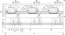
도 4 및 도 5는 본 발명의 일 실시예에 따른 디스플레이 패널의 일 부분을 개략적으로 도시하는 평면도들이다. 도 4는 도 3에 도시된 디스플레이 패널(DP)의 일부분을 확대하여 도시하고, 도 5는 도 4의 Ⅰ 부분을 확대하여 도시한다.4 and 5 are plan views schematically showing a portion of a display panel according to an embodiment of the present invention. FIG. 4 shows an enlarged portion of the display panel DP shown in FIG. 3, and FIG. 5 shows an enlarged portion I of FIG. 4.
도 4 및 도 5를 참조하면, 디스플레이 패널(DP)은 기판(100)을 구비할 수 있다. 기판(100)은 글래스재 또는 고분자 수지를 포함할 수 있다. 기판(100)은 고분자 수지를 포함하는 베이스층과 무기배리어층이 적층된 구조를 포함할 수 있다. 고분자 수지는 폴리에테르술폰(PES, polyethersulphone), 폴리아크릴레이트(PAR, polyacrylate), 폴리에테르 이미드(PEI, polyetherimide), 폴리에틸렌 나프탈레이트(PEN, polyethyelenene napthalate), 폴리에틸렌 테레프탈레이드(PET, polyethyeleneterepthalate), 폴리페닐렌 설파이드(polyphenylene sulfide: PPS), 폴리아릴레이트(polyallylate), 폴리이미드(polyimide: PI), 폴리카보네이트, 셀룰로오스 트리 아세테이트(TAC), 셀룰로오스 아세테이트 프로피오네이트(cellulose acetate propionate: CAP)일 수 있다.Referring to FIGS. 4 and 5 , the display panel DP may include a
디스플레이 패널(DP)의 구성요소들은 기판(100) 상에 배치되므로, 기판(100)은 화소(P, 도 1 참조)들을 통해 이미지를 표시하는 표시영역(DA) 및 표시영역(DA) 외측의 비표시영역(NDA)을 포함한다고 나타낼 수 있다.Since the components of the display panel (DP) are disposed on the
기판(100) 상에는 제1발광다이오드(ED1)들, 제2발광다이오드(ED2)들, 제3발광다이오드(ED3)들, 수평전압선(PLh) 및 금속뱅크층(BNL)이 배치될 수 있다. 이와 관련하여, 도 4는 금속뱅크층(BNL)과 수평전압선(PLh)의 위치 관계를 설명하기 위하여, 다른 구성요소는 생략하고 있다.First light emitting diodes (ED1), second light emitting diodes (ED2), third light emitting diodes (ED3), a horizontal voltage line (PLh), and a metal bank layer (BNL) may be disposed on the
금속뱅크층(BNL)은 후술하는 바와 같이, 서로 다른 금속 물질을 포함하는 제1서브금속층(215, 도 5 참조) 및 제2서브금속층(217, 도 5 참조)을 포함할 수 있다.As will be described later, the metal bank layer (BNL) may include a first sub-metal layer (215, see FIG. 5) and a second sub-metal layer (217, see FIG. 5) containing different metal materials.
금속뱅크층(BNL)은 표시영역(DA) 전면과 비표시영역(NDA)의 일부분을 덮도록 배치될 수 있다. 예컨대, 금속뱅크층(BNL)은 제2방향(예컨대, y 방향)으로 연장되는 제1경계(BNLE1)와, 제1경계(BNLE1)와 마주하는 제2경계(BNLE2)를 가질 수 있다. 금속뱅크층(BNL)의 제1경계(BNLE1) 및 제2경계(BNLE2)는 비표시영역(NDA) 상에 위치할 수 있다. 일 실시예에서, 금속뱅크층(BNL)의 제1경계(BNLE1)와 제2경계(BNLE2)는 공통전원공급배선(16, 도 2 참조)와 중첩할 수 있다. 본 명세서에서 "A와 B가 중첩한다"라 함은 기판(100)에 수직한 방향(예컨대, z축 방향)에서 기판(100)과 평행한 평면(예컨대, xy 평면)을 바라볼 때 A의 적어도 일부와 B의 적어도 일부가 평면 상에서 겹쳐 배치되는 것을 나타낸다.The metal bank layer (BNL) may be arranged to cover the entire display area (DA) and a portion of the non-display area (NDA). For example, the metal bank layer BNL may have a first boundary BNLE1 extending in a second direction (eg, y direction) and a second boundary BNLE2 facing the first boundary BNLE1. The first boundary (BNLE1) and the second boundary (BNLE2) of the metal bank layer (BNL) may be located on the non-display area (NDA). In one embodiment, the first boundary BNLE1 and the second boundary BNLE2 of the metal bank layer BNL may overlap the common power supply line 16 (see FIG. 2). In this specification, “A and B overlap” means that A is visible when looking at a plane parallel to the substrate 100 (e.g., xy plane) in a direction perpendicular to the substrate 100 (e.g., z-axis direction). It indicates that at least part of B and at least part of B are arranged to overlap on the plane.
금속뱅크층(BNL)은 제1발광다이오드(ED1), 제2발광다이오드(ED2) 및 제3발광다이오드(ED3) 각각에 대응하는 화소개구(OP)들을 가질 수 있다. 예컨대, 제1발광다이오드(ED1), 제2발광다이오드(ED2) 및 제3발광다이오드(ED3)는 각각 복수 개 구비될 수 있다. 일 실시예에서, 복수의 제1발광다이오드(ED1)은 제1화소행을 따라 제1방향(예컨대, x 방향)으로 상호 이격되어 배치되고, 복수의 제2발광다이오드(ED2)은 제2화소행을 따라 제1방향(예컨대, x 방향)으로 상호 이격되어 배치되고, 복수의 제3발광다이오드(ED3)은 제3화소행을 따라 제1방향(예컨대, x 방향)으로 상호 이격되어 배치될 수 있다. 제1발광다이오드(ED1), 제2발광다이오드(ED2) 및 제3발광다이오드(ED3)는 제1방향(예컨대, x 방향)과 교차하는 제2방향(예컨대, y 방향)으로 상호 이격되어 배치될 수 있다. 이에 대응하는 화소개구(OP)들은 제1방향(예컨대, x 방향) 및 제2방향(예컨대, y 방향)을 따라 상호 이격되어 배치되어 행렬을 이룰 수 있다.The metal bank layer (BNL) may have pixel openings (OP) corresponding to each of the first light emitting diode (ED1), the second light emitting diode (ED2), and the third light emitting diode (ED3). For example, a plurality of first light emitting diodes (ED1), second light emitting diodes (ED2), and third light emitting diodes (ED3) may each be provided. In one embodiment, the plurality of first light emitting diodes ED1 are arranged to be spaced apart from each other in the first direction (eg, x direction) along the first pixel row, and the plurality of second light emitting diodes ED2 are arranged in the second pixel row. They are arranged to be spaced apart from each other in a first direction (eg, x direction) along the row, and the plurality of third light emitting diodes ED3 are arranged to be spaced apart from each other in a first direction (eg, x direction) along the third pixel row. You can. The first light emitting diode (ED1), the second light emitting diode (ED2), and the third light emitting diode (ED3) are arranged to be spaced apart from each other in a second direction (eg, y direction) that intersects the first direction (eg, x direction). It can be. The pixel openings OP corresponding thereto may be arranged to be spaced apart from each other along the first direction (eg, x-direction) and the second direction (eg, y-direction) to form a matrix.
금속뱅크층(BNL)은 제1방향(예컨대, x 방향)으로 연장된 홀(h)들을 가질 수 있다. 홀(h)들은 금속뱅크층(BNL)을 관통하여, 금속뱅크층(BNL) 하부에 위치하는 절연층(예컨대, 무기뱅크층(213, 도 6 참조))을 노출시킬 수 있다.The metal bank layer BNL may have holes h extending in a first direction (eg, x direction). The holes (h) may penetrate the metal bank layer (BNL) and expose the insulating layer (eg, the inorganic bank layer 213 (see FIG. 6)) located below the metal bank layer (BNL).
홀(h)들은 화소개구(OP) 행(row) 사이에 배치될 수 있다. 화소개구(OP)들은 각각의 발광다이오드에 대응하므로, 홀(h)들은 발광다이오드 행 또는 화소 행 사이에 배치된다고 할 수 있다. 도 5에 도시된 바와 같이, 홀(h)들은 각각 제1발광다이오드(ED1)과 제2발광다이오드(ED2) 사이 및 제2발광다이오드(ED2)와 제3발광다이오드(ED3) 사이에 배치될 수 있다. 본 발명이 이에 한정되는 것은 아니며, 이웃하는 홀(h)들 사이에는 하나 이상의 발광다이오드 행이 배치될 수도 있다. 일 실시예로, 이웃하는 홀(h)들 사이에 제1발광다이오드(ED1), 제2발광다이오드(ED2) 및 제3발광다이오드(ED3)이 배치될 수 있다.Holes (h) may be arranged between pixel opening (OP) rows. Since the pixel openings (OP) correspond to each light emitting diode, the holes (h) can be said to be disposed between light emitting diode rows or pixel rows. As shown in FIG. 5, the holes (h) will be disposed between the first light emitting diode (ED1) and the second light emitting diode (ED2) and between the second light emitting diode (ED2) and the third light emitting diode (ED3), respectively. You can. The present invention is not limited to this, and one or more rows of light emitting diodes may be disposed between neighboring holes h. In one embodiment, the first light emitting diode (ED1), the second light emitting diode (ED2), and the third light emitting diode (ED3) may be disposed between neighboring holes (h).
홀(h)들은 제2방향(예컨대, y 방향)으로 상호 이격되며, 서로 평행하게 배치될 수 있다. 홀(h)들은 금속뱅크층(BNL)의 제1경계(BNLE1)과 제2경계(BNLE2) 사이에 위치할 수 있다. 즉, 홀(h)들의 외측으로 금속뱅크층(BNL)이 각 부분은 서로 연결되어 일체(一體)로 구비될 수 있다.The holes h are spaced apart from each other in the second direction (eg, y direction) and may be arranged parallel to each other. The holes (h) may be located between the first boundary (BNLE1) and the second boundary (BNLE2) of the metal bank layer (BNL). That is, each part of the metal bank layer (BNL) on the outside of the holes (h) can be connected to each other and formed as one body.
수평전압선(PLh)은 홀(h)들의 내측에 위치할 수 있다. 예컨대, 수평전압선(PLh)은 대응하는 홀(h)과 평행하게 제1방향(예컨대, x 방향)으로 연장될 수 있다. 수평전압선(PLh)은 금속뱅크층(BNL)의 제1경계(BNLE1)에 인접한 제1끝단(E1)과, 제2경계(BNLE2)에 인접한 제2끝단(E2)을 가질 수 있다. 수평전압선(PLh)의 제1끝단(E1)과 제2끝단(E2)는 금속뱅크층(BNL)의 제1경계(BNLE1)와 제2경계(BNLE2) 사이에 배치될 수 있다.The horizontal voltage line PLh may be located inside the holes h. For example, the horizontal voltage line PLh may extend in a first direction (eg, x-direction) parallel to the corresponding hole h. The horizontal voltage line PLh may have a first end E1 adjacent to the first boundary BNLE1 of the metal bank layer BNL and a second end E2 adjacent to the second boundary BNLE2. The first end E1 and the second end E2 of the horizontal voltage line PLh may be disposed between the first boundary BNLE1 and the second boundary BNLE2 of the metal bank layer BNL.
수평전압선(PLh)은 홀(h)에 의하여, 금속뱅크층(BNL)과 이격될 수 있다. 즉, 평면도 상에서, 수평전압선(PLh)은 금속뱅크층(BNL)과 이격되어 분리된 섬(island) 형상을 가질 수 있다. 다시 말해, 평면도 상에서 수평전압선(PLh)은 금속뱅크층(BNL)과 이격되되, 금속뱅크층(BNL)은 수평전압선(PLh)을 둘러싸도록 배치될 수 있다.The horizontal voltage line PLh may be separated from the metal bank layer BNL by a hole h. That is, in a plan view, the horizontal voltage line PLh may have an island shape that is separated from the metal bank layer BNL. In other words, in the plan view, the horizontal voltage line PLh may be spaced apart from the metal bank layer BNL, but the metal bank layer BNL may be arranged to surround the horizontal voltage line PLh.
도 4 및 도 5는 홀(h)의 끝단과 수평전압선(PLh)의 끝단이 모두 표시영역(DA)에 위치한 것을 도시하고 있으나, 본 발명이 이에 한정되는 것은 아니다. 일 실시예에서, 홀(h)의 끝단은 금속뱅크층(BNL)의 제1경계(BNLE1) 및 제2경계(BNLE2) 사이에 위치하되, 비표시영역(NDA)에 위치할 수 있다. 수평전압선(PLh)의 제1끝단(E1) 및 제2끝단(E2)은 홀(h) 내측에 위치하되 비표시영역(NDA)에 위치할 수 있다.4 and 5 show that both the end of the hole h and the end of the horizontal voltage line PLh are located in the display area DA, but the present invention is not limited thereto. In one embodiment, the end of the hole h is located between the first boundary BNLE1 and the second boundary BNLE2 of the metal bank layer BNL, and may be located in the non-display area NDA. The first end E1 and the second end E2 of the horizontal voltage line PLh may be located inside the hole h but in the non-display area NDA.
도 6 및 도 7은 본 발명의 일 실시예에 따른 디스플레이 패널의 일 부분을 개략적으로 도시하는 단면도들이다. 도 6은 도 5의 Ⅱ-Ⅱ' 선을 따른 디스플레이 패널의 단면을 나타내고, 도 7은 도 5의 Ⅲ-Ⅲ' 선을 따른 디스플레이 패널의 단면을 나타낸다.6 and 7 are cross-sectional views schematically showing a portion of a display panel according to an embodiment of the present invention. FIG. 6 shows a cross section of the display panel along line II-II' of FIG. 5, and FIG. 7 shows a cross section of the display panel along line III-III' of FIG. 5.
도 6을 참조하면, 기판(100)의 표시영역(DA)에는 발광다이오드 및 발광다이오드와 전기적으로 연결되는 화소회로를 포함하는 복수의 화소들이 배치될 수 있다. 예컨대, 기판(100)의 표시영역(DA)에는 제1발광다이오드(ED1), 제2발광다이오드(ED2) 및 제3발광다이오드(ED3)가 배치될 수 있다. 제1발광다이오드(ED1), 제2발광다이오드(ED2) 및 제3발광다이오드(ED3)는 서로 다른 파장의 빛을 방출할 수 있다. 예컨대, 제1발광다이오드(ED1), 제2발광다이오드(ED2) 및 제3발광다이오드(ED3)는 각각 적색, 녹색, 청색 또는 백색의 빛을 방출할 수 있다.Referring to FIG. 6, a plurality of pixels including a light-emitting diode and a pixel circuit electrically connected to the light-emitting diode may be disposed in the display area DA of the
버퍼층(201)은 기판(100)의 상면에 위치할 수 있다. 버퍼층(201)은 불순물이 화소회로의 반도체층으로 침투하는 것을 방지할 수 있다. 버퍼층(201)은 실리콘나이트라이드, 실리콘옥시나이트라이드 및 실리콘옥사이드와 같은 무기절연물을 포함할 수 있으며, 전술한 무기절연물을 포함하는 단층 또는 다층일 수 있다.The
제1화소회로(PC1), 제2화소회로(PC2) 및 제3화소회로(PC3)는 버퍼층(201) 상에 배치될 수 있다. 제1화소회로(PC1), 제2화소회로(PC2) 및 제3화소회로(PC3)는 실질적으로 동일하거나 유사한 구조를 가지므로, 이하에서는 제1화소회로(PC1)를 중심으로 설명한다.The first pixel circuit (PC1), the second pixel circuit (PC2), and the third pixel circuit (PC3) may be disposed on the
제1화소회로(PC1)은 복수의 트랜지스터들 및 스토리지 커패시터(Cst)를 포함할 수 있으며, 이와 관련하여 도 6은 박막트랜지스터(TFT) 및 스토리지 커패시터(Cst)를 포함하는 것을 도시한다.The first pixel circuit (PC1) may include a plurality of transistors and a storage capacitor (Cst), and in relation to this, FIG. 6 shows that it includes a thin film transistor (TFT) and a storage capacitor (Cst).
박막트랜지스터(TFT)는 버퍼층(201) 상의 반도체층(Act), 반도체층(Act)의 채널영역과 중첩하는 게이트전극(GE), 소스전극(SE) 및 드레인전극(DE)을 포함할 수 있다. 반도체층(Act)은 실리콘계 반도체 물질, 예컨대, 폴리 실리콘을 포함할 수 있다. 또는 반도체층(Act)은 산화물계 반도체 물질, 예컨대, Zn 산화물계 물질을 포함할 수 있다. 반도체층(Act)은 ZnO에 인듐(In)과 갈륨(Ga), 주석(Sn)과 같은 금속이 함유된 IGZO(In-Ga-Zn-O), ITZO(In-Sn-Zn-O), 또는 IGTZO(In-Ga-Sn-Zn-O) 반도체일 수 있다.The thin film transistor (TFT) may include a semiconductor layer (Act) on the
반도체층(Act)은 채널영역과 채널영역 양측에 배치된 불순물 영역들을 포함할 수 있다. 채널영역의 양측에 배치된 불순물 영역 중 어느 하나는 소스영역이고 다른 하나는 드레인영역에 해당할 수 있다.The semiconductor layer (Act) may include a channel region and impurity regions disposed on both sides of the channel region. One of the impurity regions disposed on both sides of the channel region may correspond to a source region and the other may correspond to a drain region.
반도체층(Act)과 게이트전극(GE) 사이에는 제1게이트절연층(203)이 배치될 수 있다. 제1게이트절연층(203)은 실리콘옥사이드, 실리콘나이트라이드, 실리콘옥시나이트라이드와 같은 무기절연물을 포함할 수 있으며, 전술한 무기절연물을 포함하는 단일층 또는 다층 구조를 포함할 수 있다.A first
게이트전극(GE)은 몰리브데넘, 알루미늄, 구리, 티타늄 등을 포함하는 도전 물질을 포함할 수 있고, 전술한 물질을 포함하는 단일층 또는 다층 구조를 포함할 수 있다.The gate electrode GE may include a conductive material including molybdenum, aluminum, copper, titanium, etc., and may include a single-layer or multi-layer structure including the above-described materials.
스토리지 커패시터(Cst)는 서로 중첩하는 하부전극(CE1) 및 상부전극(CE2)을 포함할 수 있다. 일 실시예로, 스토리지 커패시터(Cst)의 하부전극(CE1)은 박막트랜지스터(TFT)의 게이트전극(GE)을 포함할 수 있다. 예컨대, 박막트랜지스터(TFT)의 게이트전극(GE)은 스토리지 커패시터(Cst)의 하부전극(CE1)과 일체로 형성될 수 있다.The storage capacitor Cst may include a lower electrode CE1 and an upper electrode CE2 that overlap each other. In one embodiment, the lower electrode (CE1) of the storage capacitor (Cst) may include the gate electrode (GE) of the thin film transistor (TFT). For example, the gate electrode (GE) of the thin film transistor (TFT) may be formed integrally with the lower electrode (CE1) of the storage capacitor (Cst).
스토리지 커패시터(Cst)의 하부전극(CE1)과 상부전극(CE2) 사이에는 제1층간절연층(205)이 배치되고, 스토리지 커패시터(Cst)의 상부전극(CE2) 상에는 제2층간절연층(207)이 배치될 수 있다. 제1층간절연층(205) 및 제2층간절연층(207) 각각은 실리콘옥사이드, 실리콘나이트라이드, 실리콘옥시나이트라이드와 같은 무기절연물을 포함할 수 있으며, 전술한 무기절연물을 포함하는 단일층 또는 다층 구조를 포함할 수 있다.A first
소스전극(SE) 및/또는 드레인전극(DE)은 제2층간절연층(207) 상에 배치될 수 있다. 일부 실시예에서 소스전극(SE) 및 드레인전극(DE) 중 어느 하나는 생략될 수 있다. 소스전극(SE) 및/또는 드레인전극(DE)은 몰리브데넘, 알루미늄, 구리, 티타늄 등을 포함하는 도전 물질을 포함할 수 있고, 전술한 물질을 포함하는 단일층 또는 다층 구조를 포함할 수 있다. 예컨대, 소스전극(SE) 및/또는 드레인전극(DE)은 티타늄층/알루미늄층/티타늄층(Ti/Al/Ti)으로 이루어진 다층 구조를 가질 수 있다.The source electrode (SE) and/or the drain electrode (DE) may be disposed on the second
소스전극(SE) 및/또는 드레인전극(DE)를 덮도록 제1평탄화층(209)이 배치될 수 있다. 일 실시예에서, 제1평탄화층(209)은 유기절연물을 포함할 수 있다. 유기절연물은 아크릴, BCB(Benzocyclobutene), 폴리이미드(polyimide) 또는 HMDSO(Hexamethyldisiloxane) 등을 포함할 수 있다. 또는 제1평탄화층(209)는 무기절연물을 포함할 수 있다. 무기절연물은 실리콘옥사이드, 실리콘나이트라이드 또는 실리콘옥시나이트라이드 등을 포함할 수 있다.The
연결전극(CM)은 제1평탄화층(209) 상에 배치될 수 있다. 연결전극(CM)은 제1평탄화층(209)을 관통하는 컨택홀을 통해 박막트랜지스터(TFT)의 소스전극(SE) 또는 드레인전극(DE)와 접속될 수 있다. 연결전극(CM)은 몰리브데넘, 알루미늄, 구리, 티타늄 등을 포함하는 도전 물질을 포함할 수 있고, 전술한 물질을 포함하는 단일층 또는 다층 구조를 포함할 수 있다. 예컨대, 연결전극(CM)은 티타늄층/알루미늄층/티타늄층(Ti/Al/Ti)으로 이루어진 다층 구조를 가질 수 있다.The connection electrode CM may be disposed on the
연결전극(CM)을 덮도록 제2평탄화층(211)이 배치될 수 있다. 제2평탄화층(211)은 유기절연물을 포함할 수 있다. 유기절연물은 아크릴, BCB(Benzocyclobutene), 폴리이미드(polyimide) 또는 HMDSO(Hexamethyldisiloxane) 등을 포함할 수 있다.The
제2평탄화층(211) 상에는 제1발광다이오드(ED1), 제2발광다이오드(ED2) 및 제3발광다이오드(ED3)가 배치될 수 있다. 제1발광다이오드(ED1)은 제1화소회로(PC1)과 전기적으로 연결되고, 제2발광다이오드(ED2)는 제2화소회로(PC2)와 전기적으로 연결되고, 제3발광다이오드(ED3)는 제3화소회로(PC3)와 전기적으로 연결될 수 있다.A first light emitting diode (ED1), a second light emitting diode (ED2), and a third light emitting diode (ED3) may be disposed on the
제1발광다이오드(ED1)은 제1화소전극(221), 제1중간층(231) 및 제1대향전극(241)을 포함하고, 제2발광다이오드(ED2)은 제2화소전극(223), 제2중간층(233) 및 제2대향전극(243)을 포함하고, 제3발광다이오드(ED3)는 제3화소전극(225), 제3중간층(235) 및 제3대향전극(245)을 포함할 수 있다. 제1발광다이오드(ED1), 제2발광다이오드(ED2) 및 제3발광다이오드(ED3)는 실질적으로 동일하거나 유사한 구조를 가지므로, 이하에서는 제1발광다이오드(ED1)를 중심으로 설명한다.The first light emitting diode (ED1) includes a
제1화소전극(221)은 제2평탄화층(211) 상에 배치되며, 제2평탄화층(211)을 관통하는 컨택홀을 통하여 연결전극(CM)과 전기적으로 연결될 수 있다. 도 6에서는 박막트랜지스터(TFT)의 드레인전극(DE)과 제1화소전극(221) 사이에 제1평탄화층(209) 및 제2평탄화층(211)이 배치되는 것을 도시하고 있으나, 다른 실시예에서, 박막트랜지스터(TFT)의 드레인전극(DE)과 제1화소전극(221) 사이에는 하나의 평탄화층이 배치될 수 있다. 이러한 경우, 연결전극(CM)은 생략되고, 제1화소전극(221)은 드레인전극(DE)과 직접 접속할 수 있다. 또 다른 실시예에서, 박막트랜지스터(TFT)의 드레인전극(DE)과 제1화소전극(221) 사이에는 세 개 이상의 평탄화층이 배치될 수 있다. 이러한 경우, 제1화소전극(221)은 복수의 연결전극들을 통하여 드레인전극(DE)과 전기적으로 연결될 수 있다.The
제1화소전극(221)은 (반)투명전극이 되도록 형성할 수도 있고 반사전극이 되도록 형성할 수도 있다. 제1화소전극(221)을 (반)투명전극으로 형성할 경우, 예컨대 인듐틴옥사이드(ITO; indium tin oxide), 인듐징크옥사이드(IZO; indium zinc oxide), 징크옥사이드(ZnO; zinc oxide), 인듐옥사이드(In2O3 indium oxide), 인듐갈륨옥사이드(IGO; indium gallium oxide) 또는 알루미늄징크옥사이드(AZO; aluminium zinc oxide)로 형성될 수 있다. 제1화소전극(221)을 반사전극으로 형성할 경우에는 Ag, Mg, Al, Pt, Pd, Au, Ni, Nd, Ir, Cr 또는 이들의 화합물 등으로 반사막을 형성하고, 이 반사막 상에 ITO, IZO, ZnO 또는 In2O3로 형성된 막을 형성할 수 있다. 일 실시예로, 제1화소전극(221)은 ITO층, Ag층, ITO층이 순차적으로 적층된 구조일 수 있다.The
제1화소전극(221)의 가장자리를 덮도록 제2평탄화층(211) 상에 무기뱅크층(213)이 배치될 수 있다. 무기뱅크층(213)은 제1화소전극(221), 제2화소전극(223) 및 제3화소전극(225) 각각에 대응하는 개구들을 가질 수 있다. 무기뱅크층(213)은 실리콘산화물, 실리콘질화물, 실리콘산질화물과 같은 무기절연물을 포함할 수 있으며, 전술한 무기절연물을 포함하는 단일층 또는 다층 구조를 포함할 수 있다. 무기뱅크층(213)은 제1화소전극(221)의 가장자리와 제1대향전극(241) 사이의 거리를 증가시킴으로써, 이들 사이에서 아크(arc) 등이 발생하는 것을 방지할 수 있다.The
제1화소전극(221), 제2화소전극(223) 및 제3화소전극(225)와 무기뱅크층(213) 사이에는 잔여희생층(212)이 배치될 수 있다. 잔여희생층(212)은 디스플레이 패널(DP)의 제조공정에 포함된 에칭 공정 또는 애싱 공정 등에서 사용되는 기체 또는 액체 물질 등에 의하여 제1화소전극(221), 제2화소전극(223) 및 제3화소전극(225)이 손상되는 것을 방지하기 위한 구성일 수 있다. 예컨대, 잔여희생층(212)은 후술하는 화소개구(OP)들을 형성하기 위한 건식 식각(dry etching) 공정에서 제1화소전극(221), 제2화소전극(223) 및 제3화소전극(225)의 상면을 보호하기 위한 구성의 일부분일 수 있다. 잔여희생층(212)은 화소개구(OP)들과 중첩하는 개구들을 가질 수 있다.A remaining
잔여희생층(212)은 제1화소전극(221)의 손상 없이 선택적으로 식각 가능한 물질을 포함할 수 있다. 예컨대, 잔여희생층(212)은 IZO(Indium Zinc Oxide) 및/또는 IGZO (indium gallium zinc oxide)과 같은 도전성 산화물을 포함할 수 있다.The remaining
금속뱅크층(BNL)은 무기뱅크층(213) 상에 위치하며, 제1화소전극(221), 제2화소전극(223) 및 제3화소전극(225) 각각과 중첩하는 화소개구(OP)들 및 화소개구(OP)들 사이에 배치되는 홀(h)들을 가질 수 있다. 금속뱅크층(BNL)은 무기뱅크층(213) 상에 전체적으로 형성된 것일 수 있다.The metal bank layer (BNL) is located on the
금속뱅크층(BNL)은 서로 다른 금속을 포함하는 제1서브금속층(215) 및 제2서브금속층(217)을 포함할 수 있다. 제1서브금속층(215)과 제2서브금속층(217)은 식각선택비가 서로 상이한 금속을 포함할 수 있다. 예컨대, 제1서브금속층(215)은 알루미늄(Al) 또는 몰리브데넘(Mo)을 포함하고, 제2서브금속층(217)은 티타늄(Ti) 또는 탄탈럼(Ta)을 포함할 수 있다.The metal bank layer (BNL) may include a first
제2서브금속층(217)은 제1서브금속층(215)의 상면으로부터 화소개구(OP)들 각각의 중심 방향으로 연장된 팁(PT)들을 가질 수 있다. 예컨대, 각 화소개구(OP)에서 제2서브금속층(217) 하부에 위치하는 제1서브금속층(215)의 일부가 제거되어 제2서브금속층(217)이 돌출되는 언더컷(undercut) 구조를 이룰 수 있다.The second
홀(h)의 내측에 수평전압선(PLh)이 배치될 수 있다. 수평전압선(PLh)은 금속뱅크층(BNL)의 일 부분을 제거하여 금속뱅크층(BNL)로부터 분리된 부분으로, 금속뱅크층(BNL)과 동일한 층 구조를 가질 수 있다. 예컨대, 수평전압선(PLh)은 제1수평배선(216) 및 제1수평배선(216) 상에 위치하는 제2수평배선(218)을 포함할 수 있다. 제1수평배선(216)은 제1서브금속층(215)와 동일한 물질을 포함하고, 제2수평배선(218)은 제2서브금속층(217)과 동일한 물질을 포함할 수 있다. 일 실시예에서, 수평전압선(PLh)은 제2수평배선(218)의 하부에 위치하는 제1수평배선(216)의 일부가 제거되어, 제2수평배선(218)이 돌출되는 언더컷 구조를 가질 수 있다.A horizontal voltage line (PLh) may be disposed inside the hole (h). The horizontal voltage line PLh is a part separated from the metal bank layer BNL by removing a portion of the metal bank layer BNL, and may have the same layer structure as the metal bank layer BNL. For example, the horizontal voltage line PLh may include a first
홀(h)은 금속뱅크층(BNL)을 관통하며, 수평전압선(PLh)을 금속뱅크층(BNL)로부터 완전히 이격하여 분리할 수 있다.The hole (h) penetrates the metal bank layer (BNL), and the horizontal voltage line (PLh) can be completely separated from the metal bank layer (BNL).
금속뱅크층(BNL)의 화소개구(OP)를 통하여 제1화소전극(221) 상에 제1중간층(231)이 위치할 수 있다. 제1중간층(231)은 발광층을 포함할 수 있다. 발광층은 소정의 색상(적색, 녹색 또는 청색)의 빛을 방출하는 고분자 또는 저분자 유기물을 포함할 수 있다. 다른 실시예로, 발광층은 무기물 또는 양자점을 포함할 수 있다.The first
제1중간층(231)은 제1화소전극(221)과 발광층 사이 및/또는 발광층과 제1대향전극(241) 사이에 개재되는 기능층을 포함할 수 있다. 기능층은 홀 수송층(HTL: Hole Transport Layer), 홀 주입층(HIL: Hole Injection Layer), 전자 수송층(ETL: Electron Transport Layer) 및/또는 전자 주입층(EIL: Electron Injection Layer)을 포함할 수 있다.The first
제1중간층(231)은 단일의 발광층을 포함하는 단일 스택 구조이거나, 복수의 발광층들을 포함하는 멀티 스택 구조인 탠덤 구조를 가질 수 있다. 탠덤 구조를 갖는 경우, 복수의 스택들 사이에는 전하생성층(CGL, Charge Generation Layer)이 배치될 수 있다.The first
일 실시예에서, 제1중간층(231) 표시영역(DA)의 전면(全面)에 증착되어, 제1중간층(231)을 형성하기 위한 증착 물질은 제2서브금속층(217) 상에 위치하는 제1더미중간층(231P)을 형성할 수 있다. 제1중간층(231)과 제1더미중간층(231P)은 동일한 물질을 포함할 수 있다. 본 명세서에서 "A와 B가 동일한 물질을 포함한다"고 하는 것은 A와 B가 동일한 공정에 의하여 동시에 형성되었음을 나타낸다. 동일한 물질을 포함하는 A와 B는 동일한 막질을 가질 수 있다. 제1중간층(231)과 제1더미중간층(231P)은 제2서브금속층(217)의 팁(PT)에 의하여 서로 분리 및 이격될 수 있다.In one embodiment, the first
마찬가지로, 제2중간층(233)은 제2더미중간층(233P)과 동일한 물질을 포함하고, 제3중간층(235)은 제3더미중간층(235P)과 동일한 물질을 포함할 수 있다. 제2중간층(233)과 제2더미중간층(233P)은 제2서브금속층(217)의 팁(PT)에 의하여 서로 분리 및 이격될 수 있다. 제3중간층(235)과 제3더미중간층(235P)은 제2서브금속층(217)의 팁(PT)에 의하여 서로 분리 및 이격될 수 있다.Likewise, the second
금속뱅크층(BNL)의 화소개구(OP)를 통하여, 제1중간층(231) 상에 제1대향전극(241)이 배치될 수 있다. 제1대향전극(241)은 일함수가 낮은 도전성 물질로 이루어질 수 있다. 예컨대, 제1대향전극(241)은 은(Ag), 마그네슘(Mg), 알루미늄(Al), 백금(Pt), 팔라듐(Pd), 금(Au), 니켈(Ni), 네오디뮴(Nd), 이리듐(Ir), 크로뮴(Cr), 리튬(Li), 칼슘(Ca) 또는 이들의 합금 등을 포함하는 (반)투명층을 포함할 수 있다. 또는, 제1대향전극(241)은 전술한 물질을 포함하는 (반)투명층 상에 ITO, IZO, ZnO 또는 In2O3과 같은 층을 더 포함할 수 있다.The
일 실시예에서, 제1대향전극(241)은 표시영역(DA)의 전면(全面)에 증착되어, 제1대향전극(241)을 형성하기 위한 증착 물질은 제1더미중간층(231P) 상에 위치하는 제1더미대향전극(241P)을 형성할 수 있다. 제1대향전극(241)과 제1더미대향전극(241P)은 동일한 물질을 포함할 수 있다. 제1대향전극(241)과 제1더미대향전극(241P)은 제2서브금속층(217)의 팁(PT)에 의하여 서로 분리 및 이격될 수 있다.In one embodiment, the
마찬가지로, 제2대향전극(243)과 제2더미대향전극(243P)은 동일한 물질을 포함하고, 제3대향전극(245)과 제3더미대향전극(245P)은 동일한 물질을 포함할 수 있다. 제2대향전극(243)과 제2더미대향전극(243P)은 제2서브금속층(217)의 팁(PT)에 의하여 서로 분리 및 이격될 수 있다. 제3대향전극(245)과 제3더미대향전극(245P)은 제2서브금속층(217)의 팁(PT)에 의하여 서로 분리 및 이격될 수 있다.Likewise, the
제1대향전극(241)은 금속뱅크층(BNL)의 화소개구(OP)를 정의하는 제1서브금속층(215)의 측면에 직접 접촉할 수 있다. 예컨대, 제2서브금속층(217)의 팁(PT)에 가려져 제1중간층(231)이 형성되지 않은 제1서브금속층(215)의 측벽에 제1대향전극(241)이 직접 접촉할 수 있다. 따라서, 제1대향전극(241)은 제1서브금속층(215)과 직접 접촉하는 컨택부를 형성하고, 제1대향전극(241)은 금속뱅크층(BNL)을 통하여 공통전압(ELVSS)을 전달받을 수 있다.The
제1대향전극(241) 상에 제1캡핑층(251)이 배치될 수 있다. 제1캡핑층(251)은 제1대향전극(241)을 보호하는 동시에 광추출 효율을 높일 수 있다. 제1캡핑층(251)의 굴절률은 제1대향전극(241)보다 높을 수 있다. 또는 제1캡핑층(251)은 굴절률이 서로 다른 층들이 적층되어 구비될 수 있다. 예컨대, 제1캡핑층(251)의 굴절률은 약 1.7 내지 약 1.9 일 수 있다. 제1캡핑층(251)은 유기물질을 포함할 수 있으며, 추가적으로 LiF와 같은 무기절연물을 포함할 수 있다.A
일 실시예에서, 제1캡핑층(251)은 표시영역(DA)의 전면(全面)에 증착되어, 제1캡핑층(251)을 형성하기 위한 증착 물질은 제1더미대향전극(241P) 상에 위치하는 제1더미캡핑층(251P)을 형성할 수 있다. 제1캡핑층(251)과 제1더미캡핑층(251P)은 동일한 물질을 포함할 수 있다. 제1캡핑층(251)과 제1더미캡핑층(251P)은 제2서브금속층(217)의 팁(PT)에 의하여 서로 분리 및 이격될 수 있다.In one embodiment, the
마찬가지로, 제2캡핑층(253)과 제2더미캡핑층(253P)은 동일한 물질을 포함하고, 제3캡핑층(255)과 제3더미캡핑층(255P)은 동일한 물질을 포함할 수 있다. 제2캡핑층(253)과 제2더미캡핑층(253P)은 제2서브금속층(217)의 팁(PT)에 의하여 서로 분리 및 이격될 수 있다. 제3캡핑층(255)과 제3더미캡핑층(255P)은 제2서브금속층(217)의 팁(PT)에 의하여 서로 분리 및 이격될 수 있다.Likewise, the
제1더미층(DM1)은 제1더미중간층(231P), 제1더미대향전극(241P) 및 제1더미캡핑층(251P)을 포함할 수 있다. 제1더미층(DM1)은 제1발광다이오드(ED1)에 대응하는 금속뱅크층(BNL)의 화소개구(OP)와 인접하여 제2서브금속층(217) 상에 위치할 수 있다. 다시 말해, 제1더미층(DM1)은 제2서브금속층(217)의 팁(PT)과 중첩하는 폐루프를 형상을 가질 수 있다.The first dummy layer DM1 may include a first dummy
제2더미층(DM2)은 제2더미중간층(233P), 제2더미대향전극(243P) 및 제2더미캡핑층(253P)을 포함할 수 있다. 제2더미층(DM2)은 제2발광다이오드(ED2)에 대응하는 금속뱅크층(BNL)의 화소개구(OP)와 인접하여 제2서브금속층(217) 상에 위치할 수 있다. 제2더미층(DM2)과 금속뱅크층(BNL) 사이에는 제1클래드층(312)의 일부분(312P)이 남아있을 수 있다. 제3더미층(DM3)은 제3더미중간층(235P), 제3더미대향전극(245P) 및 제3더미캡핑층(255P)을 포함할 수 있다. 제3더미층(DM3)은 제3발광다이오드(ED3)에 대응하는 금속뱅크층(BNL)의 화소개구(OP)와 인접하여 제2서브금속층(217) 상에 위치할 수 있다. 제3더미층(DM3)과 금속뱅크층(BNL) 사이에는 제2클래드층(314)의 일부분이 남아있을 수 있다.The second dummy layer DM2 may include a second dummy
제1발광다이오드(ED1)을 밀봉하도록, 제1캡핑층(251) 상에 제1무기봉지층(311)을 형성할 수 있다. 제1무기봉지층(311)은 실리콘질화물 또는 실리콘산질화물을 포함할 수 있다.A first
제1무기봉지층(311)은 상대적으로 우수한 스텝 커버리지(step coverage)를 가져, 제2서브금속층(217)의 팁(PT)의 하면 및 제1서브금속층(215)의 측면과 직접 접촉하여 제1발광다이오드(ED1)을 완전히 둘러싸는 무기접촉영역을 형성할 수 있다. 따라서, 제1무기봉지층(311)은 제1발광다이오드(ED1)으로 불순물이 침투하는 경로를 감소시키거나 차단할 수 있다.The first
마찬가지로, 제2발광다이오드(ED2)을 밀봉하는 제2무기봉지층(313)이 제2캡핑층(253) 상에 배치되고, 제3발광다이오드(ED3)을 밀봉하는 제3무기봉지층(315)이 제3캡핑층(255) 상에 배치될 수 있다.Likewise, the second
제1무기봉지층(311), 제2무기봉지층(313) 및 제3무기봉지층(315)는 상호 이격되어 배치될 수 있다. 예컨대, 제1무기봉지층(311)은 제1발광다이오드(ED1)을 덮도록 아일랜드 형상으로 패터닝되고, 제2무기봉지층(313)은 제2발광다이오드(ED2)를 덮도록 아일랜드 형상으로 패터닝되고, 제3무기봉지층(315)은 제3발광다이오드(ED3)를 덮도록 아일랜드 형상으로 패터닝 된 것일 수 있다.The first
제1무기봉지층(311)과 금속뱅크층(BNL) 사이에 위치하는 제1더미층(DM1)의 끝단을 커버하도록 제1클래드층(312)이 배치될 수 있다. 제1클래드층(312)은 제1더미층(DM1)을 통하여 불순물이 제1발광다이오드(ED1)로 침투하는 것을 방지할 수 있다. 제1클래드층(312)은 실리콘질화물 또는 실리콘산질화물을 포함할 수 있다.The first
마찬가지로, 제2더미층(DM2)의 끝단을 커버하도록 제2클래드층(314)이 배치되고, 제3더미층(DM3)의 끝단을 커버하도록 제3클래드층(316)이 배치될 수 있다.Likewise, the second
제1무기봉지층(311), 제2무기봉지층(313) 및 제3무기봉지층(315) 상에 유기봉지층(320)이 위치할 수 있다. 유기봉지층(320)은 상부에 배치되는 구성요소들에 평탄한 베이스면을 제공할 수 있다. 유기봉지층(320)은 폴리머(polymer)계열의 물질을 포함할 수 있다. 폴리머 계열의 소재로는 아크릴계 수지, 에폭시계 수지, 폴리이미드 및 폴리에틸렌 등을 포함할 수 있다.The
유기봉지층(320) 상에는 제4무기봉지층(330)이 배치될 수 있다. 제4무기봉지층(330)은 알루미늄산화물, 티타늄산화물, 탄탈륨산화물, 하프늄산화물, 징크산화물, 실리콘산화물, 실리콘질화물, 실리콘산질화물 중 하나 이상의 무기물을 포함할 수 있다.A fourth
도 7을 참조하면, 표시영역(DA)으로부터 비표시영역(NDA)으로 버퍼층(201), 제1게이트절연층(203), 제1층간절연층(205), 제2층간절연층(207), 제1평탄화층(209) 및 제2평탄화층(211)이 연장되어 배치될 수 있다.Referring to FIG. 7, a
제2층간절연층(207)과 제1평탄화층(209) 사이에 신호배선(250)들이 배치될 수 있다. 신호배선(250)들은 몰리브데넘, 알루미늄, 구리, 티타늄 등을 포함하는 도전 물질을 포함할 수 있고, 전술한 물질을 포함하는 단일층 또는 다층 구조를 포함할 수 있다.
제1평탄화층(209)와 제2평탄화층(211) 사이에 구동전압선(PL)들이 배치될 수 있다. 구동전압선(PL)들은 몰리브데넘, 알루미늄, 구리, 티타늄 등을 포함하는 도전 물질을 포함할 수 있고, 전술한 물질을 포함하는 단일층 또는 다층 구조를 포함할 수 있다.Driving voltage lines PL may be disposed between the
비표시영역(NDA)에 공통전원공급배선(16)이 위치할 수 있다. 공통전원공급배선(16)은 기판(100)의 가장자리와 평행하게 배치되어, 표시영역(DA)의 적어도 일부를 둘러쌀 수 있다. 공통전원공급배선(16)은 제1배선(161), 제1배선(161) 상에 위치하는 제2배선(163) 및 제2배선(163) 상에 위치하는 제3배선(165)을 포함할 수 있다.The common
제1배선(161)은 제2층간절연층(207) 상에 배치되고, 제1평탄화층(209)에 의하여 내측 가장자리가 커버될 수 있다. 제2배선(163)은 제1평탄화층(209)와 제2평탄화층(211) 사이에 배치되고, 제1평탄화층(209)의 외측에서 제1배선(161)과 접속할 수 있다. 제1배선(161) 및 제2배선(163)은 몰리브데넘, 알루미늄, 구리, 티타늄 등을 포함하는 도전 물질을 포함할 수 있고, 전술한 물질을 포함하는 단일층 또는 다층 구조를 포함할 수 있다. 일 실시예에서, 제1배선(161)은 소스전극(SE) 및/또는 드레인전극(DE)와 동일한 물질을 포함하고, 제2배선(163)은 연결전극(CM)과 동일한 물질을 포함할 수 있다.The
제3배선(165)은 제2평탄화층(211) 상에 배치되고, 제2평탄화층(211)의 외측에서 제2배선(163)과 접속할 수 있다. 제3배선(165)은 제1화소전극(221)과 동일한 물질을 포함할 수 있다. 일 실시예로, 제3배선(165)은 ITO층, Ag층, ITO층이 순차적으로 적층된 구조일 수 있다.The
금속뱅크층(BNL)은 비표시영역(NDA)으로 연장되며, 공통전원공급배선(16)과 중첩하도록 배치될 수 있다. 다시 말해, 금속뱅크층(BNL)의 제2경계(BNLE2)는 공통전원공급배선(16)과 중첩하도록 배치될 수 있다. 금속뱅크층(BNL)의 제1서브금속층(215)은 제2평탄화층(211)을 관통하는 제2컨택부(CNT2)를 통하여 공통전원공급배선(16)의 제2배선(163)과 접속할 수 있다. 따라서, 금속뱅크층(BNL)은 공통전원공급배선(16)으로부터 공통전압(ELVSS)을 전달받을 수 있다. 일 실시예에서 제2컨택부(CNT2)는 공통전원공급배선(16)과 중첩하여 표시영역(DA)의 적어도 일부를 둘러싸도록 연속적으로 배치될 수 있다.The metal bank layer (BNL) extends into the non-display area (NDA) and may be arranged to overlap the common
금속뱅크층(BNL)과 수평전압선(PLh)은 홀(h)에 의하여 이격되어 분리될 수 있다. 다시 말해, 수평전압선(PLh)의 제2끝단(E2)은 홀(h) 내측에 위치할 수 있다. 수평전압선(PLh)은 제2평탄화층(211) 및 무기뱅크층(213)을 관통하는 제1컨택부(CNT1)를 통하여 구동전압선(PL)과 전기적으로 연결될 수 있다. 도 2에 도시된 바와 같이, 구동전압선(PL)은 표시영역(DA)을 가로질러 제2방향(예컨대, y 방향)으로 연장되고, 수평전압선(PLh)은 표시영역(DA)을 가로질러 제1방향(예컨대, x 방향)으로 연장되므로, 평면도 상에서 구동전압선(PL)과 수평전압선(PLh)은 메쉬 형상을 이룰 수 있다. 따라서, 구동전압선(PL)의 저항으로 인하여 발생하는 화소의 위치에 따른 휘도 차이를 감소시킬 수 있다.The metal bank layer (BNL) and the horizontal voltage line (PLh) may be separated by a hole (h). In other words, the second end E2 of the horizontal voltage line PLh may be located inside the hole h. The horizontal voltage line PLh may be electrically connected to the driving voltage line PL through the first contact portion CNT1 penetrating the
비표시영역(NDA) 상에 제1댐(DAM1) 및 제2댐(DAM2)가 상호 이격하여 배치될 수 있다. 도 7은 제1댐(DAM1)이 제1-1유기층(411), 제1무기층(413) 및 제1-2유기층(415)을 포함하고, 제2댐(DAM2)이 제2-1유기층(421), 제2-2유기층(423), 제2무기층(425) 및 제2-3유기층(427)을 포함하는 것을 도시하고 있으나, 본 발명이 이에 한정되는 것은 아니다. 제1댐(DAM1) 및/또는 제2댐(DAM2)를 구성하는 층들은 추가되거나 일부 생략될 수 있다.The first dam (DAM1) and the second dam (DAM2) may be placed spaced apart from each other on the non-display area (NDA). Figure 7 shows that the first dam (DAM1) includes the 1-1
제1댐(DAM1)은 공통전원공급배선(16)과 중첩하도록 배치될 수 있다. 예컨대, 제1댐(DAM1)의 제1-1유기층(411)은 공통전원공급배선(16)의 제2배선(163) 상에 위치할 수 있다. 제1-1유기층(411)의 적어도 일부를 덮도록 공통전원공급배선(16)의 제3배선(165)가 배치될 수 있다.The first dam (DAM1) may be arranged to overlap the common power supply wiring (16). For example, the 1-1
제1-1유기층(411)은 유기절연물을 포함할 수 있다. 유기절연물은 아크릴, BCB(Benzocyclobutene), 폴리이미드(polyimide) 또는 HMDSO(Hexamethyldisiloxane) 등을 포함할 수 있다. 일 실시예에서, 제1-1유기층(411)은 제2평탄화층(211)과 동일한 물질을 포함할 수 있다.The 1-1
제1-1유기층(411)상에 제1무기층(413)이 배치될 수 있다. 제1무기층(413)과 제1-1유기층(411)사이에는 공통전원공급배선(16)의 제3배선(165)가 배치될 수 있다. 제1무기층(413)은 실리콘산화물, 실리콘질화물, 실리콘산질화물과 같은 무기절연물을 포함할 수 있으며, 전술한 무기절연물을 포함하는 단일층 또는 다층 구조를 포함할 수 있다. 일 실시예에서, 제1무기층(413)은 무기뱅크층(213)과 동일한 물질을 포함할 수 있다.A first
제1무기층(413) 상에 제1-2유기층(415)가 배치될 수 있다. 제1-2유기층(415)은 유기절연물을 포함할 수 있다. 유기절연물은 아크릴, BCB(Benzocyclobutene), 폴리이미드(polyimide) 또는 HMDSO(Hexamethyldisiloxane) 등을 포함할 수 있다.A 1-2
제2댐(DAM2)은 공통전원공급배선(16)의 외측 가장자리를 덮도록 배치될 수 있다. 예컨대, 제2댐(DAM2)의 제2-1유기층(421)은 공통전원공급배선(16)의 제1배선(161)의 외측 가장자리를 덮고, 제2-2유기층(423)은 공통전원공급배선(16)의 제2배선(163)의 외측 가장자리를 덮을 수 있다. 공통전원공급배선(16)의 제3배선(165)의 외측 가장자리는 제2-2유기층(423)과 제2무기층(425) 사이에 위치할 수 있다.The second dam (DAM2) may be arranged to cover the outer edge of the common power supply wiring (16). For example, the 2-1
제2-1유기층(421)은 유기절연물을 포함할 수 있다. 유기절연물은 아크릴, BCB(Benzocyclobutene), 폴리이미드(polyimide) 또는 HMDSO(Hexamethyldisiloxane) 등을 포함할 수 있다. 일 실시예에서, 제2-1유기층(421)은 제1평탄화층(209)과 동일한 물질을 포함할 수 있다.The 2-1
제2-1유기층(421)을 덮도록 제2-1유기층(421)상에 제2-2유기층(423)이 배치될 수 있다. 공통전원공급배선(16)의 제2배선(163)의 외측 가장자리는 제2-1유기층(421) 상에 배치되고, 제2-2유기층(423)은 제2배선(163)의 외측 가장자리를 커버할 수 있다. 제2-2유기층(423)은 유기절연물을 포함할 수 있다. 유기절연물은 아크릴, BCB(Benzocyclobutene), 폴리이미드(polyimide) 또는 HMDSO(Hexamethyldisiloxane) 등을 포함할 수 있다. 일 실시예에서, 제2-2유기층(423)은 제2평탄화층(211)과 동일한 물질을 포함할 수 있다.The 2-2
제2-2유기층(423)를 덮도록 제2-2유기층(423) 상에 제2무기층(425)이 배치될 수 있다. 다시 말해, 제2무기층(425)은 제2-2유기층(423)상에 위치하는 공통전원공급배선(16)의 제3배선(165)의 외측 가장자리를 덮도록 배치될 수 있다. 제2무기층(425)은 실리콘산화물, 실리콘질화물, 실리콘산질화물과 같은 무기절연물을 포함할 수 있으며, 전술한 무기절연물을 포함하는 단일층 또는 다층 구조를 포함할 수 있다. 일 실시예에서, 제2무기층(425)은 무기뱅크층(213)과 동일한 물질을 포함할 수 있다. 제1무기층(413)과 제2무기층(425)은 무기뱅크층(213)을 형성하는 공정에서 동시에 형성될 수 있다.A second
제2무기층(425) 상에 제2-3유기층(427)이 배치될 수 있다. 제2-3유기층(427)은 유기절연물을 포함할 수 있다. 유기절연물은 아크릴, BCB(Benzocyclobutene), 폴리이미드(polyimide) 또는 HMDSO(Hexamethyldisiloxane) 등을 포함할 수 있다.The 2-3
도 8는 본 발명의 일 실시예에 따른 디스플레이 패널의 일 부분을 개략적으로 도시하는 평면도이고, 도 9a 및 도 9b은 본 발명의 일 실시예에 따른 디스플레이 장치의 일 부분을 개략적으로 도시하는 단면도들이다. 도 8은 도 5와 유사하나, 수평전압선(PLh)의 끝단이 제2경계(BNLE2)와 일치하는 점에서, 도 5와 차이가 존재한다. 이하 동일하거나 유사한 구성에 대한 설명을 생략하고 차이점을 중심으로 설명한다.FIG. 8 is a plan view schematically showing a portion of a display panel according to an embodiment of the present invention, and FIGS. 9A and 9B are cross-sectional views schematically showing a portion of a display device according to an embodiment of the present invention. . FIG. 8 is similar to FIG. 5, but differs from FIG. 5 in that the end of the horizontal voltage line PLh coincides with the second boundary BNLE2. Hereinafter, description of identical or similar configurations will be omitted and explanation will focus on differences.
도 8을 참조하면, 금속뱅크층(BNL)은 화소개구(OP)들 및 화소개구(OP)들과 이격되고 제1방향(예컨대, x 방향)으로 연장되는 제1서브홀(sh1) 및 제1서브홀(sh1)과 제2방향(예컨대, y 방향)으로 이격되는 제2서브홀(sh2)을 가질 수 있다.Referring to FIG. 8, the metal bank layer (BNL) has pixel openings (OP) and a first sub-hole (sh1) that is spaced apart from the pixel openings (OP) and extends in a first direction (e.g., x-direction). It may have a first sub-hole (sh1) and a second sub-hole (sh2) spaced apart in a second direction (eg, y-direction).
제1서브홀(sh1) 및 제2서브홀(sh2)은 금속뱅크층(BNL)의 제1경계(BNLE1, 도 4 참조)으로부터 표시영역(DA)을 가로질러 금속뱅크층(BNL)의 제2경계(BNLE2)로 연장될 수 있다. 다시 말해, 평면도 상에서 금속뱅크층(BNL)은 제1서브홀(sh1) 및 제2서브홀(sh2)에 의하여 복수 개의 부분들로 이격되어 분리될 수 있다.The first sub-hole (sh1) and the second sub-hole (sh2) extend from the first boundary (BNLE1, see FIG. 4) of the metal bank layer (BNL) across the display area (DA) to the first boundary of the metal bank layer (BNL). It can be extended to border 2 (BNLE2). In other words, in the plan view, the metal bank layer (BNL) may be separated into a plurality of parts by the first sub-hole (sh1) and the second sub-hole (sh2).
평면도 상에서 볼 때, 수평전압선(PLh)은 제1서브홀(sh1)과 제2서브홀(sh2) 사이에 위치할 수 있다. 일 실시예에서, 수평전압선(PLh)은 제1끝단(E1, 도 4 참조) 및 제1끝단(E1)과 마주하는 제2끝단(E2)를 갖고, 제1끝단(E1)은 금속뱅크층(BNL)의 제1경계(BNLE1)를 연장한 가상의 직선과 중첩하고, 제2끝단(E2)은 금속뱅크층(BNL)의 제2경계(BNLE2)를 연장한 가상의 직선과 중첩할 수 있다.When viewed in a plan view, the horizontal voltage line PLh may be located between the first subhole (sh1) and the second subhole (sh2). In one embodiment, the horizontal voltage line PLh has a first end (E1, see FIG. 4) and a second end (E2) facing the first end (E1), and the first end (E1) is a metal bank layer. The second end (E2) may overlap with the virtual straight line extending the first boundary (BNLE1) of the (BNL), and the second end (E2) may overlap with the virtual straight line extending the second boundary (BNLE2) of the metal bank layer (BNL). there is.
도 9a 및 도 9b를 참조하면, 표시영역(DA)으로부터 비표시영역(NDA)으로 버퍼층(201), 제1게이트절연층(203), 제1층간절연층(205), 제2층간절연층(207), 제1평탄화층(209) 및 제2평탄화층(211)이 연장되어 배치될 수 있다.Referring to FIGS. 9A and 9B, from the display area (DA) to the non-display area (NDA), a
제2층간절연층(207)과 제1평탄화층(209) 사이에 신호배선(250)들이 배치되고, 제1평탄화층(209)와 제2평탄화층(211) 사이에 구동전압선(PL)들이 배치될 수 있다. 도 2를 참조하여 설명한 바와 같이, 구동전압선(PL)은 표시영역(DA)을 가로지르도록 제2방향(예컨대, y 방향)으로 연장될 수 있다.
제1서브홀(sh1)과 제2서브홀(sh2) 사이에 수평전압선(PLh)이 배치될 수 있다. 수평전압선(PLh)은 금속뱅크층(BNL)의 일 부분을 제거하여 금속뱅크층(BNL)로부터 분리된 부분으로, 금속뱅크층(BNL)과 동일한 층 구조를 가질 수 있다. 예컨대, 수평전압선(PLh)은 제1수평배선(216) 및 제1수평배선(216) 상에 위치하는 제2수평배선(218)을 포함할 수 있다. 제1수평배선(216)은 제1서브금속층(215)와 동일한 물질을 포함하고, 제2수평배선(218)은 제2서브금속층(217)과 동일한 물질을 포함할 수 있다. 일 실시예에서, 수평전압선(PLh)은 제2수평배선(218)의 하부에 위치하는 제1수평배선(216)의 일부가 제거되어, 제2수평배선(218)이 돌출되는 언더컷 구조를 가질 수 있다.A horizontal voltage line (PLh) may be disposed between the first sub-hole (sh1) and the second sub-hole (sh2). The horizontal voltage line PLh is a part separated from the metal bank layer BNL by removing a portion of the metal bank layer BNL, and may have the same layer structure as the metal bank layer BNL. For example, the horizontal voltage line PLh may include a first
수평전압선(PLh)은 제2평탄화층(211) 및 무기뱅크층(213)을 관통하는 제1컨택부(CNT1)을 통하여 구동전압선(PL)과 접속할 수 있다. 예컨대, 수평전압선(PLh)의 제1수평배선(216)은 제1컨택부(CNT1)을 통하여 구동전압선(PL)과 직접 접촉할 수 있다. 수평전압선(PLh)은 제1방향(예컨대, x 방향)으로 연장되는 바, 평면도 상에서 구동전압선(PL)과 수평전압선(PLh)는 상호 교차하는 메쉬 형태를 이룰 수 있다.The horizontal voltage line PLh may be connected to the driving voltage line PL through the first contact portion CNT1 penetrating the
수평전압선(PLh)의 일부분은 공통전원공급배선(16)과 중첩할 수 있다. 예컨대, 도 9a에 도시된 바와 같이, 수평전압선(PLh)의 제2끝단(E2)은 공통전원공급배선(16) 상에 위치할 수 있다.A portion of the horizontal voltage line (PLh) may overlap the common power supply wiring (16). For example, as shown in FIG. 9A, the second end E2 of the horizontal voltage line PLh may be located on the common
금속뱅크층(BNL)은 무기뱅크층(213) 및 제2평탄화층(211)을 관통하는 제2컨택부(CNT2)를 통하여 공통전원공급배선(16)의 제2배선(163)과 접속할 수 있다. 예컨대, 금속뱅크층(BNL)의 제1서브금속층(215)은 제2컨택부(CNT2)를 통하여 공통전원공급배선(16)의 제2배선(163)과 직접 접촉할 수 있다. 금속뱅크층(BNL)의 제2경계(BNLE2)는 공통전원공급배선(16)과 중첩할 수 있다. 예컨대, 금속뱅크층(BNL)의 제2경계(BNLE2)는 공통전원공급배선(16) 상에 위치할 수 있다.The metal bank layer (BNL) can be connected to the
본 발명의 실시예들에 따른 수평전압선(PLh)들은 구동전압선(PL)들을 수평 반향으로 연결함에 따라, 구동전압선(PL)의 저항으로 인하여 발생하는 화소의 위치에 따른 휘도 차이를 감소시킬 수 있다. 또한, 수평전압선(PLh)들은 금속뱅크층(BNL)과 동일한 공정을 통하여 형성됨으로써, 수평전압선(PLh)들을 형성하기 위한 추가적인 공정이나 층을 필요로 하지 않는다.The horizontal voltage lines (PLh) according to embodiments of the present invention connect the driving voltage lines (PL) horizontally, thereby reducing the difference in luminance depending on the position of the pixel that occurs due to the resistance of the driving voltage line (PL). . Additionally, since the horizontal voltage lines PLh are formed through the same process as the metal bank layer BNL, no additional processes or layers are required to form the horizontal voltage lines PLh.
본 발명은 도면에 도시된 실시예를 참고로 설명되었으나 이는 예시적인 것에 불과하며, 당해 기술분야에서 통상의 지식을 가진 자라면 이로부터 다양한 변형 및 균등한 다른 실시예가 가능하다는 점을 이해할 것이다. 따라서 본 발명의 진정한 기술적 보호 범위는 첨부된 특허청구범위의 기술적 사상에 의하여 정해져야 할 것 이다.The present invention has been described with reference to the embodiments shown in the drawings, but these are merely exemplary, and those skilled in the art will understand that various modifications and equivalent other embodiments are possible therefrom. Therefore, the true technical protection scope of the present invention should be determined by the technical spirit of the attached patent claims.
1: 디스플레이 장치100: 기판
16: 공통전원공급배선201: 버퍼층
203: 제1게이트절연층205: 제1층간절연층
207: 제2층간절연층209: 제1평탄화층
211: 제2평탄화층212: 잔여희생층
213: 무기뱅크층221: 제1화소전극
231: 제1중간층241: 제1대향전극
251: 제1캡핑층311: 제1무기봉지층
312: 제1클래드층320: 유기봉지층
330: 제4무기봉지층BNL: 금속뱅크층
PL: 구동전압선PLh: 수평전압선
DAM1: 제1댐DAM2: 제2댐1: display device 100: substrate
16: Common power supply wiring 201: Buffer layer
203: first gate insulating layer 205: first interlayer insulating layer
207: second interlayer insulating layer 209: first planarization layer
211: Second planarization layer 212: Residual sacrificial layer
213: Inorganic bank layer 221: First pixel electrode
231: first intermediate layer 241: first counter electrode
251: first capping layer 311: first inorganic encapsulation layer
312: first clad layer 320: organic encapsulation layer
330: Fourth inorganic encapsulation layer BNL: Metal bank layer
PL: Driving voltage line PLh: Horizontal voltage line
DAM1: 1st dam DAM2: 2nd dam
Claims (20)
Translated fromKorean상기 표시영역에 배치되는 화소전극;
상기 표시영역 및 상기 비표시영역에 배치되고, 상기 화소전극의 일부를 노출하는 화소개구 및 상기 화소개구와 이격되고 제1방향으로 연장된 홀을 갖는, 금속뱅크층; 및
상기 표시영역에 배치되고, 평면도 상에서 볼 때 상기 홀의 내측에 위치하는 수평전압선;을 포함하는, 디스플레이 장치.A substrate including a display area on which a plurality of pixels are arranged and a non-display area located outside the display area;
a pixel electrode disposed in the display area;
a metal bank layer disposed in the display area and the non-display area and having a pixel opening exposing a portion of the pixel electrode and a hole spaced apart from the pixel opening and extending in a first direction; and
A display device comprising: a horizontal voltage line disposed in the display area and located inside the hole when viewed in a plan view.
상기 금속뱅크층은 제1서브금속층 및 상기 제1서브금속층 상에 배치되는 제2서브금속층을 포함하고,
상기 제2서브금속층은 상기 제1서브금속층의 상면으로부터 상기 화소개구의 중심 방향으로 연장된 팁을 갖는, 디스플레이 장치.According to paragraph 1,
The metal bank layer includes a first sub-metal layer and a second sub-metal layer disposed on the first sub-metal layer,
The display device wherein the second sub-metal layer has a tip extending from a top surface of the first sub-metal layer toward the center of the pixel opening.
상기 화소개구를 통하여 상기 화소전극 상에 배치되는 중간층; 및
상기 화소개구를 통하여 상기 중간층 상에 배치되는 대향전극;을 더 포함하는, 디스플레이 장치.According to paragraph 2,
an intermediate layer disposed on the pixel electrode through the pixel opening; and
A display device further comprising a counter electrode disposed on the intermediate layer through the pixel opening.
상기 대향전극은 상기 제1서브금속층에 접속하는, 디스플레이 장치.According to paragraph 3,
The counter electrode is connected to the first sub-metal layer.
상기 비표시영역에 배치되며, 상기 표시영역의 적어도 일부를 둘러싸는 공통전원공급배선;을 더 포함하고,
상기 제1서브금속층은 상기 공통전원공급배선과 접속하는, 디스플레이 장치.According to paragraph 2,
It further includes a common power supply wiring disposed in the non-display area and surrounding at least a portion of the display area,
The first sub-metal layer is connected to the common power supply wiring.
상기 금속뱅크층은 제1경계 및 상기 제1경계와 마주하는 제2경계를 갖고,
상기 제1경계 및 상기 제2경계는 평면도 상에서 상기 공통전원공급배선과 중첩하는, 디스플레이 장치.According to clause 5,
The metal bank layer has a first boundary and a second boundary facing the first boundary,
The first boundary and the second boundary overlap the common power supply wiring in a plan view.
상기 수평전압선은 제1끝단 및 상기 제1끝단과 마주하는 제2끝단을 갖고,
상기 수평전압선의 상기 제1끝단 및 상기 제2끝단은 상기 금속뱅크층의 상기 제1경계와 상기 제2경계 사이에 위치하는, 디스플레이 장치.According to clause 6,
The horizontal voltage line has a first end and a second end facing the first end,
The first end and the second end of the horizontal voltage line are located between the first boundary and the second boundary of the metal bank layer.
상기 수평전압선은 제1수평배선 및 상기 제1수평배선 상에 배치되는 제2수평배선을 포함하고,
상기 제1수평배선은 상기 제1서브금속층과 동일한 물질을 포함하고,
상기 제2수평배선은 상기 제2서브금속층과 동일한 물질을 포함하는, 디스플레이 장치.According to paragraph 2,
The horizontal voltage line includes a first horizontal wiring and a second horizontal wiring disposed on the first horizontal wiring,
The first horizontal wiring includes the same material as the first sub-metal layer,
The display device wherein the second horizontal wiring includes the same material as the second sub-metal layer.
상기 기판과 상기 금속뱅크층의 사이에 배치되고, 상기 제1방향과 교차하는 제2방향으로 연장되는 구동전압선;을 더 포함하고,
상기 수평전압선은 상기 구동전압선과 접속하는, 디스플레이 장치.According to paragraph 1,
It further includes a driving voltage line disposed between the substrate and the metal bank layer and extending in a second direction intersecting the first direction,
A display device wherein the horizontal voltage line is connected to the driving voltage line.
상기 구동전압선 및 상기 수평전압선은 각각 복수 개 구비되고,
평면도 상에서 복수의 상기 구동전압선과 복수의 상기 수평전압선은 메쉬 형상을 이루는, 디스플레이 장치.According to clause 9,
The driving voltage line and the horizontal voltage line are each provided in plural numbers,
A display device wherein the plurality of driving voltage lines and the plurality of horizontal voltage lines form a mesh shape in a plan view.
상기 표시영역에 배치되는 화소전극;
상기 표시영역 및 상기 비표시영역에 배치되고, 상기 화소전극의 일부를 노출하는 화소개구 및 상기 화소개구와 이격되고 제1방향으로 연장된 제1서브홀 및 제2서브홀을 갖는 금속뱅크층; 및
상기 표시영역 및 상기 비표시영역에 배치되고, 평면도 상에서 볼 때 상기 제1서브홀과 상기 제2서브홀 사이에 위치하는 수평전압선;을 포함하는, 디스플레이 장치.A substrate including a display area on which a plurality of pixels are arranged and a non-display area located outside the display area;
a pixel electrode disposed in the display area;
a metal bank layer disposed in the display area and the non-display area and having a pixel opening exposing a portion of the pixel electrode, and first and second sub-holes spaced apart from the pixel opening and extending in a first direction; and
A horizontal voltage line disposed in the display area and the non-display area and located between the first sub-hole and the second sub-hole when viewed in a plan view.
상기 금속뱅크층은 제1서브금속층 및 상기 제1서브금속층 상에 배치되는 제2서브금속층을 포함하고,
상기 제2서브금속층은 상기 제1서브금속층의 상면으로부터 상기 화소개구의 중심 방향으로 연장된 팁을 갖는, 디스플레이 장치.According to clause 11,
The metal bank layer includes a first sub-metal layer and a second sub-metal layer disposed on the first sub-metal layer,
The display device wherein the second sub-metal layer has a tip extending from a top surface of the first sub-metal layer toward the center of the pixel opening.
상기 화소개구를 통하여 상기 화소전극 상에 배치되는 중간층; 및
상기 화소개구를 통하여 상기 중간층 상에 배치되는 대향전극;을 더 포함하는, 디스플레이 장치.According to clause 12,
an intermediate layer disposed on the pixel electrode through the pixel opening; and
A display device further comprising a counter electrode disposed on the intermediate layer through the pixel opening.
상기 대향전극은 상기 제1서브금속층에 접속하는, 디스플레이 장치.According to clause 13,
The counter electrode is connected to the first sub-metal layer.
상기 비표시영역에 배치되며, 상기 표시영역의 적어도 일부를 둘러싸는 공통전원공급배선;을 더 포함하고,
상기 제1서브금속층은 상기 공통전원공급배선과 접속하는, 디스플레이 장치.According to clause 12,
It further includes a common power supply wiring disposed in the non-display area and surrounding at least a portion of the display area,
The first sub-metal layer is connected to the common power supply wiring.
상기 금속뱅크층은 제1경계 및 상기 제1경계와 마주하는 제2경계를 갖고,
상기 제1경계 및 상기 제2경계는 평면도 상에서 상기 공통전원공급배선과 중첩하는, 디스플레이 장치.According to clause 15,
The metal bank layer has a first boundary and a second boundary facing the first boundary,
The first boundary and the second boundary overlap the common power supply wiring in a plan view.
상기 수평전압선은 제1끝단 및 상기 제1끝단과 마주하는 제2끝단을 갖고,
상기 수평전압선의 상기 제1끝단은 상기 금속뱅크층의 상기 제1경계를 연장한 가상의 직선과 중첩하고, 상기 제2끝단은 상기 금속뱅크층의 상기 제2경계를 연장한 가상의 직선과 중첩하는, 디스플레이 장치.According to clause 16,
The horizontal voltage line has a first end and a second end facing the first end,
The first end of the horizontal voltage line overlaps an imaginary straight line extending the first boundary of the metal bank layer, and the second end overlaps an imaginary straight line extending the second boundary of the metal bank layer. A display device.
상기 수평전압선은 제1수평배선 및 상기 제1수평배선 상에 배치되는 제2수평배선을 포함하고,
상기 제1수평배선은 상기 제1서브금속층과 동일한 물질을 포함하고,
상기 제2수평배선은 상기 제2서브금속층과 동일한 물질을 포함하는, 디스플레이 장치.According to clause 12,
The horizontal voltage line includes a first horizontal wiring and a second horizontal wiring disposed on the first horizontal wiring,
The first horizontal interconnection includes the same material as the first sub-metal layer,
The display device wherein the second horizontal wiring includes the same material as the second sub-metal layer.
상기 기판과 상기 금속뱅크층의 사이에 배치되고, 상기 제1방향과 교차하는 제2방향으로 연장되는 구동전압선;을 더 포함하고,
상기 수평전압선은 상기 구동전압선과 접속하는, 디스플레이 장치.According to clause 11,
It further includes a driving voltage line disposed between the substrate and the metal bank layer and extending in a second direction intersecting the first direction,
A display device wherein the horizontal voltage line is connected to the driving voltage line.
상기 구동전압선 및 상기 수평전압선은 각각 복수 개 구비되고,
평면도 상에서 복수의 상기 구동전압선과 복수의 상기 수평전압선은 메쉬 형상을 이루는, 디스플레이 장치.According to clause 19,
The driving voltage line and the horizontal voltage line are each provided in plural numbers,
A display device wherein the plurality of driving voltage lines and the plurality of horizontal voltage lines form a mesh shape in a plan view.
Priority Applications (2)
| Application Number | Priority Date | Filing Date | Title |
|---|---|---|---|
| KR1020220162029AKR20240079322A (en) | 2022-11-28 | 2022-11-28 | Display apparatus |
| US18/464,342US20240179979A1 (en) | 2022-11-28 | 2023-09-11 | Display apparatus |
Applications Claiming Priority (1)
| Application Number | Priority Date | Filing Date | Title |
|---|---|---|---|
| KR1020220162029AKR20240079322A (en) | 2022-11-28 | 2022-11-28 | Display apparatus |
Publications (1)
| Publication Number | Publication Date |
|---|---|
| KR20240079322Atrue KR20240079322A (en) | 2024-06-05 |
Family
ID=91191463
Family Applications (1)
| Application Number | Title | Priority Date | Filing Date |
|---|---|---|---|
| KR1020220162029APendingKR20240079322A (en) | 2022-11-28 | 2022-11-28 | Display apparatus |
Country Status (2)
| Country | Link |
|---|---|
| US (1) | US20240179979A1 (en) |
| KR (1) | KR20240079322A (en) |
- 2022
- 2022-11-28KRKR1020220162029Apatent/KR20240079322A/enactivePending
- 2023
- 2023-09-11USUS18/464,342patent/US20240179979A1/enactivePending
Also Published As
| Publication number | Publication date |
|---|---|
| US20240179979A1 (en) | 2024-05-30 |
Similar Documents
| Publication | Publication Date | Title |
|---|---|---|
| EP4340572A1 (en) | Display apparatus and method of manufacturing the same | |
| EP4326034A1 (en) | Display apparatus and method of manufacturing the same | |
| CN118019395A (en) | Display device | |
| KR20240054480A (en) | Display apparatus and manufacturing methode thereof | |
| CN114975524A (en) | display device | |
| KR20240079322A (en) | Display apparatus | |
| US20240147778A1 (en) | Display apparatus and method of manufacturing the same | |
| US20240188343A1 (en) | Display apparatus and method of manufacturing the same | |
| US20240324280A1 (en) | Method of manufacturing display apparatus | |
| KR20240046393A (en) | Display apparatus | |
| US20240324305A1 (en) | Display apparatus | |
| US20240324317A1 (en) | Display apparatus and method of manufacturing the same | |
| US20240237459A1 (en) | Display apparatus | |
| KR20240033772A (en) | Display apparatus and manufacturing the same | |
| US20250126939A1 (en) | Display apparatus and method of manufacturing the same | |
| US20250194349A1 (en) | Display apparatus and method of manufacturing the same | |
| KR20240043892A (en) | Display apparatus and manufacturing methode thereof | |
| KR20240144744A (en) | Display apparatus and manufacturing the same | |
| KR20240114857A (en) | Display apparatus | |
| KR20240144706A (en) | Display apparatus | |
| CN118695696A (en) | Display device and method of manufacturing the same | |
| KR20240144637A (en) | Display apparatus | |
| KR20240144671A (en) | Display apparatus | |
| KR20240081715A (en) | Display apparatus and manufacturing methode thereof | |
| KR20250147864A (en) | Display device and manufacturing methode thereof |
Legal Events
| Date | Code | Title | Description |
|---|---|---|---|
| PA0109 | Patent application | Patent event code:PA01091R01D Comment text:Patent Application Patent event date:20221128 | |
| PG1501 | Laying open of application |