KR20240061987A - Semiconductor package and electronic device including the same - Google Patents
Semiconductor package and electronic device including the sameDownload PDFInfo
- Publication number
- KR20240061987A KR20240061987AKR1020220143965AKR20220143965AKR20240061987AKR 20240061987 AKR20240061987 AKR 20240061987AKR 1020220143965 AKR1020220143965 AKR 1020220143965AKR 20220143965 AKR20220143965 AKR 20220143965AKR 20240061987 AKR20240061987 AKR 20240061987A
- Authority
- KR
- South Korea
- Prior art keywords
- layer
- disposed
- post bump
- molding member
- pad
- Prior art date
- Legal status (The legal status is an assumption and is not a legal conclusion. Google has not performed a legal analysis and makes no representation as to the accuracy of the status listed.)
- Pending
Links
Images


Classifications
- H—ELECTRICITY
- H01—ELECTRIC ELEMENTS
- H01L—SEMICONDUCTOR DEVICES NOT COVERED BY CLASS H10
- H01L23/00—Details of semiconductor or other solid state devices
- H01L23/48—Arrangements for conducting electric current to or from the solid state body in operation, e.g. leads, terminal arrangements ; Selection of materials therefor
- H01L23/488—Arrangements for conducting electric current to or from the solid state body in operation, e.g. leads, terminal arrangements ; Selection of materials therefor consisting of soldered or bonded constructions
- H01L23/498—Leads, i.e. metallisations or lead-frames on insulating substrates, e.g. chip carriers
- H01L23/49811—Additional leads joined to the metallisation on the insulating substrate, e.g. pins, bumps, wires, flat leads
- H01L23/49816—Spherical bumps on the substrate for external connection, e.g. ball grid arrays [BGA]
- H—ELECTRICITY
- H01—ELECTRIC ELEMENTS
- H01L—SEMICONDUCTOR DEVICES NOT COVERED BY CLASS H10
- H01L23/00—Details of semiconductor or other solid state devices
- H01L23/28—Encapsulations, e.g. encapsulating layers, coatings, e.g. for protection
- H01L23/31—Encapsulations, e.g. encapsulating layers, coatings, e.g. for protection characterised by the arrangement or shape
- H01L23/3107—Encapsulations, e.g. encapsulating layers, coatings, e.g. for protection characterised by the arrangement or shape the device being completely enclosed
- H—ELECTRICITY
- H01—ELECTRIC ELEMENTS
- H01L—SEMICONDUCTOR DEVICES NOT COVERED BY CLASS H10
- H01L23/00—Details of semiconductor or other solid state devices
- H01L23/48—Arrangements for conducting electric current to or from the solid state body in operation, e.g. leads, terminal arrangements ; Selection of materials therefor
- H01L23/488—Arrangements for conducting electric current to or from the solid state body in operation, e.g. leads, terminal arrangements ; Selection of materials therefor consisting of soldered or bonded constructions
- H01L23/498—Leads, i.e. metallisations or lead-frames on insulating substrates, e.g. chip carriers
- H01L23/49805—Leads, i.e. metallisations or lead-frames on insulating substrates, e.g. chip carriers the leads being also applied on the sidewalls or the bottom of the substrate, e.g. leadless packages for surface mounting
- H—ELECTRICITY
- H01—ELECTRIC ELEMENTS
- H01L—SEMICONDUCTOR DEVICES NOT COVERED BY CLASS H10
- H01L23/00—Details of semiconductor or other solid state devices
- H01L23/48—Arrangements for conducting electric current to or from the solid state body in operation, e.g. leads, terminal arrangements ; Selection of materials therefor
- H01L23/488—Arrangements for conducting electric current to or from the solid state body in operation, e.g. leads, terminal arrangements ; Selection of materials therefor consisting of soldered or bonded constructions
- H01L23/498—Leads, i.e. metallisations or lead-frames on insulating substrates, e.g. chip carriers
- H01L23/49827—Via connections through the substrates, e.g. pins going through the substrate, coaxial cables
- H—ELECTRICITY
- H01—ELECTRIC ELEMENTS
- H01L—SEMICONDUCTOR DEVICES NOT COVERED BY CLASS H10
- H01L23/00—Details of semiconductor or other solid state devices
- H01L23/48—Arrangements for conducting electric current to or from the solid state body in operation, e.g. leads, terminal arrangements ; Selection of materials therefor
- H01L23/488—Arrangements for conducting electric current to or from the solid state body in operation, e.g. leads, terminal arrangements ; Selection of materials therefor consisting of soldered or bonded constructions
- H01L23/498—Leads, i.e. metallisations or lead-frames on insulating substrates, e.g. chip carriers
- H01L23/49838—Geometry or layout
- H—ELECTRICITY
- H01—ELECTRIC ELEMENTS
- H01L—SEMICONDUCTOR DEVICES NOT COVERED BY CLASS H10
- H01L24/00—Arrangements for connecting or disconnecting semiconductor or solid-state bodies; Methods or apparatus related thereto
- H01L24/01—Means for bonding being attached to, or being formed on, the surface to be connected, e.g. chip-to-package, die-attach, "first-level" interconnects; Manufacturing methods related thereto
- H01L24/10—Bump connectors ; Manufacturing methods related thereto
- H01L24/15—Structure, shape, material or disposition of the bump connectors after the connecting process
- H—ELECTRICITY
- H01—ELECTRIC ELEMENTS
- H01L—SEMICONDUCTOR DEVICES NOT COVERED BY CLASS H10
- H01L25/00—Assemblies consisting of a plurality of semiconductor or other solid state devices
- H01L25/03—Assemblies consisting of a plurality of semiconductor or other solid state devices all the devices being of a type provided for in a single subclass of subclasses H10B, H10D, H10F, H10H, H10K or H10N, e.g. assemblies of rectifier diodes
- H01L25/10—Assemblies consisting of a plurality of semiconductor or other solid state devices all the devices being of a type provided for in a single subclass of subclasses H10B, H10D, H10F, H10H, H10K or H10N, e.g. assemblies of rectifier diodes the devices having separate containers
- H01L25/105—Assemblies consisting of a plurality of semiconductor or other solid state devices all the devices being of a type provided for in a single subclass of subclasses H10B, H10D, H10F, H10H, H10K or H10N, e.g. assemblies of rectifier diodes the devices having separate containers the devices being integrated devices of class H10
- H—ELECTRICITY
- H01—ELECTRIC ELEMENTS
- H01L—SEMICONDUCTOR DEVICES NOT COVERED BY CLASS H10
- H01L2225/00—Details relating to assemblies covered by the group H01L25/00 but not provided for in its subgroups
- H01L2225/03—All the devices being of a type provided for in the same main group of the same subclass of class H10, e.g. assemblies of rectifier diodes
- H01L2225/10—All the devices being of a type provided for in the same main group of the same subclass of class H10, e.g. assemblies of rectifier diodes the devices having separate containers
- H01L2225/1005—All the devices being of a type provided for in the same main group of the same subclass of class H10, e.g. assemblies of rectifier diodes the devices having separate containers the devices being integrated devices of class H10
- H01L2225/1011—All the devices being of a type provided for in the same main group of the same subclass of class H10, e.g. assemblies of rectifier diodes the devices having separate containers the devices being integrated devices of class H10 the containers being in a stacked arrangement
- H01L2225/1047—Details of electrical connections between containers
- H01L2225/1058—Bump or bump-like electrical connections, e.g. balls, pillars, posts
Landscapes
- Engineering & Computer Science (AREA)
- Power Engineering (AREA)
- Microelectronics & Electronic Packaging (AREA)
- Physics & Mathematics (AREA)
- Computer Hardware Design (AREA)
- Condensed Matter Physics & Semiconductors (AREA)
- General Physics & Mathematics (AREA)
- Geometry (AREA)
- Structures Or Materials For Encapsulating Or Coating Semiconductor Devices Or Solid State Devices (AREA)
Abstract
Description
Translated fromKorean실시 예는 반도체 패키지 및 이를 포함하는 전자 디바이스에 관한 것이다.Embodiments relate to semiconductor packages and electronic devices including them.
반도체 패키지는 회로 기판에 반도체 칩이 부착된 구조를 가진다. 반도체 패키지는 서로 다른 소자가 부착된 복수의 패키지를 하나로 통합하여 제공될 수 있다. 이러한 반도체 패키지는 복수의 소자가 하나의 패키지로 구현됨에 따라 짧은 패스를 통해 고속 신호의 전송이 가능한 장점이 있다. 이에 따라 반도체 패키지는 모바일 기기 등에 많이 적용되고 있다.A semiconductor package has a structure in which a semiconductor chip is attached to a circuit board. A semiconductor package may be provided by integrating a plurality of packages with different elements attached into one. These semiconductor packages have the advantage of being able to transmit high-speed signals through a short path as multiple devices are implemented in one package. Accordingly, semiconductor packages are being widely applied to mobile devices.
한편, 반도체 칩과 같은 전자소자를 회로기판에 부착시킬 때 와이어를 적용하여 반도체 패키지를 수행하였다. 와이어 구조를 가지는 반도체 패키지는 부피가 증가하는 문제를 가진다. 이에 따라 최근에는 반도체 패키지가 플립-칩 패키징(flip chip packaging)에 의해서 수행되고 있다. 플립 칩 패키징은 반도체 칩과 같은 전자소자를 회로기판에 부착시킬 때 와이어와 같은 추가적인 연결 부재를 사용하지 않고 반도체 칩이나 회로기판의 접속 패턴에 솔더 범프를 융착하여 반도체 칩과 회로 기판을 본딩하고 패키징하는 방식이다.Meanwhile, when attaching electronic devices such as semiconductor chips to a circuit board, wires were used to create a semiconductor package. Semiconductor packages with a wire structure have the problem of increased volume. Accordingly, recently, semiconductor packaging has been performed by flip chip packaging. Flip chip packaging is a process of bonding and packaging a semiconductor chip and a circuit board by fusing solder bumps to the connection pattern of the semiconductor chip or circuit board without using additional connecting members such as wires when attaching an electronic device such as a semiconductor chip to a circuit board. This is the way to do it.
최근 고속 대용량 데이터 처리의 요구와 전자제품의 경박단소화에 따라 전자소자의 범프 피치(bump pitch)가 점자 작아지고 있다. 이러한 추세에 따라 플립 칩 패키징은 회로기판과 반도체 칩의 범프 접속의 신뢰성이 감소하고 있다. 이와 같은 신뢰성 감소를 방지하기 위해서 한국 공개 특허 10-2013-0027870호에서는 신뢰성이 향상된 포스트 범프를 포함하는 구조를 제안하고 있다.Recently, with the demand for high-speed, large-capacity data processing and electronic products becoming lighter, thinner, and shorter, the bump pitch of electronic devices is becoming smaller. According to this trend, the reliability of the bump connection between the circuit board and the semiconductor chip in flip chip packaging is decreasing. To prevent this decrease in reliability, Korean Patent Publication No. 10-2013-0027870 proposes a structure including a post bump with improved reliability.
그러나 종래 기술에 따르면, 복수의 포스트 범프 사이의 높이 편차를 줄이는데 한계가 있다. 이에 따라 상기 복수의 포스트 범프 상에 배치되는 구성의 결합성이 저하될 수 있다.However, according to the prior art, there is a limit to reducing the height difference between a plurality of post bumps. Accordingly, the cohesiveness of the components disposed on the plurality of post bumps may be reduced.
또한, 종래 기술에 따르면, 상기 포스트 범프를 몰딩하는 몰딩 부재를 포함하고 있기는 하나, 상기 몰딩 부재와 포스트 범프 사이의 높이 관계에 따라 상기 포스트 범프 상에 배치되는 전도성 접착 부재와 포스트 범프 사이의 결합 강도가 저하될 수 있다.In addition, according to the prior art, although it includes a molding member for molding the post bump, a connection between the post bump and a conductive adhesive member disposed on the post bump according to the height relationship between the molding member and the post bump Strength may decrease.
실시 예는 새로운 구조의 반도체 패키지 및 이를 포함하는 전자 디바이스를 제공한다.Embodiments provide a semiconductor package with a new structure and an electronic device including the same.
또한, 실시 예는 복수의 포스트 범프 사이의 높이 편차를 최소화할 수 있는 반도체 패키지 및 이를 포함하는 전자 디바이스를 제공한다.Additionally, embodiments provide a semiconductor package that can minimize height differences between a plurality of post bumps and an electronic device including the same.
또한, 실시 예는 상기 복수의 포스트 범프의 산화를 방지할 수 있는 반도체 패키지 및 이를 포함하는 전자 디바이스를 제공한다.Additionally, the embodiment provides a semiconductor package that can prevent oxidation of the plurality of post bumps and an electronic device including the same.
또한, 실시 예는 전도성 접착 부재와 포스트 범프 사이의 결합 강도를 향상시킬 수 있는 반도체 패키지 및 이를 포함하는 전자 디바이스를 제공한다.Additionally, the embodiment provides a semiconductor package that can improve bonding strength between a conductive adhesive member and a post bump, and an electronic device including the same.
또한, 실시 예는 복수의 포스트 범프 사이의 간격 또는 피치를 줄일 수 있는 반도체 패키지 및 이를 포함하는 전자 디바이스를 제공한다.Additionally, embodiments provide a semiconductor package that can reduce the spacing or pitch between a plurality of post bumps and an electronic device including the same.
또한, 실시 예는 회로 집적도를 향상시킬 수 있는 반도체 패키지 및 이를 포함하는 전자 디바이스를 제공한다.Additionally, embodiments provide a semiconductor package capable of improving circuit integration and an electronic device including the same.
또한, 실시 예는 포스트 범프와 패드 사이의 물리적 및/또는 전기적 접속 신뢰성이 향상된 반도체 패키지 및 이를 포함하는 전자 디바이스를 제공한다.Additionally, embodiments provide a semiconductor package with improved physical and/or electrical connection reliability between a post bump and a pad, and an electronic device including the same.
제안되는 실시 예에서 이루고자 하는 기술적 과제들은 이상에서 언급한 기술적 과제들로 제한되지 않으며, 언급되지 않은 또 다른 기술적 과제들은 아래의 기재로부터 제안되는 실시 예가 속하는 기술분야에서 통상의 지식을 가진 자에게 명확하게 이해될 수 있을 것이다.The technical challenges to be achieved in the proposed embodiment are not limited to the technical challenges mentioned above, and other technical challenges not mentioned are clear to those skilled in the art from the description below. It will be understandable.
실시 예에 따른 반도체 패키지는 제1 절연층; 상기 제1 절연층 상에 배치되고, 수평 방향으로 상호 이격된 제1 패드 및 제2 패드; 상기 제1 패드 상에 배치된 포스트 범프; 상기 제2 패드 상에 배치된 제1 접속부; 상기 제1 접속부 상에 배치된 제1 반도체 소자; 상기 제1 절연층 상에 배치되고, 상기 포스트 범프 및 상기 제1 반도체 소자를 몰딩하는 제1 몰딩 부재; 및 상기 포스트 범프 상에 배치된 표면 처리층을 포함하고, 상기 제1 몰딩 부재의 상면은 상기 제1 반도체 소자의 상면보다 높게 위치하고, 상기 제1 몰딩 부재의 상면은 상기 포스트 범프의 상면보다 낮게 위치하며, 상기 표면 처리층은 상기 포스트 범프의 상면 및 측면의 적어도 일부를 덮으며 배치된다.A semiconductor package according to an embodiment includes a first insulating layer; a first pad and a second pad disposed on the first insulating layer and spaced apart from each other in a horizontal direction; a post bump disposed on the first pad; a first connection portion disposed on the second pad; a first semiconductor element disposed on the first connection portion; a first molding member disposed on the first insulating layer and molding the post bump and the first semiconductor device; and a surface treatment layer disposed on the post bump, wherein the upper surface of the first molding member is positioned higher than the upper surface of the first semiconductor element, and the upper surface of the first molding member is positioned lower than the upper surface of the post bump. The surface treatment layer is disposed to cover at least a portion of the top and side surfaces of the post bump.
또한, 상기 표면 처리층은 상기 포스트 범프의 상면과 접촉한 제1 부분과, 상기 제1 부분으로부터 절곡 연장되며 상기 포스트 범프의 측면과 접촉한 제2 부분을 포함하고, 상기 표면 처리층의 제2 부분의 적어도 일부는 상기 제1 몰딩 부재와 접촉한다.In addition, the surface treatment layer includes a first part in contact with the upper surface of the post bump, a second part bent and extended from the first part and in contact with a side surface of the post bump, and the second part of the surface treatment layer At least a portion of the portion is in contact with the first molding member.
또한, 상기 제1 몰딩 부재의 상면은 곡면을 포함한다.Additionally, the upper surface of the first molding member includes a curved surface.
또한, 상기 제1 몰딩 부재의 상면의 곡면은 상기 포스트 범프로부터 멀어질수록 높이가 낮아지는 곡률 반경을 가진다.Additionally, the curved surface of the upper surface of the first molding member has a radius of curvature whose height decreases as the distance from the post bump increases.
또한, 상기 포스트 범프의 상면과 상기 제1 몰딩 부재의 상면은 단차를 가지며, 상기 표면 처리층의 제1 부분의 두께는 상기 단차보다 크다.Additionally, the upper surface of the post bump and the upper surface of the first molding member have a step, and the thickness of the first portion of the surface treatment layer is greater than the step.
또한, 상기 단차는 상기 표면 처리층의 상기 제1 부분의 두께의 55% 내지 85%의 범위를 가진다.Additionally, the step has a range of 55% to 85% of the thickness of the first portion of the surface treatment layer.
또한, 상기 제1 몰딩 부재 및 상기 포스트 범프 중 어느 하나에는 수직 방향을 따라 연장된 크레비스를 구비한다.Additionally, one of the first molding member and the post bump is provided with a crevice extending along a vertical direction.
또한, 상기 크레비스는 상기 제1 몰딩 부재와 수평 방향으로 중첩되면서 상기 제1 몰딩 부재와 접촉하지 않는 상기 포스트 범프의 제1 측면을 포함하고, 상기 포스트 범프의 제1 측면은 상기 표면 처리층과 접촉한다.Additionally, the crevice includes a first side of the post bump that overlaps the first molding member in a horizontal direction and does not contact the first molding member, and a first side of the post bump is in contact with the surface treatment layer. do.
또한, 상기 표면 처리층은 상기 크레비스 내에 배치되며, 상기 표면 처리층의 적어도 일부는 상기 제1 몰딩 부재의 상면보다 낮게 위치한다.Additionally, the surface treatment layer is disposed in the crevice, and at least a portion of the surface treatment layer is located lower than the upper surface of the first molding member.
또한, 상기 제1 절연층 상에 배치되고, 상기 제2 패드와 수직으로 중첩된 개구를 포함하는 제1 보호층을 더 포함하고, 상기 제1 보호층은 상기 제1 절연층 상에서 상기 제1 패드가 배치된 제1 영역에 배치되지 않는다.In addition, it further includes a first protective layer disposed on the first insulating layer and including an opening that vertically overlaps the second pad, wherein the first protective layer is disposed on the first insulating layer and the first pad. is not placed in the first area where is placed.
또한, 상기 제1 보호층의 외측면은 상기 제1 절연층의 외측면보다 더 내측에 위치한다.Additionally, the outer surface of the first protective layer is located further inside than the outer surface of the first insulating layer.
또한, 상기 제1 보호층의 외측면은 상기 제1 절연층의 외측면을 향하여 볼록한 볼록면 및 상기 제1 보호층의 내측을 향하여 오목한 오목면 중 적어도 하나를 포함한다.Additionally, the outer surface of the first protective layer includes at least one of a convex surface that is convex toward the outer surface of the first insulating layer and a concave surface that is concave toward the inner side of the first protective layer.
또한, 상기 제1 몰딩 부재는 상기 제1 보호층의 외측면 및 상면을 덮으며 배치된다.Additionally, the first molding member is disposed to cover the outer and upper surfaces of the first protective layer.
한편, 실시 예에 따른 전자 디바이스는 제1 절연층; 상기 제1 절연층 상에 배치되고, 수평 방향으로 상호 이격된 제1 패드 및 제2 패드; 상기 제1 패드 상에 배치된 포스트 범프; 상기 제2 패드 상에 배치된 제1 접속부; 상기 제1 접속부 상에 배치된 제1 반도체 소자; 상기 제1 절연층 상에 배치되고, 상기 포스트 범프, 상기 제1 접속부 및 상기 제1 반도체 소자를 몰딩하는 제1 몰딩 부재; 상기 포스트 범프 상에 배치된 표면 처리층; 상기 표면 처리층 상에 배치된 제2 접속부; 및 상기 제2 접속부 상에 배치된 제1 외부 기판을 포함하고, 상기 제1 몰딩 부재의 상면은 상기 제1 접속부의 상면 및 상기 제1 반도체 소자의 상면보다 높게 위치하고, 상기 제1 몰딩 부재의 상면은 상기 포스트 범프의 상면보다 낮게 위치하며, 상기 표면 처리층은 상기 포스트 범프의 상면 및 측면의 적어도 일부를 덮으며 배치된다.Meanwhile, an electronic device according to an embodiment includes a first insulating layer; a first pad and a second pad disposed on the first insulating layer and spaced apart from each other in a horizontal direction; a post bump disposed on the first pad; a first connection portion disposed on the second pad; a first semiconductor element disposed on the first connection portion; a first molding member disposed on the first insulating layer and molding the post bump, the first connection portion, and the first semiconductor device; a surface treatment layer disposed on the post bump; a second connection portion disposed on the surface treatment layer; and a first external substrate disposed on the second connection part, wherein the upper surface of the first molding member is positioned higher than the upper surface of the first connecting part and the upper surface of the first semiconductor device, and the upper surface of the first molding member is located lower than the top surface of the post bump, and the surface treatment layer is disposed to cover at least a portion of the top surface and side surfaces of the post bump.
또한, 전자 디바이스는 상기 제1 절연층 하에 배치된 제2 절연층; 상기 제2 절연층 하에 배치된 제2 회로층; 상기 제2 회로층 하에 배치된 제3 접속부; 및 상기 제3 접속부 하에 배치된 제2 외부 기판을 포함하고, 상기 제1 및 제2 외부 기판 중 적어도 하나는 메인 보드를 포함하고, 상기 제1 및 제2 외부 기판 중 적어도 다른 하나는 메모리 기판을 포함한다.Additionally, the electronic device may include a second insulating layer disposed under the first insulating layer; a second circuit layer disposed under the second insulating layer; a third connection portion disposed under the second circuit layer; and a second external board disposed under the third connection part, wherein at least one of the first and second external boards includes a main board, and at least the other one of the first and second external boards includes a memory board. Includes.
실시 예의 반도체 패키지는 제1 절연층 상에 배치된 제1 패드 및 제2 패드를 포함할 수 있다. 또한, 상기 제1 패드 상에는 포스트 범프가 배치될 수 있고, 제2 패드 상에는 접속부를 통해 제1 반도체 소자가 전기적으로 결합될 수 있다. 또한, 상기 제1 절연층 상에는 상기 포스트 범프 및 제1 반도체 소자를 몰딩하며 제1 몰딩 부재가 구비될 수 있다.The semiconductor package of the embodiment may include a first pad and a second pad disposed on a first insulating layer. Additionally, a post bump may be disposed on the first pad, and the first semiconductor device may be electrically coupled to the second pad through a connection portion. Additionally, a first molding member may be provided on the first insulating layer to mold the post bump and the first semiconductor device.
상기 제1 몰딩 부재는 상기 접속부 및 상기 제1 반도체 소자보다 높게 위치할 수 있다. 이를 통해, 실시 예는 상기 접속부와 상기 제1 반도체 소자가 상기 제2 패드 상에 안정적으로 결합되도록 할 수 있고, 이를 통해 상기 제1 반도체 소자의 동작 특성을 향상시킬 수 있다.The first molding member may be positioned higher than the connection portion and the first semiconductor device. Through this, the embodiment can ensure that the connection part and the first semiconductor device are stably coupled to the second pad, and through this, the operating characteristics of the first semiconductor device can be improved.
또한, 실시 예의 상기 제1 몰딩 부재의 상면과 상기 포스트 범프의 상면은 단차를 가질 수 있다. 바람직하게 제1 몰딩 부재의 상면은 포스트 범프의 상면보다 낮게 위치할 수 있다. 이를 통해 상기 포스트 범프의 측면의 적어도 일부는 상기 제1 몰딩 부재와 접촉하지 않을 수 있다. 또한, 상기 표면 처리층은 상기 제1 몰딩 부재와 접촉하지 않는 상기 포스트 범프의 측면의 적어도 일부를 둘러싸며 구비될 수 있다. 이를 통해, 실시 예는 복수의 포스트 범프 사이의 높이 편차를 최소화하면서 상기 포스트 범프와 상기 표면 처리층 사이의 접촉 면적, 나아가 상기 표면 처리층과 전도성 접속부(예를 들어, 메인 보드와 결합되는 접속부)와의 접촉 면적을 증가시킬 수 있다. 이를 통해 실시 예는 상기 포스트 범프와 표면 처리층 사이의 밀착력, 및 상기 표면 처리층과 전도성 접속부 사이의 밀착력을 향상시킬 수 있고, 나아가 상기 포스트 범프 상에 메인 보드가 안정적으로 결합되도록 할 수 있다.Additionally, in the embodiment, the upper surface of the first molding member and the upper surface of the post bump may have a step. Preferably, the upper surface of the first molding member may be located lower than the upper surface of the post bump. Through this, at least a portion of the side surface of the post bump may not contact the first molding member. Additionally, the surface treatment layer may be provided to surround at least a portion of a side surface of the post bump that is not in contact with the first molding member. Through this, the embodiment minimizes the height difference between the plurality of post bumps and increases the contact area between the post bump and the surface treatment layer, and further, the surface treatment layer and the conductive connection portion (for example, the connection portion coupled to the main board). The contact area can be increased. Through this, the embodiment can improve the adhesion between the post bump and the surface treatment layer and the adhesion between the surface treatment layer and the conductive connection part, and further enable the main board to be stably coupled to the post bump.
상기 제1 몰딩 부재의 상면은 곡면일 수 있다. 예를 들어, 상기 제1 몰딩 부재의 상면은 상기 포스트 범프로부터 멀어질수록 높이가 작아지는 특정 곡률 반경의 곡면일 수 있다. 실시 예는 상기 제1 몰딩 부재의 상면이 곡면을 가지도록 하고, 이에 따라 열적 스트레스에 의한 신뢰성 문제를 해결하도록 한다.The upper surface of the first molding member may be curved. For example, the upper surface of the first molding member may be a curved surface with a specific radius of curvature whose height decreases as the distance from the post bump increases. The embodiment allows the upper surface of the first molding member to have a curved surface, thereby solving the reliability problem caused by thermal stress.
구체적으로, 제1 몰딩 부재의 상면이 곡면을 가지는 경우, 평면일 경우 대비 상면의 길이가 증가할 수 있다. 이에 따라, 상기 제1 몰딩 부재가 열적 스트레스에 의해 팽창되는 경우, 상기 제1 몰딩 부재의 상면이 곡면을 가짐에 따라 상기 팽창에 크게 영향을 받지 않을 수 있고, 나아가 상기 제1 몰딩 부재에 작용하는 응력을 분산시킬 수 있다. 이를 통해, 실시 예는 상기 열적 스트레스에 의해 상기 포스트 범프에 충격이 발생하는 것을 방지할 수 있고, 나아가 반도체 패키지의 물리적 신뢰성 및 전기적 신뢰성을 향상시킬 수 있다.Specifically, when the upper surface of the first molding member has a curved surface, the length of the upper surface may increase compared to when it is flat. Accordingly, when the first molding member is expanded due to thermal stress, the upper surface of the first molding member has a curved surface, so it may not be greatly affected by the expansion, and further, the force acting on the first molding member Stress can be distributed. Through this, the embodiment can prevent shock from occurring on the post bump due to the thermal stress and further improve the physical and electrical reliability of the semiconductor package.
또한, 포스트 범프 및 제1 몰딩 부재 중 적어도 하나에는 크레비스를 구비할 수 있다. 이를 통해, 포스트 범프는 상기 제1 몰딩 부재와 수평으로 중첩되면서 상기 제1 몰딩 부재와 접촉하지 않는 부분을 포함할 수 있다.Additionally, at least one of the post bump and the first molding member may be provided with a crevice. Through this, the post bump may include a portion that overlaps the first molding member horizontally and does not contact the first molding member.
예를 들어, 포스트 범프는 상기 제1 몰딩 부재와 수평 방향으로 중첩되면서 상기 제1 몰딩 부재와 접촉하지 않는 제1 측면을 포함할 수 있다. 구체적으로, 실시 예는 상기 포스트 범프에 표면 처리층을 형성하는 공정에서 상기 포스트 범프에 존재하는 잔해물을 제거하기 위한 전처리 공정을 진행할 수 있다. 상기 크레비스는 상기 전처리 공정에서 상기 포스트 범프의 측면의 적어도 일부 및/또는 제1 몰딩 부재의 일부가 제거됨에 따라 구비될 수 있다. 상기 크레비스는 상기 표면 처리층으로 덮일 수 있다.For example, the post bump may include a first side that overlaps the first molding member in a horizontal direction and does not contact the first molding member. Specifically, the embodiment may perform a pretreatment process to remove debris present in the post bump during the process of forming a surface treatment layer on the post bump. The crevice may be provided by removing at least a portion of the side surface of the post bump and/or a portion of the first molding member in the pretreatment process. The crevice may be covered with the surface treatment layer.
예를 들어, 상기 포스트 범프의 제1 측면과 상기 제1 몰딩 부재의 측면 사이에는 크레비스가 구비될 수 있고, 상기 표면 처리층은 상기 크레비스를 채울 수 있다.For example, a crevice may be provided between the first side of the post bump and the side of the first molding member, and the surface treatment layer may fill the crevice.
따라서, 상기 표면 처리층의 적어도 일부는 상기 제1 몰딩 부재의 상면보다 낮게 위치할 수 있다. 상기 크레비스는 상기 표면 처리층과 상기 포스트 범프 사이의 접촉 면적을 증가시킬 수 있고, 이를 통해 상기 표면 처리층과 상기 포스트 범프 사이의 결합 강도를 향상시킬 수 있다.Accordingly, at least a portion of the surface treatment layer may be located lower than the upper surface of the first molding member. The crevice may increase the contact area between the surface treatment layer and the post bump, thereby improving the bonding strength between the surface treatment layer and the post bump.
도 1은 제1 실시 예에 따른 반도체 패키지를 나타낸 단면도이다.
도 2는 도 1의 제1 보호층 및 포스트 범프가 제거된 상태에서의 회로 기판의 평면도이다.
도 3은 도 1의 제1 보호층의 평면도이다.
도 4는 도 1의 회로 기판의 평면도이다.
도 5는 도 1의 일부 영역을 확대한 확대도이다.
도 6은 제2 실시 예에 따른 도 1의 일부 영역을 확대한 확대도이다.
도 7은 제3 실시 예에 따른 도 1의 일부 영역을 확대한 확대도이다.
도 8은 제4 실시 예에 따른 도 1의 일부 영역을 확대한 확대도이다.
도 9는 제1 실시 예에 따른 전자 디바이스를 나타낸 도면이다.
도 10은 제2 실시 예에 따른 반도체 패키지를 나타낸 단면도이다.
도 11은 제2 실시 예에 따른 전자 디바이스를 나타낸 단면도이다.
도 12 내지 27은 도 2에 도시된 제1 실시 예의 회로 기판의 제조 방법을 공정 순으로 설명하기 위한 도면이다.1 is a cross-sectional view showing a semiconductor package according to a first embodiment.
FIG. 2 is a plan view of the circuit board with the first protective layer and post bumps of FIG. 1 removed.
FIG. 3 is a plan view of the first protective layer of FIG. 1.
Figure 4 is a plan view of the circuit board of Figure 1.
Figure 5 is an enlarged view of a portion of Figure 1.
Figure 6 is an enlarged view of a partial area of Figure 1 according to the second embodiment.
Figure 7 is an enlarged view of a partial area of Figure 1 according to the third embodiment.
Figure 8 is an enlarged view of a partial area of Figure 1 according to the fourth embodiment.
Figure 9 is a diagram showing an electronic device according to the first embodiment.
Figure 10 is a cross-sectional view showing a semiconductor package according to a second embodiment.
Figure 11 is a cross-sectional view showing an electronic device according to a second embodiment.
FIGS. 12 to 27 are diagrams for explaining the manufacturing method of the circuit board of the first embodiment shown in FIG. 2 in process order.
이하, 첨부된 도면을 참조하여 본 발명의 바람직한 실시예를 상세히 설명한다. 다만, 본 발명의 기술 사상은 설명되는 일부 실시 예에 한정되는 것이 아니라 서로 다른 다양한 형태로 구현될 수 있고, 본 발명의 기술 사상 범위 내에서라면, 실시예들간 그 구성 요소들 중 하나 이상을 선택적으로 결합, 치환하여 사용할 수 있다.Hereinafter, preferred embodiments of the present invention will be described in detail with reference to the attached drawings. However, the technical idea of the present invention is not limited to some of the described embodiments, but may be implemented in various different forms, and as long as it is within the scope of the technical idea of the present invention, one or more of the components may be optionally used between the embodiments. It can be used by combining and replacing.
또한, 본 발명의 실시예에서 사용되는 용어(기술 및 과학적 용어를 포함)는, 명백하게 특별히 정의되어 기술되지 않는 한, 본 발명이 속하는 기술분야에서 통상의 지식을 가진 자에게 일반적으로 이해될 수 있는 의미로 해석될 수 있으며, 사전에 정의된 용어와 같이 일반적으로 사용되는 용어들은 관련 기술의 문맥상의 의미를 고려하여 그 의미를 해석할 수 있을 것이다.In addition, terms (including technical and scientific terms) used in the embodiments of the present invention, unless explicitly specifically defined and described, are generally understood by those skilled in the art to which the present invention pertains. It can be interpreted as meaning, and the meaning of commonly used terms, such as terms defined in a dictionary, can be interpreted by considering the contextual meaning of the related technology.
또한, 본 발명의 실시예에서 사용된 용어는 실시예들을 설명하기 위한 것이며 본 발명을 제한하고자 하는 것은 아니다. 본 명세서에서, 단수형은 문구에서 특별히 언급하지 않는 한 복수형도 포함할 수 있고, “A 및(와) B, C중 적어도 하나(또는 한개이상)”로 기재되는 경우 A, B, C로 조합할 수 있는 모든 조합 중 하나이상을 포함 할 수 있다.Additionally, the terms used in the embodiments of the present invention are for describing the embodiments and are not intended to limit the present invention. In this specification, the singular may also include the plural unless specifically stated in the phrase, and when described as “at least one (or more than one) of A, B, and C,” it can be combined with A, B, and C. It can contain one or more of all possible combinations.
또한, 본 발명의 실시 예의 구성 요소를 설명하는 데 있어서, 제1, 제2, A, B, (a), (b) 등의 용어를 사용할 수 있다. 이러한 용어는 그 구성 요소를 다른 구성 요소와 구별하기 위한 것일 뿐, 그 용어에 의해 해당 구성 요소의 본질이나 차례 또는 순서 등으로 한정되지 않는다.Additionally, when describing the components of an embodiment of the present invention, terms such as first, second, A, B, (a), and (b) may be used. These terms are only used to distinguish the component from other components, and are not limited to the essence, order, or order of the component.
그리고, 어떤 구성 요소가 다른 구성요소에 '연결', '결합' 또는 '접속'된다고 기재된 경우, 그 구성 요소는 그 다른 구성요소에 직접적으로 연결, 결합 또는 접속되는 경우뿐만 아니라, 그 구성 요소와 그 다른 구성요소 사이에 있는 또 다른 구성 요소로 인해 '연결', '결합' 또는 '접속'되는 경우도 포함할 수 있다.And, when a component is described as being 'connected', 'coupled' or 'connected' to another component, the component is not only directly connected, coupled or connected to the other component, but also is connected to the other component. It may also include cases where other components are 'connected', 'coupled', or 'connected' by another component between them.
또한, 각 구성 요소의 " 상(위) 또는 하(아래)"에 형성 또는 배치되는 것으로 기재되는 경우, 상(위) 또는 하(아래)는 두 개의 구성 요소들이 서로 직접 접촉되는 경우뿐만 아니라 하나 이상의 또 다른 구성 요소가 두 개의 구성 요소들 사이에 형성 또는 배치되는 경우도 포함한다.Additionally, when described as being formed or disposed "on top or bottom" of each component, top or bottom refers not only to cases where two components are in direct contact with each other, but also to one This also includes cases where another component described above is formed or placed between two components.
또한 “상(위) 또는 하(아래)”으로 표현되는 경우 하나의 구성 요소를 기준으로 위쪽 방향뿐만 아니라 아래쪽 방향의 의미도 포함할 수 있다.Additionally, when expressed as “up (above) or down (down),” it can include not only the upward direction but also the downward direction based on one component.
-전자 디바이스--Electronic Device-
실시 예의 설명에 앞서, 실시 예의 반도체 패키지를 포함하는 전자 디바이스에 대해 간략하게 설명하기로 한다. 전자 디바이스는 메인 보드(미도시)를 포함한다. 상기 메인 보드는 다양한 부품들과 물리적 및/또는 전기적으로 연결될 수 있다. 예를 들어, 메인 보드는 실시 예의 반도체 패키지와 연결될 수 있다. 상기 반도체 패키지에는 다양한 칩이 실장될 수 있다. 크게, 상기 반도체 패키지에는, 다양한 소자 또는 칩을 포함할 수 있다. 상기 소자 또는 칩은 휘발성 메모리(예컨대, DRAM), 비-휘발성 메모리(예컨대, ROM), 플래시 메모리 등의 메모리 칩과, 센트랄 프로세서(예컨대, CPU), 그래픽 프로세서(예컨대, GPU), 디지털 신호 프로세서, 암호화 프로세서, 마이크로 프로세서, 마이크로 컨트롤러 등의 어플리케이션 프로세서 칩과, 아날로그-디지털 컨버터, ASIC(application-specific IC) 등의 로직 칩 등을 포함할 수 있다.Before describing the embodiment, an electronic device including the semiconductor package of the embodiment will be briefly described. The electronic device includes a main board (not shown). The main board may be physically and/or electrically connected to various components. For example, the main board may be connected to the semiconductor package of the embodiment. Various chips may be mounted on the semiconductor package. Broadly speaking, the semiconductor package may include various devices or chips. The device or chip may include memory chips such as volatile memory (e.g., DRAM), non-volatile memory (e.g., ROM), flash memory, a central processor (e.g., CPU), a graphics processor (e.g., GPU), and digital signals. It may include application processor chips such as processors, cryptographic processors, microprocessors, and microcontrollers, and logic chips such as analog-to-digital converters and application-specific ICs (ASICs).
또한, 상기 소자 또는 칩은 능동 소자 및 수동 소자를 포함할 수 있다.Additionally, the device or chip may include active devices and passive devices.
상기 능동 소자는 신호 특성 중 비선형 부분을 적극적으로 이용한 소자를 의미한다. 그리고 수동 소자는 선형 및 비선형 신호 특성이 모두 존재하여도 비선형 신호 특성은 이용하지 않는 소자를 의미한다. 예를 들어, 능동 소자에는 트랜지스터, IC 반도체소자 등이 포함될 수 있으며, 상기 수동 소자에는 콘덴서, 저항 및 인덕터 등을 포함할 수 있다. 상기 수동 소자는 상기 능동 소자인 반도체 칩의 신호 처리 속도를 높이거나, 필터링 기능 등을 수행할 수 있다. 또한, 상기 칩은 와이파이(wi-fi)나 5G 통신 등에 이용 가능한 무선 통신 칩일 수 있다.The active device refers to a device that actively utilizes the nonlinear part of signal characteristics. And a passive device refers to a device that does not use nonlinear signal characteristics even though both linear and nonlinear signal characteristics exist. For example, active elements may include transistors and IC semiconductor elements, and passive elements may include condensers, resistors, and inductors. The passive element may increase the signal processing speed of the semiconductor chip, which is the active element, or may perform a filtering function. Additionally, the chip may be a wireless communication chip that can be used for Wi-Fi or 5G communication.
한편, 실시 예의 반도체 패키지가 적용되는 제품군은 CSP(Chip Scale Package), FC-CSP(Flip Chip-Chip Scale Package), FC-BGA(Flip Chip Ball Grid Array), POP (Package On Package) 및 SIP(System In Package) 중 어느 하나일 수 있으나, 이에 한정되는 것은 아니다.Meanwhile, the product lines to which the semiconductor package of the embodiment is applied include Chip Scale Package (CSP), Flip Chip-Chip Scale Package (FC-CSP), Flip Chip Ball Grid Array (FC-BGA), Package On Package (POP), and SIP ( System In Package), but is not limited to this.
이때, 상기 전자 디바이스는 스마트 폰(smart phone), 개인용 정보 단말기(personal digital assistant), 디지털 비디오 카메라(digital video camera), 디지털 스틸 카메라(digital still camera), 네트워크 시스템(network system), 컴퓨터(computer), 모니터(monitor), 태블릿(tablet), 랩탑(laptop), 넷북(netbook), 텔레비전(television), 비디오 게임(video game), 스마트 워치(smart watch), 오토모티브(Automotive) 등일 수 있다. 다만, 이에 한정되는 것은 아니며, 이들 외에도 데이터를 처리하는 임의의 다른 전자기기일 수 있음은 물론이다.At this time, the electronic device includes a smart phone, a personal digital assistant, a digital video camera, a digital still camera, a network system, and a computer. ), monitor, tablet, laptop, netbook, television, video game, smart watch, automotive, etc. However, it is not limited to this, and of course, it can be any other electronic device that processes data.
- 반도체 패키지 -- Semiconductor package -
이하에서는 실시 예에 따른 반도체 패키지에 대해 설명한다.Hereinafter, a semiconductor package according to an embodiment will be described.
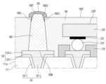
도 1은 제1 실시 예에 따른 반도체 패키지를 나타낸 단면도이다.1 is a cross-sectional view showing a semiconductor package according to a first embodiment.
도 1을 참조하면, 반도체 패키지는 회로 기판 및 상기 회로 기판 상에 배치된 적어도 하나의 반도체 소자를 포함할 수 있다.Referring to FIG. 1, a semiconductor package may include a circuit board and at least one semiconductor device disposed on the circuit board.
상기 반도체 패키지는 전자 디바이스의 메인 보드에 부착될 수 있다. 상기 반도체 패키지는 전자 디바이스의 메인 보드에 연결되어 제1 패키지를 구성할 수 있다. 또한, 실시 예의 제1 패키지는 제2 패키지와 결합할 수 있다. 상기 제2 패키지는 메모리 패키지일 수 있다.The semiconductor package may be attached to a main board of an electronic device. The semiconductor package may be connected to a main board of an electronic device to form a first package. Additionally, the first package of the embodiment may be combined with the second package. The second package may be a memory package.
반도체 패키지는 절연층(110)을 포함할 수 있다. 상기 절연층(110)은 복수의 층을 포함할 수 있다. 일 실시 예에서, 상기 절연층(110)은 3층 구조를 가질 수 있으나, 이에 한정되는 것은 아니다.The semiconductor package may include an insulating
일 실시 예에서, 반도체 패키지는 코어 기판을 포함할 수 있다. 예를 들어, 반도체 패키지는 코어층을 포함할 수 있다. 예를 들어, 실시 예의 반도체 패키지의 절연층(110)은 강화 섬유를 포함하는 코어층에 대응하는 제3 절연층(113)을 포함할 수 있다.In one embodiment, a semiconductor package may include a core substrate. For example, a semiconductor package may include a core layer. For example, the insulating
반도체 패키지는 제3 절연층(113)을 사이에 두고 이의 상부 및 하부에 각각 적어도 하나의 절연층이 적층된 구조를 가질 수 있다. 일 실시 예에서, 상기 제3 절연층(113)의 상부에 적층된 절연층과 하부에 적층된 절연층은 대칭 구조를 가질 수 있다. 다른 실시 예에서, 상기 제3 절연층(113)의 상부에 적층된 절연층과 하부에 적층된 절연층은 비대칭 구조를 가질 수 있다.The semiconductor package may have a structure in which at least one insulating layer is stacked on the top and bottom of the third insulating
이하에서는 실시 예의 반도체 패키지가 코어 기판을 포함하고, 이에 따라 상기 제3 절연층(113)이 코어층인 것으로 하여 설명한다. 다만, 실시 예는 이에 한정되지 않는다. 예를 들어, 다른 실시 예의 반도체 패키지는 코어층을 포함하지 않는 코어리스 기판을 포함할 수 있다.Hereinafter, the semiconductor package of the embodiment includes a core substrate, and accordingly, the third insulating
실시 예의 반도체 패키지의 절연층(110)은 제1 절연층(111), 제2 절연층(112) 및 제3 절연층(113)을 포함할 수 있다.The insulating
상기 제3 절연층(113)은 복수의 절연층 중 내측에 배치된 내층 절연층을 의미할 수 있다. 상기 제3 절연층(113)은 상기 제1 절연층(111)과 제2 절연층(112) 사이에 배치될 수 있다. 상기 제3 절연층(113)은 프리프레그를 포함할 수 있다. 상기 제3 절연층(113)은 강화 섬유를 포함할 수 있다.The third
상기 제1 절연층(111)은 상기 제3 절연층(113) 상에 배치될 수 있다. 예를 들어, 상기 제1 절연층(111)은 상기 제3 절연층(113)의 상면에 배치될 수 있다. 상기 제1 절연층(111)은 반도체 패키지의 절연층(110)에서 제1 최외층의 절연층을 의미할 수 있다. 예를 들어, 상기 제1 절연층(111)은 반도체 패키지의 절연층(110)에서 최상측에 배치된 절연층을 의미할 수 있다. 상기 제1 절연층(111)은 적어도 하나의 칩이 실장되는 실장 영역을 제공하거나, 제1 외부 기판이 결합되는 제1 결합 영역을 제공할 수 있다. 상기 제1 외부 기판은 전자디바이스의 메인 보드일 수 있다.The first insulating
상기 제2 절연층(112)은 상기 제3 절연층(113) 하에 배치될 수 있다. 상기 제2 절연층(112)은 반도체 패키지의 절연층(110)에서 제2 최외층의 절연층을 의미할 수 있다. 예를 들어, 상기 제2 절연층(112)은 반도체 패키지의 절연층(110)에서 최하측에 배치된 절연층을 의미할 수 있다. 상기 제2 절연층(112)은 적어도 하나의 칩이 실장되는 실장 영역을 제공하거나, 제2 외부 기판이 결합되는 제2 결합 영역을 제공할 수 있다. 상기 제2 외부 기판은 메모리 기판 또는 인터포저일 수 있다.The second
상기 제1 절연층(111) 및 제2 절연층(112)은 리지드(rigid) 또는 플렉서블(flexible)할 수 있다. 예를 들어, 상기 제1 절연층(111) 및 제2 절연층(112)은 유리 또는 플라스틱을 포함할 수 있다. 자세하게, 상기 제1 절연층(111) 및 제2 절연층(112)은 소다라임유리(soda lime glass) 또는 알루미노실리케이트유리 등의 화학 강화/반강화유리를 포함할 수 있다. 또는, 상기 제1 절연층(111) 및 제2 절연층(112)은 폴리이미드(Polyimide, PI), 폴리에틸렌 테레프탈레이트(polyethylene terephthalate, PET), 프로필렌 글리콜(propylene glycol, PPG) 폴리 카보네이트(PC) 등의 강화 혹은 연성 플라스틱을 포함할 수 있다. 또는 상기 제1 절연층(111) 및 제2 절연층(112)은 사파이어를 포함할 수 있다.The first insulating
또한, 상기 제1 절연층(111) 및 제2 절연층(112)은 광등방성 필름을 포함할 수 있다. 일례로, 상기 제1 절연층(111) 및 제2 절연층(112)은 COC(Cyclic Olefin Copolymer), COP(Cyclic Olefin Polymer), 광등방 폴리카보네이트(polycarbonate, PC) 또는 광등방 폴리메틸메타크릴레이트(PMMA) 등을 포함할 수 있다.Additionally, the first insulating
또한, 상기 제1 절연층(111) 및 제2 절연층(112)은 무기 필러 및 절연 수지를 포함하는 재료로 형성될 수 있다. 예를 들어, 상기 제1 절연층(111) 및 제2 절연층(112)은 에폭시 수지와 같은 열경화성 수지, 폴리이미드와 같은 열가소성 수지 내에 실리카, 알루미나 등의 무기 필러가 분산된 구조를 포함할 수 있다. 예를 들어, 상기 제1 절연층(111) 및 제2 절연층(112)은 ABF(Ajinomoto Build-up Film), FR-4, BT(Bismaleimide Triazine), PID(Photo Imagable Dielectric resin), BT 등을 포함할 수 있다.Additionally, the first insulating
상기 제1 절연층(111) 및 제2 절연층(112) 각각은 10㎛ 내지 60㎛의 범위의 두께를 가질 수 있다. 바람직하게, 상기 제1 절연층(111) 및 제2 절연층(112) 각각은 12㎛ 내지 50㎛의 범위의 두께를 가질 수 있다. 더욱 바람직하게, 상기 제1 절연층(111) 및 제2 절연층(112) 각각은 15㎛ 내지 40㎛의 두께를 가질 수 있다.Each of the first insulating
상기 제1 절연층(111) 또는 제2 절연층(112)의 두께가 10㎛ 미만이면, 반도체 패키지에 포함된 회로층이 안정적으로 보호되지 않을 수 있다. 또한, 상기 제1 절연층(111) 또는 제2 절연층(112)의 두께가 60㎛를 초과하면, 상기 반도체 패키지의 두께가 증가할 수 있다. 또한, 상기 제1 절연층(111) 또는 제2 절연층(112)의 두께가 60㎛를 초과하면, 이에 대응하게 회로층의 두께 및 관통 전극의 두께가 증가할 수 있다. 그리고 상기 회로층의 두께 및 관통 전극의 두께가 증가하는 경우, 미세화 구현이 어려워 회로 집적도가 감소할 수 있다. 나아가, 신호 전송 거리가 증가하여 신호 전송 손실이 증가할 수 있다.If the thickness of the first insulating
한편, 상기 제1 절연층(111)은 방향으로 복수의 영역으로 구분될 수 있다.Meanwhile, the first insulating
상기 제1 절연층(111)은 상기 제1 절연층(111)의 둘레(111a)에 인접한 제1 영역(R1)을 포함할 수 있다. 상기 제1 절연층(111)의 둘레(111a)는 상기 제1 절연층(111)의 상면의 둘레를 의미할 수 있다. 상기 제1 절연층(111)의 둘레(111a)는 상기 제1 절연층(111)의 측면에 인접한 상기 제1 절연층(111)의 상면의 테두리를 의미할 수 있다. 상기 제1 절연층(111)은 상기 제1 영역(R1) 이외의 제2 영역(R2)을 포함할 수 있다. 상기 제1 절연층(111)의 둘레(111a)는 상기 제1 절연층(111)의 측면과 가장 인접한 상기 제1 절연층(111)의 상면의 최외곽 부분을 의미할 수 있다. 상기 제2 영역(R2)은 상기 제1 영역(R1)보다 상기 제1 절연층(111)의 둘레(111a)로부터 멀리 떨어진 영역을 의미할 수 있다.The first insulating
이때, 상기 제1 절연층(111)의 상기 제1 영역(R1)은 상기 제1 절연층(111)의 둘레 방향을 따라 형성될 수 있다. 그리고, 상기 제1 절연층(111)의 상기 제2 영역(R2)은 상기 둘레 방향을 따라 형성된 상기 제1 영역(R1)의 내측 영역을 의미할 수 있다. 예를 들어, 상기 제1 절연층(111)의 상기 제1 영역(R1)은 상기 제1 절연층(111)의 상면의 외곽 영역을 의미할 수 있고, 상기 제2 영역(R2)은 상기 제1 영역(R1)을 제외한 상기 제1 절연층(111)의 상면의 내측 영역을 의미할 수 있다.At this time, the first region R1 of the first insulating
한편, 상기 제1 영역(R1) 및 제2 영역(R2)은 상기 제1 절연층(111)의 제1 영역(R1) 및 제2 영역(R2)인 것으로 설명하였으나, 이에 한정되지 않는다. 예를 들어, 상기 제1 영역(R1) 및 제2 영역(R2)은 반도체 패키지의 제1 영역(R1) 및 제2 영역(R2)을 의미할 수도 있다.Meanwhile, the first region (R1) and the second region (R2) have been described as being the first region (R1) and the second region (R2) of the first insulating
실시 예의 반도체 패키지는 절연층(110)의 표면에 배치된 회로층을 포함한다.The semiconductor package of the embodiment includes a circuit layer disposed on the surface of the insulating
예를 들어, 반도체 패키지는 제1 절연층(111)의 상면에 배치된 제1 회로층(120)을 포함할 수 있다. 예를 들어, 반도체 패키지는 제2 절연층(112)의 하면에 배치된 제2 회로층(130)을 포함할 수 있다. 또한, 반도체 패키지는 제1 절연층(111)의 하면 및 제3 절연층(113)의 상면 사이에 배치된 제3 회로층(140)을 포함할 수 있다. 예를 들어, 반도체 패키지는 제2 절연층(112)의 상면 및 제3 절연층(113)의 하면 사이에 배치된 제4 회로층(150)을 포함할 수 있다.For example, the semiconductor package may include a
상기 제1 회로층(120)은 반도체 패키지의 제1 최외층에 배치된 회로층을 의미할 수 있다. 그리고, 제2 회로층(130)은 반도체 패키지의 제2 최외층에 배치된 회로층을 의미할 수 있다.The
상기 제1 회로층(120)은 제1 절연층(111) 상에 배치된 복수의 패드를 포함할 수 있다.The
상기 제1 회로층(120)은 상기 제1 절연층(111)의 상기 제1 영역(R1) 상에 배치된 제1 패드(121)를 포함할 수 있다. 또한, 상기 제1 회로층(120)은 상기 제1 절연층(111)의 상기 제2 영역(R2) 상에 배치된 제2 패드(122)를 포함할 수 있다. 상기 제2 패드(122)는 상기 제1 패드(121)보다 상기 제1 절연층(111)의 둘레(111a)에서 멀리 이격될 수 있다.The
상기 제1 패드(121)는 제1 기능을 할 수 있고, 상기 제2 패드(122)는 상기 제1 기능과 다른 제2 기능을 할 수 있다.The
상기 제1 패드(121)의 상기 제1 기능은 상기 반도체 패키지에 제1 외부 기판을 결합하기 위한 기능을 의미할 수 있다. 또한, 상기 제2 패드(122)의 제2 기능은 상기 반도체 패키지에 칩을 실장하기 위한 기능을 의미할 수 있다.The first function of the
한편, 상기 제1 회로층(120)은 트레이스를 더 포함할 수 있다. 상기 제1 회로층(120)의 상기 트레이스는 상기 제1 절연층(111)의 제1 영역(R1) 및 제2 영역(R2) 상에 배치될 수 있다. 상기 제1 회로층(120)의 상기 트레이스는 복수의 제1 패드 사이, 복수의 제2 패드 사이, 또는 제1 패드(121)와 제2 패드(122) 사이를 연결할 수 있다.Meanwhile, the
상기 제1 패드(121)의 평면 면적은 상기 제2 패드(122)의 평면 면적과 다를 수 있다. 예를 들어, 상기 제1 패드(121)의 제1 수평 방향으로의 직경은 상기 제2 패드(122)의 제1 수평 방향으로의 직경과 다를 수 있다. 예를 들어, 상기 제1 패드(121)의 폭은 상기 제2 패드(122)의 폭과 다를 수 있다.The planar area of the
즉, 상기 제1 패드(121)는 제1 외부 기판과의 결합을 위한 패드이고, 상기 제2 패드(122)은 반도체 소자의 실장을 위한 패드이다. 그리고 5G, 사물인터넷(IOT, Internet of Things), 화질 증가, 통신 속도 증가 등의 이유로 반도체 소자의 단자의 개수가 증가하거나, 반도체 소자의 단자의 폭 또는 피치가 미세화되고 있다. 이에 반하여, 상기 제1 외부 기판에 구비된 패드들은 상기 반도체 소자의 단자보다는 큰 폭 또는 간격을 가질 수 있다. 따라서, 상기 제1 패드(121)의 평면 면적, 제1 수평 방향으로의 직경 또는 폭은 상기 제2 패드(122)의 평면 면적, 제1 수평 방향으로의 직경 또는 폭보다 클 수 있다.That is, the
상기 제1 패드(121)는 상기 제1 영역(R1)에 배치되면서, 반도체 패키지의 보호층과 접촉하지 않을 수 있다. 예를 들어, 상기 제1 패드(121)의 측면 및 상면은 보호층과 접촉하지 않을 수 있다.The
상기 제2 패드(122)는 상기 제2 영역(R2)에 배치되면서, 상기 반도체 패키지의 보호층과 접촉할 수 있다. 예를 들어, 상기 제2 패드(122)의 측면 및 상면의 적어도 일부는 보호층과 접촉할 수 있다.The
한편, 상기 제2 회로층(130)도 복수의 패드를 포함할 수 있다. 제1 실시 예의 반도체 패키지의 상기 제2 회로층(130)의 패드는 칩의 실장을 위한 패드만을 포함할 수 있으나, 이에 한정되는 것은 아니다.Meanwhile, the
한편, 상기 제1 회로층(120), 제2 회로층(130), 제3 회로층(140) 및 제4 회로층(150)은 금(Au), 은(Ag), 백금(Pt), 티타늄(Ti), 주석(Sn), 구리(Cu) 및 아연(Zn) 중에서 선택되는 적어도 하나의 금속 물질로 형성될 수 있다. 또한, 상기 제1 회로층(120), 제2 회로층(130), 제3 회로층(140) 및 제4 회로층(150)은 본딩력이 우수한 금(Au), 은(Ag), 백금(Pt), 티타늄(Ti), 주석(Sn), 구리(Cu), 아연(Zn) 중에서 선택되는 적어도 하나의 금속 물질을 포함하는 페이스트 또는 솔더 페이스트로 형성될 수 있다. 바람직하게, 상기 제1 회로층(120), 제2 회로층(130), 제3 회로층(140) 및 제4 회로층(150)은 가격이 비교적 저렴한 구리(Cu)로 형성될 수 있다.Meanwhile, the
한편, 상기 제1 회로층(120) 및 제2 회로층(130)은 5㎛ 내지 30㎛의 범위의 두께를 가질 수 있다. 예를 들어, 상기 제1 회로층(120) 및 제2 회로층(130)은 6㎛ 내지 25㎛의 범위의 두께를 가질 수 있다. 상기 제1 회로층(120) 및 제2 회로층(130)은 7㎛ 내지 20㎛의 범위의 두께를 가질 수 있다. 상기 제1 회로층(120) 및 제2 회로층(130)의 두께가 5㎛ 미만이면 저항 증가 및 신호 전송 손실이 증가할 수 있다. 상기 제1 회로층(120) 및 제2 회로층(130)의 두께가 30㎛를 초과하는 경우에는 미세화가 어렵고, 이에 따른 회로 집적도가 감소할 수 있다.Meanwhile, the
실시 예의 반도체 패키지는 포스트 범프(180)를 포함할 수 있다.The semiconductor package of the embodiment may include a
상기 포스트 범프(180)는 상기 제1 회로층(120) 상에 배치될 수 있다. 바람직하게, 상기 포스트 범프(180)는 상기 제1 회로층(120)의 상기 제1 패드(121) 상에 배치될 수 있다.The
상기 포스트 범프(180)는 상기 제1 패드(121)의 직경 또는 폭보다 작은 직경 또는 폭을 가질 수 있다. 이에 따라, 상기 제1 패드(121)의 일부는 상기 포스트 범프(180)와 수직으로 중첩되고, 상기 제1 패드(121)의 나머지 일부는 상기 포스트 범프(180)와 수직으로 중첩되지 않을 수 있다.The
상기 포스트 범프(180)는 이하에서 설명되는 제1 보호층(170)과 접촉하지 않을 수 있다. 예를 들어, 상기 포스트 범프(180)는 상기 제1 보호층(170)의 제1 개구(171) 내에 배치될 수 있다. 이에 대응하게, 상기 제1 회로층(120)의 상기 제1 패드(121)도 상기 제1 보호층(170)의 제1 개구(171) 내에 배치될 수 있다.The
상기 포스트 범프(180)는 상기 제1 패드(121) 상에 일정 높이를 가지고 배치될 수 있다.The
실시 예의 반도체 패키지는 관통 전극을 포함할 수 있다. 관통 전극은 절연층(110)을 관통할 수 있다.The semiconductor package of the embodiment may include a penetrating electrode. The penetrating electrode may penetrate the insulating
예를 들어, 반도체 패키지는 상기 제1 절연층(111)을 관통하는 제1 관통 전극(161)을 포함할 수 있다. 또한, 반도체 패키지는 제2 절연층(112)을 관통하는 제2 관통 전극(162)을 포함할 수 있다. 또한, 반도체 패키지는 제3 절연층(113)을 관통하는 제3 관통 전극(163)을 포함할 수 있다.For example, the semiconductor package may include a first through
상기 제1 관통 전극(161), 제2 관통 전극(162) 및 제3 관통 전극(163)은 적어도 하나의 절연층을 관통하는 관통 홀 내에 배치될 수 있다. 예를 들어, 상기 제1 관통 전극(161), 제2 관통 전극(162) 및 제3 관통 전극(163)은 상기 관통 홀을 전도성 물질로 충진하여 형성할 수 있다.The first through
한편, 상기 제1 관통 전극(161)은 제1 절연층(111) 내에서 수평 방향으로 이격되어 복수 개 형성될 수 있다.Meanwhile, the first through
이때, 상기 제1 관통 전극(161)은 상기 제1 회로층(120)과 수직 방향으로 중첩될 수 있다.At this time, the first through
상기 제1 관통 전극(161)은 제1 패드(121) 및 제2 패드(122) 중 적어도 하나와 수직으로 중첩될 수 있다. 예를 들어, 상기 제1 관통 전극(161)은 상기 제1 패드(121)와 수직으로 중첩되는 제1 전극 파트와, 상기 제2 패드(122)와 수직으로 중첩되는 제2 전극 파트를 포함할 수 있다. 그리고 상기 제1 관통 전극(161)의 상기 제1 전극 파트 및 제2 전극 파트는 서로 다른 폭을 가질 수 있다. 이때, 상기 제1 관통 전극(161)의 제1 전극 파트 및 제2 전극 파트 각각은 상면에서 하면을 향하여 폭이 감소하는 경사를 가질 수 있다. 그리고 상기 제1 관통 전극(161)의 제1 전극 파트의 상면은 상기 제1 관통 전극(161)의 제2 전극 파트의 상면보다 큰 폭을 가질 수 있다. 즉, 상기 제1 관통 전극(161)의 제1 전극 파트는 상기 제1 관통 전극(161)의 제2 전극 파트와 연결된 제2 패드(122)보다 상대적으로 큰 폭을 가지는 제1 패드(121)와 연결된다. 이에 따라, 상기 제1 관통 전극(161)의 제1 전극 파트는 상기 제2 전극 파트보다 큰 폭을 가질 수 있다.The first through
이를 통해, 실시 예는 동일층 내에서 수평 방향으로 서로 이격되는 복수의 전극 파트들의 폭을 서로 다르게 하여 회로 집적도를 향상시킬 수 있다. 구체적으로, 상기 제1 관통 전극(161)의 제2 전극 파트는 칩과 연결되는 제2 패드(122)와 연결된다. 그리고 상기 제2 전극 파트는 상대적으로 작은 폭을 가지며, 이에 따라 상기 제2 패드(122)의 폭 및 피치를 줄일 수 있도록 한다. 이를 통해, 실시 예는 상기 제2 패드(122)에 배치된 제2 영역(R2)에서의 회로 집적도를 향상시킬 수 있다. 나아가, 실시 예는 상기 제1 전극 파트는 상대적으로 큰 폭을 가진다. 이에 따라, 실시 예는 상기 제1 전극 파트를 통해 반도체 패키지에서 발생하는 열의 전달 특성을 향상시킬 수 있다. 이를 통해, 실시 예는 반도체 패키지 및 이를 포함하는 반도체 패키지의 방열 특성을 향상시킬 수 있다.Through this, the embodiment can improve circuit integration by varying the widths of a plurality of electrode parts spaced apart from each other in the horizontal direction within the same layer. Specifically, the second electrode part of the first through
한편, 실시 예의 반도체 패키지는 보호층을 포함한다.Meanwhile, the semiconductor package of the embodiment includes a protective layer.
구체적으로, 제1 절연층(111)의 상면에는 제1 보호층(170)이 배치된다. 상기 제1 보호층(170)은 개구를 포함한다. 상기 개구는 상기 제1 보호층(170)의 상면 및 하면을 관통하는 '관통 홀'로 정의될 수 있다. 또한, 상기 개구(171)는 상기 제1 절연층(111)의 상면 및/또는 상기 제1 회로층(120)의 상면에서 상기 제1 보호층(170)이 배치되지 않은 '미배치 영역' 또는 '오픈 영역'으로도 정의될 수 있다. 상기 제1 보호층(170)의 개구와 수직으로 중첩된 영역에서의 제1 절연층(111)의 상면 및/또는 제1 회로층(120)의 상면은 반도체 패키지의 상측으로 노출될 수 있다.Specifically, the first
상기 제1 보호층(170)은 제1 개구(171) 및 제2 개구(172)를 포함할 수 있다.The first
상기 제1 보호층(170)의 상기 제1 개구(171)는 상기 제1 영역(R1) 상에 구비될 수 있다. 상기 제1 보호층(170)의 상기 제2 개구(172)는 상기 제1 보호층(170)의 상기 제2 영역(R2) 상에 구비될 수 있다. 상기 제1 보호층(170)은 복수의 제1 패드(121)와 공통으로 수직으로 중첩되는 1개의 제1 개구(171)를 포함할 수 있다. 또한, 상기 제1 개구(171)는 상기 제1 패드(121) 상에 배치된 포스트 범프(180)와도 수직으로 중첩될 수 있다. 한편, 상기 제2 개구(172)는 복수 개일 수 있다. 예를 들어, 상기 제1 보호층(170)은 복수의 제2 패드(122) 각각과 수직으로 중첩되는 복수의 제2 개구(172)를 포함할 수 있다.The
이때, 상기 제1 보호층(170)의 상기 제1 개구(171)는 상기 제1 영역(R1)과 전체적으로 수직으로 중첩될 수 있다. 즉, 상기 제1 보호층(170)의 상기 제1 개구(171)는 상기 제1 영역(R1)에서, 상기 제1 절연층(111)의 상면 및 제1 회로층(120)의 상면 및 측면을 전체적으로 오픈할 수 있다. 이에 따라, 상기 제1 개구(171)는 실질적으로 상기 제1 절연층(111) 및 제1 회로층(120) 상에서 상기 제1 보호층(170)이 배치되지 않은 미배치 영역을 의미할 수 있다. 상기 제1 개구(171)는 상기 복수의 제2 개구(172)와 연결되지 않을 수 있다.At this time, the
상기 제1 보호층(170)의 상기 제2 개구(172)는 상기 제2 영역(R2)과 부분적으로 수직으로 중첩될 수 있다. 즉, 상기 제1 보호층(170)의 상기 제2 개구(172)는 상기 제2 영역(R2)에서, 상기 제1 절연층(111)의 상면 및 상기 제1 회로층(120)의 상면과 부분적으로 수직으로 중첩될 수 있다.The
한편, 반도체 패키지는 제2 절연층(112)의 하면에 배치된 제2 보호층(175)을 더 포함할 수 있다.Meanwhile, the semiconductor package may further include a second
상기 제2 보호층(175)은 적어도 하나의 개구를 포함할 수 있다. 예를 들어, 상기 제2 보호층(175)은 상기 제2 회로층(130)의 적어도 일부와 수직으로 중첩되는 개구를 포함할 수 있다. 상기 제2 보호층(175)의 개구는 상기 제2 회로층(130) 중 칩과 연결되는 패드와 전체적 또는 부분적으로 수직으로 중첩될 수 있다.The second
상기 제1 보호층(170) 및 제2 보호층(175)은 절연성 물질을 포함할 수 있다. 상기 제1 보호층(170) 및 제2 보호층(175)은 절연층과 회로층의 표면을 보호하기 위해 도포된 후 가열하여 경화될 수 있는 다양한 물질을 포함할 수 있다.The first
상기 제1 보호층(170) 및 제2 보호층(175)은 유기 고분자 물질을 포함하는 솔더 레지스트층일 수 있다. 일 예로, 상기 제1 보호층(170) 및 제2 보호층(175)은 에폭시 아크릴레이트 계열의 수지를 포함할 수 있다. 자세하게, 상기 제1 보호층(170) 및 제2 보호층(175)은 수지, 경화제, 광 개시제, 안료, 용매, 필러, 첨가제, 아크릴 계열의 모노머 등을 포함할 수 있다. 다만, 실시 예는 이에 한정되지 않고, 상기 제1 보호층(170) 및 제2 보호층(175)은 포토 솔더 레지스트층, 커버레이(cover-lay) 및 고분자 물질 중 어느 하나일 수 있음은 물론이다.The first
상기 제1 보호층(170) 및 제2 보호층(175)의 두께는 1㎛ 내지 20㎛일 수 있다. 상기 제1 보호층(170) 및 제2 보호층(175)의 두께는 1㎛ 내지 15㎛일 수 있다. 예를 들어, 상기 제1 보호층(170) 및 제2 보호층(175)의 두께는 5㎛ 내지 20㎛일 수 있다. 상기 제1 보호층(170) 및 제2 보호층(175)의 두께가 20㎛를 초과하는 경우, 회로 기판 및 반도체 패키지의 전체적인 두께가 증가할 수 있다.The first
반도체 패키지는 상기 제1 회로층(120)의 제2 패드(122) 상에 배치된 제1 접속부(210)를 포함할 수 있다. 또한, 반도체 패키지는 제2 회로층(130) 하에 배치된 제2 접속부(230)를 포함할 수 있다. 상기 제1 접속부(210) 및 제2 접속부(230)는 와이어 본딩, 솔더 본딩, 메탈 간 다이렉트 본딩 중 적어도 하나의 본딩 방식을 이용하여 복수의 구성 요소 사이를 전기적으로 연결할 수 있다. 즉, 제1 접속부(210) 및 제2 접속부(230)는 복수의 구성 요소를 전기적으로 연결하는 기능을 갖기 때문에, 메탈 간 다이렉트 본딩을 이용할 경우 반도체 패키지는 솔더나 와이어가 아닌, 전기적으로 연결되는 부분으로 이해될 수 있다.The semiconductor package may include a
상기 와이어 본딩 방식은 금(Au) 등의 도선을 이용하여 복수의 구성 요소 사이를 전기적으로 연결하는 것을 의미할 수 있다. 또한, 상기 솔더 본딩 방식은 Sn, Ag, Cu 중 적어도 하나를 포함하는 물질을 이용하여 복수의 구성요소 사이를 전기적으로 연결할 수 있다. 또한, 메탈 간 다이렉트 본딩 방식은 솔더, 와이어, 전도성 접착제 등의 부재 없이, 복수의 구성 요소 사이에 열과 압력을 인가하여 재결정화하고, 이를 통해 복수의 구성요소 사이를 직접 결합시키는 것을 의미할 수 있다.The wire bonding method may mean electrically connecting a plurality of components using conductors such as gold (Au). Additionally, the solder bonding method can electrically connect a plurality of components using a material containing at least one of Sn, Ag, and Cu. In addition, the direct bonding method between metals may mean recrystallization by applying heat and pressure between a plurality of components without the absence of solder, wire, conductive adhesive, etc., thereby directly bonding the plurality of components. .
실시 예의 반도체 패키지는 반도체 소자를 포함할 수 있다. 예를 들어, 실시 예의 반도체 패키지는 상기 제1 접속부(210) 상에 배치된 제1 반도체 소자(220)를 포함할 수 있다. 또한, 실시 예의 반도체 패키지는 제2 접속부(230) 하에 배치된 제2 반도체 소자(240)를 포함할 수 있다. 즉, 실시 예의 반도체 패키지는 회로 기판의 양측에 각각 반도체 소자가 결합된 구조를 가질 수 있다. 다만, 실시 예는 이에 한정되지 않는다. 예를 들어, 실시 예의 반도체 패키지는 회로 기판의 일측에서만 반도체 소자가 결합될 수도 있다. 상기 제1 반도체 소자(220) 및 제2 반도체 소자(240) 각각은 단자(225, 245)를 구비할 수 있다. 상기 단자(225, 245)는 상기 제1 접속부(210) 및 제2 접속부(230)를 통해 상기 제1 회로층(120) 및 제2 회로층(130)에 전기적으로 결합될 수 있다.The semiconductor package of the embodiment may include a semiconductor device. For example, the semiconductor package of the embodiment may include a
실시 예의 반도체 패키지는 몰딩 부재를 포함할 수 있다.The semiconductor package of the embodiment may include a molding member.
예를 들어, 실시 예의 반도체 패키지는 제1 절연층(111) 상에 배치된 제1 몰딩 부재(190)를 포함할 수 있다. 상기 제1 몰딩 부재(190)는 상기 제1 반도체 소자(220)를 몰딩할 수 있다. 또한, 상기 제1 몰딩 부재(190)는 상기 제1 접속부(210)를 몰딩할 수 있다. 또한, 상기 제1 몰딩 부재(190)는 상기 제1 보호층(170)을 몰딩할 수 있다. 또한, 상기 제1 몰딩 부재(190)는 상기 제1 패드(121)를 몰딩할 수 있다. 또한, 상기 제1 몰딩 부재(190)는 상기 포스트 범프(180)를 몰딩할 수 있다. 여기에서 몰딩한다는 것은 상기 제1 몰딩 부재(190)가 상기 기재한 구성의 표면의 적어도 일부를 덮으며 구비되는 것을 의미할 수 있다.For example, the semiconductor package of the embodiment may include a
상기 제1 몰딩 부재(190)의 상면(190T)은 상기 제1 반도체 소자(220)의 상면보다 높게 위치할 수 있다. 이를 통해, 실시 예는 상기 제1 몰딩 부재(190)에 의해 상기 제1 반도체 소자(220)가 안정적으로 보호되도록 할 수 있다.The
상기 제1 몰딩 부재(190)의 상면(190T)은 상기 제1 보호층(170)의 상면보다 높게 위치할 수 있다. 또한, 상기 제1 몰딩 부재(190)의 상면(190T)은 상기 제1 접속부(210)의 상면보다 높게 위치할 수 있다. 이를 통해, 실시 예는 상기 제1 몰딩 부재(190)가 상기 제1 보호층(170), 제1 접속부(210) 및 제1 반도체 소자(220)를 전체적으로 둘러싸며 구비되도록 할 수 있다. 따라서, 실시 예는 상기 제1 반도체 소자(220)가 더욱 안정적으로 결합되도록 할 수 있고, 이에 따라 상기 제1 반도체 소자(220)의 동작 특성을 향상시킬 수 있다.The
상기 제1 몰딩 부재(190)의 상면(190T)은 상기 포스트 범프(180)의 상면(180T)보다 낮게 위치할 수 있다. 구체적으로, 상기 제1 몰딩 부재(190)의 상면(190T)은 평탄하지 않을 수 있다. 예를 들어, 실시 예에 따라 상기 제1 몰딩 부재(190)의 상면(190T)은 일정 표면 거칠기를 가지며 굴곡을 가질 수 있다. 그리고 상기 포스트 범프(180)에 인접한 영역에서의 상기 제1 몰딩 부재(190)의 상면(190T)은 상기 포스트 범프(180)의 상면(180T)보다 낮게 위치할 수 있다. 예를 들어, 상기 포스트 범프(180)의 측면의 적어도 일부는 상기 제1 몰딩 부재(190)에 의해 덮이지 않을 수 있다. 예를 들어, 상기 포스트 범프(180)의 측면의 적어도 일부는 상기 제1 몰딩 부재(190)와 수평 방향으로 중첩되지 않을 수 있다. 따라서, 상기 포스트 범프(180)는 상기 제1 몰딩 부재(190) 상으로 돌출된 구조를 가질 수 있다.The
한편, 상기 제2 보호층(175) 하에는 제2 몰딩 부재(195)가 구비될 수 있다. 상기 제2 몰딩 부재(195)는 상기 제2 반도체 소자(240) 및 상기 제2 접속부(230)를 몰딩할 수 있다.Meanwhile, a
이때, 상기 제1 몰딩 부재(190) 및 제2 몰딩 부재(195)는 저유전율을 가질 수 있고, 이를 통해 방열 특성을 높일 수 있다. 상기 제1 몰딩 부재(190) 및 제2 몰딩 부재(195)의 유전율(Dk)은 0.2 내지 10일 수 있다. 예를 들어, 상기 제1 몰딩 부재(190) 및 제2 몰딩 부재(195)의 유전율(Dk)은 0.5 내지 8일 수 있다. 예를 들어, 상기 제1 몰딩 부재(190) 및 제2 몰딩 부재(195)의 유전율은 0.8 내지 5일 수 있다. 이에 따라, 실시 예에서는 상기 제1 몰딩 부재(190) 및 제2 몰딩 부재(195)가 저유전율을 가지도록 하여, 상기 제1 반도체 소자(220) 및 제2 반도체 소자(240)에서 발생하는 열의 효율적으로 외부로 방출할 수 있다.At this time, the
실시 예의 반도체 패키지는 표면 처리층(185)을 포함할 수 있다. 상기 표면 처리층(185)은 무전해 도금 방식에 의해 상기 포스트 범프(180) 상에 구비될 수 있다. 상기 표면 처리층(185)의 하면의 적어도 일부는 상기 포스트 범프(180)의 상면(180T)보다 낮게 위치할 수 있다. 예를 들어, 상기 표면 처리층(185)은 상기 포스트 범프(180)의 측면의 적어도 일부와 접촉할 수 있다. 예를 들어, 상기 표면 처리층(185)은 상기 포스트 범프(180)의 상면과 수직으로 중첩된 제1 부분 및 상기 제1 부분으로부터 하측 방향으로 절곡 연장된 제2 부분을 포함할 수 있다. 상기 표면 처리층(185)의 제2 부분은 상기 포스트 범프(180)의 상면과 수직으로 중첩되지 않을 수 있다. 상기 표면 처리층(185)의 제2 부분은 상기 포스트 범프(180)와 수평 방향으로 접촉할 수 있고, 이를 통해 상기 포스트 범프(180)의 측면과 접촉할 수 있다.The semiconductor package of the embodiment may include a
또한, 상기 표면 처리층(185)의 적어도 일부는 상기 제1 몰딩 부재(190)와 접촉할 수 있다. 예를 들어, 상기 표면 처리층(185)의 제2 부분의 하단부는 상기 제1 몰딩 부재(190)와 접촉할 수 있다.Additionally, at least a portion of the
상기 표면 처리층(185)은 OSP(Organic Solderability Preservative) 층일 수 있다. 바람직하게, 표면 처리층(185)은 상기 포스트 범프(180)의 상부 및 측부에 코팅된 벤지미다졸(Benzimidazole)과 같은 유기층을 포함할 수 있다.The
다른 실시 예에서, 상기 표면 처리층(185)은 금속층을 포함할 수 있다. 예를 들어, 상기 표면 처리층(185)은 무전해 도금 방식으로 형성된 금(Au) 금속층을 포함할 수 있다. 예를 들어, 상기 표면 처리층(185)은 무전해 도금된 니켈(Ni) 금속층과, 상기 니켈 금속층에 무전해 도금된 금(Au) 금속층을 포함할 수 있다. 예를 들어, 상기 표면 처리층(185)은 상기 포스트 범프(180) 상에 무전해 도금된 니켈 (Ni) 금속층과, 상기 니켈 금속층에 무전해 도금된 팔라듐(Pd) 금속층과, 상기 팔라듐 금속층에 무전해 도금된 금(Au) 금속층을 포함할 수 있다.In another embodiment, the
이하에서는 도 1에 도시된 반도체 패키지의 일부 구성에 대해 구체적으로 설명한다.Hereinafter, some configurations of the semiconductor package shown in FIG. 1 will be described in detail.
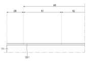
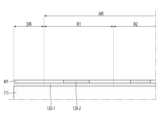
도 2는 도 1의 제1 보호층 및 포스트 범프가 제거된 상태에서의 회로 기판의 평면도이고, 도 3은 도 1의 제1 보호층의 평면도이며, 도 4는 도 1의 회로 기판의 평면도이고, 도 5는 도 1의 일부 영역을 확대한 확대도이다.FIG. 2 is a top view of the circuit board with the first protective layer and post bumps of FIG. 1 removed, FIG. 3 is a top view of the first protective layer of FIG. 1, and FIG. 4 is a top view of the circuit board of FIG. 1. , FIG. 5 is an enlarged view of a partial area of FIG. 1.
도 2를 참조하면, 제1 절연층(111)은 제1 영역(R1) 및 제2 영역(R2)을 포함할 수 있다. 상기 제1 절연층(111)의 상기 제1 영역(R1)은 상기 제1 절연층(111)의 둘레(111a)에 인접한 영역일 수 있다. 예를 들어, 상기 제1 절연층(111)의 상기 제1 영역(R1)은 상기 제1 절연층(111)의 상면의 외곽 영역일 수 있다.Referring to FIG. 2 , the first insulating
상기 제1 영역(R1)은 상기 제1 절연층(111)의 둘레(111a)에 인접하면서, 상기 제1 절연층(111)의 둘레 방향으로 구비될 수 있다. 예를 들어, 상기 제1 영역(R1)은 상기 제1 절연층(111)의 둘레(111a)에 인접하면서, 상기 둘레(111a)에 대응하는 폐루프 형상을 가질 수 있다. 다만, 실시 예는 이에 한정되지 않는다. 상기 제1 영역(R1)은 상기 둘레 방향의 둘레 영역 중 일부 영역만을 포함하는 개루프 형상을 가질 수도 있을 것이다.The first region R1 may be adjacent to the
상기 제1 절연층(111)의 상기 제1 영역(R1) 상에는 복수의 제1 패드(121)가 배치될 수 있다. 상기 복수의 제1 패드(121)는 상기 제1 절연층(111)의 상기 제1 영역(R1)에서 상기 제1 절연층(111)의 둘레 방향을 따라 배치될 수 있다.A plurality of
또한, 상기 제1 절연층(111)의 상기 제2 영역(R2) 상에는 복수의 제2 패드(122)가 배치될 수 있다. 상기 복수의 제2 패드(122)는 상기 제1 패드(121)와 수평 방향으로 이격되면서 상기 제1 절연층(111)의 상기 제2 영역(R2)에 선택적으로 배치될 수 있다.Additionally, a plurality of
상기 제1 패드(121)는 제1 폭(W1)을 가질 수 있다. 또한, 상기 제2 패드(122)는 상기 제2 폭(W2)을 가질 수 있다. 이때, 상기 제1 폭(W1)은 제2 폭(W2)과 다를 수 있다. 구체적으로, 상기 제1 폭(W1)은 상기 반도체 패키지에 결합되는 제1 외부 기판(바람직하게, 전자 디바이스의 메인 보드)에 구비된 패드에 대응할 수 있다. 그리고, 상기 제2 폭(W2)은 칩에 구비된 단자의 폭에 대응할 수 있다.The
이때, 상기 제1 외부 기판에 구비된 패드는 칩의 단자의 폭보다는 상대적으로 큰 폭을 가진다. 이에 따라, 상기 제1 패드(121)의 제1 폭(W1)은 제2 패드(122)의 제2 폭(W2)보다 클 수 있다. At this time, the pad provided on the first external substrate has a relatively larger width than the width of the terminal of the chip. Accordingly, the first width W1 of the
상기 제1 패드(121)의 상기 제1 폭(W1)은 25㎛ 내지 85㎛ 일 수 있다. 바람직하게, 상기 제1 패드(121)의 상기 제1 폭(W1)은 30㎛ 내지 80㎛일 수 있다. 더욱 바람직하게, 상기 제1 패드(121)의 상기 제1 폭(W1)은 32㎛ 내지 75㎛일 수 있다.The first width W1 of the
상기 제1 패드(121)의 상기 제1 폭(W1)이 25㎛ 미만이면, 상기 제1 외부 기판과의 결합성이 저하될 수 있다. 상기 제1 패드(121)의 상기 제1 폭(W1)이 25㎛ 미만이면, 이에 대응하게 상기 제1 패드(121) 상에 배치되는 상기 포스트 범프(180)의 폭(W3)이 감소할 수 있다. 그리고 상기 포스트 범프(180)의 폭(W3)이 감소하면, 이에 대응하게 형성 가능한 상기 포스트 범프(180)의 높이(H1)가 감소할 수 있다. 또한, 상기 제1 패드(121)의 상기 제1 폭(W1)이 25㎛ 미만이면, 반도체 패키지의 방열 특성이 저하될 수 있다.If the first width W1 of the
상기 제1 패드(121)의 제1 폭(W1)이 85㎛를 초과하면, 상기 제1 영역(R1) 상에 배치 가능한 제1 패드(121)의 개수가 감소할 수 있다. 예를 들어, 상기 제1 패드(121)의 제1 폭(W1)이 85㎛를 초과하면, 상기 제1 영역(R1)에서의 회로 집적도가 저하될 수 있다. 이에 따라, 상기 제1 영역(R1)에 상기 제1 외부 기판과 연결되는 제1 패드들을 모두 배치하기 위하여 상기 반도체 패키지의 면적이 증가할 수 있다.If the first width W1 of the
한편, 상기 제1 패드(121)는 평면 형상이 원형일 수 있다. 그리고 상기 제1 패드(121)의 평면 형상이 원형인 경우, 상기 제1 폭(W1)은 상기 제1 패드(121)의 직경을 의미할 수 있다.Meanwhile, the
다른 실시 예에서, 상기 제1 패드(121)의 평면 형상은 정사각형 또는 직사각형일 수 있다. 그리고 상기 제1 패드(121)의 평면 형상이 정사각형 또는 직사각형인 경우, 상기 제1 패드(121)의 상기 제1 폭(W1)은 상기 제1 패드(121)의 폭 방향으로의 폭 및 길이 방향으로의 폭 중 작은 폭을 의미할 수 있다.In another embodiment, the planar shape of the
또 다른 실시 예에서, 상기 제1 패드(121)의 평면 형상은 타원형일 수 있다. 그리고, 상기 제1 패드(121)의 평면 형상이 타원형인 경우, 상기 제1 패드(121)의 상기 제1 폭(W1)은 타원에서 단축 방향으로의 직경을 의미할 수 있다.In another embodiment, the planar shape of the
한편, 상기 제1 영역(R1)에서 복수의 제1 패드들 사이는 제1 간격(D1)을 가지고 이격될 수 있다. 상기 제1 간격(D1)은 상기 제1 영역(R1)에 배치된 복수의 제1 패드들 중 인접하게 배치된 2개의 제1 패드 사이의 최소 간격을 의미할 수 있다.Meanwhile, in the first region R1, the plurality of first pads may be spaced apart with a first gap D1. The first spacing D1 may mean the minimum spacing between two adjacent first pads among the plurality of first pads disposed in the first region R1.
일 실시 예에서, 상기 제1 간격(D1)은 1개의 제1 패드(121)의 상기 제1 폭(W1)에 대응하는 범위를 가질 수 있다.In one embodiment, the first gap D1 may have a range corresponding to the first width W1 of one
다른 실시 예에서, 상기 제1 간격(D1)은 1개의 제1 패드(121)의 상기 제1 폭(W1)보다 작을 수 있다.In another embodiment, the first gap D1 may be smaller than the first width W1 of one
예를 들어, 상기 복수의 제1 패드들 사이의 제1 간격(D1)은 제1 패드(121)의 제1 폭(W1)의 20% 내지 90%의 범위를 만족할 수 있다. 바람직하게, 상기 복수의 제1 패드들 사이의 제1 간격(D1)은 상기 제1 패드(121)의 제1 폭(W1)의 23% 내지 88%의 범위를 만족할 수 있다. 더욱 바람직하게, 상기 복수의 제1 패드들 사이의 제1 간격(D1)은 상기 제1 패드(121)의 제1 폭(W1)의 25% 내지 85%의 범위를 만족할 수 있다. 상기 복수의 제1 패드들 사이의 제1 간격(D1)이 상기 제1 패드(121)의 제1 폭(W1)의 20% 미만이면, 반도체 패키지를 제조하는 공정에서의 공정 능력에 따라 복수의 제1 패드(121) 사이가 서로 연결되는 회로 쇼트가 발생할 수 있고, 이에 의해 반도체 패키지의 전기적 신뢰성이 저하될 수 있다. 또한, 상기 복수의 제1 패드들 사이의 제1 간격(D1)이 상기 제1 패드(121)의 제1 폭(W1)의 20% 미만이면, 복수의 제1 패드(121)를 통해 전달되는 신호들 사이에 간섭이 발생할 수 있다. 그리고, 상기 간섭이 발생하는 경우, 신호 전송 손실이 증가하고, 이에 따라 신호 전송 특성이 저하될 수 있다.For example, the first gap D1 between the plurality of first pads may satisfy a range of 20% to 90% of the first width W1 of the
한편, 상기 복수의 제1 패드들 사이의 제1 간격(D1)이 상기 제1 패드(121)의 제1 폭(W1)의 90%를 초과하면, 비교 예 대비 상기 제1 영역(R1)에서의 회로 집적도의 향상 효과가 미비할 수 있다.Meanwhile, when the first gap D1 between the plurality of first pads exceeds 90% of the first width W1 of the
이때, 비교 예에서는 복수의 제1 패드들 사이의 간격이 상기 제1 패드의 제1 폭의 95%를 초과하였다. 이는, 상기 제1 패드들 사이의 간격을 결정하는 팩터 중의 하나에 보호층의 개구 사이즈에 포함되었기 때문이다. 즉, 비교 예의 제1 보호층은 상기 제1 영역과 부분적으로 수직으로 중첩되는 복수의 제1 개구를 포함하였다. 구체적으로, 비교 예의 제1 보호층의 제1 개구는 상기 제1 패드들의 개수에 대응하게 구비되었다. 그리고, 비교 예의 제1 보호층의 복수의 제1 개구들은 복수의 제1 패드들과 1:1로 수직으로 중첩되는 구조를 가졌다. 이에 따라, 비교 예에서는 상기 제1 보호층에 복수의 제1 개구를 형성하는 공정에서의 공정 능력 및 공정 오차 등을 고려하여, 상기 복수의 제1 패드들의 제1폭 및 상기 복수의 제1 패드들 사이의 제1 간격을 결정하였다.At this time, in the comparative example, the gap between the plurality of first pads exceeded 95% of the first width of the first pad. This is because one of the factors determining the gap between the first pads is included in the opening size of the protective layer. That is, the first protective layer of the comparative example included a plurality of first openings that partially vertically overlapped with the first region. Specifically, the first opening of the first protective layer of the comparative example was provided to correspond to the number of the first pads. In addition, the plurality of first openings of the first protective layer of the comparative example had a structure in which they vertically overlapped the plurality of first pads in a 1:1 ratio. Accordingly, in the comparative example, considering process capabilities and process errors in the process of forming the plurality of first openings in the first protective layer, the first width of the plurality of first pads and the plurality of first pads The first spacing between them was determined.
이에 반하여, 실시 예의 회로 기판의 제1 보호층(170)은 상기 제1 영역(R1)을 전체적으로 오픈하는 제1 개구(171)를 포함한다. 이때, 상기 제1 영역(R1)을 전체적으로 오픈하는 구성을 상기 제1 보호층(170)의 제1 개구(171)라고 칭하였지만, 실질적으로 상기 제1 보호층(170)은 상기 제1 영역(R1)을 제외한 제2 영역(R2)에만 배치될 수 있다. 즉, 상기 제1 보호층(170)은 상기 제1 영역(R1)에는 미배치되면서, 상기 제2 영역(R2)에만 선택적으로 배치될 수 있다.In contrast, the first
따라서, 실시 예는 상기 제1 보호층(170)에 복수의 제1 개구를 형성하는 공정에서의 공정 능력 및 공정 오차 등을 고려하지 않아도 된다. 이에 의해, 실시 예는 비교 예 대비 상기 제1 패드(121)의 제1 폭(W1) 및 복수의 제1 패드들 사이의 제1 간격(D1)을 줄일 수 있다.Accordingly, the embodiment does not need to consider process capabilities and process errors in the process of forming the plurality of first openings in the first
다만, 일반적으로, 상기 제1 패드(121)의 제1 폭(W1)은 상기 제1 외부 기판에 대응하는 메인 보드에 구비된 패드의 폭 및 이에 대응하는 포스트 범프(180)의 폭(W3)을 기준으로 결정된다. 따라서, 실시 예에서는 상기 제1 패드(121)의 제1 폭(W1)을 줄이는 것이 가능하지만, 상기 제1 패드(121)의 상기 제1 폭(W1)을 줄이는 대신에, 상기 복수의 제1 패드들 사이의 제1 간격(D1)을 줄이도록 한다. 이를 통해, 실시 예는 기존의 제1 패드(121)가 가지는 폭을 그대로 유지하면서, 회로 집적도를 향상시킬 수 있다.However, in general, the first width W1 of the
한편, 상기 제2 패드(122)의 제2 폭(W2)은 상기 제1 패드(121)의 상기 제1 폭(W1)보다 작을 수 있다.Meanwhile, the second width W2 of the
상기 제2 패드(122)의 상기 제2 폭(W2)은 15㎛ 내지 50㎛ 일 수 있다. 바람직하게, 상기 제2 패드(122)의 상기 제2 폭(W2)은 18㎛ 내지 45㎛일 수 있다. 더욱 바람직하게, 상기 제2 패드(122)의 상기 제2 폭(W2)은 20㎛ 내지 40㎛일 수 있다.The second width W2 of the
상기 제2 패드(122)의 상기 제2 폭(W2)이 15㎛ 미만이면, 상기 제2 패드(122)를 통해 전송되는 신호의 저항이 증가하고, 이에 의해 신호 전송 손실이 증가할 수 있다. 상기 제2 패드(122)의 상기 제2 폭(W2)이 50㎛를 초과하면, 회로 집적도가 저하될 수 있다. 그리고 상기 회로 집적도가 저하되면, 제한된 공간 내에 칩의 단자와 연결되는 모든 제2 패드들을 배치하지 못할 수 있다. 또한, 상기 제2 패드(122)의 제2 폭(W2)이 50㎛를 초과하면, 칩의 단자와 연결되는 복수의 제2 패드들 사이의 간격도 증가할 수 있다. 이때, 상기 제2 패드들은 서로 연결되는 적어도 2개의 제2 패드를 포함한다. 그리고 상기 간격이 증가하는 경우, 상기 적어도 2개의 제2 패드들 사이의 신호 전송 거리가 증가하고, 이로 인해 신호 전송 손실이 증가할 수 있다. 이에 의해, 신호 전송 특성이 저하될 수 있다.If the second width W2 of the
한편, 도 3을 참조하면, 상기 제1 보호층(170)은 상기 제1 절연층(111) 상에 부분적으로 배치된다. 구체적으로, 상기 제1 보호층(170)은 상기 제1 절연층(111)의 상기 제2 영역(R2) 상에 배치된다. 즉, 상기 제1 보호층(170)은 상기 제1 절연층(111)의 상기 제1 영역(R1) 상에는 배치되지 않는다.Meanwhile, referring to FIG. 3, the first
이를 다르게 표현하면, 상기 제1 보호층(170)은 제1 영역(R1)을 전체적으로 오픈하는 제1 개구(171)를 포함하면서 상기 제2 영역(R2)에만 선택적으로 배치될 수 있다. 이에 따라, 상기 제1 개구(171)는 상기 제1 보호층(170)의 오픈 영역 또는 미배치 영역이라고 할 수 있다. 또한, 상기 제1 보호층(170)은 복수의 제1 패드들 사이 영역에 배치되지 않는다. 즉, 상기 제1 보호층(170)은 상기 제1 영역(R1)을 전체적으로 오픈한다. 이에 의해, 상기 복수의 제1 패드들 사이에는 상기 제1 보호층(170)이 배치되지 않는 구조를 가질 수 있다.Expressed differently, the first
또한, 상기 제1 보호층(170)은 상기 제2 영역(R2)의 상기 제2 패드(122)와 수직으로 중첩되는 제2 개구(172)를 포함할 수 있다.Additionally, the first
한편, 실시 예는 상기 제1 보호층(170)의 외측면이 상기 제1 절연층(111)의 외측면보다 내측에 위치함에 따라 회로 기판의 휨 특성을 향상시킬 수 있다. 즉 상기 제1 보호층(170)은 반도체 패키지의 최외층의 절연층이다. 상기 제1 보호층(170)을 형성하는 공정에는 상기 제1 보호층(170)을 노광, 현상 및 경화하는 공정이 포함된다. 그리고 상기 제1 보호층(170)을 노광, 현상 및 경화하는 공정에서, 상기 회로 기판에 응력이 가해지고, 이에 따라 회로 기판의 측단이 상측 또는 하측 방향으로 휘어질 수 있다. 이때, 실시 예는 상기 제1 보호층(170)의 외측면이 상기 제1 절연층(111)의 외측면보다 내측에 위치함에 따라 상기 가해지는 응력을 최소화할 수 있다. 이에 의해, 실시 예는 회로 기판 및 이를 포함하는 반도체 패키지의 휨 특성을 향상시킬 수 있고, 나아가 제품 신뢰성을 향상시킬 수 있다.Meanwhile, in the embodiment, the bending characteristics of the circuit board can be improved as the outer surface of the first
상기 제1 보호층(170)의 외측면은 둘레를 따라 수평 방향으로 단차를 가질 수 있다. 구체적으로, 상기 제1 보호층(170)의 외측면은 제1 부분(170a)을 포함할 수 있다. 그리고, 상기 제1 보호층(170)의 외측면은 상기 제1 부분(170a)을 기준으로 내측으로 오목한 오목면에 대응하는 제2 부분(170b)를 포함할 수 있다. 또한, 상기 제1 보호층(170)의 외측면은 상기 제1 부분(170a)을 기준으로 외측으로 볼록 또는 돌출된 제3 부분(170c)을 포함할 수 있다.The outer surface of the first
이때, 상기 제1 보호층(170)의 상기 제1 부분(170a), 제2 부분(170b) 및 제3 부분(170c)은 상기 제1 보호층(170)에 인접하게 위치한 제1 패드들의 위치를 기준으로 디자인될 수 있다. 이를 통해 실시 예는 상기 보호층(170)의 외측면이 제1 부분(170a)만을 포함하는 것이 아닌 제2 부분(170b) 및 제3 부분(170c)을 포함하도록 하여 상기 제1 영역(R1)의 제1 패드들의 배치를 위한 디자인 자유도를 향상시킬 수 있다. 이를 통해 실시 예는 상기 제1 영역(R1)에서의 상기 제1 패드들의 집적도를 더욱 향상시킬 수 있다.At this time, the
한편, 도 4를 참조하면, 상기 포스트 범프(180)는 상기 제1 영역(R1) 상에 위치한 제1 패드(121) 상에 배치된다. 상기 포스트 범프(180)는 상기 제1 패드(121)의 제1 폭(W1)보다 작은 제3 폭(W3)을 가질 수 있다.Meanwhile, referring to FIG. 4, the
구체적으로, 상기 포스트 범프(180)는 상기 제1 보호층(170)의 제1 개구(171)를 통해 전체적으로 오픈된 제1 패드(121) 상에 배치될 수 있다. 이를 통해, 실시 예는 제1 보호층(170)의 개구를 마스크로 사용하여 상기 포스트 범프(180)를 형성하는 것이 아닌, 별도의 드라이 필름을 마스크로 사용하여 상기 포스트 범프(180)를 형성할 수 있다. 이때, 드라이 필름은 솔더 레지스트 대비 작은 사이즈의 개구의 형성이 가능하면서 더 큰 두께를 가질 수 있다. 이를 통해 실시 예는 상기 포스트 범프(180)가 상기 제1 패드(121)보다 작은 폭을 가지도록 할 수 있다.Specifically, the
이에 더하여, 실시 예는 상기 제1 패드(121)를 전해 도금하는데 사용한 시드층을 그대로 이용하여 상기 포스트 범프(180)를 형성할 수 있다. 이를 통해, 실시 예의 제1 패드(121)와 상기 포스트 범프(180) 사이에는 상기 포스트 범프(180)를 전해도금하기 위한 시드층이 존재하지 않는다. 그리고 실시 예는 포스트 범프(180)의 전해 도금을 위한 별도의 시드층을 제거함에 따라, 상기 드라이 필름의 개구 사이즈만을 고려하여 상기 포스트 범프(180)를 형성할 수 있다. 이를 통해, 실시 예는 상기 포스트 범프(180)의 제3 폭(W3)이 상기 제1 패드(121)의 제1 폭(W1)보다 작도록 할 수 있다.In addition, in the embodiment, the
상기 포스트 범프(180)의 제3 폭(W3)은 상기 제1 패드(121)의 제1 폭(W1)의 60% 내지 95%의 범위를 만족할 수 있다. 바람직하게, 상기 포스트 범프(180)의 제3 폭(W3)은 상기 제1 패드(121)의 제1 폭(W1)의 65% 내지 92%의 범위를 만족할 수 있다. 상기 포스트 범프(180)의 제3 폭(W3)은 상기 제1 패드(121)의 제1 폭(W1)의 70% 내지 90%의 범위를 만족할 수 있다.The third width W3 of the
상기 포스트 범프(180)의 제3 폭(W3)이 상기 제1 패드(121)의 제1 폭(W1)의 60%보다 작으면, 회로 기판의 방열 특성이 저하될 수 있다. 상기 포스트 범프(180)의 제3 폭(W3)이 상기 제1 패드(121)의 제1 폭(W1)의 60%보다 작으면, 회로 기판 상에 제1 외부 기판을 안정적으로 배치하지 못할 수 있다. 상기 포스트 범프(180)의 제3 폭(W3)이 상기 제1 패드(121)의 제1 폭(W1)의 60%보다 작으면, 상기 포스트 범프(180)의 높이(H1)를 일정 수준 이상으로 형성하지 못할 수 있다.If the third width W3 of the
상기 포스트 범프(180)의 제3 폭(W3)이 상기 제1 패드(121)의 제1 폭(W1)의 95%보다 크면, 상기 포스트 범프(180)를 형성하는 공정에서의 공정 오차로 인해 상기 포스트 범프(180)가 상기 제1 패드(121)보다 큰 폭을 가질 수 있다. 이와 같은 경우, 이웃하는 2개의 포스트 범프(180)가 서로 연결되는 회로 쇼트 문제가 발생할 수 있다. 즉, 이웃하는 2개의 포스트 범프(180) 사이의 간격이 작아짐에 따라 전기적 신뢰성 문제가 발생할 수 있다.If the third width W3 of the
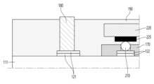
구체적으로, 도 5을 참조하면, 상기 포스트 범프(180)는 상기 제1 패드(121) 상에 상기 제1 패드(121)의 폭보다 작은 폭을 가지고 배치된다. 상기 포스트 범프(180)는 상기 제1 패드(121) 상에 일정 높이(H1)를 가지고 배치된다.Specifically, referring to FIG. 5 , the
상기 높이(H1)는 상기 포스트 범프(180)의 상면으로부터 하면까지의 수직 거리를 의미할 수 있다. 상기 포스트 범프(180)의 높이(H1)는 100㎛ 초과, 120㎛ 초과, 140㎛ 초과, 160㎛ 초과 또는 200㎛를 초과할 수 있다. 예를 들어, 상기 포스트 범프(180)의 높이(H1)는 100㎛ 내지 220㎛의 범위를 만족할 수 있다. 바람직하게, 상기 포스트 범프(180)의 높이(H1)는 110㎛ 내지 215㎛의 범위를 만족할 수 있다. 더욱 바람직하게, 상기 포스트 범프(180)의 높이는 115㎛ 내지 210㎛의 범위를 만족할 수 있다.The height H1 may refer to the vertical distance from the upper surface to the lower surface of the
상기 포스트 범프(180)의 높이(H1)가 100㎛ 미만이면, 상기 포스트 범프(180) 상에 제1 외부 기판을 안정적으로 결합하지 못할 수 있다. 상기 포스트 범프(180)의 높이(H1)가 100㎛ 미만이면, 상기 제1 외부 기판과 상기 반도체 패키지 사이의 거리가 감소하고, 이에 따라 상호 간의 신호 간섭에 의해 신호 전송 특성이 저하될 수 있다. 또한, 상기 포스트 범프(180)의 높이(H1)가 220㎛를 초과하면, 상기 포스트 범프(180)의 강성이 저하될 수 있다. 그리고 상기 포스트 범프(180)의 강성이 저하되는 경우, 상기 제1 외부 기판과의 결합 과정에서 무너짐과 같은 물리적 신뢰성 문제가 발생할 수 있다. 상기 포스트 범프(180)의 높이(H1)가 220㎛를 초과하면, 반도체 패키지의 두께 및 반도체 패키지의 두께가 증가할 수 있다.If the height H1 of the
상기 포스트 범프(180)는 단일 금속층으로 구성된다. 구체적으로, 상기 포스트 범프(180)는 화학동도금층과 같은 무전해 도금층을 포함하지 않으면서, 전해 도금층만을 포함할 수 있다.The
그리고, 상기 제1 회로층(120)은 적어도 2층의 금속층으로 구성된다. 상기 제1 회로층(120)의 제1 패드(121) 및 제2 패드(122)는 동일한 층 구조를 가질 수 있다. 나아가, 상기 제1 관통 전극(161)은 상기 제1 회로층(120)에 대응하는 2개의 금속층을 포함할 수 있다.And, the
즉, 상기 제1 회로층(120)의 제1 패드(121) 및 제2 패드(122) 각각은 제1 금속층(120-1) 및 제2 금속층(120-2)을 포함할 수 있다.That is, each of the
나아가, 상기 제1 관통 전극(161)은 상기 제1 회로층(120)의 상기 제1 금속층(120-1)에 대응하는 제3 금속층(161-1) 및 상기 제2 금속층(120-2)에 대응하는 제4 금속층(161-2)을 포함할 수 있다.Furthermore, the first through
이때, 상기 제1 금속층(120-1)과 상기 제3 금속층(161-1)은 실질적으로 1개의 층을 의미하며, 이를 배치 위치에 따라 구분한 것일 수 있다. 또한, 상기 제2 금속층(120-2)과 상기 제4 금속층(161-2)도 실질적으로 1개의 금속층을 의미하며, 이를 배치 위치에 따라 구분한 것일 수 있다.At this time, the first metal layer 120-1 and the third metal layer 161-1 substantially represent one layer, and may be divided according to the arrangement position. In addition, the second metal layer 120-2 and the fourth metal layer 161-2 also substantially represent one metal layer, and may be divided according to the arrangement position.
또한, 상기 제1 금속층(120-1)은 실질적으로 2개의 층일 수 있다. 상기 제1 금속층(120-1)은 구리 호일(Cu foil) 상에 제3 금속층(161-1)과 동일한 금속층을 포함하는 2개의 금속층일 수 있다.Additionally, the first metal layer 120-1 may substantially have two layers. The first metal layer 120-1 may be two metal layers including the same metal layer as the third metal layer 161-1 on copper foil (Cu foil).
또한, 상기 제1 금속층(120-1)은 구리 호일(Cu foil)의 1개의 층일 수 있다.Additionally, the first metal layer 120-1 may be one layer of copper foil (Cu foil).
이에 따라, 이하에서는 상기 제1 금속층(120-1) 및 제2 금속층(120-2)에 대해서만 설명하기로 한다.Accordingly, hereinafter, only the first metal layer 120-1 and the second metal layer 120-2 will be described.
상기 제1 회로층(120)의 제1 금속층(120-1)은 시드층일 수 있다. 상기 제1 회로층(120)의 제1 금속층(120-1)은 화학동도금층일 수 있다. 상기 제1 회로층(120)의 제1 금속층(120-1)은 동박층일 수 있다. 상기 제1 회로층(120)의 상기 제1 금속층(120-1)은 상기 동박층 및 화학동 도금층을 모두 포함할 수 있다.The first metal layer 120-1 of the
상기 제1 회로층(120)의 제2 금속층(120-2)은 상기 제1 금속층(120-1)을 시드층으로 전해 도금된 전해 도금층일 수 있다. 상기 제1 회로층(120)의 제2 금속층(120-2)은 상기 제1 금속층(120-1) 상에 일정 두께를 가지고 형성될 수 있다. 상기 제1 회로층(120)의 제2 금속층(120-2)은 상기 제1 회로층(120)의 제1 금속층(120-1)과 동일한 금속을 포함할 수 있으나, 이에 한정되는 것은 아니다. 일 예로, 상기 제1 회로층(120)의 상기 제1 금속층(120-1) 및 제2 금속층(120-2)은 각각 구리를 포함할 수 있다.The second metal layer 120-2 of the
포스트 범프(180)는 상기 제1 회로층(120)의 상기 제2 금속층(120-2) 상에 상기 제1 금속층(120-1)을 시드층으로 전해 도금하여 형성될 수 있다. 예를 들어, 상기 포스트 범프(180)는 제3 금속층만을 포함할 수 있다. 그리고, 상기 제3 금속층은 상기 제1 금속층(120-1)을 시드층으로 전해 도금을 진행하여 상기 제2 금속층(120-2) 상에 일정 높이(H1)를 가지고 형성될 수 있다. 즉, 상기 제3 금속층의 하면은 상기 제2 금속층(120-2)의 상면과 직접 접촉한다. 또한, 상기 제3 금속층의 상면은 상기 제1 보호층(170)의 상면보다 높게 위치한다. 이는, 상기 포스트 범프(180)가 상기 제2 금속층(120-2)과 제3 금속층 사이에 시드층을 포함하지 않는다는 것을 의미할 수 있다.The
한편, 상기 포스트 범프(180)의 상면(180T)은 상기 제1 몰딩 부재(190)의 상면(190T)과 단차를 가질 수 있다.Meanwhile, the
예를 들어, 상기 포스트 범프(180)의 상면(180T)은 상기 제1 몰딩 부재(190)의 상면(190T)보다 제2 높이(H2)만큼 높게 위치할 수 있다. 예를 들어, 상기 포스트 범프(180)의 상면(180T)에 인접한 제1 몰딩 부재(190)의 상면(190T)은 상기 포스트 범프(180)의 상면(180T)보다 제2 높이(H2)만큼 낮게 위치할 수 있다. 이를 통해, 상기 포스트 범프(180)의 측면의 적어도 일부는 상기 제1 몰딩 부재(190)로 덮이지 않을 수 있다. 예를 들어, 상기 포스트 범프(180)의 측면의 적어도 일부는 상기 제1 몰딩 부재(190)와 수평으로 중첩되지 않을 수 있다.For example, the
나아가, 상기 제1 몰딩 부재(190)의 상면(190T)은 상기 제1 반도체 소자(220)의 상면보다 높게 위치할 수 있다. 이를 통해, 실시 예는 상기 제1 몰딩 부재(190)에 의해 상기 제1 반도체 소자(220)가 안정적으로 보호되도록 할 수 있다. 상기 제1 몰딩 부재(190)의 상면(190T)은 상기 제1 보호층(170)의 상면보다 높게 위치할 수 있다. 또한, 상기 제1 몰딩 부재(190)의 상면(190T)은 상기 제1 접속부(210)의 상면보다 높게 위치할 수 있다. 이를 통해, 실시 예는 상기 제1 몰딩 부재(190)가 상기 제1 보호층(170), 제1 접속부(210) 및 제1 반도체 소자(220)를 전체적으로 둘러싸며 구비되도록 할 수 있다. 따라서, 실시 예는 상기 제1 반도체 소자(220)가 더욱 안정적으로 결합되도록 할 수 있고, 이에 따라 상기 제1 반도체 소자(220)의 동작 특성을 향상시킬 수 있다.Furthermore, the
상기 제1 몰딩 부재(190)의 상면(190T)은 상기 포스트 범프(180)의 상면(180T)보다 낮게 위치할 수 있다. 구체적으로, 상기 제1 몰딩 부재(190)의 상면(190T)은 평탄하지 않을 수 있다. 예를 들어, 실시 예에 따라 상기 제1 몰딩 부재(190)의 상면(190T)은 일정 표면 거칠기를 가지며 굴곡을 가질 수 있다. 그리고 상기 포스트 범프(180)에 인접한 영역에서의 상기 제1 몰딩 부재(190)의 상면(190T)은 상기 포스트 범프(180)의 상면(180T)보다 낮게 위치할 수 있다. 예를 들어, 상기 포스트 범프(180)의 측면의 적어도 일부는 상기 제1 몰딩 부재(190)에 의해 덮이지 않을 수 있다. 예를 들어, 상기 포스트 범프(180)의 측면의 적어도 일부는 상기 제1 몰딩 부재(190)와 수평 방향으로 중첩되지 않을 수 있다. 따라서, 상기 포스트 범프(180)는 상기 제1 몰딩 부재(190) 상으로 돌출된 구조를 가질 수 있다.The
이를 통해, 상기 표면 처리층(185)은 상기 포스트 범프(180) 상에 배치되면서 상기 제1 몰딩 부재(190)로 돌출될 수 있다.Through this, the
상기 표면 처리층(185)은 상기 포스트 범프(180)의 상면을 덮을 수 있다. 또한, 상기 표면 처리층(185)은 상기 포스트 범프(180)의 측면의 적어도 일부를 덮을 수 있다. 상기 표면 처리층(185)은 상기 포스트 범프(180) 상에 제3 높이(H3)를 가지고 배치될 수 있다. 이때, 상기 제3 높이(H3)는 상기 표면 처리층(185)의 제1 부분의 두께를 의미할 수 있다. 예를 들어, 상기 제3 높이(H3)은 상기 포스트 범프(180)와 수직으로 중첩된 영역에서의 상기 표면 처리층(185)의 두께를 의미할 수 있다. 예를 들어, 상기 제3 높이(H3)는 상기 포스트 범프(180)의 상면(180T)에서 상기 표면 처리층(185)의 상면 사이의 수직 거리를 의미할 수 있다.The
한편, 상기 제3 높이(H3)는 상기 표면 처리층(185)에 대응하는 표면 처리방식에 따라 다를 수 있다.Meanwhile, the third height H3 may vary depending on the surface treatment method corresponding to the
다만, 상기 제3 높이(H3)는 상기 제2 높이(H2)보다 클 수 있다. 바람직하게, 상기 포스트 범프(180)의 상면(190T)으로부터 상기 제1 몰딩 부재(190)의 상면(190T) 사이의 수직 거리는 상기 포스트 범프(180)의 상면(180T)으로부터 상기 표면 처리층(185)의 상면 사이의 수직 거리보다 작을 수 있다.However, the third height (H3) may be greater than the second height (H2). Preferably, the vertical distance between the
예를 들어, 상기 제2 높이(H2)는 상기 제3 높이(H3)의 50% 내지 90%의 범위를 만족할 수 있다. 예를 들어, 상기 제2 높이(H2)는 상기 제3 높이(H3)의 55% 내지 85%의 범위를 만족할 수 있다.For example, the second height H2 may satisfy a range of 50% to 90% of the third height H3. For example, the second height H2 may satisfy a range of 55% to 85% of the third height H3.
상기 제2 높이(H2)가 상기 제3 높이(H3)의 50% 미만이면, 상기 제2 높이(H2)에 의해 나타나는 접속부와 상기 표면 처리층(185) 사이의 결합 강도 상승 효과가 미비할 수 있다. 상기 제2 높이(H2)가 상기 제3 높이(H3)의 90%를 초과하면, 상기 포스트 범프(180)를 그라인딩하는 공정 시간이 증가하거나, 복수의 포스트 범프(180) 사이의 그라인딩 편차가 발생할 수 있다. 그리고 상기 그라인딩 편차가 발생하는 경우, 복수의 포스트 범프(180) 사이의 높이 편차가 발생할 수 있다. 이 경우, 상기 복수의 포스트 범프(180) 상에 메인 보드가 안정적으로 결합되지 못할 수 있고, 이에 따라 전자 디바이스가 안정적으로 동작하지 못할 수 있다.If the second height (H2) is less than 50% of the third height (H3), the effect of increasing the bond strength between the connection part and the
실시 예는 상기 제1 몰딩 부재(190)의 상면(190T)과 상기 포스트 범프(180)의 상면(180T)이 단차를 가지도록 할 수 있다. 바람직하게, 상기 제1 몰딩 부재(190)의 상면(190T)은 상기 포스트 범프(180)의 상면(180T)보다 낮게 위치할 수 있다. 이를 통해 상기 포스트 범프(180)의 측면의 적어도 일부는 상기 제1 몰딩 부재(190)와 접촉하지 않을 수 있다. 또한, 상기 표면 처리층(185)은 상기 제1 몰딩 부재(190)와 접촉하지 않는 상기 포스트 범프(180)의 측면의 적어도 일부를 둘러싸며 구비될 수 있다. 이를 통해, 실시 예는 복수의 포스트 범프(180) 사이의 높이 편차를 최소화하면서 상기 포스트 범프(180)와 상기 표면 처리층(185) 사이의 접촉 면적, 나아가 상기 표면 처리층(185)과 전도성 접속부(예를 들어, 메인 보드와 결합되는 접속부)와의 접촉 면적을 증가시킬 수 있다. 이를 통해 실시 예는 상기 포스트 범프(180)와 표면 처리층(185) 사이의 밀착력, 및 상기 표면 처리층(185)과 전도성 접속부 사이의 밀착력을 향상시킬 수 있고, 나아가 상기 포스트 범프(180) 상에 메인 보드가 안정적으로 결합되도록 할 수 있다.In an embodiment, the
도 6은 제2 실시 예에 따른 도 1의 일부 영역을 확대한 확대도이고, 도 7은 제3 실시 예에 따른 도 1의 일부 영역을 확대한 확대도이며, 도 8은 제4 실시 예에 따른 도 1의 일부 영역을 확대한 확대도이다.FIG. 6 is an enlarged view of a partial area of FIG. 1 according to the second embodiment, FIG. 7 is an enlarged view of a partial area of FIG. 1 according to the third embodiment, and FIG. 8 is an enlarged view of a partial area of FIG. 1 according to the fourth embodiment. This is an enlarged view of some areas of Figure 1.
도 7을 참조하면, 실시 예의 제1 몰딩 부재(190)의 상면(190T)은 단차를 가질 수 있다. 예를 들어, 제1 몰딩 부재(190)의 상면(190T)은 상기 포스트 범프(180)의 멀어질수록 높이가 변화할 수 있다.Referring to FIG. 7, the
바람직하게, 상기 제1 몰딩 부재(190)의 상면(190T)은 상기 포스트 범프(180)로부터 멀어질수록 높이가 낮아질 수 있다. 예를 들어, 상기 제1 몰딩 부재(190)의 상면(190T)은 상기 포스트 범프(180)에 인접한 영역에서 가장 큰 높이를 가질 수 있다.Preferably, the height of the
상기 제1 몰딩 부재(190)의 상면(190T)은 곡면일 수 있다. 예를 들어, 상기 제1 몰딩 부재(190)의 상면(190T)은 상기 포스트 범프(180)로부터 멀어질수록 높이가 작아지는 특정 곡률 반경의 곡면일 수 있다.The
실시 예는 상기 제1 몰딩 부재(190)의 상면(190T)이 곡면을 가지도록 하고, 이에 따라 열적 스트레스에 의한 신뢰성 문제를 해결하도록 한다.In the embodiment, the
구체적으로, 제1 몰딩 부재(190)의 상면(190T)이 곡면을 가지는 경우, 평면일 경우 대비 상면의 길이가 증가할 수 있다. 이에 따라, 상기 제1 몰딩 부재(190)가 열적 스트레스에 의해 팽창되는 경우, 상기 제1 몰딩 부재(190)의 상면(190T)이 곡면을 가짐에 따라 상기 팽창에 크게 영향을 받지 않을 수 있고, 나아가 상기 제1 몰딩 부재(190)에 작용하는 응력을 분산시킬 수 있다. 이를 통해, 실시 예는 상기 열적 스트레스에 의해 상기 포스트 범프(180)에 충격이 발생하는 것을 방지할 수 있고, 나아가 반도체 패키지의 물리적 신뢰성 및 전기적 신뢰성을 향상시킬 수 있다.Specifically, when the
한편, 도 7 및 도 8을 참조하면, 실시 예의 포스트 범프(180) 및 제1 몰딩 부재(190) 중 적어도 하나에는 크레비스가 구비될 수 있다. 상기 크레비스는 상기 제1 몰딩 부재(190) 및/또는 상기 포스트 범프(180)의 측면의 일부가 수직 방향으로 패인 부분을 의미할 수 있다.Meanwhile, referring to FIGS. 7 and 8 , at least one of the
예를 들어, 도 7을 참조하면, 포스트 범프(180)는 크레비스를 구비할 수 있다. 예를 들어, 상기 포스트 범프(180)는 상기 제1 몰딩 부재(190)와 수평으로 중첩되면서 상기 제1 몰딩 부재(190)와 접촉하지 않는 부분을 포함할 수 있다.For example, referring to FIG. 7 , the
예를 들어, 포스트 범프(180)는 상기 제1 몰딩 부재(190)와 수평 방향으로 중첩되면서 상기 제1 몰딩 부재(190)와 접촉하지 않는 제1 측면(180S1)을 포함할 수 있다. 예를 들어, 상기 크레비스는 상기 포스트 범프(180)의 제1 측면(180S1)에 구비될 수 있다. 구체적으로, 실시 예는 상기 포스트 범프(180)에 표면 처리층(185)을 형성하는 공정에서 상기 포스트 범프(180)에 존재하는 잔해물을 제거하기 위한 전처리 공정을 진행할 수 있다. 상기 크레비스는 상기 전처리 공정에서 상기 포스트 범프(180)의 측면의 적어도 일부가 제거됨에 따라 상기 포스트 범프(180)의 상기 제1 측면(180S1)에 구비될 수 있다. 그리고, 제1 측면(180S1)은 상기 표면 처리층(185)으로 덮일 수 있다.For example, the
예를 들어, 상기 포스트 범프(180)의 제1 측면(180S1)과 상기 제1 몰딩 부재(190) 사이에는 크레비스가 구비될 수 있고, 상기 표면 처리층(185)은 상기 크레비스를 채울 수 있다.For example, a crevice may be provided between the first side 180S1 of the
따라서, 상기 표면 처리층(185)의 적어도 일부는 상기 제1 몰딩 부재(190)와 상면(190T)보다 낮게 위치할 수 있다. 상기 크레비스는 상기 표면 처리층(185)과 상기 포스트 범프(180) 사이의 접촉 면적을 증가시킬 수 있고, 이를 통해 상기 표면 처리층(185)과 상기 포스트 범프(180) 사이의 결합 강도를 향상시킬 수 있다.Accordingly, at least a portion of the
또한, 상기 포스트 범프(180)는 상기 제1 측면(180S1)과 상면(180T) 사이에 구비되면서 상기 제1 몰딩 부재(190)와 수평 방향으로 중첩되지 않는 제2 측면(180S2)을 더 포함할 수 있다.In addition, the
한편, 상기 포스트 범프(180)는 드라이 필름에 구비된 오픈 영역을 채우며 형성될 수 있다. 상기 포스트 범프(180)는 상기 오픈 영역의 형상에 따라 다양한 형상을 가질 수 있다. 예를 들어, 포스트 범프(180)의 수직 단면 형상은 상면(180T)의 폭이 하면(180B)의 폭보다 큰 사다리꼴 형상을 가질 수 있다. 이 경우, 상기 제1 몰딩 부재(190)를 통해 덮이는 상기 포스트 범프(180)의 제3측면의 경사는 상기 포스트 범프(180)의 제1 측면(180S1) 및 제2 측면(190T)의 각각의 경사와 다를 수 있다.Meanwhile, the
한편, 도 8을 참조하면, 실시 예의 크레비스는 상기 제1 몰딩 부재(190)에 구비될 수 있다. 예를 들어, 도 7에서는 상기 포스트 범프(180)의 측부의 적어도 일부를 에칭으로 제거하고, 이를 통해 상기 포스트 범프(180)가 크레비스를 구비하도록 하였다.Meanwhile, referring to FIG. 8, the crevice of the embodiment may be provided in the
이와 다르게, 실시 예의 크레비스는 상기 포스트 범프(180)의 측면을 감싸는 상기 제1 몰딩 부재(190)의 일부 영역을 플라즈마 처리 등을 하여 제거할 수 있다. 이를 통해 상기 크레비스는 상기 제1 몰딩 부재(190)에 구비될 수 있다. 그리고 상기 제1 몰딩 부재(190)는 상기 포스트 범프(180)의 제1 측면(180S1)과 수평으로 중첩되면서 상기 포스트 범프(180)와 접촉하지 않는 측면(190S)을 포함할 수 있다.Differently, the crevice of the embodiment may remove a partial area of the
도 9는 제1 실시 예에 따른 전자 디바이스를 나타낸 도면이다.Figure 9 is a diagram showing an electronic device according to the first embodiment.
도 9를 참조하면, 실시 예의 전자 디바이스는 도 1의 회로 기판 상에 배치된 제1 외부 기판(320)을 포함할 수 있다. 상기 제1 외부 기판(320)은 전자 디바이스의 메인 보드일 수 있으나, 이에 한정되지는 않는다.Referring to FIG. 9 , the electronic device of the embodiment may include a first
상기 반도체 패키지의 상기 표면 처리층(185) 상에는 제3 접속부(310)가 구비될 수 있다. 또한, 상기 제3 접속부(310) 상에는 제1 외부 기판(320)의 단자 패드(325)가 배치될 수 있다. 이를 통해 실시 예는 상기 제1 외부 기판(320)과 반도체 패키지 사이를 안정적으로 결합시킬 수 있다.A
도 10은 제2 실시 예에 따른 반도체 패키지를 나타낸 단면도이고, 도 11은 제2 실시 예에 따른 전자 디바이스를 나타낸 단면도이다.FIG. 10 is a cross-sectional view showing a semiconductor package according to a second embodiment, and FIG. 11 is a cross-sectional view showing an electronic device according to a second embodiment.
도 10을 참조하면, 실시 예는 반도체 패키지의 상부 및 하부에 각각 구비된 포스트 범프를 포함할 수 있다.Referring to FIG. 10, the embodiment may include post bumps provided on the top and bottom of the semiconductor package, respectively.
예를 들어, 이전 실시 예에서의 반도체 패키지는 제1 패드(121) 상에 배치된 포스트 범프(180)를 포함하였다.For example, the semiconductor package in the previous embodiment included a
제2 실시 예에 따르면, 상기 제2 회로층(130)의 제3 패드 하에 배치된 제2 포스트 범프(250)를 더 포함할 수 있다. 상기 제2 포스트 범프(250)는 상기 제1 포스트 범프(180)에 대응하는 구조를 가질 수 있다. 상기 제1 포스트 범프(180)에 대해 이전 실시 예에서 이미 설명하였으므로, 이의 설명은 생략하기로 한다. 또한, 제2 포스트 범프(250)의 측면의 적어도 일부 및 하면에는 제2 표면 처리층(255)이 배치될 수 있다. 이 경우, 실시 예의 반도체 패키지는 PoP 구조에 적용될 수 있다.According to the second embodiment, it may further include a
예를 들어, 도 11을 참조하면, 전자 디바이스는 제1 실시 예의 반도체 패키지에 추가로 배치된 제2 외부 기판(340)을 더 포함할 수 있다.For example, referring to FIG. 11 , the electronic device may further include a second
이를 위해, 제2 포스트 범프(250)의 하면에는 제2 표면 처리층(255)이 구비될 수 있고, 상기 제2 표면 처리층 하에는 제4 접속부(330)가 구비될 수 있다.To this end, a second
또한, 상기 제4 접속부 하에는 제2 외부 기판(340)이 전기적으로 결합될 수 있다. 상기 제2 외부 기판(340)은 메모리 패키지일 수 있다. 이를 위해, 상기 제2 외부 기판(340)은 메모리 기판(341), 단자 패드(342), 상기 메모리 기판(341)에 부착된 메모리 소자(343) 및 상기 메모리 기판(341)과 상기 메모리 소자(341) 사이를 연결하는 연결 부재(344)를 포함할 수 있다.Additionally, a second
다만, 실시 예는 이에 한정되지 않으며, 상기 제2 외부 기판(340)은 상기 메모리 패키지와 상기 제2 포스트 범프(250) 사이에 배치되는 인터포저일 수 있다.However, the embodiment is not limited to this, and the second
실시 예의 반도체 패키지는 제1 절연층 상에 배치된 제1 패드 및 제2 패드를 포함할 수 있다. 또한, 상기 제1 패드 상에는 포스트 범프가 배치될 수 있고, 제2 패드 상에는 접속부를 통해 제1 반도체 소자가 전기적으로 결합될 수 있다. 또한, 상기 제1 절연층 상에는 상기 포스트 범프 및 제1 반도체 소자를 몰딩하며 제1 몰딩 부재가 구비될 수 있다.The semiconductor package of the embodiment may include a first pad and a second pad disposed on a first insulating layer. Additionally, a post bump may be disposed on the first pad, and the first semiconductor device may be electrically coupled to the second pad through a connection portion. Additionally, a first molding member may be provided on the first insulating layer to mold the post bump and the first semiconductor device.
상기 제1 몰딩 부재는 상기 접속부 및 상기 제1 반도체 소자보다 높게 위치할 수 있다. 이를 통해, 실시 예는 상기 접속부와 상기 제1 반도체 소자가 상기 제2 패드 상에 안정적으로 결합되도록 할 수 있고, 이를 통해 상기 제1 반도체 소자의 동작 특성을 향상시킬 수 있다.The first molding member may be positioned higher than the connection portion and the first semiconductor device. Through this, the embodiment can ensure that the connection part and the first semiconductor device are stably coupled to the second pad, and through this, the operating characteristics of the first semiconductor device can be improved.
또한, 실시 예의 상기 제1 몰딩 부재의 상면과 상기 포스트 범프의 상면은 단차를 가질 수 있다. 바람직하게 제1 몰딩 부재의 상면은 포스트 범프의 상면보다 낮게 위치할 수 있다. 이를 통해 상기 포스트 범프의 측면의 적어도 일부는 상기 제1 몰딩 부재와 접촉하지 않을 수 있다. 또한, 상기 표면 처리층은 상기 제1 몰딩 부재와 접촉하지 않는 상기 포스트 범프의 측면의 적어도 일부를 둘러싸며 구비될 수 있다. 이를 통해, 실시 예는 복수의 포스트 범프 사이의 높이 편차를 최소화하면서 상기 포스트 범프와 상기 표면 처리층 사이의 접촉 면적, 나아가 상기 표면 처리층과 전도성 접속부(예를 들어, 메인 보드와 결합되는 접속부)와의 접촉 면적을 증가시킬 수 있다. 이를 통해 실시 예는 상기 포스트 범프와 표면 처리층 사이의 밀착력, 및 상기 표면 처리층과 전도성 접속부 사이의 밀착력을 향상시킬 수 있고, 나아가 상기 포스트 범프 상에 메인 보드가 안정적으로 결합되도록 할 수 있다.Additionally, in the embodiment, the upper surface of the first molding member and the upper surface of the post bump may have a step. Preferably, the upper surface of the first molding member may be located lower than the upper surface of the post bump. Through this, at least a portion of the side surface of the post bump may not contact the first molding member. Additionally, the surface treatment layer may be provided to surround at least a portion of a side surface of the post bump that is not in contact with the first molding member. Through this, the embodiment minimizes the height difference between the plurality of post bumps and increases the contact area between the post bump and the surface treatment layer, and further, the surface treatment layer and the conductive connection portion (for example, the connection portion coupled to the main board). The contact area can be increased. Through this, the embodiment can improve the adhesion between the post bump and the surface treatment layer and the adhesion between the surface treatment layer and the conductive connection part, and further enable the main board to be stably coupled to the post bump.
상기 제1 몰딩 부재의 상면은 곡면일 수 있다. 예를 들어, 상기 제1 몰딩 부재의 상면은 상기 포스트 범프로부터 멀어질수록 높이가 작아지는 특정 곡률 반경의 곡면일 수 있다. 실시 예는 상기 제1 몰딩 부재의 상면이 곡면을 가지도록 하고, 이에 따라 열적 스트레스에 의한 신뢰성 문제를 해결하도록 한다.The upper surface of the first molding member may be curved. For example, the upper surface of the first molding member may be a curved surface with a specific radius of curvature whose height decreases as the distance from the post bump increases. The embodiment allows the upper surface of the first molding member to have a curved surface, thereby solving the reliability problem caused by thermal stress.
구체적으로, 제1 몰딩 부재의 상면이 곡면을 가지는 경우, 평면일 경우 대비 상면의 길이가 증가할 수 있다. 이에 따라, 상기 제1 몰딩 부재가 열적 스트레스에 의해 팽창되는 경우, 상기 제1 몰딩 부재의 상면이 곡면을 가짐에 따라 상기 팽창에 크게 영향을 받지 않을 수 있고, 나아가 상기 제1 몰딩 부재에 작용하는 응력을 분산시킬 수 있다. 이를 통해, 실시 예는 상기 열적 스트레스에 의해 상기 포스트 범프에 충격이 발생하는 것을 방지할 수 있고, 나아가 반도체 패키지의 물리적 신뢰성 및 전기적 신뢰성을 향상시킬 수 있다.Specifically, when the upper surface of the first molding member has a curved surface, the length of the upper surface may increase compared to when it is flat. Accordingly, when the first molding member is expanded due to thermal stress, the upper surface of the first molding member has a curved surface, so it may not be greatly affected by the expansion, and further, the force acting on the first molding member Stress can be distributed. Through this, the embodiment can prevent shock from occurring on the post bump due to the thermal stress and further improve the physical and electrical reliability of the semiconductor package.
또한, 포스트 범프 및 제1 몰딩 부재 중 적어도 하나에는 크레비스를 구비할 수 있다. 이를 통해, 포스트 범프는 상기 제1 몰딩 부재와 수평으로 중첩되면서 상기 제1 몰딩 부재와 접촉하지 않는 부분을 포함할 수 있다.Additionally, at least one of the post bump and the first molding member may be provided with a crevice. Through this, the post bump may include a portion that overlaps the first molding member horizontally and does not contact the first molding member.
예를 들어, 포스트 범프는 상기 제1 몰딩 부재와 수평 방향으로 중첩되면서 상기 제1 몰딩 부재와 접촉하지 않는 제1 측면을 포함할 수 있다. 구체적으로, 실시 예는 상기 포스트 범프에 표면 처리층을 형성하는 공정에서 상기 포스트 범프에 존재하는 잔해물을 제거하기 위한 전처리 공정을 진행할 수 있다. 상기 크레비스는 상기 전처리 공정에서 상기 포스트 범프의 측면의 적어도 일부 및/또는 제1 몰딩 부재의 일부가 제거됨에 따라 구비될 수 있다. 상기 크레비스는 상기 표면 처리층으로 덮일 수 있다.For example, the post bump may include a first side that overlaps the first molding member in a horizontal direction and does not contact the first molding member. Specifically, the embodiment may perform a pretreatment process to remove debris present in the post bump during the process of forming a surface treatment layer on the post bump. The crevice may be provided by removing at least a portion of the side surface of the post bump and/or a portion of the first molding member in the pretreatment process. The crevice may be covered with the surface treatment layer.
예를 들어, 상기 포스트 범프의 제1 측면과 상기 제1 몰딩 부재의 측면 사이에는 크레비스가 구비될 수 있고, 상기 표면 처리층은 상기 크레비스를 채울 수 있다.For example, a crevice may be provided between the first side of the post bump and the side of the first molding member, and the surface treatment layer may fill the crevice.
따라서, 상기 표면 처리층의 적어도 일부는 상기 제1 몰딩 부재의 상면보다 낮게 위치할 수 있다. 상기 크레비스는 상기 표면 처리층과 상기 포스트 범프 사이의 접촉 면적을 증가시킬 수 있고, 이를 통해 상기 표면 처리층과 상기 포스트 범프 사이의 결합 강도를 향상시킬 수 있다.Accordingly, at least a portion of the surface treatment layer may be located lower than the upper surface of the first molding member. The crevice may increase the contact area between the surface treatment layer and the post bump, thereby improving the bonding strength between the surface treatment layer and the post bump.
- 회로 기판의 제조 방법 -- Manufacturing method of circuit board -
도 12 내지 27은 도 2에 도시된 제1 실시 예의 회로 기판의 제조 방법을 공정 순으로 설명하기 위한 도면이다.FIGS. 12 to 27 are diagrams for explaining the manufacturing method of the circuit board of the first embodiment shown in FIG. 2 in process order.
또한, 이하에서는 회로 기판에서, 제1 절연층(111)을 중심으로 이의 상측에 제1 회로층(120), 제1 보호층(170) 및 포스트 범프(180)를 형성하는 공정을 중심으로 설명한다.In addition, the following description will focus on the process of forming the
도 12를 참조하면, 실시 예는 제1 절연층(111)을 준비한다. 바람직하게, 상기 제1 절연층(111)을 준비하는 단계는 상기 제3 절연층(113) 상에 제3 회로층(140)이 배치된 상태에서, 상기 제3 절연층(113) 상에 상기 제1 절연층(111)을 적층하는 공정을 의미할 수 있다. 다음으로, 실시 예는 상기 제1 절연층(111) 상에 제1 금속층(120-1)을 형성할 수 있다. 상기 제1 금속층(120-1)은 상기 제1 절연층(111) 상에 배치된 동박층을 의미할 수 있다. 이와 다르게, 상기 제1 금속층(120-1)은 상기 제1 절연층(111) 상에 무전해 도금을 진행하여 형성한 무전해 도금층일 수 있다. 예를 들어, 상기 제1 금속층(120-1)은 화학동도금층일 수 있다. 이와 다르게, 상기 제1 금속층(120-1)은 상기 동박층 및 상기 화학동도금층을 모두 포함할 수 있다.Referring to FIG. 12, in the embodiment, the first insulating
이때, 실시 예의 반도체 패키지는 스트립 단위 또는 판넬 단위로 제조될 수 있다. 즉, 스트립은 복수의 회로 기판을 포함하며, 판넬은 복수의 스트립을 포함한다.At this time, the semiconductor package of the embodiment may be manufactured in strip units or panel units. That is, the strip includes a plurality of circuit boards, and the panel includes a plurality of strips.
이에 따라, 상기 제1 절연층(111)은 복수의 영역으로 구분될 수 있다. 예를 들어, 상기 제1 절연층(111)은 회로 기판 영역에 대응하는 복수의 유효 영역(AR)과, 상기 복수의 유효 영역(AR)들 사이에 배치되는 더미 영역(DR)을 포함한다. 그리고, 최종적으로 상기 유효 영역(AR)과 더미 영역(DR) 사이의 라인을 소잉 라인으로 하여 소잉을 진행하는 것에 의해 복수의 회로 기판을 분리시킬 수 있다. 그리고, 상기 유효 영역(AR)은 상기 설명한 바와 같이 반도체 패키지의 제1 영역(R1) 및 제2 영역(R2)을 포함할 수 있다. 상기 반도체 패키지의 상기 제1 영역(R1)은 상기 더미 영역(DR)에 인접한 영역을 의미할 수 있다.Accordingly, the first insulating
다음으로, 도 13을 참조하면, 실시 예는 상기 제1 금속층(120-1) 상에 제1 마스크(M1)를 형성한다. 상기 제1 마스크(M1)는 상기 유효 영역(AR) 및 상기 더미 영역(DR) 상에 배치될 수 있다. 이때, 상기 제1 마스크(M1)는 상기 유효 영역(AR) 상에 구비되고, 제1 회로층(120)이 형성될 영역을 오픈하는 오픈 영역(OR1)을 포함할 수 있다.Next, referring to FIG. 13, in the embodiment, a first mask M1 is formed on the first metal layer 120-1. The first mask M1 may be disposed on the effective area AR and the dummy area DR. At this time, the first mask M1 is provided on the effective area AR and may include an open area OR1 that opens an area where the
다음으로, 도 14를 참조하면, 실시 예는 상기 제1 금속층(120-1)을 시드층으로 상기 제1 마스크(M1)의 오픈 영역(OR1)을 채우는 제2 금속층(120-2)을 형성한다.Next, referring to FIG. 14, in the embodiment, the second metal layer 120-2 is formed to fill the open area OR1 of the first mask M1 using the first metal layer 120-1 as a seed layer. do.
다음으로, 도 15를 참조하면, 실시 예는 상기 제1 마스크(M1)를 제거하는 공정을 진행할 수 있다.Next, referring to FIG. 15, the embodiment may proceed with a process of removing the first mask M1.
다음으로, 도 16을 참조하면, 실시 예는 제2 마스크(M2)를 형성하는 공정을 진행할 수 있다. 상기 제2 마스크(M2)는 오픈 영역(OR2)을 포함할 수 있다. 상기 제2 마스크(M2)의 오픈 영역(OR2)은 상기 유효 영역(AR)의 상기 제2 영역(R2)과 수직으로 중첩된 제1 금속층(120-1) 및 제2 금속층(120-2)과 수직으로 중첩될 수 있다. 예를 들어, 상기 제2 마스크(M2)는 상기 유효 영역(AR)의 상기 제1 영역(R1)에 배치된 제1 금속층(120-1) 및 제2 금속층(120-2)을 덮을 수 있다. 또한, 상기 제2 마스크(M2)는 상기 더미 영역(DR)에 배치된 상기 제1 금속층(120-1)을 덮을 수 있다. 그리고, 상기 제2 마스크(M2)를 통해 덮인 상기 제1 영역(R1)의 제1 금속층(120-1)과 상기 더미 영역(DR)의 제1 금속층(120-1)은 추후 포스트 범프(180)를 전해 도금하기 위한 시드층으로 이용될 수 있다.Next, referring to FIG. 16, the embodiment may proceed with a process of forming the second mask M2. The second mask M2 may include an open area OR2. The open area OR2 of the second mask M2 includes a first metal layer 120-1 and a second metal layer 120-2 that vertically overlap the second area R2 of the effective area AR. can be vertically overlapped. For example, the second mask M2 may cover the first metal layer 120-1 and the second metal layer 120-2 disposed in the first region R1 of the effective area AR. . Additionally, the second mask M2 may cover the first metal layer 120-1 disposed in the dummy region DR. In addition, the first metal layer 120-1 of the first region R1 and the first metal layer 120-1 of the dummy region DR covered through the second mask M2 will later be formed into a post bump 180. ) can be used as a seed layer for electroplating.
다음으로, 도 17을 참조하면, 실시 예는 상기 제2 마스크(M2)의 오픈 영역(OR2)을 통해 노출된 제1 금속층(120-1)을 에칭으로 제거하는 공정을 진행할 수 있다. 구체적으로, 실시 예는 상기 제2 영역(R2)에 배치된 제1 금속층(120-1) 중 상기 제2 금속층(120-2)과 수직으로 중첩되지 않는 부분을 에칭으로 제거할 수 있다. 이를 통해, 실시 예는 상기 제2 영역(R2)에서의 제1 금속층(120-1)과 제2 금속층(120-2)을 포함하는 제1 회로층(120)의 제2 패드(122)를 형성할 수 있다.Next, referring to FIG. 17 , the embodiment may proceed with a process of removing the first metal layer 120-1 exposed through the open area OR2 of the second mask M2 by etching. Specifically, in the embodiment, a portion of the first metal layer 120-1 disposed in the second region R2 that does not vertically overlap the second metal layer 120-2 may be removed by etching. Through this, the embodiment is the
다음으로, 도 18을 참조하면, 실시 예는 상기 제2 마스크(M2)를 제거하는 공정을 진행할 수 있다. 이를 통해, 상기 제1 영역(R1)에 배치된 제1 금속층(120-1)과, 상기 더미 영역(DR)에 배치된 제1 금속층(120-1)이 오픈될 수 있다.Next, referring to FIG. 18, the embodiment may proceed with a process of removing the second mask M2. Through this, the first metal layer 120-1 disposed in the first region R1 and the first metal layer 120-1 disposed in the dummy region DR may be opened.
다음으로, 도 19를 참조하면, 실시 예는 상기 유효 영역(AR) 및 상기 더미 영역(DR) 상에 전체적으로 레지스트층(170R)을 형성하는 공정을 진행할 수 있다. 상기 레지스트층(170R)는 실시 예의 제1 보호층(170)에서 제1 개구(171) 및 제2 개구(172)가 형성되기 전의 층을 의미할 수 있다. 상기 레지스트층(170R)은 제1 영역(R1)에서 상기 제1 금속층(120-1) 및 제2 금속층(120-2)을 덮을 수 있다. 상기 레지스트층(170R)은 제2 영역(R2)에서 제1 절연층(111) 및 제2 패드(122)를 덮을 수 있다. 또한, 상기 레지스트층(170R)은 더미 영역(DR)에서 상기 제1 금속층(120-1)을 덮을 수 있다.Next, referring to FIG. 19 , the embodiment may proceed with a process of forming a resist
다음으로, 도 20을 참조하면, 실시 예는 상기 레지스트층(170R)을 노광 및 현상하여, 상기 제1 영역(R1)을 전체적으로 오픈하는 제1 개구(171)를 형성하는 공정을 진행할 수 있다. 또한, 실시 예는 상기 제2 영역(R2)에 배치된 제2 패드(122)를 부분적으로 오픈하는 제2 개구(172)를 형성하는 공정을 진행할 수 있다. 이때, 상기 제1 개구(171)를 형성할 때, 상기 더미 영역(DR) 상의 레지스트층(170R)도 전체적으로 제거될 수 있다. 다만, 실시 예는 이에 한정되지 않는다.Next, referring to FIG. 20 , the embodiment may proceed with a process of exposing and developing the resist
다음으로, 도 21을 참조하면, 실시 예는 제3 마스크(M3)를 형성하는 공정을 진행할 수 있다. 상기 제3 마스크(M3)는 상기 더미 영역(DR) 및 상기 유효 영역(AR) 상에 전체적으로 배치되면서 상기 제1 영역(R1)에 위치한 제2 금속층(120-2)의 상면의 일부와 수직으로 중첩되는 오픈 영역(OR3)을 포함할 수 있다. 상기 오픈 영역(OR3)의 폭은 상기 제1 영역(R1)의 제2 금속층(120-2)의 폭보다 작을 수 있다. 이에 따라, 상기 제3 마스크(M3)는 상기 제1 영역(R1)의 상기 제2 금속층(120-2)의 상면을 부분적으로 오픈할 수 있다.Next, referring to FIG. 21, the embodiment may proceed with a process of forming the third mask M3. The third mask M3 is disposed entirely on the dummy region DR and the effective region AR and is vertically aligned with a portion of the upper surface of the second metal layer 120-2 located in the first region R1. It may include an overlapping open area (OR3). The width of the open area OR3 may be smaller than the width of the second metal layer 120-2 of the first area R1. Accordingly, the third mask M3 may partially open the upper surface of the second metal layer 120-2 in the first region R1.
다음으로, 도 22를 참조하면, 실시 예는 상기 제3 마스크(M3)의 오픈 영역(OR3)을 통해 오픈된 상기 제1 영역(R1)의 상기 제2 금속층(120-2) 상에 포스트 범프(180)를 형성하는 공정을 진행할 수 있다. 이때, 상기 포스트 범프(180)는 상기 제1 영역(R1)에 배치된 제1 금속층(120-1)과 상기 더미 영역(DR)에 배치된 제1 금속층(120-1)을 시드층으로 전해도금하여 형성할 수 있다.Next, referring to FIG. 22, in the embodiment, a post bump is formed on the second metal layer 120-2 in the first region R1 opened through the open region OR3 of the third mask M3. The process of forming (180) can be performed. At this time, the
다음으로, 도 23을 참조하면, 실시 예는 상기 제3 마스크(M3)를 제거하는 공정을 진행할 수 있다. 이를 통해, 상기 제1 영역(R1)에서의 제1 금속층(120-1)과 더미 영역(DR)에서의 제1 금속층(120-1)은 오픈될 수 있다. 또한, 실시 예는 상기 제1 영역(R1) 및 상기 더미 영역(DR)에서 오픈된 상기 제1 금속층(120-1)을 에칭으로 제거하여 제1 회로층(120)의 제1 패드(121)를 형성할 수 있다. 이후, 실시 예는 상기 더미 영역(DR)과 상기 제1 영역(R1) 사이의 라인을 소잉 라인으로 하여, 상기 유효 영역(AR)을 더미 영역(DR)으로부터 분리할 수 있다. 이를 통해 반도체 패키지가 제조될 수 있다.Next, referring to FIG. 23, the embodiment may proceed with a process of removing the third mask M3. Through this, the first metal layer 120-1 in the first region R1 and the first metal layer 120-1 in the dummy region DR may be open. In addition, in the embodiment, the open first metal layer 120-1 in the first region R1 and the dummy region DR is removed by etching to form the
한편, 실시 예는 상기 더미 영역(DR)과 제1 영역(R1) 사이의 영역(예를 들어, 제1 영역(R1)의 테두리 영역)의 적어도 일부에서 상기 레지스트층(170R)을 제거하지 않을 수 있다. 이 경우, 상기 레지스트층(170R)이 제거되지 않은 상기 테두리 영역에서의 상기 제1 금속층(120-1)은 오픈되지 않을 수 있다. 따라서, 상기 테두리 영역에서의 상기 제1 금속층(120-1)은 제거되지 않고 회로 기판에 잔존할 수 있다. 상기 잔존하는 제1 금속층(120-1)은 회로 기판의 상면의 테두리 영역을 따라 구비될 수 있고, 이에 따라 상기 회로 기판의 강성을 향상시키면서 상기 회로 기판이 특정 방향으로 크게 휘어지는 것을 방지하는 기능을 할 수 있다.Meanwhile, the embodiment does not remove the resist
다음으로, 도 24를 참조하면, 실시 예는 상기 제2 패드(122) 상에 제1 접속부(210)를 배치하고, 상기 제1 접속부(210) 상에 제1 반도체 소자(220)를 실장하는 공정을 진행할 수 있다.Next, referring to FIG. 24, in the embodiment, the
다음으로, 도 25를 참조하면, 실시 예는 상기 포스트 범프(180) 및 상기 제1 반도체 소자(220)를 몰딩하는 제1 몰딩 부재(190)를 형성하는 공정을 진행할 수 있다. 이때, 상기 제1 몰딩 부재(190)는 상기 포스트 범프(180)의 상부를 덮으며 배치될 수 있다.Next, referring to FIG. 25 , the embodiment may proceed with a process of forming a
다음으로, 도 26을 참조하면, 실시 예는 상기 제1 몰딩 부재(190)의 상면과 포스트 범프(180)의 상면을 그라인딩하는 공정을 진행할 수 있다. 그리고, 상기 그라인딩 공정에 의해 복수의 포스트 범프(180)는 균일한 높이를 가질 수 있다. 나아가, 실시 예는 상기 그라인딩 공정에서 상기 포스트 범프(180)보다 상기 제1 몰딩 부재(190) 더 많이 제거되도록 할 수 있다. 이를 통해 실시 예는 상기 포스트 범프(180)와 제1 몰딩 부재(190)가 단차를 가지도록 할 수 있다. 예를 들어, 실시 예는 상기 포스트 범프(180)의 상면(180T)보다 상기 제1 몰딩 부재(190)의 상면이 더 낮게 위치하도록 할 수 있다.Next, referring to FIG. 26 , the embodiment may proceed with a process of grinding the upper surface of the
다음으로, 도 27을 참조하면, 실시 예는 상기 제1 몰딩 부재(190)와 접촉하지 않는 상기 포스트 범프(180)의 측면의 적어도 일부 및 상면에 표면 처리층(185)을 형성할 수 있다.Next, referring to FIG. 27 , in the embodiment, a
상술한 실시 예에 설명된 특징, 구조, 효과 등은 본 발명의 적어도 하나의 실시 예에 포함되며, 반드시 하나의 실시 예에만 한정되는 것은 아니다. 나아가, 각 실시 예에서 예시된 특징, 구조, 효과 등은 실시 예들이 속하는 분야의 통상의 지식을 가지는 자에 의하여 다른 실시 예들에 대해서도 조합 또는 변형되어 실시 가능하다. 따라서 이러한 조합과 변형에 관계된 내용은 본 발명의 범위에 포함되는 것으로 해석되어야 할 것이다.The features, structures, effects, etc. described in the above-described embodiments are included in at least one embodiment of the present invention and are not necessarily limited to only one embodiment. Furthermore, the features, structures, effects, etc. illustrated in each embodiment can be combined or modified and implemented in other embodiments by a person with ordinary knowledge in the field to which the embodiments belong. Therefore, contents related to such combinations and modifications should be construed as being included in the scope of the present invention.
또한, 이상에서 실시 예들을 중심으로 설명하였으나 이는 단지 예시일 뿐 본 발명을 한정하는 것이 아니며, 본 발명이 속하는 분야의 통상의 지식을 가진 자라면 본 실시 예의 본질적인 특성을 벗어나지 않는 범위에서 이상에 예시되지 않은 여러 가지의 변형과 응용이 가능함을 알 수 있을 것이다. 예를 들어, 실시 예들에 구체적으로 나타난 각 구성 요소는 변형하여 실시할 수 있는 것이다. 그리고 이러한 변형과 응용에 관계된 차이점들은 첨부한 청구 범위에서 규정하는 본 발명의 범위에 포함되는 것으로 해석되어야 할 것이다.In addition, although the description has been made focusing on the embodiments above, this is only an example and does not limit the present invention, and those of ordinary skill in the field to which the present invention pertains will understand the above examples without departing from the essential characteristics of the present embodiments. You will be able to see that various modifications and applications are possible. For example, each component specifically shown in the embodiments can be modified and implemented. And these variations and differences in application should be construed as being included in the scope of the present invention as defined in the attached claims.
Claims (15)
Translated fromKorean상기 제1 절연층 상에 배치되고, 수평 방향으로 상호 이격된 제1 패드 및 제2 패드;
상기 제1 패드 상에 배치된 포스트 범프;
상기 제2 패드 상에 배치된 제1 접속부;
상기 제1 접속부 상에 배치된 제1 반도체 소자;
상기 제1 절연층 상에 배치되고, 상기 포스트 범프 및 상기 제1 반도체 소자를 몰딩하는 제1 몰딩 부재; 및
상기 포스트 범프 상에 배치된 표면 처리층을 포함하고,
상기 제1 몰딩 부재의 상면은 상기 제1 반도체 소자의 상면보다 높게 위치하고,
상기 제1 몰딩 부재의 상면은 상기 포스트 범프의 상면보다 낮게 위치하며,
상기 표면 처리층은 상기 포스트 범프의 상면 및 측면의 적어도 일부를 덮으며 배치된,
반도체 패키지.first insulating layer;
a first pad and a second pad disposed on the first insulating layer and spaced apart from each other in a horizontal direction;
a post bump disposed on the first pad;
a first connection portion disposed on the second pad;
a first semiconductor element disposed on the first connection portion;
a first molding member disposed on the first insulating layer and molding the post bump and the first semiconductor device; and
Comprising a surface treatment layer disposed on the post bump,
The upper surface of the first molding member is located higher than the upper surface of the first semiconductor element,
The upper surface of the first molding member is located lower than the upper surface of the post bump,
The surface treatment layer is disposed to cover at least a portion of the top and side surfaces of the post bump.
Semiconductor package.
상기 표면 처리층은 상기 포스트 범프의 상면과 접촉한 제1 부분과, 상기 제1 부분으로부터 절곡 연장되며 상기 포스트 범프의 측면과 접촉한 제2 부분을 포함하고,
상기 표면 처리층의 제2 부분의 적어도 일부는 상기 제1 몰딩 부재와 접촉하는,
반도체 패키지.According to paragraph 1,
The surface treatment layer includes a first part in contact with the upper surface of the post bump, and a second part bent and extended from the first part and in contact with a side surface of the post bump,
At least a portion of the second portion of the surface treatment layer is in contact with the first molding member,
Semiconductor package.
상기 제1 몰딩 부재의 상면은 곡면을 포함하는,
반도체 패키지.According to paragraph 1,
The upper surface of the first molding member includes a curved surface,
Semiconductor package.
상기 제1 몰딩 부재의 상면의 곡면은 상기 포스트 범프로부터 멀어질수록 높이가 낮아지는 곡률 반경을 가지는,
반도체 패키지.According to paragraph 3,
The curved surface of the upper surface of the first molding member has a radius of curvature whose height decreases as the distance from the post bump increases,
Semiconductor package.
상기 포스트 범프의 상면과 상기 제1 몰딩 부재의 상면은 단차를 가지며,
상기 표면 처리층의 제1 부분의 두께는 상기 단차보다 큰,
반도체 패키지.According to paragraph 2,
The upper surface of the post bump and the upper surface of the first molding member have a step,
The thickness of the first portion of the surface treatment layer is greater than the step,
Semiconductor package.
상기 단차는 상기 표면 처리층의 상기 제1 부분의 두께의 55% 내지 85%의 범위를 가지는,
반도체 패키지.According to clause 5,
The step has a range of 55% to 85% of the thickness of the first portion of the surface treatment layer,
Semiconductor package.
상기 제1 몰딩 부재 및 상기 포스트 범프 중 어느 하나에는 수직 방향을 따라 연장된 크레비스를 구비하는,
반도체 패키지.According to any one of claims 1 to 6,
One of the first molding member and the post bump is provided with a crevice extending along a vertical direction,
Semiconductor package.
상기 크레비스는 상기 제1 몰딩 부재와 수평 방향으로 중첩되면서 상기 제1 몰딩 부재와 접촉하지 않는 상기 포스트 범프의 제1 측면을 포함하고,
상기 포스트 범프의 제1 측면은 상기 표면 처리층과 접촉하는,
반도체 패키지.In clause 7,
The crevice includes a first side of the post bump that overlaps the first molding member in a horizontal direction and does not contact the first molding member,
The first side of the post bump is in contact with the surface treatment layer,
Semiconductor package.
상기 표면 처리층은 상기 크레비스 내에 배치되며,
상기 표면 처리층의 적어도 일부는 상기 제1 몰딩 부재의 상면보다 낮게 위치하는,
반도체 패키지.In clause 7,
The surface treatment layer is disposed in the crevice,
At least a portion of the surface treatment layer is located lower than the upper surface of the first molding member,
Semiconductor package.
상기 제1 절연층 상에 배치되고, 상기 제2 패드와 수직으로 중첩된 개구를 포함하는 제1 보호층을 더 포함하고,
상기 제1 보호층은 상기 제1 절연층 상에서 상기 제1 패드가 배치된 제1 영역에 배치되지 않는,
반도체 패키지.According to paragraph 1,
Further comprising a first protective layer disposed on the first insulating layer and including an opening vertically overlapping the second pad,
The first protective layer is not disposed on the first insulating layer in the first area where the first pad is disposed,
Semiconductor package.
상기 제1 보호층의 외측면은 상기 제1 절연층의 외측면보다 더 내측에 위치한,
반도체 패키지.According to clause 10,
The outer surface of the first protective layer is located further inside than the outer surface of the first insulating layer,
Semiconductor package.
상기 제1 보호층의 외측면은 상기 제1 절연층의 외측면을 향하여 볼록한 볼록면 및 상기 제1 보호층의 내측을 향하여 오목한 오목면 중 적어도 하나를 포함하는,
반도체 패키지.According to clause 11,
The outer surface of the first protective layer includes at least one of a convex surface that is convex toward the outer surface of the first insulating layer and a concave surface that is concave toward the inner side of the first protective layer.
Semiconductor package.
상기 제1 몰딩 부재는 상기 제1 보호층의 외측면 및 상면을 덮으며 배치되는,
반도체 패키지.According to clause 10,
The first molding member is disposed to cover the outer and upper surfaces of the first protective layer,
Semiconductor package.
상기 제1 절연층 상에 배치되고, 수평 방향으로 상호 이격된 제1 패드 및 제2 패드;
상기 제1 패드 상에 배치된 포스트 범프;
상기 제2 패드 상에 배치된 제1 접속부;
상기 제1 접속부 상에 배치된 제1 반도체 소자;
상기 제1 절연층 상에 배치되고, 상기 포스트 범프, 상기 제1 접속부 및 상기 제1 반도체 소자를 몰딩하는 제1 몰딩 부재;
상기 포스트 범프 상에 배치된 표면 처리층;
상기 표면 처리층 상에 배치된 제2 접속부; 및
상기 제2 접속부 상에 배치된 제1 외부 기판을 포함하고,
상기 제1 몰딩 부재의 상면은 상기 제1 접속부의 상면 및 상기 제1 반도체 소자의 상면보다 높게 위치하고,
상기 제1 몰딩 부재의 상면은 상기 포스트 범프의 상면보다 낮게 위치하며,
상기 표면 처리층은 상기 포스트 범프의 상면 및 측면의 적어도 일부를 덮으며 배치된,
전자 디바이스.first insulating layer;
a first pad and a second pad disposed on the first insulating layer and spaced apart from each other in a horizontal direction;
a post bump disposed on the first pad;
a first connection portion disposed on the second pad;
a first semiconductor element disposed on the first connection portion;
a first molding member disposed on the first insulating layer and molding the post bump, the first connection portion, and the first semiconductor device;
a surface treatment layer disposed on the post bump;
a second connection portion disposed on the surface treatment layer; and
Comprising a first external substrate disposed on the second connection part,
The upper surface of the first molding member is located higher than the upper surface of the first connection part and the upper surface of the first semiconductor element,
The upper surface of the first molding member is located lower than the upper surface of the post bump,
The surface treatment layer is disposed to cover at least a portion of the top and side surfaces of the post bump.
Electronic devices.
상기 제1 절연층 하에 배치된 제2 절연층;
상기 제2 절연층 하에 배치된 제2 회로층;
상기 제2 회로층 하에 배치된 제3 접속부; 및
상기 제3 접속부 하에 배치된 제2 외부 기판을 포함하고,
상기 제1 및 제2 외부 기판 중 적어도 하나는 메인 보드를 포함하고,
상기 제1 및 제2 외부 기판 중 적어도 다른 하나는 메모리 기판을 포함하는,
전자 디바이스.According to clause 14,
a second insulating layer disposed under the first insulating layer;
a second circuit layer disposed under the second insulating layer;
a third connection portion disposed under the second circuit layer; and
comprising a second external substrate disposed under the third connection portion,
At least one of the first and second external boards includes a main board,
At least one other of the first and second external substrates includes a memory substrate,
Electronic devices.
Priority Applications (1)
| Application Number | Priority Date | Filing Date | Title |
|---|---|---|---|
| KR1020220143965AKR20240061987A (en) | 2022-11-01 | 2022-11-01 | Semiconductor package and electronic device including the same |
Applications Claiming Priority (1)
| Application Number | Priority Date | Filing Date | Title |
|---|---|---|---|
| KR1020220143965AKR20240061987A (en) | 2022-11-01 | 2022-11-01 | Semiconductor package and electronic device including the same |
Publications (1)
| Publication Number | Publication Date |
|---|---|
| KR20240061987Atrue KR20240061987A (en) | 2024-05-08 |
Family
ID=91074709
Family Applications (1)
| Application Number | Title | Priority Date | Filing Date |
|---|---|---|---|
| KR1020220143965APendingKR20240061987A (en) | 2022-11-01 | 2022-11-01 | Semiconductor package and electronic device including the same |
Country Status (1)
| Country | Link |
|---|---|
| KR (1) | KR20240061987A (en) |
- 2022
- 2022-11-01KRKR1020220143965Apatent/KR20240061987A/enactivePending
Similar Documents
| Publication | Publication Date | Title |
|---|---|---|
| KR102705985B1 (en) | Circuit board and semiconductor package comprising the same | |
| KR20240061987A (en) | Semiconductor package and electronic device including the same | |
| KR102858581B1 (en) | Semiconductor package and electronic device including the same | |
| KR20240008627A (en) | Semiconductor package | |
| EP4561274A1 (en) | Circuit board and semiconductor package comprising same | |
| KR20240071198A (en) | Circuit board and semiconductor package having the same | |
| KR102756115B1 (en) | Circuit board | |
| EP4546954A1 (en) | Circuit board and semiconductor package comprising same | |
| EP4576947A1 (en) | Circuit board and semiconductor package comprising same | |
| KR20240109857A (en) | Circuit board and semiconductor package having the same | |
| KR20240034563A (en) | Circuit board and semiconductor package having the same | |
| KR20230163604A (en) | Circuit board and semiconductor package having the same | |
| KR20250146250A (en) | Circuit board and package substrate having the same | |
| KR20230172218A (en) | Semiconductor package | |
| KR20230168460A (en) | Circuit board and semiconductor package having the same | |
| KR20250145487A (en) | Circuit board and package substrate having the same | |
| KR20250027064A (en) | Circuit board and semiconductor package comprising the same | |
| KR20250145489A (en) | Circuit board and package substrate having the same | |
| KR20250115352A (en) | A circuit board and a semiconductor package including the same | |
| KR20250145503A (en) | Circuit board and package substrate having the same | |
| KR20230168461A (en) | Circuit board and semiconductor package having the same | |
| KR20250145490A (en) | Circuit board and package substrate having the same | |
| KR20250065985A (en) | Circuit board and package substrate having the same | |
| CN120226153A (en) | Circuit board and semiconductor package including the same | |
| KR20250146185A (en) | Circuit board and package substrate having the same |
Legal Events
| Date | Code | Title | Description |
|---|---|---|---|
| PA0109 | Patent application | Patent event code:PA01091R01D Comment text:Patent Application Patent event date:20221101 | |
| PG1501 | Laying open of application |