KR20240043195A - Light guide plate for backlight unit including internal micro-reflector and manufacturing method thereof - Google Patents
Light guide plate for backlight unit including internal micro-reflector and manufacturing method thereofDownload PDFInfo
- Publication number
- KR20240043195A KR20240043195AKR1020220121679AKR20220121679AKR20240043195AKR 20240043195 AKR20240043195 AKR 20240043195AKR 1020220121679 AKR1020220121679 AKR 1020220121679AKR 20220121679 AKR20220121679 AKR 20220121679AKR 20240043195 AKR20240043195 AKR 20240043195A
- Authority
- KR
- South Korea
- Prior art keywords
- light
- guide plate
- light guide
- reflector
- micro
- Prior art date
- Legal status (The legal status is an assumption and is not a legal conclusion. Google has not performed a legal analysis and makes no representation as to the accuracy of the status listed.)
- Pending
Links
Images


Classifications
- G—PHYSICS
- G02—OPTICS
- G02B—OPTICAL ELEMENTS, SYSTEMS OR APPARATUS
- G02B6/00—Light guides; Structural details of arrangements comprising light guides and other optical elements, e.g. couplings
- G02B6/0001—Light guides; Structural details of arrangements comprising light guides and other optical elements, e.g. couplings specially adapted for lighting devices or systems
- G02B6/0011—Light guides; Structural details of arrangements comprising light guides and other optical elements, e.g. couplings specially adapted for lighting devices or systems the light guides being planar or of plate-like form
- G02B6/0033—Means for improving the coupling-out of light from the light guide
- G02B6/005—Means for improving the coupling-out of light from the light guide provided by one optical element, or plurality thereof, placed on the light output side of the light guide
- G02B6/0055—Reflecting element, sheet or layer
- G—PHYSICS
- G02—OPTICS
- G02B—OPTICAL ELEMENTS, SYSTEMS OR APPARATUS
- G02B6/00—Light guides; Structural details of arrangements comprising light guides and other optical elements, e.g. couplings
- G02B6/0001—Light guides; Structural details of arrangements comprising light guides and other optical elements, e.g. couplings specially adapted for lighting devices or systems
- G02B6/0011—Light guides; Structural details of arrangements comprising light guides and other optical elements, e.g. couplings specially adapted for lighting devices or systems the light guides being planar or of plate-like form
- G02B6/0065—Manufacturing aspects; Material aspects
- G—PHYSICS
- G02—OPTICS
- G02F—OPTICAL DEVICES OR ARRANGEMENTS FOR THE CONTROL OF LIGHT BY MODIFICATION OF THE OPTICAL PROPERTIES OF THE MEDIA OF THE ELEMENTS INVOLVED THEREIN; NON-LINEAR OPTICS; FREQUENCY-CHANGING OF LIGHT; OPTICAL LOGIC ELEMENTS; OPTICAL ANALOGUE/DIGITAL CONVERTERS
- G02F1/00—Devices or arrangements for the control of the intensity, colour, phase, polarisation or direction of light arriving from an independent light source, e.g. switching, gating or modulating; Non-linear optics
- G02F1/01—Devices or arrangements for the control of the intensity, colour, phase, polarisation or direction of light arriving from an independent light source, e.g. switching, gating or modulating; Non-linear optics for the control of the intensity, phase, polarisation or colour
- G02F1/13—Devices or arrangements for the control of the intensity, colour, phase, polarisation or direction of light arriving from an independent light source, e.g. switching, gating or modulating; Non-linear optics for the control of the intensity, phase, polarisation or colour based on liquid crystals, e.g. single liquid crystal display cells
- G02F1/133—Constructional arrangements; Operation of liquid crystal cells; Circuit arrangements
- G02F1/1333—Constructional arrangements; Manufacturing methods
- G02F1/1335—Structural association of cells with optical devices, e.g. polarisers or reflectors
- G02F1/133524—Light-guides, e.g. fibre-optic bundles, louvered or jalousie light-guides
- G—PHYSICS
- G02—OPTICS
- G02F—OPTICAL DEVICES OR ARRANGEMENTS FOR THE CONTROL OF LIGHT BY MODIFICATION OF THE OPTICAL PROPERTIES OF THE MEDIA OF THE ELEMENTS INVOLVED THEREIN; NON-LINEAR OPTICS; FREQUENCY-CHANGING OF LIGHT; OPTICAL LOGIC ELEMENTS; OPTICAL ANALOGUE/DIGITAL CONVERTERS
- G02F1/00—Devices or arrangements for the control of the intensity, colour, phase, polarisation or direction of light arriving from an independent light source, e.g. switching, gating or modulating; Non-linear optics
- G02F1/01—Devices or arrangements for the control of the intensity, colour, phase, polarisation or direction of light arriving from an independent light source, e.g. switching, gating or modulating; Non-linear optics for the control of the intensity, phase, polarisation or colour
- G02F1/13—Devices or arrangements for the control of the intensity, colour, phase, polarisation or direction of light arriving from an independent light source, e.g. switching, gating or modulating; Non-linear optics for the control of the intensity, phase, polarisation or colour based on liquid crystals, e.g. single liquid crystal display cells
- G02F1/133—Constructional arrangements; Operation of liquid crystal cells; Circuit arrangements
- G02F1/1333—Constructional arrangements; Manufacturing methods
- G02F1/1335—Structural association of cells with optical devices, e.g. polarisers or reflectors
- G02F1/1336—Illuminating devices
- G02F1/133615—Edge-illuminating devices, i.e. illuminating from the side
Landscapes
- Physics & Mathematics (AREA)
- General Physics & Mathematics (AREA)
- Optics & Photonics (AREA)
- Nonlinear Science (AREA)
- Mathematical Physics (AREA)
- Chemical & Material Sciences (AREA)
- Crystallography & Structural Chemistry (AREA)
- Engineering & Computer Science (AREA)
- Manufacturing & Machinery (AREA)
- Planar Illumination Modules (AREA)
Abstract
Description
Translated fromKorean본 발명은 디스플레이 모듈의 백라이트 장치에 관한 것으로, 더욱 상세하게는 내부에 미세 반사체를 구비하여 휘도와 함께 균일도를 향상시키는 도광판과 그 제조방법에 관한 것이다.The present invention relates to a backlight device for a display module, and more specifically, to a light guide plate that improves uniformity as well as luminance by having a micro-reflector therein, and a method of manufacturing the same.
평면 디스플레이 장치인 액정표시장치(Liquid Crystal Display Device, 이하, 'LCD'라 함)는 다른 표시장치와는 달리 그 자체에서 빛을 발하지 못하여, 화상을 실현하기 위해서는 반드시 별도의 외부 광원을 필요로 한다. 따라서 LCD는 액정패널 외에 외부 광원으로 백라이트 장치를 더 포함하며, 백라이트 장치가 액정패널로 고휘도의 면광원을 균일하게 공급함으로써 고품질의 화상을 구현하게 된다.Unlike other display devices, the liquid crystal display device (hereinafter referred to as 'LCD'), a flat display device, does not emit light on its own and therefore requires a separate external light source to produce an image. . Therefore, the LCD further includes a backlight device as an external light source in addition to the liquid crystal panel, and the backlight device uniformly supplies a high-brightness surface light source to the liquid crystal panel, thereby realizing high-quality images.
이와 같이 백라이트 장치는 LCD와 같은 디스플레이 장치의 화상을 실현하기 위한 조명장치를 말하며, 광원의 위치에 따라 직하형(Direct Lighting type) 또는 측면형(Edge Lighting type) 백라이트 장치로 구분된다. 직하형 백라이트 장치는 하부의 광원에서 확산판과 광학시트를 통하여 액정패널에 직접 빛을 비추어 조명하는 방식이며, 측면형 백라이트 장치는 측부의 광원에서 도광판과 광학시트를 통하여 액정패널에 간접적으로 빛을 비추어 조명하는 방식이다. 이러한 백라이트 장치의 광원으로는 소형, 저소비 전력, 고신뢰성 등의 장점을 갖는 발광다이오드(Light Emitting Diode, 이하 'LED'라 함)가 주로 이용되고 있다.As such, backlight devices refer to lighting devices for realizing images on display devices such as LCDs, and are classified into direct lighting type or edge lighting type backlight devices depending on the location of the light source. The direct backlight device illuminates the liquid crystal panel by directing light from the lower light source through the diffusion plate and optical sheet, while the side-type backlight device indirectly illuminates the liquid crystal panel from the light source on the side through the light guide plate and optical sheet. It is a method of illuminating and illuminating. As a light source for these backlight devices, light emitting diodes (hereinafter referred to as 'LEDs') are mainly used, which have advantages such as small size, low power consumption, and high reliability.
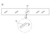
도 1은 종래의 기술에 따른 백라이트 장치의 주요 구성과 광 특성을 나타낸 도면이다. 도시된 바와 같이, 백라이트 장치는 도광판(11), 도광판(11)의 적어도 일 측부에 배치되는 광원(12), 도광판(11)의 하부에 배치되는 반사시트(13) 및 도광판(11)의 상부에 적층되는 광학시트(14)를 포함한다.1 is a diagram showing the main configuration and optical characteristics of a backlight device according to the prior art. As shown, the backlight device includes a
상기와 같은 구성의 백라이트 장치는, 광원(12)으로부터 도광판(11) 내부로 입사된 빛이 도광판(11) 상면과 하면에서 전반사되어 진행되고, 이러한 전반사를 반복하는 과정에서 면광원으로 전환되어 상면의 출광면으로 출사된다. 이때, 도광판(11)은 전반사되는 빛을 상면으로 출사시키기 위해 하면에 확산 특성을 갖는 반사패턴(11')이 인쇄될 수 있다.In the backlight device configured as above, the light incident from the
한편, 도광판(11) 내부로 입사되는 빛은 직진성으로 인하여 수평 방향에 대하여 대략 ±5°의 지향각 범위 내에서 최대 광속(Max Intensity)으로 분포되어 진행한다. 도광판(11)의 중심 영역에서 수평에 가까운 좁은 지향각으로 진행하는 빛(즉, 직광(直光), L)은 상면과 하면에서 전반사되지 못하고 반입광면으로 그대로 진행하고, 결국 반입광면을 통하여 외부로 누설된다.Meanwhile, the light incident on the inside of the
따라서, 측면형 백라이트 장치는 광 효율을 향상시키기 위하여 도광판의 반입광부로 누설되는 빛을 차단할 필요가 있으며, 그 방안으로 한국공개특허 10-2004-0061959호(선행특허 1)에는 패턴이 내장된 구조의 도광판을 소개하고 있다.Therefore, in order to improve light efficiency, the side-type backlight device needs to block light leaking into the light entering part of the light guide plate. As a solution, Korean Patent Publication No. 10-2004-0061959 (Prior Patent No. 1) discloses a structure with an embedded pattern. Introducing the light guide plate.
상기 선행특허 1의 도광판은 이중 사출을 통해 굴곡을 갖는 곡면의 경계부에 패턴을 형성하여 LGP에 내장된 패턴을 형성한 구조로, 반입광부로 누설되는 손실광을 감소시켜 휘도를 개선하는 구조이다. 그러나 선행특허 1은 이중 사출로 형성한 내부 패턴부와 기본 도광판부의 굴절율 차이를 활용한 굴절 패턴으로, 굴절을 적용하여 광경로를 변경하는 특성상 LGP 광출사에 대한 집광 및 광학시트 감소에 한계를 갖는 단점이 있다.The light guide plate of the prior patent 1 has a structure in which a pattern is formed at the boundary of a curved surface with a curved surface through double injection to form a pattern embedded in the LGP, and is a structure that improves luminance by reducing lost light leaking into the light receiving part. However, prior patent 1 is a refraction pattern that utilizes the difference in refractive index between the internal pattern part formed by double injection and the basic light guide plate part, and due to the nature of changing the optical path by applying refraction, it has limitations in concentrating light and reducing the optical sheet for LGP light emission. There is a downside.
또한, 미국등록특허 US 11,221,486호(선행특허 2)는 핀홀 미러 어레이를 갖는 AR 헤더셋을 소개하고 있다.Additionally, US Patent No. US 11,221,486 (Prior Patent 2) introduces an AR header set with a pinhole mirror array.
상기 선행특허 2는 컴바이너(LGP)의 두 면 사이에 복수의 기울어진 핀 미러(반사체)를 가변 간격으로 형성한 구조로서, 영상소자(광원)에서 입사된 광(영상)을 각 위치에 형성된 핀 미러를 통하여 아이박스(가상 스크린)로 유도 반사시켜 피사계심도(DOF : Depth of Field, 흐린 영상이 발생되지 않는 피사체의 범위) 및 영상의 밝기를 개선한 증강현실용 컴바이너 구조이다.The prior patent 2 is a structure in which a plurality of inclined pin mirrors (reflectors) are formed at variable intervals between the two sides of the combiner (LGP), and the light (image) incident from the imaging element (light source) is transmitted to each position. It is a combiner structure for augmented reality that improves the depth of field (DOF: the range of subjects that do not produce blurry images) and the brightness of the image by inducing reflection to the eyebox (virtual screen) through the formed pin mirror.
따라서 선행특허 2는 순차적 광선추적 원리를 이용하는 증강현실용 컴바이너의 특성상 각 핀 미러에 반사되는 영상은 시각적 요소를 고려해 위치별로 다른 영상이 아이박스로 포커싱(집광)되며, 핀 미러의 외적인 부분은 전방의 영상(주변광)이 투과되는 원리로 균일한 영상 구현에 한계가 있고, 효율을 개선하거나 선명한 영상을 위해서 별도의 집광 렌즈를 필요로 하는 단점이 있다.Therefore, in Prior Patent No. 2, due to the nature of the combiner for augmented reality that uses the principle of sequential ray tracing, the images reflected in each pin mirror are focused (concentrated) on the eye box for each position, taking visual factors into account, and the external part of the pin mirror is Due to the principle that the front image (ambient light) is transmitted, there are limitations in realizing a uniform image, and it has the disadvantage of requiring a separate condensing lens to improve efficiency or produce clear images.
본 발명은 상기와 같은 문제를 해결하고자 제안된 것으로, 도광판 내부로 좁은 지향각으로 입사되는 빛의 진행 방향을 변경시켜 입사되는 빛의 누설을 방지하고, 면광원으로의 광 전환 효율을 향상시킬 수 있는 도광판과 그 제조방법을 제공하는 것을 과제로 한다.The present invention was proposed to solve the above problems. By changing the direction of light incident at a narrow beam angle into the light guide plate, leakage of incident light can be prevented and light conversion efficiency to a surface light source can be improved. The task is to provide a light guide plate and its manufacturing method.
또한, 본 발명은 도광판 내부로 입사되는 빛을 정반사 또는 산란반사시켜 상면의 수직 방향으로 출사되도록 유도함으로써, 휘도를 향상시킬 수 있는 도광판과 그 제조방법을 제공하는 것을 과제로 한다.In addition, the present invention aims to provide a light guide plate and a manufacturing method thereof that can improve luminance by causing regular or scattered reflection of light incident inside the light guide plate and guiding it to be emitted in the vertical direction of the upper surface.
또한, 본 발명은 도광판의 입광부 영역에서부터 반입광부 영역까지 균일한 빛이 출사되도록 하여 휘도의 균일도를 향상시킬 수 있는 도광판과 그 제조방법을 제공하는 것을 과제로 한다.In addition, the present invention aims to provide a light guide plate and a manufacturing method thereof that can improve luminance uniformity by allowing uniform light to be emitted from the light entering area to the entering light area of the light guide plate.
상기와 같은 과제를 해결하기 위한 본 실시예는 일 측부에 광원이 배치되어 상기 광원으로부터 입사되는 빛을 면광원으로 전환하여 상면으로 출사하는 도광판에 있어서, 굴절율이 동일한 소재로서 하부의 제 1 광학 소자와 상부의 제 2 광학 소자가 광 투명 접착제에 의하여 접합되어 이루어지되, 상기 제 1 광학 소자와 상기 제 2 광학 소자가 접합되는 접합면에는 입광부에서 반입광부로 진행하는 빛을 상면으로 반사시키는 다수의 미세 반사체가 분포되는 것을 특징으로 한다.In order to solve the above problems, this embodiment is a light guide plate in which a light source is disposed on one side, converts the light incident from the light source into a surface light source and emits it to the upper surface, and the first optical element at the bottom is made of a material with the same refractive index. and the upper second optical element are joined by an optically transparent adhesive, and the bonding surface where the first optical element and the second optical element are joined has a plurality of elements that reflect light traveling from the light incident part to the light incident part to the upper surface. It is characterized by distribution of fine reflectors.
또한, 상기 미세 반사체는, 정반사 또는 산란반사 특성을 갖는다.Additionally, the micro-reflector has regular reflection or diffuse reflection characteristics.
또한, 상기 미세 반사체는, Ag, Al, Cr, Ni, TiO2, ZnO, Si, SiO2 또는 Al2O3 중 어느 하나 이상의 물질을 포함하는 소재로 구성될 수 있다.Additionally, the micro-reflector may be made of a material containing one or more of Ag, Al, Cr, Ni, TiO2 , ZnO, Si, SiO2 or Al2 O3 .
또한, 상기 미세 반사체는, 입광부에서 반입광부로 갈수록 높은 밀도로 형성될 수 있다.Additionally, the fine reflector may be formed at a higher density as it moves from the light entering part to the light entering part.
또한, 상기 미세 반사체는, 수평면에 대하여 30° 내지 45°의 경사각(θ)을 갖도록 배치될 수 있다(30°≤θ≤45°).Additionally, the micro-reflector may be arranged to have an inclination angle (θ) of 30° to 45° with respect to the horizontal plane (30°≤θ≤45°).
또한, 다수의 상기 미세 반사체는, 입광부에서 반입광부를 향하여 전체적으로 상향 경사를 이루는 선상에 배치될 수 있다.Additionally, the plurality of micro-reflectors may be disposed on a line that is generally inclined upwardly from the light entering portion to the receiving light portion.
또한, 다수의 상기 미세 반사체는, 상기 도광판의 상하 방향으로 랜덤한 위치에 배치되되, 상기 도광판의 두께(T)에 대하여 상측 방향으로 0.3T 내지 0.8T 범위(B)의 위치에 배치될 수 있다(0.3T≤B≤0.8T).In addition, the plurality of micro-reflectors may be arranged at random positions in the vertical direction of the light guide plate, and may be arranged in a position in the range (B) of 0.3T to 0.8T in the upward direction with respect to the thickness (T) of the light guide plate. (0.3T≤B≤0.8T).
또한, 상기 미세 반사체는, 원 형상, 타원 형상 또는 사각 형상을 이룰 수 있다.Additionally, the micro-reflector may have a circular shape, an oval shape, or a square shape.
또한, 원 형상의 상기 미세 반사체는 20㎛ 내지 200㎛ 길이의 직경(D)을 갖고(20㎛≤D≤200㎛), 타원 형상의 상기 미세 반사체는 50㎛ 내지 250㎛ 길이의 좌우 방향 장축(EH)과 20㎛ 내지 150㎛ 길이의 상하 방향 단축(EV)을 가지며(50㎛≤EH≤250㎛, 20㎛≤EV≤150㎛), 사각 형상의 상기 미세 반사체는 50㎛ 내지 250㎛ 길이의 좌우 방향 장변(RH)과 20㎛ 내지 150㎛ 길이의 상하 방향 단변(RV)을 가질 수 있다(50㎛≤RH≤250㎛, 20㎛≤RV≤150㎛).In addition, the circular micro-reflector has a diameter (D) of 20 μm to 200 μm in length (20 μm ≤ D ≤ 200 μm), and the oval-shaped micro reflector has a left-right major axis of 50 μm to 250 μm in length (20 μm ≤ D ≤ 200 μm). EH ) and a vertical minor axis (EV ) of 20 μm to 150 μm in length (50 μm ≤E H ≤ 250 μm, 20 μm ≤E V ≤ 150 μm), and the square-shaped microreflector has a length of 50 μm to 150 μm. It may have a left-right long side (RH ) of 250 μm in length and a vertical short side (RV ) of 20 μm to 150 μm in length (50 μm ≤R H ≤ 250 μm, 20 μm ≤R V ≤ 150 μm).
또한, 상기 도광판은, 상면으로 출사되는 빛을 집광하는 집광 패턴이 상면에 형성될 수 있다.Additionally, the light guide plate may have a light-concentrating pattern formed on the upper surface of the light guide plate to collect light emitted from the upper surface.
또한, 상기 집광 패턴은, 빛이 진행하는 방향과 나란한 방향의 길이를 갖는 프리즘 형상 또는 렌티큘러 형상의 패턴으로 구성될 수 있다.Additionally, the light collection pattern may be composed of a prism-shaped or lenticular-shaped pattern with a length parallel to the direction in which light travels.
그리고 상기와 같은 과제를 해결하기 위한 본 실시예는, 내부에 미세 반사체를 구비하는 도광판을 제조하는 방법에 있어서, (a) 제 1 광학 소자 상면에 일 측 경사면과 이에 마주하는 타 측 경사면을 갖는 다수의 기울기 패턴을 형성하는 단계, (b) 상기 기울기 패턴의 일 측 경사면에 미세 반사체를 형성하는 단계, 및, (c) 광 투명 접착제를 이용하여 상기 미세 반사체가 내부에 분포하도록 상기 제 1 광학 소자 상면에 제 2 광학 소자를 접합하는 단계를 포함한다.And the present embodiment for solving the above problems is a method of manufacturing a light guide plate having a fine reflector therein, (a) having an inclined surface on one side and an inclined surface on the other side facing the upper surface of the first optical element. forming a plurality of tilt patterns, (b) forming a micro-reflector on an inclined surface on one side of the tilt pattern, and (c) using an optically transparent adhesive to distribute the micro-reflectors inside the first optics. and bonding a second optical element to the upper surface of the element.
또한, 상기 (a) 단계는, 수평 방향에 대하여 일 측 경사면이 30° 내지 45°의 경사각(θ)을 갖고, 타 측 경사면이 80° 내지 90°의 경사각(α)을 갖도록 상기 기울기 패턴을 형성할 수 있다(30°≤θ≤45°, 80°≤α≤90°).In addition, in step (a), the tilt pattern is formed so that one side inclined surface has an inclination angle (θ) of 30° to 45° with respect to the horizontal direction, and the other side inclined surface has an inclination angle (α) of 80° to 90°. It can be formed (30°≤θ≤45°, 80°≤α≤90°).
또한, 상기 (b) 단계는, 상기 미세 반사체에 미러 가공을 적용하거나 비드 가공을 적용할 수 있다.Additionally, in step (b), mirror processing or bead processing may be applied to the fine reflector.
또한, 상기 제 1 광학 소자, 상기 제 2 광학 소자 및 상기 광 투명 접착제는 동일한 굴절율을 갖는 소재를 이용할 수 있다.Additionally, the first optical element, the second optical element, and the optically transparent adhesive may use materials having the same refractive index.
본 발명은 입광면에 수직한 방향으로 입사되는 직광 성분의 빛을 상측으로 반사시킴으로써, 수직광의 손실을 방지하고 광 효율을 향상시킬 수 있다.The present invention can prevent loss of vertical light and improve light efficiency by reflecting the light of the direct light component incident in the direction perpendicular to the light incident surface upward.
또한, 본 발명은 다수의 미세 반사체를 입광부에서 반입광부를 향하여 밀도를 다르게 배치함으로써, 상면으로 출광되는 빛의 휘도를 향상시킴과 동시에 균일도를 향상시킬 수 있다.In addition, the present invention can improve the luminance of light emitted from the upper surface and improve uniformity at the same time by arranging a plurality of fine reflectors at different densities from the light entering part to the receiving light part.
또한, 본 발명은 다수의 미세 반사체가 개별적으로 일정 기울기를 갖도록 배치하여, 광 출사각을 최적화할 수 있다.In addition, the present invention can optimize the light exit angle by arranging a plurality of micro-reflectors to have a constant inclination.
또한, 본 발명은 미세 반사체를 이용한 빛의 집광으로 프리즘 시트를 제거하여 광학시트 수를 줄이는 효과가 있다.In addition, the present invention has the effect of reducing the number of optical sheets by removing the prism sheet by concentrating light using a fine reflector.
도 1은 종래의 기술에 따른 백라이트 장치의 주요 구성과 광 특성을 나타낸 도면,
도 2는 본 실시예 따른 백라이트 장치의 주요 구성을 나타낸 도면,
도 3은 본 실시예 따른 도광판을 나타낸 사시도,
도 4는 도 3의 도광판을 나타낸 단면도,
도 5는 본 실시예에 따른 미세 반사체의 예를 나타낸 도면,
도 6은 본 실시예 따른 도광판의 미세 반사체의 배치 구조를 나타낸 도면,
도 7은 본 실시예에 따른 도광판의 변형 예를 나타낸 도면,
도 8은 본 실시예에 따른 도광판의 제조 과정을 나타낸 공정도.1 is a diagram showing the main configuration and optical characteristics of a backlight device according to the prior art;
2 is a diagram showing the main configuration of a backlight device according to this embodiment;
Figure 3 is a perspective view showing a light guide plate according to this embodiment;
Figure 4 is a cross-sectional view showing the light guide plate of Figure 3;
5 is a diagram showing an example of a fine reflector according to this embodiment;
Figure 6 is a diagram showing the arrangement structure of the micro-reflector of the light guide plate according to this embodiment;
7 is a diagram showing a modified example of the light guide plate according to this embodiment;
Figure 8 is a process chart showing the manufacturing process of the light guide plate according to this embodiment.
본 발명과 본 발명의 실시에 의해 달성되는 기술적 과제는 다음에서 설명하는 바람직한 실시예들에 의해 명확해질 것이다. 이하 첨부된 도면을 참조하여 본 발명의 바람직한 실시예를 상세히 살펴보기로 한다.The technical problems achieved by the present invention and its implementation will become clear by the preferred embodiments described below. Hereinafter, preferred embodiments of the present invention will be examined in detail with reference to the attached drawings.
후술되는, 본 실시예의 차이는 상호 배타적이지 않은 사항으로 이해되어야 한다. 즉, 본 발명의 기술 사상 및 범위를 벗어나지 않으면서, 기재되어 있는 특정 형상, 구조 및 특성은, 일 실시예에 관련하여 다른 실시예로 구현될 수 있으며, 각각의 개시된 실시예 내의 개별 구성요소의 위치 또는 배치는 변경될 수 있음이 이해되어야 하며, 도면에서 유사한 참조부호는 여러 측면에 걸쳐서 동일하거나 유사한 기능을 지칭하며, 길이, 면적 및 두께 등과 그 형태는 편의를 위하여 과장되어 표현될 수도 있다. 본 실시예의 설명에 있어서, 상, 하, 좌, 우, 전면, 배면 등과 같은 표현은 서로 상대적인 위치나 방향 등을 나타내는 것으로 그 기술적 의의가 사전적 의미에 구속되지는 않는다.It should be understood that the differences in this embodiment, described later, are not mutually exclusive. That is, without departing from the spirit and scope of the present invention, the specific shapes, structures, and characteristics described may be implemented in other embodiments with respect to one embodiment, and may be implemented in other embodiments of the individual components within each disclosed embodiment. It should be understood that the position or arrangement may be changed, and similar reference numbers in the drawings refer to the same or similar functions across various aspects, and the length, area, thickness, etc. may be exaggerated for convenience. In the description of this embodiment, expressions such as top, bottom, left, right, front, back, etc. indicate relative positions or directions, and their technical meaning is not limited by dictionary meaning.
도 2는 본 실시예 따른 백라이트 장치의 주요 구성을 나타낸 도면이다.Figure 2 is a diagram showing the main configuration of a backlight device according to this embodiment.
도시된 바와 같이, 본 실시예의 백라이트 장치는, 도광판(100), 도광판(100)의 적어도 일 측부에 배치되는 광원(200), 도광판(100)의 하부에 배치되는 반사부재(300) 및 도광판(100)의 상부에 적층되는 광학시트(400)를 포함한다. 상기 구성들은 커버버텀(미도시)에 안착되고, 커버버텀에 체결되는 가이드 패널(미도시)에 고정되면서 백라이트 장치를 구성한다. 또한, 가이드 패널 상부에는 표시패널(미도시)이 결합되어 백라이트 장치로부터 제공되는 면광원에 의하여 고화질의 영상을 제공하는 디스플레이 장치를 구현한다.As shown, the backlight device of this embodiment includes a
도광판(100)은, 광원(200)으로부터 입사되는 점광원의 빛을 면광원으로 전환하여 표시패널로 진행하도록 가이드 한다. 도광판(100)의 측면에서 입사되는 다수의 점광원의 빛은 도광판(100) 내부를 진행하면서 상하면에서 전반사를 반복하고, 이 과정에서 도광판(100) 전체 영역에 분포되면서 면광원의 빛이 상면으로 출사된다. 도광판(100)은 소정의 두께를 갖는 플레이트로 구성될 수 있다.The
또한, 도광판(100)은 소정의 굴절율을 갖는 투명 아크릴 계열의 수지로 구성되며, 일 예로 PMMA(Polymethylmethacrylate), PS(Poly styrene), MS(Meta styrene) 또는 PC(Polycarbonate) 등의 수지로 구성될 수 있다. 도광판(100)을 구성하는 수지 내부에는 미세 반사체(110)가 분포된다.In addition, the
미세 반사체(110)는 도광판(100) 내부로 입사되는 빛을 상면의 수직 방향으로 정반사 또는 산란반사시켜 휘도를 향상시킨다. 또한, 미세 반사체(110)는 입광면에 수직하는 방향으로 입사되는 직광 성분의 빛을 상측으로 반사하여 수직광의 누설을 차단함으로써, 광 효율과 휘도를 향상시킨다. 미세 반사체(110)는 Ag, Al, Cr, Ni, TiO2, ZnO, Si, SiO2 또는 Al2O3 중 어느 하나 이상의 물질을 포함하는 소재로 구성될 수 있다. 미세 반사체(110)를 포함하는 도광판(100)의 상세한 구성에 대해서는 후술한다.The micro-reflector 110 improves luminance by regularly reflecting or scattering the light incident on the
광원(200)은 도광판(100) 내부로 빛을 입사시키는 구성으로, 일반적으로 백색 발광의 LED 칩으로 구성되며, 필요에 따라 청색 발광 칩 등 다양한 종류의 LED로 구성될 수 있다. 광원(200)은 기판 상에 다수의 LED 칩이 실장되는 LED 모듈로 구성될 수 있으며, 도광판의(100) 입광면을 따라 LED 칩들이 배치된다.The
반사부재(300)는 도광판(100) 하부에 배치되어, 도광판(100) 배면으로 누설되는 빛을 다시 도광판(100)으로 반사시켜 백라이트 장치의 휘도 저하를 방지한다. 반사부재(300)는 광 반사율이 우수한 시트 또는 필름으로 구성되거나, 커버버텀의 바닥면에 광 반사 물질이 코팅되어 형성될 수 있다.The
광학시트(400)는 도광판(100)에서 출사되는 빛의 휘도와 균일도를 제어하는 구성으로, 확산시트와 같은 기능성 시트를 포함한다. 또한, 광학시트(400)는 광원(200)이 청색 발광 칩으로 구성되는 경우 청색 광을 백색 광으로 변환하는 파장변환시트를 더 포함할 수 있고, 필요에 따라 빛의 출사각을 제어하는 프리즘 시트를 더 포함할 수 있다.The
도 3 및 도 4는 본 실시예 따른 도광판을 나타낸 사시도와 단면도이고, 도 5는 본 실시예에 따른 미세 반사체의 예를 나타낸 도면이며, 도 6은 본 실시예 따른 도광판의 미세 반사체의 배치 구조를 나타낸 도면이며, 도 7은 본 실시예에 따른 도광판의 변형 예를 나타낸 도면이다.Figures 3 and 4 are a perspective view and a cross-sectional view showing the light guide plate according to this embodiment, Figure 5 is a view showing an example of a micro reflector according to this embodiment, and Figure 6 shows the arrangement structure of the micro reflector of the light guide plate according to this embodiment. 7 is a diagram showing a modified example of the light guide plate according to this embodiment.
먼저, 도 3 및 도 4를 참조하면, 본 실시예의 도광판(100)은 투명 수지 내부에 임의의 각도로 기울어진 미세 반사체(110)가 빛의 진행 방향을 따라 배치된다. 미세 반사체(110)는 Ag, Al, Cr, Ni, TiO2, ZnO, Si, SiO2 또는 Al2O3 중 어느 하나 이상을 포함하는 물질로 구성된다. 이때, 미세 반사체(110)는 정반사 특성을 갖는 반사체로 구성되거나, 산란반사 특성을 갖는 반사체로 구성될 수 있으며, 정반사 특성을 갖는 반사체와 산란반사 특성을 갖는 반사체가 혼합되어 구성될 수도 있다. 따라서 미세 반사체(110)는 입광부에서 반입광부로 진행하는 빛을 도광판 내부에서 정반사시키거나 산란반사시킨다. 여기서, 입광부는 광원이 배치되는 도광판(100)의 일 측을 말하고, 반입광부는 그 반대 측을 말한다.First, referring to FIGS. 3 and 4, in the
미세 반사체(110)는 도 4에 도시된 바와 같이, 직광 성분의 빛을 반사하기 위하여 입사되는 빛의 진행방향 중심축을 따르는 동일 선 상에서 나란하게 배치될 수 있다.As shown in FIG. 4, the
미세 반사체(110)는 도 5에 도시된 바와 같이, 원 형상을 이루거나, 일 측이 장축을 갖는 타원 형상을 이루거나, 사각 형상을 이룰 수 있다. (a)와 같이 원 형상의 미세 반사체(110)는 20㎛ 내지 200㎛ 의 직경(D)을 가질 수 있다(20㎛≤D≤200㎛). 또한, (b)와 같이 타원 형상의 미세 반사체(110)는 도광판(100)의 좌우 방향이 장축(EH)을 형성하고 상하 방향이 단축(EV)을 형성하며, 장축(EH)은 50㎛ 내지 250㎛의 길이를 갖고(50㎛≤EH≤250㎛), 단축(EV)은 20㎛ 내지 150㎛의 길이를 가질 수 있다(20㎛≤EV≤150㎛). 또한, (c)와 같이 사각 형상의 미세 반사체(110)는 도광판(100)의 좌우 방향이 장변(RH)을 형성하고 상하 방향이 단변(RV)을 형성하며, 장변(RH)은 50㎛ 내지 250㎛의 길이를 갖고(50㎛≤RH≤250㎛), 단변(RV)은 20㎛ 내지 150㎛의 길이를 가질 수 있다(20㎛≤RV≤150㎛). 미세 반사체(110)의 크기(직경, 장단축 또는 장단변의 길이)가 상기 범위를 벗어나는 경우 반사율이 줄어들어 휘도를 향상시키고 균일화시키는 효과가 저하되거나, 반사율이 지나치게 높아져 빛이 반입광부 영역으로 진행하는 것을 방해할 수 있다.As shown in FIG. 5, the micro-reflector 110 may have a circular shape, an oval shape with a long axis on one side, or a square shape. As shown in (a), the
이러한 미세 반사체(110)는 도 3에 도시된 바와 같이, 도광판(100)의 전체 영역에 대하여 서로 다른 밀도(또는 크기)로 형성된다. 일 예로, 입광부 영역에는 상대적으로 낮은 밀도(또는 크기)로 형성되고, 반입광부 영역으로 갈수록 높은 밀도(또는 크기)로 형성된다. 따라서, 이러한 미세 반사체(110)에 분포에 의하여 도광판(100)은 전체 영역에서 균일한 휘도의 빛으로 출사된다.As shown in FIG. 3, these
또한, 미세 반사체(110)는 도 4에 도시된 바와 같이, 빛이 상면으로 반사될 수 있도록 빛이 진행하는 방향으로 소정의 경사각(θ)을 갖도록 배치되며, 일 예로, 수평면에 대하여 30° 내지 45°의 경사각을 갖도록 배치된다(30°≤θ≤45°). 미세 반사체(110)가 상기 범위의 경사각으로 배치될 때, 정반사 또는 산란반사 되는 빛이 수직 상측으로 집중될 수 있다.In addition, as shown in FIG. 4, the
또한, 다수의 미세 반사체(110)는 도광판(100)의 상하 방향에 대하여 서로 다른 위치에 배치될 수 있다.Additionally, the plurality of
일 예로, 도 6의 (a)에 도시된 바와 같이, 다수의 미세 반사체(110)는 빛이 진행하는 방향에 대하여 전체적으로 상향 경사를 이루는 선상(A)에 위치하도록 배치될 수 있다. 즉, 입광부에서 반입광부를 향하여 위치가 순차적으로 높아지도록 배치될 수 있다.For example, as shown in (a) of FIG. 6, a plurality of
다른 예로, 도 6의 (b)에 도시된 바와 같이, 다수의 미세 반사체(110)는 상하 방향으로 랜덤한 위치에 배치될 수 있다. 이때, 미세 반사체(110)가 위치하는 도광판(100)의 상하 방향 폭은 일정한 범위(B)로 제한된다. 이는 빛의 분포도를 고려하여 반사율을 향상시키고 결국 휘도를 향상시킬 수 있도록 한다. 따라서 미세 반사체(110)의 중심을 기준으로 하는 다수의 미세 반사체(110)의 배치범위(B)는 도광판(100)의 두께(T)의 상측 방향에 대하여 0.3T 내지 0.8T 범위의 위치에 배치된다(0.3T≤B≤0.8T).As another example, as shown in (b) of FIG. 6, a plurality of
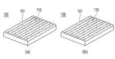
한편, 본 실시예의 도광판(100)은 상면에 출사되는 광을 집광시키는 집광 패턴(101)이 더 형성된다. 도 7을 참조하면, 집광 패턴(101)은 빛이 진행하는 방향과 나란한 방향의 길이를 갖도록 형성되며, (a)와 같이 프리즘 패턴으로 구성되거나 (b)와 같이 렌티큘러 패턴으로 구성될 수 있다. 프리즘 패턴 또는 렌티큘러 패턴은 입광면의 좌우측 방향을 따라 연속적으로 형성될 수 있다. 집광 패턴(101)은 빛이 진행하는 방향과 수직하는 방향으로 출사되는 빛을 집광하여 휘도를 추가로 상승시킨다.Meanwhile, the
도 8은 본 실시예에 따른 도광판의 제조 과정을 나타낸 공정도이다.Figure 8 is a process diagram showing the manufacturing process of the light guide plate according to this embodiment.
본 실시예의 미세 반사체를 포함하는 도광판(100)은 하측의 제 1 광학 소자(120)에 미세 반사체(110)를 형성하고, 상측의 제 2 광학 소자(130)를 제 1 광학 소자(120)에 접합하는 과정으로 이루어진다.The
구체적으로 살펴보면, 먼저, (a)와 같이 표면에 기울기 패턴(121)이 형성된 제 1 광학 소자(120)를 준비한다. 기울기 패턴(121)은 미세 반사체(110)의 분포되는 위치를 고려하여 그 형상이나 구조가 미리 설계된다.Looking specifically, first, a first
기울기 패턴(121)은 제 1 광학 소자(120) 원판에 식각 등의 공정을 이용하여 형성할 수 있으며, 사출 공정으로 제 1 광학 소자(120)를 제조하는 과정에서 동시에 형성할 수 있다. 또한, 기울기 패턴(121)은 필름 형태의 제 1 광학 소자(120) 상면에 투명 수지를 인쇄하여 형성할 수 있다. 이때, 제 1 광학 소자(120)를 구성하는 필름과 투명 수지는 경계면에서 빛이 굴절되지 않도록 동일한 굴절율을 갖는 소재로 구성되어야 한다.The
또한, 기울기 패턴(121)은 미세 반사체(110)가 형성되는 일 측 경사면(121-1)의 경사각(θ)은 30° 내지 45°의 기울기를 갖고(30°≤θ≤45°), 그 반대면인 타 측 경사면(121-2)의 경사각(α)은 수평 방향에 대하여 80° 내지 90°의 기울기를 갖도록 형성한다(80°≤α≤90°). 기울기 패턴(121)의 타 측 경사면(121-2)의 경사각(α)이 80°미만의 기울기를 갖는 경우 미세 반사체(110)를 코팅하는 과정에서 타 측 경사면(121-2)에도 미세 반사체(110)가 코팅될 우려가 있고, 90°를 초과하는 기울기를 갖는 경우 역 경사에 의하여 미세 반사체(110)가 코팅되어야 할 이웃하는 기울기 패턴(121)의 일 측 경사면(121-1)의 하부 영역에는 미세 반사체(110)가 코팅되지 않을 우려가 있다.In addition, the
기울기 패턴(121)을 갖는 제 1 광학 소자(120)를 준비한 후, (b)와 같이 마스크(140)를 이용하여 기울기 패턴(121)의 특정 위치에 미세 반사체(110)를 형성한다. 미세 반사체(110)는 스퍼터링, 스프레이 또는 인쇄 등의 공정을 이용하여 형성할 수 있고, 소재로는 Ag, Al, Cr, Ni, TiO2, ZnO, Si, SiO2 또는 Al2O3 중 어느 하나 이상의 물질을 포함한다. 이때, 미세 반사체(110)는 정반사 특성을 나타내기 위하여 미러(mirror) 처리가 적용되거나, 산란반사 특성을 나타내기 위하여 비드(bead) 처리가 적용될 수 있다.After preparing the first
그리고, (c)와 같이 미세 반사체(110)가 형성된 제 1 광학 소자(120) 표면에 제 2 광학 소자(130)를 접합한다. 이를 위하여 제 2 광학 소자(130)를 미리 준비하며, 제 2 광학 소자(130)에는 제 1 광학 소자(120)의 기울기 패턴(121)에 형합하는 오목한 형상의 대응 패턴(131)이 형성된다.Then, the second
또한, 제 1 광학 소자(120)와 제 2 광학 소자(130)의 접합면에서 빛이 굴절되지 않아야 하므로 제 1 광학 소자(120)와 제 2 광학 소자(130)는 동일할 굴절율을 갖는 소재 또는 동일한 소재로 구성된다.In addition, since light should not be refracted at the joint surface of the first
또한, 제 1 광학 소자(120)와 제 2 광학 소자(130)는 광 투명 접착제(OCA : Optically Clear Adhesive, 150)를 매개로 서로 접착되며, 광 투명 접착제(150)에 의해서도 빛이 굴절되지 않아야 하므로, 광 투명 접착제(150)도 제 1 광학 소자(120) 및 제 2 광학 소자(130)와 동일할 굴절율을 갖는 소재로 구성된다.In addition, the first
제 1 광학 소자(120)와 제 2 광학 소자(130)를 접착하는 과정을 통하여 (d)와 같이 내부에 미세 반사체(110)를 포함하는 도광판(100)이 완성된다.Through the process of adhering the first
[실험예][Experimental example]
본 실험은 실시예에 따라 미세 반사체를 포함하는 도광판에 대한 광 특성을 실험하였으며, 비교예는 종래의 기술에 따라 하면에 반사패턴이 형성되고 상면에 렌티큘러 패턴이 형성된 도광판을 기준으로 하였고, 실시예들은 내부에 정반사 또는 산란반사 특성을 갖는 미세 반사체를 구비하는 도광판들을 대상으로 하였다. 또한, 비교예는 광학시트로 한 장의 확산시트와 두 장의 프리즘 시트를 구비하였고, 실시예들에서는 광학시트로 한 장의 확산시트만 구비하였으며, 그 결과를 표 1에 나타내었다.This experiment tested the optical characteristics of a light guide plate including a fine reflector according to an example, and the comparative example was based on a light guide plate with a reflective pattern formed on the bottom and a lenticular pattern on the top according to the conventional technology. They were aimed at light guide plates that have micro-reflectors inside them that have regular reflection or diffuse reflection characteristics. In addition, the comparative examples included one diffusion sheet and two prism sheets as optical sheets, while the examples included only one diffusion sheet as optical sheets, and the results are shown in Table 1.
LGP
LGP
배광분포
Light distribution
반사체종류
Reflector type
-
-
(정반사)Ellipse
(specular reflection)
(정반사)Ellipse
(specular reflection)
(정반사)Ellipse
(specular reflection)
(산란
반사)Ellipse
(spawning
reflect)
(산란
반사)Ellipse
(spawning
reflect)
(산란
반사)Ellipse
(spawning
reflect)
광학시트
optical sheet
배광분포
Light distribution
시트구성
Sheet composition
Prism(94°)
DiffuserPrism (4°)
Prism(94°)
Diffuser
Diffuser
Diffuser
Diffuser
Diffuser
Diffuser
Diffuser
Diffuser
Diffuser
Diffuser
Diffuser
Diffuser
Diffuser
(Hor/Ver)FWHM
(Hor/Ver)
/45.3°47.9°
/45.3°
/79.4°93.3°
/79.4°
/80.7°100.5°
/80.7°
/89.1°99.8°
/89.1°
/91.9°97.9°
/91.9°
/90.4°98.7°
/90.4°
/88.2°99.9°
/88.2°
표 1에서 알 수 있는 바와 같이, 내부에 미세 반사체가 구비되는 경우 도광판에서 출사되는 빛의 피크 위치가 중앙으로 집중됨을 확인할 수 있으며, 광학시트를 통과한 빛은 상대적으로 우수한 균일도를 나타내면서 동시에 높은 휘도를 나타내고 있음을 알 수 있다. 특히, 본 실시예의 도광판은 프리즘 시트를 구비하지 않은 상태에서도 프리즘 시트를 구비한 종래의 도광판 보다 더 높은 휘도를 나타내고 있는 바, 본 실시예의 백라이트 장치는 프리즘 시트를 제거할 수 있는 효과도 있다.As can be seen in Table 1, when a fine reflector is provided inside, it can be seen that the peak position of the light emitted from the light guide plate is concentrated in the center, and the light passing through the optical sheet exhibits relatively excellent uniformity and at the same time has high luminance. It can be seen that it represents . In particular, the light guide plate of this embodiment exhibits higher luminance even without a prism sheet than a conventional light guide plate provided with a prism sheet, and the backlight device of this embodiment also has the effect of eliminating the prism sheet.
상기와 같은 광 특성을 볼 때, 미세 반사체는 빛을 집광하는 효과를 나타냄과 동시에 도광판의 전체 영역에서 균일하게 빛이 출사되도록 하는 효과를 나타내고 있는 것이다. 이는 미세 반사체가 도광판 내부로 입사된 빛을 정반사 또는 산란반사시켜 상면의 수직 방향으로 출사되도록 유도하기 때문이다.Considering the optical characteristics described above, the micro-reflector has the effect of concentrating light and at the same time has the effect of causing light to be emitted uniformly from the entire area of the light guide plate. This is because the micro-reflector regularly reflects or scatters the light incident on the inside of the light guide plate, causing it to be emitted in the vertical direction of the upper surface.
이상 설명한 바와 같이 본 발명의 예시적인 실시예가 도시되어 설명되었지만, 다양한 변형과 다른 실시예가 본 분야의 숙련된 기술자들에 의해 행해질 수 있을 것이다. 이러한 변형과 다른 실시예들은 첨부된 청구범위에 모두 고려되고 포함되어 본 발명의 진정한 취지 및 범위를 벗어나지 않는다 할 것이다.Although exemplary embodiments of the present invention have been shown and described as described above, various modifications and other embodiments will occur to those skilled in the art. These modifications and other embodiments are to be considered and included in the appended claims without departing from the true spirit and scope of the present invention.
100 : 도광판110 : 미세 반사체
120 : 제 1 광학 소자121 : 기울기 패턴
130 : 제 2 광학 소자131 : 대응 패턴
140 : 마스트150 : 광 투명 접착제
200 : 광원
300 : 반사부재
400 : 광학시트100: light guide plate 110: fine reflector
120: first optical element 121: tilt pattern
130: Second optical element 131: Corresponding pattern
140: Mast 150: Optical transparent adhesive
200: light source
300: Reflection member
400: Optical sheet
Claims (15)
Translated fromKorean굴절율이 동일한 소재로서, 하부의 제 1 광학 소자와 상부의 제 2 광학 소자가 광 투명 접착제에 의하여 접합되어 이루어지되,
상기 제 1 광학 소자와 상기 제 2 광학 소자가 접합되는 접합면에는 입광부에서 반입광부로 진행하는 빛을 상면으로 반사시키는 다수의 미세 반사체가 분포되는, 백라이트 장치용 도광판.In the light guide plate, which has a light source disposed on one side and converts light incident from the light source into a surface light source and emits it to the upper surface,
It is a material with the same refractive index, and is made by bonding the first optical element at the bottom and the second optical element at the top with an optically transparent adhesive,
A light guide plate for a backlight device, wherein a plurality of fine reflectors are distributed on a bonding surface where the first optical element and the second optical element are joined to reflect light traveling from the light incident part to the light incident part to the upper surface.
정반사 또는 산란반사 특성을 갖는, 백라이트 장치용 도광판.The method of claim 1, wherein the micro-reflector is:
A light guide plate for a backlight device having regular or diffuse reflection characteristics.
Ag, Al, Cr, Ni, TiO2, ZnO, Si, SiO2 또는 Al2O3 중 어느 하나 이상의 물질을 포함하는 소재로 구성되는, 백라이트 장치용 도광판.The method of claim 1, wherein the micro-reflector is:
A light guide plate for a backlight device, comprising a material containing one or more of Ag, Al, Cr, Ni, TiO2 , ZnO, Si, SiO2 or Al2 O3 .
입광부에서 반입광부로 갈수록 높은 밀도로 형성되는, 백라이트 장치용 도광판.The method of claim 1, wherein the micro-reflector is:
A light guide plate for a backlight device that is formed at higher densities from the light entering part to the receiving part.
수평면에 대하여 30° 내지 45°의 경사각(θ)을 갖도록 배치되는(30°≤θ≤45°), 백라이트 장치용 도광판.The method of claim 1, wherein the micro-reflector is:
A light guide plate for a backlight device arranged to have an inclination angle (θ) of 30° to 45° with respect to the horizontal plane (30°≤θ≤45°).
입광부에서 반입광부를 향하여 전체적으로 상향 경사를 이루는 선상에 배치되는, 백라이트 장치용 도광판.The method of claim 1, wherein the plurality of micro-reflectors,
A light guide plate for a backlight device that is disposed on an overall upward sloping line from the light entering part to the receiving light part.
상기 도광판의 상하 방향으로 랜덤한 위치에 배치되되, 상기 도광판의 두께(T)에 대하여 상측 방향으로 0.3T 내지 0.8T 범위(B)의 위치에 배치되는(0.3T≤B≤0.8T), 백라이트 장치용 도광판.The method of claim 1, wherein the plurality of micro-reflectors,
A backlight disposed at a random position in the vertical direction of the light guide plate, and at a position in the range (B) of 0.3T to 0.8T in the upward direction with respect to the thickness (T) of the light guide plate (0.3T≤B≤0.8T). Light guide plate for the device.
원 형상, 타원 형상 또는 사각 형상을 이루는, 백라이트 장치용 도광판.The method of claim 1, wherein the micro-reflector is:
A light guide plate for a backlight device that has a circular, oval, or square shape.
원 형상의 상기 미세 반사체는 20㎛ 내지 200㎛ 길이의 직경(D)을 갖고(20㎛≤D≤200㎛),
타원 형상의 상기 미세 반사체는 50㎛ 내지 250㎛ 길이의 좌우 방향 장축(EH)과 20㎛ 내지 150㎛ 길이의 상하 방향 단축(EV)을 가지며(50㎛≤EH≤250㎛, 20㎛≤EV≤150㎛),
사각 형상의 상기 미세 반사체는 50㎛ 내지 250㎛ 길이의 좌우 방향 장변(RH)과 20㎛ 내지 150㎛ 길이의 상하 방향 단변(RV)을 갖는(50㎛≤RH≤250㎛, 20㎛≤RV≤150㎛), 백라이트 장치용 도광판.According to claim 8,
The circular micro-reflector has a diameter (D) of 20㎛ to 200㎛ (20㎛≤D≤200㎛),
The oval-shaped micro-reflector has a long axis in the left and right directions (EH ) of 50 μm to 250 μm in length and a short axis in the vertical direction (EV ) of 20 μm to 150 μm in length (50 μm ≤E H ≤ 250 μm, 20 μm ≤EV ≤150㎛),
The square-shaped microreflector has a long side in the left and right directions (RH ) of 50 μm to 250 μm in length and a short side in the vertical direction (RV ) of 20 μm to 150 μm in length (50 μm ≤ RH ≤ 250 μm, 20 μm ≤RV ≤150㎛), light guide plate for backlight device.
상면으로 출사되는 빛을 집광하는 집광 패턴이 상면에 형성되는, 백라이트 장치용 도광판.The method of claim 1, wherein the light guide plate is:
A light guide plate for a backlight device in which a light-concentrating pattern is formed on the upper surface to converge light emitted from the upper surface.
빛이 진행하는 방향과 나란한 방향의 길이를 갖는 프리즘 형상 또는 렌티큘러 형상의 패턴으로 구성되는, 백라이트 장치용 도광판.The method of claim 10, wherein the light collection pattern is:
A light guide plate for a backlight device consisting of a prism-shaped or lenticular-shaped pattern with a length parallel to the direction in which light travels.
(a) 제 1 광학 소자 상면에 일 측 경사면과 이에 마주하는 타 측 경사면을 갖는 다수의 기울기 패턴을 형성하는 단계;
(b) 상기 기울기 패턴의 일 측 경사면에 미세 반사체를 형성하는 단계; 및,
(c) 광 투명 접착제를 이용하여 상기 미세 반사체가 내부에 분포하도록 상기 제 1 광학 소자 상면에 제 2 광학 소자를 접합하는 단계;를 포함하는, 내부 미세 반사체를 구비하는 백라이트 장치용 도광판 제조방법.In a method of manufacturing a light guide plate having a micro reflector therein,
(a) forming a plurality of inclined patterns having an inclined surface on one side and an inclined surface on the other side facing the inclined surface on the upper surface of the first optical element;
(b) forming a fine reflector on an inclined surface on one side of the inclined pattern; and,
(c) bonding a second optical element to the upper surface of the first optical element using an optically transparent adhesive so that the micro-reflectors are distributed inside. A method of manufacturing a light guide plate for a backlight device including an internal micro-reflector.
수평 방향에 대하여 일 측 경사면이 30° 내지 45°의 경사각(θ)을 갖고, 타 측 경사면이 80° 내지 90°의 경사각(α)을 갖도록 상기 기울기 패턴을 형성하는(30°≤θ≤45°, 80°≤α≤90°), 내부 미세 반사체를 구비하는 백라이트 장치용 도광판 제조방법.The method of claim 12, wherein step (a),
Forming the tilt pattern so that one inclined surface has an inclination angle (θ) of 30° to 45° with respect to the horizontal direction, and the other inclined surface has an inclination angle (α) of 80° to 90° (30°≤θ≤45 °, 80°≤α≤90°), method of manufacturing a light guide plate for a backlight device having an internal micro-reflector.
상기 미세 반사체에 미러 가공을 적용하거나 비드 가공을 적용하는, 내부 미세 반사체를 구비하는 백라이트 장치용 도광판 제조방법.The method of claim 12, wherein step (b),
A method of manufacturing a light guide plate for a backlight device having an internal micro-reflector, comprising applying mirror processing or bead processing to the micro-reflector.
상기 제 1 광학 소자, 상기 제 2 광학 소자 및 상기 광 투명 접착제는 동일한 굴절율을 갖는 소재를 이용하는, 내부 미세 반사체를 구비하는 백라이트 장치용 도광판 제조방법.
According to claim 12,
The first optical element, the second optical element, and the optically transparent adhesive use a material having the same refractive index.
Priority Applications (1)
| Application Number | Priority Date | Filing Date | Title |
|---|---|---|---|
| KR1020220121679AKR20240043195A (en) | 2022-09-26 | 2022-09-26 | Light guide plate for backlight unit including internal micro-reflector and manufacturing method thereof |
Applications Claiming Priority (1)
| Application Number | Priority Date | Filing Date | Title |
|---|---|---|---|
| KR1020220121679AKR20240043195A (en) | 2022-09-26 | 2022-09-26 | Light guide plate for backlight unit including internal micro-reflector and manufacturing method thereof |
Publications (1)
| Publication Number | Publication Date |
|---|---|
| KR20240043195Atrue KR20240043195A (en) | 2024-04-03 |
Family
ID=90662683
Family Applications (1)
| Application Number | Title | Priority Date | Filing Date |
|---|---|---|---|
| KR1020220121679APendingKR20240043195A (en) | 2022-09-26 | 2022-09-26 | Light guide plate for backlight unit including internal micro-reflector and manufacturing method thereof |
Country Status (1)
| Country | Link |
|---|---|
| KR (1) | KR20240043195A (en) |
Citations (2)
| Publication number | Priority date | Publication date | Assignee | Title |
|---|---|---|---|---|
| KR20040061959A (en) | 2002-12-31 | 2004-07-07 | 비오이 하이디스 테크놀로지 주식회사 | Liquid Crystal Display using by pattern inside structure of Light Guide Plate |
| US11221486B2 (en) | 2018-12-10 | 2022-01-11 | Auroratech Company | AR headsets with improved pinhole mirror arrays |
- 2022
- 2022-09-26KRKR1020220121679Apatent/KR20240043195A/enactivePending
Patent Citations (2)
| Publication number | Priority date | Publication date | Assignee | Title |
|---|---|---|---|---|
| KR20040061959A (en) | 2002-12-31 | 2004-07-07 | 비오이 하이디스 테크놀로지 주식회사 | Liquid Crystal Display using by pattern inside structure of Light Guide Plate |
| US11221486B2 (en) | 2018-12-10 | 2022-01-11 | Auroratech Company | AR headsets with improved pinhole mirror arrays |
Similar Documents
| Publication | Publication Date | Title |
|---|---|---|
| KR100468860B1 (en) | Light guide panel having light deflection member and edge light type backlight apparatus | |
| EP2284437B1 (en) | Transreflector and display with transreflector | |
| US7566148B2 (en) | Side light-emitting device, backlight unit having the side light-emitting device, and liquid crystal display apparatus employing the backlight unit | |
| CN100460949C (en) | Surface light source device, lighting unit and light beam control member | |
| JP4087864B2 (en) | Flat light emitting device | |
| JP5360172B2 (en) | Planar light source device and display device using the same | |
| CN100421000C (en) | Backlight unit and liquid crystal display using the backlight unit | |
| JP5409901B2 (en) | Planar light source device and display device using the same | |
| JP5295382B2 (en) | Planar light source device and display device using the same | |
| JP3955505B2 (en) | Light guide plate | |
| NL1030287C2 (en) | SIDE LIGHT SENDING DEVICE, REAR LIGHTING UNIT PROVIDED WITH THE SIDE LIGHT SENDING DEVICE AND LIQUID CRYSTAL DISPLAY DEVICE USING THE REAR LIGHTING UNIT. | |
| CN101349398A (en) | An integrated microstructure backlight system | |
| JP2006278251A (en) | Light guide plate and surface illumination device | |
| KR20190041049A (en) | Back light unit | |
| US20090303414A1 (en) | Optical member with a scatter layer, and backlight assembly and display device having the same | |
| KR20190021522A (en) | Light guide plate and backlight unit having the same | |
| JP2004179062A (en) | Illuminating device, photo conductive material and liquid crystal display | |
| TW200411271A (en) | Light guide plate and back light system with the same | |
| CN100363810C (en) | Backlight module | |
| JP5174685B2 (en) | Planar light source device and display device using the same | |
| JP2003187620A (en) | Planar luminous device and liquid crystal display device equipped with the same | |
| JP2011258362A (en) | Surface light source device | |
| KR20200123353A (en) | Light guide plate and backlight unit having the same | |
| KR20240043195A (en) | Light guide plate for backlight unit including internal micro-reflector and manufacturing method thereof | |
| JP2005135815A (en) | Surface light source device and display device using the surface light source device |
Legal Events
| Date | Code | Title | Description |
|---|---|---|---|
| PA0109 | Patent application | ||
| PG1501 | Laying open of application |