KR20240040510A - Memory device and method thereof for managing row hammer - Google Patents
Memory device and method thereof for managing row hammerDownload PDFInfo
- Publication number
- KR20240040510A KR20240040510AKR1020220119545AKR20220119545AKR20240040510AKR 20240040510 AKR20240040510 AKR 20240040510AKR 1020220119545 AKR1020220119545 AKR 1020220119545AKR 20220119545 AKR20220119545 AKR 20220119545AKR 20240040510 AKR20240040510 AKR 20240040510A
- Authority
- KR
- South Korea
- Prior art keywords
- row
- address
- input
- hammer
- register
- Prior art date
- Legal status (The legal status is an assumption and is not a legal conclusion. Google has not performed a legal analysis and makes no representation as to the accuracy of the status listed.)
- Pending
Links
Images


Classifications
- G—PHYSICS
- G11—INFORMATION STORAGE
- G11C—STATIC STORES
- G11C11/00—Digital stores characterised by the use of particular electric or magnetic storage elements; Storage elements therefor
- G11C11/21—Digital stores characterised by the use of particular electric or magnetic storage elements; Storage elements therefor using electric elements
- G11C11/34—Digital stores characterised by the use of particular electric or magnetic storage elements; Storage elements therefor using electric elements using semiconductor devices
- G11C11/40—Digital stores characterised by the use of particular electric or magnetic storage elements; Storage elements therefor using electric elements using semiconductor devices using transistors
- G11C11/401—Digital stores characterised by the use of particular electric or magnetic storage elements; Storage elements therefor using electric elements using semiconductor devices using transistors forming cells needing refreshing or charge regeneration, i.e. dynamic cells
- G11C11/406—Management or control of the refreshing or charge-regeneration cycles
- G11C11/40611—External triggering or timing of internal or partially internal refresh operations, e.g. auto-refresh or CAS-before-RAS triggered refresh
- G—PHYSICS
- G11—INFORMATION STORAGE
- G11C—STATIC STORES
- G11C11/00—Digital stores characterised by the use of particular electric or magnetic storage elements; Storage elements therefor
- G11C11/21—Digital stores characterised by the use of particular electric or magnetic storage elements; Storage elements therefor using electric elements
- G11C11/34—Digital stores characterised by the use of particular electric or magnetic storage elements; Storage elements therefor using electric elements using semiconductor devices
- G11C11/40—Digital stores characterised by the use of particular electric or magnetic storage elements; Storage elements therefor using electric elements using semiconductor devices using transistors
- G11C11/401—Digital stores characterised by the use of particular electric or magnetic storage elements; Storage elements therefor using electric elements using semiconductor devices using transistors forming cells needing refreshing or charge regeneration, i.e. dynamic cells
- G11C11/406—Management or control of the refreshing or charge-regeneration cycles
- G11C11/40603—Arbitration, priority and concurrent access to memory cells for read/write or refresh operations
- G—PHYSICS
- G11—INFORMATION STORAGE
- G11C—STATIC STORES
- G11C11/00—Digital stores characterised by the use of particular electric or magnetic storage elements; Storage elements therefor
- G11C11/21—Digital stores characterised by the use of particular electric or magnetic storage elements; Storage elements therefor using electric elements
- G11C11/34—Digital stores characterised by the use of particular electric or magnetic storage elements; Storage elements therefor using electric elements using semiconductor devices
- G11C11/40—Digital stores characterised by the use of particular electric or magnetic storage elements; Storage elements therefor using electric elements using semiconductor devices using transistors
- G11C11/401—Digital stores characterised by the use of particular electric or magnetic storage elements; Storage elements therefor using electric elements using semiconductor devices using transistors forming cells needing refreshing or charge regeneration, i.e. dynamic cells
- G11C11/406—Management or control of the refreshing or charge-regeneration cycles
- G11C11/40622—Partial refresh of memory arrays
- G—PHYSICS
- G11—INFORMATION STORAGE
- G11C—STATIC STORES
- G11C11/00—Digital stores characterised by the use of particular electric or magnetic storage elements; Storage elements therefor
- G11C11/21—Digital stores characterised by the use of particular electric or magnetic storage elements; Storage elements therefor using electric elements
- G11C11/34—Digital stores characterised by the use of particular electric or magnetic storage elements; Storage elements therefor using electric elements using semiconductor devices
- G11C11/40—Digital stores characterised by the use of particular electric or magnetic storage elements; Storage elements therefor using electric elements using semiconductor devices using transistors
- G11C11/401—Digital stores characterised by the use of particular electric or magnetic storage elements; Storage elements therefor using electric elements using semiconductor devices using transistors forming cells needing refreshing or charge regeneration, i.e. dynamic cells
- G11C11/4063—Auxiliary circuits, e.g. for addressing, decoding, driving, writing, sensing or timing
- G11C11/407—Auxiliary circuits, e.g. for addressing, decoding, driving, writing, sensing or timing for memory cells of the field-effect type
- G11C11/408—Address circuits
Landscapes
- Engineering & Computer Science (AREA)
- Microelectronics & Electronic Packaging (AREA)
- Computer Hardware Design (AREA)
- Dram (AREA)
Abstract
Description
Translated fromKorean본 개시의 기술적 사상은 전자 장치에 관한 것이며, 보다 구체적으로는, 로우 해머 어드레스를 관리하기 위한 메모리 장치 및 그의 동작 방법에 관한 것이다.The technical idea of the present disclosure relates to electronic devices, and more specifically, to a memory device for managing a row hammer address and a method of operating the same.
반도체 칩들을 사용하는 시스템은, 시스템의 동작 메모리 또는 메인 메모리로서 DRAM(Dynamic Random Access Memory)을 널리 사용한다. DRAM 용량 및 집적도를 증가시키기 위해 DRAM 셀 사이즈가 감소하고 있다. 어떤 DRAM 기반의 시스템은 과도한 작업량(heavy workload)으로 인해 때때로 간헐적인 고장(intermittent failure)을 경험한다. 이러한 고장은 싱글 메모리 셀 로우에 대한 반복적인 억세스, 일명 로우 해머로 추적(trace)된다. 특정 로우에 반복적인 억세스는 로우들 사이의 전자기적 커플링(electromagnetic coupling)으로 인해 인접한 로우들(예, 빅팀 로우들(victim rows))의 감쇠율 증가(increased rate of decay)를 유발할 수 있다. 또한, 빅팀 로우들에 연결된 메모리 셀들이 디스터브(disturb)를 받게 되어 메모리 셀 데이터의 비트값이 플립(flip)되는 데이터 변형(data corruption)이 유발될 수 있다.Systems using semiconductor chips widely use DRAM (Dynamic Random Access Memory) as the operating memory or main memory of the system. DRAM cell sizes are decreasing to increase DRAM capacity and integration. Some DRAM-based systems sometimes experience intermittent failures due to heavy workload. This failure is traced to repeated accesses to a single memory cell row, also known as row hammer. Repeated access to a particular row can cause an increased rate of decay in adjacent rows (e.g., victim rows) due to electromagnetic coupling between rows. Additionally, memory cells connected to big rows may be disturbed, causing data corruption in which bit values of memory cell data are flipped.
로우 해머를 제어하기 위하여, DRAM은 일정 시간 동안에 억세스 어드레스들 중에서 집중적으로 억세스되는 로우 해머 어드레스(들)를 모니터링할 수 있다. DRAM은 로우 해머 어드레스(들)을 한정된 레지스터(들)에 저장하고, 로우 해머 어드레스(들)에 상응하는 메모리 셀 로우(들)와 물리적으로 인접하는 메모리 셀 로우에 대해 리프레쉬 동작을 수행할 수 있다.In order to control the row hammer, the DRAM can monitor the row hammer address(es) that are accessed intensively among the access addresses for a certain period of time. DRAM stores the row hammer address(es) in limited register(s) and can perform a refresh operation on the memory cell row(s) corresponding to the row hammer address(es) and the memory cell rows physically adjacent to the memory cell row(s). .
일반적으로 DRAM은 로우 해머를 제어하기 위하여 한정된 레지스터(들)(또는 래치들)을 사용하는데, 로우 해머 어드레스(들)의 개수는 레지스터(들)의 수에 의해 결정될 수 있다. 그런데, 로우 해머의 유형은 매우 다양하므로, 로우 해머의 유형에 따라 로우 해머 어드레스의 개수가 증가되면, 이에 따른 일반적인 DRAM의 레지스터의 개수가 증가하게 되는데, 레지스터의 개수를 무한정 증가시키는 데에는 현실적인 한계가 있고, 레지스터의 개수가 증가하는 것은 DRAM 집적도에 악영향을 미친다.In general, DRAM uses a limited number of register(s) (or latches) to control the row hammer, and the number of row hammer address(es) can be determined by the number of register(s). However, since the types of row hammers are very diverse, if the number of row hammer addresses increases depending on the type of row hammer, the number of registers in a general DRAM increases accordingly, but there is a realistic limit to increasing the number of registers indefinitely. And, increasing the number of registers has a negative effect on DRAM density.
이에 따라, 레지스터의 개수를 증가시키지 않고도 다양한 유형의 로우 해머를 제어하는 메모리 장치 및 그의 동작 방법이 요구된다.Accordingly, a memory device and method of operating the same that control various types of row hammers without increasing the number of registers are required.
본 개시의 기술적 사상은, 레지스터의 개수를 줄이면서도 다양한 유형의 로우 해머를 관리하기 위한 메모리 장치 및 그의 동작 방법을 제공한다.The technical idea of the present disclosure provides a memory device and a method of operating the same for managing various types of row hammers while reducing the number of registers.
본 개시의 기술적 사상에 따른 메모리 장치는, 복수의 메모리 셀 로우들을 포함하는 메모리 셀 어레이; 복수의 메모리 셀 로우들에 대한 복수의 엑세스들을 모니터링하는 모니터링 기간 동안에 프리 로우 해머 어드레스와 복수의 엑세스들에 포함된 복수의 입력 로우 어드레스들 각각을 기초로 로우 해머 어드레스를 검출하도록 구성되고, 호스트로부터 제공된 리프레쉬 커맨드에 응답하여 로우 해머 어드레스를 출력하도록 구성된 로우 해머 관리 회로; 및 로우 해머 어드레스에 대응되는 메모리 셀 로우와 물리적으로 인접한 메모리 셀 로우에 대해 리프레쉬 동작을 수행하도록 구성된 리프레쉬 제어 회로를 포함한다.A memory device according to the technical idea of the present disclosure includes a memory cell array including a plurality of memory cell rows; Configured to detect a row hammer address based on a pre-row hammer address and a plurality of input row addresses included in the plurality of accesses during a monitoring period for monitoring a plurality of accesses to a plurality of memory cell rows, and configured to detect a row hammer address from the host a row hammer management circuit configured to output a row hammer address in response to a provided refresh command; and a refresh control circuit configured to perform a refresh operation on memory cell rows physically adjacent to the memory cell row corresponding to the row hammer address.
또한, 본 개시의 기술적 사상에 따른 메모리 장치의 동작 방법은, 호스트에 의한 복수의 엑세스들에 포함된 복수의 입력 로우 어드레스들 및 제1 레지스터에 저장된 프리 로우 해머 어드레스를 기초로, 복수의 입력 로우 어드레스들 중 프리 로우 해머 어드레스보다 큰 입력 로우 어드레스 또는 복수의 입력 로우 어드레스들 중 제1 최소 입력 로우 어드레스를, 로우 해머 어드레스로서 제2 레지스터에 저장하는 단계; 호스트로부터 제공된 리프레쉬 커맨드에 응답하여, 로우 해머 어드레스에 대응되는 메모리 셀 로우와 물리적으로 인접한 메모리 셀 로우에 대해 리프레쉬 동작을 수행하는 단계; 및 리프레쉬 커맨드에 응답하여, 로우 해머 로우 어드레스를 프리 로우 해머 어드레스로서 제1 레지스터에 저장하는 단계를 포함한다.In addition, a method of operating a memory device according to the technical idea of the present disclosure includes operating a plurality of input rows based on a plurality of input row addresses included in a plurality of accesses by the host and a pre-row hammer address stored in the first register. storing an input row address greater than a pre-row hammer address among addresses or a first minimum input row address among a plurality of input row addresses as a row hammer address in a second register; In response to a refresh command provided from the host, performing a refresh operation on a memory cell row physically adjacent to the memory cell row corresponding to the row hammer address; and in response to the refresh command, storing the row hammer row address as a pre-row hammer address in the first register.
또한, 본 개시의 기술적 사상에 따른 메모리 장치는, 복수의 메모리 셀 로우들을 포함하는 메모리 셀 어레이; 복수의 메모리 셀 로우들에 대한 복수의 엑세스들을 모니터링하는 모니터링 기간 동안에 로우 해머 어드레스를 검출하고, 호스트로부터 제공된 리프레쉬 커맨드에 응답하여 로우 해머 어드레스를 출력하는 로우 해머 관리 회로; 및 로우 해머 어드레스에 대응되는 메모리 셀 로우와 물리적으로 인접한 메모리 셀 로우에 대해 리프레쉬 동작을 수행하도록, 타겟 로우 어드레스를 출력하도록 구성된 리프레쉬 제어 회로를 포함한다. 로우 해머 관리 회로는, 모니터링 기간의 이전 모니터링 기간에서 로우 해머 어드레스로 검출 완료된 프리 로우 해머 어드레스를 저장하도록 구성된 제1 레지스터; 호스트로부터 제공된 입력 로우 어드레스와 프리 로우 해머 어드레스를 비교한 결과를 나타내는 제1 비교 결과 신호를 출력하도록 구성된 제1 비교기; 입력 로우 어드레스를 저장하도록 구성된 제2 레지스터; 입력 로우 어드레스와 제2 레지스터에 저장된 로우 어드레스를 비교한 결과를 나타내는 제2 비교 결과 신호를 출력하도록 구성된 제2 비교기; 제1 비교 결과 신호 및 제2 비교 결과 신호를 기초로 플래그 신호를 출력하도록 구성된 플래그 생성 회로; 및 리프레쉬 커맨드, 제1 비교 결과 신호, 제2 비교 결과 신호, 및 플래그 신호를 기초로, 제2 레지스터에 저장된 로우 어드레스를 로우 해머 어드레스로서 출력하도록, 제2 레지스터를 제어하도록 구성된 레지스터 제어 회로를 포함한다.Additionally, a memory device according to the technical idea of the present disclosure includes a memory cell array including a plurality of memory cell rows; a row hammer management circuit that detects a row hammer address during a monitoring period that monitors a plurality of accesses to a plurality of memory cell rows, and outputs the row hammer address in response to a refresh command provided from a host; and a refresh control circuit configured to output a target row address to perform a refresh operation on memory cell rows physically adjacent to the memory cell row corresponding to the row hammer address. The row hammer management circuit includes: a first register configured to store a pre-row hammer address that has been detected as a row hammer address in a monitoring period preceding the monitoring period; a first comparator configured to output a first comparison result signal indicating a result of comparing an input row address provided from a host and a free row hammer address; a second register configured to store an input row address; a second comparator configured to output a second comparison result signal indicating the result of comparing the input row address with the row address stored in the second register; a flag generation circuit configured to output a flag signal based on the first comparison result signal and the second comparison result signal; and a register control circuit configured to control the second register to output the row address stored in the second register as a row hammer address based on the refresh command, the first comparison result signal, the second comparison result signal, and the flag signal. do.
또한, 본 개시의 기술적 사상에 따른 메모리 장치는, 복수의 메모리 셀 로우들을 포함하는 메모리 셀 어레이; 복수의 메모리 셀 로우들에 대한 복수의 엑세스들을 모니터링하는 모니터링 기간에서 검출된 프리 로우 해머 어드레스를 저장하는 제1 레지스터, 및 모니터링 기간 이후 도래하는 후속 모니터링 기간마다 프리 로우 해머 어드레스보다 큰 하나의 로우 어드레스를 순차적으로 저장하는 제2 레지스터를 포함하는 로우 해머 관리 회로; 및 리프레쉬 동작 시, 제2 레지스터에 저장된 로우 어드레스에 대응되는 메모리 셀 로우와 물리적으로 인접한 메모리 셀 로우의 타겟 로우 어드레스를 출력하도록 구성된 리프레쉬 제어 회로를 포함한다.Additionally, a memory device according to the technical idea of the present disclosure includes a memory cell array including a plurality of memory cell rows; A first register storing a pre-row hammer address detected in a monitoring period that monitors a plurality of accesses to a plurality of memory cell rows, and one row address greater than the free-row hammer address for each subsequent monitoring period that occurs after the monitoring period. a row hammer management circuit including a second register that sequentially stores; and a refresh control circuit configured to output, during a refresh operation, a target row address of a memory cell row physically adjacent to a memory cell row corresponding to the row address stored in the second register.
또한, 본 개시의 기술적 사상에 따른 메모리 장치는, 입력 로우 어드레스들을 순차적으로 출력하도록 구성되고, 주기적으로 리프레쉬 커맨드를 출력하도록 구성된 호스트; 및 모니터링 구간에서 입력 로우 어드레스들을 기초로 로우 해머 어드레스를 검출하고, 리프레쉬 커맨드에 응답하여 리프레쉬 동작을 수행하는 메모리 장치를 포함한다. 메모리 장치는, 복수의 메모리 셀 로우들을 포함하는 메모리 셀 어레이; 입력 로우 어드레스들 각각과 모니터링 구간 이전에 검출 완료된 프리 로우 해머 어드레스를 기초로 로우 해머 어드레스를 검출하도록 구성되고, 리프레쉬 커맨드에 응답하여 로우 해머 어드레스를 출력하도록 구성된 로우 해머 관리 회로; 및 로우 해머 어드레스에 대응되는 메모리 셀 로우와 물리적으로 인접한 메모리 셀 로우에 대해 리프레쉬 동작을 수행하도록 구성된 리프레쉬 제어 회로를 포함한다.In addition, a memory device according to the technical idea of the present disclosure includes a host configured to sequentially output input row addresses and configured to periodically output a refresh command; and a memory device that detects a row hammer address based on input row addresses in a monitoring section and performs a refresh operation in response to a refresh command. The memory device includes: a memory cell array including a plurality of memory cell rows; a row hammer management circuit configured to detect a row hammer address based on each of the input row addresses and a pre-row hammer address detected before the monitoring section, and configured to output a row hammer address in response to a refresh command; and a refresh control circuit configured to perform a refresh operation on memory cell rows physically adjacent to the memory cell row corresponding to the row hammer address.
본 개시의 기술적 사상에 의하면, 로우 해머 어드레스를 저장하는 레지스터의 개수를 줄이면서도 다양한 유형의 로우 해머를 제어함으로써, 메모리 장치의 집적도를 개선하는 효과가 있다.According to the technical idea of the present disclosure, the integration of the memory device can be improved by controlling various types of row hammers while reducing the number of registers storing row hammer addresses.
또한, 본 개시의 기술적 사상에 의하면, 다양한 유형의 로우 해머를 제어함으로써, 메모리 장치의 성능 및 신뢰성을 개선하는 효과가 있다.Additionally, according to the technical idea of the present disclosure, the performance and reliability of the memory device can be improved by controlling various types of row hammers.
본 개시의 실시예들에서 얻을 수 있는 효과는 이상에서 언급한 효과들로 제한되지 아니하며, 언급되지 아니한 다른 효과들은 이하의 기재로부터 본 개시의 실시예들이 속하는 기술분야에서 통상의 지식을 가진 자에게 명확하게 도출되고 이해될 수 있다. 즉, 본 개시의 실시예들을 실시함에 따른 의도하지 아니한 효과들 역시 본 개시의 실시예들로부터 당해 기술분야의 통상의 지식을 가진 자에 의해 도출될 수 있다.The effects that can be obtained from the embodiments of the present disclosure are not limited to the effects mentioned above, and other effects not mentioned can be explained to those skilled in the art from the following description. Can be clearly derived and understood. That is, unintended effects resulting from implementing the embodiments of the present disclosure may also be derived by a person skilled in the art from the embodiments of the present disclosure.
도 1은 본 개시의 예시적인 실시예들에 따른 전자 장치를 설명하기 위한 도면이다.
도 2는 본 개시의 예시적인 실시예들에 따른 메모리 장치를 설명하기 위한 도면이다.
도 3은 본 개시의 예시적인 실시예들에 따른 로우 해머 관리 회로를 설명하기 위한 도면이다.
도 4는 본 개시의 예시적인 실시예들에 따른 리프레쉬 동작의 타이밍을 설명하는 도면이다.
도 5a, 도 5b, 및 도 5c는 본 개시의 예시적인 실시예들에 따른 리프레쉬 동작 기간 및 모니터링 기간을 설명하기 위한 도면들이다.
도 6은 본 개시의 예시적인 실시예들에 따른 메모리 장치의 동작 방법을 설명하기 위한 흐름도이다.
도 7은 도 6에 도시된 액세스들을 모니터링하는 단계의 실시예들을 설명하기 위한 흐름도이다.
도 8은 도 6에 도시된 액세스들을 모니터링하는 단계의 다른 실시예를 설명하기 위한 흐름도이다.
도 9은 도 6에 도시된 액세스들을 모니터링하는 단계의 또 다른 실시예를 설명하기 위한 흐름도이다.
도 10은 본 개시의 예시적인 실시예들에 따른 로우 해머를 관리하는 동작의 타이밍을 설명하기 위한 도면이다.
도 11은 본 개시의 예시적인 실시예에 따른 HBM(High Bandwidth Memory)으로 구현된 메모리 장치를 설명하기 위한 도면이다.
도 12는 본 개시의 예시적인 실시예들에 따른 시스템을 설명하기 위한 도면이다.1 is a diagram for explaining an electronic device according to example embodiments of the present disclosure.
FIG. 2 is a diagram for explaining a memory device according to example embodiments of the present disclosure.
3 is a diagram for explaining a row hammer management circuit according to example embodiments of the present disclosure.
FIG. 4 is a diagram illustrating the timing of a refresh operation according to example embodiments of the present disclosure.
FIGS. 5A, 5B, and 5C are diagrams for explaining a refresh operation period and a monitoring period according to exemplary embodiments of the present disclosure.
FIG. 6 is a flowchart illustrating a method of operating a memory device according to example embodiments of the present disclosure.
FIG. 7 is a flowchart for explaining embodiments of the step of monitoring accesses shown in FIG. 6.
FIG. 8 is a flowchart for explaining another embodiment of the step of monitoring accesses shown in FIG. 6.
FIG. 9 is a flowchart for explaining another embodiment of the step of monitoring accesses shown in FIG. 6.
FIG. 10 is a diagram for explaining the timing of an operation for managing a row hammer according to example embodiments of the present disclosure.
FIG. 11 is a diagram illustrating a memory device implemented with High Bandwidth Memory (HBM) according to an exemplary embodiment of the present disclosure.
FIG. 12 is a diagram for explaining a system according to example embodiments of the present disclosure.
이하, 첨부한 도면을 참조하여 본 개시의 실시예에 대해 상세히 설명한다.Hereinafter, embodiments of the present disclosure will be described in detail with reference to the attached drawings.
도 1은 본 개시의 예시적인 실시예들에 따른 전자 장치를 설명하기 위한 도면이다.1 is a diagram for explaining an electronic device according to example embodiments of the present disclosure.
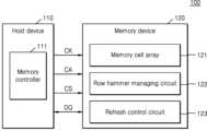
도 1을 참조하면, 전자 장치(100)는 예시적으로, 컴퓨터, 노트북, 서버, 워크 스테이션, 휴대용 통신 단말기, PDA(Personal Digital Assistant), PMP(Portable Multimedia Player), 스마트 폰, 웨어러블(Wearable) 장치와 같은 컴퓨팅 시스템일 수 있다. 전자 장치(100)는 호스트 장치(110) 및 메모리 장치(120)를 포함할 수 있다.Referring to FIG. 1, the
호스트 장치(110)는 그래픽스 카드와 같은 컴퓨팅 시스템에 포함된 구성 요소들 중 일부일 수 있다. 호스트 장치(110)는 메모리 버스를 통하여 메모리 장치(120)와 통신적으로 연결(communicatively connected)될 수 있다.The
호스트 장치(110)는 전자 장치(100) 내 일반적인 컴퓨터 동작을 수행하는 기능 블락(functional block)으로서, 중앙 처리 유닛(Central Processing Unit: CPU), 디지털 신호 프로세서(Digital Signal Processor: DSP), 그래픽 처리 유닛 (Graphics Processing Unit: GPU), 또는 어플리케이션 프로세서(Application Processor: AP)에 해당될 수 있다. 호스트 장치(110)는 메모리 장치(120)로 또는 메모리 장치(120)로부터 데이터 송수신을 제어하는 메모리 컨트롤러(111)를 포함할 수 있다. 호스트 장치(110)는 호스트로 지칭될 수 있다.The
일부 실시예들에서, 메모리 컨트롤러(111)는, 메모리 장치(120)에 대한 엑세스들을 메모리 버스를 통하여 메모리 장치(120)에 제공할 수 있다. 일 실시예에서, 엑세스는 액티브 커맨드 및 로우 어드레스를 포함할 수 있다. 하지만, 이에 한정되는 것은 아니며, 엑세스는 라이트 커맨드 또는 리드 커맨드와, 컬럼 어드레스, 및 프리차지 커맨드를 더 포함할 수도 있다.In some embodiments, the
일 실시예에서, 메모리 컨트롤러(111)는 엑세스들을 순차적으로 출력할 수 있다. 엑세스가 액티브 커맨드 및 로우 어드레스를 포함하는 경우, 메모리 컨트롤러(111)는 복수의 액티브 커맨드들 및 복수의 로우 어드레스들을 순차적으로 출력할 수 있다.In one embodiment, the
일부 실시예들에서, 메모리 컨트롤러(111)는 주기적으로 리프레쉬 커맨드를 출력할 수 있다. 리프레쉬 커맨드는 메모리 장치(120)가 리프레쉬 동작을 수행하도록 지시하는 커맨드일 수 있다.In some embodiments, the
메모리 컨트롤러(111)는 호스트 장치(110)의 메모리 리퀘스트에 따라 메모리 장치(120)를 억세스할 수 있다. 메모리 컨트롤러(111)는 메모리 위치에 대응하는 로우 및 컬럼을 선택하는 것, 메모리 위치에 데이터를 쓰거나 데이터를 읽는 것과 같은 메모리 장치(120)와 인터페이싱을 위한 메모리 물리 계층 인터페이스(Memory Physical Layer Interface: 메모리 PHY)를 포함할 수 있다. 메모리 PHY는 메모리 컨트롤러(111)와 메모리 장치(120) 사이의 효율적인 통신에 요구되는 신호들, 주파수, 타이밍, 구동, 상세 동작 파라미터 및 기능성(functionality)을 위해 제공되는 물리적 또는 전기적 계층과 논리적 계층을 포함할 수 있다. 메모리 PHY는 JEDEC(Joint Electron Device Engineering Council) 표준의 DDR(Double Data Rate) 및/또는 LPDDR(Low Power DDR) 프로토콜의 특징들을 지원할 수 있다.The
메모리 버스를 통해 메모리 컨트롤러(111)와 메모리 장치(120)가 연결될 수 있다. 하나의 신호 라인을 통하여 클럭(CK), 커맨드/어드레스(CA), 칩 선택 신호(CS), 및 데이터(DQ) 각각이 제공되는 것으로 도 1에 도시되어 있으나, 실제로는 클럭(CK), 커맨드/어드레스(CA), 칩 선택 신호(CS), 및 데이터(DQ) 각각이 복수의 신호 라인들 또는 버스를 통해 제공될 수 있다. 메모리 컨트롤러(111)와 메모리 장치(120) 사이의 신호 라인들은 커넥터들을 통하여 연결될 수 있다. 커넥터들은 핀들, 볼들, 신호 라인들, 또는 다른 하드웨어 컴포넌트들로서 구현될 수 있다.The
클럭(CK)은 메모리 버스의 클럭 신호 라인을 통해서 메모리 컨트롤러(111)로부터 메모리 장치(120)로 전송될 수 있다. 커맨드/어드레스(CA)는 메모리 버스의 커맨드/어드레스 신호 라인을 통해서 메모리 컨트롤러(111)로부터 메모리 장치(120)로 전송될 수 있다. 칩 선택 신호(CS)는 메모리 버스의 칩 선택 라인을 통해서 메모리 컨트롤러(111)로부터 메모리 장치(120)에 전송될 수 있다. 예컨대, 칩 선택 신호(CS)가 로직 하이로 활성화된 상태에서 커맨드/어드레스 신호 라인을 통해서 전송되는 신호는 커맨드일 수 있다. 데이터(DQ)는 메모리 버스의 양방향 신호 라인들로 구성되는 데이터 버스를 통해서, 메모리 컨트롤러(111)로부터 메모리 장치(120)로 전송되거나 메모리 장치(120)로부터 메모리 컨트롤러(111)로 전송될 수 있다.The clock CK may be transmitted from the
메모리 장치(120)는 메모리 컨트롤러(111)의 제어에 따라 데이터(DQ)를 쓰거나 데이터(DQ)를 읽고 리프레쉬 동작을 수행할 수 있다. 예시적으로, 메모리 장치(120)는 DDR SDRAM(Double Data Rate Synchronous Dynamic Random Access Memory) 장치일 수 있다. 그러나, 본 발명의 범위가 이에 한정되는 것은 아니며, 메모리 장치(120)는 LPDDR(Low Power Double Data Rate) SDRAM, Wide I/O(Input/Output) DRAM, HBM(High Bandwidth Memory), HMC(Hybrid Memory Cube) 등과 같은 휘발성 메모리 장치들 중 어느 하나일 수 있다.The
일부 실시예들에서, 메모리 장치(120)는 모니터링 구간에서 메모리 컨트롤러(111)로부터 제공된 액티브 커맨드들 및 로우 어드레스들을 기초로 로우 해머 어드레스를 검출할 수 있다. 일 실시예에서, 모니터링 구간은 도 4를 참조하여 후술할 기본 리프레쉬 레이트 시간(tREFi)일 수 있다. 다른 실시예에서, 모니터링 구간은 도 5b 및 도 5c를 참조하여 후술하는 바와 같이, 두 리프레쉬 동작 기간(ROP)들 사이의 기간일 수 있다. 메모리 장치(120)는 메모리 컨트롤러(111)로부터 제공된 리프레쉬 커맨드에 응답하여 검출한 로우 해머 어드레스를 기초로 리프레쉬 동작을 수행할 수 있다. 메모리 장치(120)가 메모리 컨트롤러(111)로부터 제공받은 로우 어드레스는 입력 로우 어드레스로 지칭될 수 있다.In some embodiments, the
메모리 장치(120)는 메모리 셀 어레이(121), 로우 해머 관리 회로(122), 및 리프레쉬 제어 회로(123)를 포함할 수 있다.The
메모리 셀 어레이(121)는 복수의 워드라인들, 복수의 비트라인들, 및 복수의 메모리 셀들을 포함할 수 있다. 복수의 메모리 셀들은 워드라인들과 비트라인들이 교차하는 지점에 형성될 수 있다. 메모리 셀 어레이(121)의 메모리 셀은 휘발성 메모리 셀, 예컨대, DRAM 셀일 수 있다.The
로우 해머 관리 회로(122)는 모니터링 구간 동안 엑세스의 회수를 카운트할 수 있다.The row
로우 해머 관리 회로(122)는 프리 로우 해머 어드레스와 복수의 입력 로우 어드레스들 각각을 기초로, 로우 해머 어드레스를 검출할 수 있다. 입력 로우 어드레스는 메모리 컨트롤러(111)로부터 제공된 로우 어드레스일 수 있다. 프리 로우 해머 어드레스는, 현재 모니터링 기간의 이전 모니터링 기간에서 로우 해머 어드레스로 검출 완료된 로우 어드레스일 수 있다. 프리 로우 해머 어드레스는 로우 해머 관리 회로(122)에 저장될 수 있다.The row
일 실시예에서, 로우 해머 관리 회로(122)는 리프레쉬 커맨드에 응답하여 로우 해머 어드레스를 리프레쉬 제어 회로(123)에 출력할 수 있다.In one embodiment, the row
다른 실시예에서, 로우 해머 관리 회로(122)는, 데이터 버스를 통해서, 로우 해머 어드레스를 메모리 컨트롤러(111)에 제공할 수 있다. 그리고, 로우 해머 관리 회로(122)는, 메모리 컨트롤러(111)로부터 수신된 리프레쉬 커맨드 및 적어도 하나의 타겟 로우 어드레스에 응답하여, 타겟 로우 어드레스를 리프레쉬 제어 회로(123)에 출력할 수 있다. 타겟 로우 어드레스는, 로우 해머 어드레스를 갖는 메모리 셀들과 물리적으로 인접한 메모리 셀들의 로우 어드레스일 수 있다.In another embodiment, the row
리프레쉬 제어 회로(123)는, 로우 해머 어드레스에 대응되는 메모리 셀 로우와 물리적으로 인접한 메모리 셀 로우에 대해 리프레쉬 동작을 수행할 수 있다. 일 실시예에서, 리프레쉬 제어 회로(123)는 로우 해머 관리 회로(122)로부터 제공된 로우 해머 어드레스를 기초로 타겟 로우 어드레스를 획득하고, 타겟 로우 어드레스를 메모리 셀 어레이(121)에 제공할 수 있다.The
도 2는 본 개시의 예시적인 실시예들에 따른 메모리 장치를 설명하기 위한 도면이다. 도 2에 도시된 메모리 장치(200)는 도 1에 도시된 메모리 장치(120)에 대응될 수 있다. 도 2에 도시된 메모리 장치(200)의 구성은 일 예로서 제공될 수 있다.FIG. 2 is a diagram for explaining a memory device according to example embodiments of the present disclosure. The
도 2를 참조하면, 메모리 장치(200)는 메모리 셀 어레이(210), 로우 디코더(220), 컬럼 디코더(230), 입출력 게이팅 회로(241), 입력 버퍼(242), 출력 버퍼(234), 어드레스 버퍼(250), 커맨드 버퍼(260), 커맨드 디코더(270), 제어 로직 회로(280), 및 리프레쉬 제어 회로(290)를 포함할 수 있다. 도 2에는 도시되지 않았으나, 메모리 장치(200)는 클럭 버퍼, 모드 레지스터 세트(Mode Register Set: MRS), 뱅크 제어 로직, 전압 발생 회로 등을 더 포함할 수 있다.Referring to FIG. 2, the
메모리 셀 어레이(210)는 로우들 및 컬럼들로 배열되는 매트릭스 형태로 제공되는 복수의 메모리 셀들을 포함할 수 있다. 메모리 셀 어레이(210)는 복수의 메모리 셀들과 연결되는 복수개의 워드라인들(WLs)과 복수개의 비트라인들(BLs)을 포함할 수 있다. 복수의 워드라인들(WLs)은 복수의 메모리 셀들의 로우들과 연결될 수 있다. 메모리 셀의 로우는 특정 워드라인에 연결된 메모리 셀들일 수 있다. 복수의 비트라인들(BLs)은 복수의 메모리 셀들의 컬럼들과 연결될 수 있다. 메모리 셀의 컬럼은 특정 비트라인에 연결된 메모리 셀들일 수 있다. 활성화된(actived) 워드라인에 연결된 메모리 셀들의 데이터는 복수의 비트라인들(BLs)에 연결된 센스 앰프들에 의해 센싱 및 증폭될 수 있다.The
일부 실시예들에서, 메모리 셀 어레이(210)는 복수의 뱅크들을 포함할 수 있다. 예를 들면, 메모리 셀 어레이(210)는 제1 내지 제4 뱅크들(BANK1~BANK4)을 포함할 수 있다. 뱅크 제어 로직은 뱅크 어드레스에 응답하여 뱅크 제어 신호들을 생성할 수 있다. 그리고, 제1 내지 제4 뱅크들(BANK1~BANK4) 중 뱅크 어드레스에 상응하는 뱅크의 로우 디코더(220) 및 컬럼 디코더(230)가 뱅크 제어 신호들에 응답하여 활성화될 수 있다. 4개의 뱅크들을 포함하는 메모리 장치(200)가 도 2에 도시되어 있으나, 이에 한정되는 것은 아니고, 실시예에 따라, 메모리 장치(200)는 임의의 수의 뱅크들을 포함할 수 있다.In some embodiments,
로우 디코더(220) 및 컬럼 디코더(230)는 제1 내지 제4 뱅크들(BANK1~BANK4) 각각에 대응하여 배치되고, 뱅크 어드레스에 상응하는 뱅크와 연결된 로우 디코더(220) 및 컬럼 디코더(230)가 활성화될 수 있다.The
로우 디코더(220)는 어드레스 버퍼(250)로부터 수신된 입력 로우 어드레스(ROW_ADD)를 디코딩하여 복수의 워드라인들(WLs) 중 입력 로우 어드레스(ROW_ADD)에 상응하는 워드라인을 선택할 수 있다. 일부 실시예들에서, 로우 디코더(220)는 선택된 워드라인을 활성화시키는 워드라인 드라이버를 포함할 수 있다.The
컬럼 디코더(230)는 메모리 셀 어레이(210)의 복수의 비트라인들(BLs) 중 소정의 비트라인들을 선택할 수 있다. 컬럼 디코더(230)는 버스트 모드에서 컬럼 어드레스(COL_ADD)에 기초하여 점진적으로 +1씩 증가되는 버스트 어드레스를 디코딩하여 컬럼 선택 신호를 발생하고, 컬럼 선택 신호에 의해 선택된 비트라인들을 입출력 게이팅 회로(241)에 연결할 수 있다. 버스트 어드레스는 리드 커맨드 및/또는 라이트 커맨드에 대하여 버스트 길이(BL)와 관련해서 억세스할 수 있는 컬럼 로케이션들의 어드레스들일 수 있다.The
입출력 게이팅 회로(241)는 컬럼 선택 신호에 의해 선택된 비트라인들의 읽기 데이터를 저장하는 읽기 데이터 래치들과, 메모리 셀 어레이(210)에 쓰기 데이터를 기입하기 위한 라이트 드라이버를 포함할 수 있다.The input/
입력 버퍼(242) 및 출력 버퍼(243)를 포함할 수 있다. 입출력 게이팅 회로(241)(예를 들어, 읽기 데이터 래치들)에 저장된 읽기 데이터는 출력 버퍼(243)를 통해 데이터 버스에 제공될 수 있다. 쓰기 데이터는 데이터 버스에 연결된 입력 버퍼(242) 및 입출력 게이팅 회로(241)(예를 들어, 라이트 드라이버)를 통해 메모리 셀 어레이(210)에 저장될 수 있다.It may include an
어드레스 버퍼(250)는 메모리 컨트롤러(111)로부터 커맨드/어드레스(CA)에 포함된 어드레스(ADD)를 수신할 수 있다. 어드레스(ADD)는 뱅크 어드레스, 입력 로우 어드레스(ROW_ADD) 및 컬럼 어드레스(COL_ADD)를 포함할 수 있다. 어드레스 버퍼(250)는 뱅크 어드레스를 뱅크 제어 로직에 제공하고, 입력 로우 어드레스(ROW_ADD)를 로우 디코더(220)에 제공하고, 컬럼 어드레스(COL_ADD)를 컬럼 디코더(230)에 제공할 수 있다.The
커맨드 버퍼(260)는 커맨드/어드레스(CA)에 포함된 커맨드(CMD)를 수신할 수 있다. 커맨드 버퍼(260)는 커맨드(CMD)를 커맨드 디코더(270)에 제공할 수 있다.The
커맨드 디코더(270)는 커맨드(CMD)를 디코딩하여 상응하는 커맨드, 예컨대, 액티브 커맨드(active command), 라이트 커맨드(write command), 리드 커맨드(read command), 프리차지 커맨드(pre-charge command), 리프레쉬 커맨드(refresh command) 등을 제어 로직 회로(280)에 제공할 수 있다.The
제어 로직 회로(280)는 클럭(CK) 및 커맨드(CMD)를 수신하고 메모리 장치(200)의 동작 타이밍 및/또는 메모리 동작을 제어하는 제어 신호들을 생성할 수 있다. 제어 로직 회로(280)는, MRS에 의해 저장된 동작 및 제어 파라미터에 설정된 바와 같이 동작하도록, 메모리 장치(200)의 회로들에 제어 신호들을 제공할 수 있다. 제어 로직 회로(280)는 제어 신호들을 이용하여 메모리 셀 어레이(210)로부터 데이터를 읽고, 메모리 셀 어레이(210)에 데이터를 쓸(write) 수 있다. 어드레스 버퍼(250), 커맨드 버퍼(260), 커맨드 디코더(270), 및 제어 로직 회로(280)가 별개의 구성 요소들인 것으로 도 2에 도시되어 있으나, 어드레스 버퍼(250), 커맨드 버퍼(260), 커맨드 디코더(270), 및 제어 로직 회로(280)는 하나의 구성 요소로 구현될 수도 있다. 또한, 도 2에는 커맨드(CMD) 및 어드레스(ADD)가 별개의 신호로 각각 제공되는 것으로 도시되어 있으나, LPDDR 표준 등에 제시되는 바와 같이 어드레스는 커맨드에 포함될 수도 있다.The
제어 로직 회로(280)는 메모리 셀 어레이(210) 내 메모리 셀 로우들 각각에 대한 엑세스 횟수들을 카운트할 수 있다. 그리고, 제어 로직 회로(280)는 리프레쉬 커맨드에 응답하여 카운트된 엑세스 횟수를 초기화할 수 있다.The
일부 실시예들에서, 제어 로직 회로(280)는 로우 해머 관리 회로(281)를 포함할 수 있다. 로우 해머 관리 회로(281)가 제어 로직 회로(280)에 포함되는 것으로 도 2에 도시되어 있으나, 이에 한정되는 것은 아니고, 로우 해머 관리 회로(281)는 제어 로직 회로(280)와 별개의 구성으로 제어 로직 회로(280)의 외부에 배치될 수도 있다. 로우 해머 관리 회로(281)는, 로우 해머를 제어하기 위한 및/또는 관리하기 위한 하드웨어, 펌웨어, 소프트웨어 또는 이들의 결합 방식으로 구현될 수 있다.In some embodiments,
로우 해머 관리 회로(281)는, 복수의 메모리 셀 로우들에 대한 엑세스들을 모니터링하는 모니터링 기간 동안에 로우 해머 어드레스(RH_ADD)를 검출할 수 있다. 일부 실시예들에서, 엑세스가 입력 로우 어드레스(ROW_ADD)를 포함하는 경우, 로우 해머 관리 회로(281)는 입력 로우 어드레스(ROW_ADD)를 기초로 로우 해머 어드레스(RH_ADD)를 검출할 수 있다. 일 실시예에서, 로우 해머 관리 회로(281)는, 모니터링 기간 동안에 프리 로우 해머 어드레스와 복수의 입력 로우 어드레스들 각각을 기초로, 로우 해머 어드레스(RH_ADD)를 검출할 수 있다.The row
일부 실시예들에서, 로우 해머 관리 회로(281)는 검출된 로우 해머 어드레스(RH_ADD)를 메모리 컨트롤러(111)에 전송할 수 있다. 일 실시예에서, 메모리 컨트롤러(111)는 로우 해머 어드레스(RH_ADD) 응답하여 리프레쉬 커맨드를 발행(issue)할 수 있다. 다른 실시예에서, 메모리 컨트롤러(111)는, 로우 해머 어드레스(RH_ADD) 응답하여, 복수의 메모리 셀 로우들 중 로우 해머 어드레스(RH_ADD)를 갖는 메모리 셀 로우와 물리적으로 인접한 메모리 셀 로우(들)의 어드레스(들)(예를 들면, 적어도 하나의 타겟 로우 어드레스(TR_ADD))와 리프레쉬 커맨드를 함께 메모리 장치(200)로 전송할 수 있다.In some embodiments, the row
로우 해머 관리 회로(281)는 리프레쉬 커맨드에 응답하여 로우 해머 어드레스(RH_ADD)를 리프레쉬 제어 회로(290)에 제공할 수 있다. 일 실시예에서, 로우 해머 관리 회로(281)는 메모리 컨트롤러(111)로부터 제공된 적어도 하나의 타겟 로우 어드레스(TR_ADD)를 리프레쉬 제어 회로(290)에 전달할 수 있다.The row
리프레쉬 제어 회로(290)는 로우 해머 어드레스(RH_ADD)에 대응되는 메모리 셀 로우와 물리적으로 인접한 메모리 셀 로우에 대해 리프레쉬 동작을 수행할 수 있다. 일 실시예에서, 리프레쉬 제어 회로(290)는, 리프레쉬 동작을 수행하도록, 로우 해머 관리 회로(281)로부터 전달된 적어도 하나의 타겟 로우 어드레스(TR_ADD)를 로우 디코더(220)에 제공할 수 있다. 다른 실시예에서, 리프레쉬 제어 회로(290)는, 로우 해머 관리 회로(281)로부터 전달된 로우 해머 어드레스(RH_ADD)를 기초로 적어도 하나의 타겟 로우 어드레스(TR_ADD)를 획득하고, 적어도 하나의 타겟 로우 어드레스(TR_ADD)를 로우 디코더(220)에 제공할 수 있다. 리프레쉬 동작 시, 타겟 로우 어드레스(TR_ADD)를 갖는 메모리 셀 로우가 리프레쉬될 수 있다.The
제어 로직 회로(280)는, 리프레쉬 커맨드에 응답하여, 리프레쉬 제어 회로(290)가 복수의 메모리 셀 로우들에 대한 노멀 리프레쉬 동작을 수행하도록, 리프레쉬 제어 회로(290)를 제어할 수 있다. 노멀 리프레쉬 동작은 리프레쉬 카운터 값을 +1씩 증가시킴으로써 복수의 메모리 셀 로우들을 순차적으로 리프레시하는 동작일 수 있다.The
제어 로직 회로(280)는, 리프레쉬 커맨드에 응답하여, 리프레쉬 제어 회로(290)가 타겟 로우 리프레쉬 동작을 수행하도록 제어할 수 있다. 타겟 로우 리프레쉬 동작은 로우 해머 공격을 받은 특정 메모리 셀 로우를 리프레시하는 동작일 수 있다.The
일 실시예에서, 리프레쉬 제어 회로(290)는 노멀 리프레쉬 동작과 타겟 리프레쉬 동작을 순차적으로 수행할 수 있다.In one embodiment, the
도 3은 본 개시의 예시적인 실시예들에 따른 로우 해머 관리 회로를 설명하기 위한 도면이다.3 is a diagram for explaining a row hammer management circuit according to example embodiments of the present disclosure.
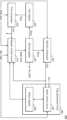
도 3을 참조하면, 로우 해머 관리 회로(300)는 레지스터 제어 회로(310), 제1 레지스터(320), 제1 비교기(330), 제2 레지스터(340), 제2 비교기(350), 플래그 생성 회로(360)를 포함할 수 있다.Referring to FIG. 3, the row
레지스터 제어 회로(310)는 리프레쉬 커맨드(REF CMD), 제1 비교 결과 신호(CR1), 제2 비교 결과 신호(CR2), 및 플래그 신호(FLAG)를 기초로 제2 레지스터(340)를 제어할 수 있다.The
일부 실시예에서, 모니터링 기간에서 입력 로우 어드레스(ROW_ADD)가 최초로 입력된 경우, 레지스터 제어 회로(310)는, 제2 레지스터(340)가 입력 로우 어드레스(ROW_ADD)를 저장하도록, 입력 로우 어드레스(ROW_ADD)를 제2 레지스터(340)에 제공할 수 있다. 최초로 입력된 입력 로우 어드레스(ROW_ADD)는 최초 입력 로우 어드레스로 지칭될 수 있다. 최초 입력 로우 어드레스가 입력될 때, 플래그 신호(FLAG)가 제1 비트값을 가질 수 있다. 예를 들어, 제1 비트값은 "0"이고 제2 비트값은 "1"일 수 있으나, 이에 한정되는 것은 아니다. 이하에서는 플래그 신호(FLAG)의 제1 비트값은 "0"이고 제2 비트값은 "1"인 것으로 가정한다. 전술한 실시예는 도 7을 참조하여 후술한다.In some embodiments, when the input row address (ROW_ADD) is input for the first time in the monitoring period, the
일부 실시예에서, 최초 입력 로우 어드레스가 프리 로우 해머 어드레스(Rpre)보다 작거나 같으면, 플래그 신호(FLAG)는 제1 비트값을 가질 수 있다. 한편, 최초 입력 로우 어드레스가 프리 로우 해머 어드레스(Rpre)보다 크면, 플래그 신호(FLAG)는 제2 비트값을 가질 수 있다.In some embodiments, if the first input row address is less than or equal to the pre-row hammer address Rpre, the flag signal FLAG may have a first bit value. Meanwhile, if the first input row address is greater than the pre-row hammer address (Rpre), the flag signal (FLAG) may have a second bit value.
일부 실시예에서, 플래그 신호(FLAG)가 제1 비트값을 갖고, 모니터링 기간에서 최초 입력 로우 어드레스 이후에 입력된 입력 로우 어드레스(ROW_ADD)가 프리 로우 해머 어드레스(Rpre)보다 클 수 있다. 이 경우, 레지스터 제어 회로(310)는, 제2 레지스터(340)가 입력 로우 어드레스(ROW_ADD)를 저장하도록, 입력 로우 어드레스(ROW_ADD)를 제2 레지스터(340)에 제공할 수 있다. 그리고, 플래그 신호(FLAG)의 비트 값은 제1 비트값에서 제2 비트값으로 변경될 수 있다. 어느 하나의 로우 어드레스가 다른 하나의 로우 어드레스보다 크다는 것은, 예를 들면, 로우 어드레스의 주소값이 상대적으로 크다는 것 또는 로우 어드레스의 번호가 상대적으로 크다는 것을 의미할 수 있다. 전술한 실시예는 도 8을 참조하여 후술한다.In some embodiments, the flag signal FLAG has a first bit value, and the input row address ROW_ADD input after the first input row address in the monitoring period may be greater than the pre-row hammer address Rpre. In this case, the
일부 실시예에서, 플래그 신호(FLAG)가 제1 비트값을 갖고, 최초 입력 로우 어드레스 이후에 입력된 입력 로우 어드레스(ROW_ADD)가 프리 로우 해머 어드레스(Rpre)보다 작거나 같고, 입력 로우 어드레스(ROW_ADD)가 제2 레지스터(340)에 저장된 로우 어드레스(Rfind)보다 작거나 같을 수 있다. 이 경우, 레지스터 제어 회로(310)는, 제2 레지스터(340)가 입력 로우 어드레스(ROW_ADD)를 저장하도록, 입력 로우 어드레스(ROW_ADD)를 제2 레지스터(340)에 제공할 수 있다. 그리고, 플래그 신호(FLAG)은 제1 비트값을 유지할 수 있다. 전술한 실시예는 도 8을 참조하여 후술한다.In some embodiments, the flag signal (FLAG) has a first bit value, the input row address (ROW_ADD) input after the first input row address is less than or equal to the pre-row hammer address (Rpre), and the input row address (ROW_ADD) ) may be less than or equal to the row address (Rfind) stored in the
일부 실시예에서, 플래그 신호(FLAG)가 제1 비트값을 갖고, 최초 입력 로우 어드레스 이후에 입력된 입력 로우 어드레스(ROW_ADD)가 프리 로우 해머 어드레스(Rpre)보다 작거나 같고, 입력 로우 어드레스(ROW_ADD)가 제2 레지스터(340)에 저장된 로우 어드레스(Rfind)보다 클 수 있다. 이 경우, 레지스터 제어 회로(310)는 입력 로우 어드레스(ROW_ADD)를 제2 레지스터(340)에 저장하지 않고 대기할 수 있다. 그리고, 플래그 신호(FLAG)은 제1 비트값을 유지할 수 있다. 전술한 실시예는 도 8을 참조하여 후술한다.In some embodiments, the flag signal (FLAG) has a first bit value, the input row address (ROW_ADD) input after the first input row address is less than or equal to the pre-row hammer address (Rpre), and the input row address (ROW_ADD) ) may be greater than the row address (Rfind) stored in the
일부 실시예에서, 플래그 신호(FLAG)가 제2 비트값을 갖고, 최초 입력 로우 어드레스 이후에 입력된 입력 로우 어드레스(ROW_ADD)가 프리 로우 해머 어드레스(Rpre)보다 크고 제2 레지스터(340)에 저장된 로우 어드레스(Rfind)보다 작을 수 있다. 이 경우, 레지스터 제어 회로(310)는 제2 레지스터(340)가 입력 로우 어드레스(ROW_ADD)를 저장하도록, 입력 로우 어드레스(ROW_ADD)를 제2 레지스터(340)에 제공할 수 있다. 그리고, 플래그 신호(FLAG)은 제2 비트값을 유지할 수 있다. 전술한 실시예는 도 9를 참조하여 후술한다.In some embodiments, the flag signal FLAG has a second bit value, and the input row address ROW_ADD input after the first input row address is greater than the pre-row hammer address Rpre and stored in the
일부 실시예에서, 레지스터 제어 회로(310)는, 리프레시 커맨드(REF CMD)에 응답하여, 제2 레지스터(340)가 로우 어드레스(Rfind)를 제1 레지스터(320)에 제공하도록, 제2 레지스터(340)를 제어할 수 있다. 그리고, 레지스터 제어 회로(310)는, 리프레시 커맨드(REF CMD)에 응답하여, 제2 레지스터(340)가 로우 어드레스(Rfind)를 로우 해머 어드레스(RH_ADD)로서 리프레쉬 제어 회로(290)에 제공하도록, 제2 레지스터(340)를 제어할 수 있다. 이때, 플래그 신호(FLAG)는 초기값을 가질 수 있다. 초기값은, 예를 들어 제1 비트값일 수 있다. 하지만, 이에 한정되는 것은 아니다.In some embodiments, the
제1 레지스터(320)는 프리 로우 해머 어드레스(Rpre)를 저장할 수 있다. 프리 로우 해머 어드레스(Rpre)는 모니터링 기간의 이전 모니터링 기간에서 로우 해머 어드레스로 검출 완료된 로우 어드레스일 수 있다. 제1 레지스터(320)는 프리 로우 해머 어드레스(Rpre)를 제1 비교기(330)에 제공할 수 있다. 일부 실시예에서, 제1 레지스터(320)는 제2 레지스터(320)로부터 출력된 로우 어드레스(Rfind)를 프리 로우 해머 어드레스(Rpre)로서 저장할 수 있다. 본 명세서에서는 제1 레지스터(320)에 저장된 로우 어드레스는 프리 로우 해머 어드레스(Rpre)로 지칭될 수 있다.The
제1 비교기(330)는 메모리 컨트롤러(111)로부터 제공된 입력 로우 어드레스(ROW_ADD)와 프리 로우 해머 어드레스(Rpre)를 비교하고, 제1 비교 결과 신호(CR1)를 출력할 수 있다. 제1 비교 결과 신호(CR1)는 입력 로우 어드레스(ROW_ADD)와 프리 로우 해머 어드레스(Rpre) 간의 비교 결과를 나타낼 수 있다. 예를 들면, 입력 로우 어드레스(ROW_ADD)가 프리 로우 해머 어드레스(Rpre)보다 작거나 같으면, 제1 비교 결과 신호(CR1)는 제1 값을 가질 수 있다. 다른 예를 들면, 입력 로우 어드레스(ROW_ADD)가 프리 로우 해머 어드레스(Rpre)보다 크면, 제1 비교 결과 신호(CR1)는 제1 값과 다른 제2 값을 가질 수 있다. 일 실시예에서, 제1 값 및 제2 값은 비트값으로 표현될 수 있으나 이에 한정되는 것은 아니다. 제1 비교 결과 신호(CR1)는 레지스터 제어 회로(310) 및 플래그 생성 회로(360)에 제공될 수 있다. 제1 비교기(330)는 디지털 비교기로 구현될 수 있으나 이에 한정되는 것은 아니다.The
제2 레지스터(340)는, 레지스터 제어 회로(310)의 제어에 의해, 입력 로우 어드레스(ROW_ADD)를 저장할 수 있다. 제2 레지스터(340)는 저장된 로우 어드레스(Rfind)를 제2 비교기(350)에 제공할 수 있다. 제2 레지스터(340)는, 레지스터 제어 회로(310)의 제어에 의해, 저장된 로우 어드레스(Rfind)를 출력할 수 있다. 출력된 로우 어드레스(Rfind)는 제1 레지스터(320)에 제공될 수 있고, 로우 해머 어드레스(RH_ADD)로서 로우 해머 제어 회로(290)에 제공될 수 있다. 일부 실시예에서, 모니터링 기간 동안에 입력 로우 어드레스(ROW_ADD)는 로우 해머 어드레스(RH_ADD)의 후보(candidate)로서 제2 레지스터(340)에 저장될 수 있다. 리프레쉬 커맨드(REF CMD)에 따른 리프레쉬 동작이 수행될 때, 제2 레지스터(340)에 로우 해머 어드레스(RH_ADD)의 후보로서 저장된 로우 어드레스(Rfind)는 로우 해머 어드레스(RH_ADD)로서 출력될 수 있다.The
일부 실시예에서, 로우 해머 어드레스(RH_ADD)로 검출 완료되는 입력 로우 어드레스(ROW_ADD)는 프리 로우 해머 어드레스(Rpre)보다 클 수 있다. 그리고, 특정 모니터링 기간에 로우 해머 어드레스(RH_ADD)로 검출 완료되는 입력 로우 어드레스(ROW_ADD)의 개수는 하나일 수 있다. 이에 따라, 프리 로우 해머 어드레스(Rpre)보다 큰 로우 해머 어드레스(RH_ADD)가 모니터링 기간마다 하나씩 검출 완료될 수 있다. 일부 실시예에서, 프리 로우 해머 어드레스(Rpre)보다 큰 로우 해머 어드레스(RH_ADD)로 검출 완료되는 입력 로우 어드레스(ROW_ADD)가 제2 레지스터(340)에 순차적으로 저장될 수 있다. 여기서, 순차적으로 저장되는 순서는, 예를 들면, 오름차순이고, 이때 오름차순은 로우 어드레스의 번호가 점점 증가되는 것을 의미할 수 있다. 하지만, 이에 한정되는 것은 아니다.In some embodiments, the input row address (ROW_ADD), which is detected as the row hammer address (RH_ADD), may be greater than the pre-row hammer address (Rpre). Also, the number of input row addresses (ROW_ADD) that are detected as row hammer addresses (RH_ADD) in a specific monitoring period may be one. Accordingly, the row hammer address (RH_ADD) that is larger than the free row hammer address (Rpre) may be detected one by one during each monitoring period. In some embodiments, the input row address (ROW_ADD), which is detected as the row hammer address (RH_ADD) that is larger than the pre-row hammer address (Rpre), may be sequentially stored in the
제2 비교기(350)는 입력 로우 어드레스(ROW_ADD)와 제2 레지스터(340)에 저장된 로우 어드레스(Rfind)를 비교하고, 제2 비교 결과 신호(CR2)를 출력할 수 있다. 제2 비교 결과 신호(CR2)는 입력 로우 어드레스(ROW_ADD)와 로우 어드레스(Rfind) 간의 비교 결과를 나타낼 수 있다.The
예를 들면, 입력 로우 어드레스(ROW_ADD)가 로우 어드레스(Rfind)보다 작으면, 제2 비교 결과 신호(CR2)는 제3 값을 가질 수 있다. 다른 예를 들면, 입력 로우 어드레스(ROW_ADD)가 로우 어드레스(Rfind)보다 크거나 같으면, 제2 비교 결과 신호(CR2)는 제3 값과 다른 제4 값을 가질 수 있다. 일 실시예에서, 제3 값 및 제4 값은 비트값으로 표현될 수 있으나 이에 한정되는 것은 아니다. 제2 비교 결과 신호(CR2)는 레지스터 제어 회로(310) 및 플래그 생성 회로(360)에 제공될 수 있다. 제2 비교기(340)는 디지털 비교기로 구현될 수 있으나 이에 한정되는 것은 아니다.For example, if the input row address ROW_ADD is smaller than the row address Rfind, the second comparison result signal CR2 may have a third value. For another example, if the input row address ROW_ADD is greater than or equal to the row address Rfind, the second comparison result signal CR2 may have a fourth value different from the third value. In one embodiment, the third value and the fourth value may be expressed as bit values, but are not limited thereto. The second comparison result signal CR2 may be provided to the
플래그 생성 회로(360)는 제1 비교 결과 신호(CR1) 및 제2 비교 결과 신호(CR2)를 기초로 플래그 신호(FLAG)를 출력할 수 있다. 일부 실시예에서, 입력 로우 어드레스(ROW_ADD)가 프리 로우 해머 어드레스(Rpre)보다 작거나 같으면, 플래그 생성 회로(360)는 제1 비트값을 갖는 플래그 신호(FLAG)를 출력할 수 있다. 일부 실시예에서, 플래그 신호(FLAG)가 제1 비트값을 갖는 상태에서, 입력 로우 어드레스(ROW_ADD)가 프리 로우 해머 어드레스(Rpre)보다 크면, 플래그 생성 회로(360)는 제2 비트값을 갖는 플래그 신호(FLAG)를 출력할 수 있다.The
일부 실시예에서, 플래그 생성 회로(360)는 리프레쉬 커맨드(REF CMD)에 응답하여, 플래그 신호(FLAG)를 초기화할 수 있다. 이때, 플래그 신호(FLAG)는 초기값을 가질 수 있으며, 초기값은 예를 들면, 제1 비트값일 수 있다.In some embodiments, the
플래그 신호(FLAG)는, 제1 비트값 또는 제2 비트값을 가짐으로써 제1 모드 및 제2 모드 중 어느 하나의 모드를 실행할 것을 지시하는 신호일 수 있다. 일 실시예에서, 플래그 신호(FLAG)가 제1 비트값을 가지면, 로우 해머 관리 회로(300)가 제1 모드를 실행할 수 있다. 제1 모드는 복수의 입력 로우 어드레스(ROW_ADD)들 중 제1 최소 입력 로우 어드레스를 검출하는 모드일 수 있다. 다른 실시예에서, 플래그 신호(FLAG)가 제2 비트값을 가지면, 로우 해머 관리 회로(300)가 제2 모드를 실행할 수 있다. 제2 모드는 프리 로우 해머 어드레스(Rpre)보다 큰 입력 로우 어드레스(ROW_ADD)들 중 제2 최소 입력 로우 어드레스를 검출하는 모드일 수 있다.The flag signal FLAG may be a signal that indicates execution of one of the first mode and the second mode by having a first bit value or a second bit value. In one embodiment, when the flag signal FLAG has a first bit value, the row
플래그 생성 회로(360)는 모드 제어 회로(361) 및 상태 레지스터(362)를 포함할 수 있다. 모드 제어 회로(361)는 제1 비교 결과 신호(CR1), 제2 비교 결과 신호(CR2), 및 리프레쉬 커맨드(REF CMD)를 기초로, 상태 레지스터(362)를 제어할 수 있다.The
일부 실시예에서, 모드 제어 회로(361)는 리프레쉬 커맨드(REF CMD)에 응답하여, 초기값을 갖는 플래그 신호(FLAG)를 출력하도록, 상태 레지스터(362)를 제어할 수 있다. 초기값은, 예를 들면, 제1 비트값일 수 있다.In some embodiments, the
일부 실시예에서, 플래그 신호(FLAG)가 초기값을 갖는 상태에서, 제1 비교 결과 신호(CR1)는 제1 값을 가지면, 모드 제어 회로(361)는 제1 비트값을 갖는 플래그 신호(FLAG)를 출력하도록, 상태 레지스터(362)를 제어할 수 있다.In some embodiments, when the flag signal FLAG has an initial value and the first comparison result signal CR1 has a first value, the
일부 실시예에서, 플래그 신호(FLAG)가 초기값을 갖는 상태에서, 제1 비교 결과 신호(CR1)는 제2 값을 가지면, 모드 제어 회로(361)는 제2 비트값을 갖는 플래그 신호(FLAG)를 출력하도록, 상태 레지스터(362)를 제어할 수 있다.In some embodiments, when the flag signal FLAG has an initial value and the first comparison result signal CR1 has a second value, the
일부 실시예에서, 플래그 신호(FLAG)가 제1 비트값을 갖는 상태에서, 제1 비교 결과 신호(CR1)는 제1 값을 갖고, 제2 비교 결과 신호(CR2)가 제3 값을 가지면, 모드 제어 회로(361)는 제1 비트값을 갖는 플래그 신호(FLAG)를 출력하도록, 상태 레지스터(362)를 제어할 수 있다.In some embodiments, when the flag signal FLAG has a first bit value, the first comparison result signal CR1 has a first value, and the second comparison result signal CR2 has a third value, The
전술한 바에 의하면, 로우 해머 관리 회로(300)가 로우 해머 어드레스로 검출 완료된 어드레스를 저장하는 레지스터 및 로우 해머 어드레스로 검출될 어드레스를 저장하는 레지스터를 포함함으로써, 레지스터의 개수를 줄이면서도 로우 해머를 효율적으로 제어할 수 있는 장점이 있다.As described above, the row
또한, 전술한 바에 의하면, 로우 해머 관리 회로(300)에 포함된 레지스터의 개수가 감소됨으로써, 메모리 장치의 집적도를 개선하는 효과가 있다.Additionally, according to the above-described description, the number of registers included in the row
도 4는 본 개시의 예시적인 실시예들에 따른 리프레쉬 동작의 타이밍을 설명하는 도면이다.FIG. 4 is a diagram illustrating the timing of a refresh operation according to example embodiments of the present disclosure.
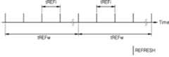
도 4를 참조하면, JEDEC 표준에 정의된 32ms 또는 64ms 리프레쉬 윈도우 시간(tREFw)이 설정될 수 있다. 실시예에 따라, 본 개시의 예시적인 실시예들에 따른 모니터링 기간은 기본 리프레쉬 레이트 시간(tREFi)에 대응될 수 있다. 기본 리프레쉬 레이트 시간(tREFi)은, 예를 들어, 32ms 리프레쉬 윈도우 시간(tREFw) 내 8K 정도의 리프레쉬 커맨드(REFRESH) 수로 정의될 수 있다. 하지만, 이에 한정되는 것은 아니다.Referring to FIG. 4, the 32ms or 64ms refresh window time (tREFw) defined in the JEDEC standard can be set. Depending on the embodiment, the monitoring period according to example embodiments of the present disclosure may correspond to the basic refresh rate time (tREFi). For example, the basic refresh rate time (tREFi) can be defined as the number of refresh commands (REFRESH) of about 8K within a 32ms refresh window time (tREFw). However, it is not limited to this.
도 5a, 도 5b, 및 도 5c는 본 개시의 예시적인 실시예들에 따른 리프레쉬 동작 기간 및 모니터링 기간을 설명하기 위한 도면들이다.FIGS. 5A, 5B, and 5C are diagrams for explaining a refresh operation period and a monitoring period according to exemplary embodiments of the present disclosure.
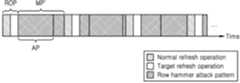
도 1, 도 3, 및 도 5a를 참조하면, 메모리 컨트롤러(111)는 리프레쉬 커맨드(REF CMD)를 주기적으로 출력할 수 있다. 이에 따라, 리프레쉬 동작 기간(ROP)과 모니터링 기간(MP)이 순차적으로 발생할 수 있다. 리프레쉬 동작 기간(ROP)에서는 메모리 장치(120)가 리프레쉬 동작을 수행할 수 있다. 도 5a에 도시된 바와 같이, 리프레쉬 동작은 타겟 리프래쉬 동작(Target refresh operation)일 수 있다.Referring to FIGS. 1, 3, and 5A, the
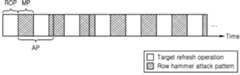
한편, 로우 해머 공격 패턴(Row hammer attack pattern)은 다양하게 존재할 수 있다. 예를 들면, 로우 해머 공격 패턴으로 NCSC(National Cyber Security Center), A4, 구글 타입 1(Google type 1), 유니폼 랜덤(Uniform random), 블랙스미스(Blacksmith) 등이 있을 수 있다. 하지만, 이에 한정되는 것은 아니다. 전술한 바와 같이 로우 해머 공격 패턴이 다양하므로, 로우 해머 공격 패턴의 패턴 사이즈(AP)도 패턴마다 다를 수 있다. 로우 해머 공격 패턴의 패턴 사이즈(AP)는 복수의 메모리 셀 로우들 중 공격하고자 하는 메모리 셀 로우들을 모두 공격 완료하는 기간에 대응될 수 있다. 로우 해머 관리 회로(122)는 공격하고자 하는 메모리 셀 로우에 대응되는 엑세스를 카운트할 수 있으므로, 로우 해머 공격 패턴의 패턴 사이즈(AP)는 복수의 엑세스들이 모두 카운팅 완료되는 기간에 대응될 수 있다. 로우 해머 공격 패턴의 패턴 사이즈(AP)는 패턴 길이, 패턴 크기, 패턴 동작 시간 등으로 지칭될 수 있다. 그런데, 도 5a에 도시된 바와 같이, 모니터링 기간(MP)이 로우 해머 공격 패턴의 패턴 사이즈(AP)보다 작으면, 로우 해머 공격 패턴에서 공격하고자 하는 메모리 셀 로우들을 전부 모니터링하지 못하는 경우가 있다.Meanwhile, low hammer attack patterns may exist in various ways. For example, low hammer attack patterns may include NCSC (National Cyber Security Center), A4,
도 5b를 참조하면, 일부 실시예에서, 모니터링 기간(MP')은 로우 해머 공격 패턴의 패턴 사이즈(AP)보다 클 수 있다. 일 실시예에서, 모니터링 기간(MP')은 복수의 엑세스들이 모두 카운팅 완료되는 기간보다 크거나 같을 수 있다. 다른 실시예에서, 모니터링 기간(MP')은 1K 이상의 액티브 커맨드 수로 정의될 수 있다. 하지만, 이에 한정되는 것은 아니다. 일부 실시예에서, 리프레쉬 동작 기간(ROP)에서 메모리 장치(120)는 타겟 리프래쉬 동작을 수행할 수 있다.Referring to FIG. 5B, in some embodiments, the monitoring period (MP') may be larger than the pattern size (AP) of the low hammer attack pattern. In one embodiment, the monitoring period (MP') may be greater than or equal to the period during which counting of all the plurality of accesses is completed. In another embodiment, the monitoring period (MP') may be defined as the number of active commands greater than 1K. However, it is not limited to this. In some embodiments, the
도 5c를 참조하면, 일부 실시예에서, 모니터링 기간(MP')은 모니터링 기간(MP')은 로우 해머 공격 패턴의 패턴 사이즈(AP)보다 크고, 리프레쉬 동작 기간(ROP)에서 메모리 장치(120)는 노멀 리프레쉬 동작(Normal refresh operation)과 타겟 리프래쉬 동작을 수행할 수 있다. 일 실시예에서, 노멀 리프레쉬 동작(Normal refresh operation)과 타겟 리프래쉬 동작은 순차적으로 수행될 수 있으며, 예를 들어, 노멀 리프레쉬 동작이 수행된 후 타겟 리프래쉬 동작이 수행될 수 있다.Referring to FIG. 5C, in some embodiments, the monitoring period (MP') is larger than the pattern size (AP) of the low hammer attack pattern, and the
전술한 바에 의하면, 메모리 장치(120)의 모니터링 기간(MP')이 로우 해머 공격 패턴의 패턴 사이즈(AP) 이상으로 설정됨으로써, 다양한 로우 해머 공격 패턴에 대한 로우 해머를 제어하는 메모리 장치의 성능 및 신뢰성을 개선하는 효과가 있다.As described above, the monitoring period (MP') of the
도 6은 본 개시의 예시적인 실시예들에 따른 메모리 장치의 동작 방법을 설명하기 위한 흐름도이다.FIG. 6 is a flowchart illustrating a method of operating a memory device according to example embodiments of the present disclosure.
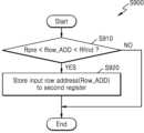
도 3 및 도 6을 참조하면, 본 개시의 메모리 장치(120)의 동작 방법은 액세스들을 모니터링하는 단계(S610), 리프레쉬 동작을 수행하는 단계(S620), 및 로우 해머 어드레스를 저장하는 단계(S630)를 포함할 수 있다.3 and 6, the operating method of the
액세스들을 모니터링하는 단계(S610)는, 메모리 장치(120)가 복수의 입력 로우 어드레스(ROW_ADD)들 및 제1 레지스터(320)에 저장된 프리 로우 해머 어드레스(Rpre)를 기초로, 로우 해머 어드레스(RH_ADD)를 검색하는 단계이다. 복수의 입력 로우 어드레스(ROW_ADD)들은 호스트 장치(110)에 의한 복수의 엑세스들에 포함될 수 있다. 일 실시예에서, 액세스들을 모니터링하는 단계(S610)는, 복수의 입력 로우 어드레스(ROW_ADD)들 중 프리 로우 해머 어드레스(Rpre)보다 큰 입력 로우 어드레스 또는 복수의 입력 로우 어드레스(ROW_ADD)들 중 제1 최소 입력 로우 어드레스를, 로우 해머 어드레스(RH_ADD)로서 제2 레지스터(340)에 저장할 수 있다.In the step of monitoring accesses (S610), the
리프레쉬 동작을 수행하는 단계(S620)는, 메모리 장치(120)가 호스트 장치(110)로부터 제공된 리프레쉬 커맨드(REF CMD)에 응답하여, 로우 해머 어드레스(RH_ADD)에 대응되는 메모리 셀 로우와 물리적으로 인접한 메모리 셀 로우에 대해 리프레쉬 동작을 수행하는 단계이다.In the step of performing a refresh operation (S620), the
로우 해머 어드레스를 저장하는 단계(S630)는, 메모리 장치(120)가 리프레쉬 커맨드(REF CMD)에 응답하여, 로우 해머 어드레스(RH_ADD)를 프리 로우 해머 어드레스(Rpre)로서 제1 레지스터(320)에 저장하는 단계이다. 구체적으로 예를 들면, 레지스터 제어 회로(310)는, 리프레쉬 커맨드(REF CMD)에 응답하여 제2 레지스터(340)에 저장된 로우 어드레스(Rfind)를 제1 레지스터(320)에 제공하도록 제2 레지스터(340)를 제어할 수 있다. 그리고, 플래그 생성 회로(360)는 제1 비트값을 초기값으로 갖는 플래그 신호(FLAG)를 출력할 수 있다.In the step of storing the row hammer address (S630), the
전술한 방법에 의하면, 로우 해머 어드레스를 저장하는 레지스터의 개수를 줄이면서도 다양한 유형의 로우 해머를 제어함으로써, 메모리 장치의 집적도를 개선하는 효과가 있다.According to the above-described method, there is an effect of improving the integration of the memory device by controlling various types of row hammers while reducing the number of registers storing row hammer addresses.
또한, 전술한 방법에 의하면, 다양한 유형의 로우 해머를 제어함으로써, 메모리 장치의 성능 및 신뢰성을 개선하는 효과가 있다.In addition, according to the above-described method, the performance and reliability of the memory device are improved by controlling various types of row hammers.
도 7은 도 6에 도시된 액세스들을 모니터링하는 단계의 실시예들을 설명하기 위한 흐름도이다.FIG. 7 is a flowchart for explaining embodiments of the step of monitoring accesses shown in FIG. 6.
도 3, 도 6, 및 도 7을 참조하면, 도 6에 도시된 액세스들을 모니터링하는 단계(S610)는 로우 해머 어드레스(RH_ADD)로서 제2 레지스터(340)에 저장하는 단계(S700)로 지칭될 수 있다.3, 6, and 7, the step of monitoring accesses shown in FIG. 6 (S610) will be referred to as the step of storing the row hammer address (RH_ADD) in the second register 340 (S700). You can.
단계 S710에서, 호스트(예를 들면, 호스트 장치(110))가 엑세스를 메모리 장치(120)에 전송한다.In step S710, the host (eg, host device 110) transmits access to the
단계 S720에서, 수신된 엑세스가 최초 엑세스(Initial access)인지 확인된다. 최초 엑세스는 최초 입력 로우 어드레스(Nadd)를 포함할 수 있다.In step S720, it is confirmed whether the received access is initial access. The first access may include the first input row address (Nadd).
수신된 엑세스가 최초 엑세스이면(S720, Yes), 단계 S730에서, 최초 입력 로우 어드레스(Nadd)가 제2 레지스터(340)에 저장된다. 구체적으로 예를 들면, 레지스터 제어 회로(310)는, 최초 입력 로우 어드레스(Nadd)를 제2 레지스터(340)에 저장하도록 최초 입력 로우 어드레스(Nadd)를 제2 레지스터(340)에 제공하고,If the received access is the first access (S720, Yes), the first input row address (Nadd) is stored in the
단계 S740에서, 최초 입력 로우 어드레스(Nadd)와 프리 로우 해머 어드레스(Rpre)와 비교된다. 구체적으로 예를 들면, 제1 비교기(330)에 의해, 최초 입력 로우 어드레스(Nadd)가 프리 로우 해머 어드레스(Rpre)보다 큰지 여부가 결정될 수 있다.In step S740, the initial input row address (Nadd) is compared with the pre-row hammer address (Rpre). Specifically, for example, the
일 실시예에서, 최초 입력 로우 어드레스(Nadd)와 프리 로우 해머 어드레스(Rpre) 간의 비교 결과에 따라, 제1 모드 및 제2 모드 중 어느 하나의 모드가 실행된다. 제1 모드는, 복수의 입력 로우 어드레스(ROW_ADD)들 중 제1 최소 입력 로우 어드레스를 검출하는 모드일 수 있다. 제2 모드는 프리 로우 해머 어드레스(Rpre)보다 큰 입력 로우 어드레스(ROW_ADD)들 중 제2 최소 입력 로우 어드레스를 검출하는 모드일 수 있다.In one embodiment, one of the first mode and the second mode is executed according to a comparison result between the first input row address (Nadd) and the pre-row hammer address (Rpre). The first mode may be a mode that detects the first minimum input row address among the plurality of input row addresses (ROW_ADD). The second mode may be a mode that detects the second minimum input row address among the input row addresses (ROW_ADD) that are greater than the free row hammer address (Rpre).
구체적으로, 최초 입력 로우 어드레스(Nadd)가 프리 로우 해머 어드레스(Rpre)보다 크면(S740, Yes), 단계 S750에서, 플래그 신호(FLAG)의 비트 값이 "0"(또는 제1 비트값)으로 설정될 수 있다.Specifically, if the first input row address (Nadd) is greater than the pre-row hammer address (Rpre) (S740, Yes), in step S750, the bit value of the flag signal (FLAG) is set to “0” (or the first bit value). can be set.
최초 입력 로우 어드레스(Nadd)가 프리 로우 해머 어드레스(Rpre)보다 작거나 같으면(S740, No), 단계 S760에서, 플래그 신호(FLAG)의 비트 값이 "1"(또는 제2 비트값)로 설정될 수 있다.If the first input row address (Nadd) is less than or equal to the pre-row hammer address (Rpre) (S740, No), the bit value of the flag signal (FLAG) is set to “1” (or the second bit value) in step S760. It can be.
수신된 엑세스가 최초 엑세스가 아니면(S720, No), 단계 S800이 수행된다. 단계 S800는 도 8을 참조하여 후술된다.If the received access is not the first access (S720, No), step S800 is performed. Step S800 is described later with reference to FIG. 8.
도 8은 도 6에 도시된 액세스들을 모니터링하는 단계의 다른 실시예를 설명하기 위한 흐름도이다.FIG. 8 is a flowchart for explaining another embodiment of the step of monitoring accesses shown in FIG. 6.
도 3, 도 6, 및 도 8을 참조하면, 단계 S810에서, 플래그(FLAG)의 비트값이 제1 비트값인지 확인된다. 구체적으로 예를 들면, 레지스터 제어 회로(310)가 플래그(FLAG)의 비트값을 확인할 수 있다.Referring to FIGS. 3, 6, and 8, in step S810, it is confirmed whether the bit value of the flag FLAG is the first bit value. Specifically, for example, the
플래그(FLAG)의 비트값이 제1 비트값이면(S810, Yes), 단계 S820에서, 제1 모드가 실행된다. 그리고, 제1 모드에서 최초 입력 로우 어드레스(Nadd) 이후에 입력되는 입력 로우 어드레스(ROW_ADD)가, 프리 로우 해머 어드레스(Rpre)보다 작거나 같은지 확인된다. 구체적으로 예를 들면, 제1 비교기(320)가 입력 로우 어드레스(ROW_ADD)와 프리 로우 해머 어드레스(Rpre)를 비교할 수 있다.If the bit value of the flag FLAG is the first bit value (S810, Yes), the first mode is executed in step S820. Also, in the first mode, it is checked whether the input row address (ROW_ADD) input after the first input row address (Nadd) is less than or equal to the pre-row hammer address (Rpre). Specifically, for example, the
입력 로우 어드레스(ROW_ADD)가 프리 로우 해머 어드레스(Rpre)보다 크면(S820, No), 단계 S830에서, 구체적으로 예를 들면, 플래그 생성 회로(360)는 플래그 신호(FLAG)의 비트값을 제1 비트값에서 제2 비트값으로 변경하고, 제2 모드가 실행된다.If the input row address (ROW_ADD) is greater than the free row hammer address (Rpre) (S820, No), in step S830, specifically, for example, the
단계 S840에서, 레지스터 제어 회로(310)는, 입력 로우 어드레스(ROW_ADD)를 제2 레지스터(340)에 저장한다.In step S840, the
입력 로우 어드레스(ROW_ADD)가 프리 로우 해머 어드레스(Rpre)보다 작거나 같으면(S820, Yes), 단계 S850에서, 입력 로우 어드레스(ROW_ADD)가 제2 레지스터(340)에 저장된 로우 어드레스(Rfind)보다 작거나 같은지 확인된다.If the input row address (ROW_ADD) is less than or equal to the pre-row hammer address (Rpre) (S820, Yes), in step S850, the input row address (ROW_ADD) is less than the row address (Rfind) stored in the
입력 로우 어드레스(ROW_ADD)가 로우 어드레스(Rfind)보다 작거나 같으면(S850, Yes), 단계 S840이 수행된다. 이 경우, 플래그 생성 회로(360)는 플래그 신호의 비트값을 제1 비트값으로 유지함으로써, 제1 모드가 계속 실행된다.If the input row address (ROW_ADD) is less than or equal to the row address (Rfind) (S850, Yes), step S840 is performed. In this case, the
플래그(FLAG)의 트값이 제2 비트값이면(S810, No), 단계 S900이 수행된다. 단계 S900는 도 9을 참조하여 후술된다.If the bit value of the flag (FLAG) is the second bit value (S810, No), step S900 is performed. Step S900 is described later with reference to FIG. 9.
도 9은 도 6에 도시된 액세스들을 모니터링하는 단계의 또 다른 실시예를 설명하기 위한 흐름도이다.FIG. 9 is a flowchart for explaining another embodiment of the step of monitoring accesses shown in FIG. 6.
도 3, 도 6, 및 도 9를 참조하면, 단계 S900은 제2 모드가 실행되는 단계이다.Referring to FIGS. 3, 6, and 9, step S900 is a step in which the second mode is executed.
단계 S910에서, 최초 입력 로우 어드레스(Nadd) 이후에 입력되는 입력 로우 어드레스(ROW_ADD)가 프리 로우 해머 어드레스(Rpre)보다 크고 제2 레지스터(340)에 저장된 로우 어드레스(Rfind)보다 작은지 확인된다. In step S910, it is checked whether the input row address (ROW_ADD) input after the first input row address (Nadd) is greater than the pre-row hammer address (Rpre) and less than the row address (Rfind) stored in the
입력 로우 어드레스(ROW_ADD)가 프리 로우 해머 어드레스(Rpre)보다 크고 로우 어드레스(Rfind)보다 작으면(S910, Yes), 단계 S920에서, 레지스터 제어 회로(310)는, 입력 로우 어드레스(ROW_ADD)를 제2 레지스터(340)에 저장한다. 이 경우, 플래그 생성 회로(360)는, 플래그(FLAG)의 비트값을 제2 비트값으로 유지할 수 있다.If the input row address (ROW_ADD) is greater than the pre-row hammer address (Rpre) and less than the row address (Rfind) (S910, Yes), in step S920, the
도 10은 본 개시의 예시적인 실시예들에 따른 로우 해머를 관리하는 동작의 타이밍을 설명하기 위한 도면이다.FIG. 10 is a diagram for explaining the timing of an operation for managing a row hammer according to example embodiments of the present disclosure.
도 3 및 도 10을 참조하면, 로우 해머 공격 패턴은, 로우 어드레스 10(R10), 로우 어드레스 30(R30), 로우 어드레스 100(R100), 및 로우 어드레스 1000(R1000)를 각각 갖는 메모리 셀 로우들에 대해 로우 해머 공격을 1회 이상 하는 패턴인 것으로 가정한다. 리프레쉬 동작의 주기는 로우 해머 공격을 받는 로우 어드레스의 종류에 대응될 수 있다. 예를 들면, 도 10에 도시된 로우 해머 공격 패턴에서 로우 해머 공격을 받는 로우 어드레스의 종류는 4가지이므로, 도 10에 도시된 리프레쉬 동작의 주기는 4일 수 있다. 리프레쉬 동작의 주기마다 커맨드(REF)가 입력될 수 있다. 리프레쉬 동작의 주기 내에서 총 액세스 수는 로우 해머 공격을 받는 로우 어드레스의 종류와 주기의 곱에 대응될 수 있다. 예를 들면, 일 커맨드(REF)와 다른 커맨드(REF) 사이에서 시간 간격에 대응되는 주기 내에서, 액세스 카운트(ACC CNT)의 수는 "6"이므로, 리프레쉬 동작의 주기 내에서 총 액세스 수는 "24(=6*4)"일 수 있다. 하지만, 이에 한정되는 것은 아니다.3 and 10, the row hammer attack pattern includes memory cell rows having row address 10 (R10), row address 30 (R30), row address 100 (R100), and row address 1000 (R1000), respectively. It is assumed that this is a pattern of performing a low hammer attack at least once. The cycle of the refresh operation may correspond to the type of row address subjected to the row hammer attack. For example, in the row hammer attack pattern shown in FIG. 10, there are four types of row addresses subjected to row hammer attack, so the cycle of the refresh operation shown in FIG. 10 may be 4. A command (REF) may be input at each cycle of the refresh operation. The total number of accesses within a cycle of a refresh operation may correspond to the product of the cycle and the type of row address subject to a row hammer attack. For example, within a period corresponding to the time interval between one command (REF) and another command (REF), the number of access counts (ACC CNT) is "6", so the total number of accesses within the period of the refresh operation is It could be "24(=6*4)". However, it is not limited to this.
커맨드(REF)는 도 3을 참조하여 전술한 리프래시 커맨드(REF CMD)일 수 있다.The command (REF) may be the refresh command (REF CMD) described above with reference to FIG. 3.
모니터링 기간은, 도 10을 참조하여 예를 들면, 커맨드(REF)가 입력된 이후부터 그 다음 커맨드(REF)가 입력되기 전까지 해당되는 기간일 수 있다.Referring to FIG. 10 , the monitoring period may be, for example, a period from when a command (REF) is input until the next command (REF) is input.
프리 로우 해머 어드레스(Rpre)의 초기값(initial value)는 로우 어드레스 30(R30)인 것으로 가정한다.It is assumed that the initial value of the pre-row hammer address (Rpre) is row address 30 (R30).
액세스 카운트(ACC CNT)는, 로우 어드레스들(R10, R30, R100, R1000) 각각이 로우 해머 관리 회로(300)에 입력될 때마다 +1씩 증가될 수 있다. 액세스 카운트(ACC CNT)는 커맨드(REF)가 입력됨에 응답하여 초기값으로 초기화될 수 있다. 도 10을 참조하여 예를 들면, 액세스 카운트(ACC CNT)는 리프래시 커맨드(REF CMD)가 로우 해머 관리 회로(300)에 입력될 때, "0"으로 초기화될 수 있다.The access count (ACC CNT) may be increased by +1 each time each of the row addresses (R10, R30, R100, and R1000) is input to the row
커맨드(REF)가 입력될 때, 플래그 신호(FLAG)는 제1 비트값(예를 들면, "0")일 수 있다.When the command REF is input, the flag signal FLAG may be the first bit value (eg, “0”).
도 10에 도시된 제1 모니터링 기간을 참조하면, 제1 모니터링 기간에서 로우 어드레스 1000(R1000), 로우 어드레스 30(R30), 로우 어드레스 100(R100), 로우 어드레스 10(R10), 로우 어드레스 30(R30), 및 로우 어드레스 100(R100)이 순차적으로 입력될 수 있다. 일부 실시예에서, 로우 해머 관리 회로(300)는, 모니터링 기간에서 최초로 입력되는 최초 입력 로우 어드레스를 로우 해머 어드레스의 후보(candidate)로 임시 저장할 수 있다. 도 10을 참조하여 예를 들면, 제1 모니터링 기간에서, 최초 입력 로우 어드레스는 로우 어드레스 1000(R1000)이다. 레지스터 제어 회로(310)는 로우 어드레스 1000(R1000)를 제2 레지스터(340)에 저장한다. 로우 어드레스 1000(R1000)는 로우 해머 어드레스의 후보(예를 들면, 도 10에 도시된 로우 어드레스(Rfind))로서 제2 레지스터(340)에 저장된다.Referring to the first monitoring period shown in FIG. 10, in the first monitoring period, row address 1000 (R1000), row address 30 (R30), row address 100 (R100), row address 10 (R10), and row address 30 ( R30), and row address 100 (R100) may be input sequentially. In some embodiments, the row
일부 실시예에서, 로우 해머 관리 회로(300)는, 최초 입력 로우 어드레스와 프리 로우 해머 어드레스를 기초로, 제1 모드 및 제2 모드 중 어느 하나의 모드를 실행할 수 있다. 도 10을 참조하여 예를 들면, 로우 어드레스 1000(R1000)이 로우 어드레스 30(R30)보다 크므로, 플래그 신호(FLAG)의 비트 값은 제2 비트값(예를 들면, "1")이다. 플래그 신호(FLAG)가 제2 비트값을 가짐에 따라, 제2 모드가 실행될 수 있다.In some embodiments, the row
일부 실시예에서, 제2 모드에서 최초 입력 로우 어드레스 이후에 입력되는 입력 로우 어드레스가 프리 로우 해머 어드레스보다 크고 입력 로우 어드레스가 로우 해머 어드레스의 후보로 임시 저장된 로우 어드레스보다 작으면, 로우 해머 관리 회로(300)는, 입력 로우 어드레스를 로우 해머 어드레스의 후보로 임시 저장할 수 있다. 일 실시예에서, 제2 모드에서 입력 로우 어드레스가 프리 로우 해머 어드레스(Rpre)보다 크고 제2 레지스터(340)에 이미 저장된 로우 어드레스(Rfind)보다 작은 경우, 입력 로우 어드레스가 제2 레지스터(340)에 저장될 수 있다. 도 10을 참조하여 예를 들면, 로우 어드레스 1000(R1000) 다음으로 입력된 로우 어드레스 30(R30)은 프리 로우 해머 어드레스(Rpre)와 동일하다. 따라서, 로우 어드레스 30(R30)은 제2 레지스터(340)에 저장되지 않는다. 로우 어드레스 30(R30) 다음으로 입력된 로우 어드레스 100(R100)는 프리 로우 해머 어드레스(Rpre)인 로우 어드레스 30(R30)보다 크다. 그리고, 로우 어드레스 100(R100)는 제2 레지스터(340)에 이미 저장된 로우 어드레스(Rfind)인 로우 어드레스 1000(R1000)보다 작다. 따라서, 로우 어드레스 100(R100)는 제2 레지스터(340)에 저장된다. 이와 같은 방식으로, 로우 어드레스 10(R10), 로우 어드레스 30(R30), 및 로우 어드레스 100(R100)이 순차적으로 입력되는데, 전술한 제2 모드에서의 크기 조건에 따를 때, 제2 레지스터(340)에 저장된 로우 어드레스(Rfind)는 로우 어드레스 100(R100)이다.In some embodiments, if the input row address input after the first input row address in the second mode is greater than the pre-row hammer address and the input row address is less than the row address temporarily stored as a candidate for the row hammer address, the row hammer management circuit ( 300) may temporarily store the input row address as a candidate for the row hammer address. In one embodiment, in the second mode, if the input row address is greater than the pre-row hammer address (Rpre) and less than the row address (Rfind) already stored in the
일부 실시예에서, 로우 해머 관리 회로(300)는, 제2 모드에서, 리프레쉬 커맨드(REF CMD)에 응답하여 모니터링 기간에서 로우 해머 어드레스의 후보로 임시 저장된 로우 어드레스를 로우 해머 어드레스로 출력할 수 있다. 도 10에 도시된 제1 모니터링 기간에서 로우 어드레스(Rfind)에 표시된 바와 같이, 제1 모니터링 기간에서 로우 어드레스 100(R100)은 로우 어드레스 30(R30) 다음으로 로우 해머 어드레스(RH_ADD)로 검출된다. 그리고, 로우 어드레스 100(R100)은 커맨드(REF)에 응답하여 출력될 수 있다.In some embodiments, the row
일부 실시예에서 로우 해머 관리 회로(300)는, 제1 모니터링 기간에서 복수의 입력 로우 어드레스들 중 프리 로우 해머 어드레스(Rpre)보다 큰 제1 입력 로우 어드레스를 로우 해머 어드레스(RH_ADD)로 검출하고, 검출된 제1 입력 로우 어드레스를 제2 레지스터(340)에 저장할 수 있다. 일 실시예에서, 제1 입력 로우 어드레스(또는 제1 로우 어드레스)는, 제1 모니터링 구간 동안 입력된 입력 로우 어드레스들(또는 로우 어드레스들) 중 가장 작은 로우 어드레스일 수 있다. 도 10을 참조하여 예를 들면, 제1 모니터링 구간 동안 입력된 로우 어드레스 10(R10), 로우 어드레스 30(R30), 로우 어드레스 100(R100), 및 로우 어드레스 1000(R1000) 중, 프리 로우 해머 어드레스(Rpre)인 로우 어드레스 30(R30)보다 큰 로우 어드레스는 로우 어드레스 100(R100) 및 로우 어드레스 1000(R1000)이다. 로우 어드레스 100(R100) 및 로우 어드레스 1000(R1000)중 가장 작은 로우 어드레스는 로우 어드레스 100(R100)이므로, 제1 입력 로우 어드레스(또는 제1 로우 어드레스)는 로우 어드레스 100(R100)이다.In some embodiments, the row
일부 실시예에서, 제1 모니터링 기간 이후 리프레시 동작 시, 로우 해머 관리 회로(300)는, 제1 입력 로우 어드레스(또는 제1 로우 어드레스)를 프리 로우 해머 어드레스(Rpre)로서 제1 레지스터(320)에 저장할 수 있다. 도 10을 참조하여 예를 들면, 제1 모니터링 기간 이후에 커맨드(REF)가 입력되면, 제1 모니터링 기간에서 검출된 로우 어드레스(Rfind)인 로우 어드레스 100(R100)이 프리 로우 해머 어드레스(Rpre)로서 제1 레지스터(320)에 저장된다.In some embodiments, during a refresh operation after the first monitoring period, the row
도 10에 도시된 제1 모니터링 기간 이후 제2 모니터링 기간을 참조하면, 제2 모니터링 기간에서 로우 어드레스 10(R10), 로우 어드레스 100(R100), 로우 어드레스 30(R30), 로우 어드레스 1000(R1000), 로우 어드레스 30(R30), 및 로우 어드레스 100(R100)이 순차적으로 입력될 수 있다.Referring to the second monitoring period after the first monitoring period shown in FIG. 10, row address 10 (R10), row address 100 (R100), row address 30 (R30), and row address 1000 (R1000) in the second monitoring period. , row address 30 (R30), and row address 100 (R100) may be input sequentially.
일부 실시예에서, 로우 해머 관리 회로(300)는, 제2 모니터링 기간에서 제1 입력 로우 어드레스(또는 제1 로우 어드레스)를 프리 로우 해머 어드레스(Rpre)로 저장할 수 있다. 도 10을 참조하여 예를 들면, 제1 입력 로우 어드레스(또는 제1 로우 어드레스)는 로우 어드레스 100(R100)이므로, 로우 어드레스 100(R100)는 제2 모니터링 기간에서 프리 로우 해머 어드레스(Rpre)로 제1 레지스터(320)에 저장된다. 커맨드(REF)가 입력될 때, 플래그 신호(FLAG)는 제1 비트값(예를 들면, "0")일 수 있다. 최초 입력 로우 어드레스인 로우 어드레스 10(R10)이 제2 레지스터(340)에 저장된다(예를 들면, 로우 어드레스(Rfind)).In some embodiments, the row
일부 실시예에서, 로우 해머 관리 회로(300)는, 최초 입력 로우 어드레스가 프리 로우 해머 어드레스(Rpre)보다 작거나 같은 경우, 제1 모드를 실행할 수 있다. 도 10을 참조하여 예를 들면, 로우 어드레스 10(R10)는 로우 어드레스 100(R100)보다 작으므로, 플래그 신호(FLAG)는 제1 비트값을 유지함으로써, 제1 모드가 실행된다. 그 다음, 로우 어드레스 100(R100) 및 로우 어드레스 30(R30) 각각은 제1 모드에서 로우 해머 어드레스(RH_ADD)의 후보(예를 들어, 로우 어드레스(Rfind))로 저장된 로우 어드레스 10(R10)보다 크므로, 플래그 신호(FLAG)의 비트값은 여전히 제1 비트값이다.In some embodiments, the row
일부 실시예에서, 로우 해머 관리 회로(300)는, 제1 모드에서, 최초 입력 로우 어드레스 이후에 입력되는 입력 로우 어드레스가 프리 로우 해머 어드레스(Rpre)보다 크면, 입력 로우 어드레스를 로우 해머 어드레스(RH_ADD)의 후보로 임시 저장하고, 제2 모드를 실행할 수 있다. 도 10을 참조하여 예를 들면, 로우 어드레스 30(R30) 다음에 입력된 로우 어드레스 1000(R1000)는 로우 어드레스 100(R100)보다 크므로, 로우 어드레스 1000(R1000)는 제2 레지스터(340)에 저장된다. 그리고 플래그 신호(FLAG)의 비트값은 제1 비트값에서 제2 비트값(예를 들면, "1")으로 변경된다. 제2 모드에서, 로우 어드레스 1000(R1000) 다음에 입력된 로우 어드레스 30(R30)은 프리 로우 해머 어드레스(Rpre)보다 작고, 로우 어드레스 30(R30) 다음에 입력된 로우 어드레스 100(R100)은 프리 로우 해머 어드레스(Rpre)와 동일하므로, 제2 레지스터(340)에 저장된 로우 어드레스(Rfind)는 로우 어드레스 1000(R1000)으로 유지된다.In some embodiments, the row
일부 실시예에서, 로우 해머 관리 회로(300)는, 제2 모니터링 기간에서, 제1 입력 로우 어드레스(또는 제1 로우 어드레스)보다 큰 제2 입력 로우 어드레스(또는 제2 로우 어드레스)를 로우 해머 어드레스(RH_ADD)로 검출하고, 제2 입력 로우 어드레스(또는 제2 로우 어드레스)를 제2 레지스터(340)에 저장할 수 있다. 일 실시예에서, 제2 입력 로우 어드레스(또는 제2 로우 어드레스)는, 제2 모니터링 구간 동안 입력된 로우 어드레스들 중 제1 입력 로우 어드레스(또는 제1 로우 어드레스) 다음으로 작은 로우 어드레스일 수 있다. 도 10을 참조하여 예를 들면, 제1 입력 로우 어드레스(또는 제1 로우 어드레스)는 로우 어드레스 100(R100)이다. 제2 모니터링 구간 동안 입력된 로우 어드레스 10(R10), 로우 어드레스 30(R30), 로우 어드레스 100(R100), 및 로우 어드레스 1000(R1000) 중, 로우 어드레스 100(R100)보다 큰 로우 어드레스는 로우 어드레스 1000(R1000)이다. 따라서, 제2 입력 로우 어드레스(또는 제2 로우 어드레스)는 로우 어드레스 1000(R1000)이다.In some embodiments, the row
일부 실시예에서, 제2 모니터링 기간 이후 리프레시 동작 시, 로우 해머 관리 회로(300)는, 제2 입력 로우 어드레스(또는 제2 로우 어드레스)를 프리 로우 해머 어드레스(Rpre)로서 제1 레지스터(320)에 저장할 수 있다. 도 10을 참조하여 로우 어드레스 1000(R1000)이 프리 로우 해머 어드레스(Rpre)로서 제1 레지스터(320)에 저장된다. 커맨드(REF)가 입력될 때, 플래그 신호(FLAG)는 제1 비트값(예를 들면, "0")일 수 있다.In some embodiments, during a refresh operation after the second monitoring period, the row
일부 실시예에서, 도 10에 도시된 제2 모니터링 기간 이후 제3 모니터링 기간에서, 최초 입력 로우 어드레스인 로우 어드레스 100(R100)이 제2 레지스터(340)에 저장된다(예를 들면, 로우 어드레스(Rfind)).In some embodiments, in the third monitoring period after the second monitoring period shown in FIG. 10, row address 100 (R100), which is the first input row address, is stored in the second register 340 (e.g., row address ( Rfind)).
일부 실시예에서, 로우 해머 관리 회로(300)는, 제1 모드에서, 최초 입력 로우 어드레스 이후에 입력되는 입력 로우 어드레스가 프리 로우 해머 어드레스보다 작거나 같고, 입력 로우 어드레스가 로우 해머 어드레스의 후보로 임시 저장된 로우 어드레스보다 작거나 같으면, 입력 로우 어드레스를 로우 해머 어드레스의 후보로 임시 저장할 수 있다. 도 10을 참조하여 예를 들면, 로우 어드레스 100(R100) 이후에 입력된 로우 어드레스 10(R10)은 로우 어드레스 1000(R1000)보다 작고, 로우 어드레스 100(R100)보다 작으므로, 로우 어드레스 10(R10)이 제2 레지스터(340)에 저장된다. 이때, 플래그 신호(FLAG)는 제1 비트값으로 유지된다. 제1 모드에서 로우 어드레스 10(R10) 이후에 입력된 로우 어드레스들(R30, R1000, R30, 및 R10)은, 프리 로우 해머 어드레스(Rpre)인 로우 어드레스 1000(R1000)보다 작다. 그리고, 로우 어드레스들(R30, R1000, R30, 및 R10)은, 제2 레지스터(340)에 저장된 로우 어드레스(Rfind)인 로우 어드레스 10(R10)보다 크거나 같다. 따라서, 로우 어드레스 10(R10)은 제2 레지스터(340)에 계속 저장된다.In some embodiments, the row
일부 실시예에서, 로우 해머 관리 회로(300)는, 복수의 입력 로우 어드레스들이 프리 로우 해머 어드레스보다 작거나 경우, 복수의 입력 로우 어드레스들 중 최소 입력 로우 어드레스를 로우 해머 어드레스(RH_ADD)로 검출할 수 있다. 도 10을 참조하여 예를 들면, 제3 모니터링 기간에서 복수의 입력 로우 어드레스들은 로우 어드레스 100(R100), 로우 어드레스 10(R10), 로우 어드레스 30(R30), 로우 어드레스 1000(R1000), 로우 어드레스 30(R30), 및 로우 어드레스 10(R10)이다. 제3 모니터링 기간에서 프리 로우 해머 어드레스(Rpre)는 로우 어드레스 1000(R1000)이므로, 복수의 입력 로우 어드레스들 중 최소 입력 로우 어드레스는 로우 어드레스 10(R10)이며, 로우 어드레스 10(R10)이 로우 해머 어드레스(RH_ADD)로 검출된다. 제3 모니터링 기간 이후 입력된 커맨드(REF)에 응답하여, 로우 어드레스 10(R10)는 로우 해머 어드레스(RH_ADD)로서 출력된다.In some embodiments, the row
전술한 실시예에 의하면, 로우 해머 어드레스를 저장하는 레지스터의 개수를 줄이면서도 다양한 유형의 로우 해머를 제어함으로써, 메모리 장치의 집적도를 개선하는 효과가 있다.According to the above-described embodiment, there is an effect of improving the integration of the memory device by controlling various types of row hammers while reducing the number of registers storing row hammer addresses.
또한, 전술한 실시예에 의하면, 다양한 유형의 로우 해머를 제어함으로써, 메모리 장치의 성능 및 신뢰성을 개선하는 효과가 있다.Additionally, according to the above-described embodiment, the performance and reliability of the memory device are improved by controlling various types of row hammers.
도 11은 본 개시의 예시적인 실시예에 따른 HBM(High Bandwidth Memory)으로 구현된 메모리 장치를 설명하기 위한 도면이다.FIG. 11 is a diagram illustrating a memory device implemented with High Bandwidth Memory (HBM) according to an exemplary embodiment of the present disclosure.
도 11을 참조하면, 도 11에 도시된 HBM 구성은 일 예로서 제공될 수 있으며, 도 11에 도시된 바에 한정되지 않는다. 도 11에 도시된 메모리 장치(1100)는 HBM으로 지칭될 수 있다.Referring to FIG. 11, the HBM configuration shown in FIG. 11 may be provided as an example and is not limited to what is shown in FIG. 11. The
도 11을 참조하면, 메모리 장치(1100)는 JEDEC(Joint Electron Device Engineering Council) 표준의 HBM 프로토콜을 통하여 호스트(예를 들어, 도 1에 도시된 호스트 장치(110))에 연결될 수 있다. HBM 프로토콜은 3차원 적층 메모리들(예를 들어, DRAM)을 위한 고성능 랜덤 액세스 메모리 인터페이스일 수 있다. 메모리 장치(1100)는, 일반적으로 다른 DRAM 기술들(예를 들어, DDR4, GDDR5 등)보다 실질적으로 더 작은 폼 팩터(form factor)에서, 더 적은 전력을 소비하면서, 더 넓은 대역폭을 달성할 수 있다.Referring to FIG. 11, the
메모리 장치(1100)는 서로 독립된 인터페이스를 갖는 다수의 채널들(CH1~CH8)을 포함함으로써 높은 대역폭을 가질 수 있다. 메모리 장치(1100)는 복수의 다이들(910, 920)을 포함할 수 있다. 예를 들면, 메모리 장치(110)는, 로직 다이(또는, 버퍼 다이)(910)와 하나 이상의 코어 다이들(920)을 포함할 수 있다. 하나 이상의 코어 다이들(920)은 로직 다이(910) 위에 적층될 수 있다. 도 11에서 제1 내지 제4 코어 다이들(921~924)이 메모리 장치(1100)에 포함될 수 있으나, 하나 이상의 코어 다이들(920)의 개수는 다양하게 변경될 수 있다. 하나 이상의 코어 다이들(920)은 메모리 다이들로 지칭될 수 있다.The
제1 내지 제4 코어 다이들(921~924) 각각은 하나 이상의 채널을 포함할 수 있다. 예를 들면, 제1 내지 제4 코어 다이들(921~924) 각각이 두 개의 채널을 포함하고, 메모리 장치(1100)는 8 개의 채널들(CH1~CH8)을 포함할 수 있다. 구체적으로 예를 들면, 제1 코어 다이(921)는 제1 채널(CH1) 및 제3 채널(CH3)을 포함하고, 제2 코어 다이(922)는 제2 채널(CH2) 및 제4 채널(CH4)을 포함하며, 제3 코어 다이(923)는 제5 채널(CH5) 및 제7 채널(CH7)을 포함하며, 제4 코어 다이(924)는 제6 채널(CH6) 및 제8 채널(CH8)을 포함할 수 있다.Each of the first to fourth core dies 921 to 924 may include one or more channels. For example, each of the first to fourth core dies 921 to 924 may include two channels, and the
로직 다이(910)는 메모리 컨트롤러(111)와 통신하는 인터페이스 회로(911)를 포함할 수 있다. 로직 다이(910)는 인터페이스 회로(911)를 통해 메모리 컨트롤러(111)로부터 커맨드/어드레스 및 데이터를 수신할 수 있다.The logic die 910 may include an
인터페이스 회로(911)는 메모리 컨트롤러(111)가 메모리 동작 또는 연산 처리를 요청하는 채널로서 커맨드/어드레스 및 데이터를 전달할 수 있다. 코어 다이들(920) 각각 또는 채널들(CH1~CH8) 각각은 프로세서-인-메모리(Processor In Memory: PIM) 회로를 포함할 수 있다.The
채널들(CH1~CH8) 각각은 다수 개의 뱅크들을 포함할 수 있고, 각각의 채널의 PIM 회로에 하나 이상의 프로세싱 소자들이 구비될 수 있다. 일 예로서, 각각의 채널에서 프로세싱 소자들의 개수는 뱅크들의 개수와 동일할 수 있다. 프로세싱 소자들의 개수가 뱅크들의 개수보다 적음에 따라, 하나의 프로세싱 소자가 적어도 두 개의 뱅크들에 공유될 수도 있다. 각 채널의 PIM 회로는 메모리 컨트롤러(111)에 의해 오프로드된 커널을 실행할 수 있다.Each of the channels CH1 to CH8 may include multiple banks, and one or more processing elements may be provided in the PIM circuit of each channel. As an example, the number of processing elements in each channel may be equal to the number of banks. As the number of processing elements is less than the number of banks, one processing element may be shared by at least two banks. The PIM circuit of each channel can execute a kernel offloaded by the
채널들(CH1~CH8) 각각은 도 1 내지 도 10을 참조하여 전술한 로우 해머 관리 회로(RHC)를 포함할 수 있다. 채널들(CH1~CH8) 각각은 메모리 셀 어레이 및 리프레시 제어 회로를 더 포함할 수 있다.Each of the channels CH1 to CH8 may include the row hammer management circuit (RHC) described above with reference to FIGS. 1 to 10. Each of the channels CH1 to CH8 may further include a memory cell array and a refresh control circuit.
로직 다이(910)는 스루 실리콘 비아(Through Silicon Via: TSV) 영역(912), HBM 물리 계층 인터페이스(PHYsical layer interface: HBM PHY) 영역(913) 및 직렬화기/역직렬화기(SERializer/DESerializer: SERDES) 영역(914)을 더 포함할 수 있다. TSV 영역(912)은 코어 다이들(920)과의 통신을 위한 TSV가 형성되는 영역으로, 채널(들)(CH1~CH8)에 대응하여 배치되는 버스(들)(130)이 형성되는 영역이다. 각각의 채널(CH1~CH8)이 128 비트의 대역폭을 갖는 경우, TSV들은 1024 비트의 데이터 입출력을 위한 구성들을 포함할 수 있다.The logic die 910 includes a Through Silicon Via (TSV)
HBM PHY 영역(913)은 메모리 컨트롤러(111)와 채널들(CH1~CH8)과의 통신을 위해 다수의 입출력 회로를 포함할 수 있으며, 일 예로서 HBM PHY 영역(913)은 메모리 컨트롤러(111)와 채널들(CH1~CH8)을 연결하기 위한 하나 이상의 인터컨넥트 회로들을 포함할 수 있다. HBM PHY 영역(913)은 메모리 컨트롤러(111)와 채널들(CH1~CH8) 사이의 효율적인 통신에 요구되는 신호들, 주파수, 타이밍, 구동, 상세 동작 파라미터 및 기능성을 위해 제공되는 물리적 또는 전기적 계층과 논리적 계층을 포함할 수 있다. HBM PHY 영역(913)은 해당 채널에 대하여 메모리 셀에 대응하는 로우 및 컬럼을 선택하는 것, 메모리 셀에 데이터를 쓰는 것, 또는 기입된 데이터를 읽는 것과 같은 메모리 인터페이싱을 수행할 수 있다. HBM PHY 영역(913)은 JEDEC 표준의 HBM 프로토콜의 특징들을 지원할 수 있다.The
SERDES 영역(914)은 메모리 컨트롤러(111)의 프로세서(들)의 프로세싱 스루풋이 증가함에 따라, 그리고 메모리 대역폭에 대한 요구들이 증가함에 따라, JEDEC 표준의 SERDES 인터페이스를 제공하는 영역이다. SERDES 영역(914)은 SERDES 송신기 부분, SERDES 수신기 부분 및 제어기 부분을 포함할 수 있다. SERDES 송신기 부분은 병렬-투-직렬 회로 및 송신기를 포함하고, 병렬 데이터 스트림을 수신하고, 수신된 병렬 데이터 스트림을 직렬화 할 수 있다. SERDES 수신기 부분은 수신기 증폭기, 등화기, 클럭 및 데이터 복원 회로 및 직렬-투-병렬 회로를 포함하고, 직렬 데이터 스트림을 수신하고, 수신된 직렬 데이터 스트림을 병렬화 할 수 있다. 제어기 부분은 에러 검출 회로, 에러 정정 회로 및 FIFO(First In First Out)와 같은 레지스터들을 포함할 수 있다.The
메모리 컨트롤러(111)는 채널(들)(CH1~CH8)에 대응하여 배치되는 버스(들)(130)을 통해 커맨드/어드레스 및 데이터를 전송할 수 있다. 일부 실시예들에서, 채널 별로 버스(130)가 구분되도록 형성되거나, 일부의 버스(130)는 적어도 두 개의 채널들에 공유될 수도 있다.The
메모리 컨트롤러(111)는, 다수의 연산 작업들 또는 커널들 중 적어도 일부가 메모리 장치(1100)에서 수행되도록, 커맨드/어드레스 및 데이터를 제공할 수 있다. 메모리 컨트롤러(111)가 지정하는 채널의 PIM 회로에서 연산 처리가 수행될 수 있다. 일 예에서, 수신된 커맨드/어드레스가 연산 처리를 지시하는 경우, 해당 채널의 PIM 회로는 메모리 컨트롤러(111)로부터 제공되는 쓰기 데이터 및/또는 해당 채널로부터 제공되는 읽기 데이터를 이용하여 연산 처리를 수행할 수 있다. 일 예에서, 메모리 장치(1100)의 해당 채널로 수신된 커맨드/어드레스가 메모리 동작을 지시하는 경우, 데이터에 대한 억세스 동작이 수행될 수 있다.The
도 12는 본 개시의 예시적인 실시예들에 따른 시스템을 설명하기 위한 도면이다.FIG. 12 is a diagram for explaining a system according to example embodiments of the present disclosure.
도 12를 참조하면, 시스템(1000)은 카메라(1100), 디스플레이(1200), 오디오 프로세서(1300), 모뎀(1400), DRAM들(1500a, 1500b), 플래시 메모리들(1600a, 1600b), I/O 디바이스들(1700a, 1700b) 및 어플리케이션 프로세서(Application Processor, 1800, 이하 "AP"라고 칭함)를 포함할 수 있다. 시스템(1000)은 랩탑(laptop) 컴퓨터, 휴대용 단말기(mobile phone), 스마트폰(smart phone), 태블릿 PC(tablet personal computer), 웨어러블 기기, 헬스케어 기기, 또는 IOT(Internet Of Things) 기기로 구현될 수 있다. 또한, 시스템(1000)은 서버(Server), 또는 개인용 컴퓨터(Personal Computer)로 구현될 수도 있다.Referring to FIG. 12, the
카메라(1100)는 사용자의 제어에 따라 정지 영상 또는 동영상을 촬영하고, 쵤영한 이미지/영상 데이터를 저장하거나 디스플레이(1200)로 전송할 수 있다.The
오디오 프로세서(1300)는 플래시 메모리 장치들(1600a, 1600b)이나 네트워크의 컨텐츠에 포함된 오디오 데이터를 처리할 수 있다.The
모뎀(1400)은 유/무선데이터 송수신을 위하여 신호를 변조하여 송신하고, 수신측에서 원래의 신호로 복구하기 위해 복조할 수 있다.The
I/O 디바이스들(1700a, 1700b)은 USB(Universal Serial Bus)나 스토리지, 디지털 카메라, SD(Secure Digital) 카드, DVD(Digital Versatile Disc), 네트워크 어댑터(Network adapter), 터치 스크린 등과 같은 디지털 입력 및/또는 출력 기능을 제공하는 기기들을 포함할 수 있다.I/
AP(1800)는 시스템(1000)의 전반적인 동작을 제어할 수 있다. AP(1800)는 플래시 메모리 장치들(1600a, 1600b)에 저장된 컨텐츠의 일부가 디스플레이(1200)에 표시되도록 디스플레이(1200)를 제어할 수 있다. AP(1800)는 I/O 디바이스들(1700a, 1700b)을 통하여 사용자 입력이 수신되면, 사용자 입력에 대응하는 제어 동작을 수행할 수 있다. AP(1800)는 AI(Artifitial Intelligence) 데이터 연산을 위한 전용 회로인 엑셀레이터(Accelerator) 블록을 포함하거나, AP(1800)와 별개로 엑셀레이터 칩(1820)을 구비할 수 있다. 엑셀레이터 블록 또는 엑셀레이터 칩(1820)에 추가적으로 DRAM(1500b)이 장착될 수 있다. 엑셀레이터 칩(1820)은 AP(1800)의 특정 기능을 전문적으로 수행하는 기능 블록으로, 엑셀레이터는 그래픽 데이터 처리를 전문적으로 수행하는 기능 블럭인 GPU, AI 계산과 인퍼런스(Inference)를 전문적으로 수행하기 위한 블럭인 NPU(Neural Processing Unit), 데이터 전송을 전문적으로 하는 블록인 DPU(Data Processing Unit)를 포함할 수 있다AP (1800) can control the overall operation of the system (1000). The
시스템(1000)은 복수의 DRAM들(1500a, 1500b)을 포함할 수 있다. AP(1800)는 JEDEC 표준 규격에 맞는 커맨드와 모드 레지스터(MRS) 셋팅을 통하여 DRAM들(1500a, 1500b)을 제어하거나, 저전압/고속/신뢰성 등 업체 고유 기능 및 CRC(Cyclic Redundancy Check)/ECC(Error Correction Code) 기능을 사용하기 위하여 DRAM 인터페이스 규약을 설정하여 통신할 수 있다. 예를 들어 AP(1800)는 LPDDR4, LPDDR5 등의 JEDEC 표준 규격에 맞는 인터페이스로 DRAM(1500a)과 통신할 수 있으며, 엑셀레이터 블록 또는 엑셀레이터 칩(1820)는 DRAM(1500a)보다 높은 대역폭을 가지는 엑셀레이터용 DRAM(1500b)을 제어하기 위하여 새로운 DRAM 인터페이스 규약을 설정하여 통신할 수 있다.
도 12에서는 DRAM들(1500a, 1500b)만을 도시하였으나, 이에 한정되지 않고 AP(1800)이나 엑셀레이터 칩(1820) 대역폭과 반응 속도, 전압 조건들을 만족한다면 PRAM이나 SRAM, MRAM, RRAM, FRAM 또는 Hybrid RAM의 메모리 등 어떤 메모리라도 사용 가능하다. DRAM들(1500a, 1500b)은 I/O 디바이스(1700a, 1700b)나 플래시 메모리들(1600a, 1600b) 보다 상대적으로 작은 레이턴시(latency)와 대역폭(bandwidth)를 가지고 있다. DRAM들(1500a, 1500b)은 시스템(1000)의 파워 온 시점에 초기화되고, 운영 체제와 어플리케이션 데이터가 로딩되어 운영 체제와 어플리케이션 데이터의 임시 저장 장소로 사용되거나 각종 소프트웨어 코드의 실행 공간으로 사용될 수 있다.FIG. 12 shows only
DRAM들(1500a, 1500b) 내에서는 더하기/빼기/곱하기/나누기 사칙 연산과 벡터 연산, 어드레스 연산, 또는 FFT(Fast Fourier Transform) 연산이 수행될 수 있다. 또한, DRAM들(1500a, 1500b) 내에서는 인퍼런스(inference)에 사용되는 수행을 위한 함수 기능(function)이 수행될 수 있다. 여기서, 인퍼런스는 인공 신경망(artificial neural network)을 이용한 딥러닝 알고리즘에서 수행될 수 있다. 딥러닝 알고리즘은 다양한 데이터를 통해 모델을 학습하는 트레이닝(training) 단계와 학습된 모델로 데이터를 인식하는 인퍼런스 단계를 포함할 수 있다. 실시예로서, 사용자가 카메라(1100)를 통해 촬영한 이미지는 신호 처리되어 DRAM(1500b) 내에 저장이 되며, 엑셀레이터 블록 또는 엑셀레이터 칩(1820)은 DRAM(1500b)에 저장된 데이터와 인퍼런스에 사용되는 함수를 이용하여 데이터를 인식하는 AI 데이터 연산을 수행할 수 있다.In the
시스템(1000)은 DRAM들(1500a, 1500b) 보다 큰 용량을 가진 복수의 스토리지 또는 복수의 플래시 메모리들(1600a, 1600b)을 포함할 수 있다. 엑셀레이터 블록 또는 엑셀레이터 칩(1820)은 플래시 메모리 장치(1600a, 1600b)를 이용하여 트레이닝(training) 단계와 AI 데이터 연산을 수행할 수 있다. 일 실시예로, 플래시 메모리들(1600a, 1600b)은 메모리 컨트롤러(1610) 내에 구비된 연산 장치를 사용하여 AP(1800) 및/내지 엑셀레이터 칩(1820)이 수행하는 트레이닝(training) 동작과 인퍼런스 AI 데이터 연산을 보다 효율적으로 수행할 수 있다. 플래시 메모리들(1600a, 1600b)은 카메라(1100)를 통하여 찍은 사진을 저장하거나, 데이터 네트워크로 전송받은 데이터를 저장할 수 있다. 예를 들어, 증강 현실(Augmented Reality)/가상 현실(Virtual Reality), HD(High Definition) 또는 UHD(Ultra High Definition) 컨텐츠를 저장할 수 있다.
DRAM들(1500a, 1500b)은 도 1 내지 도 10을 참조하여 설명된 로우 해머 관리 회로를 포함할 수 있다.The
본 개시의 범위 또는 기술적 사상을 벗어나지 않고 본 개시의 구조가 다양하게 수정되거나 변경될 수 있음은 이 분야에 숙련된 자들에게 자명하다. 상술한 내용을 고려하여 볼 때, 만약 본 개시의 수정 및 변경이 아래의 청구항들 및 동등물의 범주 내에 속한다면, 본 개시가 이 발명의 변경 및 수정을 포함하는 것으로 여겨진다.It is obvious to those skilled in the art that the structure of the present disclosure can be modified or changed in various ways without departing from the scope or technical spirit of the present disclosure. In view of the foregoing, it is believed that the present disclosure includes modifications and modifications of the present disclosure if such modifications and variations fall within the scope of the following claims and equivalents.
이상에서와 같이 도면과 명세서에서 예시적인 실시예들이 개시되었다. 본 명세서에서 특정한 용어를 사용하여 실시예들을 설명되었으나, 이는 단지 본 개시의 기술적 사상을 설명하기 위한 목적에서 사용된 것이지 의미 한정이나 특허청구범위에 기재된 본 개시의 범위를 제한하기 위하여 사용된 것은 아니다. 그러므로 본 기술분야의 통상의 지식을 가진 자라면 이로부터 다양한 변형 및 균등한 타 실시예가 가능하다는 점을 이해할 것이다. 따라서, 본 개시의 진정한 기술적 보호범위는 첨부된 특허청구범위의 기술적 사상에 의해 정해져야 할 것이다.As above, exemplary embodiments have been disclosed in the drawings and specification. Although embodiments have been described in this specification using specific terms, this is only used for the purpose of explaining the technical idea of the present disclosure and is not used to limit the meaning or scope of the present disclosure as set forth in the claims. . Therefore, those skilled in the art will understand that various modifications and other equivalent embodiments are possible therefrom. Therefore, the true technical protection scope of the present disclosure should be determined by the technical spirit of the attached patent claims.
Claims (10)
Translated fromKorean복수의 메모리 셀 로우들을 포함하는 메모리 셀 어레이;
상기 복수의 메모리 셀 로우들에 대한 복수의 엑세스들을 모니터링하는 모니터링 기간 동안에 프리 로우 해머 어드레스와 상기 복수의 엑세스들에 포함된 복수의 입력 로우 어드레스들 각각을 기초로 로우 해머 어드레스를 검출하도록 구성되고, 호스트로부터 제공된 리프레쉬 커맨드에 응답하여 상기 로우 해머 어드레스를 출력하도록 구성된 로우 해머 관리 회로; 및
상기 로우 해머 어드레스에 대응되는 메모리 셀 로우와 물리적으로 인접한 메모리 셀 로우에 대해 리프레쉬 동작을 수행하도록 구성된 리프레쉬 제어 회로를 포함하는, 메모리 장치.In the memory device,
A memory cell array including a plurality of memory cell rows;
configured to detect a row hammer address based on a pre-row hammer address and each of a plurality of input row addresses included in the plurality of accesses during a monitoring period of monitoring the plurality of accesses to the plurality of memory cell rows; a row hammer management circuit configured to output the row hammer address in response to a refresh command provided from a host; and
A memory device comprising a refresh control circuit configured to perform a refresh operation on a memory cell row physically adjacent to a memory cell row corresponding to the row hammer address.
상기 로우 해머 관리 회로는,
제1 모니터링 기간에서 상기 복수의 입력 로우 어드레스들 중 상기 프리 로우 해머 어드레스보다 큰 제1 입력 로우 어드레스를 상기 로우 해머 어드레스로 검출하고,
상기 제1 모니터링 기간 이후 제2 모니터링 기간에서 상기 제1 입력 로우 어드레스보다 큰 제2 입력 로우 어드레스를 상기 로우 해머 어드레스로 검출하는 것을 특징으로 하는, 메모리 장치.According to claim 1,
The row hammer management circuit is,
In a first monitoring period, detecting a first input row address greater than the pre-row hammer address among the plurality of input row addresses as the row hammer address,
A memory device characterized in that, in a second monitoring period after the first monitoring period, a second input row address greater than the first input row address is detected as the row hammer address.
상기 로우 해머 관리 회로는,
상기 복수의 입력 로우 어드레스들이 상기 프리 로우 해머 어드레스보다 작거나 같은 경우, 상기 복수의 입력 로우 어드레스들 중 최소 입력 로우 어드레스를 상기 로우 해머 어드레스로 검출하는 것을 특징으로 하는, 메모리 장치.According to claim 1,
The row hammer management circuit is,
When the plurality of input row addresses are less than or equal to the pre-row hammer address, a minimum input row address among the plurality of input row addresses is detected as the row hammer address.
상기 로우 해머 관리 회로는,
상기 모니터링 기간에서 최초로 입력되는 최초 입력 로우 어드레스를 상기 로우 해머 어드레스의 후보(candidate)로 저장하고,
상기 최초 입력 로우 어드레스와 상기 프리 로우 해머 어드레스를 기초로, 상기 복수의 입력 로우 어드레스들 중 제1 최소 입력 로우 어드레스를 검출하는 제1 모드 및 상기 프리 로우 해머 어드레스보다 큰 입력 로우 어드레스들 중 제2 최소 입력 로우 어드레스를 검출하는 제2 모드 중 어느 하나의 모드를 실행하는 것을 특징으로 하는, 메모리 장치.According to claim 1,
The row hammer management circuit is,
Storing the first input row address input in the monitoring period as a candidate for the row hammer address,
A first mode for detecting a first minimum input row address among the plurality of input row addresses based on the first input row address and the pre-row hammer address, and a second mode among input row addresses greater than the pre-row hammer address. A memory device, characterized in that executing any one of the second modes detecting the minimum input row address.
상기 모니터링 기간은,
상기 복수의 엑세스들이 모두 카운팅 완료되는 기간보다 크거나 같은 특징으로 하는, 메모리 장치.According to claim 1,
The monitoring period is,
A memory device characterized in that the plurality of accesses are all greater than or equal to a counting completion period.
호스트에 의한 복수의 엑세스들에 포함된 복수의 입력 로우 어드레스들 및 제1 레지스터에 저장된 프리 로우 해머 어드레스를 기초로, 상기 복수의 입력 로우 어드레스들 중 상기 프리 로우 해머 어드레스보다 큰 입력 로우 어드레스 또는 상기 복수의 입력 로우 어드레스들 중 제1 최소 입력 로우 어드레스를, 로우 해머 어드레스로서 제2 레지스터에 저장하는 단계;
상기 호스트로부터 제공된 리프레쉬 커맨드에 응답하여, 상기 로우 해머 어드레스에 대응되는 메모리 셀 로우와 물리적으로 인접한 메모리 셀 로우에 대해 리프레쉬 동작을 수행하는 단계; 및
상기 리프레쉬 커맨드에 응답하여, 상기 로우 해머 로우 어드레스를 상기 프리 로우 해머 어드레스로서 상기 제1 레지스터에 저장하는 단계를 포함하는, 메모리 장치의 동작 방법.In a method of operating a memory device,
Based on a plurality of input row addresses included in a plurality of accesses by the host and a pre-row hammer address stored in the first register, an input row address greater than the pre-row hammer address among the plurality of input row addresses or the storing a first minimum input row address among the plurality of input row addresses as a row hammer address in a second register;
In response to a refresh command provided from the host, performing a refresh operation on a memory cell row physically adjacent to a memory cell row corresponding to the row hammer address; and
In response to the refresh command, storing the row hammer row address as the pre-row hammer address in the first register.
상기 로우 해머 어드레스로서 제2 레지스터에 저장하는 단계는,
상기 복수의 엑세스들 중 최초 엑세스에 포함된 최초 입력 로우 어드레스를 상기 제2 레지스터에 저장하는 단계;
상기 최초 입력 로우 어드레스와 상기 프리 로우 해머 어드레스를 비교하는 단계;
상기 최초 입력 로우 어드레스와 상기 프리 로우 해머 어드레스 간의 비교 결과에 따라, 상기 제1 최소 입력 로우 어드레스를 검출하는 제1 모드 및 상기 프리 로우 해머 어드레스보다 큰 입력 로우 어드레스들 중 제2 최소 입력 로우 어드레스를 검출하는 제2 모드 중 어느 하나의 모드를 실행하는 단계를 포함하는 것을 특징으로 하는, 메모리 장치의 동작 방법.According to clause 6,
The step of storing the row hammer address in the second register is,
storing a first input row address included in the first access among the plurality of accesses in the second register;
Comparing the first input row address and the pre-row hammer address;
According to the result of the comparison between the first input row address and the pre-row hammer address, a first mode for detecting the first minimum input row address and a second minimum input row address among input row addresses greater than the pre-row hammer address A method of operating a memory device, comprising the step of executing any one of the detected second modes.
상기 로우 해머 어드레스로서 제2 레지스터에 저장하는 단계는,
상기 제1 모드에서 상기 최초 입력 로우 어드레스 이후에 입력되는 입력 로우 어드레스가, 상기 프리 로우 해머 어드레스보다 작거나 같은지 확인하는 단계;
상기 입력 로우 어드레스가 상기 프리 로우 해머 어드레스보다 큰 경우에 상기 입력 로우 어드레스를 상기 제2 레지스터에 저장하는 단계; 및
상기 제2 모드를 실행하는 단계를 포함하는 것을 특징으로 하는, 메모리 장치의 동작 방법.According to clause 7,
The step of storing the row hammer address in the second register is:
checking whether an input row address input after the first input row address in the first mode is less than or equal to the pre-row hammer address;
storing the input row address in the second register when the input row address is greater than the pre-row hammer address; and
A method of operating a memory device, comprising executing the second mode.
상기 로우 해머 어드레스로서 제2 레지스터에 저장하는 단계는,
상기 제2 모드에서, 상기 최초 입력 로우 어드레스 이후에 입력되는 입력 로우 어드레스가 상기 프리 로우 해머 어드레스보다 크고 상기 제2 레지스터에 저장된 로우 어드레스보다 작은지 확인하는 단계; 및
상기 입력 로우 어드레스가 상기 프리 로우 해머 어드레스보다 크고 상기 로우 어드레스보다 작은 경우에 상기 입력 로우 어드레스를 상기 제2 레지스터에 저장하는 단계를 포함하는 것을 특징으로 하는, 메모리 장치의 동작 방법.According to clause 7,
The step of storing the row hammer address in the second register is,
In the second mode, checking whether an input row address input after the first input row address is greater than the pre-row hammer address and less than a row address stored in the second register; and
A method of operating a memory device, comprising the step of storing the input row address in the second register when the input row address is greater than the pre-row hammer address and less than the row address.
복수의 메모리 셀 로우들을 포함하는 메모리 셀 어레이;
상기 복수의 메모리 셀 로우들에 대한 복수의 엑세스들을 모니터링하는 모니터링 기간 동안에 로우 해머 어드레스를 검출하고, 호스트로부터 제공된 리프레쉬 커맨드에 응답하여 상기 로우 해머 어드레스를 출력하는 로우 해머 관리 회로; 및
상기 로우 해머 어드레스에 대응되는 메모리 셀 로우와 물리적으로 인접한 메모리 셀 로우에 대해 리프레쉬 동작을 수행하도록, 타겟 로우 어드레스를 출력하도록 구성된 리프레쉬 제어 회로를 포함하고,
상기 로우 해머 관리 회로는,
상기 모니터링 기간의 이전 모니터링 기간에서 상기 로우 해머 어드레스로 검출 완료된 프리 로우 해머 어드레스를 저장하도록 구성된 제1 레지스터;
상기 호스트로부터 제공된 입력 로우 어드레스와 상기 프리 로우 해머 어드레스를 비교한 결과를 나타내는 제1 비교 결과 신호를 출력하도록 구성된 제1 비교기;
상기 입력 로우 어드레스를 저장하도록 구성된 제2 레지스터;
상기 입력 로우 어드레스와 상기 제2 레지스터에 저장된 로우 어드레스를 비교한 결과를 나타내는 제2 비교 결과 신호를 출력하도록 구성된 제2 비교기;
상기 제1 비교 결과 신호 및 상기 제2 비교 결과 신호를 기초로 플래그 신호를 출력하도록 구성된 플래그 생성 회로; 및
상기 리프레쉬 커맨드, 상기 제1 비교 결과 신호, 상기 제2 비교 결과 신호, 및 상기 플래그 신호를 기초로, 상기 제2 레지스터에 저장된 상기 로우 어드레스를 상기 로우 해머 어드레스로서 출력하도록, 상기 제2 레지스터를 제어하도록 구성된 레지스터 제어 회로를 포함하는 것을 특징으로 하는, 메모리 장치.In the memory device,
A memory cell array including a plurality of memory cell rows;
a row hammer management circuit that detects a row hammer address during a monitoring period of monitoring a plurality of accesses to the plurality of memory cell rows, and outputs the row hammer address in response to a refresh command provided from a host; and
A refresh control circuit configured to output a target row address to perform a refresh operation on memory cell rows physically adjacent to the memory cell row corresponding to the row hammer address,
The row hammer management circuit is,
a first register configured to store a pre-row hammer address that has been detected as the row hammer address in a monitoring period preceding the monitoring period;
a first comparator configured to output a first comparison result signal indicating a result of comparing an input row address provided from the host and the pre-row hammer address;
a second register configured to store the input row address;
a second comparator configured to output a second comparison result signal indicating a result of comparing the input row address with a row address stored in the second register;
a flag generation circuit configured to output a flag signal based on the first comparison result signal and the second comparison result signal; and
Controlling the second register to output the row address stored in the second register as the row hammer address based on the refresh command, the first comparison result signal, the second comparison result signal, and the flag signal. A memory device comprising a register control circuit configured to:
Priority Applications (6)
| Application Number | Priority Date | Filing Date | Title |
|---|---|---|---|
| KR1020220119545AKR20240040510A (en) | 2022-09-21 | 2022-09-21 | Memory device and method thereof for managing row hammer |
| CN202310731852.7ACN117746941A (en) | 2022-09-21 | 2023-06-20 | Electronic device, memory device, and method of operating the same |
| US18/341,128US12354637B2 (en) | 2022-09-21 | 2023-06-26 | Memory devices and methods thereof for managing row hammer events therein |
| TW112124997ATW202414406A (en) | 2022-09-21 | 2023-07-05 | Memory device, method of operating memory device and electronic device |
| TW112135552ATW202429454A (en) | 2022-09-21 | 2023-09-18 | Memory device, device for managing row hammer address and compute express link memory expansion device |
| US18/470,471US20240096395A1 (en) | 2022-09-21 | 2023-09-20 | Device, operating method, memory device, and cxl memory expansion device |
Applications Claiming Priority (1)
| Application Number | Priority Date | Filing Date | Title |
|---|---|---|---|
| KR1020220119545AKR20240040510A (en) | 2022-09-21 | 2022-09-21 | Memory device and method thereof for managing row hammer |
Publications (1)
| Publication Number | Publication Date |
|---|---|
| KR20240040510Atrue KR20240040510A (en) | 2024-03-28 |
Family
ID=90244093
Family Applications (1)
| Application Number | Title | Priority Date | Filing Date |
|---|---|---|---|
| KR1020220119545APendingKR20240040510A (en) | 2022-09-21 | 2022-09-21 | Memory device and method thereof for managing row hammer |
Country Status (4)
| Country | Link |
|---|---|
| US (1) | US12354637B2 (en) |
| KR (1) | KR20240040510A (en) |
| CN (1) | CN117746941A (en) |
| TW (1) | TW202414406A (en) |
Families Citing this family (3)
| Publication number | Priority date | Publication date | Assignee | Title |
|---|---|---|---|---|
| US12334133B2 (en)* | 2022-06-02 | 2025-06-17 | Micron Technology, Inc. | Row hammer refresh operation |
| US12230312B2 (en)* | 2022-06-17 | 2025-02-18 | Samsung Electronics Co., Ltd. | Memory device and defense method thereof |
| TW202429454A (en)* | 2022-09-21 | 2024-07-16 | 南韓商三星電子股份有限公司 | Memory device, device for managing row hammer address and compute express link memory expansion device |
Family Cites Families (13)
| Publication number | Priority date | Publication date | Assignee | Title |
|---|---|---|---|---|
| US9812185B2 (en) | 2015-10-21 | 2017-11-07 | Invensas Corporation | DRAM adjacent row disturb mitigation |
| KR102329673B1 (en) | 2016-01-25 | 2021-11-22 | 삼성전자주식회사 | Memory device performing hammer refresh operation and memory system including the same |
| KR102403341B1 (en) | 2016-03-17 | 2022-06-02 | 에스케이하이닉스 주식회사 | Memory and system including the same |
| JP2017182854A (en) | 2016-03-31 | 2017-10-05 | マイクロン テクノロジー, インク. | Semiconductor device |
| KR102699088B1 (en) | 2016-12-06 | 2024-08-26 | 삼성전자주식회사 | Memory system performing hammer refresh operation |
| KR20190087180A (en) | 2018-01-16 | 2019-07-24 | 에스케이하이닉스 주식회사 | Memory device detecting and correcting data error, and operation method thereof |
| KR102617016B1 (en)* | 2018-09-17 | 2023-12-27 | 삼성전자주식회사 | Memory module including register clock driver detecting address frequently accessed |
| US11158364B2 (en) | 2019-05-31 | 2021-10-26 | Micron Technology, Inc. | Apparatuses and methods for tracking victim rows |
| US11354408B2 (en) | 2019-08-15 | 2022-06-07 | Nxp Usa, Inc. | Technique for detecting and thwarting row-hammer attacks |
| US20220113868A1 (en) | 2020-10-09 | 2022-04-14 | Microsoft Technology Licensing, Llc | Mitigating row-hammer attacks |
| US11264079B1 (en) | 2020-12-18 | 2022-03-01 | Micron Technology, Inc. | Apparatuses and methods for row hammer based cache lockdown |
| US11631448B1 (en) | 2021-04-29 | 2023-04-18 | Samsung Electronics Co., Ltd. | Memory device performing refresh operation and method of operating the same |
| KR20230068232A (en) | 2021-11-10 | 2023-05-17 | 삼성전자주식회사 | Semiconductor memory devices and methods of operating the same |
- 2022
- 2022-09-21KRKR1020220119545Apatent/KR20240040510A/enactivePending
- 2023
- 2023-06-20CNCN202310731852.7Apatent/CN117746941A/enactivePending
- 2023-06-26USUS18/341,128patent/US12354637B2/enactiveActive
- 2023-07-05TWTW112124997Apatent/TW202414406A/enunknown
Also Published As
| Publication number | Publication date |
|---|---|
| CN117746941A (en) | 2024-03-22 |
| US12354637B2 (en) | 2025-07-08 |
| US20240096391A1 (en) | 2024-03-21 |
| TW202414406A (en) | 2024-04-01 |
Similar Documents
| Publication | Publication Date | Title |
|---|---|---|
| US12334132B2 (en) | Memory device and method for controlling row hammer | |
| US11967352B2 (en) | Method of controlling row hammer and a memory device | |
| US12119044B2 (en) | Memory devices and methods for controlling row hammer | |
| US12354637B2 (en) | Memory devices and methods thereof for managing row hammer events therein | |
| EP4095701B1 (en) | Memory device and method of controlling row hammer | |
| US12334130B2 (en) | Memory device and method for controlling row hammer | |
| US20240096395A1 (en) | Device, operating method, memory device, and cxl memory expansion device | |
| EP4376006A1 (en) | Memory device, operating method of memory device, and memory system | |
| KR20240121075A (en) | Memory device includig repair circuit and method thereof | |
| US11804254B2 (en) | Memory device and method of refreshing memory device based on temperature | |
| KR20230086543A (en) | Memory device and method for controlling row hammer | |
| US20240071446A1 (en) | Apparatuses and methods for providing command having on-the-fly (otf) latency to memory | |
| US20250239321A1 (en) | Memory device and test method for the memory device | |
| KR20240068513A (en) | Memory device, operating method of memory device, and memory system | |
| KR20220159860A (en) | Memory device and method for controlling row hammer | |
| US20240249793A1 (en) | Memory controller managing refresh operation and operating method thereof | |
| CN118016117A (en) | Memory device, operation method of memory device and memory system | |
| CN117746942A (en) | Device, operating method, memory device, and CXL memory expansion device |
Legal Events
| Date | Code | Title | Description |
|---|---|---|---|
| PA0109 | Patent application | Patent event code:PA01091R01D Comment text:Patent Application Patent event date:20220921 | |
| PG1501 | Laying open of application |