KR20240018582A - Display pixels with integrated pipeline - Google Patents
Display pixels with integrated pipelineDownload PDFInfo
- Publication number
- KR20240018582A KR20240018582AKR1020247000247AKR20247000247AKR20240018582AKR 20240018582 AKR20240018582 AKR 20240018582AKR 1020247000247 AKR1020247000247 AKR 1020247000247AKR 20247000247 AKR20247000247 AKR 20247000247AKR 20240018582 AKR20240018582 AKR 20240018582A
- Authority
- KR
- South Korea
- Prior art keywords
- display
- pixel
- data
- leds
- paragraph
- Prior art date
- Legal status (The legal status is an assumption and is not a legal conclusion. Google has not performed a legal analysis and makes no representation as to the accuracy of the status listed.)
- Pending
Links
Images


Classifications
- G—PHYSICS
- G09—EDUCATION; CRYPTOGRAPHY; DISPLAY; ADVERTISING; SEALS
- G09G—ARRANGEMENTS OR CIRCUITS FOR CONTROL OF INDICATING DEVICES USING STATIC MEANS TO PRESENT VARIABLE INFORMATION
- G09G3/00—Control arrangements or circuits, of interest only in connection with visual indicators other than cathode-ray tubes
- G09G3/20—Control arrangements or circuits, of interest only in connection with visual indicators other than cathode-ray tubes for presentation of an assembly of a number of characters, e.g. a page, by composing the assembly by combination of individual elements arranged in a matrix no fixed position being assigned to or needed to be assigned to the individual characters or partial characters
- G09G3/2085—Special arrangements for addressing the individual elements of the matrix, other than by driving respective rows and columns in combination
- G09G3/2088—Special arrangements for addressing the individual elements of the matrix, other than by driving respective rows and columns in combination with use of a plurality of processors, each processor controlling a number of individual elements of the matrix
- G—PHYSICS
- G09—EDUCATION; CRYPTOGRAPHY; DISPLAY; ADVERTISING; SEALS
- G09G—ARRANGEMENTS OR CIRCUITS FOR CONTROL OF INDICATING DEVICES USING STATIC MEANS TO PRESENT VARIABLE INFORMATION
- G09G3/00—Control arrangements or circuits, of interest only in connection with visual indicators other than cathode-ray tubes
- G09G3/20—Control arrangements or circuits, of interest only in connection with visual indicators other than cathode-ray tubes for presentation of an assembly of a number of characters, e.g. a page, by composing the assembly by combination of individual elements arranged in a matrix no fixed position being assigned to or needed to be assigned to the individual characters or partial characters
- G09G3/2092—Details of a display terminals using a flat panel, the details relating to the control arrangement of the display terminal and to the interfaces thereto
- G09G3/2096—Details of the interface to the display terminal specific for a flat panel
- G—PHYSICS
- G09—EDUCATION; CRYPTOGRAPHY; DISPLAY; ADVERTISING; SEALS
- G09G—ARRANGEMENTS OR CIRCUITS FOR CONTROL OF INDICATING DEVICES USING STATIC MEANS TO PRESENT VARIABLE INFORMATION
- G09G3/00—Control arrangements or circuits, of interest only in connection with visual indicators other than cathode-ray tubes
- G09G3/20—Control arrangements or circuits, of interest only in connection with visual indicators other than cathode-ray tubes for presentation of an assembly of a number of characters, e.g. a page, by composing the assembly by combination of individual elements arranged in a matrix no fixed position being assigned to or needed to be assigned to the individual characters or partial characters
- G09G3/22—Control arrangements or circuits, of interest only in connection with visual indicators other than cathode-ray tubes for presentation of an assembly of a number of characters, e.g. a page, by composing the assembly by combination of individual elements arranged in a matrix no fixed position being assigned to or needed to be assigned to the individual characters or partial characters using controlled light sources
- G09G3/30—Control arrangements or circuits, of interest only in connection with visual indicators other than cathode-ray tubes for presentation of an assembly of a number of characters, e.g. a page, by composing the assembly by combination of individual elements arranged in a matrix no fixed position being assigned to or needed to be assigned to the individual characters or partial characters using controlled light sources using electroluminescent panels
- G09G3/32—Control arrangements or circuits, of interest only in connection with visual indicators other than cathode-ray tubes for presentation of an assembly of a number of characters, e.g. a page, by composing the assembly by combination of individual elements arranged in a matrix no fixed position being assigned to or needed to be assigned to the individual characters or partial characters using controlled light sources using electroluminescent panels semiconductive, e.g. using light-emitting diodes [LED]
- H—ELECTRICITY
- H01—ELECTRIC ELEMENTS
- H01L—SEMICONDUCTOR DEVICES NOT COVERED BY CLASS H10
- H01L24/00—Arrangements for connecting or disconnecting semiconductor or solid-state bodies; Methods or apparatus related thereto
- H01L24/93—Batch processes
- H01L24/94—Batch processes at wafer-level, i.e. with connecting carried out on a wafer comprising a plurality of undiced individual devices
- H—ELECTRICITY
- H01—ELECTRIC ELEMENTS
- H01L—SEMICONDUCTOR DEVICES NOT COVERED BY CLASS H10
- H01L25/00—Assemblies consisting of a plurality of semiconductor or other solid state devices
- H01L25/03—Assemblies consisting of a plurality of semiconductor or other solid state devices all the devices being of a type provided for in a single subclass of subclasses H10B, H10D, H10F, H10H, H10K or H10N, e.g. assemblies of rectifier diodes
- H01L25/04—Assemblies consisting of a plurality of semiconductor or other solid state devices all the devices being of a type provided for in a single subclass of subclasses H10B, H10D, H10F, H10H, H10K or H10N, e.g. assemblies of rectifier diodes the devices not having separate containers
- H01L25/065—Assemblies consisting of a plurality of semiconductor or other solid state devices all the devices being of a type provided for in a single subclass of subclasses H10B, H10D, H10F, H10H, H10K or H10N, e.g. assemblies of rectifier diodes the devices not having separate containers the devices being of a type provided for in group H10D89/00
- H01L25/0652—Assemblies consisting of a plurality of semiconductor or other solid state devices all the devices being of a type provided for in a single subclass of subclasses H10B, H10D, H10F, H10H, H10K or H10N, e.g. assemblies of rectifier diodes the devices not having separate containers the devices being of a type provided for in group H10D89/00 the devices being arranged next and on each other, i.e. mixed assemblies
- H—ELECTRICITY
- H01—ELECTRIC ELEMENTS
- H01L—SEMICONDUCTOR DEVICES NOT COVERED BY CLASS H10
- H01L25/00—Assemblies consisting of a plurality of semiconductor or other solid state devices
- H01L25/16—Assemblies consisting of a plurality of semiconductor or other solid state devices the devices being of types provided for in two or more different subclasses of H10B, H10D, H10F, H10H, H10K or H10N, e.g. forming hybrid circuits
- H01L25/167—Assemblies consisting of a plurality of semiconductor or other solid state devices the devices being of types provided for in two or more different subclasses of H10B, H10D, H10F, H10H, H10K or H10N, e.g. forming hybrid circuits comprising optoelectronic devices, e.g. LED, photodiodes
- H—ELECTRICITY
- H01—ELECTRIC ELEMENTS
- H01L—SEMICONDUCTOR DEVICES NOT COVERED BY CLASS H10
- H01L25/00—Assemblies consisting of a plurality of semiconductor or other solid state devices
- H01L25/18—Assemblies consisting of a plurality of semiconductor or other solid state devices the devices being of the types provided for in two or more different main groups of the same subclass of H10B, H10D, H10F, H10H, H10K or H10N
- H—ELECTRICITY
- H01—ELECTRIC ELEMENTS
- H01L—SEMICONDUCTOR DEVICES NOT COVERED BY CLASS H10
- H01L25/00—Assemblies consisting of a plurality of semiconductor or other solid state devices
- H01L25/50—Multistep manufacturing processes of assemblies consisting of devices, the devices being individual devices of subclass H10D or integrated devices of class H10
- G—PHYSICS
- G09—EDUCATION; CRYPTOGRAPHY; DISPLAY; ADVERTISING; SEALS
- G09G—ARRANGEMENTS OR CIRCUITS FOR CONTROL OF INDICATING DEVICES USING STATIC MEANS TO PRESENT VARIABLE INFORMATION
- G09G2300/00—Aspects of the constitution of display devices
- G09G2300/04—Structural and physical details of display devices
- G09G2300/0404—Matrix technologies
- G09G2300/0408—Integration of the drivers onto the display substrate
- G—PHYSICS
- G09—EDUCATION; CRYPTOGRAPHY; DISPLAY; ADVERTISING; SEALS
- G09G—ARRANGEMENTS OR CIRCUITS FOR CONTROL OF INDICATING DEVICES USING STATIC MEANS TO PRESENT VARIABLE INFORMATION
- G09G2300/00—Aspects of the constitution of display devices
- G09G2300/04—Structural and physical details of display devices
- G09G2300/0421—Structural details of the set of electrodes
- G09G2300/0426—Layout of electrodes and connections
- G—PHYSICS
- G09—EDUCATION; CRYPTOGRAPHY; DISPLAY; ADVERTISING; SEALS
- G09G—ARRANGEMENTS OR CIRCUITS FOR CONTROL OF INDICATING DEVICES USING STATIC MEANS TO PRESENT VARIABLE INFORMATION
- G09G2300/00—Aspects of the constitution of display devices
- G09G2300/04—Structural and physical details of display devices
- G09G2300/0439—Pixel structures
- G09G2300/0452—Details of colour pixel setup, e.g. pixel composed of a red, a blue and two green components
- G—PHYSICS
- G09—EDUCATION; CRYPTOGRAPHY; DISPLAY; ADVERTISING; SEALS
- G09G—ARRANGEMENTS OR CIRCUITS FOR CONTROL OF INDICATING DEVICES USING STATIC MEANS TO PRESENT VARIABLE INFORMATION
- G09G2300/00—Aspects of the constitution of display devices
- G09G2300/08—Active matrix structure, i.e. with use of active elements, inclusive of non-linear two terminal elements, in the pixels together with light emitting or modulating elements
- G09G2300/0809—Several active elements per pixel in active matrix panels
- G09G2300/0842—Several active elements per pixel in active matrix panels forming a memory circuit, e.g. a dynamic memory with one capacitor
- G09G2300/0857—Static memory circuit, e.g. flip-flop
- G—PHYSICS
- G09—EDUCATION; CRYPTOGRAPHY; DISPLAY; ADVERTISING; SEALS
- G09G—ARRANGEMENTS OR CIRCUITS FOR CONTROL OF INDICATING DEVICES USING STATIC MEANS TO PRESENT VARIABLE INFORMATION
- G09G2320/00—Control of display operating conditions
- G09G2320/04—Maintaining the quality of display appearance
- G09G2320/041—Temperature compensation
- G—PHYSICS
- G09—EDUCATION; CRYPTOGRAPHY; DISPLAY; ADVERTISING; SEALS
- G09G—ARRANGEMENTS OR CIRCUITS FOR CONTROL OF INDICATING DEVICES USING STATIC MEANS TO PRESENT VARIABLE INFORMATION
- G09G2320/00—Control of display operating conditions
- G09G2320/06—Adjustment of display parameters
- G09G2320/0666—Adjustment of display parameters for control of colour parameters, e.g. colour temperature
- G—PHYSICS
- G09—EDUCATION; CRYPTOGRAPHY; DISPLAY; ADVERTISING; SEALS
- G09G—ARRANGEMENTS OR CIRCUITS FOR CONTROL OF INDICATING DEVICES USING STATIC MEANS TO PRESENT VARIABLE INFORMATION
- G09G2320/00—Control of display operating conditions
- G09G2320/06—Adjustment of display parameters
- G09G2320/0693—Calibration of display systems
- G—PHYSICS
- G09—EDUCATION; CRYPTOGRAPHY; DISPLAY; ADVERTISING; SEALS
- G09G—ARRANGEMENTS OR CIRCUITS FOR CONTROL OF INDICATING DEVICES USING STATIC MEANS TO PRESENT VARIABLE INFORMATION
- G09G2320/00—Control of display operating conditions
- G09G2320/08—Arrangements within a display terminal for setting, manually or automatically, display parameters of the display terminal
- H—ELECTRICITY
- H01—ELECTRIC ELEMENTS
- H01L—SEMICONDUCTOR DEVICES NOT COVERED BY CLASS H10
- H01L21/00—Processes or apparatus adapted for the manufacture or treatment of semiconductor or solid state devices or of parts thereof
- H01L21/70—Manufacture or treatment of devices consisting of a plurality of solid state components formed in or on a common substrate or of parts thereof; Manufacture of integrated circuit devices or of parts thereof
- H01L21/77—Manufacture or treatment of devices consisting of a plurality of solid state components or integrated circuits formed in, or on, a common substrate
- H01L21/78—Manufacture or treatment of devices consisting of a plurality of solid state components or integrated circuits formed in, or on, a common substrate with subsequent division of the substrate into plural individual devices
- H—ELECTRICITY
- H01—ELECTRIC ELEMENTS
- H01L—SEMICONDUCTOR DEVICES NOT COVERED BY CLASS H10
- H01L2224/00—Indexing scheme for arrangements for connecting or disconnecting semiconductor or solid-state bodies and methods related thereto as covered by H01L24/00
- H01L2224/01—Means for bonding being attached to, or being formed on, the surface to be connected, e.g. chip-to-package, die-attach, "first-level" interconnects; Manufacturing methods related thereto
- H01L2224/02—Bonding areas; Manufacturing methods related thereto
- H01L2224/07—Structure, shape, material or disposition of the bonding areas after the connecting process
- H01L2224/08—Structure, shape, material or disposition of the bonding areas after the connecting process of an individual bonding area
- H01L2224/081—Disposition
- H01L2224/0812—Disposition the bonding area connecting directly to another bonding area, i.e. connectorless bonding, e.g. bumpless bonding
- H01L2224/08135—Disposition the bonding area connecting directly to another bonding area, i.e. connectorless bonding, e.g. bumpless bonding the bonding area connecting between different semiconductor or solid-state bodies, i.e. chip-to-chip
- H01L2224/08145—Disposition the bonding area connecting directly to another bonding area, i.e. connectorless bonding, e.g. bumpless bonding the bonding area connecting between different semiconductor or solid-state bodies, i.e. chip-to-chip the bodies being stacked
- H—ELECTRICITY
- H01—ELECTRIC ELEMENTS
- H01L—SEMICONDUCTOR DEVICES NOT COVERED BY CLASS H10
- H01L2224/00—Indexing scheme for arrangements for connecting or disconnecting semiconductor or solid-state bodies and methods related thereto as covered by H01L24/00
- H01L2224/01—Means for bonding being attached to, or being formed on, the surface to be connected, e.g. chip-to-package, die-attach, "first-level" interconnects; Manufacturing methods related thereto
- H01L2224/26—Layer connectors, e.g. plate connectors, solder or adhesive layers; Manufacturing methods related thereto
- H01L2224/28—Structure, shape, material or disposition of the layer connectors prior to the connecting process
- H01L2224/29—Structure, shape, material or disposition of the layer connectors prior to the connecting process of an individual layer connector
- H01L2224/29001—Core members of the layer connector
- H01L2224/29099—Material
- H01L2224/2919—Material with a principal constituent of the material being a polymer, e.g. polyester, phenolic based polymer, epoxy
- H—ELECTRICITY
- H01—ELECTRIC ELEMENTS
- H01L—SEMICONDUCTOR DEVICES NOT COVERED BY CLASS H10
- H01L2224/00—Indexing scheme for arrangements for connecting or disconnecting semiconductor or solid-state bodies and methods related thereto as covered by H01L24/00
- H01L2224/01—Means for bonding being attached to, or being formed on, the surface to be connected, e.g. chip-to-package, die-attach, "first-level" interconnects; Manufacturing methods related thereto
- H01L2224/26—Layer connectors, e.g. plate connectors, solder or adhesive layers; Manufacturing methods related thereto
- H01L2224/31—Structure, shape, material or disposition of the layer connectors after the connecting process
- H01L2224/32—Structure, shape, material or disposition of the layer connectors after the connecting process of an individual layer connector
- H01L2224/321—Disposition
- H01L2224/32135—Disposition the layer connector connecting between different semiconductor or solid-state bodies, i.e. chip-to-chip
- H01L2224/32145—Disposition the layer connector connecting between different semiconductor or solid-state bodies, i.e. chip-to-chip the bodies being stacked
- H—ELECTRICITY
- H01—ELECTRIC ELEMENTS
- H01L—SEMICONDUCTOR DEVICES NOT COVERED BY CLASS H10
- H01L2224/00—Indexing scheme for arrangements for connecting or disconnecting semiconductor or solid-state bodies and methods related thereto as covered by H01L24/00
- H01L2224/01—Means for bonding being attached to, or being formed on, the surface to be connected, e.g. chip-to-package, die-attach, "first-level" interconnects; Manufacturing methods related thereto
- H01L2224/26—Layer connectors, e.g. plate connectors, solder or adhesive layers; Manufacturing methods related thereto
- H01L2224/31—Structure, shape, material or disposition of the layer connectors after the connecting process
- H01L2224/32—Structure, shape, material or disposition of the layer connectors after the connecting process of an individual layer connector
- H01L2224/321—Disposition
- H01L2224/32151—Disposition the layer connector connecting between a semiconductor or solid-state body and an item not being a semiconductor or solid-state body, e.g. chip-to-substrate, chip-to-passive
- H01L2224/32221—Disposition the layer connector connecting between a semiconductor or solid-state body and an item not being a semiconductor or solid-state body, e.g. chip-to-substrate, chip-to-passive the body and the item being stacked
- H01L2224/32225—Disposition the layer connector connecting between a semiconductor or solid-state body and an item not being a semiconductor or solid-state body, e.g. chip-to-substrate, chip-to-passive the body and the item being stacked the item being non-metallic, e.g. insulating substrate with or without metallisation
- H01L2224/32237—Disposition the layer connector connecting between a semiconductor or solid-state body and an item not being a semiconductor or solid-state body, e.g. chip-to-substrate, chip-to-passive the body and the item being stacked the item being non-metallic, e.g. insulating substrate with or without metallisation the layer connector connecting to a bonding area disposed in a recess of the surface of the item
- H—ELECTRICITY
- H01—ELECTRIC ELEMENTS
- H01L—SEMICONDUCTOR DEVICES NOT COVERED BY CLASS H10
- H01L2224/00—Indexing scheme for arrangements for connecting or disconnecting semiconductor or solid-state bodies and methods related thereto as covered by H01L24/00
- H01L2224/01—Means for bonding being attached to, or being formed on, the surface to be connected, e.g. chip-to-package, die-attach, "first-level" interconnects; Manufacturing methods related thereto
- H01L2224/26—Layer connectors, e.g. plate connectors, solder or adhesive layers; Manufacturing methods related thereto
- H01L2224/31—Structure, shape, material or disposition of the layer connectors after the connecting process
- H01L2224/33—Structure, shape, material or disposition of the layer connectors after the connecting process of a plurality of layer connectors
- H01L2224/331—Disposition
- H01L2224/3318—Disposition being disposed on at least two different sides of the body, e.g. dual array
- H01L2224/33181—On opposite sides of the body
- H—ELECTRICITY
- H01—ELECTRIC ELEMENTS
- H01L—SEMICONDUCTOR DEVICES NOT COVERED BY CLASS H10
- H01L2224/00—Indexing scheme for arrangements for connecting or disconnecting semiconductor or solid-state bodies and methods related thereto as covered by H01L24/00
- H01L2224/93—Batch processes
- H01L2224/94—Batch processes at wafer-level, i.e. with connecting carried out on a wafer comprising a plurality of undiced individual devices
- H—ELECTRICITY
- H01—ELECTRIC ELEMENTS
- H01L—SEMICONDUCTOR DEVICES NOT COVERED BY CLASS H10
- H01L24/00—Arrangements for connecting or disconnecting semiconductor or solid-state bodies; Methods or apparatus related thereto
- H01L24/01—Means for bonding being attached to, or being formed on, the surface to be connected, e.g. chip-to-package, die-attach, "first-level" interconnects; Manufacturing methods related thereto
- H01L24/02—Bonding areas ; Manufacturing methods related thereto
- H01L24/07—Structure, shape, material or disposition of the bonding areas after the connecting process
- H01L24/08—Structure, shape, material or disposition of the bonding areas after the connecting process of an individual bonding area
- H—ELECTRICITY
- H01—ELECTRIC ELEMENTS
- H01L—SEMICONDUCTOR DEVICES NOT COVERED BY CLASS H10
- H01L24/00—Arrangements for connecting or disconnecting semiconductor or solid-state bodies; Methods or apparatus related thereto
- H01L24/01—Means for bonding being attached to, or being formed on, the surface to be connected, e.g. chip-to-package, die-attach, "first-level" interconnects; Manufacturing methods related thereto
- H01L24/26—Layer connectors, e.g. plate connectors, solder or adhesive layers; Manufacturing methods related thereto
- H01L24/28—Structure, shape, material or disposition of the layer connectors prior to the connecting process
- H01L24/29—Structure, shape, material or disposition of the layer connectors prior to the connecting process of an individual layer connector
- H—ELECTRICITY
- H01—ELECTRIC ELEMENTS
- H01L—SEMICONDUCTOR DEVICES NOT COVERED BY CLASS H10
- H01L24/00—Arrangements for connecting or disconnecting semiconductor or solid-state bodies; Methods or apparatus related thereto
- H01L24/01—Means for bonding being attached to, or being formed on, the surface to be connected, e.g. chip-to-package, die-attach, "first-level" interconnects; Manufacturing methods related thereto
- H01L24/26—Layer connectors, e.g. plate connectors, solder or adhesive layers; Manufacturing methods related thereto
- H01L24/31—Structure, shape, material or disposition of the layer connectors after the connecting process
- H01L24/32—Structure, shape, material or disposition of the layer connectors after the connecting process of an individual layer connector
- H—ELECTRICITY
- H01—ELECTRIC ELEMENTS
- H01L—SEMICONDUCTOR DEVICES NOT COVERED BY CLASS H10
- H01L24/00—Arrangements for connecting or disconnecting semiconductor or solid-state bodies; Methods or apparatus related thereto
- H01L24/01—Means for bonding being attached to, or being formed on, the surface to be connected, e.g. chip-to-package, die-attach, "first-level" interconnects; Manufacturing methods related thereto
- H01L24/26—Layer connectors, e.g. plate connectors, solder or adhesive layers; Manufacturing methods related thereto
- H01L24/31—Structure, shape, material or disposition of the layer connectors after the connecting process
- H01L24/33—Structure, shape, material or disposition of the layer connectors after the connecting process of a plurality of layer connectors
- H—ELECTRICITY
- H01—ELECTRIC ELEMENTS
- H01L—SEMICONDUCTOR DEVICES NOT COVERED BY CLASS H10
- H01L24/00—Arrangements for connecting or disconnecting semiconductor or solid-state bodies; Methods or apparatus related thereto
- H01L24/80—Methods for connecting semiconductor or other solid state bodies using means for bonding being attached to, or being formed on, the surface to be connected
- H01L24/83—Methods for connecting semiconductor or other solid state bodies using means for bonding being attached to, or being formed on, the surface to be connected using a layer connector
- H—ELECTRICITY
- H01—ELECTRIC ELEMENTS
- H01L—SEMICONDUCTOR DEVICES NOT COVERED BY CLASS H10
- H01L2924/00—Indexing scheme for arrangements or methods for connecting or disconnecting semiconductor or solid-state bodies as covered by H01L24/00
- H01L2924/10—Details of semiconductor or other solid state devices to be connected
- H01L2924/11—Device type
- H01L2924/12—Passive devices, e.g. 2 terminal devices
- H01L2924/1204—Optical Diode
- H01L2924/12041—LED
- H—ELECTRICITY
- H01—ELECTRIC ELEMENTS
- H01L—SEMICONDUCTOR DEVICES NOT COVERED BY CLASS H10
- H01L2924/00—Indexing scheme for arrangements or methods for connecting or disconnecting semiconductor or solid-state bodies as covered by H01L24/00
- H01L2924/10—Details of semiconductor or other solid state devices to be connected
- H01L2924/11—Device type
- H01L2924/14—Integrated circuits
- H01L2924/141—Analog devices
- H01L2924/1425—Converter
- H01L2924/14253—Digital-to-analog converter [DAC]
- H—ELECTRICITY
- H01—ELECTRIC ELEMENTS
- H01L—SEMICONDUCTOR DEVICES NOT COVERED BY CLASS H10
- H01L2924/00—Indexing scheme for arrangements or methods for connecting or disconnecting semiconductor or solid-state bodies as covered by H01L24/00
- H01L2924/10—Details of semiconductor or other solid state devices to be connected
- H01L2924/11—Device type
- H01L2924/14—Integrated circuits
- H01L2924/143—Digital devices
- H01L2924/1431—Logic devices
- H—ELECTRICITY
- H01—ELECTRIC ELEMENTS
- H01L—SEMICONDUCTOR DEVICES NOT COVERED BY CLASS H10
- H01L2924/00—Indexing scheme for arrangements or methods for connecting or disconnecting semiconductor or solid-state bodies as covered by H01L24/00
- H01L2924/10—Details of semiconductor or other solid state devices to be connected
- H01L2924/11—Device type
- H01L2924/14—Integrated circuits
- H01L2924/143—Digital devices
- H01L2924/1434—Memory
- H01L2924/1435—Random access memory [RAM]
- H01L2924/1437—Static random-access memory [SRAM]
- H—ELECTRICITY
- H10—SEMICONDUCTOR DEVICES; ELECTRIC SOLID-STATE DEVICES NOT OTHERWISE PROVIDED FOR
- H10H—INORGANIC LIGHT-EMITTING SEMICONDUCTOR DEVICES HAVING POTENTIAL BARRIERS
- H10H20/00—Individual inorganic light-emitting semiconductor devices having potential barriers, e.g. light-emitting diodes [LED]
- H10H20/01—Manufacture or treatment
- H—ELECTRICITY
- H10—SEMICONDUCTOR DEVICES; ELECTRIC SOLID-STATE DEVICES NOT OTHERWISE PROVIDED FOR
- H10H—INORGANIC LIGHT-EMITTING SEMICONDUCTOR DEVICES HAVING POTENTIAL BARRIERS
- H10H20/00—Individual inorganic light-emitting semiconductor devices having potential barriers, e.g. light-emitting diodes [LED]
- H10H20/80—Constructional details
- H10H20/81—Bodies
- H10H20/822—Materials of the light-emitting regions
- H10H20/824—Materials of the light-emitting regions comprising only Group III-V materials, e.g. GaP
- H10H20/825—Materials of the light-emitting regions comprising only Group III-V materials, e.g. GaP containing nitrogen, e.g. GaN
- H—ELECTRICITY
- H10—SEMICONDUCTOR DEVICES; ELECTRIC SOLID-STATE DEVICES NOT OTHERWISE PROVIDED FOR
- H10H—INORGANIC LIGHT-EMITTING SEMICONDUCTOR DEVICES HAVING POTENTIAL BARRIERS
- H10H20/00—Individual inorganic light-emitting semiconductor devices having potential barriers, e.g. light-emitting diodes [LED]
- H10H20/80—Constructional details
- H10H20/85—Packages
- H10H20/851—Wavelength conversion means
- H—ELECTRICITY
- H10—SEMICONDUCTOR DEVICES; ELECTRIC SOLID-STATE DEVICES NOT OTHERWISE PROVIDED FOR
- H10H—INORGANIC LIGHT-EMITTING SEMICONDUCTOR DEVICES HAVING POTENTIAL BARRIERS
- H10H29/00—Integrated devices, or assemblies of multiple devices, comprising at least one light-emitting semiconductor element covered by group H10H20/00
- H10H29/10—Integrated devices comprising at least one light-emitting semiconductor component covered by group H10H20/00
- H—ELECTRICITY
- H10—SEMICONDUCTOR DEVICES; ELECTRIC SOLID-STATE DEVICES NOT OTHERWISE PROVIDED FOR
- H10H—INORGANIC LIGHT-EMITTING SEMICONDUCTOR DEVICES HAVING POTENTIAL BARRIERS
- H10H29/00—Integrated devices, or assemblies of multiple devices, comprising at least one light-emitting semiconductor element covered by group H10H20/00
- H10H29/30—Active-matrix LED displays
- H10H29/49—Interconnections, e.g. wiring lines or terminals
- H—ELECTRICITY
- H10—SEMICONDUCTOR DEVICES; ELECTRIC SOLID-STATE DEVICES NOT OTHERWISE PROVIDED FOR
- H10H—INORGANIC LIGHT-EMITTING SEMICONDUCTOR DEVICES HAVING POTENTIAL BARRIERS
- H10H29/00—Integrated devices, or assemblies of multiple devices, comprising at least one light-emitting semiconductor element covered by group H10H20/00
- H10H29/80—Constructional details
- H10H29/85—Packages
- H10H29/851—Wavelength conversion means
- H10H29/8511—Wavelength conversion means characterised by their material, e.g. binder
- H10H29/8512—Wavelength conversion materials
Landscapes
- Engineering & Computer Science (AREA)
- Computer Hardware Design (AREA)
- Physics & Mathematics (AREA)
- General Physics & Mathematics (AREA)
- Microelectronics & Electronic Packaging (AREA)
- Power Engineering (AREA)
- Theoretical Computer Science (AREA)
- Condensed Matter Physics & Semiconductors (AREA)
- Manufacturing & Machinery (AREA)
- Control Of Indicators Other Than Cathode Ray Tubes (AREA)
- Devices For Indicating Variable Information By Combining Individual Elements (AREA)
Abstract
Translated fromKoreanDescription
Translated fromKorean관련 출원에 대한 상호 참조Cross-reference to related applications
본 출원은 35 U.S.C. § 119(e)에 따라 2021년 6월 4일에 출원된 미국 가특허 출원 일련 번호 63/197,042("Smart Pixels")에 대한 우선권을 주장한다. 모든 전술한 내용의 발명의 대상은 전체 내용이 참조로서 본 명세서에 포함된다.This application is filed under 35 U.S.C. Priority is claimed under § 119(e) to U.S. Provisional Patent Application Serial No. 63/197,042 ("Smart Pixels"), filed June 4, 2021. The subject matter of all foregoing disclosures is incorporated herein by reference in its entirety.
기술분야Technology field
본 개시는 일반적으로 디스플레이에 관한 것이다.This disclosure relates generally to displays.
디스플레이에 대한 전세계적인 욕구는 끝이 없다. 널리 사용되는 디스플레이 종류 중 하나는 발광 다이오드(LED) 어레이를 기반으로 한다. LED에 의해 표시될 원본 디지털 이미지는 예를 들어 RGB, YUV 또는 이미지 내 각 픽셀의 컬러 및 강도에 대한 다른 형식을 사용하여 픽셀 값 어레이로 표현된다. 이러한 디지털 데이터는 LED의 해당 구동 전류/전압으로 변환되는 숫자 어레이이다.The global desire for displays is endless. One widely used type of display is based on an array of light-emitting diodes (LEDs). The original digital image to be displayed by the LED is represented as an array of pixel values, using, for example, RGB, YUV, or another format for the color and intensity of each pixel in the image. This digital data is an array of numbers that are converted into the corresponding driving current/voltage of the LED.
편의상, 이러한 변환을 수행하는 회로, 펌웨어 및/또는 소프트웨어가 픽셀 파이프라인으로 지칭될 수 있다. 기존 LED 디스플레이에서, 전체 픽셀 어레이에 대한 픽셀 파이프라인은 일반적으로 파이프라인에서 다양한 기능을 수행하는 집적 회로 세트를 사용하여 구현된다. 그러면 LED 어레이가 포함된 다이는 이 집적 회로 세트에서 생성된 구동 신호를 수신한다.For convenience, the circuitry, firmware, and/or software that performs this conversion may be referred to as a pixel pipeline. In conventional LED displays, the pixel pipeline for the entire pixel array is typically implemented using a set of integrated circuits that perform various functions in the pipeline. The die containing the LED array then receives the drive signals generated by this set of integrated circuits.
일부 경우에, LED 어레이는 구동 회로 어레이에 접합될 수 있다. LED 어레이는 프런트플레인으로, 구동 회로는 백플레인으로 지칭될 수 있다. 그런 다음 백플레인은 백플레인에 대한 인터커넥트(interconnect)를 통해 나머지 집적 회로로부터 입력을 수신할 수 있다. 이러한 설계 중 다수에서, 연결된 LED와 구동기(driver)는 인접한 픽셀 사이에 공간이 많지 않은 어레이이기 때문에 구동기에 대한 인터커넥트가 다이의 노출된 최상부 또는 바닥 표면을 통해 만들어질 수 있다.In some cases, the LED array may be bonded to a drive circuit array. The LED array can be referred to as the frontplane, and the driving circuit can be referred to as the backplane. The backplane can then receive input from the rest of the integrated circuit through interconnects to the backplane. In many of these designs, the connected LEDs and drivers are arrays with not much space between adjacent pixels, so interconnects to the drivers can be made through the exposed top or bottom surfaces of the die.
본 개시의 실시예들은, 첨부된 도면의 실시예와 함께 고려될 때, 다음의 상세한 설명 및 첨부된 청구범위로부터 보다 용이하게 명백해질 다른 장점 및 특징들을 가진다.
도 1a는 스마트 픽셀의 단면도이다.
도 1b는 스마트 픽셀의 평면도이다.
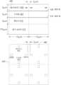
도 2는 픽셀 파이프라인의 블록도이다.
도 3a는 디스플레이 상의 스마트 픽셀 배열(arrangement)의 평면도이다.
도 3b는 기판 상의 스마트 픽셀의 단면도이다.
도 4a 내지 도 4e는 스마트 픽셀 제조 프로세스를 예시한 단면도 및 평면도이다.
도 5a는 임의의 기판 상의 스마트 픽셀 배치(placement)를 예시한다.
도 5b는 픽셀을 지나 연장되지 않는 경계를 갖는 디스플레이를 예시한다.Embodiments of the present disclosure have other advantages and features that will become more readily apparent from the following detailed description and appended claims when considered in conjunction with the embodiments of the accompanying drawings.
1A is a cross-sectional view of a smart pixel.
Figure 1b is a top view of a smart pixel.
Figure 2 is a block diagram of the pixel pipeline.
Figure 3A is a top view of a smart pixel arrangement on a display.
Figure 3b is a cross-sectional view of a smart pixel on a substrate.
4A-4E are cross-sectional and top views illustrating the smart pixel manufacturing process.
Figure 5A illustrates smart pixel placement on an arbitrary substrate.
Figure 5B illustrates a display with a border that does not extend beyond the pixels.
도면 및 다음 설명은 단지 예시로서 바람직한 실시예에 관한 것이다. 다음의 논의로부터, 본 명세서에 개시된 구조 및 방법의 대안적인 실시예는 청구범위에 기재된 내용의 원리로부터 벗어나지 않는 범위에서 사용될 수 있는 실행 가능한 대안으로서 쉽게 인식될 것이라는 점에 유의해야 한다.The drawings and the following description relate to preferred embodiments by way of example only. It should be noted that from the following discussion, alternative embodiments of the structures and methods disclosed herein will be readily recognized as viable alternatives that can be used without departing from the principles of the claims.
LED 기반 디스플레이에 대한 전통적인 접근 방식은 집적 회로 세트를 사용하여 들어오는 디지털 이미지 데이터를 어레이의 LED를 올바르게 동작시키는 데 필요한 아날로그 구동 신호로 변환한다. 예를 들어, 일부 집적 회로는 컬러 보정, 밝기 보정, 온도 보상 및/또는 노화 보정을 수행할 수 있다. 이러한 모든 기능은 특정 디바이스의 응답을 특성화하는 교정 데이터의 도움을 받을 수 있다. 디바이스별 특성을 설명하기 위해 이미지 데이터가 처리되면 구동 회로가 있는 또 다른 집적 회로를 사용하여 이러한 조정된 값을 LED를 작동시키는 데 필요한 구동 신호로 변환할 수 있다.The traditional approach to LED-based displays uses a set of integrated circuits to convert incoming digital image data into the analog drive signals needed to properly operate the array's LEDs. For example, some integrated circuits may perform color correction, brightness correction, temperature compensation, and/or aging correction. All of these functions can benefit from calibration data that characterizes the response of a specific device. Once the image data has been processed to characterize device-specific characteristics, another integrated circuit with driver circuitry can be used to convert these adjusted values into the drive signals needed to operate the LED.
집적 회로의 칩셋에 기초한 이러한 접근 방식은 특정 애플리케이션에 대해 단점이 있다. 예를 들어, 하나의 칩셋에 별도의 칩을 설계하고 제조해야 한다. 또한 이러한 칩은 최종 디스플레이 제품의 어딘가에 배치되어야 할 것이다. 이러한 칩을 디스플레이 주변회로 주위에 배치하면, 디스플레이 테두리 너비가 늘어나 진정한 테두리 없는 디스플레이 생산을 방해한다. 디스플레이의 LED 요소 뒤에 배치하면 제품의 전체 두께가 늘어난다. 별도의 칩을 사용하려면 칩 간의 인터커넥트도 필요하다. 이는 픽셀 수가 많고 비디오 프레임 속도가 높으며/높거나 파이프라인이 복잡한 경우 중요할 수 있다.This approach, based on chipsets of integrated circuits, has drawbacks for certain applications. For example, separate chips must be designed and manufactured in one chipset. Additionally, these chips will have to be placed somewhere in the final display product. Placing these chips around the display peripheral circuitry increases the width of the display border, preventing the production of a truly borderless display. Placing it behind the LED elements of the display increases the overall thickness of the product. Using separate chips also requires interconnection between the chips. This can be important for high pixel counts, high video frame rates, and/or complex pipelines.
이러한 접근법이 사용되는 한 가지 이유는 LED 어레이가 LED의 단일 다이일 수 있기 때문이다. 일부 경우에는 구동기 회로가 단일 다이 상에 제조되어 LED가 포함된 다이에 접합될 수도 있다. 그러나 이 자체가 특정 애플리케이션에서 단점을 가질 수 있다. 예를 들어, 디스플레이가 크면 LED 다이와 구동기 회로가 있는 다이도 크기가 디스플레이와 비슷해야 하기 때문에 커야 한다. 이렇게 큰 다이를 제조하는 것은 어려울 수 있다. 쉽게 제조할 수 있더라도 비용이 불필요하게 많이 들 것이다. 반도체 다이의 비용은 대략 다이 면적에 비례한다. 회로가 실제 사용된 영역보다 작게 들어갈 수 있다면 추가 다이 영역은 불필요한 비용이 된다. 또한, 반도체 다이는 일반적으로 불투명하다. 디스플레이 전체 영역을 덮는 불투명 다이는 시스루(see-through) 디스플레이 생성을 방지한다.One reason this approach is used is that the LED array can be a single die of LEDs. In some cases, the driver circuit may be fabricated on a single die and bonded to the die containing the LED. However, this itself can have disadvantages in certain applications. For example, if the display is large, the LED die and the die containing the driver circuitry must also be large because they must be similar in size to the display. Manufacturing such large dies can be difficult. Even if it were easy to manufacture, it would be unnecessarily expensive. The cost of a semiconductor die is roughly proportional to the die area. If the circuit can fit smaller than the actual area used, the additional die area becomes an unnecessary cost. Additionally, semiconductor dies are generally opaque. An opaque die that covers the entire display area prevents the creation of a see-through display.
아래에 설명된 특정 실시예에서, 디스플레이는 "스마트 픽셀"을 사용하여 생성된다. 스마트 픽셀은 별도의 집적 회로를 사용하는 대신 픽셀 파이프라인을 픽셀의 일부로 통합하는 디스플레이의 픽셀이다. 스마트 픽셀은 발광 소자, 해당 픽셀에 대한 디지털 데이터를 수신하기 위한 외부 데이터 콘택, 디지털 데이터에서 발광 소자로의 픽셀 파이프라인을 포함하는 통합 스택을 기반으로 할 수 있다.In certain embodiments described below, the display is created using “smart pixels.” A smart pixel is a pixel in a display that integrates the pixel pipeline as part of the pixel, rather than using a separate integrated circuit. A smart pixel may be based on an integrated stack that includes a light-emitting element, an external data contact for receiving digital data for that pixel, and a pixel pipeline from digital data to the light-emitting element.
예를 들어, 스마트 픽셀의 통합 스택은 디스플레이의 개별 컬러 픽셀에 대한 광을 생성하는 GaN 발광 다이오드(LED)를 포함할 수 있다. LED 자체는 다른 컬러일 수도 있고, 양자점과 같은 컬러 변환 재료와 함께 사용될 수도 있다. 스택에는 컬러 공간의 개별 컬러 픽셀을 나타내는 디지털 데이터를 수신하는 외부 콘택도 포함되어 있다. 예를 들어, 스마트 픽셀은 RGB, YUV 또는 기타 표준화된 컬러 픽셀 표현을 수신할 수 있다. 스택에는 픽셀 파이프라인을 구현하는 메모리와 CMOS 아날로그 및 디지털 회로도 포함될 수 있다. 메모리는 교정 데이터를 저장할 수 있으며 픽셀 파이프라인은 컬러, 밝기를 수정하거나 온도를 조정하기 위해 이러한 데이터를 사용하여 교정을 적용할 수 있다.For example, an integrated stack of smart pixels may include GaN light-emitting diodes (LEDs) that generate light for individual color pixels of the display. The LEDs themselves may be different colors, or may be used with color-converting materials such as quantum dots. The stack also contains external contacts that receive digital data representing individual color pixels in the color space. For example, a smart pixel may receive RGB, YUV, or other standardized color pixel representation. The stack can also include memory and CMOS analog and digital circuits that implement the pixel pipeline. Memory can store correction data, and the pixel pipeline can use this data to apply corrections to modify color, brightness, or adjust temperature.
도 1a 및 도 1b는 스마트 픽셀(100)의 단면도 및 평면도이다. 도 1a에서, 스마트 픽셀은 아래에서 위로 CMOS 메모리층(110), CMOS 디지털층(120), CMOS 아날로그층(130) 및 사이에 접합부(140)를 갖는 발광층(150)을 포함한다. 스마트 픽셀(100)은 픽셀이 표시할 광을 나타내는 디지털 데이터를 수신한다. 예를 들어, 디지털 데이터는 표준 RGB 또는 YUV 컬러 형식일 수도 있고 CIE 컬러 공간과 같은 표준 컬러 공간을 사용하여 컬러를 표현할 수도 있다. 스마트 픽셀은 이러한 디지털 데이터를 발광층(150)의 LED(160)에 대한 구동 신호로 변환하는 파이프라인(픽셀 파이프라인으로 지칭됨)을 포함한다.1A and 1B are a cross-sectional view and a top view of the
메모리층(110)은 교정 데이터를 보유하는 SRAM 셀을 포함할 수 있다. 이 교정 데이터는 디바이스 응답의 변화, 디바이스 노화의 영향, 온도 영향을 보상하거나 주변 조명 수준에 기초하여 디스플레이를 조정하는 데 사용될 수 있다. 어떤 경우에는 SRAM에 저장된 보정 데이터를 사용하여 제조 중에 픽셀을 보정할 수 있으므로 추가 보정이 필요하지 않다. 또는 제조 후에 교정 데이터를 로드할 수도 있다.
디지털 층(120)은 예를 들어 교정 데이터에 따라 입력 디지털 데이터에 교정을 적용하는 디지털 회로를 포함한다. 아날로그 층(130)은 디지털 신호를 LED(160)에 대한 아날로그 구동 신호로 변환한다. 이 예에서, LED(160)는 청색 질화 갈륨 LED이고, 양자점과 같은 컬러 변환 재료(170)가 청색 광을 일부 LED에 대해 적색 또는 녹색으로 변환하는 데 사용된다. 대안적인 설계에서, LED(160)는 서로 다른 컬러의 LED일 수 있다. 광학 웨지나 렌즈와 같은 추가 구성 요소를 스택에 추가하여 나가는 광을 성형할 수 있다.
이 예에서, 통합 스택의 풋프린트가 LED(160)에 의해 결정된다. CMOS 층(110, 120, 130)은 LED보다 면적이 현저히 크지 않다. 이는 더 큰 면적의 층에 비해 CMOS 층의 비용을 줄여준다. 또한 투명 디스플레이의 불투명 CMOS 층에 의해 차단되는 광의 양을 줄인다. LED(160)는 바람직하게는 면적 풋프린트를 줄이기 위해 조밀하게 패킹된다. 예를 들어, 한 픽셀 내의 LED는 500nm 이하로 분리될 수 있다.In this example, the footprint of the integrated stack is determined by
이 예에서 LED(160)는 LED에 대한 하나의 콘택이기도 한 바닥 반사기(162), p-도핑 GaN 층(163), 활성 영역(164) 및 n-도핑 GaN 층(165)을 포함한다. LED에 대한 공통 콘택은 n-도핑된 GaN에 대한 콘택에 의해 제공될 수 있다. 개별 LED(160)는 컬러 변환 재료(170) 사이를 포함하여 격리 영역(167 및 177)에 의해 분리된다. 격리 영역(167 및 177)은 전기적 격리(예: 유전체 재료), 광학적 격리(예: 반사층) 또는 둘 다(예: 반사 금속으로 코팅된 절연체)를 제공할 수 있다. 영역(177)은 알루미늄 또는 다른 금속일 수 있으며, 이에 따라 LED 사이의 광학적 격리와 n-도핑된 GaN 층에 대한 공통 콘택을 모두 제공한다. LED에 대한 하단 콘택이기도 한 하단 반사경(162)은, CMOS 아날로그 다이(130)에 접합(140)된다. 이 예에서, 층(110, 120, 130, 160)은 별도의 다이 상에 제조된 후 함께 접합되어 수직의 통합 스택을 생성한다. 통합 스택에는 교정 보정을 구현하는 픽셀 파이프라인이 포함되어 있으므로 픽셀은 전원 및 디지털 데이터에 대해서만 콘택을 사용하여 작동될 수 있다.In this example,
도 1b는 스마트 픽셀의 평면도이다. 픽셀(100)은 서로 다른 컬러, 즉 2개의 적색, 1개의 청색 및 1개의 녹색의 4개의 하위 픽셀(105)을 포함한다. 적색과 녹색 하위 픽셀은 도 1a와 같이 컬러 변환 재료를 사용한다. 청색 하위 픽셀은 컬러 변환 없이 청색 LED를 사용한다. 도 1b는 또한 서브픽셀 사이의 광학적 격리(177)를 도시한다. 4개의 외부 콘택(180)이 도 1b에 도시되어 있다: 하나는 디지털 데이터용(DATA), 하나는 아날로그 회로에 대한 전력용(Analog rail), 하나는 디지털 회로에 대한 전력용(Digital rail) 및 하나는 접지(GND)용. 이 예에서, 외부 콘택 DATA(180)는 픽셀 파이프라인에 대한 유일한 외부 신호 콘택이다. 외부 콘택(180)은 통합 스택의 측면 상에 위치하므로 평면도에서 직접 볼 수 없기 때문에 도 1b에서는 점선으로 표시된다.Figure 1b is a top view of a smart pixel.
도 2는 스마트 픽셀(100) 내에 포함된 픽셀 파이프라인의 블록도이다. 디지털 데이터(205)는 픽셀 파이프라인에 대한 입력이다. 예를 들어, 디지털 데이터(205)가 픽셀에 대한 색도 및 밝기 값을 포함할 수 있다. 이들 값은 CMOS 디지털 로직(220)에 의해 처리된다. 디지털 로직은 주변 광, 온도 또는 노후화와 같은 다른 요인에 대한 교정 수정 또는 조정을 수행할 수 있다. 컬러 보정, 색역 보정(color gamut correction), 밝기 보정 및 온도 보상은 디지털 로직(220)에 의해 수행될 수 있는 기능의 일부 예이다. 보정 데이터(210)는 스마트 픽셀 내의 SRAM에 저장될 수 있다. 스마트 픽셀은 또한 센서나 타이머와 같은 다른 데이터 소스(215)를 포함할 수도 있다. 이 데이터는 또한 스마트 픽셀 외부에서 생성된 다음 컬러 정보(205)와 함께 스마트 픽셀로 전송될 수 있다. 한 가지 접근법에서, 스마트 픽셀은 데이터 버스에 연결되고 데이터는 데이터 버스를 통해 픽셀로 전송된다. 수정된 디지털 신호는 CMOS 아날로그 구동기(230)에 의해 LED 구동 신호로 변환된다. 이는 개개의 LED(260)를 구동한다.Figure 2 is a block diagram of the pixel pipeline included within
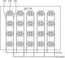
도 3a는 디스플레이 상의 스마트 픽셀 배열의 평면도이다. 디스플레이는 기판(305)을 포함하고, 스마트 픽셀(300)은 기판 상에 배열되어 디스플레이의 컬러 픽셀을 형성한다. 기판은 유리나 플라스틱과 같은 투명한 재료를 포함할 수 있다. 천과 같은 유연한 소재도 포함될 수 있다. 이 예에서, 스마트 픽셀(300)은 20um 정사각형이다. 이들은 600um 피치의 직사각형 어레이로 배열된다. 기판이 투명한 경우 픽셀 사이에 상당한 클리어 공간이 있어 디스플레이가 시스루가 될 것이다.Figure 3A is a top view of a smart pixel array on a display. The display includes a substrate 305, and
도 3b는 기판(305) 상의 스마트 픽셀(300)의 단면도이다. 이 예에서, 기판(305)은 함몰부(330)를 갖는다. 스마트 픽셀(300)은 이들 웰(330)에 안착되고 에폭시(332)에 의해 부착된다. 이러한 스마트 픽셀의 높이는 너비보다 크며, 이 예에서는 높이가 75um이고 너비가 20um이다. 도 3b는 또한 통합 스택의 측면 상의 전기 콘택(380)을 도시한다. 이들 콘택(380)은 도 3a에 도시된 바와 같이 기판 상의 금속 인터커넥트(382)에 연결된다. 도 3a의 평면도는 스마트 픽셀 어레이의 좌측 및 우측에 연결되어 픽셀에 DATA 및 POWER을 제공하는 인터커넥트(382)를 도시한다. 다른 신호를 제공하기 위해 추가 인터커넥트가 사용될 수도 있다.3B is a cross-sectional view of
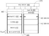
도 4a 내지 4e는 웨이퍼 레벨 프로세스를 이용하여 스마트 픽셀을 제조하는 프로세스를 예시한 단면도 및 평면도이다. 각 도의 상단 부분은 웨이퍼에서 인접한 두 픽셀의 단면도를 보여주고, 하단 부분은 픽셀의 2x2 섹션의 평면도를 보여준다. 이 예에서 각 픽셀의 면적은 15um2이다. 도 4a의 단면도는 서로 접합된 3개의 CMOS 웨이퍼, 즉 CMOS 아날로그 층(430), CMOS 디지털 층(420) 및 CMOS 메모리 층(410)을 도시한다. 이 구조에서, 아날로그 및 디지털 층(430 및 420)은 5um 두께로 얇아졌다. 메모리 층(410)은 일부 벌크 실리콘(415)을 포함한다. 한 가지 접근법에서, 아날로그 웨이퍼(430)와 디지털 웨이퍼(420)는 접합 층(422)에 의해 서로 접합된다. 그 후, 디지털 웨이퍼(420)는 5um로 얇아질 수 있다. 그 다음, 이 조합은 접합층(412)에 의해 메모리 웨이퍼(410)에 접합된다. 그 다음, 아날로그 웨이퍼(430)는 얇아지고 평탄화될 수 있다.Figures 4A-4E are cross-sectional and top views illustrating a process for manufacturing smart pixels using a wafer level process. The top part of each figure shows a cross-section of two adjacent pixels on the wafer, while the bottom part shows a top view of a 2x2 section of the pixel. In this example, the area of each pixel is 15um2 . The cross-sectional view of FIG. 4A shows three CMOS wafers bonded together: a
아날로그 층(430)은 결국 측면 콘택에 연결될 전기 콘택(482)을 포함한다. 이러한 전기 콘택(482)은 층을 통해 라우팅함으로써 다른 층에 신호를 제공할 수 있다. 대안적으로, 전기 콘택이 서로 다른 층에 제공될 수 있다. 인접한 픽셀의 콘택(482)은 짧은 거리(이 예에서는 2um)만큼 분리되어 있다. 평면도는 아날로그 층(430)의 최상부 표면을 도시한다. 예시를 위해, 전기 콘택(482)도 도시된다.
도 4b에서, 깊은 실리콘 에칭은 전기 콘택(482)을 노출시키는 트렌치(484)를 생성한다. 도 4b 내지 4d에서는 픽셀 간의 처리만 표시된다. 예를 들어, 트렌치(484)는 도 4b의 도면의 가장자리에도 존재할 것이지만 명확성을 위해 도시되지는 않았다. 일부 경우에, 콘택(482)은 에칭 전에 구축될 수 있다. 예를 들어, 콘택(482)이 구리인 경우 콘택에 구리 비아를 생성함으로써 수직 방향으로 확장될 수 있다. 그러면 트렌치(484)는 콘택(482)과 구리 비아를 모두 노출시킬 것이다.4B, a deep silicon etch creates a
그 다음, 도 4c에 도시된 바와 같이 금속(485)이 트렌치(484) 내에 증착된다. 도 4c에서, GaN LED 웨이퍼는 디바이스 스택에 접합된다. 도 4c는 LED 층(460) 및 개별 서브픽셀(470)에 대한 컬러 변환 재료를 도시한다. 깊은 트렌치(486)가 금속(485)에 에칭되어 각 금속 충전물을 두 조각으로 분할한다. 각 조각(485)은 2개의 인접한 픽셀 중 하나에 대한 측면 콘택 역할을 한다.
도 4d에서, 씨닝 테이프(490)는 통합 스택의 LED 측에 부착된다. 다른 유형의 지원이 사용될 수 있다. 도 4e에서 스택은 CMOS 측에서 얇아졌다. 씨닝이 트렌치(486)에 도달하면, 이는 도 4e에 도시된 바와 같이 웨이퍼를 개별 스마트 픽셀로 단일화할 것이다. 이전 도면과 달리, 도 4e는 인접한 픽셀 사이의 구조뿐만 아니라 픽셀 가장자리의 구조도 보여준다.In Figure 4D, thinning tape 490 is attached to the LED side of the integrated stack. Other types of support may be used. In Figure 4e, the stack is thinned on the CMOS side. Once thinning reaches
도 4a 내지 4e의 예에서, 서로 다른 CMOS 기능은 서로 다른 층(웨이퍼)(410, 420, 430)에 의해 제공된다. 대안적으로, CMOS 기능은 단일 실리콘 웨이퍼로 제조될 수 있으며, 이는 이후 LED를 포함하는 기판에 접합된다.4A-4E, different CMOS functions are provided by different layers (wafers) 410, 420, 430. Alternatively, the CMOS function can be fabricated from a single silicon wafer, which is then bonded to a substrate containing the LEDs.
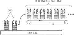
도 5a는 임의의 기판(505) 상의 스마트 픽셀(500)의 배치를 예시한다. 이 예에서, 기판은 각 픽셀에 전력 및 데이터를 공급하기만 하면 된다. 메모리나 외부 로직이 필요하지 않다. 데이터는 픽셀 주소 데이터를 포함할 수 있다. 픽 앤 플레이스 머신(590)은 도 4의 테이프에서 개별 스마트 픽셀을 선택하고 각 스마트 픽셀을 기판(505) 상의 정확한 위치에 배치한다. 대형 디스플레이의 경우 작은 픽셀이 서로 이격되어 있을 수 있다.Figure 5A illustrates the placement of
대안적인 시나리오에서, 스마트 픽셀(500)은 웨이퍼 제조 후에 서로 분리될 필요가 없다. 잘리지 않은 스마트 픽셀 어레이는 경계 없는 디스플레이를 형성할 수 있다. 예를 들어, 도 5b는 디스플레이의 에지(580)가 픽셀 경계를 넘어 확장되지 않는 디스플레이를 예시한다. 기존 디스플레이는 흔히 메모리 및 기타 백플레인 기능을 담당하는 추가 다이 영역으로 둘러싸여 있다. 경계 없는 디스플레이에는 발광, 컬러 변환, CMOS 아날로그, CMOS 디지털 및 메모리 회로가 관련된 각 웨이퍼 표면에 수직인 방향으로 적층될 수 있으므로 추가 영역이 필요하지 않다.In an alternative scenario,
상세한 설명에 많은 세부 사항이 포함되어 있지만, 이는 본 발명의 범위를 제한하는 것으로 해석되어서는 안 되며, 단지 다양한 실시예를 예시하는 것으로 해석되어야 한다. 본 개시의 범위는 위에서 상세히 논의되지 않은 다른 실시예를 포함한다는 것을 이해해야 한다. 명백할 첨부된 청구범위에 정의된 정신 및 범위 내에서, 본원에 개시된 방법 및 디바이스의 어레이, 작동 및 세부 사항에 대한 다양한 다른 수정, 변경 및 변형이 당업자에게 자명할 것이다. 따라서, 본 발명의 범위는 첨부된 청구범위 및 그 법적 등가물에 의해 결정되어야 한다.Although numerous details are included in the detailed description, they should not be construed as limiting the scope of the invention, but rather as merely illustrative of various embodiments. It should be understood that the scope of the present disclosure includes other embodiments not discussed in detail above. Various other modifications, changes and variations to the array, operation and details of the methods and devices disclosed herein will be apparent to those skilled in the art, within the spirit and scope defined in the appended claims. Accordingly, the scope of the present invention should be determined by the appended claims and their legal equivalents.
Claims (23)
Translated fromKorean기판과,
상기 디스플레이의 컬러 픽셀을 형성하기 위해 상기 기판 상에 배열된 복수의 디바이스를 포함하고,
상기 복수의 디바이스 각각은 통합 스택을 포함하며,
상기 통합 스택은,
상기 디스플레이의 개별 컬러 픽셀에 대한 광을 생성하는 적어도 2개의 GaN 발광 다이오드(LED)와,
컬러 공간에서 상기 개별 컬러 픽셀을 나타내는 디지털 데이터를 수신하기 위한 외부 데이터 콘택(contact)과,
상기 외부 데이터 콘택과 상기 LED 사이의 픽셀 파이프라인 - 상기 픽셀 파이프라인은 상기 디지털 데이터를 상기 LED용 구동 신호로 변환함 - 을 포함하는
디스플레이.As a display,
substrate,
comprising a plurality of devices arranged on the substrate to form color pixels of the display,
Each of the plurality of devices includes an integrated stack,
The integrated stack is,
at least two GaN light emitting diodes (LEDs) that generate light for individual color pixels of the display;
an external data contact for receiving digital data representing the individual color pixels in color space;
a pixel pipeline between the external data contact and the LED, wherein the pixel pipeline converts the digital data into a driving signal for the LED.
display.
상기 외부 데이터 콘택은 상기 픽셀 파이프라인에 대한 유일한 외부 신호 콘택인
디스플레이.According to paragraph 1,
The external data contact is the only external signal contact to the pixel pipeline.
display.
상기 개별 컬러 픽셀은 서로 다른 컬러의 적어도 2개의 서브픽셀을 포함하는
디스플레이.According to paragraph 2,
The individual color pixel includes at least two subpixels of different colors.
display.
상기 디지털 데이터는 표준화된 컬러 포맷인
디스플레이.According to paragraph 2,
The digital data is in a standardized color format.
display.
각각의 디바이스는 데이터 버스에 연결되는
디스플레이.According to paragraph 1,
Each device is connected to a data bus.
display.
상기 외부 데이터 콘택은 상기 통합 스택의 측면 상에 위치하는
디스플레이.According to paragraph 1,
The external data contact is located on the side of the integrated stack.
display.
상기 LED는 서로 다른 컬러의 LED인
디스플레이.According to paragraph 1,
The LEDs are LEDs of different colors.
display.
상기 LED는 동일한 컬러의 LED이고, 상기 통합 스택은 상기 LED 중 적어도 하나로부터의 광을 상이한 컬러으로 변환하기 위한 컬러 변환 재료를 더 포함하는
디스플레이.According to paragraph 1,
wherein the LEDs are LEDs of the same color, and the integrated stack further comprises a color conversion material for converting light from at least one of the LEDs into a different color.
display.
상기 기판에 함몰(depression)이 있고, 상기 디바이스는 상기 함몰 내에 위치하는
디스플레이.According to paragraph 1,
There is a depression in the substrate, and the device is located within the depression.
display.
상기 기판은 유연한
디스플레이.According to paragraph 1,
The substrate is flexible
display.
상기 기판은 투명하고,
상기 디바이스는 상기 기판 면적의 25% 미만을 차지하는
디스플레이.According to paragraph 1,
The substrate is transparent,
The device occupies less than 25% of the substrate area.
display.
상기 기판은 상기 디바이스 주위에 경계선이 없는
디스플레이.According to paragraph 1,
The substrate has no border around the device.
display.
기판과,
상기 디스플레이의 픽셀을 형성하기 위해 상기 기판 상에 배열된 복수의 디바이스를 포함하고,
상기 복수의 디바이스 각각은 통합 스택을 포함하며,
상기 통합 스택은,
상기 디스플레이의 하나 이상의 픽셀 세트를 위한 발광 소자와,
상기 픽셀 세트를 나타내는 디지털 데이터를 수신하기 위한 외부 데이터 콘택과,
상기 외부 데이터 콘택과 상기 발광 소자 사이의 하나 이상의 픽셀 파이프라인 세트 - 상기 픽셀 파이프라인은 상기 디지털 데이터를 상기 발광 소자에 대한 구동 신호로 변환함 - 를 포함하는
디스플레이.As a display,
substrate,
comprising a plurality of devices arranged on the substrate to form pixels of the display,
Each of the plurality of devices includes an integrated stack,
The integrated stack is,
a light emitting element for one or more sets of pixels of the display;
an external data contact for receiving digital data representing the set of pixels;
A set of one or more pixel pipelines between the external data contact and the light-emitting device, wherein the pixel pipeline converts the digital data into a driving signal for the light-emitting device.
display.
상기 디바이스는 통합 스택을 포함하고,
상기 통합 스택은,
상기 디스플레이의 개별 컬러 픽셀에 대한 광을 생성하는 적어도 2개의 GaN 발광 다이오드(LED)와,
컬러 공간에서 상기 개별 컬러 픽셀을 나타내는 디지털 데이터를 수신하기 위한 외부 데이터 콘택과,
상기 외부 데이터 콘택과 상기 LED 사이의 픽셀 파이프라인 - 상기 픽셀 파이프라인은 상기 디지털 데이터를 LED용 구동 신호로 변환함 - 을 포함하는
디바이스.A device for displaying color pixels of a display, comprising:
The device includes an integrated stack,
The integrated stack is,
at least two GaN light emitting diodes (LEDs) that generate light for individual color pixels of the display;
an external data contact for receiving digital data representing the individual color pixel in color space;
a pixel pipeline between the external data contact and the LED, the pixel pipeline converting the digital data into a driving signal for the LED.
device.
상기 통합 스택은,
상기 디바이스에 대한 교정 데이터를 저장하는 메모리를 포함하며, 상기 픽셀 파이프라인은 상기 구동 신호를 생성할 때 상기 교정 데이터를 적용하는
디바이스.According to clause 14,
The integrated stack is,
and a memory that stores calibration data for the device, wherein the pixel pipeline applies the calibration data when generating the driving signal.
device.
상기 교정 데이터는 컬러 교정 데이터를 포함하고, 상기 픽셀 파이프라인은 상기 수신된 디지털 데이터를 상기 컬러 교정 데이터에 따라 상기 구동 신호로 변환하는
디바이스.According to clause 15,
The correction data includes color correction data, and the pixel pipeline converts the received digital data into the driving signal according to the color correction data.
device.
상기 교정 데이터는 밝기 교정 데이터를 포함하고,
상기 픽셀 파이프라인은 상기 수신된 디지털 데이터를 상기 밝기 교정 데이터에 따라 상기 구동 신호로 변환하는
디바이스.According to clause 15,
The correction data includes brightness correction data,
The pixel pipeline converts the received digital data into the driving signal according to the brightness correction data.
device.
상기 교정 데이터는 온도 교정 데이터를 포함하고,
상기 픽셀 파이프라인은 상기 수신된 디지털 데이터를 상기 온도 교정 데이터에 따라 상기 구동 신호로 변환하는
디바이스.According to clause 15,
The calibration data includes temperature calibration data,
The pixel pipeline converts the received digital data into the driving signal according to the temperature correction data.
device.
상기 통합 스택의 상기 픽셀 파이프라인은 CMOS 아날로그 회로, CMOS 디지털 회로 및 메모리를 포함하는
디바이스.According to clause 14,
The pixel pipeline of the integrated stack includes CMOS analog circuitry, CMOS digital circuitry, and memory.
device.
상기 통합 스택은,
상기 LED 사이의 절연체를 더 포함하는
디바이스.According to clause 14,
The integrated stack is,
Further comprising an insulator between the LEDs
device.
상기 통합 스택의 베이스는 상기 LED의 면적보다 크지 않은 면적을 갖는
디바이스.According to clause 14,
The base of the integrated stack has an area no larger than that of the LED.
device.
상기 통합 스택의 높이는 상기 통합 스택의 폭보다 더 큰
디바이스.According to clause 14,
The height of the integrated stack is greater than the width of the integrated stack.
device.
상기 LED는 500nm 이하만큼 분리되어 있는
디바이스.According to clause 14,
The LEDs are separated by less than 500 nm.
device.
Applications Claiming Priority (3)
| Application Number | Priority Date | Filing Date | Title |
|---|---|---|---|
| US202163197042P | 2021-06-04 | 2021-06-04 | |
| US63/197,042 | 2021-06-04 | ||
| PCT/US2022/031999WO2022256553A1 (en) | 2021-06-04 | 2022-06-02 | Display pixels with integrated pipeline |
Publications (1)
| Publication Number | Publication Date |
|---|---|
| KR20240018582Atrue KR20240018582A (en) | 2024-02-13 |
Family
ID=84284314
Family Applications (1)
| Application Number | Title | Priority Date | Filing Date |
|---|---|---|---|
| KR1020247000247APendingKR20240018582A (en) | 2021-06-04 | 2022-06-02 | Display pixels with integrated pipeline |
Country Status (3)
| Country | Link |
|---|---|
| US (1) | US11699383B2 (en) |
| EP (1) | EP4348563A4 (en) |
| KR (1) | KR20240018582A (en) |
Families Citing this family (1)
| Publication number | Priority date | Publication date | Assignee | Title |
|---|---|---|---|---|
| US12349250B2 (en)* | 2023-01-19 | 2025-07-01 | Goodrich Lighting Systems, Inc. | Night vision imaging system (NVIS) compatible lighting with an adjustable melanopic photopic ratio |
Family Cites Families (21)
| Publication number | Priority date | Publication date | Assignee | Title |
|---|---|---|---|---|
| US6731295B1 (en)* | 1998-11-09 | 2004-05-04 | Broadcom Corporation | Graphics display system with window descriptors |
| US7623560B2 (en)* | 2007-09-27 | 2009-11-24 | Ostendo Technologies, Inc. | Quantum photonic imagers and methods of fabrication thereof |
| US9153171B2 (en) | 2012-12-17 | 2015-10-06 | LuxVue Technology Corporation | Smart pixel lighting and display microcontroller |
| US9252375B2 (en) | 2013-03-15 | 2016-02-02 | LuxVue Technology Corporation | Method of fabricating a light emitting diode display with integrated defect detection test |
| US9111464B2 (en) | 2013-06-18 | 2015-08-18 | LuxVue Technology Corporation | LED display with wavelength conversion layer |
| US9444015B2 (en) | 2014-06-18 | 2016-09-13 | X-Celeprint Limited | Micro assembled LED displays and lighting elements |
| CA2873476A1 (en) | 2014-12-08 | 2016-06-08 | Ignis Innovation Inc. | Smart-pixel display architecture |
| KR102354433B1 (en)* | 2015-07-16 | 2022-01-24 | 삼성디스플레이 주식회사 | Display appratus |
| FR3044467B1 (en) | 2015-11-26 | 2018-08-10 | Commissariat A L'energie Atomique Et Aux Energies Alternatives | LIGHT DALLE AND METHOD FOR MANUFACTURING SUCH LIGHT SLAB |
| US10923023B1 (en) | 2016-01-26 | 2021-02-16 | Apple Inc. | Stacked hybrid micro LED pixel architecture |
| EP3249639A1 (en) | 2016-05-26 | 2017-11-29 | Nederlandse Organisatie voor toegepast- natuurwetenschappelijk onderzoek TNO | Conformable matrix display device |
| DE102017106755B4 (en) | 2017-03-29 | 2022-08-18 | OSRAM Opto Semiconductors Gesellschaft mit beschränkter Haftung | Method for producing an optoelectronic semiconductor component and optoelectronic semiconductor component |
| TWI611573B (en) | 2017-06-09 | 2018-01-11 | 晶典有限公司 | Method for manufacturing micro light emitting diode display module |
| US10439101B2 (en)* | 2017-08-18 | 2019-10-08 | Intel Corporation | Micro light-emitting diode (LED) elements and display |
| DE102017123290A1 (en) | 2017-10-06 | 2019-04-11 | Osram Opto Semiconductors Gmbh | Light-emitting component, display device and method for producing a display device |
| US10437402B1 (en) | 2018-03-27 | 2019-10-08 | Shaoher Pan | Integrated light-emitting pixel arrays based devices by bonding |
| FR3083045B1 (en) | 2018-06-26 | 2020-07-31 | Aledia | ELECTROLUMINESCENT DIODES OPTOELECTRONIC DEVICE |
| KR102668256B1 (en) | 2018-11-27 | 2024-05-21 | 엘지디스플레이 주식회사 | Stretchable display device |
| US11295680B2 (en)* | 2019-04-11 | 2022-04-05 | PixelDisplay, Inc. | Method and apparatus of a multi-modal illumination and display for improved color rendering, power efficiency, health and eye-safety |
| US11710760B2 (en)* | 2019-06-21 | 2023-07-25 | Semiconductor Energy Laboratory Co., Ltd. | Display device, display module, electronic device, and manufacturing method of display device |
| KR102840056B1 (en)* | 2019-07-02 | 2025-08-01 | 삼성디스플레이 주식회사 | Display device |
- 2022
- 2022-06-02EPEP22816867.0Apatent/EP4348563A4/enactivePending
- 2022-06-02KRKR1020247000247Apatent/KR20240018582A/enactivePending
- 2022-06-09USUS17/836,966patent/US11699383B2/enactiveActive
Also Published As
| Publication number | Publication date |
|---|---|
| US20220392395A1 (en) | 2022-12-08 |
| EP4348563A1 (en) | 2024-04-10 |
| EP4348563A4 (en) | 2025-03-12 |
| US11699383B2 (en) | 2023-07-11 |
Similar Documents
| Publication | Publication Date | Title |
|---|---|---|
| US10797040B2 (en) | Method of manufacturing display module using LED | |
| US12336346B2 (en) | Method of manufacturing light emitting device package and method of manufacturing display panel using the same | |
| US10403613B2 (en) | Micro LED display module having light transmissive substrate | |
| KR102650341B1 (en) | Display device using semiconductor light emitting device and method for manufacturing | |
| EP3573431B1 (en) | Display device using semiconductor light-emitting element | |
| JP7457255B2 (en) | Image display device manufacturing method and image display device | |
| TWI864041B (en) | Method for manufacturing image display device and image display device | |
| TW201732770A (en) | Semiconductor device having integrated thin film transistor circuit | |
| JP7670712B2 (en) | Display device | |
| CN109244064A (en) | Semiconductor package | |
| US10403614B2 (en) | Micro LED display module | |
| US11031380B2 (en) | Manufacturing method of micro LED display module | |
| JP7669643B2 (en) | Image display device manufacturing method and image display device | |
| JP7507373B2 (en) | Image display device manufacturing method and image display device | |
| US11699383B2 (en) | Display pixels with integrated pipeline | |
| US20240021589A1 (en) | Led display apparatus | |
| US11031523B2 (en) | Manufacturing method of micro LED display module | |
| WO2022256553A1 (en) | Display pixels with integrated pipeline | |
| US12062643B2 (en) | Electronic device | |
| CN115707287A (en) | Display device and method for manufacturing the same | |
| JP2024099072A (en) | Image display device manufacturing method and image display device | |
| TWI838985B (en) | Micro light-emitting diode display device and manufacturing method of the same | |
| US20220238611A1 (en) | Light emitting device | |
| CN115911218A (en) | Micro light emitting diode display device and method of manufacturing the same | |
| WO2021256190A1 (en) | Method for manufacturing image display device and image display device |
Legal Events
| Date | Code | Title | Description |
|---|---|---|---|
| PA0105 | International application | Patent event date:20240103 Patent event code:PA01051R01D Comment text:International Patent Application | |
| PG1501 | Laying open of application | ||
| A201 | Request for examination | ||
| PA0201 | Request for examination | Patent event code:PA02012R01D Patent event date:20250602 Comment text:Request for Examination of Application |