KR20240007178A - semiconductor device - Google Patents
semiconductor deviceDownload PDFInfo
- Publication number
- KR20240007178A KR20240007178AKR1020237040766AKR20237040766AKR20240007178AKR 20240007178 AKR20240007178 AKR 20240007178AKR 1020237040766 AKR1020237040766 AKR 1020237040766AKR 20237040766 AKR20237040766 AKR 20237040766AKR 20240007178 AKR20240007178 AKR 20240007178A
- Authority
- KR
- South Korea
- Prior art keywords
- insulator
- oxide
- transistor
- additionally
- conductor
- Prior art date
- Legal status (The legal status is an assumption and is not a legal conclusion. Google has not performed a legal analysis and makes no representation as to the accuracy of the status listed.)
- Pending
Links
- 239000004065semiconductorSubstances0.000titleclaimsabstractdescription444
- 238000000034methodMethods0.000claimsdescription238
- 230000015572biosynthetic processEffects0.000claimsdescription106
- 229910044991metal oxideInorganic materials0.000claimsdescription84
- 150000004706metal oxidesChemical class0.000claimsdescription84
- 229910052710siliconInorganic materials0.000claimsdescription81
- 239000010703siliconSubstances0.000claimsdescription81
- 239000011701zincSubstances0.000claimsdescription49
- 229910052733galliumInorganic materials0.000claimsdescription27
- 229910052738indiumInorganic materials0.000claimsdescription26
- GYHNNYVSQQEPJS-UHFFFAOYSA-NGalliumChemical compound[Ga]GYHNNYVSQQEPJS-UHFFFAOYSA-N0.000claimsdescription24
- APFVFJFRJDLVQX-UHFFFAOYSA-Nindium atomChemical compound[In]APFVFJFRJDLVQX-UHFFFAOYSA-N0.000claimsdescription24
- 229910052725zincInorganic materials0.000claimsdescription14
- HCHKCACWOHOZIP-UHFFFAOYSA-NZincChemical compound[Zn]HCHKCACWOHOZIP-UHFFFAOYSA-N0.000claimsdescription11
- 238000005259measurementMethods0.000abstractdescription54
- 239000012212insulatorSubstances0.000description1014
- 239000004020conductorSubstances0.000description539
- 239000010408filmSubstances0.000description390
- 229910052760oxygenInorganic materials0.000description273
- 239000001301oxygenSubstances0.000description270
- QVGXLLKOCUKJST-UHFFFAOYSA-Natomic oxygenChemical compound[O]QVGXLLKOCUKJST-UHFFFAOYSA-N0.000description262
- 230000006870functionEffects0.000description207
- 239000000758substrateSubstances0.000description169
- 229910052739hydrogenInorganic materials0.000description163
- 239000001257hydrogenSubstances0.000description163
- UFHFLCQGNIYNRP-UHFFFAOYSA-NHydrogenChemical compound[H][H]UFHFLCQGNIYNRP-UHFFFAOYSA-N0.000description145
- 239000010410layerSubstances0.000description144
- 238000010438heat treatmentMethods0.000description125
- 230000002829reductive effectEffects0.000description119
- 239000012535impuritySubstances0.000description102
- 230000015654memoryEffects0.000description97
- 238000004544sputter depositionMethods0.000description96
- 239000000463materialSubstances0.000description94
- IJGRMHOSHXDMSA-UHFFFAOYSA-NAtomic nitrogenChemical compoundN#NIJGRMHOSHXDMSA-UHFFFAOYSA-N0.000description92
- 210000004027cellAnatomy0.000description87
- 239000007789gasSubstances0.000description83
- XUIMIQQOPSSXEZ-UHFFFAOYSA-NSiliconChemical compound[Si]XUIMIQQOPSSXEZ-UHFFFAOYSA-N0.000description78
- 238000010586diagramMethods0.000description77
- VYPSYNLAJGMNEJ-UHFFFAOYSA-NSilicium dioxideChemical compoundO=[Si]=OVYPSYNLAJGMNEJ-UHFFFAOYSA-N0.000description71
- 238000012545processingMethods0.000description67
- 238000000231atomic layer depositionMethods0.000description61
- 229910052581Si3N4Inorganic materials0.000description60
- HQVNEWCFYHHQES-UHFFFAOYSA-Nsilicon nitrideChemical compoundN12[Si]34N5[Si]62N3[Si]51N64HQVNEWCFYHHQES-UHFFFAOYSA-N0.000description60
- 229910052814silicon oxideInorganic materials0.000description58
- 238000004519manufacturing processMethods0.000description55
- 239000012298atmosphereSubstances0.000description53
- 229910052782aluminiumInorganic materials0.000description52
- XAGFODPZIPBFFR-UHFFFAOYSA-NaluminiumChemical compound[Al]XAGFODPZIPBFFR-UHFFFAOYSA-N0.000description52
- 229910052735hafniumInorganic materials0.000description52
- 229910052751metalInorganic materials0.000description52
- XLYOFNOQVPJJNP-UHFFFAOYSA-NwaterSubstancesOXLYOFNOQVPJJNP-UHFFFAOYSA-N0.000description51
- 229910001868waterInorganic materials0.000description51
- 238000005229chemical vapour depositionMethods0.000description43
- 238000009792diffusion processMethods0.000description43
- VBJZVLUMGGDVMO-UHFFFAOYSA-Nhafnium atomChemical compound[Hf]VBJZVLUMGGDVMO-UHFFFAOYSA-N0.000description43
- 239000013078crystalSubstances0.000description41
- 239000002184metalSubstances0.000description41
- TWNQGVIAIRXVLR-UHFFFAOYSA-Noxo(oxoalumanyloxy)alumaneChemical compoundO=[Al]O[Al]=OTWNQGVIAIRXVLR-UHFFFAOYSA-N0.000description41
- 229910052757nitrogenInorganic materials0.000description38
- 230000001965increasing effectEffects0.000description35
- 230000008569processEffects0.000description33
- 230000004888barrier functionEffects0.000description31
- 238000012546transferMethods0.000description31
- 150000004767nitridesChemical class0.000description28
- 239000000203mixtureSubstances0.000description27
- 238000004549pulsed laser depositionMethods0.000description27
- -1hafnium nitrideChemical class0.000description26
- 238000001451molecular beam epitaxyMethods0.000description26
- OKTJSMMVPCPJKN-UHFFFAOYSA-NCarbonChemical compound[C]OKTJSMMVPCPJKN-UHFFFAOYSA-N0.000description25
- PXHVJJICTQNCMI-UHFFFAOYSA-NNickelChemical group[Ni]PXHVJJICTQNCMI-UHFFFAOYSA-N0.000description24
- 230000007423decreaseEffects0.000description24
- 230000007547defectEffects0.000description24
- 230000002093peripheral effectEffects0.000description24
- 229910052721tungstenInorganic materials0.000description24
- 239000010937tungstenSubstances0.000description24
- 125000004429atomChemical group0.000description23
- 238000004364calculation methodMethods0.000description23
- 229910052799carbonInorganic materials0.000description23
- 230000005669field effectEffects0.000description23
- WFKWXMTUELFFGS-UHFFFAOYSA-NtungstenChemical compound[W]WFKWXMTUELFFGS-UHFFFAOYSA-N0.000description23
- 238000005530etchingMethods0.000description22
- 229910000449hafnium oxideInorganic materials0.000description22
- WIHZLLGSGQNAGK-UHFFFAOYSA-Nhafnium(4+);oxygen(2-)Chemical compound[O-2].[O-2].[Hf+4]WIHZLLGSGQNAGK-UHFFFAOYSA-N0.000description22
- 239000003990capacitorSubstances0.000description20
- 239000011261inert gasSubstances0.000description20
- 150000002431hydrogenChemical class0.000description19
- 239000002356single layerSubstances0.000description19
- 229910052715tantalumInorganic materials0.000description19
- GUVRBAGPIYLISA-UHFFFAOYSA-Ntantalum atomChemical compound[Ta]GUVRBAGPIYLISA-UHFFFAOYSA-N0.000description19
- RTAQQCXQSZGOHL-UHFFFAOYSA-NTitaniumChemical group[Ti]RTAQQCXQSZGOHL-UHFFFAOYSA-N0.000description18
- 238000011156evaluationMethods0.000description18
- 229910052719titaniumInorganic materials0.000description18
- 239000010936titaniumChemical group0.000description18
- RYGMFSIKBFXOCR-UHFFFAOYSA-NCopperChemical group[Cu]RYGMFSIKBFXOCR-UHFFFAOYSA-N0.000description17
- MYMOFIZGZYHOMD-UHFFFAOYSA-NDioxygenChemical compoundO=OMYMOFIZGZYHOMD-UHFFFAOYSA-N0.000description17
- 229910001882dioxygenInorganic materials0.000description17
- 238000001312dry etchingMethods0.000description17
- 230000000694effectsEffects0.000description17
- 239000000523sampleSubstances0.000description17
- 238000004140cleaningMethods0.000description16
- 229910001873dinitrogenInorganic materials0.000description16
- 238000013473artificial intelligenceMethods0.000description15
- 230000010354integrationEffects0.000description15
- 230000035515penetrationEffects0.000description15
- 238000012360testing methodMethods0.000description15
- NRTOMJZYCJJWKI-UHFFFAOYSA-NTitanium nitrideChemical compound[Ti]#NNRTOMJZYCJJWKI-UHFFFAOYSA-N0.000description14
- 229910052802copperInorganic materials0.000description14
- 239000010949copperChemical group0.000description14
- RVTZCBVAJQQJTK-UHFFFAOYSA-Noxygen(2-);zirconium(4+)Chemical compound[O-2].[O-2].[Zr+4]RVTZCBVAJQQJTK-UHFFFAOYSA-N0.000description14
- 230000005855radiationEffects0.000description14
- MZLGASXMSKOWSE-UHFFFAOYSA-Ntantalum nitrideChemical compound[Ta]#NMZLGASXMSKOWSE-UHFFFAOYSA-N0.000description14
- 229910001928zirconium oxideInorganic materials0.000description14
- XKRFYHLGVUSROY-UHFFFAOYSA-NArgonChemical compound[Ar]XKRFYHLGVUSROY-UHFFFAOYSA-N0.000description12
- XEEYBQQBJWHFJM-UHFFFAOYSA-NIronChemical group[Fe]XEEYBQQBJWHFJM-UHFFFAOYSA-N0.000description12
- 229910052759nickelInorganic materials0.000description12
- 230000003647oxidationEffects0.000description12
- 238000007254oxidation reactionMethods0.000description12
- 239000010453quartzSubstances0.000description12
- 239000000126substanceSubstances0.000description12
- KRHYYFGTRYWZRS-UHFFFAOYSA-NFluoraneChemical compoundFKRHYYFGTRYWZRS-UHFFFAOYSA-N0.000description11
- ZOKXTWBITQBERF-UHFFFAOYSA-NMolybdenumChemical compound[Mo]ZOKXTWBITQBERF-UHFFFAOYSA-N0.000description11
- 230000008859changeEffects0.000description11
- 238000000151depositionMethods0.000description11
- 238000013461designMethods0.000description11
- 239000011229interlayerSubstances0.000description11
- 229910052750molybdenumInorganic materials0.000description11
- 239000011733molybdenumSubstances0.000description11
- 229920005989resinPolymers0.000description11
- 239000011347resinSubstances0.000description11
- 229910052707rutheniumInorganic materials0.000description11
- YCKRFDGAMUMZLT-UHFFFAOYSA-NFluorine atomChemical compound[F]YCKRFDGAMUMZLT-UHFFFAOYSA-N0.000description10
- 238000002441X-ray diffractionMethods0.000description10
- 230000008021depositionEffects0.000description10
- AJNVQOSZGJRYEI-UHFFFAOYSA-Ndigallium;oxygen(2-)Chemical compound[O-2].[O-2].[O-2].[Ga+3].[Ga+3]AJNVQOSZGJRYEI-UHFFFAOYSA-N0.000description10
- 229910052731fluorineInorganic materials0.000description10
- 239000011737fluorineSubstances0.000description10
- 229910001195gallium oxideInorganic materials0.000description10
- CPLXHLVBOLITMK-UHFFFAOYSA-Nmagnesium oxideInorganic materials[Mg]=OCPLXHLVBOLITMK-UHFFFAOYSA-N0.000description10
- 238000003860storageMethods0.000description10
- 239000010409thin filmSubstances0.000description10
- MWUXSHHQAYIFBG-UHFFFAOYSA-NNitric oxideChemical compoundO=[N]MWUXSHHQAYIFBG-UHFFFAOYSA-N0.000description9
- QCWXUUIWCKQGHC-UHFFFAOYSA-NZirconiumChemical compound[Zr]QCWXUUIWCKQGHC-UHFFFAOYSA-N0.000description9
- 229910052746lanthanumInorganic materials0.000description9
- FZLIPJUXYLNCLC-UHFFFAOYSA-Nlanthanum atomChemical compound[La]FZLIPJUXYLNCLC-UHFFFAOYSA-N0.000description9
- 239000000395magnesium oxideSubstances0.000description9
- 239000012299nitrogen atmosphereSubstances0.000description9
- 238000001039wet etchingMethods0.000description9
- 229910052726zirconiumInorganic materials0.000description9
- KJTLSVCANCCWHF-UHFFFAOYSA-NRutheniumChemical compound[Ru]KJTLSVCANCCWHF-UHFFFAOYSA-N0.000description8
- XLOMVQKBTHCTTD-UHFFFAOYSA-NZinc monoxideChemical compound[Zn]=OXLOMVQKBTHCTTD-UHFFFAOYSA-N0.000description8
- 230000005540biological transmissionEffects0.000description8
- 230000006378damageEffects0.000description8
- 238000009826distributionMethods0.000description8
- AXZKOIWUVFPNLO-UHFFFAOYSA-Nmagnesium;oxygen(2-)Chemical compound[O-2].[Mg+2]AXZKOIWUVFPNLO-UHFFFAOYSA-N0.000description8
- 230000007246mechanismEffects0.000description8
- 238000002156mixingMethods0.000description8
- 230000001590oxidative effectEffects0.000description8
- 238000007789sealingMethods0.000description8
- 238000001228spectrumMethods0.000description8
- FYYHWMGAXLPEAU-UHFFFAOYSA-NMagnesiumChemical compound[Mg]FYYHWMGAXLPEAU-UHFFFAOYSA-N0.000description7
- 229910004298SiO 2Inorganic materials0.000description7
- 230000005684electric fieldEffects0.000description7
- 229910052732germaniumInorganic materials0.000description7
- GNPVGFCGXDBREM-UHFFFAOYSA-Ngermanium atomChemical compound[Ge]GNPVGFCGXDBREM-UHFFFAOYSA-N0.000description7
- 229910052749magnesiumInorganic materials0.000description7
- 239000011777magnesiumSubstances0.000description7
- 239000011159matrix materialSubstances0.000description7
- 125000004430oxygen atomChemical groupO*0.000description7
- 239000002243precursorSubstances0.000description7
- 229910052727yttriumInorganic materials0.000description7
- VWQVUPCCIRVNHF-UHFFFAOYSA-Nyttrium atomChemical group[Y]VWQVUPCCIRVNHF-UHFFFAOYSA-N0.000description7
- VHUUQVKOLVNVRT-UHFFFAOYSA-NAmmonium hydroxideChemical compound[NH4+].[OH-]VHUUQVKOLVNVRT-UHFFFAOYSA-N0.000description6
- ZOXJGFHDIHLPTG-UHFFFAOYSA-NBoronChemical compound[B]ZOXJGFHDIHLPTG-UHFFFAOYSA-N0.000description6
- 230000009471actionEffects0.000description6
- 239000000956alloySubstances0.000description6
- 235000011114ammonium hydroxideNutrition0.000description6
- 229910052786argonInorganic materials0.000description6
- 229910052796boronInorganic materials0.000description6
- 238000006243chemical reactionMethods0.000description6
- PMHQVHHXPFUNSP-UHFFFAOYSA-Mcopper(1+);methylsulfanylmethane;bromideChemical compoundBr[Cu].CSCPMHQVHHXPFUNSP-UHFFFAOYSA-M0.000description6
- 239000011810insulating materialSubstances0.000description6
- 229910052742ironInorganic materials0.000description6
- MRELNEQAGSRDBK-UHFFFAOYSA-Nlanthanum(3+);oxygen(2-)Chemical compound[O-2].[O-2].[O-2].[La+3].[La+3]MRELNEQAGSRDBK-UHFFFAOYSA-N0.000description6
- 239000007788liquidSubstances0.000description6
- PLDDOISOJJCEMH-UHFFFAOYSA-Nneodymium(3+);oxygen(2-)Chemical compound[O-2].[O-2].[O-2].[Nd+3].[Nd+3]PLDDOISOJJCEMH-UHFFFAOYSA-N0.000description6
- SIWVEOZUMHYXCS-UHFFFAOYSA-Noxo(oxoyttriooxy)yttriumChemical compoundO=[Y]O[Y]=OSIWVEOZUMHYXCS-UHFFFAOYSA-N0.000description6
- 230000003071parasitic effectEffects0.000description6
- 239000000047productSubstances0.000description6
- 238000011084recoveryMethods0.000description6
- 229910001925ruthenium oxideInorganic materials0.000description6
- WOCIAKWEIIZHES-UHFFFAOYSA-Nruthenium(iv) oxideChemical compoundO=[Ru]=OWOCIAKWEIIZHES-UHFFFAOYSA-N0.000description6
- JBQYATWDVHIOAR-UHFFFAOYSA-NtellanylidenegermaniumChemical compound[Te]=[Ge]JBQYATWDVHIOAR-UHFFFAOYSA-N0.000description6
- 238000002230thermal chemical vapour depositionMethods0.000description6
- 10210003628525-hydroxyvitamin D-1 alpha hydroxylase, mitochondrialHuman genes0.000description5
- VYZAMTAEIAYCRO-UHFFFAOYSA-NChromiumChemical compound[Cr]VYZAMTAEIAYCRO-UHFFFAOYSA-N0.000description5
- 101000875403Homo sapiens 25-hydroxyvitamin D-1 alpha hydroxylase, mitochondrialProteins0.000description5
- 229910052779NeodymiumInorganic materials0.000description5
- OAICVXFJPJFONN-UHFFFAOYSA-NPhosphorusChemical compound[P]OAICVXFJPJFONN-UHFFFAOYSA-N0.000description5
- ATJFFYVFTNAWJD-UHFFFAOYSA-NTinChemical group[Sn]ATJFFYVFTNAWJD-UHFFFAOYSA-N0.000description5
- WGLPBDUCMAPZCE-UHFFFAOYSA-NTrioxochromiumChemical compoundO=[Cr](=O)=OWGLPBDUCMAPZCE-UHFFFAOYSA-N0.000description5
- 229910052784alkaline earth metalInorganic materials0.000description5
- 229910045601alloyInorganic materials0.000description5
- 238000000137annealingMethods0.000description5
- 239000007864aqueous solutionSubstances0.000description5
- 229910052804chromiumInorganic materials0.000description5
- 239000011651chromiumSubstances0.000description5
- 229910000423chromium oxideInorganic materials0.000description5
- 150000001875compoundsChemical class0.000description5
- 230000003247decreasing effectEffects0.000description5
- 238000010894electron beam technologyMethods0.000description5
- 238000002003electron diffractionMethods0.000description5
- 238000005516engineering processMethods0.000description5
- 125000004435hydrogen atomChemical group[H]*0.000description5
- 229910003437indium oxideInorganic materials0.000description5
- PJXISJQVUVHSOJ-UHFFFAOYSA-Nindium(iii) oxideChemical compound[O-2].[O-2].[O-2].[In+3].[In+3]PJXISJQVUVHSOJ-UHFFFAOYSA-N0.000description5
- 238000001459lithographyMethods0.000description5
- 239000002159nanocrystalSubstances0.000description5
- QEFYFXOXNSNQGX-UHFFFAOYSA-Nneodymium atomChemical compound[Nd]QEFYFXOXNSNQGX-UHFFFAOYSA-N0.000description5
- BPUBBGLMJRNUCC-UHFFFAOYSA-Noxygen(2-);tantalum(5+)Chemical compound[O-2].[O-2].[O-2].[O-2].[O-2].[Ta+5].[Ta+5]BPUBBGLMJRNUCC-UHFFFAOYSA-N0.000description5
- 230000036961partial effectEffects0.000description5
- 229910052698phosphorusInorganic materials0.000description5
- 239000011574phosphorusSubstances0.000description5
- 238000001004secondary ion mass spectrometryMethods0.000description5
- 229910001936tantalum oxideInorganic materials0.000description5
- 229910052718tinInorganic materials0.000description5
- JBRZTFJDHDCESZ-UHFFFAOYSA-NAsGaChemical compound[As]#[Ga]JBRZTFJDHDCESZ-UHFFFAOYSA-N0.000description4
- 229910001218Gallium arsenideInorganic materials0.000description4
- BQCADISMDOOEFD-UHFFFAOYSA-NSilverChemical compound[Ag]BQCADISMDOOEFD-UHFFFAOYSA-N0.000description4
- GWEVSGVZZGPLCZ-UHFFFAOYSA-NTitan oxideChemical compoundO=[Ti]=OGWEVSGVZZGPLCZ-UHFFFAOYSA-N0.000description4
- 229910052783alkali metalInorganic materials0.000description4
- 150000001340alkali metalsChemical class0.000description4
- 150000001342alkaline earth metalsChemical class0.000description4
- 239000000969carrierSubstances0.000description4
- 150000004770chalcogenidesChemical class0.000description4
- 239000002131composite materialSubstances0.000description4
- YBMRDBCBODYGJE-UHFFFAOYSA-Ngermanium oxideInorganic materialsO=[Ge]=OYBMRDBCBODYGJE-UHFFFAOYSA-N0.000description4
- 238000001341grazing-angle X-ray diffractionMethods0.000description4
- 230000020169heat generationEffects0.000description4
- 238000003384imaging methodMethods0.000description4
- 238000010348incorporationMethods0.000description4
- 150000002500ionsChemical class0.000description4
- SHXXPRJOPFJRHA-UHFFFAOYSA-Kiron(iii) fluorideChemical compoundF[Fe](F)FSHXXPRJOPFJRHA-UHFFFAOYSA-K0.000description4
- 230000004048modificationEffects0.000description4
- 238000012986modificationMethods0.000description4
- PVADDRMAFCOOPC-UHFFFAOYSA-NoxogermaniumChemical compound[Ge]=OPVADDRMAFCOOPC-UHFFFAOYSA-N0.000description4
- BASFCYQUMIYNBI-UHFFFAOYSA-NplatinumChemical compound[Pt]BASFCYQUMIYNBI-UHFFFAOYSA-N0.000description4
- 238000005498polishingMethods0.000description4
- 239000011241protective layerSubstances0.000description4
- 238000004151rapid thermal annealingMethods0.000description4
- 239000002994raw materialSubstances0.000description4
- 229910052709silverInorganic materials0.000description4
- 239000004332silverSubstances0.000description4
- 230000003068static effectEffects0.000description4
- 229910052712strontiumInorganic materials0.000description4
- CIOAGBVUUVVLOB-UHFFFAOYSA-Nstrontium atomChemical compound[Sr]CIOAGBVUUVVLOB-UHFFFAOYSA-N0.000description4
- OGIDPMRJRNCKJF-UHFFFAOYSA-Ntitanium oxideInorganic materials[Ti]=OOGIDPMRJRNCKJF-UHFFFAOYSA-N0.000description4
- 229910052723transition metalInorganic materials0.000description4
- 238000007514turningMethods0.000description4
- 229910052720vanadiumInorganic materials0.000description4
- GPPXJZIENCGNKB-UHFFFAOYSA-NvanadiumChemical group[V]#[V]GPPXJZIENCGNKB-UHFFFAOYSA-N0.000description4
- 239000011787zinc oxideSubstances0.000description4
- 229910052684CeriumInorganic materials0.000description3
- ZAMOUSCENKQFHK-UHFFFAOYSA-NChlorine atomChemical compound[Cl]ZAMOUSCENKQFHK-UHFFFAOYSA-N0.000description3
- MUBZPKHOEPUJKR-UHFFFAOYSA-NOxalic acidChemical compoundOC(=O)C(O)=OMUBZPKHOEPUJKR-UHFFFAOYSA-N0.000description3
- 229910000577Silicon-germaniumInorganic materials0.000description3
- 238000003917TEM imageMethods0.000description3
- LEVVHYCKPQWKOP-UHFFFAOYSA-N[Si].[Ge]Chemical compound[Si].[Ge]LEVVHYCKPQWKOP-UHFFFAOYSA-N0.000description3
- 238000013528artificial neural networkMethods0.000description3
- 229910052790berylliumInorganic materials0.000description3
- ATBAMAFKBVZNFJ-UHFFFAOYSA-Nberyllium atomChemical group[Be]ATBAMAFKBVZNFJ-UHFFFAOYSA-N0.000description3
- 239000006227byproductSubstances0.000description3
- ZMIGMASIKSOYAM-UHFFFAOYSA-NceriumChemical compound[Ce][Ce][Ce][Ce][Ce][Ce][Ce][Ce][Ce][Ce][Ce][Ce][Ce][Ce][Ce][Ce][Ce][Ce][Ce][Ce][Ce][Ce][Ce][Ce][Ce][Ce][Ce][Ce][Ce][Ce][Ce][Ce][Ce][Ce][Ce][Ce][Ce][Ce]ZMIGMASIKSOYAM-UHFFFAOYSA-N0.000description3
- 239000003795chemical substances by applicationSubstances0.000description3
- 229910052801chlorineInorganic materials0.000description3
- 239000000460chlorineSubstances0.000description3
- 238000004891communicationMethods0.000description3
- 239000000470constituentSubstances0.000description3
- 229910003460diamondInorganic materials0.000description3
- 239000010432diamondSubstances0.000description3
- 230000005611electricityEffects0.000description3
- 238000002524electron diffraction dataMethods0.000description3
- 238000002149energy-dispersive X-ray emission spectroscopyMethods0.000description3
- 239000000446fuelSubstances0.000description3
- KQHQLIAOAVMAOW-UHFFFAOYSA-Nhafnium(4+) oxygen(2-) zirconium(4+)Chemical compound[O--].[O--].[O--].[O--].[Zr+4].[Hf+4]KQHQLIAOAVMAOW-UHFFFAOYSA-N0.000description3
- 125000005843halogen groupChemical group0.000description3
- AMGQUBHHOARCQH-UHFFFAOYSA-Nindium;oxotinChemical compound[In].[Sn]=OAMGQUBHHOARCQH-UHFFFAOYSA-N0.000description3
- 238000009616inductively coupled plasmaMethods0.000description3
- 238000003475laminationMethods0.000description3
- 238000011068loading methodMethods0.000description3
- QGLKJKCYBOYXKC-UHFFFAOYSA-NnonaoxidotritungstenChemical compoundO=[W]1(=O)O[W](=O)(=O)O[W](=O)(=O)O1QGLKJKCYBOYXKC-UHFFFAOYSA-N0.000description3
- 239000007800oxidant agentSubstances0.000description3
- 239000002245particleSubstances0.000description3
- 239000011295pitchSubstances0.000description3
- 238000000623plasma-assisted chemical vapour depositionMethods0.000description3
- LIVNPJMFVYWSIS-UHFFFAOYSA-Nsilicon monoxideChemical class[Si-]#[O+]LIVNPJMFVYWSIS-UHFFFAOYSA-N0.000description3
- 229910052714telluriumInorganic materials0.000description3
- PORWMNRCUJJQNO-UHFFFAOYSA-Ntellurium atomChemical compound[Te]PORWMNRCUJJQNO-UHFFFAOYSA-N0.000description3
- 229910001930tungsten oxideInorganic materials0.000description3
- 235000012431wafersNutrition0.000description3
- 238000005406washingMethods0.000description3
- YVTHLONGBIQYBO-UHFFFAOYSA-Nzinc indium(3+) oxygen(2-)Chemical compound[O--].[Zn++].[In+3]YVTHLONGBIQYBO-UHFFFAOYSA-N0.000description3
- QGZKDVFQNNGYKY-UHFFFAOYSA-NAmmoniaChemical compoundNQGZKDVFQNNGYKY-UHFFFAOYSA-N0.000description2
- DGAQECJNVWCQMB-PUAWFVPOSA-MIlexoside XXIXChemical compoundC[C@@H]1CC[C@@]2(CC[C@@]3(C(=CC[C@H]4[C@]3(CC[C@@H]5[C@@]4(CC[C@@H](C5(C)C)OS(=O)(=O)[O-])C)C)[C@@H]2[C@]1(C)O)C)C(=O)O[C@H]6[C@@H]([C@H]([C@@H]([C@H](O6)CO)O)O)O.[Na+]DGAQECJNVWCQMB-PUAWFVPOSA-M0.000description2
- GPXJNWSHGFTCBW-UHFFFAOYSA-NIndium phosphideChemical compound[In]#PGPXJNWSHGFTCBW-UHFFFAOYSA-N0.000description2
- BPQQTUXANYXVAA-UHFFFAOYSA-NOrthosilicateChemical compound[O-][Si]([O-])([O-])[O-]BPQQTUXANYXVAA-UHFFFAOYSA-N0.000description2
- 241000209094OryzaSpecies0.000description2
- 235000007164Oryza sativaNutrition0.000description2
- CBENFWSGALASAD-UHFFFAOYSA-NOzoneChemical compound[O-][O+]=OCBENFWSGALASAD-UHFFFAOYSA-N0.000description2
- NBIIXXVUZAFLBC-UHFFFAOYSA-NPhosphoric acidChemical compoundOP(O)(O)=ONBIIXXVUZAFLBC-UHFFFAOYSA-N0.000description2
- BUGBHKTXTAQXES-UHFFFAOYSA-NSeleniumChemical compound[Se]BUGBHKTXTAQXES-UHFFFAOYSA-N0.000description2
- 229910001080W alloyInorganic materials0.000description2
- 238000004833X-ray photoelectron spectroscopyMethods0.000description2
- 238000003491arrayMethods0.000description2
- 230000008901benefitEffects0.000description2
- 229910052800carbon group elementInorganic materials0.000description2
- 230000015556catabolic processEffects0.000description2
- 229910052798chalcogenInorganic materials0.000description2
- 150000001787chalcogensChemical class0.000description2
- 229910017052cobaltInorganic materials0.000description2
- 239000010941cobaltSubstances0.000description2
- GUTLYIVDDKVIGB-UHFFFAOYSA-Ncobalt atomChemical compound[Co]GUTLYIVDDKVIGB-UHFFFAOYSA-N0.000description2
- 238000013527convolutional neural networkMethods0.000description2
- 230000002950deficientEffects0.000description2
- 238000007865dilutingMethods0.000description2
- 238000007599dischargingMethods0.000description2
- 230000003028elevating effectEffects0.000description2
- 238000000605extractionMethods0.000description2
- 235000012041food componentNutrition0.000description2
- 239000005417food ingredientSubstances0.000description2
- 239000011521glassSubstances0.000description2
- PCHJSUWPFVWCPO-UHFFFAOYSA-NgoldChemical compound[Au]PCHJSUWPFVWCPO-UHFFFAOYSA-N0.000description2
- 229910052737goldInorganic materials0.000description2
- 239000010931goldSubstances0.000description2
- 238000009413insulationMethods0.000description2
- 238000010884ion-beam techniqueMethods0.000description2
- 229910052451lead zirconate titanateInorganic materials0.000description2
- 230000014759maintenance of locationEffects0.000description2
- WPBNNNQJVZRUHP-UHFFFAOYSA-Lmanganese(2+);methyl n-[[2-(methoxycarbonylcarbamothioylamino)phenyl]carbamothioyl]carbamate;n-[2-(sulfidocarbothioylamino)ethyl]carbamodithioateChemical compound[Mn+2].[S-]C(=S)NCCNC([S-])=S.COC(=O)NC(=S)NC1=CC=CC=C1NC(=S)NC(=O)OCWPBNNNQJVZRUHP-UHFFFAOYSA-L0.000description2
- 239000012528membraneSubstances0.000description2
- MGRWKWACZDFZJT-UHFFFAOYSA-Nmolybdenum tungstenChemical compound[Mo].[W]MGRWKWACZDFZJT-UHFFFAOYSA-N0.000description2
- RUFLMLWJRZAWLJ-UHFFFAOYSA-Nnickel silicideChemical compound[Ni]=[Si]=[Ni]RUFLMLWJRZAWLJ-UHFFFAOYSA-N0.000description2
- 229910021334nickel silicideInorganic materials0.000description2
- 229910052758niobiumInorganic materials0.000description2
- 239000010955niobiumSubstances0.000description2
- GUCVJGMIXFAOAE-UHFFFAOYSA-Nniobium atomChemical compound[Nb]GUCVJGMIXFAOAE-UHFFFAOYSA-N0.000description2
- 125000004433nitrogen atomChemical groupN*0.000description2
- 239000003758nuclear fuelSubstances0.000description2
- 230000003287optical effectEffects0.000description2
- 230000000704physical effectEffects0.000description2
- 238000005268plasma chemical vapour depositionMethods0.000description2
- 238000009832plasma treatmentMethods0.000description2
- 229910052697platinumInorganic materials0.000description2
- 229910021420polycrystalline siliconInorganic materials0.000description2
- 239000011148porous materialSubstances0.000description2
- 238000010248power generationMethods0.000description2
- 238000001552radio frequency sputter depositionMethods0.000description2
- 239000012857radioactive materialSubstances0.000description2
- 239000002901radioactive wasteSubstances0.000description2
- 239000000376reactantSubstances0.000description2
- 230000006798recombinationEffects0.000description2
- 230000009467reductionEffects0.000description2
- 235000009566riceNutrition0.000description2
- 238000000682scanning probe acoustic microscopyMethods0.000description2
- 229910052711seleniumInorganic materials0.000description2
- 239000011669seleniumSubstances0.000description2
- 238000000926separation methodMethods0.000description2
- 229910021332silicideInorganic materials0.000description2
- 229910052708sodiumInorganic materials0.000description2
- 239000011734sodiumSubstances0.000description2
- 229910000679solderInorganic materials0.000description2
- 238000012916structural analysisMethods0.000description2
- 238000004506ultrasonic cleaningMethods0.000description2
- 229910019311(Ba,Sr)TiOInorganic materials0.000description1
- POFFJVRXOKDESI-UHFFFAOYSA-N1,3,5,7-tetraoxa-4-silaspiro[3.3]heptane-2,6-dioneChemical compoundO1C(=O)O[Si]21OC(=O)O2POFFJVRXOKDESI-UHFFFAOYSA-N0.000description1
- SDDGNMXIOGQCCH-UHFFFAOYSA-N3-fluoro-n,n-dimethylanilineChemical compoundCN(C)C1=CC=CC(F)=C1SDDGNMXIOGQCCH-UHFFFAOYSA-N0.000description1
- 210000002925A-likeAnatomy0.000description1
- FIPWRIJSWJWJAI-UHFFFAOYSA-NButyl carbitol 6-propylpiperonyl etherChemical compoundC1=C(CCC)C(COCCOCCOCCCC)=CC2=C1OCO2FIPWRIJSWJWJAI-UHFFFAOYSA-N0.000description1
- 102100027992Casein kinase II subunit betaHuman genes0.000description1
- 239000004593EpoxySubstances0.000description1
- 229910002601GaNInorganic materials0.000description1
- 229910000530Gallium indium arsenideInorganic materials0.000description1
- JMASRVWKEDWRBT-UHFFFAOYSA-NGallium nitrideChemical compound[Ga]#NJMASRVWKEDWRBT-UHFFFAOYSA-N0.000description1
- 235000015842HesperisNutrition0.000description1
- 101000858625Homo sapiens Casein kinase II subunit betaProteins0.000description1
- 101000852539Homo sapiens Importin-5Proteins0.000description1
- 235000012633Iberis amaraNutrition0.000description1
- 102100036340Importin-5Human genes0.000description1
- 108010083687Ion PumpsProteins0.000description1
- 102000006391Ion PumpsHuman genes0.000description1
- WHXSMMKQMYFTQS-UHFFFAOYSA-NLithiumChemical compound[Li]WHXSMMKQMYFTQS-UHFFFAOYSA-N0.000description1
- 229910016001MoSeInorganic materials0.000description1
- 241000699670Mus sp.Species0.000description1
- 239000004677NylonSubstances0.000description1
- 239000004952PolyamideSubstances0.000description1
- 239000004642PolyimideSubstances0.000description1
- NINIDFKCEFEMDL-UHFFFAOYSA-NSulfurChemical compound[S]NINIDFKCEFEMDL-UHFFFAOYSA-N0.000description1
- 238000005411Van der Waals forceMethods0.000description1
- KXNLCSXBJCPWGL-UHFFFAOYSA-N[Ga].[As].[In]Chemical compound[Ga].[As].[In]KXNLCSXBJCPWGL-UHFFFAOYSA-N0.000description1
- 230000002159abnormal effectEffects0.000description1
- 238000010521absorption reactionMethods0.000description1
- 230000001133accelerationEffects0.000description1
- NIXOWILDQLNWCW-UHFFFAOYSA-Nacrylic acid groupChemical groupC(C=C)(=O)ONIXOWILDQLNWCW-UHFFFAOYSA-N0.000description1
- 238000004378air conditioningMethods0.000description1
- AZDRQVAHHNSJOQ-UHFFFAOYSA-NalumaneChemical group[AlH3]AZDRQVAHHNSJOQ-UHFFFAOYSA-N0.000description1
- FTWRSWRBSVXQPI-UHFFFAOYSA-Nalumanylidynearsane;gallanylidynearsaneChemical compound[As]#[Al].[As]#[Ga]FTWRSWRBSVXQPI-UHFFFAOYSA-N0.000description1
- PNEYBMLMFCGWSK-UHFFFAOYSA-Naluminium oxideInorganic materials[O-2].[O-2].[O-2].[Al+3].[Al+3]PNEYBMLMFCGWSK-UHFFFAOYSA-N0.000description1
- 229910000147aluminium phosphateInorganic materials0.000description1
- 229910021529ammoniaInorganic materials0.000description1
- 238000004458analytical methodMethods0.000description1
- 239000004760aramidSubstances0.000description1
- 229920003235aromatic polyamidePolymers0.000description1
- 238000004380ashingMethods0.000description1
- WVMYSOZCZHQCSG-UHFFFAOYSA-Nbis(sulfanylidene)zirconiumChemical compoundS=[Zr]=SWVMYSOZCZHQCSG-UHFFFAOYSA-N0.000description1
- 229910000416bismuth oxideInorganic materials0.000description1
- 230000000903blocking effectEffects0.000description1
- 229910052795boron group elementInorganic materials0.000description1
- 235000012206bottled waterNutrition0.000description1
- 239000000919ceramicSubstances0.000description1
- 230000000295complement effectEffects0.000description1
- 238000011109contaminationMethods0.000description1
- 238000005520cutting processMethods0.000description1
- 238000006731degradation reactionMethods0.000description1
- 238000001514detection methodMethods0.000description1
- 238000011161developmentMethods0.000description1
- TYIXMATWDRGMPF-UHFFFAOYSA-Ndibismuth;oxygen(2-)Chemical compound[O-2].[O-2].[O-2].[Bi+3].[Bi+3]TYIXMATWDRGMPF-UHFFFAOYSA-N0.000description1
- 238000006073displacement reactionMethods0.000description1
- 239000003814drugSubstances0.000description1
- 238000010891electric arcMethods0.000description1
- 230000008030eliminationEffects0.000description1
- 238000003379elimination reactionMethods0.000description1
- 239000000945fillerSubstances0.000description1
- 238000007667floatingMethods0.000description1
- 235000013305foodNutrition0.000description1
- 238000005247getteringMethods0.000description1
- 229910021389grapheneInorganic materials0.000description1
- 229910002804graphiteInorganic materials0.000description1
- 239000010439graphiteSubstances0.000description1
- 238000000227grindingMethods0.000description1
- NRJVMVHUISHHQB-UHFFFAOYSA-Nhafnium(4+);disulfideChemical compound[S-2].[S-2].[Hf+4]NRJVMVHUISHHQB-UHFFFAOYSA-N0.000description1
- 229910052736halogenInorganic materials0.000description1
- 150000002367halogensChemical class0.000description1
- 238000002173high-resolution transmission electron microscopyMethods0.000description1
- 229910000040hydrogen fluorideInorganic materials0.000description1
- 238000007654immersionMethods0.000description1
- 239000004615ingredientSubstances0.000description1
- 238000002347injectionMethods0.000description1
- 239000007924injectionSubstances0.000description1
- 238000007689inspectionMethods0.000description1
- 230000003993interactionEffects0.000description1
- 229910052741iridiumInorganic materials0.000description1
- GKOZUEZYRPOHIO-UHFFFAOYSA-Niridium atomChemical compound[Ir]GKOZUEZYRPOHIO-UHFFFAOYSA-N0.000description1
- 238000010030laminatingMethods0.000description1
- HFGPZNIAWCZYJU-UHFFFAOYSA-Nlead zirconate titanateChemical compound[O-2].[O-2].[O-2].[O-2].[O-2].[Ti+4].[Zr+4].[Pb+2]HFGPZNIAWCZYJU-UHFFFAOYSA-N0.000description1
- 230000000670limiting effectEffects0.000description1
- 239000004973liquid crystal related substanceSubstances0.000description1
- 229910052744lithiumInorganic materials0.000description1
- 230000004807localizationEffects0.000description1
- 238000003754machiningMethods0.000description1
- 230000005389magnetismEffects0.000description1
- 238000012423maintenanceMethods0.000description1
- 238000013507mappingMethods0.000description1
- 238000002844meltingMethods0.000description1
- QSHDDOUJBYECFT-UHFFFAOYSA-NmercuryChemical compound[Hg]QSHDDOUJBYECFT-UHFFFAOYSA-N0.000description1
- 229910052753mercuryInorganic materials0.000description1
- 239000005435mesosphereSubstances0.000description1
- 150000001247metal acetylidesChemical class0.000description1
- 229910001507metal halideInorganic materials0.000description1
- 150000005309metal halidesChemical class0.000description1
- 239000007769metal materialSubstances0.000description1
- 238000002488metal-organic chemical vapour depositionMethods0.000description1
- 150000002739metalsChemical class0.000description1
- 239000013081microcrystalSubstances0.000description1
- MHWZQNGIEIYAQJ-UHFFFAOYSA-Nmolybdenum diselenideChemical compound[Se]=[Mo]=[Se]MHWZQNGIEIYAQJ-UHFFFAOYSA-N0.000description1
- CWQXQMHSOZUFJS-UHFFFAOYSA-Nmolybdenum disulfideChemical compoundS=[Mo]=SCWQXQMHSOZUFJS-UHFFFAOYSA-N0.000description1
- 229910000484niobium oxideInorganic materials0.000description1
- URLJKFSTXLNXLG-UHFFFAOYSA-Nniobium(5+);oxygen(2-)Chemical compound[O-2].[O-2].[O-2].[O-2].[O-2].[Nb+5].[Nb+5]URLJKFSTXLNXLG-UHFFFAOYSA-N0.000description1
- 229920001778nylonPolymers0.000description1
- 238000005457optimizationMethods0.000description1
- 230000001151other effectEffects0.000description1
- 235000006408oxalic acidNutrition0.000description1
- 238000006213oxygenation reactionMethods0.000description1
- 238000004806packaging method and processMethods0.000description1
- 238000005192partitionMethods0.000description1
- 230000000149penetrating effectEffects0.000description1
- 230000035699permeabilityEffects0.000description1
- 235000011007phosphoric acidNutrition0.000description1
- 238000001020plasma etchingMethods0.000description1
- 239000004033plasticSubstances0.000description1
- 238000007747platingMethods0.000description1
- 229910052696pnictogenInorganic materials0.000description1
- 229910052699poloniumInorganic materials0.000description1
- HZEBHPIOVYHPMT-UHFFFAOYSA-Npolonium atomChemical compound[Po]HZEBHPIOVYHPMT-UHFFFAOYSA-N0.000description1
- 229920002647polyamidePolymers0.000description1
- 239000004417polycarbonateSubstances0.000description1
- 229920000515polycarbonatePolymers0.000description1
- 229920000728polyesterPolymers0.000description1
- 229920001721polyimidePolymers0.000description1
- 229920000098polyolefinPolymers0.000description1
- 229920001296polysiloxanePolymers0.000description1
- 238000012805post-processingMethods0.000description1
- 230000002250progressing effectEffects0.000description1
- 238000011002quantificationMethods0.000description1
- 238000005546reactive sputteringMethods0.000description1
- 238000005215recombinationMethods0.000description1
- 230000000306recurrent effectEffects0.000description1
- 238000002407reformingMethods0.000description1
- 230000003252repetitive effectEffects0.000description1
- 230000026954response to X-rayEffects0.000description1
- 239000010980sapphireSubstances0.000description1
- 229910052594sapphireInorganic materials0.000description1
- HVEIXSLGUCQTMP-UHFFFAOYSA-Nselenium(2-);zirconium(4+)Chemical compound[Se-2].[Se-2].[Zr+4]HVEIXSLGUCQTMP-UHFFFAOYSA-N0.000description1
- 229910021428siliceneInorganic materials0.000description1
- 238000004088simulationMethods0.000description1
- 239000007787solidSubstances0.000description1
- 238000005477sputtering targetMethods0.000description1
- 229910002076stabilized zirconiaInorganic materials0.000description1
- 239000005437stratosphereSubstances0.000description1
- VEALVRVVWBQVSL-UHFFFAOYSA-Nstrontium titanateChemical compound[Sr+2].[O-][Ti]([O-])=OVEALVRVVWBQVSL-UHFFFAOYSA-N0.000description1
- 238000000859sublimationMethods0.000description1
- 230000008022sublimationEffects0.000description1
- 238000006467substitution reactionMethods0.000description1
- 229910052717sulfurInorganic materials0.000description1
- 239000011593sulfurSubstances0.000description1
- 238000010998test methodMethods0.000description1
- 239000005439thermosphereSubstances0.000description1
- 230000008719thickeningEffects0.000description1
- 230000009466transformationEffects0.000description1
- 230000007704transitionEffects0.000description1
- 150000003624transition metalsChemical class0.000description1
- ITRNXVSDJBHYNJ-UHFFFAOYSA-Ntungsten disulfideChemical compoundS=[W]=SITRNXVSDJBHYNJ-UHFFFAOYSA-N0.000description1
- 230000000007visual effectEffects0.000description1
- 230000003936working memoryEffects0.000description1
- 229910052724xenonInorganic materials0.000description1
- FHNFHKCVQCLJFQ-UHFFFAOYSA-Nxenon atomChemical compound[Xe]FHNFHKCVQCLJFQ-UHFFFAOYSA-N0.000description1
- 229910001233yttria-stabilized zirconiaInorganic materials0.000description1
- RUDFQVOCFDJEEF-UHFFFAOYSA-Nyttrium(III) oxideInorganic materials[O-2].[O-2].[O-2].[Y+3].[Y+3]RUDFQVOCFDJEEF-UHFFFAOYSA-N0.000description1
Images


Classifications
- H01L27/092—
- H—ELECTRICITY
- H10—SEMICONDUCTOR DEVICES; ELECTRIC SOLID-STATE DEVICES NOT OTHERWISE PROVIDED FOR
- H10B—ELECTRONIC MEMORY DEVICES
- H10B12/00—Dynamic random access memory [DRAM] devices
- H10B12/50—Peripheral circuit region structures
- H—ELECTRICITY
- H10—SEMICONDUCTOR DEVICES; ELECTRIC SOLID-STATE DEVICES NOT OTHERWISE PROVIDED FOR
- H10D—INORGANIC ELECTRIC SEMICONDUCTOR DEVICES
- H10D84/00—Integrated devices formed in or on semiconductor substrates that comprise only semiconducting layers, e.g. on Si wafers or on GaAs-on-Si wafers
- H10D84/80—Integrated devices formed in or on semiconductor substrates that comprise only semiconducting layers, e.g. on Si wafers or on GaAs-on-Si wafers characterised by the integration of at least one component covered by groups H10D12/00 or H10D30/00, e.g. integration of IGFETs
- H10D84/82—Integrated devices formed in or on semiconductor substrates that comprise only semiconducting layers, e.g. on Si wafers or on GaAs-on-Si wafers characterised by the integration of at least one component covered by groups H10D12/00 or H10D30/00, e.g. integration of IGFETs of only field-effect components
- H10D84/83—Integrated devices formed in or on semiconductor substrates that comprise only semiconducting layers, e.g. on Si wafers or on GaAs-on-Si wafers characterised by the integration of at least one component covered by groups H10D12/00 or H10D30/00, e.g. integration of IGFETs of only field-effect components of only insulated-gate FETs [IGFET]
- H10D84/85—Complementary IGFETs, e.g. CMOS
- H—ELECTRICITY
- H01—ELECTRIC ELEMENTS
- H01L—SEMICONDUCTOR DEVICES NOT COVERED BY CLASS H10
- H01L21/00—Processes or apparatus adapted for the manufacture or treatment of semiconductor or solid state devices or of parts thereof
- H01L21/02—Manufacture or treatment of semiconductor devices or of parts thereof
- H01L21/04—Manufacture or treatment of semiconductor devices or of parts thereof the devices having potential barriers, e.g. a PN junction, depletion layer or carrier concentration layer
- H01L21/18—Manufacture or treatment of semiconductor devices or of parts thereof the devices having potential barriers, e.g. a PN junction, depletion layer or carrier concentration layer the devices having semiconductor bodies comprising elements of Group IV of the Periodic Table or AIIIBV compounds with or without impurities, e.g. doping materials
- H01L21/26—Bombardment with radiation
- H01L21/263—Bombardment with radiation with high-energy radiation
- H01L21/268—Bombardment with radiation with high-energy radiation using electromagnetic radiation, e.g. laser radiation
- H—ELECTRICITY
- H01—ELECTRIC ELEMENTS
- H01L—SEMICONDUCTOR DEVICES NOT COVERED BY CLASS H10
- H01L21/00—Processes or apparatus adapted for the manufacture or treatment of semiconductor or solid state devices or of parts thereof
- H01L21/02—Manufacture or treatment of semiconductor devices or of parts thereof
- H01L21/04—Manufacture or treatment of semiconductor devices or of parts thereof the devices having potential barriers, e.g. a PN junction, depletion layer or carrier concentration layer
- H01L21/18—Manufacture or treatment of semiconductor devices or of parts thereof the devices having potential barriers, e.g. a PN junction, depletion layer or carrier concentration layer the devices having semiconductor bodies comprising elements of Group IV of the Periodic Table or AIIIBV compounds with or without impurities, e.g. doping materials
- H01L21/30—Treatment of semiconductor bodies using processes or apparatus not provided for in groups H01L21/20 - H01L21/26
- H01L21/31—Treatment of semiconductor bodies using processes or apparatus not provided for in groups H01L21/20 - H01L21/26 to form insulating layers thereon, e.g. for masking or by using photolithographic techniques; After treatment of these layers; Selection of materials for these layers
- H—ELECTRICITY
- H01—ELECTRIC ELEMENTS
- H01L—SEMICONDUCTOR DEVICES NOT COVERED BY CLASS H10
- H01L21/00—Processes or apparatus adapted for the manufacture or treatment of semiconductor or solid state devices or of parts thereof
- H01L21/02—Manufacture or treatment of semiconductor devices or of parts thereof
- H01L21/04—Manufacture or treatment of semiconductor devices or of parts thereof the devices having potential barriers, e.g. a PN junction, depletion layer or carrier concentration layer
- H01L21/18—Manufacture or treatment of semiconductor devices or of parts thereof the devices having potential barriers, e.g. a PN junction, depletion layer or carrier concentration layer the devices having semiconductor bodies comprising elements of Group IV of the Periodic Table or AIIIBV compounds with or without impurities, e.g. doping materials
- H01L21/30—Treatment of semiconductor bodies using processes or apparatus not provided for in groups H01L21/20 - H01L21/26
- H01L21/324—Thermal treatment for modifying the properties of semiconductor bodies, e.g. annealing, sintering
- H—ELECTRICITY
- H01—ELECTRIC ELEMENTS
- H01L—SEMICONDUCTOR DEVICES NOT COVERED BY CLASS H10
- H01L21/00—Processes or apparatus adapted for the manufacture or treatment of semiconductor or solid state devices or of parts thereof
- H01L21/02—Manufacture or treatment of semiconductor devices or of parts thereof
- H01L21/04—Manufacture or treatment of semiconductor devices or of parts thereof the devices having potential barriers, e.g. a PN junction, depletion layer or carrier concentration layer
- H01L21/34—Manufacture or treatment of semiconductor devices or of parts thereof the devices having potential barriers, e.g. a PN junction, depletion layer or carrier concentration layer the devices having semiconductor bodies not provided for in groups H01L21/18, H10D48/04 and H10D48/07, with or without impurities, e.g. doping materials
- H01L21/42—Bombardment with radiation
- H01L21/423—Bombardment with radiation with high-energy radiation
- H01L21/428—Bombardment with radiation with high-energy radiation using electromagnetic radiation, e.g. laser radiation
- H—ELECTRICITY
- H01—ELECTRIC ELEMENTS
- H01L—SEMICONDUCTOR DEVICES NOT COVERED BY CLASS H10
- H01L21/00—Processes or apparatus adapted for the manufacture or treatment of semiconductor or solid state devices or of parts thereof
- H01L21/02—Manufacture or treatment of semiconductor devices or of parts thereof
- H01L21/04—Manufacture or treatment of semiconductor devices or of parts thereof the devices having potential barriers, e.g. a PN junction, depletion layer or carrier concentration layer
- H01L21/34—Manufacture or treatment of semiconductor devices or of parts thereof the devices having potential barriers, e.g. a PN junction, depletion layer or carrier concentration layer the devices having semiconductor bodies not provided for in groups H01L21/18, H10D48/04 and H10D48/07, with or without impurities, e.g. doping materials
- H01L21/46—Treatment of semiconductor bodies using processes or apparatus not provided for in groups H01L21/428
- H01L21/477—Thermal treatment for modifying the properties of semiconductor bodies, e.g. annealing, sintering
- H—ELECTRICITY
- H01—ELECTRIC ELEMENTS
- H01L—SEMICONDUCTOR DEVICES NOT COVERED BY CLASS H10
- H01L22/00—Testing or measuring during manufacture or treatment; Reliability measurements, i.e. testing of parts without further processing to modify the parts as such; Structural arrangements therefor
- H01L29/7869—
- H—ELECTRICITY
- H03—ELECTRONIC CIRCUITRY
- H03K—PULSE TECHNIQUE
- H03K17/00—Electronic switching or gating, i.e. not by contact-making and –breaking
- H—ELECTRICITY
- H03—ELECTRONIC CIRCUITRY
- H03K—PULSE TECHNIQUE
- H03K17/00—Electronic switching or gating, i.e. not by contact-making and –breaking
- H03K17/51—Electronic switching or gating, i.e. not by contact-making and –breaking characterised by the components used
- H03K17/56—Electronic switching or gating, i.e. not by contact-making and –breaking characterised by the components used by the use, as active elements, of semiconductor devices
- H03K17/687—Electronic switching or gating, i.e. not by contact-making and –breaking characterised by the components used by the use, as active elements, of semiconductor devices the devices being field-effect transistors
- H—ELECTRICITY
- H03—ELECTRONIC CIRCUITRY
- H03K—PULSE TECHNIQUE
- H03K19/00—Logic circuits, i.e. having at least two inputs acting on one output; Inverting circuits
- H—ELECTRICITY
- H10—SEMICONDUCTOR DEVICES; ELECTRIC SOLID-STATE DEVICES NOT OTHERWISE PROVIDED FOR
- H10B—ELECTRONIC MEMORY DEVICES
- H10B12/00—Dynamic random access memory [DRAM] devices
- H—ELECTRICITY
- H10—SEMICONDUCTOR DEVICES; ELECTRIC SOLID-STATE DEVICES NOT OTHERWISE PROVIDED FOR
- H10B—ELECTRONIC MEMORY DEVICES
- H10B41/00—Electrically erasable-and-programmable ROM [EEPROM] devices comprising floating gates
- H10B41/70—Electrically erasable-and-programmable ROM [EEPROM] devices comprising floating gates the floating gate being an electrode shared by two or more components
- H—ELECTRICITY
- H10—SEMICONDUCTOR DEVICES; ELECTRIC SOLID-STATE DEVICES NOT OTHERWISE PROVIDED FOR
- H10D—INORGANIC ELECTRIC SEMICONDUCTOR DEVICES
- H10D30/00—Field-effect transistors [FET]
- H10D30/01—Manufacture or treatment
- H10D30/021—Manufacture or treatment of FETs having insulated gates [IGFET]
- H—ELECTRICITY
- H10—SEMICONDUCTOR DEVICES; ELECTRIC SOLID-STATE DEVICES NOT OTHERWISE PROVIDED FOR
- H10D—INORGANIC ELECTRIC SEMICONDUCTOR DEVICES
- H10D30/00—Field-effect transistors [FET]
- H10D30/60—Insulated-gate field-effect transistors [IGFET]
- H10D30/67—Thin-film transistors [TFT]
- H—ELECTRICITY
- H10—SEMICONDUCTOR DEVICES; ELECTRIC SOLID-STATE DEVICES NOT OTHERWISE PROVIDED FOR
- H10D—INORGANIC ELECTRIC SEMICONDUCTOR DEVICES
- H10D30/00—Field-effect transistors [FET]
- H10D30/60—Insulated-gate field-effect transistors [IGFET]
- H10D30/67—Thin-film transistors [TFT]
- H10D30/674—Thin-film transistors [TFT] characterised by the active materials
- H10D30/6755—Oxide semiconductors, e.g. zinc oxide, copper aluminium oxide or cadmium stannate
- H—ELECTRICITY
- H10—SEMICONDUCTOR DEVICES; ELECTRIC SOLID-STATE DEVICES NOT OTHERWISE PROVIDED FOR
- H10D—INORGANIC ELECTRIC SEMICONDUCTOR DEVICES
- H10D30/00—Field-effect transistors [FET]
- H10D30/60—Insulated-gate field-effect transistors [IGFET]
- H10D30/68—Floating-gate IGFETs
- H—ELECTRICITY
- H10—SEMICONDUCTOR DEVICES; ELECTRIC SOLID-STATE DEVICES NOT OTHERWISE PROVIDED FOR
- H10D—INORGANIC ELECTRIC SEMICONDUCTOR DEVICES
- H10D30/00—Field-effect transistors [FET]
- H10D30/60—Insulated-gate field-effect transistors [IGFET]
- H10D30/69—IGFETs having charge trapping gate insulators, e.g. MNOS transistors
- H—ELECTRICITY
- H10—SEMICONDUCTOR DEVICES; ELECTRIC SOLID-STATE DEVICES NOT OTHERWISE PROVIDED FOR
- H10D—INORGANIC ELECTRIC SEMICONDUCTOR DEVICES
- H10D84/00—Integrated devices formed in or on semiconductor substrates that comprise only semiconducting layers, e.g. on Si wafers or on GaAs-on-Si wafers
- H10D84/01—Manufacture or treatment
- H10D84/0123—Integrating together multiple components covered by H10D12/00 or H10D30/00, e.g. integrating multiple IGBTs
- H10D84/0126—Integrating together multiple components covered by H10D12/00 or H10D30/00, e.g. integrating multiple IGBTs the components including insulated gates, e.g. IGFETs
- H10D84/0165—Integrating together multiple components covered by H10D12/00 or H10D30/00, e.g. integrating multiple IGBTs the components including insulated gates, e.g. IGFETs the components including complementary IGFETs, e.g. CMOS devices
- H—ELECTRICITY
- H10—SEMICONDUCTOR DEVICES; ELECTRIC SOLID-STATE DEVICES NOT OTHERWISE PROVIDED FOR
- H10D—INORGANIC ELECTRIC SEMICONDUCTOR DEVICES
- H10D84/00—Integrated devices formed in or on semiconductor substrates that comprise only semiconducting layers, e.g. on Si wafers or on GaAs-on-Si wafers
- H10D84/01—Manufacture or treatment
- H10D84/02—Manufacture or treatment characterised by using material-based technologies
- H10D84/03—Manufacture or treatment characterised by using material-based technologies using Group IV technology, e.g. silicon technology or silicon-carbide [SiC] technology
- H10D84/038—Manufacture or treatment characterised by using material-based technologies using Group IV technology, e.g. silicon technology or silicon-carbide [SiC] technology using silicon technology, e.g. SiGe
- H—ELECTRICITY
- H10—SEMICONDUCTOR DEVICES; ELECTRIC SOLID-STATE DEVICES NOT OTHERWISE PROVIDED FOR
- H10D—INORGANIC ELECTRIC SEMICONDUCTOR DEVICES
- H10D84/00—Integrated devices formed in or on semiconductor substrates that comprise only semiconducting layers, e.g. on Si wafers or on GaAs-on-Si wafers
- H10D84/80—Integrated devices formed in or on semiconductor substrates that comprise only semiconducting layers, e.g. on Si wafers or on GaAs-on-Si wafers characterised by the integration of at least one component covered by groups H10D12/00 or H10D30/00, e.g. integration of IGFETs
- H10D84/82—Integrated devices formed in or on semiconductor substrates that comprise only semiconducting layers, e.g. on Si wafers or on GaAs-on-Si wafers characterised by the integration of at least one component covered by groups H10D12/00 or H10D30/00, e.g. integration of IGFETs of only field-effect components
- H10D84/83—Integrated devices formed in or on semiconductor substrates that comprise only semiconducting layers, e.g. on Si wafers or on GaAs-on-Si wafers characterised by the integration of at least one component covered by groups H10D12/00 or H10D30/00, e.g. integration of IGFETs of only field-effect components of only insulated-gate FETs [IGFET]
- H—ELECTRICITY
- H10—SEMICONDUCTOR DEVICES; ELECTRIC SOLID-STATE DEVICES NOT OTHERWISE PROVIDED FOR
- H10D—INORGANIC ELECTRIC SEMICONDUCTOR DEVICES
- H10D86/00—Integrated devices formed in or on insulating or conducting substrates, e.g. formed in silicon-on-insulator [SOI] substrates or on stainless steel or glass substrates
- H10D86/40—Integrated devices formed in or on insulating or conducting substrates, e.g. formed in silicon-on-insulator [SOI] substrates or on stainless steel or glass substrates characterised by multiple TFTs
- H10D86/421—Integrated devices formed in or on insulating or conducting substrates, e.g. formed in silicon-on-insulator [SOI] substrates or on stainless steel or glass substrates characterised by multiple TFTs having a particular composition, shape or crystalline structure of the active layer
- H10D86/423—Integrated devices formed in or on insulating or conducting substrates, e.g. formed in silicon-on-insulator [SOI] substrates or on stainless steel or glass substrates characterised by multiple TFTs having a particular composition, shape or crystalline structure of the active layer comprising semiconductor materials not belonging to the Group IV, e.g. InGaZnO
- H—ELECTRICITY
- H10—SEMICONDUCTOR DEVICES; ELECTRIC SOLID-STATE DEVICES NOT OTHERWISE PROVIDED FOR
- H10D—INORGANIC ELECTRIC SEMICONDUCTOR DEVICES
- H10D86/00—Integrated devices formed in or on insulating or conducting substrates, e.g. formed in silicon-on-insulator [SOI] substrates or on stainless steel or glass substrates
- H10D86/40—Integrated devices formed in or on insulating or conducting substrates, e.g. formed in silicon-on-insulator [SOI] substrates or on stainless steel or glass substrates characterised by multiple TFTs
- H10D86/60—Integrated devices formed in or on insulating or conducting substrates, e.g. formed in silicon-on-insulator [SOI] substrates or on stainless steel or glass substrates characterised by multiple TFTs wherein the TFTs are in active matrices
- H—ELECTRICITY
- H10—SEMICONDUCTOR DEVICES; ELECTRIC SOLID-STATE DEVICES NOT OTHERWISE PROVIDED FOR
- H10D—INORGANIC ELECTRIC SEMICONDUCTOR DEVICES
- H10D99/00—Subject matter not provided for in other groups of this subclass
- H—ELECTRICITY
- H10—SEMICONDUCTOR DEVICES; ELECTRIC SOLID-STATE DEVICES NOT OTHERWISE PROVIDED FOR
- H10D—INORGANIC ELECTRIC SEMICONDUCTOR DEVICES
- H10D30/00—Field-effect transistors [FET]
- H10D30/60—Insulated-gate field-effect transistors [IGFET]
- H10D30/67—Thin-film transistors [TFT]
- H10D30/6729—Thin-film transistors [TFT] characterised by the electrodes
- H10D30/673—Thin-film transistors [TFT] characterised by the electrodes characterised by the shapes, relative sizes or dispositions of the gate electrodes
- H10D30/6733—Multi-gate TFTs
- H10D30/6734—Multi-gate TFTs having gate electrodes arranged on both top and bottom sides of the channel, e.g. dual-gate TFTs
Landscapes
- Engineering & Computer Science (AREA)
- Physics & Mathematics (AREA)
- Computer Hardware Design (AREA)
- Power Engineering (AREA)
- Microelectronics & Electronic Packaging (AREA)
- Manufacturing & Machinery (AREA)
- General Physics & Mathematics (AREA)
- Condensed Matter Physics & Semiconductors (AREA)
- Toxicology (AREA)
- Health & Medical Sciences (AREA)
- High Energy & Nuclear Physics (AREA)
- Optics & Photonics (AREA)
- Electromagnetism (AREA)
- Computing Systems (AREA)
- General Engineering & Computer Science (AREA)
- Mathematical Physics (AREA)
- Thin Film Transistor (AREA)
- Metal-Oxide And Bipolar Metal-Oxide Semiconductor Integrated Circuits (AREA)
- Semiconductor Integrated Circuits (AREA)
Abstract
Translated fromKorean
Description
Translated fromKorean본 발명의 일 형태는 금속 산화물의 제조 방법에 관한 것이다. 또는 본 발명의 일 형태는 트랜지스터, 반도체 장치, 및 전자 기기에 관한 것이다. 또는 본 발명의 일 형태는 반도체 장치의 제작 방법에 관한 것이다. 또는 본 발명의 일 형태는 반도체 웨이퍼 및 모듈에 관한 것이다.One aspect of the present invention relates to a method for producing metal oxide. Alternatively, one aspect of the present invention relates to transistors, semiconductor devices, and electronic devices. Alternatively, one aspect of the present invention relates to a method of manufacturing a semiconductor device. Alternatively, one aspect of the present invention relates to semiconductor wafers and modules.
또한 본 명세서 등에서 반도체 장치란, 반도체 특성을 이용함으로써 기능할 수 있는 장치 전반을 가리킨다. 트랜지스터 등의 반도체 소자를 비롯하여, 반도체 회로, 연산 장치, 기억 장치는 반도체 장치의 일 형태이다. 표시 장치(액정 표시 장치, 발광 표시 장치 등), 투영 장치, 조명 장치, 전기 광학 장치, 축전 장치, 기억 장치, 반도체 회로, 촬상 장치, 전자 기기 등은 반도체 장치를 포함한다고 할 수 있는 경우가 있다.In addition, in this specification and the like, a semiconductor device refers to all devices that can function by utilizing semiconductor characteristics. Semiconductor devices such as transistors, semiconductor circuits, arithmetic devices, and memory devices are types of semiconductor devices. Display devices (liquid crystal display devices, light emitting display devices, etc.), projection devices, lighting devices, electro-optical devices, power storage devices, memory devices, semiconductor circuits, imaging devices, electronic devices, etc. may be said to include semiconductor devices. .
또한 본 발명의 일 형태는 상기 기술분야에 한정되지 않는다. 본 명세서 등에서 개시(開示)하는 발명의 일 형태는 물건, 방법, 또는 제조 방법에 관한 것이다. 또한 본 발명의 일 형태는 공정(process), 기계(machine), 제품(manufacture), 또는 조성물(composition of matter)에 관한 것이다.Additionally, one form of the present invention is not limited to the above technical field. One form of the invention disclosed in this specification and the like relates to an article, a method, or a manufacturing method. Additionally, one aspect of the present invention relates to a process, machine, product, or composition of matter.
근년, 반도체 장치의 개발이 진행되고 있고, LSI, CPU, 메모리 등이 주로 반도체 장치에 사용되고 있다. CPU는 반도체 웨이퍼를 가공하여 칩으로 형성한 반도체 집적 회로(적어도 트랜지스터 및 메모리)를 포함하고, 접속 단자인 전극이 형성된 반도체 소자의 집합체이다.In recent years, the development of semiconductor devices is progressing, and LSI, CPU, memory, etc. are mainly used in semiconductor devices. A CPU is a collection of semiconductor elements that includes a semiconductor integrated circuit (at least a transistor and memory) formed into a chip by processing a semiconductor wafer, and has electrodes, which are connection terminals.
LSI, CPU, 메모리 등의 반도체 회로(IC칩)는 회로 기판, 예를 들어 인쇄 배선 기판에 실장되고, 다양한 전자 기기의 부품 중 하나로서 사용된다.Semiconductor circuits (IC chips) such as LSI, CPU, and memory are mounted on circuit boards, such as printed wiring boards, and are used as one of the components of various electronic devices.
또한 절연 표면을 갖는 기판 위에 형성된 반도체 박막을 사용하여 트랜지스터를 구성하는 기술이 주목받고 있다. 상기 트랜지스터는 집적 회로(IC), 화상 표시 장치(단순히 표시 장치라고도 표기함)와 같은 전자 디바이스에 널리 응용되고 있다. 트랜지스터에 적용할 수 있는 반도체 박막의 재료로서는 실리콘계 반도체 재료가 널리 알려져 있지만, 그 외의 재료로서 산화물 반도체가 주목받고 있다.Additionally, technology for constructing a transistor using a semiconductor thin film formed on a substrate with an insulating surface is attracting attention. The transistor is widely applied to electronic devices such as integrated circuits (ICs) and image display devices (also simply referred to as display devices). Silicon-based semiconductor materials are widely known as materials for semiconductor thin films that can be applied to transistors, but oxide semiconductors are attracting attention as other materials.
또한 산화물 반도체를 사용한 트랜지스터는, 비도통 상태에서 누설 전류가 매우 낮은 것이 알려져 있다. 예를 들어 특허문헌 1에는 산화물 반도체를 사용한 트랜지스터의 누설 전류가 낮다는 특성을 응용한 저소비 전력의 CPU 등이 개시되어 있다. 또한 예를 들어 특허문헌 2에는 산화물 반도체를 사용한 트랜지스터의 누설 전류가 낮다는 특성을 응용하여, 장기간에 걸쳐 기억 내용을 유지할 수 있는 기억 장치 등이 개시되어 있다.Additionally, it is known that transistors using oxide semiconductors have very low leakage current in a non-conducting state. For example,
또한 근년에는 전자 기기가 소형화, 경량화되면서, 밀도가 더 높아진 집적 회로에 대한 요구가 높아지고 있다. 또한 집적 회로를 포함한 반도체 장치의 생산성 향상이 요구되고 있다.Additionally, in recent years, as electronic devices have become smaller and lighter, the demand for integrated circuits with higher density has increased. Additionally, there is a demand for improved productivity of semiconductor devices, including integrated circuits.
본 발명의 일 형태는 다점 측정이 가능한 반도체 장치를 제공하는 것을 과제 중 하나로 한다. 또는 본 발명의 일 형태는 트랜지스터의 전기 특성의 편차가 적은 반도체 장치를 제공하는 것을 과제 중 하나로 한다. 또는 본 발명의 일 형태는 신뢰성이 양호한 반도체 장치를 제공하는 것을 과제 중 하나로 한다. 또는 본 발명의 일 형태는 전기 특성이 양호한 반도체 장치를 제공하는 것을 과제 중 하나로 한다. 또는 본 발명의 일 형태는 온 전류가 높은 반도체 장치를 제공하는 것을 과제 중 하나로 한다. 또는 본 발명의 일 형태는 미세화 또는 고집적화가 가능한 반도체 장치를 제공하는 것을 과제 중 하나로 한다. 또는 본 발명의 일 형태는 소비 전력이 낮은 반도체 장치를 제공하는 것을 과제 중 하나로 한다.One of the problems of one embodiment of the present invention is to provide a semiconductor device capable of multi-point measurement. Another object of one embodiment of the present invention is to provide a semiconductor device with less variation in the electrical characteristics of transistors. Another object of one embodiment of the present invention is to provide a semiconductor device with good reliability. Another object of one embodiment of the present invention is to provide a semiconductor device with good electrical characteristics. Another object of one embodiment of the present invention is to provide a semiconductor device with a high on-state current. Another object of one embodiment of the present invention is to provide a semiconductor device capable of miniaturization or high integration. Another object of one embodiment of the present invention is to provide a semiconductor device with low power consumption.
또한 이들 과제의 기재는 다른 과제의 존재를 방해하는 것이 아니다. 또한 본 발명의 일 형태는 이들 과제 모두를 해결할 필요는 없는 것으로 한다. 또한 이들 외의 과제는 명세서, 도면, 청구항 등의 기재에서 저절로 명백해지는 것이며 명세서, 도면, 청구항 등의 기재에서 이들 외의 과제를 추출할 수 있다.Additionally, the description of these tasks does not interfere with the existence of other tasks. Additionally, one embodiment of the present invention does not necessarily solve all of these problems. Additionally, issues other than these are naturally apparent from descriptions in specifications, drawings, claims, etc., and issues other than these can be extracted from descriptions in specifications, drawings, claims, etc.
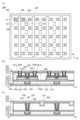
본 발명의 일 형태는 제 1 층과, 제 1 층 위의 제 2 층과, 제 1 배선과, 제 2 배선과, 제 3 배선을 포함하는 반도체 장치이다. 제 1 층은 제 1 멀티플렉서와, 제 2 멀티플렉서와, 제 1 아날로그 스위치 내지 제 4 아날로그 스위치를 포함하고, 제 2 층은 제 1 트랜지스터 내지 제 4 트랜지스터를 포함한다. 제 1 트랜지스터 내지 제 4 트랜지스터는 각각 소스와, 드레인과, 제 1 게이트를 포함한다. 제 1 배선은 제 1 트랜지스터 내지 제 4 트랜지스터 각각의 소스 및 드레인 중 한쪽에 전기적으로 접속되어 있다. 제 1 아날로그 스위치 및 제 2 아날로그 스위치 각각의 제 1 단자는 제 1 멀티플렉서에 전기적으로 접속되고, 제 1 아날로그 스위치 및 제 2 아날로그 스위치 각각의 제 2 단자는 제 2 배선에 전기적으로 접속되어 있다. 제 1 아날로그 스위치의 제 3 단자는 제 1 트랜지스터 및 제 2 트랜지스터 각각의 소스 및 드레인 중 다른 쪽에 전기적으로 접속되고, 제 2 아날로그 스위치의 제 3 단자는 제 3 트랜지스터 및 제 4 트랜지스터 각각의 소스 및 드레인 중 다른 쪽에 전기적으로 접속되어 있다. 제 3 아날로그 스위치 및 제 4 아날로그 스위치 각각의 제 1 단자는 제 2 멀티플렉서에 전기적으로 접속되고, 제 3 아날로그 스위치 및 제 4 아날로그 스위치 각각의 제 2 단자는 제 3 배선에 전기적으로 접속되어 있다. 제 3 아날로그 스위치의 제 3 단자는 제 1 트랜지스터 및 제 3 트랜지스터 각각의 제 1 게이트에 전기적으로 접속되고, 제 4 아날로그 스위치의 제 3 단자는 제 2 트랜지스터 및 제 4 트랜지스터 각각의 제 1 게이트에 전기적으로 접속되어 있다.One form of the present invention is a semiconductor device including a first layer, a second layer above the first layer, a first wiring, a second wiring, and a third wiring. The first layer includes a first multiplexer, a second multiplexer, and first to fourth analog switches, and the second layer includes first to fourth transistors. The first to fourth transistors each include a source, a drain, and a first gate. The first wiring is electrically connected to one of the source and drain of each of the first to fourth transistors. The first terminal of each of the first analog switch and the second analog switch is electrically connected to the first multiplexer, and the second terminal of each of the first analog switch and the second analog switch is electrically connected to the second wiring. The third terminal of the first analog switch is electrically connected to the other of the source and drain of each of the first and second transistors, and the third terminal of the second analog switch is electrically connected to the source and drain of each of the third and fourth transistors. It is electrically connected to the other side. The first terminal of each of the third analog switch and the fourth analog switch is electrically connected to the second multiplexer, and the second terminal of each of the third analog switch and the fourth analog switch is electrically connected to the third wiring. The third terminal of the third analog switch is electrically connected to the first gate of each of the first and third transistors, and the third terminal of the fourth analog switch is electrically connected to the first gate of each of the second and fourth transistors. It is connected to .
상기 반도체 장치는 제 4 배선을 더 포함하고, 제 1 트랜지스터 내지 제 4 트랜지스터는 각각 제 2 게이트를 더 포함하고, 제 4 배선은 제 1 트랜지스터 내지 제 4 트랜지스터 각각의 제 2 게이트에 전기적으로 접속되어 있는 것이 바람직하다.The semiconductor device further includes a fourth wiring, each of the first to fourth transistors further includes a second gate, and the fourth wiring is electrically connected to the second gate of each of the first to fourth transistors. It is desirable to have
또한 상기 반도체 장치에서, 제 1 트랜지스터 내지 제 4 트랜지스터는 각각 채널 형성 영역에 금속 산화물을 포함하는 것이 바람직하다.Additionally, in the semiconductor device, each of the first to fourth transistors preferably includes a metal oxide in the channel formation region.
또한 상기 반도체 장치에서, 금속 산화물은 인듐과, 갈륨과, 아연을 포함하는 것이 바람직하다.Also, in the semiconductor device, the metal oxide preferably contains indium, gallium, and zinc.
상기 반도체 장치에서, 제 1 아날로그 스위치 내지 제 4 아날로그 스위치는 각각 CMOS 회로로 구성되는 것이 바람직하다.In the semiconductor device, each of the first to fourth analog switches is preferably configured as a CMOS circuit.
또한 상기 반도체 장치에서, CMOS 회로에 포함되는 트랜지스터는 채널 형성 영역에 실리콘을 포함하는 것이 바람직하다.Additionally, in the semiconductor device, the transistor included in the CMOS circuit preferably includes silicon in the channel formation region.
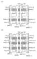
본 발명의 다른 일 형태는 제 1 층과, 제 1 층 위의 제 2 층과, 제 1 배선과, 제 2 배선과, 제 3 배선을 포함하는 반도체 장치이다. 제 1 층은 제 1 멀티플렉서와, 제 2 멀티플렉서와, 제 1 아날로그 스위치 내지 제 3 아날로그 스위치를 포함하고, 제 2 층은 제 1 트랜지스터와 제 3 트랜지스터를 포함한다. 제 1 트랜지스터 및 제 3 트랜지스터는 각각 소스와, 드레인과, 제 1 게이트를 포함한다. 제 1 배선은 제 1 트랜지스터 및 제 3 트랜지스터 각각의 소스 및 드레인 중 한쪽에 전기적으로 접속되어 있다. 제 1 아날로그 스위치 및 제 2 아날로그 스위치 각각의 제 1 단자는 제 1 멀티플렉서에 전기적으로 접속되고, 제 1 아날로그 스위치 및 제 2 아날로그 스위치 각각의 제 2 단자는 제 2 배선에 전기적으로 접속되어 있다. 제 1 아날로그 스위치의 제 3 단자는 제 1 트랜지스터의 소스 및 드레인 중 다른 쪽에 전기적으로 접속되고, 제 2 아날로그 스위치의 제 3 단자는 제 3 트랜지스터의 소스 및 드레인 중 다른 쪽에 전기적으로 접속되어 있다. 제 3 아날로그 스위치의 제 1 단자는 제 2 멀티플렉서에 전기적으로 접속되고, 제 3 아날로그 스위치의 제 2 단자는 제 3 배선에 전기적으로 접속되고, 제 3 아날로그 스위치의 제 3 단자는 제 1 트랜지스터 및 제 3 트랜지스터 각각의 제 1 게이트에 전기적으로 접속되어 있다.Another aspect of the present invention is a semiconductor device including a first layer, a second layer above the first layer, a first wiring, a second wiring, and a third wiring. The first layer includes a first multiplexer, a second multiplexer, and first to third analog switches, and the second layer includes a first transistor and a third transistor. The first transistor and the third transistor each include a source, a drain, and a first gate. The first wiring is electrically connected to one of the source and drain of each of the first and third transistors. The first terminal of each of the first analog switch and the second analog switch is electrically connected to the first multiplexer, and the second terminal of each of the first analog switch and the second analog switch is electrically connected to the second wiring. The third terminal of the first analog switch is electrically connected to the other of the source and drain of the first transistor, and the third terminal of the second analog switch is electrically connected to the other of the source and drain of the third transistor. The first terminal of the third analog switch is electrically connected to the second multiplexer, the second terminal of the third analog switch is electrically connected to the third wiring, and the third terminal of the third analog switch is electrically connected to the first transistor and the third wiring. It is electrically connected to the first gate of each of the three transistors.
상기 반도체 장치는 제 4 배선을 더 포함하고, 제 1 트랜지스터 및 제 3 트랜지스터는 각각 제 2 게이트를 더 포함하고, 제 4 배선은 제 1 트랜지스터 및 제 3 트랜지스터 각각의 제 2 게이트에 전기적으로 접속되어 있는 것이 바람직하다.The semiconductor device further includes a fourth wiring, each of the first transistor and the third transistor further includes a second gate, and the fourth wiring is electrically connected to the second gate of each of the first transistor and the third transistor. It is desirable to have
또한 상기 반도체 장치에서, 제 1 트랜지스터 및 제 3 트랜지스터는 각각 채널 형성 영역에 금속 산화물을 포함하는 것이 바람직하다.Also, in the above semiconductor device, it is preferable that the first transistor and the third transistor each include a metal oxide in the channel formation region.
또한 상기 반도체 장치에서, 금속 산화물은 인듐과, 갈륨과, 아연을 포함하는 것이 바람직하다.Also, in the semiconductor device, the metal oxide preferably contains indium, gallium, and zinc.
상기 반도체 장치에서, 제 1 아날로그 스위치 내지 제 3 아날로그 스위치는 각각 CMOS 회로로 구성되는 것이 바람직하다.In the semiconductor device, each of the first to third analog switches is preferably configured as a CMOS circuit.
또한 상기 반도체 장치에서, CMOS 회로에 포함되는 트랜지스터는 채널 형성 영역에 실리콘을 포함하는 것이 바람직하다.Additionally, in the semiconductor device, the transistor included in the CMOS circuit preferably includes silicon in the channel formation region.
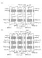
본 발명의 다른 일 형태는 제 1 층과, 제 1 층 위의 제 2 층과, 제 1 배선과, 제 2 배선과, 제 3 배선을 포함하는 반도체 장치이다. 제 1 층은 제 1 멀티플렉서와, 제 2 멀티플렉서와, 제 1 아날로그 스위치와, 제 3 아날로그 스위치와, 제 4 아날로그 스위치를 포함하고, 제 2 층은 제 1 트랜지스터와 제 2 트랜지스터를 포함한다. 제 1 트랜지스터 및 제 2 트랜지스터는 각각 소스와, 드레인과, 제 1 게이트를 포함한다. 제 1 배선은 제 1 트랜지스터 및 제 2 트랜지스터 각각의 소스 및 드레인 중 한쪽에 전기적으로 접속되어 있다. 제 1 아날로그 스위치의 제 1 단자는 제 1 멀티플렉서에 전기적으로 접속되고, 제 1 아날로그 스위치의 제 2 단자는 제 2 배선에 전기적으로 접속되고, 제 1 아날로그 스위치의 제 3 단자는 제 1 트랜지스터 및 제 2 트랜지스터 각각의 소스 및 드레인 중 다른 쪽에 전기적으로 접속되어 있다. 제 3 아날로그 스위치 및 제 4 아날로그 스위치 각각의 제 1 단자는 제 2 멀티플렉서에 전기적으로 접속되고, 제 3 아날로그 스위치 및 제 4 아날로그 스위치 각각의 제 2 단자는 제 3 배선에 전기적으로 접속되어 있다. 제 3 아날로그 스위치의 제 3 단자는 제 1 트랜지스터의 제 1 게이트에 전기적으로 접속되고, 제 4 아날로그 스위치의 제 3 단자는 제 2 트랜지스터의 제 1 게이트에 전기적으로 접속되어 있다.Another aspect of the present invention is a semiconductor device including a first layer, a second layer above the first layer, a first wiring, a second wiring, and a third wiring. The first layer includes a first multiplexer, a second multiplexer, a first analog switch, a third analog switch, and a fourth analog switch, and the second layer includes a first transistor and a second transistor. The first transistor and the second transistor each include a source, a drain, and a first gate. The first wiring is electrically connected to one of the source and drain of each of the first transistor and the second transistor. The first terminal of the first analog switch is electrically connected to the first multiplexer, the second terminal of the first analog switch is electrically connected to the second wiring, and the third terminal of the first analog switch is electrically connected to the first transistor and the first wiring. 2 It is electrically connected to the other of the source and drain of each transistor. The first terminal of each of the third analog switch and the fourth analog switch is electrically connected to the second multiplexer, and the second terminal of each of the third analog switch and the fourth analog switch is electrically connected to the third wiring. The third terminal of the third analog switch is electrically connected to the first gate of the first transistor, and the third terminal of the fourth analog switch is electrically connected to the first gate of the second transistor.
상기 반도체 장치는 제 4 배선을 더 포함하고, 제 1 트랜지스터 및 제 2 트랜지스터는 각각 제 2 게이트를 더 포함하고, 제 4 배선은 제 1 트랜지스터 및 제 2 트랜지스터 각각의 제 2 게이트에 전기적으로 접속되어 있는 것이 바람직하다.The semiconductor device further includes a fourth wiring, each of the first transistor and the second transistor further includes a second gate, and the fourth wiring is electrically connected to the second gate of each of the first transistor and the second transistor. It is desirable to have
또한 상기 반도체 장치에서, 제 1 트랜지스터 및 제 2 트랜지스터는 각각 채널 형성 영역에 금속 산화물을 포함하는 것이 바람직하다.Additionally, in the semiconductor device, it is preferable that the first transistor and the second transistor each include a metal oxide in the channel formation region.
또한 상기 반도체 장치에서, 금속 산화물은 인듐과, 갈륨과, 아연을 포함하는 것이 바람직하다.Also, in the semiconductor device, the metal oxide preferably contains indium, gallium, and zinc.
상기 반도체 장치에서, 제 1 아날로그 스위치, 제 3 아날로그 스위치, 및 제 4 아날로그 스위치는 각각 CMOS 회로로 구성되는 것이 바람직하다.In the semiconductor device, the first analog switch, the third analog switch, and the fourth analog switch are preferably each configured as a CMOS circuit.
또한 상기 반도체 장치에서, CMOS 회로에 포함되는 트랜지스터는 채널 형성 영역에 실리콘을 포함하는 것이 바람직하다.Additionally, in the semiconductor device, the transistor included in the CMOS circuit preferably includes silicon in the channel formation region.
본 발명의 일 형태에 의하여, 다점 측정이 가능한 반도체 장치를 제공할 수 있다. 또는 본 발명의 일 형태에 의하여, 트랜지스터의 전기 특성의 편차가 적은 반도체 장치를 제공할 수 있다. 또는 본 발명의 일 형태에 의하여, 신뢰성이 양호한 반도체 장치를 제공할 수 있다. 또는 본 발명의 일 형태에 의하여, 전기 특성이 양호한 반도체 장치를 제공할 수 있다. 또는 본 발명의 일 형태에 의하여, 온 전류가 높은 반도체 장치를 제공할 수 있다. 또는 본 발명의 일 형태에 의하여, 미세화 또는 고집적화가 가능한 반도체 장치를 제공할 수 있다. 또는 본 발명의 일 형태에 의하여, 소비 전력이 낮은 반도체 장치를 제공할 수 있다.According to one embodiment of the present invention, a semiconductor device capable of multi-point measurement can be provided. Alternatively, according to one embodiment of the present invention, a semiconductor device with less variation in the electrical characteristics of a transistor can be provided. Alternatively, according to one embodiment of the present invention, a semiconductor device with good reliability can be provided. Alternatively, according to one embodiment of the present invention, a semiconductor device with good electrical characteristics can be provided. Alternatively, according to one embodiment of the present invention, a semiconductor device with a high on-state current can be provided. Alternatively, according to one embodiment of the present invention, a semiconductor device capable of miniaturization or high integration can be provided. Alternatively, according to one embodiment of the present invention, a semiconductor device with low power consumption can be provided.
또한 이들 효과의 기재는 다른 효과의 존재를 방해하는 것이 아니다. 또한 본 발명의 일 형태는 이들 효과 모두를 가질 필요는 없다. 또한 이들 외의 효과는 명세서, 도면, 청구항 등의 기재에서 저절로 명백해지는 것이며 명세서, 도면, 청구항 등의 기재에서 이들 외의 효과를 추출할 수 있다.Additionally, the description of these effects does not preclude the existence of other effects. Additionally, one embodiment of the present invention does not need to have all of these effects. In addition, effects other than these are naturally apparent from descriptions such as specifications, drawings, and claims, and effects other than these can be extracted from descriptions such as specifications, drawings, and claims.
도 1의 (A)는 본 발명의 일 형태인 반도체 장치의 상면도이다. 도 1의 (B) 내지 (D)는 본 발명의 일 형태인 반도체 장치의 단면도이다.
도 2의 (A) 및 (B)는 본 발명의 일 형태인 반도체 장치의 단면도이다.
도 3의 (A)는 본 발명의 일 형태인 반도체 장치의 상면도이다. 도 3의 (B) 내지 (D)는 본 발명의 일 형태인 반도체 장치의 단면도이다.
도 4의 (A)는 본 발명의 일 형태인 반도체 장치의 상면도이다. 도 4의 (B) 내지 (D)는 본 발명의 일 형태인 반도체 장치의 단면도이다.
도 5의 (A)는 본 발명의 일 형태인 반도체 장치의 상면도이다. 도 5의 (B) 내지 (D)는 본 발명의 일 형태인 반도체 장치의 단면도이다.
도 6의 (A)는 본 발명의 일 형태인 반도체 장치의 제작 방법을 나타낸 상면도이다. 도 6의 (B) 내지 (D)는 본 발명의 일 형태인 반도체 장치의 제작 방법을 나타낸 단면도이다.
도 7의 (A)는 본 발명의 일 형태인 반도체 장치의 제작 방법을 나타낸 상면도이다. 도 7의 (B) 내지 (D)는 본 발명의 일 형태인 반도체 장치의 제작 방법을 나타낸 단면도이다.
도 8의 (A)는 본 발명의 일 형태인 반도체 장치의 제작 방법을 나타낸 상면도이다. 도 8의 (B) 내지 (D)는 본 발명의 일 형태인 반도체 장치의 제작 방법을 나타낸 단면도이다.
도 9의 (A)는 본 발명의 일 형태인 반도체 장치의 제작 방법을 나타낸 상면도이다. 도 9의 (B) 내지 (D)는 본 발명의 일 형태인 반도체 장치의 제작 방법을 나타낸 단면도이다.
도 10의 (A)는 본 발명의 일 형태인 반도체 장치의 제작 방법을 나타낸 상면도이다. 도 10의 (B) 내지 (D)는 본 발명의 일 형태인 반도체 장치의 제작 방법을 나타낸 단면도이다.
도 11의 (A)는 본 발명의 일 형태인 반도체 장치의 제작 방법을 나타낸 상면도이다. 도 11의 (B) 내지 (D)는 본 발명의 일 형태인 반도체 장치의 제작 방법을 나타낸 단면도이다.
도 12의 (A)는 본 발명의 일 형태인 반도체 장치의 제작 방법을 나타낸 상면도이다. 도 12의 (B) 내지 (D)는 본 발명의 일 형태인 반도체 장치의 제작 방법을 나타낸 단면도이다.
도 13의 (A)는 본 발명의 일 형태인 반도체 장치의 제작 방법을 나타낸 상면도이다. 도 13의 (B) 내지 (D)는 본 발명의 일 형태인 반도체 장치의 제작 방법을 나타낸 단면도이다.
도 14의 (A)는 본 발명의 일 형태인 반도체 장치의 제작 방법을 나타낸 상면도이다. 도 14의 (B) 내지 (D)는 본 발명의 일 형태인 반도체 장치의 제작 방법을 나타낸 단면도이다.
도 15의 (A)는 본 발명의 일 형태인 반도체 장치의 제작 방법을 나타낸 상면도이다. 도 15의 (B) 내지 (D)는 본 발명의 일 형태인 반도체 장치의 제작 방법을 나타낸 단면도이다.
도 16의 (A)는 본 발명의 일 형태인 반도체 장치의 제작 방법을 나타낸 상면도이다. 도 16의 (B) 내지 (D)는 본 발명의 일 형태인 반도체 장치의 제작 방법을 나타낸 단면도이다.
도 17의 (A)는 본 발명의 일 형태인 반도체 장치의 제작 방법을 나타낸 상면도이다. 도 17의 (B) 내지 (D)는 본 발명의 일 형태인 반도체 장치의 제작 방법을 나타낸 단면도이다.
도 18은 본 발명의 일 형태에 따른 마이크로파 처리 장치를 설명하는 상면도이다.
도 19는 본 발명의 일 형태에 따른 마이크로파 처리 장치를 설명하는 단면도이다.
도 20은 본 발명의 일 형태에 따른 마이크로파 처리 장치를 설명하는 단면도이다.
도 21은 본 발명의 일 형태에 따른 마이크로파 처리 장치를 설명하는 단면도이다.
도 22의 (A)는 본 발명의 일 형태에 따른 반도체 장치의 평면도이다. 도 22의 (B) 및 (C)는 본 발명의 일 형태인 반도체 장치의 단면도이다.
도 23은 반도체 장치의 회로도이다.
도 24의 (A)는 반도체 장치의 사시도이다. 도 24의 (B)는 반도체 장치의 구성을 설명하는 사시도이다.
도 25의 (A) 및 (B)는 본 발명의 일 형태의 반도체 장치에 포함되는 트랜지스터 그룹의 레이아웃을 설명하는 상면도이다.
도 26의 (A) 및 (B)는 본 발명의 일 형태의 반도체 장치에 포함되는 트랜지스터 그룹의 레이아웃을 설명하는 상면도이다.
도 27의 (A) 및 (B)는 본 발명의 일 형태의 반도체 장치에 포함되는 트랜지스터 그룹의 레이아웃을 설명하는 상면도이다.
도 28의 (A) 및 (B)는 본 발명의 일 형태의 반도체 장치에 포함되는 트랜지스터 그룹의 레이아웃을 설명하는 상면도이다.
도 29는 본 발명의 일 형태에 따른 기억 장치의 구성을 나타낸 단면도이다.
도 30은 본 발명의 일 형태에 따른 기억 장치의 구성을 나타낸 단면도이다.
도 31은 본 발명의 일 형태에 따른 반도체 장치의 단면도이다.
도 32의 (A) 및 (B)는 본 발명의 일 형태에 따른 반도체 장치의 단면도이다.
도 33은 본 발명의 일 형태에 따른 반도체 장치의 단면도이다.
도 34의 (A)는 본 발명의 일 형태에 따른 기억 장치의 구성예를 나타낸 블록도이다. 도 34의 (B)는 본 발명의 일 형태에 따른 기억 장치의 구성예를 나타낸 사시도이다.
도 35의 (A) 내지 (H)는 본 발명의 일 형태에 따른 기억 장치의 구성예를 나타낸 회로도이다.
도 36의 (A) 및 (B)는 본 발명의 일 형태에 따른 반도체 장치의 모식도이다.
도 37은 CPU의 구성예를 설명하는 도면이다.
도 38의 (A) 및 (B)는 CPU의 구성예를 설명하는 도면이다.
도 39는 CPU의 구성예를 나타낸 도면이다.
도 40의 (A) 및 (B)는 전자 부품의 일례를 설명하는 도면이다.
도 41의 (A) 내지 (E)는 본 발명의 일 형태에 따른 기억 장치의 모식도이다.
도 42의 (A) 내지 (H)는 본 발명의 일 형태에 따른 전자 기기를 나타낸 도면이다.
도 43은 가열 처리 온도와 산화물의 시트 저항의 상관을 설명하는 도면이다.
도 44의 (A) 및 (B)는 시험적으로 제작한 트랜지스터의 Id-Vg 특성을 나타낸 도면이다.
도 45의 (A1), (B1), (C1), 및 (D1)은 용량을 설명하는 도면이다. 도 45의 (A2), (B2), (C2), 및 (D2)는 시험적으로 제작한 트랜지스터의 게이트 전압-용량 특성을 나타낸 도면이다.
도 46은 시험적으로 제작한 트랜지스터의 측정 환경의 온도-오프 전류 특성을 나타낸 도면이다.
도 47은 반도체 장치의 단면 TEM 이미지이다.
도 48은 TEG의 배치를 설명하는 도면이다.
도 49의 (A) 내지 (F)는 트랜지스터의 문턱 전압의 편차를 설명하는 도면이다.
도 50의 (A) 내지 (F)는 트랜지스터의 문턱 전압의 편차를 설명하는 도면이다.
도 51의 (A) 내지 (F)는 트랜지스터의 전계 효과 이동도의 편차를 설명하는 도면이다.
도 52의 (A) 내지 (F)는 트랜지스터의 전계 효과 이동도의 편차를 설명하는 도면이다.
도 53의 (A) 및 (B)는 트랜지스터의 배열 방법을 설명하는 도면이다.
도 54의 (A) 및 (B)는 트랜지스터의 Id-Vg 특성을 나타낸 도면이다.
도 55의 (A) 내지 (C)는 트랜지스터의 문턱 전압의 편차를 설명하는 도면이다.
도 56의 (A)는 본 실시예에 따른 반도체 장치의 상면도이다. 도 56의 (B) 내지 (D)는 본 실시예에 따른 반도체 장치의 단면도이다.
도 57은 본 실시예에 따른 +GBT 스트레스 시험에서의 ΔVsh의 스트레스 시간 의존성을 나타낸 도면이다.
도 58은 X선 조사 후의 OS 트랜지스터의 Vth의 시간 의존성을 설명하는 도면이다.
도 59는 X선 조사 후의 OS 트랜지스터의 S값의 시간 의존성을 설명하는 도면이다.
도 60의 (A)는 OS 트랜지스터의 Vth의 X선의 합계 선량 의존성을 설명하는 도면이다. 도 60의 (B)는 OS 트랜지스터의 S값의 X선의 합계 선량 의존성을 설명하는 도면이다. 도 60의 (C) 및 (D)는 계산의 결과를 나타낸 도면이다.
도 61의 (A) 내지 (C)는 계산에 사용한 트랜지스터 구조를 설명하는 도면이다.
도 62는 시험적으로 제작한 칩의 광학 현미경 사진이다.
도 63은 시험적으로 제작한 OS 플립플롭의 회로도이다.
도 64의 (A) 및 (B)는 OS 트랜지스터의 문턱 전압의 X선의 합계 선량 의존성을 나타낸 도면이다.
도 65는 OS 트랜지스터의 문턱 전압의 X선의 합계 선량 의존성을 나타낸 도면이다.
도 66의 (A) 및 (B)는 OS 트랜지스터의 문턱 전압의 X선의 합계 선량 의존성을 나타낸 도면이다.
도 67은 OS 트랜지스터의 문턱 전압의 X선의 합계 선량 의존성을 나타낸 도면이다.
도 68은 X선 조사 시험 방법을 나타낸 흐름도이다.
도 69의 (A) 및 (B)는 OS 트랜지스터의 Id-Vg 특성을 나타낸 도면이다.
도 70의 (A) 및 (B)는 OS 트랜지스터의 문턱 전압의 차이를 나타낸 도면이다.
도 71의 (A) 및 (B)는 OS 트랜지스터의 문턱 전압의 변동을 나타낸 도면이다.
도 72의 (A) 및 (B)는 OS 트랜지스터의 문턱 전압의 변동량을 나타낸 도면이다.
도 73의 (A) 및 (B)는 OS 트랜지스터의 문턱 전압의 변동량을 나타낸 도면이다.
도 74는 X선 조사 시험의 평가 환경을 설명하는 도면이다.
도 75의 (A) 및 (B)는 OS 트랜지스터의 문턱 전압의 변동량을 나타낸 도면이다.
도 76의 (A)는 OS 트랜지스터의 문턱 전압의 변동량을 나타낸 도면이다. 도 76의 (B)는 OS 트랜지스터의 SS의 변동량을 나타낸 도면이다. 도 76의 (C)는 OS 트랜지스터의 전계 효과 이동도의 변동량을 나타낸 도면이다.
도 77의 (A) 및 (B)는 시험적으로 제작한 트랜지스터의 Id-Vg 특성을 나타낸 도면이다.Figure 1(A) is a top view of a semiconductor device of one form of the present invention. 1B to 1D are cross-sectional views of a semiconductor device according to one embodiment of the present invention.
2(A) and 2(B) are cross-sectional views of a semiconductor device according to one embodiment of the present invention.
FIG. 3(A) is a top view of a semiconductor device according to one embodiment of the present invention. 3B to 3D are cross-sectional views of a semiconductor device according to one embodiment of the present invention.
FIG. 4A is a top view of a semiconductor device according to one embodiment of the present invention. 4B to 4D are cross-sectional views of a semiconductor device according to one embodiment of the present invention.
FIG. 5(A) is a top view of a semiconductor device according to one embodiment of the present invention. 5(B) to 5(D) are cross-sectional views of a semiconductor device according to one embodiment of the present invention.
FIG. 6A is a top view showing a method of manufacturing a semiconductor device according to one embodiment of the present invention. 6(B) to 6(D) are cross-sectional views showing a method of manufacturing a semiconductor device according to one embodiment of the present invention.
FIG. 7(A) is a top view showing a method of manufacturing a semiconductor device according to one embodiment of the present invention. 7 (B) to (D) are cross-sectional views showing a method of manufacturing a semiconductor device according to one embodiment of the present invention.
FIG. 8(A) is a top view showing a method of manufacturing a semiconductor device according to one embodiment of the present invention. 8 (B) to (D) are cross-sectional views showing a method of manufacturing a semiconductor device according to one embodiment of the present invention.
FIG. 9A is a top view showing a method of manufacturing a semiconductor device according to one embodiment of the present invention. 9(B) to 9D are cross-sectional views showing a method of manufacturing a semiconductor device according to one embodiment of the present invention.
FIG. 10(A) is a top view showing a method of manufacturing a semiconductor device according to one embodiment of the present invention. 10(B) to 10(D) are cross-sectional views showing a method of manufacturing a semiconductor device according to one embodiment of the present invention.
FIG. 11 (A) is a top view showing a method of manufacturing a semiconductor device according to one embodiment of the present invention. 11 (B) to (D) are cross-sectional views showing a method of manufacturing a semiconductor device according to one embodiment of the present invention.
FIG. 12(A) is a top view showing a method of manufacturing a semiconductor device according to one embodiment of the present invention. 12(B) to 12(D) are cross-sectional views showing a method of manufacturing a semiconductor device according to one embodiment of the present invention.
FIG. 13(A) is a top view showing a method of manufacturing a semiconductor device according to one embodiment of the present invention. 13(B) to 13(D) are cross-sectional views showing a method of manufacturing a semiconductor device according to one embodiment of the present invention.
FIG. 14A is a top view showing a method of manufacturing a semiconductor device according to one embodiment of the present invention. 14B to 14D are cross-sectional views showing a method of manufacturing a semiconductor device according to one embodiment of the present invention.
FIG. 15(A) is a top view showing a method of manufacturing a semiconductor device according to one embodiment of the present invention. 15(B) to 15(D) are cross-sectional views showing a method of manufacturing a semiconductor device according to one embodiment of the present invention.
FIG. 16A is a top view showing a method of manufacturing a semiconductor device according to one embodiment of the present invention. 16(B) to 16(D) are cross-sectional views showing a method of manufacturing a semiconductor device according to one embodiment of the present invention.
FIG. 17(A) is a top view showing a method of manufacturing a semiconductor device according to one embodiment of the present invention. 17B to 17D are cross-sectional views showing a method of manufacturing a semiconductor device according to one embodiment of the present invention.
18 is a top view illustrating a microwave processing device according to one embodiment of the present invention.
19 is a cross-sectional view illustrating a microwave processing device according to one embodiment of the present invention.
Figure 20 is a cross-sectional view illustrating a microwave processing device according to one embodiment of the present invention.
21 is a cross-sectional view illustrating a microwave processing device according to one embodiment of the present invention.
Figure 22(A) is a plan view of a semiconductor device according to one embodiment of the present invention. 22(B) and 22(C) are cross-sectional views of a semiconductor device of one embodiment of the present invention.
23 is a circuit diagram of a semiconductor device.
Figure 24(A) is a perspective view of a semiconductor device. Figure 24(B) is a perspective view explaining the configuration of a semiconductor device.
25(A) and 25(B) are top views illustrating the layout of a transistor group included in a semiconductor device of one embodiment of the present invention.
Figures 26 (A) and (B) are top views illustrating the layout of a transistor group included in a semiconductor device of one embodiment of the present invention.
Figures 27 (A) and (B) are top views illustrating the layout of a transistor group included in a semiconductor device of one form of the present invention.
Figures 28 (A) and (B) are top views illustrating the layout of a transistor group included in a semiconductor device of one embodiment of the present invention.
Figure 29 is a cross-sectional view showing the configuration of a storage device according to one embodiment of the present invention.
Figure 30 is a cross-sectional view showing the configuration of a storage device according to one embodiment of the present invention.
31 is a cross-sectional view of a semiconductor device according to one embodiment of the present invention.
32 (A) and (B) are cross-sectional views of a semiconductor device according to one embodiment of the present invention.
33 is a cross-sectional view of a semiconductor device according to one embodiment of the present invention.
Figure 34(A) is a block diagram showing a configuration example of a storage device according to one embodiment of the present invention. Figure 34(B) is a perspective view showing a configuration example of a storage device according to one embodiment of the present invention.
35 (A) to (H) are circuit diagrams showing a configuration example of a memory device according to one embodiment of the present invention.
36(A) and 36(B) are schematic diagrams of a semiconductor device according to one embodiment of the present invention.
Figure 37 is a diagram explaining a configuration example of the CPU.
Figures 38 (A) and (B) are diagrams explaining a configuration example of the CPU.
Figure 39 is a diagram showing a configuration example of the CPU.
Figures 40 (A) and (B) are diagrams illustrating examples of electronic components.
Figures 41 (A) to (E) are schematic diagrams of a storage device according to one embodiment of the present invention.
Figures 42 (A) to (H) are diagrams showing an electronic device according to one embodiment of the present invention.
Figure 43 is a diagram explaining the correlation between heat treatment temperature and oxide sheet resistance.
Figures 44 (A) and (B) are diagrams showing the Id-Vg characteristics of the experimentally manufactured transistor.
Figures 45 (A1), (B1), (C1), and (D1) are diagrams explaining capacity. Figures 45 (A2), (B2), (C2), and (D2) are diagrams showing the gate voltage-capacitance characteristics of the experimentally manufactured transistor.
Figure 46 is a diagram showing the temperature-off current characteristics of the experimentally manufactured transistor in the measurement environment.
Figure 47 is a cross-sectional TEM image of a semiconductor device.
Figure 48 is a diagram explaining the arrangement of TEG.
Figures 49 (A) to (F) are diagrams explaining the deviation of the threshold voltage of the transistor.
Figures 50 (A) to (F) are diagrams illustrating the deviation of the threshold voltage of a transistor.
Figures 51 (A) to (F) are diagrams illustrating variations in field effect mobility of transistors.
Figures 52 (A) to (F) are diagrams illustrating variations in field effect mobility of transistors.
Figures 53 (A) and (B) are diagrams explaining the transistor arrangement method.
Figures 54 (A) and (B) are diagrams showing the Id-Vg characteristics of the transistor.
Figures 55 (A) to (C) are diagrams illustrating the deviation of the threshold voltage of a transistor.
Figure 56(A) is a top view of the semiconductor device according to this embodiment. Figures 56 (B) to (D) are cross-sectional views of the semiconductor device according to this embodiment.
Figure 57 is a diagram showing the stress time dependence of ΔVsh in the +GBT stress test according to this embodiment.
Figure 58 is a diagram explaining the time dependence of Vth of the OS transistor after X-ray irradiation.
Figure 59 is a diagram explaining the time dependence of the S value of the OS transistor after X-ray irradiation.
Figure 60(A) is a diagram explaining the dependence of the Vth of the OS transistor on the total X-ray dose. Figure 60(B) is a diagram explaining the dependence of the S value of the OS transistor on the total X-ray dose. Figures 60 (C) and (D) are diagrams showing the results of calculations.
Figures 61 (A) to (C) are diagrams explaining the transistor structure used in the calculation.
Figure 62 is an optical microscope photograph of a chip manufactured experimentally.
Figure 63 is a circuit diagram of an OS flip-flop produced experimentally.
Figures 64 (A) and (B) are diagrams showing the dependence of the threshold voltage of the OS transistor on the total dose of X-rays.
Figure 65 is a diagram showing the dependence of the threshold voltage of the OS transistor on the total X-ray dose.
Figures 66 (A) and (B) are diagrams showing the dependence of the threshold voltage of the OS transistor on the total dose of X-rays.
Figure 67 is a diagram showing the dependence of the threshold voltage of the OS transistor on the total dose of X-rays.
Figure 68 is a flow chart showing the X-ray irradiation test method.
Figures 69 (A) and (B) are diagrams showing the Id-Vg characteristics of the OS transistor.
Figures 70 (A) and (B) are diagrams showing the difference in threshold voltages of OS transistors.
Figures 71 (A) and (B) are diagrams showing changes in the threshold voltage of the OS transistor.
Figures 72 (A) and (B) are diagrams showing the amount of variation in the threshold voltage of the OS transistor.
Figures 73 (A) and (B) are diagrams showing the amount of variation in the threshold voltage of the OS transistor.
Figure 74 is a diagram explaining the evaluation environment for the X-ray irradiation test.
Figures 75 (A) and (B) are diagrams showing the amount of variation in the threshold voltage of the OS transistor.
Figure 76 (A) is a diagram showing the amount of variation in the threshold voltage of the OS transistor. Figure 76 (B) is a diagram showing the amount of variation in SS of the OS transistor. Figure 76 (C) is a diagram showing the amount of variation in the field effect mobility of the OS transistor.
Figures 77 (A) and (B) are diagrams showing the Id-Vg characteristics of the experimentally manufactured transistor.
이하에서, 실시형태에 대하여 도면을 참조하여 설명한다. 다만 실시형태는 많은 상이한 형태로 실시할 수 있고, 취지 및 그 범위에서 벗어남이 없이 그 형태 및 자세한 사항을 다양하게 변경할 수 있다는 것은 통상의 기술자라면 용이하게 이해할 수 있다. 따라서 본 발명은 이하의 실시형태의 기재 내용에 한정하여 해석되는 것이 아니다.Below, embodiments will be described with reference to the drawings. However, those skilled in the art can easily understand that the embodiment can be implemented in many different forms, and that the form and details can be changed in various ways without departing from the spirit and scope. Therefore, the present invention should not be construed as limited to the description of the embodiments below.
또한 도면에서 크기, 층의 두께, 또는 영역은 명료화를 위하여 과장되어 있는 경우가 있다. 따라서 그 스케일에 반드시 한정되는 것은 아니다. 또한 도면은 이상적인 예를 모식적으로 나타낸 것이고, 도면에 나타난 형상 또는 값 등에 한정되지 않는다. 예를 들어 실제의 제조 공정에서, 에칭 등의 처리에 의하여 층, 레지스트 마스크 등이 의도하지 않게 감소되는 경우가 있지만, 이해를 용이하게 하기 위하여 도면에 반영하지 않은 경우가 있다. 또한 도면에서 동일한 부분 또는 같은 기능을 갖는 부분에는 동일한 부호를 상이한 도면 사이에서 공통적으로 사용하고, 이에 대한 반복적인 설명은 생략하는 경우가 있다. 또한 같은 기능을 갖는 부분을 가리키는 경우에는, 해치 패턴을 동일하게 하고, 특별히 부호를 붙이지 않는 경우가 있다.Additionally, in the drawings, the size, layer thickness, or area may be exaggerated for clarity. Therefore, it is not necessarily limited to that scale. Additionally, the drawings schematically show an ideal example and are not limited to the shapes or values shown in the drawings. For example, in the actual manufacturing process, layers, resist masks, etc. may be unintentionally reduced due to processing such as etching, but this may not be reflected in the drawings to facilitate understanding. Additionally, in the drawings, the same symbols are commonly used for parts that are the same or have the same function across different drawings, and repetitive descriptions thereof may be omitted. Additionally, when referring to parts with the same function, the hatch patterns may be the same and no special symbols may be added.
또한 특히 상면도("평면도"라고도 함), 사시도 등에서, 발명의 이해를 용이하게 하기 위하여 일부의 구성 요소의 기재를 생략하는 경우가 있다. 또한 일부의 숨은선 등의 기재를 생략하는 경우가 있다.In addition, especially in top views (also referred to as "top views"), perspective views, etc., description of some components may be omitted to facilitate understanding of the invention. Additionally, there are cases where the description of some hidden lines, etc. is omitted.
또한 본 명세서 등에서 제 1, 제 2 등으로 붙여지는 서수사는 편의상 사용되는 것이며, 공정 순서 또는 적층 순서를 나타내는 것이 아니다. 그러므로 예를 들어 "제 1"을 "제 2" 또는 "제 3" 등으로 적절히 바꿔 설명할 수 있다. 또한 본 명세서 등에 기재되는 서수사와, 본 발명의 일 형태를 특정하기 위하여 사용되는 서수사는 일치하지 않는 경우가 있다.Additionally, ordinal numbers such as 1st, 2nd, etc. in this specification are used for convenience and do not indicate the process order or stacking order. Therefore, for example, “1st” can be appropriately changed to “2nd” or “3rd”. Additionally, the ordinal numbers described in this specification and the like may not match the ordinal numbers used to specify one form of the present invention.
또한 본 명세서 등에서 "위에", "아래에" 등의 배치를 나타내는 어구는 구성끼리의 위치 관계를 도면을 참조하여 설명하기 위하여 편의상 사용하고 있다. 또한 구성끼리의 위치 관계는 각 구성을 묘사하는 방향에 따라 적절히 변화된다. 따라서 명세서에서 설명된 어구에 한정되지 않고, 상황에 따라 적절히 바꿔 말할 수 있다.In addition, in this specification, etc., phrases indicating arrangement such as "above" and "below" are used for convenience to explain the positional relationship between components with reference to the drawings. Additionally, the positional relationships between components change appropriately depending on the direction in which each component is depicted. Therefore, it is not limited to the phrases described in the specification and can be appropriately rephrased depending on the situation.
예를 들어 본 명세서 등에서 X와 Y가 접속된다고 명시적으로 기재되는 경우에는, X와 Y가 전기적으로 접속되는 경우와, X와 Y가 기능적으로 접속되는 경우와, X와 Y가 직접 접속되는 경우가 본 명세서 등에 개시되어 있는 것으로 한다. 따라서 소정의 접속 관계, 예를 들어 도면 또는 문장에 나타낸 접속 관계에 한정되지 않고, 도면 또는 문장에 나타낸 접속 관계 이외의 것도 도면 또는 문장에 개시되어 있는 것으로 한다. 여기서 X, Y는 대상물(예를 들어 장치, 소자, 회로, 배선, 전극, 단자, 도전막, 층 등)인 것으로 한다.For example, in this specification, etc., when it is explicitly stated that X and Y are connected, there are cases where X and Y are electrically connected, cases where X and Y are functionally connected, and cases where is assumed to be disclosed in this specification, etc. Therefore, it is not limited to a predetermined connection relationship, for example, the connection relationship shown in the drawing or text, and connection relationships other than those shown in the drawing or text are also disclosed in the drawing or text. Here, X and Y are assumed to be objects (e.g., devices, elements, circuits, wiring, electrodes, terminals, conductive films, layers, etc.).
또한 본 명세서 등에서 트랜지스터란 게이트와, 드레인과, 소스를 포함한 적어도 3개의 단자를 갖는 소자이다. 그리고 드레인(드레인 단자, 드레인 영역, 또는 드레인 전극)과 소스(소스 단자, 소스 영역, 또는 소스 전극) 사이에 채널이 형성되는 영역(이하, 채널 형성 영역이라고도 함)을 포함하고, 채널 형성 영역을 통하여 소스와 드레인 사이에 전류를 흘릴 수 있다. 또한 본 명세서 등에서 채널 형성 영역이란 전류가 주로 흐르는 영역을 말한다.Additionally, in this specification and the like, a transistor is a device having at least three terminals including a gate, drain, and source. and a region in which a channel is formed (hereinafter also referred to as a channel formation region) between a drain (drain terminal, drain region, or drain electrode) and a source (source terminal, source region, or source electrode), and a channel formation region. Through it, current can flow between the source and drain. Additionally, in this specification and the like, the channel formation region refers to the region through which current mainly flows.
또한 소스 또는 드레인의 기능은 상이한 극성의 트랜지스터를 채용하는 경우 또는 회로 동작에서 전류의 방향이 변화되는 경우 등에는 서로 바뀌는 경우가 있다. 그러므로 본 명세서 등에서는 소스 또는 드레인이라는 용어는 서로 바꿔 사용할 수 있는 경우가 있다.Additionally, the functions of the source or drain may change when transistors of different polarities are used or when the direction of current changes during circuit operation. Therefore, in this specification and elsewhere, the terms source and drain may be used interchangeably.
또한 채널 길이란, 예를 들어 트랜지스터의 상면도에서, 반도체(또는 트랜지스터가 온 상태일 때 반도체 내에서 전류가 흐르는 부분)와 게이트 전극이 서로 중첩되는 영역, 또는 채널 형성 영역에서의 소스(소스 영역 또는 소스 전극)와 드레인(드레인 영역 또는 드레인 전극) 사이의 거리를 말한다. 또한 하나의 트랜지스터에서, 채널 길이가 모든 영역에서 같은 값을 취한다고 할 수는 없다. 즉 하나의 트랜지스터의 채널 길이는 하나의 값으로 정해지지 않는 경우가 있다. 따라서 본 명세서에서 채널 길이는 채널 형성 영역에서의 어느 하나의 값, 최댓값, 최솟값, 또는 평균값으로 한다.In addition, the channel length is, for example, in the top view of a transistor, the area where the semiconductor (or the part where current flows in the semiconductor when the transistor is on) and the gate electrode overlap each other, or the source (source area) in the channel formation area. or source electrode) and drain (drain area or drain electrode). Also, in one transistor, it cannot be said that the channel length takes the same value in all areas. That is, there are cases where the channel length of one transistor is not set to one value. Therefore, in this specification, the channel length is defined as one value, maximum value, minimum value, or average value in the channel formation area.
채널 폭이란, 예를 들어 트랜지스터의 상면도에서, 반도체(또는 트랜지스터가 온 상태일 때 반도체 내에서 전류가 흐르는 부분)와 게이트 전극이 서로 중첩되는 영역, 또는 채널 형성 영역에서의 채널 길이 방향에 수직인 방향의 채널 형성 영역의 길이를 말한다. 또한 하나의 트랜지스터에서, 채널 폭이 모든 영역에서 같은 값을 취한다고 할 수는 없다. 즉 하나의 트랜지스터의 채널 폭은 하나의 값으로 정해지지 않는 경우가 있다. 따라서 본 명세서에서 채널 폭은 채널 형성 영역에서의 어느 하나의 값, 최댓값, 최솟값, 또는 평균값으로 한다.For example, in the top view of a transistor, the channel width is the area where the semiconductor (or the part where the current flows in the semiconductor when the transistor is on) and the gate electrode overlap each other, or perpendicular to the channel length direction in the channel formation region. It refers to the length of the channel formation area in the direction. Also, in one transistor, it cannot be said that the channel width takes the same value in all areas. That is, there are cases where the channel width of one transistor is not set to one value. Therefore, in this specification, the channel width is defined as one value, maximum value, minimum value, or average value in the channel formation area.
또한 본 명세서 등에서 트랜지스터의 구조에 따라서는, 실제로 채널이 형성되는 영역에서의 채널 폭(이하, "실효적인 채널 폭"이라고도 함)과 트랜지스터의 상면도에서 나타내는 채널 폭(이하, "외관상 채널 폭"이라고도 함)이 상이한 경우가 있다. 예를 들어 게이트 전극이 반도체의 측면을 덮는 경우, 실효적인 채널 폭이 외관상 채널 폭보다 커져, 그 영향을 무시할 수 없는 경우가 있다. 예를 들어 미세하고 게이트 전극이 반도체의 측면을 덮는 트랜지스터에서는, 반도체의 측면에 형성되는 채널 형성 영역의 비율이 높아지는 경우가 있다. 이 경우에는 외관상 채널 폭보다 실효적인 채널 폭이 더 크다.In addition, depending on the structure of the transistor in this specification and the like, the channel width in the area where the channel is actually formed (hereinafter also referred to as "effective channel width") and the channel width shown in the top view of the transistor (hereinafter referred to as "apparent channel width") ) may be different. For example, when the gate electrode covers the side of the semiconductor, the effective channel width becomes larger than the apparent channel width, and the effect may not be ignored. For example, in a transistor whose fine gate electrode covers the side surface of the semiconductor, the ratio of the channel formation region formed on the side surface of the semiconductor may increase. In this case, the effective channel width is larger than the apparent channel width.
이러한 경우, 실효적인 채널 폭을 실측에 의하여 추정하기 어려운 경우가 있다. 예를 들어 설곗값으로부터 실효적인 채널 폭을 추정하기 위해서는, 반도체의 형상이 이미 알려져 있다는 가정이 필요하다. 따라서 반도체의 형상을 정확하게 알 수 없는 경우에는 실효적인 채널 폭을 정확하게 측정하기 어렵다.In this case, it may be difficult to estimate the effective channel width through actual measurements. For example, in order to estimate the effective channel width from the design value, it is necessary to assume that the shape of the semiconductor is already known. Therefore, if the shape of the semiconductor is not accurately known, it is difficult to accurately measure the effective channel width.
본 명세서에서 단순히 채널 폭이라고 기재한 경우에는 외관상 채널 폭을 가리키는 경우가 있다. 또는 본 명세서에서 단순히 채널 폭이라고 기재한 경우에는 실효적인 채널 폭을 가리키는 경우가 있다. 또한 채널 길이, 채널 폭, 실효적인 채널 폭, 외관상 채널 폭 등은 단면 TEM 이미지 등을 해석하는 것 등에 의하여 값을 결정할 수 있다.In this specification, when simply referring to a channel width, it may refer to an apparent channel width. Alternatively, in this specification, when simply referred to as a channel width, it may refer to an effective channel width. Additionally, channel length, channel width, effective channel width, apparent channel width, etc. can be determined by analyzing cross-sectional TEM images, etc.
또한 반도체의 불순물이란, 예를 들어 반도체를 구성하는 주성분 외의 것을 말한다. 예를 들어 농도가 0.1atomic% 미만인 원소는 불순물이라고 할 수 있다. 불순물이 포함됨으로써, 예를 들어 반도체의 결함 준위 밀도가 높아지거나, 결정성의 저하 등이 일어나는 경우가 있다. 반도체가 산화물 반도체인 경우, 반도체의 특성을 변화시키는 불순물로서는, 예를 들어 1족 원소, 2족 원소, 13족 원소, 14족 원소, 15족 원소, 산화물 반도체의 주성분 외의 전이 금속(transition metal) 등이 있고, 예를 들어 수소, 리튬, 소듐, 실리콘, 붕소, 인, 탄소, 질소 등이 있다. 또한 물도 불순물로서 기능하는 경우가 있다. 또한 예를 들어 불순물의 혼입으로 인하여 산화물 반도체에 산소 결손(VO: oxygen vacancy라고도 함)이 형성되는 경우가 있다.Additionally, impurities in a semiconductor refer to things other than the main components that make up the semiconductor, for example. For example, elements with a concentration of less than 0.1 atomic% can be called impurities. The inclusion of impurities may, for example, increase the density of defect states in the semiconductor or cause a decrease in crystallinity. When the semiconductor is an oxide semiconductor, impurities that change the characteristics of the semiconductor include, for example,
또한 본 명세서 등에서 산화질화 실리콘이란 그 조성에서 질소보다 산소의 함유량이 많은 것을 말한다. 또한 질화산화 실리콘이란 그 조성에서 산소보다 질소의 함유량이 많은 것을 말한다. 또한 산화질화 알루미늄이란 그 조성에서 질소보다 산소의 함유량이 많은 것을 말한다. 또한 질화산화 알루미늄이란 그 조성에서 산소보다 질소의 함유량이 많은 것을 말한다. 또한 산화질화 하프늄이란 그 조성에서 질소보다 산소의 함유량이 많은 것을 말한다. 또한 질화산화 하프늄이란 그 조성에서 산소보다 질소의 함유량이 많은 것을 말한다.In addition, in this specification and the like, silicon oxynitride refers to silicon oxynitride whose composition contains more oxygen than nitrogen. Additionally, silicon nitride oxide refers to a product that contains more nitrogen than oxygen in its composition. In addition, aluminum oxynitride refers to one that contains more oxygen than nitrogen in its composition. In addition, aluminum nitride oxide refers to one that contains more nitrogen than oxygen in its composition. Additionally, hafnium oxynitride refers to one that contains more oxygen than nitrogen in its composition. Additionally, hafnium nitride oxide refers to a substance that contains more nitrogen than oxygen in its composition.
또한 본 명세서 등에서 "절연체"라는 용어를 절연막 또는 절연층이라고 바꿔 말할 수 있다. 또한 "도전체"라는 용어를 도전막 또는 도전층이라고 바꿔 말할 수 있다. 또한 "반도체"라는 용어를 반도체막 또는 반도체층이라고 바꿔 말할 수 있다.Additionally, in this specification and elsewhere, the term “insulator” may be replaced with an insulating film or insulating layer. Additionally, the term “conductor” can be replaced with a conductive film or conductive layer. Additionally, the term “semiconductor” can be replaced with a semiconductor film or semiconductor layer.
또한 본 명세서 등에서 "평행"이란, 2개의 직선이 -10° 이상 10° 이하의 각도로 배치되어 있는 상태를 말한다. 따라서 -5° 이상 5° 이하의 경우도 포함된다. 또한 "실질적으로 평행"이란, 2개의 직선이 -30° 이상 30° 이하의 각도로 배치되어 있는 상태를 말한다. 또한 "수직"이란, 2개의 직선이 80° 이상 100° 이하의 각도로 배치되어 있는 상태를 말한다. 따라서 85° 이상 95° 이하의 경우도 포함된다. 또한 "실질적으로 수직"이란, 2개의 직선이 60° 이상 120° 이하의 각도로 배치되어 있는 상태를 말한다.In addition, in this specification and the like, “parallel” refers to a state in which two straight lines are arranged at an angle of -10° or more and 10° or less. Therefore, cases of -5° or more and 5° or less are also included. Additionally, “substantially parallel” refers to a state in which two straight lines are arranged at an angle of -30° or more and 30° or less. Additionally, “perpendicular” refers to a state in which two straight lines are arranged at an angle of 80° or more and 100° or less. Therefore, cases of 85° or more and 95° or less are also included. Additionally, “substantially perpendicular” refers to a state in which two straight lines are arranged at an angle of 60° or more and 120° or less.
본 명세서 등에서 금속 산화물(metal oxide)이란, 넓은 의미로의 금속의 산화물이다. 금속 산화물은 산화물 절연체, 산화물 도전체(투명 산화물 도전체를 포함함), 산화물 반도체(Oxide Semiconductor 또는 단순히 OS라고도 함) 등으로 분류된다. 예를 들어 트랜지스터의 반도체층에 금속 산화물을 사용한 경우, 상기 금속 산화물을 산화물 반도체라고 하는 경우가 있다. 즉 OS 트랜지스터라고 기재하는 경우에는, 금속 산화물 또는 산화물 반도체를 포함한 트랜지스터라고 바꿔 말할 수 있다.In this specification and the like, metal oxide refers to an oxide of a metal in a broad sense. Metal oxides are classified into oxide insulators, oxide conductors (including transparent oxide conductors), and oxide semiconductors (also known as oxide semiconductors or simply OS). For example, when a metal oxide is used in the semiconductor layer of a transistor, the metal oxide is sometimes called an oxide semiconductor. That is, when it is described as an OS transistor, it can be changed to a transistor containing a metal oxide or oxide semiconductor.
또한 본 명세서 등에서 노멀리 오프란 게이트에 전위를 인가하지 않거나, 게이트에 접지 전위를 인가하였을 때, 트랜지스터를 흐르는 채널 폭 1μm당 드레인 전류가 실온에서 1×10-20A 이하, 85℃에서 1×10-18A 이하, 또는 125℃에서 1×10-16A 이하인 것을 말한다.Additionally, in this specification, etc., when no potential is applied to the normally-off gate or a ground potential is applied to the gate, the drain current flowing through the transistor per 1 μm channel width is 1×10-20 A or less at room temperature and 1× at 85°C. It refers to 10-18 A or less, or 1×10-16 A or less at 125℃.
또한 본 명세서 등에서 "전압"과 "전위"는 적절히 바꿔 말할 수 있다. "전압"은 기준이 되는 전위와의 전위차를 말하고, 예를 들어 기준이 되는 전위를 그라운드 전위(접지 전위)로 하면, "전압"을 "전위"로 바꿔 말할 수 있다. 또한 그라운드 전위는 반드시 0V를 의미하는 것은 아니다. 또한 전위는 상대적인 것이고, 기준이 되는 전위가 변화됨으로써, 배선에 공급되는 전위, 회로 등에 인가되는 전위, 회로 등으로부터 출력되는 전위 등도 변화된다.Additionally, in this specification and elsewhere, “voltage” and “potential” can be appropriately interchanged. “Voltage” refers to the potential difference from the reference potential. For example, if the reference potential is the ground potential, “voltage” can be changed to “potential.” Also, ground potential does not necessarily mean 0V. Additionally, potential is relative, and as the reference potential changes, the potential supplied to the wiring, the potential applied to the circuit, etc., and the potential output from the circuit, etc. also change.
본 명세서 등에서 복수의 요소에 같은 부호를 사용하고, 이들을 특별히 구별할 필요가 있는 경우에는, 부호에 "_1", "[n]", "[m, n]" 등의 식별용 부호를 붙여서 기재하는 경우가 있다.In this specification, etc., when the same symbol is used for multiple elements and it is necessary to specifically distinguish them, they are described by adding an identification code such as "_1", "[n]", "[m, n]", etc. There are cases where it happens.
(실시형태 1)(Embodiment 1)
본 실시형태에서는, 도 1의 (A) 내지 도 22의 (C)를 사용하여 본 발명의 일 형태에 따른 트랜지스터(200)를 포함한 반도체 장치의 일례 및 그 제작 방법에 대하여 설명한다.In this embodiment, an example of a semiconductor device including a
<반도체 장치의 구성예><Configuration example of semiconductor device>
도 1을 사용하여 트랜지스터(200)를 포함한 반도체 장치의 구성에 대하여 설명한다. 도 1의 (A) 내지 (D)는 트랜지스터(200)를 포함한 반도체 장치의 상면도 및 단면도이다. 도 1의 (A)는 상기 반도체 장치의 상면도이다. 또한 도 1의 (B) 내지 (D)는 상기 반도체 장치의 단면도이다. 여기서, 도 1의 (B)는 도 1의 (A)에서 일점쇄선 A1-A2로 나타낸 부분의 단면도이고, 트랜지스터(200)의 채널 길이 방향의 단면도이기도 하다. 또한 도 1의 (C)는 도 1의 (A)에서 일점쇄선 A3-A4로 나타낸 부분의 단면도이고, 트랜지스터(200)의 채널 폭 방향의 단면도이기도 하다. 또한 도 1의 (D)는 도 1의 (A)에서 일점쇄선 A5-A6으로 나타낸 부분의 단면도이다. 또한 도 1의 (A)의 상면도에서는, 도면의 명료화를 위하여 일부의 요소를 생략하였다.The configuration of a semiconductor device including the
본 발명의 일 형태의 반도체 장치는 기판(도시하지 않았음) 위의 절연체(212)와, 절연체(212) 위의 절연체(214)와, 절연체(214) 위의 트랜지스터(200)와, 트랜지스터(200) 위의 절연체(280)와, 절연체(280) 위의 절연체(282)와, 절연체(282) 위의 절연체(283)와, 절연체(283) 위의 절연체(274)와, 절연체(283) 위 및 절연체(274) 위의 절연체(285)를 포함한다. 절연체(212), 절연체(214), 절연체(216), 절연체(280), 절연체(282), 절연체(283), 절연체(285), 및 절연체(274)는 층간막으로서 기능한다. 또한 트랜지스터(200)에 전기적으로 접속되고 플러그로서 기능하는 도전체(240)(도전체(240a) 및 도전체(240b))를 포함한다. 또한 플러그로서 기능하는 도전체(240)의 측면과 접하여 절연체(241)(절연체(241a) 및 절연체(241b))가 제공된다. 또한 절연체(285) 위 및 도전체(240) 위에는 도전체(240)에 전기적으로 접속되고 배선으로서 기능하는 도전체(246)(도전체(246a) 및 도전체(246b))가 제공된다. 또한 절연체(283)는 절연체(214)의 상면의 일부, 절연체(216)의 측면, 절연체(222)의 측면, 절연체(275)의 측면, 절연체(280)의 측면, 그리고 절연체(282)의 측면 및 상면과 접한다.A semiconductor device of one form of the present invention includes an
절연체(280), 절연체(282), 절연체(283), 및 절연체(285)의 개구의 내벽과 접하여 절연체(241a)가 제공되고, 절연체(241a)의 측면과 접하여 도전체(240a)가 제공되어 있다. 또한 절연체(280), 절연체(282), 절연체(283), 및 절연체(285)의 개구의 내벽과 접하여 절연체(241b)가 제공되고, 절연체(241b)의 측면과 접하여 도전체(240b)가 제공되어 있다. 또한 절연체(241)는 제 1 절연체가 상기 개구의 내벽과 접하여 제공되고, 그 내측에 제 2 절연체가 제공된 구조를 갖는다. 또한 도전체(240)는 제 1 도전체가 절연체(241)의 측면과 접하여 제공되고, 그 내측에 제 2 도전체가 제공된 구조를 갖는다. 여기서, 도전체(240)의 상면의 높이와, 도전체(246)와 중첩되는 영역에서의 절연체(285)의 상면의 높이는 같은 정도로 할 수 있다.An
또한 트랜지스터(200)는 절연체(241)의 제 1 절연체와 절연체(241)의 제 2 절연체가 적층된 구성을 갖지만, 본 발명은 이에 한정되지 않는다. 예를 들어 절연체(241)는 단층 구조 또는 3층 이상의 적층 구조를 가져도 좋다. 또한 트랜지스터(200)는 도전체(240)의 제 1 도전체와 도전체(240)의 제 2 도전체가 적층된 구성을 갖지만, 본 발명은 이에 한정되지 않는다. 예를 들어 도전체(240)는 단층 구조 또는 3층 이상의 적층 구조를 가져도 좋다. 구조체가 적층 구조를 갖는 경우, 형성 순으로 서수를 붙여 구별하는 경우가 있다.Additionally, the
[트랜지스터(200)][Transistor (200)]
도 1의 (A) 내지 (D)에 나타낸 바와 같이, 트랜지스터(200)는 절연체(214) 위의 절연체(216)와, 절연체(216)에 매립되도록 배치된 도전체(205)(도전체(205a) 및 도전체(205b))와, 절연체(216) 위 및 도전체(205) 위의 절연체(222)와, 절연체(222) 위의 절연체(224)와, 절연체(224) 위의 산화물(230a)과, 산화물(230a) 위의 산화물(230b)과, 산화물(230b) 위의 도전체(242a)와, 도전체(242a) 위의 절연체(271a)와, 산화물(230b) 위의 도전체(242b)와, 도전체(242b) 위의 절연체(271b)와, 산화물(230b) 위의 절연체(252)와, 절연체(252) 위의 절연체(250)와, 절연체(250) 위의 절연체(254)와, 절연체(254) 위에 위치하고 산화물(230b)의 일부와 중첩되는 도전체(260)(도전체(260a) 및 도전체(260b))와, 절연체(222), 절연체(224), 산화물(230a), 산화물(230b), 도전체(242a), 도전체(242b), 절연체(271a), 및 절연체(271b) 위에 배치되는 절연체(275)를 포함한다. 여기서, 도 1의 (B) 및 (C)에 나타낸 바와 같이, 절연체(252)는 절연체(222)의 상면, 절연체(224)의 측면, 산화물(230a)의 측면, 산화물(230b)의 측면 및 상면, 도전체(242)의 측면, 절연체(271)의 측면, 절연체(275)의 측면, 절연체(280)의 측면, 및 절연체(250)의 하면과 접한다. 또한 도전체(260)의 상면은 절연체(254)의 최상부, 절연체(250)의 최상부, 절연체(252)의 최상부, 및 절연체(280)의 상면과 높이가 실질적으로 일치하도록 배치된다. 또한 절연체(282)는 도전체(260), 절연체(252), 절연체(250), 절연체(254), 및 절연체(280)의 각각의 상면의 적어도 일부와 접한다.As shown in Figures 1 (A) to (D), the
또한 이하에서 산화물(230a)과 산화물(230b)을 통틀어 산화물(230)이라고 부르는 경우가 있다. 또한 도전체(242a)와 도전체(242b)를 통틀어 도전체(242)라고 부르는 경우가 있다. 또한 절연체(271a)와 절연체(271b)를 통틀어 절연체(271)라고 부르는 경우가 있다.In addition, hereinafter, the
절연체(280) 및 절연체(275)에는 산화물(230b)에 도달하는 개구가 제공된다. 상기 개구 내에 절연체(252), 절연체(250), 절연체(254), 및 도전체(260)가 배치되어 있다. 또한 트랜지스터(200)의 채널 길이 방향에서, 절연체(271a)와 절연체(271b) 사이 및 도전체(242a)와 도전체(242b) 사이에 도전체(260), 절연체(252), 절연체(250), 및 절연체(254)가 제공되어 있다. 절연체(254)는 도전체(260)의 측면과 접하는 영역과 도전체(260)의 밑면과 접하는 영역을 포함한다.
산화물(230)은 절연체(224) 위에 배치된 산화물(230a)과, 산화물(230a) 위에 배치된 산화물(230b)을 포함하는 것이 바람직하다. 산화물(230b) 아래에 산화물(230a)을 포함함으로써, 산화물(230a)보다 아래쪽에 형성된 구조물로부터 산화물(230b)로 불순물이 확산되는 것을 억제할 수 있다.The
또한 트랜지스터(200)에서 산화물(230)은 산화물(230a)과 산화물(230b)의 2층이 적층된 구성을 갖지만, 본 발명은 이에 한정되지 않는다. 예를 들어 산화물(230)은 산화물(230b)의 단층 구조 또는 3층 이상의 층의 적층 구조를 가져도 좋고, 산화물(230a) 및 산화물(230b)의 각각이 적층 구조를 가져도 좋다.Additionally, in the
도전체(260)는 제 1 게이트(톱 게이트라고도 함) 전극으로서 기능하고, 도전체(205)는 제 2 게이트(백 게이트라고도 함) 전극으로서 기능한다. 또한 절연체(252), 절연체(250), 및 절연체(254)는 제 1 게이트 절연체로서 기능하고, 절연체(222) 및 절연체(224)는 제 2 게이트 절연체로서 기능한다. 또한 게이트 절연체를 게이트 절연층 또는 게이트 절연막이라고 부르는 경우도 있다. 또한 도전체(242a)는 소스 전극 및 드레인 전극 중 한쪽으로서 기능하고, 도전체(242b)는 소스 전극 및 드레인 전극 중 다른 쪽으로서 기능한다. 또한 산화물(230)에서 도전체(260)와 중첩되는 영역의 적어도 일부는 채널 형성 영역으로서 기능한다.The
여기서, 도 1의 (B)에서의 채널 형성 영역 근방의 확대도를 도 2의 (A)에 나타내었다. 산화물(230b)에 산소가 공급됨으로써, 도전체(242a)와 도전체(242b) 사이의 영역에 채널 형성 영역이 형성된다. 따라서 도 2의 (A)에 나타낸 바와 같이, 산화물(230b)은 트랜지스터(200)의 채널 형성 영역으로서 기능하는 영역(230bc)과, 영역(230bc)을 사이에 두고 제공되고 소스 영역 또는 드레인 영역으로서 기능하는 영역(230ba) 및 영역(230bb)을 포함한다. 영역(230bc)은 적어도 일부가 도전체(260)와 중첩되어 있다. 바꿔 말하면, 영역(230bc)은 도전체(242a)와 도전체(242b) 사이의 영역에 제공되어 있다. 영역(230ba)은 도전체(242a)와 중첩하여 제공되고, 영역(230bb)은 도전체(242b)와 중첩하여 제공되어 있다.Here, an enlarged view of the vicinity of the channel formation area in FIG. 1 (B) is shown in FIG. 2 (A). By supplying oxygen to the
채널 형성 영역으로서 기능하는 영역(230bc)은 영역(230ba) 및 영역(230bb)보다 산소 결손이 적거나 불순물 농도가 낮기 때문에 캐리어 농도가 낮고 저항이 높은 영역이다. 따라서 영역(230bc)은 i형(진성) 또는 실질적으로 i형이라고 할 수 있다.The region 230bc, which functions as a channel formation region, has fewer oxygen vacancies or a lower impurity concentration than the regions 230ba and 230bb, so it is a region with low carrier concentration and high resistance. Therefore, the region 230bc can be said to be i-type (intrinsic) or substantially i-type.
또한 소스 영역 또는 드레인 영역으로서 기능하는 영역(230ba) 및 영역(230bb)은 산소 결손이 많거나, 수소, 질소, 금속 원소 등의 불순물의 농도가 높기 때문에, 캐리어 농도가 증가하여 저항이 감소된 영역이다. 즉 영역(230ba) 및 영역(230bb)은 영역(230bc)보다 캐리어 농도가 높고 저항이 낮은 n형 영역이다.In addition, the regions 230ba and 230bb, which function as source or drain regions, have a large number of oxygen vacancies or a high concentration of impurities such as hydrogen, nitrogen, and metal elements, so the carrier concentration increases and the resistance decreases. am. That is, the regions 230ba and 230bb are n-type regions with higher carrier concentration and lower resistance than the region 230bc.
여기서, 채널 형성 영역으로서 기능하는 영역(230bc)의 캐리어 농도는 1×1018cm-3 이하인 것이 바람직하고, 1×1017cm-3 미만인 것이 더 바람직하고, 1×1016cm-3 미만인 것이 더 바람직하고, 1×1013cm-3 미만인 것이 더 바람직하고, 1×1012cm-3 미만인 것이 더 바람직하다. 또한 채널 형성 영역으로서 기능하는 영역(230bc)의 캐리어 농도의 하한값은 특별히 한정되지 않지만, 예를 들어 1×10⁻⁹cm-3로 할 수 있다.Here, the carrier concentration of the region 230bc functioning as the channel formation region is preferably 1 × 1018 cm-3 or less, more preferably less than 1 × 1017 cm-3 , and less than 1 × 1016 cm-3 . More preferably, it is less than 1×1013 cm-3 , and even more preferably less than 1×1012 cm-3 . Additionally, the lower limit of the carrier concentration in the region 230bc functioning as the channel formation region is not particularly limited, but may be, for example, 1×10⁻⁹ cm-3 .
또한 캐리어 농도가 영역(230ba) 및 영역(230bb)의 캐리어 농도와 동등하거나 이보다 낮으며, 영역(230bc)의 캐리어 농도와 동등하거나 이보다 높은 영역이 영역(230bc)과 영역(230ba) 또는 영역(230bb) 사이에 형성되어도 좋다. 즉 상기 영역은 영역(230bc)과 영역(230ba) 또는 영역(230bb)의 접합 영역으로서 기능한다. 상기 접합 영역에서는 수소 농도가 영역(230ba) 및 영역(230bb)의 수소 농도와 동등하거나 이보다 낮으며, 영역(230bc)의 수소 농도와 동등하거나 이보다 높은 경우가 있다. 또한 상기 접합 영역에서는 산소 결손이 영역(230ba) 및 영역(230bb)의 산소 결손과 동등하거나 이보다 적으며, 영역(230bc)의 산소 결손과 동등하거나 이보다 많은 경우가 있다.In addition, the carrier concentration is equal to or lower than the carrier concentration in the region 230ba and region 230bb, and the carrier concentration in the region 230bc is equal to or higher than the carrier concentration in the region 230bc and the region 230ba or region 230bb. ) may be formed between. That is, the area functions as a junction area between the area 230bc and the area 230ba or area 230bb. In the junction region, the hydrogen concentration may be equal to or lower than the hydrogen concentration in the region 230ba and 230bb, and may be equal to or higher than the hydrogen concentration in the region 230bc. Additionally, in the junction region, oxygen vacancies may be equal to or smaller than those of the region 230ba and 230bb, and may be equal to or greater than those of the region 230bc.
또한 도 2의 (A)에는 영역(230ba), 영역(230bb), 및 영역(230bc)이 산화물(230b)에 형성되는 예를 나타내었지만, 본 발명은 이에 한정되지 않는다. 예를 들어 상기 각 영역은 산화물(230b)뿐만 아니라 산화물(230a)에도 형성되어도 좋다.In addition, Figure 2 (A) shows an example in which the region 230ba, region 230bb, and region 230bc are formed in the
또한 산화물(230)에서는, 각 영역의 경계를 명확하게 검출하기가 어려운 경우가 있다. 각 영역 내에서 검출되는 금속 원소, 그리고 수소 및 질소 등의 불순물 원소의 농도는 영역마다 단계적으로 변화되는 것에 한정되지 않고, 각 영역 내에서도 연속적으로 변화되어도 좋다. 즉 채널 형성 영역에 가까운 영역일수록 금속 원소, 그리고 수소 및 질소 등의 불순물 원소의 농도가 감소되면 좋다.Additionally, in the
트랜지스터(200)에서는, 채널 형성 영역을 포함한 산화물(230)(산화물(230a) 및 산화물(230b))로서, 반도체로서 기능하는 금속 산화물(이하, 산화물 반도체라고도 함)을 사용하는 것이 바람직하다.In the
또한 반도체로서 기능하는 금속 산화물은 밴드 갭이 2eV 이상인 것이 바람직하고, 2.5eV 이상인 것이 더 바람직하다. 밴드 갭이 큰 금속 산화물을 사용함으로써, 트랜지스터의 오프 전류를 저감할 수 있다.Additionally, the metal oxide that functions as a semiconductor preferably has a band gap of 2 eV or more, and more preferably 2.5 eV or more. By using a metal oxide with a large band gap, the off-state current of the transistor can be reduced.
산화물(230)로서는, 예를 들어 인듐, 원소 M, 및 아연을 포함한 In-M-Zn 산화물(원소 M은 알루미늄, 갈륨, 이트륨, 주석, 구리, 바나듐, 베릴륨, 붕소, 타이타늄, 철, 니켈, 저마늄, 지르코늄, 몰리브데넘, 란타넘, 세륨, 네오디뮴, 하프늄, 탄탈럼, 텅스텐, 및 마그네슘 등 중에서 선택된 1종류 또는 복수 종류) 등의 금속 산화물을 사용하는 것이 좋다. 또한 산화물(230)로서 In-Ga 산화물, In-Zn 산화물, 인듐 산화물을 사용하여도 좋다.As the
산화물(230)은 화학 조성이 다른 복수의 산화물층의 적층 구조를 갖는 것이 바람직하다. 예를 들어 산화물(230a)로서 사용하는 금속 산화물에서의 주성분인 금속 원소에 대한 원소 M의 원자수비가 산화물(230b)로서 사용하는 금속 산화물에서의 주성분인 금속 원소에 대한 원소 M의 원자수비보다 높은 것이 바람직하다. 또한 산화물(230a)로서 사용하는 금속 산화물에서의 In에 대한 원소 M의 원자수비가 산화물(230b)로서 사용하는 금속 산화물에서의 In에 대한 원소 M의 원자수비보다 높은 것이 바람직하다. 상기 구성으로 함으로써, 산화물(230a)보다 아래쪽에 형성된 구조물로부터 산화물(230b)로 불순물 및 산소가 확산되는 것을 억제할 수 있다.The
또한 산화물(230b)로서 사용하는 금속 산화물에서의 원소 M에 대한 In의 원자수비는 산화물(230a)로서 사용하는 금속 산화물에서의 원소 M에 대한 In의 원자수비보다 높은 것이 바람직하다. 상기 구성으로 함으로써, 트랜지스터(200)는 높은 온 전류 및 높은 주파수 특성을 얻을 수 있다.Additionally, it is preferable that the atomic ratio of In to the element M in the metal oxide used as the
또한 산화물(230a) 및 산화물(230b)이 산소 이외에 공통의 원소를 주성분으로서 포함함으로써, 산화물(230a)과 산화물(230b)의 계면에서의 결함 준위 밀도를 낮출 수 있다. 산화물(230a)과 산화물(230b)의 계면에서의 결함 준위 밀도를 낮출 수 있기 때문에, 계면 산란으로 인한 캐리어 전도에 대한 영향이 작아 높은 온 전류를 얻을 수 있다.Additionally, since the
구체적으로는 산화물(230a)로서, In:M:Zn=1:3:4[원자수비] 또는 그 근방의 조성, 혹은 In:M:Zn=1:1:0.5[원자수비] 또는 그 근방의 조성을 갖는 금속 산화물을 사용하면 좋다. 또한 산화물(230b)로서, In:M:Zn=1:1:1[원자수비] 또는 그 근방의 조성, In:M:Zn=1:1:2[원자수비] 또는 그 근방의 조성, 혹은 In:M:Zn=4:2:3[원자수비] 또는 그 근방의 조성을 갖는 금속 산화물을 사용하면 좋다. 또한 근방의 조성이란, 원하는 원자수비의 ±30%의 범위를 포함한 것이다. 또한 원소 M으로서 갈륨을 사용하는 것이 바람직하다. 또한 산화물(230)로서 단층의 산화물(230b)을 제공하는 경우에는, 산화물(230b)에는 산화물(230a)로서 사용할 수 있는 금속 산화물을 적용하여도 좋다.Specifically, it is an oxide (230a) with a composition of In:M:Zn=1:3:4 [atomic ratio] or thereabouts, or In:M:Zn=1:1:0.5 [atomic ratio] or thereabouts. It is good to use a metal oxide having the following composition. Additionally, as the
또한 금속 산화물을 스퍼터링법으로 성막하는 경우, 상기 원자수비는 성막된 금속 산화물의 원자수비에 한정되지 않고, 금속 산화물의 성막에 사용하는 스퍼터링 타깃의 원자수비이어도 좋다.In addition, when forming a metal oxide film by sputtering, the atomic ratio is not limited to that of the formed metal oxide, and may be the atomic ratio of the sputtering target used for forming the metal oxide film.
산화물(230b)은 결정성을 갖는 것이 바람직하다. 특히 산화물(230b)로서 CAAC-OS(c-axis aligned crystalline oxide semiconductor)를 사용하는 것이 바람직하다.The
CAAC-OS는 결정성이 높고 치밀한 구조를 갖고, 불순물 및 결함(예를 들어 산소 결손(VO) 등)이 적은 금속 산화물이다. 특히 금속 산화물의 형성 후에, 금속 산화물이 다결정화되지 않을 정도의 온도(예를 들어 400℃ 이상 600℃ 이하)에서 가열 처리를 수행함으로써, 결정성이 더 높고 치밀한 구조를 갖는 CAAC-OS로 할 수 있다. 이러한 식으로 CAAC-OS의 밀도를 더 높임으로써, 상기 CAAC-OS에서의 불순물 또는 산소의 확산을 더 저감할 수 있다.CAAC-OS is a metal oxide with high crystallinity, a dense structure, and few impurities and defects (for example, oxygen vacancies (VO ), etc.). In particular, after the formation of the metal oxide, heat treatment is performed at a temperature at which the metal oxide does not polycrystallize (e.g., 400°C or more and 600°C or less), thereby producing a CAAC-OS with higher crystallinity and a denser structure. there is. By further increasing the density of the CAAC-OS in this way, diffusion of impurities or oxygen in the CAAC-OS can be further reduced.
또한 CAAC-OS에서는 명확한 결정립계를 확인하기 어렵기 때문에, 결정립계에 기인하는 전자 이동도의 저하가 일어나기 어렵다고 할 수 있다. 따라서 CAAC-OS를 포함한 금속 산화물은 물리적 성질이 안정된다. 그러므로 CAAC-OS를 포함한 금속 산화물은 열에 강하고 신뢰성이 높다.Additionally, since it is difficult to clearly identify grain boundaries in CAAC-OS, it can be said that a decrease in electron mobility due to grain boundaries is unlikely to occur. Therefore, metal oxides including CAAC-OS have stable physical properties. Therefore, metal oxides including CAAC-OS are resistant to heat and have high reliability.
또한 산화물(230b)로서 CAAC-OS 등의 결정성을 갖는 산화물을 사용함으로써, 소스 전극 또는 드레인 전극에 의하여 산화물(230b)로부터 산소가 추출되는 것을 억제할 수 있다. 이에 의하여, 가열 처리를 수행한 경우에도 산화물(230b)로부터 산소가 추출되는 것을 저감할 수 있기 때문에, 트랜지스터(200)는 제조 공정에서의 높은 온도(소위 thermal budget)에 대하여 안정적이다.Additionally, by using a crystalline oxide such as CAAC-OS as the
산화물 반도체를 사용한 트랜지스터는 산화물 반도체 내의 채널이 형성되는 영역에 불순물 및 산소 결손이 존재하면 전기 특성이 변동되기 쉬워 신뢰성이 떨어지는 경우가 있다. 또한 산소 결손 근방의 수소가 산소 결손에 들어가 결함(이하, VOH라고 부르는 경우가 있음)을 형성하여, 캐리어가 되는 전자를 생성하는 경우가 있다. 그러므로 산화물 반도체 내의 채널이 형성되는 영역에 산소 결손이 포함되면, 트랜지스터는 노멀리 온 특성(게이트 전극에 전압을 인가하지 않아도 채널이 존재하고, 트랜지스터에 전류가 흐르는 특성)을 갖기 쉽다. 따라서 산화물 반도체 내의 채널이 형성되는 영역에서는 불순물, 산소 결손, 및 VOH는 가능한 한 저감되어 있는 것이 바람직하다. 바꿔 말하면, 산화물 반도체 내의 채널이 형성되는 영역은 캐리어 농도가 감소되고, i형(진성화) 또는 실질적으로 i형인 것이 바람직하다.Transistors using oxide semiconductors are prone to fluctuations in electrical characteristics when impurities and oxygen vacancies exist in the region where a channel is formed in the oxide semiconductor, and the reliability may be reduced. Additionally, there are cases where hydrogen near the oxygen vacancy enters the oxygen vacancy to form a defect (hereinafter sometimes referred to as VO H), thereby generating electrons that become carriers. Therefore, if the area where the channel is formed in the oxide semiconductor contains oxygen vacancies, the transistor is likely to have normally-on characteristics (characteristics in which a channel exists and current flows in the transistor even without applying a voltage to the gate electrode). Therefore, it is desirable that impurities, oxygen vacancies, and VO H be reduced as much as possible in the region where the channel in the oxide semiconductor is formed. In other words, the region where the channel in the oxide semiconductor is formed has a reduced carrier concentration and is preferably i-type (intrinsic) or substantially i-type.
한편, 가열에 의하여 이탈되는 산소(이하, 과잉 산소라고 부르는 경우가 있음)를 포함한 절연체를 산화물 반도체의 근방에 제공하고 가열 처리를 수행함으로써, 상기 절연체로부터 산화물 반도체에 산소가 공급되어 산소 결손 및 VOH를 저감할 수 있다. 다만 소스 영역 또는 드레인 영역에 과잉량의 산소가 공급되면, 트랜지스터(200)의 온 전류의 저하 또는 전계 효과 이동도의 저하가 일어날 우려가 있다. 또한 소스 영역 또는 드레인 영역에 공급되는 산소의 양의 편차가 기판면 내에서 생김으로써, 트랜지스터를 포함한 반도체 장치의 특성에 편차가 생긴다.On the other hand, by providing an insulator containing oxygen released by heating (hereinafter sometimes referred to as excess oxygen) near the oxide semiconductor and performing heat treatment, oxygen is supplied from the insulator to the oxide semiconductor, causing oxygen vacancies and VO H can be reduced. However, if an excessive amount of oxygen is supplied to the source or drain region, there is a risk that the on-state current of the
따라서 산화물 반도체 내에서 채널 형성 영역으로서 기능하는 영역(230bc)은 캐리어 농도가 감소되고, i형 또는 실질적으로 i형인 것이 바람직하지만, 소스 영역 또는 드레인 영역으로서 기능하는 영역(230ba) 및 영역(230bb)은 캐리어 농도가 높고, n형인 것이 바람직하다. 즉 산화물 반도체의 영역(230bc)의 산소 결손 및 VOH를 저감하고, 영역(230ba) 및 영역(230bb)에 과잉량의 산소가 공급되지 않도록 하는 것이 바람직하다.Accordingly, the region 230bc, which functions as a channel formation region in the oxide semiconductor, has a reduced carrier concentration and is preferably i-type or substantially i-type, while the regions 230ba and 230bb which function as source or drain regions It is preferable that the silver carrier concentration is high and that it is n-type. That is, it is desirable to reduce oxygen vacancies and VO H in the region 230bc of the oxide semiconductor and prevent excessive amounts of oxygen from being supplied to the regions 230ba and 230bb.
그러므로 본 실시형태에서는 산화물(230b) 위에 도전체(242a) 및 도전체(242b)를 제공한 상태로, 산소를 포함한 분위기에서 마이크로파 처리를 수행하여, 영역(230bc)의 산소 결손 및 VOH를 저감한다. 여기서, 마이크로파 처리란, 예를 들어 마이크로파를 사용하여 고밀도 플라스마를 발생시키는 전원을 포함한 장치를 사용한 처리를 말한다.Therefore, in this embodiment, with the
산소를 포함한 분위기에서 마이크로파 처리를 수행함으로써, 마이크로파 또는 RF(Radio Frequency) 등의 고주파를 사용하여 산소 가스를 플라스마화하고, 상기 산소 플라스마를 작용시킬 수 있다. 이때 마이크로파 또는 RF 등의 고주파를 영역(230bc)에 조사할 수도 있다. 플라스마, 마이크로파 등의 작용에 의하여, 영역(230bc)의 VOH를 산소 결손(VO)과 수소(H)로 분단하고, 상기 수소를 영역(230bc)으로부터 제거하고, 상기 산소 결손을 산소로 수복(修復)할 수 있다. 따라서 영역(230bc) 내의 수소 농도, 산소 결손, 및 VOH를 저감하여 캐리어 농도를 감소시킬 수 있다.By performing microwave treatment in an atmosphere containing oxygen, oxygen gas can be converted into plasma using high frequencies such as microwaves or RF (Radio Frequency), and the oxygen plasma can be applied. At this time, high frequency waves such as microwaves or RF may be irradiated to the area 230bc. By the action of plasma, microwaves, etc., VO H in the region 230bc is divided into oxygen vacancies (VO ) and hydrogen (H), the hydrogen is removed from the region 230bc, and the oxygen vacancies are converted into oxygen. It can be restored. Accordingly, the carrier concentration can be reduced by reducing the hydrogen concentration, oxygen vacancies, and VO H in the region 230bc.
또한 산소를 포함한 분위기에서 마이크로파 처리를 수행하는 경우, 마이크로파 또는 RF 등의 고주파, 산소 플라스마 등은 도전체(242a) 및 도전체(242b)에 의하여 차폐되므로, 영역(230ba) 및 영역(230bb)에는 작용되지 않는다. 또한 산소 플라스마의 작용은 산화물(230b) 및 도전체(242)를 덮어 제공된 절연체(271) 및 절연체(280)에 의하여 저감할 수 있다. 이에 의하여, 마이크로파 처리를 수행하는 경우에 영역(230ba) 및 영역(230bb)에서 VOH가 저감되지 않고 과잉량의 산소가 공급되지 않기 때문에, 캐리어 농도가 감소되는 것을 방지할 수 있다.In addition, when performing microwave processing in an atmosphere containing oxygen, high frequencies such as microwaves or RF, oxygen plasma, etc. are shielded by the
또한 절연체(252)가 되는 절연막의 성막 후 또는 절연체(250)가 되는 절연막의 성막 후에 산소를 포함한 분위기에서 마이크로파 처리를 수행하는 것이 바람직하다. 이와 같이 절연체(252) 또는 절연체(250)를 통하여 산소를 포함한 분위기에서 마이크로파 처리를 수행함으로써, 영역(230bc) 내에 산소를 효율적으로 주입할 수 있다. 또한 절연체(252)를 도전체(242)의 측면 및 영역(230bc)의 표면과 접하도록 배치함으로써, 영역(230bc)에 필요 이상의 산소가 주입되는 것을 억제하여, 도전체(242)의 측면이 산화되는 것을 억제할 수 있다. 또한 절연체(250)가 되는 절연막의 성막 시에 도전체(242)의 측면이 산화되는 것을 억제할 수 있다.Additionally, it is preferable to perform microwave treatment in an atmosphere containing oxygen after forming the insulating film that becomes the
또한 영역(230bc) 내에 주입되는 산소는 산소 원자, 산소 분자, 산소 라디칼(O 라디칼이라고도 하고, 홀전자(unpaired electron)를 갖는 원자 또는 분자, 혹은 이온임) 등의 다양한 형태를 갖는다. 또한 영역(230bc) 내에 주입되는 산소는 상술한 형태 중 어느 하나 또는 복수를 가지면 좋고, 특히 산소 라디칼인 것이 적합하다. 또한 절연체(252) 및 절연체(250)의 막질을 향상시킬 수 있기 때문에, 트랜지스터(200)의 신뢰성이 향상된다.Additionally, the oxygen injected into the region 230bc has various forms such as oxygen atoms, oxygen molecules, and oxygen radicals (also called O radicals, which are atoms, molecules, or ions with unpaired electrons). Additionally, the oxygen injected into the region 230bc may have one or more of the above-mentioned forms, and oxygen radicals are particularly suitable. Additionally, since the film quality of the
이러한 식으로, 산화물 반도체의 영역(230bc)에서 산소 결손 및 VOH를 선택적으로 제거하여, 영역(230bc)을 i형 또는 실질적으로 i형으로 할 수 있다. 또한 소스 영역 또는 드레인 영역으로서 기능하는 영역(230ba) 및 영역(230bb)에 과잉량의 산소가 공급되는 것을 억제하고, 마이크로파 처리를 수행하기 전의 n형 영역의 상태를 유지할 수 있다. 이에 의하여, 트랜지스터(200)의 전기 특성의 변동이 억제되므로, 기판면 내에서 트랜지스터(200)의 전기 특성에 편차가 생기는 것을 억제할 수 있다.In this way, oxygen vacancies and VO H can be selectively removed from the region 230bc of the oxide semiconductor, thereby making the region 230bc i-type or substantially i-type. Additionally, supply of an excessive amount of oxygen to the regions 230ba and 230bb functioning as the source region or the drain region can be suppressed, and the state of the n-type region before performing microwave processing can be maintained. As a result, variations in the electrical characteristics of the
상술한 구성으로 함으로써, 트랜지스터 특성의 편차가 적은 반도체 장치를 제공할 수 있다. 또한 신뢰성이 양호한 반도체 장치를 제공할 수 있다. 또한 전기 특성이 양호한 반도체 장치를 제공할 수 있다.By using the above-described configuration, it is possible to provide a semiconductor device with less variation in transistor characteristics. Additionally, a highly reliable semiconductor device can be provided. Additionally, a semiconductor device with good electrical characteristics can be provided.
또한 도 1의 (C)에 나타낸 바와 같이, 트랜지스터(200)의 채널 폭 방향의 단면에서 보았을 때, 산화물(230b)의 측면과 산화물(230b)의 상면 사이에 만곡면을 가져도 좋다. 즉 상기 측면의 단부와 상기 상면의 단부는 만곡되어도 좋다(이하, 라운드 형상이라고도 함).Additionally, as shown in FIG. 1C, when viewed from a cross section in the channel width direction of the
상기 만곡면의 곡률 반경은 0nm보다 크고, 도전체(242)와 중첩되는 영역에서의 산화물(230b)의 막 두께보다 작거나 상기 만곡면을 갖지 않는 영역의 길이의 절반보다 작은 것이 바람직하다. 상기 만곡면의 곡률 반경은 구체적으로는 0nm보다 크고 20nm 이하, 바람직하게는 1nm 이상 15nm 이하, 더 바람직하게는 2nm 이상 10nm 이하로 한다. 이와 같은 형상으로 함으로써, 산화물(230b)에 대한 절연체(252), 절연체(250), 절연체(254), 및 도전체(260)의 피복성을 높일 수 있다.The radius of curvature of the curved surface is preferably greater than 0 nm, less than the film thickness of the
또한 도 1의 (C) 등에 나타낸 바와 같이, 산화물(230)의 상면 및 측면과 접하여 산화 알루미늄 등으로 형성되는 절연체(252)를 제공함으로써, 산화물(230)과 절연체(252)의 계면 및 그 근방에 산화물(230)에 포함되는 인듐이 편재되는 경우가 있다. 이 경우, 산화물(230)의 표면 근방이 인듐 산화물 또는 In-Zn 산화물과 비슷한 원자수비를 갖는다. 이와 같이 산화물(230), 특히 산화물(230b)의 표면 근방의 인듐의 원자수비가 높아짐으로써, 트랜지스터(200)의 전계 효과 이동도를 향상시킬 수 있다.In addition, as shown in (C) of FIG. 1, etc., by providing an
산화물(230a) 및 산화물(230b)이 상술한 구성을 가짐으로써, 산화물(230a)과 산화물(230b)의 계면에서의 결함 준위 밀도를 낮출 수 있다. 그러므로 계면 산란으로 인한 캐리어 전도에 대한 영향이 작아지고, 트랜지스터(200)는 높은 온 전류 및 높은 주파수 특성을 얻을 수 있다.When the
절연체(212), 절연체(214), 절연체(271), 절연체(275), 절연체(282), 절연체(283), 및 절연체(285) 중 적어도 하나는 물, 수소 등의 불순물이 기판 측으로부터 또는 트랜지스터(200)의 위쪽으로부터 트랜지스터(200)로 확산되는 것을 억제하는 배리어 절연막으로서 기능하는 것이 바람직하다. 따라서 절연체(212), 절연체(214), 절연체(271), 절연체(275), 절연체(282), 절연체(283), 및 절연체(285) 중 적어도 하나에는 수소 원자, 수소 분자, 물 분자, 질소 원자, 질소 분자, 산화 질소 분자(N2O, NO, NO2 등), 구리 원자 등의 불순물의 확산을 억제하는 기능을 갖는(상기 불순물이 투과하기 어려운) 절연성 재료를 사용하는 것이 바람직하다. 또는 산소(예를 들어 산소 원자, 산소 분자 등 중 적어도 하나)의 확산을 억제하는 기능을 갖는(상기 산소가 투과하기 어려운) 절연성 재료를 사용하는 것이 바람직하다.At least one of the
또한 본 명세서에서 배리어 절연막이란, 배리어성을 갖는 절연막을 가리킨다. 본 명세서에서 배리어성이란, 대응하는 물질의 확산을 억제하는 기능(투과성이 낮다고도 함)을 말한다. 또는 대응하는 물질을 포획 및 고착하는(게터링이라고도 함) 기능을 말한다.Additionally, in this specification, the barrier insulating film refers to an insulating film having barrier properties. In this specification, barrier property refers to the function of suppressing the diffusion of a corresponding substance (also referred to as low permeability). Alternatively, it refers to the function of capturing and fixing the corresponding material (also called gettering).
절연체(212), 절연체(214), 절연체(271), 절연체(275), 절연체(282), 절연체(283), 및 절연체(285)로서는 물, 수소 등의 불순물 및 산소의 확산을 억제하는 기능을 갖는 절연체를 사용하는 것이 바람직하고, 예를 들어 산화 알루미늄, 산화 마그네슘, 산화 하프늄, 산화 갈륨, 인듐 갈륨 아연 산화물, 질화 실리콘, 또는 질화산화 실리콘 등을 사용할 수 있다. 예를 들어 절연체(212), 절연체(275), 및 절연체(283)에, 보다 수소 배리어성이 높은 질화 실리콘 등을 사용하는 것이 바람직하다. 또한 예를 들어 절연체(214), 절연체(271), 절연체(282), 및 절연체(285)에, 수소를 포획 및 고착하는 기능이 높은 산화 알루미늄 또는 산화 마그네슘 등을 사용하는 것이 바람직하다. 이에 의하여, 물, 수소 등의 불순물이 절연체(212) 및 절연체(214)를 통하여 기판 측으로부터 트랜지스터(200) 측으로 확산되는 것을 억제할 수 있다. 또는 물, 수소 등의 불순물이 절연체(285)보다 외측에 배치되는 층간 절연막 등으로부터 트랜지스터(200) 측으로 확산되는 것을 억제할 수 있다. 또는 절연체(224) 등에 포함되는 산소가 절연체(212) 및 절연체(214)를 통하여 기판 측으로 확산되는 것을 억제할 수 있다. 또는 절연체(280) 등에 포함되는 산소가 절연체(282) 등을 통하여 트랜지스터(200)보다 위쪽으로 확산되는 것을 억제할 수 있다. 이와 같이, 트랜지스터(200)를 물, 수소 등의 불순물 및 산소의 확산을 억제하는 기능을 갖는 절연체(212), 절연체(214), 절연체(271), 절연체(275), 절연체(282), 절연체(283), 및 절연체(285)로 둘러싸는 것이 바람직하다.The
여기서 절연체(212), 절연체(214), 절연체(271), 절연체(275), 절연체(282), 절연체(283), 및 절연체(285)에 비정질 구조를 갖는 산화물을 사용하는 것이 바람직하다. 예를 들어 AlOx(x는 0보다 큰 임의의 수) 또는 MgOy(y는 0보다 큰 임의의 수) 등의 금속 산화물을 사용하는 것이 바람직하다. 이와 같은 비정질 구조를 갖는 금속 산화물에서는, 산소 원자가 댕글링 본드(dangling bond)를 갖고, 상기 댕글링 본드로 수소를 포획 또는 고착하는 성질을 갖는 경우가 있다. 이와 같은 비정질 구조를 갖는 금속 산화물을 트랜지스터(200)의 구성 요소로서 사용하거나 트랜지스터(200)의 주위에 제공함으로써, 트랜지스터(200)에 포함되는 수소 또는 트랜지스터(200)의 주위에 존재하는 수소를 포획 또는 고착할 수 있다. 특히 트랜지스터(200)의 채널 형성 영역에 포함되는 수소를 포획 또는 고착하는 것이 바람직하다. 비정질 구조를 갖는 금속 산화물을 트랜지스터(200)의 구성 요소로서 사용하거나 트랜지스터(200)의 주위에 제공함으로써, 특성이 양호하고 신뢰성이 높은 트랜지스터(200) 및 반도체 장치를 제작할 수 있다.Here, it is preferable to use an oxide having an amorphous structure for the
또한 절연체(212), 절연체(214), 절연체(271), 절연체(275), 절연체(282), 절연체(283), 및 절연체(285)는 비정질 구조를 갖는 것이 바람직하지만, 일부에 다결정 구조의 영역이 형성되어도 좋다. 또한 절연체(212), 절연체(214), 절연체(271), 절연체(275), 절연체(282), 절연체(283), 및 절연체(285)는 비정질 구조의 층과 다결정 구조의 층이 적층된 다층 구조를 가져도 좋다. 예를 들어 비정질 구조의 층 위에 다결정 구조의 층이 형성된 적층 구조이어도 좋다.In addition, the
절연체(212), 절연체(214), 절연체(271), 절연체(275), 절연체(282), 절연체(283), 및 절연체(285)의 성막은 예를 들어 스퍼터링법을 사용하여 수행하면 좋다. 스퍼터링법은 수소를 포함한 분자를 성막 가스로서 사용하지 않아도 되기 때문에, 절연체(212), 절연체(214), 절연체(271), 절연체(275), 절연체(282), 절연체(283), 및 절연체(285)의 수소 농도를 감소시킬 수 있다. 또한 성막 방법은 스퍼터링법에 한정되지 않고, 화학 기상 성장(CVD: Chemical Vapor Deposition)법, 분자선 에피택시(MBE: Molecular Beam Epitaxy)법, 펄스 레이저 퇴적(PLD: Pulsed Laser Deposition)법, 원자층 퇴적(ALD: Atomic Layer Deposition)법 등을 적절히 사용하여도 좋다.The
또한 절연체(212), 절연체(275), 및 절연체(283)의 저항률을 낮게 하는 것이 바람직한 경우가 있다. 예를 들어 절연체(212), 절연체(275), 및 절연체(283)의 저항률을 대략 1×10¹³Ωcm로 함으로써, 반도체 장치 제작 공정의 플라스마 등을 사용하는 처리에서 절연체(212), 절연체(275), 및 절연체(283)가 도전체(205), 도전체(242), 도전체(260), 또는 도전체(246)의 차지 업을 완화할 수 있는 경우가 있다. 절연체(212), 절연체(275), 및 절연체(283)의 저항률은 바람직하게는 1×10¹⁰Ωcm 이상 1×10¹⁵Ωcm 이하로 한다.Additionally, there are cases where it is desirable to lower the resistivity of the
또한 절연체(216), 절연체(274), 절연체(280), 및 절연체(285)는 절연체(214)보다 유전율이 낮은 것이 바람직하다. 유전율이 낮은 재료를 층간막에 사용함으로써, 배선 사이에 발생하는 기생 용량을 저감할 수 있다. 예를 들어 절연체(216), 절연체(274), 절연체(280), 및 절연체(285)에, 산화 실리콘, 산화질화 실리콘, 플루오린을 첨가한 산화 실리콘, 탄소를 첨가한 산화 실리콘, 탄소 및 질소를 첨가한 산화 실리콘, 공공(空孔)을 갖는 산화 실리콘 등을 적절히 사용하면 좋다.Additionally, the
도전체(205)는 산화물(230) 및 도전체(260)와 중첩되도록 배치된다. 여기서 도전체(205)는 절연체(216)에 형성된 개구에 매립되어 제공되는 것이 바람직하다. 또한 도전체(205)의 일부가 절연체(214)에 매립되는 경우가 있다.The
도전체(205)는 도전체(205a) 및 도전체(205b)를 포함한다. 도전체(205a)는 상기 개구의 밑면 및 측벽과 접하여 제공된다. 도전체(205b)는 도전체(205a)에 형성된 오목부에 매립되도록 제공된다. 여기서 도전체(205b)의 상면의 높이는 도전체(205a)의 상면의 높이 및 절연체(216)의 상면의 높이와 실질적으로 일치한다.The
여기서 도전체(205a)에는 수소 원자, 수소 분자, 물 분자, 질소 원자, 질소 분자, 산화 질소 분자(N2O, NO, NO2 등), 구리 원자 등의 불순물의 확산을 억제하는 기능을 갖는 도전성 재료를 사용하는 것이 바람직하다. 또는 산소(예를 들어 산소 원자, 산소 분자 등 중 적어도 하나)의 확산을 억제하는 기능을 갖는 도전성 재료를 사용하는 것이 바람직하다.Here, the
도전체(205a)에 수소의 확산을 저감하는 기능을 갖는 도전성 재료를 사용함으로써, 도전체(205b)에 포함되는 수소 등의 불순물이 절연체(224) 등을 통하여 산화물(230)로 확산되는 것을 방지할 수 있다. 또한 도전체(205a)에 산소의 확산을 억제하는 기능을 갖는 도전성 재료를 사용함으로써, 도전체(205b)가 산화되어 도전율이 저하되는 것을 억제할 수 있다. 산소의 확산을 억제하는 기능을 갖는 도전성 재료로서는, 예를 들어 타이타늄, 질화 타이타늄, 탄탈럼, 질화 탄탈럼, 루테늄, 산화 루테늄 등을 사용하는 것이 바람직하다. 따라서 도전체(205a)는 상기 도전성 재료의 단층 구조 또는 적층 구조를 가지면 좋다. 예를 들어 도전체(205a)에는 질화 타이타늄을 사용하면 좋다.By using a conductive material that has the function of reducing diffusion of hydrogen in the
또한 도전체(205b)에는 텅스텐, 구리, 또는 알루미늄을 주성분으로서 포함하는 도전성 재료를 사용하는 것이 바람직하다. 예를 들어 도전체(205b)에는 텅스텐을 사용하면 좋다.Additionally, it is preferable to use a conductive material containing tungsten, copper, or aluminum as a main component for the
도전체(205)는 제 2 게이트 전극으로서 기능하는 경우가 있다. 이 경우, 도전체(205)에 인가하는 전위를 도전체(260)에 인가하는 전위와 연동시키지 않고 독립적으로 변화시킴으로써, 트랜지스터(200)의 문턱 전압(Vth)을 제어할 수 있다. 특히 도전체(205)에 음의 전위를 인가함으로써, 트랜지스터(200)의 Vth를 더 크게 하고, 오프 전류를 저감할 수 있다. 따라서 도전체(205)에 음의 전위를 인가하는 경우에는 인가하지 않는 경우보다 도전체(260)에 인가하는 전위가 0V일 때의 드레인 전류를 저감할 수 있다.The
또한 도전체(205)의 전기 저항률은 상기 도전체(205)에 인가하는 전위를 고려하여 설계되고, 도전체(205)의 막 두께는 상기 전기 저항률에 따라 설정된다. 또한 절연체(216)의 막 두께는 도전체(205)와 거의 같다. 여기서, 도전체(205)의 설계상 허용되는 범위에서 도전체(205) 및 절연체(216)의 막 두께를 얇게 하는 것이 바람직하다. 절연체(216)의 막 두께를 얇게 함으로써, 절연체(216) 내에 포함되는 수소 등의 불순물의 절대량을 감소시킬 수 있기 때문에, 상기 불순물이 산화물(230)로 확산되는 것을 저감할 수 있다.Additionally, the electrical resistivity of the
또한 도 1의 (A)에 나타낸 바와 같이, 도전체(205)는 산화물(230)에서 도전체(242a) 및 도전체(242b)와 중첩되지 않는 영역의 크기보다 크게 제공되는 것이 좋다. 특히 도 1의 (C)에 나타낸 바와 같이, 도전체(205)는 산화물(230a) 및 산화물(230b)의 채널 폭 방향의 단부보다 외측의 영역으로도 연장되어 있는 것이 바람직하다. 즉 산화물(230)의 채널 폭 방향에서의 측면의 외측에서 도전체(205)와 도전체(260)는 절연체를 개재(介在)하여 중첩되어 있는 것이 바람직하다. 상기 구성을 가짐으로써, 제 1 게이트 전극으로서 기능하는 도전체(260)의 전계와 제 2 게이트 전극으로서 기능하는 도전체(205)의 전계에 의하여, 산화물(230)의 채널 형성 영역을 전기적으로 둘러쌀 수 있다. 본 명세서에서는, 제 1 게이트 및 제 2 게이트의 전계에 의하여 채널 형성 영역을 전기적으로 둘러싸는 트랜지스터의 구조를 surrounded channel(S-channel) 구조라고 부른다.Additionally, as shown in (A) of FIG. 1, the
또한 본 명세서 등에서 S-channel 구조의 트랜지스터란, 한 쌍의 게이트 전극 중 한쪽 및 다른 쪽의 전계에 의하여 채널 형성 영역을 전기적으로 둘러싸는 트랜지스터의 구조를 말한다. 또한 본 명세서 등에서 개시하는 S-channel 구조는 Fin형 구조 및 플레이너형 구조와는 다르다. S-channel 구조를 채용함으로써, 단채널 효과에 대한 내성을 높일 수 있고, 바꿔 말하면 단채널 효과가 발생하기 어려운 트랜지스터로 할 수 있다.In addition, in this specification and the like, a transistor with an S-channel structure refers to a transistor structure that electrically surrounds a channel formation region by the electric field of one side and the other of a pair of gate electrodes. Additionally, the S-channel structure disclosed in this specification and elsewhere is different from the fin-type structure and planar-type structure. By adopting an S-channel structure, resistance to short-channel effects can be increased, or in other words, a transistor in which short-channel effects are difficult to occur can be used.
트랜지스터(200)가 노멀리 오프가 되고 상기 S-channel 구조를 갖는 경우, 채널 형성 영역을 전기적으로 둘러쌀 수 있다. 그러므로 트랜지스터(200)는 GAA(Gate All Around) 구조 또는 LGAA(Lateral Gate All Around) 구조를 갖는 것으로 간주할 수도 있다. 트랜지스터(200)가 S-channel 구조, GAA 구조, 또는 LGAA 구조를 갖는 경우, 산화물(230)과 게이트 절연체의 계면 또는 계면 근방에 형성되는 채널 형성 영역을 산화물(230)의 벌크 전체에 형성할 수 있다. 따라서 트랜지스터에 흐르는 전류 밀도를 향상시킬 수 있기 때문에, 트랜지스터의 온 전류 향상 또는 트랜지스터의 전계 효과 이동도 향상이 기대된다.When the
또한 도 1의 (C)에 나타낸 바와 같이, 도전체(205)는 연장되어 배선으로서도 기능한다. 다만 이에 한정되지 않고, 도전체(205) 아래에 배선으로서 기능하는 도전체를 제공하여도 좋다. 또한 도전체(205)는 반드시 각 트랜지스터에 하나씩 제공될 필요는 없다. 예를 들어 도전체(205)를 복수의 트랜지스터로 공유하여도 좋다.Additionally, as shown in FIG. 1(C), the
또한 트랜지스터(200)에서 도전체(205)는 도전체(205a)와 도전체(205b)가 적층된 구성을 갖지만, 본 발명은 이에 한정되지 않는다. 예를 들어 도전체(205)는 단층 구조 또는 3층 이상의 적층 구조를 가져도 좋다.Additionally, in the
절연체(222) 및 절연체(224)는 게이트 절연체로서 기능한다.
절연체(222)는 수소(예를 들어 수소 원자, 수소 분자 등 중 적어도 하나)의 확산을 억제하는 기능을 갖는 것이 바람직하다. 또한 절연체(222)는 산소(예를 들어 산소 원자, 산소 분자 등 중 적어도 하나)의 확산을 억제하는 기능을 갖는 것이 바람직하다. 예를 들어 절연체(222)는 절연체(224)보다 수소 및 산소 중 한쪽 또는 양쪽의 확산을 억제하는 기능을 갖는 것이 바람직하다.The
절연체(222)로서는 절연성 재료인 알루미늄 및 하프늄 중 한쪽 또는 양쪽의 산화물을 포함한 절연체를 사용하는 것이 좋다. 상기 절연체로서는 산화 알루미늄, 산화 하프늄, 알루미늄 및 하프늄을 포함한 산화물(하프늄 알루미네이트) 등을 사용하는 것이 바람직하다. 또는 하프늄 및 지르코늄을 포함한 산화물, 예를 들어 하프늄 지르코늄 산화물을 사용하는 것이 바람직하다. 이와 같은 재료를 사용하여 절연체(222)를 형성한 경우, 절연체(222)는 산화물(230)로부터 기판 측으로의 산소의 방출 및 트랜지스터(200)의 주변부로부터 산화물(230)로의 수소 등의 불순물의 확산을 억제하는 층으로서 기능한다. 따라서 절연체(222)를 제공함으로써, 수소 등의 불순물이 트랜지스터(200)의 내측으로 확산되는 것을 억제하고, 산화물(230) 내에 산소 결손이 생성되는 것을 억제할 수 있다. 또한 절연체(224) 및 산화물(230)에 포함되는 산소와 도전체(205)가 반응하는 것을 억제할 수 있다.As the
또는 상기 절연체에, 예를 들어 산화 알루미늄, 산화 비스무트, 산화 저마늄, 산화 나이오븀, 산화 실리콘, 산화 타이타늄, 산화 텅스텐, 산화 이트륨, 산화 지르코늄을 첨가하여도 좋다. 또는 이들 절연체를 질화 처리하여도 좋다. 또한 절연체(222)로서는 이들 절연체에 산화 실리콘, 산화질화 실리콘, 또는 질화 실리콘을 적층시킨 것을 사용하여도 좋다.Alternatively, for example, aluminum oxide, bismuth oxide, germanium oxide, niobium oxide, silicon oxide, titanium oxide, tungsten oxide, yttrium oxide, and zirconium oxide may be added to the insulator. Alternatively, these insulators may be nitrided. Additionally, the
또한 절연체(222)로서는 예를 들어 산화 알루미늄, 산화 하프늄, 산화 탄탈럼, 산화 지르코늄, 하프늄 지르코늄 산화물 등의 소위 high-k 재료를 포함한 절연체를 단층으로 또는 적층으로 사용하여도 좋다. 트랜지스터의 미세화 및 고집적화가 진행되면, 게이트 절연체가 박막화됨으로써 누설 전류 등의 문제가 발생하는 경우가 있다. 게이트 절연체로서 기능하는 절연체에 high-k 재료를 사용함으로써, 물리적 막 두께를 유지하면서 트랜지스터 동작 시의 게이트 전위를 저감할 수 있다. 또한 절연체(222)에는 타이타늄산 지르콘산 연(PZT), 타이타늄산 스트론튬(SrTiO3), (Ba,Sr)TiO3(BST) 등의 유전율이 높은 물질을 사용할 수 있는 경우도 있다.Additionally, as the
산화물(230)과 접하는 절연체(224)에는, 예를 들어 산화 실리콘, 산화질화 실리콘 등을 적절히 사용하면 좋다.For the
또한 트랜지스터(200)의 제작 공정 중에서, 산화물(230)의 표면이 노출된 상태에서 가열 처리를 수행하는 것이 적합하다. 상기 가열 처리는 예를 들어 100℃ 이상 600℃ 이하, 바람직하게는 350℃ 이상 550℃ 이하에서 수행하면 좋다. 또한 가열 처리는 질소 가스 또는 불활성 가스 분위기, 혹은 산화성 가스를 10ppm 이상, 1% 이상, 또는 10% 이상 포함한 분위기에서 수행한다. 예를 들어 가열 처리는 산소 분위기에서 수행하는 것이 바람직하다. 이로써, 산화물(230)에 산소가 공급되므로 산소 결손을 저감할 수 있다. 또한 가열 처리는 감압 상태에서 수행하여도 좋다. 또는 가열 처리는 질소 가스 또는 불활성 가스 분위기에서 가열 처리를 수행한 후에, 이탈된 산소를 보전하기 위하여 산화성 가스를 10ppm 이상, 1% 이상, 또는 10% 이상 포함한 분위기에서 수행하여도 좋다. 또는 산화성 가스를 10ppm 이상, 1% 이상, 또는 10% 이상 포함한 분위기에서 가열 처리를 수행한 후에, 연속하여 질소 가스 또는 불활성 가스 분위기에서 가열 처리를 수행하여도 좋다.Additionally, during the manufacturing process of the
또한 산화물(230)에 대하여 가산소화 처리를 수행함으로써, 공급된 산소에 의하여 산화물(230) 내의 산소 결손을 수복할 수 있다. 또한 산화물(230) 내에 잔존한 수소와 공급된 산소가 반응함으로써, 상기 수소를 H2O로서 제거(탈수화)할 수 있다. 이에 의하여, 산화물(230) 내에 잔존한 수소가 산소 결손과 재결합되어 VOH가 형성되는 것을 억제할 수 있다.Additionally, by performing additional oxygenation treatment on the
또한 절연체(222) 및 절연체(224)는 2층 이상의 적층 구조를 가져도 좋다. 이 경우, 같은 재료로 이루어진 적층 구조에 한정되지 않고, 서로 다른 재료로 이루어진 적층 구조로 하여도 좋다. 또한 절연체(224)는 산화물(230a)과 중첩하여 섬 형상으로 형성되어도 좋다. 이 경우, 절연체(275)는 절연체(224)의 측면 및 절연체(222)의 상면과 접한다. 또한 본 명세서 등에서 섬 형상이란, 동일한 공정에서 동일한 재료를 사용하여 형성된 2개 이상의 층이 물리적으로 분리된 상태를 의미한다.Additionally, the
도전체(242a) 및 도전체(242b)는 산화물(230b)의 상면과 접하여 제공된다. 도전체(242a) 및 도전체(242b)는 각각 트랜지스터(200)의 소스 전극 또는 드레인 전극으로서 기능한다.The
도전체(242)(도전체(242a) 및 도전체(242b))에는, 예를 들어 탄탈럼을 포함한 질화물, 타이타늄을 포함한 질화물, 몰리브데넘을 포함한 질화물, 텅스텐을 포함한 질화물, 탄탈럼 및 알루미늄을 포함한 질화물, 타이타늄 및 알루미늄을 포함한 질화물 등을 사용하는 것이 바람직하다. 본 발명의 일 형태에서는 탄탈럼을 포함한 질화물이 특히 바람직하다. 또한 예를 들어 산화 루테늄, 질화 루테늄, 스트론튬과 루테늄을 포함한 산화물, 란타넘과 니켈을 포함한 산화물 등을 사용하여도 좋다. 이들 재료는 산화되기 어려운 도전성 재료 또는 산소를 흡수하여도 도전성을 유지하는 재료이기 때문에 바람직하다.The conductor 242 (
또한 산화물(230b) 등에 포함되는 수소가 도전체(242a) 또는 도전체(242b)로 확산되는 경우가 있다. 특히 도전체(242a) 및 도전체(242b)에 탄탈럼을 포함한 질화물을 사용함으로써, 산화물(230b) 등에 포함되는 수소는 도전체(242a) 또는 도전체(242b)로 확산되기 쉽고, 확산된 수소는 도전체(242a) 또는 도전체(242b)에 포함되는 질소와 결합되는 경우가 있다. 즉 산화물(230b) 등에 포함되는 수소는 도전체(242a) 또는 도전체(242b)에 흡수되는 경우가 있다.Additionally, hydrogen contained in the
또한 도전체(242)의 측면과 도전체(242)의 상면 사이에 만곡면이 형성되지 않는 것이 바람직하다. 상기 만곡면이 형성되지 않는 도전체(242)로 함으로써, 도 1의 (D)에 나타낸 바와 같이, 채널 폭 방향의 단면에서의 도전체(242)의 단면적을 크게 할 수 있다. 이에 의하여, 도전체(242)의 도전율을 증가시켜, 트랜지스터(200)의 온 전류를 높일 수 있다.Additionally, it is desirable that no curved surface is formed between the side surface of the conductor 242 and the top surface of the conductor 242. By using the conductor 242 without the curved surface, the cross-sectional area of the conductor 242 in the channel width direction can be increased, as shown in FIG. 1(D). As a result, the conductivity of the conductor 242 can be increased, thereby increasing the on-state current of the
또한 도전체(242a)(도전체(242b))와 산화물(230b)이 접한 상태로 가열 처리를 수행하는 경우, 도전체(242a)(도전체(242b))와 중첩되는 영역의 산화물(230b)은 시트 저항이 감소되는 경우가 있다. 또한 캐리어 농도가 증가하는 경우가 있다. 따라서 도전체(242a)(도전체(242b))와 중첩되는 영역의 산화물(230b)의 저항을 자기 정합(self-aligned)적으로 감소시킬 수 있다.Additionally, when heat treatment is performed with the
절연체(271a)는 도전체(242a)의 상면과 접하여 제공되고, 절연체(271b)는 도전체(242b)의 상면과 접하여 제공되어 있다. 절연체(271)는 적어도 산소에 대한 배리어 절연막으로서 기능하는 것이 바람직하다. 따라서 절연체(271)는 산소의 확산을 억제하는 기능을 갖는 것이 바람직하다. 예를 들어 절연체(271)는 절연체(280)보다 산소의 확산을 억제하는 기능을 갖는 것이 바람직하다. 절연체(271)로서는, 예를 들어 산화 알루미늄 또는 산화 마그네슘 등의 절연체를 사용하면 좋다.The
절연체(275)는 절연체(224), 산화물(230a), 산화물(230b), 도전체(242), 및 절연체(271)를 덮도록 제공된다. 절연체(275)는 수소를 포획 및 고착하는 기능을 갖는 것이 바람직하다. 그 경우, 절연체(275)로서는, 질화 실리콘, 또는 비정질 구조를 갖는 금속 산화물, 예를 들어 산화 알루미늄 또는 산화 마그네슘 등의 절연체를 포함하는 것이 바람직하다. 또한 예를 들어 절연체(275)로서, 산화 알루미늄과, 상기 산화 알루미늄 위의 질화 실리콘의 적층막을 사용하여도 좋다.The
상술한 바와 같은 절연체(271) 및 절연체(275)를 제공함으로써, 산소에 대한 배리어성을 갖는 절연체로 도전체(242)를 감쌀 수 있다. 즉 절연체(224) 및 절연체(280)에 포함되는 산소가 도전체(242)로 확산되는 것을 방지할 수 있다. 이에 의하여, 절연체(224) 및 절연체(280)에 포함되는 산소에 의하여 도전체(242)가 직접 산화되므로, 저항률이 증대되고 온 전류가 저감되는 것을 억제할 수 있다.By providing the
절연체(252)는 게이트 절연체의 일부로서 기능한다. 절연체(252)로서는 산소에 대한 배리어 절연막을 사용하는 것이 바람직하다. 절연체(252)로서는, 상술한 절연체(282)로서 사용할 수 있는 절연체를 사용하면 좋다. 절연체(252)로서는, 알루미늄 및 하프늄 중 한쪽 또는 양쪽의 산화물을 포함한 절연체를 사용하는 것이 좋다. 상기 절연체로서는, 산화 알루미늄, 산화 하프늄, 알루미늄 및 하프늄을 포함한 산화물(하프늄 알루미네이트), 하프늄 및 실리콘을 포함한 산화물(하프늄 실리케이트) 등을 사용할 수 있다. 본 실시형태에서는 절연체(252)에 산화 알루미늄을 사용한다. 이 경우, 절연체(252)는 적어도 산소와 알루미늄을 포함한다.The
도 1의 (C)에 나타낸 바와 같이, 절연체(252)는 산화물(230b)의 상면 및 측면, 산화물(230a)의 측면, 절연체(224)의 측면, 그리고 절연체(222)의 상면과 접하여 제공된다. 즉 산화물(230a), 산화물(230b), 및 절연체(224)에서 도전체(260)와 중첩되는 영역은 채널 폭 방향의 단면에서 절연체(252)로 덮여 있다. 이에 의하여, 가열 처리 등을 수행하였을 때, 산화물(230a) 및 산화물(230b)로부터 산소가 이탈되는 것을, 산소에 대한 배리어성을 갖는 절연체(252)로 막을 수 있다. 따라서 산화물(230a) 및 산화물(230b)에 산소 결손이 형성되는 것을 저감할 수 있다. 이에 의하여, 영역(230bc)에 형성되는 산소 결손 및 VOH를 저감할 수 있다. 따라서 트랜지스터(200)의 전기 특성을 양호하게 하고 신뢰성을 향상시킬 수 있다.As shown in (C) of FIG. 1, the
또한 절연체(280) 및 절연체(250) 등에 과잉량의 산소가 포함되는 경우에도, 상기 산소가 산화물(230a) 및 산화물(230b)에 과잉으로 공급되는 것을 억제할 수 있다. 따라서 영역(230bc)을 통하여 영역(230ba) 및 영역(230bb)이 과잉으로 산화되어 트랜지스터(200)의 온 전류가 저하되거나 전계 효과 이동도가 저하되는 것을 억제할 수 있다.Additionally, even when an excessive amount of oxygen is included in the
또한 도 1의 (B)에 나타낸 바와 같이, 절연체(252)는 도전체(242), 절연체(271), 절연체(275), 및 절연체(280)의 각각의 측면과 접하여 제공된다. 따라서 도전체(242)의 측면이 산화되어 상기 측면에 산화막이 형성되는 것을 저감할 수 있다. 이에 의하여, 트랜지스터(200)의 온 전류가 저하되거나 전계 효과 이동도가 저하되는 것을 억제할 수 있다.Also, as shown in (B) of FIG. 1, the
또한 절연체(252)는 절연체(254), 절연체(250), 및 도전체(260)와 함께, 절연체(280) 등에 형성된 개구에 제공될 필요가 있다. 트랜지스터(200)의 미세화를 도모하기 위하여 절연체(252)의 막 두께는 얇은 것이 바람직하다. 절연체(252)의 막 두께는 0.1nm 이상 5.0nm 이하, 바람직하게는 0.5nm 이상 3.0nm 이하, 더 바람직하게는 1.0nm 이상 3.0nm 이하로 한다. 이 경우, 절연체(252)는 적어도 일부에서 상술한 바와 같은 막 두께의 영역을 가지면 좋다. 또한 절연체(252)의 막 두께는 절연체(250)의 막 두께보다 얇은 것이 바람직하다. 이 경우, 절연체(252)는 적어도 일부에서 절연체(250)보다 막 두께가 얇은 영역을 가지면 좋다.Additionally, the
절연체(252)를 상술한 바와 같이 얇은 막 두께로 성막하기 위해서는 ALD법을 사용하는 것이 바람직하다. ALD법으로서는 전구체 및 반응제의 반응을 열 에너지만으로 수행하는 열 ALD(Thermal ALD)법, 플라스마 여기된 반응제를 사용하는 PEALD(Plasma Enhanced ALD)법 등이 있다. PEALD법에서는 플라스마를 이용함으로써 더 낮은 온도에서 성막을 할 수 있기 때문에 바람직한 경우가 있다.In order to form the
ALD법에서는 원자의 성질인 자기 제어성을 이용하여 한 층씩 원자를 퇴적할 수 있기 때문에, 매우 얇게 성막이 가능하고, 종횡비가 높은 구조에 대한 성막이 가능하고, 핀홀 등의 결함이 적은 성막이 가능하고, 피복성이 우수한 성막이 가능하고, 저온에서의 성막이 가능하다는 등의 효과가 있다. 따라서 절연체(280) 등에 형성된 개구의 측면 등에 절연체(252)를 상술한 바와 같은 얇은 막 두께로 피복성 좋게 성막할 수 있다.In the ALD method, atoms can be deposited one layer at a time using self-control, which is a property of atoms, so it is possible to form a very thin film, form a structure with a high aspect ratio, and form a film with few defects such as pinholes. There are advantages such as the possibility of film formation with excellent covering properties and the possibility of film formation at low temperatures. Therefore, the
또한 ALD법에서 사용하는 전구체에는 탄소 등이 포함되는 경우가 있다. 그러므로 ALD법으로 제공된 막은 다른 성막법으로 제공된 막보다 탄소 등의 불순물을 많이 포함하는 경우가 있다. 또한 불순물의 정량은 이차 이온 질량 분석법(SIMS: Secondary Ion Mass Spectrometry), X선 광전자 분광법(XPS: X-ray Photoelectron Spectroscopy), 또는 오제 전자 분광법(AES: Auger Electron Spectroscopy)을 사용하여 수행할 수 있다.Additionally, the precursor used in the ALD method may contain carbon or the like. Therefore, films provided by the ALD method sometimes contain more impurities such as carbon than films provided by other film formation methods. Quantification of impurities can also be performed using Secondary Ion Mass Spectrometry (SIMS), X-ray Photoelectron Spectroscopy (XPS), or Auger Electron Spectroscopy (AES). .
또한 절연체(250)가 되는 절연막의 성막 조건, 산소를 포함하는 분위기에서의 마이크로파 처리 조건, 절연체(282)의 성막에 의하여 절연체(280)에 첨가되는 산소의 양 등을 적절히 조정함으로써, 영역(230bc)에 형성되는 산소 결손 및 VOH를 저감하고, 영역(230ba) 및 영역(230bb)이 과잉으로 산화되는 것을 억제할 수 있는 경우가 있다. 이러한 경우에는, 절연체(252)를 제공하지 않는 구성을 적용하면, 반도체 장치의 제작 공정을 간략화하고, 생산성을 향상시킬 수 있다.In addition, by appropriately adjusting the film formation conditions of the insulating film that becomes the
절연체(250)는 게이트 절연체의 일부로서 기능한다. 절연체(250)는 절연체(252)의 상면과 접하여 배치되는 것이 바람직하다. 절연체(250)에는 산화 실리콘, 산화질화 실리콘, 질화산화 실리콘, 질화 실리콘, 플루오린을 첨가한 산화 실리콘, 탄소를 첨가한 산화 실리콘, 탄소 및 질소를 첨가한 산화 실리콘, 공공을 갖는 산화 실리콘 등을 사용할 수 있다. 특히 산화 실리콘 및 산화질화 실리콘은 열에 대하여 안정적이므로 바람직하다. 이 경우, 절연체(250)는 적어도 산소와 실리콘을 포함한다.The
절연체(250)는 절연체(224)와 마찬가지로 절연체(250) 내의 물, 수소 등의 불순물의 농도가 감소되어 있는 것이 바람직하다. 절연체(250)의 막 두께는 1nm 이상 20nm 이하로 하는 것이 바람직하고, 0.5nm 이상 15.0nm 이하로 하는 것이 더 바람직하다. 이 경우, 절연체(250)는 적어도 일부에서, 상술한 바와 같은 막 두께의 영역을 가지면 좋다.Like the
도 1의 (A) 내지 (D) 등에서는 절연체(250)가 단층 구조를 갖는 구성을 나타내었지만, 본 발명은 이에 한정되지 않고, 2층 이상의 적층 구조를 가져도 좋다. 예를 들어 도 2의 (B)에 나타낸 바와 같이, 절연체(250)는 절연체(250a)와, 절연체(250a) 위의 절연체(250b)의 2층의 적층 구조를 가져도 좋다.In Figures 1 (A) to (D), etc., the
도 2의 (B)에 나타낸 바와 같이, 절연체(250)가 2층의 적층 구조를 갖는 경우, 아래층인 절연체(250a)는 산소가 투과하기 쉬운 절연체를 사용하여 형성되고, 위층인 절연체(250b)는 산소의 확산을 억제하는 기능을 갖는 절연체를 사용하여 형성되는 것이 바람직하다. 이와 같은 구성으로 함으로써, 절연체(250a)에 포함되는 산소가 도전체(260)로 확산되는 것을 억제할 수 있다. 즉 산화물(230)에 공급하는 산소량의 감소를 억제할 수 있다. 또한 절연체(250a)에 포함되는 산소로 인한 도전체(260)의 산화를 억제할 수 있다. 예를 들어 절연체(250a)는 상술한 절연체(250)에 사용할 수 있는 재료를 사용하여 제공되고, 절연체(250b)로서는 알루미늄 및 하프늄 중 한쪽 또는 양쪽의 산화물을 포함한 절연체를 사용하는 것이 좋다. 상기 절연체로서는, 산화 알루미늄, 산화 하프늄, 알루미늄 및 하프늄을 포함한 산화물(하프늄 알루미네이트), 하프늄 및 실리콘을 포함한 산화물(하프늄 실리케이트) 등을 사용할 수 있다. 본 실시형태에서는 절연체(250b)에 산화 하프늄을 사용한다. 이 경우, 절연체(250b)는 적어도 산소와 하프늄을 포함한다. 또한 절연체(250b)의 막 두께는 0.5nm 이상 5.0nm 이하, 바람직하게는 1.0nm 이상 5.0nm 이하, 더 바람직하게는 1.0nm 이상 3.0nm 이하로 한다. 이 경우, 절연체(250b)는 적어도 일부에서, 상술한 바와 같은 막 두께의 영역을 가지면 좋다.As shown in (B) of FIG. 2, when the
또한 절연체(250a)에 산화 실리콘 또는 산화질화 실리콘 등을 사용하는 경우, 절연체(250b)에는 비유전율이 높은 high-k 재료인 절연성 재료를 사용하여도 좋다. 절연체(250a)와 절연체(250b)의 적층 구조를 갖는 게이트 절연체는 열에 대하여 안정적이고 비유전율이 높다. 따라서 게이트 절연체의 물리적 막 두께를 유지하면서 트랜지스터 동작 시에 인가되는 게이트 전위를 저감할 수 있다. 또한 게이트 절연체로서 기능하는 절연체의 등가 산화막 두께(EOT)를 저감할 수 있다. 따라서 절연체(250)의 절연 내압을 높일 수 있다.Additionally, when using silicon oxide or silicon oxynitride for the
절연체(254)는 게이트 절연체의 일부로서 기능한다. 절연체(254)로서는 수소에 대한 배리어 절연막을 사용하는 것이 바람직하다. 이에 의하여, 도전체(260)에 포함되는 수소 등의 불순물이 절연체(250) 및 산화물(230b)로 확산되는 것을 방지할 수 있다. 절연체(254)로서는, 상술한 절연체(283)로서 사용할 수 있는 절연체를 사용하면 좋다. 예를 들어 절연체(254)에는 PEALD법으로 성막한 질화 실리콘을 사용하면 좋다. 이 경우, 절연체(254)는 적어도 질소와 실리콘을 포함한다.
또한 절연체(254)는 산소에 대한 배리어성을 더 가져도 좋다. 이에 의하여, 절연체(250)에 포함되는 산소가 도전체(260)로 확산되는 것을 억제할 수 있다.Additionally, the
또한 절연체(254)는 절연체(252), 절연체(250), 및 도전체(260)와 함께, 절연체(280) 등에 형성된 개구에 제공될 필요가 있다. 트랜지스터(200)의 미세화를 도모하기 위하여 절연체(254)의 막 두께는 얇은 것이 바람직하다. 절연체(254)의 막 두께는 0.1nm 이상 5.0nm 이하, 바람직하게는 0.5nm 이상 3.0nm 이하, 더 바람직하게는 1.0nm 이상 3.0nm 이하로 한다. 이 경우, 절연체(254)는 적어도 일부에서 상술한 바와 같은 막 두께의 영역을 가지면 좋다. 또한 절연체(254)의 막 두께는 절연체(250)의 막 두께보다 얇은 것이 바람직하다. 이 경우, 절연체(254)는 적어도 일부에서 절연체(250)보다 막 두께가 얇은 영역을 가지면 좋다.Additionally, the
또한 도 2의 (B)에 나타낸 바와 같이, 절연체(250)가 2층의 적층 구조를 갖는 경우, 절연체(250b)로서 산화 하프늄 등, 수소 등의 불순물 및 산소의 투과를 억제하는 기능을 갖는 절연체를 사용함으로써, 절연체(250b)는 절연체(254)의 기능도 가질 수 있다. 이러한 경우에는, 절연체(254)를 제공하지 않는 구성을 적용하면, 반도체 장치의 제작 공정을 간략화하고, 생산성을 향상시킬 수 있다.Additionally, as shown in Figure 2 (B), when the
도전체(260)는 트랜지스터(200)의 제 1 게이트 전극으로서 기능한다. 도전체(260)는 도전체(260a)와, 도전체(260a) 위에 배치된 도전체(260b)를 포함하는 것이 바람직하다. 예를 들어 도전체(260a)는 도전체(260b)의 밑면 및 측면을 감싸도록 배치되는 것이 바람직하다. 또한 도 1의 (B) 및 (C)에 나타낸 바와 같이, 도전체(260)의 상면은 절연체(250)의 상면과 실질적으로 일치한다. 또한 도 1의 (B) 및 (C)에서 도전체(260)는 도전체(260a)와 도전체(260b)의 2층 구조를 갖지만, 단층 구조를 가져도 좋고, 3층 이상의 적층 구조를 가져도 좋다.The
도전체(260a)에는 수소 원자, 수소 분자, 물 분자, 질소 원자, 질소 분자, 산화 질소 분자, 구리 원자 등의 불순물의 확산을 억제하는 기능을 갖는 도전성 재료를 사용하는 것이 바람직하다. 또는 산소(예를 들어 산소 원자, 산소 분자 등 중 적어도 하나)의 확산을 억제하는 기능을 갖는 도전성 재료를 사용하는 것이 바람직하다.It is preferable to use a conductive material that has a function of suppressing the diffusion of impurities such as hydrogen atoms, hydrogen molecules, water molecules, nitrogen atoms, nitrogen molecules, nitrogen oxide molecules, and copper atoms for the
또한 도전체(260a)가 산소의 확산을 억제하는 기능을 가짐으로써, 절연체(250)에 포함되는 산소로 인하여 도전체(260b)가 산화되어 도전율이 저하되는 것을 억제할 수 있다. 산소의 확산을 억제하는 기능을 갖는 도전성 재료로서는, 예를 들어 타이타늄, 질화 타이타늄, 탄탈럼, 질화 탄탈럼, 루테늄, 산화 루테늄 등을 사용하는 것이 바람직하다.Additionally, because the
또한 도전체(260)는 배선으로서도 기능하기 때문에, 도전성이 높은 도전체를 사용하는 것이 바람직하다. 예를 들어 도전체(260b)에는 텅스텐, 구리, 또는 알루미늄을 주성분으로서 포함하는 도전성 재료를 사용할 수 있다. 또한 도전체(260b)는 적층 구조를 가져도 좋고, 예를 들어 타이타늄 또는 질화 타이타늄과 상기 도전성 재료의 적층 구조를 가져도 좋다.Additionally, since the
또한 트랜지스터(200)에서 도전체(260)는 절연체(280) 등에 형성된 개구를 매립하도록 자기 정합적으로 형성된다. 도전체(260)를 이와 같이 형성함으로써, 도전체(242a)와 도전체(242b) 사이의 영역에 도전체(260)를 위치 맞춤 없이 확실하게 배치할 수 있다.Additionally, in the
또한 도 1의 (C)에 나타낸 바와 같이, 트랜지스터(200)의 채널 폭 방향에서 절연체(222)의 밑면을 기준으로 하였을 때, 도전체(260)에서 산화물(230b)과 중첩되지 않는 영역의 밑면의 높이는 산화물(230b)의 밑면의 높이보다 낮은 것이 바람직하다. 게이트 전극으로서 기능하는 도전체(260)가 절연체(250) 등을 개재하여 산화물(230b)의 채널 형성 영역의 측면 및 상면을 덮음으로써, 도전체(260)의 전계를 산화물(230b)의 채널 형성 영역 전체에 작용시키기 쉬워진다. 따라서 트랜지스터(200)의 온 전류를 증대시켜 주파수 특성을 향상시킬 수 있다. 절연체(222)의 밑면을 기준으로 하였을 때, 산화물(230a) 및 산화물(230b)과 도전체(260)가 중첩되지 않는 영역에서의 도전체(260)의 밑면의 높이와 산화물(230b)의 밑면의 높이의 차이는 0nm 이상 100nm 이하, 바람직하게는 3nm 이상 50nm 이하, 더 바람직하게는 5nm 이상 20nm 이하이다.Also, as shown in FIG. 1C, when the bottom of the
절연체(280)는 절연체(275) 위에 제공되고, 절연체(252), 절연체(250), 절연체(254), 및 도전체(260)가 제공되는 영역에 개구가 형성되어 있다. 또한 절연체(280)의 상면은 평탄화되어도 좋다.An
층간막으로서 기능하는 절연체(280)는 유전율이 낮은 것이 바람직하다. 유전율이 낮은 재료를 층간막에 사용함으로써, 배선 사이에서 발생하는 기생 용량을 저감할 수 있다. 절연체(280)는 예를 들어 절연체(216)와 같은 재료를 사용하여 제공되는 것이 바람직하다. 산화 실리콘 및 산화질화 실리콘은 열적으로 안정적이므로 특히 바람직하다. 또는 산화 실리콘, 산화질화 실리콘, 공공을 갖는 산화 실리콘 등의 재료는 가열에 의하여 이탈되는 산소를 포함한 영역을 용이하게 형성할 수 있기 때문에 특히 바람직하다.The
절연체(280) 내의 물, 수소 등의 불순물의 농도가 저감되어 있는 것이 바람직하다. 예를 들어 절연체(280)에는 산화 실리콘, 산화질화 실리콘 등의 실리콘을 포함한 산화물을 적절히 사용하면 좋다.It is desirable that the concentration of impurities such as water and hydrogen in the
절연체(282)는 물, 수소 등의 불순물이 위쪽으로부터 절연체(280)로 확산되는 것을 억제하는 배리어 절연막으로서 기능하는 것이 바람직하고, 수소 등의 불순물을 포획하는 기능을 갖는 것이 바람직하다. 또한 절연체(282)는 산소의 투과를 억제하는 배리어 절연막으로서 기능하는 것이 바람직하다. 절연체(282)로서는, 비정질 구조를 갖는 금속 산화물, 예를 들어 산화 알루미늄 등의 절연체를 사용하면 좋다. 이 경우, 절연체(282)는 적어도 산소와 알루미늄을 포함한다. 절연체(212)와 절연체(283) 사이에 끼워진 영역 내에서, 절연체(280)와 접하여, 수소 등의 불순물을 포획하는 기능을 갖는 절연체(282)를 제공함으로써, 절연체(280) 등에 포함되는 수소 등의 불순물을 포획하고, 상기 영역 내에서의 수소의 양을 일정값으로 할 수 있다. 특히 절연체(282)에 비정질 구조를 갖는 산화 알루미늄을 사용함으로써, 수소를 더 효과적으로 포획 또는 고착할 수 있는 경우가 있기 때문에 바람직하다. 이에 의하여, 특성이 양호하고 신뢰성이 높은 트랜지스터(200) 및 반도체 장치를 제작할 수 있다.The
절연체(283)는 물, 수소 등의 불순물이 위쪽으로부터 절연체(280)로 확산되는 것을 억제하는 배리어 절연막으로서 기능한다. 절연체(283)는 절연체(282) 위에 배치된다. 절연체(283)에는 질화 실리콘 또는 질화산화 실리콘 등의 실리콘을 포함한 질화물을 사용하는 것이 바람직하다. 예를 들어 절연체(283)로서 스퍼터링법으로 성막된 질화 실리콘을 사용하면 좋다. 절연체(283)를 스퍼터링법으로 성막함으로써, 밀도가 높은 질화 실리콘막을 형성할 수 있다. 또한 절연체(283)로서, 스퍼터링법으로 성막된 질화 실리콘 위에 PEALD법 또는 CVD법으로 성막된 질화 실리콘을 더 적층하여도 좋다.The
도전체(240a) 및 도전체(240b)에는 텅스텐, 구리, 또는 알루미늄을 주성분으로서 포함하는 도전성 재료를 사용하는 것이 바람직하다. 또한 도전체(240a) 및 도전체(240b)는 적층 구조를 가져도 좋다.It is preferable to use a conductive material containing tungsten, copper, or aluminum as a main component for the
또한 도전체(240)가 적층 구조를 갖는 경우, 절연체(285), 절연체(283), 절연체(282), 절연체(280), 절연체(275), 및 절연체(271)의 근방에 배치되는 제 1 도전체에는 물, 수소 등의 불순물의 투과를 억제하는 기능을 갖는 도전성 재료를 사용하는 것이 바람직하다. 예를 들어 탄탈럼, 질화 탄탈럼, 타이타늄, 질화 타이타늄, 루테늄, 산화 루테늄 등을 사용하는 것이 바람직하다. 또한 물, 수소 등의 불순물의 투과를 억제하는 기능을 갖는 도전성 재료를 단층으로 또는 적층으로 사용하여도 좋다. 또한 절연체(283)보다 위층에 포함되는 물, 수소 등의 불순물이 도전체(240a) 및 도전체(240b)를 통하여 산화물(230)에 혼입되는 것을 억제할 수 있다.Additionally, when the
절연체(241a) 및 절연체(241b)로서는 절연체(275) 등으로서 사용할 수 있는 배리어 절연막을 사용하면 좋다. 예를 들어 절연체(241a) 및 절연체(241b)로서는 질화 실리콘, 산화 알루미늄, 질화산화 실리콘 등의 절연체를 사용하면 좋다. 절연체(241a) 및 절연체(241b)는 절연체(283), 절연체(282), 및 절연체(271)와 접하여 제공되기 때문에, 절연체(280) 등에 포함되는 물, 수소 등의 불순물이 도전체(240a) 및 도전체(240b)를 통하여 산화물(230)에 혼입되는 것을 억제할 수 있다. 특히 질화 실리콘은 수소에 대한 차단성이 높기 때문에 적합하다. 또한 절연체(280)에 포함되는 산소가 도전체(240a) 및 도전체(240b)에 흡수되는 것을 방지할 수 있다.As the
도 1의 (B)에 나타낸 바와 같이, 절연체(241a) 및 절연체(241b)가 적층 구조를 갖는 경우, 절연체(280) 등의 개구의 내벽과 접하는 제 1 절연체와, 그 내측의 제 2 절연체로서는 산소에 대한 배리어 절연막과, 수소에 대한 배리어 절연막을 조합한 것을 사용하는 것이 바람직하다.As shown in FIG. 1 (B), when the
예를 들어 제 1 절연체로서 ALD법으로 성막된 산화 알루미늄을 사용하고, 제 2 절연체로서 PEALD법으로 성막된 질화 실리콘을 사용하면 좋다. 이러한 구성으로 함으로써, 도전체(240)의 산화를 억제하고, 도전체(240)에 수소가 혼입되는 것을 저감할 수 있다.For example, aluminum oxide formed by the ALD method may be used as the first insulator, and silicon nitride formed by the PEALD method may be used as the second insulator. With this configuration, oxidation of the
또한 도전체(240a)의 상면 및 도전체(240b)의 상면과 접하여 배선으로서 기능하는 도전체(246)(도전체(246a) 및 도전체(246b))를 배치하여도 좋다. 도전체(246)에는 텅스텐, 구리, 또는 알루미늄을 주성분으로서 포함하는 도전성 재료를 사용하는 것이 바람직하다. 또한 상기 도전체는 적층 구조를 가져도 좋고, 예를 들어 타이타늄 또는 질화 타이타늄과 상기 도전성 재료의 적층이어도 좋다. 또한 상기 도전체는 절연체에 제공된 개구에 매립되도록 형성되어도 좋다.Additionally, conductors 246 (
<반도체 장치의 구성 재료><Constitutive materials of semiconductor devices>
이하에서는, 반도체 장치에 사용할 수 있는 구성 재료에 대하여 설명한다.Below, structural materials that can be used in semiconductor devices will be explained.
<<기판>><<substrate>>
트랜지스터(200)를 형성하는 기판으로서는 예를 들어 절연체 기판, 반도체 기판, 또는 도전체 기판을 사용하면 좋다. 절연체 기판으로서는 예를 들어 유리 기판, 석영 기판, 사파이어 기판, 안정화 지르코니아 기판(이트리아 안정화 지르코니아 기판 등), 수지 기판 등이 있다. 또한 반도체 기판으로서는 예를 들어 실리콘, 저마늄을 재료로서 사용한 반도체 기판, 또는 탄소화 실리콘, 실리콘 저마늄, 비소화 갈륨, 인화 인듐, 산화 아연, 산화 갈륨으로 이루어지는 화합물 반도체 기판 등이 있다. 또한 상술한 반도체 기판 내부에 절연체 영역을 갖는 반도체 기판, 예를 들어 SOI(Silicon On Insulator) 기판 등이 있다. 도전체 기판으로서는 흑연 기판, 금속 기판, 합금 기판, 도전성 수지 기판 등이 있다. 또는 금속의 질화물을 포함한 기판, 금속의 산화물을 포함한 기판 등이 있다. 또한 절연체 기판에 도전체 또는 반도체가 제공된 기판, 반도체 기판에 도전체 또는 절연체가 제공된 기판, 도전체 기판에 반도체 또는 절연체가 제공된 기판 등이 있다. 또는 이들 기판에 소자가 제공된 것을 사용하여도 좋다. 기판에 제공되는 소자로서는 용량 소자, 저항 소자, 스위칭 소자, 발광 소자, 기억 소자 등이 있다.The substrate forming the
<<절연체>><<Insulator>>
절연체로서는, 절연성을 갖는 산화물, 질화물, 산화질화물, 질화산화물, 금속 산화물, 금속 산화질화물, 금속 질화산화물 등이 있다.Examples of insulators include oxides, nitrides, oxynitrides, nitride oxides, metal oxides, metal oxynitrides, and metal nitride oxides, which have insulating properties.
예를 들어 트랜지스터의 미세화 및 고집적화가 진행되면, 게이트 절연체가 박막화됨으로써 누설 전류 등의 문제가 발생하는 경우가 있다. 게이트 절연체로서 기능하는 절연체에 high-k 재료를 사용함으로써, 물리적 막 두께를 유지하면서 트랜지스터 동작 시의 전압을 저감할 수 있다. 한편, 층간막으로서 기능하는 절연체에는 비유전율이 낮은 재료를 사용함으로써, 배선 사이에서 발생하는 기생 용량을 저감할 수 있다. 따라서 절연체의 기능에 따라 재료를 선택하는 것이 좋다.For example, as transistors become miniaturized and highly integrated, problems such as leakage current may occur as gate insulators become thinner. By using a high-k material for the insulator that functions as a gate insulator, the voltage during transistor operation can be reduced while maintaining the physical film thickness. On the other hand, by using a material with a low relative dielectric constant for the insulator that functions as an interlayer film, parasitic capacitance occurring between wires can be reduced. Therefore, it is better to select the material according to its function as an insulator.
또한 비유전율이 높은 절연체로서는 산화 갈륨, 산화 하프늄, 산화 지르코늄, 알루미늄 및 하프늄을 포함한 산화물, 알루미늄 및 하프늄을 포함한 산화질화물, 실리콘 및 하프늄을 포함한 산화물, 실리콘 및 하프늄을 포함한 산화질화물, 또는 실리콘 및 하프늄을 포함한 질화물 등이 있다.Insulators with high relative permittivity also include gallium oxide, hafnium oxide, zirconium oxide, oxides containing aluminum and hafnium, oxynitrides containing aluminum and hafnium, oxides containing silicon and hafnium, oxynitrides containing silicon and hafnium, or silicon and hafnium. There are nitrides, including .
또한 비유전율이 낮은 절연체로서는 산화 실리콘, 산화질화 실리콘, 질화산화 실리콘, 질화 실리콘, 플루오린을 첨가한 산화 실리콘, 탄소를 첨가한 산화 실리콘, 탄소 및 질소를 첨가한 산화 실리콘, 공공을 갖는 산화 실리콘, 또는 수지 등이 있다.Additionally, insulators with low dielectric constant include silicon oxide, silicon oxynitride, silicon nitride oxide, silicon nitride, silicon oxide with fluorine added, silicon oxide with carbon added, silicon oxide with carbon and nitrogen added, and silicon oxide with vacancies. , or resin, etc.
또한 금속 산화물을 사용한 트랜지스터는, 수소 등의 불순물 및 산소의 투과를 억제하는 기능을 갖는 절연체로 둘러쌈으로써, 트랜지스터의 전기 특성을 안정적으로 할 수 있다. 수소 등의 불순물 및 산소의 투과를 억제하는 기능을 갖는 절연체로서는, 예를 들어 붕소, 탄소, 질소, 산소, 플루오린, 마그네슘, 알루미늄, 실리콘, 인, 염소, 아르곤, 갈륨, 저마늄, 이트륨, 지르코늄, 란타넘, 네오디뮴, 하프늄, 또는 탄탈럼을 포함한 절연체를 단층으로 또는 적층으로 사용하면 좋다. 구체적으로는, 수소 등의 불순물 및 산소의 투과를 억제하는 기능을 갖는 절연체로서, 산화 알루미늄, 산화 마그네슘, 산화 갈륨, 산화 저마늄, 산화 이트륨, 산화 지르코늄, 산화 란타넘, 산화 네오디뮴, 산화 하프늄, 산화 탄탈럼 등의 금속 산화물, 질화 알루미늄, 질화산화 실리콘, 질화 실리콘 등의 금속 질화물을 사용할 수 있다.Additionally, a transistor using a metal oxide can have stable electrical characteristics by surrounding it with an insulator that has the function of suppressing the transmission of impurities such as hydrogen and oxygen. Insulators that have the function of suppressing the penetration of impurities such as hydrogen and oxygen include, for example, boron, carbon, nitrogen, oxygen, fluorine, magnesium, aluminum, silicon, phosphorus, chlorine, argon, gallium, germanium, yttrium, Insulators containing zirconium, lanthanum, neodymium, hafnium, or tantalum can be used as a single layer or as a stack. Specifically, it is an insulator that has the function of suppressing the penetration of impurities such as hydrogen and oxygen, and includes aluminum oxide, magnesium oxide, gallium oxide, germanium oxide, yttrium oxide, zirconium oxide, lanthanum oxide, neodymium oxide, hafnium oxide, Metal oxides such as tantalum oxide, metal nitrides such as aluminum nitride, silicon nitride oxide, and silicon nitride can be used.
또한 게이트 절연체로서 기능하는 절연체는, 가열에 의하여 이탈되는 산소를 포함한 영역을 갖는 절연체인 것이 바람직하다. 예를 들어 가열에 의하여 이탈되는 산소를 포함한 영역을 갖는 산화 실리콘 또는 산화질화 실리콘이 산화물(230)과 접함으로써, 산화물(230)이 갖는 산소 결손을 보상할 수 있다.Additionally, the insulator that functions as a gate insulator is preferably an insulator that has a region containing oxygen that is released by heating. For example, silicon oxide or silicon oxynitride, which has a region containing oxygen released by heating, comes into contact with the
<<도전체>><<Conductor>>
도전체에는 알루미늄, 크로뮴, 구리, 은, 금, 백금, 탄탈럼, 니켈, 타이타늄, 몰리브데넘, 텅스텐, 하프늄, 바나듐, 나이오븀, 망가니즈, 마그네슘, 지르코늄, 베릴륨, 인듐, 루테늄, 이리듐, 스트론튬, 란타넘 등 중에서 선택된 금속 원소, 또는 상술한 금속 원소를 성분으로 하는 합금이나, 상술한 금속 원소를 조합한 합금 등을 사용하는 것이 바람직하다. 예를 들어 질화 탄탈럼, 질화 타이타늄, 텅스텐, 타이타늄과 알루미늄을 포함한 질화물, 탄탈럼과 알루미늄을 포함한 질화물, 산화 루테늄, 질화 루테늄, 스트론튬과 루테늄을 포함한 산화물, 란타넘과 니켈을 포함한 산화물 등을 사용하는 것이 바람직하다. 또한 질화 탄탈럼, 질화 타이타늄, 타이타늄과 알루미늄을 포함한 질화물, 탄탈럼과 알루미늄을 포함한 질화물, 산화 루테늄, 질화 루테늄, 스트론튬과 루테늄을 포함한 산화물, 란타넘과 니켈을 포함한 산화물은 산화되기 어려운 도전성 재료 또는 산소를 흡수하여도 도전성을 유지하는 재료이기 때문에 바람직하다. 또한 인 등의 불순물 원소를 함유시킨 다결정 실리콘으로 대표되는, 전기 전도도가 높은 반도체, 니켈 실리사이드 등의 실리사이드를 사용하여도 좋다.Conductors include aluminum, chromium, copper, silver, gold, platinum, tantalum, nickel, titanium, molybdenum, tungsten, hafnium, vanadium, niobium, manganese, magnesium, zirconium, beryllium, indium, ruthenium, iridium, It is preferable to use a metal element selected from strontium, lanthanum, etc., an alloy containing the above-mentioned metal elements as a component, or an alloy combining the above-mentioned metal elements. For example, tantalum nitride, titanium nitride, tungsten, nitrides containing titanium and aluminum, nitrides containing tantalum and aluminum, ruthenium oxide, ruthenium nitride, oxides containing strontium and ruthenium, oxides containing lanthanum and nickel, etc. It is desirable to do so. In addition, tantalum nitride, titanium nitride, nitrides containing titanium and aluminum, nitrides containing tantalum and aluminum, ruthenium oxide, ruthenium nitride, oxides containing strontium and ruthenium, and oxides containing lanthanum and nickel are conductive materials that are difficult to oxidize or It is desirable because it is a material that maintains conductivity even when it absorbs oxygen. Additionally, semiconductors with high electrical conductivity, such as polycrystalline silicon containing impurity elements such as phosphorus, and silicides such as nickel silicide may be used.
또한 상기 재료로 형성되는 도전층을 복수 적층하여 사용하여도 좋다. 예를 들어 상술한 금속 원소를 포함한 재료와 산소를 포함한 도전성 재료를 조합한 적층 구조로 하여도 좋다. 또한 상술한 금속 원소를 포함한 재료와 질소를 포함한 도전성 재료를 조합한 적층 구조로 하여도 좋다. 또한 상술한 금속 원소를 포함한 재료와, 산소를 포함한 도전성 재료와, 질소를 포함한 도전성 재료를 조합한 적층 구조로 하여도 좋다.Additionally, a plurality of conductive layers formed from the above materials may be laminated and used. For example, a laminate structure may be formed by combining a material containing the above-mentioned metal element and a conductive material containing oxygen. Additionally, a laminate structure may be formed by combining a material containing the above-mentioned metal element and a conductive material containing nitrogen. Additionally, a laminate structure may be formed by combining a material containing the above-described metal element, a conductive material containing oxygen, and a conductive material containing nitrogen.
또한 트랜지스터의 채널 형성 영역에 산화물을 사용하는 경우, 게이트 전극으로서 기능하는 도전체에는 상술한 금속 원소를 포함한 재료와 산소를 포함한 도전성 재료를 조합한 적층 구조를 사용하는 것이 바람직하다. 이 경우에는, 산소를 포함한 도전성 재료를 채널 형성 영역 측에 제공하는 것이 좋다. 산소를 포함한 도전성 재료를 채널 형성 영역 측에 제공함으로써, 상기 도전성 재료로부터 이탈된 산소가 채널 형성 영역에 공급되기 쉬워진다.Additionally, when using oxide in the channel formation region of a transistor, it is preferable to use a laminate structure that combines a material containing the above-described metal element and a conductive material containing oxygen for the conductor functioning as the gate electrode. In this case, it is better to provide a conductive material containing oxygen on the channel formation area side. By providing a conductive material containing oxygen on the channel formation region side, oxygen released from the conductive material becomes easy to be supplied to the channel formation region.
특히 게이트 전극으로서 기능하는 도전체에, 채널이 형성되는 금속 산화물에 포함되는 금속 원소 및 산소를 포함한 도전성 재료를 사용하는 것이 바람직하다. 또한 상술한 금속 원소 및 질소를 포함한 도전성 재료를 사용하여도 좋다. 예를 들어 질화 타이타늄, 질화 탄탈럼 등의 질소를 포함한 도전성 재료를 사용하여도 좋다. 또한 인듐 주석 산화물, 산화 텅스텐을 포함한 인듐 산화물, 산화 텅스텐을 포함한 인듐 아연 산화물, 산화 타이타늄을 포함한 인듐 산화물, 산화 타이타늄을 포함한 인듐 주석 산화물, 인듐 아연 산화물, 실리콘을 첨가한 인듐 주석 산화물을 사용하여도 좋다. 또한 질소를 포함한 인듐 갈륨 아연 산화물을 사용하여도 좋다. 이와 같은 재료를 사용함으로써, 채널이 형성되는 금속 산화물에 포함되는 수소를 포획할 수 있는 경우가 있다. 또는 외부의 절연체 등으로부터 혼입되는 수소를 포획할 수 있는 경우가 있다.In particular, it is preferable to use a conductive material containing oxygen and a metal element contained in the metal oxide in which the channel is formed for the conductor functioning as the gate electrode. Additionally, conductive materials containing the above-mentioned metal elements and nitrogen may be used. For example, a conductive material containing nitrogen such as titanium nitride or tantalum nitride may be used. You can also use indium tin oxide, indium oxide containing tungsten oxide, indium zinc oxide containing tungsten oxide, indium oxide containing titanium oxide, indium tin oxide containing titanium oxide, indium zinc oxide, and indium tin oxide with added silicon. good night. Additionally, indium gallium zinc oxide containing nitrogen may be used. By using such a material, it is sometimes possible to capture hydrogen contained in the metal oxide in which the channel is formed. Alternatively, there are cases where hydrogen mixed from an external insulator, etc. can be captured.
<<금속 산화물>><<Metal oxide>>
산화물(230)로서는, 반도체로서 기능하는 금속 산화물(산화물 반도체)을 사용하는 것이 바람직하다. 이하에서는, 본 발명에 따른 산화물(230)에 적용할 수 있는 금속 산화물에 대하여 설명한다.As the
금속 산화물은 적어도 인듐 또는 아연을 포함하는 것이 바람직하다. 특히 인듐 및 아연을 포함하는 것이 바람직하다. 또한 이들에 더하여 알루미늄, 갈륨, 이트륨, 주석 등이 포함되는 것이 바람직하다. 또한 붕소, 타이타늄, 철, 니켈, 저마늄, 지르코늄, 몰리브데넘, 란타넘, 세륨, 네오디뮴, 하프늄, 탄탈럼, 텅스텐, 마그네슘, 코발트 등 중에서 선택된 1종류 또는 복수 종류가 포함되어도 좋다.The metal oxide preferably contains at least indium or zinc. It is particularly preferred that it contains indium and zinc. Additionally, it is preferable that aluminum, gallium, yttrium, tin, etc. are included in addition to these. Additionally, one or more types selected from boron, titanium, iron, nickel, germanium, zirconium, molybdenum, lanthanum, cerium, neodymium, hafnium, tantalum, tungsten, magnesium, cobalt, etc. may be included.
여기서는, 금속 산화물이 인듐, 원소 M, 및 아연을 포함한 In-M-Zn 산화물인 경우를 생각한다. 또한 원소 M은 알루미늄, 갈륨, 이트륨, 또는 주석으로 한다. 이들 외의 원소 M에 적용할 수 있는 원소로서는 붕소, 타이타늄, 철, 니켈, 저마늄, 지르코늄, 몰리브데넘, 란타넘, 세륨, 네오디뮴, 하프늄, 탄탈럼, 텅스텐, 마그네슘, 코발트 등이 있다. 다만 원소 M으로서 상술한 원소를 복수 조합하여도 되는 경우가 있다. 특히 원소 M은 갈륨, 알루미늄, 이트륨, 및 주석 중에서 선택된 1종류 또는 복수 종류인 것이 바람직하다.Here, we consider the case where the metal oxide is In-M-Zn oxide containing indium, element M, and zinc. Additionally, the element M is aluminum, gallium, yttrium, or tin. Other elements that can be applied to element M include boron, titanium, iron, nickel, germanium, zirconium, molybdenum, lanthanum, cerium, neodymium, hafnium, tantalum, tungsten, magnesium, and cobalt. However, there are cases where multiple elements described above may be combined as element M. In particular, the element M is preferably one or more types selected from gallium, aluminum, yttrium, and tin.
특히 트랜지스터의 반도체층에는 인듐(In), 갈륨(Ga), 및 아연(Zn)을 포함한 산화물(IGZO라고도 표기함)을 사용하는 것이 바람직하다. 또는 트랜지스터의 반도체층에는 인듐(In), 알루미늄(Al), 및 아연(Zn)을 포함한 산화물(IAZO라고도 표기함)을 사용하여도 좋다. 또는 트랜지스터의 반도체층에는 인듐(In), 알루미늄(Al), 갈륨(Ga), 및 아연(Zn)을 포함한 산화물(IAGZO)을 사용하여도 좋다.In particular, it is desirable to use an oxide (also referred to as IGZO) containing indium (In), gallium (Ga), and zinc (Zn) for the semiconductor layer of the transistor. Alternatively, an oxide (also referred to as IAZO) containing indium (In), aluminum (Al), and zinc (Zn) may be used for the semiconductor layer of the transistor. Alternatively, an oxide (IAGZO) containing indium (In), aluminum (Al), gallium (Ga), and zinc (Zn) may be used for the semiconductor layer of the transistor.
또한 본 명세서 등에서는, 질소를 포함한 금속 산화물도 금속 산화물(metal oxide)이라고 총칭하는 경우가 있다. 또한 질소를 포함한 금속 산화물을 금속 산질화물(metal oxynitride)이라고 불러도 좋다.Additionally, in this specification and the like, metal oxides containing nitrogen may also be collectively referred to as metal oxide. Additionally, metal oxides containing nitrogen may be called metal oxynitrides.
이하에서는, 금속 산화물의 일례로서 인듐(In), 갈륨(Ga), 및 아연(Zn)을 포함하는 산화물에 대하여 설명한다. 또한 인듐(In), 갈륨(Ga), 및 아연(Zn)을 포함하는 산화물을 In-Ga-Zn 산화물이라고 부르는 경우가 있다.Below, oxides containing indium (In), gallium (Ga), and zinc (Zn) will be described as examples of metal oxides. Additionally, oxides containing indium (In), gallium (Ga), and zinc (Zn) are sometimes called In-Ga-Zn oxides.
<결정 구조의 분류><Classification of crystal structure>
산화물 반도체의 결정 구조로서는 비정질(completely amorphous를 포함함), CAAC(c-axis-aligned crystalline), nc(nanocrystalline), CAC(cloud-aligned composite), 단결정(single crystal), 및 다결정(poly crystal) 등을 들 수 있다.Crystal structures of oxide semiconductors include amorphous (including completely amorphous), c-axis-aligned crystalline (CAAC), nanocrystalline (nc), cloud-aligned composite (CAC), single crystal, and poly crystal. etc. can be mentioned.
또한 막 또는 기판의 결정 구조는 X선 회절(XRD: X-Ray Diffraction) 스펙트럼을 사용하여 평가할 수 있다. 예를 들어 GIXD(Grazing-Incidence XRD) 측정에 의하여 얻어지는 XRD 스펙트럼을 사용하여 평가할 수 있다. 또한 GIXD법은 박막법 또는 Seemann-Bohlin법이라고도 한다. 또한 이하에서는 GIXD 측정에 의하여 얻어지는 XRD 스펙트럼을 단순히 XRD 스펙트럼이라고 기재하는 경우가 있다.Additionally, the crystal structure of the film or substrate can be evaluated using an X-ray diffraction (XRD) spectrum. For example, it can be evaluated using an XRD spectrum obtained by GIXD (Grazing-Incidence XRD) measurement. Additionally, the GIXD method is also called the thin film method or Seemann-Bohlin method. In addition, hereinafter, the XRD spectrum obtained by GIXD measurement may be simply described as an XRD spectrum.
예를 들어 석영 유리 기판에서는 XRD 스펙트럼의 피크의 형상이 거의 좌우 대칭이다. 한편, 결정 구조를 갖는 In-Ga-Zn 산화물막에서는 XRD 스펙트럼의 피크의 형상이 좌우 비대칭이다. XRD 스펙트럼의 피크의 형상이 좌우 비대칭이라는 것은, 막 내 또는 기판 내의 결정의 존재를 명시한다. 바꿔 말하면, XRD 스펙트럼의 피크의 형상이 좌우 대칭이 아니면, 막 또는 기판은 비정질 상태라고 할 수 없다.For example, in a quartz glass substrate, the peak shape of the XRD spectrum is almost left-right symmetrical. On the other hand, in the In-Ga-Zn oxide film with a crystal structure, the peak shape of the XRD spectrum is left-right asymmetric. The fact that the peak shape of the XRD spectrum is left-right asymmetric indicates the presence of crystals in the film or substrate. In other words, if the shape of the peak of the XRD spectrum is not left-right symmetrical, the film or substrate cannot be said to be in an amorphous state.
또한 막 또는 기판의 결정 구조는 나노빔 전자 회절법(NBED: Nano Beam Electron Diffraction)으로 관찰되는 회절 패턴(나노빔 전자 회절 패턴이라고도 함)으로 평가할 수 있다. 예를 들어 석영 유리 기판의 회절 패턴에서는 헤일로(halo)가 관찰되므로, 석영 유리 기판이 비정질 상태인 것을 확인할 수 있다. 또한 실온에서 성막한 In-Ga-Zn 산화물막의 회절 패턴에서는 헤일로가 아니라 스폿 형상의 패턴이 관찰된다. 그러므로 실온에서 성막한 In-Ga-Zn 산화물막은 단결정도 다결정도 아니고 비정질 상태도 아닌 중간 상태이고, 비정질 상태라고 결론을 내릴 수 없는 것으로 추정된다.Additionally, the crystal structure of a film or substrate can be evaluated by a diffraction pattern (also called a nanobeam electron diffraction pattern) observed using nanobeam electron diffraction (NBED). For example, since a halo is observed in the diffraction pattern of a quartz glass substrate, it can be confirmed that the quartz glass substrate is in an amorphous state. Additionally, in the diffraction pattern of the In-Ga-Zn oxide film formed at room temperature, a spot-shaped pattern, not a halo, is observed. Therefore, it is assumed that the In-Ga-Zn oxide film formed at room temperature is neither single crystalline nor polycrystalline nor amorphous, but is in an intermediate state and cannot be concluded to be in an amorphous state.
<<산화물 반도체의 구조>><<Structure of oxide semiconductor>>
또한 산화물 반도체는 구조에 주목한 경우, 상기와는 다른 식으로 분류되는 경우가 있다. 예를 들어 산화물 반도체는 단결정 산화물 반도체와, 그 외의 비단결정 산화물 반도체로 분류된다. 비단결정 산화물 반도체로서는, 예를 들어 상술한 CAAC-OS 및 nc-OS가 있다. 또한 비단결정 산화물 반도체에는 다결정 산화물 반도체, a-like OS(amorphous-like oxide semiconductor), 비정질 산화물 반도체 등이 포함된다.Additionally, when attention is paid to the structure of oxide semiconductors, they may be classified in a different way from the above. For example, oxide semiconductors are classified into single crystal oxide semiconductors and non-single crystal oxide semiconductors. Examples of non-single crystal oxide semiconductors include CAAC-OS and nc-OS described above. Additionally, non-single crystal oxide semiconductors include polycrystalline oxide semiconductors, amorphous-like oxide semiconductors (a-like OS), and amorphous oxide semiconductors.
여기서 상술한 CAAC-OS, nc-OS, 및 a-like OS에 대하여 자세히 설명한다.Here, the CAAC-OS, nc-OS, and a-like OS described above will be described in detail.
[CAAC-OS][CAAC-OS]
CAAC-OS는 복수의 결정 영역을 갖고, 상기 복수의 결정 영역은 c축이 특정 방향으로 배향되는 산화물 반도체이다. 또한 특정 방향이란, CAAC-OS막의 두께 방향, CAAC-OS막의 피형성면의 법선 방향, 또는 CAAC-OS막의 표면의 법선 방향을 말한다. 또한 결정 영역이란, 원자 배열에 주기성을 갖는 영역을 말한다. 또한 원자 배열을 격자 배열로 간주하면, 결정 영역은 격자 배열이 정렬된 영역이기도 하다. 또한 CAAC-OS는 a-b면 방향에서 복수의 결정 영역이 연결되는 영역을 갖고, 상기 영역은 변형을 갖는 경우가 있다. 또한 변형이란, 복수의 결정 영역이 연결되는 영역에서, 격자 배열이 정렬된 영역과, 격자 배열이 정렬된 다른 영역 사이에서 격자 배열의 방향이 변화되는 부분을 가리킨다. 즉 CAAC-OS는 c축 배향을 갖고, a-b면 방향으로는 명확한 배향을 갖지 않는 산화물 반도체이다.CAAC-OS has a plurality of crystal regions, and the plurality of crystal regions is an oxide semiconductor whose c-axis is oriented in a specific direction. Additionally, the specific direction refers to the thickness direction of the CAAC-OS film, the normal direction of the formation surface of the CAAC-OS film, or the normal direction of the surface of the CAAC-OS film. Additionally, the crystal region refers to a region that has periodicity in the atomic arrangement. Additionally, if the atomic arrangement is considered a lattice arrangement, the crystal region is also an area where the lattice arrangement is aligned. Additionally, CAAC-OS has a region where a plurality of crystal regions are connected in the a-b plane direction, and this region may have deformation. In addition, deformation refers to a portion in which the direction of the lattice array changes between a region where the lattice array is aligned and another region where the lattice array is aligned in a region where a plurality of crystal regions are connected. That is, CAAC-OS is an oxide semiconductor that has a c-axis orientation and no clear orientation in the a-b plane direction.
또한 상기 복수의 결정 영역은 각각 하나 또는 복수의 미소한 결정(최대 직경이 10nm 미만인 결정)으로 구성된다. 결정 영역이 하나의 미소한 결정으로 구성되는 경우, 상기 결정 영역의 최대 직경은 10nm 미만이 된다. 또한 결정 영역이 다수의 미소한 결정으로 구성되는 경우, 상기 결정 영역의 최대 직경은 수십nm 정도가 되는 경우가 있다.Additionally, the plurality of crystal regions are each composed of one or a plurality of microscopic crystals (crystals with a maximum diameter of less than 10 nm). When the crystal region consists of a single microscopic crystal, the maximum diameter of the crystal region is less than 10 nm. Additionally, when the crystal region is composed of many tiny crystals, the maximum diameter of the crystal region may be about several tens of nm.
또한 In-Ga-Zn 산화물에서, CAAC-OS는 인듐(In) 및 산소를 포함한 층(이하, In층)과, 갈륨(Ga), 아연(Zn), 및 산소를 포함한 층(이하, (Ga,Zn)층)이 적층된 층상의 결정 구조(층상 구조라고도 함)를 갖는 경향이 있다. 또한 인듐과 갈륨은 서로 치환될 수 있다. 따라서 (Ga,Zn)층에는 인듐이 포함되는 경우가 있다. 또한 In층에는 갈륨이 포함되는 경우가 있다. 또한 In층에는 아연이 포함되는 경우도 있다. 상기 층상 구조는 예를 들어 고분해능 TEM(Transmission Electron Microscope) 이미지에서, 격자상(格子像)으로 관찰된다.Additionally, in In-Ga-Zn oxide, CAAC-OS has a layer containing indium (In) and oxygen (hereinafter referred to as In layer) and a layer containing gallium (Ga), zinc (Zn), and oxygen (hereinafter referred to as (Ga) , Zn) layers tend to have a layered crystal structure (also called a layered structure). Additionally, indium and gallium can be substituted for each other. Therefore, the (Ga, Zn) layer sometimes contains indium. Additionally, the In layer sometimes contains gallium. Additionally, the In layer sometimes contains zinc. The layered structure is observed, for example, in a lattice form in a high-resolution TEM (Transmission Electron Microscope) image.
예를 들어 XRD 장치를 사용하여 CAAC-OS막의 구조 해석을 수행할 때, θ/2θ 스캔을 사용한 Out-of-plane XRD 측정에서는, c축 배향을 나타내는 피크가 2θ=31° 또는 그 근방에서 검출된다. 또한 c축 배향을 나타내는 피크의 위치(2θ의 값)는 CAAC-OS를 구성하는 금속 원소의 종류, 조성 등에 따라 변동되는 경우가 있다.For example, when performing structural analysis of a CAAC-OS film using an do. Additionally, the position (2θ value) of the peak indicating c-axis orientation may vary depending on the type and composition of the metal element constituting the CAAC-OS.
또한 예를 들어 CAAC-OS막의 전자 회절 패턴에서 복수의 휘점(스폿)이 관측된다. 또한 어떤 스폿과 다른 스폿은 시료를 투과한 입사 전자선의 스폿(다이렉트 스폿이라고도 함)을 대칭 중심으로 하여 점대칭의 위치에서 관측된다.Additionally, for example, a plurality of bright points (spots) are observed in the electron diffraction pattern of the CAAC-OS film. In addition, certain spots and other spots are observed at point-symmetric positions with the spot (also called direct spot) of the incident electron beam that passed through the sample as the center of symmetry.
상기 특정 방향에서 결정 영역을 관찰한 경우, 상기 결정 영역 내의 격자 배열은 기본적으로 육방 격자이지만, 단위 격자는 정육각형에 한정되지 않고, 비정육각형인 경우가 있다. 또한 오각형, 칠각형 등의 격자 배열이 상기 변형에 포함되는 경우가 있다. 또한 CAAC-OS에서는, 변형 근방에서도 명확한 결정립계(그레인 바운더리)를 확인할 수는 없다. 즉 격자 배열의 변형에 의하여 결정립계의 형성이 억제되는 것을 알 수 있다. 이는, a-b면 방향에서 산소 원자의 배열이 조밀하지 않은 것, 금속 원자가 치환됨으로써 원자 사이의 결합 거리가 변화되는 것 등에 의하여 CAAC-OS가 변형을 허용할 수 있기 때문이라고 생각된다.When the crystal region is observed from the specific direction, the lattice arrangement within the crystal region is basically a hexagonal lattice, but the unit lattice is not limited to a regular hexagon and may be a non-regular hexagon. Additionally, lattice arrangements such as pentagons and heptagons may be included in the above transformation. Additionally, in CAAC-OS, clear grain boundaries (grain boundaries) cannot be confirmed even in the vicinity of deformation. In other words, it can be seen that the formation of grain boundaries is suppressed by the modification of the lattice arrangement. This is thought to be because CAAC-OS can tolerate deformation due to the fact that the arrangement of oxygen atoms in the a-b plane direction is not dense, and the bond distance between atoms changes due to substitution of metal atoms.
또한 명확한 결정립계가 확인되는 결정 구조는 소위 다결정이다. 결정립계는 재결합 중심이 되고, 캐리어가 포획되어 트랜지스터의 온 전류의 저하, 전계 효과 이동도의 저하 등을 일으킬 가능성이 높다. 따라서 명확한 결정립계가 확인되지 않는 CAAC-OS는 트랜지스터의 반도체층에 적합한 결정 구조를 갖는 결정성의 산화물의 하나이다. 또한 CAAC-OS를 구성하기 위해서는, Zn을 포함하는 구성이 바람직하다. 예를 들어 In-Zn 산화물 및 In-Ga-Zn 산화물은 In 산화물보다 결정립계의 발생을 더 억제할 수 있기 때문에 적합하다.Additionally, a crystal structure in which clear grain boundaries are identified is a so-called polycrystal. The grain boundary becomes a recombination center, and there is a high possibility that carriers will be trapped, causing a decrease in the on-state current of the transistor and a decrease in field effect mobility. Therefore, CAAC-OS, in which no clear grain boundaries are identified, is a type of crystalline oxide with a crystal structure suitable for the semiconductor layer of a transistor. Additionally, in order to construct a CAAC-OS, a composition containing Zn is preferable. For example, In-Zn oxide and In-Ga-Zn oxide are suitable because they can suppress the generation of grain boundaries more than In oxide.
CAAC-OS는 결정성이 높고, 명확한 결정립계가 확인되지 않는 산화물 반도체이다. 따라서 CAAC-OS는 결정립계에 기인하는 전자 이동도의 저하가 일어나기 어렵다고 할 수 있다. 또한 산화물 반도체의 결정성은 불순물의 혼입, 결함의 생성 등으로 인하여 저하되는 경우가 있기 때문에, CAAC-OS는 불순물 및 결함(산소 결손 등)이 적은 산화물 반도체라고 할 수도 있다. 따라서 CAAC-OS를 포함한 산화물 반도체는 물리적 성질이 안정된다. 그러므로 CAAC-OS를 포함한 산화물 반도체는 열에 강하고 신뢰성이 높다. 또한 CAAC-OS는 제조 공정에서의 높은 온도(소위 thermal budget)에 대해서도 안정적이다. 따라서 채널 형성 영역에 금속 산화물을 포함하는 트랜지스터(OS 트랜지스터라고 부르는 경우가 있음)에 CAAC-OS를 사용하면, 제조 공정의 자유도를 높일 수 있다.CAAC-OS is an oxide semiconductor with high crystallinity and no clear grain boundaries. Therefore, it can be said that CAAC-OS is unlikely to experience a decrease in electron mobility due to grain boundaries. In addition, since the crystallinity of oxide semiconductors may decrease due to the inclusion of impurities and the creation of defects, CAAC-OS can be said to be an oxide semiconductor with few impurities and defects (oxygen vacancies, etc.). Therefore, oxide semiconductors including CAAC-OS have stable physical properties. Therefore, oxide semiconductors including CAAC-OS are resistant to heat and have high reliability. Additionally, CAAC-OS is stable even at high temperatures in the manufacturing process (the so-called thermal budget). Therefore, if CAAC-OS is used in a transistor (sometimes called an OS transistor) containing a metal oxide in the channel formation region, the degree of freedom in the manufacturing process can be increased.
[nc-OS][nc-OS]
nc-OS는 미소한 영역(예를 들어 1nm 이상 10nm 이하의 영역, 특히 1nm 이상 3nm 이하의 영역)에서 원자 배열에 주기성을 갖는다. 바꿔 말하면, nc-OS는 미소한 결정을 갖는다. 또한 상기 미소한 결정은 크기가 예를 들어 1nm 이상 10nm 이하, 특히 1nm 이상 3nm 이하이기 때문에 나노 결정이라고도 한다. 또한 nc-OS에서는 상이한 나노 결정 간에서 결정 방위에 규칙성이 보이지 않는다. 그러므로 막 전체에서 배향성이 보이지 않는다. 따라서 nc-OS는 분석 방법에 따라서는 a-like OS 또는 비정질 산화물 반도체와 구별할 수 없는 경우가 있다. 예를 들어 XRD 장치를 사용하여 nc-OS막의 구조 해석을 수행할 때, θ/2θ 스캔을 사용한 Out-of-plane XRD 측정에서는, 결정성을 나타내는 피크가 검출되지 않는다. 또한 nc-OS막에 대하여 나노 결정보다 큰 프로브 직경(예를 들어 50nm 이상)의 전자선을 사용하는 전자 회절(제한 시야 전자 회절이라고도 함)을 수행하면, 헤일로 패턴과 같은 회절 패턴이 관측된다. 한편, nc-OS막에 대하여 나노 결정의 크기와 가깝거나 나노 결정보다 작은 프로브 직경(예를 들어 1nm 이상 30nm 이하)의 전자선을 사용하는 전자 회절(나노빔 전자 회절이라고도 함)을 수행하면, 다이렉트 스폿을 중심으로 하는 링 형상의 영역 내에서 복수의 스폿이 관측되는 전자 회절 패턴이 취득되는 경우가 있다.The nc-OS has periodicity in the atomic arrangement in a microscopic region (for example, a region between 1 nm and 10 nm, especially a region between 1 nm and 3 nm). In other words, nc-OS has micro-determination. In addition, the microcrystals are also called nanocrystals because their size is, for example, 1 nm or more and 10 nm or less, especially 1 nm or more and 3 nm or less. Additionally, in nc-OS, there is no regularity in crystal orientation between different nanocrystals. Therefore, no orientation is visible throughout the film. Therefore, depending on the analysis method, nc-OS may not be distinguishable from a-like OS or amorphous oxide semiconductor. For example, when performing structural analysis of an nc-OS film using an XRD device, no peak indicating crystallinity is detected in out-of-plane XRD measurement using θ/2θ scan. Additionally, when electron diffraction (also known as limited-field electron diffraction) is performed on an nc-OS film using an electron beam with a probe diameter larger than that of a nanocrystal (for example, 50 nm or more), a diffraction pattern such as a halo pattern is observed. On the other hand, when electron diffraction (also called nanobeam electron diffraction) is performed on the nc-OS film using an electron beam with a probe diameter close to the size of the nanocrystal or smaller than the nanocrystal (for example, 1 nm to 30 nm), direct There are cases where an electron diffraction pattern in which a plurality of spots are observed within a ring-shaped area centered on the spot is obtained.
[a-like OS][a-like OS]
a-like OS는 nc-OS와 비정질 산화물 반도체의 중간의 구조를 갖는 산화물 반도체이다. a-like OS는 공동 또는 저밀도 영역을 갖는다. 즉 a-like OS는 nc-OS 및 CAAC-OS보다 결정성이 낮다. 또한 a-like OS는 nc-OS 및 CAAC-OS보다 막 내의 수소 농도가 높다.a-like OS is an oxide semiconductor with a structure intermediate between nc-OS and an amorphous oxide semiconductor. A-like OS has hollow or low-density areas. In other words, a-like OS has lower determinism than nc-OS and CAAC-OS. Additionally, a-like OS has a higher hydrogen concentration in the membrane than nc-OS and CAAC-OS.
<<산화물 반도체의 구성>><<Composition of oxide semiconductor>>
다음으로, 상술한 CAC-OS에 대하여 자세히 설명한다. 또한 CAC-OS는 재료 구성에 관한 것이다.Next, the above-described CAC-OS will be described in detail. CAC-OS is also about material composition.
[CAC-OS][CAC-OS]
CAC-OS란, 예를 들어 금속 산화물을 구성하는 원소가 0.5nm 이상 10nm 이하, 바람직하게는 1nm 이상 3nm 이하, 또는 그 근방의 크기로 편재된 재료의 한 구성이다. 또한 이하에서는 금속 산화물에서 하나 또는 복수의 금속 원소가 편재되고, 상기 금속 원소를 포함하는 영역이 0.5nm 이상 10nm 이하, 바람직하게는 1nm 이상 3nm 이하, 또는 그 근방의 크기로 혼합된 상태를 모자이크 패턴 또는 패치 패턴이라고도 한다.CAC-OS, for example, is a composition of a material in which elements constituting a metal oxide are localized in a size of 0.5 nm or more and 10 nm or less, preferably 1 nm or more and 3 nm or less, or thereabouts. In addition, hereinafter, a mosaic pattern refers to a state in which one or more metal elements are localized in a metal oxide and a region containing the metal elements is mixed in a size of 0.5 nm to 10 nm, preferably 1 nm to 3 nm, or thereabouts. It is also called a patch pattern.
또한 CAC-OS란, 재료가 제 1 영역과 제 2 영역으로 분리되어 모자이크 패턴을 형성하고, 상기 제 1 영역이 막 내에 분포된 구성(이하, 클라우드상이라고도 함)이다. 즉 CAC-OS는 상기 제 1 영역과 상기 제 2 영역이 혼합된 구성을 갖는 복합 금속 산화물이다.Additionally, CAC-OS is a configuration in which the material is separated into a first region and a second region to form a mosaic pattern, and the first region is distributed within the film (hereinafter also referred to as a cloud image). That is, CAC-OS is a composite metal oxide having a composition in which the first region and the second region are mixed.
여기서, In-Ga-Zn 산화물에서의 CAC-OS를 구성하는 금속 원소에 대한 In, Ga, 및 Zn의 원자수비를 각각 [In], [Ga], 및 [Zn]이라고 표기한다. 예를 들어 In-Ga-Zn 산화물에서의 CAC-OS에서, 제 1 영역은 [In]이 CAC-OS막의 조성에서의 [In]보다 높은 영역이다. 또한 제 2 영역은 [Ga]이 CAC-OS막의 조성에서의 [Ga]보다 높은 영역이다. 또는 예를 들어 제 1 영역은 [In]이 제 2 영역에서의 [In]보다 높고, [Ga]이 제 2 영역에서의 [Ga]보다 낮은 영역이다. 또한 제 2 영역은 [Ga]이 제 1 영역에서의 [Ga]보다 높고, [In]이 제 1 영역에서의 [In]보다 낮은 영역이다.Here, the atomic ratios of In, Ga, and Zn to the metal elements constituting the CAC-OS in the In-Ga-Zn oxide are denoted as [In], [Ga], and [Zn], respectively. For example, in CAC-OS made of In-Ga-Zn oxide, the first region is a region where [In] is higher than [In] in the composition of the CAC-OS film. Additionally, the second region is a region where [Ga] is higher than [Ga] in the composition of the CAC-OS film. Or, for example, the first region is a region where [In] is higher than [In] in the second region and [Ga] is lower than [Ga] in the second region. Additionally, the second region is a region where [Ga] is higher than [Ga] in the first region and [In] is lower than [In] in the first region.
구체적으로는, 상기 제 1 영역은 인듐 산화물, 인듐 아연 산화물 등을 주성분으로서 포함한다. 또한 상기 제 2 영역은 갈륨 산화물, 갈륨 아연 산화물 등을 주성분으로서 포함한다. 즉 상기 제 1 영역은 In을 주성분으로서 포함하는 영역이라고 할 수 있다. 또한 상기 제 2 영역은 Ga을 주성분으로서 포함하는 영역이라고 할 수 있다.Specifically, the first region contains indium oxide, indium zinc oxide, etc. as main components. Additionally, the second region contains gallium oxide, gallium zinc oxide, etc. as main components. That is, the first region can be said to be a region containing In as a main component. Additionally, the second region can be said to be a region containing Ga as a main component.
또한 상기 제 1 영역과 상기 제 2 영역 사이에서 명확한 경계를 관찰할 수 없는 경우가 있다.Additionally, there are cases where a clear boundary cannot be observed between the first area and the second area.
또한 In-Ga-Zn 산화물에서의 CAC-OS란, In, Ga, Zn, 및 O를 포함하는 재료 구성에서, Ga을 주성분으로서 포함하는 영역이 일부에 존재하고, In을 주성분으로서 포함하는 영역이 일부에 존재하고, 이들 영역이 각각 무작위로 존재하여 모자이크 패턴을 형성하는 구성을 말한다. 따라서 CAC-OS는 금속 원소가 불균일하게 분포된 구조를 갖는 것으로 추측된다.In addition, CAC-OS in In-Ga-Zn oxide means that in a material composition containing In, Ga, Zn, and O, a region containing Ga as a main component exists in part and a region containing In as a main component exists. It exists in some areas, and each of these areas exists randomly, forming a mosaic pattern. Therefore, it is assumed that CAC-OS has a structure in which metal elements are unevenly distributed.
CAC-OS는 예를 들어 기판을 가열하지 않는 조건에서 스퍼터링법에 의하여 형성할 수 있다. 또한 CAC-OS를 스퍼터링법에 의하여 형성하는 경우, 성막 가스로서 불활성 가스(대표적으로는 아르곤), 산소 가스, 및 질소 가스 중에서 선택된 어느 하나 또는 복수를 사용하면 좋다. 또한 성막 시의 성막 가스의 총유량에 대한 산소 가스의 유량비는 낮을수록 바람직하다. 예를 들어 성막 시의 성막 가스의 총유량에 대한 산소 가스의 유량비는 0% 이상 30% 미만, 바람직하게는 0% 이상 10% 이하로 한다.CAC-OS can be formed, for example, by sputtering under conditions that do not heat the substrate. Additionally, when forming a CAC-OS by a sputtering method, any one or a plurality of gases selected from an inert gas (typically argon), oxygen gas, and nitrogen gas may be used as the film forming gas. Additionally, the lower the flow rate ratio of oxygen gas to the total flow rate of film forming gas during film formation, the more preferable. For example, the flow rate ratio of oxygen gas to the total flow rate of film forming gas during film formation is set to be 0% or more and less than 30%, and preferably 0% or more and 10% or less.
또한 예를 들어 In-Ga-Zn 산화물에서의 CAC-OS에서는, 에너지 분산형 X선 분광법(EDX: Energy Dispersive X-ray spectroscopy)을 사용하여 취득한 EDX 매핑으로부터, In을 주성분으로서 포함하는 영역(제 1 영역)과 Ga을 주성분으로서 포함하는 영역(제 2 영역)이 편재되고 혼합된 구조를 갖는 것을 확인할 수 있다.Also, for example, in CAC-OS of In-Ga-Zn oxide, from EDX mapping acquired using energy dispersive X-ray spectroscopy (EDX), the region containing In as the main component (see It can be confirmed that the region (region 1) and the region containing Ga as the main component (region 2) are distributed and have a mixed structure.
여기서, 제 1 영역은 제 2 영역보다 도전성이 높은 영역이다. 즉 제 1 영역을 캐리어가 흐름으로써, 금속 산화물의 도전성이 발현된다. 따라서 제 1 영역이 금속 산화물 내에서 클라우드상으로 분포됨으로써, 높은 전계 효과 이동도(μ)를 실현할 수 있다.Here, the first region is a region with higher conductivity than the second region. That is, as the carrier flows through the first region, the conductivity of the metal oxide is revealed. Therefore, by distributing the first region in a cloud form within the metal oxide, high field effect mobility (μ) can be realized.
한편, 제 2 영역은 제 1 영역보다 절연성이 높은 영역이다. 즉 제 2 영역이 금속 산화물 내에 분포됨으로써, 누설 전류를 억제할 수 있다.Meanwhile, the second region is a region with higher insulation than the first region. That is, by distributing the second region within the metal oxide, leakage current can be suppressed.
따라서 CAC-OS를 트랜지스터에 사용하는 경우에는, 제 1 영역에 기인하는 도전성과 제 2 영역에 기인하는 절연성이 상보적으로 작용함으로써, 스위칭 기능(On/Off 기능)을 CAC-OS에 부여할 수 있다. 즉 CAC-OS는 재료의 일부에서는 도전성의 기능을 갖고, 재료의 다른 일부에서는 절연성의 기능을 갖고, 재료의 전체에서는 반도체로서의 기능을 갖는다. 도전성의 기능과 절연성의 기능을 분리함으로써, 양쪽의 기능을 최대한 높일 수 있다. 따라서 CAC-OS를 트랜지스터에 사용함으로써, 높은 온 전류(Ion), 높은 전계 효과 이동도(μ), 및 양호한 스위칭 동작을 실현할 수 있다.Therefore, when CAC-OS is used in a transistor, the conductivity due to the first region and the insulation due to the second region act complementarily, so that a switching function (On/Off function) can be given to the CAC-OS. there is. In other words, CAC-OS has a conductive function in part of the material, an insulating function in another part of the material, and a semiconductor function in the entire material. By separating the conductive and insulating functions, both functions can be maximized. Therefore, by using CAC-OS in a transistor, high on-current (Ion ), high field-effect mobility (μ), and good switching operation can be realized.
또한 CAC-OS를 사용한 트랜지스터는 신뢰성이 높다. 따라서 CAC-OS는 표시 장치를 비롯한 다양한 반도체 장치에 최적이다.Additionally, transistors using CAC-OS are highly reliable. Therefore, CAC-OS is optimal for various semiconductor devices, including display devices.
산화물 반도체는 다양한 구조를 취하고, 각각이 다른 특성을 갖는다. 본 발명의 일 형태의 산화물 반도체에는 비정질 산화물 반도체, 다결정 산화물 반도체, a-like OS, CAC-OS, nc-OS, CAAC-OS 중 2종류 이상이 포함되어도 좋다.Oxide semiconductors have various structures, and each has different characteristics. The oxide semiconductor of one form of the present invention may include two or more types of an amorphous oxide semiconductor, a polycrystalline oxide semiconductor, a-like OS, CAC-OS, nc-OS, and CAAC-OS.
<산화물 반도체를 포함하는 트랜지스터><Transistor containing oxide semiconductor>
이어서, 상기 산화물 반도체를 트랜지스터에 사용하는 경우에 대하여 설명한다.Next, a case where the oxide semiconductor is used in a transistor will be described.
상기 산화물 반도체를 트랜지스터에 사용함으로써, 전계 효과 이동도가 높은 트랜지스터를 실현할 수 있다. 또한 신뢰성이 높은 트랜지스터를 실현할 수 있다.By using the above oxide semiconductor in a transistor, a transistor with high field effect mobility can be realized. Additionally, a highly reliable transistor can be realized.
트랜지스터에는 캐리어 농도가 낮은 산화물 반도체를 사용하는 것이 바람직하다. 예를 들어 산화물 반도체의 캐리어 농도는 1×1017cm-3 이하, 바람직하게는 1×1015cm-3 이하, 더 바람직하게는 1×1013cm-3 이하, 더욱 바람직하게는 1×1011cm-3 이하, 더욱더 바람직하게는 1×1010cm-3 미만이고, 1×10⁻⁹cm-3 이상이다. 또한 산화물 반도체막의 캐리어 농도를 낮추는 경우에는, 산화물 반도체막 내의 불순물 농도를 낮추고, 결함 준위 밀도를 낮추면 좋다. 본 명세서 등에서, 불순물 농도가 낮고, 결함 준위 밀도가 낮은 것을 고순도 진성 또는 실질적으로 고순도 진성이라고 한다. 또한 캐리어 농도가 낮은 산화물 반도체를 고순도 진성 또는 실질적으로 고순도 진성인 산화물 반도체라고 하는 경우가 있다.It is desirable to use an oxide semiconductor with a low carrier concentration in the transistor. For example, the carrier concentration of the oxide semiconductor is 1 × 1017 cm-3 or less, preferably 1 × 1015 cm-3 or less, more preferably 1 × 1013 cm-3 or less, even more preferably 1 × 1011 cm-3 or less, more preferably less than 1×1010 cm-3 and 1×10⁻⁹ cm-3 or more. Additionally, when lowering the carrier concentration of the oxide semiconductor film, it is good to lower the impurity concentration in the oxide semiconductor film and lower the defect level density. In this specification and the like, a low impurity concentration and a low density of defect states is referred to as high purity intrinsic or substantially high purity intrinsic. Additionally, an oxide semiconductor with a low carrier concentration is sometimes called a high-purity intrinsic or substantially high-purity intrinsic oxide semiconductor.
또한 고순도 진성 또는 실질적으로 고순도 진성인 산화물 반도체막은 결함 준위 밀도가 낮기 때문에, 트랩 준위 밀도도 낮아지는 경우가 있다.Additionally, since a high-purity intrinsic or substantially high-purity intrinsic oxide semiconductor film has a low density of defect states, the density of trap states may also be low.
또한 산화물 반도체의 트랩 준위에 포획된 전하는 소실되는 데 걸리는 시간이 길고, 마치 고정 전하처럼 작용하는 경우가 있다. 그러므로 트랩 준위 밀도가 높은 산화물 반도체에 채널 형성 영역이 형성되는 트랜지스터는 전기 특성이 불안정해지는 경우가 있다.Additionally, charges trapped in the trap level of an oxide semiconductor take a long time to disappear, and sometimes act like fixed charges. Therefore, the electrical characteristics of a transistor in which a channel formation region is formed in an oxide semiconductor with a high trap state density may become unstable.
따라서 트랜지스터의 전기 특성을 안정적으로 하기 위해서는, 산화물 반도체 내의 불순물 농도를 감소시키는 것이 유효하다. 또한 산화물 반도체 내의 불순물 농도를 감소시키기 위해서는, 근접한 막 내의 불순물 농도도 감소시키는 것이 바람직하다. 불순물로서는 수소, 질소, 알칼리 금속, 알칼리 토금속, 철, 니켈, 실리콘 등이 있다. 또한 산화물 반도체 내의 불순물이란 예를 들어 산화물 반도체를 구성하는 주성분 외의 것을 말한다. 예를 들어 농도가 0.1atomic% 미만인 원소는 불순물이라고 할 수 있다.Therefore, in order to stabilize the electrical characteristics of the transistor, it is effective to reduce the impurity concentration in the oxide semiconductor. Additionally, in order to reduce the impurity concentration in the oxide semiconductor, it is desirable to also reduce the impurity concentration in the adjacent film. Impurities include hydrogen, nitrogen, alkali metal, alkaline earth metal, iron, nickel, silicon, etc. Additionally, impurities in an oxide semiconductor refer to things other than the main components constituting the oxide semiconductor, for example. For example, elements with a concentration of less than 0.1 atomic% can be called impurities.
<불순물><Impurities>
여기서, 산화물 반도체 내에서의 각 불순물의 영향에 대하여 설명한다.Here, the influence of each impurity in the oxide semiconductor will be explained.
산화물 반도체에 14족 원소 중 하나인 실리콘 또는 탄소가 포함되면, 산화물 반도체에서 결함 준위가 형성된다. 그러므로 산화물 반도체에서의 실리콘 또는 탄소의 농도(이차 이온 질량 분석법(SIMS: Secondary Ion Mass Spectrometry)에 의하여 얻어지는 농도)를 2×10¹⁸atoms/cm3 이하, 바람직하게는 2×10¹⁷atoms/cm3 이하로 한다.When silicon or carbon, one of the
또한 산화물 반도체에 알칼리 금속 또는 알칼리 토금속이 포함되면, 결함 준위가 형성되고 캐리어가 생성되는 경우가 있다. 따라서 알칼리 금속 또는 알칼리 토금속이 포함되는 산화물 반도체를 사용한 트랜지스터는 노멀리 온 특성을 갖기 쉽다. 그러므로 SIMS에 의하여 얻어지는 산화물 반도체 내의 알칼리 금속 또는 알칼리 토금속의 농도를 1×10¹⁸atoms/cm3 이하, 바람직하게는 2×10¹⁶atoms/cm3 이하로 한다.Additionally, if an oxide semiconductor contains an alkali metal or alkaline earth metal, defect levels may be formed and carriers may be generated. Therefore, transistors using oxide semiconductors containing alkali metals or alkaline earth metals tend to have normally-on characteristics. Therefore, the concentration of alkali metal or alkaline earth metal in the oxide semiconductor obtained by SIMS is set to 1×10¹⁸ atoms/cm3 or less, preferably 2×10¹⁶ atoms/cm3 or less.
또한 산화물 반도체에 질소가 포함되면, 캐리어인 전자가 발생하고 캐리어 농도가 증가되어 n형화되기 쉽다. 그러므로 질소가 포함되는 산화물 반도체를 반도체로서 사용한 트랜지스터는 노멀리 온 특성을 갖기 쉽다. 또는 산화물 반도체에 질소가 포함되면, 트랩 준위가 형성되는 경우가 있다. 이 결과, 트랜지스터의 전기 특성이 불안정해지는 경우가 있다. 그러므로 SIMS에 의하여 얻어지는 산화물 반도체 내의 질소 농도를 5×10¹⁹atoms/cm3 미만, 바람직하게는 5×10¹⁸atoms/cm3 이하, 더 바람직하게는 1×10¹⁸atoms/cm3 이하, 더욱 바람직하게는 5×10¹⁷atoms/cm3 이하로 한다.Additionally, if nitrogen is included in the oxide semiconductor, carrier electrons are generated and the carrier concentration increases, making it easy to become n-type. Therefore, a transistor using an oxide semiconductor containing nitrogen as a semiconductor is likely to have normally-on characteristics. Alternatively, if nitrogen is included in the oxide semiconductor, a trap level may be formed. As a result, the electrical characteristics of the transistor may become unstable. Therefore, the nitrogen concentration in the oxide semiconductor obtained by SIMS is less than 5×10¹⁹ atoms/cm3 , preferably 5×10¹⁸ atoms/cm3 or less, more preferably 1×10¹⁸ atoms/cm3 or less. At least 5×10¹⁷ atoms/cm3 or less.
또한 산화물 반도체에 포함되는 수소는 금속 원자와 결합하는 산소와 반응하여 물이 되기 때문에, 산소 결손을 형성하는 경우가 있다. 상기 산소 결손에 수소가 들어감으로써, 캐리어인 전자가 생성되는 경우가 있다. 또한 수소의 일부가 금속 원자와 결합하는 산소와 결합하여, 캐리어인 전자가 생성되는 경우가 있다. 따라서 수소가 포함되는 산화물 반도체를 사용한 트랜지스터는 노멀리 온 특성을 갖기 쉽다. 그러므로 산화물 반도체 내의 수소는 가능한 한 저감되어 있는 것이 바람직하다. 구체적으로는, SIMS에 의하여 얻어지는 산화물 반도체 내의 수소 농도를 1×10²⁰atoms/cm3 미만, 바람직하게는 1×10¹⁹atoms/cm3 미만, 더 바람직하게는 5×10¹⁸atoms/cm3 미만, 더욱 바람직하게는 1×10¹⁸atoms/cm3 미만으로 한다.Additionally, hydrogen contained in an oxide semiconductor reacts with oxygen bonded to a metal atom to form water, so oxygen vacancies may be formed. When hydrogen enters the oxygen vacancy, electrons as carriers may be generated. Additionally, there are cases where part of the hydrogen combines with oxygen that binds to the metal atom, creating carrier electrons. Therefore, transistors using oxide semiconductors containing hydrogen tend to have normally-on characteristics. Therefore, it is desirable that hydrogen in the oxide semiconductor is reduced as much as possible. Specifically, the hydrogen concentration in the oxide semiconductor obtained by SIMS is less than 1×10²⁰ atoms/cm3 , preferably less than 1×10¹⁹ atoms/cm3 , and more preferably less than 5×10¹⁸ atoms/cm3 , more preferably less than 1×10¹⁸ atoms/cm3 .
불순물이 충분히 저감된 산화물 반도체를 트랜지스터의 채널 형성 영역에 사용함으로써, 안정된 전기 특성을 부여할 수 있다.By using an oxide semiconductor with sufficiently reduced impurities in the channel formation region of a transistor, stable electrical characteristics can be provided.
<<기타 반도체 재료>><<Other semiconductor materials>>
산화물(230)에 사용할 수 있는 반도체 재료는 상술한 금속 산화물에 한정되지 않는다. 산화물(230)에는 밴드 갭을 갖는 반도체 재료(제로 갭 반도체가 아닌 반도체 재료)를 사용하여도 좋다. 예를 들어 실리콘 등의 단일 원소의 반도체, 비소화 갈륨 등의 화합물 반도체, 반도체로서 기능하는 층상 물질(원자층 물질, 2차원 재료 등이라고도 함) 등을 반도체 재료로서 사용하는 것이 바람직하다. 특히 반도체로서 기능하는 층상 물질을 반도체 재료로서 사용하는 것이 적합하다.The semiconductor material that can be used for the
여기서, 본 명세서 등에서 층상 물질이란, 층상의 결정 구조를 갖는 재료군의 총칭이다. 층상의 결정 구조에서는, 공유 결합 또는 이온 결합에 의하여 형성되는 층이 판데르발스력(Van der Waals force)과 같은 공유 결합 또는 이온 결합보다 약한 결합에 의하여 적층되어 있다. 층상 물질은 단위 층(monolayer) 내에서의 전기 전도성이 높고, 즉 2차원 전기 전도성이 높다. 반도체로서 기능하고, 2차원 전기 전도성이 높은 재료를 채널 형성 영역에 사용함으로써, 온 전류가 높은 트랜지스터를 제공할 수 있다.Here, in this specification and the like, layered material is a general term for a group of materials having a layered crystal structure. In a layered crystal structure, layers formed by covalent or ionic bonds are stacked by bonds that are weaker than covalent or ionic bonds, such as Van der Waals forces. Layered materials have high electrical conductivity within a unit layer (monolayer), that is, high two-dimensional electrical conductivity. By using a material that functions as a semiconductor and has high two-dimensional electrical conductivity in the channel formation region, a transistor with a high on-state current can be provided.
층상 물질로서는 그래핀, 실리센, 칼코젠화물 등이 있다. 칼코젠화물은 칼코젠을 포함한 화합물이다. 또한 칼코젠은 16족에 속하는 원소의 총칭이고, 산소, 황, 셀레늄, 텔루륨, 폴로늄, 리버모륨이 포함된다. 또한 칼코젠화물로서는 전이 금속 칼코제나이드, 13족 칼코제나이드 등을 들 수 있다.Layered materials include graphene, silicene, and chalcogenide. Chalcogenides are compounds containing chalcogens. Additionally, chalcogen is a general term for elements belonging to group 16, and includes oxygen, sulfur, selenium, tellurium, polonium, and livermorium. Additionally, examples of chalcogenides include transition metal chalcogenides,
산화물(230)에는, 예를 들어 반도체로서 기능하는 전이 금속 칼코제나이드를 사용하는 것이 바람직하다. 산화물(230)에 적용할 수 있는 전이 금속 칼코제나이드로서, 구체적으로는 황화 몰리브데넘(대표적으로는 MoS2), 셀레늄화 몰리브데넘(대표적으로는 MoSe2), 몰리브데넘 텔루륨(대표적으로는 MoTe2), 황화 텅스텐(대표적으로는 WS2), 셀레늄화 텅스텐(대표적으로는 WSe2), 텅스텐 텔루륨(대표적으로는 WTe2), 황화 하프늄(대표적으로는 HfS2), 셀레늄화 하프늄(대표적으로는 HfSe2), 황화 지르코늄(대표적으로는 ZrS2), 셀레늄화 지르코늄(대표적으로는 ZrSe2) 등을 들 수 있다.For the
<반도체 장치의 제작 방법><Method for manufacturing semiconductor devices>
다음으로, 도 1의 (A) 내지 (D)에 나타낸 본 발명의 일 형태인 반도체 장치의 제작 방법에 대하여 도 6의 (A) 내지 도 17의 (D)를 사용하여 설명한다.Next, a method for manufacturing a semiconductor device according to one embodiment of the present invention shown in FIGS. 1A to 17D will be described using FIGS. 6A to 17D.
각 도면의 (A)는 상면도이다. 또한 각 도면의 (B)는 각 도면의 (A)에서 일점쇄선 A1-A2로 나타낸 부분에 대응하는 단면도이고, 트랜지스터(200)의 채널 길이 방향의 단면도이기도 하다. 또한 각 도면의 (C)는 각 도면의 (A)에서 일점쇄선 A3-A4로 나타낸 부분에 대응하는 단면도이고, 트랜지스터(200)의 채널 폭 방향의 단면도이기도 하다. 또한 각 도면의 (D)는 각 도면의 (A)에서 일점쇄선 A5-A6으로 나타낸 부분에 대응하는 단면도이다. 또한 각 도면의 (A)의 상면도에서는, 도면의 명료화를 위하여 일부의 요소를 생략하였다.(A) in each drawing is a top view. In addition, (B) in each figure is a cross-sectional view corresponding to the portion indicated by dashed and dotted lines A1-A2 in (A) of each figure, and is also a cross-sectional view in the channel length direction of the
이하에서, 절연체를 형성하기 위한 절연성 재료, 도전체를 형성하기 위한 도전성 재료, 또는 반도체를 형성하기 위한 반도체 재료는 스퍼터링법, CVD법, MBE법, PLD법, ALD법 등을 적절히 사용하여 성막할 수 있다.Hereinafter, the insulating material for forming an insulator, the conductive material for forming a conductor, or the semiconductor material for forming a semiconductor may be formed into a film using a sputtering method, CVD method, MBE method, PLD method, ALD method, etc. as appropriate. You can.
또한 스퍼터링법으로서는, 스퍼터링용 전원에 고주파 전원을 사용하는 RF 스퍼터링법, 직류 전원을 사용하는 DC 스퍼터링법, 그리고 전극에 인가하는 전압을 펄스적으로 변화시키는 펄스 DC 스퍼터링법이 있다. RF 스퍼터링법은 주로 절연막을 성막하는 경우에 사용되고, DC 스퍼터링법은 주로 금속 도전막을 성막하는 경우에 사용된다. 또한 펄스 DC 스퍼터링법은 주로 산화물, 질화물, 탄화물 등의 화합물을 반응성 스퍼터링법으로 성막하는 경우에 사용된다.Additionally, sputtering methods include an RF sputtering method that uses a high-frequency power source for sputtering, a DC sputtering method that uses a direct current power supply, and a pulse DC sputtering method that changes the voltage applied to the electrode in a pulse manner. The RF sputtering method is mainly used when forming an insulating film, and the DC sputtering method is mainly used when forming a metal conductive film. In addition, the pulse DC sputtering method is mainly used when depositing compounds such as oxides, nitrides, and carbides by the reactive sputtering method.
또한 CVD법은 플라스마를 이용하는 플라스마 CVD(PECVD)법, 열을 이용하는 열 CVD(TCVD: Thermal CVD)법, 광을 이용하는 광 CVD(Photo CVD)법 등으로 분류할 수 있다. 또한 사용하는 원료 가스에 따라 금속 CVD(MCVD: Metal CVD)법, 유기 금속 CVD(MOCVD: Metal Organic CVD)법으로 분류할 수 있다.In addition, CVD methods can be classified into plasma CVD (PECVD) using plasma, thermal CVD (TCVD: Thermal CVD) using heat, and photo CVD (Photo CVD) using light. In addition, depending on the raw material gas used, it can be classified into metal CVD (MCVD: Metal CVD) and metal organic CVD (MOCVD: Metal Organic CVD) methods.
플라스마 CVD법에 의하여, 비교적 낮은 온도에서 고품질의 막을 얻을 수 있다. 또한 열 CVD법은 플라스마를 사용하지 않기 때문에, 피처리물에 대한 플라스마 대미지를 작게 할 수 있는 성막 방법이다. 예를 들어 반도체 장치에 포함되는 배선, 전극, 소자(트랜지스터, 용량 소자 등) 등은 플라스마로부터 전하를 받아 차지 업하는 경우가 있다. 이때 축적된 전하로 인하여 반도체 장치에 포함되는 배선, 전극, 소자 등이 파괴되는 경우가 있다. 한편, 플라스마를 사용하지 않는 열 CVD법의 경우, 이와 같은 플라스마 대미지가 생기지 않기 때문에, 반도체 장치의 수율을 높일 수 있다. 또한 열 CVD법에서는 성막 시에 플라스마 대미지가 생기지 않기 때문에, 결함이 적은 막을 얻을 수 있다.By the plasma CVD method, high quality films can be obtained at relatively low temperatures. Additionally, since the thermal CVD method does not use plasma, it is a film forming method that can reduce plasma damage to the object to be processed. For example, wiring, electrodes, and elements (transistors, capacitors, etc.) included in semiconductor devices may receive electric charge from plasma and charge up. At this time, wiring, electrodes, and elements included in the semiconductor device may be destroyed due to the accumulated charges. On the other hand, in the case of a thermal CVD method that does not use plasma, such plasma damage does not occur, so the yield of semiconductor devices can be increased. Additionally, since no plasma damage occurs during film formation in the thermal CVD method, a film with few defects can be obtained.
또한 ALD법으로서는, 전구체 및 반응제의 반응을 열 에너지만으로 수행하는 열 ALD법, 플라스마 여기된 반응제를 사용하는 PEALD법 등을 사용할 수 있다.Additionally, as the ALD method, a thermal ALD method in which the reaction between a precursor and a reactive agent is performed using only heat energy, a PEALD method using a plasma-excited reactive agent, etc. can be used.
CVD법 및 ALD법은 타깃 등으로부터 방출되는 입자가 퇴적되는 스퍼터링법과는 다르다. 따라서 피처리물의 형상의 영향을 받기 어렵고, 단차 피복성이 양호한 성막 방법이다. 특히 ALD법은 단차 피복성과 두께 균일성이 우수하기 때문에, 종횡비가 높은 개구부의 표면을 피복하는 경우 등에 적합하다. 다만 ALD법은 성막 속도가 비교적 느리기 때문에, 성막 속도가 빠른 CVD법 등의 다른 성막 방법과 조합하여 사용하는 것이 바람직한 경우도 있다.The CVD method and the ALD method are different from the sputtering method in which particles emitted from a target or the like are deposited. Therefore, it is a film forming method that is less susceptible to the influence of the shape of the object to be processed and has good step coverage. In particular, the ALD method is excellent in step coverage and thickness uniformity, so it is suitable for covering the surface of an opening with a high aspect ratio. However, since the ALD method has a relatively slow film formation speed, it may be desirable to use it in combination with other film formation methods such as the CVD method, which has a fast film formation speed.
또한 CVD법은 원료 가스의 유량비를 변화시킴으로써, 임의의 조성을 갖는 막을 성막할 수 있다. 예를 들어 CVD법은 성막하면서 원료 가스의 유량비를 변화시킴으로써, 조성이 연속적으로 변화된 막을 성막할 수 있다. 원료 가스의 유량비를 변화시키면서 성막을 하는 경우, 반송 또는 압력 조정에 걸리는 시간이 생략되기 때문에, 복수의 성막실을 사용하여 성막을 하는 경우보다 성막에 걸리는 시간을 단축할 수 있다. 따라서 반도체 장치의 생산성을 높일 수 있는 경우가 있다.Additionally, the CVD method can form a film with an arbitrary composition by changing the flow rate ratio of the raw material gas. For example, the CVD method can form a film whose composition continuously changes by changing the flow rate ratio of the raw material gas during film formation. When forming a film while changing the flow rate ratio of the raw material gas, the time required for transport or pressure adjustment is omitted, so the time required for film forming can be shortened compared to when forming a film using a plurality of film forming chambers. Therefore, there are cases where the productivity of semiconductor devices can be increased.
또한 ALD법에서는, 복수 종류의 상이한 전구체를 동시에 도입함으로써, 임의의 조성을 갖는 막을 성막할 수 있다. 또는 복수 종류의 상이한 전구체를 도입하는 경우, 전구체 각각의 사이클 수를 제어함으로써, 임의의 조성을 갖는 막을 성막할 수 있다.Additionally, in the ALD method, a film having an arbitrary composition can be formed by simultaneously introducing multiple types of different precursors. Alternatively, when introducing multiple types of different precursors, a film having an arbitrary composition can be formed by controlling the number of cycles of each precursor.
먼저, 기판(도시하지 않았음)을 준비하고, 상기 기판 위에 절연체(212)를 성막한다(도 6의 (A) 내지 (D) 참조). 절연체(212)의 성막은 스퍼터링법을 사용하여 수행하는 것이 바람직하다. 수소를 포함한 분자를 성막 가스로서 사용하지 않아도 되는 스퍼터링법을 사용함으로써, 절연체(212) 내의 수소 농도를 감소시킬 수 있다. 다만 절연체(212)의 성막은 스퍼터링법에 한정되지 않고, CVD법, MBE법, PLD법, ALD법 등을 적절히 사용하여도 좋다.First, a substrate (not shown) is prepared, and an
본 실시형태에서는 절연체(212)로서, 질소 가스를 포함한 분위기에서 실리콘 타깃을 사용하여, 펄스 DC 스퍼터링법으로 질화 실리콘을 성막한다. 펄스 DC 스퍼터링법을 사용함으로써 타깃 표면의 아크 방전으로 인한 파티클의 발생을 억제할 수 있기 때문에, 막 두께 분포를 더 균일하게 할 수 있다. 또한 펄스 전압을 사용함으로써 고주파 전압보다 방전의 상승, 하강을 가파르게 할 수 있다. 이에 의하여, 전극에 전력을 더 효율적으로 공급하여 스퍼터링 레이트 및 막질을 향상시킬 수 있다.In this embodiment, silicon nitride is formed as the
질화 실리콘과 같은, 물, 수소 등의 불순물이 투과하기 어려운 절연체를 사용함으로써, 절연체(212)보다 아래층에 포함되는 물, 수소 등의 불순물의 확산을 억제할 수 있다. 또한 절연체(212)로서 질화 실리콘 등 구리가 투과하기 어려운 절연체를 사용함으로써, 절연체(212)보다 아래층(도시하지 않았음)의 도전체에 구리 등 확산되기 쉬운 금속을 사용하여도, 상기 금속이 절연체(212)를 통하여 위쪽으로 확산되는 것을 억제할 수 있다.By using an insulator, such as silicon nitride, through which impurities such as water and hydrogen are difficult to pass through, diffusion of impurities such as water and hydrogen contained in the layer below the
다음으로, 절연체(212) 위에 절연체(214)를 성막한다(도 6의 (A) 내지 (D) 참조). 절연체(214)의 성막은 스퍼터링법을 사용하여 수행하는 것이 바람직하다. 수소를 포함한 분자를 성막 가스로서 사용하지 않아도 되는 스퍼터링법을 사용함으로써, 절연체(214) 내의 수소 농도를 감소시킬 수 있다. 다만 절연체(214)의 성막은 스퍼터링법에 한정되지 않고, CVD법, MBE법, PLD법, ALD법 등을 적절히 사용하여도 좋다.Next, the
본 실시형태에서는 절연체(214)로서, 산소 가스를 포함한 분위기에서 알루미늄 타깃을 사용하여, 펄스 DC 스퍼터링법으로 산화 알루미늄을 성막한다. 펄스 DC 스퍼터링법을 사용함으로써, 막 두께 분포를 더 균일하게 하고 스퍼터링 레이트 및 막질을 향상시킬 수 있다. 여기서 기판에 RF 전력을 인가하여도 좋다. 기판에 인가하는 RF 전력의 크기를 바꿈으로써, 절연체(214)보다 아래층에 주입하는 산소의 양을 제어할 수 있다. RF 전력은 0W/cm2 이상 1.86W/cm2 이하로 한다. 즉 절연체(214)의 형성 시의 RF 전력을 바꿈으로써, 트랜지스터 특성에 적합한 산소량을 변화시켜 주입할 수 있다. 따라서 트랜지스터의 신뢰성을 향상시키는 데 적합한 양의 산소를 주입할 수 있다. 또한 RF의 주파수는 10MHz 이상이 바람직하다. 대표적으로는 13.56MHz이다. RF의 주파수가 높을수록 기판에 주는 대미지를 작게 할 수 있다.In this embodiment, aluminum oxide is formed as the
절연체(214)에는, 수소를 포획 및 고착하는 기능이 높은 비정질 구조를 갖는 금속 산화물, 예를 들어 산화 알루미늄을 사용하는 것이 바람직하다. 이에 의하여, 절연체(216) 등에 포함되는 수소를 포획 또는 고착하고, 상기 수소가 산화물(230)로 확산되는 것을 방지할 수 있다. 특히 절연체(214)에 비정질 구조를 갖는 산화 알루미늄 또는 비정질 구조의 산화 알루미늄을 사용함으로써, 수소를 더 효과적으로 포획 또는 고착할 수 있는 경우가 있기 때문에 바람직하다. 이에 의하여, 특성이 양호하고 신뢰성이 높은 트랜지스터(200) 및 반도체 장치를 제작할 수 있다.For the
다음으로, 절연체(214) 위에 절연체(216)를 성막한다. 절연체(216)의 성막은 스퍼터링법을 사용하여 수행하는 것이 바람직하다. 수소를 포함한 분자를 성막 가스로서 사용하지 않아도 되는 스퍼터링법을 사용함으로써, 절연체(216) 내의 수소 농도를 감소시킬 수 있다. 다만 절연체(216)의 성막은 스퍼터링법에 한정되지 않고, CVD법, MBE법, PLD법, ALD법 등을 적절히 사용하여도 좋다.Next, the
본 실시형태에서는 절연체(216)로서, 산소 가스를 포함한 분위기에서 실리콘 타깃을 사용하여, 펄스 DC 스퍼터링법으로 산화 실리콘을 성막한다. 펄스 DC 스퍼터링법을 사용함으로써, 막 두께 분포를 더 균일하게 하고 스퍼터링 레이트 및 막질을 향상시킬 수 있다.In this embodiment, silicon oxide is formed as the
절연체(212), 절연체(214), 및 절연체(216)는 대기에 노출시키지 않고 연속하여 성막하는 것이 바람직하다. 예를 들어 멀티 체임버 방식의 성막 장치를 사용하면 좋다. 이로써, 절연체(212), 절연체(214), 및 절연체(216)를 막 내의 수소를 저감하여 성막하고, 이에 더하여 각 성막 공정 사이에서 막 내에 수소가 혼입되는 것을 저감할 수 있다.It is preferable that the
다음으로, 절연체(216)에, 절연체(214)에 도달하는 개구를 형성한다. 개구에는 예를 들어 홈, 슬릿 등도 포함된다. 또한 개구가 형성된 영역을 가리켜 개구부라고 하는 경우가 있다. 개구의 형성에는 웨트 에칭을 사용하여도 좋지만, 드라이 에칭을 사용하는 것이 미세 가공을 하기 위해서는 더 바람직하다. 또한 절연체(214)로서는, 절연체(216)를 에칭하여 홈을 형성할 때 에칭 스토퍼막으로서 기능하는 절연체를 선택하는 것이 바람직하다. 예를 들어 홈을 형성하는 절연체(216)에 산화 실리콘 또는 산화질화 실리콘을 사용한 경우에는, 절연체(214)에 질화 실리콘, 산화 알루미늄, 산화 하프늄을 사용하는 것이 좋다.Next, an opening is formed in the
드라이 에칭 장치로서는 평행 평판형 전극을 포함하는 용량 결합형 플라스마(CCP: Capacitively Coupled Plasma) 에칭 장치를 사용할 수 있다. 평행 평판형 전극을 포함하는 용량 결합형 플라스마 에칭 장치는, 평행 평판형 전극 중 한쪽에 고주파 전압을 인가하는 구성을 가져도 좋다. 또는 평행 평판형 전극 중 한쪽에 복수의 상이한 고주파 전압을 인가하는 구성을 가져도 좋다. 또는 평행 평판형 전극의 각각에 주파수가 같은 고주파 전압을 인가하는 구성을 가져도 좋다. 또는 평행 평판형 전극의 각각에 주파수가 상이한 고주파 전압을 인가하는 구성을 가져도 좋다. 또는 고밀도 플라스마원을 포함하는 드라이 에칭 장치를 사용할 수 있다. 고밀도 플라스마원을 포함하는 드라이 에칭 장치로서는, 예를 들어 유도 결합형 플라스마(ICP: Inductively Coupled Plasma) 에칭 장치 등을 사용할 수 있다.As a dry etching device, a capacitively coupled plasma (CCP) etching device including parallel plate-type electrodes can be used. A capacitively coupled plasma etching device including parallel plate-shaped electrodes may have a configuration in which a high-frequency voltage is applied to one of the parallel plate-shaped electrodes. Alternatively, it may be configured to apply a plurality of different high-frequency voltages to one of the parallel plate-shaped electrodes. Alternatively, it may be configured to apply a high-frequency voltage of the same frequency to each of the parallel plate-shaped electrodes. Alternatively, it may be configured to apply high-frequency voltages with different frequencies to each of the parallel plate-shaped electrodes. Alternatively, a dry etching device including a high-density plasma source can be used. As a dry etching device containing a high-density plasma source, for example, an inductively coupled plasma (ICP: Inductively Coupled Plasma) etching device can be used.
개구의 형성 후에 도전체(205a)가 되는 도전막을 성막한다. 상기 도전막은 산소의 투과를 억제하는 기능을 갖는 도전체를 포함하는 것이 바람직하다. 예를 들어 질화 탄탈럼, 질화 텅스텐, 질화 타이타늄 등을 사용할 수 있다. 또는 산소의 투과를 억제하는 기능을 갖는 도전체와 탄탈럼, 텅스텐, 타이타늄, 몰리브데넘, 알루미늄, 구리, 몰리브데넘 텅스텐 합금과의 적층막으로 할 수 있다. 상기 도전막의 성막은 스퍼터링법, CVD법, MBE법, PLD법, ALD법 등을 사용하여 수행할 수 있다.After forming the opening, a conductive film to become the
본 실시형태에서는, 도전체(205a)가 되는 도전막으로서 질화 타이타늄을 성막한다. 이러한 금속 질화물을 도전체(205b)의 아래층에 사용함으로써, 절연체(216) 등으로 인하여 도전체(205b)가 산화되는 것을 억제할 수 있다. 또한 도전체(205b)에 구리 등 확산되기 쉬운 금속을 사용하여도, 상기 금속이 도전체(205a)로부터 외부로 확산되는 것을 방지할 수 있다.In this embodiment, titanium nitride is formed as a conductive film that becomes the
다음으로, 도전체(205b)가 되는 도전막을 성막한다. 상기 도전막에는 탄탈럼, 텅스텐, 타이타늄, 몰리브데넘, 알루미늄, 구리, 몰리브데넘 텅스텐 합금 등을 사용할 수 있다. 상기 도전막의 성막은 도금법, 스퍼터링법, CVD법, MBE법, PLD법, ALD법 등을 사용하여 수행할 수 있다. 본 실시형태에서는 상기 도전막으로서 텅스텐을 성막한다.Next, a conductive film to become the
다음으로, CMP(Chemical Mechanical Polishing) 처리를 수행함으로써 도전체(205a)가 되는 도전막 및 도전체(205b)가 되는 도전막의 일부를 제거하여, 절연체(216)를 노출시킨다(도 6의 (A) 내지 (D) 참조). 그 결과, 개구부에만 도전체(205a) 및 도전체(205b)가 잔존한다. 또한 상기 CMP 처리에 의하여 절연체(216)의 일부가 제거되는 경우가 있다.Next, by performing CMP (Chemical Mechanical Polishing) processing, the conductive film that becomes the
다음으로, 절연체(216) 및 도전체(205) 위에 절연체(222)를 성막한다(도 7의 (A) 내지 (D) 참조). 절연체(222)로서는, 알루미늄 및 하프늄 중 한쪽 또는 양쪽의 산화물을 포함한 절연체를 성막하는 것이 좋다. 또한 알루미늄 및 하프늄 중 한쪽 또는 양쪽의 산화물을 포함한 절연체로서, 산화 알루미늄, 산화 하프늄, 알루미늄 및 하프늄을 포함한 산화물(하프늄 알루미네이트) 등을 사용하는 것이 바람직하다. 또는 하프늄 지르코늄 산화물을 사용하는 것이 바람직하다. 알루미늄 및 하프늄 중 한쪽 또는 양쪽의 산화물을 포함한 절연체는 산소, 수소, 및 물에 대한 배리어성을 갖는다. 절연체(222)가 수소 및 물에 대한 배리어성을 가짐으로써, 트랜지스터(200)의 주변에 제공된 구조체에 포함되는 수소 및 물이 절연체(222)를 통하여 트랜지스터(200)의 내측으로 확산되는 것을 억제하고, 산화물(230) 내에 산소 결손이 생성되는 것을 억제할 수 있다.Next, the
절연체(222)의 성막은 스퍼터링법, CVD법, MBE법, PLD법, ALD법 등을 사용하여 수행할 수 있다. 본 실시형태에서는 절연체(222)로서 ALD법을 사용하여 산화 하프늄을 성막한다. 특히 본 발명의 일 형태인 수소 농도가 감소된 산화 하프늄의 형성 방법을 사용하는 것이 바람직하다.The film formation of the
이어서 가열 처리를 수행하는 것이 바람직하다. 가열 처리는 250℃ 이상 650℃ 이하, 바람직하게는 300℃ 이상 500℃ 이하, 더 바람직하게는 320℃ 이상 450℃ 이하에서 수행하면 좋다. 또한 가열 처리는 질소 가스 또는 불활성 가스 분위기, 혹은 산화성 가스를 10ppm 이상, 1% 이상, 또는 10% 이상 포함한 분위기에서 수행한다. 예를 들어 질소 가스와 산소 가스의 혼합 분위기에서 가열 처리를 수행하는 경우, 산소 가스를 20% 정도로 하면 좋다. 또한 가열 처리는 감압 상태에서 수행하여도 좋다. 또는 가열 처리는 질소 가스 또는 불활성 가스 분위기에서 가열 처리를 수행한 후에, 이탈된 산소를 보전하기 위하여 산화성 가스를 10ppm 이상, 1% 이상, 또는 10% 이상 포함한 분위기에서 수행하여도 좋다.It is preferable to then perform heat treatment. Heat treatment may be performed at 250°C or higher and 650°C or lower, preferably 300°C or higher and 500°C or lower, and more preferably 320°C or higher and 450°C or lower. Additionally, the heat treatment is performed in a nitrogen gas or inert gas atmosphere, or an atmosphere containing 10 ppm or more, 1% or more, or 10% or more of an oxidizing gas. For example, when heat treatment is performed in a mixed atmosphere of nitrogen gas and oxygen gas, the oxygen gas content may be about 20%. Additionally, heat treatment may be performed under reduced pressure. Alternatively, the heat treatment may be performed in an atmosphere containing 10 ppm or more, 1% or more, or 10% or more of an oxidizing gas to preserve the escaped oxygen after the heat treatment is performed in a nitrogen gas or inert gas atmosphere.
또한 상기 가열 처리에서 사용하는 가스는 고순도화되어 있는 것이 바람직하다. 예를 들어 상기 가열 처리에서 사용하는 가스에 포함되는 수분량을 1ppb 이하, 바람직하게는 0.1ppb 이하, 더 바람직하게는 0.05ppb 이하로 하면 좋다. 고순도화된 가스를 사용하여 가열 처리를 수행함으로써, 절연체(222) 등에 수분 등이 들어가는 것을 가능한 한 방지할 수 있다.Additionally, it is preferable that the gas used in the heat treatment is highly purified. For example, the moisture content contained in the gas used in the heat treatment may be 1 ppb or less, preferably 0.1 ppb or less, and more preferably 0.05 ppb or less. By performing heat treatment using a highly purified gas, it is possible to prevent moisture, etc. from entering the
본 실시형태에서는, 가열 처리로서 절연체(222)의 성막 후에 질소 가스와 산소 가스의 유량비를 4:1로 하여 400℃의 온도에서 1시간의 처리를 수행한다. 상기 가열 처리에 의하여, 절연체(222)에 포함되는 물, 수소 등의 불순물을 제거하는 것 등이 가능하다. 또한 하프늄을 포함한 산화물을 절연체(222)에 사용하는 경우, 상기 가열 처리에 의하여 절연체(222)의 일부가 결정화되는 경우가 있다. 또한 가열 처리는 절연체(224) 성막 후 등의 타이밍에 수행할 수도 있다.In this embodiment, after forming the
다음으로, 절연체(222) 위에 절연막(224A)을 성막한다(도 7의 (A) 내지 (D) 참조). 절연막(224A)의 성막은 스퍼터링법, CVD법, MBE법, PLD법, ALD법 등을 사용하여 수행할 수 있다. 본 실시형태에서는 절연막(224A)으로서 스퍼터링법을 사용하여 산화 실리콘을 성막한다. 수소를 포함한 분자를 성막 가스로서 사용하지 않아도 되는 스퍼터링법을 사용함으로써, 절연막(224A) 내의 수소 농도를 감소시킬 수 있다. 절연막(224A)은 나중의 공정에서 산화물(230a)과 접하기 때문에, 이와 같이 수소 농도가 감소되어 있는 것이 적합하다.Next, an insulating
다음으로, 절연막(224A) 위에 산화막(230A), 산화막(230B)을 이 순서대로 성막한다(도 7의 (A) 내지 (D) 참조). 또한 산화막(230A) 및 산화막(230B)은 대기 환경에 노출시키지 않고 연속하여 성막하는 것이 바람직하다. 대기에 개방하지 않고 성막함으로써, 산화막(230A) 및 산화막(230B) 위에 대기 환경으로부터의 불순물 또는 수분이 부착되는 것을 방지할 수 있어, 산화막(230A)과 산화막(230B)의 계면 근방을 청정하게 유지할 수 있다.Next, the
산화막(230A) 및 산화막(230B)의 성막은 스퍼터링법, CVD법, MBE법, PLD법, ALD법 등을 사용하여 수행할 수 있다. 산화막(230A) 및 산화막(230B)의 성막에서는, ALD법을 사용함으로써, 종횡비가 높은 홈 또는 개구부에 대해서도 두께가 균일한 막을 형성할 수 있기 때문에 바람직하다. 또한 PEALD법을 사용하는 경우, 열 ALD법보다 낮은 온도에서 산화막(230A) 및 산화막(230B)을 형성할 수 있기 때문에 바람직하다. 본 실시형태에서는, 산화막(230A) 및 산화막(230B)의 성막에는 스퍼터링법을 사용한다.The formation of the
예를 들어 산화막(230A) 및 산화막(230B)을 스퍼터링법으로 성막하는 경우에는, 스퍼터링 가스로서 산소 또는 산소와 비활성 기체의 혼합 가스를 사용한다. 스퍼터링 가스에 포함되는 산소의 비율을 높임으로써, 성막되는 산화막 내의 과잉 산소를 증가시킬 수 있다. 또한 상기 산화막을 스퍼터링법으로 성막하는 경우에는, 상기 In-M-Zn 산화물 타깃 등을 사용할 수 있다.For example, when the
특히 산화막(230A)의 성막 시에 스퍼터링 가스에 포함되는 산소의 일부가 절연막(224A)에 공급되는 경우가 있다. 따라서 상기 스퍼터링 가스에 포함되는 산소의 비율은 70% 이상, 바람직하게는 80% 이상, 더 바람직하게는 100%로 하면 좋다.In particular, when forming the
또한 산화막(230B)을 스퍼터링법으로 형성하는 경우, 스퍼터링 가스에 포함되는 산소의 비율을 30% 초과 100% 이하, 바람직하게는 70% 이상 100% 이하로 하여 성막하면, 산소 과잉형 산화물 반도체가 형성된다. 산소 과잉형 산화물 반도체를 채널 형성 영역에 사용한 트랜지스터에서는 비교적 높은 신뢰성을 얻을 수 있다. 다만 본 발명의 일 형태는 이에 한정되지 않는다. 산화막(230B)을 스퍼터링법으로 형성하는 경우, 스퍼터링 가스에 포함되는 산소의 비율을 1% 이상 30% 이하, 바람직하게는 5% 이상 20% 이하로 하여 성막하면, 산소 결핍형 산화물 반도체가 형성된다. 산소 결핍형 산화물 반도체를 채널 형성 영역에 사용한 트랜지스터에서는 비교적 높은 전계 효과 이동도를 얻을 수 있다. 또한 기판을 가열하면서 성막을 수행함으로써, 상기 산화막의 결정성을 향상시킬 수 있다.In addition, when forming the
본 실시형태에서는 In:Ga:Zn=1:3:4[원자수비]의 산화물 타깃을 사용하여 스퍼터링법으로 산화막(230A)을 성막한다. 또한 In:Ga:Zn=4:2:4.1[원자수비]의 산화물 타깃, In:Ga:Zn=1:1:1[원자수비]의 산화물 타깃, 또는 In:Ga:Zn=1:1:2[원자수비]의 산화물 타깃을 사용하여 스퍼터링법으로 산화막(230B)을 성막한다. 또한 각 산화막은, 산화물(230a) 및 산화물(230b)에 요구되는 특성을 갖도록 성막 조건 및 원자수비를 적절히 선택함으로써 형성되는 것이 좋다.In this embodiment, the
또한 절연막(224A), 산화막(230A), 및 산화막(230B)을 대기에 노출시키지 않고 스퍼터링법으로 성막하는 것이 바람직하다. 예를 들어 멀티 체임버 방식의 성막 장치를 사용하면 좋다. 이에 의하여, 각 성막 공정 사이에 절연막(224A), 산화막(230A), 및 산화막(230B)에 수소가 혼입되는 것을 저감할 수 있다.Additionally, it is preferable to form the insulating
다음으로, 가열 처리를 수행하는 것이 바람직하다. 가열 처리는 산화막(230A) 및 산화막(230B)이 다결정화되지 않는 온도 범위에서 수행하면 좋고, 250℃ 이상 650℃ 이하, 바람직하게는 400℃ 이상 600℃ 이하에서 수행하면 좋다. 또한 가열 처리는 질소 가스 또는 불활성 가스 분위기, 혹은 산화성 가스를 10ppm 이상, 1% 이상, 또는 10% 이상 포함한 분위기에서 수행한다. 예를 들어 질소 가스와 산소 가스의 혼합 분위기에서 가열 처리를 수행하는 경우, 산소 가스를 20% 정도로 하면 좋다. 또한 가열 처리는 감압 상태에서 수행하여도 좋다. 또는 가열 처리는 질소 가스 또는 불활성 가스 분위기에서 가열 처리를 수행한 후에, 이탈된 산소를 보전하기 위하여 산화성 가스를 10ppm 이상, 1% 이상, 또는 10% 이상 포함한 분위기에서 수행하여도 좋다.Next, it is desirable to perform heat treatment. The heat treatment may be performed in a temperature range at which the
또한 상기 가열 처리에서 사용하는 가스는 고순도화되어 있는 것이 바람직하다. 예를 들어 상기 가열 처리에서 사용하는 가스에 포함되는 수분량을 1ppb 이하, 바람직하게는 0.1ppb 이하, 더 바람직하게는 0.05ppb 이하로 하면 좋다. 고순도화된 가스를 사용하여 가열 처리를 수행함으로써, 산화막(230A) 및 산화막(230B) 등에 수분 등이 들어가는 것을 가능한 한 방지할 수 있다.Additionally, it is preferable that the gas used in the heat treatment is highly purified. For example, the moisture content contained in the gas used in the heat treatment may be 1 ppb or less, preferably 0.1 ppb or less, and more preferably 0.05 ppb or less. By performing heat treatment using a highly purified gas, it is possible to prevent moisture, etc. from entering the
본 실시형태에서는, 가열 처리로서 질소 가스와 산소 가스의 유량비를 4:1로 하여 400℃의 온도에서 1시간의 처리를 수행한다. 이러한 산소 가스를 포함하는 가열 처리에 의하여, 산화막(230A) 및 산화막(230B) 내의 탄소, 물, 수소 등의 불순물을 저감하는 것 등이 가능하다. 이와 같이 막 내의 불순물을 저감함으로써, 산화막(230B)의 결정성을 향상시켜, 밀도가 더 높고 치밀한 구조를 제공할 수 있다. 이에 의하여, 산화막(230A) 및 산화막(230B) 내의 결정 영역을 증대시켜, 산화막(230A) 및 산화막(230B)에서의 결정 영역의 면내 편재를 저감할 수 있다. 따라서 트랜지스터(200)의 전기 특성의 면내 편차를 저감할 수 있다.In this embodiment, heat treatment is performed at a temperature of 400° C. for 1 hour with a flow rate ratio of nitrogen gas and oxygen gas of 4:1. By such heat treatment containing oxygen gas, it is possible to reduce impurities such as carbon, water, and hydrogen in the
또한 가열 처리를 수행함으로써, 절연체(216), 절연막(224A), 산화막(230A), 및 산화막(230B) 내의 수소가 절연체(222)로 이동하고, 절연체(222) 내에 흡수된다. 바꿔 말하면, 절연체(216), 절연막(224A), 산화막(230A), 및 산화막(230B) 내의 수소가 절연체(222)로 확산된다. 따라서 절연체(222)의 수소 농도는 증가되지만, 절연체(216), 절연막(224A), 산화막(230A), 및 산화막(230B) 각각의 수소 농도는 감소된다.Additionally, by performing heat treatment, hydrogen in the
특히 절연막(224A)은 트랜지스터(200)의 게이트 절연체로서 기능하고, 산화막(230A) 및 산화막(230B)은 트랜지스터(200)의 채널 형성 영역으로서 기능한다. 그러므로 수소 농도가 감소된 절연막(224A), 산화막(230A), 및 산화막(230B)을 포함한 트랜지스터(200)는 신뢰성이 양호하므로 바람직하다.In particular, the insulating
다음으로, 산화막(230B) 위에 도전막(242A)을 성막한다(도 7의 (A) 내지 (D) 참조). 도전막(242A)의 성막은 스퍼터링법, CVD법, MBE법, PLD법, ALD법 등을 사용하여 수행할 수 있다. 예를 들어 도전막(242A)으로서, 스퍼터링법을 사용하여 질화 탄탈럼을 성막하면 좋다. 또한 도전막(242A)을 성막하기 전에 가열 처리를 수행하여도 좋다. 상기 가열 처리는 감압하에서 수행하고, 대기에 노출시키지 않고 연속하여 도전막(242A)을 성막하여도 좋다. 이러한 처리를 수행함으로써, 산화막(230B)의 표면에 흡착된 수분 및 수소를 제거하고, 산화막(230A), 및 산화막(230B) 내의 수분 농도 및 수소 농도를 감소시킬 수 있다. 가열 처리의 온도는 100℃ 이상 400℃ 이하가 바람직하다. 본 실시형태에서는 가열 처리의 온도를 200℃로 한다.Next, a
다음으로, 도전막(242A) 위에 절연막(271A)을 성막한다(도 7의 (A) 내지 (D) 참조). 절연막(271A)의 성막은 스퍼터링법, CVD법, MBE법, PLD법, 또는 ALD법 등을 사용하여 수행할 수 있다. 절연막(271A)으로서는 산소의 투과를 억제하는 기능을 갖는 절연막을 사용하는 것이 바람직하다. 예를 들어 절연막(271A)으로서는 스퍼터링법으로 산화 알루미늄 또는 질화 실리콘을 성막하면 좋다.Next, an insulating
또한 도전막(242A) 및 절연막(271A)을 대기에 노출시키지 않고 스퍼터링법으로 성막하는 것이 바람직하다. 예를 들어 멀티 체임버 방식의 성막 장치를 사용하면 좋다. 이로써, 도전막(242A) 및 절연막(271A)을 막 내의 수소를 저감하여 성막하고, 이에 더하여 각 성막 공정 사이에서 막 내에 수소가 혼입되는 것을 저감할 수 있다. 또한 절연막(271A) 위에 하드 마스크를 제공하는 경우, 상기 하드 마스크가 되는 막도 대기에 노출시키지 않고 연속하여 성막하면 좋다.Additionally, it is preferable to form the
다음으로, 리소그래피법을 사용하여 절연막(224A), 산화막(230A), 산화막(230B), 도전막(242A), 및 절연막(271A)을 섬 형상으로 가공하여 절연체(224), 산화물(230a), 산화물(230b), 도전층(242B), 및 절연층(271B)을 형성한다(도 8의 (A) 내지 (D) 참조). 여기서, 절연체(224), 산화물(230a), 산화물(230b), 도전층(242B), 및 절연층(271B)은 적어도 일부가 도전체(205)와 중첩되도록 형성된다. 상기 가공에는 드라이 에칭법 또는 웨트 에칭법을 사용할 수 있다. 드라이 에칭법에 의한 가공은 미세 가공에 적합하다. 또한 절연막(224A), 산화막(230A), 산화막(230B), 도전막(242A), 및 절연막(271A)의 가공은 각각 다른 조건으로 수행하여도 좋다.Next, the insulating
또한 리소그래피법에서는, 먼저 마스크를 통하여 레지스트를 노광한다. 다음으로, 노광된 영역을 현상액을 사용하여 제거 또는 잔존시켜 레지스트 마스크를 형성한다. 그리고 상기 레지스트 마스크를 사용하여 에칭 처리를 수행함으로써, 도전체, 반도체, 또는 절연체 등을 원하는 형상으로 가공할 수 있다. 예를 들어 KrF 엑시머 레이저 광, ArF 엑시머 레이저 광, EUV(Extreme Ultraviolet) 광 등을 사용하여 레지스트를 노광함으로써 레지스트 마스크를 형성하면 좋다. 또한 기판과 투영 렌즈 사이에 액체(예를 들어 물)를 채우고 노광하는 액침 기술을 사용하여도 좋다. 또한 상술한 광 대신에 전자 빔 또는 이온 빔을 사용하여도 좋다. 또한 전자 빔 또는 이온 빔을 사용하는 경우에는 마스크는 불필요하다. 또한 레지스트 마스크는 애싱 등의 드라이 에칭 처리를 수행하거나, 웨트 에칭 처리를 수행하거나, 드라이 에칭 처리 후에 웨트 에칭 처리를 수행하거나, 웨트 에칭 처리 후에 드라이 에칭 처리를 수행함으로써 제거할 수 있다.Additionally, in the lithography method, the resist is first exposed through a mask. Next, the exposed areas are removed or remain using a developer to form a resist mask. And by performing an etching process using the resist mask, a conductor, semiconductor, or insulator can be processed into a desired shape. For example, a resist mask may be formed by exposing the resist using KrF excimer laser light, ArF excimer laser light, or EUV (Extreme Ultraviolet) light. Additionally, a liquid immersion technique may be used in which liquid (for example, water) is filled between the substrate and the projection lens and then exposed. Additionally, an electron beam or ion beam may be used instead of the light described above. Additionally, a mask is unnecessary when using an electron beam or ion beam. Additionally, the resist mask can be removed by performing a dry etching process such as ashing, performing a wet etching process, performing a wet etching process after a dry etching process, or performing a dry etching process after a wet etching process.
또한 레지스트 마스크 아래에 절연체 또는 도전체로 이루어지는 하드 마스크를 사용하여도 좋다. 하드 마스크를 사용하는 경우, 도전막(242A) 위에 하드 마스크 재료인 절연막 또는 도전막을 형성하고, 그 위에 레지스트 마스크를 형성하고, 하드 마스크 재료를 에칭함으로써 원하는 형상의 하드 마스크를 형성할 수 있다. 도전막(242A) 등의 에칭은 레지스트 마스크를 제거한 후에 수행하여도 좋고, 레지스트 마스크를 남긴 채 수행하여도 좋다. 후자의 경우, 에칭 중에 레지스트 마스크가 소실되는 경우가 있다. 도전막(242A) 등의 에칭 후에 하드 마스크를 에칭에 의하여 제거하여도 좋다. 한편, 하드 마스크의 재료가 후공정에 영향을 미치지 않거나, 후공정에서 이용될 수 있는 경우에는 하드 마스크를 반드시 제거할 필요는 없다. 본 실시형태에서는 절연층(271B)을 하드 마스크로서 사용한다.Additionally, a hard mask made of an insulator or conductor may be used under the resist mask. When using a hard mask, a hard mask of a desired shape can be formed by forming an insulating film or a conductive film as a hard mask material on the
여기서, 절연층(271B)이 도전층(242B)의 마스크로서 기능하기 때문에, 도 8의 (B) 내지 (D)에 나타낸 바와 같이, 도전층(242B)은 측면과 상면 사이에 만곡면을 갖지 않는다. 따라서 도 1의 (B) 및 (D)에 나타낸 도전체(242a) 및 도전체(242b)는 측면과 상면이 교차되는 단부가 각진 형상이 된다. 도전체(242)의 측면과 상면이 교차되는 단부가 각진 형상을 갖는 경우, 상기 단부가 곡면을 갖는 경우에 비하여 도전체(242)의 단면적이 커진다. 이에 의하여, 도전체(242)의 저항이 감소되기 때문에, 트랜지스터(200)의 온 전류를 높일 수 있다.Here, since the insulating
또한 도 8의 (B) 내지 (D)에 나타낸 바와 같이, 절연체(224), 산화물(230a), 산화물(230b), 도전층(242B), 및 절연층(271B)의 측면이 테이퍼 형상을 가져도 좋다. 또한 본 명세서 등에서 테이퍼 형상이란, 구조의 측면의 적어도 일부가 기판면에 대하여 경사져 있는 형상을 말한다. 예를 들어 경사진 측면과 기판면이 이루는 각(이하, 테이퍼 각이라고 부르는 경우가 있음)이 90° 미만인 것이 바람직하다. 절연체(224), 산화물(230a), 산화물(230b), 도전층(242B), 및 절연층(271B)은 예를 들어 테이퍼 각이 60° 이상 90° 미만이 되도록 하면 좋다. 이와 같이 측면을 테이퍼 형상으로 함으로써, 나중의 공정에서 절연체(275) 등의 피복성이 향상되어, 공동 등의 결함을 저감할 수 있다.In addition, as shown in (B) to (D) of FIG. 8, the side surfaces of the
다만 상기에 한정되지 않고, 절연체(224), 산화물(230a), 산화물(230b), 도전층(242B), 및 절연층(271B)의 측면을 절연체(222)의 상면에 대하여 실질적으로 수직으로 하여도 좋다. 이와 같은 구성으로 함으로써, 복수의 트랜지스터(200)를 제공할 때 면적 감소, 밀도 증가가 가능하다.However, it is not limited to the above, and the side surfaces of the
또한 상기 에칭 공정에서 발생한 부생성물이 절연체(224), 산화물(230a), 산화물(230b), 도전층(242B), 및 절연층(271B)의 측면에 층상으로 형성되는 경우가 있다. 이 경우, 상기 층상의 부생성물은 절연체(224), 산화물(230a), 산화물(230b), 도전층(242B), 및 절연층(271B)과 절연체(275) 사이에 형성된다. 따라서 절연체(222)의 상면과 접하여 형성된 상기 층상의 부생성물은 제거되는 것이 바람직하다.Additionally, by-products generated in the etching process may be formed in layers on the sides of the
다음으로, 절연체(224), 산화물(230a), 산화물(230b), 도전층(242B), 및 절연층(271B)을 덮어 절연체(275)를 성막한다(도 9의 (A) 내지 (D) 참조). 여기서, 절연체(275)는 절연체(222)의 상면 및 절연체(224)의 측면과 밀접하는 것이 바람직하다. 절연체(275)의 성막은 스퍼터링법, CVD법, MBE법, PLD법, ALD법 등을 사용하여 수행할 수 있다. 절연체(275)로서는 산소의 투과를 억제하는 기능을 갖는 절연막을 사용하는 것이 바람직하다. 예를 들어 절연체(275)로서 스퍼터링법을 사용하여 산화 알루미늄을 성막하고, 그 위에 PEALD법을 사용하여 질화 실리콘을 성막하면 좋다. 절연체(275)에 이러한 적층 구조를 적용함으로써 물, 수소 등의 불순물 및 산소의 확산을 억제하는 기능이 향상되는 경우가 있다.Next, the
이러한 식으로, 산화물(230a), 산화물(230b), 및 도전층(242B)을 산소의 확산을 억제하는 기능을 갖는 절연체(275) 및 절연층(271B)으로 덮을 수 있다. 이에 의하여, 나중의 공정에서 절연체(280) 등으로부터 절연체(224), 산화물(230a), 산화물(230b), 및 도전층(242B)으로 산소가 직접 확산되는 것을 저감할 수 있다.In this way, the
다음으로, 절연체(275) 위에 절연체(280)가 되는 절연막을 성막한다. 상기 절연막의 성막은 스퍼터링법, CVD법, MBE법, PLD법, ALD법 등을 사용하여 수행할 수 있다. 예를 들어 상기 절연막으로서 스퍼터링법을 사용하여 산화 실리콘막을 성막하면 좋다. 상기 절연막을 산소를 포함한 분위기에서 스퍼터링법으로 성막함으로써, 과잉 산소를 포함한 절연체(280)를 형성할 수 있다. 또한 수소를 포함한 분자를 성막 가스로서 사용하지 않아도 되는 스퍼터링법을 사용함으로써, 절연체(280) 내의 수소 농도를 감소시킬 수 있다. 또한 상기 절연막을 성막하기 전에 가열 처리를 수행하여도 좋다. 가열 처리는 감압하에서 수행하고, 대기에 노출시키지 않고 연속하여 상기 절연막을 성막하여도 좋다. 이러한 처리를 수행함으로써, 절연체(275)의 표면 등에 흡착된 수분 및 수소를 제거하고, 산화물(230a), 산화물(230b), 및 절연체(224) 내의 수분 농도 및 수소 농도를 감소시킬 수 있다. 상기 가열 처리에는 상술한 가열 처리 조건을 사용할 수 있다.Next, an insulating film to become the
다음으로, 절연체(280)가 되는 절연막에 대하여 CMP 처리를 수행하여, 상면이 평탄한 절연체(280)를 형성한다(도 9의 (A) 내지 (D) 참조). 또한 절연체(280) 위에 예를 들어 스퍼터링법으로 질화 실리콘을 성막하고, 상기 질화 실리콘에 대하여 절연체(280)에 도달할 때까지 CMP 처리를 수행하여도 좋다.Next, CMP processing is performed on the insulating film that becomes the
다음으로, 절연체(280)의 일부, 절연체(275)의 일부, 절연층(271B)의 일부, 도전층(242B)의 일부를 가공하여 산화물(230b)에 도달하는 개구를 형성한다. 상기 개구는 도전체(205)와 중첩되도록 형성되는 것이 바람직하다. 상기 개구의 형성에 의하여 절연체(271a), 절연체(271b), 도전체(242a), 및 도전체(242b)를 형성한다(도 10의 (A) 내지 (D) 참조).Next, a part of the
여기서, 도 10의 (B) 및 (C)에 나타낸 바와 같이, 절연체(280), 절연체(275), 절연체(271), 및 도전체(242)의 측면이 테이퍼 형상을 갖는 경우가 있다. 또한 절연체(280)의 테이퍼 각이 도전체(242)의 테이퍼 각보다 큰 경우가 있다. 또한 도 10의 (A) 내지 (C)에는 도시하지 않았지만, 상기 개구를 형성할 때 산화물(230b)의 상부가 제거되는 경우가 있다.Here, as shown in Figures 10 (B) and (C), the side surfaces of the
또한 절연체(280)의 일부, 절연체(275)의 일부, 절연층(271B)의 일부, 및 도전층(242B)의 일부의 가공에는 드라이 에칭법 또는 웨트 에칭법을 사용할 수 있다. 드라이 에칭법에 의한 가공은 미세 가공에 적합하다. 또한 상기 가공은 각각 다른 조건으로 수행하여도 좋다. 예를 들어 절연체(280)의 일부를 드라이 에칭법으로 가공하고, 절연체(275)의 일부 및 절연층(271B)의 일부를 웨트 에칭법으로 가공하고, 도전층(242B)의 일부를 드라이 에칭법으로 가공하여도 좋다.Additionally, a dry etching method or a wet etching method can be used to process a portion of the
여기서, 산화물(230a)의 측면, 산화물(230b)의 상면 및 측면, 도전체(242)의 측면, 절연체(280)의 측면 등에 불순물이 부착되거나 이들 내부로 상기 불순물이 확산되는 경우가 있다. 이러한 불순물을 제거하는 공정을 수행하여도 좋다. 또한 상기 드라이 에칭에 의하여 산화물(230b)의 표면에 손상 영역이 형성되는 경우가 있다. 이러한 손상 영역을 제거하여도 좋다. 상기 불순물로서는, 절연체(280), 절연체(275), 절연층(271B)의 일부, 및 도전층(242B)에 포함되는 성분, 상기 개구의 형성 시에 사용하는 장치에 사용되는 부재에 포함되는 성분, 에칭에 사용하는 가스 또는 액체에 포함되는 성분 등에 기인한 것을 들 수 있다. 상기 불순물로서는 예를 들어 하프늄, 알루미늄, 실리콘, 탄탈럼, 플루오린, 염소 등이 있다.Here, impurities may attach to or diffuse into the side of the
특히 알루미늄, 실리콘 등의 불순물은 산화물(230b)의 결정성을 저하시키는 경우가 있다. 따라서 산화물(230b)의 표면 및 그 근방에서 알루미늄, 실리콘 등의 불순물은 제거되는 것이 바람직하다. 또한 상기 불순물의 농도는 감소되어 있는 것이 바람직하다. 예를 들어 산화물(230b)의 표면 및 그 근방에서의 알루미늄 원자의 농도를 5.0atomic% 이하로 하면 좋고, 2.0atomic% 이하가 바람직하고, 1.5atomic% 이하가 더 바람직하고, 1.0atomic% 이하가 더욱 바람직하고, 0.3atomic% 미만이 더욱더 바람직하다.In particular, impurities such as aluminum and silicon may reduce the crystallinity of the
또한 산화물(230b)의 결정성이 낮은 영역에서는 알루미늄, 실리콘 등의 불순물로 인하여 결정 구조의 치밀성이 저하되어 있기 때문에, VOH가 다량으로 형성되어 트랜지스터가 노멀리 온이 되기 쉽다. 따라서 산화물(230b)의 결정성이 낮은 영역은 저감 또는 제거되어 있는 것이 바람직하다.In addition, in the region where the crystallinity of the
한편, 산화물(230b)은 층상의 CAAC 구조를 갖는 것이 바람직하다. 특히 산화물(230b)의 드레인 하단부까지 CAAC 구조를 갖는 것이 바람직하다. 여기서, 트랜지스터(200)에서 도전체(242a) 또는 도전체(242b) 및 그 근방이 드레인으로서 기능한다. 즉 도전체(242a)(도전체(242b))의 하단부 근방의 산화물(230b)이 CAAC 구조를 갖는 것이 바람직하다. 이와 같이, 드레인 내압에 현저하게 영향을 미치는 드레인 단부에서도 산화물(230b)의 결정성이 낮은 영역이 제거되고 CAAC 구조를 가짐으로써, 트랜지스터(200)의 전기 특성의 변동을 더 억제할 수 있다. 또한 트랜지스터(200)의 신뢰성을 향상시킬 수 있다.Meanwhile, the
상기 에칭 공정에서 산화물(230b)의 표면에 부착된 불순물 등을 제거하기 위하여 세정 처리를 수행한다. 세정 방법으로서는, 세정액 등을 사용한 웨트 세정(웨트 에칭 처리라고 할 수도 있음), 플라스마를 사용한 플라스마 처리, 가열 처리에 의한 세정 등이 있고, 상기 세정을 적절히 조합하여 수행하여도 좋다. 또한 상기 세정 처리에 의하여, 상기 홈부가 깊어지는 경우가 있다.In the etching process, a cleaning treatment is performed to remove impurities attached to the surface of the
웨트 세정은 암모니아수, 옥살산, 인산, 플루오린화 수소산 등을 탄산수 또는 순수(純水)로 희석한 수용액, 순수, 탄산수 등을 사용하여 수행하여도 좋다. 또는 이들 수용액, 순수, 또는 탄산수를 사용한 초음파 세정을 수행하여도 좋다. 또는 이들 세정을 적절히 조합하여 수행하여도 좋다.Wet cleaning may be performed using an aqueous solution of ammonia water, oxalic acid, phosphoric acid, hydrofluoric acid, etc. diluted with carbonated water or pure water, pure water, carbonated water, etc. Alternatively, ultrasonic cleaning may be performed using these aqueous solutions, pure water, or carbonated water. Alternatively, these cleanings may be appropriately combined and performed.
또한 본 명세서 등에서는, 플루오린화 수소산을 순수로 희석한 수용액을 희석 플루오린화 수소산이라고 부르고, 암모니아수를 순수로 희석한 수용액을 희석 암모니아수라고 부르는 경우가 있다. 또한 상기 수용액의 농도, 온도 등은 제거하려고 하는 불순물, 세정되는 반도체 장치의 구성 등에 따라 적절히 조정하면 좋다. 희석 암모니아수의 암모니아 농도는 0.01% 이상 5% 이하, 바람직하게는 0.1% 이상 0.5% 이하로 하면 좋다. 또한 희석 플루오린화 수소산의 플루오린화 수소 농도는 0.01ppm 이상 100ppm 이하, 바람직하게는 0.1ppm 이상 10ppm 이하로 하면 좋다.Additionally, in this specification and the like, an aqueous solution obtained by diluting hydrofluoric acid with pure water may be called diluted hydrofluoric acid, and an aqueous solution obtained by diluting ammonia water with pure water may be called diluted ammonia water. Additionally, the concentration, temperature, etc. of the aqueous solution may be adjusted appropriately depending on the impurities to be removed, the configuration of the semiconductor device to be cleaned, etc. The ammonia concentration of the diluted ammonia water should be 0.01% or more and 5% or less, preferably 0.1% or more and 0.5% or less. Additionally, the hydrogen fluoride concentration of the diluted hydrofluoric acid may be 0.01 ppm or more and 100 ppm or less, preferably 0.1 ppm or more and 10 ppm or less.
또한 초음파 세정에서 주파수는 바람직하게는 200kHz 이상이고, 더 바람직하게는 900kHz 이상이다. 상기 주파수를 사용함으로써, 산화물(230b) 등에 대한 대미지를 저감할 수 있다.In addition, the frequency in ultrasonic cleaning is preferably 200 kHz or more, and more preferably 900 kHz or more. By using the above frequency, damage to the
또한 상기 세정 처리를 여러 번 수행하여도 좋고, 세정 처리마다 세정액을 변경하여도 좋다. 예를 들어 제 1 세정 처리로서 희석 플루오린화 수소산 또는 희석 암모니아수를 사용한 처리를 수행하고, 제 2 세정 처리로서 순수 또는 탄산수를 사용한 처리를 수행하여도 좋다.Additionally, the above cleaning treatment may be performed multiple times, and the cleaning liquid may be changed for each cleaning treatment. For example, a treatment using diluted hydrofluoric acid or diluted ammonia water may be performed as the first washing treatment, and a treatment using pure water or carbonated water may be performed as the second washing treatment.
상기 세정 처리로서, 본 실시형태에서는 희석 암모니아수를 사용하여 웨트 세정을 수행한다. 상기 세정 처리를 수행함으로써, 산화물(230a), 산화물(230b) 등의 표면에 부착되거나 내부로 확산된 불순물을 제거할 수 있다. 또한 산화물(230b)의 결정성을 높일 수 있다.As the cleaning treatment, wet cleaning is performed using diluted ammonia water in this embodiment. By performing the cleaning process, impurities attached to the surface of or diffused into the
상기 에칭 후 또는 상기 세정 후에 가열 처리를 수행하여도 좋다. 가열 처리는 100℃ 이상 450℃ 이하, 바람직하게는 350℃ 이상 400℃ 이하에서 수행하면 좋다. 또한 가열 처리는 질소 가스 또는 불활성 가스 분위기, 혹은 산화성 가스를 10ppm 이상, 1% 이상, 또는 10% 이상 포함한 분위기에서 수행한다. 예를 들어 가열 처리는 산소 분위기에서 수행하는 것이 바람직하다. 이로써, 산화물(230a) 및 산화물(230b)에 산소가 공급되므로 산소 결손을 저감할 수 있다. 또한 이러한 가열 처리를 수행함으로써, 산화물(230b)의 결정성을 향상시킬 수 있다. 또한 가열 처리는 감압 상태에서 수행하여도 좋다. 또는 산소 분위기에서 가열 처리를 수행한 후에, 대기에 노출시키지 않고 연속하여 질소 분위기에서 가열 처리를 수행하여도 좋다.Heat treatment may be performed after the etching or cleaning. Heat treatment may be performed at 100°C or higher and 450°C or lower, preferably 350°C or higher and 400°C or lower. Additionally, the heat treatment is performed in a nitrogen gas or inert gas atmosphere, or an atmosphere containing 10 ppm or more, 1% or more, or 10% or more of an oxidizing gas. For example, heat treatment is preferably performed in an oxygen atmosphere. As a result, oxygen is supplied to the
다음으로, 절연막(252A)을 성막한다(도 11의 (A) 내지 (D) 참조). 절연막(252A)은 스퍼터링법, CVD법, MBE법, PLD법, ALD법 등을 사용하여 성막할 수 있다. 절연막(252A)은 ALD법을 사용하여 성막하는 것이 바람직하다. 상술한 바와 같이, 절연막(252A)은 얇은 막 두께로 성막하는 것이 바람직하고, 막 두께의 편차는 저감될 필요가 있다. ALD법은 전구체와 반응제(예를 들어 산화제 등)를 교대로 도입하는 성막 방법이고, 이 사이클을 반복하는 횟수를 바꿈으로써 막 두께를 조절할 수 있기 때문에, 막 두께를 정밀하게 조절할 수 있다. 또한 도 11의 (B) 및 (C)에 나타낸 바와 같이, 절연막(252A)은 절연체(280) 등에 형성되는 개구의 밑면 및 측면에 피복성 좋게 성막될 필요가 있다. 특히 산화물(230)의 상면 및 측면, 도전체(242)의 측면에는 피복성 좋게 성막되는 것이 바람직하다. 상기 개구의 밑면 및 측면에서 원자의 층을 한 층씩 퇴적할 수 있기 때문에, 상기 개구에 대하여 피복성 좋게 절연막(252A)을 성막할 수 있다.Next, an insulating
또한 절연막(252A)을 ALD법으로 성막하는 경우, 산화제로서 오존(O3), 산소(O2), 물(H2O) 등을 사용할 수 있다. 수소를 포함하지 않는 오존(O3), 산소(O2) 등을 산화제로서 사용함으로써, 산화물(230b)로 확산되는 수소를 저감할 수 있다.Additionally, when forming the insulating
본 실시형태에서는 절연막(252A)으로서 산화 알루미늄을 열 ALD법으로 성막한다.In this embodiment, aluminum oxide is formed as the insulating
다음으로, 산소를 포함한 분위기에서 마이크로파 처리를 수행하는 것이 바람직하다(도 11의 (A) 내지 (D) 참조). 여기서, 마이크로파 처리란, 예를 들어 마이크로파를 사용하여 고밀도 플라스마를 발생시키는 전원을 포함한 장치를 사용한 처리를 말한다. 또한 본 명세서 등에서 마이크로파란, 300MHz 이상 300GHz 이하의 주파수를 갖는 전자기파를 가리키는 것으로 한다.Next, it is desirable to perform microwave treatment in an atmosphere containing oxygen (see Figures 11 (A) to (D)). Here, microwave processing refers to processing using a device including a power source that generates high-density plasma using microwaves, for example. In addition, in this specification and the like, microwave refers to electromagnetic waves having a frequency of 300 MHz or more and 300 GHz or less.
도 11의 (B) 내지 (D)에 나타낸 점선은 마이크로파, RF 등의 고주파, 산소 플라스마, 또는 산소 라디칼 등을 나타낸다. 마이크로파 처리에는, 예를 들어 마이크로파를 사용하여 고밀도 플라스마를 발생시키는 전원을 포함한 마이크로파 처리 장치를 사용하는 것이 바람직하다. 여기서 마이크로파 처리 장치의 주파수는 300MHz 이상 300GHz 이하, 바람직하게는 2.4GHz 이상 2.5GHz 이하, 예를 들어 2.45GHz로 하면 좋다. 고밀도 플라스마를 사용함으로써, 고밀도의 산소 라디칼을 생성할 수 있다. 또한 마이크로파 처리 장치의 마이크로파를 인가하는 전원의 전력은 1000W 이상 10000W 이하, 바람직하게는 2000W 이상 5000W 이하로 하면 좋다. 또한 마이크로파 처리 장치는 기판 측에 RF를 인가하는 전원을 포함하여도 좋다. 또한 기판 측에 RF를 인가함으로써, 고밀도 플라스마에 의하여 생성된 산소 이온을 산화물(230b) 내에 효율적으로 도입할 수 있다.The dotted lines shown in Figures 11 (B) to (D) represent high frequencies such as microwaves and RF, oxygen plasma, or oxygen radicals. For microwave processing, it is preferable to use, for example, a microwave processing device that includes a power source that generates high-density plasma using microwaves. Here, the frequency of the microwave processing device may be 300 MHz or more and 300 GHz or less, preferably 2.4 GHz or more and 2.5 GHz or less, for example, 2.45 GHz. By using high-density plasma, high-density oxygen radicals can be generated. Additionally, the power of the power source that applies microwaves to the microwave processing device should be 1000W or more and 10000W or less, preferably 2000W or more and 5000W or less. Additionally, the microwave processing device may include a power source that applies RF to the substrate. Additionally, by applying RF to the substrate side, oxygen ions generated by high-density plasma can be efficiently introduced into the
또한 상기 마이크로파 처리는 감압하에서 수행하는 것이 바람직하고, 압력은 10Pa 이상 1000Pa 이하, 바람직하게는 300Pa 이상 700Pa 이하로 하면 좋다. 또한 처리 온도는 750℃ 이하, 바람직하게는 500℃ 이하, 예를 들어 400℃ 정도로 하면 좋다. 또한 산소 플라스마 처리를 수행한 후에, 외기에 노출시키지 않고 연속하여 가열 처리를 수행하여도 좋다. 예를 들어 가열 처리는 100℃ 이상 750℃ 이하, 바람직하게는 300℃ 이상 500℃ 이하에서 수행하면 좋다.In addition, the microwave treatment is preferably performed under reduced pressure, and the pressure is 10 Pa or more and 1000 Pa or less, preferably 300 Pa or more and 700 Pa or less. Additionally, the treatment temperature may be 750°C or lower, preferably 500°C or lower, for example, about 400°C. Additionally, after performing the oxygen plasma treatment, heat treatment may be performed continuously without exposure to external air. For example, heat treatment may be performed at 100°C or higher and 750°C or lower, preferably 300°C or higher and 500°C or lower.
또한 예를 들어 상기 마이크로파 처리는 산소 가스와 아르곤 가스를 사용하여 수행하면 좋다. 여기서 산소 유량비(O2/(O2+Ar))는 0%보다 높고 100% 이하로 하면 좋다. 바람직하게는 산소 유량비(O2/(O2+Ar))는 0%보다 높고 50% 이하로 한다. 더 바람직하게는 산소 유량비(O2/(O2+Ar))는 10% 이상 40% 이하로 한다. 더욱 바람직하게는 산소 유량비(O2/(O2+Ar))는 10% 이상 30% 이하로 한다. 이와 같이 산소를 포함한 분위기에서 마이크로파 처리를 수행함으로써, 영역(230bc) 중의 캐리어 농도를 감소시킬 수 있다. 또한 마이크로파 처리에서 체임버에 과잉량의 산소가 도입되지 않도록 함으로써, 영역(230ba) 및 영역(230bb)에서 캐리어 농도가 지나치게 감소되는 것을 방지할 수 있다.Also, for example, the microwave treatment may be performed using oxygen gas and argon gas. Here, the oxygen flow rate ratio (O2 /(O2 +Ar)) should be higher than 0% and 100% or less. Preferably, the oxygen flow rate ratio (O2 /(O2 +Ar)) is higher than 0% and 50% or less. More preferably, the oxygen flow rate ratio (O2 /(O2 +Ar)) is 10% or more and 40% or less. More preferably, the oxygen flow rate ratio (O2 /(O2 +Ar)) is set to 10% or more and 30% or less. By performing microwave treatment in an atmosphere containing oxygen in this way, the carrier concentration in the region 230bc can be reduced. Additionally, by preventing an excessive amount of oxygen from being introduced into the chamber during microwave processing, the carrier concentration in the regions 230ba and 230bb can be prevented from being excessively reduced.
도 11의 (B) 내지 (D)에 나타낸 바와 같이, 산소를 포함한 분위기에서 마이크로파 처리를 수행함으로써, 마이크로파 또는 RF 등의 고주파를 사용하여 산소 가스를 플라스마화하고, 상기 산소 플라스마를 산화물(230b) 중 도전체(242a)와 도전체(242b) 사이의 영역에 작용시킬 수 있다. 이때 마이크로파 또는 RF 등의 고주파를 영역(230bc)에 조사할 수도 있다. 즉 도 2의 (A)에 나타낸 영역(230bc)에 마이크로파 또는 RF 등의 고주파, 산소 플라스마 등을 작용시킬 수 있다. 플라스마, 마이크로파 등의 작용에 의하여, 영역(230bc)의 VOH를 분단하고, 수소를 영역(230bc)에서 제거할 수 있다. 즉 영역(230bc)에 포함되는 VOH를 저감할 수 있다. 따라서 영역(230bc) 내의 산소 결손 및 VOH를 저감하여 캐리어 농도를 감소시킬 수 있다. 또한 영역(230bc)에서 형성된 산소 결손에, 상기 산소 플라스마에서 발생한 산소 라디칼 또는 절연체(250)에 포함되는 산소를 공급함으로써, 영역(230bc) 내의 산소 결손을 더 저감하고, 캐리어 농도를 더 감소시킬 수 있다.11 (B) to (D), by performing microwave treatment in an atmosphere containing oxygen, oxygen gas is converted into plasma using high frequencies such as microwaves or RF, and the oxygen plasma is converted into
한편, 도 2의 (A)에 나타낸 영역(230ba) 및 영역(230bb) 위에는 도전체(242a) 및 도전체(242b)가 제공되어 있다. 여기서, 도전체(242)는 산소를 포함한 분위기에서 마이크로파 처리를 수행할 때, 마이크로파, RF 등의 고주파, 산소 플라스마 등의 작용에 대한 차폐막으로서 기능하는 것이 바람직하다. 그러므로 도전체(242)는 300MHz 이상 300GHz 이하, 예를 들어 2.4GHz 이상 2.5GHz 이하의 전자기파를 차폐하는 기능을 갖는 것이 바람직하다.Meanwhile,
도 11의 (B) 내지 (D)에 나타낸 바와 같이, 도전체(242a) 및 도전체(242b)가 마이크로파 또는 RF 등의 고주파, 산소 플라스마 등의 작용을 차폐하기 때문에, 이들 작용은 영역(230ba) 및 영역(230bb)에 미치지 않는다. 따라서 마이크로파 처리에 의한 VOH의 저감 및 과잉량의 산소 공급이 영역(230ba) 및 영역(230bb)에서 발생하지 않기 때문에, 캐리어 농도의 감소를 방지할 수 있다.11 (B) to (D), since the
또한 도전체(242a) 및 도전체(242b)의 측면과 접하여 산소에 대한 배리어성을 갖는 절연체(252)가 제공되어 있다. 이에 의하여, 마이크로파 처리에 의하여 도전체(242a) 및 도전체(242b)의 측면에 산화막이 형성되는 것을 억제할 수 있다.Additionally, an
또한 절연체(252)의 막질을 향상시킬 수 있기 때문에, 트랜지스터(200)의 신뢰성이 향상된다.Additionally, since the film quality of the
이러한 식으로, 산화물 반도체의 영역(230bc)에서 산소 결손 및 VOH를 선택적으로 제거하여, 영역(230bc)을 i형 또는 실질적으로 i형으로 할 수 있다. 또한 소스 영역 또는 드레인 영역으로서 기능하는 영역(230ba) 및 영역(230bb)에 과잉량의 산소가 공급되는 것을 억제하고, 마이크로파 처리를 수행하기 전의 n형 영역의 상태를 유지할 수 있다. 이에 의하여, 트랜지스터(200)의 전기 특성의 변동이 억제되므로, 기판면 내에서 트랜지스터(200)의 전기 특성에 편차가 생기는 것을 억제할 수 있다.In this way, oxygen vacancies and VO H can be selectively removed from the region 230bc of the oxide semiconductor, thereby making the region 230bc i-type or substantially i-type. Additionally, supply of an excessive amount of oxygen to the regions 230ba and 230bb functioning as the source region or the drain region can be suppressed, and the state of the n-type region before performing microwave processing can be maintained. As a result, variations in the electrical characteristics of the
또한 마이크로파 처리에서는, 마이크로파와 산화물(230b) 내의 분자의 전자기적인 상호 작용에 의하여 산화물(230b)에 열 에너지가 직접 전달되는 경우가 있다. 이 열 에너지에 의하여 산화물(230b)이 가열되는 경우가 있다. 이러한 가열 처리를 마이크로파 어닐링이라고 부르는 경우가 있다. 마이크로파 처리를 산소를 포함한 분위기에서 수행함으로써, 산소 어닐링과 동등한 효과가 얻어지는 경우가 있다. 또한 산화물(230b)에 수소가 포함되는 경우, 이 열 에너지가 산화물(230b) 내의 수소에 전달되고, 이에 의하여 활성화된 수소가 산화물(230b)로부터 방출될 수 있다.Additionally, in microwave processing, heat energy may be directly transferred to the
다음으로, 절연막(250A)을 성막한다(도 12의 (A) 내지 (D) 참조). 절연막(250A)을 성막하기 전에 가열 처리를 수행하여도 좋고, 상기 가열 처리는 감압하에서 수행하고, 대기에 노출시키지 않고 연속하여 절연막(250A)을 성막하여도 좋다. 또한 상기 가열 처리는 산소를 포함한 분위기에서 수행하는 것이 바람직하다. 이러한 처리를 수행함으로써, 절연막(252A)의 표면 등에 흡착된 수분 및 수소를 제거하고, 산화물(230a) 및 산화물(230b) 내의 수분 농도 및 수소 농도를 감소시킬 수 있다. 가열 처리의 온도는 100℃ 이상 400℃ 이하가 바람직하다.Next, an insulating
절연막(250A)은 스퍼터링법, CVD법, PECVD법, MBE법, PLD법, ALD법 등을 사용하여 성막할 수 있다. 또한 절연막(250A)은 수소 원자가 저감되거나 제거된 가스를 사용한 성막 방법으로 성막하는 것이 바람직하다. 이로써, 절연막(250A)의 수소 농도를 감소시킬 수 있다. 절연막(250A)은 나중의 공정에서 막 두께가 얇은 절연체(252)를 사이에 두고 산화물(230b)과 대향하는 절연체(250)가 되기 때문에, 이와 같이 수소 농도가 감소되어 있는 것이 적합하다.The insulating
본 실시형태에서는 절연막(250A)으로서 산화질화 실리콘을 PECVD법으로 성막한다.In this embodiment, silicon oxynitride is formed as the insulating
또한 절연체(250)에 도 2의 (B)에 나타낸 2층 적층 구조를 적용하는 경우, 절연막(250A)의 성막 후에 절연체(250b)가 되는 절연막을 성막하면 좋다. 절연체(250b)가 되는 절연막의 성막은 스퍼터링법, CVD법, MBE법, PLD법, ALD법 등을 사용하여 수행할 수 있다. 절연체(250b)가 되는 절연막은 산소의 확산을 억제하는 기능을 갖는 절연체를 사용하여 형성되는 것이 바람직하다. 이와 같은 구성으로 함으로써, 절연체(250a)에 포함되는 산소가 도전체(260)로 확산되는 것을 억제할 수 있다. 즉 산화물(230)에 공급하는 산소량의 감소를 억제할 수 있다. 또한 절연체(250a)에 포함되는 산소로 인한 도전체(260)의 산화를 억제할 수 있다. 절연체(250b)가 되는 절연막은 절연체(222)와 같은 재료를 사용하여 제공할 수 있다. 예를 들어 절연체(250b)가 되는 절연막으로서 산화 하프늄을 열 ALD법으로 성막하면 좋다.In addition, when applying the two-layer stacked structure shown in (B) of FIG. 2 to the
절연막(250A)의 성막 후에 마이크로파 처리를 수행하여도 좋다(도 12의 (A) 내지 (D) 참조). 상기 마이크로파 처리에서는 상술한 절연막(252A)의 성막 후에 수행하는 마이크로파 처리의 조건을 사용하여도 좋다. 또한 절연막(252A)의 성막 후에 수행하는 마이크로파 처리는 수행하지 않고, 절연막(250A)의 성막 후에 마이크로파 처리를 수행하여도 좋다. 또한 상술한 바와 같이 절연체(250b)가 되는 절연막을 제공하는 경우, 절연체(250b)가 되는 절연막의 성막 후에 마이크로파 처리를 수행하여도 좋다. 상기 마이크로파 처리에서는 상술한 절연막(252A)의 성막 후에 수행하는 마이크로파 처리의 조건을 사용하여도 좋다. 또한 절연막(252A) 또는 절연막(250A)의 성막 후에 수행하는 마이크로파 처리는 수행하지 않고, 절연체(250b)가 되는 절연막의 성막 후에 마이크로파 처리를 수행하여도 좋다.Microwave treatment may be performed after forming the insulating
또한 절연막(252A), 절연막(250A)의 성막 후에 수행되는 마이크로파 처리, 및 절연체(250b)가 되는 절연막의 성막 후에 수행되는 마이크로파 처리 후에, 감압 상태를 유지한 채 가열 처리를 수행하여도 좋다. 이러한 처리를 수행함으로써, 절연막(252A) 내, 절연막(250A) 내, 절연체(250b)가 되는 절연막 내, 산화물(230b) 내, 및 산화물(230a) 내의 수소를 효율적으로 제거할 수 있다. 또한 수소의 일부는 도전체(242)(도전체(242a) 및 도전체(242b))에 게터링되는 경우가 있다. 또는 마이크로파 처리 후에 감압 상태를 유지한 채 가열 처리를 수행하는 단계를 여러 번 반복적으로 수행하여도 좋다. 가열 처리를 반복적으로 수행함으로써, 절연막(252A) 내, 절연막(250A) 내, 절연체(250b)가 되는 절연막 내, 산화물(230b) 내, 및 산화물(230a) 내의 수소를 더 효율적으로 제거할 수 있다. 또한 가열 처리의 온도는 300℃ 이상 500℃ 이하로 하는 것이 바람직하다. 또한 상기 마이크로파 처리, 즉 마이크로파 어닐링이 상기 가열 처리의 역할을 하여도 좋다. 마이크로파 어닐링에 의하여 산화물(230b) 등이 충분히 가열되는 경우에는, 상기 가열 처리는 수행하지 않아도 된다.Additionally, heat treatment may be performed while maintaining a reduced pressure state after the microwave treatment performed after the deposition of the insulating
또한 마이크로파 처리를 수행하여 절연막(252A), 절연막(250A), 및 절연체(250b)가 되는 절연막의 막질을 개선함으로써, 수소, 물, 불순물 등의 확산을 억제할 수 있다. 따라서 도전체(260)가 되는 도전막의 성막 등의 후공정 또는 가열 처리 등의 후처리에서 절연체(252)를 통하여 수소, 물, 불순물 등이 산화물(230b), 산화물(230a) 등으로 확산되는 것을 억제할 수 있다.Additionally, by performing microwave treatment to improve the film quality of the insulating
다음으로, 절연막(254A)을 성막한다(도 13의 (A) 내지 (D) 참조). 절연막(254A)의 성막은 스퍼터링법, CVD법, MBE법, PLD법, ALD법 등을 사용하여 수행할 수 있다. 절연막(254A)은 절연막(252A)과 마찬가지로 ALD법을 사용하여 성막하는 것이 바람직하다. ALD법을 사용하여 성막함으로써, 절연막(254A)을 얇은 막 두께로 피복성 좋게 성막할 수 있다. 본 실시형태에서는 절연막(254A)으로서 질화 실리콘을 PEALD법으로 성막한다.Next, an insulating
다음으로, 도전체(260a)가 되는 도전막, 도전체(260b)가 되는 도전막을 이 순서대로 성막한다. 도전체(260a)가 되는 도전막 및 도전체(260b)가 되는 도전막의 성막은 스퍼터링법, CVD법, MBE법, PLD법, ALD법 등을 사용하여 수행할 수 있다. 본 실시형태에서는, ALD법을 사용하여 도전체(260a)가 되는 도전막으로서 질화 타이타늄을 성막하고, CVD법을 사용하여 도전체(260b)가 되는 도전막으로서 텅스텐을 성막한다.Next, a conductive film to be the
다음으로, CMP 처리에 의하여 절연막(252A), 절연막(250A), 절연막(254A), 도전체(260a)가 되는 도전막, 및 도전체(260b)가 되는 도전막을 절연체(280)가 노출될 때까지 연마함으로써 절연체(252), 절연체(250), 절연체(254), 및 도전체(260)(도전체(260a) 및 도전체(260b))를 형성한다(도 14의 (A) 내지 (D) 참조). 이로써, 절연체(252)는 산화물(230b)에 도달하는 개구를 덮도록 배치된다. 또한 도전체(260)는 절연체(252), 절연체(250), 및 절연체(254)를 개재하여 상기 개구를 매립하도록 배치된다.Next, when the insulating
다음으로, 상기 가열 처리와 같은 조건으로 가열 처리를 수행하여도 좋다. 본 실시형태에서는, 질소 분위기에 있어서 400℃의 온도에서 1시간의 처리를 수행한다. 상기 가열 처리에 의하여 절연체(250) 및 절연체(280) 내의 수분 농도 및 수소 농도를 감소시킬 수 있다. 또한 상기 가열 처리 후, 대기에 노출시키지 않고 연속하여 절연체(282)를 성막하여도 좋다.Next, heat treatment may be performed under the same conditions as the heat treatment above. In this embodiment, treatment is performed for 1 hour at a temperature of 400°C in a nitrogen atmosphere. By the heat treatment, the moisture concentration and hydrogen concentration in the
다음으로, 절연체(252) 위, 절연체(250) 위, 절연체(254) 위, 도전체(260) 위, 및 절연체(280) 위에 절연체(282)를 형성한다(도 14의 (A) 내지 (D) 참조). 절연체(282)의 성막은 스퍼터링법, CVD법, MBE법, PLD법, ALD법 등을 사용하여 수행할 수 있다. 절연체(282)의 성막은 스퍼터링법을 사용하여 수행하는 것이 바람직하다. 수소를 포함한 분자를 성막 가스로서 사용하지 않아도 되는 스퍼터링법을 사용함으로써, 절연체(282) 내의 수소 농도를 감소시킬 수 있다.Next, the
본 실시형태에서는 절연체(282)로서, 산소 가스를 포함한 분위기에서 알루미늄 타깃을 사용하여, 펄스 DC 스퍼터링법으로 산화 알루미늄을 성막한다. 펄스 DC 스퍼터링법을 사용함으로써, 막 두께 분포를 더 균일하게 하고 스퍼터링 레이트 및 막질을 향상시킬 수 있다.In this embodiment, aluminum oxide is formed as the
또한 스퍼터링법을 사용하여 산소를 포함한 분위기에서 절연체(282)의 성막을 수행함으로써, 성막하면서 절연체(280)에 산소를 첨가할 수 있다. 이에 의하여, 절연체(280)에 과잉 산소를 포함시킬 수 있다. 이때 기판을 가열하면서 절연체(282)를 성막하는 것이 바람직하다.Additionally, by forming the
다음으로, 리소그래피법으로 절연체(282) 위에 에칭 마스크를 형성하고, 절연체(282)의 일부, 절연체(280)의 일부, 절연체(275)의 일부, 절연체(222)의 일부, 및 절연체(216)의 일부를 절연체(214)의 상면이 노출될 때까지 가공한다(도 15의 (A) 내지 (D) 참조). 상기 가공에는 웨트 에칭을 사용하여도 좋지만, 드라이 에칭을 사용하는 것이 미세 가공을 하기 위해서는 더 바람직하다.Next, an etching mask is formed on the
다음으로, 가열 처리를 수행하여도 좋다. 가열 처리는 250℃ 이상 650℃ 이하, 바람직하게는 350℃ 이상 600℃ 이하에서 수행하면 좋다. 또한 상기 가열 처리의 온도는 산화막(230B)의 성막 후에 수행하는 가열 처리의 온도보다 낮은 것이 바람직하다. 또한 가열 처리는 질소 가스 또는 불활성 가스 분위기에서 수행한다. 상기 가열 처리를 수행함으로써, 절연체(280)에 첨가된 산소의 일부가 절연체(250) 등을 통하여 산화물(230)로 확산된다.Next, heat treatment may be performed. Heat treatment may be performed at 250°C or higher and 650°C or lower, preferably 350°C or higher and 600°C or lower. Additionally, the temperature of the heat treatment is preferably lower than the temperature of the heat treatment performed after the formation of the
또한 상기 가열 처리를 수행함으로써, 절연체(282), 절연체(280), 절연체(275), 절연체(222), 및 절연체(216)의 가공에 의하여 형성된 절연체(280)의 측면으로부터, 절연체(280)에 포함되는 산소 및 상기 산소와 결합된 수소를 외부로 방출할 수 있다. 또한 산소와 결합된 수소는 물로서 방출된다. 따라서 절연체(280)에 포함되는 불필요한 산소 및 수소를 저감할 수 있다.Additionally, by performing the heat treatment, from the side of the
또한 산화물(230)에서 도전체(260)와 중첩되는 영역에서, 산화물(230)의 상면 및 측면과 접하여 절연체(252)가 제공되어 있다. 절연체(252)는 산소에 대한 배리어성을 갖기 때문에, 과잉량의 산소가 산화물(230)로 확산되는 것을 저감할 수 있다. 따라서 영역(230bc) 및 그 근방에 과잉량의 산소가 공급되지 않도록 산소를 공급할 수 있다. 이에 의하여, 과잉량의 산소로 인하여 도전체(242)의 측면이 산화되는 것을 억제하면서, 영역(230bc)에 형성되는 산소 결손 및 VOH를 저감할 수 있다. 따라서 트랜지스터(200)의 전기 특성을 양호하게 하고 신뢰성을 향상시킬 수 있다.Additionally, in the area of the
한편, 트랜지스터(200)가 높은 밀도로 집적되는 경우, 하나의 트랜지스터(200)에 대한 절연체(280)의 체적이 지나치게 작아지는 경우가 있다. 이 경우, 상기 가열 처리에서 산화물(230)로 확산되는 산소의 양이 현저히 적어진다. 산소가 충분히 포함되지 않는 산화물 절연체(예를 들어 절연체(250) 등)가 접한 상태로 산화물(230)을 가열하면, 산화물(230)을 구성하는 산소가 이탈될 우려가 있다. 그러나 본 실시형태에서 설명하는 트랜지스터(200)에서는, 산화물(230)에서 도전체(260)와 중첩되는 영역에서 산화물(230)의 상면 및 측면과 접하여 절연체(252)가 제공되어 있다. 절연체(252)는 산소에 대한 배리어성을 갖기 때문에, 상기 가열 처리에서도 산화물(230)로부터 산소가 이탈되는 것을 저감할 수 있다. 이에 의하여, 영역(230bc)에 형성되는 산소 결손 및 VOH를 저감할 수 있다. 따라서 트랜지스터(200)의 전기 특성을 양호하게 하고 신뢰성을 향상시킬 수 있다.Meanwhile, when the
상술한 바와 같이, 본 실시형태에 따른 반도체 장치에서는 절연체(280)로부터 공급되는 산소의 양이 많고 적음에 상관없이, 전기 특성 및 신뢰성이 양호한 트랜지스터를 형성할 수 있다. 따라서 기판면 내에서 트랜지스터(200)의 전기 특성에 편차가 생기는 것을 억제한 반도체 장치를 제공할 수 있다.As described above, in the semiconductor device according to this embodiment, a transistor with good electrical characteristics and reliability can be formed regardless of whether the amount of oxygen supplied from the
다음으로, 절연체(282) 위에 절연체(283)를 형성한다(도 16의 (A) 내지 (D) 참조). 절연체(283)의 성막은 스퍼터링법, CVD법, MBE법, PLD법, 또는 ALD법 등을 사용하여 수행할 수 있다. 절연체(283)의 성막은 스퍼터링법을 사용하여 수행하는 것이 바람직하다. 수소를 포함한 분자를 성막 가스로서 사용하지 않아도 되는 스퍼터링법을 사용함으로써, 절연체(283) 내의 수소 농도를 감소시킬 수 있다. 또한 절연체(283)는 다층으로 하여도 좋다. 예를 들어 스퍼터링법을 사용하여 질화 실리콘을 성막하고, 상기 질화 실리콘 위에 ALD법을 사용하여 질화 실리콘을 성막하여도 좋다. 배리어성이 높은 절연체(283) 및 절연체(214)로 트랜지스터(200)를 감쌈으로써, 외부로부터 수분 및 수소가 침입하는 것을 방지할 수 있다.Next, the
다음으로, 절연체(283) 위에 절연체(274)를 형성한다. 절연체(274)의 성막은 스퍼터링법, CVD법, MBE법, PLD법, 또는 ALD법 등을 사용하여 수행할 수 있다. 본 실시형태에서는 절연체(274)로서 CVD법으로 산화 실리콘을 성막한다.Next, the
다음으로, CMP 처리에 의하여 절연체(274)를 절연체(283)가 노출될 때까지 연마함으로써, 절연체(274)의 상면을 평탄화한다(도 16의 (A) 내지 (D) 참조). 상기 CMP 처리에 의하여 절연체(283)의 상면의 일부가 제거되는 경우가 있다.Next, the upper surface of the
다음으로, 절연체(274) 위 및 절연체(283) 위에 절연체(285)를 형성한다(도 17의 (A) 내지 (D) 참조). 절연체(285)의 성막은 스퍼터링법, CVD법, MBE법, PLD법, 또는 ALD법 등을 사용하여 수행할 수 있다. 절연체(285)의 성막은 스퍼터링법을 사용하여 수행하는 것이 바람직하다. 수소를 포함한 분자를 성막 가스로서 사용하지 않아도 되는 스퍼터링법을 사용함으로써, 절연체(285) 내의 수소 농도를 감소시킬 수 있다.Next, the
본 실시형태에서는 절연체(285)로서 스퍼터링법으로 산화 실리콘을 성막한다.In this embodiment, silicon oxide is formed as the
다음으로, 절연체(271), 절연체(275), 절연체(280), 절연체(282), 절연체(283), 및 절연체(285)에, 도전체(242)에 도달하는 개구를 형성한다(도 17의 (A) 및 (B) 참조). 상기 개구의 형성은 리소그래피법을 사용하여 수행하면 좋다. 또한 도 17의 (A)에서 상기 개구의 형상은 상면에서 보았을 때 원형이지만, 이에 한정되지 않는다. 예를 들어 상기 개구는, 상면에서 보았을 때 타원 등의 대략 원형, 사각형 등의 다각형, 사각형 등의 다각형의 모서리 부분을 둥글게 한 형상이어도 좋다.Next, openings reaching the conductor 242 are formed in the
다음으로, 절연체(241)가 되는 절연막을 성막하고, 상기 절연막을 이방성 에칭하여 절연체(241)를 형성한다(도 17의 (B) 참조). 상기 절연막의 성막은 스퍼터링법, CVD법, MBE법, PLD법, 또는 ALD법 등을 사용하여 수행할 수 있다. 상기 절연막으로서는, 산소의 투과를 억제하는 기능을 갖는 절연막을 사용하는 것이 바람직하다. 예를 들어 ALD법을 사용하여 산화 알루미늄을 성막하고, 그 위에 PEALD법을 사용하여 질화 실리콘을 성막하는 것이 바람직하다. 질화 실리콘은 수소에 대한 차단성이 높기 때문에 바람직하다.Next, an insulating film to become the
또한 절연체(241)가 되는 절연막의 이방성 에칭에는, 예를 들어 드라이 에칭법 등을 사용하면 좋다. 개구의 측벽부에 절연체(241)를 제공함으로써, 외부로부터의 산소의 투과를 억제하고, 다음에 형성되는 도전체(240a) 및 도전체(240b)의 산화를 방지할 수 있다. 또한 절연체(280) 등에 포함되는 물, 수소 등의 불순물이 도전체(240a) 및 도전체(240b)로 확산되는 것을 방지할 수 있다.Additionally, for anisotropic etching of the insulating film forming the
다음으로, 도전체(240a) 및 도전체(240b)가 되는 도전막을 성막한다. 상기 도전막은 물, 수소 등의 불순물의 투과를 억제하는 기능을 갖는 도전체를 포함한 적층 구조를 갖는 것이 바람직하다. 예를 들어 질화 탄탈럼, 질화 타이타늄 등과, 텅스텐, 몰리브데넘, 구리 등과의 적층으로 할 수 있다. 상기 도전막의 성막은 스퍼터링법, CVD법, MBE법, PLD법, 또는 ALD법 등을 사용하여 수행할 수 있다.Next, conductive films that become the
다음으로, CMP 처리를 수행함으로써, 도전체(240a) 및 도전체(240b)가 되는 도전막의 일부를 제거하여 절연체(285)의 상면을 노출시킨다. 그 결과, 개구에만 상기 도전막이 잔존하므로, 상면이 평탄한 도전체(240a) 및 도전체(240b)를 형성할 수 있다(도 17의 (A) 내지 (D) 참조). 또한 상기 CMP 처리에 의하여 절연체(285)의 상면의 일부가 제거되는 경우가 있다.Next, by performing CMP processing, part of the conductive film forming the
다음으로, 도전체(246)가 되는 도전막을 성막한다. 상기 도전막의 성막은 스퍼터링법, CVD법, MBE법, PLD법, 또는 ALD법 등을 사용하여 수행할 수 있다.Next, a conductive film to become the
다음으로, 도전체(246)가 되는 도전막을 리소그래피법으로 가공하여, 도전체(240a)의 상면과 접하는 도전체(246a) 및 도전체(240b)의 상면과 접하는 도전체(246b)를 형성한다. 이때 도전체(246a) 및 도전체(246b)와 중첩되지 않는 영역에서의 절연체(285)의 일부가 제거되는 경우가 있다.Next, the conductive film to become the
이러한 식으로, 도 1의 (A) 내지 (D)에 나타낸 트랜지스터(200)를 포함한 반도체 장치를 제작할 수 있다. 도 6의 (A) 내지 도 17의 (D)에 나타낸 바와 같이, 본 실시형태에서 설명하는 반도체 장치의 제작 방법을 사용함으로써, 트랜지스터(200)를 제작할 수 있다.In this way, a semiconductor device including the
<마이크로파 처리 장치><Microwave processing device>
이하에서는, 상기 반도체 장치의 제작 방법에 사용할 수 있는 마이크로파 처리 장치에 대하여 설명한다.Below, a microwave processing device that can be used in the semiconductor device manufacturing method will be described.
먼저, 반도체 장치 등의 제조 시에 들어가는 불순물이 적은 제조 장치의 구성에 대하여 도 18 내지 도 21을 사용하여 설명한다.First, the configuration of a manufacturing device with few impurities used in manufacturing semiconductor devices, etc. will be described using FIGS. 18 to 21.
도 18은 매엽식(枚葉式) 멀티 체임버의 제조 장치(2700)를 모식적으로 나타낸 상면도이다. 제조 장치(2700)는 기판을 수용하는 카세트 포트(2761)와 기판의 얼라인먼트를 수행하는 얼라인먼트 포트(2762)를 포함한 대기 측 기판 공급실(2701)과, 대기 측 기판 공급실(2701)로부터 기판을 반송하는 대기 측 기판 반송실(2702)과, 기판을 반입하며 실내의 압력을 대기압으로부터 감압 또는 감압으로부터 대기압으로 전환하는 로드록실(2703a)과, 기판을 반출하며 실내의 압력을 감압으로부터 대기압 또는 대기압으로부터 감압으로 전환하는 언로드록실(2703b)과, 진공 중에서 기판을 반송하는 반송실(2704)과, 체임버(2706a)와, 체임버(2706b)와, 체임버(2706c)와, 체임버(2706d)를 포함한다.Fig. 18 is a top view schematically showing a
또한 대기 측 기판 반송실(2702)은 로드록실(2703a) 및 언로드록실(2703b)에 접속되고, 로드록실(2703a) 및 언로드록실(2703b)은 반송실(2704)에 접속되고, 반송실(2704)은 체임버(2706a), 체임버(2706b), 체임버(2706c), 및 체임버(2706d)에 접속된다.In addition, the atmospheric side
또한 각 실의 접속부에는 게이트 밸브(GV)가 제공되어 있고, 대기 측 기판 공급실(2701)과 대기 측 기판 반송실(2702)을 제외하고, 각 실을 독립적으로 진공 상태로 유지할 수 있다. 또한 대기 측 기판 반송실(2702)에는 반송 로봇(2763a)이 제공되어 있고, 반송실(2704)에는 반송 로봇(2763b)이 제공되어 있다. 반송 로봇(2763a) 및 반송 로봇(2763b)에 의하여, 제조 장치(2700) 내에서 기판을 반송할 수 있다.In addition, a gate valve (GV) is provided at the connection part of each room, and each room, except for the atmospheric side
반송실(2704) 및 각 체임버의 배압(전체 압력)은, 예를 들어 1×10⁻⁴Pa 이하, 바람직하게는 3×10⁻⁵Pa 이하, 더 바람직하게는 1×10⁻⁵Pa 이하로 한다. 또한 반송실(2704) 및 각 체임버의 질량 전하비(m/z)가 18인 기체 분자(원자)의 부분 압력은, 예를 들어 3×10⁻⁵Pa 이하, 바람직하게는 1×10⁻⁵Pa 이하, 더 바람직하게는 3×10⁻⁶Pa 이하로 한다. 또한 반송실(2704) 및 각 체임버의 m/z가 28인 기체 분자(원자)의 부분 압력은, 예를 들어 3×10⁻⁵Pa 이하, 바람직하게는 1×10⁻⁵Pa 이하, 더 바람직하게는 3×10⁻⁶Pa 이하로 한다. 또한 반송실(2704) 및 각 체임버의 m/z가 44인 기체 분자(원자)의 부분 압력은, 예를 들어 3×10⁻⁵Pa 이하, 바람직하게는 1×10⁻⁵Pa 이하, 더 바람직하게는 3×10⁻⁶Pa 이하로 한다.The back pressure (total pressure) of the
또한 반송실(2704) 및 각 체임버 내의 전체 압력 및 부분 압력은 이온화 진공 게이지, 질량 분석계 등을 사용하여 측정할 수 있다.Additionally, the total pressure and partial pressure within the
또한 반송실(2704) 및 각 체임버에서는 외부 누설 또는 내부 누설이 적은 것이 바람직하다. 예를 들어 반송실(2704)의 누설 레이트는 1×100Pa/분 이하, 바람직하게는 5×10⁻¹Pa/분 이하로 한다. 또한 각 체임버의 누설 레이트는 1×10⁻¹Pa/분 이하, 바람직하게는 5×10⁻²Pa/분 이하로 한다.Additionally, it is desirable for the
또한 누설 레이트는 이온화 진공 게이지, 질량 분석계 등을 사용하여 측정한 전체 압력 및 부분 압력으로부터 도출하면 좋다. 예를 들어 터보 분자 펌프 등의 진공 펌프를 사용하여 진공 배기를 시작한 지 10분이 경과하였을 때의 전체 압력과, 밸브를 닫은 지 10분이 경과하였을 때의 전체 압력으로부터 도출하면 좋다. 또한 상기 진공 배기를 시작한 지 10분이 경과하였을 때의 전체 압력은 상기 전체 압력을 여러 번 측정한 경우의 평균값으로 하면 좋다.Additionally, the leak rate can be derived from the total pressure and partial pressure measured using an ionization vacuum gauge, mass spectrometer, etc. For example, it can be derived from the
누설 레이트는 외부 누설 및 내부 누설에 의존한다. 외부 누설이란, 미소한 구멍, 밀봉 불량 등으로 인하여 진공 시스템 외부로부터 기체가 유입되는 것을 말한다. 내부 누설은 진공 시스템 내의 밸브 등의 칸막이로부터의 누설 또는 내부의 부재로부터 방출되는 가스에 기인한다. 누설 레이트를 상술한 값 이하로 하기 위해서는, 외부 누설 및 내부 누설의 양면에서 대책을 세울 필요가 있다.The leakage rate depends on external leakage and internal leakage. External leakage refers to the inflow of gas from outside the vacuum system due to microscopic holes, poor sealing, etc. Internal leakage is due to leakage from partitions such as valves in the vacuum system or gases released from internal members. In order to keep the leak rate below the above-mentioned value, it is necessary to take measures against both external leakage and internal leakage.
예를 들어 반송실(2704) 및 각 체임버의 개폐 부분은 메탈 개스킷으로 밀봉되는 것이 좋다. 메탈 개스킷에는 플루오린화 철, 산화 알루미늄, 또는 산화 크로뮴으로 피복된 금속을 사용하는 것이 바람직하다. 메탈 개스킷은 O링에 비하여 밀착성이 높고, 외부 누설을 저감할 수 있다. 또한 플루오린화 철, 산화 알루미늄, 산화 크로뮴 등으로 피복된 금속의 부동태를 사용함으로써, 메탈 개스킷으로부터 방출되는 불순물을 포함한 가스의 방출이 억제되므로, 내부 누설을 저감할 수 있다.For example, the
또한 제조 장치(2700)를 구성하는 부재에는, 불순물을 포함한 가스의 방출이 적은 알루미늄, 크로뮴, 타이타늄, 지르코늄, 니켈, 또는 바나듐을 사용한다. 또한 철, 크로뮴, 및 니켈 등을 포함한 합금을 상술한 불순물을 포함한 가스의 방출이 적은 금속으로 피복하여 사용하여도 좋다. 철, 크로뮴, 및 니켈 등을 포함한 합금은 강성이 있고, 열에 강하고, 가공에 적합하다. 여기서, 표면적을 축소하기 위하여 부재의 표면 요철을 연마 등에 의하여 저감하면, 가스의 방출을 저감할 수 있다.Additionally, the members constituting the
또는 상술한 제조 장치(2700)의 부재를 플루오린화 철, 산화 알루미늄, 산화 크로뮴 등으로 피복하여도 좋다.Alternatively, the member of the above-described
제조 장치(2700)의 부재는 가능하면 금속만으로 구성되는 것이 바람직하고, 예를 들어 석영 등으로 구성되는 관찰 창 등을 설치하는 경우에도, 가스의 방출을 억제하기 위하여 표면을 플루오린화 철, 산화 알루미늄, 산화 크로뮴 등으로 얇게 피복하는 것이 좋다.The member of the
반송실(2704) 및 각 체임버에 존재하는 흡착물은 내벽 등에 흡착되어 있기 때문에 반송실(2704) 및 각 체임버의 압력에 영향을 미치지 않지만, 반송실(2704) 및 각 체임버를 배기한 경우에 가스 방출의 원인이 된다. 그러므로 누설 레이트와 배기 속도에 상관성은 없지만, 배기 능력이 높은 펌프를 사용하여 반송실(2704) 및 각 체임버에 존재하는 흡착물을 가능한 한 이탈시키고, 미리 배기를 하는 것이 중요하다. 또한 흡착물의 이탈을 촉진시키기 위하여, 반송실(2704) 및 각 체임버에 대하여 베이킹을 실시하여도 좋다. 베이킹을 실시함으로써, 흡착물의 이탈 속도를 10배 정도 높일 수 있다. 베이킹은 100℃ 이상 450℃ 이하에서 실시하면 좋다. 이때 불활성 가스를 반송실(2704) 및 각 체임버에 도입하면서 흡착물을 제거하면, 배기만으로는 이탈되기 어려운 물 등의 이탈 속도를 더 높일 수 있다. 또한 도입하는 불활성 가스를 베이킹의 온도와 같은 정도로 가열함으로써, 흡착물의 이탈 속도를 더 높일 수 있다. 여기서 불활성 가스로서는 비활성 기체를 사용하는 것이 바람직하다.Since the adsorbed substances present in the
또는 가열한 비활성 기체 등의 불활성 가스 또는 산소 등을 도입하여 반송실(2704) 및 각 체임버 내의 압력을 높이고 일정한 시간이 경과한 후에, 반송실(2704) 및 각 체임버를 다시 배기하는 처리를 수행하는 것이 바람직하다. 가열된 가스를 도입하면 반송실(2704) 및 각 체임버 내의 흡착물을 이탈시킬 수 있고, 반송실(2704) 및 각 체임버 내에 존재하는 불순물을 저감할 수 있다. 또한 이 처리는 2번 이상 30번 이하, 바람직하게는 5번 이상 15번 이하의 범위에서 반복적으로 수행하는 것이 효과적이다. 구체적으로는, 온도가 40℃ 이상 400℃ 이하, 바람직하게는 50℃ 이상 200℃ 이하인 불활성 가스 또는 산소 등을 도입하여 반송실(2704) 및 각 체임버 내의 압력을 0.1Pa 이상 10kPa 이하, 바람직하게는 1Pa 이상 1kPa 이하, 더 바람직하게는 5Pa 이상 100Pa 이하로 하고, 압력을 유지하는 기간을 1분 이상 300분 이하, 바람직하게는 5분 이상 120분 이하로 하면 좋다. 그 후, 반송실(2704) 및 각 체임버를 5분 이상 300분 이하, 바람직하게는 10분 이상 120분 이하의 기간 배기한다.Alternatively, an inert gas such as a heated inert gas or oxygen is introduced to increase the pressure in the
다음으로, 체임버(2706b) 및 체임버(2706c)에 대하여 도 19의 단면 모식도를 사용하여 설명한다.Next, the
체임버(2706b) 및 체임버(2706c)는 예를 들어 피처리물에 대하여 마이크로파 처리를 수행할 수 있는 체임버이다. 또한 체임버(2706b)와 체임버(2706c)는 마이크로파 처리를 수행할 때의 분위기만이 다르다. 그 외의 구성은 공통되기 때문에, 이하에서는 통틀어 설명한다.The
체임버(2706b) 및 체임버(2706c)는 슬롯 안테나판(2808)과, 유전체판(2809)과, 기판 홀더(2812)와, 배기구(2819)를 포함한다. 또한 체임버(2706b) 및 체임버(2706c)의 외부 등에는 가스 공급원(2801)과, 밸브(2802)와, 고주파 발생기(2803)와, 도파관(2804)과, 모드 변환기(2805)와, 가스관(2806)과, 도파관(2807)과, 매칭 박스(2815)와, 고주파 전원(2816)과, 진공 펌프(2817)와, 밸브(2818)가 제공된다.The
고주파 발생기(2803)는 도파관(2804)을 통하여 모드 변환기(2805)에 접속되어 있다. 모드 변환기(2805)는 도파관(2807)을 통하여 슬롯 안테나판(2808)에 접속되어 있다. 슬롯 안테나판(2808)은 유전체판(2809)과 접하여 배치된다. 또한 가스 공급원(2801)은 밸브(2802)를 통하여 모드 변환기(2805)에 접속되어 있다. 그리고 모드 변환기(2805), 도파관(2807), 및 유전체판(2809)을 지나가는 가스관(2806)을 통하여 체임버(2706b) 및 체임버(2706c)에 가스가 공급된다. 또한 진공 펌프(2817)는 밸브(2818) 및 배기구(2819)를 통하여 체임버(2706b) 및 체임버(2706c)로부터 가스 등을 배기하는 기능을 갖는다. 또한 고주파 전원(2816)은 매칭 박스(2815)를 통하여 기판 홀더(2812)에 접속되어 있다.The
기판 홀더(2812)는 기판(2811)을 유지하는 기능을 갖는다. 예를 들어 기판(2811)의 정전 척(electrostatic chuck) 또는 기계 척(mechanical chuck)으로서의 기능을 갖는다. 또한 고주파 전원(2816)으로부터 전력을 공급받는 전극으로서의 기능을 갖는다. 또한 내부에 가열 기구(2813)를 포함하고, 기판(2811)을 가열하는 기능을 갖는다.The
진공 펌프(2817)로서는, 예를 들어 드라이 펌프, 메커니컬 부스터 펌프, 이온 펌프, 타이타늄 서블리메이션 펌프, 크라이오펌프(cryopump), 또는 터보 분자 펌프 등을 사용할 수 있다. 또한 진공 펌프(2817)에 더하여 크라이오트랩(cryotrap)을 사용하여도 좋다. 크라이오펌프 및 크라이오트랩을 사용하면, 물을 효율적으로 배기할 수 있어 특히 바람직하다.As the
또한 가열 기구(2813)는, 예를 들어 저항 발열체 등을 사용하여 가열하는 가열 기구로 하면 좋다. 또는 가열된 가스 등의 매체로부터의 열전도 또는 열복사에 의하여 가열하는 가열 기구로 하여도 좋다. 예를 들어 GRTA(Gas Rapid Thermal Annealing) 또는 LRTA(Lamp Rapid Thermal Annealing) 등의 RTA(Rapid Thermal Annealing)를 사용할 수 있다. GRTA에서는 고온 가스를 사용하여 가열 처리를 수행한다. 가스로서는 불활성 가스가 사용된다.Additionally, the
또한 가스 공급원(2801)은 질량 유량 제어기를 통하여 정제기에 접속되어도 좋다. 가스로서는 이슬점이 -80℃ 이하, 바람직하게는 -100℃ 이하인 가스를 사용하는 것이 바람직하다. 예를 들어 산소 가스, 질소 가스, 및 비활성 기체(아르곤 가스 등)를 사용하면 좋다.
유전체판(2809)으로서는, 예를 들어 산화 실리콘(석영), 산화 알루미늄(알루미나), 또는 산화 이트륨(이트리아) 등을 사용하면 좋다. 또한 유전체판(2809)의 표면에 다른 보호층이 더 형성되어도 좋다. 보호층에는 산화 마그네슘, 산화 타이타늄, 산화 크로뮴, 산화 지르코늄, 산화 하프늄, 산화 탄탈럼, 산화 실리콘, 산화 알루미늄, 또는 산화 이트륨 등을 사용하면 좋다. 유전체판(2809)은 후술하는 고밀도 플라스마(2810)에서 특히 밀도가 높은 영역에 노출되기 때문에, 보호층을 제공하면 손상을 완화시킬 수 있다. 그 결과, 처리 시의 파티클 증가 등을 억제할 수 있다.As the
고주파 발생기(2803)는 예를 들어 0.3GHz 이상 3.0GHz 이하, 0.7GHz 이상 1.1GHz 이하, 또는 2.2GHz 이상 2.8GHz 이하의 마이크로파를 발생시키는 기능을 갖는다. 고주파 발생기(2803)에 의하여 발생시킨 마이크로파는, 도파관(2804)을 통하여 모드 변환기(2805)로 전달된다. 모드 변환기(2805)는 TE 모드로서 전달된 마이크로파를 TEM 모드로 변환시킨다. 그리고 마이크로파는 도파관(2807)을 통하여 슬롯 안테나판(2808)에 전달된다. 슬롯 안테나판(2808)에는 복수의 슬롯 구멍이 제공되어 있고, 마이크로파는 상기 슬롯 구멍 및 유전체판(2809)을 통과한다. 그리고 유전체판(2809)의 아래쪽에 전계를 발생시키고, 고밀도 플라스마(2810)를 생성할 수 있다. 고밀도 플라스마(2810)에는, 가스 공급원(2801)으로부터 공급된 가스 종류에 따른 이온 및 라디칼이 존재한다. 예를 들어 산소 라디칼 등이 존재한다.The
이때 고밀도 플라스마(2810)에서 생성된 이온 및 라디칼에 의하여, 기판(2811) 위의 막 등을 개질할 수 있다. 또한 고주파 전원(2816)을 사용하여 기판(2811) 측에 바이어스를 인가하는 것이 바람직한 경우가 있다. 고주파 전원(2816)으로서는, 예를 들어 13.56MHz, 27.12MHz 등의 주파수의 RF(Radio Frequency) 전원을 사용하면 좋다. 기판 측에 바이어스를 인가함으로써, 고밀도 플라스마(2810) 내의 이온을 기판(2811) 위의 막 등의 개구부의 깊은 부분까지 효율적으로 도달시킬 수 있다.At this time, the film on the
예를 들어 체임버(2706b) 또는 체임버(2706c)에서는 가스 공급원(2801)으로부터 산소를 도입함으로써, 고밀도 플라스마(2810)를 사용한 산소 라디칼 처리를 수행할 수 있다.For example, oxygen radical treatment using the high-
다음으로, 체임버(2706a) 및 체임버(2706d)에 대하여 도 20의 단면 모식도를 사용하여 설명한다.Next, the
체임버(2706a) 및 체임버(2706d)는 예를 들어 피처리물에 전자기파를 조사할 수 있는 체임버이다. 또한 체임버(2706a)와 체임버(2706d)는 전자기파의 종류만이 다르다. 그 외의 구성은 공통되는 부분이 많기 때문에, 이하에서는 통틀어 설명한다.The
체임버(2706a) 및 체임버(2706d)는 하나 또는 복수의 램프(2820)와, 기판 홀더(2825)와, 가스 도입구(2823)와, 배기구(2830)를 포함한다. 또한 체임버(2706a) 및 체임버(2706d)의 외부 등에는, 가스 공급원(2821)과, 밸브(2822)와, 진공 펌프(2828)와, 밸브(2829)가 제공된다.The
가스 공급원(2821)은 밸브(2822)를 통하여 가스 도입구(2823)에 접속되어 있다. 진공 펌프(2828)는 밸브(2829)를 통하여 배기구(2830)에 접속되어 있다. 램프(2820)는 기판 홀더(2825)와 대향하여 배치되어 있다. 기판 홀더(2825)는 기판(2824)을 유지하는 기능을 갖는다. 또한 기판 홀더(2825)는 내부에 가열 기구(2826)를 포함하고, 기판(2824)을 가열하는 기능을 갖는다.The
램프(2820)로서는, 예를 들어 가시광 또는 자외광 등의 전자기파를 방사하는 기능을 갖는 광원을 사용하면 좋다. 예를 들어 파장 10nm 이상 2500nm 이하, 500nm 이상 2000nm 이하, 또는 40nm 이상 340nm 이하에 피크를 갖는 전자기파를 방사하는 기능을 갖는 광원을 사용하면 좋다.As the
예를 들어 램프(2820)로서는, 할로젠 램프, 메탈 할라이드 램프, 제논 아크 램프, 카본 아크 램프, 고압 소듐 램프, 또는 고압 수은 램프 등의 광원을 사용하면 좋다.For example, as the
예를 들어 램프(2820)로부터 방사되는 전자기파는, 그 일부 또는 전부가 기판(2824)에 흡수됨으로써 기판(2824) 위의 막 등을 개질할 수 있다. 예를 들어 결함의 생성 또는 저감, 혹은 불순물의 제거 등을 수행할 수 있다. 또한 기판(2824)을 가열하면서 수행하면, 결함의 생성 또는 저감, 혹은 불순물의 제거 등을 효율적으로 수행할 수 있다.For example, part or all of the electromagnetic waves emitted from the
또는 예를 들어 램프(2820)로부터 방사되는 전자기파에 의하여, 기판 홀더(2825)를 발열시켜 기판(2824)을 가열하여도 좋다. 그 경우, 기판 홀더(2825) 내부에 가열 기구(2826)를 포함하지 않아도 된다.Alternatively, for example, the
진공 펌프(2828)에 대해서는 진공 펌프(2817)에 대한 기재를 참조한다. 또한 가열 기구(2826)에 대해서는 가열 기구(2813)에 대한 기재를 참조한다. 또한 가스 공급원(2821)에 대해서는 가스 공급원(2801)에 대한 기재를 참조한다.For
본 실시형태에서 사용할 수 있는 마이크로파 처리 장치는 상기에 한정되지 않는다. 도 21에 나타낸 마이크로파 처리 장치(2900)를 사용할 수 있다. 마이크로파 처리 장치(2900)는 석영관(2901), 배기구(2819), 가스 공급원(2801), 밸브(2802), 고주파 발생기(2803), 도파관(2804), 가스관(2806), 진공 펌프(2817), 및 밸브(2818)를 포함한다. 또한 마이크로파 처리 장치(2900)는 석영관(2901) 내에 복수의 기판(2811)(2811_1 내지 2811_n, n은 2 이상의 정수(整數))을 유지하는 기판 홀더(2902)를 포함한다. 또한 마이크로파 처리 장치(2900)는 석영관(2901)의 외측에 가열 수단(2903)을 포함하여도 좋다.The microwave processing device that can be used in this embodiment is not limited to the above. The
고주파 발생기(2803)로 발생시킨 마이크로파는 도파관(2804)을 통하여 석영관(2901) 내에 제공된 기판에 조사된다. 진공 펌프(2817)는 밸브(2818)를 통하여 배기구(2819)에 접속되어 있고, 석영관(2901) 내부의 압력을 조정할 수 있다. 또한 가스 공급원(2801)은 밸브(2802)를 통하여 가스관(2806)에 접속되어 있고, 석영관(2901) 내에 원하는 가스를 도입할 수 있다. 또한 가열 수단(2903)에 의하여, 석영관(2901) 내의 기판(2811)을 원하는 온도로 가열할 수 있다. 또는 가열 수단(2903)에 의하여, 가스 공급원(2801)으로부터 공급되는 가스를 가열하여도 좋다. 마이크로파 처리 장치(2900)에 의하여, 기판(2811)에 대하여 가열 처리와 마이크로파 처리를 동시에 수행할 수 있다. 또한 기판(2811)을 가열한 후에 마이크로파 처리를 수행할 수 있다. 또한 기판(2811)에 대하여 마이크로파 처리를 수행한 후에 가열 처리를 수행할 수 있다.Microwaves generated by the
기판(2811_1) 내지 기판(2811_n)은 모두가 반도체 장치 또는 기억 장치가 형성되는 처리 기판이어도 좋고, 일부가 더미 기판이어도 좋다. 예를 들어 기판(2811_1) 및 기판(2811_n)을 더미 기판으로 하고, 기판(2811_2) 내지 기판2811_n-1)을 처리 기판으로 하여도 좋다. 또한 기판(2811_1), 기판(2811_2), 기판(2811_n-1), 및 기판(2811_n)을 더미 기판으로 하고, 기판(2811_3) 내지 기판(2811_n-2)을 처리 기판으로 하여도 좋다. 더미 기판을 사용함으로써, 마이크로파 처리 또는 가열 처리를 수행할 때 복수의 처리 기판이 균일하게 처리되어, 처리 기판 간의 편차를 저감할 수 있기 때문에 바람직하다. 예를 들어 고주파 발생기(2803) 및 도파관(2804)에 가장 가까운 처리 기판 위에 더미 기판을 배치함으로써, 상기 처리 기판이 직접 마이크로파에 노출되는 것을 억제할 수 있기 때문에 바람직하다.All of the substrates 2811_1 to 2811_n may be processed substrates on which semiconductor devices or memory devices are formed, or some of them may be dummy substrates. For example, the substrate 2811_1 and the substrate 2811_n may be used as dummy substrates, and the substrates 2811_2 to 2811_n-1 may be used as processing substrates. Additionally, the substrate 2811_1, the substrate 2811_2, the substrate 2811_n-1, and the substrate 2811_n may be used as dummy substrates, and the substrates 2811_3 to 2811_n-2 may be used as processing substrates. Using a dummy substrate is preferable because a plurality of processed substrates can be treated uniformly when performing microwave processing or heat processing, thereby reducing variation between processed substrates. For example, it is preferable to place a dummy substrate on the processing substrate closest to the
상술한 제조 장치를 사용함으로써, 피처리물에 대한 불순물의 혼입을 억제하면서 막의 개질 등을 할 수 있다.By using the above-described manufacturing apparatus, it is possible to reform the membrane while suppressing the incorporation of impurities into the object to be treated.
<반도체 장치의 변형예><Modified example of semiconductor device>
이하에서는, 도 3의 (A) 내지 도 5의 (D)를 사용하여 본 발명의 일 형태인 반도체 장치의 일례에 대하여 설명한다.Below, an example of a semiconductor device according to one embodiment of the present invention will be described using FIGS. 3A to 5D.
각 도면의 (A)는 반도체 장치의 상면도이다. 또한 각 도면의 (B)는 각 도면의 (A)에서 일점쇄선 A1-A2로 나타낸 부분에 대응하는 단면도이다. 또한 각 도면의 (C)는 각 도면의 (A)에서 일점쇄선 A3-A4로 나타낸 부분에 대응하는 단면도이다. 또한 각 도면의 (D)는 각 도면의 (A)에서 일점쇄선 A5-A6으로 나타낸 부분에 대응하는 단면도이다. 각 도면의 (A)의 상면도에서는 도면의 명료화를 위하여 일부의 요소를 생략하였다.(A) in each figure is a top view of a semiconductor device. In addition, (B) in each drawing is a cross-sectional view corresponding to the portion indicated by dashed and dotted lines A1-A2 in (A) in each drawing. Additionally, (C) in each drawing is a cross-sectional view corresponding to the portion indicated by dashed and dotted lines A3-A4 in (A) of each drawing. Additionally, (D) in each drawing is a cross-sectional view corresponding to the portion indicated by dashed and dotted lines A5-A6 in (A) of each drawing. In the top view of (A) of each drawing, some elements are omitted for clarity of the drawing.
또한 각 도면의 (A) 내지 (D)에 나타낸 반도체 장치에서, <반도체 장치의 구성예>에서 설명한 반도체 장치를 구성하는 구조와 같은 기능을 갖는 구조에는 같은 부호를 부기하였다. 또한 본 항목에서도 반도체 장치의 구성 재료로서는 <반도체 장치의 구성예>에서 자세히 설명한 재료를 사용할 수 있다.In addition, in the semiconductor devices shown in (A) to (D) of each drawing, structures having the same function as the structures constituting the semiconductor device described in <Configuration Example of Semiconductor Device> are given the same symbols. Also, in this section, the materials described in detail in <Configuration Examples of Semiconductor Devices> can be used as the constituent materials of the semiconductor device.
<반도체 장치의 변형예 1><Modification example 1 of semiconductor device>
도 3의 (A) 내지 (D)에 나타낸 반도체 장치는 도 1의 (A) 내지 (D)에 나타낸 반도체 장치의 변형예이다. 도 3의 (A) 내지 (D)에 나타낸 반도체 장치는 절연체(282)가 제공되지 않는다는 점이 도 1의 (A) 내지 (D)에 나타낸 반도체 장치와 다르다. 따라서 도 3의 (A) 내지 (D)에 나타낸 반도체 장치에서는, 절연체(283)가 도전체(260)의 상면, 절연체(280)의 상면, 절연체(254)의 최상부, 절연체(250)의 최상부, 및 절연체(252)의 최상부와 접한다.The semiconductor device shown in FIGS. 3A to 3D is a modified example of the semiconductor device shown in FIGS. 1A to 1D. The semiconductor device shown in FIGS. 3A to 3D differs from the semiconductor device shown in FIGS. 1A to 1D in that the
예를 들어 도 11 또는 도 12에 나타낸 마이크로파 처리 등에 의하여 산화물(230)에 산소를 충분히 공급할 수 있는 경우에는, 절연체(282)를 제공하여 절연체(280)에 산소를 첨가하지 않아도 영역(230bc)을 실질적으로 i형으로 할 수 있다. 이러한 경우에는, 도 3의 (A) 내지 (D)에 나타낸 바와 같이 절연체(282)를 제공하지 않는 구성을 적용하면, 반도체 장치의 제작 공정을 간략화하고, 생산성을 향상시킬 수 있다.For example, in the case where oxygen can be sufficiently supplied to the
<반도체 장치의 변형예 2><Modified example 2 of semiconductor device>
도 4의 (A) 내지 (D)에 나타낸 반도체 장치는 도 1의 (A) 내지 (D)에 나타낸 반도체 장치의 변형예이다. 도 4의 (A) 내지 (D)에 나타낸 반도체 장치는 산화물(243)(산화물(243a), 산화물(243b))이 제공되어 있다는 점이 도 1의 (A) 내지 (D)에 나타낸 반도체 장치와 다르다. 산화물(243a)은 산화물(230b)과 도전체(242a) 사이에 제공되고, 산화물(243b)은 산화물(230b)과 도전체(242b) 사이에 제공된다. 여기서, 산화물(243a)은 산화물(230b)의 상면 및 도전체(242a)의 하면과 접하는 것이 바람직하다. 또한 산화물(243b)은 산화물(230b)의 상면 및 도전체(242b)의 하면과 접하는 것이 바람직하다.The semiconductor device shown in FIGS. 4A to 4D is a modified example of the semiconductor device shown in FIGS. 1A to 1D. The semiconductor device shown in Figures 4 (A) to (D) is different from the semiconductor device shown in Figure 1 (A) to (D) in that oxide 243 (
산화물(243)은 산소의 투과를 억제하는 기능을 갖는 것이 바람직하다. 소스 전극 또는 드레인 전극으로서 기능하는 도전체(242)와 산화물(230b) 사이에 산소의 투과를 억제하는 기능을 갖는 산화물(243)을 배치하면, 도전체(242)와 산화물(230b) 사이의 전기 저항이 감소되기 때문에 바람직하다. 이러한 구성으로 함으로써, 트랜지스터(200)의 전기 특성, 전계 효과 이동도, 및 신뢰성을 향상시킬 수 있는 경우가 있다.The oxide 243 preferably has a function of suppressing oxygen penetration. When the oxide 243, which has the function of suppressing the transmission of oxygen, is disposed between the conductor 242, which functions as a source electrode or drain electrode, and the
또한 산화물(243)로서 원소 M을 포함한 금속 산화물을 사용하여도 좋다. 특히 원소 M으로서는 알루미늄, 갈륨, 이트륨, 또는 주석을 사용하는 것이 좋다. 또한 산화물(243)은 산화물(230b)보다 원소 M의 농도가 높은 것이 바람직하다. 또한 산화물(243)에는 산화 갈륨을 사용하여도 좋다. 또한 산화물(243)로서 In-M-Zn 산화물 등의 금속 산화물을 사용하여도 좋다. 구체적으로는, 산화물(243)로서 사용하는 금속 산화물에서의 In에 대한 원소 M의 원자수비가, 산화물(230b)로서 사용하는 금속 산화물에서의 In에 대한 원소 M의 원자수비보다 높은 것이 바람직하다. 또한 산화물(243)의 막 두께는 0.5nm 이상 5nm 이하가 바람직하고, 1nm 이상 3nm 이하가 더 바람직하고, 1nm 이상 2nm 이하가 더욱 바람직하다. 또한 산화물(243)은 결정성을 갖는 것이 바람직하다. 산화물(243)이 결정성을 갖는 경우, 산화물(230) 내의 산소의 방출을 적합하게 억제할 수 있다. 예를 들어 산화물(243)이 육방정 등의 결정 구조를 가지면, 산화물(230) 내의 산소가 방출되는 것을 억제할 수 있는 경우가 있다.Additionally, a metal oxide containing the element M may be used as the oxide 243. In particular, it is recommended to use aluminum, gallium, yttrium, or tin as the element M. Additionally, the oxide 243 preferably has a higher concentration of element M than the
<반도체 장치의 변형예 3><Modified example 3 of semiconductor device>
도 5의 (A) 내지 (D)에 나타낸 반도체 장치는 도 1의 (A) 내지 (D)에 나타낸 반도체 장치의 변형예이다. 도 5의 (A) 내지 (D)에 나타낸 반도체 장치는 절연체(283)가 절연체(212)의 상면의 일부와 접한다는 점이 도 1의 (A) 내지 (D)에 나타낸 반도체 장치와 다르다. 따라서 트랜지스터(200)는 절연체(283) 및 절연체(212)로 밀봉된 영역 내에 배치된다. 상기 구성으로 함으로써, 상기 밀봉된 영역의 외부에 포함되는 수소가, 상기 밀봉된 영역 내에 혼입되는 것을 억제할 수 있다. 또한 도 5의 (A) 내지 (D)에 나타낸 트랜지스터(200)에서 절연체(212) 및 절연체(283)는 단층 구조를 갖지만, 본 발명은 이에 한정되지 않는다. 예를 들어 절연체(212) 및 절연체(283)는 각각 2층 이상의 적층 구조를 가져도 좋다.The semiconductor device shown in FIGS. 5A to 5D is a modified example of the semiconductor device shown in FIGS. 1A to 1D. The semiconductor device shown in FIGS. 5A to 5D differs from the semiconductor device shown in FIGS. 1A to 1D in that the
트랜지스터(200) 등의 OS 트랜지스터는 방사선 조사로 인한 전기 특성의 변동이 작고, 즉 방사선에 대한 내성이 높기 때문에, 방사선이 입사할 수 있는 환경에서도 적합하게 사용할 수 있다. 예를 들어 OS 트랜지스터는 우주 공간에서 적합하게 사용할 수 있다. 구체적으로는, OS 트랜지스터는 우주 왕복선, 인공위성, 우주 탐사기 등에 제공되는 반도체 장치를 구성하는 트랜지스터로서 사용할 수 있다. 방사선으로서는 예를 들어 X선 및 중성자선 등이 있다. 또한 우주 공간이란, 예를 들어 고도 100km 이상을 가리키지만, 본 명세서에 기재되는 우주 공간에는 열권, 중간권, 및 성층권이 포함되어도 좋다.OS transistors, such as the
또는 예를 들어 OS 트랜지스터는 원자력 발전소 및 방사성 폐기물의 처리장 또는 처리장의 작업용 로봇에 제공되는 반도체 장치를 구성하는 트랜지스터로서 사용할 수 있다. 특히 원자로 시설의 해체, 핵연료 또는 연료 데브리를 꺼내는 작업, 방사성 물질이 많은 공간의 실지 조사 등에서 원격 조종되는 원격 조종 로봇에 제공되는 반도체 장치를 구성하는 트랜지스터로서 적합하게 사용할 수 있다.Or, for example, the OS transistor can be used as a transistor that constitutes a semiconductor device provided to a nuclear power plant and a radioactive waste treatment plant or a work robot in a treatment plant. In particular, it can be suitably used as a transistor constituting a semiconductor device provided to a remotely controlled robot for dismantling nuclear reactor facilities, removing nuclear fuel or fuel debris, and field surveying spaces with a lot of radioactive materials.
또는 예를 들어 OS 트랜지스터는 방사선 의료에서 사용되는 전자 기기에 제공되는 반도체 장치를 구성하는 트랜지스터로서 적합하게 사용할 수 있다. 상기 전자 기기의 일례로서는 엑스레이 촬영에서 사용되는 X선 검지 패널을 들 수 있다.Alternatively, for example, the OS transistor can be suitably used as a transistor constituting a semiconductor device provided in electronic equipment used in radiation medicine. An example of the electronic device is an X-ray detection panel used in X-ray imaging.
<반도체 장치의 응용예><Application examples of semiconductor devices>
이하에서는, 도 22를 사용하여 본 발명의 일 형태인 반도체 장치의 일례에 대하여 설명한다.Below, an example of a semiconductor device according to one embodiment of the present invention will be described using FIG. 22.
도 22의 (A)는 반도체 장치(500)의 상면도이다. 도 22의 (A)에서 x축은 트랜지스터(200)의 채널 길이 방향에 대하여 평행하고, y축은 x축에 대하여 수직이다. 또한 도 22의 (B)는 도 22의 (A)에서 일점쇄선 A1-A2로 나타낸 부분에 대응하는 단면도이고, 트랜지스터(200)의 채널 길이 방향의 단면도이기도 하다. 도 22의 (C)는 도 22의 (A)에서 일점쇄선 A3-A4로 나타낸 부분에 대응하는 단면도이고, 개구 영역(400) 및 그 근방의 단면도이기도 하다. 또한 도 22의 (A)의 상면도에서는, 도면의 명료화를 위하여 일부의 요소를 생략하였다.Figure 22 (A) is a top view of the
또한 도 22의 (A) 내지 (C)에 나타낸 반도체 장치에서, <반도체 장치의 구성예>에서 설명한 반도체 장치를 구성하는 구조와 같은 기능을 갖는 구조에는 같은 부호를 부기하였다. 또한 본 항목에서도 반도체 장치의 구성 재료로서는 <반도체 장치의 구성예>에서 자세히 설명한 재료를 사용할 수 있다.In addition, in the semiconductor device shown in Figures 22 (A) to 22 (C), structures having the same function as the structures constituting the semiconductor device described in <Configuration Example of Semiconductor Device> are given the same symbols. Also, in this section, the materials described in detail in <Configuration Examples of Semiconductor Devices> can be used as the constituent materials of the semiconductor device.
도 22의 (A) 내지 (C)에 나타낸 반도체 장치(500)는 도 1의 (A) 내지 (D)에 나타낸 반도체 장치의 변형예이다. 도 22의 (A) 내지 (C)에 나타낸 반도체 장치(500)는 절연체(282) 및 절연체(280)에 개구 영역(400)이 형성되어 있다는 점이 도 1의 (A) 내지 (D)에 나타낸 반도체 장치와 다르다. 또한 복수의 트랜지스터(200)를 둘러싸도록 밀봉부(265)가 형성되어 있다는 점이 도 1의 (A) 내지 (D)에 나타낸 반도체 장치와 다르다.The
반도체 장치(500)는 매트릭스로 배치된 복수의 트랜지스터(200) 및 복수의 개구 영역(400)을 포함한다. 또한 트랜지스터(200)의 게이트 전극으로서 기능하는 복수의 도전체(260)가 y축 방향으로 연장되어 제공되어 있다. 개구 영역(400)은 산화물(230) 및 도전체(260)와 중첩되지 않는 영역에 형성되어 있다. 또한 복수의 트랜지스터(200), 복수의 도전체(260), 및 복수의 개구 영역(400)을 둘러싸도록 밀봉부(265)가 형성되어 있다. 또한 트랜지스터(200), 도전체(260), 및 개구 영역(400)의 개수, 배치, 및 크기는 도 22에 나타낸 구조에 한정되지 않고, 반도체 장치(500)의 설계에 맞추어 적절히 설정하면 좋다.The
도 22의 (B) 및 (C)에 나타낸 바와 같이, 밀봉부(265)는 복수의 트랜지스터(200), 절연체(216), 절연체(222), 절연체(275), 절연체(280), 및 절연체(282)를 둘러싸도록 제공되어 있다. 바꿔 말하면, 절연체(283)는 절연체(216), 절연체(222), 절연체(275), 절연체(280), 및 절연체(282)를 덮도록 제공되어 있다. 또한 밀봉부(265)에서는 절연체(283)가 절연체(214)의 상면과 접한다. 또한 밀봉부(265)에서는 절연체(283)와 절연체(285) 사이에 절연체(274)가 제공되어 있다. 절연체(274)의 상면은 절연체(283)의 최상면과 높이가 실질적으로 일치한다. 또한 절연체(274)로서는 절연체(280)와 같은 절연체를 사용할 수 있다.22 (B) and (C), the sealing
이러한 구조로 함으로써, 복수의 트랜지스터(200)를 절연체(283), 절연체(214), 및 절연체(212)로 감쌀 수 있다. 여기서, 절연체(283), 절연체(214), 및 절연체(212) 중 하나 또는 복수는 수소에 대한 배리어 절연막으로서 기능하는 것이 바람직하다. 이에 의하여, 밀봉부(265)의 영역 외부에 포함되는 수소가 밀봉부(265)의 영역 내에 혼입되는 것을 억제할 수 있다.With this structure, the plurality of
도 22의 (C)에 나타낸 바와 같이, 개구 영역(400)에서 절연체(282)는 개구부를 갖는다. 또한 개구 영역(400)에서 절연체(280)는 절연체(282)의 개구부와 중첩되어 홈부를 가져도 좋다. 절연체(280)의 홈부의 깊이는 깊어도 절연체(275)의 상면이 노출되는 깊이 이하로 하면 좋고, 예를 들어 절연체(280)의 최대 막 두께의 1/4 이상 1/2 이하 정도로 하면 좋다.As shown in (C) of FIG. 22, the
또한 도 22의 (C)에 나타낸 바와 같이, 절연체(283)는 개구 영역(400)의 내측에서 절연체(282)의 측면, 절연체(280)의 측면, 및 절연체(280)의 상면과 접한다. 또한 개구 영역(400) 내에서 절연체(283)에 형성된 오목부를 매립하도록 절연체(274)의 일부가 형성되는 경우가 있다. 이때 개구 영역(400) 내에 형성된 절연체(274)의 상면은 절연체(283)의 최상면과 높이가 실질적으로 일치하는 경우가 있다.Also, as shown in (C) of FIG. 22, the
이와 같이 개구 영역(400)이 형성되고 절연체(282)의 개구부에서 절연체(280)가 노출된 상태에서 가열 처리를 수행함으로써, 산화물(230)에 산소를 공급하면서, 절연체(280)에 포함되는 산소의 일부를 개구 영역(400)으로부터 외부로 확산시킬 수 있다. 이에 의하여, 가열에 의하여 이탈되는 산소를 포함한 절연체(280)로부터, 산화물 반도체에서 채널 형성 영역으로서 기능하는 영역 및 그 근방에 산소를 충분히 공급하되 과잉량의 산소는 공급되지 않도록 할 수 있다.In this way, heat treatment is performed while the
이때 절연체(280)에 포함되는 수소를 산소와 결합시켜 개구 영역(400)을 통하여 외부로 방출할 수 있다. 산소와 결합된 수소는 물로서 방출된다. 따라서 절연체(280)에 포함되는 수소를 저감하고, 절연체(280)에 포함되는 수소가 산화물(230)에 혼입되는 것을 저감할 수 있다.At this time, hydrogen contained in the
또한 도 22의 (A)에서 개구 영역(400)을 상면에서 보았을 때의 형상은 대략 직사각형이지만, 본 발명은 이에 한정되지 않는다. 예를 들어 개구 영역(400)을 상면에서 보았을 때의 형상은 직사각형, 타원형, 원형, 마름모형, 또는 이들을 조합한 형상이어도 좋다. 또한 개구 영역(400)의 면적 및 배치 간격은 트랜지스터(200)를 포함한 반도체 장치의 설계에 맞추어 적절히 설정할 수 있다. 예를 들어 트랜지스터(200)의 밀도가 낮은 영역에서는 개구 영역(400)의 면적을 넓히거나 개구 영역(400)의 배치 간격을 좁히면 좋다. 또한 예를 들어 트랜지스터(200)의 밀도가 높은 영역에서는 개구 영역(400)의 면적을 좁히거나 개구 영역(400)의 배치 간격을 넓히면 좋다.Additionally, in Figure 22 (A), the shape of the
본 발명의 일 형태에 의하여 신규 트랜지스터를 제공할 수 있다. 또는 본 발명의 일 형태에 의하여 트랜지스터 특성의 편차가 적은 반도체 장치를 제공할 수 있다. 또는 본 발명의 일 형태에 의하여 전기 특성이 양호한 반도체 장치를 제공할 수 있다. 또는 본 발명의 일 형태에 의하여 신뢰성이 양호한 반도체 장치를 제공할 수 있다. 또는 본 발명의 일 형태에 의하여 온 전류가 높은 반도체 장치를 제공할 수 있다. 또는 본 발명의 일 형태에 의하여 전계 효과 이동도가 높은 반도체 장치를 제공할 수 있다. 또는 본 발명의 일 형태에 의하여 주파수 특성이 양호한 반도체 장치를 제공할 수 있다. 또는 본 발명의 일 형태에 의하여 미세화 또는 고집적화가 가능한 반도체 장치를 제공할 수 있다. 또는 본 발명의 일 형태에 의하여 소비 전력이 낮은 반도체 장치를 제공할 수 있다.A new transistor can be provided by one embodiment of the present invention. Alternatively, a semiconductor device with less variation in transistor characteristics can be provided by one embodiment of the present invention. Alternatively, a semiconductor device with good electrical characteristics can be provided by one embodiment of the present invention. Alternatively, a highly reliable semiconductor device can be provided by one embodiment of the present invention. Alternatively, a semiconductor device with a high on-state current can be provided by one embodiment of the present invention. Alternatively, a semiconductor device with high field effect mobility can be provided by one embodiment of the present invention. Alternatively, a semiconductor device with good frequency characteristics can be provided by one embodiment of the present invention. Alternatively, a semiconductor device capable of miniaturization or high integration can be provided by one embodiment of the present invention. Alternatively, a semiconductor device with low power consumption can be provided by one embodiment of the present invention.
본 실시형태에 기재된 구성, 방법 등은 적어도 그 일부를 본 명세서에 기재된 다른 실시형태, 다른 실시예 등과 적절히 조합하여 실시할 수 있다.The configuration, method, etc. described in this embodiment can be implemented by appropriately combining at least part of them with other embodiments, other examples, etc. described in this specification.
(실시형태 2)(Embodiment 2)
본 실시예에서는, 반도체 장치의 일 형태에 대하여 도 23 및 도 24를 사용하여 설명한다. 본 실시형태에서 설명하는 반도체 장치는 다점 측정이 가능한 평가용 소자(TEG라고도 함)이다.In this embodiment, one form of a semiconductor device is explained using FIGS. 23 and 24. The semiconductor device described in this embodiment is an evaluation element (also referred to as TEG) capable of multi-point measurement.
도 23은 본 발명의 일 형태에 따른 반도체 장치의 일례인 TEG(900)의 회로도이다.23 is a circuit diagram of a
TEG(900)는 트랜지스터 그룹(TRA)과 주변 회로(PC)를 포함한다.
트랜지스터 그룹(TRA)은 m×n개(m, n은 각각 독립적으로 1 이상의 정수임)의 트랜지스터(도 23에 나타낸 트랜지스터(Tr[1,1]) 내지 트랜지스터(Tr[m,n]))를 포함한다.The transistor group (TRA) includes m Includes.
주변 회로(PC)는 2개의 멀티플렉서(멀티플렉서(MUXX) 및 멀티플렉서(MUXY))와, m개의 아날로그 스위치(아날로그 스위치(ASX[1]) 내지 아날로그 스위치(ASX[m]))와, n개의 아날로그 스위치(아날로그 스위치(ASY[1]) 내지 아날로그 스위치(ASY[n]))를 포함한다. 또한 아날로그 스위치는 입력된 제어 신호에 따라 아날로그 신호의 온/오프를 전환하는 전자 부품이다. 여기서 제어 신호는 디지털 전위(2레벨의 전압 조건)를 가리키고, 아날로그 신호는 아날로그 전위(2레벨 이상의 전압 조건)를 가리킨다. 또한 아날로그 스위치는 트랜스미션 게이트라고도 불린다.The peripheral circuit (PC) consists of two multiplexers (multiplexer (MUXX) and multiplexer (MUXY)), m analog switches (analog switches (ASX[1]) to analog switches (ASX[m])), and n analog switches (ASX[1]) to analog switches (ASX[m]). Includes switches (analog switch (ASY[1]) to analog switch (ASY[n])). Additionally, an analog switch is an electronic component that switches on/off an analog signal according to an input control signal. Here, the control signal indicates a digital potential (2-level voltage condition), and the analog signal indicates an analog potential (2-level or higher voltage condition). Analog switches are also called transmission gates.
또한 TEG(900)는 배선(WX), 배선(WY), 배선(DL), 배선(TGL), 배선(BGL), 및 배선(SL)에 전기적으로 접속되어 있다.Additionally, the
배선(WX)은 멀티플렉서(MUXX)에 전기적으로 접속되어 있다. 또한 배선(WY)은 멀티플렉서(MUXY)에 전기적으로 접속되어 있다. 또한 배선(BGL)은 트랜지스터(Tr[1,1]) 내지 트랜지스터(Tr[m,n]) 각각의 제 2 게이트에 전기적으로 접속되어 있다. 또한 배선(SL)은 트랜지스터(Tr[1,1]) 내지 트랜지스터(Tr[m,n]) 각각의 소스 및 드레인 중 한쪽에 전기적으로 접속되어 있다.The wiring (WX) is electrically connected to the multiplexer (MUXX). Additionally, the wiring (WY) is electrically connected to the multiplexer (MUXY). Additionally, the wiring BGL is electrically connected to the second gate of each of the transistors Tr[1,1] to Tr[m,n]. Additionally, the wiring SL is electrically connected to one of the source and drain of each of the transistors Tr[1,1] to Tr[m,n].
또한 트랜지스터(Tr[1,1]) 내지 트랜지스터(Tr[m,n]) 각각에서 제 1 게이트와 제 2 게이트가 전기적으로 접속되어 있는 경우, TEG(900)는 배선(BGL)을 포함하지 않아도 된다. 또한 트랜지스터(Tr[1,1]) 내지 트랜지스터(Tr[m,n])가 싱글 게이트 구조의 트랜지스터, 즉 제 2 게이트를 포함하지 않는 트랜지스터인 경우에는, TEG(900)는 배선(BGL)을 포함하지 않아도 된다.Additionally, when the first gate and the second gate of each of the transistors Tr[1,1] and Tr[m,n] are electrically connected, the
배선(WX)에는 멀티플렉서(MUXX)에서 사용되는 제어 신호가 공급된다. 또한 배선(WY)에는 멀티플렉서(MUXY)에서 사용되는 제어 신호가 공급된다.The control signal used in the multiplexer (MUXX) is supplied to the wiring (WX). Additionally, the control signal used in the multiplexer (MUXY) is supplied to the wiring (WY).
아날로그 스위치(ASX[1]) 내지 아날로그 스위치(ASX[m]) 각각의 제 1 단자는 멀티플렉서(MUXX)에 전기적으로 접속되어 있다. 또한 아날로그 스위치(ASX[1]) 내지 아날로그 스위치(ASX[m]) 각각의 제 2 단자는 배선(DL)에 전기적으로 접속되어 있다. 또한 아날로그 스위치(ASX[i])(i는 1 이상 m 이하의 정수임)의 제 3 단자는 트랜지스터(Tr[i,1]) 내지 트랜지스터(Tr[i,n]) 각각의 소스 및 드레인 중 다른 쪽에 전기적으로 접속되어 있다.The first terminal of each of the analog switches (ASX[1]) to the analog switches (ASX[m]) is electrically connected to the multiplexer (MUXX). Additionally, the second terminals of each of the analog switches (ASX[1]) to the analog switches (ASX[m]) are electrically connected to the wiring DL. In addition, the third terminal of the analog switch (ASX[i]) (i is an integer of 1 or more and m or less) is connected to the other of the source and drain of the transistor (Tr[i,1]) to the transistor (Tr[i,n]). It is electrically connected to the other side.
멀티플렉서(MUXX)는 아날로그 스위치(ASX[1]) 내지 아날로그 스위치(ASX[m]) 각각의 온/오프를 제어하는 기능을 갖는다. 구체적으로는, 멀티플렉서(MUXX)는 배선(WX)으로부터 공급된 제어 신호를 바탕으로, m개의 아날로그 스위치(ASX) 중 어느 하나를 온으로 하거나 모든 아날로그 스위치(ASX)를 오프로 하는 기능을 갖는다. 예를 들어 멀티플렉서(MUXX)로부터 공급되는 신호의 전위가 하이 레벨일 때 아날로그 스위치(ASX)는 오프가 되고, 멀티플렉서(MUXX)로부터 공급되는 신호의 전위가 로 레벨일 때 아날로그 스위치(ASX)는 온이 된다. 아날로그 스위치(ASX[i])가 온일 때, 배선(DL)과, 트랜지스터(Tr[i,1]) 내지 트랜지스터(Tr[i,n]) 각각의 소스 및 드레인 중 다른 쪽이 도통된다. 이때 배선(DL)의 전위가 트랜지스터(Tr[i,1]) 내지 트랜지스터(Tr[i,n]) 각각의 소스 및 드레인 중 다른 쪽에 공급된다.The multiplexer (MUXX) has the function of controlling the on/off of each analog switch (ASX[1]) or analog switch (ASX[m]). Specifically, the multiplexer (MUXX) has the function of turning on any one of m analog switches (ASX) or turning off all analog switches (ASX) based on a control signal supplied from the wiring (WX). For example, when the potential of the signal supplied from the multiplexer (MUXX) is high level, the analog switch (ASX) is turned off, and when the potential of the signal supplied from the multiplexer (MUXX) is low level, the analog switch (ASX) is turned on. This happens. When the analog switch ASX[i] is on, the wiring DL and the other of the source and drain of each of the transistors Tr[i,1] to Tr[i,n] are conducted. At this time, the potential of the wiring DL is supplied to the other of the source and drain of each of the transistors Tr[i,1] to Tr[i,n].
아날로그 스위치(ASY[1]) 내지 아날로그 스위치(ASY[n]) 각각의 제 1 단자는 멀티플렉서(MUXY)에 전기적으로 접속되어 있다. 또한 아날로그 스위치(ASY[1]) 내지 아날로그 스위치(ASY[n]) 각각의 제 2 단자는 배선(TGL)에 전기적으로 접속되어 있다. 또한 아날로그 스위치(ASY[j])(j는 1 이상 n 이하의 정수임)의 제 3 단자는 트랜지스터(Tr[j,1]) 내지 트랜지스터(Tr[j,n]) 각각의 제 1 게이트에 전기적으로 접속되어 있다.The first terminal of each of the analog switches (ASY[1]) to the analog switches (ASY[n]) is electrically connected to the multiplexer (MUXY). Additionally, the second terminals of each of the analog switches (ASY[1]) to the analog switches (ASY[n]) are electrically connected to the wiring (TGL). In addition, the third terminal of the analog switch (ASY[j]) (j is an integer between 1 and n and less than 1) is electrically connected to the first gate of each of the transistors (Tr[j,1]) to the transistors (Tr[j,n]). It is connected to .
멀티플렉서(MUXY)는 아날로그 스위치(ASY[1]) 내지 아날로그 스위치(ASY[n]) 각각의 온/오프를 제어하는 기능을 갖는다. 구체적으로는, 멀티플렉서(MUXY)는 배선(WY)으로부터 공급된 제어 신호를 바탕으로, n개의 아날로그 스위치(ASY) 중 어느 하나를 온으로 하거나 모든 아날로그 스위치(ASY)를 오프로 하는 기능을 갖는다. 예를 들어 멀티플렉서(MUXY)로부터 공급되는 신호의 전위가 하이 레벨일 때 아날로그 스위치(ASY)는 온이 되고, 멀티플렉서(MUXY)로부터 공급되는 신호의 전위가 로 레벨일 때 아날로그 스위치(ASY)는 오프가 된다. 또는 멀티플렉서(MUXY)로부터 공급되는 신호의 전위가 하이 레벨일 때 아날로그 스위치(ASY)는 오프가 되고, 멀티플렉서(MUXY)로부터 공급되는 신호의 전위가 로 레벨일 때 아날로그 스위치(ASY)는 온이 된다. 아날로그 스위치(ASY[j])가 온일 때, 배선(TGL)과, 트랜지스터(Tr[1,j]) 내지 트랜지스터(Tr[m,j]) 각각의 제 1 게이트가 도통된다. 이때 배선(DL)의 전위가 트랜지스터(Tr[1,j]) 내지 트랜지스터(Tr[n,j]) 각각의 제 1 게이트에 공급된다.The multiplexer (MUXY) has the function of controlling the on/off of each analog switch (ASY[1]) or analog switch (ASY[n]). Specifically, the multiplexer (MUXY) has the function of turning on any one of n analog switches (ASY) or turning off all analog switches (ASY) based on a control signal supplied from the wiring (WY). For example, when the potential of the signal supplied from the multiplexer (MUXY) is high level, the analog switch (ASY) is turned on, and when the potential of the signal supplied from the multiplexer (MUXY) is low level, the analog switch (ASY) is turned off. It becomes. Or, when the potential of the signal supplied from the multiplexer (MUXY) is high level, the analog switch (ASY) is turned off, and when the potential of the signal supplied from the multiplexer (MUXY) is low level, the analog switch (ASY) is turned on. . When the analog switch ASY[j] is on, the wiring TGL and the first gate of each of the transistors Tr[1,j] to Tr[m,j] are conducted. At this time, the potential of the wiring DL is supplied to the first gate of each of the transistors Tr[1,j] to Tr[n,j].
도 23에 나타낸 TEG(900)를 사용함으로써, m×n개의 트랜지스터 중 측정 대상이 되는 트랜지스터를 선택하여 전기 특성을 측정할 수 있다. 즉 TEG(900)는 다점 측정이 가능한 TEG라고 할 수 있다.By using the
멀티플렉서(MUXX), 멀티플렉서(MUXY), 아날로그 스위치(ASX), 및 아날로그 스위치(ASY)는 각각 독립적으로 CMOS(Complementary Metal Oxide Semiconductor) 회로 또는 단극성 회로(single-polarity circuit)로 구성되는 것이 바람직하고, 멀티플렉서(MUXX), 멀티플렉서(MUXY), 아날로그 스위치(ASX), 및 아날로그 스위치(ASY)는 CMOS 회로 또는 단극성 회로로 구성되는 것이 더 바람직하다.It is preferable that the multiplexer (MUXX), multiplexer (MUXY), analog switch (ASX), and analog switch (ASY) are each independently composed of a CMOS (Complementary Metal Oxide Semiconductor) circuit or a single-polarity circuit. , the multiplexer (MUXX), the multiplexer (MUXY), the analog switch (ASX), and the analog switch (ASY) are more preferably composed of CMOS circuits or unipolar circuits.
또한 주변 회로(PC)를 포함한 층과 트랜지스터 그룹(TRA)을 포함한 층은 적층되는 것이 바람직하다.Additionally, it is preferable that the layer containing the peripheral circuit (PC) and the layer containing the transistor group (TRA) are stacked.
도 24의 (A)는 TEG(900)의 사시도이다. TEG(900)는 층(910) 및 층(920)을 포함한다. 도 24의 (B)는 TEG(900)의 구성을 설명하기 위한 사시도이고, 층(910)과 층(920)을 분리하여 나타내었다.Figure 24 (A) is a perspective view of the TEG (900).
층(910)은 주변 회로(PC)를 포함한다. 바꿔 말하면, 층(910)은 멀티플렉서(MUXX)와, 멀티플렉서(MUXY)와, 아날로그 스위치(ASX)와, 아날로그 스위치(ASY)를 포함한다. 또한 층(920)은 트랜지스터 그룹(TRA)을 포함한다.
층(910)은 단결정 반도체, 다결정 반도체, 미결정 반도체, 또는 비정질 반도체 등을 단체로 사용하거나 이들을 조합하여 형성하면 좋다. 반도체 재료로서는 예를 들어 실리콘, 저마늄 등을 사용할 수 있다. 또한 실리콘 저마늄, 탄소화 실리콘, 비소화 갈륨, 산화물 반도체, 질화물 반도체 등의 화합물 반도체를 사용하여도 좋다. 또한 채널 형성 영역에 실리콘을 포함한 트랜지스터를 Si 트랜지스터라고 부르는 경우가 있다.The
또한 HEMT(High Electron Mobility Transistor)에 적용할 수 있는 비소화 갈륨, 비소화 알루미늄 갈륨, 비소화 인듐 갈륨, 질화 갈륨, 인화 인듐, 실리콘 저마늄 등을 사용하여도 좋다.Additionally, gallium arsenide, aluminum gallium arsenide, indium gallium arsenide, gallium nitride, indium phosphide, silicon germanium, etc. that can be applied to a HEMT (High Electron Mobility Transistor) may be used.
층(920)은 산화물 반도체 또는 실리콘 등 박막 형성이 가능한 반도체 재료를 사용하여 제공하면 좋다. 박막 형성 기술을 사용함으로써, 층(910)에 포함되는 주변 회로(PC)와 층(920)에 포함되는 트랜지스터 그룹(TRA)을 3차원적으로 제공할 수 있다. 따라서 TEG(900)의 점유 면적을 감소시킬 수 있다.The
또한 층(920)을 다른 기판 위에 형성하고 층(910)과 접합하여도 좋다.Alternatively, the
예를 들어 주변 회로(PC)를 CMOS 회로로 구성하고, 트랜지스터 그룹(TRA)을 실시형태 1에서 설명한 트랜지스터(200)로 구성한다. 구체적으로는, 주변 회로(PC)는 Si 트랜지스터로 구성되고, 트랜지스터 그룹(TRA)은 OS 트랜지스터로 구성된다. Si 트랜지스터를 포함한 층과 OS 트랜지스터를 포함한 층은 모놀리식 형태로 형성할 수 있기 때문에, 상기 구성으로 함으로써 주변 회로와 OS 트랜지스터를 접속하는 배선을 짧게 할 수 있고, 복수의 OS 트랜지스터의 전기 특성을 짧은 TAT(Turn Around Time)에 측정할 수 있다. 또한 OS 트랜지스터들 사이의 피치 폭을 좁게 할 수 있다.For example, the peripheral circuit (PC) is composed of a CMOS circuit, and the transistor group (TRA) is composed of the
또는 예를 들어 주변 회로(PC) 및 트랜지스터 그룹(TRA)을 실시형태 1에서 설명한 트랜지스터(200)로 구성한다. 구체적으로는, 주변 회로(PC) 및 트랜지스터 그룹(TRA)은 OS 트랜지스터로 구성된다. 또한 OS 트랜지스터를 포함한 층은 적층할 수 있다. 따라서 주변 회로(PC)에 사용되는 OS 트랜지스터를 포함한 층과, 트랜지스터 그룹(TRA)에 사용되는 OS 트랜지스터를 포함한 층을 적층함으로써, 주변 회로와 OS 트랜지스터를 접속하는 배선을 짧게 할 수 있고, 복수의 OS 트랜지스터의 전기 특성을 짧은 TAT에 측정할 수 있다. 또한 OS 트랜지스터들 사이의 피치 폭을 좁게 할 수 있다.Alternatively, for example, the peripheral circuit (PC) and the transistor group (TRA) are composed of the
또한 주변 회로(PC) 및 트랜지스터 그룹(TRA)은 3층 이상으로 형성되어도 좋다. 예를 들어 주변 회로(PC)에 포함되는 복수의 트랜지스터의 일부를 Si 트랜지스터로 구성하고, 주변 회로(PC)에 포함되는 복수의 트랜지스터의 나머지를 OS 트랜지스터로 구성하고, 트랜지스터 그룹(TRA)을 OS 트랜지스터로 구성하여도 좋다. 이때 TEG(900)는 Si 트랜지스터를 포함한 층과, 상기 층 위의 OS 트랜지스터를 포함한 제 1 층과, 상기 제 1 층 위의 OS 트랜지스터를 포함한 제 2 층을 포함하여도 좋다. 또한 제 1 층에 포함되는 OS 트랜지스터는 주변 회로(PC)에 포함되는 복수의 트랜지스터의 나머지로서 사용되고, 제 2 층에 포함되는 OS 트랜지스터는 트랜지스터 그룹(TRA)으로서 사용되는 것이 좋다. 상기 구성으로 함으로써, TEG(900)의 점유 면적을 더 감소시킬 수 있다.Additionally, the peripheral circuit (PC) and transistor group (TRA) may be formed in three or more layers. For example, a portion of the plurality of transistors included in the peripheral circuit (PC) is configured as a Si transistor, the remainder of the plurality of transistors included in the peripheral circuit (PC) is configured as an OS transistor, and the transistor group (TRA) is configured as an OS transistor. It may be composed of a transistor. At this time, the
또는 주변 회로(PC) 및 트랜지스터 그룹(TRA)은 같은 층에 형성되어도 좋다.Alternatively, the peripheral circuit (PC) and the transistor group (TRA) may be formed on the same layer.
<트랜지스터 그룹(TRA)의 레이아웃><Layout of transistor group (TRA)>
다음으로, 도 23에 나타낸 TEG(900)에 포함되는 트랜지스터 그룹(TRA)의 레이아웃에 대하여 도 25의 (A) 내지 도 28의 (B)를 사용하여 설명한다.Next, the layout of the transistor group (TRA) included in the
도 23에 나타낸 트랜지스터 그룹(TRA)의 일부의 상면도의 일례를 도 25의 (A)에 나타내었다. 도 25의 (A)는 도 23에 나타낸 트랜지스터 그룹(TRA)의 레이아웃을 설명하는 도면이기도 하다. 도 25의 (A)에는 도 23에 나타낸 트랜지스터 그룹(TRA) 중 트랜지스터(Tr[i,j]), 트랜지스터(Tr[i,j+1]), 트랜지스터(Tr[i+1,j]), 및 트랜지스터(Tr[i+1,j+1])를 나타내었다. 또한 도 25의 (A)의 상면도에서는 도면의 명료화를 위하여 일부의 요소를 생략하였다.An example of a top view of a portion of the transistor group (TRA) shown in FIG. 23 is shown in FIG. 25 (A). FIG. 25(A) is also a diagram illustrating the layout of the transistor group TRA shown in FIG. 23. In Figure 25 (A), transistor (Tr[i,j]), transistor (Tr[i,j+1]), and transistor (Tr[i+1,j]) among the transistor group (TRA) shown in Figure 23. , and the transistor (Tr[i+1,j+1]) is shown. In addition, in the top view of Figure 25 (A), some elements are omitted for clarity of the drawing.
산화물(OS)은 채널 형성 영역을 포함하는 금속 산화물이다. 또한 도 25의 (A)에서는, 트랜지스터에 포함되는 산화물(OS)은 상기 트랜지스터의 채널 길이 방향으로 인접한 트랜지스터에 포함되는 산화물(OS)과 분리되어 있다. 또한 트랜지스터에 포함되는 산화물(OS)은 상기 트랜지스터의 채널 폭 방향으로 인접한 트랜지스터에 포함되는 산화물(OS)과 분리되어 있다.Oxide (OS) is a metal oxide containing channel formation regions. In addition, in Figure 25 (A), the oxide (OS) included in the transistor is separated from the oxide (OS) included in the transistor adjacent to the transistor in the channel length direction of the transistor. Additionally, the oxide (OS) included in the transistor is separated from the oxide (OS) included in the adjacent transistor in the channel width direction of the transistor.
도전체(VIA)는 배선 또는 플러그로서 기능한다. 도전체(VIA)는 트랜지스터의 소스 또는 드레인 및 도전체(WIR1) 또는 도전체(WIR2)에 전기적으로 접속되어 있다. 예를 들어 도 25의 (A)에서는, 트랜지스터(Tr[i,j])의 소스 및 드레인 중 한쪽에 접속되는 도전체(VIA)는 도전체(WIR1[i])에 접속되어 있고, 트랜지스터(Tr[i,j])의 소스 및 드레인 중 다른 쪽에 접속되는 도전체(VIA)는 도전체(WIR2[i])에 접속되어 있다.The conductor (VIA) functions as a wire or plug. The conductor (VIA) is electrically connected to the source or drain of the transistor and the conductor (WIR1) or conductor (WIR2). For example, in Figure 25 (A), the conductor VIA connected to one of the source and drain of the transistor Tr[i,j] is connected to the conductor WIR1[i], and the transistor ( The conductor VIA connected to the other of the source and drain of Tr[i,j]) is connected to the conductor WIR2[i].
도전체(TGE)는 트랜지스터의 제 1 게이트로서 기능한다. 도 25의 (A)에서 도전체(TGE[j])는 트랜지스터(Tr[i,j]) 및 트랜지스터(Tr[i+1,j]) 각각에 포함되는 산화물(OS)과 중첩되는 영역을 포함한다. 마찬가지로, 도전체(TGE[j+1])는 트랜지스터(Tr[i,j+1]) 및 트랜지스터(Tr[i+1,j+1]) 각각에 포함되는 산화물(OS)과 중첩되는 영역을 포함한다.The conductor (TGE) functions as the first gate of the transistor. In Figure 25 (A), the conductor (TGE[j]) has a region overlapping with the transistor (Tr[i,j]) and the oxide (OS) included in each of the transistors (Tr[i+1,j]). Includes. Likewise, the conductor (TGE[j+1]) is a region that overlaps with the transistor (Tr[i,j+1]) and the oxide (OS) included in each of the transistors (Tr[i+1,j+1]). Includes.
도전체(BGE)는 트랜지스터의 제 2 게이트로서 기능한다. 도 25의 (A)에서 도전체(BGE[j])는 트랜지스터(Tr[i,j]) 및 트랜지스터(Tr[i+1,j]) 각각에 포함되는 산화물(OS)과 중첩되는 영역을 포함한다. 마찬가지로, 도전체(BGE[j+1])는 트랜지스터(Tr[i,j+1]) 및 트랜지스터(Tr[i+1,j+1]) 각각에 포함되는 산화물(OS)과 중첩되는 영역을 포함한다. 또한 도전체(BGE[j])는 트랜지스터(Tr[i,j]) 및 트랜지스터(Tr[i+1,j]) 각각에 포함되는 산화물(OS)을 개재하여 도전체(TGE[j])와 중첩되는 영역을 포함한다. 마찬가지로, 도전체(BGE[j+1])는 트랜지스터(Tr[i,j+1]) 및 트랜지스터(Tr[i+1,j+1]) 각각에 포함되는 산화물(OS)을 개재하여 도전체(TGE[j+1])와 중첩되는 영역을 포함한다.The conductor (BGE) functions as the second gate of the transistor. In Figure 25 (A), the conductor (BGE[j]) has a region overlapping with the transistor (Tr[i,j]) and the oxide (OS) included in each of the transistors (Tr[i+1,j]). Includes. Likewise, the conductor (BGE[j+1]) is a region that overlaps with the transistor (Tr[i,j+1]) and the oxide (OS) included in each of the transistors (Tr[i+1,j+1]). Includes. In addition, the conductor (BGE[j]) is connected to the transistor (TGE[j]) through the oxide (OS) contained in each of the transistors (Tr[i,j]) and the transistor (Tr[i+1,j]). Includes areas that overlap with . Likewise, the conductor (BGE[j+1]) conducts electricity through the transistor (Tr[i,j+1]) and the oxide (OS) contained in each of the transistors (Tr[i+1,j+1]). Contains an area overlapping with the sieve (TGE[j+1]).
도전체(WIR1)는 배선으로서 기능한다. 도 25의 (A)에서 도전체(WIR1[i])는 도전체(VIA)를 통하여 트랜지스터(Tr[i,j]) 및 트랜지스터(Tr[i,j+1]) 각각의 소스 및 드레인 중 한쪽에 전기적으로 접속되어 있다. 마찬가지로, 도전체(WIR1[i+1])는 도전체(VIA)를 통하여 트랜지스터(Tr[i+1,j]) 및 트랜지스터(Tr[i+1,j+1]) 각각의 소스 및 드레인 중 한쪽에 전기적으로 접속되어 있다.The conductor (WIR1) functions as a wiring. In Figure 25 (A), the conductor (WIR1[i]) is connected to the source and drain of the transistor (Tr[i,j]) and the transistor (Tr[i,j+1]) through the conductor (VIA). It is electrically connected on one side. Likewise, the conductor (WIR1[i+1]) is connected to the source and drain of each of the transistor (Tr[i+1,j]) and transistor (Tr[i+1,j+1]) through the conductor (VIA). It is electrically connected to one side.
도전체(WIR2)는 배선으로서 기능한다. 도 25의 (A)에서 도전체(WIR2[i])는 도전체(VIA)를 통하여 트랜지스터(Tr[i,j]) 및 트랜지스터(Tr[i,j+1]) 각각의 소스 및 드레인 중 다른 쪽에 전기적으로 접속되어 있다. 마찬가지로, 도전체(WIR2[i+1])는 도전체(VIA)를 통하여 트랜지스터(Tr[i+1,j]) 및 트랜지스터(Tr[i+1,j+1]) 각각의 소스 및 드레인 중 다른 쪽에 전기적으로 접속되어 있다.The conductor (WIR2) functions as a wiring. In Figure 25 (A), the conductor (WIR2[i]) is connected to the source and drain of the transistor (Tr[i,j]) and the transistor (Tr[i,j+1]) through the conductor (VIA). It is electrically connected to the other side. Likewise, the conductor (WIR2[i+1]) is connected to the source and drain of each of the transistor (Tr[i+1,j]) and transistor (Tr[i+1,j+1]) through the conductor (VIA). It is electrically connected to the other side.
트랜지스터(Tr)로서는 예를 들어 실시형태 1에서 설명한 트랜지스터(200)를 적용할 수 있다. 이때 산화물(OS)은 실시형태 1에서 설명한 산화물(230)에 대응하고, 도전체(TGE)는 실시형태 1에서 설명한 도전체(260)에 대응하고, 도전체(BGE)는 실시형태 1에서 설명한 도전체(205)에 대응하고, 도전체(VIA)는 실시형태 1에서 설명한 도전체(240)에 대응한다. 또한 예를 들어 도전체(WIR1)는 실시형태 1에서 설명한 도전체(246a) 및 도전체(246b) 중 한쪽에 대응하고, 도전체(WIR2)는 실시형태 1에서 설명한 도전체(246a) 및 도전체(246b) 중 다른 쪽에 대응한다.As the transistor Tr, for example, the
또한 예를 들어 도전체(WIR2[i])는 아날로그 스위치(ASX[i])에 전기적으로 접속되는 배선에 대응하고, 도전체(WIR1[i])는 배선(SL) 또는 배선(SL)에 전기적으로 접속되는 배선에 대응한다.Also, for example, the conductor (WIR2[i]) corresponds to a wire electrically connected to the analog switch (ASX[i]), and the conductor (WIR1[i]) corresponds to the wire (SL) or wire (SL). Corresponds to electrically connected wiring.
또한 TEG(900)에 포함되는 트랜지스터 그룹(TRA)의 구성예는 상기에 한정되지 않는다. TEG(900)에 포함되는 트랜지스터 그룹(TRA)의 다른 일례에 대하여 도 25의 (B), 도 26의 (A), (B), 도 27의 (A), (B), 그리고 도 28의 (A) 및 (B)를 사용하여 설명한다. 또한 각 도면에서는 도면의 명료화를 위하여 일부의 요소를 생략하였다.Additionally, the configuration example of the transistor group (TRA) included in the
도 25의 (B)는 TEG(900)에 포함되는 트랜지스터 그룹(TRA)의 일부의 상면도의 다른 일례를 나타낸 것이다. 도 25의 (B)는 도 23에 나타낸 트랜지스터 그룹(TRA)의 레이아웃을 설명하는 도면이기도 하다. 도 25의 (B)에는 도 23에 나타낸 트랜지스터 그룹(TRA) 중 트랜지스터(Tr[i,j]) 내지 트랜지스터(Tr[i,j+2]) 및 트랜지스터(Tr[i+1,j]) 내지 트랜지스터(Tr[i+1,j+2])를 나타내었다.FIG. 25B shows another example of a top view of a portion of the transistor group (TRA) included in the
도 25의 (B)에 나타낸 트랜지스터 그룹(TRA)은 산화물(OS)의 구성 또는 형상이 도 25의 (A)에 나타낸 트랜지스터 그룹(TRA)과 다르다.The transistor group (TRA) shown in Figure 25 (B) is different from the transistor group (TRA) shown in Figure 25 (A) in the structure or shape of the oxide (OS).
도 25의 (B)에 나타낸 바와 같이, 산화물(OS)은 트랜지스터의 채널 길이 방향으로 연장되어 있다. 따라서 트랜지스터의 채널 길이 방향으로 배열되는 복수의 트랜지스터의 일부 또는 모두는 하나의 산화물(OS)을 공유한다. 예를 들어 트랜지스터(Tr[i,j]) 내지 트랜지스터(Tr[i,j+2]) 각각의 채널은 하나의 산화물(OS)에 형성된다. 마찬가지로, 예를 들어 트랜지스터(Tr[i+1,j]) 내지 트랜지스터(Tr[i+1,j+2]) 각각의 채널은 상기 산화물(OS)과는 다른 하나의 산화물(OS)에 형성된다.As shown in Figure 25 (B), the oxide (OS) extends in the channel length direction of the transistor. Accordingly, some or all of the plurality of transistors arranged in the channel length direction of the transistor share one oxide (OS). For example, each channel of a transistor (Tr[i,j]) to a transistor (Tr[i,j+2]) is formed in one oxide (OS). Likewise, for example, each channel of a transistor (Tr[i+1,j]) to a transistor (Tr[i+1,j+2]) is formed in an oxide (OS) different from the oxide (OS). do.
상기 구성에서, 트랜지스터의 소스 또는 드레인은 상기 트랜지스터와 채널 길이 방향으로 인접한 트랜지스터의 소스 또는 드레인으로서도 기능한다. 예를 들어 트랜지스터(Tr[i,j+1])의 소스 및 드레인 중 한쪽은 트랜지스터(Tr[i,j])의 소스 및 드레인 중 한쪽으로서도 기능한다. 또한 트랜지스터(Tr[i,j+1])의 소스 및 드레인 중 다른 쪽은 트랜지스터(Tr[i,j+2])의 소스 및 드레인 중 다른 쪽으로서도 기능한다.In the above configuration, the source or drain of the transistor also functions as the source or drain of the transistor adjacent to the transistor in the channel length direction. For example, one of the source and drain of the transistor (Tr[i,j+1]) also functions as one of the source and drain of the transistor (Tr[i,j]). Additionally, the other of the source and drain of the transistor (Tr[i,j+1]) also functions as the other of the source and drain of the transistor (Tr[i,j+2]).
트랜지스터의 소스 또는 드레인에 접속되는 도전체(VIA)는 상기 트랜지스터와 채널 길이 방향으로 인접한 트랜지스터의 소스 또는 드레인에도 접속되어 있다. 예를 들어 트랜지스터(Tr[i,j+1])의 소스 및 드레인 중 한쪽에 접속되는 도전체(VIA)는 트랜지스터(Tr[i,j])의 소스 및 드레인 중 한쪽, 그리고 도전체(WIR1[i])에 접속되어 있다. 또한 트랜지스터(Tr[i,j+1])의 소스 및 드레인 중 다른 쪽에 접속되는 도전체(VIA)는 트랜지스터(Tr[i,j+2])의 소스 및 드레인 중 다른 쪽, 그리고 도전체(WIR2[i])에 접속되어 있다.A conductor (VIA) connected to the source or drain of the transistor is also connected to the source or drain of the transistor adjacent to the transistor in the channel length direction. For example, the conductor (VIA) connected to one of the source and drain of the transistor (Tr[i,j+1]) is connected to one of the source and drain of the transistor (Tr[i,j]), and the conductor (WIR1) is connected to one of the source and drain of the transistor (Tr[i,j]). It is connected to [i]). Additionally, the conductor (VIA) connected to the other of the source and drain of the transistor (Tr[i,j+1]) is connected to the other of the source and drain of the transistor (Tr[i,j+2]), and the conductor ( It is connected to WIR2[i]).
또한 도전체(TGE[j+2])는 트랜지스터(Tr[i,j+2]) 및 트랜지스터(Tr[i+1,j+2]) 각각에 포함되는 산화물(OS)과 중첩되는 영역을 포함한다. 또한 도전체(BGE[j+2])는 트랜지스터(Tr[i,j+2]) 및 트랜지스터(Tr[i+1,j+2]) 각각에 포함되는 산화물(OS)과 중첩되는 영역을 포함한다.In addition, the conductor (TGE[j+2]) has a region overlapping with the transistor (Tr[i,j+2]) and the oxide (OS) included in each of the transistors (Tr[i+1,j+2]). Includes. In addition, the conductor (BGE[j+2]) has a region overlapping with the transistor (Tr[i,j+2]) and the oxide (OS) included in each of the transistors (Tr[i+1,j+2]). Includes.
도 25의 (B)에 나타낸 구성으로 함으로써, 트랜지스터 그룹(TRA)의 트랜지스터 밀도를 높일 수 있다. 따라서 반도체 장치의 집적도를 높일 수 있다.By using the configuration shown in Figure 25 (B), the transistor density of the transistor group TRA can be increased. Therefore, the integration degree of semiconductor devices can be increased.
도 26의 (A)는 TEG(900)에 포함되는 트랜지스터 그룹(TRA)의 일부의 상면도의 다른 일례를 나타낸 것이다. 도 26의 (A)는 도 23에 나타낸 트랜지스터 그룹(TRA)의 레이아웃을 설명하는 도면이기도 하다. 도 26의 (A)에는 도 23에 나타낸 트랜지스터 그룹(TRA) 중 트랜지스터(Tr[i,j]), 트랜지스터(Tr[i,j+1]), 트랜지스터(Tr[i+1,j]), 및 트랜지스터(Tr[i+1,j+1])를 나타내었다.Figure 26 (A) shows another example of a top view of a portion of the transistor group (TRA) included in the
도 26의 (A)에 나타낸 트랜지스터 그룹(TRA)은 산화물(OSD)을 포함하는 점이 도 25의 (A)에 나타낸 트랜지스터 그룹(TRA)과 다르다.The transistor group (TRA) shown in (A) of FIG. 26 differs from the transistor group (TRA) shown in (A) of FIG. 25 in that it contains oxide (OSD).
도 26의 (A)에 나타낸 바와 같이, 산화물(OSD)은 트랜지스터의 채널 폭 방향으로 인접한 2개의 산화물(OS) 사이에 배치된다. 산화물(OSD)은 도전체(WIR1) 및 도전체(WIR2)에 전기적으로 접속되어 있지 않다.As shown in (A) of FIG. 26, the oxide (OSD) is disposed between two adjacent oxides (OS) in the channel width direction of the transistor. The oxide (OSD) is not electrically connected to the conductor (WIR1) and the conductor (WIR2).
산화물(OS)과 산화물(OSD)은 동일한 산화막으로 형성된다. 따라서 산화물(OS)과 산화물(OSD)은 동일한 재료를 사용하여 구성된다. 바꿔 말하면, 산화물(OS)을 구성하는 원소와 산화물(OSD)을 구성하는 원소는 동일하다.Oxide (OS) and oxide (OSD) are formed from the same oxide film. Therefore, oxide (OS) and oxide (OSD) are constructed using the same material. In other words, the elements constituting the oxide (OS) and the elements constituting the oxide (OSD) are the same.
도 26의 (A)에 나타낸 산화물(OSD)은 도 26의 (A)에 나타낸 산화물(OS)과 같은 형상을 갖지만, 이에 한정되지 않는다. 산화물(OSD)은 직사각형, 타원형, 원형, 마름모형, 또는 대략 직사각형을 가져도 좋고, 도 25의 (B)에 나타낸 산화물(OS)과 같이 트랜지스터의 채널 길이 방향으로 연장된 형상을 가져도 좋고, 이들을 조합한 형상을 가져도 좋다.The oxide (OSD) shown in FIG. 26 (A) has the same shape as the oxide (OS) shown in FIG. 26 (A), but is not limited thereto. The oxide (OSD) may have a rectangular, oval, circular, diamond, or approximately rectangular shape, or may have a shape extending in the channel length direction of the transistor, such as the oxide (OS) shown in (B) of FIG. 25, You may have a shape that combines these.
산화물(OSD)을 배치함으로써, 산화막의 가공에 의하여 형성되는 산화물의 패턴 밀도를 조정할 수 있다. 패턴 밀도를 조정함으로써, 에칭 속도 및 에칭 형상이 변화되는 로딩 효과를 억제할 수 있다.By disposing the oxide (OSD), the pattern density of the oxide formed by processing the oxide film can be adjusted. By adjusting the pattern density, the loading effect that changes the etching speed and etching shape can be suppressed.
또한 본 명세서에서 패턴 밀도는 임의의 영역에서 형성된 구조체의 면적률을 가리킨다. 예를 들어 임의의 영역의 면 전체에 산화막을 성막한 경우, 패턴 밀도는 100%가 된다. 한편, 상기 산화막의 일부를 제거하여 복수의 산화물을 형성한 경우에는, 상기 산화물의 패턴 밀도는 잔존한 산화물의 면적을 임의의 영역의 면적으로 나눔으로써 산출된다.Additionally, in this specification, pattern density refers to the area ratio of a structure formed in an arbitrary area. For example, when an oxide film is deposited on the entire surface of a certain area, the pattern density is 100%. Meanwhile, when part of the oxide film is removed to form a plurality of oxides, the pattern density of the oxides is calculated by dividing the area of the remaining oxide by the area of an arbitrary region.
또한 산화물(OSD)을 제공함으로써, 트랜지스터 제작 시에 산화물(OS)에 첨가되는 산소의 일부가 산화물(OSD)에 첨가된다. 즉 산화물(OSD)의 크기, 배치되는 개수 등을 조정함으로써 산화물(OS)에 대한 산소의 첨가량을 제어할 수 있다. 이에 의하여, 산화물(OS)의 채널 형성 영역의 산소 결손 및 VOH를 저감하고, 소스 및 드레인이 과잉으로 산화되는 것을 억제할 수 있다. 따라서 트랜지스터의 전기 특성을 양호하게 하고 신뢰성을 향상시킬 수 있다.Additionally, by providing the oxide (OSD), a portion of the oxygen added to the oxide (OS) during transistor manufacturing is added to the oxide (OSD). In other words, the amount of oxygen added to the oxide (OS) can be controlled by adjusting the size and number of oxides (OSD) to be disposed. As a result, oxygen vacancies and VO H in the channel formation region of the oxide (OS) can be reduced, and excessive oxidation of the source and drain can be suppressed. Therefore, the electrical characteristics of the transistor can be improved and reliability can be improved.
도 26의 (A)에서 산화물(OSD)은 도전체(WIR1)와 중첩되는 영역 및 도전체(WIR2)와 중첩되는 영역을 포함한다. 상기 구성으로 함으로써, 반도체 장치의 집적도를 높일 수 있다. 또한 산화물(OSD)은 도전체(WIR1)와 중첩되지 않아도 되고, 도전체(WIR2)와 중첩되지 않아도 된다.In (A) of FIG. 26, the oxide (OSD) includes a region that overlaps with the conductor (WIR1) and a region that overlaps with the conductor (WIR2). By using the above configuration, the degree of integration of the semiconductor device can be increased. Additionally, the oxide (OSD) does not need to overlap with the conductor (WIR1) and does not need to overlap with the conductor (WIR2).
도 26의 (B)는 TEG(900)에 포함되는 트랜지스터 그룹(TRA)의 일부의 상면도의 다른 일례를 나타낸 것이다. 도 26의 (B)는 도 23에 나타낸 트랜지스터 그룹(TRA)의 레이아웃을 설명하는 도면이기도 하다. 도 26의 (B)에는 도 23에 나타낸 트랜지스터 그룹(TRA) 중 트랜지스터(Tr[i,j]) 내지 트랜지스터(Tr[i,j+2]) 및 트랜지스터(Tr[i+1,j]) 내지 트랜지스터(Tr[i+1,j+2])를 나타내었다.FIG. 26B shows another example of a top view of a portion of the transistor group (TRA) included in the
도 26의 (B)에 나타낸 트랜지스터 그룹(TRA)은 산화물(OSD)을 포함하는 점이 도 25의 (B)에 나타낸 트랜지스터 그룹(TRA)과 다르다. 또한 도 26의 (B)에 나타낸 트랜지스터 그룹(TRA)은 산화물(OS) 및 산화물(OSD)의 구성 또는 형상이 도 26의 (A)에 나타낸 트랜지스터 그룹(TRA)과 다르다.The transistor group (TRA) shown in (B) of FIG. 26 differs from the transistor group (TRA) shown in (B) of FIG. 25 in that it contains oxide (OSD). Additionally, the transistor group (TRA) shown in (B) of FIG. 26 is different from the transistor group (TRA) shown in (A) of FIG. 26 in the structure or shape of the oxide (OS) and oxide (OSD).
도 26의 (B)에 나타낸 트랜지스터 그룹(TRA)에 포함되는 산화물(OS)의 구성 또는 형상의 자세한 사항에 대해서는 도 25의 (B)를 사용하여 설명한 내용을 참작할 수 있다.For details of the structure or shape of the oxide (OS) included in the transistor group (TRA) shown in FIG. 26 (B), the description using FIG. 25 (B) can be referred to.
도 26의 (B)에 나타낸 산화물(OSD)은 도 26의 (B)에 나타낸 산화물(OS)과 같은 형상을 갖지만, 이에 한정되지 않는다. 산화물(OSD)은 직사각형, 타원형, 원형, 마름모형, 또는 대략 직사각형을 가져도 좋고, 이들을 조합한 형상을 가져도 좋다.The oxide (OSD) shown in FIG. 26 (B) has the same shape as the oxide (OS) shown in FIG. 26 (B), but is not limited thereto. The oxide (OSD) may have a rectangular, oval, circular, diamond, or approximately rectangular shape, or may have a combination of these shapes.
도 26의 (B)에 나타낸 구성으로 함으로써, 반도체 장치의 집적도를 높일 수 있다. 또한 로딩 효과를 억제할 수 있다. 또한 트랜지스터의 전기 특성을 양호하게 하고 신뢰성을 향상시킬 수 있다.By using the configuration shown in (B) of FIG. 26, the degree of integration of the semiconductor device can be increased. Additionally, loading effects can be suppressed. Additionally, the electrical characteristics of the transistor can be improved and reliability can be improved.
도 27의 (A)는 TEG(900)에 포함되는 트랜지스터 그룹(TRA)의 일부의 상면도의 다른 일례를 나타낸 것이다. 도 27의 (A)는 도 23에 나타낸 트랜지스터 그룹(TRA)의 레이아웃을 설명하는 도면이기도 하다. 도 27의 (A)에는 도 23에 나타낸 트랜지스터 그룹(TRA) 중 트랜지스터(Tr[i,j]), 트랜지스터(Tr[i,j+1]), 트랜지스터(Tr[i+1,j]), 트랜지스터(Tr[i+1,j+1]), 트랜지스터(Tr[i+2,j]), 및 트랜지스터(Tr[i+2,j+1])를 나타내었다.Figure 27 (A) shows another example of a top view of a portion of the transistor group (TRA) included in the
도 27의 (A)에 나타낸 트랜지스터 그룹(TRA)은 도전체(WIR2)의 구성 또는 형상이 도 25의 (A)에 나타낸 트랜지스터 그룹(TRA)과 다르다.The transistor group TRA shown in (A) of FIG. 27 is different from the transistor group TRA shown in FIG. 25 (A) in the structure or shape of the conductor WIR2.
도 27의 (A)에 나타낸 바와 같이, 도전체(WIR2[i])는 트랜지스터(Tr[i,j]) 및 트랜지스터(Tr[i,j+1]) 각각의 소스 및 드레인 중 다른 쪽에 더하여, 트랜지스터(Tr[i+1,j]) 및 트랜지스터(Tr[i+1,j+1]) 각각의 소스 및 드레인 중 다른 쪽에도 전기적으로 접속되어 있다. 즉 도전체(WIR2[i])는 도전체(WIR2[i+1])로서도 기능한다.As shown in (A) of FIG. 27, the conductor (WIR2[i]) is in addition to the other of the source and drain of the transistor (Tr[i,j]) and the transistor (Tr[i,j+1]), respectively. , the transistor (Tr[i+1,j]) and the other of the source and drain of the transistor (Tr[i+1,j+1]) are also electrically connected. That is, the conductor (WIR2[i]) also functions as a conductor (WIR2[i+1]).
도 27의 (A)에 나타낸 구성으로 함으로써, 트랜지스터의 채널 폭 방향으로 인접한 트랜지스터의 간격을 좁힐 수 있다. 따라서 반도체 장치의 집적도를 높일 수 있다.By using the configuration shown in Figure 27 (A), the gap between adjacent transistors in the transistor channel width direction can be narrowed. Therefore, the integration degree of semiconductor devices can be increased.
도 27의 (B)는 TEG(900)에 포함되는 트랜지스터 그룹(TRA)의 일부의 상면도의 다른 일례를 나타낸 것이다. 도 27의 (B)는 도 23에 나타낸 트랜지스터 그룹(TRA)의 레이아웃을 설명하는 도면이기도 하다. 도 27의 (B)에는 도 23에 나타낸 트랜지스터 그룹(TRA) 중 트랜지스터(Tr[i,j]) 내지 트랜지스터(Tr[i,j+2]), 트랜지스터(Tr[i+1,j]) 내지 트랜지스터(Tr[i+1,j+2]), 및 트랜지스터(Tr[i+2,j]) 내지 트랜지스터(Tr[i+2,j+2])를 나타내었다.FIG. 27B shows another example of a top view of a portion of the transistor group (TRA) included in the
도 27의 (B)에 나타낸 트랜지스터 그룹(TRA)은 도전체(WIR2)의 구성 또는 형상이 도 25의 (B)에 나타낸 트랜지스터 그룹(TRA)과 다르다. 또한 도 27의 (B)에 나타낸 트랜지스터 그룹(TRA)은 산화물(OS)의 구성 또는 형상이 도 27의 (A)에 나타낸 트랜지스터 그룹(TRA)과 다르다.The transistor group TRA shown in FIG. 27B is different from the transistor group TRA shown in FIG. 25B in the configuration or shape of the conductor WIR2. Additionally, the transistor group (TRA) shown in (B) of FIG. 27 is different from the transistor group (TRA) shown in (A) of FIG. 27 in the structure or shape of the oxide (OS).
도 27의 (B)에 나타낸 트랜지스터 그룹(TRA)에 포함되는 도전체(WIR2)의 구성 또는 형상의 자세한 사항에 대해서는 도 27의 (A)를 사용하여 설명한 내용을 참작할 수 있다. 또한 도 27의 (B)에 나타낸 트랜지스터 그룹(TRA)에 포함되는 산화물(OS)의 구성 또는 형상의 자세한 사항에 대해서는 도 25의 (B)를 사용하여 설명한 내용을 참작할 수 있다.For details of the structure or shape of the conductor WIR2 included in the transistor group TRA shown in FIG. 27B, the description using FIG. 27A can be referred to. Additionally, for details of the structure or shape of the oxide (OS) included in the transistor group (TRA) shown in FIG. 27 (B), the description using FIG. 25 (B) can be taken into consideration.
도 28의 (A)는 TEG(900)에 포함되는 트랜지스터 그룹(TRA)의 일부의 상면도의 다른 일례를 나타낸 것이다. 도 28의 (A)는 도 23에 나타낸 트랜지스터 그룹(TRA)의 레이아웃을 설명하는 도면이기도 하다. 도 28의 (A)에는 도 23에 나타낸 트랜지스터 그룹(TRA) 중 트랜지스터(Tr[i,j]), 트랜지스터(Tr[i,j+1]), 트랜지스터(Tr[i+1,j]), 트랜지스터(Tr[i+1,j+1]), 트랜지스터(Tr[i+2,j]), 및 트랜지스터(Tr[i+2,j+1])를 나타내었다.Figure 28 (A) shows another example of a top view of a portion of the transistor group (TRA) included in the
도 28의 (A)에 나타낸 트랜지스터 그룹(TRA)은 산화물(OSD)을 포함하는 점이 도 27의 (A)에 나타낸 트랜지스터 그룹(TRA)과 다르다.The transistor group (TRA) shown in (A) of FIG. 28 differs from the transistor group (TRA) shown in (A) of FIG. 27 in that it contains oxide (OSD).
도 28의 (A)에 나타낸 트랜지스터 그룹(TRA)에 포함되는 산화물(OSD)의 자세한 사항에 대해서는 도 26의 (A)를 사용하여 설명한 내용을 참작할 수 있다.For details of the oxide (OSD) included in the transistor group (TRA) shown in (A) of FIG. 28, the content explained using (A) of FIG. 26 can be referred to.
도 28의 (B)는 TEG(900)에 포함되는 트랜지스터 그룹(TRA)의 일부의 상면도의 다른 일례를 나타낸 것이다. 도 28의 (B)는 도 23에 나타낸 트랜지스터 그룹(TRA)의 레이아웃을 설명하는 도면이기도 하다. 도 28의 (B)에는 도 23에 나타낸 트랜지스터 그룹(TRA) 중 트랜지스터(Tr[i,j]) 내지 트랜지스터(Tr[i,j+2]), 트랜지스터(Tr[i+1,j]) 내지 트랜지스터(Tr[i+1,j+2]), 및 트랜지스터(Tr[i+2,j]) 내지 트랜지스터(Tr[i+2,j+2])를 나타내었다.Figure 28(B) shows another example of a top view of a portion of the transistor group (TRA) included in the
도 28의 (B)에 나타낸 트랜지스터 그룹(TRA)은 산화물(OSD)을 포함하는 점이 도 27의 (B)에 나타낸 트랜지스터 그룹(TRA)과 다르다. 또한 도 28의 (B)에 나타낸 트랜지스터 그룹(TRA)은 산화물(OS) 및 산화물(OSD)의 구성 또는 형상이 도 28의 (A)에 나타낸 트랜지스터 그룹(TRA)과 다르다.The transistor group (TRA) shown in (B) of FIG. 28 differs from the transistor group (TRA) shown in (B) of FIG. 27 in that it contains oxide (OSD). Additionally, the transistor group (TRA) shown in (B) of FIG. 28 is different from the transistor group (TRA) shown in (A) of FIG. 28 in the structure or shape of the oxide (OS) and oxide (OSD).
도 28의 (B)에 나타낸 트랜지스터 그룹(TRA)에 포함되는 산화물(OS) 및 산화물(OSD)의 구성 또는 형상의 자세한 사항에 대해서는 도 26의 (B)를 사용하여 설명한 내용을 참작할 수 있다.For details of the structure or shape of the oxide (OS) and oxide (OSD) included in the transistor group (TRA) shown in Figure 28 (B), the explanation using Figure 26 (B) can be referred to. .
여기까지가 도 23에 나타낸 TEG(900)에 포함되는 트랜지스터 그룹(TRA)의 레이아웃에 대한 설명이다.This is an explanation of the layout of the transistor group (TRA) included in the
본 실시형태에 기재된 구성, 방법 등은 적어도 그 일부를 본 명세서에 기재된 다른 실시형태, 다른 실시예 등과 적절히 조합하여 실시할 수 있다.The configuration, method, etc. described in this embodiment can be implemented by appropriately combining at least part of them with other embodiments, other examples, etc. described in this specification.
(실시형태 3)(Embodiment 3)
본 실시형태에서는, 반도체 장치의 일 형태에 대하여 도 29 내지 도 33을 사용하여 설명한다.In this embodiment, one form of a semiconductor device will be described using FIGS. 29 to 33.
[기억 장치 1][Memory 1]
본 발명의 일 형태에 따른 반도체 장치(기억 장치)의 일례를 도 29에 나타내었다. 본 발명의 일 형태의 반도체 장치에서, 트랜지스터(200)는 트랜지스터(300)의 위쪽에 제공되고, 용량 소자(100)는 트랜지스터(300) 및 트랜지스터(200)의 위쪽에 제공되어 있다. 또한 트랜지스터(200)로서는 앞의 실시형태에서 설명한 트랜지스터(200)를 사용할 수 있다.An example of a semiconductor device (memory device) according to one embodiment of the present invention is shown in Figure 29. In one form of the semiconductor device of the present invention, the
트랜지스터(200)는 산화물 반도체를 포함한 반도체층에 채널이 형성되는 트랜지스터이다. 트랜지스터(200)는 오프 전류가 낮기 때문에, 이를 기억 장치에 사용함으로써 장기간에 걸쳐 기억 내용을 유지할 수 있다. 즉 리프레시 동작이 불필요하거나 리프레시 동작의 빈도가 매우 낮기 때문에, 기억 장치의 소비 전력을 충분히 감소시킬 수 있다.The
도 29에 나타낸 반도체 장치에서, 배선(1001)은 트랜지스터(300)의 소스에 전기적으로 접속되고, 배선(1002)은 트랜지스터(300)의 드레인에 전기적으로 접속되어 있다. 또한 배선(1003)은 트랜지스터(200)의 소스 및 드레인 중 한쪽에 전기적으로 접속되고, 배선(1004)은 트랜지스터(200)의 제 1 게이트에 전기적으로 접속되고, 배선(1006)은 트랜지스터(200)의 제 2 게이트에 전기적으로 접속되어 있다. 또한 트랜지스터(300)의 게이트, 그리고 트랜지스터(200)의 소스 및 드레인 중 다른 쪽은 용량 소자(100)의 한쪽 전극에 전기적으로 접속되고, 배선(1005)은 용량 소자(100)의 다른 쪽 전극에 전기적으로 접속되어 있다.In the semiconductor device shown in FIG. 29, the
또한 도 29에 나타낸 기억 장치는 매트릭스로 배치됨으로써, 메모리 셀 어레이를 구성할 수 있다.Additionally, the memory device shown in FIG. 29 can be arranged in a matrix to form a memory cell array.
<트랜지스터(300)><Transistor (300)>
트랜지스터(300)는 기판(311) 위에 제공되고, 게이트로서 기능하는 도전체(316), 게이트 절연체로서 기능하는 절연체(315), 기판(311)의 일부로 이루어지는 반도체 영역(313), 및 소스 영역 또는 드레인 영역으로서 기능하는 저저항 영역(314a) 및 저저항 영역(314b)을 포함한다. 트랜지스터(300)는 p채널형 및 n채널형 중 어느 쪽이어도 좋다.The
여기서, 도 29에 나타낸 트랜지스터(300)에서는 채널이 형성되는 반도체 영역(313)(기판(311)의 일부)이 볼록 형상을 갖는다. 또한 절연체(315)를 개재하여 반도체 영역(313)의 측면 및 상면을 덮도록 도전체(316)가 제공되어 있다. 또한 도전체(316)에는 일함수를 조정하는 재료를 사용하여도 좋다. 이와 같은 트랜지스터(300)는 반도체 기판의 볼록부를 이용하기 때문에 FIN형 트랜지스터라고도 불린다. 또한 볼록부의 상부와 접하여, 볼록부를 형성하기 위한 마스크로서 기능하는 절연체가 제공되어도 좋다. 또한 여기서는 반도체 기판의 일부를 가공하여 볼록부를 형성하는 경우에 대하여 설명하였지만, SOI 기판을 가공하여 볼록 형상을 갖는 반도체막을 형성하여도 좋다.Here, in the
또한 도 29에 나타낸 트랜지스터(300)는 일례이고, 그 구조에 한정되지 않고, 회로 구성 또는 구동 방법에 따라 적절한 트랜지스터를 사용하면 좋다.Additionally, the
<용량 소자(100)><Capacitance element (100)>
용량 소자(100)는 트랜지스터(200)의 위쪽에 제공된다. 용량 소자(100)는 제 1 전극으로서 기능하는 도전체(110), 제 2 전극으로서 기능하는 도전체(120), 및 유전체로서 기능하는 절연체(130)를 포함한다. 여기서, 절연체(130)로서는, 앞의 실시형태에서 설명한 절연체(283)로서 사용할 수 있는 절연체를 사용하는 것이 바람직하다.The
또한 예를 들어 도전체(240) 위에 제공된 도전체(112)와 도전체(110)는 동시에 형성할 수 있다. 또한 도전체(112)는 용량 소자(100), 트랜지스터(200), 또는 트랜지스터(300)에 전기적으로 접속되는 플러그 또는 배선으로서의 기능을 갖는다.Also, for example, the
도 29에서 도전체(112) 및 도전체(110)는 단층 구조를 갖지만, 상기 구성에 한정되지 않고, 2층 이상의 적층 구조를 가져도 좋다. 예를 들어 배리어성을 갖는 도전체와 도전성이 높은 도전체 사이에, 배리어성을 갖는 도전체 및 도전성이 높은 도전체에 대하여 밀착성이 높은 도전체를 형성하여도 좋다.In FIG. 29, the
또한 절연체(130)에는 예를 들어 산화 실리콘, 산화질화 실리콘, 질화산화 실리콘, 질화 실리콘, 산화 알루미늄, 산화질화 알루미늄, 질화산화 알루미늄, 질화 알루미늄, 산화 하프늄, 산화질화 하프늄, 질화산화 하프늄, 질화 하프늄 등을 사용하면 좋고, 적층 또는 단층으로 제공할 수 있다.Additionally, the
예를 들어 절연체(130)에는 산화질화 실리콘 등의 절연 내력이 큰 재료와 고유전율(high-k) 재료의 적층 구조를 사용하는 것이 바람직하다. 상기 구성으로 하면, 용량 소자(100)에서는 고유전율(high-k)의 절연체를 포함하므로 충분한 용량을 확보할 수 있고, 절연 내력이 큰 절연체를 포함하므로 절연 내력이 향상되기 때문에, 용량 소자(100)의 정전 파괴를 억제할 수 있다.For example, it is desirable to use a laminate structure of a material with high dielectric strength, such as silicon oxynitride, and a high-k material for the
또한 고유전율(high-k) 재료(비유전율이 높은 재료)로서는 산화 갈륨, 산화 하프늄, 산화 지르코늄, 알루미늄 및 하프늄을 포함한 산화물, 알루미늄 및 하프늄을 포함한 산화질화물, 실리콘 및 하프늄을 포함한 산화물, 실리콘 및 하프늄을 포함한 산화질화물, 또는 실리콘 및 하프늄을 포함한 질화물 등이 있다.Additionally, high-k materials (materials with high relative dielectric constant) include gallium oxide, hafnium oxide, zirconium oxide, oxides containing aluminum and hafnium, oxynitrides containing aluminum and hafnium, oxides containing silicon and hafnium, silicon and There are oxynitrides containing hafnium, or nitrides containing silicon and hafnium.
한편, 절연 내력이 큰 재료(비유전율이 낮은 재료)로서는 산화 실리콘, 산화질화 실리콘, 질화산화 실리콘, 질화 실리콘, 플루오린을 첨가한 산화 실리콘, 탄소를 첨가한 산화 실리콘, 탄소 및 질소를 첨가한 산화 실리콘, 공공을 갖는 산화 실리콘, 수지 등이 있다.On the other hand, materials with high dielectric strength (materials with low relative dielectric constant) include silicon oxide, silicon oxynitride, silicon nitride oxide, silicon nitride, silicon oxide with fluorine added, silicon oxide with carbon added, and silicon oxide with carbon and nitrogen added. There are silicon oxides, silicon oxides with vacancies, resins, etc.
<배선층><Wiring layer>
각 구조체 사이에는 층간막, 배선, 및 플러그 등이 제공된 배선층이 제공되어도 좋다. 또한 배선층은 설계에 따라 여러 개 제공할 수 있다. 여기서, 플러그 또는 배선으로서의 기능을 갖는 도전체에는, 복수의 구조를 합쳐서 동일한 부호를 부여하는 경우가 있다. 또한 본 명세서 등에서 배선과, 배선에 전기적으로 접속되는 플러그는 일체가 되어 있어도 좋다. 즉 도전체의 일부가 배선으로서 기능하는 경우, 그리고 도전체의 일부가 플러그로서 기능하는 경우도 있다.A wiring layer provided with interlayer films, wiring, plugs, etc. may be provided between each structure. Additionally, multiple wiring layers can be provided depending on the design. Here, for a conductor that functions as a plug or wiring, a plurality of structures may be combined and given the same symbol. Additionally, in this specification and the like, the wiring and the plug electrically connected to the wiring may be integrated. That is, there are cases where part of the conductor functions as a wiring, and there are cases where part of the conductor functions as a plug.
예를 들어 트랜지스터(300) 위에는 층간막으로서 절연체(320), 절연체(322), 절연체(324), 및 절연체(326)가 순차적으로 적층되어 제공되어 있다. 또한 절연체(320), 절연체(322), 절연체(324), 및 절연체(326)에는 용량 소자(100) 또는 트랜지스터(200)에 전기적으로 접속되는 도전체(328) 및 도전체(330) 등이 매립되어 있다. 또한 도전체(328) 및 도전체(330)는 플러그 또는 배선으로서 기능한다.For example, an
또한 층간막으로서 기능하는 절연체는 그 아래쪽의 요철 형상을 피복하는 평탄화막으로서 기능하여도 좋다. 예를 들어 절연체(322)의 상면은 평탄성을 높이기 위하여 화학 기계 연마(CMP)법 등을 사용한 평탄화 처리에 의하여 평탄화되어도 좋다.Additionally, the insulator functioning as an interlayer film may function as a planarization film covering the concave-convex shape underneath. For example, the upper surface of the
절연체(326) 및 도전체(330) 위에 배선층을 제공하여도 좋다. 예를 들어 도 29에서는 절연체(350), 절연체(352), 및 절연체(354)가 순차적으로 적층되어 제공되어 있다. 또한 절연체(350), 절연체(352), 및 절연체(354)에는 도전체(356)가 형성되어 있다. 도전체(356)는 플러그 또는 배선으로서 기능한다.A wiring layer may be provided on the
마찬가지로, 절연체(210), 절연체(212), 절연체(214), 및 절연체(216)에는 도전체(218) 및 트랜지스터(200)를 구성하는 도전체(도전체(205)) 등이 매립되어 있다. 또한 도전체(218)는 용량 소자(100) 또는 트랜지스터(300)에 전기적으로 접속되는 플러그 또는 배선으로서의 기능을 갖는다. 또한 도전체(120) 및 절연체(130) 위에는 절연체(150)가 제공되어 있다.Similarly, the
여기서, 앞의 실시형태에서 설명한 절연체(241)와 마찬가지로, 플러그로서 기능하는 도전체(218)의 측면과 접하여 절연체(217)가 제공된다. 절연체(217)는 절연체(210), 절연체(212), 절연체(214), 및 절연체(216)에 형성된 개구의 내벽과 접하여 제공되어 있다. 즉 절연체(217)는 도전체(218)와, 절연체(210), 절연체(212), 절연체(214), 및 절연체(216) 사이에 제공되어 있다. 또한 도전체(205)는 도전체(218)와 병행하여 형성할 수 있기 때문에, 도전체(205)의 측면과 접하여 절연체(217)가 형성되는 경우도 있다.Here, like the
절연체(217)로서는, 예를 들어 질화 실리콘, 산화 알루미늄, 또는 질화산화 실리콘 등의 절연체를 사용하면 좋다. 절연체(217)는 절연체(210), 절연체(212), 절연체(214), 및 절연체(222)와 접하여 제공되기 때문에, 절연체(210) 또는 절연체(216) 등으로부터 물 또는 수소 등의 불순물이 도전체(218)를 통하여 산화물(230)에 혼입되는 것을 억제할 수 있다. 특히 질화 실리콘은 수소에 대한 차단성이 높기 때문에 적합하다. 또한 절연체(210) 또는 절연체(216)에 포함되는 산소가 도전체(218)에 흡수되는 것을 방지할 수 있다.As the
절연체(217)는 절연체(241)와 같은 방법으로 형성할 수 있다. 예를 들어 PEALD법을 사용하여 질화 실리콘을 성막하고, 이방성 에칭을 사용하여 도전체(356)에 도달하는 개구를 형성하면 좋다.The
층간막으로서 사용할 수 있는 절연체로서는, 절연성을 갖는 산화물, 질화물, 산화질화물, 질화산화물, 금속 산화물, 금속 산화질화물, 금속 질화산화물 등이 있다.Insulators that can be used as interlayer films include insulating oxides, nitrides, oxynitrides, nitride oxides, metal oxides, metal oxynitrides, and metal nitride oxides.
예를 들어 층간막으로서 기능하는 절연체에는 비유전율이 낮은 재료를 사용함으로써, 배선 사이에 발생하는 기생 용량을 저감할 수 있다. 따라서 절연체의 기능에 따라 재료를 선택하는 것이 좋다.For example, by using a material with a low relative dielectric constant for the insulator that functions as an interlayer film, parasitic capacitance occurring between wiring lines can be reduced. Therefore, it is better to select the material according to its function as an insulator.
예를 들어 절연체(150), 절연체(210), 절연체(352), 및 절연체(354) 등은 비유전율이 낮은 절연체를 포함하는 것이 바람직하다. 예를 들어 상기 절연체는 플루오린을 첨가한 산화 실리콘, 탄소를 첨가한 산화 실리콘, 탄소 및 질소를 첨가한 산화 실리콘, 공공을 갖는 산화 실리콘, 수지 등을 포함하는 것이 바람직하다. 또는 상기 절연체는 산화 실리콘, 산화질화 실리콘, 질화산화 실리콘, 질화 실리콘, 플루오린을 첨가한 산화 실리콘, 탄소를 첨가한 산화 실리콘, 탄소 및 질소를 첨가한 산화 실리콘, 또는 공공을 갖는 산화 실리콘과, 수지의 적층 구조를 갖는 것이 바람직하다. 산화 실리콘 및 산화질화 실리콘은 열적으로 안정적이기 때문에, 수지와 조합함으로써 열적으로 안정적이며 비유전율이 낮은 적층 구조로 할 수 있다. 수지로서는, 예를 들어 폴리에스터, 폴리올레핀, 폴리아마이드(나일론, 아라미드 등), 폴리이미드, 폴리카보네이트, 또는 아크릴 등이 있다.For example, the
또한 산화물 반도체를 사용한 트랜지스터는, 수소 등의 불순물 및 산소의 투과를 억제하는 기능을 갖는 절연체로 둘러쌈으로써, 트랜지스터의 전기 특성을 안정적으로 할 수 있다. 따라서 절연체(214), 절연체(212), 및 절연체(350) 등으로서는 수소 등의 불순물 및 산소의 투과를 억제하는 기능을 갖는 절연체를 사용하면 좋다.Additionally, a transistor using an oxide semiconductor can have stable electrical characteristics by surrounding it with an insulator that has the function of suppressing the transmission of impurities such as hydrogen and oxygen. Therefore, as the
수소 등의 불순물 및 산소의 투과를 억제하는 기능을 갖는 절연체로서는, 예를 들어 붕소, 탄소, 질소, 산소, 플루오린, 마그네슘, 알루미늄, 실리콘, 인, 염소, 아르곤, 갈륨, 저마늄, 이트륨, 지르코늄, 란타넘, 네오디뮴, 하프늄, 또는 탄탈럼을 포함한 절연체를 단층으로 또는 적층으로 사용하면 좋다. 구체적으로는, 수소 등의 불순물 및 산소의 투과를 억제하는 기능을 갖는 절연체로서, 산화 알루미늄, 산화 마그네슘, 산화 갈륨, 산화 저마늄, 산화 이트륨, 산화 지르코늄, 산화 란타넘, 산화 네오디뮴, 산화 하프늄, 또는 산화 탄탈럼 등의 금속 산화물, 질화산화 실리콘, 또는 질화 실리콘 등을 사용할 수 있다.Insulators that have the function of suppressing the penetration of impurities such as hydrogen and oxygen include, for example, boron, carbon, nitrogen, oxygen, fluorine, magnesium, aluminum, silicon, phosphorus, chlorine, argon, gallium, germanium, yttrium, Insulators containing zirconium, lanthanum, neodymium, hafnium, or tantalum can be used as a single layer or as a lamination. Specifically, it is an insulator that has the function of suppressing the penetration of impurities such as hydrogen and oxygen, and includes aluminum oxide, magnesium oxide, gallium oxide, germanium oxide, yttrium oxide, zirconium oxide, lanthanum oxide, neodymium oxide, hafnium oxide, Alternatively, metal oxides such as tantalum oxide, silicon nitride oxide, or silicon nitride can be used.
배선, 플러그에 사용할 수 있는 도전체에는 알루미늄, 크로뮴, 구리, 은, 금, 백금, 탄탈럼, 니켈, 타이타늄, 몰리브데넘, 텅스텐, 하프늄, 바나듐, 나이오븀, 망가니즈, 마그네슘, 지르코늄, 베릴륨, 인듐, 루테늄 등 중에서 선택된 금속 원소를 1종류 이상 포함한 재료를 사용할 수 있다. 또한 인 등의 불순물 원소를 함유시킨 다결정 실리콘으로 대표되는, 전기 전도도가 높은 반도체, 니켈 실리사이드 등의 실리사이드를 사용하여도 좋다.Conductors that can be used in wiring and plugs include aluminum, chromium, copper, silver, gold, platinum, tantalum, nickel, titanium, molybdenum, tungsten, hafnium, vanadium, niobium, manganese, magnesium, zirconium, and beryllium. A material containing one or more types of metal elements selected from , indium, ruthenium, etc. can be used. Additionally, semiconductors with high electrical conductivity, such as polycrystalline silicon containing impurity elements such as phosphorus, and silicides such as nickel silicide may be used.
예를 들어 도전체(328), 도전체(330), 도전체(356), 도전체(218), 및 도전체(112) 등에는, 상기 재료로 형성되는 금속 재료, 합금 재료, 금속 질화물 재료, 또는 금속 산화물 재료 등의 도전성 재료를 단층으로 또는 적층으로 사용할 수 있다. 내열성과 도전성을 양립하는 텅스텐, 몰리브데넘 등의 고융점 재료를 사용하는 것이 바람직하고, 텅스텐을 사용하는 것이 바람직하다. 또는 알루미늄, 구리 등의 저저항 도전성 재료로 형성하는 것이 바람직하다. 저저항 도전성 재료를 사용함으로써, 배선 저항을 감소시킬 수 있다.For example, the
<산화물 반도체가 제공된 층의 배선 또는 플러그><Wiring or plug of layer provided with oxide semiconductor>
또한 트랜지스터(200)에 산화물 반도체를 사용하는 경우, 산화물 반도체 근방에 과잉 산소 영역을 포함한 절연체를 제공하는 경우가 있다. 그 경우, 상기 과잉 산소 영역을 포함한 절연체와, 상기 과잉 산소 영역을 포함한 절연체에 제공하는 도전체 사이에 배리어성을 갖는 절연체를 제공하는 것이 바람직하다.Additionally, when an oxide semiconductor is used in the
예를 들어 도 29에서는 과잉 산소를 포함한 절연체(280)와 도전체(240) 사이에 절연체(241)를 제공하는 것이 좋다. 절연체(241)와 절연체(222), 절연체(282), 및 절연체(283)가 접하여 제공되면, 트랜지스터(200)는 배리어성을 갖는 절연체로 밀봉될 수 있다.For example, in Figure 29, it is better to provide an
즉 절연체(241)를 제공함으로써, 절연체(280)에 포함되는 과잉 산소가 도전체(240)에 흡수되는 것을 억제할 수 있다. 또한 절연체(241)를 제공함으로써, 불순물인 수소가 도전체(240)를 통하여 트랜지스터(200)로 확산되는 것을 억제할 수 있다.That is, by providing the
또한 절연체(241)에는, 물 또는 수소 등의 불순물 및 산소의 확산을 억제하는 기능을 갖는 절연성 재료를 사용하는 것이 좋다. 예를 들어 질화 실리콘, 질화산화 실리콘, 산화 알루미늄, 또는 산화 하프늄 등을 사용하는 것이 바람직하다. 특히 질화 실리콘은 수소에 대한 차단성이 높기 때문에 바람직하다. 또한 이들 외에도, 예를 들어 산화 마그네슘, 산화 갈륨, 산화 저마늄, 산화 이트륨, 산화 지르코늄, 산화 란타넘, 산화 네오디뮴, 또는 산화 탄탈럼 등의 금속 산화물 등을 사용할 수 있다.Additionally, for the
또한 앞의 실시형태에서 설명한 바와 같이, 트랜지스터(200)는 절연체(212), 절연체(214), 절연체(282), 및 절연체(283)로 밀봉되어도 좋다. 이와 같은 구성으로 함으로써, 절연체(274), 절연체(150) 등에 포함되는 수소가 절연체(280) 등에 혼입되는 것을 저감할 수 있다.Also, as described in the previous embodiment, the
여기서, 절연체(283) 및 절연체(282)에는 도전체(240)가 관통되고, 절연체(214) 및 절연체(212)에는 도전체(218)가 관통되어 있지만, 상술한 바와 같이 절연체(241)가 도전체(240)와 접하여 제공되고, 절연체(217)가 도전체(218)와 접하여 제공되어 있다. 이에 의하여, 도전체(240) 및 도전체(218)를 통하여 절연체(212), 절연체(214), 절연체(282), 및 절연체(283)의 내측에 혼입되는 수소를 저감할 수 있다. 이러한 식으로, 절연체(212), 절연체(214), 절연체(282), 절연체(283), 절연체(241), 및 절연체(217)로 트랜지스터(200)를 밀봉하여, 절연체(274) 등에 포함되는 수소 등의 불순물이 외측으로부터 혼입되는 것을 저감할 수 있다.Here, the
<다이싱 라인><Dicing Line>
이하에서는, 대면적 기판을 반도체 소자마다 분단함으로써 복수의 반도체 장치를 칩 형상으로 얻는 경우에 제공되는 다이싱 라인(스크라이브 라인, 분단 라인, 또는 절단 라인이라고 부르는 경우가 있음)에 대하여 설명한다. 분단 방법으로서는, 예를 들어 먼저 기판에 반도체 소자를 분단하기 위한 홈(다이싱 라인)을 형성한 후, 다이싱 라인을 따라 절단하여, 복수의 반도체 장치로 분단(분할)하는 경우가 있다.Below, a dicing line (sometimes called a scribe line, dividing line, or cutting line) provided when obtaining a plurality of semiconductor devices in a chip shape by dividing a large-area substrate for each semiconductor element will be explained. As a dividing method, for example, a groove (dicing line) for dividing the semiconductor element is first formed in the substrate, and then the substrate is cut along the dicing line to divide (split) the semiconductor device into a plurality of semiconductor devices.
여기서, 예를 들어 도 29에 나타낸 바와 같이, 절연체(283)와 절연체(214)가 접하는 영역이 다이싱 라인에 겹치도록 설계하는 것이 바람직하다. 즉 복수의 트랜지스터(200)를 포함한 메모리 셀의 가장자리에 제공되는 다이싱 라인이 되는 영역 근방에서, 절연체(282), 절연체(280), 절연체(275), 절연체(222), 및 절연체(216)에 개구를 제공한다.Here, for example, as shown in FIG. 29, it is desirable to design the area where the
즉 절연체(282), 절연체(280), 절연체(275), 절연체(222), 및 절연체(216)에 제공된 개구에서 절연체(214)와 절연체(283)가 접한다.That is, the
또한 예를 들어 절연체(282), 절연체(280), 절연체(275), 절연체(222), 절연체(216), 및 절연체(214)에 개구를 제공하여도 좋다. 이와 같은 구성으로 함으로써, 절연체(282), 절연체(280), 절연체(275), 절연체(222), 절연체(216), 및 절연체(214)에 제공된 개구에서 절연체(212)와 절연체(283)가 접한다. 이때 절연체(212)와 절연체(283)를 같은 재료 및 같은 방법을 사용하여 형성하여도 좋다. 절연체(212) 및 절연체(283)를 같은 재료 및 같은 방법을 사용하여 제공함으로써, 밀착성을 높일 수 있다. 예를 들어 질화 실리콘을 사용하는 것이 바람직하다.Additionally, for example, openings may be provided in the
상기 구조로 함으로써, 절연체(212), 절연체(214), 절연체(282), 및 절연체(283)로 트랜지스터(200)를 감쌀 수 있다. 절연체(212), 절연체(214), 절연체(282), 및 절연체(283) 중 적어도 하나는 산소, 수소, 및 물의 확산을 억제하는 기능을 갖기 때문에, 본 실시형태에서의 반도체 소자가 형성된 회로 영역마다 기판을 분단함으로써, 복수의 칩으로 가공하여도, 분단된 기판의 측면 방향으로부터 수소 또는 물 등의 불순물이 혼입되고 트랜지스터(200)로 확산되는 것을 방지할 수 있다.With the above structure, the
또한 상기 구조로 함으로써, 절연체(280) 및 절연체(224)의 과잉 산소가 외부로 확산되는 것을 방지할 수 있다. 따라서 절연체(280) 및 절연체(224)의 과잉 산소는 트랜지스터(200)에서 채널이 형성되는 산화물에 효율적으로 공급된다. 상기 산소에 의하여 트랜지스터(200)에서 채널이 형성되는 산화물의 산소 결손을 저감할 수 있다. 따라서 트랜지스터(200)에서 채널이 형성되는 산화물을 결함 준위 밀도가 낮고 안정적인 특성을 갖는 산화물 반도체로 할 수 있다. 즉 트랜지스터(200)의 전기 특성의 변동을 억제하면서 신뢰성을 향상시킬 수 있다.In addition, by using the above structure, it is possible to prevent excess oxygen in the
또한 도 29에 나타낸 기억 장치에서 용량 소자(100)의 형상은 플레이너형이지만, 본 실시형태에서 설명하는 기억 장치는 이에 한정되지 않는다. 예를 들어 도 30에 나타낸 바와 같이, 용량 소자(100)의 형상을 실린더형으로 하여도 좋다. 또한 도 30에 나타낸 기억 장치에서 절연체(150)보다 아래의 구성은 도 29에 나타낸 반도체 장치와 같다.Additionally, in the memory device shown in FIG. 29, the shape of the
도 30에 나타낸 용량 소자(100)는 절연체(130) 위의 절연체(150)와, 절연체(150) 위의 절연체(142)와, 절연체(150) 및 절연체(142)에 형성된 개구 내에 배치된 도전체(115)와, 도전체(115) 및 절연체(142) 위의 절연체(145)와, 절연체(145) 위의 도전체(125)와, 도전체(125) 및 절연체(145) 위의 절연체(152)를 포함한다. 여기서, 절연체(150) 및 절연체(142)에 형성된 개구 내에 도전체(115), 절연체(145), 및 도전체(125)의 적어도 일부가 배치된다.The
도전체(115)는 용량 소자(100)의 하부 전극으로서 기능하고, 도전체(125)는 용량 소자(100)의 상부 전극으로서 기능하고, 절연체(145)는 용량 소자(100)의 유전체로서 기능한다. 용량 소자(100)는 절연체(150) 및 절연체(142)의 개구에서, 밑면뿐만 아니라 측면에서도 상부 전극과 하부 전극이 유전체를 사이에 두고 대향하는 구성을 갖기 때문에, 단위 면적당 정전 용량을 크게 할 수 있다. 따라서 상기 개구의 깊이를 깊게 할수록, 용량 소자(100)의 정전 용량을 크게 할 수 있다. 이와 같이 용량 소자(100)의 단위 면적당 정전 용량을 크게 함으로써, 반도체 장치의 미세화 또는 고집적화를 추진할 수 있다.The
절연체(152)로서는, 절연체(280)로서 사용할 수 있는 절연체를 사용하면 좋다. 또한 절연체(142)는 절연체(150)의 개구를 형성할 때의 에칭 스토퍼로서 기능하는 것이 바람직하고, 절연체(214)로서 사용할 수 있는 절연체를 사용하면 좋다.As the
절연체(150) 및 절연체(142)에 형성된 개구를 상면에서 본 형상은 사각형이어도 좋고, 사각형 이외의 다각형이어도 좋고, 다각형의 모서리 부분을 만곡시킨 형상이어도 좋고, 타원을 포함하는 원형이어도 좋다. 여기서, 상면에서 보았을 때, 상기 개구와 트랜지스터(200)가 중첩되는 면적이 큰 것이 바람직하다. 이와 같은 구성으로 함으로써, 용량 소자(100)와 트랜지스터(200)를 포함한 반도체 장치의 점유 면적을 감소시킬 수 있다.The shape of the openings formed in the
도전체(115)는 절연체(142) 및 절연체(150)에 형성된 개구와 접하여 배치된다. 도전체(115)의 상면은 절연체(142)의 상면과 실질적으로 일치하는 것이 바람직하다. 또한 도전체(115)의 하면은 절연체(130)의 개구를 통하여 도전체(110)와 접한다. 도전체(115)는 ALD법 또는 CVD법 등을 사용하여 성막하는 것이 바람직하고, 예를 들어 도전체(205)로서 사용할 수 있는 도전체를 사용하면 좋다.The
절연체(145)는 도전체(115) 및 절연체(142)를 덮도록 배치된다. 예를 들어 ALD법 또는 CVD법 등을 사용하여 절연체(145)를 성막하는 것이 바람직하다. 절연체(145)에는 예를 들어 산화 실리콘, 산화질화 실리콘, 질화산화 실리콘, 질화 실리콘, 산화 지르코늄, 산화 알루미늄, 산화질화 알루미늄, 질화산화 알루미늄, 질화 알루미늄, 산화 하프늄, 산화질화 하프늄, 질화산화 하프늄, 질화 하프늄 등을 사용하면 좋고, 적층 또는 단층으로 제공할 수 있다. 예를 들어 절연체(145)로서는, 산화 지르코늄, 산화 알루미늄, 산화 지르코늄이 이 순서대로 적층된 절연막을 사용할 수 있다.The
또한 절연체(145)에는 산화질화 실리콘 등의 절연 내력이 큰 재료 또는 고유전율(high-k) 재료를 사용하는 것이 바람직하다. 또는 절연 내력이 큰 재료와 고유전율(high-k) 재료의 적층 구조를 사용하여도 좋다.Additionally, it is desirable to use a material with high dielectric strength, such as silicon oxynitride, or a high-k material for the
또한 고유전율(high-k) 재료(비유전율이 높은 재료)로서는 산화 갈륨, 산화 하프늄, 산화 지르코늄, 알루미늄 및 하프늄을 포함한 산화물, 알루미늄 및 하프늄을 포함한 산화질화물, 실리콘 및 하프늄을 포함한 산화물, 실리콘 및 하프늄을 포함한 산화질화물, 실리콘 및 하프늄을 포함한 질화물 등이 있다. 이와 같은 high-k 재료를 사용함으로써, 절연체(145)를 두껍게 하여도 용량 소자(100)의 정전 용량을 충분히 확보할 수 있다. 절연체(145)를 두껍게 함으로써, 도전체(115)와 도전체(125) 사이에 발생하는 누설 전류를 억제할 수 있다.Additionally, high-k materials (materials with high relative dielectric constant) include gallium oxide, hafnium oxide, zirconium oxide, oxides containing aluminum and hafnium, oxynitrides containing aluminum and hafnium, oxides containing silicon and hafnium, silicon and There are oxynitrides containing hafnium, nitrides containing silicon and hafnium, etc. By using such a high-k material, the electrostatic capacity of the
한편, 절연 내력이 큰 재료로서는 산화 실리콘, 산화질화 실리콘, 질화산화 실리콘, 질화 실리콘, 플루오린을 첨가한 산화 실리콘, 탄소를 첨가한 산화 실리콘, 탄소 및 질소를 첨가한 산화 실리콘, 공공을 갖는 산화 실리콘, 수지 등이 있다. 예를 들어 PEALD법을 사용하여 성막한 질화 실리콘(SiNx), PEALD법을 사용하여 성막한 산화 실리콘(SiOx), PEALD법을 사용하여 성막한 질화 실리콘(SiNx)이 이 순서대로 적층된 절연막을 사용할 수 있다. 또는 산화 지르코늄, ALD법을 사용하여 성막한 산화 실리콘, 산화 지르코늄이 이 순서대로 적층된 절연막을 사용할 수 있다. 이와 같은 절연 내력이 큰 절연체를 사용함으로써, 절연 내력을 향상시키고 용량 소자(100)의 정전 파괴를 억제할 수 있다.On the other hand, materials with high dielectric strength include silicon oxide, silicon oxynitride, silicon nitride oxide, silicon nitride, silicon oxide with fluorine added, silicon oxide with carbon added, silicon oxide with carbon and nitrogen added, and oxide with vacancies. Silicone, resin, etc. For example, silicon nitride (SiNx ) deposited using the PEALD method, silicon oxide (SiOx ) deposited using the PEALD method, and silicon nitride (SiN An insulating film can be used. Alternatively, an insulating film in which zirconium oxide, silicon oxide formed using an ALD method, and zirconium oxide are laminated in this order can be used. By using such an insulator with high dielectric strength, the dielectric strength can be improved and electrostatic destruction of the
도전체(125)는 절연체(142) 및 절연체(150)에 형성된 개구를 매립하도록 배치된다. 또한 도전체(125)는 도전체(140) 및 도전체(153)를 통하여 배선(1005)에 전기적으로 접속되어 있다. 도전체(125)는 ALD법 또는 CVD법 등을 사용하여 성막하는 것이 바람직하고, 예를 들어 도전체(205)로서 사용할 수 있는 도전체를 사용하면 좋다.The
또한 도전체(153)는 절연체(154) 위에 제공되고, 절연체(156)로 덮여 있다. 도전체(153)로서는 도전체(112)로서 사용할 수 있는 도전체를 사용하면 좋고, 절연체(156)로서는 절연체(152)로서 사용할 수 있는 절연체를 사용하면 좋다. 여기서, 도전체(153)는 도전체(140)의 상면과 접하고, 용량 소자(100), 트랜지스터(200), 또는 트랜지스터(300)의 단자로서 기능한다.Additionally, the
[기억 장치 2][Memory 2]
본 발명의 일 형태에 따른 반도체 장치(기억 장치)의 일례를 도 31에 나타내었다.An example of a semiconductor device (memory device) according to one embodiment of the present invention is shown in FIG. 31.
<메모리 디바이스의 구성예><Configuration example of memory device>
도 31은 메모리 디바이스(290)를 포함한 반도체 장치의 단면도이다. 도 31에 나타낸 메모리 디바이스(290)는 도 1의 (A) 내지 (D)에 나타낸 트랜지스터(200)에 더하여 용량 디바이스(292)를 포함한다. 도 31은 트랜지스터(200)의 채널 길이 방향의 단면도에 상당한다.31 is a cross-sectional view of a semiconductor device including
용량 디바이스(292)는 도전체(242b)와, 도전체(242b) 위에 제공된 절연체(271b)와, 절연체(271b)의 상면, 절연체(271b)의 측면, 도전체(242b)의 측면과 접하여 제공된 절연체(275)와, 절연체(275) 위의 도전체(294)를 포함한다. 즉 용량 디바이스(292)는 MIM(Metal-Insulator-Metal) 용량 소자를 구성한다. 또한 용량 디바이스(292)의 한 쌍의 전극 중 한쪽, 즉 도전체(242b)는 트랜지스터의 소스 전극으로서도 기능할 수 있다. 또한 용량 디바이스(292)의 유전체층은 트랜지스터에 제공되는 보호층, 즉 절연체(271) 및 절연체(275)로서도 기능할 수 있다. 따라서 용량 디바이스(292)의 제작 공정이 트랜지스터의 제작 공정의 일부를 겸할 수 있기 때문에 생산성이 높은 반도체 장치로 할 수 있다. 또한 용량 디바이스(292)의 한 쌍의 전극 중 한쪽, 즉 도전체(242b)는 트랜지스터의 소스 전극으로서도 기능하기 때문에, 트랜지스터와 용량 디바이스가 배치되는 면적을 감소시킬 수 있다.The
또한 도전체(294)에는 예를 들어 도전체(242)에 사용할 수 있는 재료를 사용하면 좋다.Additionally, for the
<메모리 디바이스의 변형예><Variation example of memory device>
이하에서는 도 32의 (A), (B), 및 도 33을 사용하여 앞의 <메모리 디바이스의 구성예>에서 설명한 것과는 다른, 본 발명의 일 형태에 따른 트랜지스터(200) 및 용량 디바이스(292)를 포함한 반도체 장치의 일례에 대하여 설명한다. 또한 도 32의 (A), (B), 및 도 33에 나타낸 반도체 장치에서, 앞의 실시형태 및 <메모리 디바이스의 구성예>에서 설명한 반도체 장치(도 31 참조)를 구성하는 구조와 같은 기능을 갖는 구조에는 같은 부호를 부기하였다. 또한 본 항목에서, 트랜지스터(200) 및 용량 디바이스(292)의 구성 재료로서는 앞의 실시형태 및 <메모리 디바이스의 구성예>에서 자세히 설명한 재료를 사용할 수 있다. 또한 도 32의 (A), (B), 및 도 33 등에서는, 메모리 디바이스로서 도 31에 나타낸 메모리 디바이스를 사용하였지만, 이에 한정되지 않는다.Hereinafter, the
<<메모리 디바이스의 변형예 1>><<Modification example 1 of memory device>>
이하에서는 본 발명의 일 형태에 따른 트랜지스터(200a), 트랜지스터(200b), 용량 디바이스(292a), 및 용량 디바이스(292b)를 포함한 반도체 장치(600)의 일례에 대하여 도 32의 (A)를 사용하여 설명한다.Hereinafter, (A) in FIG. 32 is used as an example of a
도 32의 (A)는 트랜지스터(200a), 트랜지스터(200b), 용량 디바이스(292a), 및 용량 디바이스(292b)를 포함한 반도체 장치(600)의 채널 길이 방향의 단면도이다. 여기서, 용량 디바이스(292a)는 도전체(242a)와, 도전체(242a) 위의 절연체(271a)와, 절연체(271a)의 상면, 절연체(271a)의 측면, 및 도전체(242a)의 측면과 접하는 절연체(275)와, 절연체(275) 위의 도전체(294a)를 포함한다. 또한 용량 디바이스(292b)는 도전체(242b)와, 도전체(242b) 위의 절연체(271b)와, 절연체(271b)의 상면, 절연체(271b)의 측면, 및 도전체(242b)의 측면과 접하는 절연체(275)와, 절연체(275) 위의 도전체(294b)를 포함한다.Figure 32 (A) is a cross-sectional view in the channel length direction of the
반도체 장치(600)는 도 32의 (A)에 나타낸 바와 같이, 일점쇄선 A3-A4를 대칭축으로 하여 선대칭의 구성을 갖는다. 도전체(242c)는 트랜지스터(200a)의 소스 전극 및 드레인 전극 중 한쪽과, 트랜지스터(200b)의 소스 전극 및 드레인 전극 중 한쪽으로서 기능한다. 또한 도전체(242c) 위에는 절연체(271c)가 제공된다. 또한 플러그로서 기능하는 도전체(240)가, 배선으로서 기능하는 도전체(246)와 트랜지스터(200a)를 접속하고, 배선으로서 기능하는 도전체(246)와 트랜지스터(200b)를 접속한다. 이와 같이, 2개의 트랜지스터와, 2개의 용량 디바이스와, 배선과, 플러그의 접속에 상술한 구성을 적용함으로써, 미세화 또는 고집적화가 가능한 반도체 장치를 제공할 수 있다.As shown in (A) of FIG. 32, the
트랜지스터(200a), 트랜지스터(200b), 용량 디바이스(292a), 및 용량 디바이스(292b)의 각 구성 및 효과에 대해서는 도 31에 나타낸 반도체 장치의 구성예를 참작할 수 있다.The configuration example of the semiconductor device shown in FIG. 31 can be taken into consideration for each configuration and effect of the
<<메모리 디바이스의 변형예 2>><<Modification example 2 of memory device>>
앞에서는 반도체 장치의 구성예로서 트랜지스터(200a), 트랜지스터(200b), 용량 디바이스(292a), 및 용량 디바이스(292b)를 제시하였지만, 본 실시형태에서 설명하는 반도체 장치는 이에 한정되지 않는다. 예를 들어 도 32의 (B)에 나타낸 바와 같이 반도체 장치(600)와, 반도체 장치(600)와 같은 구성을 갖는 반도체 장치가 용량부를 통하여 접속되는 구성을 적용하여도 좋다. 본 명세서에서는 트랜지스터(200a), 트랜지스터(200b), 용량 디바이스(292a), 및 용량 디바이스(292b)를 포함한 반도체 장치를 셀이라고 부른다. 트랜지스터(200a), 트랜지스터(200b), 용량 디바이스(292a), 및 용량 디바이스(292b)의 구성에 대해서는 앞의 트랜지스터(200a), 트랜지스터(200b), 용량 디바이스(292a), 및 용량 디바이스(292b)에 관련된 기재를 참작할 수 있다.In the above, the
도 32의 (B)의 단면도에서는, 트랜지스터(200a), 트랜지스터(200b), 용량 디바이스(292a), 및 용량 디바이스(292b)를 포함한 반도체 장치(600)와, 반도체 장치(600)와 같은 구성을 갖는 셀이 용량부를 통하여 접속되어 있다.In the cross-sectional view of FIG. 32 (B), a
도 32의 (B)에 나타낸 바와 같이, 반도체 장치(600)에 포함되는 용량 디바이스(292b)의 한쪽 전극으로서 기능하는 도전체(294b)는, 반도체 장치(600)와 같은 구성을 갖는 반도체 장치(601)에 포함되는 용량 디바이스의 한쪽 전극으로서도 기능한다. 또한 도시하지 않았지만, 반도체 장치(600)에 포함되는 용량 디바이스(292a)의 한쪽 전극으로서 기능하는 도전체(294a)는, 반도체 장치(600)의 왼쪽, 즉 도 32의 (B)에서 A1 방향으로 인접한 반도체 장치의 용량 디바이스의 한쪽 전극으로서도 기능한다. 또한 반도체 장치(601)의 오른쪽, 즉 도 32의 (B)에서의 A2 방향의 셀도 같은 구성을 갖는다. 즉 셀 어레이(메모리 디바이스층이라고도 함)를 구성할 수 있다. 셀 어레이에 이러한 구성을 적용함으로써, 인접한 셀의 간격을 작게 할 수 있기 때문에, 셀 어레이의 투영 면적을 작게 할 수 있어 고집적화를 이룰 수 있다. 또한 도 32의 (B)에 나타낸 셀 어레이를 매트릭스로 배치함으로써, 매트릭스상의 셀 어레이를 구성할 수 있다.As shown in FIG. 32B, the
상술한 바와 같이, 본 실시형태에서 설명하는 구성을 갖도록 트랜지스터(200a), 트랜지스터(200b), 용량 디바이스(292a), 및 용량 디바이스(292b)를 형성함으로써, 셀의 면적을 감소시키고, 셀 어레이를 포함한 반도체 장치의 미세화 또는 고집적화를 이룰 수 있다.As described above, by forming the
또한 상기 셀 어레이는 평면으로 제공하여도 좋고 적층 구조로 하여도 좋다. 도 33은 n층 적층된 셀 어레이(610)를 나타낸 단면도이다. 도 33에 나타낸 바와 같이, 복수의 셀 어레이(셀 어레이(610_1) 내지 셀 어레이(610_n))를 적층함으로써, 셀 어레이의 점유 면적을 증가시키지 않고 셀을 집적하여 배치할 수 있다. 즉 3D 셀 어레이를 구성할 수 있다.Additionally, the cell array may be provided in a flat shape or may have a stacked structure. Figure 33 is a cross-sectional view showing an n-layer stacked cell array 610. As shown in FIG. 33, by stacking a plurality of cell arrays (cell arrays 610_1 to 610_n), cells can be integrated and arranged without increasing the occupied area of the cell array. In other words, a 3D cell array can be formed.
본 실시형태에 기재된 구성, 방법 등은 적어도 그 일부를 본 명세서에 기재된 다른 실시형태, 다른 실시예 등과 적절히 조합하여 실시할 수 있다.The configuration, method, etc. described in this embodiment can be implemented by appropriately combining at least part of them with other embodiments, other examples, etc. described in this specification.
(실시형태 4)(Embodiment 4)
본 실시형태에서는, 도 34의 (A), (B), 및 도 35의 (A) 내지 (H)를 사용하여 본 발명의 일 형태에 따른 산화물을 반도체에 사용한 트랜지스터(이하, OS 트랜지스터라고 부르는 경우가 있음) 및 용량 소자가 적용된 기억 장치(이하, OS 메모리 장치라고 부르는 경우가 있음)에 대하여 설명한다. OS 메모리 장치는 적어도 용량 소자와, 용량 소자의 충방전을 제어하는 OS 트랜지스터를 포함하는 기억 장치이다. OS 트랜지스터의 오프 전류는 매우 낮기 때문에, OS 메모리 장치는 유지 특성이 우수하고 비휘발성 메모리로서 기능할 수 있다.In this embodiment, using Figures 34 (A), (B), and Figures 35 (A) to (H), a transistor (hereinafter referred to as an OS transistor) using the oxide according to one embodiment of the present invention as a semiconductor is used. (in some cases) and a memory device to which a capacitive element is applied (hereinafter sometimes referred to as an OS memory device) will be described. An OS memory device is a memory device that includes at least a capacitive element and an OS transistor that controls charging and discharging of the capacitive element. Because the off-current of the OS transistor is very low, the OS memory device has excellent retention characteristics and can function as a non-volatile memory.
<기억 장치의 구성예><Example of configuration of memory device>
도 34의 (A)에 OS 메모리 장치의 구성의 일례를 나타내었다. 기억 장치(1400)는 주변 회로(1411) 및 메모리 셀 어레이(1470)를 포함한다. 주변 회로(1411)는 행 회로(1420), 열 회로(1430), 출력 회로(1440), 및 컨트롤 로직 회로(1460)를 포함한다.Figure 34(A) shows an example of the configuration of the OS memory device. The
열 회로(1430)는 예를 들어 열 디코더, 프리차지 회로, 감지 증폭기, 기록 회로 등을 포함한다. 프리차지 회로는 배선을 프리차지하는 기능을 갖는다. 감지 증폭기는 메모리 셀로부터 판독된 데이터 신호를 증폭하는 기능을 갖는다. 또한 상기 배선은 메모리 셀 어레이(1470)에 포함되는 메모리 셀에 접속되는 배선이고, 자세한 내용은 후술한다. 증폭된 데이터 신호는 출력 회로(1440)를 통하여 데이터 신호(RDATA)로서 기억 장치(1400)의 외부에 출력된다. 또한 행 회로(1420)는, 예를 들어 행 디코더, 워드선 드라이버 회로 등을 포함하고, 액세스하는 행을 선택할 수 있다.The
기억 장치(1400)에는 외부로부터 전원 전압으로서 저전원 전압(VSS), 주변 회로(1411)용 고전원 전압(VDD), 메모리 셀 어레이(1470)용 고전원 전압(VIL)이 공급된다. 또한 기억 장치(1400)에는 제어 신호(CE, WE, RES), 어드레스 신호(ADDR), 데이터 신호(WDATA)가 외부로부터 입력된다. 어드레스 신호(ADDR)는 행 디코더 및 열 디코더에 입력되고, 데이터 신호(WDATA)는 기록 회로에 입력된다.The
컨트롤 로직 회로(1460)는 외부로부터 입력되는 제어 신호(CE, WE, RES)를 처리하고, 행 디코더, 열 디코더의 제어 신호를 생성한다. 제어 신호(CE)는 칩 인에이블 신호이고, 제어 신호(WE)는 기록 인에이블 신호이고, 제어 신호(RES)는 판독 인에이블 신호이다. 컨트롤 로직 회로(1460)가 처리하는 신호는 이들에 한정되지 않고, 필요에 따라 다른 제어 신호를 입력하면 좋다.The
메모리 셀 어레이(1470)는 매트릭스로 배치된 복수의 메모리 셀(MC)과 복수의 배선을 포함한다. 또한 메모리 셀 어레이(1470)와 행 회로(1420)를 접속하는 배선의 수는 메모리 셀(MC)의 구성, 1열에 포함되는 메모리 셀(MC)의 개수 등에 따라 결정된다. 또한 메모리 셀 어레이(1470)와 열 회로(1430)를 접속하는 배선의 수는 메모리 셀(MC)의 구성, 1행에 포함되는 메모리 셀(MC)의 개수 등에 따라 결정된다.The
또한 도 34의 (A)에는 주변 회로(1411)와 메모리 셀 어레이(1470)를 동일한 평면에 형성하는 예를 나타내었지만, 본 실시형태는 이에 한정되지 않는다. 예를 들어 도 34의 (B)에 나타낸 바와 같이, 주변 회로(1411)의 일부 위에 중첩되도록 메모리 셀 어레이(1470)를 제공하여도 좋다. 예를 들어 메모리 셀 어레이(1470) 아래에 중첩되도록 감지 증폭기를 제공하여도 좋다.34A shows an example in which the
도 35의 (A) 내지 (H)는 상술한 메모리 셀(MC)에 적용할 수 있는 메모리 셀의 구성예를 설명하기 위한 것이다.Figures 35 (A) to (H) are for explaining a configuration example of a memory cell that can be applied to the memory cell MC described above.
[DOSRAM][DOSRAM]
도 35의 (A) 내지 (C)에 DRAM의 메모리 셀의 회로 구성예를 나타내었다. 본 명세서 등에서는, 1OS 트랜지스터 1용량 소자형 메모리 셀을 사용한 DRAM을 DOSRAM(Dynamic Oxide Semiconductor Random Access Memory)이라고 부르는 경우가 있다. 도 35의 (A)에 나타낸 메모리 셀(1471)은 트랜지스터(M1)와 용량 소자(CA)를 포함한다. 또한 트랜지스터(M1)는 게이트(톱 게이트라고 부르는 경우가 있음) 및 백 게이트를 포함한다.Figures 35 (A) to (C) show examples of circuit configurations of DRAM memory cells. In this specification and the like, DRAM using a 1OS transistor 1-capacity element type memory cell is sometimes called DOSRAM (Dynamic Oxide Semiconductor Random Access Memory). The
트랜지스터(M1)의 제 1 단자는 용량 소자(CA)의 제 1 단자에 접속되고, 트랜지스터(M1)의 제 2 단자는 배선(BIL)에 접속되고, 트랜지스터(M1)의 게이트는 배선(WOL)에 접속되고, 트랜지스터(M1)의 백 게이트는 배선(BGL)에 접속되어 있다. 용량 소자(CA)의 제 2 단자는 배선(LL)에 접속되어 있다.The first terminal of the transistor M1 is connected to the first terminal of the capacitive element CA, the second terminal of the transistor M1 is connected to the wiring BIL, and the gate of the transistor M1 is connected to the wiring WOL. and the back gate of the transistor M1 is connected to the wiring BGL. The second terminal of the capacitive element CA is connected to the wiring LL.
배선(BIL)은 비트선으로서 기능하고, 배선(WOL)은 워드선으로서 기능한다. 배선(LL)은 용량 소자(CA)의 제 2 단자에 소정의 전위를 인가하기 위한 배선으로서 기능한다. 데이터의 기록 시 및 판독 시, 배선(LL)의 전위는 접지 전위로 하여도 좋고, 저레벨 전위로 하여도 좋다. 배선(BGL)은 트랜지스터(M1)의 백 게이트에 전위를 인가하기 위한 배선으로서 기능한다. 배선(BGL)에 임의의 전위를 인가함으로써, 트랜지스터(M1)의 문턱 전압을 증감시킬 수 있다.The wiring (BIL) functions as a bit line, and the wiring (WOL) functions as a word line. The wiring LL functions as a wiring for applying a predetermined potential to the second terminal of the capacitive element CA. When writing or reading data, the potential of the wiring LL may be set to a ground potential or a low level potential. The wiring BGL functions as a wiring for applying a potential to the back gate of the transistor M1. By applying an arbitrary potential to the wiring BGL, the threshold voltage of the transistor M1 can be increased or decreased.
여기서, 도 35의 (A)에 나타낸 메모리 셀(1471)은, 도 31에 나타낸 기억 장치에 대응한다. 즉 트랜지스터(M1)는 트랜지스터(200)에 대응하고, 용량 소자(CA)는 용량 디바이스(292)에 대응한다.Here, the
또한 메모리 셀(MC)은 메모리 셀(1471)에 한정되지 않고, 회로 구성을 변경할 수 있다. 예를 들어 메모리 셀(MC)은 도 35의 (B)에 나타낸 메모리 셀(1472)과 같이, 트랜지스터(M1)의 백 게이트가 배선(BGL)이 아니라 배선(WOL)에 접속되어도 좋다. 또한 예를 들어 메모리 셀(MC)은 도 35의 (C)에 나타낸 메모리 셀(1473)과 같이, 싱글 게이트 구조의 트랜지스터, 즉 백 게이트를 포함하지 않는 트랜지스터(M1)로 구성된 메모리 셀이어도 좋다.Additionally, the memory cell MC is not limited to the
앞의 실시형태에서 설명한 반도체 장치를 메모리 셀(1471) 등에 사용하는 경우, 트랜지스터(M1)로서 트랜지스터(200)를 사용하고, 용량 소자(CA)로서 용량 소자(100)를 사용할 수 있다. 트랜지스터(M1)로서 OS 트랜지스터를 사용함으로써, 트랜지스터(M1)의 누설 전류를 매우 낮게 할 수 있다. 즉 기록한 데이터가 트랜지스터(M1)에 의하여 장시간 유지될 수 있기 때문에, 메모리 셀의 리프레시 빈도를 줄일 수 있다. 또는 메모리 셀의 리프레시 동작을 불필요하게 할 수 있다. 또한 누설 전류가 매우 낮기 때문에, 메모리 셀(1471), 메모리 셀(1472), 메모리 셀(1473)에서 멀티레벨 데이터 또는 아날로그 데이터를 유지할 수 있다.When the semiconductor device described in the previous embodiment is used for the
또한 DOSRAM에서, 상술한 바와 같이 메모리 셀 어레이(1470) 아래에 중첩되도록 감지 증폭기를 제공하면, 비트선을 짧게 할 수 있다. 이로써, 비트선 용량이 작아지고 메모리 셀의 유지 용량을 저감할 수 있다.Additionally, in DOSRAM, if a sense amplifier is provided to overlap under the
[NOSRAM][NOSRAM]
도 35의 (D) 내지 (G)에 2트랜지스터 1용량 소자의 게인 셀형 메모리 셀의 회로 구성예를 나타내었다. 도 35의 (D)에 나타낸 메모리 셀(1474)은 트랜지스터(M2)와, 트랜지스터(M3)와, 용량 소자(CB)를 포함한다. 또한 트랜지스터(M2)는 톱 게이트(단순히 게이트라고 부르는 경우가 있음) 및 백 게이트를 포함한다. 본 명세서 등에서는, 트랜지스터(M2)로서 OS 트랜지스터를 사용한 게인 셀형 메모리 셀을 포함한 기억 장치를 NOSRAM(Nonvolatile Oxide Semiconductor RAM)이라고 부르는 경우가 있다.Figures 35 (D) to (G) show an example circuit configuration of a gain cell type memory cell with a two-transistor, one-capacitance element. The
트랜지스터(M2)의 제 1 단자는 용량 소자(CB)의 제 1 단자에 접속되고, 트랜지스터(M2)의 제 2 단자는 배선(WBL)에 접속되고, 트랜지스터(M2)의 게이트는 배선(WOL)에 접속되고, 트랜지스터(M2)의 백 게이트는 배선(BGL)에 접속되어 있다. 용량 소자(CB)의 제 2 단자는 배선(CAL)에 접속되어 있다. 트랜지스터(M3)의 제 1 단자는 배선(RBL)에 접속되고, 트랜지스터(M3)의 제 2 단자는 배선(SL)에 접속되고, 트랜지스터(M3)의 게이트는 용량 소자(CB)의 제 1 단자에 접속되어 있다.The first terminal of the transistor M2 is connected to the first terminal of the capacitive element CB, the second terminal of the transistor M2 is connected to the wiring WBL, and the gate of the transistor M2 is connected to the wiring WOL. and the back gate of the transistor M2 is connected to the wiring BGL. The second terminal of the capacitive element CB is connected to the wiring CAL. The first terminal of the transistor M3 is connected to the wiring RBL, the second terminal of the transistor M3 is connected to the wiring SL, and the gate of the transistor M3 is connected to the first terminal of the capacitive element CB. is connected to.
배선(WBL)은 기록 비트선으로서 기능하고, 배선(RBL)은 판독 비트선으로서 기능하고, 배선(WOL)은 워드선으로서 기능한다. 배선(CAL)은 용량 소자(CB)의 제 2 단자에 소정의 전위를 인가하기 위한 배선으로서 기능한다. 데이터의 기록 시 및 데이터의 판독 시, 배선(CAL)에는 고레벨 전위를 인가하는 것이 바람직하다. 또한 데이터 유지 중 배선(CAL)에는 저레벨 전위를 인가하는 것이 바람직하다. 배선(BGL)은 트랜지스터(M2)의 백 게이트에 전위를 인가하기 위한 배선으로서 기능한다. 배선(BGL)에 임의의 전위를 인가함으로써, 트랜지스터(M2)의 문턱 전압을 증감시킬 수 있다.The wiring WBL functions as a write bit line, the wiring RBL functions as a read bit line, and the wiring WOL functions as a word line. The wiring CAL functions as a wiring for applying a predetermined potential to the second terminal of the capacitive element CB. When writing or reading data, it is desirable to apply a high level potential to the wiring (CAL). Additionally, it is desirable to apply a low level potential to the wiring (CAL) during data retention. The wiring BGL functions as a wiring for applying a potential to the back gate of the transistor M2. By applying an arbitrary potential to the wiring BGL, the threshold voltage of the transistor M2 can be increased or decreased.
여기서, 도 35의 (D)에 나타낸 메모리 셀(1474)은, 도 29 및 도 30에 나타낸 기억 장치에 대응한다. 즉 트랜지스터(M2)는 트랜지스터(200)에, 용량 소자(CB)는 용량 소자(100)에, 트랜지스터(M3)는 트랜지스터(300)에, 배선(WBL)은 배선(1003)에, 배선(WOL)은 배선(1004)에, 배선(BGL)은 배선(1006)에, 배선(CAL)은 배선(1005)에, 배선(RBL)은 배선(1002)에, 배선(SL)은 배선(1001)에 대응한다.Here, the
또한 메모리 셀(MC)은 메모리 셀(1474)에 한정되지 않고, 회로 구성을 적절히 변경할 수 있다. 예를 들어 메모리 셀(MC)은 도 35의 (E)에 나타낸 메모리 셀(1475)과 같이, 트랜지스터(M2)의 백 게이트가 배선(BGL)이 아니라 배선(WOL)에 접속되어도 좋다. 또한 예를 들어 메모리 셀(MC)은 도 35의 (F)에 나타낸 메모리 셀(1476)과 같이, 싱글 게이트 구조의 트랜지스터, 즉 백 게이트를 포함하지 않는 트랜지스터(M2)로 구성된 메모리 셀이어도 좋다. 또한 예를 들어 메모리 셀(MC)은 도 35의 (G)에 나타낸 메모리 셀(1477)과 같이, 배선(WBL)과 배선(RBL)을 하나의 배선(BIL)으로 합친 구성을 가져도 좋다.Additionally, the memory cell MC is not limited to the
앞의 실시형태에서 설명한 반도체 장치를 메모리 셀(1474) 등에 사용하는 경우, 트랜지스터(M2)로서 트랜지스터(200)를 사용하고, 트랜지스터(M3)로서 트랜지스터(300)를 사용하고, 용량 소자(CB)로서 용량 소자(100)를 사용할 수 있다. 트랜지스터(M2)로서 OS 트랜지스터를 사용함으로써, 트랜지스터(M2)의 누설 전류를 매우 낮게 할 수 있다. 이에 의하여, 기록한 데이터가 트랜지스터(M2)에 의하여 장시간 유지될 수 있기 때문에, 메모리 셀의 리프레시 빈도를 줄일 수 있다. 또는 메모리 셀의 리프레시 동작을 불필요하게 할 수 있다. 또한 누설 전류가 매우 낮기 때문에, 메모리 셀(1474)에서 멀티레벨 데이터 또는 아날로그 데이터를 유지할 수 있다. 메모리 셀(1475) 내지 메모리 셀(1477)도 마찬가지이다.When the semiconductor device described in the previous embodiment is used for the
또한 트랜지스터(M3)는 채널 형성 영역에 실리콘을 포함한 트랜지스터(이하, Si 트랜지스터라고 부르는 경우가 있음)이어도 좋다. Si 트랜지스터의 도전형은 n채널형이어도 좋고, p채널형이어도 좋다. Si 트랜지스터는 OS 트랜지스터보다 전계 효과 이동도가 높은 경우가 있다. 따라서 판독 트랜지스터로서 기능하는 트랜지스터(M3)로서 Si 트랜지스터를 사용하여도 좋다. 또한 트랜지스터(M3)로서 Si 트랜지스터를 사용함으로써, 트랜지스터(M3) 위에 적층하여 트랜지스터(M2)를 제공할 수 있기 때문에, 메모리 셀의 점유 면적을 감소시켜, 기억 장치의 고집적화를 이룰 수 있다.Additionally, the transistor M3 may be a transistor containing silicon in the channel formation region (hereinafter sometimes referred to as a Si transistor). The conductivity type of the Si transistor may be either an n-channel type or a p-channel type. Si transistors sometimes have higher field effect mobility than OS transistors. Therefore, a Si transistor may be used as the transistor M3 that functions as a read transistor. Additionally, by using a Si transistor as the transistor M3, the transistor M2 can be provided by stacking on the transistor M3, thereby reducing the area occupied by the memory cell and achieving high integration of the memory device.
또한 트랜지스터(M3)는 OS 트랜지스터이어도 좋다. 트랜지스터(M2) 및 트랜지스터(M3)로서 OS 트랜지스터를 사용한 경우, 메모리 셀 어레이(1470)의 회로를 n형 트랜지스터만을 사용하여 구성할 수 있다.Additionally, the transistor M3 may be an OS transistor. When OS transistors are used as transistors M2 and M3, the circuit of the
또한 도 35의 (H)에 3트랜지스터 1용량 소자의 게인 셀형 메모리 셀의 일례를 나타내었다. 도 35의 (H)에 나타낸 메모리 셀(1478)은 트랜지스터(M4) 내지 트랜지스터(M6) 및 용량 소자(CC)를 포함한다. 용량 소자(CC)는 적절히 제공된다. 메모리 셀(1478)은 배선(BIL), 배선(RWL), 배선(WWL), 배선(BGL), 및 배선(GNDL)에 전기적으로 접속되어 있다. 배선(GNDL)은 저레벨 전위를 인가하는 배선이다. 또한 메모리 셀(1478)을 배선(BIL) 대신에 배선(RBL), 배선(WBL)에 전기적으로 접속하여도 좋다.Additionally, Figure 35(H) shows an example of a gain cell type memory cell with a 3-transistor 1-capacitance device. The
트랜지스터(M4)는 백 게이트를 포함한 OS 트랜지스터이고, 백 게이트는 배선(BGL)에 전기적으로 접속되어 있다. 또한 트랜지스터(M4)의 백 게이트와 게이트를 서로 전기적으로 접속하여도 좋다. 또는 트랜지스터(M4)는 백 게이트를 포함하지 않아도 된다.The transistor M4 is an OS transistor including a back gate, and the back gate is electrically connected to the wiring (BGL). Additionally, the back gate and gate of the transistor M4 may be electrically connected to each other. Alternatively, transistor M4 does not need to include a back gate.
또한 트랜지스터(M5), 트랜지스터(M6)는 각각, n채널형 Si 트랜지스터 또는 p채널형 Si 트랜지스터이어도 좋다. 또는 트랜지스터(M4) 내지 트랜지스터(M6)가 OS 트랜지스터이어도 좋다. 이 경우, 메모리 셀 어레이(1470)의 회로를 n형 트랜지스터만을 사용하여 구성할 수 있다.Additionally, the transistor M5 and transistor M6 may each be an n-channel type Si transistor or a p-channel type Si transistor. Alternatively, transistors M4 to M6 may be OS transistors. In this case, the circuit of the
앞의 실시형태에서 설명한 반도체 장치를 메모리 셀(1478)에 사용하는 경우, 트랜지스터(M4)로서 트랜지스터(200)를 사용하고, 트랜지스터(M5), 트랜지스터(M6)로서 트랜지스터(300)를 사용하고, 용량 소자(CC)로서 용량 소자(100)를 사용할 수 있다. 트랜지스터(M4)로서 OS 트랜지스터를 사용함으로써, 트랜지스터(M4)의 누설 전류를 매우 낮게 할 수 있다.When the semiconductor device described in the previous embodiment is used for the
또한 본 실시형태에서 설명한 주변 회로(1411), 메모리 셀 어레이(1470) 등의 구성은 상기에 한정되지 않는다. 이들 회로 및 상기 회로에 접속되는 배선, 회로 소자 등의 배치 또는 기능은 필요에 따라 변경, 삭제, 또는 추가되어도 좋다.Additionally, the configuration of the
본 실시형태에 기재된 구성, 방법 등은 본 실시형태에 기재된 다른 구성, 방법, 다른 실시형태에 기재된 구성, 방법 등과 적절히 조합하여 사용할 수 있다.The configuration, method, etc. described in this embodiment can be used in appropriate combination with other configurations, methods, etc. described in this embodiment, and configurations, methods, etc. described in other embodiments.
(실시형태 5)(Embodiment 5)
본 실시형태에서는, 도 36의 (A) 및 (B)를 사용하여 본 발명의 반도체 장치가 실장된 칩(1200)의 일례를 설명한다. 칩(1200)에는 복수의 회로(시스템)가 실장되어 있다. 이와 같이, 복수의 회로(시스템)를 하나의 칩에 집적하는 기술을 시스템 온 칩(System on Chip: SoC)이라고 부르는 경우가 있다.In this embodiment, an example of the
도 36의 (A)에 나타낸 바와 같이, 칩(1200)은 CPU(1211), GPU(1212), 하나 또는 복수의 아날로그 연산부(1213), 하나 또는 복수의 메모리 컨트롤러(1214), 하나 또는 복수의 인터페이스(1215), 하나 또는 복수의 네트워크 회로(1216) 등을 포함한다.As shown in (A) of FIG. 36, the
칩(1200)에는 범프(도시하지 않았음)가 제공되고, 도 36의 (B)에 나타낸 바와 같이, 패키지 기판(1201)의 제 1 면에 접속된다. 또한 패키지 기판(1201)의 제 1 면의 뒷면에는 복수의 범프(1202)가 제공되고, 머더보드(1203)에 접속된다.The
머더보드(1203)에는 DRAM(1221), 플래시 메모리(1222) 등의 기억 장치가 제공되어도 좋다. 예를 들어 DRAM(1221)으로서 앞의 실시형태에서 설명한 DOSRAM을 사용할 수 있다. 또한 예를 들어 플래시 메모리(1222)로서 앞의 실시형태에서 설명한 NOSRAM을 사용할 수 있다.The
CPU(1211)는 복수의 CPU 코어를 포함하는 것이 바람직하다. 또한 GPU(1212)는 복수의 GPU 코어를 포함하는 것이 바람직하다. 또한 CPU(1211) 및 GPU(1212)는 각각 데이터를 일시적으로 저장하는 메모리를 포함하여도 좋다. 또는 CPU(1211) 및 GPU(1212)에 공통된 메모리가 칩(1200)에 제공되어도 좋다. 상기 메모리로서는 상술한 NOSRAM 또는 DOSRAM을 사용할 수 있다. 또한 GPU(1212)는 다수의 데이터의 병렬 계산에 적합하고, 화상 처리 또는 적화 연산(product-sum operation)에 사용할 수 있다. GPU(1212)에 본 발명의 산화물 반도체를 사용한 화상 처리 회로 또는 적화 연산 회로를 제공함으로써, 화상 처리 및 적화 연산을 저소비 전력으로 실행할 수 있다.The
또한 CPU(1211) 및 GPU(1212)가 동일한 칩에 제공되면, CPU(1211)와 GPU(1212) 간의 배선을 짧게 할 수 있기 때문에, CPU(1211)로부터 GPU(1212)로의 데이터 전송(轉送), CPU(1211) 및 GPU(1212)에 포함되는 메모리 간의 데이터 전송, 그리고 GPU(1212)에서의 연산 후의, GPU(1212)로부터 CPU(1211)로의 연산 결과의 전송을 고속으로 수행할 수 있다.Additionally, if the
아날로그 연산부(1213)는 A/D(아날로그/디지털) 변환 회로 및 D/A(디지털/아날로그) 변환 회로 중 한쪽 또는 양쪽을 포함한다. 또한 아날로그 연산부(1213)에 상기 적화 연산 회로를 제공하여도 좋다.The
메모리 컨트롤러(1214)는 DRAM(1221)의 컨트롤러로서 기능하는 회로 및 플래시 메모리(1222)의 인터페이스로서 기능하는 회로를 포함한다.The
인터페이스(1215)는 표시 장치, 스피커, 마이크로폰, 카메라, 컨트롤러 등의 외부 접속 기기와의 인터페이스 회로를 포함한다. 컨트롤러에는 마우스, 키보드, 게임용 컨트롤러 등이 포함된다. 이와 같은 인터페이스로서, USB(Universal Serial Bus), HDMI(등록 상표)(High-Definition Multimedia Interface) 등을 사용할 수 있다.The
네트워크 회로(1216)는 LAN(Local Area Network) 등의 네트워크 회로를 포함한다. 또한 네트워크 보안용 회로를 포함하여도 좋다.The
칩(1200)에는 상기 회로(시스템)를 동일한 제조 공정으로 형성할 수 있다. 그러므로 칩(1200)에 필요한 회로의 개수가 증가하여도 제조 공정을 증가시킬 필요가 없어, 칩(1200)을 적은 비용으로 제작할 수 있다.The above circuit (system) can be formed in the
GPU(1212)를 포함한 칩(1200)이 제공된 패키지 기판(1201), DRAM(1221), 및 플래시 메모리(1222)가 제공된 머더보드(1203)를 GPU 모듈(1204)이라고 부를 수 있다.A
GPU 모듈(1204)은 SoC 기술을 사용한 칩(1200)을 포함하기 때문에, 그 크기를 작게 할 수 있다. 또한 화상 처리 능력이 높기 때문에, 스마트폰, 태블릿 단말기, 랩톱 PC, 휴대용(들고 다닐 수 있는) 게임기 등의 휴대용 전자 기기에 사용하는 것이 적합하다. 또한 GPU(1212)를 사용한 적화 연산 회로에 의하여, 심층 신경망(DNN), 합성곱 신경망(CNN), 순환 신경망(RNN), 자기 부호화기, 심층 볼츠만 머신(DBM), 심층 신뢰 신경망(DBN) 등의 방법을 실행할 수 있기 때문에, 칩(1200)을 AI 칩으로서, 또는 GPU 모듈(1204)을 AI 시스템 모듈로서 사용할 수 있다.Since the
본 실시형태에 기재된 구성, 방법 등은 적어도 그 일부를 본 명세서에 기재된 다른 실시형태, 다른 실시예 등과 적절히 조합하여 실시할 수 있다.The configuration, method, etc. described in this embodiment can be implemented by appropriately combining at least part of them with other embodiments, other examples, etc. described in this specification.
(실시형태 6)(Embodiment 6)
본 실시형태에서는, 앞의 실시형태에서 설명한 CPU로서 기능하는 반도체 장치에 대하여 설명한다. 본 실시형태에서 설명하는 반도체 장치는 매우 낮은 소비 전력으로 동작할 수 있는 CPU로서 기능하는 반도체 장치이다.In this embodiment, a semiconductor device functioning as a CPU described in the previous embodiment will be described. The semiconductor device described in this embodiment is a semiconductor device that functions as a CPU that can operate with very low power consumption.
파워 게이팅을 할 수 있는 CPU 코어(3311)를 포함한 CPU(3310)의 일례에 대하여 설명한다.An example of the
도 37에 CPU(3310)의 구성예를 나타내었다. CPU(3310)는 CPU 코어(CPU Core)(3311), L1(레벨 1) 캐시 메모리 장치(L1 Cache)(3371), L2 캐시 메모리 장치(L2 Cache)(3372), 버스 인터페이스부(Bus I/F)(3373), 파워 스위치(3315) 내지 파워 스위치(3317), 및 레벨 시프터(LS)(3318)를 포함한다. CPU 코어(3311)는 플립플롭(3314)을 포함한다.Figure 37 shows a configuration example of
버스 인터페이스부(3373)를 통하여, CPU 코어(3311), L1 캐시 메모리 장치(3371), L2 캐시 메모리 장치(3372)가 서로 접속된다.Through the bus interface unit 3373, the
외부로부터 입력되는 인터럽트 신호(Interrupts), CPU(3310)가 발행하는 신호(SLEEP1) 등의 신호에 따라, PMU(3313)는 클록 신호(GCLK1), 각종 PG(파워 게이팅) 제어 신호(PG control signals)를 생성한다. 클록 신호(GCLK1), PG 제어 신호는 CPU(3310)에 입력된다. PG 제어 신호는 파워 스위치(3315) 내지 파워 스위치(3317), 플립플롭(3314)을 제어한다.According to signals such as externally input interrupt signals (Interrupts) and signals (SLEEP1) issued by the CPU (3310), the PMU (3313) generates a clock signal (GCLK1) and various PG (power gating) control signals. ) is created. The clock signal (GCLK1) and PG control signal are input to the CPU (3310). The PG control signal controls the
파워 스위치(3315) 및 파워 스위치(3316)는 가상 전원선(V_VDD)(이하, V_VDD선이라고 부름)에 대한 전압(VDDD) 및 전압(VDD1)의 공급을 각각 제어한다. 파워 스위치(3317)는 레벨 시프터(LS)(3318)에 대한 전압(VDDH)의 공급을 제어한다. CPU(3310) 및 PMU(3313)에는 파워 스위치를 통하지 않고 전압(VSSS)이 입력된다. PMU(3313)에는 파워 스위치를 통하지 않고 전압(VDDD)이 입력된다.The
전압(VDDD) 및 전압(VDD1)은 CMOS 회로용 구동 전압이다. 전압(VDD1)은 전압(VDDD)보다 낮고, 슬리프 상태에서의 구동 전압이다. 전압(VDDH)은 OS 트랜지스터용 구동 전압이고, 전압(VDDD)보다 높다.Voltage VDDD and voltage VDD1 are driving voltages for the CMOS circuit. The voltage VDD1 is lower than the voltage VDDD and is a driving voltage in a sleep state. The voltage (VDDH) is the driving voltage for the OS transistor and is higher than the voltage (VDDD).
L1 캐시 메모리 장치(3371), L2 캐시 메모리 장치(3372), 버스 인터페이스부(3373)의 각각은 파워 게이팅을 할 수 있는 파워 도메인을 적어도 하나 포함한다. 파워 게이팅을 할 수 있는 파워 도메인에는 하나 또는 복수의 파워 스위치가 제공되어 있다. 이들 파워 스위치는 PG 제어 신호에 의하여 제어된다.Each of the L1
플립플롭(3314)은 레지스터에 사용된다. 플립플롭(3314)에는 백업 회로가 제공되어 있다. 이하에서, 플립플롭(3314)에 대하여 설명한다.Flip-
도 38의 (A)에 플립플롭(3314)의 회로 구성예를 나타내었다. 플립플롭(3314)은 스캔 플립플롭(3319), 백업 회로(3312)를 포함한다.Figure 38(A) shows an example circuit configuration of the flip-
스캔 플립플롭(3319)은 노드(D1), 노드(Q1), 노드(SD), 노드(SE), 노드(RT), 노드(CK), 및 클록 버퍼 회로(3319A)를 포함한다.The scan flip-
노드(D1)는 데이터(data) 입력 노드이고, 노드(Q1)는 데이터 출력 노드이고, 노드(SD)는 스캔 테스트용 데이터의 입력 노드이다. 노드(SE)는 신호(SCE)의 입력 노드이다. 노드(CK)는 클록 신호(GCLK1)의 입력 노드이다. 클록 신호(GCLK1)는 클록 버퍼 회로(3319A)에 입력된다. 스캔 플립플롭(3319)의 아날로그 스위치는 클록 버퍼 회로(3319A)의 노드(CK1), 노드(CKB1)에 접속된다. 노드(RT)는 리셋 신호(reset signal)의 입력 노드이다.Node (D1) is a data input node, node (Q1) is a data output node, and node (SD) is an input node of data for scan test. Node (SE) is the input node of signal (SCE). Node (CK) is the input node of the clock signal (GCLK1). The clock signal GCLK1 is input to the
신호(SCE)는 스캔 인에이블 신호이고, PMU(3313)에서 생성된다. PMU(3313)는 신호(BK), 신호(RC)를 생성한다. 레벨 시프터(3318)는 신호(BK), 신호(RC)를 레벨 시프트하여 신호(BKH), 신호(RCH)를 생성한다. 신호(BK)는 백업 신호이고, 신호(RC)는 리커버리 신호이다.The signal (SCE) is a scan enable signal and is generated in the PMU (3313). The PMU (3313) generates signals (BK) and signals (RC). The
스캔 플립플롭(3319)의 회로 구성은 도 38의 (A)에 나타낸 것에 한정되지 않는다. 표준적인 회로 라이브러리에 준비되어 있는 플립플롭을 적용할 수 있다.The circuit configuration of the scan flip-
백업 회로(3312)는 노드(SD_IN), 노드(SN11), 트랜지스터(M11) 내지 트랜지스터(M13), 및 용량 소자(C11)를 포함한다.The
노드(SD_IN)는 스캔 테스트 데이터의 입력 노드이고, 스캔 플립플롭(3319)의 노드(Q1)에 접속된다. 노드(SN11)는 백업 회로(3312)의 유지 노드이다. 용량 소자(C11)는 노드(SN11)의 전압을 유지하기 위한 유지 용량이다.Node SD_IN is an input node of scan test data and is connected to node Q1 of scan flip-
트랜지스터(M11)는 노드(Q1)와 노드(SN11) 사이의 도통 상태를 제어한다. 트랜지스터(M12)는 노드(SN11)와 노드(SD) 사이의 도통 상태를 제어한다. 트랜지스터(M13)는 노드(SD_IN)와 노드(SD) 사이의 도통 상태를 제어한다. 트랜지스터(M11) 및 트랜지스터(M13)의 온/오프는 신호(BKH)에 의하여 제어되고, 트랜지스터(M12)의 온/오프는 신호(RCH)에 의하여 제어된다.The transistor M11 controls the conduction state between the node Q1 and the node SN11. The transistor M12 controls the conduction state between the node SN11 and the node SD. The transistor (M13) controls the conduction state between the node (SD_IN) and the node (SD). On/off of the transistor M11 and M13 is controlled by the signal BKH, and on/off of the transistor M12 is controlled by the signal RCH.
트랜지스터(M11) 내지 트랜지스터(M13)는 OS 트랜지스터이다. 트랜지스터(M11) 내지 트랜지스터(M13)가 백 게이트를 포함하는 구성을 나타내었다. 트랜지스터(M11) 내지 트랜지스터(M13)의 백 게이트는 전압(VBG1)을 공급하는 전원선에 접속되어 있다.Transistors M11 to M13 are OS transistors. A configuration in which transistors M11 to M13 include back gates is shown. The back gates of transistors M11 to M13 are connected to a power line that supplies voltage VBG1.
적어도 트랜지스터(M11) 및 트랜지스터(M12)가 OS 트랜지스터인 것이 바람직하다. 오프 전류가 매우 낮다는 OS 트랜지스터의 장점에 의하여 노드(SN11)의 전압의 저하를 억제할 수 있고, 데이터의 유지에 전력이 거의 소비되지 않기 때문에, 백업 회로(3312)는 비휘발성의 특성을 갖는다. 용량 소자(C11)의 충방전에 의하여 데이터를 재기록하기 때문에, 백업 회로(3312)는 원리적으로 재기록 횟수에 제약이 없고, 낮은 에너지로 데이터의 기록 및 판독을 할 수 있다.It is preferable that at least the transistor M11 and transistor M12 are OS transistors. Due to the OS transistor's advantage of having a very low off-current, a decrease in the voltage of the node SN11 can be suppressed, and because little power is consumed to maintain data, the
백업 회로(3312)의 트랜지스터는 모두 OS 트랜지스터인 것이 매우 바람직하다. 도 38의 (B)에 나타낸 바와 같이, 실리콘 CMOS 회로로 구성되는 스캔 플립플롭(3319) 위에 백업 회로(3312)를 적층할 수 있다.It is highly desirable that the transistors in the
백업 회로(3312)는 스캔 플립플롭(3319)보다 소자 수가 매우 적기 때문에, 백업 회로(3312)를 적층하는 데 있어 스캔 플립플롭(3319)의 회로 구성 및 레이아웃을 변경할 필요가 없다. 즉 백업 회로(3312)는 범용성이 매우 높은 백업 회로이다. 또한 스캔 플립플롭(3319)이 형성되어 있는 영역 내에 백업 회로(3312)를 제공할 수 있기 때문에, 백업 회로(3312)를 제공하여도 플립플롭(3314)의 면적 오버헤드를 0으로 할 수 있다. 따라서 백업 회로(3312)를 플립플롭(3314)에 제공함으로써, CPU 코어(3311)의 파워 게이팅이 가능하다. 파워 게이팅에 필요한 에너지가 적기 때문에, CPU 코어(3311)의 파워 게이팅을 고효율로 수행할 수 있다.Since the
백업 회로(3312)를 제공하면 트랜지스터(M11)의 기생 용량이 노드(Q1)에 부가되지만, 노드(Q1)에 접속되는 논리 회로의 기생 용량보다 작기 때문에, 스캔 플립플롭(3319)의 동작에 대한 영향은 없다. 즉 백업 회로(3312)를 제공하여도 플립플롭(3314)의 성능은 실질적으로 저하되지 않는다.When the
CPU 코어(3311)는 저소비 전력 상태로서, 예를 들어 클록 게이팅 상태, 파워 게이팅 상태, 휴지 상태로 설정될 수 있다. PMU(3313)는 인터럽트 신호, 신호(SLEEP1) 등을 바탕으로, CPU 코어(3311)의 저소비 전력 모드를 선택한다. 예를 들어 통상 동작 상태로부터 클록 게이팅 상태로 이행하는 경우, PMU(3313)는 클록 신호(GCLK1)의 생성을 정지한다.The
예를 들어 통상 동작 상태로부터 휴지 상태로 이행하는 경우에는, PMU(3313)는 전압 및/또는 주파수 스케일링을 수행한다. 예를 들어 전압 스케일링을 수행하는 경우, PMU(3313)는 전압(VDD1)을 CPU 코어(3311)에 입력하기 위하여, 파워 스위치(3315)를 오프로 하고, 파워 스위치(3316)를 온으로 한다. 전압(VDD1)은 스캔 플립플롭(3319)의 데이터가 소실되지 않는 전압이다. 주파수 스케일링을 수행하는 경우, PMU(3313)는 클록 신호(GCLK1)의 주파수를 저하시킨다.For example, when transitioning from a normal operating state to an idle state, the
CPU 코어(3311)를 통상 동작 상태로부터 파워 게이팅 상태로 이행하는 경우에는, 스캔 플립플롭(3319)의 데이터를 백업 회로(3312)에 백업하는 동작이 수행된다. CPU 코어(3311)를 파워 게이팅 상태로부터 통상 동작 상태로 복귀시키는 경우에는, 백업 회로(3312)의 데이터를 스캔 플립플롭(3319)에 리커버리하는 동작이 수행된다.When the
도 39에 CPU 코어(3311)의 파워 게이팅 시퀀스의 일례를 나타내었다. 또한 도 39에서, t1 내지 t7은 시각을 나타낸다. 신호(PSE0) 내지 신호(PSE2)는 파워 스위치(3315) 내지 파워 스위치(3317)의 제어 신호이고, PMU(3313)에서 생성된다. 신호(PSE0)가 "H"/"L"일 때, 파워 스위치(3315)는 온/오프이다. 신호(PSE1), 신호(PSE2)에 대해서도 마찬가지이다.Figure 39 shows an example of the power gating sequence of the
시각 t1 이전은 통상 동작 상태(Normal Operation)이다. 파워 스위치(3315)는 온이고, CPU 코어(3311)에는 전압(VDDD)이 입력된다. 스캔 플립플롭(3319)은 통상 동작을 수행한다. 이때 레벨 시프터(3318)를 동작시킬 필요가 없기 때문에, 파워 스위치(3317)는 오프이고, 신호(SCE), 신호(BK), 신호(RC)는 "L"이다. 노드(SE)가 "L"이기 때문에, 스캔 플립플롭(3319)은 노드(D1)의 데이터를 저장한다. 또한 도 39의 예에서, 시각 t1에 백업 회로(3312)의 노드(SN11)는 "L"이다.Before time t1 is normal operation. The
백업(Backup) 시의 동작에 대하여 설명한다. 시각 t1에 PMU(3313)는 클록 신호(GCLK1)를 정지하고, 신호(PSE2), 신호(BK)를 "H"로 한다. 레벨 시프터(3318)는 액티브가 되고, "H"의 신호(BKH)를 백업 회로(3312)에 출력한다.The operation during backup is explained. At time t1, the
백업 회로(3312)의 트랜지스터(M11)가 온이 되고, 스캔 플립플롭(3319)의 노드(Q1)의 데이터가 백업 회로(3312)의 노드(SN11)에 기록된다. 스캔 플립플롭(3319)의 노드(Q1)가 "L"이면 노드(SN11)는 그대로 "L"이고, 노드(Q1)가 "H"이면 노드(SN11)는 "H"가 된다.The transistor M11 of the
PMU(3313)는 시각 t2에 신호(PSE2), 신호(BK)를 "L"로 하고, 시각 t3에 신호(PSE0)를 "L"로 한다. 시각 t3에 CPU 코어(3311)의 상태는 파워 게이팅 상태로 이행한다. 또한 신호(BK)를 하강시키는 타이밍에 신호(PSE0)를 하강시켜도 좋다.The
파워 게이팅(Power-gating) 시의 동작에 대하여 설명한다. 신호(PSE0)가 "L"이 되면 V_VDD선의 전압이 저하되기 때문에, 노드(Q1)의 데이터는 소실된다. 노드(SN11)는 시각 t3의 노드(Q1)의 데이터를 계속 유지한다.The operation during power-gating will be explained. When the signal PSE0 becomes “L”, the voltage on the V_VDD line decreases, and the data at the node Q1 is lost. The node SN11 continues to maintain the data of the node Q1 at time t3.
리커버리(Recovery) 시의 동작에 대하여 설명한다. 시각 t4에 PMU(3313)가 신호(PSE0)를 "H"로 함으로써, 파워 게이팅 상태로부터 리커버리 상태로 이행한다. V_VDD선의 충전이 시작되고, V_VDD선의 전압이 VDDD가 된 상태(시각 t5)에서 PMU(3313)는 신호(PSE2), 신호(RC), 신호(SCE)를 "H"로 한다.The operation during recovery will be explained. At time t4, the
트랜지스터(M12)는 온이 되고, 용량 소자(C11)의 전하가 노드(SN11)와 노드(SD)에 분배된다. 노드(SN11)가 "H"이면, 노드(SD)의 전압은 상승된다. 노드(SE)는 "H"이기 때문에, 스캔 플립플롭(3319)의 입력 측 래치 회로에 노드(SD)의 데이터가 기록된다. 시각 t6에 노드(CK)에 클록 신호(GCLK1)가 입력되면, 입력 측 래치 회로의 데이터가 노드(Q1)에 기록된다. 즉 노드(SN11)의 데이터가 노드(Q1)에 기록된다.The transistor M12 is turned on, and the charge of the capacitor C11 is distributed to the node SN11 and the node SD. When node SN11 is "H", the voltage of node SD rises. Since the node SE is “H”, the data of the node SD is written to the latch circuit on the input side of the scan flip-
시각 t7에 PMU(3313)는 신호(PSE2), 신호(SCE), 신호(RC)를 "L"로 하여, 리커버리 동작이 종료된다.At time t7, the
OS 트랜지스터를 사용한 백업 회로(3312)는 동적 및 정적 소비 전력이 모두 낮기 때문에, 노멀리 오프 컴퓨팅에 매우 적합하다. 또한 OS 트랜지스터를 사용한 백업 회로(3312)가 포함된 CPU 코어(3311)를 포함하는 CPU(3310)는 NoffCPU(등록 상표)라고 부를 수 있다. NoffCPU는 비휘발성의 특성을 갖는 백업 회로를 포함하고, 동작이 불필요한 경우에는 전력 공급을 정지할 수 있다. 플립플롭(3314)을 탑재하여도 CPU 코어(3311)의 성능 저하, 동적 전력의 증가가 거의 일어나지 않도록 할 수 있다.The
또한 CPU 코어(3311)는 파워 게이팅을 할 수 있는 복수의 파워 도메인을 포함하여도 좋다. 복수의 파워 도메인에는 전압의 입력을 제어하기 위한 하나 또는 복수의 파워 스위치가 제공된다. 또한 CPU 코어(3311)는 파워 게이팅을 수행하지 않는 하나 또는 복수의 파워 도메인을 포함하여도 좋다. 예를 들어 파워 게이팅을 수행하지 않는 파워 도메인에 플립플롭(3314), 파워 스위치(3315) 내지 파워 스위치(3317)의 제어를 수행하기 위한 파워 게이팅 제어 회로를 제공하여도 좋다.Additionally, the
또한 플립플롭(3314)의 적용은 CPU(3310)에 한정되지 않는다. CPU(3310)에서, 파워 게이팅을 할 수 있는 파워 도메인에 제공되는 레지스터에 플립플롭(3314)을 적용할 수 있다.Additionally, application of the flip-
앞의 실시형태에서 설명한 바와 같이, OS 트랜지스터는 방사선 조사에 기인한 전기 특성의 변동이 작고, 즉 방사선에 대한 내성이 높다. 따라서 OS 트랜지스터를 사용한 백업 회로를 포함한 CPU 코어를 포함하는 NoffCPU는 방사선에 대한 내성이 높다고 할 수 있다. 방사선에 대한 내성이 높고, 매우 낮은 소비 전력으로 동작할 수 있는 NoffCPU는 예를 들어 우주 공간에서 사용하는 경우에 적합하다.As explained in the previous embodiment, the OS transistor has small fluctuations in electrical characteristics due to radiation irradiation, that is, has high resistance to radiation. Therefore, it can be said that NoffCPU, which includes a CPU core including a backup circuit using an OS transistor, has high resistance to radiation. NoffCPU, which is highly resistant to radiation and can operate with very low power consumption, is suitable for use in outer space, for example.
또는 예를 들어 상기 NoffCPU는 원자력 발전소 및 방사성 폐기물의 처리장 또는 처리장의 작업용 로봇에 제공되는 반도체 장치에 사용할 수 있다. 특히 원자로 시설의 해체, 핵연료 또는 연료 데브리를 꺼내는 작업, 방사성 물질이 많은 공간의 실지 조사 등에서 원격 조종되는 원격 조종 로봇에 제공되는 반도체 장치에 적합하게 사용할 수 있다.Or, for example, the NoffCPU can be used in a semiconductor device provided to a nuclear power plant and a radioactive waste treatment plant or a work robot in a treatment plant. In particular, it can be suitably used for semiconductor devices provided to remotely controlled robots in the dismantling of nuclear reactor facilities, removal of nuclear fuel or fuel debris, and field inspection of spaces with a lot of radioactive materials.
본 실시형태는 다른 실시형태의 기재와 적절히 조합할 수 있다.This embodiment can be appropriately combined with descriptions of other embodiments.
(실시형태 7)(Embodiment 7)
본 실시형태에서는, 앞의 실시형태에서 설명한 기억 장치 등이 제공된 전자 부품 및 전자 기기의 일례를 설명한다.In this embodiment, an example of electronic components and electronic devices provided with the memory device and the like described in the previous embodiment will be described.
<전자 부품><Electronic components>
먼저, 기억 장치(720)가 제공된 전자 부품의 예를 도 40의 (A) 및 (B)를 사용하여 설명한다.First, an example of an electronic component provided with a
도 40의 (A)는 전자 부품(700) 및 전자 부품(700)이 실장된 기판(실장 기판(704))의 사시도이다. 도 40의 (A)에 나타낸 전자 부품(700)은 몰드(711) 내에 기억 장치(720)를 포함한다. 도 40의 (A)에서는, 전자 부품(700)의 내부를 나타내기 위하여 일부를 생략하였다. 전자 부품(700)은 몰드(711) 외측에 랜드(712)를 포함한다. 랜드(712)는 전극 패드(713)에 전기적으로 접속되고, 전극 패드(713)는 와이어(714)를 통하여 기억 장치(720)에 전기적으로 접속되어 있다. 전자 부품(700)은 예를 들어 인쇄 회로 기판(702)에 실장된다. 이와 같은 전자 부품이 복수 조합되고, 각각이 인쇄 회로 기판(702) 위에서 전기적으로 접속됨으로써, 실장 기판(704)이 완성된다.Figure 40(A) is a perspective view of the
기억 장치(720)는 구동 회로층(721)과 기억 회로층(722)을 포함한다.The
도 40의 (B)는 전자 부품(730)의 사시도이다. 전자 부품(730)은 SiP(System in package) 또는 MCM(Multi Chip Module)의 일례이다. 전자 부품(730)에서는 패키지 기판(732)(인쇄 회로 기판) 위에 인터포저(731)가 제공되고, 인터포저(731) 위에 반도체 장치(735) 및 복수의 기억 장치(720)가 제공되어 있다.Figure 40(B) is a perspective view of the
기억 장치(720)를 광대역 메모리(HBM: High Bandwidth Memory)로서 사용하는 전자 부품(730)을 예로서 나타내었다. 또한 반도체 장치(735)로서는 CPU, GPU, FPGA 등의 집적 회로(반도체 장치)를 사용할 수 있다.An
패키지 기판(732)으로서는 세라믹 기판, 플라스틱 기판, 유리 에폭시 기판 등을 사용할 수 있다. 인터포저(731)로서는 실리콘 인터포저, 수지 인터포저 등을 사용할 수 있다.As the
인터포저(731)는 복수의 배선을 포함하고, 단자 피치가 다른 복수의 집적 회로를 전기적으로 접속하는 기능을 갖는다. 복수의 배선은 단층 또는 다층으로 제공된다. 또한 인터포저(731)는 인터포저(731) 위에 제공된 집적 회로를 패키지 기판(732)에 제공된 전극에 전기적으로 접속하는 기능을 갖는다. 그러므로 인터포저를 "재배선 기판" 또는 "중간 기판"이라고 하는 경우가 있다. 또한 인터포저(731)에 관통 전극을 제공하고, 상기 관통 전극을 사용하여 집적 회로와 패키지 기판(732)을 전기적으로 접속하는 경우도 있다. 또한 실리콘 인터포저에서는 관통 전극으로서 TSV(Through Silicon Via)를 사용할 수도 있다.The
인터포저(731)로서 실리콘 인터포저를 사용하는 것이 바람직하다. 실리콘 인터포저는 능동 소자가 제공될 필요가 없기 때문에, 집적 회로보다 적은 비용으로 제작할 수 있다. 또한 실리콘 인터포저의 배선은 반도체 공정으로 형성할 수 있기 때문에, 수지 인터포저에서는 어려운 미세 배선의 형성이 쉽다.It is desirable to use a silicon interposer as the
HBM에서는 넓은 메모리 밴드 폭을 실현하기 위하여 많은 배선을 접속할 필요가 있다. 그러므로 HBM을 실장하는 인터포저에는 미세하고 밀도가 높은 배선의 형성이 요구된다. 따라서 HBM을 실장하는 인터포저로서는 실리콘 인터포저를 사용하는 것이 바람직하다.In HBM, it is necessary to connect many wires to realize a wide memory band width. Therefore, the interposer that mounts HBM requires the formation of fine and high-density wiring. Therefore, it is desirable to use a silicon interposer as an interposer for mounting HBM.
또한 실리콘 인터포저를 사용한 SiP, MCM 등에서는, 집적 회로와 인터포저 사이의 팽창 계수의 차이로 인한 신뢰성 저하가 발생하기 어렵다. 또한 실리콘 인터포저는 표면의 평탄성이 높기 때문에, 실리콘 인터포저 위에 제공하는 집적 회로와 실리콘 인터포저 사이의 접속 불량이 발생하기 어렵다. 특히 복수의 집적 회로를 인터포저 위에 옆으로 나란히 배치하는 2.5D 패키지(2.5차원 실장)에서는 실리콘 인터포저를 사용하는 것이 바람직하다.Additionally, in SiP, MCM, etc. using a silicon interposer, it is difficult for reliability to decrease due to differences in expansion coefficients between the integrated circuit and the interposer. Additionally, because the silicon interposer has a high surface flatness, it is difficult for a connection failure between the silicon interposer and an integrated circuit provided on the silicon interposer to occur. In particular, it is desirable to use a silicon interposer in a 2.5D package (2.5-dimensional packaging) in which a plurality of integrated circuits are arranged side by side on an interposer.
또한 전자 부품(730)과 중첩시켜 히트 싱크(방열판)를 제공하여도 좋다. 히트 싱크를 제공하는 경우에는, 인터포저(731) 위에 제공하는 집적 회로의 높이를 같게 하는 것이 바람직하다. 예를 들어 본 실시형태에서 설명하는 전자 부품(730)에서는, 기억 장치(720)와 반도체 장치(735)의 높이를 같게 하는 것이 바람직하다.Additionally, a heat sink (heat sink) may be provided by overlapping with the
전자 부품(730)을 다른 기판에 실장하기 위하여, 패키지 기판(732)의 바닥 부분에 전극(733)을 제공하여도 좋다. 도 40의 (B)에는 전극(733)을 땜납 볼로 형성하는 예를 나타내었다. 패키지 기판(732)의 바닥 부분에 땜납 볼을 매트릭스로 제공함으로써, BGA(Ball Grid Array) 실장을 실현할 수 있다. 또한 전극(733)을 도전성의 핀으로 형성하여도 좋다. 패키지 기판(732)의 바닥 부분에 도전성의 핀을 매트릭스로 제공함으로써, PGA(Pin Grid Array) 실장을 실현할 수 있다.In order to mount the
전자 부품(730)은 BGA 및 PGA에 한정되지 않고, 다양한 실장 방법을 사용하여 다른 기판에 실장할 수 있다. 예를 들어 SPGA(Staggered Pin Grid Array), LGA(Land Grid Array), QFP(Quad Flat Package), QFJ(Quad Flat J-leaded package), 또는 QFN(Quad Flat Non-leaded package) 등의 실장 방법을 사용할 수 있다.The
본 실시형태에 기재된 구성, 방법 등은 본 실시형태에 기재된 다른 구성, 방법, 다른 실시형태에 기재된 구성, 방법 등과 적절히 조합하여 사용할 수 있다.The configuration, method, etc. described in this embodiment can be used in appropriate combination with other configurations, methods, etc. described in this embodiment, and configurations, methods, etc. described in other embodiments.
(실시형태 8)(Embodiment 8)
본 실시형태에서는, 앞의 실시형태에서 설명한 반도체 장치를 사용한 기억 장치의 응용예에 대하여 설명한다. 앞의 실시형태에서 설명한 반도체 장치는, 예를 들어 각종 전자 기기(예를 들어 정보 단말기, 컴퓨터, 스마트폰, 전자책 단말기, 디지털 카메라(비디오 카메라도 포함함), 녹화 재생 장치, 내비게이션 시스템 등)의 기억 장치에 적용할 수 있다. 또한 여기서 컴퓨터에는, 태블릿형 컴퓨터, 노트북형 컴퓨터, 데스크톱형 컴퓨터뿐만 아니라, 서버 시스템과 같은 대형 컴퓨터도 포함된다. 또는 앞의 실시형태에서 설명한 반도체 장치는, 메모리 카드(예를 들어 SD 카드), USB 메모리, SSD(Solid State Drive) 등의 각종 리무버블 기억 장치에 적용된다. 도 41의 (A) 내지 (E)에 리무버블 기억 장치의 몇 가지 구성예를 모식적으로 나타내었다. 예를 들어 앞의 실시형태에서 설명한 반도체 장치는 패키징된 메모리 칩으로 가공되고, 다양한 기억 장치, 리무버블 메모리에 사용된다.In this embodiment, an application example of a memory device using the semiconductor device described in the previous embodiment will be described. The semiconductor devices described in the previous embodiments include, for example, various electronic devices (e.g., information terminals, computers, smartphones, e-readers, digital cameras (including video cameras), recording and playback devices, navigation systems, etc.) Can be applied to memory devices. Also, the computer herein includes not only tablet-type computers, laptop-type computers, and desktop-type computers, but also large computers such as server systems. Alternatively, the semiconductor device described in the previous embodiment is applied to various removable storage devices such as memory cards (for example, SD cards), USB memories, and solid state drives (SSDs). Figures 41 (A) to (E) schematically show several configuration examples of a removable memory device. For example, the semiconductor device described in the previous embodiment is processed into a packaged memory chip and used in various memory devices and removable memories.
도 41의 (A)는 USB 메모리의 모식도이다. USB 메모리(1100)는 하우징(1101), 캡(1102), USB 커넥터(1103), 및 기판(1104)을 포함한다. 기판(1104)은 하우징(1101)에 수납되어 있다. 예를 들어 기판(1104)에는 메모리 칩(1105), 컨트롤러 칩(1106)이 장착되어 있다. 메모리 칩(1105) 등에 앞의 실시형태에서 설명한 반도체 장치를 제공할 수 있다.Figure 41 (A) is a schematic diagram of a USB memory. The
도 41의 (B)는 SD 카드의 외관의 모식도이고, 도 41의 (C)는 SD 카드의 내부 구조의 모식도이다. SD 카드(1110)는 하우징(1111), 커넥터(1112), 및 기판(1113)을 포함한다. 기판(1113)은 하우징(1111)에 수납되어 있다. 예를 들어 기판(1113)에는 메모리 칩(1114), 컨트롤러 칩(1115)이 장착되어 있다. 기판(1113)의 뒷면 측에도 메모리 칩(1114)을 제공함으로써, SD 카드(1110)의 용량을 증가시킬 수 있다. 또한 무선 통신 기능을 갖는 무선 칩을 기판(1113)에 제공하여도 좋다. 이로써, 호스트 장치와 SD 카드(1110) 사이의 무선 통신에 의하여 메모리 칩(1114)의 데이터의 판독, 기록이 가능하게 된다. 메모리 칩(1114) 등에 앞의 실시형태에서 설명한 반도체 장치를 제공할 수 있다.Figure 41 (B) is a schematic diagram of the external appearance of the SD card, and Figure 41 (C) is a schematic diagram of the internal structure of the SD card.
도 41의 (D)는 SSD의 외관의 모식도이고, 도 41의 (E)는 SSD의 내부 구조의 모식도이다. SSD(1150)는 하우징(1151), 커넥터(1152), 및 기판(1153)을 포함한다. 기판(1153)은 하우징(1151)에 수납되어 있다. 예를 들어 기판(1153)에는 메모리 칩(1154), 메모리 칩(1155), 컨트롤러 칩(1156)이 장착되어 있다. 메모리 칩(1155)은 컨트롤러 칩(1156)의 작업 메모리이고, 예를 들어 DOSRAM 칩을 사용하면 좋다. 기판(1153)의 뒷면 측에도 메모리 칩(1154)을 제공함으로써, SSD(1150)의 용량을 증가시킬 수 있다. 메모리 칩(1154) 등에 앞의 실시형태에서 설명한 반도체 장치를 제공할 수 있다.Figure 41 (D) is a schematic diagram of the external appearance of the SSD, and Figure 41 (E) is a schematic diagram of the internal structure of the SSD.
본 실시형태에 기재된 구성, 방법 등은 적어도 그 일부를 본 명세서에 기재된 다른 실시형태, 다른 실시예 등과 적절히 조합하여 실시할 수 있다.The configuration, method, etc. described in this embodiment can be implemented by appropriately combining at least part of them with other embodiments, other examples, etc. described in this specification.
(실시형태 9)(Embodiment 9)
본 발명의 일 형태에 따른 반도체 장치는 CPU, GPU 등의 프로세서 또는 칩에 사용할 수 있다. 도 42의 (A) 내지 (H)에 본 발명의 일 형태에 따른 CPU, GPU 등의 프로세서 또는 칩을 포함한 전자 기기의 구체적인 예를 나타내었다.The semiconductor device according to one embodiment of the present invention can be used in a processor or chip such as a CPU or GPU. Figures 42 (A) to (H) show specific examples of electronic devices including processors or chips such as CPU and GPU according to one embodiment of the present invention.
<전자 기기·시스템><Electronic devices/systems>
본 발명의 일 형태에 따른 GPU 또는 칩은 다양한 전자 기기에 탑재할 수 있다. 전자 기기의 예로서는 텔레비전 장치, 데스크톱형 또는 노트북형 정보 단말기용 등의 모니터, 디지털 사이니지(Digital Signage: 전자 간판), 파친코기 등의 대형 게임기 등 비교적 큰 화면을 갖는 전자 기기 외에, 디지털 카메라, 디지털 비디오 카메라, 디지털 액자, 전자책 단말기, 휴대 전화기, 휴대용 게임기, 휴대 정보 단말기, 음향 재생 장치 등을 들 수 있다. 또한 본 발명의 일 형태에 따른 GPU 또는 칩을 전자 기기에 제공함으로써, 전자 기기에 인공 지능을 탑재할 수 있다.The GPU or chip according to one embodiment of the present invention can be mounted on various electronic devices. Examples of electronic devices include electronic devices with relatively large screens such as television devices, monitors for desktop or laptop-type information terminals, digital signage, and large game machines such as pachinko machines, as well as digital cameras and digital devices. Examples include video cameras, digital picture frames, e-readers, mobile phones, portable game consoles, portable information terminals, and sound reproduction devices. Additionally, by providing a GPU or a chip according to one embodiment of the present invention to an electronic device, artificial intelligence can be installed in the electronic device.
본 발명의 일 형태의 전자 기기는 안테나를 포함하여도 좋다. 안테나로 신호를 수신함으로써, 표시부에서 영상, 정보 등을 표시할 수 있다. 또한 전자 기기가 안테나 및 이차 전지를 포함하는 경우, 안테나를 비접촉 전력 전송에 사용하여도 좋다.The electronic device of one embodiment of the present invention may include an antenna. By receiving signals with an antenna, images, information, etc. can be displayed on the display unit. Additionally, if the electronic device includes an antenna and a secondary battery, the antenna may be used for non-contact power transmission.
본 발명의 일 형태의 전자 기기는 센서(힘, 변위, 위치, 속도, 가속도, 각속도, 회전수, 거리, 광, 액체, 자기, 온도, 화학 물질, 음성, 시간, 경도(硬度), 전기장, 전류, 전압, 전력, 방사선, 유량, 습도, 경사도, 진동, 냄새, 또는 적외선을 측정하는 기능을 갖는 것)를 포함하여도 좋다.One form of electronic device of the present invention is a sensor (force, displacement, position, speed, acceleration, angular velocity, number of rotations, distance, light, liquid, magnetism, temperature, chemical, voice, time, longitude, electric field, It may also include a function that measures current, voltage, power, radiation, flow rate, humidity, gradient, vibration, odor, or infrared rays).
본 발명의 일 형태의 전자 기기는 다양한 기능을 가질 수 있다. 예를 들어 다양한 정보(정지 화상, 동영상, 텍스트 화상 등)를 표시부에 표시하는 기능, 터치 패널 기능, 달력, 날짜, 또는 시각 등을 표시하는 기능, 다양한 소프트웨어(프로그램)를 실행하는 기능, 무선 통신 기능, 기록 매체에 저장된 프로그램 또는 데이터를 판독하는 기능 등을 가질 수 있다. 도 42의 (A) 내지 (H)에 전자 기기의 예를 나타내었다.The electronic device of one form of the present invention may have various functions. For example, the function to display various information (still images, videos, text images, etc.) on the display, touch panel function, function to display calendar, date, or time, etc., function to run various software (programs), wireless communication It may have a function, such as a function to read a program or data stored in a recording medium. Examples of electronic devices are shown in Figures 42 (A) to (H).
[정보 단말기][Information terminal]
도 42의 (A)에는 정보 단말기의 1종류인 휴대 전화기(스마트폰)를 나타내었다. 정보 단말기(5100)는 하우징(5101)과 표시부(5102)를 포함하고, 입력용 인터페이스로서 터치 패널이 표시부(5102)에 제공되고, 버튼이 하우징(5101)에 제공되어 있다.Figure 42 (A) shows a mobile phone (smart phone), which is one type of information terminal. The
정보 단말기(5100)는, 본 발명의 일 형태의 칩을 적용함으로써, 인공 지능을 이용한 애플리케이션을 실행할 수 있다. 인공 지능을 이용한 애플리케이션으로서는, 예를 들어 회화를 인식하고 그 회화 내용을 표시부(5102)에 표시하는 애플리케이션, 표시부(5102)에 제공된 터치 패널에 사용자가 입력한 문자, 도형 등을 인식하고 표시부(5102)에 표시하는 애플리케이션, 지문, 성문 등의 생체 인증을 수행하는 애플리케이션 등이 있다.The
도 42의 (B)에는 노트북형 정보 단말기(5200)를 나타내었다. 노트북형 정보 단말기(5200)는 정보 단말기의 본체(5201)와, 표시부(5202)와, 키보드(5203)를 포함한다.Figure 42 (B) shows a laptop-
노트북형 정보 단말기(5200)는 상술한 정보 단말기(5100)와 마찬가지로, 본 발명의 일 형태의 칩을 적용함으로써, 인공 지능을 이용한 애플리케이션을 실행할 수 있다. 인공 지능을 이용한 애플리케이션으로서는, 예를 들어 설계 지원 소프트웨어, 문장 첨삭 소프트웨어, 식단 자동 생성 소프트웨어 등이 있다. 또한 노트북형 정보 단말기(5200)를 사용함으로써 신규 인공 지능을 개발할 수 있다.Like the above-described
또한 앞에서는 전자 기기로서 스마트폰 및 노트북형 정보 단말기를 예로 들어 각각 도 42의 (A), (B)에 나타내었지만, 스마트폰 및 노트북형 정보 단말기 이외의 정보 단말기를 적용할 수도 있다. 스마트폰 및 노트북형 정보 단말기 이외의 정보 단말기로서는 예를 들어 PDA(Personal Digital Assistant), 데스크톱형 정보 단말기, 워크스테이션 등이 있다.In addition, in the above, smartphones and laptop-type information terminals are shown as examples of electronic devices in (A) and (B) of FIG. 42, respectively, but information terminals other than smartphones and laptop-type information terminals can also be applied. Examples of information terminals other than smartphones and laptop-type information terminals include PDAs (Personal Digital Assistants), desktop-type information terminals, and workstations.
[게임기][Gaming machine]
도 42의 (C)는 게임기의 일례인 휴대용 게임기(5300)를 나타낸 것이다. 휴대용 게임기(5300)는 하우징(5301), 하우징(5302), 하우징(5303), 표시부(5304), 접속부(5305), 조작 키(5306) 등을 포함한다. 하우징(5302) 및 하우징(5303)은 하우징(5301)에서 떼어낼 수 있다. 하우징(5301)에 제공된 접속부(5305)를 다른 하우징(도시하지 않았음)에 장착함으로써, 표시부(5304)에 출력되는 영상을 다른 영상 기기(도시하지 않았음)에 출력할 수 있다. 이때 하우징(5302) 및 하우징(5303)은 각각 조작부로서 기능할 수 있다. 이에 의하여, 복수의 플레이어가 동시에 게임을 할 수 있다. 하우징(5301), 하우징(5302), 및 하우징(5303)의 기판에 제공된 칩 등에 앞의 실시형태에서 설명한 칩을 포함시킬 수 있다.Figure 42 (C) shows a portable game machine 5300, which is an example of a game machine. The portable game machine 5300 includes a
또한 도 42의 (D)는 게임기의 일례인 거치형 게임기(5400)를 나타낸 것이다. 거치형 게임기(5400)에는 무선 또는 유선으로 컨트롤러(5402)가 접속되어 있다.Additionally, (D) in Figure 42 shows a
휴대용 게임기(5300), 거치형 게임기(5400) 등의 게임기에 본 발명의 일 형태의 GPU 또는 칩을 적용함으로써, 저소비 전력의 게임기를 실현할 수 있다. 또한 소비 전력이 낮으면 회로로부터의 발열을 저감할 수 있기 때문에, 발열로 인한 그 회로 자체, 주변 회로, 및 모듈에 대한 영향을 줄일 수 있다.By applying a GPU or chip of the present invention to a game machine such as a portable game machine 5300 or a
또한 휴대용 게임기(5300)에 본 발명의 일 형태의 GPU 또는 칩을 적용함으로써, 인공 지능을 갖는 휴대용 게임기(5300)를 실현할 수 있다.Additionally, by applying a GPU or chip of the present invention to the portable game machine 5300, a portable game machine 5300 with artificial intelligence can be realized.
원래, 게임의 진행, 게임에 등장하는 생물의 언동, 게임에서 발생하는 현상 등의 표현은 그 게임이 갖는 프로그램에 의하여 정해져 있지만, 휴대용 게임기(5300)에 인공 지능을 적용함으로써, 게임의 프로그램에 의하여 한정되지 않는 표현이 가능하게 된다. 예를 들어 플레이어가 질문하는 내용, 게임의 진행 상황, 시각, 게임에 등장하는 인물의 언동을 변화시켜 표현할 수 있게 된다.Originally, the expression of the progress of the game, the words and actions of creatures appearing in the game, and the phenomena that occur in the game were determined by the program of the game, but by applying artificial intelligence to the portable game console 5300, the expression of the game's program Unlimited expression becomes possible. For example, it is possible to express the questions asked by the player, the progress of the game, the time of day, and the words and actions of the characters appearing in the game.
또한 휴대용 게임기(5300)로 복수의 플레이어를 필요로 하는 게임을 하는 경우에는, 인공 지능이 의인적으로 게임 플레이어를 구성할 수 있기 때문에, 인공 지능이 구성한 게임 플레이어를 상대로 설정함으로써, 혼자서도 게임을 할 수 있다.In addition, when playing a game that requires multiple players with the portable game console 5300, since artificial intelligence can anthropomorphically configure game players, you can play the game alone by setting the game player configured by artificial intelligence against you. You can.
도 42의 (C), (D)에는 게임기의 일례로서 휴대용 게임기 및 거치형 게임기를 나타내었지만, 본 발명의 일 형태의 GPU 또는 칩을 적용하는 게임기는 이들에 한정되지 않는다. 본 발명의 일 형태의 GPU 또는 칩을 적용하는 게임기로서는, 예를 들어 오락 시설(오락실, 놀이공원 등)에 설치되는 아케이드 게임기, 스포츠 시설에 설치되는 배팅 연습용 피칭 머신 등이 있다.Figures 42 (C) and (D) show portable game machines and stationary game machines as examples of game machines, but game machines to which one type of GPU or chip of the present invention is applied are not limited to these. Game machines to which one type of GPU or chip of the present invention is applied include, for example, arcade game machines installed in entertainment facilities (arcades, amusement parks, etc.) and pitching machines for batting practice installed in sports facilities.
[대형 컴퓨터][Large computer]
본 발명의 일 형태의 GPU 또는 칩은 대형 컴퓨터에 적용될 수 있다.One form of GPU or chip of the present invention can be applied to large computers.
도 42의 (E)는 대형 컴퓨터의 일례인 슈퍼컴퓨터(5500)를 나타낸 것이다. 도 42의 (F)는 슈퍼컴퓨터(5500)에 포함되는 랙 마운트형 계산기(5502)를 나타낸 것이다.Figure 42 (E) shows a
슈퍼컴퓨터(5500)는 랙(5501)과, 복수의 랙 마운트형 계산기(5502)를 포함한다. 또한 복수의 계산기(5502)는 랙(5501)에 격납되어 있다. 또한 계산기(5502)에는 복수의 기판(5504)이 제공되고, 상기 기판 위에 앞의 실시형태에서 설명한 GPU 또는 칩을 탑재할 수 있다.The
슈퍼컴퓨터(5500)는 주로 과학 기술 계산에 이용되는 대형 컴퓨터이다. 과학 기술 계산에서는 방대한 연산을 고속으로 처리할 필요가 있기 때문에, 소비 전력이 높고, 칩의 발열이 크다. 슈퍼컴퓨터(5500)에 본 발명의 일 형태의 GPU 또는 칩을 적용함으로써, 저소비 전력의 슈퍼컴퓨터를 실현할 수 있다. 또한 소비 전력이 낮으면 회로로부터의 발열을 저감할 수 있기 때문에, 발열로 인한 그 회로 자체, 주변 회로, 및 모듈에 대한 영향을 줄일 수 있다.A supercomputer (5500) is a large computer mainly used for scientific and technological calculations. In scientific and technological calculations, it is necessary to process massive calculations at high speed, so power consumption is high and the chip generates a lot of heat. By applying a GPU or chip of the present invention to the
도 42의 (E), (F)에는 대형 컴퓨터의 일례로서 슈퍼컴퓨터를 나타내었지만, 본 발명의 일 형태의 GPU 또는 칩이 적용되는 대형 컴퓨터는 이들에 한정되지 않는다. 본 발명의 일 형태의 GPU 또는 칩이 적용되는 대형 컴퓨터로서는, 예를 들어 서비스를 제공하는 컴퓨터(서버), 대형 범용 컴퓨터(메인 프레임) 등이 있다.Although a supercomputer is shown as an example of a large computer in FIGS. 42(E) and 42(F), the large computer to which one type of GPU or chip of the present invention is applied is not limited to these. Large computers to which one type of GPU or chip of the present invention is applied include, for example, computers that provide services (servers), large general-purpose computers (mainframes), and the like.
[이동체][Moving object]
본 발명의 일 형태의 GPU 또는 칩은 이동체인 자동차, 및 자동차의 운전석 주변에 적용할 수 있다.One form of GPU or chip of the present invention can be applied to a mobile vehicle, a vehicle, and around the driver's seat of the vehicle.
도 42의 (G)는 이동체의 일례인 자동차의 실내에서의 앞유리 주변을 나타낸 것이다. 도 42의 (G)에는 대시 보드에 장착된 표시 패널(5701), 표시 패널(5702), 표시 패널(5703) 외에, 필러에 장착된 표시 패널(5704)을 나타내었다.Figure 42 (G) shows the area around the windshield inside a car, which is an example of a moving object. Figure 42(G) shows a
표시 패널(5701) 내지 표시 패널(5703)은, 속도계, 회전 속도계, 주행 거리, 연료계, 기어 상태, 에어컨디셔너의 설정 등을 표시함으로써, 다양한 정보를 제공할 수 있다. 또한 표시 패널에 표시되는 표시 항목, 레이아웃 등은 사용자의 취향에 따라 적절히 변경할 수 있기 때문에, 디자인성을 높일 수 있다. 표시 패널(5701) 내지 표시 패널(5703)은 조명 장치로서 사용할 수도 있다.The
표시 패널(5704)은 자동차에 제공된 촬상 장치(도시하지 않았음)로부터의 영상을 표시함으로써, 필러로 가려진 시계(사각(死角))를 보완할 수 있다. 즉 자동차의 외측에 제공된 촬상 장치로부터의 화상을 표시함으로써, 사각을 보완하여 안전성을 높일 수 있다. 또한 보이지 않는 부분을 보완하는 영상을 표시함으로써, 더 자연스럽고 위화감 없이 안전을 확인할 수 있다. 표시 패널(5704)은 조명 장치로서 사용할 수도 있다.The
본 발명의 일 형태의 GPU 또는 칩은 인공 지능의 구성 요소로서 적용할 수 있기 때문에, 예를 들어 상기 칩을 자동차의 자율 주행 시스템에 사용할 수 있다. 또한 상기 칩을 도로 안내, 위험 예측 등을 하는 시스템에 사용할 수 있다. 표시 패널(5701) 내지 표시 패널(5704)에는 도로 안내, 위험 예측 등의 정보를 표시하는 구성을 적용하여도 좋다.Since the GPU or chip of one form of the present invention can be applied as a component of artificial intelligence, for example, the chip can be used in an autonomous driving system of a car. Additionally, the chip can be used in systems such as road guidance and risk prediction. The
또한 앞에서는 이동체의 일례로서 자동차에 대하여 설명하였지만, 이동체는 자동차에 한정되지 않는다. 예를 들어 이동체로서는 전철, 모노레일, 선박, 비행체(헬리콥터, 무인 항공기(드론), 비행기, 로켓) 등도 있고, 이들 이동체에 본 발명의 일 형태의 칩을 적용하여 인공 지능을 이용한 시스템을 부여할 수 있다.In addition, although automobiles were described above as an example of a moving object, moving objects are not limited to automobiles. For example, moving objects include trains, monorails, ships, and flying vehicles (helicopters, unmanned aerial vehicles (drones), airplanes, rockets), etc., and a chip of the present invention can be applied to these moving objects to provide a system using artificial intelligence. there is.
[전자 제품][Electronic products]
도 42의 (H)는 전자 제품의 일례인 전기 냉동 냉장고(5800)를 나타낸 것이다. 전기 냉동 냉장고(5800)는 하우징(5801), 냉장실용 문(5802), 냉동실용 문(5803) 등을 포함한다.Figure 42 (H) shows an electric refrigerator/
전기 냉동 냉장고(5800)에 본 발명의 일 형태의 칩을 적용함으로써, 인공 지능을 갖는 전기 냉동 냉장고(5800)를 실현할 수 있다. 인공 지능을 이용함으로써, 전기 냉동 냉장고(5800)는 전기 냉동 냉장고(5800)에 보관되어 있는 식재료, 그 식재료의 소비 기한 등을 바탕으로 식단을 자동 생성하는 기능, 전기 냉동 냉장고(5800)에 보관되어 있는 식재료에 적합한 온도로 자동으로 조절하는 기능 등을 가질 수 있다.By applying a chip of the present invention to the
전자 제품의 일례로서 전기 냉동 냉장고에 대하여 설명하였지만, 그 외의 전자 제품으로서는 예를 들어 청소기, 전자 레인지, 전기 오븐, 밥솥, 온수기, IH 조리기, 생수기, 에어컨디셔너를 포함한 냉난방 기구, 세탁기, 건조기, 오디오 비주얼 기기(audio visual appliance) 등이 있다.Electric refrigerators and refrigerators were explained as an example of electronic products, but other electronic products include, for example, vacuum cleaners, microwave ovens, electric ovens, rice cookers, water heaters, IH cookers, bottled water dispensers, air conditioning and heating equipment including air conditioners, washing machines, dryers, and audiovisual devices. There are audio visual appliances, etc.
본 실시형태에서 설명한 전자 기기, 그 전자 기기의 기능, 인공 지능의 응용예, 그 효과 등은 다른 전자 기기에 관한 기재와 적절히 조합할 수 있다.Electronic devices, functions of the electronic devices, application examples of artificial intelligence, effects, etc. described in this embodiment can be appropriately combined with descriptions of other electronic devices.
본 실시형태에 기재된 구성, 방법 등은 적어도 그 일부를 본 명세서에 기재된 다른 실시형태, 다른 실시예 등과 적절히 조합하여 실시할 수 있다.The configuration, method, etc. described in this embodiment can be implemented by appropriately combining at least part of them with other embodiments, other examples, etc. described in this specification.
(실시예 1)(Example 1)
본 실시예에서는, 산화물 위에 도전체를 제공한 적층체에서 상기 산화물의 깊이 방향에서의 시트 저항을 측정하였다. 측정에 사용한 시료 A에 대하여 설명한다.In this example, the sheet resistance in the depth direction of the oxide was measured in a laminate in which a conductor was provided on the oxide. Sample A used for measurement will be described.
먼저, 시료 A의 제작 방법에 대하여 설명한다. 석영 기판을 준비하고, 이 석영 기판 위에, In:Ga:Zn=1:1:1[원자수비]의 타깃을 사용하여 막 두께 500nm의 산화물을 스퍼터링법에 의하여 형성하였다. 다음으로, 질소 분위기에 있어서 400℃에서 1시간 동안 가열 처리를 수행한 다음, 산소 분위기에 있어서 400℃에서 1시간 동안 가열 처리를 수행하였다.First, the manufacturing method of sample A will be described. A quartz substrate was prepared, and on this quartz substrate, an oxide with a film thickness of 500 nm was formed by sputtering using a target of In:Ga:Zn = 1:1:1 [atomic ratio]. Next, heat treatment was performed at 400°C for 1 hour in a nitrogen atmosphere, and then heat treatment was performed at 400°C for 1 hour in an oxygen atmosphere.
다음으로, 산화물 위에 막 두께 20nm의 질화 탄탈럼막을 스퍼터링법에 의하여 형성하였다. 질화 탄탈럼막은 Ta을 포함하는 타깃을 사용하여, 아르곤과 질소를 포함하는 분위기에 있어서 실온에서 형성하였다.Next, a tantalum nitride film with a film thickness of 20 nm was formed on the oxide by sputtering. The tantalum nitride film was formed at room temperature in an atmosphere containing argon and nitrogen using a target containing Ta.
시료 A는 시료 A1 내지 시료 A4의 4개로 분할하였다. 시료 A2 내지 시료 A4에 대하여 질소 분위기에서 가열 처리를 1시간 동안 수행하였다. 또한 시료 A2에 대하여 수행하는 질소 분위기에서의 가열 처리의 온도는 250℃로, 시료 A3에 대하여 수행하는 질소 분위기에서의 가열 처리의 온도는 300℃로, 시료 A4에 대하여 수행하는 질소 분위기에서의 가열 처리의 온도는 400℃로 하였다. 또한 시료 A1에 대해서는 질소 분위기에서의 가열 처리를 수행하지 않았다.Sample A was divided into four, Sample A1 to Sample A4. Heat treatment was performed on Samples A2 to A4 in a nitrogen atmosphere for 1 hour. In addition, the temperature of the heat treatment in a nitrogen atmosphere performed on Sample A2 is 250°C, the temperature of the heat treatment performed on Sample A3 in a nitrogen atmosphere is 300°C, and the temperature of the heat treatment performed on Sample A4 in a nitrogen atmosphere is 300°C. The treatment temperature was 400°C. Additionally, heat treatment in a nitrogen atmosphere was not performed on Sample A1.
다음으로, 시료 A1 내지 시료 A4의 질화 탄탈럼막을 드라이 에칭법을 사용하여 제거하였다. 이어서, 각 시료에 대하여 산화물의 시트 저항을 측정하는 단계(단계 1)를 수행하였다. 그리고 산화물의 일부를 에칭하는 단계(단계 2)를 수행하였다. 다음으로, 산화물의 남은 두께를 측정하는 단계(단계 3)를 수행하였다. 이후, 시트 저항이 오버 레인지인 6×10⁶Ω/square가 될 때까지 단계 1 내지 단계 3을 반복하였다. 또한 시료 A3 및 시료 A4에서는, 에칭한 산화물의 막 두께가 450nm 전후인 경우에도 시트 저항이 오버 레인지가 되지 않았다.Next, the tantalum nitride films of Samples A1 to A4 were removed using a dry etching method. Next, a step (step 1) of measuring the sheet resistance of the oxide was performed for each sample. Then, a step (step 2) of etching part of the oxide was performed. Next, the step of measuring the remaining thickness of the oxide (step 3) was performed. Thereafter, steps 1 to 3 were repeated until the sheet resistance reached an over-range of 6×10⁶ Ω/square. Additionally, in Samples A3 and A4, the sheet resistance did not overrange even when the etched oxide film thickness was around 450 nm.
도 43은 가열 처리 온도와 산화물의 시트 저항의 상관을 설명하는 도면이다. 도 43에서 가로축은 산화물의 표면으로부터의 깊이(Depth)[nm]를 나타내고, 세로축은 산화물의 시트 저항(Sheet Resistance of IGZO)[Ω/square]을 나타낸다.Figure 43 is a diagram explaining the correlation between heat treatment temperature and oxide sheet resistance. In Figure 43, the horizontal axis represents the depth [nm] from the surface of the oxide, and the vertical axis represents the sheet resistance of the oxide (Sheet Resistance of IGZO) [Ω/square].
도 43으로부터, 산화물과 질화 탄탈럼막이 접한 상태에서 가열 처리를 수행하면, 산화물의 시트 저항이 감소되고, 캐리어 농도가 증가하는 것을 알 수 있었다.From Figure 43, it can be seen that when heat treatment is performed while the oxide and the tantalum nitride film are in contact, the sheet resistance of the oxide decreases and the carrier concentration increases.
본 실시예는 다른 실시형태 및 다른 실시예에 기재된 구성, 구조, 방법 등과 적절히 조합하여 사용할 수 있다.This embodiment can be used in appropriate combination with the configuration, structure, method, etc. described in other embodiments and other examples.
(실시예 2)(Example 2)
본 실시예에서는, 본 실시형태에서 설명한 트랜지스터를 시험적으로 제작하고, 상기 트랜지스터의 전기 특성을 측정하였다. 또한 시험적으로 제작한 트랜지스터의 설곗값은 채널 길이를 60nm로, 채널 폭을 60nm로 하였다. 또한 상기 트랜지스터는 채널 형성 영역에 CAAC 구조를 갖는 In-Ga-Zn 산화물(CAAC-IGZO)을 포함한다.In this example, the transistor described in this embodiment was manufactured experimentally, and the electrical characteristics of the transistor were measured. Additionally, the design values of the experimentally manufactured transistor were set at 60 nm for the channel length and 60 nm for the channel width. Additionally, the transistor includes In-Ga-Zn oxide (CAAC-IGZO) having a CAAC structure in the channel formation region.
도 44의 (A) 및 (B)는 시험적으로 제작한 트랜지스터의 톱 게이트 전압(도면에서는 "Vg"라고 표기함)-드레인 전류(도면에서는 "Id"라고 표기함) 특성을 나타낸 것이다.Figures 44 (A) and (B) show the top gate voltage (indicated as "Vg" in the drawing) - drain current (indicated as "Id" in the drawing) characteristics of the experimentally manufactured transistor.
도 44의 (A)는 톱 게이트 전압-드레인 전류 특성을 측정한 결과를 나타낸 것이고, 측정은 소스에 대한 드레인 전압이 0.1V이고, 측정 환경의 온도가 27℃일 때, 소스에 대한 백 게이트 전압(도면에서는 "Vb"라고 표기함)이 +6V부터 -6V까지의 범위에서 2V마다 수행하였다.Figure 44 (A) shows the results of measuring the top gate voltage-drain current characteristics. The measurement was performed when the drain voltage to the source was 0.1V and the temperature of the measurement environment was 27°C, and the back gate voltage to the source was measured. (Indicated as "Vb" in the drawing) was performed every 2V in the range from +6V to -6V.
도 44의 (B)는 톱 게이트 전압-드레인 전류 특성을 측정한 결과를 나타낸 것이고, 측정은 소스에 대한 드레인 전압이 2.5V이고, 측정 환경의 온도가 27℃일 때, 소스에 대한 백 게이트 전압이 +6V부터 -6V까지의 범위에서 2V마다 수행하였다.Figure 44 (B) shows the results of measuring the top gate voltage-drain current characteristics. The measurement was performed on the back gate voltage against the source when the drain voltage against the source was 2.5V and the temperature of the measurement environment was 27°C. This was performed every 2V in the range from +6V to -6V.
도 44의 (A) 및 (B)로부터, 소스에 대한 백 게이트 전압에 따라, 시험적으로 제작한 트랜지스터의 문턱 전압이 증감하는 모습을 확인할 수 있다.From Figures 44 (A) and (B), it can be seen that the threshold voltage of the experimentally manufactured transistor increases or decreases depending on the back gate voltage with respect to the source.
다음으로, 도 45의 (A1) 내지 (D2)를 사용하여, 시험적으로 제작한 트랜지스터의 게이트 전압-용량 특성에 대하여 설명한다.Next, the gate voltage-capacitance characteristics of the experimentally manufactured transistor will be explained using (A1) to (D2) in Figures 45.
도 45의 (A1), (B1), (C1), 및 (D1)은 용량을 설명하는 도면이다. 도 45의 (A1), (B1), (C1), 및 (D1)에서, G는 제 1 게이트(톱 게이트라고도 함)를 나타내고, S는 소스를 나타내고, D는 드레인을 나타내고, BG는 제 2 게이트(백 게이트라고도 함)를 나타낸다.Figures 45 (A1), (B1), (C1), and (D1) are diagrams explaining capacity. In (A1), (B1), (C1), and (D1) of Figure 45, G represents the first gate (also called top gate), S represents the source, D represents the drain, and BG represents the first gate. 2 Represents a gate (also called back gate).
도 45의 (A2) 및 (B2)는 시험적으로 제작한 트랜지스터의 톱 게이트 전압(도면에서는 "Vg"라고 표기함)-용량 특성을 나타낸 도면이다. 도 45의 (C2) 및 (D2)는 시험적으로 제작한 트랜지스터의 백 게이트 전압(도면에서는 "Vbg"라고 표기함)-용량 특성을 나타낸 도면이다.Figures 45 (A2) and (B2) are diagrams showing the top gate voltage (indicated as "Vg" in the drawing) and capacitance characteristics of the experimentally manufactured transistor. Figures 45 (C2) and (D2) are diagrams showing the back gate voltage (indicated as "Vbg" in the drawing) and capacitance characteristics of the experimentally manufactured transistor.
도 45의 (A1), (A2)에 나타낸 용량(도면에서는 "Cgsd(Cgc)"라고 표기함)은 톱 게이트와 소스 사이의 용량과, 톱 게이트와 드레인 사이의 용량의 합성 용량이다. 도 45의 (B1), (B2)에 나타낸 용량(도면에서는 "Cgb"라고 표기함)은 톱 게이트와 백 게이트 사이의 용량이다.The capacitance shown in (A1) and (A2) of Figures 45 (indicated as "Cgsd(Cgc)" in the drawing) is the composite capacitance of the capacitance between the top gate and the source and the capacitance between the top gate and the drain. The capacitance shown in (B1) and (B2) of Figures 45 (indicated as "Cgb" in the drawing) is the capacitance between the top gate and the back gate.
도 45의 (A2) 및 (B2)는 톱 게이트 전압-용량 특성을 측정한 결과를 나타낸 것이고, 측정은 소스에 대한 드레인 전압이 0.0V이고, 측정 주파수가 100kHz이고, 측정 환경의 온도가 27℃일 때, 소스에 대한 백 게이트 전압을 +6V부터 -6V까지 변화시켜 수행하였다.Figures 45 (A2) and (B2) show the results of measuring the top gate voltage-capacitance characteristics. The measurements were performed when the drain voltage to the source was 0.0V, the measurement frequency was 100kHz, and the temperature of the measurement environment was 27°C. When , the back gate voltage to the source was varied from +6V to -6V.
도 45의 (C1), (C2)에 나타낸 용량(도면에서는 "Cbsd(Cbc)"라고 표기함)은 백 게이트와 소스 사이의 용량과, 백 게이트와 드레인 사이의 용량의 합성 용량이다. 도 45의 (D1), (D2)에 나타낸 용량(도면에서는 "Cbg"라고 표기함)은 백 게이트와 톱 게이트 사이의 용량이다.The capacitance shown in (C1) and (C2) of Figures 45 (indicated as "Cbsd (Cbc)" in the drawing) is a composite capacitance of the capacitance between the back gate and the source and the capacitance between the back gate and the drain. The capacitance shown in (D1) and (D2) of Figures 45 (indicated as "Cbg" in the drawing) is the capacitance between the back gate and the top gate.
도 45의 (C2) 및 (D2)는 백 게이트 전압-용량 특성을 측정한 결과를 나타낸 것이고, 측정은 소스에 대한 드레인 전압이 0.0V이고, 측정 주파수가 100kHz이고, 측정 환경의 온도가 27℃일 때, 소스에 대한 톱 게이트 전압을 +2.5V부터 -2.5V까지 변화시켜 수행하였다.(C2) and (D2) in Figure 45 show the results of measuring the back gate voltage-capacitance characteristics. The measurement was performed when the drain voltage to the source was 0.0V, the measurement frequency was 100kHz, and the temperature of the measurement environment was 27°C. When , the top gate voltage to the source was varied from +2.5V to -2.5V.
도 45의 (A2), (B2), (C2), 및 (D2)로부터, 소스에 대한 톱 게이트 전압에 따라 채널 경로가 변화되는 것을 알 수 있다.From Figures 45 (A2), (B2), (C2), and (D2), it can be seen that the channel path changes depending on the top gate voltage with respect to the source.
도 46은 시험적으로 제작한 트랜지스터의 측정 환경의 온도-오프 전류(도면에서는 "Ioff"라고 표기함) 특성을 나타낸 것이다. 도 46에는 측정 환경의 온도-오프 전류 특성을 측정한 결과를 나타내었으며, 측정은 소스에 대한 드레인 전압이 1.2V이고, 톱 게이트 전압이 -2V이고, 소스에 대한 백 게이트 전압이 -3V이고, 측정 환경의 온도가 85℃, 100℃, 125℃일 때 수행하였다. 또한 트랜지스터를 20000개 병렬로 접속하여 측정을 수행하였다.Figure 46 shows the temperature-off current (indicated as "Ioff" in the figure) characteristics of the experimentally manufactured transistor in the measurement environment. Figure 46 shows the results of measuring the temperature-off current characteristics of the measurement environment, where the drain voltage to the source is 1.2V, the top gate voltage is -2V, the back gate voltage to the source is -3V, The measurement was performed when the temperature of the measurement environment was 85°C, 100°C, and 125°C. Additionally, measurements were performed by connecting 20,000 transistors in parallel.
도 46으로부터, 본 실시예에서 시험적으로 제작한 트랜지스터의 오프 전류값은 85℃에서 3zA/FET(3×10-21A/FET)이고, 오프 전류가 낮은 것을 알 수 있었다.From Figure 46, it can be seen that the off-current value of the transistor experimentally manufactured in this example was 3zA/FET (3x10-21 A/FET) at 85°C, and the off-current was low.
본 실시예에 기재된 구성, 구조, 방법 등은 다른 실시형태 등에 기재된 구성, 구조, 방법 등과 적절히 조합하여 사용할 수 있다.The configuration, structure, method, etc. described in this embodiment can be used in appropriate combination with the configuration, structure, method, etc. described in other embodiments.
(실시예 3)(Example 3)
본 실시예에서는, 실시형태 2에서 설명한 다점 측정이 가능한 TEG를 제작하고, 트랜지스터의 전기 특성의 편차를 평가하였다.In this example, a TEG capable of performing the multi-point measurement described in
또한 본 실시예에서, 멀티플렉서(MUXX), 멀티플렉서(MUXY), 아날로그 스위치(ASX), 및 아날로그 스위치(ASY)는 각각 CMOS 회로로 구성하였다. 즉 멀티플렉서(MUXX), 멀티플렉서(MUXY), 아날로그 스위치(ASX), 및 아날로그 스위치(ASY)를 포함한 주변 회로를 Si 트랜지스터로 형성하였다.Also, in this embodiment, the multiplexer (MUXX), multiplexer (MUXY), analog switch (ASX), and analog switch (ASY) are each configured as CMOS circuits. That is, the peripheral circuits including the multiplexer (MUXX), multiplexer (MUXY), analog switch (ASX), and analog switch (ASY) were formed with Si transistors.
또한 본 실시예에서는, 트랜지스터(Tr[1,1]) 내지 트랜지스터(Tr[m,n])로서 실시형태 1에서 설명한 트랜지스터(200)를 제작하였다. 즉 트랜지스터(Tr[1,1]) 내지 트랜지스터(Tr[m,n])는 채널 형성 영역에 금속 산화물을 포함한다. 구체적으로는, 트랜지스터(Tr)의 제 1 게이트는 실시형태 1에서 설명한 도전체(260)에 대응하고, 트랜지스터(Tr)의 제 2 게이트는 실시형태 1에서 설명한 도전체(205)에 대응하고, 트랜지스터(Tr)의 소스 또는 드레인은 실시형태 1에서 설명한 도전체(242a) 또는 도전체(242b) 혹은 영역(230ba) 또는 영역(230bb)에 대응한다.Additionally, in this embodiment, the
또한 본 실시예에서는 m 및 n을 각각 128로 하였다. 또한 각 트랜지스터의 설곗값은 채널 길이를 60nm로, 채널 폭을 60nm로 하였다.Additionally, in this example, m and n were each set to 128. Additionally, the design values of each transistor were set at 60 nm for the channel length and 60 nm for the channel width.
도 47은 본 실시예에서 제작한 TEG(900)의 일부를 확대한 단면 TEM 이미지이다. TEG(900)는 층(M1) 내지 층(M9)을 포함한다. 또한 층(M1) 내지 층(M9)은 배선 또는 전극 등의 도전체를 포함하는 층이다. 도 47로부터, Si 트랜지스터(Bulk Si FET)의 위쪽에 OS 트랜지스터(CAAC-IGZO FET) 및 MIM(Metal-Insulator-Metal) 구조의 용량 소자(MIM)가 제공되어 있는 것을 알 수 있다.Figure 47 is an enlarged cross-sectional TEM image of a portion of the TEG (900) manufactured in this example.
여기까지가 본 실시예에서 사용한 TEG(900)에 대한 설명이다.This is the description of the
<트랜지스터의 전기 특성의 편차 평가(1)><Evaluation of deviations in electrical characteristics of transistors (1)>
여기서는, 기판에 형성한 트랜지스터의 전기 특성의 편차를 평가한 결과에 대하여 설명한다.Here, the results of evaluating the variation in the electrical characteristics of the transistor formed on the substrate will be explained.
먼저, 5인치×5인치(12.7cm×12.7cm)의 실리콘 기판 내에 상술한 TEG(900)를 12개 배치하였다. 12개의 TEG(900)(TEG(900[1]) 내지 TEG(900[12]))의 배치를 도 48에 나타내었다. 또한 이하에서는 TEG(900[1]) 내지 TEG(900[12]) 각각에서의 트랜지스터의 전기 특성의 편차를 국지적 편차라고 표기한다.First, 12 of the above-described
본 실시예에서는, 트랜지스터(Tr)의 Id-Vg 특성을 측정하고, 측정한 Id-Vg 특성으로부터 문턱 전압(Vth) 및 전계 효과 이동도(μ)를 산출하였다. 또한 Id-Vg 특성의 측정에서는, 트랜지스터(Tr)의 소스 전극에 인가하는 전위를 0V로 하고, 트랜지스터(Tr)의 드레인 전극에 인가하는 전위를 0.1V로 하고, 트랜지스터(Tr)의 제 2 게이트 전극에 인가하는 전위를 0V로 하였다.In this example, the Id-Vg characteristics of the transistor (Tr) were measured, and the threshold voltage (Vth) and field effect mobility (μ) were calculated from the measured Id-Vg characteristics. Additionally, in measuring the Id-Vg characteristics, the potential applied to the source electrode of the transistor Tr is set to 0V, the potential applied to the drain electrode of the transistor Tr is set to 0.1V, and the potential applied to the drain electrode of the transistor Tr is set to 0V. The potential applied to the electrode was set to 0V.
도 49의 (A) 내지 도 50의 (F)는 TEG(900[1]) 내지 TEG(900[12]) 각각에서 산출된 트랜지스터의 문턱 전압(Vth)의 편차를 설명하는 도면이다. 도 49의 (A) 내지 (F)는 각각 TEG(900[1]) 내지 TEG(900[6])에 포함되는 트랜지스터(Tr) 중 1024개에 대하여 산출을 수행한 문턱 전압의 히스토그램이다. 또한 도 50의 (A) 내지 (F)는 각각 TEG(900[7]) 내지 TEG(900[12])에 포함되는 트랜지스터(Tr) 중 1024개에 대하여 산출을 수행한 문턱 전압의 히스토그램이다. 도 49의 (A) 내지 도 50의 (F)에서 가로축은 문턱 전압(Vth)[V]을 나타내고, 세로축은 도수(count)를 나타낸다.Figures 49 (A) to 50 (F) are diagrams illustrating the deviation of the threshold voltage (Vth) of the transistor calculated in each of TEG (900[1]) to TEG (900[12]). Figures 49 (A) to (F) are histograms of threshold voltages calculated for 1024 of the transistors (Tr) included in TEGs 900[1] to 900[6], respectively. Additionally, Figures 50 (A) to (F) are histograms of threshold voltages calculated for 1024 transistors (Tr) included in TEGs 900[7] to 900[12], respectively. In Figures 49 (A) to 50 (F), the horizontal axis represents the threshold voltage (Vth) [V], and the vertical axis represents the count.
또한 도 49의 (A) 내지 도 50의 (F)에는 루트 Id법으로 산출한 문턱 전압(Vth)을 나타내었다. 여기서 루트 Id법은, 가로축이 게이트 전압 Vg[V]를 나타내고, 세로축이 드레인 전류의 제곱근 Id1/2[A]를 나타내는 Id-Vg 곡선에서, 곡선의 기울기가 가장 큰 점에서의 접선과 Id1/2=0의 직선(즉 Vg축)의 교점에서의 게이트 전압을 문턱 전압으로 정의하는 방법이다.In addition, Figures 49 (A) to 50 (F) show the threshold voltage (Vth) calculated by the root Id method. Here, the root Id method uses the Id-Vg curve, where the horizontal axis represents the gate voltage Vg [V] and the vertical axis represents the square root of the drain current Id1/2 [A], the tangent line at the point with the greatest slope of the curve and Id This is a method of defining the gate voltage at the intersection ofthe 1/2 = 0 straight line (i.e. Vg axis) as the threshold voltage.
도 49의 (A) 내지 도 50의 (F)에 따르면, 문턱 전압의 중앙값은 1.32V이고, 편차(σ)는 0.16V이었다. 이로부터 본 실시예에서 제작한 OS 트랜지스터는 문턱 전압의 편차가 작은 것을 알 수 있었다.According to Figures 49 (A) to 50 (F), the median value of the threshold voltage was 1.32 V, and the deviation (σ) was 0.16 V. From this, it was found that the OS transistor manufactured in this example had a small threshold voltage deviation.
도 51의 (A) 내지 도 52의 (F)는 TEG(900[1]) 내지 TEG(900[12]) 각각에서 산출된 트랜지스터의 전계 효과 이동도(μ)의 편차를 설명하는 도면이다. 도 51의 (A) 내지 (F)는 각각 TEG(900[1]) 내지 TEG(900[6])에 포함되는 트랜지스터(Tr) 중 1024개에 대하여 산출을 수행한 전계 효과 이동도의 히스토그램이다. 또한 도 52의 (A) 내지 (F)는 각각 TEG(900[7]) 내지 TEG(900[12])에 포함되는 트랜지스터(Tr) 중 1024개에 대하여 산출을 수행한 전계 효과 이동도의 히스토그램이다. 도 51의 (A) 내지 도 52의 (F)에서 가로축은 전계 효과 이동도(mobility)[cm2/(V·s)]를 나타내고, 세로축은 도수(count)를 나타낸다.Figures 51 (A) to 52 (F) are diagrams illustrating the deviation of the field effect mobility (μ) of the transistor calculated for each of TEG (900[1]) to TEG (900[12]). Figures 51 (A) to (F) are histograms of field effect mobility calculated for 1024 of the transistors (Tr) included in TEG (900[1]) to TEG (900[6]), respectively. . In addition, Figures 52 (A) to (F) are histograms of field effect mobility calculated for 1024 transistors (Tr) included in TEG (900[7]) to TEG (900[12]), respectively. am. In Figures 51 (A) to 52 (F), the horizontal axis indicates field effect mobility [cm2 /(V·s)], and the vertical axis indicates frequency (count).
또한 도 51의 (A) 내지 도 52의 (F)에는 점진적 채널 근사(gradual channel approximation)의 선형 영역의 식을 사용하여 산출한 전계 효과 이동도를 나타내었다.In addition, Figures 51 (A) to 52 (F) show the field effect mobility calculated using the linear region equation of gradual channel approximation.
도 51의 (A) 내지 도 52의 (F)로부터, 본 실시예에서 제작한 OS 트랜지스터는 전계 효과 이동도의 편차가 작은 것을 알 수 있었다.From Figures 51 (A) to 52 (F), it can be seen that the OS transistor manufactured in this example has a small variation in field effect mobility.
<트랜지스터의 전기 특성의 편차 평가(2)><Evaluation of deviations in electrical characteristics of transistors (2)>
여기서는, 트랜지스터(Tr[1,1]) 내지 트랜지스터(Tr[m,n])의 배열 방법이 트랜지스터의 전기 특성의 편차에 미치는 영향을 평가하였다.Here, the effect of the arrangement method of transistors (Tr[1,1]) to transistors (Tr[m,n]) on the deviation of the electrical characteristics of the transistors was evaluated.
도 53의 (A), (B)는 트랜지스터(Tr[1,1]) 내지 트랜지스터(Tr[m,n])의 배열 방법을 설명하는 도면이다. 여기서, 도 53의 (A)에 나타낸 배열을 갖는 트랜지스터(Tr[1,1]) 내지 트랜지스터(Tr[m,n])를 트랜지스터 그룹(TRAa)이라고 표기한다. 또한 도 53의 (B)에 나타낸 배열을 갖는 트랜지스터(Tr[1,1]) 내지 트랜지스터(Tr[m,n])를 트랜지스터 그룹(TRAb)이라고 표기한다.Figures 53 (A) and (B) are diagrams illustrating the arrangement method of transistors (Tr[1,1]) to transistors (Tr[m,n]). Here, the transistors (Tr[1,1]) to transistors (Tr[m,n]) having the arrangement shown in (A) of Figure 53 are denoted as a transistor group (TRAa). Additionally, transistors (Tr[1,1]) to transistors (Tr[m,n]) having the arrangement shown in (B) of Figure 53 are referred to as a transistor group (TRAb).
도 53의 (A) 및 (B)에서 산화물(OS)은 채널 형성 영역을 포함하는 금속 산화물이고, 실시형태 1에서 설명한 산화물(230)에 대응한다. 또한 도전체(TGE)는 제 1 게이트이고, 실시형태 1에서 설명한 도전체(260)에 대응한다. 또한 도전체(BGE)는 제 2 게이트이고, 실시형태 1에서 설명한 도전체(205)에 대응한다. 또한 도전체(VIA)는 소스 전극 또는 드레인 전극에 접속되는 도전체이고, 실시형태 1에서 설명한 도전체(240)에 대응한다.53 (A) and (B), the oxide (OS) is a metal oxide including a channel formation region and corresponds to the
도 53의 (A)에 나타낸 트랜지스터 그룹(TRAa)은 트랜지스터의 소스 전극 또는 드레인 전극이 상기 트랜지스터와 채널 길이 방향으로 인접한 트랜지스터의 소스 전극 또는 드레인 전극으로서도 기능하는 구성을 갖는다. 한편, 도 53의 (B)에 나타낸 트랜지스터 그룹(TRAb)은 트랜지스터의 소스 전극 또는 드레인 전극과, 상기 트랜지스터와 채널 길이 방향으로 인접한 트랜지스터의 소스 전극 또는 드레인 전극이 분리된 구성을 갖는다.The transistor group TRAa shown in (A) of FIG. 53 has a configuration in which the source electrode or drain electrode of the transistor also functions as the source electrode or drain electrode of the transistor adjacent to the transistor in the channel length direction. Meanwhile, the transistor group TRAb shown in (B) of FIG. 53 has a configuration in which the source electrode or drain electrode of the transistor is separated from the source electrode or drain electrode of the transistor adjacent to the transistor in the channel length direction.
트랜지스터 그룹(TRAa)을 포함한 TEG(900) 및 트랜지스터 그룹(TRAb)을 포함한 TEG(900)에 대하여 트랜지스터의 전기 특성의 편차를 평가하였다. 구체적으로는, 트랜지스터 그룹(TRAa)에 포함되는 트랜지스터(Tr) 중 1024개 및 트랜지스터 그룹(TRAb)에 포함되는 트랜지스터(Tr) 중 1024개에 대하여 Id-Vg 특성을 측정하였다. 또한 Id-Vg 특성의 측정에서는, 트랜지스터(Tr)의 소스 전극에 인가하는 전위를 0V로 하고, 트랜지스터(Tr)의 드레인 전극에 인가하는 전위를 0.1V로 하고, 트랜지스터(Tr)의 제 2 게이트 전극에 인가하는 전위를 0V로 하였다.Deviations in the electrical characteristics of the transistors were evaluated for TEG (900) including the transistor group (TRAa) and TEG (900) including the transistor group (TRAb). Specifically, Id-Vg characteristics were measured for 1024 transistors (Tr) included in the transistor group (TRAa) and 1024 transistors (Tr) included in the transistor group (TRAb). Additionally, in measuring the Id-Vg characteristics, the potential applied to the source electrode of the transistor Tr is set to 0V, the potential applied to the drain electrode of the transistor Tr is set to 0.1V, and the potential applied to the drain electrode of the transistor Tr is set to 0V. The potential applied to the electrode was set to 0V.
도 54의 (A) 및 (B)는 트랜지스터의 Id-Vg 특성을 나타낸 것이다. 도 54의 (A)에는 측정을 수행한 트랜지스터 그룹(TRAa)의 1024개의 트랜지스터(Tr) 중 192개의 트랜지스터의 Id-Vg 특성을 나타내었다. 또한 도 54의 (B)에는 측정을 수행한 트랜지스터 그룹(TRAb)의 1024개의 트랜지스터(Tr) 중 192개의 트랜지스터의 Id-Vg 특성을 나타내었다. 도 54의 (A) 및 (B)에서 가로축은 게이트 전위(Vg)[V]를 나타내고, 세로축은 드레인 전류(Id)[A]를 나타낸다.Figures 54 (A) and (B) show the Id-Vg characteristics of the transistor. Figure 54 (A) shows the Id-Vg characteristics of 192 transistors (Tr) out of 1024 transistors (Tr) of the transistor group (TRAa) on which measurements were performed. In addition, Figure 54 (B) shows the Id-Vg characteristics of 192 transistors (Tr) out of 1024 transistors (Tr) of the transistor group (TRAb) on which measurements were performed. In Figures 54 (A) and (B), the horizontal axis represents the gate potential (Vg) [V], and the vertical axis represents the drain current (Id) [A].
도 55의 (A) 내지 (C)는 트랜지스터 그룹(TRAa) 및 트랜지스터 그룹(TRAb) 각각에 포함되는 트랜지스터의 문턱 전압(Vth)의 편차를 설명하는 도면이다. 또한 도 55의 (A) 내지 (C)에는 정전류법으로 산출한 문턱 전압(Vth)을 나타내었다. 여기서 정전류법은, Id-Vg 특성의 결과로부터, 일정 전류(여기서는 1nA)가 흐르는 경우의 Vg를 문턱 전압(Vth)으로 하는 방법이다.Figures 55 (A) to (C) are diagrams illustrating the deviation of the threshold voltage (Vth) of the transistors included in each of the transistor group (TRAa) and transistor group (TRAb). Additionally, Figures 55 (A) to (C) show the threshold voltage (Vth) calculated by the galvanostatic method. Here, the constant current method is a method that uses Vg as the threshold voltage (Vth) when a constant current (here, 1 nA) flows, based on the results of the Id-Vg characteristics.
도 55의 (A)는 트랜지스터 그룹(TRAa)에 포함되는 트랜지스터(Tr) 중 1024개에 대하여 산출을 수행한 문턱 전압의 히스토그램이다. 또한 도 55의 (B)는 트랜지스터 그룹(TRAb)에 포함되는 트랜지스터(Tr) 중 1024개에 대하여 산출을 수행한 문턱 전압의 히스토그램이다. 도 55의 (A) 및 (B)에서 가로축은 문턱 전압(Vth)[V]을 나타내고, 세로축은 도수(Frequency)를 나타낸다.Figure 55 (A) is a histogram of the threshold voltage calculated for 1024 transistors (Tr) included in the transistor group (TRAa). In addition, Figure 55 (B) is a histogram of the threshold voltage calculated for 1024 transistors (Tr) included in the transistor group (TRAb). In Figures 55 (A) and (B), the horizontal axis represents the threshold voltage (Vth) [V], and the vertical axis represents frequency.
도 55의 (A) 및 (B)로부터, 트랜지스터 그룹(TRAa)에 포함되는 트랜지스터는 트랜지스터 그룹(TRAb)에 포함되는 트랜지스터보다 문턱 전압의 중앙값이 작고, 문턱 전압의 편차도 작은 것을 알 수 있었다. 또한 트랜지스터 그룹(TRAa)에 포함되는 트랜지스터 중 1024개의 트랜지스터에서 문턱 전압의 중앙값은 0.37V이고, 문턱 전압의 표준 편차는 43mV이었다.From Figures 55 (A) and (B), it can be seen that the median value of the threshold voltage of the transistors included in the transistor group TRAa is smaller and the deviation of the threshold voltage is also smaller than that of the transistors included in the transistor group TRAb. Additionally, among the transistors included in the transistor group (TRAa), the median threshold voltage of 1024 transistors was 0.37V, and the standard deviation of the threshold voltage was 43mV.
도 55의 (C)는 도 55의 (A) 및 (B)에 나타낸 문턱 전압의 정규 분포 플롯이다. 도 55의 (C)에서 가로축은 문턱 전압(Vth)[V]을 나타내고, 세로축은 정규 분포(Normal distribution)[σ]를 나타낸다.Figure 55(C) is a normal distribution plot of the threshold voltage shown in Figures 55(A) and (B). In (C) of Figure 55, the horizontal axis represents the threshold voltage (Vth) [V], and the vertical axis represents normal distribution [σ].
도 55의 (C)로부터, 트랜지스터 그룹(TRAa) 및 트랜지스터 그룹(TRAb)은 모두 정규 분포 플롯이 실질적으로 직선이고, 문턱 전압의 편차가 정규 분포를 나타내는 것이 시사되었다.From Figure 55 (C), it is suggested that the normal distribution plots of both the transistor group (TRAa) and the transistor group (TRAb) are substantially straight lines, and the deviation of the threshold voltage shows a normal distribution.
본 실시예에 기재된 구성, 방법 등은 적어도 그 일부를 본 명세서에 기재된 다른 실시형태와 적절히 조합하여 실시할 수 있다.The configuration, method, etc. described in this embodiment can be implemented by appropriately combining at least part of it with other embodiments described in this specification.
(실시예 4)(Example 4)
본 실시예에서는, 도 56의 (A) 내지 (D)에 나타낸 반도체 장치를 제작하고, 트랜지스터(200)의 신뢰성 평가를 수행하고, 스트레스 시간 의존성을 조사한 결과에 대하여 설명한다.In this embodiment, the semiconductor device shown in Figures 56 (A) to 56 (D) is manufactured, the reliability of the
도 56의 (A)는 반도체 장치의 상면도이다. 또한 도 56의 (B)는 도 56의 (A)에서 일점쇄선 A1-A2로 나타낸 부분에 대응하는 단면도이다. 또한 도 56의 (C)는 도 56의 (A)에서 일점쇄선 A3-A4로 나타낸 부분에 대응하는 단면도이다. 또한 도 56의 (D)는 도 56의 (A)에서 일점쇄선 A5-A6으로 나타낸 부분에 대응하는 단면도이다. 도 56의 (A)의 상면도에서는 도면의 명료화를 위하여 일부의 요소를 생략하였다.Figure 56(A) is a top view of the semiconductor device. Additionally, Figure 56(B) is a cross-sectional view corresponding to the portion indicated by the dashed-dotted line A1-A2 in Figure 56(A). Additionally, Figure 56(C) is a cross-sectional view corresponding to the portion indicated by dashed and dotted lines A3-A4 in Figure 56(A). Additionally, Figure 56(D) is a cross-sectional view corresponding to the portion indicated by dashed and dotted lines A5-A6 in Figure 56(A). In the top view of Figure 56 (A), some elements are omitted for clarity of the drawing.
도 56의 (A) 내지 (D)에 나타낸 반도체 장치는 도 1의 (A) 내지 (D)에 나타낸 반도체 장치의 변형예이다. 도 56의 (A) 내지 (D)에 나타낸 반도체 장치는 절연체(252) 및 절연체(254)가 제공되지 않는다는 점이 도 1의 (A) 내지 (D)에 나타낸 반도체 장치와 다르다. 또한 절연체(250) 및 절연체(283)가 각각 적층 구조를 갖고, 절연체(241)가 단층 구조를 갖는다는 점이 다르다.The semiconductor device shown in Figures 56 (A) to (D) is a modified example of the semiconductor device shown in Figures 1 (A) to (D). The semiconductor device shown in FIGS. 56A to 56 (D) differs from the semiconductor device shown in FIGS. 1A to 1D in that the
도 56의 (A) 내지 (D)에 나타낸 반도체 장치에 포함되는 트랜지스터(200)에서, 산화물(230a)은 In:Ga:Zn=1:3:4[원자수비]의 산화물 타깃을 사용한 스퍼터링법에 의하여 성막한 In-Ga-Zn 산화막을 사용함으로써 형성하였다. 산화물(230b)은 In:Ga:Zn=4:2:4.1[원자수비]의 산화물 타깃을 사용한 스퍼터링법에 의하여 성막한 In-Ga-Zn 산화막을 사용함으로써 형성하였다. 또한 산화물(230a)과 산화물(230b)은 연속적으로 성막하였다.In the
도전체(242)로서 질화 탄탈럼을 형성하였다. 또한 절연체(250a)로서 산화질화 실리콘을 형성하였다. 또한 절연체(250b)로서 ALD법을 사용하여 산화 하프늄을 형성하였다.Tantalum nitride was formed as the conductor 242. Additionally, silicon oxynitride was formed as the
도전체(260a)로서 질화 타이타늄을 형성하였다. 또한 도전체(260b)로서 텅스텐을 형성하였다. 또한 도전체(260a)가 되는 막과 도전체(260b)가 되는 막은 연속적으로 성막하였다.Titanium nitride was formed as the
또한 본 실시예에서 제작한 트랜지스터(200)는 신뢰성을 평가하기 전에 질소 분위기에 있어서 400℃에서 가열 처리를 8시간 동안 수행하였다.Additionally, the
본 실시예에서 제작한 트랜지스터(200)의 설곗값은 채널 길이가 60nm이고, 채널 폭이 60nm이다.The design of the
신뢰성 평가는 스트레스 온도 150℃의 +GBT(Gate Bias Temperature) 스트레스 시험에 의하여 수행하였다. 설정 온도를 150℃로 하고, 드레인 전위(Vd), 소스 전위(Vs), 및 보텀 게이트 전위(Vbg)를 0V로 하고, 톱 게이트 전위(Vg)를 +3.63V로 하였다.Reliability evaluation was performed by +GBT (Gate Bias Temperature) stress test at a stress temperature of 150°C. The set temperature was set to 150°C, the drain potential (Vd), source potential (Vs), and bottom gate potential (Vbg) were set to 0 V, and the top gate potential (Vg) was set to +3.63 V.
본 실시예에서는, +GBT 스트레스 시험에 의하여 ΔVsh의 스트레스 시간에 따른 변동을 평가하였다. 또한 ΔVsh는 시프트 전압(Vsh)의 변동량이다. 여기서 시프트 전압(Vsh)이란, 트랜지스터(200)의 Id-Vg 트랜지스터 특성 커브에서, 최대의 기울기의 접선이 Id=1.0×10⁻¹²A와 교차되는 Vg의 값을 말한다.In this example, the variation of ΔVsh with stress time was evaluated by the +GBT stress test. Also, ΔVsh is the amount of change in shift voltage (Vsh). Here, the shift voltage (Vsh) refers to the value of Vg at which the tangent of the maximum slope intersects Id=1.0×10⁻¹² A in the Id-Vg transistor characteristic curve of the
도 57은 ΔVsh의 스트레스 시간 의존성을 나타낸 그래프이다. 도 57에서 가로축은 스트레스 시간(Time)[hr]을 나타내고, 세로축은 ΔVsh[mV]를 나타낸다.Figure 57 is a graph showing the stress time dependence of ΔVsh. In Figure 57, the horizontal axis represents stress time (Time) [hr], and the vertical axis represents ΔVsh [mV].
스트레스 시간이 5390시간이 될 때까지의 기간, 본 실시예에서 제작한 트랜지스터(200)는 ΔVsh가 -100mV 내지 +100mV의 범위 내에서 추이(推移)하였다. 또한 5390시간부터 6400시간까지의 기간에도 본 실시예에서 제작한 트랜지스터(200)는 ΔVsh가 -110mV 내지 +100mV의 범위 내에서 추이하였다. 상술한 결과로부터 본 발명의 일 형태인 트랜지스터(200)는 신뢰성이 높은 것이 확인되었다.During the period until the stress time reached 5390 hours, ΔVsh of the
본 실시예에 기재된 구성, 방법 등은 적어도 그 일부를 본 명세서에 기재된 다른 실시형태, 다른 실시예 등과 적절히 조합하여 실시할 수 있다.The configuration, method, etc. described in this embodiment can be implemented by appropriately combining at least part of it with other embodiments, other examples, etc. described in this specification.
(실시예 5)(Example 5)
본 실시예에서는, 실시형태 1에서 도 1을 사용하여 설명한 OS 트랜지스터를 시험적으로 제작하고, 상기 OS 트랜지스터에 대하여 X선 조사 시험을 수행하였다. 또한 시험적으로 제작한 OS 트랜지스터의 설곗값은 채널 길이를 200nm로, 채널 폭을 60nm로 하였다.In this example, the OS transistor described in
또한 본 실시예에서는 상기 OS 트랜지스터를 2개 제작하였다. 제작한 2개의 OS 트랜지스터를 구별하기 위하여, 이하에서는 한쪽을 OS 트랜지스터(OSTr1)라고 표기하고, 다른 쪽을 OS 트랜지스터(OSTr2)라고 표기한다. 또한 본 실시예에서는 OS 트랜지스터(OSTr1) 및 OS 트랜지스터(OSTr2)를 통틀어 OS 트랜지스터라고 표기하는 경우가 있다.Additionally, in this embodiment, two OS transistors were manufactured. In order to distinguish between the two manufactured OS transistors, hereinafter one will be referred to as the OS transistor (OSTr1) and the other will be referred to as the OS transistor (OSTr2). Additionally, in this embodiment, the OS transistor (OSTr1) and the OS transistor (OSTr2) may be collectively referred to as OS transistors.
본 실시예에서 사용한 X선 조사 시험의 평가 환경을 도 74에 나타내었다. X선(8000)이 조사되는 체임버 내에 승강대를 제공하고, 이 승강대 위에 프로브 및 스테이지(8001)를 설치하였다. 또한 X선원(8002)과 스테이지(8001) 사이에 조리개(8003)를 배치하였다. 조리개(8003)를 배치함으로써 반동된 X선을 차폐할 수 있다. 또한 프로브의 동축 암에 대한 X선 조사를 저감하여, 프로브에 이상 전류가 흐르는 것을 억제할 수 있다. 조사 선량률은 Radcal Corporation이 제조한 Accu-Dose 방사선 측정 시스템 2186형을 사용하여 계측하였다. 또한 OS 트랜지스터의 전기 특성 평가에는 Keysight Technologies가 제조한 4156C를 사용하였다.The evaluation environment for the X-ray irradiation test used in this example is shown in Figure 74. An elevating platform was provided within the chamber where X-rays (8000) were irradiated, and a probe and stage (8001) were installed on this elevating platform. Additionally, an aperture 8003 was placed between the X-ray source 8002 and the stage 8001. By arranging the aperture 8003, the recoiled X-rays can be shielded. Additionally, by reducing X-ray irradiation to the coaxial arm of the probe, it is possible to suppress abnormal current flowing into the probe. Irradiation dose rate was measured using Accu-Dose radiation measurement system type 2186 manufactured by Radcal Corporation. Additionally, 4156C manufactured by Keysight Technologies was used to evaluate the electrical characteristics of the OS transistor.
본 실시예에서는, X선 조사 시험에 사용하는 X선 조사 장치로서 mediXtec Corporation이 제조한 MX-160Labo를 사용하였다. 또한 X선원은 텅스텐이고, 튜브 전압 범위는 30kV 이상 160kV 이하이고, 튜브 전류 범위는 0.3mA 이상 3.0mA 이하이다.In this example, the MX-160Labo manufactured by mediXtec Corporation was used as an X-ray irradiation device used in the X-ray irradiation test. Additionally, the X-ray source is tungsten, the tube voltage range is 30kV to 160kV, and the tube current range is 0.3mA to 3.0mA.
여기서, X선 조사 시험의 절차에 대하여 설명한다.Here, the procedure of the X-ray irradiation test is explained.
먼저, X선 조사 장치 내에 기판을 설치하고, 제전기(ionizer)를 사용하여 제전 처리를 5분 동안 수행하였다.First, the substrate was installed in the X-ray irradiation device, and static elimination treatment was performed for 5 minutes using an ionizer.
다음으로, X선 조사 전에 OS 트랜지스터의 Id-Vg 측정을 수행하였다. Id-Vg 측정은 기판 온도를 실온으로 하고, 드레인 전압(Vd)을 0.1V 또는 1.2V로 하고, 소스 전압(Vs) 및 백 게이트 전압(Vbg)을 0V로 하고, 게이트 전압(Vg)을 -4V부터 +4V까지의 범위에서 스위핑한 경우의 드레인 전류(Id)를 측정함으로써 수행하였다.Next, Id-Vg measurements of the OS transistor were performed before X-ray irradiation. For Id-Vg measurement, the substrate temperature is set to room temperature, the drain voltage (Vd) is set to 0.1V or 1.2V, the source voltage (Vs) and back gate voltage (Vbg) are set to 0V, and the gate voltage (Vg) is -. This was done by measuring the drain current (Id) when swept in the range from 4V to +4V.
다음으로, X선 조사 장치에서 프로빙을 수행한 후, OS 트랜지스터에 대하여 X선을 약 25시간 동안 조사하였다. X선 조사 시, OS 트랜지스터의 모든 단자(소스, 드레인, 게이트, 및 백 게이트)는 접지되어 있었다. 또한 OS 트랜지스터에 조사한 X선의 한계 선량은 1000Gy 상당이었다.Next, after probing was performed in an X-ray irradiation device, X-rays were irradiated to the OS transistor for about 25 hours. Upon X-ray irradiation, all terminals (source, drain, gate, and back gate) of the OS transistor were grounded. Additionally, the limiting dose of X-rays irradiated to the OS transistor was equivalent to 1000Gy.
다음으로, X선 조사 후에 OS 트랜지스터의 Id-Vg 측정을 수행하였다. Id-Vg 측정의 조건은 X선 조사 전의 OS 트랜지스터에서의 Id-Vg 측정과 같게 하였다.Next, Id-Vg measurements of the OS transistor were performed after X-ray irradiation. The conditions for the Id-Vg measurement were the same as those for the Id-Vg measurement on the OS transistor before X-ray irradiation.
또한 OS 트랜지스터에 조사한 X선의 합계 선량이 100Gy 상당 또는 200Gy 상당이 되는 타이밍에도 OS 트랜지스터의 Id-Vg 측정을 수행하였다. 또한 X선 조사 전에는 X선의 합계 선량은 0Gy라고 바꿔 말할 수 있다.In addition, Id-Vg measurements of the OS transistor were also performed at timings when the total dose of X-rays irradiated to the OS transistor was equivalent to 100 Gy or 200 Gy. Additionally, before X-ray irradiation, the total dose of X-rays can be said to be 0Gy.
또한 X선 조사 후의 OS 트랜지스터에서의 Id-Vg 측정은 시간 간격을 두고 여러 번 수행하였다. 또한 Id-Vg 측정을 수행하지 않는 기간에는 OS 트랜지스터는 실온하에서 관리되었다. Id-Vg 측정을 시간 간격을 두고 여러 번 수행함으로써, 실온 어닐링을 조사할 수 있다.Additionally, Id-Vg measurements on the OS transistor after X-ray irradiation were performed several times at intervals. Additionally, during periods when Id-Vg measurements were not performed, the OS transistor was maintained at room temperature. By performing multiple Id-Vg measurements at time intervals, room temperature annealing can be investigated.
상기 절차로 X선 조사 시험을 수행하였다.X-ray irradiation tests were performed using the above procedure.
X선 조사 전후에 측정된 OS 트랜지스터의 Id-Vg 특성으로부터, 정전류법을 사용하여 OS 트랜지스터의 문턱 전압(Vth)을 산출하였다. 여기서 정전류법은, Id-Vg 특성의 결과로부터, 일정 전류(여기서는 1pA)가 흐르는 경우의 게이트 전압(Vg)을 문턱 전압(Vth)으로 하는 방법이다.From the Id-Vg characteristics of the OS transistor measured before and after X-ray irradiation, the threshold voltage (Vth) of the OS transistor was calculated using the galvanostatic method. Here, the constant current method is a method in which the gate voltage (Vg) when a constant current (here, 1pA) flows is used as the threshold voltage (Vth) based on the results of the Id-Vg characteristics.
도 58은 X선 조사 후의 OS 트랜지스터의 Vth의 시간 의존성을 설명하는 도면이다. 도 58에서 가로축은 X선 조사 종료 시점부터의 경과 시간[hr]을 나타내고, 세로축은 Vth[V]를 나타낸다. 또한 도 58에서
도 58에 따르면, OS 트랜지스터(OSTr1)에서 X선 조사 전의 Vth는 0.51V이고, X선 조사 종료 직후의 Vth는 0.16V이었다. 또한 OS 트랜지스터(OSTr2)에서 X선 조사 전의 Vth는 0.53V이고, X선 조사 종료 직후의 Vth는 0.15V이었다.According to Figure 58, in the OS transistor (OSTr1), Vth before X-ray irradiation was 0.51V, and Vth immediately after completion of X-ray irradiation was 0.16V. Additionally, in the OS transistor (OSTr2), Vth before X-ray irradiation was 0.53 V, and Vth immediately after completion of X-ray irradiation was 0.15 V.
도 58로부터, OS 트랜지스터(OSTr1) 및 OS 트랜지스터(OSTr2)의 Vth는 모두 X선 조사에 의하여 음 방향으로 시프트되는 것을 알 수 있었다. 또한 X선 조사 전의 Vth와 X선 조사 종료 직후의 Vth의 차이는 OS 트랜지스터(OSTr1)에서는 0.35V이고, OS 트랜지스터(OSTr2)에서는 0.38V이었다. 또한 OS 트랜지스터(OSTr1) 및 OS 트랜지스터(OSTr2)의 Vth는 모두 X선 조사 후의 시간 경과에 따라 양의 방향으로 시프트되는 것을 알 수 있었다. 또한 X선 조사 종료 시점부터의 경과 시간이 5시간 이상, 특히 15시간 이상이 되면 Vth의 값은 거의 변화되지 않고, X선 조사 전의 Vth의 값에 근사한 것을 알 수 있었다.From Figure 58, it can be seen that the Vth of the OS transistor (OSTr1) and the OS transistor (OSTr2) are both shifted in the negative direction due to X-ray irradiation. Additionally, the difference between Vth before X-ray irradiation and Vth immediately after completion of X-ray irradiation was 0.35 V for the OS transistor (OSTr1) and 0.38 V for the OS transistor (OSTr2). In addition, it was found that the Vth of the OS transistor (OSTr1) and OS transistor (OSTr2) both shifted in the positive direction with the passage of time after X-ray irradiation. In addition, it was found that when the elapsed time from the end of X-ray irradiation was more than 5 hours, especially more than 15 hours, the value of Vth hardly changed and was close to the value of Vth before X-ray irradiation.
또한 X선 조사 전후에 측정된 OS 트랜지스터의 Id-Vg 특성으로부터 OS 트랜지스터의 서브스레숄드 스윙값(S값)을 산출하였다. 여기서 S값이란, 서브스레숄드 영역에서의 드레인 전류를 일정한 드레인 전압에서 한 자릿수 변화시키는 게이트 전압의 변화량을 말한다.In addition, the subthreshold swing value (S value) of the OS transistor was calculated from the Id-Vg characteristics of the OS transistor measured before and after X-ray irradiation. Here, the S value refers to the amount of change in gate voltage that changes the drain current in the subthreshold region by one order of magnitude from a constant drain voltage.
도 59는 1000Gy의 X선을 조사한 후의 OS 트랜지스터의 S값의 시간 의존성을 설명하는 도면이다. 도 59에서 가로축은 X선 조사 종료 시점부터의 경과 시간[hr]을 나타내고, 세로축은 S값[mV/dec]을 나타낸다. 또한 도 59에서 및 실선으로 나타낸 그래프는 시간 경과에 대한 OS 트랜지스터(OSTr1)의 S값의 변동을 나타낸다. 또한 도 59에서 △ 및 파선으로 나타낸 그래프는 시간 경과에 대한 OS 트랜지스터(OSTr2)의 S값의 변동을 나타낸다.Figure 59 is a diagram explaining the time dependence of the S value of the OS transistor after irradiation with 1000 Gy of X-rays. In Figure 59, the horizontal axis represents the elapsed time [hr] from the end of X-ray irradiation, and the vertical axis represents the S value [mV/dec]. Also in Figure 59 and the graph indicated by the solid line shows the variation of the S value of the OS transistor (OSTr1) over time. Additionally, the graph indicated by Δ and the dashed line in FIG. 59 shows the variation of the S value of the OS transistor (OSTr2) over time.
도 59로부터, OS 트랜지스터(OSTr1) 및 OS 트랜지스터(OSTr2)의 S값은 모두 1000Gy의 X선을 조사하고 시간이 경과하여도 거의 일정한 것을 알 수 있었다.From Figure 59, it can be seen that the S values of the OS transistor (OSTr1) and OS transistor (OSTr2) are almost constant even over time after irradiation of X-rays of 1000 Gy.
도 60의 (A)는 OS 트랜지스터의 Vth의 X선의 합계 선량 의존성을 설명하는 도면이다. 도 60의 (A)에서 가로축은 X선의 합계 선량[Gy]을 나타내고, 세로축은 ΔVth[V]를 나타낸다. 여기서 ΔVth는 Vth의 변화량을 나타내고, X선 조사 후의 Vth에서 X선 조사 전의 Vth를 뺀 값이다.Figure 60(A) is a diagram explaining the dependence of the Vth of the OS transistor on the total X-ray dose. In Figure 60 (A), the horizontal axis represents the total X-ray dose [Gy], and the vertical axis represents ΔVth [V]. Here, ΔVth represents the amount of change in Vth, and is the value obtained by subtracting Vth before X-ray irradiation from Vth after X-ray irradiation.
도 60의 (A)에서 관찰되는 바와 같이, OS 트랜지스터에 X선을 조사하였을 때 합계 선량이 증가하면 Vth가 감소하는 경향이 있었다. 또한 합계 선량 1000Gy의 X선을 조사하였을 때의 ΔVth는 약 -0.2V이었다.As observed in Figure 60 (A), when the OS transistor was irradiated with X-rays, Vth tended to decrease as the total dose increased. Additionally, ΔVth when irradiated with X-rays with a total dose of 1000 Gy was approximately -0.2 V.
도 60의 (B)는 OS 트랜지스터의 S값의 X선의 합계 선량 의존성을 설명하는 도면이다. 도 60의 (B)에서 가로축은 X선의 합계 선량[Gy]을 나타내고, 세로축은 ΔS값[mV/dec]을 나타낸다. 여기서 ΔS값은 S값의 변화량을 나타내고, X선 조사 후의 S값에서 X선 조사 전의 S값을 뺀 값이다.Figure 60(B) is a diagram explaining the dependence of the S value of the OS transistor on the total X-ray dose. In Figure 60 (B), the horizontal axis represents the total X-ray dose [Gy], and the vertical axis represents the ΔS value [mV/dec]. Here, the ΔS value represents the amount of change in the S value, and is the value obtained by subtracting the S value before X-ray irradiation from the S value after X-ray irradiation.
도 60의 (B)로부터, OS 트랜지스터에 X선을 조사하였을 때 합계 선량이 증가하여도 S값은 거의 일정한 것을 알 수 있었다.From Figure 60 (B), it can be seen that when the OS transistor is irradiated with X-rays, the S value is almost constant even if the total dose increases.
<계산><Calculation>
본 항목에서는, OS 트랜지스터에 X선을 조사한 경우의 Vth 및 S값의 변동 경향에 대하여 계산을 사용하여 평가하였다.In this section, the fluctuation tendency of Vth and S values when the OS transistor is irradiated with X-rays was evaluated using calculations.
Si 트랜지스터에서, 게이트 절연체 내 또는 채널 형성 영역과 게이트 절연체의 계면에서 발생하는 결함은 방사선에 의한 문턱 전압의 변동 요인 중 하나로 생각되고 있다. 예를 들어 Si 트랜지스터에서의 산화 실리콘(SiO2)막에 대한 방사선 조사가 결함의 생성을 초래하는 물리적 공정은 다음과 같다.In Si transistors, defects occurring within the gate insulator or at the interface between the channel formation region and the gate insulator are considered to be one of the factors causing variation in the threshold voltage due to radiation. For example, the physical process by which irradiation of a silicon oxide (SiO2 ) film in a Si transistor leads to the creation of defects is as follows.
방사선이 SiO2막 내에 조사됨으로써 전자-정공 쌍이 발생한다. 발생한 전자-정공 쌍은 대부분 재결합에 의하여 소멸된다. 또한 재결합되지 않는 전자-정공 쌍의 일부에서, 정공보다 이동도가 높은 전자는 작은 바이어스에 의하여 게이트 전극 또는 Si 내에 방출된다. 또한 재결합되지 않는 전자-정공 쌍에서, 일부의 정공은 얕은 결함 준위에 의하여 Si와 SiO2의 계면 부근으로 이동하여, SiO2막 내의 깊은 결함 준위에 트랩된다. 또는 재결합되지 않는 전자-정공 쌍에서, 다른 일부의 정공은 수소를 통하여 Si와 SiO2의 계면으로 이동하여 계면 준위를 형성한다.When radiation is irradiated into the SiO2 film, electron-hole pairs are generated. Most of the generated electron-hole pairs are annihilated by recombination. Additionally, in some of the electron-hole pairs that do not recombine, electrons with higher mobility than holes are emitted into the gate electrode or Si by a small bias. Additionally, in electron-hole pairs that do not recombine, some holes move to the vicinity of the interface between Si and SiO2 due to shallow defect levels and are trapped in deep defect levels in the SiO2 film. Alternatively, in electron-hole pairs that do not recombine, some other holes move to the interface between Si and SiO2 through hydrogen to form an interface level.
상술한 공정에서 SiO2막 내 또는 Si와 SiO2의 계면에 정공이 축적되는 경우, Si 트랜지스터의 Vth는 음 방향으로 시프트되는 것으로 추정된다.In the above-described process, when holes accumulate in the SiO2 film or at the interface between Si and SiO2 , it is assumed that the Vth of the Si transistor is shifted in the negative direction.
그래서 OS 트랜지스터에 대한 X선 조사에 의하여 발생한 결함에 정공이 포획된 경우의 OS 트랜지스터의 Vth 및 S값의 변동 경향을 계산에 의하여 평가하였다. 구체적으로는, X선 조사에 의하여 OS 트랜지스터의 채널 형성 영역을 포함하는 금속 산화물과 게이트 절연체의 계면에 양의 고정 전하가 발생한다는 가정하에서, 정공 농도를 변화시킨 디바이스 시뮬레이션을 수행하였다.Therefore, the fluctuation tendency of the Vth and S values of the OS transistor when holes are captured in defects generated by X-ray irradiation of the OS transistor was evaluated by calculation. Specifically, a device simulation was performed in which the hole concentration was changed under the assumption that positive fixed charges were generated at the interface between the gate insulator and the metal oxide including the channel formation region of the OS transistor by X-ray irradiation.
계산에 사용한 OS 트랜지스터의 구조를 도 61의 (A) 내지 (C)에 나타내었다. 도 61의 (A)는 OS 트랜지스터의 채널 길이 방향의 단면도이다. 도 61의 (B)는 OS 트랜지스터의 소스 영역 또는 드레인 영역을 포함하는 채널 폭 방향의 단면도이다. 도 61의 (C)는 OS 트랜지스터의 채널 형성 영역을 포함하는 채널 폭 방향의 단면도이다.The structure of the OS transistor used in the calculation is shown in Figures 61 (A) to (C). Figure 61 (A) is a cross-sectional view in the channel length direction of the OS transistor. Figure 61 (B) is a cross-sectional view in the channel width direction including the source region or drain region of the OS transistor. Figure 61 (C) is a cross-sectional view in the channel width direction including the channel formation region of the OS transistor.
도 61의 (A) 내지 (C)에 나타낸 바와 같이, 계산에 사용한 OS 트랜지스터는 도전체(805)와, 도전체(805) 위의 절연체(822)와, 절연체(822) 위의 절연체(824)와, 절연체(824) 위의 산화물(830a)과, 산화물(830a) 위의 산화물(830b)과, 산화물(830b) 위의 도전체(842a) 및 도전체(842b)와, 도전체(842a) 위의 절연체(871a1)와, 절연체(871a1) 위의 절연체(871a2)와, 도전체(842b) 위의 절연체(871b1)와, 절연체(871b1) 위의 절연체(871b2)와, 절연체(871a2) 위 및 절연체(871b2) 위의 절연체(875a)와, 절연체(875a) 위의 절연체(875b)와, 산화물(830b) 위의 절연체(852)와, 절연체(852) 위의 절연체(850)와, 절연체(850) 위의 절연체(854)와, 절연체(854) 위의 도전체(860)를 포함한다. 또한 산화물(830b)의 상부는 절연체(852), 절연체(850), 절연체(854), 및 도전체(860)와 중첩되는 영역에 제거된 영역을 포함한다.As shown in Figures 61 (A) to (C), the OS transistor used in the calculation includes a
이하에서는 산화물(830a)과 산화물(830b)을 통틀어 산화물(830)이라고 부르는 경우가 있다.Hereinafter, the
도전체(860)는 제 1 게이트 전극으로서 기능하고, 실시형태 1에서 설명한 도전체(260)에 대응한다. 또한 도전체(805)는 제 2 게이트 전극으로서 기능하고, 실시형태 1에서 설명한 도전체(205)에 대응한다. 또한 절연체(852), 절연체(850), 및 절연체(854)는 제 1 게이트 절연체로서 기능하고, 실시형태 1에서 설명한 절연체(252), 절연체(250), 및 절연체(254)에 각각 대응한다. 또한 절연체(822) 및 절연체(824)는 제 2 게이트 절연체로서 기능하고, 실시형태 1에서 설명한 절연체(222) 및 절연체(224)에 각각 대응한다. 또한 도전체(842a)는 소스 전극 및 드레인 전극 중 한쪽으로서 기능하고, 실시형태 1에서 설명한 도전체(242a)에 대응한다. 또한 도전체(842b)는 소스 전극 및 드레인 전극 중 다른 쪽으로서 기능하고, 실시형태 1에서 설명한 도전체(242b)에 대응한다. 또한 산화물(830)에서 도전체(860)와 중첩되는 영역의 적어도 일부는 채널 형성 영역으로서 기능한다. 산화물(830a)은 실시형태 1에서 설명한 산화물(230a)에 대응하고, 산화물(830b)은 실시형태 1에서 설명한 산화물(230b)에 대응한다.The
상술한 OS 트랜지스터의 채널 형성 영역을 포함하는 금속 산화물과 게이트 절연체의 계면은 산화물(230b)과 절연체(252)의 계면에 대응한다. 또한 채널 형성 영역을 단순히 채널이라고 표기하는 경우가 있다.The interface between the gate insulator and the metal oxide including the channel formation region of the OS transistor described above corresponds to the interface between the
계산에는 Synopsys, Inc.가 제조한 Sentaurus3D를 사용하였다. 계산에 사용한 파라미터의 자세한 사항을 표 1 및 표 2에 나타낸다.Sentaurus3D manufactured by Synopsys, Inc. was used for the calculations. Details of the parameters used in the calculation are shown in Table 1 and Table 2.
[표 1][Table 1]
[표 2][Table 2]
표 1에 나타낸 L(SD)은 도전체(860)를 개재하여 대향하는 도전체(842a)의 측면과 도전체(842b)의 측면 사이의 거리이고, 도전체(842a)로부터 도전체(842b)까지의 최단 거리이기도 하다. 또한 표 1에 나타낸 L(Gate)은 OS 트랜지스터의 상면도에서 산화물(830b)과 도전체(860)가 서로 중첩되는 영역에서의 도전체(842a)와 도전체(842b) 사이의 거리이다. 또한 표 1에 나타낸 L(Gate)은 OS 트랜지스터의 채널 길이 방향의 단면도에서의 도전체(860)의 폭이다. 또한 표 1에 나타낸 H는 OS 트랜지스터의 채널 폭 방향의 단면도에서의 절연체(824)의 상면으로부터, 산화물(830)과 중첩되지 않는 영역의 절연체(822)의 상면까지의 거리이다(도 61의 (B) 및 (C) 참조).L(SD) shown in Table 1 is the distance between the side of the
표 1에 나타낸 바와 같이, 계산에 사용한 OS 트랜지스터는 L 길이가 200nm이고, W 길이가 60nm이다.As shown in Table 1, the OS transistor used in the calculation has an L length of 200 nm and a W length of 60 nm.
도 60의 (C) 및 (D)에 계산의 결과를 나타내었다. 도 60의 (C)는 OS 트랜지스터의 ΔVth의 정공 농도 의존성을 설명하는 도면이다. 도 60의 (C)에서 가로축은 산화물(830b)과 절연체(852)의 계면에서의 정공 농도[cm-2]를 나타내고, 세로축은 ΔVth[V]를 나타낸다. 도 60의 (D)는 OS 트랜지스터의 ΔS값의 정공 농도 의존성을 설명하는 도면이다. 도 60의 (D)에서 가로축은 산화물(830b)과 절연체(852)의 계면에서의 정공 농도[cm-2]를 나타내고, 세로축은 ΔS값[mV/dec]을 나타낸다.The results of the calculation are shown in Figures 60 (C) and (D). Figure 60(C) is a diagram explaining the dependence of ΔVth of the OS transistor on hole concentration. In Figure 60(C), the horizontal axis represents the hole concentration [cm-2 ] at the interface between the
도 60의 (A) 내지 (D)로부터, Vth의 변동 경향이 OS 트랜지스터의 실측(도 60의 (A) 참조)과 계산(도 60의 (C) 참조)에서 유사한 것을 알 수 있었다. 또한 S값의 변동 경향이 OS 트랜지스터의 실측(도 60의 (B) 참조)과 계산(도 60의 (D) 참조)에서 유사한 것을 알 수 있었다. 그러므로 X선 조사에 의하여 OS 트랜지스터의 Vth가 음 방향으로 시프트되는 요인은 OS 트랜지스터의 채널 형성 영역을 포함하는 금속 산화물과 게이트 절연체의 계면에서의 양의 고정 전하의 증가에 있다는 것이 시사되었다.From Figures 60 (A) to (D), it can be seen that the variation tendency of Vth is similar in actual measurement (see Figure 60 (A)) and calculation (see Figure 60 (C)) of the OS transistor. In addition, it was found that the variation tendency of the S value was similar in the actual measurement (see (B) of Figure 60) and calculation (see (D) of Figure 60) of the OS transistor. Therefore, it was suggested that the factor causing the Vth of the OS transistor to shift in the negative direction due to X-ray irradiation is the increase in positive fixed charge at the interface between the gate insulator and the metal oxide including the channel formation region of the OS transistor.
또한 합계 선량 1000Gy의 X선을 조사하였을 때의 ΔVth는 약 -0.2V이었다. 이것은 산화물(830b)과 절연체(852)의 계면에서의 정공 농도가 1×1012cm-2 정도일 때의 ΔVth에 대응한다. 그러므로 OS 트랜지스터에 1000Gy의 X선을 조사하였을 때, 산화물(830b)과 절연체(852)의 계면에서의 정공 농도가 1×1012cm-2 정도 증가하는 것으로 추측된다.Additionally, ΔVth when irradiated with X-rays with a total dose of 1000 Gy was approximately -0.2 V. This corresponds to ΔVth when the hole concentration at the interface between the
본 실시예에 기재된 구성, 구조, 방법 등은 다른 실시형태 등에 기재된 구성, 구조, 방법 등과 적절히 조합하여 사용할 수 있다.The configuration, structure, method, etc. described in this embodiment can be used in appropriate combination with the configuration, structure, method, etc. described in other embodiments.
(실시예 6)(Example 6)
본 실시예에서는, 상술한 NoffCPU를 포함하는 칩을 시험적으로 제작하고, 이 칩의 X선 내성을 평가하였다.In this example, a chip including the above-described NoffCPU was fabricated experimentally, and the X-ray resistance of this chip was evaluated.
도 62는 시험적으로 제작한 칩의 광학 현미경 사진이다. 도 62에 나타낸 바와 같이, 상기 칩은 NoffCPU, 데이터 메모리, 프로그램 메모리, 전원 생성 회로, A/D 컨버터(ADC), 클록 생성용 발진기(OSC), 백 게이트 유지 회로(VBG) 등을 포함한다. 또한 전원 생성 회로는 밴드 갭 참조 회로, Low Drop-Out 레귤레이터(LDO) 등을 포함한다. 또한 데이터 메모리로서 8K Byte의 NOSRAM이 실장되고, 프로그램 메모리로서 32K Byte의 NOSRAM이 실장되어 있다.Figure 62 is an optical microscope photograph of a chip manufactured experimentally. As shown in Figure 62, the chip includes NoffCPU, data memory, program memory, power generation circuit, A/D converter (ADC), oscillator for clock generation (OSC), back gate holding circuit (VBG), etc. The power generation circuit also includes a band gap reference circuit and a low drop-out regulator (LDO). Additionally, 8K Bytes of NOSRAM is installed as data memory, and 32K Bytes of NOSRAM is installed as program memory.
NoffCPU는 제 1 논리 회로와 제 2 논리 회로를 포함한다.NoffCPU includes a first logic circuit and a second logic circuit.
제 1 논리 회로에 포함되는 트랜지스터는 Si 트랜지스터로 구성된다.The transistor included in the first logic circuit is composed of a Si transistor.
제 2 논리 회로는 OS 트랜지스터를 포함한 플립플롭(이하, OSFF)을 포함한다.The second logic circuit includes a flip-flop (hereinafter referred to as OSFF) including an OS transistor.
도 63은 OSFF의 회로도이다. 도 63에 나타낸 바와 같이, 3개의 OS 트랜지스터와 하나의 용량 소자가 스캔 플립플롭(SCAN_FF)에 추가되어 있다. 신호(BK)는 백업 신호이고, 신호(RC)는 리커버리 신호이다. PMU(도 63에는 도시하지 않았음)로부터 공급되는 신호(BK), 신호(RE)에 의하여 OSFF의 백업과 리커버리가 수행된다.Figure 63 is a circuit diagram of OSFF. As shown in Figure 63, three OS transistors and one capacitive element are added to the scan flip-flop (SCAN_FF). Signal BK is a backup signal, and signal RC is a recovery signal. OSFF backup and recovery are performed using signals BK and RE supplied from the PMU (not shown in FIG. 63).
또한 스캔 플립플롭은 Si 트랜지스터로 구성되어 있다. 즉 OSFF는 Si 트랜지스터와 OS 트랜지스터로 구성되어 있다.Additionally, the scan flip-flop is composed of Si transistors. That is, OSFF is composed of a Si transistor and an OS transistor.
다음으로, NoffCPU를 포함하는 칩의 X선 내성에 대하여 설명한다.Next, the X-ray resistance of the chip including NoffCPU will be described.
X선 내성의 평가는 시험적으로 제작한 칩 전체에 대한 X선 조사 전후에서의 테스터 평가에 의하여 수행하였다. X선 조사 장치로서는 mediXtec Corporation이 제조한 MX-160Labo를 사용하였다. X선 조사의 조건은 X선의 합계 선량이 1000Gy이고, X선 튜브 전압이 160kV이다.Evaluation of X-ray resistance was performed by a tester before and after X-ray irradiation of the entire experimentally manufactured chip. As an X-ray irradiation device, MX-160Labo manufactured by mediXtec Corporation was used. The conditions for X-ray irradiation are that the total dose of X-rays is 1000Gy and the X-ray tube voltage is 160kV.
테스터 평가란, 칩이 입력된 명령을 실행하고 원하는 동작을 수행하고 있는지 여부를 테스터 장치를 사용하여 수행하는 평가를 가리킨다. 본 실시예에서는, 테스터 장치로서 Advantest Corporation이 제조한 T2000을 사용하였다.Tester evaluation refers to an evaluation performed using a tester device to determine whether the chip is executing the input command and performing the desired operation. In this example, T2000 manufactured by Advantest Corporation was used as a tester device.
본 실시예에서는, X선 조사 전후의 상기 칩에 Noff 명령을 입력함으로써 X선 내성의 평가를 수행하였다.In this example, evaluation of X-ray resistance was performed by inputting a Noff command to the chip before and after X-ray irradiation.
Noff 명령이란, 신호(BK)에 펄스 신호("L", "H", "L"의 순서로 공급되는 신호)를 공급하고, 일정한 기간 칩을 정지시킨 후(신호(BK) 이후에 신호를 일정한 기간 공급하지 않는 상태를 유지한 후), 신호(RE)에 펄스 신호를 공급하여 동작을 종료하는 명령을 가리킨다. 데이터를 유지하는 영역을 상기 Noff 명령에 의하여 변경함으로써, 상기 칩의 전원이 정지되어도 데이터를 유지할 수 있다. 또한 칩을 정지시키는 시간은 변경 가능하지만, 본 실시예에서는 정지시키는 시간을 10msec로 하였다.The Noff command supplies a pulse signal (signals supplied in the order of "L", "H", and "L") to the signal (BK), stops the chip for a certain period of time (no signal is This refers to a command to end the operation by supplying a pulse signal to the signal (RE) after maintaining a non-supplying state for a certain period of time. By changing the area for maintaining data using the Noff command, data can be maintained even when the power to the chip is turned off. Additionally, the time to stop the chip can be changed, but in this embodiment, the time to stop the chip is set to 10 msec.
상기 Noff 명령을 X선 조사 전후의 상기 칩에서 수행함으로써, Si 트랜지스터 및 OS 트랜지스터의 X선 내성을 평가할 수 있다. Si 트랜지스터 및 OS 트랜지스터는 X선 조사 후에 Vth가 음 방향으로 시프트되는 것이 알려져 있다. Vth가 음 방향으로 과도하게 시프트된 상태로 Noff 명령을 실행한 경우, OSFF 내의 데이터가 변환될 가능성이 있다. 이 데이터 변환의 유무로 Si 트랜지스터 및 OS 트랜지스터의 X선 내성을 평가할 수 있다.By executing the Noff command on the chip before and after X-ray irradiation, the X-ray resistance of the Si transistor and OS transistor can be evaluated. It is known that Vth of Si transistors and OS transistors shifts in the negative direction after X-ray irradiation. If the Noff command is executed with Vth excessively shifted in the negative direction, there is a possibility that the data in OSFF may be converted. The presence or absence of this data conversion can evaluate the X-ray resistance of Si transistors and OS transistors.
먼저, X선 조사 전의 NoffCPU에서 테스터 평가를 수행하였다. 다음으로, 부유 상태의 NoffCPU를 포함한 칩에 대하여 X선 조사 장치를 사용하여 상술한 조건에서 X선을 조사하였다. X선을 조사한 지 약 한나절이 지난 후의 NoffCPU에서 테스터 평가를 수행하였다.First, tester evaluation was performed on NoffCPU before X-ray irradiation. Next, the chip containing the floating NoffCPU was irradiated with X-rays under the conditions described above using an X-ray irradiation device. Tester evaluation was performed on NoffCPU about half a day after X-ray irradiation.
NoffCPU의 테스터 평가를 수행한 결과를 표 3에 나타낸다. 또한 표 3에서 ○는 논리 회로로부터의 출력이 정상적이었음을 나타낸다.Table 3 shows the results of NoffCPU's tester evaluation. Also, in Table 3, ○ indicates that the output from the logic circuit was normal.
[표 3][Table 3]
표 3으로부터, Si 트랜지스터로 구성되는 제 1 논리 회로 및 OSFF를 포함하는 제 2 논리 회로는 모두 X선 조사 전후에 정상적으로 동작하는 것을 확인할 수 있었다. 따라서 NoffCPU는 X선 내성이 높은 것을 알 수 있었다.From Table 3, it was confirmed that both the first logic circuit composed of Si transistors and the second logic circuit including OSFF operated normally before and after X-ray irradiation. Therefore, it was found that NoffCPU has high X-ray resistance.
본 실시예에 기재된 구성, 구조, 방법 등은 다른 실시형태 등에 기재된 구성, 구조, 방법 등과 적절히 조합하여 사용할 수 있다.The configuration, structure, method, etc. described in this embodiment can be used in appropriate combination with the configuration, structure, method, etc. described in other embodiments.
(실시예 7)(Example 7)
본 실시예에서는, 실시형태 1에서 도 1을 사용하여 설명한 OS 트랜지스터를 시험적으로 제작하고, 상기 OS 트랜지스터에 대하여 X선 조사 시험을 수행하였다. 또한 시험적으로 제작한 OS 트랜지스터의 설곗값은 채널 길이를 200nm로, 채널 폭을 60nm로 하였다.In this example, the OS transistor described in
본 실시예에서는, 도 74를 사용하여 설명한 X선 조사 시험의 평가 환경을 사용하였다. 본 실시예에서는, X선 조사 시험에 사용하는 X선 조사 장치로서 mediXtec Corporation이 제조한 MX-160Labo를 사용하였다. X선원은 텅스텐이고, 튜브 전압 범위는 30kV 이상 160kV 이하이고, 튜브 전류 범위는 0.3mA 이상 3.0mA 이하이다.In this example, the evaluation environment for the X-ray irradiation test described using Figure 74 was used. In this example, the MX-160Labo manufactured by mediXtec Corporation was used as an X-ray irradiation device used in the X-ray irradiation test. The X-ray source is tungsten, the tube voltage range is 30kV to 160kV, and the tube current range is 0.3mA to 3.0mA.
<평가 1><
시료들 간에서 X선의 선량률을 다르게 하고, X선 조사에 대한 OS 트랜지스터의 전기 특성의 변동을 평가하였다. 여기서는 시료로서 2개의 OS 트랜지스터(OS 트랜지스터(OSTr3) 및 OS 트랜지스터(OSTr4))를 사용하였다. 또한 OS 트랜지스터(OSTr3) 및 OS 트랜지스터(OSTr4)를 통틀어 OS 트랜지스터라고 표기하는 경우가 있다.The X-ray dose rate was varied among the samples, and the variation of the electrical characteristics of the OS transistor in response to X-ray irradiation was evaluated. Here, two OS transistors (OS transistor (OSTr3) and OS transistor (OSTr4)) were used as samples. Additionally, the OS transistor (OSTr3) and OS transistor (OSTr4) are sometimes collectively referred to as OS transistors.
먼저, X선 조사 시험의 절차에 대하여 설명한다.First, the procedure of the X-ray irradiation test is explained.
먼저, X선 조사 장치 내에 기판을 설치하고, 제전기를 사용하여 제전 처리를 5분 동안 수행하였다.First, the substrate was installed in the X-ray irradiation device, and static electricity removal treatment was performed for 5 minutes using a static electricity eliminator.
다음으로, X선 조사 전에 OS 트랜지스터의 Id-Vg 측정을 수행하였다. Id-Vg 측정에서는, 드레인 전압(Vd)을 0.1V로 하고, 소스 전압(Vs) 및 백 게이트 전압(Vbg)을 0V로 하고, 게이트 전압(Vg)을 -4V부터 +4V까지 스위핑한 경우의 드레인 전류(Id)를 측정하였다. 이어서, 드레인 전압(Vd)을 1.2V로 하고, 소스 전압(Vs) 및 백 게이트 전압(Vbg)을 0V로 하고, 게이트 전압(Vg)을 -4V부터 +4V까지 스위핑한 경우의 드레인 전류(Id)를 측정하였다. 상술한 드레인 전압(Vd)을 0.1V로 한 경우의 측정과 1.2V로 한 경우의 측정을 교대로 반복하여 총 5세트의 측정을 수행하였다(드레인 전압(Vd)을 0.1V로 한 경우의 측정을 5번 수행하고, 1.2V로 한 경우의 측정을 5번 수행함). 또한 Id-Vg 측정 시의 기판 온도는 모두 실온으로 하였다.Next, Id-Vg measurements of the OS transistor were performed before X-ray irradiation. In the Id-Vg measurement, the drain voltage (Vd) is set to 0.1V, the source voltage (Vs) and back gate voltage (Vbg) are set to 0V, and the gate voltage (Vg) is swept from -4V to +4V. The drain current (Id) was measured. Next, the drain voltage (Vd) is set to 1.2V, the source voltage (Vs) and the back gate voltage (Vbg) are set to 0V, and the drain current (Id) when the gate voltage (Vg) is swept from -4V to +4V ) was measured. A total of 5 sets of measurements were performed by alternately repeating the above-mentioned measurements when the drain voltage (Vd) was set to 0.1 V and measurements when the drain voltage (Vd) was set to 1.2 V (measurements when the drain voltage (Vd) was set to 0.1 V) was performed 5 times, and the measurement at 1.2V was performed 5 times). Additionally, the substrate temperature during Id-Vg measurement was all set to room temperature.
다음으로, X선 조사 장치에서 프로빙을 수행한 후, OS 트랜지스터에 대하여 X선을 조사하였다. X선 조사 시, OS 트랜지스터의 모든 단자(소스, 드레인, 게이트, 및 백 게이트)는 접지되어 있었다. X선의 조사 선량을 100Gy로 하였다. 시료들 간에서 X선의 선량률을 다르게 하였으며, OS 트랜지스터(OSTr3)의 선량률은 40.0Gy/hr로, OS 트랜지스터(OSTr4)의 선량률은 13.3Gy/hr로 하였다.Next, after probing was performed with an X-ray irradiation device, X-rays were irradiated to the OS transistor. Upon X-ray irradiation, all terminals (source, drain, gate, and back gate) of the OS transistor were grounded. The X-ray irradiation dose was 100 Gy. The dose rate of
다음으로, OS 트랜지스터의 Id-Vg 측정을 수행하였다. Id-Vg 측정의 조건은 X선 조사 전의 Id-Vg 측정과 같게 하였다.Next, Id-Vg measurements of the OS transistor were performed. The conditions for Id-Vg measurement were the same as the Id-Vg measurement before X-ray irradiation.
본 평가에서는, OS 트랜지스터에 조사한 X선의 합계 선량이 1000Gy가 될 때까지 상술한 X선 조사와 Id-Vg 측정을 반복하였다. 또한 X선 조사 전에는 X선의 합계 선량은 0Gy라고 할 수 있다.In this evaluation, the above-described X-ray irradiation and Id-Vg measurement were repeated until the total dose of X-rays irradiated to the OS transistor reached 1000 Gy. Additionally, before X-ray irradiation, the total dose of X-rays can be said to be 0Gy.
정전류법을 사용하여 Id-Vg 특성으로부터 OS 트랜지스터의 문턱 전압(Vth)을 산출하였다. 본 실시예에서는, 1pA의 전류가 흐르는 게이트 전압(Vg)을 문턱 전압(Vth)으로 하였다.The threshold voltage (Vth) of the OS transistor was calculated from the Id-Vg characteristics using the galvanostatic method. In this embodiment, the gate voltage (Vg) through which a current of 1pA flows was set as the threshold voltage (Vth).
OS 트랜지스터(OSTr3)의 문턱 전압(Vth)을 도 64의 (A)에 나타내었다. OS 트랜지스터(OSTr4)의 문턱 전압(Vth)을 도 64의 (B)에 나타내었다. 도 64의 (A) 및 (B)에서 가로축은 X선의 합계 선량을 나타내고, 세로축은 문턱 전압(Vth)을 나타낸다.The threshold voltage (Vth) of the OS transistor (OSTr3) is shown in (A) of Figure 64. The threshold voltage (Vth) of the OS transistor (OSTr4) is shown in (B) of Figure 64. In Figures 64 (A) and (B), the horizontal axis represents the total dose of X-rays, and the vertical axis represents the threshold voltage (Vth).
OS 트랜지스터(OSTr3) 및 OS 트랜지스터(OSTr4)의 문턱 전압의 변동량(ΔVth)을 도 65에 나타내었다. 도 65에서 가로축은 X선의 합계 선량을 나타내고, 세로축은 문턱 전압의 변동량(ΔVth)을 나타낸다. 문턱 전압의 변동량(ΔVth)은 X선 조사 후의 문턱 전압에서 X선 조사 전의 문턱 전압을 뺀 값이다. 또한 도 64의 (A), (B), 및 도 65에는 각각 드레인 전압(Vd)이 0.1V일 때의 데이터를 나타내었다.The variation (ΔVth) of the threshold voltage of the OS transistor (OSTr3) and OS transistor (OSTr4) is shown in Figure 65. In Figure 65, the horizontal axis represents the total dose of X-rays, and the vertical axis represents the amount of change in threshold voltage (ΔVth). The variation in threshold voltage (ΔVth) is the value obtained by subtracting the threshold voltage before X-ray irradiation from the threshold voltage after X-ray irradiation. Additionally, Figures 64 (A), (B), and Figure 65 respectively show data when the drain voltage (Vd) is 0.1 V.
도 64의 (A), (B), 및 도 65에 나타낸 바와 같이, X선의 선량률이 높아지면 문턱 전압의 변동량이 크게 되는 경향을 확인할 수 있었다.As shown in Figures 64 (A), (B), and Figure 65, it was confirmed that as the dose rate of X-rays increases, the amount of variation in the threshold voltage tends to increase.
<평가 2><
Id-Vg 측정 및 X선 조사의 조건을 상술한 <평가 1>과 다르게 하여, X선 조사에 대한 OS 트랜지스터의 전기 특성의 변동을 평가하였다. 여기서는 시료로서 3개의 OS 트랜지스터(OS 트랜지스터(OSTr5) 내지 OS 트랜지스터(OSTr7))를 사용하였다. 또한 <평가 1>과 중복되는 부분은 설명을 생략하는 경우가 있다.The conditions of Id-Vg measurement and X-ray irradiation were different from the above-mentioned <
먼저, X선 조사 시험의 절차에 대하여 설명한다.First, the procedure of the X-ray irradiation test is explained.
먼저, X선 조사 장치 내에 기판을 설치하고, 제전기를 사용하여 제전 처리를 5분 동안 수행하였다.First, the substrate was installed in the X-ray irradiation device, and static electricity removal treatment was performed for 5 minutes using a static electricity eliminator.
다음으로, X선 조사 전에 OS 트랜지스터의 Id-Vg 측정을 수행하였다. Id-Vg 측정에서는, 드레인 전압(Vd)을 0.1V로 하고, 소스 전압(Vs) 및 백 게이트 전압(Vbg)을 0V로 하고, 게이트 전압(Vg)을 0V부터 +3V까지 스위핑한 경우의 드레인 전류(Id)를 측정하였다. 이어서, 드레인 전압(Vd)을 1.2V로 하고, 소스 전압(Vs) 및 백 게이트 전압(Vbg)을 0V로 하고, 게이트 전압(Vg)을 0V부터 +3V까지 스위핑한 경우의 드레인 전류(Id)를 측정하였다. 상술한 드레인 전압(Vd)을 0.1V로 한 경우의 측정과 1.2V로 한 경우의 측정을 교대로 반복하여 총 5세트의 측정을 수행하였다(드레인 전압(Vd)을 0.1V로 한 경우의 측정을 5번 수행하고, 1.2V로 한 경우의 측정을 5번 수행함). 또한 Id-Vg 측정 시의 기판 온도는 모두 실온으로 하였다.Next, Id-Vg measurements of the OS transistor were performed before X-ray irradiation. In the Id-Vg measurement, the drain voltage (Vd) is set to 0.1V, the source voltage (Vs) and back gate voltage (Vbg) are set to 0V, and the gate voltage (Vg) is swept from 0V to +3V. The current (Id) was measured. Next, the drain voltage (Vd) is set to 1.2V, the source voltage (Vs) and back gate voltage (Vbg) are set to 0V, and the drain current (Id) when the gate voltage (Vg) is swept from 0V to +3V. was measured. A total of 5 sets of measurements were performed by alternately repeating the above-mentioned measurements when the drain voltage (Vd) was set to 0.1 V and measurements when the drain voltage (Vd) was set to 1.2 V (measurements when the drain voltage (Vd) was set to 0.1 V) was performed 5 times, and the measurement at 1.2V was performed 5 times). Additionally, the substrate temperature during Id-Vg measurement was all set to room temperature.
다음으로, X선 조사 장치에서 프로빙을 수행한 후, OS 트랜지스터에 대하여 X선을 조사하였다. X선 조사 시, OS 트랜지스터의 모든 단자(소스, 드레인, 게이트, 및 백 게이트)는 접지되어 있었다. X선의 조사 선량을 100Gy로 하고, X선의 선량률을 35.0Gy/hr로 하였다.Next, after probing was performed with an X-ray irradiation device, X-rays were irradiated to the OS transistor. Upon X-ray irradiation, all terminals (source, drain, gate, and back gate) of the OS transistor were grounded. The X-ray irradiation dose was 100 Gy, and the X-ray dose rate was 35.0 Gy/hr.
다음으로, OS 트랜지스터의 Id-Vg 측정을 수행하였다. Id-Vg 측정의 조건은 X선 조사 전의 Id-Vg 측정과 같게 하였다.Next, Id-Vg measurements of the OS transistor were performed. The conditions for Id-Vg measurement were the same as the Id-Vg measurement before X-ray irradiation.
OS 트랜지스터(OSTr5)에서는 조사한 X선의 합계 선량이 3200Gy가 될 때까지 상술한 X선 조사와 Id-Vg 측정을 반복하였다. OS 트랜지스터(OSTr6) 및 OS 트랜지스터(OSTr7) 각각에서는 조사한 X선의 합계 선량이 300Gy가 될 때까지 상술한 X선 조사와 Id-Vg 측정을 반복하였다.For the OS transistor (OSTr5), the above-described X-ray irradiation and Id-Vg measurement were repeated until the total dose of irradiated X-rays reached 3200Gy. For each of the OS transistor (OSTr6) and OS transistor (OSTr7), the above-described X-ray irradiation and Id-Vg measurement were repeated until the total dose of irradiated X-rays reached 300 Gy.
X선의 합계 선량이 300Gy가 될 때까지의 OS 트랜지스터(OSTr5) 내지 OS 트랜지스터(OSTr7)의 문턱 전압(Vth)을 도 66의 (A)에 나타내었다. 도 66의 (A)에서 가로축은 X선의 합계 선량을 나타내고, 세로축은 문턱 전압(Vth)을 나타낸다. OS 트랜지스터(OSTr5) 내지 OS 트랜지스터(OSTr7)의 문턱 전압의 변동량(ΔVth)을 도 66의 (B)에 나타내었다. 도 66의 (B)에서 가로축은 X선의 합계 선량을 나타내고, 세로축은 문턱 전압의 변동량(ΔVth)을 나타낸다.The threshold voltages (Vth) of the OS transistors (OSTr5) to OS transistors (OSTr7) until the total dose of X-rays reaches 300 Gy are shown in Figure 66 (A). In Figure 66 (A), the horizontal axis represents the total dose of X-rays, and the vertical axis represents the threshold voltage (Vth). The amount of change (ΔVth) in the threshold voltage of the OS transistors (OSTr5) to OS transistors (OSTr7) is shown in (B) of Figure 66. In Figure 66 (B), the horizontal axis represents the total dose of X-rays, and the vertical axis represents the amount of change in threshold voltage (ΔVth).
X선의 합계 선량이 3200Gy가 될 때까지의 OS 트랜지스터(OSTr5)의 문턱 전압의 변동량(ΔVth)을 도 67에 나타내었다. 도 67에서 가로축은 X선의 합계 선량을 나타내고, 세로축은 문턱 전압의 변동량(ΔVth)을 나타낸다. 또한 도 67에는 OS 트랜지스터(OSTr6) 및 OS 트랜지스터(OSTr7)의 데이터도 함께 나타내었다. 또한 도 66의 (A), (B), 및 도 67에는 각각 드레인 전압(Vd)이 1.2V일 때의 데이터를 나타내었다.The amount of change (ΔVth) in the threshold voltage of the OS transistor (OSTr5) until the total dose of X-rays reaches 3200 Gy is shown in Figure 67. In Figure 67, the horizontal axis represents the total dose of X-rays, and the vertical axis represents the amount of change in threshold voltage (ΔVth). In addition, Figure 67 also shows data of the OS transistor (OSTr6) and OS transistor (OSTr7). Additionally, Figures 66 (A), (B), and Figure 67 respectively show data when the drain voltage (Vd) is 1.2V.
도 66의 (A), (B), 및 도 67에 나타낸 바와 같이, X선의 합계 선량이 증가하면 문턱 전압의 변동량이 크게 되는 경향을 확인할 수 있었다.As shown in Figures 66 (A), (B), and Figure 67, it was confirmed that the amount of change in threshold voltage tended to increase as the total dose of X-rays increased.
<평가 3><
Id-Vg 측정 및 X선 조사의 조건을 상술한 <평가 1> 및 <평가 2>와 다르게 하여, X선 조사에 대한 OS 트랜지스터의 전기 특성의 변동을 평가하였다. 여기서는 시료로서 3개의 OS 트랜지스터(OS 트랜지스터(OSTr8) 내지 OS 트랜지스터(OSTr10))를 사용하였다. 또한 <평가 1> 또는 <평가 2>와 중복되는 부분은 설명을 생략하는 경우가 있다.The conditions for Id-Vg measurement and X-ray irradiation were different from the above-described <
먼저, X선 조사 시험의 절차에 대하여 설명한다. X선 조사 시험의 흐름도를 도 68에 나타내었다.First, the procedure of the X-ray irradiation test is explained. The flow chart of the X-ray irradiation test is shown in Figure 68.
먼저, X선 조사 장치 내에 기판을 설치하고, 제전기를 사용하여 제전 처리를 5분 동안 수행하였다(도 68의 단계 S11).First, the substrate was installed in the X-ray irradiation device, and static electricity removal treatment was performed for 5 minutes using a static electricity eliminator (step S11 in FIG. 68).
다음으로, X선 조사 전에 OS 트랜지스터의 Id-Vg 측정을 수행하였다(도 68의 단계 S12). 시료들 간에서 Id-Vg 측정의 조건을 다르게 하였다.Next, Id-Vg measurement of the OS transistor was performed before X-ray irradiation (step S12 in FIG. 68). The conditions for Id-Vg measurement were different between samples.
OS 트랜지스터(OSTr8) 및 OS 트랜지스터(OSTr9) 각각에서는, 드레인 전압(Vd)을 0.1V로 하고, 소스 전압(Vs) 및 백 게이트 전압(Vbg)을 0V로 하고, 게이트 전압(Vg)을 0V부터 +3V까지 스위핑한 후에 +3V부터 0V까지 스위핑한 경우의 드레인 전류(Id)를 측정하였다. 이어서, 드레인 전압(Vd)을 1.2V로 하고, 소스 전압(Vs) 및 백 게이트 전압(Vbg)을 0V로 하고, 게이트 전압(Vg)을 0V부터 +3V까지 스위핑한 후에 +3V부터 0V까지 스위핑한 경우의 드레인 전류(Id)를 측정하였다. 상술한 드레인 전압(Vd)을 0.1V로 한 경우의 측정과 1.2V로 한 경우의 측정을 교대로 반복하여 총 5세트의 측정을 수행하였다(드레인 전압(Vd)을 0.1V로 한 경우의 측정을 5번 수행하고, 1.2V로 한 경우의 측정을 5번 수행함). 또한 Id-Vg 측정 시의 기판 온도는 모두 실온으로 하였다.In each of the OS transistors (OSTr8) and OS transistors (OSTr9), the drain voltage (Vd) is set to 0.1 V, the source voltage (Vs) and back gate voltage (Vbg) are set to 0 V, and the gate voltage (Vg) starts from 0 V. After sweeping up to +3V, the drain current (Id) when sweeping from +3V to 0V was measured. Next, the drain voltage (Vd) is set to 1.2V, the source voltage (Vs) and the back gate voltage (Vbg) are set to 0V, and the gate voltage (Vg) is swept from 0V to +3V and then swept from +3V to 0V. The drain current (Id) in one case was measured. A total of 5 sets of measurements were performed by alternately repeating the above-mentioned measurements when the drain voltage (Vd) was set to 0.1 V and measurements when the drain voltage (Vd) was set to 1.2 V (measurements when the drain voltage (Vd) was set to 0.1 V) was performed 5 times, and the measurement at 1.2V was performed 5 times). Additionally, the substrate temperature during Id-Vg measurement was all set to room temperature.
OS 트랜지스터(OSTr10)에서는, 드레인 전압(Vd)을 0.1V로 하고, 소스 전압(Vs) 및 백 게이트 전압(Vbg)을 0V로 하고, 게이트 전압(Vg)을 -4V부터 +4V까지 스위핑한 경우의 드레인 전류(Id)를 측정하였다. 이어서, 드레인 전압(Vd)을 1.2V로 하고, 소스 전압(Vs) 및 백 게이트 전압(Vbg)을 0V로 하고, 게이트 전압(Vg)을 -4V부터 +4V까지 스위핑한 경우의 드레인 전류(Id)를 측정하였다. 상술한 드레인 전압(Vd)을 0.1V로 한 경우의 측정과 1.2V로 한 경우의 측정을 교대로 반복하여 총 5세트의 측정을 수행하였다(드레인 전압(Vd)을 0.1V로 한 경우의 측정을 5번 수행하고, 1.2V로 한 경우의 측정을 5번 수행함). 또한 Id-Vg 측정 시의 기판 온도는 모두 실온으로 하였다.In the OS transistor (OSTr10), when the drain voltage (Vd) is set to 0.1V, the source voltage (Vs) and back gate voltage (Vbg) are set to 0V, and the gate voltage (Vg) is swept from -4V to +4V. The drain current (Id) was measured. Next, the drain voltage (Vd) is set to 1.2V, the source voltage (Vs) and the back gate voltage (Vbg) are set to 0V, and the drain current (Id) when the gate voltage (Vg) is swept from -4V to +4V ) was measured. A total of 5 sets of measurements were performed by alternately repeating the above-mentioned measurements when the drain voltage (Vd) was set to 0.1 V and measurements when the drain voltage (Vd) was set to 1.2 V (measurements when the drain voltage (Vd) was set to 0.1 V) was performed 5 times, and the measurement at 1.2V was performed 5 times). Additionally, the substrate temperature during Id-Vg measurement was all set to room temperature.
다음으로, X선 조사 장치에서 프로빙을 수행한 후, OS 트랜지스터에 대하여 X선을 조사하였다(도 68의 단계 S13). X선 조사 시, OS 트랜지스터의 모든 단자(소스, 드레인, 게이트, 및 백 게이트)는 접지되어 있었다. X선의 조사 선량을 100Gy로 하고, X선의 선량률을 35.0Gy/hr로 하였다.Next, after probing was performed with the X-ray irradiation device, X-rays were irradiated to the OS transistor (step S13 in FIG. 68). Upon X-ray irradiation, all terminals (source, drain, gate, and back gate) of the OS transistor were grounded. The X-ray irradiation dose was 100 Gy, and the X-ray dose rate was 35.0 Gy/hr.
다음으로, OS 트랜지스터의 Id-Vg 측정을 수행하였다(도 68의 단계 S14). Id-Vg 측정의 조건은 X선 조사 전의 Id-Vg 측정(도 68의 단계 S12)과 같게 하였다.Next, Id-Vg measurement of the OS transistor was performed (step S14 in Figure 68). The conditions for the Id-Vg measurement were the same as those for the Id-Vg measurement before X-ray irradiation (step S12 in FIG. 68).
OS 트랜지스터(OSTr8) 및 OS 트랜지스터(OSTr9) 각각에서는 조사한 X선의 합계 선량이 3000Gy가 될 때까지 상술한 X선 조사(도 68의 단계 S13)와 Id-Vg 측정(도 68의 단계 S14)을 반복하였다. OS 트랜지스터(OSTr10)에서는 조사한 X선의 합계 선량이 1000Gy가 될 때까지 상술한 X선 조사(도 68의 단계 S13)와 Id-Vg 측정(도 68의 단계 S14)을 반복하였다.For each of the OS transistor (OSTr8) and OS transistor (OSTr9), the above-described X-ray irradiation (step S13 in Figure 68) and Id-Vg measurement (step S14 in Figure 68) are repeated until the total dose of did. For the OS transistor (OSTr10), the above-described X-ray irradiation (step S13 in Figure 68) and Id-Vg measurement (step S14 in Figure 68) were repeated until the total dose of irradiated X-rays reached 1000 Gy.
다음으로, X선 조사 장치에서 프로빙을 수행한 상태로 실온에서 방치하였다(도 68의 단계 S15). 방치 시, OS 트랜지스터의 모든 단자(소스, 드레인, 게이트, 및 백 게이트)는 접지되어 있었다.Next, it was left at room temperature while probing was performed in an X-ray irradiation device (step S15 in FIG. 68). When left unattended, all terminals (source, drain, gate, and back gate) of the OS transistor were grounded.
다음으로, OS 트랜지스터의 Id-Vg 측정을 수행하였다(도 68의 단계 S16). Id-Vg 측정의 조건은 X선 조사 전의 Id-Vg 측정(도 68의 단계 S12)과 같게 하였다. 실온에서의 방치(도 68의 단계 S15)와 Id-Vg 측정(도 68의 단계 S16)을 반복적으로 수행하였다.Next, Id-Vg measurement of the OS transistor was performed (step S16 in Figure 68). The conditions for the Id-Vg measurement were the same as those for the Id-Vg measurement before X-ray irradiation (step S12 in Figure 68). Standing at room temperature (step S15 in Figure 68) and Id-Vg measurement (step S16 in Figure 68) were repeatedly performed.
OS 트랜지스터(OSTr8)에서 조사한 X선의 합계 선량이 1000Gy가 된 경우의 Id-Vg 특성을 도 69의 (A) 및 (B)에 나타내었다. 도 69의 (A) 및 (B)에서 가로축은 게이트 전위(Vg)를 나타내고, 세로축은 드레인 전류(Id)를 나타낸다.Id-Vg characteristics when the total dose of X-rays irradiated from the OS transistor (OSTr8) is 1000 Gy are shown in Figures 69 (A) and (B). In Figures 69 (A) and (B), the horizontal axis represents the gate potential (Vg), and the vertical axis represents the drain current (Id).
도 69의 (A)에서는, 드레인 전압(Vd)을 0.1V로 하고, 게이트 전압(Vg)을 0V부터 +3V까지 스위핑하여 수행한 첫 번째 측정 내지 5번째 측정의 데이터(1st_F, 2nd_F, 3rd_F, 4th_F, 및 5th_F)를 겹쳐서 나타내었다.In Figure 69 (A), the data (1st_F, 2nd_F, 3rd_F, 4th_F, and 5th_F) are shown overlapping.
도 69의 (B)에서는, 드레인 전압(Vd)을 0.1V로 하고, 게이트 전압(Vg)을 0V부터 +3V까지 스위핑하여 수행한 측정의 데이터와, 게이트 전압(Vg)을 +3V부터 0V까지 스위핑하여 수행한 측정의 데이터를 겹쳐서 나타내었다. 구체적으로는, 게이트 전압(Vg)을 0V부터 +3V까지 스위핑하여 수행한 첫 번째 측정의 데이터(1st_F), +3V부터 0V까지 스위핑하여 수행한 첫 번째 측정의 데이터(1st_R), 0V부터 +3V까지 스위핑하여 수행한 2번째 측정의 데이터(2nd_F), +3V부터 0V까지 스위핑하여 수행한 2번째 측정의 데이터(2nd_R), 0V부터 +3V까지 스위핑하여 수행한 5번째 측정의 데이터(5th_F), +3V부터 0V까지 스위핑하여 수행한 5번째 측정의 데이터(5th_R)를 겹쳐서 나타내었다. 또한 도 69의 (A) 및 (B)에서는 가로축의 게이트 전위(Vg)의 범위를 0.0V 내지 0.6V로 확대하여 나타내었다.In Figure 69 (B), the drain voltage (Vd) is set to 0.1V and the data of the measurement performed by sweeping the gate voltage (Vg) from 0V to +3V, and the gate voltage (Vg) from +3V to 0V. Data from measurements performed by sweeping are shown overlaid. Specifically, data from the first measurement performed by sweeping the gate voltage (Vg) from 0V to +3V (1st_F), data from the first measurement performed by sweeping the gate voltage (Vg) from +3V to 0V (1st_R), 0V to +3V. Data from the 2nd measurement performed by sweeping up to (2nd_F), data from the 2nd measurement performed by sweeping from +3V to 0V (2nd_R), data from the 5th measurement performed by sweeping from 0V to +3V (5th_F), The data (5th_R) of the 5th measurement performed by sweeping from +3V to 0V is shown overlaid. Additionally, in Figures 69 (A) and (B), the range of the gate potential (Vg) on the horizontal axis is expanded to 0.0 V to 0.6 V.
도 69의 (A) 및 (B)에 나타낸 바와 같이, 드레인 전압(Vd)을 0.1V로 한 경우의 측정에 있어서, 0V부터 +3V까지 스위핑하여 수행한 첫 번째 측정에서는 OS 트랜지스터의 특성 변동이 큰 것을 알 수 있었다. 또한 +3V부터 0V까지 스위핑하여 수행한 첫 번째 측정, 0V부터 +3V까지 스위핑하여 수행한 2번째 이후의 측정, 및 +3V부터 0V까지 스위핑하여 수행한 2번째 이후의 측정에서는 OS 트랜지스터의 특성에 특별한 차이는 보이지 않은 것을 확인할 수 있었다.As shown in Figures 69 (A) and (B), in the measurement when the drain voltage (Vd) is set to 0.1 V, the first measurement performed by sweeping from 0 V to +3 V shows a change in the characteristics of the OS transistor. I could see something big. Additionally, the first measurement performed by sweeping from +3 V to 0 V, the second subsequent measurement performed by sweeping from 0 V to +3 V, and the second subsequent measurement performed by sweeping from +3 V to 0 V will affect the characteristics of the OS transistor. It was confirmed that no special differences were visible.
OS 트랜지스터(OSTr8)에서 0V부터 +3V까지 스위핑한 경우의 문턱 전압과 +3V부터 0V까지 스위핑한 경우의 문턱 전압의 차(ΔVth_his)를 도 70의 (A) 및 (B)에 나타내었다. 도 70의 (A) 및 (B)에서 가로축은 X선의 합계 선량을 나타내고, 세로축은 문턱 전압의 차(ΔVth_his)를 나타낸다. 문턱 전압의 차(ΔVth_his)는 +3V부터 0V까지 스위핑한 경우의 문턱 전압과 0V부터 +3V까지 스위핑한 경우의 문턱 전압의 차를 가리킨다. 또한 도 70의 (A)는 드레인 전압(Vd)을 0.1V로 한 경우의 데이터를 나타낸 것이고, 도 70의 (B)는 드레인 전압(Vd)을 1.2V로 한 경우의 데이터를 나타낸 것이다.The difference (ΔVth_his) between the threshold voltage when the OS transistor (OSTr8) is swept from 0V to +3V and the threshold voltage when swept from +3V to 0V is shown in (A) and (B) of Figure 70. In Figures 70 (A) and (B), the horizontal axis represents the total dose of X-rays, and the vertical axis represents the difference in threshold voltage (ΔVth_his). The difference in threshold voltage (ΔVth_his) refers to the difference between the threshold voltage when sweeping from +3V to 0V and the threshold voltage when sweeping from 0V to +3V. Additionally, Figure 70 (A) shows data when the drain voltage (Vd) is set to 0.1 V, and Figure 70 (B) shows data when the drain voltage (Vd) is set to 1.2 V.
도 70의 (A) 및 (B)에 나타낸 바와 같이, 드레인 전압(Vd)을 0.1V로 하여 수행한 첫 번째 측정에서는 특성의 변동이 큰 경향이 있다는 것을 알 수 있었다. 또한 도 70의 (A)에서 점선의 동그라미로 나타낸 바와 같이, 드레인 전압(Vd)을 0.1V로 하여 수행한 2번째 측정 내지 5번째 측정에서는 드레인 전압(Vd)을 0.1V로 하여 수행한 첫 번째 측정보다 특성의 변동이 작은 경향이 있다는 것을 알 수 있었다. 또한 드레인 전압(Vd)을 1.2V로 하여 수행한 측정은 드레인 전압(Vd)을 0.1V로 하여 수행한 첫 번째 측정보다 특성의 변동이 작은 경향이 있다는 것을 알 수 있었다.As shown in Figures 70 (A) and (B), in the first measurement performed with the drain voltage (Vd) set to 0.1 V, it was found that the variation in characteristics tended to be large. In addition, as indicated by the dotted circle in Figure 70 (A), in the second to fifth measurements performed with the drain voltage (Vd) of 0.1V, the first measurement performed with the drain voltage (Vd) of 0.1V It was found that the variation in characteristics tended to be smaller than in measurements. In addition, it was found that the measurement performed with the drain voltage (Vd) of 1.2V tended to have less variation in characteristics than the first measurement performed with the drain voltage (Vd) of 0.1V.
OS 트랜지스터의 문턱 전압의 변동을 도 71의 (A) 및 (B)에 나타내었다. 도 71의 (A) 및 (B)에서 가로축은 시간(Time)을 나타내고, 세로축은 문턱 전압(Vth)을 나타낸다. 도 71의 (A) 및 (B)에 나타낸 시간(Time)은 마지막 X선 조사가 종료된 시점을 0로 한 상대적인 시간을 나타내고, 음의 값은 X선 조사와 Id-Vg 측정을 반복적으로 수행한 기간을 나타내고, 양의 값은 X선 조사가 종료된 후에 실온에서의 방치와 Id-Vg 측정을 반복적으로 수행한 기간을 나타낸다. 또한 도 71의 (A)는 드레인 전압(Vd)을 0.1V로 한 경우의 데이터를 나타낸 것이고, 도 71의 (B)는 드레인 전압(Vd)을 1.2V로 한 경우의 데이터를 나타낸 것이다. 또한 도 71의 (A) 및 (B)의 플롯은 Id-Vg 측정을 5번 수행하여 얻어진 문턱 전압(Vth)의 중앙값을 나타내고, 오차 막대는 최댓값 및 최솟값을 나타낸다.Changes in the threshold voltage of the OS transistor are shown in Figures 71 (A) and (B). In Figures 71 (A) and (B), the horizontal axis represents time, and the vertical axis represents threshold voltage (Vth). The time shown in Figures 71 (A) and (B) represents the relative time with the end point of the last X-ray irradiation set to 0, and negative values indicate that X-ray irradiation and Id-Vg measurements are performed repeatedly. It represents one period, and positive values represent the period of time left at room temperature and Id-Vg measurements were repeatedly performed after the end of X-ray irradiation. Additionally, Figure 71 (A) shows data when the drain voltage (Vd) is set to 0.1 V, and Figure 71 (B) shows data when the drain voltage (Vd) is set to 1.2 V. Additionally, the plots in Figures 71 (A) and (B) indicate the median value of the threshold voltage (Vth) obtained by performing Id-Vg measurements five times, and the error bars indicate the maximum and minimum values.
도 71의 (A) 및 (B)에 나타낸 바와 같이, X선 조사를 수행하고 있는 기간은 X선 조사 종료 후의 기간보다 특성의 편차가 큰 경향이 있다는 것을 알 수 있었다. 또한 드레인 전압(Vd)을 0.1V로 한 경우의 측정에서는 1.2V로 한 경우의 측정보다 특성의 편차가 큰 경향이 있다는 것을 알 수 있었다.As shown in Figures 71 (A) and (B), it was found that the period during which X-ray irradiation was being performed tended to have greater variation in characteristics than the period after the end of X-ray irradiation. Additionally, it was found that in measurements when the drain voltage (Vd) was 0.1 V, the variation in characteristics tended to be larger than in measurements when the drain voltage (Vd) was 1.2 V.
드레인 전압(Vd)을 0.1V로 한 경우의 OS 트랜지스터의 문턱 전압의 변동량을 도 72의 (A) 및 도 73의 (A)에 나타내었다. 도 72의 (A) 및 도 73의 (A)에서 가로축은 시간(Time)을 나타내고, 세로축은 문턱 전압의 변동량(ΔVth)을 나타낸다. 도 72의 (A)에서는 가로축을 -12hr 내지 0hr의 범위로 확대하여 나타내고, X선 조사와 Id-Vg 측정을 반복적으로 수행한 기간의 문턱 전압의 변동량(ΔVth)을 나타내었다. 도 73의 (A)에서는 가로축을 0hr 내지 60hr의 범위로 확대하여 나타내고, X선 조사가 종료된 후에 실온에서의 방치와 Id-Vg 측정을 반복적으로 수행한 기간의 문턱 전압의 변동량(ΔVth)을 나타내었다. 또한 도 72의 (A) 및 도 73의 (A)에서는 각각 첫 번째 측정 내지 5번째 측정의 데이터를 겹쳐서 나타내었다.The amount of change in the threshold voltage of the OS transistor when the drain voltage (Vd) is set to 0.1 V is shown in Figure 72 (A) and Figure 73 (A). In Figure 72(A) and Figure 73(A), the horizontal axis represents time, and the vertical axis represents the amount of change in threshold voltage (ΔVth). In Figure 72 (A), the horizontal axis is enlarged to the range of -12 hr to 0 hr, and the variation in threshold voltage (ΔVth) during the period in which X-ray irradiation and Id-Vg measurement were repeatedly performed is shown. In Figure 73 (A), the horizontal axis is enlarged to show the range from 0 hr to 60 hr, and the variation in threshold voltage (ΔVth) during the period of repeated leaving at room temperature and Id-Vg measurement after the end of X-ray irradiation is shown. indicated. In addition, in Figure 72 (A) and Figure 73 (A), data from the first to fifth measurements are shown overlapping, respectively.
도 72의 (A)의 가로축을 Id-Vg 측정의 횟수로 환산한 그래프를 도 72의 (B)에 나타내었다. 도 73의 (A)의 가로축을 Id-Vg 측정의 횟수로 환산한 그래프를 도 73의 (B)에 나타내었다. 도 72의 (B) 및 도 73의 (B)에서 가로축은 Id-Vg 측정의 횟수(Measurement count)를 나타내고, 세로축은 문턱 전압의 변동량(ΔVth)을 나타낸다. 횟수(Measurement count)는 X선 조사가 종료된 후 처음으로 수행되는 Id-Vg 측정(도 68의 단계 S16에서의 첫 번째 Id-Vg 측정)을 0로 한 상대적인 횟수를 나타내고, 음의 값은 X선 조사와 Id-Vg 측정을 반복적으로 수행한 기간을 나타내고, 양의 값은 X선 조사가 종료된 후에 실온에서의 방치와 Id-Vg 측정을 반복적으로 수행한 기간을 나타낸다. OS 트랜지스터(OSTr8) 및 OS 트랜지스터(OSTr9)에 대해서는, 게이트 전압(Vg)을 0V부터 +3V까지 스위핑하여 얻은 데이터와 +3V부터 0V까지 스위핑하여 얻은 데이터를 각각 나타내었다. 또한 게이트 전압(Vg)을 +3V부터 0V까지 스위핑하여 수행한 측정의 횟수는 0V부터 +3V까지 스위핑하여 수행한 측정의 횟수에 0.5를 더한 값으로 하였다.A graph in which the horizontal axis of Figure 72 (A) is converted to the number of Id-Vg measurements is shown in Figure 72 (B). A graph in which the horizontal axis of Figure 73 (A) is converted to the number of Id-Vg measurements is shown in Figure 73 (B). In Figures 72(B) and 73(B), the horizontal axis represents the number of Id-Vg measurements (Measurement count), and the vertical axis represents the amount of change in threshold voltage (ΔVth). Measurement count represents the relative number of times that the first Id-Vg measurement performed after the end of X-ray irradiation (the first Id-Vg measurement in step S16 in Figure 68) is set to 0, and a negative value is It represents the period during which ray irradiation and Id-Vg measurements were repeatedly performed, and positive values represent the period during which leaving at room temperature and Id-Vg measurements were repeatedly performed after X-ray irradiation was completed. For the OS transistor (OSTr8) and OS transistor (OSTr9), data obtained by sweeping the gate voltage (Vg) from 0V to +3V and data obtained by sweeping from +3V to 0V are shown, respectively. Additionally, the number of measurements performed by sweeping the gate voltage (Vg) from +3V to 0V was set to the number of measurements performed by sweeping the gate voltage (Vg) from 0V to +3V plus 0.5.
도 72의 (A) 및 (B)에 나타낸 바와 같이, X선 조사와 Id-Vg 측정을 반복적으로 수행한 기간에는, Id-Vg 측정에 의하여 문턱 전압의 변동량(ΔVth)이 양의 방향으로 커지는 경향을 확인할 수 있었다. 또한 도 73의 (A) 및 (B)에 나타낸 바와 같이, X선 조사가 종료된 후에 실온에서의 방치와 Id-Vg 측정을 반복적으로 수행한 기간에는, X선 조사가 종료된 직후에 문턱 전압의 변동량(ΔVth)이 양의 방향으로 커지는 경향을 확인할 수 있었다.As shown in Figures 72 (A) and (B), during the period in which X-ray irradiation and Id-Vg measurement were repeatedly performed, the amount of change in threshold voltage (ΔVth) increased in the positive direction due to the Id-Vg measurement. A trend could be confirmed. In addition, as shown in Figures 73 (A) and (B), during the period of repeated leaving at room temperature and Id-Vg measurement after the end of X-ray irradiation, the threshold voltage immediately after the end of X-ray irradiation It was confirmed that the amount of variation (ΔVth) tended to increase in the positive direction.
상술한 바와 같이, 도 71의 (A)에서는 Id-Vg 측정을 5번 수행하여 얻어진 문턱 전압(Vth)의 중앙값을 플롯하였다. 도 75의 (A)에서는 OS 트랜지스터(OSTr8)의 문턱 전압의 변동에 관하여 첫 번째 측정 내지 5번째 측정의 데이터를 겹쳐서 나타내었다.As described above, in Figure 71 (A), the median value of the threshold voltage (Vth) obtained by performing Id-Vg measurements five times is plotted. In Figure 75 (A), data from the first to fifth measurements regarding the variation of the threshold voltage of the OS transistor (OSTr8) are overlapped and shown.
도 75의 (A)에서 가로축은 시간(Time)[h]을 나타내고, 세로축은 문턱 전압의 변동량(ΔVth_recovery)[V]을 나타낸다. 도 75의 (A)에 나타낸 시간(Time)은 마지막 X선 조사가 종료된 시점을 0로 한 상대적인 시간을 나타내고, 음의 값은 X선 조사와 Id-Vg 측정을 반복적으로 수행한 기간(irradiation)을 나타내고, 양의 값은 X선 조사가 종료된 후에 실온에서의 방치와 Id-Vg 측정을 반복적으로 수행한 기간(recovery)을 나타낸다. 또한 마지막 X선 조사가 종료된 시점(가로축이 0인 시점)에 수행한 Id-Vg 측정에서의 ΔVth가 0가 되도록 세로축을 조정하였다.In Figure 75 (A), the horizontal axis represents time (Time) [h], and the vertical axis represents the amount of change in threshold voltage (ΔVth_recovery) [V]. The time shown in (A) of Figure 75 represents the relative time with the end point of the last X-ray irradiation set to 0, and the negative value represents the period during which ), and the positive value represents the period (recovery) of leaving the sample at room temperature and repeatedly performing Id-Vg measurements after the end of the X-ray irradiation. Additionally, the vertical axis was adjusted so that ΔVth in the Id-Vg measurement performed at the end of the last X-ray irradiation (the horizontal axis was 0) was 0.
또한 도 75의 (A)에 나타낸 결과 중 X선 조사가 종료된 후에 실온에서의 방치와 Id-Vg 측정을 반복적으로 수행한 기간의 결과를 도 75의 (B)에 나타내었다.In addition, among the results shown in (A) of Figure 75, the results of a period of repeated leaving at room temperature and Id-Vg measurements after the end of X-ray irradiation are shown in (B) of Figure 75.
도 75의 (A)로부터, X선 조사 시와 X선 조사 후의 방치에서는 반대 방향의 Vth 변동이 관찰되었다. 즉 TID(total ionizing dose effect)로 인한 열화가 회복된 것으로 추측된다. 또한 도 75의 (B)로부터, 회복 속도는 빠르고, 약 5시간의 방치로 포화가 일어나는 모습이 관찰되었다. 최종적으로는 TID로 인한 열화의 40% 정도가 회복되었다.From Figure 75 (A), Vth fluctuations in opposite directions were observed during X-ray irradiation and when left after X-ray irradiation. In other words, it is assumed that the deterioration caused by TID (total ionizing dose effect) has been recovered. Additionally, from (B) in Figure 75, it was observed that the recovery speed was fast and that saturation occurred after leaving for about 5 hours. Ultimately, about 40% of the deterioration caused by TID was recovered.
또한 <평가 3>에서는, Id-Vg 측정에 의하여 얻어진 Id-Vg 특성으로부터, 문턱 전압(Vth)에 더하여 서브스레숄드 슬로프(SS) 및 전계 효과 이동도(μFE)를 추출하였다.Additionally, in <
OS 트랜지스터(OSTr8)의 문턱 전압(Vth), 서브스레숄드 슬로프(SS), 및 전계 효과 이동도(μFE) 각각의 변동을 도 76의 (A) 내지 (C)에 나타내었다.Changes in the threshold voltage (Vth), subthreshold slope (SS), and field effect mobility (μFE) of the OS transistor (OSTr8) are shown in Figures 76 (A) to (C).
도 76의 (A)는 문턱 전압의 변동량(ΔVth)을 플롯한 것이다. 도 76의 (A)에서 가로축은 X선의 합계 선량(Total Dose)[Gy]을 나타내고, 세로축은 ΔVth[V]를 나타낸다. 또한 도 76의 (A)의 플롯은 Id-Vg 측정을 5번 수행하여 얻어진 ΔVth의 중앙값을 나타내고, 오차 막대는 최댓값 및 최솟값을 나타낸다.Figure 76 (A) plots the amount of change in threshold voltage (ΔVth). In Figure 76 (A), the horizontal axis represents the total dose of X-rays (Total Dose) [Gy], and the vertical axis represents ΔVth [V]. Additionally, the plot in Figure 76 (A) represents the median value of ΔVth obtained by performing Id-Vg measurements five times, and the error bars represent the maximum and minimum values.
도 76의 (B)는 정규화된 서브스레숄드 슬로프(SS)를 플롯한 것이다. 도 76의 (B)에서 가로축은 X선의 합계 선량(Total Dose)[Gy]을 나타내고, 세로축은 정규화된 SS(Normalized SS)를 나타낸다. 또한 도 76의 (B)의 플롯은 Id-Vg 측정을 5번 수행하여 얻어진 정규화된 SS의 중앙값을 나타내고, 오차 막대는 최댓값 및 최솟값을 나타낸다.Figure 76 (B) plots the normalized subthreshold slope (SS). In Figure 76 (B), the horizontal axis represents the total dose of X-rays (Gy), and the vertical axis represents normalized SS. Additionally, the plot in Figure 76 (B) represents the median value of normalized SS obtained by performing Id-Vg measurements five times, and the error bars represent the maximum and minimum values.
도 76의 (C)는 정규화된 전계 효과 이동도(μFE)를 플롯한 것이다. 도 76의 (C)에서 가로축은 X선의 합계 선량(Total Dose)[Gy]을 나타내고, 세로축은 정규화된 전계 효과 이동도(μFE)(Normalized μFE)를 나타낸다. 또한 도 76의 (C)의 플롯은 Id-Vg 측정을 5번 수행하여 얻어진 정규화된 μFE의 중앙값을 나타내고, 오차 막대는 최댓값 및 최솟값을 나타낸다.Figure 76 (C) plots the normalized field effect mobility (μFE). In Figure 76 (C), the horizontal axis represents the total dose of X-rays (Total Dose) [Gy], and the vertical axis represents normalized field effect mobility (μFE) (Normalized μFE). Additionally, the plot in Figure 76 (C) represents the median value of normalized μFE obtained by performing Id-Vg measurements five times, and the error bars represent the maximum and minimum values.
도 76의 (A)로부터, 문턱 전압(Vth)은 TID에 의하여 음 방향으로 시프트되는 것이 확인되었다. 또한 합계 선량이 300Gy 이상이 되면 문턱 전압의 변동이 둔해지는 모습이 확인되었다. 또한 합계 선량이 3000Gy일 때, 문턱 전압의 변동량 ΔVth는 300mV이었다. 한편, 도 76의 (B) 및 (C)에 나타낸 바와 같이, 서브스레숄드 슬로프(SS) 및 전계 효과 이동도(μFE)는 합계 선량에 대하여 변화가 없거나 변화가 매우 작았다.From Figure 76 (A), it was confirmed that the threshold voltage (Vth) is shifted in the negative direction by TID. In addition, it was confirmed that when the total dose exceeds 300 Gy, the fluctuation of threshold voltage becomes dull. Additionally, when the total dose was 3000 Gy, the variation ΔVth of the threshold voltage was 300 mV. Meanwhile, as shown in Figures 76 (B) and (C), the subthreshold slope (SS) and field effect mobility (μFE) showed no change or very small change with respect to the total dose.
상기 결과로부터, OS 트랜지스터에서는 TID에 의하여 고정 전하의 축적은 일어나지만, 계면에서의 불순물 준위의 발생 등 디바이스의 구동력에 영향을 미치는 열화는 일어나지 않는 것이 시사되었다.From the above results, it was suggested that in the OS transistor, accumulation of fixed charges occurs due to TID, but no deterioration that affects the driving force of the device, such as generation of impurity levels at the interface, occurs.
여기서, X선 조사 전의 OS 트랜지스터(OSTr8)의 Id-Vg 특성의 측정 결과에 대해서도 설명한다.Here, the measurement results of the Id-Vg characteristics of the OS transistor (OSTr8) before X-ray irradiation will also be described.
도 77의 (A) 및 (B)는 OS 트랜지스터(OSTr8)의 톱 게이트 전압(도면에서는 "Vgs"라고 표기함)-드레인 전류(도면에서는 "Id"라고 표기함) 특성을 나타낸 것이다.Figures 77 (A) and (B) show the top gate voltage (indicated as "Vgs" in the figure) - drain current (indicated as "Id" in the figure) characteristics of the OS transistor (OSTr8).
도 77의 (A)는 톱 게이트 전압-드레인 전류 특성을 측정한 결과를 나타낸 것이고, 측정은 소스에 대한 드레인 전압이 0.1V이고, 소스 전압이 0V이고, 측정 환경의 온도가 27℃일 때, 소스에 대한 백 게이트 전압(Vbs)이 +2V부터 -6V까지의 범위에서 2V마다 수행하였다.Figure 77 (A) shows the results of measuring the top gate voltage-drain current characteristics. The measurement was performed when the drain voltage to the source was 0.1V, the source voltage was 0V, and the temperature of the measurement environment was 27°C. The back gate voltage (Vbs) to the source was performed every 2V in the range of +2V to -6V.
도 77의 (B)는 톱 게이트 전압-드레인 전류 특성을 측정한 결과를 나타낸 것이고, 측정은 소스에 대한 드레인 전압이 0.1V이고, 소스 전압 및 백 게이트 전압이 0V이고, 측정 환경의 온도가 125℃, 27℃, 또는 -40℃일 때 수행하였다.Figure 77 (B) shows the results of measuring the top gate voltage-drain current characteristics. The measurement was performed when the drain voltage to the source was 0.1 V, the source voltage and back gate voltage were 0 V, and the temperature of the measurement environment was 125 Conducted at ℃, 27℃, or -40℃.
도 77의 (A)로부터, Id-Vg 특성은 백 게이트 전압(Vbs)에 대하여 실질적으로 같은 간격으로 가로축 방향으로 평행 이동하는 모습이 확인되었다. 따라서 OS 트랜지스터의 문턱 전압(Vth)은 백 게이트 전압의 인가에 의하여 디바이스의 구동력에 크게 영향을 미치지 않고 제어될 수 있다는 것을 알 수 있었다.From Figure 77 (A), it was confirmed that the Id-Vg characteristic moves in parallel in the horizontal axis direction at substantially equal intervals with respect to the back gate voltage (Vbs). Therefore, it was found that the threshold voltage (Vth) of the OS transistor can be controlled by applying the back gate voltage without significantly affecting the driving force of the device.
도 77의 (B)로부터, 온도 상승에 따른 Vth의 음 방향으로의 시프트, SS의 상승, 및 상호 컨덕턴스(gm)의 향상이 관찰되었다. 그러나 Vth, SS, 및 gm의 변동량은 작고, OS 트랜지스터는 온도 변화에 대하여 비교적 안정적인 것을 알 수 있었다.From Figure 77 (B), a shift in the negative direction of Vth, an increase in SS, and an improvement in transconductance (gm) with increase in temperature were observed. However, the variations in Vth, SS, and gm were small, and the OS transistor was found to be relatively stable against temperature changes.
본 실시예에 기재된 구성, 구조, 방법 등은 다른 실시형태 등에 기재된 구성, 구조, 방법 등과 적절히 조합하여 사용할 수 있다.The configuration, structure, method, etc. described in this embodiment can be used in appropriate combination with the configuration, structure, method, etc. described in other embodiments.
ASX: 아날로그 스위치, ASY: 아날로그 스위치, BGE: 도전체, BGL: 배선, DL: 배선, MUXX: 멀티플렉서, MUXY: 멀티플렉서, OS: 산화물, OSD: 산화물, PC: 주변 회로, SL: 배선, TGE: 도전체, TGL: 배선, Tr: 트랜지스터, TRA: 트랜지스터 그룹, TRAa: 트랜지스터 그룹, TRAb: 트랜지스터 그룹, VIA: 도전체, WIR1: 도전체, WIR2: 도전체, WX: 배선, WY: 배선, 100: 용량 소자, 110: 도전체, 112: 도전체, 115: 도전체, 120: 도전체, 125: 도전체, 130: 절연체, 140: 도전체, 142: 절연체, 145: 절연체, 150: 절연체, 152: 절연체, 153: 도전체, 154: 절연체, 156: 절연체, 200: 트랜지스터, 200a: 트랜지스터, 200b: 트랜지스터, 205: 도전체, 205a: 도전체, 205b: 도전체, 210: 절연체, 212: 절연체, 214: 절연체, 216: 절연체, 217: 절연체, 218: 도전체, 222: 절연체, 224: 절연체, 224A: 절연막, 230: 산화물, 230a: 산화물, 230A: 산화막, 230b: 산화물, 230B: 산화막, 230ba: 영역, 230bb: 영역, 230bc: 영역, 240: 도전체, 240a: 도전체, 240b: 도전체, 241: 절연체, 241a: 절연체, 241b: 절연체, 242: 도전체, 242a: 도전체, 242A: 도전막, 242b: 도전체, 242B: 도전층, 242c: 도전체, 243: 산화물, 243a: 산화물, 243b: 산화물, 246: 도전체, 246a: 도전체, 246b: 도전체, 250: 절연체, 250a: 절연체, 250A: 절연막, 250b: 절연체, 252: 절연체, 252A: 절연막, 254: 절연체, 254A: 절연막, 260: 도전체, 260a: 도전체, 260b: 도전체, 265: 밀봉부, 271: 절연체, 271a: 절연체, 271A: 절연막, 271b: 절연체, 271B: 절연층, 271c: 절연체, 274: 절연체, 275: 절연체, 280: 절연체, 282: 절연체, 283: 절연체, 285: 절연체, 290: 메모리 디바이스, 292: 용량 디바이스, 292a: 용량 디바이스, 292b: 용량 디바이스, 294: 도전체, 294a: 도전체, 294b: 도전체, 300: 트랜지스터, 311: 기판, 313: 반도체 영역, 314a: 저저항 영역, 314b: 저저항 영역, 315: 절연체, 316: 도전체, 320: 절연체, 322: 절연체, 324: 절연체, 326: 절연체, 328: 도전체, 330: 도전체, 350: 절연체, 352: 절연체, 354: 절연체, 356: 도전체, 400: 개구 영역, 500: 반도체 장치, 600: 반도체 장치, 601: 반도체 장치, 610: 셀 어레이, 610_n: 셀 어레이, 610_1: 셀 어레이, 700: 전자 부품, 702: 인쇄 회로 기판, 704: 실장 기판, 711: 몰드, 712: 랜드, 713: 전극 패드, 714: 와이어, 720: 기억 장치, 721: 구동 회로층, 722: 기억 회로층, 730: 전자 부품, 731: 인터포저, 732: 패키지 기판, 733: 전극, 735: 반도체 장치, 805: 도전체, 822: 절연체, 824: 절연체, 830a: 산화물, 830b: 산화물, 830: 산화물, 842a: 도전체, 842b: 도전체, 850: 절연체, 852: 절연체, 854: 절연체, 860: 도전체, 871a1: 절연체, 871a2: 절연체, 871b1: 절연체, 871b2: 절연체, 875a: 절연체, 875b: 절연체, 900: TEG, 910: 층, 920: 층, 1001: 배선, 1002: 배선, 1003: 배선, 1004: 배선, 1005: 배선, 1006: 배선, 1100: USB 메모리, 1101: 하우징, 1102: 캡, 1103: USB 커넥터, 1104: 기판, 1105: 메모리 칩, 1106: 컨트롤러 칩, 1110: SD 카드, 1111: 하우징, 1112: 커넥터, 1113: 기판, 1114: 메모리 칩, 1115: 컨트롤러 칩, 1150: SSD, 1151: 하우징, 1152: 커넥터, 1153: 기판, 1154: 메모리 칩, 1155: 메모리 칩, 1156: 컨트롤러 칩, 1200: 칩, 1201: 패키지 기판, 1202: 범프, 1203: 머더보드, 1204: GPU 모듈, 1211: CPU, 1212: GPU, 1213: 아날로그 연산부, 1214: 메모리 컨트롤러, 1215: 인터페이스, 1216: 네트워크 회로, 1221: DRAM, 1222: 플래시 메모리, 1400: 기억 장치, 1411: 주변 회로, 1420: 행 회로, 1430: 열 회로, 1440: 출력 회로, 1460: 컨트롤 로직 회로, 1470: 메모리 셀 어레이, 1471: 메모리 셀, 1472: 메모리 셀, 1473: 메모리 셀, 1474: 메모리 셀, 1475: 메모리 셀, 1476: 메모리 셀, 1477: 메모리 셀, 1478: 메모리 셀, 2700: 제조 장치, 2701: 대기 측 기판 공급실, 2702: 대기 측 기판 반송실, 2703a: 로드록실, 2703b: 언로드록실, 2704: 반송실, 2706a: 체임버, 2706b: 체임버, 2706c: 체임버, 2706d: 체임버, 2761: 카세트 포트, 2762: 얼라인먼트 포트, 2763a: 반송 로봇, 2763b: 반송 로봇, 2801: 가스 공급원, 2802: 밸브, 2803: 고주파 발생기, 2804: 도파관, 2805: 모드 변환기, 2806: 가스관, 2807: 도파관, 2808: 슬롯 안테나판, 2809: 유전체판, 2810: 고밀도 플라스마, 2811: 기판, 2811_n: 기판, 2811_n-1: 기판, 2811_n-2: 기판, 2811_1: 기판, 2811_2: 기판, 2811_3: 기판, 2812: 기판 홀더, 2813: 가열 기구, 2815: 매칭 박스, 2816: 고주파 전원, 2817: 진공 펌프, 2818: 밸브, 2819: 배기구, 2820: 램프, 2821: 가스 공급원, 2822: 밸브, 2823: 가스 도입구, 2824: 기판, 2825: 기판 홀더, 2826: 가열 기구, 2828: 진공 펌프, 2829: 밸브, 2830: 배기구, 2900: 마이크로파 처리 장치, 2901: 석영관, 2902: 기판 홀더, 2903: 가열 수단, 3310: CPU, 3311: CPU 코어, 3312: 백업 회로, 3313: PMU, 3314: 플립플롭, 3315: 파워 스위치, 3316: 파워 스위치, 3317: 파워 스위치, 3318: 레벨 시프터, 3319: 스캔 플립플롭, 3319A: 클록 버퍼 회로, 3371: 캐시 메모리 장치, 3372: 캐시 메모리 장치, 3373: 버스 인터페이스부, 5100: 정보 단말기, 5101: 하우징, 5102: 표시부, 5200: 노트북형 정보 단말기, 5201: 본체, 5202: 표시부, 5203: 키보드, 5300: 휴대용 게임기, 5301: 하우징, 5302: 하우징, 5303: 하우징, 5304: 표시부, 5305: 접속부, 5306: 조작 키, 5400: 거치형 게임기, 5402: 컨트롤러, 5500: 슈퍼컴퓨터, 5501: 랙, 5502: 계산기, 5504: 기판, 5701: 표시 패널, 5702: 표시 패널, 5703: 표시 패널, 5704: 표시 패널, 5800: 전기 냉동 냉장고, 5801: 하우징, 5802: 냉장실용 문, 5803: 냉동실용 문, 8000: X선, 8001: 스테이지, 8002: X선원, 8003: 조리개ASX: Analog Switch, ASY: Analog Switch, BGE: Conductor, BGL: Wiring, DL: Wiring, MUXX: Multiplexer, MUXY: Multiplexer, OS: Oxide, OSD: Oxide, PC: Peripheral Circuit, SL: Wiring, TGE: Conductor, TGL: wire, Tr: transistor, TRA: transistor group, TRAa: transistor group, TRAb: transistor group, VIA: conductor, WIR1: conductor, WIR2: conductor, WX: wire, WY: wire, 100 : capacitive element, 110: conductor, 112: conductor, 115: conductor, 120: conductor, 125: conductor, 130: insulator, 140: conductor, 142: insulator, 145: insulator, 150: insulator, 152: insulator, 153: conductor, 154: insulator, 156: insulator, 200: transistor, 200a: transistor, 200b: transistor, 205: conductor, 205a: conductor, 205b: conductor, 210: insulator, 212: Insulator, 214: Insulator, 216: Insulator, 217: Insulator, 218: Conductor, 222: Insulator, 224: Insulator, 224A: Insulating film, 230: Oxide, 230a: Oxide, 230A: Oxide film, 230b: Oxide, 230B: Oxide film , 230ba: area, 230bb: area, 230bc: area, 240: conductor, 240a: conductor, 240b: conductor, 241: insulator, 241a: insulator, 241b: insulator, 242: conductor, 242a: conductor, 242A: conductive film, 242b: conductor, 242B: conductive layer, 242c: conductor, 243: oxide, 243a: oxide, 243b: oxide, 246: conductor, 246a: conductor, 246b: conductor, 250: insulator , 250a: insulator, 250A: insulating film, 250b: insulator, 252: insulator, 252A: insulating film, 254: insulator, 254A: insulating film, 260: conductor, 260a: conductor, 260b: conductor, 265: sealing portion, 271 : insulator, 271a: insulator, 271A: insulating film, 271b: insulator, 271B: insulating layer, 271c: insulator, 274: insulator, 275: insulator, 280: insulator, 282: insulator, 283: insulator, 285: insulator, 290: Memory device, 292: Capacitive device, 292a: Capacitive device, 292b: Capacitive device, 294: Conductor, 294a: Conductor, 294b: Conductor, 300: Transistor, 311: Substrate, 313: Semiconductor region, 314a: Low resistance Region, 314b: low-resistance region, 315: insulator, 316: conductor, 320: insulator, 322: insulator, 324: insulator, 326: insulator, 328: conductor, 330: conductor, 350: insulator, 352: insulator , 354: insulator, 356: conductor, 400: opening area, 500: semiconductor device, 600: semiconductor device, 601: semiconductor device, 610: cell array, 610_n: cell array, 610_1: cell array, 700: electronic component, 702: printed circuit board, 704: mounting board, 711: mold, 712: land, 713: electrode pad, 714: wire, 720: memory device, 721: driving circuit layer, 722: memory circuit layer, 730: electronic component, 731: interposer, 732: package substrate, 733: electrode, 735: semiconductor device, 805: conductor, 822: insulator, 824: insulator, 830a: oxide, 830b: oxide, 830: oxide, 842a: conductor, 842b : conductor, 850: insulator, 852: insulator, 854: insulator, 860: conductor, 871a1: insulator, 871a2: insulator, 871b1: insulator, 871b2: insulator, 875a: insulator, 875b: insulator, 900: TEG, 910 : layer, 920: layer, 1001: wiring, 1002: wiring, 1003: wiring, 1004: wiring, 1005: wiring, 1006: wiring, 1100: USB memory, 1101: housing, 1102: cap, 1103: USB connector, 1104 : board, 1105: memory chip, 1106: controller chip, 1110: SD card, 1111: housing, 1112: connector, 1113: board, 1114: memory chip, 1115: controller chip, 1150: SSD, 1151: housing, 1152: Connector, 1153: substrate, 1154: memory chip, 1155: memory chip, 1156: controller chip, 1200: chip, 1201: package substrate, 1202: bump, 1203: motherboard, 1204: GPU module, 1211: CPU, 1212: GPU, 1213: analog operation unit, 1214: memory controller, 1215: interface, 1216: network circuit, 1221: DRAM, 1222: flash memory, 1400: memory device, 1411: peripheral circuit, 1420: row circuit, 1430: column circuit, 1440: output circuit, 1460: control logic circuit, 1470: memory cell array, 1471: memory cell, 1472: memory cell, 1473: memory cell, 1474: memory cell, 1475: memory cell, 1476: memory cell, 1477: memory Cell, 1478: Memory cell, 2700: Manufacturing device, 2701: Atmospheric side substrate supply room, 2702: Atmospheric side substrate transfer room, 2703a: Load lock room, 2703b: Unload lock room, 2704: Transfer room, 2706a: Chamber, 2706b: Chamber, 2706c: chamber, 2706d: chamber, 2761: cassette port, 2762: alignment port, 2763a: transfer robot, 2763b: transfer robot, 2801: gas source, 2802: valve, 2803: high frequency generator, 2804: waveguide, 2805: mode converter , 2806: gas pipe, 2807: waveguide, 2808: slot antenna plate, 2809: dielectric plate, 2810: high density plasma, 2811: substrate, 2811_n: substrate, 2811_n-1: substrate, 2811_n-2: substrate, 2811_1: substrate, 2811_2 : Substrate, 2811_3: Substrate, 2812: Substrate holder, 2813: Heating mechanism, 2815: Matching box, 2816: High frequency power source, 2817: Vacuum pump, 2818: Valve, 2819: Exhaust port, 2820: Lamp, 2821: Gas source, 2822 : valve, 2823: gas inlet, 2824: substrate, 2825: substrate holder, 2826: heating mechanism, 2828: vacuum pump, 2829: valve, 2830: exhaust port, 2900: microwave processing device, 2901: quartz tube, 2902: substrate Holder, 2903: Heating means, 3310: CPU, 3311: CPU core, 3312: Backup circuit, 3313: PMU, 3314: Flip-flop, 3315: Power switch, 3316: Power switch, 3317: Power switch, 3318: Level shifter, 3319: scan flip-flop, 3319A: clock buffer circuit, 3371: cache memory device, 3372: cache memory device, 3373: bus interface unit, 5100: information terminal, 5101: housing, 5102: display unit, 5200: notebook type information terminal, 5201: main body, 5202: display, 5203: keyboard, 5300: portable game machine, 5301: housing, 5302: housing, 5303: housing, 5304: display, 5305: connection, 5306: operation keys, 5400: stationary game machine, 5402: controller , 5500: supercomputer, 5501: rack, 5502: calculator, 5504: substrate, 5701: display panel, 5702: display panel, 5703: display panel, 5704: display panel, 5800: electric freezer refrigerator, 5801: housing, 5802: Refrigerator door, 5803: Freezer door, 8000: X-ray, 8001: Stage, 8002: X-ray source, 8003: Aperture
Claims (18)
Translated fromKorean제 1 층과, 상기 제 1 층 위의 제 2 층과, 제 1 배선과, 제 2 배선과, 제 3 배선을 포함하고,
상기 제 1 층은 제 1 멀티플렉서와, 제 2 멀티플렉서와, 제 1 아날로그 스위치 내지 제 4 아날로그 스위치를 포함하고,
상기 제 2 층은 제 1 트랜지스터 내지 제 4 트랜지스터를 포함하고,
상기 제 1 트랜지스터 내지 상기 제 4 트랜지스터는 각각 소스와, 드레인과, 제 1 게이트를 포함하고,
상기 제 1 배선은 상기 제 1 트랜지스터 내지 상기 제 4 트랜지스터 각각의 소스 및 드레인 중 한쪽에 전기적으로 접속되고,
상기 제 1 아날로그 스위치 및 상기 제 2 아날로그 스위치 각각의 제 1 단자는 상기 제 1 멀티플렉서에 전기적으로 접속되고,
상기 제 1 아날로그 스위치 및 상기 제 2 아날로그 스위치 각각의 제 2 단자는 상기 제 2 배선에 전기적으로 접속되고,
상기 제 1 아날로그 스위치의 제 3 단자는 상기 제 1 트랜지스터 및 상기 제 2 트랜지스터 각각의 소스 및 드레인 중 다른 쪽에 전기적으로 접속되고,
상기 제 2 아날로그 스위치의 제 3 단자는 상기 제 3 트랜지스터 및 상기 제 4 트랜지스터 각각의 소스 및 드레인 중 다른 쪽에 전기적으로 접속되고,
상기 제 3 아날로그 스위치 및 상기 제 4 아날로그 스위치 각각의 제 1 단자는 상기 제 2 멀티플렉서에 전기적으로 접속되고,
상기 제 3 아날로그 스위치 및 상기 제 4 아날로그 스위치 각각의 제 2 단자는 상기 제 3 배선에 전기적으로 접속되고,
상기 제 3 아날로그 스위치의 제 3 단자는 상기 제 1 트랜지스터 및 상기 제 3 트랜지스터 각각의 제 1 게이트에 전기적으로 접속되고,
상기 제 4 아날로그 스위치의 제 3 단자는 상기 제 2 트랜지스터 및 상기 제 4 트랜지스터 각각의 제 1 게이트에 전기적으로 접속되는, 반도체 장치.As a semiconductor device,
comprising a first layer, a second layer above the first layer, a first wiring, a second wiring, and a third wiring,
The first layer includes a first multiplexer, a second multiplexer, and first to fourth analog switches,
The second layer includes first to fourth transistors,
The first to fourth transistors each include a source, a drain, and a first gate,
The first wiring is electrically connected to one of the source and drain of each of the first to fourth transistors,
A first terminal of each of the first analog switch and the second analog switch is electrically connected to the first multiplexer,
A second terminal of each of the first analog switch and the second analog switch is electrically connected to the second wiring,
A third terminal of the first analog switch is electrically connected to the other of the source and drain of each of the first transistor and the second transistor,
A third terminal of the second analog switch is electrically connected to the other of the source and drain of each of the third transistor and the fourth transistor,
A first terminal of each of the third analog switch and the fourth analog switch is electrically connected to the second multiplexer,
A second terminal of each of the third analog switch and the fourth analog switch is electrically connected to the third wiring,
A third terminal of the third analog switch is electrically connected to the first transistor and the first gate of each of the third transistors,
A third terminal of the fourth analog switch is electrically connected to the first gate of each of the second transistor and the fourth transistor.
제 4 배선을 더 포함하고,
상기 제 1 트랜지스터 내지 상기 제 4 트랜지스터는 각각 제 2 게이트를 더 포함하고,
상기 제 4 배선은 상기 제 1 트랜지스터 내지 상기 제 4 트랜지스터 각각의 제 2 게이트에 전기적으로 접속되는, 반도체 장치.According to claim 1,
further comprising a fourth wiring,
Each of the first to fourth transistors further includes a second gate,
The fourth wiring is electrically connected to a second gate of each of the first to fourth transistors.
상기 제 1 트랜지스터 내지 상기 제 4 트랜지스터는 각각 채널 형성 영역에 금속 산화물을 포함하는, 반도체 장치.The method of claim 1 or 2,
Each of the first to fourth transistors includes a metal oxide in a channel formation region.
상기 금속 산화물은 인듐과, 갈륨과, 아연을 포함하는, 반도체 장치.According to claim 3,
A semiconductor device, wherein the metal oxide includes indium, gallium, and zinc.
상기 제 1 아날로그 스위치 내지 상기 제 4 아날로그 스위치는 각각 CMOS 회로로 구성되는, 반도체 장치.The method according to any one of claims 1 to 4,
The semiconductor device wherein the first to fourth analog switches are each configured as a CMOS circuit.
상기 CMOS 회로에 포함되는 트랜지스터는 채널 형성 영역에 실리콘을 포함하는, 반도체 장치.According to claim 5,
A transistor included in the CMOS circuit includes silicon in a channel formation region.
제 1 층과, 상기 제 1 층 위의 제 2 층과, 제 1 배선과, 제 2 배선과, 제 3 배선을 포함하고,
상기 제 1 층은 제 1 멀티플렉서와, 제 2 멀티플렉서와, 제 1 아날로그 스위치 내지 제 3 아날로그 스위치를 포함하고,
상기 제 2 층은 제 1 트랜지스터와 제 3 트랜지스터를 포함하고,
상기 제 1 트랜지스터 및 상기 제 3 트랜지스터는 각각 소스와, 드레인과, 제 1 게이트를 포함하고,
상기 제 1 배선은 상기 제 1 트랜지스터 및 상기 제 3 트랜지스터 각각의 소스 및 드레인 중 한쪽에 전기적으로 접속되고,
상기 제 1 아날로그 스위치 및 상기 제 2 아날로그 스위치 각각의 제 1 단자는 상기 제 1 멀티플렉서에 전기적으로 접속되고,
상기 제 1 아날로그 스위치 및 상기 제 2 아날로그 스위치 각각의 제 2 단자는 상기 제 2 배선에 전기적으로 접속되고,
상기 제 1 아날로그 스위치의 제 3 단자는 상기 제 1 트랜지스터의 소스 및 드레인 중 다른 쪽에 전기적으로 접속되고,
상기 제 2 아날로그 스위치의 제 3 단자는 상기 제 3 트랜지스터의 소스 및 드레인 중 다른 쪽에 전기적으로 접속되고,
상기 제 3 아날로그 스위치의 제 1 단자는 상기 제 2 멀티플렉서에 전기적으로 접속되고,
상기 제 3 아날로그 스위치의 제 2 단자는 상기 제 3 배선에 전기적으로 접속되고,
상기 제 3 아날로그 스위치의 제 3 단자는 상기 제 1 트랜지스터 및 상기 제 3 트랜지스터 각각의 제 1 게이트에 전기적으로 접속되는, 반도체 장치.As a semiconductor device,
comprising a first layer, a second layer above the first layer, a first wiring, a second wiring, and a third wiring,
The first layer includes a first multiplexer, a second multiplexer, and first to third analog switches,
The second layer includes a first transistor and a third transistor,
The first transistor and the third transistor each include a source, a drain, and a first gate,
The first wiring is electrically connected to one of the source and drain of each of the first transistor and the third transistor,
A first terminal of each of the first analog switch and the second analog switch is electrically connected to the first multiplexer,
A second terminal of each of the first analog switch and the second analog switch is electrically connected to the second wiring,
A third terminal of the first analog switch is electrically connected to the other of the source and drain of the first transistor,
A third terminal of the second analog switch is electrically connected to the other of the source and drain of the third transistor,
A first terminal of the third analog switch is electrically connected to the second multiplexer,
A second terminal of the third analog switch is electrically connected to the third wiring,
A third terminal of the third analog switch is electrically connected to the first transistor and a first gate of each of the third transistors.
제 4 배선을 더 포함하고,
상기 제 1 트랜지스터 및 상기 제 3 트랜지스터는 각각 제 2 게이트를 더 포함하고,
상기 제 4 배선은 상기 제 1 트랜지스터 및 상기 제 3 트랜지스터 각각의 제 2 게이트에 전기적으로 접속되는, 반도체 장치.According to claim 7,
further comprising a fourth wiring,
The first transistor and the third transistor each further include a second gate,
The fourth wiring is electrically connected to a second gate of each of the first transistor and the third transistor.
상기 제 1 트랜지스터 및 상기 제 3 트랜지스터는 각각 채널 형성 영역에 금속 산화물을 포함하는, 반도체 장치.According to claim 7 or 8,
The first transistor and the third transistor each include metal oxide in a channel formation region.
상기 금속 산화물은 인듐과, 갈륨과, 아연을 포함하는, 반도체 장치.According to clause 9,
A semiconductor device, wherein the metal oxide includes indium, gallium, and zinc.
상기 제 1 아날로그 스위치 내지 제 3 아날로그 스위치는 각각 CMOS 회로로 구성되는, 반도체 장치.The method according to any one of claims 7 to 10,
The first to third analog switches are each configured as a CMOS circuit.
상기 CMOS 회로에 포함되는 트랜지스터는 채널 형성 영역에 실리콘을 포함하는, 반도체 장치.According to claim 11,
A transistor included in the CMOS circuit includes silicon in a channel formation region.
제 1 층과, 상기 제 1 층 위의 제 2 층과, 제 1 배선과, 제 2 배선과, 제 3 배선을 포함하고,
상기 제 1 층은 제 1 멀티플렉서와, 제 2 멀티플렉서와, 제 1 아날로그 스위치와, 제 3 아날로그 스위치와, 제 4 아날로그 스위치를 포함하고,
상기 제 2 층은 제 1 트랜지스터와 제 2 트랜지스터를 포함하고,
상기 제 1 트랜지스터 및 상기 제 2 트랜지스터는 각각 소스와, 드레인과, 제 1 게이트를 포함하고,
상기 제 1 배선은 상기 제 1 트랜지스터 및 상기 제 2 트랜지스터 각각의 소스 및 드레인 중 한쪽에 전기적으로 접속되고,
상기 제 1 아날로그 스위치의 제 1 단자는 상기 제 1 멀티플렉서에 전기적으로 접속되고,
상기 제 1 아날로그 스위치의 제 2 단자는 상기 제 2 배선에 전기적으로 접속되고,
상기 제 1 아날로그 스위치의 제 3 단자는 상기 제 1 트랜지스터 및 상기 제 2 트랜지스터 각각의 소스 및 드레인 중 다른 쪽에 전기적으로 접속되고,
상기 제 3 아날로그 스위치 및 상기 제 4 아날로그 스위치 각각의 제 1 단자는 상기 제 2 멀티플렉서에 전기적으로 접속되고,
상기 제 3 아날로그 스위치 및 상기 제 4 아날로그 스위치 각각의 제 2 단자는 상기 제 3 배선에 전기적으로 접속되고,
상기 제 3 아날로그 스위치의 제 3 단자는 상기 제 1 트랜지스터의 제 1 게이트에 전기적으로 접속되고,
상기 제 4 아날로그 스위치의 제 3 단자는 상기 제 2 트랜지스터의 제 1 게이트에 전기적으로 접속되는, 반도체 장치.As a semiconductor device,
comprising a first layer, a second layer above the first layer, a first wiring, a second wiring, and a third wiring,
The first layer includes a first multiplexer, a second multiplexer, a first analog switch, a third analog switch, and a fourth analog switch,
The second layer includes a first transistor and a second transistor,
The first transistor and the second transistor each include a source, a drain, and a first gate,
The first wiring is electrically connected to one of the source and drain of each of the first transistor and the second transistor,
A first terminal of the first analog switch is electrically connected to the first multiplexer,
A second terminal of the first analog switch is electrically connected to the second wiring,
A third terminal of the first analog switch is electrically connected to the other of the source and drain of each of the first transistor and the second transistor,
A first terminal of each of the third analog switch and the fourth analog switch is electrically connected to the second multiplexer,
A second terminal of each of the third analog switch and the fourth analog switch is electrically connected to the third wiring,
A third terminal of the third analog switch is electrically connected to the first gate of the first transistor,
A third terminal of the fourth analog switch is electrically connected to the first gate of the second transistor.
제 4 배선을 더 포함하고,
상기 제 1 트랜지스터 및 상기 제 2 트랜지스터는 각각 제 2 게이트를 더 포함하고,
상기 제 4 배선은 상기 제 1 트랜지스터 및 상기 제 2 트랜지스터 각각의 제 2 게이트에 전기적으로 접속되는, 반도체 장치.According to claim 13,
further comprising a fourth wiring,
The first transistor and the second transistor each further include a second gate,
The semiconductor device wherein the fourth wiring is electrically connected to a second gate of each of the first transistor and the second transistor.
상기 제 1 트랜지스터 및 상기 제 2 트랜지스터는 각각 채널 형성 영역에 금속 산화물을 포함하는, 반도체 장치.The method of claim 13 or 14,
The first transistor and the second transistor each include metal oxide in a channel formation region.
상기 금속 산화물은 인듐과, 갈륨과, 아연을 포함하는, 반도체 장치.According to claim 15,
A semiconductor device, wherein the metal oxide includes indium, gallium, and zinc.
상기 제 1 아날로그 스위치, 상기 제 3 아날로그 스위치, 및 상기 제 4 아날로그 스위치는 각각 CMOS 회로로 구성되는, 반도체 장치.The method according to any one of claims 13 to 16,
The first analog switch, the third analog switch, and the fourth analog switch are each configured as a CMOS circuit.
상기 CMOS 회로에 포함되는 트랜지스터는 채널 형성 영역에 실리콘을 포함하는, 반도체 장치.According to claim 17,
A transistor included in the CMOS circuit includes silicon in a channel formation region.
Applications Claiming Priority (15)
| Application Number | Priority Date | Filing Date | Title |
|---|---|---|---|
| JPJP-P-2021-081237 | 2021-05-12 | ||
| JP2021081237 | 2021-05-12 | ||
| JPJP-P-2021-086042 | 2021-05-21 | ||
| JP2021086042 | 2021-05-21 | ||
| JP2021100127 | 2021-06-16 | ||
| JPJP-P-2021-100127 | 2021-06-16 | ||
| JPJP-P-2021-113387 | 2021-07-08 | ||
| JP2021113387 | 2021-07-08 | ||
| JPJP-P-2021-122705 | 2021-07-27 | ||
| JP2021122705 | 2021-07-27 | ||
| JPJP-P-2021-176861 | 2021-10-28 | ||
| JP2021176861 | 2021-10-28 | ||
| JP2021194212 | 2021-11-30 | ||
| JPJP-P-2021-194212 | 2021-11-30 | ||
| PCT/IB2022/053801WO2022238794A1 (en) | 2021-05-12 | 2022-04-25 | Semiconductor device |
Publications (1)
| Publication Number | Publication Date |
|---|---|
| KR20240007178Atrue KR20240007178A (en) | 2024-01-16 |
Family
ID=84029475
Family Applications (1)
| Application Number | Title | Priority Date | Filing Date |
|---|---|---|---|
| KR1020237040766APendingKR20240007178A (en) | 2021-05-12 | 2022-04-25 | semiconductor device |
Country Status (5)
| Country | Link |
|---|---|
| US (1) | US20240260257A1 (en) |
| JP (1) | JPWO2022238794A1 (en) |
| KR (1) | KR20240007178A (en) |
| TW (1) | TW202301695A (en) |
| WO (1) | WO2022238794A1 (en) |
Citations (2)
| Publication number | Priority date | Publication date | Assignee | Title |
|---|---|---|---|---|
| JP2011151383A (en) | 2009-12-25 | 2011-08-04 | Semiconductor Energy Lab Co Ltd | Semiconductor device |
| JP2012257187A (en) | 2010-08-06 | 2012-12-27 | Semiconductor Energy Lab Co Ltd | Semiconductor integrated circuit |
Family Cites Families (2)
| Publication number | Priority date | Publication date | Assignee | Title |
|---|---|---|---|---|
| US9647132B2 (en)* | 2015-01-30 | 2017-05-09 | Semiconductor Energy Laboratory Co., Ltd. | Semiconductor device and memory device |
| US9911756B2 (en)* | 2015-08-31 | 2018-03-06 | Semiconductor Energy Laboratory Co., Ltd. | Semiconductor device including transistor and electronic device surrounded by layer having assigned band gap to prevent electrostatic discharge damage |
- 2022
- 2022-04-25KRKR1020237040766Apatent/KR20240007178A/enactivePending
- 2022-04-25JPJP2023520559Apatent/JPWO2022238794A1/jaactivePending
- 2022-04-25USUS18/559,083patent/US20240260257A1/enactivePending
- 2022-04-25WOPCT/IB2022/053801patent/WO2022238794A1/ennot_activeCeased
- 2022-05-03TWTW111116620Apatent/TW202301695A/enunknown
Patent Citations (2)
| Publication number | Priority date | Publication date | Assignee | Title |
|---|---|---|---|---|
| JP2011151383A (en) | 2009-12-25 | 2011-08-04 | Semiconductor Energy Lab Co Ltd | Semiconductor device |
| JP2012257187A (en) | 2010-08-06 | 2012-12-27 | Semiconductor Energy Lab Co Ltd | Semiconductor integrated circuit |
Also Published As
| Publication number | Publication date |
|---|---|
| WO2022238794A1 (en) | 2022-11-17 |
| TW202301695A (en) | 2023-01-01 |
| JPWO2022238794A1 (en) | 2022-11-17 |
| US20240260257A1 (en) | 2024-08-01 |
Similar Documents
| Publication | Publication Date | Title |
|---|---|---|
| JP7741277B2 (en) | Semiconductor Devices | |
| JP7629446B2 (en) | Semiconductor Device | |
| JP7628956B2 (en) | Semiconductor Device | |
| US20250056786A1 (en) | Semiconductor device, storage device, and method for manufacturing the semiconductor device | |
| KR20220052972A (en) | semiconductor device | |
| KR20220020831A (en) | Semiconductor device and method of manufacturing semiconductor device | |
| US20230402279A1 (en) | Method for manufacturing semiconductor device | |
| WO2023002290A1 (en) | Semiconductor device | |
| US12363954B2 (en) | Semiconductor device and manufacturing method of semiconductor device | |
| KR20230050353A (en) | Method for modifying an insulating film and method for manufacturing a semiconductor device | |
| US20220416059A1 (en) | Semiconductor device | |
| KR20240141735A (en) | semiconductor devices, memory devices | |
| US20230326751A1 (en) | Manufacturing method of metal oxide | |
| TW202335185A (en) | Storage device | |
| KR20240007178A (en) | semiconductor device | |
| US20250294808A1 (en) | Transistor | |
| US20250015089A1 (en) | Semiconductor Device | |
| US20230326955A1 (en) | Semiconductor device and manufacturing method thereof | |
| US20230298906A1 (en) | Method for manufacturing semiconductor device | |
| US20240063028A1 (en) | Manufacturing Method Of Semiconductor Device | |
| KR20240118100A (en) | semiconductor device | |
| KR20240067242A (en) | semiconductor device | |
| US20220399338A1 (en) | Semiconductor device | |
| KR20240141777A (en) | Electronic devices, methods for manufacturing electronic devices, semiconductor devices, methods for manufacturing semiconductor devices, memory devices | |
| CN117280467A (en) | Semiconductor device with a semiconductor device having a plurality of semiconductor chips |
Legal Events
| Date | Code | Title | Description |
|---|---|---|---|
| PA0105 | International application | Patent event date:20231127 Patent event code:PA01051R01D Comment text:International Patent Application | |
| PG1501 | Laying open of application | ||
| A201 | Request for examination | ||
| PA0201 | Request for examination | Patent event code:PA02012R01D Patent event date:20250423 Comment text:Request for Examination of Application |