KR20230163604A - Circuit board and semiconductor package having the same - Google Patents
Circuit board and semiconductor package having the sameDownload PDFInfo
- Publication number
- KR20230163604A KR20230163604AKR1020220062618AKR20220062618AKR20230163604AKR 20230163604 AKR20230163604 AKR 20230163604AKR 1020220062618 AKR1020220062618 AKR 1020220062618AKR 20220062618 AKR20220062618 AKR 20220062618AKR 20230163604 AKR20230163604 AKR 20230163604A
- Authority
- KR
- South Korea
- Prior art keywords
- layer
- post
- metal layer
- thickness
- circuit
- Prior art date
- Legal status (The legal status is an assumption and is not a legal conclusion. Google has not performed a legal analysis and makes no representation as to the accuracy of the status listed.)
- Pending
Links
Images


Classifications
- H—ELECTRICITY
- H05—ELECTRIC TECHNIQUES NOT OTHERWISE PROVIDED FOR
- H05K—PRINTED CIRCUITS; CASINGS OR CONSTRUCTIONAL DETAILS OF ELECTRIC APPARATUS; MANUFACTURE OF ASSEMBLAGES OF ELECTRICAL COMPONENTS
- H05K1/00—Printed circuits
- H05K1/02—Details
- H05K1/11—Printed elements for providing electric connections to or between printed circuits
- H05K1/115—Via connections; Lands around holes or via connections
- H—ELECTRICITY
- H01—ELECTRIC ELEMENTS
- H01L—SEMICONDUCTOR DEVICES NOT COVERED BY CLASS H10
- H01L23/00—Details of semiconductor or other solid state devices
- H—ELECTRICITY
- H01—ELECTRIC ELEMENTS
- H01L—SEMICONDUCTOR DEVICES NOT COVERED BY CLASS H10
- H01L23/00—Details of semiconductor or other solid state devices
- H01L23/28—Encapsulations, e.g. encapsulating layers, coatings, e.g. for protection
- H01L23/31—Encapsulations, e.g. encapsulating layers, coatings, e.g. for protection characterised by the arrangement or shape
- H01L23/3107—Encapsulations, e.g. encapsulating layers, coatings, e.g. for protection characterised by the arrangement or shape the device being completely enclosed
- H—ELECTRICITY
- H01—ELECTRIC ELEMENTS
- H01L—SEMICONDUCTOR DEVICES NOT COVERED BY CLASS H10
- H01L23/00—Details of semiconductor or other solid state devices
- H01L23/48—Arrangements for conducting electric current to or from the solid state body in operation, e.g. leads, terminal arrangements ; Selection of materials therefor
- H01L23/488—Arrangements for conducting electric current to or from the solid state body in operation, e.g. leads, terminal arrangements ; Selection of materials therefor consisting of soldered or bonded constructions
- H01L23/498—Leads, i.e. metallisations or lead-frames on insulating substrates, e.g. chip carriers
- H01L23/49827—Via connections through the substrates, e.g. pins going through the substrate, coaxial cables
- H—ELECTRICITY
- H01—ELECTRIC ELEMENTS
- H01L—SEMICONDUCTOR DEVICES NOT COVERED BY CLASS H10
- H01L23/00—Details of semiconductor or other solid state devices
- H01L23/48—Arrangements for conducting electric current to or from the solid state body in operation, e.g. leads, terminal arrangements ; Selection of materials therefor
- H01L23/488—Arrangements for conducting electric current to or from the solid state body in operation, e.g. leads, terminal arrangements ; Selection of materials therefor consisting of soldered or bonded constructions
- H01L23/498—Leads, i.e. metallisations or lead-frames on insulating substrates, e.g. chip carriers
- H01L23/49838—Geometry or layout
- H—ELECTRICITY
- H01—ELECTRIC ELEMENTS
- H01L—SEMICONDUCTOR DEVICES NOT COVERED BY CLASS H10
- H01L24/00—Arrangements for connecting or disconnecting semiconductor or solid-state bodies; Methods or apparatus related thereto
- H01L24/01—Means for bonding being attached to, or being formed on, the surface to be connected, e.g. chip-to-package, die-attach, "first-level" interconnects; Manufacturing methods related thereto
- H01L24/02—Bonding areas ; Manufacturing methods related thereto
- H01L24/04—Structure, shape, material or disposition of the bonding areas prior to the connecting process
- H—ELECTRICITY
- H01—ELECTRIC ELEMENTS
- H01L—SEMICONDUCTOR DEVICES NOT COVERED BY CLASS H10
- H01L24/00—Arrangements for connecting or disconnecting semiconductor or solid-state bodies; Methods or apparatus related thereto
- H01L24/01—Means for bonding being attached to, or being formed on, the surface to be connected, e.g. chip-to-package, die-attach, "first-level" interconnects; Manufacturing methods related thereto
- H01L24/02—Bonding areas ; Manufacturing methods related thereto
- H01L24/07—Structure, shape, material or disposition of the bonding areas after the connecting process
- H—ELECTRICITY
- H01—ELECTRIC ELEMENTS
- H01L—SEMICONDUCTOR DEVICES NOT COVERED BY CLASS H10
- H01L24/00—Arrangements for connecting or disconnecting semiconductor or solid-state bodies; Methods or apparatus related thereto
- H01L24/01—Means for bonding being attached to, or being formed on, the surface to be connected, e.g. chip-to-package, die-attach, "first-level" interconnects; Manufacturing methods related thereto
- H01L24/10—Bump connectors ; Manufacturing methods related thereto
- H01L24/12—Structure, shape, material or disposition of the bump connectors prior to the connecting process
- H—ELECTRICITY
- H01—ELECTRIC ELEMENTS
- H01L—SEMICONDUCTOR DEVICES NOT COVERED BY CLASS H10
- H01L24/00—Arrangements for connecting or disconnecting semiconductor or solid-state bodies; Methods or apparatus related thereto
- H01L24/01—Means for bonding being attached to, or being formed on, the surface to be connected, e.g. chip-to-package, die-attach, "first-level" interconnects; Manufacturing methods related thereto
- H01L24/10—Bump connectors ; Manufacturing methods related thereto
- H01L24/15—Structure, shape, material or disposition of the bump connectors after the connecting process
- H—ELECTRICITY
- H05—ELECTRIC TECHNIQUES NOT OTHERWISE PROVIDED FOR
- H05K—PRINTED CIRCUITS; CASINGS OR CONSTRUCTIONAL DETAILS OF ELECTRIC APPARATUS; MANUFACTURE OF ASSEMBLAGES OF ELECTRICAL COMPONENTS
- H05K1/00—Printed circuits
- H05K1/02—Details
- H05K1/09—Use of materials for the conductive, e.g. metallic pattern
- H—ELECTRICITY
- H05—ELECTRIC TECHNIQUES NOT OTHERWISE PROVIDED FOR
- H05K—PRINTED CIRCUITS; CASINGS OR CONSTRUCTIONAL DETAILS OF ELECTRIC APPARATUS; MANUFACTURE OF ASSEMBLAGES OF ELECTRICAL COMPONENTS
- H05K1/00—Printed circuits
- H05K1/02—Details
- H05K1/11—Printed elements for providing electric connections to or between printed circuits
- H05K1/111—Pads for surface mounting, e.g. lay-out
- H—ELECTRICITY
- H05—ELECTRIC TECHNIQUES NOT OTHERWISE PROVIDED FOR
- H05K—PRINTED CIRCUITS; CASINGS OR CONSTRUCTIONAL DETAILS OF ELECTRIC APPARATUS; MANUFACTURE OF ASSEMBLAGES OF ELECTRICAL COMPONENTS
- H05K3/00—Apparatus or processes for manufacturing printed circuits
- H05K3/10—Apparatus or processes for manufacturing printed circuits in which conductive material is applied to the insulating support in such a manner as to form the desired conductive pattern
- H05K3/18—Apparatus or processes for manufacturing printed circuits in which conductive material is applied to the insulating support in such a manner as to form the desired conductive pattern using precipitation techniques to apply the conductive material
- H05K3/181—Apparatus or processes for manufacturing printed circuits in which conductive material is applied to the insulating support in such a manner as to form the desired conductive pattern using precipitation techniques to apply the conductive material by electroless plating
- H—ELECTRICITY
- H05—ELECTRIC TECHNIQUES NOT OTHERWISE PROVIDED FOR
- H05K—PRINTED CIRCUITS; CASINGS OR CONSTRUCTIONAL DETAILS OF ELECTRIC APPARATUS; MANUFACTURE OF ASSEMBLAGES OF ELECTRICAL COMPONENTS
- H05K3/00—Apparatus or processes for manufacturing printed circuits
- H05K3/10—Apparatus or processes for manufacturing printed circuits in which conductive material is applied to the insulating support in such a manner as to form the desired conductive pattern
- H05K3/18—Apparatus or processes for manufacturing printed circuits in which conductive material is applied to the insulating support in such a manner as to form the desired conductive pattern using precipitation techniques to apply the conductive material
- H05K3/188—Apparatus or processes for manufacturing printed circuits in which conductive material is applied to the insulating support in such a manner as to form the desired conductive pattern using precipitation techniques to apply the conductive material by direct electroplating
- H—ELECTRICITY
- H05—ELECTRIC TECHNIQUES NOT OTHERWISE PROVIDED FOR
- H05K—PRINTED CIRCUITS; CASINGS OR CONSTRUCTIONAL DETAILS OF ELECTRIC APPARATUS; MANUFACTURE OF ASSEMBLAGES OF ELECTRICAL COMPONENTS
- H05K3/00—Apparatus or processes for manufacturing printed circuits
- H05K3/40—Forming printed elements for providing electric connections to or between printed circuits
- H05K3/4007—Surface contacts, e.g. bumps
Landscapes
- Engineering & Computer Science (AREA)
- Microelectronics & Electronic Packaging (AREA)
- Computer Hardware Design (AREA)
- Power Engineering (AREA)
- Physics & Mathematics (AREA)
- Condensed Matter Physics & Semiconductors (AREA)
- General Physics & Mathematics (AREA)
- Manufacturing & Machinery (AREA)
- Geometry (AREA)
- Production Of Multi-Layered Print Wiring Board (AREA)
- Structure Of Printed Boards (AREA)
Abstract
Description
Translated fromKorean실시 예는 회로 기판 및 이를 포함하는 반도체 패키지에 관한 것이다.The embodiment relates to a circuit board and a semiconductor package including the same.
반도체 패키지는 회로 기판에 반도체 칩이 부착된 구조를 가진다. 반도체 패키지는 서로 다른 소자가 부착된 복수의 패키지를 하나로 통합하여 제공될 수 있다. 이러한 반도체 패키지는 복수의 소자가 하나의 패키지로 구현됨에 따라 짧은 패스를 통해 고속 신호의 전송이 가능한 장점이 있다. 이에 따라 반도체 패키지는 모바일 기기 등에 많이 적용되고 있다.A semiconductor package has a structure in which a semiconductor chip is attached to a circuit board. A semiconductor package may be provided by integrating a plurality of packages with different elements attached into one. These semiconductor packages have the advantage of being able to transmit high-speed signals through a short path as multiple devices are implemented in one package. Accordingly, semiconductor packages are being widely applied to mobile devices.
한편, 반도체 칩과 같은 전자소자를 회로기판에 부착시킬 때 와이어를 적용하여 반도체 패키지를 수행하였다. 와이어 구조를 가지는 반도체 패키지는 부피가 증가하는 문제를 가진다. 이에 따라 최근에는 반도체 패키지가 플립-칩 패키징(flip chip packaging)에 의해서 수행되고 있다. 플립 칩 패키징은 반도체 칩과 같은 전자소자를 회로기판에 부착시킬 때 와이어와 같은 추가적인 연결 부재를 사용하지 않고 반도체 칩이나 회로기판의 접속 패턴에 솔더 범프를 융착하여 반도체 칩과 회로 기판을 본딩하고 패키징하는 방식이다.Meanwhile, when attaching electronic devices such as semiconductor chips to a circuit board, wires were used to create a semiconductor package. Semiconductor packages with a wire structure have the problem of increased volume. Accordingly, recently, semiconductor packaging has been performed by flip chip packaging. Flip chip packaging is a process of bonding and packaging a semiconductor chip and a circuit board by fusing solder bumps to the connection pattern of the semiconductor chip or circuit board without using additional connecting members such as wires when attaching an electronic device such as a semiconductor chip to a circuit board. This is the way to do it.
최근 고속 대용량 데이터 처리의 요구와 전자제품의 경박단소화에 따라 전자소자의 범프 피치(bump pitch)가 점자 작아지고 있다. 이러한 추세에 따라 플립 칩 패키징은 회로기판과 반도체 칩의 범프 접속의 신뢰성이 감소하고 있다. 이와 같은 신뢰성 감소를 방지하기 위해서 한국 공개 특허 10-2013-0027870호에서는 신뢰성이 향상된 포스트 범프를 포함하는 구조를 제안하고 있다.Recently, with the demand for high-speed, large-capacity data processing and electronic products becoming lighter, thinner, and shorter, the bump pitch of electronic devices is becoming smaller. According to this trend, the reliability of the bump connection between the circuit board and the semiconductor chip in flip chip packaging is decreasing. To prevent this decrease in reliability, Korean Patent Publication No. 10-2013-0027870 proposes a structure including a post bump with improved reliability.
실시 예는 새로운 구조의 회로 기판 및 이를 포함하는 반도체 패키지를 제공한다.Embodiments provide a circuit board with a new structure and a semiconductor package including the same.
또한, 실시 예는 복수의 포스트(post) 사이의 피치를 줄일 수 있는 회로 기판 및 이를 포함하는 반도체 패키지를 제공한다.Additionally, the embodiment provides a circuit board capable of reducing the pitch between a plurality of posts and a semiconductor package including the same.
또한, 실시 예는 회로 집적도를 향상시킬 수 있는 회로 기판 및 이를 포함하는 반도체 패키지를 제공한다.Additionally, the embodiment provides a circuit board capable of improving circuit integration and a semiconductor package including the same.
또한, 실시 예는 포스트의 패드 부분과 범프 부분 사이의 접속 신뢰성이 향상된 회로 기판 및 이를 포함하는 반도체 패키지를 제공한다.Additionally, the embodiment provides a circuit board with improved connection reliability between the pad portion of the post and the bump portion and a semiconductor package including the same.
또한, 실시 예는 포스트의 하부 영역의 측면에 형성되는 패임부의 패임 정도를 최소화할 수 있는 회로 기판 및 이를 포함하는 반도체 패키지를 제공한다.Additionally, the embodiment provides a circuit board that can minimize the degree of depression of the depression formed on the side of the lower region of the post and a semiconductor package including the same.
또한, 실시 예는 복수의 포스트의 두께 편차를 최소화할 수 있는 회로 기판 및 이를 포함하는 반도체 패키지를 제공한다.Additionally, the embodiment provides a circuit board capable of minimizing thickness deviation of a plurality of posts and a semiconductor package including the same.
제안되는 실시 예에서 이루고자 하는 기술적 과제들은 이상에서 언급한 기술적 과제들로 제한되지 않으며, 언급되지 않은 또 다른 기술적 과제들은 아래의 기재로부터 제안되는 실시 예가 속하는 기술분야에서 통상의 지식을 가진 자에게 명확하게 이해될 수 있을 것이다The technical challenges to be achieved in the proposed embodiment are not limited to the technical challenges mentioned above, and other technical challenges not mentioned are clear to those skilled in the art from the description below. It will be understandable
실시 예에 따른 회로 기판은 제1 절연층; 상기 제1 절연층을 관통하는 제1 관통 전극; 및 상기 제1 절연층 상에 배치되고, 상기 제1 관통 전극과 연결된 포스트를 포함하는 제1 회로층을 포함하고, 상기 포스트는, 상기 제1 절연층 상에 배치된 제1 금속층; 및 상기 제1 금속층 상에 배치된 제3 금속층을 포함하고, 상기 제3 금속층에서의 폭은 상기 제1 금속층에서의 폭보다 크다.A circuit board according to an embodiment includes a first insulating layer; a first penetrating electrode penetrating the first insulating layer; and a first circuit layer disposed on the first insulating layer and including a post connected to the first through electrode, wherein the post includes: a first metal layer disposed on the first insulating layer; and a third metal layer disposed on the first metal layer, wherein the width of the third metal layer is greater than the width of the first metal layer.
또한, 상기 포스트는, 상기 제1 금속층과 상기 제3 금속층 사이에 배치된 제2 금속층을 더 포함한다.Additionally, the post further includes a second metal layer disposed between the first metal layer and the third metal layer.
또한, 상기 포스트는 상기 제1 절연층 및 상기 제1 관통 전극 상에 배치된 패드 부분과, 상기 패드 부분 상에 배치되고, 상기 제3 금속층을 포함하는 범프 부분을 포함하고, 상기 포스트의 상기 패드 부분은 상기 포스트의 상기 범프 부분과 일체로 형성된다.Additionally, the post includes a pad portion disposed on the first insulating layer and the first through electrode, a bump portion disposed on the pad portion and including the third metal layer, and the pad of the post. The portion is formed integrally with the bump portion of the post.
또한, 상기 포스트의 상기 제2 금속층에서의 폭은, 상기 포스트의 상기 제1 금속층에서의 폭보다 크다.Additionally, the width of the post in the second metal layer is greater than the width of the post in the first metal layer.
또한, 상기 포스트의 상기 제3 금속층에서의 폭은, 상기 포스트의 상기 제2 금속층에서의 폭보다 크다.Additionally, the width of the post in the third metal layer is greater than the width of the post in the second metal layer.
또한, 상기 제1 금속층은 상기 제1 절연층 상에 배치된 화학동도금층이고, 상기 제2 금속층은 상기 화학동도금층을 시드층으로 전해 도금된 제1 전해 도금층이며, 상기 제3 금속층은 상기 화학동도금층 및 상기 제1 전해 도금층을 시드층으로 전해 도금된 제2 전해 도금층이다.In addition, the first metal layer is a chemical copper plating layer disposed on the first insulating layer, the second metal layer is a first electrolytic plating layer electrolytically plated using the chemical copper plating layer as a seed layer, and the third metal layer is the chemical copper plating layer. It is a second electrolytic plating layer that is electrolytically plated using the copper plating layer and the first electrolytic plating layer as a seed layer.
또한, 상기 포스트는, 상기 제1 절연층의 상면과 상기 포스트의 상기 제1 금속층 사이에 배치된 제4 금속층을 더 포함하고, 상기 제3 금속층에서의 폭은, 상기 제4 금속층에서의 폭보다 크다.In addition, the post further includes a fourth metal layer disposed between the upper surface of the first insulating layer and the first metal layer of the post, and the width of the third metal layer is greater than the width of the fourth metal layer. big.
또한, 상기 제4 금속층은 동박층이다.Additionally, the fourth metal layer is a copper foil layer.
또한, 상기 포스트의 상기 제1 금속층은 0.5㎛ 내지 1.5㎛의 범위의 제1 두께를 가지고, 상기 포스트의 상기 제2 금속층은 3㎛ 내지 5㎛의 범위의 제2 두께를 가지며, 상기 포스트의 상기 제3 금속층은 100㎛ 내지 220㎛의 범위의 제3 두께를 가지며, 상기 포스트의 상기 제4 금속층은 0.8㎛ 내지 2㎛의 범위의 제4 두께를 가진다.Additionally, the first metal layer of the post has a first thickness in the range of 0.5 μm to 1.5 μm, the second metal layer of the post has a second thickness in the range of 3 μm to 5 μm, and the The third metal layer has a third thickness ranging from 100 μm to 220 μm, and the fourth metal layer of the post has a fourth thickness ranging from 0.8 μm to 2 μm.
또한, 상기 제1 관통 전극은 상기 포스트와 수직 방향으로 중첩된 제1-1 관통 전극을 포함하고, 상기 포스트는 상기 제1-1 관통 전극과 일체로 형성된다.Additionally, the first through electrode includes a 1-1 through electrode that overlaps the post in a vertical direction, and the post is formed integrally with the 1-1 through electrode.
또한, 상기 제1 회로층은 상기 제1 절연층 및 상기 제1 관통 전극 상에 배치된 패드 및 트레이스 중 적어도 하나를 포함하며, 상기 패드 또는 트레이스는 상기 포스트에 대응하는 제1 내지 제3 금속층을 포함하고, 상기 패드 또는 트레이스의 제3 금속층의 두께는 상기 포스트의 제3 금속층의 두께보다 작다.Additionally, the first circuit layer includes at least one of a pad and a trace disposed on the first insulating layer and the first through electrode, and the pad or trace includes first to third metal layers corresponding to the post. and a thickness of the third metal layer of the pad or trace is less than a thickness of the third metal layer of the post.
또한, 상기 패드 또는 트레이스의 제3 금속층의 두께는, 상기 포스트의 상기 패드 부분에서의 제3 금속층의 두께에 대응된다.Additionally, the thickness of the third metal layer of the pad or trace corresponds to the thickness of the third metal layer at the pad portion of the post.
또한, 상기 포스트는 수평 방향으로 서로 이격된 복수의 포스트를 포함하고, 상기 복수의 포스트의 각각의 두께는, 상기 복수의 포스트의 두께의 평균값을 기준으로 20% 이하의 편차를 가진다.In addition, the post includes a plurality of posts spaced apart from each other in the horizontal direction, and the thickness of each of the plurality of posts has a deviation of 20% or less based on the average value of the thickness of the plurality of posts.
또한, 상기 회로 기판은 상기 제1 절연층 하에 배치된 제2 절연층; 상기 제2 절연층을 관통하는 제2 관통 전극; 및 상기 제1 절연층과 상기 제2 절연층 사이에 배치된 제2 회로층을 포함하고, 상기 제2 회로층은 상기 제1 회로층보다 작은 층수의 금속층을 포함하고, 상기 제2 관통 전극은 상기 제1 관통 전극보다 작은 층수의 금속층을 포함한다.Additionally, the circuit board may include a second insulating layer disposed under the first insulating layer; a second penetrating electrode penetrating the second insulating layer; and a second circuit layer disposed between the first insulating layer and the second insulating layer, wherein the second circuit layer includes a metal layer with a smaller number of layers than the first circuit layer, and the second through electrode is It includes a metal layer with a smaller number of layers than the first through electrode.
한편, 실시 예에 따른 반도체 패키지는 제1 절연층; 상기 제1 절연층을 관통하는 제1 관통 전극; 상기 제1 절연층 상에 배치되고, 상기 제1 관통 전극과 연결된 포스트를 포함하는 제1 회로층; 상기 제1 절연층 상에 상기 포스트를 몰딩하며, 상기 포스트의 상면과 중첩되는 개구를 포함하는 몰딩층; 상기 제1 회로층의 상기 포스트 상에 배치된 제1 접촉부; 및 상기 제1 접속부 상에 결합된 외부 기판을 포함하고, 상기 포스트는, 상기 제1 절연층 상에 배치된 제1 금속층; 상기 제1 금속층 상에 배치된 제2 금속층; 및 상기 제2 금속층 상에 배치된 제3 금속층을 포함하고, 상기 포스트의 상기 제3 금속층에서의 폭은 상기 포스트의 상기 제1 금속층에서의 폭보다 크고, 상기 포스트의 상기 제2 금속층에서의 폭은 상기 포스트의 상기 제1 금속층에서의 폭보다 크고, 상기 포스트의 상기 제3 금속층에서의 폭은 상기 포스트의 상기 제2 금속층에서의 폭보다 크며, 상기 포스트는, 상기 제1 내지 제3 금속층을 포함하며 상기 제1 절연층 및 상기 제1 관통 전극 상에 배치된 패드 부분과, 상기 제3 금속층을 포함하고, 상기 패드 부분 상에 배치된 범프 부분을 포함하고, 상기 포스트의 상기 패드 부분은 상기 포스트의 상기 범프 부분과 일체로 형성되고, 상기 제1 관통 전극은 상기 포스트의 상기 패드 부분 및 상기 범프 부분과 일체로 형성된다.Meanwhile, a semiconductor package according to an embodiment includes a first insulating layer; a first penetrating electrode penetrating the first insulating layer; a first circuit layer disposed on the first insulating layer and including a post connected to the first through electrode; a molding layer that molds the post on the first insulating layer and includes an opening overlapping an upper surface of the post; a first contact portion disposed on the post of the first circuit layer; and an external substrate coupled to the first connection part, wherein the post includes: a first metal layer disposed on the first insulating layer; a second metal layer disposed on the first metal layer; and a third metal layer disposed on the second metal layer, wherein the width of the post in the third metal layer is greater than the width of the post in the first metal layer, and the width of the post in the second metal layer is greater than the width of the post in the first metal layer. is greater than the width of the post in the first metal layer, the width of the post in the third metal layer is greater than the width of the post in the second metal layer, and the post has the first to third metal layers. It includes a pad portion disposed on the first insulating layer and the first through electrode, and the third metal layer, and includes a bump portion disposed on the pad portion, and the pad portion of the post is It is formed integrally with the bump portion of the post, and the first through electrode is formed integrally with the pad portion and the bump portion of the post.
또한, 상기 제1 회로층은 상기 포스트와 수평 방향으로 이격되고 상기 포스트의 제1 내지 제3 금속층에 대응하는 제1 내지 제3 금속층을 포함하는 패드를 더 포함하고, 상기 패드의 제3 금속층의 두께는 상기 포스트의 제3 금속층의 두께보다 작고, 상기 반도체 패키지는, 상기 패드의 제3 금속층 상에 배치된 제2 접속부; 및 상기 제2 접속부 상에 실장된 칩을 포함한다.In addition, the first circuit layer further includes a pad spaced apart from the post in a horizontal direction and including first to third metal layers corresponding to the first to third metal layers of the post, and the third metal layer of the pad. The thickness is smaller than the thickness of the third metal layer of the post, and the semiconductor package includes: a second connection portion disposed on the third metal layer of the pad; and a chip mounted on the second connection portion.
실시 예의 회로 기판은 제1 절연층, 상기 제1 절연층을 관통하는 제1 관통 전극 및 상기 제1 절연층 상에 배치된 제1 회로층을 포함한다. 이때, 상기 제1 회로층은 포스트를 포함한다. 상기 포스트는 제1 절연층 및 제1 관통 전극 상에 배치된 제1 부분과, 상기 제1 부분 상의 제2 부분을 포함한다. 그리고, 상기 포스트의 제1 부분과 상기 제2 부분 사이에는 계면이 존재하지 않는다. 다시 말해서, 상기 제1 부분과 상기 제2 부분은 서로 일체로 형성된다. 나아가, 상기 제1 관통 전극은 상기 포스트의 제1 부분 및 제2 부분과 일체로 형성된다. 다시 말해서, 상기 제1 관통 전극과 상기 포스트 사이에도 계면이 존재하지 않는다.The circuit board of the embodiment includes a first insulating layer, a first through electrode penetrating the first insulating layer, and a first circuit layer disposed on the first insulating layer. At this time, the first circuit layer includes posts. The post includes a first part disposed on the first insulating layer and the first through electrode, and a second part on the first part. And, there is no interface between the first part of the post and the second part. In other words, the first part and the second part are formed integrally with each other. Furthermore, the first through electrode is formed integrally with the first portion and the second portion of the post. In other words, there is no interface between the first through electrode and the post.
따라서, 실시 예의 포스트는 제1 부분과 제2 부분 사이에 추가적인 층이 배치되지 않는다. 구체적으로, 포스트는 상기 제1 부분과 제2 부분 사이에 시드층이 존재하지 않는다. 이를 통해 실시 예는 상기 포스트의 제1 부분과 제2 부분 사이의 물리적 접속성 및 전기적 접속성을 향상시킬 수 있다. 나아가, 실시 예의 포스트는 상기 제1 관통 전극과도 일체로 형성되며, 이에 따른 전기적 및 물리적 신뢰성을 더욱 향상시킬 수 있다.Accordingly, the post of the embodiment does not have an additional layer disposed between the first and second portions. Specifically, the post does not have a seed layer between the first and second parts. Through this, the embodiment can improve physical and electrical connectivity between the first and second parts of the post. Furthermore, the post of the embodiment is formed integrally with the first through electrode, thereby further improving electrical and physical reliability.
이때, 비교 예에서는, 관통 전극과 포스트의 패드는 서로 일체로 형성되기는 하지만, 상기 관통 전극과 상기 포스트의 범프는 별개의 공정에 의한 분리된 금속층이다. 이에 따라, 비교 예에서는 상호 간의 전기적 및 물리적 접속성이 저하되고, 신호 전송 손실이 증가하는 문제를 가졌다. 나아가, 비교 예는 상기 포스트의 패드와 범프 사이에 시드층이 추가로 배치된 구조를 가지며, 상기 시드층의 물리적 신뢰성 문제로 인해 상기 포스트의 전체적인 신뢰성이 저하되는 문제를 가졌다.At this time, in the comparative example, although the pads of the through electrode and the post are formed integrally with each other, the bumps of the through electrode and the post are separated metal layers through a separate process. Accordingly, in the comparative example, mutual electrical and physical connectivity was deteriorated and signal transmission loss was increased. Furthermore, the comparative example had a structure in which a seed layer was additionally disposed between the pad and the bump of the post, and had a problem in that the overall reliability of the post was lowered due to the physical reliability problem of the seed layer.
이에 반하여, 실시 예는 상기 제1 관통 전극, 포스트의 제1 부분 및 포스트의 제2 부분이 서로 일체로 형성된 구조를 가진다. 이에 따라, 실시 예는 제1 관통 전극과 포스트 사이의 전기적 및 물리적 접속성을 향상시킬 수 있다. 이에 따라, 실시 예는 회로 기판의 물리적 신뢰성 및 전기적 신뢰성을 향상시킬 수 있다.In contrast, the embodiment has a structure in which the first through electrode, the first part of the post, and the second part of the post are formed integrally with each other. Accordingly, the embodiment can improve electrical and physical connectivity between the first through electrode and the post. Accordingly, the embodiment can improve the physical reliability and electrical reliability of the circuit board.
또한, 실시 예는 상기 포스트가 제1 금속층, 제2 금속층 및 제3 금속층을 포함한다. 그리고 상기 제2 금속층은 상기 제1 금속층을 시드층으로 전해 도금된 제1 전해 도금층이며, 상기 제3 금속층은 상기 제1 금속층과 제2 금속층을 시드층으로 전해 도금된 제2 전해 도금층이다.Additionally, in the embodiment, the post includes a first metal layer, a second metal layer, and a third metal layer. And the second metal layer is a first electrolytic plating layer obtained by electroplating the first metal layer as a seed layer, and the third metal layer is a second electrolytic plating layer obtained by electroplating the first metal layer and the second metal layer as a seed layer.
따라서, 실시 예는 회로층의 형성 이후에 진행되는 시드층의 에칭 공정에서 발생하는 패임부의 깊이를 최소화할 수 있다. 즉, 상기 제2 금속층은 전해 도금층으로 제1 금속층보다 높은 금속밀도를 가질 수 있다. 따라서, 상기 제2 금속층은 상기 에칭 공정에서 상기 제1 금속층의 측면에 발생하는 패임부의 깊이를 최소화하는 배리어층으로 기능할 수 있다. 나아가, 상기 제2 금속층은 상기 에칭 공정에서 상기 제3 금속층이 변형되는 것을 방지하는 기능을 할 수 있다. 따라서, 실시 예는 상기 포스트가 상기 제2 금속층을 더 포함하는 것에 의해 상기 포스트의 하부 측면에 형성되는 패임부의 깊이를 최소화할 수 있다. 따라서, 실시 예는 포스트의 물리적 신뢰성 및 전기적 신뢰성을 향상시킬 수 있다.Accordingly, the embodiment can minimize the depth of the depression that occurs in the seed layer etching process performed after the circuit layer is formed. That is, the second metal layer is an electrolytic plating layer and may have a higher metal density than the first metal layer. Accordingly, the second metal layer may function as a barrier layer that minimizes the depth of depressions generated on the side of the first metal layer during the etching process. Furthermore, the second metal layer may function to prevent the third metal layer from being deformed during the etching process. Accordingly, in the embodiment, the depth of the depression formed on the lower side of the post can be minimized by the post further including the second metal layer. Accordingly, the embodiment can improve the physical reliability and electrical reliability of the post.
또한, 상기 포스트의 제3 금속층은 상기 제1 금속층 뿐 아니라, 상기 제2 금속층을 시드층으로 전해 도금된다. 이에 따라, 실시 예는 회로 기판에 포함되는 복수의 포스트들 사이의 두께 편차를 최소화할 수 있다.Additionally, the third metal layer of the post is electroplated using not only the first metal layer but also the second metal layer as a seed layer. Accordingly, the embodiment can minimize thickness deviation between a plurality of posts included in the circuit board.
구체적으로, 비교 예의 회로 기판을 보면, 포스트의 도금은 화학동 도금층만을 시드층으로 이용하여 진행된다. 이때, 상기 포스트는 100㎛ 이상의 두께를 가진다. 이에 따라 100㎛ 이상의 두께를 가지는 금속층을 도금하는 경우, 상기 화학동도금층만으로는 전체 영역에서 균일한 두께를 가지는 도금 공정이 진행되기 어렵다. 따라서, 비교 예의 회로 기판은 복수의 포스트의 두께의 평균값 대비 각각의 포스트의 두께의 편차는 30%를 초과하였다. 예를 들어, 상기 평균값이 100㎛일 경우, 상기 복수의 포스트 중 적어도 하나의 포스트의 두께는 70㎛ 미만이거나, 130㎛을 초과하였다. 이에 따라, 비교 예의 회로 기판은 각각의 포스트의 두께를 맞추기 위해 목표 두께보다 큰 두께를 가지도록 도금 공정을 진행한다. 이에 의해, 비교 예는 최종적으로 포스트의 두께를 목표 두께로 맞추면서, 두께 균일화를 위해 연마 공정이 필수적으로 포함되어야 하며, 상기 연마 공정 시간이 증가하는 문제를 가졌다.Specifically, looking at the circuit board of the comparative example, plating of the post is carried out using only the chemical copper plating layer as a seed layer. At this time, the post has a thickness of 100㎛ or more. Accordingly, when plating a metal layer with a thickness of 100 μm or more, it is difficult to proceed with a plating process with a uniform thickness in the entire area using only the chemical copper plating layer. Accordingly, in the circuit board of the comparative example, the deviation of the thickness of each post compared to the average value of the thickness of the plurality of posts exceeded 30%. For example, when the average value is 100 μm, the thickness of at least one post among the plurality of posts is less than 70 μm or exceeds 130 μm. Accordingly, the circuit board of the comparative example is subjected to a plating process to have a thickness greater than the target thickness in order to match the thickness of each post. Accordingly, the comparative example had a problem in that a polishing process must be included to uniformize the thickness while finally adjusting the thickness of the post to the target thickness, and the polishing process time increases.
이에 반하여, 실시 예는 상기 포스트의 제1 금속층 뿐 아니라, 상기 제2 금속층을 시드층으로 이용하여 상기 포스트의 제3 금속층의 전해 도금을 진행한다. 이에 따라 실시 예는 복수의 포스트들 사이의 두께 편차를 최소화할 수 있다. 이에 따라, 실시 예는 상기 포스트가 목표 두께에 대응하는 두께를 가지는 조건으로 도금 공정이 진행될 수 있다. 이에 의해 실시 예는 연마 공정을 생략하거나, 연마 공정 시간을 획기적으로 단축할 수 있다.In contrast, in the embodiment, electrolytic plating of the third metal layer of the post is performed using not only the first metal layer of the post, but also the second metal layer as a seed layer. Accordingly, the embodiment can minimize thickness deviation between a plurality of posts. Accordingly, in the embodiment, the plating process may be performed under the condition that the post has a thickness corresponding to the target thickness. As a result, the embodiment can omit the polishing process or dramatically shorten the polishing process time.
도 1은 비교 예에 따른 회로 기판을 나타낸 단면도이다.
도 2는 실시 예에 따른 회로 기판을 나타낸 단면도이다.
도 3은 제1 실시 예의 제1 회로층의 포스트의 층 구조를 나타낸 단면도이다.
도 4는 제1 실시 예의 제1 회로층의 패드의 층 구조를 나타낸 단면도이다.
도 5는 제1 실시 예의 제1 회로층의 트레이스의 층 구조를 나타낸 단면도이다.
도 6은 실시 예의 제2 회로층의 층 구조를 나타낸 단면도이다.
도 7은 제2 실시 예의 제1 회로층의 포스트의 층 구조를 나타낸 단면도이다.
도 8은 제1 실시 예에 따른 도 7의 A 영역을 확대한 확대도이다.
도 9는 제2 실시 예에 따른 도 7의 A 영역을 확대한 확대도이다.
도 10은 실시 예에 따른 반도체 패키지를 나타낸 도면이다.
도 11 내지 도 22는 도 2에 도시된 회로 기판의 제조 방법을 공정순으로 나타낸 단면도이다.1 is a cross-sectional view showing a circuit board according to a comparative example.
Figure 2 is a cross-sectional view showing a circuit board according to an embodiment.
Figure 3 is a cross-sectional view showing the layer structure of the post of the first circuit layer in the first embodiment.
Figure 4 is a cross-sectional view showing the layer structure of the pad of the first circuit layer in the first embodiment.
Figure 5 is a cross-sectional view showing the layer structure of the trace of the first circuit layer in the first embodiment.
Figure 6 is a cross-sectional view showing the layer structure of the second circuit layer in the embodiment.
Figure 7 is a cross-sectional view showing the layer structure of the post of the first circuit layer in the second embodiment.
FIG. 8 is an enlarged view of area A of FIG. 7 according to the first embodiment.
FIG. 9 is an enlarged view of area A of FIG. 7 according to the second embodiment.
Figure 10 is a diagram showing a semiconductor package according to an embodiment.
11 to 22 are cross-sectional views showing the manufacturing method of the circuit board shown in FIG. 2 in process order.
이하, 첨부된 도면을 참조하여 본 발명의 바람직한 실시예를 상세히 설명한다. 다만, 본 발명의 기술 사상은 설명되는 일부 실시 예에 한정되는 것이 아니라 서로 다른 다양한 형태로 구현될 수 있고, 본 발명의 기술 사상 범위 내에서라면, 실시예들간 그 구성 요소들 중 하나 이상을 선택적으로 결합, 치환하여 사용할 수 있다.Hereinafter, preferred embodiments of the present invention will be described in detail with reference to the attached drawings. However, the technical idea of the present invention is not limited to some of the described embodiments, but may be implemented in various different forms, and as long as it is within the scope of the technical idea of the present invention, one or more of the components may be optionally used between the embodiments. It can be used by combining and replacing.
또한, 본 발명의 실시예에서 사용되는 용어(기술 및 과학적 용어를 포함)는, 명백하게 특별히 정의되어 기술되지 않는 한, 본 발명이 속하는 기술분야에서 통상의 지식을 가진 자에게 일반적으로 이해될 수 있는 의미로 해석될 수 있으며, 사전에 정의된 용어와 같이 일반적으로 사용되는 용어들은 관련 기술의 문맥상의 의미를 고려하여 그 의미를 해석할 수 있을 것이다.In addition, terms (including technical and scientific terms) used in the embodiments of the present invention, unless explicitly specifically defined and described, are generally understood by those skilled in the art to which the present invention pertains. It can be interpreted as meaning, and the meaning of commonly used terms, such as terms defined in a dictionary, can be interpreted by considering the contextual meaning of the related technology.
또한, 본 발명의 실시예에서 사용된 용어는 실시예들을 설명하기 위한 것이며 본 발명을 제한하고자 하는 것은 아니다. 본 명세서에서, 단수형은 문구에서 특별히 언급하지 않는 한 복수형도 포함할 수 있고, “A 및(와) B, C중 적어도 하나(또는 한개이상)”로 기재되는 경우 A, B, C로 조합할 수 있는 모든 조합 중 하나이상을 포함 할 수 있다.Additionally, the terms used in the embodiments of the present invention are for describing the embodiments and are not intended to limit the present invention. In this specification, the singular may also include the plural unless specifically stated in the phrase, and when described as “at least one (or more than one) of A, B, and C,” it can be combined with A, B, and C. It can contain one or more of all possible combinations.
또한, 본 발명의 실시 예의 구성 요소를 설명하는 데 있어서, 제1, 제2, A, B, (a), (b) 등의 용어를 사용할 수 있다. 이러한 용어는 그 구성 요소를 다른 구성 요소와 구별하기 위한 것일 뿐, 그 용어에 의해 해당 구성 요소의 본질이나 차례 또는 순서 등으로 한정되지 않는다.Additionally, when describing the components of an embodiment of the present invention, terms such as first, second, A, B, (a), and (b) may be used. These terms are only used to distinguish the component from other components, and are not limited to the essence, sequence, or order of the component.
그리고, 어떤 구성 요소가 다른 구성요소에 '연결', '결합' 또는 '접속'된다고 기재된 경우, 그 구성 요소는 그 다른 구성요소에 직접적으로 연결, 결합 또는 접속되는 경우뿐만 아니라, 그 구성 요소와 그 다른 구성요소 사이에 있는 또 다른 구성 요소로 인해 '연결', '결합' 또는 '접속'되는 경우도 포함할 수 있다.And, when a component is described as being 'connected', 'coupled' or 'connected' to another component, the component is not only directly connected, coupled or connected to the other component, but also is connected to the other component. It may also include cases where other components are 'connected', 'coupled', or 'connected' by another component between them.
또한, 각 구성 요소의 " 상(위) 또는 하(아래)"에 형성 또는 배치되는 것으로 기재되는 경우, 상(위) 또는 하(아래)는 두 개의 구성 요소들이 서로 직접 접촉되는 경우뿐만 아니라 하나 이상의 또 다른 구성 요소가 두 개의 구성 요소들 사이에 형성 또는 배치되는 경우도 포함한다.Additionally, when described as being formed or disposed "above" or "below" each component, "above" or "below" refers not only to cases where two components are in direct contact with each other, but also to one This also includes cases where another component described above is formed or placed between two components.
또한 “상(위) 또는 하(아래)”으로 표현되는 경우 하나의 구성 요소를 기준으로 위쪽 방향뿐만 아니라 아래쪽 방향의 의미도 포함할 수 있다.Additionally, when expressed as “top (above) or bottom (bottom),” it can include the meaning of not only the upward direction but also the downward direction based on one component.
- 비교 예 -- Comparison example -
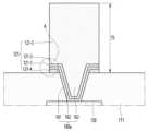
도 1은 비교 예에 따른 회로 기판을 나타낸 단면도이다.1 is a cross-sectional view showing a circuit board according to a comparative example.
도 1을 참조하면, 회로 기판은 절연층(10)을 포함한다.Referring to FIG. 1, the circuit board includes an insulating
그리고, 절연층(10)의 상면에는 제1 회로 패턴(20)이 배치되고, 절연층(10)의 하면에는 제2 회로 패턴(30)이 배치된다. 상기 제1 회로 패턴(20)은 패드를 포함한다.Then, the
또한, 비교 예의 회로 기판은 절연층(10)을 관통하는 관통 전극을 포함한다.Additionally, the circuit board of the comparative example includes a penetrating electrode that penetrates the insulating
상기 절연층(10)의 상면에는 상기 제1 회로 패턴(20)의 패드의 상면과 수직 방향으로 중첩되는 개구를 가지는 보호층(50)이 배치된다.A
그리고, 상기 제1 회로 패턴(20)의 패드 상에는 범프(70)가 배치된다.Additionally, a
상기 범프(70)는 일정 높이 또는 두께를 가지고 상기 제1 회로 패턴(20)의 패드 상에 돌출된다. 따라서, 상기 범프(70)는 무전해 도금으로 형성이 어렵다.The
이에 의해, 상기 범프(70)와 상기 제1 회로 패턴(20)의 패드 사이에는 시드층(60)이 배치된다. 상기 시드층(60)은 화학동도금층이다.Accordingly, the
상기 시드층(60)은 상기 제1 회로 패턴(20)의 패드의 상면 및 상기 보호층(50)의 내벽에 각각 배치된다.The
즉, 비교 예는 범프(70)와 제1 회로 패턴(20)의 패드 사이에 시드층(60)이 배치된 구조를 가진다. 이에 따라 비교 예는 상기 시드층(60)을 형성하는 공정을 추가로 진행해야 하며, 이에 따른 제조 공정이 복잡해지거나, 제조 시간이 증가하는 문제를 가졌다.That is, the comparative example has a structure in which the
또한, 비교 예의 회로기판은 무전해 도금으로 형성되는 시드층(60)의 디스미어 공정에서 사용되는 용액에 의해 보호층(50)의 화이트닝(whitening) 현상이 발생한다. 또한, 비교 예의 회로기판은 패드와 범프(70) 사이에 시드층(60)이 배치된 구조를 가지고, 이에 의해 범프 레이어는 다공성(porous)의 미세 구조를 가지게 된다. 이때, 다공성 구조는 금속의 밀집도가 낮으며, 이에 따라 외부 충격이나 기타 물리적인 힘에 의해 다공성을 가진 시드층(60)에 크랙이 발생하는 문제가 있다. 그리고, 상기 크랙의 발생에 의해 범프(70)의 파괴되고, 이에 의한 제품 신뢰성이나 내구성이 급격하게 감소하는 문제점이 있다.In addition, in the circuit board of the comparative example, whitening of the
나아가 비교 예는 상기 시드층(60)이 배치된 구조에 의해 패드와 범프(70) 사이의 접속 신뢰성이 저하되는 문제가 있다.Furthermore, the comparative example has a problem in that the reliability of the connection between the pad and the
또한, 비교 예는 상기 범프(70)의 표면 처리를 위한 전처리 공정에서 상기 시드층(60)이 에칭되는 문제가 발생하고, 이에 따른 범프(70)가 정상 기능을 수행하지 못하는 문제가 있다.In addition, in the comparative example, there is a problem in which the
또한, 비교 예의 범프(70)는 패드 상에 상기 패드의 폭보다 작은 폭을 가지고 배치된다. 이에 따라, 복수의 범프 사이의 피치는 상기 복수의 범프와 각각 연결되는 복수의 패드 사이의 피치에 대응된다. 그리고 상기 복수의 패드 사이의 피치는 이와 연결되는 복수의 관통 전극 사이의 피치에 대응된다.Additionally, the
이때, 비교 예는 상기 범프(70)를 형성하는 공정에서의 공차, 상기 제1 회로 패턴(20)의 패드를 형성하는 공정에서의 공차, 그리고 상기 관통 전극(40)의 관통 홀을 형성하는 공정에서의 공차를 모두 고려하여 상기 관통 전극 사이의 피치, 상기 패드 사이의 피치, 및 상기 범프 사이의 피치가 결정된다. 이에 따라 비교 예는 복수의 범프 사이의 피치를 줄이는데 한계가 있다.At this time, comparative examples include the tolerance in the process of forming the
또한, 비교 예는 제1 회로 패턴(20)의 패드 상에 별도로 배치된 시드층(60)에 의해 범프(70)의 도금이 이루어진다. 이에 의해, 비교 예는 복수의 범프(70) 사이의 두께 편차가 큰 문제가 있다. 따라서, 비교 예는 복수의 범프의 두께를 맞추기 위한 연마 공정을 필수로 진행해야 하는 문제가 있다.In addition, in the comparative example, the
실시 예는 복수의 포스트(post) 사이의 피치를 줄여 회로 집적도를 향상시키고, 포스트의 패드 부분과 범프 부분 사이의 접속 신뢰성을 향상시키며, 하부 영역의 측면에 형성되는 패임부의 패임 정도를 최소화하고, 복수의 포스트의 두께 편차를 최소화할 수 있는 회로 기판 및 이를 포함하는 반도체 패키지를 제공하도록 한다.The embodiment improves circuit integration by reducing the pitch between a plurality of posts, improves the connection reliability between the pad portion of the post and the bump portion, minimizes the degree of depression of the depression formed on the side of the lower region, and , to provide a circuit board that can minimize the thickness deviation of a plurality of posts and a semiconductor package including the same.
-전자 디바이스--Electronic Device-
실시 예의 설명에 앞서, 실시 예의 반도체 패키지를 포함하는 전자 디바이스에 대해 간략하게 설명하기로 한다. 전자 디바이스는 메인 보드(미도시)를 포함한다. 상기 메인 보드는 다양한 부품들과 물리적 및/또는 전기적으로 연결될 수 있다. 예를 들어, 메인 보드는 실시 예의 반도체 패키지와 연결될 수 있다. 상기 반도체 패키지에는 다양한 칩이 실장될 수 있다. 크게, 상기 반도체 패키지에는, 다양한 소자 또는 칩을 포함할 수 있다. 상기 소자 또는 칩은 휘발성 메모리(예컨대, DRAM), 비-휘발성 메모리(예컨대, ROM), 플래시 메모리 등의 메모리 칩과, 센트랄 프로세서(예컨대, CPU), 그래픽 프로세서(예컨대, GPU), 디지털 신호 프로세서, 암호화 프로세서, 마이크로 프로세서, 마이크로 컨트롤러 등의 어플리케이션 프로세서 칩과, 아날로그-디지털 컨버터, ASIC(application-specific IC) 등의 로직 칩 등을 포함할 수 있다.Before describing the embodiment, an electronic device including the semiconductor package of the embodiment will be briefly described. The electronic device includes a main board (not shown). The main board may be physically and/or electrically connected to various components. For example, the main board may be connected to the semiconductor package of the embodiment. Various chips may be mounted on the semiconductor package. Broadly speaking, the semiconductor package may include various devices or chips. The device or chip may include memory chips such as volatile memory (e.g., DRAM), non-volatile memory (e.g., ROM), flash memory, a central processor (e.g., CPU), a graphics processor (e.g., GPU), and digital signals. It may include application processor chips such as processors, cryptographic processors, microprocessors, and microcontrollers, and logic chips such as analog-to-digital converters and application-specific ICs (ASICs).
또한, 상기 소자 또는 칩은 능동 소자 및 수동 소자를 포함할 수 있다.Additionally, the device or chip may include active devices and passive devices.
상기 능동 소자는 신호 특성 중 비선형 부분을 적극적으로 이용한 소자를 의미한다. 그리고 수동 소자는 선형 및 비선형 신호 특성이 모두 존재하여도 비선형 신호 특성은 이용하지 않는 소자를 의미한다. 예를 들어, 능동 소자에는 트랜지스터, IC 반도체소자 등이 포함될 수 있으며, 상기 수동 소자에는 콘덴서, 저항 및 인덕터 등을 포함할 수 있다. 상기 수동 소자는 상기 능동 소자인 반도체 칩의 신호 처리 속도를 높이거나, 필터링 기능 등을 수행할 수 있다. 또한, 상기 칩은 와이파이(wi-fi)나 5G 통신 등에 이용 가능한 무선 통신 칩일 수 있다.The active device refers to a device that actively utilizes the nonlinear part of signal characteristics. And a passive device refers to a device that does not use nonlinear signal characteristics even though both linear and nonlinear signal characteristics exist. For example, active devices may include transistors and IC semiconductor devices, and passive devices may include condensers, resistors, and inductors. The passive element may increase the signal processing speed of the semiconductor chip, which is the active element, or may perform a filtering function. Additionally, the chip may be a wireless communication chip that can be used for Wi-Fi or 5G communication.
한편, 실시 예의 반도체 패키지가 적용되는 제품군은 CSP(Chip Scale Package), FC-CSP(Flip Chip-Chip Scale Package), FC-BGA(Flip Chip Ball Grid Array), POP (Package On Package) 및 SIP(System In Package) 중 어느 하나일 수 있으나, 이에 한정되는 것은 아니다.Meanwhile, the product lines to which the semiconductor package of the embodiment is applied include Chip Scale Package (CSP), Flip Chip-Chip Scale Package (FC-CSP), Flip Chip Ball Grid Array (FC-BGA), Package On Package (POP), and SIP ( System In Package), but is not limited to this.
이때, 상기 전자 디바이스는 스마트 폰(smart phone), 개인용 정보 단말기(personal digital assistant), 디지털 비디오 카메라(digital video camera), 디지털 스틸 카메라(digital still camera), 네트워크 시스템(network system), 컴퓨터(computer), 모니터(monitor), 태블릿(tablet), 랩탑(laptop), 넷북(netbook), 텔레비전(television), 비디오 게임(video game), 스마트 워치(smart watch), 오토모티브(Automotive) 등일 수 있다. 다만, 이에 한정되는 것은 아니며, 이들 외에도 데이터를 처리하는 임의의 다른 전자기기일 수 있음은 물론이다.At this time, the electronic device includes a smart phone, a personal digital assistant, a digital video camera, a digital still camera, a network system, and a computer. ), monitor, tablet, laptop, netbook, television, video game, smart watch, automotive, etc. However, it is not limited to this, and of course, it can be any other electronic device that processes data.
도 2는 실시 예에 따른 회로 기판을 나타낸 단면도이다.Figure 2 is a cross-sectional view showing a circuit board according to an embodiment.
이하에서는 도 2를 참조하여 실시 예에 따른 회로 기판의 전체적인 구조에 대해 설명한다.Hereinafter, the overall structure of the circuit board according to the embodiment will be described with reference to FIG. 2.
도 2를 참조하면, 회로 기판(100)은 적어도 1개의 칩이 부착될 수 있도록 한다. 또한, 실시 예의 회로 기판(100)은 전자 디바이스의 메인 보드에 부착될 수 있도록 한다. 상기 메인보드는 전자 디바이스의 마더보드를 의미할 수 있다.Referring to FIG. 2, the
또한, 상기 회로 기판(100)에 실장되는 칩은, 1개일 수 있으며, 이와 다르게 2개 이상일 수 있다. 예를 들어, 회로 기판(100)에는 1개의 프로세서 칩이 실장될 수 있다. 예를 들어, 회로 기판(100)에는 서로 다른 기능을 하는 적어도 2개의 프로세서 칩이 실장될 수 있다. 예를 들어, 회로 기판(100)에는 1개의 프로세서 칩과 함께 1개의 메모리 칩이 실장될 수 있다. 예를 들어, 회로 기판(100)에는 서로 다른 기능을 하는 적어도 2개의 프로세서 칩과 적어도 1개의 메모리 칩이 실장될 수 있다.Additionally, the number of chips mounted on the
회로 기판(100)은 절연층(110)을 포함한다.The
이때, 실시 예의 회로 기판(100)은 코어 기판일 수 있다. 예를 들어, 회로 기판(100)은 코어층의 제2 절연층(112)을 포함할 수 있다.At this time, the
예를 들어, 회로 기판(100)은 제2 절연층(112)을 중심으로 이의 상부 및 하부에 상호 대칭 구조를 가지는 복수의 절연층이 적층된 구조를 가질 수 있다. 다만, 실시 예는 이에 한정되지 않는다. 예를 들어, 상기 제2 절연층(112)을 중심으로 이의 상부 및 하부에는 서로 비대칭 구조를 가지며 복수의 절연층이 배치될 수도 있을 것이다.For example, the
이하에서는 실시 예의 회로 기판(100)이 코어 기판이고, 이에 따라 상기 제2 절연층(112)이 코어층인 것으로 하여 설명한다. 다만, 실시 예는 이에 한정되지 않는다. 예를 들어, 실시 예의 회로 기판(100)은 코어층을 포함하지 않는 코어리스 기판일 수 있다. 실시 예의 회로 기판(100)에서의 구조적 특징은 회로 기판(100)의 최외층의 회로층에 있다. 그리고 이하에서는 실시 예의 회로 기판(100)의 최외층의 회로층의 구조를 중심으로 설명하기로 한다.Hereinafter, the
이에 따라, 이하에서 설명되는 회로 기판(100)의 최외층의 회로층(120)의 구조는 코어 기판에 적용될 수 있고, 이와 다르게 코어리스 기판에 적용될 수 있을 것이다. 나아가, 상기 최외층의 회로층(120)의 구조는 일반적인 회로 기판의 적층 구조뿐 아니라, ETS(Embedded Trace Substrate) 구조의 회로 기판에도 적용 가능할 것이다.Accordingly, the structure of the
실시 예의 회로 기판(100)은 절연층(110)을 포함한다.The
상기 절연층(110)은 상측에서부터 제1 절연층(111), 제2 절연층(112) 및 제3 절연층(113)을 포함할 수 있다.The insulating
상기 제2 절연층(112)은 상기 회로 기판(100)의 복수의 절연층 중 내층에 배치된 내층 절연층을 의미할 수 있다. 상기 제2 절연층(112)은 프리프레그를 포함할 수 있다.The second
이때, 도면상에서 상기 제1 절연층(111)이 1층 구조를 가지는 것으로 도시하였으나, 이에 한정되는 것은 아니다. 예를 들어, 상기 제1 절연층(111)은 다층 구조를 가질 수 있다. 예를 들어, 상기 회로 기판(100)은 4층 이상의 층 구조를 가질 수 있다. 그리고, 상기 회로 기판(100)의 내층 절연층에 대응하는 제1 절연층(111)은 상기 회로 기판(100)의 전체 층 수를 기준으로 복수의 층 구조를 가질 수 있다.At this time, although the first insulating
상기 제1 절연층(111)은 상기 제2 절연층(112) 상에 배치될 수 있다. 예를 들어, 상기 제1 절연층(111)은 상기 제2 절연층(112)의 상면에 배치될 수 있다.The first insulating
상기 제1 절연층(111)은 회로 기판(100)의 절연층(110)에서 제1 최외층의 절연층을 의미할 수 있다. 예를 들어, 상기 제1 절연층(111)은 회로 기판(100)의 절연층(110)에서 최상측에 배치된 절연층을 나타낸 것일 수 있다. 상기 제1 절연층(111)은 칩이 실장되는 실장 영역을 제공하거나, 전자 디바이스의 메인 보드와 같은 외부 기판이 결합되는 결합 영역을 제공할 수 있다.The first insulating
상기 제3 절연층(113)은 상기 제2 절연층(112)의 하면에 배치될 수 있다. 상기 제3 절연층(113)은 회로 기판(100)의 절연층(110)에서 제2 최외층의 절연층을 의미할 수 있다. 예를 들어, 상기 제3 절연층(113)은 회로 기판(100)의 절연층(110)에서 최하측에 배치된 절연층을 나타낸 것일 수 있다.The third
상기 제1 절연층(111) 및 제3 절연층(113)은 리지드(rigid) 또는 플렉서블(flexible)할 수 있다. 예를 들어, 상기 제1 절연층(111) 및 제3 절연층(113)은 유리 또는 플라스틱을 포함할 수 있다. 자세하게, 상기 제1 절연층(111) 및 제3 절연층(113)은 소다라임유리(soda lime glass) 또는 알루미노실리케이트유리 등의 화학 강화/반강화유리를 포함할 수 있다. 또는, 상기 제1 절연층(111) 및 제3 절연층(113)은 폴리이미드(Polyimide, PI), 폴리에틸렌 테레프탈레이트(polyethylene terephthalate, PET), 프로필렌 글리콜(propylene glycol, PPG) 폴리 카보네이트(PC) 등의 강화 혹은 연성 플라스틱을 포함할 수 있다. 또는 상기 제1 절연층(111) 및 제3 절연층(113)은 사파이어를 포함할 수 있다.The first insulating
또한, 상기 제1 절연층(111) 및 제3 절연층(113)은 광등방성 필름을 포함할 수 있다. 일례로, 상기 제1 절연층(111) 및 제3 절연층(113)은 COC(Cyclic Olefin Copolymer), COP(Cyclic Olefin Polymer), 광등방 폴리카보네이트(polycarbonate, PC) 또는 광등방 폴리메틸메타크릴레이트(PMMA) 등을 포함할 수 있다.Additionally, the first insulating
또한, 상기 제1 절연층(111) 및 제3 절연층(113)은 무기 필러 및 절연 수지를 포함하는 재료로 형성될 수 있다. 예를 들어, 상기 제1 절연층(111) 및 제3 절연층(113)은 에폭시 수지와 같은 열경화성 수지, 폴리이미드와 같은 열가소성 수지 내에 실리카, 알루미나 등의 무기 필러가 분산된 구조를 포함할 수 있다. 예를 들어, 상기 제1 절연층(111) 및 제3 절연층(113)은 ABF(Ajinomoto Build-up Film), FR-4, BT(Bismaleimide Triazine), PID(Photo Imagable Dielectric resin), BT 등을 포함할 수 있다.Additionally, the first insulating
또한, 제1 절연층(111) 및 제3 절연층(113)은 부분적으로 곡면을 가지면서 휘어질 수 있다. 즉, 제1 절연층(111) 및 제3 절연층(113)은 부분적으로는 평면을 가지고, 부분적으로는 곡면을 가지면서 휘어질 수 있다. 자세하게, 상기 제1 절연층(111) 및 제3 절연층(113)은 끝단이 곡면을 가지면서 휘어지거나 랜덤한 곡률을 포함한 표면을 가지며 휘어지거나 구부러질 수 있다.Additionally, the first insulating
또한, 상기 제1 절연층(111) 및 제3 절연층(113)은 유연한 특성을 가지는 플렉서블(flexible) 기판일 수 있다. 또한, 상기 제1 절연층(111) 및 제3 절연층(113)은 커브드(curved) 또는 벤디드(bended) 기판일 수 있다.Additionally, the first insulating
상기 제1 절연층(111) 및 제3 절연층(113) 각각은 10㎛ 내지 60㎛의 범위의 두께를 가질 수 있다. 바람직하게, 상기 제1 절연층(111) 및 제3 절연층(113) 각각은 12㎛ 내지 50㎛의 범위의 두께를 가질 수 있다. 더욱 바람직하게, 상기 제1 절연층(111) 및 제3 절연층(113) 각각은 15㎛ 내지 40㎛의 두께를 가질 수 있다.Each of the first insulating
상기 제1 절연층(111) 또는 제3 절연층(113)의 두께가 10㎛ 미만이면, 회로 기판(100)에 포함된 회로층이 안정적으로 보호되지 않을 수 있다.If the thickness of the first insulating
또한, 상기 제1 절연층(111) 또는 제3 절연층(113)의 두께가 60㎛를 초과하면, 상기 회로 기판(100)의 두께가 증가할 수 있고, 이에 의해 반도체 패키지의 두께가 증가할 수 있다. 또한, 상기 제1 절연층(111) 또는 제3 절연층(113)의 두께가 60㎛를 초과하면, 이에 대응하게 회로층의 두께 및 관통 전극의 두께가 증가할 수 있다. 그리고 상기 회로층의 두께 및 관통 전극의 두께가 증가하는 경우, 미세화 구현이 어려워 회로 집적도가 감소할 수 있고, 신호 전송 거리가 증가하여 신호 전송 손실이 증가할 수 있다.In addition, when the thickness of the first insulating
실시 예의 회로 기판(100)은 절연층(110)에 배치된 회로층을 포함한다.The
예를 들어, 회로 기판(100)은 제1 절연층(111)의 상면에 배치된 제1 회로층(120)을 포함할 수 있다.For example, the
예를 들어, 회로 기판(100)은 제1 절연층(111)의 하면 및 제2 절연층(112)의 상면 사이에 배치된 제2 회로층(130)을 포함할 수 있다.For example, the
예를 들어, 회로 기판(100)은 제2 절연층(112)의 하면 및 제3 절연층(113)의 상면 사이에 배치된 제3 회로층(140)을 포함할 수 있다.For example, the
예를 들어, 회로 기판(100)은 제3 절연층(113)의 하면에 배치된 제4 회로층(150)을 포함할 수 있다.For example, the
상기 제1 회로층(120), 제2 회로층(130), 제3 회로층(140) 및 제4 회로층(150)은 통상적인 인쇄회로기판의 제조 공정인 어디티브 공법(Additive process), 서브트렉티브 공법(Subtractive Process), MSAP(Modified Semi Additive Process) 및 SAP(Semi Additive Process) 공법 등으로 가능하며 여기에서는 상세한 설명은 생략한다.The
상기 제1 회로층(120)은 회로 기판(100)의 제1 최외층에 배치된 회로층을 의미할 수 있다. 그리고, 제4 회로층(140)은 회로 기판(100)의 제2 최외층에 배치된 회로층을 의미할 수 있다.The
상기 제1 회로층(120)은 제1 절연층(111)의 상면 위로 돌출된 구조를 가질 수 있다. 또한, 상기 제4 회로층(140)은 상기 제3 절연층(113)의 하면 아래로 돌출된 구조를 가질 수 있다. 다만, 실시 예는 이에 한정되지 않는다. 예를 들어, 실시 예의 회로 기판(100)이 ETS 구조를 가지는 경우, 상기 제1 회로층(120) 및 제4 회로층(140) 중 어느 하나(바람직하게는, 제4 회로층)는 절연층의 표면 내에 매립된 구조를 가질 수 있다.The
상기 제1 회로층(120)은 기능에 따라 복수의 회로 패턴으로 구분될 수 있다.The
예를 들어, 상기 제1 회로층(120)은 제1 회로 패턴(121), 제2 회로 패턴(122) 및 제3 회로 패턴(123)을 포함할 수 있다.For example, the
상기 제1 회로 패턴(121)은 회로 기판(100) 상에 외부 기판(예를 들어, 전자 디바이스의 메인 보드)을 결합하기 위한 금속 포스트로 기능한다. 이에 따라, 상기 제1 회로 패턴(121)은 '포스트'라고도 할 수 있다. 이하에서는 상기 제1 회로 패턴(121)을 '포스트'라고 하여 설명한다.The
상기 제2 회로 패턴(122)은 회로 기판(100) 상에 칩을 실장하기 위한 실장 패드로 기능한다. 이에 따라 상기 제2 회로 패턴(122)은 '패드'라고도 할 수 있다. 이하에서는 상기 제2 회로 패턴(122)을 '패드'라고 하여 설명한다.The
상기 제3 회로 패턴(123)은 상기 제1 회로 패턴(121) 및 제2 회로 패턴(122) 중 적어도 하나와 연결되어 배선 기능을 하는 트레이스로 기능한다. 이에 따라 상기 제3 회로 패턴(123)은 '트레이스'라고도 할 수 있다. 이하에서는 상기 제3 회로 패턴(123)을 '트레이스'라고 하여 설명한다.The
상기 포스트(121)는 상기 패드(122) 및 트레이스(123)와 다른 두께를 가질 수 있다. 바람직하게, 상기 포스트(121)는 상기 패드(122) 및 트레이스(123)의 두께보다 클 수 있다. 그리고, 상기 패드(122) 및 트레이스(123)는 서로 동일한 두께를 가질 수 있다. 여기에서, 서로 동일한 두께라는 것은 패드(122)와 트레이스(123)의 두께 차이가 5㎛ 이하, 4㎛ 이하, 3㎛ 이하, 2㎛ 이하, 또는 1㎛ 이하인 것을 의미할 수 있다.The
상기 포스트(121)의 두께는 상기 패드(122) 또는 트레이스(123)의 두께의 3배 이상일 수 있다. 예를 들어, 상기 포스트(121)의 두께는 상기 패드(122) 또는 트레이스(123)의 두께의 5배 이상일 수 있다. 예를 들어, 상기 포스트(121)의 두께는 상기 패드(122)의 두께 또는 트레이스(123)의 두께의 7배 이상일 수 있다. 예를 들어, 상기 포스트(121)의 두께는 상기 패드(122)의 두께 또는 트레이스(123)의 두께의 10배 이상일 수 있다.The thickness of the
이때, 상기 포스트(121)의 두께가 상기 패드(122)의 두께 또는 트레이스(123)의 두께보다 큰 것은, 상기 포스트(121)를 구성하는 금속층의 층수가 상기 패드(122) 또는 트레이스(123)를 구성하는 금속층의 층수보다 많다는 것을 의미하지 않는다. 다시 말해서, 상기 포스트(121)를 구성하는 금속층의 층수는 상기 패드(122) 또는 트레이스(123)를 구성하는 금속층의 층수와 동일하다. 즉, 상기 포스트(121)의 층 구조는 상기 패드(122) 또는 트레이스(123)의 층 구조와 동일하다. 다만, 상기 포스트(121)를 구성하는 금속층 중 어느 하나의 금속층의 두께는 상기 패드(122) 또는 트레이스(123)의 대응 금속층의 두께보다 크다.At this time, the thickness of the
이에 따라, 상기 포스트(121)의 두께는 상기 패드(122) 또는 트레이스(123)의 두께보다 크다.Accordingly, the thickness of the
상기 포스트(121)는 복수의 부분으로 구분할 수 있다. 상기 포스트(121)는 두께 방향을 기준으로 제1 부분(121P) 및 제2 부분(121B)으로 구분할 수 있다. 이때, 상기 제1 부분(121P) 및 제2 부분(121B)의 구분은 층 구분을 의미하지 않는다. 구체적으로, 상기 제1 부분(121P) 및 제2 부분(121B)은 서로 일체로 형성되는 하나의 구성이며, 단지 이를 패드(122) 또는 트레이스(123)를 기준으로 구분한 것일 수 있다.The
상기 포스트(121)의 제1 부분(121P)은 상기 포스트(121)의 패드 부분을 의미할 수 있다. 상기 포스트(121)의 제1 부분(121P)은 상기 패드(122) 또는 트레이스(123)의 두께에 대응하는 두께를 가질 수 있다.The
상기 포스트(121)의 제2 부분(121B)은 상기 포스트(121)의 제1 부분(121P) 상에 배치된다. 상기 포스트(121)의 제2 부분(121B)은 상기 포스트(121)의 범프 부분이라고 할 수 있다.The
이에 따라, 상기 포스트(121)는 상기 제2 부분(121B)의 두께만큼 상기 패드(122) 또는 트레이스(123)의 두께보다 클 수 있다.Accordingly, the
이를 위해, 상기 포스트(121)는 상기 패드(122) 또는 트레이스(123)와는 별개의 도금 공정을 통해 형성될 수 있다. 다만, 실시 예는 이에 한정되지 않는다. 상기 포스트(121)는 상기 패드(122) 또는 트레이스(123)의 도금 공정에서 상기 제1 부분(121P)이 형성될 수 있고, 추가적인 도금 공정을 진행하여 상기 제1 부분(121P)과 일체의 상기 포스트(121)의 제2 부분(121B)이 형성될 수도 있을 것이다.To this end, the
이를 통해, 실시 예의 포스트(121)는 제1 부분(121P)과 제2 부분(121B) 사이에 추가적인 층이 배치되지 않는다. 구체적으로, 포스트(121)는 상기 제1 부분(121P)과 제2 부분(121B) 사이에 시드층이 존재하지 않는다. 이를 통해 실시 예는 상기 포스트(121)의 제1 부분(121P)과 제2 부분(121B) 사이의 물리적 접속성 및 전기적 접속성을 향상시킬 수 있다. 또한, 상기 포스트(121)는 제1 부분(121P)과 제2 부분(121B)의 폭이 서로 대응할 수 있다. 여기에서 상기 제1 부분(121P)의 폭은 상기 제1 부분(121P)의 하부 영역에 포함된 패임부(도 22의 121U)와 수평으로 중첩되지 않는 위치에서의 폭을 의미할 수 있다. 이에 따라, 실시 예는 상기 포스트(121)의 제2 부분(121B)의 피치를 기준으로 복수의 포스트(121a, 121b) 사이의 피치를 결정할 수 있다.Through this, the
상기 제1 회로층(120)의 포스트(121), 패드(122) 및 트레이스(123)의 상세 구조에 대해서는 하기에서 더욱 상세히 설명한다.The detailed structure of the
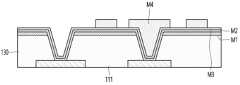
상기 제2 회로층(130), 제3 회로층(140) 및 제4 회로층(150)은 상기 제1 회로층(120)과는 다른 층 구조를 가질 수 있다. 예를 들어, 제2 회로층(130), 제3 회로층(140) 및 제4 회로층(150)의 금속층의 층수는 상기 제1 회로층(120)의 금속층의 층수와 다를 수 있다. 예를 들어, 상기 제2 회로층(130), 제3 회로층(140) 및 제4 회로층(150)의 금속층의 층수는 상기 제1 회로층(120)의 금속층의 층수보다 작을 수 있다.The
구체적으로, 제1 회로층(120), 제2 회로층(130), 제3 회로층(140) 및 제4 회로층(150)은 각각 시드층에 대응하는 금속층을 포함한다. 그리고, 상기 제2 회로층(130), 제3 회로층(140) 및 제4 회로층(150)의 시드층의 층수는 상기 제1 회로층(120)의 시드층의 층수보다 작을 수 있다.Specifically, the
다만, 상기 제4 회로층(150)은 회로기판의 제2 최외층 회로층이며, 상기 제1 회로층(120)의 형성 시에 함께 형성될 수 있다. 이에 따라, 실시 예는 공정성을 향상시키기 위해 상기 제4 회로층(150)은 상기 제1 회로층(120)에 대응하는 층 구조를 갖도록 할 수 있다.However, the
상기 제1 회로층(120), 제2 회로층(130), 제3 회로층(140) 및 제4 회로층(150)은 금(Au), 은(Ag), 백금(Pt), 티타늄(Ti), 주석(Sn), 구리(Cu) 및 아연(Zn) 중에서 선택되는 적어도 하나의 금속 물질로 형성될 수 있다. 또한, 상기 제1 회로층(120), 제2 회로층(130), 제3 회로층(140) 및 제4 회로층(150)은 본딩력이 우수한 금(Au), 은(Ag), 백금(Pt), 티타늄(Ti), 주석(Sn), 구리(Cu), 아연(Zn) 중에서 선택되는 적어도 하나의 금속 물질을 포함하는 페이스트 또는 솔더 페이스트로 형성될 수 있다. 바람직하게, 상기 제1 회로층(120), 제2 회로층(130), 제3 회로층(140) 및 제4 회로층(150)은 가격이 비교적 저렴한 구리(Cu)로 형성될 수 있다.The
상기 제2 회로층(130), 제3 회로층(140) 및 제4 회로층(150)은 5㎛ 내지 20㎛의 범위의 두께를 가질 수 있다. 예를 들어, 상기 제2 회로층(130), 제3 회로층(140) 및 제4 회로층(150)은 6㎛ 내지 17㎛의 범위의 두께를 가질 수 있다. 상기 제2 회로층(130), 제3 회로층(140) 및 제4 회로층(150)은 7㎛ 내지 13㎛의 범위의 두께를 가질 수 있다. 상기 제2 회로층(130), 제3 회로층(140) 및 제4 회로층(150)의 두께가 5㎛ 미만인 경우에는 저항이 증가할 수 있다. 상기 제2 회로층(130), 제3 회로층(140) 및 제4 회로층(150)의 두께가 20㎛를 초과하는 경우에는 회로 미세화가 어렵고, 이에 따른 회로 집적도가 감소할 수 있다.The
한편, 상기 제1 회로층(120)의 패드(122) 및 트레이스(123)는 상기 제2 회로층(130), 제3 회로층(140) 및 제4 회로층(150)의 두께에 대응하는 두께를 가질 수 있다.Meanwhile, the
그리고 상기 제1 회로층(120)의 포스트(121)는 상기 패드(122), 트레이스(123), 제2 회로층(130), 제3 회로층(140) 및 제4 회로층(150)의 두께보다 클 수 있다.And the
상기 제1 회로층(120)의 포스트(121)의 두께는 100㎛를 초과할 수 있다. 상기 제1 회로층(120)의 포스트(121)의 두께는 120㎛를 초과할 수 있다. 상기 제1 회로층(120)의 포스트(121)의 두께는 140㎛를 초과할 수 있다. 상기 제1 회로층(120)의 포스트(121)의 두께는 160㎛를 초과할 수 있다. 상기 제1 회로층(120)의 포스트(121)의 두께는 200㎛를 초과할 수 있다.The thickness of the
상기 제1 회로층(120)의 포스트(121)의 두께는 100㎛ 내지 220㎛의 범위를 만족할 수 있다. 바람직하게, 상기 제1 회로층(120)의 포스트(121)의 두께는 110㎛ 내지 215㎛의 범위를 만족할 수 있다. 더욱 바람직하게, 상기 제1 회로층(120)의 포스트(121)의 두께는 115㎛ 내지 210㎛의 범위를 만족할 수 있다.The thickness of the
상기 제1 회로층(120)의 포스트(121)의 두께가 100㎛ 미만이면, 상기 제1 포스트(121) 상에 외부 기판(예를 들어, 전자 디바이스의 메인 보드)가 안정적으로 결합되지 못할 수 있다. 예를 들어, 상기 제1 회로층(120)의 포스트(121)의 두께가 220㎛를 초과하면, 상기 포스트(121)의 강성이 저하될 수 있고, 이에 따라 상기 외부 기판이 결합된 상태에서 무너짐과 같은 신뢰성 문제가 발생할 수 있다. 또한, 상기 제1 회로층(120)의 포스트(121)의 두께가 220㎛를 초과하면, 복수의 포스트들 사이의 두께 편차가 커지고, 이에 따라 연마 공정을 위한 시간이 증가할 수 있다. 또한, 상기 제1 회로층(120)의 포스트(121)의 두께가 220㎛를 초과하면, 회로 기판(100)의 두께 및 반도체 패키지의 두께가 증가할 수 있다.If the thickness of the
실시 예의 회로 기판은 관통 전극을 포함할 수 있다.The circuit board of the embodiment may include a through electrode.
구체적으로, 관통 전극은 절연층(110)을 관통할 수 있다. 바람직하게, 관통 전극은 상기 제1 절연층(111)을 관통하는 제1 관통 전극(160)을 포함한다. 또한, 상기 관통 전극은 제2 절연층(112)을 관통하는 제2 관통 전극(170)을 포함한다. 또한, 상기 관통 전극은 제3 절연층(113)을 관통하는 제3 관통 전극(180)을 포함한다.Specifically, the penetrating electrode may penetrate the insulating
상기 제1 관통 전극(160), 제2 관통 전극(170) 및 제3 관통 전극(180)은 각각의 절연층을 관통하는 관통 홀 내에 배치될 수 있다. 예를 들어, 상기 제1 관통 전극(160), 제2 관통 전극(170) 및 제3 관통 전극(180)은 상기 관통 홀을 전도성 물질로 충진하여 형성할 수 있다.The first through
상기 관통 홀은 기계, 레이저 및 화학 가공 중 어느 하나의 가공 방식에 의해 형성될 수 있다. 상기 관통 홀은 밀링(Milling), 드릴(Drill) 및 라우팅(Routing) 등의 기계 가공 방식으로 형성될 수 있다. 또한, 상기 관통 홀은 UV나 CO2 레이저 방식을 사용할 수 있다. 또한, 상기 제1 관통 홀은 미노실란, 케톤류 등을 포함하는 약품을 이용한 화학 가공 방식을 사용할 수 있다.The through hole may be formed by any one of mechanical, laser, and chemical processing. The through hole may be formed through machining methods such as milling, drilling, and routing. Additionally, the through hole may use a UV or CO2 laser method. Additionally, the first through hole may be formed using a chemical processing method using chemicals including minosilane, ketones, etc.
상기 관통 홀이 형성되면, 상기 관통 홀 내부를 구리(Cu), 은(Ag), 주석(Sn), 금(Au), 니켈(Ni) 및 팔라듐(Pd) 중에서 선택되는 어느 하나의 금속 물질로 충진하여 상기 제1 관통 전극(160), 제2 관통 전극(170) 및 제3 관통 전극(180)을 형성할 수 있다. 이때, 상기 전도성 물질의 충진은 무전해 도금, 전해 도금, 스크린 인쇄(Screen Printing), 스퍼터링(Sputtering), 증발법(Evaporation), 잉크젯팅 및 디스펜싱 중 어느 하나 또는 이들의 조합된 방식을 이용할 수 있다.When the through hole is formed, the inside of the through hole is made of any one metal material selected from copper (Cu), silver (Ag), tin (Sn), gold (Au), nickel (Ni), and palladium (Pd). By filling, the first through
한편, 상기 제1 관통 전극(160)은 제1 절연층(111) 내에서 수평 방향으로 이격되어 복수 개 형성될 수 있다.Meanwhile, the first through
이때, 상기 제1 관통 전극(160)은 상기 제1 회로층(120)과 수직 방향으로 중첩될 수 있다. 그리고, 상기 제1 관통 전극(160)은 상기 제1 회로층(120)의 포스트(121)와 수직 방향으로 중첩되는 제1-1 관통 전극(160a)을 포함할 수 있다. 또한, 상기 제1 관통 전극(160)은 상기 제1 회로층(120)의 패드(122)와 수직 방향으로 중첩되는 제1-2 관통 전극(160b)을 포함할 수 있다.At this time, the first through
이때, 상기 제1 관통 전극(160)은 상기 제1 회로층(120)과 일체로 형성된다. 이는, 상기 제1 절연층(111)을 관통하는 관통 홀 내부의 충진과, 상기 제1 절연층(111) 상에서의 회로층 형성을 위한 도금 공정이 동시에 진행되기 때문이다.At this time, the first through
따라서, 상기 패드(122)는 상기 제1-2 관통 전극(160b)과 일체로 형성될 수 있다. 여기에서 일체로 형성된다는 것은, 상기 패드(122)를 구성하는 적어도 하나의 금속층과 상기 제1-2 관통 전극을 구성하는 적어도 하나의 금속층이 한 번의 도금 공정에 의해 형성된 도금층인 것을 의미할 수 있다.Accordingly, the
나아가, 상기 포스트(121)는 상기 제1-1 관통 전극(160a)과 일체로 형성될 수 있다. 예를 들어, 상기 포스트(121)의 범프 부분에 대응하는 제2 부분(121B)은 상기 포스트(121)의 패드 부분에 대응하는 제1 부분(121P)과 일체로 형성된다. 그리고, 상기 포스트(121)의 제1 부분(121P)은 상기 제1-1 관통 전극(160a)과 일체로 형성된다. 따라서, 상기 포스트(121)의 제2 부분(121B)은 상기 제1-1 관통 전극(160a)과 일체로 형성된다.Furthermore, the
이때, 비교 예에서는, 관통 전극과 포스트의 패드는 서로 일체로 형성되기는 하지만, 상기 관통 전극과 상기 포스트의 범프는 별개의 공정에 의한 분리된 금속층이다. 이에 따라, 비교 예에서는 상호 간의 전기적 및 물리적 접속성이 저하되고, 신호 전송 손실이 증가하는 문제를 가졌다.At this time, in the comparative example, although the pads of the through electrode and the post are formed integrally with each other, the bumps of the through electrode and the post are separated metal layers through a separate process. Accordingly, in the comparative example, mutual electrical and physical connectivity was deteriorated and signal transmission loss was increased.
이에 반하여, 실시 예는 상기 제1-1 관통 전극(160a), 포스트(121)의 제1 부분(121P) 및 포스트(121)의 제2 부분(121B)이 서로 일체로 형성된 구조를 가진다. 이에 따라, 실시 예는 제1-1 관통 전극(160a)과 포스트(121) 사이의 전기적 및 물리적 접속성을 향상시킬 수 있다. 이에 따라, 실시 예는 회로 기판의 물리적 신뢰성 및 전기적 신뢰성을 향상시킬 수 있다.In contrast, the embodiment has a structure in which the 1-1 through
실시 예의 회로 기판(100)은 보호층을 포함한다.The
구체적으로, 제1 절연층(111)의 상면에는 제1 보호층(195)이 배치된다. 상기 제1 보호층(195)은 적어도 하나의 개구를 포함한다. 구체적으로, 상기 제1 보호층(195)은 상기 제1 회로층(120)의 포스트(121)와 수직 방향으로 중첩되는 개구를 포함한다. 이때, 상기 제1 보호층(195)의 개구의 폭은 상기 포스트(121)의 폭과 동일할 수 있다.Specifically, the first
여기에서, 비교 예는 상기 제1 보호층의 개구의 폭이 포스트의 폭보다 크거나 작았다. 이는, 상기 제1 보호층의 노광 및 현상 공정에서의 공차에 의해, 상기 제1 보호층의 개구의 폭과 상기 포스트의 폭을 실질적으로 동일하게 형성하기 어렵기 때문이다. 이에 따라, 비교 예에서는 상기 공차를 고려하여 상기 제1 보호층의 개구의 폭을 증가시키거나, 상기 포스트의 폭을 증가시켰다. 이에 따라, 비교 예에서는 복수의 포스트 사이의 피치를 줄이는데 한계가 있었다.Here, in the comparative example, the width of the opening of the first protective layer was larger or smaller than the width of the post. This is because it is difficult to make the width of the opening of the first protective layer and the width of the post substantially the same due to tolerances in the exposure and development process of the first protective layer. Accordingly, in the comparative example, the width of the opening of the first protective layer was increased or the width of the post was increased in consideration of the tolerance. Accordingly, in the comparative example, there was a limit to reducing the pitch between a plurality of posts.
이에 반하여, 실시 예는 상기 포스트(121)를 일정 두께를 형성한 이후에 상기 제1 보호층(195)을 형성한다. 이에 따라 실시 예는 포스트(121)의 폭과 상기 제1 보호층(195)의 개구의 폭이 실질적으로 동일하도록 할 수 있다. 이를 통해 실시 예는 복수의 포스트 사이의 피치를 더욱 줄일 수 있다. 이에 따라 실시 예는 회로 기판의 회로 집적도를 향상시킬 수 있다.In contrast, in the embodiment, the first
한편, 회로 기판(100)은 제3 절연층(113)의 하면에 배치된 제2 보호층(195)을 더 포함할 수 있다.Meanwhile, the
상기 제1 보호층(195) 및 제2 보호층(195)은 절연성 물질을 포함할 수 있다. 상기 제1 보호층(195) 및 제2 보호층(195)은 절연층과 회로층의 표면을 보호하기 위해 도포된 후 가열하여 경화될 수 있는 다양한 물질을 포함할 수 있다.The first
상기 제1 보호층(195) 및 제2 보호층(195)은 유기 고분자 물질을 포함하는 솔더 레지스트층일 수 있다. 일 예로, 상기 제1 보호층(195) 및 제2 보호층(195)은 에폭시 아크릴레이트 계열의 수지를 포함할 수 있다. 자세하게, 상기 제1 보호층(195) 및 제2 보호층(195)은 수지, 경화제, 광 개시제, 안료, 용매, 필러, 첨가제, 아크릴 계열의 모노머 등을 포함할 수 있다. 다만, 실시 예는 이에 한정되지 않고, 상기 제1 보호층(195) 및 제2 보호층(195)은 포토 솔더 레지스트층, 커버레이(cover-lay) 및 고분자 물질 중 어느 하나일 수 있음은 물론이다.The first
상기 제1 보호층(195) 및 제2 보호층(195)의 두께는 1㎛ 내지 20㎛일 수 있다. 상기 제1 보호층(195) 및 제2 보호층(195)의 두께는 1㎛ 내지 15㎛일 수 있다. 예를 들어, 상기 제1 보호층(195) 및 제2 보호층(195)의 두께는 5㎛ 내지 20㎛일 수 있다. 상기 제1 보호층(195) 및 제2 보호층(195)의 두께가 20㎛를 초과하는 경우, 회로 기판 및 반도체 패키지의 전체적인 두께가 증가할 수 있다.The first
한편, 도면상에서는 회로 기판이 제1 보호층(195) 및 제2 보호층(195)을 포함하는 것으로 도시하였으나, 이에 한정되는 것은 아니다.Meanwhile, in the drawing, the circuit board is shown as including a first
예를 들어, 상기 제1 보호층(195) 및 제2 보호층(195) 중 적어도 하나는 생략될 수 있다.For example, at least one of the first
바람직하게, 도 2의 회로 기판(100)에서 제1 보호층(195)은 생략될 수 있다. 이에 따라, 상기 제1 절연층(111)의 상면 및 제1 회로층(120)의 상면과 측면은 회로기판(100)의 외측으로 노출될 수 있다. 그리고, 상기 제1 절연층(111)의 상면 및 상기 제1 회로층(120)의 상면의 적어도 일부 및 측면은 반도체 패키지 공정에서 몰딩층에 의해 덮일 수 있을 것이다.Preferably, the first
한편, 도면에 도시하지는 않았지만, 회로 기판(100)의 제1 회로층(120) 상에는 표면 처리층이 배치될 수 있다. 예를 들어, 상기 제1 회로층(120)의 포스트(121) 및 패드(122) 중 적어도 하나의 상면에는 표면 처리층이 배치될 수 있다. 상기 표면 처리층은 회로층의 부식 및 산화를 방지하면서, 솔더성을 높이기 위해 형성될 수 있다. 이때,Meanwhile, although not shown in the drawing, a surface treatment layer may be disposed on the
상기 표면 처리층은 OSP(Organic Solderability Preservative) 층일 수 있다. 바람직하게, 상기 표면 처리층은 회로층 상에 코팅된 벤지미다졸(Benzimidazole)과 같은 유기물로 형성된 유기층일 수 있다.The surface treatment layer may be an Organic Solderability Preservative (OSP) layer. Preferably, the surface treatment layer may be an organic layer formed of an organic material such as benzimidazole coated on the circuit layer.
이와 다르게, 상기 표면 처리층은 도금층일 수 있다. 예를 들어, 상기 표면 처리층은 무전해 도금된 금(Au) 도금층을 포함할 수 있다. 예를 들어, 상기 표면 처리층은 무전해 도금된 니켈(Ni) 도금층과, 상기 니켈 도금층에 무전해 도금된 금(Au) 도금층을 포함할 수 있다. 예를 들어, 상기 표면 처리층은 무전해 도금된 니켈(Ni) 도금층과, 상기 니켈 도금층에 무전해 도금된 팔라듐(Pd) 도금층과, 상기 팔라듐 도금층에 무전해 도금된 금(Au) 도금층을 포함할 수 있다.Alternatively, the surface treatment layer may be a plating layer. For example, the surface treatment layer may include an electroless gold (Au) plating layer. For example, the surface treatment layer may include an electroless-plated nickel (Ni) plating layer and a gold (Au) plating layer electrolessly plated on the nickel plating layer. For example, the surface treatment layer includes a nickel (Ni) plating layer electrolessly plated, a palladium (Pd) plating layer electrolessly plated on the nickel plating layer, and a gold (Au) plating layer electrolessly plated on the palladium plating layer. can do.
이하에서는 실시 예의 회로 기판에 포함된 회로층에 대해 보다 구체적으로 설명하기로 한다.Hereinafter, the circuit layer included in the circuit board of the embodiment will be described in more detail.
도 3은 제1 실시 예의 제1 회로층의 포스트의 층 구조를 나타낸 단면도이고, 도 4는 제1 실시 예의 제1 회로층의 패드의 층 구조를 나타낸 단면도이며, 도 5는 제1 실시 예의 제1 회로층의 트레이스의 층 구조를 나타낸 단면도이고, 도 6은 실시 예의 제2 회로층의 층 구조를 나타낸 단면도이고, 도 7은 제2 실시 예의 제1 회로층의 포스트의 층 구조를 나타낸 단면도이다.FIG. 3 is a cross-sectional view showing the layer structure of the post of the first circuit layer of the first embodiment, FIG. 4 is a cross-sectional view showing the layer structure of the pad of the first circuit layer of the first embodiment, and FIG. 5 is a cross-sectional view showing the layer structure of the pad of the first circuit layer of the first embodiment. 1 is a cross-sectional view showing the layer structure of the trace of the circuit layer, FIG. 6 is a cross-sectional view showing the layer structure of the second circuit layer of the embodiment, and FIG. 7 is a cross-sectional view showing the layer structure of the posts of the first circuit layer of the second embodiment. .
잠시, 도 2를 다시 참조하면, 제1 회로층(120)은 포스트(121), 패드(122) 및 트레이스(123)를 포함한다. 그리고 상기 제1 회로층(120), 포스트(121) 및 패드(122)는 서로 동일한 층 구조를 가지는 반면에, 적어도 하나는 적어도 다른 하나의 두께와 다른 두께를 가진다.Referring again to FIG. 2 for a moment, the
반면에, 제2 회로층(130)은 상기 제1 회로층(120)과는 다른 층 구조를 가진다. 예를 들어, 상기 제2 회로층(130)은 제1 회로층(120)의 층수보다 작은 층수를 가진다. 예를 들어, 제2 회로층(130)의 시드층의 층수는 상기 제1 회로층(120)의 시드층의 층수보다 작다.On the other hand, the
한편, 실시 예의 제1 회로층(120)은 제조 방식에 따라 서로 다른 층 구조를 가질 수 있다. 예를 들어, 제1 회로층(120)이 SAP 공법으로 제조되는 경우, 상기 제1 회로층(120)은 동박층에 대응하는 제4 금속층(121-4)을 포함하지 않는 제1 내지 제3 금속층(121-1, 121-2, 121-3)만을 포함한다. 그리고, 상기 제1 회로층(120)이 MSAP 공법으로 제조되는 경우, 상기 제1 회로층(120)은 상기 동박층을 포함하는 제1 내지 제4 금속층(121-1, 121-2, 121-3, 121-4)을 포함할 수 있다.Meanwhile, the
도 3을 참조하면, 회로 기판(100)은 제1 절연층(111)을 관통하는 제1-1 관통 전극(160a) 및 상기 제1-1 관통 전극(160a) 상에 배치된 제1 회로층(120)의 포스트(121)를 포함한다.Referring to FIG. 3, the
이때, 상기 제1-1 관통 전극(160a)과 상기 포스트(121)는 일체로 형성된다.At this time, the 1-1 through
상기 포스트(121)는 복수의 금속층을 포함한다. 그리고, 상기 제1-1 관통 전극(160a)도 상기 포스트(121)의 복수의 금속층에 대응되는 복수의 금속층을 포함한다. 그리고 상기 포스트(121)의 복수의 금속층 각각은 상기 제1-1 관통 전극(160a)의 복수의 금속층 중 대응 금속층과 일체로 형성된다. 일체로 형성된다는 것은 상기 포스트(121)를 구성하는 복수의 금속층 중 어느 하나와 상기 제1-1 관통 전극(160a)을 구성하는 복수의 금속층 중 어느 하나가 하나의 층으로 구성된다는 것을 의미할 수 있다.The
상기 포스트(121)는 제1 금속층(121-1)을 포함한다. 상기 제1 금속층(121-1)은 제1 실시 예의 회로 기판에서 상기 제1 절연층(111)의 상면에 배치된다.The
상기 포스트(121)의 제1 금속층(121-1)은 무전해 도금층일 수 있다. 예를 들어, 상기 포스트(121)의 제1 금속층(121-1)은 화학동 도금층일 수 있다.The first metal layer 121-1 of the
예를 들어, 상기 포스트(121)의 제1 금속층(121-1)은 탈지 과정, 소프트 부식 과정, 예비 촉매 처리 과정, 촉매 처리 과정, 활성화 과정, 무전해 도금 과정 및 산화 방지 처리 과정 순으로 진행되는 화학동도금 방식에 의해 형성될 수 있다.For example, the first metal layer 121-1 of the
상기 포스트(121)의 제1 금속층(121-1)은 제1 두께를 가질 수 있다. 상기 포스트(121)의 제1 금속층(121-1)의 제1 두께는 0.5㎛ 내지 1.5㎛의 범위를 만족할 수 있다. 바람직하게, 상기 포스트(121)의 제1 금속층(121-1)의 제1 두께는 0.7㎛ 내지 1.3㎛의 범위를 만족할 수 있다. 더욱 바람직하게, 상기 포스트(121)의 제1 금속층(121-1)의 제1 두께는 0.8㎛ 내지 1.2㎛의 범위를 만족할 수 있다. 상기 포스트(121)의 제1 금속층(121-1)의 제1 두께가 0.5㎛보다 작으면, 상기 제1 금속층(121-1)이 시드층으로 정상적인 기능을 수행하지 못할 수 있다. 상기 포스트(121)의 제1 금속층(121-1)의 제1 두께가 1.5㎛보다 크면, 상기 포스트(121)의 신뢰성이 저하될 수 있다. 예를 들어 상기 포스트(121)의 제1 금속층(121-1)의 제1 두께가 1.5㎛보다 크면, 포스트(121)의 형성 이후에 진행되는 제1 금속층(121-1)의 에칭 공정에서 패임부(또는 언더컷)의 깊이가 증가할 수 있다. 또한, 상기 포스트(121)의 제1 금속층(121-1)의 제1 두께가 1.5㎛보다 크면, 상기 에칭 공정 시간이 증가할 수 있다. 또한, 상기 포스트(121)으 제1 금속층(121-1)의 제1 두께가 1.5㎛보다 크면, 상기 제1 금속층(121-1)의 에칭 공정에서 상기 포스트(121)의 제3 금속층(123)의 변형이 발생할 수 있다.The first metal layer 121-1 of the
상기 포스트(121)는 상기 제1 금속층(121-1) 상에 배치된 제2 금속층(121-2)을 포함할 수 있다. 상기 포스트(121)의 제2 금속층(121-2)은 전해 도금층일 수 있다. 예를 들어, 상기 포스트(121)의 제2 금속층(121-2)은 상기 포스트(121)의 제1 금속층(121-1)을 시드층으로 전해 도금하여 형성한 제1 전해 도금층일 수 있다.The
상기 포스트(121)의 제2 금속층(121-2)은 상기 포스트(121)의 제1 금속층(121-1)의 제1 두께보다 큰 제2 두께를 가질 수 있다. 예를 들어, 상기 포스트(121)의 제2 금속층(121-2)의 제2 두께는 상기 포스트(121)의 제1 금속층(121-1)의 제1 두께의 1.3배 이상일 수 있다. 예를 들어, 상기 포스트(121)의 제2 금속층(121-2)의 제2 두께는 상기 포스트(121)의 제1 금속층(121-1)의 제1 두께의 1.5배 이상일 수 있다. 예를 들어, 상기 포스트(121)의 제2 금속층(121-2)의 제2 두께는 상기 포스트(121)의 제1 금속층(121-1)의 제1 두께의 2배 이상일 수 있다.The second metal layer 121-2 of the
상기 포스트(121)의 제2 금속층(121-2)의 제2 두께는 3㎛ 내지 5㎛의 범위를 만족할 수 있다. 예를 들어, 상기 포스트(121)의 제2 금속층(121-2)의 제2 두께는 3.2㎛ 내지 4.8㎛의 범위를 만족할 수 있다. 예를 들어, 포스트(121)의 제2 금속층(121-2)의 제2 두께는 3.5㎛ 내지 4.5㎛의 범위를 만족할 수 있다.The second thickness of the second metal layer 121-2 of the
상기 포스트(121)의 제2 금속층(121-2)의 제2 두께가 3㎛ 미만이면, 상기 제2 금속층(121-2)의 형성에 의해 나타나는 효과가 미비할 수 있다. 예를 들어, 상기 포스트(121)의 제2 금속층(121-2)은 상기 포스트(121)의 도금공정에서의 공정성을 향상시키면서, 상기 제1 금속층(121-1)의 에칭 공정에서 패임부의 깊이를 줄이는 기능을 할 수 있다. 예를 들어, 상기 포스트(121)의 제2 금속층(121-2)은 복수의 포스트들 사이의 두께 편차를 줄이는 기능을 할 수 있다. 그리고, 상기 포스트(121)의 제2 금속층(121-2)의 제2 두께가 3㎛ 미만이면, 상기 제2 금속층(121-2)에 의한 효과가 미비할 수 있다. 상기 포스트(121)의 제2 금속층(121-2)의 제2 두께가 5㎛를 초과하면, 상기 제2 금속층(121-2)을 에칭하는 공정에서의 공정 시간이 증가할 수 있다.If the second thickness of the second metal layer 121-2 of the
상기 포스트(121)의 제1 금속층(121-1) 및 제2 금속층(121-2)은 제3 금속층(121-3)을 전해 도금으로 형성하기 위한 시드층으로 기능한다. 구체적으로, 제1 금속층(121-1)은 제2 금속층(121-2)을 전해 도금으로 형성하기 위한 시드층으로 기능한다. 그리고, 제1 금속층(121-1) 및 제2 금속층(121-2)은 상기 제3 금속층(121-3)을 전해 도금으로 형성하기 위한 시드층으로 기능한다.The first metal layer 121-1 and the second metal layer 121-2 of the
즉, 상기 포스트(121)는 상기 포스트(121)의 제2 금속층(121-2) 상에 배치된 제3 금속층(121-3)을 포함한다. 상기 제3 금속층(121-3)은 상기 제1 금속층(121-1) 및 제2 금속층(121-2)을 시드층으로 전해 도금하여 형성한 전해 도금층이다. 예를 들어, 상기 포스트(121)의 제3 금속층(121-3)은 상기 포스트(121)의 제2 전해 도금층이라고도 할 수 있다.That is, the
상기 포스트(121)의 제3 금속층(121-3)의 제3 두께는 95㎛를 초과할 수 있다. 예를 들어, 포스트(121)의 제3 금속층(121-3)의 제3 두께는 115㎛를 초과할 수 있다. 상기 포스트(121)의 제3 금속층(121-3)의 제3 두께는 135㎛를 초과할 수 있다. 상기 포스트(121)의 제3 금속층(121-3)의 제3 두께는 155㎛를 초과할 수 있다. 상기 포스트(121)의 제3 금속층(121-3)의 제3 두께는 195㎛를 초과할 수 있다.The third thickness of the third metal layer 121-3 of the
즉, 상기 포스트(121)는 제1 금속층(121-1), 제2 금속층(121-2) 및 제3 금속층(121-3)을 포함한다. 그리고, 제1 금속층(121-1), 제2 금속층(121-2) 및 제3 금속층(121-3)을 포함하는 포스트(121)의 두께(T1)는 100㎛ 내지 220㎛의 범위를 만족할 수 있다. 바람직하게, 포스트(121)의 두께(T1)는 110㎛ 내지 215㎛의 범위를 만족할 수 있다. 더욱 바람직하게, 포스트(121)의 두께(T1)는 115㎛ 내지 210㎛의 범위를 만족할 수 있다.That is, the
상기 포스트(121)의 두께(T1)가 100㎛ 미만이면, 상기 제1 포스트(121) 상에 외부 기판(예를 들어, 전자 디바이스의 메인 보드)가 안정적으로 결합되지 못할 수 있다. 예를 들어, 상기 포스트(121)의 두께(T1)가 220㎛를 초과하면, 상기 포스트(121)의 강성이 저하될 수 있고, 이에 따라 상기 외부 기판이 결합된 상태에서 무너짐과 같은 신뢰성 문제가 발생할 수 있다. 또한, 상기 포스트(121)의 두께(T1)가 220㎛를 초과하면, 복수의 포스트들 사이의 두께 편차가 커지고, 이에 따라 연마 공정을 위한 시간이 증가할 수 있다. 또한, 상기 포스트(121)의 두께(T1)가 220㎛를 초과하면, 회로 기판(100)의 두께 및 반도체 패키지의 두께가 증가할 수 있다.If the thickness T1 of the
실시 예는 상기 포스트(121)가 제1 금속층(121-1), 제2 금속층(121-2) 및 제3 금속층(121-3)을 포함한다. 그리고, 상기 제2 금속층(121-2)은 상기 제1 금속층(121-1)을 시드층으로 전해 도금된 제1 전해 도금층이며, 상기 제3 금속층(121-3)은 상기 제1 금속층(121-1)과 제2 금속층(121-2)을 시드층으로 전해 도금된 제2 전해 도금층이다.In the embodiment, the
따라서, 실시 예는 회로층의 형성 이후에 진행되는 시드층의 에칭 공정에서 발생하는 패임부의 깊이를 최소화할 수 있다. 즉, 상기 제2 금속층(121-2)은 전해 도금층으로 제1 금속층(121-1)보다 높은 금속밀도를 가질 수 있다. 따라서, 상기 제2 금속층(121-2)은 상기 에칭 공정에서 상기 제1 금속층(121-1)의 측면에 발생하는 패임부의 깊이를 최소화하는 배리어층으로 기능할 수 있다. 나아가, 상기 제2 금속층(121-2)은 상기 에칭 공정에서 상기 제3 금속층(121-3)이 변형되는 것을 방지하는 기능을 할 수 있다. 따라서, 실시 예는 상기 포스트(121)가 상기 제2 금속층(121-2)을 더 포함하는 것에 의해 상기 포스트(121)의 하부 측면에 형성되는 패임부의 깊이를 최소화할 수 있다. 따라서, 실시 예는 포스트(121)의 물리적 신뢰성 및 전기적 신뢰성을 향상시킬 수 있다.Accordingly, the embodiment can minimize the depth of the depression that occurs in the seed layer etching process performed after the circuit layer is formed. That is, the second metal layer 121-2 is an electrolytic plating layer and may have a higher metal density than the first metal layer 121-1. Accordingly, the second metal layer 121-2 may function as a barrier layer that minimizes the depth of the depression formed on the side of the first metal layer 121-1 during the etching process. Furthermore, the second metal layer 121-2 may function to prevent the third metal layer 121-3 from being deformed during the etching process. Accordingly, in the embodiment, the
또한, 상기 포스트(121)의 제3 금속층(121-3)은 상기 제1 금속층(121-1)뿐 아니라, 상기 제2 금속층(121-2)을 시드층으로 전해 도금된다. 이에 따라, 실시 예는 회로 기판(100)에 포함되는 복수의 포스트들 사이의 두께 편차를 최소화할 수 있다.In addition, the third metal layer 121-3 of the
구체적으로, 비교 예의 회로 기판을 보면, 포스트의 도금은 화학동 도금층만을 시드층으로 이용하여 진행된다. 이때, 상기 포스트는 100㎛ 이상의 두께를 가진다. 이에 따라 100㎛ 이상의 두께를 가지는 금속층을 도금하는 경우, 상기 화학동도금층만으로는 전체 영역에서 균일한 두께를 가지는 도금 공정이 진행되기 어렵다. 따라서, 비교 예의 회로 기판은 복수의 포스트의 두께의 평균값 대비 각각의 포스트의 두께의 편차는 30%를 초과하였다. 예를 들어, 상기 평균값이 100㎛일 경우, 상기 복수의 포스트 중 적어도 하나의 포스트의 두께는 70㎛ 미만이거나, 130㎛을 초과하였다. 이에 따라, 비교 예의 회로 기판은 각각의 포스트의 두께를 맞추기 위해 목표 두께보다 큰 두께를 가지도록 도금 공정을 진행한다. 이에 의해, 비교 예는 최종적으로 포스트의 두께를 목표 두께로 맞추면서, 두께 균일화를 위해 연마 공정이 필수적으로 포함되어야 하며, 상기 연마 공정 시간이 증가하는 문제를 가졌다.Specifically, looking at the circuit board of the comparative example, plating of the post is carried out using only the chemical copper plating layer as a seed layer. At this time, the post has a thickness of 100㎛ or more. Accordingly, when plating a metal layer with a thickness of 100 μm or more, it is difficult to proceed with a plating process with a uniform thickness in the entire area using only the chemical copper plating layer. Accordingly, in the circuit board of the comparative example, the deviation of the thickness of each post compared to the average value of the thickness of the plurality of posts exceeded 30%. For example, when the average value is 100 μm, the thickness of at least one post among the plurality of posts is less than 70 μm or exceeds 130 μm. Accordingly, the circuit board of the comparative example is subjected to a plating process to have a thickness greater than the target thickness in order to match the thickness of each post. Accordingly, the comparative example had a problem in that a polishing process must be included to uniformize the thickness while finally adjusting the thickness of the post to the target thickness, and the polishing process time increases.
이에 반하여, 실시 예는 상기 포스트(121)의 제1 금속층(121-1)뿐 아니라, 상기 제2 금속층(121-2)을 시드층으로 이용하여 상기 포스트(121)의 제3 금속층(121-3)의 전해 도금을 진행한다. 이에 따라 실시 예는 복수의 포스트들 사이의 두께 편차를 최소화할 수 있다. 이에 따라, 실시 예는 상기 포스트(121)가 목표 두께에 대응하는 두께를 가지는 조건으로 도금 공정이 진행될 수 있다. 이에 의해 실시 예는 연마 공정을 생략하거나, 연마 공정 시간을 획기적으로 단축할 수 있다.In contrast, the embodiment uses not only the first metal layer 121-1 of the
구체적으로, 실시 예의 회로 기판(100)은 수평 방향으로 상호 이격된 복수의 포스트(121a, 121b)를 포함한다. 그리고, 실시 예는 복수의 포스트(121a, 121b)의 두께의 평균값을 기준으로, 각각의 포스트(121a, 121b)가 가지는 두께의 편차를 20% 이하로 맞출 수 있다. 예를 들어, 실시 예는 복수의 포스트(121a, 121b)의 두께의 평균값을 기준으로, 각각의 포스트(121a, 121b)가 가지는 두께의 편차를 15% 이하로 맞출 수 있다. 예를 들어, 실시 예는 복수의 포스트(121a, 121b)의 두께의 평균값을 기준으로, 각각의 포스트(121a, 121b)가 가지는 두께의 편차를 10% 이하로 맞출 수 있다.Specifically, the
한편, 실시 예의 회로 기판의 제1 관통 전극(160)은 상기 포스트(121)와 수직 방향으로 중첩되는 제1-1 관통 전극(160a)을 포함한다. 그리고, 상기 제1-1 관통 전극(160a)은 상기 포스트(121)에 대응하는 층 구조를 가질 수 있다.Meanwhile, the first through
예를 들어, 상기 제1-1 관통 전극(160a)은 포스트(121)의 제1 금속층(121-1), 제2 금속층(121-2) 및 제3 금속층(121-3)에 대응하는 제1-1 관통 전극(160a)의 제1 금속층(161), 제2 금속층(162) 및 제3 금속층(163)을 포함할 수 있다.For example, the 1-1 through
상기 제1-1 관통 전극(160a)의 제1 금속층(161)은 상기 포스트(121)의 제1 금속층(121-1)에 대응될 수 있다. 다시 말해서, 상기 제1-1 관통 전극(160a)의 제1 금속층(161)은 상기 포스트(121)의 제1 금속층(121-1)과 일체로 형성될 수 있다.The
또한, 상기 제1-1 관통 전극(160a)의 제2 금속층(162)은 상기 포스트(121)의 제2 금속층(121-2)에 대응될 수 있다. 다시 말해서, 상기 제1-1 관통 전극(160a)의 제2 금속층(162)은 상기 포스트(121)의 제2 금속층(121-2)과 일체로 형성될 수 있다.Additionally, the
또한, 상기 제1-1 관통 전극(160a)의 제3 금속층(163)은 상기 포스트(121)의 제3 금속층(121-3)에 대응될 수 있다. 다시 말해서, 상기 제1-1 관통 전극(160a)의 제3 금속층(163)은 상기 포스트(121)의 제3 금속층(121-3)과 일체로 형성될 수 있다.Additionally, the
이에 따라, 실시 예의 포스트(121)는 상기 제1 관통 전극(160)의 제1-1 관통 전극(160a)와 일체로 형성된 구조를 가질 수 있다.Accordingly, the
한편, 도 4를 참조하면, 상기 제1 회로층(120)은 패드(122)를 포함한다. 이때, 상기 패드(122)의 두께(T2)는 상기 포스트(121)의 두께(T1)보다 작다.Meanwhile, referring to FIG. 4 , the
이때, 상기 패드(122)는 제1 내지 제3 금속층(122-1, 122-2, 122-3)을 포함한다.At this time, the
그리고, 상기 패드(122)의 제1 및 제2 금속층(122-1, 122-2)은 상기 포스트(121)의 제1 금속층(121-1) 및 제2 금속층(121-2)에 대응된다.And, the first and second metal layers 122-1 and 122-2 of the
이때, 상기 패드(122)의 제3 금속층(122-3)은 상기 패드(122)의 제1 및 제2 금속층(122-1, 122-2)을 시드층으로 전해 도금된다는 점에서 상기 포스트(121)의 제3 금속층(121-3)과 동일하다.At this time, the third metal layer 122-3 of the
다만, 상기 패드(122)의 제3 금속층(122-3)의 두께는 상기 포스트(121)의 제3 금속층(121-3)의 두께보다 작다. 다시 말해서, 상기 패드(122)의 제3 금속층(122-3)의 두께는 상기 패드(122)의 전체 두께(T2)를 기준으로 결정될 수 있다.However, the thickness of the third metal layer 122-3 of the
또한, 회로 기판(100)은 상기 패드(122)와 수직 방향으로 중첩된 제1-2 관통 전극(160b)을 포함한다.Additionally, the
상기 제1-2 관통 전극(160b)은 상기 패드(122)의 층 구조에 대응하는 층 구조를 가질 수 있다.The 1-2 through
예를 들어, 상기 제1-2 관통 전극(160b)은 패드(122)의 제1 금속층(122-1)에 대응하는 상기 제1-2 관통 전극(160b) 제1 금속층(161)을 포함할 수 있다. 상기 제1-2 관통 전극(160b)의 제1 금속층(161)은 상기 패드(122)의 제1 금속층(122-1)과 일체로 형성될 수 있다.For example, the 1-2 through
예를 들어, 상기 제1-2 관통 전극(160b)은 패드(122)의 제2 금속층(122-2)에 대응하는 상기 제1-2 관통 전극(160b)의 제2 금속층(162)을 포함할 수 있다. 상기 제1-2 관통 전극(160b)의 제2 금속층(162)은 상기 패드(122)의 제2 금속층(122-2)과 일체로 형성될 수 있다.For example, the 1-2 through
예를 들어, 상기 제1-2 관통 전극(160b)은 패드(122)의 제3 금속층(122-3)에 대응하는 상기 제1-2 관통 전극(160b)의 제3 금속층(163)을 포함할 수 있다. 상기 제1-2 관통 전극(160b)의 제3 금속층(163)은 상기 패드(122)의 제3 금속층(122-3)과 일체로 형성될 수 있다.For example, the 1-2 through
한편, 도 5를 참조하면, 상기 제1 회로층(120)의 트레이스(123)는 제1 내지 제3 금속층(123-1, 123-2, 123-3)을 포함할 수 있다.Meanwhile, referring to FIG. 5, the
이때, 상기 트레이스(123)의 제1 내지 제3 금속층(123-1, 123-2, 123-3)은 상기 패드(122)의 제1 내지 제3 금속층(122-1, 122-2, 122-3)에 대응할 수 있다. 그리고, 상기 트레이스(123)의 두께(T3)는 상기 패드(122)의 두께(T2)에 대응할 수 있다.At this time, the first to third metal layers 123-1, 123-2, and 123-3 of the
이에 따라, 상기 트레이스(123)의 제1 내지 제3 금속층(123-1, 123-2, 123-3)의 구체적인 설명은 생략하기로 한다.Accordingly, detailed description of the first to third metal layers 123-1, 123-2, and 123-3 of the
한편, 도 6을 참조하면, 회로 기판(100)의 제2 회로층(130)은 상기 제1 회로층(120)과는 다른 층 구조를 가질 수 있다. 예를 들어, 제2 회로층(130)이 가지는 층수는 상기 제1 회로층(120)이 가지는 층수와 다를 수 있다. 예를 들어, 상기 제2 회로층(130)이 가지는 금속층의 층수는 상기 제1 회로층(120)이 가지는 금속층의 층수보다 작을 수 있다.Meanwhile, referring to FIG. 6, the
이에 대응하게, 상기 회로 기판(100)의 제2 절연층(112)을 관통하는 제2 관통 전극(170)은 상기 제1 관통 전극(160)과는 다른 층 구조를 가질 수 있다. 예를 들어, 상기 제2 관통 전극(170)은 상기 제1 관통 전극(160)이 가지는 금속층의 층수보다 작은 층수의 금속층을 포함할 수 있다.Correspondingly, the second through
예를 들어, 상기 제2 회로층(130)은 상기 제1 회로층(120)의 패드(122) 또는 트레이스(123)의 제1 금속층(122-1 또는 123-1)에 대응하는 제1 금속층(130-1)을 포함한다. 또한, 상기 제2 회로층(130)은 상기 제1 회로층(120)의 패드(122) 또는 트레이스(123)의 제3 금속층(122-3 또는 123-3)에 대응하는 제3 금속층(130-2)을 포함한다. 다시 말해서, 상기 제2 회로층(130)은 상기 제1 회로층(120)의 패드(122) 또는 트레이스(123)와 비교하여, 상기 패드(122) 또는 트레이스(123)의 제2 금속층(122-2 또는 123-2)을 포함하지 않는 구조를 가질 수 있다.For example, the
또한, 상기 제2 관통 전극(170)은 상기 제1-1 관통 전극(160a) 또는 제1-2 관통 전극(160b)의 제1 금속층(160-1)에 대응하는 제1 금속층(171)을 포함한다. 또한, 상기 제2 관통 전극(170)은 상기 제1-1 관통 전극(160a) 또는 제1-2 관통 전극(160b)의 제3 금속층(160-3)에 대응하는 제2 금속층(172)을 포함한다. 다시 말해서, 상기 제2 관통 전극(170)은 상기 제1-1 관통 전극(160a) 또는 제1-2 관통 전극(160b)과 비교하여, 상기 제1-1 관통 전극(160a) 또는 제1-2 관통 전극(160b)의 제2 금속층(160-2)을 포함하지 않는 구조를 가질 수 있다.In addition, the second through
한편, 도 7을 참조하면, 실시 예의 회로 기판(100)은 MSAP 공정을 통해 제조될 수 있다.Meanwhile, referring to FIG. 7, the
구체적으로, 제1 회로층(120)은 도 3 내지 도 5 대비, 제4 금속층을 더 포함할 수 있다. 다시 말해서, 상기 제1 회로층(120)의 포스트(121), 패드(122) 및 트레이스(123) 각각은 제1 절연층(111)의 상면과 제1 금속층 사이에 배치된 제4 금속층을 더 포함할 수 있다. 이에 반하여, 제1 관통 전극(160)은 도 3 내지 도 5에서 설명한 바와 같은 제1 내지 제3 금속층(161, 162, 163)을 포함할 수 있다.Specifically, the
이때, 제1 회로층(120)의 포스트(121), 패드(122) 및 트레이스(123)는 각각 동일한 제4 금속층을 포함한다. 이에 따라, 이하에서는 포스트(121)의 제4 금속층(121-4)을 중심으로 설명하기로 한다.At this time, the
제1 회로층(120)의 포스트(121)는 제4 금속층(121-4)을 더 포함한다. 상기 제4 금속층(121-4)은 상기 포스트(121)의 제1 금속층(121-1)과 상기 제1 절연층(111)의 상면 사이에 배치된다. 상기 제4 금속층(121-4)은 동박층일 수 있다. 구체적으로, 상기 제4 금속층(121-4)은 상기 제1 절연층(111)을 적층하는 공정에서, 상기 제1 절연층(111)의 상면에 부착되어 있던 구리 호일(foil)일 수 있다.The
그리고 제2 실시 예의 회로 기판(100)은 MSAP 공정으로 제조를 진행하며, 이에 따라, 상기 제1 절연층(111)의 상면에 배치되어 있던 동박층인 제4 금속층(121-4)을 제거하지 않고 회로층의 형성 공정을 진행한다.And the
상기 제4 금속층(121-4)은 제4 두께를 가질 수 있다. 예를 들어, 상기 제4 금속층(121-4)의 제4 두께는 0.8㎛ 내지 2㎛의 범위를 만족할 수 있다. 상기 제4 금속층(121-4)의 제4 두께는 1.0㎛ 내지 1.8㎛의 범위를 만족할 수 있다. 상기 제4 금속층(121-4)의 제4 두께는 1.2㎛ 내지 1.6㎛의 범위를 만족할 수 있다. 상기 제4 금속층(121-4)의 제4 두께가 0.8㎛ 미만이면, 상기 제1 절연층(111)을 적층하는 공정에서의 평탄도 저하 등과 같은 신뢰성 문제가 발생할 수 있다. 상기 제4 금속층(121-4)의 제4 두께가 2㎛를 초과하면, 상기 제4 금속층(121-4)을 에칭하는 공정(예를 들어, 시드층의 에칭 공정 또는 관통 홀 형성 공정)에서의 공정성이 저하될 수 있다.The fourth metal layer 121-4 may have a fourth thickness. For example, the fourth thickness of the fourth metal layer 121-4 may satisfy the range of 0.8 μm to 2 μm. The fourth thickness of the fourth metal layer 121-4 may satisfy the range of 1.0 μm to 1.8 μm. The fourth thickness of the fourth metal layer 121-4 may satisfy the range of 1.2 ㎛ to 1.6 ㎛. If the fourth thickness of the fourth metal layer 121-4 is less than 0.8 μm, reliability problems such as decreased flatness may occur during the process of stacking the first insulating
이에 따라, 제2 실시 예의 포스트(121)의 두께(T5)는 제1 실시 예의 포스트(121)의 두께(T1)보다 상기 제4 금속층(121-4)의 제4 두께만큼 클 수 있다.Accordingly, the thickness T5 of the
이하에서는 실시 예의 포스트(121)의 하부 영역에 형성되는 패임부에 대해 설명한다.Hereinafter, the depression formed in the lower area of the
도 8은 제1 실시 예에 따른 도 7의 A 영역을 확대한 확대도이고, 도 9는 제2 실시 예에 따른 도 7의 A 영역을 확대한 확대도이다.FIG. 8 is an enlarged view of area A of FIG. 7 according to the first embodiment, and FIG. 9 is an enlarged view of area A of FIG. 7 according to the second embodiment.
도 8 및 도 9를 참조하면 실시 예의 제1 회로층(120)은 제1 절연층(111)의 상면과 인접한 하부 영역에 형성된 패임부를 포함할 수 있다. 상기 패임부는 언더컷이라고도 할 수 있다. 상기 패임부는 상기 제1 회로층(120)의 포스트(121), 패드(122) 및 트레이스(123)의 하부 영역에 각각 형성될 수 있다.Referring to FIGS. 8 and 9 , the
구체적으로, 도 7을 참조하면, 상기 패임부는 상기 포스트(121), 패드(122) 및 트레이스(123)의 각각의 제1 금속층 및 제4 금속층에 형성될 수 있다.Specifically, referring to FIG. 7 , the depression may be formed in each of the first and fourth metal layers of the
이와 다르게, 도 8을 참조하면, 상기 패임부는 상기 제1, 제2 및 제4 금속층에 형성될 수 있다.Alternatively, referring to FIG. 8, the recess may be formed in the first, second, and fourth metal layers.
이하에서는 포스트(121)에 형성되는 패임부를 중심으로 설명한다. 그리고, 상기 포스트(121)에 형성되는 패임부에 대응하게, 상기 제1 회로층(120)의 패드(122) 및 트레이스(123)에도 패임부가 형성될 수 있다.Hereinafter, the description will focus on the depression formed in the
이때, 상기 포스트(121)와 제1-1 관통 전극(160a) 사이에는 계면이 존재하지 않는다. 즉, 상기 계면이 존재하지 않는다는 것은 상기 포스트(121)와 상기 제1-1 관통 전극(160a)이 서로 일체로 형성된다는 것을 의미할 수 있다.At this time, there is no interface between the
도 7을 참조하면, 상기 포스트(121)에서의 패임부는 상기 포스트(121)의 제1 금속층(121-1) 및 제4 금속층(121-4)에 형성될 수 있다. 그리고, 상기 포스트(121)가 SAP 공정으로 형성되는 경우, 상기 포스트(121)의 패임부는 상기 포스트(121)의 제1 금속층(121-1)에만 형성될 수 있다.Referring to FIG. 7, the depression in the
이에 따라, 상기 포스트(121)는 두께 방향으로 폭이 변화하는 부분을 포함할 수 있다.Accordingly, the
예를 들어, 상기 포스트(121)는 상기 제1 금속층(121-1)이 배치된 영역에서의 폭이 상기 제3 금속층(121-3)이 배치된 영역에서의 폭보다 작을 수 있다. 또한, 상기 포스트(121)는 상기 제4 금속층(121-4)이 배치된 영역에서의 폭이 상기 제3 금속층(121-3)이 배치된 영역에서의 폭보다 작을 수 있다.For example, the width of the
그리고, 상기 포스트(121)는 상기 제1 금속층(121-1)이 배치된 영역에서의 폭이 상기 제2 금속층(121-2)이 배치된 영역에서의 폭보다 작을 수 있다. 또한, 상기 포스트(121)는 상기 제2 금속층(121-2)이 배치된 영역에서의 폭이 상기 제4 금속층(121-4)이 배치된 영역에서의 폭보다 클 수 있다.Additionally, the width of the
그리고 상기 포스트(121)는 상기 제2 금속층(121-2)이 배치된 영역에서의 폭이 상기 제3 금속층(121-3)이 배치된 영역에서의 폭과 동일할 수 있다.Additionally, the width of the
이때, 실시 예는 상기 제1 금속층(121-1) 상에 제2 금속층(121-2)을 추가로 형성하고, 상기 형성한 제2 금속층(121-2)을 추가 시드층으로 이용하여 상기 제3 금속층(121-3)을 형성한다. 그리고, 실시 예는 상기 제3 금속층(121-3)을 형성한 이후 시드층을 에칭하는 공정에서, 상기 제2 금속층(121-2)에 의해 상기 제1 금속층(121-1)의 에칭이 과하게 진행되는 것을 방지할 수 있다. 이에 따라 실시 예는 상기 패임부의 깊이(명확하게, 상기 패임부의 수평 방향으로의 폭)를 최소화할 수 있다.At this time, in the embodiment, a second metal layer (121-2) is additionally formed on the first metal layer (121-1), and the formed second metal layer (121-2) is used as an additional seed layer. 3 Form a metal layer (121-3). In addition, in the embodiment, in the process of etching the seed layer after forming the third metal layer 121-3, the first metal layer 121-1 is excessively etched by the second metal layer 121-2. Progress can be prevented. Accordingly, the embodiment can minimize the depth of the depression (specifically, the width of the depression in the horizontal direction).
또한, 도 8을 참조하면, 상기 포스트(121)에서의 패임부는 상기 포스트(121)의 제1 금속층(121-1), 제2 금속층(121-2) 및 제4 금속층(121-4)에 형성될 수 있다. 그리고, 상기 포스트(121)가 SAP 공정으로 형성되는 경우, 상기 포스트(121)의 패임부는 상기 포스트(121)의 제1 금속층(121-1) 및 제2 금속층(121-2)에 형성될 수 있다.Also, referring to FIG. 8, the depressions in the
이에 따라, 상기 포스트(121)는 두께 방향으로 폭이 변화하는 부분을 포함할 수 있다.Accordingly, the
예를 들어, 상기 포스트(121)는 상기 제1 금속층(121-1)이 배치된 영역에서의 폭이 상기 제3 금속층(121-3)이 배치된 영역에서의 폭보다 작을 수 있다. 또한, 상기 포스트(121)는 상기 제4 금속층(121-4)이 배치된 영역에서의 폭이 상기 제3 금속층(121-3)이 배치된 영역에서의 폭보다 작을 수 있다. 또한, 상기 포스트(121)는 상기 제2 금속층(121-2)이 배치된 영역에서의 폭이 상기 제3 금속층(121-3)이 배치된 영역에서의 폭보다 작을 수 있다.For example, the width of the
이때, 실시 예는 상기 제2 금속층(121-2)에도 상기 패임부의 일부가 형성될 수 있다. 그러나, 상기 제2 금속층(121-2)에서의 패임부의 깊이는 상기 제1 금속층(121-1)에서의 패임부의 깊이보다 작다.At this time, in the embodiment, a portion of the recess may be formed in the second metal layer 121-2. However, the depth of the depression in the second metal layer 121-2 is smaller than the depth of the depression in the first metal layer 121-1.
예를 들어, 상기 포스트(121)는 상기 제2 금속층(121-2)이 배치된 영역의 적어도 일부는 상기 제1 금속층(121-1)이 배치된 영역보다 큰 폭을 가진다. 그리고, 실시 예는 상기 포스트(121)의 제2 금속층(121-2)에도 패임부가 형성될 수는 있지만, 이의 깊이를 최소화할 수 있고, 나아가 상기 제2 금속층(121-2)에 의해 상기 제1 금속층(121-1) 및 제4 금속층(121-4)에 형성되는 패임부의 깊이도 최소화할 수 있다.For example, the
실시 예의 회로 기판은 제1 절연층, 상기 제1 절연층을 관통하는 제1 관통 전극 및 상기 제1 절연층 상에 배치된 제1 회로층을 포함한다. 이때, 상기 제1 회로층은 포스트를 포함한다. 상기 포스트는 제1 절연층 및 제1 관통 전극 상에 배치된 제1 부분과, 상기 제1 부분 상의 제2 부분을 포함한다. 그리고, 상기 포스트의 제1 부분과 상기 제2 부분 사이에는 계면이 존재하지 않는다. 다시 말해서, 상기 제1 부분과 상기 제2 부분은 서로 일체로 형성된다. 나아가, 상기 제1 관통 전극은 상기 포스트의 제1 부분 및 제2 부분과 일체로 형성된다. 다시 말해서, 상기 제1 관통 전극과 상기 포스트 사이에도 계면이 존재하지 않는다.The circuit board of the embodiment includes a first insulating layer, a first through electrode penetrating the first insulating layer, and a first circuit layer disposed on the first insulating layer. At this time, the first circuit layer includes posts. The post includes a first part disposed on the first insulating layer and the first through electrode, and a second part on the first part. And, there is no interface between the first part of the post and the second part. In other words, the first part and the second part are formed integrally with each other. Furthermore, the first through electrode is formed integrally with the first portion and the second portion of the post. In other words, there is no interface between the first through electrode and the post.
따라서, 실시 예의 포스트는 제1 부분과 제2 부분 사이에 추가적인 층이 배치되지 않는다. 구체적으로, 포스트는 상기 제1 부분과 제2 부분 사이에 시드층이 존재하지 않는다. 이를 통해 실시 예는 상기 포스트의 제1 부분과 제2 부분 사이의 물리적 접속성 및 전기적 접속성을 향상시킬 수 있다. 나아가, 실시 예의 포스트는 상기 제1 관통 전극과도 일체로 형성되며, 이에 따른 전기적 및 물리적 신뢰성을 더욱 향상시킬 수 있다.Accordingly, the post of the embodiment does not have an additional layer disposed between the first and second portions. Specifically, the post does not have a seed layer between the first and second parts. Through this, the embodiment can improve physical and electrical connectivity between the first and second parts of the post. Furthermore, the post of the embodiment is formed integrally with the first through electrode, thereby further improving electrical and physical reliability.
이때, 비교 예에서는, 관통 전극과 포스트의 패드는 서로 일체로 형성되기는 하지만, 상기 관통 전극과 상기 포스트의 범프는 별개의 공정에 의한 분리된 금속층이다. 이에 따라, 비교 예에서는 상호 간의 전기적 및 물리적 접속성이 저하되고, 신호 전송 손실이 증가하는 문제를 가졌다. 나아가, 비교 예는 상기 포스트의 패드와 범프 사이에 시드층이 추가로 배치된 구조를 가지며, 상기 시드층의 물리적 신뢰성 문제로 인해 상기 포스트의 전체적인 신뢰성이 저하되는 문제를 가졌다.At this time, in the comparative example, although the pads of the through electrode and the post are formed integrally with each other, the bumps of the through electrode and the post are separated metal layers through a separate process. Accordingly, in the comparative example, mutual electrical and physical connectivity was deteriorated and signal transmission loss was increased. Furthermore, the comparative example had a structure in which a seed layer was additionally disposed between the pad and the bump of the post, and had a problem in that the overall reliability of the post was lowered due to the physical reliability problem of the seed layer.
이에 반하여, 실시 예는 상기 제1 관통 전극, 포스트의 제1 부분 및 포스트의 제2 부분이 서로 일체로 형성된 구조를 가진다. 이에 따라, 실시 예는 제1 관통 전극과 포스트 사이의 전기적 및 물리적 접속성을 향상시킬 수 있다. 이에 따라, 실시 예는 회로 기판의 물리적 신뢰성 및 전기적 신뢰성을 향상시킬 수 있다.In contrast, the embodiment has a structure in which the first through electrode, the first part of the post, and the second part of the post are formed integrally with each other. Accordingly, the embodiment can improve electrical and physical connectivity between the first through electrode and the post. Accordingly, the embodiment can improve the physical reliability and electrical reliability of the circuit board.
또한, 실시 예는 상기 포스트가 제1 금속층, 제2 금속층 및 제3 금속층을 포함한다. 그리고 상기 제2 금속층은 상기 제1 금속층을 시드층으로 전해 도금된 제1 전해 도금층이며, 상기 제3 금속층은 상기 제1 금속층과 제2 금속층을 시드층으로 전해 도금된 제2 전해 도금층이다.Additionally, in the embodiment, the post includes a first metal layer, a second metal layer, and a third metal layer. And the second metal layer is a first electrolytic plating layer obtained by electroplating the first metal layer as a seed layer, and the third metal layer is a second electrolytic plating layer obtained by electroplating the first metal layer and the second metal layer as a seed layer.
따라서, 실시 예는 회로층의 형성 이후에 진행되는 시드층의 에칭 공정에서 발생하는 패임부의 깊이를 최소화할 수 있다. 즉, 상기 제2 금속층은 전해 도금층으로 제1 금속층보다 높은 금속밀도를 가질 수 있다. 따라서, 상기 제2 금속층은 상기 에칭 공정에서 상기 제1 금속층의 측면에 발생하는 패임부의 깊이를 최소화하는 배리어층으로 기능할 수 있다. 나아가, 상기 제2 금속층은 상기 에칭 공정에서 상기 제3 금속층이 변형되는 것을 방지하는 기능을 할 수 있다. 따라서, 실시 예는 상기 포스트가 상기 제2 금속층을 더 포함하는 것에 의해 상기 포스트의 하부 측면에 형성되는 패임부의 깊이를 최소화할 수 있다. 따라서, 실시 예는 포스트의 물리적 신뢰성 및 전기적 신뢰성을 향상시킬 수 있다.Accordingly, the embodiment can minimize the depth of the depression that occurs in the seed layer etching process performed after the circuit layer is formed. That is, the second metal layer is an electrolytic plating layer and may have a higher metal density than the first metal layer. Accordingly, the second metal layer may function as a barrier layer that minimizes the depth of depressions generated on the side of the first metal layer during the etching process. Furthermore, the second metal layer may function to prevent the third metal layer from being deformed during the etching process. Accordingly, in the embodiment, the depth of the depression formed on the lower side of the post can be minimized by the post further including the second metal layer. Accordingly, the embodiment can improve the physical reliability and electrical reliability of the post.
또한, 상기 포스트의 제3 금속층은 상기 제1 금속층 뿐 아니라, 상기 제2 금속층을 시드층으로 전해 도금된다. 이에 따라, 실시 예는 회로 기판에 포함되는 복수의 포스트들 사이의 두께 편차를 최소화할 수 있다.Additionally, the third metal layer of the post is electroplated using not only the first metal layer but also the second metal layer as a seed layer. Accordingly, the embodiment can minimize thickness deviation between a plurality of posts included in the circuit board.
구체적으로, 비교 예의 회로 기판을 보면, 포스트의 도금은 화학동 도금층만을 시드층으로 이용하여 진행된다. 이때, 상기 포스트는 100㎛ 이상의 두께를 가진다. 이에 따라 100㎛ 이상의 두께를 가지는 금속층을 도금하는 경우, 상기 화학동도금층만으로는 전체 영역에서 균일한 두께를 가지는 도금 공정이 진행되기 어렵다. 따라서, 비교 예의 회로 기판은 복수의 포스트의 두께의 평균값 대비 각각의 포스트의 두께의 편차는 30%를 초과하였다. 예를 들어, 상기 평균값이 100㎛일 경우, 상기 복수의 포스트 중 적어도 하나의 포스트의 두께는 70㎛ 미만이거나, 130㎛을 초과하였다. 이에 따라, 비교 예의 회로 기판은 각각의 포스트의 두께를 맞추기 위해 목표 두께보다 큰 두께를 가지도록 도금 공정을 진행한다. 이에 의해, 비교 예는 최종적으로 포스트의 두께를 목표 두께로 맞추면서, 두께 균일화를 위해 연마 공정이 필수적으로 포함되어야 하며, 상기 연마 공정 시간이 증가하는 문제를 가졌다.Specifically, looking at the circuit board of the comparative example, plating of the post is carried out using only the chemical copper plating layer as a seed layer. At this time, the post has a thickness of 100㎛ or more. Accordingly, when plating a metal layer with a thickness of 100 μm or more, it is difficult to proceed with a plating process with a uniform thickness in the entire area using only the chemical copper plating layer. Accordingly, in the circuit board of the comparative example, the deviation of the thickness of each post compared to the average value of the thickness of the plurality of posts exceeded 30%. For example, when the average value is 100 μm, the thickness of at least one post among the plurality of posts is less than 70 μm or exceeds 130 μm. Accordingly, the circuit board of the comparative example is subjected to a plating process to have a thickness greater than the target thickness in order to match the thickness of each post. Accordingly, the comparative example had a problem in that a polishing process must be included to uniformize the thickness while finally adjusting the thickness of the post to the target thickness, and the polishing process time increases.
이에 반하여, 실시 예는 상기 포스트의 제1 금속층 뿐 아니라, 상기 제2 금속층을 시드층으로 이용하여 상기 포스트의 제3 금속층의 전해 도금을 진행한다. 이에 따라 실시 예는 복수의 포스트들 사이의 두께 편차를 최소화할 수 있다. 이에 따라, 실시 예는 상기 포스트가 목표 두께에 대응하는 두께를 가지는 조건으로 도금 공정이 진행될 수 있다. 이에 의해 실시 예는 연마 공정을 생략하거나, 연마 공정 시간을 획기적으로 단축할 수 있다.In contrast, in the embodiment, electrolytic plating of the third metal layer of the post is performed using not only the first metal layer of the post, but also the second metal layer as a seed layer. Accordingly, the embodiment can minimize thickness deviation between a plurality of posts. Accordingly, in the embodiment, the plating process may be performed under the condition that the post has a thickness corresponding to the target thickness. As a result, the embodiment can omit the polishing process or dramatically shorten the polishing process time.
도 10은 실시 예에 따른 반도체 패키지를 나타낸 도면이다.Figure 10 is a diagram showing a semiconductor package according to an embodiment.
도 10을 참조하면, 실시 예의 반도체 패키지는 도 2의 회로 기판 상에 복수의 칩 및 외부 기판이 배치된 구조를 가질 수 있다.Referring to FIG. 10 , the semiconductor package of the embodiment may have a structure in which a plurality of chips and an external substrate are arranged on the circuit board of FIG. 2 .
이를 위해 회로 기판은 제1 회로층(120)의 포스트(121) 및 패드(122)를 포함한다.For this purpose, the circuit board includes
그리고, 반도체 패키지는 상기 회로 기판의 패드(122) 상에 배치된 제1 접착부(210)를 포함할 수 있다. 또한, 반도체 패키지는 상기 포스트(121) 상에 배치된 제2 접착부(240)를 포함할 수 있다.Additionally, the semiconductor package may include a first
상기 제1 접착부(210) 및 제2 접착부(240)는 서로 동일한 형상을 가질 수 있고, 이와 다르게 서로 다른 형상을 가질 수 있다.The first
예를 들어, 상기 제1 접착부(210) 및 제2 접착부(240)는 육면체 형상을 가질 수 있다. 예를 들어, 상기 제1 접착부(210) 및 제2 접착부(240)의 단면은 사각형 형상을 포함할 수 있다. 상기 제1 접착부(210) 및 제2 접착부(240)의 단면은 직사각형 또는 정사각형을 포함할 수 있다. 예를 들어, 상기 제1 접착부(210) 및 제2 접착부(240)는 구형 형상을 포함할 수 있다. 예를 들어, 상기 제1 접착부(210) 및 제2 접착부(240)의 단면은 원형 형상 또는 반원 형상을 포함할 수 있다. 예를 들어, 상기 제1 접착부(210) 및 제2 접착부(240)의 단면은 부분적으로 또는 전체적으로 라운드진 형상을 포함할 수 있다. 상기 제1 접착부(210) 및 제2 접착부(240)의 단면 형상은 일측면에서 평면이고, 다른 일측면에서 곡면일 수 있다. 상기 제1 접착부(210) 및 제2 접착부(240)는 솔더 볼일 수 있으나, 이에 한정되는 것은 아니다.For example, the first
실시 예에서는 상기 제1 접착부(210)에 배치되는 칩(220)을 포함할 수 있다. 상기 칩(220)은 제1 프로세서 칩일 수 있다. 예를 들어, 상기 칩(220)은 센트랄 프로세서(예컨대, CPU), 그래픽 프로세서(예컨대, GPU), 디지털 신호 프로세서, 암호화 프로세서, 마이크로 프로세서, 마이크로 컨트롤러 중 어플리케이션 프로세서(AP) 칩일 수 있다. 상기 칩(220)의 단자(225)는 상기 제1 접착부(210)를 통해 상기 패드(122)와 전기적으로 연결될 수 있다.In an embodiment, it may include a
또한, 실시 예에서는 상기 제2 접착부(240)에 결합되는 외부 기판(250)을 포함할 수 있다. 상기 외부 기판(250)은 하면에 상기 제2 접착부(240)와 전기적으로 연결되는 단자부(255)를 포함할 수 있다.Additionally, in the embodiment, it may include an
상기 외부 기판(250)은 메인보드일 수 있다. 예를 들어, 상기 외부 기판(250)은 전자 디바이스의 마더 보드일 수 있다.The
이와 다르게, 상기 외부 기판(250)은 인터포져일 수 있다. 예를 들어, 상기 외부 기판(250)은 실시 예의 반도체 패키지와 다른 패키지(예를 들어, 메모리 패키지) 사이를 연결하는 인터포져일 수 있다.Alternatively, the
이와 다르게, 상기 외부 기판(250)은 메모리칩이 실장된 메모리 기판 또는 메모리 패키지일 수 있다.Alternatively, the
상기 반도체 패키지는 몰딩층(230)을 포함할 수 있다. 상기 몰딩층(230)은 상기 칩(220) 및 상기 포스트(121)를 덮으며 배치될 수 있다.The semiconductor package may include a
상기 회로 기판에 제1 보호층(195)이 생략된 경우, 상기 몰딩층(230)은 회로 기판의 최상측에 배치된 구성들을 덮으며 배치될 수 있다.When the first
상기 몰딩층(230)은 상기 실장된 칩(220)을 보호하기 위해 형성되는 EMC(Epoxy Mold Compound)일 수 있으나, 이에 한정되는 것은 아니다.The
이때, 상기 몰딩층(230)은 방열 특성을 높이기 위해, 저유전율을 가질 수 있다. 예를 들어, 상기 몰딩층(230)의 유전율(Dk)은 0.2 내지 10일 수 있다. 예를 들어, 상기 몰딩층(230)의 유전율(Dk)은 0.5 내지 8일 수 있다. 예를 들어, 상기 몰딩층(230)의 유전율(Dk)은 0.8 내지 5일 수 있다. 이에 따라, 실시 예에서는 상기 몰딩층(230)이 저유전율을 가지도록 하여, 상기 칩(220)에서 발생하는 열의 방열 특성을 높일 수 있도록 한다.At this time, the
한편, 반도체 패키지는 상기 회로 기판의 최하측에 배치된 제3 접착부(260)를 포함할 수 있다. 상기 제3 접착부(260)는 상기 제2 보호층(195)의 개구를 통해 노출된 제4 회로층(150)의 하면에 배치될 수 있다.Meanwhile, the semiconductor package may include a third
이하에서는 실시 예에 따른 회로 기판의 제조 방법에 대해 설명하기로 한다.Hereinafter, a method of manufacturing a circuit board according to an embodiment will be described.
도 11 내지 도 22는 도 2에 도시된 회로 기판의 제조 방법을 공정순으로 나타낸 단면도이다.11 to 22 are cross-sectional views showing the manufacturing method of the circuit board shown in FIG. 2 in process order.
도 11을 참조하면, 실시 예는 회로 기판(100)의 내층을 제조하는 공정을 진행할 수 있다. 이를 위해, 실시 예는 제2 절연층(112)을 준비한다. 그리고, 실시 예는 상기 제2 절연층(112)에 관통 홀을 형성한다. 이후, 실시 예는 상기 제2 절연층(112)의 관통 홀을 채우는 제2 관통 전극(170)과 함께, 상기 제2 절연층(112)의 상면에 배치된 제2 회로층(130) 및 하면에 배치된 제3 회로층(140)을 형성하는 공정을 진행할 수 있다.Referring to FIG. 11 , the embodiment may proceed with a process of manufacturing the inner layer of the
한편, 실시 예의 회로 기판(100)이 코어 기판이 아닌 경우, 상기 내층을 제조하는 공정은 캐리어 보드를 이용하여 진행될 수 있다.Meanwhile, when the
또한, 상기 회로 기판(100)이 4층 이상의 다층 구조를 가지는 경우, 상기 내층을 제조하는 공정은 복수 회 반복하여 진행될 수 있다.Additionally, when the
다음으로, 도 12를 참조하면, 실시 예는 상기 제조된 내층 상에 외층을 제조하는 공정을 진행할 수 있다.Next, referring to FIG. 12, the embodiment may proceed with a process of manufacturing an outer layer on the manufactured inner layer.
이를 위해, 실시 예는 상기 제2 절연층(112) 상에 제1 절연층(111)을 적층하는 공정을 진행할 수 있다. 이때, 상기 제1 절연층(111) 상에는 동박층(M1)이 적층된 구조를 가질 수 있다. 그리고, 상기 동박층(M1)은 SAP 공정에서는 제거되어 없어질 수 있고, MSAP 공정에서는 제1 회로층(120)의 일부를 구성할 수 있다.To this end, the embodiment may proceed with a process of laminating the first insulating
이에 대응하게, 실시 예는 상기 제2 절연층(112) 아래에 제3 절연층(113)을 적층하는 공정을 진행할 수 있다. 이때, 상기 제3 절연층(113) 하에는 동박층(M2)이 적층된 구조를 가질 수 있다. 그리고, 상기 동박층(M2)은 SAP 공정에서는 제거되어 없어질 수 있고, MSAP 공정에서는 제4 회로층(150)의 일부를 구성할 수 있다.Correspondingly, the embodiment may proceed with a process of stacking the third insulating
다음으로, 도 13을 참조하면, 실시 예는 상기 제1 절연층(111) 및 제3 절연층(113)을 가공하여 관통 홀을 형성하는 공정을 진행할 수 있다. 예를 들어, 실시 예는 상기 제1 절연층(111) 및 동박층(M1)을 가공하여 제1 관통 홀(VH1)을 형성하는 공정을 진행할 수 있다.Next, referring to FIG. 13, the embodiment may proceed with a process of forming a through hole by processing the first insulating
또한, 실시 예는 제3 절연층(113) 및 동박층(M2)을 가공하여, 제2 관통 홀(VH2)을 형성하는 공정을 진행할 수 있다.Additionally, the embodiment may proceed with a process of forming the second through hole (VH2) by processing the third insulating
한편, 이후 실시 예는 상기 제1 절연층(111)에서 제1 회로층(120) 및 제1 관통 전극(160)을 형성하는 공정과, 제3 절연층(113)에서 제4 회로층(150) 및 제3 관통 전극(180)을 형성하는 공정을 진행할 수 있다.Meanwhile, the following embodiment includes a process of forming the
이하에서는 상기 제1 절연층(111)에 형성되는 제1 회로층(120) 및 제1 관통 전극(160)의 제조 공정을 기준으로 설명한다. 그리고, 이에 대응하게 상기 제3 절연층(113)에서의 제4 회로층(150) 및 제3 관통 전극(180)을 형성하는 공정을 진행할 수 있다.Hereinafter, the manufacturing process of the
도 14를 참조하면, 실시 예는 상기 제1 관통 홀(VH1)이 형성된 이후에, 상기 동박층(M1) 및 상기 제1 관통 홀(VH1)의 내벽에 무전해 도금층(M2)을 형성하는 공정을 진행할 수 있다. 이때, 상기 무전해 도금층(M2)은 화학동도금층을 의미할 수 있다.Referring to FIG. 14, the embodiment is a process of forming an electroless plating layer (M2) on the copper foil layer (M1) and the inner wall of the first through hole (VH1) after the first through hole (VH1) is formed. You can proceed. At this time, the electroless plating layer (M2) may mean a chemical copper plating layer.
상기 무전해 도금층(M2)은 상기 제1 관통 홀(VH1)과 수직 방향으로 중첩된 제2 회로층(120)의 상면에도 배치될 수 있다. 상기 무전해 도금층(M2)은 회로 기판에서 제1 회로층(120)의 포스트(121), 패드(122), 및 트레이스(123)의 각각의 제1 금속층을 구성한다.The electroless plating layer M2 may also be disposed on the upper surface of the
도 15를 참조하면, 실시 예는 상기 무전해 도금층(M2) 상에 제1 전해 도금층(M3)을 형성하는 공정을 진행할 수 있다. 상기 제1 전해 도금층(M3)은 상기 무전해 도금층(M2)을 시드층으로 1차 전해 도금을 진행하여 형성될 수 있다. 그리고, 상기 제1 전해 도금층(M3)은 회로 기판에서 제1 회로층(120)의 포스트(121), 패드(122), 및 트레이스(123)의 각각의 제2 금속층을 구성한다. 상기 제1 전해 도금층(M3)은 상기 무전해 도금층(M2)의 표면의 프로파일에 대응하게 형성될 수 있다.Referring to FIG. 15, the embodiment may proceed with a process of forming a first electrolytic plating layer (M3) on the electroless plating layer (M2). The first electrolytic plating layer (M3) may be formed by performing primary electrolytic plating using the electroless plating layer (M2) as a seed layer. In addition, the first electrolytic plating layer M3 constitutes the second metal layer of each of the
도 16을 참조하면, 실시 예는 상기 제1 전해 도금층(M3) 상에 제1 마스크(DF1)를 형성하는 공정을 진행할 수 있다. 이때, 상기 제1 마스크(DF1)는 제1 오픈 영역(OR1) 및 제2 오픈 영역(OR2)을 포함한다. 바람직하게, 상기 제1 마스크(DF1)는 상기 제1 전해 도금층(M3)의 상부 영역 중 제1 회로층(120)의 패드(122) 및 제1 관통 전극(160)이 배치될 영역에 대응하게 제1 오픈 영역(OR1)이 형성될 수 있다. 또한, 상기 제1 마스크(DF1)는 상기 제1 전해 도금층(M3)의 상부 영역 중 제1 회로층(120)의 트레이스(123)가 배치될 영역에 대응하게 제2 오픈 영역(OR2)이 형성될 수 있다. 이때, 상기 제1 마스크(DF1)는 상기 제1 전해 도금층(M3)의 상부 영역 중 포스트(121)가 배치될 영역을 덮으며 배치된다.Referring to FIG. 16, the embodiment may proceed with a process of forming a first mask DF1 on the first electrolytic plating layer M3. At this time, the first mask DF1 includes a first open area OR1 and a second open area OR2. Preferably, the first mask DF1 corresponds to an area in the upper area of the first electrolytic plating layer M3 where the
도 17을 참조하면, 실시 예는 상기 무전해 도금층(M2) 및 상기 제1 전해 도금층(M3)을 시드층으로 전해 도금을 진행하여 제2 전해 도금층(M4)을 형성하는 공정을 진행한다. 이에 따라, 상기 제1 마스크(DF1)의 제1 오픈 영역(OR1) 및 제2 오픈 영역(OR2)에 대응하게 상기 제2 전해 도금층(M4)이 형성될 수 있다. 상기 제2 전해 도금층(M4)은 제1 관통 전극(160)의 제1-2 관통 전극(160b), 제1 회로층(120)의 패드(122) 및 트레이스(123)의 제3 금속층을 구성할 수 있다.Referring to FIG. 17, the embodiment proceeds with a process of forming a second electrolytic plating layer (M4) by performing electrolytic plating using the electroless plating layer (M2) and the first electrolytic plating layer (M3) as a seed layer. Accordingly, the second electrolytic plating layer M4 may be formed to correspond to the first open area OR1 and the second open area OR2 of the first mask DF1. The second electrolytic plating layer (M4) constitutes the 1-2 through
다음으로, 도 18을 참조하면, 실시 예는 상기 제1 전해 도금층(M3) 상에 배치된 제1 마스크(DF1)를 제거하는 공정을 진행할 수 있다.Next, referring to FIG. 18 , the embodiment may proceed with a process of removing the first mask DF1 disposed on the first electrolytic plating layer M3.
다음으로, 도 19를 참조하면, 실시 예는 제1 전해 도금층(M3) 및 상기 제2 전해 도금층(M4) 상에 제2 마스크(DF2)를 형성하는 공정을 진행할 수 있다. 상기 제2 마스크(DF2)는 제3 오픈 영역(OR3)을 포함할 수 있다. 상기 제3 오픈 영역(OR3)은 상기 제1 전해 도금층(M3)의 상부 영역 중 제1 관통 전극(160)의 제1-1 관통 전극(160a) 및 포스트(121)가 배치될 영역에 대응하게 형성될 수 있다.Next, referring to FIG. 19, the embodiment may proceed with a process of forming a second mask DF2 on the first electrolytic plating layer M3 and the second electrolytic plating layer M4. The second mask DF2 may include a third open area OR3. The third open area OR3 corresponds to the area where the 1-1 through
다음으로, 도 20을 참조하면, 실시 예는 상기 무전해 도금층(M2) 및 상기 제1 전해 도금층(M3)을 시드층으로 전해 도금을 진행하여 상기 제2 마스크(DF2)의 제3 오픈 영역(OR3)을 채우는 제3 전해 도금층(M5)을 형성할 수 있다. 이때, 상기 제3 전해 도금층(M5)은 상기 제1-1 관통 전극(160a) 및 상기 포스트(121)의 각각의 제3 금속층을 구성할 수 있다.Next, referring to FIG. 20, in the embodiment, electrolytic plating is performed using the electroless plating layer (M2) and the first electrolytic plating layer (M3) as a seed layer to form a third open area ( A third electrolytic plating layer (M5) filling OR3) can be formed. At this time, the third electrolytic plating layer M5 may constitute a third metal layer of each of the 1-1 through
다음으로, 도 21을 참조하면, 실시 예는 상기 제2 마스크(DF2)를 제거하는 공정을 진행할 수 있다.Next, referring to FIG. 21, the embodiment may proceed with a process of removing the second mask DF2.
다음으로, 도 22를 참조하면, 실시 예는 상기 제2 전해 도금층(M4) 및 제3 전해 도금층(M5)과 수직으로 중첩되지 않는 영역에서의 동박층(M1), 무전해 도금층(M2), 및 제1 전해 도금층(M3)을 제거하는 에칭 공정을 진행할 수 있다.Next, referring to FIG. 22, in the embodiment, a copper foil layer (M1), an electroless plating layer (M2) in a region that does not vertically overlap the second electrolytic plating layer (M4) and the third electrolytic plating layer (M5), And an etching process to remove the first electrolytic plating layer (M3) may be performed.
이를 통해, 실시 예는 각각 제1 내지 제4 금속층을 포함하면서, 제1 관통 전극과 일체로 형성된 포스트(121), 패드(122) 및 트레이스(123)를 포함하는 제1 회로층(120)을 형성할 수 있다. 이때, 상기 에칭 공정에서, 상기 포스트(121)의 하부 영역의 측면에는 제1 패임부(121U)가 형성될 수 있다 또한, 상기 에칭 공정에서 상기 패드(122)의 하부 영역의 측면에는 제2 패임부(122U)가 형성될 수 있다. 또한, 상기 에칭 공정에서 상기 트레이스(123)의 하부 영역의 측면에는 제3 패임부(123U)가 형성될 수 있다.Through this, the embodiment includes a
상술한 실시예에 설명된 특징, 구조, 효과 등은 본 발명의 적어도 하나의 실시예에 포함되며, 반드시 하나의 실시예에만 한정되는 것은 아니다. 나아가, 각 실시예에서 예시된 특징, 구조, 효과 등은 실시예들이 속하는 분야의 통상의 지식을 가지는 자에 의하여 다른 실시예들에 대해서도 조합 또는 변형되어 실시 가능하다. 따라서 이러한 조합과 변형에 관계된 내용들은 본 발명의 범위에 포함되는 것으로 해석되어야 할 것이다.The features, structures, effects, etc. described in the above-described embodiments are included in at least one embodiment of the present invention and are not necessarily limited to only one embodiment. Furthermore, the features, structures, effects, etc. illustrated in each embodiment can be combined or modified and implemented in other embodiments by a person with ordinary knowledge in the field to which the embodiments belong. Therefore, contents related to such combinations and modifications should be construed as being included in the scope of the present invention.
또한, 이상에서 실시예들을 중심으로 설명하였으나 이는 단지 예시일 뿐 본 발명을 한정하는 것이 아니며, 본 발명이 속하는 분야의 통상의 지식을 가진 자라면 본 실시예의 본질적인 특성을 벗어나지 않는 범위에서 이상에 예시되지 않은 여러 가지의 변형과 응용이 가능함을 알 수 있을 것이다. 예를 들어, 실시예들에 구체적으로 나타난 각 구성 요소는 변형하여 실시할 수 있는 것이다. 그리고 이러한 변형과 응용에 관계된 차이점들은 첨부한 청구 범위에서 규정하는 본 발명의 범위에 포함되는 것으로 해석되어야 할 것이다.In addition, although the description has been made focusing on the embodiments above, this is only an example and does not limit the present invention, and those skilled in the art will understand the above examples without departing from the essential characteristics of the present embodiments. You will be able to see that various modifications and applications are possible. For example, each component specifically shown in the embodiments can be modified and implemented. And these variations and differences in application should be construed as being included in the scope of the present invention as defined in the attached claims.
Claims (16)
Translated fromKorean상기 제1 절연층을 관통하는 제1 관통 전극; 및
상기 제1 절연층 상에 배치되고, 상기 제1 관통 전극과 연결된 포스트를 포함하는 제1 회로층을 포함하고,
상기 포스트는,
상기 제1 절연층 상에 배치된 제1 금속층; 및
상기 제1 금속층 상에 배치된 제3 금속층을 포함하고,
상기 제3 금속층에서의 폭은 상기 제1 금속층에서의 폭보다 큰,
회로 기판.first insulating layer;
a first penetrating electrode penetrating the first insulating layer; and
A first circuit layer disposed on the first insulating layer and including a post connected to the first through electrode,
The post said,
a first metal layer disposed on the first insulating layer; and
Comprising a third metal layer disposed on the first metal layer,
The width in the third metal layer is larger than the width in the first metal layer,
circuit board.
상기 포스트는,
상기 제1 금속층과 상기 제3 금속층 사이에 배치된 제2 금속층을 더 포함하는,
회로 기판.According to paragraph 1,
The post said,
Further comprising a second metal layer disposed between the first metal layer and the third metal layer,
circuit board.
상기 포스트는
상기 제1 절연층 및 상기 제1 관통 전극 상에 배치된 패드 부분과,
상기 패드 부분 상에 배치되고, 상기 제3 금속층을 포함하는 범프 부분을 포함하고,
상기 포스트의 상기 패드 부분은 상기 포스트의 상기 범프 부분과 일체로 형성된,
회로 기판.According to paragraph 1,
The above post is
a pad portion disposed on the first insulating layer and the first through electrode;
a bump portion disposed on the pad portion and including the third metal layer;
The pad portion of the post is formed integrally with the bump portion of the post,
circuit board.
상기 포스트의 상기 제2 금속층에서의 폭은,
상기 포스트의 상기 제1 금속층에서의 폭보다 큰,
회로 기판.According to paragraph 2,
The width of the post in the second metal layer is,
greater than the width of the post in the first metal layer,
circuit board.
상기 포스트의 상기 제3 금속층에서의 폭은,
상기 포스트의 상기 제2 금속층에서의 폭보다 큰,
회로 기판.According to paragraph 2,
The width of the post at the third metal layer is,
greater than the width of the post in the second metal layer,
circuit board.
상기 제1 금속층은 상기 제1 절연층 상에 배치된 화학동도금층이고,
상기 제2 금속층은 상기 화학동도금층을 시드층으로 전해 도금된 제1 전해 도금층이며,
상기 제3 금속층은 상기 화학동도금층 및 상기 제1 전해 도금층을 시드층으로 전해 도금된 제2 전해 도금층인,
회로 기판.According to paragraph 2,
The first metal layer is a chemical copper plating layer disposed on the first insulating layer,
The second metal layer is a first electrolytic plating layer electrolytically plated using the chemical copper plating layer as a seed layer,
The third metal layer is a second electrolytic plating layer electrolytically plated using the chemical copper plating layer and the first electrolytic plating layer as a seed layer,
circuit board.
상기 포스트는,
상기 제1 절연층의 상면과 상기 포스트의 상기 제1 금속층 사이에 배치된 제4 금속층을 더 포함하고,
상기 제3 금속층에서의 폭은,
상기 제4 금속층에서의 폭보다 큰,
회로 기판.According to clause 6,
The post said,
Further comprising a fourth metal layer disposed between the upper surface of the first insulating layer and the first metal layer of the post,
The width of the third metal layer is,
greater than the width in the fourth metal layer,
circuit board.
상기 제4 금속층은 동박층인,
회로 기판.In clause 7,
The fourth metal layer is a copper foil layer,
circuit board.
상기 포스트의 상기 제1 금속층은 0.5㎛ 내지 1.5㎛의 범위의 제1 두께를 가지고,
상기 포스트의 상기 제2 금속층은 3㎛ 내지 5㎛의 범위의 제2 두께를 가지며,
상기 포스트의 상기 제3 금속층은 100㎛ 내지 220㎛의 범위의 제3 두께를 가지며,
상기 포스트의 상기 제4 금속층은 0.8㎛ 내지 2㎛의 범위의 제4 두께를 가지는,
회로 기판.In clause 7,
the first metal layer of the post has a first thickness ranging from 0.5 μm to 1.5 μm,
the second metal layer of the post has a second thickness in the range of 3 μm to 5 μm,
the third metal layer of the post has a third thickness ranging from 100 μm to 220 μm,
The fourth metal layer of the post has a fourth thickness ranging from 0.8 μm to 2 μm,
circuit board.
상기 제1 관통 전극은 상기 포스트와 수직 방향으로 중첩된 제1-1 관통 전극을 포함하고,
상기 포스트는 상기 제1-1 관통 전극과 일체로 형성되는
회로 기판.According to any one of claims 1 to 9,
The first through electrode includes a 1-1 through electrode vertically overlapped with the post,
The post is formed integrally with the 1-1 through electrode.
circuit board.
상기 제1 회로층은 상기 제1 절연층 및 상기 제1 관통 전극 상에 배치된 패드 및 트레이스 중 적어도 하나를 포함하며,
상기 패드 또는 트레이스는 상기 포스트에 대응하는 제1 내지 제3 금속층을 포함하고,
상기 패드 또는 트레이스의 제3 금속층의 두께는 상기 포스트의 제3 금속층의 두께보다 작은,
회로 기판.According to clause 10,
The first circuit layer includes at least one of a pad and a trace disposed on the first insulating layer and the first through electrode,
The pad or trace includes first to third metal layers corresponding to the posts,
The thickness of the third metal layer of the pad or trace is less than the thickness of the third metal layer of the post,
circuit board.
상기 패드 또는 트레이스의 제3 금속층의 두께는,
상기 포스트의 상기 패드 부분에서의 제3 금속층의 두께에 대응되는,
회로 기판.According to clause 11,
The thickness of the third metal layer of the pad or trace is,
Corresponding to the thickness of the third metal layer at the pad portion of the post,
circuit board.
상기 포스트는 수평 방향으로 서로 이격된 복수의 포스트를 포함하고,
상기 복수의 포스트의 각각의 두께는,
상기 복수의 포스트의 두께의 평균값을 기준으로 20% 이하의 편차를 가지는,
회로 기판.According to any one of claims 1 to 9,
The post includes a plurality of posts spaced apart from each other in the horizontal direction,
The thickness of each of the plurality of posts is,
Having a deviation of 20% or less based on the average value of the thickness of the plurality of posts,
circuit board.
상기 제1 절연층 하에 배치된 제2 절연층;
상기 제2 절연층을 관통하는 제2 관통 전극; 및
상기 제1 절연층과 상기 제2 절연층 사이에 배치된 제2 회로층을 포함하고,
상기 제2 회로층은 상기 제1 회로층보다 작은 층수의 금속층을 포함하고,
상기 제2 관통 전극은 상기 제1 관통 전극보다 작은 층수의 금속층을 포함하는,
회로 기판.According to clause 11,
a second insulating layer disposed under the first insulating layer;
a second penetrating electrode penetrating the second insulating layer; and
It includes a second circuit layer disposed between the first insulating layer and the second insulating layer,
The second circuit layer includes a metal layer with a smaller number of layers than the first circuit layer,
The second through electrode includes a metal layer with a smaller number of layers than the first through electrode.
circuit board.
상기 제1 절연층을 관통하는 제1 관통 전극;
상기 제1 절연층 상에 배치되고, 상기 제1 관통 전극과 연결된 포스트를 포함하는 제1 회로층;
상기 제1 절연층 상에 상기 포스트를 몰딩하며, 상기 포스트의 상면과 중첩되는 개구를 포함하는 몰딩층;
상기 제1 회로층의 상기 포스트 상에 배치된 제1 접촉부; 및
상기 제1 접속부 상에 결합된 외부 기판을 포함하고,
상기 포스트는,
상기 제1 절연층 상에 배치된 제1 금속층;
상기 제1 금속층 상에 배치된 제2 금속층; 및
상기 제2 금속층 상에 배치된 제3 금속층을 포함하고,
상기 포스트의 상기 제3 금속층에서의 폭은 상기 포스트의 상기 제1 금속층에서의 폭보다 크고,
상기 포스트의 상기 제2 금속층에서의 폭은 상기 포스트의 상기 제1 금속층에서의 폭보다 크고,
상기 포스트의 상기 제3 금속층에서의 폭은 상기 포스트의 상기 제2 금속층에서의 폭보다 크며,
상기 포스트는,
상기 제1 내지 제3 금속층을 포함하며 상기 제1 절연층 및 상기 제1 관통 전극 상에 배치된 패드 부분과,
상기 제3 금속층을 포함하고, 상기 패드 부분 상에 배치된 범프 부분을 포함하고,
상기 포스트의 상기 패드 부분은 상기 포스트의 상기 범프 부분과 일체로 형성되고,
상기 제1 관통 전극은 상기 포스트의 상기 패드 부분 및 상기 범프 부분과 일체로 형성되는,
반도체 패키지.first insulating layer;
a first penetrating electrode penetrating the first insulating layer;
a first circuit layer disposed on the first insulating layer and including a post connected to the first through electrode;
a molding layer that molds the post on the first insulating layer and includes an opening overlapping an upper surface of the post;
a first contact portion disposed on the post of the first circuit layer; and
Comprising an external substrate coupled to the first connection part,
The post said,
a first metal layer disposed on the first insulating layer;
a second metal layer disposed on the first metal layer; and
Comprising a third metal layer disposed on the second metal layer,
The width of the post in the third metal layer is greater than the width of the post in the first metal layer,
The width of the post in the second metal layer is greater than the width of the post in the first metal layer,
The width of the post in the third metal layer is greater than the width of the post in the second metal layer,
The post said,
a pad portion including the first to third metal layers and disposed on the first insulating layer and the first through electrode;
It includes the third metal layer, and includes a bump portion disposed on the pad portion,
The pad portion of the post is formed integrally with the bump portion of the post,
The first through electrode is formed integrally with the pad portion and the bump portion of the post,
Semiconductor package.
상기 제1 회로층은 상기 포스트와 수평 방향으로 이격되고 상기 포스트의 제1 내지 제3 금속층에 대응하는 제1 내지 제3 금속층을 포함하는 패드를 더 포함하고,
상기 패드의 제3 금속층의 두께는 상기 포스트의 제3 금속층의 두께보다 작고,
상기 반도체 패키지는,
상기 패드의 제3 금속층 상에 배치된 제2 접속부; 및
상기 제2 접속부 상에 실장된 칩을 포함하는,
반도체 패키지.According to clause 15,
The first circuit layer further includes a pad spaced apart from the post in a horizontal direction and including first to third metal layers corresponding to the first to third metal layers of the post,
The thickness of the third metal layer of the pad is smaller than the thickness of the third metal layer of the post,
The semiconductor package is,
a second connection portion disposed on the third metal layer of the pad; and
Including a chip mounted on the second connection portion,
Semiconductor package.
Priority Applications (4)
| Application Number | Priority Date | Filing Date | Title |
|---|---|---|---|
| KR1020220062618AKR20230163604A (en) | 2022-05-23 | 2022-05-23 | Circuit board and semiconductor package having the same |
| JP2024569266AJP2025519112A (en) | 2022-05-23 | 2023-05-23 | Semiconductor Package |
| PCT/KR2023/007026WO2023229350A1 (en) | 2022-05-23 | 2023-05-23 | Semiconductor package |
| CN202380042358.8ACN119256630A (en) | 2022-05-23 | 2023-05-23 | Semiconductor package |
Applications Claiming Priority (1)
| Application Number | Priority Date | Filing Date | Title |
|---|---|---|---|
| KR1020220062618AKR20230163604A (en) | 2022-05-23 | 2022-05-23 | Circuit board and semiconductor package having the same |
Publications (1)
| Publication Number | Publication Date |
|---|---|
| KR20230163604Atrue KR20230163604A (en) | 2023-12-01 |
Family
ID=88919701
Family Applications (1)
| Application Number | Title | Priority Date | Filing Date |
|---|---|---|---|
| KR1020220062618APendingKR20230163604A (en) | 2022-05-23 | 2022-05-23 | Circuit board and semiconductor package having the same |
Country Status (4)
| Country | Link |
|---|---|
| JP (1) | JP2025519112A (en) |
| KR (1) | KR20230163604A (en) |
| CN (1) | CN119256630A (en) |
| WO (1) | WO2023229350A1 (en) |
Family Cites Families (5)
| Publication number | Priority date | Publication date | Assignee | Title |
|---|---|---|---|---|
| JP2006278551A (en)* | 2005-03-28 | 2006-10-12 | Fujitsu Ltd | Semiconductor device and manufacturing method thereof |
| KR100832651B1 (en)* | 2007-06-20 | 2008-05-27 | 삼성전기주식회사 | Printed circuit board |
| US10074553B2 (en)* | 2007-12-03 | 2018-09-11 | STATS ChipPAC Pte. Ltd. | Wafer level package integration and method |
| KR20110124993A (en)* | 2010-05-12 | 2011-11-18 | 삼성전자주식회사 | Semiconductor chip, semiconductor package and method for manufacturing same |
| US8970035B2 (en)* | 2012-08-31 | 2015-03-03 | Taiwan Semiconductor Manufacturing Company, Ltd. | Bump structures for semiconductor package |
- 2022
- 2022-05-23KRKR1020220062618Apatent/KR20230163604A/enactivePending
- 2023
- 2023-05-23CNCN202380042358.8Apatent/CN119256630A/enactivePending
- 2023-05-23JPJP2024569266Apatent/JP2025519112A/enactivePending
- 2023-05-23WOPCT/KR2023/007026patent/WO2023229350A1/ennot_activeCeased
Also Published As
| Publication number | Publication date |
|---|---|
| CN119256630A (en) | 2025-01-03 |
| WO2023229350A1 (en) | 2023-11-30 |
| JP2025519112A (en) | 2025-06-24 |
Similar Documents
| Publication | Publication Date | Title |
|---|---|---|
| JP2023542353A (en) | circuit board | |
| US20240120265A1 (en) | Circuit board and package substrate comprising same | |
| JP2023183389A (en) | semiconductor package | |
| KR20230040817A (en) | Circuit board and package substrate having the same | |
| US20250185160A1 (en) | Circuit board and semiconductor package comprising same | |
| KR20230155289A (en) | Circuit board and semiconductor package having the same | |
| KR20230163604A (en) | Circuit board and semiconductor package having the same | |
| JP2024538384A (en) | Circuit board and semiconductor package including same | |
| JP2024525917A (en) | Circuit Board | |
| KR20230018242A (en) | Circuit board and package substrate having the same | |
| KR20220148007A (en) | Circuit board and package substrate having the same | |
| KR20230030995A (en) | Circuit board and package board | |
| EP4561274A1 (en) | Circuit board and semiconductor package comprising same | |
| KR102858581B1 (en) | Semiconductor package and electronic device including the same | |
| KR20240109857A (en) | Circuit board and semiconductor package having the same | |
| EP4546954A1 (en) | Circuit board and semiconductor package comprising same | |
| KR20240034563A (en) | Circuit board and semiconductor package having the same | |
| KR20230168461A (en) | Circuit board and semiconductor package having the same | |
| KR20240061987A (en) | Semiconductor package and electronic device including the same | |
| KR20230168460A (en) | Circuit board and semiconductor package having the same | |
| KR20240071198A (en) | Circuit board and semiconductor package having the same | |
| KR20250146202A (en) | Circuit board and package substrate having the same | |
| KR20250027064A (en) | Circuit board and semiconductor package comprising the same | |
| KR20230155288A (en) | Circuit board and semiconductor package having the same | |
| KR20230089369A (en) | Circuit board and semiconductor package comprising the same |
Legal Events
| Date | Code | Title | Description |
|---|---|---|---|
| PA0109 | Patent application | Patent event code:PA01091R01D Comment text:Patent Application Patent event date:20220523 | |
| PG1501 | Laying open of application | ||
| A201 | Request for examination | ||
| PA0201 | Request for examination | Patent event code:PA02012R01D Patent event date:20250523 Comment text:Request for Examination of Application |