KR20230134185A - Fast power-efficient phase modulators based on strip embedded polymeric optical waveguide, and manufacturing method of the same - Google Patents
Fast power-efficient phase modulators based on strip embedded polymeric optical waveguide, and manufacturing method of the sameDownload PDFInfo
- Publication number
- KR20230134185A KR20230134185AKR1020220031168AKR20220031168AKR20230134185AKR 20230134185 AKR20230134185 AKR 20230134185AKR 1020220031168 AKR1020220031168 AKR 1020220031168AKR 20220031168 AKR20220031168 AKR 20220031168AKR 20230134185 AKR20230134185 AKR 20230134185A
- Authority
- KR
- South Korea
- Prior art keywords
- optical
- optical waveguide
- phase modulator
- cladding layer
- core layer
- Prior art date
- Legal status (The legal status is an assumption and is not a legal conclusion. Google has not performed a legal analysis and makes no representation as to the accuracy of the status listed.)
- Granted
Links
Images


Classifications
- G—PHYSICS
- G02—OPTICS
- G02F—OPTICAL DEVICES OR ARRANGEMENTS FOR THE CONTROL OF LIGHT BY MODIFICATION OF THE OPTICAL PROPERTIES OF THE MEDIA OF THE ELEMENTS INVOLVED THEREIN; NON-LINEAR OPTICS; FREQUENCY-CHANGING OF LIGHT; OPTICAL LOGIC ELEMENTS; OPTICAL ANALOGUE/DIGITAL CONVERTERS
- G02F1/00—Devices or arrangements for the control of the intensity, colour, phase, polarisation or direction of light arriving from an independent light source, e.g. switching, gating or modulating; Non-linear optics
- G02F1/01—Devices or arrangements for the control of the intensity, colour, phase, polarisation or direction of light arriving from an independent light source, e.g. switching, gating or modulating; Non-linear optics for the control of the intensity, phase, polarisation or colour
- G02F1/0147—Devices or arrangements for the control of the intensity, colour, phase, polarisation or direction of light arriving from an independent light source, e.g. switching, gating or modulating; Non-linear optics for the control of the intensity, phase, polarisation or colour based on thermo-optic effects
- G—PHYSICS
- G02—OPTICS
- G02B—OPTICAL ELEMENTS, SYSTEMS OR APPARATUS
- G02B26/00—Optical devices or arrangements for the control of light using movable or deformable optical elements
- G02B26/06—Optical devices or arrangements for the control of light using movable or deformable optical elements for controlling the phase of light
- G—PHYSICS
- G02—OPTICS
- G02B—OPTICAL ELEMENTS, SYSTEMS OR APPARATUS
- G02B6/00—Light guides; Structural details of arrangements comprising light guides and other optical elements, e.g. couplings
- G02B6/10—Light guides; Structural details of arrangements comprising light guides and other optical elements, e.g. couplings of the optical waveguide type
Landscapes
- Physics & Mathematics (AREA)
- General Physics & Mathematics (AREA)
- Optics & Photonics (AREA)
- Nonlinear Science (AREA)
- Optical Modulation, Optical Deflection, Nonlinear Optics, Optical Demodulation, Optical Logic Elements (AREA)
Abstract
Translated fromKoreanDescription
Translated fromKorean본 개시는 광도파로를 지나가는 광파의 위상을 변조시키기 위한 광집적회로(photonic integrated circuits)에 기반한 광위상 변조기 및 그의 제조 방법에 대한 것으로서, 구체적으로는 폴리머 재료를 이용하여 제작 가능하고 열광학 효과를 이용하여 저전력으로 위상 변조가 가능하며 기존 열광학 광위상 변조기보다 빠른 시간 응답 특성을 지니는 고속 저전력 광위상 변조기 및 그의 제조 방법에 관한 것이다.The present disclosure relates to an optical phase modulator based on photonic integrated circuits for modulating the phase of a light wave passing through an optical waveguide and a method of manufacturing the same. Specifically, it can be manufactured using a polymer material and provides a thermo-optic effect. It relates to a high-speed, low-power optical phase modulator that enables phase modulation at low power and has faster time response characteristics than existing thermo-optical optical phase modulators, and a method of manufacturing the same.
실리콘 또는 유리 기판상에 굴절률이 서로 다른 재료를 다층 구조로 형성한 평면 상에 광도파로 소자 패턴을 제작하여 광집적회로를 제작하는 기술은 다양한 기능의 광통신, 광센서 소자들을 제작하기 위하여 널리 연구개발된 분야이다. 전자회로를 집적화하여 집적회로(Integrated Circuit: IC) 형태로 제작하였을 때 얻을 수 있는 장점과 유사하게, 광집적회로 기술을 이용하여 광신호 처리를 위한 간섭계나 회절 장치 등을 작은 기판상에 구현하게 되면 다양한 장점을 지니게 된다. 특히 광집적회로 기술은 기존 광부품들을 집적화시켜서 제작하여 광부품의 가격을 획기적으로 낮추고 대량생산이 가능하도록 만드는 장점도 지닌다.The technology of manufacturing optical integrated circuits by manufacturing optical waveguide element patterns on a flat surface made of materials with different refractive indices in a multi-layer structure on a silicon or glass substrate has been widely researched and developed to produce optical communication and optical sensor elements with various functions. It is a field that has become Similar to the advantages that can be obtained when electronic circuits are integrated and manufactured in the form of an integrated circuit (IC), optical integrated circuit technology can be used to implement interferometers or diffraction devices for optical signal processing on small substrates. If you do this, it will have various advantages. In particular, optical integrated circuit technology has the advantage of dramatically lowering the price of optical components and making mass production possible by integrating and manufacturing existing optical components.
다양한 기능의 광집적회로 소자 중에서 광파의 위상을 조절할 수 있는 기능을 가진 광위상 변조기는 광통신에서 필요로 하는 마흐젠더 간섭형 광변조기(Mach-Zehnder interferometric optical modulators), 광신호의 출력 방향을 스위칭 시키는 광스위치(optical switches), 또는 광도파로 어레이를 이용한 빔스캐너(beam scanner)에서 반드시 필요한 핵심 부품이다. 광위상 변조기의 특성 중 가장 중요한 두 가지는 위상 변조 속도와 위상 변조에 필요한 전력이다. 본 개시에서는 이 두 가지 특성을 동시에 개선하기 위해서 기존 광위상 변조기와 다른 개선된 광도파로 구조를 바탕으로 하는 새로운 구조의 광위상 변조기를 제안한다.Among optical integrated circuit devices with various functions, optical phase modulators with the function of adjusting the phase of light waves are Mach-Zehnder interferometric optical modulators required in optical communication, which switch the output direction of optical signals. It is a key component that is essential for optical switches or beam scanners using optical waveguide arrays. The two most important characteristics of an optical phase modulator are the phase modulation speed and the power required for phase modulation. In order to simultaneously improve these two characteristics, this disclosure proposes an optical phase modulator with a new structure based on an improved optical waveguide structure that is different from existing optical phase modulators.
다양한 실시예들은 스트립 임베디드 폴리머 광도파로 기반 고속 저전력 광위상 변조기 및 그의 제조 방법을 제공한다.Various embodiments provide a high-speed, low-power optical phase modulator based on a strip-embedded polymer optical waveguide and a method of manufacturing the same.
다양한 실시예들에 따른 고속 저전력의 광위상 변조기는, 하부 클래딩층 및 상부 클래딩층을 갖는 클래딩층, 상기 하부 클래딩층 및 상기 상부 클래딩층 사이에 샌드위치되는 코아층, 상기 코아층 내에 배치되는 스트립 패턴, 및 상기 클래딩층의 표면에 제공되는 마이크로 히터를 포함한다.A high-speed, low-power optical phase modulator according to various embodiments includes a cladding layer having a lower cladding layer and an upper cladding layer, a core layer sandwiched between the lower cladding layer and the upper cladding layer, and a strip pattern disposed in the core layer. , and a micro heater provided on the surface of the cladding layer.
다양한 실시예들에 따른 고속 저전력의 광위상 변조기의 제조 방법은, 하부 클래딩층 상에 스트립 패턴을 형성하는 단계, 상기 하부 클래딩층 상에서 상기 스트립 패턴을 덮는 코아층을 형성하는 단계, 상기 코아층 상에 상부 클래딩층을 형성하는 단계, 및 상기 상부 클래딩층의 표면에 마이크로 히터를 형성하는 단계를 포함한다.A method of manufacturing a high-speed, low-power optical phase modulator according to various embodiments includes forming a strip pattern on a lower cladding layer, forming a core layer covering the strip pattern on the lower cladding layer, and forming a core layer on the core layer. It includes forming an upper cladding layer, and forming a micro heater on the surface of the upper cladding layer.
다양한 실시예들은 코아층과 스트립 패턴을 갖는 스트립 임베디드 광도파로(strip embedded waveguide; SEW)를 포함하는 광위상 변조기를 제공하며, 이러한 광위상 변조기는 저전력 구동, 고속 응답 특성 및 높은 위상 변조 효율을 달성한다. 광위상 변조기가 저전력 구동의 특성을 유지한 채 위상 변조 속도가 10 배 이상 개선된 고속 응답 특성을 달성함으로써, 광스위치, 광감쇠기, 가변파장레이저, 광도파로 빔스캐너 소자 등의 저전력뿐 아니라 고속으로 신호 처리를 해야 하는 다양한 광소자에 적용될 수 있을 것이다. 특히, 최근들어 각광을 받고 있는 광도파로 어레이 방식의 빔스캐닝 라이다에서는 고속의 위상 변조기를 필요로 하는데, 제안된 광위상 변조기를 적용하면, 스캐닝 속도를 개선 하는데에 기여를 할 수 있을 것이다.Various embodiments provide an optical phase modulator including a strip embedded waveguide (SEW) having a core layer and a strip pattern, and such optical phase modulator achieves low-power operation, high-speed response characteristics, and high phase modulation efficiency. do. The optical phase modulator achieves high-speed response characteristics with the phase modulation speed improved by more than 10 times while maintaining the low-power driving characteristics, enabling the use of optical switches, optical attenuators, tunable wavelength lasers, optical waveguide beam scanner devices, etc. at not only low power but also high speed. It can be applied to various optical devices that require signal processing. In particular, the optical waveguide array-type beam scanning LiDAR, which has recently been in the spotlight, requires a high-speed phase modulator. Applying the proposed optical phase modulator will contribute to improving the scanning speed.
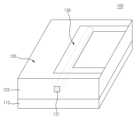
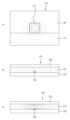
도 1a는 일반적인 광위상 변조기를 도시하는 사시도이다.
도 1b는 일반적인 광위상 변조기를 도시하는 평면도이다.
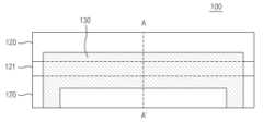
도 1c는 일반적인 광위상 변조기의 광도파로 및 마이크로 히터를 도시하는 단면도이다.
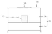
도 2a는 본 개시의 다양한 실시예들에 따른 광위상 변조기를 도시하는 사시도이다.
도 2b는 본 개시의 다양한 실시예들에 따른 광위상 변조기를 도시하는 평면도이다.
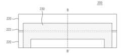
도 2c는 본 개시의 다양한 실시예들에 따른 광위상 변조기의 광도파로 및 마이크로 히터를 도시하는 단면도이다.
도 3은 일반적인 광도파로와 본 개시의 다양한 실시예들에 따른 광도파로의 도파모드 분포들을 나타내는 도면들이다.
도 4는 도 3의 일반적인 광도파로와 본 개시의 다양한 실시예들에 따른 광도파로의 시간 응답 특성들을 나타내는 도면들이다.
도 5는 도 3의 일반적인 광도파로와 본 개시의 다양한 실시예들에 따른 광도파로의 온도 분포들을 나타내는 도면들이다.
도 6은 다양한 실시예들에 따른 광위상 변조기의 제조 방법을 도시하는 도면이다.Figure 1a is a perspective view showing a general optical phase modulator.
Figure 1b is a plan view showing a general optical phase modulator.
Figure 1c is a cross-sectional view showing the optical waveguide and micro heater of a general optical phase modulator.
FIG. 2A is a perspective view illustrating an optical phase modulator according to various embodiments of the present disclosure.
FIG. 2B is a plan view illustrating an optical phase modulator according to various embodiments of the present disclosure.
FIG. 2C is a cross-sectional view illustrating an optical waveguide and a micro heater of an optical phase modulator according to various embodiments of the present disclosure.
FIG. 3 is a diagram showing waveguide mode distributions of a general optical waveguide and an optical waveguide according to various embodiments of the present disclosure.
FIG. 4 is a diagram illustrating time response characteristics of the general optical waveguide of FIG. 3 and optical waveguides according to various embodiments of the present disclosure.
FIG. 5 is a diagram showing temperature distributions of the general optical waveguide of FIG. 3 and optical waveguides according to various embodiments of the present disclosure.
FIG. 6 is a diagram illustrating a method of manufacturing an optical phase modulator according to various embodiments.
이하, 본 문서의 다양한 실시예들이 첨부된 도면을 참조하여 설명된다.Hereinafter, various embodiments of this document are described with reference to the attached drawings.
도 1a는 일반적인 광위상 변조기(100)를 도시하는 사시도이다. 도 1b는 일반적인 광위상 변조기(100)를 도시하는 평면도이다. 도 1c는 일반적인 광위상 변조기(100)의 광도파로(120) 및 마이크로 히터(130)를 도시하는 단면도이다. 여기서, 도 1c는 도 1b에서 A-A'을 따라서 절단된 단면을 나타낸다.Figure 1a is a perspective view showing a general
도 1a, 도 1b, 및 도 1c를 참조하면, 일반적인 광위상 변조기(100)는 기판(110), 광도파로(120) 및 마이크로 히터(130)를 포함한다. 기판(110)은 광도파로(120) 및 마이크로 히터(130)를 지지한다. 광도파로(120)는 기판(110) 상에 제공되며, 코아부(121) 및 클래딩부(123)을 포함한다. 코아부(121)가 클래딩부(123)의 내측에 배치되며, 즉, 클래딩부(123)이 코아부(121)를 감싸고 있다. 구체적으로, 클래딩부(123)은 하부 클래딩부(124) 및 상부 클래딩부(126)을 포함하고, 코아부(121)는 하부 클래딩부(124)과 상부 클래딩부(126)의 사이에서 하부 클래딩부(124)과 상부 클래딩부(126)에 의해 둘러싸인다. 마이크로 히터(130)는 광도파로(120)의 표면에 제공된다. 마이크로 히터(130)는 클래딩부(123)의 표면에서 코아부(121)를 따라서 정렬된다.Referring to FIGS. 1A, 1B, and 1C, a general
일반적으로, 코아부(121)와 클래딩부(123)은 서로 다른 재료들로 이루어지며, 서로 다른 광학적 굴절률들을 갖는다. 이 때, 코아부(121)의 굴절률이 클래딩부(123)의 굴절률보다 더 크며, 이로써, 코아부(121)에 입사된 빛이 클래딩부(123)으로 빠져나가지 않고, 코아부(121)를 따라서 진행된다. 여기서, 코아부(121)는 폴리머 재료로 이루어진다.Generally, the
따라서, 마이크로 히터(130)에 전류가 인가됨에 따라, 마이크로 히터(130)가 열을 발생시킨다. 마이크로 히터(130)에서 발생된 열이 코아부(121)로 전달됨으로써, 코아부(121)의 굴절률이 변화되면서 코아부(121)를 따라 진행되는 빛의 위상이 변화되며, 이를 통해 코아부(121)에서 출력되는 빛이 미리 정해진 위상을 지니게 된다. 여기서, 열에 의해 굴절률이 변화되는 현상을 열광학 효과라 한다. 이 때, 폴리머 재료가 지니는 우수한 열광학 효과로 인해, 코아부(121)는 적은 열량으로도 큰 굴절률 변화를 일으킬 수 있다. 이로써, 일반적인 광위상 변조기(100)는 저전력 구동의 장점을 갖는다. 그러나, 폴리머 재료의 열광학 효과는 폴리머 재료의 열팽창에 의해 일어나는 것이기 때문에, 일반적인 광위상 변조기(100)는 저속 응답 특성의 단점을 갖는다.Therefore, as current is applied to the
도 2a는 본 개시의 다양한 실시예들에 따른 광위상 변조기(200)를 도시하는 사시도이다. 도 2b는 본 개시의 다양한 실시예들에 따른 광위상 변조기(200)를 도시하는 평면도이다. 도 2c는 본 개시의 다양한 실시예들에 따른 광위상 변조기(200)의 광도파로(220) 및 마이크로 히터(230)를 도시하는 단면도이다. 여기서, 도 2c는 도 2b에서 B-B'을 따라서 절단된 단면을 나타낸다.FIG. 2A is a perspective view illustrating an
도 2a, 도 2b, 및 도 2c를 참조하면, 다양한 실시예들에 따른 광위상 변조기(200)는 기판(210), 광도파로(220) 및 마이크로 히터(230)를 포함한다. 기판(210)은 광도파로(220) 및 마이크로 히터(230)를 지지한다. 광도파로(220)는 기판(210) 상에 제공되며, 다층 구조로 구현된다. 이러한 광도파로(220)는 코아층(221), 스트립 패턴(222), 및 클래딩층(223)을 포함하며, 클래딩층(223)은 하부 클래딩층(224) 및 상부 클래딩층(226)을 포함한다. 이러한 광도파로(220)는 스트립 임베디드 광도파로(strip embedded waveguide; SEW)로 지칭될 수 있다. 코아층(221)은 하부 클래딩층(224)과 상부 클래딩층(226)의 사이에 샌드위치되며, 스트립 패턴(222)은 하부 클래딩층(224)과 코아층(221)의 사이에서 코아층(221)의 내측에 배치된다. 마이크로 히터(230)는 광도파로(220)의 표면에 제공된다. 마이크로 히터(230)는 상부 클래딩층(226)의 표면에 제공된다.Referring to FIGS. 2A, 2B, and 2C, the
다양한 실시예들에 따르면, 코아층(221), 스트립 패턴(222), 및 클래딩층(223)은 서로 다른 재료들로 이루어지며, 서로 다른 광학적 굴절률들을 갖는다. 여기서, 코아층(221) 및 클래딩층(223)은 상이한 폴리머 재료들로 이루어질 수 있다. 이 때, 코아층(221)의 굴절귤이 클래딩층(223)의 굴절률보다 더 크며, 이로써, 코아층(221)에 입사된 빛이 클래딩층(223)으로 빠져나가지 않고, 코아층(221)을 따라서 진행된다. 그리고, 스트립 패턴(222)은 코아층(221)의 굴절률보다 현저하게 높은 고굴절률을 가지며, 이로써, 스트립 패턴(222)이 코아층(221)에서 진행되는 빛을 코아층(221) 내에 국한시킨다. 즉, 코아층(221)에서 진행되는 빛이 스트립 패턴(222)을 향해 모이면서 코아층(221) 내에 분포된다. 이러한 스트립 패턴(222)은 실리콘 나이트라이드(Silicon Nitride), 실리콘, 고굴절률 폴리머 등을 이용하여 제작 가능하다.According to various embodiments, the
따라서, 마이크로 히터(230)에 전류가 인가됨에 따라, 마이크로 히터(230)가 열을 발생시킨다. 마이크로 히터(230)에서 발생된 열이 코아층(221)으로 전달됨으로써, 코아층(221)의 굴절률이 변화되면서 코아층(221)을 따라 진행되는 빛의 위상이 변화되며, 이를 통해 코아층(221)에서 출력되는 빛의 위상을 변화시킬 수 있다. 이 때, 실리카 재료의 열광학 효과는 양의 값을 갖는 반면, 폴리머 재료의 열광학 효과는 음의 값을 갖는다. 그리고, 폴리머 재료의 열광학 상수는 실리카 재료의 열광학 상수에 비해 10 배 이상의 큰 값을 갖는다. 이러한 이유로, 스트립 패턴(222)의 외측에서, 폴리머 재료의 코아층(221)이 적은 열량으로도 큰 굴절률 변화를 일으킬 수 있으며, 이로써, 다양한 실시예들에 따른 광위상 변조기(200)는 저전력 구동의 장점을 갖는다. 아울러, 스트립 패턴(222)이 코아층(221)의 내측에서 코아층(221)에서 진행되는 빛을 얇은 두께를 지닌 폴리머 재료의 코아층(221) 내에 국한시킴으로써, 다양한 실시예들에 따른 광위상 변조기(200)는 고속 응답 특성의 장점을 갖는다. 즉, 다양한 실시예들에 따른 광위상 변조기(200)의 스트립 임베디드 광도파로(SEW)는 다층 구조로 구현됨에 따라 얇은 두께를 가지면서, 저전력 구동 및 고속 응답 특성의 장점들을 갖는다.Therefore, as current is applied to the
도 3은 일반적인 광도파로(120)와 본 개시의 다양한 실시예들에 따른 광도파로(220; 321, 322)의 도파모드 분포들을 나타내는 도면들이다. 도 3에서, 도파모드 분포들이 등고선으로 표현되어 있다. 보다 상세하게는, 도 3의 (a)는 일반적인 광도파로(120)의 도파모드 분포를 나타내고, 도 3의 (b)는 본 개시의 일 실시예에 따른 광도파로(321)의 도파모드 분포를 나타내며, 도 3의 (c)는 본 개시의 다른 실시예에 따른 광도파로(322)의 도파모드 분포를 나타낸다.FIG. 3 is a diagram showing waveguide mode distributions of a general
도 3을 참조하면, 일반적인 광도파로(120)의 도파모드는 코아부(121)를 중심으로 코아부(121) 주변에 국한되어 분포되는데 반해, 다양한 실시예들에 따른 광도파로(220; 321, 322)의 도파모드는 코아층(221)의 내부에 국한되어 분포된다. 이 때, 다양한 실시예들에 따른 광도파로(220; 321, 322)의 도파모드는 스트립 패턴(222)의 폭이 작을수록, 코아층(221)의 내부에 넓게 퍼져서 분포된다.Referring to FIG. 3, while the waveguide mode of the general
구체적으로, 도 3의 (a)에 도시된 바와 같이, 일반적인 광도파로(120)의 도파모드는 코아부(121)를 중심으로 원형으로 분포되며, 이로써, 코아부(121)를 벗어나면서 분포된다. 이 때, 일반적인 광도파로(120)는, 전체 높이가 약 28 ㎛이며, 여기서 코아부(121)의 높이가 약 8 ㎛가 될 때 단일모드 광도파로 조건을 만족시키도록 설계된다.Specifically, as shown in (a) of FIG. 3, the waveguide mode of the general
한편, 다양한 실시예들에 따른 광도파로(220)는 스트립 패턴(222)의 단면적에 따라, 일 실시예에 따른 광도파로(321)와 다른 실시예에 따른 광도파로(322)로 구분된다. 이 때, 다양한 실시예들에 따른 광도파로(220; 321, 322)는, 전체 높이가 약 7 ㎛이며, 여기서, 코아층(221)의 높이는 3 ㎛이고, 하부 클래딩층(224) 및 상부 클래딩층(226)은 각각 2 ㎛가 되도록, 구현된다. 여기서, 일 실시예에 따른 광도파로(321)에서의 스트립 패턴(222)의 단면적이 다른 실시예에 따른 광도파로(322)에서의 스트립 패턴(222)의 단면적보다 크다. 도 3의 (b)에 도시된 바와 같이, 일 실시예에 따른 광도파로(321)의 도파모드는 코아층(221)의 내부에서 스트립 패턴(222) 주변부에 강하게 국한되어 분포된다. 그리고, 도 3의 (c)에 도시된 바와 같이, 다른 실시예에 따른 광도파로(322)의 도파모드는 스트립 패턴(222)을 중심으로 코아층(221)의 내부에 국한되데, 넓은 면적에 걸쳐 분산되어 분포된다.Meanwhile, the
다양한 실시예들에 따르면, 스트립 임베디드 광도파로(SEW)가 얇은 두께로 구현됨에 따라, 마이크로 히터(230)에서 발생된 열이 빠른 속도로 기판(210)까지 전달된다. 따라서, 다양한 실시예들에 따른 광위상 변조기(200)가 안정 상태에 도달하는 시간이 단축되며, 이로써, 고속 응답 특성이 달성된다. 즉, 다양한 실시예들에 따른 광위상 변조기(200)의 스트립 임베디드 광도파로(SEW)는 얇은 두께를 가지면서, 저전력 구동 및 고속 응답 특성의 장점들을 갖는다. 아울러, 도파모드가 코아층(221)의 내부에서 보다 넓게 분산되어 분포될수록, 코아층(221)의 폴리머 재료가 지니는 우수한 열광학 효과의 영향을 주도적으로 받게 되어, 다양한 실시예들에 따른 광도파로(220)의 위상 변조 효율은 높아진다.According to various embodiments, as the strip embedded optical waveguide (SEW) is implemented with a thin thickness, heat generated in the
도 4는 도 3의 일반적인 광도파로(120)와 본 개시의 다양한 실시예들에 따른 광도파로(220; 321, 322)의 시간 응답 특성들을 나타내는 도면들이다. 도 4는 1 kHz 주파수의 구형파를 각각 입력하였을 때 나타나는 시간 응답 특성들을 나타낸다. 보다 상세하게는, 도 4의 (a)는 외부에서 전력을 인가하였을 때 마이크로 히터(130, 230)의 시간에 따른 온도 변화를 나타내고, 도 4의 (b)는 일반적인 광도파로(120) 구조에서 나타나는 시간 응답 특성을 나타내고, 도 4의 (c)는 본 개시의 일 실시예에 따른 광도파로(321)의 시간 응답 특성을 나타내며, 도 4의 (d)는 본 개시의 다른 실시예에 따른 광도파로(322)의 시간 응답 특성을 나타낸다. 여기서, 굴절률 변화가 0에서 100 %로 나타나는 과정에서 초기 10 %로부터 90 %까지 걸리는 시간이 위상 변조에 걸리는 시간, 즉, 라이징 타임(rising time)으로서 정의될 수 있다.FIG. 4 is a diagram showing time response characteristics of the general
도 4를 참조하면, 마이크로 히터(130, 230)의 시간에 따른 온도 변화에 대응하여, 일반적인 광도파로(120)의 코아부(121) 및 다양한 실시예들에 따른 광도파로(220; 321, 322)의 코아층(221)에서의 시간에 따른 온도 변화들이 측정된다. 이러한 온도 변화들은 코아부(121) 및 코아층(221)의 굴절률 변화를 초래한다. 이를 기반으로, 도 4의 (b)에 도시된 바와 같이, 일반적인 광도파로(120)의 경우, 라이징 타임은 3.3 ms로 확인되나, 도 4의 (c) 및 (d)에 도시된 바와 같이, 다양한 실시예들에 따른 광도파로(220; 321, 322)의 경우 라이징 타임은 0.075 ms로 확인된다. 이는, 다양한 실시예들에 따른 광도파로(220; 321, 322)의 라이징 타임이 일반적인 광도파로(120)의 라이징 타임에 비해, 10 배 이상 개선됨을 나타낸다. 즉, 다양한 실시예들에 따른 광도파로(220; 321, 322)의 라이징 타임은 크게 감소되며, 이는 응답 속도 개선을 나타낸다.Referring to FIG. 4, in response to temperature changes of the
도 5는 도 3의 일반적인 광도파로(120)와 본 개시의 다양한 실시예들에 따른 광도파로(220; 321, 322)의 온도 분포들을 나타내는 도면들이다. 도 5에서, 마이크로 히터(130, 230)를 통해 동일한 온도 변화가 여기될 때의 온도 분포들이 등온선으로 표현되어 있으며, 각 등온선의 값이 수치로 표현되어 있다. 보다 상세하게는, 도 5의 (a)는 일반적인 광도파로(120)의 온도 분포를 도파모드 분포와 함께 나타내고, 도 5의 (b)는 본 개시의 일 실시예에 따른 광도파로(321)의 온도 분포를 도파모드와 함께 나타내며, 도 5의 (c)는 본 개시의 다른 실시예에 따른 광도파로(322)의 온도 분포를 도파모드와 함께 나타낸다.FIG. 5 is a diagram showing temperature distributions of the general
도 5를 참조하면, 다양한 실시예들에 따른 위상변조기(200)의 광도파로(220; 321, 322)는 응답 속도가 개선되는 장점이 있는 반면, 도파모드가 스트립 패턴(222) 내부에 국한되면 위상 변화를 일으키기 위한 전력이 높아지는 단점이 존재한다. 이는 스트립 패턴(222)의 재료, 예컨대, 실리콘 나이트라이드는 폴리머 재료에 비하여 열광학 효과가 현저히 떨어지기 때문이다. 이 때, 위상 변조 효율은 마이크로 히터(130, 230)에서 동일한 온도 변화를 일으킬 때 도파모드의 위상 변화가 얼마나 일어나는 가에 따라 결정된다. 따라서, 이러한 온도 분포들을 바탕으로 재료의 열광학 효과를 고려하여, 도파모드 위상 변조에 필요한 전력이 계산될 수 있다. 한편, 마이크로 히터(130, 230)에서 동일한 온도 변화를 일으키기 위한 인가 전력은 광도파로(120, 220; 321, 322)의 두께가 얇을수록 더 높다. 이는 기판(110, 210)으로 열이 빠져나가는 구조에서 중간에 위치한 폴리머 재료가 두꺼울수록 낮은 전력으로도 마이크로 히터(130, 230)를 가열하기가 용이하기 때문이다.Referring to FIG. 5, while the
이러한 현상을 포괄적으로 설계하기 위하여, 도파모드의 위상을 180 도만큼 변화시키는 데 필요한 인가 전력 Pπ가 계산되었다. 그 결과, 일반적인 광도파로(120)에서는 Pπ가 3.25 mW 로서 폴리머 재료의 특성을 반영한 낮은 전력이 필요한 반면, 일 실시예에 따른 광도파로(321)에서는 Pπ가 118 mW 로서 매우 높은 전력이 필요하다. 이는 도파모드가 열광학 효과가 낮은 스트립 패턴(222), 예컨대, 실리콘 나이트라이드에 대부분 국한되어 있기 때문에, 인가된 열에 의해 도파모드의 위상 변화가 매우 작게 나타나기 때문이다. 이러한 문제점을 개선하기 위해서, 다른 실시예에 따른 광도파로(322)와 같이 스트립 패턴(222)의 폭을 줄이게 되면, 도파모드는 스트립 패턴(222)의 외부에서 분산된 상태로 존재하게 되며 폴리머 재료의 코아층(221)에 걸쳐진 도파모드 성분이 많아짐에 따라 폴리머 재료의 높은 열광학 특성에 따른 효율적인 위상 변조를 일으킬 수 있게 된다. 이로 인해, 다른 실시예에 따른 광도파로(322)에서는 Pπ가 7.02 mW 로 감소된다.In order to comprehensively design this phenomenon, the applied power Pπ required to change the phase of the waveguide mode by 180 degrees was calculated. As a result, in the general
따라서, 일반적인 광위상 변조기(100)와 다양한 실시예들에 따른 광위상 변조기(200)의 응답 속도 및 위상 변조 효율은 하기 [표 1]과 같이 설계된다. 이 때, 위상 변조에 걸리는 시간, 즉, 라이징 타임이 짧고, 위상 변조에 필요한 전력이 작을수록, 유리하다. 즉, 다양한 실시예들에 따른 광위상 변조기(200)에서는 라이징 타임이 대폭 감소되어, 고속 응답 특성이 달성된다. 또한, 다양한 실시예들에 따른 광위상 변조기(200)에서, 다른 실시예에 따른 광도파로(322)와 같이 스트립 패턴(222)의 단면적을 감소시킴으로써, 일반적인 광위상 변조기(100)와 유사한 정도로 위상 변조에 필요한 전력이 감소되어, 저전력 구동이 달성된다. 위상 변조에 걸리는 시간과 위상 변조에 필요한 전력을 곱한 값으로 성능 지표를 도출해보면, 일반적인 광위상 변조기(100)는 10.7인 반면, 다른 실시예에 따른 광도파로(322)를 갖는 광위상 변조기(200)는 0.52이며, 이는 다른 실시예에 따른 광도파로(322)를 갖는 광위상 변조기(200)가 우수한 성능을 가짐을 나타낸다.Therefore, the response speed and phase modulation efficiency of the general
광위상 변조기Normally
optical phase modulator
광위상 변조기According to one embodiment
optical phase modulator
광위상 변조기According to another embodiment
optical phase modulator
(rising time) [ms]phase modulation time
(rising time) [ms]
Pπ[mW]phase modulation power
Pπ [mW]
도 6은 다양한 실시예들에 따른 광위상 변조기(200)의 제조 방법을 도시하는 도면이다.FIG. 6 is a diagram illustrating a method of manufacturing an
도 6을 참조하면, 610 단계에서, 하부 클래딩층(224)이 형성된다. 이 때, 하부 클래딩층(224)은 기판(210) 상에 형성된다. 620 단계에서, 하부 클래딩층(224) 상에 스트립 패턴(222)이 형성된다. 여기서, 스트립 패턴(222)의 폭은 하부 클래딩층(224)의 폭보다 작다. 630 단계에서, 하부 클래딩층(224) 및 스트립 패턴(222) 상에 코아층(221)이 형성된다. 이 때, 코아층(221)은 하부 클래딩층(224) 상에서 스트립 패턴(222)을 덮는다. 640 단계에서, 코아층(221) 상에 상부 클래딩층(226)이 형성된다. 이를 통해, 코아층(221)은 하부 클래딩층(224)과 상부 클래딩층(226)의 사이에 샌드위치되며, 스트립 패턴(222)은 패터닝(pattering) 공정 없이, 하부 클래딩층(224)과 코아층(221)의 사이에서 코아층(221)의 내측에 배치된다. 따라서, 코아층(221), 스트립 패턴(222), 하부 클래딩층(224) 및 상부 클래딩층(226)을 포함하는 광도파로(220)가 스트립 임베디드 광도파로로서 제조된다. 예를 들면, 광도파로(220)는, 전체 높이가 약 7 ㎛이며, 여기서, 코아층(221)의 높이는 3 ㎛이고, 하부 클래딩층(224) 및 상부 클래딩층(226)은 각각 2 ㎛가 되도록, 구현된다. 650 단계에서, 상부 클래딩층(226)의 표면에 마이크로 히터(230)가 형성된다. 결과적으로, 광위상 변조기(200)가 제조된다. 여기서, 마이크로 히터(230)는 포토리소그래피(photolithography) 공정을 통해, 형성될 수 있다.Referring to FIG. 6, in step 610, a
다양한 실시예들은 코아층(221)과 스트립 패턴(222)을 갖는 스트립 임베디드 광도파로(SEW)를 포함하는 광위상 변조기(200)를 제공하며, 이러한 광위상 변조기(200)는 저전력 구동, 고속 응답 특성 및 높은 위상 변조 효율을 달성한다. 광위상 변조기(200)가 저전력 구동의 특성을 유지한 채 위상 변조 속도가 10 배 이상 개선된 고속 응답 특성을 달성함으로써, 광스위치, 광감쇠기, 가변파장레이저, 광도파로 빔스캐너 소자 등의 고속으로 신호 처리를 해야 하는 다양한 광소자에 적용될 수 있을 것이다. 특히, 최근들어 각광을 받고 있는 광도파로 어레이 방식의 빔스캐닝 라이다 기술이 느린 위상 변조 속도로 어려움이 있었으나, 이러한 광위상 변조기(200)를 적용하면, 그러한 어려움의 해결에 기여를 할 수 있을 것이다.Various embodiments provide an
본 문서의 다양한 실시예들 및 이에 사용된 용어들은 본 문서에 기재된 기술을 특정한 실시 형태에 대해 한정하려는 것이 아니며, 해당 실시 예의 다양한 변경, 균등물, 및/또는 대체물을 포함하는 것으로 이해되어야 한다. 도면의 설명과 관련하여, 유사한 구성 요소에 대해서는 유사한 참조 부호가 사용될 수 있다. 단수의 표현은 문맥상 명백하게 다르게 뜻하지 않는 한, 복수의 표현을 포함할 수 있다. 본 문서에서, "A 또는 B", "A 및/또는 B 중 적어도 하나", "A, B 또는 C" 또는 "A, B 및/또는 C 중 적어도 하나" 등의 표현은 함께 나열된 항목들의 모든 가능한 조합을 포함할 수 있다. "제 1", "제 2", "첫째" 또는 "둘째" 등의 표현들은 해당 구성 요소들을, 순서 또는 중요도에 상관없이 수식할 수 있고, 한 구성 요소를 다른 구성 요소와 구분하기 위해 사용될 뿐 해당 구성 요소들을 한정하지 않는다. 어떤(예: 제 1) 구성 요소가 다른(예: 제 2) 구성 요소에 "(기능적으로 또는 통신적으로) 연결되어" 있다거나 "접속되어" 있다고 언급된 때에는, 상기 어떤 구성 요소가 상기 다른 구성 요소에 직접적으로 연결되거나, 다른 구성 요소(예: 제 3 구성 요소)를 통하여 연결될 수 있다.The various embodiments of this document and the terms used herein are not intended to limit the technology described in this document to a specific embodiment, and should be understood to include various changes, equivalents, and/or replacements of the embodiments. In connection with the description of the drawings, similar reference numbers may be used for similar components. Singular expressions may include plural expressions, unless the context clearly dictates otherwise. In this document, expressions such as “A or B”, “at least one of A and/or B”, “A, B or C” or “at least one of A, B and/or C” refer to all of the items listed together. Possible combinations may be included. Expressions such as "first", "second", "first" or "second" can modify the corresponding components regardless of order or importance, and are only used to distinguish one component from another. It does not limit the components. When a component (e.g. a first) component is said to be "connected (functionally or communicatively)" or "connected" to another (e.g. a second) component, it means that the component is connected to the other component. It may be connected directly to a component or may be connected through another component (e.g., a third component).
다양한 실시예들에 따르면, 기술한 구성 요소들의 각각의 구성 요소는 단수 또는 복수의 개체를 포함할 수 있다. 다양한 실시예들에 따르면, 전술한 해당 구성 요소들 중 하나 이상의 구성 요소들 또는 단계들이 생략되거나, 또는 하나 이상의 다른 구성 요소들 또는 단계들이 추가될 수 있다. 대체적으로 또는 추가적으로, 복수의 구성 요소들은 하나의 구성 요소로 통합될 수 있다. 이런 경우, 통합된 구성 요소는 복수의 구성 요소들 각각의 구성 요소의 하나 이상의 기능들을 통합 이전에 복수의 구성 요소들 중 해당 구성 요소에 의해 수행되는 것과 동일 또는 유사하게 수행할 수 있다.According to various embodiments, each of the described components may include a single or plural entity. According to various embodiments, one or more of the components or steps described above may be omitted, or one or more other components or steps may be added. Alternatively or additionally, multiple components may be integrated into one component. In this case, the integrated component may perform one or more functions of each component of the plurality of components identically or similarly to those performed by the corresponding component of the plurality of components prior to integration.
Claims (4)
Translated fromKorean하부 클래딩층 및 상부 클래딩층을 갖는 클래딩층;
상기 하부 클래딩층 및 상기 상부 클래딩층 사이에 샌드위치되는 코아층;
상기 코아층 내에 배치되는 스트립 패턴; 및
상기 클래딩층의 표면에 제공되는 마이크로 히터
를 포함하는,
광위상 변조기.
In a high-speed, low-power optical phase modulator,
a cladding layer having a lower cladding layer and an upper cladding layer;
a core layer sandwiched between the lower cladding layer and the upper cladding layer;
a strip pattern disposed within the core layer; and
Micro heater provided on the surface of the cladding layer
Including,
Optical phase modulator.
상기 스트립 패턴은,
상기 코아층에서 진행되는 빛이 상기 스트립 패턴을 향해 모이면서 상기 코아층 내에서 분산되어 분포되게 하는,
광위상 변조기.
According to claim 1,
The strip pattern is,
Light traveling in the core layer gathers toward the strip pattern and is dispersed and distributed within the core layer.
Optical phase modulator.
상기 스트립 패턴의 굴절률이 상기 코아층의 굴절률보다 더 크고,
상기 스트립 패턴은 실리콘 나이트라이드(Silicon Nitride), 실리콘, 또는 고굴절률 폴리머 중 적어도 하나를 포함하는,
광위상 변조기.
According to claim 1,
The refractive index of the strip pattern is greater than the refractive index of the core layer,
The strip pattern includes at least one of silicon nitride, silicon, or a high refractive index polymer,
Optical phase modulator.
하부 클래딩층 상에 스트립 패턴을 형성하는 단계;
상기 하부 클래딩층 상에서 상기 스트립 패턴을 덮는 코아층을 형성하는 단계;
상기 코아층 상에 상부 클래딩층을 형성하는 단계; 및
상기 상부 클래딩층의 표면에 마이크로 히터를 형성하는 단계
를 포함하는,
광위상 변조기의 제조 방법.In a method of manufacturing a high-speed, low-power optical phase modulator,
forming a strip pattern on the lower cladding layer;
forming a core layer covering the strip pattern on the lower cladding layer;
forming an upper cladding layer on the core layer; and
Forming a micro heater on the surface of the upper cladding layer
Including,
Method for manufacturing an optical phase modulator.
Priority Applications (1)
| Application Number | Priority Date | Filing Date | Title |
|---|---|---|---|
| KR1020220031168AKR102670438B1 (en) | 2022-03-14 | 2022-03-14 | Fast power-efficient phase modulators based on strip embedded polymeric optical waveguide, and manufacturing method of the same |
Applications Claiming Priority (1)
| Application Number | Priority Date | Filing Date | Title |
|---|---|---|---|
| KR1020220031168AKR102670438B1 (en) | 2022-03-14 | 2022-03-14 | Fast power-efficient phase modulators based on strip embedded polymeric optical waveguide, and manufacturing method of the same |
Publications (2)
| Publication Number | Publication Date |
|---|---|
| KR20230134185Atrue KR20230134185A (en) | 2023-09-21 |
| KR102670438B1 KR102670438B1 (en) | 2024-05-29 |
Family
ID=88189449
Family Applications (1)
| Application Number | Title | Priority Date | Filing Date |
|---|---|---|---|
| KR1020220031168AActiveKR102670438B1 (en) | 2022-03-14 | 2022-03-14 | Fast power-efficient phase modulators based on strip embedded polymeric optical waveguide, and manufacturing method of the same |
Country Status (1)
| Country | Link |
|---|---|
| KR (1) | KR102670438B1 (en) |
Citations (5)
| Publication number | Priority date | Publication date | Assignee | Title |
|---|---|---|---|---|
| KR20050036404A (en)* | 2003-10-16 | 2005-04-20 | 한국전자통신연구원 | Optical device employing the silica/polymer hybrid optical waveguide |
| KR20060113304A (en)* | 2005-04-30 | 2006-11-02 | 오민철 | Variable Optical Attenuator Using Large Core Polymer Optical Waveguide |
| KR20060121438A (en)* | 2005-05-24 | 2006-11-29 | 엘지전자 주식회사 | Micro Ring Optical Resonator and Manufacturing Method Thereof |
| KR20110055086A (en)* | 2009-11-19 | 2011-05-25 | 전남대학교산학협력단 | Optical module and manufacturing method |
| KR20110064325A (en)* | 2009-12-08 | 2011-06-15 | 부산대학교 산학협력단 | Optical waveguide integrated polarizer and manufacturing method |
- 2022
- 2022-03-14KRKR1020220031168Apatent/KR102670438B1/enactiveActive
Patent Citations (5)
| Publication number | Priority date | Publication date | Assignee | Title |
|---|---|---|---|---|
| KR20050036404A (en)* | 2003-10-16 | 2005-04-20 | 한국전자통신연구원 | Optical device employing the silica/polymer hybrid optical waveguide |
| KR20060113304A (en)* | 2005-04-30 | 2006-11-02 | 오민철 | Variable Optical Attenuator Using Large Core Polymer Optical Waveguide |
| KR20060121438A (en)* | 2005-05-24 | 2006-11-29 | 엘지전자 주식회사 | Micro Ring Optical Resonator and Manufacturing Method Thereof |
| KR20110055086A (en)* | 2009-11-19 | 2011-05-25 | 전남대학교산학협력단 | Optical module and manufacturing method |
| KR20110064325A (en)* | 2009-12-08 | 2011-06-15 | 부산대학교 산학협력단 | Optical waveguide integrated polarizer and manufacturing method |
Also Published As
| Publication number | Publication date |
|---|---|
| KR102670438B1 (en) | 2024-05-29 |
Similar Documents
| Publication | Publication Date | Title |
|---|---|---|
| KR100686920B1 (en) | Optical devices comprising thermo-optic polymers | |
| JP4146520B2 (en) | Optical integrated circuit | |
| JP2011022464A (en) | Optical waveguide | |
| KR100326046B1 (en) | Thermo-optic switch and method of forming the same | |
| US7756376B2 (en) | Optical functional waveguide, optical modulator, arrayed waveguide grating, and dispersion compensation circuit | |
| JP3552159B2 (en) | Temperature-independent arrayed waveguide grating device | |
| KR20070093285A (en) | Microring resonator filter with variable bandwidth and manufacturing method thereof | |
| KR102670438B1 (en) | Fast power-efficient phase modulators based on strip embedded polymeric optical waveguide, and manufacturing method of the same | |
| US7184631B2 (en) | Optical device | |
| KR100563489B1 (en) | Optical device using silica / polymer hybrid optical waveguide | |
| KR100194622B1 (en) | Structure of Waveguide Polymer Electrooptic Modulator / Switch | |
| CN113991275B (en) | Fully-reconfigurable silicon-based Fano resonator chip | |
| US6810182B2 (en) | Optical tunable grid-assisted add/drop filter in codirectional mode of operation | |
| JPH1068833A (en) | Optical waveguide, method of manufacturing the same, and optical circuit | |
| KR100839268B1 (en) | Variable Optical Attenuator Using Multimode Interference | |
| US6961493B2 (en) | Optical device | |
| US20030128908A1 (en) | Planar optical circuit | |
| KR100198935B1 (en) | Asymmetric directional coupler and manufacturing method thereof | |
| CN116125594B (en) | A broadband on-chip beam combining device | |
| KR102836767B1 (en) | MONOLITHICALLY INTEGRATED POLYMER-SiN WAVEGUIDE OPTICAL PHASED ARRAY BEAM SCANNER, AND MANUFACTURING METHOD OF THE SAME | |
| EP0585468B1 (en) | Waveguide type optical part | |
| US20250053060A1 (en) | Integrated-Optics Waveguide Having High-Stress-Sensitivity Region | |
| US8098999B2 (en) | Multiple channel power monitor | |
| KR100370278B1 (en) | Optical Path Controlling two by two Optical Switch | |
| CN116774355A (en) | waveguide structure |
Legal Events
| Date | Code | Title | Description |
|---|---|---|---|
| PA0109 | Patent application | St.27 status event code:A-0-1-A10-A12-nap-PA0109 | |
| PA0201 | Request for examination | St.27 status event code:A-1-2-D10-D11-exm-PA0201 | |
| PG1501 | Laying open of application | St.27 status event code:A-1-1-Q10-Q12-nap-PG1501 | |
| PN2301 | Change of applicant | St.27 status event code:A-3-3-R10-R13-asn-PN2301 St.27 status event code:A-3-3-R10-R11-asn-PN2301 | |
| E902 | Notification of reason for refusal | ||
| PE0902 | Notice of grounds for rejection | St.27 status event code:A-1-2-D10-D21-exm-PE0902 | |
| E13-X000 | Pre-grant limitation requested | St.27 status event code:A-2-3-E10-E13-lim-X000 | |
| P11-X000 | Amendment of application requested | St.27 status event code:A-2-2-P10-P11-nap-X000 | |
| P13-X000 | Application amended | St.27 status event code:A-2-2-P10-P13-nap-X000 | |
| E701 | Decision to grant or registration of patent right | ||
| PE0701 | Decision of registration | St.27 status event code:A-1-2-D10-D22-exm-PE0701 | |
| R18-X000 | Changes to party contact information recorded | St.27 status event code:A-3-3-R10-R18-oth-X000 | |
| PR0701 | Registration of establishment | St.27 status event code:A-2-4-F10-F11-exm-PR0701 | |
| PR1002 | Payment of registration fee | St.27 status event code:A-2-2-U10-U11-oth-PR1002 Fee payment year number:1 | |
| PG1601 | Publication of registration | St.27 status event code:A-4-4-Q10-Q13-nap-PG1601 | |
| PN2301 | Change of applicant | St.27 status event code:A-5-5-R10-R13-asn-PN2301 St.27 status event code:A-5-5-R10-R11-asn-PN2301 | |
| R18-X000 | Changes to party contact information recorded | St.27 status event code:A-5-5-R10-R18-oth-X000 |