KR20230132826A - display device - Google Patents
display deviceDownload PDFInfo
- Publication number
- KR20230132826A KR20230132826AKR1020237027900AKR20237027900AKR20230132826AKR 20230132826 AKR20230132826 AKR 20230132826AKR 1020237027900 AKR1020237027900 AKR 1020237027900AKR 20237027900 AKR20237027900 AKR 20237027900AKR 20230132826 AKR20230132826 AKR 20230132826A
- Authority
- KR
- South Korea
- Prior art keywords
- layer
- light
- film
- additionally
- display device
- Prior art date
- Legal status (The legal status is an assumption and is not a legal conclusion. Google has not performed a legal analysis and makes no representation as to the accuracy of the status listed.)
- Pending
Links
- 239000000758substrateSubstances0.000claimsdescription182
- 238000000034methodMethods0.000claimsdescription83
- 230000001681protective effectEffects0.000claimsdescription53
- XUIMIQQOPSSXEZ-UHFFFAOYSA-NSiliconChemical compound[Si]XUIMIQQOPSSXEZ-UHFFFAOYSA-N0.000claimsdescription22
- 229910052710siliconInorganic materials0.000claimsdescription22
- 239000010703siliconSubstances0.000claimsdescription22
- 239000010410layerSubstances0.000description768
- 239000010408filmSubstances0.000description334
- 238000005401electroluminescenceMethods0.000description238
- 239000000463materialSubstances0.000description124
- 239000004065semiconductorSubstances0.000description124
- 230000006870functionEffects0.000description106
- 239000011241protective layerSubstances0.000description62
- 230000003287optical effectEffects0.000description52
- 238000005530etchingMethods0.000description49
- 239000011701zincSubstances0.000description44
- 238000004519manufacturing processMethods0.000description43
- 239000013078crystalSubstances0.000description37
- 238000002347injectionMethods0.000description34
- 239000007924injectionSubstances0.000description34
- 230000015572biosynthetic processEffects0.000description33
- 238000010586diagramMethods0.000description30
- 229910052751metalInorganic materials0.000description29
- 230000032258transportEffects0.000description29
- 229920005989resinPolymers0.000description26
- 239000011347resinSubstances0.000description26
- 239000002184metalSubstances0.000description24
- 239000012535impuritySubstances0.000description23
- 239000000203mixtureSubstances0.000description22
- 239000007789gasSubstances0.000description19
- 229910052760oxygenInorganic materials0.000description19
- QVGXLLKOCUKJST-UHFFFAOYSA-Natomic oxygenChemical compound[O]QVGXLLKOCUKJST-UHFFFAOYSA-N0.000description18
- 229910044991metal oxideInorganic materials0.000description18
- 150000004706metal oxidesChemical class0.000description18
- 239000001301oxygenSubstances0.000description18
- 230000005525hole transportEffects0.000description17
- 238000004544sputter depositionMethods0.000description17
- XLYOFNOQVPJJNP-UHFFFAOYSA-NwaterSubstancesOXLYOFNOQVPJJNP-UHFFFAOYSA-N0.000description17
- 125000004429atomChemical group0.000description16
- 230000008569processEffects0.000description16
- IJGRMHOSHXDMSA-UHFFFAOYSA-NAtomic nitrogenChemical compoundN#NIJGRMHOSHXDMSA-UHFFFAOYSA-N0.000description15
- XLOMVQKBTHCTTD-UHFFFAOYSA-NZinc monoxideChemical compound[Zn]=OXLOMVQKBTHCTTD-UHFFFAOYSA-N0.000description15
- 150000002894organic compoundsChemical class0.000description15
- PXHVJJICTQNCMI-UHFFFAOYSA-NNickelChemical compound[Ni]PXHVJJICTQNCMI-UHFFFAOYSA-N0.000description14
- 229910052733galliumInorganic materials0.000description14
- 229910052739hydrogenInorganic materials0.000description14
- 239000001257hydrogenSubstances0.000description14
- 230000001965increasing effectEffects0.000description14
- UFHFLCQGNIYNRP-UHFFFAOYSA-NHydrogenChemical compound[H][H]UFHFLCQGNIYNRP-UHFFFAOYSA-N0.000description13
- VYPSYNLAJGMNEJ-UHFFFAOYSA-NSilicium dioxideChemical compoundO=[Si]=OVYPSYNLAJGMNEJ-UHFFFAOYSA-N0.000description13
- 239000012790adhesive layerSubstances0.000description13
- 238000000231atomic layer depositionMethods0.000description13
- 239000003086colorantSubstances0.000description13
- 238000001312dry etchingMethods0.000description13
- 229910052738indiumInorganic materials0.000description13
- 238000012545processingMethods0.000description13
- 230000002829reductive effectEffects0.000description13
- GYHNNYVSQQEPJS-UHFFFAOYSA-NGalliumChemical compound[Ga]GYHNNYVSQQEPJS-UHFFFAOYSA-N0.000description12
- XEEYBQQBJWHFJM-UHFFFAOYSA-NIronChemical compound[Fe]XEEYBQQBJWHFJM-UHFFFAOYSA-N0.000description12
- 229910052782aluminiumInorganic materials0.000description12
- XAGFODPZIPBFFR-UHFFFAOYSA-NaluminiumChemical compound[Al]XAGFODPZIPBFFR-UHFFFAOYSA-N0.000description12
- 150000001875compoundsChemical class0.000description12
- 238000010894electron beam technologyMethods0.000description12
- -1etc.)Substances0.000description12
- 238000006243chemical reactionMethods0.000description11
- APFVFJFRJDLVQX-UHFFFAOYSA-Nindium atomChemical compound[In]APFVFJFRJDLVQX-UHFFFAOYSA-N0.000description11
- 229910052581Si3N4Inorganic materials0.000description10
- 239000000853adhesiveSubstances0.000description10
- 230000001070adhesive effectEffects0.000description10
- 230000007547defectEffects0.000description10
- TWNQGVIAIRXVLR-UHFFFAOYSA-Noxo(oxoalumanyloxy)alumaneChemical compoundO=[Al]O[Al]=OTWNQGVIAIRXVLR-UHFFFAOYSA-N0.000description10
- HQVNEWCFYHHQES-UHFFFAOYSA-Nsilicon nitrideChemical compoundN12[Si]34N5[Si]62N3[Si]51N64HQVNEWCFYHHQES-UHFFFAOYSA-N0.000description10
- 239000010409thin filmSubstances0.000description10
- ZOKXTWBITQBERF-UHFFFAOYSA-NMolybdenumChemical compound[Mo]ZOKXTWBITQBERF-UHFFFAOYSA-N0.000description9
- 238000002441X-ray diffractionMethods0.000description9
- 238000005229chemical vapour depositionMethods0.000description9
- 229910052750molybdenumInorganic materials0.000description9
- 239000011733molybdenumSubstances0.000description9
- 239000010936titaniumSubstances0.000description9
- 229910052721tungstenInorganic materials0.000description9
- 239000010937tungstenSubstances0.000description9
- 238000001039wet etchingMethods0.000description9
- RTAQQCXQSZGOHL-UHFFFAOYSA-NTitaniumChemical compound[Ti]RTAQQCXQSZGOHL-UHFFFAOYSA-N0.000description8
- 239000000956alloySubstances0.000description8
- 230000000903blocking effectEffects0.000description8
- 229910052814silicon oxideInorganic materials0.000description8
- 229910052719titaniumInorganic materials0.000description8
- WFKWXMTUELFFGS-UHFFFAOYSA-NtungstenChemical compound[W]WFKWXMTUELFFGS-UHFFFAOYSA-N0.000description8
- 229910052727yttriumInorganic materials0.000description8
- VWQVUPCCIRVNHF-UHFFFAOYSA-Nyttrium atomChemical compound[Y]VWQVUPCCIRVNHF-UHFFFAOYSA-N0.000description8
- 239000011787zinc oxideSubstances0.000description8
- 238000000576coating methodMethods0.000description7
- 238000004891communicationMethods0.000description7
- 229910052759nickelInorganic materials0.000description7
- 229910052757nitrogenInorganic materials0.000description7
- LFQSCWFLJHTTHZ-UHFFFAOYSA-NEthanolChemical compoundCCOLFQSCWFLJHTTHZ-UHFFFAOYSA-N0.000description6
- KFZMGEQAYNKOFK-UHFFFAOYSA-NIsopropanolChemical compoundCC(C)OKFZMGEQAYNKOFK-UHFFFAOYSA-N0.000description6
- FYYHWMGAXLPEAU-UHFFFAOYSA-NMagnesiumChemical compound[Mg]FYYHWMGAXLPEAU-UHFFFAOYSA-N0.000description6
- 229910052783alkali metalInorganic materials0.000description6
- 229910052784alkaline earth metalInorganic materials0.000description6
- 150000001342alkaline earth metalsChemical class0.000description6
- 230000004888barrier functionEffects0.000description6
- 239000011248coating agentSubstances0.000description6
- 238000000151depositionMethods0.000description6
- 235000019441ethanolNutrition0.000description6
- 239000011521glassSubstances0.000description6
- 238000010438heat treatmentMethods0.000description6
- AMGQUBHHOARCQH-UHFFFAOYSA-Nindium;oxotinChemical compound[In].[Sn]=OAMGQUBHHOARCQH-UHFFFAOYSA-N0.000description6
- 229910052742ironInorganic materials0.000description6
- 239000011777magnesiumSubstances0.000description6
- 239000007769metal materialSubstances0.000description6
- 239000002904solventSubstances0.000description6
- 238000001228spectrumMethods0.000description6
- 229910052715tantalumInorganic materials0.000description6
- GUVRBAGPIYLISA-UHFFFAOYSA-Ntantalum atomChemical compound[Ta]GUVRBAGPIYLISA-UHFFFAOYSA-N0.000description6
- RYGMFSIKBFXOCR-UHFFFAOYSA-NCopperChemical compound[Cu]RYGMFSIKBFXOCR-UHFFFAOYSA-N0.000description5
- MYMOFIZGZYHOMD-UHFFFAOYSA-NDioxygenChemical compoundO=OMYMOFIZGZYHOMD-UHFFFAOYSA-N0.000description5
- QCWXUUIWCKQGHC-UHFFFAOYSA-NZirconiumChemical compound[Zr]QCWXUUIWCKQGHC-UHFFFAOYSA-N0.000description5
- 238000010521absorption reactionMethods0.000description5
- 150000001340alkali metalsChemical class0.000description5
- 229910045601alloyInorganic materials0.000description5
- 239000012298atmosphereSubstances0.000description5
- 239000003990capacitorSubstances0.000description5
- 229910052802copperInorganic materials0.000description5
- 239000010949copperSubstances0.000description5
- 230000006378damageEffects0.000description5
- 229910001882dioxygenInorganic materials0.000description5
- 229910052735hafniumInorganic materials0.000description5
- 229910000449hafnium oxideInorganic materials0.000description5
- WIHZLLGSGQNAGK-UHFFFAOYSA-Nhafnium(4+);oxygen(2-)Chemical compound[O-2].[O-2].[Hf+4]WIHZLLGSGQNAGK-UHFFFAOYSA-N0.000description5
- 239000011261inert gasSubstances0.000description5
- 229910052749magnesiumInorganic materials0.000description5
- 239000002159nanocrystalSubstances0.000description5
- 150000004767nitridesChemical class0.000description5
- 238000000206photolithographyMethods0.000description5
- 229910052709silverInorganic materials0.000description5
- 239000004332silverSubstances0.000description5
- 239000002356single layerSubstances0.000description5
- 229910052725zincInorganic materials0.000description5
- YVTHLONGBIQYBO-UHFFFAOYSA-Nzinc indium(3+) oxygen(2-)Chemical compound[O--].[Zn++].[In+3]YVTHLONGBIQYBO-UHFFFAOYSA-N0.000description5
- 229910052726zirconiumInorganic materials0.000description5
- 229920000178Acrylic resinPolymers0.000description4
- 239000004925Acrylic resinSubstances0.000description4
- XKRFYHLGVUSROY-UHFFFAOYSA-NArgonChemical compound[Ar]XKRFYHLGVUSROY-UHFFFAOYSA-N0.000description4
- OKTJSMMVPCPJKN-UHFFFAOYSA-NCarbonChemical compound[C]OKTJSMMVPCPJKN-UHFFFAOYSA-N0.000description4
- KDLHZDBZIXYQEI-UHFFFAOYSA-NPalladiumChemical compound[Pd]KDLHZDBZIXYQEI-UHFFFAOYSA-N0.000description4
- ATJFFYVFTNAWJD-UHFFFAOYSA-NTinChemical group[Sn]ATJFFYVFTNAWJD-UHFFFAOYSA-N0.000description4
- 229910052796boronInorganic materials0.000description4
- XJHCXCQVJFPJIK-UHFFFAOYSA-Mcaesium fluorideChemical compound[F-].[Cs+]XJHCXCQVJFPJIK-UHFFFAOYSA-M0.000description4
- 239000000969carrierSubstances0.000description4
- 239000002131composite materialSubstances0.000description4
- 238000001723curingMethods0.000description4
- 239000003822epoxy resinSubstances0.000description4
- 230000005669field effectEffects0.000description4
- VBJZVLUMGGDVMO-UHFFFAOYSA-Nhafnium atomChemical group[Hf]VBJZVLUMGGDVMO-UHFFFAOYSA-N0.000description4
- 229910003437indium oxideInorganic materials0.000description4
- PJXISJQVUVHSOJ-UHFFFAOYSA-Nindium(iii) oxideChemical compound[O-2].[O-2].[O-2].[In+3].[In+3]PJXISJQVUVHSOJ-UHFFFAOYSA-N0.000description4
- 239000007788liquidSubstances0.000description4
- 239000011159matrix materialSubstances0.000description4
- BASFCYQUMIYNBI-UHFFFAOYSA-NplatinumChemical compound[Pt]BASFCYQUMIYNBI-UHFFFAOYSA-N0.000description4
- 229920000647polyepoxidePolymers0.000description4
- 229920001721polyimidePolymers0.000description4
- 238000002310reflectometryMethods0.000description4
- 238000007789sealingMethods0.000description4
- 238000001004secondary ion mass spectrometryMethods0.000description4
- WGTYBPLFGIVFAS-UHFFFAOYSA-Mtetramethylammonium hydroxideChemical compound[OH-].C[N+](C)(C)CWGTYBPLFGIVFAS-UHFFFAOYSA-M0.000description4
- 229910052718tinInorganic materials0.000description4
- 238000012546transferMethods0.000description4
- XESMNQMWRSEIET-UHFFFAOYSA-N2,9-dinaphthalen-2-yl-4,7-diphenyl-1,10-phenanthrolineChemical compoundC1=CC=CC=C1C1=CC(C=2C=C3C=CC=CC3=CC=2)=NC2=C1C=CC1=C(C=3C=CC=CC=3)C=C(C=3C=C4C=CC=CC4=CC=3)N=C21XESMNQMWRSEIET-UHFFFAOYSA-N0.000description3
- DHDHJYNTEFLIHY-UHFFFAOYSA-N4,7-diphenyl-1,10-phenanthrolineChemical compoundC1=CC=CC=C1C1=CC=NC2=C1C=CC1=C(C=3C=CC=CC=3)C=CN=C21DHDHJYNTEFLIHY-UHFFFAOYSA-N0.000description3
- QTBSBXVTEAMEQO-UHFFFAOYSA-NAcetic acidChemical compoundCC(O)=OQTBSBXVTEAMEQO-UHFFFAOYSA-N0.000description3
- ZOXJGFHDIHLPTG-UHFFFAOYSA-NBoronChemical group[B]ZOXJGFHDIHLPTG-UHFFFAOYSA-N0.000description3
- 229910052684CeriumInorganic materials0.000description3
- VYZAMTAEIAYCRO-UHFFFAOYSA-NChromiumChemical compound[Cr]VYZAMTAEIAYCRO-UHFFFAOYSA-N0.000description3
- YCKRFDGAMUMZLT-UHFFFAOYSA-NFluorine atomChemical compound[F]YCKRFDGAMUMZLT-UHFFFAOYSA-N0.000description3
- WHXSMMKQMYFTQS-UHFFFAOYSA-NLithiumChemical compound[Li]WHXSMMKQMYFTQS-UHFFFAOYSA-N0.000description3
- OKKJLVBELUTLKV-UHFFFAOYSA-NMethanolChemical compoundOCOKKJLVBELUTLKV-UHFFFAOYSA-N0.000description3
- 229910052779NeodymiumInorganic materials0.000description3
- MUBZPKHOEPUJKR-UHFFFAOYSA-NOxalic acidChemical compoundOC(=O)C(O)=OMUBZPKHOEPUJKR-UHFFFAOYSA-N0.000description3
- BQCADISMDOOEFD-UHFFFAOYSA-NSilverChemical compound[Ag]BQCADISMDOOEFD-UHFFFAOYSA-N0.000description3
- HCHKCACWOHOZIP-UHFFFAOYSA-NZincChemical compound[Zn]HCHKCACWOHOZIP-UHFFFAOYSA-N0.000description3
- 230000001133accelerationEffects0.000description3
- 239000000872bufferSubstances0.000description3
- 229910052799carbonInorganic materials0.000description3
- ZMIGMASIKSOYAM-UHFFFAOYSA-NceriumChemical group[Ce][Ce][Ce][Ce][Ce][Ce][Ce][Ce][Ce][Ce][Ce][Ce][Ce][Ce][Ce][Ce][Ce][Ce][Ce][Ce][Ce][Ce][Ce][Ce][Ce][Ce][Ce][Ce][Ce][Ce][Ce][Ce][Ce][Ce][Ce][Ce][Ce][Ce]ZMIGMASIKSOYAM-UHFFFAOYSA-N0.000description3
- 229910052804chromiumInorganic materials0.000description3
- 239000011651chromiumSubstances0.000description3
- 239000010941cobaltSubstances0.000description3
- 229910017052cobaltInorganic materials0.000description3
- GUTLYIVDDKVIGB-UHFFFAOYSA-Ncobalt atomChemical compound[Co]GUTLYIVDDKVIGB-UHFFFAOYSA-N0.000description3
- 239000004020conductorSubstances0.000description3
- 238000011109contaminationMethods0.000description3
- 239000006059cover glassSubstances0.000description3
- 230000008021depositionEffects0.000description3
- 238000009792diffusion processMethods0.000description3
- AJNVQOSZGJRYEI-UHFFFAOYSA-Ndigallium;oxygen(2-)Chemical compound[O-2].[O-2].[O-2].[Ga+3].[Ga+3]AJNVQOSZGJRYEI-UHFFFAOYSA-N0.000description3
- 230000000694effectsEffects0.000description3
- 239000011737fluorineSubstances0.000description3
- 229910052731fluorineInorganic materials0.000description3
- 229910001195gallium oxideInorganic materials0.000description3
- 229910052732germaniumInorganic materials0.000description3
- GNPVGFCGXDBREM-UHFFFAOYSA-Ngermanium atomChemical group[Ge]GNPVGFCGXDBREM-UHFFFAOYSA-N0.000description3
- 238000001341grazing-angle X-ray diffractionMethods0.000description3
- 125000005843halogen groupChemical group0.000description3
- 150000002390heteroarenesChemical class0.000description3
- 239000011810insulating materialSubstances0.000description3
- 229910052746lanthanumInorganic materials0.000description3
- FZLIPJUXYLNCLC-UHFFFAOYSA-Nlanthanum atomChemical group[La]FZLIPJUXYLNCLC-UHFFFAOYSA-N0.000description3
- 229910052744lithiumInorganic materials0.000description3
- 238000004768lowest unoccupied molecular orbitalMethods0.000description3
- QEFYFXOXNSNQGX-UHFFFAOYSA-Nneodymium atomChemical group[Nd]QEFYFXOXNSNQGX-UHFFFAOYSA-N0.000description3
- 238000000623plasma-assisted chemical vapour depositionMethods0.000description3
- 229920002037poly(vinyl butyral) polymerPolymers0.000description3
- 229920006122polyamide resinPolymers0.000description3
- 239000009719polyimide resinSubstances0.000description3
- 239000004800polyvinyl chlorideSubstances0.000description3
- 229920000915polyvinyl chloridePolymers0.000description3
- 239000002096quantum dotSubstances0.000description3
- 239000000523sampleSubstances0.000description3
- VQGHOUODWALEFC-UHFFFAOYSA-N2-phenylpyridineChemical compoundC1=CC=CC=C1C1=CC=CC=N1VQGHOUODWALEFC-UHFFFAOYSA-N0.000description2
- 229920002284Cellulose triacetatePolymers0.000description2
- 229920000089Cyclic olefin copolymerPolymers0.000description2
- KRHYYFGTRYWZRS-UHFFFAOYSA-NFluoraneChemical compoundFKRHYYFGTRYWZRS-UHFFFAOYSA-N0.000description2
- PEDCQBHIVMGVHV-UHFFFAOYSA-NGlycerineChemical compoundOCC(O)COPEDCQBHIVMGVHV-UHFFFAOYSA-N0.000description2
- NBIIXXVUZAFLBC-UHFFFAOYSA-NPhosphoric acidChemical compoundOP(O)(O)=ONBIIXXVUZAFLBC-UHFFFAOYSA-N0.000description2
- 206010034960PhotophobiaDiseases0.000description2
- 239000004372Polyvinyl alcoholSubstances0.000description2
- JUJWROOIHBZHMG-UHFFFAOYSA-NPyridineChemical groupC1=CC=NC=C1JUJWROOIHBZHMG-UHFFFAOYSA-N0.000description2
- SMWDFEZZVXVKRB-UHFFFAOYSA-NQuinolineChemical compoundN1=CC=CC2=CC=CC=C21SMWDFEZZVXVKRB-UHFFFAOYSA-N0.000description2
- 229910020994Sn-ZnInorganic materials0.000description2
- 229910009069Sn—ZnInorganic materials0.000description2
- NRTOMJZYCJJWKI-UHFFFAOYSA-NTitanium nitrideChemical compound[Ti]#NNRTOMJZYCJJWKI-UHFFFAOYSA-N0.000description2
- NNLVGZFZQQXQNW-ADJNRHBOSA-N[(2r,3r,4s,5r,6s)-4,5-diacetyloxy-3-[(2s,3r,4s,5r,6r)-3,4,5-triacetyloxy-6-(acetyloxymethyl)oxan-2-yl]oxy-6-[(2r,3r,4s,5r,6s)-4,5,6-triacetyloxy-2-(acetyloxymethyl)oxan-3-yl]oxyoxan-2-yl]methyl acetateChemical compoundO([C@@H]1O[C@@H]([C@H]([C@H](OC(C)=O)[C@H]1OC(C)=O)O[C@H]1[C@@H]([C@@H](OC(C)=O)[C@H](OC(C)=O)[C@@H](COC(C)=O)O1)OC(C)=O)COC(=O)C)[C@@H]1[C@@H](COC(C)=O)O[C@@H](OC(C)=O)[C@H](OC(C)=O)[C@H]1OC(C)=ONNLVGZFZQQXQNW-ADJNRHBOSA-N0.000description2
- 229910052786argonInorganic materials0.000description2
- 150000004982aromatic aminesChemical class0.000description2
- 238000004380ashingMethods0.000description2
- 239000002585baseSubstances0.000description2
- WZJYKHNJTSNBHV-UHFFFAOYSA-Nbenzo[h]quinolineChemical classC1=CN=C2C3=CC=CC=C3C=CC2=C1WZJYKHNJTSNBHV-UHFFFAOYSA-N0.000description2
- 229910052790berylliumInorganic materials0.000description2
- ATBAMAFKBVZNFJ-UHFFFAOYSA-Nberyllium atomChemical group[Be]ATBAMAFKBVZNFJ-UHFFFAOYSA-N0.000description2
- 230000005540biological transmissionEffects0.000description2
- DQXBYHZEEUGOBF-UHFFFAOYSA-Nbut-3-enoic acid;etheneChemical compoundC=C.OC(=O)CC=CDQXBYHZEEUGOBF-UHFFFAOYSA-N0.000description2
- 150000001716carbazolesChemical class0.000description2
- 229920002678cellulosePolymers0.000description2
- 239000001913celluloseSubstances0.000description2
- 239000000919ceramicSubstances0.000description2
- 230000000295complement effectEffects0.000description2
- 239000000470constituentSubstances0.000description2
- PMHQVHHXPFUNSP-UHFFFAOYSA-Mcopper(1+);methylsulfanylmethane;bromideChemical compoundBr[Cu].CSCPMHQVHHXPFUNSP-UHFFFAOYSA-M0.000description2
- 238000007766curtain coatingMethods0.000description2
- 238000002484cyclic voltammetryMethods0.000description2
- 230000002950deficientEffects0.000description2
- 230000003111delayed effectEffects0.000description2
- 238000013461designMethods0.000description2
- 230000006866deteriorationEffects0.000description2
- 238000011161developmentMethods0.000description2
- 238000006073displacement reactionMethods0.000description2
- 238000001035dryingMethods0.000description2
- 239000000428dustSubstances0.000description2
- 230000005684electric fieldEffects0.000description2
- 239000005038ethylene vinyl acetateSubstances0.000description2
- 210000001508eyeAnatomy0.000description2
- PCHJSUWPFVWCPO-UHFFFAOYSA-NgoldChemical compound[Au]PCHJSUWPFVWCPO-UHFFFAOYSA-N0.000description2
- 229910052737goldInorganic materials0.000description2
- 239000010931goldSubstances0.000description2
- 210000003128headAnatomy0.000description2
- 238000004770highest occupied molecular orbitalMethods0.000description2
- 238000007654immersionMethods0.000description2
- 150000002484inorganic compoundsChemical class0.000description2
- 229910010272inorganic materialInorganic materials0.000description2
- 238000009413insulationMethods0.000description2
- 229910052741iridiumInorganic materials0.000description2
- GKOZUEZYRPOHIO-UHFFFAOYSA-Niridium atomChemical class[Ir]GKOZUEZYRPOHIO-UHFFFAOYSA-N0.000description2
- 238000002955isolationMethods0.000description2
- MRELNEQAGSRDBK-UHFFFAOYSA-Nlanthanum(3+);oxygen(2-)Chemical compound[O-2].[O-2].[O-2].[La+3].[La+3]MRELNEQAGSRDBK-UHFFFAOYSA-N0.000description2
- 239000010985leatherSubstances0.000description2
- 239000003446ligandSubstances0.000description2
- 208000013469light sensitivityDiseases0.000description2
- 239000004973liquid crystal related substanceSubstances0.000description2
- 230000005389magnetismEffects0.000description2
- 238000005259measurementMethods0.000description2
- 230000007246mechanismEffects0.000description2
- 239000012528membraneSubstances0.000description2
- 150000002739metalsChemical class0.000description2
- 238000012986modificationMethods0.000description2
- 230000004048modificationEffects0.000description2
- 229910021421monocrystalline siliconInorganic materials0.000description2
- PLDDOISOJJCEMH-UHFFFAOYSA-Nneodymium(3+);oxygen(2-)Chemical compound[O-2].[O-2].[O-2].[Nd+3].[Nd+3]PLDDOISOJJCEMH-UHFFFAOYSA-N0.000description2
- 238000007645offset printingMethods0.000description2
- 229910052763palladiumInorganic materials0.000description2
- 239000005011phenolic resinSubstances0.000description2
- 229910052697platinumInorganic materials0.000description2
- 229920001200poly(ethylene-vinyl acetate)Polymers0.000description2
- 229920000139polyethylene terephthalatePolymers0.000description2
- 239000005020polyethylene terephthalateSubstances0.000description2
- 229920001343polytetrafluoroethylenePolymers0.000description2
- 239000004810polytetrafluoroethyleneSubstances0.000description2
- 229920002451polyvinyl alcoholPolymers0.000description2
- 238000004549pulsed laser depositionMethods0.000description2
- 125000003373pyrazinyl groupChemical group0.000description2
- 150000003222pyridinesChemical class0.000description2
- 229940083082pyrimidine derivative acting on arteriolar smooth muscleDrugs0.000description2
- 150000003230pyrimidinesChemical class0.000description2
- 125000000714pyrimidinyl groupChemical group0.000description2
- 239000010453quartzSubstances0.000description2
- 150000003252quinoxalinesChemical class0.000description2
- 230000005855radiationEffects0.000description2
- 230000006798recombinationEffects0.000description2
- 238000005488sandblastingMethods0.000description2
- 239000010980sapphireSubstances0.000description2
- 229910052594sapphireInorganic materials0.000description2
- 238000007650screen-printingMethods0.000description2
- 230000035939shockEffects0.000description2
- 239000007787solidSubstances0.000description2
- 238000004528spin coatingMethods0.000description2
- 238000005507sprayingMethods0.000description2
- 238000012916structural analysisMethods0.000description2
- 239000000126substanceSubstances0.000description2
- MZLGASXMSKOWSE-UHFFFAOYSA-Ntantalum nitrideChemical compound[Ta]#NMZLGASXMSKOWSE-UHFFFAOYSA-N0.000description2
- JBQYATWDVHIOAR-UHFFFAOYSA-NtellanylidenegermaniumChemical compound[Te]=[Ge]JBQYATWDVHIOAR-UHFFFAOYSA-N0.000description2
- 238000002230thermal chemical vapour depositionMethods0.000description2
- 238000001771vacuum depositionMethods0.000description2
- 229910052720vanadiumInorganic materials0.000description2
- GPPXJZIENCGNKB-UHFFFAOYSA-NvanadiumChemical group[V]#[V]GPPXJZIENCGNKB-UHFFFAOYSA-N0.000description2
- 238000007740vapor depositionMethods0.000description2
- 239000011800void materialSubstances0.000description2
- JYEUMXHLPRZUAT-UHFFFAOYSA-N1,2,3-triazineChemical groupC1=CN=NN=C1JYEUMXHLPRZUAT-UHFFFAOYSA-N0.000description1
- QWENRTYMTSOGBR-UHFFFAOYSA-N1H-1,2,3-TriazoleChemical groupC=1C=NNN=1QWENRTYMTSOGBR-UHFFFAOYSA-N0.000description1
- AEJARLYXNFRVLK-UHFFFAOYSA-N4H-1,2,3-triazoleChemical groupC1C=NN=N1AEJARLYXNFRVLK-UHFFFAOYSA-N0.000description1
- JWBHNEZMQMERHA-UHFFFAOYSA-N5,6,11,12,17,18-hexaazatrinaphthyleneChemical compoundC1=CC=C2N=C3C4=NC5=CC=CC=C5N=C4C4=NC5=CC=CC=C5N=C4C3=NC2=C1JWBHNEZMQMERHA-UHFFFAOYSA-N0.000description1
- 210000002925A-likeAnatomy0.000description1
- 229910001316Ag alloyInorganic materials0.000description1
- ROFVEXUMMXZLPA-UHFFFAOYSA-NBipyridylChemical classN1=CC=CC=C1C1=CC=CC=N1ROFVEXUMMXZLPA-UHFFFAOYSA-N0.000description1
- JOYRKODLDBILNP-UHFFFAOYSA-NEthyl urethaneChemical compoundCCOC(N)=OJOYRKODLDBILNP-UHFFFAOYSA-N0.000description1
- 229910001111Fine metalInorganic materials0.000description1
- 229910002601GaNInorganic materials0.000description1
- 229910000530Gallium indium arsenideInorganic materials0.000description1
- JMASRVWKEDWRBT-UHFFFAOYSA-NGallium nitrideChemical compound[Ga]#NJMASRVWKEDWRBT-UHFFFAOYSA-N0.000description1
- 239000004838Heat curing adhesiveSubstances0.000description1
- 229910012294LiPPInorganic materials0.000description1
- 229910000861Mg alloyInorganic materials0.000description1
- GRYLNZFGIOXLOG-UHFFFAOYSA-NNitric acidChemical compoundO[N+]([O-])=OGRYLNZFGIOXLOG-UHFFFAOYSA-N0.000description1
- 239000004677NylonSubstances0.000description1
- 229920012266Poly(ether sulfone) PESPolymers0.000description1
- 239000004962Polyamide-imideSubstances0.000description1
- 239000002202Polyethylene glycolSubstances0.000description1
- 239000004642PolyimideSubstances0.000description1
- 239000004743PolypropyleneSubstances0.000description1
- 229920001328Polyvinylidene chloridePolymers0.000description1
- 239000004373PullulanSubstances0.000description1
- 229920001218PullulanPolymers0.000description1
- 229910000577Silicon-germaniumInorganic materials0.000description1
- FZWLAAWBMGSTSO-UHFFFAOYSA-NThiazoleChemical groupC1=CSC=N1FZWLAAWBMGSTSO-UHFFFAOYSA-N0.000description1
- 241000700605VirusesSpecies0.000description1
- LEVVHYCKPQWKOP-UHFFFAOYSA-N[Si].[Ge]Chemical compound[Si].[Ge]LEVVHYCKPQWKOP-UHFFFAOYSA-N0.000description1
- FBVMFXMAMOEEKB-UHFFFAOYSA-N[Zn][Ti][In]Chemical compound[Zn][Ti][In]FBVMFXMAMOEEKB-UHFFFAOYSA-N0.000description1
- 238000004847absorption spectroscopyMethods0.000description1
- NIXOWILDQLNWCW-UHFFFAOYSA-Nacrylic acid groupChemical groupC(C=C)(=O)ONIXOWILDQLNWCW-UHFFFAOYSA-N0.000description1
- 229920000122acrylonitrile butadiene styrenePolymers0.000description1
- 230000002411adverseEffects0.000description1
- 239000003570airSubstances0.000description1
- 150000001298alcoholsChemical class0.000description1
- 229910000147aluminium phosphateInorganic materials0.000description1
- 150000001408amidesChemical class0.000description1
- 229910021417amorphous siliconInorganic materials0.000description1
- 238000004458analytical methodMethods0.000description1
- 239000010405anode materialSubstances0.000description1
- 150000001454anthracenesChemical class0.000description1
- 229940027991antiseptic and disinfectant quinoline derivativeDrugs0.000description1
- 239000007864aqueous solutionSubstances0.000description1
- 239000004760aramidSubstances0.000description1
- 229920003235aromatic polyamidePolymers0.000description1
- 210000001367arteryAnatomy0.000description1
- 230000003190augmentative effectEffects0.000description1
- UMIVXZPTRXBADB-UHFFFAOYSA-NbenzocyclobuteneChemical compoundC1=CC=C2CCC2=C1UMIVXZPTRXBADB-UHFFFAOYSA-N0.000description1
- 239000008280bloodSubstances0.000description1
- 210000004369bloodAnatomy0.000description1
- 210000000988bone and boneAnatomy0.000description1
- 210000005252bulbus oculiAnatomy0.000description1
- YVVVSJAMVJMZRF-UHFFFAOYSA-Nc1cncc(c1)-c1cccc(c1)-c1cccc(c1)-c1nc(nc(n1)-c1cccc(c1)-c1cccc(c1)-c1cccnc1)-c1cccc(c1)-c1cccc(c1)-c1cccnc1Chemical compoundc1cncc(c1)-c1cccc(c1)-c1cccc(c1)-c1nc(nc(n1)-c1cccc(c1)-c1cccc(c1)-c1cccnc1)-c1cccc(c1)-c1cccc(c1)-c1cccnc1YVVVSJAMVJMZRF-UHFFFAOYSA-N0.000description1
- 229910052792caesiumInorganic materials0.000description1
- TVFDJXOCXUVLDH-UHFFFAOYSA-Ncaesium atomChemical compound[Cs]TVFDJXOCXUVLDH-UHFFFAOYSA-N0.000description1
- FJDQFPXHSGXQBY-UHFFFAOYSA-Lcaesium carbonateChemical compound[Cs+].[Cs+].[O-]C([O-])=OFJDQFPXHSGXQBY-UHFFFAOYSA-L0.000description1
- 229910000024caesium carbonateInorganic materials0.000description1
- WUKWITHWXAAZEY-UHFFFAOYSA-Lcalcium difluorideChemical compound[F-].[F-].[Ca+2]WUKWITHWXAAZEY-UHFFFAOYSA-L0.000description1
- 229910052800carbon group elementInorganic materials0.000description1
- 238000003763carbonizationMethods0.000description1
- 229910000420cerium oxideInorganic materials0.000description1
- 230000008859changeEffects0.000description1
- 238000004040coloringMethods0.000description1
- 229920001577copolymerPolymers0.000description1
- 229910021419crystalline siliconInorganic materials0.000description1
- 150000001925cycloalkenesChemical class0.000description1
- 125000005331diazinyl groupChemical groupN1=NC(=CC=C1)*0.000description1
- 150000004826dibenzofuransChemical class0.000description1
- IYYZUPMFVPLQIF-ALWQSETLSA-NdibenzothiopheneChemical classC1=CC=CC=2[34S]C3=C(C=21)C=CC=C3IYYZUPMFVPLQIF-ALWQSETLSA-N0.000description1
- 238000010790dilutionMethods0.000description1
- 239000012895dilutionSubstances0.000description1
- 229910001873dinitrogenInorganic materials0.000description1
- KPUWHANPEXNPJT-UHFFFAOYSA-NdisiloxaneChemical class[SiH3]O[SiH3]KPUWHANPEXNPJT-UHFFFAOYSA-N0.000description1
- 230000009977dual effectEffects0.000description1
- 229920001971elastomerPolymers0.000description1
- 230000005611electricityEffects0.000description1
- 238000002003electron diffractionMethods0.000description1
- 238000002524electron diffraction dataMethods0.000description1
- 125000006575electron-withdrawing groupChemical group0.000description1
- 238000001962electrophoresisMethods0.000description1
- 238000005516engineering processMethods0.000description1
- 230000002708enhancing effectEffects0.000description1
- 238000007687exposure techniqueMethods0.000description1
- 238000000605extractionMethods0.000description1
- 210000000744eyelidAnatomy0.000description1
- 239000004744fabricSubstances0.000description1
- 150000002220fluorenesChemical class0.000description1
- 210000001061foreheadAnatomy0.000description1
- 150000002240furansChemical class0.000description1
- YZZNJYQZJKSEER-UHFFFAOYSA-Ngallium tinChemical compound[Ga].[Sn]YZZNJYQZJKSEER-UHFFFAOYSA-N0.000description1
- JVZRCNQLWOELDU-UHFFFAOYSA-Ngamma-PhenylpyridineNatural productsC1=CC=CC=C1C1=CC=NC=C1JVZRCNQLWOELDU-UHFFFAOYSA-N0.000description1
- BIXHRBFZLLFBFL-UHFFFAOYSA-Ngermanium nitrideChemical compoundN#[Ge]N([Ge]#N)[Ge]#NBIXHRBFZLLFBFL-UHFFFAOYSA-N0.000description1
- 230000009477glass transitionEffects0.000description1
- 235000011187glycerolNutrition0.000description1
- 229910021389grapheneInorganic materials0.000description1
- 230000004886head movementEffects0.000description1
- 125000001072heteroaryl groupChemical group0.000description1
- 238000002173high-resolution transmission electron microscopyMethods0.000description1
- 150000002431hydrogenChemical class0.000description1
- 150000002460imidazolesChemical class0.000description1
- 125000002883imidazolyl groupChemical group0.000description1
- 150000003949imidesChemical class0.000description1
- BDVZHDCXCXJPSO-UHFFFAOYSA-Nindium(3+) oxygen(2-) titanium(4+)Chemical compound[O-2].[Ti+4].[In+3]BDVZHDCXCXJPSO-UHFFFAOYSA-N0.000description1
- 238000007641inkjet printingMethods0.000description1
- 230000002452interceptive effectEffects0.000description1
- 239000011229interlayerSubstances0.000description1
- 229940079865intestinal antiinfectives imidazole derivativeDrugs0.000description1
- 238000002361inverse photoelectron spectroscopyMethods0.000description1
- 230000001678irradiating effectEffects0.000description1
- 239000002649leather substituteSubstances0.000description1
- 230000000670limiting effectEffects0.000description1
- NMFYNYFBVADWSC-UHFFFAOYSA-Mlithium 2-pyridin-2-ylpyridin-3-olateChemical compoundN1=C(C=CC=C1)C1=NC=CC=C1[O-].[Li+]NMFYNYFBVADWSC-UHFFFAOYSA-M0.000description1
- PQXKHYXIUOZZFA-UHFFFAOYSA-Mlithium fluorideChemical compound[Li+].[F-]PQXKHYXIUOZZFA-UHFFFAOYSA-M0.000description1
- FUJCRWPEOMXPAD-UHFFFAOYSA-Nlithium oxideChemical compound[Li+].[Li+].[O-2]FUJCRWPEOMXPAD-UHFFFAOYSA-N0.000description1
- 229910001947lithium oxideInorganic materials0.000description1
- PSAFWEIHLJUJOI-UHFFFAOYSA-Mlithium;2-pyridin-2-ylphenolateChemical compound[Li+].[O-]C1=CC=CC=C1C1=CC=CC=N1PSAFWEIHLJUJOI-UHFFFAOYSA-M0.000description1
- 239000000395magnesium oxideSubstances0.000description1
- CPLXHLVBOLITMK-UHFFFAOYSA-Nmagnesium oxideInorganic materials[Mg]=OCPLXHLVBOLITMK-UHFFFAOYSA-N0.000description1
- AXZKOIWUVFPNLO-UHFFFAOYSA-Nmagnesium;oxygen(2-)Chemical compound[O-2].[Mg+2]AXZKOIWUVFPNLO-UHFFFAOYSA-N0.000description1
- 238000013507mappingMethods0.000description1
- 238000002844meltingMethods0.000description1
- 230000008018meltingEffects0.000description1
- 239000013081microcrystalSubstances0.000description1
- 238000012544monitoring processMethods0.000description1
- 239000002121nanofiberSubstances0.000description1
- 150000002790naphthalenesChemical class0.000description1
- 230000007935neutral effectEffects0.000description1
- 229910052758niobiumInorganic materials0.000description1
- 239000010955niobiumSubstances0.000description1
- GUCVJGMIXFAOAE-UHFFFAOYSA-Nniobium atomChemical compound[Nb]GUCVJGMIXFAOAE-UHFFFAOYSA-N0.000description1
- 229910017604nitric acidInorganic materials0.000description1
- QJGQUHMNIGDVPM-UHFFFAOYSA-Nnitrogen groupChemical group[N]QJGQUHMNIGDVPM-UHFFFAOYSA-N0.000description1
- 229920001778nylonPolymers0.000description1
- 239000011368organic materialSubstances0.000description1
- 125000002524organometallic groupChemical group0.000description1
- 230000001151other effectEffects0.000description1
- 150000004866oxadiazolesChemical class0.000description1
- 235000006408oxalic acidNutrition0.000description1
- 150000007978oxazole derivativesChemical class0.000description1
- 125000002971oxazolyl groupChemical class0.000description1
- BMMGVYCKOGBVEV-UHFFFAOYSA-Noxo(oxoceriooxy)ceriumChemical compound[Ce]=O.O=[Ce]=OBMMGVYCKOGBVEV-UHFFFAOYSA-N0.000description1
- SIWVEOZUMHYXCS-UHFFFAOYSA-Noxo(oxoyttriooxy)yttriumChemical compoundO=[Y]O[Y]=OSIWVEOZUMHYXCS-UHFFFAOYSA-N0.000description1
- 125000004430oxygen atomChemical groupO*0.000description1
- BPUBBGLMJRNUCC-UHFFFAOYSA-Noxygen(2-);tantalum(5+)Chemical compound[O-2].[O-2].[O-2].[O-2].[O-2].[Ta+5].[Ta+5]BPUBBGLMJRNUCC-UHFFFAOYSA-N0.000description1
- RVTZCBVAJQQJTK-UHFFFAOYSA-Noxygen(2-);zirconium(4+)Chemical compound[O-2].[O-2].[Zr+4]RVTZCBVAJQQJTK-UHFFFAOYSA-N0.000description1
- 230000036961partial effectEffects0.000description1
- 230000035699permeabilityEffects0.000description1
- 150000002987phenanthrenesChemical class0.000description1
- 150000005041phenanthrolinesChemical class0.000description1
- 238000001420photoelectron spectroscopyMethods0.000description1
- 229920002120photoresistant polymerPolymers0.000description1
- 230000000704physical effectEffects0.000description1
- 150000003057platinumChemical class0.000description1
- 229920003229poly(methyl methacrylate)Polymers0.000description1
- 229920006350polyacrylonitrile resinPolymers0.000description1
- 229920002312polyamide-imidePolymers0.000description1
- 239000004417polycarbonateSubstances0.000description1
- 229920000515polycarbonatePolymers0.000description1
- 229910021420polycrystalline siliconInorganic materials0.000description1
- 229920001225polyester resinPolymers0.000description1
- 239000004645polyester resinSubstances0.000description1
- 229920001223polyethylene glycolPolymers0.000description1
- 239000011112polyethylene naphthalateSubstances0.000description1
- 239000004926polymethyl methacrylateSubstances0.000description1
- 229920001155polypropylenePolymers0.000description1
- 229920005591polysiliconPolymers0.000description1
- 229920001296polysiloxanePolymers0.000description1
- 229920005990polystyrene resinPolymers0.000description1
- 229920005749polyurethane resinPolymers0.000description1
- 239000005033polyvinylidene chlorideSubstances0.000description1
- 229920000036polyvinylpyrrolidonePolymers0.000description1
- 239000001267polyvinylpyrrolidoneSubstances0.000description1
- 235000013855polyvinylpyrrolidoneNutrition0.000description1
- 239000002243precursorSubstances0.000description1
- 238000002360preparation methodMethods0.000description1
- 238000003825pressingMethods0.000description1
- 238000007639printingMethods0.000description1
- 230000001737promoting effectEffects0.000description1
- 235000019423pullulanNutrition0.000description1
- 150000003220pyrenesChemical class0.000description1
- PBMFSQRYOILNGV-UHFFFAOYSA-NpyridazineChemical groupC1=CC=NN=C1PBMFSQRYOILNGV-UHFFFAOYSA-N0.000description1
- 150000003248quinolinesChemical class0.000description1
- 125000002943quinolinyl groupChemical classN1=C(C=CC2=CC=CC=C12)*0.000description1
- 229910052761rare earth metalChemical class0.000description1
- 150000002910rare earth metalsChemical class0.000description1
- 238000005215recombinationMethods0.000description1
- 239000005871repellentSubstances0.000description1
- 230000036387respiratory rateEffects0.000description1
- 230000035945sensitivityEffects0.000description1
- 229920002050silicone resinPolymers0.000description1
- 229920002379silicone rubberPolymers0.000description1
- 239000004945silicone rubberSubstances0.000description1
- 239000007779soft materialSubstances0.000description1
- 229910000679solderInorganic materials0.000description1
- 230000003595spectral effectEffects0.000description1
- 238000003860storageMethods0.000description1
- 238000006467substitution reactionMethods0.000description1
- 230000002194synthesizing effectEffects0.000description1
- 229940042055systemic antimycotics triazole derivativeDrugs0.000description1
- 229910001936tantalum oxideInorganic materials0.000description1
- 238000010345tape castingMethods0.000description1
- 230000003685thermal hair damageEffects0.000description1
- 150000007979thiazole derivativesChemical class0.000description1
- 150000003577thiophenesChemical class0.000description1
- 230000009466transformationEffects0.000description1
- 125000005580triphenylene groupChemical group0.000description1
- 210000003462veinAnatomy0.000description1
- 230000037303wrinklesEffects0.000description1
- TYHJXGDMRRJCRY-UHFFFAOYSA-Nzinc indium(3+) oxygen(2-) tin(4+)Chemical compound[O-2].[Zn+2].[Sn+4].[In+3]TYHJXGDMRRJCRY-UHFFFAOYSA-N0.000description1
- 229910001928zirconium oxideInorganic materials0.000description1
Images


Classifications
- H—ELECTRICITY
- H10—SEMICONDUCTOR DEVICES; ELECTRIC SOLID-STATE DEVICES NOT OTHERWISE PROVIDED FOR
- H10K—ORGANIC ELECTRIC SOLID-STATE DEVICES
- H10K59/00—Integrated devices, or assemblies of multiple devices, comprising at least one organic light-emitting element covered by group H10K50/00
- H10K59/60—OLEDs integrated with inorganic light-sensitive elements, e.g. with inorganic solar cells or inorganic photodiodes
- H10K59/65—OLEDs integrated with inorganic image sensors
- G—PHYSICS
- G09—EDUCATION; CRYPTOGRAPHY; DISPLAY; ADVERTISING; SEALS
- G09F—DISPLAYING; ADVERTISING; SIGNS; LABELS OR NAME-PLATES; SEALS
- G09F9/00—Indicating arrangements for variable information in which the information is built-up on a support by selection or combination of individual elements
- G—PHYSICS
- G09—EDUCATION; CRYPTOGRAPHY; DISPLAY; ADVERTISING; SEALS
- G09F—DISPLAYING; ADVERTISING; SIGNS; LABELS OR NAME-PLATES; SEALS
- G09F9/00—Indicating arrangements for variable information in which the information is built-up on a support by selection or combination of individual elements
- G09F9/30—Indicating arrangements for variable information in which the information is built-up on a support by selection or combination of individual elements in which the desired character or characters are formed by combining individual elements
- H—ELECTRICITY
- H05—ELECTRIC TECHNIQUES NOT OTHERWISE PROVIDED FOR
- H05B—ELECTRIC HEATING; ELECTRIC LIGHT SOURCES NOT OTHERWISE PROVIDED FOR; CIRCUIT ARRANGEMENTS FOR ELECTRIC LIGHT SOURCES, IN GENERAL
- H05B33/00—Electroluminescent light sources
- H05B33/02—Details
- H—ELECTRICITY
- H10—SEMICONDUCTOR DEVICES; ELECTRIC SOLID-STATE DEVICES NOT OTHERWISE PROVIDED FOR
- H10K—ORGANIC ELECTRIC SOLID-STATE DEVICES
- H10K39/00—Integrated devices, or assemblies of multiple devices, comprising at least one organic radiation-sensitive element covered by group H10K30/00
- H10K39/30—Devices controlled by radiation
- H10K39/32—Organic image sensors
- H10K39/34—Organic image sensors integrated with organic light-emitting diodes [OLED]
- H—ELECTRICITY
- H10—SEMICONDUCTOR DEVICES; ELECTRIC SOLID-STATE DEVICES NOT OTHERWISE PROVIDED FOR
- H10K—ORGANIC ELECTRIC SOLID-STATE DEVICES
- H10K59/00—Integrated devices, or assemblies of multiple devices, comprising at least one organic light-emitting element covered by group H10K50/00
- H10K59/10—OLED displays
- H10K59/12—Active-matrix OLED [AMOLED] displays
- H10K59/122—Pixel-defining structures or layers, e.g. banks
- H—ELECTRICITY
- H10—SEMICONDUCTOR DEVICES; ELECTRIC SOLID-STATE DEVICES NOT OTHERWISE PROVIDED FOR
- H10K—ORGANIC ELECTRIC SOLID-STATE DEVICES
- H10K59/00—Integrated devices, or assemblies of multiple devices, comprising at least one organic light-emitting element covered by group H10K50/00
- H10K59/30—Devices specially adapted for multicolour light emission
- H10K59/35—Devices specially adapted for multicolour light emission comprising red-green-blue [RGB] subpixels
- H10K59/351—Devices specially adapted for multicolour light emission comprising red-green-blue [RGB] subpixels comprising more than three subpixels, e.g. red-green-blue-white [RGBW]
- H—ELECTRICITY
- H10—SEMICONDUCTOR DEVICES; ELECTRIC SOLID-STATE DEVICES NOT OTHERWISE PROVIDED FOR
- H10K—ORGANIC ELECTRIC SOLID-STATE DEVICES
- H10K59/00—Integrated devices, or assemblies of multiple devices, comprising at least one organic light-emitting element covered by group H10K50/00
- H10K59/30—Devices specially adapted for multicolour light emission
- H10K59/35—Devices specially adapted for multicolour light emission comprising red-green-blue [RGB] subpixels
- H10K59/353—Devices specially adapted for multicolour light emission comprising red-green-blue [RGB] subpixels characterised by the geometrical arrangement of the RGB subpixels
- H—ELECTRICITY
- H10—SEMICONDUCTOR DEVICES; ELECTRIC SOLID-STATE DEVICES NOT OTHERWISE PROVIDED FOR
- H10K—ORGANIC ELECTRIC SOLID-STATE DEVICES
- H10K59/00—Integrated devices, or assemblies of multiple devices, comprising at least one organic light-emitting element covered by group H10K50/00
- H10K59/80—Constructional details
- H10K59/87—Passivation; Containers; Encapsulations
- H—ELECTRICITY
- H10—SEMICONDUCTOR DEVICES; ELECTRIC SOLID-STATE DEVICES NOT OTHERWISE PROVIDED FOR
- H10K—ORGANIC ELECTRIC SOLID-STATE DEVICES
- H10K77/00—Constructional details of devices covered by this subclass and not covered by groups H10K10/80, H10K30/80, H10K50/80 or H10K59/80
- H10K77/10—Substrates, e.g. flexible substrates
- H—ELECTRICITY
- H10—SEMICONDUCTOR DEVICES; ELECTRIC SOLID-STATE DEVICES NOT OTHERWISE PROVIDED FOR
- H10K—ORGANIC ELECTRIC SOLID-STATE DEVICES
- H10K59/00—Integrated devices, or assemblies of multiple devices, comprising at least one organic light-emitting element covered by group H10K50/00
- H10K59/80—Constructional details
- H10K59/87—Passivation; Containers; Encapsulations
- H10K59/871—Self-supporting sealing arrangements
- H—ELECTRICITY
- H10—SEMICONDUCTOR DEVICES; ELECTRIC SOLID-STATE DEVICES NOT OTHERWISE PROVIDED FOR
- H10K—ORGANIC ELECTRIC SOLID-STATE DEVICES
- H10K59/00—Integrated devices, or assemblies of multiple devices, comprising at least one organic light-emitting element covered by group H10K50/00
- H10K59/80—Constructional details
- H10K59/87—Passivation; Containers; Encapsulations
- H10K59/873—Encapsulations
- H10K59/8731—Encapsulations multilayered coatings having a repetitive structure, e.g. having multiple organic-inorganic bilayers
Landscapes
- Chemical & Material Sciences (AREA)
- Inorganic Chemistry (AREA)
- Life Sciences & Earth Sciences (AREA)
- Sustainable Development (AREA)
- Engineering & Computer Science (AREA)
- Physics & Mathematics (AREA)
- General Physics & Mathematics (AREA)
- Theoretical Computer Science (AREA)
- Microelectronics & Electronic Packaging (AREA)
- Electroluminescent Light Sources (AREA)
- Devices For Indicating Variable Information By Combining Individual Elements (AREA)
Abstract
Translated fromKorean
Description
Translated fromKorean본 발명의 일 형태는 표시 장치에 관한 것이다. 본 발명의 일 형태는 표시 장치의 제작 방법에 관한 것이다.One aspect of the present invention relates to a display device. One aspect of the present invention relates to a method of manufacturing a display device.
또한 본 발명의 일 형태는 상기 기술분야에 한정되지 않는다. 본 명세서 등에 개시(開示)되는 본 발명의 일 형태의 기술분야로서는 반도체 장치, 표시 장치, 발광 장치, 축전 장치, 기억 장치, 전자 기기, 조명 장치, 입력 장치, 입출력 장치, 이들의 구동 방법, 또는 이들의 제조 방법을 일례로 들 수 있다. 반도체 장치란 반도체 특성을 이용함으로써 기능할 수 있는 장치 전반을 가리킨다.Additionally, one form of the present invention is not limited to the above technical field. Technical fields of one form of the present invention disclosed in this specification, etc. include semiconductor devices, display devices, light-emitting devices, power storage devices, memory devices, electronic devices, lighting devices, input devices, input/output devices, and driving methods thereof, or Their manufacturing method can be given as an example. Semiconductor devices refer to all devices that can function by utilizing semiconductor characteristics.
근년 디스플레이 패널의 고정세화(高精細化)가 요구되고 있다. 고정세의 디스플레이 패널이 요구되는 기기로서는, 예를 들어 스마트폰, 태블릿 단말기, 노트북형 컴퓨터 등이 있다. 또한 텔레비전 장치, 모니터 장치 등의 거치형 디스플레이 장치에서도 고해상도화에 따라 고정세화가 요구되고 있다. 또한 가장 높은 정세도가 요구되는 기기로서는, 예를 들어 가상 현실(VR: Virtual Reality)용 기기 또는 증강 현실(AR: Augmented Reality)용 기기가 있다.In recent years, there has been a demand for high-definition display panels. Devices that require a high-definition display panel include, for example, smartphones, tablet terminals, and laptop-type computers. In addition, stationary display devices such as television devices and monitor devices are also required to have high resolution due to increased resolution. Additionally, devices requiring the highest resolution include, for example, devices for virtual reality (VR) or devices for augmented reality (AR).
또한 디스플레이 패널에 적용할 수 있는 표시 장치로서는 대표적으로 액정 표시 장치, 유기 EL(Electro Luminescence) 소자, 발광 다이오드(LED: Light Emitting Diode) 등의 발광 소자를 포함하는 발광 장치, 전기 영동 방식 등에 의하여 표시를 수행하는 전자 종이 등을 들 수 있다.In addition, display devices that can be applied to display panels include liquid crystal displays, organic EL (Electro Luminescence) devices, light emitting devices including light emitting diodes (LEDs: Light Emitting Diodes), and displays using electrophoresis methods. Examples include electronic paper that performs .
예를 들어 유기 EL 소자의 기본적인 구성은, 한 쌍의 전극 사이에 발광성 유기 화합물을 포함한 층을 끼운 것이다. 이 소자에 전압을 인가함으로써 발광성 유기 화합물로부터 발광을 얻을 수 있다. 이와 같은 유기 EL 소자가 적용된 표시 장치에서는 액정 표시 장치 등에서 필요한 백라이트가 불필요하기 때문에, 박형, 경량, 고(高)콘트라스트, 저소비 전력의 표시 장치를 실현할 수 있다. 예를 들어 유기 EL 소자를 사용한 표시 장치의 일례가 특허문헌 1에 기재되어 있다.For example, the basic structure of an organic EL device is that a layer containing a light-emitting organic compound is sandwiched between a pair of electrodes. By applying voltage to this device, light emission can be obtained from a luminescent organic compound. In a display device using such an organic EL element, the backlight required for a liquid crystal display device, etc. is unnecessary, so a thin, lightweight display device with high contrast and low power consumption can be realized. For example, an example of a display device using an organic EL element is described in Patent Document 1.
또한 상기 스마트폰, 태블릿 단말기, 노트북형 컴퓨터 등의 정보 단말기는 개인 정보가 포함되는 경우가 많기 때문에, 부정 이용을 방지하기 위한 다양한 인증 기술이 개발되고 있다.Additionally, since information terminals such as smartphones, tablet terminals, and laptop computers often contain personal information, various authentication technologies are being developed to prevent unauthorized use.
예를 들어 특허문헌 2에는 푸시 버튼 스위치부에 지문 센서를 갖는 전자 기기가 개시되어 있다.For example, Patent Document 2 discloses an electronic device having a fingerprint sensor in a push button switch unit.
본 발명의 일 형태는 개인 인증 기능을 갖고 정세도가 높은 표시 장치를 제공하는 것을 과제 중 하나로 한다. 본 발명의 일 형태는 고정세화가 용이한 표시 장치 및 이 표시 장치의 제작 방법을 제공하는 것을 과제 중 하나로 한다. 본 발명의 일 형태는 콘트라스트가 높은 표시 장치를 제공하는 것을 과제 중 하나로 한다. 본 발명의 일 형태는 신뢰성이 높은 표시 장치를 제공하는 것을 과제 중 하나로 한다.One of the problems of one embodiment of the present invention is to provide a display device with a personal authentication function and high definition. One of the problems of one embodiment of the present invention is to provide a display device that is easy to achieve high resolution and a method of manufacturing the display device. One aspect of the present invention has as one object to provide a display device with high contrast. One aspect of the present invention has as one object to provide a highly reliable display device.
본 발명의 일 형태는 신규 구성을 갖는 표시 장치 또는 표시 장치의 제작 방법을 제공하는 것을 과제 중 하나로 한다. 본 발명의 일 형태는 상술한 표시 장치를 높은 수율로 제조하는 방법을 제공하는 것을 과제 중 하나로 한다. 본 발명의 일 형태는 선행 기술의 문제점들 중 적어도 하나를 적어도 경감하는 것을 과제 중 하나로 한다.One aspect of the present invention has as one object to provide a display device or a method of manufacturing a display device having a novel configuration. One aspect of the present invention aims to provide a method for manufacturing the above-described display device with high yield. One aspect of the present invention has as one of its tasks to alleviate at least one of the problems of the prior art.
또한 이들 과제의 기재는 다른 과제의 존재를 방해하는 것은 아니다. 또한 본 발명의 일 형태는 이들 과제 모두를 해결할 필요는 없는 것으로 한다. 또한 이들 외의 과제는 명세서, 도면, 청구항 등의 기재에서 추출될 수 있다.Additionally, the description of these tasks does not prevent the existence of other tasks. Additionally, one embodiment of the present invention does not necessarily solve all of these problems. Additionally, tasks other than these can be extracted from descriptions such as specifications, drawings, and claims.
본 발명의 일 형태는 표시부와 센서부를 포함하고, 표시부는 제 1 발광 소자와 제 2 발광 소자를 포함하고, 제 1 발광 소자는 제 1 EL층을 포함하고, 제 2 발광 소자는 제 2 EL층을 포함하고, 센서부는 수광 소자를 포함하고, 제 1 발광 소자는 적외광을 방출하는 기능을 갖고, 수광 소자는 적외광을 검출하는 기능을 갖고, 제 1 EL층과 제 2 EL층 간의 거리가 6μm 이하인, 표시 장치이다.One form of the present invention includes a display unit and a sensor unit, the display unit includes a first light-emitting element and a second light-emitting element, the first light-emitting element includes a first EL layer, and the second light-emitting element includes a second EL layer. It includes, the sensor unit includes a light-receiving element, the first light-emitting element has a function of emitting infrared light, the light-receiving element has a function of detecting infrared light, and the distance between the first EL layer and the second EL layer is It is a display device that is less than 6μm.
상기에서, 보호 부재와 하우징을 포함하고, 표시부와 센서부는 보호 부재와 하우징에 둘러싸이는 영역 내에 배치되고, 표시부와 센서부는 하우징 위에 나란히 배치되는 구성으로 하여도 좋다. 또한 상기에서, 표시부는 제 1 기판과 제 2 기판을 포함하고, 제 1 기판은 제 1 발광 소자 및 제 2 발광 소자와 하우징 사이에 배치되고, 제 2 기판은 제 1 발광 소자 및 제 2 발광 소자와 보호 부재 사이에 배치되고, 제 2 기판 및 보호 부재는 투광성을 갖는 것이 바람직하다.In the above, it may be configured to include a protection member and a housing, where the display unit and the sensor unit are arranged in an area surrounded by the protection member and the housing, and the display unit and the sensor unit are arranged side by side on the housing. Also in the above, the display unit includes a first substrate and a second substrate, the first substrate is disposed between the first light-emitting element and the second light-emitting element and the housing, and the second substrate is disposed between the first light-emitting element and the second light-emitting element. and the protective member, and the second substrate and the protective member are preferably transparent.
또한 상기에서, 보호 부재와 하우징을 포함하고, 표시부와 센서부는 보호 부재와 하우징에 둘러싸이는 영역 내에 배치되고, 센서부는 하우징 위에 배치되고, 표시부는 센서부 위에 배치되는 구성으로 하여도 좋다. 또한 상기에서, 표시부는 제 1 기판과 제 2 기판을 포함하고, 제 1 기판은 제 1 발광 소자 및 제 2 발광 소자와 센서부 사이에 배치되고, 제 2 기판은 제 1 발광 소자 및 제 2 발광 소자와 보호 부재 사이에 배치되고, 제 1 기판, 제 2 기판, 및 보호 부재는 투광성을 갖는 것이 바람직하다.In addition, in the above, it may be configured to include a protection member and a housing, where the display unit and the sensor unit are disposed in an area surrounded by the protection member and the housing, the sensor unit is disposed on the housing, and the display unit is disposed on the sensor unit. Additionally, in the above, the display unit includes a first substrate and a second substrate, the first substrate is disposed between the first light-emitting element and the second light-emitting element, and the sensor unit, and the second substrate is disposed between the first light-emitting element and the second light-emitting element. It is disposed between the element and the protective member, and the first substrate, the second substrate, and the protective member are preferably transparent.
또한 상기에서, 제 2 발광 소자는 적색, 녹색, 또는 청색의 광을 방출하는 기능을 갖는 것이 바람직하다. 또한 상기에서, 제 1 EL층 및 제 2 EL층으로서 유기막을 사용하는 것이 바람직하다. 또한 상기에서, 제 1 EL층과 제 2 EL층 간의 거리가 3μm 이하인 구성으로 하여도 좋다. 또한 상기에서 수광 소자는 실리콘 기판에 형성되는 것이 바람직하다.Also, in the above, the second light emitting element preferably has a function of emitting red, green, or blue light. Also, in the above, it is preferable to use an organic film as the first EL layer and the second EL layer. Additionally, in the above configuration, the distance between the first EL layer and the second EL layer may be 3 μm or less. Additionally, it is preferable that the light receiving element is formed on a silicon substrate.
본 발명의 일 형태에 의하여, 개인 인증 기능을 갖고 정세도가 높은 표시 장치를 제공할 수 있다. 또는 본 발명의 일 형태에 의하여, 고정세화가 용이한 표시 장치 및 이 표시 장치의 제작 방법을 제공할 수 있다. 또는 본 발명의 일 형태에 의하여, 콘트라스트가 높은 표시 장치를 제공할 수 있다. 또는 본 발명의 일 형태에 의하여, 신뢰성이 높은 표시 장치를 제공할 수 있다.According to one form of the present invention, a display device with a personal authentication function and high definition can be provided. Alternatively, according to one embodiment of the present invention, a display device that is easy to achieve high definition and a method of manufacturing the display device can be provided. Alternatively, according to one embodiment of the present invention, a display device with high contrast can be provided. Alternatively, according to one embodiment of the present invention, a highly reliable display device can be provided.
또한 본 발명의 일 형태에 의하여, 신규 구성을 갖는 표시 장치 또는 표시 장치의 제작 방법을 제공할 수 있다. 또는 상술한 표시 장치를 높은 수율로 제조하는 방법을 제공할 수 있다. 본 발명의 일 형태에 의하여, 선행 기술의 문제점들 중 적어도 하나를 적어도 경감할 수 있다.Additionally, according to one embodiment of the present invention, a display device or a method of manufacturing a display device having a novel configuration can be provided. Alternatively, a method of manufacturing the above-described display device with high yield can be provided. By one aspect of the present invention, at least one of the problems of the prior art can be alleviated.
또한 이들 효과의 기재는 다른 효과의 존재를 방해하는 것이 아니다. 또한 본 발명의 일 형태는 이들 효과 모두를 반드시 가질 필요는 없다. 또한 이들 외의 효과는 명세서, 도면, 및 청구항 등의 기재에서 추출될 수 있다.Additionally, the description of these effects does not preclude the existence of other effects. Additionally, one embodiment of the present invention does not necessarily have all of these effects. Additionally, effects other than these can be extracted from descriptions such as specifications, drawings, and claims.
도 1의 (A) 내지 (C)는 표시 장치의 구성예를 나타낸 도면이다.
도 2의 (A) 내지 (D)는 표시 장치의 구성예를 나타낸 도면이다.
도 3의 (A) 내지 (F)는 표시 장치의 제작 방법의 예를 나타낸 도면이다.
도 4의 (A) 내지 (F)는 표시 장치의 제작 방법의 예를 나타낸 도면이다.
도 5의 (A) 내지 (C)는 표시 장치의 제작 방법의 예를 나타낸 도면이다.
도 6의 (A) 내지 (D)는 표시 장치의 구성예를 나타낸 도면이다.
도 7의 (A) 내지 (E)는 표시 장치의 제작 방법의 예를 나타낸 도면이다.
도 8의 (A) 내지 (C)는 표시 장치의 구성예를 나타낸 도면이다.
도 9의 (A) 내지 (C)는 표시 장치의 구성예를 나타낸 도면이다.
도 10의 (A) 내지 (C)는 표시 장치의 구성예를 나타낸 도면이다.
도 11의 (A) 내지 (C)는 표시 장치의 일례를 나타낸 사시도이다.
도 12의 (A) 및 (B)는 표시 장치의 일례를 나타낸 단면도이다.
도 13의 (A)는 표시 장치의 일례를 나타낸 단면도이다. 도 13의 (B)는 트랜지스터의 일례를 나타낸 단면도이다.
도 14의 (A) 및 (B)는 표시 모듈의 일례를 나타낸 사시도이다.
도 15는 표시 장치의 일례를 나타낸 단면도이다.
도 16은 표시 장치의 일례를 나타낸 단면도이다.
도 17은 표시 장치의 일례를 나타낸 단면도이다.
도 18의 (A) 내지 (D)는 발광 소자의 구성예를 나타낸 도면이다.
도 19의 (A1) 내지 (B3)은 센서 모듈의 일례를 나타낸 단면도이다.
도 20의 (A) 및 (B)는 전자 기기의 일례를 나타낸 도면이다.
도 21의 (A) 내지 (D)는 전자 기기의 일례를 나타낸 도면이다.
도 22의 (A) 내지 (F)는 전자 기기의 일례를 나타낸 도면이다.
도 23의 (A) 내지 (F)는 전자 기기의 일례를 나타낸 도면이다.1 (A) to (C) are diagrams showing a configuration example of a display device.
Figures 2 (A) to (D) are diagrams showing a configuration example of a display device.
FIGS. 3A to 3F are diagrams illustrating an example of a method of manufacturing a display device.
FIGS. 4A to 4F are diagrams illustrating an example of a method of manufacturing a display device.
FIGS. 5A to 5C are diagrams illustrating an example of a method of manufacturing a display device.
FIGS. 6A to 6D are diagrams showing a configuration example of a display device.
Figures 7 (A) to (E) are diagrams showing examples of methods for manufacturing a display device.
Figures 8 (A) to (C) are diagrams showing a configuration example of a display device.
FIGS. 9A to 9C are diagrams showing a configuration example of a display device.
10A to 10C are diagrams showing a configuration example of a display device.
11 (A) to (C) are perspective views showing an example of a display device.
Figures 12 (A) and (B) are cross-sectional views showing an example of a display device.
Figure 13 (A) is a cross-sectional view showing an example of a display device. Figure 13(B) is a cross-sectional view showing an example of a transistor.
Figures 14 (A) and (B) are perspective views showing an example of a display module.
Figure 15 is a cross-sectional view showing an example of a display device.
Figure 16 is a cross-sectional view showing an example of a display device.
Figure 17 is a cross-sectional view showing an example of a display device.
Figures 18 (A) to (D) are diagrams showing examples of the configuration of a light-emitting device.
19 (A1) to (B3) are cross-sectional views showing an example of a sensor module.
Figures 20 (A) and (B) are diagrams showing an example of an electronic device.
21 (A) to (D) are diagrams showing an example of an electronic device.
Figures 22 (A) to (F) are diagrams showing an example of an electronic device.
Figures 23 (A) to (F) are diagrams showing an example of an electronic device.
이하에서, 실시형태에 대하여 도면을 참조하면서 설명한다. 다만 실시형태는 많은 다른 형태에서 실시할 수 있고, 취지 및 그 범위에서 벗어남이 없이 그 형태 및 자세한 사항을 다양하게 변경할 수 있다는 것은 통상의 기술자라면 용이하게 이해할 수 있다. 따라서, 본 발명은 이하의 실시형태의 기재 내용에 한정하여 해석되는 것은 아니다.Below, embodiments will be described with reference to the drawings. However, those skilled in the art can easily understand that the embodiment can be implemented in many different forms, and that the form and details can be changed in various ways without departing from the spirit and scope. Accordingly, the present invention should not be construed as limited to the description of the embodiments below.
또한 이하에서 설명하는 발명의 구성에서, 동일한 부분 또는 같은 기능을 갖는 부분에는 동일한 부호를 상이한 도면 사이에서 공통적으로 사용하고, 그 반복 설명은 생략한다. 또한 같은 기능을 갖는 부분을 가리키는 경우에는, 해치 패턴을 동일하게 하고, 특별히 부호를 붙이지 않는 경우가 있다.In addition, in the structure of the invention described below, the same symbols are commonly used in different drawings for parts that are the same or have the same function, and repeated description thereof is omitted. Additionally, when referring to parts with the same function, the hatch patterns may be the same and no special symbols may be added.
또한 본 명세서에서 설명하는 각 도면에서 각 구성 요소의 크기, 층의 두께, 또는 영역은 명료화를 위하여 과장되어 있는 경우가 있다. 따라서 그 스케일에 반드시 한정되는 것은 아니다.Additionally, in each drawing described in this specification, the size of each component, thickness of layer, or area may be exaggerated for clarity. Therefore, it is not necessarily limited to that scale.
또한 본 명세서 등에서의 "제 1", "제 2" 등의 서수사는 구성 요소의 혼동을 피하기 위하여 부여하는 것이고, 수적으로 한정하는 것은 아니다.Additionally, ordinal numerals such as “first” and “second” in this specification and the like are used to avoid confusion between constituent elements, and are not numerically limiting.
또한 본 명세서 등에서 '막'이라는 용어와 '층'이라는 용어는 서로 바꿀 수 있다. 예를 들어 '도전층' 또는 '절연층'이라는 용어는 '도전막' 또는 '절연막'이라는 용어와 서로 바꿀 수 있는 경우가 있다.Additionally, in this specification, etc., the terms 'film' and 'layer' are interchangeable. For example, the terms 'conductive layer' or 'insulating layer' may be interchangeable with the terms 'conductive film' or 'insulating film'.
또한 본 명세서에서 EL층이란 발광 소자의 한 쌍의 전극 사이에 제공되고, 적어도 발광성의 물질을 포함하는 층(발광층이라고도 부름) 또는 발광층을 포함하는 적층체를 나타내는 것으로 한다.In this specification, the EL layer is provided between a pair of electrodes of a light-emitting element and refers to a layer containing at least a light-emitting material (also called a light-emitting layer) or a laminate containing a light-emitting layer.
본 명세서 등에서, 표시 장치의 일 형태인 표시 패널은 표시면에 화상 등을 표시(출력)하는 기능을 갖는 것이다. 따라서 표시 패널은 출력 장치의 일 형태이다.In this specification and the like, a display panel, which is one form of a display device, has a function of displaying (outputting) an image or the like on a display screen. Therefore, the display panel is a form of output device.
또한 본 명세서 등에서는, 표시 패널의 기판에 예를 들어 FPC(Flexible Printed Circuit) 또는 TCP(Tape Carrier Package) 등의 커넥터가 장착된 것, 또는 기판에 COG(Chip On Glass) 방식 등에 의하여 IC가 실장된 것을 표시 패널 모듈, 표시 모듈, 또는 단순히 표시 패널 등이라고 부르는 경우가 있다.In addition, in this specification and the like, a connector such as FPC (Flexible Printed Circuit) or TCP (Tape Carrier Package) is mounted on the substrate of the display panel, or an IC is mounted on the substrate using the COG (Chip On Glass) method. This may be called a display panel module, a display module, or simply a display panel.
(실시형태 1)(Embodiment 1)
본 실시형태에서는, 본 발명의 일 형태의 표시 장치의 구성예 및 표시 장치의 제작 방법의 예에 대하여 설명한다.In this embodiment, an example of the configuration of a display device of one embodiment of the present invention and an example of a method of manufacturing the display device will be described.
본 발명의 일 형태는 발광 소자(발광 디바이스라고 할 수도 있음)와 수광 소자(수광 디바이스, 광전 변환 디바이스라고 할 수도 있음)를 포함한 표시 장치이다. 표시 장치는 다른 색의 광을 방출하는 2개 이상의 발광 소자를 포함하고, 적어도 적외광을 방출하는 발광 소자를 포함한다. 또한 적외광은 비가시광이지만, 본 명세서 등에서는, 이것도 포함하여 "색"이라고 표현하는 경우가 있다. 발광 소자는 각각 한 쌍의 전극과 그 사이의 EL층을 포함한다. 발광 소자는 유기 EL 소자(유기 전계 발광 소자)인 것이 바람직하다. 상이한 색을 방출하는 2개 이상의 발광 소자는 각각 상이한 재료를 포함한 EL층을 포함한다. 예를 들어 각각 적색(R), 녹색(G), 또는 청색(B)의 가시광과, 적외광(IR)을 방출하는 4종류의 발광 소자를 포함함으로써, 개인 인증 기능을 갖는 풀 컬러의 표시 장치를 실현할 수 있다.One form of the present invention is a display device including a light-emitting element (may be referred to as a light-emitting device) and a light-receiving element (may be referred to as a light-receiving device or a photoelectric conversion device). A display device includes two or more light-emitting devices that emit light of different colors, and includes at least a light-emitting device that emits infrared light. In addition, infrared light is invisible light, but in this specification and the like, it may be expressed as "color" including this. Each light emitting element includes a pair of electrodes and an EL layer between them. The light emitting device is preferably an organic EL device (organic electroluminescent device). Two or more light-emitting elements emitting different colors each include EL layers containing different materials. For example, a full-color display device with a personal authentication function by including four types of light-emitting elements that each emit red (R), green (G), or blue (B) visible light and infrared light (IR). can be realized.
여기서, 본 발명의 일 형태는 적외광을 방출하는 기능을 갖는 발광 소자와, 적외광을 검출하는 기능을 갖는 수광 소자를 포함한다. 이에 의하여, 본 발명의 일 형태는 적외광을 이용한 개인 인증 기능을 실현할 수 있다. 즉 발광 소자로부터 사출된 적외광을 대상물에 조사하고, 대상물에서 반사된 적외광을 수광 소자가 검출함으로써, 상기 대상물의 개인 인증을 수행할 수 있다. 예를 들어 대상물을 사람의 얼굴로 하면 얼굴 인증을 수행할 수 있고, 대상물을 사람의 손가락으로 하면 지문 인증을 수행할 수 있고, 대상물을 사람의 손으로 하면 장문 인증을 수행할 수 있다.Here, one embodiment of the present invention includes a light-emitting element that has a function of emitting infrared light, and a light-receiving element that has a function of detecting infrared light. Thereby, one form of the present invention can realize a personal authentication function using infrared light. That is, personal authentication of the object can be performed by irradiating infrared light emitted from the light emitting element to the object and detecting the infrared light reflected from the object by the light receiving element. For example, face authentication can be performed if the object is a person's face, fingerprint authentication can be performed if the object is a person's finger, and palm print authentication can be performed if the object is a person's hand.
이때 본 발명의 일 형태에서는, 눈에 보이지 않는 적외광을 사용하여 개인 인증을 수행함으로써 표시 장치의 표시를 방해하지 않고 개인 인증을 수행할 수 있다. 특히 얼굴 인증을 수행하는 경우, 유저는 그 광을 인식하지 않으므로 스트레스를 받지 않고 표시 장치를 이용할 수 있다.At this time, in one form of the present invention, personal authentication can be performed without interfering with the display of the display device by performing personal authentication using invisible infrared light. In particular, when performing face authentication, the user does not recognize the light and can use the display device without stress.
또한 표시용 발광 소자(RGB 등)와 같은 식으로 적외광의 발광 소자를 제공하면, 개인 인증용의 적외광의 발광 장치를 제공할 필요가 없게 된다. 이에 의하여, 표시 장치의 공간 절약을 도모할 수 있으므로, 표시 장치의 경량화 또는 배터리의 대형화 등을 도모할 수 있다.Additionally, if an infrared light-emitting device is provided in the same way as a display light-emitting device (RGB, etc.), there is no need to provide an infrared light-emitting device for personal authentication. As a result, it is possible to save space in the display device, making it possible to reduce the weight of the display device or increase the size of the battery.
또한 상이한 색의 발광 소자 간에서 EL층을 따로따로 형성하는 방법으로서, 메탈 마스크 또는 FMM(파인 메탈 마스크, 고정세의 메탈 마스크) 등의 섀도 마스크를 사용한 증착법이 알려져 있다. 또한 본 명세서 등에서 이와 같이 형성된 디바이스를 MM(메탈 마스크) 구조라고 부르는 경우가 있다. 그러나 MM 구조에서는, 메탈 마스크의 정밀도, 메탈 마스크와 기판의 위치의 어긋남, 메탈 마스크의 휨, 및 증기의 산란 등으로 인한 성막되는 막의 윤곽의 확장 등 다양한 영향에 의하여, 섬 형상의 유기막의 형상 및 위치가 설계 시와 달라질 수 있기 때문에, 고정세화 및 고개구율화가 어렵다. 그러므로 펜타일 배열 등 특수한 화소 배열 방식을 적용하는 것 등에 의하여 의사적으로 정세도(화소 밀도라고도 함)를 높이는 대책이 실시되어 왔다.Additionally, as a method of separately forming EL layers between light emitting elements of different colors, a deposition method using a shadow mask such as a metal mask or FMM (fine metal mask, high-definition metal mask) is known. Additionally, in this specification and elsewhere, a device formed in this way may be referred to as an MM (metal mask) structure. However, in the MM structure, the shape of the island-shaped organic film and Because the location may be different from that at the time of design, it is difficult to achieve fixed detail and high spherical ratio. Therefore, measures to pseudo-increase definition (also known as pixel density) have been implemented by applying special pixel arrangement methods such as pentile arrangement.
본 발명의 일 형태에서는, 메탈 마스크 또는 FMM 등의 섀도 마스크를 사용하지 않고 EL층을 미세한 패턴으로 가공한다. 예를 들어 포토리소그래피법을 사용하여 EL층을 미세한 패턴으로 가공한다. 또한 본 명세서 등에서는, 이와 같은 식으로 형성된 디바이스를 MML(메탈 마스크리스) 구조라고 부르는 경우가 있다. MML 구조의 디바이스를 사용하면, 여태까지 실현이 어려웠던 높은 정세도와 높은 개구율을 갖는 표시 장치를 제작할 수 있다. 또한 EL층을 구분하여 형성할 수 있기 때문에 매우 선명하고 콘트라스트가 높고 표시 품질이 높은 표시 장치를 실현할 수 있다.In one form of the present invention, the EL layer is processed into a fine pattern without using a shadow mask such as a metal mask or FMM. For example, the EL layer is processed into a fine pattern using photolithography. Additionally, in this specification and the like, a device formed in this manner may be referred to as an MML (metal maskless) structure. Using a device with an MML structure, it is possible to manufacture a display device with high definition and high aperture ratio, which has been difficult to realize until now. Additionally, because the EL layers can be formed separately, a display device with very clear, high contrast, and high display quality can be realized.
상이한 색의 EL층과 EL층 간의 거리에 대해서는, 예를 들어 MM 구조의 경우에는 10μm 미만으로 하기 어렵지만, MML 구조의 경우에는 6μm 이하, 4μm 이하, 3μm 이하, 2μm 이하, 또는 1μm 이하까지 좁힐 수 있다. 또한 예를 들어 LSI용 노광 장치를 사용함으로써 500nm 이하, 200nm 이하, 100nm 이하, 나아가서는 50nm 이하까지 간격을 좁힐 수도 있다. 이에 의하여 2개의 발광 소자 사이에 존재할 수 있는 비발광 영역의 면적을 대폭 축소할 수 있어 개구율을 100%에 가깝게 할 수 있다. 예를 들어 50% 이상, 60% 이상, 70% 이상, 80% 이상, 또는 90% 이상이며 100% 미만의 개구율을 실현할 수도 있다.Regarding the distance between the EL layers of different colors, for example, in the case of the MM structure, it is difficult to keep it below 10μm, but in the case of the MML structure, it can be narrowed to 6μm or less, 4μm or less, 3μm or less, 2μm or less, or 1μm or less. there is. Additionally, for example, by using an exposure device for LSI, the gap can be narrowed to 500 nm or less, 200 nm or less, 100 nm or less, and even 50 nm or less. As a result, the area of the non-emission area that may exist between two light-emitting devices can be greatly reduced, and the aperture ratio can be brought close to 100%. For example, an aperture ratio of 50% or more, 60% or more, 70% or more, 80% or more, or 90% or more but less than 100% may be realized.
또한 EL층 자체의 패턴도, 메탈 마스크를 사용한 경우에 비하여 매우 작게 할 수 있다. 또한 예를 들어 EL층을 구분하여 형성할 때 메탈 마스크를 사용한 경우에는 패턴의 중앙부와 단부에서 두께에 편차가 생기기 때문에, 패턴 전체의 면적에 대한, 발광 영역으로서 사용할 수 있는 유효 면적은 작아진다. 한편 상기 제작 방법에서는 균일한 두께로 성막한 막을 가공함으로써 패턴을 형성하기 때문에 패턴 내에서 두께를 균일하게 할 수 있고, 미세한 패턴이어도 거의 모든 영역을 발광 영역으로서 사용할 수 있다. 그러므로 상기 제작 방법을 사용하면 높은 정세도 및 높은 개구율을 겸비할 수 있다.Additionally, the pattern of the EL layer itself can be made much smaller than when a metal mask is used. Also, for example, when a metal mask is used when forming the EL layer separately, the thickness varies at the center and end of the pattern, so the effective area that can be used as a light emitting area relative to the entire pattern area becomes small. Meanwhile, in the above manufacturing method, a pattern is formed by processing a film formed to a uniform thickness, so the thickness can be made uniform within the pattern, and almost the entire area, even if it is a fine pattern, can be used as a light emitting area. Therefore, using the above manufacturing method, both high precision and high aperture ratio can be achieved.
이와 같이, 상기 제작 방법을 사용하면 미세한 발광 소자를 집적시킨 표시 장치를 실현할 수 있기 때문에, 예를 들어 펜타일 방식 등의 특수한 화소 배열 방식을 적용하여 의사적으로 정세도를 높일 필요가 없으므로, R, G, B를 각각 한 방향으로 배열시킨 소위 스트라이프 배열이 적용되며, 500ppi 이상, 1000ppi 이상, 또는 2000ppi 이상, 나아가서는 3000ppi 이상, 더 나아가서는 5000ppi 이상의 정세도를 갖는 표시 장치를 실현할 수 있다.In this way, since the above manufacturing method can be used to realize a display device integrating fine light-emitting elements, there is no need to artificially increase the resolution by applying a special pixel arrangement method such as a pentile method, for example, R A so-called stripe arrangement in which , G, and B are each arranged in one direction is applied, and a display device having a resolution of 500 ppi or more, 1000 ppi or more, or 2000 ppi or more, and even 3000 ppi or more, and even 5000 ppi or more, can be realized.
이와 같이, MML 구조를 사용함으로써 개인 인증 기능을 갖고 정세도가 높은 표시 장치를 제공할 수 있다.In this way, by using the MML structure, it is possible to provide a display device with a personal authentication function and high resolution.
이하에서는, 도 1의 (A) 내지 (C)를 참조하여 본 발명의 일 형태의 표시 장치의 구성에 대하여 설명한다.Below, the configuration of a display device of one embodiment of the present invention will be described with reference to Figures 1 (A) to (C).
[표시부와 센서부를 포함한 표시 장치의 구성예][Configuration example of a display device including a display unit and a sensor unit]
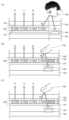
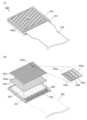
도 1의 (A)에 본 발명의 일 형태에 따른 표시 장치의 모식도를 나타내었다. 도 1의 (A)에 나타낸 표시 장치는 표시부(100)와, 센서부(104)와, 하우징(103)과, 보호 부재(105)를 포함한다. 표시부(100) 및 센서부(104)는 하우징(103)과 보호 부재(105) 사이에 끼워진 영역, 또는 하우징(103)과 보호 부재(105)로 둘러싸인 영역에 배치된다. 여기서 표시부(100) 및 센서부(104)는 하우징(103) 위에 나란히 배치된다. 또한 각 구성 요소의 자세한 내용에 대해서는 후술한다.Figure 1(A) shows a schematic diagram of a display device according to one embodiment of the present invention. The display device shown in FIG. 1 (A) includes a
표시부(100)는 기판(101)과, 기판(102)과, 복수의 발광 소자를 포함한다. 복수의 발광 소자로서는, 예를 들어 적색을 방출하는 발광 소자(110R), 녹색을 방출하는 발광 소자(110G), 청색을 방출하는 발광 소자(110B), 및 적외광을 방출하는 발광 소자(110IR)를 사용하는 구성으로 하면 좋다. 이하에서, 발광 소자(110R), 발광 소자(110G), 발광 소자(110B), 및 발광 소자(110IR)를 통틀어 발광 소자(110)라고 부르는 경우가 있다. 발광 소자(110)는 기판(101)과 기판(102) 사이에 끼워지는 영역에 배치된다. 바꿔 말하면, 기판(101)은 하우징(103)과 발광 소자(110) 사이에 배치되고, 기판(102)은 발광 소자(110)와 보호 부재(105) 사이에 배치된다.The
발광 소자(110IR)가 방출하는 광은 적외광을 포함하는 것이 바람직하고, 근적외광을 포함하는 것이 더 바람직하다. 예를 들어 파장 700nm 이상 2500nm 이하의 범위에 하나 이상의 피크를 갖는 근적외광을 적합하게 사용할 수 있다.The light emitted by the light emitting device 110IR preferably includes infrared light, and more preferably includes near infrared light. For example, near-infrared light having one or more peaks in a wavelength range of 700 nm to 2500 nm can be suitably used.
센서부(104)는 적외광을 검출하는 기능을 갖는 수광 소자를 포함한다. 이 수광 소자는 발광 소자(110IR)가 방출하는 적외광에 대응하는 광감도를 갖는 것이 바람직하고, 근적외광에 대응하는 광감도를 갖는 것이 더 바람직하다.The
도 1의 (A)에 나타낸 바와 같이, 표시부(100)의 발광 소자(110R), 발광 소자(110G), 및 발광 소자(110B)의 발광에 의하여 화상이 표시된다. 또한 표시부(100)의 발광 소자(110IR)로부터 사출된 적외광이 유저의 얼굴(109)에서 반사되고, 그 반사광을 센서부(104)의 수광 소자가 검출함으로써, 개인 인증이 수행된다. 그러므로 기판(102) 및 보호 부재(105)는 발광 소자(110R), 발광 소자(110G), 및 발광 소자(110B)로부터 방출되는 가시광과, 발광 소자(110IR)로부터 방출되고 얼굴(109)에서 반사된 적외광의 양쪽을 투과시킬 필요가 있다. 따라서 기판(102) 및 보호 부재(105)는 가시광 및 적외광에 대한 투광성을 갖는 것이 바람직하다.As shown in FIG. 1 (A), an image is displayed by light emission from the light-emitting
상술한 바와 같이, 도 1의 (A)에 나타낸 표시 장치에서, 표시부(100)와 센서부(104)는 하우징(103) 위에 나란히 배치된다. 그러므로 기판 면에 평행한 방향에서, 발광 소자(110IR)와 센서부(104)의 수광 소자 간의 거리는 비교적 길어진다. 따라서 도 1의 (A)에 나타낸 표시 장치에서는, 부호 부재(105)와의 거리가 가까운 대상물의 센싱은 어렵다. 그러므로 도 1의 (A)에 나타낸 표시 장치는 센싱의 대상물(얼굴(109))과 보호 부재(105) 간의 거리가 비교적 긴 얼굴 인증에 사용되는 것이 바람직하다.As described above, in the display device shown in FIG. 1 (A), the
또한 본 발명의 일 형태는 도 1의 (B)에 나타내는 바와 같은 구성으로 하여도 좋다. 도 1의 (B)에 나타낸 표시 장치는 센서부(104)가 표시부(100) 아래에 제공되어 있는 점에서 도 1의 (A)에 나타낸 표시 장치와 다르다. 도 1의 (B)에 나타낸 표시 장치에서는, 하우징(103) 위에 센서부(104)가 제공되고, 센서부(104) 위에 표시부(100)가 제공되고, 표시부(100) 위에 부호 부재(105)가 제공되어 있다. 또한 기타 구성에 대해서는, 도 1의 (A)에 나타낸 표시 장치와 같기 때문에 자세한 내용에 대해서는 도 1의 (A)에 따른 앞의 기재 등을 참작할 수 있다.Additionally, one embodiment of the present invention may be configured as shown in Fig. 1(B). The display device shown in FIG. 1(B) is different from the display device shown in FIG. 1(A) in that the
도 1의 (B)에 나타낸 바와 같이, 표시부(100)의 발광 소자(110R), 발광 소자(110G), 및 발광 소자(110B)의 발광에 의하여 화상이 표시된다. 또한 표시부(100)의 발광 소자(110IR)로부터 사출된 적외광이 유저의 손가락(108)에서 반사되고, 그 반사광을 센서부(104)의 수광 소자가 검출함으로써, 개인 인증이 수행된다. 그러므로 기판(102) 및 보호 부재(105)는 발광 소자(110R), 발광 소자(110G), 및 발광 소자(110B)로부터 방출되는 가시광과, 발광 소자(110IR) 및 손가락(108)에서 반사된 적외광의 양쪽을 투과시킬 필요가 있다. 따라서 기판(102) 및 보호 부재(105)는 가시광 및 적외광에 대한 투광성을 갖는 것이 바람직하다. 또한 손가락(108)에서 반사된 적외광은 기판(101)을 투과할 필요가 있다. 따라서 기판(101)은 적어도 적외광에 대한 투광성을 갖는 것이 바람직하다.As shown in FIG. 1 (B), an image is displayed by light emission from the light-emitting
상술한 바와 같이, 도 1의 (B)에 나타낸 표시 장치에서, 표시부(100)는 센서부(104) 위에 중첩되어 배치된다. 그러므로 기판 면에 평행한 방향에서, 발광 소자(110IR)와 센서부(104)의 수광 소자 간의 거리는 비교적 짧아진다. 따라서 도 1의 (B)에 나타낸 표시 장치에서는, 부호 부재(105)와의 거리가 가까운 대상물의 센싱은 용이하다. 그러므로 도 1의 (B)에 나타낸 표시 장치는 센싱의 대상물(손가락(108))과 보호 부재(105)가 접촉하는 지문 인증에 사용되는 것이 바람직하다.As described above, in the display device shown in FIG. 1 (B), the
도 1의 (B)에 나타낸 표시 장치에서는, 손가락(108)이 보호 부재(105)와 접촉하는 예를 나타내었지만, 손가락(108)이 보호 부재(105)와 반드시 접촉할 필요는 없다. 예를 들어 도 1의 (C)에 나타낸 바와 같이, 손가락(108)과 보호 부재(105)가 떨어져 있는 상태에서 센싱을 할 수 있는 경우도 있다. 다만 이때 손가락(108)과 보호 부재(105) 사이의 거리가 비교적 가까운 것이 바람직하고, 이 상태를 니어 터치(near touch) 또는 호버 터치라고 부르는 경우가 있다.In the display device shown in FIG. 1 (B), an example in which the
본 명세서 등에서 니어 터치 또는 호버 터치란 예를 들어 표시 장치에 대상물(손가락(108))이 접촉하지 않아도 대상물(손가락(108))을 검출할 수 있는 상태를 가리킨다. 예를 들어 표시 장치와 대상물(손가락(108)) 사이의 거리가 0.1mm 이상 300mm 이하, 바람직하게는 3mm 이상 50mm 이하인 범위에서 표시 장치가 대상물(손가락(108))을 검출할 수 있는 구성인 것이 바람직하다. 상기 구성으로 함으로써, 표시 장치에 대상물(손가락(108))이 직접 접촉하지 않아도 조작을 할 수 있고, 바꿔 말하면 비접촉(터치리스)으로 표시 장치를 조작할 수 있다. 상기 구성으로 함으로써, 표시 장치에 오염이 부착되거나 흠이 생길 위험성을 저감하면서 표시 장치를 조작할 수 있거나, 대상물(손가락(108))이 표시 장치에 부착되어 있을 수 있는 오염(예를 들어 먼지 또는 바이러스 등)에 직접 접촉하지 않고 표시 장치를 조작할 수 있다.In this specification and the like, near touch or hover touch refers to a state in which an object (finger 108) can be detected, for example, without the object (finger 108) coming into contact with the display device. For example, the display device is configured to detect the object (finger 108) in a range where the distance between the display device and the object (finger 108) is 0.1 mm or more and 300 mm or less, preferably 3 mm or more and 50 mm or less. desirable. With the above configuration, operations can be performed without the object (finger 108) directly contacting the display device. In other words, the display device can be operated non-contactly (touchless). By using the above configuration, the display device can be operated while reducing the risk of contamination adhering to the display device or scratches, or an object (the finger 108) can be removed from contamination (e.g. dust or dirt) that may be attached to the display device. You can operate the display device without direct contact with viruses, etc.
또한 위에서, 도 1의 (A)에는 센서부(104)를 표시부(100) 옆에 배치하는 구성을 나타내고, 도 1의 (B), (C)에는 센서부(104)를 표시부(100) 아래에 배치하는 구성을 나타내었지만, 이들을 조합하여 사용하여도 좋다. 즉 표시부 옆에 제 1 센서부를 제공하고, 표시부 아래에 제 2 센서부를 제공하는 구성으로 하여도 좋다. 이와 같은 구성으로 함으로써, 보안의 수준에 따라 얼굴 인증과 지문 인증을 조합하여 사용할 수 있다. 예를 들어 일반적인 수준의 보안 처리(예를 들어 화면 잠금의 해제 등)에서는 얼굴 인증을 수행하고, 더 높은 수준의 보안이 요구되는 처리(예를 들어 물품의 구입 등)에서는 지문 인증을 더 수행할 수 있다.Also, from above, Figure 1 (A) shows a configuration in which the
또한 위에서는, 센싱의 대상물을 얼굴, 지문으로 하는 예에 대하여 나타내었지만, 본 발명은 이에 한정되지 않는다. 예를 들어 장문, 맥 형상(정맥 형상, 동맥 형상을 포함함), 흥채 등을 센싱의 대상물로 하여 개인 인증을 수행하는 표시 장치로 하여도 좋다.Also, in the above, an example was shown where the sensing object is a face or a fingerprint, but the present invention is not limited to this. For example, it may be used as a display device that performs personal authentication by using palm prints, pulse shapes (including vein shapes, artery shapes), and heungchae as objects of sensing.
또한 위에서는, 본 발명에 따른 표시 장치를 사용하여 개인 인증을 수행하는 기능에 대하여 설명하였지만, 본 발명은 이에 한정되지 않는다. 예를 들어 제스처를 센서부로 촬상하고, 이 제스처에 따른 처리를 수행하는 기능을 표시 장치에 부여하여도 좋다. 또한 예를 들어 센서부의 촬상 데이터로부터 맥박, 호흡수, 맥파, 산소 포화도, 혈당치, 중성 지방 농도 등의 생체 데이터를 취득하는 기능을 표시 장치에 부여하여도 좋다.In addition, although the function of performing personal authentication using the display device according to the present invention has been described above, the present invention is not limited to this. For example, the display device may be given the function of capturing an image of a gesture with a sensor unit and performing processing according to the gesture. Additionally, for example, the display device may be provided with a function of acquiring biometric data such as pulse, respiratory rate, pulse wave, oxygen saturation, blood sugar level, and neutral fat concentration from the image captured data of the sensor unit.
또한 위에서는, 적색을 방출하는 발광 소자(110R), 녹색을 방출하는 발광 소자(110G), 청색을 방출하는 발광 소자(110B), 및 적외광을 방출하는 발광 소자(110IR)의 4종류의 발광 소자를 사용하여 화소를 형성하는 구성을 나타내었지만, 본 발명은 이에 한정되지 않는다. 예를 들어 발광 소자(110R)가 적색의 파장과 적외의 파장의 양쪽에 피크를 갖는 광을 방출하는 구성으로 하여, 발광 소자(110R), 발광 소자(110G), 및 발광 소자(110B)의 3종류의 발광 소자로 화소를 형성하는 구성으로 하여도 좋다.Also, from above, there are four types of light emission: a light-emitting
다음으로, 본 발명의 일 형태의 표시 장치에 제공되는 표시부(100)의 더 구체적인 구성예 및 제작 방법의 예에 대하여 도면을 참조하여 설명한다.Next, a more specific example of the configuration and manufacturing method of the
[표시부의 구성예 1][Configuration example 1 of display unit]
도 2의 (A)에 본 발명의 일 형태의 표시부(100)의 상면 개략도를 나타내었다. 표시부(100)는 적색광을 방출하는 발광 소자(110R), 녹색광을 방출하는 발광 소자(110G), 청색광을 방출하는 발광 소자(110B), 및 적외광을 방출하는 발광 소자(110IR)를 각각 복수로 포함한다. 도 2의 (A)에서는, 각 발광 소자를 쉽게 구별하기 위하여, 각 발광 소자의 발광 영역 내에 R, G, B, IR의 부호를 붙였다.Figure 2(A) shows a top schematic diagram of the
발광 소자(110R), 발광 소자(110G), 발광 소자(110B), 및 발광 소자(110IR)는 각각 매트릭스로 배열되어 있다. 도 2의 (A)에는 한 방향으로 동일한 색의 발광 소자가 배열된 소위 스트라이프 배열을 나타내었다. 또한 발광 소자의 배열 방법은 이에 한정되지 않고, 델타 배열, 지그재그 배열 등의 배열 방법을 적용하여도 좋고, 펜타일 배열을 사용할 수도 있다.The light-emitting
발광 소자(110R), 발광 소자(110G), 발광 소자(110B), 및 발광 소자(110IR)는 X 방향으로 배열되어 있다. 또한 X 방향과 교차하는 Y 방향으로는 동일한 색의 발광 소자가 배열되어 있다.The light-emitting
또한 도 1의 (A)에서는, 발광 소자(110R), 발광 소자(110G), 발광 소자(110B), 및 발광 소자(110IR)가 하나씩 제공되어 하나의 화소를 구성하는 예를 나타내었지만, 본 발명은 이에 한정되지 않는다. 예를 들어 기본적인 화소는 발광 소자(110R), 발광 소자(110G), 및 발광 소자(110B)로 구성되고, 부분적으로 발광 소자(110IR)를 포함하는 화소가 더 제공되는 구성으로 하여도 좋다.In addition, in Figure 1 (A), an example of configuring one pixel is shown in which the light-emitting
발광 소자(110R), 발광 소자(110G), 발광 소자(110B), 및 발광 소자(110IR)로서는, OLED(Organic Light Emitting Diode) 또는 QLED(Quantum-dot Light Emitting Diode) 등의 EL 소자를 사용하는 것이 바람직하다. EL 소자가 포함하는 발광 물질로서는 형광을 방출하는 물질(형광 재료), 인광을 방출하는 물질(인광 재료), 무기 화합물(퀀텀닷(quantum dot) 재료 등), 열 활성화 지연 형광을 나타내는 물질(열 활성화 지연 형광(Thermally activated delayed fluorescence: TADF) 재료) 등을 들 수 있다.As the light-emitting
도 2의 (B)는 도 2의 (A)에서의 일점쇄선 A1-A2에 대응하는 단면 개략도이고, 도 2의 (C)는 일점쇄선 B1-B2에 대응하는 단면 개략도이다.FIG. 2(B) is a cross-sectional schematic diagram corresponding to the dashed-dash line A1-A2 in FIG. 2(A), and FIG. 2(C) is a cross-sectional schematic diagram corresponding to the dashed-dash line B1-B2.
도 2의 (B)에는 발광 소자(110R), 발광 소자(110G), 발광 소자(110B), 및 발광 소자(110IR)의 단면을 나타내었다. 발광 소자(110R)는 화소 전극(111R), EL층(112R), EL층(114), 및 공통 전극(113)을 포함한다. 발광 소자(110G)는 화소 전극(111G), EL층(112G), EL층(114), 및 공통 전극(113)을 포함한다. 발광 소자(110B)는 화소 전극(111B), EL층(112B), EL층(114), 및 공통 전극(113)을 포함한다. 발광 소자(110IR)는 화소 전극(111IR), EL층(112IR), EL층(114), 및 공통 전극(113)을 포함한다. EL층(114)과 공통 전극(113)은 발광 소자(110R), 발광 소자(110G), 발광 소자(110B), 및 발광 소자(110IR)에 공통적으로 제공된다. EL층(114)은 공통층이라고 할 수도 있다.Figure 2 (B) shows cross-sections of the light-emitting
발광 소자(110R)에 포함되는 EL층(112R)은 적어도 적색의 파장 영역에 강도를 갖는 광을 방출하는 발광성 유기 화합물을 포함한다. 발광 소자(110G)에 포함되는 EL층(112G)은 적어도 녹색의 파장 영역에 강도를 갖는 광을 방출하는 발광성 유기 화합물을 포함한다. 발광 소자(110B)에 포함되는 EL층(112B)은 적어도 청색의 파장 영역에 강도를 갖는 광을 방출하는 발광성 유기 화합물을 포함한다.The
EL층(112R), EL층(112G), EL층(112B), 및 EL층(112IR)은 각각 발광성 유기 화합물을 포함한 층(발광층) 외에 전자 주입층, 전자 수송층, 정공 주입층, 및 정공 수송층 중 하나 이상을 포함하여도 좋다. EL층(114)은 발광층을 포함하지 않는 구성으로 할 수 있다. 예를 들어 EL층(114)은 전자 주입층, 전자 수송층, 정공 주입층, 및 정공 수송층 중 하나 이상을 포함한다.The
화소 전극(111R), 화소 전극(111G), 화소 전극(111B), 및 화소 전극(111IR)은 각각 발광 소자마다 제공되어 있다. 또한 공통 전극(113) 및 EL층(114)은 각 발광 소자에서 공통되는 하나의 연속된 층으로서 제공되어 있다. 각 화소 전극 및 공통 전극(113) 중 어느 한쪽에 가시광에 대한 투광성을 갖는 도전막을 사용하고, 다른 쪽에 반사성을 갖는 도전막을 사용한다. 각 화소 전극을 투광성으로, 공통 전극(113)을 반사성으로 함으로써, 하면 사출형(보텀 이미션형) 표시 장치로 할 수 있고, 이와 반대로 각 화소 전극을 반사성으로, 공통 전극(113)을 투광성으로 함으로써, 상면 사출형(톱 이미션형) 표시 장치로 할 수 있다. 또한 각 화소 전극 및 공통 전극(113)의 양쪽을 투광성으로 함으로써, 양면 사출형(듀얼 이미션형) 표시 장치로 할 수도 있다.A
화소 전극(111R), 화소 전극(111G), 화소 전극(111B), 및 화소 전극(111IR)의 단부를 덮어 절연층(131)이 제공되어 있다. 절연층(131)의 단부는 테이퍼 형상인 것이 바람직하다. 또한 절연층(131)은 불필요하면 제공하지 않아도 된다.An insulating
EL층(112R), EL층(112G), EL층(112B), 및 EL층(112IR)은 각각 화소 전극의 상면과 접촉하는 영역과, 절연층(131)의 표면과 접촉하는 영역을 포함한다. 또한 EL층(112R), EL층(112G), EL층(112B), 및 EL층(112IR)의 단부는 절연층(131) 위에 위치한다.The
도 2의 (B)에 나타낸 바와 같이 상이한 색의 발광 소자 간에서 2개의 EL층 사이에 틈이 있다. 이와 같이 EL층(112R), EL층(112G), EL층(112B), 및 EL층(112IR)이 서로 접촉하지 않도록 제공되어 있는 것이 바람직하다. 이에 의하여, 인접한 2개의 EL층을 통하여 전류가 흘러, 의도치 않은 발광이 발생하는 것을 적합하게 방지할 수 있다. 그러므로 콘트라스트를 높일 수 있고, 표시 품질이 높은 표시 장치를 실현할 수 있다.As shown in Figure 2(B), there is a gap between the two EL layers between the light emitting elements of different colors. In this way, it is preferable that the
도 2의 (C)에 나타낸 바와 같이, Y 방향에서 EL층(112R)은 하나의 연속된 층이 되도록 띠 형상으로 형성되어 있다. EL층(112R) 등을 띠 형상으로 형성함으로써, 이들을 분단하기 위한 공간이 불필요하게 되어, 발광 소자 사이의 비발광 영역의 면적을 축소할 수 있기 때문에, 개구율을 높일 수 있다. 또한 도 2의 (C)에는 일례로서 발광 소자(110R)의 단면을 나타내었지만, 발광 소자(110G), 발광 소자(110B), 및 발광 소자(110IR)에 대해서도 같은 형상으로 할 수 있다.As shown in FIG. 2C, in the Y direction, the
공통 전극(113) 위에는 발광 소자(110R), 발광 소자(110G), 발광 소자(110IR), 및 발광 소자(110B)를 덮어 보호층(121)이 제공되어 있다. 보호층(121)은 위쪽으로부터 각 발광 소자로 물 등의 불순물이 확산되는 것을 방지하는 기능을 갖는다.A
보호층(121)은 예를 들어 적어도 무기 절연막을 포함하는 단층 구조 또는 적층 구조를 가질 수 있다. 무기 절연막으로서는 예를 들어 산화 실리콘막, 산화질화 실리콘막, 질화산화 실리콘막, 질화 실리콘막, 산화 알루미늄막, 산화질화 알루미늄막, 산화 하프늄막 등의 산화물막 또는 질화물막을 들 수 있다. 또는 보호층(121)에 인듐 갈륨 산화물, 인듐 갈륨 아연 산화물 등의 반도체 재료를 사용하여도 좋다.For example, the
또한 보호층(121)으로서, 무기 절연막과 유기 절연막의 적층막을 사용할 수도 있다. 예를 들어, 한 쌍의 무기 절연막 사이에 유기 절연막을 끼운 구성으로 하는 것이 바람직하다. 또한 유기 절연막이 평탄화막으로서 기능하는 것이 바람직하다. 이에 의하여, 유기 절연막의 상면을 평탄하게 할 수 있기 때문에, 그 위의 무기 절연막의 피복성이 향상되어, 배리어성을 높일 수 있다. 또한 보호층(121)의 상면이 평탄하게 되기 때문에, 보호층(121) 위쪽에 구조물(예를 들어 컬러 필터, 터치 센서의 전극, 또는 렌즈 어레이 등)을 제공하는 경우에, 아래쪽의 구조에 기인하는 요철 형상의 영향을 경감할 수 있어 바람직하다.Additionally, as the
또한 도 2의 (A)에는 공통 전극(113)과 전기적으로 접속되는 접속 전극(111C)을 나타내었다. 접속 전극(111C)은 공통 전극(113)에 공급하기 위한 전위(예를 들어 애노드 전위 또는 캐소드 전위)가 공급된다. 접속 전극(111C)은 발광 소자(110R) 등이 배열되는 표시 영역의 외부에 제공된다. 또한 도 2의 (A)에는 공통 전극(113)을 파선으로 나타내었다.Additionally, Figure 2 (A) shows a
접속 전극(111C)은 표시 영역의 외주를 따라 제공할 수 있다. 예를 들어, 표시 영역의 외주의 한 변을 따라 제공되어 있어도 좋고, 표시 영역의 외주의 두 변 이상을 따라 제공되어 있어도 좋다. 즉, 표시 영역의 상면 형상이 직사각형인 경우에는 접속 전극(111C)의 상면 형상은 띠 형상, L자 형상, 디귿자 형상(대괄호 형상), 또는 사각형 등으로 할 수 있다.The
도 2의 (D)는 도 2의 (A)에서의 일점쇄선 C1-C2에 대응하는 단면 개략도이다. 도 2의 (D)에는 접속 전극(111C)과 공통 전극(113)이 전기적으로 접속되는 접속부(130)를 나타내었다. 접속부(130)에서는 접속 전극(111C) 위에 공통 전극(113)이 접촉하여 제공되고, 공통 전극(113)을 덮어 보호층(121)이 제공되어 있다. 또한 접속 전극(111C)의 단부를 덮어 절연층(131)이 제공되어 있다.FIG. 2(D) is a cross-sectional schematic diagram corresponding to the dashed-dotted line C1-C2 in FIG. 2(A). Figure 2(D) shows a
[제작 방법의 예 1][Example 1 of production method]
이하에서는, 본 발명의 일 형태의 표시 장치의 제작 방법의 일례에 대하여 도면을 참조하여 설명한다. 여기서는 상기 구성예에서 나타낸 표시부(100)를 예로 들어 설명한다. 도 3의 (A) 내지 도 4의 (F)는 이하에서 예시하는 표시 장치의 제작 방법의 각 공정에서의 단면 개략도이다. 또한 도 3의 (A) 등에서는, 오른쪽에 접속부(130) 및 그 근방에서의 단면 개략도를 함께 나타내었다. 또한 도 3의 (A) 내지 도 4의 (F)에서는, 도면의 명료화를 위하여 발광 소자(110B)를 생략하였지만, 발광 소자(110B)도 발광 소자(110R), 발광 소자(110G), 발광 소자(110IR)와 같은 식으로 제작할 수 있다.Below, an example of a method of manufacturing a display device of one embodiment of the present invention will be described with reference to the drawings. Here, the
또한 표시 장치를 구성하는 박막(절연막, 반도체막, 도전막 등)은 스퍼터링법, 화학 기상 퇴적(CVD: Chemical Vapor Deposition)법, 진공 증착법, 펄스 레이저 퇴적(PLD: Pulsed Laser Deposition)법, 원자층 퇴적(ALD: Atomic Layer Deposition)법 등을 사용하여 형성할 수 있다. CVD법으로서는 플라스마 화학 기상 퇴적(PECVD: Plasma Enhanced CVD)법 또는 열 CVD법 등이 있다. 또한 열 CVD법 중 하나에 유기 금속 화학 기상 퇴적(MOCVD: Metal Organic CVD)법이 있다.In addition, the thin films (insulating films, semiconductor films, conductive films, etc.) that make up the display device are made using sputtering methods, chemical vapor deposition (CVD) methods, vacuum deposition methods, pulsed laser deposition (PLD) methods, and atomic layer methods. It can be formed using ALD: Atomic Layer Deposition (ALD) method. CVD methods include plasma chemical vapor deposition (PECVD: Plasma Enhanced CVD) and thermal CVD. Additionally, one of the thermal CVD methods is metal organic chemical vapor deposition (MOCVD).
또한 표시 장치를 구성하는 박막(절연막, 반도체막, 도전막 등)은 스핀 코팅, 딥, 스프레이 도포, 잉크젯, 디스펜스, 스크린 인쇄, 오프셋 인쇄, 닥터 나이프법, 슬릿 코팅, 롤 코팅, 커튼 코팅, 나이프 코팅 등의 방법을 사용하여 형성할 수 있다.In addition, thin films (insulating films, semiconductor films, conductive films, etc.) that make up display devices can be applied by spin coating, dip, spray coating, inkjet, dispensing, screen printing, offset printing, doctor knife method, slit coating, roll coating, curtain coating, and knife coating. It can be formed using methods such as coating.
또한 표시 장치를 구성하는 박막을 가공할 때에는, 포토리소그래피법 등을 사용할 수 있다. 이 외에, 나노 임프린트법, 샌드블라스트법(sandblasting method), 리프트 오프법 등으로 가공되어도 좋다. 또한 메탈 마스크 등의 차폐 마스크를 사용한 성막 방법에 의하여 섬 형상의 박막을 직접 형성하여도 좋다.Additionally, when processing the thin film that constitutes the display device, a photolithography method or the like can be used. In addition, it may be processed by nano imprint method, sandblasting method, lift-off method, etc. Additionally, an island-shaped thin film may be formed directly by a film forming method using a shielding mask such as a metal mask.
포토리소그래피법으로서 대표적으로는 다음 2가지 방법이 있다. 하나는 가공하고자 하는 박막 위에 레지스트 마스크를 형성하고, 에칭 등에 의하여 상기 박막을 가공하고, 레지스트 마스크를 제거하는 방법이다. 다른 하나는 감광성을 갖는 박막을 형성한 후에, 노광, 현상을 수행하여 상기 박막을 원하는 형상으로 가공하는 방법이다.There are two representative photolithographic methods: One method is to form a resist mask on the thin film to be processed, process the thin film by etching, etc., and remove the resist mask. The other method is to form a photosensitive thin film and then process the thin film into a desired shape by performing exposure and development.
포토리소그래피법에서 노광에 사용하는 광으로서는 예를 들어 i선(파장 365nm), g선(파장 436nm), h선(파장 405nm), 또는 이들을 혼합시킨 광을 사용할 수 있다. 그 외에, 자외선, KrF 레이저 광, 또는 ArF 레이저 광 등을 사용할 수도 있다. 또한 액침 노광 기술에 의하여 노광을 수행하여도 좋다. 또한 노광에 극단 자외(EUV: Extreme Ultra-violet)광, X선 등의 광을 사용하여도 좋다. 또한 노광에 사용되는 광 대신에 전자 빔을 사용할 수도 있다. 극단 자외광, X선, 또는 전자 빔을 사용하면, 매우 미세한 가공을 수행할 수 있어 바람직하다. 또한 전자 빔 등의 빔을 주사하여 노광을 수행하는 경우에는 포토마스크가 필요하지 않다.As light used for exposure in the photolithography method, for example, i-line (wavelength 365 nm), g-line (wavelength 436 nm), h-line (wavelength 405 nm), or a mixture of these can be used. In addition, ultraviolet rays, KrF laser light, or ArF laser light can also be used. Additionally, exposure may be performed using a liquid immersion exposure technique. Additionally, light such as extreme ultra-violet (EUV) light or X-ray may be used for exposure. Additionally, an electron beam may be used instead of the light used for exposure. The use of extreme ultraviolet light, X-rays, or electron beams is desirable because it allows very fine processing to be performed. Additionally, when exposure is performed by scanning a beam such as an electron beam, a photomask is not required.
박막의 에칭에는 드라이 에칭법, 웨트 에칭법, 샌드 블라스트법 등을 사용할 수 있다.Dry etching, wet etching, sand blasting, etc. can be used to etch thin films.
[기판(101)의 준비][Preparation of substrate 101]
기판(101)으로서는 적어도 추후의 열처리에 견딜 수 있을 정도의 내열성을 갖는 기판을 사용할 수 있다. 기판(101)으로서 절연성 기판을 사용하는 경우에는 유리 기판, 석영 기판, 사파이어 기판, 세라믹 기판, 유기 수지 기판 등을 사용할 수 있다. 또한 실리콘, 탄소화 실리콘 등을 재료로 한 단결정 반도체 기판, 다결정 반도체 기판, 실리콘 저마늄 등으로 이루어지는 화합물 반도체 기판, SOI 기판 등의 반도체 기판을 사용할 수 있다. 다만, 도 1의 (B) 등에 나타낸 표시 장치에 사용하는 경우에는, 기판(101)에 유리 기판 등의 투광성을 갖는 재료를 사용하는 것이 바람직하다.As the
특히 기판(101)으로서 상기 반도체 기판 또는 절연성 기판 위에 트랜지스터 등의 반도체 소자를 포함하는 반도체 회로가 형성된 기판을 사용하는 것이 바람직하다. 상기 반도체 회로는 예를 들어 화소 회로, 게이트선 구동 회로(게이트 드라이버), 소스선 구동 회로(소스 드라이버) 등을 구성하는 것이 바람직하다. 또한 상기에 더하여 연산 회로, 기억 회로 등이 구성되어 있어도 좋다.In particular, it is preferable to use, as the
[화소 전극(111R, 111G, 111B, 111IR, 접속 전극(111C)의 형성][Formation of
이어서, 기판(101) 위에 화소 전극(111R), 화소 전극(111G), 화소 전극(111B)(도시하지 않았음), 화소 전극(111IR), 및 접속 전극(111C)을 형성한다. 먼저 화소 전극이 되는 도전막을 성막하고, 포토리소그래피법을 사용하여 레지스트 마스크를 형성하고, 도전막의 불필요한 부분을 에칭에 의하여 제거한다. 그 후, 레지스트 마스크를 제거함으로써 화소 전극(111R), 화소 전극(111G), 화소 전극(111B), 및 화소 전극(111IR)을 형성할 수 있다.Next, a
각 화소 전극으로서 가시광에 대한 반사성을 갖는 도전막을 사용하는 경우, 가시광의 파장 영역 전체에서 반사율이 가능한 한 높은 재료(예를 들어 은 또는 알루미늄 등)를 적용하는 것이 바람직하다. 이에 의하여, 발광 소자의 광 추출 효율을 높일 수 있을 뿐만 아니라, 색 재현성을 높일 수 있다.When using a conductive film having reflectivity for visible light as each pixel electrode, it is desirable to use a material (for example, silver or aluminum) with a reflectivity as high as possible in the entire visible light wavelength region. As a result, not only can the light extraction efficiency of the light emitting device be improved, but also color reproducibility can be improved.
[절연층(131)의 형성][Formation of insulating layer 131]
이어서, 화소 전극(111R), 화소 전극(111G), 화소 전극(111B), 및 화소 전극(111IR)의 단부를 덮어 절연층(131)을 형성한다(도 3의 (A)). 절연층(131)에는, 유기 절연막 또는 무기 절연막을 사용할 수 있다. 절연층(131)은 나중에 형성되는 EL막의 단차 피복성을 향상시키기 위하여, 단부를 테이퍼 형상으로 하는 것이 바람직하다. 특히 유기 절연막을 사용하는 경우에는 감광성 재료를 사용하면 노광 및 현상의 조건에 의하여 단부의 형상을 제어하기 쉬워 바람직하다.Next, an insulating
[EL막(112Rf)의 형성][Formation of EL film (112Rf)]
다음으로, 화소 전극(111R), 화소 전극(111G), 화소 전극(111B), 화소 전극(111IR), 및 절연층(131) 위에 나중에 EL층(112R)이 되는 EL막(112Rf)을 성막한다.Next, an EL film 112Rf, which will later become the
EL막(112Rf)은 적어도 발광성 화합물을 포함한 막을 포함한다. 이 외에 전자 주입층, 전자 수송층, 전하 발생층, 정공 수송층, 또는 정공 주입층으로서 기능하는 막 중 하나 이상이 적층된 구성으로 하여도 좋다. EL막(112Rf)은 예를 들어 증착법, 스퍼터링법, 또는 잉크젯법 등을 사용하여 형성할 수 있다. 또한 이에 한정되지 않고, 상술한 성막 방법을 적절히 사용할 수 있다.The EL film 112Rf includes at least a film containing a luminescent compound. In addition, one or more films functioning as an electron injection layer, an electron transport layer, a charge generation layer, a hole transport layer, or a hole injection layer may be laminated. The EL film 112Rf can be formed using, for example, a deposition method, a sputtering method, or an inkjet method. Additionally, it is not limited to this, and the above-described film forming method can be appropriately used.
일례로서는 EL막(112Rf)으로서 정공 주입층, 정공 수송층, 발광층, 전자 수송층이 이 순서대로 적층된 적층막으로 하는 것이 바람직하다. 이때 나중에 형성되는 EL층(114)으로서는 전자 주입층을 포함하는 막을 사용할 수 있다. 특히 발광층을 덮어 전자 수송층을 제공함으로써 추후의 포토리소그래피 공정 등에 의하여 발광층이 대미지를 받는 것을 억제할 수 있어, 신뢰성이 높은 발광 소자를 제작할 수 있다. 또한 EL막(112Rf) 등에 사용하는 전자 수송층과, 나중에 형성되는 EL층(114)에 사용하는 전자 주입층으로서, 같은 유기 화합물을 포함한 층을 사용하면, 이들을 양호하게 접합할 수 있어, 발광 효율이 높고 신뢰성이 높은 발광 소자를 실현할 수 있다. 예를 들어 전자 수송층에 전자 수송성이 높은 유기 화합물을 사용하고, 전자 주입층에 상기 유기 화합물과 금속을 포함한 재료를 사용할 수 있다.As an example, the EL film 112Rf is preferably a laminated film in which a hole injection layer, a hole transport layer, a light emitting layer, and an electron transport layer are stacked in this order. At this time, a film containing an electron injection layer can be used as the
EL막(112Rf)은 접속 전극(111C) 위에 제공되지 않도록 형성되는 것이 바람직하다. 예를 들어, EL막(112Rf)을 증착법(또는 스퍼터링법)을 사용하여 형성하는 경우, 접속 전극(111C)에 EL막(112Rf)이 성막되지 않도록 차폐 마스크를 사용하여 형성하는 것이 바람직하다.The EL film 112Rf is preferably formed so as not to be provided on the
[희생막(144a)의 형성][Formation of
이어서 EL막(112Rf)을 덮어 희생막(144a)을 형성한다. 또한 희생막(144a)은 접속 전극(111C)의 상면과 접촉하여 제공된다. 또한 희생막은 마스크막이라고도 부를 수 있다.Next, the
희생막(144a)으로서는, EL막(112Rf) 등의 각 EL막의 에칭 처리에 대한 내성이 높은 막, 즉 에칭 선택비가 큰 막을 사용할 수 있다. 또한 희생막(144a)으로서는, 후술하는 보호막(146a) 등의 보호막과의 에칭 선택비가 큰 막을 사용할 수 있다. 또한 희생막(144a)으로서는, 각 EL막에 대한 대미지가 적은 웨트 에칭법을 사용하여 제거할 수 있는 막을 사용할 수 있다.As the
희생막(144a)으로서는 예를 들어 금속막, 합금막, 금속 산화물막, 반도체막, 무기 절연막 등의 무기막을 사용할 수 있다. 희생막(144a)은 스퍼터링법, 증착법, CVD법, ALD법 등의 각종 성막 방법에 의하여 형성할 수 있다.As the
희생막(144a)으로서는 예를 들어 금, 은, 백금, 마그네슘, 니켈, 텅스텐, 크로뮴, 몰리브데넘, 철, 코발트, 구리, 팔라듐, 타이타늄, 알루미늄, 이트륨, 지르코늄, 및 탄탈럼 등의 금속 재료, 또는 이 금속 재료를 포함한 합금 재료를 사용할 수 있다. 특히 알루미늄 또는 은 등의 저융점 재료를 사용하는 것이 바람직하다.The
또한 희생막(144a)에는 인듐 갈륨 아연 산화물(In-Ga-Zn 산화물, IGZO라고도 표기함) 등의 금속 산화물을 사용할 수 있다. 또한 산화 인듐, 인듐 아연 산화물(In-Zn 산화물), 인듐 주석 산화물(In-Sn 산화물), 인듐 타이타늄 산화물(In-Ti 산화물), 인듐 주석 아연 산화물(In-Sn-Zn 산화물), 인듐 타이타늄 아연 산화물(In-Ti-Zn 산화물), 인듐 갈륨 주석 아연 산화물(In-Ga-Sn-Zn 산화물) 등을 사용할 수 있다. 또는 실리콘을 포함하는 인듐 주석 산화물 등을 사용할 수도 있다.Additionally, a metal oxide such as indium gallium zinc oxide (In-Ga-Zn oxide, also referred to as IGZO) may be used for the
또한 상기 갈륨 대신에 원소 M(M은 알루미늄, 실리콘, 붕소, 이트륨, 구리, 바나듐, 베릴륨, 타이타늄, 철, 니켈, 저마늄, 지르코늄, 몰리브데넘, 란타넘, 세륨, 네오디뮴, 하프늄, 탄탈럼, 텅스텐, 및 마그네슘 중에서 선택된 1종류 또는 복수 종류)을 사용한 경우에도 적용할 수 있다. 특히 M은 갈륨, 알루미늄, 또는 이트륨 중에서 선택된 1종류 또는 복수 종류로 하는 것이 바람직하다.In addition, instead of gallium, the element M (M is aluminum, silicon, boron, yttrium, copper, vanadium, beryllium, titanium, iron, nickel, germanium, zirconium, molybdenum, lanthanum, cerium, neodymium, hafnium, tantalum) It can also be applied when one or more types selected from , tungsten, and magnesium are used. In particular, M is preferably one or more types selected from gallium, aluminum, or yttrium.
또한 희생막(144a)은 산화 알루미늄, 산화 하프늄, 산화 실리콘 등의 무기 절연 재료를 사용하여 형성할 수 있다.Additionally, the
또한 희생막(144a)에는, EL막(112Rf)의 최상부에 위치하는 막에 대하여 화학적으로 안정된 용매에 용해될 수 있는 재료를 사용하는 것이 바람직하다. 특히 물 또는 알코올에 용해되는 재료를 희생막(144a)에 적합하게 사용할 수 있다. 희생막(144a)은, 재료를 물 또는 알코올 등의 용매에 용해시킨 상태에서 습식의 성막 방법으로 도포한 후에, 용매를 증발시키기 위한 가열 처리를 함으로써 성막하는 것이 바람직하다. 이때 감압 분위기에서 가열 처리를 하면, 저온 및 단시간으로 용매를 제거할 수 있기 때문에, EL막(112Rf)에 대한 열적인 대미지를 저감할 수 있어 바람직하다.Additionally, for the
희생막(144a)의 형성에 사용할 수 있는 습식의 성막 방법으로서는, 스핀 코팅, 딥, 스프레이 도포, 잉크젯, 디스펜싱, 스크린 인쇄, 오프셋 인쇄, 닥터 나이프법, 슬릿 코팅, 롤 코팅, 커튼 코팅, 나이프 코팅 등이 있다.Wet film formation methods that can be used to form the
희생막(144a)으로서는, 폴리바이닐알코올(PVA), 폴리바이닐뷰티랄, 폴리바이닐피롤리돈, 폴리에틸렌글라이콜, 폴리글리세린, 풀루란, 수용성 셀룰로스, 또는 알코올 가용성 폴리아마이드 수지 등의 유기 재료를 사용할 수 있다.As the
[보호막(146a)의 형성][Formation of
이어서, 희생막(144a) 위에 보호막(146a)을 형성한다(도 3의 (B)).Next, a
보호막(146a)은 나중에 희생막(144a)을 에칭할 때 하드 마스크로서 사용되는 막이다. 또한 추후의 보호막(146a)의 가공 시에는 희생막(144a)이 노출된다. 따라서 희생막(144a)과 보호막(146a)에는 에칭 속도가 서로 크게 다른 막의 조합을 선택한다. 그러므로 희생막(144a)의 에칭 조건 및 보호막(146a)의 에칭 조건에 따라 보호막(146a)에 사용할 수 있는 막을 선택할 수 있다.The
예를 들어, 보호막(146a)의 에칭에 플루오린을 포함하는 가스(플루오린계 가스라고도 함)를 사용한 드라이 에칭을 사용하는 경우에는, 실리콘, 질화 실리콘, 산화 실리콘, 텅스텐, 타이타늄, 몰리브데넘, 탄탈럼, 질화 탄탈럼, 몰리브데넘과 나이오븀을 포함하는 합금, 또는 몰리브데넘과 텅스텐을 포함하는 합금 등을 보호막(146a)에 사용할 수 있다. 여기서 상기 플루오린계 가스를 사용한 드라이 에칭에서 에칭 선택비가 큰(즉, 에칭 속도를 느리게 할 수 있는) 막으로서는 IGZO, ITO 등의 금속 산화물막 등이 있고, 이를 희생막(144a)에 사용할 수 있다.For example, when dry etching using a gas containing fluorine (also called fluorine-based gas) is used to etch the
또한 보호막(146a)은 이에 한정되지 않고, 희생막(144a)의 에칭 조건 및 보호막(146a)의 에칭 조건에 따라 다양한 재료 중에서 선택할 수 있다. 예를 들어 상기 희생막(144a)에 사용할 수 있는 막 중에서 선택할 수도 있다. 예를 들어 보호막(146a)으로서 IGZO 또는 ITO 등의 금속 산화물을 사용할 수도 있다. 예를 들어 희생막(144a)으로서 ALD법으로 성막한 산화 알루미늄을 사용하고, 보호막(146a)으로서 스퍼터링법으로 성막한 IGZO를 사용할 수 있다. 또한 희생막(144a)으로서는 특히 산화 알루미늄을 사용하면 제조 비용을 낮출 수 있으므로 바람직하다. 또한 ALD법은 스퍼터링법에 비하여 하지가 받는 성막 대미지를 적게 할 수 있다.Additionally, the
또한 희생막(144a)은 단층 구조 또는 2층 이상의 적층 구조를 가져도 좋다. 상기 적층 구조로서는, 대표적으로는 스퍼터링법에 의하여 형성되는 In-Ga-Zn 산화물과, 스퍼터링법에 의하여 형성되는 질화 실리콘막의 2층 구조, 스퍼터링법에 의하여 형성되는 In-Ga-Zn 산화물과, ALD법에 의하여 형성되는 산화 알루미늄의 2층 구조, 또는 ALD법에 의하여 형성되는 산화 알루미늄과, 스퍼터링법에 의하여 형성되는 In-Ga-Zn 산화물의 2층 구조 등이 있다.Additionally, the
또한 ALD법 또는 스퍼터링법에 의하여 희생막(144a)을 형성할 때, 가열 성막하는 구성으로 하여도 좋다. 이 구성의 경우, 하지 재료(여기서는, EL막(112Rf))이 열화하지 않는 범위가 바람직하고, 희생막(144a)의 성막 시의 기판 온도로서는, 실온 이상 200℃ 이하, 바람직하게는 50℃ 이상 150℃ 이하, 더 바람직하게는 70℃ 이상 100℃ 이하, 대표적으로는 80℃ 근방의 온도로 하면 좋다. 상기 구성으로 함으로써, 하지 재료와 희생막(144a)의 밀착성을 향상시킬 수 있다.Additionally, when forming the
또한 보호막(146a)으로서는 예를 들어 질화물막을 사용할 수 있다. 구체적으로는 질화 실리콘, 질화 알루미늄, 질화 하프늄, 질화 타이타늄, 질화 탄탈럼, 질화 텅스텐, 질화 갈륨, 질화 저마늄 등의 질화물을 사용할 수도 있다.Additionally, for example, a nitride film can be used as the
또는 보호막(146a)으로서 산화물막을 사용할 수 있다. 대표적으로는 산화 실리콘, 산화질화 실리콘, 산화 알루미늄, 산화질화 알루미늄, 산화 하프늄, 산화질화 하프늄 등의 산화물막 또는 산화질화물막을 사용할 수도 있다.Alternatively, an oxide film can be used as the
또한 보호막(146a)으로서 EL막(112Rf) 등에 사용할 수 있는 유기막을 사용하여도 좋다. 예를 들어 EL막(112Rf), EL막(112Gf), 또는 EL막(112Bf)에 사용하는 유기막과 동일한 막을 보호막(146a)에 사용할 수 있다. 이와 같은 유기막을 사용함으로써 EL막(112Rf) 등과 성막 장치를 공통적으로 사용할 수 있어 바람직하다.Additionally, an organic film that can be used for the EL film 112Rf or the like may be used as the
[레지스트 마스크(143a)의 형성][Formation of resist
이어서 보호막(146a) 위에서 화소 전극(111R)과 중첩되는 위치 및 접속 전극(111C)과 중첩되는 위치에 각각 레지스트 마스크(143a)를 형성한다(도 3의 (C)).Next, a resist
레지스트 마스크(143a)에는 포지티브형 레지스트 재료 또는 네거티브형 레지스트 재료 등, 감광성 수지를 포함하는 레지스트 재료를 사용할 수 있다.A resist material containing a photosensitive resin, such as a positive resist material or a negative resist material, can be used for the resist
여기서 보호막(146a)을 포함하지 않고, 희생막(144a) 위에 레지스트 마스크(143a)를 형성하는 경우, 희생막(144a)에 핀홀 등의 결함이 존재하면 레지스트 재료의 용매로 인하여 EL막(112Rf)이 용해될 우려가 있다. 보호막(146a)을 사용함으로써 이와 같은 문제가 발생하는 것을 방지할 수 있다.Here, when the resist
또한 희생막(144a)에 핀홀 등의 결함이 발생하기 어려운 막을 사용하는 경우에는 보호막(146a)을 사용하지 않고, 희생막(144a) 위에 직접 레지스트 마스크(143a)를 형성하여도 좋다.Additionally, when using a film in which defects such as pinholes are unlikely to occur in the
[보호막(146a)의 에칭][Etching of
이어서 레지스트 마스크(143a)로 덮이지 않는 보호막(146a)의 일부를 에칭으로 제거하여 띠 형상의 보호층(147a)을 형성한다. 이때 동시에 접속 전극(111C) 위에도 보호층(147a)이 형성된다.Next, a portion of the
보호막(146a)을 에칭할 때, 희생막(144a)이 상기 에칭으로 제거되지 않도록, 선택비가 높은 에칭 조건을 적용하는 것이 바람직하다. 보호막(146a)의 에칭은 웨트 에칭 또는 드라이 에칭으로 수행할 수 있고, 드라이 에칭을 사용하면 보호막(146a)의 패턴이 축소되는 것을 억제할 수 있다.When etching the
[레지스트 마스크(143a)의 제거][Removal of resist
이어서 레지스트 마스크(143a)를 제거한다(도 3의 (D)).Next, the resist
레지스트 마스크(143a)의 제거는 웨트 에칭 또는 드라이 에칭으로 수행할 수 있다. 특히 산소 가스를 에칭 가스로서 사용한 드라이 에칭(플라스마 애싱이라고도 함)에 의하여 레지스트 마스크(143a)를 제거하는 것이 바람직하다.Removal of the resist
이때, 레지스트 마스크(143a)의 제거는 EL막(112Rf)이 희생막(144a)으로 덮인 상태로 수행되기 때문에 EL막(112Rf)에 대한 영향이 억제되어 있다. 특히, EL막(112Rf)이 산소에 노출되면, 전기 특성에 악영향을 미치는 경우가 있어, 플라스마 애싱 등 산소 가스를 사용한 에칭을 수행하는 경우에는 적합하다.At this time, removal of the resist
[희생막(144a)의 에칭][Etching of
이어서, 보호층(147a)을 마스크로서 사용하여, 보호층(147a)으로 덮이지 않은 희생막(144a)의 일부를 에칭으로 제거하여, 띠 형상의 희생층(145a)을 형성한다(도 3의 (E)). 이때 동시에 접속 전극(111C) 위에도 희생층(145a)이 형성된다. 또한 희생층은 마스크층이라고 부를 수도 있다.Next, using the
희생막(144a)의 에칭은 웨트 에칭 또는 드라이 에칭으로 수행할 수 있고, 드라이 에칭법을 사용하면 패턴의 축소를 억제할 수 있어 바람직하다.Etching of the
[EL막(112Rf), 보호층(147a)의 에칭][Etching of EL film (112Rf) and protective layer (147a)]
다음으로, 보호층(147a)을 에칭함과 동시에 희생층(145a)으로 덮이지 않는 EL막(112Rf)의 일부분을 에칭에 의하여 제거하여, 띠 형상의 EL층(112R)을 형성한다(도 3의 (F)). 이때 동시에 접속 전극(111C) 위의 보호층(147a)도 제거된다.Next, the
EL막(112Rf)과 보호층(147a)을 동일한 처리를 사용하여 에칭함으로써, 공정을 간략화할 수 있어, 표시 장치의 제작 비용을 절감할 수 있어 바람직하다.By etching the EL film 112Rf and the
특히 EL막(112Rf)의 에칭에는 산소를 주성분으로 포함하지 않는 에칭 가스를 사용한 드라이 에칭을 사용하는 것이 바람직하다. 이에 의하여 EL막(112Rf)이 변질되는 것을 억제하여 신뢰성이 높은 표시 장치를 실현할 수 있다. 산소를 주성분으로 포함하지 않는 에칭 가스로서는, 예를 들어 CF4, C4F8, SF6, CHF3, Cl2, H2O, BCl3, H2, 또는 He 등의 비활성 기체를 들 수 있다. 또한 상기 가스와, 산소를 포함하지 않는 희석 가스의 혼합 가스를 에칭 가스로서 사용할 수 있다.In particular, it is preferable to use dry etching using an etching gas that does not contain oxygen as a main component for etching the EL film 112Rf. As a result, deterioration of the EL film 112Rf can be suppressed and a highly reliable display device can be realized. Examples of the etching gas that does not contain oxygen as a main component include inert gases such as CF4 , C4 F8 , SF6 , CHF3 , Cl2 , H2 O, BCl3 , H2 , or He. there is. Additionally, a mixed gas of the above gas and a dilution gas that does not contain oxygen can be used as the etching gas.
또한 EL막(112Rf)의 에칭과 보호층(147a)의 에칭을 따로따로 수행하여도 좋다. 이때, EL막(112Rf)을 먼저 에칭하여도 좋고, 보호층(147a)을 먼저 에칭하여도 좋다.Additionally, etching of the EL film 112Rf and etching of the
이 시점에서는 EL층(112R)과 접속 전극(111C)은 희생층(145a)으로 덮인 상태가 된다.At this point, the
[EL막(112Gf)의 형성][Formation of EL film (112Gf)]
다음으로, 희생층(145a), 절연층(131), 화소 전극(111G), 화소 전극(111B), 화소 전극(111IR) 위에, 나중에 EL층(112G)이 되는 EL막(112Gf)을 성막한다. 이 경우, 상기 EL막(112Rf)과 같이 접속 전극(111C) 위에는 EL막(112Gf)을 제공하지 않는 것이 바람직하다.Next, an EL film 112Gf, which will later become the
EL막(112Gf)의 형성 방법에 대해서는 상기 EL막(112Rf)의 기재를 원용할 수 있다.For the method of forming the EL film 112Gf, the description of the EL film 112Rf can be used.
[희생막(144b)의 형성][Formation of
다음으로, EL막(112Gf) 위에 희생막(144b)을 형성한다. 희생막(144b)은 상기 희생막(144a)과 같은 방법으로 형성할 수 있다. 특히, 희생막(144b)에는 희생막(144a)과 동일한 재료를 사용하는 것이 바람직하다.Next, a
이때 동시에 접속 전극(111C) 위에서 희생층(145a)을 덮어 희생막(144a)이 형성된다.At this time, the
[보호막(146b)의 형성][Formation of
이어서 희생막(144b) 위에 보호막(146b)을 형성한다. 보호막(146b)은 상기 보호막(146a)과 같은 방법으로 형성할 수 있다. 특히 보호막(146b)에는 상기 보호막(146a)과 동일한 재료를 사용하는 것이 바람직하다.Next, a
[레지스트 마스크(143b)의 형성][Formation of resist
이어서, 보호막(146b) 위에서 화소 전극(111G)과 중첩되는 영역 및 접속 전극(111C)과 중첩되는 영역에 레지스트 마스크(143b)를 형성한다(도 4의 (A)).Next, a resist
레지스트 마스크(143b)는 상기 레지스트 마스크(143a)와 같은 방법으로 형성할 수 있다.The resist
[보호막(146b)의 에칭][Etching of
이어서 보호막(146b)에서 레지스트 마스크(143b)로 덮이지 않는 일부를 에칭에 의하여 제거하여 띠 형상의 보호층(147b)을 형성한다(도 4의 (B)). 이때 동시에 접속 전극(111C) 위에도 보호층(147b)이 형성된다.Next, a portion of the
보호막(146b)의 에칭에 대해서는 상기 보호막(146a)의 기재를 원용할 수 있다.For etching of the
[레지스트 마스크(143b)의 제거][Removal of resist
이어서, 레지스트 마스크(143b)를 제거한다. 레지스트 마스크(143b)의 제거에 대해서는 상기 레지스트 마스크(143a)의 기재를 원용할 수 있다.Next, the resist
[희생막(144b)의 에칭][Etching of
이어서 보호층(147b)을 마스크로서 사용하여, 보호층(147b)으로 덮이지 않는 희생막(144b)의 일부를 에칭으로 제거하여 띠 형상의 희생층(145b)을 형성한다. 이때 동시에 접속 전극(111C) 위에도 희생층(145b)이 형성된다. 접속 전극(111C) 위에는 희생층(145a)과 희생층(145b)이 적층된다.Next, using the
희생막(144b)의 에칭에 대해서는 상기 희생막(144a)의 기재를 원용할 수 있다.For etching of the
[EL막(112Gf), 보호층(147b)의 에칭][Etching of EL film (112Gf), protective layer (147b)]
다음으로, 보호층(147b)을 에칭함과 동시에 희생층(145b)으로 덮이지 않는 EL막(112Gf)의 일부분을 에칭에 의하여 제거하고, 띠 형상의 EL층(112G)을 형성한다(도 4의 (C)). 이때 동시에 접속 전극(111C) 위의 보호층(147b)도 제거된다.Next, the
EL막(112Gf) 및 보호층(147b)의 에칭에 대해서는 상기 EL막(112Rf) 및 보호층(147a)의 기재를 원용할 수 있다.For etching of the EL film 112Gf and the
이때, EL층(112R)은 희생층(145a)에 의하여 보호되기 때문에, EL막(112Gf)의 에칭 공정에서 손상을 받는 것을 방지할 수 있다.At this time, since the
이와 같이 하여, 띠 형상의 EL층(112R)과 띠 형상의 EL층(112G)을 높은 위치 정밀도로 따로따로 형성할 수 있다. 여기서 띠 형상의 EL층(112R)과 띠 형상의 EL층(112G) 사이의 거리를 6μm 이하, 4μm 이하, 3μm 이하, 2μm 이하, 또는 1μm 이하까지 좁힐 수 있다. 또한 예를 들어 LSI용 노광 장치를 사용함으로써 500nm 이하, 200nm 이하, 100nm 이하, 나아가서는 50nm 이하까지 간격을 좁힐 수도 있다.In this way, the strip-shaped
[EL층(112B) 및 EL층(112IR)의 형성][Formation of EL layer (112B) and EL layer (112IR)]
상술한 공정을 EL막(112Bf)(도시하지 않았음)에 대하여 수행함으로써, 섬 형상의 EL층(112B)(도시하지 않았음)과 섬 형상의 희생층(145c)(도시하지 않았음)을 형성할 수 있다.By performing the above-described process on the EL film 112Bf (not shown), an island-shaped
또한 같은 공정을 EL막(112IRf)(도시하지 않았음)에 대하여 수행함으로써, 섬 형상의 EL층(112IR)과 섬 형상의 희생층(145d)을 형성할 수 있다(도 4의 (D)).Additionally, by performing the same process on the EL film 112IRf (not shown), an island-shaped EL layer 112IR and an island-shaped
EL층(112IR)은 다음과 같이 형성된다. EL층(112B)의 형성 후, EL막(112IRf), 희생막(144d), 보호막(146d), 및 레지스트 마스크(143d)(모두 도시하지 않았음)를 순차적으로 형성한다. 다음으로 보호막(146d)을 에칭하여 보호층(147d)(도시하지 않았음)을 형성한 후에 레지스트 마스크(143d)를 제거한다. 이어서 희생막(144d)을 에칭하여 희생층(145d)을 형성한다. 그 후, 보호층(147d)과 EL막(112IRf)을 에칭하여 띠 형상의 EL층(112IR)을 형성한다. 또한 EL층(112B)도 EL층(112IR)과 같은 공정으로 형성할 수 있다.The EL layer 112IR is formed as follows. After forming the
또한 EL층(112B) 형성 후 동시에 접속 전극(111C) 위에도 희생층(145c)이 형성되고, EL층(112IR) 형성 후 희생층(145c) 위에 희생층(145d)이 형성된다. 즉 접속 전극(111C) 위에는 희생층(145a), 희생층(145b), 희생층(145c), 및 희생층(145d)이 적층된다.Additionally, a
[희생층의 제거][Removal of sacrificial layer]
다음으로, 희생층(145a), 희생층(145b), 희생층(145c) 및 희생층(145d)을 제거하여, EL층(112R), EL층(112G), EL층(112B), 및 EL층(112IR)의 상면을 노출시킨다(도 4의 (E)). 이때 동시에 접속 전극(111C)의 상면도 노출된다.Next, the
희생층(145a), 희생층(145b), 희생층(145c), 및 희생층(145d)은 웨트 에칭 또는 드라이 에칭으로 제거할 수 있다. 이때, EL층(112R), EL층(112G), EL층(112B), 및 EL층(112IR)에 가능한 한 대미지를 주지 않는 방법을 사용하는 것이 바람직하다. 특히, 웨트 에칭 처리법을 사용하는 것이 바람직하다. 예를 들어, 수산화 테트라메틸 암모늄(TMAH) 수용액, 희석된 플루오린화 수소산, 옥살산, 인산, 아세트산, 질산, 또는 이들의 혼합 액체를 사용한 웨트 에칭을 사용하는 것이 바람직하다.The
또는 희생층(145a), 희생층(145b), 희생층(145c), 및 희생층(145d)을 물 또는 알코올 등의 용매에 용해시킴으로써 제거하는 것이 바람직하다. 여기서 희생층(145a), 희생층(145b), 희생층(145c), 및 희생층(145d)을 용해시킬 수 있는 알코올로서는 에틸알코올, 메틸알코올, 아이소프로필알코올(IPA), 또는 글리세린 등 다양한 알코올을 사용할 수 있다.Alternatively, it is preferable to remove the
희생층(145a), 희생층(145b), 희생층(145c) 및 희생층(145d)을 제거한 후에 EL층(112R), EL층(112G), EL층(112B), 및 EL층(112IR)의 내부에 포함되는 물 및 이들의 표면에 흡착된 물을 제거하기 위하여 건조 처리를 수행하는 것이 바람직하다. 예를 들어, 불활성 가스 분위기 또는 감압 분위기하에서 가열 처리를 수행하는 것이 바람직하다. 가열 처리는 기판 온도로서 50℃ 이상 200℃ 이하, 바람직하게는 60℃ 이상 150℃ 이하, 더 바람직하게는 70℃ 이상 120℃ 이하의 온도에서 수행할 수 있다. 감압 분위기로 함으로써, 더 낮은 온도에서 건조할 수 있어 바람직하다.
이와 같이 하여, EL층(112R), EL층(112G), EL층(112B), 및 EL층(112IR)을 따로따로 형성할 수 있다.In this way, the
[EL층(114)의 형성][Formation of EL layer 114]
다음으로 EL층(112R), EL층(112G), EL층(112B), 및 EL층(112IR)을 덮어 EL층(114)을 성막한다.Next, the
EL층(114)은 EL막(112Rf) 등과 같은 방법으로 성막할 수 있다. 증착법을 사용하여 EL층(114)을 성막하는 경우에는 EL층(114)이 접속 전극(111C) 위에 성막되지 않도록 차폐 마스크를 사용하여 성막하는 것이 바람직하다.The
[공통 전극(113)의 형성][Formation of common electrode 113]
이어서 EL층(114) 및 접속 전극(111C)을 덮어 공통 전극(113)을 형성한다(도 4의 (F)).Next, the
공통 전극(113)은 증착법 또는 스퍼터링법 등의 성막 방법으로 형성할 수 있다. 또는 증착법으로 형성한 막과 스퍼터링법으로 형성한 막을 적층시켜도 좋다. 이때 EL층(114)이 성막되는 영역을 덮도록 공통 전극(113)을 형성하는 것이 바람직하다. 즉, EL층(114)의 단부가 공통 전극(113)과 중첩되는 구성으로 할 수 있다. 공통 전극(113)은 차폐 마스크를 사용하여 형성하는 것이 바람직하다.The
공통 전극(113)은 표시 영역의 외부에서 접속 전극(111C)과 전기적으로 접속된다.The
[보호층의 형성][Formation of protective layer]
다음으로, 공통 전극(113) 위에 보호층(121)을 형성한다. 보호층(121)에 사용하는 무기 절연막의 성막에는 스퍼터링법, PECVD법, 또는 ALD법을 사용하는 것이 바람직하다. 특히 ALD법은 단차 피복성이 우수하고, 핀홀 등의 결함이 발생하기 어렵기 때문에 바람직하다. 또한 유기 절연막의 성막에 잉크젯법을 사용하면 원하는 영역에 균일한 막을 형성할 수 있어 바람직하다.Next, a
상술한 식으로 도 2의 (A) 내지 (D)에 나타낸 표시부(100)를 제작할 수 있다.The
또한 상기에서는 공통 전극(113)과 EL층(114)을 상면 형상이 상이하게 되도록 형성한 경우에 대하여 나타내었지만, 이들을 같은 영역에 형성하여도 좋다.In addition, although the above shows the case where the
도 5의 (A)에는 위에서 희생층을 제거한 후의 단면 개략도를 나타내었다. 이어서, 도 5의 (B)에 나타낸 바와 같이, EL층(114)과 공통 전극(113)을 동일한 차폐 마스크를 사용하여 형성하거나 차폐 마스크를 사용하지 않고 형성한다. 이에 의하여, 다른 차폐 마스크를 사용하는 경우보다 제조 비용을 절감할 수 있다.Figure 5 (A) shows a cross-sectional schematic diagram after removing the sacrificial layer from above. Next, as shown in (B) of FIG. 5, the
이때 도 5의 (B)에 나타낸 바와 같이, 접속부(130)에서는 접속 전극(111C)과 공통 전극(113) 사이에 EL층(114)이 협지된 구성이 된다. 이때 EL층(114)으로서는, 가능한 한 전기 저항이 낮은 재료를 사용하는 것이 바람직하다. 또는 가능한 한 얇게 형성함으로써 EL층(114)의 두께 방향의 전기 저항을 저감할 수 있어 바람직하다. 예를 들어 EL층(114)으로서, 두께가 1nm 이상 5nm 이하, 바람직하게는 1nm 이상 3nm 이하인 전자 주입성 또는 정공 주입성 재료를 사용함으로써, 접속 전극(111C)과 공통 전극(113) 사이의 전기 저항을 무시할 수 있을 정도로 작게 할 수 있는 경우가 있다.At this time, as shown in (B) of FIG. 5, the
이어서, 도 5의 (C)에 나타낸 바와 같이, 보호층(121)을 형성한다. 이때 도 5의 (C)에 나타낸 바와 같이, 보호층(121)을 공통 전극(113)의 단부 및 EL층(114)의 단부를 덮어 제공하는 것이 바람직하다. 이에 의하여, EL층(114), 및 EL층(114)과 공통 전극(113)의 계면에 외부로부터 물 또는 산소 등의 불순물이 확산되는 것을 효과적으로 방지할 수 있다.Next, as shown in FIG. 5(C), a
여기까지가 표시 장치의 제작 방법의 예에 대한 설명이다.This is an explanation of an example of a method for manufacturing a display device.
[표시부의 구성예 2][Configuration example 2 of display unit]
아래에서는 상기 구성예 1과는 일부의 구성이 다른 표시부의 구성예에 대하여 설명한다. 이하에서는 상술한 내용과 중복되는 부분에 대해서는 설명을 생략하는 경우가 있다.Below, a configuration example of a display unit that is partially different from configuration example 1 above will be described. Below, description of parts that overlap with the above-mentioned content may be omitted.
도 6의 (A) 내지 (D)에 나타낸 표시부(100A)는 주로 EL층(114) 및 공통 전극(113)의 형상이 다른 점에서 상기 표시부(100)와 다르다.The
도 6의 (C)에 나타낸 바와 같이, Y 방향의 단면에서, 2개의 발광 소자(110R) 사이에서 EL층(112R), EL층(114), 및 공통 전극(113)이 분리되어 있다. 바꿔 말하면, EL층(112R), EL층(114), 및 공통 전극(113)은 절연층(131)과 중첩되는 부분에 단부를 갖는다.As shown in FIG. 6C, in the cross section in the Y direction, the
또한 보호층(121)은 절연층(131)과 중첩되는 영역에서 EL층(112R), EL층(114), 및 공통 전극(113)의 각 측면을 덮어 제공되어 있다.Additionally, the
또한 도 6의 (C)에 나타낸 바와 같이, 절연층(131)의 상면의 일부에는 오목부가 형성되어 있어도 좋다. 이때 절연층(131)의 오목부의 표면을 따라 보호층(121)이 접촉하여 제공되는 것이 바람직하다. 이에 의하여, 절연층(131)과 보호층(121)의 접촉 면적이 증대되어 이들의 밀착성이 향상되기 때문에 바람직하다.Additionally, as shown in FIG. 6C, a concave portion may be formed in a portion of the upper surface of the insulating
도 6의 (A)에는 공통 전극(113)과 EL층(114)의 윤곽을 파선으로 나타내었다. 도 6의 (A)에 나타낸 바와 같이, 공통 전극(113) 및 EL층(114)은 각각 긴쪽 방향이 X 방향과 평행한 띠 형상의 상면 형상을 갖는다. 한편 도 6의 (B) 및 (C)에 나타낸 바와 같이, EL층(112R)은 섬 형상을 갖는다.In Figure 6 (A), the outlines of the
또한 여기서는 나타내지 않았지만, 발광 소자(110G), 발광 소자(110B), 및 발광 소자(110IR)도 같은 구성으로 할 수 있다.Additionally, although not shown here, the light-emitting
[제작 방법의 예 2][Example 2 of production method]
이하에서는, 상기 표시부(100A)의 제작 방법의 예에 대하여 설명한다. 또한 이하에서는 상기 제작 방법의 예 1과 중복되는 부분에 대해서는 이를 원용하고 설명을 생략한다. 여기서 예시하는 제작 방법의 예는 상기 제작 방법의 예 1과 공통 전극(113)의 형성 공정 이후의 공정이 다르다.Below, an example of a manufacturing method of the
도 7의 (A) 내지 (D)에는 이하에서 예시하는 각 공정에서 단면 개략도를 나타내었다. 여기서는, 도 6의 (A)에서의 일점쇄선 B3-B4에 대응하는 단면과, 일점쇄선 C3-C4에 대응하는 단면을 나란히 나타내었다.Figures 7 (A) to (D) show cross-sectional schematic diagrams for each process illustrated below. Here, the cross section corresponding to the dashed-dash line B3-B4 and the cross-section corresponding to the dashed-dash line C3-C4 in Fig. 6(A) are shown side by side.
상기 제작 방법의 예 1과 같이, 공통 전극(113)의 형성까지 순차적으로 수행한다(도 7의 (A)).As in Example 1 of the above manufacturing method, the formation of the
이어서, 공통 전극(113) 위에 복수의 레지스트 마스크(143e)를 형성한다. 레지스트 마스크(143e)는 X 방향으로 연장되는 띠 형상의 상면 형상을 갖도록 형성한다. 레지스트 마스크(143e)는 화소 전극(111R)과 중첩된다. 또한 레지스트 마스크(143e)는 절연층(131) 위에 단부가 제공되어 있다.Next, a plurality of resist
이어서, 공통 전극(113), EL층(114), EL층(112R), EL층(112G)(도시하지 않았음), EL층(112B)(도시하지 않았음), 및 EL층(112IR)(도시하지 않았음)의 레지스트 마스크(143e)로 덮이지 않은 부분을 에칭에 의하여 제거한다(도 7의 (C)). 이에 의하여, 여기까지 모든 화소 전극을 덮어 각각 하나의 연속된 층으로서 제공된 공통 전극(113)과 EL층(114)은 상기 에칭에 의하여 슬릿이 형성되어 분단됨으로써, 복수의 띠 형상의 공통 전극(113)과 EL층(114)이 형성된다.Next, the
에칭은 드라이 에칭에 의하여 수행하는 것이 바람직하다. 예를 들어 에칭 가스를 전환함으로써 대기에 노출시키지 않고 연속적으로 공통 전극(113), EL층(114), 및 EL층(112R) 등을 순차적으로 에칭하는 것이 바람직하다. 또한 에칭 가스로서 산소를 주성분으로 포함하지 않는 가스를 사용하는 것이 바람직하다.Etching is preferably performed by dry etching. For example, it is desirable to sequentially etch the
공통 전극(113), EL층(114), 및 EL층(112R) 등의 에칭 시에 절연층(131)의 일부가 에칭되어, 도 7의 (C)에 나타낸 바와 같이, 절연층(131)의 상부에 오목부가 형성되어도 좋다. 또는 절연층(131)의 레지스트 마스크(143e)로 덮이지 않는 부분이 에칭되어 2개로 분단되는 경우도 있다.When etching the
이어서 레지스트 마스크(143e)를 제거한다. 레지스트 마스크(143e)의 제거는 웨트 에칭 또는 드라이 에칭으로 수행할 수 있다.Next, the resist
이어서 보호층(121)을 형성한다(도 7의 (D)). 보호층(121)은 공통 전극(113)의 측면, EL층(114)의 측면, EL층(112R)의 측면을 덮어 제공된다. 또한 보호층(121)은 절연층(131)의 상면과 접촉하여 제공되는 것이 바람직하다.Next, a
또한 도 7의 (E)에 나타낸 바와 같이, 보호층(121)의 형성 시, 절연층(131)의 상방에 공극(틈, 공간 등이라고도 함)(122)이 형성되는 경우가 있다. 공극(122)은 감압 상태이어도 좋고, 대기업이어도 좋다. 또한 공기, 질소, 비활성 기체 등의 가스, 또는 보호층(121)의 성막에 사용하는 성막 가스 등을 포함하여도 좋다.Additionally, as shown in FIG. 7(E), when forming the
여기까지가 표시부(100A)의 제작 방법의 예에 대한 설명이다.This is an explanation of an example of the manufacturing method of the
또한 여기서는 공통 전극(113) 위에 레지스트 마스크(143e)를 직접 형성하였지만, 공통 전극(113) 위에 하드 마스크로서 기능하는 막을 제공하여도 좋다. 이때 레지스트 마스크(143e)를 마스크로서 사용하여 하드 마스크를 형성하고, 레지스트 마스크를 제거한 후에 하드 마스크를 마스크로서 사용하여 공통 전극(113), EL층(114), 및 EL층(112R) 등을 에칭할 수 있다. 또한 이때 하드 마스크는 제거하여도 좋고, 잔존시켜도 좋다.In addition, although the resist
[변형예][Variation example]
이하에서는, 일부의 구성이 상술한 것과는 상이한 예에 대하여 설명한다. 또한 이하에서는 상술한 내용과 중복되는 부분에 대해서는 상술한 내용을 원용하고, 설명을 생략한다.Below, an example in which some configurations are different from those described above will be described. In addition, below, for parts that overlap with the above-described content, the above-described content will be used and explanation will be omitted.
[변형예 1][Variation Example 1]
도 8의 (A) 및 (B)에 표시부(100B)의 단면 개략도를 나타내었다. 표시부(100B)의 상면도는 도 2의 (A)와 같다. 도 8의 (A)는 X 방향의 단면에 상당하고, 도 8의 (B)는 Y 방향의 단면에 상당한다.Figures 8 (A) and (B) show a cross-sectional schematic diagram of the
표시부(100B)는 주로 공통층인 EL층(114)을 포함하지 않는 점에서 상기 표시부(100)와 다르다.The
공통 전극(113)은 EL층(112R), EL층(112G), EL층(112B), 및 EL층(112IR)의 상면과 접촉하여 제공되어 있다. EL층(114)을 제공하지 않기 때문에, 발광 소자(110R), 발광 소자(110G), 발광 소자(110B), 및 발광 소자(110IR)를 서로 전혀 다른 적층 구조로 할 수 있으므로, 재료의 선택의 폭이 넓어져 설계의 자유도를 높일 수 있다.The
도 8의 (C)에 나타낸 표시부(100C)는 상기 표시부(100A)와 같이 공통 전극(113)에서 절연층(131)과 중첩되는 영역에 X 방향으로 연장되는 슬릿을 형성한 경우의 예이다. 표시부(100C)에서, 보호층(121)은 공통 전극(113)의 측면, EL층(112R)의 측면, 및 절연층(131)의 상면과 접촉하여 제공되어 있다.The
[변형예 2][Variation 2]
도 9의 (A), (B)에 나타낸 표시부(100D)는 주로 상기 표시부(100)와 발광 소자의 구성이 다르다.The
발광 소자(110R)는 화소 전극(111R)과 EL층(112R) 사이에 광학 조정층(115R)을 포함한다. 발광 소자(110G)는 화소 전극(111G)과 EL층(112G) 사이에 광학 조정층(115G)을 포함한다. 발광 소자(110B)는 화소 전극(111B)과 EL층(112B) 사이에 광학 조정층(115B)을 포함한다. 발광 소자(110IR)는 화소 전극(111IR)과 EL층(112IR) 사이에 광학 조정층(115IR)을 포함한다.The
또한 광학 조정층(115R), 광학 조정층(115G), 광학 조정층(115B), 및 광학 조정층(115IR)은 각각 가시광에 대한 투광성을 갖는다. 광학 조정층(115R), 광학 조정층(115G), 광학 조정층(115B), 및 광학 조정층(115IR)은 서로 두께가 다르다. 이에 의하여 발광 소자마다 광로 길이를 상이하게 할 수 있다.Additionally, the
여기서 화소 전극(111R), 화소 전극(111G), 화소 전극(111B), 및 화소 전극(111IR)에 가시광에 대한 반사성을 갖는 도전막을 사용하고, 공통 전극(113)에 가시광 및 적외광에 대한 반사성 및 투과성을 갖는 도전막을 사용한다. 이에 의하여, 각 발광 소자에서 소위 마이크로캐비티 구조(미소 공진기 구조)가 실현되어 특정 파장의 광이 강해진다. 따라서 색 순도가 향상된 표시 장치를 실현할 수 있다.Here, a conductive film having reflectivity to visible light is used for the
각 광학 조정층으로서는, 가시광 또는 적외광에 대한 투광성을 갖는 도전성 재료를 사용할 수 있다. 예를 들어 산화 인듐, 인듐 주석 산화물, 인듐 아연 산화물, 산화 아연, 갈륨을 포함하는 산화 아연, 실리콘을 포함하는 인듐 주석 산화물, 실리콘을 포함하는 인듐 아연 산화물 등의 도전성 산화물을 사용할 수 있다.As each optical adjustment layer, a conductive material capable of transmitting visible light or infrared light can be used. For example, conductive oxides such as indium oxide, indium tin oxide, indium zinc oxide, zinc oxide, zinc oxide containing gallium, indium tin oxide containing silicon, and indium zinc oxide containing silicon can be used.
각 광학 조정층은 화소 전극(111R), 화소 전극(111G), 화소 전극(111B), 및 화소 전극(111IR)을 형성한 후이고 EL막(112Rf) 등을 형성하기 전에 형성할 수 있다. 광학 조정층에는 각각 두께가 상이한 도전막을 사용하여도 좋고, 얇은 순으로 단층 구조, 2층 구조, 3층 구조 등으로 하여도 좋다.Each optical adjustment layer can be formed after forming the
또한 도 9의 (C)에 나타낸 표시부(100E)는 상기 표시부(100A)에 광학 조정층을 적용한 경우의 예이다. 도 9의 (C)에서는, Y 방향으로 나란히 배치된 2개의 발광 소자(110G)의 단면을 나타내었다.Additionally, the
[변형예 3][Variation Example 3]
도 10의 (A) 및 (B)에 나타낸 표시부(100F)는 주로 광학 조정층을 포함하지 않는 점에서 상기 표시부(100D)와 다르다.The
표시부(100F)는 EL층(112R), EL층(112G), EL층(112B), 및 EL층(112IR)의 두께에 의하여 마이크로캐비티 구조를 실현한 예이다. 이와 같은 구성으로 함으로써 광학 조정층을 별도로 제공할 필요가 없어지기 때문에 공정을 간략화할 수 있다.The
예를 들어 표시부(100F)에서는 파장이 가장 긴 광을 방출하는 발광 소자(110IR)의 EL층(112IR)이 가장 두껍고, 파장이 가장 짧은 광을 방출하는 발광 소자(110B)의 EL층(112B)이 가장 얇다. 또한 이에 한정되지 않고 각 발광 소자가 방출하는 광의 파장, 발광 소자를 구성하는 층의 광학 특성, 및 발광 소자의 전기 특성 등을 고려하여 각 EL층의 두께를 조정할 수 있다.For example, in the
또한 도 10의 (C)에 나타낸 표시부(100G)는 상기 표시부(100A)의 EL층의 두께를 다르게 하여 마이크로캐비티 구조를 실현한 예이다. 도 10의 (C)에서는, Y 방향으로 나란히 배치된 2개의 발광 소자(110G)의 단면을 나타내었다.Additionally, the
여기까지가 변형예에 대한 설명이다.This is the explanation of the modified example.
또한 상기 변형예 2 및 변형예 3에서는, EL층(114)을 사용하는 예를 나타내었지만, EL층(114)을 제공하지 않는 구성으로 하여도 좋다.In addition, in the above modifications 2 and 3, examples using the
본 실시형태에서 예시한 구성예 및 이들에 대응하는 도면 등은, 적어도 그 일부를 다른 구성예 또는 도면 등과 적절히 조합할 수 있다.At least part of the configuration examples and corresponding drawings illustrated in this embodiment can be appropriately combined with other configuration examples or drawings.
본 실시형태는 적어도 그 일부를 본 명세서 중에 기재하는 다른 실시형태와 적절히 조합하여 실시할 수 있다.This embodiment can be implemented by appropriately combining at least part of it with other embodiments described in this specification.
(실시형태 2)(Embodiment 2)
본 실시형태에서는, 본 발명의 일 형태에 따른 표시 장치의 구성예에 대하여 설명한다.In this embodiment, a configuration example of a display device according to one embodiment of the present invention will be described.
[표시 장치(400A)][Display device (400A)]
도 11에 표시 장치(400A)의 사시도를 나타내고, 도 12의 (A)에 표시 장치(400A)의 단면도를 나타내었다.A perspective view of the
표시 장치(400A)는 기판(452)과 기판(451)이 접합된 구성을 갖는다. 도 11에서는 기판(452)을 파선으로 명시하였다. 여기서 본 실시형태에 나타낸 표시 장치는 도 1의 (A) 내지 (C)에 나타낸 표시부(100)에 사용할 수 있고, 기판(451)은 표시부(100)의 기판(101)에 대응하고, 기판(452)은 표시부(100)의 기판(102)에 대응한다.The
표시 장치(400A)는 표시부(462), 회로(464), 배선(465) 등을 포함한다. 도 11에서는 표시 장치(400A)에 IC(473) 및 FPC(472)가 실장되어 있는 예를 나타내었다. 그러므로 도 11에 나타낸 구성은 표시 장치(400A), IC(집적 회로), 및 FPC를 갖는 표시 모듈이라고도 할 수 있다.The
회로(464)로서는 예를 들어 주사선 구동 회로를 사용할 수 있다.As the
배선(465)은 표시부(462) 및 회로(464)에 신호 및 전력을 공급하는 기능을 갖는다. 상기 신호 및 전력은 FPC(472)를 통하여 외부로부터 배선(465)에 입력되거나, IC(473)로부터 배선(465)에 입력된다.The
도 11에는 COG(Chip On Glass) 방식 또는 COF(Chip on Film) 방식 등에 의하여 기판(451)에 IC(473)가 제공되어 있는 예를 나타내었다. IC(473)로서는 예를 들어 주사선 구동 회로 또는 신호선 구동 회로 등을 갖는 IC를 적용할 수 있다. 또한 표시 장치(400A) 및 표시 모듈은 IC를 제공하지 않는 구성으로 하여도 좋다. 또한 IC를 COF 방식 등에 의하여 FPC에 실장하여도 좋다.FIG. 11 shows an example in which an
도 11의 (A)의 오른쪽에 표시부(462)에 형성되는 화소의 확대도를 나타내었다. 표시부(462)에 형성되는 화소는 발광색이 서로 다른 발광 소자(430a, 430b, 430c, 430d)를 포함한다. 여기서 발광 소자(430a)는 적색의 광을 방출하는 기능을 갖고, 발광 소자(430b)는 녹색의 광을 방출하는 기능을 갖고, 발광 소자(430c)는 청색의 광을 방출하는 기능을 갖고, 발광 소자(430d)는 적외광을 방출하는 기능을 갖는다. 발광 소자(430a), 발광 소자(430b), 발광 소자(430c), 및 발광 소자(430d)에는 실시형태 1에서 예시한 발광 소자를 적용할 수 있다.An enlarged view of the pixels formed in the
또한 발광 소자의 발색의 종류는 상술한 것에 한정되지 않는다. 표시 장치의 화소가 적외광의 부화소 이외에 부화소를 3종류 포함하는 경우, 상기 3개의 부화소로서는, 황색(Y), 시안(C), 및 마젠타(M)의 3색의 부화소를 사용하여도 좋다. 또한 표시 장치의 화소가 적외광의 부화소 이외에 부화소를 4개 포함하는 경우, 상기 4개의 부화소로서는, R, G, B, 백색(W)의 4색의 부화소, R, G, B, Y의 4색의 부화소 등을 사용하여도 좋다.Additionally, the types of coloring of the light emitting element are not limited to those described above. When the pixel of the display device includes three types of subpixels in addition to the infrared subpixel, subpixels of three colors: yellow (Y), cyan (C), and magenta (M) are used as the three subpixels. You may do so. Additionally, when the pixel of the display device includes four subpixels in addition to the infrared light subpixel, the four subpixels include four color subpixels: R, G, B, and white (W), R, G, and B. , Y subpixels of four colors, etc. may be used.
발광 소자(430a) 내지 발광 소자(430d)는 도 11의 (A)에 나타낸 바와 같이, 발광 소자가 가로로 일렬로 배열된 스트라이프 배열로 배치하여도 좋다. 스트라이프 배열은 화소 회로를 고밀도로 배열할 수 있기 때문에 고정세의 표시 장치를 제공할 수 있다.The light-emitting
또한 발광 소자(430a) 내지 발광 소자(430d)는 도 11의 (B)에 나타낸 바와 같이, 2×2의 매트릭스로 배열되어도 좋다. 또한 발광 소자(430a) 내지 발광 소자(430d)는 도 11의 (B)에 나타낸 바와 같이, 발광 소자(430a, 430b, 430c)가 가로로 일렬로 배열되고, 그 아래 측에 가로로 긴 발광 소자(430d)가 배열되어도 좋다. 또한 도시하지 않았지만, 델타 배열, 펜타일 배열 등 다양한 배열 방법을 적용할 수 있다.Additionally, the light-emitting
도 12의 (A)에 표시 장치(400A)에서 FPC(472)를 포함하는 영역의 일부, 회로(464)의 일부, 표시부(462)의 일부, 및 단부를 포함하는 영역의 일부를 각각 절단한 경우의 단면의 일례를 나타내었다.In Figure 12 (A), a part of the area including the
도 12의 (A)에 나타낸 표시 장치(400A)는 기판(451)과 기판(452) 사이에 트랜지스터(201), 트랜지스터(205), 적색의 광을 방출하는 발광 소자(430a), 녹색의 광을 방출하는 발광 소자(430b), 청색의 광을 방출하는 발광 소자(430c)(도시하지 않았음), 및 적외광을 방출하는 발광 소자(430d) 등을 포함한다. 또한 도 12의 (A) 및 (B)에서는, 도면의 명료화를 위하여 발광 소자(430c)를 생략하였지만, 발광 소자(430c)도 발광 소자(430a), 발광 소자(430b), 및 발광 소자(430d)와 같은 식으로 제공할 수 있다.The
보호층(416)과 기판(452)은 접착층(442)을 개재(介在)하여 접착되어 있다. 발광 소자의 밀봉에는 고체 밀봉 구조 또는 중공 밀봉 구조 등을 적용할 수 있다. 도 12의 (A)에서는 기판(452), 접착층(442), 및 기판(451)으로 둘러싸인 공간(443)이 불활성 가스(질소 또는 아르곤 등)로 충전되어 있고, 중공 밀봉 구조가 적용되어 있다. 접착층(442)은 발광 소자와 중첩되어 제공되어 있어도 좋다. 또한 기판(452), 접착층(442), 및 기판(451)으로 둘러싸인 공간(443)을 접착층(442)과는 상이한 수지로 충전하여도 좋다.The
발광 소자(430a, 430b, 430c, 430d)는 화소 전극과 EL층 사이에 광학 조정층을 포함한다. 발광 소자(430a)는 광학 조정층(426a)을 포함하고, 발광 소자(430b)는 광학 조정층(426b)을 포함하고, 발광 소자(430c)는 광학 조정층(426c)(도시하지 않았음)을 포함하고, 발광 소자(430d)는 광학 조정층(426d)을 포함한다. 발광 소자의 자세한 내용에 대해서는 실시형태 1을 참조할 수 있다.The
화소 전극(411a, 411b, 411c(도시하지 않았음), 411d)은 각각 절연층(214)에 제공된 개구를 통하여 트랜지스터(205)가 갖는 도전층(222b)과 접속되어 있다.The
화소 전극 및 광학 조정층의 단부는 절연층(421)으로 덮여 있다. 화소 전극은 가시광을 반사하는 재료를 포함하고, 대향 전극은 가시광 및 적외광을 투과시키는 재료를 포함한다.The ends of the pixel electrode and the optical adjustment layer are covered with an insulating
발광 소자가 방출하는 광은 기판(452) 측으로 사출된다. 기판(452)에는 가시광 및 적외광에 대한 투과성이 높은 재료를 사용하는 것이 바람직하다.The light emitted by the light emitting device is emitted toward the
트랜지스터(201) 및 트랜지스터(205)는 모두 기판(451) 위에 형성되어 있다. 이들 트랜지스터는 동일한 재료 및 동일한 공정으로 제작할 수 있다.Both the
기판(451) 위에는 절연층(211), 절연층(213), 절연층(215), 및 절연층(214)이 이 순서대로 제공되어 있다. 절연층(211)은 그 일부가 각 트랜지스터의 게이트 절연층으로서 기능한다. 절연층(213)은 그 일부가 각 트랜지스터의 게이트 절연층으로서 기능한다. 절연층(215)은 트랜지스터를 덮어 제공된다. 절연층(214)은 트랜지스터를 덮어 제공되고, 평탄화층으로서의 기능을 갖는다. 또한 게이트 절연층의 개수 및 트랜지스터를 덮는 절연층의 개수는 한정되지 않고, 각각 단층이어도 좋고 2층 이상이어도 좋다.On the
트랜지스터를 덮는 절연층 중 적어도 하나의 층에 물 및 수소 등의 불순물이 확산되기 어려운 재료를 사용하는 것이 바람직하다. 이에 의하여 절연층은 배리어층으로서 기능할 수 있다. 이와 같은 구성으로 함으로써, 트랜지스터에 외부로부터 불순물이 확산되는 것을 효과적으로 억제할 수 있어 표시 장치의 신뢰성을 높일 수 있다.It is desirable to use a material in which impurities such as water and hydrogen are difficult to diffuse in at least one of the insulating layers covering the transistor. Thereby, the insulating layer can function as a barrier layer. With such a configuration, the diffusion of impurities from the outside into the transistor can be effectively suppressed, thereby improving the reliability of the display device.
절연층(211), 절연층(213), 및 절연층(215)으로서는 각각 무기 절연막을 사용하는 것이 바람직하다. 무기 절연막으로서는 예를 들어 질화 실리콘막, 산화질화 실리콘막, 산화 실리콘막, 질화산화 실리콘막, 산화 알루미늄막, 질화 알루미늄막 등을 사용할 수 있다. 또한 산화 하프늄막, 산화 이트륨막, 산화 지르코늄막, 산화 갈륨막, 산화 탄탈럼막, 산화 마그네슘막, 산화 란타넘막, 산화 세륨막, 및 산화 네오디뮴막 등을 사용하여도 좋다. 또한 상술한 절연막을 2개 이상 적층하여 사용하여도 좋다.It is preferable to use inorganic insulating films as the insulating
여기서, 유기 절연막은 무기 절연막에 비하여 배리어성이 낮은 경우가 많다. 그러므로 유기 절연막은 표시 장치(400A)의 단부 근방에 개구를 갖는 것이 바람직하다. 이로써, 표시 장치(400A)의 단부로부터 유기 절연막을 통하여 불순물이 들어가는 것을 억제할 수 있다. 또는 유기 절연막의 단부가 표시 장치(400A)의 단부보다 내측에 위치하도록 유기 절연막을 형성하여, 표시 장치(400A)의 단부에서 유기 절연막이 노출되지 않도록 하여도 좋다.Here, the organic insulating film often has lower barrier properties than the inorganic insulating film. Therefore, it is desirable for the organic insulating film to have an opening near the end of the
평탄화층으로서 기능하는 절연층(214)에는 유기 절연막이 적합하다. 유기 절연막에 사용할 수 있는 재료로서는 아크릴 수지, 폴리이미드 수지, 에폭시 수지, 폴리아마이드 수지, 폴리이미드아마이드 수지, 실록산 수지, 벤조사이클로뷰텐계 수지, 페놀 수지, 및 이들 수지의 전구체 등을 들 수 있다.An organic insulating film is suitable for the insulating
도 12의 (A)에 나타낸 영역(228)에서는 절연층(214)에 개구가 형성되어 있다. 이로써, 절연층(214)에 유기 절연막을 사용하는 경우에도, 절연층(214)을 통하여 외부로부터 표시부(462)에 불순물이 들어가는 것을 억제할 수 있다. 따라서 표시 장치(400A)의 신뢰성을 높일 수 있다.In the
트랜지스터(201) 및 트랜지스터(205)는 게이트로서 기능하는 도전층(221), 게이트 절연층으로서 기능하는 절연층(211), 소스 및 드레인으로서 기능하는 도전층(222a) 및 도전층(222b), 반도체층(231), 게이트 절연층으로서 기능하는 절연층(213), 그리고 게이트로서 기능하는 도전층(223)을 포함한다. 여기서는, 동일한 도전막을 가공하여 얻어지는 복수의 층에 같은 해치 패턴을 부여하였다. 절연층(211)은 도전층(221)과 반도체층(231) 사이에 위치한다. 절연층(213)은 도전층(223)과 반도체층(231) 사이에 위치한다.The
본 실시형태의 표시 장치가 갖는 트랜지스터의 구조는 특별히 한정되지 않는다. 예를 들어 플레이너(planar)형 트랜지스터, 스태거형 트랜지스터, 역스태거형 트랜지스터 등을 사용할 수 있다. 또한 톱 게이트형 및 보텀 게이트형 중 어느 구조를 갖는 트랜지스터로 하여도 좋다. 또는 채널이 형성되는 반도체층 위아래에 게이트가 제공되어도 좋다.The structure of the transistor included in the display device of this embodiment is not particularly limited. For example, a planar transistor, a staggered transistor, an inverted staggered transistor, etc. can be used. Additionally, the transistor may have either a top gate type or bottom gate type structure. Alternatively, gates may be provided above and below the semiconductor layer where the channel is formed.
트랜지스터(201) 및 트랜지스터(205)에는 채널이 형성되는 반도체층을 2개의 게이트로 끼우는 구성이 적용되어 있다. 2개의 게이트를 접속시키고 이들에 동일한 신호를 공급함으로써 트랜지스터를 구동시켜도 좋다. 또는 2개의 게이트 중 한쪽에 문턱 전압을 제어하기 위한 전위를 인가하고, 다른 쪽에 구동시키기 위한 전위를 인가함으로써, 트랜지스터의 문턱 전압을 제어하여도 좋다.The
트랜지스터에 사용하는 반도체 재료의 결정성에 대해서도 특별히 한정되지 않고, 비정질 반도체, 단결정 반도체, 및 단결정 이외의 결정성을 갖는 반도체(미결정 반도체, 다결정 반도체, 또는 일부에 결정 영역을 갖는 반도체) 중 어느 것을 사용하여도 좋다. 단결정 반도체 또는 결정성을 갖는 반도체를 사용하면 트랜지스터 특성의 열화를 억제할 수 있으므로 바람직하다.The crystallinity of the semiconductor material used in the transistor is not particularly limited, and any of amorphous semiconductors, single crystalline semiconductors, and semiconductors with crystallinity other than single crystals (microcrystalline semiconductors, polycrystalline semiconductors, or semiconductors with a partial crystalline region) can be used. You may do so. It is preferable to use a single crystal semiconductor or a semiconductor with crystallinity because deterioration of transistor characteristics can be suppressed.
트랜지스터의 반도체층은 금속 산화물(산화물 반도체라고도 함)을 포함하는 것이 바람직하다. 즉, 본 실시형태의 표시 장치에는 금속 산화물을 채널 형성 영역에 사용한 트랜지스터(이하, OS 트랜지스터)를 사용하는 것이 바람직하다. 또는 트랜지스터의 반도체층은 실리콘을 가져도 좋다. 실리콘으로서는 비정질 실리콘, 결정성 실리콘(저온 폴리실리콘, 단결정 실리콘 등) 등을 들 수 있다.The semiconductor layer of the transistor preferably contains a metal oxide (also called an oxide semiconductor). That is, it is preferable to use a transistor (hereinafter referred to as an OS transistor) using a metal oxide in the channel formation region in the display device of this embodiment. Alternatively, the semiconductor layer of the transistor may include silicon. Examples of silicon include amorphous silicon, crystalline silicon (low-temperature polysilicon, single crystal silicon, etc.).
반도체층은 예를 들어 인듐과, M(M은 갈륨, 알루미늄, 실리콘, 붕소, 이트륨, 주석, 구리, 바나듐, 베릴륨, 타이타늄, 철, 니켈, 저마늄, 지르코늄, 몰리브데넘, 란타넘, 세륨, 네오디뮴, 하프늄, 탄탈럼, 텅스텐, 및 마그네슘 중에서 선택되는 1종류 또는 복수 종류)과, 아연을 갖는 것이 바람직하다. 특히 M은 알루미늄, 갈륨, 이트륨, 및 주석 중에서 선택되는 1종류 또는 복수 종류인 것이 바람직하다.The semiconductor layer is, for example, indium, M (M is gallium, aluminum, silicon, boron, yttrium, tin, copper, vanadium, beryllium, titanium, iron, nickel, germanium, zirconium, molybdenum, lanthanum, cerium) , neodymium, hafnium, tantalum, tungsten, and magnesium) and zinc. In particular, M is preferably one or more types selected from aluminum, gallium, yttrium, and tin.
특히 반도체층으로서 인듐(In), 갈륨(Ga), 및 아연(Zn)을 포함한 산화물(IGZO라고도 표기함)을 사용하는 것이 바람직하다.In particular, it is preferable to use an oxide (also referred to as IGZO) containing indium (In), gallium (Ga), and zinc (Zn) as the semiconductor layer.
반도체층이 In-M-Zn 산화물인 경우, 상기 In-M-Zn 산화물에서의 In의 원자수비는 M의 원자수비 이상인 것이 바람직하다. 이와 같은 In-M-Zn 산화물의 금속 원소의 원자수비로서 In:M:Zn=1:1:1 또는 그 근방의 조성, In:M:Zn=1:1:1.2 또는 그 근방의 조성, In:M:Zn=2:1:3 또는 그 근방의 조성, In:M:Zn=3:1:2 또는 그 근방의 조성, In:M:Zn=4:2:3 또는 그 근방의 조성, In:M:Zn=4:2:4.1 또는 그 근방의 조성, In:M:Zn=5:1:3 또는 그 근방의 조성, In:M:Zn=5:1:6 또는 그 근방의 조성, In:M:Zn=5:1:7 또는 그 근방의 조성, In:M:Zn=5:1:8 또는 그 근방의 조성, In:M:Zn=6:1:6 또는 그 근방의 조성, In:M:Zn=5:2:5 또는 그 근방의 조성 등을 들 수 있다. 또한 근방의 조성이란, 원하는 원자수비의 ±30%의 범위를 포함한 것이다.When the semiconductor layer is In-M-Zn oxide, the atomic ratio of In in the In-M-Zn oxide is preferably greater than or equal to the atomic ratio of M. As the atomic ratio of the metal elements of this In-M-Zn oxide, the composition is In:M:Zn=1:1:1 or thereabouts, In:M:Zn=1:1:1.2 or thereabouts, In :M:Zn=2:1:3 or its vicinity, In:M:Zn=3:1:2 or its vicinity, In:M:Zn=4:2:3 or its vicinity, Composition at or near In:M:Zn=4:2:4.1, Composition at or near In:M:Zn=5:1:3, Composition at or near In:M:Zn=5:1:6 , In:M:Zn=5:1:7 or its vicinity, In:M:Zn=5:1:8 or its vicinity, In:M:Zn=6:1:6 or its vicinity. Composition, In:M:Zn=5:2:5 or a composition nearby, etc. may be mentioned. Additionally, the composition in the vicinity includes a range of ±30% of the desired atomic ratio.
예를 들어, 원자수비가 In:Ga:Zn=4:2:3 또는 그 근방의 조성이라고 기재된 경우, In의 원자수비를 4로 하였을 때, Ga의 원자수비가 1 이상 3 이하이고, Zn의 원자수비가 2 이상 4 이하인 경우를 포함한다. 또한 원자수비가 In:Ga:Zn=5:1:6 또는 그 근방의 조성이라고 기재된 경우, In의 원자수비를 5로 하였을 때, Ga의 원자수비가 0.1보다 크고 2 이하이고, Zn의 원자수비가 5 이상 7 이하인 경우를 포함한다. 또한 원자수비가 In:Ga:Zn=1:1:1 또는 그 근방의 조성이라고 기재된 경우, In의 원자수비를 1로 하였을 때, Ga의 원자수비가 0.1보다 크고 2 이하이고, Zn의 원자수비가 0.1보다 크고 2 이하인 경우를 포함한다.For example, when the atomic ratio is described as a composition of In:Ga:Zn=4:2:3 or nearby, when the atomic ratio of In is 4, the atomic ratio of Ga is 1 or more and 3 or less, and the atomic ratio of Zn is 4 or less. This includes cases where the atomic ratio is 2 or more and 4 or less. In addition, when the atomic ratio is described as a composition of In:Ga:Zn=5:1:6 or nearby, when the atomic ratio of In is set to 5, the atomic ratio of Ga is greater than 0.1 and less than 2, and the atomic ratio of Zn is Includes cases where is 5 or more and 7 or less. In addition, when the atomic ratio is described as a composition of In:Ga:Zn=1:1:1 or nearby, when the atomic ratio of In is set to 1, the atomic ratio of Ga is greater than 0.1 and less than 2, and the atomic ratio of Zn is Includes cases where is greater than 0.1 and less than or equal to 2.
회로(464)가 갖는 트랜지스터와 표시부(462)가 갖는 트랜지스터는 같은 구조이어도 좋고, 상이한 구조이어도 좋다. 회로(464)가 갖는 복수의 트랜지스터의 구조는 모두 같아도 좋고, 2종류 이상이어도 좋다. 이와 마찬가지로, 표시부(462)가 갖는 복수의 트랜지스터의 구조는 모두 같아도 좋고, 2종류 이상이어도 좋다.The transistor of the
기판(452)이 중첩되지 않은 기판(451)의 영역에는 접속부(204)가 제공되어 있다. 접속부(204)에서는 배선(465)이 도전층(466) 및 접속층(242)을 통하여 FPC(472)에 전기적으로 접속되어 있다. 도전층(466)은 화소 전극과 동일한 도전막을 가공하여 얻어진 도전막과, 광학 조정층과 동일한 도전막을 가공하여 얻어진 도전막의 적층 구조인 예를 나타낸 것이다. 접속부(204)의 상면에서는 도전층(466)이 노출되어 있다. 이로써, 접속부(204)와 FPC(472)를 접속층(242)을 통하여 전기적으로 접속시킬 수 있다.A
기판(452)의 기판(451) 측의 면에는 차광층(417)을 제공하는 것이 바람직하다. 또한 기판(452)의 외측에는 각종 광학 부재를 배치할 수 있다. 광학 부재로서는 편광판, 위상차판, 광 확산층(확산 필름 등), 반사 방지층, 및 집광 필름 등을 들 수 있다. 또한 기판(452)의 외측에는 먼지의 부착을 억제하는 대전 방지막, 오염이 부착되기 어렵게 하는 발수성을 갖는 막, 사용에 따른 손상의 발생을 억제하는 하드코트막, 충격 흡수층 등을 배치하여도 좋다.It is desirable to provide a light-
발광 소자를 덮는 보호층(416)을 제공함으로써, 발광 소자에 물 등의 불순물이 들어가는 것을 억제하여 발광 소자의 신뢰성을 높일 수 있다.By providing a
표시 장치(400A)의 단부 근방의 영역(228)에서, 절연층(214)의 개구를 통하여 절연층(215)과 보호층(416)이 서로 접하는 것이 바람직하다. 특히, 절연층(215)이 갖는 무기 절연막과 보호층(416)이 갖는 무기 절연막이 서로 접하는 것이 바람직하다. 이로써, 유기 절연막을 통하여 외부로부터 표시부(462)에 불순물이 들어가는 것을 억제할 수 있다. 따라서 표시 장치(400A)의 신뢰성을 높일 수 있다.In the
도 12의 (B)에 보호층(416)이 3층 구조인 예를 나타내었다. 도 12의 (B)에서, 보호층(416)은 발광 소자(430d) 위의 무기 절연층(416a)과, 무기 절연층(416a) 위의 유기 절연층(416b)과, 유기 절연층(416b) 위의 무기 절연층(416c)을 포함한다.Figure 12(B) shows an example in which the
무기 절연층(416a)의 단부와 무기 절연층(416c)의 단부는 유기 절연층(416b)의 단부보다 외측으로 연장되고, 이들은 서로 접한다. 그리고, 무기 절연층(416a)은 절연층(214)(유기 절연층)의 개구를 통하여 절연층(215)(무기 절연층)과 접한다. 이로써, 절연층(215)과 보호층(416)으로 발광 소자를 둘러쌀 수 있기 때문에 발광 소자의 신뢰성을 높일 수 있다.The end of the inorganic insulating
이와 같이, 보호층(416)은 유기 절연막과 무기 절연막의 적층 구조이어도 좋다. 이때, 무기 절연막의 단부를 유기 절연막의 단부보다 외측으로 연장시키는 것이 바람직하다.In this way, the
기판(451) 및 기판(452)에는 각각 유리, 석영, 세라믹, 사파이어, 수지, 금속, 합금, 반도체 등을 사용할 수 있다. 발광 소자로부터의 광을 추출하는 측의 기판에는 상기 광을 투과시키는 재료를 사용한다. 예를 들어 도 1의 (A)에 나타낸 표시부(100)에 사용하는 경우, 기판(452)은 가시광 및 적외광에 대한 투광성을 갖는 것이 바람직하다. 또한 예를 들어 도 1의 (B), (C)에 나타낸 표시부(100)에 사용하는 경우, 기판(452)은 가시광 및 적외광에 대한 투광성을 갖는 것이 바람직하고, 기판(451)은 적어도 적외광에 대한 투광성을 갖는 것이 바람직하다. 또한 기판(451) 및 기판(452)에 가요성을 갖는 재료를 사용하면 표시 장치의 가요성을 높일 수 있다. 또한 기판(451) 또는 기판(452)으로서 편광판을 사용하여도 좋다.Glass, quartz, ceramic, sapphire, resin, metal, alloy, semiconductor, etc. can be used for the
기판(451) 및 기판(452)으로서는 각각 폴리에틸렌테레프탈레이트(PET), 폴리에틸렌나프탈레이트(PEN) 등의 폴리에스터 수지, 폴리아크릴로나이트릴 수지, 아크릴 수지, 폴리이미드 수지, 폴리메틸메타크릴레이트 수지, 폴리카보네이트(PC) 수지, 폴리에터설폰(PES) 수지, 폴리아마이드 수지(나일론, 아라미드 등), 폴리실록산 수지, 사이클로올레핀 수지, 폴리스타이렌 수지, 폴리아마이드이미드 수지, 폴리우레탄 수지, 폴리염화 바이닐 수지, 폴리염화 바이닐리덴 수지, 폴리프로필렌 수지, 폴리테트라플루오로에틸렌(PTFE) 수지, ABS 수지, 셀룰로스 나노 섬유 등을 사용할 수 있다. 기판(451) 및 기판(452) 중 한쪽 또는 양쪽에 가요성을 가질 정도의 두께를 갖는 유리를 사용하여도 좋다.The
또한 표시 장치에 원편광판을 중첩시키는 경우, 표시 장치가 갖는 기판에는 광학 등방성이 높은 기판을 사용하는 것이 바람직하다. 광학 등방성이 높은 기판은 복굴절이 작다(복굴절량이 작다고도 할 수 있음).Additionally, when a circularly polarizing plate is superimposed on a display device, it is desirable to use a substrate with high optical isotropy as the substrate of the display device. A substrate with high optical isotropy has small birefringence (it can also be said that the amount of birefringence is small).
광학등방성이 높은 기판의 위상차(retardation)값의 절댓값은 30nm 이하가 바람직하고, 20nm 이하가 더 바람직하고, 10nm 이하가 더욱 바람직하다.The absolute value of the retardation value of a substrate with high optical isotropy is preferably 30 nm or less, more preferably 20 nm or less, and even more preferably 10 nm or less.
광학 등방성이 높은 필름으로서는 트라이아세틸셀룰로스(TAC, 셀룰로스트라이아세테이트라고도 함) 필름, 사이클로올레핀 폴리머(COP) 필름, 사이클로올레핀 공중합체(COC) 필름, 및 아크릴 필름 등을 들 수 있다.Films with high optical isotropy include triacetylcellulose (TAC, also known as cellulose triacetate) film, cycloolefin polymer (COP) film, cycloolefin copolymer (COC) film, and acrylic film.
또한 기판으로서 필름을 사용하는 경우, 필름이 흡수(吸水)함으로써, 표시 패널에 주름이 생기는 등 형상 변화가 일어날 우려가 있다. 그러므로 기판에는 흡수율이 낮은 필름을 사용하는 것이 바람직하다. 예를 들어, 흡수율이 1% 이하의 필름을 사용하는 것이 바람직하고, 0.1% 이하의 필름을 사용하는 것이 더 바람직하고, 0.01% 이하의 필름을 사용하는 것이 더욱 바람직하다.Additionally, when a film is used as a substrate, there is a risk that the film absorbs water, causing shape changes, such as wrinkles, in the display panel. Therefore, it is desirable to use a film with low absorption rate as the substrate. For example, it is preferable to use a film with a water absorption of 1% or less, more preferably a film with a water absorption rate of 0.1% or less, and even more preferably a film with a water absorption rate of 0.01% or less.
접착층으로서는 자외선 경화형 등의 광 경화형 접착제, 반응 경화형 접착제, 열 경화형 접착제, 혐기형 접착제 등 각종 경화형 접착제를 사용할 수 있다. 이들 접착제로서는 에폭시 수지, 아크릴 수지, 실리콘(silicone) 수지, 페놀 수지, 폴리이미드 수지, 이미드 수지, PVC(폴리바이닐클로라이드) 수지, PVB(폴리바이닐뷰티랄) 수지, EVA(에틸렌바이닐아세테이트) 수지 등을 들 수 있다. 특히 에폭시 수지 등 투습성이 낮은 재료가 바람직하다. 또한 2액 혼합형 수지를 사용하여도 좋다. 또한 접착 시트 등을 사용하여도 좋다.As the adhesive layer, various curing adhesives can be used, such as light curing adhesives such as ultraviolet curing adhesives, reaction curing adhesives, heat curing adhesives, and anaerobic adhesives. These adhesives include epoxy resin, acrylic resin, silicone resin, phenol resin, polyimide resin, imide resin, PVC (polyvinyl chloride) resin, PVB (polyvinyl butyral) resin, and EVA (ethylene vinyl acetate) resin. etc. can be mentioned. In particular, materials with low moisture permeability such as epoxy resin are preferable. Additionally, a two-liquid mixed resin may be used. Additionally, an adhesive sheet or the like may be used.
접속층(242)으로서는 이방성 도전 필름(ACF: Anisotropic Conductive Film), 이방성 도전 페이스트(ACP: Anisotropic Conductive Paste) 등을 사용할 수 있다.As the
트랜지스터의 게이트, 소스, 및 드레인 외에, 표시 장치를 구성하는 각종 배선 및 전극 등의 도전층에 사용할 수 있는 재료로서는 알루미늄, 타이타늄, 크로뮴, 니켈, 구리, 이트륨, 지르코늄, 몰리브데넘, 은, 탄탈럼, 및 텅스텐 등의 금속, 그리고 상기 금속을 주성분으로 하는 합금 등을 들 수 있다. 이들 재료를 포함한 막을 단층으로 또는 적층 구조로 사용할 수 있다.In addition to the gate, source, and drain of transistors, materials that can be used for conductive layers such as various wiring and electrodes that make up display devices include aluminum, titanium, chromium, nickel, copper, yttrium, zirconium, molybdenum, silver, and tantalum. Metals such as rum and tungsten, and alloys containing these metals as main components can be mentioned. Membranes containing these materials can be used as a single layer or in a laminated structure.
또한 투광성을 갖는 도전성 재료로서는 산화 인듐, 인듐 주석 산화물, 인듐 아연 산화물, 산화 아연, 갈륨을 포함하는 산화 아연 등의 도전성 산화물, 또는 그래핀을 사용할 수 있다. 또는 금, 은, 백금, 마그네슘, 니켈, 텅스텐, 크로뮴, 몰리브데넘, 철, 코발트, 구리, 팔라듐, 및 타이타늄 등의 금속 재료, 혹은 상기 금속 재료가 포함되는 합금 재료를 사용할 수 있다. 또는 상기 금속 재료의 질화물(예를 들어 질화 타이타늄) 등을 사용하여도 좋다. 또한 금속 재료 또는 합금 재료(또는 이들의 질화물)를 사용하는 경우에는, 투광성을 가질 정도로 얇게 하는 것이 바람직하다. 또한 상기 재료의 적층막을 도전층으로서 사용할 수 있다. 예를 들어, 은과 마그네슘의 합금과 인듐 주석 산화물의 적층막 등을 사용하면, 도전성을 높일 수 있기 때문에 바람직하다. 이들은 표시 장치를 구성하는 각종 배선 및 전극 등의 도전층, 및 발광 소자가 갖는 도전층(화소 전극 또는 공통 전극으로서 기능하는 도전층)에도 사용할 수 있다.Additionally, as a conductive material having light transparency, conductive oxides such as indium oxide, indium tin oxide, indium zinc oxide, zinc oxide, gallium-containing zinc oxide, or graphene can be used. Alternatively, metal materials such as gold, silver, platinum, magnesium, nickel, tungsten, chromium, molybdenum, iron, cobalt, copper, palladium, and titanium, or alloy materials containing the above metal materials can be used. Alternatively, nitrides (for example, titanium nitride) of the above-mentioned metal materials may be used. Additionally, when using a metal material or alloy material (or nitride thereof), it is desirable to make it thin enough to have light transparency. Additionally, a laminated film of the above materials can be used as a conductive layer. For example, it is preferable to use a laminated film of an alloy of silver and magnesium and indium tin oxide because conductivity can be increased. These can also be used for conductive layers such as various wiring and electrodes that make up a display device, and conductive layers (conductive layers that function as pixel electrodes or common electrodes) of light-emitting elements.
각 절연층에 사용할 수 있는 절연 재료로서는 예를 들어 아크릴 수지, 에폭시 수지 등의 수지, 산화 실리콘, 산화질화 실리콘, 질화산화 실리콘, 질화 실리콘, 산화 알루미늄 등의 무기 절연 재료가 있다.Insulating materials that can be used in each insulating layer include, for example, resins such as acrylic resin and epoxy resin, and inorganic insulating materials such as silicon oxide, silicon oxynitride, silicon nitride oxide, silicon nitride, and aluminum oxide.
[표시 장치(400B)][Display device (400B)]
도 13의 (A)에 표시 장치(400B)의 단면도를 나타내었다. 표시 장치(400B)의 사시도는 표시 장치(400A)(도 11)와 같다. 도 13의 (A)에는 표시 장치(400B)에서 FPC(472)를 포함하는 영역의 일부, 회로(464)의 일부, 및 표시부(462)의 일부를 각각 절단한 경우의 단면의 일례를 나타내었다. 도 13의 (A)에는, 표시부(462)에서 특히 녹색의 광을 방출하는 발광 소자(430b)와 적외광을 방출하는 발광 소자(430d)가 포함되는 영역을 절단한 경우의 단면의 일례를 나타내었다. 또한 표시 장치(400A)와 같은 부분에 대해서는 설명을 생략하는 경우가 있다.Figure 13(A) shows a cross-sectional view of the
도 13의 (A)에 나타낸 표시 장치(400B)는 기판(453)과 기판(454) 사이에 트랜지스터(202), 트랜지스터(210), 발광 소자(430b), 및 발광 소자(430d) 등을 포함한다. 여기서 기판(453)은 표시부(100)의 기판(101)에 대응하고, 기판(454)은 표시부(100)의 기판(102)에 대응한다.The
기판(454)과 보호층(416)은 접착층(442)을 개재하여 접착되어 있다. 접착층(442)은 발광 소자(430b) 및 발광 소자(430d) 각각과 중첩되어 제공되어 있고, 표시 장치(400B)에는 고체 밀봉 구조가 적용되어 있다.The
기판(453)과 절연층(212)은 접착층(455)에 의하여 접합되어 있다.The
표시 장치(400B)의 제작 방법으로서는, 먼저 절연층(212), 각 트랜지스터, 각 발광 소자 등이 제공된 제작 기판과, 차광층(417)이 제공된 기판(454)을 접착층(442)에 의하여 접합한다. 그리고, 제작 기판을 박리하여 노출된 면에 기판(453)을 접합함으로써, 제작 기판 위에 형성된 각 구성 요소를 기판(453)으로 전치한다. 기판(453) 및 기판(454)은 각각 가요성을 갖는 것이 바람직하다. 이로써, 표시 장치(400B)의 가요성을 높일 수 있다.As a method of manufacturing the
절연층(212)에는 각각 절연층(211), 절연층(213), 및 절연층(215)에 사용할 수 있는 무기 절연막을 사용할 수 있다.For the insulating
화소 전극은 절연층(214)에 제공된 개구를 통하여 트랜지스터(210)가 갖는 도전층(222b)과 접속되어 있다. 도전층(222b)은 절연층(215) 및 절연층(225)에 제공된 개구를 통하여 저저항 영역(231n)과 접속된다. 트랜지스터(210)는 발광 소자의 구동을 제어하는 기능을 갖는다.The pixel electrode is connected to the
화소 전극의 단부는 절연층(421)으로 덮여 있다.The end of the pixel electrode is covered with an insulating
발광 소자(430b, 430d)가 방출하는 광은 기판(454) 측으로 사출된다. 기판(454)에는 가시광 및 적외광에 대한 투과성이 높은 재료를 사용하는 것이 바람직하다.The light emitted by the
기판(453)에서 기판(454)이 중첩되지 않은 영역에는 접속부(204)가 제공되어 있다. 접속부(204)에서는 배선(465)이 도전층(466) 및 접속층(242)을 통하여 FPC(472)에 전기적으로 접속되어 있다. 도전층(466)은 화소 전극과 동일한 도전막을 가공하여 얻을 수 있다. 이로써, 접속부(204)와 FPC(472)를 접속층(242)을 통하여 전기적으로 접속시킬 수 있다.A
트랜지스터(202) 및 트랜지스터(210)는 게이트로서 기능하는 도전층(221), 게이트 절연층으로서 기능하는 절연층(211), 채널 형성 영역(231i) 및 한 쌍의 저저항 영역(231n)을 포함하는 반도체층, 한 쌍의 저저항 영역(231n) 중 한쪽에 접속되는 도전층(222a), 한 쌍의 저저항 영역(231n) 중 다른 쪽에 접속되는 도전층(222b), 게이트 절연층으로서 기능하는 절연층(225), 게이트로서 기능하는 도전층(223), 그리고 도전층(223)을 덮는 절연층(215)을 포함한다. 절연층(211)은 도전층(221)과 채널 형성 영역(231i) 사이에 위치한다. 절연층(225)은 도전층(223)과 채널 형성 영역(231i) 사이에 위치한다.The
도전층(222a) 및 도전층(222b)의 각각은 절연층(215)에 제공된 개구를 통하여 저저항 영역(231n)에 접속된다. 도전층(222a) 및 도전층(222b) 중 한쪽은 소스로서 기능하고, 다른 쪽은 드레인으로서 기능한다.Each of the
도 13의 (A)에는 절연층(225)이 반도체층의 상면 및 측면을 덮는 예를 나타내었다. 도전층(222a) 및 도전층(222b)은 각각 절연층(225) 및 절연층(215)에 제공된 개구를 통하여 저저항 영역(231n)에 접속된다.Figure 13 (A) shows an example in which the insulating
한편, 도 13의 (B)에 나타낸 트랜지스터(209)에서는, 절연층(225)은 반도체층(231)의 채널 형성 영역(231i)과 중첩되고, 저저항 영역(231n)과는 중첩되지 않는다. 예를 들어, 도전층(223)을 마스크로서 사용하여 절연층(225)을 가공함으로써, 도 13의 (B)에 나타낸 구조를 제작할 수 있다. 도 13의 (B)에서는, 절연층(225) 및 도전층(223)을 덮어 절연층(215)이 제공되고, 절연층(215)의 개구를 통하여 도전층(222a) 및 도전층(222b)이 각각 저저항 영역(231n)에 접속되어 있다. 또한 트랜지스터를 덮는 절연층(218)을 제공하여도 좋다.On the other hand, in the
본 실시형태에서 예시한 구성예 및 이들에 대응하는 도면 등은 적어도 그 일부를 다른 구성예 또는 도면 등과 적절히 조합할 수 있다.At least part of the configuration examples and corresponding drawings illustrated in this embodiment can be appropriately combined with other configuration examples or drawings.
본 실시형태는 적어도 그 일부를 본 명세서 중에 기재하는 다른 실시형태와 적절히 조합하여 실시할 수 있다.This embodiment can be implemented by appropriately combining at least part of it with other embodiments described in this specification.
(실시형태 3)(Embodiment 3)
본 실시형태에서는, 상술한 것과는 상이한 표시 장치의 구성예에 대하여 설명한다.In this embodiment, a configuration example of a display device different from the one described above will be described.
본 실시형태의 표시 장치는 고정세한 표시 장치로 할 수 있다. 따라서, 본 실시형태의 표시 장치는 예를 들어 손목시계형, 팔찌형 등의 정보 단말기(웨어러블 기기), 그리고 헤드 마운트 디스플레이 등의 VR용 기기, 안경형 AR용 기기 등 머리에 장착할 수 있는 웨어러블 기기의 표시부에 사용할 수 있다.The display device of this embodiment can be a high-definition display device. Therefore, the display device of this embodiment is, for example, an information terminal (wearable device) such as a wristwatch type or a bracelet type, and a wearable device that can be mounted on the head, such as a VR device such as a head-mounted display or a glasses-type AR device. It can be used in the display part of .
[표시 모듈][Display module]
도 14의 (A)에 표시 모듈(280)의 사시도를 나타내었다. 표시 모듈(280)은 표시 장치(400C)와 FPC(290)를 갖는다. 또한 표시 모듈(280)이 갖는 표시 장치는 표시 장치(400C)에 한정되지 않고, 후술하는 표시 장치(400D) 또는 표시 장치(400E)이어도 좋다.Figure 14(A) shows a perspective view of the
표시 모듈(280)은 기판(291) 및 기판(292)을 갖는다. 표시 모듈(280)은 표시부(281)를 갖는다. 표시부(281)는 표시 모듈(280)에서의 화상을 표시하는 영역이고, 후술하는 화소부(284)에 제공되는 각 화소로부터의 광을 시인할 수 있는 영역이다.The
도 14의 (B)에 기판(291) 측의 구성을 모식적으로 나타낸 사시도를 나타내었다. 기판(291) 위에는 회로부(282)와, 회로부(282) 위의 화소 회로부(283)와, 화소 회로부(283) 위의 화소부(284)가 적층되어 있다. 또한 기판(291) 위에서 화소부(284)와 중첩되지 않은 부분에 FPC(290)와 접속하기 위한 단자부(285)가 제공되어 있다. 단자부(285)와 회로부(282)는 복수의 배선으로 구성되는 배선부(286)에 의하여 전기적으로 접속되어 있다.FIG. 14B is a perspective view schematically showing the configuration of the
화소부(284)는 주기적으로 배열된 복수의 화소(284a)를 갖는다. 도 14의 (B)의 오른쪽에 하나의 화소(284a)의 확대도를 나타내었다. 화소(284a)는 발광색이 서로 상이한 발광 소자(430a, 430b, 430c, 430d)를 갖는다. 복수의 발광 소자는 도 14의 (B)에 나타낸 바와 같이 스트라이프 배열로 배치하여도 좋다. 스트라이프 배열은 고밀도로 화소 회로를 배열할 수 있기 때문에 고정세한 표시 장치를 제공할 수 있다. 또한 복수의 발광 소자는 도 11의 (B), (C)에 나타낸 바와 같이 배열되어도 좋다. 또한 델타 배열, 펜타일 배열 등 다양한 배열 방법을 적용할 수 있다.The
화소 회로부(283)는 주기적으로 배열된 복수의 화소 회로(283a)를 갖는다.The
하나의 화소 회로(283a)는 하나의 화소(284a)가 갖는 3개의 발광 소자의 발광을 제어하는 회로이다. 하나의 화소 회로(283a)는 하나의 발광 소자의 발광을 제어하는 회로가 3개 제공되는 구성으로 하여도 좋다. 예를 들어, 화소 회로(283a)는 하나의 발광 소자마다 하나의 선택 트랜지스터와, 하나의 전류 제어용 트랜지스터(구동 트랜지스터)와, 용량 소자를 적어도 갖는 구성으로 할 수 있다. 이때 선택 트랜지스터의 게이트에는 게이트 신호가 입력되고, 소스 및 드레인 중 한쪽에는 소스 신호가 입력된다. 이로써 액티브 매트릭스형 표시 장치가 실현되어 있다.One
회로부(282)는 화소 회로부(283)의 각 화소 회로(283a)를 구동하는 회로를 갖는다. 예를 들어 게이트선 구동 회로 및 소스선 구동 회로 중 한쪽 또는 양쪽을 갖는 것이 바람직하다. 이 이외에, 연산 회로, 메모리 회로, 및 전원 회로 등 중 적어도 하나를 가져도 좋다.The
FPC(290)는 외부로부터 회로부(282)에 비디오 신호 또는 전원 전위 등을 공급하기 위한 배선으로서 기능한다. 또한 FPC(290) 위에 IC가 실장되어 있어도 좋다.The
표시 모듈(280)은 화소부(284)의 아래쪽에 화소 회로부(283) 및 회로부(282) 중 한쪽 또는 양쪽이 적층된 구성으로 할 수 있기 때문에, 표시부(281)의 개구율(유효 표시 면적비)을 매우 높게 할 수 있다. 예를 들어 표시부(281)의 개구율은 40% 이상 100% 미만, 바람직하게는 50% 이상 95% 이하, 더 바람직하게는 60% 이상 95% 이하로 할 수 있다. 또한 화소(284a)를 매우 높은 밀도로 배치할 수 있고, 표시부(281)의 정세도를 매우 높게 할 수 있다. 예를 들어 표시부(281)에는 2000ppi 이상, 바람직하게는 3000ppi 이상, 더 바람직하게는 5000ppi 이상, 더욱 바람직하게는 6000ppi 이상이고, 20000ppi 이하 또는 30000ppi 이하의 정세도로 화소(284a)가 배치되는 것이 바람직하다.Since the
이와 같은 표시 모듈(280)은 매우 고정세하기 때문에, 헤드 마운트 디스플레이 등의 VR용 기기, 또는 안경형 AR용 기기에 적합하게 사용할 수 있다. 예를 들어, 렌즈를 통하여 표시 모듈(280)의 표시부를 시인하는 구성이어도, 표시 모듈(280)은 매우 고정세한 표시부(281)를 가지기 때문에, 렌즈로 표시부가 확대되어도 화소가 시인되지 않고, 몰입감이 높은 표시를 수행할 수 있다. 또한 표시 모듈(280)은 이에 한정되지 않고, 비교적 소형의 표시부를 갖는 전자 기기에 적합하게 사용할 수 있다. 예를 들어, 손목시계 등 장착형 전자 기기의 표시부에 적합하게 사용할 수 있다.Since this type of
[표시 장치(400C)][Display device (400C)]
도 15에 나타낸 표시 장치(400C)는 기판(301), 발광 소자(430a, 430b, 430c(도시하지 않았음), 430d), 용량 소자(240), 및 트랜지스터(310)를 포함한다. 또한 도 15 내지 도 17에서는, 도면의 명료화를 위하여 발광 소자(430c)를 생략하였지만, 발광 소자(430c)도 발광 소자(430a), 발광 소자(430b), 및 발광 소자(430d)와 같은 식으로 제공할 수 있다.The
기판(301)은 도 14의 (A) 및 (B)에서의 기판(291)에 상당한다. 기판(301)부터 절연층(255)까지의 적층 구조는 실시형태 1에서의 기판에 상당한다.The
트랜지스터(310)는 기판(301)에 채널 형성 영역을 갖는 트랜지스터이다. 기판(301)으로서는 예를 들어 단결정 실리콘 기판 등의 반도체 기판을 사용할 수 있다. 트랜지스터(310)는 기판(301)의 일부, 도전층(311), 저저항 영역(312), 절연층(313), 및 절연층(314)을 포함한다. 도전층(311)은 게이트 전극으로서 기능한다. 절연층(313)은 기판(301)과 도전층(311) 사이에 위치하고, 게이트 절연층으로서 기능한다. 저저항 영역(312)은 기판(301)에 불순물이 도핑된 영역이고, 소스 및 드레인 중 한쪽으로서 기능한다. 절연층(314)은 도전층(311)의 측면을 덮어 제공되고, 절연층으로서 기능한다.The
또한 인접한 2개의 트랜지스터(310) 사이에, 기판(301)에 매립되도록 소자 분리층(315)이 제공되어 있다.Additionally, a
또한 트랜지스터(310)를 덮어 절연층(261)이 제공되고, 절연층(261) 위에 용량 소자(240)가 제공되어 있다.Additionally, an insulating
용량 소자(240)는 도전층(241)과, 도전층(245)과, 이들 사이에 위치하는 절연층(243)을 포함한다. 도전층(241)은 용량 소자(240)의 한쪽 전극으로서 기능하고, 도전층(245)은 용량 소자(240)의 다른 쪽 전극으로서 기능하고, 절연층(243)은 용량 소자(240)의 유전체로서 기능한다.The
도전층(241)은 절연층(261) 위에 제공되고, 절연층(254)에 매립되어 있다. 도전층(241)은 절연층(261)에 매립된 플러그(271)에 의하여 트랜지스터(310)의 소스 및 드레인 중 한쪽에 전기적으로 접속되어 있다. 절연층(243)은 도전층(241)을 덮어 제공된다. 도전층(245)은 절연층(243)을 개재하여 도전층(241)과 중첩되는 영역에 제공되어 있다.The
용량 소자(240)를 덮어 절연층(255)이 제공되고, 절연층(255) 위에 발광 소자(430a, 430b, 430c(도시하지 않았음), 430d) 등이 제공되어 있다. 발광 소자(430a, 430b, 430c(도시하지 않았음), 430d) 위에는 보호층(416)이 제공되어 있고, 보호층(416)의 상면에는 수지층(419)에 의하여 기판(420)이 접합되어 있다. 기판(420)은 도 14의 (A)에서의 기판(292)에 상당한다.An insulating
발광 소자의 화소 전극은 절연층(255)에 매립된 플러그(256), 절연층(254)에 매립된 도전층(241), 및 절연층(261)에 매립된 플러그(271)에 의하여 트랜지스터(310)의 소스 및 드레인 중 한쪽에 전기적으로 접속되어 있다.The pixel electrode of the light emitting device is a transistor ( 310) is electrically connected to one of the source and drain.
[표시 장치(400D)][Display device (400D)]
도 16에 나타낸 표시 장치(400D)는 주로 트랜지스터의 구성이 상이하다는 점에서 표시 장치(400C)와 상이하다. 또한 표시 장치(400C)와 같은 부분에 대해서는 설명을 생략하는 경우가 있다.The
트랜지스터(320)는 채널이 형성되는 반도체층에 금속 산화물(산화물 반도체라고도 함)이 적용된 트랜지스터이다.The
트랜지스터(320)는 반도체층(321), 절연층(323), 도전층(324), 한 쌍의 도전층(325), 절연층(326), 및 도전층(327)을 포함한다.The
기판(331)은 도 14의 (A) 및 (B)에서의 기판(291)에 상당한다. 기판(331)으로부터 절연층(255)까지의 적층 구조는 실시형태 1에서의 기판에 상당한다. 기판(331)으로서는 절연성 기판 또는 반도체 기판을 사용할 수 있다.The
기판(331) 위에 절연층(332)이 제공되어 있다. 절연층(332)은 기판(331)으로부터 트랜지스터(320)로 물 또는 수소 등의 불순물이 확산되는 것, 및 반도체층(321)으로부터 절연층(332) 측으로 산소가 이탈되는 것을 방지하는 배리어층으로서 기능한다. 절연층(332)으로서는 예를 들어 산화 알루미늄막, 산화 하프늄막, 질화 실리콘막 등 산화 실리콘막보다 수소 또는 산소가 확산되기 어려운 막을 사용할 수 있다.An insulating
절연층(332) 위에 도전층(327)이 제공되고, 도전층(327)을 덮어 절연층(326)이 제공되어 있다. 도전층(327)은 트랜지스터(320)의 제 1 게이트 전극으로서 기능하고, 절연층(326)의 일부는 제 1 게이트 절연층으로서 기능한다. 절연층(326)의 적어도 반도체층(321)과 접하는 부분에는 산화 실리콘막 등 산화물 절연막을 사용하는 것이 바람직하다. 절연층(326)의 상면은 평탄화되어 있는 것이 바람직하다.A
반도체층(321)은 절연층(326) 위에 제공된다. 반도체층(321)은 반도체 특성을 갖는 금속 산화물(산화물 반도체라고도 함)막을 갖는 것이 바람직하다. 반도체층(321)에 적합하게 사용할 수 있는 재료의 자세한 사항에 대해서는 후술한다.The
한 쌍의 도전층(325)은 반도체층(321) 위에 접촉하여 제공되고, 소스 전극 및 드레인 전극으로서 기능한다.A pair of
또한 한 쌍의 도전층(325)의 상면 및 측면, 그리고 반도체층(321)의 측면 등을 덮어 절연층(328)이 제공되고, 절연층(328) 위에 절연층(264)이 제공되어 있다. 절연층(328)은 절연층(264) 등으로부터 반도체층(321)으로 물 또는 수소 등의 불순물이 확산되는 것, 및 반도체층(321)으로부터 산소가 이탈되는 것을 방지하는 배리어층으로서 기능한다. 절연층(328)으로서는 상기 절연층(332)과 같은 절연막을 사용할 수 있다.Additionally, an insulating
절연층(328) 및 절연층(264)에는 반도체층(321)에 도달하는 개구가 제공되어 있다. 상기 개구의 내부에서, 절연층(264), 절연층(328), 및 도전층(325)의 측면, 그리고 반도체층(321)의 상면에 접하는 절연층(323)과, 도전층(324)이 매립되어 있다. 도전층(324)은 제 2 게이트 전극으로서 기능하고, 절연층(323)은 제 2 게이트 절연층으로서 기능한다.The insulating
도전층(324)의 상면, 절연층(323)의 상면, 및 절연층(264)의 상면은 각각 높이가 실질적으로 일치하도록 평탄화 처리가 실시되고, 이들을 덮어 절연층(329) 및 절연층(265)이 제공되어 있다.The top surface of the
절연층(264) 및 절연층(265)은 층간 절연층으로서 기능한다. 절연층(329)은 절연층(265) 등으로부터 트랜지스터(320)로 물 또는 수소 등의 불순물이 확산되는 것을 방지하는 배리어층으로서 기능한다. 절연층(329)으로서는 상기 절연층(328) 및 절연층(332)과 같은 절연막을 사용할 수 있다.The insulating
한 쌍의 도전층(325) 중 한쪽에 전기적으로 접속되는 플러그(274)는 절연층(265), 절연층(329), 및 절연층(264)에 매립되도록 제공되어 있다. 여기서, 플러그(274)는 절연층(265), 절연층(329), 절연층(264), 및 절연층(328) 각각의 개구의 측면 및 도전층(325)의 상면의 일부를 덮는 도전층(274a)과, 도전층(274a)의 상면에 접하는 도전층(274b)을 포함하는 것이 바람직하다. 이때, 도전층(274a)으로서 수소 및 산소가 확산되기 어려운 도전성 재료를 사용하는 것이 바람직하다.A
표시 장치(400D)에서의 절연층(254)으로부터 기판(420)까지의 구성은 표시 장치(400C)와 같다.The configuration of the
[표시 장치(400E)][Display device (400E)]
도 17에 나타낸 표시 장치(400E)는 기판(301)에 채널이 형성되는 트랜지스터(310)와, 채널이 형성되는 반도체층에 금속 산화물을 포함하는 트랜지스터(320)가 적층된 구성을 갖는다. 또한 표시 장치(400C, 400D)와 같은 부분에 대해서는 설명을 생략하는 경우가 있다.The
트랜지스터(310)를 덮어 절연층(261)이 제공되고, 절연층(261) 위에 도전층(251)이 제공되어 있다. 또한 도전층(251)을 덮어 절연층(262)이 제공되고, 절연층(262) 위에 도전층(252)이 제공되어 있다. 도전층(251) 및 도전층(252)은 각각 배선으로서 기능한다. 또한 도전층(252)을 덮어 절연층(263) 및 절연층(332)이 제공되고, 절연층(332) 위에 트랜지스터(320)가 제공되어 있다. 또한 트랜지스터(320)를 덮어 절연층(265)이 제공되고, 절연층(265) 위에 용량 소자(240)가 제공되어 있다. 용량 소자(240)와 트랜지스터(320)는 플러그(274)에 의하여 전기적으로 접속되어 있다.An insulating
트랜지스터(320)는 화소 회로를 구성하는 트랜지스터로서 사용될 수 있다. 또한 트랜지스터(310)는 화소 회로를 구성하는 트랜지스터 또는 상기 화소 회로를 구동하기 위한 구동 회로(게이트선 구동 회로, 소스선 구동 회로)를 구성하는 트랜지스터로서 사용될 수 있다. 또한 트랜지스터(310) 및 트랜지스터(320)는 연산 회로 또는 기억 회로 등의 각종 회로를 구성하는 트랜지스터로서 사용될 수 있다.The
이와 같은 구성으로 함으로써, 발광 소자의 직하에 화소 회로뿐만 아니라 구동 회로 등을 형성할 수 있기 때문에, 표시 영역의 주변에 구동 회로를 제공하는 경우보다 표시 장치를 소형화할 수 있게 된다.With such a configuration, not only the pixel circuit but also the driving circuit, etc. can be formed directly below the light emitting element, making it possible to miniaturize the display device compared to the case where the driving circuit is provided around the display area.
본 실시형태에서 예시한 구성예 및 이들에 대응하는 도면 등은, 적어도 그 일부를 다른 구성예 또는 도면 등과 적절히 조합할 수 있다.At least part of the configuration examples and corresponding drawings illustrated in this embodiment can be appropriately combined with other configuration examples or drawings.
본 실시형태는 적어도 그 일부를 본 명세서 중에 기재하는 다른 실시형태와 적절히 조합하여 실시할 수 있다.This embodiment can be implemented by appropriately combining at least part of it with other embodiments described in this specification.
(실시형태 4)(Embodiment 4)
본 실시형태에서는, 본 발명의 일 형태인 표시 장치에 사용할 수 있는 발광 소자(발광 디바이스라고도 함)에 대하여 설명한다.In this embodiment, a light-emitting element (also referred to as a light-emitting device) that can be used in a display device of one embodiment of the present invention will be described.
<발광 소자의 구성예><Configuration example of light emitting device>
도 18의 (A)에 나타낸 바와 같이, 발광 소자는 한 쌍의 전극(하부 전극(21), 상부 전극(25)) 사이에 EL층(23)을 포함한다. EL층(23)은 층(4420), 발광층(4411), 층(4430) 등 복수의 층으로 구성할 수 있다. 층(4420)은 예를 들어 전자 주입성이 높은 물질을 포함하는 층(전자 주입층) 및 전자 수송성이 높은 물질을 포함하는 층(전자 수송층) 등을 가질 수 있다. 발광층(4411)은 예를 들어 발광성 화합물을 포함한다. 층(4430)은 예를 들어 정공 주입성이 높은 물질을 포함하는 층(정공 주입층) 및 정공 수송성이 높은 물질을 포함하는 층(정공 수송층)을 가질 수 있다.As shown in Figure 18 (A), the light emitting element includes an
한 쌍의 전극 사이에 제공된 층(4420), 발광층(4411), 및 층(4430)을 갖는 구성은 단일의 발광 유닛으로서 기능할 수 있고, 본 명세서에서는 도 18의 (A)의 구성을 싱글 구조라고 부른다.A configuration having the
또한 도 18의 (B)는 도 18의 (A)에 나타낸 발광 소자(20)에 포함되는 EL층(23)의 변형예를 나타낸 것이다. 구체적으로는, 도 18의 (B)에 나타낸 발광 소자(20)는 하부 전극(21) 위의 층(4430-1)과, 층(4430-1) 위의 층(4430-2)과, 층(4430-2) 위의 발광층(4411)과, 발광층(4411) 위의 층(4420-1)과, 층(4420-1) 위의 층(4420-2)과, 층(4420-2) 위의 상부 전극(25)을 포함한다. 예를 들어, 하부 전극(21)을 양극으로 하고, 상부 전극(25)을 음극으로 한 경우, 층(4430-1)이 정공 주입층으로서 기능하고, 층(4430-2)이 정공 수송층으로서 기능하고, 층(4420-1)이 전자 수송층으로서 기능하고, 층(4420-2)이 전자 주입층으로서 기능한다. 또는 하부 전극(21)을 음극으로 하고, 상부 전극(25)을 양극으로 한 경우, 층(4430-1)이 전자 주입층으로서 기능하고, 층(4430-2)이 전자 수송층으로서 기능하고, 층(4420-1)이 정공 수송층으로서 기능하고, 층(4420-2)이 정공 주입층으로서 기능한다. 이와 같은 층 구조로 함으로써, 발광층(4411)에 캐리어를 효율적으로 주입하고, 발광층(4411) 내에서의 캐리어의 재결합의 효율을 높일 수 있다.Additionally, Figure 18 (B) shows a modified example of the
또한 도 18의 (C)에 나타낸 바와 같이, 층(4420)과 층(4430) 사이에 복수의 발광층(발광층(4411, 4412, 4413))이 제공된 구성도 싱글 구조의 베리에이션이다.Additionally, as shown in (C) of FIG. 18, a configuration in which a plurality of light-emitting layers (light-emitting
또한 도 18의 (D)에 나타낸 바와 같이, 복수의 발광 유닛(EL층(23a), EL층(23b))이 중간층(전하 발생층)(4440)을 사이에 두고 직렬로 접속된 구성을 본 명세서에서는 탠덤 구조라고 부른다. 또한 본 명세서 등에서는, 도 18의 (D)에 나타낸 구성을 탠덤 구조라고 부르지만, 이에 한정되지 않고, 예를 들어 탠덤 구조를 스택 구조라고 불러도 좋다. 또한 탠덤 구조로 함으로써, 고휘도 발광이 가능한 발광 소자로 할 수 있다.Additionally, as shown in (D) of FIG. 18, a configuration in which a plurality of light emitting units (
또한 도 18의 (C) 및 (D)에서도, 도 18의 (B)에 나타낸 바와 같이 층(4420)과 층(4430)은 2층 이상의 층으로 이루어지는 적층 구조로 하여도 좋다.Also, in Figures 18(C) and 18(D), the
또한 본 명세서 등에서, 각 색의 발광 소자(여기서는 청색(B), 녹색(G), 적색(R), 및 적외광(IR))의 발광층을 구분하여 형성하거나 개별 도포하는 구조를 SBS(Side By Side) 구조라고 부르는 경우가 있다.In addition, in this specification and the like, a structure in which light emitting layers of each color of light emitting device (here, blue (B), green (G), red (R), and infrared light (IR)) are separately formed or individually applied is called SBS (Side By). There are cases where it is called a side structure.
발광 소자의 발광색은 EL층(23)을 구성하는 재료에 따라 적색, 녹색, 청색, 시안, 마젠타, 황색, 백색, 또는 적외광 등으로 할 수 있다. 또한 발광 소자를 마이크로캐비티 구조로 함으로써, 색 순도를 더 높일 수 있다.The emission color of the light emitting element can be red, green, blue, cyan, magenta, yellow, white, or infrared light depending on the material constituting the
또한 본 명세서 등에서, 백색광을 방출할 수 있는 발광 디바이스를 백색 발광 디바이스라고 부르는 경우가 있다. 또한 백색 발광 디바이스는 착색층(예를 들어, 컬러 필터)과 조합함으로써 풀 컬러 표시의 발광 디바이스로 할 수 있다.Additionally, in this specification and the like, a light-emitting device capable of emitting white light may be referred to as a white light-emitting device. Additionally, the white light-emitting device can be converted into a full-color display light-emitting device by combining it with a colored layer (for example, a color filter).
또한 발광 디바이스는 싱글 구조와 탠덤 구조로 크게 나눌 수 있다. 싱글 구조의 디바이스는 한 쌍의 전극 사이에 하나의 발광 유닛을 갖고, 상기 발광 유닛은 1개 이상의 발광층을 포함하는 구성으로 하는 것이 바람직하다. 백색 발광을 얻기 위해서는, 2개 이상의 발광층의 각 발광이 보색의 관계가 되는 발광층을 선택하면 좋다. 예를 들어, 제 1 발광층의 발광색과 제 2 발광층의 발광색을 보색 관계가 되도록 함으로써, 발광 디바이스 전체로서 백색을 발광하는 구성을 얻을 수 있다. 또한 발광층을 3개 이상 갖는 발광 디바이스의 경우도 마찬가지이다.Additionally, light emitting devices can be roughly divided into single structure and tandem structure. A device with a single structure preferably has one light-emitting unit between a pair of electrodes, and the light-emitting unit includes one or more light-emitting layers. In order to obtain white light emission, it is sufficient to select two or more light emitting layers in which the respective light emissions of the light emitting layers have complementary colors. For example, by making the emission color of the first light-emitting layer and the emission color of the second light-emitting layer complementary, it is possible to obtain a configuration in which the light-emitting device as a whole emits white light. This also applies to light-emitting devices having three or more light-emitting layers.
탠덤 구조의 디바이스는 한 쌍의 전극 사이에 2개 이상의 복수의 발광 유닛을 갖고, 각 발광 유닛은 1개 이상의 발광층을 포함하는 구성으로 하는 것이 바람직하다. 백색 발광을 얻기 위해서는 복수의 발광 유닛의 발광층으로부터의 광을 합성시켜 백색 발광이 얻어지는 구성으로 하면 좋다. 또한 백색 발광이 얻어지는 구성에 대해서는, 싱글 구조의 구성과 마찬가지이다. 또한 탠덤 구조의 디바이스에서, 복수의 발광 유닛 사이에는 전하 발생층 등의 중간층이 제공되는 것이 바람직하다.A device with a tandem structure preferably has two or more light-emitting units between a pair of electrodes, and each light-emitting unit includes one or more light-emitting layers. In order to obtain white light emission, a configuration may be used in which white light emission is obtained by synthesizing light from the light emitting layers of a plurality of light emitting units. Additionally, the configuration for obtaining white light emission is the same as that of the single structure. Additionally, in a device with a tandem structure, it is preferable that an intermediate layer such as a charge generation layer is provided between the plurality of light emitting units.
또한 상술한 백색 발광 디바이스(싱글 구조 또는 탠덤 구조)와, SBS 구조의 발광 디바이스를 비교한 경우, SBS 구조의 발광 디바이스는 백색 발광 디바이스보다 소비 전력을 낮출 수 있다. 소비 전력을 낮게 하고자 하는 경우에는 SBS 구조의 발광 디바이스를 사용하면 적합하다. 한편 백색 발광 디바이스는 제조 프로세스가 SBS 구조의 발광 디바이스보다 간단하기 때문에 제조 비용을 낮게 할 수 있거나, 제조 수율을 높게 할 수 있어 적합하다.Additionally, when comparing the white light emitting device (single structure or tandem structure) described above with the light emitting device of the SBS structure, the light emitting device of the SBS structure can consume less power than the white light emitting device. If you want to lower power consumption, it is appropriate to use a light emitting device with an SBS structure. Meanwhile, white light-emitting devices are suitable because the manufacturing process is simpler than that of SBS-structured light-emitting devices, so manufacturing costs can be lowered and manufacturing yields can be increased.
또한 백색 발광 디바이스의 발광층은 R(적색), G(녹색), B(청색), Y(황색), O(주황색) 등의 발광을 나타내는 발광 물질을 2개 이상 포함하는 구성으로 하여도 좋다. 또는 발광 물질을 2개 이상 포함하고, 각 발광 물질의 발광은 R, G, B 중 2개 이상의 색의 스펙트럼 성분을 포함하는 구성으로 하여도 좋다.Additionally, the light-emitting layer of the white light-emitting device may be configured to include two or more light-emitting materials that emit light such as R (red), G (green), B (blue), Y (yellow), and O (orange). Alternatively, it may be configured to include two or more light-emitting materials, and the light emission of each light-emitting material includes spectral components of two or more colors among R, G, and B.
여기서 발광 소자의 구체적인 구성예에 대하여 설명한다.Here, a specific configuration example of the light emitting device will be described.
발광 소자는 적어도 발광층을 포함한다. 또한 발광 소자는 발광층 외의 층으로서, 정공 주입성이 높은 물질, 정공 수송성이 높은 물질, 정공 차단 재료, 전자 수송성이 높은 물질, 전자 차단 재료, 전자 주입성이 높은 물질, 또는 양극성 물질(전자 수송성 및 정공 수송성이 높은 물질) 등을 포함한 층을 더 포함하여도 좋다.The light emitting device includes at least a light emitting layer. In addition, the light-emitting device is a layer other than the light-emitting layer, such as a material with high hole injection, a material with high hole transport, a hole blocking material, a material with high electron transport, an electron blocking material, a material with high electron injection, or a bipolar material (electron transport and A layer containing a material with high hole transport properties may be further included.
발광 디바이스에는 저분자계 화합물 및 고분자계 화합물 중 어느 쪽이든 사용할 수 있고, 무기 화합물이 포함되어도 좋다. 발광 디바이스를 구성하는 층은 각각 증착법(진공 증착법을 포함함), 전사법, 인쇄법, 잉크젯법, 도포법 등의 방법으로 형성할 수 있다.Either a low molecular compound or a high molecular compound can be used in the light emitting device, and an inorganic compound may be included. The layers constituting the light-emitting device can be formed by methods such as deposition (including vacuum deposition), transfer, printing, inkjet, and coating.
예를 들어 발광 디바이스는 정공 주입층, 정공 수송층, 정공 차단층, 전자 차단층, 전자 수송층, 및 전자 주입층 중 하나 이상을 갖는 구성으로 할 수 있다.For example, the light emitting device may be configured to have one or more of a hole injection layer, a hole transport layer, a hole blocking layer, an electron blocking layer, an electron transport layer, and an electron injection layer.
정공 주입층은 양극으로부터 정공 수송층에 정공을 주입하는 층이고, 정공 주입성이 높은 재료를 포함하는 층이다. 정공 주입성이 높은 재료로서는, 방향족 아민 화합물, 및 정공 수송성 재료와 억셉터성 재료(전자 수용성 재료)를 포함한 복합 재료 등을 들 수 있다.The hole injection layer is a layer that injects holes from the anode to the hole transport layer, and is a layer containing a material with high hole injection properties. Examples of materials with high hole injection properties include aromatic amine compounds and composite materials containing a hole-transporting material and an acceptor material (electron-accepting material).
정공 수송층은 정공 주입층에 의하여 양극으로부터 주입된 정공을 발광층으로 수송하는 층이다. 정공 수송층은 정공 수송성 재료를 포함하는 층이다. 정공 수송성 재료로서는, 정공 이동도가 10-6cm2/Vs 이상인 물질이 바람직하다. 또한 전자 수송성보다 정공 수송성이 높은 물질이면, 이들 외의 물질을 사용할 수도 있다. 정공 수송성 재료로서는, π전자 과잉형 헤테로 방향족 화합물(예를 들어 카바졸 유도체, 싸이오펜 유도체, 퓨란 유도체 등), 방향족 아민(방향족 아민 골격을 갖는 화합물) 등의 정공 수송성이 높은 재료가 바람직하다.The hole transport layer is a layer that transports holes injected from the anode by the hole injection layer to the light emitting layer. The hole transport layer is a layer containing a hole transport material. As a hole-transporting material, a material having a hole mobility of 10-6 cm2 /Vs or more is preferable. Additionally, materials other than these may be used as long as they have higher hole transport properties than electron transport properties. As the hole-transporting material, materials with high hole-transporting properties such as π-electron-excessive heteroaromatic compounds (e.g., carbazole derivatives, thiophene derivatives, furan derivatives, etc.) and aromatic amines (compounds having an aromatic amine skeleton) are preferred.
전자 수송층은 전자 주입층에 의하여 음극으로부터 주입된 전자를 발광층으로 수송하는 층이다. 전자 수송층은 전자 수송성 재료를 포함하는 층이다. 전자 수송성 재료로서는, 전자 이동도가 1×10⁻⁶cm2/Vs 이상인 물질이 바람직하다. 또한 정공 수송성보다 전자 수송성이 높은 물질이면, 이들 외의 물질을 사용할 수도 있다. 전자 수송성 재료로서는, 퀴놀린 골격을 갖는 금속 착체, 벤조퀴놀린 골격을 갖는 금속 착체, 옥사졸 골격을 갖는 금속 착체, 싸이아졸 골격을 갖는 금속 착체 등 외에, 옥사다이아졸 유도체, 트라이아졸 유도체, 이미다졸 유도체, 옥사졸 유도체, 싸이아졸 유도체, 페난트롤린 유도체, 퀴놀린 배위자를 갖는 퀴놀린 유도체, 벤조퀴놀린 유도체, 퀴녹살린 유도체, 다이벤조퀴녹살린 유도체, 피리딘 유도체, 바이피리딘 유도체, 피리미딘 유도체, 그 외에 질소 함유 헤테로 방향족 화합물을 포함한 π전자 부족형 헤테로 방향족 화합물 등의 전자 수송성이 높은 재료를 사용할 수 있다.The electron transport layer is a layer that transports electrons injected from the cathode by the electron injection layer to the light emitting layer. The electron transport layer is a layer containing an electron transport material. As the electron transport material, a material having an electron mobility of 1×10⁻⁶ cm2 /Vs or more is preferable. Additionally, materials other than these may be used as long as they have higher electron transport properties than hole transport properties. Examples of electron transport materials include metal complexes with a quinoline skeleton, metal complexes with a benzoquinoline skeleton, metal complexes with an oxazole skeleton, and metal complexes with a thiazole skeleton, as well as oxadiazole derivatives, triazole derivatives, and imidazole derivatives. , oxazole derivatives, thiazole derivatives, phenanthroline derivatives, quinoline derivatives with a quinoline ligand, benzoquinoline derivatives, quinoxaline derivatives, dibenzoquinoxaline derivatives, pyridine derivatives, bipyridine derivatives, pyrimidine derivatives, and other nitrogen-containing Materials with high electron transport properties, such as π electron-deficient heteroaromatic compounds including heteroaromatic compounds, can be used.
전자 주입층은 음극으로부터 전자 수송층에 전자를 주입하는 층이고, 전자 주입성이 높은 재료를 포함하는 층이다. 전자 주입성이 높은 재료로서는, 알칼리 금속, 알칼리 토금속, 또는 이들의 화합물을 사용할 수 있다. 전자 주입성이 높은 재료로서는, 전자 수송성 재료와 도너성 재료(전자 공여성 재료)를 포함한 복합 재료를 사용할 수도 있다.The electron injection layer is a layer that injects electrons from the cathode to the electron transport layer, and is a layer containing a material with high electron injection properties. As materials with high electron injection properties, alkali metals, alkaline earth metals, or compounds thereof can be used. As a material with high electron injection properties, a composite material containing an electron transport material and a donor material (electron donating material) can also be used.
전자 주입층에는 예를 들어 리튬, 세슘, 플루오린화 리튬(LiF), 플루오린화 세슘(CsF), 플루오린화 칼슘(CaF2), 8-(퀴놀리놀레이토)리튬(약칭: Liq), 2-(2-피리딜)페놀레이토리튬(약칭: LiPP), 2-(2-피리딜)-3-피리디놀레이토리튬(약칭: LiPPy), 4-페닐-2-(2-피리딜)페놀레이토리튬(약칭: LiPPP), 리튬 산화물(LiOx), 탄산 세슘 등과 같은 알칼리 금속, 알칼리 토금속, 또는 이들의 화합물을 사용할 수 있다.The electron injection layer includes, for example, lithium, cesium, lithium fluoride (LiF), cesium fluoride (CsF), calcium fluoride (CaF2 ), 8-(quinolinolate)lithium (abbreviated as Liq), 2- (2-pyridyl)phenolate lithium (abbreviated name: LiPP), 2-(2-pyridyl)-3-pyridinolate lithium (abbreviated name: LiPPy), 4-phenyl-2-(2-pyridyl)phenolate Alkali metals, alkaline earth metals, such as lithium (abbreviated name: LiPPP), lithium oxide (LiOx ), cesium carbonate, etc., or compounds thereof can be used.
또는 상술한 전자 주입층으로서는, 전자 수송성을 갖는 재료를 사용하여도 좋다. 예를 들어 비공유 전자쌍을 갖고, 전자 부족형 헤테로 방향족 고리를 갖는 화합물을 전자 수송성을 갖는 재료에 사용할 수 있다. 구체적으로는, 피리딘 고리, 다이아진 고리(피리미딘 고리, 피라진 고리, 피리다진 고리), 트라이아진 고리 중 적어도 하나를 갖는 화합물을 사용할 수 있다.Alternatively, as the electron injection layer described above, a material having electron transport properties may be used. For example, a compound having a lone pair of electrons and an electron-deficient heteroaromatic ring can be used as a material having electron transport properties. Specifically, a compound having at least one of a pyridine ring, a diazine ring (pyrimidine ring, pyrazine ring, pyridazine ring), and a triazine ring can be used.
또한 비공유 전자쌍을 갖는 유기 화합물의 최저 비점유 분자 궤도(LUMO: Lowest Unoccupied Molecular Orbital)가 -3.6eV 이상 -2.3eV 이하인 것이 바람직하다. 또한 일반적으로 CV(사이클릭 볼타메트리), 광전자 분광법, 광 흡수 분광법, 역광전자 분광법 등에 의하여 유기 화합물의 최고 점유 분자 궤도(HOMO: Highest Occupied Molecular Orbital) 준위 및 LUMO 준위를 추산할 수 있다.In addition, it is preferable that the lowest unoccupied molecular orbital (LUMO) of the organic compound having a lone pair of electrons is -3.6 eV or more and -2.3 eV or less. In addition, the highest occupied molecular orbital (HOMO) level and LUMO level of organic compounds can generally be estimated by CV (cyclic voltammetry), photoelectron spectroscopy, optical absorption spectroscopy, and inverse photoelectron spectroscopy.
예를 들어 4,7-다이페닐-1,10-페난트롤린(약칭: BPhen), 2,9-비스(나프탈렌-2-일)-4,7-다이페닐-1,10-페난트롤린(약칭: NBPhen), 다이퀴녹살리노[2,3-a:2',3'-c]페나진(약칭: HATNA), 2,4,6-트리스[3'-(피리딘-3-일)바이페닐-3-일]-1,3,5-트라이아진(약칭: TmPPPyTz) 등을, 비공유 전자쌍을 갖는 유기 화합물에 사용할 수 있다. 또한 NBPhen은 BPhen에 비하여 높은 유리 전이 온도(Tg)를 갖고, 내열성이 우수하다.For example, 4,7-diphenyl-1,10-phenanthroline (abbreviated as BPhen), 2,9-bis(naphthalen-2-yl)-4,7-diphenyl-1,10-phenanthroline (abbreviated name: NBPhen), diquinoxalino[2,3-a:2',3'-c]phenazine (abbreviated name: HATNA), 2,4,6-tris[3'-(pyridin-3-yl ) Biphenyl-3-yl] -1,3,5-triazine (abbreviated name: TmPPPyTz), etc. can be used for organic compounds having a lone pair of electrons. Additionally, NBPhen has a higher glass transition temperature (Tg) than BPhen and has excellent heat resistance.
발광층은 발광 물질을 포함하는 층이다. 발광층은 1종류 또는 복수 종류의 발광 물질을 포함할 수 있다. 발광 물질로서는, 청색, 자색, 청자색, 녹색, 황록색, 황색, 주황색, 적색 등의 발광색을 나타내는 물질을 적절히 사용한다. 또한 발광 물질로서, 근적외광을 발하는 물질을 사용할 수도 있다.The light-emitting layer is a layer containing a light-emitting material. The light-emitting layer may include one type or multiple types of light-emitting materials. As the luminescent material, a material that emits luminous colors such as blue, purple, bluish-violet, green, yellow-green, yellow, orange, and red is appropriately used. Additionally, as a light-emitting material, a material that emits near-infrared light can be used.
발광 물질로서는, 형광 재료, 인광 재료, TADF 재료, 퀀텀닷 재료 등을 들 수 있다.Examples of light-emitting materials include fluorescent materials, phosphorescent materials, TADF materials, and quantum dot materials.
형광 재료로서는, 예를 들어 피렌 유도체, 안트라센 유도체, 트라이페닐렌 유도체, 플루오렌 유도체, 카바졸 유도체, 다이벤조싸이오펜 유도체, 다이벤조퓨란 유도체, 다이벤조퀴녹살린 유도체, 퀴녹살린 유도체, 피리딘 유도체, 피리미딘 유도체, 페난트렌 유도체, 나프탈렌 유도체 등이 있다.Examples of fluorescent materials include pyrene derivatives, anthracene derivatives, triphenylene derivatives, fluorene derivatives, carbazole derivatives, dibenzothiophene derivatives, dibenzofuran derivatives, dibenzoquinoxaline derivatives, quinoxaline derivatives, pyridine derivatives, There are pyrimidine derivatives, phenanthrene derivatives, naphthalene derivatives, etc.
인광 재료로서는, 예를 들어 4H-트라이아졸 골격, 1H-트라이아졸 골격, 이미다졸 골격, 피리미딘 골격, 피라진 골격, 또는 피리딘 골격을 갖는 유기 금속 착체(특히 이리듐 착체), 전자 흡인기를 갖는 페닐피리딘 유도체를 배위자로 하는 유기 금속 착체(특히 이리듐 착체), 백금 착체, 희토류 금속 착체 등이 있다.Examples of the phosphorescent material include organometallic complexes (especially iridium complexes) having a 4H-triazole skeleton, 1H-triazole skeleton, imidazole skeleton, pyrimidine skeleton, pyrazine skeleton, or pyridine skeleton, and phenylpyridine having an electron-withdrawing group. There are organic metal complexes (especially iridium complexes), platinum complexes, and rare earth metal complexes that use derivatives as ligands.
발광층은 발광 물질(게스트 재료)에 더하여 1종류 또는 복수 종류의 유기 화합물(호스트 재료, 어시스트 재료 등)을 포함하여도 좋다. 1종류 또는 복수 종류의 유기 화합물로서는, 정공 수송성 재료 및 전자 수송성 재료 중 한쪽 또는 양쪽을 사용할 수 있다. 또한 1종류 또는 복수 종류의 유기 화합물로서, 양극성 재료 또는 TADF 재료를 사용하여도 좋다.The light-emitting layer may contain one or more types of organic compounds (host material, assist material, etc.) in addition to the light-emitting material (guest material). As one or more types of organic compounds, one or both of a hole-transporting material and an electron-transporting material can be used. Additionally, as one or more types of organic compounds, an anodic material or a TADF material may be used.
발광층은 예를 들어 인광 재료와, 들뜬 복합체를 형성하기 쉬운 정공 수송성 재료와 전자 수송성 재료의 조합을 포함하는 것이 바람직하다. 이와 같은 구성으로 함으로써, 들뜬 복합체로부터 발광 물질(인광 재료)로의 에너지 이동인 ExTET(Exciplex-Triplet Energy Transfer)를 사용한 발광을 효율적으로 얻을 수 있다. 발광 물질의 가장 낮은 에너지 측의 흡수대의 파장과 중첩되는 발광을 나타내는 들뜬 복합체를 형성하는 조합을 선택함으로써, 에너지 이동이 원활해져 발광을 효율적으로 얻을 수 있다. 이 구성에 의하여, 발광 디바이스의 고효율, 저전압 구동, 장수명을 동시에 실현할 수 있다.The light-emitting layer preferably contains, for example, a combination of a phosphorescent material, a hole-transporting material that easily forms an exciplex, and an electron-transporting material. With such a configuration, light emission using ExTET (Exciplex-Triplet Energy Transfer), which is energy transfer from the excited complex to the light-emitting material (phosphorescent material), can be efficiently obtained. By selecting a combination that forms an excited complex that emits light that overlaps the wavelength of the absorption band on the lowest energy side of the light-emitting material, energy transfer becomes smooth and light emission can be obtained efficiently. With this configuration, high efficiency, low-voltage operation, and long life of the light-emitting device can be achieved simultaneously.
본 실시형태에서 예시한 구성예 및 이들에 대응하는 도면 등은, 적어도 그 일부를 다른 구성예 또는 도면 등과 적절히 조합할 수 있다.At least part of the configuration examples and corresponding drawings illustrated in this embodiment can be appropriately combined with other configuration examples or drawings.
본 실시형태는 적어도 그 일부를 본 명세서에 기재되는 다른 실시형태와 적절히 조합하여 실시할 수 있다.This embodiment can be implemented by appropriately combining at least part of it with other embodiments described in this specification.
(실시형태 5)(Embodiment 5)
본 실시형태에서는, 위 실시형태에서 설명한 OS 트랜지스터에 사용할 수 있는 금속 산화물(산화물 반도체라고도 함)에 대하여 설명한다.In this embodiment, a metal oxide (also referred to as an oxide semiconductor) that can be used in the OS transistor described in the above embodiment will be explained.
금속 산화물은 적어도 인듐 또는 아연을 포함하는 것이 바람직하다. 특히 인듐 및 아연을 포함하는 것이 바람직하다. 또한 이들에 더하여 알루미늄, 갈륨, 이트륨, 주석 등이 포함되는 것이 바람직하다. 또한 붕소, 실리콘, 타이타늄, 철, 니켈, 저마늄, 지르코늄, 몰리브데넘, 란타넘, 세륨, 네오디뮴, 하프늄, 탄탈럼, 텅스텐, 마그네슘, 및 코발트 등 중에서 선택된 1종류 또는 복수 종류가 포함되어도 좋다.The metal oxide preferably contains at least indium or zinc. It is particularly preferred that it contains indium and zinc. Additionally, it is preferable that aluminum, gallium, yttrium, tin, etc. are included in addition to these. Additionally, one or more types selected from boron, silicon, titanium, iron, nickel, germanium, zirconium, molybdenum, lanthanum, cerium, neodymium, hafnium, tantalum, tungsten, magnesium, and cobalt may be included. .
또한 금속 산화물은 스퍼터링법, 유기 금속 화학 기상 성장(MOCVD: Metal Organic Chemical Vapor Deposition)법 등의 화학 기상 성장(CVD: Chemical Vapor Deposition)법, 또는 원자층 퇴적(ALD: Atomic Layer Deposition)법 등에 의하여 형성할 수 있다.In addition, metal oxides are produced by chemical vapor deposition (CVD) methods such as sputtering, metal organic chemical vapor deposition (MOCVD), or atomic layer deposition (ALD) methods. can be formed.
<결정 구조의 분류><Classification of crystal structure>
산화물 반도체의 결정 구조로서는 비정질(completely amorphous를 포함함), CAAC(c-axis-aligned crystalline), nc(nanocrystalline), CAC(cloud-aligned composite), 단결정(single crystal), 및 다결정(poly crystal) 등을 들 수 있다.Crystal structures of oxide semiconductors include amorphous (including completely amorphous), c-axis-aligned crystalline (CAAC), nanocrystalline (nc), cloud-aligned composite (CAC), single crystal, and poly crystal. etc. can be mentioned.
또한 막 또는 기판의 결정 구조는 X선 회절(XRD: X-Ray Diffraction) 스펙트럼을 사용하여 평가할 수 있다. 예를 들어 GIXD(Grazing-Incidence XRD) 측정에서 얻어지는 XRD 스펙트럼을 사용하여 평가할 수 있다. 또한 GIXD법은 박막법 또는 Seemann-Bohlin법이라고도 한다.Additionally, the crystal structure of the film or substrate can be evaluated using an X-ray diffraction (XRD) spectrum. For example, it can be evaluated using the XRD spectrum obtained from GIXD (Grazing-Incidence XRD) measurement. Additionally, the GIXD method is also called the thin film method or Seemann-Bohlin method.
예를 들어 석영 유리 기판에서는 XRD 스펙트럼의 피크의 형상이 거의 좌우 대칭이다. 한편, 결정 구조를 갖는 IGZO막에서는 XRD 스펙트럼의 피크의 형상이 좌우 비대칭이다. XRD 스펙트럼의 피크의 형상이 좌우 비대칭이라는 것은, 막 내 또는 기판 내의 결정의 존재를 명시한다. 환언하면, XRD 스펙트럼의 피크의 형상이 좌우 대칭이 아니면, 막 또는 기판은 비정질 상태라고 할 수 없다.For example, in a quartz glass substrate, the peak shape of the XRD spectrum is almost left-right symmetrical. On the other hand, in the IGZO film with a crystal structure, the peak shape of the XRD spectrum is left-right asymmetric. The fact that the peak shape of the XRD spectrum is left-right asymmetric indicates the presence of crystals in the film or substrate. In other words, if the peak shape of the XRD spectrum is not left-right symmetrical, the film or substrate cannot be said to be in an amorphous state.
또한 막 또는 기판의 결정 구조는 나노빔 전자선 회절법(NBED: Nano Beam Electron Diffraction)에 의하여 관찰되는 회절 패턴(나노빔 전자선 회절 패턴이라고도 함)으로 평가할 수 있다. 예를 들어, 석영 유리 기판의 회절 패턴에서는 헤일로가 관찰되고, 석영 유리는 비정질 상태인 것을 확인할 수 있다. 또한 실온 성막한 IGZO막의 회절 패턴에서는 헤일로가 아니라 스폿상 패턴이 관찰된다. 그러므로 실온에서 성막한 IGZO막은 결정 상태도 비정질 상태도 아닌 중간 상태이고, 비정질 상태라고 결론을 내릴 수 없는 것으로 추정된다.Additionally, the crystal structure of the film or substrate can be evaluated by a diffraction pattern (also called nanobeam electron diffraction pattern) observed by nanobeam electron diffraction (NBED). For example, a halo is observed in the diffraction pattern of a quartz glass substrate, and it can be confirmed that the quartz glass is in an amorphous state. Additionally, in the diffraction pattern of the IGZO film formed at room temperature, a spot pattern, not a halo, is observed. Therefore, it is assumed that the IGZO film formed at room temperature is in an intermediate state, neither a crystalline state nor an amorphous state, and it cannot be concluded that it is an amorphous state.
<<산화물 반도체의 구조>><<Structure of oxide semiconductor>>
또한 산화물 반도체는 구조에 주목한 경우, 상기와는 상이한 분류가 되는 경우가 있다. 예를 들어 산화물 반도체는 단결정 산화물 반도체와, 그 외의 비단결정 산화물 반도체로 분류된다. 비단결정 산화물 반도체로서는, 예를 들어 상술한 CAAC-OS 및 nc-OS가 있다. 또한 비단결정 산화물 반도체에는 다결정 산화물 반도체, a-like OS(amorphous-like oxide semiconductor), 비정질 산화물 반도체 등이 포함된다.Additionally, when attention is paid to the structure of oxide semiconductors, they may be classified differently from the above. For example, oxide semiconductors are classified into single crystal oxide semiconductors and non-single crystal oxide semiconductors. Examples of non-single crystal oxide semiconductors include CAAC-OS and nc-OS described above. Additionally, non-single crystal oxide semiconductors include polycrystalline oxide semiconductors, amorphous-like oxide semiconductors (a-like OS), and amorphous oxide semiconductors.
여기서, 상술한 CAAC-OS, nc-OS, 및 a-like OS에 대하여 자세히 설명한다.Here, the above-described CAAC-OS, nc-OS, and a-like OS will be described in detail.
[CAAC-OS][CAAC-OS]
CAAC-OS는 복수의 결정 영역을 갖고, 상기 복수의 결정 영역은 c축이 특정 방향으로 배향되는 산화물 반도체이다. 또한 특정 방향이란, CAAC-OS막의 두께 방향, CAAC-OS막의 피형성면의 법선 방향, 또는 CAAC-OS막의 표면의 법선 방향을 말한다. 또한 결정 영역이란, 원자 배열에 주기성을 갖는 영역을 말한다. 또한 원자 배열을 격자 배열로 간주하면, 결정 영역은 격자 배열이 정렬된 영역이기도 하다. 또한 CAAC-OS는 a-b면 방향에서 복수의 결정 영역이 연결되는 영역을 갖고, 상기 영역은 변형을 갖는 경우가 있다. 또한 변형이란, 복수의 결정 영역이 연결되는 영역에서, 격자 배열이 정렬된 영역과, 격자 배열이 정렬된 다른 영역 사이에서 격자 배열의 방향이 변화되는 부분을 가리킨다. 즉, CAAC-OS는 c축 배향을 갖고, a-b면 방향으로는 명확한 배향을 가지지 않는 산화물 반도체이다.CAAC-OS has a plurality of crystal regions, and the plurality of crystal regions is an oxide semiconductor whose c-axis is oriented in a specific direction. Additionally, the specific direction refers to the thickness direction of the CAAC-OS film, the normal direction of the formation surface of the CAAC-OS film, or the normal direction of the surface of the CAAC-OS film. Additionally, the crystal region refers to a region that has periodicity in the atomic arrangement. Additionally, if the atomic arrangement is considered a lattice arrangement, the crystal region is also an area where the lattice arrangement is aligned. Additionally, CAAC-OS has a region where a plurality of crystal regions are connected in the a-b plane direction, and this region may have deformation. In addition, deformation refers to a portion in which the direction of the lattice array changes between a region where the lattice array is aligned and another region where the lattice array is aligned in a region where a plurality of crystal regions are connected. In other words, CAAC-OS is an oxide semiconductor that has a c-axis orientation and no clear orientation in the a-b plane direction.
또한 상기 복수의 결정 영역의 각각은, 하나 또는 복수의 미소한 결정(최대 직경이 10nm 미만인 결정)으로 구성된다. 결정 영역이 하나의 미소한 결정으로 구성되는 경우, 상기 결정 영역의 최대 직경은 10nm 미만이 된다. 또한 결정 영역이 다수의 미소한 결정으로 구성되는 경우, 상기 결정 영역의 크기는 수십nm 정도가 되는 경우가 있다.Additionally, each of the plurality of crystal regions is composed of one or more microscopic crystals (crystals with a maximum diameter of less than 10 nm). When the crystal region consists of a single microscopic crystal, the maximum diameter of the crystal region is less than 10 nm. Additionally, when the crystal region is composed of many tiny crystals, the size of the crystal region may be about several tens of nm.
또한 In-M-Zn 산화물(원소 M은 알루미늄, 갈륨, 이트륨, 주석, 및 타이타늄 등 중에서 선택된 1종류 또는 복수 종류)에서, CAAC-OS는 인듐(In) 및 산소를 포함하는 층(이하 In층)과, 원소 M, 아연(Zn), 및 산소를 포함하는 층(이하 (M,Zn)층)이 적층된 층상의 결정 구조(층상 구조라고도 함)를 갖는 경향이 있다. 또한 인듐과 원소 M은 서로 치환될 수 있다. 따라서 (M,Zn)층에는 인듐이 포함되는 경우가 있다. 또한 In층에는 원소 M이 포함되는 경우가 있다. 또한 In층에는 Zn이 포함되는 경우도 있다. 상기 층상 구조는 예를 들어 고분해능 TEM(Transmission Electron Microscope)상에서 격자상으로 관찰된다.In addition, in In-M-Zn oxide (element M is one or more types selected from aluminum, gallium, yttrium, tin, titanium, etc.), CAAC-OS is a layer containing indium (In) and oxygen (hereinafter referred to as In layer). ) and a layer containing the elements M, zinc (Zn), and oxygen (hereinafter referred to as a (M,Zn) layer) tend to have a layered crystal structure (also referred to as a layered structure). Additionally, indium and element M can be substituted for each other. Therefore, the (M,Zn) layer sometimes contains indium. Additionally, the In layer may contain element M. Additionally, the In layer sometimes contains Zn. The layered structure is observed in a lattice form, for example, on a high-resolution TEM (Transmission Electron Microscope).
예를 들어 XRD 장치를 사용하여 CAAC-OS막의 구조 해석을 수행할 때, θ/2θ 스캔을 사용한 Out-of-plane XRD 측정에서는 c축 배향을 나타내는 피크가 2θ=31° 또는 그 근방에서 검출된다. 또한 c축 배향을 나타내는 피크의 위치(2θ의 값)는 CAAC-OS를 구성하는 금속 원소의 종류, 조성 등에 따라 변동되는 경우가 있다.For example, when performing structural analysis of a CAAC-OS film using an XRD device, a peak indicating c-axis orientation is detected at or near 2θ=31° in out-of-plane . Additionally, the position (2θ value) of the peak indicating c-axis orientation may vary depending on the type and composition of the metal element constituting the CAAC-OS.
또한 예를 들어 CAAC-OS막의 전자선 회절 패턴에서 복수의 휘점(스폿)이 관측된다. 또한 어떤 스폿과 다른 스폿은 시료를 투과한 입사 전자선의 스폿(다이렉트 스폿이라고도 함)을 대칭 중심으로 점대칭의 위치에서 관측된다.Additionally, for example, a plurality of bright points (spots) are observed in the electron beam diffraction pattern of the CAAC-OS film. In addition, certain spots and other spots are observed at point-symmetric positions with the spot of the incident electron beam passing through the sample (also called the direct spot) as the center of symmetry.
상기 특정 방향에서 결정 영역을 관찰한 경우, 상기 결정 영역 내의 격자 배열은 기본적으로 육방 격자이지만, 단위 격자는 정육각형에 한정되지 않고, 비정육각형인 경우가 있다. 또한 오각형, 칠각형 등의 격자 배열이 상기 변형에 포함되는 경우가 있다. 또한 CAAC-OS에서 변형 근방에서도 명확한 결정립계(그레인 바운더리)를 확인할 수는 없다. 즉, 격자 배열의 변형에 의하여 결정립계의 형성이 억제되는 것을 알 수 있다. 이는, CAAC-OS가 a-b면 방향에서 산소 원자의 배열이 조밀하지 않거나, 금속 원자가 치환됨으로써 원자 사이의 결합 거리가 변화되는 것 등에 의하여 변형을 허용할 수 있기 때문이라고 생각된다.When the crystal region is observed from the specific direction, the lattice arrangement within the crystal region is basically a hexagonal lattice, but the unit lattice is not limited to a regular hexagon and may be a non-regular hexagon. Additionally, lattice arrangements such as pentagons and heptagons may be included in the above transformation. Additionally, in CAAC-OS, clear grain boundaries cannot be confirmed even near the deformation. In other words, it can be seen that the formation of grain boundaries is suppressed by modification of the lattice arrangement. This is thought to be because CAAC-OS can tolerate deformation due to a lack of dense arrangement of oxygen atoms in the a-b plane direction or a change in the bond distance between atoms due to substitution of metal atoms.
또한 명확한 결정립계가 확인되는 결정 구조는 소위 다결정(polycrystal)이다. 결정립계는 재결합 중심이 되고, 캐리어가 포획되어 트랜지스터의 온 전류의 저하, 전계 효과 이동도의 저하 등을 일으킬 가능성이 높다. 따라서 명확한 결정립계가 확인되지 않는 CAAC-OS는 트랜지스터의 반도체층에 적합한 결정 구조를 갖는 결정성의 산화물의 하나이다. 또한 CAAC-OS를 구성하기 위해서는, Zn을 포함하는 구성이 바람직하다. 예를 들어 In-Zn 산화물 및 In-Ga-Zn 산화물은 In 산화물보다 결정립계의 발생을 억제할 수 있기 때문에 적합하다.Additionally, the crystal structure in which clear grain boundaries are identified is so-called polycrystal. The grain boundary becomes a recombination center, and there is a high possibility that carriers will be trapped, causing a decrease in the on-state current of the transistor and a decrease in field effect mobility. Therefore, CAAC-OS, in which no clear grain boundaries are identified, is a type of crystalline oxide with a crystal structure suitable for the semiconductor layer of a transistor. Additionally, in order to construct a CAAC-OS, a composition containing Zn is preferable. For example, In-Zn oxide and In-Ga-Zn oxide are suitable because they can suppress the generation of grain boundaries more than In oxide.
CAAC-OS는 결정성이 높고, 명확한 결정립계가 확인되지 않는 산화물 반도체이다. 따라서 CAAC-OS는 결정립계에 기인하는 전자 이동도의 저하가 일어나기 어렵다고 할 수 있다. 또한 산화물 반도체의 결정성은 불순물의 혼입, 결함의 생성 등으로 인하여 저하하는 경우가 있기 때문에, CAAC-OS는 불순물 및 결함(산소 결손 등)이 적은 산화물 반도체라고도 할 수 있다. 따라서 CAAC-OS를 갖는 산화물 반도체는 물리적 성질이 안정된다. 그러므로 CAAC-OS를 갖는 산화물 반도체는 열에 강하고 신뢰성이 높다. 또한 CAAC-OS는 제조 공정에서의 높은 온도(소위 thermal budget)에 대해서도 안정적이다. 따라서, OS 트랜지스터에 CAAC-OS를 사용하면 제조 공정의 자유도를 높일 수 있게 된다.CAAC-OS is an oxide semiconductor with high crystallinity and no clear grain boundaries. Therefore, it can be said that CAAC-OS is unlikely to experience a decrease in electron mobility due to grain boundaries. In addition, since the crystallinity of oxide semiconductors may decrease due to the inclusion of impurities and the creation of defects, CAAC-OS can also be said to be an oxide semiconductor with few impurities and defects (oxygen vacancies, etc.). Therefore, the physical properties of the oxide semiconductor with CAAC-OS are stable. Therefore, oxide semiconductors with CAAC-OS are resistant to heat and have high reliability. Additionally, CAAC-OS is stable even at high temperatures in the manufacturing process (the so-called thermal budget). Therefore, using CAAC-OS for OS transistors can increase the degree of freedom in the manufacturing process.
[nc-OS][nc-OS]
nc-OS는 미소한 영역(예를 들어, 1nm 이상 10nm 이하의 영역, 특히 1nm 이상 3nm 이하의 영역)에서 원자 배열에 주기성을 갖는다. 환언하면, nc-OS는 미소한 결정을 갖는다. 또한 상기 미소한 결정은 크기가 예를 들어 1nm 이상 10nm 이하, 특히 1nm 이상 3nm 이하이기 때문에 나노 결정이라고도 한다. 또한 nc-OS에서는 상이한 나노 결정 간에서 결정 방위에 규칙성이 보이지 않는다. 그러므로 막 전체에서 배향성이 보이지 않는다. 따라서, nc-OS는 분석 방법에 따라서는 a-like OS 또는 비정질 산화물 반도체와 구별이 되지 않는 경우가 있다. 예를 들어 XRD 장치를 사용하여 nc-OS막의 구조 해석을 수행할 때, θ/2θ 스캔을 사용한 Out-of-plane XRD 측정에서는 결정성을 나타내는 피크가 검출되지 않는다. 또한 nc-OS막에 대하여 나노 결정보다 큰 프로브 직경(예를 들어 50nm 이상)의 전자선을 사용하는 전자선 회절(제한 시야 전자선 회절이라고도 함)을 수행하면, 헤일로 패턴과 같은 회절 패턴이 관측된다. 한편, nc-OS막에 대하여 나노 결정의 크기와 가깝거나 나노 결정보다 작은 프로브 직경(예를 들어 1nm 이상 30nm 이하)의 전자선을 사용하는 전자선 회절(나노빔 전자선 회절이라고도 함)을 수행하면, 다이렉트 스폿을 중심으로 하는 링 형상의 영역 내에 복수의 스폿이 관측되는 전자선 회절 패턴이 취득되는 경우가 있다.The nc-OS has periodicity in the atomic arrangement in a microscopic region (for example, a region between 1 nm and 10 nm, especially a region between 1 nm and 3 nm). In other words, nc-OS has microscopic crystals. In addition, the microcrystals are also called nanocrystals because their size is, for example, 1 nm or more and 10 nm or less, especially 1 nm or more and 3 nm or less. Additionally, in nc-OS, there is no regularity in crystal orientation between different nanocrystals. Therefore, no orientation is visible throughout the film. Therefore, depending on the analysis method, nc-OS may be indistinguishable from a-like OS or amorphous oxide semiconductor. For example, when performing structural analysis of an nc-OS film using an XRD device, no peak indicating crystallinity is detected in out-of-plane XRD measurement using θ/2θ scan. Additionally, when electron beam diffraction (also known as limited field of view electron beam diffraction) is performed on the nc-OS film using an electron beam with a probe diameter larger than that of the nanocrystal (for example, 50 nm or more), a diffraction pattern such as a halo pattern is observed. On the other hand, when electron beam diffraction (also called nanobeam electron beam diffraction) is performed on the nc-OS film using an electron beam with a probe diameter that is close to the size of a nanocrystal or smaller than the nanocrystal (for example, 1 nm or more and 30 nm or less), direct There are cases where an electron beam diffraction pattern is obtained in which a plurality of spots are observed within a ring-shaped area centered on the spot.
[a-like OS][a-like OS]
a-like OS는 nc-OS와 비정질 산화물 반도체의 중간의 구조를 갖는 산화물 반도체이다. a-like OS는 공동(void) 또는 저밀도 영역을 갖는다. 즉, a-like OS는 nc-OS 및 CAAC-OS에 비하여 결정성이 낮다. 또한 a-like OS는 nc-OS 및 CAAC-OS에 비하여 막 내의 수소 농도가 높다.a-like OS is an oxide semiconductor with a structure intermediate between nc-OS and an amorphous oxide semiconductor. A-like OS has void or low-density areas. In other words, a-like OS has lower determinism than nc-OS and CAAC-OS. Additionally, a-like OS has a higher hydrogen concentration in the membrane compared to nc-OS and CAAC-OS.
<<산화물 반도체의 구성>><<Composition of oxide semiconductor>>
다음으로, 상술한 CAC-OS에 대하여 자세히 설명한다. 또한 CAC-OS는 재료 구성에 관한 것이다.Next, the above-described CAC-OS will be described in detail. CAC-OS is also about material composition.
[CAC-OS][CAC-OS]
CAC-OS란, 예를 들어 금속 산화물을 구성하는 원소가 0.5nm 이상 10nm 이하, 바람직하게는 1nm 이상 3nm 이하, 또는 그 근방의 크기로 편재된 재료의 한 구성이다. 또한 이하에서는 금속 산화물에서 하나 또는 복수의 금속 원소가 편재되고, 상기 금속 원소를 포함하는 영역이 0.5nm 이상 10nm 이하, 바람직하게는 1nm 이상 3nm 이하, 또는 그 근방의 크기로 혼합된 상태를 모자이크 패턴 또는 패치 패턴이라고도 한다.CAC-OS, for example, is a composition of a material in which elements constituting a metal oxide are localized in a size of 0.5 nm or more and 10 nm or less, preferably 1 nm or more and 3 nm or less, or thereabouts. In addition, hereinafter, a mosaic pattern refers to a state in which one or more metal elements are localized in a metal oxide and a region containing the metal elements is mixed in a size of 0.5 nm to 10 nm, preferably 1 nm to 3 nm, or thereabouts. It is also called a patch pattern.
또한 CAC-OS란, 재료가 제 1 영역과 제 2 영역으로 분리하여 모자이크 패턴을 형성하고, 상기 제 1 영역이 막 내에 분포된 구성(이하, 클라우드상이라고도 함)이다. 즉, CAC-OS는 상기 제 1 영역과 상기 제 2 영역이 혼합된 구성을 갖는 복합 금속 산화물이다.Additionally, CAC-OS is a configuration in which the material is separated into a first region and a second region to form a mosaic pattern, and the first region is distributed within the film (hereinafter also referred to as a cloud image). That is, CAC-OS is a composite metal oxide having a composition in which the first region and the second region are mixed.
여기서, In-Ga-Zn 산화물에서의 CAC-OS를 구성하는 금속 원소에 대한 In, Ga, 및 Zn의 원자수비를 각각 [In], [Ga], 및 [Zn]으로 표기한다. 예를 들어, In-Ga-Zn 산화물에서의 CAC-OS에서, 제 1 영역은 [In]이 CAC-OS막의 조성에서의 [In]보다 큰 영역이다. 또한 제 2 영역은 [Ga]가 CAC-OS막의 조성에서의 [Ga]보다 큰 영역이다. 또는 예를 들어 제 1 영역은 [In]이 제 2 영역에서의 [In]보다 크며, [Ga]가 제 2 영역에서의 [Ga]보다 작은 영역이다. 또한 제 2 영역은 [Ga]가 제 1 영역에서의 [Ga]보다 크며, [In]이 제 1 영역에서의 [In]보다 작은 영역이다.Here, the atomic ratios of In, Ga, and Zn to the metal elements constituting the CAC-OS in the In-Ga-Zn oxide are expressed as [In], [Ga], and [Zn], respectively. For example, in CAC-OS of In-Ga-Zn oxide, the first region is a region where [In] is larger than [In] in the composition of the CAC-OS film. Additionally, the second region is a region where [Ga] is larger than [Ga] in the composition of the CAC-OS film. Or, for example, the first region is a region where [In] is greater than [In] in the second region, and [Ga] is smaller than [Ga] in the second region. Additionally, the second region is a region where [Ga] is larger than [Ga] in the first region and [In] is smaller than [In] in the first region.
구체적으로는, 상기 제 1 영역은 인듐 산화물, 인듐 아연 산화물 등이 주성분인 영역이다. 또한 상기 제 2 영역은 갈륨 산화물, 갈륨 아연 산화물 등이 주성분인 영역이다. 즉, 상기 제 1 영역을 In을 주성분으로 하는 영역이라고 환언할 수 있다. 또한 상기 제 2 영역을 Ga를 주성분으로 하는 영역이라고 환언할 수 있다.Specifically, the first region is a region where indium oxide, indium zinc oxide, etc. are the main components. Additionally, the second region is a region where gallium oxide, gallium zinc oxide, etc. are the main components. In other words, the first region can be said to be a region containing In as a main component. Additionally, the second region can be said to be a region containing Ga as a main component.
또한 상기 제 1 영역과 상기 제 2 영역 사이에서 명확한 경계를 관찰할 수 없는 경우가 있다.Additionally, there are cases where a clear boundary cannot be observed between the first area and the second area.
또한 In-Ga-Zn 산화물에서의 CAC-OS란, In, Ga, Zn, 및 O를 포함하는 재료 구성에서, 일부에 Ga를 주성분으로 하는 영역을 갖고, 일부에 In을 주성분으로 하는 영역을 갖고, 이들 영역이 각각 모자이크 패턴이며 랜덤으로 존재하는 구성을 말한다. 따라서 CAC-OS는 금속 원소가 불균일하게 분포된 구조를 갖는 것으로 추측된다.In addition, CAC-OS in In-Ga-Zn oxide is a material composition containing In, Ga, Zn, and O, and has a region mainly composed of Ga in part and a region mainly composed of In in part. , Each of these areas is a mosaic pattern and refers to a composition that exists randomly. Therefore, it is assumed that CAC-OS has a structure in which metal elements are unevenly distributed.
CAC-OS는 예를 들어 기판을 의도적으로 가열하지 않는 조건에서 스퍼터링법으로 형성할 수 있다. 또한 CAC-OS를 스퍼터링법으로 형성하는 경우, 성막 가스로서 불활성 가스(대표적으로는 아르곤), 산소 가스, 및 질소 가스 중에서 선택된 어느 하나 또는 복수를 사용하면 좋다. 또한 성막 시의 성막 가스의 총유량에 대한 산소 가스의 유량비는 낮을수록 바람직하고, 예를 들어 성막 시의 성막 가스의 총유량에 대한 산소 가스의 유량비를 0% 이상 30% 미만, 바람직하게는 0% 이상 10% 이하로 하는 것이 바람직하다.CAC-OS can be formed, for example, by sputtering under conditions where the substrate is not intentionally heated. Additionally, when forming a CAC-OS by a sputtering method, any one or a plurality of gases selected from an inert gas (typically argon), oxygen gas, and nitrogen gas may be used as the film forming gas. In addition, the lower the flow rate ratio of oxygen gas to the total flow rate of film formation gas during film formation, the more preferable. For example, the flow rate ratio of oxygen gas to the total flow rate of film formation gas during film formation is 0% or more and less than 30%, preferably 0. It is desirable to keep it from % to 10%.
또한 예를 들어 In-Ga-Zn 산화물에서의 CAC-OS에서는 에너지 분산형 X선 분광법(EDX: Energy Dispersive X-ray spectroscopy)을 사용하여 취득한 EDX 매핑에 의하여, In을 주성분으로 하는 영역(제 1 영역)과, Ga를 주성분으로 하는 영역(제 2 영역)이 편재되고 혼합되는 구조를 갖는 것을 확인할 수 있다.Also, for example, in CAC-OS of In-Ga-Zn oxide, the region containing In as the main component (the first region) is determined by EDX mapping acquired using energy dispersive It can be confirmed that the region) and the region containing Ga as the main component (second region) have a structure in which they are distributed and mixed.
여기서, 제 1 영역은 제 2 영역에 비하여 도전성이 높은 영역이다. 즉, 제 1 영역을 캐리어가 흐름으로써 금속 산화물의 도전성이 발현된다. 따라서 제 1 영역이 금속 산화물 내에서 클라우드상으로 분포됨으로써 높은 전계 효과 이동도(μ)를 실현할 수 있다.Here, the first region is a region with higher conductivity than the second region. In other words, the conductivity of the metal oxide is revealed when the carrier flows through the first region. Therefore, high field effect mobility (μ) can be realized by distributing the first region in a cloud form within the metal oxide.
한편, 제 2 영역은 제 1 영역에 비하여 절연성이 높은 영역이다. 즉, 제 2 영역이 금속 산화물 내에 분포됨으로써 누설 전류를 억제할 수 있다.Meanwhile, the second region is a region with higher insulation than the first region. That is, leakage current can be suppressed by the second region being distributed within the metal oxide.
따라서 CAC-OS를 트랜지스터에 사용하는 경우에는, 제 1 영역에 기인하는 도전성과 제 2 영역에 기인하는 절연성이 상보적으로 작용함으로써, 스위칭 기능(On/Off 기능)을 CAC-OS에 부여할 수 있다. 즉, CAC-OS는 재료의 일부에서는 도전성의 기능을 갖고, 재료의 일부에서는 절연성의 기능을 갖고, 재료의 전체에서는 반도체로서의 기능을 갖는다. 도전성의 기능과 절연성의 기능을 분리함으로써 양쪽의 기능을 최대한 높일 수 있다. 따라서, CAC-OS를 트랜지스터에 사용함으로써, 높은 온 전류(Ion), 높은 전계 효과 이동도(μ), 및 양호한 스위칭 동작을 실현할 수 있다.Therefore, when CAC-OS is used in a transistor, the conductivity due to the first region and the insulation due to the second region act complementarily, so that a switching function (On/Off function) can be given to the CAC-OS. there is. In other words, the CAC-OS has a conductive function in part of the material, an insulating function in part of the material, and a semiconductor function in the entire material. By separating the conductive and insulating functions, both functions can be maximized. Therefore, by using CAC-OS in a transistor, high on-current (Ion ), high field-effect mobility (μ), and good switching operation can be realized.
또한 CAC-OS를 사용한 트랜지스터는 신뢰성이 높다. 따라서, CAC-OS는 표시 장치를 비롯한 다양한 반도체 장치에 최적이다.Additionally, transistors using CAC-OS are highly reliable. Therefore, CAC-OS is optimal for various semiconductor devices, including display devices.
산화물 반도체는 다양한 구조를 취하고, 각각이 상이한 특성을 갖는다. 본 발명의 일 형태의 산화물 반도체에는 비정질 산화물 반도체, 다결정 산화물 반도체, a-like OS, CAC-OS, nc-OS, 및 CAAC-OS 중 2종류 이상이 포함되어도 좋다.Oxide semiconductors take on various structures, and each has different properties. The oxide semiconductor of one form of the present invention may include two or more types of an amorphous oxide semiconductor, a polycrystalline oxide semiconductor, a-like OS, CAC-OS, nc-OS, and CAAC-OS.
<산화물 반도체를 갖는 트랜지스터><Transistor with oxide semiconductor>
이어서, 상기 산화물 반도체를 트랜지스터에 사용하는 경우에 대하여 설명한다.Next, a case where the oxide semiconductor is used in a transistor will be described.
상기 산화물 반도체를 트랜지스터에 사용함으로써 전계 효과 이동도가 높은 트랜지스터를 실현할 수 있다. 또한 신뢰성이 높은 트랜지스터를 실현할 수 있다.By using the oxide semiconductor in a transistor, a transistor with high field effect mobility can be realized. Additionally, a highly reliable transistor can be realized.
트랜지스터에는 캐리어 농도가 낮은 산화물 반도체를 사용하는 것이 바람직하다. 예를 들어 산화물 반도체의 캐리어 농도는 1×1017cm-3 이하, 바람직하게는 1×1015cm-3 이하, 더 바람직하게는 1×1013cm-3 이하, 더욱 바람직하게는 1×1011cm-3 이하, 더욱더 바람직하게는 1×1010cm-3 미만이고, 1×10⁻⁹cm-3 이상이다. 또한 산화물 반도체막의 캐리어 농도를 낮추는 경우에는, 산화물 반도체막 내의 불순물 농도를 낮추고, 결함 준위 밀도를 낮추면 좋다. 본 명세서 등에서, 불순물 농도가 낮고 결함 준위 밀도가 낮은 것을 고순도 진성 또는 실질적으로 고순도 진성이라고 한다. 또한 캐리어 농도가 낮은 산화물 반도체를 고순도 진성 또는 실질적으로 고순도 진성인 산화물 반도체라고 부르는 경우가 있다.It is desirable to use an oxide semiconductor with a low carrier concentration in the transistor. For example, the carrier concentration of the oxide semiconductor is 1 × 1017 cm-3 or less, preferably 1 × 1015 cm-3 or less, more preferably 1 × 1013 cm-3 or less, even more preferably 1 × 1011 cm-3 or less, more preferably less than 1×1010 cm-3 and 1×10⁻⁹ cm-3 or more. Additionally, when lowering the carrier concentration of the oxide semiconductor film, it is good to lower the impurity concentration in the oxide semiconductor film and lower the defect level density. In this specification and the like, a low impurity concentration and low defect level density is referred to as high purity intrinsic or substantially high purity intrinsic. Additionally, an oxide semiconductor with a low carrier concentration is sometimes called a high-purity intrinsic or substantially high-purity intrinsic oxide semiconductor.
또한 고순도 진성 또는 실질적으로 고순도 진성인 산화물 반도체막은 결함 준위 밀도가 낮기 때문에 트랩 준위 밀도도 낮아지는 경우가 있다.Additionally, since a high-purity intrinsic or substantially high-purity intrinsic oxide semiconductor film has a low density of defect states, the density of trap states may also be low.
또한 산화물 반도체의 트랩 준위에 포획된 전하는, 소실되는 데 걸리는 시간이 길고, 마치 고정 전하처럼 작용하는 경우가 있다. 그러므로 트랩 준위 밀도가 높은 산화물 반도체에 채널 형성 영역이 형성되는 트랜지스터는 전기 특성이 불안정해지는 경우가 있다.Additionally, charges trapped in the trap level of an oxide semiconductor take a long time to disappear, and sometimes act like fixed charges. Therefore, the electrical characteristics of a transistor in which a channel formation region is formed in an oxide semiconductor with a high trap state density may become unstable.
따라서 트랜지스터의 전기 특성을 안정적으로 하기 위해서는, 산화물 반도체 내의 불순물 농도를 저감하는 것이 유효하다. 또한 산화물 반도체 내의 불순물 농도를 저감하기 위해서는, 근접한 막 내의 불순물 농도도 저감하는 것이 바람직하다. 불순물로서는 수소, 질소, 알칼리 금속, 알칼리 토금속, 철, 니켈, 실리콘 등이 있다.Therefore, in order to stabilize the electrical characteristics of the transistor, it is effective to reduce the impurity concentration in the oxide semiconductor. Additionally, in order to reduce the impurity concentration in the oxide semiconductor, it is desirable to also reduce the impurity concentration in the adjacent film. Impurities include hydrogen, nitrogen, alkali metal, alkaline earth metal, iron, nickel, silicon, etc.
<불순물><Impurities>
여기서, 산화물 반도체 내에서의 각 불순물의 영향에 대하여 설명한다.Here, the influence of each impurity in the oxide semiconductor will be explained.
산화물 반도체에 14족 원소의 하나인 실리콘 또는 탄소가 포함되면 산화물 반도체에서 결함 준위가 형성된다. 그러므로 산화물 반도체에서의 실리콘 또는 탄소의 농도와, 산화물 반도체의 계면 근방의 실리콘 또는 탄소의 농도(이차 이온 질량 분석법(SIMS: Secondary Ion Mass Spectrometry)에 의하여 얻어지는 농도)를 2×10¹⁸atoms/cm3 이하, 바람직하게는 2×10¹⁷atoms/cm3 이하로 한다.When silicon or carbon, one of the group 14 elements, is included in the oxide semiconductor, a defect level is formed in the oxide semiconductor. Therefore, the concentration of silicon or carbon in the oxide semiconductor and the concentration of silicon or carbon near the interface of the oxide semiconductor (concentration obtained by secondary ion mass spectrometry (SIMS)) are 2×10¹⁸ atoms/cm3 Hereinafter, preferably 2×10¹⁷ atoms/cm3 or less.
또한 산화물 반도체에 알칼리 금속 또는 알칼리 토금속이 포함되면, 결함 준위를 형성하여 캐리어를 생성하는 경우가 있다. 따라서 알칼리 금속 또는 알칼리 토금속이 포함되는 산화물 반도체를 사용한 트랜지스터는 노멀리 온 특성을 가지기 쉽다. 그러므로 SIMS에 의하여 얻어지는 산화물 반도체 내의 알칼리 금속 또는 알칼리 토금속의 농도를 1×10¹⁸atoms/cm3 이하, 바람직하게는 2×10¹⁶atoms/cm3 이하로 한다.Additionally, when an alkali metal or alkaline earth metal is included in the oxide semiconductor, defect levels may be formed to generate carriers. Therefore, transistors using oxide semiconductors containing alkali metals or alkaline earth metals tend to have normally-on characteristics. Therefore, the concentration of alkali metal or alkaline earth metal in the oxide semiconductor obtained by SIMS is set to 1×10¹⁸ atoms/cm3 or less, preferably 2×10¹⁶ atoms/cm3 or less.
또한 산화물 반도체에 질소가 포함되면, 캐리어인 전자가 발생하고 캐리어 농도가 증가되어 n형화되기 쉽다. 그러므로 질소가 포함되는 산화물 반도체를 반도체에 사용한 트랜지스터는 노멀리 온 특성을 가지기 쉽다. 또는 산화물 반도체에 질소가 포함되면, 트랩 준위가 형성되는 경우가 있다. 이 결과, 트랜지스터의 전기 특성이 불안정해지는 경우가 있다. 그러므로 SIMS에 의하여 얻어지는 산화물 반도체 내의 질소 농도를 5×10¹⁹atoms/cm3 미만, 바람직하게는 5×10¹⁸atoms/cm3 이하, 더 바람직하게는 1×10¹⁸atoms/cm3 이하, 더욱 바람직하게는 5×10¹⁷atoms/cm3 이하로 한다.Additionally, if nitrogen is included in the oxide semiconductor, carrier electrons are generated and the carrier concentration increases, making it easy to become n-type. Therefore, transistors using oxide semiconductors containing nitrogen tend to have normally-on characteristics. Alternatively, if nitrogen is included in the oxide semiconductor, a trap level may be formed. As a result, the electrical characteristics of the transistor may become unstable. Therefore, the nitrogen concentration in the oxide semiconductor obtained by SIMS is less than 5×10¹⁹ atoms/cm3 , preferably 5×10¹⁸ atoms/cm3 or less, more preferably 1×10¹⁸ atoms/cm3 or less. At least 5×10¹⁷ atoms/cm3 or less.
또한 산화물 반도체에 포함되는 수소는 금속 원자와 결합하는 산소와 반응하여 물이 되기 때문에 산소 결손을 형성하는 경우가 있다. 상기 산소 결손에 수소가 들어감으로써, 캐리어인 전자가 생성되는 경우가 있다. 또한 수소의 일부가 금속 원자와 결합하는 산소와 결합하여, 캐리어인 전자를 생성하는 경우가 있다. 따라서 수소가 포함되는 산화물 반도체를 사용한 트랜지스터는 노멀리 온 특성을 가지기 쉽다. 그러므로 산화물 반도체 내의 수소는 가능한 한 저감되어 있는 것이 바람직하다. 구체적으로는, 산화물 반도체에서 SIMS에 의하여 얻어지는 수소 농도를 1×10²⁰atoms/cm3 미만, 바람직하게는 1×10¹⁹atoms/cm3 미만, 더 바람직하게는 5×10¹⁸atoms/cm3 미만, 더욱 바람직하게는 1×10¹⁸atoms/cm3 미만으로 한다.Additionally, hydrogen contained in an oxide semiconductor reacts with oxygen bonded to a metal atom to form water, which may form oxygen vacancies. When hydrogen enters the oxygen vacancy, electrons as carriers may be generated. Additionally, there are cases where part of the hydrogen combines with oxygen, which bonds to a metal atom, to generate carrier electrons. Therefore, transistors using oxide semiconductors containing hydrogen tend to have normally-on characteristics. Therefore, it is desirable that hydrogen in the oxide semiconductor is reduced as much as possible. Specifically, the hydrogen concentration obtained by SIMS in the oxide semiconductor is less than 1×10²⁰ atoms/cm3 , preferably less than 1×10¹⁹ atoms/cm3 , and more preferably less than 5×10¹⁸ atoms/cm3 , more preferably less than 1×10¹⁸ atoms/cm3 .
불순물이 충분히 저감된 산화물 반도체를 트랜지스터의 채널 형성 영역에 사용함으로써, 안정된 전기 특성을 부여할 수 있다.By using an oxide semiconductor with sufficiently reduced impurities in the channel formation region of a transistor, stable electrical characteristics can be provided.
본 실시형태는 적어도 그 일부를 본 명세서 중에 기재하는 다른 실시형태와 적절히 조합하여 실시할 수 있다.This embodiment can be implemented by appropriately combining at least part of it with other embodiments described in this specification.
(실시형태 6)(Embodiment 6)
본 실시형태에서는 이미지 센서 칩을 내장한 패키지 및 센서 모듈의 일례에 대하여 설명한다. 이미지 센서 칩을 내장한 패키지 및 센서 모듈은 도 1의 (A) 내지 (C)에 나타낸 센서부(104)에 사용할 수 있다.In this embodiment, an example of a package and sensor module containing an image sensor chip will be described. A package and sensor module containing an image sensor chip can be used in the
여기서 이미지 센서 칩은 복수의 수광 소자가 매트릭스로 배치된 화소부와, 상기 화소부를 제어하는 구동 회로 등을 포함한다. 수광 소자로서는 광전 변환층이 실리콘 기판에 형성된 포토다이오드 등을 사용할 수 있다.Here, the image sensor chip includes a pixel unit in which a plurality of light-receiving elements are arranged in a matrix, and a driving circuit that controls the pixel unit. As a light receiving element, a photodiode or the like in which a photoelectric conversion layer is formed on a silicon substrate can be used.
또한 상기 화소부 위, 바꿔 말하면, 입사광이 입사하는 측에 광학 변환층이 제공된다. 광학 변환층에 파장 차단 필터를 사용하면, 파장 차단 필터의 파장 영역에 따른 화상을 얻을 수 있다. 그러므로 광학 변환층에 가시광선의 파장 이하의 광을 차단하는 필터를 사용하면, 수광 소자를 적외선 센서로서 기능시킬 수 있다. 또한 광학 변환층에 근적외선의 파장 이하의 광을 차단하는 필터를 사용하면, 수광 소자를 원적외선 센서로서 기능시킬 수 있다.Additionally, an optical conversion layer is provided on the pixel portion, in other words, on the side where incident light enters. If a wavelength blocking filter is used in the optical conversion layer, an image can be obtained according to the wavelength range of the wavelength blocking filter. Therefore, if a filter that blocks light below the wavelength of visible light is used in the optical conversion layer, the light receiving element can function as an infrared sensor. Additionally, if a filter that blocks light below the wavelength of near-infrared rays is used in the optical conversion layer, the light-receiving element can function as a far-infrared sensor.
또한 광학 변환층의 파장 차단 필터를 화소별로 할당하여도 좋다. 예를 들어 광학 변환층에 가시광선의 파장 이하의 광을 차단하는 필터와, 컬러 필터를 사용할 수 있다. R(적색), G(녹색), B(청색), Y(황색), C(시안), M(마젠타) 등의 색의 컬러 필터를 화소별로 할당함으로써, 적외선 센서로서 기능하면서 컬러 화상을 얻을 수 있다.Additionally, the wavelength blocking filter of the optical conversion layer may be assigned to each pixel. For example, a filter that blocks light below the wavelength of visible light and a color filter can be used in the optical conversion layer. By assigning color filters of colors such as R (red), G (green), B (blue), Y (yellow), C (cyan), and M (magenta) to each pixel, color images can be obtained while functioning as an infrared sensor. You can.
또한 포토다이오드를 화합물 반도체로 형성할 수도 있다. 화합물 반도체는 구성 원소의 조합 및 그 원자수비에 따라 밴드 갭을 변화시킬 수 있기 때문에, 적외광에 감도를 갖는 포토다이오드를 형성할 수 있다. 예를 들어 가시광에서 중적외광까지의 광에 감도를 갖는 포토다이오드를 형성하기 위해서는, 광전 변환층에 InGaAs 등을 사용하면 좋다.Additionally, photodiodes can be formed from compound semiconductors. Since the band gap of a compound semiconductor can be changed depending on the combination of constituent elements and their atomic ratio, a photodiode with sensitivity to infrared light can be formed. For example, in order to form a photodiode that is sensitive to light from visible light to mid-infrared light, InGaAs or the like may be used in the photoelectric conversion layer.
도 19의 (A1)은 이미지 센서 칩을 내장한 패키지의 상면 측의 외관 사시도이다. 상기 패키지는 이미지 센서 칩(650)을 고정하는 패키지 기판(610), 커버 유리(620), 및 이들을 접착시키는 접착제(630) 등을 갖는다.Figure 19 (A1) is an external perspective view of the top side of a package containing an image sensor chip. The package includes a
도 19의 (A2)는 상기 패키지의 하면 측의 외관 사시도이다. 패키지의 하면에는 땜납 볼을 범프(640)로 한 BGA(Ball grid array)가 제공되어 있다. 또한 BGA에 한정되지 않고, LGA(Land grid array) 또는 PGA(Pin Grid Array) 등을 가져도 좋다.Figure 19 (A2) is an external perspective view of the lower side of the package. A BGA (Ball grid array) with solder balls as
도 19의 (A3)은 커버 유리(620) 및 접착제(630)의 일부를 생략하여 도시한 패키지의 사시도이다. 패키지 기판(610) 위에는 전극 패드(660)가 형성되고, 전극 패드(660)와 범프(640)는 스루 홀(through hole)을 통하여 전기적으로 접속되어 있다. 전극 패드(660)는 와이어(670)에 의하여 이미지 센서 칩(650)에 전기적으로 접속되어 있다.FIG. 19 (A3) is a perspective view of the package with parts of the
또한 도 19의 (B1)은 렌즈 일체형의 패키지에 이미지 센서 칩을 내장한 센서 모듈의 상면 측의 외관 사시도이다. 상기 센서 모듈은 이미지 센서 칩(651)을 고정하는 패키지 기판(611), 렌즈 커버(621), 및 렌즈(635) 등을 갖는다. 또한 패키지 기판(611)과 이미지 센서 칩(651) 사이에는 수광 소자의 구동 회로 및 신호 변환 회로 등의 기능을 갖는 IC칩(690)도 제공되어 있고, SiP(System in package)로서의 구성을 갖는다.Additionally, Figure 19 (B1) is a perspective view of the upper surface of a sensor module with an image sensor chip built into a lens-integrated package. The sensor module has a
도 19의 (B2)는 상기 센서 모듈의 하면 측의 외관 사시도이다. 패키지 기판(611)의 하면 및 측면에는 실장용 랜드(641)가 제공된 QFN(Quad flat no-lead package)의 구성을 갖는다. 또한 상기 구성은 일례이고, QFP(Quad flat package) 또는 상술한 BGA가 제공되어도 좋다.Figure 19 (B2) is an external perspective view of the bottom side of the sensor module. The
도 19의 (B3)은 렌즈 커버(621) 및 렌즈(635)의 일부를 생략하여 도시한 모듈의 사시도이다. 랜드(641)는 전극 패드(661)에 전기적으로 접속되고, 전극 패드(661)는 와이어(671)에 의하여 이미지 센서 칩(651) 또는 IC칩(690)에 전기적으로 접속되어 있다.Figure 19 (B3) is a perspective view of the module with parts of the
상술한 바와 같은 형태의 패키지에 이미지 센서 칩을 내장함으로써, 인쇄 기판 등으로의 실장이 용이하게 되어, 다양한 반도체 장치, 전자 기기에 이미지 센서 칩을 제공할 수 있다.By embedding the image sensor chip in a package of the type described above, mounting on a printed board or the like becomes easy, and the image sensor chip can be provided for various semiconductor devices and electronic devices.
본 실시형태는 다른 실시형태의 기재와 적절히 조합할 수 있다.This embodiment can be appropriately combined with descriptions of other embodiments.
(실시형태 7)(Embodiment 7)
본 실시형태에서는, 본 발명의 일 형태에 따른 표시 장치를 사용할 수 있는 전자 기기에 대하여 도 20 내지 도 23을 사용하여 설명한다.In this embodiment, an electronic device that can use a display device according to one embodiment of the present invention will be described using FIGS. 20 to 23.
본 실시형태의 전자 기기는 본 발명의 일 형태의 표시 장치를 갖는다. 본 발명의 일 형태의 표시 장치는 고정세화, 고해상도화, 대형화가 각각 용이하다. 따라서, 본 발명의 일 형태의 표시 장치는 다양한 전자 기기의 표시부에 사용할 수 있다.The electronic device of this embodiment has a display device of one form of the present invention. The display device of one embodiment of the present invention is easy to increase in high definition, high resolution, and large size. Accordingly, one type of display device of the present invention can be used in display units of various electronic devices.
또한 본 발명의 일 형태의 표시 장치는 낮은 비용으로 제작할 수 있기 때문에 전자 기기의 제조 비용을 절감할 수 있다.Additionally, since one type of display device of the present invention can be manufactured at low cost, the manufacturing cost of electronic devices can be reduced.
전자 기기로서는 예를 들어 텔레비전 장치, 데스크톱형 또는 노트북형 퍼스널 컴퓨터, 컴퓨터용 등의 모니터, 디지털 사이니지, 파칭코기 등의 대형 게임기 등 비교적 큰 화면을 갖는 전자 기기 외에, 디지털 카메라, 디지털 비디오 카메라, 디지털 액자, 휴대 전화기, 휴대용 게임기, 스마트폰, 손목시계형 단말기, 태블릿 단말기, 휴대 정보 단말기, 음향 재생 장치 등이 있다.Electronic devices include, for example, electronic devices with relatively large screens such as television devices, desktop or laptop-type personal computers, computer monitors, digital signage, and large game machines such as pachinko machines, as well as digital cameras, digital video cameras, These include digital picture frames, mobile phones, portable game consoles, smartphones, watch-type terminals, tablet terminals, portable information terminals, and sound reproduction devices.
특히, 본 발명의 일 형태의 표시 장치는 정세도를 높일 수 있기 때문에, 비교적 작은 표시부를 갖는 전자 기기에 적합하게 사용할 수 있다. 이와 같은 전자 기기로서는 예를 들어 손목시계형, 팔찌형 등의 정보 단말기(웨어러블 기기), 헤드 마운트 디스플레이 등의 VR용 기기, 안경형 AR용 기기 등 머리에 장착할 수 있는 웨어러블 기기 등이 있다. 또한 웨어러블 기기로서는 SR(Substitutional Reality)용 기기 및 MR(Mixed Reality)용 기기도 들 수 있다.In particular, since the display device of one embodiment of the present invention can increase the resolution, it can be suitably used in electronic devices having a relatively small display portion. Examples of such electronic devices include information terminals (wearable devices) such as wristwatches and bracelets, VR devices such as head-mounted displays, and wearable devices that can be mounted on the head such as glasses-type AR devices. In addition, wearable devices include devices for Substitutional Reality (SR) and devices for Mixed Reality (MR).
본 발명의 일 형태의 표시 장치는 HD(화소수 1280×720), FHD(화소수 1920×1080), WQHD(화소수 2560×1440), WQXGA(화소수 2560×1600), 4K2K(화소수 3840×2160), 8K4K(화소수 7680×4320) 등 매우 높은 해상도를 갖는 것이 바람직하다. 특히 4K2K, 8K4K, 또는 그 이상의 해상도로 하는 것이 바람직하다. 또한 본 발명의 일 형태의 표시 장치에서의 화소 밀도(정세도)는 300ppi 이상이 바람직하고, 500ppi 이상이 더 바람직하고, 1000ppi 이상이 더 바람직하고, 2000ppi 이상이 더 바람직하고, 3000ppi 이상이 더 바람직하고, 5000ppi 이상이 더 바람직하고, 7000ppi 이상이 더욱 바람직하다. 이와 같이 높은 해상도 또는 높은 정세도를 갖는 표시 장치를 사용함으로써, 휴대용 또는 가정용 등의 개인적 사용을 위한 전자 기기에서 현장감 및 깊이감 등을 더 높일 수 있다.A display device of one form of the present invention is HD (number of pixels: 1280 × 720), FHD (number of pixels: 1920 × 1080), WQHD (number of pixels: 2560 × 1440), WQXGA (number of pixels: 2560 × 1600), 4K2K (number of pixels: 3840) ×2160), 8K4K (number of pixels: 7680×4320), etc. is desirable to have very high resolution. In particular, it is desirable to have a resolution of 4K2K, 8K4K, or higher. In addition, the pixel density (definition) of the display device of one embodiment of the present invention is preferably 300 ppi or more, more preferably 500 ppi or more, more preferably 1000 ppi or more, more preferably 2000 ppi or more, and still more preferably 3000 ppi or more. And, 5000ppi or more is more preferable, and 7000ppi or more is even more preferable. By using a display device with such high resolution or high definition, the sense of presence and depth can be further enhanced in electronic devices for personal use such as portable or home use.
본 실시형태의 전자 기기는 가옥 또는 빌딩의 내벽 또는 외벽, 또는 자동차의 내장 또는 외장의 곡면을 따라 제공할 수 있다.The electronic device of this embodiment can be provided along the curved surface of the inner or outer wall of a house or building, or the interior or exterior of a car.
본 실시형태의 전자 기기는 안테나를 가져도 좋다. 안테나로 신호를 수신함으로써 표시부에 영상 및 정보 등을 표시할 수 있다. 또한 전자 기기가 안테나 및 이차 전지를 갖는 경우, 안테나를 비접촉 전력 전송에 사용하여도 좋다.The electronic device of this embodiment may have an antenna. By receiving signals with an antenna, images and information can be displayed on the display. Additionally, when the electronic device has an antenna and a secondary battery, the antenna may be used for non-contact power transmission.
본 실시형태의 전자 기기는 센서(힘, 변위, 위치, 속도, 가속도, 각속도, 회전수, 거리, 광, 액체, 자기, 온도, 화학 물질, 음성, 시간, 경도(硬度), 전기장, 전류, 전압, 전력, 방사선, 유량, 습도, 경사도, 진동, 냄새 또는 적외선을 검지, 검출, 또는 측정하는 기능을 포함하는 것)를 가져도 좋다.The electronic device of this embodiment includes sensors (force, displacement, position, speed, acceleration, angular velocity, rotation speed, distance, light, liquid, magnetism, temperature, chemical substance, voice, time, hardness, electric field, current, may have a function that detects, detects, or measures voltage, power, radiation, flow, humidity, gradient, vibration, odor, or infrared rays).
본 실시형태의 전자 기기는 다양한 기능을 가질 수 있다. 예를 들어, 다양한 정보(정지 화상, 동영상, 텍스트 화상 등)를 표시부에 표시하는 기능, 터치 패널 기능, 달력, 날짜, 또는 시각 등을 표시하는 기능, 다양한 소프트웨어(프로그램)를 실행하는 기능, 무선 통신 기능, 기록 매체에 기록되는 프로그램 또는 데이터를 판독하는 기능 등을 가질 수 있다.The electronic device of this embodiment may have various functions. For example, the function of displaying various information (still images, videos, text images, etc.) on the display, touch panel function, function of displaying calendar, date, or time, etc., function of running various software (programs), wireless It may have a communication function, a function to read programs or data recorded on a recording medium, etc.
도 20의 (A)에 나타낸 전자 기기(6500)는 스마트폰으로서 사용할 수 있는 휴대 정보 단말기이다.The
전자 기기(6500)는 하우징(6501), 표시부(6502), 전원 버튼(6503), 버튼(6504), 스피커(6505), 마이크로폰(6506), 카메라(6507), 광원(6508), 및 센서부(6520) 등을 포함한다. 표시부(6502)는 터치 패널 기능을 갖는다.The
표시부(6502)는 도 1의 (A) 내지 (C)에 나타낸 표시부(100)에 대응하고, 예를 들어 도 12의 (A), (B)에 나타낸 표시 장치(400A) 또는 도 13의 (A), (B)에 나타낸 표시 장치(400B) 등을 사용할 수 있다. 센서부(6520)는 도 1의 (B) 및 (C)에 나타낸 센서부(104)에 대응하고, 예를 들어 도 19의 (A1) 내지 (B3)에 나타낸 이미지 센서 칩이 제공된 패키지 또는 센서 모듈 등을 사용할 수 있다. 또한 센서부(6520)를 제공하지 않는 구성으로 하여도 좋다. 이 경우, 카메라(6507)를 도 1의 (A)에 나타낸 센서부(104)로서 기능시키는 것이 바람직하다. 이에 의하여, 전자 기기(6500)를 도 1의 (A)에 나타낸 표시 장치로서 기능시킬 수 있다.The
도 20의 (B)는 하우징(6501)의 마이크로폰(6506) 측의 단부를 포함하는 단면 개략도이다.Figure 20(B) is a cross-sectional schematic diagram including an end portion of the
하우징(6501)의 표시면 측에는 투광성을 갖는 보호 부재(6510)가 제공된다. 또한 보호 부재(6510)는 도 1의 (A) 내지 (C)에 나타낸 보호 부재(105)에 대응하고, 하우징(6501)은 도 1의 (A) 내지 (C)에 나타낸 하우징(103)에 대응한다.A light-transmitting
하우징(6501)과 보호 부재(6510)로 둘러싸인 공간 내에 표시 패널(6511), 광학 부재(6512), 터치 센서 패널(6513), 인쇄 기판(6517), 배터리(6518), 센서부(6520), 하우징(6521) 등이 배치되어 있다. 여기서 표시 패널(6511), 광학 부재(6512), 및 터치 센서 패널(6513)과, 인쇄 기판(6517), 배터리(6518), 및 센서부(6520)는 하우징(6521)에 의하여 분할되어 있다. 또한 하우징(6521)은 하우징(6501)에 고정되어 있어도 좋고, 하우징(6521)과 하우징(6501)이 일체로 형성되어 있어도 좋다.In the space surrounded by the
보호 부재(6510)에는 표시 패널(6511), 광학 부재(6512), 및 터치 센서 패널(6513)이 접착층(도시하지 않았음)에 의하여 고정되어 있다.The
표시부(6502)보다 외측의 영역에서 표시 패널(6511)의 일부가 접히고, 이 접힌 부분에 FPC(6515)가 접속된다. FPC(6515)에는 IC(6516)가 실장되어 있다. FPC(6515)는 인쇄 기판(6517)에 제공된 단자에 접속되어 있다. 또한 FPC(6515)는 하우징(6521)에 제공된 개구를 통하여 인쇄 기판(6517)의 단자에 접속되도록 하면 좋다. 이와 마찬가지로 센서부(6520)도 FPC(도시하지 않았음)에 의하여 인쇄 기판(6517)의 단자에 접속되도록 하면 좋다.A portion of the
표시 패널(6511)에는 본 발명의 일 형태의 플렉시블 디스플레이(가요성을 갖는 표시 장치)를 적용할 수 있다. 그러므로 매우 가벼운 전자 기기를 실현할 수 있다. 또한 표시 패널(6511)이 매우 얇기 때문에 전자 기기의 두께를 억제하면서 대용량 배터리(6518)를 탑재할 수도 있다. 또한 표시 패널(6511)의 일부를 접어 화소부의 이면 측에 FPC(6515)와의 접속부를 배치함으로써 슬림 베젤의 전자 기기를 실현할 수 있다.A flexible display (a flexible display device) of the present invention can be applied to the
센서부(6520)는 하우징(6521)에 고정되어 제공되는 것이 바람직하다. 이에 의하여, 센서부(6520)의 수광부의 위치가 고정되기 때문에, 센싱을 더 정밀하게 수행할 수 있다. 또한 하우징(6521)을 제공하지 않고 센서부(6520)를 하우징(6501)에 고정하여도 좋다.The
하우징(6521)은 센서부(6520)의 수광부가 노출되도록 개구가 형성되어 있는 것이 바람직하다. 또한 센서부(6520)의 수광부와 중첩되도록 차광성의 부재(예를 들어 FPC(6515) 등)가 배치되는 경우, 상기 차광성의 부재에서 상기 수광부와 중첩되는 영역에 개구를 제공하는 것이 바람직하다. 이와 같이 하여, 보호 부재(6510) 위쪽으로부터 입사하는 적외광을 센서부(6520)가 수광하도록 할 필요가 있다.The
도 21의 (A)에 텔레비전 장치의 일례를 나타내었다. 텔레비전 장치(7100)는 하우징(7101)에 표시부(7000)가 포함된다. 여기서는 스탠드(7103)에 의하여 하우징(7101)을 지지한 구성을 나타내었다.Figure 21(A) shows an example of a television device. The
표시부(7000)에 본 발명의 일 형태의 표시 장치를 적용할 수 있다.A display device according to the present invention can be applied to the
도 21의 (A)에 나타낸 텔레비전 장치(7100)는 하우징(7101)이 갖는 조작 스위치 및 별체의 리모트 컨트롤러(7111)에 의하여 조작할 수 있다. 또는 표시부(7000)에 터치 센서를 가져도 좋고, 손가락 등으로 표시부(7000)를 터치함으로써 텔레비전 장치(7100)를 조작하여도 좋다. 리모트 컨트롤러(7111)는 상기 리모트 컨트롤러(7111)로부터 출력되는 정보를 표시하는 표시부를 가져도 좋다. 리모트 컨트롤러(7111)의 조작 키 또는 터치 패널에 의하여 채널 및 음량을 조작할 수 있고, 표시부(7000)에 표시되는 영상을 조작할 수 있다.The
또한 텔레비전 장치(7100)는 수신기 및 모뎀 등을 갖는 구성으로 한다. 수신기에 의하여 일반적인 텔레비전 방송을 수신할 수 있다. 또한 모뎀을 통하여 유선 또는 무선에 의하여 통신 네트워크에 접속함으로써 한 방향(송신자로부터 수신자) 또는 쌍방향(송신자와 수신자 사이, 또는 수신자들 사이 등)의 정보 통신을 수행할 수도 있다.Additionally, the
도 21의 (B)에 노트북형 퍼스널 컴퓨터의 일례를 나타내었다. 노트북형 퍼스널 컴퓨터(7200)는 하우징(7211), 키보드(7212), 포인팅 디바이스(7213), 외부 접속 포트(7214) 등을 갖는다. 하우징(7211)에 표시부(7000)가 제공된다.Figure 21(B) shows an example of a laptop-type personal computer. The laptop-type
표시부(7000)에 본 발명의 일 형태의 표시 장치를 적용할 수 있다.A display device according to the present invention can be applied to the
도 21의 (C) 및 (D)에 디지털 사이니지의 일례를 나타내었다.An example of digital signage is shown in Figures 21 (C) and (D).
도 21의 (C)에 나타낸 디지털 사이니지(7300)는 하우징(7301), 표시부(7000), 및 스피커(7303) 등을 갖는다. 또한 LED 램프, 조작 키(전원 스위치 또는 조작 스위치를 포함함), 접속 단자, 각종 센서, 마이크로폰 등을 가질 수 있다.The
도 21의 (D)는 원기둥 형상의 기둥(7401)에 제공된 디지털 사이니지(7400)이다. 디지털 사이니지(7400)는 기둥(7401)의 곡면을 따라 제공된 표시부(7000)를 갖는다.(D) in FIG. 21 is a
도 21의 (C) 및 (D)에서는 표시부(7000)에 본 발명의 일 형태의 표시 장치를 적용할 수 있다.In Figures 21 (C) and (D), one type of display device of the present invention can be applied to the
표시부(7000)가 넓을수록 한번에 제공할 수 있는 정보량을 늘릴 수 있다. 또한 표시부(7000)가 넓을수록 사람의 눈에 띄기 쉽고, 예를 들어 광고의 홍보 효과를 높일 수 있다.The wider the
표시부(7000)에 터치 패널을 적용함으로써, 표시부(7000)에 화상 또는 동영상을 표시할 뿐만 아니라, 사용자가 직관적으로 조작할 수 있어 바람직하다. 또한 노선 정보 또는 교통 정보 등의 정보를 제공하기 위한 용도로 사용하는 경우에는, 직관적인 조작에 의하여 사용성을 높일 수 있다.By applying a touch panel to the
또한 도 21의 (C) 및 (D)에 나타낸 바와 같이, 디지털 사이니지(7300) 또는 디지털 사이니지(7400)는 사용자가 갖는 스마트폰 등의 정보 단말기(7311) 또는 정보 단말기(7411)와 무선 통신에 의하여 연계할 수 있는 것이 바람직하다. 예를 들어, 표시부(7000)에 표시되는 광고의 정보를 정보 단말기(7311) 또는 정보 단말기(7411)의 화면에 표시시킬 수 있다. 또한 정보 단말기(7311) 또는 정보 단말기(7411)를 조작함으로써 표시부(7000)의 표시를 전환할 수 있다.In addition, as shown in (C) and (D) of FIGS. 21, the
또한 디지털 사이니지(7300) 또는 디지털 사이니지(7400)에 정보 단말기(7311) 또는 정보 단말기(7411)의 화면을 조작 수단(컨트롤러)으로 한 게임을 실행시킬 수도 있다. 이로써, 불특정 다수의 사용자가 동시에 게임에 참가하여 즐길 수 있다.Additionally, a game using the
도 22의 (A)는 파인더(8100)가 장착된 상태의 카메라(8000)의 외관을 나타낸 도면이다.Figure 22 (A) is a diagram showing the appearance of the
카메라(8000)는 하우징(8001), 표시부(8002), 조작 버튼(8003), 셔터 버튼(8004) 등을 갖는다. 또한 카메라(8000)에는 탈착 가능한 렌즈(8006)가 장착된다. 또한 카메라(8000)는 렌즈(8006)와 하우징이 일체화되어 있어도 좋다.The
카메라(8000)는 셔터 버튼(8004)을 누르거나 터치 패널로서 기능하는 표시부(8002)를 터치함으로써 촬상할 수 있다.The
하우징(8001)은 전극을 갖는 마운트를 갖고, 파인더(8100) 외에 스트로보 장치 등을 접속할 수 있다.The
파인더(8100)는 하우징(8101), 표시부(8102), 버튼(8103) 등을 갖는다.The
하우징(8101)은 카메라(8000)의 마운트와 결합하는 마운트에 의하여 카메라(8000)에 장착되어 있다. 파인더(8100)는 카메라(8000)로부터 수신한 영상 등을 표시부(8102)에 표시시킬 수 있다.The
버튼(8103)은 전원 버튼 등으로서의 기능을 갖는다.
카메라(8000)의 표시부(8002) 및 파인더(8100)의 표시부(8102)에 본 발명의 일 형태의 표시 장치를 적용할 수 있다. 또한 파인더가 내장된 카메라(8000)이어도 좋다.A display device according to the present invention can be applied to the
도 22의 (B)는 헤드 마운트 디스플레이(8200)의 외관을 나타낸 도면이다.Figure 22 (B) is a diagram showing the appearance of the head mounted
헤드 마운트 디스플레이(8200)는 장착부(8201), 렌즈(8202), 본체(8203), 표시부(8204), 케이블(8205) 등을 갖는다. 또한 장착부(8201)에는 배터리(8206)가 내장된다.The head mounted
케이블(8205)은 배터리(8206)로부터 본체(8203)에 전력을 공급한다. 본체(8203)는 무선 수신기 등을 갖고, 수신한 영상 정보를 표시부(8204)에 표시시킬 수 있다. 또한 본체(8203)는 카메라를 갖고, 사용자의 안구 또는 눈꺼풀의 움직임의 정보를 입력 수단으로서 사용할 수 있다.
또한 장착부(8201)는 사용자와 접하는 위치에 사용자의 안구의 움직임에 따라 흐르는 전류를 검지할 수 있는 복수의 전극이 제공되고, 시선을 인식하는 기능을 가져도 좋다. 또한 상기 전극을 흐르는 전류에 의하여 사용자의 맥박을 모니터링하는 기능을 가져도 좋다. 또한 장착부(8201)는 온도 센서, 압력 센서, 가속도 센서 등의 각종 센서를 가져도 좋고, 사용자의 생체 정보를 표시부(8204)에 표시하는 기능, 사용자의 머리 움직임에 맞추어 표시부(8204)에 표시되는 영상을 변화시키는 기능 등을 가져도 좋다.Additionally, the mounting
표시부(8204)에 본 발명의 일 형태의 표시 장치를 적용할 수 있다.A display device of one form of the present invention can be applied to the
도 22의 (C) 내지 (E)는 헤드 마운트 디스플레이(8300)의 외관을 나타낸 도면이다. 헤드 마운트 디스플레이(8300)는 하우징(8301)과, 표시부(8302)와, 밴드상의 고정구(8304)와, 한 쌍의 렌즈(8305)를 갖는다.Figures 22 (C) to (E) are diagrams showing the appearance of the head mounted
사용자는 렌즈(8305)를 통하여 표시부(8302)의 표시를 시인할 수 있다. 또한 표시부(8302)를 만곡시켜 배치하면, 사용자는 높은 현장감을 느낄 수 있어 바람직하다. 또한 표시부(8302)의 상이한 영역에 표시된 다른 화상을 렌즈(8305)를 통하여 시인함으로써 시차를 사용한 3차원 표시 등을 할 수도 있다. 또한 하나의 표시부(8302)를 제공하는 구성에 한정되지 않고, 2개의 표시부(8302)를 제공하여 사용자의 한쪽 눈마다 하나의 표시부를 배치하여도 좋다.The user can view the display on the
표시부(8302)에 본 발명의 일 형태의 표시 장치를 적용할 수 있다. 본 발명의 일 형태의 표시 장치는 매우 높은 정세도를 실현할 수도 있다. 예를 들어 도 22의 (E)와 같이 렌즈(8305)를 사용하여 표시가 확대되어 시인되는 경우에도 사용자에게 화소가 시인되기 어렵다. 즉, 표시부(8302)를 사용하여 사용자에게 현실감이 높은 영상을 시인시킬 수 있다.A display device of one form of the present invention can be applied to the
도 22의 (F)는 고글형 헤드 마운트 디스플레이(8400)의 외관을 나타낸 도면이다. 헤드 마운트 디스플레이(8400)는 한 쌍의 하우징(8401)과, 장착부(8402)와, 완충 부재(8403)를 갖는다. 한 쌍의 하우징(8401) 내에는 각각 표시부(8404) 및 렌즈(8405)가 제공된다. 한 쌍의 표시부(8404)에 서로 상이한 화상을 표시함으로써, 시차를 사용한 3차원 표시를 수행할 수 있다.Figure 22(F) is a diagram showing the appearance of the goggle-type head mounted
사용자는 렌즈(8405)를 통하여 표시부(8404)를 시인할 수 있다. 렌즈(8405)는 초점 조정 기구를 갖고, 사용자의 시력에 따라 위치를 조정할 수 있다. 표시부(8404)는 정사각형 또는 가로로 긴 직사각형인 것이 바람직하다. 이로써 현장감을 높일 수 있다.The user can view the
장착부(8402)는 사용자의 얼굴 크기에 따라 조정할 수 있고 또한 흘러내리지 않도록 가소성 및 탄성을 갖는 것이 바람직하다. 또한 장착부(8402)의 일부는 골전도 이어폰으로서 기능하는 진동 기구를 갖는 것이 바람직하다. 이로써, 별도로 이어폰, 스피커 등의 음향 기기가 불필요하고, 장착하기만 하면 영상과 음성을 즐길 수 있다. 또한 하우징(8401) 내에 무선 통신에 의하여 음성 데이터를 출력하는 기능을 가져도 좋다.The mounting
장착부(8402)와 완충 부재(8403)는 사용자의 얼굴(이마, 뺨 등)에 접촉하는 부분이다. 완충 부재(8403)가 사용자의 얼굴과 밀착되면, 광 누설을 방지할 수 있기 때문에 몰입감을 더 높일 수 있다. 완충 부재(8403)는 사용자가 헤드 마운트 디스플레이(8400)를 장착하였을 때 사용자의 얼굴에 밀착되도록 부드러운 소재를 사용하는 것이 바람직하다. 예를 들어 고무, 실리콘(silicone) 고무, 우레탄, 스펀지 등의 소재를 사용할 수 있다. 또한 스펀지 등의 표면을 천, 피혁(천연 피혁 또는 합성 피혁) 등으로 덮은 것을 사용하면, 사용자의 얼굴과 완충 부재(8403) 사이에 틈이 생기기 어렵기 때문에 광 누설을 적합하게 방지할 수 있다. 또한 이와 같은 소재를 사용하면 촉감이 좋고, 추운 계절 등에 장착한 경우에 사용자가 차갑다고 느끼지 않기 때문에 바람직하다. 완충 부재(8403) 또는 장착부(8402) 등 사용자의 피부에 접촉되는 부재를 탈착 가능한 구성으로 하면, 클리닝 또는 교환이 용이하기 때문에 바람직하다.The mounting
도 23의 (A) 내지 (F)에 나타낸 전자 기기는 하우징(9000), 표시부(9001), 스피커(9003), 조작 키(9005)(전원 스위치 또는 조작 스위치를 포함함), 접속 단자(9006), 센서(9007)(힘, 변위, 위치, 속도, 가속도, 각속도, 회전수, 거리, 광, 액체, 자기, 온도, 화학 물질, 음성, 시간, 경도, 전기장, 전류, 전압, 전력, 방사선, 유량, 습도, 경사도, 진동, 냄새 또는 적외선을 검지, 검출, 또는 측정하는 기능을 포함하는 것), 마이크로폰(9008) 등을 갖는다.The electronic device shown in Figures 23 (A) to (F) includes a
도 23의 (A) 내지 (F)에 나타낸 전자 기기는 다양한 기능을 갖는다. 예를 들어 다양한 정보(정지 화상, 동영상, 텍스트 화상 등)를 표시부에 표시하는 기능, 터치 패널 기능, 달력, 날짜, 또는 시각 등을 표시하는 기능, 다양한 소프트웨어(프로그램)에 의하여 처리를 제어하는 기능, 무선 통신 기능, 기록 매체에 기록되는 프로그램 또는 데이터를 판독하여 처리하는 기능 등을 가질 수 있다. 또한 전자 기기의 기능은 이들에 한정되지 않고 다양한 기능을 가질 수 있다. 전자 기기는 복수의 표시부를 가져도 좋다. 또한 전자 기기는 카메라 등이 제공되고, 정지 화상 또는 동영상을 촬영하고 기록 매체(외부 기록 매체 또는 카메라에 내장된 기록 매체)에 저장하는 기능, 촬영한 화상을 표시부에 표시하는 기능 등을 가져도 좋다.The electronic devices shown in Figures 23 (A) to (F) have various functions. For example, a function to display various information (still images, videos, text images, etc.) on the display, a touch panel function, a function to display a calendar, date, or time, etc., and a function to control processing using various software (programs). , it may have a wireless communication function, a function to read and process programs or data recorded on a recording medium, etc. Additionally, the functions of electronic devices are not limited to these and may have a variety of functions. The electronic device may have a plurality of display units. Additionally, the electronic device may be provided with a camera, etc., and may have a function to capture still images or moving images and save them on a recording medium (external recording medium or a recording medium built into the camera), a function to display the captured images on the display, etc. .
표시부(9001)에 본 발명의 일 형태의 표시 장치를 적용할 수 있다.A display device of one form of the present invention can be applied to the
도 23의 (A) 내지 (F)에 나타낸 전자 기기의 자세한 내용에 대하여 이하에서 설명한다.Details of the electronic devices shown in Figures 23 (A) to (F) will be described below.
도 23의 (A)는 휴대 정보 단말기(9101)를 나타낸 사시도이다. 휴대 정보 단말기(9101)는 예를 들어 스마트폰으로서 사용할 수 있다. 또한 휴대 정보 단말기(9101)에는 스피커(9003), 접속 단자(9006), 센서(9007) 등을 제공하여도 좋다. 또한 휴대 정보 단말기(9101)는 복수의 면에 문자 및 화상 정보를 표시할 수 있다. 도 23의 (A)에서는 3개의 아이콘(9050)을 표시한 예를 나타내었다. 또한 파선의 직사각형으로 나타낸 정보(9051)를 표시부(9001)의 다른 면에 표시할 수도 있다. 정보(9051)의 일례로서는 전자 메일, SNS, 전화 등의 착신의 알림, 전자 메일, SNS 등의 제목, 송신자명, 일시, 시각, 배터리의 잔량, 안테나 수신의 강도 등이 있다. 또는 정보(9051)가 표시되는 위치에는 아이콘(9050) 등을 표시하여도 좋다.Figure 23 (A) is a perspective view showing the
도 23의 (B)는 휴대 정보 단말기(9102)를 나타낸 사시도이다. 휴대 정보 단말기(9102)는 표시부(9001)의 3면 이상에 정보를 표시하는 기능을 갖는다. 여기서는 정보(9052), 정보(9053), 정보(9054)가 각각 상이한 면에 표시되어 있는 예를 나타내었다. 예를 들어, 사용자는 옷의 가슴 포켓에 휴대 정보 단말기(9102)를 수납한 상태에서, 휴대 정보 단말기(9102) 위쪽에서 볼 수 있는 위치에 표시된 정보(9053)를 확인할 수도 있다. 사용자는 휴대 정보 단말기(9102)를 포켓으로부터 꺼내지 않고 표시를 확인하고, 예를 들어 전화를 받을지 여부를 판단할 수 있다.Figure 23(B) is a perspective view showing the
도 23의 (C)는 손목시계형 휴대 정보 단말기(9200)를 나타낸 사시도이다. 휴대 정보 단말기(9200)는 예를 들어 스마트워치(등록 상표)로서 사용할 수 있다. 또한 표시부(9001)는 그 표시면이 만곡되어 제공되고, 만곡된 표시면을 따라 표시를 수행할 수 있다. 또한 휴대 정보 단말기(9200)를 예를 들어 무선 통신이 가능한 헤드셋과 상호 통신시킴으로써 핸즈프리로 통화를 할 수도 있다. 또한 휴대 정보 단말기(9200)는 접속 단자(9006)에 의하여 다른 정보 단말기와 상호적으로 데이터를 전송하거나, 충전할 수 있다. 또한 충전 동작은 무선 급전에 의하여 수행하여도 좋다.Figure 23 (C) is a perspective view showing a wristwatch-type
도 23의 (D) 내지 (F)는 접을 수 있는 휴대 정보 단말기(9201)를 나타낸 사시도이다. 또한 도 23의 (D)는 휴대 정보 단말기(9201)를 펼친 상태, 도 23의 (F)는 접은 상태, 도 23의 (E)는 도 23의 (D) 및 (F) 중 한쪽으로부터 다른 쪽으로 변화되는 중간 상태의 사시도이다. 휴대 정보 단말기(9201)는 접은 상태에서는 가반성이 우수하고, 펼친 상태에서는 이음매가 없고 넓은 표시 영역에 의하여 표시의 일람성이 우수하다. 휴대 정보 단말기(9201)가 갖는 표시부(9001)는 힌지(9055)에 의하여 연결된 3개의 하우징(9000)으로 지지된다. 예를 들어 표시부(9001)는 곡률 반경 0.1mm 이상 150mm 이하로 구부릴 수 있다.Figures 23 (D) to (F) are perspective views showing a foldable
본 실시형태에서 예시한 구성예 및 이들에 대응하는 도면 등은, 적어도 그 일부를 다른 구성예 또는 도면 등과 적절히 조합할 수 있다.At least part of the configuration examples and corresponding drawings illustrated in this embodiment can be appropriately combined with other configuration examples or drawings.
본 실시형태는 적어도 그 일부를 본 명세서 중에 기재하는 다른 실시형태와 적절히 조합하여 실시할 수 있다.This embodiment can be implemented by appropriately combining at least part of it with other embodiments described in this specification.
20: 발광 소자, 21: 하부 전극, 23: EL층, 23a: EL층, 23b: EL층, 25: 상부 전극, 100: 표시부, 100A: 표시부, 100B: 표시부, 100C: 표시부, 100D: 표시부, 100E: 표시부, 100F: 표시부, 100G: 표시부, 101: 기판, 102: 기판, 103: 하우징, 104: 센서부, 105: 보호부재, 108: 指, 109: 얼굴, 110: 발광 소자, 110B: 발광 소자, 110G: 발광 소자, 110IR: 발광 소자, 110R: 발광 소자, 111B: 화소 전극, 111C: 접속 전극, 111G: 화소 전극, 111IR: 화소 전극, 111R: 화소 전극, 112B: EL층, 112Bf: EL막, 112G: EL층, 112Gf: EL막, 112IR: EL층, 112IRf:EL막, 112R: EL층, 112Rf: EL막, 113: 공통 전극, 114: EL층, 115B: 광학 조정층, 115G: 광학 조정층, 115IR: 광학 조정층, 115R: 광학 조정층, 121: 보호층, 122: 공극, 130: 접속부, 131: 절연층, 143a: 레지스트 마스크, 143b: 레지스트 마스크, 143d: 레지스트 마스크, 143e: 레지스트 마스크, 144a: 희생막, 144b: 희생막, 144d: 희생막, 145a: 희생층, 145b: 희생층, 145c: 희생층, 145d: 희생층, 146a: 보호막, 146b: 보호막, 146d: 보호막, 147a: 보호층, 147b: 보호층, 147d: 보호층, 201: 트랜지스터, 202: 트랜지스터, 204: 접속부, 205: 트랜지스터, 209: 트랜지스터, 210: 트랜지스터, 211: 절연층, 212: 절연층, 213: 절연층, 214: 절연층, 215: 절연층, 218: 절연층, 221: 도전층, 222a: 도전층, 222b: 도전층, 223: 도전층, 225: 절연층, 228: 영역, 231: 반도체층, 231i: 채널 형성 영역, 231n: 저저항 영역, 240: 용량 소자, 241: 도전층, 242: 접속층, 243: 절연층, 245: 도전층, 251: 도전층, 252: 도전층, 254: 절연층, 255: 절연층, 256: 플러그, 261: 절연층, 262: 절연층, 263: 절연층, 264: 절연층, 265: 절연층, 271: 플러그, 274: 플러그, 274a: 도전층, 274b: 도전층, 280: 표시 모듈, 281: 표시부, 282: 회로부, 283: 화소 회로부, 283a: 화소 회로, 284: 화소부, 284a: 화소, 285: 단자부, 286: 배선부, 290: FPC, 291: 기판, 292: 기판, 301: 기판, 310: 트랜지스터, 311: 도전층, 312: 저저항 영역, 313: 절연층, 314: 절연층, 315: 소자 분리층, 320: 트랜지스터, 321: 반도체층, 323: 절연층, 324: 도전층, 325: 도전층, 326: 절연층, 327: 도전층, 328: 절연층, 329: 절연층, 331: 기판, 332: 절연층, 400A: 표시 장치, 400B: 표시 장치, 400C: 표시 장치, 400D: 표시 장치, 400E: 표시 장치, 411a: 화소 전극, 411b: 화소 전극, 411c: 화소 전극, 416: 보호층, 416a: 무기 절연층, 416b: 유기 절연층, 416c: 무기 절연층, 417: 차광층, 419: 수지층, 420: 기판, 421: 절연층, 426a: 광학 조정층, 426b: 광학 조정층, 426c: 광학 조정층, 426d: 광학 조정층, 430a: 발광 소자, 430b: 발광 소자, 430c: 발광 소자, 430d: 발광 소자, 442: 접착층, 443: 공간, 451: 기판, 452: 기판, 453: 기판, 454: 기판, 455: 접착층, 462: 표시부, 464: 회로, 465: 배선, 466: 도전층, 472: FPC, 473: IC, 610: 패키지 기판, 611: 패키지 기판, 620: 커버 유리, 621: 렌즈 커버, 630: 접착제, 635: 렌즈, 640: 범프, 641: 랜드, 650: 이미지 센서 칩, 651: 이미지 센서 칩, 660: 전극 패드, 661: 전극 패드, 670: 와이어, 671: 와이어, 690: IC칩, 4411: 발광층, 4412: 발광층, 4413: 발광층, 4420: 층, 4420-1: 층, 4420-2: 층, 4430: 층, 4430-1: 층, 4430-2: 층, 6500: 전자 기기, 6501: 하우징, 6502: 표시부, 6503: 전원 버튼, 6504: 버튼, 6505: 스피커, 6506: 마이크로폰, 6507: 카메라, 6508: 광원, 6510: 보호부재, 6511: 표시 패널, 6512: 광학부재, 6513: 터치 센서 패널, 6515: FPC, 6516: IC, 6517: 인쇄 기판, 6518: 배터리, 6520: 센서부, 6521: 하우징, 7000: 표시부, 7100: 텔레비전 장치, 7101: 하우징, 7103: 스탠드, 7111: 리모트 컨트롤러, 7200: 노트북형 퍼스널 컴퓨터, 7211: 하우징, 7212: 키보드, 7213: 포인팅 디바이스, 7214: 외부 접속 포트, 7300: 디지털 사이니지, 7301: 하우징, 7303: 스피커, 7311: 정보 단말기, 7400: 디지털 사이니지, 7401: 기둥, 7411: 정보 단말기, 8000: 카메라, 8001: 하우징, 8002: 표시부, 8003: 조작 버튼, 8004: 셔터 버튼, 8006: 렌즈, 8100: 파인더, 8101: 하우징, 8102: 표시부, 8103: 버튼, 8200: 헤드 마운트 디스플레이, 8201: 장착부, 8202: 렌즈, 8203: 본체, 8204: 표시부, 8205: 케이블, 8206: 배터리, 8300: 헤드 마운트 디스플레이, 8301: 하우징, 8302: 표시부, 8304: 고정구, 8305: 렌즈, 8400: 헤드 마운트 디스플레이, 8401: 하우징, 8402: 장착부, 8403: 완충 부재, 8404: 표시부, 8405: 렌즈, 9000: 하우징, 9001: 표시부, 9003: 스피커, 9005: 조작 키, 9006: 접속 단자, 9007: 센서, 9008: 마이크로폰, 9050: 아이콘, 9051: 정보, 9052: 정보, 9053: 정보, 9054: 정보, 9055: 힌지, 9101: 휴대 정보 단말기, 9102: 휴대 정보 단말기, 9200: 휴대 정보 단말기, 9201: 휴대 정보 단말기20: light emitting element, 21: lower electrode, 23: EL layer, 23a: EL layer, 23b: EL layer, 25: upper electrode, 100: display unit, 100A: display unit, 100B: display unit, 100C: display unit, 100D: display unit, 100E: display unit, 100F: display unit, 100G: display unit, 101: substrate, 102: substrate, 103: housing, 104: sensor unit, 105: protection member, 108: finger, 109: face, 110: light emitting element, 110B: light emission Element, 110G: light-emitting element, 110IR: light-emitting element, 110R: light-emitting element, 111B: pixel electrode, 111C: connection electrode, 111G: pixel electrode, 111IR: pixel electrode, 111R: pixel electrode, 112B: EL layer, 112Bf: EL Film, 112G: EL layer, 112Gf: EL film, 112IR: EL layer, 112IRf: EL film, 112R: EL layer, 112Rf: EL film, 113: Common electrode, 114: EL layer, 115B: Optical adjustment layer, 115G: Optical adjustment layer, 115IR: Optical adjustment layer, 115R: Optical adjustment layer, 121: Protective layer, 122: Air gap, 130: Connection part, 131: Insulating layer, 143a: Resist mask, 143b: Resist mask, 143d: Resist mask, 143e : Resist mask, 144a: sacrificial layer, 144b: sacrificial layer, 144d: sacrificial layer, 145a: sacrificial layer, 145b: sacrificial layer, 145c: sacrificial layer, 145d: sacrificial layer, 146a: protective layer, 146b: protective layer, 146d: protective layer , 147a: protective layer, 147b: protective layer, 147d: protective layer, 201: transistor, 202: transistor, 204: connection, 205: transistor, 209: transistor, 210: transistor, 211: insulating layer, 212: insulating layer, 213: insulating layer, 214: insulating layer, 215: insulating layer, 218: insulating layer, 221: conductive layer, 222a: conductive layer, 222b: conductive layer, 223: conductive layer, 225: insulating layer, 228: area, 231 : semiconductor layer, 231i: channel formation region, 231n: low-resistance region, 240: capacitive element, 241: conductive layer, 242: connection layer, 243: insulating layer, 245: conductive layer, 251: conductive layer, 252: conductive layer , 254: insulating layer, 255: insulating layer, 256: plug, 261: insulating layer, 262: insulating layer, 263: insulating layer, 264: insulating layer, 265: insulating layer, 271: plug, 274: plug, 274a: Conductive layer, 274b: Conductive layer, 280: Display module, 281: Display section, 282: Circuit section, 283: Pixel circuit section, 283a: Pixel circuit, 284: Pixel section, 284a: Pixel, 285: Terminal section, 286: Wiring section, 290 : FPC, 291: substrate, 292: substrate, 301: substrate, 310: transistor, 311: conductive layer, 312: low-resistance region, 313: insulating layer, 314: insulating layer, 315: device isolation layer, 320: transistor, 321: semiconductor layer, 323: insulating layer, 324: conductive layer, 325: conductive layer, 326: insulating layer, 327: conductive layer, 328: insulating layer, 329: insulating layer, 331: substrate, 332: insulating layer, 400A : display device, 400B: display device, 400C: display device, 400D: display device, 400E: display device, 411a: pixel electrode, 411b: pixel electrode, 411c: pixel electrode, 416: protective layer, 416a: inorganic insulating layer, 416b: Organic insulating layer, 416c: Inorganic insulating layer, 417: Light blocking layer, 419: Resin layer, 420: Substrate, 421: Insulating layer, 426a: Optical adjustment layer, 426b: Optical adjustment layer, 426c: Optical adjustment layer, 426d : Optical adjustment layer, 430a: light-emitting device, 430b: light-emitting device, 430c: light-emitting device, 430d: light-emitting device, 442: adhesive layer, 443: space, 451: substrate, 452: substrate, 453: substrate, 454: substrate, 455 : Adhesive layer, 462: Display unit, 464: Circuit, 465: Wiring, 466: Conductive layer, 472: FPC, 473: IC, 610: Package substrate, 611: Package substrate, 620: Cover glass, 621: Lens cover, 630: Adhesive, 635: Lens, 640: Bump, 641: Land, 650: Image sensor chip, 651: Image sensor chip, 660: Electrode pad, 661: Electrode pad, 670: Wire, 671: Wire, 690: IC chip, 4411 : light-emitting layer, 4412: light-emitting layer, 4413: light-emitting layer, 4420: layer, 4420-1: layer, 4420-2: layer, 4430: layer, 4430-1: layer, 4430-2: layer, 6500: electronic device, 6501: Housing, 6502: Display unit, 6503: Power button, 6504: Button, 6505: Speaker, 6506: Microphone, 6507: Camera, 6508: Light source, 6510: Protective member, 6511: Display panel, 6512: Optical member, 6513: Touch sensor Panel, 6515: FPC, 6516: IC, 6517: Printed board, 6518: Battery, 6520: Sensor unit, 6521: Housing, 7000: Display unit, 7100: Television device, 7101: Housing, 7103: Stand, 7111: Remote controller, 7200: Laptop-type personal computer, 7211: Housing, 7212: Keyboard, 7213: Pointing device, 7214: External access port, 7300: Digital signage, 7301: Housing, 7303: Speaker, 7311: Information terminal, 7400: Digital signage , 7401: pillar, 7411: information terminal, 8000: camera, 8001: housing, 8002: display unit, 8003: operation button, 8004: shutter button, 8006: lens, 8100: finder, 8101: housing, 8102: display unit, 8103: Button, 8200: Head mounted display, 8201: Mounting part, 8202: Lens, 8203: Body, 8204: Display part, 8205: Cable, 8206: Battery, 8300: Head mounted display, 8301: Housing, 8302: Display part, 8304: Fixture, 8305: Lens, 8400: Head mounted display, 8401: Housing, 8402: Mounting portion, 8403: Shock absorbing member, 8404: Display portion, 8405: Lens, 9000: Housing, 9001: Display portion, 9003: Speaker, 9005: Operation key, 9006: Connection terminal, 9007: sensor, 9008: microphone, 9050: icon, 9051: information, 9052: information, 9053: information, 9054: information, 9055: hinge, 9101: portable information terminal, 9102: portable information terminal, 9200: portable Information terminal, 9201: Mobile information terminal
Claims (9)
Translated fromKorean표시부와 센서부를 포함하고,
상기 표시부는 제 1 발광 소자와 제 2 발광 소자를 포함하고,
상기 제 1 발광 소자는 제 1 EL층을 포함하고,
상기 제 2 발광 소자는 제 2 EL층을 포함하고,
상기 센서부는 수광 소자를 포함하고,
상기 제 1 발광 소자는 적외광을 방출하는 기능을 갖고,
상기 수광 소자는 적외광을 검출하는 기능을 갖고,
상기 제 1 EL층과 상기 제 2 EL층 간의 거리가 6μm 이하인, 표시 장치.As a display device,
Includes a display unit and a sensor unit,
The display unit includes a first light-emitting element and a second light-emitting element,
The first light emitting element includes a first EL layer,
The second light emitting element includes a second EL layer,
The sensor unit includes a light receiving element,
The first light emitting element has a function of emitting infrared light,
The light receiving element has a function of detecting infrared light,
A display device wherein the distance between the first EL layer and the second EL layer is 6 μm or less.
보호 부재와 하우징을 포함하고,
상기 표시부와 상기 센서부는 상기 보호 부재와 상기 하우징에 둘러싸이는 영역 내에 배치되고,
상기 표시부와 상기 센서부는 상기 하우징 위에 나란히 배치되는, 표시 장치.According to claim 1,
comprising a protective member and a housing,
The display unit and the sensor unit are disposed in an area surrounded by the protective member and the housing,
A display device wherein the display unit and the sensor unit are arranged side by side on the housing.
상기 표시부는 제 1 기판과 제 2 기판을 포함하고,
상기 제 1 기판은 상기 제 1 발광 소자 및 상기 제 2 발광 소자와 상기 하우징 사이에 배치되고,
상기 제 2 기판은 상기 제 1 발광 소자 및 상기 제 2 발광 소자와 상기 보호 부재 사이에 배치되고,
상기 제 2 기판 및 상기 보호 부재는 투광성을 갖는, 표시 장치.According to claim 2,
The display unit includes a first substrate and a second substrate,
The first substrate is disposed between the first light-emitting device and the second light-emitting device and the housing,
The second substrate is disposed between the first light-emitting element and the second light-emitting element and the protection member,
The display device wherein the second substrate and the protective member are transparent.
보호 부재와 하우징을 포함하고,
상기 표시부와 상기 센서부는 상기 보호 부재와 상기 하우징에 둘러싸이는 영역 내에 배치되고,
상기 센서부는 상기 하우징 위에 배치되고,
상기 표시부는 상기 센서부 위에 배치되는, 표시 장치.According to claim 1,
comprising a protective member and a housing,
The display unit and the sensor unit are disposed in an area surrounded by the protective member and the housing,
The sensor unit is disposed on the housing,
A display device wherein the display unit is disposed on the sensor unit.
상기 표시부는 제 1 기판과 제 2 기판을 포함하고,
상기 제 1 기판은 상기 제 1 발광 소자 및 상기 제 2 발광 소자와 상기 센서부 사이에 배치되고,
상기 제 2 기판은 상기 제 1 발광 소자 및 상기 제 2 발광 소자와 상기 보호 부재 사이에 배치되고,
상기 제 1 기판, 상기 제 2 기판, 및 상기 보호 부재는 투광성을 갖는, 표시 장치.According to claim 4,
The display unit includes a first substrate and a second substrate,
The first substrate is disposed between the first light-emitting device, the second light-emitting device, and the sensor unit,
The second substrate is disposed between the first light-emitting element and the second light-emitting element and the protection member,
The display device wherein the first substrate, the second substrate, and the protective member are transparent.
상기 제 2 발광 소자는 적색, 녹색, 또는 청색의 광을 방출하는 기능을 갖는, 표시 장치.The method according to any one of claims 1 to 5,
A display device wherein the second light emitting element has a function of emitting red, green, or blue light.
상기 제 1 EL층 및 상기 제 2 EL층으로서 유기막을 사용하는, 표시 장치.The method according to any one of claims 1 to 6,
A display device using an organic film as the first EL layer and the second EL layer.
상기 수광 소자는 실리콘 기판에 형성되는, 표시 장치.The method according to any one of claims 1 to 7,
A display device wherein the light receiving element is formed on a silicon substrate.
상기 제 1 EL층과 상기 제 2 EL층 간의 거리가 3μm 이하인, 표시 장치.The method according to any one of claims 1 to 8,
A display device wherein the distance between the first EL layer and the second EL layer is 3 μm or less.
Applications Claiming Priority (3)
| Application Number | Priority Date | Filing Date | Title |
|---|---|---|---|
| JPJP-P-2021-012188 | 2021-01-28 | ||
| JP2021012188 | 2021-01-28 | ||
| PCT/IB2022/050336WO2022162492A1 (en) | 2021-01-28 | 2022-01-17 | Display device |
Publications (1)
| Publication Number | Publication Date |
|---|---|
| KR20230132826Atrue KR20230132826A (en) | 2023-09-18 |
Family
ID=82654211
Family Applications (1)
| Application Number | Title | Priority Date | Filing Date |
|---|---|---|---|
| KR1020237027900APendingKR20230132826A (en) | 2021-01-28 | 2022-01-17 | display device |
Country Status (6)
| Country | Link |
|---|---|
| US (1) | US20240090248A1 (en) |
| JP (1) | JPWO2022162492A1 (en) |
| KR (1) | KR20230132826A (en) |
| CN (1) | CN116724349A (en) |
| TW (1) | TW202230778A (en) |
| WO (1) | WO2022162492A1 (en) |
Citations (2)
| Publication number | Priority date | Publication date | Assignee | Title |
|---|---|---|---|---|
| JP2002324673A (en) | 2001-02-22 | 2002-11-08 | Semiconductor Energy Lab Co Ltd | Organic light emitting device and display device using the same |
| US20140056493A1 (en) | 2012-08-23 | 2014-02-27 | Authentec, Inc. | Electronic device performing finger biometric pre-matching and related methods |
Family Cites Families (8)
| Publication number | Priority date | Publication date | Assignee | Title |
|---|---|---|---|---|
| JP4567028B2 (en)* | 2006-09-26 | 2010-10-20 | エルジー ディスプレイ カンパニー リミテッド | Liquid crystal display device having multi-touch sensing function and driving method thereof |
| KR101719587B1 (en)* | 2010-10-29 | 2017-03-27 | 삼성디스플레이 주식회사 | Organic Light Emitting Display having Touch Screen Funtion |
| CN205657058U (en)* | 2016-06-03 | 2016-10-19 | 京东方科技集团股份有限公司 | Display substrate and display panel |
| KR102463734B1 (en)* | 2017-03-08 | 2022-11-04 | 삼성디스플레이 주식회사 | Light emitting display device |
| CN107785400A (en)* | 2017-10-26 | 2018-03-09 | 京东方科技集团股份有限公司 | Array base palte and display device |
| CN108494909B (en)* | 2018-03-09 | 2020-03-20 | Oppo广东移动通信有限公司 | Electronic device and manufacturing method |
| EP3637472B1 (en)* | 2018-10-08 | 2025-07-02 | Samsung Electronics Co., Ltd. | Organic light emitting diode display panels and display devices including the same |
| US11514707B2 (en)* | 2019-05-31 | 2022-11-29 | Taiwan Semiconductor Manufacturing Co., Ltd. | Optical sensor and methods of making the same |
- 2022
- 2022-01-17WOPCT/IB2022/050336patent/WO2022162492A1/ennot_activeCeased
- 2022-01-17JPJP2022577805Apatent/JPWO2022162492A1/jaactivePending
- 2022-01-17CNCN202280010444.6Apatent/CN116724349A/enactivePending
- 2022-01-17KRKR1020237027900Apatent/KR20230132826A/enactivePending
- 2022-01-17USUS18/273,079patent/US20240090248A1/enactivePending
- 2022-01-18TWTW111102078Apatent/TW202230778A/enunknown
Patent Citations (2)
| Publication number | Priority date | Publication date | Assignee | Title |
|---|---|---|---|---|
| JP2002324673A (en) | 2001-02-22 | 2002-11-08 | Semiconductor Energy Lab Co Ltd | Organic light emitting device and display device using the same |
| US20140056493A1 (en) | 2012-08-23 | 2014-02-27 | Authentec, Inc. | Electronic device performing finger biometric pre-matching and related methods |
Also Published As
| Publication number | Publication date |
|---|---|
| TW202230778A (en) | 2022-08-01 |
| WO2022162492A1 (en) | 2022-08-04 |
| JPWO2022162492A1 (en) | 2022-08-04 |
| US20240090248A1 (en) | 2024-03-14 |
| CN116724349A (en) | 2023-09-08 |
Similar Documents
| Publication | Publication Date | Title |
|---|---|---|
| KR20230136118A (en) | display device | |
| KR20230154462A (en) | Display devices, display modules, and electronic devices | |
| KR20240011807A (en) | Display device and method of manufacturing the display device | |
| KR20240011167A (en) | display device | |
| KR20230146031A (en) | Display device, method of manufacturing display device, display module, and electronic device | |
| WO2022153145A1 (en) | Display device and production method for display device | |
| KR20240090225A (en) | display device | |
| KR20230148185A (en) | display device | |
| KR20230150290A (en) | Display device, display module, electronic device, and method of manufacturing display device | |
| WO2022162485A1 (en) | Display device | |
| KR20230152703A (en) | Display device, display module, electronic device, and method of manufacturing display device | |
| KR20230132826A (en) | display device | |
| KR20230131471A (en) | Manufacturing method of display device | |
| KR20230166098A (en) | Display device, method of manufacturing a display device, display module, electronic device | |
| KR20230160851A (en) | Display device, method of manufacturing display device, display module, and electronic device | |
| KR20230156066A (en) | display device | |
| KR20230131872A (en) | display device | |
| KR20230166105A (en) | display device | |
| KR20230171959A (en) | Display device and method of manufacturing the display device | |
| KR20230133866A (en) | display device | |
| KR20230148161A (en) | Display device, display module, electronic device, and method of manufacturing the display device | |
| KR20230146547A (en) | Display device and method of manufacturing the display device | |
| KR20240032056A (en) | display device | |
| KR20230142487A (en) | display device | |
| KR20230154464A (en) | Display device, display module, electronic device, and method of manufacturing display device |
Legal Events
| Date | Code | Title | Description |
|---|---|---|---|
| PA0105 | International application | Patent event date:20230817 Patent event code:PA01051R01D Comment text:International Patent Application | |
| PG1501 | Laying open of application | ||
| A201 | Request for examination | ||
| PA0201 | Request for examination | Patent event code:PA02012R01D Patent event date:20250116 Comment text:Request for Examination of Application |