KR20230123051A - Display device - Google Patents
Display deviceDownload PDFInfo
- Publication number
- KR20230123051A KR20230123051AKR1020220019009AKR20220019009AKR20230123051AKR 20230123051 AKR20230123051 AKR 20230123051AKR 1020220019009 AKR1020220019009 AKR 1020220019009AKR 20220019009 AKR20220019009 AKR 20220019009AKR 20230123051 AKR20230123051 AKR 20230123051A
- Authority
- KR
- South Korea
- Prior art keywords
- sub
- light
- disposed
- pixel
- layer
- Prior art date
- Legal status (The legal status is an assumption and is not a legal conclusion. Google has not performed a legal analysis and makes no representation as to the accuracy of the status listed.)
- Pending
Links
Images


Classifications
- H—ELECTRICITY
- H10—SEMICONDUCTOR DEVICES; ELECTRIC SOLID-STATE DEVICES NOT OTHERWISE PROVIDED FOR
- H10H—INORGANIC LIGHT-EMITTING SEMICONDUCTOR DEVICES HAVING POTENTIAL BARRIERS
- H10H20/00—Individual inorganic light-emitting semiconductor devices having potential barriers, e.g. light-emitting diodes [LED]
- H10H20/80—Constructional details
- H10H20/85—Packages
- H10H20/851—Wavelength conversion means
- H01L33/50—
- H—ELECTRICITY
- H01—ELECTRIC ELEMENTS
- H01L—SEMICONDUCTOR DEVICES NOT COVERED BY CLASS H10
- H01L25/00—Assemblies consisting of a plurality of semiconductor or other solid state devices
- H01L25/03—Assemblies consisting of a plurality of semiconductor or other solid state devices all the devices being of a type provided for in a single subclass of subclasses H10B, H10D, H10F, H10H, H10K or H10N, e.g. assemblies of rectifier diodes
- H01L25/04—Assemblies consisting of a plurality of semiconductor or other solid state devices all the devices being of a type provided for in a single subclass of subclasses H10B, H10D, H10F, H10H, H10K or H10N, e.g. assemblies of rectifier diodes the devices not having separate containers
- H01L25/075—Assemblies consisting of a plurality of semiconductor or other solid state devices all the devices being of a type provided for in a single subclass of subclasses H10B, H10D, H10F, H10H, H10K or H10N, e.g. assemblies of rectifier diodes the devices not having separate containers the devices being of a type provided for in group H10H20/00
- H01L25/0753—Assemblies consisting of a plurality of semiconductor or other solid state devices all the devices being of a type provided for in a single subclass of subclasses H10B, H10D, H10F, H10H, H10K or H10N, e.g. assemblies of rectifier diodes the devices not having separate containers the devices being of a type provided for in group H10H20/00 the devices being arranged next to each other
- H—ELECTRICITY
- H10—SEMICONDUCTOR DEVICES; ELECTRIC SOLID-STATE DEVICES NOT OTHERWISE PROVIDED FOR
- H10H—INORGANIC LIGHT-EMITTING SEMICONDUCTOR DEVICES HAVING POTENTIAL BARRIERS
- H10H20/00—Individual inorganic light-emitting semiconductor devices having potential barriers, e.g. light-emitting diodes [LED]
- H10H20/80—Constructional details
- H10H20/83—Electrodes
- H10H20/831—Electrodes characterised by their shape
- H10H20/8312—Electrodes characterised by their shape extending at least partially through the bodies
- H—ELECTRICITY
- H01—ELECTRIC ELEMENTS
- H01L—SEMICONDUCTOR DEVICES NOT COVERED BY CLASS H10
- H01L25/00—Assemblies consisting of a plurality of semiconductor or other solid state devices
- H01L25/16—Assemblies consisting of a plurality of semiconductor or other solid state devices the devices being of types provided for in two or more different subclasses of H10B, H10D, H10F, H10H, H10K or H10N, e.g. forming hybrid circuits
- H01L25/167—Assemblies consisting of a plurality of semiconductor or other solid state devices the devices being of types provided for in two or more different subclasses of H10B, H10D, H10F, H10H, H10K or H10N, e.g. forming hybrid circuits comprising optoelectronic devices, e.g. LED, photodiodes
- H01L27/124—
- H01L27/156—
- H01L33/08—
- H01L33/36—
- H01L33/62—
- H—ELECTRICITY
- H10—SEMICONDUCTOR DEVICES; ELECTRIC SOLID-STATE DEVICES NOT OTHERWISE PROVIDED FOR
- H10D—INORGANIC ELECTRIC SEMICONDUCTOR DEVICES
- H10D86/00—Integrated devices formed in or on insulating or conducting substrates, e.g. formed in silicon-on-insulator [SOI] substrates or on stainless steel or glass substrates
- H10D86/40—Integrated devices formed in or on insulating or conducting substrates, e.g. formed in silicon-on-insulator [SOI] substrates or on stainless steel or glass substrates characterised by multiple TFTs
- H10D86/441—Interconnections, e.g. scanning lines
- H—ELECTRICITY
- H10—SEMICONDUCTOR DEVICES; ELECTRIC SOLID-STATE DEVICES NOT OTHERWISE PROVIDED FOR
- H10D—INORGANIC ELECTRIC SEMICONDUCTOR DEVICES
- H10D86/00—Integrated devices formed in or on insulating or conducting substrates, e.g. formed in silicon-on-insulator [SOI] substrates or on stainless steel or glass substrates
- H10D86/40—Integrated devices formed in or on insulating or conducting substrates, e.g. formed in silicon-on-insulator [SOI] substrates or on stainless steel or glass substrates characterised by multiple TFTs
- H10D86/60—Integrated devices formed in or on insulating or conducting substrates, e.g. formed in silicon-on-insulator [SOI] substrates or on stainless steel or glass substrates characterised by multiple TFTs wherein the TFTs are in active matrices
- H—ELECTRICITY
- H10—SEMICONDUCTOR DEVICES; ELECTRIC SOLID-STATE DEVICES NOT OTHERWISE PROVIDED FOR
- H10H—INORGANIC LIGHT-EMITTING SEMICONDUCTOR DEVICES HAVING POTENTIAL BARRIERS
- H10H20/00—Individual inorganic light-emitting semiconductor devices having potential barriers, e.g. light-emitting diodes [LED]
- H10H20/80—Constructional details
- H10H20/81—Bodies
- H10H20/813—Bodies having a plurality of light-emitting regions, e.g. multi-junction LEDs or light-emitting devices having photoluminescent regions within the bodies
- H—ELECTRICITY
- H10—SEMICONDUCTOR DEVICES; ELECTRIC SOLID-STATE DEVICES NOT OTHERWISE PROVIDED FOR
- H10H—INORGANIC LIGHT-EMITTING SEMICONDUCTOR DEVICES HAVING POTENTIAL BARRIERS
- H10H20/00—Individual inorganic light-emitting semiconductor devices having potential barriers, e.g. light-emitting diodes [LED]
- H10H20/80—Constructional details
- H10H20/83—Electrodes
- H—ELECTRICITY
- H10—SEMICONDUCTOR DEVICES; ELECTRIC SOLID-STATE DEVICES NOT OTHERWISE PROVIDED FOR
- H10H—INORGANIC LIGHT-EMITTING SEMICONDUCTOR DEVICES HAVING POTENTIAL BARRIERS
- H10H20/00—Individual inorganic light-emitting semiconductor devices having potential barriers, e.g. light-emitting diodes [LED]
- H10H20/80—Constructional details
- H10H20/85—Packages
- H10H20/851—Wavelength conversion means
- H10H20/8511—Wavelength conversion means characterised by their material, e.g. binder
- H10H20/8512—Wavelength conversion materials
- H10H20/8513—Wavelength conversion materials having two or more wavelength conversion materials
- H—ELECTRICITY
- H10—SEMICONDUCTOR DEVICES; ELECTRIC SOLID-STATE DEVICES NOT OTHERWISE PROVIDED FOR
- H10H—INORGANIC LIGHT-EMITTING SEMICONDUCTOR DEVICES HAVING POTENTIAL BARRIERS
- H10H20/00—Individual inorganic light-emitting semiconductor devices having potential barriers, e.g. light-emitting diodes [LED]
- H10H20/80—Constructional details
- H10H20/85—Packages
- H10H20/851—Wavelength conversion means
- H10H20/8514—Wavelength conversion means characterised by their shape, e.g. plate or foil
- H—ELECTRICITY
- H10—SEMICONDUCTOR DEVICES; ELECTRIC SOLID-STATE DEVICES NOT OTHERWISE PROVIDED FOR
- H10H—INORGANIC LIGHT-EMITTING SEMICONDUCTOR DEVICES HAVING POTENTIAL BARRIERS
- H10H20/00—Individual inorganic light-emitting semiconductor devices having potential barriers, e.g. light-emitting diodes [LED]
- H10H20/80—Constructional details
- H10H20/85—Packages
- H10H20/857—Interconnections, e.g. lead-frames, bond wires or solder balls
- H—ELECTRICITY
- H10—SEMICONDUCTOR DEVICES; ELECTRIC SOLID-STATE DEVICES NOT OTHERWISE PROVIDED FOR
- H10H—INORGANIC LIGHT-EMITTING SEMICONDUCTOR DEVICES HAVING POTENTIAL BARRIERS
- H10H29/00—Integrated devices, or assemblies of multiple devices, comprising at least one light-emitting semiconductor element covered by group H10H20/00
- H10H29/10—Integrated devices comprising at least one light-emitting semiconductor component covered by group H10H20/00
- H10H29/14—Integrated devices comprising at least one light-emitting semiconductor component covered by group H10H20/00 comprising multiple light-emitting semiconductor components
- H10H29/142—Two-dimensional arrangements, e.g. asymmetric LED layout
- H—ELECTRICITY
- H10—SEMICONDUCTOR DEVICES; ELECTRIC SOLID-STATE DEVICES NOT OTHERWISE PROVIDED FOR
- H10H—INORGANIC LIGHT-EMITTING SEMICONDUCTOR DEVICES HAVING POTENTIAL BARRIERS
- H10H20/00—Individual inorganic light-emitting semiconductor devices having potential barriers, e.g. light-emitting diodes [LED]
- H10H20/80—Constructional details
- H10H20/81—Bodies
- H10H20/819—Bodies characterised by their shape, e.g. curved or truncated substrates
- H—ELECTRICITY
- H10—SEMICONDUCTOR DEVICES; ELECTRIC SOLID-STATE DEVICES NOT OTHERWISE PROVIDED FOR
- H10H—INORGANIC LIGHT-EMITTING SEMICONDUCTOR DEVICES HAVING POTENTIAL BARRIERS
- H10H20/00—Individual inorganic light-emitting semiconductor devices having potential barriers, e.g. light-emitting diodes [LED]
- H10H20/80—Constructional details
- H10H20/84—Coatings, e.g. passivation layers or antireflective coatings
Landscapes
- Engineering & Computer Science (AREA)
- Microelectronics & Electronic Packaging (AREA)
- Power Engineering (AREA)
- Physics & Mathematics (AREA)
- Condensed Matter Physics & Semiconductors (AREA)
- General Physics & Mathematics (AREA)
- Computer Hardware Design (AREA)
- Electroluminescent Light Sources (AREA)
- Devices For Indicating Variable Information By Combining Individual Elements (AREA)
Abstract
Translated fromKoreanDescription
Translated fromKorean본 발명은 표시 장치에 관한 것이다.The present invention relates to a display device.
표시 장치는 멀티미디어의 발달과 함께 그 중요성이 증대되고 있다. 이에 부응하여 유기발광 표시 장치(Organic Light Emitting Display, OLED), 액정 표시 장치(Liquid Crystal Display, LCD) 등과 같은 여러 종류의 표시 장치가 사용되고 있다.The importance of display devices is increasing along with the development of multimedia. In response to this, various types of display devices such as organic light emitting displays (OLEDs) and liquid crystal displays (LCDs) are being used.
표시 장치의 화상을 표시하는 장치로서 발광 소자를 포함하는 자발광 표시 장치가 있다. 자발광 표시 장치는 발광 소자로서 유기물을 발광 물질로 이용하는 유기 발광 표시 장치, 또는 무기물을 발광 물질로 이용하는 무기 발광 표시 장치 등이 있다.As a device for displaying an image of a display device, there is a self-luminous display device including a light emitting element. Self-luminous display devices include an organic light-emitting display device using an organic material as a light-emitting element and an inorganic light-emitting display device using an inorganic material as a light-emitting material.
본 발명이 해결하고자 하는 과제는 신규한 화소 배치 구조를 갖는 무기 발광 다이오드 표시 장치를 제공하는 것이다.An object to be solved by the present invention is to provide an inorganic light emitting diode display having a novel pixel arrangement structure.
본 발명의 과제들은 이상에서 언급한 과제로 제한되지 않으며, 언급되지 않은 또 다른 기술적 과제들은 아래의 기재로부터 당업자에게 명확하게 이해될 수 있을 것이다.The tasks of the present invention are not limited to the tasks mentioned above, and other technical tasks not mentioned will be clearly understood by those skilled in the art from the following description.
상기 과제를 해결하기 위한 일 실시예에 따른 표시 장치는 제1 방향으로 연장되고 서로 제2 방향으로 이격된 제1 전극과 제2 전극, 및 상기 제1 전극과 상기 제2 전극 상에 배치되고 상기 제1 전극 및 상기 제2 전극과 전기적으로 연결된 발광 소자들을 포함하는 복수의 서브 화소들, 상기 서브 화소들의 상기 발광 소자가 배치된 영역을 둘러싸는 뱅크층, 및 상기 뱅크층이 둘러싸는 영역 내에 배치된 복수의 파장 변환층과 투광층을 포함하고, 상기 서브 화소는 상기 뱅크층이 둘러싸는 영역에서 상기 발광 소자들과 중첩하도록 배치된 제1 파장 변환층을 포함하는 제1 서브 화소, 및 상기 뱅크층이 둘러싸는 영역에서 상기 발광 소자들 중 일부와 각각 제2 파장 변환층, 제3 파장 변환층, 및 제1 투광층을 포함하는 제2 서브 화소를 포함하고, 상기 제2 서브 화소의 상기 제2 파장 변환층 및 상기 제3 파장 변환층은 서로 다른 파장 변환 입자를 포함한다.A display device according to an exemplary embodiment for solving the above problems is disposed on first electrodes and second electrodes extending in a first direction and spaced apart from each other in a second direction, and on the first electrode and the second electrode, and A plurality of sub-pixels including light-emitting elements electrically connected to a first electrode and the second electrode, a bank layer surrounding a region where the light-emitting elements of the sub-pixels are disposed, and disposed within the region surrounded by the bank layer A first sub-pixel including a first wavelength conversion layer disposed to overlap the light emitting elements in a region surrounded by the bank layer, and the bank a second sub-pixel including a portion of the light emitting elements and a second wavelength conversion layer, a third wavelength conversion layer, and a first light-transmitting layer, respectively, in a region surrounded by the layer; The second wavelength conversion layer and the third wavelength conversion layer include different wavelength conversion particles.
상기 제2 서브 화소의 상기 제2 파장 변환층, 상기 제3 파장 변환층, 및 상기 제1 투광층과 각각 중첩하는 상기 발광 소자들은 서로 동일한 상기 제1 전극 및 상기 제2 전극 상에 배치될 수 있다.The light emitting elements overlapping the second wavelength conversion layer, the third wavelength conversion layer, and the first light-transmitting layer of the second sub-pixel, respectively, may be disposed on the same first electrode and the second electrode. there is.
상기 제1 파장 변환층은 상기 제1 서브 화소에 배치된 상기 발광 소자들과 각각 중첩하고, 상기 제2 파장 변환층과 서로 동일한 제1 파장 변환 입자를 포함할 수 있다.The first wavelength conversion layer may overlap each of the light emitting elements disposed in the first sub-pixel and include the same first wavelength conversion particles as the second wavelength conversion layer.
상기 제2 서브 화소의 상기 제2 파장 변환층, 상기 제3 파장 변환층, 및 상기 제1 투광층은 각각 상기 제1 전극 및 상기 제2 전극과 중첩하되, 각각 상기 제1 전극 및 상기 제2 전극의 다른 부분과 중첩할 수 있다.The second wavelength conversion layer, the third wavelength conversion layer, and the first light-transmitting layer of the second sub-pixel overlap the first electrode and the second electrode, respectively, and It may overlap other parts of the electrode.
상기 뱅크층은 상기 제2 서브 화소의 상기 발광 소자들이 배치된 영역을 복수의 서브 발광 영역들로 구분하고, 상기 제2 파장 변환층, 상기 제3 파장 변환층, 및 상기 제1 투광층은 상기 서브 발광 영역들에 각각 배치될 수 있다.The bank layer divides an area where the light emitting elements of the second sub-pixel are disposed into a plurality of sub light emitting areas, and the second wavelength conversion layer, the third wavelength conversion layer, and the first light-transmitting layer are Each of the sub light emitting regions may be disposed.
상기 제1 서브 화소의 상기 제1 파장 변환층 상에 배치된 제1 컬러 필터층, 상기 제2 서브 화소의 상기 제2 파장 변환층 상에 배치된 제2 컬러 필터층, 상기 제3 파장 변환층 상에 배치된 제3 컬러 필터층, 및 상기 제1 투광층 상에 배치된 제4 컬러 필터층을 포함하고, 상기 제2 컬러 필터층, 상기 제3 컬러 필터층, 및 상기 제4 컬러 필터층들 중 적어도 둘은 서로 부분적으로 중첩할 수 있다.A first color filter layer disposed on the first wavelength conversion layer of the first sub-pixel, a second color filter layer disposed on the second wavelength conversion layer of the second sub-pixel, and a third wavelength conversion layer disposed on the a third color filter layer disposed on the first light-transmitting layer, and at least two of the second color filter layer, the third color filter layer, and the fourth color filter layer partially overlap each other. can be nested with
상기 제2 파장 변환층, 상기 제3 파장 변환층, 및 상기 제1 투광층은 각각 서로 상기 제1 방향으로 이격되도록 배치될 수 있다.The second wavelength conversion layer, the third wavelength conversion layer, and the first light-transmitting layer may be spaced apart from each other in the first direction.
상기 제2 파장 변환층, 상기 제3 파장 변환층, 및 상기 제1 투광층은 서로 상기 제1 방향으로 배열되되, 각각 서로 맞닿도록 배치될 수 있다.The second wavelength conversion layer, the third wavelength conversion layer, and the first light-transmitting layer may be arranged in the first direction and contact each other.
상기 제2 컬러 필터층과 상기 제3 컬러 필터층은 서로 일부분이 중첩하도록 배치되고, 상기 제2 컬러 필터층과 상기 제3 컬러 필터층이 중첩하는 부분 상에 배치되고 상기 제4 컬러 필터층과 동일한 색재를 포함한 컬러 패턴을 더 포함할 수 있다.The second color filter layer and the third color filter layer are arranged to partially overlap each other, and the second color filter layer and the third color filter layer are disposed on the overlapping portion and contain the same color material as the fourth color filter layer. It may contain more patterns.
상기 제2 서브 화소의 상기 제2 파장 변환층, 상기 제3 파장 변환층, 및 상기 제1 투광층은 서로 상기 제1 방향으로 배열되고, 상기 제3 파장 변환층은 상기 제2 파장 변환층 및 상기 제1 투광층과 각각 부분적으로 중첩하도록 배치되고, 상기 제3 컬러 필터층은 상기 제2 컬러 필터층 및 상기 제4 컬러 필터층과 각각 부분적으로 중첩하도록 배치될 수 있다.The second wavelength conversion layer, the third wavelength conversion layer, and the first light-transmitting layer of the second sub-pixel are arranged in the first direction, and the third wavelength conversion layer comprises the second wavelength conversion layer and the first light-transmitting layer. The first light-transmitting layer may be disposed to partially overlap each other, and the third color filter layer may be disposed to partially overlap each of the second color filter layer and the fourth color filter layer.
상기 서브 화소는 상기 뱅크층이 둘러싸는 영역에서 상기 발광 소자들과 중첩하도록 배치된 제4 파장 변환층을 포함하는 제3 서브 화소를 포함하고, 상기 제4 파장 변환층은 상기 제3 파장 변환층과 동일한 제2 파장 변환 입자를 포함할 수 있다.The sub-pixel includes a third sub-pixel including a fourth wavelength conversion layer disposed to overlap the light emitting elements in a region surrounded by the bank layer, the fourth wavelength conversion layer comprising the third wavelength conversion layer And may include the same second wavelength conversion particles.
상기 서브 화소는 상기 뱅크층이 둘러싸는 영역에서 상기 발광 소자들과 중첩하도록 배치된 제2 투광층을 포함하는 제4 서브 화소를 포함할 수 있다.The sub-pixel may include a fourth sub-pixel including a second light-transmitting layer disposed to overlap the light emitting elements in an area surrounded by the bank layer.
상기 제3 서브 화소의 상기 제4 파장 변환층은 상기 제3 서브 화소에 배치된 복수의 상기 발광 소자들과 중첩하도록 배치되고, 상기 제4 서브 화소의 상기 제2 투광층은 상기 제4 서브 화소에 배치된 복수의 상기 발광 소자들과 중첩하도록 배치될 수 있다.The fourth wavelength conversion layer of the third sub-pixel is disposed to overlap the plurality of light emitting elements disposed in the third sub-pixel, and the second light-transmitting layer of the fourth sub-pixel is disposed to overlap the plurality of light emitting elements disposed in the third sub-pixel. It may be arranged to overlap with a plurality of the light emitting elements disposed on.
상기 과제를 해결하기 위한 일 실시예에 따른 표시 장치는 제1 방향으로 연장되고 서로 제2 방향으로 이격된 제1 전극과 제2 전극, 및 상기 제1 전극과 상기 제2 전극 상에 배치되고 상기 제1 전극 및 상기 제2 전극과 전기적으로 연결된 발광 소자들을 포함하는 복수의 서브 화소들, 상기 서브 화소들의 상기 발광 소자가 배치된 영역을 둘러싸는 뱅크층, 및 상기 뱅크층이 둘러싸는 영역 내에 배치된 투광층을 포함하고, 상기 서브 화소는 상기 제1 전극 및 상기 제2 전극과 전기적으로 연결되고 제1 색의 광을 방출하는 제1 발광 소자를 포함하는 제1 서브 화소, 및 상기 제1 전극 및 상기 제2 전극과 전기적으로 연결되고 상기 제1 색의 광을 방출하는 상기 제1 발광 소자, 상기 제1 색과 다른 제2 색의 광을 방출하는 제2 발광 소자, 및 상기 제1 색 및 상기 제2 색과 다른 제3 색의 광을 방출하는 제3 발광 소자를 포함하는 제2 서브 화소를 포함하고, 상기 제2 서브 화소는 상기 제2 발광 소자와 전기적으로 연결되고 상기 제1 전극 및 상기 제2 전극과 각각 상기 제1 방향으로 이격된 제3 전극 및 제4 전극, 및 상기 제3 발광 소자와 전기적으로 연결되고 상기 제3 전극 및 상기 제4 전극과 각각 상기 제1 방향으로 이격된 제5 전극과 제6 전극을 포함한다.A display device according to an exemplary embodiment for solving the above problems is disposed on first electrodes and second electrodes extending in a first direction and spaced apart from each other in a second direction, and on the first electrode and the second electrode, and A plurality of sub-pixels including light-emitting elements electrically connected to a first electrode and the second electrode, a bank layer surrounding a region where the light-emitting elements of the sub-pixels are disposed, and disposed within the region surrounded by the bank layer a light-transmitting layer, wherein the sub-pixel includes a first light-emitting element electrically connected to the first electrode and the second electrode and emitting light of a first color; and the first electrode And the first light emitting element electrically connected to the second electrode and emitting light of the first color, a second light emitting element emitting light of a second color different from the first color, and the first color and and a second sub-pixel including a third light-emitting element emitting light of a third color different from the second color, wherein the second sub-pixel is electrically connected to the second light-emitting element and includes the first electrode and A third electrode and a fourth electrode spaced apart from the second electrode in the first direction, and electrically connected to the third light emitting element and spaced apart from the third electrode and the fourth electrode in the first direction, respectively. It includes a fifth electrode and a sixth electrode.
상기 제1 서브 화소에 배치된 상기 투광층은 상기 제1 서브 화소의 상기 제1 발광 소자와 중첩하고, 상기 제2 서브 화소에 배치된 상기 투광층은 상기 제2 서브 화소의 상기 제1 발광 소자, 상기 제2 발광 소자, 및 상기 제3 발광 소자와 각각 중첩할 수 있다.The light-transmitting layer disposed on the first sub-pixel overlaps the first light-emitting element of the first sub-pixel, and the light-transmitting layer disposed on the second sub-pixel overlaps the first light-emitting element of the second sub-pixel. , The second light emitting element, and the third light emitting element may overlap each other.
상기 제2 서브 화소의 상기 제1 발광 소자, 상기 제2 발광 소자, 및 상기 제3 발광 소자는 서로 상기 제1 방향으로 이격되어 배치되고, 상기 뱅크층은 상기 제2 서브 화소에서 상기 제1 발광 소자가 배치된 영역, 상기 제2 발광 소자가 배치된 영역, 및 상기 제3 발광 소자가 배치된 영역을 각각 둘러싸도록 배치되고, 상기 제2 서브 화소에 배치된 상기 투광층은 상기 제2 서브 화소에서 상기 뱅크층이 둘러싸는 영역 내에 각각 배치될 수 있다.The first light emitting element, the second light emitting element, and the third light emitting element of the second sub-pixel are spaced apart from each other in the first direction, and the bank layer is configured to emit the first light emitting element in the second sub-pixel. The light-transmitting layer disposed on the second sub-pixel is disposed to surround an area where the element is disposed, an area where the second light-emitting element is disposed, and an area where the third light-emitting element is disposed, respectively. may be respectively disposed in a region surrounded by the bank layer.
상기 서브 화소는 상기 제1 전극 및 상기 제2 전극과 전기적으로 연결되고 상기 제2 색의 광을 방출하는 상기 제2 발광 소자를 포함하는 제3 서브 화소를 더 포함하고, 상기 제3 서브 화소에 배치된 상기 투광층은 상기 제3 서브 화소의 상기 제2 발광 소자와 중첩할 수 있다.The sub-pixel further includes a third sub-pixel including the second light-emitting element electrically connected to the first electrode and the second electrode and emitting light of the second color, wherein the third sub-pixel The disposed light-transmitting layer may overlap the second light-emitting element of the third sub-pixel.
상기 서브 화소는 상기 제1 전극 및 상기 제2 전극과 전기적으로 연결되고 상기 제3 색의 광을 방출하는 상기 제3 발광 소자를 포함하는 제4 서브 화소를 더 포함하고, 상기 제4 서브 화소에 배치된 상기 투광층은 상기 제4 서브 화소의 상기 제3 발광 소자와 중첩할 수 있다.The sub-pixel further includes a fourth sub-pixel including the third light-emitting element electrically connected to the first electrode and the second electrode and emitting light of the third color, wherein the fourth sub-pixel The disposed light-transmitting layer may overlap the third light-emitting element of the fourth sub-pixel.
상기 제2 서브 화소는 상기 제1 전극과 전기적으로 연결된 제1 트랜지스터, 상기 제3 전극과 전기적으로 연결된 제2 트랜지스터, 및 상기 제5 전극과 전기적으로 연결된 제3 트랜지스터를 포함하고, 상기 제1 트랜지스터, 상기 제2 트랜지스터, 및 상기 제3 트랜지스터 각각은 제1 전원 전압이 인가되는 제1 전압 배선과 전기적으로 연결될 수 있다.The second sub-pixel includes a first transistor electrically connected to the first electrode, a second transistor electrically connected to the third electrode, and a third transistor electrically connected to the fifth electrode, wherein the first transistor , the second transistor, and the third transistor may be electrically connected to a first voltage line to which a first power supply voltage is applied.
상기 제1 서브 화소의 상기 제2 전극, 상기 제2 서브 화소의 상기 제2 전극, 상기 제4 전극, 및 상기 제6 전극 각각은 상기 제1 전원 전압과 다른 제2 전원 전압이 인가되는 제2 전압 배선과 전기적으로 연결되고, 상기 제1 서브 화소는 상기 제1 전극 및 상기 제1 전압 배선과 전기적으로 연결된 하나의 트랜지스터를 포함할 수 있다.The second electrode of the first sub-pixel, the second electrode, the fourth electrode, and the sixth electrode of the second sub-pixel each have a second power supply voltage different from the first power supply voltage applied thereto. It is electrically connected to a voltage line, and the first sub-pixel may include one transistor electrically connected to the first electrode and the first voltage line.
기타 실시예의 구체적인 사항들은 상세한 설명 및 도면들에 포함되어 있다.Other embodiment specifics are included in the detailed description and drawings.
일 실시예에 따른 표시 장치는 서로 다른 색의 광이 출사되는 복수의 서브 화소들을 포함하는 화소들을 포함할 수 있다. 표시 장치의 서브 화소들은 신규한 화소 구조, 또는 전극 구조를 갖고 각각 서로 다른 색의 광을 출사할 수 있다.A display device according to an exemplary embodiment may include pixels including a plurality of sub-pixels from which light of different colors is emitted. Sub-pixels of the display device may have a novel pixel structure or an electrode structure and emit light of different colors.
실시예들에 따른 효과는 이상에서 예시된 내용에 의해 제한되지 않으며, 더욱 다양한 효과들이 본 명세서 내에 포함되어 있다.Effects according to the embodiments are not limited by the contents exemplified above, and more various effects are included in this specification.
도 1은 일 실시예에 따른 표시 장치의 개략적인 평면도이다.
도 2는 일 실시예에 따른 표시 장치의 배선들의 개략적인 배치를 나타내는 평면도이다.
도 3 및 도 4는 일 실시예에 따른 표시 장치에 배치된 서브 화소의 화소 회로도들이다.
도 5는 일 실시예에 따른 표시 장치의 화소들 및 발광 영역의 배치를 나타내는 평면도이다.
도 6은 일 실시예에 따른 표시 장치의 화소들 및 투광 영역의 배치를 나타내는 평면도이다.
도 7은 일 실시예에 따른 일 화소에 배치된 발광 영역들을 개략적으로 나타내는 평면도이다.
도 8은 일 실시예에 따른 일 화소에 배치된 투광 영역들을 개략적으로 나타내는 평면도이다.
도 9는 일 실시예에 따른 표시 장치의 일 화소를 나타내는 평면도이다.
도 10은 도 9의 N1-N1'선을 따라 자른 단면도이다.
도 11은 도 9의 N2-N2'선을 따라 자른 단면도이다.
도 12는 일 실시예에 따른 표시 장치의 일 화소에 배치된 파장 변환층들 및 투광층들을 나타내는 평면도이다.
도 13은 도 12의 N3-N3'선을 따라 자른 단면도이다.
도 14는 도 12의 N4-N4'선을 따라 자른 단면도이다.
도 15는 일 실시예에 따른 발광 소자의 개략도이다.
도 16은 다른 실시예에 따른 표시 장치의 일 화소에 배치된 파장 변환층들 및 투광층들을 나타내는 평면도이다.
도 17은 도 16의 N5-N5'선을 따라 자른 단면도이다.
도 18은 다른 실시예에 따른 표시 장치의 일 화소에 배치된 파장 변환층들 및 투광층들을 나타내는 평면도이다.
도 19는 도 18의 N6-N6'선을 따라 자른 단면도이다.
도 20은 다른 실시예에 따른 표시 장치의 일 화소를 나타내는 평면도이다.
도 21은 도 20의 일 화소에 배치된 파장 변환층들 및 투광층들을 나타내는 평면도이다.
도 22는 도 21의 N7-N7'선을 따라 자른 단면도이다.
도 23은 다른 실시예에 따른 표시 장치의 일 화소에 배치된 발광 영역들을 개략적으로 나타내는 평면도이다.
도 24는 도 23의 표시 장치의 일 화소에 배치된 투광층들의 개략적인 배치를 나타내는 평면도이다.
도 25는 일 실시예에 따른 표시 장치의 일 화소를 나타내는 평면도이다.
도 25는 일 실시예에 따른 표시 장치의 일 화소를 나타내는 평면도이다.
도 26은 도 25의 제2 서브 화소를 나타내는 평면도이다.
도 27은 도 26의 E1-E1'선을 따라 자른 단면도이다.
도 28은 도 26의 E2-E2'선을 따라 자른 단면도이다.
도 29는 도 26의 E3-E3'선을 따라 자른 단면도이다.
도 30은 도 25의 일 화소에 배치된 투광층들을 나타내는 평면도이다.
도 31는 도 30의 E4-E4'선을 따라 자른 단면도이다.
도 32는 도 30의 E5-E5'선을 따라 자른 단면도이다.
도 33은 다른 실시예에 따른 표시 장치의 일 화소에 배치된 투광층들을 나타내는 평면도이다.
도 34는 도 33의 E6-E6'선을 따라 자른 단면도이다.
도 35는 다른 실시예에 따른 표시 장치의 일 서브 화소를 나타내는 평면도이다.
도 36은 도 35의 Q1-Q1'선을 따라 자른 단면도이다.
도 37은 도 35의 Q2-Q2'선을 따라 자른 단면도이다.
도 38은 도 35의 제1 서브 화소 및 제2 서브 화소에 배치된 파장 변환층들 및 투광층들을 나타내는 평면도이다.1 is a schematic plan view of a display device according to an exemplary embodiment.
2 is a plan view illustrating a schematic arrangement of wires of a display device according to an exemplary embodiment.
3 and 4 are pixel circuit diagrams of sub-pixels disposed in a display device according to an exemplary embodiment.
5 is a plan view illustrating arrangement of pixels and a light emitting region of a display device according to an exemplary embodiment.
6 is a plan view illustrating arrangement of pixels and a light transmission area of a display device according to an exemplary embodiment.
7 is a plan view schematically illustrating light emitting regions disposed in one pixel according to an exemplary embodiment.
8 is a plan view schematically illustrating light-transmitting areas disposed in one pixel according to an exemplary embodiment.
9 is a plan view illustrating one pixel of a display device according to an exemplary embodiment.
10 is a cross-sectional view taken along line N1-N1' of FIG. 9 .
FIG. 11 is a cross-sectional view taken along line N2-N2' of FIG. 9 .
12 is a plan view illustrating wavelength conversion layers and light transmission layers disposed in one pixel of a display device according to an exemplary embodiment.
13 is a cross-sectional view taken along the line N3-N3' of FIG. 12;
14 is a cross-sectional view taken along the line N4-N4' of FIG. 12;
15 is a schematic diagram of a light emitting device according to an embodiment.
16 is a plan view illustrating wavelength conversion layers and light-transmitting layers disposed on one pixel of a display device according to another exemplary embodiment.
17 is a cross-sectional view taken along line N5-N5' of FIG. 16;
18 is a plan view illustrating wavelength conversion layers and light-transmitting layers disposed on one pixel of a display device according to another exemplary embodiment.
19 is a cross-sectional view taken along line N6-N6' of FIG. 18;
20 is a plan view illustrating one pixel of a display device according to another exemplary embodiment.
FIG. 21 is a plan view illustrating wavelength conversion layers and light-transmitting layers disposed in one pixel of FIG. 20 .
FIG. 22 is a cross-sectional view taken along line N7-N7' of FIG. 21 .
23 is a plan view schematically illustrating emission regions disposed in one pixel of a display device according to another exemplary embodiment.
FIG. 24 is a plan view schematically illustrating the arrangement of light-transmitting layers disposed in one pixel of the display device of FIG. 23 .
25 is a plan view illustrating one pixel of a display device according to an exemplary embodiment.
25 is a plan view illustrating one pixel of a display device according to an exemplary embodiment.
FIG. 26 is a plan view illustrating the second sub-pixel of FIG. 25 .
27 is a cross-sectional view taken along the line E1-E1' of FIG. 26;
28 is a cross-sectional view taken along the line E2-E2' of FIG. 26;
29 is a cross-sectional view taken along the line E3-E3' of FIG. 26;
FIG. 30 is a plan view illustrating light-transmitting layers disposed in one pixel of FIG. 25 .
31 is a cross-sectional view taken along the line E4-E4' of FIG. 30;
32 is a cross-sectional view taken along the line E5-E5' of FIG. 30;
33 is a plan view illustrating light-transmitting layers disposed on one pixel of a display device according to another exemplary embodiment.
34 is a cross-sectional view taken along the line E6-E6' of FIG. 33;
35 is a plan view illustrating one sub-pixel of a display device according to another exemplary embodiment.
36 is a cross-sectional view taken along the line Q1-Q1' of FIG. 35;
37 is a cross-sectional view taken along the line Q2-Q2' of FIG. 35;
FIG. 38 is a plan view illustrating wavelength conversion layers and light-transmitting layers disposed in the first sub-pixel and the second sub-pixel of FIG. 35 .
본 발명의 이점 및 특징, 그리고 그것들을 달성하는 방법은 첨부되는 도면과 함께 상세하게 후술되어 있는 실시예들을 참조하면 명확해질 것이다. 그러나 본 발명은 이하에서 개시되는 실시예들에 한정되는 것이 아니라 서로 다른 다양한 형태로 구현될 것이며, 단지 본 실시예들은 본 발명의 개시가 완전하도록 하며, 본 발명이 속하는 기술분야에서 통상의 지식을 가진 자에게 발명의 범주를 완전하게 알려주기 위해 제공되는 것이며, 본 발명은 청구항의 범주에 의해 정의될 뿐이다.Advantages and features of the present invention, and methods of achieving them, will become clear with reference to the detailed description of the following embodiments taken in conjunction with the accompanying drawings. However, the present invention is not limited to the embodiments disclosed below, but will be implemented in various different forms, only these embodiments make the disclosure of the present invention complete, and common knowledge in the art to which the present invention belongs. It is provided to fully inform the holder of the scope of the invention, and the present invention is only defined by the scope of the claims.
소자(Elements) 또는 층이 다른 소자 또는 층의 "상(On)"으로 지칭되는 것은 다른 소자 바로 위에 또는 중간에 다른 층 또는 다른 소자를 개재한 경우를 모두 포함한다. 이와 마찬가지로, "하(Below)", "좌(Left)" 및 "우(Right)"로 지칭되는 것들은 다른 소자와 바로 인접하게 개재된 경우 또는 중간에 다른 층 또는 다른 소재를 개재한 경우를 모두 포함한다. 명세서 전체에 걸쳐 동일 참조 부호는 동일 구성 요소를 지칭한다.When an element or layer is referred to as “on” another element or layer, it includes all cases in which another element or layer is directly on top of another element or another layer or other element is interposed therebetween. Likewise, those referred to as "Below", "Left", and "Right" are all interposed immediately adjacent to other elements or interposed with another layer or other material in the middle. include Like reference numbers designate like elements throughout the specification.
비록 제1, 제2 등이 다양한 구성요소들을 서술하기 위해서 사용되나, 이들 구성요소들은 이들 용어에 의해 제한되지 않음은 물론이다. 이들 용어들은 단지 하나의 구성요소를 다른 구성요소와 구별하기 위하여 사용하는 것이다. 따라서, 이하에서 언급되는 제1 구성요소는 본 발명의 기술적 사상 내에서 제2 구성요소일 수도 있음은 물론이다.Although first, second, etc. are used to describe various components, these components are not limited by these terms, of course. These terms are only used to distinguish one component from another. Accordingly, it goes without saying that the first element mentioned below may also be the second element within the technical spirit of the present invention.
이하, 첨부된 도면을 참고로 하여 실시예들에 대해 설명한다.Hereinafter, embodiments will be described with reference to the accompanying drawings.
도 1은 일 실시예에 따른 표시 장치의 개략적인 평면도이다.1 is a schematic plan view of a display device according to an exemplary embodiment.
도 1을 참조하면, 표시 장치(10)는 동영상이나 정지영상을 표시한다. 표시 장치(10)는 표시 화면을 제공하는 모든 전자 장치를 지칭할 수 있다. 예를 들어, 표시 화면을 제공하는 텔레비전, 노트북, 모니터, 광고판, 사물 인터넷, 모바일 폰, 스마트 폰, 태블릿 PC(Personal Computer), 전자 시계, 스마트 워치, 워치 폰, 헤드 마운트 디스플레이, 이동 통신 단말기, 전자 수첩, 전자 책, PMP(Portable Multimedia Player), 내비게이션, 게임기, 디지털 카메라, 캠코더 등이 표시 장치(10)에 포함될 수 있다.Referring to FIG. 1 , the
표시 장치(10)는 표시 화면을 제공하는 표시 패널을 포함한다. 표시 패널의 예로는 무기 발광 다이오드 표시 패널, 유기발광 표시 패널, 양자점 발광 표시 패널, 플라즈마 표시 패널, 전계방출 표시 패널 등을 들 수 있다. 이하에서는 표시 패널의 일 예로서, 무기 발광 다이오드 표시 패널이 적용된 경우를 예시하지만, 그에 제한되는 것은 아니며, 동일한 기술적 사상이 적용 가능하다면 다른 표시 패널에도 적용될 수 있다.The
표시 장치(10)의 형상은 다양하게 변형될 수 있다. 예를 들어, 표시 장치(10)는 가로가 긴 직사각형, 세로가 긴 직사각형, 정사각형, 코너부(꼭지점)가 둥근 사각형, 기타 다각형, 원형 등의 형상을 가질 수 있다. 표시 장치(10)의 표시 영역(DPA)의 형상 또한 표시 장치(10)의 전반적인 형상과 유사할 수 있다. 도 1에서는 제2 방향(DR2)의 길이가 긴 직사각형 형상의 표시 장치(10)가 예시되어 있다.The shape of the
표시 장치(10)는 표시 영역(DPA)과 비표시 영역(NDA)을 포함할 수 있다. 표시 영역(DPA)은 화면이 표시될 수 있는 영역이고, 비표시 영역(NDA)은 화면이 표시되지 않는 영역이다. 표시 영역(DPA)은 활성 영역으로, 비표시 영역(NDA)은 비활성 영역으로도 지칭될 수 있다. 표시 영역(DPA)은 대체로 표시 장치(10)의 중앙을 차지할 수 있다.The
표시 영역(DPA)의 주변에는 비표시 영역(NDA)이 배치될 수 있다. 비표시 영역(NDA)은 표시 영역(DPA)을 전부 또는 부분적으로 둘러쌀 수 있다. 표시 영역(DPA)은 직사각형 형상이고, 비표시 영역(NDA)은 표시 영역(DPA)의 4변에 인접하도록 배치될 수 있다. 비표시 영역(NDA)은 표시 장치(10)의 베젤을 구성할 수 있다. 각 비표시 영역(NDA)들에는 표시 장치(10)에 포함되는 배선들 또는 회로 구동부들이 배치되거나, 외부 장치들이 실장될 수 있다.A non-display area NDA may be disposed around the display area DPA. The non-display area NDA may entirely or partially surround the display area DPA. The display area DPA may have a rectangular shape, and the non-display area NDA may be disposed adjacent to four sides of the display area DPA. The non-display area NDA may constitute a bezel of the
도 2는 일 실시예에 따른 표시 장치의 배선들의 개략적인 배치를 나타내는 평면도이다.2 is a plan view illustrating a schematic arrangement of wires of a display device according to an exemplary embodiment.
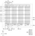
도 2를 참조하면, 표시 장치(10)는 복수의 배선들을 포함할 수 있다. 표시 장치(10)는 복수의 스캔 라인(SL; SL1, SL2, SL3)들, 복수의 데이터 라인(DTL; DTL1, DTL2, DTL3), 초기화 전압 배선(VIL), 및 복수의 전압 배선(VL; VL1, VL2, VL3, VL4)들을 포함할 수 있다. 또한, 도면에 도시되지 않았으나, 표시 장치(10)는 다른 배선들이 더 배치될 수 있다. 복수의 배선들은 제1 도전층으로 이루어지고 제1 방향(DR1)으로 연장된 배선들과, 제3 도전층으로 이루어지고 제2 방향(DR2)으로 연장된 배선들을 포함할 수 있다. 다만, 각 배선들의 연장 방향은 이에 제한되지 않는다.Referring to FIG. 2 , the
제1 스캔 라인(SL1)과 제2 스캔 라인(SL2)은 제1 방향(DR1)으로 연장되어 배치될 수 있다. 제1 스캔 라인(SL1)과 제2 스캔 라인(SL2)은 서로 인접한 상태로 배치되며, 다른 제1 스캔 라인(SL1) 및 제2 스캔 라인(SL2)과 제2 방향(DR2)으로 이격되어 배치될 수 있다. 제1 스캔 라인(SL1)과 제2 스캔 라인(SL2)은 스캔 구동부(미도시)에 연결된 스캔 배선 패드(WPD_SC)와 연결될 수 있다. 제1 스캔 라인(SL1)과 제2 스캔 라인(SL2)은 비표시 영역(NDA)에 배치된 패드 영역(PDA)으로부터 표시 영역(DPA)까지 연장되어 배치될 수 있다.The first scan line SL1 and the second scan line SL2 may be disposed to extend in the first direction DR1. The first scan line SL1 and the second scan line SL2 are disposed adjacent to each other and are spaced apart from the other first and second scan lines SL1 and SL2 in the second direction DR2. It can be. The first scan line SL1 and the second scan line SL2 may be connected to a scan wiring pad WPD_SC connected to a scan driver (not shown). The first scan line SL1 and the second scan line SL2 may extend from the pad area PDA disposed in the non-display area NDA to the display area DPA.
제3 스캔 라인(SL3)은 제2 방향(DR2)으로 연장되어 배치되고, 다른 제3 스캔 라인(SL3)과 제1 방향(DR1)으로 이격되어 배치될 수 있다. 하나의 제3 스캔 라인(SL3)은 하나 이상의 제1 스캔 라인(SL1), 또는 하나 이상의 제2 스캔 라인(SL2)과 연결될 수 있다. 복수의 스캔 라인(SL)들은 표시 영역(DPA) 전면에서 메쉬(Mesh) 구조를 가질 수 있으나, 이에 제한되지 않는다.The third scan line SL3 may extend in the second direction DR2 and be spaced apart from the other third scan lines SL3 in the first direction DR1. One third scan line SL3 may be connected to one or more first scan lines SL1 or one or more second scan lines SL2. The plurality of scan lines SL may have a mesh structure on the entire surface of the display area DPA, but is not limited thereto.
한편, 본 명세서에서 '연결'의 의미를 어느 한 부재가 다른 부재와 상호 물리적인 접촉을 통하여 연결되는 것뿐만 아니라, 다른 부재를 통하여 연결된 것을 의미할 수도 있다. 또한, 이는 일체화된 하나의 부재로서 어느 일 부분과 다른 부분은 일체화된 부재로 인하여 상호 연결된 것으로 이해될 수 있다. 나아가, 어느 한 부재와 다른 부재의 연결은 직접 접촉된 연결에 더하여 다른 부재를 통한 전기적 연결까지 포함하는 의미로 해석될 수 있다.On the other hand, in this specification, the meaning of 'connection' may mean that any one member is connected through mutual physical contact with another member as well as through another member. In addition, this may be understood as an integrated member, in which one part and the other part are interconnected due to the integrated member. Further, the connection between one member and another member may be interpreted as including an electrical connection through another member in addition to a direct contact connection.
데이터 라인(DTL)들은 제1 방향(DR1)으로 연장되어 배치될 수 있다. 데이터 라인(DTL)은 제1 데이터 라인(DTL1), 제2 데이터 라인(DTL2) 및 제3 데이터 라인(DTL3)을 포함하며, 하나의 제1 내지 제3 데이터 라인(DTL1, DTL2, DTL3)들은 하나의 쌍을 이루며 서로 인접하게 배치된다. 각 데이터 라인(DTL1, DTL2, DTL3)들은 비표시 영역(NDA)에 배치된 패드 영역(PDA)으로부터 표시 영역(DPA)까지 연장되어 배치될 수 있다. 다만, 이에 제한되지 않으며, 복수의 데이터 라인(DTL)들은 후술하는 제1 전압 배선(VL1)과 제2 전압 배선(VL2) 사이에서 등간격으로 이격되어 배치될 수도 있다.The data lines DTL may extend in the first direction DR1 and may be disposed. The data line DTL includes a first data line DTL1 , a second data line DTL2 , and a third data line DTL3 , and one of the first to third data lines DTL1 , DTL2 , and DTL3 are They form a pair and are placed adjacent to each other. Each of the data lines DTL1 , DTL2 , and DTL3 may be disposed to extend from the pad area PDA disposed in the non-display area NDA to the display area DPA. However, the present invention is not limited thereto, and the plurality of data lines DTL may be spaced apart at regular intervals between the first voltage line VL1 and the second voltage line VL2 to be described later.
초기화 전압 배선(VIL)은 제1 방향(DR1)으로 연장되어 배치될 수 있다. 초기화 전압 배선(VIL)은 데이터 라인(DTL)들과 제1 전압 배선(VL1) 사이에 배치될 수 있다. 초기화 전압 배선(VIL)은 비표시 영역(NDA)에 배치된 패드 영역(PDA)으로부터 표시 영역(DPA)까지 연장되어 배치될 수 있다.The initialization voltage line VIL may be disposed to extend in the first direction DR1. The initialization voltage line VIL may be disposed between the data lines DTL and the first voltage line VL1. The initialization voltage line VIL may be disposed to extend from the pad area PDA disposed in the non-display area NDA to the display area DPA.
제1 전압 배선(VL1) 및 제2 전압 배선(VL2)은 제1 방향(DR1)으로 연장되어 배치되고, 제3 전압 배선(VL3)과 제4 전압 배선(VL4)은 제2 방향(DR2)으로 연장되어 배치된다. 제1 전압 배선(VL1)과 제2 전압 배선(VL2)은 제2 방향(DR2)으로 교번되어 배치되고, 제3 전압 배선(VL3)과 제4 전압 배선(VL4)은 제1 방향(DR1)으로 교번되어 배치될 수 있다. 제1 전압 배선(VL1)과 제2 전압 배선(VL2)은 제1 방향(DR1)으로 연장되어 표시 영역(DPA)을 가로지르도록 배치되고, 제3 전압 배선(VL3)과 제4 전압 배선(VL4)은 각각 일부의 배선들은 표시 영역(DPA)에 배치되고 다른 배선들은 표시 영역(DPA)의 제1 방향(DR1) 양 측에 위치한 비표시 영역(NDA)에 배치될 수 있다. 제1 전압 배선(VL1)과 제2 전압 배선(VL2)은 제1 도전층으로 이루어지고, 제3 전압 배선(VL3)과 제4 전압 배선(VL4)은 제1 도전층과 다른 층에 배치된 제3 도전층으로 이루어질 수 있다. 제1 전압 배선(VL1)은 적어도 하나의 제3 전압 배선(VL3)과 연결되며, 제2 전압 배선(VL2)은 적어도 하나의 제4 전압 배선(VL4)과 복수의 전압 배선(VL)들은 표시 영역(DPA) 전면에서 메쉬(Mesh) 구조를 가질 수 있다. 다만, 이에 제한되지 않는다.The first voltage line VL1 and the second voltage line VL2 extend in the first direction DR1, and the third voltage line VL3 and the fourth voltage line VL4 extend in the second direction DR2. is extended and placed. The first voltage wire VL1 and the second voltage wire VL2 are alternately disposed in the second direction DR2, and the third voltage wire VL3 and the fourth voltage wire VL4 extend in the first direction DR1. can be arranged alternately. The first voltage line VL1 and the second voltage line VL2 extend in the first direction DR1 and are disposed to cross the display area DPA, and the third voltage line VL3 and the fourth voltage line ( VL4), some wires may be disposed in the display area DPA, and other wires may be disposed in the non-display area NDA located on both sides of the display area DPA in the first direction DR1. The first voltage wire VL1 and the second voltage wire VL2 are formed of the first conductive layer, and the third voltage wire VL3 and the fourth voltage wire VL4 are disposed on a different layer from the first conductive layer. It may be made of a third conductive layer. The first voltage line VL1 is connected to at least one third voltage line VL3, and the second voltage line VL2 is connected to at least one fourth voltage line VL4 and the plurality of voltage lines VL are displayed. The entire surface of the area DPA may have a mesh structure. However, it is not limited thereto.
제1 스캔 라인(SL1), 제2 스캔 라인(SL2), 데이터 라인(DTL), 초기화 전압 배선(VIL), 제1 전압 배선(VL1)과 제2 전압 배선(VL2)은 적어도 하나의 배선 패드(WPD)와 전기적으로 연결될 수 있다. 각 배선 패드(WPD)는 비표시 영역(NDA)에 배치될 수 있다. 일 실시예에서, 각 배선 패드(WPD)들은 표시 영역(DPA)의 제1 방향(DR1) 타 측인 하측에 위치한 패드 영역(PDA)에 배치될 수 있다. 제1 스캔 라인(SL1)과 제2 스캔 라인(SL2)은 패드 영역(PDA)에 배치된 스캔 배선 패드(WPD_SC)와 연결되고, 복수의 데이터 라인(DTL)들은 각각 서로 다른 데이터 배선 패드(WPD_DT)와 연결된다. 초기화 전압 배선(VIL)의 초기화 배선 패드(WPD_Vint)에 연결되며, 제1 전압 배선(VL1)은 제1 전압 배선 패드(WPD_VL1), 및 제2 전압 배선(VL2)은 제2 전압 배선 패드(WPD_VL2)와 연결된다. 배선 패드(WPD) 상에는 외부 장치가 실장될 수 있다. 외부 장치는 이방성 도전 필름, 초음파 접합 등을 통해 배선 패드(WPD) 상에 실장될 수 있다. 도면에서는 각 배선 패드(WPD)들이 표시 영역(DPA)의 하측에 배치된 패드 영역(PDA)에 배치된 것이 예시되어 있으나, 이에 제한되지 않는다. 복수의 배선 패드(WPD)들 중 일부는 표시 영역(DPA)의 상측, 또는 좌우측 어느 한 영역에 배치될 수도 있다.The first scan line SL1, the second scan line SL2, the data line DTL, the initialization voltage line VIL, and the first and second voltage lines VL1 and VL2 may include at least one wiring pad. (WPD) and can be electrically connected. Each wire pad WPD may be disposed in the non-display area NDA. In one embodiment, each wire pad WPD may be disposed in the pad area PDA located on the lower side of the display area DPA in the first direction DR1 . The first scan line SL1 and the second scan line SL2 are connected to the scan wiring pad WPD_SC disposed in the pad area PDA, and the plurality of data lines DTL are respectively different data wiring pads WPD_DT. ) is connected to It is connected to the initialization line pad WPD_Vint of the initialization voltage line VIL, the first voltage line VL1 is connected to the first voltage line pad WPD_VL1, and the second voltage line VL2 is connected to the second voltage line pad WPD_VL2. ) is connected to An external device may be mounted on the wiring pad WPD. An external device may be mounted on the wiring pad WPD through an anisotropic conductive film, ultrasonic bonding, or the like. In the drawing, it is illustrated that each wire pad WPD is disposed in the pad area PDA disposed below the display area DPA, but is not limited thereto. Some of the plurality of wire pads WPD may be disposed on either the upper side or the left and right sides of the display area DPA.
표시 장치(10)의 각 화소(PX) 또는 서브 화소(SPXn, n은 1 내지 3의 정수)는 화소 구동 회로를 포함한다. 상술한 배선들은 각 화소(PX) 또는 그 주위를 지나면서 각 화소 구동 회로에 구동 신호를 인가할 수 있다. 화소 구동 회로는 트랜지스터와 커패시터를 포함할 수 있다. 각 화소 구동 회로의 트랜지스터와 커패시터의 개수는 다양하게 변형될 수 있다. 일 실시예에 따르면, 표시 장치(10)의 각 서브 화소(SPXn)는 화소 구동 회로가 3개의 트랜지스터와 1개의 커패시터를 포함하는 3T1C 구조일 수 있다. 이하에서는 3T1C 구조를 예로 하여, 화소 구동 회로에 대해 설명하지만, 이에 제한되지 않고 2T1C 구조, 7T1C 구조, 6T1C 구조 등 다른 다양한 변형 구조가 적용될 수도 있다.Each pixel PX or sub-pixel SPXn (n is an integer of 1 to 3) of the
도 3 및 도 4는 일 실시예에 따른 표시 장치에 배치된 서브 화소의 화소 회로도들이다.3 and 4 are pixel circuit diagrams of sub-pixels disposed in a display device according to an exemplary embodiment.
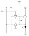
도 3을 참조하면, 일 실시예에 따른 표시 장치(10)의 각 서브 화소(SPXn)는 발광 다이오드(EL) 이외에, 3개의 트랜지스터(T1, T2, T3)와 1개의 스토리지 커패시터(Cst)를 포함한다.Referring to FIG. 3 , each sub-pixel SPXn of the
발광 다이오드(EL)는 제1 트랜지스터(T1)를 통해 공급되는 전류에 따라 발광한다. 발광 다이오드(EL)는 제1 전극, 제2 전극 및 이들 사이에 배치된 적어도 하나의 발광 소자를 포함한다. 상기 발광 소자는 제1 전극과 제2 전극으로부터 전달되는 전기 신호에 의해 특정 파장대의 광을 방출할 수 있다.The light emitting diode EL emits light according to the current supplied through the first transistor T1. The light emitting diode EL includes a first electrode, a second electrode, and at least one light emitting element disposed between them. The light emitting device may emit light of a specific wavelength range by electrical signals transmitted from the first electrode and the second electrode.
발광 다이오드(EL)의 일 단은 제1 트랜지스터(T1)의 소스 전극에 연결되고, 타 단은 제1 전압 배선(VL1)의 고전위 전압(이하, 제1 전원 전압)보다 낮은 저전위 전압(이하, 제2 전원 전압)이 공급되는 제2 전압 배선(VL2)에 연결될 수 있다.One end of the light emitting diode EL is connected to the source electrode of the first transistor T1, and the other end has a low potential voltage (hereinafter referred to as a first power supply voltage) lower than a high potential voltage (hereinafter, a first power supply voltage) of the first voltage line VL1. Hereinafter, a second power supply voltage) may be connected to the second voltage line VL2 to which it is supplied.
제1 트랜지스터(T1)는 게이트 전극과 소스 전극의 전압 차에 따라 제1 전원 전압이 공급되는 제1 전압 배선(VL1)으로부터 발광 다이오드(EL)로 흐르는 전류를 조정한다. 일 예로, 제1 트랜지스터(T1)는 발광 다이오드(EL)의 구동을 위한 구동 트랜지스터일 수 있다. 제1 트랜지스터(T1)의 게이트 전극은 제2 트랜지스터(T2)의 소스 전극에 연결되고, 소스 전극은 발광 다이오드(EL)의 제1 전극에 연결되며, 드레인 전극은 제1 전원 전압이 인가되는 제1 전압 배선(VL1)에 연결될 수 있다.The first transistor T1 adjusts the current flowing from the first voltage line VL1 to which the first power supply voltage is supplied to the light emitting diode EL according to the voltage difference between the gate electrode and the source electrode. For example, the first transistor T1 may be a driving transistor for driving the light emitting diode EL. The gate electrode of the first transistor T1 is connected to the source electrode of the second transistor T2, the source electrode is connected to the first electrode of the light emitting diode EL, and the drain electrode is connected to the first power supply voltage. 1 can be connected to the voltage wire (VL1).
제2 트랜지스터(T2)는 제1 스캔 라인(SL1)의 스캔 신호에 의해 턴-온되어 데이터 라인(DTL)을 제1 트랜지스터(T1)의 게이트 전극에 연결시킨다. 제2 트랜지스터(T2)의 게이트 전극은 제1 스캔 라인(SL1)에 연결되고, 소스 전극은 제1 트랜지스터(T1)의 게이트 전극에 연결되며, 드레인 전극은 데이터 라인(DTL)에 연결될 수 있다.The second transistor T2 is turned on by the scan signal of the first scan line SL1 and connects the data line DTL to the gate electrode of the first transistor T1. The gate electrode of the second transistor T2 may be connected to the first scan line SL1, the source electrode may be connected to the gate electrode of the first transistor T1, and the drain electrode may be connected to the data line DTL.
제3 트랜지스터(T3)는 제2 스캔 라인(SL2)의 스캔 신호에 의해 턴-온되어 초기화 전압 배선(VIL)을 발광 다이오드(EL)의 일 단에 연결시킨다. 제3 트랜지스터(T3)의 게이트 전극은 제2 스캔 라인(SL2)에 연결되고, 드레인 전극은 초기화 전압 배선(VIL)에 연결되며, 소스 전극은 발광 다이오드(EL)의 일 단 또는 제1 트랜지스터(T1)의 소스 전극에 연결될 수 있다.The third transistor T3 is turned on by the scan signal of the second scan line SL2 and connects the initialization voltage line VIL to one end of the light emitting diode EL. The gate electrode of the third transistor T3 is connected to the second scan line SL2, the drain electrode is connected to the initialization voltage line VIL, and the source electrode is connected to one end of the light emitting diode EL or the first transistor ( It may be connected to the source electrode of T1).
일 실시예에서, 각 트랜지스터(T1, T2, T3)들의 소스 전극과 드레인 전극은 상술한 바에 제한되지 않고, 그 반대의 경우일 수도 있다. 트랜지스터(T1, T2, T3)들 각각은 박막 트랜지스터(thin film transistor)로 형성될 수 있다. 도 3에서는 각 트랜지스터(T1, T2, T3)들이 N 타입 MOSFET(Metal Oxide Semiconductor Field Effect Transistor)으로 형성된 것을 중심으로 설명하였으나, 이에 제한되는 것은 아니다. 즉, 각 트랜지스터(T1, T2, T3)들은 P 타입 MOSFET으로 형성되거나, 일부는 N 타입 MOSFET으로, 다른 일부는 P 타입 MOSFET으로 형성될 수도 있다.In one embodiment, the source and drain electrodes of each of the transistors T1 , T2 , and T3 are not limited to those described above, and vice versa. Each of the transistors T1, T2, and T3 may be formed as a thin film transistor. In FIG. 3 , each of the transistors T1 , T2 , and T3 has been described based on being formed of an N-type MOSFET (Metal Oxide Semiconductor Field Effect Transistor), but is not limited thereto. That is, each of the transistors T1 , T2 , and T3 may be formed of P-type MOSFETs, some may be formed of N-type MOSFETs, and others may be formed of P-type MOSFETs.
스토리지 커패시터(Cst)는 제1 트랜지스터(T1)의 게이트 전극과 소스 전극 사이에 형성된다. 스토리지 커패시터(Cst)는 제1 트랜지스터(T1)의 게이트 전압과 소스 전압의 차전압을 저장한다.The storage capacitor Cst is formed between the gate electrode and the source electrode of the first transistor T1. The storage capacitor Cst stores a difference voltage between the gate voltage and the source voltage of the first transistor T1.
도 3의 실시예에서, 제2 트랜지스터(T2)의 게이트 전극은 제1 스캔 라인(SL1)에 연결되고, 제3 트랜지스터(T3)의 게이트 전극은 제2 스캔 라인(SL2)에 연결될 수 있다. 제1 스캔 라인(SL1)과 제2 스캔 라인(SL2)은 서로 다른 스캔 라인으로, 제2 트랜지스터(T2) 및 제3 트랜지스터(T3)는 서로 다른 스캔 라인에서 인가된 스캔 신호에 턴-온될 수 있다. 다만, 이에 제한되지 않는다.3 , the gate electrode of the second transistor T2 may be connected to the first scan line SL1, and the gate electrode of the third transistor T3 may be connected to the second scan line SL2. The first scan line SL1 and the second scan line SL2 are different scan lines, and the second and third transistors T2 and T3 may be turned on by scan signals applied from different scan lines. there is. However, it is not limited thereto.
도 4를 참조하면, 제2 트랜지스터(T2) 및 제3 트랜지스터(T3)의 게이트 전극은 서로 동일한 스캔 라인(SL)에 연결될 수 있다. 제2 트랜지스터(T2) 및 제3 트랜지스터(T3)는 동일한 스캔 라인에서 인가된 스캔 신호에 의해 동시에 턴-온될 수도 있다.Referring to FIG. 4 , gate electrodes of the second transistor T2 and the third transistor T3 may be connected to the same scan line SL. The second transistor T2 and the third transistor T3 may be simultaneously turned on by a scan signal applied from the same scan line.
도 5는 일 실시예에 따른 표시 장치의 화소들 및 발광 영역의 배치를 나타내는 평면도이다. 도 6은 일 실시예에 따른 표시 장치의 화소들 및 투광 영역의 배치를 나타내는 평면도이다.5 is a plan view illustrating arrangement of pixels and a light emitting region of a display device according to an exemplary embodiment. 6 is a plan view illustrating arrangement of pixels and a light transmission area of a display device according to an exemplary embodiment.
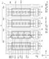
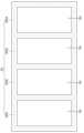
도 5 및 도 6을 참조하면, 표시 장치(10)는 복수의 화소(PX)들을 포함할 수 있다. 복수의 화소(PX)들은 행렬 방향으로 배열될 수 있다. 예를 들어, 서로 다른 화소(PX)들은 제1 방향(DR1) 및 제2 방향(DR2)으로 배열될 수 있다. 각 화소(PX)의 형상은 평면상 직사각형 또는 정사각형일 수 있지만, 이에 제한되는 것은 아니고 각 변이 일 방향에 대해 기울어진 마름모 형상일 수도 있다. 각 화소(PX)는 스트라이프 타입 또는 아일랜드 타입으로 배열될 수 있다. 또한, 화소(PX)들 각각은 특정 파장대의 광을 방출하는 발광 소자를 하나 이상 포함하여 특정 색을 표시할 수 있다.Referring to FIGS. 5 and 6 , the
화소(PX)들 각각은 복수의 서브 화소(SPXn)들을 포함할 수 있다. 예를 들어, 하나의 화소(PX)는 제1 서브 화소(SPX1), 제2 서브 화소(SPX2), 제3 서브 화소(SPX3) 및 제4 서브 화소(SPX4)를 포함할 수 있다. 제1 서브 화소(SPX1), 제2 서브 화소(SPX2), 제3 서브 화소(SPX3) 및 제4 서브 화소(SPX4)는 서로 제2 방향(DR2)으로 이격되어 배열될 수 있다. 제1 서브 화소(SPX1), 제2 서브 화소(SPX2), 제3 서브 화소(SPX3) 및 제4 서브 화소(SPX4)들 각각은 서로 제1 방향(DR1)으로 반복되어 배열될 수 있다. 다만, 이에 제한되지 않는다. 각 서브 화소(SPXn)들의 배치, 및 배열은 표시 장치(10)의 화소(PX)들 배치 및 형상에 따라 달라질 수도 있다. 도면에서는 하나의 화소(PX)가 4개의 서브 화소(SPXn)들을 포함하는 것을 예시하였으나, 이에 제한되지 않고, 화소(PX)는 더 많은 수의 서브 화소(SPXn)들을 포함할 수 있다. Each of the pixels PX may include a plurality of sub-pixels SPXn. For example, one pixel PX may include a first sub-pixel SPX1 , a second sub-pixel SPX2 , a third sub-pixel SPX3 , and a fourth sub-pixel SPX4 . The first sub-pixel SPX1 , the second sub-pixel SPX2 , the third sub-pixel SPX3 , and the fourth sub-pixel SPX4 may be arranged spaced apart from each other in the second direction DR2 . Each of the first sub-pixel SPX1 , the second sub-pixel SPX2 , the third sub-pixel SPX3 , and the fourth sub-pixel SPX4 may be repeatedly arranged in the first direction DR1 . However, it is not limited thereto. The arrangement and arrangement of each sub-pixel SPXn may vary according to the arrangement and shape of the pixels PXs of the
각 서브 화소(SPXn)들은 발광 영역(EMA1, EMA2, EMA3, EMA4)과 비발광 영역을 포함할 수 있다. 발광 영역(EMA)은 발광 소자(ED)가 배치되어 특정 파장대의 광이 생성되는 영역일 수 있다. 비발광 영역은 발광 소자(ED)가 배치되지 않고, 발광 소자(ED)에서 방출된 광들이 도달하지 않아 출사되지 않는 영역일 수 있다. 제1 서브 화소(SPX1)는 제1 발광 영역(EMA1)을 포함하고, 제2 서브 화소(SPX2)는 제2 발광 영역(EMA2)을 포함하고, 제3 서브 화소(SPX3)는 제3 발광 영역(EMA3)을 포함하며, 제4 서브 화소(SPX4)는 제4 발광 영역(EMA4)을 포함할 수 있다. 화소(PX)의 비발광 영역은 각 서브 화소(SPXn)들의 발광 영역(EMA1, EMA2, EMA3, EMA4) 이외의 영역일 수 있다.Each sub-pixel SPXn may include light emitting areas EMA1 , EMA2 , EMA3 , and EMA4 and a non-emitting area. The light emitting area EMA may be an area where the light emitting device ED is disposed to generate light of a specific wavelength range. The non-emission area may be an area in which the light emitting device ED is not disposed and the light emitted from the light emitting device ED does not reach and is not emitted. The first sub-pixel SPX1 includes the first light-emitting area EMA1, the second sub-pixel SPX2 includes the second light-emitting area EMA2, and the third sub-pixel SPX3 includes the third light-emitting area. (EMA3), and the fourth sub-pixel SPX4 may include the fourth light emitting region EMA4. The non-emission area of the pixel PX may be an area other than the emission areas EMA1 , EMA2 , EMA3 , and EMA4 of each sub-pixel SPXn.
각 서브 화소(SPXn)들은 발광 영역(EMA1, EMA2, EMA3, EMA4)에 대응되는 투광 영역(TA1, TA2, TA3, TA4) 및 비발광 영역에 대응되는 차광 영역(BA)을 포함할 수 있다. 투광 영역(TA1, TA2, TA3, TA4)은 발광 영역(EMA1, EMA2, EMA3, EMA4)에서 생성된 광이 각 서브 화소(SPXn)에서 출사되는 영역이고, 차광 영역(BA)은 광이 출사되지 않는 영역일 수 있다. 제1 서브 화소(SPX1)는 제1 투광 영역(TA1)을 포함하고, 제2 서브 화소(SPX2)는 제2 투광 영역(TA2)을 포함하고, 제3 서브 화소(SPX3)는 제3 투광 영역(TA3)을 포함하며, 제4 서브 화소(SPX4)는 제4 투광 영역(TA4)을 포함할 수 있다. 화소(PX)의 차광 영역(BA)은 각 서브 화소(SPXn)들의 투광 영역(TA1, TA2, TA3, TA4) 이외의 영역일 수 있다.Each of the sub-pixels SPXn may include light-transmitting areas TA1 , TA2 , TA3 , and TA4 corresponding to the light-emitting areas EMA1 , EMA2 , EMA3 , and EMA4 and a light-blocking area BA corresponding to the non-emission area. The light-transmitting areas TA1, TA2, TA3, and TA4 are areas from which light generated in the light-emitting areas EMA1, EMA2, EMA3, and EMA4 are emitted from each sub-pixel SPXn, and the light-blocking area BA is not emitted. It may be an area that does not exist. The first sub-pixel SPX1 includes the first light-transmitting area TA1, the second sub-pixel SPX2 includes the second light-transmitting area TA2, and the third sub-pixel SPX3 includes the third light-transmitting area. TA3 , and the fourth sub-pixel SPX4 may include a fourth light-transmitting area TA4 . The blocking area BA of the pixel PX may be an area other than the transmissive areas TA1 , TA2 , TA3 , and TA4 of each sub-pixel SPXn.
각 서브 화소(SPXn)의 투광 영역(TA1, TA2, TA3, TA4)은 발광 영역(EMA1, EMA2, EMA3, EMA4)들 각각에 대응될 수 있으나, 반드시 그렇지는 않을 수 있다. 예를 들어, 각 서브 화소(SPXn)의 투광 영역(TA1, TA2, TA3, TA4)은 발광 영역(EMA1, EMA2, EMA3, EMA4)과 각각 중첩하거나 동일한 형상을 갖지 않을 수도 있다. 표시 장치(10)의 각 화소(PX) 및 서브 화소(SPXn)에서 발광 영역(EMA1, EMA2, EMA3, EMA4)은 후술하는 발광 소자(ED, 도 9에 도시)들이 배치되어 광이 방출되는 영역이고, 투광 영역(TA1, TA2, TA3, TA4)은 상기 광들이 출사되어 서브 화소(SPXn)에서 광이 표시되는 영역일 수 있다.The light-transmitting areas TA1 , TA2 , TA3 , and TA4 of each sub-pixel SPXn may correspond to the light-emitting areas EMA1 , EMA2 , EMA3 , and EMA4 , respectively, but this may not necessarily be the case. For example, the light-transmitting areas TA1 , TA2 , TA3 , and TA4 of each sub-pixel SPXn may overlap or not have the same shape as the light-emitting areas EMA1 , EMA2 , EMA3 , and EMA4 . The light-emitting areas EMA1, EMA2, EMA3, and EMA4 of each pixel PX and sub-pixel SPXn of the
표시 장치(10)는 광이 방출되는 발광 영역(EMA1, EMA2, EMA3, EMA4)과 상기 광들이 출사되는 투광 영역(TA1, TA2, TA3, TA4)을 포함할 수 있다. 각 서브 화소(SPXn)의 발광 영역(EMA1, EMA2, EMA3, EMA4) 및 투광 영역(TA1, TA2, TA3, TA4)은 서로 다른 색의 광이 방출되고 출사될 수 있다. 예를 들어, 표시 장치(10)는 각 서브 화소(SPXn)에 배치된 발광 소자(ED)들은 서로 동일한 색의 광을 방출하는 반면, 각 서브 화소(SPXn)에서 출사되는 광들은 서로 다른 색을 가질 수 있다.The
도 7은 일 실시예에 따른 일 화소에 배치된 발광 영역들을 개략적으로 나타내는 평면도이다. 도 8은 일 실시예에 따른 일 화소에 배치된 투광 영역들을 개략적으로 나타내는 평면도이다.7 is a plan view schematically illustrating light emitting regions disposed in one pixel according to an exemplary embodiment. 8 is a plan view schematically illustrating light-transmitting areas disposed in one pixel according to an exemplary embodiment.
도 7 및 도 8을 참조하면, 표시 장치(10)는 각 서브 화소(SPXn)들의 발광 영역(EMA1, EMA2, EMA3, EMA4)에서 방출되는 광들은 서로 동일한 색, 또는 실질적으로 동일한 중심 파장 대역을 가질 수 있다. 다만, 발광 영역(EMA#)에서 방출된 광들은 서브 화소(SPXn)에 배치된 컬러 제어 구조물(도 12 내지 도 14에 도시)을 통해 다른 색 또는 중심 파장 대역을 갖는 광으로 변환되어 투광 영역(TA#)에서 출사될 수 있다.Referring to FIGS. 7 and 8 , the
예를 들어, 제1 서브 화소(SPX1)는 제1 색의 광이 출사되고, 제3 서브 화소(SPX3)는 제2 색의 광이 출사되고, 제4 서브 화소(SPX4)는 제3 색의 광이 출사될 수 있다. 제2 서브 화소(SPX2)는 제1 색의 광, 제2 색의 광, 및 제3 색의 광이 각각 출사되거나, 이들이 혼합된 혼합광인 제4 색의 광이 출사될 수 있다. 일 예로, 제1 색은 적색, 제2 색은 녹색, 제3 색은 청색일 수 있다. 다만, 각 서브 화소(SPXn)들은 동일한 발광 소자(ED)를 포함하고, 발광 영역(EMA#)들은 동일한 색의 광, 예를 들어 제3 색의 청색 광을 방출할 수 있다. 각 서브 화소(SPXn)의 발광 소자(ED)가 방출하는 제3 색의 청색 광들 중 일부는 서브 화소(SPXn)에 배치된 컬러 제어 구조물을 통해 제3 색과 다른 색, 또는 중심 파장 대역을 갖는 광으로 변환되어 출사될 수 있다.For example, the first sub-pixel SPX1 emits light of a first color, the third sub-pixel SPX3 emits light of a second color, and the fourth sub-pixel SPX4 emits light of a third color. Light may be emitted. The second sub-pixel SPX2 may emit light of the first color, light of the second color, and light of the third color, respectively, or light of a fourth color, which is a mixed light of the mixed light. For example, the first color may be red, the second color may be green, and the third color may be blue. However, each sub-pixel SPXn may include the same light emitting element ED, and the light emitting regions EMA# may emit light of the same color, for example, blue light of the third color. Some of the blue light of the third color emitted from the light emitting device ED of each sub-pixel SPXn has a color different from the third color or a central wavelength band through the color control structure disposed in the sub-pixel SPXn. It can be converted into light and emitted.
일 실시예에 따르면, 제1 서브 화소(SPX1)에 배치된 발광 소자(ED)에서 방출된 광은 제1 색의 적색 광으로 변환되어 제1 투광 영역(TA1)에서 출사되고, 제3 서브 화소(SPX3)에 배치된 발광 소자(ED)에서 방출된 광은 제2 색의 녹색 광으로 변환되어 제3 투광 영역(TA3)에서 출사될 수 있다. 제4 서브 화소(SPX4)에 배치된 발광 소자(ED)에서 방출된 광은 변환되지 않고 제3 색의 청색 광으로 제4 투광 영역(TA4)에서 출사될 수 있다.According to an embodiment, the light emitted from the light emitting device ED disposed in the first sub-pixel SPX1 is converted into red light of a first color and emitted from the first light-transmitting area TA1, and the third sub-pixel Light emitted from the light emitting device ED disposed on SPX3 may be converted into green light of a second color and emitted from the third light transmitting area TA3 . Light emitted from the light emitting element ED disposed in the fourth sub-pixel SPX4 may be emitted from the fourth light-transmitting area TA4 as blue light of a third color without being converted.
제2 서브 화소(SPX2)에 배치된 발광 소자(ED)에서 방출된 광은 일부는 제1 색의 적색 광으로 변환되고, 다른 일부는 제2 색의 녹색 광으로 변환되며, 또 다른 일부는 변환되지 않고 제3 색의 청색 광으로 출사될 수 있다. 제2 서브 화소(SPX2)의 제2 투광 영역(TA2)에서는 제1 색의 적색 광, 제2 색의 녹색 광, 및 제3 색의 청색 광이 각각, 또는 이들이 혼합되어 출사될 수 있다. 제2 서브 화소(SPX2)의 제2 투광 영역(TA2)은 제1 색의 광이 출사되는 제1 서브 투광 영역(STA1), 제2 색의 광이 출사되는 제2 서브 투광 영역(STA2), 및 제3 색의 광이 출사되는 제3 서브 투광 영역(STA3)을 포함할 수 있다. 제2 서브 영역(SPX2)의 제2 투광 영역(TA2)에서 제1 내지 제3 서브 투광 영역(STA1, STA2, STA3)은 제1 방향(DR1)으로 서로 이격되거나, 맞닿아 배치될 수 있다. 다만, 제2 투광 영역(TA2)이 복수의 서브 투광 영역(STA1, STA2, STA3)들을 포함하더라도 서브 투광 영역(STA1, STA2, STA3)들이 물리적인 계면을 형성하며 구분되지 않을 수 있다. 도면에 도시된 복수의 서브 투광 영역(STA1, STA2, STA3)들은 후술하는 제2 서브 화소(SPX2)에 배치된 컬러 제어 구조물(도 12 내지 도 14에 도시)들에 대응하여 구분되는 영역으로서, 표시 장치(10)의 제2 서브 화소(SPX2)에서 물리적으로 구분되지 않고 하나의 제2 투광 영역(TA2)을 형성할 수 있다. 다만, 이에 제한되지 않으며, 제2 서브 화소(SPX2)에 배치된 뱅크층(BNL)의 구조에 따라 제2 투광 영역(TA2)은 물리적으로 이격된 복수의 서브 투광 영역(STA1, STA2, STA3)들을 포함할 수도 있다.Some of the light emitted from the light emitting device ED disposed in the second sub-pixel SPX2 is converted into red light of the first color, another part is converted into green light of the second color, and another part is converted into green light of the second color. and may be emitted as blue light of the third color. Red light of the first color, green light of the second color, and blue light of the third color may be emitted from the second light transmission area TA2 of the second sub-pixel SPX2, respectively, or a mixture thereof. The second light-transmitting area TA2 of the second sub-pixel SPX2 includes a first sub-transmitting area STA1 through which light of a first color is emitted, a second sub-transmitting area STA2 through which light of a second color is emitted, and and a third sub light-transmitting area STA3 through which light of a third color is emitted. In the second light-transmitting area TA2 of the second sub-area SPX2, the first to third sub-light-transmitting areas STA1, STA2, and STA3 may be spaced apart from each other in the first direction DR1 or may be in contact with each other. However, even if the second light-transmitting area TA2 includes a plurality of sub-light-transmitting areas STA1, STA2, and STA3, the sub-light-transmitting areas STA1, STA2, and STA3 form a physical interface and may not be distinguished. The plurality of sub light-transmitting areas STA1, STA2, and STA3 shown in the figure are divided corresponding to color control structures (shown in FIGS. 12 to 14) disposed in a second sub-pixel SPX2 to be described later, In the second sub-pixel SPX2 of the
표시 장치(10)는 각 화소(PX)들이 서로 다른 색의 광이 출사되는 서브 화소(예를 들어, 제1 서브 화소(SPX1), 제3 서브 화소(SPX3), 및 제4 서브 화소(SPX4))에 더하여, 서로 다른 색의 광이 동시에 출사되거나 혼합되어 출사되는 서브 화소(예를 들어, 제2 서브 화소(SPX2))를 포함할 수 있다. 이는 표시 장치(10)의 각 서브 화소(SPXn)들이 갖는 발광 소자(ED)들의 배치, 및 컬러 제어 구조물들의 배치에 따라 달라질 수 있다.In the
이하, 표시 장치(10)에 배치된 화소(PX) 및 서브 화소(SPXn)들의 구조에 대하여 상세히 설명하기로 한다.Hereinafter, structures of the pixels PX and the sub-pixels SPXn disposed in the
도 9는 일 실시예에 따른 표시 장치의 일 화소를 나타내는 평면도이다.9 is a plan view illustrating one pixel of a display device according to an exemplary embodiment.
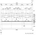
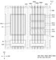
도 9는 표시 장치(10)의 일 화소(PX)에 배치된 전극(RME: RME1, RME2)들, 격벽(BP1, BP2)들과 뱅크층(BNL), 복수의 발광 소자(ED)들 및 연결 전극(CNE: CNE1, CNE2)의 평면 배치를 도시하고 있다.9 illustrates electrodes RME (RME1 and RME2) disposed in one pixel PX of the
도 9를 참조하면, 표시 장치(10)의 화소(PX)들 각각은 복수의 서브 화소(SPXn)들을 포함할 수 있다. 예를 들어, 하나의 화소(PX)는 제1 서브 화소(SPX1), 제2 서브 화소(SPX2), 제3 서브 화소(SPX3) 및 제4 서브 화소(SPX4)를 포함할 수 있다. 각 서브 화소(SPXn)들의 배치 및 이들이 표시하는 색에 대한 설명은 상술한 바와 동일하다. 도면에서는 서로 다른 색의 광들이 동시, 또는 혼합되어 출사되는 제2 서브 화소(SPX2)가 제1 서브 화소(SPX1) 및 제3 서브 화소(SPX3) 사이에 배치된 것이 예시되어 있으나, 이에 제한되지 않는다. 제2 서브 화소(SPX2)의 위치는 달라질 수 있다.Referring to FIG. 9 , each of the pixels PX of the
표시 장치(10)의 각 서브 화소(SPXn)들은 발광 영역(EMA) 및 비발광 영역을 포함할 수 있다. 발광 영역(EMA)은 발광 소자(ED)가 배치되어 특정 파장대의 광이 출사되는 영역일 수 있다. 비발광 영역은 발광 소자(ED)가 배치되지 않고, 발광 소자(ED)에서 방출된 광들이 도달하지 않아 출사되지 않는 영역일 수 있다.Each sub-pixel SPXn of the
발광 영역(EMA)은 발광 소자(ED)가 배치된 영역과, 발광 소자(ED)와 인접한 영역으로 발광 소자(ED)에서 방출된 광들이 출사되는 영역을 포함할 수 있다. 예를 들어, 발광 영역(EMA)은 발광 소자(ED)에서 방출된 광이 다른 부재에 의해 반사되거나 굴절되어 출사되는 영역도 포함할 수 있다. 복수의 발광 소자(ED)들은 각 서브 화소(SPXn)에 배치되고, 이들이 배치된 영역과 이에 인접한 영역을 포함하여 발광 영역을 형성할 수 있다.The light emitting area EMA may include an area where the light emitting device ED is disposed, and an area adjacent to the light emitting device ED and from which light emitted from the light emitting device ED is emitted. For example, the light emitting area EMA may also include an area in which light emitted from the light emitting device ED is reflected or refracted by another member to be emitted. A plurality of light emitting devices ED may be disposed in each sub-pixel SPXn, and may form an emission area including an area in which they are disposed and an area adjacent thereto.
도면에서는 각 서브 화소(SPXn)의 발광 영역(EMA)들이 서로 균일한 면적을 갖는 것이 예시되어 있으나, 이에 제한되지 않는다. 몇몇 실시예에서, 각 서브 화소(SPXn)의 각 발광 영역(EMA)들은 해당 서브 화소에 배치된 발광 소자(ED)에서 방출된 광의 색 또는 파장대에 따라 서로 다른 면적을 가질 수도 있다.In the drawing, it is exemplified that the light emitting regions EMA of each sub-pixel SPXn have a uniform area, but is not limited thereto. In some embodiments, each light emitting area EMA of each sub pixel SPXn may have a different area according to the color or wavelength band of light emitted from the light emitting device ED disposed in the corresponding sub pixel.
각 서브 화소(SPXn)는 비발광 영역에 배치된 서브 영역(SA)을 더 포함할 수 있다. 해당 서브 화소(SPXn)의 서브 영역(SA)은 발광 영역(EMA)의 제1 방향(DR1) 타 측인 하측에 배치될 수 있다. 발광 영역(EMA)과 서브 영역(SA)은 제1 방향(DR1)을 따라 교번되어 배열되며, 제1 방향(DR1)으로 이격된 서로 다른 서브 화소(SPXn)의 발광 영역(EMA) 사이에는 서브 영역(SA)이 배치될 수 있다. 예를 들어, 발광 영역(EMA)과 서브 영역(SA)은 서로 제1 방향(DR1)으로 교대 배열되고, 발광 영역(EMA) 및 서브 영역(SA) 각각은 제2 방향(DR2)으로 반복 배열될 수 있다. 다만, 이에 제한되지 않고, 복수의 화소(PX)들에서 발광 영역(EMA)들과 서브 영역(SA)들은 도 9와 다른 배열을 가질 수도 있다.Each sub-pixel SPXn may further include a sub-region SA disposed in the non-emission area. The sub-region SA of the corresponding sub-pixel SPXn may be disposed on the lower side, which is the other side of the emission area EMA in the first direction DR1 . The light emitting area EMA and the sub area SA are alternately arranged along the first direction DR1, and between the light emitting areas EMA of the different sub pixels SPXn spaced apart in the first direction DR1 are sub An area SA may be disposed. For example, the light emitting area EMA and the sub area SA are alternately arranged in the first direction DR1, and each of the light emitting area EMA and the sub area SA is repeatedly arranged in the second direction DR2. It can be. However, the present invention is not limited thereto, and the emission areas EMAs and sub areas SA in the plurality of pixels PX may have a different arrangement from that of FIG. 9 .
서브 영역(SA)에는 발광 소자(ED)가 배치되지 않아 광이 출사되지 않으나, 각 서브 화소(SPXn)에 배치된 전극(RME) 일부가 배치될 수 있다. 서로 다른 서브 화소(SPXn)에 배치되는 전극(RME)들은 서브 영역(SA)의 분리부(ROP) 서로 분리되어 배치될 수 있다.Although the light emitting device ED is not disposed in the sub area SA, light is not emitted, but a portion of the electrode RME disposed in each sub pixel SPXn may be disposed. The electrodes RME disposed in different sub-pixels SPXn may be disposed to be separated from each other in the separator ROP of the sub-region SA.
표시 장치(10)는 복수의 전극(RME: RME1, RME2)들, 격벽(BP1, BP2)들, 뱅크층(BNL), 발광 소자(ED)들, 및 연결 전극(CNE: CNE1, CNE2)들을 포함할 수 있다.The
복수의 격벽(BP1, BP2)들은 각 서브 화소(SPXn)의 발광 영역(EMA)에 배치될 수 있다. 격벽(BP1, BP2)들은 대체로 제1 방향(DR1)으로 연장되고, 서로 제2 방향(DR2)을 이격되어 배치될 수 있다.A plurality of barrier ribs BP1 and BP2 may be disposed in the light emitting area EMA of each sub-pixel SPXn. The barrier ribs BP1 and BP2 generally extend in the first direction DR1 and may be spaced apart from each other in the second direction DR2 .
예를 들어, 격벽(BP1, BP2)들은 각 서브 화소(SPXn)의 발광 영역(EMA) 내에서 서로 제2 방향(DR2)으로 이격된 제1 격벽(BP1), 및 제2 격벽(BP2)을 포함할 수 있다. 제1 격벽(BP1)은 발광 영역(EMA)의 중심에서 제2 방향(DR2)의 일 측인 좌측에 배치되고, 제2 격벽(BP2)들은 제1 격벽(BP1)과 이격되어 발광 영역(EMA)의 중심에서 제2 방향(DR2)의 타 측인 우측에 배치될 수 있다. 제1 격벽(BP1)과 제2 격벽(BP2)은 제2 방향(DR2)을 따라 서로 교대로 배치되며, 표시 영역(DPA)에서 섬형의 패턴으로 배치될 수 있다. 제1 격벽(BP1)과 제2 격벽(BP2) 사이에는 복수의 발광 소자(ED)들이 배치될 수 있다.For example, the barrier ribs BP1 and BP2 include the first barrier rib BP1 and the second barrier rib BP2 spaced apart from each other in the second direction DR2 within the emission area EMA of each sub-pixel SPXn. can include The first barrier rib BP1 is disposed on the left side in the second direction DR2 from the center of the light emitting area EMA, and the second barrier ribs BP2 are spaced apart from the first barrier rib BP1 to form the light emitting area EMA. It may be disposed on the right side, which is the other side of the second direction DR2, from the center of . The first barrier rib BP1 and the second barrier rib BP2 are alternately disposed along the second direction DR2 and may be disposed in an island-like pattern in the display area DPA. A plurality of light emitting elements ED may be disposed between the first barrier rib BP1 and the second barrier rib BP2 .
제1 격벽(BP1)과 제2 격벽(BP2)은 제1 방향(DR1) 길이는 서로 동일하되, 뱅크층(BNL)이 둘러싸는 발광 영역(EMA)의 제1 방향(DR1) 길이보다 작을 수 있다. 제1 격벽(BP1)과 제2 격벽(BP2)은 뱅크층(BNL) 중 제2 방향(DR2)으로 연장된 부분과 이격될 수 있다. 다만, 이에 제한되지 않고, 격벽(BP1, BP2)들은 뱅크층(BNL)과 일체화되거나, 뱅크층(BNL)의 제2 방향(DR2)으로 연장된 부분과 일부 중첩할 수도 있다. 이 경우, 격벽(BP1, BP2)들의 제1 방향(DR1) 길이는 뱅크층(BNL)이 둘러싸는 발광 영역(EMA)의 제1 방향(DR1) 길이와 동일하거나 더 클 수 있다.The first and second barrier ribs BP1 and BP2 may have the same length in the first direction DR1 but may be shorter than the length in the first direction DR1 of the light emitting region EMA surrounded by the bank layer BNL. there is. The first barrier rib BP1 and the second barrier rib BP2 may be spaced apart from a portion of the bank layer BNL extending in the second direction DR2 . However, it is not limited thereto, and the barrier ribs BP1 and BP2 may be integrated with the bank layer BNL or partially overlap a portion of the bank layer BNL extending in the second direction DR2. In this case, the length of the barrier ribs BP1 and BP2 in the first direction DR1 may be equal to or greater than the length of the light emitting area EMA surrounded by the bank layer BNL in the first direction DR1.
도면에서는 각 서브 화소(SPXn)마다 2개의 격벽(BP1, BP2)이 배치된 것이 예시되어 있으나, 이에 제한되지 않는다. 격벽(BP1, BP2)들의 개수 및 형상은 전극(RME)들의 개수 또는 배치 구조에 따라 달라질 수 있다.In the drawing, it is exemplified that two barrier ribs BP1 and BP2 are disposed for each sub-pixel SPXn, but is not limited thereto. The number and shape of the barrier ribs BP1 and BP2 may vary depending on the number or arrangement structure of the electrodes RME.
복수의 전극(RME: RME1, RME2)들은 일 방향으로 연장된 형상으로 각 서브 화소(SPXn)마다 배치된다. 복수의 전극(RME1, RME2)들은 제1 방향(DR1)으로 연장되어 서브 화소(SPXn)의 발광 영역(EMA) 및 서브 영역(SA)에 배치될 수 있으며, 이들은 서로 제2 방향(DR2)으로 이격되어 배치될 수 있다. 복수의 전극(RME)들은 후술하는 발광 소자(ED)와 전기적으로 연결될 수 있다. 다만, 이에 제한되지 않으며, 전극(RME)들은 발광 소자(ED)와 전기적으로 연결되지 않을 수도 있다.A plurality of electrodes RME (RME1, RME2) are disposed in each sub-pixel SPXn in a shape extending in one direction. The plurality of electrodes RME1 and RME2 extend in the first direction DR1 and may be disposed in the light emitting area EMA and the sub area SA of the sub pixel SPXn, and they extend in the second direction DR2. They can be spaced apart. The plurality of electrodes RME may be electrically connected to a light emitting element ED to be described later. However, it is not limited thereto, and the electrodes RME may not be electrically connected to the light emitting element ED.
표시 장치(10)는 각 서브 화소(SPXn)에 배치된 제1 전극(RME1) 및 제2 전극(RME2)을 포함할 수 있다. 제1 전극(RME1)은 발광 영역(EMA)의 중심에서 좌측에 배치되고, 제2 전극(RME2)은 제1 전극(RME1)과 제2 방향(DR2)으로 이격되어 발광 영역(EMA)의 중심에서 우측에 배치된다. 제1 전극(RME1)은 제1 격벽(BP1) 상에 배치되고, 제2 전극(RME2)은 제2 격벽(BP2) 상에 배치될 수 있다. 제1 전극(RME1)과 제2 전극(RME2)은 뱅크층(BNL)을 넘어 해당 서브 화소(SPXn) 및 서브 영역(SA)에 부분적으로 배치될 수 있다. 서로 다른 서브 화소(SPXn)의 제1 전극(RME1)과 제2 전극(RME2)은 어느 한 서브 화소(SPXn)의 서브 영역(SA) 내에 위치한 분리부(ROP)에서 서로 이격되거나 분리될 수 있다.The
도면에서는 각 서브 화소(SPXn)마다 2개의 전극(RME)들이 제1 방향(DR1)으로 연장된 형상을 갖는 것이 예시되어 있으나, 이에 제한되지 않는다. 예를 들어, 표시 장치(10)는 하나의 서브 화소(SPXn)에 더 많은 수의 전극(RME)들이 배치되거나, 전극(RME)들이 부분적으로 절곡되고, 위치에 따라 폭이 다른 형상을 가질 수도 있다.In the figure, it is illustrated that two electrodes RME for each sub-pixel SPXn have a shape extending in the first direction DR1, but is not limited thereto. For example, the
뱅크층(BNL)은 복수의 서브 화소(SPXn)들, 및 발광 영역(EMA)과 서브 영역(SA)을 둘러싸도록 배치될 수 있다. 뱅크층(BNL)은 제1 방향(DR1) 및 제2 방향(DR2)으로 인접한 서브 화소(SPXn)들의 경계에 배치될 수 있고, 발광 영역(EMA)과 서브 영역(SA)의 경계에도 배치될 수 있다. 표시 장치(10)의 서브 화소(SPXn)들, 발광 영역(EMA) 및 서브 영역(SA)은 뱅크층(BNL)의 배치에 의해 구분되는 영역들일 수 있다. 복수의 서브 화소(SPXn)들과 발광 영역(EMA)들, 및 서브 영역(SA)들 사이의 간격은 뱅크층(BNL)의 폭에 따라 달라질 수 있다.The bank layer BNL may be disposed to surround the plurality of sub-pixels SPXn, the light emitting area EMA, and the sub area SA. The bank layer BNL may be disposed on a boundary between adjacent sub-pixels SPXn in the first and second directions DR1 and DR2, and may also be disposed on a boundary between the emission area EMA and the sub-region SA. can The sub-pixels SPXn, the emission area EMA, and the sub-area SA of the
뱅크층(BNL)은 평면상 제1 방향(DR1) 및 제2 방향(DR2)으로 연장된 부분을 포함하여 표시 영역(DPA) 전면에서 격자형 패턴으로 배치될 수 있다. 뱅크층(BNL)은 각 서브 화소(SPXn)들의 경계에 걸쳐 배치되어 이웃하는 서브 화소(SPXn)들을 구분할 수 있다. 또한, 뱅크층(BNL)은 서브 화소(SPXn)마다 배치된 발광 영역(EMA)과 서브 영역(SA)을 둘러싸도록 배치되어 이들을 구분할 수 있다. 후술할 바와 같이, 뱅크층(BNL)은 표시 장치(10)의 컬러 제어 구조물들이 배치되는 영역을 형성할 수도 있다.The bank layer BNL may be disposed in a lattice pattern on the entire surface of the display area DPA, including portions extending in the first and second directions DR1 and DR2 on a plan view. The bank layer BNL may be disposed across the boundary of each sub-pixel SPXn to distinguish neighboring sub-pixels SPXn. In addition, the bank layer BNL is disposed to surround the light emitting area EMA and the sub area SA disposed in each sub pixel SPXn to distinguish them. As will be described later, the bank layer BNL may form an area where color control structures of the
복수의 발광 소자(ED)들은 발광 영역(EMA)에 배치될 수 있다. 발광 소자(ED)들은 격벽(BP1, BP2)들 사이에 배치되며, 서로 제1 방향(DR1)으로 이격되어 배열될 수 있다. 일 실시예에서, 복수의 발광 소자(ED)들은 일 방향으로 연장된 형상을 가질 수 있고, 양 단부가 각각 서로 다른 전극(RME)들 상에 배치될 수 있다. 발광 소자(ED)는 길이가 제2 방향(DR2)으로 이격된 전극(RME)들 사이의 간격보다 길 수 있다. 발광 소자(ED)들은 대체로 연장된 방향이 전극(RME)들이 연장된 제1 방향(DR1)에 수직하게 배열될 수 있다. 다만, 이에 제한되지 않으며, 발광 소자(ED)의 연장된 방향은 제2 방향(DR2) 또는 그에 비스듬히 기울어진 방향을 향하도록 배치될 수 있다.A plurality of light emitting elements ED may be disposed in the light emitting area EMA. The light emitting elements ED may be disposed between the barrier ribs BP1 and BP2 and spaced apart from each other in the first direction DR1 . In one embodiment, the plurality of light emitting elements ED may have a shape extending in one direction, and both ends may be disposed on different electrodes RME. The length of the light emitting element ED may be longer than the distance between the electrodes RME spaced apart in the second direction DR2 . The light emitting elements ED may be arranged substantially perpendicular to the first direction DR1 in which the electrodes RME extend. However, it is not limited thereto, and the elongated direction of the light emitting device ED may be disposed toward the second direction DR2 or a direction inclined at an angle thereto.
복수의 연결 전극(CNE; CNE1, CNE2)들은 복수의 전극(RME)들, 및 격벽(BP1, BP2)들 상에 배치될 수 있다. 복수의 연결 전극(CNE)들은 각각 일 방향으로 연장된 형상을 갖고, 서로 이격되어 배치될 수 있다. 각 연결 전극(CNE)들은 발광 소자(ED)와 접촉하고, 전극(RME) 또는 그 하부의 도전층과 전기적으로 연결될 수 있다.The plurality of connection electrodes CNE (CNE1 and CNE2) may be disposed on the plurality of electrodes RME and the barrier ribs BP1 and BP2. Each of the plurality of connection electrodes CNE may have a shape extending in one direction and may be spaced apart from each other. Each of the connection electrodes CNE may contact the light emitting element ED and be electrically connected to the electrode RME or a conductive layer therebelow.
연결 전극(CNE)들은 각 서브 화소(SPXn)에 배치된 제1 연결 전극(CNE1)과 제2 연결 전극(CNE2)을 포함할 수 있다. 제1 연결 전극(CNE1)은 제1 방향(DR1)으로 연장된 형상을 갖고 제1 전극(RME1) 또는 제1 격벽(BP1) 상에 배치될 수 있다. 제1 연결 전극(CNE1)은 제1 전극(RME1)과 부분적으로 중첩하며 발광 영역(EMA)으로부터 뱅크층(BNL)을 넘어 서브 영역(SA)까지 배치될 수 있다. 제2 연결 전극(CNE2)은 제1 방향(DR1)으로 연장된 형상을 갖고 제2 전극(RME2) 또는 제2 격벽(BP2) 상에 배치될 수 있다. 제2 연결 전극(CNE2)은 제2 전극(RME2)과 부분적으로 중첩하며 발광 영역(EMA)으로부터 뱅크층(BNL)을 넘어 서브 영역(SA)까지 배치될 수 있다.The connection electrodes CNE may include a first connection electrode CNE1 and a second connection electrode CNE2 disposed in each sub-pixel SPXn. The first connection electrode CNE1 has a shape extending in the first direction DR1 and may be disposed on the first electrode RME1 or the first partition wall BP1. The first connection electrode CNE1 partially overlaps the first electrode RME1 and may be disposed from the light emitting area EMA to the sub area SA beyond the bank layer BNL. The second connection electrode CNE2 has a shape extending in the first direction DR1 and may be disposed on the second electrode RME2 or the second partition wall BP2 . The second connection electrode CNE2 partially overlaps the second electrode RME2 and may be disposed from the light emitting area EMA to the sub area SA beyond the bank layer BNL.
도 10은 도 9의 N1-N1'선을 따라 자른 단면도이다. 도 11은 도 9의 N2-N2'선을 따라 자른 단면도이다.10 is a cross-sectional view taken along line N1-N1' of FIG. 9 . FIG. 11 is a cross-sectional view taken along line N2-N2' of FIG. 9 .
도 10은 제1 서브 화소(SPX1)에 배치된 발광 소자(ED)의 양 단부와 전극 컨택홀(CTD, CTS)들을 가로지르는 단면을 도시하고 있고, 도 11은 제1 서브 화소(SPXn)에 배치된 발광 소자(ED)의 양 단부와 컨택부(CT1, CT2)들을 가로지르는 단면을 도시하고 있다.10 shows a cross section crossing both ends of the light emitting element ED disposed in the first sub-pixel SPX1 and the electrode contact holes CTD and CTS, and FIG. 11 shows a cross section in the first sub-pixel SPXn. A cross section crossing both ends of the disposed light emitting device ED and the contact portions CT1 and CT2 is shown.
도 9에 더하여 도 10 및 도 11을 참조하여 표시 장치(10)의 단면 구조에 대하여 설명하면, 표시 장치(10)는 제1 기판(SUB)과 그 상에 배치되는 반도체층, 복수의 도전층, 및 복수의 절연층들을 포함할 수 있다. 또한, 표시 장치(10)는 복수의 전극(RME: RME1, RME2)들, 발광 소자(ED) 및 연결 전극(CNE: CNE1, CNE2)을 포함할 수 있다. 상기 반도체층, 도전층 및 절연층들은 각각 표시 장치(10)의 회로층을 구성할 수 있다.A cross-sectional structure of the
제1 기판(SUB)은 절연 기판일 수 있다. 제1 기판(SUB)은 유리, 석영, 또는 고분자 수지 등의 절연 물질로 이루어질 수 있다. 또한, 제1 기판(SUB)은 리지드(Rigid) 기판일 수 있지만, 벤딩(Bending), 폴딩(Folding), 롤링(Rolling) 등이 가능한 플렉시블(Flexible) 기판일 수도 있다. 제1 기판(SUB)은 표시 영역(DPA)과 이를 둘러싸는 비표시 영역(NDA)을 포함하고, 표시 영역(DPA)은 발광 영역(EMA)과 비발광 영역 중 일부인 서브 영역(SA)을 포함할 수 있다.The first substrate SUB may be an insulating substrate. The first substrate SUB may be made of an insulating material such as glass, quartz, or polymer resin. Also, the first substrate SUB may be a rigid substrate, but may also be a flexible substrate capable of being bent, folded, or rolled. The first substrate SUB includes a display area DPA and a non-display area NDA surrounding the display area DPA, and the display area DPA includes an emission area EMA and a sub area SA that is a part of the non-emission area. can do.
제1 도전층은 제1 기판(SUB) 상에 배치될 수 있다. 제1 도전층은 하부 금속층(BML), 제1 전압 배선(VL1) 및 제2 전압 배선(VL2)을 포함할 수 있다. 하부 금속층(BML)은 제1 트랜지스터(T1)의 액티브층(ACT1)과 중첩하도록 배치된다. 하부 금속층(BML)은 제1 트랜지스터의 제1 액티브층(ACT1)에 광이 입사되는 것을 방지하거나, 제1 액티브층(ACT1)과 전기적으로 연결되어 제1 트랜지스터(T1)의 전기적 특성을 안정화하는 기능을 수행할 수 있다. 다만, 하부 금속층(BML)은 생략될 수 있다.The first conductive layer may be disposed on the first substrate SUB. The first conductive layer may include a lower metal layer BML, a first voltage line VL1 and a second voltage line VL2. The lower metal layer BML is disposed to overlap the active layer ACT1 of the first transistor T1. The lower metal layer BML prevents light from being incident on the first active layer ACT1 of the first transistor or is electrically connected to the first active layer ACT1 to stabilize the electrical characteristics of the first transistor T1. function can be performed. However, the lower metal layer BML may be omitted.
제1 전압 배선(VL1)은 제1 전극(RME1)에 전달되는 고전위 전압(또는, 제1 전원 전압)이 인가되고, 제2 전압 배선(VL2)은 제2 전극(RME2)에 전달되는 저전위 전압(또는, 제2 전원 전압)이 인가될 수 있다. 제1 전압 배선(VL1)은 제3 도전층의 도전 패턴(예를 들어, 제3 도전 패턴(CDP3))을 통해 제1 트랜지스터(T1)와 전기적으로 연결될 수 있다. 제2 전압 배선(VL2)은 제3 도전층의 도전 패턴(예를 들어, 제2 도전 패턴(CDP2))을 통해 제2 전극(RME2)과 전기적으로 연결될 수 있다.The first voltage line VL1 receives a high potential voltage (or first power supply voltage) transmitted to the first electrode RME1, and the second voltage line VL2 applies a low potential voltage transmitted to the second electrode RME2. A potential voltage (or second power supply voltage) may be applied. The first voltage line VL1 may be electrically connected to the first transistor T1 through the conductive pattern of the third conductive layer (eg, the third conductive pattern CDP3). The second voltage line VL2 may be electrically connected to the second electrode RME2 through the conductive pattern of the third conductive layer (eg, the second conductive pattern CDP2).
도면에서는 제1 전압 배선(VL1)과 제2 전압 배선(VL2)이 제1 도전층에 배치된 것이 예시되어 있으나, 이에 제한되지 않는다. 몇몇 실시예에서, 제1 전압 배선(VL1)과 제2 전압 배선(VL2)은 제3 도전층에 배치되어 각각 제1 트랜지스터(T1)와 제2 전극(RME2)에 직접 전기적으로 연결될 수도 있다.In the drawing, it is illustrated that the first voltage line VL1 and the second voltage line VL2 are disposed on the first conductive layer, but is not limited thereto. In some embodiments, the first voltage line VL1 and the second voltage line VL2 may be disposed on the third conductive layer and directly electrically connected to the first transistor T1 and the second electrode RME2, respectively.
버퍼층(BL)은 제1 도전층 및 제1 기판(SUB) 상에 배치될 수 있다. 버퍼층(BL)은 투습에 취약한 제1 기판(SUB)을 통해 침투하는 수분으로부터 화소(PX)의 트랜지스터들을 보호하기 위해 제1 기판(SUB) 상에 형성되며, 표면 평탄화 기능을 수행할 수 있다.The buffer layer BL may be disposed on the first conductive layer and the first substrate SUB. The buffer layer BL is formed on the first substrate SUB to protect the transistors of the pixel PX from moisture penetrating through the first substrate SUB, which is vulnerable to moisture permeation, and may perform a surface planarization function.
반도체층은 버퍼층(BL) 상에 배치된다. 반도체층은 제1 트랜지스터(T1)의 제1 액티브층(ACT1) 및 제2 트랜지스터(T2)의 제2 액티브층(ACT2)을 포함할 수 있다. 제1 액티브층(ACT1)과 제2 액티브층(ACT2)은 각각 후술하는 제2 도전층의 제1 게이트 전극(G1) 및 제2 게이트 전극(G2)과 부분적으로 중첩하도록 배치될 수 있다.A semiconductor layer is disposed on the buffer layer BL. The semiconductor layer may include a first active layer ACT1 of the first transistor T1 and a second active layer ACT2 of the second transistor T2. The first active layer ACT1 and the second active layer ACT2 may be disposed to partially overlap the first and second gate electrodes G1 and G2 of the second conductive layer, respectively.
반도체층은 다결정 실리콘, 단결정 실리콘, 산화물 반도체 등을 포함할 수 있다. 다른 실시예에서, 반도체층은 다결정 실리콘을 포함할 수도 있다. 상기 산화물 반도체는 인듐(In)을 함유하는 산화물 반도체일 수 있다. 예를 들어, 상기 산화물 반도체는 인듐 주석 산화물(Indium Tin Oxide, ITO), 인듐 아연 산화물(Indium Zinc Oxide, IZO), 인듐 갈륨 산화물(Indium Gallium Oxide, IGO), 인듐 아연 주석 산화물(Indium Zinc Tin Oxide, IZTO), 인듐 갈륨 주석 산화물(Indium Gallium Tin Oxide, IGTO), 인듐 갈륨 아연 산화물(Indium Gallium Zinc Oxide, IGZO), 인듐 갈륨 아연 주석 산화물(Indium Gallium Zinc Tin Oxide, IGZTO) 중 적어도 하나일 수 있다.The semiconductor layer may include polycrystalline silicon, single crystal silicon, an oxide semiconductor, or the like. In another embodiment, the semiconductor layer may include polycrystalline silicon. The oxide semiconductor may be an oxide semiconductor containing indium (In). For example, the oxide semiconductor may be Indium Tin Oxide (ITO), Indium Zinc Oxide (IZO), Indium Gallium Oxide (IGO), or Indium Zinc Tin Oxide. , IZTO), indium gallium tin oxide (IGTO), indium gallium zinc oxide (IGZO), and indium gallium zinc tin oxide (IGZTO). .
도면에서는 표시 장치(10)의 서브 화소(SPXn)에 하나의 제1 트랜지스터(T1)가 배치된 것을 예시하고 있으나, 이에 제한되지 않고 표시 장치(10)는 더 많은 수의 트랜지스터들을 포함할 수 있다.Although the figure illustrates that one first transistor T1 is disposed in the sub-pixel SPXn of the
제1 게이트 절연층(GI)은 표시 영역(DPA)에서 반도체층 상에 배치된다. 제1 게이트 절연층(GI)은 각 트랜지스터(T1, T2)의 게이트 절연막의 역할을 할 수 있다. 도면에서는 제1 게이트 절연층(GI)이 후술하는 제2 도전층의 게이트 전극(G1, G2)과 함께 패터닝되어, 제2 도전층과 반도체층의 액티브층(ACT1, ACT2) 사이에 부분적으로 배치된 것이 예시되어 있으나, 이에 제한되지 않는다. 몇몇 실시예에서, 제1 게이트 절연층(GI)은 버퍼층(BL) 상에 전면적으로 배치될 수도 있다.The first gate insulating layer GI is disposed on the semiconductor layer in the display area DPA. The first gate insulating layer GI may serve as a gate insulating layer of each of the transistors T1 and T2. In the figure, the first gate insulating layer GI is patterned together with the gate electrodes G1 and G2 of the second conductive layer, which will be described later, and is partially disposed between the second conductive layer and the active layers ACT1 and ACT2 of the semiconductor layer. It has been exemplified, but is not limited thereto. In some embodiments, the first gate insulating layer GI may be entirely disposed on the buffer layer BL.
제2 도전층은 제1 게이트 절연층(GI) 상에 배치된다. 제2 도전층은 제1 트랜지스터(T1)의 제1 게이트 전극(G1)과 제2 트랜지스터(T2)의 제2 게이트 전극(G2)을 포함할 수 있다. 제1 게이트 전극(G1)은 제1 액티브층(ACT1)의 채널 영역과 두께 방향인 제3 방향(DR3)으로 중첩하도록 배치되고, 제2 게이트 전극(G2)은 제2 액티브층(ACT2)의 채널 영역과 두께 방향인 제3 방향(DR3)으로 중첩하도록 배치될 수 있다. 도면에 도시하지 않았으나, 제2 도전층은 스토리지 커패시터의 일 전극을 더 포함할 수도 있다.The second conductive layer is disposed on the first gate insulating layer GI. The second conductive layer may include a first gate electrode G1 of the first transistor T1 and a second gate electrode G2 of the second transistor T2. The first gate electrode G1 is disposed to overlap the channel region of the first active layer ACT1 in the third direction DR3, which is the thickness direction, and the second gate electrode G2 is formed to overlap the channel region of the second active layer ACT2. It may be disposed to overlap the channel region in the third direction DR3, which is the thickness direction. Although not shown in the drawings, the second conductive layer may further include one electrode of the storage capacitor.
제1 층간 절연층(IL1)은 제2 도전층 상에 배치된다. 제1 층간 절연층(IL1)은 제2 도전층과 그 상에 배치되는 다른 층들 사이에서 절연막의 기능을 수행하며 제2 도전층을 보호할 수 있다.The first interlayer insulating layer IL1 is disposed on the second conductive layer. The first interlayer insulating layer IL1 may serve as an insulating layer between the second conductive layer and other layers disposed thereon and may protect the second conductive layer.
제3 도전층은 제1 층간 절연층(IL1) 상에 배치된다. 제3 도전층은 복수의 도전 패턴(CDP1, CDP2, CDP3)들과 각 트랜지스터(T1, T2)들의 소스 전극(S1, S2) 및 드레인 전극(D1, D2)을 포함할 수 있다. 도전 패턴(CDP1, CDP2, CDP3)들 중 일부는 서로 다른 층의 도전층들 또는 반도체층들을 서로 전기적으로 연결하며 트랜지스터(T1, T2)의 소스/드레인 전극을 역할을 할 수 있다.The third conductive layer is disposed on the first interlayer insulating layer IL1. The third conductive layer may include a plurality of conductive patterns CDP1 , CDP2 , and CDP3 and source electrodes S1 and S2 and drain electrodes D1 and D2 of the respective transistors T1 and T2 . Some of the conductive patterns CDP1 , CDP2 , and CDP3 electrically connect conductive layers or semiconductor layers of different layers to each other and may serve as source/drain electrodes of the transistors T1 and T2 .
제1 도전 패턴(CDP1)은 제1 층간 절연층(IL1)을 관통하는 컨택홀을 통해 제1 트랜지스터(T1)의 제1 액티브층(ACT1)과 접촉할 수 있다. 제1 도전 패턴(CDP1)은 제1 층간 절연층(IL1)과 버퍼층(BL)을 관통하는 컨택홀을 통해 하부 금속층(BML)과 접촉할 수 있다. 제1 도전 패턴(CDP1)은 제1 트랜지스터(T1)의 제1 소스 전극(S1)의 역할을 할 수 있다. 제1 도전 패턴(CDP1)은 제1 전극(RME1) 또는 제1 연결 전극(CNE1)과 전기적으로 연결될 수 있다. 제1 트랜지스터(T1)는 제1 전압 배선(VL1)으로부터 인가되는 제1 전원 전압을 제1 전극(RME1) 또는 제1 연결 전극(CNE1)으로 전달할 수 있다.The first conductive pattern CDP1 may contact the first active layer ACT1 of the first transistor T1 through a contact hole penetrating the first interlayer insulating layer IL1. The first conductive pattern CDP1 may contact the lower metal layer BML through a contact hole penetrating the first interlayer insulating layer IL1 and the buffer layer BL. The first conductive pattern CDP1 may serve as a first source electrode S1 of the first transistor T1. The first conductive pattern CDP1 may be electrically connected to the first electrode RME1 or the first connection electrode CNE1. The first transistor T1 may transfer the first power supply voltage applied from the first voltage line VL1 to the first electrode RME1 or the first connection electrode CNE1.
제2 도전 패턴(CDP2)은 제1 층간 절연층(IL1) 및 버퍼층(BL)을 관통하는 컨택홀을 통해 제2 전압 배선(VL2)과 접촉할 수 있다. 제2 도전 패턴(CDP2)은 제1 전극(RME1) 또는 제1 연결 전극(CNE1)과 전기적으로 연결될 수 있다. 제2 전압 배선(VL2)은 제2 전원 전압을 제2 전극(RME2) 또는 제2 연결 전극(CNE2)으로 전달할 수 있다.The second conductive pattern CDP2 may contact the second voltage line VL2 through a contact hole penetrating the first interlayer insulating layer IL1 and the buffer layer BL. The second conductive pattern CDP2 may be electrically connected to the first electrode RME1 or the first connection electrode CNE1. The second voltage wire VL2 may transfer the second power supply voltage to the second electrode RME2 or the second connection electrode CNE2.
제3 도전 패턴(CDP3)은 제1 층간 절연층(IL1) 및 버퍼층(BL)을 관통하는 컨택홀을 통해 제1 전압 배선(VL1)과 접촉할 수 있다. 또한, 제3 도전 패턴(CDP3)은 제1 층간 절연층(IL1)을 관통하는 컨택홀을 통해 제1 트랜지스터(T1)의 제1 액티브층(ACT1)과 접촉할 수 있다. 제3 도전 패턴(CDP3)은 제1 전압 배선(VL1)을 제1 트랜지스터(T1)와 전기적으로 연결하며 제1 트랜지스터(T1)의 제1 드레인 전극(D1)의 역할을 할 수 있다.The third conductive pattern CDP3 may contact the first voltage line VL1 through a contact hole penetrating the first interlayer insulating layer IL1 and the buffer layer BL. Also, the third conductive pattern CDP3 may contact the first active layer ACT1 of the first transistor T1 through a contact hole penetrating the first interlayer insulating layer IL1. The third conductive pattern CDP3 electrically connects the first voltage line VL1 to the first transistor T1 and may serve as a first drain electrode D1 of the first transistor T1.
제2 소스 전극(S2)과 제2 드레인 전극(D2)은 각각 제1 층간 절연층(IL1)을 관통하는 컨택홀을 통해 제2 트랜지스터(T2)의 제2 액티브층(ACT2)과 접촉할 수 있다. 제2 트랜지스터(T2)는 데이터 신호를 제1 트랜지스터(T1)에 전달하거나, 초기화 신호를 전달할 수 있다.The second source electrode S2 and the second drain electrode D2 may contact the second active layer ACT2 of the second transistor T2 through a contact hole penetrating the first interlayer insulating layer IL1, respectively. there is. The second transistor T2 may transfer a data signal to the first transistor T1 or an initialization signal.
제1 보호층(PV1)은 제3 도전층 상에 배치된다. 제1 보호층(PV1)은 제3 도전층 다른 층들 사이에서 절연막의 기능을 수행하며 제3 도전층을 보호할 수 있다.The first passivation layer PV1 is disposed on the third conductive layer. The first passivation layer PV1 may serve as an insulating layer between the third conductive layer and other layers and protect the third conductive layer.
상술한 버퍼층(BL), 제1 게이트 절연층(GI), 제1 층간 절연층(IL1), 및 제1 보호층(PV1)은 교번하여 적층된 복수의 무기층들로 이루어질 수 있다. 예를 들어, 버퍼층(BL), 제1 게이트 절연층(GI), 제1 층간 절연층(IL1), 및 제1 보호층(PV1)은 실리콘 산화물(Silicon Oxide, SiOx), 실리콘 질화물(Silicon Nitride, SiNx), 실리콘 산질화물(Silicon Oxynitride, SiOxNy) 중 적어도 어느 하나를 포함하는 무기층이 적층된 이중층, 또는 이들이 교번하여 적층된 다중층으로 형성될 수 있다. 다만, 이에 제한되지 않으며 버퍼층(BL), 제1 게이트 절연층(GI), 제1 층간 절연층(IL1), 및 제1 보호층(PV1)은 상술한 절연성 재료를 포함하여 하나의 무기층으로 이루어질 수도 있다. 또한, 몇몇 실시예에서, 제1 층간 절연층(IL1)은 폴리이미드(Polyimide, PI)와 같은 유기 절연 물질로 이루어질 수도 있다.The aforementioned buffer layer BL, first gate insulating layer GI, first interlayer insulating layer IL1, and first protective layer PV1 may be formed of a plurality of inorganic layers that are alternately stacked. For example, the buffer layer BL, the first gate insulating layer GI, the first interlayer insulating layer IL1, and the first protective layer PV1 may include silicon oxide (SiOx ), silicon nitride (Silicon Nitride, SiNx ), silicon oxynitride (Silicon Oxynitride, SiOx Ny ) It may be formed of a double layer in which inorganic layers including at least one are stacked, or multi-layers in which they are alternately stacked. However, it is not limited thereto, and the buffer layer BL, the first gate insulating layer GI, the first interlayer insulating layer IL1, and the first protective layer PV1 are made of one inorganic layer including the above-described insulating material. may be done Also, in some embodiments, the first interlayer insulating layer IL1 may be made of an organic insulating material such as polyimide (PI).
비아층(VIA)은 표시 영역(DPA)에서 제3 도전층 상에 배치된다. 비아층(VIA)은 유기 절연 물질, 예를 들어 폴리이미드(PI)와 같은 유기 절연 물질을 포함하여, 하부 도전층들에 의한 단차를 보상하며 상면을 평탄하게 형성할 수 있다. 다만, 몇몇 실시예에서 비아층(VIA)은 생략될 수 있다.The via layer VIA is disposed on the third conductive layer in the display area DPA. The via layer VIA may include an organic insulating material, such as polyimide (PI), to compensate for a level difference caused by lower conductive layers, and may have a flat upper surface. However, in some embodiments, the via layer VIA may be omitted.
표시 장치(10)는 비아층(VIA) 상에 배치된 표시 소자층으로서, 격벽(BP1, BP2)들, 복수의 전극(RME: RME1, RME2)들과 뱅크층(BNL), 복수의 발광 소자(ED)들과 복수의 연결 전극(CNE: CNE1, CNE2)들을 포함할 수 있다. 또한, 표시 장치(10)는 비아층(VIA) 상에 배치된 절연층(PAS1, PAS2, PAS3)들을 포함할 수 있다.The
복수의 격벽(BP1, BP2)들은 비아층(VIA) 상에 배치될 수 있다. 예를 들어, 격벽(BP1, BP2)들은 비아층(VIA) 상에 직접 배치될 수 있고, 비아층(VIA)의 상면을 기준으로 적어도 일부가 돌출된 구조를 가질 수 있다. 격벽(BP1, BP2)의 돌출된 부분은 경사지거나 일정 곡률을 갖고 휘어진 측면을 가질 수 있고, 발광 소자(ED)에서 방출된 광은 격벽(BP1, BP2) 상에 배치되는 전극(RME)에서 반사되어 비아층(VIA)의 상부 방향으로 출사될 수 있다. 도면에 예시된 바와 달리, 격벽(BP1, BP2)은 단면도 상 외면이 일정 곡률을 갖고 휘어진 형상, 예컨대 반원 또는 반타원의 형상을 가질 수도 있다. 격벽(BP1, BP2)은 폴리이미드(Polyimide, PI)와 같은 유기 절연 물질을 포함할 수 있으나, 이에 제한되지 않는다.A plurality of barrier ribs BP1 and BP2 may be disposed on the via layer VIA. For example, the barrier ribs BP1 and BP2 may be directly disposed on the via layer VIA, and may have a structure in which at least a portion of the barrier ribs BP1 and BP2 protrude from a top surface of the via layer VIA. The protruding portions of the barrier ribs BP1 and BP2 may have inclined or curved sides with a certain curvature, and the light emitted from the light emitting device ED is reflected from the electrode RME disposed on the barrier ribs BP1 and BP2. and may be emitted in an upper direction of the via layer VIA. Unlike illustrated in the drawing, the outer surfaces of the barrier ribs BP1 and BP2 may have a curved shape having a certain curvature in cross-sectional view, for example, a semicircular or semielliptical shape. The barrier ribs BP1 and BP2 may include an organic insulating material such as polyimide (PI), but is not limited thereto.
복수의 전극(RME: RME1, RME2)들은 격벽(BP1, BP2) 및 비아층(VIA) 상에 배치될 수 있다. 예를 들어, 제1 전극(RME1)과 제2 전극(RME2)은 적어도 격벽(BP1, BP2)의 경사진 측면 상에 배치될 수 있다. 복수의 전극(RME)들의 제2 방향(DR2)으로 측정된 폭은 격벽(BP1, BP2)의 제2 방향(DR2)으로 측정된 폭보다 작을 수 있고, 제1 전극(RME1)과 제2 전극(RME2)이 제2 방향(DR2)으로 이격된 간격은 격벽(BP1, BP2)들 사이의 간격보다 좁을 수 있다. 제1 전극(RME1)과 제2 전극(RME2)은 적어도 일부 영역이 비아층(VIA) 상에 직접 배치되어 이들은 동일 평면 상에 배치될 수 있다.A plurality of electrodes RME (RME1 and RME2) may be disposed on the barrier ribs BP1 and BP2 and the via layer VIA. For example, the first electrode RME1 and the second electrode RME2 may be disposed on at least the inclined side surfaces of the barrier ribs BP1 and BP2 . Widths of the plurality of electrodes RME measured in the second direction DR2 may be smaller than widths of the barrier ribs BP1 and BP2 measured in the second direction DR2, and the first electrode RME1 and the second electrode The interval at which RME2 is spaced apart in the second direction DR2 may be smaller than the interval between the barrier ribs BP1 and BP2 . At least a portion of the first electrode RME1 and the second electrode RME2 are directly disposed on the via layer VIA, so that they may be disposed on the same plane.
격벽(BP1, BP2)들 사이에는 배치된 발광 소자(ED)는 양 단부 방향으로 광을 방출하고, 상기 방출된 광은 격벽(BP1, BP2) 상에 배치된 전극(RME)으로 향할 수 있다. 각 전극(RME)은 격벽(BP1, BP2) 상에 배치된 부분이 발광 소자(ED)에서 방출된 광을 반사시킬 수 있는 구조를 가질 수 있다. 제1 전극(RME1)과 제2 전극(RME2)은 적어도 격벽(BP1, BP2)의 일 측면은 덮도록 배치되어 발광 소자(ED)에서 방출된 광을 반사시킬 수 있다.The light emitting element ED disposed between the barrier ribs BP1 and BP2 emits light toward both ends, and the emitted light may be directed to the electrode RME disposed on the barrier rib BP1 and BP2. Each electrode RME may have a structure in which portions disposed on the barrier ribs BP1 and BP2 may reflect light emitted from the light emitting element ED. The first electrode RME1 and the second electrode RME2 are disposed to cover at least one side surface of the barrier ribs BP1 and BP2 to reflect light emitted from the light emitting element ED.
전극(RME)들은 발광 영역(EMA)과 서브 영역(SA) 사이에서 뱅크층(BNL)과 중첩하는 부분에서 전극 컨택홀(CTD, CTS)을 통해 제3 도전층과 직접 접촉할 수 있다. 제1 전극 컨택홀(CTD)은 뱅크층(BNL)과 제1 전극(RME1)이 중첩하는 영역에 형성되고, 제2 전극 컨택홀(CTS)은 뱅크층(BNL)과 제2 전극(RME2)이 중첩하는 영역에 형성될 수 있다. 제1 전극(RME1)은 비아층(VIA) 및 제1 보호층(PV1)을 관통하는 제1 전극 컨택홀(CTD)을 통해 제1 도전 패턴(CDP1)과 접촉할 수 있다. 제2 전극(RME2)은 비아층(VIA) 및 제1 보호층(PV1)을 관통하는 제2 전극 컨택홀(CTS)을 통해 제2 전압 배선(VL2)과 접촉할 수 있다. 제1 전극(RME1)은 제1 도전 패턴(CDP1)을 통해 제1 트랜지스터(T1)와 전기적으로 연결되어 제1 전원 전압이 인가되고, 제2 전극(RME2)은 제2 전압 배선(VL2)과 전기적으로 연결되어 제2 전원 전압이 인가될 수 있다. 다만, 이에 제한되지 않는다. 다른 실시예에서 각 전극(RME1, RME2)들은 제3 도전층의 전압 배선(VL1, VL2)들과 전기적으로 연결되지 않을 수도 있고, 후술하는 연결 전극(CNE)이 제3 도전층과 직접 연결될 수 있다.The electrodes RME may directly contact the third conductive layer through the electrode contact holes CTD and CTS at a portion overlapping the bank layer BNL between the light emitting area EMA and the sub area SA. The first electrode contact hole CTD is formed in an area where the bank layer BNL and the first electrode RME1 overlap, and the second electrode contact hole CTS is formed in the region where the bank layer BNL and the second electrode RME2 overlap. may be formed in the overlapping region. The first electrode RME1 may contact the first conductive pattern CDP1 through the first electrode contact hole CTD penetrating the via layer VIA and the first passivation layer PV1. The second electrode RME2 may contact the second voltage line VL2 through the second electrode contact hole CTS penetrating the via layer VIA and the first passivation layer PV1. The first electrode RME1 is electrically connected to the first transistor T1 through the first conductive pattern CDP1 to receive the first power supply voltage, and the second electrode RME2 is connected to the second voltage line VL2. Electrically connected, the second power supply voltage may be applied. However, it is not limited thereto. In another embodiment, each of the electrodes RME1 and RME2 may not be electrically connected to the voltage lines VL1 and VL2 of the third conductive layer, and a connection electrode CNE described below may be directly connected to the third conductive layer. there is.
복수의 전극(RME)들은 반사율이 높은 전도성 물질을 포함할 수 있다. 예를 들어, 전극(RME)들은 은(Ag), 구리(Cu), 알루미늄(Al) 등과 같은 금속을 포함하거나, 알루미늄(Al), 니켈(Ni), 란타늄(La) 등을 포함하는 합금, 또는 티타늄(Ti), 몰리브덴(Mo), 및 나이오븀(Nb)과 같은 금속층과 상기 합금이 적층된 구조를 가질 수도 있다. 몇몇 실시예에서, 전극(RME)들은 알루미늄(Al)을 포함하는 합금과 티타늄(Ti), 몰리브덴(Mo), 및 나이오븀(Nb)으로 이루어진 적어도 한 층 이상의 금속층이 적층된 이중층 또는 다중층으로 이루어질 수 있다.The plurality of electrodes RME may include a conductive material having high reflectivity. For example, the electrodes RME include metals such as silver (Ag), copper (Cu), and aluminum (Al), or alloys including aluminum (Al), nickel (Ni), and lanthanum (La). Alternatively, a metal layer such as titanium (Ti), molybdenum (Mo), or niobium (Nb) and the alloy may have a laminated structure. In some embodiments, the electrodes RME are formed of a double layer or multi-layer in which an alloy including aluminum (Al) and at least one metal layer including titanium (Ti), molybdenum (Mo), and niobium (Nb) are stacked. It can be done.
이에 제한되지 않고, 각 전극(RME)들은 투명성 전도성 물질을 더 포함할 수 있다. 예를 들어, 각 전극(RME)은 ITO, IZO, ITZO 등과 같은 물질을 포함할 수 있다. 몇몇 실시예에서 각 전극(RME)들은 투명성 전도성 물질과 반사율이 높은 금속층이 각각 한층 이상 적층된 구조를 이루거나, 이들을 포함하여 하나의 층으로 형성될 수도 있다. 예를 들어, 각 전극(RME)은 ITO/Ag/ITO/, ITO/Ag/IZO, 또는 ITO/Ag/ITZO/IZO 등의 적층 구조를 가질 수 있다. 전극(RME)들은 발광 소자(ED)와 전기적으로 연결되면서, 발광 소자(ED)에서 방출된 광들 중 일부를 제1 기판(SUB)의 상부 방향으로 반사할 수 있다.Without being limited thereto, each electrode RME may further include a transparent conductive material. For example, each electrode RME may include a material such as ITO, IZO, or ITZO. In some embodiments, each of the electrodes RME may have a structure in which a transparent conductive material and a metal layer having high reflectance are stacked one or more layers, or may be formed as a single layer including these. For example, each electrode RME may have a stacked structure such as ITO/Ag/ITO/, ITO/Ag/IZO, or ITO/Ag/ITZO/IZO. The electrodes RME may be electrically connected to the light emitting element ED, and may reflect some of the light emitted from the light emitting element ED upward toward the first substrate SUB.
제1 절연층(PAS1)은 표시 영역(DPA) 전면에 배치되며, 비아층(VIA) 및 복수의 전극(RME)들 상에 배치될 수 있다. 제1 절연층(PAS1)은 절연성 물질을 포함하여 복수의 전극(RME)들을 보호함과 동시에 서로 다른 전극(RME)들을 상호 절연시킬 수 있다. 제1 절연층(PAS1)은 뱅크층(BNL)이 형성되기 전, 전극(RME)들을 덮도록 배치됨에 따라 전극(RME)들이 뱅크층(BNL)을 형성하는 공정에서 전극(RME)들이 손상되는 것을 방지할 수 있다. 또한, 제1 절연층(PAS1)은 그 상에 배치되는 발광 소자(ED)가 다른 부재들과 직접 접촉하여 손상되는 것을 방지할 수도 있다.The first insulating layer PAS1 is disposed on the entire surface of the display area DPA and may be disposed on the via layer VIA and the plurality of electrodes RME. The first insulating layer PAS1 includes an insulating material to protect the plurality of electrodes RME and at the same time insulate different electrodes RME from each other. As the first insulating layer PAS1 is disposed to cover the electrodes RME before the bank layer BNL is formed, the electrodes RME are not damaged in the process of forming the bank layer BNL. that can be prevented In addition, the first insulating layer PAS1 may prevent the light emitting element ED disposed thereon from being damaged by direct contact with other members.
예시적인 실시예에서, 제1 절연층(PAS1)은 제2 방향(DR2)으로 이격된 전극(RME) 사이에서 상면의 일부가 함몰되도록 단차가 형성될 수 있다. 제1 절연층(PAS1)의 단차가 형성된 상면에는 발광 소자(ED)가 배치되고, 발광 소자(ED)와 제1 절연층(PAS1) 사이에는 공간이 형성될 수도 있다.In an exemplary embodiment, a step may be formed such that a portion of the upper surface of the first insulating layer PAS1 is recessed between the electrodes RME spaced apart in the second direction DR2 . The light emitting element ED is disposed on the upper surface of the first insulating layer PAS1 on which the step is formed, and a space may be formed between the light emitting element ED and the first insulating layer PAS1.
제1 절연층(PAS1)은 서브 영역(SA)에 배치된 컨택부(CT1, CT2)들을 포함할 수 있다. 컨택부(CT1, CT2)들은 각각 서로 다른 전극(RME)과 중첩하도록 배치될 수 있다. 예를 들어, 컨택부(CT1, CT2)들은 제1 전극(RME1)과 중첩하도록 배치된 제1 컨택부(CT1)들, 및 제2 전극(RME2)과 중첩하도록 배치된 제2 컨택부(CT2)들을 포함할 수 있다. 제1 컨택부(CT1)들과 제2 컨택부(CT2)들은 제1 절연층(PAS1)을 관통하여 그 하부의 제1 전극(RME1) 또는 제2 전극(RME2)의 상면 일부를 노출할 수 있다. 제1 컨택부(CT1)와 제2 컨택부(CT2)는 각각 제1 절연층(PAS1) 상에 배치되는 다른 절연층들 중 일부를 더 관통할 수 있다. 각 컨택부(CT1, CT2)들에 의해 노출된 전극(RME)은 연결 전극(CNE)과 접촉할 수 있다.The first insulating layer PAS1 may include contact portions CT1 and CT2 disposed in the sub-region SA. The contact portions CT1 and CT2 may be disposed to overlap each other electrode RME. For example, the contact portions CT1 and CT2 may include first contact portions CT1 disposed to overlap the first electrode RME1 and second contact portions CT2 disposed to overlap the second electrode RME2. ) may be included. The first contact parts CT1 and the second contact parts CT2 may penetrate the first insulating layer PAS1 and expose a portion of the upper surface of the first electrode RME1 or the second electrode RME2 thereunder. there is. Each of the first contact portion CT1 and the second contact portion CT2 may further penetrate some of the other insulating layers disposed on the first insulating layer PAS1. The electrode RME exposed by each of the contact portions CT1 and CT2 may contact the connection electrode CNE.
뱅크층(BNL)은 제1 절연층(PAS1) 상에 배치될 수 있다. 뱅크층(BNL)은 제1 방향(DR1) 및 제2 방향(DR2)으로 연장된 부분을 포함하며, 각 서브 화소(SPXn)들을 둘러쌀 수 있다. 뱅크층(BNL)은 각 서브 화소(SPXn)의 발광 영역(EMA) 및 서브 영역(SA)을 둘러싸며 이들을 구분할 수 있고, 표시 영역(DPA)의 최외곽을 둘러싸며 표시 영역(DPA)과 비표시 영역(NDA)을 구분할 수 있다.The bank layer BNL may be disposed on the first insulating layer PAS1. The bank layer BNL includes portions extending in the first and second directions DR1 and DR2 and may surround each sub-pixel SPXn. The bank layer BNL surrounds the light emitting area EMA and the sub area SA of each sub-pixel SPXn to distinguish them, surrounds the outermost periphery of the display area DPA, and The display area NDA may be divided.
뱅크층(BNL)은 격벽(BP1, BP2)과 유사하게 일정 높이를 가질 수 있다. 몇몇 실시예에서, 뱅크층(BNL)은 상면의 높이가 격벽(BP1, BP2)보다 높을 수 있고, 그 두께는 격벽(BP1, BP2)과 같거나 더 클 수 있다. 뱅크층(BNL)은 표시 장치(10)의 제조 공정 중 잉크젯 프린팅 공정에서 잉크가 인접한 서브 화소(SPXn)로 넘치는 것을 방지할 수 있다. 뱅크층(BNL)은 격벽(BP1, BP2)과 동일하게 폴리 이미드와 같은 유기 절연 물질을 포함할 수 있다.The bank layer BNL may have a certain height similar to the barrier ribs BP1 and BP2. In some embodiments, a top surface of the bank layer BNL may have a height higher than that of the barrier ribs BP1 and BP2 and a thickness equal to or greater than that of the barrier ribs BP1 and BP2. The bank layer BNL may prevent ink from overflowing to adjacent sub-pixels SPXn during an inkjet printing process during a manufacturing process of the
발광 소자(ED)들은 발광 영역(EMA)에 배치될 수 있다. 발광 소자(ED)들은 격벽(BP1, BP2)들 사이에서 제1 절연층(PAS1) 상에 배치될 수 있다. 발광 소자(ED)는 연장된 일 방향이 제1 기판(SUB)의 상면과 평행하도록 배치될 수 있다. 후술할 바와 같이, 발광 소자(ED)는 상기 연장된 일 방향을 따라 배치된 복수의 반도체층들을 포함할 수 있고, 상기 복수의 반도체층들은 제1 기판(SUB)의 상면과 평행한 방향을 따라 순차적으로 배치될 수 있다. 다만, 이에 제한되지 않고, 발광 소자(ED)가 다른 구조를 갖는 경우, 복수의 반도체층들은 제1 기판(SUB)에 수직한 방향으로 배치될 수도 있다.The light emitting devices ED may be disposed in the light emitting area EMA. The light emitting devices ED may be disposed on the first insulating layer PAS1 between the barrier ribs BP1 and BP2. The light emitting element ED may be disposed such that one extended direction is parallel to the upper surface of the first substrate SUB. As will be described later, the light emitting device ED may include a plurality of semiconductor layers disposed along the extended direction, and the plurality of semiconductor layers extend along a direction parallel to the upper surface of the first substrate SUB. Can be arranged sequentially. However, it is not limited thereto, and when the light emitting device ED has a different structure, a plurality of semiconductor layers may be disposed in a direction perpendicular to the first substrate SUB.
각 서브 화소(SPXn)에 배치된 발광 소자(ED)들은 상술한 반도체층이 이루는 재료에 따라 서로 다른 파장대의 광을 방출할 수 있다. 다만, 이에 제한되지 않고, 각 서브 화소(SPXn)에 배치된 발광 소자(ED)들은 동일한 재료의 반도체층을 포함하여 동일한 색의 광을 방출할 수 있다.The light emitting elements ED disposed in each sub-pixel SPXn may emit light of different wavelengths depending on the material of the above-described semiconductor layer. However, the present invention is not limited thereto, and the light emitting devices ED disposed in each sub-pixel SPXn may include a semiconductor layer of the same material and emit light of the same color.
일 실시예에서, 표시 장치(10)는 서로 다른 색의 광이 출사되는 서브 화소(SPXn)들이 서로 동일한 색의 광을 방출하는 발광 소자(ED)를 포함할 수 있다. 제1 서브 화소(SPX1), 제2 서브 화소(SPX2), 제3 서브 화소(SPX3) 및 제4 서브 화소(SPX4)는 서로 동일한 발광 소자(ED)들을 포함할 수 있다. 각 서브 화소(SPXn)들의 발광 영역(EMA)에서 방출되는 광들은 서로 동일한 색의 광, 예를 들어 제3 색의 청색 광일 수 있다. 후술할 바와 같이, 발광 소자(ED)에서 방출된 제3 색의 청색 광은 그 상에 배치된 컬러 제어 구조물들에 의해 그 색이 변환될 수 있다. 이에 대한 자세한 설명은 다른 도면이 참조하여 후술하기로 한다.In an exemplary embodiment, the
다만, 표시 장치(10)의 각 서브 화소(SPXn)들이 반드시 동일한 발광 소자(ED)들을 포함하지 않을 수도 있다. 예를 들어, 각 서브 화소(SPXn)마다 다른 색의 광을 방출하는 발광 소자(ED)들이 배치될 수 있다. 특히, 제2 서브 화소(SPX2)에서는 서로 다른 서브 투광 영역(STA1, STA2, STA3)에 대응되어 서로 다른 광을 방출하는 발광 소자(ED)들이 배치될 수도 있다. 이에 대한 설명은 다른 실시예가 참조된다.However, each sub-pixel SPXn of the
발광 소자(ED)들은 연결 전극(CNE: CNE1, CNE2)들과 접촉하여 전극(RME) 및 비아층(VIA) 하부의 도전층들과 전기적으로 연결될 수 있고, 전기 신호가 인가되어 특정 파장대의 광을 방출할 수 있다.The light emitting elements ED may contact the connecting electrodes CNE (CNE1, CNE2) to be electrically connected to the conductive layers under the electrode RME and the via layer VIA, and an electrical signal is applied to generate light of a specific wavelength range. can emit.
제2 절연층(PAS2)은 복수의 발광 소자(ED)들, 제1 절연층(PAS1), 및 뱅크층(BNL) 상에 배치될 수 있다. 제2 절연층(PAS2)은 격벽(BP1, BP2)들 사이에서 제1 방향(DR1)으로 연장되어 복수의 발광 소자(ED)들 상에 배치된 패턴부를 포함한다. 상기 패턴부는 발광 소자(ED)의 외면을 부분적으로 감싸도록 배치되며, 발광 소자(ED)의 양 측, 또는 양 단부는 덮지 않을 수 있다. 상기 패턴부는 평면도상 각 서브 화소(SPXn) 내에서 선형 또는 섬형 패턴을 형성할 수 있다. 제2 절연층(PAS2)의 상기 패턴부는 발광 소자(ED)를 보호함과 동시에 표시 장치(10)의 제조 공정에서 발광 소자(ED)들을 고정시킬 수 있다. 또한, 제2 절연층(PAS2)은 발광 소자(ED)와 그 하부의 제1 절연층(PAS1) 사이의 공간을 채우도록 배치될 수도 있다. 제2 절연층(PAS2) 중 일부분은 뱅크층(BNL) 상부, 및 서브 영역(SA)들에 배치될 수 있다.The second insulating layer PAS2 may be disposed on the plurality of light emitting elements ED, the first insulating layer PAS1 , and the bank layer BNL. The second insulating layer PAS2 extends between the barrier ribs BP1 and BP2 in the first direction DR1 and includes a pattern portion disposed on the plurality of light emitting devices ED. The pattern part is disposed to partially cover an outer surface of the light emitting device ED, and both sides or both ends of the light emitting device ED may not be covered. The pattern unit may form a linear or island pattern in each sub-pixel SPXn in a plan view. The pattern portion of the second insulating layer PAS2 may protect the light emitting devices ED and at the same time fix the light emitting devices ED in the manufacturing process of the
제2 절연층(PAS2)은 서브 영역(SA)에 배치된 컨택부(CT1, CT2)들을 포함할 수 있다. 제2 절연층(PAS2)은 제1 전극(RME1)과 중첩하도록 배치된 제1 컨택부(CT1), 및 제2 전극(RME2)과 중첩하도록 배치된 제2 컨택부(CT2)를 포함할 수 있다. 컨택부(CT1, CT2)들은 제1 절연층(PAS1)에 더하여 제2 절연층(PAS2)도 관통할 수 있다. 복수의 제1 컨택부(CT1)들과 제2 컨택부(CT2)들은 각각 그 하부의 제1 전극(RME1) 또는 제2 전극(RME2)의 상면 일부를 노출할 수 있다.The second insulating layer PAS2 may include contact portions CT1 and CT2 disposed in the sub-region SA. The second insulating layer PAS2 may include a first contact portion CT1 disposed to overlap the first electrode RME1 and a second contact portion CT2 disposed to overlap the second electrode RME2. there is. The contact portions CT1 and CT2 may pass through the second insulating layer PAS2 in addition to the first insulating layer PAS1. Each of the plurality of first contact portions CT1 and second contact portions CT2 may expose a portion of the upper surface of the first electrode RME1 or the second electrode RME2 thereunder.
복수의 연결 전극(CNE: CNE1, CNE2)들은 복수의 전극(RME)들, 및 격벽(BP1, BP2)들 상에 배치될 수 있다. 제1 연결 전극(CNE1)은 제1 전극(RME1) 및 제1 격벽(BP1) 상에 배치될 수 있다. 제1 연결 전극(CNE1)은 제1 전극(RME1)과 부분적으로 중첩하며 발광 영역(EMA)으로부터 뱅크층(BNL)을 넘어 서브 영역(SA)까지 배치될 수 있다. 제2 연결 전극(CNE2)은 제2 전극(RME2) 및 제2 격벽(BP2) 상에 배치될 수 있다. 제2 연결 전극(CNE2)은 제2 전극(RME2)과 부분적으로 중첩하며 발광 영역(EMA)으로부터 뱅크층(BNL)을 넘어 서브 영역(SA)까지 배치될 수 있다.The plurality of connection electrodes CNE (CNE1 and CNE2) may be disposed on the plurality of electrodes RME and the barrier ribs BP1 and BP2. The first connection electrode CNE1 may be disposed on the first electrode RME1 and the first partition wall BP1. The first connection electrode CNE1 partially overlaps the first electrode RME1 and may be disposed from the light emitting area EMA to the sub area SA beyond the bank layer BNL. The second connection electrode CNE2 may be disposed on the second electrode RME2 and the second partition BP2. The second connection electrode CNE2 partially overlaps the second electrode RME2 and may be disposed from the light emitting area EMA to the sub area SA beyond the bank layer BNL.
제1 연결 전극(CNE1)과 제2 연결 전극(CNE2)은 각각 제2 절연층(PAS2) 상에 배치되며 발광 소자(ED)들과 접촉할 수 있다. 제1 연결 전극(CNE1)은 제1 전극(RME1)과 부분적으로 중첩하며 발광 소자(ED)들의 일 단부와 접촉할 수 있다. 제2 연결 전극(CNE2)은 제2 전극(RME2)과 부분적으로 중첩하여 발광 소자(ED)들의 타 단부와 접촉할 수 있다. 복수의 연결 전극(CNE)들은 발광 영역(EMA)과 서브 영역(SA)에 걸쳐 배치된다. 연결 전극(CNE)들은 발광 영역(EMA)에 배치된 부분에서 발광 소자(ED)들과 접촉하고, 서브 영역(SA)에 배치된 부분에서 제3 도전층과 전기적으로 연결될 수 있다. 제1 연결 전극(CNE1)은 발광 소자(ED)들의 제1 단부와 접촉하고, 제2 연결 전극(CNE2)은 발광 소자(ED)들의 제2 단부와 접촉할 수 있다.The first connection electrode CNE1 and the second connection electrode CNE2 are respectively disposed on the second insulating layer PAS2 and may contact the light emitting devices ED. The first connection electrode CNE1 partially overlaps the first electrode RME1 and may contact one end of the light emitting elements ED. The second connection electrode CNE2 may partially overlap the second electrode RME2 and contact other ends of the light emitting devices ED. A plurality of connection electrodes CNE are disposed across the light emitting area EMA and the sub area SA. The connection electrodes CNE may contact the light emitting elements ED at a portion disposed in the light emitting area EMA, and may be electrically connected to the third conductive layer at a portion disposed in the sub area SA. The first connection electrode CNE1 may contact the first ends of the light emitting devices ED, and the second connection electrode CNE2 may contact the second ends of the light emitting devices ED.
일 실시예에 따르면, 표시 장치(10)는 각 연결 전극(CNE)들이 서브 영역(SA)에 배치된 컨택부(CT1, CT2)를 통해 전극(RME)과 접촉할 수 있다. 제1 연결 전극(CNE1)은 서브 영역(SA)에서 제1 절연층(PAS1), 제2 절연층(PAS2) 및 제3 절연층(PAS3)을 관통하는 제1 컨택부(CT1)를 통해 제1 전극(RME1)과 접촉할 수 있다. 제2 연결 전극(CNE2)은 서브 영역(SA)에서 제1 절연층(PAS1) 및 제2 절연층(PAS2)을 관통하는 제2 컨택부(CT2)를 통해 제2 전극(RME2)과 접촉할 수 있다. 각 연결 전극(CNE)들은 각 전극(RME)들을 통해 제3 도전층과 전기적으로 연결될 수 있다. 제1 연결 전극(CNE1)은 제1 트랜지스터(T1)와 전기적으로 연결되어 제1 전원 전압이 인가되고, 제2 연결 전극(CNE2)은 제2 전압 배선(VL2)과 전기적으로 연결되어 제2 전원 전압이 인가될 수 있다. 각 연결 전극(CNE)은 발광 영역(EMA)에서 발광 소자(ED)와 접촉하여 전원 전압을 발광 소자(ED)에 전달할 수 있다.According to an exemplary embodiment, in the
다만, 이에 제한되지 않는다. 몇몇 실시예에서 복수의 연결 전극(CNE)들은 제3 도전층과 직접 접촉할 수 있고, 전극(RME)이 아닌 다른 패턴들을 통해 제3 도전층과 전기적으로 연결될 수도 있다.However, it is not limited thereto. In some embodiments, the plurality of connection electrodes CNE may directly contact the third conductive layer and may be electrically connected to the third conductive layer through patterns other than the electrode RME.
연결 전극(CNE)들은 전도성 물질을 포함할 수 있다. 예를 들어, ITO, IZO, ITZO, 알루미늄(Al) 등을 포함할 수 있다. 일 예로, 연결 전극(CNE)은 투명성 전도성 물질을 포함하고, 발광 소자(ED)에서 방출된 광은 연결 전극(CNE)을 투과하여 출사될 수 있다.The connection electrodes CNE may include a conductive material. For example, it may include ITO, IZO, ITZO, aluminum (Al), and the like. For example, the connection electrode CNE may include a transparent conductive material, and light emitted from the light emitting device ED may pass through the connection electrode CNE and be emitted.
제3 절연층(PAS3)은 제1 연결 전극층의 제2 연결 전극(CNE2)과 제2 절연층(PAS2) 상에 배치된다. 제3 절연층(PAS3)은 제2 절연층(PAS2) 상에 전면적으로 배치되어 제2 연결 전극(CNE2)을 덮도록 배치되고, 제2 연결 전극층의 제1 연결 전극(CNE1)은 제3 절연층(PAS3) 상에 배치될 수 있다. 제3 절연층(PAS3)은 제1 연결 전극(CNE1)이 제2 연결 전극(CNE2)과 직접 접촉하지 않도록 이들을 상호 절연시킬 수 있다.The third insulating layer PAS3 is disposed on the second connecting electrode CNE2 and the second insulating layer PAS2 of the first connecting electrode layer. The third insulating layer PAS3 is disposed on the entire surface of the second insulating layer PAS2 to cover the second connecting electrode CNE2, and the first connecting electrode CNE1 of the second connecting electrode layer is disposed to cover the third insulating layer. It may be disposed on the layer PAS3. The third insulating layer PAS3 may mutually insulate the first connection electrode CNE1 from directly contacting the second connection electrode CNE2 .
제3 절연층(PAS3)은 서브 영역(SA)에 배치된 제1 컨택부(CT1)들을 포함할 수 있다. 제1 컨택부(CT1)는 제1 절연층(PAS1) 및 제2 절연층(PAS2)에 더하여 제3 절연층(PAS3)도 관통할 수 있다. 복수의 제1 컨택부(CT1)들은 그 하부의 제1 전극(RME1)의 상면 일부를 노출할 수 있다.The third insulating layer PAS3 may include first contact parts CT1 disposed in the sub-region SA. The first contact portion CT1 may pass through the third insulating layer PAS3 in addition to the first insulating layer PAS1 and the second insulating layer PAS2 . A portion of the upper surface of the first electrode RME1 below the plurality of first contact portions CT1 may be exposed.
도면으로 도시하지 않았으나, 제3 절연층(PAS3), 및 제1 연결 전극(CNE1) 상에는 다른 절연층이 더 배치될 수 있다. 상기 절연층은 제1 기판(SUB) 상에 배치된 부재들을 외부 환경에 대하여 보호하는 기능을 할 수 있다.Although not shown in the drawing, another insulating layer may be further disposed on the third insulating layer PAS3 and the first connection electrode CNE1. The insulating layer may serve to protect members disposed on the first substrate SUB against external environments.
상술한 제1 절연층(PAS1), 제2 절연층(PAS2) 및 제3 절연층(PAS3)은 각각 무기물 절연성 물질 또는 유기물 절연성 물질을 포함할 수 있다. 일 예로, 제1 절연층(PAS1), 제2 절연층(PAS2) 및 제3 절연층(PAS3)은 각각 무기물 절연성 물질을 포함하거나, 제1 절연층(PAS1) 및 제3 절연층(PAS3)은 무기물 절연성 물질을 포함하되 제2 절연층(PAS2)은 유기물 절연성 물질을 포함할 수 있다. 제1 절연층(PAS1), 제2 절연층(PAS2) 및 제3 절연층(PAS3)은 각각, 또는 적어도 어느 한 층은 복수의 절연층이 교번 또는 반복하여 적층된 구조로 형성될 수도 있다. 예시적인 실시예에서, 제1 절연층(PAS1), 제2 절연층(PAS2), 및 제3 절연층(PAS3)은 각각 실리콘 산화물(SiOx), 실리콘 질화물(SiNx), 및 실리콘 산질화물(SiOxNy) 중 어느 하나일 수 있다. 제1 절연층(PAS1), 제2 절연층(PAS2), 및 제3 절연층(PAS3)은 서로 동일한 재료로 이루어지거나, 일부는 서로 동일하고 일부는 서로 다른 재료로 이루어지거나, 각각 서로 다른 재료로 이루어질 수도 있다.Each of the above-described first insulating layer PAS1 , second insulating layer PAS2 , and third insulating layer PAS3 may include an inorganic insulating material or an organic insulating material. For example, the first insulating layer PAS1 , the second insulating layer PAS2 , and the third insulating layer PAS3 each include an inorganic insulating material, or each of the first insulating layer PAS1 and the third insulating layer PAS3 Silver may include an inorganic insulating material, but the second insulating layer PAS2 may include an organic insulating material. Each or at least one of the first insulating layer PAS1 , the second insulating layer PAS2 , and the third insulating layer PAS3 may have a structure in which a plurality of insulating layers are alternately or repeatedly stacked. In an exemplary embodiment, the first insulating layer PAS1 , the second insulating layer PAS2 , and the third insulating layer PAS3 may be silicon oxide (SiOx ), silicon nitride (SiNx ), and silicon oxynitride, respectively. (SiOx Ny ). The first insulating layer PAS1 , the second insulating layer PAS2 , and the third insulating layer PAS3 are made of the same material, some are the same and some are made of different materials, or are made of different materials. may be made with
일 실시예에 따르면, 표시 장치(10)는 발광 소자(ED)들 상에 배치된 컬러 제어 구조물(도 12의 'TPL', 'WCL') 및 컬러 필터층(도 13 및 도 14의 'CFL')을 더 포함할 수 있다. 발광 소자(ED)에서 방출된 광은 컬러 제어 구조물(TPL, WCL)과 컬러 필터층(CFL)을 거쳐 출사될 수 있으며, 각 서브 화소(SPXn)마다 동일한 종류의 발광 소자(ED)들이 배치되더라도 출사된 광의 색은 서브 화소(SPXn)마다 다를 수 있다.According to an exemplary embodiment, the
도 12는 일 실시예에 따른 표시 장치의 일 화소에 배치된 파장 변환층들 및 투광층들을 나타내는 평면도이다. 도 13은 도 12의 N3-N3'선을 따라 자른 단면도이다. 도 14는 도 12의 N4-N4'선을 따라 자른 단면도이다.12 is a plan view illustrating wavelength conversion layers and light transmission layers disposed in one pixel of a display device according to an exemplary embodiment. 13 is a cross-sectional view taken along the line N3-N3' of FIG. 12; 14 is a cross-sectional view taken along the line N4-N4' of FIG. 12;
도 12는 일 화소(PX)의 각 서브 화소(SPXn)들에 배치된 뱅크층(BNL)과 전극(RME1, RME2)들, 및 발광 소자(ED)들에 대하여 컬러 제어 구조물(WCL, TPL)들의 상대적인 평면 배치를 도시하고 있다. 도 13은 제1 내지 제4 서브 화소(SPX1, SPX2, SPX3, SPX4)에 배치된 컬러 제어 구조물들을 제2 방향(DR2)으로 가로지르는 단면을 도시하고 있고, 도 14는 제2 서브 화소(SPX2)에 배치된 컬러 제어 구조물들을 제1 방향(DR1)으로 가로지르는 단면을 도시하고 있다. 도 13 및 도 14에서는 각 서브 화소(SPXn)에 배치된 격벽(BP1, BP2)들, 전극(RME1, RME2)들, 뱅크층(BNL), 발광 소자(ED)들, 연결 전극(CNE1, CNE2)들의 형상을 간략히 도시하였고, 절연층(PAS1, PAS2, PAS3)들 중 제1 절연층(PAS1)만을 도시하였다. 이들의 자세한 배치 구조는 도 10 및 도 11을 참조하면 이해될 수 있을 것이다.12 shows the color control structures WCL and TPL for the bank layer BNL, the electrodes RME1 and RME2, and the light emitting elements ED disposed in each sub-pixel SPXn of one pixel PX. Relative planar arrangement of them is shown. FIG. 13 illustrates a cross section crossing the color control structures disposed in the first to fourth sub-pixels SPX1 , SPX2 , SPX3 , and SPX4 in the second direction DR2 , and FIG. 14 illustrates a cross-section of the second sub-pixel SPX2 ) is shown as a cross section crossing the color control structures disposed in the first direction DR1. 13 and 14 , barrier ribs BP1 and BP2, electrodes RME1 and RME2, bank layer BNL, light emitting elements ED, and connection electrodes CNE1 and CNE2 are disposed in each sub-pixel SPXn. ) are briefly shown, and only the first insulating layer PAS1 among the insulating layers PAS1 , PAS2 , and PAS3 is shown. Their detailed arrangement structure will be understood with reference to FIGS. 10 and 11 .
도 12 내지 도 14를 참조하면, 표시 장치(10)는 제1 기판(SUB) 상에 발광 소자(ED)들이 배치되고, 그 상부에 배치된 컬러 제어 구조물(TPL, WCL) 및 컬러 필터층(CFL)을 포함할 수 있다. 표시 장치(10)는 컬러 제어 구조물(TPL, WCL)들과 컬러 필터층(CFL) 사이, 및 그 상에 배치된 복수의 층들을 더 포함할 수 있다.Referring to FIGS. 12 to 14 , the
제4 절연층(PAS4)은 도면에 도시되지 않은 제3 절연층(PAS3)과 연결 전극(CNE1, CNE2)들 및 뱅크층(BNL) 상에 배치될 수 있다. 제4 절연층(PAS4)은 제1 기판(SUB) 상에 배치된 발광 소자(ED)들을 보호할 수 있다. 다만, 제4 절연층(PAS4)은 생략될 수 있다.The fourth insulating layer PAS4 may be disposed on the third insulating layer PAS3 (not shown), the connection electrodes CNE1 and CNE2, and the bank layer BNL. The fourth insulating layer PAS4 may protect the light emitting devices ED disposed on the first substrate SUB. However, the fourth insulating layer PAS4 may be omitted.
제4 절연층(PAS4) 상에는 상부 뱅크층(UBN), 컬러 제어 구조물(TPL, WCL), 컬러 패턴(CP1, CP2, CP3) 및 컬러 필터층(CFL)이 배치될 수 있다. 컬러 제어 구조물(TPL, WCL)과 컬러 필터층(CFL) 사이에는 캡핑층(CPL1, CPL2)들, 저굴절층(LRL), 및 평탄화층(PNL)이 배치되고, 컬러 필터층(CFL) 상에는 오버코트층(OC)이 배치될 수 있다.An upper bank layer UBN, color control structures TPL and WCL, color patterns CP1 , CP2 and CP3 , and a color filter layer CFL may be disposed on the fourth insulating layer PAS4 . Capping layers CPL1 and CPL2, a low refractive index layer LRL, and a planarization layer PNL are disposed between the color control structures TPL and WCL and the color filter layer CFL, and an overcoat layer is disposed on the color filter layer CFL. (OC) can be placed.
표시 장치(10)의 각 서브 화소(SPXn)는 컬러 필터층(CFL)이 배치되어 광이 출사되는 복수의 투광 영역(TA: TA1, TA2, TA3, TA4)과, 투광 영역(TA)들 사이에서 광이 출사되지 않는 차광 영역(BA)을 포함할 수 있다. 투광 영역(TA)은 각 서브 화소(SPXn)의 발광 영역(EMA) 중 일부분에 대응되어 배치될 수 있고, 차광 영역(BA)은 투광 영역(TA) 이외의 영역일 수 있다. 예를 들어, 차광 영역(BA)은 투광 영역(TA)들 각각을 둘러쌀 수 있다.Each sub-pixel SPXn of the
상부 뱅크층(UBN)은 제4 절연층(PAS4) 상에서 뱅크층(BNL)과 중첩하도록 배치될 수 있다. 상부 뱅크층(UBN)은 제1 방향(DR1) 및 제2 방향(DR2)으로 연장된 부분을 포함하여 격자형 패턴으로 배치될 수 있다. 상부 뱅크층(UBN)은 발광 영역(EMA) 또는 발광 소자(ED)들이 배치된 부분을 둘러쌀 수 있다. 상부 뱅크층(UBN)은 컬러 제어 구조물(TPL, WCL)이 배치되는 영역을 형성할 수 있다.The upper bank layer UBN may be disposed to overlap the bank layer BNL on the fourth insulating layer PAS4. The upper bank layer UBN may be disposed in a lattice pattern including portions extending in the first and second directions DR1 and DR2 . The upper bank layer UBN may surround the light emitting area EMA or a portion where the light emitting elements ED are disposed. The upper bank layer UBN may form an area where the color control structures TPL and WCL are disposed.
컬러 제어 구조물(TPL, WCL)은 제4 절연층(PAS4) 상에서 상부 뱅크층(UBN)이 둘러싸는 영역 내에 배치될 수 있다. 도 12에서는 컬러 제어 구조물(TPL, WCL)이 뱅크층(BNL)과 일정 간격 이격되어 배치된 것처럼 도시되어 있으나, 몇몇 서브 화소(SPXn)에서 컬러 제어 구조물(TPL, WCL)은 뱅크층(BNL) 및 상부 뱅크층(UBN)이 둘러싸는 영역을 채우도록 배치될 수 있다. 컬러 제어 구조물(TPL, WCL)은 상부 뱅크층(UBN)의 내측 측변과 직접 접촉하도록 배치될 수 있다. 컬러 제어 구조물(TPL, WCL)들은 상부 뱅크층(UBN)이 둘러싸는 투광 영역(TA)에 배치되어 표시 영역(DPA)에서 섬형의 패턴을 형성할 수 있다. 다만, 이에 제한되지 않고, 컬러 제어 구조물(TPL, WCL)은 각각 일 방향으로 연장되어 복수의 서브 화소(SPXn)들에 걸쳐 배치됨으로써 선형의 패턴을 형성할 수도 있다.The color control structures TPL and WCL may be disposed on the fourth insulating layer PAS4 in an area surrounded by the upper bank layer UBN. In FIG. 12 , the color control structures TPL and WCL are shown as being spaced apart from the bank layer BNL by a predetermined distance, but in some sub-pixels SPXn, the color control structures TPL and WCL are disposed on the bank layer BNL. and the upper bank layer UBN may be disposed to fill the surrounding area. The color control structures TPL and WCL may be disposed to directly contact an inner side of the upper bank layer UBN. The color control structures TPL and WCL may be disposed in the light transmission area TA surrounded by the upper bank layer UBN to form an island-shaped pattern in the display area DPA. However, it is not limited thereto, and each of the color control structures TPL and WCL may extend in one direction and be disposed over a plurality of sub-pixels SPXn to form a linear pattern.
각 서브 화소(SPXn)의 발광 소자(ED)가 제3 색의 청색광을 방출하는 실시예에서, 컬러 제어 구조물(TPL, WCL)은 복수의 파장 변환층(WCL: WCL1, WCL2, WCL3, WCL4), 및 복수의 투광층(TPL: TPL1, TPL2)을 포함할 수 있다. 파장 변환층(WCL)은 제1 서브 화소(SPX1)에 배치된 제1 파장 변환층(WCL1), 제2 서브 화소(SPX2)에 배치된 제2 파장 변환층(WCL2)과 제3 파장 변환층(WCL3), 및 제3 서브 화소(SPX3)에 배치된 제4 파장 변환층(WCL4)을 포함할 수 있다. 투광층(TPL)은 제2 서브 화소(SPX2)에 배치된 제1 투광층(TPL1) 및 제4 서브 화소(SPX4)에 배치된 제2 투광층(TPL2)을 포함할 수 있다. 제1 파장 변환층(WCL1)은 제1 투광 영역(TA1)에 배치되고, 제2 파장 변환층(WCL2)은 제2 투광 영역(TA2)의 제1 서브 투광 영역(STA1)에 배치될 수 있다. 제3 파장 변환층(WCL3)은 제2 투광 영역(TA2)의 제2 서브 투광 영역(STA2)에 배치되고, 제4 파장 변환층(WCL4)은 제3 서브 화소(SPX3)의 제3 투광 영역(TA3)에 배치될 수 있다. 제1 투광층(TPL1)은 제2 서브 화소(SPX2)의 제3 서브 투광 영역(STA3)에 배치되고, 제2 투광층(TPL2)은 제4 서브 화소(SPX4)의 제4 투광 영역(TA4)에 배치될 수 있다.In an embodiment in which the light emitting device ED of each sub-pixel SPXn emits blue light of a third color, the color control structures TPL and WCL include a plurality of wavelength conversion layers WCL: WCL1 , WCL2 , WCL3 , and WCL4 . , and a plurality of light-transmitting layers (TPL: TPL1, TPL2). The wavelength conversion layer WCL includes a first wavelength conversion layer WCL1 disposed on the first sub-pixel SPX1, a second wavelength conversion layer WCL2 disposed on the second sub-pixel SPX2, and a third wavelength conversion layer disposed on the second sub-pixel SPX2. (WCL3), and a fourth wavelength conversion layer (WCL4) disposed on the third sub-pixel (SPX3). The light-transmitting layer TPL may include a first light-transmitting layer TPL1 disposed on the second sub-pixel SPX2 and a second light-transmitting layer TPL2 disposed on the fourth sub-pixel SPX4 . The first wavelength conversion layer WCL1 may be disposed on the first light-transmitting area TA1, and the second wavelength conversion layer WCL2 may be disposed on the first sub-light-transmitting area STA1 of the second light-transmitting area TA2. . The third wavelength conversion layer WCL3 is disposed in the second sub-transmission area STA2 of the second transmission area TA2, and the fourth wavelength conversion layer WCL4 is disposed in the third transmission area of the third sub-pixel SPX3. (TA3). The first light-transmitting layer TPL1 is disposed in the third sub-transmitting area STA3 of the second sub-pixel SPX2, and the second light-transmitting layer TPL2 is disposed in the fourth sub-transmitting area TA4 of the fourth sub-pixel SPX4. ) can be placed.
제1 파장 변환층(WCL1) 및 제2 파장 변환층(WCL2)은 제1 베이스 수지(BRS1) 및 제1 베이스 수지(BRS1) 내에 배치된 제1 파장 변환 물질(WCP1)을 포함할 수 있다. 제3 파장 변환층(WCL3) 및 제4 파장 변환층(WCL4)은 제2 베이스 수지(BRS2) 및 제2 베이스 수지(BRS2) 내에 배치된 제2 파장 변환 물질(WCP2)을 포함할 수 있다. 파장 변환층(WCL)은 발광 소자(ED)에서 입사되는 제3 색의 청색광의 파장을 변환시켜 투과시킬 수 있다. 파장 변환층(WCL)은 각 베이스 수지에 포함된 산란체(SCP)를 더 포함하고, 산란체(SCP)는 파장 변환 효율을 증가시킬 수 있다.The first wavelength conversion layer WCL1 and the second wavelength conversion layer WCL2 may include a first base resin BRS1 and a first wavelength conversion material WCP1 disposed in the first base resin BRS1. The third wavelength conversion layer WCL3 and the fourth wavelength conversion layer WCL4 may include a second base resin BRS2 and a second wavelength conversion material WCP2 disposed in the second base resin BRS2. The wavelength conversion layer WCL may convert the wavelength of blue light of the third color incident from the light emitting element ED and transmit the same. The wavelength conversion layer (WCL) may further include a scattering material (SCP) included in each base resin, and the scattering material (SCP) may increase wavelength conversion efficiency.
제1 투광층(TPL1) 및 제2 투광층(TPL2)은 제3 베이스 수지(BRS3) 및 제3 베이스 수지(BSR3) 내에 배치된 산란체(SCP)를 포함할 수 있다. 투광층(TPL)은 발광 소자(ED)에서 입사되는 제3 색의 청색광의 파장을 유지한 채 투과시킬 수 있다. 투광층(TPL)의 산란체(SCP)는 투광층(TPL)을 통해 출사되는 빛의 출사 경로를 조절하는 역할을 할 수 있다. 투광층(TPL)은 파장 변환 물질을 불포함할 수 있다.The first light-transmitting layer TPL1 and the second light-transmitting layer TPL2 may include a third base resin BRS3 and a scattering body SCP disposed in the third base resin BSR3. The light-transmitting layer TPL may transmit the blue light of the third color incident from the light emitting device ED while maintaining the wavelength. The scattering object SCP of the light-transmitting layer TPL may serve to control an emission path of light emitted through the light-transmitting layer TPL. The light transmission layer TPL may not include a wavelength conversion material.
산란체(SCP)는 금속 산화물 입자 또는 유기 입자일 수 있다. 상기 금속 산화물로는 산화 티타늄(TiO2), 산화 지르코늄(ZrO2), 산화 알루미늄(Al2O3), 산화 인듐(In2O3), 산화 아연(ZnO) 또는 산화 주석(SnO2) 등이 예시될 수 있고, 상기 유기 입자 재료로는 아크릴계 수지 또는 우레탄계 수지 등이 예시될 수 있다.Scatterers (SCPs) may be metal oxide particles or organic particles. Examples of the metal oxide include titanium oxide (TiO2 ), zirconium oxide (ZrO2 ), aluminum oxide (Al2 O3 ), indium oxide (In2 O3 ), zinc oxide (ZnO), or tin oxide (SnO2 ). This may be exemplified, and as the organic particle material, an acrylic resin or a urethane resin may be exemplified.
제1 내지 제3 베이스 수지(BRS1, BRS2, BRS3)는 투광성 유기 물질을 포함할 수 있다. 예를 들어, 제1 내지 제3 베이스 수지(BRS1, BRS2, BRS3)는 에폭시계 수지, 아크릴계 수지, 카도계 수지 또는 이미드계 수지 등을 포함하여 이루어질 수 있다. 제1 내지 제3 베이스 수지(BRS1, BRS2, BRS3)는 모두 동일한 물질로 이루어질 수 있지만, 이에 제한되지 않는다.The first to third base resins BRS1 , BRS2 , and BRS3 may include a light-transmitting organic material. For example, the first to third base resins BRS1 , BRS2 , and BRS3 may include an epoxy-based resin, an acrylic-based resin, a cardo-based resin, or an imide-based resin. The first to third base resins BRS1 , BRS2 , and BRS3 may all be made of the same material, but are not limited thereto.
제1 파장 변환 물질(WCP1)은 제3 색의 청색광을 제1 색의 적색광으로 변환하고, 제2 파장 변환 물질(WCP2)은 제3 색의 청색광을 제2 색의 녹색광으로 변환하는 물질일 수 있다. 제1 파장 변환 물질(WCP1)과 제2 파장 변환 물질(WCP2)은 양자점, 양자 막대, 형광체 등일 수 있다. 상기 양자점은 IV족계 나노 결정, II-VI족계 화합물 나노 결정, III-V족계 화합물 나노 결정, IV-VI족계 나노 결정 또는 이들의 조합을 포함할 수 있다.The first wavelength conversion material WCP1 may convert blue light of a third color into red light of a first color, and the second wavelength conversion material WCP2 may convert blue light of a third color into green light of a second color. there is. The first wavelength conversion material WCP1 and the second wavelength conversion material WCP2 may be quantum dots, quantum rods, or phosphors. The quantum dot may include a group IV nanocrystal, a group II-VI compound nanocrystal, a group III-V compound nanocrystal, a group IV-VI nanocrystal, or a combination thereof.
몇몇 실시예에서, 컬러 제어 구조물(TPL, WCL)은 잉크젯 프린팅 공정, 또는 포토 레지스트 공정을 통해 형성될 수 있다. 컬러 제어 구조물(TPL, WCL)들은 이들을 이루는 재료가 상부 뱅크층(UBN)이 둘러싸는 영역 내에 분사 또는 도포된 후, 건조 또는 노광 및 현상 공정을 통해 형성될 수 있다. 일 예로, 컬러 제어 구조물(TPL, WCL)이 잉크젯 프린팅 공정으로 형성되는 실시예에서, 도면에서는 컬러 제어 구조물(TPL, WCL)의 각 층들의 상면이 굴곡지게 형성되어 상부 뱅크층(UBN)과 인접한 가장자리 부분이 중심부보다 높을 수 있다. 다만, 이에 제한되지 않는다. 컬러 제어 구조물(TPL, WCL)이 포토 레지스트 공정으로 형성되는 실시예에서, 컬러 제어 구조물(TPL, WCL)의 각 층들의 상면이 평탄하게 형성되어 상부 뱅크층(UBN)과 인접한 가장자리 부분이 상부 뱅크층(UBN)의 상면과 평행하거나, 도면과 달리 컬러 제어 구조물(TPL, WCL)의 중심부가 더 높게 형성될 수도 있다.In some embodiments, the color control structures TPL and WCL may be formed through an inkjet printing process or a photoresist process. The color control structures TPL and WCL may be formed through a drying or exposure and development process after a material constituting them is sprayed or coated in an area surrounded by the upper bank layer UBN. For example, in an embodiment in which the color control structures TPL and WCL are formed by an inkjet printing process, in the drawings, upper surfaces of the respective layers of the color control structures TPL and WCL are formed to be curved so as to be adjacent to the upper bank layer UBN. The edge portion may be higher than the center portion. However, it is not limited thereto. In an embodiment in which the color control structures TPL and WCL are formed through a photoresist process, upper surfaces of the respective layers of the color control structures TPL and WCL are formed flat so that an edge portion adjacent to the upper bank layer UBN is formed on the upper bank The center of the color control structures TPL and WCL may be formed parallel to the upper surface of the layer UBN or higher than shown in the drawing.
제1 파장 변환층(WCL1), 및 제4 파장 변환층(WCL4)은 각각 제1 서브 화소(SPX1) 및 제3 서브 화소(SPX3)에 배치될 수 있다. 제1 파장 변환층(WCL1)은 제1 서브 화소(SPX1)의 제1 발광 영역(EMA1) 상에 배치되며, 뱅크층(BNL) 및 상부 뱅크층(UBN)이 제1 서브 화소(SPX1)를 둘러싸는 영역 내에 배치될 수 있다. 제4 파장 변환층(WCL4)은 제3 서브 화소(SPX3)의 제3 발광 영역(EMA3) 상에 배치되며, 뱅크층(BNL) 및 상부 뱅크층(UBN)이 제3 서브 화소(SPX3)를 둘러싸는 영역 내에 배치될 수 있다. 이와 유사하게, 제2 투광층(TPL2)은 제4 서브 화소(SPX4)에 배치되며, 제4 발광 영역(EMA4) 상에서 뱅크층(BNL) 및 상부 뱅크층(UBN)이 제4 서브 화소(SPX4)를 둘러싸는 영역 내에 배치될 수 있다. 제1 서브 화소(SPX1)의 제1 투광 영역(TA1), 제3 서브 화소(SPX3)의 제3 투광 영역(TA3) 및 제4 서브 화소(SPX4)의 제4 투광 영역(TA4)은 각 서브 화소(SPXn)에 배치된 컬러 제어 구조물(TPL, WCL)과 후술하는 컬러 필터층(CFL)의 배치에 따라 정의될 수 있다.The first wavelength conversion layer WCL1 and the fourth wavelength conversion layer WCL4 may be disposed on the first sub-pixel SPX1 and the third sub-pixel SPX3 , respectively. The first wavelength conversion layer WCL1 is disposed on the first light emitting region EMA1 of the first sub-pixel SPX1, and the bank layer BNL and the upper bank layer UBN cover the first sub-pixel SPX1. It can be placed within the enclosing area. The fourth wavelength conversion layer WCL4 is disposed on the third light emitting region EMA3 of the third sub-pixel SPX3, and the bank layer BNL and the upper bank layer UBN cover the third sub-pixel SPX3. It can be placed within the enclosing area. Similarly, the second light-transmitting layer TPL2 is disposed on the fourth sub-pixel SPX4, and the bank layer BNL and the upper bank layer UBN are disposed on the fourth light-emitting region EMA4. ) can be placed in the area surrounding the . The first transmissive area TA1 of the first sub-pixel SPX1, the third transmissive area TA3 of the third sub-pixel SPX3, and the fourth transmissive area TA4 of the fourth sub-pixel SPX4 are each of the sub-pixels SPX4. It may be defined according to the arrangement of the color control structures TPL and WCL disposed in the pixel SPXn and the color filter layer CFL, which will be described later.
제2 파장 변환층(WCL2), 제3 파장 변환층(WCL3) 및 제1 투광층(TPL1)은 각각 제2 서브 화소(SPX2)에 배치될 수 있다. 제2 파장 변환층(WCL2), 제3 파장 변환층(WCL3) 및 제1 투광층(TPL1)은 제2 발광 영역(EMA2)에 배치되며, 뱅크층(BNL) 및 상부 뱅크층(UBN)이 제2 서브 화소(SPX2)를 둘러싸는 영역 내에 함께 배치될 수 있다. 일 실시예에서, 제2 파장 변환층(WCL2), 제3 파장 변환층(WCL3) 및 제1 투광층(TPL1)은 제2 서브 화소(SPX2)에서 제1 방향(DR1)으로 서로 이격되어 배치될 수 있다. 제2 파장 변환층(WCL2)은 제2 서브 화소(SPX2)의 제2 발광 영역(EMA2)에서 제1 방향(DR1)의 일 측인 상측에 배치되고, 제3 파장 변환층(WCL3)은 제2 발광 영역(EMA2)의 중심부, 또는 중앙 영역에 배치되고, 제1 투광층(TPL1)은 제2 발광 영역(EMA2)에서 제1 방향(DR1)의 타 측인 하측에 배치될 수 있다. 제2 서브 화소(SPX2)의 제2 투광 영역(TA2)은 복수의 서브 투광 영역(STA1, STA2, STA3)을 포함하고, 이들은 제2 서브 화소(SPXn)에 배치된 서로 다른 컬러 제어 구조물(TPL, WCL)들 및 후술하는 컬러 필터층(CFL)의 배치에 따라 정의될 수 있다. 예를 들어, 제2 투광 영역(TA2) 중 제2 파장 변환층(WCL2)과 중첩하는 부분은 제1 서브 투광 영역(STA1)이 되고, 제3 파장 변환층(WCL3)과 중첩하는 부분은 제2 서브 투광 영역(STA2)이 되고, 제1 투광층(TPL1)과 중첩하는 부분은 제3 서브 투광 영역(STA3)이 될 수 있다.The second wavelength conversion layer WCL2 , the third wavelength conversion layer WCL3 , and the first light transmission layer TPL1 may be respectively disposed on the second sub-pixel SPX2 . The second wavelength conversion layer WCL2, the third wavelength conversion layer WCL3, and the first light transmission layer TPL1 are disposed in the second light emitting region EMA2, and the bank layer BNL and the upper bank layer UBN are They may be disposed together in an area surrounding the second sub-pixel SPX2. In an embodiment, the second wavelength conversion layer WCL2, the third wavelength conversion layer WCL3, and the first light transmission layer TPL1 are spaced apart from each other in the first direction DR1 in the second sub-pixel SPX2. It can be. The second wavelength conversion layer WCL2 is disposed on the upper side of the second emission area EMA2 of the second sub-pixel SPX2 in the first direction DR1, and the third wavelength conversion layer WCL3 is the second wavelength conversion layer WCL3. The first light-transmitting layer TPL1 may be disposed on the lower side of the second light-emitting area EMA2 in the first direction DR1. The second light-transmitting area TA2 of the second sub-pixel SPX2 includes a plurality of sub-transmitting areas STA1, STA2, and STA3, which are disposed on the second sub-pixel SPXn and have different color control structures TPL. , WCLs) and color filter layers (CFLs) to be described later. For example, a portion of the second light-transmitting area TA2 overlapping the second wavelength conversion layer WCL2 becomes the first sub-transmitting area STA1, and a portion overlapping the third wavelength conversion layer WCL3 becomes the first sub-transmitting area STA1. It becomes the second sub light-transmitting area STA2, and a portion overlapping the first light-transmitting layer TPL1 may become the third sub light-transmitting area STA3.
표시 장치(10)는 제1 서브 화소(SPX1), 제3 서브 화소(SPX3) 및 제4 서브 화소(SPX4)와 같이, 뱅크층(BNL) 및 상부 뱅크층(UBN)이 둘러싸는 영역 내에 한 종류의 컬러 제어 구조물(TPL, WCL)이 배치된 제1 타입 서브 화소와, 제2 서브 화소(SPX2)와 같이 뱅크층(BNL) 및 상부 뱅크층(UBN)이 둘러싸는 영역 내에 서로 다른 두 종류 이상의 컬러 제어 구조물(TPL, WCL)이 배치된 제2 타입 서브 화소를 포함할 수 있다.The
각 서브 화소(SPXn)에 배치된 발광 소자(ED)들은 그 상부의 컬러 제어 구조물(TPL, WCL)들과 중첩하도록 배치되고, 발광 소자(ED)에서 방출된 광들은 컬러 제어 구조물(TPL, WCL)들에 입사될 수 있다. 제1 타입 서브 화소들은 그에 배치된 컬러 제어 구조물(TPL, WCL)의 종류에 따라 특정 색의 광, 또는 특정 파장 대역의 광이 투광 영역(TA)에서 출사될 수 있다. 반면, 제2 타입 서브 화소는 서로 다른 두 종류 이상의 컬러 제어 구조물(TPL, WCL)에 따라 서로 다른 색의 광, 또는 서로 다른 파장 대역의 광이 동시에 출사되거나, 이들이 혼합된 혼합광이 투광 영역(TA)에서 출사될 수 있다.The light emitting devices EDs disposed in each sub-pixel SPXn are disposed to overlap the color control structures TPL and WCL thereon, and the light emitted from the light emitting devices ED is emitted from the color control structures TPL and WCL. ) can be entered. In the first type sub-pixels, light of a specific color or light of a specific wavelength band may be emitted from the light transmission area TA according to the type of the color control structure TPL or WCL disposed thereon. On the other hand, in the second type sub-pixel, light of different colors or light of different wavelength bands is simultaneously emitted according to two or more different types of color control structures (TPL and WCL), or mixed light in which they are mixed is transmitted to the light-transmitting area ( TA) may be issued.
예를 들어, 각 서브 화소(SPXn)의 발광 소자(ED)는 동일한 제3 색의 청색광을 방출할 수 있고, 각 서브 화소(SPXn)에서 출사되는 광은 서로 다른 색의 광일 수 있다. 제1 서브 화소(SPX1)에 배치된 발광 소자(ED)에서 방출된 광은 제1 파장 변환층(WCL1)으로 입사되고, 제3 서브 화소(SPX3)에 배치된 발광 소자(ED)에서 방출된 광은 제4 파장 변환층(WCL4)으로 입사되며, 제4 서브 화소(SPX4)에 배치된 발광 소자(ED)에서 방출된 광은 제2 투광층(TPL2)으로 입사될 수 있다. 제1 파장 변환층(WCL1)으로 입사된 광은 적색광으로 변환되고 제4 파장 변환층(WCL4)으로 입사된 광은 녹색광으로 변환되며, 제2 투광층(TPL2)으로 입사된 광은 파장 변환 없이 동일한 청색광으로 투과될 수 있다. 제1 서브 화소(SPX1), 제3 서브 화소(SPX3), 및 제4 서브 화소(SPX4)는 동일한 색의 광을 방출하는 발광 소자(ED)들을 포함하더라도, 그 상부에 배치된 컬러 제어 구조물(TPL, WCL)의 배치에 따라 서로 다른 색의 광을 출사할 수 있다.For example, the light emitting device ED of each sub-pixel SPXn may emit blue light of the same third color, and light emitted from each sub-pixel SPXn may be light of a different color. Light emitted from the light emitting device ED disposed on the first sub-pixel SPX1 is incident on the first wavelength conversion layer WCL1, and emitted from the light emitting device ED disposed on the third sub-pixel SPX3. Light may be incident on the fourth wavelength conversion layer WCL4 , and light emitted from the light emitting device ED disposed in the fourth sub-pixel SPX4 may be incident on the second light-transmitting layer TPL2 . Light incident to the first wavelength conversion layer WCL1 is converted into red light, light incident to the fourth wavelength conversion layer WCL4 is converted into green light, and light incident to the second light transmission layer TPL2 is converted without wavelength conversion. The same blue light can be transmitted. Even though the first sub-pixel SPX1 , the third sub-pixel SPX3 , and the fourth sub-pixel SPX4 include light emitting devices ED emitting light of the same color, the color control structure disposed thereon ( Different colors of light can be emitted according to the arrangement of TPL and WCL).
제2 서브 화소(SPX2)에 배치된 발광 소자(ED)들 중 일부는 제2 파장 변환층(WCL2)과 중첩하도록 배치되고, 다른 일부는 제3 파장 변환층(WCL3)과 중첩하도록 배치되며, 또 다른 일부는 제1 투광층(TPL1)과 중첩하도록 배치될 수 있다. 제2 서브 화소(SPX2)의 발광 소자(ED)들 중 일부에서 방출된 광들은 제2 파장 변환층(WCL2)으로 입사되고, 다른 일부의 발광 소자(ED)들에서 방출된 광들은 제3 파장 변환층(WCL3)으로 입사되고, 또 다른 일부의 발광 소자(ED)들에서 방출된 광들은 제1 투광층(TPL1)으로 입사될 수 있다. 제2 파장 변환층(WCL2)은 발광 소자(ED)에서 방출된 제3 색의 청색 광을 제1 색의 적색 광으로 변환하고, 제1 서브 투광 영역(STA1)에서는 제1 색의 적색 광이 출사될 수 있다. 제3 파장 변환층(WCL3)은 발광 소자(ED)에서 방출된 제3 색의 청색 광을 제2 색의 녹색 광으로 변환하고, 제2 서브 투광 영역(STA2)에서는 제2 색의 녹색 광이 출사될 수 있다. 제1 투광층(TPL1)은 발광 소자(ED)에서 방출된 제3 색의 청색 광을 변환하지 않을 수 있고, 제3 서브 투광 영역(STA3)에서는 제3 색의 청색 광이 출사될 수 있다. 제2 서브 화소(SPX2)는 각 서브 투광 영역(STA1, STA2, STA3)마다 다른 색의 광이 출사될 수 있고, 제2 투광 영역(TA2)에서는 서로 다른 색의 광들이 동시에 출사되거나, 이들이 혼합된 혼합광, 예를 들어 백색광이 출사될 수 있다.Some of the light emitting elements EDs disposed in the second sub-pixel SPX2 are disposed to overlap the second wavelength conversion layer WCL2, and others are disposed to overlap the third wavelength conversion layer WCL3. Another part may be disposed to overlap the first light-transmitting layer TPL1 . Lights emitted from some of the light emitting elements EDs of the second sub-pixel SPX2 are incident to the second wavelength conversion layer WCL2, and lights emitted from other light emitting elements EDs of the second sub-pixel SPX2 are incident to the third wavelength conversion layer. Lights incident on the conversion layer WCL3 and emitted from another portion of the light emitting elements ED may be incident on the first light-transmitting layer TPL1 . The second wavelength conversion layer WCL2 converts the blue light of the third color emitted from the light emitting element ED into red light of the first color, and the red light of the first color is converted into red light of the first color in the first sub-transmitting area STA1. can be released The third wavelength conversion layer WCL3 converts blue light of a third color emitted from the light emitting element ED into green light of a second color, and green light of the second color is emitted from the second sub-transmitting area STA2. can be released The first light-transmitting layer TPL1 may not convert blue light of the third color emitted from the light emitting device ED, and blue light of the third color may be emitted from the third sub-light-transmitting area STA3 . In the second sub-pixel SPX2, light of different colors may be emitted for each of the sub light-transmitting areas STA1, STA2, and STA3, and light of different colors may be emitted simultaneously or mixed in the second light-transmitting area TA2. Mixed light, for example, white light, may be emitted.
제1 캡핑층(CPL1)은 복수의 컬러 제어 구조물(TPL, WCL)들 및 상부 뱅크층(UBN) 상에 배치될 수 있다. 제1 캡핑층(CPL1)은 외부로부터 수분 또는 공기 등의 불순물이 침투하여 컬러 제어 구조물(TPL, WCL)을 손상시키거나 오염시키는 것을 방지할 수 있다. 제1 캡핑층(CPL1)은 무기물 절연성 물질을 포함할 수 있다.The first capping layer CPL1 may be disposed on the plurality of color control structures TPL and WCL and the upper bank layer UBN. The first capping layer CPL1 may prevent impurities such as moisture or air from penetrating from the outside to damage or contaminate the color control structures TPL and WCL. The first capping layer CPL1 may include an inorganic insulating material.
제1 캡핑층(CPL1)은 컬러 제어 구조물(TPL, WCL)들 덮도록 배치되고, 이들이 형성하는 단차를 따라 배치될 수 있다. 제1 서브 화소(SPX1), 제3 서브 화소(SPX3) 및 제4 서브 화소(SPX4)에서는 컬러 제어 구조물(TPL, WCL)들이 상부 뱅크층(UBN)이 둘러싸는 영역을 채우도록 배치될 수 있고, 제1 캡핑층(CPL1)은 컬러 제어 구조물(TPL, WCL)들의 상면으로부터 상부 뱅크층(UBN)의 상면까지 연장되어 배치될 수 있다. 반면, 제2 서브 화소(SPX2)에서는 컬러 제어 구조물(TPL, WCL)들, 예를 들어 제2 파장 변환층(WCL2), 제3 파장 변환층(WCL3) 및 제1 투광층(TPL1)이 상부 뱅크층(UBN)이 둘러싼 영역 내에 배치되되 이들이 서로 이격되도록 배치될 수 있다. 제2 서브 화소(SPX2)의 컬러 제어 구조물(TPL, WCL)들은 상부 뱅크층(UBN)이 둘러싼 영역을 완전히 채우도록 배치되지 않을 수 있고, 제1 캡핑층(CPL1)은 컬러 제어 구조물(TPL, WCL)들이 이격된 사이에서 제4 절연층(PAS4) 상에 직접 배치될 수 있다. 제4 절연층(PAS4)이 생략된 실시예에서, 제1 캡핑층(CPL1)은 제3 절연층(PAS3), 또는 연결 전극(CNE) 중 어느 하나 상에 직접 배치될 수 있다. 제1 캡핑층(CPL1)은 제2 서브 화소(SPX2)에서 컬러 제어 구조물(TPL, WCL)들이 서로 이격된 사이에도 배치되면서, 컬러 제어 구조물(TPL, WCL)들을 완전하게 덮을 수 있다.The first capping layer CPL1 may be disposed to cover the color control structures TPL and WCL, and may be disposed along steps formed by the color control structures TPL and WCL. In the first sub-pixel SPX1 , the third sub-pixel SPX3 , and the fourth sub-pixel SPX4 , the color control structures TPL and WCL may be disposed to fill an area surrounded by the upper bank layer UBN. , the first capping layer CPL1 may be disposed to extend from the top surface of the color control structures TPL and WCL to the top surface of the upper bank layer UBN. On the other hand, in the second sub-pixel SPX2, the color control structures TPL and WCL, eg, the second wavelength conversion layer WCL2, the third wavelength conversion layer WCL3, and the first light-transmitting layer TPL1 are disposed on the upper portion. The bank layer UBN may be disposed within the surrounding region, but may be disposed such that they are spaced apart from each other. The color control structures TPL and WCL of the second sub-pixel SPX2 may not be disposed to completely fill the area surrounded by the upper bank layer UBN, and the first capping layer CPL1 may have the color control structure TPL, WCL) may be directly disposed on the fourth insulating layer PAS4 while being spaced apart from each other. In an embodiment in which the fourth insulating layer PAS4 is omitted, the first capping layer CPL1 may be directly disposed on either the third insulating layer PAS3 or the connection electrode CNE. The first capping layer CPL1 may be disposed even between the color control structures TPL and WCL spaced apart from each other in the second sub-pixel SPX2 and completely cover the color control structures TPL and WCL.
저굴절층(LRL)은 제1 캡핑층(CPL1) 상에 배치될 수 있다. 저굴절층(LRL)은 컬러 제어 구조물(TPL, WCL)을 통과한 광을 리사이클(Recycle)하는 광학층으로, 표시 장치(10)의 출광 효율 및 색 순도를 향상시킬 수 있다. 저굴절층(LRL)은 낮은 굴절률을 갖는 유기 물질로 이루어질 수 있고, 컬러 제어 구조물(TPL, WCL) 및 상부 뱅크층(UBN)에 의해 형성된 단차를 보상할 수 있다.The low refractive index layer LRL may be disposed on the first capping layer CPL1. The low refractive index layer LRL is an optical layer that recycles light passing through the color control structures TPL and WCL, and can improve light emission efficiency and color purity of the
제2 캡핑층(CPL2)은 저굴절층(LRL) 상에 배치되고, 외부로부터 수분 또는 공기 등의 불순물이 침투하여 저굴절층(LRL)을 손상시키거나 오염시키는 것을 방지할 수 있다. 제2 캡핑층(CPL2)은 제1 캡핑층(CPL1)과 유사하게 무기물 절연 물질을 포함할 수 있다.The second capping layer CPL2 is disposed on the low refractive index layer LRL and can prevent impurities such as moisture or air from penetrating from the outside to damage or contaminate the low refractive index layer LRL. Similar to the first capping layer CPL1 , the second capping layer CPL2 may include an inorganic insulating material.
평탄화층(PNL)은 제2 캡핑층(CPL2) 상에서 표시 영역(DPA) 및 비표시 영역(NDA) 전면에 걸쳐 배치될 수 있다. 평탄화층(PNL)은 표시 영역(DPA)에서 컬러 제어 구조물(TPL, WCL)들과 중첩할 수 있다. 평탄화층(PNL)은 복수의 캡핑층(CPL1, CPL2)들 및 저굴절층(LRL)에 더하여, 제1 기판(SUB) 상에 배치된 부재들을 보호하며, 이들에 의해 생기는 단차를 부분적으로 보상할 수 있다. 특히, 평탄화층(PNL)은 표시 영역(DPA)에서 그 하부의 컬러 제어 구조물(TPL, WCL)들과 상부 뱅크층(UBN)과 뱅크층(BNL)에 의해 형성되는 단차를 보상하여, 그 상에 배치되는 컬러 필터층(CFL)들은 평탄한 면 상에 형성될 수 있다.The planarization layer PNL may be disposed over the entire surface of the display area DPA and the non-display area NDA on the second capping layer CPL2 . The planarization layer PNL may overlap the color control structures TPL and WCL in the display area DPA. The planarization layer PNL, in addition to the plurality of capping layers CPL1 and CPL2 and the low refractive index layer LRL, protects members disposed on the first substrate SUB and partially compensates for a step caused by them. can do. In particular, the planarization layer PNL compensates for a level difference formed by the lower color control structures TPL and WCL, the upper bank layer UBN, and the bank layer BNL in the display area DPA, so that the phase The color filter layers (CFL) disposed on may be formed on a flat surface.
복수의 컬러 필터층(CFL: CLF1, CLF2, CFL3, CFL4, CFL5, CFL6)은 평탄화층(PNL) 상에 배치될 수 있다. 컬러 필터층(CFL) 각각은 서브 화소(SPXn)에서 투광 영역(TA), 또는 서브 투광 영역(STA1, STA2, STA3)에 배치될 수 있고, 일부분은 차광 영역(BA)까지 연장되어 배치될 수 있다. 컬러 필터층(CFL)은 차광 영역(BA)에서 다른 컬러 필터층(CFL) 또는 컬러 패턴(CP1, CP2, CP3)과 중첩될 수 있다. 컬러 필터층(CFL)이 다른 컬러 필터층(CFL)과 중첩하지 않는 부분은 광이 출사되는 투광 영역(TA)이고, 서로 다른 컬러 필터층(CFL)들이 중첩하거나 컬러 패턴(CP1, CP2, CP3)이 배치된 영역은 광의 출사가 차단되는 차광 영역(BA)일 수 있다.A plurality of color filter layers (CFL: CLF1, CLF2, CFL3, CFL4, CFL5, CFL6) may be disposed on the planarization layer PNL. Each of the color filter layers CFL may be disposed in the light transmitting area TA or the sub light transmitting areas STA1 , STA2 , and STA3 of the sub pixel SPXn, and a portion of the color filter layer CFL may extend to the light blocking area BA. . The color filter layer CFL may overlap another color filter layer CFL or color patterns CP1 , CP2 , and CP3 in the light-blocking area BA. The part where the color filter layer CFL does not overlap with other color filter layers CFL is the light transmission area TA where light is emitted, and different color filter layers CFLs overlap each other or the color patterns CP1, CP2, and CP3 are disposed. The shaded area may be a light-blocking area BA that blocks light from being emitted.
컬러 필터층(CFL)은 제1 서브 화소(SPX1)에 배치되는 제1 컬러 필터층(CFL1), 제2 서브 화소(SPX2)에 배치되는 제2 내지 제4 컬러 필터층(CFL2, CFL3, CFL4), 제3 서브 화소(SPX3)에 배치되는 제5 컬러 필터층(CFL5) 및 제4 서브 화소(SPX4)에 제6 컬러 필터층(CFL6)을 포함할 수 있다. 컬러 필터층(CFL)은 투광 영역(TA) 또는 발광 영역(EMA)에 대응하여 섬형의 패턴으로 배치될 수 있다. 다만, 이에 제한되지 않는다. 컬러 필터층(CFL)은 복수의 투광 영역(TA) 또는 발광 영역(EMA)에 걸쳐 배치되어 선형의 패턴을 형성할 수도 있다.The color filter layer CFL includes a first color filter layer CFL1 disposed on the first sub-pixel SPX1, second to fourth color filter layers CFL2, CFL3, and CFL4 disposed on the second sub-pixel SPX2, A fifth color filter layer CFL5 disposed in the third sub-pixel SPX3 and a sixth color filter layer CFL6 disposed in the fourth sub-pixel SPX4 may be included. The color filter layer CFL may be disposed in an island-shaped pattern corresponding to the light transmission area TA or the light emission area EMA. However, it is not limited thereto. The color filter layer CFL may be disposed over a plurality of light-transmitting areas TA or light-emitting areas EMA to form a linear pattern.
컬러 필터층(CFL)은 특정 파장대의 광 이외의 다른 파장대의 광을 흡수하는 염료나 안료 같은 색재(colorant)를 포함할 수 있다. 컬러 필터층(CFL)은 서브 화소(SPXn)에서 컬러 필터층(CFL)으로 입사되는 광 중 일부만을 투과시킬 수 있다. 표시 장치(10)의 각 서브 화소(SPXn)에서는 컬러 필터층(CFL)이 투과하는 광만이 선택적으로 표시될 수 있다. 예시적인 실시예에서, 제1 컬러 필터층(CFL1) 및 제2 컬러 필터층(CFL2)은 적색 컬러 필터층이고, 제3 컬러 필터층(CFL3) 및 제5 컬러 필터층(CFL5)은 녹색 컬러 필터층이고, 제4 컬러 필터층(CFL4) 및 제6 컬러 필터층(CFL6)은 청색 컬러 필터층일 수 있다. 발광 소자(ED)에서 방출된 광들은 컬러 제어 구조물(TPL, WCL)을 통과하여 컬러 필터층(CFL)을 통해 출사될 수 있다.The color filter layer (CFL) may include a colorant such as a dye or pigment that absorbs light in a wavelength range other than a specific wavelength range. The color filter layer CFL may transmit only a part of light incident from the sub-pixel SPXn to the color filter layer CFL. In each sub-pixel SPXn of the
컬러 패턴(CP1, CP2, CP3)은 평탄화층(PNL) 또는 컬러 필터층(CFL) 상에 배치될 수 있다. 컬러 패턴(CP1, CP2, CP3)은 컬러 필터층(CFL)과 동일한 재료를 포함하여 차광 영역(BA)에 배치될 수 있다. 차광 영역(BA)에는 컬러 패턴(CP1, CP2, CP3)과 서로 다른 컬러 필터층(CFL)들이 적층되어 배치되고, 이들이 적층된 영역에서 광의 투과가 차단될 수 있다.The color patterns CP1 , CP2 , and CP3 may be disposed on the planarization layer PNL or the color filter layer CFL. The color patterns CP1 , CP2 , and CP3 may include the same material as the color filter layer CFL and may be disposed in the light blocking area BA. Color patterns CP1 , CP2 , and CP3 and different color filter layers CFLs may be stacked and disposed in the light-blocking area BA, and transmission of light may be blocked in the area where the color patterns CP1 , CP2 , and CP3 are stacked.
제1 컬러 패턴(CP1)은 제1 컬러 필터층(CFL1) 및 제2 컬러 필터층(CFL2)과 동일한 재료를 포함하여 차광 영역(BA)에 배치될 수 있다. 제1 컬러 패턴(CP1)은 차광 영역(BA)에서 평탄화층(PNL) 상에 직접 배치될 수 있으며, 제1 서브 화소(SPX1)의 제1 투광 영역(TA1), 및 제2 서브 화소(SPX2)의 제1 서브 투광 영역(STA1)과 인접한 차광 영역(BA)에는 배치되지 않을 수 있다. 제1 컬러 패턴(CP1)은 제2 서브 화소(SPX2)와 제3 서브 화소(SPX3) 사이의 차광 영역(BA), 또는 제2 투광 영역(TA2) 중 제2 서브 투광 영역(STA2)과 제3 서브 투광 영역(STA3) 사이에 배치될 수 있다. 제1 서브 화소(SPX1) 주변의 차광 영역(BA)에는 제1 컬러 필터층(CFL1)이 연장되어 배치되고, 제1 서브 투광 영역(STA1)의 주변에는 제2 컬러 필터층(CFL2)이 연장되어 배치될 수 있다.The first color pattern CP1 may include the same material as the first color filter layer CFL1 and the second color filter layer CFL2 and may be disposed in the light blocking area BA. The first color pattern CP1 may be directly disposed on the planarization layer PNL in the light-blocking area BA, and the first light-transmitting area TA1 of the first sub-pixel SPX1 and the second sub-pixel SPX2 ) may not be disposed in the blocking area BA adjacent to the first sub light-transmitting area STA1. The first color pattern CP1 is formed in the light-blocking area BA between the second sub-pixel SPX2 and the third sub-pixel SPX3 or in the second sub-transmission area STA2 of the second transmission area TA2 and the second sub-transmission area STA2. It may be disposed between the 3 sub light transmission areas STA3. A first color filter layer CFL1 is extended and disposed in the light-blocking area BA around the first sub-pixel SPX1, and a second color filter layer CFL2 is extended and disposed around the first sub-transmitting area STA1. It can be.
제2 컬러 패턴(CP2)은 제3 컬러 필터층(CFL3) 및 제5 컬러 필터층(CFL5)과 동일한 재료를 포함하여 차광 영역(BA)에 배치될 수 있다. 제2 컬러 패턴(CP2)은 차광 영역(BA)의 평탄화층(PNL) 상에서 제1 컬러 패턴(CP1), 또는 제1 컬러 필터층(CFL1)이나 제2 컬러 필터층(CFL2) 상에 직접 배치될 수 있으며, 제3 서브 화소(SPX3)의 제3 투광 영역(TA3)과 인접한 차광 영역(BA)에는 배치되지 않을 수 있다. 제2 컬러 패턴(CP2)은 제1 서브 화소(SPX1)와 제2 서브 화소(SPX2) 사이, 또는 제1 서브 화소(SPX1)와 제4 서브 화소(SPX4) 사이의 차광 영역(BA), 또는 제2 투광 영역(TA2) 중 제1 서브 투광 영역(STA1)과 제3 서브 투광 영역(STA3) 주변 중 제2 서브 투광 영역(STA2)과 맞닿지 않는 영역에 배치될 수 있다. 제3 서브 화소(SPX3) 주변의 차광 영역(BA)에는 제5 컬러 필터층(CFL5)이 연장되어 배치될 수 있다.The second color pattern CP2 may include the same material as the third color filter layer CFL3 and the fifth color filter layer CFL5 and may be disposed in the light blocking area BA. The second color pattern CP2 may be directly disposed on the first color pattern CP1 on the planarization layer PNL of the light blocking area BA or on the first color filter layer CFL1 or the second color filter layer CFL2. and may not be disposed in the blocking area BA adjacent to the third light-transmitting area TA3 of the third sub-pixel SPX3. The second color pattern CP2 is a light-blocking area BA between the first sub-pixel SPX1 and the second sub-pixel SPX2 or between the first sub-pixel SPX1 and the fourth sub-pixel SPX4 , or It may be disposed in an area around the first sub light-transmitting area STA1 and the third sub-transmitting area STA3 of the second light-transmitting area TA2 that does not come into contact with the second sub-light-transmitting area STA2. A fifth color filter layer CFL5 may extend and be disposed in the blocking area BA around the third sub-pixel SPX3.
이와 유사하게, 제3 컬러 패턴(CP3)은 제3 컬러 필터층(CFL3) 및 제6 컬러 필터층(CFL6)과 동일한 재료를 포함하여 차광 영역(BA)에 배치될 수 있다. 제3 컬러 패턴(CP3)은 차광 영역(BA)의 평탄화층(PNL) 상에서 제2 컬러 패턴(CP2), 또는 제2 컬러 필터층(CFL2)이나 제5 컬러 필터층(CFL5) 상에 직접 배치될 수 있으며, 제4 서브 화소(SPX4)의 제4 투광 영역(TA4)과 인접한 차광 영역(BA)에는 배치되지 않을 수 있다. 제3 컬러 패턴(CP3)은 제1 서브 화소(SPX1)와 제2 서브 화소(SPX2) 사이, 또는 제2 서브 화소(SPX2)와 제3 서브 화소(SPX3) 사이의 차광 영역(BA), 또는 제2 투광 영역(TA2) 중 제1 서브 투광 영역(STA1)과 제2 서브 투광 영역(STA2) 사이에 배치될 수 있다. 제4 서브 화소(SPX4) 주변의 차광 영역(BA)에는 제6 컬러 필터층(CFL6)이 연장되어 배치될 수 있다.Similarly, the third color pattern CP3 may include the same material as the third color filter layer CFL3 and the sixth color filter layer CFL6 and may be disposed in the light blocking area BA. The third color pattern CP3 may be directly disposed on the second color pattern CP2 or on the second color filter layer CFL2 or the fifth color filter layer CFL5 on the planarization layer PNL of the light blocking area BA. and may not be disposed in the blocking area BA adjacent to the fourth light-transmitting area TA4 of the fourth sub-pixel SPX4. The third color pattern CP3 is a light blocking area BA between the first sub-pixel SPX1 and the second sub-pixel SPX2 or between the second sub-pixel SPX2 and the third sub-pixel SPX3, or It may be disposed between the first sub light-transmitting area STA1 and the second sub light-transmitting area STA2 of the second light-transmitting area TA2. A sixth color filter layer CFL6 may extend and be disposed in the blocking area BA around the fourth sub-pixel SPX4 .
표시 장치(10)는 뱅크층(BNL) 및 상부 뱅크층(UBN)과 중첩하는 영역이 차광 영역(BA)이 되고, 차광 영역(BA)에서 제1 컬러 패턴(CP1), 제2 컬러 패턴(CP2) 및 제3 컬러 패턴(CP3) 각각이 다른 색재를 포함하는 컬러 필터층(CFL) 중 적어도 어느 하나와 중첩하도록 배치될 수 있다. 예를 들어, 서로 다른 서브 화소(SPXn) 사이 영역에서, 제1 컬러 패턴(CP1)은 제5 컬러 필터층(CFL5) 및 제6 컬러 필터층(CFL6)과 중첩하도록 배치되고, 제2 컬러 패턴(CP2)은 제1 컬러 필터층(CFL1) 및 제6 컬러 필터층(CFL6)과 중첩하도록 배치되고, 제3 컬러 패턴(CP3)은 제1 컬러 필터층(CFL1) 및 제5 컬러 필터층(CFL5)과 중첩하도록 배치될 수 있다. 차광 영역(BA)은 서로 다른 색재를 포함하는 컬러 패턴(CP1, CP2, CP3) 및 컬러 필터층(CFL)들이 서로 중첩함으로서, 광의 투과를 차단할 수 있다.In the
일 실시예에 따르면, 제2 투광 영역(TA2) 내의 서로 다른 서브 투광 영역(STA1, STA2, STA3)들 사이에서, 제1 컬러 패턴(CP1)은 제2 컬러 필터층(CFL2) 및 제3 컬러 필터층(CFL3)과 중첩하도록 배치되고, 제2 컬러 패턴(CP2)은 제2 컬러 필터층(CFL2) 및 제4 컬러 필터층(CFL4)과 중첩하도록 배치되고, 제3 컬러 패턴(CP3)은 제2 컬러 필터층(CFL2) 및 제3 컬러 필터층(CFL3)과 중첩하도록 배치될 수 있다. 제2 투광 영역(TA2) 내에서 일부 영역에는 서로 다른 색재를 포함하는 컬러 필터층(CFL) 및 컬러 패턴(CP1, CP2, CP3)들이 서로 중첩하도록 배치될 수 있다. 다만, 이에 제한되지 않는다.According to an embodiment, the first color pattern CP1 is formed between the second color filter layer CFL2 and the third color filter layer between the different sub light-transmitting areas STA1, STA2, and STA3 within the second light-transmitting area TA2. The second color pattern CP2 overlaps the second color filter layer CFL2 and the fourth color filter layer CFL4, and the third color pattern CP3 overlaps the second color filter layer CFL3. (CFL2) and the third color filter layer (CFL3). The color filter layer CFL including different color materials and the color patterns CP1 , CP2 , and CP3 may be disposed to overlap each other in some areas of the second light-transmitting area TA2 . However, it is not limited thereto.
도면에서는 제2 서브 화소(SPX2)에 배치된 컬러 패턴(CP1, CP2, CP3)들이 서로 다른 컬러 필터층(CFL)들과 중첩하도록 배치된 것이 예시되어 있으나, 이에 제한되지 않는다. 제2 서브 화소(SPX2)는 제1 색의 적색, 제2 색의 녹색 및 제3 색의 청색 광이 제2 투광 영역(TA2) 전체에서 동시에, 또는 이들이 혼합되어 출사된다면, 서로 다른 서브 투광 영역(STA1, STA2, STA3) 사이의 영역에서 특정 파장대의 광의 투과를 차단하지 않을 수도 있다. 이 경우, 제2 서브 화소(SPX2)의 서브 투광 영역(STA1, STA2, STA3)들 사이, 또는 서로 다른 컬러 필터층(CFL)들이 맞닿거나 중첩하는 부분에 컬러 패턴(CP1, CP2, CP3)이 배치되지 않을 수도 있다.In the figure, it is exemplified that the color patterns CP1 , CP2 , and CP3 disposed on the second sub-pixel SPX2 are disposed to overlap different color filter layers CFLs, but it is not limited thereto. In the second sub-pixel SPX2, if the red light of the first color, the green light of the second color, and the blue light of the third color are simultaneously emitted from the entire second light-transmitting area TA2 or they are mixed together, different sub-light-transmitting areas are different from each other. In the region between (STA1, STA2, and STA3), transmission of light of a specific wavelength range may not be blocked. In this case, the color patterns CP1 , CP2 , and CP3 are disposed between the sub-transmitting areas STA1 , STA2 , and STA3 of the second sub-pixel SPX2 or in portions where different color filter layers CFLs contact or overlap each other. It may not be.
복수의 컬러 패턴(CP1, CP2, CP3)들은 컬러 필터층(CFL)과 적층된 구조를 갖고, 서로 다른 색재를 포함한 재료에 의해 이웃한 영역 간의 혼색을 방지할 수 있다. 컬러 패턴(CP1, CP2, CP3)은 컬러 필터층(CFL)과 동일한 재료를 포함함에 따라 차광 영역(BA)을 투과한 외광 또는 반사광은 특정 색의 파장대역을 가질 수 있다. 사용자의 눈이 인식하는 색상별 민감도(eye color sensibility)는 광의 색상에 따라 다른데, 특히 청색 파장대역의 광은 녹색 파장대역의 광 및 적색 파장대역의 광보다 사용자에게 보다 덜 민감하게 인식될 수 있다. 표시 장치(10)는 차광 영역(BA)에 컬러 패턴(CP1, CP2, CP3)이 배치됨으로써, 광의 투과를 차단함과 동시에 사용자는 반사광을 상대적으로 덜 민감하게 인식할 수 있고, 표시 장치(10)의 외부에서 유입되는 광의 일부를 흡수하여 외광에 의한 반사광을 저감시킬 수 있다.The plurality of color patterns CP1 , CP2 , and CP3 have a stacked structure with the color filter layer CFL, and may prevent color mixing between adjacent regions by using materials including different color materials. Since the color patterns CP1 , CP2 , and CP3 include the same material as the color filter layer CFL, external light or reflected light transmitted through the light blocking area BA may have a specific color wavelength band. Eye color sensibility recognized by the user's eyes differs depending on the color of light. In particular, light in the blue wavelength band may be perceived by the user as less sensitive than light in the green wavelength band and light in the red wavelength band. . In the
오버코트층(OC)은 컬러 필터층(CFL) 및 컬러 패턴(CP1, CP2, CP3) 상에 배치될 수 있다. 오버코트층(OC)은 표시 영역(DPA) 전면에 걸쳐 배치되며, 일부분은 비표시 영역(NDA)에도 배치될 수 있다. 오버코트층(OC)은 유기 절연 물질을 포함하여 표시 영역(DPA)에 배치된 부재들을 외부로부터 보호할 수 있다.The overcoat layer OC may be disposed on the color filter layer CFL and the color patterns CP1 , CP2 , and CP3 . The overcoat layer OC is disposed over the entire surface of the display area DPA, and a portion thereof may also be disposed in the non-display area NDA. The overcoat layer OC may include an organic insulating material to protect members disposed in the display area DPA from the outside.
일 실시예에 따른 표시 장치(10)는 발광 소자(ED)들의 상부에 배치되는 컬러 제어 구조물(TPL, WCL)과 컬러 필터층(CFL)을 포함하여, 각 서브 화소(SPXn)마다 동일한 종류의 발광 소자(ED)들이 배치되더라도 서로 다른 색의 광을 표시할 수 있다.The
예를 들어, 제1 서브 화소(SPX1)에 배치된 발광 소자(ED)는 제3 색의 청색광을 방출하고, 상기 광은 제4 절연층(PAS4)을 통과하여 제1 파장 변환층(WCL1)으로 입사될 수 있다. 제1 파장 변환층(WCL1)의 제1 베이스 수지(BRS1)는 투명한 재료로 이루어지고 상기 광 중 일부는 제1 베이스 수지(BRS1)를 투과하여 그 상부에 배치된 제1 캡핑층(CPL1)으로 입사될 수 있다. 다만, 상기 광 중 적어도 일부는 제1 베이스 수지(BRS1) 내에 배치된 산란체(SCP) 및 제1 파장 변환 물질(WCP1)로 입사되고, 상기 광은 산란 및 파장이 변환되어 적색광으로 제1 캡핑층(CPL1)으로 입사될 수 있다. 제1 캡핑층(CPL1)으로 입사된 광들은 저굴절층(LRL), 제2 캡핑층(CPL2) 및 평탄화층(PNL)을 통과하여 제1 컬러 필터층(CFL1)으로 입사되고, 제1 컬러 필터층(CFL1)은 적색광을 제외한 다른 광들의 투과를 차단할 수 있다. 이에 따라, 제1 서브 화소(SPX1)에서는 적색광이 출사될 수 있다.For example, the light emitting device ED disposed on the first sub-pixel SPX1 emits blue light of a third color, and the light passes through the fourth insulating layer PAS4 to reach the first wavelength conversion layer WCL1. can be hired as The first base resin BRS1 of the first wavelength conversion layer WCL1 is made of a transparent material, and some of the light passes through the first base resin BRS1 to the first capping layer CPL1 disposed thereon. can be hired However, at least some of the light is incident on the scattering body SCP and the first wavelength conversion material WCP1 disposed in the first base resin BRS1, and the light is scattered and the wavelength is converted into red light in the first cap. It may be incident on the ping layer CPL1. The light incident on the first capping layer CPL1 passes through the low refractive index layer LRL, the second capping layer CPL2 and the planarization layer PNL, and is incident on the first color filter layer CFL1. (CFL1) may block transmission of other lights except red light. Accordingly, red light may be emitted from the first sub-pixel SPX1.
이와 유사하게, 제3 서브 화소(SPX3)에 배치된 발광 소자(ED)에서 방출된 광들은 제4 절연층(PAS4), 제4 파장 변환층(WCL4), 제1 캡핑층(CPL1), 저굴절층(LRL), 제2 캡핑층(CPL2), 평탄화층(PNL) 및 제5 컬러 필터층(CFL5)을 지나 녹색광으로 출사될 수 있다.Similarly, the light emitted from the light emitting element ED disposed in the third sub-pixel SPX3 is transmitted through the fourth insulating layer PAS4, the fourth wavelength conversion layer WCL4, the first capping layer CPL1, the low Green light may be emitted after passing through the refraction layer LRL, the second capping layer CPL2, the planarization layer PNL, and the fifth color filter layer CFL5.
제4 서브 화소(SPX4)에 배치된 발광 소자(ED)는 제3 색의 청색광을 방출하고, 상기 제4 절연층(PAS4)을 통과하여 제2 투광층(TPL2)으로 입사될 수 있다. 제2 투광층(TPL2)의 제3 베이스 수지(BRS3)는 투명한 재료로 이루어지고 상기 광 중 일부는 제3 베이스 수지(BRS3)를 투과하여 그 상부에 배치된 제1 캡핑층(CPL1)으로 입사될 수 있다. 제1 캡핑층(CPL1)으로 입사된 광들은 저굴절층(LRL), 제2 캡핑층(CPL2) 및 평탄화층(PNL)을 통과하여 제6 컬러 필터층(CFL6)으로 입사되고, 제6 컬러 필터층(CFL6)은 청색광을 제외한 다른 광들의 투과를 차단할 수 있다. 이에 따라, 제4 서브 화소(SPX4)에서는 청색광이 출사될 수 있다.The light emitting element ED disposed in the fourth sub-pixel SPX4 may emit blue light of a third color, pass through the fourth insulating layer PAS4 and be incident on the second light-transmitting layer TPL2 . The third base resin BRS3 of the second light-transmitting layer TPL2 is made of a transparent material, and some of the light passes through the third base resin BRS3 and enters the first capping layer CPL1 disposed thereon. It can be. Light incident on the first capping layer CPL1 passes through the low refractive index layer LRL, the second capping layer CPL2 and the planarization layer PNL, and is incident on the sixth color filter layer CFL6, and is incident on the sixth color filter layer CFL6. (CFL6) may block transmission of other lights except blue light. Accordingly, blue light may be emitted from the fourth sub-pixel SPX4.
제2 서브 화소(SPX2)에 배치된 발광 소자(ED)는 제3 색의 청색광을 방출하고, 상기 제4 절연층(PAS4)을 통과하여 제2 파장 변환층(WCL2), 제3 파장 변환층(WCL3) 및 제1 투광층(TPL1) 중 어느 하나로 입사될 수 있다. 상기 광들은 제3 파장 변환층(WCL3) 및 제1 투광층(TPL1)과, 제1 캡핑층(CPL1), 저굴절층(LRL), 제2 캡핑층(CPL2) 및 평탄화층(PNL)을 통과하여 서로 다른 컬러 필터층(CFL)으로 입사될 수 있다. 제2 파장 변환층(WCL2)을 통과한 광들은 제2 컬러 필터층(CFL2)으로 입사되고, 제2 컬러 필터층(CFL2)은 적색광을 제외한 다른 광들의 투과를 차단할 수 있다. 제3 파장 변환층(WCL3)을 통과한 광들은 제3 컬러 필터층(CFL3)으로 입사되고, 제3 컬러 필터층(CFL3)은 녹색광을 제외한 다른 광들의 투과를 차단할 수 있다. 제1 투광층(TPL1)을 통과한 광들은 제3 컬러 필터층(CFL3)으로 입사되고, 제3 컬러 필터층(CFL3)은 청색광을 제외한 다른 광들의 투과를 차단할 수 있다. 이에 따라, 제2 서브 화소(SPX2)에서는 적색광, 녹색광 및 청색광이 동시에 출사되거나, 이들이 혼합된 혼합광, 예를 들어 백색광이 출사될 수 있다.The light emitting element ED disposed on the second sub-pixel SPX2 emits blue light of a third color and passes through the fourth insulating layer PAS4 to form a second wavelength conversion layer WCL2 and a third wavelength conversion layer. (WCL3) and the first light-transmitting layer (TPL1) may be incident. The lights pass through the third wavelength conversion layer WCL3, the first light transmission layer TPL1, the first capping layer CPL1, the low refractive index layer LRL, the second capping layer CPL2, and the planarization layer PNL. It can pass through and be incident to different color filter layers (CFLs). Light passing through the second wavelength conversion layer WCL2 is incident to the second color filter layer CFL2, and the second color filter layer CFL2 may block transmission of other lights except red light. Light passing through the third wavelength conversion layer WCL3 is incident to the third color filter layer CFL3 , and the third color filter layer CFL3 may block transmission of other lights except green light. Light passing through the first light-transmitting layer TPL1 is incident to the third color filter layer CFL3 , and the third color filter layer CFL3 may block transmission of other lights except blue light. Accordingly, red light, green light, and blue light may be simultaneously emitted from the second sub-pixel SPX2, or mixed light, such as white light, may be emitted.
각 서브 화소(SPXn)들은 적어도 한 쌍의 제1 전극(RME1)과 제2 전극(RME2)이 배치되고, 각 서브 화소(SPXn)들에 배치된 발광 소자(ED)들은 서로 동일한 제1 전극(RME1) 및 제2 전극(RME2), 또는 제1 연결 전극(CNE1) 및 제2 연결 전극(CNE2)과 전기적으로 연결될 수 있다. 제1 서브 화소(SPX1), 제3 서브 화소(SPX3), 및 제4 서브 화소(SPX4)는 각각 하나의 색의 광을 출사하므로, 이들에 배치된 발광 소자(ED)들이 서로 동일한 전극(RME) 및/또는 연결 전극(CNE)에 전기적으로 연결될 수 있다. 제2 서브 화소(SPX2)는 서로 다른 색의 광들이 동시에 출사되거나 이들의 혼합광이 출사되더라도, 제2 서브 화소(SPX2)에 배치된 발광 소자(ED)들이 서로 동일한 전극(RME) 및/또는 연결 전극(CNE)에 전기적으로 연결될 수 있다. 제2 서브 화소(SPX2)는 다른 서브 화소(SPX1)들과 다른 출광 구조를 갖더라도, 이들과 동일한 화소 회로 구조를 포함할 수 있다. 도 3 및 도 4에 예시된 바와 같이, 표시 장치(10)의 각 서브 화소(SPXn)들이 3T1C 화소 회로 구조를 갖는 실시예에서, 제2 서브 화소(SPX2)는 3T1C 화소 회로 구조를 포함하여 복수의 발광 소자(ED)들이 동일한 구동 신호에 발광할 수 있고, 제2 서브 화소(SPX2)에서는 서로 다른 색의 광들이 동시에 출사되거나 이들의 혼합광이 출사될 수 있다.At least one pair of first and second electrodes RME1 and RME2 are disposed in each sub-pixel SPXn, and light emitting elements EDs disposed in each sub-pixel SPXn have the same first electrode ( RME1) and the second electrode RME2, or may be electrically connected to the first connection electrode CNE1 and the second connection electrode CNE2. Since each of the first sub-pixel SPX1 , the third sub-pixel SPX3 , and the fourth sub-pixel SPX4 emit light of one color, the light emitting devices ED disposed thereon have the same electrode RME. ) and/or electrically connected to the connection electrode CNE. In the second sub-pixel SPX2, even if lights of different colors are simultaneously emitted or mixed lights are emitted, the light emitting elements ED disposed in the second sub-pixel SPX2 have the same electrode RME and/or It may be electrically connected to the connection electrode CNE. Although the second sub-pixel SPX2 has a light emission structure different from that of the other sub-pixels SPX1, it may include the same pixel circuit structure as the other sub-pixels SPX1. As illustrated in FIGS. 3 and 4 , in an embodiment in which each sub-pixel SPXn of the
제1 서브 화소(SPX1), 제3 서브 화소(SPX3), 및 제4 서브 화소(SPX4)는 각각 한가지의 특정 파장대의 광을 출사하므로, 복수의 발광 소자(ED)들이 동시에 구동되거나 발광하더라도, 해당 서브 화소(SPXn)에서 표시되는 색의 색좌표를 조절하는 데에 무리가 없을 수 있다. 제1 서브 화소(SPX1), 제3 서브 화소(SPX3), 및 제4 서브 화소(SPX4)는 발광 소자(ED)가 발광하기 위한 구동 전류, 및 컬러 제어 구조물(TPL, WCL)과 컬러 필터층(CFL)의 두께를 조절하여 원하는 색좌표를 얻을 수 있다. 반면, 제2 서브 화소(SPXn)는 발광 소자(ED)들이 동시에 구동되어 발광하기 때문에, 구동 전류를 제어하기 보다 컬러 제어 구조물(TPL, WCL)과 컬러 필터층(CFL)의 두께를 조절하여 원하는 색좌표를 얻을 수 있다. 특히, 제2 서브 화소(SPXn)가 둘 이상의 광들이 혼합된 혼합광이 출사되므로, 혼합광에서 특정 색의 광에 대한 색좌표를 조절할 경우, 해당 색의 광과 관련된 컬러 제어 구조물(TPL, WCL) 또는 컬러 필터층(CFL)의 두께를 조절하는 것으로 원하는 색좌표를 얻을 수 있다.Since the first sub-pixel SPX1, the third sub-pixel SPX3, and the fourth sub-pixel SPX4 each emit light of one specific wavelength range, even if the plurality of light emitting elements ED are simultaneously driven or emit light, There may be no difficulty in adjusting the color coordinates of the colors displayed in the corresponding sub-pixel SPXn. The first sub-pixel SPX1 , the third sub-pixel SPX3 , and the fourth sub-pixel SPX4 control the driving current for the light emitting element ED to emit light, the color control structures TPL and WCL, and the color filter layer ( The desired color coordinates can be obtained by adjusting the thickness of the CFL). On the other hand, in the second sub-pixel SPXn, since the light emitting devices ED are simultaneously driven to emit light, the desired color coordinates are obtained by adjusting the thicknesses of the color control structures TPL and WCL and the color filter layer CFL rather than controlling the driving current. can be obtained. In particular, since mixed light in which two or more lights are mixed is emitted from the second sub-pixel SPXn, when adjusting the color coordinates of light of a specific color in the mixed light, the color control structures (TPL, WCL) related to the light of the corresponding color Alternatively, desired color coordinates may be obtained by adjusting the thickness of the color filter layer (CFL).
일 실시예에 따른 표시 장치(10)는 각 서브 화소(SPXn)에 배치된 전극(RME)들, 및 연결 전극(CNE)들의 배치는 서로 동일하고, 이들에 배치된 발광 소자(ED)들도 서로 동일한 종류를 포함하되, 각 화소(PX)가 적색, 녹색, 및 청색광에 더하여 백색광을 동시에 출사할 수 있다. 표시 장치(10)는 하나의 화소(PX)가 4개의 서브 화소(SPXn)를 포함하고, 하나의 색의 광을 출사하는 제1 타입 서브 화소(예를 들어, 제1 서브 화소, 제3 서브 화소, 및 제4 서브 화소)와 둘 이상의 색의 광, 또는 혼합광을 출사하는 제2 타입 서브 화소를 포함할 수 있다. 제1 타입 서브 화소와 제2 타입 서브 화소는 전극(RME), 및 발광 소자(ED)들의 구조는 서로 동일하되, 그 상에 배치된 컬러 제어 구조물(TPL, WCL)들의 배치가 달라 서로 다른 색의 광들이 출사될 수 있다.In the
다만, 이에 제한되지 않는다. 몇몇 실시예에서, 표시 장치(10)는 각 서브 화소(SPXn)마다 배치된 발광 소자(ED)들이 다르고, 전극 구조가 다르면서 각 서브 화소(SPXn)마다 다른 색의 광을 출사할 수 있다. 이 경우, 각 서브 화소(SPXn)에 배치된 컬러 제어 구조물(TPL, WCL)은 서로 동일할 수 있다. 이에 대한 설명은 다른 실시예를 참조하여 후술하기로 한다.However, it is not limited thereto. In some embodiments, the
도 15는 일 실시예에 따른 발광 소자의 개략도이다.15 is a schematic diagram of a light emitting device according to an embodiment.
도 15를 참조하면, 발광 소자(ED)는 발광 다이오드(Light Emitting diode)일 수 있으며, 구체적으로 발광 소자(ED)는 나노 미터(Nano-meter) 내지 마이크로 미터(Micro-meter) 단위의 크기를 가지고, 무기물로 이루어진 무기 발광 다이오드일 수 있다. 발광 소자(ED)는 서로 대향하는 두 전극들 사이에 특정 방향으로 전계를 형성하면 극성이 형성되는 상기 두 전극 사이에 정렬될 수 있다.Referring to FIG. 15 , the light emitting device ED may be a light emitting diode, and specifically, the light emitting device ED has a size of a nanometer to micrometer unit. and may be an inorganic light emitting diode made of an inorganic material. The light emitting device ED may be aligned between the two electrodes, where a polarity is formed when an electric field is formed in a specific direction between the two electrodes facing each other.
일 실시예에 따른 발광 소자(ED)는 일 방향으로 연장된 형상을 가질 수 있다. 발광 소자(ED)는 원통, 로드(Rod), 와이어(Wire), 튜브(Tube) 등의 형상을 가질 수 있다. 다만, 발광 소자(ED)의 형태가 이에 제한되는 것은 아니며, 정육면체, 직육면체, 육각기둥형 등 다각기둥의 형상을 갖거나, 일 방향으로 연장되되 외면이 부분적으로 경사진 형상을 갖는 등 발광 소자(ED)는 다양한 형태를 가질 수 있다.The light emitting device ED according to an exemplary embodiment may have a shape extending in one direction. The light emitting element ED may have a shape such as a cylinder, a rod, a wire, or a tube. However, the shape of the light emitting element ED is not limited thereto, and has a shape of a polygonal column such as a regular hexahedron, a rectangular parallelepiped, or a hexagonal prism, or a light emitting element that extends in one direction but has a partially inclined outer surface. ED) can have various forms.
발광 소자(ED)는 임의의 도전형(예컨대, p형 또는 n형) 도펀트로 도핑된 반도체층을 포함할 수 있다. 반도체층은 외부의 전원으로부터 인가되는 전기 신호가 전달되어 특정 파장대의 광을 방출할 수 있다. 발광 소자(ED)는 제1 반도체층(31), 제2 반도체층(32), 발광층(36), 전극층(37) 및 절연막(38)을 포함할 수 있다.The light emitting device ED may include a semiconductor layer doped with an arbitrary conductivity type (eg, p-type or n-type) dopant. The semiconductor layer may emit light of a specific wavelength range by passing an electric signal applied from an external power source. The light emitting device ED may include a
제1 반도체층(31)은 n형 반도체일 수 있다. 제1 반도체층(31)은 AlxGayIn1-x-yN(0≤x≤1,0≤y≤1, 0≤x+y≤1)의 화학식을 갖는 반도체 재료를 포함할 수 있다. 예를 들어, 제1 반도체층(31)은 n형 도펀트로 도핑된 AlGaInN, GaN, AlGaN, InGaN, AlN 및 InN 중에서 어느 하나 이상일 수 있다. 제1 반도체층(31)에 도핑된 n형 도펀트는 Si, Ge, Sn, Se 등일 수 있다.The
제2 반도체층(32)은 발광층(36)을 사이에 두고 제1 반도체층(31) 상에 배치된다. 제2 반도체층(32)은 p형 반도체일 수 있으며, 제2 반도체층(32)은 AlxGayIn1-x-yN(0≤x≤1,0≤y≤1, 0≤x+y≤1)의 화학식을 갖는 반도체 재료를 포함할 수 있다. 예를 들어, 제2 반도체층(32)은 p형 도펀트로 도핑된 AlGaInN, GaN, AlGaN, InGaN, AlN 및 InN 중에서 어느 하나 이상일 수 있다. 제2 반도체층(32)에 도핑된 p형 도펀트는 Mg, Zn, Ca, Ba 등일 수 있다.The second semiconductor layer 32 is disposed on the
한편, 도면에서는 제1 반도체층(31)과 제2 반도체층(32)이 하나의 층으로 구성된 것을 도시하고 있으나, 이에 제한되는 것은 아니다. 발광층(36)의 물질에 따라 제1 반도체층(31)과 제2 반도체층(32)은 더 많은 수의 층, 예컨대 클래드층(Clad layer) 또는 TSBR(Tensile strain barrier reducing)층을 더 포함할 수도 있다. 예를 들어, 발광 소자(ED)는 제1 반도체층(31)과 발광층(36) 사이, 또는 제2 반도체층(32)과 발광층(36) 사이에 배치된 다른 반도체층을 더 포함할 수 있다. 제1 반도체층(31)과 발광층(36) 사이에 배치된 반도체층은 n형 도펀트로 도핑된 AlGaInN, GaN, AlGaN, InGaN, AlN, InN 및 SLs 중에서 어느 하나 이상일 수 있고, 제2 반도체층(32)과 발광층(36) 사이에 배치된 반도체층은 p형 도펀트로 도핑된 AlGaInN, GaN, AlGaN, InGaN, AlN 및 InN 중에서 어느 하나 이상일 수 있다.Meanwhile, in the drawings, the
발광층(36)은 제1 반도체층(31)과 제2 반도체층(32) 사이에 배치된다. 발광층(36)은 단일 또는 다중 양자 우물 구조의 물질을 포함할 수 있다. 발광층(36)이 다중 양자 우물 구조의 물질을 포함하는 경우, 양자층(Quantum layer)과 우물층(Well layer)이 서로 교번되어 복수 개 적층된 구조일 수도 있다. 발광층(36)은 제1 반도체층(31) 및 제2 반도체층(32)을 통해 인가되는 전기 신호에 따라 전자-정공 쌍의 결합에 의해 광을 발광할 수 있다. 발광층(36)은 AlGaN, AlGaInN, InGaN 등의 물질을 포함할 수 있다. 특히, 발광층(36)이 다중 양자 우물 구조로 양자층과 우물층이 교번되어 적층된 구조인 경우, 양자층은 AlGaN, 또는 AlGaInN, 우물층은 GaN 또는 AlInN 등과 같은 물질을 포함할 수 있다.The light emitting layer 36 is disposed between the
발광층(36)은 밴드갭(Band gap) 에너지가 큰 종류의 반도체 물질과 밴드갭 에너지가 작은 반도체 물질들이 서로 교번되어 적층된 구조일 수도 있고, 발광하는 광의 파장대에 따라 다른 3족 내지 5족 반도체 물질들을 포함할 수도 있다. 발광층(36)이 방출하는 광은 청색 파장대의 광으로 제한되지 않고, 경우에 따라 적색, 녹색 파장대의 광을 방출할 수도 있다.The light emitting layer 36 may have a structure in which semiconductor materials having a high band gap energy and semiconductor materials having a low band gap energy are alternately stacked, and
전극층(37)은 오믹(Ohmic) 연결 전극일 수 있다. 다만, 이에 제한되지 않고, 쇼트키(Schottky) 연결 전극일 수도 있다. 발광 소자(ED)는 적어도 하나의 전극층(37)을 포함할 수 있다. 발광 소자(ED)는 하나 이상의 전극층(37)을 포함할 수 있으나, 이에 제한되지 않고 전극층(37)은 생략될 수도 있다.The electrode layer 37 may be an Ohmic connection electrode. However, it is not limited thereto, and may be a Schottky connection electrode. The light emitting device ED may include at least one electrode layer 37 . The light emitting element ED may include one or more electrode layers 37, but is not limited thereto and the electrode layer 37 may be omitted.
전극층(37)은 표시 장치(10)에서 발광 소자(ED)가 전극 또는 연결 전극과 전기적으로 연결될 때, 발광 소자(ED)와 전극 또는 연결 전극 사이의 저항을 감소시킬 수 있다. 전극층(37)은 전도성이 있는 금속을 포함할 수 있다. 예를 들어, 전극층(37)은 알루미늄(Al), 티타늄(Ti), 인듐(In), 금(Au), 은(Ag), ITO, IZO 및 ITZO 중에서 적어도 어느 하나를 포함할 수 있다.The electrode layer 37 may reduce resistance between the light emitting element ED and the electrode or connection electrode when the light emitting element ED is electrically connected to the electrode or connection electrode in the
절연막(38)은 상술한 복수의 반도체층 및 전극층의 외면을 둘러싸도록 배치된다. 예를 들어, 절연막(38)은 적어도 발광층(36)의 외면을 둘러싸도록 배치되되, 발광 소자(ED)의 길이방향의 양 단부는 노출되도록 형성될 수 있다. 또한, 절연막(38)은 발광 소자(ED)의 적어도 일 단부와 인접한 영역에서 단면상 상면이 라운드지게 형성될 수도 있다.The insulating
절연막(38)은 절연특성을 가진 물질들, 예를 들어, 실리콘 산화물(SiOx), 실리콘 질화물(SiNx), 실리콘 산질화물 (SiOxNy), 질화알루미늄(AlNx), 산화알루미늄(AlOx), 지르코늄 산화물(ZrOx), 하프늄 산화물(HfOx), 및 티타늄 산화물(TiOx) 중 적어도 하나를 포함할 수 있다. 도면에서는 절연막(38)이 단일층으로 형성된 것이 예시되어 있으나 이에 제한되지 않으며, 몇몇 실시예에서 절연막(38)은 복수의 층이 적층된 다중층 구조로 형성될 수도 있다.The insulating
절연막(38)은 발광 소자(ED)의 반도체층들 및 전극층을 보호하는 기능을 수행할 수 있다. 절연막(38)은 발광 소자(ED)에 전기 신호가 전달되는 전극과 직접 접촉하는 경우 발광층(36)에 발생할 수 있는 전기적 단락을 방지할 수 있다. 또한, 절연막(38)은 발광 소자(ED)의 발광 효율의 저하를 방지할 수 있다.The insulating
또한, 절연막(38)은 외면이 표면 처리될 수 있다. 발광 소자(ED)는 소정의 잉크 내에서 분산된 상태로 전극 상에 분사되어 정렬될 수 있다. 여기서, 발광 소자(ED)가 잉크 내에서 인접한 다른 발광 소자(ED)와 응집되지 않고 분산된 상태를 유지하기 위해, 절연막(38)은 표면이 소수성 또는 친수성 처리될 수 있다.In addition, the outer surface of the insulating
이하, 다른 도면들을 참조하여 표시 장치(10)의 다양한 실시예들에 대하여 설명하기로 한다.Hereinafter, various exemplary embodiments of the
도 16은 다른 실시예에 따른 표시 장치의 일 화소에 배치된 파장 변환층들 및 투광층들을 나타내는 평면도이다. 도 17은 도 16의 N5-N5'선을 따라 자른 단면도이다. 도 17은 도 16의 제2 서브 화소(SPX2)를 제1 방향(DR1)으로 가로지르도록 자른 단면을 도시하고 있다.16 is a plan view illustrating wavelength conversion layers and light-transmitting layers disposed on one pixel of a display device according to another exemplary embodiment. 17 is a cross-sectional view taken along line N5-N5' of FIG. 16; FIG. 17 illustrates a cross section cut to cross the second sub-pixel SPX2 of FIG. 16 in the first direction DR1.
도 16 및 도 17을 참조하면, 일 실시예에 따른 표시 장치(10_1)는 제2 서브 화소(SPX2)의 제2 파장 변환층(WCL2), 제3 파장 변환층(WCL3) 및 제1 투광층(TPL1)이 서로 이격되지 않고 맞닿아 배치될 수 있다. 제2 서브 화소(SPX2)에 배치되는 컬러 제어 구조물로서, 제2 파장 변환층(WCL2), 제3 파장 변환층(WCL3) 및 제1 투광층(TPL1)은 뱅크층(BNL) 및 상부 뱅크층(UBN)이 둘러싸는 영역을 채우도록 배치될 수 있다. 제2 파장 변환층(WCL2), 제3 파장 변환층(WCL3) 및 제1 투광층(TPL1)들이 서로 맞닿아 배치됨에 따라, 이들을 덮도록 배치되는 제1 캡핑층(CPL1)은 컬러 제어 구조물들 하부의 제4 절연층(PAS4)과 직접 접촉하지 않을 수 있다.16 and 17 , the display device 10_1 according to an exemplary embodiment includes the second wavelength conversion layer WCL2, the third wavelength conversion layer WCL3, and the first light-transmitting layer of the second sub-pixel SPX2. (TPL1) may be disposed in contact with each other without being spaced apart. As a color control structure disposed in the second sub-pixel SPX2, the second wavelength conversion layer WCL2, the third wavelength conversion layer WCL3, and the first light transmission layer TPL1 are formed by the bank layer BNL and the upper bank layer. (UBN) can be arranged to fill the enclosing area. As the second wavelength conversion layer WCL2 , the third wavelength conversion layer WCL3 , and the first light transmission layer TPL1 are disposed to contact each other, the first capping layer CPL1 disposed to cover the color control structures It may not directly contact the lower fourth insulating layer PAS4.
제2 서브 화소(SPX2)의 컬러 제어 구조물들이 서로 맞닿아 배치됨에 따라, 발광 소자(ED)에서 방출된 광들 중 일부가 인접한 다른 컬러 제어 구조물로 입사될 수 있다. 예를 들어, 제3 파장 변환층(WCL3)과 중첩하도록 배치된 발광 소자(ED)에서 방출된 광들 중 일부는 제3 파장 변환층(WCL3)을 통해 컬러 필터층(CFL)으로 입사하는 반면, 다른 일부는 제2 파장 변환층(WCL2) 또는 제1 투광층(TPL1)을 통해 컬러 필터층(CFL)으로 입사할 수도 있다. 다만, 발광 소자(ED)에서 방출된 광들 중 일부가 다른 컬러 제어 구조물을 통해 출사되더라도, 제2 서브 화소(SPX2)에서 출사되는 광들의 광량은 제2 서브 화소(SPX2)에 배치된 발광 소자(ED)들의 개수에 의해 결정되므로, 컬러 제어 구조물들이 서로 맞닿아 배치되더라도 출사되는 광의 광량에는 변화가 거의 없을 수 있다. 또한, 제2 서브 화소(SPX2)에서 컬러 제어 구조물들이 발광 소자(ED)를 덮도록 배치되므로, 발광 소자(ED)에서 방출된 광들 중 의도한 바와 다른 컬러 제어 구조물을 통해 컬러 필터층(CFL)으로 입사되는 광량은 거의 적을 수 있다.As the color control structures of the second sub-pixel SPX2 are in contact with each other, some of the light emitted from the light emitting device ED may be incident to other adjacent color control structures. For example, some of the light emitted from the light emitting device ED disposed to overlap the third wavelength conversion layer WCL3 is incident to the color filter layer CFL through the third wavelength conversion layer WCL3, while others Some may be incident to the color filter layer CFL through the second wavelength conversion layer WCL2 or the first light-transmitting layer TPL1 . However, even if some of the light emitted from the light emitting element ED is emitted through another color control structure, the light amount of the light emitted from the second sub-pixel SPX2 is the light emitting element disposed in the second sub-pixel SPX2 ( Since it is determined by the number of EDs, there may be little change in the amount of emitted light even when the color control structures are disposed in contact with each other. In addition, since the color control structures are disposed to cover the light emitting element ED in the second sub-pixel SPX2, the light emitted from the light emitting element ED is transmitted to the color filter layer CFL through a different color control structure than intended. The amount of incident light may be almost small.
도 18은 다른 실시예에 따른 표시 장치의 일 화소에 배치된 파장 변환층들 및 투광층들을 나타내는 평면도이다. 도 19는 도 18의 N6-N6'선을 따라 자른 단면도이다.18 is a plan view illustrating wavelength conversion layers and light-transmitting layers disposed on one pixel of a display device according to another exemplary embodiment. 19 is a cross-sectional view taken along line N6-N6' of FIG. 18;
도 18 및 도 19를 참조하면, 일 실시예에 따른 표시 장치(10_2)는 제2 서브 화소(SPX2)의 제2 파장 변환층(WCL2), 제3 파장 변환층(WCL3) 및 제1 투광층(TPL1)이 서로 부분적으로 중첩하도록 배치될 수 있다. 제2 서브 화소(SPX2)에 배치되는 컬러 제어 구조물로서, 제2 파장 변환층(WCL2), 제3 파장 변환층(WCL3) 및 제1 투광층(TPL1)은 뱅크층(BNL) 및 상부 뱅크층(UBN)이 둘러싸는 영역을 채우도록 배치될 수 있다. 제2 파장 변환층(WCL2), 제3 파장 변환층(WCL3) 및 제1 투광층(TPL1)들은 서로 인접한 다른 컬러 제어 구조물과 부분적으로 중첩하도록 배치될 수 있다. 예를 들어, 제2 파장 변환층(WCL2)은 제3 파장 변환층(WCL3)과 중첩하도록 배치되고, 제3 파장 변환층(WCL3)은 제2 파장 변환층(WCL2) 및 제1 투광층(TPL1)과 중첩하도록 배치될 수 있다. 제2 파장 변환층(WCL2), 제3 파장 변환층(WCL3) 및 제1 투광층(TPL1)들을 순차적으로 형성한 실시예에서, 제2 파장 변환층(WCL2)이 상대적으로 가장 하부에 배치되고, 제1 투광층(TPL1)이 상대적으로 가장 상부에 배치될 수 있다. 제2 파장 변환층(WCL2), 제3 파장 변환층(WCL3) 및 제1 투광층(TPL1)들이 부분적으로 서로 중첩하도록 배치됨에 따라, 이들을 덮도록 배치되는 제1 캡핑층(CPL1)은 컬러 제어 구조물들 하부의 제4 절연층(PAS4)과 직접 접촉하지 않을 수 있다.18 and 19 , the display device 10_2 according to an exemplary embodiment includes the second wavelength conversion layer WCL2, the third wavelength conversion layer WCL3, and the first light-transmitting layer of the second sub-pixel SPX2. (TPL1) may be arranged to partially overlap each other. As a color control structure disposed in the second sub-pixel SPX2, the second wavelength conversion layer WCL2, the third wavelength conversion layer WCL3, and the first light transmission layer TPL1 are formed by the bank layer BNL and the upper bank layer. (UBN) can be arranged to fill the enclosing area. The second wavelength conversion layer WCL2 , the third wavelength conversion layer WCL3 , and the first light transmission layer TPL1 may be disposed to partially overlap another adjacent color control structure. For example, the second wavelength conversion layer WCL2 is disposed to overlap the third wavelength conversion layer WCL3, and the third wavelength conversion layer WCL3 includes the second wavelength conversion layer WCL2 and the first light transmission layer ( TPL1) may be arranged to overlap. In an embodiment in which the second wavelength conversion layer WCL2, the third wavelength conversion layer WCL3, and the first light-transmitting layer TPL1 are sequentially formed, the second wavelength conversion layer WCL2 is disposed at a relatively lower part, , the first light-transmitting layer TPL1 may be disposed at a relatively uppermost part. As the second wavelength conversion layer WCL2, the third wavelength conversion layer WCL3, and the first light transmission layer TPL1 are disposed to partially overlap each other, the first capping layer CPL1 disposed to cover them controls color control. It may not directly contact the fourth insulating layer PAS4 below the structures.
제2 서브 화소(SPX2)에 배치되는 컬러 필터층(CFL)들은 컬러 제어 구조물들과 유사하게 서로 부분적으로 중첩하도록 배치되고, 이들이 중첩된 부분에는 컬러 패턴(CP1, CP2, CP3)이 배치되지 않을 수도 있다. 예를 들어, 제2 파장 변환층(WCL2) 상에 배치된 제2 컬러 필터층(CFL2)과 제3 파장 변환층(WCL3) 상에 배치된 제3 컬러 필터층(CFL3)은 서로 부분적으로 중첩하도록 배치될 수 있다. 제3 파장 변환층(WCL3) 상에 배치된 제3 컬러 필터층(CFL3)과 제1 투광층(TPL1) 상에 배치된 제4 컬러 필터층(CFL4)은 서로 부분적으로 중첩하도록 배치될 수 있다. 서로 다른 컬러 필터층(CFL)들이 중첩하는 부분 상에는 컬러 패턴(CP1, CP2, CP3)이 배치되지 않을 수 있다.The color filter layers CFLs disposed on the second sub-pixel SPX2 are disposed to partially overlap each other similarly to the color control structures, and the color patterns CP1, CP2, and CP3 may not be disposed at the overlapping portion. there is. For example, the second color filter layer CFL2 disposed on the second wavelength conversion layer WCL2 and the third color filter layer CFL3 disposed on the third wavelength conversion layer WCL3 partially overlap each other. It can be. The third color filter layer CFL3 disposed on the third wavelength conversion layer WCL3 and the fourth color filter layer CFL4 disposed on the first light transmitting layer TPL1 may partially overlap each other. The color patterns CP1 , CP2 , and CP3 may not be disposed on portions where different color filter layers CFLs overlap each other.
제2 서브 화소(SPX2)는 서로 다른 컬러 제어 구조물들이 배치되어 서로 다른 색의 광들이 동시에 또는 이들의 혼합광들이 출사될 수 있다. 제2 서브 화소(SPX2)의 제2 투광 영역(TA2)에서 적색 광, 녹색 광, 및 청색 광들의 혼합광이 출사되기에 용이한 구조로서, 제2 파장 변환층(WCL2), 제3 파장 변환층(WCL3) 및 제1 투광층(TPL1)들이 부분적으로 서로 중첩하도록 배치될 수 있다.In the second sub-pixel SPX2, different color control structures are disposed so that light of different colors may be simultaneously emitted or mixed lights of the different colors may be emitted. A structure in which mixed light of red light, green light, and blue light is easily emitted from the second light transmission area TA2 of the second sub-pixel SPX2, the second wavelength conversion layer WCL2, and the third wavelength conversion layer. The layer WCL3 and the first light-transmitting layer TPL1 may be disposed to partially overlap each other.
도 20은 다른 실시예에 따른 표시 장치의 일 화소를 나타내는 평면도이다. 도 21은 도 20의 일 화소에 배치된 파장 변환층들 및 투광층들을 나타내는 평면도이다. 도 22는 도 21의 N7-N7'선을 따라 자른 단면도이다.20 is a plan view illustrating one pixel of a display device according to another exemplary embodiment. FIG. 21 is a plan view illustrating wavelength conversion layers and light-transmitting layers disposed in one pixel of FIG. 20 . FIG. 22 is a cross-sectional view taken along line N7-N7' of FIG. 21 .
도 20 내지 도 22를 참조하면, 일 실시예에 따른 표시 장치(10_3)는 뱅크층(BNL)이 제2 서브 화소(SPX2)의 제2 발광 영역(EMA2)을 복수의 영역으로 구분하도록 배치되고, 상부 뱅크층(UBN)은 복수의 서브 투광 영역(STA1, STA2, STA3)들을 구분하도록 배치될 수 있다. 제2 서브 화소(SPX2)에서 제1 전극(RME1)과 제2 전극(RME2)은 뱅크층(BNL)이 구분하는 영역에 무관하게 이들을 제1 방향(DR1)으로 가로지르도록 배치될 수 있고, 발광 소자(ED)들은 뱅크층(BNL)이 구분한 복수의 영역들에 각각 나뉘어져 배치될 수 있다. 다만, 복수의 발광 소자(ED)들은 서로 동일한 제1 전극(RME1) 및 제2 전극(RME2), 또는 제1 연결 전극(CNE1) 및 제2 연결 전극(CNE2)과 전기적으로 연결될 수 있다.20 to 22 , in the display device 10_3 according to an exemplary embodiment, the bank layer BNL is disposed to divide the second emission area EMA2 of the second sub-pixel SPX2 into a plurality of areas. , The upper bank layer UBN may be disposed to divide a plurality of sub light-transmitting areas STA1, STA2, and STA3. In the second sub-pixel SPX2, the first electrode RME1 and the second electrode RME2 may be disposed to cross them in the first direction DR1 regardless of the region divided by the bank layer BNL. The light emitting devices ED may be disposed separately in a plurality of regions divided by the bank layer BNL. However, the plurality of light emitting devices ED may be electrically connected to the same first electrode RME1 and second electrode RME2 or to the same first and second connection electrodes CNE1 and CNE2.
제2 서브 화소(SPX2)의 제2 투광 영역(TA2)은 상부 뱅크층(UBN)에 의해 구분된 복수의 서브 투광 영역(STA1, STA2, STA3)들을 포함할 수 있다. 제2 파장 변환층(WCL2), 제3 파장 변환층(WCL3) 및 제1 투광층(TPL1)은 상부 뱅크층(UBN)에 의해 서로 구분된 영역에 각각 배치될 수 있다. 제2 서브 화소(SPX2)의 제2 컬러 필터층(CFL2), 제3 컬러 필터층(CFL3), 및 제4 컬러 필터층(CFL4)은 각각 제2 파장 변환층(WCL2), 제3 파장 변환층(WCL3) 및 제1 투광층(TPL1) 상에 배치될 수 있다. 제2 컬러 필터층(CFL2), 제3 컬러 필터층(CFL3), 및 제4 컬러 필터층(CFL4)은 상부 뱅크층(UBN)과 중첩하는 영역까지 연장되어 배치되고, 인접한 서로 다른 컬러 필터층(CFL)들은 서로 중첩할 수 있다. 또한, 서로 다른 두 컬러 필터층(CFL)들이 중첩된 부분에는 중첩된 두 컬러 필터층(CFL)들과 다른 색재를 포함한 컬러 패턴(CP1, CP2, CP3)이 배치될 수 있다.The second light-transmitting area TA2 of the second sub-pixel SPX2 may include a plurality of sub-transmitting areas STA1 , STA2 , and STA3 divided by the upper bank layer UBN. The second wavelength conversion layer WCL2 , the third wavelength conversion layer WCL3 , and the first light transmission layer TPL1 may be respectively disposed in regions separated from each other by the upper bank layer UBN. The second color filter layer CFL2 , the third color filter layer CFL3 , and the fourth color filter layer CFL4 of the second sub-pixel SPX2 include the second wavelength conversion layer WCL2 and the third wavelength conversion layer WCL3 , respectively. ) and the first light-transmitting layer TPL1. The second color filter layer (CFL2), the third color filter layer (CFL3), and the fourth color filter layer (CFL4) are disposed to extend to an area overlapping the upper bank layer (UBN), and the adjacent color filter layers (CFLs) are different from each other. can overlap each other. In addition, the color patterns CP1 , CP2 , and CP3 including the overlapping two color filter layers CFLs and a different color material may be disposed at a portion where the two different color filter layers CFLs overlap each other.
표시 장치(10_3)의 제2 서브 화소(SPX2)는 상부 뱅크층(UBN)에 의해 구분된 영역에 배치된 서로 다른 컬러 제어 구조물들을 포함하고, 발광 소자(ED)에서 방출된 광들은 각 컬러 제어 구조물들 및 컬러 필터층(CFL)을 통해 제2 서브 화소(SPX2)의 서브 투광 영역(STA1, STA2, STA3)들에서 각각 동시에 출사될 수 있다. 제2 서브 화소(SPX2)의 제2 투광 영역(TA2)은 서로 다른 서브 투광 영역(STA1, STA2, STA3)에서 서로 다른 색의 광들이 동시에 출사될 수 있고, 제2 서브 화소(SPX2)는 상기 광들이 혼합된 색을 표시할 수 있다.The second sub-pixel SPX2 of the display device 10_3 includes different color control structures disposed in an area divided by the upper bank layer UBN, and the light emitted from the light emitting device ED controls each color. Through the structures and the color filter layer CFL, light may be simultaneously emitted from the sub light-transmitting areas STA1 , STA2 , and STA3 of the second sub-pixel SPX2 . In the second light transmitting area TA2 of the second sub pixel SPX2, lights of different colors may be simultaneously emitted from different sub light transmitting areas STA1, STA2, and STA3, and the second sub pixel SPX2 has the above A mixed color of lights may be displayed.
도 23은 다른 실시예에 따른 표시 장치의 일 화소에 배치된 발광 영역들을 개략적으로 나타내는 평면도이다. 도 24는 도 23의 표시 장치의 일 화소에 배치된 투광층들의 개략적인 배치를 나타내는 평면도이다.23 is a plan view schematically illustrating emission regions disposed in one pixel of a display device according to another exemplary embodiment. FIG. 24 is a plan view schematically illustrating the arrangement of light-transmitting layers disposed in one pixel of the display device of FIG. 23 .
도 23 및 도 24를 참조하면, 일 실시예에 따른 표시 장치(10_4)는 각 서브 화소(SPXn)들의 발광 영역(EMA1, EMA2, EMA3, EMA4)에서 방출되는 광들은 서로 다른 색, 또는 서로 다른 중심 파장 대역을 가질 수 있다. 발광 영역(EMA)에서 방출된 광들은 서브 화소(SPXn)에 배치된 투광층(TPL)들을 통해 광의 색, 또는 파장이 변환되지 않고 투광 영역(TA)에서 출사될 수 있다. 각 화소(PX)의 서브 화소(SPXn)들은 투광 영역(TA)에서 서로 다른 색의 광들이 출사될 수 있다.23 and 24 , in the display device 10_4 according to an exemplary embodiment, lights emitted from the light emitting areas EMA1, EMA2, EMA3, and EMA4 of each sub-pixel SPXn are of different colors or different colors. may have a central wavelength band. The light emitted from the emission area EMA may be emitted from the light transmission area TA without converting the color or wavelength of the light through the light transmission layers TPL disposed in the sub-pixel SPXn. The sub-pixels SPXn of each pixel PX may emit light of different colors from the light transmission area TA.
예를 들어, 제1 서브 화소(SPX1)는 제1 색의 광이 출사되고, 제3 서브 화소(SPX3)는 제2 색의 광이 출사되고, 제4 서브 화소(SPX4)는 제3 색의 광이 출사될 수 있다. 제2 서브 화소(SPX2)는 제1 색의 광, 제2 색의 광, 및 제3 색의 광이 각각 출사되거나, 이들이 혼합된 혼합광인 제4 색의 광이 출사될 수 있다. 일 예로, 제1 색은 적색, 제2 색은 녹색, 제3 색은 청색일 수 있다. 각 서브 화소(SPXn)들은 서로 다른 색의 광을 방출하는 발광 소자(ED)를 포함하고, 각 발광 영역(EMA)들 및 투광 영역(TA)은 서로 다른 색의 광을 방출할 수 있다.For example, the first sub-pixel SPX1 emits light of a first color, the third sub-pixel SPX3 emits light of a second color, and the fourth sub-pixel SPX4 emits light of a third color. Light may be emitted. The second sub-pixel SPX2 may emit light of the first color, light of the second color, and light of the third color, respectively, or light of a fourth color, which is a mixed light of the mixed light. For example, the first color may be red, the second color may be green, and the third color may be blue. Each sub-pixel SPXn includes a light emitting device ED emitting light of different colors, and each of the light emitting areas EMA and the light transmitting area TA may emit light of different colors.
일 실시예에 따르면, 제1 서브 화소(SPX1)에 배치된 발광 소자(ED)는 제1 색의 적색 광을 방출하고, 상기 광은 제1 서브 화소(SPX1)에 배치된 투광층(TPL)을 통해 제1 투광 영역(TA1)에서 적색 광으로 출사될 수 있다. 제1 서브 화소(SPX1)의 제1 발광 영역(EMA1)에서는 제1 색의 적색 광이 방출되고, 제1 투광 영역(TA1)에서도 제1 색의 적색 광이 출사될 수 있다.According to an exemplary embodiment, the light emitting device ED disposed on the first sub-pixel SPX1 emits red light of a first color, and the light is transmitted through the light transmitting layer TPL disposed on the first sub-pixel SPX1. Through this, red light may be emitted from the first light transmission area TA1. Red light of the first color may be emitted from the first emission area EMA1 of the first sub-pixel SPX1, and red light of the first color may also be emitted from the first light transmission area TA1.
이와 유사하게, 제3 서브 화소(SPX3)에 배치된 발광 소자(ED)는 제2 색의 녹색 광을 방출하고, 상기 광은 제3 서브 화소(SPX3)에 배치된 투광층(TPL)을 통해 제3 투광 영역(TA3)에서 녹색 광으로 출사될 수 있다. 제4 서브 화소(SPX4)에 배치된 발광 소자(ED)는 제3 색의 청색 광을 방출하고, 상기 광은 제4 서브 화소(SPX4)에 배치된 투광층(TPL)을 통해 제4 투광 영역(TA4)에서 청색 광으로 출사될 수 있다. 제3 서브 화소(SPX3)의 제3 발광 영역(EMA3)에서는 제2 색의 녹색 광이 방출되고, 제3 투광 영역(TA3)에서도 제2 색의 녹색 광이 출사될 수 있다. 제4 서브 화소(SPX4)의 제4 발광 영역(EMA4)에서는 제3 색의 청색 광이 방출되고, 제4 투광 영역(TA4)에서도 제3 색의 청색 광이 출사될 수 있다.Similarly, the light emitting device ED disposed on the third sub-pixel SPX3 emits green light of the second color, and the light passes through the light-transmitting layer TPL disposed on the third sub-pixel SPX3. Green light may be emitted from the third light transmission area TA3 . The light emitting device ED disposed on the fourth sub-pixel SPX4 emits blue light of a third color, and the light passes through the light-transmitting layer TPL disposed on the fourth sub-pixel SPX4 to a fourth light-transmitting area. Blue light may be emitted from (TA4). Green light of the second color may be emitted from the third emission area EMA3 of the third sub-pixel SPX3, and green light of the second color may also be emitted from the third light transmission area TA3. Blue light of the third color may be emitted from the fourth emission area EMA4 of the fourth sub-pixel SPX4, and blue light of the third color may also be emitted from the fourth light transmission area TA4.
제2 서브 화소(SPX2)에는 서로 다른 색의 광을 방출하는 복수의 발광 소자(ED)들이 배치될 수 있다. 제2 서브 화소(SPX2)의 발광 소자(ED)들 중 일부는 제1 색의 적색 광을 방출하고, 다른 일부는 제2 색의 녹색 광을 방출하며, 또 다른 일부는 제3 색의 청색 광을 방출할 수 있다. 제2 서브 화소(SPX2)의 제2 발광 영역(EMA2)은 서로 다른 색의 광이 방출되는 복수의 서브 발광 영역(SEA1, SEA2, SEA3)들을 포함할 수 있다. 제1 서브 발광 영역(SEA1)은 제1 색의 적색 광을 방출하는 발광 소자(ED)들이 배치되어 적색 광이 방출되고, 제2 서브 발광 영역(SEA2)은 제2 색의 녹색 광을 방출하는 발광 소자(ED)들이 배치되어 녹색 광이 방출되고, 제3 서브 발광 영역(SEA3)은 제3 색의 청색 광을 방출하는 발광 소자(ED)들이 배치되어 청색 광이 방출될 수 있다.A plurality of light emitting elements ED emitting light of different colors may be disposed in the second sub-pixel SPX2 . Some of the light emitting elements EDs of the second sub-pixel SPX2 emit red light of the first color, others emit green light of the second color, and some emit blue light of the third color. can emit. The second light emitting area EMA2 of the second sub pixel SPX2 may include a plurality of sub light emitting areas SEA1 , SEA2 , and SEA3 emitting light of different colors. In the first sub light emitting area SEA1, light emitting elements EDs emitting red light of a first color are disposed to emit red light, and in the second sub light emitting area SEA2, green light of a second color is emitted. Light emitting elements ED are disposed to emit green light, and light emitting elements ED emitting third color blue light are disposed in the third sub light emitting area SEA3 to emit blue light.
다만, 제2 발광 영역(EMA2)이 복수의 서브 발광 영역(SEA1, SEA2, SEA3)들을 포함하더라도 서브 발광 영역(SEA1, SEA2, SEA3)들이 물리적인 계면을 형성하며 구분되지 않을 수 있다. 도면에 도시된 복수의 서브 발광 영역(SEA1, SEA2, SEA3)들은 후술하는 제2 서브 화소(SPX2)에 배치된 서로 다른 전극(도 25 및 도 26에 도시)들에 대응하여 구분되는 영역으로서, 표시 장치(10_4)의 제2 서브 화소(SPX2)에서 물리적으로 구분되지 않고 하나의 제2 발광 영역(EMA2)을 형성할 수 있다. 다만, 이에 제한되지 않고, 제2 서브 화소(SPX2)에 배치된 뱅크층(BNL) 구조에 따라 제2 발광 영역(EMA2)은 물리적으로 서로 이격된 서브 발광 영역(SEA1, SEA2, SEA3)들을 포함할 수도 있다.However, even if the second light emitting region EMA2 includes a plurality of sub light emitting regions SEA1 , SEA2 , and SEA3 , the sub light emitting regions SEA1 , SEA2 , and SEA3 form a physical interface and may not be distinguished. The plurality of sub-light emitting regions SEA1, SEA2, and SEA3 shown in the figure are divided corresponding to different electrodes (shown in FIGS. 25 and 26) disposed in a second sub-pixel SPX2 to be described later. In the second sub-pixel SPX2 of the display device 10_4, one second emission area EMA2 may be formed without being physically separated. However, it is not limited thereto, and according to the structure of the bank layer BNL disposed in the second sub-pixel SPX2, the second light emitting area EMA2 includes the sub light emitting areas SEA1, SEA2, and SEA3 physically spaced apart from each other. You may.
표시 장치(10_4)는 각 화소(PX)들이 서로 다른 색의 광이 출사되는 서브 화소(예를 들어, 제1 서브 화소(SPX1), 제3 서브 화소(SPX3), 및 제4 서브 화소(SPX4))에 더하여, 서로 다른 색의 광이 동시에 출사되거나 혼합되어 출사되는 서브 화소(예를 들어, 제2 서브 화소(SPX2))를 포함할 수 있다. 이는 표시 장치(10_4)의 각 서브 화소(SPXn)들이 갖는 발광 소자(ED)들의 배치, 및 컬러 제어 구조물들의 배치에 따라 달라질 수 있다.In the display device 10_4 , each of the pixels PX emits light of a different color (eg, a first sub-pixel SPX1 , a third sub-pixel SPX3 , and a fourth sub-pixel SPX4 ). )), a sub-pixel (eg, the second sub-pixel SPX2 ) may be included in which light of different colors is simultaneously emitted or mixed and emitted. This may vary according to the arrangement of the light emitting elements ED of each sub-pixel SPXn of the display device 10_4 and the arrangement of color control structures.
도 25는 일 실시예에 따른 표시 장치의 일 화소를 나타내는 평면도이다. 도 26은 도 25의 제2 서브 화소를 나타내는 평면도이다. 도 27은 도 26의 E1-E1'선을 따라 자른 단면도이다. 도 28은 도 26의 E2-E2'선을 따라 자른 단면도이다. 도 29는 도 26의 E3-E3'선을 따라 자른 단면도이다. 도 27 내지 도 29는 제2 서브 화소(SPX2)에 배치된 서로 다른 발광 소자(ED: ED1, ED2, ED3)들의 양 단부를 가로지르는 단면들을 도시하고 있다.25 is a plan view illustrating one pixel of a display device according to an exemplary embodiment. FIG. 26 is a plan view illustrating the second sub-pixel of FIG. 25 . 27 is a cross-sectional view taken along the line E1-E1' of FIG. 26; 28 is a cross-sectional view taken along the line E2-E2' of FIG. 26; 29 is a cross-sectional view taken along the line E3-E3' of FIG. 26; 27 to 29 show cross-sections crossing both ends of different light emitting elements EDs (ED1, ED2, and ED3) disposed in the second sub-pixel SPX2.
도 23 및 도 24에 더하여 도 25 내지 도 29를 참조하여, 표시 장치(10_4)의 일 화소에 배치된 전극들 구조에 대하여 설명하기로 한다. 이하에서는 중복된 설명은 생략하고, 차이점을 중심으로 설명하기로 한다.A structure of electrodes disposed in one pixel of the display device 10_4 will be described with reference to FIGS. 25 to 29 in addition to FIGS. 23 and 24 . Hereinafter, redundant descriptions will be omitted, and descriptions will be made focusing on the differences.
표시 장치(10_4)의 화소(PX)들 각각은 복수의 서브 화소(SPXn)들을 포함할 수 있다. 예를 들어, 하나의 화소(PX)는 제1 서브 화소(SPX1), 제2 서브 화소(SPX2), 제3 서브 화소(SPX3) 및 제4 서브 화소(SPX4)를 포함할 수 있다. 이들에 대한 설명은 상술한 바와 동일하다.Each of the pixels PX of the display device 10_4 may include a plurality of sub-pixels SPXn. For example, one pixel PX may include a first sub-pixel SPX1 , a second sub-pixel SPX2 , a third sub-pixel SPX3 , and a fourth sub-pixel SPX4 . Descriptions of these are the same as described above.
표시 장치(10)의 각 서브 화소(SPXn)들은 발광 영역(EMA) 및 비발광 영역을 포함할 수 있다. 발광 영역(EMA)은 발광 소자(ED)가 배치되어 특정 파장대의 광이 출사되는 영역일 수 있다. 비발광 영역은 발광 소자(ED)가 배치되지 않고, 발광 소자(ED)에서 방출된 광들이 도달하지 않아 출사되지 않는 영역일 수 있다. 각 서브 화소(SPXn)는 비발광 영역에 배치된 서브 영역(SA)을 더 포함할 수 있다.Each sub-pixel SPXn of the
표시 장치(10_4)는 복수의 전극(RME: RME1, RME2, RME3, RME4, RME5, RME6)들, 격벽(BP1, BP2)들, 뱅크층(BNL), 발광 소자(ED: ED1, ED2, ED3)들, 및 연결 전극(CNE: CNE1, CNE2, CNE3, CNE4, CNE5, CNE6)들을 포함할 수 있다.The display device 10_4 includes a plurality of electrodes RME: RME1, RME2, RME3, RME4, RME5, and RME6, barrier ribs BP1 and BP2, a bank layer BNL, and light emitting elements ED: ED1, ED2, and ED3. ), and connection electrodes CNE: CNE1, CNE2, CNE3, CNE4, CNE5, and CNE6.
복수의 격벽(BP1, BP2)들은 각 서브 화소(SPXn)의 발광 영역(EMA)에 배치될 수 있다. 격벽(BP1, BP2)들은 대체로 제1 방향(DR1)으로 연장되고, 서로 제2 방향(DR2)을 이격되어 배치될 수 있다. 예를 들어, 격벽(BP1, BP2)들은 각 서브 화소(SPXn)의 발광 영역(EMA) 내에서 서로 제2 방향(DR2)으로 이격된 제1 격벽(BP1), 및 제2 격벽(BP2)을 포함할 수 있다. 제1 격벽(BP1)과 제2 격벽(BP2) 사이에는 복수의 발광 소자(ED)들이 배치될 수 있다.A plurality of barrier ribs BP1 and BP2 may be disposed in the light emitting area EMA of each sub-pixel SPXn. The barrier ribs BP1 and BP2 generally extend in the first direction DR1 and may be spaced apart from each other in the second direction DR2 . For example, the barrier ribs BP1 and BP2 include the first barrier rib BP1 and the second barrier rib BP2 spaced apart from each other in the second direction DR2 within the emission area EMA of each sub-pixel SPXn. can include A plurality of light emitting elements ED may be disposed between the first barrier rib BP1 and the second barrier rib BP2 .
복수의 전극(RME: RME1, RME2, RME3, RME4, RME5, RME6)들은 일 방향으로 연장된 형상으로 각 서브 화소(SPXn)마다 배치된다. 복수의 전극(RME)들 중 일부는 제1 방향(DR1)으로 연장되어 서브 화소(SPXn)의 발광 영역(EMA) 및 서브 영역(SA)에 배치될 수 있으며, 이들은 서로 제2 방향(DR2)으로 이격되어 배치될 수 있다. 다른 몇몇 전극(RME)들은 서브 화소(SPXn)의 발광 영역(EMA) 내에서 뱅크층(BNL)과 부분적으로 중첩하도록 배치될 수 있다.A plurality of electrodes (RME: RME1, RME2, RME3, RME4, RME5, RME6) are disposed in each sub-pixel SPXn in a shape extending in one direction. Some of the plurality of electrodes RME may extend in the first direction DR1 and be disposed in the light emitting area EMA and the sub area SA of the sub pixel SPXn, which mutually extend in the second direction DR2. can be spaced apart from each other. Some other electrodes RME may be disposed to partially overlap the bank layer BNL in the emission area EMA of the sub-pixel SPXn.
일 실시예에 따르면, 표시 장치(10_4)는 각 화소(PX)들 중, 제1 서브 화소(SPX1), 제3 서브 화소(SPX3) 및 제4 서브 화소(SPX4)에 배치된 제1 전극(RME1) 및 제2 전극(RME2)을 포함할 수 있다. 해당 서브 화소들에서, 제1 전극(RME1)은 발광 영역(EMA)의 중심에서 좌측에 배치되고, 제2 전극(RME2)은 제1 전극(RME1)과 제2 방향(DR2)으로 이격되어 발광 영역(EMA)의 중심에서 우측에 배치된다. 제1 전극(RME1)은 제1 격벽(BP1) 상에 배치되고, 제2 전극(RME2)은 제2 격벽(BP2) 상에 배치될 수 있다. 제1 전극(RME1)과 제2 전극(RME2)은 뱅크층(BNL)을 넘어 해당 서브 화소(SPXn) 및 서브 영역(SA)에 부분적으로 배치될 수 있다. 서로 다른 서브 화소(SPXn)의 제1 전극(RME1)과 제2 전극(RME2)은 어느 한 서브 화소(SPXn)의 서브 영역(SA) 내에 위치한 분리부(ROP)에서 서로 이격되거나 분리될 수 있다.According to an exemplary embodiment, the display device 10_4 includes first electrodes disposed on the first sub-pixel SPX1 , the third sub-pixel SPX3 , and the fourth sub-pixel SPX4 among the pixels PX. RME1) and a second electrode RME2. In the corresponding sub-pixels, the first electrode RME1 is disposed on the left side of the center of the emission area EMA, and the second electrode RME2 is spaced apart from the first electrode RME1 in the second direction DR2 to emit light. It is disposed on the right side of the center of the area EMA. The first electrode RME1 may be disposed on the first barrier rib BP1, and the second electrode RME2 may be disposed on the second barrier rib BP2. The first electrode RME1 and the second electrode RME2 may be partially disposed in the corresponding sub-pixel SPXn and sub-region SA beyond the bank layer BNL. The first electrode RME1 and the second electrode RME2 of different sub-pixels SPXn may be spaced apart or separated from each other by a separator ROP located in the sub-region SA of one sub-pixel SPXn. .
제2 서브 화소(SPX2)는 제1 전극(RME1) 및 제2 전극(RME2)에 더하여, 이들 각각과 제1 방향(DR1)으로 이격된 제3 전극(RME3), 제4 전극(RME4), 제5 전극(RME5) 및 제6 전극(RME6)을 더 포함할 수 있다.The second sub-pixel SPX2 includes, in addition to the first and second electrodes RME1 and RME2, a third electrode RME3 and a fourth electrode RME4 spaced apart from each other in the first direction DR1; A fifth electrode RME5 and a sixth electrode RME6 may be further included.
제2 서브 화소(SPX2)에 배치된 제1 내지 제6 전극(RME1, RME2, RME3, RME4, RME5, RME6)들은 다른 서브 화소(SPXn)들에 배치된 전극(RME)들보다 제1 방향(DR1)으로 연장된 길이가 상대적으로 짧을 수 있다. 제2 서브 화소(SPXn)의 전극(RME1, RME2, RME3, RME4, RME5, RME6)들은 발광 영역(EMA)에서 서로 이격되도록 분리될 수 있다.The first to sixth electrodes RME1 , RME2 , RME3 , RME4 , RME5 , and RME6 disposed in the second sub-pixel SPX2 are higher than the electrodes RME disposed in the other sub-pixels SPXn in the first direction ( The length extended to DR1) may be relatively short. The electrodes RME1 , RME2 , RME3 , RME4 , RME5 , and RME6 of the second sub-pixel SPXn may be separated from each other in the emission area EMA.
제1 전극(RME1)과 제2 전극(RME2)은 발광 영역(EMA)의 상측에 배치되어 제1 방향(DR1)으로 연장되고, 서로 제2 방향(DR2)으로 이격되어 대향할 수 있다. 제1 전극(RME1)과 제2 전극(RME2)은 각각 제1 격벽(BP1) 및 제2 격벽(BP2) 상에 배치되며, 발광 영역(EMA)으로부터 그 상측에 배치된 서브 영역(SA)까지 배치될 수 있다. 제1 전극(RME1)과 제2 전극(RME2)은 뱅크층(BNL)과 중첩하는 부분에 형성된 제1 전극 컨택홀(CTD) 및 제2 전극 컨택홀(CTS)을 통해 제3 도전층과 전기적으로 연결될 수 있다. 제1 전극(RME1)은 제1 전극 컨택홀(CTD)을 통해 제1-1 트랜지스터(T1_1)와 전기적으로 연결될 수 있고, 제2 전극(RME2)은 제2 전극 컨택홀(CTS)을 통해 제2 전압 배선(VL2)과 전기적으로 연결될 수 있다.The first electrode RME1 and the second electrode RME2 may be disposed above the light emitting region EMA, extend in the first direction DR1, and be spaced apart from each other in the second direction DR2 to face each other. The first electrode RME1 and the second electrode RME2 are disposed on the first and second barrier ribs BP1 and BP2, respectively, and extend from the light emitting area EMA to the sub-region SA disposed thereon. can be placed. The first electrode RME1 and the second electrode RME2 are electrically connected to the third conductive layer through the first electrode contact hole CTD and the second electrode contact hole CTS formed at the portion overlapping the bank layer BNL. can be connected to The first electrode RME1 may be electrically connected to the 1-1 transistor T1_1 through the first electrode contact hole CTD, and the second electrode RME2 may be electrically connected through the second electrode contact hole CTS. 2 It can be electrically connected to the voltage wire (VL2).
제3 전극(RME3)과 제4 전극(RME4)은 발광 영역(EMA)의 중심부, 또는 중앙 영역에 배치되어 각각 제1 전극(RME1) 및 제2 전극(RME2)과 제1 방향(DR1)으로 이격될 수 있다. 제3 전극(RME3)과 제4 전극(RME4)은 제1 방향(DR1)으로 연장된 부분과, 이로부터 제2 방향(DR2)으로 절곡되어 뱅크층(BNL)과 중첩되는 부분을 포함할 수 있다. 제3 전극(RME3)과 제4 전극(RME4)은 각각 제1 방향(DR1)으로 연장된 부분이 제1 격벽(BP1) 및 제2 격벽(BP2) 상에 배치될 수 있고, 뱅크층(BNL)과 중첩하는 부분에 형성된 제1 전극 컨택홀(CTD) 및 제2 전극 컨택홀(CTS)을 통해 제3 도전층과 전기적으로 연결될 수 있다. 제3 전극(RME3)은 제1 전극 컨택홀(CTD)을 통해 제1-2 트랜지스터(T1_2)와 전기적으로 연결될 수 있고, 제4 전극(RME4)은 제2 전극 컨택홀(CTS)을 통해 제2 전압 배선(VL2)과 전기적으로 연결될 수 있다.The third electrode RME3 and the fourth electrode RME4 are disposed in the center or the center area of the light emitting area EMA, respectively, to the first and second electrodes RME1 and RME2 in the first direction DR1. can be separated The third electrode RME3 and the fourth electrode RME4 may include a portion extending in the first direction DR1 and a portion bent in the second direction DR2 and overlapping the bank layer BNL. there is. Portions of the third electrode RME3 and the fourth electrode RME4 extending in the first direction DR1 may be disposed on the first barrier rib BP1 and the second barrier rib BP2, respectively, and the bank layer BNL ) may be electrically connected to the third conductive layer through the first electrode contact hole (CTD) and the second electrode contact hole (CTS) formed at the overlapping portion. The third electrode RME3 may be electrically connected to the first and second transistors T1_2 through the first electrode contact hole CTD, and the fourth electrode RME4 may be electrically connected through the second electrode contact hole CTS. 2 It can be electrically connected to the voltage wire (VL2).
제5 전극(RME5)과 제6 전극(RME6)은 발광 영역(EMA)의 하측에 배치되어 제1 방향(DR1)으로 연장되고, 각각 제3 전극(RME3) 및 제4 전극(RME4)과 제1 방향(DR1)으로 이격될 수 있다. 제5 전극(RME5)과 제6 전극(RME6)은 제1 방향(DR1)으로 연장된 부분과, 이로부터 제2 방향(DR2)으로 절곡되어 뱅크층(BNL)과 중첩되는 부분을 포함할 수 있다. 제5 전극(RME5)과 제6 전극(RME6)은 각각 제1 격벽(BP1) 및 제2 격벽(BP2) 상에 배치되며, 발광 영역(EMA)으로부터 그 하측에 배치된 서브 영역(SA)까지 배치될 수 있다. 제5 전극(RME5)과 제6 전극(RME6)은 뱅크층(BNL)과 중첩하는 부분에 형성된 제1 전극 컨택홀(CTD) 및 제2 전극 컨택홀(CTS)을 통해 제3 도전층과 전기적으로 연결될 수 있다. 제5 전극(RME5)은 제1 전극 컨택홀(CTD)을 통해 제1-3 트랜지스터(T1_3)와 전기적으로 연결될 수 있고, 제6 전극(RME6)은 제2 전극 컨택홀(CTS)을 통해 제2 전압 배선(VL2)과 전기적으로 연결될 수 있다.The fifth electrode RME5 and the sixth electrode RME6 are disposed below the light emitting region EMA and extend in the first direction DR1, and the third electrode RME3 and the fourth electrode RME4 and the second electrode RME4 respectively. They may be spaced apart in one direction DR1. The fifth electrode RME5 and the sixth electrode RME6 may include a portion extending in the first direction DR1 and a portion bent in the second direction DR2 and overlapping the bank layer BNL. there is. The fifth electrode RME5 and the sixth electrode RME6 are disposed on the first and second barrier ribs BP1 and BP2, respectively, and extend from the light emitting area EMA to the sub-region SA disposed below the first barrier rib BP1 and the second barrier rib BP2. can be placed. The fifth electrode RME5 and the sixth electrode RME6 are electrically connected to the third conductive layer through the first electrode contact hole CTD and the second electrode contact hole CTS formed at the portion overlapping the bank layer BNL. can be connected to The fifth electrode RME5 may be electrically connected to the first to third transistors T1_3 through the first electrode contact hole CTD, and the sixth electrode RME6 may be electrically connected to the second electrode contact hole CTS. 2 It can be electrically connected to the voltage wire (VL2).
제1 서브 화소(SPX1), 제3 서브 화소(SPX3) 및 제4 서브 화소(SPX4)는 각각 한 쌍의 전극(예를 들어, 제1 전극(RME1)과 제2 전극(RME2))을 포함하고 해당 서브 화소(SPXn)에 배치된 복수의 발광 소자(ED)들은 각각 동일한 전극(RME1, RME2)들 상에 배치될 수 있다. 이와 달리, 제2 서브 화소(SPX2)는 적어도 두 쌍 이상의 전극(예를 들어, 3쌍의 전극으로서 제1 내지 제6 전극(RME1, RME2, RME3, RME4, RME5, RME6))을 포함하고, 해당 서브 화소(SPXn)에 배치된 복수의 발광 소자(ED)들은 서로 다른 전극(RME1, RME2, RME3, RME4, RME5, RME6)들 상에 배치된 발광 소자(ED)들로 구분될 수 있다. 또한, 제2 서브 화소(SPX2)는 서로 다른 쌍의 전극(RME)들이 각각 개별적으로 구동될 수 있다. 제1 서브 화소(SPX1), 제3 서브 화소(SPX3) 및 제4 서브 화소(SPX4)는 두 전극(RME1, RME2)이 각각 제1 트랜지스터(T1)와 제2 전압 배선(VL2)에 전기적으로 연결되는 반면, 제2 서브 화소(SPX2)의 서로 다른 쌍의 전극(RME1, RME2, RME3, RME4, RME5, RME6)들은 서로 다른 제1 트랜지스터(예를 들어, 제1-1 내지 제1-3 트랜지스터(T1_1, T1_2, T1_3))들과 전기적으로 연결될 수 있다. 후술할 바와 같이, 복수의 서브 화소(SPXn)들에 배치된 발광 소자(ED)들은 서로 다른 색의 광을 방출하고, 제2 서브 화소(SPX2)에는 서로 다른 색의 광을 방출하는 발광 소자(ED)들이 함께 배치될 수 있다. 제2 서브 화소(SPX2)에서 서로 다른 색의 광을 방출하는 발광 소자(ED)들은 각각 서로 다른 쌍의 전극(RME1, RME2, RME3, RME4, RME5, RME6)들 상에 배치되고, 이들은 각각 개별적으로 구동될 수 있다. 도 3 및 도 4를 참조하여 상술한 바와 같이, 일 서브 화소(SPXn)가 3T1C 화소 회로 구조를 갖는 실시예에서, 표시 장치(10_4)의 제2 서브 화소(SPX2)는 9T3C 화소 회로 구조를 가질 수 있다.Each of the first sub-pixel SPX1 , the third sub-pixel SPX3 , and the fourth sub-pixel SPX4 includes a pair of electrodes (eg, the first electrode RME1 and the second electrode RME2 ). and the plurality of light emitting elements ED disposed on the corresponding sub-pixel SPXn may be disposed on the same electrodes RME1 and RME2, respectively. Unlike this, the second sub-pixel SPX2 includes at least two pairs of electrodes (eg, first to sixth electrodes RME1 , RME2 , RME3 , RME4 , RME5 , and RME6 as three pairs of electrodes), The plurality of light emitting elements ED disposed on the corresponding sub-pixel SPXn may be divided into light emitting elements ED disposed on different electrodes RME1 , RME2 , RME3 , RME4 , RME5 , and RME6 . Also, in the second sub-pixel SPX2 , different pairs of electrodes RME may be individually driven. In the first sub-pixel SPX1, the third sub-pixel SPX3, and the fourth sub-pixel SPX4, the two electrodes RME1 and RME2 are electrically connected to the first transistor T1 and the second voltage line VL2, respectively. While connected, different pairs of electrodes RME1 , RME2 , RME3 , RME4 , RME5 , and RME6 of the second sub-pixel SPX2 have different first transistors (eg, 1-1 to 1-3 ) It may be electrically connected to the transistors T1_1, T1_2, and T1_3. As will be described later, the light emitting elements ED disposed in the plurality of sub-pixels SPXn emit light of different colors, and the light emitting element EDs emitting light of different colors in the second sub-pixel SPX2 ( ED) can be placed together. In the second sub-pixel SPX2, the light emitting elements EDs emitting light of different colors are disposed on different pairs of electrodes RME1, RME2, RME3, RME4, RME5, and RME6, and they are individually can be driven by As described above with reference to FIGS. 3 and 4 , in an embodiment in which one sub-pixel SPXn has a 3T1C pixel circuit structure, the second sub-pixel SPX2 of the display device 10_4 has a 9T3C pixel circuit structure. can
뱅크층(BNL)은 복수의 서브 화소(SPXn)들, 및 발광 영역(EMA)과 서브 영역(SA)을 둘러싸도록 배치될 수 있다. 뱅크층(BNL)은 제1 방향(DR1) 및 제2 방향(DR2)으로 인접한 서브 화소(SPXn)들의 경계에 배치될 수 있고, 발광 영역(EMA)과 서브 영역(SA)의 경계에도 배치될 수 있다. 뱅크층(BNL)은 평면상 제1 방향(DR1) 및 제2 방향(DR2)으로 연장된 부분을 포함하여 표시 영역(DPA) 전면에서 격자형 패턴으로 배치될 수 있다.The bank layer BNL may be disposed to surround the plurality of sub-pixels SPXn, the light emitting area EMA, and the sub area SA. The bank layer BNL may be disposed on a boundary between adjacent sub-pixels SPXn in the first and second directions DR1 and DR2, and may also be disposed on a boundary between the emission area EMA and the sub-region SA. can The bank layer BNL may be disposed in a lattice pattern on the entire surface of the display area DPA, including portions extending in the first and second directions DR1 and DR2 on a plan view.
복수의 발광 소자(ED1, ED2, ED3)들은 각 서브 화소(SPXn)의 발광 영역(EMA)에 배치될 수 있다. 발광 소자(ED)들은 격벽(BP1, BP2)들 사이에 배치되며, 서로 제1 방향(DR1)으로 이격되어 배열될 수 있다.The plurality of light emitting elements ED1 , ED2 , and ED3 may be disposed in the light emitting area EMA of each sub-pixel SPXn. The light emitting elements ED may be disposed between the barrier ribs BP1 and BP2 and spaced apart from each other in the first direction DR1 .
일 실시예에서, 각 서브 화소(SPXn)에 배치된 발광 소자(ED1, ED2, ED3)들은 서로 다른 색의 광을 방출할 수 있고, 제2 서브 화소(SPX2)에는 서로 다른 색의 광을 방출하는 복수의 발광 소자(ED1, ED2, ED3)들이 배치될 수 있다.In an embodiment, the light emitting elements ED1 , ED2 , and ED3 disposed in each sub-pixel SPXn may emit light of different colors, and the second sub-pixel SPX2 may emit light of different colors. A plurality of light emitting elements ED1 , ED2 , and ED3 may be disposed.
예를 들어, 제1 서브 화소(SPX1)는 제1 색의 적색 광을 방출하는 제1 발광 소자(ED1)가 배치될 수 있다. 제3 서브 화소(SPX3)는 제2 색의 녹색 광을 방출하는 제2 발광 소자(ED2)가 배치되고, 제4 서브 화소(SPX4)는 제3 색의 청색 광을 방출하는 제3 발광 소자(ED3)가 배치될 수 있다. 제1 서브 화소(SPX1), 제3 서브 화소(SPX3), 및 제4 서브 화소(SPX4)에 배치된 제1 내지 제3 발광 소자(ED1, ED2, ED3)는 각각 서로 이격된 제1 전극(RME1) 및 제2 전극(RME2) 상에 배치될 수 있다.For example, a first light emitting element ED1 emitting red light of a first color may be disposed in the first sub-pixel SPX1 . The third sub-pixel SPX3 has a second light emitting element ED2 emitting green light of a second color, and the fourth sub-pixel SPX4 has a third light emitting element emitting blue light of a third color ( ED3) can be placed. The first to third light emitting elements ED1 , ED2 , and ED3 disposed in the first sub-pixel SPX1 , the third sub-pixel SPX3 , and the fourth sub-pixel SPX4 have first electrodes spaced apart from each other ( RME1) and the second electrode RME2.
제2 서브 화소(SPX2)는 제1 색의 적색 광을 방출하는 제1 발광 소자(ED1), 제2 색의 녹색 광을 방출하는 제2 발광 소자(ED2) 및 제3 색의 청색 광을 방출하는 제3 발광 소자(ED3)가 배치될 수 있다. 제1 발광 소자(ED1)는 제1 전극(RME1) 및 제2 전극(RME2) 상에 배치되고, 제2 발광 소자(ED2)는 제3 전극(RME3) 및 제4 전극(RME4) 상에 배치되며, 제3 발광 소자(ED3)는 제5 전극(RME5) 및 제6 전극(RME6) 상에 배치될 수 있다. 제2 서브 화소(SPX2)의 제1 발광 소자(ED1), 제2 발광 소자(ED2) 및 제3 발광 소자(ED3)는 각각 서로 다른 한 쌍의 전극(RME1, RME2, RME3, RME4, RME5, RME6)들 상에 배치되며, 서로 제1 방향(DR1)으로 이격되어 배치될 수 있다.The second sub-pixel SPX2 includes a first light emitting element ED1 emitting red light of a first color, a second light emitting element ED2 emitting green light of a second color, and blue light of a third color. A third light emitting element ED3 may be disposed. The first light emitting element ED1 is disposed on the first electrode RME1 and the second electrode RME2, and the second light emitting element ED2 is disposed on the third electrode RME3 and the fourth electrode RME4. and the third light emitting element ED3 may be disposed on the fifth electrode RME5 and the sixth electrode RME6. The first light emitting element ED1, the second light emitting element ED2, and the third light emitting element ED3 of the second sub-pixel SPX2 are a pair of different electrodes RME1, RME2, RME3, RME4, RME5, RME6 ) and may be spaced apart from each other in the first direction DR1 .
제1 서브 화소(SPX1), 제3 서브 화소(SPX3), 및 제4 서브 화소(SPX4)에 배치된 복수의 제1 내지 제3 발광 소자(ED1, ED2, ED3)들은 해당 서브 화소(SPXn)에서 서로 동일한 전극(RME)과 전기적으로 연결되고, 해당 서브 화소(SPXn)에 배치된 동일한 발광 소자(ED)들과 함께 구동되거나 발광할 수 있다. 이와 달리, 제2 서브 화소(SPX2)에 배치된 복수의 제1 내지 제3 발광 소자(ED1, ED2, ED3)들은 해당 서브 화소(SPXn)에서 서로 다른 전극(RME)과 전기적으로 연결되고, 해당 서브 화소(SPXn)에 배치된 서로 다른 발광 소자(ED)들은 각각 개별적으로 구동되거나 발광할 수 있다.The plurality of first to third light emitting elements ED1 , ED2 , and ED3 disposed in the first sub-pixel SPX1 , the third sub-pixel SPX3 , and the fourth sub-pixel SPX4 are the corresponding sub-pixel SPXn , may be driven or emit light together with the same light emitting elements ED electrically connected to the same electrode RME and disposed in the corresponding sub-pixel SPXn. Unlike this, the plurality of first to third light emitting elements ED1 , ED2 , and ED3 disposed in the second sub-pixel SPX2 are electrically connected to different electrodes RME in the corresponding sub-pixel SPXn, and Different light emitting elements EDs disposed in the sub-pixel SPXn may be individually driven or emit light.
제1 서브 화소(SPX1)의 제1 발광 영역(EMA1)에서는 제1 발광 소자(ED1)가 방출하는 제1 색의 적색 광이 방출되고, 제3 서브 화소(SPX3)의 제3 발광 영역(EMA3)에서는 제2 발광 소자(ED2)가 방출하는 제2 색의 녹색 광이 방출되고, 제4 서브 화소(SPX4)의 제4 발광 영역(EMA4)에서는 제3 발광 소자(ED3)가 방출하는 제3 색의 청색 광이 방출될 수 있다. 제2 서브 화소(SPX2)의 제2 발광 영역(EMA2)에서는 제1 내지 제3 발광 소자(ED1, ED2, ED3)들이 방출하는 적색 광, 녹색 광, 및 청색 광이 동시에 방출되거나, 이들의 혼합광인 백색 광이 방출될 수 있다. 표시 장치(10_4)는 각 서브 화소(SPXn)마다 서로 다른 발광 소자(ED)들을 포함하여 각각 다른 색의 광을 방출할 수 있다.Red light of the first color emitted from the first light emitting element ED1 is emitted from the first light emitting area EMA1 of the first sub pixel SPX1, and the third light emitting area EMA3 of the third sub pixel SPX3 is emitted. ), green light of the second color emitted by the second light emitting element ED2 is emitted, and in the fourth light emitting area EMA4 of the fourth sub-pixel SPX4, the third light emitting element ED3 emits third light. A blue colored light may be emitted. In the second light emitting area EMA2 of the second sub-pixel SPX2, the red light, green light, and blue light emitted by the first to third light emitting elements ED1, ED2, and ED3 are emitted simultaneously or mixed. White light, which is light, may be emitted. The display device 10_4 may include different light emitting elements EDs for each sub-pixel SPXn to emit light of different colors.
복수의 연결 전극(CNE; CNE1, CNE2, CNE3, CNE4, CNE5, CNE6)들은 복수의 전극(RME)들, 및 격벽(BP1, BP2)들 상에 배치될 수 있다. 각 연결 전극(CNE)들은 발광 소자(ED)와 접촉하고, 전극(RME) 또는 그 하부의 도전층과 전기적으로 연결될 수 있다.The plurality of connection electrodes CNE (CNE1, CNE2, CNE3, CNE4, CNE5, and CNE6) may be disposed on the plurality of electrodes RME and the barrier ribs BP1 and BP2. Each of the connection electrodes CNE may contact the light emitting element ED and be electrically connected to the electrode RME or a conductive layer therebelow.
연결 전극(CNE)은 제1 서브 화소(SPX1), 제3 서브 화소(SPX3), 및 제4 서브 화소(SPX4)에 배치된 제1 연결 전극(CNE1)과 제2 연결 전극(CNE2)을 포함할 수 있다. 제1 연결 전극(CNE1)은 제1 방향(DR1)으로 연장된 형상을 갖고 제1 전극(RME1) 또는 제1 격벽(BP1) 상에 배치될 수 있다. 제1 연결 전극(CNE1)은 발광 영역(EMA)으로부터 뱅크층(BNL)을 넘어 서브 영역(SA)까지 배치될 수 있다. 제2 연결 전극(CNE2)은 제1 방향(DR1)으로 연장된 형상을 갖고 제2 전극(RME2) 또는 제2 격벽(BP2) 상에 배치될 수 있다. 제2 연결 전극(CNE2)은 발광 영역(EMA)으로부터 뱅크층(BNL)을 넘어 서브 영역(SA)까지 배치될 수 있다.The connection electrode CNE includes a first connection electrode CNE1 and a second connection electrode CNE2 disposed on the first sub-pixel SPX1 , the third sub-pixel SPX3 , and the fourth sub-pixel SPX4 . can do. The first connection electrode CNE1 has a shape extending in the first direction DR1 and may be disposed on the first electrode RME1 or the first partition wall BP1. The first connection electrode CNE1 may be disposed from the light emitting area EMA to the sub area SA over the bank layer BNL. The second connection electrode CNE2 has a shape extending in the first direction DR1 and may be disposed on the second electrode RME2 or the second partition wall BP2 . The second connection electrode CNE2 may be disposed from the light emitting area EMA to the sub area SA over the bank layer BNL.
연결 전극(CNE)은 제2 서브 화소(SPX2)에 배치된 제1 내지 제6 연결 전극(CNE1, CNE2, CNE3, CNE4, CNE5, CNE6)을 포함할 수 있다. 제2 서브 화소(SPX2)의 제1 연결 전극(CNE1)은 제1 전극(RME1) 상에 배치되며 제1 발광 소자(ED1)와 접촉하고, 제1 전극(RME1)과 전기적으로 연결될 수 있다. 제2 연결 전극(CNE2)은 제2 전극(RME2) 상에 배치되어 제2 발광 소자(ED2)와 접촉하고, 제2 전극(RME2)과 전기적으로 연결될 수 있다.The connection electrode CNE may include first to sixth connection electrodes CNE1 , CNE2 , CNE3 , CNE4 , CNE5 , and CNE6 disposed on the second sub-pixel SPX2 . The first connection electrode CNE1 of the second sub-pixel SPX2 is disposed on the first electrode RME1, contacts the first light emitting element ED1, and may be electrically connected to the first electrode RME1. The second connection electrode CNE2 may be disposed on the second electrode RME2 to contact the second light emitting element ED2 and be electrically connected to the second electrode RME2.
이와 유사하게, 제2 서브 화소(SPX2)에 배치된 제3 연결 전극(CNE3) 및 제4 연결 전극(CNE4)은 각각 제3 전극(RME3) 및 제4 전극(RME4) 상에 배치되며, 제2 발광 소자(ED2)와 접촉하고 제3 전극(RME3) 및 제4 전극(RME4)과 전기적으로 연결될 수 있다. 제2 서브 화소(SPX2)에 배치된 제5 연결 전극(CNE5) 및 제6 연결 전극(CNE6)은 각각 제5 전극(RME5) 및 제6 전극(RME6) 상에 배치되며, 제3 발광 소자(ED3)와 접촉하고 제5 전극(RME5) 및 제6 전극(RME6)과 전기적으로 연결될 수 있다.Similarly, the third connection electrode CNE3 and the fourth connection electrode CNE4 disposed on the second sub-pixel SPX2 are disposed on the third electrode RME3 and the fourth electrode RME4, respectively. It may contact the second light emitting element ED2 and be electrically connected to the third electrode RME3 and the fourth electrode RME4. The fifth connection electrode CNE5 and the sixth connection electrode CNE6 disposed on the second sub-pixel SPX2 are disposed on the fifth electrode RME5 and the sixth electrode RME6, respectively, and the third light emitting element ( ED3) and electrically connected to the fifth electrode RME5 and the sixth electrode RME6.
표시 장치(10_4)는 각 서브 화소(SPXn)마다 다른 종류의 발광 소자(ED)들을 포함함에 따라, 발광 소자(ED) 상에 배치되는 컬러 제어 구조물들이 발광 소자(ED)에서 방출된 광을 다른 색의 광으로 변환하지 않을 수 있다. 일 실시예에 따른 표시 장치(10_4)는 서로 다른 발광 소자(ED)들 상에 배치된 복수의 투광층(TPL)들을 포함하여, 각 서브 화소(SPXn)마다 다른 색의 광을 표시할 수 있다.As the display device 10_4 includes different types of light emitting devices ED for each sub-pixel SPXn, color control structures disposed on the light emitting devices ED transmit light emitted from the light emitting devices ED to other types of light emitting devices ED. It may not be converted into colored light. The display device 10_4 according to an exemplary embodiment includes a plurality of light-transmitting layers TPL disposed on different light emitting elements ED, and may display light of a different color for each sub-pixel SPXn. .
도 30은 도 25의 일 화소에 배치된 투광층들을 나타내는 평면도이다. 도 31은 도 30의 E4-E4'선을 따라 자른 단면도이다. 도 32는 도 30의 E5-E5'선을 따라 자른 단면도이다.FIG. 30 is a plan view illustrating light-transmitting layers disposed in one pixel of FIG. 25 . 31 is a cross-sectional view taken along the line E4-E4' of FIG. 30; 32 is a cross-sectional view taken along the line E5-E5' of FIG. 30;
도 23 및 도 24에 더하여 도 30 내지 도 32를 참조하여, 표시 장치(10_4)의 일 화소에 배치된 투광층(TPL)들 구조에 대하여 설명하기로 한다. 이하에서는 중복된 설명은 생략하고, 차이점을 중심으로 설명하기로 한다.30 to 32 in addition to FIGS. 23 and 24 , the structure of the light transmitting layers (TPL) disposed in one pixel of the display device 10_4 will be described. Hereinafter, redundant descriptions will be omitted, and descriptions will be made focusing on the differences.
표시 장치(10_4)는 각 서브 화소(SPXn)의 상부 뱅크층(UBN)이 둘러싸는 영역에 배치된 복수의 투광층(TPL)들을 포함할 수 있다. 제1 서브 화소(SPX1), 제2 서브 화소(SPX2), 제3 서브 화소(SPX3) 및 제4 서브 화소(SPX4)에는 각각 발광 소자(ED)들 상에 투광층(TPL)이 배치될 수 있다. 투광층(TPL)은 산란체(SCP), 및 베이스 수지(BRS)를 포함하고, 발광 소자(ED)에서 방출된 광들을 변환하지 않고 그대로 상부 방향으로 출사시킬 수 있다. 투광층(TPL) 상에는 제1 캡핑층(CPL1), 저굴절층(LRL), 제2 캡핑층(CPL2), 평탄화층(PNL), 컬러 필터층(CFL), 및 오버코트층(OC)이 배치된다. 이들에 대한 자세한 설명은 상술한 바와 동일하다.The display device 10_4 may include a plurality of light-transmitting layers TPL disposed in an area surrounded by the upper bank layer UBN of each sub-pixel SPXn. A light-transmitting layer TPL may be disposed on the light emitting elements ED in each of the first sub-pixel SPX1 , the second sub-pixel SPX2 , the third sub-pixel SPX3 , and the fourth sub-pixel SPX4 . there is. The light transmission layer TPL includes a scattering material SCP and a base resin BRS, and may emit light emitted from the light emitting device ED upwards without being converted. A first capping layer CPL1, a low refractive index layer LRL, a second capping layer CPL2, a planarization layer PNL, a color filter layer CFL, and an overcoat layer OC are disposed on the light transmission layer TPL. . A detailed description of these is the same as described above.
제1 서브 화소(SPX1)에 배치된 투광층(TPL)은 복수의 제1 발광 소자(ED1)들과 중첩하도록 배치된다. 제1 발광 소자(ED1)에서 방출된 제1 색의 적색 광은 투광층(TPL) 및 제1 컬러 필터층(CFL1)을 통과하여 출사되고, 제1 서브 화소(SPX1)의 제1 투광 영역(TA1)에서는 제1 색의 적색 광이 출사되거나 표시될 수 있다. 이와 유사하게, 제3 서브 화소(SPX3)에 배치된 투광층(TPL)은 복수의 제2 발광 소자(ED2)들과 중첩하도록 배치된다. 제2 발광 소자(ED2)에서 방출된 제2 색의 녹색 광은 투광층(TPL) 및 제5 컬러 필터층(CFL5)을 통과하여 출사되고, 제3 서브 화소(SPX3)의 제3 투광 영역(TA3)에서는 제2 색의 녹색 광이 출사되거나 표시될 수 있다. 제4 서브 화소(SPX4)에 배치된 투광층(TPL)은 복수의 제3 발광 소자(ED3)들과 중첩하도록 배치된다. 제3 발광 소자(ED3)에서 방출된 제3 색의 청색 광은 투광층(TPL) 및 제6 컬러 필터층(CFL6)을 통과하여 출사되고, 제4 서브 화소(SPX4)의 제4 투광 영역(TA4)에서는 제3 색의 청색 광이 출사되거나 표시될 수 있다.The light transmission layer TPL disposed on the first sub-pixel SPX1 is disposed to overlap the plurality of first light emitting elements ED1. Red light of the first color emitted from the first light-emitting element ED1 passes through the light-transmitting layer TPL and the first color filter layer CFL1 and is emitted, and is emitted in the first light-transmitting area TA1 of the first sub-pixel SPX1. ), red light of the first color may be emitted or displayed. Similarly, the light transmission layer TPL disposed on the third sub-pixel SPX3 is disposed to overlap the plurality of second light emitting elements ED2. The green light of the second color emitted from the second light-emitting element ED2 passes through the light-transmitting layer TPL and the fifth color filter layer CFL5 and is emitted, and is emitted in the third light-transmitting area TA3 of the third sub-pixel SPX3. ), green light of the second color may be emitted or displayed. The light transmission layer TPL disposed on the fourth sub-pixel SPX4 is disposed to overlap the plurality of third light emitting elements ED3. The blue light of the third color emitted from the third light emitting element ED3 passes through the light-transmitting layer TPL and the sixth color filter layer CFL6 and is emitted, and is emitted in the fourth light-transmitting area TA4 of the fourth sub-pixel SPX4. ), blue light of the third color may be emitted or displayed.
제2 서브 화소(SPX2)에 배치된 투광층(TPL)은 복수의 제1 발광 소자(ED1)들, 제2 발광 소자(ED2)들, 및 제3 발광 소자(ED3)들과 중첩할 수 있다. 또한, 투광층(TPL)은 서로 이격된 복수의 전극(RME1, RME2, RME3, RME4, RME5, RME6)들과도 중첩할 수 있다. 제1 내지 제3 발광 소자(ED1, ED2, ED3)에서 방출된 광들은 각각 투광층(TPL), 및 제2 내지 제4 컬러 필터층(CFL2, CFL3, CFL4)을 통과하여 출사될 수 있다. 제2 서브 화소(SPX2)의 제2 투광 영역(TA2)에서는 제1 색의 적색 광, 제2 색의 녹색 광, 및 제3 색의 청색 광이 동시에 출사되거나, 이들이 혼합된 혼합광이 출사될 수 있다.The light-transmitting layer TPL disposed on the second sub-pixel SPX2 may overlap the plurality of first light-emitting devices ED1, second light-emitting devices ED2, and third light-emitting devices ED3. . In addition, the light transmission layer TPL may also overlap the plurality of electrodes RME1 , RME2 , RME3 , RME4 , RME5 , and RME6 spaced apart from each other. Light emitted from the first to third light emitting devices ED1 , ED2 , and ED3 may pass through the light-transmissive layer TPL and the second to fourth color filter layers CFL2 , CFL3 , and CFL4 , respectively, and be emitted. The red light of the first color, the green light of the second color, and the blue light of the third color may be simultaneously emitted from the second light transmission area TA2 of the second sub-pixel SPX2, or a mixed light of these may be emitted. can
일 실시예에 따른 표시 장치(10_4)는 도 9 내지 도 14의 실시예와 달리, 각 서브 화소(SPXn)마다 다른 색의 광을 방출하는 발광 소자(ED)들, 및 그 상에 배치된 투광층(TPL)을 포함할 수 있다. 다만, 상술한 실시예와 동일하게, 표시 장치(10_4)는 제1 내지 제3 색의 광들 중 어느 하나를 각각 출사하는 제1 타입 서브 화소(예를 들어, 제1 서브 화소(SPX1), 제3 서브 화소(SPX3), 및 제4 서브 화소(SPX4))와, 제1 내지 제3 색의 광들을 동시에, 또는 이들의 혼합광을 출사하는 제2 타입 서브 화소(예를 들어, 제2 서브 화소(SPX2))를 포함할 수 있다.Unlike the embodiments of FIGS. 9 to 14 , the display device 10_4 according to an exemplary embodiment includes light emitting elements EDs emitting light of different colors for each sub-pixel SPXn, and light transmitting elements disposed thereon. A layer (TPL) may be included. However, similar to the above-described exemplary embodiment, the display device 10_4 includes a first type sub-pixel (eg, a first sub-pixel SPX1) emitting any one of first to third color lights, respectively. A second type sub-pixel (for example, a second sub-pixel (for example, a second sub-pixel) that emits light of the first to third colors simultaneously or mixed light of the three sub-pixels SPX3 and the fourth sub-pixel SPX4 ). A pixel SPX2) may be included.
도 33은 다른 실시예에 따른 표시 장치의 일 화소에 배치된 투광층들을 나타내는 평면도이다. 도 34는 도 33의 E6-E6'선을 따라 자른 단면도이다.33 is a plan view illustrating light-transmitting layers disposed on one pixel of a display device according to another exemplary embodiment. 34 is a cross-sectional view taken along the line E6-E6' of FIG. 33;
도 33 및 도 34를 참조하면, 일 실시예에 따른 표시 장치(10_5)는 뱅크층(BNL)이 제2 서브 화소(SPX2)의 제2 발광 영역(EMA2)을 복수의 영역으로 구분하도록 배치되고, 상부 뱅크층(UBN)은 복수의 서브 투광 영역(STA1, STA2, STA3)들을 구분하도록 배치될 수 있다. 제2 서브 화소(SPX2)에서 서로 다른 쌍의 전극(RME1, RME2, RME3, RME4, RME5, RME6)들은 각각 뱅크층(BNL)이 구분하는 복수의 서브 발광 영역(SEA1, SEA2, SEA3)에 대응하여 배치될 수 있다. 서로 다른 제1 내지 제3 발광 소자(ED1, ED2, ED3)들, 및 연결 전극(CNE)들도 뱅크층(BNL)이 구분하는 복수의 서브 발광 영역(SEA1, SEA2, SEA3)에 대응하여 배치될 수 있다.33 and 34 , in the display device 10_5 according to an exemplary embodiment, the bank layer BNL is disposed to divide the second emission area EMA2 of the second sub-pixel SPX2 into a plurality of areas. , The upper bank layer UBN may be disposed to divide a plurality of sub light-transmitting areas STA1, STA2, and STA3. In the second sub-pixel SPX2, different pairs of electrodes RME1, RME2, RME3, RME4, RME5, and RME6 respectively correspond to a plurality of sub light emitting regions SEA1, SEA2, and SEA3 divided by the bank layer BNL. can be placed. Different first to third light emitting elements ED1 , ED2 , ED3 and connection electrodes CNE are also disposed corresponding to the plurality of sub light emitting regions SEA1 , SEA2 , SEA3 divided by the bank layer BNL. It can be.
제2 서브 화소(SPX2)의 제2 투광 영역(TA2)은 상부 뱅크층(UBN)에 의해 구분된 복수의 서브 투광 영역(STA1, STA2, STA3)들을 포함할 수 있다. 제2 서브 화소(SPX2)에는 상부 뱅크층(UBN)이 구분하는 복수의 영역들에 각각 투광층(TPL)들이 배치될 수 있다. 제2 서브 화소(SPX2)에 배치된 투광층(TPL)들은 상부 뱅크층(UBN)을 사이에 두고 서로 이격될 수 있다.The second light-transmitting area TA2 of the second sub-pixel SPX2 may include a plurality of sub-transmitting areas STA1 , STA2 , and STA3 divided by the upper bank layer UBN. In the second sub-pixel SPX2 , light-transmitting layers TPL may be disposed in each of a plurality of regions divided by the upper bank layer UBN. The light transmission layers TPL disposed on the second sub-pixel SPX2 may be spaced apart from each other with the upper bank layer UBN interposed therebetween.
본 실시예의 표시 장치(10_5)는 각 서브 화소(SPXn)마다 서로 다른 색의 광을 방출하는 발광 소자(ED)들을 포함하며, 뱅크층(BNL) 및 상부 뱅크층(UBN)의 구조는 도 20의 실시예와 동일할 수 있다. 즉, 본 실시예의 표시 장치(10_5)는 도 20의 실시예와 도 25 내지 도 32의 실시예를 조합한 실시예로 이해될 수 있다. 표시 장치(10_5)의 구체적은 구조에 대한 설명은 상술한 실시예들과 실질적으로 동일한 바, 자세한 설명은 생략하기로 한다.The display device 10_5 of this embodiment includes light emitting elements ED emitting light of different colors for each sub-pixel SPXn, and the structures of the bank layer BNL and the upper bank layer UBN are shown in FIG. 20 . It may be the same as the embodiment of That is, the display device 10_5 of this embodiment may be understood as an embodiment in which the embodiment of FIG. 20 and the embodiments of FIGS. 25 to 32 are combined. A detailed description of the structure of the display device 10_5 is substantially the same as that of the above-described embodiments, and thus a detailed description thereof will be omitted.
도 35는 다른 실시예에 따른 표시 장치의 일 서브 화소를 나타내는 평면도이다. 도 36은 도 35의 Q1-Q1'선을 따라 자른 단면도이다. 도 37은 도 35의 Q2-Q2'선을 따라 자른 단면도이다.35 is a plan view illustrating one sub-pixel of a display device according to another exemplary embodiment. 36 is a cross-sectional view taken along the line Q1-Q1' of FIG. 35; 37 is a cross-sectional view taken along the line Q2-Q2' of FIG. 35;
도 35는 표시 장치(10_6)의 일 화소(PX)에 배치된 전극(RME: RME1, RME2, RME3, RME4)들, 격벽(BP1, BP2, BP3)들과 뱅크층(BNL), 복수의 발광 소자(ED)들 및 연결 전극(CNE: CNE1, CNE2, CNE3, CNE4, CNE5)의 평면 배치를 도시하고 있다. 도 36에서는 서로 다른 전극(RME)들 상에 배치된 발광 소자(ED: ED1, ED2, ED3, ED4)의 양 단부를 가로지르는 단면을 도시하고 있고, 도 37에서는 복수의 컨택부(CT1, CT2, CT3, CT4)들을 가로지르는 단면을 도시하고 있다.35 illustrates electrodes RME (RME: RME1, RME2, RME3, and RME4) disposed in one pixel PX of the display device 10_6, barrier ribs BP1, BP2, and BP3, a bank layer BNL, and a plurality of light emitting elements. A planar arrangement of the elements ED and the connecting electrodes CNE: CNE1, CNE2, CNE3, CNE4, and CNE5 is shown. 36 shows cross-sections across both ends of the light emitting elements ED (ED1, ED2, ED3, and ED4) disposed on different electrodes RME, and in FIG. 37, a plurality of contact units CT1 and CT2 , CT3, and CT4) are shown.
도 35 내지 도 37를 참조하면, 일 실시예에 따른 표시 장치(10_6)는 더 많은 수의 전극(RME: RME1, RME2, RME3, RME4)들과 격벽(BP1, BP2, BP3)들, 발광 소자(ED: ED1, ED2, ED3, ED4)들 및 연결 전극(CNE: CNE1, CNE2, CNE3, CNE4, CNE5)들을 포함할 수 있다. 본 실시예에 따른 표시 장치(10_6)는 각 서브 화소(SPXn) 당 더 많은 수의 전극과 발광 소자들을 포함하는 점에서 도 9의 실시예와 차이가 있다. 이하에서는 중복된 내용은 생략하고 차이점을 중심으로 설명하기로 한다.35 to 37 , the display device 10_6 according to an exemplary embodiment includes a larger number of electrodes RME (RME1, RME2, RME3, and RME4), barrier ribs BP1, BP2, and BP3, and a light emitting element. (ED: ED1, ED2, ED3, ED4) and connection electrodes (CNE: CNE1, CNE2, CNE3, CNE4, CNE5). The display device 10_6 according to the present exemplary embodiment is different from the exemplary embodiment of FIG. 9 in that each sub-pixel SPXn includes a larger number of electrodes and light emitting elements. In the following, redundant contents will be omitted and the differences will be mainly described.
격벽(BP1, BP2, BP3)은 제1 격벽(BP1)과 제2 격벽(BP2) 사이에 배치된 제3 격벽(BP3)을 더 포함할 수 있다. 제1 격벽(BP1)은 발광 영역(EMA)의 중심에서 좌측에 배치되고, 제2 격벽(BP2)은 발광 영역(EMA)의 중심에서 우측에 배치되며, 제3 격벽(BP3)은 발광 영역(EMA)의 중심에 배치될 수 있다. 제3 격벽(BP3)은 제1 격벽(BP1) 및 제2 격벽(BP2)보다 제2 방향(DR2)으로 측정된 폭이 더 클 수 있다. 각 격벽(BP1, BP2, BP3)들 사이의 제2 방향(DR2)으로 이격된 간격은 각 전극(RME)들 사이의 간격보다 클 수 있다. 제1 격벽(BP1)은 제1 전극(RME1)과 부분적으로 중첩하도록 배치되고, 제2 격벽(BP2)은 제4 전극(RME4)과 부분적으로 중첩하도록 배치될 수 있다. 제3 격벽(BP3)은 제2 전극(RME2) 및 제3 전극(RME3)과 부분적으로 중첩하도록 배치될 수 있다. 각 전극(RME)들은 적어도 일부분이 격벽(BP1, BP2, BP3)들과 비중첩하도록 배치될 수 있다.The partition walls BP1 , BP2 , and BP3 may further include a third partition BP3 disposed between the first partition BP1 and the second partition BP2 . The first barrier rib BP1 is disposed on the left side of the center of the light emitting area EMA, the second barrier rib BP2 is disposed on the right side of the center of the light emitting area EMA, and the third barrier rib BP3 is disposed on the light emitting area ( EMA) can be placed at the center. The width of the third partition BP3 measured in the second direction DR2 may be greater than that of the first partition BP1 and the second partition BP2 . The distance between the barrier ribs BP1 , BP2 , and BP3 in the second direction DR2 may be greater than the distance between the electrodes RME. The first barrier rib BP1 may be disposed to partially overlap the first electrode RME1, and the second barrier rib BP2 may be disposed to partially overlap the fourth electrode RME4. The third barrier rib BP3 may be disposed to partially overlap the second and third electrodes RME2 and RME3. Each of the electrodes RME may be disposed such that at least a portion thereof does not overlap with the barrier ribs BP1 , BP2 , and BP3 .
각 서브 화소(SPXn)마다 배치되는 복수의 전극(RME)은 제1 전극(RME1) 및 제2 전극(RME2)에 더하여 제3 전극(RME3)과 제4 전극(RME4)을 더 포함할 수 있다.The plurality of electrodes RME disposed in each sub-pixel SPXn may further include a third electrode RME3 and a fourth electrode RME4 in addition to the first electrode RME1 and the second electrode RME2. .
제3 전극(RME3)은 제1 전극(RME1)과 제2 전극(RME2) 사이에 배치되고, 제4 전극(RME4)은 제2 전극(RME2)을 사이에 두고 제3 전극(RME3)과 제2 방향(DR2)으로 이격되어 배치될 수 있다. 복수의 전극(RME)들은 서브 화소(SPXn)의 좌측으로부터 우측으로 갈수록 제1 전극(RME1), 제3 전극(RME3), 제2 전극(RME2) 및 제4 전극(RME4)이 순차적으로 배치될 수 있다. 각 전극(RME)들은 서로 제2 방향(DR2)으로 이격되어 대향할 수 있다. 복수의 전극(RME)들은 서브 영역(SA)의 분리부(ROP)에서 제1 방향(DR1)으로 인접한 다른 서브 화소(SPXn)의 전극(RME)들과 이격될 수 있다.The third electrode RME3 is disposed between the first electrode RME1 and the second electrode RME2, and the fourth electrode RME4 is disposed between the third electrode RME3 and the second electrode RME2 with the second electrode RME2 therebetween. It may be disposed spaced apart in two directions (DR2). In the plurality of electrodes RME, the first electrode RME1 , the third electrode RME3 , the second electrode RME2 , and the fourth electrode RME4 are sequentially disposed from the left side to the right side of the sub-pixel SPXn. can Each of the electrodes RME may be spaced apart from each other in the second direction DR2 and face each other. The plurality of electrodes RME may be spaced apart from electrodes RMEs of other sub-pixels SPXn adjacent to each other in the first direction DR1 in the separating portion ROP of the sub-region SA.
복수의 전극(RME)들 중, 제1 전극(RME1)과 제2 전극(RME2)은 각각 뱅크층(BNL) 하부에 배치된 전극 컨택홀(CTD, CTS)을 통해 하부의 제1 도전 패턴(CDP1) 및 제2 전압 배선(VL2)과 접촉하는 반면, 제3 전극(RME3)과 제4 전극(RME4)은 그렇지 않을 수 있다.Among the plurality of electrodes RME, the first electrode RME1 and the second electrode RME2 form a lower first conductive pattern (through electrode contact holes CTD and CTS) disposed under the bank layer BNL, respectively. CDP1 ) and the second voltage line VL2 , while the third electrode RME3 and the fourth electrode RME4 may not.
제1 절연층(PAS1)은 상술한 실시예들과 유사한 구조로 배치될 수 있다. 제1 절연층(PAS1)은 표시 영역(DPA)에 전면적으로 배치되며, 복수의 전극(RME)들 및 격벽(BP1, BP2, BP3)들을 덮을 수 있다.The first insulating layer PAS1 may have a structure similar to that of the above-described embodiments. The first insulating layer PAS1 is disposed over the entire display area DPA and may cover the plurality of electrodes RME and the barrier ribs BP1 , BP2 , and BP3 .
복수의 발광 소자(ED)들은 격벽(BP1, BP2, BP3)들 사이, 또는 서로 다른 전극(RME)들 상에 배치될 수 있다. 발광 소자(ED)들 중 일부는 제1 격벽(BP1)과 제3 격벽(BP3) 사이에 배치되고, 다른 일부는 제3 격벽(BP3)과 제2 격벽(BP2) 사이에 배치될 수 있다. 일 실시예에 따르면, 발광 소자(ED)는 제1 격벽(BP1)과 제3 격벽(BP3) 사이에 배치된 제1 발광 소자(ED1) 및 제3 발광 소자(ED3)와, 제3 격벽(BP3)과 제2 격벽(BP2) 사이에 배치된 제2 발광 소자(ED2) 및 제4 발광 소자(ED4)를 포함할 수 있다. 제1 발광 소자(ED1)와 제3 발광 소자(ED3)는 각각 제1 전극(RME1)과 제3 전극(RME3) 상에 배치되고, 제2 발광 소자(ED2)와 제4 발광 소자(ED4)는 각각 제2 전극(RME2)과 제4 전극(RME4) 상에 배치될 수 있다. 제1 발광 소자(ED1)와 제2 발광 소자(ED2)는 해당 서브 화소(SPXn)의 발광 영역(EMA)에서 하측, 또는 서브 영역(SA)에 인접하여 배치되고, 제3 발광 소자(ED3)와 제4 발광 소자(ED4)는 해당 서브 화소(SPXn)의 발광 영역(EMA)에서 상측에 인접하여 배치될 수 있다.The plurality of light emitting devices ED may be disposed between the barrier ribs BP1 , BP2 , and BP3 or on different electrodes RME. Some of the light emitting elements ED may be disposed between the first and third barrier ribs BP1 and BP3, and other portions may be disposed between the third and second barrier ribs BP3 and BP2. According to an embodiment, the light emitting device ED includes a first light emitting device ED1 and a third light emitting device ED3 disposed between the first and third barrier ribs BP1 and BP3, and the third barrier rib ( A second light emitting device ED2 and a fourth light emitting device ED4 disposed between the BP3 and the second partition wall BP2 may be included. The first light emitting element ED1 and the third light emitting element ED3 are disposed on the first electrode RME1 and the third electrode RME3, respectively, and the second light emitting element ED2 and the fourth light emitting element ED4 may be disposed on the second electrode RME2 and the fourth electrode RME4, respectively. The first light emitting device ED1 and the second light emitting device ED2 are disposed below the light emitting area EMA of the corresponding sub-pixel SPXn or adjacent to the sub area SA, and the third light emitting device ED3 and the fourth light-emitting element ED4 may be disposed adjacent to an upper side of the light-emitting area EMA of the corresponding sub-pixel SPXn.
다만, 각 발광 소자(ED)들은 발광 영역(EMA)에서 배치된 위치에 따라 구분되는 것이 아니며, 후술하는 연결 전극(CNE)과의 연결 관계에 따라 구분된 것일 수 있다. 각 발광 소자(ED)들은 연결 전극(CNE)들의 배치 구조에 따라 양 단부가 접촉하는 연결 전극(CNE)이 서로 다를 수 있고, 접촉하는 연결 전극(CNE)의 종류에 따라 서로 다른 발광 소자(ED)들로 구분될 수 있다.However, each light emitting element ED is not classified according to a position disposed in the light emitting area EMA, but may be classified according to a connection relationship with a connection electrode CNE described later. Each of the light emitting elements ED may have different connection electrodes CNEs that both ends of which are in contact with each other according to the arrangement structure of the connection electrodes CNEs, and different light emitting elements EDs depending on the type of the connection electrodes CNEs in contact. ) can be distinguished.
복수의 연결 전극(CNE)은 제1 전극(RME1) 상에 배치된 제1 연결 전극(CNE1) 및 제2 전극(RME2) 상에 배치된 제2 연결 전극(CNE2)에 더하여, 복수의 전극(RME)들에 걸쳐 배치된 제3 연결 전극(CNE3), 제4 연결 전극(CNE4) 및 제5 연결 전극(CNE5)을 더 포함할 수 있다.In addition to the first connection electrode CNE1 disposed on the first electrode RME1 and the second connection electrode CNE2 disposed on the second electrode RME2, the plurality of connection electrodes CNE include a plurality of electrodes ( A third connection electrode CNE3 , a fourth connection electrode CNE4 , and a fifth connection electrode CNE5 disposed across the RMEs may be further included.
도 9 내지 도 11의 실시예와 달리, 제1 연결 전극(CNE1)과 제2 연결 전극(CNE2)은 각각 제1 방향(DR1)으로 연장된 길이가 비교적 짧을 수 있다. 제1 연결 전극(CNE1)과 제2 연결 전극(CNE2)은 발광 영역(EMA)의 중심을 기준으로 하측에 배치될 수 있다. 제1 연결 전극(CNE1)과 제2 연결 전극(CNE2)은 발광 영역(EMA)과 해당 서브 화소(SPXn)의 서브 영역(SA)에 걸쳐 배치되고, 각각 서브 영역(SA)에 형성된 컨택부(CT1, CT2)를 통해 전극(RME)과 직접 접촉할 수 있다. 제1 연결 전극(CNE1)은 서브 영역(SA)에서 제1 절연층(PAS1), 제2 절연층(PAS2), 및 제3 절연층(PAS3)을 관통하는 제1 컨택부(CT1)를 통해 제1 전극(RME1)과 직접 접촉하고, 제2 연결 전극(CNE2)은 서브 영역(SA)에서 제1 절연층(PAS1), 제2 절연층(PAS2), 및 제3 절연층(PAS3)을 관통하는 제2 컨택부(CT2)를 통해 제2 전극(RME2)과 접촉할 수 있다.Unlike the exemplary embodiments of FIGS. 9 to 11 , each of the first connection electrode CNE1 and the second connection electrode CNE2 may have a relatively short length extending in the first direction DR1 . The first connection electrode CNE1 and the second connection electrode CNE2 may be disposed below the center of the emission area EMA. The first connection electrode CNE1 and the second connection electrode CNE2 are disposed over the light emitting area EMA and the sub area SA of the corresponding sub pixel SPXn, and each contact portion formed in the sub area SA ( CT1 and CT2) may directly contact the electrode RME. The first connection electrode CNE1 is formed through the first contact portion CT1 penetrating the first insulating layer PAS1 , the second insulating layer PAS2 , and the third insulating layer PAS3 in the sub area SA. It directly contacts the first electrode RME1, and the second connection electrode CNE2 covers the first insulating layer PAS1, the second insulating layer PAS2, and the third insulating layer PAS3 in the sub-region SA. It may contact the second electrode RME2 through the penetrating second contact portion CT2.
제3 연결 전극(CNE3)은 제3 전극(RME3) 상에 배치된 제1 연장부(CN_E1), 제1 전극(RME1) 상에 배치된 제2 연장부(CN_E2), 및 제1 연장부(CN_E1)와 제2 연장부(CN_E2)를 연결하는 제1 연결부(CN_B1)를 포함할 수 있다. 제1 연장부(CN_E1)는 제1 연결 전극(CNE1)과 제2 방향(DR2)으로 이격 대향하고, 제2 연장부(CN_E2)는 제1 연결 전극(CNE1)과 제1 방향(DR1)으로 이격될 수 있다. 제1 연장부(CN_E1)는 해당 서브 화소(SPXn)의 발광 영역(EMA) 중 하측에 배치되며, 제2 연장부(CN_E2)는 발광 영역(EMA)의 상측에 배치될 수 있다. 제1 연장부(CN_E1)와 제2 연장부(CN_E2)는 발광 영역(EMA) 내에 배치될 수 있다. 제1 연결부(CN_B1)는 발광 영역(EMA)의 중심부에서 제1 전극(RME1) 및 제3 전극(RME3)에 걸쳐 배치될 수 있다. 제3 연결 전극(CNE3)은 대체로 제1 방향(DR1)으로 연장된 형상을 갖되, 제2 방향(DR2)으로 절곡되었다가 다시 제1 방향(DR1)으로 연장된 형상을 가질 수 있다.The third connection electrode CNE3 includes a first extension part CN_E1 disposed on the third electrode RME3, a second extension part CN_E2 disposed on the first electrode RME1, and a first extension part ( A first connection part CN_B1 connecting the CN_E1 and the second extension part CN_E2 may be included. The first extension CN_E1 faces the first connection electrode CNE1 at a distance in the second direction DR2, and the second extension CN_E2 extends to the first connection electrode CNE1 in the first direction DR1. can be separated The first extension CN_E1 may be disposed below the emission area EMA of the corresponding sub-pixel SPXn, and the second extension CN_E2 may be disposed above the emission area EMA. The first extension CN_E1 and the second extension CN_E2 may be disposed within the emission area EMA. The first connection part CN_B1 may be disposed across the first electrode RME1 and the third electrode RME3 in the center of the emission area EMA. The third connection electrode CNE3 generally has a shape extending in the first direction DR1 , and may have a shape bent in the second direction DR2 and then extended in the first direction DR1 again.
제4 연결 전극(CNE4)은 제4 전극(RME4) 상에 배치된 제3 연장부(CN_E3), 제2 전극(RME2) 상에 배치된 제4 연장부(CN_E4), 및 제3 연장부(CN_E3)와 제4 연장부(CN_E4)를 연결하는 제2 연결부(CN_B2)를 포함할 수 있다. 제3 연장부(CN_E3)는 제2 연결 전극(CNE2)과 제2 방향(DR2)으로 이격 대향하며, 제4 연장부(CN_E4)는 제2 연결 전극(CNE2)과 제1 방향(DR1)으로 이격될 수 있다. 제3 연장부(CN_E3)는 해당 서브 화소(SPXn)의 발광 영역(EMA) 중 하측에 배치되며, 제4 연장부(CN_E4)는 발광 영역(EMA)의 상측에 배치될 수 있다. 제3 연장부(CN_E3)와 제4 연장부(CN_E4)는 발광 영역(EMA) 내에 배치될 수 있다. 제2 연결부(CN_B2)는 발광 영역(EMA)의 중심에 인접하여 제2 전극(RME2) 및 제4 전극(RME4)에 걸쳐 배치될 수 있다. 제4 연결 전극(CNE4)은 대체로 제1 방향(DR1)으로 연장된 형상을 갖되, 제2 방향(DR2)으로 절곡되었다가 다시 제1 방향(DR1)으로 연장된 형상을 가질 수 있다.The fourth connection electrode CNE4 includes a third extension CN_E3 disposed on the fourth electrode RME4, a fourth extension CN_E4 disposed on the second electrode RME2, and a third extension ( A second connection part CN_B2 connecting CN_E3 and the fourth extension part CN_E4 may be included. The third extension CN_E3 faces the second connection electrode CNE2 at a distance in the second direction DR2, and the fourth extension CN_E4 extends to the second connection electrode CNE2 in the first direction DR1. can be separated The third extension CN_E3 may be disposed below the emission area EMA of the corresponding sub-pixel SPXn, and the fourth extension CN_E4 may be disposed above the emission area EMA. The third extension CN_E3 and the fourth extension CN_E4 may be disposed within the emission area EMA. The second connection portion CN_B2 may be disposed adjacent to the center of the emission area EMA and spanning the second and fourth electrodes RME2 and RME4 . The fourth connection electrode CNE4 may have a shape generally extending in the first direction DR1 , bent in the second direction DR2 , and then extended in the first direction DR1 again.
제5 연결 전극(CNE5)은 제3 전극(RME3) 상에 배치된 제5 연장부(CN_E5), 제4 전극(RME4) 상에 배치된 제6 연장부(CN_E6), 및 제5 연장부(CN_E5)와 제6 연장부(CN_E6)를 연결하는 제3 연결부(CN_B3)를 포함할 수 있다. 제5 연장부(CN_E5)는 제3 연결 전극(CNE3)의 제2 연장부(CN_E2)와 제2 방향(DR2)으로 이격 대향하고, 제6 연장부(CN_E6)는 제4 연결 전극(CNE4)의 제4 연장부(CN_E4)와 제2 방향(DR2)으로 이격 대향할 수 있다. 제5 연장부(CN_E5) 및 제6 연장부(CN_E6)는 각각 발광 영역(EMA)의 상측에 배치되고, 제3 연결부(CN_B3)는 제3 전극(RME3), 제2 전극(RME2) 및 제4 전극(RME4)에 걸쳐 배치될 수 있다. 제5 연결 전극(CNE5)은 평면도 상 제4 연결 전극(CNE4)의 제4 연장부(CN_E4)를 둘러싸는 형상으로 배치될 수 있다.The fifth connection electrode CNE5 includes a fifth extension CN_E5 disposed on the third electrode RME3, a sixth extension CN_E6 disposed on the fourth electrode RME4, and a fifth extension ( A third connection part CN_B3 connecting CN_E5) and the sixth extension part CN_E6 may be included. The fifth extension CN_E5 is spaced apart from and opposed to the second extension CN_E2 of the third connection electrode CNE3 in the second direction DR2, and the sixth extension CN_E6 is the fourth connection electrode CNE4. It may face and be spaced apart from the fourth extension part CN_E4 of the second direction DR2. The fifth extension part CN_E5 and the sixth extension part CN_E6 are disposed above the light emitting area EMA, respectively, and the third connection part CN_B3 includes the third electrode RME3, the second electrode RME2 and the second electrode RME2. It may be disposed across the 4 electrodes RME4. The fifth connection electrode CNE5 may be disposed in a shape surrounding the fourth extension CN_E4 of the fourth connection electrode CNE4 in a plan view.
제3 연결 전극(CNE3)은 서브 영역(SA)에서 제1 절연층(PAS1), 및 제2 절연층(PAS2)을 관통하는 제3 컨택부(CT3)를 통해 제3 전극(RME3)과 직접 접촉하고, 제4 연결 전극(CNE4)은 서브 영역(SA)에서 제1 절연층(PAS1) 및 제2 절연층(PAS2)을 관통하는 제4 컨택부(CT4)를 통해 제4 전극(RME4)과 접촉할 수 있다.The third connection electrode CNE3 is directly connected to the third electrode RME3 through the third contact portion CT3 penetrating the first insulating layer PAS1 and the second insulating layer PAS2 in the sub area SA. and the fourth connection electrode CNE4 is connected to the fourth electrode RME4 through the fourth contact portion CT4 penetrating the first insulating layer PAS1 and the second insulating layer PAS2 in the sub area SA. can come into contact with
다만, 이에 제한되지 않는다. 몇몇 실시예에서, 표시 장치(10)는 연결 전극(CNE)들 중 일부가 제3 도전층과 직접 연결될 수 있다. 예를 들어, 제1 타입 연결 전극인 제1 연결 전극(CNE1)과 제2 연결 전극(CNE2)은 각각 제3 도전층과 직접 연결되고, 전극(RME)과 전기적으로 연결되지 않을 수 있다. 제2 타입 연결 전극과 제3 타입 연결 전극도 전극(RME)과 전기적으로 연결되지 않으며, 발광 소자(ED)들과만 연결될 수도 있다.However, it is not limited thereto. In some embodiments, in the
제1 연결 전극(CNE1)과 제2 연결 전극(CNE2)은 각각 제3 도전층과 직접 연결된 전극(RME1, RME2)과 연결된 제1 타입 연결 전극이고, 제3 연결 전극(CNE3), 및 제4 연결 전극(CNE4)은 제3 도전층과 연결되지 않는 전극(RME3, RME4)과 연결된 제2 타입 연결 전극이며, 제5 연결 전극(CNE5)은 전극(RME)과 연결되지 않는 제3 타입 연결 전극일 수 있다. 제5 연결 전극(CNE5)은 전극(RME)과 연결되지 않고 발광 소자(ED)들과 접촉하며 다른 연결 전극(CNE)들과 함께 발광 소자(ED)들의 전기적 연결 회로를 구성할 수 있다.The first connection electrode CNE1 and the second connection electrode CNE2 are first type connection electrodes connected to the electrodes RME1 and RME2 directly connected to the third conductive layer, respectively, and the third connection electrode CNE3 and the fourth connection electrode CNE3 respectively. The connection electrode CNE4 is a second type connection electrode connected to the electrodes RME3 and RME4 not connected to the third conductive layer, and the fifth connection electrode CNE5 is a third type connection electrode not connected to the electrode RME. can be The fifth connection electrode CNE5 is not connected to the electrode RME, but contacts the light emitting devices ED, and may constitute an electrical connection circuit of the light emitting devices ED together with the other connection electrodes CNE.
제2 타입 연결 전극인 제3 연결 전극(CNE3)과 제4 연결 전극(CNE4)은 제1 방향(DR1)으로 연장된 전극 연장부들이 서로 제2 방향(DR2)으로 나란하지 않은 연결 전극들이고, 제3 타입 연결 전극인 제5 연결 전극(CNE5)은 제1 방향(DR1)으로 연장된 전극 연장부들이 서로 제2 방향(DR2)으로 나란한 연결 전극일 수 있다. 제3 연결 전극(CNE3)과 제4 연결 전극(CNE4)은 제1 방향(DR1)으로 연장되되 절곡된 형상을 갖고, 제5 연결 전극(CNE5)은 다른 연결 전극의 일부분을 둘러싸는 형상을 가질 수 있다.The third connection electrode CNE3 and the fourth connection electrode CNE4, which are the second type connection electrodes, are connection electrodes in which electrode extensions extending in the first direction DR1 are not parallel to each other in the second direction DR2, The fifth connection electrode CNE5, which is a third type connection electrode, may be a connection electrode in which electrode extensions extending in the first direction DR1 are parallel to each other in the second direction DR2. The third connection electrode CNE3 and the fourth connection electrode CNE4 extend in the first direction DR1 but have a bent shape, and the fifth connection electrode CNE5 has a shape surrounding a portion of the other connection electrode. can
연결 전극(CNE)들의 배치 구조에 대응하여 복수의 발광 소자(ED)들은 양 단부가 접촉하는 연결 전극(CNE)에 따라 서로 다른 발광 소자(ED)들로 구분될 수 있다. 제1 발광 소자(ED1) 및 제2 발광 소자(ED2)는 제1 단부가 제1 타입 연결 전극과 접촉하고 제2 단부가 제2 타입 연결 전극과 접촉할 수 있다. 제1 발광 소자(ED1)는 제1 연결 전극(CNE1) 및 제3 연결 전극(CNE3)과 접촉하고, 제2 발광 소자(ED2)는 제2 연결 전극(CNE2) 및 제4 연결 전극(CNE4)과 접촉할 수 있다. 제3 발광 소자(ED3) 및 제4 발광 소자(ED4)는 제1 단부가 제2 타입 연결 전극과 접촉하고 제2 단부가 제3 타입 연결 전극과 접촉할 수 있다. 제3 발광 소자(ED3)는 제3 연결 전극(CNE3) 및 제5 연결 전극(CNE5)과 접촉하고, 제4 발광 소자(ED4)는 제4 연결 전극(CNE4) 및 제5 연결 전극(CNE5)과 접촉할 수 있다.Corresponding to the arrangement structure of the connection electrodes CNE, the plurality of light emitting devices ED may be divided into different light emitting devices ED according to the connection electrode CNE with both ends of which are in contact. The first light emitting element ED1 and the second light emitting element ED2 may have first ends in contact with the first type connection electrode and second ends in contact with the second type connection electrode. The first light emitting element ED1 contacts the first connection electrode CNE1 and the third connection electrode CNE3, and the second light emitting element ED2 contacts the second connection electrode CNE2 and the fourth connection electrode CNE4. can come into contact with The third light emitting element ED3 and the fourth light emitting element ED4 may have first ends in contact with the second type connection electrode and second ends in contact with the third type connection electrode. The third light emitting element ED3 contacts the third connection electrode CNE3 and the fifth connection electrode CNE5, and the fourth light emitting element ED4 contacts the fourth connection electrode CNE4 and the fifth connection electrode CNE5. can come into contact with
복수의 발광 소자(ED)들은 복수의 연결 전극(CNE)들을 통해 서로 직렬로 연결될 수 있다. 본 실시예에 따른 표시 장치(10)는 각 서브 화소(SPXn)마다 더 많은 수의 발광 소자(ED)들을 포함하며 이들의 직렬 연결을 구성할 수 있어, 단위 면적 당 발광량이 더욱 증가할 수 있다.The plurality of light emitting elements ED may be serially connected to each other through a plurality of connection electrodes CNE. The
도 38은 도 35의 제1 서브 화소 및 제2 서브 화소에 배치된 파장 변환층들 및 투광층들을 나타내는 평면도이다.FIG. 38 is a plan view illustrating wavelength conversion layers and light-transmitting layers disposed in the first sub-pixel and the second sub-pixel of FIG. 35 .
도 38을 참조하면, 표시 장치(10_6)는 제1 서브 화소(SPX1)와 제2 서브 화소(SPX2)에 배치된 컬러 제어 구조물(TPL, WCL)들의 구조가 서로 다를 수 있다. 상술한 바와 같이, 제1 서브 화소(SPX1)에는 제1 파장 변환층(WCL1)이 배치되고, 제2 서브 화소(SPX2)에는 제2 파장 변환층(WCL2), 제3 파장 변환층(WCL3), 및 제1 투광층(TPL1)이 배치될 수 있다. 도 38에는 도시되지 않았으나, 제3 서브 화소(SPX3)에는 제4 파장 변환층(WCL4)이 배치되고, 제4 서브 화소(SPX4)에는 제2 투광층(TPL4)이 배치될 수 있다. 또한, 각 서브 화소(SPXn)에는 컬러 제어 구조물(TPL, WCL)에 대응하여 제1 내지 제6 컬러 필터층(CFL1, CFL2, CFL3, CFL4, CFL5, CFL6)이 배치될 수 있다. 본 실시예는 표시 장치(10_6)의 각 서브 화소(SPXn)들이 4개의 전극들이 한 쌍을 이루어 배치되고, 더 많은 수의 발광 소자(ED)들이 서로 직렬로 연결된 점에서 도 9 내지 도 14의 실시예와 차이가 있다. 그 외, 다른 설명들은 상술한 바와 동일한 바, 자세한 설명은 생략하기로 한다.Referring to FIG. 38 , in the display device 10_6 , structures of the color control structures TPL and WCL disposed in the first sub-pixel SPX1 and the second sub-pixel SPX2 may be different from each other. As described above, the first wavelength conversion layer WCL1 is disposed in the first sub-pixel SPX1, and the second wavelength conversion layer WCL2 and the third wavelength conversion layer WCL3 are disposed in the second sub-pixel SPX2. , and the first light-transmitting layer TPL1 may be disposed. Although not shown in FIG. 38 , the fourth wavelength conversion layer WCL4 may be disposed on the third sub-pixel SPX3 , and the second light-transmitting layer TPL4 may be disposed on the fourth sub-pixel SPX4 . In addition, first to sixth color filter layers CFL1 , CFL2 , CFL3 , CFL4 , CFL5 , and CFL6 may be disposed in each sub-pixel SPXn to correspond to the color control structures TPL and WCL. 9 to 14 in that each sub-pixel SPXn of the display device 10_6 is disposed in a pair of four electrodes, and a larger number of light emitting devices ED are connected in series to each other. There is a difference from the embodiment. In addition, other descriptions are the same as those described above, and detailed descriptions will be omitted.
이상 첨부된 도면을 참조하여 본 발명의 실시예들을 설명하였지만, 본 발명이 속하는 기술분야에서 통상의 지식을 가진 자는 본 발명의 그 기술적 사상이나 필수적인 특징을 변경하지 않고서 다른 구체적인 형태로 실시될 수 있다는 것을 이해할 수 있을 것이다. 그러므로 이상에서 기술한 실시예들은 모든 면에서 예시적인 것이며 한정적이 아닌 것으로 이해해야만 한다.Although the embodiments of the present invention have been described with reference to the accompanying drawings, those skilled in the art to which the present invention pertains can be implemented in other specific forms without changing the technical spirit or essential features of the present invention. you will be able to understand Therefore, the embodiments described above should be understood as illustrative in all respects and not limiting.
10: 표시 장치
SUB: 기판
RME: 전극VIA: 비아층
PAS1, PAS2, PAS3, PAS4: 제1 내지 제4 절연층
BP1, BP2: 격벽
BNL: 뱅크층
ED: 발광 소자
CNE: 연결 전극
WCL: 파장 변환층TPL: 투광층
CFL: 컬러 필터층CPL1, CPL2: 캡핑층10: display device
SUB: substrate
RME: electrode VIA: via layer
PAS1, PAS2, PAS3, PAS4: first to fourth insulating layers
BP1, BP2: Bulkhead
BNL: bank layer
ED: light emitting element
CNE: connecting electrode
WCL: wavelength conversion layer TPL: light transmission layer
CFL: color filter layer CPL1, CPL2: capping layer
Claims (20)
Translated fromKorean상기 서브 화소들의 상기 발광 소자가 배치된 영역을 둘러싸는 뱅크층; 및
상기 뱅크층이 둘러싸는 영역 내에 배치된 복수의 파장 변환층과 투광층을 포함하고,
상기 서브 화소는
상기 뱅크층이 둘러싸는 영역에서 상기 발광 소자들과 중첩하도록 배치된 제1 파장 변환층을 포함하는 제1 서브 화소; 및
상기 뱅크층이 둘러싸는 영역에서 상기 발광 소자들 중 일부와 각각 제2 파장 변환층, 제3 파장 변환층, 및 제1 투광층을 포함하는 제2 서브 화소를 포함하고,
상기 제2 서브 화소의 상기 제2 파장 변환층 및 상기 제3 파장 변환층은 서로 다른 파장 변환 입자를 포함하는 표시 장치.A first electrode and a second electrode extending in a first direction and spaced apart from each other in a second direction, and a light emitting element disposed on the first electrode and the second electrode and electrically connected to the first electrode and the second electrode. a plurality of sub-pixels including;
a bank layer surrounding regions of the sub-pixels where the light emitting elements are disposed; and
a plurality of wavelength conversion layers and a light-transmitting layer disposed in an area surrounded by the bank layer;
The sub-pixel is
a first sub-pixel including a first wavelength conversion layer disposed to overlap the light emitting elements in an area surrounded by the bank layer; and
A second sub-pixel including a portion of the light emitting elements and a second wavelength conversion layer, a third wavelength conversion layer, and a first light-transmitting layer, respectively, in a region surrounded by the bank layer;
The second wavelength conversion layer and the third wavelength conversion layer of the second sub-pixel include different wavelength conversion particles.
상기 제2 서브 화소의 상기 제2 파장 변환층, 상기 제3 파장 변환층, 및 상기 제1 투광층과 각각 중첩하는 상기 발광 소자들은 서로 동일한 상기 제1 전극 및 상기 제2 전극 상에 배치된 표시 장치.According to claim 1,
The light emitting elements respectively overlapping the second wavelength conversion layer, the third wavelength conversion layer, and the first light-transmitting layer of the second sub-pixel are disposed on the same first electrode and the second electrode. Device.
상기 제1 파장 변환층은 상기 제1 서브 화소에 배치된 상기 발광 소자들과 각각 중첩하고,
상기 제2 파장 변환층과 서로 동일한 제1 파장 변환 입자를 포함하는 표시 장치.According to claim 2,
The first wavelength conversion layer overlaps each of the light emitting elements disposed in the first sub-pixel,
A display device comprising first wavelength conversion particles identical to those of the second wavelength conversion layer.
상기 제2 서브 화소의 상기 제2 파장 변환층, 상기 제3 파장 변환층, 및 상기 제1 투광층은 각각 상기 제1 전극 및 상기 제2 전극과 중첩하되, 각각 상기 제1 전극 및 상기 제2 전극의 다른 부분과 중첩하는 표시 장치.According to claim 2,
The second wavelength conversion layer, the third wavelength conversion layer, and the first light-transmitting layer of the second sub-pixel overlap the first electrode and the second electrode, respectively, and A display device that overlaps with other parts of the electrode.
상기 뱅크층은 상기 제2 서브 화소의 상기 발광 소자들이 배치된 영역을 복수의 서브 발광 영역들로 구분하고,
상기 제2 파장 변환층, 상기 제3 파장 변환층, 및 상기 제1 투광층은 상기 서브 발광 영역들에 각각 배치된 표시 장치.According to claim 2,
The bank layer divides an area where the light emitting elements of the second sub-pixel are disposed into a plurality of sub light emitting areas;
The second wavelength conversion layer, the third wavelength conversion layer, and the first light-transmitting layer are respectively disposed in the sub light emitting regions.
상기 제1 서브 화소의 상기 제1 파장 변환층 상에 배치된 제1 컬러 필터층,
상기 제2 서브 화소의 상기 제2 파장 변환층 상에 배치된 제2 컬러 필터층,
상기 제3 파장 변환층 상에 배치된 제3 컬러 필터층, 및
상기 제1 투광층 상에 배치된 제4 컬러 필터층을 포함하고,
상기 제2 컬러 필터층, 상기 제3 컬러 필터층, 및 상기 제4 컬러 필터층들 중 적어도 둘은 서로 부분적으로 중첩하는 표시 장치.According to claim 1,
a first color filter layer disposed on the first wavelength conversion layer of the first sub-pixel;
a second color filter layer disposed on the second wavelength conversion layer of the second sub-pixel;
A third color filter layer disposed on the third wavelength conversion layer, and
A fourth color filter layer disposed on the first light-transmitting layer;
At least two of the second color filter layer, the third color filter layer, and the fourth color filter layer partially overlap each other.
상기 제2 파장 변환층, 상기 제3 파장 변환층, 및 상기 제1 투광층은 각각 서로 상기 제1 방향으로 이격되도록 배치된 표시 장치.According to claim 6,
The second wavelength conversion layer, the third wavelength conversion layer, and the first light-transmitting layer are each disposed to be spaced apart from each other in the first direction.
상기 제2 파장 변환층, 상기 제3 파장 변환층, 및 상기 제1 투광층은 서로 상기 제1 방향으로 배열되되, 각각 서로 맞닿도록 배치된 표시 장치.According to claim 6,
The second wavelength conversion layer, the third wavelength conversion layer, and the first light-transmitting layer are arranged in the first direction, and are disposed to contact each other.
상기 제2 컬러 필터층과 상기 제3 컬러 필터층은 서로 일부분이 중첩하도록 배치되고,
상기 제2 컬러 필터층과 상기 제3 컬러 필터층이 중첩하는 부분 상에 배치되고 상기 제4 컬러 필터층과 동일한 색재를 포함한 컬러 패턴을 더 포함하는 표시 장치.According to claim 6,
the second color filter layer and the third color filter layer are disposed so as to partially overlap each other;
and a color pattern disposed on an overlapping portion of the second color filter layer and the third color filter layer and including a color material identical to that of the fourth color filter layer.
상기 제2 서브 화소의 상기 제2 파장 변환층, 상기 제3 파장 변환층, 및 상기 제1 투광층은 서로 상기 제1 방향으로 배열되고,
상기 제3 파장 변환층은 상기 제2 파장 변환층 및 상기 제1 투광층과 각각 부분적으로 중첩하도록 배치되고,
상기 제3 컬러 필터층은 상기 제2 컬러 필터층 및 상기 제4 컬러 필터층과 각각 부분적으로 중첩하도록 배치된 표시 장치.According to claim 6,
The second wavelength conversion layer, the third wavelength conversion layer, and the first light-transmitting layer of the second sub-pixel are arranged in the first direction;
The third wavelength conversion layer is disposed to partially overlap the second wavelength conversion layer and the first light-transmitting layer, respectively;
The third color filter layer is disposed to partially overlap the second color filter layer and the fourth color filter layer, respectively.
상기 서브 화소는 상기 뱅크층이 둘러싸는 영역에서 상기 발광 소자들과 중첩하도록 배치된 제4 파장 변환층을 포함하는 제3 서브 화소를 포함하고,
상기 제4 파장 변환층은 상기 제3 파장 변환층과 동일한 제2 파장 변환 입자를 포함하는 표시 장치.According to claim 1,
The sub-pixel includes a third sub-pixel including a fourth wavelength conversion layer disposed to overlap the light emitting elements in an area surrounded by the bank layer;
The fourth wavelength conversion layer includes second wavelength conversion particles identical to those of the third wavelength conversion layer.
상기 서브 화소는 상기 뱅크층이 둘러싸는 영역에서 상기 발광 소자들과 중첩하도록 배치된 제2 투광층을 포함하는 제4 서브 화소를 포함하는 표시 장치.According to claim 11,
The display device of claim 1 , wherein the sub-pixel includes a fourth sub-pixel including a second light-transmitting layer disposed to overlap the light emitting elements in an area surrounded by the bank layer.
상기 제3 서브 화소의 상기 제4 파장 변환층은 상기 제3 서브 화소에 배치된 복수의 상기 발광 소자들과 중첩하도록 배치되고,
상기 제4 서브 화소의 상기 제2 투광층은 상기 제4 서브 화소에 배치된 복수의 상기 발광 소자들과 중첩하도록 배치된 표시 장치.According to claim 12,
The fourth wavelength conversion layer of the third sub-pixel is disposed to overlap the plurality of light emitting elements disposed in the third sub-pixel;
The second light-transmitting layer of the fourth sub-pixel is disposed to overlap the plurality of light emitting elements disposed in the fourth sub-pixel.
상기 서브 화소들의 상기 발광 소자가 배치된 영역을 둘러싸는 뱅크층; 및
상기 뱅크층이 둘러싸는 영역 내에 배치된 투광층을 포함하고,
상기 서브 화소는
상기 제1 전극 및 상기 제2 전극과 전기적으로 연결되고 제1 색의 광을 방출하는 제1 발광 소자를 포함하는 제1 서브 화소; 및
상기 제1 전극 및 상기 제2 전극과 전기적으로 연결되고 상기 제1 색의 광을 방출하는 상기 제1 발광 소자, 상기 제1 색과 다른 제2 색의 광을 방출하는 제2 발광 소자, 및 상기 제1 색 및 상기 제2 색과 다른 제3 색의 광을 방출하는 제3 발광 소자를 포함하는 제2 서브 화소를 포함하고,
상기 제2 서브 화소는 상기 제2 발광 소자와 전기적으로 연결되고 상기 제1 전극 및 상기 제2 전극과 각각 상기 제1 방향으로 이격된 제3 전극 및 제4 전극, 및
상기 제3 발광 소자와 전기적으로 연결되고 상기 제3 전극 및 상기 제4 전극과 각각 상기 제1 방향으로 이격된 제5 전극과 제6 전극을 포함하는 표시 장치.A first electrode and a second electrode extending in a first direction and spaced apart from each other in a second direction, and a light emitting element disposed on the first electrode and the second electrode and electrically connected to the first electrode and the second electrode. a plurality of sub-pixels including;
a bank layer surrounding regions of the sub-pixels where the light emitting elements are disposed; and
a light-transmitting layer disposed in a region surrounded by the bank layer;
The sub-pixel is
a first sub-pixel including a first light emitting element electrically connected to the first electrode and the second electrode and emitting light of a first color; and
The first light emitting element electrically connected to the first electrode and the second electrode and emitting light of the first color, the second light emitting element emitting light of a second color different from the first color, and A second sub-pixel including a third light emitting element emitting light of a first color and a third color different from the second color;
The second sub-pixel includes a third electrode and a fourth electrode electrically connected to the second light emitting element and spaced apart from the first electrode and the second electrode in the first direction, and
A display device including a fifth electrode and a sixth electrode electrically connected to the third light emitting element and spaced apart from the third electrode and the fourth electrode in the first direction, respectively.
상기 제1 서브 화소에 배치된 상기 투광층은 상기 제1 서브 화소의 상기 제1 발광 소자와 중첩하고,
상기 제2 서브 화소에 배치된 상기 투광층은 상기 제2 서브 화소의 상기 제1 발광 소자, 상기 제2 발광 소자, 및 상기 제3 발광 소자와 각각 중첩하는 표시 장치.According to claim 14,
the light-transmitting layer disposed on the first sub-pixel overlaps the first light-emitting element of the first sub-pixel;
The light-transmitting layer disposed on the second sub-pixel overlaps the first light-emitting element, the second light-emitting element, and the third light-emitting element of the second sub-pixel, respectively.
상기 제2 서브 화소의 상기 제1 발광 소자, 상기 제2 발광 소자, 및 상기 제3 발광 소자는 서로 상기 제1 방향으로 이격되어 배치되고,
상기 뱅크층은 상기 제2 서브 화소에서 상기 제1 발광 소자가 배치된 영역, 상기 제2 발광 소자가 배치된 영역, 및 상기 제3 발광 소자가 배치된 영역을 각각 둘러싸도록 배치되고,
상기 제2 서브 화소에 배치된 상기 투광층은 상기 제2 서브 화소에서 상기 뱅크층이 둘러싸는 영역 내에 각각 배치된 표시 장치.According to claim 15,
The first light emitting element, the second light emitting element, and the third light emitting element of the second sub-pixel are spaced apart from each other in the first direction;
The bank layer is disposed to surround an area where the first light emitting element is disposed, an area where the second light emitting element is disposed, and an area where the third light emitting element is disposed in the second sub-pixel, respectively;
The light-transmitting layer disposed on the second sub-pixel is disposed within an area surrounded by the bank layer in the second sub-pixel.
상기 서브 화소는 상기 제1 전극 및 상기 제2 전극과 전기적으로 연결되고 상기 제2 색의 광을 방출하는 상기 제2 발광 소자를 포함하는 제3 서브 화소를 더 포함하고,
상기 제3 서브 화소에 배치된 상기 투광층은 상기 제3 서브 화소의 상기 제2 발광 소자와 중첩하는 표시 장치.According to claim 15,
The sub-pixel further includes a third sub-pixel including the second light-emitting element electrically connected to the first electrode and the second electrode and emitting light of the second color;
The light-transmitting layer disposed on the third sub-pixel overlaps the second light-emitting element of the third sub-pixel.
상기 서브 화소는 상기 제1 전극 및 상기 제2 전극과 전기적으로 연결되고 상기 제3 색의 광을 방출하는 상기 제3 발광 소자를 포함하는 제4 서브 화소를 더 포함하고,
상기 제4 서브 화소에 배치된 상기 투광층은 상기 제4 서브 화소의 상기 제3 발광 소자와 중첩하는 표시 장치.According to claim 15,
The sub-pixel further includes a fourth sub-pixel including the third light-emitting element electrically connected to the first electrode and the second electrode and emitting light of the third color;
The light-transmitting layer disposed on the fourth sub-pixel overlaps the third light-emitting element of the fourth sub-pixel.
상기 제2 서브 화소는 상기 제1 전극과 전기적으로 연결된 제1 트랜지스터, 상기 제3 전극과 전기적으로 연결된 제2 트랜지스터, 및 상기 제5 전극과 전기적으로 연결된 제3 트랜지스터를 포함하고,
상기 제1 트랜지스터, 상기 제2 트랜지스터, 및 상기 제3 트랜지스터 각각은 제1 전원 전압이 인가되는 제1 전압 배선과 전기적으로 연결된 표시 장치.According to claim 14,
The second sub-pixel includes a first transistor electrically connected to the first electrode, a second transistor electrically connected to the third electrode, and a third transistor electrically connected to the fifth electrode;
The display device of claim 1 , wherein each of the first transistor, the second transistor, and the third transistor is electrically connected to a first voltage line to which a first power supply voltage is applied.
상기 제1 서브 화소의 상기 제2 전극, 상기 제2 서브 화소의 상기 제2 전극, 상기 제4 전극, 및 상기 제6 전극 각각은 상기 제1 전원 전압과 다른 제2 전원 전압이 인가되는 제2 전압 배선과 전기적으로 연결되고,
상기 제1 서브 화소는 상기 제1 전극 및 상기 제1 전압 배선과 전기적으로 연결된 하나의 트랜지스터를 포함하는 표시 장치.According to claim 19,
The second electrode of the first sub-pixel, the second electrode, the fourth electrode, and the sixth electrode of the second sub-pixel each have a second power supply voltage different from the first power supply voltage applied thereto. electrically connected to the voltage wiring,
The first sub-pixel includes a transistor electrically connected to the first electrode and the first voltage line.
Priority Applications (5)
| Application Number | Priority Date | Filing Date | Title |
|---|---|---|---|
| KR1020220019009AKR20230123051A (en) | 2022-02-14 | 2022-02-14 | Display device |
| US18/063,036US20230261144A1 (en) | 2022-02-14 | 2022-12-07 | Display device |
| CN202310148519.3ACN116598407A (en) | 2022-02-14 | 2023-02-14 | Display device |
| EP23156652.2AEP4239676A3 (en) | 2022-02-14 | 2023-02-14 | Display device |
| CN202320216402.XUCN219961262U (en) | 2022-02-14 | 2023-02-14 | Display device |
Applications Claiming Priority (1)
| Application Number | Priority Date | Filing Date | Title |
|---|---|---|---|
| KR1020220019009AKR20230123051A (en) | 2022-02-14 | 2022-02-14 | Display device |
Publications (1)
| Publication Number | Publication Date |
|---|---|
| KR20230123051Atrue KR20230123051A (en) | 2023-08-23 |
Family
ID=85251840
Family Applications (1)
| Application Number | Title | Priority Date | Filing Date |
|---|---|---|---|
| KR1020220019009APendingKR20230123051A (en) | 2022-02-14 | 2022-02-14 | Display device |
Country Status (4)
| Country | Link |
|---|---|
| US (1) | US20230261144A1 (en) |
| EP (1) | EP4239676A3 (en) |
| KR (1) | KR20230123051A (en) |
| CN (2) | CN116598407A (en) |
Family Cites Families (3)
| Publication number | Priority date | Publication date | Assignee | Title |
|---|---|---|---|---|
| KR20210142038A (en)* | 2020-05-14 | 2021-11-24 | 삼성디스플레이 주식회사 | Display device and method of fabricating the same |
| KR102858557B1 (en)* | 2020-07-24 | 2025-09-11 | 삼성디스플레이 주식회사 | Display device |
| KR20220014470A (en)* | 2020-07-28 | 2022-02-07 | 삼성디스플레이 주식회사 | Display device |
- 2022
- 2022-02-14KRKR1020220019009Apatent/KR20230123051A/enactivePending
- 2022-12-07USUS18/063,036patent/US20230261144A1/enactivePending
- 2023
- 2023-02-14EPEP23156652.2Apatent/EP4239676A3/enactivePending
- 2023-02-14CNCN202310148519.3Apatent/CN116598407A/enactivePending
- 2023-02-14CNCN202320216402.XUpatent/CN219961262U/enactiveActive
Also Published As
| Publication number | Publication date |
|---|---|
| EP4239676A2 (en) | 2023-09-06 |
| CN219961262U (en) | 2023-11-03 |
| EP4239676A3 (en) | 2023-11-15 |
| CN116598407A (en) | 2023-08-15 |
| US20230261144A1 (en) | 2023-08-17 |
Similar Documents
| Publication | Publication Date | Title |
|---|---|---|
| US12324313B2 (en) | Display device | |
| KR20220014390A (en) | Display device | |
| KR20230013657A (en) | Display device | |
| EP4496002A1 (en) | Display device | |
| KR20240109639A (en) | Display device | |
| KR20230017376A (en) | Display device | |
| KR20230118212A (en) | Display device and method of manufacturing for the same | |
| KR20230094212A (en) | Display device | |
| KR20220168606A (en) | Display device | |
| KR20230087673A (en) | Display device | |
| KR20230123051A (en) | Display device | |
| EP4181221A1 (en) | Display device | |
| US20250210598A1 (en) | Display device | |
| US20230275196A1 (en) | Display device | |
| EP4451354A1 (en) | Display device | |
| KR20240032241A (en) | Display device | |
| KR20230128174A (en) | Display device | |
| KR20230142010A (en) | Display device | |
| KR20240005273A (en) | Display device | |
| KR20230143218A (en) | Display device and method for manufacturing the same | |
| KR20240000662A (en) | Display device and manufacturing method of the same | |
| KR20230168227A (en) | Display device | |
| KR20230132030A (en) | Display device and method of manufacturing for the same | |
| KR20230054532A (en) | Display device | |
| KR20230097282A (en) | Display device |
Legal Events
| Date | Code | Title | Description |
|---|---|---|---|
| PA0109 | Patent application | Patent event code:PA01091R01D Comment text:Patent Application Patent event date:20220214 | |
| PG1501 | Laying open of application | ||
| A201 | Request for examination | ||
| PA0201 | Request for examination | Patent event code:PA02012R01D Patent event date:20250212 Comment text:Request for Examination of Application |