KR20230111510A - Semiconductor devices - Google Patents
Semiconductor devicesDownload PDFInfo
- Publication number
- KR20230111510A KR20230111510AKR1020220007453AKR20220007453AKR20230111510AKR 20230111510 AKR20230111510 AKR 20230111510AKR 1020220007453 AKR1020220007453 AKR 1020220007453AKR 20220007453 AKR20220007453 AKR 20220007453AKR 20230111510 AKR20230111510 AKR 20230111510A
- Authority
- KR
- South Korea
- Prior art keywords
- pattern
- bit line
- layer
- upper conductive
- capping
- Prior art date
- Legal status (The legal status is an assumption and is not a legal conclusion. Google has not performed a legal analysis and makes no representation as to the accuracy of the status listed.)
- Pending
Links
Images


Classifications
- H—ELECTRICITY
- H10—SEMICONDUCTOR DEVICES; ELECTRIC SOLID-STATE DEVICES NOT OTHERWISE PROVIDED FOR
- H10B—ELECTRONIC MEMORY DEVICES
- H10B12/00—Dynamic random access memory [DRAM] devices
- H10B12/30—DRAM devices comprising one-transistor - one-capacitor [1T-1C] memory cells
- H10B12/31—DRAM devices comprising one-transistor - one-capacitor [1T-1C] memory cells having a storage electrode stacked over the transistor
- H10B12/315—DRAM devices comprising one-transistor - one-capacitor [1T-1C] memory cells having a storage electrode stacked over the transistor with the capacitor higher than a bit line
- G—PHYSICS
- G11—INFORMATION STORAGE
- G11C—STATIC STORES
- G11C11/00—Digital stores characterised by the use of particular electric or magnetic storage elements; Storage elements therefor
- G11C11/21—Digital stores characterised by the use of particular electric or magnetic storage elements; Storage elements therefor using electric elements
- G11C11/34—Digital stores characterised by the use of particular electric or magnetic storage elements; Storage elements therefor using electric elements using semiconductor devices
- G11C11/40—Digital stores characterised by the use of particular electric or magnetic storage elements; Storage elements therefor using electric elements using semiconductor devices using transistors
- G11C11/401—Digital stores characterised by the use of particular electric or magnetic storage elements; Storage elements therefor using electric elements using semiconductor devices using transistors forming cells needing refreshing or charge regeneration, i.e. dynamic cells
- G11C11/4063—Auxiliary circuits, e.g. for addressing, decoding, driving, writing, sensing or timing
- G11C11/407—Auxiliary circuits, e.g. for addressing, decoding, driving, writing, sensing or timing for memory cells of the field-effect type
- G11C11/409—Read-write [R-W] circuits
- G11C11/4097—Bit-line organisation, e.g. bit-line layout, folded bit lines
- H—ELECTRICITY
- H10—SEMICONDUCTOR DEVICES; ELECTRIC SOLID-STATE DEVICES NOT OTHERWISE PROVIDED FOR
- H10B—ELECTRONIC MEMORY DEVICES
- H10B12/00—Dynamic random access memory [DRAM] devices
- H10B12/01—Manufacture or treatment
- H10B12/02—Manufacture or treatment for one transistor one-capacitor [1T-1C] memory cells
- H10B12/03—Making the capacitor or connections thereto
- H10B12/033—Making the capacitor or connections thereto the capacitor extending over the transistor
- H10B12/0335—Making a connection between the transistor and the capacitor, e.g. plug
- H—ELECTRICITY
- H10—SEMICONDUCTOR DEVICES; ELECTRIC SOLID-STATE DEVICES NOT OTHERWISE PROVIDED FOR
- H10B—ELECTRONIC MEMORY DEVICES
- H10B12/00—Dynamic random access memory [DRAM] devices
- H10B12/30—DRAM devices comprising one-transistor - one-capacitor [1T-1C] memory cells
- H10B12/34—DRAM devices comprising one-transistor - one-capacitor [1T-1C] memory cells the transistor being at least partially in a trench in the substrate
- H—ELECTRICITY
- H10—SEMICONDUCTOR DEVICES; ELECTRIC SOLID-STATE DEVICES NOT OTHERWISE PROVIDED FOR
- H10B—ELECTRONIC MEMORY DEVICES
- H10B12/00—Dynamic random access memory [DRAM] devices
- H10B12/30—DRAM devices comprising one-transistor - one-capacitor [1T-1C] memory cells
- H10B12/48—Data lines or contacts therefor
- H10B12/482—Bit lines
Landscapes
- Engineering & Computer Science (AREA)
- Manufacturing & Machinery (AREA)
- Microelectronics & Electronic Packaging (AREA)
- Computer Hardware Design (AREA)
- Semiconductor Memories (AREA)
- Internal Circuitry In Semiconductor Integrated Circuit Devices (AREA)
Abstract
Translated fromKoreanDescription
Translated fromKorean본 발명은 반도체 장치 및 그 제조방법에 대한 것으로, 보다 상세하게는 반도체 메모리 장치 및 그 제조방법에 대한 것이다.The present invention relates to a semiconductor device and a method for manufacturing the same, and more particularly, to a semiconductor memory device and a method for manufacturing the same.
소형화, 다기능화 및/또는 낮은 제조 단가 등의 특성들로 인하여 반도체 장치는 전자 산업에서 중요한 요소로 각광 받고 있다. 반도체 장치들은 논리 데이터를 저장하는 반도체 메모리 장치, 논리 데이터를 연산 처리하는 반도체 논리 장치, 및 기억 요소와 논리 요소를 포함하는 하이브리드(hybrid) 반도체 장치 등으로 구분될 수 있다.Due to characteristics such as miniaturization, multifunctionality, and/or low manufacturing cost, semiconductor devices are in the limelight as an important element in the electronic industry. Semiconductor devices may be classified into semiconductor memory devices that store logic data, semiconductor logic devices that operate and process logic data, and hybrid semiconductor devices including memory elements and logic elements.
최근에 전자 기기의 고속화, 저 소비전력화에 따라 이에 내장되는 반도체 장치 역시 빠른 동작 속도 및/또는 낮은 동작 전압 등이 요구되고 있다. 이러한 요구 특성들을 충족시키기 위하여 반도체 장치는 보다 고집적화 되고 있다. 반도체 장치의 고집적화가 심화될수록, 반도체 장치의 신뢰성이 저하될 수 있다. 하지만, 전자 산업이 고도로 발전함에 따라, 반도체 장치의 높은 신뢰성에 대한 요구가 증가되고 있다. 따라서, 반도체 장치의 신뢰성을 향상시키기 위한 많은 연구가 진행되고 있다.Recently, with the high speed and low power consumption of electronic devices, semiconductor devices embedded therein are also required to have high operating speeds and/or low operating voltages. In order to satisfy these required characteristics, semiconductor devices are becoming more highly integrated. Reliability of the semiconductor device may deteriorate as the degree of integration of the semiconductor device increases. However, as the electronic industry is highly developed, demands for high reliability of semiconductor devices are increasing. Therefore, many studies are being conducted to improve the reliability of semiconductor devices.
본 발명이 이루고자 하는 일 기술적 과제는 전기적 특성이 개선된 반도체 장치 및 그 제조방법을 제공하는데 있다.One technical problem to be achieved by the present invention is to provide a semiconductor device with improved electrical characteristics and a manufacturing method thereof.
본 발명이 이루고자 하는 다른 기술적 과제는 우수한 신뢰성을 갖는 반도체 장치 및 그 제조방법을 제공하는데 있다.Another technical problem to be achieved by the present invention is to provide a semiconductor device having excellent reliability and a manufacturing method thereof.
본 발명에 따른 반도체 장치는, 복수의 활성 패턴들(ACT)을 포함하는 기판(100); 상기 기판 상에 상기 복수의 활성 패턴들을 가로지르고 제1 방향으로 연장되는 비트 라인(BL); 및 상기 비트 라인 아래에서 상기 제1 방향으로 배열되고 상기 복수의 활성 패턴들에 각각 전기적으로 연결되는 비트 라인 콘택들(DC)을 포함할 수 있다. 상기 비트 라인는 상기 비트 라인 콘택들 상에서 상기 제1 방향으로 연장되는 상부 도전 패턴(134); 상기 상부 도전 패턴 상에서 상기 제1 방향으로 연장되는 비트 라인 캐핑 패턴(BCP); 및 상기 상부 도전 패턴과 상기 비트 라인 캐핑 패턴 사이에서 상기 제1 방향으로 연장되는 확산 배리어 패턴(136)을 포함할 수 있다. 상기 상부 도전 패턴(134)은 루테늄(Ru)을 포함할 수 있고, 상기 확산 배리어 패턴(136)은 그래핀 패턴을 포함할 수 있다.A semiconductor device according to the present invention includes a
본 발명에 따른 반도체 장치는, 복수의 활성 패턴들(ACT)을 포함하는 기판(100); 상기 기판 상에 상기 복수의 활성 패턴들을 가로지르는 비트 라인들(BL), 상기 비트 라인들은 제1 방향으로 연장되고 제2 방향으로 서로 이격되되, 상기 제1 방향 및 상기 제2 방향은 상기 기판의 하면에 평행하고 서로 교차하는 것; 상기 비트 라인들의 각각의 아래에서 상기 제1 방향으로 배열되고, 상기 복수의 활성 패턴들 중 대응하는 활성 패턴들에 각각 전기적으로 연결되는 비트 라인 콘택들; 상기 비트 라인들 사이에서 상기 제1 방향으로 서로 이격되고, 상기 복수의 활성 패턴들 중 대응하는 활성 패턴들의 단부들에 각각 전기적으로 연결되는 스토리지 노드 콘택들; 및 상기 스토리지 노드 콘택들에 연결되는 캐패시터 구조체를 포함할 수 있다. 상기 비트 라인들의 각각은 상기 비트 라인 콘택들 상에서 상기 제1 방향으로 연장되고, 루테늄(Ru)을 포함하는 상부 도전 패턴; 상기 상부 도전 패턴 상에서 상기 제1 방향으로 연장되고, 실리콘 화합물을 포함하는 비트 라인 캐핑 패턴; 및 상기 상부 도전 패턴과 상기 비트 라인 캐핑 패턴 사이에서 상기 제1 방향으로 연장되는 확산 배리어 패턴을 포함할 수 있다. 상기 확산 배리어 패턴은 그래핀 패턴을 포함할 수 있다.A semiconductor device according to the present invention includes a
본 발명의 개념에 따르면, 비트 라인은 루테늄(Ru)을 포함하는 상부 도전 패턴과 비트 라인 캐핑 패턴 사이에 개재되는 확산 배리어 패턴을 포함할 수 있고, 상기 확산 배리어 패턴은 그래핀 패턴을 포함할 수 있다. 상기 상부 도전 패턴이 루테늄(Ru)을 포함함에 따라, 상기 비트 라인은 낮은 저항을 가질 수 있다. 더하여, 상기 그래핀 패턴은 상기 비트 라인 캐핑 패턴 내 실리콘이 상기 상부 도전 패턴 내로 확산되는 것을 방지할 수 있고, 그 결과, 상기 비트 라인의 저항이 증가되는 것이 방지될 수 있다. 따라서, 전기적 특성이 개선되고 우수한 신뢰성을 갖는 반도체 장치가 제공될 수 있다.According to the concept of the present invention, the bit line may include a diffusion barrier pattern interposed between an upper conductive pattern containing ruthenium (Ru) and a bit line capping pattern, and the diffusion barrier pattern may include a graphene pattern. As the upper conductive pattern includes ruthenium (Ru), the bit line may have low resistance. In addition, the graphene pattern may prevent diffusion of silicon in the bit line capping pattern into the upper conductive pattern, and as a result, increase in resistance of the bit line may be prevented. Accordingly, a semiconductor device having improved electrical characteristics and excellent reliability can be provided.
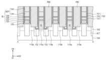
도 1은 본 발명의 실시예들에 따른 반도체 장치의 평면도이다.
도 2는 도 1의 A-A'에 따른 단면도이다.
도 3은 도 1의 B-B'에 따른 단면도이다.
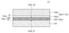
도 4a 내지 도 4d는 도 2의 P1부분의 확대도들이다.
도 5, 도 8, 도 10, 도 12 및 도 14는 본 발명의 실시예들에 따른 반도체 장치의 제조방법을 나타내는 도면들로, 도 1의 A-A'에 대응하는 단면도들이다.
도 6, 도 9, 도 11, 도 13 및 도 15는 본 발명의 실시예들에 따른 반도체 장치의 제조방법을 나타내는 도면들로, 도 1의 B-B'에 대응하는 단면도들이다.
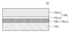
도 7a 내지 도 7d는 도 5의 P2 부분의 확대도들이다.
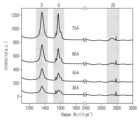
도 16은 도 1의 확산 배리어 패턴 내 그래핀 패턴의 XPS 그래프이다.
도 17은 도 1의 확산 배리어 패턴 내 그래핀 패턴의 라만 피크(Raman Peak)를 나타내는 그래프이다.1 is a top plan view of a semiconductor device according to example embodiments.
FIG. 2 is a cross-sectional view taken along A-A' in FIG. 1;
FIG. 3 is a cross-sectional view taken along line BB′ of FIG. 1 .
4A to 4D are enlarged views of part P1 of FIG. 2 .
5, 8, 10, 12, and 14 are views illustrating a method of manufacturing a semiconductor device according to example embodiments, and are cross-sectional views corresponding to line AA' in FIG. 1 .
6, 9, 11, 13, and 15 are diagrams illustrating a method of manufacturing a semiconductor device according to example embodiments, and are cross-sectional views corresponding to lines BB′ of FIG. 1 .
7A to 7D are enlarged views of part P2 of FIG. 5 .
16 is an XPS graph of a graphene pattern within the diffusion barrier pattern of FIG. 1 .
FIG. 17 is a graph showing Raman peaks of the graphene pattern within the diffusion barrier pattern of FIG. 1 .
이하, 첨부한 도면을 참조하여 본 발명의 실시예들을 설명함으로써 본 발명을 상세히 설명한다.Hereinafter, the present invention will be described in detail by describing embodiments of the present invention with reference to the accompanying drawings.
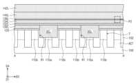
도 1은 본 발명의 실시예들에 따른 반도체 장치의 평면도이다. 도 2는 도 1의 A-A'에 따른 단면도이고, 도 3은 도 1의 B-B'에 따른 단면도이다. 도 4a 내지 도 4d는 도 2의 P1부분의 확대도들이다.1 is a top plan view of a semiconductor device according to example embodiments. FIG. 2 is a cross-sectional view taken along line A-A' of FIG. 1, and FIG. 3 is a cross-sectional view taken along line BB' of FIG. 4A to 4D are enlarged views of part P1 of FIG. 2 .
도 1, 도 2 및 도 3을 참조하면, 기판(100)이 제공될 수 있다. 상기 기판(100)은 반도체 기판, 일 예로 실리콘 기판, 게르마늄 기판, 또는 실리콘-게르마늄 기판일 수 있다. 복수의 활성 패턴들(ACT)이 상기 기판(100) 상에 배치될 수 있다. 상기 활성 패턴들(ACT)은 상기 기판(100)의 하면(100L)에 평행한 제1 방향(D1) 및 제2 방향(D2)을 따라 서로 이격될 수 있다. 상기 제1 방향(D1) 및 상기 제2 방향(D2)은 서로 교차할 수 있다. 상기 활성 패턴들(ACT)의 각각은 상기 기판(100)의 하면(100L)에 평행하고 상기 제1 방향(D1) 및 상기 제2 방향(D2) 모두에 교차하는 제3 방향(D3)으로 연장되는 바(bar) 형태를 가질 수 있다. 상기 활성 패턴들(ACT)의 각각은 상기 기판(100)의 하면(100L)에 수직한 제4 방향(D4)을 따라 상기 기판(100)으로부터 돌출된 상기 기판(100)의 일부일 수 있다.Referring to FIGS. 1 , 2 and 3 , a
소자분리막(102)이 상기 기판(100) 상에 배치되어 상기 활성 패턴들(ACT)을 정의할 수 있다. 상기 소자분리막(102)은 상기 활성 패턴들(ACT) 사이에 개재될 수 있다. 상기 소자분리막(102)은 일 예로, 실리콘 산화물, 실리콘 질화물, 및/또는 실리콘 산질화물을 포함할 수 있다.A
복수의 워드라인들(WL)이 상기 기판(100) 상에 배치될 수 있고, 상기 활성 패턴들(ACT) 및 상기 소자분리막(102)을 가로지를 수 있다. 상기 워드라인들(WL)은 상기 제1 방향(D1)으로 서로 이격될 수 있고, 상기 제2 방향(D2)을 따라 연장될 수 있다. 상기 워드라인들(WL)은 상기 기판(100) 내에 매립된 매립 워드라인들일 수 있고, 상기 활성 패턴들(ACT) 및 상기 소자분리막(102) 내에 매립될 수 있다.A plurality of word lines WL may be disposed on the
상기 워드라인들(WL)의 각각은 상기 활성 패턴들(ACT) 및 상기 소자분리막(102)의 상부들을 관통하는 게이트 전극(GE), 상기 게이트 전극(GE)과 상기 활성 패턴들(ACT) 사이 및 상기 게이트 전극(GE)과 상기 소자분리막(102) 사이에 개재하는 게이트 유전 패턴(GI), 및 상기 게이트 전극(GE)의 상면 상의 게이트 캐핑 패턴(GC)을 포함할 수 있다. 상기 게이트 캐핑 패턴(GC)의 상면은 상기 활성 패턴들(ACT)의 상면들과 공면을 이룰 수 있다. 일 예로, 상기 게이트 캐핑 패턴(GC)의 상기 상면은 상기 활성 패턴들(CACT)의 상기 상면들과 동일한 높이에 위치할 수 있다.Each of the word lines WL may include a gate electrode GE penetrating the active patterns ACT and upper portions of the
상기 게이트 전극(GE)은 도전 물질을 포함할 수 있다. 일 예로, 상기 도전 물질은 도핑된 반도체 물질(도핑된 실리콘, 도핑된 게르마늄 등), 도전성 금속질화물(질화티타늄, 질화탄탈륨 등), 금속(텅스텐, 티타늄, 탄탈륨 등), 및 금속-반도체 화합물(텅스텐 실리사이드, 코발트 실리사이드, 티타늄 실리사이드 등) 중 어느 하나일 수 있다. 상기 게이트 유전 패턴(GI)은 일 예로, 실리콘 산화막, 실리콘 질화막, 및/또는 실리콘 산질화막을 포함할 수 있다. 상기 게이트 캐핑 패턴(GC)은 일 예로, 실리콘 산화막, 실리콘 질화막, 및/또는 실리콘 산질화막을 포함할 수 있다.The gate electrode GE may include a conductive material. For example, the conductive material may be any one of a doped semiconductor material (doped silicon, doped germanium, etc.), a conductive metal nitride (titanium nitride, tantalum nitride, etc.), a metal (tungsten, titanium, tantalum, etc.), and a metal-semiconductor compound (tungsten silicide, cobalt silicide, titanium silicide, etc.). The gate dielectric pattern GI may include, for example, a silicon oxide layer, a silicon nitride layer, and/or a silicon oxynitride layer. The gate capping pattern GC may include, for example, a silicon oxide layer, a silicon nitride layer, and/or a silicon oxynitride layer.
상기 활성 패턴들(ACT)의 각각 내에 제1 불순물 주입 영역(110a) 및 제2 불순물 주입 영역들(110b)이 제공될 수 있다. 상기 제2 불순물 주입 영역들(110b)은 상기 제1 불순물 주입 영역(110a)을 사이에 두고 서로 이격될 수 있다. 상기 제1 불순물 주입 영역(110a)은 상기 활성 패턴들(ACT)의 각각을 가로지르는 한 쌍의 워드라인들(WL) 사이에 제공될 수 있다. 상기 제2 불순물 주입 영역들(110b)은 상기 한 쌍의 워드라인들(WL)을 사이에 두고 서로 이격될 수 있다. 상기 제1 불순물 주입 영역(110a)은 상기 제2 불순물 주입 영역들(110b)과 동일한 도전형의 불순물을 포함할 수 있다.A first
절연막(120)이 상기 기판(100) 상에 배치될 수 있고, 상기 활성 패턴들(ACT), 상기 소자분리막(102) 및 상기 워드라인들(WL)을 덮을 수 있다. 상기 절연막(120)은 일 예로, 실리콘 산화막, 실리콘 질화막 및 실리콘 산화질화막 중 적어도 하나를 포함하는 단일막 또는 다중막을 포함할 수 있다.An
복수의 비트 라인들(BL)이 상기 기판(100) 상에, 그리고 상기 절연막(120) 상에 배치될 수 있다. 상기 비트 라인들(BL)은 상기 워드라인들(WL)을 가로지를 수 있다. 상기 비트 라인들(BL)은 상기 제1 방향(D1)으로 연장될 수 있고, 상기 제2 방향(D2)으로 서로 이격될 수 있다. 상기 비트 라인들(BL)의 각각은 상기 절연막(120) 상에서 상기 제1 방향(D1)으로 배열되는 하부 도전 패턴들(130), 상기 하부 도전 패턴들(130) 상에서 상기 제1 방향(D1)으로 연장되는 하부 배리어 패턴(132), 및 상기 하부 배리어 패턴(132) 상에 차례로 적층된 상부 도전 패턴(134), 확산 배리어 패턴(136), 및 비트 라인 캐핑 패턴(BCP)을 포함할 수 있다. 상기 상부 도전 패턴(134), 상기 확산 배리어 패턴(136) 및 상기 비트 라인 캐핑 패턴(BCP)의 각각은 상기 제1 방향(D1)으로 연장될 수 있다. 상기 비트 라인 캐핑 패턴(BCP)은 상기 확산 배리어 패턴(136) 상에 차례로 적층된 하부 캐핑 패턴(140) 및 상부 캐핑 패턴(142)을 포함할 수 있고, 상기 하부 캐핑 패턴(140) 및 상기 상부 캐핑 패턴(142)의 각각은 상기 제1 방향(D1)으로 연장될 수 있다.A plurality of bit lines BL may be disposed on the
상기 하부 도전 패턴들(130)은 불순물이 도핑되거나 도핑되지 않은 폴리실리콘을 포함할 수 있고, 상기 하부 배리어 패턴(132)은 도전성 금속 질화물(일 예로, 티타늄 질화물, 탄탈륨 질화물, 텅스텐 질화물) 및 금속 실리사이드 중 적어도 하나를 포함할 수 있다. 상기 상부 도전 패턴(134)은 금속(일 예로, 루테늄, 텅스텐, 티타늄, 탄탈륨 등) 및 도전성 금속 질화물(일 예로, 티타늄 질화물, 탄탈륨 질화물, 텅스텐 질화물) 중 적어도 하나를 포함할 수 있다. 일 예로, 상기 상부 도전 패턴(134)은 루테늄(Ru)을 포함할 수 있다. 상기 비트 라인 캐핑 패턴(BCP)은 실리콘 화합물을 포함할 수 있다. 상기 하부 캐핑 패턴(140) 및 상기 상부 캐핑 패턴(142)의 각각은 실리콘 화합물을 포함할 수 있고, 상기 실리콘 화합물은 일 예로, 단결정 실리콘, 불순물이 도핑되거나 도핑되지 않은 폴리실리콘, SiOx, SiC, SiN, SiOC 및 SiOCN 중 적어도 하나를 포함할 수 있다.The lower
도 2 및 도 4a를 참조하면, 상기 확산 배리어 패턴(136)은 그래핀 패턴(136a)을 포함할 수 있다. 상기 그래핀 패턴(136a)은 상기 상부 도전 패턴(134)과 상기 비트 라인 캐핑 패턴(BCP, 즉 상기 하부 캐핑 패턴(140)) 사이에 개재된 단일의 그래핀 층이거나, 상기 상부 도전 패턴(134)과 상기 비트 라인 캐핑 패턴(BCP, 즉 상기 하부 캐핑 패턴(140)) 사이에서 상기 제4 방향(D4)을 적층된 복수의 그래핀 층들을 포함할 수 있다. 상기 복수의 그래핀 층들의 수는 일 예로, 2 내지 20일 수 있다. 상기 그래핀 패턴(136a)은 상기 제4 방향(D4)에 따른 두께(136a_T)를 가질 수 있고, 상기 그래핀 패턴(136a)의 상기 두께(136_T)는 일 예로, 100Å보다 작거나 같을 수 있다. 상기 그래핀 패턴(136a)은 상기 제4 방향(D4)으로 서로 대향하는 제1 면(136a_S1) 및 제2 면(136a_S2)을 가질 수 있다. 일부 실시예들에 따르면, 상기 그래핀 패턴(136a)의 상기 제1 면(136a_S1)은 상기 상부 도전 패턴(134)과 접촉할 수 있고, 상기 그래핀 패턴(136a)의 상기 제2 면(136a_S2)은 상기 비트 라인 캐핑 패턴(BCP, 즉 상기 하부 캐핑 패턴(140))과 접촉할 수 있다.Referring to FIGS. 2 and 4A , the
도 2, 도 4b 및 도 4c를 참조하면, 일부 실시예들에 따르면, 상기 확산 배리어 패턴(136)은 상기 그래핀 패턴(136a)과 상기 비트 라인 캐핑 패턴(BCP, 즉 상기 하부 캐핑 패턴(140)) 사이, 또는 상기 그래핀 패턴(136a)과 상기 상부 도전 패턴(134) 사이에 개재되는 상부 배리어 패턴(136b)을 더 포함할 수 있다. 상기 상부 배리어 패턴(136b)은 금속 원소를 포함할 수 있다. 상기 상부 배리어 패턴(136b)은 도전성 금속 질화물 및 금속 실리사이드 중 적어도 하나를 포함할 수 있다. 상기 상부 배리어 패턴(136b)은 일 예로, TiSiN, TiN, TaN, WN 및 WSi 중 적어도 하나를 포함할 수 있다.2, 4B, and 4C , according to some embodiments, the
일 예로, 도 4b를 참조하면, 상기 상부 배리어 패턴(136b)은 상기 그래핀 패턴(136a)과 상기 비트 라인 캐핑 패턴(BCP, 즉 상기 하부 캐핑 패턴(140)) 사이에 개재될 수 있다. 이 경우, 상기 그래핀 패턴(136a)의 상기 제1 면(136a_S1)은 상기 상부 도전 패턴(134)과 접촉할 수 있고, 상기 그래핀 패턴(136a)의 상기 제2 면(136a_S2)은 상기 상부 배리어 패턴(136b)과 접촉할 수 있다 상기 상부 배리어 패턴(136b)은 상기 그래핀 패턴(136a)의 상기 제2 면(136a_S2)과 상기 비트 라인 캐핑 패턴(BCP, 즉 상기 하부 캐핑 패턴(140)) 사이에 개재될 수 있다.For example, referring to FIG. 4B , the
다른 예로, 도 4c를 참조하면, 상기 상부 배리어 패턴(136b)은 상기 그래핀 패턴(136a)과 상기 상부 도전 패턴(134) 사이에 개재될 수 있다. 이 경우, 상기 그래핀 패턴(136a)의 상기 제1 면(136a_S1)은 상기 상부 배리어 패턴(136b)과 접촉할 수 있고, 상기 그래핀 패턴(136a)의 상기 제2 면(136a_S2)은 상기 비트 라인 캐핑 패턴(BCP, 즉 상기 하부 캐핑 패턴(140))과 접촉할 수 있다. 상기 상부 배리어 패턴(136b)은 상기 그래핀 패턴(136a)의 상기 제1 면(136a_S1)과 상기 상부 도전 패턴(134) 사이에 개재될 수 있다.As another example, referring to FIG. 4C , the
도 2 및 도 4d를 참조하면, 일부 실시예들에 따르면, 상기 비트 라인 캐핑 패턴(BCP)의 상기 하부 캐핑 패턴(140)은 상기 확산 배리어 패턴(136)에 인접하는 제1 하부 캐핑 패턴(140a), 및 상기 제1 하부 캐핑 패턴(140a) 상의 제2 하부 캐핑 패턴(140b)을 포함할 수 있다. 상기 제1 하부 캐핑 패턴(140a)은 상기 확산 배리어 패턴(136)과 상기 제2 하부 캐핑 패턴(140b) 사이에 개재될 수 있다. 상기 제1 하부 캐핑 패턴(140a)은 상기 제2 하부 캐핑 패턴(140b)보다 저온에서 증착된 물질을 포함할 수 있다. 일 예로, 상기 제1 하부 캐핑 패턴(140a)은 상대적으로 저온에서(일 예로, 약 300℃) 증착된 실리콘 질화물(SiN)을 포함할 수 있고, 상기 제2 하부 캐핑 패턴(140b)은 상대적으로 고온에서(일 예로, 약 630℃ 내지 740℃) 증착된 실리콘 질화물(SiN)을 포함할 수 있다. 상기 제1 하부 캐핑 패턴(140a)의 상기 제4 방향(D4)에 따른 두께(140a_T)는 상기 제2 하부 캐핑 패턴(140b)의 상기 제4 방향(D4)에 따른 두께보다 작을 수 있다. 상기 확산 배리어 패턴(136)은 상기 그래핀 패턴(136a)을 포함할 수 있다. 일부 실시예들에 따르면, 상기 그래핀 패턴(136a)의 상기 제1 면(136a_S1)은 상기 상부 도전 패턴(134)과 접촉할 수 있고, 상기 그래핀 패턴(136a)의 상기 제2 면(136a_S2)은 상기 제1 하부 캐핑 패턴(140a)과 접촉할 수 있다.2 and 4D , according to some embodiments, the
도 1, 도 2 및 도 3을 다시 참조하면, 비트 라인 콘택들(DC)이 상기 비트 라인들(BL)의 각각의 아래에 배치될 수 있고, 상기 제1 방향(D1)으로 배열될 수 있다. 상기 비트 라인 콘택들(DC)은 상기 제1 방향(D1)으로 서로 이격될 수 있고, 상기 하부 도전 패턴들(130) 사이에 배치될 수 있다. 상기 하부 도전 패턴들(130) 및 상기 비트 라인 콘택들(DC)은 상기 제1 방향(D1)을 따라 교대로 배열될 수 있다. 상기 비트 라인 콘택들(DC)은 상기 절연막(120)을 관통할 수 있고, 상기 활성 패턴들(ACT) 중 대응하는 활성 패턴들(ACT)에 각각 전기적으로 연결될 수 있다. 상기 비트 라인 콘택들(DC)의 각각은 상기 대응하는 활성 패턴들(ACT)의 각각의 상기 제1 불순물 주입 영역(110a)에 전기적으로 연결될 수 있다. 상기 상부 도전 패턴(134)은 상기 하부 도전 패턴들(130) 및 상기 비트 라인 콘택들(DC) 상에서 상기 제1 방향(D1)으로 연장될 수 있다. 상기 하부 배리어 패턴(132)은 상기 하부 도전 패턴들(130)과 상기 상부 도전 패턴(134) 사이, 및 상기 비트 라인 콘택들(DC)과 상기 상부 도전 패턴(134) 사이에서 상기 제1 방향(D1)으로 연장될 수 있다.Referring back to FIGS. 1, 2, and 3 , bit line contacts DC may be disposed below each of the bit lines BL and may be arranged in the first direction D1. The bit line contacts DC may be spaced apart from each other in the first direction D1 and may be disposed between the lower
비트라인 스페이서(150)가 상기 비트 라인들(BL)의 각각의 양 측면들 상에 배치될 수 있다. 상기 비트라인 스페이서(150)는 상기 비트 라인들(BL)의 각각의 일 측면을 따라 상기 제1 방향(D1)으로 연장될 수 있다. 상기 비트라인 스페이서(150)는 상기 비트 라인들(BL)의 각각의 상기 측면 상에 차례로 적층된 제1 스페이서(151), 제2 스페이서(155) 및 제3 스페이서(157)를 포함할 수 있다. 상기 제1 스페이서(151) 및 상기 제2 스페이서(155)는 상기 절연막(120) 상에 배치될 수 있다. 상기 제1 스페이서(151)는 상기 비트 라인들(BL)의 각각의 상기 측면으로부터 상기 제2 스페이서(155)와 상기 절연막(120) 사이로 연장될 수 있고, 상기 제1 스페이서(151)의 최하부면은 상기 절연막(120)의 상면과 접촉할 수 있다. 상기 제2 스페이서(155)의 최하부면은 상기 제1 스페이서(151)와 접촉할 수 있다. 상기 제3 스페이서(157)는 상기 절연막(120)의 측면을 덮을 수 있고, 상기 제3 스페이서(157)의 최하부면은 상기 기판(100)의 상면과 접할 수 있다.A
상기 제1 스페이서(151) 및 상기 제3 스페이서(157)는 서로 동일한 절연 물질(일 예로, 실리콘 질화물)을 포함할 수 있고, 상기 제2 스페이서(155)는 상기 제1 스페이서(151) 및 상기 제3 스페이서(157)와 다른 물질을 포함할 수 있다. 일부 실시예들에 따르면, 상기 제2 스페이서(155)는 상기 제1 및 제3 스페이서들(151, 157)에 대해 식각 선택비를 갖는 절연 물질(일 예로, 실리콘 산화물)을 포함할 수 있다. 다른 실시예들에 따르면, 상기 제2 스페이서(155)는 에어 갭 영역일 수도 있다.The
매립 절연패턴(153)이 상기 비트 라인 콘택들(DC)의 각각의 측면 상에 배치될 수 있다. 상기 매립 절연패턴(153)은 실리콘 산화물, 실리콘 질화물 및 실리콘 산화질화물 중 적어도 하나를 포함할 수 있다. 상기 제1 스페이서(151)는 상기 비트 라인 콘택들(DC)의 각각의 상기 측면과 상기 매립 절연패턴(153) 사이로 연장될 수 있고, 상기 소자분리막(102)과 상기 매립 절연패턴(153) 사이로 더 연장될 수 있다. 절연 라이너(152)가 상기 제1 스페이서(151)과 상기 매립 절연 패턴(153) 사이에 개재될 수 있다. 상기 매립 절연패턴(153)은 상기 절연 라이너(152)를 사이에 두고 상기 제1 스페이서(151)로부터 이격될 수 있다. 상기 절연 라이너(152)의 적어도 일부는 상기 제1 스페이서(151)와 상기 제3 스페이서(157) 사이로 연장될 수 있고, 상기 제2 스페이서(155)의 상기 최하부면과 접할 수 있다. 상기 매립 절연패턴(153)은 상기 제3 스페이서(157)의 상기 최하부면과 접할 수 있다. 상기 절연 라이너(152)는 일 예로, 실리콘 산화물을 포함할 수 있다.A buried insulating
스토리지 노드 콘택들(BC)이 상기 비트 라인들(BL) 중 서로 이웃하는 한 쌍의 비트 라인들(BL) 사이에 배치될 수 있다. 상기 스토리지 노드 콘택들(BC)은 상기 한 쌍의 비트 라인들(BL) 사이에서 상기 제1 방향(D1)으로 이격될 수 있고, 상기 활성 패턴들(ACT) 중 대응하는 활성 패턴들(ACT)의 단부들에 각각 전기적으로 연결될 수 있다. 상기 스토리지 노드 콘택들(BC)의 각각은 상기 대응하는 활성 패턴들(ACT)의 각각의 상기 제2 불순물 주입 영역(SD2)에 전기적으로 연결될 수 있다. 상기 스토리지 노드 콘택들(BC)은 불순물이 도핑되거나 도핑되지 않은 폴리실리콘을 포함할 수 있다. 절연 펜스들이 상기 스토리지 노드 콘택들(BC) 사이에 배치될 수 있다. 상기 절연 펜스들 및 상기 스토리지 노드 콘택들(BC)은 상기 한 쌍의 비트라인들(BL) 사이에서 상기 제1 방향(D1)으로 교대로 배치될 수 있다. 상기 절연 펜스들은 일 예로, 실리콘 질화물을 포함할 수 있다.Storage node contacts BC may be disposed between a pair of adjacent bit lines BL among the bit lines BL. The storage node contacts BC may be spaced apart from each other in the first direction D1 between the pair of bit lines BL, and may be electrically connected to ends of corresponding active patterns ACT among the active patterns ACT. Each of the storage node contacts BC may be electrically connected to the second impurity implantation region SD2 of each of the corresponding active patterns ACT. The storage node contacts BC may include polysilicon doped or undoped with impurities. Insulation fences may be disposed between the storage node contacts BC. The insulation fences and the storage node contacts BC may be alternately disposed in the first direction D1 between the pair of bit lines BL. The insulation fences may include, for example, silicon nitride.
상기 비트라인 스페이서(150)는 상기 비트 라인들(BL)의 각각과 상기 스토리지 노드 콘택들(BC) 사이에 개재될 수 있다. 상기 제1 스페이서(151)는 상기 비트 라인들(BL)의 각각의 상기 측면과 상기 제2 스페이서(155) 사이에 개재될 수 있고, 상기 제3 스페이서(157)는 상기 제2 스페이서(155)와 상기 스토리지 노드 콘택들(BC) 사이에 개재될 수 있다.The
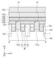
랜딩 패드들(LP)이 상기 스토리지 노드 콘택들(BC) 상에 각각 배치될 수 있다. 상기 랜딩 패드들(LP)은 텅스텐과 같은 금속 함유 물질을 포함할 수 있다. 상기 랜딩 패드들(LP)의 각각의 상부는 상기 비트 라인 캐핑 패턴(BCP, 즉, 상기 상부 캐핑 패턴(142))의 상면을 덮을 수 있고, 상기 스토리지 노드 콘택들(BC)의 각각보다 큰 폭을 가질 수 있다. 상기 랜딩 패드들(LP)의 각각의 상기 상부는 상기 스토리지 노드 콘택들(BC)의 각각으로부터 옆으로(일 예로, 상기 제2 방향(D2) 또는 상기 제2 방향(D2)의 반대방향으로) 쉬프트될 수 있다. 상기 랜딩 패드들(LP)의 각각의 상기 상부는 상기 비트 라인들(BL) 중 대응하는 비트 라인(BL)과 수직적으로 중첩할 수 있다. 도시하지는 않았지만, 스토리지 노드 오믹층과 확산 방지 패턴이 상기 스토리지 노드 콘택들(BC)의 각각과 상기 랜딩 패드들(LP)의 각각 사이에 개재될 수 있다. 상기 스토리지 노드 오믹층은 금속실리사이드를 포함할 수 있다. 상기 확산 방지 패턴은 티타늄질화막, 탄탈륨 질화막과 같은 금속 질화물을 포함할 수 있다.Landing pads LP may be respectively disposed on the storage node contacts BC. The landing pads LP may include a metal-containing material such as tungsten. An upper portion of each of the landing pads LP may cover an upper surface of the bit line capping pattern BCP (that is, the upper capping pattern 142) and may have a larger width than each of the storage node contacts BC. The upper portion of each of the landing pads LP may be shifted laterally (eg, in the second direction D2 or in a direction opposite to the second direction D2) from each of the storage node contacts BC. The upper portion of each of the landing pads LP may vertically overlap a corresponding bit line BL among the bit lines BL. Although not shown, a storage node ohmic layer and an anti-diffusion pattern may be interposed between each of the storage node contacts BC and each of the landing pads LP. The storage node ohmic layer may include metal silicide. The anti-diffusion pattern may include a metal nitride such as a titanium nitride layer or a tantalum nitride layer.
제1 상부 절연막(160)이 상기 랜딩 패드들(LP) 사이의 공간을 채울 수 있다. 상기 제1 상부 절연막(160)은 상기 비트 라인 캐핑 패턴(BCP)의 일부(일 예로, 상기 상부 캐핑 패턴(142) 및 상기 하부 캐핑 패턴(140)의 부분들)를 관통할 수 있고, 상기 제1 내지 제3 스페이서들(151, 155, 157)의 상부면들과 접촉할 수 있다. 상기 제1 상부 절연막(160)은 일 예로, 실리콘 산화물, 실리콘 질화물 및 실리콘 산질화물 중 적어도 하나를 포함할 수 있다.A first upper insulating
캐패시터 구조체(CAP)가 상기 랜딩 패드들(LP) 상에 배치될 수 있다. 상기 캐패시터 구조체(CAP)는 상기 랜딩 패드들(LP) 상에 각각 배치되는 하부 전극들(BE), 상기 하부 전극들(BE)을 덮는 상부 전극(TE), 및 상기 하부 전극들(BE)의 각각과 상기 상부 전극(TE) 사이의 유전막(175)을 포함할 수 있다. 상기 하부 전극들(BE)의 각각은 원기둥 형태이거나 속이 빈 실린더 혹은 컵 형태를 가질 수 있다. 상기 하부 전극들(BE)은 불순물이 도핑된 폴리실리콘, 티타늄질화막과 같은 금속 질화막, 및 텅스텐, 알루미늄 및 구리와 같은 금속막 중 적어도 하나를 포함할 수 있다.A capacitor structure CAP may be disposed on the landing pads LP. The capacitor structure CAP may include lower electrodes BE respectively disposed on the landing pads LP, an upper electrode TE covering the lower electrodes BE, and a
상부 지지 패턴(182)이 상기 하부 전극들(BE)의 상부 측벽들을 지지할 수 있고, 하부 지지 패턴(180)이 상기 하부 전극들(BE)의 하부 측벽들을 지지할 수 있다. 상기 상부 및 하부 지지 패턴들(182, 180)은 실리콘 질화물, 실리콘 산화물, 실리콘 산질화물과 같은 절연물질을 포함할 수 있다. 식각 저지막(170)이 상기 하부 전극들(BE) 사이에서 상기 제1 상부 절연막(160)을 덮을 수 있다. 상기 식각 저지막(170)은 일 예로, 실리콘 질화물, 실리콘 산화물, 실리콘 산질화물과 같은 절연물질을 포함할 수 있다.An
상기 유전막(175)은 상기 하부 전극들(BE)의 표면과 상기 상부 및 하부 지지 패턴들(182, 180)의 표면을 덮을 수 있다. 상기 유전막(175)은 일 예로, 실리콘 산화막, 실리콘 질화막, 실리콘 산질화막, 및 고유전막(일 예로, 하프늄 산화막) 중의 적어도 하나를 포함할 수 있다. 상기 상부 전극(TE)은 상기 유전막(175) 상에 배치될 수 있고, 상기 하부 전극들(BE) 사이 및 상기 상부 지지 패턴(182)과 상기 하부 지지 패턴(180) 사이의 공간을 채울 수 있다. 상기 상부 전극(TE)은 불순물이 도핑된 폴리실리콘막, 불순물이 도핑된 실리콘게르마늄막, 티타늄질화막과 같은 금속 질화막, 및 텅스텐, 알루미늄 및 구리와 같은 금속막 중 적어도 하나를 포함할 수 있다.The
상기 비트 라인들(BL)의 각각에서, 루테늄(Ru)을 포함하는 상기 상부 도전 패턴(134)과 실리콘 화합물을 포함하는 상기 비트 라인 캐핑 패턴(CP)이 직접 접촉하는 경우, 상기 상부 도전 패턴(134)과 상기 비트 라인 캐핑 패턴(BCP) 사이의 계면에 루테늄 실리사이드가 형성될 수 있고, 이로 인해, 상기 비트 라인들(BL)의 저항이 증가되는 문제가 있을 수 있다.In each of the bit lines BL, when the upper
본 발명의 개념에 따르면, 상기 비트 라인들(BL)의 각각의 상기 상부 도전 패턴(134)은 루테늄(Ru)을 포함할 수 있고, 이에 따라, 상기 비트 라인들(BL)은 낮은 저항을 가질 수 있다. 더하여, 상기 확산 배리어 패턴(136)이 루테늄(Ru)을 포함하는 상기 상부 도전 패턴(134)과 실리콘 화합물을 포함하는 상기 비트 라인 캐핑 패턴(CP) 사이게 개재될 수 있고, 상기 확산 배리어 패턴(136)은 상기 그래핀 패턴(136a)을 포함할 수 있다. 상기 그래핀 패턴(136a)은 적어도 하나의 그래핀 층을 포함할 수 있다. 그래핀은 탄소원자들이 벌집 구조로 결합된 2차원 탄소 물질로, 서로 인접하는 탄소 원자들 사이의 거리가 실리콘 원자의 크기보다 작을 수 있다. 이에 따라, 상기 그래핀 패턴(136a)은 상기 비트 라인 캐핑 패턴(BCP) 내 실리콘이 상기 상부 도전 패턴(134) 내로 확산되는 것을 방지할 수 있다. 그 결과, 상기 상부 도전 패턴(134)과 상기 비트 라인 캐핑 패턴(BCP) 사이에 루테늄 실리사이드가 형성되는 것이 방지될 수 있고, 상기 비트 라인들(BL)의 저항이 증가되는 것이 방지될 수 있다.According to the concept of the present invention, each of the upper
따라서, 전기적 특성이 개선되고 우수한 신뢰성을 갖는 반도체 장치가 제공될 수 있다.Accordingly, a semiconductor device having improved electrical characteristics and excellent reliability can be provided.
도 5, 도 8, 도 10, 도 12 및 도 14는 본 발명의 실시예들에 따른 반도체 장치의 제조방법을 나타내는 도면들로, 도 1의 A-A'에 대응하는 단면도들이다. 도 6, 도 9, 도 11, 도 13 및 도 15는 본 발명의 실시예들에 따른 반도체 장치의 제조방법을 나타내는 도면들로, 도 1의 B-B'에 대응하는 단면도들이다. 도 7a 내지 도 7d는 도 5의 P2 부분의 확대도들이다.설명의 간소화를 위해, 도 1, 도 2, 도 3, 도 4a 내지 도 4d를 참조하여 설명한 반도체 장치와 중복되는 설명은 생략된다.5, 8, 10, 12, and 14 are views illustrating a method of manufacturing a semiconductor device according to example embodiments, and are cross-sectional views corresponding to line AA' in FIG. 1 . 6, 9, 11, 13, and 15 are diagrams illustrating a method of manufacturing a semiconductor device according to example embodiments, and are cross-sectional views corresponding to lines BB′ of FIG. 1 . 7A to 7D are enlarged views of part P2 of FIG. 5 . For simplicity of description, descriptions overlapping those of the semiconductor device described with reference to FIGS. 1, 2, 3, and 4A to 4D will be omitted.
도 1, 도 5 및 도 6을 참조하면, 활성 패턴들(ACT)이 상기 기판(100) 상에 형성될 수 있다. 상기 활성 패턴들(ACT)을 형성하는 것은, 일 예로, 상기 기판(100) 상에 제1 마스크 패턴들을 형성하는 것, 및 상기 제1 마스크 패턴들을 식각 마스크로 이용하여 상기 기판(100)의 상부를 식각하는 것을 포함할 수 있다. 상기 기판(100)의 상기 상부가 식각됨에 따라, 상기 활성 패턴들(ACT)의 측면들을 노출하는 트렌치(T)가 상기 기판(100) 내에 형성될 수 있다. 소자분리막(102)이 상기 트렌치(T)를 채우도록 형성될 수 있다. 상기 소자분리막(102)을 형성하는 것은, 일 예로, 상기 기판(100) 상에 상기 트렌치(T)를 채우는 소자분리 절연막을 형성하는 것, 및 상기 기판(100)의 상면에 노출될 때까지 상기 소자분리 절연막을 평탄화하는 것을 포함할 수 있다.Referring to FIGS. 1 , 5 and 6 , active patterns ACT may be formed on the
워드라인들(WL)이 상기 기판(100) 내에 형성될 수 있고, 상기 활성 패턴들(ACT) 및 상기 소자분리막(102)을 가로지를 수 있다. 상기 워드라인들(WL)은 상기 제1 방향(D1)으로 서로 이격될 수 있고, 상기 제2 방향(D2)을 따라 연장될 수 있다. 상기 워드라인들(WL)의 각각은 상기 활성 패턴들(ACT) 및 상기 소자분리막(102)의 상부들을 관통하는 게이트 전극(GE), 상기 게이트 전극(GE)과 상기 활성 패턴들(ACT) 사이 및 상기 게이트 전극(GE)과 상기 소자분리막(102) 사이에 개재하는 게이트 유전 패턴(GI), 및 상기 게이트 전극(GE)의 상면 상의 게이트 캐핑 패턴(GC)을 포함할 수 있다. 상기 게이트 전극(GE) 및 상기 게이트 유전 패턴(GI)을 형성하는 것은, 일 예로, 상기 기판(100) 내에 상기 활성 패턴들(ACT) 및 상기 소자분리막(102)의 상부들을 관통하는 그루브들을 형성하는 것, 상기 그루브들의 각각의 내면을 덮는 게이트 유전막을 형성하는 것, 상기 그루브들의 각각을 채우는 게이트 전극막을 형성하는 것, 및 상기 기판(100)의 상면에 노출될 때까지 상기 게이트 유전막 및 상기 게이트 전극막을 평탄화하는 것을 포함할 수 있다. 상기 게이트 캐핑 패턴(GC)을 형성하는 것은, 일 예로, 상기 게이트 전극(GE)의 상부를 리세스하여 상기 그루브들의 각각 내에 빈 영역을 형성하는 것, 상기 빈 영역을 채우는 게이트 캐핑막을 형성하는 것, 및 상기 기판(100)의 상면에 노출될 때까지 상기 게이트 캐핑막을 평탄화하는 것을 포함할 수 있다.Word lines WL may be formed in the
상기 활성 패턴들(ACT)의 각각 내에 제1 불순물 주입 영역(110a) 및 제2 불순물 주입 영역들(110b)이 형성될 수 있다. 상기 제1 및 제2 불순물 주입 영역들(110a, 110b)을 형성하는 것은, 일 예로, 상기 게이트 캐핑 패턴(GC) 및 상기 소자분리막(102)을 마스크로 이용하여 상기 활성 패턴들(ACT) 내에 동일한 도전형을 불순물을 주입하는 것을 포함할 수 있다.A first
절연막(120)이 상기 기판(100) 상에 형성될 수 있고, 상기 활성 패턴들(ACT), 상기 소자분리막(102) 및 상기 워드라인들(WL)을 덮을 수 있다. 하부 도전막(130L)이 상기 절연막(120) 상에 적층될 수 있다. 리세스 영역들(R1)이 상기 절연막(120) 및 상기 하부 도전막(130L)을 관통하도록, 그리고 상기 활성 패턴들(ACT) 및 상기 소자분리막(102) 내부로 연장되도록 형성될 수 있다. 상기 리세스 영역들(R1)을 형성하는 것은 일 예로, 상기 하부 도전막(130L) 상에 상기 리세스 영역들(R1)이 형성될 영역을 정의하는 제2 마스크 패턴을 형성하는 것, 및 상기 제2 마스크 패턴을 식각 마스크로 이용하여 상기 하부 도전막(130L), 상기 절연막(120), 상기 활성 패턴들(ACT) 및 상기 소자분리막(102)을 식각하는 것을 포함할 수 있다. 상기 리세스 영역들(R1)이 형성된 후, 상기 제2 마스크 패턴들은 제거될 수 있다.An insulating
비트라인 콘택막(DCL)이 상기 리세스 영역들(R1)을 채우도록 형성될 수 있다. 상기 비트라인 콘택막(DCL)을 형성하는 것은, 일 예로, 상기 하부 도전막(130L) 상에 상기 리세스 영역들(R1)을 채우는 상기 비트라인 콘택막(DCL)을 형성하는 것, 및 상기 하부 도전막(130L)의 상면이 노출될 때까지 상기 비트라인 콘택막(DCL)을 평탄화하는 것을 포함할 수 있다. 이에 따라, 상기 비트라인 콘택막(DCL)은 상기 리세스 영역들(R1) 내에 국소적으로 형성될 수 있다.A bit line contact layer DCL may be formed to fill the recess regions R1. Forming the bit line contact layer DCL may include, for example, forming the bit line contact layer DCL on the lower
하부 배리어막(132L), 상부 도전막(134L), 확산 배리어막(136L), 하부 캐핑막(140L) 및 상부 캐핑막(142L)이 상기 하부 도전막(130L) 상에 차례로 적층될 수 있고, 상기 비트라인 콘택막(DCL) 상으로 연장될 수 있다. 상기 하부 배리어막(132L)은 상기 하부 도전막(130L) 및 상기 비트라인 콘택막(DCL)의 상면들을 덮을 수 있다. 상기 하부 배리어막(132L), 상기 상부 도전막(134L), 상기 확산 배리어막(136L), 상기 하부 캐핑막(140L) 및 상기 상부 캐핑막(142L)의 각각은 물리 기상 증착, 화학 기상 증착 또는 원자층 증착 방법을 이용하여 형성될 수 있다.A
도 5 및 도 7a를 참조하면, 상기 확산 배리어막(136L)은 그래핀 박막(136La)을 포함할 수 있다. 상기 그래핀 박막(136La)은 상기 상부 도전막(134L)과 상기 하부 캐핑막(140L) 사이에 개재된 단일의 그래핀 층이거나, 상기 상부 도전막(134L)과 상기 하부 캐핑막(140L) 사이에서 상기 제4 방향(D4)으로 적층된 복수의 그래핀 층들을 포함할 수 있다. 상기 그래핀 박막(136La)은 일 예로, 마이크로웨이브 플라즈마, ICP(Inductively Coupled Plasma), CCP(Capacitively Coupled Plasma) 또는 펄스 플라즈마(pulsed plasma)를 이용한 화학 기상 증착(CVD) 방법, 열 화학 기상 증착(thermal CVD) 방법, 또는 원자층 증착 방법(ALD)을 이용하여 형성될 수 있다.Referring to FIGS. 5 and 7A , the
도 5, 도 7b 및 도 7c를 참조하면, 일부 실시예들에 따르면, 상기 확산 배리어막(136L)은 상기 그래핀 박막(136La)과 상기 하부 캐핑막(140L) 사이, 또는 상기 그래핀 박막(136La)과 상기 상부 도전막(134L) 사이에 개재되는 상부 배리어막(136Lb)을 더 포함할 수 있다. 상기 상부 배리어막(136Lb)은 물리 기상 증착, 화학 기상 증착 또는 원자층 증착 방법을 이용하여 형성될 수 있다. 일 예로, 도 7b를 참조하면, 상기 상부 배리어막(136Lb)은 상기 그래핀 박막(136La)과 상기 하부 캐핑막(140L) 사이에 형성될 수 있다. 다른 예로, 도 7c를 참조하면, 상기 상부 배리어막(136Lb)은 상기 그래핀 박막(136La)과 상기 상부 도전막(134L) 사이에 형성될 수 있다.5, 7B, and 7C , according to some embodiments, the
도 5 및 도 7d를 참조하면, 일부 실시예들에 따르면, 상기 하부 캐핑막(140L)은 상기 확산 배리어막(136L)에 인접하는 제1 하부 캐핑막(140La), 및 상기 제1 하부 캐핑막(140La) 상의 제2 하부 캐핑막(140Lb)을 포함할 수 있다. 상기 제1 하부 캐핑막(140La)은 상기 확산 배리어막(136L)과 상기 제2 하부 캐핑막(140Lb) 사이에 형성될 수 있다. 상기 제1 하부 캐핑막(140La)의 증착 공정은 상기 제2 하부 캐핑막(140Lb)의 증착 공정보다 낮은 온도에서 수행될 수 있다. 일 예로, 상기 제1 하부 캐핑막(140La)은 상대적으로 저온에서(일 예로, 약 300℃) 증착된 실리콘 질화물(SiN)을 포함할 수 있고, 상기 제2 하부 캐핑막(140Lb)은 상대적으로 고온에서(일 예로, 약 630℃ 내지 740℃) 증착된 실리콘 질화물(SiN)을 포함할 수 있다.5 and 7D , according to some embodiments, the
상기 하부 캐핑막(140L) 및 상기 상부 캐핑막(142L)의 각각은 실리콘 화합물을 포함할 수 있다. 상기 제1 하부 캐핑막(140La)이 저온 증착 공정에 의해 형성되는 경우, 상기 하부 캐핑막(140L) 내 실리콘이 상기 상부 도전막(134L) 내로 확산되는 것이 억제될 수 있다.Each of the
도 1, 도 8 및 도 9를 참조하면, 상기 상부 캐핑막(142L), 상기 하부 캐핑막(140L), 상기 확산 배리어막(136L), 상기 상부 도전막(134L), 상기 하부 배리어막(132L), 및 상기 하부 도전막(130L)이 순차로 식각될 수 있고, 이에 따라, 비트 라인들(BL)이 형성될 수 있다. 상기 비트 라인들(BL)은 상기 절연막(120) 상에 형성될 수 있고, 상기 워드라인들(WL)을 가로지를 수 있다. 상기 비트 라인들(BL)은 상기 제1 방향(D1)으로 연장될 수 있고, 상기 제2 방향(D2)으로 서로 이격될 수 있다. 상기 비트 라인들(BL)의 각각은 상기 상부 캐핑막(142L), 상기 하부 캐핑막(140L), 상기 확산 배리어막(136L), 상기 상부 도전막(134L), 상기 하부 배리어막(132L), 및 상기 하부 도전막(130L)을 식각함으로써 각각 형성된, 상부 캐핑 패턴(142), 하부 캐핑 패턴(140), 확산 배리어 패턴(136), 상부 도전 패턴(134), 하부 배리어 패턴(132) 및 하부 도전 패턴들(130)을 포함할 수 있다. 상기 상부 캐핑 패턴(142) 및 하부 캐핑 패턴(140)은 비트라인 캐핑 패턴(BCP)으로 지칭될 수 있다. 상기 비트 라인들(BL)의 각각의 상기 하부 도전 패턴들(130)은 상기 절연막(120) 상에서 상기 제1 방향(D1)으로 배열될 수 있다.Referring to FIGS. 1, 8, and 9 , the
비트라인 콘택들(DC)이 상기 비트 라인들(BL)의 각각의 아래에 형성될 수 있고, 상기 제1 방향(D1)으로 서로 이격될 수 있다. 상기 하부 도전 패턴들(130) 및 상기 비트 라인 콘택들(DC)은 상기 제1 방향(D1)을 따라 교대로 배열될 수 있다. 상기 비트라인 콘택들(DC)은 상기 비트라인 콘택막(DCL)을 식각함으로써 형성될 수 있다. 상기 비트라인 콘택들(DC)의 각각의 양 측에서 상기 리세스 영역들(R1)의 각각의 내면이 노출될 수 있다.Bit line contacts DC may be formed below each of the bit lines BL and may be spaced apart from each other in the first direction D1. The lower
제1 스페이서(151)가 상기 비트 라인들(BL)의 각각의 측면 상에 형성될 수 있고, 상기 절연막(120) 상으로 연장될 수 있다. 상기 제1 스페이서(151)는 상기 비트라인 콘택들(DC)의 각각의 측면 상으로 연장될 수 있고, 상기 리세스 영역들(R1)의 각각의 상기 노출된 내면을 덮을 수 있다. 절연 라이너(152) 및 매립 절연패턴(153)이 상기 비트라인 콘택들(DC)의 각각의 양 측에 형성될 수 있고, 상기 리세스 영역들(R1)의 각각의 잔부를 채우도록 형성될 수 있다. 상기 절연 라이너(152)는 상기 제1 스페이서(151)과 상기 매립 절연 패턴(153) 사이에 개재될 수 있다.A
상기 제1 스페이서(151), 상기 절연 라이너(152) 및 상기 매립 절연패턴(153)을 형성하는 것은, 일 예로, 상기 비트 라인들(BL)의 각각의 상기 측면, 상기 비트라인 콘택들(DC)의 각각의 상기 측면 및 상기 리세스 영역들(R1)의 각각의 상기 노출된 내면을 덮는 제1 스페이서막을 형성하는 것, 상기 제1 스페이서막 상에 상기 제1 스페이서막을 따라 연장되는 절연 라이너막을 형성하는 것, 상기 리세스 영역들(R1)의 각각의 잔부를 채우는 매립 절연막을 형성하는 것, 및 상기 매립 절연막, 상기 절연 라이너막, 및 상기 제1 스페이서막을 이방성 식각하는 것을 포함할 수 있다.Forming the
도 1, 도 10 및 도 11을 참조하면, 제2 스페이서(155)가 상기 비트 라인들(BL)의 각각의 상기 측면 상에 형성될 수 있다. 상기 제1 스페이서(151)는 상기 비트 라인들(BL)의 각각의 상기 측면과 상기 제2 스페이서(155) 사이에 개재될 수 있고, 상기 절연막(120)의 상면과 상기 제2 스페이서(155) 사이로 연장될 수 있다. 상기 제2 스페이서(155)를 형성하는 것은, 일 예로, 상기 비트 라인들(BL)의 각각의 상기 측면을 덮는 제2 스페이서막을 형성하는 것, 및 상기 제2 스페이서막을 이방성 식각하는 것을 포함할 수 있다. 상기 제2 스페이서(155)에 의해 노출되는, 상기 절연막(120)의 일부가 상기 제2 스페이서막의 상기 이방성 식각 동안 함께 식각될 수 있다.Referring to FIGS. 1 , 10 and 11 , a
제3 스페이서(157)가 상기 비트 라인들(BL)의 각각의 상기 측면 상에 형성될 수 있다. 상기 제1 및 제2 스페이서들(151, 155)은 상기 비트 라인들(BL)의 각각의 상기 측면과 상기 제3 스페이서(157) 사이에 개재될 수 있다. 상기 제3 스페이서(157)는 상기 절연막(120)의 측면을 덮을 수 있고, 상기 기판(100)의 상면 및 상기 매립 절연패턴(153)의 상면과 접촉할 수 있다. 상기 제3 스페이서(157)는 상기 제2 스페이서(155)와 실질적으로 동일한 방법으로 형성될 수 있다.A
상기 제1 내지 제3 스페이서들(151, 155, 157)은 비트라인 스페이서(150)를 구성할 수 있다. 상기 비트라인 스페이서(150)는 상기 비트 라인들(BL)의 각각의 상기 측면을 따라 상기 제1 방향(D1)으로 연장될 수 있다.The first to
도 1, 도 12 및 도 13을 참조하면, 예비 콘택막(PBC)이 상기 기판(100) 상에, 그리고 상기 비트 라인들(BL) 사이에 형성될 수 있다. 상기 비트라인 스페이서(150)는 상기 비트 라인들(BL)의 각각과 상기 예비 콘택막(PBC) 사이에 개재될 수 있다. 상기 예비 콘택막(PBC)을 형성하는 것은, 일 예로, 상기 기판(100) 상에 상기 비트 라인들(BL) 사이의 공간을 채우는 콘택 도전막을 형성하는 것, 및 상기 상부 캐핑 패턴(142)의 상면이 노출될 때까지 상기 콘택 도전막을 평탄화하는 것을 포함할 수 있다. 상기 예비 콘택막(PBC)은 서로 이웃하는 한 쌍의 비트 라인들(BL) 사이에서 상기 제1 방향(D1)으로 연장될 수 있다.Referring to FIGS. 1, 12, and 13 , a preliminary contact layer PBC may be formed on the
도 1, 도 14 및 도 15을 참조하면, 상기 예비 콘택막(PBC)의 상부가 리세스될 수 있다. 이후, 스토리지 노드 콘택들(BC)이 상기 예비 콘택막(PBC)을 패터닝함으로써 형성될 수 있다. 상기 스토리지 노드 콘택들(BC)은 서로 이웃하는 한 쌍의 비트 라인들(BL) 사이에서 상기 제1 방향(D1)으로 서로 이격될 수 있다. 절연 펜스들이 상기 스토리지 노드 콘택들(BC) 사이에 형성될 수 있다. 상기 절연 펜스들 및 상기 스토리지 노드 콘택들(BC)은 상기 한 쌍의 비트라인들(BL) 사이에서 상기 제1 방향(D1)으로 교대로 배치될 수 있다. 도전막(CL)이 상기 기판(100) 상에 상기 비트 라인들(BL), 상기 스토리지 노드 콘택들(BC) 및 상기 절연 펜스들의 상면들을 덮도록 형성될 수 있다.Referring to FIGS. 1, 14, and 15 , an upper portion of the preliminary contact layer PBC may be recessed. After that, storage node contacts BC may be formed by patterning the preliminary contact layer PBC. The storage node contacts BC may be spaced apart from each other in the first direction D1 between a pair of adjacent bit lines BL. Insulation fences may be formed between the storage node contacts BC. The insulation fences and the storage node contacts BC may be alternately disposed in the first direction D1 between the pair of bit lines BL. A conductive layer CL may be formed on the
도 1, 도 2 및 도 3을 다시 참조하면, 랜딩 패드들(LP)이 상기 도전막(CL)을 패터닝함으로써 형성될 수 있다. 제1 상부 절연막(160)이 상기 랜딩 패드들(LP) 사이의 공간을 채우도록 형성될 수 있다.Referring back to FIGS. 1 , 2 and 3 , landing pads LP may be formed by patterning the conductive layer CL. A first upper insulating
식각 저지막(170)이 상기 랜딩 패드들(LP) 및 상기 제1 상부 절연막(160) 상에 형성될 수 있다. 하부 전극들(BE)이 상기 랜딩 패드들(LP) 상에 각각 형성될 수 있다. 상기 하부 전극들(BE)의 각각은 상기 식각 저지막(170)을 관통하여 상기 랜딩 패드들(LP) 중 대응하는 랜딩 패드(LP)에 연결될 수 있다.An
상부 지지 패턴(182)이 상기 하부 전극들(BE)의 상부 측벽들 상에 형성될 수 있고, 상기 하부 전극들(BE)의 상기 상부 측벽들을 지지할 수 있다. 하부 지지 패턴(180)이 상기 하부 전극들(BE)의 하부 측벽들 상에 형성될 수 있고, 상기 하부 전극들(BE)의 상기 하부 측벽들을 지지할 수 있다. 유전막(175)이 상기 하부 전극들(BE)의 표면과 상기 상부 및 하부 지지 패턴들(182, 180)의 표면을 덮도록 형성될 수 있다. 상부 전극(TE)이 상기 활성 셀 영역(ACR) 상에 형성될 수 있고, 상기 하부 전극들(BE) 사이의 공간을 채울 수 있다. 상기 하부 전극들(BE), 상기 유전막(175) 및 상기 상부 전극(TE)은 캐패시터 구조체(CAP)를 구성할 수 있다.An
도 16은 도 1의 확산 배리어 패턴 내 그래핀 패턴의 XPS 그래프이고, 도 17은 도 1의 확산 배리어 패턴 내 그래핀 패턴의 라만 피크(Raman Peak)를 나타내는 그래프이다.FIG. 16 is an XPS graph of the graphene pattern in the diffusion barrier pattern of FIG. 1 , and FIG. 17 is a graph showing Raman peaks of the graphene pattern in the diffusion barrier pattern of FIG. 1 .
도 16을 참조하면, 상기 그래핀 패턴(136a) 내 전체 결합(fitting) 내에서 sp2 결합은 약 50%이상을 차지할 수 있다. 일 예로, 상기 그래핀 패턴(136a) 내 sp2 결합은 상기 그래핀 패턴(136a) 내 전체 결합(fitting)의 50%보다 크거나 같고 100%보다 작을 수 있다.Referring to FIG. 16 , sp2 bonding may occupy about 50% or more of the total fitting in the
도 17을 참조하면, 상기 그래핀 패턴(136a)의 두께가 증가할수록 G 피크의 강도가 증가할 수 있다. G 피크는 흑연계 물질에서 공통적으로 나타나는 피크로, 육각형 구조의 탄소 원자들이 인접한 원자와 서로 반대방향으로 진동하는 모드에 해당한다. D 피크 및 2D 피크는 그래핀 패턴(136a) 내 결함에 의한 피크이다. 본 발명의 실시예들에 따르면, 상기 그래핀 패턴(136a)은 i) (D 피크 강도)/(G 피크 강도)가 2.0보다 작거나 같고, ii) (2D 피크 강도)/(G 피크 강도)가 0.1보다 크거나 같은 조건을 만족할 수 있다.Referring to FIG. 17 , as the thickness of the
본 발명의 실시예들에 대한 이상의 설명은 본 발명의 설명을 위한 예시를 제공한다. 따라서 본 발명은 이상의 실시예들에 한정되지 않으며, 본 발명의 기술적 사상 내에서 당해 기술 분야의 통상의 지식을 가진 자에 의하여 상기 실시예들을 조합하여 실시하는 등 여러 가지 많은 수정 및 변경이 가능함은 명백하다.The above description of embodiments of the present invention provides examples for explaining the present invention. Therefore, the present invention is not limited to the above embodiments, and various modifications and changes, such as combining and implementing the above embodiments, are possible by those skilled in the art within the technical spirit of the present invention. It is obvious.
Claims (10)
Translated fromKorean상기 기판 상에 상기 복수의 활성 패턴들을 가로지르고 제1 방향으로 연장되는 비트 라인; 및
상기 비트 라인 아래에서 상기 제1 방향으로 배열되고 상기 복수의 활성 패턴들에 각각 전기적으로 연결되는 비트 라인 콘택들을 포함하되,
상기 비트 라인는:
상기 비트 라인 콘택들 상에서 상기 제1 방향으로 연장되는 상부 도전 패턴;
상기 상부 도전 패턴 상에서 상기 제1 방향으로 연장되는 비트 라인 캐핑 패턴; 및
상기 상부 도전 패턴과 상기 비트 라인 캐핑 패턴 사이에서 상기 제1 방향으로 연장되는 확산 배리어 패턴을 포함하고,
상기 상부 도전 패턴은 루테늄(Ru)을 포함하고, 상기 확산 배리어 패턴은 그래핀 패턴을 포함하는 반도체 장치.a substrate including a plurality of active patterns;
a bit line extending in a first direction and crossing the plurality of active patterns on the substrate; and
bit line contacts arranged under the bit line in the first direction and electrically connected to the plurality of active patterns, respectively;
The bit line is:
an upper conductive pattern extending in the first direction on the bit line contacts;
a bit line capping pattern extending in the first direction on the upper conductive pattern; and
a diffusion barrier pattern extending in the first direction between the upper conductive pattern and the bit line capping pattern;
The semiconductor device of claim 1 , wherein the upper conductive pattern includes ruthenium (Ru), and the diffusion barrier pattern includes a graphene pattern.
상기 비트 라인은:
상기 상부 도전 패턴 아래에서 상기 비트 라인 콘택들 사이에 개재되는 하부 도전 패턴들; 및
상기 하부 도전 패턴들과 상기 상부 도전 패턴 사이, 및 상기 비트 라인들 콘택들과 상기 상부 도전 패턴 사이에서 상기 제1 방향으로 연장되는 하부 배리어 패턴을 더 포함하되,
상기 하부 도전 패턴들 및 상기 비트 라인 콘택들은 상기 제1 방향을 따라 교대로 배열되는 반도체 장치.The method of claim 1,
The bit line is:
lower conductive patterns interposed between the bit line contacts under the upper conductive pattern; and
a lower barrier pattern extending in the first direction between the lower conductive patterns and the upper conductive pattern and between the bit line contacts and the upper conductive pattern;
The lower conductive patterns and the bit line contacts are alternately arranged along the first direction.
상기 비트 라인 캐핑 패턴은 실리콘 화합물을 포함하는 반도체 장치.The method of claim 1,
The bit line capping pattern includes a silicon compound.
상기 확산 배리어 패턴은 상기 상부 도전 패턴과 상기 그래핀 패턴 사이, 또는 상기 비트 라인 캐핑 패턴과 상기 그래핀 패턴 사이에 개재되는 상부 배리어 패턴을 더 포함하는 반도체 장치.The method of claim 1,
The diffusion barrier pattern further includes an upper barrier pattern interposed between the upper conductive pattern and the graphene pattern or between the bit line capping pattern and the graphene pattern.
상기 상부 배리어 패턴은 도전성 금속 질화물 및 금속 실리사이드 중 적어도 하나를 포함하는 반도체 장치.The method of claim 4,
The upper barrier pattern includes at least one of a conductive metal nitride and a metal silicide.
상기 비트 라인 캐핑 패턴은 상기 확산 배리어 패턴에 인접하는 제1 하부 캐핑 패턴, 및 상기 제1 하부 캐핑 패턴 상의 제2 하부 캐핑 패턴을 포함하고,
상기 제1 하부 캐핑 패턴 및 상기 제2 하부 캐핑 패턴의 각각은 상기 기판의 하면에 수직한 방향에 따른 두께를 가지고,
상기 제1 하부 캐핑 패턴의 두께는 상기 제2 하부 캐핑 패턴의 두께보다 작은 반도체 장치.The method of claim 1,
the bit line capping pattern includes a first lower capping pattern adjacent to the diffusion barrier pattern and a second lower capping pattern on the first lower capping pattern;
Each of the first lower capping pattern and the second lower capping pattern has a thickness along a direction perpendicular to the lower surface of the substrate;
The semiconductor device of claim 1 , wherein a thickness of the first lower capping pattern is smaller than a thickness of the second lower capping pattern.
상기 그래핀 패턴은 상기 기판의 하면에 수직한 방향으로 적층된 복수의 그래핀 층들을 포함하는 반도체 장치.The method of claim 1,
The graphene pattern includes a plurality of graphene layers stacked in a direction perpendicular to a lower surface of the substrate.
상기 비트 라인은 복수 개로 제공되되,
상기 복수의 비트 라인들은 상기 제1 방향으로 연장되고, 상기 제1 방향에 교차하는 제2 방향으로 서로 이격되고,
상기 제1 방향 및 상기 제2 방향은 상기 기판의 하면에 평행한 반도체 장치.The method of claim 1,
The bit line is provided in plurality,
The plurality of bit lines extend in the first direction and are spaced apart from each other in a second direction crossing the first direction;
The first direction and the second direction are parallel to the lower surface of the substrate.
상기 기판 상에 상기 복수의 활성 패턴들을 가로지르는 비트 라인들, 상기 비트 라인들은 제1 방향으로 연장되고 제2 방향으로 서로 이격되되, 상기 제1 방향 및 상기 제2 방향은 상기 기판의 하면에 평행하고 서로 교차하는 것;
상기 비트 라인들의 각각의 아래에서 상기 제1 방향으로 배열되고, 상기 복수의 활성 패턴들 중 대응하는 활성 패턴들에 각각 전기적으로 연결되는 비트 라인 콘택들;
상기 비트 라인들 사이에서 상기 제1 방향으로 서로 이격되고, 상기 복수의 활성 패턴들 중 대응하는 활성 패턴들의 단부들에 각각 전기적으로 연결되는 스토리지 노드 콘택들; 및
상기 스토리지 노드 콘택들에 연결되는 캐패시터 구조체를 포함하되,
상기 비트 라인들의 각각은:
상기 비트 라인 콘택들 상에서 상기 제1 방향으로 연장되고, 루테늄(Ru)을 포함하는 상부 도전 패턴;
상기 상부 도전 패턴 상에서 상기 제1 방향으로 연장되고, 실리콘 화합물을 포함하는 비트 라인 캐핑 패턴; 및
상기 상부 도전 패턴과 상기 비트 라인 캐핑 패턴 사이에서 상기 제1 방향으로 연장되는 확산 배리어 패턴을 포함하고,
상기 확산 배리어 패턴은 그래핀 패턴을 포함하는 반도체 장치.a substrate including a plurality of active patterns;
bit lines crossing the plurality of active patterns on the substrate, the bit lines extending in a first direction and spaced apart from each other in a second direction, the first direction and the second direction being parallel to and crossing the lower surface of the substrate;
bit line contacts arranged under each of the bit lines in the first direction and electrically connected to corresponding active patterns among the plurality of active patterns;
storage node contacts spaced apart from each other between the bit lines in the first direction and electrically connected to ends of corresponding active patterns among the plurality of active patterns, respectively; and
A capacitor structure coupled to the storage node contacts;
Each of the bit lines is:
an upper conductive pattern extending in the first direction on the bit line contacts and including ruthenium (Ru);
a bit line capping pattern extending in the first direction on the upper conductive pattern and including a silicon compound; and
a diffusion barrier pattern extending in the first direction between the upper conductive pattern and the bit line capping pattern;
The semiconductor device of claim 1 , wherein the diffusion barrier pattern includes a graphene pattern.
상기 비트 라인들의 각각은:
상기 상부 도전 패턴 아래에서 상기 비트 라인 콘택들 사이에 개재되는 하부 도전 패턴들; 및
상기 하부 도전 패턴들과 상기 상부 도전 패턴 사이, 및 상기 비트 라인들 콘택들과 상기 상부 도전 패턴 사이에서 상기 제1 방향으로 연장되는 하부 배리어 패턴을 더 포함하는 반도체 장치.The method of claim 9,
Each of the bit lines is:
lower conductive patterns interposed between the bit line contacts under the upper conductive pattern; and
and a lower barrier pattern extending in the first direction between the lower conductive patterns and the upper conductive pattern and between the bit line contacts and the upper conductive pattern.
Priority Applications (4)
| Application Number | Priority Date | Filing Date | Title |
|---|---|---|---|
| KR1020220007453AKR20230111510A (en) | 2022-01-18 | 2022-01-18 | Semiconductor devices |
| US17/892,275US12289880B2 (en) | 2022-01-18 | 2022-08-22 | Semiconductor devices having a graphene pattern between the first conductive pattern and the bit line capping |
| CN202211232958.4ACN116507115A (en) | 2022-01-18 | 2022-10-10 | Semiconductor device |
| TW111138414ATWI844984B (en) | 2022-01-18 | 2022-10-11 | Semiconductor devices |
Applications Claiming Priority (1)
| Application Number | Priority Date | Filing Date | Title |
|---|---|---|---|
| KR1020220007453AKR20230111510A (en) | 2022-01-18 | 2022-01-18 | Semiconductor devices |
Publications (1)
| Publication Number | Publication Date |
|---|---|
| KR20230111510Atrue KR20230111510A (en) | 2023-07-25 |
Family
ID=87161537
Family Applications (1)
| Application Number | Title | Priority Date | Filing Date |
|---|---|---|---|
| KR1020220007453APendingKR20230111510A (en) | 2022-01-18 | 2022-01-18 | Semiconductor devices |
Country Status (4)
| Country | Link |
|---|---|
| US (1) | US12289880B2 (en) |
| KR (1) | KR20230111510A (en) |
| CN (1) | CN116507115A (en) |
| TW (1) | TWI844984B (en) |
Families Citing this family (1)
| Publication number | Priority date | Publication date | Assignee | Title |
|---|---|---|---|---|
| KR20250045333A (en)* | 2023-09-25 | 2025-04-01 | 삼성전자주식회사 | Semiconductor devices including bit lines |
Family Cites Families (15)
| Publication number | Priority date | Publication date | Assignee | Title |
|---|---|---|---|---|
| KR20010097949A (en) | 2000-04-27 | 2001-11-08 | 윤종용 | Method of planarizing insulating layer covered capacitor for semiconductor device |
| KR100668836B1 (en) | 2004-12-30 | 2007-01-16 | 주식회사 하이닉스반도체 | Planarization method of insulating film of semiconductor device |
| KR20080088987A (en) | 2007-03-30 | 2008-10-06 | 주식회사 하이닉스반도체 | Insulating Planarization Method of Semiconductor Device |
| US8476765B2 (en) | 2010-12-06 | 2013-07-02 | Stmicroelectronics, Inc. | Copper interconnect structure having a graphene cap |
| CN202121691U (en)* | 2011-07-08 | 2012-01-18 | 杨鹏 | Camera with scanner |
| US9472450B2 (en) | 2012-05-10 | 2016-10-18 | Samsung Electronics Co., Ltd. | Graphene cap for copper interconnect structures |
| US9209136B2 (en) | 2013-04-01 | 2015-12-08 | Intel Corporation | Hybrid carbon-metal interconnect structures |
| US9337149B2 (en) | 2014-07-29 | 2016-05-10 | Samsung Electronics Co, Ltd. | Semiconductor devices and methods of fabricating the same |
| CN113793872A (en) | 2014-12-10 | 2021-12-14 | 株式会社半导体能源研究所 | Semiconductor device and method of manufacturing the same |
| US9786760B1 (en) | 2016-09-29 | 2017-10-10 | International Business Machines Corporation | Air gap and air spacer pinch off |
| KR20180062817A (en) | 2016-12-01 | 2018-06-11 | 삼성전자주식회사 | semiconductor device including multi-liner layer in a trench |
| JP7550759B2 (en) | 2019-07-12 | 2024-09-13 | 株式会社半導体エネルギー研究所 | SEMICONDUCTOR DEVICE AND METHOD FOR MANUFACTURING SEMICONDUCTOR DEVICE |
| TW202129877A (en) | 2019-08-30 | 2021-08-01 | 日商半導體能源研究所股份有限公司 | Semiconductor device |
| US11081489B2 (en) | 2019-11-11 | 2021-08-03 | Xia Tai Xin Semiconductor (Qing Dao) Ltd. | Semiconductor structure and method for fabricating the same |
| US12150290B2 (en)* | 2022-02-14 | 2024-11-19 | Nanya Technology Corporation | Semiconductor device with composite gate dielectric and method for preparing the same |
- 2022
- 2022-01-18KRKR1020220007453Apatent/KR20230111510A/enactivePending
- 2022-08-22USUS17/892,275patent/US12289880B2/enactiveActive
- 2022-10-10CNCN202211232958.4Apatent/CN116507115A/enactivePending
- 2022-10-11TWTW111138414Apatent/TWI844984B/enactive
Also Published As
| Publication number | Publication date |
|---|---|
| US12289880B2 (en) | 2025-04-29 |
| US20230232611A1 (en) | 2023-07-20 |
| CN116507115A (en) | 2023-07-28 |
| TWI844984B (en) | 2024-06-11 |
| TW202331943A (en) | 2023-08-01 |
Similar Documents
| Publication | Publication Date | Title |
|---|---|---|
| US20220352173A1 (en) | Semiconductor device | |
| EP4277449A1 (en) | Semiconductor memory device and method for fabricating the same | |
| KR20230022322A (en) | Semiconductor Device | |
| KR20230111510A (en) | Semiconductor devices | |
| CN106469725A (en) | Memory element and method for manufacturing the same | |
| US12432909B2 (en) | Semiconductor memory device having an ohmic contact on the impurity regions | |
| KR100439038B1 (en) | Bitline of semiconductor device having stud type capping layer and method for fabricating the same | |
| KR20220162019A (en) | Semiconductor memory device and method of fabricating the same | |
| US20240147707A1 (en) | Semiconductor memory device | |
| US20240324182A1 (en) | Semiconductor memory devices | |
| US20250016993A1 (en) | Semiconductor device | |
| US20250098153A1 (en) | Semiconductor device | |
| US20240147706A1 (en) | Semiconductor memory device | |
| EP4468840A1 (en) | Semiconductor memory device | |
| US20240334684A1 (en) | Semiconductor memory device | |
| US20250275122A1 (en) | Semiconductor device and method of fabricating the same | |
| CN118231376A (en) | Semiconductor device with a semiconductor layer having a plurality of semiconductor layers | |
| KR20230174960A (en) | Semiconductor memory device and method of forming the same | |
| KR20250107526A (en) | semiconductor device | |
| KR20250046967A (en) | Semiconducotr device | |
| JP2024127787A (en) | Semiconductor Device | |
| CN118475116A (en) | Semiconductor devices | |
| KR20240131105A (en) | Semiconductor memory device | |
| KR20240002776A (en) | Semiconductor device and method for fabricating the same |
Legal Events
| Date | Code | Title | Description |
|---|---|---|---|
| PA0109 | Patent application | St.27 status event code:A-0-1-A10-A12-nap-PA0109 | |
| P22-X000 | Classification modified | St.27 status event code:A-2-2-P10-P22-nap-X000 | |
| P22-X000 | Classification modified | St.27 status event code:A-2-2-P10-P22-nap-X000 | |
| PG1501 | Laying open of application | St.27 status event code:A-1-1-Q10-Q12-nap-PG1501 | |
| A201 | Request for examination | ||
| PA0201 | Request for examination | St.27 status event code:A-1-2-D10-D11-exm-PA0201 | |
| PE0902 | Notice of grounds for rejection | St.27 status event code:A-1-2-D10-D21-exm-PE0902 |