KR20230102887A - Stereoscopic Image Display Panel - Google Patents
Stereoscopic Image Display PanelDownload PDFInfo
- Publication number
- KR20230102887A KR20230102887AKR1020210193352AKR20210193352AKR20230102887AKR 20230102887 AKR20230102887 AKR 20230102887AKR 1020210193352 AKR1020210193352 AKR 1020210193352AKR 20210193352 AKR20210193352 AKR 20210193352AKR 20230102887 AKR20230102887 AKR 20230102887A
- Authority
- KR
- South Korea
- Prior art keywords
- sub
- pixels
- light emitting
- eye
- pixel
- Prior art date
- Legal status (The legal status is an assumption and is not a legal conclusion. Google has not performed a legal analysis and makes no representation as to the accuracy of the status listed.)
- Pending
Links
Images


Classifications
- G—PHYSICS
- G02—OPTICS
- G02B—OPTICAL ELEMENTS, SYSTEMS OR APPARATUS
- G02B30/00—Optical systems or apparatus for producing three-dimensional [3D] effects, e.g. stereoscopic images
- G02B30/20—Optical systems or apparatus for producing three-dimensional [3D] effects, e.g. stereoscopic images by providing first and second parallax images to an observer's left and right eyes
- G02B30/26—Optical systems or apparatus for producing three-dimensional [3D] effects, e.g. stereoscopic images by providing first and second parallax images to an observer's left and right eyes of the autostereoscopic type
- G02B30/30—Optical systems or apparatus for producing three-dimensional [3D] effects, e.g. stereoscopic images by providing first and second parallax images to an observer's left and right eyes of the autostereoscopic type involving parallax barriers
- G02B30/32—Optical systems or apparatus for producing three-dimensional [3D] effects, e.g. stereoscopic images by providing first and second parallax images to an observer's left and right eyes of the autostereoscopic type involving parallax barriers characterised by the geometry of the parallax barriers, e.g. staggered barriers, slanted parallax arrays or parallax arrays of varying shape or size
- G—PHYSICS
- G02—OPTICS
- G02B—OPTICAL ELEMENTS, SYSTEMS OR APPARATUS
- G02B30/00—Optical systems or apparatus for producing three-dimensional [3D] effects, e.g. stereoscopic images
- G02B30/40—Optical systems or apparatus for producing three-dimensional [3D] effects, e.g. stereoscopic images giving the observer of a single two-dimensional [2D] image a perception of depth
- G—PHYSICS
- G09—EDUCATION; CRYPTOGRAPHY; DISPLAY; ADVERTISING; SEALS
- G09G—ARRANGEMENTS OR CIRCUITS FOR CONTROL OF INDICATING DEVICES USING STATIC MEANS TO PRESENT VARIABLE INFORMATION
- G09G3/00—Control arrangements or circuits, of interest only in connection with visual indicators other than cathode-ray tubes
- G09G3/20—Control arrangements or circuits, of interest only in connection with visual indicators other than cathode-ray tubes for presentation of an assembly of a number of characters, e.g. a page, by composing the assembly by combination of individual elements arranged in a matrix no fixed position being assigned to or needed to be assigned to the individual characters or partial characters
- G09G3/2007—Display of intermediate tones
- G09G3/2074—Display of intermediate tones using sub-pixels
- G—PHYSICS
- G09—EDUCATION; CRYPTOGRAPHY; DISPLAY; ADVERTISING; SEALS
- G09G—ARRANGEMENTS OR CIRCUITS FOR CONTROL OF INDICATING DEVICES USING STATIC MEANS TO PRESENT VARIABLE INFORMATION
- G09G3/00—Control arrangements or circuits, of interest only in connection with visual indicators other than cathode-ray tubes
- G09G3/20—Control arrangements or circuits, of interest only in connection with visual indicators other than cathode-ray tubes for presentation of an assembly of a number of characters, e.g. a page, by composing the assembly by combination of individual elements arranged in a matrix no fixed position being assigned to or needed to be assigned to the individual characters or partial characters
- G09G3/22—Control arrangements or circuits, of interest only in connection with visual indicators other than cathode-ray tubes for presentation of an assembly of a number of characters, e.g. a page, by composing the assembly by combination of individual elements arranged in a matrix no fixed position being assigned to or needed to be assigned to the individual characters or partial characters using controlled light sources
- G09G3/30—Control arrangements or circuits, of interest only in connection with visual indicators other than cathode-ray tubes for presentation of an assembly of a number of characters, e.g. a page, by composing the assembly by combination of individual elements arranged in a matrix no fixed position being assigned to or needed to be assigned to the individual characters or partial characters using controlled light sources using electroluminescent panels
- G09G3/32—Control arrangements or circuits, of interest only in connection with visual indicators other than cathode-ray tubes for presentation of an assembly of a number of characters, e.g. a page, by composing the assembly by combination of individual elements arranged in a matrix no fixed position being assigned to or needed to be assigned to the individual characters or partial characters using controlled light sources using electroluminescent panels semiconductive, e.g. using light-emitting diodes [LED]
- G09G3/3208—Control arrangements or circuits, of interest only in connection with visual indicators other than cathode-ray tubes for presentation of an assembly of a number of characters, e.g. a page, by composing the assembly by combination of individual elements arranged in a matrix no fixed position being assigned to or needed to be assigned to the individual characters or partial characters using controlled light sources using electroluminescent panels semiconductive, e.g. using light-emitting diodes [LED] organic, e.g. using organic light-emitting diodes [OLED]
- G09G3/3225—Control arrangements or circuits, of interest only in connection with visual indicators other than cathode-ray tubes for presentation of an assembly of a number of characters, e.g. a page, by composing the assembly by combination of individual elements arranged in a matrix no fixed position being assigned to or needed to be assigned to the individual characters or partial characters using controlled light sources using electroluminescent panels semiconductive, e.g. using light-emitting diodes [LED] organic, e.g. using organic light-emitting diodes [OLED] using an active matrix
- G09G3/3233—Control arrangements or circuits, of interest only in connection with visual indicators other than cathode-ray tubes for presentation of an assembly of a number of characters, e.g. a page, by composing the assembly by combination of individual elements arranged in a matrix no fixed position being assigned to or needed to be assigned to the individual characters or partial characters using controlled light sources using electroluminescent panels semiconductive, e.g. using light-emitting diodes [LED] organic, e.g. using organic light-emitting diodes [OLED] using an active matrix with pixel circuitry controlling the current through the light-emitting element
- G—PHYSICS
- G09—EDUCATION; CRYPTOGRAPHY; DISPLAY; ADVERTISING; SEALS
- G09G—ARRANGEMENTS OR CIRCUITS FOR CONTROL OF INDICATING DEVICES USING STATIC MEANS TO PRESENT VARIABLE INFORMATION
- G09G3/00—Control arrangements or circuits, of interest only in connection with visual indicators other than cathode-ray tubes
- G09G3/20—Control arrangements or circuits, of interest only in connection with visual indicators other than cathode-ray tubes for presentation of an assembly of a number of characters, e.g. a page, by composing the assembly by combination of individual elements arranged in a matrix no fixed position being assigned to or needed to be assigned to the individual characters or partial characters
- G09G3/34—Control arrangements or circuits, of interest only in connection with visual indicators other than cathode-ray tubes for presentation of an assembly of a number of characters, e.g. a page, by composing the assembly by combination of individual elements arranged in a matrix no fixed position being assigned to or needed to be assigned to the individual characters or partial characters by control of light from an independent source
- G09G3/36—Control arrangements or circuits, of interest only in connection with visual indicators other than cathode-ray tubes for presentation of an assembly of a number of characters, e.g. a page, by composing the assembly by combination of individual elements arranged in a matrix no fixed position being assigned to or needed to be assigned to the individual characters or partial characters by control of light from an independent source using liquid crystals
- G09G3/3607—Control arrangements or circuits, of interest only in connection with visual indicators other than cathode-ray tubes for presentation of an assembly of a number of characters, e.g. a page, by composing the assembly by combination of individual elements arranged in a matrix no fixed position being assigned to or needed to be assigned to the individual characters or partial characters by control of light from an independent source using liquid crystals for displaying colours or for displaying grey scales with a specific pixel layout, e.g. using sub-pixels
- H—ELECTRICITY
- H10—SEMICONDUCTOR DEVICES; ELECTRIC SOLID-STATE DEVICES NOT OTHERWISE PROVIDED FOR
- H10K—ORGANIC ELECTRIC SOLID-STATE DEVICES
- H10K59/00—Integrated devices, or assemblies of multiple devices, comprising at least one organic light-emitting element covered by group H10K50/00
- H10K59/30—Devices specially adapted for multicolour light emission
- H10K59/35—Devices specially adapted for multicolour light emission comprising red-green-blue [RGB] subpixels
- H10K59/352—Devices specially adapted for multicolour light emission comprising red-green-blue [RGB] subpixels the areas of the RGB subpixels being different
- H—ELECTRICITY
- H10—SEMICONDUCTOR DEVICES; ELECTRIC SOLID-STATE DEVICES NOT OTHERWISE PROVIDED FOR
- H10K—ORGANIC ELECTRIC SOLID-STATE DEVICES
- H10K59/00—Integrated devices, or assemblies of multiple devices, comprising at least one organic light-emitting element covered by group H10K50/00
- H10K59/30—Devices specially adapted for multicolour light emission
- H10K59/35—Devices specially adapted for multicolour light emission comprising red-green-blue [RGB] subpixels
- H10K59/353—Devices specially adapted for multicolour light emission comprising red-green-blue [RGB] subpixels characterised by the geometrical arrangement of the RGB subpixels
- G—PHYSICS
- G09—EDUCATION; CRYPTOGRAPHY; DISPLAY; ADVERTISING; SEALS
- G09G—ARRANGEMENTS OR CIRCUITS FOR CONTROL OF INDICATING DEVICES USING STATIC MEANS TO PRESENT VARIABLE INFORMATION
- G09G2300/00—Aspects of the constitution of display devices
- G09G2300/04—Structural and physical details of display devices
- G09G2300/0439—Pixel structures
- G09G2300/0452—Details of colour pixel setup, e.g. pixel composed of a red, a blue and two green components
- G—PHYSICS
- G09—EDUCATION; CRYPTOGRAPHY; DISPLAY; ADVERTISING; SEALS
- G09G—ARRANGEMENTS OR CIRCUITS FOR CONTROL OF INDICATING DEVICES USING STATIC MEANS TO PRESENT VARIABLE INFORMATION
- G09G2300/00—Aspects of the constitution of display devices
- G09G2300/08—Active matrix structure, i.e. with use of active elements, inclusive of non-linear two terminal elements, in the pixels together with light emitting or modulating elements
- G09G2300/0809—Several active elements per pixel in active matrix panels
- G09G2300/0842—Several active elements per pixel in active matrix panels forming a memory circuit, e.g. a dynamic memory with one capacitor
- G—PHYSICS
- G09—EDUCATION; CRYPTOGRAPHY; DISPLAY; ADVERTISING; SEALS
- G09G—ARRANGEMENTS OR CIRCUITS FOR CONTROL OF INDICATING DEVICES USING STATIC MEANS TO PRESENT VARIABLE INFORMATION
- G09G3/00—Control arrangements or circuits, of interest only in connection with visual indicators other than cathode-ray tubes
- G09G3/001—Control arrangements or circuits, of interest only in connection with visual indicators other than cathode-ray tubes using specific devices not provided for in groups G09G3/02 - G09G3/36, e.g. using an intermediate record carrier such as a film slide; Projection systems; Display of non-alphanumerical information, solely or in combination with alphanumerical information, e.g. digital display on projected diapositive as background
- G09G3/003—Control arrangements or circuits, of interest only in connection with visual indicators other than cathode-ray tubes using specific devices not provided for in groups G09G3/02 - G09G3/36, e.g. using an intermediate record carrier such as a film slide; Projection systems; Display of non-alphanumerical information, solely or in combination with alphanumerical information, e.g. digital display on projected diapositive as background to produce spatial visual effects
- H—ELECTRICITY
- H10—SEMICONDUCTOR DEVICES; ELECTRIC SOLID-STATE DEVICES NOT OTHERWISE PROVIDED FOR
- H10K—ORGANIC ELECTRIC SOLID-STATE DEVICES
- H10K59/00—Integrated devices, or assemblies of multiple devices, comprising at least one organic light-emitting element covered by group H10K50/00
- H10K59/10—OLED displays
- H10K59/12—Active-matrix OLED [AMOLED] displays
- H10K59/122—Pixel-defining structures or layers, e.g. banks
Landscapes
- Physics & Mathematics (AREA)
- General Physics & Mathematics (AREA)
- Engineering & Computer Science (AREA)
- Optics & Photonics (AREA)
- Computer Hardware Design (AREA)
- Theoretical Computer Science (AREA)
- Chemical & Material Sciences (AREA)
- Crystallography & Structural Chemistry (AREA)
- Geometry (AREA)
- Electroluminescent Light Sources (AREA)
Abstract
Description
Translated fromKorean본 발명은 입체 영상 디스플레이 패널에 관한 것이다.The present invention relates to a stereoscopic image display panel.
최근 디스플레이 기술의 발달로 인해 시청자로 하여금 장면 속에 있는 것과 같이 느낄 수 있도록 하는 입체감 실현 기술 또한 개발되고 있다. 즉, 2D 디스플레이에서의 높은 화질 구현에 중점을 두었던 상황에서 3D 디스플레이의 개발로 그 패러다임이 바뀌고 있다.Due to the recent development of display technology, a three-dimensional effect realization technology is also being developed that allows viewers to feel as if they are in a scene. That is, the paradigm is changing with the development of a 3D display in a situation where the focus was on realizing high image quality in a 2D display.
현재 개발된 3D 디스플레이 방식은 안경 방식과 무안경 방식으로 나눌 수 있다. 안경 방식은 편광 안경 방식(Passive Glasses Type)과 셔터 글라스 방식(Shutter Glasses Type)이 대표적이다. 편광 안경 방식은 디스플레이 장치가 좌안용 영상 및 우안용 영상을 동시에 출력해주고, 사용자는 편광 안경을 이용하여 좌안용 영상은 좌안을 통해서, 우안용 영상은 우안을 통해서 볼 수 있도록 하는 방식이다. 이러한 방식은 디스플레이가 깜빡거리지 않기 때문에 눈에 피로감을 덜 줄 수 있다는 장점이 있으나, 편광 안경을 사용하여야 하기 때문에 화질 저하의 문제가 따르는 단점이 있다. 한편, 셔터 글라스 방식은 좌안용 영상과 우안용 영상을 순차적으로 재생하고, 사용자는 좌/우의 셔터가 번갈아가며 개폐되는 안경을 통해 상기 재생되는 영상을 볼 수 있도록 하는 방식이다. 이 방식은 화질 저하 문제가 상대적으로 덜 하다는 장점이 있으나, 디스플레이가 깜빡이기 때문에 눈에 피로감을 많이 줄 수 있다는 단점을 갖는다.Currently developed 3D display methods can be divided into glasses and non-glasses types. Representative glasses types include a polarized glasses type and a shutter glasses type. The polarization glasses method is a method in which a display device simultaneously outputs an image for the left eye and an image for the right eye, and allows the user to view the image for the left eye through the left eye and the image for the right eye through the right eye using polarized glasses. This method has the advantage of reducing eye fatigue because the display does not flicker, but has the disadvantage of deteriorating image quality because polarized glasses must be used. Meanwhile, in the shutter glass method, images for the left eye and images for the right eye are sequentially reproduced, and the user can view the reproduced image through glasses in which left and right shutters are alternately opened and closed. This method has the advantage of relatively less picture quality degradation, but has the disadvantage of causing a lot of eye fatigue because the display flickers.
무안경 방식의 3D 디스플레이 구현 방법에는 대표적으로 렌티큘러 렌즈(Lenticular Lens) 방식과 패럴렉스 배리어(Parallax Barrier) 방식이 있다.There are typically a lenticular lens method and a parallax barrier method as methods for implementing an autostereoscopic 3D display.
본 발명은 입체 영상의 좌우 휘도 반사(Scattering)를 개선하고 하나의 디스플레이 패널로 2D 및 3D를 구현할 수 있는 입체 영상 디스플레이 패널을 제공하기 위한 것이다.An object of the present invention is to provide a stereoscopic image display panel capable of improving left and right luminance scattering of a stereoscopic image and realizing 2D and 3D images with a single display panel.
상기와 같은 목적을 달성하기 위한 본 발명의 실시예에 따른 입체 영상 디스플레이 패널은, 좌안 화상을 표시하는 다수의 좌안 서브 화소들과, 우안 화상을 표시하는 다수의 우안 서브 화소들과, 각 서브 화소들의 발광 영역의 경계부에 배치되는 뱅크층을 구비하고, 각 서브 화소의 발광 영역은 톱니 모양으로 형성될 수 있다.To achieve the above object, a stereoscopic image display panel according to an embodiment of the present invention includes a plurality of left-eye sub-pixels displaying a left-eye image, a plurality of right-eye sub-pixels displaying a right-eye image, and each sub-pixel A bank layer disposed at the boundary between the light emitting areas of the pixels, and the light emitting area of each sub-pixel may be formed in a sawtooth shape.
상기 다수의 좌안 서브 화소들 및 상기 다수의 우안 서브 화소들은 적색, 녹색, 청색 서브 화소를 구비하고, 각 적색, 녹색, 청색 서브 화소들은 서로 다른 형상의 톱니 모양의 발광 영역을 가질 수 있다.The plurality of left-eye sub-pixels and the plurality of right-eye sub-pixels may include red, green, and blue sub-pixels, and each of the red, green, and blue sub-pixels may have a sawtooth light emitting area having a different shape.
상기 적색, 녹색 및 청색 서브 화소들 중 하나는, 하나의 6각형 모양의 발광 영역을 갖고, 다른 하나는 2개의 6각형 모양이 한 변을 공유하여 결합된 형태의 발광 영역을 가지며, 나머지 하나는 3개의 6각형 모양이 두 변을 공유하여 일렬로 결합되고, 상부면 및 하부면 일부가 절단된 형태의 발광 영역을 가질 수 있다.One of the red, green, and blue sub-pixels has a hexagonal light emitting area, the other has a light emitting area in which two hexagonal shapes share a side and are combined, and the other has Three hexagonal shapes may share two sides and be combined in a row, and may have a light emitting region in which upper and lower surfaces are partially cut.
상기 적색 서브 화소 하나의 6각형 모양의 발광 영역을 갖고, 녹색 서브 화소는 2개의 6각형 모양이 한 변을 공유하여 결합된 형태의 발광 영역을 가지며, 청색 서브 화소는 3개의 6각형 모양이 두 변을 공유하여 일렬로 결합되고, 상부면 및 하부면 일부가 절단된 형태의 발광 영역을 가질 수 있다.The red sub-pixel has a hexagon-shaped light emitting area, the green sub-pixel has a light-emitting area in which two hexagonal shapes share a side and are combined, and the blue sub-pixel has three hexagonal shapes. The light emitting regions may have a shape in which sides are shared and coupled in a row, and portions of upper and lower surfaces are cut.
상기 다수의 좌안 서브 화소들 및 상기 다수의 우안 서브 화소들은 적색, 녹색, 청색 서브 화소를 구비하고, 각 적색, 녹색, 청색 서브 화소들은 서로 동일한 형상의 톱니 모양의 발광 영역을 가질 수 있다.The plurality of left-eye sub-pixels and the plurality of right-eye sub-pixels may include red, green, and blue sub-pixels, and each of the red, green, and blue sub-pixels may have a sawtooth light emitting area having the same shape as each other.
상기 적색, 녹색 및 청색 서브 화소들은, 하나의 6각형 모양의 발광 영역, 2개의 6각형 모양이 한 변을 공유하여 결합된 형태의 발광 영역 또는 3개의 6각형 모양이 두 변을 공유하여 일렬로 결합되고, 상부면 및 하부면 일부가 절단된 형태의 발광 영역 중 하나의 발광 영역을 가질 수 있다.The red, green, and blue sub-pixels are arranged in a single hexagonal light emitting area, a combined light emitting area with two hexagonal shapes sharing one side, or a line with three hexagonal shapes sharing two sides. It may have one light emitting area among light emitting areas in a form in which parts of the upper and lower surfaces are combined and cut.
상기 다수의 좌안 서브 화소들의 색상 배치 순서와 상기 다수의 우안 서브 화소들의 색상 배치 순서가 서로 다를 수 있다A color arrangement order of the plurality of left-eye sub-pixels may be different from a color arrangement order of the plurality of right-eye sub-pixels.
상기 다수의 좌안 서브 화소들의 발광 영역의 위치와 상기 다수의 우안 서브 화소들의 발광 영역의 위치가 서로 다를 수 있다.Positions of light emitting regions of the plurality of left-eye sub-pixels may be different from positions of light-emitting regions of the plurality of right-eye sub-pixels.
상기 다수의 좌안 서브 화소들의 발광 영역들은 인접한 상기 다수의 우안 서브 화소들의 발광 영역 사이에 위치되고, 상기 다수의 우안 서브 화소들의 발광 영역들은 인접한 상기 다수의 좌안 서브 화소들의 발광 영역들 사이에 위치될 수 있다.Light-emitting regions of the plurality of left-eye sub-pixels may be located between adjacent light-emitting regions of the plurality of right-eye sub-pixels, and light-emitting regions of the plurality of right-eye sub-pixels may be located between adjacent light-emitting regions of the plurality of left-eye sub-pixels. can
상기와 같은 특징을 갖는 본 발명의 실시예에 따른 입체 영상 디스플레이 패널은 다음과 같은 효과가 있다.The three-dimensional image display panel according to the embodiment of the present invention having the above characteristics has the following effects.
본 발명은 서브 화소를 톱니 모양으로 형성하므로, 서브 화소가 사각형 형태일 때 보다 좌우 휘도 반사를 줄일 수 있다.Since the sub-pixels are formed in a sawtooth shape, left and right luminance reflection can be reduced more than when the sub-pixels have a rectangular shape.
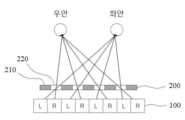
도 1은 본 발명의 실시예들에 따른 패럴렉스 배리어 방식의 3D 디스플레이 방식을 설명하기 위한 도면이다.
도 2는 본 발명의 실시예들에 따른 입체 영상 디스플레이 패널(100)의 평면도이다.
도 3은 본 발명의 실시예에 따른 입체 영상 디스플레이 패널(100)의 서브 화소들의 유기 발광 소자 및 유기 발광 소자를 독립적으로 구동하기 위한 화소 회로의 구성도이다.
도 4는 본 발명의 실시예에 따른 입체 영상 디스플레이 패널(100)의 일 서브 픽셀의 단면도이다.
도 5는 좌우 휘도 반사를 측정하는 원리를 설명하기 위한 설명도이다.
도 6은 서브 화소가 사각형 형태일 경우, 좌우 휘도 반사(Scattering)를 나타낸 표이다.
도 7은 본 발명의 실시예에 따라 서브 화소가 톱니 모양일 경우 좌우 휘도 반사(Scattering)를 나타낸 표이다.1 is a diagram for explaining a 3D display method of a parallax barrier method according to embodiments of the present invention.
2 is a plan view of a stereoscopic
3 is a configuration diagram of an organic light emitting device of sub-pixels of a stereoscopic
4 is a cross-sectional view of one sub-pixel of the stereoscopic
5 is an explanatory diagram for explaining the principle of measuring left and right luminance reflection.
6 is a table showing left and right luminance scattering when a sub-pixel has a rectangular shape.
7 is a table showing left and right luminance scattering when sub-pixels have a sawtooth shape according to an embodiment of the present invention.
본 발명의 이점 및 특징, 그리고 그것들을 달성하는 방법은 첨부되는 도면과 함께 상세하게 후술되어 있는 실시예들을 참조하면 명확해질 것이다. 그러나 본 발명은 이하에서 개시되는 실시예들에 한정되는 것이 아니라 서로 다른 다양한 형태로 구현될 것이며, 단지 본 실시예들은 본 발명의 개시가 완전하도록 하며, 본 발명이 속하는 기술분야에서 통상의 지식을 가진 자에게 발명의 범주를 완전하게 알려주기 위해 제공되는 것이며, 본 발명은 청구항의 범주에 의해 정의될 뿐이다.Advantages and features of the present invention, and methods of achieving them, will become clear with reference to the detailed description of the following embodiments taken in conjunction with the accompanying drawings. However, the present invention is not limited to the embodiments disclosed below, but will be implemented in various different forms, only these embodiments make the disclosure of the present invention complete, and common knowledge in the art to which the present invention belongs. It is provided to fully inform the holder of the scope of the invention, and the present invention is only defined by the scope of the claims.
본 발명의 실시예를 설명하기 위한 도면에 개시된 형상, 크기, 비율, 각도, 개수 등은 예시적인 것이므로 본 발명이 도시된 사항에 한정되는 것은 아니다. 명세서 전체에 걸쳐 동일 참조 부호는 동일 구성 요소를 지칭한다. 또한, 본 발명을 설명함에 있어서, 관련된 공지 기술에 대한 구체적인 설명이 본 발명의 요지를 불필요하게 흐릴 수 있다고 판단되는 경우 그 상세한 설명은 생략한다.The shapes, sizes, ratios, angles, numbers, etc. disclosed in the drawings for explaining the embodiments of the present invention are illustrative, so the present invention is not limited to the details shown. Like reference numbers designate like elements throughout the specification. In addition, in describing the present invention, if it is determined that a detailed description of related known technologies may unnecessarily obscure the subject matter of the present invention, the detailed description will be omitted.
본 발명의 명세서에서 언급된 '포함한다', '갖는다', '이루어진다' 등이 사용되는 경우, '~만'이 사용되지 않는 이상 다른 부분이 추가될 수 있다. 구성 요소를 단수로 표현한 경우에 특별히 명시적인 기재 사항이 없는 한 복수를 포함하는 경우를 포함한다.When 'includes', 'has', 'consists of', etc. mentioned in the specification of the present invention is used, other parts may be added unless 'only' is used. In the case where a component is expressed in the singular, the case including the plural is included unless otherwise explicitly stated.
구성 요소를 해석함에 있어서, 별도의 명시적 기재가 없더라도 오차 범위를 포함하는 것으로 해석한다.In interpreting the components, even if there is no separate explicit description, it is interpreted as including the error range.
위치 관계에 대한 설명일 경우, 예를 들어, '~상에', '~상부에', '~하부에', '~옆에' 등으로 두 부분의 위치 관계가 설명되는 경우, '바로' 또는 '직접'이 사용되지 않는 이상 두 부분 사이에 하나 이상의 다른 부분이 위치할 수도 있다.In the case of a description of a positional relationship, for example, 'on top of', 'on top of', 'at the bottom of', 'next to', etc. Or, unless 'directly' is used, one or more other parts may be located between the two parts.
시간 관계에 대한 설명일 경우, 예를 들어, '~후에', '~에 이어서', '~다음에', '~전에' 등으로 시간적 선후 관계가 설명되는 경우, '바로' 또는 '직접'이 사용되지 않는 이상 연속적이지 않은 경우도 포함할 수 있다.In the case of a description of a temporal relationship, for example, 'immediately' or 'directly' when a temporal precedence relationship is described in terms of 'after', 'following', 'next to', 'before', etc. It can also include non-continuous cases unless is used.
제 1, 제 2 등이 다양한 구성요소들을 서술하기 위해서 사용되나, 이들 구성요소들은 이들 용어에 의해 제한되지 않는다. 이들 용어들은 단지 하나의 구성요소를 다른 구성요소와 구별하기 위하여 사용하는 것이다. 따라서, 이하에서 언급되는 제 1 구성요소는 본 발명의 기술적 사상 내에서 제 2 구성요소일 수도 있다.Although first, second, etc. are used to describe various components, these components are not limited by these terms. These terms are only used to distinguish one component from another. Therefore, the first component mentioned below may also be the second component within the technical spirit of the present invention.
"X축 방향", "Y축 방향" 및 "Z축 방향"은 서로 간의 관계가 수직으로 이루어진 기하학적인 관계만으로 해석되어서는 아니 되며, 본 발명의 구성이 기능적으로 작용할 수 있는 범위 내에서보다 넓은 방향성을 가지는 것을 의미할 수 있다."X-axis direction", "Y-axis direction", and "Z-axis direction" should not be interpreted only as a geometric relationship in which the relationship between each other is made upright, and may be broader within the range in which the configuration of the present invention can function functionally. It can mean having a direction.
"적어도 하나"의 용어는 하나 이상의 관련 항목으로부터 제시 가능한 모든 조합을 포함하는 것으로 이해되어야 한다. 예를 들어, "제 1 항목, 제 2 항목 및 제 3 항목 중에서 적어도 하나"의 의미는 제 1 항목, 제 2 항목 또는 제 3 항목 각각 뿐만 아니라 제 1 항목, 제 2 항목 및 제 3 항목 중에서 2개 이상으로부터 제시될 수 있는 모든 항목의 조합을 의미할 수 있다.The term “at least one” should be understood to include all possible combinations from one or more related items. For example, "at least one of the first item, the second item, and the third item" means not only the first item, the second item, or the third item, respectively, but also two of the first item, the second item, and the third item. It may mean a combination of all items that can be presented from one or more.
본 발명의 여러 실시예들의 각각 특징들이 부분적으로 또는 전체적으로 서로 결합 또는 조합 가능하고, 기술적으로 다양한 연동 및 구동이 가능하며, 각 실시예들이 서로에 대하여 독립적으로 실시 가능할 수도 있고 연관 관계로 함께 실시할 수도 있다.Each feature of the various embodiments of the present invention can be partially or entirely combined or combined with each other, technically various interlocking and driving are possible, and each embodiment can be implemented independently of each other or can be implemented together in a related relationship. may be
이하, 본 발명의 바람직한 실시예들을 첨부된 도면을 참조하여 보다 상세히 설명하면 다음과 같다.Hereinafter, preferred embodiments of the present invention will be described in more detail with reference to the accompanying drawings.
도 1은 본 발명의 실시예들에 따른 입체 영상 디스플레이 장치의 구성도이다.1 is a configuration diagram of a stereoscopic image display device according to embodiments of the present invention.
본 발명의 실시예들에 따른 입체 영상 디스플레이 장치는, 도 1에 도시한 바와 같이, 영상을 표시하는 디스플레이 패널(100)과, 디스플레이 패널(100) 전면에 배치되는 패럴렉스 배리어(Parallax Barrier; 200)를 포함한다.As shown in FIG. 1, a stereoscopic image display device according to embodiments of the present invention includes a
패럴렉스 배리어(200)는 복수의 라인 패턴을 갖는다. 예를 들어, 패럴렉스 배리어(200)는 디스플레이 패널(100)에서 나오는 광을 차단하는 차단 영역(210)과, 디스플레이 패널(100)에서 나오는 광을 그대로 투과시키는 투과 영역(220)을 구비한다.The
차단 영역(210)과 투과 영역(220)은 라인 형태로 구성되고, 서로 교번하여 배치된다.The blocking
이와 같은 디스플레이 패널(100)은 PDP(Plasma Display Panel), PALC(Plasma Address Liquid Crystal display panel), LCD(Liquid Crystal Display) 및 OLED(Organic Light Emitting Diode) 패널 등으로 형성될 수 있다. 다만, 설명의 편의상 본 명세서 상에서는 OLED 패널을 기준으로 설명한다.Such a
OLED 패널은 데이터 라인들, 스캔 라인들, 데이터 라인들과 스캔 라인들의 교차부에 형성된 다수의 서브 화소들을 구비한다.The OLED panel includes data lines, scan lines, and a plurality of sub-pixels formed at intersections of the data lines and scan lines.
OLED 패널의 각 서브 화소들은, 유기 발광 다이오드(organic light emitting diode; 이하 'OLED' 라 함)와 상기 유기 발광 다이오드(OLED)를 독립적으로 구동하는 화소 회로를 구비한다.Each sub-pixel of the OLED panel includes an organic light emitting diode (hereinafter referred to as 'OLED') and a pixel circuit independently driving the organic light emitting diode (OLED).
유기 발광 다이오드(OLED)는 제1 전극과 제2 전극 사이에 발광층이 배치되는 구조를 갖고, 발광층에서 전자(electric)와 정공(Hole)의 재결합으로 발광층을 발광시키는 자발광 소자이다.An organic light emitting diode (OLED) is a self-luminous device that has a structure in which a light emitting layer is disposed between a first electrode and a second electrode, and emits light through the light emitting layer by recombination of electrons and holes in the light emitting layer.
상기 화소 회로는, 게이트-소스 간 전압에 따라 상기 OLED에 흐르는 구동 전류를 제어하는 구동 TFT(Driving Thin Film Transistor), 구동 TFT의 게이트-소스 간 전압을 한 프레임 동안 일정하게 유지시키는 커패시터, 및 게이트 신호에 응답하여 구동 TFT의 게이트-소스 간 전압을 프로그래밍하는 적어도 하나 이상의 스위칭 TFT(Switching Thin Film Transistor) 등을 포함한다.The pixel circuit includes a driving thin film transistor (TFT) controlling a driving current flowing through the OLED according to a gate-source voltage, a capacitor maintaining the gate-source voltage of the driving TFT constant for one frame, and a gate and at least one switching TFT (Switching Thin Film Transistor) for programming the voltage between the gate and source of the driving TFT in response to a signal.
여기서, 단위 화소가 3개의 서브 화소들로 구성되거나 4개의 서브 화소들로 구성될 수 있다.Here, a unit pixel may be composed of 3 sub-pixels or 4 sub-pixels.
디스플레이 패널(100)은 좌안용 영상(L)과 우안용 영상(R)이 X축 방향으로 교번적으로 배치된 프레임을 디스플레이한다. 이 때, 패럴렉스 배리어(200)에 의해 좌안용 영상(L)과 우안용 영상(R)은 각각 시청자의 좌안 및 우안으로 입사된다. 이에 따라 시청자는 양시차에 의한 입체감을 느낄 수 있다.The
디스플레이 패널(21)은 좌안용 영상(L)과 우안용 영상(R)을 디스플레이하는 서브 화소가 사각형 형태일 경우, 좌우 휘도 반사(Scattering)가 높아 질 수 있다.In the display panel 21, when sub-pixels displaying the image L for the left eye and the image R for the right eye have a rectangular shape, left and right luminance scattering may be increased.
따라서, 본 발명은 서브 화소가 사각형 형태가 아닌 적어도 6각 형태로 형성하여 좌우 휘도 반사(Scattering)를 낮출 수 있다.Accordingly, in the present invention, scattering of left and right luminance can be reduced by forming sub-pixels in at least a hexagonal shape rather than a rectangular shape.
도 2는 본 발명의 실시예들에 따른 입체 영상 디스플레이 패널(100)의 평면도이다.2 is a plan view of a stereoscopic
본 발명의 실시예들에 따른 입체 영상 디스플레이 패널(100)은 좌안 화상을 표시하는 다수의 좌안 서브 화소들(10)과 우안 화상을 표시하는 다수의 우안 서브 화소들(20)을 포함한다.A stereoscopic
각 서브 화소들은 발광 영역을 포함하고, 각 서브 화소의 발광 영역의 경계부에는 뱅크층(30)이 배치된다.Each sub-pixel includes a light emitting region, and a bank layer 30 is disposed at a boundary of the light emitting region of each sub pixel.
다수의 좌안 서브 화소들(10) 및 다수의 우안 서브 화소들(20)은 각각 녹색 서브 화소(G), 적색 서브 화소(R) 및 청색 서브 화소(B)를 구비한다.The plurality of left-eye sub-pixels 10 and the plurality of right-
녹색 서브 화소(G), 적색 서브 화소(R) 및 청색 서브 화소(B)는 톱니 모양의 발광 영역을 갖는다.The green sub-pixel (G), the red sub-pixel (R), and the blue sub-pixel (B) have a sawtooth-shaped emission area.
녹색 서브 화소(G), 적색 서브 화소(R) 및 청색 서브 화소(B)는 각각 다른 형태의 톱니 모양의 발광 영역을 갖는다.The green sub-pixel G, the red sub-pixel R, and the blue sub-pixel B each have a sawtooth light emitting area having a different shape.
예를 들면, 적색 서브 화소(R)는 하나의 6각형 모양의 발광 영역을 갖는다.For example, the red sub-pixel R has a hexagonal light emitting area.
녹색 서브 화소(G)는 2개의 6각형 모양이 한 변을 공유하여 결합된 형태의 발광 영역을 갖는다. The green sub-pixel G has a light emitting region in which two hexagonal shapes share a side and are combined.
청색 서브 화소(B)는 3개의 6각형 모양이 두 변을 공유하여 일렬로 결합되고, 상부면 및 하부면 일부가 절단된 형태의 발광 영역을 갖는다. 그러나 이에 한정되지 않는다.The blue sub-pixel B has a light emitting region in which three hexagonal shapes share two sides and are combined in a row, and upper and lower surfaces are partially cut. However, it is not limited thereto.
상기 모든 서브 화소는 상기 3개의 형태 중 어느 하나의 모양으로 동일하게 형성된 발광 영역을 가질 수 있다. 즉, 모든 서브 화소가, 하나의 6각형 모양의 발광 영역을 가질 수 있고, 2개의 6각형 모양이 한 변을 공유하여 결합된 형태의 발광 영역을 가질 수 있으며, 3개의 6각형 모양이 두 변을 공유하여 일렬로 결합되고 상부면 및 하부면 일부가 절단된 형태의 발광 영역을 가질 수 있다.All of the sub-pixels may have a light emitting region identically formed in one of the three shapes. That is, all sub-pixels may have one hexagonal light emitting area, two hexagonal shapes may share one side and have a combined light emitting area, and three hexagonal shapes may have two sides. It is possible to have a light emitting region in a form in which parts of the upper and lower surfaces are cut and coupled in a row by sharing.
즉, 패럴렉스 배리어(200)의 차단 영역에 인접하는 각 서브 화소의 발광 영역이 톱니 모양을 갖도록 형성될 수 있다.That is, the light emitting area of each sub-pixel adjacent to the blocking area of the
상기에서 설명한 녹색 서브 화소(G), 적색 서브 화소(R) 및 청색 서브 화소(B)의 발광 영역은 유기 발광 소자의 구성 중 제1 전극과 제2 전극 사이에 배치되는 발광층 중 뱅크층에 의해 노출된 모양을 나타낸 것이다.The light emitting regions of the green sub-pixel G, the red sub-pixel R, and the blue sub-pixel B described above are formed by the bank layer among the light-emitting layers disposed between the first electrode and the second electrode in the structure of the organic light emitting device. It shows the exposed shape.
다수의 좌안 서브 화소들(10)의 발광 영역과 다수의 우안 서브 화소들(20)의 발광 영역은 서로 다른 배치를 갖는다. 예를 들면, 다수의 좌안 서브 화소들(10)은 Y축 "?향으?* 청색 서브 화소(B), 적색 서브 화소(R) 및 녹색 서브 화소(G) 순으로 배치되고, 성기 좌안 서브 화소들(10)에 인접한 상기 다수의 우안 서브 화소들(20)은 Y축 "?향으?* 녹색 서브 화소(G), 청색 서브 화소(B) 및 적색 서브 화소(R) 순으로 배치될 수 있다The emission regions of the plurality of left-eye sub-pixels 10 and the emission regions of the plurality of right-
또한, 다수의 좌안 서브 화소들(10)의 발광 영역과 다수의 우안 서브 화소들(20)의 발광 영역은 서로 다른 배치 위치를 갖는다.Also, the emission regions of the plurality of left-eye sub-pixels 10 and the emission regions of the plurality of right-
즉, 다수의 좌안 서브 화소들(10)의 발광 영역 각각은 인접한 다수의 우안 서브 화소들(20)의 발광 영역 사이의 위치에 배치되고, 마찬가지로, 다수의 우안 서브 화소들(20)의 발광 영역 각각은 인접한 다수의 좌안 서브 화소들(10)으 발광 영역 사이의 위치에 배치될 수 있다.That is, each light-emitting area of the plurality of left-eye sub-pixels 10 is disposed at a position between the light-emitting areas of the plurality of adjacent right-
또한, 패럴렉스 배리어(200)의 차단 영역(210)이 다수의 좌안 서브 화소들(10)의 발광 영역과 다수의 우안 서브 화소들(20)의 발광 영역 사이의 뱅크층(30)에 대응하도록 디스플레이 패널(100)과 패럴렉스 배리어(200)가 배치된다.In addition, the blocking
패럴렉스 배리어(200)의 차단 영역(210)은 인접한 다수의 좌안 서브 화소들(10)의 발광 영역과 다수의 우안 서브 화소들(20)의 발광 영역 가장자리 부분에 중첩될 수 있다.The blocking
도 3은 본 발명의 실시예에 따른 입체 영상 디스플레이 패널(100)의 서브 화소들의 유기 발광 소자 및 유기 발광 소자를 독립적으로 구동하기 위한 화소 회로의 구성도이다.3 is a configuration diagram of an organic light emitting device of sub-pixels of a stereoscopic
상기에서 설명한 바와 같이, 녹색 서브 화소(G), 적색 서브 화소(R) 및 청색 서브 화소(B)의 발광 영역의 모양은 유기 발광 소자의 구성 중 제1 전극과 제2 전극 사이에 배치되는 발광층 중 뱅크층에 의해 노출된 모양을 나타낸 것이다.As described above, the shapes of the emission regions of the green sub-pixel G, the red sub-pixel R, and the blue sub-pixel B depend on the light-emitting layer disposed between the first electrode and the second electrode in the organic light-emitting device. It shows the shape exposed by the middle bank layer.
따라서, 각 유기 발광 소자(OLED)는 발광층(1)과 제1 전극(2)만 도시되어 있다.Therefore, in each organic light emitting diode OLED, only the
또한, 다수개의 게이트 라인들(GL(n), GL(n+1))이 X축 방향으로 배치되고, 다수의 데이터 라인들(Date(R), Data(G), Data(B))과 고전압 공급 라인들(VDD)이 Y축 방향으로 배치될 수 있다.In addition, a plurality of gate lines GL(n) and GL(n+1) are disposed in the X-axis direction, and a plurality of data lines Date(R), Data(G), Data(B) and High voltage supply lines VDD may be disposed in the Y-axis direction.
각 게이트 라인(GL(n), GL(n+1))과 각 데이터 라인(Data(R), Data(G), Data(B))이 교차되는 부분에는 유기 발광 소자를 독립적으로 구동 하기 위한 화소 회로들이 배치된다.At the intersection of each gate line (GL(n), GL(n+1)) and each data line (Data(R), Data(G), Data(B)), there is Pixel circuits are disposed.
각 유기 발광 소자(OLED)를 독립적으로 구동하는 화소 회로는 게이트-소스 간 전압에 따라 상기 유기 발광 소자(OLED)에 흐르는 구동 전류를 제어하는 구동 TFT(DT(R), DT(G), DT(B))와, 구동 TFT(DT(R), DT(G), DT(B))의 게이트-소스 간 전압을 한 프레임 동안 일정하게 유지시키는 커패시터(C(R), C(G), C(B)) 및 게이트 신호에 응답하여 구동 TFT(DT(R), DT(G), DT(B))의 게이트에 데이터 전압을 프로그래밍하는 스위칭 TFT(ST(R), ST(G), ST(B)) 등을 구비한다.A pixel circuit that independently drives each organic light emitting diode OLED includes driving TFTs (DT(R), DT(G), and DT that control a driving current flowing through the organic light emitting diode OLED according to a gate-source voltage). (B)) and capacitors (C(R), C(G) that keep the gate-source voltage of the driving TFTs (DT(R), DT(G), DT(B)) constant for one frame, C(B)) and switching TFTs (ST(R), ST(G), which program data voltages to gates of driving TFTs (DT(R), DT(G), DT(B)) in response to gate signals. ST(B)) and the like.
예를 들면, 각 게이트 라인(GL(n), GL(n+1))과 적색 데이터 전압이 공급되는 제1 데이터 라인(Data(R))이 교차되는 지점에는 구동 TFT(DT(R), 커패시터(C(R) 및 스위칭 TFT(ST(R)로 구성되어 적색 서브 화소의 유기 발광 소자를 구동하는 적색 화소 회로가 구성된다.For example, a driving TFT (DT(R), A red pixel circuit composed of the capacitor C(R) and the switching TFT ST(R) is configured to drive the organic light emitting element of the red sub-pixel.
각 게이트 라인(GL(n), GL(n+1))과 청색 데이터 전압이 공급되는 제2 데이터 라인(Data(B))이 교차되는 지점에는 구동 TFT(DT(B), 커패시터(C(B) 및 스위칭 TFT(ST(B)로 구성되어 청색 서브 화소의 유기 발광 소자를 구동하는 청색 화소 회로가 구성된다.A driving TFT (DT(B), a capacitor (C( B) and a switching TFT (ST(B)) to drive the organic light emitting element of the blue sub-pixel.
각 게이트 라인(GL(n), GL(n+1))과 녹색 데이터 전압이 공급되는 제3 데이터 라인(Data(G))이 교차되는 지점에는 구동 TFT(DT(G), 커패시터(C(G) 및 스위칭 TFT(ST(G)로 구성되어 녹색 서브 화소의 유기 발광 소자를 구동하는 녹색 화소 회로가 구성된다.A driving TFT (DT(G), capacitor C( G) and a switching TFT (ST(G)) to drive the organic light emitting element of the green sub-pixel.
그러나, 각 색상의 화소 회로에 인접안 서브 화소 영역에 해당 유기 발광 소자가 배치되지 않을 수도 있다.However, the corresponding organic light emitting element may not be disposed in a sub-pixel area adjacent to the pixel circuit of each color.
예를 들면, 다수의 좌안 서브 화소들(10) 중 청색 서브 화소의 유기 발광 소자(B)의 제1 전극(2)은, 서브 화소(20)의 녹색 서브 화소의 유기 발광 소자(G)를 우회하여, 청색 화소 회로의 구동 TFT(DT(B))에 연결된다.For example, the
도 4는 본 발명의 실시예에 따른 입체 영상 디스플레이 패널(100)의 일 서브 픽셀의 단면도이다. 즉, 좌안 서브 화소(10)의 적색 유기 발광 소자의 단면도이다.4 is a cross-sectional view of one sub-pixel of the stereoscopic
도 4에 도시한 바와 같이, 기판(GLS) 상에 제1 금속 패턴(LS)이 형성된다. 제1 금속 패턴(LS)은 TFT의 아래에 배치되어 TFT로 조사되는 빛을 차단한다. 여기서, TFT는 도 3에 도시된 구동 TFT(DT(R))를 나타낸 것이다.As shown in FIG. 4 , a first metal pattern LS is formed on the substrate GLS. The first metal pattern LS is disposed under the TFT to block light irradiated to the TFT. Here, TFT denotes the driving TFT (DT(R)) shown in FIG.
버퍼층(BUF)은 무기 절연재료 예를 들어, SiO2, SiNx 등으로 형성되어 제1 금속 패턴(LS)을 덮는다.The buffer layer BUF is formed of an inorganic insulating material, such as SiO2 or SiNx, and covers the first metal pattern LS.
박막트랜지스터(TFT)부의 액티브 패턴(ACT)은 TFT의 반도체 채널층을 포함한다. 액티브 패턴(ACT)의 일부는 커패시터((Cst)의 하부 전극으로 이용될 수 있다. TFT가 산화물(Oxide) TFT로 구현된 경우, 액티브 패턴(ACT)은 IGZO(Indium gallium zinc oxide)를 포함할 수 있다. 커패시터(Cst)는 도 3에 도시된 커패시터(C(R))를 나타낸 것이다.The active pattern ACT of the thin film transistor (TFT) unit includes a semiconductor channel layer of the TFT. A part of the active pattern ACT may be used as a lower electrode of the capacitor Cst. If the TFT is implemented as an oxide TFT, the active pattern ACT may include indium gallium zinc oxide (IGZO). The capacitor Cst represents the capacitor C(R) shown in FIG.
박막트랜지스터(TFT)부의 액티브 패턴(ACT) 상에 게이트 절연막(GI)이 형성된다. 게이트 절연막(GI)은 무기 절연재료로 형성될 수 있다.A gate insulating layer GI is formed on the active pattern ACT of the thin film transistor TFT. The gate insulating layer GI may be formed of an inorganic insulating material.
제1 및 제2 층간 절연층(ILD1, IDD2)는 제3 금속 패턴(GATE)과 제4 금속 패턴(SD) 사이에 배치되어 이 금속 패 턴들 간을 절연한다.The first and second interlayer insulating layers ILD1 and IDD2 are disposed between the third metal pattern GATE and the fourth metal pattern SD to insulate between the metal patterns.
커패시터(Cst)부에서 제1 층간 절연층(ILD1) 상에 제2 금속 패턴(GATE2)이 형성된다. 제2 금속 패턴(GATE2)은 커패시터(Cst)의 상부 전극을 포함한다.A second metal pattern GATE2 is formed on the first interlayer insulating layer ILD1 in the capacitor Cst part. The second metal pattern GATE2 includes an upper electrode of the capacitor Cst.
박막트랜지스터(TFT)부에 배치된 제3 금속 패턴(GATE)은 TFT의 게이트 전극을 포함한다.The third metal pattern GATE disposed on the thin film transistor TFT includes a gate electrode of the TFT.
제4 금속 패턴(SD)은 TFT의 소스 전극 및 드레인 전극을 포함한다.The fourth metal pattern SD includes a source electrode and a drain electrode of the TFT.
TFT의 소스 전극과 드레인 전극은 제1 및 제2 층간 절연층(ILD1, ILD2)를 관통하는 콘택홀들을 통해 액티브 패턴(ACT)에 전기적으로 연결된다. 커패시터(Cst)부에서 제4 금속 패턴(SD)은 제2 층간 절연층(ILD2)를 관통하는 콘택홀들을 통해 제2 금속 패턴(GATE2)에 전기적으로 연결된다.The source and drain electrodes of the TFT are electrically connected to the active pattern ACT through contact holes penetrating the first and second interlayer insulating layers ILD1 and ILD2. In the capacitor Cst part, the fourth metal pattern SD is electrically connected to the second metal pattern GATE2 through contact holes penetrating the second interlayer insulating layer ILD2.
보호층(PAS)은 박막트랜지스터(TFT)부와 커패시터(Cst)부를 덮는다. 보호층(PAS)은 무기 절연재료로 형성될 수 있다.The protective layer PAS covers the thin film transistor TFT and capacitor Cst. The protective layer PAS may be formed of an inorganic insulating material.
평탄화층(OC)은 보호층(PAS)을 덮어 표면을 평탄하게 한다. 평탄화층(OC)은 유기 절연재료로 형성될 수 있다.The planarization layer OC covers the passivation layer PAS to flatten the surface. The planarization layer OC may be formed of an organic insulating material.
발광 소자(OLED)의 애노드 전극(ANO)은 평탄화층(OC) 상에 배치되어 보호층(PAS)과 평탄화층(OC)을 관통하는 콘택홀을 통해 TFT의 제4 금속 패턴에 접촉된다. 애노드 전극(ANO)은 금속 물질을 포함할 수 있다.The anode electrode ANO of the light emitting element OLED is disposed on the planarization layer OC and contacts the fourth metal pattern of the TFT through the contact hole penetrating the passivation layer PAS and the planarization layer OC. The anode electrode ANO may include a metal material.
뱅크 패턴(BANK)은 유기 절연재료로 형성되어 애노드 전극(ANO)의 일부와 평탄화층(OC)과 상에 배치되어 발광 영역을 정의한다.The bank pattern BANK is formed of an organic insulating material and disposed on a portion of the anode electrode ANO and the planarization layer OC to define an emission area.
발광 소자(OLED)의 유기 화합물층(EL)은 뱅크 패턴(BANK)에 의해 정의된 애노드 전극의 노출 영역 상애 배치되고, 뱅크 패턴(BANK) 상에 배치된다.The organic compound layer EL of the light emitting element OLED is disposed on the exposed area of the anode electrode defined by the bank pattern BANK and disposed on the bank pattern BANK.
발광 소자(OLED)의 캐소드 전극(CAT)은 유기 화합물층(EL) 상에 배치된다. 캐소드 전극은 IZO(Indium Zinc Oxide)와 같은 투명 금속 전극 물질을 포함할 수 있다.The cathode electrode CAT of the light emitting element OLED is disposed on the organic compound layer EL. The cathode electrode may include a transparent metal electrode material such as indium zinc oxide (IZO).
여기서, 애노드 전극(ANO)은 도 3의 제1 전극(2)에 해당된다.Here, the anode electrode ANO corresponds to the
도 5는 좌우 휘도 반사를 측정하는 원리를 설명하기 위한 설명도이다.5 is an explanatory diagram for explaining the principle of measuring left and right luminance reflection.
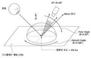
좌우 휘도 반사의 측정은, 도 5에 도시한 바와 같이, X축 방향으로 디스플레이 패널(100)을 위치시킨 상태에서 45도 각도로 광을 조사하고, 조사된 광이 반사되는 반사 각도와 Y축 사이에서 20도 내지 40도 범위에서 카메라로 촬영한 것이다.As shown in FIG. 5, the measurement of left and right luminance reflection is performed by irradiating light at an angle of 45 degrees with the
도 6은 서브 화소가 사각형 형태일 경우, 좌우 휘도 반사(Scattering)를 나타낸 표이고, 도 7은 본 발명의 실시예에 따라 서브 화소가 톱니 모양일 경우 좌우 휘도 반사(Scattering)를 나타낸 표이다.6 is a table showing left and right luminance scattering when a sub-pixel has a rectangular shape, and FIG. 7 is a table showing left and right luminance scattering when a sub-pixel has a sawtooth shape according to an embodiment of the present invention.
도 6 및 도 7은 도 5와 같은 측정 원리로 3번에 걸쳐 측정한 것으로, 측정 각도가 20도, 25도 30도 및 35도 일 때 좌우 휘도 반사 값을 나타낸 것이다.6 and 7 are measured three times using the same measurement principle as in FIG. 5, and show left and right luminance reflection values when the measurement angles are 20 degrees, 25 degrees, 30 degrees, and 35 degrees.
도 6 및 도 7에서 도시한 바와 같이, 본 발명은 서브 화소를 톱니 모양으로 형성하므로, 서브 화소가 사각형 형태일 때 보다 좌우 휘도 반사를 줄일 수 있다.As shown in FIGS. 6 and 7 , since the sub-pixels are formed in a sawtooth shape, left and right luminance reflection can be reduced more than when the sub-pixels have a rectangular shape.
이상 설명한 내용을 통해 당업자라면 본 발명의 기술 사상을 일탈하지 아니하는 범위에서 다양한 변경 및 수정이 가능함을 알 수 있을 것이다. 따라서, 본 발명의 기술적 범위는 명세서의 상세한 설명에 기재된 내용으로 한정되는 것이 아니라 특허 청구 범위에 의해 한정되어야 할 것이다.Through the above description, those skilled in the art will know that various changes and modifications are possible without departing from the spirit of the present invention. Therefore, the technical scope of the present invention should not be limited to the contents described in the detailed description of the specification, but should be limited by the claims.
10: 다수의 좌안 서브 화소들20: 다수의 우안 서브 화소들
100: 디스플레이 패널200: 패럴렉스 베리어
210; 차단 영역 220: 투과 영역10: multiple left eye sub-pixels 20: multiple right eye sub-pixels
100: display panel 200: parallax barrier
210; Blocking area 220: transmission area
Claims (9)
Translated fromKorean우안 화상을 표시하는 다수의 우안 서브 화소들과,
각 서브 화소들의 발광 영역의 경계부에 배치되는 뱅크층을 구비하고,
각 서브 화소의 발광 영역은 톱니 모양으로 배치되는 입체 영상 디스플레이 패널.A plurality of left eye sub-pixels displaying a left eye image;
A plurality of right eye sub-pixels displaying a right eye image;
A bank layer disposed at the boundary of the light emitting area of each sub-pixel,
A three-dimensional image display panel in which light emitting regions of each sub-pixel are arranged in a sawtooth shape.
상기 다수의 좌안 서브 화소들 및 상기 다수의 우안 서브 화소들은 적색, 녹색, 청색 서브 화소를 구비하고, 각 적색, 녹색, 청색 서브 화소들은 서로 다른 형상의 톱니 모양의 발광 영역을 갖는 입체 영상 디스플레이 패널.According to claim 1,
The plurality of left-eye sub-pixels and the plurality of right-eye sub-pixels include red, green, and blue sub-pixels, and each red, green, and blue sub-pixel has a sawtooth light emitting area having a different shape. .
상기 적색, 녹색 및 청색 서브 화소들 중 하나는, 하나의 6각형 모양의 발광 영역을 갖고, 다른 하나는 2개의 6각형 모양이 한 변을 공유하여 결합된 형태의 발광 영역을 가지며, 나머지 하나는 3개의 6각형 모양이 두 변을 공유하여 일렬로 결합되고, 상부면 및 하부면 일부가 절단된 형태의 발광 영역을 갖는 입체 영상 디스플레이 패널.According to claim 2,
One of the red, green, and blue sub-pixels has a hexagonal light emitting area, the other has a light emitting area in which two hexagonal shapes share a side and are combined, and the other has A three-dimensional image display panel having a light emitting area in which three hexagonal shapes share two sides and are combined in a row, and portions of upper and lower surfaces are cut.
상기 적색 서브 화소 하나의 6각형 모양의 발광 영역을 갖고,
녹색 서브 화소는 2개의 6각형 모양이 한 변을 공유하여 결합된 형태의 발광 영역을 가지며,
청색 서브 화소는 3개의 6각형 모양이 두 변을 공유하여 일렬로 결합되고, 상부면 및 하부면 일부가 절단된 형태의 발광 영역을 갖는 입체 영상 디스플레이 패널.According to claim 3,
a hexagonal light emitting area of one red sub-pixel;
The green sub-pixel has a light emitting area in which two hexagonal shapes share a side and are combined.
A three-dimensional image display panel having a light emitting area in which three hexagonal shapes are combined in a row by sharing two sides of the blue sub-pixels, and portions of upper and lower surfaces are cut.
상기 다수의 좌안 서브 화소들 및 상기 다수의 우안 서브 화소들은 적색, 녹색, 청색 서브 화소를 구비하고, 각 적색, 녹색, 청색 서브 화소들은 서로 동일한 형상의 톱니 모양의 발광 영역을 갖는 입체 영상 디스플레이 패널.According to claim 1,
The plurality of left-eye sub-pixels and the plurality of right-eye sub-pixels include red, green, and blue sub-pixels, and each of the red, green, and blue sub-pixels has a sawtooth-shaped light emitting area having the same shape as a three-dimensional image display panel. .
상기 적색, 녹색 및 청색 서브 화소들은, 하나의 6각형 모양의 발광 영역, 2개의 6각형 모양이 한 변을 공유하여 결합된 형태의 발광 영역 또는 3개의 6각형 모양이 두 변을 공유하여 일렬로 결합되고, 상부면 및 하부면 일부가 절단된 형태의 발광 영역 중 하나의 발광 영역을 갖는 입체 영상 디스플레이 패널.According to claim 5,
The red, green, and blue sub-pixels are arranged in a single hexagonal light emitting area, a combined light emitting area with two hexagonal shapes sharing one side, or a line with three hexagonal shapes sharing two sides. A three-dimensional image display panel having one light emitting region among light emitting regions in which upper and lower surfaces are partially cut.
상기 다수의 좌안 서브 화소들의 색상 배치 순서와 상기 다수의 우안 서브 화소들의 색상 배치 순서가 서로 다른 입체 영상 디스플레이 패널.According to claim 1,
A color arrangement order of the plurality of left eye sub-pixels and a color arrangement order of the plurality of right eye sub-pixels are different from each other.
상기 다수의 좌안 서브 화소들의 발광 영역의 위치와 상기 다수의 우안 서브 화소들의 발광 영역의 위치가 서로 다른 입체 영상 디스플레이 패널.According to claim 1,
The three-dimensional image display panel of claim 1 , wherein positions of light emitting regions of the plurality of left-eye sub-pixels are different from positions of light-emitting regions of the plurality of right-eye sub-pixels.
상기 다수의 좌안 서브 화소들의 발광 영역들은 인접한 상기 다수의 우안 서브 화소들의 발광 영역 사이에 위치되고, 상기 다수의 우안 서브 화소들의 발광 영역들은 인접한 상기 다수의 좌안 서브 화소들의 발광 영역들 사이에 위치되는 입체 영상 디스플레이 패널.According to claim 8,
Light-emitting regions of the plurality of left-eye sub-pixels are positioned between adjacent light-emitting regions of the plurality of right-eye sub-pixels, and light-emitting regions of the plurality of right-eye sub-pixels are positioned between adjacent light-emitting regions of the plurality of left-eye sub-pixels. Stereoscopic image display panel.
Priority Applications (3)
| Application Number | Priority Date | Filing Date | Title |
|---|---|---|---|
| KR1020210193352AKR20230102887A (en) | 2021-12-30 | 2021-12-30 | Stereoscopic Image Display Panel |
| CN202210831908.1ACN116413925A (en) | 2021-12-30 | 2022-07-15 | Stereoscopic image display panel and stereoscopic image display device |
| US17/895,597US20230217762A1 (en) | 2021-12-30 | 2022-08-25 | Stereoscopic image display panel and stereoscopic image display device |
Applications Claiming Priority (1)
| Application Number | Priority Date | Filing Date | Title |
|---|---|---|---|
| KR1020210193352AKR20230102887A (en) | 2021-12-30 | 2021-12-30 | Stereoscopic Image Display Panel |
Publications (1)
| Publication Number | Publication Date |
|---|---|
| KR20230102887Atrue KR20230102887A (en) | 2023-07-07 |
Family
ID=86991441
Family Applications (1)
| Application Number | Title | Priority Date | Filing Date |
|---|---|---|---|
| KR1020210193352APendingKR20230102887A (en) | 2021-12-30 | 2021-12-30 | Stereoscopic Image Display Panel |
Country Status (3)
| Country | Link |
|---|---|
| US (1) | US20230217762A1 (en) |
| KR (1) | KR20230102887A (en) |
| CN (1) | CN116413925A (en) |
Family Cites Families (7)
| Publication number | Priority date | Publication date | Assignee | Title |
|---|---|---|---|---|
| EP2312375A4 (en)* | 2008-07-15 | 2012-10-10 | Kenji Yoshida | Naked eye three-dimensional video image display system, naked eye three-dimensional video image display device, amusement game machine and parallax barrier sheet |
| JP5796761B2 (en)* | 2010-09-15 | 2015-10-21 | Nltテクノロジー株式会社 | Image display device and display panel |
| JP2012189885A (en)* | 2011-03-11 | 2012-10-04 | Japan Display West Co Ltd | Display device |
| US8724040B2 (en)* | 2011-11-02 | 2014-05-13 | Chimei Innolux Corporation | Pixel structures of 3D display devices |
| KR101366678B1 (en)* | 2013-04-26 | 2014-02-25 | (주)이노션 | A large scale 3-dimensional display apparatus and a display system including it and a display driving method thereof. |
| KR20220008028A (en)* | 2020-07-13 | 2022-01-20 | 엘지디스플레이 주식회사 | Stereoscopic display apparatus having a display panel and lenticular lenses |
| CN112558320B (en)* | 2020-12-23 | 2022-12-09 | 维沃移动通信有限公司 | Display panels and display devices |
- 2021
- 2021-12-30KRKR1020210193352Apatent/KR20230102887A/enactivePending
- 2022
- 2022-07-15CNCN202210831908.1Apatent/CN116413925A/enactivePending
- 2022-08-25USUS17/895,597patent/US20230217762A1/enactivePending
Also Published As
| Publication number | Publication date |
|---|---|
| CN116413925A (en) | 2023-07-11 |
| US20230217762A1 (en) | 2023-07-06 |
Similar Documents
| Publication | Publication Date | Title |
|---|---|---|
| CN103517053B (en) | Parallax Barrier Type Stereoscopic Image Display Device | |
| US10237538B2 (en) | Display panel, driving method thereof, manufacturing method thereof and display device | |
| US7066599B2 (en) | Display unit | |
| US11002983B2 (en) | Switching parallax barrier comprising a plurality of first and second electrodes respectively on a blocking region and a transmitting region and 3D display device having the same | |
| US8692971B2 (en) | 2D and 3D switchable display device and liquid crystal lens thereof | |
| US8264626B2 (en) | Stereoscopic image display device | |
| US11943973B2 (en) | Preparation method of display panel, display panel and displaying device | |
| KR101837325B1 (en) | 3d display panel with effect of depth of field, and display method therefor | |
| US9176327B2 (en) | Three-dimensional display for naked eyes | |
| US8384834B2 (en) | Electronic imaging device and driving method thereof | |
| KR102671914B1 (en) | Electroluminescent Display Device | |
| CN110911439A (en) | Display panel, display screen and display terminal | |
| US11189678B2 (en) | Electroluminescent display apparatus and display apparatus | |
| US8995047B2 (en) | Three-dimensional image display and converter therefor | |
| KR102008904B1 (en) | Organic light emitting display device | |
| KR20230102887A (en) | Stereoscopic Image Display Panel | |
| KR101706238B1 (en) | Organic light emitting diode display device | |
| KR102449685B1 (en) | stereoscopic image display device | |
| KR101147425B1 (en) | Display device | |
| KR101931331B1 (en) | Stereoscopic image display device | |
| WO2020015446A1 (en) | Display panel and driving method therefor, and display device | |
| KR20130028350A (en) | A patterned retarder type 3d display device having black strips and manufacturing method therefor | |
| KR102631568B1 (en) | Autostereoscopic 3d image display device | |
| KR101696468B1 (en) | Stereoscopic image display device and drving method thereof | |
| KR20140029828A (en) | Stereoscopic image display device |
Legal Events
| Date | Code | Title | Description |
|---|---|---|---|
| PA0109 | Patent application | Patent event code:PA01091R01D Comment text:Patent Application Patent event date:20211230 | |
| PG1501 | Laying open of application | ||
| A201 | Request for examination | ||
| PA0201 | Request for examination | Patent event code:PA02012R01D Patent event date:20241119 Comment text:Request for Examination of Application |