KR20230098237A - Self-Aligned Top Via - Google Patents
Self-Aligned Top ViaDownload PDFInfo
- Publication number
- KR20230098237A KR20230098237AKR1020237017555AKR20237017555AKR20230098237AKR 20230098237 AKR20230098237 AKR 20230098237AKR 1020237017555 AKR1020237017555 AKR 1020237017555AKR 20237017555 AKR20237017555 AKR 20237017555AKR 20230098237 AKR20230098237 AKR 20230098237A
- Authority
- KR
- South Korea
- Prior art keywords
- liner
- spacers
- dielectric material
- lines
- conductive metal
- Prior art date
- Legal status (The legal status is an assumption and is not a legal conclusion. Google has not performed a legal analysis and makes no representation as to the accuracy of the status listed.)
- Granted
Links
Images


Classifications
- H—ELECTRICITY
- H01—ELECTRIC ELEMENTS
- H01L—SEMICONDUCTOR DEVICES NOT COVERED BY CLASS H10
- H01L21/00—Processes or apparatus adapted for the manufacture or treatment of semiconductor or solid state devices or of parts thereof
- H01L21/70—Manufacture or treatment of devices consisting of a plurality of solid state components formed in or on a common substrate or of parts thereof; Manufacture of integrated circuit devices or of parts thereof
- H01L21/71—Manufacture of specific parts of devices defined in group H01L21/70
- H01L21/768—Applying interconnections to be used for carrying current between separate components within a device comprising conductors and dielectrics
- H01L21/76897—Formation of self-aligned vias or contact plugs, i.e. involving a lithographically uncritical step
- H—ELECTRICITY
- H01—ELECTRIC ELEMENTS
- H01L—SEMICONDUCTOR DEVICES NOT COVERED BY CLASS H10
- H01L21/00—Processes or apparatus adapted for the manufacture or treatment of semiconductor or solid state devices or of parts thereof
- H01L21/70—Manufacture or treatment of devices consisting of a plurality of solid state components formed in or on a common substrate or of parts thereof; Manufacture of integrated circuit devices or of parts thereof
- H01L21/71—Manufacture of specific parts of devices defined in group H01L21/70
- H01L21/768—Applying interconnections to be used for carrying current between separate components within a device comprising conductors and dielectrics
- H01L21/76801—Applying interconnections to be used for carrying current between separate components within a device comprising conductors and dielectrics characterised by the formation and the after-treatment of the dielectrics, e.g. smoothing
- H01L21/76802—Applying interconnections to be used for carrying current between separate components within a device comprising conductors and dielectrics characterised by the formation and the after-treatment of the dielectrics, e.g. smoothing by forming openings in dielectrics
- H01L21/76816—Aspects relating to the layout of the pattern or to the size of vias or trenches
- H—ELECTRICITY
- H01—ELECTRIC ELEMENTS
- H01L—SEMICONDUCTOR DEVICES NOT COVERED BY CLASS H10
- H01L21/00—Processes or apparatus adapted for the manufacture or treatment of semiconductor or solid state devices or of parts thereof
- H01L21/70—Manufacture or treatment of devices consisting of a plurality of solid state components formed in or on a common substrate or of parts thereof; Manufacture of integrated circuit devices or of parts thereof
- H01L21/71—Manufacture of specific parts of devices defined in group H01L21/70
- H01L21/768—Applying interconnections to be used for carrying current between separate components within a device comprising conductors and dielectrics
- H01L21/76838—Applying interconnections to be used for carrying current between separate components within a device comprising conductors and dielectrics characterised by the formation and the after-treatment of the conductors
- H01L21/76877—Filling of holes, grooves or trenches, e.g. vias, with conductive material
- H—ELECTRICITY
- H01—ELECTRIC ELEMENTS
- H01L—SEMICONDUCTOR DEVICES NOT COVERED BY CLASS H10
- H01L21/00—Processes or apparatus adapted for the manufacture or treatment of semiconductor or solid state devices or of parts thereof
- H01L21/70—Manufacture or treatment of devices consisting of a plurality of solid state components formed in or on a common substrate or of parts thereof; Manufacture of integrated circuit devices or of parts thereof
- H01L21/71—Manufacture of specific parts of devices defined in group H01L21/70
- H01L21/768—Applying interconnections to be used for carrying current between separate components within a device comprising conductors and dielectrics
- H01L21/76838—Applying interconnections to be used for carrying current between separate components within a device comprising conductors and dielectrics characterised by the formation and the after-treatment of the conductors
- H01L21/76885—By forming conductive members before deposition of protective insulating material, e.g. pillars, studs
- H—ELECTRICITY
- H01—ELECTRIC ELEMENTS
- H01L—SEMICONDUCTOR DEVICES NOT COVERED BY CLASS H10
- H01L23/00—Details of semiconductor or other solid state devices
- H01L23/52—Arrangements for conducting electric current within the device in operation from one component to another, i.e. interconnections, e.g. wires, lead frames
- H01L23/522—Arrangements for conducting electric current within the device in operation from one component to another, i.e. interconnections, e.g. wires, lead frames including external interconnections consisting of a multilayer structure of conductive and insulating layers inseparably formed on the semiconductor body
- H01L23/5226—Via connections in a multilevel interconnection structure
- H—ELECTRICITY
- H01—ELECTRIC ELEMENTS
- H01L—SEMICONDUCTOR DEVICES NOT COVERED BY CLASS H10
- H01L23/00—Details of semiconductor or other solid state devices
- H01L23/52—Arrangements for conducting electric current within the device in operation from one component to another, i.e. interconnections, e.g. wires, lead frames
- H01L23/522—Arrangements for conducting electric current within the device in operation from one component to another, i.e. interconnections, e.g. wires, lead frames including external interconnections consisting of a multilayer structure of conductive and insulating layers inseparably formed on the semiconductor body
- H01L23/532—Arrangements for conducting electric current within the device in operation from one component to another, i.e. interconnections, e.g. wires, lead frames including external interconnections consisting of a multilayer structure of conductive and insulating layers inseparably formed on the semiconductor body characterised by the materials
- H01L23/53204—Conductive materials
- H01L23/53209—Conductive materials based on metals, e.g. alloys, metal silicides
- H01L23/53257—Conductive materials based on metals, e.g. alloys, metal silicides the principal metal being a refractory metal
- H01L23/53266—Additional layers associated with refractory-metal layers, e.g. adhesion, barrier, cladding layers
Landscapes
- Engineering & Computer Science (AREA)
- Physics & Mathematics (AREA)
- Condensed Matter Physics & Semiconductors (AREA)
- General Physics & Mathematics (AREA)
- Computer Hardware Design (AREA)
- Microelectronics & Electronic Packaging (AREA)
- Power Engineering (AREA)
- Manufacturing & Machinery (AREA)
- Internal Circuitry In Semiconductor Integrated Circuit Devices (AREA)
- Semiconductor Integrated Circuits (AREA)
Abstract
Translated fromKoreanDescription
Translated fromKorean본 발명은 일반적으로 반도체 구조들 및 제조 분야에 관한 것으로, 특히 상단 비아 및 금속 상호접속 라인 구조의 제조(the fabrication of a top via and metal interconnect line structure)에 관한 것이다. The present invention relates generally to semiconductor structures and the field of fabrication, and more particularly to the fabrication of a top via and metal interconnect line structure.
BEOL(Back End of Line)은 개별 소자들(트랜지스터들, 커패시터들, 레지스터들, 등)을, 금속화 층(the metallization layer)의, 웨이퍼 상에서 배선으로 상호접속하는 집적 회로 제조의 부분이다. BEOL은 일반적으로 금속의 제1 층이 웨이퍼에 증착될 때 시작된다. BEOL은 접점들(contacts), 절연층들(유전체), 금속 레벨들, 칩-패키지 연결들을 위한 본딩 사이트들(bonding sites)을 포함한다. Back End of Line (BEOL) is the part of integrated circuit fabrication that interconnects discrete devices (transistors, capacitors, resistors, etc.) with wires on the wafer, in the metallization layer. BEOL typically begins when a first layer of metal is deposited on a wafer. BEOL includes bonding sites for contacts, insulating layers (dielectric), metal levels, and chip-to-package connections.
비아는 하나 또는 그 이상의 인접한 층들의 평면을 통과하는 물리적 전자 회로의 층들 간 전기 연결이다. 집적 회로 설계에서, 비아는 서로 다른 층들 사이의 전도성 연결을 허용하는 절연 산화물 층의 작은 개구부이다. A via is an electrical connection between layers of a physical electronic circuit that passes through the plane of one or more adjacent layers. In integrated circuit design, a via is a small opening in an insulating oxide layer that allows a conductive connection between different layers.
다마신 프로세스(Damascene processing)은 유전체를 증착하고 정의된 패턴에 따라 유전체를 에칭한 후, 패턴에 따라 금속을 채우고 화학적 기계적 연마/평탄화(CMP)를 통해 과잉 금속을 제거하는 추가 프로세스(an additive process)이다. Damascene processing is an additive process that deposits a dielectric, etches it according to a defined pattern, then fills in metal according to the pattern and removes the excess metal through chemical mechanical polishing/planarization (CMP). )am.
본 발명의 실시예들은 반도체 소자를 제조하는 방법 및 최종 구조를 포함한다. 상기 방법은 라이너(a liner) 상에 맨드릴들을 패터닝하는 단계(patterning mandrels)를 포함할 수 있고, 상기 라이너는 반도체 기판 상에 위치한다. 상기 방법은 또한 상기 맨드릴들의 측벽들 상에 스페이서들(spacers)을 형성하는 단계를 포함할 수 있다. 상기 방법은 또한 상기 라이너의 노출된 표면들 상에 그리고 상기 스페이서들 사이의 복수의 갭들 내에 유전체 재료 라인들(dielectric material lines)을 형성하는 단계를 포함할 수 있다. 상기 방법은 또한 상기 맨드릴들을 제거하는 단계를 포함할 수 있다. 상기 방법은 또한 상기 스페이서들 사이의 상기 복수의 갭들 중 적어도 하나 내의 상기 유전체 재료 라인들 중 적어도 하나를 제거하는 단계를 포함할 수 있다. 상기 방법은 또한 각 갭 내에 전도성 금속(conductive metal)을 형성하는 단계를 포함할 수 있다. 상기 방법은 또한 금속 상호접속 라인들 및 비아들을 형성하기 위해 전도성 금속을 패터닝하는 단계를 포함할 수 있다. 상기 방법은 또한 상기 복수의 스페이서들 및 남아있는 유전체 재료 라인들(the remaining dielectric material lines)을 제거는 단계를 포함할 수 있다. Embodiments of the present invention include a method of manufacturing a semiconductor device and a final structure. The method may include patterning mandrels on a liner, the liner positioned on a semiconductor substrate. The method may also include forming spacers on sidewalls of the mandrels. The method may also include forming dielectric material lines on exposed surfaces of the liner and within a plurality of gaps between the spacers. The method may also include removing the mandrels. The method may also include removing at least one of the lines of dielectric material within at least one of the plurality of gaps between the spacers. The method may also include forming a conductive metal within each gap. The method may also include patterning the conductive metal to form metal interconnect lines and vias. The method may also include removing the plurality of spacers and the remaining dielectric material lines.
본 발명의 실시예들은 반도체 소자 및 최종 구조를 제조하기 위한 대안적인 방법들을 추가로 포함할 수 있다. 상기 방법은 라이너의 표면 상에 위치한 유전층을 제공하는 단계를 포함할 수 있으며, 상기 라이너는 반도체 기판의 표면 상에 위치한다. 상기 방법은 또한 상기 라이너의 표면을 노출시키고 상기 남아있는 유전체층으로부터 유전체 재료 라인들을 생성하는 깊이의 복수의 트렌치들을 형성하는 단계를 포함할 수 있다. 상기 방법은 또한 상기 유전체 재료 라인들의 측벽들 상에 스페이서들을 형성하는 단계를 포함할 수 있다. 상기 방법은 또한 상기 스페이서들 2개 사이에 있는 상기 유전체 재료 라인들 중 적어도 하나를 제거하는 단계를 포함할 수 있다. 상기 방법은 또한 각각의 존재하는 갭 내에 전도성 금속을 형성하는 단계를 포함할 수 있다. 상기 방법은 또한 금속 상호접속 라인들 및 비아들을 형성하기 위해 상기 전도성 금속을 패터닝하는 단계를 포함할 수 있다. 상기 방법은 또한 상기 복수의 스페이서들 및 상기 남아있는 유전체 재료 라인들을 제거하는 단계를 포함할 수 있다. Embodiments of the present invention may further include alternative methods for fabricating semiconductor devices and resulting structures. The method may include providing a dielectric layer positioned on a surface of a liner, the liner positioned on a surface of a semiconductor substrate. The method may also include forming a plurality of trenches of a depth that exposes a surface of the liner and creates lines of dielectric material from the remaining dielectric layer. The method may also include forming spacers on sidewalls of the dielectric material lines. The method may also include removing at least one of the dielectric material lines between the two spacers. The method may also include forming a conductive metal within each existing gap. The method may also include patterning the conductive metal to form metal interconnection lines and vias. The method may also include removing the plurality of spacers and the remaining lines of dielectric material.
도 1은, 본 발명의 일 실시예에 따라, 라이너, 유전층 및 하드마스크를 포함하는 반도체 기판 및 스택을 도시한다.
도 2는, 본 발명의 일 실시예에 따라, 스택의 유전층으로부터 맨드릴을 형성하는 프로세스를 도시한다.
도 3은, 본 발명의 일 실시예에 따라, 맨드릴의 측벽에 스페이서를 형성하는 프로세스를 도시한다.
도 4는, 본 발명의 일 실시예에 따라, 스페이서 사이의 노출된 갭 내에 유전층을 형성하는 프로세스를 도시한다.
도 5는, 본 발명의 일 실시예에 따라, 맨드릴을 제거하는 프로세스를 도시한다.
도 6은, 본 발명의 일 실시예에 따라, 유전체 재료 라인을 제거하는 프로세스를 도시한다.
도 7은, 본 발명의 일 실시예에 따라, 기존 갭 내에 전도성 금속을 형성하는 프로세스를 도시한다.
도 8은, 본 발명의 일 실시예에 따라, 상단 비아 및 금속 상호접속 라인을 형성하는 프로세스를 도시한다.
도 9는, 본 발명의 일 실시예에 따라, 유전체층 및 스페이서의 남아있는 부분을 제거하는 프로세스를 도시한다.
도 10은, 본 발명의 일 실시예에 따라, 트렌치를 생성하는 프로세스를 도시한다.
도 11은, 본 발명의 일 실시예에 따라, 유전층의 노출된 면의 측벽에 스페이서를 형성하는 프로세스를 도시한다.
도 12는, 본 발명의 일 실시예에 따라, 유전체 재료 라인을 제거하는 프로세스를 도시한다.
도 13은, 본 발명의 일 실시예에 따라, 기존 갭 내에 전도성 금속을 형성하는 프로세스를 도시한다.
도 14는, 본 발명의 일 실시예에 따라, 상단 비아 및 금속 상호접속 라인을 형성하는 프로세스를 도시한다.
도 15는, 본 발명의 일 실시예에 따라, 유전체층 및 스페이서의 남아있는 부분을 제거하는 프로세스를 도시한다.
도 16은, 본 발명의 일 실시예에 따라, 라이너의 노출된 부분을 제거하는 프로세스를 도시한다.1 shows a semiconductor substrate and stack including a liner, dielectric layer and hardmask, in accordance with one embodiment of the present invention.
2 illustrates a process for forming a mandrel from a dielectric layer of a stack, in accordance with one embodiment of the present invention.
3 illustrates a process for forming spacers on the sidewalls of a mandrel, in accordance with one embodiment of the present invention.
4 shows a process for forming a dielectric layer in an exposed gap between spacers, in accordance with one embodiment of the present invention.
5 illustrates a process for removing a mandrel, in accordance with one embodiment of the present invention.
6 shows a process for removing a dielectric material line, in accordance with one embodiment of the present invention.
7 illustrates a process for forming conductive metal within an existing gap, in accordance with one embodiment of the present invention.
8 illustrates a process for forming top vias and metal interconnect lines, in accordance with one embodiment of the present invention.
9 illustrates a process for removing remaining portions of a dielectric layer and spacer, in accordance with one embodiment of the present invention.
10 shows a process for creating a trench, in accordance with one embodiment of the present invention.
11 illustrates a process for forming spacers on the sidewall of an exposed side of a dielectric layer, in accordance with one embodiment of the present invention.
12 shows a process for removing a dielectric material line, in accordance with one embodiment of the present invention.
13 shows a process for forming conductive metal within an existing gap, in accordance with one embodiment of the present invention.
14 shows a process for forming top vias and metal interconnect lines, in accordance with one embodiment of the present invention.
15 shows a process for removing remaining portions of a dielectric layer and spacer, in accordance with one embodiment of the present invention.
16 illustrates a process for removing an exposed portion of a liner, in accordance with one embodiment of the present invention.
본 발명의 실시예들은 자가 정렬된 BEOL(a self-aligned back end of line) 금속 라인 및 상단 비아 구조를 형성하는 방법과 최종 구조를 설명한다. 본 발명의 실시예들은 전도성 금속이 광학적으로 불투명하고(optically opaque) 정렬 및 오버레이 문제들(alignment and overlay challenges)을 야기할 수 있음을 인식한다. 두꺼운 전도성 금속들은 높은 응력을 유발하여 웨이퍼 휘어짐(wafer warpage)을 유발할 수 있다. 또한, 본 발명의 실시예들은 두꺼운 금속의 차감 에칭(subtractive etching of thick metal)이 불량한 라인 엣지 거칠기(bad line edge roughness), 마우스 바이팅(mouse biting) 또는 다른 문제들을 야기할 수 있음을 인식한다. 본 발명의 실시예들은 다마신 기술들(damascene techniques)이 차감 패터닝(subtractive patterning)과 비교할 때 라인 엣지 거칠기를 개선할 수 있지만, 라인 흔들림 문제들(line wiggling issues)을 야기할 수 있음을 인식한다. 따라서, 본 발명의 실시예들은 다마신을 통해 금속 상호접속 라인을 형성하고 차감 에칭 프로세스에 의해 비아들을 형성하여 금속 상호접속 라인들 및 비아들이 모두 자체 정렬되는 구조들을 생성하는 접근법을 설명한다. 또한, 본 발명의 실시예들은 이용된 스페이서들이 스캐폴드(a scaffold)로서 작용하고 상단 비아 형성 후에 제거되기 때문에 그러한 접근법이 스캐폴드를 필요로 하지 않는다는 것을 인식한다. Embodiments of the present invention describe a method of forming a self-aligned back end of line (BEOL) metal line and top via structure and the resulting structure. Embodiments of the present invention recognize that conductive metals are optically opaque and can present alignment and overlay challenges. Thick conductive metals can cause high stress and cause wafer warpage. Further, embodiments of the present invention recognize that subtractive etching of thick metal can cause bad line edge roughness, mouse biting, or other problems. . Embodiments of the present invention recognize that damascene techniques can improve line edge roughness when compared to subtractive patterning, but can cause line wiggling issues. . Accordingly, embodiments of the present invention describe an approach to forming metal interconnect lines through a damascene and forming vias by a subtractive etch process to create structures in which the metal interconnect lines and vias are all self-aligned. Further, embodiments of the present invention recognize that such an approach does not require a scaffold since the spacers used act as a scaffold and are removed after top via formation.
청구된 구조들 및 방법들의 상세한 실시예들이 여기에 개시된다; 그러나 개시된 실시예들은 다양한 형태들로 구현될 수 있는 청구된 구조들 및 방법들의 예시일 뿐이라는 것을 이해해야 한다. 또한, 다양한 실시예들과 관련하여 주어진 실시예들 각각은 설명을 위한 것이며 제한적이지 않다. 또한, 도면들은 반드시 축척에 따른 것은 아니며 일부 특징들은 특정 컴포넌트들의 세부 사항들을 보여주기 위해 과장될 수 있다. 따라서, 본 명세서에 개시된 특정 구조적 및 기능적 세부 사항들은 제한하는 것으로 해석되어서는 안 되며, 단지 당업자가 본 발명의 방법들 및 구조들을 다양하게 사용하도록 교시하기 위한 대표적인 근거로 해석되어야 한다. 또한 유사하고 대응하는 엘리멘트들은 유사한 참조 번호로 지칭됨을 주목해야 한다. Detailed embodiments of the claimed structures and methods are disclosed herein; However, it should be understood that the disclosed embodiments are merely illustrative of claimed structures and methods that may be implemented in various forms. Also, each of the examples given in relation to the various embodiments are illustrative and not limiting. Also, the drawings are not necessarily to scale and some features may be exaggerated to show details of certain components. Accordingly, the specific structural and functional details disclosed herein are not to be construed as limiting, but merely as a representative basis for teaching one of ordinary skill in the various uses of the methods and structures of the present invention. It should also be noted that like and corresponding elements are denoted by like reference numbers.
본 출원의 다양한 실시예들에 대한 이해를 제공하기 위해 특정 구조들, 컴포넌트들, 재료들, 치수들, 처리 단계들 및 기술들과 같은 다수의 특정 세부 사항들이 제시된다. 그러나, 당업자는 본 출원의 다양한 실시예들이 이들 특정 세부 사항들 없이 실시될 수 있음을 이해할 것이다. 다른 경우들에서, 잘 알려진 구조들 또는 처리 단계들은 본 출원을 모호하게 하는 것을 피하기 위해 상세히 설명되지 않았다. Numerous specific details are set forth such as specific structures, components, materials, dimensions, processing steps and techniques to provide an understanding of various embodiments of the present application. However, one skilled in the art will understand that the various embodiments of the present application may be practiced without these specific details. In other instances, well-known structures or processing steps have not been described in detail to avoid obscuring the present application.
본 명세서에서 "일 실시예", "하나의 실시예", "예시적 실시예" 등에 대한 참조들은 설명된 실시예가 특정 특징, 구조 또는 특성을 포함할 수 있음을 나타낸다. 더욱이, 그러한 문구들은 반드시 동일한 실시예를 언급하는 것은 아니다. 또한, 특정한 특징, 구조 또는 특성이 일 실시예와 관련하여 설명될 때, 명시적으로 설명되었던지 아니던지 간에 다른 실시예들과 관련하여 그러한 특징, 구조 또는 특성에 영향을 미치는 것은 당업자의 지식 내에 있다고 간주된다. References herein to “one embodiment,” “one embodiment,” “an exemplary embodiment,” or the like, indicate that the described embodiment may include a particular feature, structure, or characteristic. Moreover, such phrases are not necessarily referring to the same embodiment. Additionally, when a particular feature, structure or characteristic is described in connection with one embodiment, it is within the knowledge of those skilled in the art to affect that feature, structure or characteristic in connection with other embodiments, whether explicitly described or not. is considered to be
이하 설명의 목적을 위해, 용어들 "상부(upper)", "우측(right)", "좌측(left)", "수직(vertical)", "수평(horizontal)", "상단(top)", "하단(bottom)" 및 이들의 파생어들은 도면들에서 방향을 가리키기 위해 개시된 구조들 및 방법들과 관련될 것이다. 용어들 "오버레이(overlaying)", “맨위(atop)”, "상에 위치된(positioned on)" 또는 "맨위에 위치된"은, 제1 구조와 같은, 제1 엘리멘트가, 제2 구조와 같은, 제2 엘리멘트 상에 존재하는 것을 의미하며, 여기에서 예컨대, 인터페이스 구조와 같은, 중간 엘리멘트들이 제1 엘리멘트와 제2 엘리멘트 사이에 존재할 수 있다. "직접 접촉"이라는 용어는, 제1 구조와 같은, 제1 엘리멘트와, 제2 구조와 같은, 제2 엘리멘트가 두 엘리멘트들의 인터페이스에서 어떠한 중간 전도, 절연 또는 반도체 층들 없이 연결되는 것을 의미한다. For purposes of description below, the terms "upper", "right", "left", "vertical", "horizontal", "top" , “bottom” and their derivatives will relate to the structures and methods disclosed to indicate direction in the drawings. The terms “overlaying”, “atop”, “positioned on” or “positioned on top” refer to a first element, such as a first structure, with a second structure. The same means existing on the second element, where intermediate elements, such as an interface structure, may exist between the first element and the second element. The term “direct contact” means that a first element, such as a first structure, and a second element, such as a second structure, are connected without any intermediate conducting, insulating or semiconducting layers at the interface of the two elements.
층, 영역 또는 기판으로서의 엘리멘트가 다른 엘리멘트 "상에(on)" 또는 "위에(over)" 있는 것으로 언급될 때, 그것은 다른 엘리멘트 바로 위에 있을 수 있거나 중간 엘리멘트가 또한 존재할 수 있다는 것이 이해될 것이다. 대조적으로, 엘리멘트가 다른 엘리멘트 "상에 직접" 또는 "바로 위에" 있다고 언급될 때 중간 엘리멘트는 존재하지 않는다. 또한 어떤 엘리멘트가 다른 엘리멘트 "아래(beneath)" 또는 "하에(under)"에 있다고 언급될 때, 그것은 다른 엘리멘트 바로 아래 또는 하에 있을 수 있거나 중간 엘리멘트가 존재할 수 있음이 이해될 것이다. 대조적으로, 어떤 엘리멘트가 다른 엘리멘트의 "직접 아래" 또는 "하에 직접"이라고 언급될 때 중간 엘리멘트는 존재하지 않는다. It will be understood that when an element as a layer, region or substrate is referred to as being “on” or “over” another element, it may be directly on the other element or intervening elements may also be present. In contrast, when an element is said to be "directly on" or "directly on" another element, there are no intermediate elements present. It will also be understood that when an element is referred to as being “beneath” or “under” another element, it may be directly below or below the other element, or intervening elements may be present. In contrast, when an element is referred to as "directly under" or "directly under" another element, there are no intermediate elements present.
본 발명은 이제 도면들을 참조하여 상세하게 설명될 것이다. The present invention will now be described in detail with reference to the drawings.
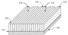
도 1은 소자(device)를 형성하는 방법의 초기 단계에서 소자의 등축도(an isometric view)를 도시한다. 도 1의 반도체 구조는, 반도체 기판(100)의 표면 상에, 라이너(110)의 표면 상에, 유전체층(120)의 표면 상에, 하드마스크(130)를 포함하는 반도체 재료 스택을 포함한다. 1 shows an isometric view of a device at an early stage of a method of forming the device. The semiconductor structure of FIG. 1 includes a stack of semiconductor materials including a
반도체 기판(100)은 실리콘 함유 재료로 구성될 수 있다. 실리콘 함유 재료들은 실리콘, 단결정 실리콘, 다결정 실리콘, SiGe, 단결정 SiGe, 다결정 SiGe, 또는 탄소로 도핑된 실리콘(Si:C), 비정질 실리콘, 및 이들의 조합 및 다층을 포함하지만 이에 제한되지 않는다. 반도체 기판(100)은 또한, 게르마늄(Ge)과 같은, 다른 반도체 재료들, 및 III/V형 반도체 기판들, 예를 들어 갈륨 비소(GaAs)와 같은, 화합물 반도체 기판들로 구성될 수 있다. 반도체 기판(100)은, 일부 실시예들에서, FEOL(front-end-of-line), MOL(middle-of-the-line) 및/또는 BEOL 금속들을 갖는 웨이퍼들일 수 있다. 일반적으로 반도체 기판(100)은 표면이 매끄러운 기판이다. The
라이너(110)는 스퍼터링, 화학 기상 증착(CVD) 또는 원자층 증착(ALD)에 의해 형성되고, 티티늄 질화물(TiN) 또는 탄탈륨 질화물(TaN)과 같은, 전도체이다. 일부 실시예들에서, 라이너(110)는 알루미늄(AL), 구리(Cu), 니켈(Ni), 코발트(Co), 루테늄(Ru), 티타늄(Ti), 탄탈륨(Ta), 또는 이들의 조합과 같은, 다른 전도성 재료들로 구성될 수 있다.
유전체층(120)은 라이너(110)의 상단(top) 상에 증착된다. 유전체층(120)은 일반적으로 절연 재료의 층이다. 유전층(120)은, 예를 들어, 실리콘 질화물(SiN), 실리콘 탄질화물(SiCN), (SiOCN), (SiBCN), 또는 당업계에 공지된 다른 절연 재료들로 구성될 수 있다. 유전체층(120)은 유전체층(120)이 최종 소자의 비아와 금속 라인의 결합된 원하는 높이에 대응하는 두께를 갖도록 증착된다. A
하드마스크 (130)는 유전층(120)의 상단 상에 증착된다. 하드마스크는 에칭 마스크로서 반도체 프로세싱에서 사용되는 재료이다. 하드마스크 (130)는, 예를 들어 SiN, 실리콘 산화물 또는 실리콘 질화물과 실리콘 산화물의 조합과 같은, 금속 또는 유전체 재료로 구성되며, 이들은, 예를 들어, 저압 화학 기상 증착(LPCVD)과 같은 프로세스를 사용하여 증착될 수 있다. 다양한 실시예들에서, 표준 포토리소그래피 프로세스들이 하드마스크(130) 상에 증착된 포토레지스트(미도시) 층에 하드 마스크(130)의 패턴을 정의하기 위해 사용된다. 그 다음, 원하는 하드마스크 패턴이 포토레지스트 층의 패턴에 의해 보호되지 않는 영역들으로부터 하드마스크(130)를 제거함으로써 하드마스크(130)에 형성될 수 있다. 하드마스크(130)는, 예를 들어, 반응성 이온 에칭(RIE)을 사용하여 제거된다. RIE는, 전자기장에 의해 생성된, 화학적 반응 플라즈마(chemically reactive plasma)를 사용하여 다양한 재료들을 제거한다. 당업자는 사용되는 플라즈마의 유형이 하드마스크(130)가 구성되는 재료에 따라 달라지거나, 습식 화학 에칭 또는 레이저 제거(laser ablation)와 같은 다른 에칭 프로세스들이 사용될 수 있음을 인식할 것이다. 도시되지는 않았지만, 하드마스크(130)가 맨드릴들(mandrels)(210)이 되는 유전층(120)의 영역을 덮도록 하드마스크(130)는 패터닝될 수 있다 (도 2 참조).
도 2는, 본 발명의 실시예들에 따른, 제조 단계들의 등축도를 도시한다. 도 2는 유전층(120)으로부터 맨드릴들(210)의 형성 및 하드마스크(130)의 제거를 도시한다. 맨드릴들은 스페이서 패터닝에 사용된다. 스페이서 패터닝은 기존 리소그래피로 달성할 수 있는 것보다 더 작은 선폭들로 특징들(features)을 패터닝하는 데 채용되는 기술이다. 일반적으로, 스페이서(a spacer)(예를 들어, 스페이서들(310), 도 3 참조)는 맨드릴(예를 들어, 맨드릴들(210)) 위에 증착되고, 맨드릴은 미리-패터닝된 특징(a pre-patterned feature)이다. 스페이서는 후속적으로 에치백되어(etched back) 맨드릴을 덮는 스페이서 부분이 에칭되고 측벽 상의 스페이서 부분이 남는다. 그런 다음 맨드릴은 제거되어, 각 맨드릴에 두 개의 스페이서들(각 엣지에 하나씩)을 남길 수 있다. 2 shows an isometric view of manufacturing steps, in accordance with embodiments of the present invention. 2 shows the formation of
맨드릴들(210)은, RIE, 레이저 제거와 같은, 에칭 프로세스에 의해, 또는 유전층(120)과 같은 재료의 일부를 선택적으로 제거하는 데 사용될 수 있는 모든 에칭 프로세스에 의해 형성될 수 있다. 도 1을 참조하여 전술한 바와 같이, 하드마스크(130)는 맨드릴들(210)을 덮도록 패터닝될 수 있고 맨드릴들(210)의 생성에서 에칭 프로세스 동안 이용될 수 있다. 상기 에칭 프로세스는 하드마스크(130)에 의해 보호되지 않는 유전층(120)의 부분들만을 제거하고 상기 에칭 프로세스는 라이너(110)에서 멈춘다. 상기 맨드릴들 각각은 원하는 금속 라인과 비아 높이들을 조합한 높이와 같은 높이를 갖는다.
일부 실시예들에서, 맨드릴들(210)의 형성 후에, 하드마스크(130)는 제거된다. 일반적으로, 하드마스크(130)를 제거하는 프로세스는, RIE, 레이저 제거와 같은 에칭 프로세스 또는, 하드마스크(130)와 같은, 재료의 일부를 선택적으로 제거하는 데 사용될 수 있는 모든 에칭 프로세스의 사용을 포함한다. 대안적인 실시예들에서, 하드마스크(130)는 이때에 제거되지 않고 나중의 금속 화학적 기계적 연마/평탄화(CMP) 단계(도 7 참조)가 수행될 때까지 디바이스 상에 남아 있을 수 있다. In some embodiments, after formation of
도 3은, 본 발명의 일 실시예에 따라, 제조 단계의 등축도를 도시한다. 도 3은 맨드릴들(210)의 노출된 측면들 상의 스페이서들(310)의 형성을 도시한다. 스페이서들(310)는 금속(예를 들어, TiN, TaN) 또는, 예를 들어 유전체 산화물, 유전체 질화물 및/또는 유전체 산질화물을 포함하는 모든 유전체 스페이서 재료로 구성된다. 일부 실시예들에서, 스페이서들(310)은 실리콘 이산화물(SiO2)과 같은 비전도성 저-캐패시턴스 유전체 재료로 구성된다. 일반적으로, 스페이서들(310)은 라이너(110)와 다른 재료로 구성된다. 스페이서들(310)을 형성하는 프로세스는, 라이너(110) 및 맨드릴들(210)의 노출된 표면들 위에, 실리콘 질화물과 같은, 절연 재료의 컨포멀 층(미도시)을 증착하는 단계를 포함할 수 있다. 스페이서들(310)은, 예를 들어 CVD, PECVD(플라즈마 강화 화학 기상 증착), PVD(물리 기상 증착) 또는 기타 증착 프로세스들을 사용하여 증착될 수 있다. 순방향의 에칭률이 측면 방향들의 에칭률보다 더 큰, 이방성 에칭 프로세스(anisotropic etch process)는 절연층의 일부들을 제거하는데 사용될 수 있고, 이에 의해, 도 3에 도시된 바와 같이, 맨드릴들(210)의 측벽들 상에 위치한 스페이서들(310)을 형성할 수 있다.3 shows an isometric view of a manufacturing step, in accordance with one embodiment of the present invention. 3 shows the formation of
도 4는, 본 발명의 실시예들에 따른, 제조 단계들의 등축도를 도시한다. 도 4는 라이너(110) 상의 그리고 스페이서들(310) 사이의 노출된 갭들 내에 유전체층(410)의 형성을 도시한다. 노출된 갭들 각각 내의 유전체층(410) 부분들은 복수의 유전체 재료 라인들을 생성할 수 있다. 유전층(120)과 관련하여 전술한 바와 같이, 유전층(410)은 일반적으로 절연 재료의 층이고, 예를 들어 SiN, SiCN, SiOCN, SiBCN, 또는 당업계에 공지된 다른 절연 재료들로 구성될 수 있다. 일부 실시예들에서, 유전층(410)은 로우(low)-k 유전 재료의 층이다. 로우-κ 유전 재료는 SiO2에 비해 상대 유전 상수(κ)가 작은 재료이다. 로우-κ 재료들은, 예를 들어 불소 도핑된 SiO2, 오가노실리게이트 유리(OSG), 다공성 SiO2, 다공성 오가노실리게이트 유리, 스핀-온 유기 폴리머 유전체들 및 스핀-온 실리콘 기반 폴리머 유전체들을 포함한다. 일부 실시예들에서, 유전층(410)은 스핀-온-글라스이다. 스핀-온-글라스(Spin-on-Glass)는 서브-유전체 표면의 좁은 갭들을 채우기 위해 액체 형태로 인가되는 층간 유전체 재료(an interlayer dielectric material)이다. 일부 실시예들에서, 유전층(410)은 유동성 화학 기상 증착(fCVD) 또는 스핀-온 유전 방법들(spin-on dielectric methods)을 사용하여 증착된다. 유전층(410)은 원하는 높이 이상으로 유전층(410)을 증착한 다음 맨드릴들(210)의 상단 표면이 노출되도록 유전층(410)의 높이를 감소시키기 위해 CMP와 같은 평탄화 프로세스를 이용함으로써 생성될 수 있다.4 shows an isometric view of manufacturing steps, in accordance with embodiments of the present invention. 4 shows the formation of
도 5는, 본 발명의 실시예들에 따른, 제조 단계들의 등축도를 도시한다. 도 5는 도 5에 도시된 갭들 내에 제1 트렌치를 생성하기 위한 맨드릴들(210)의 제거를 도시한다. 맨드릴들(210)은 제1 트렌치를 포함하는 갭들을 생성하기 위해 에칭 프로세스를 사용하여 제거될 수 있고, 상기 에칭 프로세스는 스페이서(310) 및 유전층(410)에 대해 맨드릴들(210)의 물리적으로 노출된 부분들을 선택적으로 제거한다. 이용되는 상기 에칭 프로세스는 건식 에칭 또는 습식 에칭 프로세스일 수 있다. 5 shows an isometric view of manufacturing steps, in accordance with embodiments of the present invention. FIG. 5 shows the removal of
도 6은, 본 발명의 실시예들에 따른, 제조 단계들의 등축도를 도시한다. 도 6은 제2 트렌치를 생성하기 위해 유전층(410)의 부분들 제거하는 것을 도시한다. 하나 또는 그 이상의 유전체 재료 라인들이 제거될 수 있다. 도시된 실시예에서, 유전층(410)의 중간 및 끝 부분들(the middle and end portions)은 제거되지 않는다. 제거된 유전층(410)의 부분은 스페이서들(310), 유전층(410), 및/또는 라이너(110)의 상단 표면 상에 증착된 포토레지스트(미도시) 층에서 제2 트렌치의 원하는 형상을 정의하기 위해 표준 포토리소그래피 프로세스를 사용함으로써 제거될 수 있다. 다양한 실시예들에서, 표준 포토리소그래피 프로세스가 제2 트렌치의 형성에서 제거될 유전층의 영역들에 대응하는 포토레지스트층의 부분을 제거하기 위해 사용된다. 유전층(410)의 원하는 부분(들)을 제거하기 위해 상기 부분 또는 유전층(410)은, 예를 들어 RIE와 같은 건식 에칭 프로세스를 사용하여 제거될 수 있다. 유전층(410)의 부분들을 에칭한 결과, 제2 트렌치로 정의된 영역에서 라이너(110)는 노출된다. 6 shows an isometric view of manufacturing steps, in accordance with embodiments of the present invention. 6 shows removing portions of
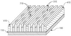
도 7은, 본 발명의 실시예들에 따른, 제조 단계들의 등축도를 도시한다. 도 7은 제1 및 제2 트렌치들을 포함하는 갭들 내의 전도성 금속(710)의 형성을 도시한다. 전도성 금속(710)은 모든 유형의 전도성 금속일 수 있다. 예를 들어, 전도성 금속(710)은 Ru, Co, 몰리브덴(Mo), 텅스텐(W), Al 또는 로듐(Rh)으로 구성될 수 있다. 전도성 금속(710)은, 예를 들어 CVD, PECVD, PVD 또는 다른 증착 프로세스를 사용하여 증착될 수 있다. 전도성 금속(710)은 원하는 높이 이상으로 전도성 금속(710)을 증착하고 그 후에 스페이서들(310) 및 유전층(410)의 상단 표면들이 노출되도록 전도성 금속(710)의 높이를 감소시키기 위해, CMP와 같은, 평탄화 프로세스를 이용함으로써 생성될 수 있다. 7 shows an isometric view of manufacturing steps, in accordance with embodiments of the present invention. 7 shows the formation of
스페이서들(310)이 TiN으로 구성되는, 일부 실시 예들에서, 라인 비틀림(line wiggle)은 다른 재료 사용에 비해 감소될 수 있다. 본 발명의 실시예들은 더 높은 모듈러스(higher modulus)를 갖는 템플릿들이 포스트 메탈 필 라인 위글링(post metal fill line wiggling)을 완화할 수 있음을 인식한다. 스페이서들(310)이 TiN으로 구성된, TiN 템플릿은 모듈러스가 약 500기가파스칼(Gpa)로, 다른 많은 재료들보다 높다. In some embodiments where the
도 8은, 본 발명의 실시예들에 따른, 제조 단계들의 등축도를 도시한다. 도 8은, 전도성 금속(710)의 비아-아닌 부분들(non-via portions)이 원하는 비아 구조에 대해 목표 깊이까지 리세스되는(recessed) 동안, 차감 패터닝 프로세스들(subtractive patterning processes)에 의한 상단 비아 및 금속 상호접속 라인의 형성을 도시한다. 상단 비아의 형성은 포토리소그래픽 차감 패터닝 프로세스들을 사용하여 수행될 수 있다. 전도성 금속(710)에 비아들을 형성하기 위해 마스킹 단계가 이용된다. 그러한 마스킹 단계는 포토레지스트 층을 증착하는 단계 및 자외선을 사용하여 상기 층을 패터닝하는 단계, 상기 포토레지스트의 선택된 부분만 제거하는 단계, 및 그 다음 상기 포토레지스트 패턴에 따라 전도성 금속(710)을 에칭하는 단계를 수반할 수 있다. 도 8(및 후속 유사 도면들)에 묘사된 비아들의 배열은 원하는 최종 비아 구조의 구현 세부 사항들에 따라 달라질 수 있음에 유의해야 한다. 일부 실시예들에서, 선택적 에칭 프로세스가 이용될 수 있다. 도 8에 도시된 실시예와 같은 일부 실시예들에서, 유전층(410)은 에칭 프로세스의 결과로서 손상될 수 있으며, 이는 유전층(410)의 감소된 높이에 의해 도 8에 표현된다. 8 shows an isometric view of manufacturing steps, in accordance with embodiments of the present invention. 8 shows a top view by subtractive patterning processes while non-via portions of
도 9는, 본 발명의 실시예들에 따른, 제조 단계들의 등축도를 도시한다. 도 9는 스페이서들(310) 및 유전층(410)의 선택적 제거를 도시하고 그리고 반도체 기판(100) 상의 전도성 금속(710) 및 라이너(110)에 형성된 하나 또는 그 이상의 비아들을 포함하는 최종 비아 구조를 도시한다. 스페이서들(310) 및 유전층(410)은 에칭 프로세스를 사용하여 제거될 수 있는데, 상기 에칭 프로세스는 모든 스페이서들(310) 및 유전층(410)을 제거하고 라이너(110)의 부분들을 노출시키기 위해 스페이서들(310) 및/또는 유전층(410)의 물리적으로 노출된 부분들을 전도성 금속(710)에 대해 선택적으로 제거한다. 이용되는 에칭 프로세스는 건식 에칭 또는 습식 에칭 프로세스일 수 있다. 9 shows an isometric view of fabrication steps, in accordance with embodiments of the present invention. 9 illustrates the selective removal of
일부 실시예들에서, 라이너(110)의 노출된 부분들은 반도체 기판(100) 상에 남아 있다. 다른 실시예들에서, 라이너(110)가 전도성 금속(710) 아래에만 존재하도록 라이너(110)의 노출된 부분들이 에칭된다(도 16 참조, 여기서 전도성 금속(1310)은 전도성 금속(710)과 유사하다). In some embodiments, exposed portions of
최종 구조는 BEOL 금속 라인과 상단 비아 구조이다. 상기 구조는, 예를 들어, 다마신에 의해 형성된 금속 라인들 및 차감 프로세스에 의해 형성된 상단 비아를 포함하는 금속-절연체-금속 커패시터(a metal-insulator-metal capacitor)일 수 있으며, 여기서 스페이서들(310)은 상단 비아 에칭 프로세스 동안 스캐폴드(scaffold)로서 작용한다. The final structure is a BEOL metal line and top via structure. The structure may be, for example, a metal-insulator-metal capacitor including metal lines formed by damascene and a top via formed by a subtraction process, where the spacers ( 310) serves as a scaffold during the top via etch process.
도 10 내지 도 16은 트렌치 에칭으로 시작하는 상이한 제조 프로세스에 따라 형성되는 본 발명의 실시예들을 도시한다. 10-16 show embodiments of the present invention formed according to different fabrication processes starting with trench etching.
도 10에 도시된 제조 프로세스는 도 1에 원래 도시된 동일 소자에 관해 수행되며, 이는, 이전에 기술된 바와 같이, 유전층(120) 상에, 라이너(110) 상에, 반도체 기판(100) 상에, 하드마스크(130)를 포함하는 반도체 재료 스택을 포함하는 소자의 등축도를 도시한다. The fabrication process shown in FIG. 10 is performed on the same device originally shown in FIG. 1, which is on
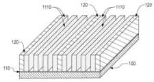
도 10은, 본 발명의 실시예들에 따른, 제조 단계들의 등축도를 도시한다. 도 10은 트렌치들을 생성하기 위해 하드마스크(130) 및 유전층(120)의 부분들을 제거하는 것을 도시한다. 상기 트렌치들은 RIE, 레이저 제거와 같은 에칭 프로세스에 의해, 또는, 유전층(120)과 같은, 재료의 부분을 선택적으로 제거하는 데 사용될 수 있는 모든 에칭 프로세스에 의해 제거될 수 있다. 하드마스크(130)는, 도 10에 도시된 바와 같이, 에칭 프로세스를 수행하기 전에, 패터닝될 수 있으며, 이는 유전체층(120)의 나머지 부분들이 에칭 프로세스 동안 제거되는 것을 방지함으로써 트렌치들의 생성을 돕기 위해서이다. 상기 에칭 프로세스는 하드마스크(130)에 의해 보호되지 않는 유전층(120)의 부분들만을 제거하고 에칭 프로세스는 라이너(110)에서 멈춘다. 트렌치 폭은 원하는 최종 금속 라인 폭과 스페이서 두께의 합에 기초하여 선택된다. 일부 실시예들에서, 트렌치 폭은 원하는 최종 금속 라인 폭의 3배와 동일하다. 유전층(120)의 나머지 부분들은 유전 재료 라인들을 형성할 수 있다. 10 shows an isometric view of fabrication steps, in accordance with embodiments of the present invention. 10 shows removing portions of
도 11은, 본 발명의 실시예들에 따른, 제조 단계들의 등축도를 도시한다. 도 11은 유전층(120)의 노출된 측면들 상의 스페이서들(1110)의 형성을 도시한다. 스페이서들(1110)은 금속(예를 들어, TiN, TaN) 또는, 예를 들어 유전체 산화물, 유전체 질화물 및/또는 유전체 산질화물을 포함하는, 모든 유전체 스페이서 재료로 구성된다. 일부 실시예들에서, 스페이서들(1110)은 실리콘 이산화물(SiO2)과 같은 비-전도성 저-캐패시턴스 유전체 재료로 구성된다. 일반적으로, 스페이서들(1110)은 라이너(110)와 다른 재료로 구성된다. 스페이서들(1110)을 형성하는 프로세스는 라이너(110)의 노출된 표면들 및 맨드릴 유전체층 위에, 실리콘 질화물과 같은, 절연 재료의 컨포멀층(a conformal layer)(미도시)을 증착하는 단계를 포함할 수 있다. 스페이서들(310)은, 예를 들어 CVD, PECVD(플라즈마 강화 화학 기상 증착), PVD(물리 기상 증착) 또는 기타 증착 프로세스를 사용하여 증착될 수 있다. 순방향의 에칭률이 측면 방향들의 에칭률보다 큰 이방성 에칭 프로세스가 절연층의 부분들 제거하여, 이에 의해, 도 11에서 도시된 바와 같이, 유전체층(120)의 측벽들 상에 위치한 스페이서들(1110)를 형성하는 데 사용될 수 있다.11 shows an isometric view of manufacturing steps, in accordance with embodiments of the invention. 11 shows the formation of
도 11은 또한 하드마스크(130)의 제거를 도시한다. 일반적으로, 하드마스크 (130)를 제거하는 프로세스는, RIE, 레이저 제거와 같은, 에칭 프로세스, 또는 하드마스크(130)와 같은, 재료의 부분을 선택적으로 제거하는 데 사용될 수 있는 모든 에칭 프로세스의 사용을 포함한다. 11 also shows the removal of
도 12는, 본 발명의 실시예들에 따른, 제조 단계들의 등축도를 도시한다. 도 12는 제2 트렌치를 생성하기 위해 유전층(120)의 부분들을 제거하는 단계를 도시한다. 도시된 실시예에서, 유전층(120)의 중간 및 끝 부분들은 제거되지 않는다. 제거되는 유전층(120)의 부분은 스페이서들(1110), 유전층(120), 및/또는 라이너(110)의 상단 표면 상에 증착된 포토레지스트(미도시) 층에서 제2 트렌치의 원하는 형상을 정의하기 위해 표준 포토리소그래피 프로세스를 사용함으로써 제거될 수 있다. 다양한 실시예들에서, 표준 포토리소그래피 프로세스가 제2 트렌치의 형성에서 제거될 유전층의 영역에 대응하는 포토레지스트층의 부분을 제거하기 위해 사용된다. 상기 부분 또는 유전층(120)은, 유전층(120)의 원하는 부분(들)을 제거하기 위한, 예를 들어, RIE와 같은 건식 에칭 프로세스를 사용하여, 제거될 수 있다. 유전층(120)의 상기 부분들을 에칭한 결과, 라이너(110)가 제2 트렌치로 정의된 영역에서 노출된다. 12 shows an isometric view of fabrication steps, in accordance with embodiments of the invention. 12 shows removing portions of
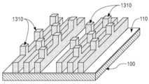
도 13은, 본 발명의 실시예들에 따른, 제조 단계들의 등축도를 도시한다. 도 13은 트렌치들을 포함하는 갭 내의 전도성 금속(1310)의 형성을 도시한다. 전도성 금속(1310)은 모든 유형의 전도성 금속일 수 있다. 예를 들어, 전도성 금속(710)은 Ru, Co, Mo, W, Al 또는 Rh로 구성될 수 있다. 전도성 금속(1310)은, 예를 들어 CVD, PECVD, PVD 또는 다른 증착 프로세스를 사용하여 증착될 수 있다. 전도성 금속(1310)은 원하는 높이 이상으로 전도성 금속(1310)을 증착하고 그 후 스페이서들(1110) 및 유전층(120)의 상단 표면들이 노출되도록 전도성 금속(1310)의 높이를 감소시키기 위해 CMP와 같은 평탄화 프로세스를 이용함으로써 생성될 수 있다. 13 shows an isometric view of manufacturing steps, in accordance with embodiments of the present invention. 13 shows the formation of
스페이서들(1110)이 TiN으로 구성되는, 일부 실시 예들에서, 라인 비틀림(line wiggle)은 다른 재료 사용에 비해 감소될 수 있다. 본 발명의 실시예들은 더 높은 모듈러스(higher modulus)를 갖는 템플릿들이 포스트 메탈 필 라인 위글링(post metal fill line wiggling)을 완화할 수 있음을 인식한다. 스페이서들(1110)이 TiN으로 구성된, TiN 템플릿은 모듈러스가 약 500기가파스칼(Gpa)로, 다른 많은 재료들보다 높다. In some embodiments where the
도 14는, 본 발명의 실시예들에 따른, 제조 단계들의 등축도를 도시한다. 도 14는, 전도성 금속(1310)의 비아-아닌 부분들(non-via portions)이 원하는 비아 구조에 대해 목표 깊이까지 리세스되는(recessed) 동안, 차감 패터닝 프로세스들(subtractive patterning processes)에 의한 상단 비아 및 금속 상호접속 라인의 형성을 도시한다. 상단 비아의 형성은 포토리소그래픽 차감 패터닝 프로세스들을 사용하여 수행될 수 있다. 전도성 금속(1310)에 비아들을 형성하기 위해 마스킹 단계가 이용된다. 그러한 마스킹 단계는 포토레지스트 층을 증착하는 단계 및 자외선을 사용하여 상기 층을 패터닝하는 단계, 상기 포토레지스트의 선택된 부분만 제거하는 단계, 및 그 다음 상기 포토레지스트 패턴에 따라 전도성 금속(1310)을 에칭하는 단계를 수반할 수 있다. 도 14(및 후속 유사 도면들)에 묘사된 비아들의 배열은 원하는 최종 비아 구조의 구현 세부 사항들에 따라 달라질 수 있음에 유의해야 한다. 일부 실시예들에서, 선택적 에칭 프로세스가 이용될 수 있다. 도 14에 도시된 실시예와 같은, 일부 실시예들에서, 유전층(120)은 에칭 프로세스의 결과로서 손상될 수 있으며, 이는 유전층(120)의 감소된 높이에 의해 도 14에 표현된다. 14 shows an isometric view of manufacturing steps, in accordance with embodiments of the present invention. 14 shows a top view by subtractive patterning processes while non-via portions of
도 15는, 본 발명의 실시예들에 따른, 제조 단계들의 등축도를 도시한다. 도 15는 스페이서들(1110) 및 유전층(120)의 선택적 제거를 도시하고 그리고 반도체 기판(100) 상의 전도성 금속(1310) 및 라이너(110)에 형성된 하나 또는 그 이상의 비아들을 포함하는 최종 비아 구조를 도시한다. 스페이서들(1110) 및 유전층(120)은 에칭 프로세스를 사용하여 제거될 수 있는데, 상기 에칭 프로세스는 모든 스페이서들(1110) 및 유전층(120)을 제거하고 라이너(110)의 부분들을 노출시키기 위해 스페이서들(1110) 및/또는 유전층(120)의 물리적으로 노출된 부분들을 전도성 금속(1310)에 대해 선택적으로 제거한다. 이용되는 에칭 프로세스는 건식 에칭 또는 습식 에칭 프로세스일 수 있다. 15 shows an isometric view of manufacturing steps, in accordance with embodiments of the invention. 15 illustrates the selective removal of
일부 실시예들에서, 라이너(110)의 노출된 부분들은 반도체 기판(100) 상에 남아 있다. 다른 실시예들에서, 라이너(110)가 전도성 금속(1310) 아래에만 존재하도록 라이너(110)의 노출된 부분들이 에칭된다(도 16 참조). In some embodiments, exposed portions of
도 16은, 본 발명의 실시예들에 따른, 제조 단계들의 등축도를 도시한다. 도 16은 라이너(110)의 노출된 부분들의 선택적 제거를 도시한다. 라이너(110)는, RIE와 같은, 에칭 기술들을 사용하여 제거된다. RIE는 전자기장에 의해 생성된 화학적 반응 플라즈마를 사용하여 다양한 재료들을 제거한다. 당업자는 사용되는 플라즈마의 유형이 라이너(110)를 구성하는 재료에 따라 달라지거나 습식 화학 에칭 또는 레이저 제거와 같은 다른 에칭 프로세스가 사용될 수 있음을 인식할 것이다. 일 실시예에서, 화학적 에칭은 라이너(110)의 노출된 부분을 제거하고 반도체 기판(100)의 표면을 노출시키기 위해 사용된다. 일부 실시예들에서, TiN 및 TaN 습식 제거 프로세스들은, 예를 들어, 라이너(110)가 TiN 또는 TaN 으로 구성될 때, 라이너(110)의 노출된 부분을 제거하기 위해 이용될 수 있다. 16 shows an isometric view of manufacturing steps, in accordance with embodiments of the invention. 16 shows selective removal of exposed portions of
최종 구조는 BEOL 금속 라인과 상단 비아 구조이다. 상기 구조는, 예를 들어, 다마신에 의해 형성된 금속 라인 및 차감 프로세스에 의해 형성된 상단 비아를 포함하는 금속-절연체-금속 커패시터일 수 있으며, 여기서 스페이서들(310)이 상단 비아 에칭 프로세스 동안 스캐폴드로서 작용한다. The final structure is a BEOL metal line and top via structure. The structure can be, for example, a metal-insulator-metal capacitor comprising a metal line formed by a damascene and a top via formed by a subtraction process, where
최종 집적 회로 칩들은 가공되지 않은 웨이퍼 형태(raw wafer form)(즉, 여러 개의 패키징되지 않은 칩들을 포함하는 단일 웨이퍼)로, 베어 다이로서 또는 패키지된 형태로 제조자에 의해 유통될 수 있다. 후자의 경우 칩은 단일 칩 패키지(예: 마더보드 또는 기타 상위 수준 캐리어에 부착된 리드들이 있는 플라스틱 캐리어) 또는 멀티칩 패키지(예: 표면 상호접속들 또는 매립된 상호접속들 둘 중 하나 또는 둘 모두를 갖는 세라믹 캐리어)에 장착된다. 어떤 경우이든, 칩은 그 다음에 (a) 마더보드와 같은 중간 제품 또는 (b) 최종 제품의 일부로서 다른 칩들, 개별 회로 엘리멘트들 및/또는 기타 신호 처리 장치들과 통합된다. 최종 제품은 집적 회로 칩들을 포함하는 모든 제품이 될 수 있으며, 이들은 장난감 및 기타 저가형 애플리케이션들로부터 디스플레이, 키보드 또는 기타 입력 장치 및 중앙 프로세서가 있는 고급 컴퓨터 제품들에 이르기까지 다양하다. The final integrated circuit chips may be distributed by the manufacturer in raw wafer form (ie, a single wafer containing several unpackaged chips), as a bare die or in packaged form. In the latter case, the chip may be in a single chip package (e.g., a plastic carrier with leads attached to a motherboard or other higher-level carrier) or a multi-chip package (e.g., either surface interconnects or buried interconnects, or both). It is mounted on a ceramic carrier with In any case, the chip is then integrated with other chips, discrete circuit elements and/or other signal processing devices as part of (a) an intermediate product such as a motherboard or (b) a final product. The end product can be anything containing integrated circuit chips, ranging from toys and other low-cost applications to high-end computer products with displays, keyboards or other input devices and central processors.
본 출원에서 사용된 용어는 단지 특정한 실시예들을 설명하기 위해 사용된 것으로, 본 발명을 한정하려는 의도가 아니다. 본 명세서에서 사용된 단수형은 문맥상 명백하게 다르게 나타내지 않는 한 복수형도 포함하는 것으로 의도된다. "포함하다" 및/또는 "포함하는"이라는 용어는 본 명세서에서 사용될 때 명시된 특징, 정수, 단계, 동작, 엘리멘트 및/또는 컴포넌트의 존재를 명시하지만 하나 또는 그 이상의 다른 특징, 정수, 단계, 동작, 엘리멘트, 컴포넌트 및/또는 이들의 그룹의 존재 또는 추가를 배제하지는 않는다는 것이 또한 이해될 것이다. Terms used in this application are only used to describe specific embodiments and are not intended to limit the present invention. As used herein, the singular is intended to include the plural as well, unless the context clearly dictates otherwise. The terms "comprise" and/or "comprising" when used herein indicate the presence of specified features, integers, steps, operations, elements and/or components, but not one or more other features, integers, steps, or operations. , it will also be understood that does not exclude the presence or addition of elements, components and/or groups thereof.
본 출원은 특히 그의 바람직한 실시예에 대해 도시되고 설명되었지만, 본 출원의 범위를 벗어나지 않고 형태들 및 세부 사항들에 있어서 전술한 변경들 및 기타 변경들이 이루어질 수 있음을 당업자는 이해할 것이다. 따라서 본 출원은 기술되고 예시된 정확한 형태들 및 세부 사항들에 제한되지 않고 첨부된 청구 범위 내에 속하도록 의도된다. While this application has been shown and described with respect to its preferred embodiment, it will be appreciated by those skilled in the art that the above changes and other changes may be made in form and detail without departing from the scope of this application. It is therefore intended that this application fall within the scope of the appended claims and not be limited to the precise forms and details described and illustrated.
본 발명의 바람직한 실시예에서, 방법이 제공되고, 상기 방법은: 라이너 상에 위치한 유전체층을 제공하는 단계 - 상기 라이너는 반도체 기판의 표면 상에 위치됨 -; 상기 라이너의 표면을 노출시키고 상기 남아있는 유전체층으로부터 유전체 재료 라인들을 생성하는 깊이의 복수의 트렌치들을 형성하는 단계; 상기 유전체 재료 라인들의 측벽들 상에 스페이서들을 형성하는 단계; 상기 스페이서들 2개 사이에 있는 유전체 재료 라인들 중 적어도 하나를 제거하는 단계 ; 각각의 존재하는 갭 내에 전도성 금속을 형성하는 단계; 금속 상호접속 라인들 및 비아들을 형성하기 위해 전도성 금속을 패터닝하는 단계; 및 상기 복수의 스페이서들 및 상기 남아있는 유전체 재료 라인들을 제거하는 단계를 포함한다.상기 트렌치의 폭은 원하는 금속 상호접속 라인 폭과 예상 스페이서 두께의 합과 같을 수 있다. 상기 트렌치의 폭은 원하는 금속 배선 폭보다 3배 더 클 수 있다. 상기 스페이서들은 티타늄 질화물(TiN)으로 구성될 수 있다. 상기 전도성 금속은 루테늄(Ru), 몰리브덴(Mo), 코발트(Co), 알루미늄(Al), 텅스텐(W) 및 로듐(Rh)으로 이루어진 군에서 선택될 수 있다. 상기 방법은: 상기 복수의 스페이서들 및 상기 남아있는 유전체 재료 라인들을 제거한 후에, 상기 라이너의 노출된 부분들을 제거하는 단계를 더 포함할 수 있다. 상기 금속 상호접속 라인들 및 상기 비아들을 형성하기 위해 상기 전도성 금속을 패터닝하는 단계는 차감 패터닝 프로세스를 이용할 수 있다. In a preferred embodiment of the present invention, a method is provided, the method comprising: providing a dielectric layer positioned on a liner, wherein the liner is positioned on a surface of a semiconductor substrate; forming a plurality of trenches of a depth exposing a surface of the liner and creating lines of dielectric material from the remaining dielectric layer; forming spacers on sidewalls of the lines of dielectric material; removing at least one of the dielectric material lines between two of the spacers; forming a conductive metal within each existing gap; patterning the conductive metal to form metal interconnect lines and vias; and removing the plurality of spacers and the remaining lines of dielectric material. The width of the trench may be equal to the sum of a desired metal interconnect line width and an expected spacer thickness. The width of the trench may be three times larger than the desired metal line width. The spacers may be made of titanium nitride (TiN). The conductive metal may be selected from the group consisting of ruthenium (Ru), molybdenum (Mo), cobalt (Co), aluminum (Al), tungsten (W), and rhodium (Rh). The method may further include: after removing the plurality of spacers and the remaining lines of dielectric material, removing exposed portions of the liner. Patterning the conductive metal to form the metal interconnect lines and the vias may use a subtractive patterning process.
본 발명의 다른 바람직한 실시예에서, 반도체 구조가 제공되고, 상기 반도체 구조는: 반도체 기판; 상기 반도체 기판 표면 상의 라이너; 상기 라이너의 표면 상의 복수의 상호접속 라인들 및 비아들 - 상기 복수의 상호접속 라인들 및 비아들은 전도성 금속으로 구성됨 -; 및 상기 복수의 상호접속 라인들과 비아들 각각 사이에 있는 복수의 스페이서들을 포함한다. 상기 복수의 스페이서들은 티타늄 질화물(TiN)로 구성될 수 있다. 상기 전도성 금속은 루테늄(Ru), 몰리브덴(Mo), 코발트(Co), 알루미늄(Al), 텅스텐(W) 및 로듐(Rh)으로 이루어진 군에서 선택될 수 있다. 상기 라이너는 티타늄 질화물(TiN), 탄탈륨 질화물(TaN), 티타늄(Ti) 및 탄탈륨(Ta)으로 구성된 그룹에서 선택하여 구성될 수 있다. 상기 복수의 상호접속 라인들 및 비아들 각각은 상호접속 라인의 표면으로부터 돌출하는 적어도 하나의 비아를 포함할 수 있다. 상기 상호접속 라인의 표면은 상단 표면(a top surface)일 수 있다. In another preferred embodiment of the present invention, a semiconductor structure is provided, the semiconductor structure comprising: a semiconductor substrate; a liner on the surface of the semiconductor substrate; a plurality of interconnection lines and vias on a surface of the liner, wherein the plurality of interconnection lines and vias are composed of a conductive metal; and a plurality of spacers between each of the plurality of interconnection lines and vias. The plurality of spacers may be composed of titanium nitride (TiN). The conductive metal may be selected from the group consisting of ruthenium (Ru), molybdenum (Mo), cobalt (Co), aluminum (Al), tungsten (W), and rhodium (Rh). The liner may be formed by selecting from the group consisting of titanium nitride (TiN), tantalum nitride (TaN), titanium (Ti) and tantalum (Ta). Each of the plurality of interconnection lines and vias may include at least one via protruding from a surface of the interconnection line. The surface of the interconnect line may be a top surface.
Claims (11)
Translated fromKorean라이너(a liner) 상에 맨드릴들을 패터닝하는 단계(patterning mandrels) - 상기 라이너는 반도체 기판 상에 위치됨 -;
상기 맨드릴들의 측벽들 상에 스페이서들(spacers)을 형성하는 단계;
상기 라이너의 노출된 표면들 상에 그리고 상기 스페이서들 사이의 복수의 갭들 내에 유전체 재료 라인들(dielectric material lines)을 형성하는 단계;
상기 맨드릴들을 제거하는 단계;
상기 스페이서들 사이의 상기 복수의 갭들 중 적어도 하나 내의 상기 유전체 재료 라인들 중 적어도 하나를 제거하는 단계;
각 갭 내에 전도성 금속(conductive metal)을 형성하는 단계;
금속 상호접속 라인들 및 비아들을 형성하기 위해 전도성 금속을 패터닝하는 단계; 그리고
상기 복수의 스페이서들 및 남아있는 유전체 재료 라인들(the remaining dielectric material lines)을 제거는 단계를 포함하는
방법.In the method, the method comprises:
patterning mandrels on a liner, the liner being placed on a semiconductor substrate;
forming spacers on sidewalls of the mandrels;
forming dielectric material lines on exposed surfaces of the liner and within a plurality of gaps between the spacers;
removing the mandrels;
removing at least one of the dielectric material lines within at least one of the plurality of gaps between the spacers;
forming a conductive metal within each gap;
patterning the conductive metal to form metal interconnect lines and vias; and
removing the plurality of spacers and the remaining dielectric material lines.
method.
스핀-온-글라스(spin-on-glass) 및 유동성 화학 기상 증착(flowable chemical vapor deposition)으로 이루어진 그룹으로부터 선택된 프로세스를 통해, 상기 맨드릴들 위의 높이까지 유전체 재료를 증착하는 단계; 그리고
상기 유전체 재료층을 형성하고 평탄화 프로세스를 이용하여 상기 맨드릴들의 상단 표면을 노출시키기 위해 상기 유전체 재료의 높이를 감소시키는 단계(reducing)를 포함하는
방법.2. The method of claim 1 wherein forming the dielectric material layer on the exposed portions of the liner comprises:
depositing dielectric material to a height above the mandrels via a process selected from the group consisting of spin-on-glass and flowable chemical vapor deposition; and
forming the dielectric material layer and reducing the height of the dielectric material to expose the top surface of the mandrels using a planarization process.
method.
방법.2. The method of claim 1, wherein the spacers are composed of titanium nitride (TiN).
method.
방법.The method of claim 1, wherein the conductive metal is ruthenium (Ru), molybdenum (Mo), cobalt (Co), aluminum (Al), tungsten (W) and rhodium (Rh) (ruthenium (Ru), molybdenum (Mo), cobalt (Co), aluminum (Al), tungsten (W), and rhodium (Rh))
method.
상기 복수의 스페이서들 및 상기 남아있는 유전체 재료 라인들을 제거한 후, 라이너의 노출된 부분들을 제거하는 단계를 더 포함하는
방법.The method of claim 1 , wherein the method:
after removing the plurality of spacers and the remaining lines of dielectric material, removing exposed portions of the liner.
method.
방법.2. The method of claim 1 wherein at least one of the dielectric material lines comprises a plurality of dielectric material lines.
method.
방법.2. The method of claim 1 wherein patterning the conductive metal to form the metal interconnect lines and the vias uses a subtractive patterning process.
method.
반도체 기판;
상기 반도체 기판 표면의 부분 상의 라이너; 그리고
상기 라이너의 표면 상에 상호접속 라인들과 비아들을 형성하도록 패터닝된 전도성 금속을 포함하는
반도체 구조.As for the semiconductor structure, the semiconductor structure comprises:
semiconductor substrate;
a liner on a portion of the surface of the semiconductor substrate; and
a conductive metal patterned to form interconnection lines and vias on the surface of the liner;
semiconductor structure.
반도체 구조.9. The method of claim 8, wherein no part of the liner is exposed to the outside.
semiconductor structure.
반도체 구조.The method of claim 8, wherein the conductive metal is selected from the group consisting of ruthenium (Ru), molybdenum (Mo), cobalt (Co), aluminum (Al), tungsten (W) and rhodium (Rh)
semiconductor structure.
반도체 구조.9. The liner of claim 8, wherein the liner is composed of a selection from the group consisting of titanium nitride (TiN), tantalum nitride (TaN), titanium (Ti) and tantalum (Ta).
semiconductor structure.
Applications Claiming Priority (3)
| Application Number | Priority Date | Filing Date | Title |
|---|---|---|---|
| US17/117,186 | 2020-12-10 | ||
| US17/117,186US11315872B1 (en) | 2020-12-10 | 2020-12-10 | Self-aligned top via |
| PCT/EP2021/081386WO2022122294A1 (en) | 2020-12-10 | 2021-11-11 | Self-aligned top via |
Publications (2)
| Publication Number | Publication Date |
|---|---|
| KR20230098237Atrue KR20230098237A (en) | 2023-07-03 |
| KR102818332B1 KR102818332B1 (en) | 2025-06-10 |
Family
ID=78770598
Family Applications (1)
| Application Number | Title | Priority Date | Filing Date |
|---|---|---|---|
| KR1020237017555AActiveKR102818332B1 (en) | 2020-12-10 | 2021-11-11 | Self-aligned top via |
Country Status (6)
| Country | Link |
|---|---|
| US (1) | US11315872B1 (en) |
| EP (1) | EP4260365A1 (en) |
| JP (1) | JP2023553604A (en) |
| KR (1) | KR102818332B1 (en) |
| CN (1) | CN116964736A (en) |
| WO (1) | WO2022122294A1 (en) |
Families Citing this family (1)
| Publication number | Priority date | Publication date | Assignee | Title |
|---|---|---|---|---|
| CN113921472B (en)* | 2020-07-08 | 2024-07-19 | 长鑫存储技术有限公司 | Semiconductor structure and manufacturing method thereof |
Citations (7)
| Publication number | Priority date | Publication date | Assignee | Title |
|---|---|---|---|---|
| KR20160044453A (en)* | 2013-08-21 | 2016-04-25 | 인텔 코포레이션 | Method and structure to contact tight pitch conductive layers with guided vias |
| KR20170002380A (en)* | 2014-05-08 | 2017-01-06 | 인텔 코포레이션 | Necked interconnect fuse structure for integrated circuits |
| KR20170033830A (en)* | 2014-10-17 | 2017-03-27 | 타이완 세미콘덕터 매뉴팩쳐링 컴퍼니 리미티드 | Iterative self-aligned patterning |
| KR20190038241A (en)* | 2017-09-29 | 2019-04-08 | 타이완 세미콘덕터 매뉴팩쳐링 컴퍼니 리미티드 | Metal routing with flexible space formed using self-aligned spacer patterning |
| WO2019089045A1 (en)* | 2017-11-03 | 2019-05-09 | Intel Corporation | Techniques for forming vias and other interconnects for integrated circuit structures |
| WO2020018236A1 (en)* | 2018-07-17 | 2020-01-23 | Applied Materials, Inc. | Methods for manufacturing an interconnect structure for semiconductor devices |
| US20200350206A1 (en)* | 2019-05-01 | 2020-11-05 | Applied Materials, Inc. | Fully Aligned Subtractive Processes And Electronic Devices Therefrom |
Family Cites Families (18)
| Publication number | Priority date | Publication date | Assignee | Title |
|---|---|---|---|---|
| JP2001194084A (en)* | 1999-12-15 | 2001-07-17 | Lg Electronics Inc | Fin tube type heat exchanger |
| US8357609B2 (en) | 2010-05-04 | 2013-01-22 | Globalfoundries Inc. | Dual damascene-like subtractive metal etch scheme |
| US8492270B2 (en) | 2010-09-20 | 2013-07-23 | International Business Machines Corporation | Structure for nano-scale metallization and method for fabricating same |
| JP6009152B2 (en)* | 2011-09-15 | 2016-10-19 | ルネサスエレクトロニクス株式会社 | Manufacturing method of semiconductor device |
| US9059001B2 (en)* | 2011-12-16 | 2015-06-16 | Taiwan Semiconductor Manufacturing Company, Ltd. | Semiconductor device with biased feature |
| US9761489B2 (en)* | 2013-08-20 | 2017-09-12 | Applied Materials, Inc. | Self-aligned interconnects formed using substractive techniques |
| EP3050087B1 (en) | 2013-09-27 | 2020-04-29 | Intel Corporation | Subtractive self-aligned via and plug patterning for back end of line (beol) interconnects |
| US9177797B2 (en)* | 2013-12-04 | 2015-11-03 | Taiwan Semiconductor Manufacturing Company, Ltd. | Lithography using high selectivity spacers for pitch reduction |
| US9646883B2 (en) | 2015-06-12 | 2017-05-09 | International Business Machines Corporation | Chemoepitaxy etch trim using a self aligned hard mask for metal line to via |
| US9613861B2 (en) | 2015-08-05 | 2017-04-04 | Globalfoundries Inc. | Damascene wires with top via structures |
| US9502350B1 (en) | 2016-01-28 | 2016-11-22 | International Business Machines Corporation | Interconnect scaling method including forming dielectric layer over subtractively etched first conductive layer and forming second conductive material on dielectric layer |
| WO2017204821A1 (en) | 2016-05-27 | 2017-11-30 | Intel Corporation | Subtractive plug and tab patterning with photobuckets for back end of line (beol) spacer-based interconnects |
| US9852986B1 (en)* | 2016-11-28 | 2017-12-26 | Globalfoundries Inc. | Method of patterning pillars to form variable continuity cuts in interconnection lines of an integrated circuit |
| US9984919B1 (en) | 2017-07-31 | 2018-05-29 | Globalfoundries Inc. | Inverted damascene interconnect structures |
| CN111834212B (en) | 2019-04-23 | 2023-05-26 | 中芯国际集成电路制造(上海)有限公司 | Semiconductor device and method of forming the same |
| US11139202B2 (en)* | 2019-09-27 | 2021-10-05 | International Business Machines Corporation | Fully aligned top vias with replacement metal lines |
| US11244897B2 (en) | 2020-04-06 | 2022-02-08 | International Business Machines Corporation | Back end of line metallization |
| US11270913B2 (en) | 2020-04-28 | 2022-03-08 | International Business Machines Corporation | BEOL metallization formation |
- 2020
- 2020-12-10USUS17/117,186patent/US11315872B1/enactiveActive
- 2021
- 2021-11-11JPJP2023534155Apatent/JP2023553604A/enactivePending
- 2021-11-11CNCN202180083332.9Apatent/CN116964736A/enactivePending
- 2021-11-11WOPCT/EP2021/081386patent/WO2022122294A1/ennot_activeCeased
- 2021-11-11KRKR1020237017555Apatent/KR102818332B1/enactiveActive
- 2021-11-11EPEP21814716.3Apatent/EP4260365A1/enactivePending
Patent Citations (8)
| Publication number | Priority date | Publication date | Assignee | Title |
|---|---|---|---|---|
| KR20160044453A (en)* | 2013-08-21 | 2016-04-25 | 인텔 코포레이션 | Method and structure to contact tight pitch conductive layers with guided vias |
| KR20170002380A (en)* | 2014-05-08 | 2017-01-06 | 인텔 코포레이션 | Necked interconnect fuse structure for integrated circuits |
| KR20170033830A (en)* | 2014-10-17 | 2017-03-27 | 타이완 세미콘덕터 매뉴팩쳐링 컴퍼니 리미티드 | Iterative self-aligned patterning |
| KR20190038241A (en)* | 2017-09-29 | 2019-04-08 | 타이완 세미콘덕터 매뉴팩쳐링 컴퍼니 리미티드 | Metal routing with flexible space formed using self-aligned spacer patterning |
| WO2019089045A1 (en)* | 2017-11-03 | 2019-05-09 | Intel Corporation | Techniques for forming vias and other interconnects for integrated circuit structures |
| WO2020018236A1 (en)* | 2018-07-17 | 2020-01-23 | Applied Materials, Inc. | Methods for manufacturing an interconnect structure for semiconductor devices |
| US20200027782A1 (en)* | 2018-07-17 | 2020-01-23 | Applied Materials, Inc. | Methods for manufacturing an interconnect structure for semiconductor devices |
| US20200350206A1 (en)* | 2019-05-01 | 2020-11-05 | Applied Materials, Inc. | Fully Aligned Subtractive Processes And Electronic Devices Therefrom |
Also Published As
| Publication number | Publication date |
|---|---|
| CN116964736A (en) | 2023-10-27 |
| US11315872B1 (en) | 2022-04-26 |
| JP2023553604A (en) | 2023-12-25 |
| EP4260365A1 (en) | 2023-10-18 |
| WO2022122294A1 (en) | 2022-06-16 |
| KR102818332B1 (en) | 2025-06-10 |
Similar Documents
| Publication | Publication Date | Title |
|---|---|---|
| US8298943B1 (en) | Self aligning via patterning | |
| US9613861B2 (en) | Damascene wires with top via structures | |
| US20210035856A1 (en) | Interconnect Structure Having an Etch Stop Layer Over Conductive Lines | |
| US10636698B2 (en) | Skip via structures | |
| US11929258B2 (en) | Via connection to a partially filled trench | |
| US10741495B2 (en) | Structure and method to reduce shorts and contact resistance in semiconductor devices | |
| US20230136674A1 (en) | Self-aligned double patterning (sadp) integration with wide line spacing | |
| US11791258B2 (en) | Conductive lines with subtractive cuts | |
| KR102818332B1 (en) | Self-aligned top via | |
| US10896870B2 (en) | Semiconductor device with air gaps in interlayer insulating layer and method of manufacturing the same | |
| KR100909174B1 (en) | How to form a dual damascene pattern | |
| US12266605B2 (en) | Top via interconnects with line wiggling prevention | |
| US12057395B2 (en) | Top via interconnects without barrier metal between via and above line | |
| US20250079174A1 (en) | Method for processing a substrate | |
| US20240153864A1 (en) | Metallization levels with skip via and dielectric layer | |
| KR100571259B1 (en) | Method for forming damascene pattern of semiconductor device | |
| KR100579856B1 (en) | Metal wiring formation method of semiconductor device | |
| US7514356B2 (en) | Ribs for line collapse prevention in damascene structures | |
| US20130299993A1 (en) | Interconnection of semiconductor device and fabrication method thereof | |
| KR20060079808A (en) | Double damascene process and interlayer insulating film structure formed using this process | |
| KR20100067568A (en) | Mask and method for manufacturing the mask |
Legal Events
| Date | Code | Title | Description |
|---|---|---|---|
| PA0105 | International application | Patent event date:20230523 Patent event code:PA01051R01D Comment text:International Patent Application | |
| A201 | Request for examination | ||
| PA0201 | Request for examination | Patent event code:PA02012R01D Patent event date:20230531 Comment text:Request for Examination of Application | |
| PG1501 | Laying open of application | ||
| E902 | Notification of reason for refusal | ||
| PE0902 | Notice of grounds for rejection | Comment text:Notification of reason for refusal Patent event date:20241113 Patent event code:PE09021S01D | |
| E701 | Decision to grant or registration of patent right | ||
| PE0701 | Decision of registration | Patent event code:PE07011S01D Comment text:Decision to Grant Registration Patent event date:20250522 | |
| GRNT | Written decision to grant | ||
| PR0701 | Registration of establishment | Comment text:Registration of Establishment Patent event date:20250604 Patent event code:PR07011E01D | |
| PR1002 | Payment of registration fee | Payment date:20250604 End annual number:3 Start annual number:1 | |
| PG1601 | Publication of registration |