KR20230095939A - Manufacturing method of light emitting diode supply substrate, manufacturing method of light emitting diode display, manufacturing method of division unit of light emitting diode display, and manufacturing method of element supply substrate - Google Patents
Manufacturing method of light emitting diode supply substrate, manufacturing method of light emitting diode display, manufacturing method of division unit of light emitting diode display, and manufacturing method of element supply substrateDownload PDFInfo
- Publication number
- KR20230095939A KR20230095939AKR1020237012549AKR20237012549AKR20230095939AKR 20230095939 AKR20230095939 AKR 20230095939AKR 1020237012549 AKR1020237012549 AKR 1020237012549AKR 20237012549 AKR20237012549 AKR 20237012549AKR 20230095939 AKR20230095939 AKR 20230095939A
- Authority
- KR
- South Korea
- Prior art keywords
- light emitting
- emitting diode
- supply substrate
- manufacturing
- substrate
- Prior art date
- Legal status (The legal status is an assumption and is not a legal conclusion. Google has not performed a legal analysis and makes no representation as to the accuracy of the status listed.)
- Ceased
Links
Images


Classifications
- H—ELECTRICITY
- H10—SEMICONDUCTOR DEVICES; ELECTRIC SOLID-STATE DEVICES NOT OTHERWISE PROVIDED FOR
- H10H—INORGANIC LIGHT-EMITTING SEMICONDUCTOR DEVICES HAVING POTENTIAL BARRIERS
- H10H29/00—Integrated devices, or assemblies of multiple devices, comprising at least one light-emitting semiconductor element covered by group H10H20/00
- H10H29/01—Manufacture or treatment
- H10H29/02—Manufacture or treatment using pick-and-place processes
- H—ELECTRICITY
- H01—ELECTRIC ELEMENTS
- H01L—SEMICONDUCTOR DEVICES NOT COVERED BY CLASS H10
- H01L24/00—Arrangements for connecting or disconnecting semiconductor or solid-state bodies; Methods or apparatus related thereto
- H01L24/93—Batch processes
- H01L24/95—Batch processes at chip-level, i.e. with connecting carried out on a plurality of singulated devices, i.e. on diced chips
- H01L24/97—Batch processes at chip-level, i.e. with connecting carried out on a plurality of singulated devices, i.e. on diced chips the devices being connected to a common substrate, e.g. interposer, said common substrate being separable into individual assemblies after connecting
- B—PERFORMING OPERATIONS; TRANSPORTING
- B23—MACHINE TOOLS; METAL-WORKING NOT OTHERWISE PROVIDED FOR
- B23K—SOLDERING OR UNSOLDERING; WELDING; CLADDING OR PLATING BY SOLDERING OR WELDING; CUTTING BY APPLYING HEAT LOCALLY, e.g. FLAME CUTTING; WORKING BY LASER BEAM
- B23K26/00—Working by laser beam, e.g. welding, cutting or boring
- B23K26/36—Removing material
- G—PHYSICS
- G01—MEASURING; TESTING
- G01R—MEASURING ELECTRIC VARIABLES; MEASURING MAGNETIC VARIABLES
- G01R31/00—Arrangements for testing electric properties; Arrangements for locating electric faults; Arrangements for electrical testing characterised by what is being tested not provided for elsewhere
- G01R31/26—Testing of individual semiconductor devices
- G01R31/2607—Circuits therefor
- G01R31/2632—Circuits therefor for testing diodes
- G01R31/2635—Testing light-emitting diodes, laser diodes or photodiodes
- G—PHYSICS
- G09—EDUCATION; CRYPTOGRAPHY; DISPLAY; ADVERTISING; SEALS
- G09F—DISPLAYING; ADVERTISING; SIGNS; LABELS OR NAME-PLATES; SEALS
- G09F9/00—Indicating arrangements for variable information in which the information is built-up on a support by selection or combination of individual elements
- G09F9/30—Indicating arrangements for variable information in which the information is built-up on a support by selection or combination of individual elements in which the desired character or characters are formed by combining individual elements
- G09F9/33—Indicating arrangements for variable information in which the information is built-up on a support by selection or combination of individual elements in which the desired character or characters are formed by combining individual elements being semiconductor devices, e.g. diodes
- H—ELECTRICITY
- H01—ELECTRIC ELEMENTS
- H01L—SEMICONDUCTOR DEVICES NOT COVERED BY CLASS H10
- H01L21/00—Processes or apparatus adapted for the manufacture or treatment of semiconductor or solid state devices or of parts thereof
- H01L21/67—Apparatus specially adapted for handling semiconductor or electric solid state devices during manufacture or treatment thereof; Apparatus specially adapted for handling wafers during manufacture or treatment of semiconductor or electric solid state devices or components ; Apparatus not specifically provided for elsewhere
- H01L21/683—Apparatus specially adapted for handling semiconductor or electric solid state devices during manufacture or treatment thereof; Apparatus specially adapted for handling wafers during manufacture or treatment of semiconductor or electric solid state devices or components ; Apparatus not specifically provided for elsewhere for supporting or gripping
- H01L21/6835—Apparatus specially adapted for handling semiconductor or electric solid state devices during manufacture or treatment thereof; Apparatus specially adapted for handling wafers during manufacture or treatment of semiconductor or electric solid state devices or components ; Apparatus not specifically provided for elsewhere for supporting or gripping using temporarily an auxiliary support
- H—ELECTRICITY
- H01—ELECTRIC ELEMENTS
- H01L—SEMICONDUCTOR DEVICES NOT COVERED BY CLASS H10
- H01L22/00—Testing or measuring during manufacture or treatment; Reliability measurements, i.e. testing of parts without further processing to modify the parts as such; Structural arrangements therefor
- H01L22/20—Sequence of activities consisting of a plurality of measurements, corrections, marking or sorting steps
- H01L22/22—Connection or disconnection of sub-entities or redundant parts of a device in response to a measurement
- H—ELECTRICITY
- H01—ELECTRIC ELEMENTS
- H01L—SEMICONDUCTOR DEVICES NOT COVERED BY CLASS H10
- H01L24/00—Arrangements for connecting or disconnecting semiconductor or solid-state bodies; Methods or apparatus related thereto
- H01L24/01—Means for bonding being attached to, or being formed on, the surface to be connected, e.g. chip-to-package, die-attach, "first-level" interconnects; Manufacturing methods related thereto
- H01L24/26—Layer connectors, e.g. plate connectors, solder or adhesive layers; Manufacturing methods related thereto
- H01L24/27—Manufacturing methods
- H—ELECTRICITY
- H01—ELECTRIC ELEMENTS
- H01L—SEMICONDUCTOR DEVICES NOT COVERED BY CLASS H10
- H01L24/00—Arrangements for connecting or disconnecting semiconductor or solid-state bodies; Methods or apparatus related thereto
- H01L24/74—Apparatus for manufacturing arrangements for connecting or disconnecting semiconductor or solid-state bodies
- H01L24/799—Apparatus for disconnecting
- H—ELECTRICITY
- H01—ELECTRIC ELEMENTS
- H01L—SEMICONDUCTOR DEVICES NOT COVERED BY CLASS H10
- H01L24/00—Arrangements for connecting or disconnecting semiconductor or solid-state bodies; Methods or apparatus related thereto
- H01L24/80—Methods for connecting semiconductor or other solid state bodies using means for bonding being attached to, or being formed on, the surface to be connected
- H01L24/83—Methods for connecting semiconductor or other solid state bodies using means for bonding being attached to, or being formed on, the surface to be connected using a layer connector
- H—ELECTRICITY
- H01—ELECTRIC ELEMENTS
- H01L—SEMICONDUCTOR DEVICES NOT COVERED BY CLASS H10
- H01L24/00—Arrangements for connecting or disconnecting semiconductor or solid-state bodies; Methods or apparatus related thereto
- H01L24/98—Methods for disconnecting semiconductor or solid-state bodies
- H—ELECTRICITY
- H01—ELECTRIC ELEMENTS
- H01L—SEMICONDUCTOR DEVICES NOT COVERED BY CLASS H10
- H01L25/00—Assemblies consisting of a plurality of semiconductor or other solid state devices
- H01L25/03—Assemblies consisting of a plurality of semiconductor or other solid state devices all the devices being of a type provided for in a single subclass of subclasses H10B, H10D, H10F, H10H, H10K or H10N, e.g. assemblies of rectifier diodes
- H01L25/04—Assemblies consisting of a plurality of semiconductor or other solid state devices all the devices being of a type provided for in a single subclass of subclasses H10B, H10D, H10F, H10H, H10K or H10N, e.g. assemblies of rectifier diodes the devices not having separate containers
- H01L25/075—Assemblies consisting of a plurality of semiconductor or other solid state devices all the devices being of a type provided for in a single subclass of subclasses H10B, H10D, H10F, H10H, H10K or H10N, e.g. assemblies of rectifier diodes the devices not having separate containers the devices being of a type provided for in group H10H20/00
- H01L25/0753—Assemblies consisting of a plurality of semiconductor or other solid state devices all the devices being of a type provided for in a single subclass of subclasses H10B, H10D, H10F, H10H, H10K or H10N, e.g. assemblies of rectifier diodes the devices not having separate containers the devices being of a type provided for in group H10H20/00 the devices being arranged next to each other
- H01L33/48—
- H—ELECTRICITY
- H10—SEMICONDUCTOR DEVICES; ELECTRIC SOLID-STATE DEVICES NOT OTHERWISE PROVIDED FOR
- H10H—INORGANIC LIGHT-EMITTING SEMICONDUCTOR DEVICES HAVING POTENTIAL BARRIERS
- H10H20/00—Individual inorganic light-emitting semiconductor devices having potential barriers, e.g. light-emitting diodes [LED]
- H10H20/01—Manufacture or treatment
- H10H20/011—Manufacture or treatment of bodies, e.g. forming semiconductor layers
- H10H20/013—Manufacture or treatment of bodies, e.g. forming semiconductor layers having light-emitting regions comprising only Group III-V materials
- H—ELECTRICITY
- H10—SEMICONDUCTOR DEVICES; ELECTRIC SOLID-STATE DEVICES NOT OTHERWISE PROVIDED FOR
- H10H—INORGANIC LIGHT-EMITTING SEMICONDUCTOR DEVICES HAVING POTENTIAL BARRIERS
- H10H20/00—Individual inorganic light-emitting semiconductor devices having potential barriers, e.g. light-emitting diodes [LED]
- H10H20/01—Manufacture or treatment
- H10H20/021—Singulating, e.g. dicing
- H—ELECTRICITY
- H10—SEMICONDUCTOR DEVICES; ELECTRIC SOLID-STATE DEVICES NOT OTHERWISE PROVIDED FOR
- H10H—INORGANIC LIGHT-EMITTING SEMICONDUCTOR DEVICES HAVING POTENTIAL BARRIERS
- H10H29/00—Integrated devices, or assemblies of multiple devices, comprising at least one light-emitting semiconductor element covered by group H10H20/00
- H10H29/01—Manufacture or treatment
- H10H29/011—Manufacture or treatment of integrated devices comprising at least one light-emitting semiconductor component covered by group H10H20/00
- H—ELECTRICITY
- H10—SEMICONDUCTOR DEVICES; ELECTRIC SOLID-STATE DEVICES NOT OTHERWISE PROVIDED FOR
- H10H—INORGANIC LIGHT-EMITTING SEMICONDUCTOR DEVICES HAVING POTENTIAL BARRIERS
- H10H29/00—Integrated devices, or assemblies of multiple devices, comprising at least one light-emitting semiconductor element covered by group H10H20/00
- H10H29/01—Manufacture or treatment
- H10H29/012—Manufacture or treatment of active-matrix LED displays
- H—ELECTRICITY
- H10—SEMICONDUCTOR DEVICES; ELECTRIC SOLID-STATE DEVICES NOT OTHERWISE PROVIDED FOR
- H10H—INORGANIC LIGHT-EMITTING SEMICONDUCTOR DEVICES HAVING POTENTIAL BARRIERS
- H10H29/00—Integrated devices, or assemblies of multiple devices, comprising at least one light-emitting semiconductor element covered by group H10H20/00
- H10H29/01—Manufacture or treatment
- H10H29/036—Manufacture or treatment of packages
- H10H29/0364—Manufacture or treatment of packages of interconnections
- H—ELECTRICITY
- H10—SEMICONDUCTOR DEVICES; ELECTRIC SOLID-STATE DEVICES NOT OTHERWISE PROVIDED FOR
- H10H—INORGANIC LIGHT-EMITTING SEMICONDUCTOR DEVICES HAVING POTENTIAL BARRIERS
- H10H29/00—Integrated devices, or assemblies of multiple devices, comprising at least one light-emitting semiconductor element covered by group H10H20/00
- H10H29/30—Active-matrix LED displays
- H10H29/45—Active-matrix LED displays comprising two substrates, each having active devices thereon, e.g. displays comprising LED arrays and driving circuitry on different substrates
- H—ELECTRICITY
- H10—SEMICONDUCTOR DEVICES; ELECTRIC SOLID-STATE DEVICES NOT OTHERWISE PROVIDED FOR
- H10H—INORGANIC LIGHT-EMITTING SEMICONDUCTOR DEVICES HAVING POTENTIAL BARRIERS
- H10H29/00—Integrated devices, or assemblies of multiple devices, comprising at least one light-emitting semiconductor element covered by group H10H20/00
- H10H29/30—Active-matrix LED displays
- H10H29/49—Interconnections, e.g. wiring lines or terminals
- H—ELECTRICITY
- H01—ELECTRIC ELEMENTS
- H01L—SEMICONDUCTOR DEVICES NOT COVERED BY CLASS H10
- H01L2221/00—Processes or apparatus adapted for the manufacture or treatment of semiconductor or solid state devices or of parts thereof covered by H01L21/00
- H01L2221/67—Apparatus for handling semiconductor or electric solid state devices during manufacture or treatment thereof; Apparatus for handling wafers during manufacture or treatment of semiconductor or electric solid state devices or components; Apparatus not specifically provided for elsewhere
- H01L2221/683—Apparatus for handling semiconductor or electric solid state devices during manufacture or treatment thereof; Apparatus for handling wafers during manufacture or treatment of semiconductor or electric solid state devices or components; Apparatus not specifically provided for elsewhere for supporting or gripping
- H01L2221/68304—Apparatus for handling semiconductor or electric solid state devices during manufacture or treatment thereof; Apparatus for handling wafers during manufacture or treatment of semiconductor or electric solid state devices or components; Apparatus not specifically provided for elsewhere for supporting or gripping using temporarily an auxiliary support
- H01L2221/68368—Apparatus for handling semiconductor or electric solid state devices during manufacture or treatment thereof; Apparatus for handling wafers during manufacture or treatment of semiconductor or electric solid state devices or components; Apparatus not specifically provided for elsewhere for supporting or gripping using temporarily an auxiliary support used in a transfer process involving at least two transfer steps, i.e. including an intermediate handle substrate
- H—ELECTRICITY
- H01—ELECTRIC ELEMENTS
- H01L—SEMICONDUCTOR DEVICES NOT COVERED BY CLASS H10
- H01L2221/00—Processes or apparatus adapted for the manufacture or treatment of semiconductor or solid state devices or of parts thereof covered by H01L21/00
- H01L2221/67—Apparatus for handling semiconductor or electric solid state devices during manufacture or treatment thereof; Apparatus for handling wafers during manufacture or treatment of semiconductor or electric solid state devices or components; Apparatus not specifically provided for elsewhere
- H01L2221/683—Apparatus for handling semiconductor or electric solid state devices during manufacture or treatment thereof; Apparatus for handling wafers during manufacture or treatment of semiconductor or electric solid state devices or components; Apparatus not specifically provided for elsewhere for supporting or gripping
- H01L2221/68304—Apparatus for handling semiconductor or electric solid state devices during manufacture or treatment thereof; Apparatus for handling wafers during manufacture or treatment of semiconductor or electric solid state devices or components; Apparatus not specifically provided for elsewhere for supporting or gripping using temporarily an auxiliary support
- H01L2221/68381—Details of chemical or physical process used for separating the auxiliary support from a device or wafer
- H01L2221/68386—Separation by peeling
- H—ELECTRICITY
- H01—ELECTRIC ELEMENTS
- H01L—SEMICONDUCTOR DEVICES NOT COVERED BY CLASS H10
- H01L2224/00—Indexing scheme for arrangements for connecting or disconnecting semiconductor or solid-state bodies and methods related thereto as covered by H01L24/00
- H01L2224/80—Methods for connecting semiconductor or other solid state bodies using means for bonding being attached to, or being formed on, the surface to be connected
- H01L2224/80001—Methods for connecting semiconductor or other solid state bodies using means for bonding being attached to, or being formed on, the surface to be connected by connecting a bonding area directly to another bonding area, i.e. connectorless bonding, e.g. bumpless bonding
- H01L2224/802—Applying energy for connecting
- H01L2224/8022—Applying energy for connecting with energy being in the form of electromagnetic radiation
- H01L2224/80224—Applying energy for connecting with energy being in the form of electromagnetic radiation using a laser
- H—ELECTRICITY
- H01—ELECTRIC ELEMENTS
- H01L—SEMICONDUCTOR DEVICES NOT COVERED BY CLASS H10
- H01L25/00—Assemblies consisting of a plurality of semiconductor or other solid state devices
- H01L25/16—Assemblies consisting of a plurality of semiconductor or other solid state devices the devices being of types provided for in two or more different subclasses of H10B, H10D, H10F, H10H, H10K or H10N, e.g. forming hybrid circuits
- H01L25/167—Assemblies consisting of a plurality of semiconductor or other solid state devices the devices being of types provided for in two or more different subclasses of H10B, H10D, H10F, H10H, H10K or H10N, e.g. forming hybrid circuits comprising optoelectronic devices, e.g. LED, photodiodes
- H—ELECTRICITY
- H01—ELECTRIC ELEMENTS
- H01L—SEMICONDUCTOR DEVICES NOT COVERED BY CLASS H10
- H01L2924/00—Indexing scheme for arrangements or methods for connecting or disconnecting semiconductor or solid-state bodies as covered by H01L24/00
- H01L2924/10—Details of semiconductor or other solid state devices to be connected
- H01L2924/11—Device type
- H01L2924/12—Passive devices, e.g. 2 terminal devices
- H01L2924/1204—Optical Diode
- H01L2924/12041—LED
- H—ELECTRICITY
- H10—SEMICONDUCTOR DEVICES; ELECTRIC SOLID-STATE DEVICES NOT OTHERWISE PROVIDED FOR
- H10H—INORGANIC LIGHT-EMITTING SEMICONDUCTOR DEVICES HAVING POTENTIAL BARRIERS
- H10H20/00—Individual inorganic light-emitting semiconductor devices having potential barriers, e.g. light-emitting diodes [LED]
- H10H20/01—Manufacture or treatment
- H10H20/011—Manufacture or treatment of bodies, e.g. forming semiconductor layers
- H10H20/018—Bonding of wafers
Landscapes
- Engineering & Computer Science (AREA)
- Microelectronics & Electronic Packaging (AREA)
- Power Engineering (AREA)
- Computer Hardware Design (AREA)
- Physics & Mathematics (AREA)
- General Physics & Mathematics (AREA)
- Manufacturing & Machinery (AREA)
- Condensed Matter Physics & Semiconductors (AREA)
- Led Device Packages (AREA)
- Led Devices (AREA)
- Devices For Indicating Variable Information By Combining Individual Elements (AREA)
- Die Bonding (AREA)
- Optics & Photonics (AREA)
- Theoretical Computer Science (AREA)
- Plasma & Fusion (AREA)
- Mechanical Engineering (AREA)
Abstract
Translated fromKoreanDescription
Translated fromKorean본 발명은, 발광다이오드 공급기판의 제조방법, 발광다이오드 디스플레이의 제조방법, 발광다이오드 디스플레이의 분할유닛의 제조방법, 및 소자 공급기판의 제조방법에 관한 것이다.The present invention relates to a manufacturing method of a light emitting diode supply substrate, a manufacturing method of a light emitting diode display, a manufacturing method of a division unit of a light emitting diode display, and a manufacturing method of an element supply substrate.
최근, 미니 발광다이오드 및 마이크로 발광다이오드를 이용한 디스플레이의 개발이 활발히 행해지고 있다. 그들의 실용화를 향한 제조상의 큰 과제의 하나는, 미소한 발광다이오드를 디스플레이패널에 배치하는 제조수단이다. 그 조립수단으로서, 스탬프를 이용한 미소구조체 이재(移載)기술이 주목받고 있다(예를 들어, 특허문헌 1, 비특허문헌 1).Recently, displays using mini light emitting diodes and micro light emitting diodes have been actively developed. One of the major problems in manufacturing toward their practical use is a manufacturing means for arranging minute light emitting diodes on a display panel. As the assembly means, microstructure transfer technology using a stamp has attracted attention (for example,
이 기술을 이용하여 FHD(1920×1080)의 디스플레이패널을 조립하는 경우, 발광다이오드 공급기판으로부터 1개씩 발광다이오드를 이재한다고 하면, 2,073,600화소분의 이재가 필요하게 된다. 컬러 디스플레이를 제조하는 경우, 1화소에 대하여 적어도 적색(R), 녹색(G), 청색(B)의 3종류의 미니 발광다이오드 혹은 마이크로 발광다이오드의 이재가 필요하게 된다. 가령 1소자씩 이재한다고 하면, 약 600만회 이상의 이재가 필요하게 된다. 이것이 4K 디스플레이가 되면, 2,400만회 이상의 이재동작이 필요하게 된다. 이러한 노력을 기울여 디스플레이 조립을 행해도, 다량의 불량 발광다이오드가 섞인 공급기판을 사용한 경우, 디스플레이패널 기판 상에서 정상의 발광다이오드를 재배치, 즉, 리페어를 해야 한다는 문제를 갖고 있다. 그 때문에, 정상의 발광다이오드만 탑재된 공급기판이 절실히 요망되고 있다. 한편, 이 문제는, 공급기판으로부터 디스플레이패널 기판에 일괄 전사하는 경우여도, 본질적인 공통문제이다.In the case of assembling a FHD (1920x1080) display panel using this technology, assuming that light emitting diodes are transferred one by one from the light emitting diode supply substrate, transfer of 2,073,600 pixels is required. In the case of manufacturing a color display, it is necessary to transfer at least three types of mini light emitting diodes or micro light emitting diodes of red (R), green (G), and blue (B) for each pixel. For example, if transfer is carried out one by one, about 6 million or more transfers are required. If this becomes a 4K display, more than 24 million transfer operations will be required. Even if display assembly is performed with such efforts, when a supply substrate mixed with a large amount of defective light emitting diodes is used, there is a problem in that normal light emitting diodes must be rearranged on the display panel substrate, that is, repaired. Therefore, a supply substrate on which only normal light emitting diodes are mounted is desperately desired. On the other hand, this problem is an essential common problem even in the case of batch transfer from the supply substrate to the display panel substrate.
스탬프방식을 대신하는 보다 고속, 또한, 고효율의 이재수단으로서, 레이저 리프트오프법이 있다. 특허문헌 2에 있어서, 이재 대상인 미소기능소자와 기판 사이에 박리층을 마련하고, 레이저 조사시에 박리층이 어블레이션하여 기판과 소자를 분리시키는 방법이 나타내어져 있다. 이 방식을 이용한 경우의 결점은, 박리층의 재료가 미소기능소자의 측에 부착된 상태가 되기 때문에, 이재 후 세정할 필요가 생기므로 반드시 좋은 방법이라고는 할 수 없다. 박리층을 이용하지 않는 방법으로서, 실리콘 수지인 PDMS(PolyDiMethylSiloxane)의 감압접착성을 이용하는 방법이 있다(특허문헌 3, 비특허문헌 2). 이 방법을 이용하면, 미소기능소자가 레이저 리프트오프된 후에 불필요한 부착물이 미소기능소자에 부착되지 않기 때문에, 실리콘 수지를 이용한 레이저 리프트오프법에 대한 기대가 높아지고 있다. 미소기능소자를 레이저 리프트오프법에 의해 이재하기 위한 장치의 일례는, 특허문헌 4에 나타내어져 있다.As a higher-speed and higher-efficiency transfer means replacing the stamp method, there is a laser lift-off method.
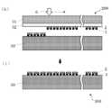
이하, 도 9를 참조하면서, 상기한 레이저 리프트오프법에 의한 종래의 발광다이오드 디스플레이패널의 제조방법의 일례에 대하여 설명한다. 도 9(I)~(III)은, 발광다이오드 제조기판으로부터 공급기판을 제조하는 공정의 일례를 나타내는 것이고, 상기 서술한 스탬프법에 있어서 1개씩 발광다이오드를 디스플레이패널 기판에 이재하는 공정은, 도 9(IV) 및 (V)에 나타내어져 있다.Hereinafter, referring to FIG. 9, an example of a method of manufacturing a conventional light emitting diode display panel by the laser lift-off method described above will be described. 9 (I) to (III) show an example of a step of manufacturing a supply substrate from a light emitting diode manufacturing substrate, and the step of transferring the light emitting diodes one by one to the display panel substrate in the above-described stamp method is shown in FIG. 9(IV) and (V).
도 9(I)에 있어서, 1은, 출발기판으로서의 사파이어기판이고, 그 일방의 표면에 형성된 복수의 GaN계의 발광다이오드(2)가 개개로 각각 분리된 상태로 가공되어 있다. 나아가 발광다이오드(2)는 전극(3)을 구비하고 있다. 4는 제1의 공급기판이고, 석영으로 이루어지는 기판(41)과, 그 위에 형성된 점착층으로서의 실리콘 수지층(42)으로 이루어진다.In Fig. 9(I), 1 is a sapphire substrate as a starting substrate, and a plurality of GaN-based
도 9(I)에 나타낸 바와 같이, 제1의 공급기판(4) 및 출발기판(사파이어기판)(1)을, 발광다이오드(2)가 점착층(42)에 대향하여 양자의 간극이 일정해지도록 또한 최적의 거리를 두고 배치한다. 이 상태에서, 출발기판(1) 중 발광다이오드(2)가 형성되어 있지 않은 표면측으로부터, 레이저광(6)을 조사한다. 레이저광(6)은 출발기판(1)을 통과하여, 출발기판(1)의 표면과 발광다이오드(2)의 계면 근방에 도달함으로써, 이 계면 근방의 발광다이오드(2)측의 GaN이 얇게 레이저 어블레이션된다. 이것이 소위 레이저 리프트오프이며, 출발기판(1)으로부터 발광다이오드(2)가 분리되고, 발광다이오드(2)가 대향하는 제1의 공급기판(4)을 향하여 방출된다. 그 결과, 방출된 발광다이오드(2)는, 점착층(실리콘 수지층)(42)의 표면까지 비행하여, 점착층(42)의 표면에 가접착된다. 레이저광(6)이 출발기판(1)의 원하는 영역을 스캔함으로써, 출발기판(1) 상의 원하는 발광다이오드(2)를 모두 제1의 공급기판(4)에 이재할 수 있고, 도 9(II)의 제1의 공급기판(4)이 완성된다. 이 경우, 어블레이션에 의해 GaN의 성분이 발광다이오드(2)에 잔사로서 부착되지 않기 때문에, 박리층(유기 폴리머를 포함한다)의 경우와 같이 박리층의 일부의 부착물을 세정할 필요가 생기지 않는다.As shown in FIG. 9(I), the
다음으로, 도 9(III)에 나타내는 바와 같이, 기판(51)과 그 위의 점착층으로서의 실리콘 수지층(52)을 갖는 제2의 공급기판(5)을 준비한다. 이어서, 이 제2의 공급기판(5) 및 도 9(II)의 제1의 공급기판(4)을, 발광다이오드(2)가 점착층(52)에 대향하여, 양자의 간극이 일정해지도록 또한 최적의 거리를 두고 배치한다.Next, as shown in FIG. 9(III), a
이 상태에서, 제1의 공급기판(4) 중 발광다이오드(2)가 배치되어 있지 않은 표면의 원하는 영역에, 레이저광(6)을 스캔하면서 조사함으로써, 전극(3)을 구비한 발광다이오드(2)가 상하 반전한 상태에서 가접착된 제2의 공급기판(5)이 완성된다. 이와 같이 하여, 전극(3)이 외향으로 배치된 발광다이오드 공급기판으로서의 제2의 공급기판(5)을 제작할 수 있다.In this state, by irradiating the
다음으로, 도 9(IV)에 나타내는, 공급처로서의 디스플레이패널 기판(39)을 준비한다. 디스플레이패널 기판(39)은, 도시하지 않으나 전극 및 배선을 구비하고 있다. 이 디스플레이패널 기판(39)과 제2의 공급기판(5)을 양자의 간극이 일정해지도록 또한 최적의 거리를 두고 배치한다. 이 상태에서, 제2의 공급기판(5) 중 발광다이오드(2)가 배치되어 있지 않은 표면측으로부터 레이저광(6)을 조사한다. 이와 같은 레이저 리프트오프법에 의해, 도 9(V)에 나타내는 바와 같이, 복수의 발광다이오드(2)가 제2의 공급기판(5)으로부터 디스플레이패널 기판(39)에 이재된다.Next, the display panel board|
이와 같이 레이저 리프트오프법을 이용하여, 디스플레이패널 기판(39) 상의 원하는 전극위치에 발광다이오드(2)의 전극(3)이 전기적 접촉하도록 배치함으로써, 디스플레이패널(300)이 완성된다(도 9(V)).In this way, the
그러나, 이와 같이 스탬프법보다도 고속으로 이재할 수 있는 레이저 리프트오프법을 이용하여 디스플레이를 제조했다고 하더라도, 다량의 불량 발광다이오드가 섞인 공급기판을 사용한 경우, 디스플레이 기판 상에서 정상의 발광다이오드를 재배치, 즉, 리페어를 해야 한다는 문제를 갖고 있다. 그 때문에, 정상의 발광다이오드만 탑재된 공급기판이 절실히 요망되고 있다.However, even if the display is manufactured using the laser lift-off method, which can be transferred at a higher speed than the stamp method, when a supply substrate mixed with a large amount of defective light emitting diodes is used, normal light emitting diodes are rearranged on the display substrate, that is, , has the problem of having to repair. Therefore, a supply substrate on which only normal light emitting diodes are mounted is desperately desired.
이상 설명한 바와 같이, 스탬프법, 레이저 리프트오프법의 어느 방법을 이용한 경우에도, 디스플레이패널 기판에 발광다이오드를 공급하는 공급기판(도 9의 제2의 공급기판(5)) 상에 탑재된 발광다이오드 중에 불량의 발광다이오드가 포함되어 있는 경우, 불량 발광다이오드를 디스플레이패널 기판에 그대로 이재하기 때문에, 정상의 이재수율이 저하된다는 문제를 갖고 있었다.As described above, even in the case of using either the stamp method or the laser lift-off method, the light emitting diode mounted on the supply substrate for supplying the light emitting diode to the display panel substrate (the
본 발명은, 상기 문제를 해결하기 위해 이루어진 것으로, 복수의 정상의 발광다이오드를 공급처에 이재할 수 있는 발광다이오드 공급기판을 제조할 수 있는 발광다이오드 공급기판의 제조방법, 고수율의 발광다이오드 디스플레이의 제조방법, 고수율의 발광다이오드 디스플레이의 분할유닛의 제조방법, 및 복수의 정상의 소자를 공급처에 이재할 수 있는 소자 공급기판을 제조할 수 있는 소자 공급기판의 제조방법을 제공하는 것을 목적으로 한다.The present invention has been made to solve the above problems, and a method for manufacturing a light emitting diode supply substrate capable of manufacturing a light emitting diode supply substrate capable of transferring a plurality of normal light emitting diodes to a supplier, and a high yield light emitting diode display It is an object to provide a manufacturing method, a manufacturing method of a division unit of a high-yield light emitting diode display, and a manufacturing method of an element supply substrate capable of manufacturing an element supply substrate capable of transferring a plurality of normal elements to a supplier. .
상기 과제를 해결하기 위해, 본 발명에서는, 복수의 발광다이오드를 공급처에 이재하기 위한 발광다이오드 공급기판의 제조방법으로서,In order to solve the above problems, in the present invention, as a method of manufacturing a light emitting diode supply substrate for transferring a plurality of light emitting diodes to a supplier,
공급기판 상에 복수의 발광다이오드를 탑재하는 제1 탑재공정과,A first mounting step of mounting a plurality of light emitting diodes on a supply substrate;
상기 공급기판 상의 불량의 발광다이오드를 선택적으로 제거하는 선택제거공정과,a selective removal step of selectively removing defective light emitting diodes on the supply substrate;
상기 공급기판 상의 상기 불량의 발광다이오드가 배치되어 있던 위치에, 정상의 발광다이오드를 이재하는 제2 탑재공정A second mounting step of transferring a normal light emitting diode to the position where the defective light emitting diode was placed on the supply substrate.
을 포함하는 것을 특징으로 하는 발광다이오드 공급기판의 제조방법을 제공한다.It provides a method for manufacturing a light emitting diode supply substrate comprising a.
이와 같이 하면, 정상의 발광다이오드만을 구비한 발광다이오드 공급기판을 제조할 수 있다. 이와 같이 하여 제조한 발광다이오드 공급기판을 이용함으로써, 정상의 복수의 발광다이오드를 공급처에 일괄로, 혹은, 선택하여 이재할 수 있다. 요컨대, 본 발명의 발광다이오드 공급기판의 제조방법에 따르면, 복수의 정상의 발광다이오드를 공급처에 일괄로, 혹은, 선택하여 이재할 수 있는 발광다이오드 공급기판을 제조할 수 있다.In this way, a light emitting diode supply substrate having only normal light emitting diodes can be manufactured. By using the light emitting diode supply substrate manufactured in this way, a plurality of normal light emitting diodes can be collectively or selectively transferred to the supply destination. In short, according to the manufacturing method of the light emitting diode supply substrate of the present invention, it is possible to manufacture a light emitting diode supply substrate capable of transferring a plurality of normal light emitting diodes to a supplier in a lump sum or selectively.
또한, 본 발명의 발광다이오드 공급기판의 제조방법에 의해 제조된 발광다이오드 공급기판은, 불량 발광다이오드를 포함하지 않기 때문에, 발광다이오드 디스플레이, 또는, 발광다이오드 디스플레이의 분할유닛을 제조할 때의 발광불량 결함의 발생을 현저히 저감할 수 있다. 그 결과, 발광다이오드 디스플레이 또는 그의 분할유닛을 고수율 및 고효율로 제조하는 것이 가능해진다.In addition, since the light emitting diode supply substrate manufactured by the manufacturing method of the light emitting diode supply substrate of the present invention does not include defective light emitting diodes, the light emitting diode display or the division unit of the light emitting diode display is manufactured. The occurrence of defects can be significantly reduced. As a result, it becomes possible to manufacture a light emitting diode display or a division unit thereof with high yield and high efficiency.
상기 선택제거공정 전에, 상기 공급기판 상의 개개의 상기 발광다이오드가 정상인지 여부를 판정하는 판정공정을 추가로 포함하는 것이 바람직하다.Prior to the selective removal step, it is preferable to further include a determination step of determining whether or not each of the light emitting diodes on the supply substrate is normal.
이와 같이 하면, 불량 발광다이오드를 확실히 선별제거할 수 있다.In this way, defective light emitting diodes can be reliably sorted out.
또한, 상기 판정공정을, 포토루미네선스법에 의해 행하는 것이 바람직하다.Moreover, it is preferable to perform the said determination process by the photoluminescence method.
상기 판정공정을 포토루미네선스법에 의해 행하면, 비접촉으로 판정할 수 있다.If the above judgment step is performed by the photoluminescence method, it can be judged in a non-contact manner.
상기 선택제거공정, 상기 제2 탑재공정, 또는 그의 양방을, 레이저 리프트오프법에 의해 행하는 것이 바람직하다.It is preferable to perform the selective removal step, the second mounting step, or both of them by a laser lift-off method.
선택제거공정, 제2 탑재공정, 또는 그의 양방이 레이저 리프트오프법으로 행해지도록 하면, 보다 고효율로 발광다이오드 공급기판을 제조할 수 있다.If the selective removal process, the second mounting process, or both are performed by the laser lift-off method, the light emitting diode supply substrate can be manufactured with higher efficiency.
상기 선택제거공정, 상기 제2 탑재공정, 또는 그의 양방에 있어서의 상기 레이저 리프트오프법에 이용하는 레이저를 엑시머레이저로 하는 것이 바람직하다.It is preferable that the laser used in the laser lift-off method in the selective removal process, the second mounting process, or both is an excimer laser.
이와 같이 하면, 시간압축된 펄스레이저광을 생성할 수 있다. 펄스폭이나 광강도는 펄스발신전압 등의 장치전원 파라미터를 제어함으로써 용이하게 제어가 가능하며, 다른 연속파발진(CW)레이저로는 실현할 수 없는 단펄스이고 고강도인 레이저광을 발생시킬 수 있다.In this way, time-compressed pulsed laser light can be generated. The pulse width and light intensity can be easily controlled by controlling device power parameters such as pulse transmission voltage, and short-pulse, high-intensity laser light can be generated, which cannot be realized with other continuous wave oscillation (CW) lasers.
상기 선택제거공정, 상기 제2 탑재공정, 또는 그의 양방에 있어서의 상기 레이저 리프트오프법에 이용하는 레이저를 펄스레이저로 하고, 1펄스의 레이저광조사로 리프트오프를 행하면 된다.The laser used in the laser lift-off method in the selective removal step, the second mounting step, or both thereof may be a pulsed laser, and lift-off may be performed by one-pulse laser light irradiation.
이와 같이 하면, 상기 선택제거공정, 상기 제2 탑재공정, 또는 그의 양방에 있어서 이용하는 레이저를 엑시머레이저로 한정할 필요는 없고, 필요한 강도의 펄스레이저광을 생성할 수 있는 레이저를 사용가능하다.In this way, it is not necessary to limit the laser used in the selective removal process, the second mounting process, or both to the excimer laser, and a laser capable of generating pulsed laser light with a required intensity can be used.
상기 발광다이오드로서, 최장부가 300μm보다 작은 것을 이용하면 된다.As the light emitting diode, a light emitting diode having a longest part smaller than 300 μm may be used.
이와 같이 하면, 레이저 리프트오프법에 의해, 보다 효율적으로 이재가 가능해진다.In this way, the transfer can be performed more efficiently by the laser lift-off method.
상기 발광다이오드로서, 적색 발광다이오드, 녹색 발광다이오드, 및 청색 발광다이오드로 이루어지는 군으로부터 선택되는 1종류를 이용할 수 있다.As the light emitting diode, one type selected from the group consisting of a red light emitting diode, a green light emitting diode, and a blue light emitting diode can be used.
이와 같이 하면, 적색, 녹색, 청색의 각 발광다이오드의 단색의 공급기판을 제조할 수 있다.In this way, it is possible to manufacture monochromatic supply substrates for each of the red, green, and blue light emitting diodes.
상기 복수의 발광다이오드를, 적색 발광다이오드, 녹색 발광다이오드, 및 청색 발광다이오드의 각 1개 이상이 1세트의 화소가 되도록 배치할 수도 있다.The plurality of light emitting diodes may be arranged so that at least one of each of a red light emitting diode, a green light emitting diode, and a blue light emitting diode constitutes one set of pixels.
이와 같이 하면, 발광다이오드 디스플레이를 제조할 때에, 일괄 혹은 1화소 단위로의 이재가 가능해진다.In this way, when manufacturing a light emitting diode display, transfer in batches or in units of one pixel becomes possible.
공급기판으로서, 석영기판과, 이 석영기판 상에 마련된 점착층을 포함하는 것을 이용하고,As the supply substrate, a quartz substrate and an adhesive layer provided on the quartz substrate are used,
상기 제1 탑재공정에 있어서, 상기 공급기판의 상기 점착층의 표면에, 상기 복수의 발광다이오드를 매트릭스상으로 점착시키는 것이 바람직하다.In the first mounting step, it is preferable to attach the plurality of light emitting diodes in a matrix to the surface of the adhesive layer of the supply substrate.
이와 같이 하면 발광다이오드의 공급기판을 효율좋게 제조할 수 있다.In this way, the supply substrate of the light emitting diode can be efficiently manufactured.
상기 제2 탑재공정을,The second mounting step,
석영기판과, 이 석영기판 상에 마련된 점착층과, 상기 점착층의 표면에 매트릭스상으로 점착된 복수의 발광다이오드를 포함하는 보충기판을 준비하고,preparing a supplementary substrate including a quartz substrate, an adhesive layer provided on the quartz substrate, and a plurality of light emitting diodes adhered to the surface of the adhesive layer in a matrix form;
상기 보충기판 상의 정상의 발광다이오드를, 상기 공급기판 상의 상기 불량의 발광다이오드가 제거된 위치에 이재함The normal light emitting diode on the supplementary board is moved to the position where the defective light emitting diode on the supply board is removed.
으로써 행하는 것이 바람직하다.It is preferable to do so.
이와 같이 하면, 발광다이오드의 공급기판을 보다 효율좋게 제조할 수 있다.In this way, the supply substrate of the light emitting diode can be manufactured more efficiently.
상기 선택제거공정과 상기 제2 탑재공정 사이에, 상기 보충기판을 상기 공급기판과 대향하도록 배치하는 배치공정을 추가로 포함하는 것이 바람직하다.It is preferable to further include a arranging step of arranging the supplementary substrate to face the supply substrate between the selective removal step and the second mounting step.
이와 같이 하면, 제2 탑재공정에 있어서의 정밀도를 더욱 높일 수 있다.In this way, the precision in the second mounting step can be further increased.
이 경우, 상기 배치공정에 있어서, 상기 공급기판 상의 상기 불량의 발광다이오드가 배치되어 있던 위치와, 상기 보충기판 상의 상기 정상의 발광다이오드의 위치가 대향하도록 위치맞춤하는 것이 바람직하다.In this case, in the arranging step, it is preferable that the positions of the defective light emitting diodes on the supply substrate are aligned so that the positions of the normal light emitting diodes on the supplementary substrate face each other.
이에 따라, 불량의 발광다이오드를 제거한 위치에, 보다 정확히 정상의 발광다이오드를 탑재할 수 있다.Accordingly, it is possible to more accurately mount a good light emitting diode at the position where the defective light emitting diode is removed.
상기 공급기판으로서, 상기 석영기판이 합성석영으로 이루어지는 것을 이용하는 것이 바람직하다.As the supply substrate, it is preferable to use a quartz substrate made of synthetic quartz.
합성석영은, 우수한 면 내 막두께균일성을 나타낼 수 있다. 따라서, 상기 석영기판에 합성석영을 이용하면, 레이저 리프트오프법을 행하기 위해 대향시키는 기판 간의 간극의 제어가 가능해진다.Synthetic quartz can exhibit excellent in-plane film thickness uniformity. Therefore, if synthetic quartz is used for the quartz substrate, it is possible to control the gap between opposing substrates for performing the laser lift-off method.
보충기판의 석영기판도, 합성석영으로 이루어지는 것으로 하는 것이 바람직하다. 이 경우, 예를 들어 상기 배치공정에 있어서 보충기판을 공급기판과 평행하게 대향하도록 배치하는 경우에, 기판 전체면에 걸쳐 고정밀도로 일정거리로 배치할 수 있다.It is preferable that the quartz substrate of the supplementary substrate is also made of synthetic quartz. In this case, for example, in the case of arranging the supplementary substrate so as to face the supply substrate in parallel in the above arrangement step, it is possible to arrange the supplementary substrate at a constant distance over the entire surface of the substrate with high precision.
상기 공급기판으로서, 상기 석영기판에 패싯이 마련되어 있는 것을 이용하면 된다.As the supply substrate, a quartz substrate provided with facets may be used.
이와 같이 하면, 레이저 리프트오프법을 이용한 이재장치에 공급기판을 세트할 때에, 회전위치를 틀리는 일 없이 세트할 수 있다.In this way, when the supply substrate is set in the transfer device using the laser lift-off method, the rotational position can be set without error.
이 경우, 상기 보충기판으로서, 상기 석영기판에 패싯이 마련되어 있는 것을 이용하는 것이 보다 바람직하다.In this case, as the supplementary substrate, it is more preferable to use a quartz substrate provided with facets.
이 경우, 상기 패싯이, 오리엔테이션을 나타내는 표시(印)인 것이 더욱 바람직하다.In this case, it is more preferable that the facet is a mark indicating orientation.
이 경우, 레이저 리프트오프법을 이용한 이재장치에 공급기판을 세트할 때에, 회전위치를 틀리는 일 없이 세트할 수 있다.In this case, when the supply substrate is set in the transfer device using the laser lift-off method, the rotational position can be set without error.
상기 공급기판으로서, 상기 석영기판이 문자, 기호 및 2D바코드로 이루어지는 군으로부터 선택되는 1종 이상을 갖는 것을 이용할 수 있다.As the supply substrate, a quartz substrate having one or more types selected from the group consisting of letters, symbols, and 2D barcodes may be used.
상기 보충기판으로서, 상기 석영기판이 문자, 기호 및 2D바코드로 이루어지는 군으로부터 선택되는 1종 이상을 갖는 것을 이용할 수도 있다.As the supplementary substrate, a quartz substrate having at least one selected from the group consisting of letters, symbols, and 2D barcodes may be used.
이와 같이 함으로써, 개개의 공급기판 및 보충기판의 관리가 가능해진다.In this way, it is possible to manage individual supply substrates and supplementary substrates.
상기 문자, 상기 기호 및 상기 2D바코드가, 오리엔테이션을 나타내는 표시인 것으로 할 수 있다.The character, the symbol, and the 2D bar code may be a display indicating orientation.
상기 문자, 상기 기호 및 상기 2D바코드에 의해 상기 공급기판의 개체식별을 행할 수 있다. 또한, 오리엔테이션을 나타내는 표시로 할 수도 있다.Individual identification of the supply substrate can be performed by the character, the symbol, and the 2D barcode. Moreover, it can also be set as a display which shows orientation.
이 경우, 레이저 리프트오프법을 이용한 이재장치에 공급기판을 세트할 때에, 정확히 개체판별할 수 있고, 또한, 회전위치를 틀리는 일 없이 세트할 수 있다.In this case, when the supply substrate is set in the transfer device using the laser lift-off method, it is possible to accurately discriminate the substrate and set it without misalignment of the rotational position.
상기 공급기판으로서, 상기 점착층이 실리콘을 포함하는 감압접착제로 이루어지는 것을 이용하는 것이 바람직하다.As the supply substrate, it is preferable to use one in which the adhesive layer is made of a pressure-sensitive adhesive containing silicon.
상기 보충기판으로서, 상기 점착층이 실리콘을 포함하는 감압접착제로 이루어지는 것을 이용할 수도 있다.As the supplementary substrate, one in which the adhesive layer is made of a pressure-sensitive adhesive containing silicon may be used.
이에 따라, 양호한 점착력을 제공할 수 있다. 또한, 레이저 리프트오프법으로 발광다이오드를 이재할 때에 발광다이오드에 불순물이 부착되지 않는다. 나아가, 한번 발광다이오드를 제거한 후에 재차 발광다이오드를 점착시킬 수 있다.Accordingly, good adhesive force can be provided. In addition, impurities are not attached to the light emitting diode when the light emitting diode is transferred by the laser lift-off method. Furthermore, after removing the light emitting diode once, the light emitting diode may be attached again.
상기 공급기판으로서, 상기 매트릭스의 피치가 디스플레이패널의 화소피치 또는 화소피치의 정수분의 1배인 것을 이용하면 된다.As the supply substrate, a substrate having a pitch of the matrix of the display panel or an integral part of the pixel pitch may be used.
이와 같이 하면, 공급기판의 불필요한 위치맞춤이동 없이, 최소한의 이동동작만을 행하여, 레이저 조사위치를 제어이동시킴으로써, 복수의 발광다이오드를 레이저 리프트오프법에 의해 이재할 수 있다.In this way, a plurality of light emitting diodes can be transferred by the laser lift-off method by performing only a minimum movement operation and controllingly moving the laser irradiation position without unnecessary alignment movement of the supply substrate.
상기 제1 탑재공정이,The first mounting step,
출발기판으로서, 그 위에 상기 복수의 발광다이오드가 제조된 출발기판을 준비하는 공정과,a step of preparing a starting substrate on which the plurality of light emitting diodes are manufactured as a starting substrate;
상기 출발기판 상의 상기 복수의 발광다이오드 간을 1소자씩으로 분리하는 공정과,a step of separating the plurality of light emitting diodes on the starting substrate into elements;
1소자씩으로 분리된 상기 복수의 발광다이오드를 상기 공급기판 상에 이재하는 공정Step of transferring the plurality of light emitting diodes separated into one element on the supply substrate
을 포함하는 것이 바람직하다.It is preferable to include
이와 같이 하면, 효율좋게 제1 탑재공정을 행할 수 있다.In this way, the first mounting step can be efficiently performed.
상기 제1 탑재공정에서의 상기 복수의 발광다이오드를 상기 공급기판 상에 이재하는 공정을, 레이저 리프트오프법에 의해 행하는 것이 바람직하다.Preferably, the step of transferring the plurality of light emitting diodes on the supply substrate in the first mounting step is performed by a laser lift-off method.
이와 같이 하면, 더욱 효율좋게 제1 탑재공정을 행할 수 있다.In this way, the first mounting step can be performed more efficiently.
또한, 본 발명에서는, 발광다이오드 디스플레이의 제조방법으로서,In addition, in the present invention, as a method for manufacturing a light emitting diode display,
본 발명의 발광다이오드 공급기판의 제조방법에 의해, 상기 발광다이오드 공급기판을 제조하는 공정과,The step of manufacturing the light emitting diode supply substrate by the method of manufacturing the light emitting diode supply substrate of the present invention;
상기 발광다이오드 공급기판 상의 상기 복수의 발광다이오드를, 디스플레이패널 기판 상에 이재하는 공정Step of transferring the plurality of light emitting diodes on the light emitting diode supply substrate onto a display panel substrate
을 갖는 것을 특징으로 하는 발광다이오드 디스플레이의 제조방법을 제공한다.It provides a method for manufacturing a light emitting diode display characterized by having a.
본 발명의 발광다이오드 디스플레이의 제조방법에서는, 본 발명의 발광다이오드 공급기판의 제조방법으로 발광다이오드 공급기판을 제조하고, 이것을 이용하여 복수의 발광다이오드를 발광다이오드 디스플레이 기판에 이재하기 때문에, 불량 발광다이오드를 포함하지 않는 발광다이오드 디스플레이를 효율좋게 제조할 수 있다. 즉, 본 발명의 발광다이오드 디스플레이의 제조방법에 따르면, 고수율로 발광다이오드 디스플레이를 제조할 수 있다.In the manufacturing method of the light emitting diode display of the present invention, since the light emitting diode supply substrate is manufactured by the manufacturing method of the light emitting diode supply substrate of the present invention, and a plurality of light emitting diodes are transferred to the light emitting diode display substrate using this, defective light emitting diodes A light emitting diode display that does not contain can be efficiently manufactured. That is, according to the manufacturing method of the light emitting diode display of the present invention, the light emitting diode display can be manufactured with high yield.
상기 발광다이오드 공급기판 상의 상기 복수의 발광다이오드를, 상기 디스플레이패널 기판 상에 이재하는 공정을, 레이저 리프트오프법에 의해 행하는 것이 바람직하다.Preferably, the step of transferring the plurality of light emitting diodes on the light emitting diode supply substrate onto the display panel substrate is performed by a laser lift-off method.
이와 같이 하면, 보다 고속으로 복수의 발광다이오드를 이재할 수 있기 때문에, 보다 실용적인 발광다이오드 디스플레이의 제조방법을 제공할 수 있다.In this way, since a plurality of light emitting diodes can be transferred at a higher speed, a more practical light emitting diode display manufacturing method can be provided.
또한, 본 발명에서는, 발광다이오드 디스플레이의 분할유닛의 제조방법으로서,In addition, in the present invention, as a method for manufacturing a division unit of a light emitting diode display,
본 발명의 발광다이오드 공급기판의 제조방법에 의해, 상기 발광다이오드 공급기판을 제조하는 공정과,The step of manufacturing the light emitting diode supply substrate by the method of manufacturing the light emitting diode supply substrate of the present invention;
상기 발광다이오드 공급기판 상의 상기 복수의 발광다이오드를, 발광다이오드 디스플레이의 분할유닛 상에 이재하는 공정A step of transferring the plurality of light emitting diodes on the light emitting diode supply substrate onto a division unit of a light emitting diode display.
을 갖는 것을 특징으로 하는 발광다이오드 디스플레이의 분할유닛의 제조방법을 제공한다.It provides a method of manufacturing a division unit of a light emitting diode display, characterized in that it has.
본 발명의 발광다이오드 디스플레이의 분할유닛의 제조방법에서는, 본 발명의 발광다이오드 공급기판의 제조방법으로 발광다이오드 공급기판을 제조하고, 이것을 이용하여 복수의 발광다이오드를 발광다이오드 디스플레이의 분할유닛에 이재하기 때문에, 불량 발광다이오드를 포함하지 않는 발광다이오드 디스플레이의 분할유닛을 효율좋게 제조할 수 있다. 즉, 본 발명의 발광다이오드 디스플레이의 분할유닛의 제조방법에 따르면, 고수율로 발광다이오드 디스플레이의 분할유닛을 제조할 수 있다.In the manufacturing method of the division unit of the light emitting diode display of the present invention, the light emitting diode supply substrate is manufactured by the manufacturing method of the light emitting diode supply substrate of the present invention, and a plurality of light emitting diodes are transferred to the division unit of the light emitting diode display using this. Therefore, it is possible to efficiently manufacture a division unit of a light emitting diode display that does not include defective light emitting diodes. That is, according to the manufacturing method of the division unit of the light emitting diode display of the present invention, the division unit of the light emitting diode display can be manufactured with high yield.
상기 발광다이오드 공급기판 상의 상기 복수의 발광다이오드를, 상기 발광다이오드 디스플레이의 분할유닛 상에 이재하는 공정을, 레이저 리프트오프법에 의해 행하는 것이 바람직하다.Preferably, the step of transferring the plurality of light emitting diodes on the light emitting diode supply substrate onto the division unit of the light emitting diode display is performed by a laser lift-off method.
이와 같이 하면, 보다 고속으로 복수의 발광다이오드를 이재할 수 있기 때문에, 보다 실용적인 발광다이오드 디스플레이의 분할유닛의 제조방법을 제공할 수 있다.In this way, since a plurality of light emitting diodes can be transferred at a higher speed, it is possible to provide a more practical method of manufacturing a division unit of a light emitting diode display.
또한, 본 발명에서는, 복수의 소자를 공급처에 이재하기 위한 소자 공급기판의 제조방법으로서,In addition, in the present invention, as a method of manufacturing an element supply substrate for transferring a plurality of elements to a supplier,
공급기판 상에 복수의 소자를 탑재하는 제1 탑재공정과,A first mounting step of mounting a plurality of elements on a supply substrate;
상기 공급기판 상의 불량의 소자를 선택적으로 제거하는 선택제거공정과,a selective removal step of selectively removing defective devices on the supply substrate;
상기 공급기판 상의 상기 불량의 소자가 배치되어 있던 위치에, 정상의 소자를 이재하는 제2 탑재공정A second mounting step of transferring a good element to the position where the defective element was placed on the supply substrate.
을 포함하는 것을 특징으로 하는 소자 공급기판의 제조방법을 제공한다.It provides a method for manufacturing an element supply substrate comprising a.
본 발명은, 발광다이오드를 이재하기 위한 공급기판으로 한정되지 않고, 예를 들어 미소전기소자나 미소반도체칩 등의 소자를 이재하기 위한 소자 공급기판을 제공할 수 있다. 이 소자 공급기판은, 복수의 정상의 소자를 공급처에 이재할 수 있다. 이러한 소자 공급기판의 제조방법은, 예를 들어, 3차원 실장 그리고 전기·전자기기의 제조에 사용할 수 있다.The present invention is not limited to a supply substrate for transferring light emitting diodes, but can provide an element supply substrate for transferring devices such as microelectric devices and micro semiconductor chips, for example. This element supply substrate can transfer a plurality of normal elements to a supply destination. This method of manufacturing an element supply substrate can be used for, for example, three-dimensional mounting and manufacturing of electric/electronic devices.
예를 들어, 상기 소자는, 전기소자, 반도체칩, 또는 MEMS소자로 할 수 있다.For example, the element may be an electric element, a semiconductor chip, or a MEMS element.
이와 같이, 본 발명의 소자 공급기판의 제조방법은, 다양한 소자의 공급에 적용할 수 있다.In this way, the manufacturing method of the element supply substrate of the present invention can be applied to the supply of various elements.
이상과 같이, 본 발명의 발광다이오드 공급기판의 제조방법에 따르면, 복수의 정상의 발광다이오드를 공급처에 일괄로, 혹은, 선택하여 이재할 수 있는 발광다이오드 공급기판을 제조할 수 있다.As described above, according to the manufacturing method of the light emitting diode supply substrate of the present invention, it is possible to manufacture a light emitting diode supply substrate capable of transferring a plurality of normal light emitting diodes to a supplier in a lump sum or selectively.
또한, 본 발명의 발광다이오드 공급기판의 제조방법에 의해 제조된 발광다이오드 공급기판은, 불량 발광다이오드를 포함하지 않기 때문에, 발광다이오드 디스플레이, 또는, 발광다이오드 디스플레이의 분할유닛을 제조할 때의 발광불량 결함의 발생을 현저히 저감할 수 있다. 그 결과, 발광다이오드 디스플레이를 고수율 및 고효율로 제조하는 것이 가능해진다.In addition, since the light emitting diode supply substrate manufactured by the manufacturing method of the light emitting diode supply substrate of the present invention does not include defective light emitting diodes, the light emitting diode display or the division unit of the light emitting diode display is manufactured. The occurrence of defects can be significantly reduced. As a result, it becomes possible to manufacture a light emitting diode display with high yield and high efficiency.
나아가, 본 발명의 발광다이오드 디스플레이의 제조방법 및 발광다이오드 디스플레이의 분할유닛의 제조방법은, 본 발명의 발광다이오드 공급기판의 제조방법을 포함하기 때문에, 불량 발광다이오드를 포함하지 않는 발광다이오드 디스플레이 또는 발광다이오드 디스플레이의 분할유닛을 효율좋게 제조할 수 있다.Furthermore, since the manufacturing method of the light emitting diode display and the manufacturing method of the division unit of the light emitting diode display of the present invention include the manufacturing method of the light emitting diode supply substrate of the present invention, the light emitting diode display or light emitting diode display does not include defective light emitting diodes. A division unit of a diode display can be efficiently manufactured.
그리고, 본 발명의 소자 공급기판의 제조방법에 따르면, 복수의 정상의 소자를 공급처에 일괄로, 혹은, 선택하여 이재할 수 있는 소자 공급기판을 제조할 수 있다.Further, according to the method for manufacturing an element supply substrate of the present invention, it is possible to manufacture an element supply substrate capable of transferring a plurality of normal elements to a supplier in a lump sum or selectively.
도 1은 본 발명의 발광다이오드 공급기판의 제조방법의 제1의 실시형태의 일부를 나타내는 설명도이다.
도 2는 본 발명의 발광다이오드 공급기판의 제조방법의 제1의 실시형태의 다른 일부를 나타내는 설명도이다.
도 3은 도 1 및 도 2에 나타낸 제조방법으로 제조한 발광다이오드 공급기판을 이용하는, 발광다이오드 디스플레이의 제조방법의 일례의 일부를 나타내는 설명도이다.
도 4는 본 발명의 발광다이오드 공급기판의 제조방법의 제2의 실시형태의 일부를 나타내는 설명도이다.
도 5는 본 발명의 발광다이오드 공급기판의 제조방법의 제2의 실시형태의 다른 일부를 나타내는 설명도이다.
도 6은 본 발명의 발광다이오드 공급기판의 제조방법의 제3의 실시형태의 일부를 나타내는 설명도이다.
도 7은 본 발명의 발광다이오드 공급기판의 제조방법의 제4의 실시형태의 일부를 나타내는 설명도이다.
도 8은 본 발명의 발광다이오드 공급기판의 제조방법의 제5의 실시형태의 일부를 나타내는 설명도이다.
도 9는 종래의 발광다이오드 공급기판의 제조방법의 일례 및 발광다이오드 디스플레이의 제조방법의 일례를 나타내는 설명도이다.1 is an explanatory view showing a part of a first embodiment of a method for manufacturing a light emitting diode supply substrate of the present invention.
Fig. 2 is an explanatory view showing another part of the first embodiment of the method for manufacturing a light emitting diode supply substrate of the present invention.
FIG. 3 is an explanatory view showing part of an example of a method for manufacturing a light emitting diode display using a light emitting diode supply substrate manufactured by the manufacturing method shown in FIGS. 1 and 2 .
Fig. 4 is an explanatory diagram showing a part of a second embodiment of a method for manufacturing a light emitting diode supply substrate of the present invention.
Fig. 5 is an explanatory view showing another part of the second embodiment of the method for manufacturing a light emitting diode supply substrate of the present invention.
Fig. 6 is an explanatory view showing a part of a third embodiment of a method for manufacturing a light emitting diode supply substrate of the present invention.
Fig. 7 is an explanatory diagram showing a part of a fourth embodiment of a method for manufacturing a light emitting diode supply substrate of the present invention.
Fig. 8 is an explanatory diagram showing a part of a fifth embodiment of a method for manufacturing a light emitting diode supply substrate of the present invention.
9 is an explanatory view showing an example of a conventional manufacturing method of a light emitting diode supply substrate and an example of a manufacturing method of a light emitting diode display.
상기 서술한 바와 같이, 복수의 정상의 발광다이오드를 공급처에 일괄로, 혹은, 선택하여 이재할 수 있는 발광다이오드 공급기판을 제조할 수 있는 발광다이오드 공급기판의 제조방법, 고수율의 발광다이오드 디스플레이의 제조방법, 고수율의 발광다이오드 디스플레이의 분할유닛의 제조방법, 및 복수의 정상의 소자를 공급처에 일괄로, 혹은, 선택하여 이재할 수 있는 소자 공급기판을 제조할 수 있는 소자 공급기판의 제조방법의 개발이 요구되고 있었다.As described above, a method for manufacturing a light emitting diode supply substrate capable of manufacturing a light emitting diode supply substrate capable of transferring a plurality of normal light emitting diodes to a supplier in a lump sum or selectively, and a high yield light emitting diode display A manufacturing method, a method for manufacturing a division unit of a high-yield light emitting diode display, and a manufacturing method for an element supply substrate capable of manufacturing an element supply substrate capable of collectively or selectively transferring a plurality of normal elements to a supplier. development was required.
본 발명자들은, 상기 과제에 대하여 예의검토를 거듭한 결과, 불량의 발광다이오드를 선택적으로 제거하는 선택제거공정과, 불량의 발광다이오드가 배치되어 있던 위치에 정상의 발광다이오드를 이재하는 제2 탑재공정을 포함하는 발광다이오드 공급기판의 제조방법이, 상기 과제를 해결할 수 있는 것을 발견하여, 본 발명을 완성시켰다.As a result of repeated intensive examinations on the above problems, the inventors of the present invention have found a selective removal process for selectively removing defective light emitting diodes and a second mounting process for transferring normal light emitting diodes to the positions where the defective light emitting diodes have been placed. A method for manufacturing a light emitting diode supply substrate comprising a was found to be able to solve the above problems, thereby completing the present invention.
즉, 본 발명은, 복수의 발광다이오드를 공급처에 이재하기 위한 발광다이오드 공급기판의 제조방법으로서,That is, the present invention is a method for manufacturing a light emitting diode supply substrate for transferring a plurality of light emitting diodes to a supplier,
공급기판 상에 복수의 발광다이오드를 탑재하는 제1 탑재공정과,A first mounting step of mounting a plurality of light emitting diodes on a supply substrate;
상기 공급기판 상의 불량의 발광다이오드를 선택적으로 제거하는 선택제거공정과,a selective removal step of selectively removing defective light emitting diodes on the supply substrate;
상기 공급기판 상의 상기 불량의 발광다이오드가 배치되어 있던 위치에, 정상의 발광다이오드를 이재하는 제2 탑재공정A second mounting step of transferring a normal light emitting diode to the position where the defective light emitting diode was placed on the supply substrate.
을 포함하는 것을 특징으로 하는 발광다이오드 공급기판의 제조방법이다.A method for manufacturing a light emitting diode supply substrate comprising a.
또한, 본 발명은, 발광다이오드 디스플레이의 제조방법으로서,In addition, the present invention is a method for manufacturing a light emitting diode display,
본 발명의 발광다이오드 공급기판의 제조방법에 의해, 상기 발광다이오드 공급기판을 제조하는 공정과,The step of manufacturing the light emitting diode supply substrate by the method of manufacturing the light emitting diode supply substrate of the present invention;
상기 발광다이오드 공급기판 상의 상기 복수의 발광다이오드를, 디스플레이패널 기판 상에 이재하는 공정Step of transferring the plurality of light emitting diodes on the light emitting diode supply substrate onto a display panel substrate
을 갖는 것을 특징으로 하는 발광다이오드 디스플레이의 제조방법이다.It is a method for manufacturing a light emitting diode display characterized in that it has.
나아가, 본 발명은, 발광다이오드 디스플레이의 분할유닛의 제조방법으로서,Furthermore, the present invention is a method for manufacturing a division unit of a light emitting diode display,
본 발명의 발광다이오드 공급기판의 제조방법에 의해, 상기 발광다이오드 공급기판을 제조하는 공정과,The step of manufacturing the light emitting diode supply substrate by the method of manufacturing the light emitting diode supply substrate of the present invention;
상기 발광다이오드 공급기판 상의 상기 복수의 발광다이오드를, 발광다이오드 디스플레이의 분할유닛 상에 이재하는 공정A step of transferring the plurality of light emitting diodes on the light emitting diode supply substrate onto a division unit of a light emitting diode display.
을 갖는 것을 특징으로 하는 발광다이오드 디스플레이의 분할유닛의 제조방법이다.It is a manufacturing method of a division unit of a light emitting diode display characterized in that it has.
그리고, 본 발명은, 복수의 소자를 공급처에 이재하기 위한 소자 공급기판의 제조방법으로서,And, the present invention is a method of manufacturing an element supply substrate for transferring a plurality of elements to a supplier,
공급기판 상에 복수의 소자를 탑재하는 제1 탑재공정과,A first mounting step of mounting a plurality of elements on a supply substrate;
상기 공급기판 상의 불량의 소자를 선택적으로 제거하는 선택제거공정과,a selective removal step of selectively removing defective devices on the supply substrate;
상기 공급기판 상의 상기 불량의 소자가 배치되어 있던 위치에, 정상의 소자를 이재하는 제2 탑재공정A second mounting step of transferring a good element to the position where the defective element was placed on the supply substrate.
을 포함하는 것을 특징으로 하는 소자 공급기판의 제조방법이다.It is a method of manufacturing an element supply substrate comprising a.
이하, 본 발명에 대하여 상세히 설명하는데, 본 발명은 이들로 한정되는 것은 아니다.Hereinafter, the present invention will be described in detail, but the present invention is not limited thereto.
[발광다이오드 공급기판의 제조방법][Method of Manufacturing Light-Emitting Diode Supply Substrate]
본 발명은, 복수의 발광다이오드를 공급처에 이재하기 위한 발광다이오드 공급기판의 제조방법으로서,The present invention is a method for manufacturing a light emitting diode supply substrate for transferring a plurality of light emitting diodes to a supplier,
공급기판 상에 복수의 발광다이오드를 탑재하는 제1 탑재공정과,A first mounting step of mounting a plurality of light emitting diodes on a supply substrate;
상기 공급기판 상의 불량의 발광다이오드를 선택적으로 제거하는 선택제거공정과,a selective removal step of selectively removing defective light emitting diodes on the supply substrate;
상기 공급기판 상의 상기 불량의 발광다이오드가 배치되어 있던 위치에, 정상의 발광다이오드를 이재하는 제2 탑재공정A second mounting step of transferring a normal light emitting diode to the position where the defective light emitting diode was placed on the supply substrate.
을 포함하는 것을 특징으로 한다.It is characterized in that it includes.
본 발명의 발광다이오드 공급기판의 제조방법에서는, 선택제거공정에 있어서, 제1 탑재공정에서 공급기판 상에 배치한 복수의 발광다이오드 중, 불량의 발광다이오드를 선택하여, 그것을 제거한다. 그리고, 제2 탑재공정에 있어서, 앞서 제거한 불량의 발광다이오드가 배치되어 있던 위치에, 정상의 발광다이오드를 이재한다. 이러한 제조방법에 따르면, 정상의 발광다이오드만을 구비한 발광다이오드 공급기판을 제조할 수 있다. 이와 같이 하여 제조한 발광다이오드 공급기판을 이용함으로써, 정상의 복수의 발광다이오드를 레이저 리프트오프법 혹은 스탬프법에 의해 공급처에 일괄로, 혹은, 선택하여 이재할 수 있다. 요컨대, 본 발명의 발광다이오드 공급기판의 제조방법에 따르면, 복수의 정상의 발광다이오드를 공급처에 일괄로 이재할 수 있는 발광다이오드 공급기판을 제조할 수 있다. 또한, 본 발명에 의해 제조된 발광다이오드의 공급기판 상의 원하는 위치의 발광다이오드를 선택하여 레이저 리프트오프법에 의해 공급처에 정상의 발광다이오드를 이재할 수 있다. 요컨대, 어느 위치를 선택해도 정상의 발광다이오드를 이재할 수 있는 발광다이오드의 공급기판을 제조할 수 있다.In the manufacturing method of the light emitting diode supply substrate of the present invention, in the selective removal step, a defective light emitting diode is selected from among a plurality of light emitting diodes disposed on the supply substrate in the first mounting step and removed. Then, in the second mounting step, the normal light emitting diode is transferred to the position where the previously removed defective light emitting diode was placed. According to this manufacturing method, a light emitting diode supply substrate having only normal light emitting diodes can be manufactured. By using the light emitting diode supply substrate manufactured in this way, a plurality of normal light emitting diodes can be collectively or selectively transferred to a supply destination by a laser lift-off method or a stamp method. In short, according to the manufacturing method of the light emitting diode supply substrate of the present invention, it is possible to manufacture a light emitting diode supply substrate capable of collectively transferring a plurality of normal light emitting diodes to a supplier. In addition, a normal light emitting diode can be transferred to a supplier by a laser lift-off method by selecting a light emitting diode at a desired position on the supply substrate of the light emitting diode manufactured according to the present invention. In short, it is possible to manufacture a light emitting diode supply substrate on which a normal light emitting diode can be transferred no matter which position is selected.
나아가, 본 발명의 발광다이오드 공급기판의 제조방법에 의해 제조된 발광다이오드 공급기판은, 불량 발광다이오드를 포함하지 않기 때문에, 발광다이오드 디스플레이, 또는, 발광다이오드 디스플레이의 분할유닛을 제조할 때의 발광불량 결함의 발생을 현저히 저감할 수 있다. 그 결과, 발광다이오드 디스플레이 또는 그의 분할유닛을 고수율 및 고효율로 제조하는 것이 가능해진다.Furthermore, since the light emitting diode supply substrate manufactured by the manufacturing method of the light emitting diode supply substrate of the present invention does not include defective light emitting diodes, the light emitting diode display or the division unit of the light emitting diode display is manufactured. The occurrence of defects can be significantly reduced. As a result, it becomes possible to manufacture a light emitting diode display or a division unit thereof with high yield and high efficiency.
다음으로, 각 공정을 보다 상세히 설명한다.Next, each process is explained in more detail.
[제1 탑재공정][First loading process]
제1 탑재공정에서는, 공급기판 상에 복수의 발광다이오드를 탑재한다.In the first mounting step, a plurality of light emitting diodes are mounted on a supply substrate.
여기서의 공급기판으로서, 예를 들어, 석영기판과, 이 석영기판 상에 마련된 점착층을 포함하는 것을 이용할 수 있다. 공급기판, 석영기판 및 점착층의 상세에 대해서는, 후술한다.As the supply substrate here, for example, one containing a quartz substrate and an adhesive layer provided on the quartz substrate can be used. Details of the supply substrate, the quartz substrate and the adhesive layer will be described later.
상기 발광다이오드로서, 적색 발광다이오드, 녹색 발광다이오드, 및 청색 발광다이오드로 이루어지는 군으로부터 선택되는 1종류를 이용할 수 있다.As the light emitting diode, one type selected from the group consisting of a red light emitting diode, a green light emitting diode, and a blue light emitting diode can be used.
이와 같이 하면, 적색, 녹색, 청색의 각 발광다이오드의 단색의 공급기판을 제조할 수 있다.In this way, it is possible to manufacture monochromatic supply substrates for each of the red, green, and blue light emitting diodes.
발광다이오드로서, 최장부가 300μm보다 작은 것을 이용하면 된다.As the light emitting diode, a light emitting diode having a longest part smaller than 300 μm may be used.
이와 같이 하면, 발광다이오드의 관성질량이 작아져, 레이저 리프트오프법에 의해, 보다 효율적으로 이재가 가능해진다.In this way, the inertial mass of the light emitting diode is reduced, and the transfer can be carried out more efficiently by the laser lift-off method.
발광다이오드의 최장부의 하한은 특별히 한정되지 않는데, 예를 들어, 최장부가 10μm 이상인 발광다이오드를 이용할 수 있다.The lower limit of the longest part of the light emitting diode is not particularly limited. For example, a light emitting diode having a longest part of 10 μm or more can be used.
제1 탑재공정에 있어서, 공급기판의 점착층의 표면에, 복수의 발광다이오드를 매트릭스상으로 점착시키는 것이 바람직하다.In the first mounting step, it is preferable to attach a plurality of light emitting diodes in a matrix form to the surface of the adhesive layer of the supply substrate.
이와 같이 하면 발광다이오드의 공급기판을 효율좋게 제조할 수 있다.In this way, the supply substrate of the light emitting diode can be efficiently manufactured.
이 경우, 매트릭스의 피치가 디스플레이패널의 화소피치 또는 화소피치의 정수분의 1배인 것을 이용하면 된다.In this case, the pitch of the matrix may be one times the pixel pitch of the display panel or an integral part of the pixel pitch.
이와 같이 하면, 공급기판의 불필요한 위치맞춤이동 없이, 최소한의 이동동작만을 행하여, 레이저 조사위치를 제어이동시킴으로써, 복수의 발광다이오드를 레이저 리프트오프법에 의해 일괄로 이재할 수 있다.In this way, a plurality of light emitting diodes can be transferred collectively by the laser lift-off method by controlling and moving the laser irradiation position by performing only a minimum movement operation without unnecessary positioning movement of the supply substrate.
제1 탑재공정이,The first mounting step,
출발기판으로서, 그 위에 상기 복수의 발광다이오드가 제조된 출발기판을 준비하는 공정과,a step of preparing a starting substrate on which the plurality of light emitting diodes are manufactured as a starting substrate;
상기 출발기판 상의 상기 복수의 발광다이오드 간을 1소자씩으로 분리하는 공정과,a step of separating the plurality of light emitting diodes on the starting substrate into elements;
1소자씩으로 분리된 상기 복수의 발광다이오드를 상기 공급기판 상에 이재하는 공정Step of transferring the plurality of light emitting diodes separated into one element on the supply substrate
을 포함하는 것이 바람직하다.It is preferable to include
이와 같이 하면, 효율좋게 제1 탑재공정을 행할 수 있다.In this way, the first mounting step can be efficiently performed.
여기서, 출발기판으로는, 예를 들어, 사파이어기판과, 이 사파이어기판 상에 제조된 복수의 발광다이오드를 포함하는 것을 이용할 수 있다.Here, as the starting substrate, for example, a sapphire substrate and a plurality of light emitting diodes manufactured on the sapphire substrate can be used.
제1 탑재공정에서의 상기 복수의 발광다이오드를 이재하는 공정을, 레이저 리프트오프법에 의해 행하는 것이 바람직하다.Preferably, the step of transferring the plurality of light emitting diodes in the first mounting step is performed by a laser lift-off method.
이와 같이 하면, 더욱 효율좋게 제1 탑재공정을 행할 수 있다.In this way, the first mounting step can be performed more efficiently.
[선택제거공정][Selection removal process]
선택제거공정에서는, 공급기판 상의 불량의 발광다이오드를 선택적으로 제거한다.In the selective removal process, defective light emitting diodes on the supply substrate are selectively removed.
선택제거공정 전에, 공급기판 상의 개개의 발광다이오드가 정상인지 여부를 판정하는 판정공정을 추가로 포함하는 것이 바람직하다.Prior to the selective removal step, it is preferable to further include a determination step of determining whether or not individual light emitting diodes on the supplied substrate are normal.
이와 같이 함으로써, 선택제거공정에서, 불량의 발광다이오드를 보다 확실히 제거할 수 있다.By doing this, it is possible to more reliably remove defective light emitting diodes in the selective removal step.
이 판정공정에서, 불량의 발광다이오드 위치의 정보를, 예를 들어 매핑기록할 수도 있다.In this determination step, information on the location of the defective light emitting diode may be mapped and recorded, for example.
또한, 판정공정을, 포토루미네선스법에 의해 행하는 것이 바람직하다.In addition, it is preferable to perform the determination step by the photoluminescence method.
판정공정을 포토루미네선스법에 의해 행하면, 비접촉으로 판정할 수 있다.If the judgment step is performed by the photoluminescence method, it can be judged in a non-contact manner.
포토루미네선스법은, 물질에 광을 조사하고, 여기된 전자가 기저상태로 되돌아갈 때에 발생하는 광을 관측하는 방법이며, 관측한 광정보로부터 물질이나 기능소자의 전자디바이스 등의 정상/이상을 판정할 수 있다. 발광다이오드의 경우, 예를 들어, TASMIT사의 INSPECTRA PL시리즈가 있다.The photoluminescence method is a method of irradiating a material with light and observing the light generated when the excited electrons return to the ground state, and from the observed light information, normal/abnormality of the material or electronic device of the functional element is determined. can determine In the case of light emitting diodes, there is, for example, TASMIT's INSPECTRA PL series.
한편, 비접촉이고, 판정속도가 빠르다는 점에서 포토루미네선스법은 바람직한 것이지만, 정상/이상 판정되는 대상물에 대하여 포토루미네선스법보다도 바람직한 방법이 있으면, 다른 방법을 이용할 수도 있다. 발광다이오드 이외의 물질이나 기능소자 등의 전자디바이스 등을 대상으로 하는 경우에, 각각 판정 대상물에 적합한 방법을 이용하면 된다.On the other hand, although the photoluminescence method is preferable in that it is non-contact and has a high determination speed, other methods may be used if there is a method more preferable than the photoluminescence method for an object to be judged normal or abnormal. In the case of materials other than light emitting diodes or electronic devices such as functional elements, a method suitable for each object to be judged may be used.
선택제거공정은, 레이저 리프트오프법에 의해 행하는 것이 바람직하다.The selective removal step is preferably performed by a laser lift-off method.
선택제거공정을 레이저 리프트오프법으로 행하면, 타깃인 불량의 발광다이오드만을 용이하게 제거할 수 있고, 그 결과, 보다 고효율로 발광다이오드 공급기판을 제조할 수 있다.If the selective removal step is performed by the laser lift-off method, only the target defective light emitting diodes can be easily removed, and as a result, the light emitting diode supply substrate can be manufactured with higher efficiency.
선택제거공정을 레이저 리프트오프법에 의해 행하는 경우, 레이저광을, 불량의 발광다이오드와 공급기판의 점착층의 계면 근방에 있어서, 불량의 발광다이오드의 사이즈와 대략 동일한 사이즈로 정형(整形)하는 것이 바람직하다.When the selective removal process is performed by the laser lift-off method, it is preferable to shape the laser light to a size approximately equal to that of the defective light emitting diode in the vicinity of the interface between the defective light emitting diode and the adhesive layer of the supply substrate. desirable.
이와 같이 하면, 불량의 발광다이오드 하나하나를 선택적으로 레이저 리프트오프하여 제거할 수 있다.In this way, each of the defective light emitting diodes can be selectively removed by laser lift-off.
또한, 레이저광을 스캔하여, 조사타이밍마다 다른 발광다이오드 위치에 조사되도록 함으로써, 타깃인 불량의 발광다이오드를 선택적으로 레이저 리프트오프할 수 있다.In addition, by scanning the laser light and irradiating different light emitting diode positions at each irradiation timing, laser lift-off can be performed selectively on a target, a defective light emitting diode.
선택제거공정에서의 레이저 리프트오프법에서 이용할 수 있는 레이저광에 대해서는, 후술한다.The laser light usable in the laser lift-off method in the selective removal step will be described later.
[제2 탑재공정][Second mounting process]
제2 탑재공정에서는, 공급기판 상의 불량의 발광다이오드가 배치되어 있던 위치에, 정상의 발광다이오드를 이재한다.In the second mounting step, a good light emitting diode is transferred to the position where the defective light emitting diode was placed on the supply substrate.
제2 탑재공정을,The second mounting process,
석영기판과, 이 석영기판 상에 마련된 점착층과, 상기 점착층의 표면에 매트릭스상으로 점착된 복수의 발광다이오드를 포함하는 보충기판을 준비하고,preparing a supplementary substrate including a quartz substrate, an adhesive layer provided on the quartz substrate, and a plurality of light emitting diodes adhered to the surface of the adhesive layer in a matrix form;
상기 보충기판 상의 정상의 발광다이오드를, 상기 공급기판 상의 상기 불량의 발광다이오드가 제거된 위치에 이재함The normal light emitting diode on the supplementary board is moved to the position where the defective light emitting diode on the supply board is removed.
으로써 행하는 것이 바람직하다.It is preferable to do so.
이와 같이 하면, 발광다이오드의 공급기판을 보다 효율좋게 제조할 수 있다.In this way, the supply substrate of the light emitting diode can be manufactured more efficiently.
혹은, 보충기판으로는, 예를 들어, 출발기판과 동일한, 사파이어기판과, 이 사파이어기판 상에 제조된 복수의 발광다이오드를 포함하는 것을 이용할 수도 있다.Alternatively, as the supplementary substrate, for example, a sapphire substrate identical to the starting substrate and a plurality of light emitting diodes fabricated on the sapphire substrate may be used.
선택제거공정과 제2 탑재공정 사이에, 보충기판을 공급기판과 대향하도록 배치하는 배치공정을 추가로 포함하는 것이 바람직하다.Between the selective removal process and the second mounting process, it is preferable to further include a disposing process of arranging the supplementary substrate to face the supply substrate.
이와 같이 하면, 제2 탑재공정에 있어서의 정밀도를 더욱 높일 수 있다.In this way, the precision in the second mounting step can be further increased.
이 경우, 상기 배치공정에 있어서, 공급기판 상의 불량의 발광다이오드가 배치되어 있던 위치와, 보충기판 상의 상기 정상의 발광다이오드의 위치가 대향하도록 위치맞춤하는 것이 바람직하다.In this case, in the arrangement step, it is preferable to align the positions of the defective light emitting diodes on the supply substrate and the normal light emitting diodes on the supplementary substrate to face each other.
이에 따라, 불량의 발광다이오드를 제거한 위치에, 보다 정확히 정상의 발광다이오드를 탑재할 수 있다.Accordingly, it is possible to more accurately mount a good light emitting diode at the position where the defective light emitting diode is removed.
제2 탑재공정은, 레이저 리프트오프법에 의해 행하는 것이 바람직하다.The second mounting step is preferably performed by a laser lift-off method.
제2 탑재공정을 레이저 리프트오프법으로 행하면, 타깃인 정상의 발광다이오드만을 선택하여, 불량의 발광다이오드가 배치되어 있던 위치에 용이하게 이재할 수 있고, 그 결과, 보다 고효율로 발광다이오드 공급기판을 제조할 수 있다.If the second mounting step is performed by the laser lift-off method, only good light emitting diodes, which are targets, can be selected and easily transferred to the position where defective light emitting diodes have been placed. As a result, the light emitting diode supply substrate can be manufactured with higher efficiency. can be manufactured
제2 탑재공정을 레이저 리프트오프법에 의해 행하는 경우, 레이저광을, 이재하는 정상의 발광다이오드와 보충기판의 점착층의 계면 근방에 있어서, 이재하는 정상의 발광다이오드의 사이즈와 대략 동일한 사이즈로 정형하는 것이 바람직하다.When the second mounting step is performed by the laser lift-off method, the laser beam is shaped to a size substantially equal to the size of the normal light emitting diode to be transferred in the vicinity of the interface between the normal light emitting diode to be transferred and the adhesive layer of the supplementary substrate. It is desirable to do
이와 같이 하면, 정상의 발광다이오드 하나하나를 선택적으로 레이저 리프트오프하여, 정상의 발광다이오드를, 불량의 발광다이오드가 배치되어 있던 위치에 보다 정확히 이재할 수 있다.In this way, by selectively laser lifting off each of the good light emitting diodes, the good light emitting diodes can be more accurately relocated to the position where the defective light emitting diodes were placed.
또한, 레이저광을 스캔하여, 조사타이밍마다 다른 발광다이오드 위치에 조사하도록 함으로써, 타깃인 정상의 발광다이오드를 선택적으로 레이저 리프트오프할 수 있다.In addition, by scanning the laser light and irradiating it to different light emitting diode positions at each irradiation timing, it is possible to selectively laser lift off a normal light emitting diode as a target.
제2 탑재공정에서의 레이저 리프트오프법에서 이용할 수 있는 레이저광에 대해서는, 후술한다.The laser light usable in the laser lift-off method in the second mounting step will be described later.
본 발명의 발광다이오드 공급기판의 제조방법에서는, 제2 탑재공정에서 얻어진 기판을 그대로 발광다이오드 공급기판으로 할 수도 있다. 혹은, 제2 탑재공정에서 얻어진 1개 또는 복수의 기판으로부터, 복수의 발광다이오드를 다른 기판에 이재하고, 그에 따라 얻어진 기판을 발광다이오드 공급기판으로 할 수도 있다. 각각의 구체예는, 후술한다.In the manufacturing method of the light emitting diode supply substrate of the present invention, the substrate obtained in the second mounting step may be used as a light emitting diode supply substrate as it is. Alternatively, a plurality of light emitting diodes may be transferred to another substrate from one or a plurality of substrates obtained in the second mounting step, and the resulting substrate may be used as a light emitting diode supply substrate. Each specific example is mentioned later.
다음으로, 본 발명의 발광다이오드 공급기판의 제조방법에서 이용할 수 있는 공급기판, 임의의 보충기판, 레이저광, 및 발광다이오드에 대하여, 보다 상세히 설명한다.Next, a supply substrate, an arbitrary supplementary substrate, a laser light, and a light emitting diode that can be used in the manufacturing method of the light emitting diode supply substrate of the present invention will be described in more detail.
[공급기판][Supply Substrate]
공급기판의 평면의 형상에 대해서는, 원형일 수도 있고, 직사각형일 수도 있다. 물론, 목적에 따라, 최적의 형상을 이용하면 된다. 단지, 정상의 발광다이오드의 공급기판으로서 사용하는 경우는, 발광다이오드 제조시의 패턴레이아웃을 승계하여, 원형의 공급기판을 이용하는 것이 가장 효율좋게 발광다이오드의 공급기판을 제공하는 방법이라고 할 수 있다. 한편, 최종적인 디스플레이를 제조하기 위한 발광다이오드 공급기판이라는 것을 중시하는 것이라면, 원하는 디스플레이의 화면(형상, 종횡비)을 유지한 채로, 종횡 각각 정수분의 1로 분할한 분할유닛, 소위, 타일에 대응한 공급기판의 형상이 바람직하다. 이와 같이, 최종적으로 제조하는 전자기기 등의 제품에 적합한 형태의 공급기판을 제공하는 것이 바람직하다.As for the shape of the plane of the supply substrate, it may be circular or rectangular. Of course, an optimal shape may be used depending on the purpose. However, in the case of using it as a normal light emitting diode supply substrate, it can be said that the most efficient way to provide a light emitting diode supply substrate is to use a circular supply substrate by inheriting the pattern layout at the time of light emitting diode manufacturing. On the other hand, if it is important that it is a light emitting diode supply substrate for manufacturing a final display, it corresponds to the so-called tile, a division unit that divides each of the length and width by an integral part while maintaining the screen (shape, aspect ratio) of the desired display. The shape of one supply substrate is preferred. In this way, it is desirable to provide a supply substrate in a form suitable for a product such as an electronic device to be finally manufactured.
다음으로, 공급기판 및 임의의 보충기판에서 이용할 수 있는 석영기판 및 점착층에 대하여, 보다 상세히 설명한다.Next, a quartz substrate and an adhesive layer that can be used in a supply substrate and an optional supplementary substrate will be described in more detail.
[석영기판][Quartz Substrate]
공급기판 및 임의의 보충기판으로서 석영기판을 포함하는 것을 이용하면, 레이저 어블레이션을 일으키는 단파장 UV레이저광의 높은 투과율을 제공할 수 있다. 바람직하게는, 석영기판이 합성석영기판이면 된다.If a quartz substrate is used as the supply substrate and any supplementary substrate, it is possible to provide high transmittance of short-wavelength UV laser light that causes laser ablation. Preferably, the quartz substrate may be a synthetic quartz substrate.
합성석영유리의 경우는 대략 1μm 이하의 면 내 막두께균일성(TTV: total thickness variation)을 실현할 수 있기 때문에, 합성석영유리를 이용함으로써, 레이저 리프트오프법을 행하기 위해 대향시키는 기판 간의 간극의 제어가 가능해진다.In the case of synthetic quartz glass, since in-plane film thickness uniformity (TTV: total thickness variation) of approximately 1 μm or less can be realized, by using synthetic quartz glass, the gap between opposing substrates for performing the laser lift-off method can be reduced. control becomes possible.
나아가, 합성석영유리를 사용하는 것의 메리트는, 열적 안정성이 얻어지는 것이다. 즉, 합성석영유리기판은 다른 석영유리기판과 비교하여 대략 1/5의 열팽창계수를 가지며, 동작 중의 열변형을 줄일 수 있다. 특히, 볼록형 형상 돌기를 갖는 스탬프부품의 경우, 열신축에 의한 돌기위치의 어긋남·변형(디스토션)을 저감할 수 있기 때문에, 정확한 레이저 리프트오프 이재동작이 가능해진다.Furthermore, the merit of using synthetic quartz glass is that thermal stability is obtained. That is, the synthetic quartz glass substrate has a coefficient of thermal expansion approximately 1/5 of that of other quartz glass substrates, and can reduce thermal deformation during operation. In particular, in the case of stamp parts having convex-shaped protrusions, displacement and deformation (distortion) of the protrusion positions due to thermal expansion and contraction can be reduced, so that accurate laser lift-off transfer operation is possible.
또한, 석영기판의 표면측 또는 이면측의 적어도 1개 이상의 정점에 패싯을 마련하거나, 혹은, 석영기판의 주변부의 표면, 이면, 측면의 어느 1개에 석영기판의 오리엔테이션을 나타내는 표시를 부여하면 된다. 이와 같이 하면, 레이저 리프트오프법을 이용한 이재장치에 공급기판을 세트할 때에, 회전위치를 틀리는 일 없이 세트할 수 있다.In addition, facets may be provided on at least one vertex on the front side or back side of the quartz substrate, or a mark indicating the orientation of the quartz substrate may be provided on any one of the front, back and side surfaces of the peripheral portion of the quartz substrate. . In this way, when the supply substrate is set in the transfer device using the laser lift-off method, the rotational position can be set without error.
또한, 석영기판에 문자, 기호 또는 2D바코드 등이 새겨져 있음으로써, 개개의 공급기판의 관리가 가능해진다. 한편, 이 문자, 기호 혹은 2D바코드 등을 오리엔테이션의 표시로서 사용할 수도 있다. 상기 패싯을, 오리엔테이션을 나타내는 표시로서 이용할 수도 있다.In addition, since characters, symbols, or 2D barcodes are engraved on the quartz substrate, individual supply substrates can be managed. On the other hand, this character, symbol or 2D bar code can also be used as an orientation display. The facet can also be used as a mark indicating orientation.
[점착층][adhesive layer]
상기 점착층에는, 예를 들어, 계면에서 어블레이션을 일으키지 않는 실리콘을 주성분으로 하는 (실리콘계)감압접착제를 이용하는 것이 바람직하다. 실리콘계의 감압접착제로는, PDMS(Polydimethylsiloxane), PDMS의 측쇄 및 양말단을 변성한 실리콘 조성물, 및 그들의 조합으로 이루어지는 조성물을 이용하면 된다. 각각의 재료 조성(분자량, 변성기, 변성물질, 변성량 등) 및 혼합물의 경우는 혼합비 등을 조제함으로써, 재료의 굳기, 압접착력 및 반복접착성 등의 물성을 제어할 수 있다. 혼합할 뿐만 아니라, 각종 변성 실리콘 조성물끼리를 가교 혹은 분자의 3차원 구조화를 행함으로써 최적화할 수도 있다. 실리콘계의 감압접착제를 본 발명의 공정에 최적화하여 사용하면, 유기물재료, 예를 들어 폴리이미드나 아크릴 감압접착제 등, 주로 주쇄가 유기물골격으로 이루어지는 유기계 조성물을 점착층으로서 이용할 때와 같이, 레이저 리프트오프법 레이저 어블레이션에 의해 점착층으로부터 발광다이오드를 박리했을 때에 발광다이오드에 유기점착층이 부착되어 남는 일은 없다. 그 결과, 종래 유기계 조성물의 점착층으로는 실현할 수 없었던 반복하여 동일한 장소에 발광다이오드를 탑재하는 것이 가능해진다.For the adhesive layer, it is preferable to use, for example, a (silicone-based) pressure-sensitive adhesive containing silicone as a main component which does not cause ablation at the interface. As the silicone-based pressure-sensitive adhesive, PDMS (Polydimethylsiloxane), a silicone composition obtained by modifying the side chain and both terminals of PDMS, and a composition comprising a combination thereof may be used. By adjusting the composition of each material (molecular weight, modifier group, modifier material, modifier amount, etc.) and the mixing ratio in the case of a mixture, physical properties such as hardness, press-adhesion force, and repeat adhesiveness of the material can be controlled. In addition to mixing, it can also be optimized by performing crosslinking or three-dimensional structuring of molecules between various modified silicone compositions. When a silicon-based pressure-sensitive adhesive is optimized for the process of the present invention and is used as an adhesive layer, an organic material such as polyimide or acrylic pressure-sensitive adhesive, such as an organic composition whose main chain is mainly composed of an organic backbone, is used as an adhesive layer. When the light emitting diode is separated from the adhesive layer by laser ablation, the organic adhesive layer does not remain attached to the light emitting diode. As a result, it becomes possible to repeatedly mount light emitting diodes in the same place, which could not be realized with conventional adhesive layers of organic compositions.
한편, 점착제가 되는 실리콘계 감압접착제의 점착원리는, 재료 고유의 점착력과 압입(가압으로서 작용하는 외력)에 의해 택력이 발생하는 부분에 있다. 택력은 수미크론 내지 5μm 정도의 압입변위량으로 충분히 발생하기 때문에, 5~10μm 정도이면 된다. 물론, 그 이상 두꺼워도 아무런 문제가 없다.On the other hand, the adhesive principle of the silicone-based pressure-sensitive adhesive, which serves as an adhesive, lies in the part where tack force is generated by the adhesive force inherent in the material and press-in (external force acting as pressure). Since the tack force is sufficiently generated at a press-in displacement amount of about a few microns to about 5 μm, it may be about 5 to 10 μm. Of course, there is no problem if it is thicker than that.
[레이저광][Laser light]
다음으로, 레이저 리프트오프법에서 이용할 수 있는 레이저광에 대하여, 보다 상세히 설명한다.Next, the laser light usable in the laser lift-off method will be described in more detail.
선택제거공정, 제2 탑재공정, 또는 그의 양방에 있어서 레이저 리프트오프법을 이용하는 경우, 레이저를 엑시머레이저로 하는 것이 바람직하다.When the laser lift-off method is used in the selective removal process, the second mounting process, or both, it is preferable to use an excimer laser as the laser.
이와 같이 하면, 시간압축된 펄스레이저광을 생성할 수 있다. 펄스폭이나 광강도는 펄스발신전압 등의 장치전원 파라미터를 제어함으로써 용이하게 제어가 가능하며, 다른 연속파발진(CW)레이저로는 실현할 수 없는 단펄스이고 고강도인 레이저광을 발생시킬 수 있다.In this way, time-compressed pulsed laser light can be generated. The pulse width and light intensity can be easily controlled by controlling device power parameters such as pulse transmission voltage, and short-pulse, high-intensity laser light can be generated, which cannot be realized with other continuous wave oscillation (CW) lasers.
선택제거공정, 제2 탑재공정, 또는 그의 양방에 있어서 레이저 리프트오프법을 이용하는 경우, 레이저를 펄스레이저로 하고, 1펄스의 레이저광조사로 리프트오프를 행하면 된다. 그 이유를 이하에 설명한다.In the case of using the laser lift-off method in the selective removal process, the second mounting process, or both, the lift-off may be performed by using a laser as a pulse laser and irradiating with one pulse of laser light. The reason for this is explained below.
레이저 리프트오프법에 있어서 CW레이저를 사용하면, 1파장당 에너지가 낮아 장시간의 레이저 조사를 하지 않으면 레이저 어블레이션에 의한 발광다이오드의 박리가 불가능하다. 이와 같이, CW레이저로는 박리가능하여도 박리하는 순간의 레이저 에너지도 작기 때문에, 공급기판측으로부터 수취기판측으로 발광다이오드를 비행시키는 것은 용이하지 않다. 이에 반해, 펄스레이저의 경우는 시간압축된 고에너지의 펄스레이저광을 취출할 수 있기 때문에, 1펄스로 순식간에 레이저 어블레이션을 일으킬 수 있다. 그 결과, 공급측의 기판으로부터 수취측의 기판으로 발광다이오드를 비행시키는 힘도 크며 또한 이 힘이 순발적(瞬發的)으로 발현되기 때문에, 레이저 리프트오프법에 의한 발광다이오드의 이재에 호적하다.When a CW laser is used in the laser lift-off method, since the energy per wavelength is low, peeling of the light emitting diode by laser ablation is impossible unless the laser is irradiated for a long time. In this way, even if peeling is possible with a CW laser, since the laser energy at the moment of peeling is small, it is not easy to fly the light emitting diode from the supply substrate side to the receiving substrate side. On the other hand, in the case of a pulse laser, since time-compressed high-energy pulse laser light can be taken out, laser ablation can be instantaneously generated with one pulse. As a result, the force for flying the light emitting diode from the supply side substrate to the receiving side substrate is large and this force is instantaneously expressed, so it is suitable for transferring the light emitting diode by the laser lift-off method.
특히, 펄스레이저 중에서도 엑시머레이저를 사용하는 것이 바람직하다. 엑시머(Excimer)의 종류로는, XeCl(308nm), KrF(248nm), ArF(193nm)가 실용상 바람직하다. 예를 들어, XeCl엑시머레이저의 예로서, COHERENT사로부터 발매되고 있는 LAMBDA SX가 있으며, 1000mJ의 최대펄스·에너지를 출력하고, 최대펄스 반복주파수는 500Hz(500W)와 600Hz(600W)인 시스템이 있다.In particular, it is preferable to use an excimer laser among pulse lasers. As the type of excimer, XeCl (308 nm), KrF (248 nm), and ArF (193 nm) are preferable for practical purposes. For example, as an example of the XeCl excimer laser, there is the LAMBDA SX marketed by COHERENT, which outputs a maximum pulse energy of 1000 mJ and has a maximum pulse repetition frequency of 500 Hz (500 W) and 600 Hz (600 W). .
KrF 및 ArF엑시머레이저의 예로는, COHERENT사로부터 발매되고 있는 IndyStar시리즈가 있다. KrF의 경우, 12W의 최대출력을 가지며, 최대펄스·에너지 12mJ의 경우에 최대펄스 반복주파수 1KHz의 발진이 가능하다. 나아가, 최대펄스·에너지 6mJ의 경우에 최대펄스 반복주파수 2KHz의 발진이 가능하다.Examples of KrF and ArF excimer lasers include the IndyStar series marketed by COHERENT. In the case of KrF, it has a maximum output of 12W, and in the case of a maximum pulse energy of 12mJ, an oscillation of a maximum pulse repetition frequency of 1KHz is possible. Furthermore, in the case of a maximum pulse energy of 6 mJ, oscillation with a maximum pulse repetition frequency of 2 KHz is possible.
ArF의 경우, 8W의 최대출력을 가지며, 최대펄스·에너지 8mJ의 경우에 최대펄스 반복주파수 1KHz의 발진이 가능하다. 나아가, 최대펄스·에너지 4mJ의 경우에 최대펄스 반복주파수 2KHz의 발진이 가능하다.In the case of ArF, it has a maximum output of 8W, and in the case of a maximum pulse energy of 8mJ, an oscillation of a maximum pulse repetition frequency of 1KHz is possible. Furthermore, in the case of a maximum pulse energy of 4 mJ, oscillation with a maximum pulse repetition frequency of 2 KHz is possible.
펄스 반복주파수가 1KHz인 경우, 펄스 시간간격은 1msec가 된다. 실제로는, 배치공정의 시간이 더해지기 때문에, 본 발명의 발광다이오드 공급기판의 제조방법은 스테이지이동 시간율속이 되는데, 스탬프법에 비하면 매우 고속의 이재가 가능하다. 또한, 본 발명의 발광다이오드 공급기판의 제조방법의 선택제거공정 및 제2 탑재공정에서는, 기판 전체면에 배치된 발광다이오드를 일괄 이재하는 것이 아니라, 불량 발광다이오드의 제거와 그 위치에의 정상의 발광다이오드를 탑재하는 것을 각각 주된 목적으로 하고 있기 때문에, 불량 발광다이오드를 포함하지 않는 공급기판을 제조하는 방법으로는, 매우 유용한 방법이다.When the pulse repetition frequency is 1KHz, the pulse time interval is 1msec. In practice, since the time of the arrangement process is added, the manufacturing method of the light emitting diode supply substrate of the present invention is limited to the stage movement time rate, and very high-speed transfer is possible compared to the stamp method. In addition, in the selective removal step and the second mounting step of the manufacturing method of the light emitting diode supply substrate of the present invention, the light emitting diodes disposed on the entire surface of the substrate are not transferred at once, but the defective light emitting diodes are removed and the light emitting diodes are placed in normal positions. Since mounting a light emitting diode is the main purpose of each method, it is a very useful method as a method for manufacturing a supply substrate that does not contain defective light emitting diodes.
또한, 엑시머레이저광의 에너지 자체는 고에너지인데, 1펄스의 시간폭이 XeCl에서는 24nsec(FWHM), KrF와 ArF에서는 7nsec(FWHM)로 매우 짧은 시간에 압축된 광이기 때문에, 레이저 조사영역에 데미지를 남기기 어렵다는 메리트가 있다.In addition, the energy of the excimer laser light itself is high energy, and the time width of 1 pulse is 24nsec (FWHM) for XeCl and 7nsec (FWHM) for KrF and ArF. Since the light is compressed in a very short time, damage to the laser irradiation area There is an advantage that is difficult to leave behind.
한편, 엑시머레이저 이외의 레이저로서, 본 발명을 실현하기에 충분한 성능을 갖는 펄스레이저가 있으면, 그들을 이용할 수도 있다.On the other hand, as lasers other than excimer lasers, if there are pulse lasers having sufficient performance to realize the present invention, they may be used.
이와 같이, 선택제거공정, 제2 탑재공정, 또는 그의 양방에 있어서 이용하는 레이저를 엑시머레이저로 한정할 필요는 없으며, 필요한 강도의 펄스레이저광을 생성할 수 있는 레이저를 사용가능하다.In this way, it is not necessary to limit the laser used in the selective removal process, the second mounting process, or both to the excimer laser, and a laser capable of generating pulsed laser light with a required intensity can be used.
제1 탑재공정에서의 복수의 발광다이오드를 일괄 이재하는 공정을 레이저 리프트오프법으로 행하는 경우, 이용하는 레이저는, 특별히 한정되지 않고, CW레이저로 할 수도 있다.When the step of collectively transferring a plurality of light emitting diodes in the first mounting step is performed by the laser lift-off method, the laser to be used is not particularly limited and can also be a CW laser.
[발광다이오드][Light Emitting Diode]
다음으로, 본 발명의 발광다이오드 공급기판의 제조방법에서 이용하는 발광다이오드를 보다 상세히 설명한다.Next, the light emitting diode used in the manufacturing method of the light emitting diode supply substrate of the present invention will be described in more detail.
일반적으로, 발광다이오드는, 단변이 100μm 이상~300μm인 발광다이오드 정도인 것을 미니 발광다이오드, 단변이 100μm 이하, 나아가서는, 50μ 이하인 것도 마이크로 발광다이오드라고 부르고 있다. 최근에는, 상업상의 메리트를 우선하여, 150μm×150μm의 발광다이오드를 마이크로 발광다이오드라고 부르는 회사도 있다. 이들의 스케일감의 정확한 정의는 어려우나, 본 발명의 이재 대상인 발광다이오드는, 상기 미니 발광다이오드 또는 마이크로 발광다이오드라고 불리는 것이다.In general, light emitting diodes with a short side of 100 μm or more to 300 μm are called mini light emitting diodes, and those with a short side of 100 μm or less, and furthermore, 50 μ or less are called micro light emitting diodes. In recent years, some companies have given priority to commercial merits and call light emitting diodes of 150 μm × 150 μm micro light emitting diodes. Although it is difficult to accurately define these senses of scale, the light emitting diodes to be transferred in the present invention are called mini light emitting diodes or micro light emitting diodes.
예를 들어, 세로×가로가 100μm×200μm인 미니 발광다이오드의 경우, 높이는 100μm 이하였으나, 최근에는 세로 150μm×가로 150μm×높이 10μm보다 약간 작은 박막상의 청색 미니 발광다이오드 및 녹색 미니 발광다이오드도 나오기 시작하였다. 이에 대응하여, 적색 미니 발광다이오드의 경우, 그의 2배보다 약간 작은 높이의 것이 있다. 100μm×100μm의 평면사이즈를 하회하는 마이크로 발광다이오드의 경우, 박막화는 더욱 진행되어, 전극을 포함하여 10미크론 이하, 그 중에는 7미크론 정도로 되고 있다. 발광다이오드의 평면사이즈에 있어서는, 이미 세로 25μm×가로 25μm×높이 7μm의 것도 가능하게 되었다,For example, in the case of a mini light emitting diode with a length × width of 100 μm × 200 μm, the height was less than 100 μm, but recently, thin-film blue mini light emitting diodes and green mini light emitting diodes with a length of 150 μm × width 150 μm × height of 10 μm have begun to appear. did Correspondingly, in the case of red mini light emitting diodes, there are ones with a height slightly less than twice that. In the case of micro light emitting diodes smaller than the plane size of 100 μm × 100 μm, thinning is further progressed, including electrodes, to 10 microns or less, including about 7 microns. Regarding the flat size of the light emitting diode, it has already become possible to have a length of 25 μm × width of 25 μm × height of 7 μm.
상기와 같은 미니 발광다이오드 및 마이크로 발광다이오드를 레이저 리프트오프법에 의해 이재하는 경우, 발광다이오드 공급기판과 수취기판 간의 거리를 대략 평면사이즈의 1변의 길이의 4배 정도 이하의 비행거리가 되도록 조정하면 된다. 바람직하게는 대략 평면사이즈의 1변의 길이의 3배 이하, 더욱 바람직하게는 평면사이즈의 1변의 길이의 2배 이하가 되도록 조정하면 된다. 평면사이즈의 1변의 길이의 4배 정도의 비행거리이면, 레이저광강도 및 그 면 내 균일성, 레이저광조사 사이즈를 조정함으로써, 레이저 리프트오프법에 의한 발광다이오드의 이재는 가능하다. 한편, 레이저 조사 사이즈는 대상이 되는 발광다이오드의 사이즈와 대략 동일하거나 혹은 조금 큰 스폿사이즈이면 된다.When the mini light emitting diode and the micro light emitting diode as described above are transferred by the laser lift-off method, if the distance between the light emitting diode supply board and the receiving board is adjusted to be approximately 4 times or less of the length of one side of the plane size, do. It is preferable to adjust so as to be 3 times or less of the length of one side of the flat size, more preferably 2 times or less of the length of one side of the flat size. If the flight distance is about 4 times the length of one side of the plane size, it is possible to transfer the light emitting diode by the laser lift-off method by adjusting the intensity of the laser light, its in-plane uniformity, and the size of the laser light irradiation. On the other hand, the size of the laser irradiation may be approximately equal to or slightly larger than the size of the target light emitting diode.
물론 평면사이즈의 1변의 길이와 동일 정도, 또는, 그 이하일 수도 있다. 보통의 석영기판으로는 실현곤란하지만, 공급기판의 기재에 TTV로 1μm 이하의 면 내 막두께균일성을 갖는 합성석영기판을 이용함으로써, 공급기판과 수취측의 기판 간의 간극을 수10미크론으로 하는 것도 가능하다. 그 간극의 한계거리는, 공급기판과 수취측의 기판을 취급하는 장치의 포텐셜에 의존한다.Of course, it may be equal to or less than the length of one side of the plane size. Although it is difficult to realize with a normal quartz substrate, by using a synthetic quartz substrate having an in-plane film thickness uniformity of 1 μm or less in terms of TTV for the base material of the supply substrate, the gap between the supply substrate and the receiving substrate can be reduced to several tens of microns. It is also possible. The critical distance of the gap depends on the potential of the device handling the supply substrate and the receiving substrate.
발광다이오드 공급기판에 있어서, 복수의 발광다이오드를, 적색 발광다이오드, 녹색 발광다이오드, 및 청색 발광다이오드의 각 1개 이상이 1세트의 화소가 되도록 배치할 수도 있다.In the light emitting diode supply substrate, a plurality of light emitting diodes may be arranged so that at least one of each of a red light emitting diode, a green light emitting diode, and a blue light emitting diode constitutes one set of pixels.
예를 들어, 제2 탑재공정에 있어서, 적색 발광다이오드에 대한 공급기판, 녹색 발광다이오드에 대한 공급기판, 및 청색 발광다이오드에 대한 공급기판을 각각 제작하고, 이들 공급기판을 이용하여, 적색 발광다이오드, 녹색 발광다이오드, 및 청색 발광다이오드를, 각 1개 이상이 1세트의 화소가 되도록, 추가적인 공급기판 상에 이재할 수 있다.For example, in the second mounting process, a supply substrate for red light emitting diodes, a supply substrate for green light emitting diodes, and a supply substrate for blue light emitting diodes are manufactured, respectively, and the red light emitting diodes are formed using these supply substrates. , green light emitting diodes, and blue light emitting diodes can be transferred on an additional supply substrate so that at least one of each constitutes one set of pixels.
이와 같이 하면, 발광다이오드 디스플레이를 제조할 때에, 일괄 혹은 1화소 단위로의 이재가 가능해진다.In this way, when manufacturing a light emitting diode display, transfer in batches or in units of one pixel becomes possible.
다음으로, 도면을 참조하면서, 본 발명의 발광다이오드 공급기판의 제조방법의 몇 가지 실시형태를, 구체적으로 설명한다.Next, several embodiments of the manufacturing method of the light emitting diode supply substrate of the present invention will be specifically described with reference to the drawings.
(제1 실시형태)(First Embodiment)
도 1 및 도 2는, 본 발명의 발광다이오드 공급기판의 제조방법의 제1 실시형태를 설명한 도면이다.1 and 2 are diagrams for explaining a first embodiment of a method for manufacturing a light emitting diode supply substrate of the present invention.
도 1에 있어서, 1은 출발기판으로서의 제1의 사파이어기판, 2는 발광다이오드이고, 출발기판(제1의 사파이어기판)(1) 상에서 제조된 후, 개편화된 상태로 되어 있다. 3은 발광다이오드(2)에 마련된 전극을 나타낸다. 4는 제1의 공급기판이고, 석영기판으로 이루어지는 기판(41)과, 그 편방의 표면에 형성된 점착층(42)을 포함한다. 6은 레이저광이다. 7은 용기이고, 불량의 발광다이오드(2’)를 포집하기 위한 것이다. 8은 보충기판으로서의 제2의 사파이어기판이다. 보충기판(제2의 사파이어기판)(8)은, 도 1(a)의 출발기판(1)과 마찬가지로, 개편화되어, 전극(3)이 형성된 발광다이오드(9)를 구비하고 있다. 도 2에 있어서, 5는 제2의 공급기판이고, 석영기판으로 이루어지는 기판(51)과, 그 편방의 표면에 형성된 점착층(52)을 포함하고 있다.In Fig. 1, 1 is a first sapphire substrate as a starting substrate, and 2 is a light emitting diode. 3 denotes an electrode provided on the
도 1(a)~(e) 그리고 도 2(f) 및 (g)를 이용하여, 본 발명의 제1의 실시형태의 발광다이오드 공급기판의 제조방법에 대하여 설명한다.A method for manufacturing a light emitting diode supply substrate according to the first embodiment of the present invention will be described using Figs. 1(a) to (e) and Figs. 2(f) and (g).
(제1 탑재공정)(First loading process)
우선, 도 1(a)를 이용하여, 공급기판 상에 복수의 발광다이오드를 탑재하는 제1 탑재공정의 일례에 대하여 설명한다.First, an example of a first mounting step of mounting a plurality of light emitting diodes on a supply substrate will be described using FIG. 1(a).
도 1(a)에 나타내는 바와 같이, 제1의 공급기판(4)의 점착층(42)이 마련된 면(표면)과, 출발기판(1)의 발광다이오드(2)가 제조된 면(표면)을, 서로 평행하게 대향하도록 배치하고, 면 내가 일정한 거리가 되도록 조정한다. 이 상태에서, 출발기판(1)의 이면(발광다이오드(2)가 배치되어 있지 않은 쪽의 면)으로부터 레이저광(6)을 입사하고, 이 레이저광(6)을 원하는 발광다이오드(2)와 출발기판(1)의 계면 근방에 포커스한다. 발광다이오드(2)가 청색 및 녹색의 발광다이오드인 경우, 출발기판(1)과 출발기판(1) 상에 제조되어 있는 발광다이오드(2)의 계면에는, 발광다이오드(2)의 GaN층이 존재한다. 이 층에 레이저광(6)이 도달하면 레이저 어블레이션에 의해 GaN층의 일부가 증발하여, 출발기판(1)으로부터 발광다이오드(2)가 분리된다. 이 방법은, 레이저 리프트오프법의 일형태이다. 이와 같이 분리된 발광다이오드(2)는, 대향하는 제1의 공급기판(4)의 점착층(42)을 향하여 비행하고, 점착층(42)에 부착되어 고정된다. 도 1(a)에 나타내는 바와 같이, 레이저광(6)을 출발기판(1)의 이면을 이동시키면서 모든 발광다이오드(2)를 출발기판(1)으로부터 제1의 공급기판(4)의 점착층(42)의 표면에 일괄로 이재한다. 이와 같이 하여 원하는 발광다이오드(2)를 모두 이재한 상태가 도 1(b)에 나타내어져 있다.As shown in FIG. 1(a), the side (surface) of the
한편, 도 1(a)에 있어서, 제1 탑재공정에서의 복수의 발광다이오드를 일괄 이재하는 공정에 있어서 CW레이저를 이용하여 레이저 리프트오프법으로 행하는 경우는, 발광다이오드(2)의 전극부(3)를 점착층(42)에 압압(押壓)한 상태에서 행하면 된다(도시하지 않음). 이와 같이 하면, CW레이저로도 레이저 리프트오프에 의한 발광다이오드의 일괄 이재가 가능해진다.On the other hand, in FIG. 1(a), in the step of collectively transferring a plurality of light emitting diodes in the first mounting step, when the laser lift-off method is performed using a CW laser, the electrode portion of the light emitting diode 2 ( 3) may be performed in a state in which pressure is applied to the adhesive layer 42 (not shown). In this way, even with a CW laser, batch transfer of light emitting diodes by laser lift-off becomes possible.
(선택제거공정)(selection removal process)
다음으로, 도 1(c)를 이용하여, 불량의 발광다이오드를 선택제거하는 공정의 일례에 대하여 설명한다.Next, an example of a process of selectively removing defective light emitting diodes will be described using FIG. 1(c).
우선, 제1 공급기판(4) 상의 발광다이오드(2) 중, 제거해야 할 불량의 발광다이오드(2’)를 선택한다. 이 선택은, 예를 들어, 앞서 설명한 판정공정의 결과에 기초하여 행할 수 있다.First, among the
다음으로, 제1 공급기판(4)의 이면(발광다이오드(2)가 배치되어 있지 않은 면)측으로부터 레이저광(6)을 조사하고, 제1 공급기판(4) 표면의 점착층(42)에 부착되어 있는 불량의 발광다이오드(2’)에 레이저광(6)을 맞혀서, 레이저 리프트오프법에 의해 불량의 발광다이오드(2’)를 선택적으로 제거한다. 보다 상세하게는, 이 경우, 레이저광(6)이, 불량의 발광다이오드(2’)의 전극(3), 및 불량의 발광다이오드(2’)의 적어도 일부의 점착층(42)과 접하고 있는 부분 근방에 레이저광이 포커스되어 조사됨으로써, 불량의 발광다이오드(2’) 및 전극(3)의 열적 팽창과 점착층(42)의 열팽창률의 차가 발생하고, 그들의 계면에 시어 스트레스(shear stress)가 발생한다. 그 결과, 순발적으로 불량의 발광다이오드(2’) 및 그 위에 형성된 전극(3)이 박리제거된다. 박리제거된 발광다이오드(2’)는, 불량 발광다이오드 포집용의 용기(7)에 의해 포획된다. 이것도 또한, 레이저 리프트오프법의 일형태이다. 이와 같이, 선택제거 대상인 불량의 발광다이오드(2’)에 대하여 레이저광(6)의 조사위치를 이동시키면서 상기 박리제거 동작을 선택적으로 행함으로써, 제1의 공급기판(4) 상의 불량의 발광다이오드(2’)는 모두 제거된다.Next, the
한편, 불량의 발광다이오드(2’)의 위치(10)는, 예를 들어, 앞서 설명한 판정공정에 있어서, 출발기판(1) 상에서 사전에 정상/불량 판정을 하고, 그 위치정보를 매핑기록해 두면 된다.On the other hand, the
(제2 탑재공정)(Second mounting process)
다음으로, 도 1(d)를 이용하여, 공급기판 상의 불량의 발광다이오드가 배치되어 있던 위치에, 정상의 발광다이오드를 이재하는 제2 탑재공정의 일례에 대하여 설명한다.Next, an example of the second mounting step of transferring a normal light emitting diode to the position where the defective light emitting diode was placed on the supply substrate will be described with reference to FIG. 1(d).
도 1(d)에 나타내는 바와 같이, 제1의 공급기판(4)의 표면(점착층(42))을 위(중력의 반대방향)로 하고, 그 위에 보충기판(제2의 사파이어기판)(8)의 표면을 아래로 하여, 이들을 일정한 거리로 평행하게 대향하도록 배치한다. 동시에 제1의 공급기판(4) 표면의 X-Y축과 보충기판(8) 표면의 X-Y축의 로우텐션을 보정한 상태에서, 보충하고자 하는 보충기판(8) 상의 정상의 발광다이오드(9)의 위치와 제1의 공급기판(4)의 불량의 발광다이오드(2’)가 배치되어 있던 위치(정상의 발광다이오드(9)를 보충하고자 하는 위치)(10)가 일치하도록, 얼라인먼트 제어하여 배치한다. 나아가 동시에 Z축방향에서는 보충기판(8)의 표면과 제1의 공급기판(4)의 표면의 거리가 최적의 거리가 되도록 조정배치한다. 즉, 제1 실시형태의 발광다이오드 공급기판의 제조방법은, 선택제거공정과 제2 탑재공정 사이에, 보충기판(8)을 제1 공급기판(4)과 대향하도록 배치하는 배치공정을 추가로 포함하고, 이 배치공정에 있어서, 제1 공급기판(1) 상의 불량의 발광다이오드(2’)가 배치되어 있던 위치(10)와, 보충기판(8) 상의 정상의 발광다이오드(9)의 위치가 대향하도록 위치맞춤한다.As shown in Fig. 1(d), the surface of the first supply substrate 4 (adhesive layer 42) is turned upward (in the opposite direction of gravity), and a supplementary substrate (second sapphire substrate) is placed on it ( With the surface of 8) facing down, arrange them so that they face each other in parallel at a certain distance. At the same time, in a state in which the low tension of the X-Y axis of the surface of the
구체적으로는 도시하지 않으나, 보충기판(8)을 유지하는 스테이지와 제1의 공급기판(4)을 유지하는 스테이지의 적어도 일방, 혹은, 양방이 X-Y 이동기구를 갖고, 적어도 어느 일방의 스테이지가 로테이션보정할 수 있는 기구를 갖고, 적어도 어느 일방의 스테이지가 Z방향 이동기구를 갖는 3차원 위치 얼라인먼트 시스템에 의해 실현할 수 있다.Although not specifically shown, at least one or both of the stage holding the
다음으로, 상기 배치공정이 완료된 후에, 레이저광(6)을 보충기판(8)의 이면으로부터 정상의 발광다이오드(9)를 향하여 조사하고, 레이저 리프트오프법에 의해 제1의 공급기판(4)의 발광다이오드 결손부(불량의 발광다이오드(2’)가 배치되어 있던 위치)(10)에 이재한다. 이것도 또한, 레이저 리프트오프법의 일형태이다(제2 탑재공정).Next, after the above arrangement process is completed, a
상기 배치공정과 제2 탑재공정을 반복하여 행함으로써, 도 1(e)에 나타내는 바와 같은, 불량의 발광다이오드(2’)를 포함하지 않는 제1의 발광다이오드 공급기판(100)을 제조할 수 있다.By repeating the above arrangement process and the second mounting process, the first light emitting
한편, 정상의 발광다이오드(9)의 위치는, 예를 들어, 보충기판(8) 상에서 사전에 정상/불량 판정을 하고, 그 위치정보를 매핑기록해 두면 된다.On the other hand, the position of the normal
(반전공정)(reversal process)
도 1(e)의 상태에서는, 제1의 발광다이오드 공급기판(100)의 발광다이오드(2)의 전극(3)측이 접착층(5)측을 향하고 있기 때문에, 발광다이오드 디스플레이패널에의 이재에 그대로 사용할 수 없다. 그 때문에, 모든 발광다이오드(2)를 다시 표리반전시킬 필요가 있다. 여기서 행하는 반전공정을, 이하에 설명한다.In the state of FIG. 1(e), since the side of the
우선, 도 2(f)에 나타내는 제2의 공급기판(5)을 준비한다. 이어서, 도 2(f)에 나타내는 바와 같이, 제2의 공급기판(5)의 점착층(52)이 마련된 면(표면)의 위에, 제1의 공급기판(4)의 발광다이오드(2)가 탑재된 점착층(42)측(표면)을, 하향의 상태에서, 이들이 일정한 거리로 평행하게 대향하도록 배치한다. 이 상태에서, 레이저 리프트오프법을 행하여, 레이저 어블레이션을 일으키고, 제1의 공급기판(4) 상의 모든 발광다이오드(2)를 표리반전시켜 제2의 공급기판(5)에 이재한다. 그 결과, 도 2(g)와 같이, 제2의 발광다이오드 공급기판(200)을 제조할 수 있다.First, the
이와 같이, 본 발명의 제1의 실시형태에 따르면, 불량의 발광다이오드(2’)를 포함하지 않는, 제1 및 제2의 발광다이오드 공급기판(100 및 200)을 제조할 수 있다.In this way, according to the first embodiment of the present invention, the first and second light emitting
다음으로, 이상과 같이 하여 제조한 제2 발광다이오드 공급기판을 이용한, 발광다이오드 디스플레이의 제조방법의 예를, 도 3을 참조하면서, 개략적으로 설명한다.Next, an example of a method for manufacturing a light emitting diode display using the second light emitting diode supply substrate manufactured as described above will be schematically described with reference to FIG. 3 .
도 3에 나타내는 예에서는, 도 3(h)에 나타내는 바와 같이, 발광다이오드 공급기판(200)과, 공급처인 디스플레이패널 기판(39)을, 발광다이오드 공급기판(200)의 발광다이오드(2)의 위치와 디스플레이패널 기판(39)의 전극위치가 맞도록, 서로 대향시켜 배치한다.In the example shown in FIG. 3, as shown in FIG. 3(h), the light emitting
이 상태에서, 도 3(h)에 나타내는 바와 같이, 도 9(IV)를 참조하면서 설명한 것과 동일한 수순으로, 제2 발광다이오드 공급기판(200)으로부터 디스플레이패널 기판(39)으로, 레이저 리프트오프법에 의해 복수의 발광다이오드(2)를 일괄로 이재배치한다. 이어서 전기적 접속을 행함으로써, 도 3(i)에 나타내는, 디스플레이패널 기판(39)과, 이 기판 상에 배치된 복수의 발광다이오드(2)를 구비한, 발광다이오드 디스플레이(또는, 그의 분할유닛으로서의 발광다이오드 디스플레이패널)(300)를 얻을 수 있다.In this state, as shown in FIG. 3(h), in the same procedure as described with reference to FIG. 9(IV), from the second light emitting
한편, 도시하지는 않으나, 스탬프법을 이용해도 제2 발광다이오드 공급기판(200)으로부터 디스플레이패널 기판(39)으로, 복수의 발광다이오드(2)를 일괄로 이재배치할 수 있다.Meanwhile, although not shown, the plurality of
이상에 설명한 제조방법의 예에 따르면, 불량의 발광다이오드를 포함하지 않는 조립작업이 실현된다. 이 작업을 RGB 각 색에 대하여 행하여, RGB 컬러 발광다이오드 디스플레이(발광다이오드 디스플레이패널)를 제조할 수 있다.According to the example of the manufacturing method described above, an assembling operation that does not include defective light emitting diodes is realized. By performing this operation for each RGB color, an RGB color light emitting diode display (light emitting diode display panel) can be manufactured.
이와 같이, 본 발명의 발광다이오드 공급기판의 제조방법의 제1 실시형태에 의해 제조할 수 있는 발광다이오드 공급기판을 이용하여 제조함으로써, 발광불량 결함이 매우 적은 발광다이오드 디스플레이의 제조가 가능해진다.In this way, by using the light emitting diode supply substrate that can be manufactured according to the first embodiment of the manufacturing method of the light emitting diode supply substrate of the present invention, it is possible to manufacture a light emitting diode display with very few defects of light emitting defects.
제2의 발광다이오드 공급기판(200)으로부터 디스플레이패널 기판(39)에의 발광다이오드(2)의 일괄 이재공정을, 레이저 리프트오프법에 의한 레이저 어블레이션에 의해 행하면, 비접촉이며 고속으로 일괄 이재가능하며, 실용적으로도 고효율의 발광다이오드 디스플레이(300)의 제조가 가능해진다. 이와 같이 본 발명의 발광다이오드 공급기판의 제조방법에 의해 제조되는 발광다이오드 공급기판(200)은, 무기 발광다이오드 디스플레이, 소위, 미니 발광다이오드 디스플레이, 마이크로 발광다이오드 디스플레이의 실현에 있어서 매우 유익하다.If the batch transfer process of the
또한, 제2의 발광다이오드 공급기판(200)의 제조의 단계에서, 디스플레이로서 요구되는 화소피치로, 적색 발광다이오드, 녹색 발광다이오드, 및 청색 발광다이오드를 각 색 적어도 1개 이상을 구비한 상태에서 레이아웃하여, 1화소의 RGB 발광다이오드군을 형성하도록 제조하면 된다. 그를 위해서는, RGB 각 색에 대한 발광다이오드(2)의 제1 공급기판(100)을 이용하여, 한 색마다 제2 공급기판(5)에의 이재위치를 제어하여, 디스플레이피치로, 또한, 디스플레이패널 기판(39)측의 전극위치와 부합하도록 RGB 발광다이오드를 배치하는 공정을 행하면 된다. 이와 같이, 제2의 발광다이오드 공급기판(200)측에서 원하는 디스플레이패널 기판(39)에 부합하는 화소구성과 화소피치를 구비한 상태로 제조해 두면, 제2의 발광다이오드 공급기판(200)으로부터 디스플레이패널 기판(39)에 복수의 발광다이오드를 일괄 이재하는 것만으로, RGB 디스플레이(300)의 조립이 가능해진다.In addition, in the step of manufacturing the second light emitting
또한, RGB 각 색의 배치매트릭스(X-Y)의 피치가 디스플레이패널의 화소피치, 혹은, 상기 화소피치P의 정수N분의 1배가 되도록 발광다이오드(2)가 배치되어 있으면 된다.Further, the
그를 위해서는, 제1 공급기판(4)으로부터 제2 공급기판(5)으로 발광다이오드를 이재하는 공정, 혹은, 출발기판(1)으로부터 제1 공급기판(4)에 이재하는 공정(제1 탑재공정)에서, 원하는 화소피치P 혹은 P/N피치위치에 발광다이오드(2)를 이재해 두면 된다. 나아가, 제1 공급기판(4) 및/또는 제2 공급기판(5)에 발광다이오드(2)를 이재하여 배치하는 경우에, 원하는 화소피치P의 정수N분의 1배의 피치(P/N)로, 또한, 각 발광다이오드(2)가 중첩되지 않는 피치로 배치함으로써, 원하는 화소피치에 대응한 최대탑재량의 제2의 발광다이오드 공급기판(200)을 제조할 수 있다.To this end, the process of transferring the light emitting diode from the
이와 같이 P/N(N: 정수)피치위치에 발광다이오드(2)를 탑재한 제2 발광다이오드 공급기판(200)을 이용하면, 디스플레이패널 기판(39)에 발광다이오드(2)를 실장할 때에, 이재속도를 현저히 향상시킬 수 있다. 즉, 제2 발광다이오드 공급기판(200)으로부터 디스플레이패널 기판(39)에 레이저 리프트오프법에 의해 발광다이오드를 이재할 때에, 레이저 조사위치를 광학적으로 이동시켜, X-Y 매트릭스 상의 원하는 화소피치위치의 발광다이오드(2)를 선택적으로 이재함으로써, 1회의 스테이지이동을 포함하는 배치공정에서 단숨에(일괄로) 복수의 발광다이오드(2)를 이재할 수 있다.In this way, when the second light emitting
다음으로, 이때 레이저 리프트오프법에 의해 이재한 발광다이오드(2)의 위치 옆의 칩위치를 다음의 이재위치(디스플레이패널의 피치위치)로 이동하고, 상기 선택적인 레이저 리프트오프법에 의한 이재를 행한다. 이 일련의 동작을 반복하여 행함으로써, 대략 N배의 속도로 화소피치위치에 발광다이오드(2)를 구비한 발광다이오드 디스플레이패널을 제조할 수 있다. 상기 일련의 동작을, 각 색의 발광다이오드마다 순차적으로 행함으로써, RGB 발광다이오드 디스플레이(300), 혹은, 디스플레이의 분할유닛(예를 들어 발광다이오드 디스플레이패널)(300)을 제조할 수 있다.Next, at this time, the chip position next to the position of the
이상과 같이, 발광다이오드 공급기판의 제조단계에서, 디스플레이에의 발광다이오드의 실장조립에 적합한 위치에 배치된 발광다이오드의 공급기판을 제조해 두면, 디스플레이, 혹은, 디스플레이의 분할유닛의 제조조립공정에 있어서, 더욱 제조효율을 향상시킬 수 있다.As described above, in the manufacturing step of the light emitting diode supply substrate, if the light emitting diode supply substrate disposed in a suitable position for mounting and assembling the light emitting diode to the display is manufactured, it is possible to manufacture and assemble the display or the division unit of the display. In this way, the production efficiency can be further improved.
한편, 도 1(a)의 출발기판(1)으로부터 제1의 공급기판(4)에 레이저 리프트오프법을 이용하여 발광다이오드(2)를 일괄 이재하는 경우, 및, 도 2(f)의 제1의 공급기판(4)으로부터 제2의 공급기판(5)에 발광다이오드(2)를 일괄 이재하는 경우는, 불량의 발광다이오드(2’)의 제거공정(도 1(c)) 및 정상의 발광다이오드(9)의 제2 탑재공정(도 1(d))과 같이 스테이지이동을 수반하는 동작보다도, 스테이지이동을 수반하지 않는 동작이, 실용적인 시간의 관점에서 바람직하다. 이와 같은 경우는, 레이저광(6) 쪽을 스캔하는 방법으로 이재하면 실용적인 시간에 일괄 이재가 가능해진다. 그때는, 엑시머레이저의 고속의 반복주파수가 효과를 발휘한다. 또한, 고출력의 레이저광이 얻어지기 때문에 조사범위를 분할된 개개의 발광다이오드(2)를 1개 1개가 아니라, 복수의 발광다이오드(2)를 커버하는 영역으로 레이저빔 스폿 사이즈를 넓혀, 복수개를 한꺼번에 전사할 수 있다. 그 스폿형상은 정사각형일 수도 직사각형일 수도 있다. 레이저광조사는, 펄스발진주파수 혹은 그 정수배에 동기시켜, 불필요한 펄스발진광은 광학셔터로 차단함으로써, 효율좋게 발광다이오드를 이재할 수 있다.On the other hand, when the
(제2 실시형태)(Second Embodiment)
도 4 및 도 5는, 본 발명의 제2의 실시형태에 따른 발광다이오드 공급기판의 제조방법을 설명하는 도면이다.4 and 5 are views explaining a method of manufacturing a light emitting diode supply substrate according to a second embodiment of the present invention.
앞서 설명한 제1의 실시형태는, 도 1(c) 및 (d)에 나타내는 바와 같이, 제1의 공급기판(4) 상에서, 불량의 발광다이오드(2’)를 선택제거하는 공정~정상의 발광다이오드(9)를 이재하는 제2 탑재공정까지를 행하는 것이 특징이었다. 한편, 도 4 및 도 5에 나타내는 제2의 실시형태에서는, 도 5(e2) 및 (f2)에 나타내는 바와 같이, 제2의 공급기판(5) 상에서, 불량의 발광다이오드(2’)를 선택제거하는 공정~정상의 발광다이오드(9)를 이재하는 이재하는 제2 탑재공정까지를 행하는 것이 특징이다. 나아가, 상이한 점은, 정상의 발광다이오드(9)를 공급하는 기판이, 보충기판으로서의 제3의 공급기판(11)을 이용하는 부분이다. 제3의 공급기판(11)으로는, 예를 들어, 도 4(b2)에서 얻어지는 제1의 공급기판(4)과 동일하게 제작된 것을 이용할 수 있다. 당연히, 출발기판(1) 상에서 사전에 발광다이오드(2 및 9)의 정상/이상이 판정된 결과와 그 위치정보는, 출발기판(1)으로부터 제1 공급기판(4) 및 제3 공급기판(11)에 발광다이오드(2 및 9)가 일괄 이재된 시점에서 인계되고 있다.As shown in Figs. 1(c) and (d), the first embodiment described above is a process of selectively removing defective light emitting diodes 2' on the first supply substrate 4 - normal light emission. It was characterized by performing up to the second mounting step of transferring the
또한, 제1의 실시형태의 도 1(e)에 나타내는 상태, 즉, 불량 판정된 발광다이오드(2’)를 제거하고, 모두 정상의 발광다이오드(2)가 탑재된 상태의 제1의 발광다이오드 공급기판(100)을, 본 발명의 제2의 실시형태에 있어서의, 도 5(f2)에 나타내는 제3의 공급기판(11)으로서 이용하면, 제1의 발광다이오드 공급기판(100)의 모든 발광다이오드(2)를 구별없이 사용할 수 있다. 그 결과, 도 5(f2)에 나타내는 제2의 공급기판(5) 상에서의 배치공정 및 제2 탑재공정의 효율업을 도모할 수 있다.Further, the state shown in FIG. 1(e) of the first embodiment, that is, the first light emitting diode in a state where the light emitting diodes 2' judged to be defective are removed and the
(제3 실시형태)(Third Embodiment)
도 6은, 본 발명의 제3의 실시형태에 따른 발광다이오드 공급기판의 제조방법의 설명도의 일부를 나타내고 있으며, 본 발명의 제2의 실시형태와 상이한 점을 뽑아낸 것이다.Fig. 6 shows a part of an explanatory diagram of a method for manufacturing a light emitting diode supply substrate according to a third embodiment of the present invention, and points different from that of the second embodiment of the present invention are extracted.
도 6(f’)는, 본 발명의 제2의 실시형태의 도 5(f2) 공정에 있어서의 제3의 공급기판(11) 대신에 보충기판(제2의 사파이어기판)(8)을 이용하는 것을 특징으로 하고 있다. 도시되어 있는 보충기판(8)은, 본 발명의 제1의 실시형태의 도 1(d)에 나타낸 것과 동일하다.Fig. 6(f') shows a supplementary substrate (second sapphire substrate) 8 instead of the
도 6(f’)의 공정에 의해 얻어지는, 도 6(g’)에 나타내는 제2의 발광다이오드 공급기판(200)은, 도 2(g) 및 도 5(g2)에 나타낸 것과 동일하다.The second light emitting
(제4 실시형태)(4th embodiment)
상기 제1의 실시형태~제3의 실시형태에서는, 제1 탑재공정으로서, 발광다이오드(2)가 제조된 출발기판(1)으로부터 제1의 공급기판(4)에 복수의 발광다이오드(2)를 일괄 이재하는 공정이, 도 1(a) 및 도 4(a2)에 나타내어져 있다. 이것은, 발광다이오드(2)가 청색 및 녹색의 발광다이오드인 경우, 출발기판(사파이어기판)(8)과 발광다이오드(2)의 계면이 GaN층이기 때문에 실현할 수 있다. 보다 상세하게는, 계면의 GaN층이 어블레이션되어 N이 승화됨으로써, 발광다이오드(2)가 출발기판(8)으로부터 박리되어, 사출된다. 나아가, 청색 및 녹색의 발광다이오드에서는, 전극이 동일한 면측에 형성되는 래터럴구조이기 때문에 실현가능하게 되어 있다.In the first to third embodiments, as the first mounting step, a plurality of
그러나, 적색 다이오드의 경우는, 출발기판 자체가 GaAs기판 상에 형성되고, 통상 전극이 발광다이오드를 사이에 끼우도록 형성되어 있는, 소위, 버티컬구조가 주류였다. 이것을 그대로 디스플레이패널에 탑재하여 이용하면, 청색 및 녹색의 래터럴구조의 발광다이오드와 상이한 구조이기 때문에, 전극접속이 보다 한층 복잡해진다는 과제가 있었다. 이 과제를 극복하기 위해, 최근 래터럴구조의 적색 발광다이오드가 만들어지고, 유통되게 되어 왔다.However, in the case of a red diode, a so-called vertical structure in which the starting substrate itself is formed on a GaAs substrate and electrodes are usually formed so as to sandwich the light emitting diode has been mainstream. If this is mounted and used as it is on a display panel, there is a problem that the electrode connection becomes more complicated because the structure is different from that of the blue and green lateral light emitting diodes. In order to overcome this problem, recently, lateral structure red light emitting diodes have been made and distributed.
도 7은, 본 발명의 제4의 실시형태에 따른 발광다이오드 공급기판의 제조방법의 설명도의 일부이다.Fig. 7 is a part of explanatory diagram of a method for manufacturing a light emitting diode supply substrate according to a fourth embodiment of the present invention.
도 7에 있어서, 21은 출발기판(사파이어기판)이고, 22는 적색 발광다이오드이다. 23 및 24는 발광다이오드에 마련된 전극이고, 전극(23)과 전극(24)은 각각 적색 다이오드(22)의 반대의 면의 도전층에 접속되어 있다. 이와 같이 적색 발광다이오드(22)는 전극이 래터럴구조로 구성되어 있다. 적색 발광다이오드(22)는, 접착층(25)에 의해 출발기판(21)에 고정되어 있다. 접착층(25)은 일반적으로 BCB(Benzocyclobutene) 등의 수지가 이용된다. 또한, 4는 제1의 공급기판이고, 기판(41)과, 그 위에 형성된 점착층(42)을 포함하고 있다.In Fig. 7, 21 is a starting substrate (sapphire substrate), and 22 is a red light emitting diode.
제4의 실시형태에서는, 도 7(a4)에 나타내는 바와 같이, 출발기판(21)과 제1의 공급기판(4)을 서로 평행하게 대향하도록 배치하고, 면 내가 일정한 거리가 되도록 조정한다. 이 상태에서, 레이저 리프트오프법에 의해 접착층(25)의 일부를 어블레이션하여, 접착층(25)으로 출발기판(21)에 고정된 적색 발광다이오드(22)를 제1의 공급기판(4)에 이재한다.In the fourth embodiment, as shown in Fig. 7 (a4 ), the starting
이 경우, 접착층(25)의 BCB의 잔사가 적색 발광다이오드(22)에 남기 때문에, 도시하지는 않으나 웨트프로세스, 혹은, 드라이프로세스에 따른 케미컬에칭에 의해 BCB잔사를 제거하는 공정이 필요하게 된다.In this case, since the BCB residue of the
이와 같이 하여, 제1의 공급기판(4)(도 7(b2))이 완성된다. 이후, 예를 들어, 본 발명의 제1의 실시형태 혹은 제2의 실시형태에 나타내는 방법을 이용하여, 불량의 발광다이오드를 포함하지 않는 제2의 공급기판(5)을 제조할 수 있다.In this way, the first supply substrate 4 (FIG. 7(b2 )) is completed. After that, for example, the
한편, 적색 발광다이오드(22)의 정상/불량 판정은, 적색 발광다이오드(22)가 출발기판(1)에 고정된 상태에서, 포토루미네선스법에 의해 실시하면 된다.On the other hand, the normal/defective determination of the red
이상 서술해 온 바와 같이, 청색, 녹색, 적색 각 색의 발광다이오드에 대하여, 발광다이오드 디스플레이 제조용의 발광다이오드의 공급기판을 제조할 수 있다.As described above, a light emitting diode supply substrate for manufacturing a light emitting diode display can be manufactured for light emitting diodes of each color of blue, green, and red.
(제5 실시형태)(Fifth Embodiment)
제1 실시형태~제4 실시형태에서는, 제1 탑재공정에 있어서, 레이저 리프트오프법에 의해, 출발기판(1)과 제1의 공급기판(4) 사이에 일정한 간극을 마련한 상태에서 레이저광(6)을 스캔하여, 각 색의 발광다이오드(2 또는 22)를 제1의 공급기판(4)에 일괄 탑재해 있다. 또한, 제1의 공급기판(4)으로부터 제2의 공급기판(5)에의 일괄 이재에 있어서도, 양 기판 간에 일정한 간극을 마련해 있다. 이 경우의 메리트는, 제1의 공급기판(4) 및 제2의 공급기판(5) 상의 점착층에 동일한 점착재료를 이용할 수 있는 것이다.In the first to fourth embodiments, in the first mounting step, a laser light ( 6) is scanned, and the
그러나, 반드시 간극을 두지 않아도 일괄 전사는 가능하다.However, batch transfer is possible without necessarily providing a gap.
도 8은, 본 발명의 제5의 실시형태에 따른 발광다이오드 공급기판의 제조방법의 설명도의 일부이다. 도 8(a5-1)은 도 1(a)에 대응하고, 도 8(a5-2)는 도 7(a4)에 대응하고, 도 8(f5)는 도 2(f)에 대응한다.Fig. 8 is a part of explanatory diagram of a method for manufacturing a light emitting diode supply substrate according to a fifth embodiment of the present invention. 8(a5-1 ) corresponds to FIG. 1(a), FIG. 8(a5-2 ) corresponds to FIG. 7(a4 ), and FIG. 8(f5 ) corresponds to FIG. 2(f) respond
도 8(a5-1), 도 8(a5-2) 및 도 8(f5)에 나타내는 바와 같이, 간극을 마련하지 않고 레이저 리프트오프법에 의해 발광다이오드(2 또는 22)를 이재하는 경우, 어느 경우도, 조금 압압하여 접착층(42 및 52)의 태킹효과를 획득해 두면 된다.As shown in Figs. 8(a5-1 ), 8(a5-2 ) and 8(f5 ), the
도 8(a5-1) 및 도 8(a5-2)의 경우는, 발광다이오드(2 및 22)가 각각 출발기판(사파이어기판)(1) 및 접착층(25)으로부터 박리되기 때문에, 상기와 같이 압압이 효과적으로 기능한다.8 (a5-1 ) and 8 (a5-2 ), since the
도 8(f5)의 경우는, 점착층(42)보다도 점착층(52)의 점착력(택력을 포함한다)이 큰 재료를 이용함으로써, 레이저 리프트오프법에 의한 일괄 이재가 실현된다.In the case of FIG. 8(f5 ), batch transfer by the laser lift-off method is realized by using a material having a higher adhesive force (including tack) of the
한편, 제5의 실시형태에 있어서의 기타 공정은, 예를 들어, 제1의 실시형태 또는 제2의 실시형태의 다른 공정과 같이 하면 된다.On the other hand, the other steps in the fifth embodiment may be the same as the other steps in the first embodiment or the second embodiment, for example.
제2~제4의 실시형태에 따른 발광다이오드 공급기판의 제조방법에 의해 제조된 제2의 발광다이오드 공급기판(200)을 이용함으로써, 제1의 실시형태에 따른 발광다이오드 공급기판의 제조방법에 의해 제조된 제2의 발광다이오드 공급기판(200)을 이용한 경우와 마찬가지로, 예를 들어 도 3에 나타내는 수순으로, 발광다이오드 디스플레이(또는, 발광다이오드 디스플레이의 분할유닛 혹은 발광다이오드 디스플레이패널)(300)를 제조할 수 있다.By using the second light emitting
[발광다이오드 디스플레이의 제조방법 및 발광다이오드 디스플레이의 분할유닛의 제조방법][Method of manufacturing light emitting diode display and division unit of light emitting diode display]
본 발명의 발광다이오드 디스플레이의 제조방법은,The manufacturing method of the light emitting diode display of the present invention,
본 발명의 발광다이오드 공급기판의 제조방법에 의해, 상기 발광다이오드 공급기판을 제조하는 공정과,The step of manufacturing the light emitting diode supply substrate by the method of manufacturing the light emitting diode supply substrate of the present invention;
상기 발광다이오드 공급기판 상의 상기 복수의 발광다이오드를, 디스플레이패널 기판 상에 이재하는 공정Step of transferring the plurality of light emitting diodes on the light emitting diode supply substrate onto a display panel substrate
을 갖는 것을 특징으로 한다.It is characterized by having.
또한, 본 발명의 발광다이오드 디스플레이의 분할유닛의 제조방법은,In addition, the manufacturing method of the division unit of the light emitting diode display of the present invention,
본 발명의 발광다이오드 공급기판의 제조방법에 의해, 상기 발광다이오드 공급기판을 제조하는 공정과,The step of manufacturing the light emitting diode supply substrate by the method of manufacturing the light emitting diode supply substrate of the present invention;
상기 발광다이오드 공급기판 상의 상기 복수의 발광다이오드를, 발광다이오드 디스플레이의 분할유닛 상에 이재하는 공정A step of transferring the plurality of light emitting diodes on the light emitting diode supply substrate onto a division unit of a light emitting diode display.
을 갖는 것을 특징으로 한다.It is characterized by having.
본 발명의 발광다이오드 디스플레이의 제조방법 및 발광다이오드 디스플레이의 분할유닛의 제조방법에서는, 본 발명의 발광다이오드 공급기판의 제조방법으로 발광다이오드 공급기판을 제조하고, 이것을 이용하여 복수의 발광다이오드를 발광다이오드 디스플레이 기판 또는 발광다이오드 디스플레이의 분할유닛에 이재하기 때문에, 불량 발광다이오드를 포함하지 않는 발광다이오드 디스플레이 또는 발광다이오드 디스플레이의 분할유닛을 효율좋게 제조할 수 있다. 즉, 본 발명의 발광다이오드 디스플레이의 제조방법에 따르면, 고수율로 발광다이오드 디스플레이를 제조할 수 있다. 또한, 본 발명의 발광다이오드 디스플레이의 분할유닛의 제조방법에 따르면, 고수율로 발광다이오드 디스플레이의 분할유닛을 제조할 수 있다.In the manufacturing method of the light emitting diode display and the manufacturing method of the division unit of the light emitting diode display of the present invention, a light emitting diode supply substrate is manufactured by the manufacturing method of the light emitting diode supply substrate of the present invention, and a plurality of light emitting diodes are formed using this light emitting diode Since it is transferred to a display substrate or a division unit of a light emitting diode display, it is possible to efficiently manufacture a light emitting diode display or a division unit of a light emitting diode display that does not contain defective light emitting diodes. That is, according to the manufacturing method of the light emitting diode display of the present invention, the light emitting diode display can be manufactured with high yield. In addition, according to the manufacturing method of the division unit of the light emitting diode display of the present invention, the division unit of the light emitting diode display can be manufactured with high yield.
상기 발광다이오드 공급기판 상의 상기 복수의 발광다이오드를, 상기 디스플레이패널 기판 상에 이재하는 공정을, 레이저 리프트오프법에 의해 행하는 것이 바람직하다.Preferably, the step of transferring the plurality of light emitting diodes on the light emitting diode supply substrate onto the display panel substrate is performed by a laser lift-off method.
이와 같이 하면, 보다 고속으로 복수의 발광다이오드를 이재할 수 있기 때문에, 보다 실용적인 발광다이오드 디스플레이의 제조방법을 제공할 수 있다.In this way, since a plurality of light emitting diodes can be transferred at a higher speed, a more practical light emitting diode display manufacturing method can be provided.
마찬가지로, 상기 발광다이오드 공급기판 상의 상기 복수의 발광다이오드를, 상기 발광다이오드 디스플레이의 분할유닛 상에 이재하는 공정을, 레이저 리프트오프법에 의해 행하는 것이 바람직하다.Similarly, the step of transferring the plurality of light emitting diodes on the light emitting diode supply substrate onto the division unit of the light emitting diode display is preferably performed by a laser lift-off method.
이와 같이 하면, 보다 고속으로 복수의 발광다이오드를 이재할 수 있기 때문에, 보다 실용적인 발광다이오드 디스플레이의 분할유닛의 제조방법을 제공할 수 있다.In this way, since a plurality of light emitting diodes can be transferred at a higher speed, it is possible to provide a more practical method of manufacturing a division unit of a light emitting diode display.
본 발명의 발광다이오드 디스플레이의 제조방법 및 본 발명의 발광다이오드 디스플레이의 분할유닛의 제조방법의 구체예가, 도 1~도 3을 참조하면서 설명한 예이다.Specific examples of the manufacturing method of the light emitting diode display of the present invention and the manufacturing method of the division unit of the light emitting diode display of the present invention are examples described with reference to FIGS. 1 to 3 .
한편, 본 발명의 발광다이오드 디스플레이의 제조방법 및 본 발명의 발광다이오드 디스플레이의 분할유닛의 제조방법에 따르면, 예를 들어, 고해상도의 대화면 디스플레이 및 그의 분할유닛을 제조할 수 있다. 그러나, 본 발명의 발광다이오드 디스플레이의 제조방법 및 본 발명의 발광다이오드 디스플레이의 분할유닛의 제조방법에 따르면, 본 발명의 발광다이오드 공급기판의 제조방법으로 제조한 발광다이오드 공급기판을 이용함으로써, 손목시계 사이즈의 헬스케어기기, 복합디바이스, 차재용의 헤드업 디스플레이나 네비게이션시스템 디스플레이, AR/VR/MR 등의 시각확장기기, 안경형의 표시기기 등의 표시기능유닛을 제공할 수 있다. 그 결과, 상기 발광다이오드 디스플레이 또는 그의 분할유닛을 구비한 전기·전자기기를 고수율로 제조 제공할 수 있다.Meanwhile, according to the manufacturing method of the light emitting diode display and the method of manufacturing the division unit of the light emitting diode display of the present invention, for example, a high-resolution large-screen display and its division unit can be manufactured. However, according to the manufacturing method of the light emitting diode display of the present invention and the manufacturing method of the division unit of the light emitting diode display of the present invention, by using the light emitting diode supply substrate manufactured by the manufacturing method of the light emitting diode supply substrate of the present invention, wrist watch It is possible to provide display function units such as health care devices, complex devices, in-vehicle head-up displays or navigation system displays, visual expansion devices such as AR/VR/MR, and glasses-type display devices. As a result, it is possible to manufacture and provide an electric/electronic device having the light emitting diode display or its division unit with high yield.
[소자 공급기판의 제조방법][Method of manufacturing device supply substrate]
본 발명의 소자 공급기판의 제조방법은, 복수의 소자를 공급처에 이재하기 위한 소자 공급기판의 제조방법으로서,The method of manufacturing an element supply substrate of the present invention is a method of manufacturing an element supply substrate for transferring a plurality of elements to a supplier,
공급기판 상에 복수의 소자를 탑재하는 제1 탑재공정과,A first mounting step of mounting a plurality of elements on a supply substrate;
상기 공급기판 상의 불량의 소자를 선택적으로 제거하는 선택제거공정과,a selective removal step of selectively removing defective devices on the supply substrate;
상기 공급기판 상의 상기 불량의 소자가 배치되어 있던 위치에, 정상의 소자를 이재하는 제2 탑재공정A second mounting step of transferring a good element to the position where the defective element was placed on the supply substrate.
을 포함하는 것을 특징으로 한다.It is characterized in that it includes.
본 발명의 발광다이오드 공급기판의 제조방법에 있어서, 발광다이오드를 대신하여, 예를 들어 미소전기소자나 미소반도체칩 등의 소자를 적용하면, 3차원 실장 그리고 전기·전자기기의 제조에 사용할 수 있는 소자 공급기판을 제조할 수 있다.In the manufacturing method of the light emitting diode supply substrate of the present invention, if an element such as a microelectronic element or a microsemiconductor chip is applied instead of the light emitting diode, it can be used for three-dimensional mounting and manufacturing of electrical and electronic devices. An element supply substrate can be manufactured.
이와 같이 하여 제조한 소자 공급기판을 이용함으로써, 정상의 복수의 소자를 레이저 리프트오프법 혹은 스탬프법에 의해 공급처에 일괄로 이재할 수 있다. 요컨대, 본 발명의 소자 공급기판의 제조방법에 따르면, 복수의 정상의 소자를 공급처에 일괄로 이재할 수 있는 소자 공급기판을 제조할 수 있다. 또한, 본 발명에 의해 제조된 소자 공급기판 상의 원하는 위치의 소자를 선택하여 레이저 리프트오프법에 의해 공급처에 정상의 소자를 이재할 수 있다. 요컨대, 어느 위치를 선택해도 정상의 소자를 이재할 수 있는 소자 공급기판을 제조할 수 있다.By using the element supply substrate manufactured in this way, a plurality of normal elements can be collectively transferred to the supplier by the laser lift-off method or the stamp method. In short, according to the method for manufacturing an element supply substrate of the present invention, it is possible to manufacture an element supply substrate capable of transferring a plurality of normal elements to a supplier at once. In addition, it is possible to select a device at a desired position on the device supply substrate manufactured according to the present invention and transfer the normal device to a supplier by a laser lift-off method. In short, it is possible to manufacture an element supply substrate on which normal elements can be transferred no matter which position is selected.
그리고, 이러한 소자 공급기판의 제조방법은, 예를 들어, 3차원 실장 그리고 전기·전자기기의 제조에 사용할 수 있다.And, this method of manufacturing an element supply substrate can be used, for example, in three-dimensional mounting and in the manufacture of electric/electronic devices.
미소전기소자로는, 저항, 커패시터, 인덕터가 있다. 미소반도체칩에는 Si-CMOS반도체 IC 및 LSI, 다이오드 등의 디스크리트 반도체, 화합물 반도체칩 등이 있다. 또한, 가속도센서 등의 MEMS소자도 취급할 수 있다.Microelectric elements include resistors, capacitors, and inductors. Micro-semiconductor chips include Si-CMOS semiconductor ICs, LSIs, discrete semiconductors such as diodes, compound semiconductor chips, and the like. In addition, MEMS elements such as acceleration sensors can also be handled.
한편, 본 발명은, 상기 실시형태로 한정되는 것은 아니다. 상기 실시형태는 예시이며, 본 발명의 특허청구범위에 기재된 기술적 사상과 실질적으로 동일한 구성을 갖고, 동일한 작용효과를 나타내는 것은, 어떠한 것이어도 본 발명의 기술적 범위에 포함된다.On the other hand, this invention is not limited to the said embodiment. The above embodiment is an example, and any one having substantially the same configuration and exhibiting the same operation and effect as the technical concept described in the claims of the present invention is included in the technical scope of the present invention.
Claims (28)
Translated fromKorean공급기판 상에 복수의 발광다이오드를 탑재하는 제1 탑재공정과,
상기 공급기판 상의 불량의 발광다이오드를 선택적으로 제거하는 선택제거공정과,
상기 공급기판 상의 상기 불량의 발광다이오드가 배치되어 있던 위치에, 정상의 발광다이오드를 이재하는 제2 탑재공정
을 포함하는 것을 특징으로 하는 발광다이오드 공급기판의 제조방법.As a method of manufacturing a light emitting diode supply substrate for transferring a plurality of light emitting diodes to a supplier,
A first mounting step of mounting a plurality of light emitting diodes on a supply substrate;
a selective removal step of selectively removing defective light emitting diodes on the supply substrate;
A second mounting step of transferring a normal light emitting diode to the position where the defective light emitting diode was placed on the supply substrate.
Method for manufacturing a light emitting diode supply substrate comprising a.
상기 선택제거공정 전에, 상기 공급기판 상의 개개의 상기 발광다이오드가 정상인지 여부를 판정하는 판정공정을 추가로 포함하는 것을 특징으로 하는 발광다이오드 공급기판의 제조방법.According to claim 1,
The manufacturing method of the light emitting diode supply substrate characterized by further comprising a judgment step of determining whether each of the light emitting diodes on the supply substrate is normal before the selective removal step.
상기 판정공정을, 포토루미네선스법에 의해 행하는 것을 특징으로 하는 발광다이오드 공급기판의 제조방법.According to claim 2,
A method for manufacturing a light emitting diode supply substrate characterized in that the above determination step is performed by a photoluminescence method.
상기 선택제거공정, 상기 제2 탑재공정, 또는 그의 양방을, 레이저 리프트오프법에 의해 행하는 것을 특징으로 하는 발광다이오드 공급기판의 제조방법.According to any one of claims 1 to 3,
A method for manufacturing a light emitting diode supply substrate, wherein the selective removal step, the second mounting step, or both are performed by a laser lift-off method.
상기 선택제거공정, 상기 제2 탑재공정, 또는 그의 양방에 있어서의 상기 레이저 리프트오프법에 이용하는 레이저를 엑시머레이저로 하는 것을 특징으로 하는 발광다이오드 공급기판의 제조방법.According to claim 4,
A method of manufacturing a light emitting diode supply substrate characterized by using an excimer laser as a laser used in the laser lift-off method in the selective removal step, the second mounting step, or both.
상기 선택제거공정, 상기 제2 탑재공정, 또는 그의 양방에 있어서의 상기 레이저 리프트오프법에 이용하는 레이저를 펄스레이저로 하고, 1펄스의 레이저광조사로 리프트오프를 행하는 것을 특징으로 하는 발광다이오드 공급기판의 제조방법.According to claim 4 or 5,
A light emitting diode supply substrate characterized in that the laser used in the laser lift-off method in the selective removal step, the second mounting step, or both is a pulse laser, and lift-off is performed by irradiation of one pulse of laser light. Manufacturing method of.
상기 발광다이오드로서, 최장부가 300μm보다 작은 것을 이용하는 것을 특징으로 하는 발광다이오드 공급기판의 제조방법.According to any one of claims 1 to 6,
A method of manufacturing a light emitting diode supply substrate, characterized in that using a light emitting diode having a longest part smaller than 300 μm.
상기 발광다이오드로서, 적색 발광다이오드, 녹색 발광다이오드, 및 청색 발광다이오드로 이루어지는 군으로부터 선택되는 1종류를 이용하는 것을 특징으로 하는 발광다이오드 공급기판의 제조방법.According to any one of claims 1 to 7,
A method of manufacturing a light emitting diode supply substrate, characterized in that using one type selected from the group consisting of a red light emitting diode, a green light emitting diode, and a blue light emitting diode as the light emitting diode.
상기 복수의 발광다이오드를, 적색 발광다이오드, 녹색 발광다이오드, 및 청색 발광다이오드의 각 1개 이상이 1세트의 화소가 되도록 배치하는 것을 특징으로 하는 발광다이오드 공급기판의 제조방법.According to any one of claims 1 to 7,
A method of manufacturing a light emitting diode supply substrate characterized in that the plurality of light emitting diodes are arranged so that at least one of each of a red light emitting diode, a green light emitting diode, and a blue light emitting diode constitutes one set of pixels.
상기 공급기판으로서, 석영기판과, 이 석영기판 상에 마련된 점착층을 포함하는 것을 이용하고,
상기 제1 탑재공정에 있어서, 상기 공급기판의 상기 점착층의 표면에, 상기 복수의 발광다이오드를 매트릭스상으로 점착시키는 것을 특징으로 하는 발광다이오드 공급기판의 제조방법.According to any one of claims 1 to 9,
As the supply substrate, a quartz substrate and an adhesive layer provided on the quartz substrate are used,
In the first mounting step, the plurality of light emitting diodes are attached in a matrix form to the surface of the adhesive layer of the supply substrate.
상기 제2 탑재공정을,
석영기판과, 이 석영기판 상에 마련된 점착층과, 상기 점착층의 표면에 매트릭스상으로 점착된 복수의 발광다이오드를 포함하는 보충기판을 준비하고,
상기 보충기판 상의 정상의 발광다이오드를, 상기 공급기판 상의 상기 불량의 발광다이오드가 제거된 위치에 이재함
으로써 행하는 것을 특징으로 하는 발광다이오드 공급기판의 제조방법.According to any one of claims 1 to 10,
The second mounting step,
preparing a supplementary substrate including a quartz substrate, an adhesive layer provided on the quartz substrate, and a plurality of light emitting diodes adhered to the surface of the adhesive layer in a matrix form;
The normal light emitting diode on the supplementary board is moved to the position where the defective light emitting diode on the supply board is removed.
Method for manufacturing a light emitting diode supply substrate, characterized in that carried out by the.
상기 선택제거공정과 상기 제2 탑재공정 사이에, 상기 보충기판을 상기 공급기판과 대향하도록 배치하는 배치공정을 추가로 포함하는 발광다이오드 공급기판의 제조방법.According to claim 11,
The manufacturing method of the light emitting diode supply board further comprising a disposing step of arranging the supplementary substrate to face the supply substrate between the selective removal step and the second mounting step.
상기 배치공정에 있어서, 상기 공급기판 상의 상기 불량의 발광다이오드가 배치되어 있던 위치와, 상기 보충기판 상의 상기 정상의 발광다이오드의 위치가 대향하도록 위치맞춤하는 것을 특징으로 하는 발광다이오드 공급기판의 제조방법.According to claim 12,
In the arranging step, the positions of the defective light emitting diodes on the supply substrate are aligned so that the positions of the normal light emitting diodes on the supplementary substrate face each other. .
상기 공급기판으로서, 상기 석영기판이 합성석영으로 이루어지는 것을 이용하는 것을 특징으로 하는 발광다이오드 공급기판의 제조방법.According to claim 10,
A method of manufacturing a light emitting diode supply substrate, characterized in that the quartz substrate is made of synthetic quartz as the supply substrate.
상기 공급기판으로서, 상기 석영기판에 패싯이 마련되어 있는 것을 이용하는 것을 특징으로 하는 발광다이오드 공급기판의 제조방법.The method of claim 10 or 14,
A method of manufacturing a light emitting diode supply substrate, characterized in that using a facet provided on the quartz substrate as the supply substrate.
상기 공급기판으로서, 상기 석영기판이 문자, 기호 및 2D바코드로 이루어지는 군으로부터 선택되는 1종 이상을 갖는 것을 이용하는 것을 특징으로 하는 발광다이오드 공급기판 제조방법.The method of claim 10, 14 or 15,
A method for manufacturing a light emitting diode supply substrate, characterized in that the quartz substrate having at least one selected from the group consisting of letters, symbols, and 2D barcodes is used as the supply substrate.
상기 패싯이, 오리엔테이션을 나타내는 표시인 것을 특징으로 하는 발광다이오드 공급기판의 제조방법.According to claim 15,
The method of manufacturing a light emitting diode supply substrate, characterized in that the facet is a mark indicating orientation.
상기 문자, 상기 기호 및 상기 2D바코드가, 오리엔테이션을 나타내는 표시인 것을 특징으로 하는 발광다이오드 공급기판의 제조방법.According to claim 16,
The method of manufacturing a light emitting diode supply substrate, characterized in that the character, the symbol and the 2D bar code are marks indicating orientation.
상기 공급기판으로서, 상기 점착층이 실리콘을 포함하는 감압접착제로 이루어지는 것을 이용하는 것을 특징으로 하는 발광다이오드 공급기판의 제조방법.The method of any one of claims 10 and 14 to 18,
As the supply substrate, the method of manufacturing a light emitting diode supply substrate characterized in that the adhesive layer is made of a pressure-sensitive adhesive containing silicon.
상기 공급기판으로서, 상기 매트릭스의 피치가 디스플레이패널의 화소피치 또는 화소피치의 정수분의 1배인 것을 이용하는 것을 특징으로 하는 발광다이오드 공급기판의 제조방법.The method of any one of claims 10 and 14 to 19,
A method of manufacturing a light emitting diode supply substrate, characterized in that using a substrate having a pitch of the matrix of a display panel or an integral part of a pixel pitch of the display panel as the supply substrate.
상기 제1 탑재공정이,
출발기판으로서, 그 위에 상기 복수의 발광다이오드가 제조된 출발기판을 준비하는 공정과,
상기 출발기판 상의 상기 복수의 발광다이오드 간을 1소자씩으로 분리하는 공정과,
1소자씩으로 분리된 상기 복수의 발광다이오드를 상기 공급기판 상에 이재하는 공정
을 포함하는 것을 특징으로 하는 발광다이오드 공급기판의 제조방법.The method of any one of claims 1 to 20,
The first mounting step,
A step of preparing a starting substrate on which the plurality of light emitting diodes are manufactured as a starting substrate;
a step of separating the plurality of light emitting diodes on the starting substrate into elements;
Step of transferring the plurality of light emitting diodes separated into one element on the supply substrate
Method for manufacturing a light emitting diode supply substrate comprising a.
상기 제1 탑재공정에서의 상기 복수의 발광다이오드를 상기 공급기판 상에 이재하는 공정을, 레이저 리프트오프법에 의해 행하는 것을 특징으로 하는 발광다이오드 공급기판의 제조방법.According to claim 21,
A method for manufacturing a light emitting diode supply substrate, wherein the step of transferring the plurality of light emitting diodes on the supply substrate in the first mounting step is performed by a laser lift-off method.
제1항 내지 제22항 중 어느 한 항에 기재된 발광다이오드 공급기판의 제조방법에 의해, 상기 발광다이오드 공급기판을 제조하는 공정과,
상기 발광다이오드 공급기판 상의 상기 복수의 발광다이오드를, 디스플레이패널 기판 상에 이재하는 공정
을 갖는 것을 특징으로 하는 발광다이오드 디스플레이의 제조방법.As a method of manufacturing a light emitting diode display,
A step of manufacturing the light emitting diode supply substrate by the method of manufacturing the light emitting diode supply substrate according to any one of claims 1 to 22;
Step of transferring the plurality of light emitting diodes on the light emitting diode supply substrate onto a display panel substrate
Method for manufacturing a light emitting diode display, characterized in that having a.
상기 발광다이오드 공급기판 상의 상기 복수의 발광다이오드를, 상기 디스플레이패널 기판 상에 이재하는 공정을, 레이저 리프트오프법에 의해 행하는 것을 특징으로 하는 발광다이오드 디스플레이의 제조방법.According to claim 23,
A method for manufacturing a light emitting diode display, wherein a step of transferring the plurality of light emitting diodes on the light emitting diode supply substrate onto the display panel substrate is performed by a laser lift-off method.
제1항 내지 제22항 중 어느 한 항에 기재된 발광다이오드 공급기판의 제조방법에 의해, 상기 발광다이오드 공급기판을 제조하는 공정과,
상기 발광다이오드 공급기판 상의 상기 복수의 발광다이오드를, 발광다이오드 디스플레이의 분할유닛 상에 이재하는 공정
을 갖는 것을 특징으로 하는 발광다이오드 디스플레이의 분할유닛의 제조방법.As a method of manufacturing a division unit of a light emitting diode display,
A step of manufacturing the light emitting diode supply substrate by the method of manufacturing the light emitting diode supply substrate according to any one of claims 1 to 22;
A step of transferring the plurality of light emitting diodes on the light emitting diode supply substrate onto a division unit of a light emitting diode display.
Method for manufacturing a division unit of a light emitting diode display, characterized in that having a.
상기 발광다이오드 공급기판 상의 상기 복수의 발광다이오드를, 상기 발광다이오드 디스플레이의 분할유닛 상에 이재하는 공정을, 레이저 리프트오프법에 의해 행하는 것을 특징으로 하는 발광다이오드 디스플레이의 분할유닛의 제조방법.According to claim 25,
A method for manufacturing a division unit of a light emitting diode display, wherein a step of transferring the plurality of light emitting diodes on the light emitting diode supply substrate onto a division unit of the light emitting diode display is performed by a laser lift-off method.
공급기판 상에 복수의 소자를 탑재하는 제1 탑재공정과,
상기 공급기판 상의 불량의 소자를 선택적으로 제거하는 선택제거공정과,
상기 공급기판 상의 상기 불량의 소자가 배치되어 있던 위치에, 정상의 소자를 이재하는 제2 탑재공정
을 포함하는 것을 특징으로 하는 소자 공급기판의 제조방법.As a method of manufacturing an element supply substrate for transferring a plurality of elements to a supplier,
A first mounting step of mounting a plurality of elements on a supply substrate;
a selective removal step of selectively removing defective devices on the supply substrate;
A second mounting step of transferring a good element to the position where the defective element was placed on the supply substrate.
A method of manufacturing an element supply substrate comprising a.
상기 소자가, 전기소자, 반도체칩, 또는 MEMS소자인 것을 특징으로 하는 소자 공급기판의 제조방법.The method of claim 27,
A method of manufacturing an element supply substrate, characterized in that the element is an electric element, a semiconductor chip, or a MEMS element.
Priority Applications (1)
| Application Number | Priority Date | Filing Date | Title |
|---|---|---|---|
| KR1020257020323AKR20250100771A (en) | 2020-10-30 | 2021-09-27 | Production method for light-emitting diode supply substrate, production method for light-emitting diode display, production method for segmented unit of light-emitting diode display, and production method for element supply substrate |
Applications Claiming Priority (3)
| Application Number | Priority Date | Filing Date | Title |
|---|---|---|---|
| JP2020182746AJP2022073007A (en) | 2020-10-30 | 2020-10-30 | Manufacturing method of light emitting diode supply board, manufacturing method of light emitting diode display, manufacturing method of split unit for light emitting diode display, and manufacturing method of element supply board |
| JPJP-P-2020-182746 | 2020-10-30 | ||
| PCT/JP2021/035465WO2022091670A1 (en) | 2020-10-30 | 2021-09-27 | Production method for light-emitting diode supply substrate, production method for light-emitting diode display, production method for segmented unit of light-emitting diode display, and production method for element supply substrate |
Related Child Applications (1)
| Application Number | Title | Priority Date | Filing Date |
|---|---|---|---|
| KR1020257020323ADivisionKR20250100771A (en) | 2020-10-30 | 2021-09-27 | Production method for light-emitting diode supply substrate, production method for light-emitting diode display, production method for segmented unit of light-emitting diode display, and production method for element supply substrate |
Publications (1)
| Publication Number | Publication Date |
|---|---|
| KR20230095939Atrue KR20230095939A (en) | 2023-06-29 |
Family
ID=81384004
Family Applications (2)
| Application Number | Title | Priority Date | Filing Date |
|---|---|---|---|
| KR1020257020323APendingKR20250100771A (en) | 2020-10-30 | 2021-09-27 | Production method for light-emitting diode supply substrate, production method for light-emitting diode display, production method for segmented unit of light-emitting diode display, and production method for element supply substrate |
| KR1020237012549ACeasedKR20230095939A (en) | 2020-10-30 | 2021-09-27 | Manufacturing method of light emitting diode supply substrate, manufacturing method of light emitting diode display, manufacturing method of division unit of light emitting diode display, and manufacturing method of element supply substrate |
Family Applications Before (1)
| Application Number | Title | Priority Date | Filing Date |
|---|---|---|---|
| KR1020257020323APendingKR20250100771A (en) | 2020-10-30 | 2021-09-27 | Production method for light-emitting diode supply substrate, production method for light-emitting diode display, production method for segmented unit of light-emitting diode display, and production method for element supply substrate |
Country Status (7)
| Country | Link |
|---|---|
| US (1) | US20230387084A1 (en) |
| EP (1) | EP4239696A4 (en) |
| JP (3) | JP2022073007A (en) |
| KR (2) | KR20250100771A (en) |
| CN (1) | CN116325194A (en) |
| TW (1) | TW202220255A (en) |
| WO (1) | WO2022091670A1 (en) |
Families Citing this family (3)
| Publication number | Priority date | Publication date | Assignee | Title |
|---|---|---|---|---|
| US11856710B2 (en)* | 2022-05-25 | 2023-12-26 | Innolux Corporation | Method of manufacturing an electronic device |
| WO2024157426A1 (en)* | 2023-01-26 | 2024-08-02 | 信越エンジニアリング株式会社 | Transport method |
| WO2025182702A1 (en)* | 2024-02-28 | 2025-09-04 | 東レ株式会社 | Laminate and laminate production method |
Citations (4)
| Publication number | Priority date | Publication date | Assignee | Title |
|---|---|---|---|---|
| JPS5319533B1 (en) | 1971-07-06 | 1978-06-21 | ||
| CN107943491A (en) | 2017-11-21 | 2018-04-20 | 深圳创维-Rgb电子有限公司 | A kind of method, system and storage device based on high in the clouds intelligence burning key codes |
| CN109555644A (en) | 2017-09-25 | 2019-04-02 | 李受勋 | Wind power generation device and traffic vehicle with same |
| JP2020004478A (en) | 2017-06-28 | 2020-01-09 | 丸文株式会社 | Lift device and method of use |
Family Cites Families (16)
| Publication number | Priority date | Publication date | Assignee | Title |
|---|---|---|---|---|
| JP4491948B2 (en)* | 2000-10-06 | 2010-06-30 | ソニー株式会社 | Device mounting method and image display device manufacturing method |
| JP4461616B2 (en)* | 2000-12-14 | 2010-05-12 | ソニー株式会社 | Element transfer method, element holding substrate forming method, and element holding substrate |
| US7943491B2 (en) | 2004-06-04 | 2011-05-17 | The Board Of Trustees Of The University Of Illinois | Pattern transfer printing by kinetic control of adhesion to an elastomeric stamp |
| JP2007281413A (en)* | 2006-03-17 | 2007-10-25 | Ji Engineering:Kk | Exposure apparatus and exposure printing apparatus |
| KR101588019B1 (en) | 2006-09-20 | 2016-02-12 | 더 보오드 오브 트러스티스 오브 더 유니버시티 오브 일리노이즈 | Release strategies for making transferable semiconductor structures, devices and device components |
| US9555644B2 (en) | 2011-07-14 | 2017-01-31 | The Board Of Trustees Of The University Of Illinois | Non-contact transfer printing |
| US8794501B2 (en)* | 2011-11-18 | 2014-08-05 | LuxVue Technology Corporation | Method of transferring a light emitting diode |
| JP2013254814A (en)* | 2012-06-06 | 2013-12-19 | Sharp Corp | Semiconductor device manufacturing process and semiconductor device manufactured thereby |
| EP3218939B1 (en)* | 2015-08-18 | 2019-05-22 | Goertek. Inc | Pre-screening method of micro-led |
| JP6630357B2 (en)* | 2015-08-18 | 2020-01-15 | ゴルテック.インク | Method for repairing micro light emitting diode, manufacturing method, device and electronic equipment |
| KR102369934B1 (en)* | 2017-06-23 | 2022-03-03 | 삼성전자주식회사 | Chip mounting apparatus and method using the same |
| CN107731864B (en)* | 2017-11-20 | 2020-06-12 | 开发晶照明(厦门)有限公司 | Micro light emitting diode display and method of manufacture |
| JP6932676B2 (en)* | 2018-09-27 | 2021-09-08 | 東レエンジニアリング株式会社 | Transfer method, manufacturing method of image display device using this, and transfer device |
| JP7145096B2 (en)* | 2019-02-12 | 2022-09-30 | 信越化学工業株式会社 | MICROSTRUCTURE TRANSFER DEVICE, STAMP HEAD UNIT, STAMP COMPONENT FOR TRANSFERRING MICROSTRUCTURE, AND METHOD FOR TRANSFERRING MICROSTRUCTURE INTEGRATED COMPONENT |
| KR102240603B1 (en)* | 2019-04-04 | 2021-04-15 | 영남대학교 산학협력단 | Method for transferring LED structure |
| JP2019140400A (en)* | 2019-04-08 | 2019-08-22 | ゴルテック.インク | Pre-screening method, manufacturing method, device, and electronic apparatus of micro light emitting diode |
- 2020
- 2020-10-30JPJP2020182746Apatent/JP2022073007A/enactivePending
- 2021
- 2021-09-27KRKR1020257020323Apatent/KR20250100771A/enactivePending
- 2021-09-27USUS18/031,735patent/US20230387084A1/enactivePending
- 2021-09-27WOPCT/JP2021/035465patent/WO2022091670A1/ennot_activeCeased
- 2021-09-27CNCN202180071541.1Apatent/CN116325194A/enactivePending
- 2021-09-27EPEP21885789.4Apatent/EP4239696A4/enactivePending
- 2021-09-27KRKR1020237012549Apatent/KR20230095939A/ennot_activeCeased
- 2021-10-01TWTW110136686Apatent/TW202220255A/enunknown
- 2024
- 2024-06-03JPJP2024089958Apatent/JP7699695B2/enactiveActive
- 2025
- 2025-06-17JPJP2025100725Apatent/JP2025123390A/enactivePending
Patent Citations (4)
| Publication number | Priority date | Publication date | Assignee | Title |
|---|---|---|---|---|
| JPS5319533B1 (en) | 1971-07-06 | 1978-06-21 | ||
| JP2020004478A (en) | 2017-06-28 | 2020-01-09 | 丸文株式会社 | Lift device and method of use |
| CN109555644A (en) | 2017-09-25 | 2019-04-02 | 李受勋 | Wind power generation device and traffic vehicle with same |
| CN107943491A (en) | 2017-11-21 | 2018-04-20 | 深圳创维-Rgb电子有限公司 | A kind of method, system and storage device based on high in the clouds intelligence burning key codes |
Non-Patent Citations (2)
| Title |
|---|
| Kristin M. Charipar, Raymond C.Y. Auyeung, Heungsoo Kim, Nicholas A. Charipar and Alberto Pique, "Use of an Elastomeric Donor for LIFT of Metal Foils", JLMN-Journal of Laser Micro/Nanoengineering, Vol. 13, No. 2, 2018. |
| Matthew A. Meitl, Zheng-Tao Zhu, Vipan Kumar, Keon Jae Lee, Xue Feng, Yonggang Y. Huang, Ilesanmi Adesida, Ralph G. Nuzzo & John A. Rogers, "Transfer printing by kinetic control of adhesion to an elastomeric stamp", Nature Materials, Volume 5, 33-38(2006) |
Also Published As
| Publication number | Publication date |
|---|---|
| JP2024123296A (en) | 2024-09-11 |
| CN116325194A (en) | 2023-06-23 |
| TW202220255A (en) | 2022-05-16 |
| WO2022091670A1 (en) | 2022-05-05 |
| EP4239696A1 (en) | 2023-09-06 |
| JP2025123390A (en) | 2025-08-22 |
| JP7699695B2 (en) | 2025-06-27 |
| EP4239696A4 (en) | 2024-11-27 |
| JP2022073007A (en) | 2022-05-17 |
| KR20250100771A (en) | 2025-07-03 |
| US20230387084A1 (en) | 2023-11-30 |
Similar Documents
| Publication | Publication Date | Title |
|---|---|---|
| KR20230095939A (en) | Manufacturing method of light emitting diode supply substrate, manufacturing method of light emitting diode display, manufacturing method of division unit of light emitting diode display, and manufacturing method of element supply substrate | |
| US10985046B2 (en) | Micro-LED transfer methods using light-based debonding | |
| US20240105491A1 (en) | Parallel assembly of discrete components onto a substrate | |
| TW202036838A (en) | Light emitting diode (led) mass-transfer apparatus and method of manufacture | |
| TW202006987A (en) | Micro-LED transfer methods using light-based debonding | |
| CN107833526B (en) | Pick-and-remove system and method of repairing illuminated displays | |
| JP4899675B2 (en) | Mounting method, electronic device manufacturing method, and light emitting diode display manufacturing method | |
| CN111512423B (en) | Mounting method and mounting device | |
| TW201917811A (en) | Light emitting diode (LED) mass-transfer apparatus and method of manufacture | |
| WO2004079700A1 (en) | Element transfer method and display device | |
| US11101317B2 (en) | Method of manufacturing element array and method of removing specific element | |
| WO2019188105A1 (en) | Transfer substrate, mounting method using same, and method for manufacturing image display device | |
| Yu et al. | Challenges of high-yield manufacture in micro-light-emitting diodes displays: chip fabrication, mass transfer, and detection | |
| Yang et al. | Super retina TFT based full color microLED display via laser mass transfer | |
| CN115335974A (en) | Mounting method, mounting apparatus, and transfer apparatus | |
| JP2021150614A (en) | Mounting method and mounting device | |
| CN115621377A (en) | Micro-LED chip transfer method, display module and display device | |
| US20240038939A1 (en) | Micro light-emitting diode transfer device and method of transferring thereof | |
| JP2025149202A (en) | Circuit board repair method and mounting system | |
| KR20200121714A (en) | Led transferring method and display module manufatured by the same |
Legal Events
| Date | Code | Title | Description |
|---|---|---|---|
| PA0105 | International application | Patent event date:20230412 Patent event code:PA01051R01D Comment text:International Patent Application | |
| A201 | Request for examination | ||
| PA0201 | Request for examination | Patent event code:PA02012R01D Patent event date:20230615 Comment text:Request for Examination of Application | |
| PG1501 | Laying open of application | ||
| E902 | Notification of reason for refusal | ||
| PE0902 | Notice of grounds for rejection | Comment text:Notification of reason for refusal Patent event date:20240619 Patent event code:PE09021S01D | |
| E601 | Decision to refuse application | ||
| PE0601 | Decision on rejection of patent | Patent event date:20250122 Comment text:Decision to Refuse Application Patent event code:PE06012S01D |