KR20230093067A - Micro light emitting assembly, micro light emitting diode, and transfer printing method for micro light emitting diode - Google Patents
Micro light emitting assembly, micro light emitting diode, and transfer printing method for micro light emitting diodeDownload PDFInfo
- Publication number
- KR20230093067A KR20230093067AKR1020237019840AKR20237019840AKR20230093067AKR 20230093067 AKR20230093067 AKR 20230093067AKR 1020237019840 AKR1020237019840 AKR 1020237019840AKR 20237019840 AKR20237019840 AKR 20237019840AKR 20230093067 AKR20230093067 AKR 20230093067A
- Authority
- KR
- South Korea
- Prior art keywords
- light emitting
- micro light
- emitting diode
- columnar structure
- intermediate layer
- Prior art date
- Legal status (The legal status is an assumption and is not a legal conclusion. Google has not performed a legal analysis and makes no representation as to the accuracy of the status listed.)
- Granted
Links
Images


Classifications
- H—ELECTRICITY
- H01—ELECTRIC ELEMENTS
- H01L—SEMICONDUCTOR DEVICES NOT COVERED BY CLASS H10
- H01L25/00—Assemblies consisting of a plurality of semiconductor or other solid state devices
- H01L25/03—Assemblies consisting of a plurality of semiconductor or other solid state devices all the devices being of a type provided for in a single subclass of subclasses H10B, H10D, H10F, H10H, H10K or H10N, e.g. assemblies of rectifier diodes
- H01L25/10—Assemblies consisting of a plurality of semiconductor or other solid state devices all the devices being of a type provided for in a single subclass of subclasses H10B, H10D, H10F, H10H, H10K or H10N, e.g. assemblies of rectifier diodes the devices having separate containers
- H01L25/13—Assemblies consisting of a plurality of semiconductor or other solid state devices all the devices being of a type provided for in a single subclass of subclasses H10B, H10D, H10F, H10H, H10K or H10N, e.g. assemblies of rectifier diodes the devices having separate containers the devices being of a type provided for in group H10H20/00
- H—ELECTRICITY
- H10—SEMICONDUCTOR DEVICES; ELECTRIC SOLID-STATE DEVICES NOT OTHERWISE PROVIDED FOR
- H10H—INORGANIC LIGHT-EMITTING SEMICONDUCTOR DEVICES HAVING POTENTIAL BARRIERS
- H10H20/00—Individual inorganic light-emitting semiconductor devices having potential barriers, e.g. light-emitting diodes [LED]
- H10H20/80—Constructional details
- H10H20/85—Packages
- H10H20/8506—Containers
- H01L33/486—
- H—ELECTRICITY
- H01—ELECTRIC ELEMENTS
- H01L—SEMICONDUCTOR DEVICES NOT COVERED BY CLASS H10
- H01L21/00—Processes or apparatus adapted for the manufacture or treatment of semiconductor or solid state devices or of parts thereof
- H01L21/67—Apparatus specially adapted for handling semiconductor or electric solid state devices during manufacture or treatment thereof; Apparatus specially adapted for handling wafers during manufacture or treatment of semiconductor or electric solid state devices or components ; Apparatus not specifically provided for elsewhere
- H01L21/683—Apparatus specially adapted for handling semiconductor or electric solid state devices during manufacture or treatment thereof; Apparatus specially adapted for handling wafers during manufacture or treatment of semiconductor or electric solid state devices or components ; Apparatus not specifically provided for elsewhere for supporting or gripping
- H01L21/6835—Apparatus specially adapted for handling semiconductor or electric solid state devices during manufacture or treatment thereof; Apparatus specially adapted for handling wafers during manufacture or treatment of semiconductor or electric solid state devices or components ; Apparatus not specifically provided for elsewhere for supporting or gripping using temporarily an auxiliary support
- H—ELECTRICITY
- H01—ELECTRIC ELEMENTS
- H01L—SEMICONDUCTOR DEVICES NOT COVERED BY CLASS H10
- H01L25/00—Assemblies consisting of a plurality of semiconductor or other solid state devices
- H01L25/03—Assemblies consisting of a plurality of semiconductor or other solid state devices all the devices being of a type provided for in a single subclass of subclasses H10B, H10D, H10F, H10H, H10K or H10N, e.g. assemblies of rectifier diodes
- H01L25/04—Assemblies consisting of a plurality of semiconductor or other solid state devices all the devices being of a type provided for in a single subclass of subclasses H10B, H10D, H10F, H10H, H10K or H10N, e.g. assemblies of rectifier diodes the devices not having separate containers
- H01L25/075—Assemblies consisting of a plurality of semiconductor or other solid state devices all the devices being of a type provided for in a single subclass of subclasses H10B, H10D, H10F, H10H, H10K or H10N, e.g. assemblies of rectifier diodes the devices not having separate containers the devices being of a type provided for in group H10H20/00
- H01L25/0753—Assemblies consisting of a plurality of semiconductor or other solid state devices all the devices being of a type provided for in a single subclass of subclasses H10B, H10D, H10F, H10H, H10K or H10N, e.g. assemblies of rectifier diodes the devices not having separate containers the devices being of a type provided for in group H10H20/00 the devices being arranged next to each other
- H01L33/0093—
- H01L33/0095—
- H—ELECTRICITY
- H10—SEMICONDUCTOR DEVICES; ELECTRIC SOLID-STATE DEVICES NOT OTHERWISE PROVIDED FOR
- H10H—INORGANIC LIGHT-EMITTING SEMICONDUCTOR DEVICES HAVING POTENTIAL BARRIERS
- H10H20/00—Individual inorganic light-emitting semiconductor devices having potential barriers, e.g. light-emitting diodes [LED]
- H10H20/01—Manufacture or treatment
- H10H20/011—Manufacture or treatment of bodies, e.g. forming semiconductor layers
- H10H20/018—Bonding of wafers
- H—ELECTRICITY
- H10—SEMICONDUCTOR DEVICES; ELECTRIC SOLID-STATE DEVICES NOT OTHERWISE PROVIDED FOR
- H10H—INORGANIC LIGHT-EMITTING SEMICONDUCTOR DEVICES HAVING POTENTIAL BARRIERS
- H10H20/00—Individual inorganic light-emitting semiconductor devices having potential barriers, e.g. light-emitting diodes [LED]
- H10H20/01—Manufacture or treatment
- H10H20/036—Manufacture or treatment of packages
- H—ELECTRICITY
- H10—SEMICONDUCTOR DEVICES; ELECTRIC SOLID-STATE DEVICES NOT OTHERWISE PROVIDED FOR
- H10H—INORGANIC LIGHT-EMITTING SEMICONDUCTOR DEVICES HAVING POTENTIAL BARRIERS
- H10H20/00—Individual inorganic light-emitting semiconductor devices having potential barriers, e.g. light-emitting diodes [LED]
- H10H20/80—Constructional details
- H10H20/84—Coatings, e.g. passivation layers or antireflective coatings
- H—ELECTRICITY
- H10—SEMICONDUCTOR DEVICES; ELECTRIC SOLID-STATE DEVICES NOT OTHERWISE PROVIDED FOR
- H10H—INORGANIC LIGHT-EMITTING SEMICONDUCTOR DEVICES HAVING POTENTIAL BARRIERS
- H10H20/00—Individual inorganic light-emitting semiconductor devices having potential barriers, e.g. light-emitting diodes [LED]
- H10H20/80—Constructional details
- H10H20/85—Packages
- H—ELECTRICITY
- H01—ELECTRIC ELEMENTS
- H01L—SEMICONDUCTOR DEVICES NOT COVERED BY CLASS H10
- H01L2221/00—Processes or apparatus adapted for the manufacture or treatment of semiconductor or solid state devices or of parts thereof covered by H01L21/00
- H01L2221/67—Apparatus for handling semiconductor or electric solid state devices during manufacture or treatment thereof; Apparatus for handling wafers during manufacture or treatment of semiconductor or electric solid state devices or components; Apparatus not specifically provided for elsewhere
- H01L2221/683—Apparatus for handling semiconductor or electric solid state devices during manufacture or treatment thereof; Apparatus for handling wafers during manufacture or treatment of semiconductor or electric solid state devices or components; Apparatus not specifically provided for elsewhere for supporting or gripping
- H01L2221/68304—Apparatus for handling semiconductor or electric solid state devices during manufacture or treatment thereof; Apparatus for handling wafers during manufacture or treatment of semiconductor or electric solid state devices or components; Apparatus not specifically provided for elsewhere for supporting or gripping using temporarily an auxiliary support
- H01L2221/68363—Apparatus for handling semiconductor or electric solid state devices during manufacture or treatment thereof; Apparatus for handling wafers during manufacture or treatment of semiconductor or electric solid state devices or components; Apparatus not specifically provided for elsewhere for supporting or gripping using temporarily an auxiliary support used in a transfer process involving transfer directly from an origin substrate to a target substrate without use of an intermediate handle substrate
- H—ELECTRICITY
- H01—ELECTRIC ELEMENTS
- H01L—SEMICONDUCTOR DEVICES NOT COVERED BY CLASS H10
- H01L2221/00—Processes or apparatus adapted for the manufacture or treatment of semiconductor or solid state devices or of parts thereof covered by H01L21/00
- H01L2221/67—Apparatus for handling semiconductor or electric solid state devices during manufacture or treatment thereof; Apparatus for handling wafers during manufacture or treatment of semiconductor or electric solid state devices or components; Apparatus not specifically provided for elsewhere
- H01L2221/683—Apparatus for handling semiconductor or electric solid state devices during manufacture or treatment thereof; Apparatus for handling wafers during manufacture or treatment of semiconductor or electric solid state devices or components; Apparatus not specifically provided for elsewhere for supporting or gripping
- H01L2221/68304—Apparatus for handling semiconductor or electric solid state devices during manufacture or treatment thereof; Apparatus for handling wafers during manufacture or treatment of semiconductor or electric solid state devices or components; Apparatus not specifically provided for elsewhere for supporting or gripping using temporarily an auxiliary support
- H01L2221/68381—Details of chemical or physical process used for separating the auxiliary support from a device or wafer
- H01L2221/68386—Separation by peeling
- H01L2933/0033—
- H—ELECTRICITY
- H10—SEMICONDUCTOR DEVICES; ELECTRIC SOLID-STATE DEVICES NOT OTHERWISE PROVIDED FOR
- H10H—INORGANIC LIGHT-EMITTING SEMICONDUCTOR DEVICES HAVING POTENTIAL BARRIERS
- H10H20/00—Individual inorganic light-emitting semiconductor devices having potential barriers, e.g. light-emitting diodes [LED]
- H10H20/01—Manufacture or treatment
- H10H20/034—Manufacture or treatment of coatings
Landscapes
- Engineering & Computer Science (AREA)
- Microelectronics & Electronic Packaging (AREA)
- Power Engineering (AREA)
- Physics & Mathematics (AREA)
- Condensed Matter Physics & Semiconductors (AREA)
- General Physics & Mathematics (AREA)
- Computer Hardware Design (AREA)
- Manufacturing & Machinery (AREA)
- Led Devices (AREA)
- Led Device Packages (AREA)
Abstract
Translated fromKoreanDescription
Translated fromKorean본 발명은 반도체 제조 분야에 관한 것으로, 특히 마이크로 발광어셈블리, 마이크로 발광다이오드 및 마이크로 발광다이오드 전사 방법에 관한 것이다.The present invention relates to the field of semiconductor manufacturing, and more particularly to a micro light emitting assembly, a micro light emitting diode, and a micro light emitting diode transfer method.
마이크로 발광다이오드(Micro LED)는 현재 핫한 연구 대상인 차세대 디스플레이 광원이다. 마이크로 발광다이오드 디스플레이는 전력소비가 낮고, 휘도가 높으며, 해상도 및 색채 포화도가 매우 높고, 반응속도가 빠르며, 에너지 소모가 낮고, 수명이 긴 등 장점을 가진다. 그밖에, 마이크로 발광다이오드 디스플레이의 전력소모량은 LCD의 약 10%, OLED의 약 50%이다. 마찬가지로 자체 발광하는 OLED와 비교하면, 휘도가 30배 높으며, 해상도는 1500PPI(픽셀 밀도, Pixels Per Inch)에 달할 수 있다. 마이크로 발광다이오드 디스플레이의 이러한 뚜렷한 장점들로 인해, 시중의 OLED 및 LCD를 대체하여 차세대 디스플레이가 될 수 있다. 마이크로 발광다이오드는 현재 극복해야 할 기술적인 난제가 많아, 대량으로 생산할 수 없으며, 그 중 하나의 중요한 난제는 전사 수율을 향상시키는 것이다.Micro LED is a next-generation display light source that is currently a hot research subject. The micro light emitting diode display has advantages such as low power consumption, high luminance, very high resolution and color saturation, fast response speed, low energy consumption, and long lifespan. In addition, the power consumption of the micro light emitting diode display is about 10% of LCD and about 50% of OLED. Similarly, compared to self-emitting OLED, the luminance is 30 times higher, and the resolution can reach 1500 PPI (pixels per inch). Due to these distinct advantages of the micro light emitting diode display, it can be a next-generation display replacing OLED and LCD in the market. Micro light emitting diodes currently cannot be mass-produced due to many technical difficulties to be overcome, and one of the important challenges is to improve the transfer yield.
예를 들면 TIANJIN SANAN OPTOELECTRONICS CO., LTD. 의 특허출원(공개번호: CN107681034A)에서 언급한 마이크로 발광다이오드 제조기술은, 열경화성 재료를 이용하여 지지 기둥을 형성하여 칩렛을 지지하고, 디바이스를 픽업 대기 상태로 하며, 당해 특허출원에서 제공되는 디바이스를 기반으로 스탬핑 방식을 통해 칩렛을 대량으로 전사한다.For example, TIANJIN SANAN OPTOELECTRONICS CO., LTD. The micro light emitting diode manufacturing technology mentioned in the patent application (Publication No.: CN107681034A) of a chiplet is supported by forming a support column using a thermosetting material, the device is in a pickup standby state, and the device provided in the patent application is Based on the stamping method, a large amount of chiplets are transferred.
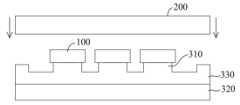
도 1 및 도 2를 참조하면, 상기 특허출원의 공정에서 제조된 디바이스는 플립형 마이크로 발광다이오드(100)를 대량으로 전사하는 데 사용될 수 있지만, 스탬프(200)를 이용하여 상기 디바이스에 대해 임프린팅을 진행하는 과정에서, 열경화성 재료로 제조된 지지 기둥(310)의 마이크로 발광다이오드(100)에 대한 접착력은 지지 기둥(310) 내부 자체의 파단 강도보다 크며, 지지 기둥(310)은 접착력의 외부 하중 작용으로, 응력이 지지 기둥(310) 재료의 파단 강도에 도달하여 파단이 발생한다. 상기 파단 위치는 제어하기 어렵고, 남은 지지 기둥(311)은 마이크로 발광다이오드(100) 표면에 부착되는바, 일부 상황에서, 상기 남은 지지 기둥(311)의 높이는 마이크로 발광다이오드(100) 전극의 높이보다 높고, 잔류 높이가 너무 높으면 후속되는 마이크로 발광다이오드(100)의 다이 본딩 공정을 완성할 수 없어, 다이 본딩 공정의 수율에 심각한 영향을 미친다.1 and 2, the device manufactured in the process of the patent application can be used to transfer a large amount of flip-type micro
본 발명은 종래 기술의 문제점에 대해 실행 가능한 해결 방안을 제공하는 것이며, 상기 방안을 통해 마이크로 발광다이오드 표면에 지지 기둥이 잔류하는 것을 크게 감소시킬 수 있다.The present invention provides a feasible solution to the problems of the prior art, and through the above solution, the remaining support pillars on the surface of the micro light emitting diode can be greatly reduced.
본 발명은,The present invention,
기둥형 구조체를 포함하는 베이스 프레임과, 적어도 하나의 마이크로 발광다이오드를 포함하고,A base frame including a columnar structure and at least one micro light emitting diode,
상기 적어도 하나의 마이크로 발광다이오드는 일부 상황에서 일련의 마이크로 발광다이오드로 어레이를 구성하여 배치 가능하고, 마이크로 발광다이오드는 기둥형 구조체를 통해 베이스 프레임에 연결되고, 마이크로 발광다이오드는 기둥형 구조체에 의해 지지되며,The at least one micro light emitting diode can be arranged by configuring an array of a series of micro light emitting diodes in some circumstances, the micro light emitting diodes are connected to the base frame through a columnar structure, and the micro light emitting diodes are supported by the columnar structure. becomes,
기둥형 구조체는 마이크로 발광다이오드가 연결된 일단이 마이크로 발광다이오드 표면의 오목홈 내에 위치하고, 기둥형 구조체의 재료는 고분자 폴리머인 마이크로 발광어셈블리를 제공한다.The columnar structure provides a micro light emitting assembly in which one end to which the micro light emitting diode is connected is located in a concave groove on the surface of the micro light emitting diode, and the material of the columnar structure is a polymer.
본 발명에 따르면, 기둥형 구조체는 오목홈의 저부 및 측벽과 접촉하는 것이 바람직하다.According to the present invention, it is preferable that the columnar structure is in contact with the bottom and side walls of the concave groove.
본 발명에 따르면, 기둥형 구조체는 원주 구조체 또는 기둥 직경이 상단에서 작고 하단에서 큰 원뿔대 구조체인 것이 바람직하다.According to the present invention, the columnar structure is preferably a columnar structure or a truncated cone structure in which the column diameter is small at the top and large at the bottom.
본 발명에 따르면, 기둥형 구조체의 기둥 직경은 변화되며, 기둥형 구조체는 소면적 단면을 가지고, 상기 소면적 단면은 그 근처의 단면에 비해 더 작은 횡단면적을 가지는 것이 바람직하다.According to the present invention, it is preferable that the column diameter of the columnar structure is varied, the columnar structure has a small area cross section, and the small area cross section has a smaller cross sectional area than a cross section near it.
본 발명에 따르면, 소면적 단면은 기둥형 구조체의 다른 영역에 비해 더 작은 횡단면적을 가지는 것이 바람직하다.According to the present invention, the small area cross section preferably has a smaller cross sectional area than other areas of the columnar structure.
본 발명에 따르면, 기둥형 구조체는 마이크로 발광다이오드와 이격된 일단의 기둥 직경이 마이크로 발광다이오드와 인접한 일단의 기둥 직경보다 큰 것이 바람직하다.According to the present invention, in the columnar structure, it is preferable that the diameter of one end of the pillar spaced apart from the micro light emitting diode is larger than the diameter of one end of the pillar adjacent to the micro light emitting diode.
본 발명에 따르면, 기둥형 구조체는 응력 집중 영역을 구비하거나 또는 응력 결함 영역을 구비하는 것이 바람직하다.According to the present invention, it is preferable that the columnar structure has a stress concentration region or a stress defect region.
본 발명에 따르면, 기둥형 구조체와 마이크로 발광다이오드 사이에 제1 중간층을 구비하는 것이 바람직하다.According to the present invention, it is preferable to provide a first intermediate layer between the columnar structure and the micro light emitting diode.
본 발명에 따르면, 기둥형 구조체에 대한 제1 중간층의 접합력은 마이크로 발광다이오드에 대한 기둥형 구조체의 접합력보다 크고, 질화갈륨계를 예로 들면, 기둥형 구조체에 대한 제1 중간층의 접합력은 질화갈륨에 대한 기둥형 구조체의 접합력보다 큰 것이 바람직하다.According to the present invention, the bonding strength of the first intermediate layer to the columnar structure is greater than the bonding strength of the columnar structure to the micro light emitting diode, and taking a gallium nitride system as an example, the bonding strength of the first intermediate layer to the columnar structure is greater than the bonding strength of the columnar structure to gallium nitride. It is preferable that the bonding force of the columnar structure to the
본 발명에 따르면, 기둥형 구조체와 마이크로 발광다이오드 사이에 제2 중간층을 구비하는 것이 바람직하다.According to the present invention, it is preferable to provide a second intermediate layer between the columnar structure and the micro light emitting diode.
본 발명에 따르면, 기둥형 구조체에 대한 제2 중간층의 접착력은 기둥형 구조체 내의 분자간의 작용력보다 작은 것이 바람직하다.According to the present invention, it is preferable that the adhesive force of the second intermediate layer to the columnar structure is smaller than the action force between molecules in the columnar structure.
본 발명에 따르면, 제2 중간층의 표면은 공동(孔洞) 구조를 구비하는 것이 바람직하다.According to the present invention, it is preferable that the surface of the second intermediate layer has a hollow structure.
본 발명에 따르면, 제2 중간층은 제1 표면과 제2 표면을 구비하고, 제1 표면은 마이크로 발광다이오드에 가까운 일측에 위치하고, 제2 표면은 기둥형 구조체에 가까운 일측에 위치하고, 공동 구조는 제1 표면 및/또는 제2 표면에 위치하는 것이 바람직하다. According to the present invention, the second intermediate layer has a first surface and a second surface, the first surface is located on one side close to the micro light emitting diode, the second surface is located on one side close to the columnar structure, and the cavity structure is located on the first side. It is preferably located on the first surface and/or the second surface.
본 발명에 따르면, 제2 중간층은 제1 중간층과의 접착성이 좋은 재료를 포함하고, 제1 중간층이 이산화규소로 제조된 PV보호층인 것을 예로 들면, 제2 중간층은 크롬 또는 티타늄을 선택하는 것이 바람직하다.According to the present invention, the second intermediate layer includes a material having good adhesion with the first intermediate layer, and the first intermediate layer is a PV protective layer made of silicon dioxide, for example, the second intermediate layer is selected from chrome or titanium. it is desirable
본 발명에 따르면, 제2 중간층은 희생층인 것이 바람직하다.According to the present invention, the second intermediate layer is preferably a sacrificial layer.
본 발명에 따르면, 희생층 재료는 예를 들어 포토레지스트 또는 자외선 UV 접착제와 같은 감광성 접착제인 것이 바람직하며, 이산화규소와 같이 쉽게 제거할 수 있는 재료일 수도 있다.According to the present invention, the sacrificial layer material is preferably a photosensitive adhesive such as photoresist or ultraviolet UV adhesive, and may be a material that can be easily removed such as silicon dioxide.
본 발명에 따르면, 오목홈의 깊이는 1000옹스트롬 내지 2500옹스트롬인 것이 바람직하다.According to the present invention, the depth of the concave groove is preferably 1000 angstroms to 2500 angstroms.
본 발명에 따르면, 오목홈의 깊이는 너무 깊은 것은 바람직하지 않으며, 너무 깊어서는 안 되며, 너무 깊으면 접착력이 너무 강해 기둥형 구조체가 쉽게 파단되므로, 1800옹스트롬 내지 2000옹스트롬인 것이 바람직하다.According to the present invention, the depth of the concave groove is preferably 1800 angstroms to 2000 angstroms, because too deep an adhesive force is too strong and the columnar structure is easily broken.
상술한 마이크로 발광어셈블리는 픽업 대기 상태에 있는 디바이스이며, 상기 디바이스를 스탬핑하여 마이크로 발광어셈블리 내의 마이크로 발광다이오드를 픽업 및 전사하고,The above-described micro light emitting assembly is a device in a pickup standby state, and the micro light emitting diode in the micro light emitting assembly is picked up and transferred by stamping the device,
상기 마이크로 발광다이오드는,The micro light emitting diode,
N측 층, P측 층과 양자 사이의 발광층을 구비하는 발광에피택셜층;a light-emitting epitaxial layer including an N-side layer and a P-side layer and a light-emitting layer between them;
N측 층과 연결되는 N전극;an N electrode connected to the N-side layer;
P측 층과 연결되는 P전극을 포함하고,Including a P electrode connected to the P-side layer,
마이크로 발광다이오드는 서로 대응되는 제1 표면과 제2 표면을 구비하고, 제1 표면은 오목홈을 구비하고, 오목홈은 상기 기둥형 구조체와 결합하여 마이크로 발광다이오드에 지지력을 전달하는 한편 기둥형 구조체와의 접착력을 제공하기 위한 것이며, 오목홈은 제1 중간층으로 구성된다.The micro light emitting diode has a first surface and a second surface that correspond to each other, the first surface has a concave groove, and the concave groove is combined with the columnar structure to transmit a supporting force to the micro light emitting diode, while the columnar structure It is to provide adhesion with the concave groove is composed of the first intermediate layer.
고분자 폴리머에 대한 제1 중간층의 접착력은 발광에피택셜층에 대한 고분자 폴리머의 접착력보다 크다.The adhesive force of the first intermediate layer to the high polymer is greater than the adhesive force of the high polymer to the light emitting epitaxial layer.
본 발명에 따르면, 제1 중간층은 이산화규소, 산화알루미늄 또는 질화규소를 포함하고, 고분자 폴리머는 실리콘 접착제 또는 자외선 UV 접착제인 것이 바람직하다.According to the present invention, it is preferred that the first intermediate layer comprises silicon dioxide, aluminum oxide or silicon nitride, and the high molecular weight polymer is a silicone adhesive or an ultraviolet UV adhesive.
본 발명에 따르면, 오목홈의 깊이는 1000옹스트롬 내지 2500옹스트롬인 것이 바람직하다.According to the present invention, the depth of the concave groove is preferably 1000 angstroms to 2500 angstroms.
본 발명에 따르면, 오목홈의 표면은 제2 중간층을 구비하는 것이 바람직하다.According to the present invention, it is preferable that the surface of the concave groove has a second intermediate layer.
본 발명에 따르면, 기둥형 구조체에 대한 제2 중간층의 접착력은 기둥형 구조체 내의 분자간의 작용력보다 작은 것이 바람직하다.According to the present invention, it is preferable that the adhesive force of the second intermediate layer to the columnar structure is smaller than the action force between molecules in the columnar structure.
본 발명에 따르면, 제2 중간층의 표면은 공동 구조를 구비하는 것이 바람직하다.According to the present invention, it is preferable that the surface of the second intermediate layer has a hollow structure.
본 발명에 따르면, 제2 중간층은 제1 표면과 제2 표면을 구비하고, 제1 표면은 마이크로 발광다이오드에 가까운 일측에 위치하고, 제2 표면은 마이크로 발광다이오드와 이격된 일측에 위치하고, 공동 구조는 제1 표면 및/또는 제2 표면에 위치하는 것이 바람직하다.According to the present invention, the second intermediate layer has a first surface and a second surface, the first surface is located on one side close to the micro light emitting diode, the second surface is located on one side spaced apart from the micro light emitting diode, and the cavity structure has It is preferably located on the first surface and/or on the second surface.
본 발명에 따르면, 제2 중간층은 크롬(Cr) 또는 티타늄(Ti)을 포함하는 것이 바람직하다.According to the present invention, the second intermediate layer preferably includes chromium (Cr) or titanium (Ti).
본 발명에 따르면, 제2 중간층은 희생층인 것이 바람직하다.According to the present invention, the second intermediate layer is preferably a sacrificial layer.
본 발명에 따르면, 희생층 재료는 감광성 접착제 또는 이산화규소인 것이 바람직하다.According to the present invention, the sacrificial layer material is preferably a photosensitive adhesive or silicon dioxide.
본 발명에 따르면, 오목홈은 마이크로 발광다이오드의 비발광면 측에 위치하거나 또는 직접적으로 비출광면에 위치하는 것이 바람직하다.According to the present invention, it is preferable that the concave groove is located on the non-light emitting surface side of the micro light emitting diode or directly located on the non-light emitting surface.
오목홈과 P전극, N전극은 마이크로 발광다이오드의 동일 측에 위치하고, 오목홈 내에 고분자 폴리머가 잔류되어 있고, 고분자 폴리머의 높이는 P전극과 N전극보다 낮다.The concave groove, the P electrode, and the N electrode are located on the same side of the micro light emitting diode, the high polymer remains in the concave groove, and the height of the high polymer is lower than that of the P electrode and the N electrode.
상기 마이크로 발광어셈블리와 마이크로 발광다이오드 외에, 본 발명은 마이크로 발광다이오드를 대량 전사하기 위한 공정 방법을 추가로 공개한다. 상기 방법은,In addition to the micro light emitting assembly and the micro light emitting diode, the present invention further discloses a process method for mass transfer of the micro light emitting diode. The method,
단계 1로서, 복수의 마이크로 발광다이오드가 어레이형으로 이격 배치된 기판을 제공하고, 마이크로 발광다이오드의 표면 및 그 사이에 노출된 기판 표면에 제1 중간층을 형성하는 단계;As step 1, providing a substrate on which a plurality of micro light emitting diodes are spaced apart in an array form, and forming a first intermediate layer on a surface of the micro light emitting diodes and a surface of the substrate exposed therebetween;
단계 2로서, 마이크로 발광다이오드 표면에 먼저 희생 재료를 증착한 후, 희생 재료와 제1 증간층에 오목홈을 형성하는 단계;Step 2, first depositing a sacrificial material on the surface of the micro light emitting diode, and then forming concave grooves in the sacrificial material and the first intermediate layer;
단계 3으로서, 희생 재료와 제1 중간층의 오목홈 내에 제2 중간층을 형성하는 단계;Step 3, forming a second intermediate layer in the sacrificial material and the groove of the first intermediate layer;
단계 4로서, 제2 중간층에 지지층을 형성하는 단계;As step 4, forming a support layer on the second intermediate layer;
단계 5로서, 본딩 베이스 프레임을 제공하는 단계;As step 5, providing a bonding base frame;
단계 6으로서, 본딩 베이스 프레임과 지지층을 본딩하는 단계;As step 6, bonding the bonding base frame and the supporting layer;
단계 7로서, 기판을 박리하여 마이크로 발광다이오드와 제1 중간층을 노출시키는 단계;As step 7, exposing the micro light emitting diode and the first intermediate layer by exfoliating the substrate;
단계 8로서, 노출된 제1 중간층과 희생 재료를 순차적으로 제거하는 단계를 포함한다.As step 8, it includes sequentially removing the exposed first intermediate layer and the sacrificial material.
본 발명에 따르면, 단계 8 이후, 스탬프를 이용하여 접착제층과 이격된 마이크로 발광다이오드의 일면에 대해 임프린팅하고, 마이크로 발광다이오드와 접착제층을 분리하는 단계 9를 포함하는 것이 바람직하다.According to the present invention, after step 8, it is preferable to include imprinting on one surface of the micro light emitting diode spaced apart from the adhesive layer using a stamp, and step 9 of separating the micro light emitting diode and the adhesive layer.
본 발명은 적어도 아래와 같은 유익한 효과가 있다.The present invention has at least the following advantageous effects.
전사 과정에서, 마이크로 발광다이오드상의 기둥형 구조체의 파단 및 잔류를 감소시키거나 제거하여, 과도한 공정 잔류물로 인해 후속되는 회로 기판에 대한 마이크로 발광다이오드(100)의 공정(共晶)이 영향을 받는 것을 방지한다.In the transfer process, the breakage and residual of the columnar structure on the micro light emitting diode is reduced or eliminated, so that the process of the micro
본 발명의 기타 특징 및 장점은 아래에서 상세하게 설명될 것이며, 일부 특징 및 장점은 상세한 설명을 통해 자명해지거나, 또는 본 발명을 실시함으로써 이해하게 될 것이다. 본 발명의 목적 및 기타 장점은 상세한 설명, 청구 범위 및 도면에서 특정한 구조를 통해 실현될 수 있다.Other features and advantages of the present invention will be described in detail below, and some features and advantages will become apparent from the detailed description, or will be understood by practicing the present invention. The objectives and other advantages of the present invention may be realized through the specific structure in the detailed description, claims and drawings.
도면은 본 발명에 대한 추가적인 이해를 위해 제공하며, 상세한 설명의 일부분을 구성하며, 본 발명의 실시예와 함께 본 발명을 설명하기 위한 것일 뿐, 본 발명을 한정하기 위한 것은 아니다. 또한, 도면의 데이터는 설명의 요약이며, 비율에 따라 그려진 것이 아니다.
도 1~도 2는 종래 기술의 개략도이다.
도 3은 실시예 1에 따른 마이크로 발광어셈블리의 개략도이다.
도 4는 실시예 2에 따른 마이크로 발광어셈블리의 개략도이다.
도 5는 실시예 3에 따른 마이크로 발광어셈블리의 개략도이다.
도 6은 실시예 4에 따른 마이크로 발광어셈블리의 개략도이다.
도 7~도 8은 실시예 4의 변형예에 따른 마이크로 발광어셈블리의 개략도이다.
도 9는 실시예 5에 따른 마이크로 발광어셈블리의 개략도이다.
도 10~도 15는 실시예 6에 따른 마이크로 발광다이오드의 전사 공정 개략도이다.
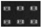
도 16~도 17은 실시예 6에서 전사된 마이크로 발광다이오드의 실물 사진이다.
도 18은 실시예 6에서 전사된 마이크로 발광다이오드의 개략도이다.The drawings are provided for further understanding of the present invention, constitute a part of the detailed description, and are intended to explain the present invention in conjunction with embodiments of the present invention, but are not intended to limit the present invention. In addition, the data in the drawings is a summary of the description and is not drawn to scale.
1-2 are schematic diagrams of the prior art.
3 is a schematic diagram of a micro light emitting assembly according to Example 1;
4 is a schematic diagram of a micro light emitting assembly according to Example 2;
5 is a schematic diagram of a micro light emitting assembly according to Example 3;
6 is a schematic diagram of a micro light emitting assembly according to Example 4;
7 to 8 are schematic views of a micro light emitting assembly according to a modified example of Example 4;
9 is a schematic diagram of a micro light emitting assembly according to Example 5;
10 to 15 are schematic diagrams of a micro light emitting diode transfer process according to Example 6;
16 and 17 are actual photos of micro light emitting diodes transferred in Example 6.
18 is a schematic diagram of a micro light emitting diode transferred in Example 6.
이하, 도면 및 실시예와 결합하여 본 발명의 실시 방식을 상세히 설명함으로써, 본 발명이 어떻게 기술수단을 응용하여 기술 문제를 해결하고, 기술 효과를 이루는지에 대한 과정을 보여주고자 한다. 설명해야 할 점은, 모순되지 않는 한, 본 발명의 각 실시예 및 각 실시예의 각 특징은 서로 결합될 수 있고, 결합된 기술방안은 모두 본 발명의 보호 범위 내에 있어야 한다.Hereinafter, by explaining the implementation method of the present invention in detail in combination with drawings and examples, the process of how the present invention solves technical problems and achieves technical effects by applying technical means will be shown. It should be noted that, unless contradictory, each embodiment of the present invention and each feature of each embodiment may be combined with each other, and the combined technical solutions shall fall within the protection scope of the present invention.
이해해야 할 것은, 본 발명에서 사용한 용어는 구체적인 실시예를 설명하기 위한 것일 뿐, 본 발명을 한정하기 위한 것은 아니다. 이해해야 할 것은, 본 발명에서 사용된 "포함", "함유"라는 용어는, 설명되는 특징, 전체, 단계, 어셈블리 및/또는 존재를 설명하기 위한 것이고, 하나 또는 하나 이상의 다른 특징, 전체, 단계, 어셈블리 및 /또는 이들 조합의 존재 또는 증가를 배제하지 않는다.It should be understood that the terms used in the present invention are only for describing specific embodiments and are not intended to limit the present invention. It should be understood that the terms "comprising" and "comprising" as used herein are intended to describe a feature, whole, step, assembly and/or being described, and one or more other features, whole, step, The presence or increase of assemblies and/or combinations thereof is not excluded.
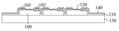
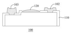
도 3을 참조하면, 본 발명의 제1 실시예에서, 개선된 마이크로 발광어셈블리를 제공하며, 상기 마이크로 발광어셈블리는, 베이스 프레임, 적어도 하나의 발광다이오드(100), 기둥형 구조체(310)를 포함한다. 베이스 프레임은 안정화 작용을 하며, 본 실시예에서 베이스 프레임은 전체적으로 사파이어 웨이퍼(320)와 스핀 코팅된 고분자 폴리머로 구성되고, 사파이어 웨이퍼(320)는 유리와 실리콘 기판으로 대체될 수도 있으며, 고분자 폴리머는 지지층(330)으로서, 예를 들면 BCB 접착제(벤조시클로부텐)로 구성되며, 베이스 프레임은 BCB 접착제로 구성된 기둥형 구조체(310)를 포함한다. 상기 적어도 하나의 마이크로 발광다이오드(100)는 어레이형 분포를 예로 들며, 마이크로 발광다이오드(100)는 기둥형 구조체(310)를 통해 베이스 프레임에 연결되고, 마이크로 발광다이오드(100)는 기둥형 구조체(310)에 의해 지지된다. 기둥형 구조체(310)는 마이크로 발광다이오드(100)가 연결되는 일단이 마이크로 발광다이오드(100) 표면에 위치하고, 상기 표면은 바람직하게는 비출광면이다. Referring to FIG. 3 , in the first embodiment of the present invention, an improved micro light emitting assembly is provided, and the micro light emitting assembly includes a base frame, at least one
기둥형 구조체(310)의 기둥 직경은 변화된다. 예를 들면 기둥형 구조체(310)는 원뿔대형이며, 마이크로 발광다이오드(100)와 접촉하는 일단의 기둥 직경은 마이크로 발광다이오드(100)와 이격된 일단의 직경보다 작고, 위에서 아래로 점점 굵어진다. 이 구성은 아래와 같은 장점을 가진다. 즉, 기둥형 구조체(310)와 마이크로 발광다이오드(100)의 접촉면이 작고, 접합력과 접촉면적이 정비례하므로, 기둥형 구조체(310)가 마이크로 발광다이오드(100)를 안정하게 지지하면서 양자의 접합력이 감소되고, 위에서 아래로 점점 굵어지는 기둥형 구조체(310)는 더욱 강한 파단 강도를 구비하고, 접합력이 감소되고, 파단 강도가 증가하며, 기둥형 구조체(310)와 마이크로 발광다이오드(100)가 스탬프의 작용으로 분리될 경우의 파단 가능성을 감소시키므로, 마이크로 발광다이오드(100)의 픽업 전사 수율을 향상시킨다.The column diameter of the
도 4를 참조하면, 본 발명의 제2 실시예에서, 개선된 마이크로 발광어셈블리를 제공하며, 상기 마이크로 발광어셈블리는, 기둥형 구조체(310)의 기둥 직경이 변화되며, 기둥형 구조체(310)는 소면적 단면을 가지고, 상기 소면적 단면은 그 근처의 단면에 비해 더 작은 횡단면적을 가진다.Referring to FIG. 4 , in the second embodiment of the present invention, an improved micro light emitting assembly is provided, in which the column diameter of the
구체적으로, 소면적 단면은 기둥형 구조체(310)의 다른 영역에 비해 더 작은 횡단면적을 가지고, 곡선형의 기둥형 구조체(310)를 이용한다. 이 실시예에서, 소면적 단면은 기둥형 구조체(310)의 응력 집중면(312)이며, 스탬핑에 의해 마이크로 발광어셈블리의 마이크로 발광다이오드(100)에 압력을 가하고, 압력은 마이크로 발광다이오드(100)에서 기둥형 구조체(310)로 전달되고, 기둥형 구조체(310)는 응력 집중면(312)에서 파단되므로, 파단 위치를 제어할 수 있으며, 응력 집중면(312)의 중심 위치의 높이는 전극의 높이보다 낮게 설계될 수 있어, 파단 후의 기둥형 구조체(310)가 전극의 높이보다 낮도록 보장하고, 후속되는 공정 본딩 공정에서 남은 기둥형 구조체(311)가 전극의 공정을 간섭하지 않도록 보장한다.Specifically, the small-area cross section has a smaller cross-sectional area than other regions of the
제2 실시예의 변형예에서, 기둥형 구조체(310)에 응력 결함 영역을 설계하고, 응력 결함 영역은 기둥형 구조체(310)의 파단면의 제어 가능성을 구현한다. 예를 들면 기둥형 구조체(310)에 다공성 구조를 설계하고, 응력 결함 영역의 중심 위치의 높이는 전극의 높이보다 낮게 설계하여, 파단 후 남은 기둥형 구조체(311)가 전극의 높이보다 낮도록 보장하고, 남은 기둥형 구조체(311)가 후속되는 공정(共晶) 본딩 공정에서 전극의 공정을 간섭하지 않도록 보장할 수 있다.In a modification of the second embodiment, a stress defect area is designed in the
도 5를 참조하면, 본 발명의 제3 실시예에서, 마이크로 발광다이오드(100)와 기둥형 구조체(310) 사이에 제1 중간층(110)이 추가되고, 제1 중간층(110)은 적어도 이행 작용을 겸한다. 마이크로 발광다이오드(100)는 대량 전사 공정에서 에칭이 불가피하며, 에칭의 화학적 반응은 기포를 생성하며, 기포는 마이크로 발광다이오드(100)에 대해 충격력을 발생시킨다. 질화갈륨계 마이크로 발광다이오드를 예로 들면, 통상의 경우, 질화갈륨과 고분자 폴리머는 접착성이 좋지 않으므로, 기둥형 구조체와 마이크로 발광다이오드 사이의 접합을 충분히 보장해야 하는바, 제1 중간층(110)은 마이크로 발광다이오드(100)와 기둥형 구조체(310)가 충분한 접합력을 가지도록 보장하고, 접합력을 통해 안정하게 지지한다. 본 실시예의 제1 중간층(110)은 이산화규소, 산화알루미늄 또는 질화규소를 포함하고, 고분자 폴리머는 벤조시클로부텐, 실리콘 접착제 또는 자외선 UV 접착제를 포함하며, 질화갈륨에 비해 제1 중간층(110)은 고분자 폴리머와의 접착성이 더 우수하다.Referring to FIG. 5 , in the third embodiment of the present invention, a first
본 발명의 제4 실시예에서, 마이크로 발광다이오드(100)와 기둥형 구조체(310) 사이에 제2 중간층(120)이 추가되고, 제2 중간층(120)은 예를 들어 희생층이다. 즉, 마이크로 발광다이오드(100)와 기둥형 구조체(310) 사이에 희생층이 추가되고, 전사 과정에서 일부 또는 전체 희생층을 제거함으로써, 마이크로 발광다이오드(100)와 기둥형 구조체(310)의 분리를 구현한다. 선택적 제거 공정은 마이크로 발광다이오드(100)가 분리된 후 기둥형 구조체가 남지 않도록 보장하는 데 도움을 주며, 전사된 마이크로 발광다이오드(100) 표면에는 일부 희생층 재료만 남아있거나 또는 전혀 잔류물이 없게 된다. 본 실시예에서, 희생층 재료는 예를 들면 포토레지스트 또는 자외선 UV 접착제와 같은 감광성 접착제이며, 이산화규소와 같이 쉽게 제거할 수 있는 재료일 수도 있다.In the fourth embodiment of the present invention, a second
도 6을 참조하면, 본 실시예에서, 스탬프(200)를 이용하여 마이크로 발광다이오드(100)를 전사할 경우, 스탬프(200)는 먼저 마이크로 발광다이오드(100)를 아래로 누르고 압력에 의해 접착을 발생시키고, 접착에 의해 발생한 흡인력을 이용하여 마이크로발광다이오드(100)를 위로 들어올린다. 여기서 상기 흡인력은 예를 들면 반데르발스힘이다. 본 실시예에서, 기둥형 구조체(310)에 대한 제2 중간층(120)의 접착력은 기둥형 구조체(310) 내의 분자간의 작용력보다 작아야 한다. 그러면 제2 중간층(120)과 기둥형 구조체(310)가 분리될 때, 기둥형 구조체(310)의 내부가 분리 시의 과도한 장력으로 인해 파단되지 않도록 보장할 수 있다.Referring to FIG. 6 , in this embodiment, when the micro
도 7을 참조하면, 제4 실시예의 제1 변형예에서, 제2 중간층(120)의 표면은 공동 구조(121)를 구비하고, 상기 공동 구조(121)는 제2 중간층(120)과 기둥형 구조체(310)의 접촉 면적을 감소시키므로, 제2 중간층(120)과 기둥형 구조체(310)의 분리 곤란도를 줄인다. 구체적으로, 제2 중간층(120)은 제1 표면과 제2 표면을 구비하고, 제1 표면은 상부 표면으로, 마이크로 발광다이오드에 가까운 일측에 위치하며, 제2 표면은 하부 표면으로, 기둥형 구조체에 가까운 일측에 위치하며, 공동 구조체(121)는 제1 표면 및/또는 제2 표면에 위치한다.Referring to FIG. 7 , in the first modified example of the fourth embodiment, the surface of the second
본 실시예와 유사한 설계에 따르면, 발광에피택셜층으로부터 멀어진 측의 제1 중간층(110)의 표면에 다공성 표면을 설계할 수 있고, 다공성 표면은 기둥형 구조체(310)와 연결하기 위한 것으로, 이 역시 제1 중간층(110)과 기둥형 구조체(310)의 접합력을 감소시키는 작용을 한다.According to a design similar to this embodiment, a porous surface can be designed on the surface of the first
도 8을 참조하면, 제4 실시예의 제2 변형예에서, 마이크로 발광어셈블리는 제1 중간층(110)을 포함할 뿐만 아니라 제2 중간층(120)도 포함하며, 제2 중간층(120)은 제1 중간층(110)과의 접착성이 우수한 재료를 포함한다. 제1 중간층(110)이 이산화규소로 제조된 PV 보호층인 것을 예로 들면, 제2 중간층(120)은 크롬 또는 티타늄을 선택하고, 제2 중간층(120)과 고분자 폴리머의 접착성은 제1 중간층(110)과 고분자 폴리머의 접착성보다 낮으므로, 기둥형 구조체(310)는 제2 중간층(120)과 비교적 쉽게 분리되고, 분리 과정에서, 기둥형 구조체(310)는 파단이 발생하지 않고, 분리 후의 마이크로 발광다이오드(100)에는 잔류된 고분자 폴리머가 확인되지 않았다.Referring to FIG. 8 , in the second modified example of the fourth embodiment, the micro light emitting assembly not only includes the first
도 9를 참조하면, 본 발명의 제5 실시예에서, 고분자 폴리머가 잔류되지 않는 것을 전제로 공정을 간소화하기 위해, 본 실시예는 마이크로 발광다이오드(100)에 오목홈(101)을 형성한다. 오목홈(101)은 기둥형 구조체(310)를 수용하고 지지력을 전달하기 위한 것이고, 기둥형 구조체(310)는 오목홈(101)의 저부 및 측벽과 접촉한다.Referring to FIG. 9 , in the fifth embodiment of the present invention,
본 실시예의 구체적인 공정 단계는 다음 단계를 포함한다.The specific process steps in this embodiment include the following steps.
도 10을 참조하면,Referring to Figure 10,
단계 1: 성장 기판(130)을 제공하고, 성장 기판(130)은 포토 마스크를 이용한 에칭을 통해, 어레이형으로 이격 배치된 복수의 마이크로 발광다이오드(100)를 형성한다. 본 실시예의 마이크로 발광다이오드(100)는 플립칩형 구조를 이용하고, 마이크로 발광다이오드(100)의 표면 및 그 사이에서 노출된 성장 기판(130)의 표면에 제1 중간층(110)을 형성하고, 제1 중간층(110)은 PV 보호층이며, 재료는 이산화규소, 산화알루미늄 또는 질화규소를 포함한다.Step 1: A
단계 2: 마이크로 발광다이오드(100) 표면에 먼저 희생 재료(140)를 증착한 후, 희생 재료(140)와 제1 중간층(110)에 오목홈(101)을 형성하며, 제1 중간층(110)의 오목홈(101)의 깊이는 1000옹스트롬 내지 25000옹스트롬이다. 오목홈(101)의 깊이는 너무 깊은 것은 바람직하지 않으며, 너무 깊어서는 안 되며, 너무 깊으면 접착력이 너무 강해 기둥형 구조체(310)가 쉽게 파단된다. 실험 결과에 따르면 가장 적합한 깊이는 1800옹스트롬 내지 2000옹스트롬이다.Step 2: After depositing the
단계 3: 희생 재료(140)와 제1 중간층(110) 중의 오목홈(101) 내에 제2 중간층(120)을 형성한다. 상기 제2 중간층(120)은 비교적 얇다. 도면에는 희생 재료(140)상의 제2 중간층(120)이 도시되지 않았으며, 오목홈 내의 제2 중간층(120)의 두께는 적당히 확대되었다. 제2 중간층(120)은 크롬 또는 티타늄이다.Step 3: Form the second
도 11을 참조하면,Referring to Figure 11,
단계 4: 제2 중간층(120)상에 지지층(330)으로서의 접착제층을 형성한다. 접착제층은 예를 들면 고분자 폴리머를 이용하고, 본 실시예는 BCB 접착제, 자외선 감광성 접착제 또는 포토레지스트를 선택할 수 있다. 일부 상황에서, 지지층(330)은 금, 은, 니켈 또는 주석과 같은 금속을 선택할 수도 있으며, 지지층(330)의 접착제층은 오목홈을 채워, 기둥형 구조체(310)를 형성한다.Step 4: An adhesive layer as a
단계 5: 본딩 베이스 프레임을 제공한다. 본딩 베이스 프레임의 본딩되는 측에도 접착제층이 스핀 코팅되고, 본딩 베이스 프레임은 예를 들면 사파이어, 실리콘 또는 유리 웨이퍼를 이용한다.Step 5: Provide a bonding base frame. An adhesive layer is also spin-coated on the bonded side of the bonding base frame, and the bonding base frame uses, for example, a sapphire, silicon or glass wafer.
단계 6: 본딩 베이스 프레임과 제2 중간층(120)의 지지층(220)은 접착제층을 통해 본딩된다.Step 6: Bonding The base frame and the support layer 220 of the second
도 12를 참조하면,Referring to Figure 12,
단계 7: 성장 기판(130)을 박리하되, 예를 들면 레이저 박리 공정을 이용하며, 기판을 제거하여 마이크로 발광다이오드(100)와 제1 중간층(110)을 노출시킨다.Step 7: The
도 13과 도 14를 참조하면,Referring to Figures 13 and 14,
단계 8: 노출된 제1 중간층(110), 희생 재료(140) 및 그 위의 제2 중간층(120)을 순차적으로 제거하여, 마이크로 발광다이오드(100)가 기둥형 구조체(310)에 독립적으로 지지되도록 하고, 오목홈(101) 내의 제2 중간층(120)의 적어도 일부를 잔류시킨다. 상기 잔류된 제2 중간층(120)은 기둥형 구조체(310)와 오목홈(101) 내에 위치하므로, 제거 과정에서 잔류되어, 본 실시예의 마이크로 발광어셈블리를 구성한다.Step 8: The exposed first
도 15를 참조하면,Referring to Figure 15,
단계 9: 스탬프(200)를 이용하여 접착제층과 이격된 마이크로 발광다이오드(100)의 일면에 대해 임프린팅하고, 마이크로 발광다이오드와 접착제층을 분리한다. 즉 마이크로 발광다이오드(100)와 기둥형 구조체(310)를 분리하여 마이크로 발광다이오드(100)를 픽업한다.Step 9: Using the
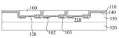
도 16 및 도 17을 참조하면, 오목홈(101) 내의 제2 중간층(120)의 높이는 마이크로 발광다이오드의 P전극(102)과 N전극(103)의 높이보다 낮다. 오목홈(101) 내에 제2 중간층(120)이 설치되므로, 기둥형 구조체(310)와 제1 중간층(110)이 쉽게 분리하며, 기본적으로 기둥형 구조체(310)가 파단되지 않는다.16 and 17, the height of the second
도 18을 참조하면, 실시예 5에 따라 제조된 마이크로 발광다이오드(100)는 N측 층, P측 층과 양자 사이의 발광층을 구비하는 발광에피택셜층(비핵심요소이므로 도면에 도시하지 않음); P측 층과 전기적으로 연결되는 P전극(102); N측 층과 전기적으로 연결되는 N전극(103)을 포함하고, 마이크로 발광다이오드(100)는 서로 대응되는 제1 표면과 제2 표면을 구비하고, 제1 표면은 오목홈(101)을 구비한다. 오목홈(101)은 기둥형 구조체(310)와 도킹하기 위한 것이며, 기둥형 구조체(310)는 오목홈(101) 내에서 마이크로 발광다이오드(100)를 지지한다. 플립칩 발광다이오드(100)를 예로 들면, 오목홈(101)과 2개의 전극은 동일면에 위치하고, 오목홈(101)은 마이크로 발광다이오드(100)의 하부 표면에 위치한다. 즉 오목홈(101)은 출광면에 위치하지 않으며, 이로써 출광효율의 감소를 방지한다.Referring to FIG. 18, a micro
오목홈(101)은 제1 중간층(110)으로 구성되고, 상대적으로 발광에피택셜층으로 직접 구성되며, 제1 중간층(110)은 충분한 접합력을 가진다. 또한, 고분자 폴리머에 대한 제1 중간층(110)의 접합력은 발광에피택셜층에 대한 고분자 폴리머의 접합력보다 크다. 오목홈(101)의 개구는 발광에피택셜층으로부터 멀어질수록 점차 커진다.The
제1 중간층(110)은 이산화규소, 산화알루미늄 또는 질화규소를 포함하고, 고분자 폴리머는 벤조시클로부텐, 실리콘 접착제 또는 자외선 UV 접착제를 포함한다. 오목홈(101)의 홈 내에 제2 중간층(120)이 구비되고, 고분자 폴리머에 대한 제2 중간층(120)의 접착력은 고분자 폴리머 내의 분자간의 작용력보다 작다. 제2 중간층(120)의 재료는 크롬 또는 티타늄을 포함한다. 오목홈(101) 내에 고분자 폴리머가 잔류된다면, 잔류된 고분자 폴리머의 높이도 P전극(10)과 N전극(103)보다 높지 않다.The first
이상은 단지 본 발명의 바람직한 실시형태일 뿐이다. 지적해야 할 것은, 본 분야의 통상의 기술자는 본 발명의 원리를 벗어나지 않으면서 일부 개량과 수정을 진행할 수도 있으며, 이러한 개량과 수정도 본 발명의 보호 범위 내에 속한다는 점이다.The above are merely preferred embodiments of the present invention. It should be pointed out that a person skilled in the art may make some improvements and modifications without departing from the principles of the present invention, and these improvements and modifications also fall within the protection scope of the present invention.
100: 마이크로 발광다이오드
101: 오목홈
102: P전극
103: N전극
110: 제1 중간층
120: 제2 중간층
121: 공동 구조
130: 성장 기판
140: 희생 재료
200: 스탬프
310: 지지 기둥/기둥형 구조체
311: 남은 지지 기둥/남은 기둥형 구조체
312: 응력 집중면
320: 사파이어 웨이퍼
330: 지지층100: micro light emitting diode
101: concave groove
102: P electrode
103: N electrode
110: first intermediate layer
120: second intermediate layer
121: cavity structure
130: growth substrate
140: sacrificial material
200: stamp
310: support column / columnar structure
311: Remaining support column / remaining columnar structure
312: stress concentration plane
320: sapphire wafer
330: support layer
Claims (10)
Translated fromKorean기둥형 구조체를 포함하는 베이스 프레임;
상기 기둥형 구조체를 통해 상기 베이스 프레임에 연결되고, 상기 기둥형 구조체에 의해 지지되는 적어도 하나의 마이크로 발광다이오드; 및
상기 적어도 하나의 발광 다이오드의 표면에 형성되고, 상기 기둥형 구조체와 상기 적어도 하나의 마이크로 발광 다이오드 사이에 설치되고, 오목홈이 형성되어 있는 제1 중간층을 포함하고,
상기 기둥형 구조체의 상기 제1 중간층과 연결된 일단이 상기 오목홈 내에 위치하는,
마이크로 발광어셈블리.As a micro light emitting assembly,
A base frame including a columnar structure;
at least one micro light emitting diode connected to the base frame through the columnar structure and supported by the columnar structure; and
A first intermediate layer formed on a surface of the at least one light emitting diode, installed between the columnar structure and the at least one micro light emitting diode, and having a concave groove formed therein;
One end connected to the first intermediate layer of the columnar structure is located in the concave groove,
Micro light emitting assembly.
상기 제1 중간층과 상기 기둥형 구조체 사이에 설치되고, 상기 오목홈 내에 위치하는 제2 중간층을 더 포함하는 것을 특징으로 하는, 마이크로 발광어셈블리.According to claim 1,
The micro light emitting assembly further comprising a second intermediate layer installed between the first intermediate layer and the columnar structure and located in the concave groove.
상기 제2 중간층은 크롬 또는 티타늄인, 마이크로 발광어셈블리.According to claim 2,
Wherein the second intermediate layer is chrome or titanium.
상기 기둥형 구조체는 고분자 폴리머 또는 금속에서 선택되는, 마이크로 발광어셈블리.According to claim 1,
The columnar structure is selected from a high molecular weight polymer or metal, micro light emitting assembly.
상기 오목홈의 깊이는 1000옹스트롬 내지 2500옹스트롬인, 마이크로 발광어셈블리.According to claim 1,
The depth of the concave groove is 1000 angstroms to 2500 angstroms, micro light emitting assembly.
상기 기둥형 구조체는 상기 오목홈의 저부 및 측벽과 접촉하는, 마이크로 발광어셈블리.According to claim 1,
The columnar structure is in contact with the bottom and sidewalls of the concave groove, the micro light emitting assembly.
상기 기둥형 구조체에 대한 제1 중간층의 접합력은 상기 적어도 하나의 마이크로 발광다이오드에 대한 상기 기둥형 구조체의 접합력보다 큰 것을 특징으로 하는, 마이크로 발광어셈블리.According to claim 1,
The micro light emitting assembly, characterized in that the bonding strength of the first intermediate layer to the columnar structure is greater than the bonding strength of the columnar structure to the at least one micro light emitting diode.
상기 기둥형 구조체에 대한 제2 중간층의 접합력은 상기 기둥형 구조체 내의 분자간 작용력보다 작은, 마이크로 발광어셈블리.According to claim 2,
The bonding force of the second intermediate layer to the columnar structure is smaller than the intermolecular action force within the columnar structure, the micro light emitting assembly.
상기 제2 중간층의 표면은 공동(孔洞) 구조를 구비하는, 마이크로 발광어셈블리.According to claim 2,
The micro light emitting assembly, wherein the surface of the second intermediate layer has a cavity structure.
상기 제2 중간층은 제1 표면과 제2 표면을 구비하고, 상기 제1 표면은 상기 적어도 하나의 마이크로 발광다이오드에 가까운 일측에 위치하고, 상기 제2 표면은 상기 기둥형 구조체에 가까운 일측에 위치하고, 상기 공동 구조는 상기 제1 표면 및 상기 제2 표면의 어느 하나 이상에 위치하는, 마이크로 발광어셈블리.According to claim 9,
The second intermediate layer has a first surface and a second surface, the first surface is located on one side close to the at least one micro light emitting diode, the second surface is located on one side close to the columnar structure, The cavity structure is located on at least one of the first surface and the second surface, the micro light emitting assembly.
Applications Claiming Priority (2)
| Application Number | Priority Date | Filing Date | Title |
|---|---|---|---|
| KR1020217010914AKR102544715B1 (en) | 2019-03-25 | 2019-03-25 | Micro light emitting assembly, micro light emitting diode and micro light emitting diode transfer method |
| PCT/CN2019/079577WO2020191593A1 (en) | 2019-03-25 | 2019-03-25 | Micro light emitting assembly, micro light emitting diode, and transfer printing method for micro light emitting diode |
Related Parent Applications (1)
| Application Number | Title | Priority Date | Filing Date |
|---|---|---|---|
| KR1020217010914ADivisionKR102544715B1 (en) | 2019-03-25 | 2019-03-25 | Micro light emitting assembly, micro light emitting diode and micro light emitting diode transfer method |
Publications (2)
| Publication Number | Publication Date |
|---|---|
| KR20230093067Atrue KR20230093067A (en) | 2023-06-26 |
| KR102676899B1 KR102676899B1 (en) | 2024-06-19 |
Family
ID=70202062
Family Applications (2)
| Application Number | Title | Priority Date | Filing Date |
|---|---|---|---|
| KR1020217010914AActiveKR102544715B1 (en) | 2019-03-25 | 2019-03-25 | Micro light emitting assembly, micro light emitting diode and micro light emitting diode transfer method |
| KR1020237019840AActiveKR102676899B1 (en) | 2019-03-25 | 2019-03-25 | Micro light emitting assembly, micro light emitting diode, and transfer printing method for micro light emitting diode |
Family Applications Before (1)
| Application Number | Title | Priority Date | Filing Date |
|---|---|---|---|
| KR1020217010914AActiveKR102544715B1 (en) | 2019-03-25 | 2019-03-25 | Micro light emitting assembly, micro light emitting diode and micro light emitting diode transfer method |
Country Status (6)
| Country | Link |
|---|---|
| US (1) | US20220005794A1 (en) |
| JP (1) | JP7154371B2 (en) |
| KR (2) | KR102544715B1 (en) |
| CN (1) | CN111033737B (en) |
| TW (1) | TWI745842B (en) |
| WO (1) | WO2020191593A1 (en) |
Families Citing this family (15)
| Publication number | Priority date | Publication date | Assignee | Title |
|---|---|---|---|---|
| TWI759839B (en)* | 2020-08-31 | 2022-04-01 | 錼創顯示科技股份有限公司 | Micro-led display device and manufacturing method of the same |
| DE102020102952B4 (en)* | 2020-02-05 | 2024-09-19 | OSRAM Opto Semiconductors Gesellschaft mit beschränkter Haftung | METHOD FOR SELECTING SEMICONDUCTOR COMPONENTS |
| WO2022006723A1 (en)* | 2020-07-06 | 2022-01-13 | 重庆康佳光电技术研究院有限公司 | Led chip transfer method, display back plate and fabricating method therefor, and display device |
| CN112018145B (en)* | 2020-08-31 | 2023-06-27 | 錼创显示科技股份有限公司 | Micro light emitting diode display assembly and manufacturing method thereof |
| CN112366247B (en)* | 2020-10-22 | 2021-10-08 | 中国电子科技集团公司第五十五研究所 | A kind of preparation method of transfer printing integrated top incident InGaAs detector |
| EP4174963A4 (en)* | 2020-10-30 | 2023-08-23 | BOE Technology Group Co., Ltd. | Light emitting diode substrate and manufacturing method therefor, and display apparatus |
| CN114122050A (en)* | 2020-11-23 | 2022-03-01 | 伊乐视有限公司 | Mass transfer method for microscopic light-emitting diode displays based on fluidic assembly |
| CN112510127B (en)* | 2020-12-21 | 2022-04-05 | 厦门大学 | Manufacturing method of suspension LED device |
| EP4275232A4 (en)* | 2021-01-08 | 2024-10-16 | Jade Bird Display (Shanghai) Limited | Systems and methods for led structures that increase current flow density |
| CN113421954B (en)* | 2021-05-21 | 2023-06-09 | 友达光电股份有限公司 | Display device and method for manufacturing the same |
| CN115706131B (en)* | 2021-08-10 | 2025-02-18 | 重庆康佳光电科技有限公司 | Huge amount transfer method, temporary substrate, transfer substrate and LED display device |
| CN116013945A (en)* | 2021-10-21 | 2023-04-25 | 重庆康佳光电技术研究院有限公司 | Weakened structure and manufacturing method thereof, transfer method of light-emitting device |
| KR20240119922A (en)* | 2023-01-30 | 2024-08-07 | 삼성전자주식회사 | Micro light emitting diode chip and method for manufacturing thereof |
| CN116207126B (en)* | 2023-03-27 | 2025-07-25 | 天马新型显示技术研究院(厦门)有限公司 | Micro-light-emitting element array, micro-light-emitting element transferring method and display device |
| WO2025116062A1 (en)* | 2023-11-28 | 2025-06-05 | 엘지전자 주식회사 | Transfer method of semiconductor light-emitting device for display pixels |
Citations (4)
| Publication number | Priority date | Publication date | Assignee | Title |
|---|---|---|---|---|
| KR20160083035A (en)* | 2013-12-27 | 2016-07-11 | 럭스뷰 테크놀로지 코포레이션 | Led with internally confined current injection area |
| CN107818931A (en)* | 2017-09-30 | 2018-03-20 | 厦门市三安光电科技有限公司 | The transfer method and transfer device of semiconductor microactuator element |
| US20180138071A1 (en)* | 2016-11-15 | 2018-05-17 | X-Celeprint Limited | Micro-transfer-printable flip-chip structures and methods |
| CN108231968A (en)* | 2017-12-11 | 2018-06-29 | 厦门市三安光电科技有限公司 | Micro- light emitting diode and its transfer method |
Family Cites Families (27)
| Publication number | Priority date | Publication date | Assignee | Title |
|---|---|---|---|---|
| JPH09148225A (en)* | 1995-11-27 | 1997-06-06 | Hitachi Ltd | Substrate holder and microfabrication device using the same |
| CN1300859C (en)* | 1997-01-31 | 2007-02-14 | 松下电器产业株式会社 | Light emitting element |
| KR101081135B1 (en)* | 2010-03-15 | 2011-11-07 | 엘지이노텍 주식회사 | Light emitting device, method for fabricating the light emitting device and light emitting device package |
| US9161448B2 (en)* | 2010-03-29 | 2015-10-13 | Semprius, Inc. | Laser assisted transfer welding process |
| US9269878B2 (en)* | 2011-05-27 | 2016-02-23 | Lg Innotek Co., Ltd. | Light emitting device and light emitting apparatus |
| KR101969334B1 (en)* | 2011-11-16 | 2019-04-17 | 엘지이노텍 주식회사 | Light emitting device and light emitting apparatus having the same |
| KR101596386B1 (en)* | 2011-11-18 | 2016-02-22 | 애플 인크. | Method of forming a micro led structure and array of micro led structures with an electrically insulating layer |
| US8794501B2 (en)* | 2011-11-18 | 2014-08-05 | LuxVue Technology Corporation | Method of transferring a light emitting diode |
| US8518204B2 (en)* | 2011-11-18 | 2013-08-27 | LuxVue Technology Corporation | Method of fabricating and transferring a micro device and an array of micro devices utilizing an intermediate electrically conductive bonding layer |
| US9773750B2 (en)* | 2012-02-09 | 2017-09-26 | Apple Inc. | Method of transferring and bonding an array of micro devices |
| US20130292719A1 (en)* | 2012-05-04 | 2013-11-07 | Chi Mei Lighting Technology Corp. | Light-emitting diode structure and method for manufacturing the same |
| US8835940B2 (en)* | 2012-09-24 | 2014-09-16 | LuxVue Technology Corporation | Micro device stabilization post |
| US9035279B2 (en)* | 2013-07-08 | 2015-05-19 | LuxVue Technology Corporation | Micro device with stabilization post |
| US9768345B2 (en)* | 2013-12-20 | 2017-09-19 | Apple Inc. | LED with current injection confinement trench |
| US9444015B2 (en)* | 2014-06-18 | 2016-09-13 | X-Celeprint Limited | Micro assembled LED displays and lighting elements |
| US10128307B2 (en)* | 2014-10-17 | 2018-11-13 | Intel Corporation | MicroLED display and assembly |
| TWI610459B (en)* | 2015-05-13 | 2018-01-01 | 友達光電股份有限公司 | Miniature light emitting diode device and manufacturing method thereof |
| US10468363B2 (en)* | 2015-08-10 | 2019-11-05 | X-Celeprint Limited | Chiplets with connection posts |
| KR102150819B1 (en)* | 2015-12-22 | 2020-09-01 | 애플 인크. | Led sidewall processing to mitigate non-radiative recombination |
| US10395966B2 (en)* | 2016-11-15 | 2019-08-27 | X-Celeprint Limited | Micro-transfer-printable flip-chip structures and methods |
| JP6366799B1 (en)* | 2017-02-10 | 2018-08-01 | ルーメンス カンパニー リミテッド | Micro LED module and manufacturing method thereof |
| WO2018156877A1 (en)* | 2017-02-24 | 2018-08-30 | Massachusetts Institute Of Technology | Apparatus and methods for curved focal plane array |
| CN107170771B (en)* | 2017-05-23 | 2019-12-24 | 深圳市华星光电技术有限公司 | Packaging structure of micro-LED array substrate and packaging method thereof |
| CN107154374B (en)* | 2017-05-23 | 2019-09-10 | 深圳市华星光电技术有限公司 | Micro- transfer method |
| CN107933064B (en)* | 2017-11-10 | 2019-05-07 | 上海天马微电子有限公司 | Transfer printing substrate and manufacturing method thereof |
| CN108364971B (en)* | 2018-03-20 | 2021-03-30 | 厦门市三安光电科技有限公司 | Micro light emitting element, micro light emitting diode and transfer method thereof |
| KR20200005235A (en)* | 2018-07-06 | 2020-01-15 | (주)포인트엔지니어링 | Transfer head for micro led |
- 2019
- 2019-03-25CNCN201980003930.3Apatent/CN111033737B/enactiveActive
- 2019-03-25JPJP2021500864Apatent/JP7154371B2/enactiveActive
- 2019-03-25KRKR1020217010914Apatent/KR102544715B1/enactiveActive
- 2019-03-25KRKR1020237019840Apatent/KR102676899B1/enactiveActive
- 2019-03-25WOPCT/CN2019/079577patent/WO2020191593A1/ennot_activeCeased
- 2020
- 2020-01-30TWTW109102770Apatent/TWI745842B/enactive
- 2021
- 2021-09-23USUS17/448,539patent/US20220005794A1/enactivePending
Patent Citations (4)
| Publication number | Priority date | Publication date | Assignee | Title |
|---|---|---|---|---|
| KR20160083035A (en)* | 2013-12-27 | 2016-07-11 | 럭스뷰 테크놀로지 코포레이션 | Led with internally confined current injection area |
| US20180138071A1 (en)* | 2016-11-15 | 2018-05-17 | X-Celeprint Limited | Micro-transfer-printable flip-chip structures and methods |
| CN107818931A (en)* | 2017-09-30 | 2018-03-20 | 厦门市三安光电科技有限公司 | The transfer method and transfer device of semiconductor microactuator element |
| CN108231968A (en)* | 2017-12-11 | 2018-06-29 | 厦门市三安光电科技有限公司 | Micro- light emitting diode and its transfer method |
Also Published As
| Publication number | Publication date |
|---|---|
| CN111033737A (en) | 2020-04-17 |
| US20220005794A1 (en) | 2022-01-06 |
| KR102676899B1 (en) | 2024-06-19 |
| WO2020191593A1 (en) | 2020-10-01 |
| TWI745842B (en) | 2021-11-11 |
| KR20210055768A (en) | 2021-05-17 |
| KR102544715B1 (en) | 2023-06-15 |
| JP7154371B2 (en) | 2022-10-17 |
| TW202036931A (en) | 2020-10-01 |
| JP2021531647A (en) | 2021-11-18 |
| CN111033737B (en) | 2024-02-06 |
Similar Documents
| Publication | Publication Date | Title |
|---|---|---|
| KR102544715B1 (en) | Micro light emitting assembly, micro light emitting diode and micro light emitting diode transfer method | |
| US11990558B2 (en) | Transferable light emitting device array and production method thereof | |
| US12040430B2 (en) | Micro light-emitting element and device and transfer method thereof | |
| US9978728B2 (en) | Display apparatus and fabricating method thereof | |
| US20190189838A1 (en) | Semiconductor light emitting device including a window layer and a light-directing structure | |
| JP4996706B2 (en) | Semiconductor light emitting device and manufacturing method thereof | |
| CN112713167B (en) | A kind of display panel and the preparation method of display panel | |
| CN115498089B (en) | Microdisplay device and manufacturing method | |
| CN112768370A (en) | Transfer method and transfer device for micro-component | |
| KR102078643B1 (en) | Display appartus using one chip type led and fabrication method of the same | |
| US20220231203A1 (en) | Semiconductor devices incorporating quantum dots | |
| CN112864287A (en) | Transfer method, micro device array and preparation method thereof | |
| US20210398841A1 (en) | Light emitting diode | |
| KR20060049302A (en) | Light emitting diode | |
| JP2012070017A (en) | Semiconductor light-emitting element | |
| US20250248190A1 (en) | Semiconductor device arrangement and method of manufacturing the same | |
| TWI847685B (en) | Semiconductor structure and method of forming the same | |
| TWI838985B (en) | Micro light-emitting diode display device and manufacturing method of the same | |
| KR100588378B1 (en) | Manufacturing method of vertical structure gallium nitride light emitting diode | |
| TWI438876B (en) | Light-emitting device and method of manufacturing the same | |
| WO2024082074A1 (en) | Micro light-emitting diode and display apparatus having same | |
| TW202515396A (en) | Semiconductor device arrangement structure for semiconductor device transfer process, semiconductor device transfer process, and display device |
Legal Events
| Date | Code | Title | Description |
|---|---|---|---|
| A107 | Divisional application of patent | ||
| PA0104 | Divisional application for international application | Comment text:Divisional Application for International Patent Patent event code:PA01041R01D Patent event date:20230613 Application number text:1020217010914 Filing date:20210413 | |
| PA0201 | Request for examination | ||
| PG1501 | Laying open of application | ||
| E902 | Notification of reason for refusal | ||
| PE0902 | Notice of grounds for rejection | Comment text:Notification of reason for refusal Patent event date:20231211 Patent event code:PE09021S01D | |
| E701 | Decision to grant or registration of patent right | ||
| PE0701 | Decision of registration | Patent event code:PE07011S01D Comment text:Decision to Grant Registration Patent event date:20240321 | |
| GRNT | Written decision to grant | ||
| PR0701 | Registration of establishment | Comment text:Registration of Establishment Patent event date:20240617 Patent event code:PR07011E01D | |
| PR1002 | Payment of registration fee | Payment date:20240617 End annual number:3 Start annual number:1 | |
| PG1601 | Publication of registration |