KR20230085421A - Display device - Google Patents
Display deviceDownload PDFInfo
- Publication number
- KR20230085421A KR20230085421AKR1020210173566AKR20210173566AKR20230085421AKR 20230085421 AKR20230085421 AKR 20230085421AKR 1020210173566 AKR1020210173566 AKR 1020210173566AKR 20210173566 AKR20210173566 AKR 20210173566AKR 20230085421 AKR20230085421 AKR 20230085421A
- Authority
- KR
- South Korea
- Prior art keywords
- light
- disposed
- light emitting
- pixels
- layer
- Prior art date
- Legal status (The legal status is an assumption and is not a legal conclusion. Google has not performed a legal analysis and makes no representation as to the accuracy of the status listed.)
- Pending
Links
Images


Classifications
- H—ELECTRICITY
- H10—SEMICONDUCTOR DEVICES; ELECTRIC SOLID-STATE DEVICES NOT OTHERWISE PROVIDED FOR
- H10K—ORGANIC ELECTRIC SOLID-STATE DEVICES
- H10K59/00—Integrated devices, or assemblies of multiple devices, comprising at least one organic light-emitting element covered by group H10K50/00
- H10K59/60—OLEDs integrated with inorganic light-sensitive elements, e.g. with inorganic solar cells or inorganic photodiodes
- H10K59/65—OLEDs integrated with inorganic image sensors
- H—ELECTRICITY
- H10—SEMICONDUCTOR DEVICES; ELECTRIC SOLID-STATE DEVICES NOT OTHERWISE PROVIDED FOR
- H10K—ORGANIC ELECTRIC SOLID-STATE DEVICES
- H10K59/00—Integrated devices, or assemblies of multiple devices, comprising at least one organic light-emitting element covered by group H10K50/00
- H10K59/30—Devices specially adapted for multicolour light emission
- H10K59/35—Devices specially adapted for multicolour light emission comprising red-green-blue [RGB] subpixels
- H10K59/353—Devices specially adapted for multicolour light emission comprising red-green-blue [RGB] subpixels characterised by the geometrical arrangement of the RGB subpixels
- H—ELECTRICITY
- H10—SEMICONDUCTOR DEVICES; ELECTRIC SOLID-STATE DEVICES NOT OTHERWISE PROVIDED FOR
- H10K—ORGANIC ELECTRIC SOLID-STATE DEVICES
- H10K59/00—Integrated devices, or assemblies of multiple devices, comprising at least one organic light-emitting element covered by group H10K50/00
- H10K59/60—OLEDs integrated with inorganic light-sensitive elements, e.g. with inorganic solar cells or inorganic photodiodes
- G—PHYSICS
- G06—COMPUTING OR CALCULATING; COUNTING
- G06V—IMAGE OR VIDEO RECOGNITION OR UNDERSTANDING
- G06V10/00—Arrangements for image or video recognition or understanding
- G06V10/10—Image acquisition
- G06V10/12—Details of acquisition arrangements; Constructional details thereof
- G06V10/14—Optical characteristics of the device performing the acquisition or on the illumination arrangements
- G06V10/147—Details of sensors, e.g. sensor lenses
- G—PHYSICS
- G06—COMPUTING OR CALCULATING; COUNTING
- G06V—IMAGE OR VIDEO RECOGNITION OR UNDERSTANDING
- G06V40/00—Recognition of biometric, human-related or animal-related patterns in image or video data
- G06V40/10—Human or animal bodies, e.g. vehicle occupants or pedestrians; Body parts, e.g. hands
- G06V40/16—Human faces, e.g. facial parts, sketches or expressions
- G06V40/172—Classification, e.g. identification
- H—ELECTRICITY
- H10—SEMICONDUCTOR DEVICES; ELECTRIC SOLID-STATE DEVICES NOT OTHERWISE PROVIDED FOR
- H10K—ORGANIC ELECTRIC SOLID-STATE DEVICES
- H10K50/00—Organic light-emitting devices
- H10K50/80—Constructional details
- H10K50/84—Passivation; Containers; Encapsulations
- H10K50/841—Self-supporting sealing arrangements
- H—ELECTRICITY
- H10—SEMICONDUCTOR DEVICES; ELECTRIC SOLID-STATE DEVICES NOT OTHERWISE PROVIDED FOR
- H10K—ORGANIC ELECTRIC SOLID-STATE DEVICES
- H10K50/00—Organic light-emitting devices
- H10K50/80—Constructional details
- H10K50/85—Arrangements for extracting light from the devices
- H10K50/858—Arrangements for extracting light from the devices comprising refractive means, e.g. lenses
- H—ELECTRICITY
- H10—SEMICONDUCTOR DEVICES; ELECTRIC SOLID-STATE DEVICES NOT OTHERWISE PROVIDED FOR
- H10K—ORGANIC ELECTRIC SOLID-STATE DEVICES
- H10K59/00—Integrated devices, or assemblies of multiple devices, comprising at least one organic light-emitting element covered by group H10K50/00
- H10K59/30—Devices specially adapted for multicolour light emission
- H10K59/35—Devices specially adapted for multicolour light emission comprising red-green-blue [RGB] subpixels
- H10K59/352—Devices specially adapted for multicolour light emission comprising red-green-blue [RGB] subpixels the areas of the RGB subpixels being different
- H—ELECTRICITY
- H10—SEMICONDUCTOR DEVICES; ELECTRIC SOLID-STATE DEVICES NOT OTHERWISE PROVIDED FOR
- H10K—ORGANIC ELECTRIC SOLID-STATE DEVICES
- H10K59/00—Integrated devices, or assemblies of multiple devices, comprising at least one organic light-emitting element covered by group H10K50/00
- H10K59/10—OLED displays
- H10K59/12—Active-matrix OLED [AMOLED] displays
- H10K59/121—Active-matrix OLED [AMOLED] displays characterised by the geometry or disposition of pixel elements
- H—ELECTRICITY
- H10—SEMICONDUCTOR DEVICES; ELECTRIC SOLID-STATE DEVICES NOT OTHERWISE PROVIDED FOR
- H10K—ORGANIC ELECTRIC SOLID-STATE DEVICES
- H10K59/00—Integrated devices, or assemblies of multiple devices, comprising at least one organic light-emitting element covered by group H10K50/00
- H10K59/90—Assemblies of multiple devices comprising at least one organic light-emitting element
Landscapes
- Physics & Mathematics (AREA)
- Engineering & Computer Science (AREA)
- Optics & Photonics (AREA)
- Chemical & Material Sciences (AREA)
- Inorganic Chemistry (AREA)
- Life Sciences & Earth Sciences (AREA)
- Sustainable Development (AREA)
- General Physics & Mathematics (AREA)
- General Health & Medical Sciences (AREA)
- Multimedia (AREA)
- Theoretical Computer Science (AREA)
- Health & Medical Sciences (AREA)
- Vascular Medicine (AREA)
- Oral & Maxillofacial Surgery (AREA)
- Human Computer Interaction (AREA)
- Devices For Indicating Variable Information By Combining Individual Elements (AREA)
- Electroluminescent Light Sources (AREA)
Abstract
Translated fromKoreanDescription
Translated fromKorean실시예는 표시 장치에 관한 것이다.The embodiment relates to a display device.
전계 발광 표시장치는 발광층의 재료에 따라 무기 발광 표시장치와 유기 발광 표시장치로 구별된다. 액티브 매트릭스 타입(active matrix type)의 유기 발광 표시장치는 스스로 발광하는 유기 발광 다이오드(Organic Light Emitting Diode: 이하, "OLED"라 함)를 포함하며, 응답속도가 빠르고 발광효율, 휘도 및 시야각이 큰 장점이 있다. 유기 발광 표시장치는 OLED(Organic Light Emitting Diode)가 픽셀들 각각에 형성된다. 유기 발광 표시장치는 응답속도가 빠르고 발광효율, 휘도, 시야각 등이 우수할 뿐 아니라, 블랙 계조를 완전한 블랙으로 표현할 수 있기 때문에 명암비(contrast ratio)와 색재현율이 우수하다.The electroluminescent display device is classified into an inorganic light emitting display device and an organic light emitting display device according to the material of the light emitting layer. An active matrix type organic light emitting display includes an organic light emitting diode (OLED) that emits light by itself, and has a fast response speed, high luminous efficiency, luminance, and viewing angle. There are advantages. In the organic light emitting display device, an Organic Light Emitting Diode (OLED) is formed in each pixel. The organic light emitting display device has a fast response speed, excellent luminous efficiency, luminance, viewing angle, etc., and excellent contrast ratio and color gamut because it can express a black gradation as complete black.
모바일 단말기의 멀티 미디어 기능이 향상되고 있다. 예를 들어, 스마트 폰에 카메라가 기본으로 내장되고 있고 카메라의 해상도가 기존의 디지털 카메라 수준으로 높아지고 있는 추세에 있다. 그런데, 스마트 폰의 전방 카메라는 화면 디자인을 제한하여 화면 디자인을 어렵게 하고 있다. 카메라가 차지하는 공간을 줄이기 위하여 노치(notch) 또는 펀치홀(punch hole)을 포함한 화면 디자인이 스마트 폰에 채택된 바 있지만, 카메라로 인하여 화면 크기가 여전히 제한되어 풀 스크린 디스플레이(Full-screen display)를 구현하기 어렵다.Multimedia functions of mobile terminals are being improved. For example, a camera is basically built into a smart phone, and the resolution of the camera is increasing to the level of a conventional digital camera. However, the front camera of the smart phone limits the screen design, making it difficult to design the screen. In order to reduce the space occupied by the camera, a screen design including a notch or punch hole has been adopted for smart phones, but the screen size is still limited due to the camera, so a full-screen display is required. difficult to implement
풀 스크린 디스플레이를 구현하기 위하여, 표시 패널의 화면 내에 저해상도 픽셀들이 배치된 촬상 영역을 마련하고, 표시 패널의 아래에 촬상 영역과 대향하는 위치에 카메라 및 각종 센서와 같은 전자부품을 배치하는 방안이 제안되고 있다.In order to implement a full-screen display, a method of providing an imaging area in which low-resolution pixels are disposed within the screen of the display panel and arranging electronic components such as a camera and various sensors at a position opposite to the imaging area is proposed under the display panel. It is becoming.
실시예는 전자부품이 복수 개로 소형화되어 패널에 분산 배치된 표시장치를 제공한다.The embodiment provides a display device in which a plurality of electronic components are miniaturized and distributed on a panel.
본 발명의 과제는 이상에서 언급한 과제로 제한되지 않으며, 언급되지 않은 또 다른 과제들은 아래의 기재로부터 당업자에게 명확하게 이해될 수 있을 것이다.The objects of the present invention are not limited to the tasks mentioned above, and other tasks not mentioned will be clearly understood by those skilled in the art from the following description.
본 발명의 일 특징에 따른 표시장치는, 복수 개의 픽셀을 포함하는 표시 패널; 광을 조사하는 복수 개의 발광소자를 포함하는 발광모듈; 및 반사광을 수신하는 수광모듈을 포함하고, 상기 복수 개의 발광소자는 상기 복수 개의 픽셀 사이에 분산 배치된다.A display device according to one aspect of the present invention includes a display panel including a plurality of pixels; A light emitting module including a plurality of light emitting elements for irradiating light; and a light receiving module for receiving reflected light, wherein the plurality of light emitting devices are distributed among the plurality of pixels.
상기 표시 패널의 상부에 배치되는 커버 글라스를 포함하고, 상기 커버 글라스는 상기 복수 개의 발광소자와 수직 방향으로 중첩되는 복수 개의 회절패턴을 포함할 수 있다.A cover glass disposed above the display panel may be included, and the cover glass may include a plurality of diffraction patterns overlapping the plurality of light emitting elements in a vertical direction.
상기 복수 개의 발광소자와 상기 복수 개의 회절패턴 사이에 배치되는 복수 개의 제1 렌즈를 포함할 수 있다.A plurality of first lenses disposed between the plurality of light emitting devices and the plurality of diffraction patterns may be included.
상기 복수 개의 발광소자는 상기 표시 패널의 하부에 배치될 수 있다.The plurality of light emitting devices may be disposed under the display panel.
상기 복수 개의 발광소자는 수직 공동 표면 방출 레이저를 포함할 수 있다.The plurality of light emitting devices may include vertical cavity surface emitting lasers.
상기 복수 개의 픽셀이 배치되는 픽셀 영역은, 기판 상에 배치된 회로층; 상기 회로층 상에 배치되는 제1 전극층; 상기 제1 전극층 상에 배치되는 소자층; 및 상기 소자층 상에 배치되는 제2 전극층을 포함할 수 있다.The pixel area in which the plurality of pixels are disposed may include a circuit layer disposed on a substrate; a first electrode layer disposed on the circuit layer; an element layer disposed on the first electrode layer; and a second electrode layer disposed on the element layer.
상기 복수 개의 발광소자는 상기 제2 전극층 상에 배치될 수 있다.The plurality of light emitting devices may be disposed on the second electrode layer.
상기 복수 개의 발광소자는 상기 제1 전극층과 상기 제2 전극층 사이에 배치될 수 있다.The plurality of light emitting devices may be disposed between the first electrode layer and the second electrode layer.
상기 표시 패널은, 복수 개의 제1 픽셀이 배치되는 제1 표시영역; 및 복수 개의 제2 픽셀이 배치되는 픽셀 영역 및 상기 복수 개의 제2 픽셀 사이에 배치되는 복수 개의 투광 영역을 포함하는 제2 표시영역을 포함하고, 상기 복수 개의 발광소자는 상기 제2 표시영역에 배치될 수 있다.The display panel may include a first display area in which a plurality of first pixels are disposed; and a second display area including a pixel area in which a plurality of second pixels are disposed and a plurality of light-transmitting areas disposed between the plurality of second pixels, wherein the plurality of light emitting elements are disposed in the second display area. It can be.
상기 복수 개의 발광소자에서 방출된 광은 상기 회절패턴을 통과하여 0차빔과 1차빔으로 분리되고, 상기 복수 개의 수광소자는 상기 1차 빔을 수신할 수 있다.Light emitted from the plurality of light emitting elements passes through the diffraction pattern and is separated into a zeroth-order beam and a first-order beam, and the plurality of light-receiving elements may receive the first-order beam.
상기 0차빔과 상기 1차빔의 회절 비율은 1:2 내지 1:7일 수 있다.A diffraction ratio between the 0th-order beam and the 1st-order beam may be 1:2 to 1:7.
본 발명의 다른 특징에 따른 표시장치는, 복수 개의 픽셀을 포함하는 표시 패널; 광을 조사하는 발광모듈; 및 반사광을 수신하는 복수 개의 수광소자를 포함하는 수광모듈을 포함하고, 상기 복수 개의 수광소자는 상기 복수 개의 픽셀 사이에 분산 배치될 수 있다.A display device according to another feature of the present invention includes a display panel including a plurality of pixels; A light emitting module for irradiating light; and a light-receiving module including a plurality of light-receiving elements receiving reflected light, wherein the plurality of light-receiving elements may be distributed among the plurality of pixels.
상기 복수 개의 수광소자는 상기 표시 패널의 하부에 배치되고, 상기 표시 패널은 상기 복수 개의 수광소자와 중첩되는 영역에 투광 영역이 형성될 수 있다.The plurality of light-receiving elements may be disposed below the display panel, and a light-transmitting area may be formed in an area overlapping the plurality of light-receiving elements of the display panel.
상기 표시 패널과 복수 개의 수광소자 사이에 배치되는 제2 렌즈를 포함할 수 있다.A second lens disposed between the display panel and the plurality of light receiving elements may be included.
상기 수광소자와 상기 제2 렌즈의 중심을 연결한 광축은 수직 방향으로 기준으로 기울어질 수 있다.An optical axis connecting the light receiving element and the center of the second lens may be tilted in a vertical direction.
상기 수광소자와 상기 제2 렌즈의 중심을 연결한 광축은 상기 표시 패널의 중심을 향해 기울어질 수 있다.An optical axis connecting the light receiving element and the center of the second lens may be inclined toward the center of the display panel.
상기 복수 개의 수광소자는 복수 개의 그룹으로 분할되고, 상기 복수 개의 그룹과 각각 독립적으로 연결되는 복수 개의 센싱 회로를 포함할 수 있다.The plurality of light receiving elements may include a plurality of sensing circuits divided into a plurality of groups and independently connected to the plurality of groups.
본 발명의 또 다른 특징에 따른 표시장치는, 복수 개의 픽셀을 포함하는 표시 패널; 광을 조사하는 복수 개의 발광소자를 포함하는 발광모듈; 및 반사광을 수신하는 복수 개의 수광소자를 포함하는 수광모듈을 포함하고, 상기 복수 개의 발광소자는 상기 복수 개의 픽셀 사이에 분산 배치되고, 상기 복수 개의 수광소자는 상기 복수 개의 픽셀 사이에 분산 배치될 수 있다.A display device according to another feature of the present invention includes a display panel including a plurality of pixels; A light emitting module including a plurality of light emitting elements for irradiating light; and a light-receiving module including a plurality of light-receiving elements receiving reflected light, wherein the plurality of light-emitting elements are distributed among the plurality of pixels, and the plurality of light-receiving elements are distributed among the plurality of pixels. there is.
상기 복수 개의 발광소자가 배치되는 층과 상기 복수 개의 수광소자가 배치되는 층은 상이할 수 있다.A layer on which the plurality of light emitting elements are disposed may be different from a layer on which the plurality of light receiving elements are disposed.
실시예에 따르면, 전자부품이 복수 개로 소형화되어 패널에 분산 배치되므로 표시영역의 면적을 확장할 수 있는 장점이 있다.According to the embodiment, since the electronic components are miniaturized into a plurality of pieces and distributed in a panel, the area of the display area can be expanded.
본 발명의 효과들은 이상에서 언급한 효과들로 제한되지 않으며, 언급되지 않은 또 다른 효과들은 청구범위의 기재로부터 당업자에게 명확하게 이해될 수 있을 것이다.The effects of the present invention are not limited to the effects mentioned above, and other effects not mentioned will be clearly understood by those skilled in the art from the description of the claims.
도 1은 본 발명의 제1 실시예에 따른 표시장치의 개념도이다.
도 2는 본 발명의 제1 실시예에 따른 표시 패널을 개략적으로 보여주는 단면도이다.
도 3은 종래 얼굴 이미지 검출 방법을 보여주는 도면이다.
도 4는 본 발명의 실시예에 따른 얼굴 이미지 검출 방법을 보여주는 도면이다.
도 5a 내지 도 5c는 다양한 위치에 배치되는 제2 표시영역을 보여주는 도면이다.
도 6은 본 발명의 일 실시예에 따른 제1 표시영역의 픽셀 배치를 보여주는 도면이다.
도 7은 제2 표시영역의 픽셀과 투광영역을 보여주는 도면이다.
도 8a 내지 도 8d는 복수 개의 발광소자가 배치되는 다양한 픽셀 구조를 보여주는 도면이다.
도 9는 복수 개의 발광소자에서 출사된 광이 회절 패턴에 의해 회절되는 상태를 보여주는 도면이다.
도 10은 발광소자의 단면도이다.
도 11은 복수 개의 발광소자가 표시 패널 내부에 배치된 구조를 보여주는 도면이다.
도 12는 복수 개의 발광소자의 상부에 렌즈가 배치된 구조를 보여주는 도면이다.
도 13은 렌즈가 발광소자의 상부에 배치된 구조를 보여주는 도면이다.
도 14는 본 발명의 제2 실시예에 따른 표시장치의 개념도이다.
도 15는 복수 개의 수광소자가 반사광을 수신하는 구조를 보여주는 도면이다.
도 16은 복수 개의 수광소자가 픽셀 사이에 배치된 상태를 보여주는 도면이다.
도 17a 내지 도 17d는 복수 개의 수광소자가 배치되는 다양한 픽셀 구조를 보여주는 도면이다.
도 18은 표시 패널의 하부에 수광모듈이 배치된 상태를 보여주는 도면이다.
도 19는 복수 개의 수광소자를 통해 얼굴 이미지를 획득하는 과정을 보여주는 도면이다.
도 20은 수광소자의 위치에 따라 광축이 기울어진 상태를 보여주는 도면이다.
도 21은 복수 개의 센싱 영역마다 센싱 회로가 분할된 상태를 보여주는 도면이다.
도 22a와 도 22b는 복수 개의 분할된 이미지를 합성하는 과정을 보여주는 도면이다.
도 23은 본 발명의 제3 실시예에 따른 표시장치의 개념도이다.
도 24는 도 23의 제1 변형예이다.
도 25는 도 23의 제2 변형예이다.
도 26은 복수 개의 수광소자가 패널에 배치된 구조를 보여주는 도면이다.
도 27은 복수 개의 발광소자가 패널에 배치된 구조를 보여주는 도면이다.
도 28은 본 발명의 실시예에 따른 표시 패널과 표시 패널 구동부를 보여주는 블록도이다.
도 29는 드라이브 IC 구성을 개략적으로 보여주는 블록도이다.
도 30은 본 발명의 일 실시예에 따른 표시 패널에서 픽셀 영역의 단면 구조를 상세히 보여주는 단면도이다.
도 31은 본 발명의 일 실시예에 따른 픽셀 영역 및 투광영역의 단면 구조이다.
도 32는 도 31의 제1 변형예이다.
도 33은 도 31의 제2 변형예이다.1 is a conceptual diagram of a display device according to a first embodiment of the present invention.
2 is a schematic cross-sectional view of a display panel according to a first embodiment of the present invention.
3 is a diagram showing a conventional face image detection method.
4 is a diagram showing a face image detection method according to an embodiment of the present invention.
5A to 5C are views showing second display areas disposed in various positions.
6 is a diagram showing a pixel arrangement of a first display area according to an embodiment of the present invention.
7 is a diagram showing pixels and a light transmission area of a second display area.
8A to 8D are diagrams illustrating various pixel structures in which a plurality of light emitting elements are disposed.
9 is a view showing a state in which light emitted from a plurality of light emitting devices is diffracted by a diffraction pattern.
10 is a cross-sectional view of a light emitting device.
11 is a view showing a structure in which a plurality of light emitting elements are disposed inside a display panel.
12 is a view showing a structure in which lenses are disposed on top of a plurality of light emitting devices.
13 is a view showing a structure in which a lens is disposed above a light emitting device.
14 is a conceptual diagram of a display device according to a second embodiment of the present invention.
15 is a view showing a structure in which a plurality of light receiving elements receive reflected light.
16 is a diagram showing a state in which a plurality of light receiving elements are arranged between pixels.
17A to 17D are diagrams illustrating various pixel structures in which a plurality of light receiving elements are disposed.
18 is a view showing a state in which a light receiving module is disposed under a display panel.
19 is a diagram illustrating a process of acquiring a face image through a plurality of light receiving elements.
20 is a view showing a state in which an optical axis is tilted according to a position of a light receiving element.
21 is a diagram showing a state in which sensing circuits are divided for each of a plurality of sensing areas.
22A and 22B are diagrams illustrating a process of synthesizing a plurality of divided images.
23 is a conceptual diagram of a display device according to a third embodiment of the present invention.
FIG. 24 is a first modified example of FIG. 23 .
FIG. 25 is a second modified example of FIG. 23 .
26 is a view showing a structure in which a plurality of light receiving elements are disposed on a panel.
27 is a view showing a structure in which a plurality of light emitting devices are disposed on a panel.
28 is a block diagram illustrating a display panel and a display panel driving unit according to an exemplary embodiment.
29 is a block diagram schematically showing a configuration of a drive IC.
30 is a cross-sectional view showing in detail a cross-sectional structure of a pixel area in a display panel according to an exemplary embodiment.
31 is a cross-sectional structure of a pixel area and a light transmission area according to an embodiment of the present invention.
FIG. 32 is a first modified example of FIG. 31 .
FIG. 33 is a second modified example of FIG. 31 .
본 발명의 이점 및 특징, 그리고 그것들을 달성하는 방법은 첨부되는 도면과 함께 상세하게 후술되어 있는 실시예들을 참조하면 명확해질 것이다. 그러나, 본 발명은 이하에서 개시되는 실시예들에 한정되는 것이 아니라 서로 다른 다양한 형태로 구현될 것이며, 단지 본 실시예들은 본 발명의 개시가 완전하도록 하며, 본 발명이 속하는 기술분야에서 통상의 지식을 가진 자에게 발명의 범주를 완전하게 알려주기 위해 제공되는 것이며, 본 발명은 청구항의 범주에 의해 정의될 뿐이다.Advantages and features of the present invention, and methods of achieving them, will become clear with reference to the detailed description of the following embodiments taken in conjunction with the accompanying drawings. However, the present invention is not limited to the embodiments disclosed below and will be implemented in various forms different from each other, only these embodiments make the disclosure of the present invention complete, and common knowledge in the art to which the present invention pertains. It is provided to completely inform the person who has the scope of the invention, and the present invention is only defined by the scope of the claims.
본 발명의 실시예를 설명하기 위한 도면에 개시된 형상, 크기, 비율, 각도, 개수 등은 예시적인 것이므로 본 발명이 도시된 사항에 한정되는 것은 아니다. 명세서 전체에 걸쳐 동일 참조 부호는 동일 구성 요소를 지칭한다. 또한, 본 발명을 설명함에 있어서, 관련된 공지 기술에 대한 구체적인 설명이 본 발명의 요지를 불필요하게 흐릴 수 있다고 판단되는 경우 그 상세한 설명은 생략한다.The shapes, sizes, ratios, angles, numbers, etc. disclosed in the drawings for explaining the embodiments of the present invention are illustrative, so the present invention is not limited to the details shown. Like reference numbers designate like elements throughout the specification. In addition, in describing the present invention, if it is determined that a detailed description of related known technologies may unnecessarily obscure the subject matter of the present invention, the detailed description will be omitted.
본 명세서 상에서 언급된 '포함한다', '갖는다', '이루어진다' 등이 사용되는 경우 ' ~ 만'이 사용되지 않는 이상 다른 부분이 추가될 수 있다. 구성 요소를 단수로 표현한 경우에 특별히 명시적인 기재 사항이 없는 한 복수를 포함하는 경우를 포함한다.When 'includes', 'has', 'consists of', etc. mentioned in this specification is used, other parts may be added unless 'only' is used. In the case where a component is expressed in the singular, the case including the plural is included unless otherwise explicitly stated.
구성 요소를 해석함에 있어서, 별도의 명시적 기재가 없더라도 오차 범위를 포함하는 것으로 해석한다.In interpreting the components, even if there is no separate explicit description, it is interpreted as including the error range.
위치 관계에 대한 설명일 경우, 예를 들어, ' ~ 상에', ' ~ 상부에', ' ~ 하부에', ' ~ 옆에' 등으로 두 부분의 위치 관계가 설명되는 경우, '바로' 또는 ‘직접’이 사용되지 않는 이상 두 부분 사이에 하나 이상의 다른 부분이 위치할 수도 있다.In the case of a description of a positional relationship, for example, when the positional relationship of two parts is described as 'on ~', 'upon ~', '~ below', 'next to', etc., 'right' Or, unless 'directly' is used, one or more other parts may be located between the two parts.
실시예 설명에서, 제1, 제2 등이 다양한 구성 요소들을 서술하기 위해서 사용되지만, 이들 구성 요소들은 이들 용어에 의해 제한되지 않는다. 이들 용어들은 단지 하나의 구성 요소를 다른 구성요소와 구별하기 위하여 사용하는 것이다. 따라서, 이하에서 언급되는 제1 구성 요소는 본 발명의 기술적 사상 내에서 제2 구성요소일 수도 있다.In the description of the embodiment, first, second, etc. are used to describe various constituent elements, but these constituent elements are not limited by these terms. These terms are only used to distinguish one component from another. Therefore, the first component mentioned below may also be the second component within the technical spirit of the present invention.
명세서 전체에 걸쳐 동일 참조 부호는 동일 구성 요소를 지칭한다.Like reference numbers designate like elements throughout the specification.
여러 실시예들의 특징들이 부분적으로 또는 전체적으로 서로 결합 또는 조합 가능하며, 기술적으로 다양한 연동 및 구동이 가능하며, 각 실시예들이 서로에 대하여 독립적으로 실시 가능할 수도 있고 연관 관계로 함께 실시 가능할 수도 있다.Features of various embodiments can be partially or entirely combined or combined with each other, technically various interlocking and driving are possible, and each embodiment can be implemented independently of each other or together in an association relationship.
이하, 첨부된 도면을 참조하여 본 발명의 다양한 실시예들을 상세히 설명한다.Hereinafter, various embodiments of the present invention will be described in detail with reference to the accompanying drawings.
도 1은 본 발명의 일 실시예에 따른 표시장치의 개념도이다. 도 2는 본 발명의 실시예에 따른 표시 패널을 개략적으로 보여주는 단면도이다. 도 3은 종래 얼굴 이미지 검출 방법을 보여주는 도면이다. 도 4는 실시예에 따른 얼굴 이미지 검출 방법을 보여주는 도면이다.1 is a conceptual diagram of a display device according to an exemplary embodiment of the present invention. 2 is a schematic cross-sectional view of a display panel according to an exemplary embodiment of the present invention. 3 is a diagram showing a conventional face image detection method. 4 is a diagram illustrating a face image detection method according to an exemplary embodiment.
도 1을 참조하면, 표시장치는 표시 패널(100) 및 케이스를 포함하고, 표시 패널(100)의 전면이 표시영역으로 구성될 수 있다. 따라서, 풀 스크린 디스플레이(Full-screen display)가 가능해질 수 있다.Referring to FIG. 1 , the display device includes a
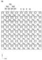
표시영역은 제1 표시영역(DA)과 제2 표시영역(CA)을 포함할 수 있다. 제1 표시영역(DA)은 센서가 배치되지 않은 영역이고 제2 표시영역(CA)은 복수 개의 센서(40, 50, 60, 70)가 배치된 영역으로 구분될 수 있다.The display area may include a first display area DA and a second display area CA. The first display area DA may be an area where no sensors are disposed, and the second display area CA may be divided into areas where a plurality of
제1 표시영역(DA)과 제2 표시영역(CA)은 모두 영상을 출력하며 해상도가 동일할 수 있다. 그러나 반드시 이에 한정하는 것은 아니고 제2 표시영역(CA)에 배치된 복수 개의 제2 픽셀의 해상도는 제1 표시영역(DA)에 배치된 복수 개의 제1 픽셀의 해상도(또는 밀도)보다 낮을 수도 있다. 제2 표시영역(CA)에 배치된 복수 개의 제2 픽셀의 해상도(또는 밀도)가 낮아지는 만큼 제2 표시영역(CA)에 배치된 센서에 상대적으로 많은 광량이 주입될 수 있다.Both the first display area DA and the second display area CA output images and may have the same resolution. However, it is not necessarily limited thereto, and the resolution of the plurality of second pixels disposed in the second display area CA may be lower than the resolution (or density) of the plurality of first pixels disposed in the first display area DA. . As the resolution (or density) of the plurality of second pixels disposed in the second display area CA decreases, a relatively large amount of light may be injected into the sensor disposed in the second display area CA.
제2 표시영역(CA)은 복수 개의 센서(40, 50, 60, 70)와 중첩되는 영역이므로 영상의 대부분을 출력하는 제1 표시영역(DA)보다 면적이 작을 수 있다. 제2 표시영역(CA)은 표시장치의 상단에 배치된 것으로 도시되었으나 반드시 이에 한정하지 않는다. 제2 표시영역(CA)의 위치 및 면적은 다양하게 변형될 수 있다.Since the second display area CA is an area overlapping the plurality of
복수 개의 센서(40, 50, 60, 70)는 이미지 센서, 근접 센서, 조도 센서, 제스처 센서, 모션 센서, 지문 인식 센서 및 생체 센서 중 적어도 하나를 포함할 수 있다. 예시적으로 제1 센서는 조도 센서일 수 있고 제2 센서는 이미지 또는 동영상을 촬영하는 이미지 센서일 수 있으나 반드시 이에 한정하지 않는다.The plurality of
제2 표시영역(CA)은 복수 개의 센서(40, 50, 70)가 배치되는 제1 분할영역(CA1) 및 발광모듈(60)이 배치되는 제2 분할영역(CA2)을 포함할 수 있다. 발광모듈(60)은 제2 분할영역(CA2)에 분산 배치되는 복수 개의 발광소자(61)를 포함할 수 있다. 복수 개의 발광소자(61)는 적외선 광을 방출하는 레이저 발광소자일 수 있으나 반드시 이에 한정하지 않는다.The second display area CA may include a first partition area CA1 in which the plurality of
제1 분할영역(CA1)과 제2 분할영역(CA2)은 해상도가 동일할 수 있으나 반드시 이에 한정하지 않는다. 예시적으로 제1 분할영역(CA1)의 해상도는 제2 분할영역(CA2)보다 작을 수 있다. 제1 분할영역(CA1)은 카메라가 배치되므로 광 투과율을 높이기 위해 픽셀의 개수가 적어진 반면 제2 분할영역(CA2)은 복수 개의 발광소자(61)가 작게 제작되어 픽셀들 사이에 분산 배치되므로 제1 표시영역과 동일한 픽셀수를 가질 수도 있다.The first partition area CA1 and the second partition area CA2 may have the same resolution, but are not necessarily limited thereto. Illustratively, the resolution of the first partition area CA1 may be smaller than that of the second partition area CA2. Since the camera is placed in the first partition area CA1, the number of pixels is reduced to increase light transmittance, whereas in the second partition area CA2, a plurality of
도 2를 참조하면, 제1 표시영역(DA)과 제2 표시영역(CA)은 픽셀 데이터가 기입되는 픽셀들이 배치된 픽셀 어레이를 포함할 수 있다. 전술한 바와 같이 제2 표시영역(CA)의 단위 면적당 픽셀 수(Pixels Per Inch: 이하, "PPI"라 함)는 제1 표시영역(DA)과 동일할 수도 있으나 광 투과율을 확보하기 위하여 제1 표시영역(DA) 보다 낮을 수도 있다.Referring to FIG. 2 , the first display area DA and the second display area CA may include a pixel array in which pixels on which pixel data is written are arranged. As described above, the number of pixels per inch (hereinafter referred to as "PPI") of the second display area CA may be the same as that of the first display area DA, but in order to secure light transmittance, the first It may be lower than the display area DA.
제1 표시영역(DA)의 픽셀 어레이는 PPI가 높은 복수의 픽셀 그룹들이 배치된 픽셀 영역을 포함할 수 있다. 제2 표시영역(CA)의 픽셀 어레이는 투광영역(TA)에 의해 이격되어 상대적으로 PPI가 낮은 복수의 픽셀 그룹들이 배치된 픽셀 영역을 포함할 수 있다. 제2 표시영역(CA)에서 외부 광은 광 투과율이 높은 투광영역(TA)을 통해 표시 패널(100)을 투과하여 표시 패널(100) 아래의 센서에 수광될 수 있다. 또한, 복수 개의 발광소자(61)에서 조사된 광은 투광영역(TA)을 통해 외부로 출사될 수도 있다The pixel array of the first display area DA may include a pixel area in which a plurality of pixel groups having a high PPI are disposed. The pixel array of the second display area CA may include a pixel area in which a plurality of pixel groups having a relatively low PPI are disposed spaced apart from each other by the light-transmitting area TA. In the second display area CA, external light may be transmitted through the
제1 표시영역(DA)과 제2 표시영역(CA)의 픽셀들 각각은 영상의 컬러 구현을 위하여 컬러가 다른 서브 픽셀들을 포함할 수 있다. 서브 픽셀들은 적색, 녹색 및 청색 서브 픽셀을 포함할 수 있다. 도시하지 않았으나 픽셀 그룹은 백색 서브 픽셀을 더 포함할 수 있다. 서브 픽셀들 각각은 픽셀 회로부와, OLED를 포함할 수 있다.Each of the pixels of the first display area DA and the second display area CA may include sub-pixels having different colors in order to implement color of an image. The sub-pixels may include red, green and blue sub-pixels. Although not shown, the pixel group may further include a white sub-pixel. Each of the sub-pixels may include a pixel circuit and an OLED.
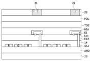
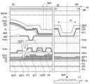
표시 패널(100)은 기판(10) 상에 배치된 회로층(12)과, 회로층(12) 상에 배치된 소자층(14)을 포함할 수 있다. 소자층(14) 상에는 편광판(18)이 배치되고, 편광판(18) 위에 커버 글라스(20)가 배치될 수 있다.The
회로층(12)은 데이터 라인들, 게이트 라인들, 전원 라인들 등의 배선들에 연결된 픽셀 회로, 게이트 라인들에 연결된 게이트 구동부 등을 포함할 수 있다.The
회로층(12)은 TFT(Thin Film Transistor)로 구현된 트랜지스터와 커패시터 등의 회로 소자를 포함할 수 있다. 회로층(12)의 배선과 회로 소자들은 복수의 절연층들과, 절연층을 사이에 두고 분리된 둘 이상의 금속층, 그리고 반도체 물질을 포함하는 액티브층으로 구현될 수 있다.The
소자층(14)은 픽셀 회로에 의해 구동되는 OLED를 포함할 수 있다. OLED는 애노드와 캐소드 사이에 형성된 유기 화합물층을 포함할 수 있다.The
유기 화합물층은 정공주입층(Hole Injection layer, HIL), 정공수송층(Hole transport layer, HTL), 발광층(Emission layer, EML), 전자수송층(Electron transport layer, ETL) 및 전자주입층(Electron Injection layer, EIL)을 포함할 수 있으나 이에 한정되지 않는다.The organic compound layer includes a hole injection layer (HIL), a hole transport layer (HTL), an emission layer (EML), an electron transport layer (ETL), and an electron injection layer, EIL), but is not limited thereto.
OLED의 애노드와 캐소드에 전압이 인가되면 정공수송층(HTL)을 통과한 정공과 전자수송층(ETL)을 통과한 전자가 발광층(EML)으로 이동되어 여기자를 형성하여 발광층(EML)에서 가시광이 방출될 수 있다.When voltage is applied to the anode and cathode of the OLED, holes that have passed through the hole transport layer (HTL) and electrons that have passed through the electron transport layer (ETL) are moved to the light emitting layer (EML) to form excitons and visible light is emitted from the light emitting layer (EML). can
소자층(14)은 적색, 녹색 및 청색의 파장을 선택적으로 투과시키는 픽셀들 상에 배치되고, 컬러 필터 어레이를 더 포함할 수 있다.The
소자층(14)은 보호막에 의해 덮일 수 있고, 보호막은 봉지층(encapsulation layer)에 의해 덮일 수 있다. 보호층과 봉지층은 유기막과 무기막이 교대로 적층된 구조일 수 있다. 무기막은 수분이나 산소의 침투를 차단할 수 있다. 유기막은 무기막의 표면을 평탄화할 수 있다. 유기막과 무기막이 여러 겹으로 적층되면, 단일 층에 비해 수분이나 산소의 이동 경로가 길어져 소자층(14)에 영향을 주는 수분/산소의 침투가 효과적으로 차단될 수 있다.The
소자층(14) 상에는 편광판(18)이 배치될 수 있다. 편광판(18)은 표시장치의 야외 시인성을 개선할 수 있다. 편광판(18)은 표시 패널(100)의 표면으로부터 반사되는 광을 줄이고, 회로층(12)의 금속으로부터 반사되는 광을 차단하여 픽셀들의 밝기를 향상시킬 수 있다. 편광판(18)은 선편광판과 위상지연필름이 접합된 편광판 또는 원편광판으로 구현될 수 있다.A
제2 표시영역(CA)은 표시 패널(100)의 화면 아래에는 복수 개의 센서가 배치될 수 있다.A plurality of sensors may be disposed below the screen of the
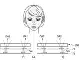
적외선 센서는 표시 패널(100)의 전면에 적외선 광을 조사하는 발광모듈(60)과 반사광을 수신하는 수광모듈(70)을 포함할 수 있다. 발광모듈(60)은 복수 개의 발광소자(61)를 포함할 수 있다. 복수 개의 발광소자(61)는 각각 적외선 광을 방출하는 레이저 발광소자일 수 있다. 이를 이용하여 사용자의 얼굴을 검출할 수 있다.The infrared sensor may include a
도 3을 참조하면, 종래 얼굴 이미지 검출 방법은 적외선 프로젝터(6)의 발광 어레이(6a)에서 복수 개의 적외선 광이 조사되고, 사용자(OBJ1)의 얼굴에 반사된 광을 적외선 카메라(7)의 수광 어레이(7b)가 수신하여 3차원 특징맵을 생성할 수 있다. 이러한 과정을 통해 사용자의 얼굴을 인식할 수 있다. 그러나, 이러한 구조는 적외선 광을 조사하는 적외선 프로젝터(6)와 적외선 카메라(7)가 배치되는 별도의 공간이 필요한 문제가 있으며 적외선 프로젝터(6)와 적외선 카메라(7)가 차지하는 면적만큼 표시영역이 작아지는 문제가 있다.Referring to FIG. 3 , in the conventional facial image detection method, a plurality of infrared lights are irradiated from the
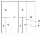
도 4를 참조하면, 실시예에 따른 발광모듈(60)은 복수 개의 발광소자(61)가 픽셀들(R, G, B) 사이에 분산 배치되므로 별도의 공간을 차지하지 않을 수 있다. 즉, 픽셀의 개수 및/또는 크기를 적절히 조절하고 픽셀들 사이에 복수 개의 발광소자(61)를 각각 배치할 수 있다.Referring to FIG. 4 , the
복수 개의 발광소자(61)에서 조사된 적외선 광은 사용자의 얼굴에 반사되고 수광모듈(70)의 수광 어레이(71)는 반사광을 수신하여 3차원 특징맵을 생성할 수 있다.Infrared light emitted from the plurality of light emitting
도 5a 내지 도 5c는 다양한 위치에 배치되는 제2 표시영역을 보여주는 도면이다.5A to 5C are views showing second display areas disposed in various positions.
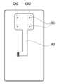
도 5a 내지 도 5c를 참조하면, 복수 개의 발광소자(61)의 위치는 픽셀들 사이의 다양한 위치에 배치될 수 있다. 복수 개의 발광소자(61)는 연성회로기판(62)을 통해 전원을 공급받을 수 있다. 연성회로기판(62)의 면적은 복수 개의 발광소자(61)의 이격 위치 및 개수에 따라 다양하게 변형될 수 있다.Referring to FIGS. 5A to 5C , the positions of the plurality of light emitting
예시적으로 도 5a와 같이 복수 개의 발광소자(61)는 표시영역의 상단에 배치될 수 있다. 또는 도 5b와 같이 복수 개의 발광소자(61)는 표시영역의 중앙 영역에 배치될 수도 있고, 도 5c와 같이 각각의 발광소자(61)가 이격되어 제2 분할영역(CA2)이 복수 개로 이격 배치될 수도 있다.Illustratively, as shown in FIG. 5A, the plurality of light emitting
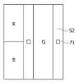
도 6은 본 발명의 일 실시예에 따른 제1 표시영역의 픽셀 배치를 보여주는 도면이다. 도 7은 제2 표시영역의 픽셀과 투광영역을 보여주는 도면이다.6 is a diagram showing a pixel arrangement of a first display area according to an embodiment of the present invention. 7 is a diagram showing pixels and a light transmission area of a second display area.
도 6을 참조하면, 제1 표시영역(DA)은 매트릭스 형태로 배열된 복수 개의 제1 픽셀 그룹(PG1)을 포함할 수 있다. 복수 개의 제1 픽셀 그룹(PG1)은 서브 픽셀 렌더링 알고리즘을 이용하여 두 개의 서브 픽셀이 하나의 픽셀을 구성할 수 있다. 예를 들어, 제1 단위 픽셀(PIX1)은 R 및 G1 서브 픽셀(SP1, SP2)로 구성되고, 제2 단위 픽셀(PIX2)은 B 및 G2 서브 픽셀(SP3, SP4)로 구성될 수 있다. 각각의 단위 픽셀들(PIX1, PIX2)에서 부족한 컬러 표현은 이웃한 픽셀들 간에 해당 컬러 데이터들의 평균값으로 보상될 수 있다. 그러나 반드시 이에 한정하는 것은 아니고 복수 개의 제1 픽셀 그룹(PG1)은 RGB 서브 픽셀을 포함하는 리얼 타입 픽셀일 수도 있다.Referring to FIG. 6 , the first display area DA may include a plurality of first pixel groups PG1 arranged in a matrix form. In the plurality of first pixel groups PG1, two sub-pixels may constitute one pixel by using a sub-pixel rendering algorithm. For example, the first unit pixel PIX1 may include R and G1 subpixels SP1 and SP2, and the second unit pixel PIX2 may include B and G2 subpixels SP3 and SP4. A lack of color expression in each of the unit pixels PIX1 and PIX2 may be compensated for by an average value of corresponding color data among neighboring pixels. However, it is not necessarily limited thereto, and the plurality of first pixel groups PG1 may be real-type pixels including RGB sub-pixels.
도 7을 참조하면, 제2 표시영역(CA)은 복수 개의 제2 픽셀 그룹(PG2)과 복수 개의 투광영역(TA)을 포함할 수 있다. 복수 개의 투광영역(TA)은 복수 개의 제2 픽셀 그룹(PG2) 사이에 배치될 수 있다. 구체적으로, 투광영역(TA)은 제1 방향 및 제2 방향으로 각각 제2 픽셀 그룹(PG2)과 교번하여 배치될 수 있다. 복수 개의 발광소자(61) 또는 각종 센서는 투광영역(TA)의 하부에 배치될 수 있다. 이 경우 투광영역(TA)의 면적이 증가하는 만큼 제2 표시영역(CA)의 해상도는 제1 표시영역(DA)의 해상도보다 작아질 수 있다.Referring to FIG. 7 , the second display area CA may include a plurality of second pixel groups PG2 and a plurality of transmissive areas TA. A plurality of light-transmitting areas TA may be disposed between the plurality of second pixel groups PG2. Specifically, the light transmission area TA may be alternately disposed with the second pixel group PG2 in the first direction and the second direction, respectively. A plurality of
그러나 복수 개의 발광소자(61)는 반드시 투광영역(TA)에 배치되는 것은 아니고 일부 픽셀이 제거된 영역에 적절히 배치될 수도 있다.However, the plurality of light emitting
투광영역(TA)은 최소한의 광 손실로 빛이 입사될 수 있도록 금속 없이 광 투과율이 높은 투명한 매질들을 포함할 수 있다. 투광영역(TA)은 금속 배선이나 픽셀들을 포함하지 않고 투명한 절연 재료들로 이루어질 수 있다. 제2 표시영역(CA)의 광 투과율은 투광영역(TA)이 클수록 높아질 수 있다.The light transmission area TA may include transparent media having high light transmittance without metal so that light may be incident with minimal light loss. The light transmission area TA may be formed of transparent insulating materials without including metal wires or pixels. The light transmittance of the second display area CA may increase as the transmittance area TA is larger.
복수 개의 제2 픽셀 그룹(PG2)은 하나 또는 두 개의 픽셀을 포함할 수 있다. 예를 들어, 제2 픽셀 그룹(PG2)의 제1 단위 픽셀(PIX1)은 R 및 G1 서브 픽셀들(SP1, SP2)로 구성되고, 제2 단위 픽셀(PIX2)은 B 및 G2 서브 픽셀들(SP3, SP4)로 구성될 수 있다. 제2 픽셀 그룹(PG2)의 픽셀 형상 및 배치는 제1 픽셀 그룹(PG1)과 동일할 수도 있으나 상이할 수도 있다.The plurality of second pixel groups PG2 may include one or two pixels. For example, the first unit pixel PIX1 of the second pixel group PG2 includes R and G1 subpixels SP1 and SP2, and the second unit pixel PIX2 includes B and G2 subpixels ( SP3, SP4) can be configured. The pixel shape and arrangement of the second pixel group PG2 may be the same as or different from those of the first pixel group PG1.
투광영역(TA)의 형상은 사각형으로 예시되었으나 이에 한정되지 않는다. 예를 들어, 투광영역(TA)은 원형, 타원형, 다각형 등 다양한 형태로 설계될 수 있다.The shape of the light transmission area TA is illustrated as a rectangle, but is not limited thereto. For example, the light transmission area TA may be designed in various shapes such as a circle, an ellipse, and a polygon.
투광영역(TA)에서 금속 전극 물질은 모두 제거될 수 있다. 따라서, 픽셀의 배선들은 투광영역(TA)의 외측에 배치될 수 있다. 따라서, 투광영역(TA)을 통해 광은 유효하게 입사될 수 있다. 그러나 반드시 이에 한정하는 것은 아니고 투광영역(TA)내의 일부 영역에는 금속 전극 물질이 존재할 수도 있다.All metal electrode materials may be removed from the light transmission area TA. Accordingly, the lines of the pixels may be arranged outside the light-transmitting area TA. Accordingly, light can be effectively incident through the light transmission area TA. However, it is not necessarily limited thereto, and a metal electrode material may be present in some areas of the light transmission area TA.
도 8a 내지 도 8d는 복수 개의 발광소자가 배치되는 다양한 픽셀 구조를 보여주는 도면이다.8A to 8D are diagrams illustrating various pixel structures in which a plurality of light emitting elements are disposed.
도 8a를 참조하면, 제2 표시영역(CA)은 픽셀의 PPI는 그대로 유지하고 서브픽셀의 크기를 줄여 복수 개의 발광소자(61)가 배치되는 공간을 확보할 수도 있다. 복수 개의 서브픽셀의 크기를 전체적으로 줄여 픽셀 라인과 픽셀 라인 사이에 이격 공간(S1)을 형성하고, 이격 공간(S1)에 복수 개의 발광소자(61)를 배치할 수 있다.Referring to FIG. 8A , in the second display area CA, a space in which a plurality of light emitting
도 8b를 참조하면, 녹색 서브픽셀(G)의 크기만을 상대적으로 줄여 이격 공간(S1)을 형성하고, 이격 공간에 복수 개의 발광소자(61)를 배치할 수도 있다.Referring to FIG. 8B , only the size of the green sub-pixel G may be relatively reduced to form a separation space S1 and a plurality of light emitting
도 8c를 참조하면, 청색 서브픽셀(B)의 크기를 상대적으로 줄여 이격 공간(S1)을 형성하고 복수 개의 발광소자(61)를 배치할 수도 있다.Referring to FIG. 8C , the size of the blue sub-pixel B may be relatively reduced to form a separation space S1 and a plurality of
또한, 도 8d과 같이 서브픽셀들 사이에 이격 공간(S1)을 형성하여 복수 개의 발광소자(61)를 배치할 수도 있다. 이러한 구성에 의하면 픽셀의 해상도는 그대로 유지하면서 복수 개의 발광소자(61)를 분산시킬 수 있는 장점이 있다. 이때, 줄어든 서브픽셀은 휘도를 보상하기 위해 데이터 전압을 높여 출력할 수 있다.In addition, as shown in FIG. 8D, a plurality of light emitting
도 9는 복수 개의 발광소자에서 출사된 광이 회절 패턴에 의해 회절되는 상태를 보여주는 도면이다. 도 10은 발광소자의 단면도이다.9 is a view showing a state in which light emitted from a plurality of light emitting devices is diffracted by a diffraction pattern. 10 is a cross-sectional view of a light emitting device.
도 9를 참조하면, 복수 개의 발광소자(61)는 표시 패널(100)의 하부에 배치될 수 있다. 복수 개의 발광소자(61)는 복수 개의 픽셀과 수직 방향으로 중첩되지 않도록 배치될 수 있다. 복수 개의 발광소자(61)가 픽셀 사이에 배치된다는 의미는 동일평면 상에서 픽셀 사이에 배치되는 것뿐만 아니라 복수 개의 발광소자(61)가 수직 방향으로 픽셀과 중첩되지 않는 구조인 것을 포함할 수 있다.Referring to FIG. 9 , a plurality of light emitting
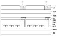
커버 글라스(20)에는 복수 개의 발광소자(61)와 중첩되는 영역에 복수 개의 회절패턴(21)이 형성될 수 있다. 회절패턴은 커버 글라스를 패터닝하여 형성할 수 있으나 반드시 이에 한정하는 것은 아니고 다양한 패턴 형성 방법이 제한 없이 선택될 수 있다. 예시적으로 회전 패턴이 형성된 필름을 부착할 수도 있다.A plurality of
복수 개의 발광소자(61)에서 출사된 광은 회절패턴(21)에 기록되어 있는 패턴 정보에 의해 도트 이미지(1차빔)가 형성되고 회절 되지 않은 성분(0차빔)은 그대로 출사될 수 있다.The light emitted from the plurality of
실시예에 따르면, 복수 개의 발광소자(61)가 서로 이격되어 광을 출력하므로 발광소자(61)의 개수 및 출력을 조절하면 출사된 0차빔(L1)을 조명용 광원(Flood illuminator)으로 사용할 수 있다.According to the embodiment, since the plurality of
복수 개의 발광소자(61)는 콜리메이션(Collimation) 및 코히어런트(Coherence) 정도에 따라 회절 효율이 결정되는데, 회절 효율을 조절함으로써 1차빔(L2)의 비율을 조절할 수 있다. 회절 효율은 콜리메이터 렌즈 등을 이용하여 조절할 수 있다. 또한, 1차빔(L2)의 비율을 높이기 위해 발광소자의 개수를 늘릴 수 있다.The diffraction efficiency of the plurality of
얼굴 인식의 신뢰성을 보장하기 위해 회절효율은 1차빔(L2)이 0차빔(L1)보다 크도록 설정하는 것이 바람직하다. 또한, 1차빔(L2)을 이용하여 안정적으로 3차원 특징맵을 생성하면서도 0차빔(L1)을 조명용 광원으로도 사용하기 위해 0차빔(L1)과 1차빔(L2)의 비율(0차빔: 1차빔)은 1:2 내지 1:7로 조절될 수 있다.In order to ensure reliability of face recognition, it is preferable to set the diffraction efficiency so that the first-order beam L2 is greater than the zero-order beam L1. In addition, in order to stably generate a 3D feature map using the 1st beam L2 and use the 0th beam L1 as a light source for illumination, the ratio of the 0th beam L1 to the 1st beam L2 (0th beam: 1 chabim) can be adjusted from 1:2 to 1:7.
0차빔(L1)과 1차빔(L2)의 비율이 1:2 보다 작은 경우(예:1:1.5)에는 1차빔이 상대적으로 부족해져 안정적으로 3차원 특징맵을 형성하기 어려울 수 있다. 또한, 0차빔(L1)과 1차빔(L2)의 비율이 1:7 보다 큰 경우(예:1:8)에는 0차빔의 광량이 상대적으로 작아져 조명용 광원의 기능을 수행하기 어려울 수 있다.When the ratio of the 0th-order beam L1 to the 1st-order beam L2 is less than 1:2 (eg, 1:1.5), it may be difficult to stably form a 3D feature map due to a relatively insufficient first-order beam. In addition, when the ratio of the 0th-order beam L1 to the 1st-order beam L2 is greater than 1:7 (eg, 1:8), the amount of light of the 0th-order beam is relatively small, making it difficult to perform the function of a light source for illumination.
도 10을 참조하면, 복수 개의 발광소자(61)는 소형 제작된 수직 공동 표면 방출 레이저(Vertical Cavity Surface Emitting Laser; VCSEL)일 수 있다. 각각의 발광소자(61)는 픽셀들 사이에 분산될 수 있을 정도의 크기로 소형화될 수 있다.Referring to FIG. 10 , the plurality of light emitting
수직 공동 표면 방출 레이저는 좁은 스펙트럼의 단일 종모드(single longitudinal mode) 발진이 가능하고, 빔의 방사각이 작아 결합 효율(coupling efficiency)이 높은 장점이 있다.The vertical cavity surface emitting laser is capable of oscillating in a single longitudinal mode of a narrow spectrum and has advantages of high coupling efficiency due to a small emission angle of a beam.
각각의 발광소자(61)는 지지기판(611), 지지기판(611) 상에 배치되는 제1 반사층(612a), 제1 반사층(612a) 상에 배치된 레이저 캐비티(612b), 레이저 캐비티(612b) 상에 배치되는 제2 반사층(612c), 제2 반사층(612c) 상에 배치되는 제1 패드(614) 및 제2 패드(613)를 포함할 수 있다.Each
지지기판(611)은 반절연성 또는 전도성 기판일 수 있다. 예시적으로 기판은 도핑 농도가 높은 GaAs 기판으로서, 도펀트가 도핑될 수 있다. 필요에 따라 기판 상에 AlGaAs 또는 GaAs 박막과 같은 버퍼층이 더 배치될 수 있으나 반드시 이에 한정하지 않는다.The supporting
제1 반사층(612a)은 n형의 초격자(superlattice) 구조의 분산형 브래그 반사기(Distributed Bragg Reflector: DBR)를 포함할 수 있다. 제1 반사층(612a)은 MOCVD, MBE 등의 기법에 의해 기판 상에 에피택셜 증착될 수 있다.The first
제1 반사층(612a)은 한 쌍의 반사층이 교대로 적층될 수 있다. 제1 서브 반사층과 제2 서브 반사층은 모두 AlGaAs일 수 있으나 제1 서브 반사층의 알루미늄 조성이 더 높을 수 있다.In the first
레이저 캐비티(612b)는 하나 이상의 우물층과 장벽층을 포함할 수 있다. 우물층은 GaAs, AlGaAs, AlGaAsSb, InAlGaAs, AlInGaP, GaAsP 또는 InGaAsP 중 어느 하나가 선택될 수 있고, 장벽층은 AlGaAs, InAlGaAs, InAlGaAsP, AlGaAsSb, GaAsP, GaInP, AlInGaP, 또는 InGaAsP 중 어느 하나가 선택될 수 있다.The
레이저 캐비티(612b)는 충분한 광학적 이득을 갖도록 설계될 수 있다. 예시적으로 실시 예에 따른 레이저 캐비티는 적외선 파장대의 광을 방출하기 위해 적정한 두께 및 조성비를 가지는 우물층을 중심에 가질 수 있다. 그러나, 우물층이 출력하는 레이저의 파장대는 특별히 한정하지 않는다.The
산화층(618)은 레이저 캐비티 상에 배치될 수 있다. 산화층(618)은 알루미늄을 함유하는 반도체 화합물, 예를 들면, AlAs, AlGaAs, InAlGaAs 등을 포함할 수 있다. 실시 예에 따른 산화층은 중앙에 산화되지 않은 개구부(618a)를 포함할 수 있다.An
산화층(618)은 저항이 상대적으로 높은 반면 굴절율은 상대적으로 낮을 수 있다. 따라서, 전류는 개구부(618a)로 주입될 수 있으므로 레이저 광을 소자의 중앙으로 모을 수 있다.The
제2 반사층(612c)은 산화층의 상부에 배치될 수 있다. 상부 반사층은 복수 개의 제3 서브 반사층과 제4 서브 반사층을 포함할 수 있다.The second
제3 서브 반사층은 AlGaAs의 조성을 가질 수 있고, 제4 서브 반사층은 GaAs 조성을 가질 수 있다. 제1 반사층의 반사율은 제2 반사층의 반사율보다 낮을 수 있다. 따라서, 레이저 캐비티(612b)에서 생성된 광은 산화층(618)의 개구부(618a)를 통과하여 지지기판(611)을 통해 출사될 수 있다.The third sub-reflective layer may have a composition of AlGaAs, and the fourth sub-reflective layer may have a composition of GaAs. The reflectance of the first reflective layer may be lower than that of the second reflective layer. Accordingly, light generated in the
제1 패드(614)와 제2 패드(613)는 제2 반사층(612c) 상에 배치될 수 있다. 제1 패드(614)는 에피 구조물(612)에 형성된 관통홀로 연장된 전극(615)을 통해 제1 반사층(612a)과 전기적으로 연결될 수 있다. 즉, 수직 공동 표면 방출 레이저는 플립칩 타입일 수 있다. 그러나, 반드시 이에 한정하는 것은 아니고 수평형 또는 수직형과 같은 다양한 타입의 전극 배치를 가질 수도 있다. 또한 수직 공동 표면 방출 레이저 를 작게 제작하기 위해 레이저 구조는 다양하게 변형될 수 있다.The
도 11은 복수 개의 발광소자가 표시 패널 내부에 배치된 구조를 보여주는 도면이다. 도 12는 복수 개의 발광소자의 상부에 렌즈가 배치된 구조를 보여주는 도면이다. 도 13은 렌즈가 발광소자의 상부에 배치된 구조를 보여주는 도면이다.11 is a view showing a structure in which a plurality of light emitting elements are disposed inside a display panel. 12 is a view showing a structure in which lenses are disposed on top of a plurality of light emitting devices. 13 is a view showing a structure in which a lens is disposed above a light emitting device.
도 11을 참조하면, 복수 개의 픽셀이 배치된 소자층(14)은 애노드 전극(AND)과 캐소드 전극(CAT) 사이에 배치되는 반면, 복수 개의 발광소자(61)는 캐소드 전극(CAT)의 상부에 배치되어 패드전극(611)과 연결될 수 있다. 또한, 복수 개의 발광소자(61)는 관통전극(612)을 통해 애노드 전극(AND)과 전기적으로 연결될 수 있다. 도시되지는 않았으나 관통전극(612)은 캐소드 전극(CAT)과는 절연될 수 있다. 이러한 구조는 발광소자(61)가 플립칩인 경우 적용될 수 있다. 만약 발광소자(61)가 수직형 구조인 경우에는 애노드 전극(AND)과 캐소드 전극(CAT) 사이에 배치될 수 있다.Referring to FIG. 11, the
복수 개의 발광소자(61)를 통해 출사된 광은 터치 패널(TOE)과 편광판(POL)을 통과하여 커버 글라스(20)의 회절패턴(21)에 의해 0차빔과 1차빔으로 분리될 수 있다.Light emitted through the plurality of light emitting
이러한 구성에 의하면 별도의 연성회로기판을 생략할 수 있고 표시 패널(100) 형성시 발광모듈(60)을 함께 제작할 수 있는 장점이 있다. 도시되지는 않았으나 복수 개의 발광소자(61)에 전원을 공급하는 배선이 추가적으로 형성될 수 있다.According to this configuration, there is an advantage in that a separate flexible printed circuit board can be omitted and the
도 12를 참조하면, 회절패턴(21)과 발광소자(61) 사이에는 제1 렌즈(61a)가 배치될 수 있다. 제1 렌즈(61a)는 발광소자(61)에서 출사되는 광을 평행광으로 변환하는 콜리메이터 렌즈일 수 있으나 반드시 이에 한정하는 것은 아니고 원하는 광 제어를 위해 필요한 렌즈가 적용될 수도 있다. 앞서 설명한 바와 같이 제1 렌즈(61a)가 회절 패턴과 발광소자(61) 사이에 배치됨으로써 0차빔과 1차빔의 회절 효율을 조절할 수 있다.Referring to FIG. 12 , a
실시예에 따르면 복수 개의 제1 렌즈(61a)는 소자층(14)에 배치될 수 있으나 반드시 이에 한정하는 것은 아니고 회절 패턴과 발광소자(61) 사이의 층이면 제한 없이 형성될 수 있다. 제1 렌즈(61a)는 레진을 도포하여 소자층(14) 내에 형성할 수 있다.According to the embodiment, the plurality of
도 13을 참조하면 제1 렌즈(61a)는 발광소자(61) 상에 직접 형성될 수도 있다. 이러한 구성에 의하면 발광소자(61)에서 출사된 광이 제1 렌즈(61a)에 직접 입사되어 광 결합 효율이 증가할 수 있다.Referring to FIG. 13 , the
제1 렌즈(61a)는 발광소자(61)의 상면에만 형성될 수 있으나 반드시 이에 한정하는 것은 아니고 발광소자(61)의 측면까지 형성되어 발광소자(61)를 보호할 수도 있다.The
제1 렌즈(61a)는 발광소자(61) 상에 미리 형성된 후 표시 패널(100)이 배치될 수 있으나 반드시 이에 한정하지 않는다. 예시적으로 발광소자(61)를 캐소드 전극(CAT) 상에 배치한 후 레진을 도포하여 제1 렌즈(61a)를 형성할 수도 있다. 이 경우 레진의 일부가 발광소자(61)와 캐소드 전극(CAT) 사이에 충전되어 발광소자(61)를 고정하는 역할도 수행할 수 있다.The
도 14는 본 발명의 제2 실시예에 따른 표시장치의 개념도이다. 도 15는 복수 개의 수광소자가 반사광을 수신하는 구조를 보여주는 도면이다.14 is a conceptual diagram of a display device according to a second embodiment of the present invention. 15 is a view showing a structure in which a plurality of light receiving elements receive reflected light.
도 14 및 도 15를 참조하면, 표시장치는 복수 개의 픽셀을 포함하는 표시 패널(100) 및 수광모듈(70)을 포함하고, 수광모듈(70)은 복수 개의 픽셀 사이에 분산 배치되는 복수 개의 수광소자(71)를 포함할 수 있다.14 and 15, the display device includes a
복수 개의 수광소자(71)는 표시영역의 전체에 걸쳐 분산될 수 있다. 각각의 수광소자(71)는 이미지 센서의 단위 픽셀과 대응되는 구성일 수 있다. 예시적으로 1개의 수광소자는 1개의 단위 픽셀과 대응되는 구성일 수도 있고, 복수 개의 단위 픽셀과 대응되는 구성일 수도 있다. 따라서, 각각의 수광소자(71)는 해당 영역의 이미지를 촬영하는 촬상 유닛의 역할을 수행할 수 있다. 그러나 반드시 이에 한정하지 않는 것은 아니고 복수 개의 수광소자(71)는 표시영역의 중심 영역에만 배치될 수도 있고, 상단 일부에만 배치될 수도 있다.The plurality of light receiving
수광모듈(70)을 제외한 복수 개의 센서(40, 50, 60)들은 제2 표시영역(CA)에 배치될 수 있다. 제2 표시영역(CA)은 복수 개의 센서(40, 50, 60)가 배치된 영역이고 제1 표시영역(DA)은 제2 표시영역(CA)을 제외한 나머지 영역 또는 복수 개의 수광소자(71)가 배치된 영역일 수 있다. 제1 표시영역(DA)과 제2 표시영역(CA)은 모두 영상을 출력하며 해상도가 동일할 수 있으나 반드시 이에 한정되는 것은 아니고 제2 표시영역(CA)의 해상도가 더 낮을 수도 있다.The plurality of
복수 개의 센서(40, 50, 60)는 이미지 센서, 근접 센서, 조도 센서, 제스처 센서, 모션 센서, 지문 인식 센서 및 생체 센서 중 적어도 하나를 포함할 수 있다. 예시적으로 제1 센서는 적외선 센서일 수 있고 제2 센서는 이미지 또는 동영상을 촬영하는 이미지 센서일 수 있으나 반드시 이에 한정하지 않는다.The plurality of
실시예에 따른 수광모듈(70)은 복수 개의 수광소자(71)가 픽셀들 사이에 분산 배치되므로 수광모듈이 수납되는 별도의 독립된 공간을 생략할 수 있다. 실시예에 따르면, 수광모듈(70)을 복수 개의 수광소자(71)로 분리하여 패널에 분산 배치하므로 표시영역을 확장할 수 있는 장점이 있다. 발광모듈(60)에서 출사된 광은 사용자(OBJ1)에 반사되고, 패널에 분산된 복수 개의 수광소자(71)는 반사광을 수신할 수 있다.In the
도 16은 복수 개의 수광소자가 픽셀 사이에 배치된 상태를 보여주는 도면이다.16 is a diagram showing a state in which a plurality of light receiving elements are arranged between pixels.
도 16을 참조하면, 제1 표시영역(DA)은 복수 개의 제2 픽셀 그룹(PG2)과 복수 개의 투광영역(TA)을 포함할 수 있다. 복수 개의 투광영역(TA)은 복수 개의 제2 픽셀 그룹(PG2) 사이에 배치될 수 있다. 구체적으로, 투광영역(TA)은 제1 방향 및 제2 방향으로 각각 제2 픽셀 그룹(PG2)과 교번하여 배치될 수 있다. 복수 개의 수광소자(71)는 투광영역(TA)에 배치될 수 있다. 이 경우 투광영역(TA)의 면적이 증가하는 만큼 제1 표시영역(DA)의 해상도는 낮아질 수 있다.Referring to FIG. 16 , the first display area DA may include a plurality of second pixel groups PG2 and a plurality of transmissive areas TA. A plurality of light-transmitting areas TA may be disposed between the plurality of second pixel groups PG2. Specifically, the light transmission area TA may be alternately disposed with the second pixel group PG2 in the first direction and the second direction, respectively. A plurality of light receiving
투광영역(TA)은 최소한의 광 손실로 빛이 입사될 수 있도록 금속 없이 광 투과율이 높은 투명한 매질들을 포함할 수 있다. 투광영역(TA)은 금속 배선이나 픽셀들을 포함하지 않고 투명한 절연 재료들로 이루어질 수 있다.The light transmission area TA may include transparent media having high light transmittance without metal so that light may be incident with minimal light loss. The light transmission area TA may be formed of transparent insulating materials without including metal wires or pixels.
도 17a 내지 도 17d는 복수 개의 수광소자가 배치되는 다양한 픽셀 구조를 보여주는 도면이다.17A to 17D are diagrams illustrating various pixel structures in which a plurality of light receiving elements are disposed.
도 17a를 참조하면, 픽셀의 PPI는 그대로 유지하고 픽셀의 크기를 줄여 복수 개의 수광소자(71)가 배치되는 공간을 확보할 수도 있다. 복수 개의 픽셀의 크기를 전체적으로 줄여 픽셀 라인과 픽셀 라인 사이에 이격 공간(S2)을 형성하고, 이격 공간(S2)에 복수 개의 수광소자(71)를 배치할 수 있다.Referring to FIG. 17A, the PPI of the pixel may be maintained and the pixel size may be reduced to secure a space in which the plurality of light receiving
도 17b를 참조하면, 녹색 서브픽셀(G)의 크기만을 상대적으로 줄여 이격 공간(S2)을 형성하고, 이격 공간(S2)에 복수 개의 수광소자(71)를 배치할 수도 있다.Referring to FIG. 17B, only the size of the green sub-pixel G may be relatively reduced to form a separation space S2, and a plurality of light receiving
도 17c를 참조하면, 청색 서브픽셀(B)의 크기를 상대적으로 줄여 이격 공간(S2)을 형성하여 복수 개의 수광소자(71)를 배치할 수도 있다.Referring to FIG. 17C , a plurality of light receiving
또한, 도 17d과 같이 픽셀들 사이에 이격공간(S2)을 형성하여 복수 개의 수광소자(71)를 배치할 수도 있다. 이러한 구성에 의하면 픽셀의 해상도는 그대로 유지하면서 복수 개의 수광소자(71)를 분산시킬 수 있는 장점이 있다. 이때, 줄어든 픽셀은 휘도를 보상하기 위해 데이터 전압을 높여 출력할 수 있다.In addition, as shown in FIG. 17D, a plurality of light receiving
도 18은 표시 패널의 하부에 수광모듈이 배치된 상태를 보여주는 도면이다. 도 19는 복수 개의 수광소자를 통해 얼굴 이미지를 획득하는 과정을 보여주는 도면이다.18 is a view showing a state in which a light receiving module is disposed under a display panel. 19 is a diagram illustrating a process of acquiring a face image through a plurality of light receiving elements.
도 18을 참조하면, 수광모듈(70)은 표시패널의 하부에 배치되고 표시 패널(100)에 형성된 투광영역(TA)을 통해 입사되는 광 데이터를 수신할 수 있다. 수광모듈(70)과 표시 패널(100)의 사이에는 제2 렌즈(72a)가 배치되어 입사되는 광의 경로를 제어할 수 있다. 복수 개의 수광소자(71)는 회로기판(73) 상에 배치될 수 있으며, 제2 렌즈(72a)는 렌즈 기판(72) 상에 형성될 수 있다. 제2 렌즈(72a)와 렌즈 기판(72)은 일체로 형성될 수 있으나 반드시 이에 한정되는 것은 아니고 제2 렌즈(72a)를 별도로 제작한 후 렌즈 기판(72)에 부착할 수도 있다.Referring to FIG. 18 , the
표시 패널(100)에는 광이 수광소자(71)에 입사되도록 개구 영역(H1)이 형성될 수 있다. 개구 영역(H1)은 복수 개의 픽셀 사이에 형성된 핀홀일 수도 있고 전술한 투광 영역일 수도 있다.An opening area H1 may be formed in the
도 19를 참조하면, 복수 개의 수광소자(71)는 해당 위치에서 할당된 영역의 이미지를 획득할 수 있다. 표시장치의 호스트 시스템은 복수 개의 수광소자(71)에서 획득한 이미지를 합성하여 3차원 특징맵을 생성할 수 있다.Referring to FIG. 19 , the plurality of light receiving
도 20은 수광소자의 위치에 따라 광축이 기울어진 상태를 보여주는 도면이다.20 is a view showing a state in which an optical axis is tilted according to a position of a light receiving element.
도 20을 참조하면, 복수 개의 수광소자(71)는 위치에 따라 초점이 조절될 수 있다. 기존 이미지 센서의 픽셀들을 분리하여 배치하게 되면 기존보다 넓은 영역의 이미지를 획득하게 되므로 각 위치마다 고유의 초점각도를 조절할 필요가 있다.Referring to FIG. 20 , the focus of the plurality of light receiving
실시예에서는 수광소자(71)의 제2 렌즈(72a)를 시프트하는 방법을 통해 사용자의 얼굴 방향에 맞게 촬영 각도를 조절할 수 있다. 예시적으로 패널의 중심을 기준으로 좌측에 배치된 복수 개의 수광소자(71)는 광축(OA1)이 중앙(C1)을 향하도록 제2 렌즈(72a)를 수광소자(71)에 비해 오른쪽으로 시프트시켜 배치할 수 있다.In the embodiment, the photographing angle may be adjusted according to the direction of the user's face by shifting the
또한, 우측에 배치된 복수 개의 수광소자(71)는 광축(OA2)이 중앙(C1)을 향하도록 제2 렌즈(72a)를 수광소자(71)에 비해 왼쪽으로 시프트시켜 배치할 수 있다.In addition, the plurality of light receiving
도시되지는 않았지만 표시 패널(100)의 하단에 배치된 수광소자(71)와 상단에 배치된 수광소자(71)는 각각 제2 렌즈(72a)를 시프트시켜 광축이 패널의 중앙을 향하도록 초점을 조절할 수 있다.Although not shown, the
도 21은 복수 개의 센싱 영역마다 센싱 회로가 분할된 상태를 보여주는 도면이다. 도 22a와 도 22b는 복수 개의 분할된 이미지를 합성하는 과정을 보여주는 도면이다.21 is a diagram showing a state in which sensing circuits are divided for each of a plurality of sensing areas. 22A and 22B are diagrams illustrating a process of synthesizing a plurality of divided images.
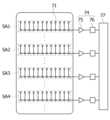
도 21을 참조하면, 수광모듈(70)은 복수 개의 센싱 영역(SA1, SA2, SA3, SA4)을 포함할 수 있고, 각각의 센싱 영역(SA1, SA2, SA3, SA4)에 배치된 복수 개의 수광소자(71)는 각각 센싱 회로(74)에 연결될 수 있다. 센싱 회로(74)는 연산 증폭기(75) 및 아날로그-디지털 변환기(76) 등 신호 수신에 필요한 다양한 회로소자들을 포함할 수 있다.Referring to FIG. 21 , the
복수 개의 수광소자(71)가 분산 배치되어 이미지를 획득하는 경우, 복수 개의 수광소자(71)의 거리에 따라 신호 지연 및 노이즈 편차가 발생할 수 있다.When the plurality of light receiving
따라서, 실시예에 따르면 복수 개의 센싱 영역(SA1, SA2, SA3, SA4)으로 분할되고 각 센싱 영역(SA1, SA2, SA3, SA4)에는 각각 센싱 회로(74)가 배치되어 신호를 병렬적으로 수신하므로 신호 지연 및 노이즈 발생을 최소화할 수 있다. 복수 개의 센싱 회로(74)를 통해 전송된 신호는 이미지 합성부(77)로 전송되어 합성 이미지를 생성할 수 있다.Therefore, according to the embodiment, it is divided into a plurality of sensing areas SA1, SA2, SA3, and SA4, and a
도 22a를 참조하면, 복수 개의 수광소자(71)가 분산 배치되어 복수 개의 이미지를 획득하는 경우 각각의 수광소자(71)의 화각이 중첩되므로 획득하는 이미지(IM1, IM2, IM3, IM4, IM5, IM6)에 중첩 부분이 발생할 수 있다. 따라서, 도 22b와 같이 이미지가 중첩되는 영역을 알고리즘을 통해 추출하고 중첩 부분을 제거하여 합성된 영상 이미지를 생성할 수 있다. 중첩된 영역을 추출하는 방법은 특별히 한정하지 않으며 다양한 영상 처리 기법이 제한 없이 이용될 수 있다.Referring to FIG. 22A, when a plurality of light-receiving
또 다른 실시예로는 최초 사용자의 얼굴 영상 획득시 중첩 부분을 제거하지 않고 기준 이미지를 설정한 경우 중첩된 이미지 자체를 기준 이미지와 비교하여 사용자 일치 여부를 판단할 수도 있다. 즉, 사용자 동일 여부를 확인하기 위한 최초로 획득한 기준 이미지가 도 22a와 같이 중첩된 영역을 갖는 이미지로 설정된 경우 사용자 확인을 위해 검출한 이미지 역시 중첩 부분을 제거하지 않고도 기준 이미지와 비교할 수 있다. 이 경우 중첩 여부를 계산하는 연산 처리를 생략할 수 있으므로 처리 속도가 향상될 수 있다.In another embodiment, when the reference image is set without removing the overlapping portion when the face image of the first user is acquired, the overlapped image itself may be compared with the reference image to determine whether the user matches. That is, when the reference image initially obtained for confirming user identity is set to an image having an overlapping area as shown in FIG. 22A, the image detected for user confirmation may also be compared with the reference image without removing the overlapping portion. In this case, processing speed may be improved because calculation processing for calculating overlapping or non-overlapping may be omitted.
도 23은 본 발명의 제3 실시예에 따른 표시장치의 개념도이다. 도 24는 도 23의 제1 변형예이다. 도 25는 도 23의 제2 변형예이다.23 is a conceptual diagram of a display device according to a third embodiment of the present invention. FIG. 24 is a first modified example of FIG. 23 . FIG. 25 is a second modified example of FIG. 23 .
도 23을 참조하면, 표시 패널(100)의 표시영역에는 발광모듈(60)의 복수 개의 발광소자(61)와 수광모듈(70)의 복수 개의 수광소자(71)가 픽셀들 사이에 분산 배치될 수 있다.Referring to FIG. 23 , in the display area of the
복수 개의 발광소자(61)와 수광소자(71)가 픽셀들 사이에 분산 배치되므로 풀 스크린 디스플레이(Full-screen display)가 가능하며, 발광모듈(60)과 수광모듈(70)이 배치되는 별도의 공간을 줄여 표시영역을 넓힐 수 있는 장점이 있다.Since a plurality of
실시예에 따르면, 표시 패널(100)의 일부 영역(R1)에는 복수 개의 발광소자(61)가 배치되고, 표시 패널(100)의 나머지 영역(R2)에는 복수 개의 수광소자(71)가 배치될 수 있다. 이러한 구조에 의하면 복수 개의 수광소자(71)가 발광 영역을 둘러싸는 형태를 가질 수 있다. 그러나, 반드시 이에 한정되는 것은 아니고 복수 개의 발광소자(61)와 복수 개의 수광소자(71)의 배치는 다양하게 변형될 수 있다.According to the exemplary embodiment, a plurality of
도 24를 참조하면, 표시 패널(100)은 복수 개의 발광소자(61)가 배치되는 발광 영역(TXA1) 및 복수 개의 수광소자(71)가 배치되는 수광 영역(RXA1)을 포함할 수 있다.Referring to FIG. 24 , the
발광 영역(TXA1)은 복수 개의 픽셀 및 복수 개의 발광소자(61)를 포함할 수 있다. 복수 개의 발광소자(61)는 복수 개의 픽셀들 사이에 배치될 수 있다. 복수 개의 픽셀들은 기존의 PPI를 그대로 유지한 상태에서 픽셀의 사이에 발광소자(61)가 배치될 수 있다. 또는 일부 픽셀이 생략되어 투광 영역을 마련하고 복수 개의 발광소자(61)가 투광 영역에 배치될 수도 있다. 발광소자(61)가 배치되는 구성은 전술한 구성이 모두 적용될 수 있다.The light emitting area TXA1 may include a plurality of pixels and a plurality of
수광 영역(RXA1)은 복수 개의 픽셀 및 복수 개의 수광소자(71)를 포함할 수 있다. 복수 개의 수광소자(71)는 복수 개의 픽셀들 사이에 배치될 수 있다. 복수 개의 픽셀들은 기존의 PPI를 그대로 유지한 상태에서 픽셀의 사이에 수광소자(71)가 배치될 수 있다. 또는 일부 픽셀이 생략되어 투광 영역을 마련하고, 복수 개의 수광소자(71)가 투광 영역에 배치될 수도 있다.The light receiving area RXA1 may include a plurality of pixels and a plurality of light receiving
도 25를 참조하면, 복수 개의 발광소자(61)와 수광소자(71)는 교대로 픽셀들 사이에 배치될 수도 있다. 이러한 구성에 의하면 복수 개의 발광소자에서 방출되는 광이 표시장치의 전면에서 출사될 수 있으며, 수광소자가 수신할 수 있는 면적이 증가할 수 있다. 복수 개의 발광소자(61)와 수광소자(71)는 교대로 픽셀들 사이에 배치되는 구성은 반드시 이에 한정되지 않으며 다양하게 변형될 수 있다.Referring to FIG. 25 , a plurality of
도 26은 복수 개의 수광소자가 패널에 배치된 구조를 보여주는 도면이다. 도 27은 복수 개의 발광소자가 패널에 배치된 구조를 보여주는 도면이다.26 is a view showing a structure in which a plurality of light receiving elements are disposed on a panel. 27 is a view showing a structure in which a plurality of light emitting devices are disposed on a panel.
도 26을 참조하면, 복수 개의 발광소자(61)는 표시 패널(100)의 하부에 배치될 수 있다. 복수 개의 발광소자(61)는 복수 개의 픽셀과 수직 방향으로 중첩되지 않도록 배치될 수 있다. 커버 글라스(20)에는 복수 개의 발광소자(61)와 중첩되는 영역에 회절패턴(21)이 형성될 수 있다.Referring to FIG. 26 , a plurality of light emitting
복수 개의 발광소자(61)에서 출사된 광이 회절패턴(21)에 기록되어 있는 패턴 정보에 의해 도트 이미지(1차빔)가 형성되고 회절 되지 않은 성분(0차빔)은 그대로 출사될 수 있다.A dot image (first-order beam) is formed by the pattern information recorded on the
실시예에 따르면, 복수 개의 발광소자(61)가 서로 이격되어 광을 출력하므로 발광소자(61)의 개수 및 출력을 조절하면 출사된 0차빔을 조명용 광원(Flood illuminator)으로 사용할 수 있다.According to the embodiment, since the plurality of
복수 개의 수광소자(71)는 픽셀들 사이에 배치될 수 있다. 따라서, 복수 개의 발광소자(61)가 배치되는 층과 복수 개의 수광소자(71)가 배치되는 층은 상이할 수 있다. 이러한 구성에 의하면 복수 개의 발광소자(61)의 위치가 복수 개의 수광소자(71)보다 낮은 위치에 배치될 수 있다. 복수 개의 발광소자(61)는 별도의 회로기판을 통해 연결함으로써 배선 구조가 복잡해지는 것을 방지할 수 있다.A plurality of light receiving
그러나, 반드시 이에 한정하는 것은 아니고 복수 개의 수광소자(71) 역시 표시 패널(100)의 하부에 배치될 수도 있다. 이때, 복수 개의 발광소자(61)를 전기적으로 연결하는 제1 회로기판과 복수 개의 수광소자(71)를 전기적으로 연결하는 제2 회로기판이 배치될 수 있다. 또는 하나의 회로기판에 복수 개의 발광소자(61)와 복수 개의 수광소자(71)가 같이 배치될 수도 있다.However, it is not necessarily limited thereto, and a plurality of light receiving
도 27을 참조하면, 복수 개의 픽셀은 회로부의 애노드 전극(AND)과 캐소드 전극(CAT) 사이에 배치되는 반면, 복수 개의 발광소자(61)는 캐소드 전극(CAT)의 상부에 배치되고 관통전극(612)을 통해 애노드 전극(AND)과 전기적으로 연결될 수 있다. 따라서, 복수 개의 발광소자(61)의 위치는 복수 개의 수광소자(71)보다 높게 배치될 수 있다. 이러한 구조는 발광소자가 플립칩 구조인 경우 적용될 수 있다.Referring to FIG. 27, a plurality of pixels are disposed between the anode electrode AND and the cathode electrode CAT of the circuit part, while the plurality of
복수 개의 발광소자(61)를 통해 출사된 광은 터치 패널(TOE)과 편광판(POL)을 통과하여 커버 글라스(20)의 회절패턴(21)에 의해 0차빔과 1차빔으로 분리될 수 있다.Light emitted through the plurality of light emitting
회절패턴(21)과 발광소자(61) 사이에는 제1 렌즈(미도시)가 배치될 수 있다. 제1 렌즈는 발광소자(61)에서 출사되는 광을 집광하거나 평행광으로 변환할 수 있다. 또한, 수광소자(71)의 상부에는 제2 렌즈 또는 핀홀(pin hole)이 배치될 수 있다.A first lens (not shown) may be disposed between the
도 28은 본 발명의 실시예에 따른 표시 패널과 표시 패널 구동부를 보여주는 블록도이다. 도 29는 드라이브 IC 구성을 개략적으로 보여주는 블록도이다.28 is a block diagram illustrating a display panel and a display panel driving unit according to an exemplary embodiment. 29 is a block diagram schematically showing a configuration of a drive IC.
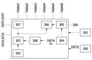
도 28 및 도 29를 참조하면, 표시장치는 화면 상에 픽셀 어레이가 배치된 표시 패널(100)과, 표시 패널 구동부 등을 포함할 수 있다.Referring to FIGS. 28 and 29 , the display device may include a
표시 패널(100)의 픽셀 어레이는 데이터 라인들(DL), 데이터 라인들(DL)과 교차되는 게이트 라인들(GL), 및 데이터 라인들(DL)과 게이트 라인들(GL)에 의해 정의된 매트릭스 형태로 배열된 픽셀들(P)을 포함할 수 있다.The pixel array of the
표시 패널(100)에서 입력 영상이 재현되는 화면은 제1 표시영역(DA) 및 제2 표시영역(CA)을 포함할 수 있다. 제2 표시영역(CA)은 전술한 바와 같이 복수 개의 센서가 배치된 영역일 수 있다. 또한, 센서의 종류에 따라 제1 표시영역(DA) 또는 제2 표시영역(CA)에 복수 개의 발광소자(61) 또는 수광소자(71)가 배치될 수 있다.A screen on which an input image is reproduced on the
제1 표시영역(DA)과 제2 표시영역(CA) 각각의 서브 픽셀들은 픽셀 회로를 포함할 수 있다. 픽셀 회로는 발광소자(OLED)에 전류를 공급하는 구동 소자, 구동 소자의 문턱 전압을 샘플링하고 픽셀 회로의 전류 패스(current path)를 스위칭하는 복수의 스위치 소자, 구동 소자의 게이트 전압을 유지하는 커패시터 등을 포함할 수 있다. 픽셀 회로는 발광소자의 아래에 배치될 수 있다.Sub-pixels of each of the first display area DA and the second display area CA may include a pixel circuit. The pixel circuit includes a driving element for supplying current to the light emitting element OLED, a plurality of switch elements for sampling the threshold voltage of the driving element and switching the current path of the pixel circuit, and a capacitor for maintaining the gate voltage of the driving element. etc. may be included. The pixel circuit may be disposed below the light emitting element.
제2 표시영역(CA)은 픽셀 그룹들 사이에 배치된 투광영역(TA)과, 제2 표시영역(CA) 아래에 배치된 복수 개의 센서를 포함할 수 있다. 카메라 모듈(400)은 촬상 모드에서 제2 표시영역(CA)을 통해 입사되는 빛을 이미지 센서를 이용하여 광전변환하고, 이미지 센서로부터 출력된 이미지의 픽셀 데이터를 디지털 데이터로 변환하여 촬상된 이미지 데이터를 출력할 수 있다.The second display area CA may include a light transmission area TA disposed between the pixel groups and a plurality of sensors disposed under the second display area CA. The
표시 패널 구동부는 입력 영상의 픽셀 데이터를 픽셀들(P)에 기입할 수 있다. 픽셀들(P)은 다수의 서브 픽셀들을 포함한 픽셀 그룹으로 해석될 수 있다.The display panel driver may write pixel data of an input image into the pixels P. Pixels P may be interpreted as a pixel group including a plurality of sub-pixels.
표시 패널 구동부는 픽셀 데이터의 데이터 전압을 데이터 라인들(DL)에 공급하는 데이터 구동부(306)와, 게이트 펄스를 게이트 라인들(GL)에 순차적으로 공급하는 게이트 구동부(120)를 포함할 수 있다. 데이터 구동부(306)는 드라이브 IC(300)에 집적될 수 있다. 표시 패널 구동부는 도면에서 생략된 터치센서 구동부를 더 포함할 수 있다.The display panel driver may include a
드라이브 IC(300)는 표시 패널(100) 상에 접착될 수 있다. 드라이브 IC(300)는 호스트 시스템(200)으로부터 입력 영상의 픽셀 데이터와 타이밍 신호를 입력 받아 픽셀들에 픽셀 데이터의 데이터 전압을 공급하고, 데이터 구동부(306)와 게이트 구동부(120)를 동기시킨다.The
드라이브 IC(300)는 데이터 출력 채널들을 통해 데이터 라인들(DL)에 연결되어 데이터 라인들(DL)에 픽셀 데이터의 데이터 전압을 공급할 수 있다. 드라이브 IC(300)는 게이트 타이밍 신호 출력 채널들을 통해 게이트 구동부(120)를 제어하기 위한 게이트 타이밍 신호를 출력할 수 있다.The
타이밍 콘트롤러(303)로부터 발생된 게이트 타이밍 신호는 스타트 펄스(Gate start pulse, VST), 시프트 클럭(Gate shift clock, CLK) 등을 포함할 수 있다. 스타트 펄스(VST)와 시프트 클럭(CLK)은 게이트 온 전압(VGL)과 게이트 오프 전압(VGH) 사이에서 스윙(swing)할 수 있다.The gate timing signal generated from the
레벨 시프터(307)로부터 출력된 게이트 타이밍 신호(VST, CLK)는 게이트 구동부(120)에 인가되어 게이트 구동부(120)의 시프트 동작을 제어할 수 있다.The gate timing signals VST and CLK output from the
게이트 구동부(120)는 픽셀 어레이와 함께 표시 패널(100)의 회로층에 형성되는 시프트 레지스터(shift register)를 포함할 수 있다. 게이트 구동부(120)의 시프트 레지스터는 타이밍 콘트롤러의 제어 하에 게이트 신호를 게이트 라인들(GL)에 순차적으로 공급할 수 있다. 게이트 신호는 스캔 펄스와, 발광 신호의 EM 펄스를 포함할 수 있다.The
시프트 레지스터는 스캔 펄스를 출력하는 스캔 구동부와, EM 펄스를 출력하는 EM 구동부를 포함할 수 있다. 도 29에서 GVST와 GCLK은 스캔 구동부에 입력되는 게이트 타이밍 신호이다. EVST와 ECLK은 EM 구동부에 입력되는 게이트 타이밍 신호이다.The shift register may include a scan driver that outputs scan pulses and an EM driver that outputs EM pulses. 29, GVST and GCLK are gate timing signals input to the scan driver. EVST and ECLK are gate timing signals input to the EM driver.
드라이브 IC(300)는 호스트 시스템(200), 제1 메모리(301), 및 표시 패널(100)에 연결될 수 있다. 드라이브 IC(300)는 데이터 수신 및 연산부(308), 타이밍 콘트롤러(303), 데이터 구동부(306), 감마 보상전압 발생부(305), 전원부(304), 제2 메모리(302) 등을 포함할 수 있다.The
데이터 수신 및 연산부(308)는 호스트 시스템(200)으로부터 디지털 신호로 입력된 픽셀 데이터를 수신하는 수신부와, 수신부를 통해 입력된 픽셀 데이터를 처리하여 화질을 향상시키는 데이터 연산부를 포함할 수 있다.The data reception and
데이터 연산부는 압축된 픽셀 데이터를 디코딩(Decoding)하여 복원하는 데이터 복원부와, 미리 설정된 광학 보상값을 픽셀 데이터에 더하는 광학 보상부 등을 포함할 수 있다. 광학 보상값은 제조 공정에서 촬영된 카메라 영상을 바탕으로 측정된 화면의 휘도를 바탕으로 픽셀 데이터 각각의 휘도를 보정하기 위한 값으로 설정될 수 있다.The data operation unit may include a data restoration unit that decodes and restores the compressed pixel data, and an optical compensation unit that adds a preset optical compensation value to the pixel data. The optical compensation value may be set as a value for correcting the luminance of each pixel data based on the luminance of the screen measured based on the camera image captured in the manufacturing process.
타이밍 콘트롤러(303)는 호스트 시스템(200)으로부터 수신되는 입력 영상의 픽셀 데이터를 데이터 구동부(306)에 제공할 수 있다. 타이밍 콘트롤러(303)는 게이트 구동부(120)를 제어하기 위한 게이트 타이밍 신호와, 데이터 구동부(306)를 제어하기 위한 소스 타이밍 신호를 발생하여 게이트 구동부(120)와 데이터 구동부(306)의 동작 타이밍을 제어할 수 있다.The
데이터 구동부(306)는 디지털-아날로그 변환기(Digital to Analog converter, DAC)를 통해 타이밍 콘트롤러(303)로부터 수신된 픽셀 데이터를 포함한 디지털 데이터를 감마 보상전압으로 변환하여 데이터 전압을 출력할 수 있다. 데이터 구동부(306)로부터 출력된 데이터 전압은 드라이브 IC(300)의 데이터 채널에 연결된 출력 버퍼를 통해 픽셀 어레이의 데이터 라인들(DL)에 공급될 수 있다.The
감마 보상전압 발생부(305)는 전원부(304)로부터의 감마 기준 전압을 분압 회로를 통해 분압하여 계조별 감마 보상전압을 발생할 수 있다. 감마 보상전압은 픽셀 데이터의 계조별로 전압이 설정된 아날로그 전압이다. 감마 보상전압 발생부(305)로부터 출력된 감마 보상전압은 데이터 구동부(306)에 제공될 수 있다.The gamma
전원부(304)는 직류-직류 변환기(DC-DC Converter)를 이용하여 표시 패널(100)의 픽셀 어레이, 게이트 구동부(120), 및 드라이브 IC(300)의 구동에 필요한 전원을 발생할 수 있다. 직류-직류 변환기는 차지 펌프(Charge pump), 레귤레이터(Regulator), 벅 변환기(Buck Converter), 부스트 변환기(Boost Converter) 등을 포함할 수 있다.The
전원부(304)는 호스트 시스템(200)으로부터의 직류 입력 전압을 조정하여 감마 기준 전압, 게이트 온 전압(VGL). 게이트 오프 전압(VGH), 픽셀 구동전압(VDD), 저전위 전원 전압(VSS), 초기화 전압(Vini) 등의 직류 전원을 발생할 수 있다.The
감마 기준 전압은 감마 보상전압 발생부(305)에 공급될 수 있다. 게이트 온 전압(VGL)과 게이트 오프 전압(VGH)은 레벨 시프터(307)와 게이트 구동부(120)에 공급될 수 있다. 픽셀 구동전압(VDD), 저전위 전원 전압(VSS), 초기화 전압(Vini) 등의 픽셀 전원은 픽셀들(P)에 공통으로 공급될 수 있다.The gamma reference voltage may be supplied to the gamma
초기화 전압(Vini)은 픽셀 구동전압(VDD)보다 낮고 발광소자(OLED)의 문턱 전압 보다 낮은 직류 전압으로 설정되어 픽셀 회로들의 주요 노드들을 초기화하고, 발광소자(OLED)의 발광을 억제할 수 있다.The initialization voltage Vini is set to a direct current voltage that is lower than the pixel driving voltage VDD and lower than the threshold voltage of the light emitting element OLED to initialize main nodes of the pixel circuits and suppress light emission of the light emitting element OLED. .
제2 메모리(302)는 드라이브 IC(300)에 전원이 입력될 때 제1 메모리(301)로부터 수신된 보상값, 레지스터 설정 데이터 등을 저장할 수 있다.The
보상값은 화질 향상을 한 다양한 알고리즘에 적용될 수 있다. 보상값은 광학 보상값을 포함할 수 있다. 레지스터 설정 데이터는 데이터 구동부(306), 타이밍 콘트롤러(303), 감마 보상전압 발생부(305) 등의 동작을 정의할 수 있다. 제1 메모리(301)는 플래시 메모리(Flash memory)를 포함할 수 있다. 제2 메모리(302)는 SRAM(Static RAM)을 포함할 수 있다.The compensation value may be applied to various algorithms that improve image quality. The compensation value may include an optical compensation value. The register setting data may define operations of the
호스트 시스템(200)은 AP(Application Processor)로 구현될 수 있다. 호스트 시스템(200)은 MIPI(Mobile Industry Processor Interface)를 통해 드라이브 IC(300)에 입력 영상의 픽셀 데이터를 전송할 수 있다. 호스트 시스템(200)은 가요성 인쇄 회로 예를 들면, FPC(Flexible Printed Circuit)를 통해 드라이브 IC(300)에 연결될 수 있다.The
한편, 표시 패널은 플렉시블 디스플레이에 적용 가능한 플렉시블 패널로 구현될 수 있다. 플렉시블 디스플레이는 플렉시블 패널을 감거나 접고 구부리는 방법으로 화면의 크기가 가변될 수 있고 다양한 디자인으로 쉽게 제작될 수 있다.Meanwhile, the display panel may be implemented as a flexible panel applicable to a flexible display. A flexible display can have a variable screen size and can be easily manufactured in various designs by winding, folding, or bending a flexible panel.
플렉시블 디스플레이는 롤러블 디스플레이(rollable display), 폴더블 디스플레이(foldable display), 벤더블(bendable) 디스플레이, 슬라이더블 디스플레이(slidable display) 등으로 구현될 수 있다.The flexible display may be implemented as a rollable display, a foldable display, a bendable display, a slidable display, and the like.
플렉시블 패널은 소위 “플라스틱 OLED 패널”로 제작될 수 있다. 플라스틱 OLED 패널은 백 플레이트(Back plate)와, 그 백 플레이트 상에 접착된 유기 박막 필름 상에 픽셀 어레이를 포함할 수 있다. 픽셀 어레이 위에 터치 센서 어레이가 형성될 수 있다.Flexible panels can be made of so-called “plastic OLED panels”. A plastic OLED panel may include a pixel array on a back plate and an organic thin film adhered on the back plate. A touch sensor array may be formed over the pixel array.
백 플레이트는 PET(Polyethylene terephthalate) 기판일 수 있다. 유기 박막 필름 상에 픽셀 어레이와 터치 센서 어레이가 형성될 수 있다. 백 플레이트는 픽셀 어레이가 습도에 노출되지 않도록 유기 박막 필름을 향하는 투습을 차단할 수 있다.The back plate may be a polyethylene terephthalate (PET) substrate. A pixel array and a touch sensor array may be formed on the organic thin film. The back plate may block moisture permeation toward the organic thin film so that the pixel array is not exposed to humidity.
유기 박막 필름은 PI(Polyimide) 기판일 수 있다. 유기 박막 필름 상에 도시하지 않은 절연 물질로 다층의 버퍼막이 형성될 수 있다. 유기 박막 필름 상에 회로층(12)과 소자층(14)이 적층될 수 있다.The organic thin film may be a polyimide (PI) substrate. A multi-layered buffer film may be formed on the organic thin film with an insulating material (not shown). The
본 발명의 표시장치에서 회로층(12)에 배치된 픽셀 회로와 게이트 구동부 등은 복수의 트랜지스터들을 포함할 수 있다. 트랜지스터들은 산화물 반도체를 포함한 Oxide TFT(Thin Film Transistor), 저온 폴리 실리콘(Low Temperature Poly Silicon, LTPS)을 포함한 LTPS TFT 등으로 구현될 수 있다. 트랜지스터들 각각은 p 채널 TFT 또는 n 채널 TFT로 구현될 수 있다. 실시예에서 픽셀 회로의 트랜지스터들이 p 채널 TFT로 구현된 예를 중심으로 설명되지만 본 발명은 이에 한정되지 않는다.In the display device of the present invention, the pixel circuit and the gate driver disposed on the
트랜지스터는 게이트(gate), 소스(source) 및 드레인(drain)을 포함한 3 전극 소자이다. 소스는 캐리어(carrier)를 트랜지스터에 공급하는 전극이다. 트랜지스터 내에서 캐리어는 소스로부터 흐르기 시작할 수 있다. 드레인은 트랜지스터에서 캐리어가 외부로 나가는 전극이다.A transistor is a three-electrode device including a gate, a source, and a drain. The source is an electrode that supplies a carrier to the transistor. Within a transistor, carriers can start flowing from a source. The drain is an electrode through which carriers exit the transistor.
트랜지스터에서 캐리어의 흐름은 소스로부터 드레인으로 흐른다. n 채널 트랜지스터의 경우, 캐리어가 전자(electron)이기 때문에 소스로부터 드레인으로 전자가 흐를 수 있도록 소스 전압이 드레인 전압보다 낮은 전압을 가진다. n 채널 트랜지스터에서 전류의 방향은 드레인으로부터 소스 쪽으로 흐른다.The flow of carriers in a transistor flows from the source to the drain. In the case of an n-channel transistor, since carriers are electrons, the source voltage has a voltage lower than the drain voltage so that electrons can flow from the source to the drain. The direction of current in an n-channel transistor is from drain to source.
p 채널 트랜지스터(PMOS)의 경우, 캐리어가 정공(hole)이기 때문에 소스로부터 드레인으로 정공이 흐를 수 있도록 소스 전압이 드레인 전압보다 높다. p 채널 트랜지스터에서 정공이 소스로부터 드레인 쪽으로 흐르기 때문에 전류가 소스로부터 드레인 쪽으로 흐른다. 트랜지스터의 소스와 드레인은 고정된 것이 아니라는 것에 주의하여야 한다. 예컨대, 소스와 드레인은 인가 전압에 따라 변경될 수 있다. 따라서, 트랜지스터의 소스와 드레인으로 인하여 발명이 제한되지 않는다. 이하의 설명에서 트랜지스터의 소스와 드레인을 제1 및 제2 전극으로 칭하기로 한다.In the case of a p-channel transistor (PMOS), since the carrier is a hole, the source voltage is higher than the drain voltage so that holes can flow from the source to the drain. In a p-channel transistor, current flows from the source to the drain because holes flow from the source to the drain. It should be noted that the source and drain of a transistor are not fixed. For example, the source and drain may change depending on the applied voltage. Therefore, the invention is not limited by the source and drain of the transistor. In the following description, the source and drain of the transistor will be referred to as first and second electrodes.
게이트 펄스는 게이트 온 전압(Gate On Voltage)과 게이트 오프 전압(Gate Off Voltage) 사이에서 스윙(swing)할 수 있다. 게이트 온 전압은 트랜지스터의 문턱 전압 보다 높은 전압으로 설정되며, 게이트 오프 전압은 트랜지스터의 문턱 전압 보다 낮은 전압으로 설정될 수 있다.The gate pulse can swing between a Gate On Voltage and a Gate Off Voltage. The gate-on voltage may be set to a voltage higher than the threshold voltage of the transistor, and the gate-off voltage may be set to a voltage lower than the threshold voltage of the transistor.
트랜지스터는 게이트 온 전압에 응답하여 턴온(turn-on)되는 반면, 게이트 오프 전압에 응답하여 턴오프(turn-off)될 수 있다. n 채널 트랜지스터의 경우에, 게이트 온 전압은 게이트 하이 전압(Gate High Voltage, VGH)이고, 게이트 오프 전압은 게이트 로우 전압(Gate Low Voltage, VGL)일 수 있다. p 채널 트랜지스터의 경우에, 게이트 온 전압은 게이트 로우 전압(VGL)이고, 게이트 오프 전압은 게이트 하이 전압(VGH)일 수 있다.A transistor may be turned on in response to a gate-on voltage, while turned off in response to a gate-off voltage. In the case of an n-channel transistor, the gate-on voltage may be a gate high voltage (VGH), and the gate-off voltage may be a gate low voltage (VGL). In the case of a p-channel transistor, the gate-on voltage may be the gate low voltage (VGL) and the gate-off voltage may be the gate high voltage (VGH).
픽셀 회로의 구동 소자는 트랜지스터로 구현될 수 있다. 구동 소자는 모든 픽셀들 간에 그 전기적 특성이 균일하여야 하지만 공정 편차와 소자 특성 편차로 인하여 픽셀들 간에 차이가 있을 수 있고 디스플레이 구동 시간의 경과에 따라 변할 수 있다.A driving element of the pixel circuit may be implemented as a transistor. The electrical characteristics of the driving element should be uniform among all pixels, but there may be differences between the pixels due to process variation and element characteristic variation, and may change according to the lapse of display driving time.
이러한 구동 소자의 전기적 특성 편차를 보상하기 위해, 표시장치는 내부 보상 회로와 외부 보상 회로를 포함할 수 있다. 내부 보상 회로는 서브 픽셀들 각각에서 픽셀 회로에 추가되어 구동 소자의 전기적 특성에 따라 변하는 구동 소자의 문턱 전압(Vth) 및/또는 이동도(μ)를 샘플링하고 그 변화를 실시간 보상할 수 있다.In order to compensate for the variation in electrical characteristics of the driving element, the display device may include an internal compensation circuit and an external compensation circuit. An internal compensation circuit may be added to the pixel circuit in each of the sub-pixels to sample the threshold voltage (Vth) and/or mobility (μ) of the driving element, which varies according to the electrical characteristics of the driving element, and compensate for the change in real time.
외부 보상 회로는 서브 픽셀들 각각에 연결된 센싱 라인을 통해 센싱된 구동 소자의 문턱 전압 및/또는 이동도를 외부의 보상부로 전송할 수 있다. 외부 보상 회로의 보상부는 센싱 결과를 반영하여 입력 영상의 픽셀 데이터를 변조함으로써 구동 소자의 전기적 특성 변화를 보상할 수 있다.The external compensation circuit may transmit the threshold voltage and/or mobility of the driving element sensed through the sensing line connected to each of the subpixels to an external compensation unit. The compensation unit of the external compensation circuit may compensate for a change in electrical characteristics of the driving element by modulating pixel data of an input image by reflecting a sensing result.
외부 보상 구동 소자의 전기적 특성에 따라 변하는 픽셀의 전압을 센싱하고, 센싱된 전압을 바탕으로 외부 회로에서 입력 영상의 데이터를 변조함으로써 픽셀들 간 구동 소자의 전기적 특성 편차를 보상할 수 있다.A deviation in electrical characteristics of the driving element between pixels may be compensated for by sensing a voltage of a pixel that varies according to electrical characteristics of the external compensation driving element and modulating data of an input image in an external circuit based on the sensed voltage.
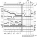
도 30은 본 발명의 일 실시예에 따른 표시 패널에서 픽셀 영역의 단면 구조를 상세히 보여주는 단면도이다. 도 31은 본 발명의 일 실시예에 따른 픽셀 영역 및 투광영역의 단면 구조이다. 도 32는 도 31의 제1 변형예이다. 도 33은도 31의 제2 변형예이다.30 is a cross-sectional view showing in detail a cross-sectional structure of a pixel area in a display panel according to an exemplary embodiment. 31 is a cross-sectional structure of a pixel area and a light transmission area according to an embodiment of the present invention. FIG. 32 is a first modified example of FIG. 31 . FIG. 33 is a second modified example of FIG. 31 .
도 30에서 TFT는 픽셀 회로의 구동 소자(DT)를 나타낸다.In FIG. 30 , TFT represents the driving element DT of the pixel circuit.
도 30을 참조하면, 픽셀 영역(PIX)에서 회로층, 소자층 등이 기판(PI1, PI2) 상에 적층될 수 있다. 기판(PI1, PI2)은 제1 PI 기판(PI1) 및 제2 PI 기판(PI2)을 포함할 수 있다. 제1 PI 기판(PI1)과 제2 PI 기판(PI2) 사이에 무기막(IPD)이 형성될 수 있다. 무기막(IPD)은 수분 침투를 차단할 수 있다.Referring to FIG. 30 , in the pixel area PIX, circuit layers and device layers may be stacked on substrates PI1 and PI2. The substrates PI1 and PI2 may include a first PI substrate PI1 and a second PI substrate PI2. An inorganic layer IPD may be formed between the first PI substrate PI1 and the second PI substrate PI2. An inorganic film (IPD) can block moisture permeation.
제1 버퍼층(BUF1)은 제2 PI 기판(PI2) 상에 형성될 수 있다. 제1 버퍼층(BUF1) 상에 제1 금속층이 형성될 수 있고, 제1 금속층 상에 제2 버퍼층(BUF2)이 형성될 수 있다.The first buffer layer BUF1 may be formed on the second PI substrate PI2. A first metal layer may be formed on the first buffer layer BUF1, and a second buffer layer BUF2 may be formed on the first metal layer.
제1 금속층은 포토리소그래피(Photolithography) 공정에서 패터닝될 수 있다. 제1 금속층은 광쉴드 패턴(light shield pattern, BSM)을 포함할 수 있다. 광쉴드 패턴(BSM)은 TFT의 액티브층에 빛이 조사되지 않도록 외부 광을 차단하여 픽셀 영역에 형성된 TFT의 광전류(photo current)를 방지할 수 있다.The first metal layer may be patterned in a photolithography process. The first metal layer may include a light shield pattern (BSM). The light shield pattern BSM blocks external light so that light is not irradiated to the active layer of the TFT, thereby preventing photo current of the TFT formed in the pixel area.
광쉴드 패턴(BSM)은 제2 표시영역(CA)에서 제거되어야 할 금속층(예: 캐소드 전극)에 비하여 레이저 어블레이션 공정에서 이용되는 레이저 파장의 흡수 계수가 낮은 금속으로 형성되면, 광쉴드 패턴(BSM)은 레이저 어블레이션 공정에서 레이저 빔(LB)을 차단하는 광쉴드 층(LS)의 역할을 겸할 수 있다.When the light shield pattern BSM is formed of a metal having a lower absorption coefficient of the laser wavelength used in the laser ablation process than a metal layer (eg, a cathode electrode) to be removed from the second display area CA, the light shield pattern ( BSM) may serve as a light shield layer LS that blocks the laser beam LB in the laser ablation process.
제1 및 제2 버퍼층(BUF1, BUF2) 각각은 무기 절연재료로 형성되고, 하나 이상의 절연층으로 이루어질 수 있다.Each of the first and second buffer layers BUF1 and BUF2 is made of an inorganic insulating material and may include one or more insulating layers.
액티브층(ACT)은 제2 버퍼층(BUF2) 상에 증착되는 반도체 물질로 형성되고 포토-리소그래피 공정에 의해 패터닝될 수 있다. 액티브층(ACT)은 픽셀 회로의 TFT들과 게이트 구동부의 TFT 각각의 액티브 패턴을 포함할 수 있다. 액티브층(ACT)은 이온 도핑에 의해 일 부분이 금속화될 수 있다. 금속화된 부분은 픽셀 회로의 일부 노드에서 금속층들을 연결하는 점퍼 패턴(jumper pattern)으로 이용되어 픽셀 회로의 구성 요소들을 연결할 수 있다.The active layer ACT may be formed of a semiconductor material deposited on the second buffer layer BUF2 and patterned through a photo-lithography process. The active layer ACT may include active patterns of TFTs of the pixel circuit and TFTs of the gate driver. A portion of the active layer ACT may be metalized by ion doping. The metalized portion may be used as a jumper pattern connecting metal layers at some nodes of the pixel circuit to connect components of the pixel circuit.
게이트 절연층(GI)은 액티브층(ACT)을 덮도록 제2 버퍼층(BUF2) 상에 형성될 수 있다. 게이트 절연층(GI)은 무기 절연재료로 이루어질 수 있다.A gate insulating layer GI may be formed on the second buffer layer BUF2 to cover the active layer ACT. The gate insulating layer GI may be made of an inorganic insulating material.
제2 금속층은 제2 게이트 절연층(GI) 상에 형성될 수 있다. 제2 금속층은 포토-리소그래피 공정에 의해 패터닝될 수 있다. 제2 금속층은 게이트 라인 및 게이트 전극 패턴(GATE), 스토리지 커패시터(Cst1)의 하부 전극, 제1 금속층과 제3 금속층의 패턴을 연결하는 점퍼 패턴 등을 포함할 수 있다.The second metal layer may be formed on the second gate insulating layer GI. The second metal layer may be patterned by a photo-lithography process. The second metal layer may include a gate line and gate electrode pattern GATE, a lower electrode of the storage capacitor Cst1, and a jumper pattern connecting patterns of the first metal layer and the third metal layer.
제1 층간 절연층(ILD1)은 제2 금속층을 덮도록 게이트 절연층(GI) 상에 형성될 수 있다. 제1 층간 절연층(ILD2) 상에 제3 금속층이 형성되고, 제2 층간 절연층(ILD2)이 제3 금속층을 덮을 수 있다. 제3 금속층은 포토-리소그래피 공정에 의해 패터닝될 수 있다. 제3 금속층은 스토리지 커패시터(Cst1)의 상부 전극과 같은 금속 패턴들(TM)을 포함할 수 있다. 제1 및 제2 층간 절연층들(ILD1, ILD2)은 무기 절연재료를 포함할 수 있다.The first interlayer insulating layer ILD1 may be formed on the gate insulating layer GI to cover the second metal layer. A third metal layer may be formed on the first interlayer insulating layer ILD2, and the second interlayer insulating layer ILD2 may cover the third metal layer. The third metal layer may be patterned by a photo-lithography process. The third metal layer may include the same metal patterns TM as the upper electrode of the storage capacitor Cst1. The first and second interlayer insulating layers ILD1 and ILD2 may include an inorganic insulating material.
제2 층간 절연층(ILD2) 상에 제4 금속층이 형성되고, 그 위에 무기 절연층(PAS1)과 제1 평탄화층(PLN1)이 적층될 수 있다. 제5 금속층이 제1 평탄화층(PLN1) 상에 형성될 수 있다.A fourth metal layer may be formed on the second interlayer insulating layer ILD2 , and an inorganic insulating layer PAS1 and a first planarization layer PLN1 may be stacked thereon. A fifth metal layer may be formed on the first planarization layer PLN1.
제4 금속층의 일부 패턴은 제1 평탄화층(PLN1)과 무기 절연층(PAS1)을 관통하는 콘택홀(Contact hole)을 통해 제3 금속층에 연결될 수 있다. 제1 및 제2 평탄화층(PLN1, PLN2)은 표면을 평탄하게 하는 유기 절연재료로 이루어질 수 있다.Part of the pattern of the fourth metal layer may be connected to the third metal layer through a contact hole passing through the first planarization layer PLN1 and the inorganic insulating layer PAS1. The first and second planarization layers PLN1 and PLN2 may be formed of an organic insulating material for flattening surfaces.
제4 금속층은 제2 층간 절연층(ILD2)을 관통하는 콘택홀을 통해 TFT의 액티브 패턴에 연결되는 TFT의 제1 및 제2 전극을 포함할 수 있다. 데이터 라인(DL)과, 전원 배선들은 제4 금속층의 패턴(SD1) 또는 제5 금속층의 패턴(SD2)으로 구현될 수 있다.The fourth metal layer may include first and second electrodes of the TFT connected to the active pattern of the TFT through the contact hole penetrating the second interlayer insulating layer ILD2 . The data line DL and the power lines may be implemented as a pattern SD1 of the fourth metal layer or a pattern SD2 of the fifth metal layer.
발광소자(OLED)의 제1 전극층인 애노드 전극(AND)은 제2 평탄화층(PLN2) 상에 형성될 수 있다. 애노드 전극(AND)은 제2 평탄화층(PLN2)을 관통하는 콘택홀을 통해 스위치 소자 또는 구동 소자로 이용되는 TFT의 전극에 연결될 수 있다. 애노드 전극(AND)은 투명 또는 반투명 전극 물질로 이루어질 수 있다.The anode electrode AND, which is the first electrode layer of the light emitting device OLED, may be formed on the second planarization layer PLN2. The anode electrode AND may be connected to an electrode of a TFT used as a switch element or a driving element through a contact hole penetrating the second planarization layer PLN2 . The anode electrode AND may be made of a transparent or translucent electrode material.
픽셀 정의막(BNK)은 발광소자(OLED)의 애노드 전극(AND)을 덮을 수 있다. 픽셀 정의막(BNK)은 픽셀들 각각에서 외부로 빛이 통과되는 발광 영역(또는 개구 영역)을 정의하는 패턴으로 형성될 수 있다. 픽셀 정의막(BNK) 상에 스페이서(SPC)가 형성될 수 있다. 픽셀 정의막(BNK)과 스페이서(SPC)는 동일한 유기 절연 재료로 일체화될 수 있다. 스페이서(SPC)는 유기 화합물(EL)의 증착 공정에서 FMM(Fine Metal Mask)이 애노드 전극(AND)과 접촉되지 않도록 FMM과 애노드 전극(AND) 사이의 갭(gap)을 확보할 수 있다.The pixel defining layer BNK may cover the anode electrode AND of the light emitting element OLED. The pixel-defining layer BNK may be formed in a pattern defining an emission area (or an opening area) through which light passes from each pixel to the outside. A spacer SPC may be formed on the pixel definition layer BNK. The pixel definition layer BNK and the spacer SPC may be integrated with the same organic insulating material. The spacer SPC may secure a gap between the FMM and the anode electrode AND so that the fine metal mask (FMM) does not come into contact with the anode electrode AND during the deposition process of the organic compound EL.
픽셀 정의막(BNK)에 의해 정의된 픽셀들 각각의 발광 영역에 유기 화합물(EL)이 형성될 수 있다. 발광소자(OLED)의 제2 전극층인 캐소드 전극(CAT)은 픽셀 정의막(BNK), 스페이서(SPC), 및 유기 화합물(EL)을 덮도록 표시 패널(100)의 전면에 형성될 수 있다. 캐소드 전극(CAT)은 그 하부의 금속층들 중 어느 하나로 형성된 VSS 라인(PL3)에 연결될 수 있다. 캡핑층(CPL)은 캐소드 전극(CAT)을 덮을 수 있다. 캡핑층(CPL)은 무기 절연재료로 형성되어 공기(air)와 캡핑층(CPL) 상에 도포되는 유기 절연재료의 아웃 개싱(out gassing)의 침투를 차단하여 캐소드 전극(CAT)을 보호할 수 있다. 무기 절연층(PAS2)이 캡핑층(CPL)을 덮고, 무기 절연층(PAS2) 상에 평탄화층(PCL)이 형성될 수 있다. 평탄화층(PCL)은 유기 절연 재료를 포함할 수 있다. 봉지층의 무기 절연층(PAS3)이 평탄화층(PCL) 상에 형성될 수 있다.An organic compound EL may be formed in an emission area of each of the pixels defined by the pixel defining layer BNK. The cathode electrode CAT, which is the second electrode layer of the light emitting device OLED, may be formed on the entire surface of the
편광판(18)은 무기 절연층(PAS3) 상에 배치되어 표시장치의 야외 시인성을 개선할 수 있다. 편광판(18)은 표시 패널(100)의 표면으로부터 반사되는 빛을 줄이고, 회로층(12)의 금속으로부터 반사되는 빛을 차단하여 픽셀들의 밝기를 향상시킬 수 있다.The
도 31을 참조하면, 투광영역(TA)에서 편광판(18)은 제1 투광 패턴(18d)이 형성될 수 있다. 제1 투광 패턴(18d)은 레이저에 의해 편광자(18b)가 변색되어 형성될 수도 있고, 편광자(18b)가 일부 제거되어 형성될 수도 있다.Referring to FIG. 31 , a first light-transmitting
투광영역(TA)에서 캐소드 전극(CAT)은 개구부(H1)가 형성될 수 있다. 이러한 개구부(H1)는 픽셀 정의막(BNK) 상에 캐소드 전극(CAT)을 형성한 후 캐소드 전극(CAT)과 픽셀 정의막(BNK)을 한번에 식각하여 형성할 수 있다. 따라서, 픽셀 정의막(BNK)은 제1 홈(RC1)이 형성되고 제1 홈(RC1) 상에는 캐소드 전극(CAT)의 개구부(H1)가 형성될 수 있다. 그러나 반드시 이에 한정되는 것은 아니고 투광영역(TA)에는 픽셀 정의막이 형성되지 않고 캐소드 전극(CAT)은 제2 평탄화층(PLN2) 상에 배치될 수도 있다.An opening H1 may be formed in the cathode electrode CAT in the light transmission area TA. The opening H1 may be formed by forming the cathode electrode CAT on the pixel defining layer BNK and then etching the cathode electrode CAT and the pixel defining layer BNK at once. Accordingly, the pixel-defining layer BNK may have a first groove RC1 and an opening H1 of the cathode electrode CAT may be formed on the first groove RC1. However, it is not necessarily limited thereto, and the pixel defining layer may not be formed in the transmissive area TA, and the cathode electrode CAT may be disposed on the second planarization layer PLN2.
투광영역(TA)에서 편광판(18)은 제1 투광 패턴(18d)이 형성되고 캐소드 전극은 개구부(H1)가 형성되므로 광 투과율이 향상될 수 있다. 따라서, 복수 개의 발광소자(61)에서 출사된 광은 외부로 유효하게 출사되어 도트 이미지를 구현할 수 있다. 또한, 도 32와 같이 투광영역(TA) 상에 복수 개의 수광소자(71)가 배치된 경우 복수 개의 수광소자(71)에 반사광이 충분히 유입되어 3차원 특징맵을 생성하기 충분한 광 데이터를 획득할 수 있다. 도 33을 참조하면, 투광영역(TA) 상에 복수 개의 발광소자(61)와 복수 개의 수광소자(71)가 배치된 경우 발광소자(61)에서 출사된 광은 외부로 유효하게 출사되어 도트 이미지를 구현할 수 있으며, 복수 개의 수광소자(71)에 반사광이 충분히 유입되어 3차원 특징맵을 생성하기 충분한 광 데이터를 획득할 수 있다.In the light transmission area TA, since the first
Claims (19)
Translated fromKorean광을 조사하는 복수 개의 발광소자를 포함하는 발광모듈; 및
반사광을 수신하는 수광모듈을 포함하고,
상기 복수 개의 발광소자는 상기 복수 개의 픽셀 사이에 분산 배치되는 표시 장치.a display panel including a plurality of pixels;
A light emitting module including a plurality of light emitting elements for irradiating light; and
A light receiving module for receiving reflected light;
The plurality of light emitting elements are distributed among the plurality of pixels.
상기 표시 패널의 상부에 배치되는 커버 글라스를 포함하고,
상기 커버 글라스는 상기 복수 개의 발광소자와 수직 방향으로 중첩되는 복수 개의 회절패턴을 포함하는 표시 장치.According to claim 1,
a cover glass disposed above the display panel;
The cover glass includes a plurality of diffraction patterns overlapping the plurality of light emitting elements in a vertical direction.
상기 복수 개의 발광소자와 상기 복수 개의 회절패턴 사이에 배치되는 복수 개의 제1 렌즈를 포함하는 표시 장치.According to claim 2,
A display device comprising a plurality of first lenses disposed between the plurality of light emitting elements and the plurality of diffraction patterns.
상기 복수 개의 발광소자는 상기 표시 패널의 하부에 배치되는 표시 장치.According to claim 1,
The plurality of light emitting elements are disposed below the display panel.
상기 복수 개의 발광소자는 수직 공동 표면 방출 레이저를 포함하는 표시 장치.According to claim 1,
The plurality of light emitting elements include vertical cavity surface emitting lasers.
상기 복수 개의 픽셀이 배치되는 픽셀 영역은,
기판 상에 배치된 회로층;
상기 회로층 상에 배치되는 제1 전극층;
상기 제1 전극층 상에 배치되는 소자층; 및
상기 소자층 상에 배치되는 제2 전극층을 포함하는 표시 장치.According to claim 1,
A pixel area in which the plurality of pixels are disposed,
a circuit layer disposed on the substrate;
a first electrode layer disposed on the circuit layer;
an element layer disposed on the first electrode layer; and
A display device comprising a second electrode layer disposed on the element layer.
상기 복수 개의 발광소자는 상기 제2 전극층 상에 배치되는 표시 장치.According to claim 6,
The plurality of light emitting elements are disposed on the second electrode layer.
상기 복수 개의 발광소자는 상기 제1 전극층과 상기 제2 전극층 사이에 배치되는 표시 장치.According to claim 6,
The plurality of light emitting elements are disposed between the first electrode layer and the second electrode layer.
상기 표시 패널은,
복수 개의 제1 픽셀이 배치되는 제1 표시영역; 및
복수 개의 제2 픽셀이 배치되는 픽셀 영역 및 상기 복수 개의 제2 픽셀 사이에 배치되는 복수 개의 투광 영역을 포함하는 제2 표시영역을 포함하고,
상기 복수 개의 발광소자는 상기 제2 표시영역에 배치되는 표시 장치.According to claim 1,
The display panel,
a first display area in which a plurality of first pixels are disposed; and
a second display area including a pixel area in which a plurality of second pixels are disposed and a plurality of light-transmitting areas disposed between the plurality of second pixels;
The plurality of light emitting elements are disposed in the second display area.
상기 복수 개의 발광소자에서 방출된 광은 상기 회절패턴을 통과하여 0차빔과 1차빔으로 분리되고,
상기 복수 개의 수광소자는 상기 1차빔을 수신하는 표시 장치.According to claim 2,
The light emitted from the plurality of light emitting devices passes through the diffraction pattern and is separated into a 0-order beam and a 1-order beam,
The plurality of light-receiving elements receive the primary beam.
상기 0차빔과 상기 1차빔의 회절 비율은 1:2 내지 1:7인 표시 장치.According to claim 10,
The diffraction ratio of the 0th-order beam and the 1st-order beam is 1:2 to 1:7.
광을 조사하는 발광모듈; 및
반사광을 수신하는 복수 개의 수광소자를 포함하는 수광모듈을 포함하고,
상기 복수 개의 수광소자는 상기 복수 개의 픽셀 사이에 분산 배치되는 표시 장치.a display panel including a plurality of pixels;
A light emitting module for irradiating light; and
A light receiving module including a plurality of light receiving elements for receiving reflected light;
The plurality of light receiving elements are distributed among the plurality of pixels.
상기 복수 개의 수광소자는 상기 표시 패널의 하부에 배치되고,
상기 표시 패널은 상기 복수 개의 수광소자와 배치되는 영역에 투광 영역이 형성되는 표시 장치.According to claim 12,
The plurality of light receiving elements are disposed under the display panel,
The display device of claim 1 , wherein the display panel has a light transmission area formed in an area disposed with the plurality of light receiving elements.
상기 표시 패널과 복수 개의 수광소자 사이에 배치되는 제2 렌즈를 포함하는 표시 장치.According to claim 12,
A display device comprising a second lens disposed between the display panel and a plurality of light receiving elements.
상기 수광소자와 상기 제2 렌즈의 중심을 연결한 광축은 수직 방향으로 기준으로 기울어진 표시 장치.According to claim 14,
The display device of claim 1 , wherein an optical axis connecting the light receiving element and the center of the second lens is tilted with respect to a vertical direction.
상기 수광소자와 상기 제2 렌즈의 중심을 연결한 광축은 상기 표시 패널의 중심을 향해 기울어진 표시 장치.According to claim 14,
An optical axis connecting the light receiving element and the center of the second lens is tilted toward the center of the display panel.
상기 복수 개의 수광소자는 복수 개의 센싱그룹으로 분할되고,
상기 복수 개의 센싱그룹과 각각 연결되는 복수 개의 센싱 회로를 포함하는 표시 장치.According to claim 12,
The plurality of light receiving elements are divided into a plurality of sensing groups;
A display device comprising a plurality of sensing circuits respectively connected to the plurality of sensing groups.
광을 조사하는 복수 개의 발광소자를 포함하는 발광모듈; 및
반사광을 수신하는 복수 개의 수광소자를 포함하는 수광모듈을 포함하고,
상기 복수 개의 발광소자는 상기 복수 개의 픽셀 사이에 분산 배치되고,
상기 복수 개의 수광소자는 상기 복수 개의 픽셀 사이에 분산 배치되는 표시 장치.a display panel including a plurality of pixels;
A light emitting module including a plurality of light emitting elements for irradiating light; and
A light receiving module including a plurality of light receiving elements for receiving reflected light;
The plurality of light emitting devices are distributed among the plurality of pixels,
The plurality of light receiving elements are distributed among the plurality of pixels.
상기 복수 개의 발광소자가 배치되는 층과 상기 복수 개의 수광소자가 배치되는 층은 상이한 표시 장치.According to claim 18,
A layer in which the plurality of light emitting elements are disposed is different from a layer in which the plurality of light receiving elements are disposed.
Priority Applications (6)
| Application Number | Priority Date | Filing Date | Title |
|---|---|---|---|
| KR1020210173566AKR20230085421A (en) | 2021-12-07 | 2021-12-07 | Display device |
| EP22209206.6AEP4195904A1 (en) | 2021-12-07 | 2022-11-23 | Display device |
| US18/073,331US20230180570A1 (en) | 2021-12-07 | 2022-12-01 | Display device |
| TW111146295ATWI868527B (en) | 2021-12-07 | 2022-12-02 | Display panel for display device |
| CN202211549353.8ACN116249411A (en) | 2021-12-07 | 2022-12-05 | Display panel |
| JP2022195281AJP7488321B2 (en) | 2021-12-07 | 2022-12-07 | Display device |
Applications Claiming Priority (1)
| Application Number | Priority Date | Filing Date | Title |
|---|---|---|---|
| KR1020210173566AKR20230085421A (en) | 2021-12-07 | 2021-12-07 | Display device |
Publications (1)
| Publication Number | Publication Date |
|---|---|
| KR20230085421Atrue KR20230085421A (en) | 2023-06-14 |
Family
ID=84361685
Family Applications (1)
| Application Number | Title | Priority Date | Filing Date |
|---|---|---|---|
| KR1020210173566APendingKR20230085421A (en) | 2021-12-07 | 2021-12-07 | Display device |
Country Status (6)
| Country | Link |
|---|---|
| US (1) | US20230180570A1 (en) |
| EP (1) | EP4195904A1 (en) |
| JP (1) | JP7488321B2 (en) |
| KR (1) | KR20230085421A (en) |
| CN (1) | CN116249411A (en) |
| TW (1) | TWI868527B (en) |
Families Citing this family (3)
| Publication number | Priority date | Publication date | Assignee | Title |
|---|---|---|---|---|
| DE112023002816T5 (en)* | 2022-06-29 | 2025-04-24 | Ams International Ag | BEHIND DISPLAY PROJECTION AND DEVICE THEREFOR |
| CN119654990A (en)* | 2022-08-12 | 2025-03-18 | 3M创新有限公司 | Display system |
| KR20250101631A (en)* | 2023-12-27 | 2025-07-04 | 엘지디스플레이 주식회사 | Display device |
Family Cites Families (15)
| Publication number | Priority date | Publication date | Assignee | Title |
|---|---|---|---|---|
| US9385238B2 (en)* | 2011-07-08 | 2016-07-05 | Semiconductor Energy Laboratory Co., Ltd. | Transistor using oxide semiconductor |
| CN107045628B (en) | 2017-04-17 | 2019-06-04 | 京东方科技集团股份有限公司 | A touch panel, a display panel, a display device and a fingerprint identification method |
| KR20180121329A (en)* | 2017-04-28 | 2018-11-07 | 엘지디스플레이 주식회사 | Optical sensor, display device and mobile terminal using the optical sensor |
| CN109509767B (en) | 2017-09-15 | 2024-07-12 | 京东方科技集团股份有限公司 | Display panel and display device |
| US10284759B2 (en)* | 2017-09-28 | 2019-05-07 | Motorola Mobility Llc | Display with interspaced microlenses and corresponding devices and methods |
| KR102470004B1 (en)* | 2018-01-23 | 2022-11-24 | 삼성전자주식회사 | Infrared element mounted display and electronic device including thereof |
| WO2019205975A1 (en) | 2018-04-28 | 2019-10-31 | Oppo广东移动通信有限公司 | Control system, control method and control device for camera module, electronic device and computer readable storage medium |
| EP3637472B1 (en) | 2018-10-08 | 2025-07-02 | Samsung Electronics Co., Ltd. | Organic light emitting diode display panels and display devices including the same |
| JP7320970B2 (en) | 2019-03-28 | 2023-08-04 | 株式会社ジャパンディスプレイ | Display device |
| KR102763576B1 (en)* | 2019-07-24 | 2025-02-07 | 삼성전자주식회사 | Electronic device incluidng optical sensor module |
| CN112542483A (en)* | 2019-09-05 | 2021-03-23 | 光程研创(美商)股份有限公司 | Display device |
| KR20210082316A (en)* | 2019-12-24 | 2021-07-05 | 삼성디스플레이 주식회사 | Display panel and display device including the same |
| EP4174949A4 (en)* | 2020-06-25 | 2024-03-20 | Sony Semiconductor Solutions Corporation | IMAGING DEVICE AND ELECTRONIC APPARATUS |
| EP4002455B1 (en)* | 2020-11-12 | 2022-10-12 | Infineon Technologies AG | Display device and electronic device comprising the same |
| CN113270562B (en) | 2021-06-25 | 2025-06-20 | 京东方科技集团股份有限公司 | Display panel and display device |
- 2021
- 2021-12-07KRKR1020210173566Apatent/KR20230085421A/enactivePending
- 2022
- 2022-11-23EPEP22209206.6Apatent/EP4195904A1/enactivePending
- 2022-12-01USUS18/073,331patent/US20230180570A1/enactivePending
- 2022-12-02TWTW111146295Apatent/TWI868527B/enactive
- 2022-12-05CNCN202211549353.8Apatent/CN116249411A/enactivePending
- 2022-12-07JPJP2022195281Apatent/JP7488321B2/enactiveActive
Also Published As
| Publication number | Publication date |
|---|---|
| JP7488321B2 (en) | 2024-05-21 |
| US20230180570A1 (en) | 2023-06-08 |
| JP2023084700A (en) | 2023-06-19 |
| CN116249411A (en) | 2023-06-09 |
| TW202324734A (en) | 2023-06-16 |
| TWI868527B (en) | 2025-01-01 |
| EP4195904A1 (en) | 2023-06-14 |
Similar Documents
| Publication | Publication Date | Title |
|---|---|---|
| US12200999B2 (en) | Display panel and display device including the same | |
| US11315957B2 (en) | Light emitting display apparatus | |
| JP7488321B2 (en) | Display device | |
| US10741614B2 (en) | Display device having a sloped insulating layer supporting an OLED array as used in eyeglasses-like augmented reality device | |
| KR20210158592A (en) | Display device and mobile terminal device including the same | |
| US20200321409A1 (en) | Display panel, display device and method for driving display panel | |
| JP2012058639A (en) | Organic electroluminescent display device and driving method thereof | |
| US20220013598A1 (en) | Display device | |
| KR20220001805A (en) | Display panel and display device including the same | |
| KR102393788B1 (en) | Organic light emitting display device | |
| KR20210081573A (en) | Light emitting display panel | |
| US12396307B2 (en) | Display device | |
| US20230137445A1 (en) | Display device and mobile terminal including the same | |
| KR20230062296A (en) | Display device | |
| KR102409120B1 (en) | Organic light emitting display device | |
| KR102873340B1 (en) | Display panel and display device including the same | |
| US20250169280A1 (en) | Display panel and electronic device including same | |
| KR102858657B1 (en) | Light emitting display panel and light emitting display apparatus using the same | |
| US20250311572A1 (en) | Display device | |
| US12096665B2 (en) | Display device having a sensor disposed under the display panel | |
| US20240188345A1 (en) | Display device | |
| KR20220052657A (en) | Display panel and display device including the same | |
| JP2025031491A (en) | Light-emitting device and display device including the same | |
| CN118201421A (en) | Display panel, display device, and mobile terminal including the display device | |
| KR20250050143A (en) | Display device, driving method thereof, and head-mounted display device inluding the same |
Legal Events
| Date | Code | Title | Description |
|---|---|---|---|
| PA0109 | Patent application | St.27 status event code:A-0-1-A10-A12-nap-PA0109 | |
| P22-X000 | Classification modified | St.27 status event code:A-2-2-P10-P22-nap-X000 | |
| P22-X000 | Classification modified | St.27 status event code:A-2-2-P10-P22-nap-X000 | |
| PG1501 | Laying open of application | St.27 status event code:A-1-1-Q10-Q12-nap-PG1501 | |
| A201 | Request for examination | ||
| PA0201 | Request for examination | St.27 status event code:A-1-2-D10-D11-exm-PA0201 | |
| PE0902 | Notice of grounds for rejection | St.27 status event code:A-1-2-D10-D21-exm-PE0902 |