KR20230078884A - Photovoltaic substrate having contamination-resistant layer and method for manufacturing the same - Google Patents
Photovoltaic substrate having contamination-resistant layer and method for manufacturing the sameDownload PDFInfo
- Publication number
- KR20230078884A KR20230078884AKR1020210165758AKR20210165758AKR20230078884AKR 20230078884 AKR20230078884 AKR 20230078884AKR 1020210165758 AKR1020210165758 AKR 1020210165758AKR 20210165758 AKR20210165758 AKR 20210165758AKR 20230078884 AKR20230078884 AKR 20230078884A
- Authority
- KR
- South Korea
- Prior art keywords
- substrate
- transparent substrate
- photovoltaic
- irregularities
- resistant layer
- Prior art date
- Legal status (The legal status is an assumption and is not a legal conclusion. Google has not performed a legal analysis and makes no representation as to the accuracy of the status listed.)
- Granted
Links
- 239000000758substrateSubstances0.000titleclaimsabstractdescription137
- 238000011109contaminationMethods0.000titleclaimsabstractdescription41
- 238000004519manufacturing processMethods0.000titleclaimsabstractdescription22
- 238000000034methodMethods0.000titleclaimsdescription13
- 239000000463materialSubstances0.000claimsabstractdescription22
- XPBBUZJBQWWFFJ-UHFFFAOYSA-NfluorosilaneChemical compound[SiH3]FXPBBUZJBQWWFFJ-UHFFFAOYSA-N0.000claimsabstractdescription17
- 238000000576coating methodMethods0.000claimsdescription46
- 239000011248coating agentSubstances0.000claimsdescription45
- 239000007788liquidSubstances0.000claimsdescription6
- 239000005361soda-lime glassSubstances0.000claimsdescription6
- 101710162828Flavin-dependent thymidylate synthaseProteins0.000claimsdescription4
- 101710135409Probable flavin-dependent thymidylate synthaseProteins0.000claimsdescription4
- 238000012545processingMethods0.000claimsdescription4
- VIFIHLXNOOCGLJ-UHFFFAOYSA-Ntrichloro(3,3,4,4,5,5,6,6,7,7,8,8,9,9,10,10,10-heptadecafluorodecyl)silaneChemical compoundFC(F)(F)C(F)(F)C(F)(F)C(F)(F)C(F)(F)C(F)(F)C(F)(F)C(F)(F)CC[Si](Cl)(Cl)ClVIFIHLXNOOCGLJ-UHFFFAOYSA-N0.000claimsdescription4
- 238000000059patterningMethods0.000claimsdescription3
- 238000005488sandblastingMethods0.000claimsdescription3
- 238000005507sprayingMethods0.000claimsdescription3
- 238000004381surface treatmentMethods0.000abstractdescription2
- 239000008367deionised waterSubstances0.000description8
- 229910021641deionized waterInorganic materials0.000description8
- 239000000243solutionSubstances0.000description8
- XLYOFNOQVPJJNP-UHFFFAOYSA-NwaterChemical compoundOXLYOFNOQVPJJNP-UHFFFAOYSA-N0.000description8
- 230000003373anti-fouling effectEffects0.000description7
- DCAYPVUWAIABOU-UHFFFAOYSA-NhexadecaneChemical compoundCCCCCCCCCCCCCCCCDCAYPVUWAIABOU-UHFFFAOYSA-N0.000description6
- 238000002834transmittanceMethods0.000description6
- 238000006243chemical reactionMethods0.000description4
- 239000000654additiveSubstances0.000description3
- 238000004140cleaningMethods0.000description3
- 229920000642polymerPolymers0.000description3
- 230000000996additive effectEffects0.000description2
- 230000032683agingEffects0.000description2
- 238000005516engineering processMethods0.000description2
- 230000007774longtermEffects0.000description2
- 239000003002pH adjusting agentSubstances0.000description2
- 229920002120photoresistant polymerPolymers0.000description2
- 239000007921spraySubstances0.000description2
- XEEYBQQBJWHFJM-UHFFFAOYSA-NIronChemical group[Fe]XEEYBQQBJWHFJM-UHFFFAOYSA-N0.000description1
- 230000015572biosynthetic processEffects0.000description1
- 238000010924continuous productionMethods0.000description1
- 230000006866deteriorationEffects0.000description1
- 238000011161developmentMethods0.000description1
- 230000018109developmental processEffects0.000description1
- 238000001035dryingMethods0.000description1
- 239000012535impuritySubstances0.000description1
- 238000002347injectionMethods0.000description1
- 239000007924injectionSubstances0.000description1
- 238000012423maintenanceMethods0.000description1
- 238000012986modificationMethods0.000description1
- 230000004048modificationEffects0.000description1
- 239000003960organic solventSubstances0.000description1
- 239000002861polymer materialSubstances0.000description1
- 239000002243precursorSubstances0.000description1
- 238000004528spin coatingMethods0.000description1
Images


Classifications
- H01L31/02366—
- H—ELECTRICITY
- H10—SEMICONDUCTOR DEVICES; ELECTRIC SOLID-STATE DEVICES NOT OTHERWISE PROVIDED FOR
- H10F—INORGANIC SEMICONDUCTOR DEVICES SENSITIVE TO INFRARED RADIATION, LIGHT, ELECTROMAGNETIC RADIATION OF SHORTER WAVELENGTH OR CORPUSCULAR RADIATION
- H10F77/00—Constructional details of devices covered by this subclass
- H10F77/70—Surface textures, e.g. pyramid structures
- H10F77/707—Surface textures, e.g. pyramid structures of the substrates or of layers on substrates, e.g. textured ITO layer on a glass substrate
- C—CHEMISTRY; METALLURGY
- C03—GLASS; MINERAL OR SLAG WOOL
- C03C—CHEMICAL COMPOSITION OF GLASSES, GLAZES OR VITREOUS ENAMELS; SURFACE TREATMENT OF GLASS; SURFACE TREATMENT OF FIBRES OR FILAMENTS MADE FROM GLASS, MINERALS OR SLAGS; JOINING GLASS TO GLASS OR OTHER MATERIALS
- C03C17/00—Surface treatment of glass, not in the form of fibres or filaments, by coating
- C03C17/28—Surface treatment of glass, not in the form of fibres or filaments, by coating with organic material
- C03C17/30—Surface treatment of glass, not in the form of fibres or filaments, by coating with organic material with silicon-containing compounds
- Y—GENERAL TAGGING OF NEW TECHNOLOGICAL DEVELOPMENTS; GENERAL TAGGING OF CROSS-SECTIONAL TECHNOLOGIES SPANNING OVER SEVERAL SECTIONS OF THE IPC; TECHNICAL SUBJECTS COVERED BY FORMER USPC CROSS-REFERENCE ART COLLECTIONS [XRACs] AND DIGESTS
- Y02—TECHNOLOGIES OR APPLICATIONS FOR MITIGATION OR ADAPTATION AGAINST CLIMATE CHANGE
- Y02E—REDUCTION OF GREENHOUSE GAS [GHG] EMISSIONS, RELATED TO ENERGY GENERATION, TRANSMISSION OR DISTRIBUTION
- Y02E10/00—Energy generation through renewable energy sources
- Y02E10/50—Photovoltaic [PV] energy
Landscapes
- Chemical & Material Sciences (AREA)
- Life Sciences & Earth Sciences (AREA)
- Engineering & Computer Science (AREA)
- Chemical Kinetics & Catalysis (AREA)
- General Chemical & Material Sciences (AREA)
- Geochemistry & Mineralogy (AREA)
- Materials Engineering (AREA)
- Organic Chemistry (AREA)
- Photovoltaic Devices (AREA)
Abstract
Description
Translated fromKorean본 발명은 태양광 기판 및 그의 제조 방법에 관한 것으로, 더욱 상세하게는 태양광 기판의 표면 처리를 통해서 내오염성을 향상시킬 수 있는 내오염층을 갖는 태양광 기판 및 그의 제조 방법에 관한 것이다.The present invention relates to a photovoltaic substrate and a method for manufacturing the same, and more particularly, to a photovoltaic substrate having a fouling resistance layer capable of improving contamination resistance through surface treatment of the photovoltaic substrate and a method for manufacturing the same.
일반적인 투명 기판의 표면 코팅 기술 중 다수의 기술은 고분자나 무기 프리커서를 이용하여 투명 기판 상에 얇은 층을 형성함으로써, 그 목적을 구현하고 있다.Many of the surface coating technologies of general transparent substrates use polymers or inorganic precursors to form a thin layer on the transparent substrate, thereby realizing their purpose.
태양전지 분야에서 최근 이슈가 되고 있는 장기 사용에 따른 외부 오염으로 인한 광전기 전화 효율 감소는 친환경 에너지의 지속적인 생산에 중요한 부분으로 다수의 방법이 고안되어 적용되고 있다.Photovoltaic conversion efficiency reduction due to external contamination due to long-term use, which has recently become an issue in the field of solar cells, is an important part for the continuous production of eco-friendly energy, and a number of methods have been devised and applied.
태양광 기판을 외부 오염으로부터 보호하기 위해서, 일반적으로 태양광 기판의 표면에 대한 기계적인 세척이나 고분자 코팅, 다층 무기막 등이 사용되고 있다. 기계적 세척은 대용량/대면적 태양전지의 경우 유지 비용이 상승하는 문제와 거리적 한계가 존재하여 광범위한 적용에는 한계가 있다. 고분자 코팅 기술은 태양광에 의한 고분자 소재의 열화 등의 문제로 그 사용에 있어서 제약이 많은 편이다.In order to protect the photovoltaic substrate from external contamination, mechanical cleaning, polymer coating, or multilayer inorganic film on the surface of the photovoltaic substrate is generally used. Mechanical cleaning has limitations in wide application due to the problem of increasing maintenance costs and distance limitations in the case of large-capacity/large-area solar cells. Polymer coating technology has many limitations in its use due to problems such as deterioration of polymer materials by sunlight.
따라서 본 발명의 목적은 태양광 기판의 내오염성을 향상시킬 수 있는 내오염층을 갖는 태양광 기판 및 그의 제조 방법을 제공하는 데 있다.Accordingly, an object of the present invention is to provide a photovoltaic substrate having a fouling-resistant layer capable of improving fouling resistance of the photovoltaic substrate and a manufacturing method thereof.
본 발명의 다른 목적은 태양광 기판의 장기수명 특성과 광전기 전환 효율을 향상시킬 수 있는 내오염층을 갖는 태양광 기판 및 그의 제조 방법을 제공하는 데 있다.Another object of the present invention is to provide a photovoltaic substrate having a fouling-resistant layer capable of improving long life characteristics and photoelectric conversion efficiency of the photovoltaic substrate and a manufacturing method thereof.
본 발명의 또 다른 목적은 태양광 기판에 대한 양호한 결합력을 갖는 내오염층을 갖는 태양광 기판 및 그의 제조 방법을 제공하는 데 있다.Another object of the present invention is to provide a photovoltaic substrate having a fouling-resistant layer having good bonding strength to the photovoltaic substrate and a manufacturing method thereof.
상기 목적을 달성하기 위하여, 본 발명은 표면에 마이크로 크기의 요철이 균일하게 형성된 투명 기판; 및 상기 투명 기판의 표면에 코팅되되, 상기 요철에 충전되게 코팅되는 불화실란 소재의 내오염층;을 포함하는 태양광 기판을 제공한다.In order to achieve the above object, the present invention is a transparent substrate having micro-sized irregularities uniformly formed on the surface; and a contamination-resistant layer of a fluorosilane material coated on the surface of the transparent substrate so as to fill the irregularities.
상기 투명 기판의 소재는 소다석회유리(soda-lime glass)를 포함할 수 있다.The material of the transparent substrate may include soda-lime glass.
상기 요철은 마이크로 블라스트 가공을 통해 형성할 수 있다.The irregularities may be formed through microblasting.
상기 요철의 요부는 입구의 단면적이 상기 입구 안쪽의 단면적과 동일하거나 클 수 있다.A cross-sectional area of the concave portion of the concavo-convex part may be equal to or greater than a cross-sectional area of the inside of the inlet.
상기 불화실란 소재는 FDTS, FAS 및 FDTMEs 중에 적어도 하나를 포함할 수 있다.The fluorosilane material may include at least one of FDTS, FAS, and FDTMEs.
본 발명은 또한, 투명 기판의 표면에 균일하게 마이크로 크기의 요철을 형성하는 단계; 및 상기 투명 기판의 표면을 덮도록 불화실란 소재의 코팅액으로 코팅하여 내오염층을 형성하며, 상기 코팅액이 상기 요철에 충전되어 상기 내오염층을 형성하는 단계;를 포함하는 태양광 기판의 제조 방법을 제공한다.The present invention also includes the steps of uniformly forming micro-sized irregularities on the surface of a transparent substrate; and coating the surface of the transparent substrate with a coating solution of a fluorosilane material to form a contamination resistant layer, and filling the unevenness with the coating solution to form the contamination resistant layer. provides
상기 요철을 형성하는 단계는, 상기 투명 기판의 표면에 드라이 필름을 코팅하는 단계; 상기 드라이 필름을 패터닝하여 형성할 요철에 대응되게 패턴 홀을 형성하는 단계; 상기 드라이 필름 위에 마이크로 샌드블라스트용 연마재를 분사하여 상기 패턴 홀에 노출된 투명 기판의 표면에 요부를 형성하는 단계; 및 상기 투명 기판으로부터 상기 드라이 필름을 박리하여 상기 투명 기판의 표면에 마이크로 크기의 요철을 형성하는 단계;를 포함할 수 있다.Forming the irregularities may include coating a dry film on the surface of the transparent substrate; forming pattern holes corresponding to irregularities to be formed by patterning the dry film; spraying an abrasive for micro sandblasting on the dry film to form recesses on the surface of the transparent substrate exposed to the pattern holes; and forming micro-sized irregularities on the surface of the transparent substrate by peeling the dry film from the transparent substrate.
그리고 상기 코팅액은 1액형일 수 있다.And the coating solution may be a one-component type.
본 발명에 따르면, 투명 기판의 표면에 마이크로 블라스트 가공을 통해서 균일하게 마이크로 크기의 요철을 형성한 후, 요철을 덮도록 불화실란 소재로 내오염층을 형성함으로써, 태양광 기판의 내오염성을 향상시킬 수 있다.According to the present invention, after uniformly forming micro-sized irregularities on the surface of a transparent substrate through micro-blast processing, a contamination resistance layer is formed of a fluorosilane material to cover the irregularities, thereby improving the contamination resistance of the photovoltaic substrate. can
투명 기판의 표면에 형성된 내오염층을 통하여 태양광 기판의 내오염성을 향상시킴으로써, 태양광 기판의 장기수명 특성과 광전기 전환 효율을 향상시킬 수 있다.By improving the fouling resistance of the photovoltaic substrate through the antifouling layer formed on the surface of the transparent substrate, it is possible to improve long lifespan characteristics and photoelectric conversion efficiency of the photovoltaic substrate.
그리고 투명 기판의 표면에 코팅되는 내오염층은 요철에 의해 투명 기판의 표면과의 접촉 면적이 증가하기 때문에, 투명 기판과 내오염층 간의 양호한 결합력을 구현할 수 있다. 이로 인해 외부 충격 등에 의해 태양광 기판으로부터 내오염층이 탈리하는 문제를 해소할 수 있다.In addition, since the contact area of the contamination resistant layer coated on the surface of the transparent substrate with the surface of the transparent substrate increases due to irregularities, good bonding force between the transparent substrate and the contamination resistant layer can be realized. Due to this, it is possible to solve a problem in which the contamination resistant layer is detached from the photovoltaic substrate due to an external impact or the like.
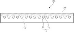
도 1은 본 발명의 실시예에 따른 내오염층을 갖는 태양광 기판을 보여주는 단면도이다.
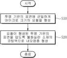
도 2는 본 발명의 실시예에 따른 내오염층을 갖는 태양광 기판의 제조 방법에 따른 흐름도이다.
도 3은 도 2의 요철을 형성하는 단계에 대한 상세 흐름도이다.
도 4 내지 도 10은 도 2의 제조 방법에 따른 각 단계를 보여주는 도면들이다.
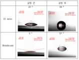
도 11은 내오염층의 코팅 전 후의 태양광 기판의 탈이온수에 대한 소수성 정도를 보여주는 사진이다.
도 12는 내오염층의 코팅 전 후의 태양광 기판의 접촉각을 보여주는 도면이다.1 is a cross-sectional view showing a photovoltaic substrate having a fouling-resistant layer according to an embodiment of the present invention.
2 is a flowchart of a method of manufacturing a photovoltaic substrate having a fouling-resistant layer according to an embodiment of the present invention.
FIG. 3 is a detailed flowchart of the step of forming the unevenness of FIG. 2 .
4 to 10 are views showing each step according to the manufacturing method of FIG. 2 .
11 is a photograph showing the degree of hydrophobicity to deionized water of a photovoltaic substrate before and after coating a fouling resistant layer.
12 is a view showing contact angles of a photovoltaic substrate before and after coating a fouling-resistant layer.
하기의 설명에서는 본 발명의 실시예를 이해하는데 필요한 부분만이 설명되며, 그 이외 부분의 설명은 본 발명의 요지를 벗어나지 않는 범위에서 생략될 것이라는 것을 유의하여야 한다.It should be noted that in the following description, only parts necessary for understanding the embodiments of the present invention are described, and descriptions of other parts will be omitted without departing from the gist of the present invention.
이하에서 설명되는 본 명세서 및 청구범위에 사용된 용어나 단어는 통상적이거나 사전적인 의미로 한정해서 해석되어서는 아니 되며, 발명자는 그 자신의 발명을 가장 최선의 방법으로 설명하기 위해 용어의 개념으로 적절하게 정의할 수 있다는 원칙에 입각하여 본 발명의 기술적 사상에 부합하는 의미와 개념으로 해석되어야만 한다. 따라서 본 명세서에 기재된 실시예와 도면에 도시된 구성은 본 발명의 바람직한 실시예에 불과할 뿐이고, 본 발명의 기술적 사상을 모두 대변하는 것은 아니므로, 본 출원시점에 있어서 이들을 대체할 수 있는 다양한 균등물과 변형예들이 있을 수 있음을 이해하여야 한다.The terms or words used in this specification and claims described below should not be construed as being limited to ordinary or dictionary meanings, and the inventors have appropriately used the concept of terms to describe their inventions in the best way. It should be interpreted as a meaning and concept consistent with the technical spirit of the present invention based on the principle that it can be defined in the following way. Therefore, the embodiments described in this specification and the configurations shown in the drawings are only preferred embodiments of the present invention, and do not represent all of the technical spirit of the present invention, so various equivalents that can replace them at the time of the present application. It should be understood that there may be variations and variations.
이하, 첨부된 도면을 참조하여 본 발명의 실시예를 보다 상세하게 설명하고자 한다.Hereinafter, embodiments of the present invention will be described in more detail with reference to the accompanying drawings.
도 1은 본 발명의 실시예에 따른 내오염층을 갖는 태양광 기판을 보여주는 단면도이다.1 is a cross-sectional view showing a photovoltaic substrate having a fouling-resistant layer according to an embodiment of the present invention.
도 1을 참조하면, 본 실시예에 따른 태양광 기판(100)은 태양광 발전(photovoltaics, PV)에 사용되는 태양전지용 패널이다. 이러한 본 실시예에 따른 태양광 기판(100)은 투명 기판(10)과, 투명 기판(10) 위에 코팅되는 불화실란 소재의 내오염층(20)을 포함한다. 투명 기판(10)은 표면에 마이크로 크기의 요철(11)이 균일하게 형성되어 있다. 그리고 내오염층(20)은 투명 기판(10)의 표면에 코팅되되, 요철(11)에 충전되게 코팅된다.Referring to FIG. 1 , a
여기서 투명 기판(10)의 소재로는 광투과성이 양호한 소다석회유리(soda-lime glass)가 사용될 수 있다.Here, as a material for the
요철(11)은 마이크로 블라스트 가공을 통해 형성할 수 있다. 요철(11)은 요부(13)와 철부(15)를 포함한다. 요부(13)의 크기는 수십 ㎛일 수 있다. 즉 요부(13)의 폭과 깊이가 각각 수십 ㎛일 수 있다. 요부(13)는 폭 보다 깊이가 길 수 있다. 요부(13)의 폭은 철부(15)의 폭과 동일하거나 클 수 있다.The
요철(11)의 요부(13)는 입구의 단면적이 입구 안쪽의 단면적과 동일하거나 크게 형성될 수 있다. 예컨대 요부(13)는 기둥형, 원통형, 역쐐기형 등으로 형성될 수 있으며, 이것에 한정되는 것은 아니다.The
그리고 내오염층(20)은 불화실란 소재의 코팅액을 코팅하여 형성한다. 불화실란 소재는 FDTS, FAS 및 FDTMEs 중에 적어도 하나를 포함한다. 내오염층(20)의 형성으로 인한 태양광 기판(100)의 광투과율 저하를 최소화하기 위해서, 내오염층(20)을 형성하는 코팅액으로는 1액형 코팅액을 사용하는 것이 바람직하다.In addition, the contamination
투명 기판(10)의 표면에 코팅액을 도포한 이후에, 코팅막의 에이징 시간과 첨가제 조절을 통해서 내오염층(20)의 소수성과 광투과율을 적절하게 조절할 수 있다. 여기서 첨가제는 pH 조절제를 포함한다.After the coating solution is applied to the surface of the
이와 같이 본 실시예에 따르면, 투명 기판(10)의 표면에 마이크로 블라스트 가공을 통해서 균일하게 마이크로 크기의 요철(11)을 형성한 후, 요철(11)을 덮도록 불화실란 소재로 내오염층(20)을 형성함으로써, 태양광 기판(100)의 내오염성을 향상시킬 수 있다.As described above, according to the present embodiment,
태양광 기판(100)의 표면에 형성된 내오염층(20)을 통하여 내오염성을 향상시킴으로써, 태양광 기판(100)의 장기수명 특성과 광전기 전환 효율을 향상시킬 수 있다.By improving fouling resistance through the fouling-
그리고 투명 기판(10)의 표면에 코팅되는 내오염층(20)은 요철(11)에 의해 투명 기판(10)의 표면과의 접촉 면적이 증가하기 때문에, 투명 기판(10)과 내오염층(20) 간의 양호한 결합력을 구현할 수 있다. 이로 인해 외부 충격 등에 의해 태양광 기판(100)으로부터 내오염층(20)이 탈리하는 문제를 해소할 수 있다.In addition, since the contact area of the contamination
이와 같이 투명 기판(10)의 표면에 요철(11)을 형성하는 이유에 대해서 구체적으로 설명하면 다음과 같다. 만약 투명 기판의 표면에 요철을 형성하지 않고 내오염층을 형성하는 경우에도 내오염층으로 인한 내오염성 향상을 기대할 수 있다. 하지만 요철이 형성되지 않은 투명 기판의 표면은 매끈하기 때문에, 투명 기판의 표면과 내오염층 간의 결합력이 떨어질 수 있다. 이로 인해 태양광 기판에 외부 충격이 인가될 경우, 투명 기판의 표면으로 내오염층이 박리되는 문제가 발생될 수 있다.The reason why the
하지만 본 실시예에서는 투명 기판(10)의 표면에 요철(11)을 형성하여 투명 기판(10)과 내오염층(20) 간의 접촉 면적을 증가시킴으로써, 투명 기판(10)과 내오염층(20) 간에 양호한 결합력을 제공할 수 있다.However, in this embodiment, by forming
그리고 요철(11)은 마이크로 크기로 형성되기 때문에, 요철(11)로 인한 태양광 기판(100)의 광투과율 저하를 최소화할 수 있다.In addition, since the
[내오염층(20)을 갖는 태양광 기판(100)의 제조 방법][Method of
이와 같은 본 실시예에 따른 내오염층(20)을 갖는 태양광 기판(100)의 제조 방법에 대해서 도 2 내지 도 10을 참조하여 설명하면 다음과 같다. 여기서 도 2는 본 발명의 실시예에 따른 내오염층(20)을 갖는 태양광 기판(100)의 제조 방법에 따른 흐름도이다. 도 3은 도 2의 요철(11)을 형성하는 단계에 대한 상세 흐름도이다. 그리고 도 4 내지 도 10은 도 2의 제조 방법에 따른 각 단계를 보여주는 도면들이다.A method of manufacturing the
본 실시예에 따른 태양광 기판(100)의 제조 방법은 투명 기판(10)의 표면에 균일하게 마이크로 크기의 요철(11)을 형성하는 단계(S10)와, 투명 기판(10)의 표면을 덮도록 불화실란 소재의 코팅액으로 코팅하여 내오염층(20)을 형성하며, 코팅액이 요철(11)에 충전되어 내오염층(20)을 형성하는 단계(S20)를 포함한다.The manufacturing method of the
먼저 S10단계에 따른 요철(11)을 형성하는 단계를 구체적으로 설명하면 다음과 같다.First, the step of forming the
먼저 도 4 및 도 5에 도시된 바와 같이, S11단계에서 투명 기판(10)의 표면에 드라이 필름(30)을 코팅한다. 즉 도 4에 도시된 바와 같이, 투명 기판(10)을 준비한다. 투명 기판(10)은 세척 공정을 통해서 표면에 존재할 수 있는 불순물을 제거할 수 있다.First, as shown in FIGS. 4 and 5 , a
도 5에 도시된 바와 같이, 투명 기판(10)의 표면에 드라이 필름(30)을 코팅한다. 드라이 필름(30)은 롤러를 이용하여 투명 기판(10)의 표면에 코팅될 수 있다. 여기서 드라이 필름(30)은 자외선을 이용한 사진 공정을 통하여 패터닝이 가능한 소재이다. 드라이 필름(30) 대신에 감광액을 도포하여 감광층을 형성할 수도 있다.As shown in FIG. 5 , a
다음으로 도 6에 도시된 바와 같이, S13단계에서 드라이 필름(30)을 패터닝하여 형성할 요철에 대응되게 패턴 홀(31)을 형성하다. 즉 드라이 필름(30)에 대한 자외선 노광 및 현상을 포함하는 사진 공정을 통하여 패턴 홀(31)을 형성한다. 패턴 홀(13)은 요철의 요부에 대응되게 형성된다.Next, as shown in FIG. 6 , pattern holes 31 are formed to correspond to irregularities to be formed by patterning the
다음으로 도 7에 도시된 바와 같이, S15단계에서 드라이 필름(30) 위에 마이크로 샌드블라스트용 연마제(41)를 분사 노즐(40)로 분사하여 패턴 홀(31)에 노출된 투명 기판(10)의 표면에 요부(13)를 형성한다.Next, as shown in FIG. 7, in step S15, the abrasive 41 for micro-sandblasting is sprayed with the
이와 같이 도 7에 도시된 바와 바와 같은 마이크로 블라스트 가공을 통해서, 도 8에 도시된 바와 같이, 투명 기판(10)의 표면에 요철(11)을 형성할 수 있다.As such, as shown in FIG. 8 , through the microblasting process as shown in FIG. 7 ,
이어서 도 8 및 도 9에 도시된 바와 같이, S17단계에서 투명 기판(10)으로부터 드라이 필름(30)을 박리함으로써, 표면에 마이크로 크기의 요철(11)이 형성된 투명 기판(10)을 얻을 수 있다. 즉 투명 기판(10) 위에 드라이 필름(30)용 박리액을 분사하여 투명 기판(10)으로 드라이 필름(30)을 박리하여 제거함으로써, 표면에 요철(11)이 균일하게 혀엉된 투명 기판(10)을 제조한다.Subsequently, as shown in FIGS. 8 and 9 , by peeling the
그리고 도 10에 도시된 바와 같이, S20단계에서 요철(11)이 형성된 투명 기판(10)의 표면을 덮도록 불화실란 소재의 코팅액으로 코팅하여 내오염층(20)을 형성함으로써, 본 실시예에 따른 태양광 기판(100)을 제조한다. 즉 투명 기판(10)의 표면을 코팅액으로 코팅하여 코팅막을 형성하고, 코팅막에 대한 에이징을 포함한 건조 공정을 통하여 내오염층(20)을 형성한다.And, as shown in FIG. 10, in step S20, the contamination
이때 코팅액은 스프레이, 스핀 코팅, 바 코팅, 슬롯 다이 등 다양한 코팅 방식으로 투명 기판(10)의 표면에 코팅될 수 있다. 코팅액은 불화실란 소재를 기반으로 하여, 첨가제로 pH 조절제를 더 포함할 수 있다.At this time, the coating liquid may be coated on the surface of the
이와 같은 본 실시예에 따른 투명 기판(10)의 내오염성을 확인하기 위해서, 내오염층(20)을 코팅하기 전 후의 탈이온수에 대한 소수성 정도를 확인하였다.In order to confirm the fouling resistance of the
도 11은 내오염층의 코팅 전 후의 태양광 기판의 탈이온수에 대한 소수성 정도를 보여주는 사진이다. 여기서 도 11의 (a) 코팅 전의 태양광 기판을 보여준다. 도 11의 (b)는 코팅 후의 태양광 기판을 보여준다. 내오염층을 형성하는 투명 기판으로는 소다석회유리 기판을 사용하였다.11 is a photograph showing the degree of hydrophobicity to deionized water of a photovoltaic substrate before and after coating a fouling resistant layer. Here, (a) of FIG. 11 shows a photovoltaic substrate before coating. Figure 11 (b) shows the photovoltaic substrate after coating. A soda-lime glass substrate was used as a transparent substrate forming the contamination-resistant layer.
도 11의 (a)를 참조하면, 코팅 전 태양광 기판은 표면에서 탈이온수가 넓게 퍼진 것을 확인할 수 있다. 코팅 전 태양광 기판, 즉 투명 기판의 표면은 소수성 보다 친수성을 갖는 것을 확인할 수 있다.Referring to (a) of FIG. 11 , it can be seen that deionized water spreads widely on the surface of the photovoltaic substrate before coating. It can be seen that the surface of the photovoltaic substrate before coating, that is, the transparent substrate has more hydrophilicity than hydrophobicity.
하지만 도 11의 (b)를 참조하면, 코팅 후 태양광 기판은 표면에서 탈이온수가 반구 형태로 모인 것을 확인할 수 있다. 즉 코팅 후 태양광 기판은 내오염층으로 인해 소수성이 향상된 것을 확인할 수 있다.However, referring to (b) of FIG. 11 , it can be confirmed that deionized water is collected in a hemispherical shape on the surface of the photovoltaic substrate after coating. That is, it can be confirmed that the hydrophobicity of the photovoltaic substrate after coating is improved due to the fouling-resistant layer.
도 12는 내오염층의 코팅 전 후의 태양광 기판의 접촉각을 보여주는 도면이다. 여기서 도 12는 코팅 전 후의 태양광 기판에 대한 탈이온수와 헥사데칸(Hexadecane)에 대한 접촉각을 측정하였다.12 is a view showing contact angles of a photovoltaic substrate before and after coating a fouling-resistant layer. Here, FIG. 12 measures the contact angles of deionized water and hexadecane on the solar substrate before and after coating.
도 12를 참조하면, 코팅 전 태양광 기판에 대한 탈이온수와 헥사데칸에 대한 접촉각이 28도 및 9도로 측정되었다.Referring to FIG. 12 , the contact angles of deionized water and hexadecane to the solar substrate before coating were measured at 28 degrees and 9 degrees.
반면에 코팅 후 태양광 기판에 대한 탈이온수와 헥사데칸에 대한 접촉각이 94도 및 57도로 측정되었다.On the other hand, the contact angles of deionized water and hexadecane to the solar substrate after coating were measured at 94 degrees and 57 degrees.
즉 본 실시예에 따른 내오염층을 태양광 기판에 코팅함으로써, 태양광 기판 표면의 소수성이 향상된 것을 확인할 수 있다.That is, it can be confirmed that the hydrophobicity of the surface of the photovoltaic substrate is improved by coating the antifouling layer according to the present embodiment on the photovoltaic substrate.
이와 같이 본 실시예에서는 태양광 기판용 투명 기판의 표면에 마이크로 블라스트 가공을 통해 마이크로 크기의 요철과 같은 거시적인 미세 구조를 형성하고, 요철이 형성된 표면에 불화실란 소재의 내오염층을 형성하여 높은 표면에너지를 구현함으로써, 태양광 기판의 내오염성을 향상시킬 수 있다.In this way, in this embodiment, a macroscopic microstructure such as micro-sized irregularities is formed on the surface of a transparent substrate for a photovoltaic substrate through micro-blast processing, and a contamination-resistant layer of fluorosilane material is formed on the surface where the irregularities are formed, thereby providing high By implementing the surface energy, it is possible to improve the fouling resistance of the photovoltaic substrate.
이로 인해 본 실시예에 따른 태양광 기판은 동적 접촉각(dynamic contact angle)의 차이가 5도 이내로 점성이 있거나 표면에너지가 낮은 유기용매의 오염으로부터 장기적인 내구성을 확보할 수 있다.As a result, the photovoltaic substrate according to the present embodiment has a dynamic contact angle difference of less than 5 degrees, and long-term durability can be secured from contamination by an organic solvent having a viscous surface or a low surface energy.
본 실시예에 따른 내오염층이 형성된 태양광 기판의 광투과율을 확인한 결과, 내오염층이 형성되지 않은 태양광 기판과 비교했을 때, 광투과율의 저하는 1% 내외인 것을 확인하였다.As a result of confirming the light transmittance of the photovoltaic substrate with the antifouling layer according to the present embodiment, it was confirmed that the decrease in light transmittance was around 1% compared to the photovoltaic substrate without the antifouling layer.
한편, 본 명세서와 도면에 개시된 실시예들은 이해를 돕기 위해 특정 예를 제시한 것에 지나지 않으며, 본 발명의 범위를 한정하고자 하는 것은 아니다. 여기에 개시된 실시예들 이외에도 본 발명의 기술적 사상에 바탕을 둔 다른 변형예들이 실시 가능하다는 것은, 본 발명이 속하는 기술분야에서 통상의 지식을 가진 자에게는 자명한 것이다.On the other hand, the embodiments disclosed in this specification and drawings are only presented as specific examples to aid understanding, and are not intended to limit the scope of the present invention. In addition to the embodiments disclosed herein, it is obvious to those skilled in the art that other modifications based on the technical idea of the present invention can be implemented.
10 : 투명 기판
11 : 요철
13 : 요부
15 : 철부
20 : 내오염층
30 : 드라이 필름
31 : 패턴 홀
40 : 분사 노즐
41 : 연마재
100 : 태양광 기판10: transparent substrate
11: unevenness
13: Lumbar
15: iron part
20: contamination resistant layer
30: dry film
31: pattern hole
40: injection nozzle
41: abrasive
100: solar substrate
Claims (12)
Translated fromKorean상기 투명 기판의 표면에 코팅되되, 상기 요철에 충전되게 코팅되는 불화실란 소재의 내오염층;
을 포함하는 태양광 기판.A transparent substrate having micro-sized irregularities uniformly formed on a surface thereof;
Doedoe coated on the surface of the transparent substrate, a contamination resistant layer of a fluorosilane material coated so as to fill the irregularities;
A solar panel comprising a.
상기 투명 기판의 소재는 소다석회유리(soda-lime glass)를 포함하는 것을 특징으로 하는 태양광 기판.According to claim 1,
The material of the transparent substrate is a solar substrate, characterized in that it comprises soda-lime glass (soda-lime glass).
상기 요철은 마이크로 블라스트 가공을 통해 형성한 것을 특징으로 하는 태양광 기판.According to claim 1,
The photovoltaic substrate, characterized in that the unevenness is formed through microblast processing.
상기 요철의 요부는 입구의 단면적이 상기 입구 안쪽의 단면적과 동일하거나 큰 것을 특징으로 하는 태양광 기판.According to claim 1,
The photovoltaic substrate according to claim 1 , wherein a cross-sectional area of an inlet of the concavo-convex portion is equal to or greater than a cross-sectional area of an inside of the inlet.
상기 불화실란 소재는 FDTS, FAS 및 FDTMEs 중에 적어도 하나를 포함하는 것을 특징으로 하는 태양광 기판.According to claim 1,
The photovoltaic substrate, characterized in that the fluorosilane material comprises at least one of FDTS, FAS and FDTMEs.
상기 투명 기판의 표면을 덮도록 불화실란 소재의 코팅액으로 코팅하여 내오염층을 형성하며, 상기 코팅액이 상기 요철에 충전되어 상기 내오염층을 형성하는 단계;
를 포함하는 태양광 기판의 제조 방법.uniformly forming micro-sized irregularities on the surface of the transparent substrate; and
coating the surface of the transparent substrate with a coating solution of a fluorosilane material to form a contamination resistant layer, and filling the uneven surfaces with the coating solution to form the contamination resistant layer;
Method for manufacturing a photovoltaic substrate comprising a.
상기 투명 기판의 소재는 소다석회유리(soda-lime glass)를 포함하는 것을 특징으로 하는 태양광 기판의 제조 방법.According to claim 6,
The method of manufacturing a photovoltaic substrate, characterized in that the material of the transparent substrate comprises soda-lime glass.
상기 요철은 마이크로 블라스트 가공을 통해 형성한 것을 특징으로 하는 태양광 기판의 제조 방법.The method of claim 6, wherein in the step of forming the irregularities,
The manufacturing method of the photovoltaic substrate, characterized in that the unevenness is formed through microblast processing.
상기 투명 기판의 표면에 드라이 필름을 코팅하는 단계;
상기 드라이 필름을 패터닝하여 형성할 요철에 대응되게 패턴 홀을 형성하는 단계;
상기 드라이 필름 위에 마이크로 샌드블라스트용 연마재를 분사하여 상기 패턴 홀에 노출된 투명 기판의 표면에 요부를 형성하는 단계; 및
상기 투명 기판으로부터 상기 드라이 필름을 박리하여 상기 투명 기판의 표면에 마이크로 크기의 요철을 형성하는 단계;
를 포함하는 것을 특징으로 하는 태양광 기판의 제조 방법.The method of claim 8, wherein the step of forming the irregularities,
coating a dry film on the surface of the transparent substrate;
forming pattern holes corresponding to irregularities to be formed by patterning the dry film;
spraying an abrasive for micro sandblasting on the dry film to form recesses on the surface of the transparent substrate exposed to the pattern holes; and
forming micro-sized irregularities on the surface of the transparent substrate by peeling the dry film from the transparent substrate;
Method for manufacturing a photovoltaic substrate comprising a.
상기 요철의 요부는 입구의 단면적이 상기 입구 안쪽의 단면적과 동일하거나 큰 것을 특징으로 하는 태양광 기판의 제조 방법.According to claim 9,
The method of manufacturing a photovoltaic substrate, characterized in that the cross-sectional area of the concavo-convex portion of the inlet is equal to or larger than the cross-sectional area of the inside of the inlet.
상기 불화실란 소재는 FDTS, FAS 및 FDTMEs 중에 적어도 하나를 포함하는 것을 특징으로 하는 태양광 기판의 제조 방법.According to claim 6,
The method of manufacturing a photovoltaic substrate, characterized in that the fluorosilane material includes at least one of FDTS, FAS and FDTMEs.
상기 코팅액은 1액형인 것을 특징으로 하는 태양광 기판의 제조 방법.According to claim 11,
The method of manufacturing a photovoltaic substrate, characterized in that the coating liquid is a one-component type.
Priority Applications (1)
| Application Number | Priority Date | Filing Date | Title |
|---|---|---|---|
| KR1020210165758AKR102677868B1 (en) | 2021-11-26 | 2021-11-26 | Photovoltaic substrate having contamination-resistant layer and method for manufacturing the same |
Applications Claiming Priority (1)
| Application Number | Priority Date | Filing Date | Title |
|---|---|---|---|
| KR1020210165758AKR102677868B1 (en) | 2021-11-26 | 2021-11-26 | Photovoltaic substrate having contamination-resistant layer and method for manufacturing the same |
Publications (2)
| Publication Number | Publication Date |
|---|---|
| KR20230078884Atrue KR20230078884A (en) | 2023-06-05 |
| KR102677868B1 KR102677868B1 (en) | 2024-06-25 |
Family
ID=86764310
Family Applications (1)
| Application Number | Title | Priority Date | Filing Date |
|---|---|---|---|
| KR1020210165758AActiveKR102677868B1 (en) | 2021-11-26 | 2021-11-26 | Photovoltaic substrate having contamination-resistant layer and method for manufacturing the same |
Country Status (1)
| Country | Link |
|---|---|
| KR (1) | KR102677868B1 (en) |
Cited By (1)
| Publication number | Priority date | Publication date | Assignee | Title |
|---|---|---|---|---|
| KR102768179B1 (en)* | 2023-08-14 | 2025-02-13 | 한국중부발전(주) | Solar panel pattern manufacturing method |
Families Citing this family (1)
| Publication number | Priority date | Publication date | Assignee | Title |
|---|---|---|---|---|
| KR20020013091A (en)* | 2000-08-11 | 2002-02-20 | 정동혁 | Word Writing System using jog-shuttle button on portable phone and wireless internet terminal |
Citations (8)
| Publication number | Priority date | Publication date | Assignee | Title |
|---|---|---|---|---|
| JPH11298030A (en)* | 1998-04-15 | 1999-10-29 | Asahi Glass Co Ltd | Cover glass for solar cell, method for manufacturing the same, and solar cell |
| JP2001057439A (en)* | 1999-06-11 | 2001-02-27 | Kanegafuchi Chem Ind Co Ltd | Solar battery module |
| KR20100109305A (en)* | 2009-03-31 | 2010-10-08 | 엘지이노텍 주식회사 | Solar cell and method of fabricating the same |
| JP2012015442A (en)* | 2010-07-05 | 2012-01-19 | Toppan Printing Co Ltd | Back surface protective sheet and solar cell using it |
| KR20150049922A (en)* | 2013-10-31 | 2015-05-08 | 현대하이스코 주식회사 | Method of forming electrode for dye sensitive solar cell using surface pattering |
| KR20160010697A (en)* | 2014-07-17 | 2016-01-28 | (주)우인켐텍 | anti-pollution coating solution composition and manufacture method the anti-pollution coating solution composition |
| KR20200069685A (en) | 2018-12-07 | 2020-06-17 | 강원대학교산학협력단 | Composition for water repellent coating comprising organic/inorganic hybrided nanoparticles synthesized with bridged organosilica precursor and method thereof |
| KR20210052098A (en)* | 2019-10-31 | 2021-05-10 | 주식회사 시노펙스 | the wafer etching method using the sand blast method of construction |
- 2021
- 2021-11-26KRKR1020210165758Apatent/KR102677868B1/enactiveActive
Patent Citations (8)
| Publication number | Priority date | Publication date | Assignee | Title |
|---|---|---|---|---|
| JPH11298030A (en)* | 1998-04-15 | 1999-10-29 | Asahi Glass Co Ltd | Cover glass for solar cell, method for manufacturing the same, and solar cell |
| JP2001057439A (en)* | 1999-06-11 | 2001-02-27 | Kanegafuchi Chem Ind Co Ltd | Solar battery module |
| KR20100109305A (en)* | 2009-03-31 | 2010-10-08 | 엘지이노텍 주식회사 | Solar cell and method of fabricating the same |
| JP2012015442A (en)* | 2010-07-05 | 2012-01-19 | Toppan Printing Co Ltd | Back surface protective sheet and solar cell using it |
| KR20150049922A (en)* | 2013-10-31 | 2015-05-08 | 현대하이스코 주식회사 | Method of forming electrode for dye sensitive solar cell using surface pattering |
| KR20160010697A (en)* | 2014-07-17 | 2016-01-28 | (주)우인켐텍 | anti-pollution coating solution composition and manufacture method the anti-pollution coating solution composition |
| KR20200069685A (en) | 2018-12-07 | 2020-06-17 | 강원대학교산학협력단 | Composition for water repellent coating comprising organic/inorganic hybrided nanoparticles synthesized with bridged organosilica precursor and method thereof |
| KR20210052098A (en)* | 2019-10-31 | 2021-05-10 | 주식회사 시노펙스 | the wafer etching method using the sand blast method of construction |
Cited By (1)
| Publication number | Priority date | Publication date | Assignee | Title |
|---|---|---|---|---|
| KR102768179B1 (en)* | 2023-08-14 | 2025-02-13 | 한국중부발전(주) | Solar panel pattern manufacturing method |
Also Published As
| Publication number | Publication date |
|---|---|
| KR102677868B1 (en) | 2024-06-25 |
Similar Documents
| Publication | Publication Date | Title |
|---|---|---|
| KR20230078884A (en) | Photovoltaic substrate having contamination-resistant layer and method for manufacturing the same | |
| US10629851B2 (en) | OLED thin film encapsulation structure | |
| TWI432835B (en) | Flexible display panel and method of manufacturing same | |
| JP6899917B2 (en) | Pixel structure and manufacturing method | |
| JP4640322B2 (en) | Photoelectric conversion element, method for producing the same, and method for producing electrochemical cell | |
| CN105293427B (en) | Preparation method of super-hydrophobic surface based on limited local plating of meniscus | |
| Luo et al. | Direct fabrication of microlens arrays with high numerical aperture by ink-jetting on nanotextured surface | |
| KR101254318B1 (en) | Solar cell and solar cell manufacturing method therefor | |
| CN107068865A (en) | Perovskite solar cell and preparation method thereof | |
| TW201228807A (en) | Method of imprinting a texture on a rigid substrate using flexible stamp | |
| CN101958361A (en) | Etching method of light-transmitting thin-film solar cell module | |
| CN111293971A (en) | Wear-resisting automatically cleaning solar cell panel | |
| KR100928330B1 (en) | Transparent substrate and manufacturing method thereof | |
| EP2720285B1 (en) | Method of fabricating patterned substrate | |
| CN103594555B (en) | A kind of preparation method with the black silicon material of self-cleaning function | |
| Liu et al. | Self-cleaning antireflective coating with a hierarchical texture for light trapping in micromorph solar cells | |
| US20230365457A1 (en) | High transparency, high haze nanostructured structures | |
| WO2011106236A2 (en) | Nanoscale high-aspect-ratio metallic structure and method of manufacturing same | |
| KR20100131045A (en) | Method for manufacturing dustproof antifouling layer of solar cell | |
| US20160172517A1 (en) | Reflecting films with rounded microstructures for use in solar modules | |
| CN109941961A (en) | A kind of preparation method of multifunctional thin film with micro-nano structure | |
| KR101207504B1 (en) | Channel structure of organic thin-film solar cell manufacturing method | |
| CN107717148B (en) | A kind of method of exposure mask Electrolyzed Processing micro structure array | |
| KR20220159599A (en) | Nano-micro hybrid pattern with highly transparent superhydrophobic surface and method for manufacturing the same | |
| KR101769183B1 (en) | Preparing method for conductive film having fine metal layer and conductive film manufactured thereby |
Legal Events
| Date | Code | Title | Description |
|---|---|---|---|
| PA0109 | Patent application | Patent event code:PA01091R01D Comment text:Patent Application Patent event date:20211126 | |
| PA0201 | Request for examination | ||
| PG1501 | Laying open of application | ||
| E902 | Notification of reason for refusal | ||
| PE0902 | Notice of grounds for rejection | Comment text:Notification of reason for refusal Patent event date:20230718 Patent event code:PE09021S01D | |
| E902 | Notification of reason for refusal | ||
| PE0902 | Notice of grounds for rejection | Comment text:Notification of reason for refusal Patent event date:20231207 Patent event code:PE09021S01D | |
| E701 | Decision to grant or registration of patent right | ||
| PE0701 | Decision of registration | Patent event code:PE07011S01D Comment text:Decision to Grant Registration Patent event date:20240614 | |
| GRNT | Written decision to grant | ||
| PR0701 | Registration of establishment | Comment text:Registration of Establishment Patent event date:20240619 Patent event code:PR07011E01D | |
| PR1002 | Payment of registration fee | Payment date:20240619 End annual number:3 Start annual number:1 | |
| PG1601 | Publication of registration |