KR20230070454A - Resonant reflective device detection - Google Patents
Resonant reflective device detectionDownload PDFInfo
- Publication number
- KR20230070454A KR20230070454AKR1020237009065AKR20237009065AKR20230070454AKR 20230070454 AKR20230070454 AKR 20230070454AKR 1020237009065 AKR1020237009065 AKR 1020237009065AKR 20237009065 AKR20237009065 AKR 20237009065AKR 20230070454 AKR20230070454 AKR 20230070454A
- Authority
- KR
- South Korea
- Prior art keywords
- charging
- frequency
- coil
- excitation
- resonant frequency
- Prior art date
- Legal status (The legal status is an assumption and is not a legal conclusion. Google has not performed a legal analysis and makes no representation as to the accuracy of the status listed.)
- Withdrawn
Links
Images


Classifications
- H—ELECTRICITY
- H02—GENERATION; CONVERSION OR DISTRIBUTION OF ELECTRIC POWER
- H02J—CIRCUIT ARRANGEMENTS OR SYSTEMS FOR SUPPLYING OR DISTRIBUTING ELECTRIC POWER; SYSTEMS FOR STORING ELECTRIC ENERGY
- H02J50/00—Circuit arrangements or systems for wireless supply or distribution of electric power
- H02J50/90—Circuit arrangements or systems for wireless supply or distribution of electric power involving detection or optimisation of position, e.g. alignment
- H—ELECTRICITY
- H02—GENERATION; CONVERSION OR DISTRIBUTION OF ELECTRIC POWER
- H02J—CIRCUIT ARRANGEMENTS OR SYSTEMS FOR SUPPLYING OR DISTRIBUTING ELECTRIC POWER; SYSTEMS FOR STORING ELECTRIC ENERGY
- H02J50/00—Circuit arrangements or systems for wireless supply or distribution of electric power
- H02J50/10—Circuit arrangements or systems for wireless supply or distribution of electric power using inductive coupling
- H02J50/12—Circuit arrangements or systems for wireless supply or distribution of electric power using inductive coupling of the resonant type
- H—ELECTRICITY
- H02—GENERATION; CONVERSION OR DISTRIBUTION OF ELECTRIC POWER
- H02J—CIRCUIT ARRANGEMENTS OR SYSTEMS FOR SUPPLYING OR DISTRIBUTING ELECTRIC POWER; SYSTEMS FOR STORING ELECTRIC ENERGY
- H02J50/00—Circuit arrangements or systems for wireless supply or distribution of electric power
- H02J50/40—Circuit arrangements or systems for wireless supply or distribution of electric power using two or more transmitting or receiving devices
- H02J50/402—Circuit arrangements or systems for wireless supply or distribution of electric power using two or more transmitting or receiving devices the two or more transmitting or the two or more receiving devices being integrated in the same unit, e.g. power mats with several coils or antennas with several sub-antennas
- H—ELECTRICITY
- H02—GENERATION; CONVERSION OR DISTRIBUTION OF ELECTRIC POWER
- H02J—CIRCUIT ARRANGEMENTS OR SYSTEMS FOR SUPPLYING OR DISTRIBUTING ELECTRIC POWER; SYSTEMS FOR STORING ELECTRIC ENERGY
- H02J7/00—Circuit arrangements for charging or depolarising batteries or for supplying loads from batteries
- H02J7/0047—Circuit arrangements for charging or depolarising batteries or for supplying loads from batteries with monitoring or indicating devices or circuits
- H—ELECTRICITY
- H02—GENERATION; CONVERSION OR DISTRIBUTION OF ELECTRIC POWER
- H02J—CIRCUIT ARRANGEMENTS OR SYSTEMS FOR SUPPLYING OR DISTRIBUTING ELECTRIC POWER; SYSTEMS FOR STORING ELECTRIC ENERGY
- H02J7/00—Circuit arrangements for charging or depolarising batteries or for supplying loads from batteries
- H02J7/007—Regulation of charging or discharging current or voltage
- H02J7/00712—Regulation of charging or discharging current or voltage the cycle being controlled or terminated in response to electric parameters
- H02J7/00714—Regulation of charging or discharging current or voltage the cycle being controlled or terminated in response to electric parameters in response to battery charging or discharging current
- H02J7/00718—Regulation of charging or discharging current or voltage the cycle being controlled or terminated in response to electric parameters in response to battery charging or discharging current in response to charge current gradient
Landscapes
- Engineering & Computer Science (AREA)
- Power Engineering (AREA)
- Computer Networks & Wireless Communication (AREA)
- Charge And Discharge Circuits For Batteries Or The Like (AREA)
Abstract
Translated fromKorean
Description
Translated fromKorean우선권 주장priority claim
본 출원은 2021년 8월 11일자로 미국 특허청에 출원된 정식 특허 출원 번호 제17/400,068호 및 2020년 8월 15일자로 미국 특허청에 출원된 가특허 출원 번호 제63/066,221호에 대한 우선권 및 이익을 주장하고, 본 출원의 전체 내용은 전체적으로 아래에 완전히 진술된 바와 같이 그리고 모든 적용가능한 목적을 위해 본원에 참조로 통합된다.This application claims priority to Provisional Patent Application No. 17/400,068, filed with the U.S. Patent and Trademark Office on August 11, 2021, and Provisional Patent Application No. 63/066,221, filed with the U.S. Patent and Trademark Office on August 15, 2020; and The benefit is claimed, the entire contents of this application in its entirety as fully set forth below and for all applicable purposes are incorporated herein by reference.
본 발명은 일반적으로 모바일 컴퓨팅 디바이스의 배터리를 포함하는 배터리의 무선 충전에 관한 것으로서, 보다 구체적으로는 충전 디바이스 근처에 배치되는 디바이스의 검출에 관한 것이다.[0002] The present invention relates generally to wireless charging of batteries, including batteries of mobile computing devices, and more particularly to detection of devices placed in proximity to a charging device.
무선 충전 시스템은 특정 타입의 디바이스가 물리적 충전 연결의 사용없이 내부 배터리를 충전할 수 있도록 배치되었다. 무선 충전을 이용할 수 있는 디바이스는 모바일 처리 디바이스 및/또는 통신 디바이스를 포함한다. 무선 전력 컨소시엄에 의해 정의되는 Qi 표준과 같은 표준은 제1 공급자에 의해 제조되는 디바이스가 제2 공급자에 의해 제조되는 충전기를 사용하여 무선으로 충전되게 할 수 있다. 무선 충전을 위한 표준은 디바이스의 상대적으로 간단한 구성에 대해 최적화되고 기본 충전 능력을 제공하는 경향이 있다.Wireless charging systems are positioned to allow certain types of devices to charge their internal batteries without the use of a physical charging connection. Devices that can utilize wireless charging include mobile processing devices and/or communication devices. Standards such as the Qi standard defined by the Wireless Power Consortium allow devices manufactured by a first supplier to be wirelessly charged using chargers manufactured by a second supplier. Standards for wireless charging tend to be optimized for a device's relatively simple configuration and provide basic charging capabilities.
무선 충전 능력의 개선은 모바일 디바이스의 지속적으로 증가하는 복잡성 및 변화하는 폼 팩터(form factor)를 지원하기 위해 요구된다. 예를 들어, 충전 디바이스가 충전 디바이스의 표면 상의 충전가능한 디바이스를 검출하고 위치를 찾아낼 수 있게 하는 더 빠른, 더 낮은 전력 검출 기술에 대한 필요성이 존재한다.Improvements in wireless charging capabilities are required to support the ever-increasing complexity and changing form factors of mobile devices. There is a need for faster, lower power detection techniques that enable, for example, a charging device to detect and locate a chargeable device on the surface of the charging device.
도 1은 본원에 개시되는 특정 양태에 따라 무선 충전 디바이스에 의해 제공되는 충전 표면 상에 제공될 수 있는 충전 셀의 예를 예시한다.
도 2는 본원에 개시되는 특정 양태에 따라 무선 충전 디바이스에 의해 제공되는 충전 표면의 세그먼트의 단일 층 상에 제공되는 충전 셀의 배열의 예를 예시한다.
도 3은 충전 셀의 다수의 층이 본원에 개시되는 특정 양태에 따라 무선 충전 디바이스에 의해 제공되는 충전 표면의 세그먼트 내에 오버레이될 때 충전 셀의 배열의 예를 예시한다.
도 4는 본원에 개시되는 특정 양태에 따라 구성되는 충전 셀의 다수의 층을 이용하는 충전 디바이스의 충전 표면에 의해 제공되는 전력 전송 영역의 배열을 예시한다.
도 5는 본원에 개시되는 특정 양태에 따라 적응될 수 있는 무선 충전 디바이스에 제공될 수 있는 무선 전력 송신기를 예시한다.
도 6은 본원에 개시되는 특정 양태에 따라 충전가능한 디바이스에 제공될 수 있는 무선 전력 수신기를 예시한다.
도 7은 본원에 개시되는 특정 양태에 따라 충전 표면 상에 또는 근처에 배치되는 충전가능한 디바이스의 존재를 검출하도록 구성되는 무선 충전기의 충전 표면의 예를 예시한다.
도 8은 본 개시의 특정 양태에 따라 호환가능한 충전가능한 디바이스를 검출하도록 구성되는 검출 회로의 제1 예를 예시한다.
도 9는 여기 신호가 본원에 개시되는 특정 양태에 따라 주파수의 범위에 걸쳐 송신될 때 송신 코일에서 관찰될 수 있는 주파수 응답을 예시한다.
도 10은 본원에 개시되는 특정 양태에 따라 주파수의 범위에 걸쳐 반사된 또는 재송신된 신호와 여기 신호 사이의 위상 차이에 대응하는 위상 응답을 예시하는 응답 다이어그램이다.
도 11은 본 개시의 특정 양태에 따라 호환가능한 충전가능한 디바이스를 검출하도록 구성되는 검출 회로의 제2 예를 예시한다.
도 12는 여기 신호가 본원에 개시되는 특정 양태에 따라 주파수 범위에 걸쳐 송신될 때 송신 코일에서 관찰될 수 있는 주파수 응답을 예시하는 응답 다이어그램이다.
도 13은 본원에 개시되는 특정 양태에 따라 여기 신호가 주파수의 범위에 걸쳐 송신될 때 송신 코일에서 관찰되는 위상 응답을 예시하는 응답 다이어그램이다.
도 14는 본 개시의 특정 양태에 따라 호환가능한 충전가능한 디바이스를 검출하도록 구성되는 검출 회로의 제3 예를 예시한다.
도 15는 펄스가 본원에 개시되는 특정 양태에 따라 여기 신호로 송신된 후 송신 코일에서 관찰되는 응답을 예시한다.
도 16은 본원에 개시되는 특정 양태에 따라 근접 위치된 디바이스의 물리적 구성을 예시한다.
도 17은 본원에 개시되는 특정 양태에 따라 적응될 수 있는 처리 회로를 이용하는 장치의 일 예를 예시한다.
도 18은 본 개시의 특정 양태에 따라 충전 디바이스를 동작시키기 위한 방법을 예시한다.1 illustrates an example of a charging cell that may be provided on a charging surface provided by a wireless charging device according to certain aspects disclosed herein.
2 illustrates an example of an arrangement of charging cells provided on a single layer of a segment of a charging surface provided by a wireless charging device in accordance with certain aspects disclosed herein.
3 illustrates an example of an arrangement of charging cells when multiple layers of charging cells are overlaid within segments of a charging surface provided by a wireless charging device in accordance with certain aspects disclosed herein.
4 illustrates an arrangement of power transfer areas provided by a charging surface of a charging device using multiple layers of charging cells constructed in accordance with certain aspects disclosed herein.
5 illustrates a wireless power transmitter that may be provided in a wireless charging device that may be adapted according to certain aspects disclosed herein.
6 illustrates a wireless power receiver that may be provided to a chargeable device according to certain aspects disclosed herein.
7 illustrates an example of a charging surface of a wireless charger configured to detect the presence of a chargeable device disposed on or near the charging surface in accordance with certain aspects disclosed herein.
8 illustrates a first example of detection circuitry configured to detect compatible rechargeable devices in accordance with certain aspects of the present disclosure.
9 illustrates a frequency response that may be observed at a transmitting coil when an excitation signal is transmitted over a range of frequencies in accordance with certain aspects disclosed herein.
10 is a response diagram illustrating a phase response corresponding to a phase difference between a reflected or retransmitted signal and an excitation signal over a range of frequencies in accordance with certain aspects disclosed herein.
11 illustrates a second example of detection circuitry configured to detect compatible rechargeable devices in accordance with certain aspects of the present disclosure.
12 is a response diagram illustrating a frequency response that may be observed at a transmitting coil when an excitation signal is transmitted over a range of frequencies in accordance with certain aspects disclosed herein.
13 is a response diagram illustrating the phase response observed at a transmitting coil when an excitation signal is transmitted over a range of frequencies in accordance with certain aspects disclosed herein.
14 illustrates a third example of detection circuitry configured to detect compatible rechargeable devices in accordance with certain aspects of the present disclosure.
15 illustrates a response observed at a transmitting coil after a pulse is transmitted with an excitation signal in accordance with certain aspects disclosed herein.
16 illustrates a physical configuration of a proximately positioned device in accordance with certain aspects disclosed herein.
17 illustrates an example of an apparatus using processing circuitry that may be adapted in accordance with certain aspects disclosed herein.
18 illustrates a method for operating a charging device in accordance with certain aspects of the present disclosure.
첨부된 도면과 함께 아래에 진술되는 상세 설명은 다양한 구성의 설명으로서 의도되고 본원에 설명되는 개념이 실시될 수 있는 구성만을 나타내도록 의도되지 않는다. 상세 설명은 다양한 개념의 완전한 이해를 제공하기 위해 특정 상세를 포함한다. 그러나, 이러한 개념은 이러한 특정 상세 없이 실시될 수 있다는 점이 당업자에게 명백할 것이다. 일부 경우에서, 잘 알려진 구조 및 구성요소는 그러한 개념을 모호화하는 것을 방지하기 위해 블록도 형태로 도시된다.The detailed description set forth below in conjunction with the accompanying drawings is intended as a description of various configurations and is not intended to represent the only configurations in which the concepts described herein may be practiced. The detailed description includes specific details in order to provide a thorough understanding of various concepts. However, it will be apparent to those skilled in the art that these concepts may be practiced without these specific details. In some instances, well-known structures and components are shown in block diagram form in order to avoid obscuring such concepts.
무선 충전 시스템의 수 개의 양태는 이제 다양한 장치 및 방법을 참조하여 제시될 것이다. 이러한 장치 및 방법은 다음의 상세 설명에서 설명되고 다양한 블록, 모듈, 구성요소, 회로, 단계, 프로세스, 알고리즘 등(집합적으로 "요소(element)"로서 지칭됨)에 의해 첨부 도면에 예시될 것이다. 이러한 요소는 전자 하드웨어, 컴퓨터 소프트웨어, 또는 그 임의의 조합을 사용하여 구현될 수 있다. 그러한 요소가 하드웨어 또는 소프트웨어로서 구현되는지 여부는 전체 시스템 상에 부과되는 설계 제약 및 특정 적용에 의존한다.Several aspects of a wireless charging system will now be presented with reference to various apparatus and methods. Such apparatus and methods will be described in the detailed description that follows and illustrated in the accompanying drawings by various blocks, modules, components, circuits, steps, processes, algorithms, etc. (collectively referred to as “elements”). . These elements may be implemented using electronic hardware, computer software, or any combination thereof. Whether such elements are implemented as hardware or software depends on the particular application and design constraints imposed on the overall system.
예로서, 요소, 또는 요소의 임의의 부분, 또는 요소의 임의의 조합은 하나 이상의 프로세서를 포함하는 "처리 시스템(processing system)"으로 구현될 수 있다. 프로세서의 예는 마이크로프로세서, 마이크로컨트롤러, 디지털 신호 프로세서(digital signal processor; DSP), 필드 프로그램가능 게이트 어레이(field programmable gate array; FPGA), 프로그램가능 로직 디바이스(programmable logic device; PLD), 상태 머신, 게이트형 로직, 이산 하드웨어 회로, 및 본 개시 도처에서 설명되는 다양한 기능을 수행하도록 구성되는 다른 적합한 하드웨어를 포함한다. 처리 시스템에서의 하나 이상의 프로세서는 소프트웨어를 실행시킬 수 있다. 소프트웨어는 소프트웨어, 펌웨어, 미들웨어, 마이크로코드, 하드웨어 기술 언어로서, 또는 달리 지칭되든, 명령어, 명령어 세트, 코드, 코드 세그먼트, 프로그램 코드, 프로그램, 서브프로그램, 소프트웨어 모듈, 애플리케이션, 소프트웨어 애플리케이션, 소프트웨어 패키지, 루틴, 서브루틴, 객체, 실행파일, 실행 스레드, 절차, 함수 등을 의미하도록 광범위하게 해석되어야 한다. 소프트웨어는 프로세서-판독가능 저장 매체 상에 상주할 수 있다. 컴퓨터-판독가능 매체로서 본원에 또한 지칭될 수 있는 프로세서-판독가능 저장 매체는, 예로서, 자기 저장 디바이스(예를 들어, 하드 디스크, 플로피 디스크, 자기 스트립), 광학 디스크(예를 들어, 콤팩트 디스크(CD), 디지털 다기능 디스크(DVD)), 스마트 카드, 플래시 메모리 디바이스(예를 들어, 카드, 스틱, 키 드라이브), 근거리 통신(NFC) 토큰, 랜덤 액세스 메모리(RAM), 판독 전용 메모리(ROM), 프로그램가능 ROM(PROM), 소거가능 PROM(EPROM), 전기적 소거가능 PROM(EEPROM), 레지스터, 제거가능 디스크, 반송파, 전송 라인, 및 소프트웨어를 저장 및 송신하기 위한 임의의 다른 적합한 매체를 포함할 수 있다. 컴퓨터-판독가능 매체는 처리 시스템 내에, 처리 시스템 외부에 상주하거나, 처리 시스템을 포함하는 다수의 엔티티에 걸쳐 분포될 수 있다. 컴퓨터-판독가능 매체는 컴퓨터-프로그램 제품에 구현될 수 있다. 예로서, 컴퓨터-프로그램 제품은 패키징 재료에 컴퓨터-판독가능 매체를 포함할 수 있다. 당업자는 전체 시스템에 부과되는 전체 설계 제약 및 특정 적용에 따라 본 개시 도처에 제시되는 설명된 기능을 최선으로 구현하는 방법을 인식할 것이다.By way of example, an element, or any portion of an element, or any combination of elements may be implemented in a “processing system” that includes one or more processors. Examples of processors include microprocessors, microcontrollers, digital signal processors (DSPs), field programmable gate arrays (FPGAs), programmable logic devices (PLDs), state machines, gated logic, discrete hardware circuitry, and other suitable hardware configured to perform the various functions described throughout this disclosure. One or more processors in the processing system may execute software. Software is software, firmware, middleware, microcode, hardware description language, or otherwise referred to as instructions, instruction sets, codes, code segments, program codes, programs, subprograms, software modules, applications, software applications, software packages, It should be interpreted broadly to mean routine, subroutine, object, executable file, thread of execution, procedure, function, etc. Software may reside on a processor-readable storage medium. Processor-readable storage media, which may also be referred to herein as computer-readable media, include, for example, magnetic storage devices (eg, hard disks, floppy disks, magnetic strips), optical disks (eg, compact disk (CD), digital versatile disk (DVD)), smart card, flash memory device (e.g., card, stick, key drive), near field communication (NFC) token, random access memory (RAM), read-only memory ( ROM), programmable ROM (PROM), erasable PROM (EPROM), electrically erasable PROM (EEPROM), registers, removable disks, carrier waves, transmission lines, and any other suitable medium for storing and transmitting software. can include Computer-readable media can reside within the processing system, external to the processing system, or distributed across multiple entities that include the processing system. A computer-readable medium may be embodied in a computer-program product. By way of example, a computer-program product may include a computer-readable medium in packaging material. Those skilled in the art will recognize how best to implement the described functionality presented throughout this disclosure depending on the particular application and the overall design constraints imposed on the overall system.
개요outline
본 개시의 특정 양태는 무선 충전 디바이스 및 기술에 적용가능한 시스템, 장치 및 방법에 관한 것이다. 충전 셀은 충전 디바이스에서 충전 표면을 제공하기 위해 하나 이상의 유도 코일로 구성될 수 있으며 여기서 충전 표면은 충전 디바이스가 하나 이상의 충전가능한 디바이스를 무선으로 충전할 수 있게 한다. 충전될 디바이스의 위치는 디바이스의 위치를 충전 표면 상의 공지된 위치에 센터링되는 물리적 특성의 변화에 연관시키는 감지 기술을 통해 검출될 수 있다. 위치의 감지는 용량성, 저항성, 유도성, 터치, 압력, 부하, 변형(strain), 및/또는 다른 적절한 타입의 감지를 사용하여 구현될 수 있다.Certain aspects of the present disclosure relate to systems, apparatus and methods applicable to wireless charging devices and technologies. A charging cell may consist of one or more induction coils to provide a charging surface in a charging device where the charging surface enables the charging device to wirelessly charge one or more chargeable devices. The position of the device to be charged may be detected through a sensing technique that correlates the position of the device to a change in a physical property centered at a known location on the charging surface. Sensing of position may be implemented using capacitive, resistive, inductive, touch, pressure, load, strain, and/or other suitable types of sensing.
본 개시의 일 양태에서, 충전 디바이스를 동작시키기 위한 방법은 충전 디바이스로부터 여기 플럭스 - 여기 플럭스는 호환가능한 충전가능한 디바이스와 연관되는 제1 공칭 공진 주파수를 포함하는 제1 주파수 범위에서 송신됨 -를 송신하는 단계, 공진이 여기 플럭스에 응답하여 검출될 때 호환가능한 충전가능한 디바이스가 충전 디바이스에 의해 충전에 대해 이용가능한지를 결정하는 단계, 및 충전 디바이스의 전력 송신 코일에 충전 전류 - 충전 전류는 호환가능한 충전가능한 디바이스와 연관되는 제2 공칭 공진 주파수를 포함하는 제2 주파수 범위에서 제공됨 -를 제공하는 단계를 포함한다.In one aspect of the present disclosure, a method for operating a charging device transmits an excitation flux from a charging device, wherein the excitation flux is transmitted in a first frequency range that includes a first nominal resonant frequency associated with a compatible chargeable device. determining whether a compatible chargeable device is available for charging by the charging device when a resonance is detected in response to the excitation flux, and charging current to a power transmission coil of the charging device - the charge current being the compatible charge provided at a second frequency range that includes a second nominal resonant frequency associated with the capable device;
일부 경우에서, 충전 디바이스는 충전 표면을 제공할 수 있으며 그것에 의해 전력은 충전 표면 상의 어느 곳에나 위치되는 수신 디바이스에 무선으로 전송될 수 있다. 수신 디바이스는 임의적으로 정의된 크기 및/또는 형상을 가질 수 있고 충전을 위해 가능한 임의의 이산 배치 위치에 관계없이 배치될 수 있다. 다수의 디바이스는 단일 충전 표면 상에서 동시에 충전될 수 있다. 장치는 충전 표면에 걸쳐 하나 이상의 디바이스의 모션을 추적할 수 있다.In some cases, a charging device can provide a charging surface whereby power can be wirelessly transferred to a receiving device located anywhere on the charging surface. The receiving device may have an arbitrarily defined size and/or shape and may be placed in any discrete placement position possible for charging. Multiple devices can be charged simultaneously on a single charging surface. The device may track the motion of one or more devices across the charging surface.
충전 셀charge cell
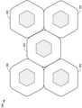
본원에 개시되는 특정 양태에 따르면, 충전 표면은 충전 디바이스에서 충전 셀을 사용하여 제공될 수 있으며, 여기서 충전 셀은 충전 표면에 인접하여 배치된다. 일 예에서, 충전 셀은 벌집형 패키징 구성에 따라 충전 표면의 하나 이상의 층에 배치된다. 충전 셀은 코일에 인접한 충전 표면에 실질적으로 직교하는 축을 따라 자기 필드를 각각 유도할 수 있는 하나 이상의 코일을 사용하여 구현될 수 있다. 본 설명에서, 충전 셀은 하나 이상의 코일을 갖는 요소를 지칭할 수 있으며 여기서 각각의 코일은 충전 셀의 다른 코일에 의해 생성되고 공통 축을 따라 또는 근접하여 지향되는 필드에 대해 부가적인 전자기 필드를 생성하도록 구성된다. 일부 예에서, 충전 셀의 코일은 인쇄 회로 보드 상의 트레이스(trace)를 사용하여 형성된다. 일부 예에서, 충전 셀의 코일은 평면 코일 또는 일반적으로 원통형 윤곽을 갖는 코일을 획득하기 위해 와이어를 나선형으로 권선함으로써 형성된다. 일 예에서, 리츠(Litz) 와이어는 코일에 중앙 전력 전송 영역을 제공하는 평면 또는 실질적으로 평탄 권선을 형성하기 위해 사용될 수 있다.According to certain aspects disclosed herein, a charging surface may be provided using a charging cell in a charging device, where the charging cell is disposed adjacent to the charging surface. In one example, the charging cells are disposed in one or more layers of the charging surface according to the honeycomb packaging configuration. A charging cell may be implemented using one or more coils, each capable of inducing a magnetic field along an axis substantially orthogonal to a charging surface adjacent to the coil. In this description, a charge cell may refer to an element having one or more coils, where each coil is configured to produce an electromagnetic field that is additional to a field generated by the other coils of the charge cell and directed along or proximate to a common axis. It consists of In some examples, the coil of the charge cell is formed using traces on a printed circuit board. In some examples, the coil of the charge cell is formed by helically winding the wire to obtain a planar coil or a coil with a generally cylindrical contour. In one example, Litz wire may be used to form planar or substantially flat windings that provide a central power transfer area to the coil.
일부 구현예에서, 충전 셀은 공통 축을 따라 스택되고/되거나 오버랩되는 코일을 포함함으로써 그들은 충전 표면에 실질적으로 직교하는 유도된 자기 필드에 기여한다. 일부 구현예에서, 충전 셀은 충전 표면의 정의된 부분 내에 배열되고 충전 셀과 연관되는 충전 표면의 실질적 직교 부분 내의 유도된 자기 필드에 기여하는 코일을 포함한다. 일부 구현예에서, 충전 셀은 활성화 전류를 동적으로 정의된 충전 셀에 포함되는 코일에 제공함으로써 구성가능할 수 있다. 예를 들어, 충전 디바이스는 충전 표면에 걸쳐 배치되는 다수의 코일 스택을 포함할 수 있고, 충전 디바이스는 충전될 디바이스의 위치를 검출할 수 있고 충전될 디바이스에 인접한 충전 셀을 제공하기 위해 코일 스택의 일부 조합을 선택할 수 있다. 일부 경우에서, 충전 셀은 단일 코일을 포함하거나, 단일 코일로서 특징지어질 수 있다. 그러나, 충전 셀은 다수의 스택된 코일 및/또는 다수의 인접한 코일 또는 코일 스택을 포함할 수 있다고 점이 이해되어야 한다. 코일은 충전 코일, 무선 충전 코일, 송신기 코일, 송신 코일, 전력 송신 코일, 전력 송신기 코일 등으로서 본원에 지칭될 수 있다.In some implementations, the charging cells include coils that are stacked and/or overlapping along a common axis so that they contribute an induced magnetic field that is substantially orthogonal to the charging surface. In some implementations, a charging cell includes a coil arranged within a defined portion of the charging surface and contributing to an induced magnetic field within a substantially orthogonal portion of the charging surface associated with the charging cell. In some implementations, the charging cell can be configurable by providing an activation current to a coil included in the dynamically defined charging cell. For example, a charging device can include multiple coil stacks disposed across a charging surface, and the charging device can detect the location of the device to be charged and determine the position of the coil stack to provide a charging cell adjacent to the device to be charged. Some combinations can be selected. In some cases, a charge cell may include or be characterized as a single coil. However, it should be understood that a charge cell may include multiple stacked coils and/or multiple adjacent coils or coil stacks. A coil may be referred to herein as a charging coil, wireless charging coil, transmitter coil, transmitting coil, power transmitting coil, power transmitter coil, or the like.
도 1은 충전 디바이스의 충전 표면을 제공하도록 배치되고/되거나 구성될 수 있는 충전 셀(100)의 예를 예시한다. 본원에 설명되는 바와 같이, 충전 표면은 하나 이상의 기판(106) 상에 제공되는 충전 셀(100)의 어레이를 포함할 수 있다. 하나 이상의 집적 회로(IC) 및/또는 별개의 전자 부품(electronic component)을 포함하는 회로는 기판(106) 중 하나 이상에 제공될 수 있다. 회로는 전력을 수신 디바이스에 송신하기 위해 사용되는 코일에 제공되는 전류를 제어하기 위해 사용되는 드라이버 및 스위치를 포함할 수 있다. 회로는 본원에 개시되는 특정 기능을 수행하도록 구성될 수 있는 하나 이상의 프로세서 및/또는 하나 이상의 컨트롤러를 포함하는 처리 회로로서 구성될 수 있다. 일부 경우에서, 처리 회로의 일부 또는 전부는 충전 디바이스 외부에 제공될 수 있다. 일부 경우에서, 전원 장치는 충전 디바이스에 결합될 수 있다.1 illustrates an example of a charging
충전 셀(100)은 충전 디바이스의 외부 표면 영역에 가까이 근접하여 제공될 수 있으며, 그 상에 하나 이상의 디바이스가 충전을 위해 배치될 수 있다. 충전 디바이스는 충전 셀(100)의 다수의 인스턴스(instance)를 포함할 수 있다. 일 예에서, 충전 셀(100)은 하나 이상의 코일(102)을 둘러싸는 실질적으로 육각형 형상을 가지며, 이는 전력 전송 영역(104)에서 전자기 필드를 생성하기에 충분한 전류를 수신할 수 있는 도체, 와이어 또는 회로 보드 트레이스를 사용하여 구성될 수 있다. 다양한 구현예에서, 일부 코일(102)은, 도 1에 예시되는 육각형 충전 셀(100)을 포함하는, 실질적으로 다각형인 형상을 가질 수 있다. 다른 구현예는 다른 형상을 갖는 코일(102)을 제공한다. 코일(102)의 형상은 제조 기술의 능력 및 한계에 의해 적어도 부분적으로 결정되고/되거나, 인쇄 회로 보드 기판과 같은 기판(106) 상에 충전 셀의 레이아웃(layout)을 최적화하도록 결정될 수 있다. 각각의 코일(102)은 와이어, 인쇄 회로 보드 트레이스 및/또는 나선형 구성의 다른 커넥터를 사용하여 구현될 수 있다. 각각의 충전 셀(100)은 상이한 층의 코일(102)이 공통 축(108)을 중심으로 센터링되도록 절연체 또는 기판(106)에 의해 분리되는 2개 이상의 층에 걸쳐 있을 수 있다.The charging
도 2는 본원에 개시되는 특정 양태에 따라 적응될 수 있는 충전 디바이스의 충전 표면의 세그먼트의 단일 층 상에 제공되는 충전 셀(202)의 배열(200)의 예를 예시한다. 충전 셀(202)은 벌집형 패키징 구성에 따라 배열된다. 이러한 예에서, 충전 셀(202)은 중첩(overlap) 없이 단대단(end-to-end)으로 배열된다. 이러한 배열은 스루-홀(through-hole) 또는 와이어 상호연결 없이 제공될 수 있다. 다른 배열이 가능하며, 이는 충전 셀(202)의 일부 부분이 중첩되는 배열을 포함한다. 예를 들어, 2개 이상의 코일의 와이어는 어느 정도 인터리빙될 수 있다.2 illustrates an example of an
도 3은 다수의 층이 본원에 개시되는 특정 양태에 따라 적응될 수 있는 충전 표면의 세그먼트 내에 오버레이될 때 2개의 관점(300, 310)(예를 들어, 상단 및 프로파일 뷰)으로부터의 충전 셀의 배열의 예를 예시한다. 충전 셀(302, 304, 306, 308)의 층은 충전 표면의 세그먼트 내에 제공된다. 충전 셀(302, 304, 306, 308)의 각각의 층 내의 충전 셀은 벌집형 패키징 구성에 따라 배열된다. 일 예에서, 충전 셀(302, 304, 306, 308)의 층은 4개 이상의 층을 갖는 인쇄 회로 보드 상에 형성될 수 있다. 충전 셀(100)의 배열은 예시된 세그먼트에 인접한 지정된 충전 영역의 완전한 커버리지(coverage)를 제공하도록 선택될 수 있다. 충전 셀은 형상에서 다각형인 송신 코일에 의해 제공되는 전력 전송 영역에 대응하는 도 3에 예시되는 302, 304, 306, 308일 수 있다. 다른 구현예에서, 충전 코일은 와이어로부터 구성되는 나선형으로 권선된 평면 코일을 포함하며, 각각은 실질적으로 원형 전력 전송 영역을 제공하도록 권선된다. 후자의 예에서, 다수의 나선형으로 권선된 평면 코일은 무선 충전 디바이스의 충전 표면 아래에 스택된 평면으로 배치될 수 있다.3 shows a charge cell from two
도 4는 본원에 개시되는 특정 양태에 따라 구성되는 충전 셀의 다수의 층을 이용하는 충전 표면(400)에 제공되는 전력 전송 영역의 배열을 예시한다. 예시된 충전 표면은 충전 셀(402, 404, 406, 408)의 4개의 층으로부터 구성되며, 이는 도 3에서 충전 셀(302, 304, 306, 308)의 층에 대응할 수 있다. 도 4에서, 충전 셀(402)의 제1 층에 있는 충전 셀에 의해 제공되는 각각의 전력 전송 영역은 "L1"으로 마킹되고, 충전 셀(404)의 제2 층에 있는 충전 셀에 의해 제공되는 각각의 전력 전송 영역은 "L2"로 마킹되고, 충전 셀(406)의 제3 층에 있는 충전 셀에 의해 제공되는 각각의 전력 전송 영역은 "L3"로 마킹되고, 충전 셀(408)의 제4 층에 있는 충전 셀에 의해 제공되는 각각의 전력 전송 영역은 "L4"로 마킹된다.4 illustrates an arrangement of power transfer areas provided on a charging
무선 송신기wireless transmitter
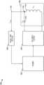
도 5는 본 개시의 특정 양태에 따라 적응될 수 있는 무선 충전 디바이스 내의 무선 송신기(500)의 예를 예시한다. 컨트롤러(502)는 컨디셔닝 회로(conditioning circuit)(508)에 의해 필터링되거나 달리 처리되는 피드백 신호를 수신할 수 있다. 컨트롤러는 커패시터(512) 및 인덕터(514)를 포함하는 회로에 의해 표현될 수 있는 공진 회로(506)에 교류(alternating current)를 제공하는 드라이버 회로(504)의 동작을 제어할 수 있다. 공진 회로(506)는 또한 탱크 회로, LC 탱크 회로, 또는 LC 탱크로서 본원에 지칭될 수 있고, 공진 회로(506)의 LC 노드(510)에서 측정되는 전압(516)은 탱크 전압으로서 지칭될 수 있다.5 illustrates an example of a
무선 송신기(500)는 호환가능한 디바이스가 무선 충전 디바이스의 충전 표면 상에 배치되었는지 여부를 결정하기 위해 충전 디바이스에 의해 사용될 수 있다. 예를 들어, 충전 디바이스는 호환가능한 디바이스가 무선 송신기(500)를 통해 간헐적 테스트 신호(능동 또는 디지털 핑)를 전송함으로써 충전 표면 상에 배치되었다는 것을 결정할 수 있으며, 여기서 공진 회로(506)는 호환가능한 디바이스가 테스트 신호에 응답할 때 인코딩된 신호를 검출하거나 수신할 수 있다. 충전 디바이스는 표준, 관례, 제조업자 또는 애플리케이션에 의해 정의되는 응답 신호의 수신을 결정한 후 적어도 하나의 충전 셀에서 하나 이상의 코일을 활성화하도록 구성될 수 있다. 일부 예에서, 호환가능한 디바이스는 충전 디바이스가 호환가능한 디바이스를 충전하기 위해 사용될 최적의 충전 셀을 발견할 수 있도록 수신된 신호 강도를 전달함으로써 핑에 응답한다.The
본원에 개시되는 특정 기술을 포함하는 수동(passive) 디바이스 발견 기술은 충전가능한 디바이스가 충전가능한 디바이스로부터 능동 응답(active response)을 요구하지 않는 테스트 신호를 사용하여 충전 표면 상에 배치되었다고 결정할 수 있다. 수동 디바이스 발견 기술은 충전가능한 디바이스의 존재 또는 부재를 나타내는 응답을 자극하기 위해 충전 디바이스의 표면을 통한 펄스의 전송을 수반할 수 있다. 일 예에서, 처리 회로는 무선 충전 디바이스의 충전 표면에 근접하여 배치되는 수신 코일의 존재를 식별하기 위해 충전 디바이스 내의 LC 노드(510)에서 측정되거나 관찰되는 전압 및/또는 전류를 모니터링할 수 있다. 회로는 종종 LC 노드(510)에서 전압을 측정하거나 LC 네트워크에서 전류를 측정하기 위해 무선 충전 디바이스에 제공된다. 이러한 전압 및 전류 측정은 전력 조절 목적을 위해 또는, 일부 경우에서, 디바이스 사이의 통신을 지원하기 위해 모니터링될 수 있다. 도 5의 무선 송신기(500)는 LC 노드(510)에서 전압의 측정이 모니터링되는 것을 예시한다. 전류는 짧은 펄스가 공진 회로(506)에 제공될 때 수동 핑(passive ping)을 지원하기 위해 추가적으로 또는 대안적으로 모니터링될 수 있다. 전압 예에서, 수동 핑(초기 전압V0)에 대한 공진 회로(506)의 응답은, 다음과 같이, LC 노드(510)에서의 전압(VLC)에 의해 표현될 수 있다:Passive device discovery techniques, including certain techniques disclosed herein, can determine that a chargeable device has been placed on a charging surface using a test signal that does not require an active response from the chargeable device. Passive device discovery techniques may involve sending pulses through the surface of a charging device to stimulate a response indicating the presence or absence of a chargeable device. In one example, processing circuitry may monitor the voltage and/or current measured or observed at the

본원에 개시되는 특정 양태에 따르면, 하나 이상의 충전 셀 내의 코일은 호환가능한 디바이스를 충전하기 위한 최적의 전자기 필드를 제공하기 위해 선택적으로 활성화될 수 있다. 일부 경우에서, 코일은 충전 셀에 할당될 수 있고, 일부 충전 셀은 다른 충전 셀과 중첩될 수 있다. 후자의 경우에서, 최적의 충전 구성은 충전 셀 레벨에서 선택될 수 있다. 다른 경우에서, 충전 셀은 충전 디바이스의 표면 상의 충전될 디바이스의 배치에 기초하여 정의될 수 있다. 이러한 다른 경우에서, 각각의 충전 이벤트에 대해 활성화되는 코일의 조합은 서로 다를 수 있다. 일부 구현예에서, 충전 디바이스는 충전 이벤트 동안 활성화를 위해 하나 이상의 셀 및/또는 하나 이상의 미리정의된 충전 셀을 선택할 수 있는 드라이버 회로를 포함할 수 있다.According to certain aspects disclosed herein, coils within one or more charging cells may be selectively activated to provide optimal electromagnetic fields for charging compatible devices. In some cases, coils may be assigned to charge cells, and some charge cells may overlap other charge cells. In the latter case, the optimal charging configuration can be selected at the charging cell level. In another case, a charging cell may be defined based on the placement of the device to be charged on the surface of the charging device. In these other cases, the combination of coils that are activated for each charging event may be different. In some implementations, the charging device can include driver circuitry that can select one or more cells and/or one or more predefined charging cells for activation during a charging event.
본 개시의 특정 양태는 충전가능한 디바이스의 존재 또는 부재를 검출하기 위해 충전가능한 디바이스의 특성(characteristics)의 측정 또는 모니터링에 관한 것이다. 일 양태에서, 충전가능한 디바이스의 위치는 충전가능한 디바이스의 충전 표면을 제공하는 하나 이상의 송신 코일에 대해 결정될 수 있다. 일부 경우에서, 충전 디바이스는 송신 코일로부터 충전가능한 디바이스의 절대 거리 또는 정렬 및/또는 송신 코일에 대한 충전가능한 디바이스의 다차원(multi-dimensional) 정렬을 결정할 수 있다.Certain aspects of the present disclosure relate to measuring or monitoring characteristics of a chargeable device to detect the presence or absence of a chargeable device. In one aspect, a location of a chargeable device may be determined relative to one or more transmit coils providing a charging surface for the chargeable device. In some cases, the charging device may determine an absolute distance or alignment of the chargeable device from the transmitting coil and/or a multi-dimensional alignment of the chargeable device relative to the transmitting coil.
본 개시의 특정 양태에서, 충전가능한 디바이스의 특성은 공진 반사를 사용하여 측정되거나 모니터링될 수 있다. 공진 반사는 충전가능한 디바이스에 제공되는 전력 수신 회로의 공진을 이용한다. 도 6은 Qi 표준과 호환가능하고 수신 회로(602) 및 충전 회로(612)를 포함하는 시스템(600) 내의 무선 충전의 예를 예시한다. 수신 회로(602)는 2차 변압기로서 동작하는 수신 코일(604)을 포함하며, 1차 변압기는 충전 회로(612) 내의 송신 코일(614)에 의해 제공된다. 수신 코일(604)은 인덕턴스(Ls)를 갖는다. 수신 회로(602)는 수신 코일(604)의 인덕턴스에 기초하여 선택되는 커패시턴스(Cs)를 갖는 일련의 공진 커패시터(606)를 더 포함하고, 이는 송신 코일(614)에 의해 제공되는 충전 플럭스의 주파수에 수신 회로(602)를 튜닝하기 위해 선택될 수 있다. 일 예에서, 충전 플럭스의 주파수는 명목상 100 kHz이다. 따라서, 수신 회로(602)의 제1 공진 주파수(fs)는 다음과 같이 진술될 수 있다:In certain aspects of the present disclosure, characteristics of a chargeable device may be measured or monitored using resonant reflection. Resonant reflection exploits the resonance of the power receiving circuit provided in the chargeable device. 6 illustrates an example of wireless charging within a

Qi 표준은 검출 커패시터(608)가 수신 코일(604)과 병렬로 제공될 것임을 지정한다. 검출 커패시터(608)는 수신 코일(604)의 인덕턴스에 기초하여 선택되는 커패시턴스(Cd)를 갖고 공칭 1 MHz에서 공진하는 검출 공진 회로를 제공한다. 수신 회로(602)의 검출 공진 회로는 다음과 같이 진술될 수 있는 제2 공진 주파수(fd)를 갖는다:The Qi standard specifies that the

검출 공진 회로는 Qi 표준에 의해 정의되지만, 그것은 전형적으로 기존 충전 시스템에서 사용되지 않는다.A detection resonant circuit is defined by the Qi standard, but it is typically not used in existing charging systems.
본 개시의 특정 양태에 따르면, 충전 디바이스는 검출 공진 회로가 공진하게 하고 1MHz 공진 주파수에서 여기 신호의 에너지를 방사하거나 재방사하게 하는 여기 신호를 송신할 수 있다. 예를 들어, 충전 회로(612)는 1 MHz에서 또는 그 부근에서 측정될 수 있는 주파수를 갖는 여기 플럭스를 송신할 수 있고, 1 MHz에 튜닝되는 공진 회로를 장착한 충전가능한 디바이스 내의 수신기는 이러한 에너지를 의미있는 또는 측정가능한 크기로 충전 회로(612)에 다시 재방사할 것이다. 본 개시의 목적을 위해, 1 MHz에 튜닝되는 공진 회로를 장착한 충전가능한 디바이스는 Qi 호환가능한 충전가능한 디바이스, Qi 호환가능한 디바이스 또는 단순히 호환가능한 디바이스로서 지칭될 수 있다. Qi 표준과 호환되지 않거나 호환가능한 충전가능한 디바이스 및 다른 디바이스 또는 객체(object)는 1 MHz 여기 신호에 응답할 것으로 예상되지 않는다. Qi 규격이 아닌 특정 충전가능한 디바이스는 무선 충전 디바이스로부터 전력을 수신할 수 있을 때 1 MHz 여기 신호에 응답하도록 적응될 수 있다.According to certain aspects of the present disclosure, the charging device may transmit an excitation signal that causes the detecting resonant circuit to resonate and radiate or re-radiate the energy of the excitation signal at a 1 MHz resonant frequency. For example, the charging
도 7은 충전 표면(700) 상에 또는 근처에 배치되는 충전가능한 디바이스의 존재를 검출할 수 있는 여기 코일(702)을 포함하는 무선 충전기의 충전 표면(700)의 예를 예시한다. 여기 코일(702)은 충전 표면(700)과 연관되는 하나 이상의 충전 코일(LP1-LP18) 주위에 제공될 수 있다. 일부 예에서, 여기 코일(702)은 충전 코일(LP1-LP18) 중 일부 또는 전부를 포함하는 충전 표면(700)의 영역을 둘러싼다. 일 예에서, 여기 코일(702)은 충전 표면(700)에 제공되는 모든 충전 코일과경계를 이루거나 이를 둘러싼다. 다른 예에서, 여기 코일(702)은 개별 충전 코일 또는 충전 코일 그룹과 경계를 이루거나 이를 둘러싼다. 예를 들어, 여기 코일(702)은 충전 표면(700) 상에 마킹되거나 달리 식별되는 충전 구역과 경계를 이루거나 이를 둘러쌀 수 있으며, 여기서 여기 코일(702)은 본원에 개시되는 공진 반사 기술을 사용하여 모니터링될 충전 구역의 외부 한계를 추적하거나 정의하도록 구성된다.7 illustrates an example of a charging
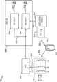
도 8은 본 개시의 특정 양태에 따라 호환가능한 충전가능한 디바이스(810)를 검출하도록 구성되는 검출 회로(800)의 제1 예를 예시한다. 검출 회로(800)는 무선 충전 디바이스 내에 제공된다. 일부 예에서, 검출 회로(800)는 도 7에 예시되는 충전 표면(700)과 유사한 충전 표면을 제공하는 무선 충전 디바이스에 제공될 수 있다. 검출 회로(800)는 단일 여기 코일(702)에 결합되는 처리 회로(808)를 포함할 수 있다. 일부 예에서, 처리 회로(808)는 하나보다 많은 여기 코일(702)에 결합될 수 있다. 일부 예에서, 검출 회로(800)는 무선 충전 디바이스에 제공되는 다수의 검출 회로 중 하나일 수 있다.8 illustrates a first example of a
일부 구현예에서, 검출 회로(800)는 여기 코일(702)이 전자기 플럭스(828)를 송신하게 하도록 구성가능한 여기 신호(816)를 제공하는 신호 드라이버 회로(806)를 포함한다. 전자기 플럭스(828)는 여기 플럭스로서 지칭될 수 있다. 여기 신호(816)는 호환가능한 또는 식별가능한 충전가능한 디바이스(810)에서 검출 공진 회로의 공진 주파수에서 또는 근처에서 제공된다. 일 예에서, 충전가능한 디바이스(810)는 그것이 Qi 표준을 준수하는 전력 수신 회로를 가질 때 호환가능할 수 있다(예를 들어, 도 6 참조). 다른 예에서, 충전가능한 디바이스(810)는 그것이 여기 신호(816)의 주파수에서 공진하는 전력 수신 회로를 가질 때 호환가능하거나 식별가능할 수 있으며, 이는 신호 드라이버 회로(806)를 사용하여 구성되거나 선택될 수 있다. 다양한 구현예에서, 여기 신호(816)는 1 MHz의 공칭 주파수를 갖는다.In some implementations, the
여기 코일(702)에 의해 송신되는 전자기 플럭스(828)는 충전가능한 디바이스(810)에서 수신 코일을 여기시킬 수 있다. 무선 충전 디바이스의 충전 표면(700)에 위치되는 송신 코일(804)은 공진 회로의 존재에 의해 영향을 받을 수 있고/있거나 여기 코일(702)에 의해 송신되는 전자기 플럭스(828)를 검출할 수 있다. 일부 경우에서, 충전 디바이스는 그것이 충전 표면(700) 상에 또는 근처에 배치될 때 충전가능한 디바이스(810)에 의해 송신되는 반사된 플럭스(830)에 응답할 수 있다. 검출 회로(800)는 충전가능한 디바이스(810)에서 전력 수신 회로로부터 송신되는 반사된 플럭스(830)의 전력, 진폭, 신호 이득, 또는 위상 편이에 기초하여 충전가능한 디바이스(810)의 존재 또는 위치를 식별할 수 있다. 반사된 플럭스(830)는 충전 표면(700)에서 송신 코일(804) 중 하나 이상에 의해 검출될 수 있다.
검출 회로(800)는 전력의 크기또는 위상 편이가 공진에 기인하고 여기 신호(816)의 주파수에서 충전가능한 디바이스(810) 내의 전력 수신 회로의 공진과 일치할 때 충전가능한 디바이스(810)가 존재한다고 결정할 수 있다. 송신 코일(804)의 특성(814)은 충전가능한 디바이스(810)가 호환가능하고 충전 표면 상에 또는 근처에 배치되었을 때를 결정하기 위해 모니터링될 수 있다. 특성(814)은 송신 코일(804)에 흐르는 전류 또는 송신 코일(804)과 연관되는 탱크 전압에 대응할 수 있다. 도 5에 예시되는 무선 송신기(500)를 참조하면, 특성은 공진 회로(506)의 LC 노드(510)에서 취해지는 측정에 의해 표현될 수 있다. 일 예에서, 특성은 인덕터(514)를 통해 흐르는 전류, 또는 전류의 변화에 의해 표현될 수 있다. 다른 예에서, 특성은 인덕터(514)에 걸쳐 측정되는 전압, 또는 전압의 변화에 의해 표현될 수 있다. 다른 예에서, 특성은 인덕터(514)를 통한 전류 흐름의 일련의 측정 또는 인덕터(514)에 걸친 전압의 측정을 사용하여 계산되거나 달리 획득되는 공진 회로(506)의 공진 주파수, 또는 공진 주파수의 변화에 의해 표현될 수 있다. 일의 예에서, 아날로그-디지털 변환기(ADC(802))는 공진 회로(506)에서 전류 또는 전압을 샘플링 및 정량화하고 인덕터(514)와 연관되는 전류 또는 탱크 전압의 측정의 시계열(time-series)의 디지털 표현을 제공하는 멀티비트 신호(812)를 제공하기 위해 사용될 수 있으며, 이는 송신 코일(804)의 인덕턴스를 포함하는 인덕턴스를 가질 수 있다.The
멀티비트 신호(812)는 회로를 포함하거나 멀티비트 신호(812)에 의해 표현되는 바와 같은 관찰된 특성(814)과 하나 이상의 기준 신호 사이의 차이를 검출하도록 구성되는 비교기(818, 820)로서 동작하는 모듈을 구현하는 처리 회로(808)에 제공된다. 기준 신호는 충전가능한 디바이스가 존재하지 않을 때 송신 코일(804)의 상태를 표현할 수 있다.The
도 9는 여기 신호(816)가 주파수 범위에 걸쳐 송신될 때 송신 코일(804)에서 관찰될 수 있는 주파수 응답(902, 904)을 예시하는 응답 다이어그램(900)이다. 제1 주파수 응답(902)은 무선 충전기의 충전 표면 근처에 위치되지 않을 때, 또는 충전 표면(700) 상에 배치되는 객체가 이중-공진(dual-resonant) 전력 수신 회로를 갖지 않을 때 송신 코일(804) 중 하나 이상에서 관찰될 것으로 예상되는 응답을 예시한다. 제2 주파수 응답(904)은 무선 충전기의 충전 표면(700) 근처에 위치되는 객체가 이중-공진 전력 수신 회로를 가질 때 송신 코일(804) 중 하나 이상에서 관찰될 것으로 예상되는 응답을 예시하고, 여기서 검출 회로는 공칭 1 MHz 주파수에서 공진하도록 구성된다. 주파수 응답(902, 904)은 더 높은 주파수(예를 들어,f > 500 kHz)에서 발산하기 시작하고 이득(gain)의 현저한 차이는 1 MHz 주파수 근처에서 관찰되며, 최대 차이(910)는 1 MHz보다 더 큰 주파수에서 관찰된다. 제2 주파수 응답(904)의 이득은 초기에 제1 주파수 응답(902)에 대해 최대 양의(positive) 차이(908)로 증가하고, 제1 주파수 응답(902)에 대해 음의(negative) 차이인 최대 차이(910)로 강하한다. 이득의 피크 응답은 수신 코일과 충전 디바이스 내의 송신 코일의 결합(coupling)이 검출 회로의 인덕턴스에 영향을 미치고 검출 회로의 공진 주파수를 수정하기 때문에 충전가능한 디바이스 내의 검출 회로의 공칭 공진 주파수와 다른 주파수에서 관찰될 수 있다.FIG. 9 is a response diagram 900 illustrating the
도 10은 주파수 범위에 걸쳐 반사된 또는 재송신된 신호와 여기 신호(816) 사이의 위상 차이에 대응하는 위상 응답(1002, 1004)을 예시하는 응답 다이어그램(1000)이다. 제1 위상 응답(1002)은 객체가 무선 충전기의 충전 표면(700) 근처에 위치되지 않을 때, 또는 충전 표면(700) 상에 배치되는 객체가 이중-공진 전력 수신 회로를 갖지 않을 때 송신 코일(804) 중 하나 이상에서 관찰될 것으로 예상되는 응답을 예시한다. 제2 위상 응답(1004)은 무선 충전기의 충전 표면(700) 근처에 위치되는 객체가 이중-공진 전력 수신 회로를 가지질 때 송신 코일(804) 중 하나 이상에서 관찰될 것으로 예상되는 응답을 예시하며, 그것에 의해 검출 회로는 공칭 1 MHz 주파수에서 공진하도록 구성된다. 최대 차이(1006)는 1 MHz보다 더 큰 주파수에서 관찰된다. 위상 응답(1002, 1004) 사이의 위상 편이의 피크 차이는 수신 코일과 충전 디바이스 내의 송신 코일의 결합(coupling)이 검출 회로의 인덕턴스에 영향을 미치고 검출 회로의 공진 주파수를 수정하기 때문에 충전가능한 디바이스 내의 검출 회로의 공칭 공진 주파수와 다른 주파수에서 관찰될 수 있다.10 is a response diagram 1000 illustrating
주파수 응답(902, 904)과 위상 응답(1002, 1004) 사이의 차이는 호환가능한 충전가능한 디바이스(예를 들어, 충전가능한 디바이스(810))가 무선 충전기의 충전 표면(700) 상에 배치되거나 위치되는 때를 결정하기 위해 도 8의 검출 회로(800)에 의해 사용될 수 있다. 처리 회로(808)는 송신 코일(804)과 연관되는 전류 또는 탱크 전압의 측정의 시계열을 표현하는 멀티비트 신호(812)와 기준 신호 또는 임계값을 비교하도록 구성되는 진폭 비교기(818)를 포함하거나 제공할 수 있다. 일 예에서, 기준 신호는 여기 신호(816)가 비교가능한 이득이 주파수 응답(902, 904)에서 예상되는 주파수를 가질 때 반사된 신호의 진폭을 표현할 수 있다. 제1 주파수 응답(902)(객체 부존재)의 궤적은 증가하는 또는 실질적으로 평탄할 것으로 예상될 수 있고, 이득의 강하는 호환가능한 충전가능한 디바이스(810)의 존재를 나타낼 수 있다. 기준 신호는 검색 절차 동안 획득될 수 있다. 일부 경우에서, 기준 신호는 다수의 검색에서 사용될 수 있는 송신 코일(804) 중 하나 이상에 대한 임계 레벨을 설정하기 위해 사용될 수 있다.The difference between the
처리 회로(808)는 여기 신호(816)의 위상(826)과 연관되는 전류 또는 탱크 전압의 측정의 시계열을 표현하는 멀티비트 신호(812)의 위상을 비교하도록 구성되는 위상 비교기(820)를 포함하거나 제공할 수 있다. 위상 비교기(820)는 위상 편이 차이가 임계 차이를 초과했는지 또는 위상 편이의 변화율이 임계 변화율을 초과하는지를 결정하도록 더 구성될 수 있다.The
주파수 응답(902, 904) 및 위상 응답(1002, 1004)은 호환가능한 충전가능한 디바이스의 존재가 주파수 응답(902, 904) 및 위상 응답(1002, 1004) 둘 다에서 큰 차이를 야기한다는 점을 보여준다. 호환가능한 충전가능한 디바이스의 존재는 위상 응답(1002, 1004)의 최대 차이가 발생하는 주파수와 다른 주파수에서 발생하는 주파수 응답(902, 904)의 최대 차이를 야기할 수 있다. 더욱이, 주파수 응답(902, 904) 및 위상 응답(1002, 1004)의 최대 차이는 전형적으로 충전 디바이스 내의 송신 코일과 충전가능한 디바이스(810) 내의 수신 코일 사이의 결합(coupling)에 의해 야기되는 공진 주파수의 변화로 인해 정확히 1 MHz에서 발생하지 않는다.
특정 구현예에서, 충전가능한 디바이스(810)의 위치는 다수의 송신 코일(804)에 대해 측정되는 응답에 기초하여 추정되거나 확인될 수 있다. 일 예에서, 충전가능한 디바이스(810)에 가장 가까운 송신 코일(804)은 검출된, 반사된 신호에서 가장 큰 진폭 또는 위상 편이를 생성할 수 있다. 다른 예에서, 충전가능한 디바이스(810)에 가장 가까운 송신 코일(804)은 기준 신호에 비해 검출된, 반사된 신호에서 가장 큰 진폭의 변화 또는 위상 편이의 변화를 생성할 수 있다. 일부 경우에서, 각각의 송신 코일(804)에 대해 사용되는 기준 신호는 교정 절차(calibration procedure) 동안 송신 코일(804)에 대해 캡처되는 신호일 수 있다. 일부 경우에서, 각각의 송신 코일(804)에 대해 사용되는 기준 신호는 호환가능한 충전가능한 디바이스(810)에서 공진 응답을 유발할 것으로 예상되지 않는 주파수에서의 검색 절차 동안 캡처될 수 있다.In certain implementations, the location of the
일부 구현예에서, 처리 회로(808)는 충전가능한 디바이스(810)의 존재의 검출의 신뢰성을 개선하기 위해 진폭 비교기(818) 및 위상 비교기(820) 둘 다를 포함하거나 제공할 수 있다. 2개의 검출 결정(822, 824)의 생성은 신뢰성을 개선할 수 있고 검출 회로의 공간 주파수의 변화를 수용할 수 있다. 주파수 디터링(dithering)은 검출을 더 개선하기 위해 사용될 수 있다. 주파수 디터링은 관습적으로 잡음 스펙트럼을 확산시킴으로써 전원 장치에서 신호 대 잡음 비(signal-to-noise ratio; SNR)를 개선하기 위해 이용된다. 가변 주파수 여기 신호(816)의 사용은 그러한 존재가 검출 회로의 공진 주파수를 예측할 수 없는 정도로 수정할 수 있을 때 충전가능한 디바이스(810)의 존재의 검출을 개선할 수 있으며, 여기서 공진 주파수의 변화는, 예를 들어, 전력 송신 및 전력 수신 코일의 근접도 및 중첩 정도에 의존할 수 있다. 주파수 디터링 기술은 검출의 불확실성을 감소시키기 위해 적용될 수 있으며, 이는 SNR의 형태로서 정량화될 수 있다.In some implementations,
일부 구현예는 검출의 증가된 불확실성을 희생시키면서 복잡성을 감소시키기 위해 단일 여기 주파수를 사용할 수 있다. 일부 구현예는 충전 회로에서 복잡성을 감소시키기 위해 단일 검출 메트릭 - 진폭 또는 위상 -을 사용할 수 있다. 반사된 신호의 위상 편이 및 진폭 둘 다의 모니터링 및 측정은 검출 회로 감도 및 검출 신뢰성을 증가시킬 수 있다.Some implementations may use a single excitation frequency to reduce complexity at the expense of increased uncertainty of detection. Some implementations may use a single detection metric - amplitude or phase - to reduce complexity in the charging circuit. Monitoring and measuring both the phase shift and amplitude of the reflected signal can increase detection circuit sensitivity and detection reliability.
도 11은 본 개시의 특정 양태에 따라 호환가능한 충전가능한 디바이스(1110)를 검출하도록 구성되는 검출 회로(1100)의 제2 예를 예시한다. 검출 회로(1100)는 무선 충전기에 제공될 수 있다. 본원에 설명되는 일 예에서, 검출 회로(1100)는 도 7에 예시되는 충전 표면(700)을 제공하고, 여기 신호(1116)를 송신하기 위해 하나 이상의 전력 송신 코일(1104)을 사용하는 무선 충전기에 제공될 수 있다. 여기 신호(1116)를 송신하는 전력 송신 코일(1104)은 또한 여기 신호(1116)에 응답하여 반사되는 임의의 신호를 검출할 수 있다.11 illustrates a second example of a
예시된 예에서, 검출 회로(1100)는 여기 신호(1116)를 전력 송신 코일(1104)에 제공하는 신호 드라이버(1106)를 포함한다. 여기 신호(1116)는 전력 송신 코일(1104)이 전자기 플럭스(1128)를 송신하게 한다. 여기 신호(1116)는 호환가능한 또는 식별가능한 충전가능한 디바이스 내의 검출 공진 회로의 공칭 공진 주파수에 가까운 주파수를 갖는다. 일 예에서, 충전가능한 디바이스는 그것이 Qi 표준을 준수하는 전력 수신 회로를 가질 때 호환가능할 수 있다(예를 들어, 도 6 참조). 다른 예에서, 충전가능한 디바이스는 그것이 신호 드라이버(1106)를 사용하여 구성되거나 선택되는 여기 신호(1116)의 주파수에서 공진하는 전력 수신 회로를 가질 때 호환가능하거나 식별가능할 수 있다. 다양한 구현예에서, 여기 신호(1116)는 1 MHz의 공칭 주파수를 갖는다.In the illustrated example, the
전력 송신 코일(1104)에 의해 송신되는 전자기 플럭스(1128)는 충전가능한 디바이스(1110) 내의 수신 코일을 여기시킬 수 있다. 예를 들어, 충전 표면(700)에 위치되는 전력 송신 코일(1104)은 공진 회로의 존재에 의해 및/또는 충전 표면(700) 상에 또는 근처에 위치되는 충전가능한 디바이스(1110)에 의해 송신되는 반사된 플럭스(1130)에 의해 영향을 받을 수 있다. 검출 회로(1100)는 전력 송신 코일(1104)에서 측정되는 진폭 또는 위상 편이에 기초하여 충전가능한 디바이스(1110)의 존재 또는 위치를 식별할 수 있다. 일부 구현예에서, 전력 송신 코일(1104)과 연관되는 탱크 전압 또는 전류의 진폭 및/또는 위상은 여기 신호(1116)의 주파수에서 또는 근처에서 충전가능한 디바이스(1110) 내의 전력 수신 회로의 공진에 기인하는 전압 또는 전류의 크기, 위상 또는 크기 또는 위상의 변화를 결정하기 위해 모니터링될 수 있다.The
전력 송신 코일(1104)의 특성(1114)은 호환가능한 충전가능한 디바이스(1110)가 충전 표면 근처에 배치된 때를 결정하기 위해 모니터링될 수 있다. 특성(1114)은 전력 송신 코일(1104)에 흐르는 전류 또는 전력 송신 코일(1104)과 연관되는 탱크 전압의 진폭에 대응할 수 있다. 일 구현예에서, 아날로그-디지털 변환기(ADC(1102))는 하나 이상의 특성(1114)을 샘플링 및 측정하고 전력 송신 코일(1104)과 연관되는 전류 또는 탱크 전압의 측정의 시계열의 디지털 표현을 제공하는 멀티비트 신호(1112)를 제공하기 위해 사용될 수 있다.
멀티비트 신호(1112)는 멀티비트 신호(1112)에 의해 표현되는 바와 같은 관찰된 특성(1114)과 하나 이상의 기준 신호 사이의 차이를 검출하도록 구성되는 비교기(1118, 1120)로서 동작하는 회로를 포함하거나 모듈을 구현하는 처리 회로(1108)에 제공된다. 기준 신호는 충전가능한 디바이스가 존재하지 않을 때 전력 송신 코일(1104)의 상태를 표현할 수 있다.The
도 12는 여기 신호(1116)가 주파수 범위에 걸쳐 송신될 때 전력 송신 코일(1104)에서 관찰될 수 있는 주파수 응답(1202, 1204)을 예시하는 응답 다이어그램(1200)이다. 주파수 응답(1202, 1204)은 여기 신호(1116)의 주파수에 대한 전압 또는 전류 진폭을 플롯팅하고 측정은 전력 송신 코일(1104)에서 취해질 수 있다. 제1 주파수 응답(1202)은 객체가 무선 충전기의 충전 표면(700) 근처에 위치되지 않을 때, 또는 충전 표면(700) 상에 배치되는 객체가 이중-공진 전력 수신 회로를 갖지 않을 때 전력 송신 코일(1104)에서 관찰되는 응답을 예시한다. 제2 주파수 응답(1204)은 무선 충전기의 충전 표면(700) 근처에 위치되는 객제가 이중-공진 전력 수신 회로를 가질 때 송신 코일(1104)에서 관찰되는 응답을 예시하며, 그것에 의해 호환가능한 충전가능한 디바이스(1110) 내의 검출 회로는 공칭 1 MHz 주파수에서 공진하도록 구성된다. 주파수 응답(1202, 1204)은 1 MHz보다 더 큰 주파수에서 최대 차이(1206)를 나타낸다.12 is a response diagram 1200 illustrating the
도 13은 여기 신호(1116)가 주파수 범위에 걸쳐 송신될 때 전력 송신 코일(1104)에서 관찰되는 위상 응답(1302, 1304)을 예시하는 응답 다이어그램(1300)이다. 주파수 응답(1202, 1204)은 여기 신호(1116)의 주파수에 대한 전압 또는 전류 진폭의 위상 차이를 플롯팅하고 전력 송신 코일(1104)에서 관찰될 수 있다. 위상 차이는 반사된 또는 재송신된 신호 또는 전력 송신 코일(1104)을 포함하는 충전 회로 상의 근처의 충전가능한 디바이스(1110) 내의 공진 회로의 영향(effect)에 기인할 수 있다.13 is a response diagram 1300 illustrating the
제1 위상 응답(1302)은 객체가 무선 충전기의 충전 표면(700) 근처에 위치되지 않을 때, 또는 충전 표면(700) 상에 배치되는 객체가 이중-공진 전력 수신 회로를 갖지 않을 때 전력 송신 코일(1104)에서 관찰되는 응답을 예시한다. 제2 위상 응답(1304)은 무선 충전기의 충전 표면(700) 근처에 위치되는 객체가 이중-공진 전력 수신 회로를 가질 때 전력 송신 코일(1104)에서 관찰되는 응답을 예시하며, 그것에 의해 검출 회로는 공칭 1 MHz 주파수에서 공진하도록 구성된다. 최대 차이는 1 MHz보다 더 큰 주파수(1306)에서 관찰된다. 위상 응답(1302, 1304) 사이의 위상 편이의 피크 차이는 수신 코일과 충전 디바이스 내의 송신 코일의 결합(coupling)이 검출 회로의 인덕턴스에 영향을 미치고 검출 회로의 공진 주파수를 수정하기 때문에 충전가능한 디바이스 내의 검출 회로의 공칭 공진 주파수와 다른 주파수에서 관찰될 수 있다.The
주파수 응답(902, 904)과 위상 응답(1302, 1304) 사이의 차이는 호환가능한 충전가능한 디바이스(1110)가 무선 충전기의 충전 표면(700) 상에 배치되거나 존재할 때를 결정하기 위해 도 11의 검출 회로(1100)에 의해 사용될 수 있다. 처리 회로(1108)는 전력 송신 코일(1104)과 연관되는 전류 또는 탱크 전압의 측정의 시계열을 표현하는 멀티비트 신호(1112)와 기준 신호 또는 임계값을 비교하도록 구성되는 진폭 비교기(1118)를 포함하거나 제공할 수 있다. 제1 주파수 응답(1202)(객체 비존재)의 궤적은 실질적으로 평탄할 것으로 예상될 수 있고, 이득의 강하는 호환가능한 충전가능한 디바이스(1110)의 존재를 나타낼 수 있다. 기준 신호는 검색 절차 동안 획득될 수 있다. 일부 경우에서, 기준 신호는 다수의 검색에서 사용될 수 있는 전력 송신 코일(1104) 중 하나 이상에 대한 임계 레벨을 설정하기 위해 사용될 수 있다.The difference between the
처리 회로(1108)는 여기 신호(1116)의 위상(1126)과 연관되는 전류 또는 탱크 전압의 측정의 시계열을 표현하는 멀티비트 신호(1112)의 위상을 비교하도록 구성되는 위상 비교기(1120)를 포함하거나 제공할 수 있다. 위상 비교기(1120)는 위상 편이 차이가 임계 차이를 초과했는지 또는 위상 편이의 변화율이 임계 변화율을 초과하는지를 결정하도록 더 구성될 수 있다.The
주파수 응답(902, 904) 및 위상 응답(1302, 1304)은 호환가능한 충전가능한 디바이스(1110)의 존재가 주파수 응답(902, 904) 및 위상 응답(1302, 1304) 둘 다에서 큰 차이를 야기한다는 점을 보여준다. 호환가능한 충전가능한 디바이스(1110)의 존재는 위상 응답(1302, 1304)의 최대 차이가 발생하는 주파수와 다른 주파수에서 발생하는 주파수 응답(902, 904)의 최대 차이를 야기할 수 있다. 더욱이, 주파수 응답(902, 904) 및 위상 응답(1302, 1304)의 최대 차이는 전형적으로 충전 디바이스 내의 송신 코일과 충전가능한 디바이스(1110) 내의 수신 코일 사이의 결합(coupling)에 의해 야기되는 공진 주파수의 변화로 인해 정확히 1 MHz에서 발생하지 않는다.
특정 구현예에서, 호환가능한 충전가능한 디바이스(1110)의 위치는 다수의 전력 송신 코일(1104)에 대해 측정되는 응답에 기초하여 추정되거나 확인될 수 있다. 일 예에서, 호환가능한 충전가능한 디바이스(1110)에 가장 가까운 전력 송신 코일(1104)은 검출된, 반사된 신호에서 가장 큰 진폭 또는 위상 편이를 생성할 수 있다. 다른 예에서, 호환가능한 충전가능한 디바이스(1110)에 가장 가까운 전력 송신 코일(1104)은 기준 신호에 비해 검출된, 반사된 신호에서 가장 큰 진폭의 변화 또는 위상 편이의 변화를 생성할 수 있다. 일부 경우에서, 각각의 전력 송신 코일(1104)에 대해 사용되는 기준 신호는 교정 절차 동안 전력 송신 코일(1104)에 대해 캡처되는 신호일 수 있다. 일부 경우에서, 각각의 전력 송신 코일(1104)에 대해 사용되는 기준 신호는 호환가능한 충전가능한 디바이스(1110)에서 공진 응답을 유발할 것으로 예상되지 않는 주파수에서 검색 절차 동안 캡처될 수 있다.In certain implementations, the location of a compatible
일부 구현예에서, 처리 회로(1108)는 호환가능한 충전가능한 디바이스(1110)의 존재의 검출에 대한 신뢰성을 개선하기 위해 진폭 비교기(1118) 및 위상 비교기(1120) 둘 다를 포함하거나 제공할 수 있다. 2개의 검출 결정(1122, 1124)의 생성은 신뢰성을 개선하고 검출 회로의 공진 주파수의 변화를 수용할 수 있다. 주파수 디터링은 검출을 더 개선하기 위해 사용될 수 있다. 주파수 디터링은 관습적으로 잡음 스펙트럼을 확산시킴으로써 전원 장치에서 SNR을 개선하기 위해 이용된다. 가변 주파수 여기 신호(1116)의 사용은 그러한 존재가 검출 회로의 공진 주파수를 예측할 수 없는 정도로 수정할 수 있을 때 호환가능한 충전가능한 디바이스(1110)의 존재의 검출을 개선할 수 있으며, 여기서 공진 주파수의 변화는, 예를 들어, 전력 송신 및 전력 수신 코일의 근접도 및 중첩 정도에 의존할 수 있다. 주파수 디터링 기술은 검출의 불확실성을 감소시키기 위해 적용될 수 있으며, 이는 SNR의 형태로서 정량화될 수 있다.In some implementations,
일부 구현예는 검출의 불확실성을 희생시키면서 복잡성을 감소시키기 위해 단일 여기 주파수를 사용할 수 있다. 일부 구현예는 충전 회로의 복잡성을 감소시키기 위해 단일 검출 메트릭을 사용할 수 있다. 반사된 신호의 위상 편이 및 진폭 둘 다의 모니터링 및 측정은 검출 회로 감도 및 검출 신뢰성을 증가시킬 수 있다.Some implementations may use a single excitation frequency to reduce complexity at the expense of detection uncertainty. Some implementations may use a single detection metric to reduce the complexity of the charging circuit. Monitoring and measuring both the phase shift and amplitude of the reflected signal can increase detection circuit sensitivity and detection reliability.
도 14는 본 개시의 특정 양태에 따라 호환가능한 충전가능한 디바이스를 검출하도록 구성되는 검출 회로(1400)의 제3 예를 예시한다. 도 15는 펄스가 여기 신호(1414)로 송신된 후 전력 송신 코일(1404)에서 관찰되는 응답(1502, 1504)을 예시하는 다이어그램(1500)이다. 검출 회로(1400)는 무선 충전기에 제공될 수 있다. 본원에 설명되는 일 예에서, 검출 회로(1400)는 도 7에 예시되는 충전 표면(700)을 제공하는 무선 충전기에 제공될 수 있고, 그것은 여기 신호(1414)를 송신하기 위해 하나 이상의 전력 송신 코일(1404)을 사용한다. 여기 신호(1414)를 송신하는 전력 송신 코일(1404)은 또한 여기 신호(1414)에 응답하여 반사되는 임의의 신호를 검출할 수 있다.14 illustrates a third example of a
예시된 예에서, 검출 회로(1400)는 여기 신호(1414)에 짧은 펄스를 제공하는 펄스 생성기(1406)를 포함한다. 여기 신호(1414)는 전력 송신 코일(1404)에 제공되고 호환가능한 또는 식별가능한 충전가능한 디바이스 내의 공진 회로를 자극하도록 구성될 수 있다. 일 예에서, 충전가능한 디바이스는 그것이 Qi 표준을 준수하는 전력 수신 회로를 가질 때 호환가능할 수 있다(예를 들어, 도 6 참조). 다른 예에서, 충전가능한 디바이스는 그것이 1 MHz의 공칭 주파수에서 공진하는 전력 수신 회로를 가질 때 호환가능하거나 식별가능할 수 있다.In the illustrated example, the
여기 신호(1414)는 전력 송신 코일(1404)이 여기 플럭스로서 본원에 지칭될 수 있는 전자기 플럭스를 송신하게 할 수 있다. 여기 플럭스는 충전가능한 디바이스 내의 수신 회로에 의해 반사될 수 있다. 예를 들어, 충전 표면(700)에 위치되는 전력 송신 코일(1404)은 충전 표면(700) 상에 또는 근처에 위치되는 충전가능한 디바이스 내의 수신 코일과 결합될 수 있다. 검출 회로(1400)는 펄스의 송신 시간(1506)과 충전가능한 디바이스로부터 수신되는 응답 사이의 지연에 기초하여 충전가능한 디바이스의 존재 또는 위치를 식별할 수 있다. 특정 구현예에서, 호환가능한 충전가능한 디바이스로부터 수신되는 응답은 충전가능한 디바이스 내의 공진 회로의 공진 주파수에서 링잉(ringing)(1508)을 포함한다. 검출 회로(1400)는 충전가능한 디바이스 내의 공진 회로의 공진 주파수를 결정하기 위해 링잉의 진동 주기(1510)를 결정하도록 구성될 수 있다. 호환가능한 충전가능한 디바이스는 1 MHz의 공칭 주파수에서 또는 근처에서 공진할 수 있다. 전력 송신 코일(1404)의 특성은 호환가능한 충전가능한 디바이스가 충전 표면 근처에 배치된 때를 결정하기 위해 모니터링될 수 있다. 특성은 전력 송신 코일(1404)에 흐르는 전류의 진폭 또는 전력 송신 코일(1404)과 연관되는 탱크 전압의 진폭에 대응할 수 있다. 일 구현예에서, 아날로그-디지털 변환기(ADC(1402))는 하나 이상의 특성을 샘플링 및 측정하고 전력 송신 코일(1404)과 연관되는 전류 또는 탱크 전압의 측정의 시계열의 디지털 표현을 제공하는 멀티비트 신호(1412)를 제공하기 위해 사용될 수 있다.The
멀티비트 신호(1412)는 멀티비트 신호(1412)에 의해 표현되는 바와 같은 관찰된 특성과 하나 이상의 기준 신호 사이의 차이를 검출하도록 구성되는 비교기(1416, 1418)로서 동작하는 회로를 포함하거나 모듈을 구현하는 처리 회로(1408)에 제공된다. 기준 신호는 충전가능한 디바이스가 존재하지 않을 때 전력 송신 코일(1404)의 상태를 표현할 수 있다.
도 15의 응답(1502, 1504)은 시간에 대한 전압 또는 전류를 플롯팅하고 전력 송신 코일(1404)에서 관찰될 수 있다. 제1 응답(1502)은 객체가 무선 충전기의 충전 표면(700) 근처에 위치되지 않을 때, 또는 충전 표면(700) 상에 배치되는 객체가 이중-공진 전력 수신 회로를 갖지 않을 때 전력 송신 코일(1404)에서 관찰되는 응답을 예시한다. 제2 응답(1504)은 무선 충전기의 충전 표면(700) 근처에 위치되는 객체가 이중-공진 전력 수신 회로를 가질 때 전력 송신 코일(1404)에서 관찰되는 응답을 예시하며, 그것에 의해 충전가능한 디바이스 내의 검출 회로는 공칭 1 MHz 주파수에서 공진하도록 구성된다. 제2 응답(1504)은 객체의 공진 주파수에서 링잉(1508)을 포함한다.The
처리 회로(1408)는 반사된 펄스를 검출하기 위해 멀티비트 신호(1412)의 진폭을 계산하고/하거나 이를 하나 이상의 임계값에 비교하도록 구성되는 진폭 비교기(1416)를 포함하거나 제공할 수 있다. 일부 경우에서, 주파수 비교기(1418)는 반사된 신호에서 공진 주파수의 검출을 용이하게 하거나 가능하게 하는 노치 필터, 대역 통과 필터 또는 고역 통과 필터로 대체되거나 보충될 수 있다. 처리 회로(1408)로부터 획득되는 시간 정보는 전력 송신 코일(1404)로부터 충전가능한 디바이스의 거리를 추정하기 위해 사용될 수 있다.The
처리 회로(808, 1108, 1408)는 멀티비트 신호(1412)를 처리하도록 구성되는 DSP 또는 다른 프로세서를 포함할 수 있다. DSP 또는 다른 프로세서는 디지털 필터링, 주파수 추정 또는 검출, 위상 측정 및 진폭 측정을 수행할 수 있다. DSP 또는 다른 프로세서는 시간-도메인 및 주파수 도메인 계산을 수행하도록 구성될 수 있다. 일부 구현예에서, 하나 이상의 기능은 필터 비교기 및 증폭기를 포함하는 아날로그 회로를 사용하여 수행될 수 있다.
일부 구현예에서, 위상 최대와 진폭 최대 사이의 차이 또는 공진 주파수에서 측정되는 다른 변수는 충전 디바이스에 대한 충전 구성을 최적화하기 위해 사용될 수 있다. 도 16은, 충전 디바이스(1602) 내의 송신 코일(1606)과 충전가능한 디바이스(1604) 내의 수신 코일(1608) 사이에 유도 결합(coupling)이 존재하도록, 충전 디바이스(1602) 및 충전가능한 디바이스(1604)가 근접 위치되는 디바이스의 물리적 구성(1600)의 특정 양태를 예시한다. 최대 결합은 충전 디바이스(1602) 및 충전가능한 디바이스(1604)의 표면이 평탄하게 접촉하고 있을 때 그리고 송신 코일(1606) 및 수신 코일(1608)의 중심이 동축으로 배열될 때 달성될 수 있다. 많은 경우에서, 충전 디바이스(1602) 및 충전가능한 디바이스(1604)의 표면 사이에 간격(1612)이 존재할 수 있거나 송신 코일(1606) 및 수신 코일(1608)의 축은 오프셋(1610)되거나 달리 오정렬될 수 있어서, 최대 결합 미만을 야기할 수 있다. 결합의 변화(Variance)는 수신 코일(1608), 직렬 공진 커패시터(1614), 및 검출 커패시터(1616)를 포함하는 충전가능한 디바이스(1604)의 검출 회로의 공진 주파수의 변화를 야기할 수 있다.In some implementations, the difference between the phase maximum and the amplitude maximum or other variable measured at the resonant frequency can be used to optimize the charging configuration for the charging device. 16
본 개시의 일 양태에서, 충전가능한 디바이스(1604)에 대한 충전 구성은 송신 코일(1606)과 수신 코일(1608) 사이의 결합에 기초하여 선택될 수 있으며, 이는 충전가능한 디바이스(1604)의 검출 회로로부터 취해지는 측정(1618)에 기초하여 결정될 수 있다. 측정(1618)은 탱크 전압, 전류 또는 주파수를 포함할 수 있다. 일부 경우에서, 측정(1618)은 탱크 전압 또는 전류의 진폭의 시계열로서 획득된다. 탱크 전압, 전류 또는 주파수는 위상 편이 또는 이득을 계산하기 위해 사용될 수 있고 충전 디바이스(1602) 내의 하나 이상의 충전 셀에 대한 충전 구성 또는 동작 지점을 결정하기 위해 사용될 수 있다. 충전 구성은 어느 송신 코일(1606)이 충전 이벤트 동안 충전 전류를 수신할 것인지를 결정할 수 있고, 각각의 송신 코일(1606)에서 전류의 진폭 및 위상을 더 정의할 수 있다.In one aspect of the present disclosure, a charging configuration for the
일 예에서, 동작 지점은 충전가능한 디바이스(1604)를 충전하기 위해 사용될 전류의 크기 및 주파수를 구성하기 위해 사용되는 룩업 테이블로부터 결정될 수 있다. 충전가능한 디바이스(1604)는 무선 충전을 위해 원하는 전력 레벨을 나타내거나 협상할 수 있다. 원하는 전력 레벨은 디지털 핑을 통해 전달되거나 동의될 수 있다. 충전 디바이스(1602)는 무선 충전을 위해 원하는 전력 레벨을 제공하도록 계산되는 전류 레벨을 구성하기 위해 동작 지점을 사용할 수 있다. 충전 디바이스(1602)는 송신 코일(1606) 및 수신 코일(1608)이 자기적으로 결합될 때 충전 디바이스(1602) 내의 수신 회로의 공진 주파수를 일치시키기 위해 송신 코일(1606)을 구동하도록 사용되는 주파수를 구성하기 위해 동작 지점을 사용할 수 있다.In one example, the operating point can be determined from a lookup table used to configure the magnitude and frequency of the current to be used to charge the
처리 회로의 예Processing Circuit Example
도 17은 배터리가 무선 충전될 수 있게 하는 충전 디바이스 또는 수신 디바이스에 통합될 수 있는 장치(1700)에 대한 하드웨어 구현의 예를 예시한다. 일부 예에서, 장치(1700)는 본원에 개시되는 하나 이상의 기능을 수행할 수 있다. 본 개시의 다양한 양태에 따르면, 본원에 개시되는 바와 같은 요소, 또는 요소의 임의의 부분, 또는 요소의 임의의 조합은 처리 회로(1702)를 사용하여 구현될 수 있다. 처리 회로(1702)는 하드웨어 및 소프트웨어 모듈의 일부 조합에 의해 제어되는 하나 이상의 프로세서(1704)를 포함할 수 있다. 프로세서(1704)의 예는 마이크로프로세서, 마이크로컨트롤러, DSP, SoC, ASIC, 필드 프로그램가능 게이트 어레이(FPGA), 프로그램가능 로직 디바이스(PLD), 상태 머신, 시퀀서, 게이트형 로직, 이산 하드웨어 회로, 및 본 개시 도처에 설명되는 다양한 기능을 수행하도록 구성되는 다른 적합한 하드웨어를 포함한다. 하나 이상의 프로세서(1704)는 특정 기능을 수행하고, 소프트웨어 모듈(1716) 중 하나에 의해 구성, 증강 또는 제어될 수 있는 전문 프로세서를 포함할 수 있다. 하나 이상의 프로세서(1704)는 초기화 동안 로딩되는 소프트웨어 모듈(1716)의 조합을 통해 구성되고, 동작 동안 하나 이상의 소프트웨어 모듈(1716)을 로딩 또는 언로딩함으로써 더 구성될 수 있다.17 illustrates an example of a hardware implementation for an
예시된 예에서, 처리 회로(1702)는 일반적으로 버스(1710)에 의해 표현되는 버스 아키텍처로 구현될 수 있다. 버스(1710)는 처리 회로(1702)의 특정 적용 및 전체 설계 제약에 따라 임의의 수의 상호연결 버스 및 브리지를 포함할 수 있다. 버스(1710)는 하나 이상의 프로세서(1704), 및 스토리지(1706)를 포함하는 다양한 회로를 함께 링크시킨다. 스토리지(1706)는 메모리 디바이스 및 대용량 스토리지 디바이스를 포함할 수 있고, 본원에 컴퓨터-판독가능 매체 및/또는 프로세서-판독가능 매체로서 지칭될 수 있다. 스토리지(1706)는 일시적 스토리지 매체 및/또는 비-일시적 스토리지 매체를 포함할 수 있다.In the illustrated example,
버스(1710)는 또한 타이밍 소스, 타이머, 주변장치, 전압 조절기, 및 전력 관리 회로와 같은 다양한 다른 회로를 링크시킬 수 있다. 버스 인터페이스(1708)는 버스(1710)와 하나 이상의 송수신기(1712) 사이의 인터페이스를 제공할 수 있다. 일 예에서, 송수신기(1712)는 장치(1700)가 표준-정의된 프로토콜에 따라 충전 또는 수신 디바이스와 통신할 수 있게 하도록 제공될 수 있다. 장치(1700)의 특성(nature)에 따라, 사용자 인터페이스(1718)(예를 들어, 키패드, 디스플레이, 스피커, 마이크로폰, 조이스틱)가 또한 제공될 수 있고, 버스(1710)에 직접적으로 또는 버스 인터페이스(1708)를 통해 통신적으로 결합될 수 있다.
프로세서(1704)는 버스(1710)를 관리하는 것에 대해 그리고 스토리지(1706)를 포함할 수 있는 컴퓨터-판독가능 매체에 저장되는 소프트웨어의 실행을 포함할 수 있는 일반적인 처리에 대해 책임이 있을 수 있다. 이러한 점에서, 프로세서(1704)를 포함하는 처리 회로(1702)는 본원에 개시되는 방법, 기능 및 기술 중 임의의 것을 구현하기 위해 사용될 수 있다. 스토리지(1706)는 소프트웨어를 실행할 때 프로세서(1704)에 의해 조작되는 데이터를 저장하기 위해 사용될 수 있고, 소프트웨어는 본원에 개시되는 방법 중 임의의 방법을 구현하도록 구성될 수 있다.
처리 회로(1702) 내의 하나 이상의 프로세서(1704)는 소프트웨어를 실행할 수 있다. 소프트웨어는 소프트웨어, 펌웨어, 미들웨어, 마이크로코드, 하드웨어 기술 언어, 또는 다른 것으로서 지칭되든, 명령어, 명령어 세트, 코드, 코드 세그먼트, 프로그램 코드, 프로그램, 서브프로그램, 소프트웨어 모듈, 애플리케이션, 소프트웨어 애플리케이션, 소프트웨어 패키지, 루틴, 서브루틴, 객체, 실행파일, 실행 스레드, 절차, 기능, 알고리즘 등을 의미하도록 광범위하게 해석되어야 한다. 소프트웨어는 스토리지(1706) 또는 외부 컴퓨터-판독가능 매체에 컴퓨터-판독가능 형태로 상주할 수 있다. 외부 컴퓨터-판독가능 매체 및/또는 스토리지(1706)는 비-일시적 컴퓨터-판독가능 매체를 포함할 수 있다. 비-일시적 컴퓨터-판독가능 매체는, 예로서, 자기 저장 디바이스(예를 들어, 하드 디스크, 플로피 디스크, 자기 스트립), 광학 디스크(예를 들어, 콤팩트 디스크(CD) 또는 디지털 다기능 디스크(DVD)), 스마트 카드, 플래시 메모리 디바이스(예를 들어, "플래시 드라이브", 카드, 스틱, 또는 키 드라이브), RAM, ROM, 프로그램가능 판독-전용 메모리(PROM), EEPROM을 포함하는 소거가능 PROM(EPROM), 레지스터, 제거가능 디스크, 및 컴퓨터에 의해 액세스 및 판독될 수 있는 소프트웨어 및/또는 명령어를 저장하기 위한 임의의 다른 적합한 매체를 포함한다. 컴퓨터-판독가능 매체 및/또는 스토리지(1706)는 또한, 예로서, 반송파, 전송 라인, 및 컴퓨터에 의해 액세스 및 판독될 수 있는 소프트웨어 및/또는 명령어를 송신하기 위한 임의의 다른 적합한 매체를 포함할 수 있다. 컴퓨터-판독가능 매체 및/또는 스토리지(1706)는 처리 회로(1702)에, 프로세서(1704)에, 처리 회로(1702) 외부에 상주하거나, 처리 회로(1702)를 포함하는 다수의 엔티티에 걸쳐 분포될 수 있다. 컴퓨터-판독가능 매체 및/또는 스토리지(1706)는 컴퓨터 프로그램 제품에 구현될 수 있다. 예로서, 컴퓨터 프로그램 제품은 패키징 재료에 컴퓨터-판독가능 매체를 포함할 수 있다. 당업자는 전체 시스템에 부과되는 전체 설계 제약 및 특정 적용에 따라 본 개시 도처에 제시되는 설명된 기능을 최선으로 구현하는 방법을 인식할 것이다.One or
스토리지(1706)는, 소프트웨어 모듈(1716)로서 본원에 지칭될 수 있는, 로딩가능한 코드 세그먼트, 모듈, 애플리케이션, 프로그램 등으로 소프트웨어를 유지하고/하거나 조직할 수 있다. 소프트웨어 모듈(1716) 각각은, 처리 회로(1702) 상에 설치 또는 로딩되고 하나 이상의 프로세서(1704)에 의해 실행될 때, 하나 이상의 프로세서(1704)의 동작을 제어하는 런-타임(run-time) 이미지(1717)에 기여하는 명령어 및 데이터를 포함할 수 있다. 실행될 때, 특정 명령어는 처리 회로(1702)가 본원에 설명되는 특정 방법, 알고리즘 및 프로세스에 따라 기능을 수행하게 할 수 있다.
소프트웨어 모듈(1716) 중 일부는 처리 회로(1702)의 초기화 동안 로딩될 수 있고, 이러한 소프트웨어 모듈(1716)은 본원에 개시되는 다양한 기능의 성능을 가능하게 하기 위해 처리 회로(1702)를 구성할 수 있다. 예를 들어, 일부 소프트웨어 모듈(1716)은 프로세서(1704)의 논리 회로(2717) 및/또는 내부 디바이스를 구성할 수 있고, 송수신기(1712), 버스 인터페이스(1708), 사용자 인터페이스(1718), 타이머, 수학적 코프로세서(coprocessor) 등과 같은 외부 디바이스에 대한 액세스를 관리할 수 있다. 소프트웨어 모듈(1716)은 인터럽트 핸들러 및 디바이스 드라이버와 상호작용하고, 처리 회로(1702)에 의해 제공되는 다양한 자원에 대한 액세스를 제어하는 제어 프로그램 및/또는 운영 시스템을 포함할 수 있다. 자원은 메모리, 처리 타임, 송수신기(1712)에 대한 액세스, 사용자 인터페이스(1718) 등을 포함할 수 있다.Some of the
처리 회로(1702)의 하나 이상의 프로세서(1704)는 다기능일 수 있으며, 그것에 의해 소프트웨어 모듈(1716)의 일부는 동일한 기능의 상이한 인스턴스 또는 상이한 기능을 수행하도록 로딩되고 구성된다. 하나 이상의 프로세서(1704)는 예를 들어, 사용자 인터페이스(1718), 송수신기(1712), 및 디바이스 드라이버로부터의 입력에 응답하여 개시되는 백그라운드 태스크를 관리하도록 추가적으로 적응될 수 있다. 다수의 기능의 수행을 지원하기 위해, 하나 이상의 프로세서(1704)는 멀티태스킹 환경을 제공하도록 구성될 수 있으며, 그것에 의해 복수의 기능 각각은 필요하거나 원하는 바와 같이 하나 이상의 프로세서(1704)에 의해 서비스되는 한 세트의 태스크로서 구현된다. 일 예에서, 멀티태스킹 환경은 상이한 태스크 사이에서 프로세서(1704)의 제어를 통과시키는 타임쉐어링 프로그램(1720)을 사용하여 구현될 수 있으며, 그것에 의해 각각의 태스크는 임의의 미해결 동작(outstanding operation)의 완료 시 및/또는 인터럽트와 같은 입력에 응답하여 타임쉐어링 프로그램(1720)에 하나 이상의 프로세서(1704)의 제어를 반환한다. 태스크가 하나 이상의 프로세서(1704)를 제어할 때, 처리 회로는 제어 태스크와 연관되는 기능에 의해 처리되는 목적을 위해 효과적으로 특수화된다. 타임쉐어링 프로그램(1720)은 운영 시스템, 라운드-로빈 방식으로 제어를 전달하는 메인 루프, 기능의 우선순위화에 따라 하나 이상의 프로세서(1704)의 제어를 할당하는 기능, 및/또는 하나 이상의 프로세서(1704)의 제어를 핸들링 기능에 제공함으로써 외부 이벤트에 응답하는 인터럽트 구동 메인 루프를 포함할 수 있다.One or
일 구현예에서, 장치(1700)는 충전 회로에 결합되는 배터리 충전 전원, 복수의 충전 셀 및 하나 이상의 프로세서(1704)에 포함될 수 있는 컨트롤러를 갖는 무선 충전 디바이스를 포함하거나 이로써 동작한다. 복수의 충전 셀은 충전 표면을 제공하도록 구성될 수 있다. 적어도 하나의 코일은 각각의 충전 셀의 전하 전송 영역을 통해 전자기 필드를 지향시키도록 구성될 수 있다. 컨트롤러는 충전 회로로 하여금 여기 플럭스가 충전 디바이스로부터 송신되도록 하게 하고, 공진이 여기 플럭스에 응답하여 검출될 때 호환가능한 충전가능한 디바이스가 충전 디바이스에 의한 충전데 대해 이용가능한지를 결정하고, 충전 전류를 충전 디바이스의 전력 송신 코일을 제공하도록 구성될 수 있다. 여기 플럭스는 호환가능한 충전가능한 디바이스와 연관되는 제1 공칭 공진 주파수를 포함하는 제1 주파수 범위에서 송신될 수 있다. 충전 전류는 호환가능한 충전가능한 디바이스와 연관되는 제2 공칭 공진 주파수를 포함하는 제2 주파수 범위에서 제공될 수 있다. 제1 주파수 범위 및 제2 주파수 범위는 제3 주파수 범위에 의해 분리될 수 있다. 일 예에서, 제1 공칭 공진 주파수는 1 메가헤르츠로서 정의되고 제2 공칭 공진 주파수는 100 킬로헤르츠로서 정의된다. 제1 공칭 공진 주파수 및 제2 공칭 공진 주파수는 프로토콜에 의해 또는 Qi 표준과 같은 표준에 의해 정의될 수 있다.In one implementation,
일부 예에서, 컨트롤러는 충전 디바이스의 표면의 영역 내에 제공되는 하나 이상의 전력 송신 코일을 둘러싸는 여기 코일에 여기 신호를 제공하도록 더 구성된다. 컨트롤러는 여기 신호의 반사인 전력 송신 코일에 의해 수신되는 신호의 위상 또는 이득에 기초하여 공진을 검출하도록 더 구성될 수 있다.In some examples, the controller is further configured to provide an excitation signal to an excitation coil surrounding one or more power transmission coils provided within the region of the surface of the charging device. The controller may be further configured to detect resonance based on a phase or gain of a signal received by the power transmission coil that is a reflection of the excitation signal.
일부 예에서, 컨트롤러는 여기 신호를 전력 송신 코일에 제공하도록 더 구성된다. 컨트롤러는 전력 송신 코일을 포함하는 회로에서 위상 또는 이득에 기초하여 공진을 검출하도록 더 구성될 수 있다. 일부 예에서, 컨트롤러는 여기 플럭스를 송신하는 코일에 펄스를 제공하고, 펄스의 반사의 주파수에 기초하여 공진을 검출하도록 더 구성된다.In some examples, the controller is further configured to provide an excitation signal to the power transmission coil. The controller may be further configured to detect resonance based on phase or gain in a circuit that includes the power transmission coil. In some examples, the controller is further configured to provide a pulse to the coil that transmits the excitation flux and to detect a resonance based on a frequency of a reflection of the pulse.
일부 예에서, 컨트롤러는 공진 주파수와 제1 공칭 공진 주파수 사이의 차이를 결정하고, 차이에 기초하여 충전 전류의 진폭 또는 주파수를 구성하도록 더 구성된다.In some examples, the controller is further configured to determine a difference between the resonant frequency and the first nominal resonant frequency, and configure an amplitude or frequency of the charging current based on the difference.
일부 구현예에서, 스토리지(1706)는 명령 및 정보를 유지하고 여기서 명령은 하나 이상의 프로세서(1704)로 하여금 여기 플럭스가 충전 디바이스로부터 송신되게 하고, 공진이 여기 플럭스에 응답하여 검출될 때 호환가능한 충전가능한 디바이스가 충전 디바이스에 의한 충전에 대해 이용가능한지를 결정하게 하고, 충전 전류를 충전 디바이스의 전력 송신 코일에 제공하게 하도록 구성된다. 여기 플럭스는 호환가능한 충전가능한 디바이스와 연관되는 제1 공칭 공진 주파수를 포함하는 제1 주파수 범위에서 송신될 수 있다. 충전 전류는 호환가능한 충전가능한 디바이스와 연관되는 제2 공칭 공진 주파수를 포함하는 제2 주파수 범위에서 제공될 수 있다. 제1 주파수 범위 및 제2 주파수 범위는 제3 주파수 범위에 의해 분리될 수 있다. 일 예에서, 제1 공칭 공진 주파수는 1 메가헤르츠로서 정의되고 제2 공칭 공진 주파수는 100 킬로헤르츠로서 정의된다. 제1 공칭 공진 주파수 및 제2 공칭 공진 주파수는 프로토콜에 의해 또는 Qi 표준과 같은 표준에 의해 정의될 수 있다.In some implementations,
일부 예에서, 여기 플럭스를 송신하는 것은 충전 디바이스의 표면의 영역 내에 제공되는 하나 이상의 전력 송신 코일을 둘러싸는 여기 코일에 여기 신호를 제공하는 것을 포함한다. 명령은 하나 이상의 프로세서(1704)가 여기 신호의 반사인 전력 송신 코일에 의해 수신되는 신호의 위상 또는 이득에 기초하여 공진을 검출하게 하도록 구성될 수 있다.In some examples, transmitting the excitation flux includes providing an excitation signal to an excitation coil surrounding one or more power transmission coils provided within an area of a surface of the charging device. Instructions may be configured to cause one or
일부 예에서, 여기 플럭스를 송신하는 것은 여기 신호를 전력 송신 코일에 제공하는 것을 포함한다. 명령은 하나 이상의 프로세서(1704)가 전력 송신 코일을 포함하는 회로에서 위상 또는 이득에 기초하여 공진을 검출하게 하도록 구성될 수 있다. 명령은 하나 이상의 프로세서(1704)가 여기 플럭스를 송신하는 코일에 펄스를 제공하게 하고, 펄스의 반사의 주파수에 기초하여 공진을 검출하게 하도록 구성될 수 있다. 명령은 하나 이상의 프로세서(1704)가 공진 주파수와 제1 공칭 공진 주파수 사이의 차이를 결정하게 하고, 차이에 기초하여 충전 전류의 진폭 또는 주파수를 구성하게 하도록 구성될 수 있다.In some examples, transmitting the excitation flux includes providing an excitation signal to a power transmission coil. Instructions may be configured to cause one or
도 18은 본 개시의 특정 양태에 따라 충전 디바이스를 동작시키기 위한 방법을 예시하는 흐름도(1800)이다. 방법은 DSP, 프로세서 또는 충전 디바이스의 다른 컨트롤러에 의해 수행될 수 있다. 블록(1802)에서, 컨트롤러는 충전 디바이스로부터 여기 플럭스를 송신할 수 있다. 여기 플럭스는 호환가능한 충전가능한 디바이스와 연관되는 제1 공칭 공진 주파수를 포함하는 제1 주파수 범위에서 송신될 수 있다. 블록(1804)에서, 컨트롤러는 공진이 여기 플럭스에 응답하여 검출될 때 호환가능한 충전가능한 디바이스가 충전 디바이스에 의한 충전에 대해 이용가능한지를 결정할 수 있다. 블록(1806)에서, 컨트롤러는 충전 전류를 충전 디바이스의 전력 송신 코일에 제공할 수 있다. 충전 전류는 호환가능한 충전가능한 디바이스와 연관되는 제2 공칭 공진 주파수를 포함하는 제2 주파수 범위에서 제공될 수 있다.18 is a flow diagram 1800 illustrating a method for operating a charging device in accordance with certain aspects of the present disclosure. The method may be performed by a DSP, processor or other controller of the charging device. At
일부 예에서, 제1 주파수 범위 및 제2 주파수 범위는 제3 주파수 범위에 의해 분리된다. 제1 공칭 공진 주파수는 1 메가헤르츠로서 정의되고 제2 공칭 공진 주파수는 100 킬로헤르츠로서 정의된다.In some examples, the first frequency range and the second frequency range are separated by a third frequency range. The first nominal resonant frequency is defined as 1 megahertz and the second nominal resonant frequency is defined as 100 kilohertz.
일부 예에서, 컨트롤러는 충전 디바이스의 표면의 영역 내에 제공되는 하나 이상의 전력 송신 코일을 둘러싸는 여기 코일에 여기 신호를 제공함으로써 여기 플럭스를 송신할 수 있다. 컨트롤러는 여기 신호의 반사인 전력 송신 코일에 의해 수신되는 신호의 위상 또는 이득에 기초하여 공진을 검출할 수 있다.In some examples, the controller may transmit the excitation flux by providing an excitation signal to an excitation coil surrounding one or more power transmission coils provided within the region of the surface of the charging device. The controller can detect resonance based on the phase or gain of a signal received by the power transmission coil that is a reflection of the excitation signal.
일부 예에서, 컨트롤러는 여기 신호를 전력 송신 코일에 제공함으로써 여기 플럭스를 송신할 수 있다. 컨트롤러는 전력 송신 코일을 포함하는 회로에서 위상 또는 이득에 기초하여 공진을 검출할 수 있다. 일부 구현예에서, 컨트롤러는 여기 플럭스를 송신하는 코일에 펄스를 제공하고, 펄스의 반사의 주파수에 기초하여 공진을 검출할 수 있다. 일부 구현예에서, 컨트롤러는 공진 주파수와 제1 공칭 공진 주파수 사이의 차이를 결정할 수 있고, 차이에 기초하여 충전 전류의 진폭 또는 주파수를 구성할 수 있다.In some examples, the controller may transmit the excitation flux by providing an excitation signal to the power transmission coil. The controller may detect resonance based on phase or gain in a circuit including a power transmission coil. In some implementations, the controller can provide a pulse to a coil that transmits the excitation flux and detect resonance based on the frequency of the pulse's reflection. In some implementations, the controller can determine the difference between the resonant frequency and the first nominal resonant frequency and configure the amplitude or frequency of the charging current based on the difference.
일부 구현예는 다음의 넘버링된 항(clause)에서 설명된다:Some implementations are described in the following numbered clauses:
1. 충전 디바이스를 동작시키기 위한 방법으로서, 다음: 즉, 상기 충전 디바이스로부터 여기 플럭스 - 상기 여기 플럭스는 호환가능한 충전가능한 디바이스와 연관되는 제1 공칭 공진 주파수를 포함하는 제1 주파수 범위에서 송신됨 -를 송신하는 단계; 공진이 상기 여기 플럭스에 응답하여 검출될 때 호환가능한 충전가능한 디바이스가 상기 충전 디바이스에 의한 충전에 대해 이용가능한지를 결정하는 단계; 및 상기 충전 디바이스의 전력 송신 코일에 충전 전류 - 상기 충전 전류는 상기 호환가능한 충전가능한 디바이스와 연관되는 제2 공칭 공진 주파수를 포함하는 제2 주파수 범위에서 제공됨 -를 제공하는 단계를 포함하는, 방법.1. A method for operating a charging device, i.e., an excitation flux from the charging device, wherein the excitation flux is transmitted in a first frequency range that includes a first nominal resonant frequency associated with a compatible chargeable device. sending a; determining whether a compatible chargeable device is available for charging by the charging device when a resonance is detected in response to the excitation flux; and providing a charging current to a power transmission coil of the charging device, wherein the charging current is provided in a second frequency range that includes a second nominal resonant frequency associated with the compatible rechargeable device.
2. 제1항에 있어서, 상기 제1 주파수 범위 및 상기 제2 주파수 범위는 제3 주파수 범위에 의해 분리되는, 방법.2. The method of
3. 제1항 또는 제2항에 있어서, 상기 제1 공칭 공진 주파수는 1 메가헤르츠로서 정의되고 상기 제2 공칭 공진 주파수는 100 킬로헤르츠로서 정의되는, 방법.3. The method according to
4. 제1항 내지 제3항 중 어느 한 항에 있어서, 상기 여기 플럭스를 송신하는 단계는: 상기 충전 디바이스의 표면의 영역 내에 제공되는 하나 이상의 전력 송신 코일을 둘러싸는 여기 코일에 여기 신호를 제공하는 단계를 포함하는, 방법.4. The method of any one of
5. 제4항에 있어서, 다음: 즉, 상기 여기 신호의 반사인 상기 전력 송신 코일에 의해 수신되는 신호의 위상 또는 이득에 기초하여 공진을 검출하는 단계를 더 포함하는, 방법.5. The method of clause 4, further comprising: detecting resonance based on a phase or gain of a signal received by the power transmission coil that is a reflection of the excitation signal.
6. 제1항 내지 제5항 중 어느 한 항에 있어서, 상기 여기 플럭스를 송신하는 단계는: 여기 신호를 상기 전력 송신 코일에 제공하는 단계를 포함하는, 방법.6. The method according to any of
7. 제6항에 있어서, 다음: 즉, 상기 전력 송신 코일을 포함하는 회로에서 위상 또는 이득에 기초하여 공진을 검출하는 단계를 더 포함하는, 방법.7. The method of clause 6, further comprising: detecting a resonance based on phase or gain in a circuit including the power transmission coil.
8. 제1항 내지 제7항 중 어느 한 항에 있어서, 다음: 즉, 상기 여기 플럭스를 송신하는 코일에 펄스를 제공하는 단계; 및 상기 펄스의 반사의 주파수에 기초하여 공진을 검출하는 단계를 더 포함하는, 방법.8. A method according to any one of
9. 제1항 내지 제8항 중 어느 한 항에 있어서, 다음: 즉, 상기 공진 주파수와 상기 제1 공칭 공진 주파수 사이의 차이를 결정하는 단계; 및 상기 차이에 기초하여 상기 충전 전류의 진폭 또는 주파수를 구성하는 단계를 더 포함하는, 방법.9. A method according to any one of
10. 충전 디바이스로서, 다음: 즉, 충전 회로; 및 컨트롤러를 포함하며, 상기 컨트롤러는: 상기 충전 디바이스로부터 여기 플럭스 - 상기 여기 플럭스는 호환가능한 충전가능한 디바이스와 연관되는 제1 공칭 공진 주파수를 포함하는 제1 주파수 범위에서 송신됨 -가 송신되게 하고; 공진이 상기 여기 플럭스에 응답하여 검출될 때 호환가능한 충전가능한 디바이스가 상기 충전 디바이스에 의한 충전에 대해 이용가능한지를 결정하고; 상기 충전 디바이스의 전력 송신 코일에 충전 전류 - 상기 충전 전류는 상기 호환가능한 충전가능한 디바이스와 연관되는 제2 공칭 공진 주파수를 포함하는 제2 주파수 범위에서 제공됨 -를 제공하도록 구성되는, 충전 디바이스.10. As a charging device, the following: a charging circuit; and a controller that: causes transmission of an excitation flux from the charging device, wherein the excitation flux is transmitted in a first frequency range that includes a first nominal resonant frequency associated with a compatible rechargeable device; determine whether a compatible chargeable device is available for charging by the charging device when a resonance is detected in response to the excitation flux; and provide a charging current to a power transmission coil of the charging device, wherein the charging current is provided in a second frequency range that includes a second nominal resonant frequency associated with the compatible chargeable device.
11. 제10항에 있어서, 상기 제1 주파수 범위 및 상기 제2 주파수 범위는 제3 주파수 범위에 의해 분리되는, 충전 디바이스.11. The charging device according to clause 10, wherein the first frequency range and the second frequency range are separated by a third frequency range.
12. 제10항 또는 제11항에 있어서, 상기 제1 공칭 공진 주파수는 1 메가헤르츠로서 정의되고 상기 제2 공칭 공진 주파수는 100 킬로헤르츠로서 정의되는, 충전 디바이스.12. The charging device according to points 10 or 11, wherein the first nominal resonant frequency is defined as 1 megahertz and the second nominal resonant frequency is defined as 100 kilohertz.
13. 제10항 내지 제12항 중 어느 한 항에 있어서, 상기 컨트롤러는: 상기 충전 디바이스의 표면의 영역 내에 제공되는 하나 이상의 전력 송신 코일을 둘러싸는 여기 코일에 여기 신호를 제공하도록 더 구성되는, 충전 디바이스.13. The method according to any one of clauses 10 to 12, wherein the controller is further configured to: provide an excitation signal to an excitation coil surrounding one or more power transmission coils provided within the region of the surface of the charging device. charging device.
14. 제13항에 있어서, 상기 컨트롤러는: 상기 여기 신호의 반사인 상기 전력 송신 코일에 의해 수신되는 신호의 위상 또는 이득에 기초하여 공진을 검출하도록 더 구성되는, 충전 디바이스.14. The charging device according to clause 13, wherein the controller is further configured to: detect resonance based on a phase or gain of a signal received by the power transmission coil that is a reflection of the excitation signal.
15. 제10항 내지 제14항 중 어느 한 항에 있어서, 상기 컨트롤러는: 여기 신호를 상기 전력 송신 코일에 제공하도록 더 구성되는, 충전 디바이스.15. The charging device according to any of clauses 10 to 14, wherein the controller is further configured to: provide an excitation signal to the power transmission coil.
16. 제15항에 있어서, 상기 컨트롤러는: 상기 전력 송신 코일을 포함하는 회로에서 위상 또는 이득에 기초하여 공진을 검출하도록 더 구성되는, 충전 디바이스.16. The charging device according to clause 15, wherein the controller is further configured to: detect a resonance based on phase or gain in a circuit including the power transmission coil.
17. 제10항 내지 제16항 중 어느 한 항에 있어서, 상기 컨트롤러는: 상기 여기 플럭스를 송신하는 코일에 펄스를 제공하고; 상기 펄스의 반사의 주파수에 기초하여 공진을 검출하도록 더 구성되는, 충전 디바이스.17. The method of any of points 10 to 16, wherein the controller: provides a pulse to a coil transmitting the excitation flux; and further configured to detect a resonance based on a frequency of a reflection of the pulse.
18. 제10항 내지 제17항 중 어느 한 항에 있어서, 상기 컨트롤러는: 상기 공진 주파수와 상기 제1 공칭 공진 주파수 사이의 차이를 결정하고; 상기 차이에 기초하여 상기 충전 전류의 진폭 또는 주파수를 구성하도록 더 구성되는, 충전 디바이스.18. The method of any of clauses 10-17, wherein the controller: determines a difference between the resonant frequency and the first nominal resonant frequency; and configure an amplitude or frequency of the charging current based on the difference.
19. 명령이 그 상에 저장된 프로세서-판독가능 저장 매체로서, 상기 명령은, 충전 디바이스 내의 적어도 하나의 프로세서에 의해 실행될 때, 상기 프로세서로 하여금: 상기 충전 디바이스로부터 여기 플럭스 - 상기 여기 플럭스는 호환가능한 충전가능한 디바이스와 연관되는 제1 공칭 공진 주파수를 포함하는 제1 주파수 범위에서 송신됨 -가 송신되게 하고; 공진이 상기 여기 플럭스에 응답하여 검출될 때 호환가능한 충전가능한 디바이스가 상기 충전 디바이스에 의한 충전에 대해 이용가능한지를 결정하게 하고; 상기 충전 디바이스의 전력 송신 코일에 충전 전류 - 상기 충전 전류는 상기 호환가능한 충전가능한 디바이스와 연관되는 제2 공칭 공진 주파수를 포함하는 제2 주파수 범위에서 제공됨 -를 제공하게 하는, 프로세스-판독가능 저장 매체.19. A processor-readable storage medium having instructions stored thereon, which instructions, when executed by at least one processor in a charging device, cause the processor to: extract an excitation flux from the charging device, wherein the excitation flux is compatible transmitted in a first frequency range that includes a first nominal resonant frequency associated with the chargeable device; determine whether a compatible chargeable device is available for charging by the charging device when a resonance is detected in response to the excitation flux; to provide a charging current to a power transmission coil of the charging device, wherein the charging current is provided in a second frequency range that includes a second nominal resonant frequency associated with the compatible rechargeable device. .
20. 제19항에 있어서, 상기 명령은 상기 프로세서로 하여금: 상기 공진 주파수와 상기 제1 공칭 공진 주파수 사이의 차이를 결정하게 하고; 상기 차이에 기초하여 상기 충전 전류의 진폭 또는 주파수를 구성하게 하는, 프로세스-판독가능 저장 매체.20. The method of clause 19, wherein the instructions cause the processor to: determine a difference between the resonant frequency and the first nominal resonant frequency; configure an amplitude or frequency of the charging current based on the difference.
이전 설명은 임의의 당업자가 본원에 설명되는 다양한 양태를 실시할 수 있도록 제공된다. 이러한 양태에 대한 다양한 수정은 당업자에게 쉽게 명백할 것이고, 본원에 정의되는 일반적인 원리는 다른 양태에 적용될 수 있다. 따라서, 청구항은 본원에 도시되는 양태에 제한되도록 의도되지 않고, 언어 청구항과 일치하는 전체 범위에 부합되도록 의도되며, 여기서 단수의 요소에 대한 참조는 구체적으로 그렇게 명시되지 않는 한 "하나 및 단지 하나"를 의미하도록 의도되지 않고, 오히려 "하나 이상의"을 의미하도록 의도된다. 달리 구체적으로 명시되지 않는 한, 용어 "일부"는 하나 이상을 지칭한다. 당업자에게 공지되거나 나중에 공지될 본 개시 도처에 설명되는 다양한 양태의 요소에 대한 모든 구조적 및 기능적 등가물은 참조로 본원에 명시적으로 통합되고 청구항에 의해 망라되도록 의도된다. 더욱이, 본원에 개시되는 어떤 것도 그러한 개시가 청구항에 명시적으로 이용되는지 여부와 관계없이 대중에게 전용되는 것으로 의도되지 않는다. 청구항 요소는 요소가 어구 "~을 위한 수단"을 사용하여 명백하게 인용되지 않거나, 방법 청구항의 경우, 요소가 어구 "~을 위한 단계"를 사용하여 인용되지 않으면, 35 U.S.C. §112, 제6항의 규정 하에 해석되지 않는다.The previous description is provided to enable any person skilled in the art to practice the various aspects described herein. Various modifications to these aspects will be readily apparent to those skilled in the art, and the general principles defined herein may be applied to other aspects. Thus, the claims are not intended to be limited to the aspects shown herein, but are to be accorded the full scope consistent with the linguistic claims, wherein references to singular elements are intended to be "one and only one" unless specifically so indicated. is not intended to mean, but rather "one or more". Unless specifically stated otherwise, the term “some” refers to one or more. All structural and functional equivalents to elements of the various aspects described throughout this disclosure that are known or will later be known to those skilled in the art are expressly incorporated herein by reference and are intended to be covered by the claims. Moreover, nothing disclosed herein is intended to be dedicated to the public regardless of whether such disclosure is expressly recited in a claim. A claim element is 35 U.S.C. §112, paragraph 6, shall not be construed.
Claims (20)
Translated fromKorean상기 충전 디바이스로부터 여기 플럭스 - 상기 여기 플럭스는 호환가능한 충전가능한 디바이스와 연관되는 제1 공칭 공진 주파수를 포함하는 제1 주파수 범위에서 송신됨 -를 송신하는 단계;
공진이 상기 여기 플럭스에 응답하여 검출될 때 호환가능한 충전가능한 디바이스가 상기 충전 디바이스에 의한 충전에 대해 이용가능한지를 결정하는 단계; 및
상기 충전 디바이스의 전력 송신 코일에 충전 전류 - 상기 충전 전류는 상기 호환가능한 충전가능한 디바이스와 연관되는 제2 공칭 공진 주파수를 포함하는 제2 주파수 범위에서 제공됨 -를 제공하는 단계를 포함하는, 방법.As a method for operating a charging device,
transmitting an excitation flux from the charging device, wherein the excitation flux is transmitted in a first frequency range that includes a first nominal resonant frequency associated with a compatible rechargeable device;
determining whether a compatible chargeable device is available for charging by the charging device when a resonance is detected in response to the excitation flux; and
providing a charging current to a power transmission coil of the charging device, wherein the charging current is provided in a second frequency range that includes a second nominal resonant frequency associated with the compatible rechargeable device.
상기 제1 주파수 범위 및 상기 제2 주파수 범위는 제3 주파수 범위에 의해 분리되는, 방법.According to claim 1,
wherein the first frequency range and the second frequency range are separated by a third frequency range.
상기 제1 공칭 공진 주파수는 1 메가헤르츠로서 정의되고 상기 제2 공칭 공진 주파수는 100 킬로헤르츠로서 정의되는, 방법.According to claim 1,
wherein the first nominal resonant frequency is defined as 1 megahertz and the second nominal resonant frequency is defined as 100 kilohertz.
상기 여기 플럭스를 송신하는 단계는:
상기 충전 디바이스의 표면의 영역 내에 제공되는 하나 이상의 전력 송신 코일을 둘러싸는 여기 코일에 여기 신호를 제공하는 단계를 포함하는, 방법.According to claim 1,
The step of transmitting the excitation flux is:
providing an excitation signal to an excitation coil surrounding one or more power transmission coils provided within an area of the surface of the charging device.
상기 여기 신호의 반사인 상기 전력 송신 코일에 의해 수신되는 신호의 위상 또는 이득에 기초하여 공진을 검출하는 단계를 더 포함하는, 방법.According to claim 4,
detecting resonance based on a phase or gain of a signal received by the power transmission coil that is a reflection of the excitation signal.
상기 여기 플럭스를 송신하는 단계는:
여기 신호를 상기 전력 송신 코일에 제공하는 단계를 포함하는, 방법.According to claim 1,
The step of transmitting the excitation flux is:
providing an excitation signal to the power transmission coil.
상기 전력 송신 코일을 포함하는 회로에서 위상 또는 이득에 기초하여 공진을 검출하는 단계를 더 포함하는, 방법.According to claim 6,
Detecting a resonance based on phase or gain in a circuit that includes the power transmission coil.
상기 여기 플럭스를 송신하는 코일에 펄스를 제공하는 단계; 및
상기 펄스의 반사의 주파수에 기초하여 공진을 검출하는 단계를 더 포함하는, 방법.According to claim 1,
providing a pulse to a coil transmitting the excitation flux; and
Detecting a resonance based on the frequency of the reflection of the pulse.
상기 공진 주파수와 상기 제1 공칭 공진 주파수 사이의 차이를 결정하는 단계; 및
상기 차이에 기초하여 상기 충전 전류의 진폭 또는 주파수를 구성하는 단계를 더 포함하는, 방법.According to claim 1,
determining a difference between the resonant frequency and the first nominal resonant frequency; and
configuring an amplitude or frequency of the charging current based on the difference.
충전 회로; 및
컨트롤러;
를 포함하며,
상기 컨트롤러는:
상기 충전 디바이스로부터 여기 플럭스 - 상기 여기 플럭스는 호환가능한 충전가능한 디바이스와 연관되는 제1 공칭 공진 주파수를 포함하는 제1 주파수 범위에서 송신됨 -가 송신되게 하고;
공진이 상기 여기 플럭스에 응답하여 검출될 때 호환가능한 충전가능한 디바이스가 상기 충전 디바이스에 의한 충전에 대해 이용가능한지를 결정하고;
상기 충전 디바이스의 전력 송신 코일에 충전 전류 - 상기 충전 전류는 상기 호환가능한 충전가능한 디바이스와 연관되는 제2 공칭 공진 주파수를 포함하는 제2 주파수 범위에서 제공됨 -를 제공하도록
구성되는, 충전 디바이스.As a charging device,
charging circuit; and
controller;
Including,
The controller:
cause an excitation flux from the charging device to be transmitted, wherein the excitation flux is transmitted in a first frequency range that includes a first nominal resonant frequency associated with a compatible rechargeable device;
determine whether a compatible chargeable device is available for charging by the charging device when a resonance is detected in response to the excitation flux;
To provide a charging current to a power transmission coil of the charging device, wherein the charging current is provided in a second frequency range that includes a second nominal resonant frequency associated with the compatible chargeable device.
A charging device configured.
상기 제1 주파수 범위 및 상기 제2 주파수 범위는 제3 주파수 범위에 의해 분리되는, 충전 디바이스.According to claim 10,
Wherein the first frequency range and the second frequency range are separated by a third frequency range.
상기 제1 공칭 공진 주파수는 1 메가헤르츠로서 정의되고 상기 제2 공칭 공진 주파수는 100 킬로헤르츠로서 정의되는, 충전 디바이스.According to claim 10,
The first nominal resonant frequency is defined as 1 megahertz and the second nominal resonant frequency is defined as 100 kilohertz.
상기 컨트롤러는:
상기 충전 디바이스의 표면의 영역 내에 제공되는 하나 이상의 전력 송신 코일을 둘러싸는 여기 코일에 여기 신호를 제공하도록 더 구성되는, 충전 디바이스.According to claim 10,
The controller:
and provide an excitation signal to an excitation coil surrounding one or more power transmission coils provided within an area of the surface of the charging device.
상기 컨트롤러는:
상기 여기 신호의 반사인 상기 전력 송신 코일에 의해 수신되는 신호의 위상 또는 이득에 기초하여 공진을 검출하도록 더 구성되는, 충전 디바이스.According to claim 13,
The controller:
and detect resonance based on a phase or gain of a signal received by the power transmission coil that is a reflection of the excitation signal.
상기 컨트롤러는:
여기 신호를 상기 전력 송신 코일에 제공하도록 더 구성되는, 충전 디바이스.According to claim 10,
The controller:
and further configured to provide an excitation signal to the power transmission coil.
상기 컨트롤러는:
상기 전력 송신 코일을 포함하는 회로에서 위상 또는 이득에 기초하여 공진을 검출하도록 더 구성되는, 충전 디바이스.According to claim 15,
The controller:
and further configured to detect a resonance based on a phase or gain in a circuit that includes the power transmission coil.
상기 컨트롤러는:
상기 여기 플럭스를 송신하는 코일에 펄스를 제공하고;
상기 펄스의 반사의 주파수에 기초하여 공진을 검출하도록 더 구성되는, 충전 디바이스.According to claim 10,
The controller:
providing a pulse to a coil that transmits the excitation flux;
and further configured to detect a resonance based on a frequency of a reflection of the pulse.
상기 컨트롤러는:
상기 공진 주파수와 상기 제1 공칭 공진 주파수 사이의 차이를 결정하고;
상기 차이에 기초하여 상기 충전 전류의 진폭 또는 주파수를 구성하도록 더 구성되는, 충전 디바이스.According to claim 10,
The controller:
determine a difference between the resonant frequency and the first nominal resonant frequency;
and configure an amplitude or frequency of the charging current based on the difference.
상기 명령은, 충전 디바이스 내의 적어도 하나의 프로세서에 의해 실행될 때, 상기 프로세서로 하여금:
상기 충전 디바이스로부터 여기 플럭스 - 상기 여기 플럭스는 호환가능한 충전가능한 디바이스와 연관되는 제1 공칭 공진 주파수를 포함하는 제1 주파수 범위에서 송신됨 -가 송신되게 하고;
공진이 상기 여기 플럭스에 응답하여 검출될 때 호환가능한 충전가능한 디바이스가 상기 충전 디바이스에 의한 충전에 대해 이용가능한지를 결정하게 하고;
상기 충전 디바이스의 전력 송신 코일에 충전 전류 - 상기 충전 전류는 상기 호환가능한 충전가능한 디바이스와 연관되는 제2 공칭 공진 주파수를 포함하는 제2 주파수 범위에서 제공됨 -를 제공하게 하는, 프로세스-판독가능 저장 매체.A processor-readable storage medium in which instructions are stored,
The instructions, when executed by at least one processor in the charging device, cause the processor to:
cause an excitation flux from the charging device to be transmitted, wherein the excitation flux is transmitted in a first frequency range that includes a first nominal resonant frequency associated with a compatible rechargeable device;
determine whether a compatible chargeable device is available for charging by the charging device when a resonance is detected in response to the excitation flux;
to provide a charging current to a power transmission coil of the charging device, wherein the charging current is provided in a second frequency range that includes a second nominal resonant frequency associated with the compatible rechargeable device. .
상기 명령은 상기 프로세서로 하여금:
상기 공진 주파수와 상기 제1 공칭 공진 주파수 사이의 차이를 결정하게 하고;
상기 차이에 기초하여 상기 충전 전류의 진폭 또는 주파수를 구성하게 하는, 프로세스-판독가능 저장 매체.According to claim 19,
The instructions cause the processor to:
determine a difference between the resonant frequency and the first nominal resonant frequency;
configure an amplitude or frequency of the charging current based on the difference.
Applications Claiming Priority (5)
| Application Number | Priority Date | Filing Date | Title |
|---|---|---|---|
| US202063066221P | 2020-08-15 | 2020-08-15 | |
| US63/066,221 | 2020-08-15 | ||
| US17/400,068 | 2021-08-11 | ||
| US17/400,068US20220052565A1 (en) | 2020-08-15 | 2021-08-11 | Resonant Reflection Device Detection |
| PCT/US2021/045816WO2022040020A1 (en) | 2020-08-15 | 2021-08-12 | Resonant reflection device detection |
Publications (1)
| Publication Number | Publication Date |
|---|---|
| KR20230070454Atrue KR20230070454A (en) | 2023-05-23 |
Family
ID=80223147
Family Applications (1)
| Application Number | Title | Priority Date | Filing Date |
|---|---|---|---|
| KR1020237009065AWithdrawnKR20230070454A (en) | 2020-08-15 | 2021-08-12 | Resonant reflective device detection |
Country Status (6)
| Country | Link |
|---|---|
| US (1) | US20220052565A1 (en) |
| EP (1) | EP4197085A1 (en) |
| JP (1) | JP2023537624A (en) |
| KR (1) | KR20230070454A (en) |
| CN (1) | CN116491044A (en) |
| WO (1) | WO2022040020A1 (en) |
Family Cites Families (36)
| Publication number | Priority date | Publication date | Assignee | Title |
|---|---|---|---|---|
| DE19621076C2 (en)* | 1996-05-24 | 2001-06-28 | Siemens Ag | Device and method for the contactless transmission of energy or data |
| FR2902891B1 (en)* | 2006-06-22 | 2008-12-12 | Commissariat Energie Atomique | SYSTEM AND METHOD FOR MEASURING A MAGNETIC RESONANCE SIGNAL |
| US8004235B2 (en)* | 2006-09-29 | 2011-08-23 | Access Business Group International Llc | System and method for inductively charging a battery |
| JP4308858B2 (en)* | 2007-02-16 | 2009-08-05 | セイコーエプソン株式会社 | Power transmission control device, power reception control device, non-contact power transmission system, power transmission device, power reception device, and electronic equipment |
| JP4494426B2 (en)* | 2007-02-16 | 2010-06-30 | セイコーエプソン株式会社 | Power transmission control device, power reception control device, non-contact power transmission system, power transmission device, power reception device, and electronic equipment |
| US7893564B2 (en)* | 2008-08-05 | 2011-02-22 | Broadcom Corporation | Phased array wireless resonant power delivery system |
| JP4911148B2 (en)* | 2008-09-02 | 2012-04-04 | ソニー株式会社 | Contactless power supply |
| US9407327B2 (en)* | 2009-02-13 | 2016-08-02 | Qualcomm Incorporated | Wireless power for chargeable and charging devices |
| JP5515368B2 (en)* | 2009-03-31 | 2014-06-11 | 富士通株式会社 | Wireless power supply method and wireless power supply system |
| TWM385858U (en)* | 2010-02-12 | 2010-08-01 | Fu Da Tong Technology Co Ltd | Frequency conversion type wireless power supply and charging device |
| US9306399B2 (en)* | 2011-05-12 | 2016-04-05 | Samsung Electronics Co., Ltd. | Wireless power transmission and charging system, and resonance frequency control method of wireless power transmission and charging system |
| JP5997554B2 (en)* | 2012-02-10 | 2016-09-28 | 東光株式会社 | Wireless power transmission equipment |
| JP5903624B2 (en)* | 2012-03-09 | 2016-04-13 | パナソニックIpマネジメント株式会社 | Non-contact power transmission device driving method and non-contact power transmission device |
| KR102008808B1 (en)* | 2012-12-13 | 2019-10-21 | 엘지이노텍 주식회사 | Wireless power receiver and controlling method thereof |
| US9774208B2 (en)* | 2013-06-10 | 2017-09-26 | Cellco Partnership | NFC assisted wireless charging |
| JP2015006096A (en)* | 2013-06-21 | 2015-01-08 | ルネサスエレクトロニクス株式会社 | Non-contact charging system and non-contact charging method |
| JPWO2015015771A1 (en)* | 2013-07-31 | 2017-03-02 | パナソニック株式会社 | Wireless power transmission system and power transmission device |
| US10320234B2 (en)* | 2013-08-02 | 2019-06-11 | Integrated Device Technology, Inc. | Multimode wireless power receivers and related methods |
| JP6467638B2 (en)* | 2013-11-01 | 2019-02-13 | パナソニックIpマネジメント株式会社 | Portable terminal charger and car equipped with it |
| US9939539B2 (en)* | 2014-04-04 | 2018-04-10 | Texas Instruments Incorporated | Wireless power receiver and/or foreign object detection by a wireless power transmitter |
| KR20170002903A (en)* | 2015-06-30 | 2017-01-09 | 엘지이노텍 주식회사 | Multiple Mode Wireless Power Transmitting Method and Apparatus Therefor |
| CN106560978B (en)* | 2015-10-02 | 2021-06-29 | 松下知识产权经营株式会社 | Wireless Power Transmission System |
| KR20170054708A (en)* | 2015-11-10 | 2017-05-18 | 엘지이노텍 주식회사 | Multi-Coil Wireless Charging Method and Apparatus and System therefor |
| WO2017176128A1 (en)* | 2016-04-04 | 2017-10-12 | Powerbyproxi Limited | Inductive power transmitter |
| US11183885B2 (en)* | 2016-05-13 | 2021-11-23 | Samsung Electronics Co., Ltd. | Wireless power transmission device and control method thereof |
| CA3025472C (en)* | 2016-05-23 | 2020-03-24 | Nissan Motor Co., Ltd. | Coil position detecting method for non-contact power supply system, and non-contact power supply system |
| JP6675093B2 (en)* | 2016-05-31 | 2020-04-01 | パナソニックIpマネジメント株式会社 | Non-contact power supply device, program, non-contact power supply device control method, and non-contact power transmission system |
| US10199871B2 (en)* | 2016-06-29 | 2019-02-05 | Qualcomm Incorporated | Apparatus and method for wireless power charging of subsequent receiver |
| EP3510684A4 (en)* | 2016-09-07 | 2020-08-05 | Michael J. Dueweke | SELF-TUNING MICROELECTROMECHANICAL IMPEDANCE MATCHING CIRCUITS AND METHOD OF MANUFACTURING |
| JP6997522B2 (en)* | 2017-02-27 | 2022-01-17 | キヤノン株式会社 | Power supply devices and electronic devices, their control methods and programs, and wireless power transmission systems. |
| US11171502B2 (en)* | 2018-02-23 | 2021-11-09 | Aira, Inc. | Free positioning charging pad |
| US10110030B1 (en)* | 2018-04-09 | 2018-10-23 | Apple Inc. | Wireless charging systems with multiple power receiving devices |
| CN109004768B (en)* | 2018-06-26 | 2022-05-31 | 华为技术有限公司 | Wireless charging device and method |
| US11456628B2 (en)* | 2019-07-23 | 2022-09-27 | Aira, Inc. | Dynamic inferred coupling estimation |
| US20210218286A1 (en)* | 2020-01-09 | 2021-07-15 | Aira, Inc. | Wireless watch charging stand and standby circuit |
| CN214755753U (en)* | 2021-05-13 | 2021-11-16 | 宁波微鹅电子科技有限公司 | A wireless charging device |
- 2021
- 2021-08-11USUS17/400,068patent/US20220052565A1/ennot_activeAbandoned
- 2021-08-12JPJP2023511552Apatent/JP2023537624A/enactivePending
- 2021-08-12EPEP21858860.6Apatent/EP4197085A1/ennot_activeWithdrawn
- 2021-08-12CNCN202180070969.4Apatent/CN116491044A/enactivePending
- 2021-08-12WOPCT/US2021/045816patent/WO2022040020A1/ennot_activeCeased
- 2021-08-12KRKR1020237009065Apatent/KR20230070454A/ennot_activeWithdrawn
Also Published As
| Publication number | Publication date |
|---|---|
| JP2023537624A (en) | 2023-09-04 |
| WO2022040020A1 (en) | 2022-02-24 |
| CN116491044A (en) | 2023-07-25 |
| EP4197085A1 (en) | 2023-06-21 |
| US20220052565A1 (en) | 2022-02-17 |
Similar Documents
| Publication | Publication Date | Title |
|---|---|---|
| JP7561441B2 (en) | Free Position Charging Pad | |
| JP7253295B2 (en) | Detecting device removal from the surface of a multi-coil wireless charger | |
| KR102806322B1 (en) | Digital Ping Lockout in Multi-Coil Wireless Chargers | |
| JP7641665B2 (en) | Digital PING selection in multi-coil type wireless charging device | |
| JP7680071B2 (en) | Adaptive Foreign Object Detection and Avoidance in Multi-Coil Wireless Charging Devices | |
| KR20230066003A (en) | Radio frequency identification for multi-device wireless chargers | |
| KR20230070454A (en) | Resonant reflective device detection |
Legal Events
| Date | Code | Title | Description |
|---|---|---|---|
| PA0105 | International application | St.27 status event code:A-0-1-A10-A15-nap-PA0105 | |
| P11-X000 | Amendment of application requested | St.27 status event code:A-2-2-P10-P11-nap-X000 | |
| P13-X000 | Application amended | St.27 status event code:A-2-2-P10-P13-nap-X000 | |
| PG1501 | Laying open of application | St.27 status event code:A-1-1-Q10-Q12-nap-PG1501 | |
| R18-X000 | Changes to party contact information recorded | St.27 status event code:A-3-3-R10-R18-oth-X000 | |
| PC1203 | Withdrawal of no request for examination | St.27 status event code:N-1-6-B10-B12-nap-PC1203 |