KR20230068232A - Semiconductor memory devices and methods of operating the same - Google Patents
Semiconductor memory devices and methods of operating the sameDownload PDFInfo
- Publication number
- KR20230068232A KR20230068232AKR1020220000084AKR20220000084AKR20230068232AKR 20230068232 AKR20230068232 AKR 20230068232AKR 1020220000084 AKR1020220000084 AKR 1020220000084AKR 20220000084 AKR20220000084 AKR 20220000084AKR 20230068232 AKR20230068232 AKR 20230068232A
- Authority
- KR
- South Korea
- Prior art keywords
- hammer
- address
- row
- refresh
- addresses
- Prior art date
- Legal status (The legal status is an assumption and is not a legal conclusion. Google has not performed a legal analysis and makes no representation as to the accuracy of the status listed.)
- Pending
Links
Images


Classifications
- G—PHYSICS
- G11—INFORMATION STORAGE
- G11C—STATIC STORES
- G11C11/00—Digital stores characterised by the use of particular electric or magnetic storage elements; Storage elements therefor
- G11C11/21—Digital stores characterised by the use of particular electric or magnetic storage elements; Storage elements therefor using electric elements
- G11C11/34—Digital stores characterised by the use of particular electric or magnetic storage elements; Storage elements therefor using electric elements using semiconductor devices
- G11C11/40—Digital stores characterised by the use of particular electric or magnetic storage elements; Storage elements therefor using electric elements using semiconductor devices using transistors
- G11C11/401—Digital stores characterised by the use of particular electric or magnetic storage elements; Storage elements therefor using electric elements using semiconductor devices using transistors forming cells needing refreshing or charge regeneration, i.e. dynamic cells
- G11C11/4063—Auxiliary circuits, e.g. for addressing, decoding, driving, writing, sensing or timing
- G11C11/407—Auxiliary circuits, e.g. for addressing, decoding, driving, writing, sensing or timing for memory cells of the field-effect type
- G11C11/4078—Safety or protection circuits, e.g. for preventing inadvertent or unauthorised reading or writing; Status cells; Test cells
- G—PHYSICS
- G11—INFORMATION STORAGE
- G11C—STATIC STORES
- G11C11/00—Digital stores characterised by the use of particular electric or magnetic storage elements; Storage elements therefor
- G11C11/21—Digital stores characterised by the use of particular electric or magnetic storage elements; Storage elements therefor using electric elements
- G11C11/34—Digital stores characterised by the use of particular electric or magnetic storage elements; Storage elements therefor using electric elements using semiconductor devices
- G11C11/40—Digital stores characterised by the use of particular electric or magnetic storage elements; Storage elements therefor using electric elements using semiconductor devices using transistors
- G11C11/401—Digital stores characterised by the use of particular electric or magnetic storage elements; Storage elements therefor using electric elements using semiconductor devices using transistors forming cells needing refreshing or charge regeneration, i.e. dynamic cells
- G11C11/406—Management or control of the refreshing or charge-regeneration cycles
- G11C11/40611—External triggering or timing of internal or partially internal refresh operations, e.g. auto-refresh or CAS-before-RAS triggered refresh
- G—PHYSICS
- G11—INFORMATION STORAGE
- G11C—STATIC STORES
- G11C11/00—Digital stores characterised by the use of particular electric or magnetic storage elements; Storage elements therefor
- G11C11/21—Digital stores characterised by the use of particular electric or magnetic storage elements; Storage elements therefor using electric elements
- G11C11/34—Digital stores characterised by the use of particular electric or magnetic storage elements; Storage elements therefor using electric elements using semiconductor devices
- G11C11/40—Digital stores characterised by the use of particular electric or magnetic storage elements; Storage elements therefor using electric elements using semiconductor devices using transistors
- G11C11/401—Digital stores characterised by the use of particular electric or magnetic storage elements; Storage elements therefor using electric elements using semiconductor devices using transistors forming cells needing refreshing or charge regeneration, i.e. dynamic cells
- G11C11/4063—Auxiliary circuits, e.g. for addressing, decoding, driving, writing, sensing or timing
- G11C11/407—Auxiliary circuits, e.g. for addressing, decoding, driving, writing, sensing or timing for memory cells of the field-effect type
- G11C11/408—Address circuits
Landscapes
- Engineering & Computer Science (AREA)
- Microelectronics & Electronic Packaging (AREA)
- Computer Hardware Design (AREA)
- Computer Security & Cryptography (AREA)
- Dram (AREA)
Abstract
Translated fromKorean
Description
Translated fromKorean본 발명은 메모리 분야에 관한 것으로, 보다 상세하게는 해머 리프레쉬 동작을 수행하는 반도체 메모리 장치 및 이의 동작 방법에 관한 것이다.The present invention relates to a memory field, and more particularly, to a semiconductor memory device performing a hammer refresh operation and an operating method thereof.
반도체 메모리 장치는 크게 휘발성 메모리 장치(Volatile memory device)와 불휘발성 메모리 장치(Nonvolatile memory device)로 구분될 수 있다. 휘발성 메모리 장치는 전원 공급이 차단되면 저장하고 있던 데이터가 소멸되는 메모리 장치이다. 휘발성 메모리 장치 중 동적 랜덤 엑세스 메모리(DRAM; dynamic random access memory)는 모바일 시스템, 서버, 그래픽 장치 등 다양한 분야에서 사용되고 있다.Semiconductor memory devices can be largely classified into volatile memory devices and nonvolatile memory devices. A volatile memory device is a memory device in which stored data is lost when power supply is cut off. Among volatile memory devices, dynamic random access memory (DRAM) is used in various fields such as mobile systems, servers, and graphic devices.
디램 등의 휘발성 메모리 장치에서는 누설 전류에 의해 메모리 셀에 저장된 셀 전하가 소실될 수 있다. 또한 워드라인이 액티브 상태와 프리차지 상태 사이에서 빈번하게 천이하는 경우에, 즉 워드라인 또는 행이 집중적으로 액세스되는 경우에 인접 워드라인에 연결된 메모리 셀들에 영향을 미쳐 셀 전하가 소실될 수 있다. 셀 전하가 소실되어 데이터가 완전히 손상되기 전에 다시 메모리 셀의 전하를 재충전해야 하고, 이러한 셀 전하의 재충전을 리프레쉬 동작이라고 한다. 이러한 리프레쉬 동작은 셀 전하가 소실되기 전에 반복적으로 수행되어야 한다.In a volatile memory device such as a DRAM, cell charge stored in a memory cell may be lost due to leakage current. In addition, when a word line frequently transitions between an active state and a precharged state, that is, when a word line or row is intensively accessed, memory cells connected to adjacent word lines may be affected and cell charge may be lost. The charge of the memory cell must be recharged again before the cell charge is lost and the data is completely damaged, and this recharging of the cell charge is referred to as a refresh operation. This refresh operation must be repeatedly performed before the cell charge is lost.
본 발명의 일 목적은 메모리 셀 로우들에 대한 액세스 비율에 기초하여 로우 해머를 관리하는 반도체 메모리 장치를 제공하는 것이다.One object of the present invention is to provide a semiconductor memory device that manages row hammers based on access rates for memory cell rows.
본 발명의 일 목적은 메모리 셀 로우들에 대한 액세스 비율에 기초하여 로우 해머를 관리하는 반도체 메모리 장치의 동작 방법을 제공하는 것이다.One object of the present invention is to provide a method of operating a semiconductor memory device that manages a row hammer based on an access rate for memory cell rows.
상기 일 목적을 달성하기 위한 본 발명의 실시예들에 따른 반도체 메모리 장치는 메모리 셀 어레이, 로우 해머 관리 회로 및 리프레쉬 제어 회로를 포함한다. 상기 메모리 셀 어레이는 각각이 복수의 휘발성 메모리 셀들을 구비하는 복수의 메모리 셀 로우들을 포함한다. 상기 로우 해머 관리 회로는 기준 구간 동안에, 균일한 제1 선택 확률을 가지는, 외부의 메모리 컨트롤러로부터의 액티브 커맨드들 중 랜덤하게 선택된 제1 액티브 커맨들에 수반되는 로우 어드레스들을 캡쳐하고, 상기 캡쳐된 로우 어드레스들을 중 적어도 하나의 로우 어드레스를 상기 액티브 커맨드들에 기초한 액세스 비율에 비례하도록 해머 어드레스로 선택한다. 상기 리프레쉬 제어 회로는 상기 해머 어드레스를 수신하고, 상기 해머 어드레스에 상응하는 메모리 셀 로우에 물리적으로 인접한 빅팀(victim) 메모리 셀 로우들에 대하여 해머 리프레쉬 동작을 수행한다.To achieve the above object, a semiconductor memory device according to example embodiments includes a memory cell array, a row hammer management circuit, and a refresh control circuit. The memory cell array includes a plurality of memory cell rows each having a plurality of volatile memory cells. The row hammer management circuit captures row addresses accompanying randomly selected first active commands among active commands having a uniform first selection probability from an external memory controller during a reference period, and the captured row At least one row address among the addresses is selected as a hammer address in proportion to an access ratio based on the active commands. The refresh control circuit receives the hammer address and performs a hammer refresh operation on victim memory cell rows physically adjacent to the memory cell row corresponding to the hammer address.
상기 일 목적을 달성하기 위한 본 발명의 실시예들에 따른 각각이 복수의 휘발성 메모리 셀들을 포함하는 복수의 메모리 셀 로우들을 구비하는 메모리 셀 어레이를 구비하는 반도체 메모리 장치의 동작 방법에서는 기준 구간 동안에, 균일한 선택 확률을 가지는, 외부의 메모리 컨트롤러로부터의 액티브 커맨드들 중 랜덤하게 선택된 제1 액티브 커맨들에 수반되는 로우 어드레스들을 캡쳐하고, 상기 캡쳐된 로우 어드레스들을 중 적어도 하나의 로우 어드레스를 상기 액티브 커맨드들에 기초한 액세스 비율에 비례하도록 해머 어드레스로 선택한다. 상기 해머 어드레스에 상응하는 메모리 셀 로우에 물리적으로 인접한 빅팀(victim) 메모리 셀 로우들에 대하여 해머 리프레쉬 동작을 수행한다.In an operating method of a semiconductor memory device having a memory cell array having a plurality of memory cell rows each including a plurality of volatile memory cells according to embodiments of the present invention for achieving the above object, during a reference period, Captures row addresses accompanying first active commands randomly selected from among active commands having a uniform selection probability from an external memory controller, and converts at least one row address among the captured row addresses into the active command Select with the hammer address to be proportional to the access rate based on . A hammer refresh operation is performed on victim memory cell rows physically adjacent to the memory cell row corresponding to the hammer address.
상기 일 목적을 달성하기 위한 본 발명의 실시예들에 따른 반도체 메모리 장치는 메모리 셀 어레이, 로우 해머 관리 회로 및 리프레쉬 제어 회로를 포함한다. 상기 메모리 셀 어레이는 각각이 복수의 휘발성 메모리 셀들을 구비하는 복수의 메모리 셀 로우들을 포함한다. 상기 로우 해머 관리 회로는 기준 구간 동안에, 균일한 제1 선택 확률을 가지는, 외부의 메모리 컨트롤러로부터의 액티브 커맨드들 중 랜덤하게 선택된 제1 액티브 커맨들에 수반되는 로우 어드레스들을 캡쳐하고, 상기 캡쳐된 로우 어드레스들을 중 적어도 하나의 로우 어드레스를 상기 액티브 커맨드들에 기초한 액세스 비율에 비례하도록 해머 어드레스로 선택한다. 상기 리프레쉬 제어 회로는 상기 해머 어드레스를 수신하고, 상기 해머 어드레스에 상응하는 메모리 셀 로우에 물리적으로 인접한 빅팀(victim) 메모리 셀 로우들에 대하여 해머 리프레쉬 동작을 수행한다. 상기 선택 확률은 상기 리프레쉬 주기 동안에 상기 복수의 메모리 셀 로우들에 대한 평균 액세스 횟수에 대한 상기 리프레쉬 주기 동안에 상기 복수의 메모리 셀 로우들에 대하여 수행될 수 있는 상기 해머 리프레쉬 동작의 횟수의 비에 해당하고, 상기 로우 해머 관리 회로는 랜덤하게 변화하는 랜덤 이진 코드와 기준 이준 코드가 일치하는 것에 기초하여 선택된 상기 제1 액티브 커맨드들에 수반되는 상기 로우 어드레스들 중 적어도 일부를 상기 해머 어드레스로 선택한다.To achieve the above object, a semiconductor memory device according to example embodiments includes a memory cell array, a row hammer management circuit, and a refresh control circuit. The memory cell array includes a plurality of memory cell rows each having a plurality of volatile memory cells. The row hammer management circuit captures row addresses accompanying randomly selected first active commands among active commands having a uniform first selection probability from an external memory controller during a reference period, and the captured row At least one row address among the addresses is selected as a hammer address in proportion to an access ratio based on the active commands. The refresh control circuit receives the hammer address and performs a hammer refresh operation on victim memory cell rows physically adjacent to the memory cell row corresponding to the hammer address. the selection probability corresponds to a ratio of the number of hammer refresh operations that can be performed on the plurality of memory cell rows during the refresh period to the average number of accesses to the plurality of memory cell rows during the refresh period; , The row hammer management circuit selects, as the hammer address, at least some of the row addresses following the first active commands selected based on a coincidence between a randomly changing random binary code and a reference binary code.
본 발명의 실시예들에 따른 반도체 메모리 장치 및 반도체 메모리 장치의 동작 방법에 따르면, 기준 구간 동안에 동일한 선택 확률을 가지는 액티브 커맨드들 중 랜덤하게 선택된 제1 액티브 커맨드들에 수반되는 로우 어드레스들에 기초하여 메모리 셀 로우들에 대한 액세스 비율에 비례하도록 해머 어드레스를 생성하고, 상기 해머 어드레스에 기초하여 해머 어드레스에 상응하는 메모리 셀 로우에 물리적으로 인접한 빅팀(victim) 메모리 셀 로우들에 대하여 해머 리프레쉬 동작을 메모리 셀 로우들에 대한 액세스 비율에 비례하도록 수행함으로써, Blacksmith와 같은 비균일 공격 패턴에 의한 로우 해머를 방지할 수 있다.According to the semiconductor memory device and method of operating the semiconductor memory device according to embodiments of the present invention, based on row addresses accompanying first active commands randomly selected from among active commands having the same selection probability during a reference period, A hammer address is generated in proportion to an access ratio to memory cell rows, and a hammer refresh operation is performed on victim memory cell rows physically adjacent to a memory cell row corresponding to the hammer address based on the hammer address. Row hammer due to a non-uniform attack pattern such as Blacksmith can be prevented by performing the method in proportion to the access ratio to the cell rows.
도 1은 본 발명의 실시예들에 따른 메모리 시스템을 나타내는 블록도이다.
도 2는 본 발명의 실시예들에 따른 도 1의 메모리 시스템에서 메모리 컨트롤러의 구성을 나타내는 블록도이다.
도 3은 본 발명의 실시예들에 따른 도 1의 메모리 시스템에서 반도체 메모리 장치의 구성을 나타내는 블록도이다.
도 4는 본 발명의 실시예들에 따른 도 3의 반도체 메모리 장치에서 제1 뱅크 어레이를 나타낸다.
도 5는 본 발명의 실시예들에 따른 도 3의 반도체 메모리 장치에서 로우 해머 관리 회로의 예를 나타내는 블록도이다.
도 6은 본 발명의 실시예들에 따른 도 5의 로우 해머 관리 회로에 포함되는 어드레스 스토리지의 예를 나타내는 블록도이다.
도 7은 본 발명의 실시예들에 따른 액세스 비율에 따른 해머 리프레쉬를 설명하기 위한 도면이다.
도 8은 본 발명의 실시예들에 따른 도 5의 랜덤 비트 생성기의 예를 나타내는 회로도이다.
도 9는 본 발명의 실시예들에 따른 도 5의 로우 해머 관리 회로의 동작을 나타낸다.
도 10은 본 발명의 실시예들에 따른 도 3의 반도체 메모리 장치에서 로우 해머 관리 회로의 예를 나타내는 블록도이다.
도 11은 본 발명의 실시예들에 따른 도 5의 로우 해머 관리 회로의 동작을 나타낸다.
도 12는 본 발명의 실시예들에 따른 도 3의 반도체 메모리 장치에서 로우 해머 관리 회로의 예를 나타내는 블록도이다.
도 13은 본 본 발명의 실시예들에 따른 도 3의 반도체 메모리 장치에서 리프레쉬 제어 회로의 구성을 나타내는 블록도이다.
도 14는 본 발명의 실시예들에 따른 도 13의 리프레쉬 제어 회로에서 리프레쉬 클럭 생성기의 일 예를 나타낸다.
도 15는 본 발명의 실시예들에 따른 도 13의 리프레쉬 제어 회로에서 리프레쉬 클럭 생성기의 일 예를 나타낸다.
도 16은 본 발명의 실시예들에 따른 도 3의 반도체 메모리 장치에서 제1 뱅크 어레이를 나타낸다.
도 17은 본 발명의 실시예들에 따른 도 16의 제1 뱅크 어레이의 부분을 보다 상세히 나타낸다.
도 18 및 도 19는 본 발명의 실시예들에 따른 도 1의 메모리 시스템의 커맨드들을 나타낸다.
도 20은 본 발명의 실시예들에 따른 메모리 시스템이 프리차지 커맨드를 이용하여 해머 어드레스 결정하는 경우에 메모리 시스템의 커맨드 프로토콜을 나타낸다.
도 21은 본 발명의 실시예들에 따라 해머 어드레스에 대하여 해머 리프레쉬 어드레스를 생성하는 것을 설명하기 위해 메모리 셀 어레이의 일부를 나타낸다.
도 22 및 도 23은 본 발명의 실시예들에 따른 도 13의 리프레쉬 제어 회로의 동작 예들을 나타내는 타이밍도들이다.
도 24은 본 발명의 실시예들에 따라 해머 리프레쉬 어드레스를 생성하는 것을 설명하기 위해 메모리 셀 어레이의 일부를 나타낸다.
도 25는 본 발명의 실시예들에 따른 반도체 메모리 장치의 동작 방법을 나타내는 흐름도이다.
도 26은 본 발명의 실시예들에 따른 반도체 메모리 장치를 보여주는 예시적인 블록도이다.
도 27은 본 발명의 실시예들에 따른 스택형 메모리 장치를 포함하는 반도체 패키지의 예를 나타내는 구조도이다.
도 28은 본 발명의 실시예들에 따른 모바일 시스템을 나타내는 블록도이다.1 is a block diagram illustrating a memory system according to example embodiments.
FIG. 2 is a block diagram illustrating a configuration of a memory controller in the memory system of FIG. 1 according to example embodiments.
FIG. 3 is a block diagram illustrating the configuration of a semiconductor memory device in the memory system of FIG. 1 according to example embodiments.
FIG. 4 illustrates a first bank array in the semiconductor memory device of FIG. 3 according to example embodiments.
5 is a block diagram illustrating an example of a row hammer management circuit in the semiconductor memory device of FIG. 3 according to example embodiments.
FIG. 6 is a block diagram illustrating an example of an address storage included in the row hammer management circuit of FIG. 5 according to example embodiments.
7 is a diagram for explaining hammer refresh according to an access ratio according to embodiments of the present invention.
8 is a circuit diagram illustrating an example of the random bit generator of FIG. 5 according to embodiments of the present invention.
9 illustrates the operation of the row hammer management circuit of FIG. 5 in accordance with embodiments of the present invention.
10 is a block diagram illustrating an example of a row hammer management circuit in the semiconductor memory device of FIG. 3 according to example embodiments.
11 illustrates the operation of the row hammer management circuit of FIG. 5 in accordance with embodiments of the present invention.
12 is a block diagram illustrating an example of a row hammer management circuit in the semiconductor memory device of FIG. 3 according to example embodiments.
FIG. 13 is a block diagram illustrating the configuration of a refresh control circuit in the semiconductor memory device of FIG. 3 according to example embodiments.
14 shows an example of a refresh clock generator in the refresh control circuit of FIG. 13 according to embodiments of the present invention.
15 illustrates an example of a refresh clock generator in the refresh control circuit of FIG. 13 according to embodiments of the present invention.
16 illustrates a first bank array in the semiconductor memory device of FIG. 3 according to example embodiments.
17 shows a portion of the first bank array of FIG. 16 in more detail in accordance with embodiments of the present invention.
18 and 19 show commands of the memory system of FIG. 1 according to embodiments of the present invention.
20 illustrates a command protocol of a memory system when a hammer address is determined using a precharge command in the memory system according to example embodiments.
21 illustrates a portion of a memory cell array to explain generating a hammer refresh address for a hammer address according to embodiments of the present invention.
22 and 23 are timing diagrams illustrating operation examples of the refresh control circuit of FIG. 13 according to embodiments of the present invention.
24 illustrates a portion of a memory cell array to illustrate generating a hammer refresh address according to embodiments of the present invention.
25 is a flowchart illustrating an operating method of a semiconductor memory device according to example embodiments.
26 is an exemplary block diagram illustrating a semiconductor memory device according to example embodiments.
27 is a structural diagram illustrating an example of a semiconductor package including a stacked memory device according to example embodiments.
28 is a block diagram illustrating a mobile system according to embodiments of the present invention.
이하, 첨부한 도면들을 참조하여, 본 발명의 바람직한 실시예를 보다 상세하게 설명하고자 한다. 도면상의 동일한 구성요소에 대해서는 동일한 참조부호를 사용하고 동일한 구성요소에 대해서 중복된 설명은 생략한다.Hereinafter, with reference to the accompanying drawings, preferred embodiments of the present invention will be described in more detail. The same reference numerals are used for the same components in the drawings, and redundant descriptions of the same components are omitted.
도 1은 본 발명의 실시예들에 따른 메모리 시스템을 나타내는 블록도이다.1 is a block diagram illustrating a memory system according to example embodiments.
도 1을 참조하면, 메모리 시스템(20)은 메모리 컨트롤러(30) 및 반도체 메모리 장치(200)를 포함할 수 있다.Referring to FIG. 1 , a memory system 20 may include a
메모리 컨트롤러(Memory Controller; 30)는 메모리 시스템(Memory System; 20)의 동작을 전반적으로 제어하며, 외부의 호스트와 반도체 메모리 장치(200) 사이의 전반적인 데이터 교환을 제어한다. 예컨대, 메모리 컨트롤러(30)는 호스트의 요청에 따라 반도체 메모리 장치(200)를 제어하여 데이터를 기입하거나 데이터를 독출한다.The
또한, 메모리 컨트롤러(30)는 반도체 메모리 장치(200)를 제어하기 위한 동작 커맨드(command)들을 인가하여, 반도체 메모리 장치(200)의 동작을 제어한다. 실시예에 따라, 반도체 메모리 장치(200)는 휘발성 메모리 셀들을 구비하는 DRAM(dynamic random access), DDR5(double data rate 5) SDRAM(synchronous DRAM) 또는 DDR6 SDRAM일 수 있다.Also, the
메모리 컨트롤러(30)는 반도체 메모리 장치(200)에 클럭 신호(CK, 또는, 커맨드 클럭 신호)와 커맨드(CMD) 및 어드레스(ADDR)를 전송할 수 있다. 메모리 컨트롤러(30)는 반도체 메모리 장치(200)에 데이터 신호(DQ)를 기입하거나 반도체 메모리 장치(200)로부터 데이터 신호(DQ)를 독출할 때, 데이터 스트로브 신호(DQS)를 반도체 메모리 장치(200)와 교환할 수 있다. 어드레스(ADDR)는 커맨드(CMD)에 수반될 수 있고, 본 명세서에서 어드레스(ADDR)는 액세스 어드레스라 호칭될 수 있다.The
메모리 컨트롤러(30)는 반도체 메모리 장치(200)의 메모리 셀 로우들 중 로우 해머와 관련된 리프레쉬 관리(refresh management, RFM) 커맨드를 생성하는 RFM 제어 로직(100)을 포함할 수 있다.The
반도체 메모리 장치(200)는 데이터 신호(DQ)가 저장되는 메모리 셀 어레이(300), 제어 로직 회로(210) 및 로우 해머 관리 회로(500)를 포함할 수 있다.The
제어 로직 회로(210)는 반도체 메모리 장치(200)의 동작을 제어할 수 있다. 메모리 셀 어레이(310)는 각각이 복수의 휘발성 메모리 셀들을 구비하는 복수의 메모리 셀 로우들을 포함할 수 있다.The
로우 해머 관리 회로(RH management circuit, 500)는 기준 구간 동안에, 균일한 제1 선택 확률을 가지는, 메모리 컨트롤러(30)로부터의 액티브 커맨드들 중 랜덤하게 선택된 제1 액티브 커맨들에 수반되는 로우 어드레스들을 캡쳐하고, 상기 캡쳐된 로우 어드레스들 중 적어도 하나의 로우 어드레스를, 상기 기준 구간 동안에 상기 적어도 하나의 로우 어드레스에 대응되는 액티브 커맨드의 액세스 카운트에 비례하는 횟수만큼 해머 어드레스로 선택할 수 있다.A row hammer management circuit (RH management circuit, 500) transmits row addresses following randomly selected first active commands among active commands having a uniform first selection probability during a reference period from the
실시예에 있어서, 상기 기준 구간은 상기 복수의 메모리 셀 로우들을 리프레쉬하는 반도체 메모리 장치(200)의 리프레쉬 사이클 사이의 리프레쉬 인터벌(refresh interval)에 해당할 수 있다. 상기 제1 선택 확률은 상기 기준 구간 동안에 상기 복수의 메모리 셀 로우들에 대한 평균 액세스 횟수에 대한 상기 리프레쉬 주기 동안에 상기 복수의 메모리 셀 로우들에 대하여 수행될 수 있는 상기 해머 리프레쉬 동작의 횟수의 비에 해당할 수 있다.In an embodiment, the reference period may correspond to a refresh interval between refresh cycles of the
예를 들어, 상기 기준 구간 동안에 상기 복수의 메모리 셀 로우들에 대한 평균 액세스 횟수가 K(K는 3이상의 자연수)이고, 상기 리프레쉬 주기 동안에 상기 복수의 메모리 셀 로우들에 대하여 수행될 수 있는 상기 해머 리프레쉬 동작의 횟수가 L(L은 K 보다 작은 2 이상의 자연수)인 경우에, 상기 제1 확률은 L/K에 해당할 수 있다.For example, the hammer may be performed on the plurality of memory cell rows during the refresh period when the average number of accesses to the plurality of memory cell rows is K (K is a natural number of 3 or greater) during the reference period. When the number of refresh operations is L (L is a natural number smaller than K and greater than or equal to 2), the first probability may correspond to L/K.
반도체 메모리 장치(200)는 데이터를 저장하는 메모리 셀의 전하 누설(charge leakage) 때문에 주기적으로 리프레쉬를 해야 한다. 디램의 공정 미세화에 따라서 메모리 셀의 저장 커패시턴스가 작아지고 리프레쉬 주기가 짧아지고 있다. 또한 반도체 메모리 장치(200)의 전체 메모리 용량이 증가함에 따라서 반도체 메모리 장치(200) 전체를 리프레쉬하기 위해 소요되는 시간이 길어지므로 리프레쉬 주기가 더욱 짧아지고 있다.The
특정 메모리 셀 로우에 대한 집중적인 액세스에 의한 인접 셀의 열화(degradation)을 보상하기 위해 종래에는 TRR(Target Row Refresh) 방식을 채용하였고, 그 이후 시스템의 부담(burden)을 줄이기 위해 인-메모리 리프레쉬(In-memory refresh) 방식이 개발되어 사용되고 있다. TRR 방식은 집중적으로 액세스되는 해머 어드레스에 관한 해머 리프레쉬 동작에 관한 부담을 전적으로 메모리 컨트롤러가 책임지는 것이고, 인-메모리 리프레쉬 방식은 상기 부담을 전적으로 반도체 메모리 장치가 책임지는 것이다.In order to compensate for the degradation of adjacent cells due to intensive access to a specific memory cell row, the TRR (Target Row Refresh) method was conventionally adopted, and then in-memory refresh to reduce system burden. (In-memory refresh) method has been developed and used. In the TRR method, the memory controller entirely bears the burden of a hammer refresh operation for intensively accessed hammer addresses, and in the in-memory refresh method, the semiconductor memory device fully bears the burden.
장래에 반도체 메모리 장치가 더욱 고용량화, 저전력화가 되면서 인-메모리 리프레쉬를 위한 칩 사이즈 오버헤드(chip size overhead) 그리고 특정 메모리 셀 로우가 집중되지 않은 상황임에도 이를 고려(care)하기 위한 전력 소모 증가의 문제가 발생할 수 있다. 또한 비균일 공격 패턴에 의하여 메모리 셀들에서 로우 해머가 발생할 수 있다.In the future, as semiconductor memory devices become more high-capacity and low-power, the problem of chip size overhead for in-memory refresh and increased power consumption to take care of it even when a specific memory cell row is not concentrated may occur. Row hammers may also occur in memory cells due to a non-uniform attack pattern.
본 발명의 실시예들에 따른 반도체 메모리 장치(20)에서는 메모리 셀 로우들 각각에 대한 액세스 횟수(카운트)에 비례하도록 해머 어드레스를 생성하고, 상기 해머 어드레스에 기초하여 해머 어드레스에 상응하는 메모리 셀 로우에 물리적으로 인접한 빅팀(victim) 메모리 셀 로우들에 대하여 해머 리프레쉬 동작을 메모리 셀 로우들에 대한 액세스 횟수에 비례하도록 수행함으로써, 비균일 공격 패턴에 의한 로우 해머를 방지할 수 있다.In the semiconductor memory device 20 according to embodiments of the present invention, a hammer address is generated in proportion to the number of accesses (counts) to each of the memory cell rows, and a memory cell row corresponding to the hammer address is generated based on the hammer address. A row hammer due to a non-uniform attack pattern may be prevented by performing a hammer refresh operation on victim memory cell rows physically adjacent to memory cell rows in proportion to the number of accesses to the memory cell rows.
도 2는 본 발명의 실시예들에 따른 도 1의 메모리 시스템에서 메모리 컨트롤러의 구성을 나타내는 블록도이다.FIG. 2 is a block diagram illustrating a configuration of a memory controller in the memory system of FIG. 1 according to example embodiments.
도 2를 참조하면, 메모리 컨트롤러(30)는 버스(31)를 통하여 서로 연결되는 중앙 처리 장치(central processing unit, 이하 'CPU')(35), RFM 제어 로직(100), 리프레쉬 로직(40), 호스트 인터페이스(50), 스케쥴러(55) 및 메모리 인터페이스(60)를 포함할 수 있다.Referring to FIG. 2 , the
CPU(35)는 메모리 컨트롤러(30)의 제반 동작을 제어한다. CPU(35)는 RFM 제어 로직(100), 리프레쉬 로직(40), 호스트 인터페이스(50), 스케쥴러(55) 및 메모리 인터페이스(60)를 제어할 수 있다.The
리프레쉬 로직(40)은 복수의 메모리 셀 로우들을 순차적으로 리프레쉬하기 위한 오토 리프레쉬 커맨드를 리프레쉬 주기에 따라 생성할 수 있다.The
호스트 인터페이스(50)는 호스트와 인터페이싱을 수행할 수 있다. 메모리 인터페이스(60)는 반도체 메모리 장치(200)와 인터페이싱을 수행할 수 있다.The
스케쥴러(55)는 메모리 컨트롤러(30) 내에서 생성된 커맨드들의 시퀀스들의 스케쥴링 및 전송을 관리할 수 있다. 특히 스케쥴러(55)는 액티브 커맨드와 후속 커맨드를 메모리 인터페이스(60)를 통하여 반도체 메모리 장치(200)에 제공할 수 있다.
도 3은 본 발명의 실시예들에 따른 도 1의 메모리 시스템에서 반도체 메모리 장치의 구성을 나타내는 블록도이다.FIG. 3 is a block diagram illustrating the configuration of a semiconductor memory device in the memory system of FIG. 1 according to example embodiments.
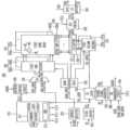
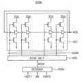
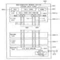
도 3을 참조하면, 반도체 메모리 장치(200)는 제어 로직 회로(210), 어드레스 레지스터(220), 뱅크 제어 로직(230), 리프레시 제어 회로(400), 로우 어드레스 멀티플렉서(240), 칼럼 어드레스 래치(250), 로우 디코더(260), 칼럼 디코더(270), 메모리 셀 어레이(310), 센스 앰프부(285), 입출력 게이팅 회로(290), ECC 엔진(350), 클럭 버퍼(225), 스트로브 신호 생성기(235), 로우 해머 관리 회로(500) 및 데이터 입출력 버퍼(320)를 포함할 수 있다.Referring to FIG. 3 , the
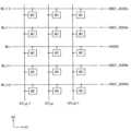
상기 메모리 셀 어레이(310)는 제1 내지 제16 뱅크 어레이들(310a~310s)을 포함할 수 있다. 또한, 상기 로우 디코더(260)는 제1 내지 제16 뱅크 어레이들(310a~310s)에 각각 연결된 제1 내지 제16 로우 디코더들(260a~260s)을 포함하고, 상기 칼럼 디코더(270)는 제1 내지 제16 뱅크 어레이들(310a~310s)에 각각 연결된 제1 내지 제16 칼럼 디코더들(270a~270s)을 포함하며, 상기 센스 앰프부(285)는 제1 내지 제16 뱅크 어레이들(310a~310s)에 각각 연결된 제1 내지 제16 센스 앰프들(285a~285s)을 포함할 수 있다.The
제1 내지 제16 뱅크 어레이들(310a~310s), 제1 내지 제16 센스 앰프들(285a~285s), 제1 내지 제16 칼럼 디코더들(270a~270s) 및 제1 내지 제16 로우 디코더들(260a~260s)은 제1 내지 제16 뱅크들을 각각 구성할 수 있다. 제1 내지 제16 뱅크 어레이들(310a~310s) 각각은 복수의 워드라인(WL)들과 복수의 비트라인(BTL)들 및 워드라인(WL)들과 비트라인(BTL)들이 교차하는 지점에 형성되는 복수의 메모리 셀(MC)들을 포함할 수 있다.The first to sixteenth
어드레스 레지스터(220)는 메모리 컨트롤러(100)로부터 뱅크 어드레스(BANK_ADDR), 로우 어드레스(ROW_ADDR) 및 칼럼 어드레스(COL_ADDR)를 포함하는 어드레스(ADDR)를 수신할 수 있다. 어드레스 레지스터(220)는 수신된 뱅크 어드레스(BANK_ADDR)를 뱅크 제어 로직(230)에 제공하고, 수신된 로우 어드레스(ROW_ADDR)를 로우 어드레스 멀티플렉서(240)에 제공하며, 수신된 칼럼 어드레스(COL_ADDR)를 칼럼 어드레스 래치(250)에 제공할 수 있다. 또한, 어드레스 레지스터(220)는 뱅크 어드레스(BANK_ADDR) 및 로우 어드레스(ROW_ADDR)를 로우 해머 관리 회로(500)에 제공할 수 있다.The
뱅크 제어 로직(230)은 뱅크 어드레스(BANK_ADDR)에 응답하여 뱅크 제어 신호들을 생성할 수 있다. 상기 뱅크 제어 신호들에 응답하여, 제1 내지 제16 로우 디코더들(260a~260s) 중 뱅크 어드레스(BANK_ADDR)에 상응하는 로우 디코더가 활성화되고, 제1 내지 제16 칼럼 디코더들(270a~270s) 중 뱅크 어드레스(BANK_ADDR)에 상응하는 칼럼 디코더가 활성화될 수 있다.The
로우 어드레스 멀티플렉서(240)는 어드레스 레지스터(220)로부터 로우 어드레스(ROW_ADDR)를 수신하고, 리프레쉬 카운터(245)로부터 리프레쉬 로우 어드레스(REF_ADDR)를 수신할 수 있다. 로우 어드레스 멀티플렉서(240)는 로우 어드레스(ROW_ADDR) 또는 리프레쉬 로우 어드레스(REF_ADDR)를 로우 어드레스(SRA)로서 선택적으로 출력할 수 있다. 로우 어드레스 멀티플렉서(240)로부터 출력된 로우 어드레스(SRA)는 제1 내지 제16 로우 디코더들(260a~260s)에 각각 인가될 수 있다.The
리프레쉬 제어 회로(400)는 제어 로직 회로(210)로부터의 리프레쉬 신호들(IREF1, IREF2)에 응답하여 노멀 리프레쉬 모드에서는 리프레쉬 로우 어드레스(REF_ADDR)를 순차적으로 증가시키거나 감소시킬 수 있다. 리프레쉬 제어 회로(400)는 해머 리프레쉬 모드에서는 해머 어드레스(HADDR)을 수신하고, 해머 어드레스(HADDR)에 해당하는 메모리 셀 로우에 물리적으로 인접하는 메모리 셀 로우들의 어드레스들인 해머 리프레쉬 로우 어드레스를 리프레쉬 로우 어드레스(REF_ADDR)로 출력할 수 있다.The
제1 내지 제16 로우 디코더들(260a~260s) 중 뱅크 제어 로직(230)에 의해 활성화된 로우 디코더는 로우 어드레스 멀티플렉서(240)로부터 출력된 로우 어드레스(RA)를 디코딩하여 상기 로우 어드레스에 상응하는 워드라인을 활성화할 수 있다. 예를 들어, 상기 활성화된 로우 디코더는 로우 어드레스에 상응하는 워드라인에 워드라인 구동 전압을 인가할 수 있다.Among the first to sixteenth row decoders 260a to 260s, the row decoder activated by the
칼럼 어드레스 래치(250)는 어드레스 레지스터(220)로부터 칼럼 어드레스(COL_ADDR)를 수신하고, 수신된 칼럼 어드레스(COL_ADDR)를 일시적으로 저장할 수 있다. 또한, 칼럼 어드레스 래치(250)는, 버스트 모드에서, 수신된 칼럼 어드레스(COL_ADDR)를 점진적으로 증가시킬 수 있다. 칼럼 어드레스 래치(250)는 일시적으로 저장된 또는 점진적으로 증가된 칼럼 어드레스(COL_ADDR')를 제1 내지 제16 칼럼 디코더들(270a~270s)에 각각 인가할 수 있다.The
제1 내지 제16 칼럼 디코더들(270a~270s) 중 뱅크 제어 로직(230)에 의해 활성화된 칼럼 디코더는 상응하는 입출력 게이팅 회로(290)를 통하여 뱅크 어드레스(BANK_ADDR) 및 칼럼 어드레스(COL_ADDR)에 상응하는 센스 앰프를 활성화시킬 수 있다.Among the first to sixteenth
입출력 게이팅 회로(290)는 입출력 데이터를 게이팅하는 회로들과 함께, 입력 데이터 마스크 로직, 제1 내지 제16 뱅크 어레이들(310a~310s)로부터 출력된 코드워드를 저장하기 위한 독출 데이터 래치들, 및 제1 내지 제16 뱅크 어레이들(310a~310s)에 데이터를 기입하기 위한 기입 드라이버들을 포함할 수 있다.The input/
제1 내지 제16 뱅크 어레이들(310a~310s) 중 하나의 뱅크 어레이에서 독출된 코드워드(CW)는 상기 하나의 뱅크 어레이에 상응하는 센스 앰프에 의해 감지되고, 상기 독출 데이터 래치들에 저장될 수 있다. 상기 독출 데이터 래치들에 저장된 코드워드(CW)는 ECC 엔진(350)에 의하여 ECC 디코딩이 수행되어 데이터(DTA)로서 데이터 입출력 버퍼(320)에 제공되고, 데이터 입출력 버퍼(320)는 데이터(DTA)를 기초하여 데이터 신호(DQ)로 변환하고 데이터 신호(DQ)를 스트로브 신호(DQS)와 함께 메모리 컨트롤러(100)로 제공할 수 있다.The codeword CW read from one of the first to sixteenth
제1 내지 제16 뱅크 어레이들(310a~310s) 중 하나의 뱅크 어레이에 기입될 데이터 신호(DQ)는 스트로브 신호(DQS)와 함께 데이터 입출력 버퍼(320)에 의하여 수신된다. 데이터 입출력 버퍼(320)는 데이터 신호(DQ)를 데이터 데이터(DTA)로 변환하여 ECC 엔진(390)에 제공하고, ECC 엔진(350)은 데이터(DTA)에 기초하여 패리티 비트들(또는 패리티 데이터)을 생성하고, 상기 데이터(DTA)와 상기 패리티 비트들을 포함하는 코드워드(CW)를 입출력 게이팅 회로(290)에 제공할 수 있다. 입출력 게이팅 회로(290)는 상기 기입 드라이버들을 통하여 상기 코드워드(CW)를 상기 하나의 뱅크 어레이의 타겟 페이지에 기입할 수 있다.The data signal DQ to be written in one of the first to sixteenth
데이터 입출력 버퍼(320)는 기입 동작에서는 데이터 신호(DQ)를 데이터(DTA)로 변환하여 ECC 엔진(350)에 제공하고, 독출 동작에서는 ECC 엔진(350)으로부터 제공되는 데이터(DTA)를 데이터 신호(DQ)로 변환하고, 데이터 신호(DQ)와 스트로브 신호(DQS)를 메모리 컨트롤러(30)에 제공할 수 있다.The data input/
ECC 엔진(350)은 제어 로직 회로(210)로부터의 제2 제어 신호(CTL2)에 기초하여 데이터(DTA)에 대한 ECC 인코딩과 코드워드(CW)에 대한 ECC 디코딩을 수행할 수 있다.The
클럭 버퍼(225)는 클럭 신호(CK)를 수신하고, 클럭 신호(CK)를 버퍼링하여 내부 클럭 신호(ICK)를 생성하고, 내부 클럭 신호(ICK)는 커맨드(CMD)와 어드레스(ADDR)를 처리하는 구성 요소들에 제공할 수 있다.The
스트로브 신호 생성기(235)는 클럭 신호(CK)를 수신하고, 클럭 신호(CK)에 기초하여 스트로브 신호(DQS)를 생성하고, 스트로브 신호(DQS)를 데이터 입출력 버퍼(320)에 제공할 수 있다.The
제어 로직 회로(210)는 반도체 메모리 장치(200)의 동작을 제어할 수 있다. 예를 들어, 제어 로직 회로(210)는 반도체 메모리 장치(200)가 기입 동작, 독출 동작, 노멀 리프레쉬 동작 및 해머 리프레쉬 동작을 수행하도록 제어 신호들을 생성할 수 있다. 제어 로직 회로(210)는 상기 메모리 컨트롤러(100)로부터 수신되는 커맨드(CMD)를 디코딩하는 커맨드 디코더(211) 및 반도체 메모리 장치(200)의 동작 모드를 설정하기 위한 모드 레지스터 세트(MRS, 212)를 포함할 수 있다.The
예를 들어, 커맨드 디코더(211)는 칩 선택 신호 및 커맨드/어드레스 신호 등을 디코딩하여 커맨드(CMD)에 상응하는 상기 제어 신호들을 생성할 수 있다. 특히 제어 로직 회로(210)는 커맨드(CMD)를 디코딩하여 입출력 게이팅 회로(290)를 제어하는 제1 제어 신호(CTL1), ECC 엔진(350)을 제어하는 제2 제어 신호(CTL2), 리프레쉬 제어 회로(400)를 제어하는 제3 제어 신호(CTL3) 및 로우 해머 관리 회로(500)를 제어하는 제4 제어 신호(CTL4)를 생성할 수 있다.For example, the
로우 해머 관리 회로(500)는 커맨드(CMD) 및 어드레스(ADDR(뱅크 어드레스(BANK_ADDR) 및 로우 어드레스(ROW_ADDR)을 포함)를 수신하고, 커맨드(CMD)가 액티브 커맨드에 해당하는 경우, 액티브 커맨드들 중 랜덤하게 선택된 제1 액티브 커맨들에 수반되는 로우 어드레스들을 캡쳐하고, 상기 캡쳐된 로우 어드레스들 중 적어도 하나의 로우 어드레스를, 상기 기준 구간 동안에 상기 적어도 하나의 로우 어드레스에 대응되는 액티브 커맨드의 액세스 카운트에 비례하는 횟수만큼 해머 어드레스(HADDR)로 출력할 수 있다.The row
도 4는 본 발명의 실시예들에 따른 도 3의 반도체 메모리 장치에서 제1 뱅크 어레이를 나타낸다.FIG. 4 illustrates a first bank array in the semiconductor memory device of FIG. 3 according to example embodiments.
도 4를 참조하면, 제1 뱅크 어레이(310a)는 도 3을 참조하면, 제1 뱅크 어레이(310)는 복수개의 워드라인들(WL0~WLm-1, m은 2이상의 짝수인 정수), 복수개의 비트라인들(BL0~BLn-1, n은 2이상의 짝수인 정수), 그리고 워드라인들(WL0~WLm-1)과 비트라인들(BL0~BLn-1) 사이의 교차점에 배치되는 복수개의 메모리 셀들(MCs)을 포함한다.Referring to FIG. 4, the
각 메모리 셀(MC)은 DRAM 셀 구조를 갖는다. 또한, 짝수 워드라인(WL0) 각각과 홀수 워드라인(WL1)에 연결되는 메모리 셀들(MCs)의 배치가 서로 다름을 알 수 있다. 메모리 셀들(MCs) 각각은 워드라인들 워드라인들(WL0~WLm-1) 각각과 비트라인들(BL0~BLn-1) 각각에 연결되는 셀 트랜지스터 및 상기 셀 트랜지스터에 연결되는 셀 커패시터를 포함할 수 있다.Each memory cell MC has a DRAM cell structure. Also, it can be seen that arrangements of memory cells MCs connected to each of the even-numbered word lines WL0 and the odd-numbered word lines WL1 are different from each other. Each of the memory cells MCs may include a cell transistor connected to each of the word lines WL0 to WLm-1 and each of the bit lines BL0 to BLn-1 and a cell capacitor connected to the cell transistor. can
메모리 셀들(MCs)이 연결되는 제1 방향(D1)으로 연장된 워드라인들(WL0~WLm-1)을 제1 뱅크 어레이(310a)의 로우들(rows)이라고 정의하고, 메모리 셀들(MCs)이 연결되는 제2 방향(D2)으로 연장된 비트라인들(BL0~BLn-1)을 제1 뱅크 어레이(310a)의 칼럼들(columns)이라고 정할 수 있다.The word lines WL0 to WLm−1 extending in the first direction D1 to which the memory cells MCs are connected are defined as rows of the
도 5는 본 발명의 실시예들에 따른 도 3의 반도체 메모리 장치에서 로우 해머 관리 회로의 예를 나타내는 블록도이다.5 is a block diagram illustrating an example of a row hammer management circuit in the semiconductor memory device of FIG. 3 according to example embodiments.
도 5를 참조하면, 로우 해머 관리 회로(500a)는 어드레스 캡쳐기(510a), 어드레스 스토리지(520), 해머 어드레스 선택기(530), 비교기(540) 및 랜덤 비트 생성기(550) 및 제어 로직(590a)를 포함할 수 있다.Referring to FIG. 5, the row
랜덤 비트 생성기(550)는 액티브 커맨드(ACT)들에 응답하여 랜덤하게 변화하며 복수의 비트들을 포함하는 랜덤 이진 코드(RBC)를 출력할 수 있다. 랜덤 비트 생성기(550)는 액티브 커맨드(ACT)가 인가될 때마다, 랜덤 이진 코드(RBC)를 출력할 수 있다. 랜덤 이진 코드(RBC)는 수도 랜덤 시퀀스(pseudo random sequence)일 수 있다. 랜덤 이진 코드(RBC)는 수도 랜덤 시퀀스인 경우, 액티브 커맨드(ACT)에 따라 랜덤 비트 생성기(550)로부터 출력되는 랜덤 이진 코드(RBC)는 주기적으로 반복될 수 있다.The
비교기(540)는 랜덤 비트 생성기(550)로부터 출력된 랜덤 이진 코드(RBC)와 미리 저장된 기준 이진 코드(PBC)를 비교할 수 있다. 기준 이진 코드(PBC)는 랜덤 비트 생성기(550)로부터 출력 가능한 랜덤 이진 코드(RBC)의 값들 중 적어도 하나와 동일할 수 있다.The
예를 들어, 기준 이진 코드(PBC)는 외부의 레지스터로부터 비교기(540)로 제공되거나, 비교기(540) 내부의 레지스터에 저장될 수 있다. 랜덤 이진 코드(RBC)의 비트들과 기준 이진 코드(PBC)의 비트들이 일치되는 경우(즉, 랜덤 이진 코드(RBC)와 기준 이진 코드(PBC)가 동일한 경우), 비교기(540)는 매칭 신호(MTC1)를 출력할 수 있다. 예를 들어, 랜덤 이진 코드(RBC)가 주기적으로 반복되는 경우, 랜덤 이진 코드(RBC)와 기준 이진 코드(PBC)에 대한 비교 결과가 주기적으로 반복되므로 비교기(540)는 랜덤 이진 코드(RBC)에 따라 주기적으로 반복되는 매칭 신호(MTC)를 출력할 수 있다.For example, the reference binary code (PBC) may be provided to
예시적인 실시 예에서, 비교기(540)는 랜덤 이진 코드(RBC)를 복수의 기준 이진 코드(PBC)와 비교할 수 있다. 이 경우, 기준 이진 코드(PBC)의 개수에 따라 매칭 신호(MTC1)가 생성되는 빈도수가 달라질 수 있다. 예를 들어, 기준 이진 코드(PBC)의 개수가 증가되는 경우, 매칭 신호(MTC1)가 생성되는 빈도수가 증가될 수 있다.In an exemplary embodiment,
어드레스 캡쳐기(510a)는 로우 어드레스(ROW_ADDR)를 수반하는 액티브 커맨드(ACT)들을 수신하고, 매칭 신호(MTC1)에 기초하여 액티브 커맨드(ACT)들 중 랜덤하게 선택된 제1 액티브 커맨드들에 수반되는 로우 어드레스들을 캡쳐된 로우 어드레스(CRA)들로서 출력할 수 있다. 액티브 커맨드(ACT)들은 확률 정보(PBI)에 의하여 균일한 제1 선택 확률로 선택될 수 있다.The
어드레스 스토리지(520)는 캡쳐된 로우 어드레스(CRA)들을 순차적으로 저장할 수 있다.The
해머 어드레스 선택기(530)는 어드레스 스토리지(520)에 저장된 캡쳐된 로우 어드레스(CRA)들 중에서 적어도 하나를 선택하여 해머 어드레스(HADDR)로 출력할 수 있다.The
제어 로직(590a)은 어드레스 스토리지(520)와 해머 어드레스 선택기(530)를 제어할 수 있다. 제어 로직(590a)은 캡쳐된 로우 어드레스(CRA)들이 어드레스 스토리지(520)에 저장되는 것을 제어하고, 어드레스 스토리지(520)를 관리할 수 있다.The
제어 로직(590a)은 선택 모드 신호(SMS1)를 해머 어드레스 선택기(530)에 제공하여 해머 어드레스 선택기(530)가 해머 어드레스(HADDR)를 선택하는 모드를 제어할 수 있다. 제어 로직(590a)은 또한 해머 어드레스 선택기(530)가 해머 어드레스(HADDR)을 출력할 때, 이를 나타내는 해머 어드레스 발생 신호(HAG)를 도 3의 리프레쉬 제어 회로(400)에 제공할 수 있다.The
예를 들어, 선택 모드 신호(SMS1)가 제1 로직 레벨을 가지는 것에 응답하여 해머 어드레스 선택기(530)는 어드레스 스토리지(520)에 저장된 캡쳐된 로우 어드레스(CRA)들을 저장된 순서대로 해머 어드레스(HADDR)로 출력할 수 있다. 예를 들어, 선택 모드 신호(SMS1)가 제2 로직 레벨을 가지는 것에 응답하여 해머 어드레스 선택기(530)는 어드레스 스토리지(520)에 저장된 캡쳐된 로우 어드레스(CRA)들을 동일한 제2 확률로 랜덤하게 해머 어드레스(HADDR)로 출력할 수 있다.For example, in response to the selection mode signal SMS1 having a first logic level, the
해머 어드레스 선택기(530)는 내부에 랜덤 비트 생성기(535)를 포함할 수 있다. 랜덤 비트 생성기(535)는 제2 로직 레벨을 가지는 선택 모드 신호(SMS1)에 응답하여 랜덤 이진 코드(RBC1)을 어드레스 스토리지(520)에 제공할 수 있다. 어드레스 스토리지(520)는 랜덤 이진 코드(RBC1)에 응답하여 저장된 캡쳐된 로우 어드레스(CRA)들 중 하나를 해머 어드레스 선택기(530)에 제공할 수 있다.The
즉, 도 5의 해머 어드레스 관리 회로(500a)는 액티브 커맨드(ACT)들에 응답하여 랜덤하게 변화하는 랜덤 이진 코드(RBC)와 기준 이준 코드(PBC)가 일치하는 것에 기초하여 선택된 제1 액티브 커맨드들에 수반되는 상기 로우 어드레스(ROW_ADDR)들 중 적어도 일부를 상기 해머 어드레스(HADDR)로 선택할 수 있다.That is, the hammer
도 6은 본 발명의 실시예들에 따른 도 5의 로우 해머 관리 회로에 포함되는 어드레스 스토리지의 예를 나타내는 블록도이다.FIG. 6 is a block diagram illustrating an example of an address storage included in the row hammer management circuit of FIG. 5 according to example embodiments.
도 6을 참조하면, 어드레스 스토리지(520)는 복수의 저장 블록들(SBK_A~SBK_S) (520a~520s, s는 3이상의 자연수)을 포함할 수 있고, 저장 블록들(520a~520s) 각각은 복수의 저장 유닛들(SU1~SUH, H은 4 이상의 자연수)을 포함할 수 있다. 저장 블록들(520a~520s)은 동일한 구성을 가질 수 있으며, 이하에서는 저장 블록(520a)에 대해서 설명한다.Referring to FIG. 6 , the
저장 유닛들(SU1~SUH)은 메모리 셀 로우들의 액세스와 관련된 로우 어드레스들을 저장하는 어드레스 레지스터들(AREG1~AREGH)을 포함할 수 있다.The storage units SU1 to SUH may include address registers ARG1 to AREGH that store row addresses related to access of memory cell rows.
도 7은 본 발명의 실시예들에 따른 액세스 비율에 따른 해머 리프레쉬를 설명하기 위한 도면이다.7 is a diagram for explaining hammer refresh according to an access ratio according to embodiments of the present invention.
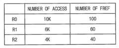
도 7을 참조하면, 상술한 기준 구간 동안에, 로우 어드레스(R0)에 대한 액세스 횟수가 10000번이고, 로우 어드레스(R1)에 대한 액세스 횟수가 6000이고, 로우 어드레스(R0)에 대한 액세스 횟수가 4000인 경우, 로우 어드레스들(R0, R1, R2)에 대한 액세스 횟수에 비례하여, 로우 어드레스들(R0, R1, R2)에 각각에 인접한 빅팀 메모리 셀 로우들에 대하여 해머 리프레쉬(FREF)가 각각 100회, 60회 및 40회가 수행된다.Referring to FIG. 7, during the above reference period, the number of accesses to the row address R0 is 10000, the number of accesses to the row address R1 is 6000, and the number of accesses to the row address R0 is 4000. , the hammer refresh FREF is 100 for each of the victim memory cell rows adjacent to the row addresses R0, R1, and R2, respectively, in proportion to the number of accesses to the row addresses R0, R1, and R2. times, 60 times and 40 times are performed.
도 8은 본 발명의 실시예들에 따른 도 5의 랜덤 비트 생성기의 예를 나타내는 회로도이다.8 is a circuit diagram illustrating an example of the random bit generator of FIG. 5 according to embodiments of the present invention.
도 8을 참조하면, 랜덤 비트 생성기(550)는 레지스터 회로(551) 및 논리 연산 회로(553)를 포함할 수 있다. 예시적인 실시 예에서, 랜덤 비트 생성기(530)는 선형 피드백 쉬프트 레지스터(Linear Feedback Shift Register)로 구현될 수 있다. 즉, 레지스터 회로(551C) 및 논리 연산 회로(553)는 선형 피드백 쉬프트 레지스터를 구성할 수 있다.Referring to FIG. 8 , a
선형 피드백 쉬프트 레지스터는 계수가 0 또는 1인 특성 다항식에 기초하여 피드백 비트를 결정할 수 있다. 피드백 비트는 선형 피드백 쉬프트 레지스터의 피드백 경로로 출력되고, 피드백 비트를 기반으로 논리 연산에 의해 생성된 비트가 선형 피드백 쉬프트 레지스터의 입력 단으로 입력될 수 있다. 선형 피드백 쉬프트 레지스터는 입력 단으로 입력된 비트를 기반으로 쉬프트 동작을 수행하여 수도 랜덤 시퀀스를 생성할 수 있다.The linear feedback shift register may determine the feedback bits based on a characteristic polynomial with coefficients of 0 or 1. The feedback bit is output to a feedback path of the linear feedback shift register, and a bit generated by a logic operation based on the feedback bit may be input to an input terminal of the linear feedback shift register. The linear feedback shift register may generate a random sequence by performing a shift operation based on bits input through an input terminal.
예를 들어, 도 8에 도시된 바와 같이, 랜덤 비트 생성기(550)가 x11+x9+x7+x2+1의 다항식을 기반으로 구현되는 경우, 레지스터 회로(551)는 제1 내지 제11 레지스터들(REG1~REG11)을 포함하고, 논리 연산 회로(553)는 제1 내지 제3 논리 회로들(XOR1~XOR3)을 포함할 수 있다.For example, as shown in FIG. 8 , when the
예를 들어, 제1 내지 제11 레지스터들(REG1~REG11)에는 제1 내지 제11 비트들(b1~b11)이 각각 저장될 수 있다. 제1 내지 제11 비트들(b1~b11)의 비트 값들은 시프트 동작에 따라 달라질 수 있다. 예를 들어, 제1 내지 제3 논리 회로들(XOR1~XOR3) 각각은 배타적 논리합(XOR) 연산을 수행할 수 있다.For example, the first to eleventh bits b1 to b11 may be stored in the first to eleventh registers REG1 to REG11, respectively. Bit values of the first to eleventh bits b1 to b11 may vary according to a shift operation. For example, each of the first to third logic circuits XOR1 to XOR3 may perform an exclusive OR (XOR) operation.
랜덤 비트 생성기(550)는 레지스터 회로(551)를 통해 랜덤 이진 코드(RBC)를 출력할 수 있다. 랜덤 비트 생성기(550)는 미리 정해진 개수의 비트들을 가지는 랜덤 이진 코드(RBC)를 출력할 수 있다. 예를 들어, 랜덤 비트 생성기(550)는 제1 내지 제5 레지스터들(REG1~REG5)에 저장된 제1 내지 제5 비트들(b1~b5)을 기반으로 5개의 비트들을 가지는 랜덤 이진 코드(RBC)를 출력할 수 있다.The
논리 연산 회로(553)는 랜덤 비트 생성기(550)의 피드백 경로 상에 위치할 수 있다. 제1 논리 회로(XOR1)는 제2 레지스터(REG2)의 출력 단에 위치하고, 제2 논리 회로(XOR2)는 제7 레지스터(REG7)의 출력 단에 위치하고, 제3 논리 회로(XOR3)는 제9 레지스터(REG9) 및 제11 레지스터(REG11)의 공통 출력 단에 위치할 수 있다.The logic operation circuit 553 may be located on the feedback path of the
예를 들어, 도 8에 도시된 바와 같이, 제3 논리 회로(XOR3)는 제9 레지스터(REG9)의 제9 비트(b9) 및 제11 레지스터(REG11)의 제11 비트(b11)를 기반으로 논리 연산을 수행할 수 있다. 제2 논리 회로(XOR2)는 제7 레지스터(REG7)의 제7 비트(b7) 및 제3 논리 회로(XOR3)로부터 출력되는 비트를 기반으로 논리 연산을 수행할 수 있다. 제1 논리 회로(XOR1)는 제2 레지스터(REG2)의 제2 비트(b2) 및 제2 논리 회로(XOR2)로부터 출력되는 비트를 기반으로 논리 연산을 수행할 수 있다.For example, as shown in FIG. 8 , the third logic circuit XOR3 is based on the ninth bit b9 of the ninth register REG9 and the eleventh bit b11 of the eleventh register REG11. It can perform logical operations. The second logic circuit XOR2 may perform a logic operation based on the seventh bit b7 of the seventh register REG7 and the bit output from the third logic circuit XOR3. The first logic circuit XOR1 may perform a logic operation based on the second bit b2 of the second register REG2 and the bit output from the second logic circuit XOR2.
이 경우, 제1 논리 회로(XOR1)로부터 출력되는 비트는 제2 비트(b2), 제7 비트(b7), 제9 비트(b9), 및 제11 비트(b11) 값들에 따라 달라질 수 있다. 즉, 제2 비트(b2), 제7 비트(b7), 제9 비트(b9), 및 제11 비트(b11) 각각은 피드백 비트일 수 있다. 제1 논리 회로(XOR1)로부터 출력되는 비트는 제1 레지스터(REG1)의 입력 단으로 입력될 수 있다.In this case, the bits output from the first logic circuit XOR1 may vary according to values of the second bit b2 , the seventh bit b7 , the ninth bit b9 , and the eleventh bit b11 . That is, each of the second bit b2 , the seventh bit b7 , the ninth bit b9 , and the eleventh bit b11 may be a feedback bit. A bit output from the first logic circuit XOR1 may be input to an input terminal of the first register REG1.
이에 따라, 제1 레지스터(REG1)는 피드백 경로를 통해 입력 단으로 입력된 비트를 제1 비트(b1)로서 저장할 수 있다. 피드백 경로를 통해 입력된 비트는 제어 신호에 기초하여 제1 내지 제11 레지스터들(REG1~REG11)을 통해 쉬프트될 수 있다.Accordingly, the first register REG1 may store the bit input through the feedback path as the first bit b1. Bits input through the feedback path may be shifted through the first to eleventh registers REG1 to REG11 based on the control signal.
도 9는 본 발명의 실시예들에 따른 도 5의 로우 해머 관리 회로의 동작을 나타낸다.9 illustrates the operation of the row hammer management circuit of FIG. 5 in accordance with embodiments of the present invention.
도 9에서는 설명의 편의를 위하여 노멀 리프레쉬 동작(NREF)들 사이의 기준 구간(RINT) 동안에, 로우 어드레스들(R0, R1, R3, R1, R0, R2)이 액세스되고, 기준 이진 코드(PBC)가 [01001]인 것으로 가정한다. 즉, 기준 구간(RINT)은 반도체 메모리 장치(200)의 리프레쉬 인터벌에 해당할 수 있다.In FIG. 9, for convenience of description, row addresses R0, R1, R3, R1, R0, and R2 are accessed during the reference period RINT between normal refresh operations NREF, and the reference binary code PBC Assume that is [01001]. That is, the reference period RINT may correspond to the refresh interval of the
도 5 및 도 9를 참조하면, 랜덤 비트 생성기(550)가 5비트의 랜덤 이진 코드(RBC)를 생성하고, 어드레스 캡쳐기(510a)는 랜덤 이진 코드(RBC)가 [01001]인 경우에 활성화되는 매칭 신호(MTC1)에 응답하여 액티브 커맨드(CMD)에 수반되는 로우 어드레스(R3)를 캡쳐하여 어드레스 스토리지(520)에 저장한다. 어드레스 스토리지(520)에 저장된 캡쳐된 로우 어드레스(R3)에 인접한 빅팀 메모리 셀 로우들에 대하여는 노멀 리프레쉬 동작(NREF) 이후에 액세스되는 로우 어드레스들(R7, R5, R1, R2) 다음의 리프레쉬 타이밍에 해머 리프레쉬(FREF) 동작이 수행될 수 있다.5 and 9, the
도 10은 본 발명의 실시예들에 따른 도 3의 반도체 메모리 장치에서 로우 해머 관리 회로의 예를 나타내는 블록도이다.10 is a block diagram illustrating an example of a row hammer management circuit in the semiconductor memory device of FIG. 3 according to example embodiments.
도 10을 참조하면, 로우 해머 관리 회로(500a)는 어드레스 캡쳐기(510a), 어드레스 스토리지(520), 해머 어드레스 선택기(530), 비교기(540a) 및 난수 생성기(550a), 액티브 카운터(545) 및 제어 로직(590a)를 포함할 수 있다.Referring to FIG. 10, the row
어드레스 스토리지(520), 해머 어드레스 선택기(530) 및 제어 로직(590a) 각각의 동작은 도 5의 로우 해머 관리 회로(500a)의 대응되는 구성 요소들과 동일하므로 도 5와 중복되는 설명은 생략한다.Since the operations of the
난수 발생기(550a)는 액티브 커맨드(ACT)들에 응답하여 랜덤하게 변화하며 난수(RN)를 출력할 수 있다. 난수 발생기(550a)는 액티브 커맨드(ACT)가 인가될 때마다, 난수(RN)를 출력할 수 있다.The
액티브 카운터(545)는 액티브 커맨드(ACT)들을 카운팅하여 상응하는 카운팅 값(CV)을 출력할 수 있다.The
비교기(540a)는 난수 발생기(550a)로부터 출력된 난수(RN)와 액티브 카운터(545)로부터 출력되는 카운팅 값(CV)를 비교하고, 난수(RN)와 카운팅 값(CV)이 일치하는 경우, 매칭 신호(MTC2)를 출력할 수 있다.The
어드레스 캡쳐기(510b)는 로우 어드레스(ROW_ADDR)를 수반하는 액티브 커맨드(ACT)들을 수신하고, 매칭 신호(MTC2)에 기초하여 액티브 커맨드(ACT)들 중 랜덤하게 선택된 제1 액티브 커맨드들에 수반되는 로우 어드레스들을 캡쳐된 로우 어드레스(CRA)들로서 출력할 수 있다. 액티브 커맨드(ACT)들은 확률 정보(PBI)에 의하여 균일한 제1 선택 확률로 선택될 수 있다.The
따라서, 도 10의 해머 어드레스 관리 회로(500b)는 액티브 커맨드(ACT)들에 응답하여 랜덤하게 변화하는 난수(RN)와 액티브 커맨드(ACT)들의 카운팅에 기초한 카운팅 값(CV)이 일치하는 것에 기초하여 선택된 제1 액티브 커맨드들에 수반되는 상기 로우 어드레스(ROW_ADDR)들 중 적어도 일부를 대응되는 제1 액티브 커맨드들 각각의 액세스 카운트에 비례하는 횟수만큼 상기 해머 어드레스(HADDR)로 선택할 수 있다.Accordingly, the hammer
도 11은 본 발명의 실시예들에 따른 도 5의 로우 해머 관리 회로의 동작을 나타낸다.11 illustrates the operation of the row hammer management circuit of FIG. 5 in accordance with embodiments of the present invention.
도 11에서는 설명의 편의를 위하여 노멀 리프레쉬 동작(NREF)들 사이의 기준 구간(RINT) 동안에, 로우 어드레스들(R0, R1, R3, R1, R0, R2)이 액세스되고, 로우 어드레스들(R0, R1, R3, R1, R0, R2) 각각에 대한 액티브 커맨드의 카운팅 값(CV)이 각각 0, 1, 2, 3, 4, 5이고, 난수(RN)가 5인 경우를 가정한다.In FIG. 11, for convenience of description, row addresses R0, R1, R3, R1, R0, and R2 are accessed during the reference period RINT between normal refresh operations NREF, and row addresses R0, It is assumed that the counting values (CV) of the active commands for each of R1, R3, R1, R0, and R2 are 0, 1, 2, 3, 4, and 5, and the random number (RN) is 5.
도 10 및 도 11을 참조하면, 난수 발생기(550a)가 '5'에 해당하는 난수(RN)를 생성하고, 어드레스 캡쳐기(510a)는 로우 어드레스(R2)에 해당하는 액티브 커맨드의 카운팅 값(CV)이 5인 경우에 활성화되는 매칭 신호(MTC2)에 응답하여 액티브 커맨드(CMD)에 수반되는 로우 어드레스(R2)를 캡쳐하여 어드레스 스토리지(520)에 저장한다. 어드레스 스토리지(520)에 저장된 캡쳐된 로우 어드레스(R3)에 인접한 빅팀 메모리 셀 로우들에 대하여는 노멀 리프레쉬 동작(NREF) 이후에 액세스되는 로우 어드레스들(R7, R5, R1, R2) 다음의 리프레쉬 타이밍에 해머 리프레쉬(FREF) 동작이 수행될 수 있다. 로우 어드레스들(R7, R5)에 대한 액티브 커맨드의 카운팅 값(CV)은 각각 '6'과 '7'에 해당할 수 있다.Referring to FIGS. 10 and 11 , the
도 12는 본 발명의 실시예들에 따른 도 3의 반도체 메모리 장치에서 로우 해머 관리 회로의 예를 나타내는 블록도이다.12 is a block diagram illustrating an example of a row hammer management circuit in the semiconductor memory device of FIG. 3 according to example embodiments.
도 12를 참조하면, 로우 해머 관리 회로(500c)는 어드레스 캡쳐기(510a), 후보 어드레스 레지스터(560), 어드레스 선택기(570), 어드레스 스토리지(580), 해머 어드레스 선택기(530a), 비교기(540) 및 랜덤 비트 생성기(550) 및 제어 로직(590a)를 포함할 수 있다.Referring to FIG. 12, the row
랜덤 비트 생성기(550)는 액티브 커맨드(ACT)들에 응답하여 랜덤하게 변화하며 복수의 비트들을 포함하는 랜덤 이진 코드(RBC)를 출력할 수 있다. 랜덤 비트 생성기(550)는 액티브 커맨드(ACT)가 인가될 때마다, 랜덤 이진 코드(RBC)를 출력할 수 있다. 랜덤 이진 코드(RBC)는 수도 랜덤 시퀀스(pseudo random sequence)일 수 있다. 랜덤 이진 코드(RBC)는 수도 랜덤 시퀀스인 경우, 액티브 커맨드(ACT)에 따라 랜덤 비트 생성기(550)로부터 출력되는 랜덤 이진 코드(RBC)는 주기적으로 반복될 수 있다.The
비교기(540)는 랜덤 비트 생성기(550)로부터 출력된 랜덤 이진 코드(RBC)와 미리 저장된 기준 이진 코드(PBC)를 비교할 수 있다. 기준 이진 코드(PBC)는 랜덤 비트 생성기(550)로부터 출력 가능한 랜덤 이진 코드(RBC)의 값들 중 적어도 하나와 동일할 수 있다. 랜덤 이진 코드(RBC)의 비트들과 기준 이진 코드(PBC)의 비트들이 일치되는 경우(즉, 랜덤 이진 코드(RBC)와 기준 이진 코드(PBC)가 동일한 경우), 비교기(540)는 매칭 신호(MTC1)를 출력할 수 있다.The
어드레스 캡쳐기(510a)는 로우 어드레스(ROW_ADDR)를 수반하는 액티브 커맨드(ACT)들을 수신하고, 매칭 신호(MTC1)에 기초하여 액티브 커맨드(ACT)들 중 랜덤하게 선택된 N(N은 2 이상의 개의 제1 액티브 커맨드들에 수반되는 N 개의 로우 어드레스들을 캡쳐된 로우 어드레스(CRA)들로서 출력할 수 있다.The
후보 어드레스 레지스터(560)는 캡쳐된 로우 어드레스(CRA)을 순차적으로 제1 후보 어드레스들(CDRA1)로 저장할 수 있다.The
어드레스 선택기(560)는 후보 어드레스 레지스터(560)가 풀(full)인 경우, 제1 후보 어드레스들(CDRA1)의 일부를 일정한 제3 확률로 선택하여 제2 후보 어드레스들(CDRA2)를 출력할 수 있다.When the
어드레스 스토리지(580)는 제2 후보 어드레스들(CDRA2)을 순차적으로 저장할 수 있다.The
해머 어드레스 선택기(580)는 어드레스 스토리지(520)에 저장된 제2 후보 어드레스들(CDRA2) 중에서 적어도 하나를 선택하여 해머 어드레스(HDAAR)로서 출력할 수 있다.The
제어 로직(590b)은 후보 어드레스 레지스터(560), 어드레스 스토리지(580) 및 해머 어드레스 선택기(530a)를 제어할 수 있다.
제어 로직(590b)은 후보 어드레스 레지스터(560)와 어드레스 스토리지(580)가 비어있는지 풀(full)인지 여부를 판단하고, 후보 어드레스 레지스터(560)와 어드레스 스토리지(580)의 저장 동작을 제어할 수 있다.The
제어 로직(590b)은 선택 모드 신호(SMS2)를 해머 어드레스 선택기(530a)에 제공하여 해머 어드레스 선택기(530a)가 해머 어드레스(HADDR)를 선택하는 모드를 제어할 수 있다. 제어 로직(590b)은 또한 해머 어드레스 선택기(530)가 해머 어드레스(HADDR)을 출력할 때, 이를 나타내는 해머 어드레스 발생 신호(HAG)를 도 3의 리프레쉬 제어 회로(400)에 제공할 수 있다.The
예를 들어, 선택 모드 신호(SMS2)가 제1 로직 레벨을 가지는 것에 응답하여 해머 어드레스 선택기(530a)는 어드레스 스토리지(580)에 저장된 제2 후보 어드레스들(CDRA2)을 저장된 순서대로 해머 어드레스(HADDR)로 출력할 수 있다. 예를 들어, 선택 모드 신호(SMS2)가 제2 로직 레벨을 가지는 것에 응답하여 어 해머 어드레스 선택기(530a)는 드레스 스토리지(580)에 저장된 제2 후보 어드레스들(CDRA2)을 동일한 제2 확률로 랜덤하게 해머 어드레스(HADDR)로 출력할 수 있다.For example, in response to the selection mode signal SMS2 having the first logic level, the
해머 어드레스 선택기(530a)는 내부에 랜덤 비트 생성기(535b)를 포함할 수 있다. 랜덤 비트 생성기(535b)는 제2 로직 레벨을 가지는 선택 모드 신호(SMS2)에 응답하여 랜덤 이진 코드(RBC2)을 어드레스 스토리지(580)에 제공할 수 있다. 어드레스 스토리지(580)는 랜덤 이진 코드(RBC2)에 응답하여 저장된 제2 어드레스들(CDRA2) 중 하나를 해머 어드레스 선택기(530a)에 제공할 수 있다.The
해머 어드레스 선택기(530a)는 메모리 컨트롤러(30)부터의 리프레쉬 관리 커맨드에 응답하여 상기 해머 리프레쉬의 수행 시점에 상기 해머 어드레스 큐가 비어있는 것에 응답하여 후보 어드레스 레지스터(560)에 저장된 상기 제1 후보 로우 어드레스들(CDRA1) 중에서 적어도 하나를 선택하여 해머 어드레스(HADDR)로서 출력할 수 있다.The
즉, 도 12의 로우 해머 관리 회로(500c)는 액티브 커맨드(ACT)들에 응답하여 랜덤하게 변화하는 랜덤 이진 코드(RBC)와 기준 이준 코드(PBC)가 일치하는 것에 기초하여 상기 액티브 커맨드들 중 N 개의 제1 액티브 커맨드들을 선택하고, 상기 제1 액티브 커맨드들에 수반되는 N 개의 로우 어드레스들을 제1 후보 로우 어드레스들(CDRA1)로 저장하고, 제1 후보 로우 어드레스들(CDRA1) 중 적어도 일부를 해머 어드레스(HADDR)로 선택할 수 있다.That is, the row
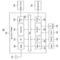
도 13은 본 본 발명의 실시예들에 따른 도 3의 반도체 메모리 장치에서 리프레쉬 제어 회로의 구성을 나타내는 블록도이다.FIG. 13 is a block diagram illustrating the configuration of a refresh control circuit in the semiconductor memory device of FIG. 3 according to example embodiments.
도 13을 참조하면, 리프레쉬 제어 회로(400)는 리프레쉬 제어 로직(410), 리프레쉬 클럭 생성기(420), 리프레쉬 카운터(430) 및 해머 리프레쉬 어드레스 생성기(440)를 포함할 수 있다. 해머 리프레쉬 어드레스 생성기(440)는 해머 어드레스 스토리지(450) 및 맵퍼(460)를 포함할 수 있다.Referring to FIG. 13 , the
리프레쉬 제어 로직(410)은 해머 리프레쉬 발생 신호(HAG)에 응답하여 모드 신호(MS)를 리프레쉬 클럭 생성기(420)에 제공할 수 있다. 리프레쉬 제어 로직(410)은 제1 리프레쉬 신호(IREF1)와 제2 리프레쉬 신호(IREF) 중 하나에 기초하여 해머 어드레스의 출력 타이밍을 제어하는 해머 리프레쉬 신호(HREF)를 해머 리프레쉬 어드레스 생성기(440)에 제공할 수 있다.The
리프레쉬 클럭 생성기(420)는 제1 리프레쉬 제어 신호(IREF1), 제2 리프레쉬 제어 신호(IREF2) 및 모드 신호(MS)에 기초하여 노멀 리프레쉬 동작의 타이밍을 나타내는 리프레쉬 클럭 신호(RCK)를 생성할 수 있다. 리프레쉬 클럭 생성기(420)는 제1 리프레쉬 제어 신호(IREF1)가 인가될 때마다 또는 제2 리프레쉬 제어 신호(IREF2)가 활성화되는 동안에 리프레쉬 클럭 신호(RCK)를 생성할 수 있다. 제1 리프레쉬 제어 신호(IREF1) 및 제2 리프레쉬 제어 신호(IREF2)는 도 3의 제3 제어 신호(CTL3)에 포함될 수 있다.The
도 3의 제어 로직 회로(210)는 메모리 컨트롤러(30)로부터의 커맨드(CMD)가 오토 리프레쉬 커맨드인 경우에, 오토 리프레쉬 커맨드가 인가될 때마다 제1 리프레쉬 제어 신호(IREF1)를 리프레쉬 제어 회로(400)에 인가할 수 있다. 제어 로직 회로(210)는 메모리 컨트롤러(100)로부터의 커맨드(CMD)가 셀프 리프레쉬 진입 커맨드인 경우에, 셀프 리프레쉬 진입 커맨드의 수신 후 셀프 리프레쉬 탈출 커맨드가 인가될 때까지 활성화되는 제2 리프레쉬 제어 신호(IREF2)를 리프레쉬 제어 회로(400)에 인가할 수 있다.When the command CMD from the
리프레쉬 카운터(420)는 리프레쉬 클럭 신호(RCK)의 주기마다 카운팅 동작을 수행하여 메모리 셀 로우들 각각을 지정하는 카운터 리프레쉬 어드레스(CREF_ADDR)를 생성하고, 카운터 리프레쉬 어드레스(CREF_ADDR)를 리프레쉬 로우 어드레스(REF_ADDR)로서 도 3의 로우 어드레스 멀티플렉서(240)에 제공할 수 있다.The
해머 리프레쉬 어드레스 생성기(440)는 해머 어드레스 스토리지(450) 및 맵퍼(460)를 포함할 수 있다.The hammer
해머 어드레스 스토리지(450)는 해머 어드레스(HADDR)을 저장하고, 해머 리프레쉬 신호(HREF)에 기초하여 저장된 해머 어드레스(HADDR)를 맵퍼(460)에 출력할 수 있다. 맵퍼(460)는 해머 어드레스(HADDR)에 상응하는 메모리 셀 로우에 물리적으로 인접한 빅팀 메모리 셀 로우들의 어드레스들을 나타내는 해머 리프레쉬 어드레스들(HREF_ADDR)을 생성할 수 있다.The
예를 들어, 맵퍼(460)는 해머 어드레스(HADDR)에 상응하는 메모리 셀 로우에 물리적으로 인접한 적어도 빅팀 메모리 셀 로우들의 어드레스들을 나타내는 해머 리프레쉬 어드레스들(HREF_ADDR)을 생성할 수 있다.For example, the
해머 리프레쉬 어드레스 생성기(440)는 해머 리프레쉬 어드레스들(HREF_ADDR)을 리프레쉬 로우 어드레스(REF_ADDR)로서 도 3의 로우 어드레스 멀티플렉서(240)에 제공할 수 있다.The hammer
도 14는 본 발명의 실시예들에 따른 도 13의 리프레쉬 제어 회로에서 리프레쉬 클럭 생성기의 일 예를 나타낸다.14 shows an example of a refresh clock generator in the refresh control circuit of FIG. 13 according to embodiments of the present invention.
도 14를 참조하면, 리프레쉬 클럭 생성기(420a)는 복수의 발진기들(421, 422, 423), 멀티플렉서(424) 및 디코더(425a)를 포함할 수 있다.Referring to FIG. 14 , a
디코더(425a)는 제1 리프레쉬 제어 신호(IREF1), 제2 리프레쉬 제어 신호(IREF2) 및 모드 신호(MS)를 디코딩하여 클럭 제어 신호(RCS1)를 출력할 수 있다. 복수의 발진기들(421, 422, 423)은 서로 다른 주기를 가지는 리프레쉬 클럭 신호들(RCK1, RCK2, RCK3)을 발생한다. 멀티플렉서(424)는 클럭 제어 신호(RCS1)에 응답하여 복수의 리프레쉬 클럭 신호들(RCK1, RCK2, RCK3) 중에서 어느 하나를 선택하여, 리프레쉬 클럭 신호(RCK)로서 출력한다.The
모드 신호(MS)는 해머 어드레스가 발생하였음을 나타낼 수 있으므로, 리프레쉬 클럭 생성기(420a)는 클럭 제어 신호(RCS1)에 응답하여 복수의 리프레쉬 클럭 신호들(RCK1, RCK2, RCK3) 중에서 어느 하나를 선택함으로써 리프레쉬 사이클을 조절할 수 있다.Since the mode signal MS may indicate that a hammer address has been generated, the
도 15는 본 발명의 실시예들에 따른 도 13의 리프레쉬 제어 회로에서 리프레쉬 클럭 생성기의 일 예를 나타낸다.15 illustrates an example of a refresh clock generator in the refresh control circuit of FIG. 13 according to embodiments of the present invention.
도 15를 참조하면, 리프레쉬 클럭 생성기(420b)는 디코더(425b), 바이어스부(426) 및 발진기(427)를 포함할 수 있다.Referring to FIG. 15 , the
디코더(425b)는 제1 리프레쉬 제어 신호(IREF1), 제2 리프레쉬 제어 신호(IREF2) 및 모드 신호(MS)를 디코딩하여 클럭 제어 신호(RCS2)를 출력할 수 있다. 바이어스부(426)는 클럭 제어 신호(RCS2)에 응답하여 제어 전압(VCON)을 발생할 수 있다. 발진기(427)는 제어 전압(VCON)에 따라, 그 주기가 가변되는 리프레쉬 클럭 신호(RCK)를 발생할 수 있다.The
모드 신호(MS)는 해머 어드레스가가 발생하였음을 나타낼 수 있으므로, 리프레쉬 클럭 생성기(420b)는 클럭 제어 신호(RCS1)에 응답하여 리프레쉬 클럭 신호(RCK)의 주기를 가변하여 리프레쉬 사이클을 조절할 수 있다.Since the mode signal MS may indicate that a hammer address has occurred, the
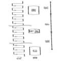
도 16은 본 발명의 실시예들에 따른 도 3의 반도체 메모리 장치에서 제1 뱅크 어레이를 나타낸다.16 illustrates a first bank array in the semiconductor memory device of FIG. 3 according to example embodiments.
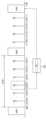
도 16을 참조하면, 제1 뱅크 어레이(310a)에는 제1 방향(D1)으로 I개, 제2 방향(D2)으로 J개의 서브 어레이 블록(SCB)들이 배치될 수 있다.Referring to FIG. 16 , I number of subarray blocks SCBs may be disposed in the first direction D1 and J number of subarray blocks SCBs in the second direction D2 in the
하나의 로우에서 제1 방향(D1)으로 배치되는 I개의 서브 어레이 블록(SCB)을 로우 블록이라 부를 수 있다. 서브 어레이 블록(SCB)들 각각에는 복수의 비트라인들과, 복수의 워드라인들과, 비트라인들과 워드라인들이 교차하는 지점에 위치하는 메모리 셀들이 배치될 수 있다.I sub-array blocks SCBs disposed in one row in the first direction D1 may be referred to as row blocks. A plurality of bit lines, a plurality of word lines, and memory cells located at intersections of the bit lines and word lines may be disposed in each of the sub array blocks SCB.
제1 방향(D1)으로 상기 서브 어레이 블록(SCB)들 사이에 I+1개의 서브 워드라인 드라이버 영역(SWB)들이 배치될 수 있다. 서브 워드라인 드라이버 영역(SWB)에는, 서브 워드라인 드라이버들이 배치될 수 있다. 제2 방향(D2)으로 상기 서브 어레이 블록(SCB)들 사이에 J+1개의 비트라인 감지 증폭기 영역(BLSAB)들이 배치될 수 있다. 상기 비트라인 감지 증폭기 영역(BLSAB)에는 복수의 비트라인 감지 증폭기들이 배치될 수 있다.I+1 sub word line driver regions SWB may be disposed between the sub array blocks SCB in the first direction D1 . Sub word line drivers may be disposed in the sub word line driver area SWB. J+1 bit line sense amplifier regions BLSAB may be disposed between the sub array blocks SCB in the second direction D2 . A plurality of bit line sense amplifiers may be disposed in the bit line sense amplifier area BLSAB.
서브 워드라인 드라이버 영역(SWB)들 각각에는 복수의 서브 워드라인 드라이버들이 배치된다. 하나의 서브 워드라인 드라이버 영역(SWB)은 제1 방향(D1)으로 두 개의 서브 어레이 블록(SCB)을 담당할 수 있다.A plurality of sub word line drivers are disposed in each of the sub word line driver areas SWB. One sub word line driver area SWB may be in charge of two sub array blocks SCB in the first direction D1.
서브 워드라인 드라이버 영역(SWB)들과 비트라인 감지 증폭기 영역(BLSAB)들에 인접하여 복수의 컨졍션 영역(CONJ)들이 배치될 수 있다. 상기 컨졍션 영역(CONJ)들 각각에는 전압 생성기가 배치될 수 있다. 제1 뱅크 어레이(310)의 부분(390)은 도 17을 참조하여 상세히 설명한다.A plurality of connection regions CONJ may be disposed adjacent to the sub word line driver regions SWB and the bit line sense amplifier regions BLSAB. A voltage generator may be disposed in each of the conjunction regions CONJ.
도 17은 본 발명의 실시예들에 따른 도 16의 제1 뱅크 어레이의 부분을 보다 상세히 나타낸다.17 shows a portion of the first bank array of FIG. 16 in more detail in accordance with embodiments of the present invention.
도 16 및 도 17을 참조하면, 제1 뱅크 어레이(310)의 부분(390)에는 서브 어레이 블록(SCB), 비트라인 감지 증폭기 영역들(BLSA) 서브 워드라인 드라이버 영역들(SWB) 및 컨졍션(conjunction) 영역들(CONJ)이 배치될 수 있다.16 and 17, the
서브 어레이 블록(SCB)은 행 방향(제1 방향(D1))으로 연장되는 복수의 워드라인들(WL1~WL4) 및 열 방향(제2 방향(D2))으로 연장되는 복수의 비트라인 쌍들(BTL1~BTL2, BTLB1~BTLB2)을 포함한다. 서브 어레이 블록(SCB)은 복수의 워드라인들(WL1~WL4)과 복수의 비트라인 쌍들(BTL1~BTL2, BTLB1~BTLB2)이 교차하는 지점에 배치되는 메모리 셀들(MC)을 포함한다.The sub array block SCB includes a plurality of word lines WL1 to WL4 extending in a row direction (first direction D1) and a plurality of bit line pairs extending in a column direction (second direction D2). BTL1 to BTL2, BTLB1 to BTLB2). The sub array block SCB includes memory cells MC disposed at intersections of a plurality of word lines WL1 to WL4 and a plurality of bit line pairs BTL1 to BTL2 and BTLB1 to BTLB2.
서브 워드라인 드라이버 영역(SWB)들은 워드라인들(WL1~WL4)을 각각 구동하기 위한 서브 워드라인 드라이버들(651, 652, 653, 654)을 포함한다. 도 17에 도시된 바와 같이, 서브 워드라인 드라이버들(651, 652, 653, 654)은 교대로 서브 어레이 블록(SCB)의 좌측과 우측에 배치될 수 있다.The sub word line driver areas SWB include sub
비트라인 감지 증폭기 영역(BLSAB)은 비트라인 쌍들(BTL1~BTL2, BTLB1~BTLB2)에 연결되는 비트라인 감지 증폭기들(660, 670) 및 로컬 감지 증폭기 회로들(680, 690)을 포함한다. 비트라인 감지 증폭기(660)는 비트라인 쌍(BTL1, BTLB1)에 감지되는 전압 레벨의 차이를 증폭하고, 증폭된 전압 레벨의 차이를 로컬입출력 라인 쌍(LIO1, LIOB1)에 제공할 수 있다.The bit line sense amplifier region BLSAB includes bit
로컬 감지 증폭기 회로(680)는 로컬입출력 라인 쌍(LIO1, LIOB1)과 글로벌 입출력 라인 쌍(GIO1, GIOB1) 사이의 연결을 제어하고, 로컬 감지 증폭기 회로(690)는 로컬 입출력 라인 쌍(LIO2, LIOB2)과 글로벌 입출력 라인 쌍(GIO2, GIOB2) 사이의 연결을 제어한다.The local
도 17에 도시된 바와 같이, 비트라인 감지 증폭기들(660, 670)은 교대로 서브 어레이 블록(SCB)의 위쪽과 아래쪽에 배치될 수 있다. 비트라인 감지 증폭기 영역(BLSAB)들, 서브 워드라인 드라이버 영역(SWB)들 및 서브 어레이 블록(SCB)에 인접하여 컨졍션 영역(CONJ)들이 배치된다. 컨졍션 영역(CONJ)들에는 전압 생성기들(610, 620, 630, 640)이 배치될 수 있다.As shown in FIG. 17 , bit
도 18 및 도 19는 본 발명의 실시예들에 따른 도 1의 메모리 시스템의 커맨드들을 나타낸다.18 and 19 show commands of the memory system of FIG. 1 according to embodiments of the present invention.
도 18에는 액티브 커맨드(ACT), 기입 커맨드(WR) 및 독출 커맨드(RD)를 나타내는 나타내는 칩 선택 신호(CS_n) 및 제1 내지 제14 커맨드/어드레스 신호들(CA0~CA13)의 조합이 도시되어 있고, 도 19에는 프라차지 커맨드들(PREab, PREsb, PPREpb)를 나타내는 칩 선택 신호(CS_n) 및 제1 내지 제14 커맨드/어드레스 신호들(CA0~CA13)의 조합이 도시되어 있다.18 shows a combination of a chip select signal CS_n representing an active command ACT, a write command WR, and a read command RD, and first to fourteenth command/address signals CA0 to CA13. 19 illustrates a combination of the chip select signal CS_n representing the precharge commands PREab, PREsb, and PPREpb and the first to fourteenth command/address signals CA0 to CA13.
도 18 및 도 19에서, H는 논리 하이 레벨을 나타내고, L은 논리 로우 레벨을 나타내고, V는 논리 하이 레벨이나 논리 로우 레벨 중 하나인 유효한 논리 레벨을 나타내고, R0~R17은 로우 어드레스의 비트들을 나타내고, BA0 및 BA1은 뱅크 어드레스의 비트들을 나타내고, BG0~BA2는 뱅크 그룹 어드레스의 비트들을 나타내고, CID0~CID3는 도 1의 반도체 메모리 장치(200)가 적층형 메모리 장치로 구성되는 경우의 메모리 다이의 칩 식별자를 나타낸다. 또한 도 18에서 C2~C10은 컬럼 어드레스의 비트들을 나타내고, BL은 버스트 길이 플래그를 나타낸다.18 and 19, H represents a logic high level, L represents a logic low level, V represents a valid logic level that is either a logic high level or a logic low level, and R0 to R17 represent bits of a row address. BA0 and BA1 denote bits of a bank address, BG0 to BA2 denote bits of a bank group address, and CID0 to CID3 denote memory dies when the
도 18을 참조하면, 액티브 커맨드(ACT), 기입 커맨드(WR) 및 독출 커맨드(RD)는 칩 선택 신호(CS_n)의 하이 레벨과 로우 레벨에서 전송되는 두 개의 사이클 커맨드이고, 액티브 커맨드(ACT)는 뱅크 어드레스(BA0, BA1) 및 로우 어드레스(R0~R17)을 포함할 수 있다.Referring to FIG. 18 , the active command ACT, write command WR, and read command RD are two cycle commands transmitted at the high level and low level of the chip select signal CS_n, and the active command ACT may include bank addresses BA0 and BA1 and row addresses R0 to R17.
도 19에서 PREpb는 특정한 뱅크 그룹 내의 특정한 뱅크를 프리차지하라는 프리차지 커맨드이고, PREab는 모든 뱅크 그룹들의 모든 뱅크들을 프리차지하라는 올 뱅크(all bnak) 프리차지 커맨드이고, PREsb는 모든 뱅크 그룹들에서 동일한 뱅크를 프리차지하라는 동일 뱅크(same bank) 프라치지 커맨드이다.In FIG. 19, PREpb is a precharge command to precharge a specific bank in a specific bank group, PREab is an all bank (all bnak) precharge command to precharge all banks of all bank groups, and PREsb is a precharge command in all bank groups. Same bank prache command to precharge the same bank.
도 19을 참조하면, PREab와 PREsb의 제9 커맨드/어드레스 신호(CA8) 또는 제10 커맨드/어드레스 신호(CA9)는 해머 어드레스를 결정하는 플래그로 이용될 수 있다.Referring to FIG. 19 , a ninth command/address signal CA8 or a 10th command/address signal CA9 of PREab and PREsb may be used as a flag for determining a hammer address.
도 20은 본 발명의 실시예들에 따른 메모리 시스템이 프리차지 커맨드를 이용하여 해머 어드레스 결정하는 경우에 메모리 시스템의 커맨드 프로토콜을 나타낸다.20 illustrates a command protocol of a memory system when a hammer address is determined using a precharge command in the memory system according to example embodiments.
도 1, 도 2, 도 19 및 도 20를 참조하면, 스케쥴러(55)는 클럭 신호(CK_t)의 에지에 동기하여 제1 액티브 커맨드(ACT1)를 반도체 메모리 장치(200)에 인가하고, 액티브 to 프리차지 시간에 해당하는 tRAS 후, 제1 액티브 커맨드(ACT1)에 수반되는 로우 어드레스가 지정하는 메모리 셀 로우가 해머 어드레스에 해당하는지 여부의 판단을 지시하는 프리차지 커맨드(PRE)를 반도체 메모리 장치(200)에 인가한다. 이 경우, 스케쥴러(55)는 프리차지 커맨드(PRE)의 제10 커맨드/어드레스 신호(CA5)를 로우 레벨로 설정할 수 있다.1, 2, 19, and 20, the
프리차지 동작에 소요되는 시간(tRP) 이후에, 스케쥴러(55)는 다른 커맨드들의 개재없이 클럭 신호(CK_t)의 에지에 동기하여 직접 리프레쉬 관리 커맨드(DRFM)를 반도체 메모리 장치(200)에 인가한다. 반도체 메모리 장치(200)는 리프레쉬 사이클 구간(tRFC) 동안에 직접 리프레쉬 관리 커맨드(DRFM)에 응답하여 해머 어드레스에 해당하는 메모리 셀 로우에 인접한 빅팀 메모리 셀 로우들에 대하여 해머 리프레쉬 동작을 수행한다. 리프레쉬 사이클 구간(tRFC) 동안에는 반도체 메모리 장치(200)가 직접 리프레쉬 관리 커맨드(DRFM)를 수신한 시점부터 다른 커맨드의 발생이 금지된다.After the time required for the precharge operation (tRP), the
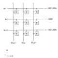
도 21은 본 발명의 실시예들에 따라 해머 어드레스에 대하여 해머 리프레쉬 어드레스를 생성하는 것을 설명하기 위해 메모리 셀 어레이의 일부를 나타낸다.21 illustrates a portion of a memory cell array to explain generating a hammer refresh address for a hammer address according to embodiments of the present invention.
도 21에는 메모리 셀 어레이 내에서 로우 방향(제1 방향, D1)으로 연장되고(extended) 컬럼 방향(제2 방향, D2)으로 인접하여 순차적으로 배열된(arranged) 3개의 워드라인들(WLt-1, WLt, WLt+1), 컬럼 방향(D2)으로 신장되고 로우 방향(D1)으로 인접하여 순차적으로 배열된 3개의 비트라인들(BTLg-1, BTLg, BTLg+1) 및 이들에 각각 결합된 메모리 셀들(MC)이 도시되어 있다.21 shows three word lines WLt- extended in a row direction (first direction, D1) and sequentially arranged adjacent to each other in a column direction (second direction, D2) in a memory cell array. 1, WLt, WLt+1), three bit lines (BTLg-1, BTLg, BTLg+1) extended in the column direction (D2) and sequentially arranged adjacent to each other in the row direction (D1) and their respective couplings memory cells MC are shown.
예를 들어, 가운데 워드라인(WLt)이 집중적으로 액세스되는 해머 어드레스(HADDR)에 상응할 수 있다. 여기서 집중적으로 액세스된다는 것은 워드라인의 액티브 회수가 많거나 액티브 빈도가 높다는 것을 말한다. 해머 워드라인(WLt)이 액세스되어 액티브 및 프리차지되면, 즉 해머 워드라인(WLt)의 전압이 상승 및 하강하면, 인접 워드라인들(WLt-1, WLt+1) 사이에 발생하는 커플링 현상으로 인해 인접 워드라인들(WLt-1, WLt+1)의 전압이 함께 상승 및 하강하면서 인접 워드라인들(WLt-1, WLt+1)에 연결된 메모리 셀들(MC)에 충전된 셀 전하에 영향을 미친다. 해머 워드라인(WLs)이 빈번하게 액세스될수록 빅팀 워드라인들(WLt-1, WLt+1)에 연결된 메모리 셀들(MC)의 셀 전하가 소실되고 저장된 데이터가 손상될 가능성이 높아진다.For example, the middle word line WLt may correspond to a hammer address HADDR that is intensively accessed. Here, intensive access means that the number of actives of word lines is high or the active frequency is high. Coupling phenomenon occurring between adjacent word lines WLt−1 and WLt+1 when the hammer word line WLt is accessed and activated and precharged, that is, when the voltage of the hammer word line WLt rises and falls. As a result, the voltages of the adjacent word lines WLt-1 and WLt+1 rise and fall together, affecting the cell charge charged in the memory cells MC connected to the adjacent word lines WLt-1 and WLt+1. crazy As the hammer word lines WLs are frequently accessed, the cell charge of the memory cells MC connected to the victim word lines WLt-1 and WLt+1 is lost and the stored data is more likely to be damaged.
도 13의 해머 리프레쉬 어드레스 생성기(440)는 해머 어드레스(HADDR)에 상응하는 워드라인(WLt)과 물리적으로 인접하는 워드라인들(WLt-1, WLt+1)의 어드레스(HREF_ADDRa, HREF_ADDRb)를 나타내는 해머 리프레쉬 어드레스(HREF_ADDR)를 제공하고, 이러한 해머 리프레쉬 어드레스(HREF_ADDR)에 기초하여 인접 워드라인들(WLt-1, WLt+1)에 대한 해머 리프레쉬 동작을 추가적으로 수행함으로써 집중적인 액세스에 의한 메모리 셀들의 데이터 손상을 방지할 수 있다.The hammer
도 22 및 도 23은 본 발명의 실시예들에 따른 도 13의 리프레쉬 제어 회로의 동작 예들을 나타내는 타이밍도들이다.22 and 23 are timing diagrams illustrating operation examples of the refresh control circuit of FIG. 13 according to embodiments of the present invention.
도 22 및 도 23에서는 t1~t15 또는 t1~t10에서 펄스 형태로 활성화되는 리프레쉬 제어 신호(IREF)에 대하여 리프레쉬 클럭 신호(RCK), 해머 리프레쉬 신호(HERF), 카운터 리프레쉬 어드레스(CREF_ADDR) 및 해머 리프레쉬 어드레스(HREF_ADDR)의 발생에 관한 실시예들이 도시되어 있다. 리프레쉬 제어 신호(IREF)의 활성화 시점들(t1~t15) 사이의 간격은 규칙적일 수도 있고 불규칙적일 수도 있다.22 and 23, the refresh clock signal RCK, the hammer refresh signal HERF, the counter refresh address CREF_ADDR, and the hammer refresh Embodiments relating to the generation of the address HREF_ADDR are shown. The interval between activation points t1 to t15 of the refresh control signal IREF may be regular or irregular.
도 13 및 도 22를 참조하면, 리프레쉬 제어 로직(410)은 리프레쉬 제어 신호(IREF)의 활성화 시점들(t1~t15) 중 일부(t1~t4, t6~t10, t12~t15)에 동기하여 리프레쉬 클럭 신호(RCK)를 활성화하고 리프레쉬 제어 신호(IREF)의 활성화 시점들(t1~t15) 중 나머지 일부(t5, t11)에 동기하여 해머 리프레쉬 어드레스(HERF_ADDR)를 활성화할 수 있다.13 and 22, the
리프레쉬 카운터(430)는 리프레쉬 클럭 신호(RCK)의 활성화 시점들(t1~t4, t6~t10, t12~t15)에 동기하여 순차적으로 변화하는 어드레스(X+1~X+12)를 나타내는 카운터 리프레쉬 어드레스(CREF_ADDR)를 발생한다. 해머 리프레쉬 어드레스 생성기(440)는 해머 리프레쉬 신호(HREF)의 활성화 시점들(t5, t11)에 동기하여 전술한 해머 어드레스(HADDR)에 상응하는 메모리 셀 로우와 물리적으로 인접하는 빅팀 메모리 셀 로우들의 어드레스(Ha1, Ha2)를 나타내는 해머 리프레쉬 어드레스(HREF_ADDR)를 발생한다.The
도 13 및 도 23을 참조하면, 리프레쉬 제어 로직(410)은 리프레쉬 제어 신호(IREF)의 활성화 시점들(t1~t10) 중 일부(t1~t4, t7~t10)에 동기하여 리프레쉬 클럭 신호(RCK)를 활성화하고 리프레쉬 제어 신호(IREF)의 활성화 시점들(t1~t10) 중 나머지 일부(t5, t6)에 동기하여 해머 리프레쉬 어드레스(HERF_ADDR)를 활성화할 수 있다.13 and 23, the
리프레쉬 카운터(430)는 리프레쉬 클럭 신호(RCK)의 활성화 시점들(t1~t4, t7~t10)에 동기하여 순차적으로 변화하는 어드레스(X+1~X+7)를 나타내는 카운터 리프레쉬 어드레스(CREF_ADDR)를 발생한다. 해머 리프레쉬 어드레스 생성기(440)는 해머 리프레쉬 신호(HREF)의 활성화 시점들(t5, t6)에 동기하여 전술한 해머 어드레스(HADDR)에 상응하는 메모리 셀 로우와 물리적으로 인접하는 빅팀 메모리 셀 로우들의 어드레스(Ha1, Ha2)를 나타내는 해머 리프레쉬 어드레스(HREF_ADDR)를 발생한다.The
도 24은 본 발명의 실시예들에 따라 해머 리프레쉬 어드레스를 생성하는 것을 설명하기 위해 메모리 셀 어레이의 일부를 나타낸다.24 illustrates a portion of a memory cell array to illustrate generating a hammer refresh address according to embodiments of the present invention.
도 24에는 메모리 셀 어레이 내에서 로우 방향(D1)으로 신장되고 컬럼 방향(D2)으로 인접하여 순차적으로 배열된 5개의 워드라인들(WLt-2, WLt-1, WLt, WLt+1, WLt+2), 컬럼 방향(D2)으로 신장되고 로우 방향(D1)으로 인접하여 순차적으로 배열된 3개의 비트라인들(BLg-1, BLg, BLg+1) 및 이들에 각각 결합된 메모리 셀들(MC)이 도시되어 있다.24, five word lines (WLt-2, WLt-1, WLt, WLt+1, WLt+) are sequentially arranged adjacent to each other in the column direction D2 and extended in the row direction D1 in the memory cell array. 2), three bit lines BLg-1, BLg, and BLg+1 that extend in the column direction D2 and are sequentially arranged adjacent to each other in the row direction D1, and memory cells MC coupled thereto, respectively. this is shown
도 13의 해머 리프레쉬 어드레스 생성기(440)는 해머 어드레스(HADDR)에 상응하는 워드라인(WLt)과 물리적으로 인접하는 워드라인들(WLt-1, WLt+1, WLt-2, WLt+2)의 어드레스(HREF_ADDRa, HREF_ADDRb, REF_ADDRc, HREF_ADDRd)를 나타내는 해머 리프레쉬 어드레스(HREF_ADDR)를 제공하고, 이러한 해머 리프레쉬 어드레스(HREF_ADDR)에 기초하여 인접 워드라인들(WLt-1, WLt+1, WLt-2, WLt+2)에 대한 해머 리프레쉬 동작을 추가적으로 수행함으로써 집중적인 액세스에 의한 메모리 셀들의 데이터 손상을 방지할 수 있다.The hammer
도 25는 본 발명의 실시예들에 따른 반도체 메모리 장치의 동작 방법을 나타내는 흐름도이다.25 is a flowchart illustrating an operating method of a semiconductor memory device according to example embodiments.
도 3 내지 도 25를 참조하면, 각각이 복수의 휘발성 메모리 셀들을 포함하는 복수의 메모리 셀 로우들을 구비하는 메모리 셀 어레이(310)를 구비하는 반도체 메모리 장치(200)의 동작 방법이 제공된다.3 to 25 , a method of operating a
상기 방법에 의하면, 로우 해머 관리 회로(500)에서 기준 구간 동안에, 균일한 선택 확률을 가지는, 외부의 메모리 컨트롤러로부터의 액티브 커맨드들 중 랜덤하게 선택된 제1 액티브 커맨들에 수반되는 로우 어드레스들을 캡쳐한다(S100).According to the above method, during a reference period in the row
로우 해머 관리 회로(500)에서 상기 캡쳐된 로우 어드레스들을 중 적어도 하나의 로우 어드레스를, 상기 기준 구간 동안에 상기 적어도 하나의 로우 어드레스에 대응되는 액티브 커맨드의 액세스 카운트에 비례하는 횟수만큼 해머 어드레스(HADDR)로 선택한다(S200).At least one of the captured row addresses in the row
리프레쉬 관리 회로(400)에서 해머 어드레스(HADDR)에 상응하는 메모리 셀 로우에 물리적으로 인접한 빅팀(victim) 메모리 셀 로우들에 대하여 해머 리프레쉬 동작을 수행한다(S300).The
따라서, 본 발명의 실시예들에 따른 반도체 메모리 장치 및 반도체 메모리 장치의 동작 방법에 의하면, 기준 구간 동안에 동일한 선택 확률을 가지는 액티브 커맨드들 중 랜덤하게 선택된 제1 액티브 커맨드들에 수반되는 로우 어드레스들에 기초하여 메모리 셀 로우들에 대한 액세스 카운트 비례하는 횟수만큼 해머 어드레스를 생성하고, 상기 해머 어드레스에 기초하여 해머 어드레스에 상응하는 메모리 셀 로우에 물리적으로 인접한 빅팀(victim) 메모리 셀 로우들에 대하여 해머 리프레쉬 동작을 메모리 셀 로우들에 대한 액세스 비율에 비례하도록 수행함으로써, Blacksmith와 같은 비균일 공격 패턴에 의한 로우 해머를 방지할 수 있다.Accordingly, according to the semiconductor memory device and the operating method of the semiconductor memory device according to embodiments of the present invention, row addresses following randomly selected first active commands among active commands having the same selection probability during a reference period generating hammer addresses as many times as the number of times proportional to the access count for memory cell rows based on the hammer address, and performing hammer refresh on victim memory cell rows physically adjacent to memory cell rows corresponding to the hammer addresses based on the hammer addresses. By performing the operation in proportion to the access ratio to the memory cell rows, it is possible to prevent a row hammer due to a non-uniform attack pattern such as Blacksmith.
도 26은 본 발명의 실시예들에 따른 반도체 메모리 장치를 보여주는 예시적인 블록도이다.26 is an exemplary block diagram illustrating a semiconductor memory device according to example embodiments.
도 26을 참조하면, 반도체 메모리 장치(800)는, 스택드 칩 구조에서 소프트 데이터 페일의 분석 및 구제 기능을 제공하기 위해 적어도 하나의 버퍼 다이(810) 및 복수의 메모리 다이들(820-1,820-2,...,820-p, p는 3 이상의 자연수)을 포함할 수 있다.Referring to FIG. 26 , a
복수의 메모리 다이들(820-1,820-2,...,820-p)은 버퍼 다이(810) 사상부에 순차적으로 적층되고 복수의 쓰루 실리콘 비아(이하 TSV) 라인들을 통해 데이터를 통신할 수 있다.The plurality of memory dies 820-1, 820-2, ..., 820-p are sequentially stacked on the mapping portion of the buffer die 810 and may communicate data through a plurality of through-silicon via (TSV) lines. there is.
상기 복수의 메모리 다이들(820-1,820-2,...,820-p) 각각은 데이터를 저장하는 셀 코어(821), 버퍼 다이(810)로 전송되는 전송 데이터를 이용하여 전송 패리티 비트들을 생성하는 셀 코어 ECC 엔진(823), 리프레쉬 제어 회로(RCC, 825) 및 로우 해머 관리 회로(RHMC, 827)을 포함할 수 있다. 셀 코어(821)는 DRAM 셀 구조를 가지는 복수의 메모리 셀들을 포함할 수 있다.Each of the plurality of memory dies 820-1, 820-2, ..., 820-p converts transmission parity bits using transmission data transmitted to a
리프레쉬 제어 회로(825)는 도 13의 리프레쉬 제어 회로(400)를 채용할 수 있고, 로우 해머 관리 회로(827)는 도 5의 로우 해머 관리 회로(500a), 도 10의 로우 해머 관리 회로(500b) 및 도 12의 로우 해머 관리 회로(500c) 중 하나를 채용할 수 있다. 따라서, 로우 해머 관리 회로(827)는 기준 구간 동안에 동일한 선택 확률을 가지는 액티브 커맨드들 중 랜덤하게 선택된 제1 액티브 커맨드들에 수반되는 로우 어드레스들에 기초하여 메모리 셀 로우들에 대한 액세스 횟수에 비례하는 횟수만큼 해머 어드레스를 생성하고, 상기 해머 어드레스에 기초하여 해머 어드레스에 상응하는 메모리 셀 로우에 물리적으로 인접한 빅팀(victim) 메모리 셀 로우들에 대하여 해머 리프레쉬 동작을 메모리 셀 로우들에 대한 액세스 비율에 비례하도록 수행할 수 있다.The
버퍼 다이(810)는 상기 복수의 TSV 라인들을 통해 수신되는 전송 데이터에 전송 에러가 발생된 경우에 전송 패리티 비트들을 이용하여 전송 에러를 정정함에 의해 에러 정정된 데이터를 생성하는 비아 ECC 엔진(812)을 포함할 수 있다.The buffer die 810 includes a via
버퍼 다이(810)는 데이터 입출력 버퍼(816)를 포함할 수 있다. 데이터 입출력 버퍼(816)는 비아 ECC ECC 엔진(812)으로부터 제공되는 데이터(DTA)를 샘플링하여 데이터 신호(DQ)를 생성하고 데이터 신호(DQ)를 외부로 출력할 수 있다.The buffer die 810 may include a data input/output buffer 816 . The data input/output buffer 816 may generate a data signal DQ by sampling the data DTA provided from the via
반도체 메모리 장치(800)는 상기 TSV 라인들을 통해 상기 데이터 및 제어 신호들을 통신하는 스택 칩 타입 메모리 장치 혹은 스택드 메모리 장치일 수 있다. 상기 TSV 라인들은 실리콘 관통 전극들로도 칭해질 수 있다.The
셀 코어 ECC 엔진(822)은 전송 데이터가 전송되기 이전에 메모리 다이(820-p)로부터 출력되는 데이터에 대한 에러 정정도 수행할 수 있다.The cell core ECC engine 822 may also perform error correction on data output from the memory die 820-p before transmission data is transmitted.
하나의 메모리 다이(820-p)에 형성되는 데이터 TSV 라인 그룹(832)은 TSV 라인들(L1~Lp)로 구성될 수 있고, 패리티 TSV 라인 그룹(834)은 TSV 라인들(L10~Lq)로 구성될 수 있다. 데이터 TSV 라인 그룹(832)의 TSV 라인들라인들(L1~Lp)과 패리티 TSV 라인 그룹(834)의 TSV 라인들(L10~Lq)은 복수의 메모리 다이들(820-1~820-p)의 사이에 대응적으로 형성된 마이크로 범프(MCB)들에 연결될 수 있다.The data
반도체 메모리 장치(800)는 데이터 버스(B10)를 통해 외부의 메모리 컨트롤러와 통신하기 위해 3D 칩 구조 또는 2.5D 칩 구조를 가질 수 있다. 상기 버퍼 다이(810)는 데이터 버스(B10)를 통해 외부의 메모리 컨트롤러에 연결될 수 있다.The
본 발명의 실시예들에서는 도 30에서와 같이 메모리 다이에는 셀 코어 ECC 엔진을 설치하고, 버퍼 다이에는 비아 ECC 엔진을 설치함으로써 소프트 데이터 페일의 검출 및 정정을 검증할 수 있다. 소프트 데이터 페일은 쓰루 실리콘 비아 라인들을 통해 데이터가 전송될 시에 노이즈에 기인하여 발생된 전송 에러를 포함할 수 있다.In embodiments of the present invention, detection and correction of a soft data fail can be verified by installing a cell core ECC engine in a memory die and a via ECC engine in a buffer die, as shown in FIG. 30 . The soft data fail may include a transmission error caused by noise when data is transmitted through through silicon via lines.
도 27은 본 발명의 실시예들에 따른 스택형 메모리 장치를 포함하는 반도체 패키지의 예를 나타내는 구조도이다.27 is a structural diagram illustrating an example of a semiconductor package including a stacked memory device according to example embodiments.
도 27을 참조하면, 반도체 패키지(900)는 하나 이상의 스택형 메모리 장치(910)와 그래픽 프로세싱 유닛(graphic processing unit, GPU)(920)를 포함할 수 있다. 상기 스택형 메모리 장치(910)와 GPU(920)는 인터포저(Interposer, 930) 상에 장착되고, 스택형 메모리 장치(910)와 GPU(920)가 장착된 인터포저(930)는 패키지 기판(940) 상에 장착될 수 있다. 패키지 기판(940)은 솔더 볼(950) 상에 장착될 수 있다. GPU(920)는 메모리 컨트롤러 기능을 수행할 수 있는 반도체 장치에 해당할 수 있으며, 일 예로서 GPU(920)는 어플리케이션 프로세서로 구현될 수 있다. GPU(920)는 또한 상술한 스케쥴러를 구비하는 메모리 컨트롤러를 포함할 수 있다.Referring to FIG. 27 , a
스택형 메모리 장치(910)는 다양한 형태로 구현이 가능하며, 일 실시예에 따라 스택형 메모리 장치(910)는 다수 개의 레이어들이 적층된 HBM(High Bandwidth Memory) 형태의 메모리 장치일 수 있다. 이에 따라, 스택형 메모리 장치(910)는 버퍼 다이 및 복수의 메모리 다이들을 포함하고, 복수의 메모리 다이들 각각은 상술한 리프레쉬 제어 회로와 로우 해머 관리 회로를 포함할 수 있다.The
인터포저(930) 상에는 다수 개의 스택형 메모리 장치(910)들이 장착될 수 있으며, GPU (920)는 다수개의 스택형 메모리 장치(910)들과 통신할 수 있다. 일 예로서, 스택형 메모리 장치(910)들 각각과 GPU(920)는 물리(PHY) 영역을 포함할 수 있으며, 물리(PHY) 영역을 통해 스택형 메모리 장치(910)들과 GPU(920) 사이에서 통신이 수행될 수 있다.A plurality of
한편, 스택형 메모리 장치(910)가 직접 액세스 영역을 포함하는 경우, 패키지 기판(940)의 하부에 장착되는 도전 수단(예컨대, 솔더볼(950)) 및 직접 액세스 영역을 통해 테스트 신호가 스택형 메모리 장치(910) 내부로 제공될 수 있다.Meanwhile, when the
도 28은 본 발명의 실시예들에 따른 모바일 시스템을 나타내는 블록도이다.28 is a block diagram illustrating a mobile system according to embodiments of the present invention.
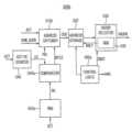
도 28을 참조하면, 모바일 시스템(2000)은 카메라(2100), 디스플레이(2200), 오디오 처리부(2300), 입출력 장치(2400), 메모리 장치(2500), 스토리지 장치(2600), 안테나(2700), 및 어플리케이션 프로세서(Application Processor, 이하 "AP")(2800)를 포함할 수 있다.Referring to FIG. 28 , a
모바일 시스템(2000)은 랩탑 컴퓨터, 휴대용 단말기, 스마트폰(smart phone), 태블릿 PC(tablet personal computer), 웨어러블 기기, 헬스케어 기기, 또는 IOT 기기로 구현될 수 있다. 또한, 모바일 시스템(2000)은 서버, 또는 개인용 컴퓨터(Personal Computer)로 구현될 수 있다.The
카메라(2100)는 사용자의 제어에 따라 이미지 또는 동영상을 촬영할 수 있다. 카메라(2100)는 카메라 인터페이스(2870)를 통해 AP(2800)와 통신할 수 있다.The
디스플레이(2200)는 LCD(Liquid Crystal Display), OLED(Organic Light Emitting Diodes) 디스플레이, AM-OLED(Active-Matrix Organic Light-Emitting Diode), PDP(Plasma Display Panel) 등과 같은 다양한 형태로 구현될 수 있다. 예시적인 실시 예에서, 디스플레이(2200)는 사용자의 터치를 통한 입력 신호를 수신하여 모바일 시스템(2000)의 입력 장치로 사용될 수 있다. 디스플레이(2200)는 디스플레이 인터페이스(2860)를 통해 AP(2800)와 통신할 수 있다.The
오디오 처리부(2300)는 메모리 장치(2500) 또는 스토리지 장치(2600)로부터 전달된 컨텐츠에 포함된 오디오 데이터를 처리할 수 있다. 예를 들어, 오디오 처리부(2300)는 오디오 데이터에 대한 인코딩/디코딩, 노이즈 필터링 등과 같은 다양한 처리를 수행할 수 있다.The
입출력 장치(2400)는 사용자로부터의 입력을 생성하는 장치, USB, 스토리지, 디지털 카메라, SD 카드, DVD, 네트워크 어댑터(Network adapter) 등과 같은 디지털 입력 및 출력 기능을 제공하는 기기들을 포함할 수 있다. 오디오 처리부(2300)와 입출력 장치(2400)는 주변장치 인터페이스(2850)를 통해 AP(2800)와 통신할 수 있다.The input/
AP(2800)는 중앙처리장치(2810)를 통해서 모바일 시스템(2000)의 전반적인 동작을 제어할 수 있다. 예를 들어, AP(2800)는 스토리지 장치(2600)에 저장된 컨텐츠의 일부가 디스플레이(2200)에 표시되도록 디스플레이(2200)를 제어할 수 있다. 또한, AP(2800)는 입출력 장치(2400) 등을 통해 사용자 입력이 수신되면, 사용자 입력에 대응하는 제어 동작을 수행할 수 있다. 또한, AP(2800)는 버스(2890)를 포함할 수 있으며, 버스(2890)를 통해 중앙처리장치(2810), 메모리 인터페이스(2830), 스토리지 인터페이스(2840), 주변장치 인터페이스(2850), 디스플레이 인터페이스(2860), 카메라 인터페이스(2870) 등과 같은 다양한 구성 요소들을 서로 연결할 수 있다.The
AP(2800)는 응용 프로그램, 운영 체제(Operating System, OS) 등을 구동하는 시스템 온 칩(System-on-Chip, 이하 "SoC")으로 구현될 수 있다. 또는 AP(2800) 및 다른 반도체 부품(예를 들어, 메모리 장치(2500), 스토리지 장치(2600))은 다양한 형태들의 패키징 기법을 기반으로 실장될 수 있다. 예를 들어, AP(2800) 및 다른 반도체 부품은 PoP(Package on Package), Ball grid arrays(BGAs), Chip scale packages(CSPs), System In Package(SIP), Multi Chip Package(MCP), Wafer-level Fabricated Package(WFP), Wafer-Level Processed Stack Package(WSP) 등과 같은 패키징 기법들을 이용하여 실장될 수 있다.The
예시적인 실시 예에서, AP(2800)는 가속기(2820)를 더 포함할 수 있다. 가속기(2820)는 AP(2800)의 특정 기능을 수행하는 기능 블록일 수 있다. 예를 들어, 가속기(2820)는 그래픽 데이터를 처리하는 기능 블럭인 GPU(Graphics Processing Unit), AI 연산(예를 들어, 훈련(training) 및/또는 추론(Inference))을 수행하기 위한 기능 블럭인 NPU(Neural Processing Unit) 등을 포함할 수 있다.In an exemplary embodiment, the
예시적인 실시 예에서, AP(2800)는 모뎀(2880)을 포함하거나 AP(2800) 외부에 별도로 위치하는 모뎀 칩을 구비할 수 있다. 모뎀(2880)은 안테나(2700)를 통해서 무선 데이터를 송수신하고, 안테나(2700)로부터 전송되는 신호를 변조하거나 안테나(2700)로 수신되는 신호를 복조할 수 있다.In an exemplary embodiment, the
예시적인 실시 예에서, AP(2800)는 메모리 장치(2500)와의 통신을 위한 메모리 인터페이스(2830)를 포함할 수 있다. 메모리 인터페이스(2830)에 메모리 장치(2500)를 제어하기 위한 메모리 컨트롤러가 내장될 수 있다. 이에 따라, 메모리 장치(2500)는 AP(2800)와 직접 연결될 수 있다. 예를 들어, 메모리 인터페이스(2830)에 내장된 메모리 컨트롤러는 중앙처리장치(2810), 가속기(2820), 모뎀(2880) 등에서 발행되는 메모리 읽기/쓰기 명령을 메모리 장치(2500)를 제어하기 위한 커맨드로 변경하여 메모리 장치(2500)를 제어할 수 있다.In an exemplary embodiment, the
AP(2800)는 메모리 장치(2500)와 미리 정해진 인터페이스 규약을 기반으로 통신할 수 있다. 예를 들어, AP(2800)는 LPDDR4, LPDDR5 등의 JEDEC 표준 규격에 맞는 인터페이스를 기반으로 메모리 장치(2500)와 통신할 수 있다. 또한, AP(2800)는 HBM, HMC, Wide I/O와 같은 고대역폭 JEDEC 표준 규격에 맞는 인터페이스를 기반으로 메모리 장치(2500)와 통신할 수 있다.The
예시적인 실시 예에서, 메모리 장치(2500)는 DRAM을 기반으로 구현될 수 있다. 그러나, 본 발명이 이에 한정되는 것은 아니며, 메모리 장치(2500)는 PRAM, SRAM, MRAM, RRAM, FRAM, 또는 Hybrid RAM을 기반으로 구현될 수 있다.In an exemplary embodiment, the
메모리 장치(2500)는 입출력 장치(2400)나 스토리지 장치(2600)보다 상대적으로 작은 레이턴시(latency)와 대역폭(bandwidth)을 가질 수 있다. 메모리 장치(2500)는 모바일 시스템(2000)의 파워 온 시점에 초기화되고, 운영 체제와 어플리케이션 데이터가 메모리 장치(2500)에 로딩될 수 있다. 이에 따라, 메모리 장치(2500)는 운영 체제와 어플리케이션 데이터의 임시 저장 장소로 사용되거나 각종 소프트웨어 코드의 실행 공간으로 사용될 수 있다.The
예시적인 실시 예에서, 메모리 장치(2500)는 도 1 내지 10을 참조하여 설명한 메모리 장치(200)에 대응할 수 있다. 예를 들어, 메모리 장치(2500)는 AP(2800)의 메모리 컨트롤러로부터 수신된 커맨드(CMD) 및 어드레스(ADD)를 기초로 하여 기준 구간 동안의 액세스 횟수에 비례하도록 해머 리프레쉬를 선택하고, 상기 선택된 해머 리프레쉬에 대한 해머 리프레쉬 동작을 수행할 수 있다.In an exemplary embodiment, the
예시적인 실시 예에서, AP(2800)는 스토리지 장치(2600)와의 통신을 위한 스토리지 인터페이스(2840)를 포함할 수 있다. 이에 따라, 스토리지 장치(2600)는 AP(2800)와 직접 연결될 수 있다. 예를 들어, 스토리지 장치(2600)는 별도의 칩으로 구현될 수 있으며, AP(2800)와 스토리지 장치(2600)는 하나의 패키지(package)로 조립될 수 있다. 예를 들어, 스토리지 장치(2600)는 낸드 플래시 메모리를 기반으로 구현될 수 있으나, 본 발명이 이에 한정되는 것은 아니다.In an example embodiment, the
본 발명은 복수의 휘발성 메모리 셀들을 포함하는 반도체 메모리 장치를 사용하는 다양한 시스템에 적용될 수 있다. 즉 본 발명은 스마트 폰, 내비게이션 시스템, 노트북 컴퓨터, 데스크 탑 컴퓨터, 게임 콘솔 등과 같은 반도체 메모리 장치를 동작 메모리로 사용하는 다양한 시스템에 적용될 수 있다.The present invention can be applied to various systems using a semiconductor memory device including a plurality of volatile memory cells. That is, the present invention can be applied to various systems using semiconductor memory devices as operating memories, such as smart phones, navigation systems, notebook computers, desktop computers, and game consoles.
상술한 바와 같이, 본 발명의 실시예들을 참조하여 설명하였지만, 해당 기술 분야에서 통상의 지식을 가진 자는 하기의 특허청구범위에 기재된 본 발명의 사상 및 영역으로부터 벗어나지 않는 범위 내에서 본 발명을 다양하게 수정 및 변경시킬 수 있음을 이해할 것이다.As described above, although it has been described with reference to the embodiments of the present invention, those skilled in the art can make various modifications to the present invention within the scope not departing from the spirit and scope of the present invention described in the claims below. It will be understood that modifications and changes may be made.
Claims (20)
Translated fromKorean기준 구간 동안에, 균일한 제1 선택 확률을 가지는, 외부의 메모리 컨트롤러로부터의 액티브 커맨드들 중 랜덤하게 선택된 제1 액티브 커맨들에 수반되는 로우 어드레스들을 캡쳐하고, 상기 캡쳐된 로우 어드레스들을 중 적어도 하나의 로우 어드레스를, 상기 기준 구간 동안에 상기 적어도 하나의 로우 어드레스에 대응되는 액티브 커맨드의 액세스 카운트에 비례하는 횟수만큼 해머 어드레스로 선택하는 로우 해머 관리 회로; 및
상기 해머 어드레스를 수신하고, 상기 해머 어드레스에 상응하는 메모리 셀 로우에 물리적으로 인접한 빅팀(victim) 메모리 셀 로우들에 대하여 해머 리프레쉬 동작을 수행하는 리프레쉬 제어 회로를 포함하는 반도체 메모리 장치.a memory cell array including a plurality of memory cell rows each having a plurality of volatile memory cells;
During the reference period, row addresses accompanying randomly selected active commands among active commands having a uniform first selection probability from an external memory controller are captured, and at least one of the captured row addresses is captured. a row hammer management circuit which selects a row address as a hammer address a number of times proportional to an access count of an active command corresponding to the at least one row address during the reference period; and
and a refresh control circuit that receives the hammer address and performs a hammer refresh operation on victim memory cell rows physically adjacent to a memory cell row corresponding to the hammer address.
상기 기준 구간은 상기 복수의 메모리 셀 로우들을 리프레쉬하는 상기 반도체 메모리 장치의 리프레쉬 사이클 사이의 리프레쉬 인터벌에 해당하고,
상기 제1 선택 확률은 상기 기준 구간 동안에 상기 복수의 메모리 셀 로우들에 대한 평균 액세스 횟수에 대한 상기 반도체 메모리 장치의 리프레쉬 주기 동안에 상기 복수의 메모리 셀 로우들에 대하여 수행될 수 있는 상기 해머 리프레쉬 동작의 횟수의 비에 해당하는 반도체 메모리 장치.According to claim 1,
the reference period corresponds to a refresh interval between refresh cycles of the semiconductor memory device for refreshing the plurality of memory cell rows;
The first selection probability is the hammer refresh operation that may be performed on the plurality of memory cell rows during a refresh cycle of the semiconductor memory device with respect to the average number of accesses to the plurality of memory cell rows during the reference period. A semiconductor memory device corresponding to a ratio of times.
상기 액티브 커맨드들에 응답하여 랜덤하게 변화하는 랜덤 이진 코드와 기준 이준 코드가 일치하는 것에 기초하여 선택된 상기 제1 액티브 커맨드들에 수반되는 상기 로우 어드레스들 중 적어도 일부를 상기 해머 어드레스로 선택하는 것을 특징으로 하는 반도체 메모리 장치.2. The method of claim 1, wherein the row hammer management circuit comprises:
Selecting at least some of the row addresses following the first active commands selected based on coincidence of a random binary code that randomly changes in response to the active commands and a reference binary code as the hammer address. A semiconductor memory device made of.
상기 액티브 커맨드들에 응답하여 상기 랜덤 이진 코드를 출력하는 랜덤 비트 생성기;
상기 랜덤 이진 코드와 상기 기준 이진 코드를 비교하고 상기 비교의 결과에 기초하여 매칭 신호를 출력하는 비교기;
상기 매칭 신호에 기초하여 상기 랜덤하게 선택된 상기 제1 액티브 커맨들에 수반되는 로우 어드레스들을 상기 캡쳐된 로우 어드레스들로 출력하는 어드레스 캡쳐기;
상기 캡쳐된 로우 어드레스들을 순차적으로 저장하는 어드레스 스토리지;
상기 어드레스 스토리지에 저장된 상기 캡쳐된 로우 어드레스들 중에서 적어도 하나를 선택하여 상기 해머 어드레스로서 출력하는 해머 어드레스 선택기; 및
상기 어드레스 스토리지 및 상기 해머 어드레스 선택기를 제어하는 제어 로직을 포함하는 반도체 메모리 장치.4. The method of claim 3, wherein the row hammer management circuit
a random bit generator outputting the random binary code in response to the active commands;
a comparator that compares the random binary code with the reference binary code and outputs a matching signal based on a result of the comparison;
an address capturer configured to output row addresses accompanying the randomly selected first active commands as the captured row addresses based on the matching signal;
an address storage for sequentially storing the captured row addresses;
a hammer address selector configured to select at least one of the captured row addresses stored in the address storage and output the selected row address as the hammer address; and
and a control logic controlling the address storage and the hammer address selector.
상기 해머 어드레스 선택기는 상기 캡쳐된 로우 어드레스들을 저장된 순서대로 상기 해머 어드레스로서 출력하는 반도체 메모리 장치.According to claim 4,
The hammer address selector outputs the captured row addresses as the hammer addresses in a stored order.
상기 해머 어드레스 선택기는 상기 캡쳐된 로우 어드레스들을 동일한 제2 선택 확률로 랜덤하게 상기 해머 어드레스로서 출력하는 반도체 메모리 장치.According to claim 4,
The hammer address selector randomly outputs the captured row addresses as the hammer addresses with the same second selection probability.
상기 액티브 커맨드들에 응답하여 상기 난수를 출력하는 난수 발생기;
상기 액티브 커맨드들을 카운팅하여 상기 카운팅 값을 출력하는 액티브 카운터;
상기 난수와 상기 카운팅 값을 비교하고, 상기 비교의 결과에 기초하여 매칭 신호를 출력하는 비교기;
상기 매칭 신호에 기초하여 상기 액티브 커맨드들 중 상기 제1 액티브 커맨들에 수반되는 로우 어드레스들을 상기 캡쳐된 로우 어드레스들로 출력하는 어드레스 캡쳐기;
상기 캡쳐된 로우 어드레스들을 순차적으로 저장하는 어드레스 스토리지;
상기 어드레스 스토리지에 저장된 상기 캡쳐된 로우 어드레스들 중에서 적어도 하나를 선택하여 상기 해머 어드레스로서 출력하는 해머 어드레스 선택기; 및
상기 어드레스 스토리지 및 상기 해머 어드레스 선택기를 제어하는 제어 로직을 포함하는 반도체 메모리 장치.8. The method of claim 7, wherein the row hammer management circuit comprises:
a random number generator outputting the random number in response to the active commands;
an active counter that counts the active commands and outputs the counted value;
a comparator that compares the random number with the counting value and outputs a matching signal based on a result of the comparison;
an address capturer configured to output row addresses accompanying the first active commands among the active commands as the captured row addresses based on the matching signal;
an address storage for sequentially storing the captured row addresses;
a hammer address selector configured to select at least one of the captured row addresses stored in the address storage and output the selected row address as the hammer address; and
and a control logic controlling the address storage and the hammer address selector.
상기 해머 어드레스 선택기는 상기 캡쳐된 로우 어드레스들을 저장된 순서대로 상기 해머 어드레스로서 출력하는 반도체 메모리 장치.According to claim 8,
The hammer address selector outputs the captured row addresses as the hammer addresses in a stored order.
상기 해머 어드레스 선택기는 상기 캡쳐된 로우 어드레스들을 동일한 제2 선택 확률로 랜덤하게 상기 해머 어드레스로서 출력하는 반도체 메모리 장치.According to claim 8,
The hammer address selector randomly outputs the captured row addresses as the hammer addresses with the same second selection probability.
상기 액티브 커맨드들에 응답하여 랜덤하게 변화하는 랜덤 이진 코드와 기준 이준 코드가 일치하는 것에 기초하여 상기 액티브 커맨드들 중 N(N은 2 이상의 자연수) 개의 제1 액티브 커맨드들을 선택하고, 상기 제1 액티브 커맨드들에 수반되는 N 개의 로우 어드레스들을 제1 후보 로우 어드레스들로 저장하고, 상기 제1 후보 로우 어드레스들 중 적어도 일부를 상기 해머 어드레스로 선택하는 것을 특징으로 하는 반도체 메모리 장치.2. The method of claim 1, wherein the row hammer management circuit comprises:
N (N is a natural number greater than or equal to 2) first active commands are selected from among the active commands based on a coincidence between a random binary code that randomly changes in response to the active commands and a reference binary code, and the first active commands are selected. A semiconductor memory device comprising: storing N row addresses accompanying commands as first candidate row addresses, and selecting at least some of the first candidate row addresses as the hammer addresses.
상기 액티브 커맨드들에 응답하여 상기 랜덤 이진 코드를 출력하는 랜덤 비트 생성기;
상기 랜덤 이진 코드와 상기 기준 이진 코드를 비교하고 상기 비교의 결과에 기초하여 매칭 신호를 출력하는 비교기;
상기 매칭 신호에 기초하여 상기 액티브 커맨드들 중 상기 제1 액티브 커맨들에 수반되는 상기 N 개의 로우 어드레스들을 상기 캡쳐된 로우 어드레스들로 출력하는 어드레스 캡쳐기;
상기 캡쳐된 로우 어드레스들을 순차적으로 상기 제1 후보 로우 어드레스들로 저장하는 후보 어드레스 레지스터;
상기 후보 어드레스 레지스터가 풀(full)인 경우, 상기 제1 후보 로우 어드레스들 중 일부를 일정한 확률로 선택하여 제2 후보 로우 어드레스들을 출력하는 어드레스 선택기;
상기 제2 후보 로우 어드레스들을 저장하는 어드레스 스토리지;
상기 어드레스 스토리지 및 상기 후보 어드레스 레지스터에 연결되고, 상기 제2 로우 후보 어드레스들 중에서 적어도 하나를 선택하여 상기 해머 어드레스로서 출력하는 해머 어드레스 선택기; 및
상기 후보 어드레스 레지스터, 상기 어드레스 스토리지 및 상기 해머 어드레스 선택기를 제어하는 제어 로직을 포함하는 반도체 메모리 장치.12. The method of claim 11, wherein the row hammer management circuit
a random bit generator outputting the random binary code in response to the active commands;
a comparator that compares the random binary code with the reference binary code and outputs a matching signal based on a result of the comparison;
an address capturer outputting the N row addresses following the first active commands among the active commands as the captured row addresses based on the matching signal;
a candidate address register for sequentially storing the captured row addresses as the first candidate row addresses;
an address selector configured to select some of the first candidate row addresses with a predetermined probability and output second candidate row addresses when the candidate address register is full;
an address storage configured to store the second candidate row addresses;
a hammer address selector coupled to the address storage and the candidate address register and configured to select at least one of the second row candidate addresses and output the selected one as the hammer address; and
and a control logic controlling the candidate address register, the address storage, and the hammer address selector.
상기 해머 어드레스 선택기는 상기 메모리 컨트롤러로부터의 리프레쉬 관리 커맨드에 응답하여 상기 해머 리프레쉬의 수행 시점에 상기 어드레스 스토리지가 비어있는 것에 응답하여 상기 후보 어드레스 레지스터에 저장된 상기 제1 후보 로우 어드레스들 중에서 적어도 하나를 선택하여 상기 해머 어드레스로서 출력하는 반도체 메모리 장치.According to claim 12,
The hammer address selector selects at least one of the first candidate row addresses stored in the candidate address register in response to the address storage being empty at the time of performing the hammer refresh in response to a refresh management command from the memory controller. and outputs the hammer address as the hammer address.
상기 해머 어드레스 선택기는 상기 제2 후보 어드레스들을 저장된 순서대로 상기 해머 어드레스로서 출력하는 반도체 메모리 장치.According to claim 12,
The hammer address selector outputs the second candidate addresses as the hammer addresses in the stored order.
상기 해머 어드레스 선택기는 상기 제2 후보 어드레스들을 동일한 제2 선택 확률로 랜덤하게 상기 해머 어드레스로서 출력하는 반도체 메모리 장치.According to claim 12,
The hammer address selector randomly outputs the second candidate addresses as the hammer addresses with the same second selection probability.
상기 로우 해머 관리 회로로부터의 해머 어드레스 발생 신호에 응답하여 해머 리프레쉬 신호를 생성하는 리프레쉬 제어 로직;
리프레쉬 신호에 응답하여 리프레쉬 클럭 신호를 생성하는 리프레쉬 클럭 생성기;
상기 리프레쉬 클럭 신호에 기초하여 상기 복수의 메모리 셀 로우들의 노멀 리프레쉬 동작과 관련된 카운터 리프레쉬 어드레스를 생성하는 리프레쉬 카운터;
상기 해머 어드레스를 저장하고, 상기 해머 리프레쉬 신호에 응답하여 상기 해머 어드레스를 출력하는 해머 어드레스 스토리지; 및
상기 해머 어드레스 스토리지로부터 출력되는 상기 해머 어드레스에 기초하여 상기 빅팀 메모리 셀 로우들의 어드레스들을 나타내는 해머 리프레쉬 어드레스들을 생성하는 맵퍼를 포함하는 반도체 메모리 장치.The method of claim 1, wherein the refresh control circuit
a refresh control logic generating a hammer refresh signal in response to a hammer address generating signal from the row hammer management circuit;
a refresh clock generator generating a refresh clock signal in response to the refresh signal;
a refresh counter configured to generate a counter refresh address related to a normal refresh operation of the plurality of memory cell rows based on the refresh clock signal;
a hammer address storage for storing the hammer address and outputting the hammer address in response to the hammer refresh signal; and
and a mapper that generates hammer refresh addresses representing addresses of the victim memory cell rows based on the hammer address output from the hammer address storage.
적어도 하나의 버퍼 다이; 및
상기 적어도 하나의 버퍼 다이 상부에 적층되고 복수의 관통 라인들을 통해 데이터를 통신하는 복수의 메모리 다이들을 포함하며,
상기 복수의 메모리 다이들 중 적어도 하나는 상기 메모리 셀 어레이, 상기 로우 해머 관리 회로 및 상기 리프레쉬 제어 회로를 포함하는 반도체 메모리 장치.The method of claim 1 , wherein the semiconductor memory device
at least one buffer die; and
a plurality of memory dies stacked on top of the at least one buffer die and communicating data through a plurality of through lines;
At least one of the plurality of memory dies includes the memory cell array, the row hammer management circuit, and the refresh control circuit.
기준 구간 동안에, 균일한 선택 확률을 가지는, 외부의 메모리 컨트롤러로부터의 액티브 커맨드들 중 랜덤하게 선택된 제1 액티브 커맨들에 수반되는 로우 어드레스들을 캡쳐하는 단계;
상기 캡쳐된 로우 어드레스들을 중 적어도 하나의 로우 어드레스를, 상기 기준 구간 동안에 상기 적어도 하나의 로우 어드레스에 대응되는 액티브 커맨드의 액세스 카운트에 비례하는 횟수만큼 해머 어드레스로 선택하는 단계; 및
상기 해머 어드레스에 상응하는 메모리 셀 로우에 물리적으로 인접한 빅팀(victim) 메모리 셀 로우들에 대하여 해머 리프레쉬 동작을 수행하는 단계를 포함하는 반도체 메모리 장치의 동작 방법.A method of operating a semiconductor memory device having a memory cell array including a plurality of memory cell rows each including a plurality of volatile memory cells, the method comprising:
capturing row addresses accompanying randomly selected first active commands among active commands having a uniform selection probability from an external memory controller during a reference period;
selecting at least one row address among the captured row addresses as a hammer address a number of times proportional to an access count of an active command corresponding to the at least one row address during the reference period; and
and performing a hammer refresh operation on victim memory cell rows physically adjacent to the memory cell row corresponding to the hammer address.
상기 기준 구간은 상기 복수의 메모리 셀 로우들을 리프레쉬하는 상기 반도체 메모리 장치의 리프레쉬 사이클 사이의 리프레쉬 인터벌에 해당하고,
상기 선택 확률은 상기 기준 동안에 상기 복수의 메모리 셀 로우들에 대한 평균 액세스 횟수와 상기 반도체 메모리 장치의 리프레쉬 주기 동안에 상기 복수의 메모리 셀 로우들에 대하여 수행될 수 있는 상기 해머 리프레쉬 동작의 횟수의 비에 해당하는 반도체 메모리 장치의 동작 방법.According to claim 18,
the reference period corresponds to a refresh interval between refresh cycles of the semiconductor memory device for refreshing the plurality of memory cell rows;
The selection probability is a ratio of the average number of accesses to the plurality of memory cell rows during the reference period to the number of hammer refresh operations that can be performed on the plurality of memory cell rows during a refresh cycle of the semiconductor memory device. A method of operating a corresponding semiconductor memory device.
기준 구간 동안에, 균일한 제1 선택 확률을 가지는, 외부의 메모리 컨트롤러로부터의 액티브 커맨드들 중 랜덤하게 선택된 제1 액티브 커맨들에 수반되는 로우 어드레스들을 캡쳐하고, 상기 캡쳐된 로우 어드레스들을 중 적어도 하나의 로우 어드레스를, 상기 기준 구간 동안에 상기 적어도 하나의 로우 어드레스에 대응되는 액티브 커맨드의 액세스 카운트에 비례하는 횟수만큼 해머 어드레스로 선택하는 로우 해머 관리 회로; 및
상기 해머 어드레스를 수신하고, 상기 해머 어드레스에 상응하는 메모리 셀 로우에 물리적으로 인접한 빅팀(victim) 메모리 셀 로우들에 대하여 해머 리프레쉬 동작을 수행하는 리프레쉬 제어 회로를 포함하고,
상기 제1 선택 확률은 상기 기준 구간 동안에 상기 복수의 메모리 셀 로우들에 대한 평균 액세스 횟수에 대한 상기 반도체 메모리 장치의 리프레쉬 주기 동안에 상기 복수의 메모리 셀 로우들에 대하여 수행될 수 있는 상기 해머 리프레쉬 동작의 횟수의 비에 해당하고,
상기 로우 해머 관리 회로는 랜덤하게 변화하는 랜덤 이진 코드와 기준 이준 코드가 일치하는 것에 기초하여 선택된 상기 제1 액티브 커맨드들에 수반되는 상기 로우 어드레스들 중 적어도 일부를 상기 해머 어드레스로 선택하는 반도체 메모리 장치.a memory cell array including a plurality of memory cell rows each having a plurality of volatile memory cells;
During the reference period, row addresses accompanying randomly selected active commands among active commands having a uniform first selection probability from an external memory controller are captured, and at least one of the captured row addresses is captured. a row hammer management circuit which selects a row address as a hammer address a number of times proportional to an access count of an active command corresponding to the at least one row address during the reference period; and
a refresh control circuit receiving the hammer address and performing a hammer refresh operation on victim memory cell rows physically adjacent to a memory cell row corresponding to the hammer address;
The first selection probability is the hammer refresh operation that may be performed on the plurality of memory cell rows during a refresh cycle of the semiconductor memory device with respect to the average number of accesses to the plurality of memory cell rows during the reference period. Corresponds to the ratio of the number of times,
The row hammer management circuit selects at least some of the row addresses accompanying the first active commands selected based on a coincidence between a randomly changing random binary code and a reference binary code as the hammer address. .
Priority Applications (4)
| Application Number | Priority Date | Filing Date | Title |
|---|---|---|---|
| US17/864,736US12288578B2 (en) | 2021-11-10 | 2022-07-14 | Semiconductor memory device and method of operating the same |
| EP22184960.7AEP4181129B1 (en) | 2021-11-10 | 2022-07-14 | Semiconductor memory device and method of operating the same |
| CN202211323041.5ACN116107921A (en) | 2021-11-10 | 2022-10-27 | Semiconductor memory device and method of operating the same |
| US19/082,267US20250218487A1 (en) | 2021-11-10 | 2025-03-18 | Semiconductor memory device and method of operating the same |
Applications Claiming Priority (2)
| Application Number | Priority Date | Filing Date | Title |
|---|---|---|---|
| KR20210153972 | 2021-11-10 | ||
| KR1020210153972 | 2021-11-10 |
Publications (1)
| Publication Number | Publication Date |
|---|---|
| KR20230068232Atrue KR20230068232A (en) | 2023-05-17 |
Family
ID=86547369
Family Applications (1)
| Application Number | Title | Priority Date | Filing Date |
|---|---|---|---|
| KR1020220000084APendingKR20230068232A (en) | 2021-11-10 | 2022-01-03 | Semiconductor memory devices and methods of operating the same |
Country Status (1)
| Country | Link |
|---|---|
| KR (1) | KR20230068232A (en) |
Cited By (1)
| Publication number | Priority date | Publication date | Assignee | Title |
|---|---|---|---|---|
| US12354637B2 (en) | 2022-09-21 | 2025-07-08 | Samsung Electronics Co., Ltd. | Memory devices and methods thereof for managing row hammer events therein |
- 2022
- 2022-01-03KRKR1020220000084Apatent/KR20230068232A/enactivePending
Cited By (1)
| Publication number | Priority date | Publication date | Assignee | Title |
|---|---|---|---|---|
| US12354637B2 (en) | 2022-09-21 | 2025-07-08 | Samsung Electronics Co., Ltd. | Memory devices and methods thereof for managing row hammer events therein |
Similar Documents
| Publication | Publication Date | Title |
|---|---|---|
| EP4181129B1 (en) | Semiconductor memory device and method of operating the same | |
| KR102699088B1 (en) | Memory system performing hammer refresh operation | |
| EP4123650A1 (en) | Semiconductor memory device and memory system including the same | |
| US12250807B2 (en) | Semiconductor device using different types of through-silicon-vias | |
| US20240144988A1 (en) | Memory device, memory system including memory device, and method of operating memory device | |
| KR20240057588A (en) | Semiconductor memory devices and memory systems including the same | |
| KR20220021097A (en) | Semiconductor memory devices and method of operating semiconductor memory devices | |
| US11901025B2 (en) | Semiconductor memory device and method of operating semiconductor memory device | |
| US12236991B1 (en) | Memory device performing refresh operation and method of operating the same | |
| TWI828094B (en) | Memory controller and memory system including the same | |
| CN115705871A (en) | Host device, storage device operating method and storage device | |
| KR20240040510A (en) | Memory device and method thereof for managing row hammer | |
| KR20240014440A (en) | A semiconductor memory device and a memory system including the same | |
| US12080332B2 (en) | Memory device, a memory system having the same and an operating method thereof in which a row address is not separated depending on pages in a byte mode operation | |
| KR20230014032A (en) | Semiconductor memory device and memory system including the same | |
| KR20230068232A (en) | Semiconductor memory devices and methods of operating the same | |
| US20250103217A1 (en) | Memory device, memory system, and operating method of memory device | |
| US11615829B1 (en) | Memory device performing refresh operation based on a random value and method of operating the same | |
| TW202410039A (en) | Semiconductor memory device and memory system including the same | |
| EP4489008A1 (en) | Semiconductor memory device and memory system including the same | |
| US20240071446A1 (en) | Apparatuses and methods for providing command having on-the-fly (otf) latency to memory | |
| KR20230145889A (en) | A semiconductor memory device and a memory system | |
| KR20230087339A (en) | A semiconductor memory device | |
| KR20240014439A (en) | A semiconductor memory device and a memory system | |
| CN117457047A (en) | Semiconductor memory device and memory system including semiconductor memory device |
Legal Events
| Date | Code | Title | Description |
|---|---|---|---|
| PA0109 | Patent application | St.27 status event code:A-0-1-A10-A12-nap-PA0109 | |
| PG1501 | Laying open of application | St.27 status event code:A-1-1-Q10-Q12-nap-PG1501 | |
| A201 | Request for examination | ||
| PA0201 | Request for examination | St.27 status event code:A-1-2-D10-D11-exm-PA0201 | |
| PE0902 | Notice of grounds for rejection | St.27 status event code:A-1-2-D10-D21-exm-PE0902 |