KR20230063827A - Reset synchronizing circuit and glitchless clock buffer circuit to prevent start-up failure, and IQ divider circuit - Google Patents
Reset synchronizing circuit and glitchless clock buffer circuit to prevent start-up failure, and IQ divider circuitDownload PDFInfo
- Publication number
- KR20230063827A KR20230063827AKR1020220001077AKR20220001077AKR20230063827AKR 20230063827 AKR20230063827 AKR 20230063827AKR 1020220001077 AKR1020220001077 AKR 1020220001077AKR 20220001077 AKR20220001077 AKR 20220001077AKR 20230063827 AKR20230063827 AKR 20230063827A
- Authority
- KR
- South Korea
- Prior art keywords
- signal
- reset
- clock
- buffer
- level
- Prior art date
- Legal status (The legal status is an assumption and is not a legal conclusion. Google has not performed a legal analysis and makes no representation as to the accuracy of the status listed.)
- Pending
Links
Images


Classifications
- H—ELECTRICITY
- H03—ELECTRONIC CIRCUITRY
- H03K—PULSE TECHNIQUE
- H03K21/00—Details of pulse counters or frequency dividers
- H03K21/38—Starting, stopping or resetting the counter
- H—ELECTRICITY
- H03—ELECTRONIC CIRCUITRY
- H03L—AUTOMATIC CONTROL, STARTING, SYNCHRONISATION OR STABILISATION OF GENERATORS OF ELECTRONIC OSCILLATIONS OR PULSES
- H03L7/00—Automatic control of frequency or phase; Synchronisation
- H03L7/06—Automatic control of frequency or phase; Synchronisation using a reference signal applied to a frequency- or phase-locked loop
- H03L7/16—Indirect frequency synthesis, i.e. generating a desired one of a number of predetermined frequencies using a frequency- or phase-locked loop
- H—ELECTRICITY
- H04—ELECTRIC COMMUNICATION TECHNIQUE
- H04L—TRANSMISSION OF DIGITAL INFORMATION, e.g. TELEGRAPHIC COMMUNICATION
- H04L7/00—Arrangements for synchronising receiver with transmitter
- H04L7/0016—Arrangements for synchronising receiver with transmitter correction of synchronization errors
- G—PHYSICS
- G06—COMPUTING OR CALCULATING; COUNTING
- G06F—ELECTRIC DIGITAL DATA PROCESSING
- G06F1/00—Details not covered by groups G06F3/00 - G06F13/00 and G06F21/00
- G06F1/04—Generating or distributing clock signals or signals derived directly therefrom
- G06F1/06—Clock generators producing several clock signals
- H—ELECTRICITY
- H03—ELECTRONIC CIRCUITRY
- H03L—AUTOMATIC CONTROL, STARTING, SYNCHRONISATION OR STABILISATION OF GENERATORS OF ELECTRONIC OSCILLATIONS OR PULSES
- H03L7/00—Automatic control of frequency or phase; Synchronisation
- H03L7/06—Automatic control of frequency or phase; Synchronisation using a reference signal applied to a frequency- or phase-locked loop
- H03L7/08—Details of the phase-locked loop
- H03L7/0807—Details of the phase-locked loop concerning mainly a recovery circuit for the reference signal
- H—ELECTRICITY
- H03—ELECTRONIC CIRCUITRY
- H03L—AUTOMATIC CONTROL, STARTING, SYNCHRONISATION OR STABILISATION OF GENERATORS OF ELECTRONIC OSCILLATIONS OR PULSES
- H03L7/00—Automatic control of frequency or phase; Synchronisation
- H03L7/06—Automatic control of frequency or phase; Synchronisation using a reference signal applied to a frequency- or phase-locked loop
- H03L7/16—Indirect frequency synthesis, i.e. generating a desired one of a number of predetermined frequencies using a frequency- or phase-locked loop
- H03L7/18—Indirect frequency synthesis, i.e. generating a desired one of a number of predetermined frequencies using a frequency- or phase-locked loop using a frequency divider or counter in the loop
- H03L7/197—Indirect frequency synthesis, i.e. generating a desired one of a number of predetermined frequencies using a frequency- or phase-locked loop using a frequency divider or counter in the loop a time difference being used for locking the loop, the counter counting between numbers which are variable in time or the frequency divider dividing by a factor variable in time, e.g. for obtaining fractional frequency division
- H03L7/199—Indirect frequency synthesis, i.e. generating a desired one of a number of predetermined frequencies using a frequency- or phase-locked loop using a frequency divider or counter in the loop a time difference being used for locking the loop, the counter counting between numbers which are variable in time or the frequency divider dividing by a factor variable in time, e.g. for obtaining fractional frequency division with reset of the frequency divider or the counter, e.g. for assuring initial synchronisation
- H—ELECTRICITY
- H04—ELECTRIC COMMUNICATION TECHNIQUE
- H04L—TRANSMISSION OF DIGITAL INFORMATION, e.g. TELEGRAPHIC COMMUNICATION
- H04L7/00—Arrangements for synchronising receiver with transmitter
- H04L7/0016—Arrangements for synchronising receiver with transmitter correction of synchronization errors
- H04L7/005—Correction by an elastic buffer
- H—ELECTRICITY
- H04—ELECTRIC COMMUNICATION TECHNIQUE
- H04L—TRANSMISSION OF DIGITAL INFORMATION, e.g. TELEGRAPHIC COMMUNICATION
- H04L7/00—Arrangements for synchronising receiver with transmitter
- H04L7/02—Speed or phase control by the received code signals, the signals containing no special synchronisation information
- H04L7/033—Speed or phase control by the received code signals, the signals containing no special synchronisation information using the transitions of the received signal to control the phase of the synchronising-signal-generating means, e.g. using a phase-locked loop
- H—ELECTRICITY
- H03—ELECTRONIC CIRCUITRY
- H03K—PULSE TECHNIQUE
- H03K21/00—Details of pulse counters or frequency dividers
Landscapes
- Engineering & Computer Science (AREA)
- Computer Networks & Wireless Communication (AREA)
- Signal Processing (AREA)
- Theoretical Computer Science (AREA)
- Physics & Mathematics (AREA)
- General Engineering & Computer Science (AREA)
- General Physics & Mathematics (AREA)
- Manipulation Of Pulses (AREA)
Abstract
Description
Translated fromKorean본 발명은 클럭 분주 회로에 관한 것이다.The present invention relates to a clock divider circuit.
송수신 시스템에 있어서, 송신기는 데이터를 수신기로 전송하고, 수신기는 송신기로부터 제공받은 데이터를 복원하여 복원된 데이터를 출력할 수 있다. 이 과정에서, 송신기는 일정한 주파수를 갖는 클럭 신호를 제공받아, 클럭 신호의 토글 타이밍에 기초하여 추출한 데이터를 수신기로 전송할 수 있다.In a transmission/reception system, a transmitter transmits data to a receiver, and the receiver may restore data provided from the transmitter and output restored data. In this process, the transmitter may receive a clock signal having a constant frequency and transmit data extracted based on the toggle timing of the clock signal to the receiver.
한편, 수신기는 송신기로부터 제공받은 데이터를 복원하기 위하여, 데이터에 내장된 클럭 신호를 통해 데이터를 복원하거나, 클럭 신호를 외부로부터 제공받아 데이터를 복원할 수 있다.Meanwhile, in order to restore data provided from the transmitter, the receiver may restore data through a clock signal embedded in the data or receive a clock signal from the outside to restore data.
후자의 경우 데이터를 복원하기 위하여, 분주 회로를 통해 클럭 신호를 변조한 클럭 분주 신호를 이용할 수 있다. 이 과정에서, 분주 회로는 제공받은 클럭 신호와, 분주 회로를 동작시키는 인에이블 신호가 동기화되지 않는 경우, 글리치(glitch)가 발생하여 분주 회로가 제대로 작동하지 못하게 되는 문제가 발생할 수 있다.In the latter case, in order to restore data, a clock division signal obtained by modulating a clock signal through a divider circuit may be used. In this process, if the clock signal provided to the divider circuit and an enable signal for operating the divider circuit are not synchronized, a glitch may occur, which may prevent the divider circuit from operating properly.
본 발명이 해결하고자 하는 기술적 과제는 고속으로 동작하는 송수신 시스템에 있어서, 글리치(glitch)의 발생을 방지하여 동작 성능이 향상된 클럭 분주 회로를 제공하는 것이다.A technical problem to be solved by the present invention is to provide a clock divider circuit with improved operating performance by preventing the occurrence of glitches in a high-speed transmission/reception system.
본 발명이 해결하고자 하는 다른 기술적 과제는 고속으로 동작하는 송수신 시스템에 있어서, 글리치의 발생을 방지하여 동작 성능이 향상된 수신기를 제공하는 것이다.Another technical problem to be solved by the present invention is to provide a receiver with improved operating performance by preventing glitches in a high-speed transmission/reception system.
본 발명의 기술적 과제들은 이상에서 언급한 기술적 과제로 제한되지 않으며, 언급되지 않은 또 다른 기술적 과제들은 아래의 기재로부터 당업자에게 명확하게 이해될 수 있을 것이다.The technical problems of the present invention are not limited to the technical problems mentioned above, and other technical problems not mentioned will be clearly understood by those skilled in the art from the following description.
상기 기술적 과제를 달성하기 위한 몇몇 실시예에 따른 클럭 분주 회로는, 리셋 신호와 클럭 신호를 입력받아, 리셋 신호가 버퍼링된 차동 신호 쌍의 리셋 버퍼 신호와, 리셋 신호를 클럭 신호에 동기화시킨 리셋 싱크 신호를 출력하는 리셋 리타이머 회로(reset retimer circuit), 클럭 신호와 리셋 싱크 신호를 입력받아, 클럭 신호가 버퍼링된 차동 신호 쌍의 클럭 버퍼 신호를 출력하는 클럭 버퍼 회로(clock buffer circuit), 및 리셋 버퍼 신호와, 클럭 버퍼 신호를 기초로, 서로 다른 위상을 가지는 제1 내지 제4 출력 신호를 출력하는 IQ 분주기 회로(IQ divider circuit)를 포함한다.A clock divider circuit according to some embodiments for achieving the above technical problem receives a reset signal and a clock signal, a reset buffer signal of a differential signal pair in which the reset signal is buffered, and a reset sink synchronized with the reset signal to the clock signal. A reset retimer circuit that outputs a signal, a clock buffer circuit that receives a clock signal and a reset sync signal, and outputs a clock buffer signal of a differential signal pair in which the clock signal is buffered, and a reset and an IQ divider circuit for outputting first to fourth output signals having different phases based on the buffer signal and the clock buffer signal.
상기 기술적 과제를 달성하기 위한 몇몇 실시예에 따른 클럭 분주 회로는, 제2 레벨보다 낮은 제1 레벨과, 제2 레벨 사이를 천이하는 클럭 신호와, 리셋 신호를 입력받아, 리셋 버퍼 신호와 리셋 싱크 신호를 출력하는 리셋 리타이머 회로, 클럭 신호와 리셋 싱크 신호를 입력받아 클럭 버퍼 신호를 출력하는 클럭 버퍼 회로, 및 리셋 버퍼 신호와 클럭 버퍼 신호를 기초로, 서로 다른 위상을 가지는 제1 내지 제4 출력 신호를 출력하는 IQ 분주기 회로를 포함하되, 리셋 신호는 제1 시점에서 제1 레벨에서 제2 레벨로 천이하고, 리셋 버퍼 신호는 리셋 신호가 제1 레벨에서 제2 레벨로 천이한 제1 시점 이후의 제2 시점에서 제1 레벨에서 제2 레벨로 천이하고, 리셋 싱크 신호는 클럭 신호가 제1 레벨에서 제2 레벨로 천이하는 제3 시점에 동기화되어 제1 레벨에서 제2 레벨로 천이한다.A clock divider circuit according to some embodiments for achieving the above technical problem receives a first level lower than the second level and a clock signal transitioning between the second level and a reset signal, and receives a reset buffer signal and a reset sync A reset retimer circuit outputting a signal, a clock buffer circuit receiving a clock signal and a reset sync signal and outputting a clock buffer signal, and first through fourth phases having different phases based on the reset buffer signal and the clock buffer signal. An IQ divider circuit that outputs an output signal, wherein the reset signal transitions from a first level to a second level at a first time point, and the reset buffer signal includes a first level when the reset signal transitions from the first level to the second level. The transition from the first level to the second level occurs at a second time point after the time point, and the reset sync signal is synchronized with the third time point when the clock signal transitions from the first level to the second level and transitions from the first level to the second level. do.
상기 기술적 과제를 달성하기 위한 몇몇 실시예에 따른 수신기는, 리셋 신호와 클럭 신호를 입력받아 서로 다른 위상을 가지는 제1 내지 제4 출력 신호를 출력하는 클럭 분주 회로, 및 출력 신호를 바탕으로 송신기로부터 제공받은 데이터를 복원하는 클럭-데이터 복원부(CDR; Clock and Data Recovery)를 포함하되, 클럭 분주 회로는, 리셋 신호와 클럭 신호를 입력받아, 클럭 신호에 동기화된 리셋 싱크 신호와, 리셋 신호가 버퍼링된 리셋 버퍼 신호와, 클럭 신호가 버퍼링된 클럭 버퍼 신호를 생성하고, 리셋 버퍼 신호와 클럭 버퍼 신호를 기초로 출력 신호를 출력한다.A receiver according to some embodiments for achieving the above technical problem is a clock dividing circuit for receiving a reset signal and a clock signal and outputting first to fourth output signals having different phases, and from a transmitter based on the output signal. It includes a clock and data recovery (CDR) that restores the provided data, but the clock divider circuit receives a reset signal and a clock signal, a reset sync signal synchronized with the clock signal, and a reset signal A buffered reset buffer signal and a clock signal buffered are generated, and an output signal is output based on the reset buffer signal and the clock buffer signal.
기타 실시예들의 구체적인 사항들은 상세한 설명 및 도면들에 포함되어 있다.Details of other embodiments are included in the detailed description and drawings.
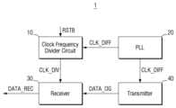
도 1은 몇몇 실시예에 따른 송수신 시스템을 설명하기 위한 블록도이다.
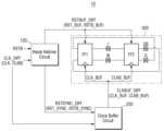
도 2는 도 1의 몇몇 실시예에 따른 클럭 분주 회로를 설명하기 위한 블록도이다.
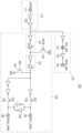
도 3은 도 2의 몇몇 실시예에 따른 클럭 분주 회로에 포함된 리셋 리타이머 회로를 도시한 회로도이다.
도 4는 도 2의 몇몇 실시예에 따른 클럭 분주 회로에 포함된 클럭 버퍼 회로를 도시한 회로도이다.
도 5는 도 2의 몇몇 실시예에 따른 클럭 분주 회로에 포함된 IQ 분주기 회로를 도시한 회로도이다.
도 6은 도 1의 몇몇 실시예에 따른 클럭 분주 회로의 동작을 설명하기 위한 타이밍도이다.
도 7은 도 1의 몇몇 실시예에 따른 클럭 분주 회로의 동작을 설명하기 위한 타이밍도이다.
도 8은 도 1의 몇몇 실시예에 따른 클럭 분주 회로의 동작을 설명하기 위한 타이밍도이다.
도 9는 도 1의 몇몇 실시예에 따른 클럭 분주 회로의 동작을 설명하기 위한 타이밍도이다.
도 10은 도 1의 몇몇 실시예에 따른 클럭 분주 회로의 동작을 설명하기 위한 타이밍도이다.
도 11은 몇몇 실시예에 따른 수신기를 설명하기 위한 블록도이다.1 is a block diagram for explaining a transmission/reception system according to some embodiments.
FIG. 2 is a block diagram illustrating a clock dividing circuit according to some exemplary embodiments of FIG. 1 .
FIG. 3 is a circuit diagram illustrating a reset retimer circuit included in the clock divider circuit according to some embodiments of FIG. 2 .
FIG. 4 is a circuit diagram illustrating a clock buffer circuit included in the clock divider circuit according to some embodiments of FIG. 2 .
FIG. 5 is a circuit diagram showing an IQ divider circuit included in the clock divider circuit according to some embodiments of FIG. 2 .
FIG. 6 is a timing diagram illustrating an operation of a clock divider circuit according to some embodiments of FIG. 1 .
FIG. 7 is a timing diagram illustrating an operation of a clock divider circuit according to some exemplary embodiments of FIG. 1 .
FIG. 8 is a timing diagram illustrating an operation of a clock divider circuit according to some embodiments of FIG. 1 .
FIG. 9 is a timing diagram illustrating an operation of a clock divider circuit according to some embodiments of FIG. 1 .
FIG. 10 is a timing diagram illustrating an operation of a clock divider circuit according to some embodiments of FIG. 1 .
11 is a block diagram illustrating a receiver according to some embodiments.
이하, 첨부된 도면을 참조하여 본 발명의 기술적 사상에 따른 실시예들에 대해 설명한다.Hereinafter, embodiments according to the technical idea of the present invention will be described with reference to the accompanying drawings.
도 1은 몇몇 실시예에 따른 송수신 시스템을 설명하기 위한 블록도이다.1 is a block diagram for explaining a transmission/reception system according to some embodiments.
도 1을 참조하면, 송수신 시스템(1)은 클럭 분주 회로(Clock frequency divider circuit)(10)와, 위상 고정 루프(PLL; Phase Locked Loop)(20)와, 수신기(Receiver)(30)와, 송신기(Transmitter)(40)를 포함할 수 있다.Referring to FIG. 1, the transmission/
클럭 분주 회로(10)는 클럭 분주 회로(10)를 턴온(turn-on)시키는 리셋 신호(RSTB)를 입력받을 수 있고, 위상 고정 루프(20)로부터 차동 신호 쌍의 클럭 신호(CLK_DIFF)를 입력받을 수 있다. 클럭 분주 회로(10)는 제공받은 리셋 신호(RSTB)와 클럭 신호(CLK_DIFF)를 기초로 출력 신호(CLK_DIV)를 출력할 수 있다. 몇몇 실시예에서, 출력 신호(CLK_DIV)는 제1 내지 제4 출력 신호를 포함할 수 있다.The
위상 고정 루프(20)는 클럭 분주 회로(10)와 송신기(40)에 차동 신호 쌍의 클럭 신호(CLK_DIFF)를 제공할 수 있다. 위상 고정 루프(20)는 일정한 주파수를 가지는 클럭 신호(CLK_DIFF)를 출력하기 위하여, 오실리에이터(Oscillator)를 포함할 수 있으나, 이에 제한되는 것은 아니다.The phase locked
송신기(40)는 위상 고정 루프(20)로부터 클럭 신호(CLK_DIFF)를 제공받을 수 있다. 송신기(40)는 제공받은 클럭 신호(CLK_DIFF)를 기초로, 데이터(DATA_OG)를 수신기(30)로 전송할 수 있다.The
수신기(30)는 송신기(40)로부터 데이터(DATA_OG)를 제공받을 수 있고, 클럭 분주 회로(10)로부터 출력 신호(CLK_DIV)를 제공받을 수 있다. 수신기(30)는 제공받은 출력 신호(CLK_DIV)를 기초로, 제공받은 데이터(DATA_OG)를 복원하여 복원 데이터(DATA_REC)를 출력할 수 있다.The
도 2는 도 1의 몇몇 실시예에 따른 클럭 분주 회로를 설명하기 위한 블록도이다.FIG. 2 is a block diagram illustrating a clock dividing circuit according to some exemplary embodiments of FIG. 1 .
도 2를 참조하면, 클럭 분주 회로(10)는 리셋 리타이머 회로(Reset Retimer Circuit)(100)와, 클럭 버퍼 회로(Clock Buffer Circuit)(200)와, IQ 분주기 회로(IQ divider Circuit)(300)를 포함할 수 있다.Referring to FIG. 2, the
리셋 리타이머 회로(100)는 리셋 신호(RSTB)와 클럭 신호(CLK_DIFF)를 제공받을 수 있다. 여기서, 클럭 신호(CLK_DIFF)는 제1 클럭 신호(CLK)와 제2 클럭 신호(CLKB)를 포함할 수 있다. 제1 클럭 신호(CLK)와 제2 클럭 신호(CLKB)는 서로 반대되는 위상을 가지는 차동 쌍의 신호일 수 있다.The
리셋 리타이머 회로(100)는 제공받은 리셋 신호(RSTB)와 클럭 신호(CLK_DIFF)를 기초로, 리셋 버퍼 신호(RSTBUF_DIFF)와 리셋 싱크 신호(RSTSYNC_DIFF)를 출력할 수 있다.The
리셋 버퍼 신호(RSTBUF_DIFF)는 제1 리셋 버퍼 신호(RST_BUF)와 제2 리셋 버퍼 신호(RSTB_BUF)를 포함할 수 있다. 제1 리셋 버퍼 신호(RST_BUF)와 제2 리셋 버퍼 신호(RSTB_BUF)는 서로 반대되는 위상을 가지는 차동 쌍의 신호일 수 있다.The reset buffer signal RSTBUF_DIFF may include a first reset buffer signal RST_BUF and a second reset buffer signal RSTB_BUF. The first reset buffer signal RST_BUF and the second reset buffer signal RSTB_BUF may be a differential pair signal having phases opposite to each other.
리셋 싱크 신호(RSTSYNC_DIFF)는 제1 리셋 싱크 신호(RST_SYNC)와 제2 리셋 싱크 신호(RSTB_SYNC)를 포함할 수 있다. 제1 리셋 싱크 신호(RST_SYNC)와 제2 리셋 싱크 신호(RSTB_SYNC)는 서로 반대되는 위상을 가지는 차동 쌍의 신호일 수 있다. 리셋 싱크 신호(RSTSYNC_DIFF)는 제공받은 클럭 신호(CLK_DIFF)에 동기화된 신호일 수 있다. 구체적인 내용은 후술한다.The reset sync signal RSTSYNC_DIFF may include a first reset sync signal RST_SYNC and a second reset sync signal RSTB_SYNC. The first reset sync signal RST_SYNC and the second reset sync signal RSTB_SYNC may be a differential pair of signals having opposite phases. The reset sync signal RSTSYNC_DIFF may be a signal synchronized with the provided clock signal CLK_DIFF. Specific details are described later.
리셋 리타이머 회로(100)는 출력한 리셋 버퍼 신호(RSTBUF_DIFF)를 IQ 분주기 회로(300)에 제공할 수 있고, 출력한 리셋 싱크 신호(RSTSYNC_DIFF)를 클럭 버퍼 회로(200)에 제공할 수 있다.The
클럭 버퍼 회로(200)는 클럭 신호(CLK_DIFF)와 리셋 싱크 신호(RSTSYNC_DIFF)를 제공받을 수 있다. 클럭 버퍼 회로(200)는 제공받은 클럭 신호(CLK_DIFF)와 리셋 싱크 신호(RSTSYNC_DIFF)를 기초로, 클럭 버퍼 신호(CLKBUF_DIFF)를 출력할 수 있다.The
클럭 버퍼 신호(CLKBUF_DIFF)는 제1 클럭 버퍼 신호(CLK_BUF)와 제2 클럭 버퍼 신호(CLKB_BUF)를 포함할 수 있다. 제1 클럭 버퍼 신호(CLK_BUF)와 제2 클럭 버퍼 신호(CLKB_BUF)는 서로 반대되는 위상을 가지는 차동 쌍의 신호일 수 있다. 클럭 버퍼 신호(CLKBUF_DIFF)는 클럭 신호(CLK_DIFF)가 버퍼링된 신호일 수 있다. 구체적인 내용은 후술한다.The clock buffer signal CLKBUF_DIFF may include a first clock buffer signal CLK_BUF and a second clock buffer signal CLKB_BUF. The first clock buffer signal CLK_BUF and the second clock buffer signal CLKB_BUF may be a differential pair signal having phases opposite to each other. The clock buffer signal CLKBUF_DIFF may be a buffered signal of the clock signal CLK_DIFF. Specific details are described later.
IQ 분주기 회로(300)는 2개의 플립플롭(FF1, FF2)과, 플립플롭 사이에 존재하는 4개의 출력단(I, IB, Q, QB)을 포함할 수 있다. IQ 분주기 회로(300)는 리셋 버퍼 신호(RSTBUF_DIFF)와 클럭 버퍼 신호(CLKBUF_DIFF)를 제공받을 수 있다.The
IQ 분주기 회로(300)는 제공받은 리셋 버퍼 신호(RSTBUF_DIFF)와 클럭 버퍼 신호(CLKBUF_DIFF)를 기초로, 출력단(I, IB, Q, QB)를 통해 제1 내지 제4 출력 신호를 출력할 수 있다. 예를 들어, 출력단(I)은 제1 출력 신호를 출력하고, 출력단(Q)은 제2 출력 신호를 출력하고, 출력단(IB)은 제3 출력 신호를 출력하고, 출력단(QB)은 제4 출력 신호를 출력할 수 있다.The
여기서, 제1 내지 제4 출력 신호는 서로 다른 위상을 가질 수 있다. 예를 들어, 제1 내지 제4 출력 신호는 순차적으로 90°의 위상차를 가지는 관계일 수 있다. 구체적으로, 제1 출력 신호는 클럭 신호의 폴링 엣지(falling edge)에서 토글(toggle)될 수 있고, 제2 출력 신호는 클럭 신호의 라이징 엣지(rising edge)에서 토글될 수 있으며, 제3 출력 신호는 제1 출력 신호와 반대의 위상을 가질 수 있고, 제4 출력 신호는 제2 출력 신호와 반대의 위상을 가질 수 있다.Here, the first to fourth output signals may have different phases. For example, the first to fourth output signals may sequentially have a phase difference of 90°. Specifically, the first output signal may be toggled at the falling edge of the clock signal, the second output signal may be toggled at the rising edge of the clock signal, and the third output signal may be toggled at the rising edge of the clock signal. may have a phase opposite to that of the first output signal, and the fourth output signal may have a phase opposite to that of the second output signal.
도 3은 도 2의 몇몇 실시예에 따른 클럭 분주 회로에 포함된 리셋 리타이머 회로를 도시한 회로도이다.FIG. 3 is a circuit diagram illustrating a reset retimer circuit included in the clock divider circuit according to some embodiments of FIG. 2 .
도 3을 참조하면, 리셋 리타이머 회로(100)는 입력부(110)와, 리셋 버퍼 신호 출력부(120)와, 리셋 싱크 신호 출력부(130)를 포함할 수 있다.Referring to FIG. 3 , the
입력부(110)는 리셋 신호 입력단(111)과, 복수의 인버터(Inverter, 112)를 포함할 수 있다.The
리셋 신호 입력단(111)은 클럭 분주 회로에 입력되는 리셋 신호(RSTB)를 입력받을 수 있다.The reset
복수의 인버터(112)는 리셋 신호(RSTB)를 입력받아 버퍼 기능을 할 수 있다. 도 3에서, 복수의 인버터(112)는 2개의 인버터를 포함하는 것으로 도시되었으나, 이에 제한되는 것은 아니며 다른 수의 인버터를 포함할 수 있다.The plurality of
리셋 버퍼 신호 출력부(120)는 제1 리셋 버퍼 신호 출력단(121)과, 인버터(122), 및 제2 리셋 버퍼 신호 출력단(123)을 포함할 수 있다.The reset buffer
제1 리셋 버퍼 신호 출력단(121)과 제2 리셋 버퍼 신호 출력단(123)은 리셋 버퍼 신호를 출력할 수 있다. 예를 들어, 제1 리셋 버퍼 신호 출력단(121)은 제1 리셋 버퍼 신호(RST_BUF)를 출력할 수 있고, 제2 리셋 버퍼 신호 출력단(123)은 제1 리셋 버퍼 신호(RST_BUF)와 위상이 반대되는 제2 리셋 버퍼 신호(RSTB_BUF)를 출력할 수 있다.The first reset buffer
인버터(122)는 제1 리셋 버퍼 신호 출력단(121)과 제2 리셋 버퍼 신호 출력단(123)이 서로 반대의 위상을 가지는 리셋 버퍼 신호를 출력하도록, 제1 리셋 버퍼 신호 출력단(121)과 제2 리셋 버퍼 신호 출력단(123) 사이에 존재할 수 있다. 이에 따라 도 3에서, 인버터(122)가 1개 존재하는 것으로 도시되었으나, 이에 제한되는 것은 아니며, 제1 리셋 버퍼 신호 출력단(121)과 제2 리셋 버퍼 신호 출력단(123)이 서로 반대의 위상을 가지는 리셋 버퍼 신호를 출력하도록, 홀수개의 인버터가 존재할 수도 있다.The
리셋 싱크 신호 출력부(130)는 복수의 플립 플롭(131, 132)과, 복수의 스위칭 트랜지스터(133, 134)와, 제1 스위치(135), 제2 스위치(136), 제1 리셋 싱크 신호 출력단(137), 제2 리셋 싱크 신호 출력단(138), 및 래치(latch)(139)를 포함할 수 있다.The reset sync
복수의 플립 플롭(131, 132)은 인버터와 스위치를 포함할 수 있다. 스위치는 제1 클럭 신호(CLK) 및 제2 클럭 신호(CLKB)에 동기화되어 동작할 수 있다.The plurality of
복수의 스위칭 트랜지스터(133, 134)는 복수의 플립 플롭(131, 132) 각각의 출력단에 연결될 수 있다. 복수의 스위칭 트랜지스터(133, 134)는 차동 신호 쌍의 리셋 신호(RST, RSTB)에 의해 게이팅되어 스위치로 동작할 수 있다.The plurality of switching
제1 스위치(135)는 제2 플립 플롭(132)의 출력단에 연결된 인버터와 연결될 수 있다. 제1 스위치(135)는 제1 클럭 신호(CLK)에 의해 동기화되어 동작할 수 있다. 제1 스위치(135)는 제1 클럭 신호(CLK)에 의해 동기화되어, 제1 리셋 싱크 신호(RST_SYNC)를 출력할 수 있다.The
제2 스위치(136)는 제2 플립 플롭(132)의 출력단에 연결된 인버터와 연결될 수 있다. 제2 스위치(136)는 제1 클럭 신호(CLK)에 의해 동기화되어 동작할 수 있다. 제2 스위치(136)는 제1 클럭 신호(CLK)에 의해 동기화되어, 제2 리셋 싱크 신호(RSTB_SYNC)를 출력할 수 있다.The
제1 리셋 싱크 신호 출력단(137)은 제1 스위치(135)에 연결되어 제1 리셋 싱크 신호(RST_SYNC)를 출력할 수 있다.The first reset sync
제2 리셋 싱크 신호 출력단(138)은 제2 스위치(136)에 연결되어 제2 리셋 싱크 신호(RSTB_SYNC)를 출력할 수 있다.The second reset sync
래치(139)는 제1 리셋 싱크 신호 출력단(137)과 제2 리셋 싱크 신호 출력단(138) 사이에 연결될 수 있다. 래치(139)는 제1 스위치(135) 및 제2 스위치(136)가 개방된 경우, 제1 리셋 싱크 신호 출력단(137)과 제2 리셋 싱크 신호 출력단(138)이 일정한 레벨의 신호를 출력하도록 동작할 수 있다.The
도 3에서, 제1 스위치(135)의 입력단은 1개의 인버터가 존재하고, 제2 스위치(136)의 입력단은 2개의 인버터가 존재하여 서로 반대의 위상을 가지는 리셋 싱크 신호를 출력하도록 도시되었으나, 이에 제한되는 것은 아니며 다른 수의 인버터를 포함할 수 있다.In FIG. 3, the input terminal of the
도 4는 도 2의 몇몇 실시예에 따른 클럭 분주 회로에 포함된 클럭 버퍼 회로를 도시한 회로도이다.FIG. 4 is a circuit diagram illustrating a clock buffer circuit included in the clock divider circuit according to some embodiments of FIG. 2 .
클럭 버퍼 회로(200)는 제1 클럭 버퍼 신호(CLK_BUF)를 출력하는 제1 클럭 버퍼 회로(210)와, 제2 클럭 버퍼 신호(CLKB_BUF)를 출력하는 제2 클럭 버퍼 회로(220)를 포함할 수 있다. 여기서, 제1 클럭 버퍼 회로(210)와 제2 클럭 버퍼 회로(220)는 실질적으로 동일한 구성을 포함하므로, 제1 클럭 버퍼 회로(210)만을 설명한다.The
제1 클럭 버퍼 회로(210)는 제1 클럭 신호 입력단(211), 제1 3상 버퍼(tristate buffer)(212), 제1 트랜지스터(216), 제1 인버터(217), 및 제1 클럭 버퍼 신호 출력단(218)을 포함할 수 있다.The first
제1 클럭 신호 입력단(211)은 제1 클럭 신호(CLK)를 입력받을 수 있다.The first clock
제1 3상 버퍼(212)는 제2 인버터(214)와, 제2 트랜지스터(213)와, 제3 트랜지스터(215)를 포함할 수 있다.The first three-
제2 트랜지스터(213)의 일단은 구동 전압(VDD)을 제공받을 수 있다. 제2 트랜지스터(213)의 타단은 제2 인버터(214)와 연결될 수 있다. 제2 트랜지스터(213)는 제1 리셋 싱크 신호(RST_SYNC)에 의해 게이팅될 수 있다. 몇몇 실시예에서, 제2 트랜지스터(213)는 PMOS 트랜지스터일 수 있으나, 이에 제한되는 것은 아니다.One end of the second transistor 213 may receive the driving voltage VDD. The other end of the second transistor 213 may be connected to the
제3 트랜지스터(215)의 일단은 제2 인버터(214)와 연결될 수 있다. 제3 트랜지스터(215)의 타단은 접지 전압(VSS)을 제공받을 수 있다. 제3 트랜지스터(215)는 제2 리셋 싱크 신호(RSTB_SYNC)에 의해 게이팅될 수 있다. 몇몇 실시예에서, 제3 트랜지스터(215)는 NMOS 트랜지스터일 수 있으나, 이에 제한되는 것은 아니다.One end of the
제2 인버터(214)는 제2 트랜지스터(213) 및 제3 트랜지스터(215)와 연결될 수 있다. 제2 인버터(214)는 제2 트랜지스터(213) 및 제3 트랜지스터(215)가 각각 제1 리셋 싱크 신호(RST_SYNC)와 제2 리셋 싱크 신호(RSTB_SYNC)에 의해 게이팅되는 경우 인버터로써 동작할 수 있다. 반면에, 제2 트랜지스터(213) 및 제3 트랜지스터(215)가 각각 제1 리셋 싱크 신호(RST_SYNC)와 제2 리셋 싱크 신호(RSTB_SYNC)에 의해 게이팅되지 않는 경우 플로팅(floating)된 상태로 존재할 수 있다.The
제1 트랜지스터(216)의 일단은 제1 3상 버퍼(212)의 출력단과 제1 인버터(217) 사이에 연결될 수 있다. 제1 트랜지스터(216)의 타단은 접지 전압(VSS)을 제공받을 수 있다. 제1 트랜지스터(216)는 제1 리셋 싱크 신호(RST_SYNC)에 의해 게이팅될 수 있다. 몇몇 실시예에서, 제1 트랜지스터(216)는 NMOS 트랜지스터일 수 있으나, 이에 제한되는 것은 아니다.One end of the
제1 인버터(217)는 제1 3상 버퍼(212)로부터 출력된 신호를 제공받아, 인버터로 동작할 수 있다. 따라서, 제1 3상 버퍼(212)가 인버터로 동작하는 경우, 제1 3상 버퍼(212)와 제1 인버터(217)는 버퍼로써 동작할 수 있다.The
제1 클럭 버퍼 신호 출력단(218)은 제1 클럭 버퍼 신호(CLK_BUF)를 출력할 수 있다. 제1 클럭 버퍼 신호 출력단(218)은 제1 클럭 버퍼 신호(CLK_BUF)를 IQ 분주기 회로에 제공할 수 있다.The first clock buffer
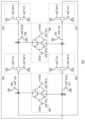
도 5는 도 2의 몇몇 실시예에 따른 클럭 분주 회로에 포함된 IQ 분주기 회로를 도시한 회로도이다.FIG. 5 is a circuit diagram showing an IQ divider circuit included in the clock divider circuit according to some embodiments of FIG. 2 .
IQ 분주기 회로(300)는 제3 내지 제6 3상 버퍼(310, 320, 330, 340)와, 제3 내지 제6 스위칭 트랜지스터(350, 360, 370, 380)와, 복수의 래치(390, 395), 및 복수의 출력단(I, IB, Q, QB)을 포함할 수 있다.The
제3 내지 제6 3상 버퍼(310, 320, 330, 340)는 실질적으로 동일한 구성을 포함하고, 도 4의 제1 3상 버퍼(212)와 실질적으로 동일하므로 자세한 설명은 이하 생략한다.Since the third to sixth three-
제3 및 제6 스위칭 트랜지스터(350, 380)는 실질적으로 동일하므로, 제3 스위칭 트랜지스터(350)만을 설명한다.Since the third and
제3 스위칭 트랜지스터(350)의 일단은 제3 3상 버퍼(310)의 출력단과 제1 출력 신호를 출력하는 출력단(I)과 연결될 수 있다. 제3 스위칭 트랜지스터(350)의 타단은 접지 전압(VSS)을 제공받을 수 있다. 제3 스위칭 트랜지스터(350)는 제1 리셋 버퍼 신호(RST_BUF)에 의해 게이팅될 수 있다. 몇몇 실시예에서, 제3 스위칭 트랜지스터(350)는 NMOS 트랜지스터일 수 있으나, 이에 제한되는 것은 아니다.One end of the
제4 및 제5 스위칭 트랜지스터(360, 370)는 실질적으로 동일하므로, 제4 스위칭 트랜지스터(360)만을 설명한다.Since the fourth and
제4 스위칭 트랜지스터(360)의 일단은 구동 전압(VDD)을 제공받을 수 있다. 제4 스위칭 트랜지스터(360)의 타단은 제4 3상 버퍼(320)의 출력단과 제3 출력 신호를 출력하는 출력단(IB)과 연결될 수 있다. 제4 스위칭 트랜지스터(360)는 제2 리셋 버퍼 신호(RSTB_BUF)에 의해 게이팅될 수 있다. 몇몇 실시예에서, 제4 스위칭 트랜지스터(360)는 PMOS 트랜지스터일 수 있으나, 이에 제한되는 것은 아니다.One end of the
복수의 출력단(I, IB, Q, QB)은 제1 내지 제4 출력 신호를 출력할 수 있다. 구체적으로, 출력단(I)은 제1 출력 신호를 출력하고, 출력단(Q)은 제2 출력 신호를 출력하고, 출력단(IB)은 제3 출력 신호를 출력하고, 출력단(QB)은 제4 출력 신호를 출력할 수 있다.The plurality of output terminals I, IB, Q, and QB may output first to fourth output signals. Specifically, the output terminal I outputs a first output signal, the output terminal Q outputs a second output signal, the output terminal IB outputs a third output signal, and the output terminal QB outputs a fourth output signal. signal can be output.
제1 내지 제4 출력 신호는 서로 다른 위상을 가질 수 있다. 예를 들어, 제1 내지 제4 출력 신호는 순차적으로 90°의 위상차를 가지는 관계일 수 있다. 구체적으로, 제1 출력 신호는 클럭 신호의 폴링 엣지(falling edge)에서 토글(toggle)될 수 있고, 제2 출력 신호는 클럭 신호의 라이징 엣지(rising edge)에서 토글될 수 있으며, 제3 출력 신호는 제1 출력 신호와 반대의 위상을 가질 수 있고, 제4 출력 신호는 제2 출력 신호와 반대의 위상을 가질 수 있다.The first to fourth output signals may have different phases. For example, the first to fourth output signals may sequentially have a phase difference of 90°. Specifically, the first output signal may be toggled at the falling edge of the clock signal, the second output signal may be toggled at the rising edge of the clock signal, and the third output signal may be toggled at the rising edge of the clock signal. may have a phase opposite to that of the first output signal, and the fourth output signal may have a phase opposite to that of the second output signal.
도 6은 도 1의 몇몇 실시예에 따른 클럭 분주 회로의 동작을 설명하기 위한 타이밍도이다.FIG. 6 is a timing diagram illustrating an operation of a clock divider circuit according to some embodiments of FIG. 1 .
도 6을 참조하면, 클럭 신호(CLK)와 리셋 신호(RSTB)는 로우 레벨(Low Level)에 대응되는 제1 레벨(L)과, 하이 레벨(High Level)에 대응되는 제2 레벨(H) 사이를 천이(transition)할 수 있다.Referring to FIG. 6, the clock signal CLK and the reset signal RSTB have a first level L corresponding to a low level and a second level H corresponding to a high level. You can transition between them.
클럭 신호(CLK)는 도 1의 위상 고정 루프(20)로부터 일정한 주파수를 가지는 형태로 출력될 수 있다.The clock signal CLK may be output in a form having a constant frequency from the phase locked
리셋 신호(RSTB)는 클럭 분주 회로가 동작하는 제1 시점(T1)에서 제1 레벨(L)에서 제2 레벨(H)로 천이할 수 있다. 즉, 리셋 신호(RSTB)는 인에이블 신호에 대응될 수 있다. 따라서 제1 시점(T1) 이전의 A 구간은 클럭 분주 회로가 동작하기 이전의 구간에 대응될 수 있고, 제1 시점(T1) 이후의 B, C, D 구간은 클럭 분주 회로가 동작을 수행하는 구간에 대응될 수 있다.The reset signal RSTB may transition from a first level (L) to a second level (H) at a first time point (T1) when the clock divider circuit operates. That is, the reset signal RSTB may correspond to the enable signal. Therefore, section A before the first time point T1 may correspond to a section before the clock divider circuit operates, and sections B, C, and D after the first time point T1 may correspond to sections before the clock divider circuit operates. It may correspond to a section.
한편, 도 6에 도시된 바와 같이, 리셋 신호(RSTB)는 클럭 신호(CLK)와 동기화되지 않은 상태일 수 있다. 구체적으로, 리셋 신호(RSTB)가 제1 레벨에서 제2 레벨로 천이하는 제1 시점(T1)과 클럭 신호(CLK)가 토글링하는 시점이 동일하지 않을 수 있다.Meanwhile, as shown in FIG. 6 , the reset signal RSTB may be out of synchronization with the clock signal CLK. Specifically, the first time T1 when the reset signal RSTB transitions from the first level to the second level may not be the same as the time when the clock signal CLK toggles.
한편 상기와 같이 리셋 신호(RSTB)와 클럭 신호(CLK)가 동기화되지 않는 경우, 제1 시점(T1)부터 제2 시점(T2) 사이의 구간에서 클럭 신호(CLK)보다 폭이 작은 숏 글리치(glitch)가 발생할 수 있다. 글리치는 IQ 분주기 회로에 포함된 3상 버퍼가 인버터로 동작하는 과정에서 출력 신호의 위상을 충분히 드라이빙하지 못하게 되는 문제를 유발할 수 있다. 출력 신호의 위상이 충분히 드라이빙되지 못하는 경우, 복수의 출력단은 제1 레벨(L)과 제2 레벨(H) 사이를 천이하지 않고 일정한 레벨을 갖는 신호를 출력할 수도 있다.Meanwhile, when the reset signal RSTB and the clock signal CLK are not synchronized as described above, a short glitch (with a width smaller than that of the clock signal CLK) in the section between the first time point T1 and the second time point T2 glitches) may occur. The glitch may cause a problem in that the phase of the output signal cannot be sufficiently driven while the 3-phase buffer included in the IQ divider circuit operates as an inverter. When the phase of the output signal is not sufficiently driven, the plurality of output terminals may output a signal having a constant level without transitioning between the first level (L) and the second level (H).
구체적으로 도 5를 참조하면, 제5 3상 버퍼(330)에 제2 레벨(H)을 갖는 제1 클럭 신호가 제1 클럭 버퍼 신호(CLK_BUF)로써, 제1 레벨(L)을 갖는 제2 클럭 신호가 제2 클럭 버퍼 신호(CLKB_BUF)로써 제공되는 경우, 제5 3상 버퍼(330)는 인버터로써 동작할 수 있다. 하지만, 상기 제1 클럭 신호와 제2 클럭 신호가 순간적으로 발생하여 제5 3상 버퍼(330)가 충분히 드라이빙하지 못하는 문제가 발생할 수 있다. 이에 따라 출력단(QB)에 제공되는 신호의 위상이 반대로 바뀌지 않고 일정한 레벨을 가질 수 있다.Specifically, referring to FIG. 5 , the first clock signal having the second level (H) in the fifth three-
이에 본 발명의 몇몇 실시예에 따른 클럭 분주 회로는, 클럭 신호와 동기화된 리셋 싱크 신호를 기초로 클럭 신호가 버퍼링된 클럭 버퍼 신호를 IQ 분주기 회로에 제공함으로써, 글리치를 제거하여 IQ 분주기 회로의 복수의 출력단에서 서로 다른 위상을 갖는 출력 신호를 정상적으로 출력하도록 동작할 수 있다.Accordingly, a clock divider circuit according to some embodiments of the present invention provides a clock buffer signal in which a clock signal is buffered based on a reset sync signal synchronized with a clock signal to an IQ divider circuit, thereby eliminating glitches and providing the IQ divider circuit It is possible to operate to normally output output signals having different phases from a plurality of output terminals.
도 7은 도 1의 몇몇 실시예에 따른 클럭 분주 회로의 동작을 설명하기 위한 타이밍도이다.FIG. 7 is a timing diagram illustrating an operation of a clock divider circuit according to some exemplary embodiments of FIG. 1 .
도 7을 참조하면, 먼저 리셋 신호(RSTB)가 제1 시점(T1)에서 제1 레벨(L)에서 제2 레벨(H)로 천이한 후, 제2 리셋 버퍼 신호(RSTB_BUF)가 제2 시점(T2)에서 제1 레벨(L)에서 제2 레벨(H)로 천이할 수 있다.Referring to FIG. 7 , after the reset signal RSTB transitions from the first level L to the second level H at a first time point T1, the second reset buffer signal RSTB_BUF is output at a second time point T1. In (T2), it is possible to transition from the first level (L) to the second level (H).
구체적으로 도 3을 참조하면, 리셋 신호 입력단(111)과 제2 리셋 버퍼 신호 출력단(123) 사이에 짝수개의 인버터가 존재하므로, 리셋 신호(RSTB)가 제1 레벨(L)에서 제2 레벨(H)로 천이한 것에 대응하여, 동일하게 제2 리셋 버퍼 신호(RSTB_BUF) 또한 제1 레벨(L)에서 제2 레벨(H)로 천이할 수 있다.Specifically, referring to FIG. 3 , since an even number of inverters exist between the reset
한편, 제2 리셋 버퍼 신호(RSTB_BUF)는 리셋 신호(RSTB)가 입력된 후 인버터 등의 추가적인 구성을 거쳐 출력되므로, B 구간만큼 딜레이(delay)된 후에 천이할 수 있다. 또한, 제2 리셋 버퍼 신호(RSTB_BUF)는 리셋 신호(RSTB)와 마찬가지로 제1 클럭 신호(CLK)에 동기화되지 않은 신호일 수 있다.Meanwhile, since the second reset buffer signal RSTB_BUF is output through an additional configuration such as an inverter after the reset signal RSTB is input, it can transition after being delayed by a period B. Also, the second reset buffer signal RSTB_BUF may be a signal that is not synchronized with the first clock signal CLK like the reset signal RSTB.
도 8은 도 1의 몇몇 실시예에 따른 클럭 분주 회로의 동작을 설명하기 위한 타이밍도이다.FIG. 8 is a timing diagram illustrating an operation of a clock divider circuit according to some embodiments of FIG. 1 .
도 8을 참조하면, 제2 리셋 버퍼 신호(RSTB_BUF)가 제2 시점(T2)에서 제2 레벨(H)로 천이한 이후에, 제2 리셋 싱크 신호(RSTB_SYNC)가 제3 시점(T3)에서 제1 레벨(L)에서 제2 레벨(H)로 천이할 수 있다. 제3 시점(T3)은 제1 클럭 신호(CLK)의 라이징 엣지 시점에 대응될 수 있고, 제2 리셋 싱크 신호(RSTB_SYNC)는 제1 클럭 신호(CLK)의 라이징 엣지에 동기화되어 제1 레벨(L)에서 제2 레벨(H)로 천이할 수 있다.Referring to FIG. 8 , after the second reset buffer signal RSTB_BUF transitions to the second level H at the second time T2, the second reset sync signal RSTB_SYNC is output at the third time T3. It is possible to transition from the first level (L) to the second level (H). The third time point T3 may correspond to the time point of the rising edge of the first clock signal CLK, and the second reset sync signal RSTB_SYNC is synchronized with the rising edge of the first clock signal CLK to reach the first level ( L) to the second level (H).
구체적으로 도 3을 함께 참조하면, 구간 A에서 리셋 신호(RSTB)가 제1 레벨(L)에 대응되는 경우, 제2 스위칭 트랜지스터(134)는 게이팅되어 제2 플립 플롭(132)과 연결된 노드를 풀다운(pull down)할 수 있다. 이에 따라, 제2 리셋 싱크 신호 출력단(138)은 제1 레벨(L)의 제2 리셋 싱크 신호(RSTB_SYNC)를 출력할 수 있다.Specifically, referring to FIG. 3 , when the reset signal RSTB corresponds to the first level L in period A, the
한편, 제1 시점(T1)에서 리셋 신호(RSTB)가 제1 레벨(L)에서 제2 레벨(H)로 천이하는 경우, 제1 및 제2 스위칭 트랜지스터(133, 134)는 모두 턴오프(turn-off)될 수 있고, 이에 대응하여 제2 스위칭 트랜지스터(134)와 제2 플립 플롭(132)이 연결된 노드는 하이 레벨을 가질 수 있다. 이에 따라, 제2 리셋 싱크 신호 출력단(138)은 제2 레벨(H)의 제2 리셋 싱크 신호(RSTB_SYNC)를 출력할 수 있다.Meanwhile, when the reset signal RSTB transitions from the first level (L) to the second level (H) at the first time point T1, both the first and
또한, 제2 리셋 싱크 신호 출력단(138)은 제1 클럭 신호(CLK)에 동기화된 제2 스위치(136)와 연결되어, 제1 클럭 신호(CLK)에 동기화된 제2 리셋 싱크 신호(RSTB_SYNC)를 출력할 수 있다. 한편, 제1 클럭 신호(CLK)에 의해 제2 스위치(136)와 연결되지 않더라도, 래치(139)에 의해 일정한 레벨을 가지는 제2 리셋 싱크 신호(RSTB_SYNC)가 출력될 수 있다. 또한, 제2 리셋 싱크 신호(RSTB_SYNC)는 제2 시점(T2)에서 제2 리셋 버퍼 신호(RSTB_BUF)가 천이된 후 C 구간만큼 딜레이된 후에 천이할 수 있다.In addition, the second reset sync
도 9는 도 1의 몇몇 실시예에 따른 클럭 분주 회로의 동작을 설명하기 위한 타이밍도이다.FIG. 9 is a timing diagram illustrating an operation of a clock divider circuit according to some embodiments of FIG. 1 .
도 9를 참조하면, 제2 리셋 싱크 신호(RSTB_SYNC)가 제2 레벨(H)로 천이한 이후에, 제1 클럭 버퍼 신호(CLK_BUF)가 제1 클럭 신호(CLK)와 동일한 형태로 출력될 수 있다. 즉, 클럭 버퍼 신호(CLK_BUF)는 제4 시점(T4) 이전에서 제2 레벨(H)의 일정한 레벨로 출력될 수 있고, 제4 시점(T4) 이후에서 제1 클럭 신호(CLK)와 동일한 형태로 출력될 수 있다.Referring to FIG. 9 , after the second reset sync signal RSTB_SYNC transitions to the second level H, the first clock buffer signal CLK_BUF may be output in the same form as the first clock signal CLK. there is. That is, the clock buffer signal CLK_BUF can be output at a constant level of the second level H before the fourth time point T4, and has the same shape as the first clock signal CLK after the fourth time point T4. can be output as
구체적으로 도 4를 참조하면, 제3 시점(T3) 이전에서 제2 리셋 싱크 신호(RSTB_SYNC)는 제1 레벨(L)로 일정하게 유지될 수 있다. 따라서, 제1 트랜지스터(216)는 제2 레벨(H)의 제1 리셋 싱크 신호(RST_SYNC)에 의해 게이팅될 수 있고, 제1 인버터(217)의 입력단은 풀다운될 수 있다. 따라서, 제1 클럭 버퍼 신호 출력단(218)은 제2 레벨(H)을 가지는 제1 클럭 버퍼 신호(CLK_BUF)를 출력할 수 있다.Specifically, referring to FIG. 4 , before the third time point T3 , the second reset sync signal RSTB_SYNC may be constantly maintained at the first level L. Accordingly, the
한편, 제3 시점(T3)에서 제2 리셋 싱크 신호(RSTB_SYNC)가 제1 레벨(L)에서 제2 레벨(H)로 천이한 경우, 제1 트랜지스터(216)는 제1 리셋 싱크 신호(RST_SYNC)가 제2 레벨(H)에서 제1 레벨(L)로 천이함에 따라 턴오프될 수 있다. 제1 클럭 버퍼 신호(CLK_BUF)는 버퍼링되어 D 구간 동안 기존의 제2 레벨(H)을 유지할 수 있다.Meanwhile, when the second reset sync signal RSTB_SYNC transitions from the first level L to the second level H at the third time point T3, the
제4 시점(T4)에서, 제1 리셋 싱크 신호(RST_SYNC)가 제1 레벨(L)에서 제2 레벨(H)로 천이함에 따라 제1 트랜지스터(216)는 턴오프될 수 있다. 한편, 제1 3상 버퍼(212)에 포함된 제2 트랜지스터(213) 및 제3 트랜지스터(215)는 각각 제1 리셋 싱크 신호(RST_SYNC)와 제2 리셋 싱크 신호(RSTB_SYNC)에 의해 게이팅되므로, 제1 3상 버퍼(212)는 인버터로써 동작할 수 있다.At a fourth time point T4 , the
따라서, 제1 3상 버퍼(212)와 제1 인버터(217)는 버퍼로써 동작하여, 입력받은 제1 클럭 신호(CLK)를 버퍼링하여 제1 클럭 버퍼 신호(CLK_BUF)를 출력할 수 있다. 따라서, 제1 클럭 버퍼 신호(CLK_BUF)는 제3 시점(T3) 이후 D 구간만큼 딜레이된 후에 제4 시점(T4)부터 제1 클럭 신호(CLK)와 동일한 형태로 출력될 수 있다.Accordingly, the first three-
도 10은 도 1의 몇몇 실시예에 따른 클럭 분주 회로의 동작을 설명하기 위한 타이밍도이다.FIG. 10 is a timing diagram illustrating an operation of a clock divider circuit according to some embodiments of FIG. 1 .
도 10을 참조하면, 제1 클럭 버퍼 신호(CLK_BUF)가 제4 시점(T4)에서 제1 클럭 신호(CLK)와 동일한 형태로 출력되는 것에 대응하여, 출력단(I)에서 제1 출력 신호가 출력될 수 있다. 구체적으로, 제1 출력 신호는 제1 클럭 신호(CLK)의 폴링 엣지에서 토글할 수 있고, 제2 출력 신호는 제1 클럭 신호(CLK)의 라이징 엣지에서 토글할 수 있다. 또한, 제3 출력 신호는 제1 출력 신호와 반대의 위상을 가질 수 있고, 제4 출력 신호는 제2 출력 신호와 반대의 위상을 가질 수 있다.Referring to FIG. 10, in response to the first clock buffer signal CLK_BUF being output in the same form as the first clock signal CLK at the fourth time point T4, the first output signal is output from the output terminal I. It can be. Specifically, the first output signal may toggle at the falling edge of the first clock signal CLK, and the second output signal may toggle at the rising edge of the first clock signal CLK. Also, the third output signal may have a phase opposite to that of the first output signal, and the fourth output signal may have a phase opposite to that of the second output signal.
구체적으로 도 5를 함께 참조하면, 도 10의 A 및 B 구간에서 제1 리셋 버프 신호(RST_BUF)는 제2 레벨(H)로 유지될 수 있고, 제2 리셋 버퍼 신호(RSTB_BUF)는 제1 레벨(L)로 유지될 수 있다. 이에 따라 제3 내지 제6 스위칭 트랜지스터(350, 360, 370, 380)는 게이팅될 수 있다. 따라서, 제1 출력 신호(I)와 제2 출력 신호(Q)는 제1 레벨(L)로 일정하게 유지될 수 있고, 제3 출력 신호(IB)와 제4 출력 신호(QB)는 제2 레벨(H)로 일정하게 유지될 수 있다.Specifically, referring to FIG. 5 , in sections A and B of FIG. 10 , the first reset buffer signal RST_BUF may be maintained at the second level H, and the second reset buffer signal RSTB_BUF may be maintained at the first level. (L) can be maintained. Accordingly, the third to
한편, 도 10의 C 및 D 구간에서, 제1 리셋 버프 신호(RST_BUF)가 제1 레벨(L)로 유지되고, 제2 리셋 버퍼 신호(RSTB_BUF)가 제2 레벨(H)로 유지됨에 따라 제3 내지 제6 스위칭 트랜지스터(350, 360, 370, 380)는 모두 턴오프될 수 있다. 한편, 제1 클럭 버퍼 신호(CLK_BUF)는 A 및 B 구간에서와 동일하게 제2 레벨(H)을 유지하고, 제2 클럭 버퍼 신호(CLKB_BUF)는 A 및 B 구간에서와 동일하게 제1 레벨(L)을 유지할 수 있다. 이에 따라, 제3 3상 버퍼(310)와 제4 3상 버퍼(320)는 플로팅된 상태로 존재할 수 있고, 제5 3상 버퍼(330)와 제6 3상 버퍼(340)는 인버터로 동작할 수 있다. 따라서, 제1 출력 신호(I)와 제2 출력 신호(Q)는 제1 레벨(L)로 일정하게 유지될 수 있고, 제3 출력 신호(IB)와 제4 출력 신호(QB)는 제2 레벨(H)로 일정하게 유지될 수 있다.Meanwhile, in sections C and D of FIG. 10 , the first reset buffer signal RST_BUF is maintained at the first level (L) and the second reset buffer signal RSTB_BUF is maintained at the second level (H). All of the third to
한편, 제4 시점(T4) 이후에서 제1 클럭 버퍼 신호(CLK_BUF) 및 제2 클럭 버퍼 신호(CLKB_BUF)가 천이를 시작함에 따라, 제1 내지 제4 출력 신호(I, IB, Q, QB) 또한 천이를 시작할 수 있다. 제1 내지 제4 출력 신호(I, IB, Q, QB)가 출력되는 과정은 실질적으로 동일하므로, 이하에서는 제1 출력 신호(I)의 출력 과정만을 설명한다.Meanwhile, as the first clock buffer signal CLK_BUF and the second clock buffer signal CLKB_BUF start to transition after the fourth time point T4, the first to fourth output signals I, IB, Q, and QB It can also initiate a transition. Since the process of outputting the first to fourth output signals I, IB, Q, and QB is substantially the same, only the output process of the first output signal I will be described below.
제4 시점(T4)에서 제1 클럭 버퍼 신호(CLK_BUF)가 제2 레벨(H)에서 제1 레벨(L)로 천이하고, 제2 클럭 버퍼 신호(CLKB_BUF)가 제1 레벨(L)에서 제2 레벨(H)로 천이함에 따라, 제3 3상 버퍼(310)는 인버터로써 동작할 수 있다. 따라서 출력단(Q)에서 제1 레벨(L)에 대응되는 신호가 출력되므로 제1 출력 신호(I)는 제2 레벨(H)로 천이할 수 있다.At a fourth time point T4, the first clock buffer signal CLK_BUF transitions from the second level H to the first level L, and the second clock buffer signal CLKB_BUF shifts from the first level L to the second level T4. Upon transition to level 2 (H), the third three-
이어서, 제1 클럭 버퍼 신호(CLK_BUF)가 제1 레벨(L)에서 제2 레벨(H)로 천이하고, 제2 클럭 버퍼 신호(CLKB_BUF)가 제2 레벨(H)에서 제1 레벨(L)로 천이하는 경우, 제3 3상 버퍼(310)는 플로팅 상태로 존재할 수 있다. 따라서, 제1 출력 신호(I)는 제2 레벨(H)을 유지할 수 있다.Subsequently, the first clock buffer signal CLK_BUF transitions from the first level (L) to the second level (H), and the second clock buffer signal CLKB_BUF transitions from the second level (H) to the first level (L). When transitioning to , the third three-
이어서, 제1 클럭 버퍼 신호(CLK_BUF)가 제2 레벨(H)에서 제1 레벨(L)로 천이하고, 제2 클럭 버퍼 신호(CLKB_BUF)가 제1 레벨(L)에서 제2 레벨(H)로 천이함에 따라, 제3 3상 버퍼(310)는 인버터로써 동작할 수 있다. 따라서, 출력단(Q)에 제2 레벨(H)에 대응되는 신호가 출력되므로 제1 출력 신호(I)는 제1 레벨(L)로 천이할 수 있다.Subsequently, the first clock buffer signal CLK_BUF transitions from the second level H to the first level L, and the second clock buffer signal CLKB_BUF changes from the first level L to the second level H. As the transition to , the third three-
즉, 제3 및 제4 3상 버퍼(310, 320)는 제공받는 제1 클럭 버퍼 신호(CLK_BUF)가 제1 레벨(L)에 대응되고 제2 클럭 버퍼 신호(CLKB_BUF)가 제2 레벨(H)에 대응되는 경우에 인버터로 동작할 수 있다. 유사하게, 제5 및 제6 3상 버퍼(330, 340)는 제공받는 제1 클럭 버퍼 신호(CLK_BUF)가 제2 레벨(H)에 대응되고 제2 클럭 버퍼 신호(CLKB_BUF)가 제1 레벨(L)에 대응되는 경우에 인버터로 동작할 수 있다.That is, in the third and fourth three-
따라서, 제1 내지 제4 출력 신호(I, IB, Q, QB)는 클럭 신호(CLK)의 주파수의 절반에 해당하는 주파수를 가질 수 있다. 또한, 제1 내지 제4 출력 신호(I, IB, Q, QB)는 순차적으로 90°의 위상 차이를 가질 수 있다.Accordingly, the first to fourth output signals I, IB, Q, and QB may have a frequency corresponding to half of the frequency of the clock signal CLK. Also, the first to fourth output signals I, IB, Q, and QB may sequentially have a phase difference of 90°.
도 11은 몇몇 실시예에 따른 수신기를 설명하기 위한 블록도이다.11 is a block diagram illustrating a receiver according to some embodiments.
수신기(30)는 클럭 분주 회로(10)와 클럭 데이터 복원부(CDR; Clock and Data Recovery)(50)를 포함할 수 있다.The
클럭 분주 회로(10)는 차동 신호 쌍의 클럭 신호(CLK_DIFF)와 클럭 분주 회로를 턴온시키는 리셋 신호(RSTB)를 입력받을 수 있다. 클럭 분주 회로(10)는 제공받은 클럭 신호(CLK_DIFF)와 리셋 신호(RSTB)를 기초로 출력 신호(CLK_DIV)를 출력할 수 있다. 클럭 분주 회로(10)는 도 1 내지 도 10에서 설명한 몇몇 실시예에 따른 클럭 분주 회로와 동일할 수 있다.The
클럭 데이터 복원부(50)는 클럭 분주 회로(10)로부터 출력 신호(CLK_DIV)를 제공받고, 데이터(DATA_OG)를 제공받을 수 있다. 클럭 데이터 복원부(50)는 제공받은 출력 신호(CLK_DIV)와 데이터(DATA_OG)를 기초로 복원 데이터(DATA_REC)를 출력할 수 있다.The clock
이상 첨부된 도면을 참조하여 본 발명의 실시예들을 설명하였으나, 본 발명은 상기 실시예들에 한정되는 것이 아니라 서로 다른 다양한 형태로 제조될 수 있으며, 본 발명이 속하는 기술분야에서 통상의 지식을 가진 자는 본 발명의 기술적 사상이나 필수적인 특징을 변경하지 않고서 다른 구체적인 형태로 실시될 수 있다는 것을 이해할 수 있을 것이다. 그러므로 이상에서 기술한 실시예들은 모든 면에서 예시적인 것이며 한정적이 아닌 것으로 이해해야만 한다.Although the embodiments of the present invention have been described with reference to the accompanying drawings, the present invention is not limited to the above embodiments and can be manufactured in a variety of different forms, and those skilled in the art in the art to which the present invention belongs A person will understand that the present invention may be embodied in other specific forms without changing the technical spirit or essential features. Therefore, the embodiments described above should be understood as illustrative in all respects and not limiting.
1: 송수신 시스템 10: 클럭 분주 회로
20: 위상 고정 루프 30: 수신기
40: 송신기 100: 리셋 리타이머 회로
200: 클럭 버퍼 회로 300: IQ 분주기 회로1: transmission and reception system 10: clock division circuit
20: phase locked loop 30: receiver
40: transmitter 100: reset retimer circuit
200: clock buffer circuit 300: IQ divider circuit
Claims (10)
Translated fromKorean상기 클럭 신호와 상기 리셋 싱크 신호를 입력받아, 상기 클럭 신호가 버퍼링된 차동 신호 쌍의 클럭 버퍼 신호를 출력하는 클럭 버퍼 회로(clock buffer circuit); 및
상기 리셋 버퍼 신호와, 상기 클럭 버퍼 신호를 기초로, 서로 다른 위상을 가지는 제1 내지 제4 출력 신호를 출력하는 IQ 분주기 회로(IQ divider circuit)를 포함하는 클럭 분주 회로.a reset retimer circuit which receives a reset signal and a clock signal and outputs a reset buffer signal of a differential signal pair in which the reset signal is buffered and a reset sync signal synchronizing the reset signal with the clock signal;
a clock buffer circuit receiving the clock signal and the reset sync signal and outputting a clock buffer signal of a differential signal pair in which the clock signal is buffered; and
and an IQ divider circuit configured to output first to fourth output signals having different phases based on the reset buffer signal and the clock buffer signal.
상기 리셋 리타이머 회로는,
상기 리셋 신호를 입력받는 리셋 신호 입력부와,
상기 리셋 신호 입력부와 연결되어 상기 리셋 버퍼 신호를 출력하는 리셋 버퍼 신호 출력부와,
상기 리셋 신호 입력부와 연결되어 상기 리셋 싱크 신호를 출력하는 리셋 싱크 신호 출력부를 포함하되,
상기 리셋 버퍼 신호 출력부와 상기 리셋 싱크 신호 출력부는 병렬로 연결된 클럭 분주 회로.According to claim 1,
The reset retimer circuit,
a reset signal input unit receiving the reset signal;
a reset buffer signal output unit connected to the reset signal input unit to output the reset buffer signal;
A reset sync signal output unit connected to the reset signal input unit to output the reset sync signal,
The reset buffer signal output unit and the reset sync signal output unit are connected in parallel to each other.
상기 리셋 버퍼 신호는 제1 리셋 버퍼 신호와 제2 리셋 버퍼 신호를 포함하고,
상기 리셋 버퍼 신호 출력부는,
상기 제1 리셋 버퍼 신호를 출력하여 상기 IQ 분주기 회로에 제공하는 제1 리셋 버퍼 신호 출력단과,
상기 제2 리셋 버퍼 신호를 출력하여 상기 IQ 분주기 회로에 제공하는 제2 리셋 버퍼 신호 출력단과,
상기 제1 리셋 버퍼 신호 출력단과 상기 제2 리셋 버퍼 신호 출력단 사이에 직렬로 연결된 인버터를 포함하는 클럭 분주 회로.According to claim 2,
The reset buffer signal includes a first reset buffer signal and a second reset buffer signal,
The reset buffer signal output unit,
a first reset buffer signal output terminal for outputting the first reset buffer signal and providing it to the IQ divider circuit;
a second reset buffer signal output terminal for outputting the second reset buffer signal and providing the second reset buffer signal to the IQ divider circuit;
and an inverter connected in series between the first reset buffer signal output terminal and the second reset buffer signal output terminal.
상기 리셋 싱크 신호는 제1 리셋 싱크 신호와 제2 리셋 싱크 신호를 포함하고,
상기 리셋 싱크 신호 출력부는,
제1 스위치와 연결되고 상기 제1 리셋 싱크 신호를 출력하는 제1 리셋 싱크 신호 출력단과,
제2 스위치와 연결되고 상기 제2 리셋 싱크 신호를 출력하는 제2 리셋 싱크 신호 출력단을 포함하되,
상기 제1 스위치와 상기 제2 스위치는 상기 클럭 신호에 의해 동기화된 클럭 분주 회로.According to claim 2,
The reset sync signal includes a first reset sync signal and a second reset sync signal,
The reset sync signal output unit,
A first reset sync signal output terminal connected to a first switch and outputting the first reset sync signal;
A second reset sync signal output terminal connected to a second switch and outputting the second reset sync signal,
The clock dividing circuit wherein the first switch and the second switch are synchronized by the clock signal.
상기 클럭 버퍼 신호는 제1 클럭 버퍼 신호와 제2 클럭 버퍼 신호를 포함하고,
상기 클럭 버퍼 회로는,
상기 제1 클럭 버퍼 신호를 출력하여 상기 IQ 분주기 회로에 제공하는 제1 클럭 버퍼 회로와,
상기 제2 클럭 버퍼 신호를 출력하여 상기 IQ 분주기 회로에 제공하는 제2 클럭 버퍼 회로를 포함하는 클럭 분주 회로.According to claim 1,
The clock buffer signal includes a first clock buffer signal and a second clock buffer signal,
The clock buffer circuit,
a first clock buffer circuit that outputs the first clock buffer signal and provides it to the IQ divider circuit;
and a second clock buffer circuit outputting the second clock buffer signal and providing the second clock buffer signal to the IQ divider circuit.
상기 제1 클럭 버퍼 회로는,
상기 클럭 신호를 입력받는 3상 버퍼(tristate buffer)와,
상기 3상 버퍼의 출력단과 연결된 제1 인버터와,
상기 3상 버퍼와 상기 제1 인버터 사이에 연결된 제1 트랜지스터를 포함하고,
상기 3상 버퍼와 상기 제1 트랜지스터는 상기 리셋 싱크 신호에 의해 게이팅되는 클럭 분주 회로.According to claim 5,
The first clock buffer circuit,
A tristate buffer receiving the clock signal;
A first inverter connected to the output terminal of the three-phase buffer;
A first transistor connected between the three-phase buffer and the first inverter;
The 3-phase buffer and the first transistor are gated by the reset sync signal.
상기 클럭 신호와 상기 리셋 싱크 신호를 입력받아 클럭 버퍼 신호를 출력하는 클럭 버퍼 회로(clock buffer circuit); 및
상기 리셋 버퍼 신호와 상기 클럭 버퍼 신호를 기초로, 서로 다른 위상을 가지는 제1 내지 제4 출력 신호를 출력하는 IQ 분주기 회로(IQ divider circuit)를 포함하되,
상기 리셋 신호는 제1 시점에서 상기 제1 레벨에서 상기 제2 레벨로 천이하고,
상기 리셋 버퍼 신호는 상기 리셋 신호가 상기 제1 레벨에서 상기 제2 레벨로 천이한 상기 제1 시점 이후의 제2 시점에서 상기 제1 레벨에서 상기 제2 레벨로 천이하고,
상기 리셋 싱크 신호는 상기 클럭 신호가 상기 제1 레벨에서 상기 제2 레벨로 천이하는 제3 시점에 동기화되어 상기 제1 레벨에서 상기 제2 레벨로 천이하는 클럭 분주 회로.a reset retimer circuit receiving a reset signal and a clock signal transitioning between a first level lower than the second level and the second level, and outputting a reset buffer signal and a reset sink signal;
a clock buffer circuit receiving the clock signal and the reset sync signal and outputting a clock buffer signal; and
An IQ divider circuit for outputting first to fourth output signals having different phases based on the reset buffer signal and the clock buffer signal,
The reset signal transitions from the first level to the second level at a first time point;
The reset buffer signal transitions from the first level to the second level at a second time point after the first time point at which the reset signal transitions from the first level to the second level;
The reset sync signal is synchronized with a third time when the clock signal transitions from the first level to the second level, and transitions from the first level to the second level.
상기 리셋 싱크 신호는 상기 리셋 버퍼 신호가 상기 제1 레벨에서 상기 제2 레벨로 천이하는 상기 제2 시점 이후에 상기 제1 레벨에서 상기 제2 레벨로 천이하는 클럭 분주 회로.According to claim 7,
wherein the reset sync signal transitions from the first level to the second level after the second time point when the reset buffer signal transitions from the first level to the second level.
상기 클럭 버퍼 신호는 상기 리셋 싱크 신호가 상기 제1 레벨에서 상기 제2 레벨로 천이하는 상기 제3 시점 이전에서 제2 레벨을 유지하고,
상기 제3 시점과, 상기 클럭 신호가 상기 제2 레벨에서 상기 제1 레벨로 천이하는 제4 시점 사이에서 상기 제2 레벨을 유지하고,
상기 제4 시점 이후에서 상기 클럭 신호와 동일한 위상을 가지는 클럭 분주 회로.According to claim 7,
The clock buffer signal maintains a second level before the third point in time when the reset sync signal transitions from the first level to the second level;
maintaining the second level between the third time point and a fourth time point when the clock signal transitions from the second level to the first level;
A clock dividing circuit having the same phase as the clock signal after the fourth time point.
상기 출력 신호를 바탕으로 송신기로부터 제공받은 데이터를 복원하는 클럭-데이터 복원부(CDR; Clock and Data Recovery)를 포함하되,
상기 클럭 분주 회로는,
상기 리셋 신호와 상기 클럭 신호를 입력받아, 상기 클럭 신호에 동기화된 리셋 싱크 신호와, 상기 리셋 신호가 버퍼링된 리셋 버퍼 신호와, 상기 클럭 신호가 버퍼링된 클럭 버퍼 신호를 생성하고,
상기 리셋 버퍼 신호와 상기 클럭 버퍼 신호를 기초로 상기 출력 신호를 출력하는 수신기.a clock divider circuit receiving a reset signal and a clock signal and outputting first to fourth output signals having different phases; and
Including a clock-data recovery unit (CDR; Clock and Data Recovery) for restoring data provided from a transmitter based on the output signal,
The clock divider circuit,
Receiving the reset signal and the clock signal, generating a reset sync signal synchronized with the clock signal, a reset buffer signal buffered with the reset signal, and a clock buffer signal buffered with the clock signal;
A receiver configured to output the output signal based on the reset buffer signal and the clock buffer signal.
Applications Claiming Priority (2)
| Application Number | Priority Date | Filing Date | Title |
|---|---|---|---|
| IN202141050276 | 2021-11-02 | ||
| IN202141050276 | 2021-11-02 |
Publications (1)
| Publication Number | Publication Date |
|---|---|
| KR20230063827Atrue KR20230063827A (en) | 2023-05-09 |
Family
ID=86145705
Family Applications (1)
| Application Number | Title | Priority Date | Filing Date |
|---|---|---|---|
| KR1020220001077APendingKR20230063827A (en) | 2021-11-02 | 2022-01-04 | Reset synchronizing circuit and glitchless clock buffer circuit to prevent start-up failure, and IQ divider circuit |
Country Status (2)
| Country | Link |
|---|---|
| US (2) | US11804945B2 (en) |
| KR (1) | KR20230063827A (en) |
Families Citing this family (4)
| Publication number | Priority date | Publication date | Assignee | Title |
|---|---|---|---|---|
| KR20230063827A (en)* | 2021-11-02 | 2023-05-09 | 삼성전자주식회사 | Reset synchronizing circuit and glitchless clock buffer circuit to prevent start-up failure, and IQ divider circuit |
| US11870880B2 (en)* | 2022-01-31 | 2024-01-09 | Samsung Display Co., Ltd. | Clock data recovery (CDR) with multiple proportional path controls |
| US11909407B2 (en)* | 2022-06-17 | 2024-02-20 | Samsung Electronics Co., Ltd. | Method and system of dynamically controlling reset signal of IQ divider |
| US12249990B1 (en)* | 2023-11-15 | 2025-03-11 | Ciena Corporation | Apparatus and method for wideband multi-phase clock generation |
Family Cites Families (13)
| Publication number | Priority date | Publication date | Assignee | Title |
|---|---|---|---|---|
| US6085342A (en) | 1997-05-06 | 2000-07-04 | Telefonaktiebolaget L M Ericsson (Publ) | Electronic system having a chip integrated power-on reset circuit with glitch sensor |
| KR100652565B1 (en) | 2000-01-25 | 2006-12-01 | 엘지전자 주식회사 | Tap Controller of J-Tack Circuit |
| CA2425654C (en) | 2002-04-16 | 2006-04-11 | Research In Motion Limited | Frequency divider system |
| KR20060059544A (en) | 2004-11-29 | 2006-06-02 | 주식회사 하이닉스반도체 | Reset signal generation circuit of semiconductor memory device |
| JP2007171060A (en) | 2005-12-23 | 2007-07-05 | Toshiba Corp | Operation mode setting circuit, LSI having operation mode setting circuit, and operation mode setting method |
| DE102007053128B3 (en) | 2007-11-08 | 2008-12-18 | Texas Instruments Deutschland Gmbh | Electronic device comprises clock change over switch for switching between two clock pulses, so that one of clock pulse is made available as output signal |
| KR100942973B1 (en) | 2008-06-30 | 2010-02-17 | 주식회사 하이닉스반도체 | Semiconductor memory device and its reset control circuit |
| US20140103984A1 (en)* | 2012-10-17 | 2014-04-17 | Qualcomm Incorporated | Quadrature symmetric clock signal generation |
| US9024661B2 (en) | 2013-04-30 | 2015-05-05 | The United Sates of America as represented by the Secretary of the Air Force | Glitch free clock multiplexer |
| US9509318B2 (en) | 2015-03-13 | 2016-11-29 | Qualcomm Incorporated | Apparatuses, methods, and systems for glitch-free clock switching |
| US9360883B1 (en) | 2015-08-26 | 2016-06-07 | Freescale Semiconductor, Inc. | Clock multiplexer for generating glitch-free clock signal |
| US10157087B1 (en) | 2017-07-14 | 2018-12-18 | Nxp Usa, Inc. | Robust boot block design and architecture |
| KR20230063827A (en)* | 2021-11-02 | 2023-05-09 | 삼성전자주식회사 | Reset synchronizing circuit and glitchless clock buffer circuit to prevent start-up failure, and IQ divider circuit |
- 2022
- 2022-01-04KRKR1020220001077Apatent/KR20230063827A/enactivePending
- 2022-02-10USUS17/669,262patent/US11804945B2/enactiveActive
- 2023
- 2023-09-07USUS18/243,442patent/US12212645B2/enactiveActive
Also Published As
| Publication number | Publication date |
|---|---|
| US20230138296A1 (en) | 2023-05-04 |
| US20230421343A1 (en) | 2023-12-28 |
| US11804945B2 (en) | 2023-10-31 |
| US12212645B2 (en) | 2025-01-28 |
Similar Documents
| Publication | Publication Date | Title |
|---|---|---|
| KR20230063827A (en) | Reset synchronizing circuit and glitchless clock buffer circuit to prevent start-up failure, and IQ divider circuit | |
| US5301196A (en) | Half-speed clock recovery and demultiplexer circuit | |
| US5818890A (en) | Method for synchronizing signals and structures therefor | |
| USRE40939E1 (en) | Multi-phase locked loop for data recovery | |
| US6043693A (en) | Multiplexed synchronization circuits for switching frequency synthesized signals | |
| US6639956B1 (en) | Data resynchronization circuit | |
| US7576584B2 (en) | Clock generators for generation of in-phase and quadrature clock signals | |
| US7734000B2 (en) | Clock and data recovery circuits | |
| JP2919799B2 (en) | Digital system with stabilized data transfer | |
| US5808571A (en) | Synchronization control unit which maintains synchronization between serial-to-parallel converters operating in parallel, or between parallel-to-serial converters operating in parallel | |
| US7254201B2 (en) | Clock and data recovery circuit and method | |
| US20040114702A1 (en) | Bang-bang phase detector for full-rate and half-rate schemes clock and data recovery and method therefor | |
| US20020174374A1 (en) | High speed phase selector | |
| US8648636B2 (en) | Delaying data signals | |
| EP1113616B1 (en) | Method for recovering a clock signal in a telecommunications system and circuit thereof | |
| US6249157B1 (en) | Synchronous frequency dividing circuit | |
| US7622965B2 (en) | Dual-edge shaping latch/synchronizer for re-aligning edges | |
| US20030081712A1 (en) | Data extraction circuit used for serial transmission of data signals between communication devices having different clock signal sources | |
| US6163550A (en) | State dependent synchronization circuit which synchronizes leading and trailing edges of asynchronous input pulses | |
| KR100324983B1 (en) | Source Synchronous Data Transmission Circuit | |
| KR20040004838A (en) | Clock and data recovery circuit | |
| JPH0225575B2 (en) | ||
| KR900003423Y1 (en) | Multiplexing and Demultiplexing Circuit of Synchronization Signal and Basic Clock | |
| JP2000358019A (en) | Bit synchronization circuit | |
| JPS6276338A (en) | High-speed data transmission synchronization method |
Legal Events
| Date | Code | Title | Description |
|---|---|---|---|
| PA0109 | Patent application | Patent event code:PA01091R01D Comment text:Patent Application Patent event date:20220104 | |
| PG1501 | Laying open of application | ||
| A201 | Request for examination | ||
| PA0201 | Request for examination | Patent event code:PA02012R01D Patent event date:20241111 Comment text:Request for Examination of Application |