KR20230049628A - Laminates for circuit boards - Google Patents
Laminates for circuit boardsDownload PDFInfo
- Publication number
- KR20230049628A KR20230049628AKR1020237004222AKR20237004222AKR20230049628AKR 20230049628 AKR20230049628 AKR 20230049628AKR 1020237004222 AKR1020237004222 AKR 1020237004222AKR 20237004222 AKR20237004222 AKR 20237004222AKR 20230049628 AKR20230049628 AKR 20230049628A
- Authority
- KR
- South Korea
- Prior art keywords
- copper plate
- laminate
- nitride sintered
- sintered substrate
- circuit board
- Prior art date
- Legal status (The legal status is an assumption and is not a legal conclusion. Google has not performed a legal analysis and makes no representation as to the accuracy of the status listed.)
- Pending
Links
Images


Classifications
- H—ELECTRICITY
- H05—ELECTRIC TECHNIQUES NOT OTHERWISE PROVIDED FOR
- H05K—PRINTED CIRCUITS; CASINGS OR CONSTRUCTIONAL DETAILS OF ELECTRIC APPARATUS; MANUFACTURE OF ASSEMBLAGES OF ELECTRICAL COMPONENTS
- H05K1/00—Printed circuits
- H05K1/02—Details
- H05K1/03—Use of materials for the substrate
- H05K1/0306—Inorganic insulating substrates, e.g. ceramic, glass
- H—ELECTRICITY
- H05—ELECTRIC TECHNIQUES NOT OTHERWISE PROVIDED FOR
- H05K—PRINTED CIRCUITS; CASINGS OR CONSTRUCTIONAL DETAILS OF ELECTRIC APPARATUS; MANUFACTURE OF ASSEMBLAGES OF ELECTRICAL COMPONENTS
- H05K3/00—Apparatus or processes for manufacturing printed circuits
- H05K3/38—Improvement of the adhesion between the insulating substrate and the metal
- H05K3/389—Improvement of the adhesion between the insulating substrate and the metal by the use of a coupling agent, e.g. silane
- C—CHEMISTRY; METALLURGY
- C04—CEMENTS; CONCRETE; ARTIFICIAL STONE; CERAMICS; REFRACTORIES
- C04B—LIME, MAGNESIA; SLAG; CEMENTS; COMPOSITIONS THEREOF, e.g. MORTARS, CONCRETE OR LIKE BUILDING MATERIALS; ARTIFICIAL STONE; CERAMICS; REFRACTORIES; TREATMENT OF NATURAL STONE
- C04B37/00—Joining burned ceramic articles with other burned ceramic articles or other articles by heating
- C04B37/02—Joining burned ceramic articles with other burned ceramic articles or other articles by heating with metallic articles
- C04B37/023—Joining burned ceramic articles with other burned ceramic articles or other articles by heating with metallic articles characterised by the interlayer used
- C04B37/026—Joining burned ceramic articles with other burned ceramic articles or other articles by heating with metallic articles characterised by the interlayer used consisting of metals or metal salts
- H—ELECTRICITY
- H05—ELECTRIC TECHNIQUES NOT OTHERWISE PROVIDED FOR
- H05K—PRINTED CIRCUITS; CASINGS OR CONSTRUCTIONAL DETAILS OF ELECTRIC APPARATUS; MANUFACTURE OF ASSEMBLAGES OF ELECTRICAL COMPONENTS
- H05K1/00—Printed circuits
- H05K1/02—Details
- H05K1/0201—Thermal arrangements, e.g. for cooling, heating or preventing overheating
- H05K1/0203—Cooling of mounted components
- H—ELECTRICITY
- H05—ELECTRIC TECHNIQUES NOT OTHERWISE PROVIDED FOR
- H05K—PRINTED CIRCUITS; CASINGS OR CONSTRUCTIONAL DETAILS OF ELECTRIC APPARATUS; MANUFACTURE OF ASSEMBLAGES OF ELECTRICAL COMPONENTS
- H05K1/00—Printed circuits
- H05K1/02—Details
- H05K1/0271—Arrangements for reducing stress or warp in rigid printed circuit boards, e.g. caused by loads, vibrations or differences in thermal expansion
- H—ELECTRICITY
- H05—ELECTRIC TECHNIQUES NOT OTHERWISE PROVIDED FOR
- H05K—PRINTED CIRCUITS; CASINGS OR CONSTRUCTIONAL DETAILS OF ELECTRIC APPARATUS; MANUFACTURE OF ASSEMBLAGES OF ELECTRICAL COMPONENTS
- H05K3/00—Apparatus or processes for manufacturing printed circuits
- H05K3/0058—Laminating printed circuit boards onto other substrates, e.g. metallic substrates
- H05K3/0061—Laminating printed circuit boards onto other substrates, e.g. metallic substrates onto a metallic substrate, e.g. a heat sink
- H—ELECTRICITY
- H05—ELECTRIC TECHNIQUES NOT OTHERWISE PROVIDED FOR
- H05K—PRINTED CIRCUITS; CASINGS OR CONSTRUCTIONAL DETAILS OF ELECTRIC APPARATUS; MANUFACTURE OF ASSEMBLAGES OF ELECTRICAL COMPONENTS
- H05K3/00—Apparatus or processes for manufacturing printed circuits
- H05K3/38—Improvement of the adhesion between the insulating substrate and the metal
- C—CHEMISTRY; METALLURGY
- C04—CEMENTS; CONCRETE; ARTIFICIAL STONE; CERAMICS; REFRACTORIES
- C04B—LIME, MAGNESIA; SLAG; CEMENTS; COMPOSITIONS THEREOF, e.g. MORTARS, CONCRETE OR LIKE BUILDING MATERIALS; ARTIFICIAL STONE; CERAMICS; REFRACTORIES; TREATMENT OF NATURAL STONE
- C04B2235/00—Aspects relating to ceramic starting mixtures or sintered ceramic products
- C04B2235/02—Composition of constituents of the starting material or of secondary phases of the final product
- C04B2235/30—Constituents and secondary phases not being of a fibrous nature
- C04B2235/38—Non-oxide ceramic constituents or additives
- C04B2235/3852—Nitrides, e.g. oxynitrides, carbonitrides, oxycarbonitrides, lithium nitride, magnesium nitride
- C04B2235/3873—Silicon nitrides, e.g. silicon carbonitride, silicon oxynitride
- C04B2235/3882—Beta silicon nitrides
- C—CHEMISTRY; METALLURGY
- C04—CEMENTS; CONCRETE; ARTIFICIAL STONE; CERAMICS; REFRACTORIES
- C04B—LIME, MAGNESIA; SLAG; CEMENTS; COMPOSITIONS THEREOF, e.g. MORTARS, CONCRETE OR LIKE BUILDING MATERIALS; ARTIFICIAL STONE; CERAMICS; REFRACTORIES; TREATMENT OF NATURAL STONE
- C04B2235/00—Aspects relating to ceramic starting mixtures or sintered ceramic products
- C04B2235/02—Composition of constituents of the starting material or of secondary phases of the final product
- C04B2235/30—Constituents and secondary phases not being of a fibrous nature
- C04B2235/42—Non metallic elements added as constituents or additives, e.g. sulfur, phosphor, selenium or tellurium
- C04B2235/428—Silicon
- C—CHEMISTRY; METALLURGY
- C04—CEMENTS; CONCRETE; ARTIFICIAL STONE; CERAMICS; REFRACTORIES
- C04B—LIME, MAGNESIA; SLAG; CEMENTS; COMPOSITIONS THEREOF, e.g. MORTARS, CONCRETE OR LIKE BUILDING MATERIALS; ARTIFICIAL STONE; CERAMICS; REFRACTORIES; TREATMENT OF NATURAL STONE
- C04B2235/00—Aspects relating to ceramic starting mixtures or sintered ceramic products
- C04B2235/02—Composition of constituents of the starting material or of secondary phases of the final product
- C04B2235/50—Constituents or additives of the starting mixture chosen for their shape or used because of their shape or their physical appearance
- C04B2235/54—Particle size related information
- C04B2235/5418—Particle size related information expressed by the size of the particles or aggregates thereof
- C04B2235/5436—Particle size related information expressed by the size of the particles or aggregates thereof micrometer sized, i.e. from 1 to 100 micron
- C—CHEMISTRY; METALLURGY
- C04—CEMENTS; CONCRETE; ARTIFICIAL STONE; CERAMICS; REFRACTORIES
- C04B—LIME, MAGNESIA; SLAG; CEMENTS; COMPOSITIONS THEREOF, e.g. MORTARS, CONCRETE OR LIKE BUILDING MATERIALS; ARTIFICIAL STONE; CERAMICS; REFRACTORIES; TREATMENT OF NATURAL STONE
- C04B2235/00—Aspects relating to ceramic starting mixtures or sintered ceramic products
- C04B2235/65—Aspects relating to heat treatments of ceramic bodies such as green ceramics or pre-sintered ceramics, e.g. burning, sintering or melting processes
- C04B2235/658—Atmosphere during thermal treatment
- C04B2235/6587—Influencing the atmosphere by vaporising a solid material, e.g. by using a burying of sacrificial powder
- C—CHEMISTRY; METALLURGY
- C04—CEMENTS; CONCRETE; ARTIFICIAL STONE; CERAMICS; REFRACTORIES
- C04B—LIME, MAGNESIA; SLAG; CEMENTS; COMPOSITIONS THEREOF, e.g. MORTARS, CONCRETE OR LIKE BUILDING MATERIALS; ARTIFICIAL STONE; CERAMICS; REFRACTORIES; TREATMENT OF NATURAL STONE
- C04B2235/00—Aspects relating to ceramic starting mixtures or sintered ceramic products
- C04B2235/70—Aspects relating to sintered or melt-casted ceramic products
- C04B2235/74—Physical characteristics
- C04B2235/77—Density
- C—CHEMISTRY; METALLURGY
- C04—CEMENTS; CONCRETE; ARTIFICIAL STONE; CERAMICS; REFRACTORIES
- C04B—LIME, MAGNESIA; SLAG; CEMENTS; COMPOSITIONS THEREOF, e.g. MORTARS, CONCRETE OR LIKE BUILDING MATERIALS; ARTIFICIAL STONE; CERAMICS; REFRACTORIES; TREATMENT OF NATURAL STONE
- C04B2235/00—Aspects relating to ceramic starting mixtures or sintered ceramic products
- C04B2235/70—Aspects relating to sintered or melt-casted ceramic products
- C04B2235/96—Properties of ceramic products, e.g. mechanical properties such as strength, toughness, wear resistance
- C04B2235/963—Surface properties, e.g. surface roughness
- C—CHEMISTRY; METALLURGY
- C04—CEMENTS; CONCRETE; ARTIFICIAL STONE; CERAMICS; REFRACTORIES
- C04B—LIME, MAGNESIA; SLAG; CEMENTS; COMPOSITIONS THEREOF, e.g. MORTARS, CONCRETE OR LIKE BUILDING MATERIALS; ARTIFICIAL STONE; CERAMICS; REFRACTORIES; TREATMENT OF NATURAL STONE
- C04B2237/00—Aspects relating to ceramic laminates or to joining of ceramic articles with other articles by heating
- C04B2237/02—Aspects relating to interlayers, e.g. used to join ceramic articles with other articles by heating
- C04B2237/12—Metallic interlayers
- C04B2237/122—Metallic interlayers based on refractory metals
- C—CHEMISTRY; METALLURGY
- C04—CEMENTS; CONCRETE; ARTIFICIAL STONE; CERAMICS; REFRACTORIES
- C04B—LIME, MAGNESIA; SLAG; CEMENTS; COMPOSITIONS THEREOF, e.g. MORTARS, CONCRETE OR LIKE BUILDING MATERIALS; ARTIFICIAL STONE; CERAMICS; REFRACTORIES; TREATMENT OF NATURAL STONE
- C04B2237/00—Aspects relating to ceramic laminates or to joining of ceramic articles with other articles by heating
- C04B2237/02—Aspects relating to interlayers, e.g. used to join ceramic articles with other articles by heating
- C04B2237/12—Metallic interlayers
- C04B2237/125—Metallic interlayers based on noble metals, e.g. silver
- C—CHEMISTRY; METALLURGY
- C04—CEMENTS; CONCRETE; ARTIFICIAL STONE; CERAMICS; REFRACTORIES
- C04B—LIME, MAGNESIA; SLAG; CEMENTS; COMPOSITIONS THEREOF, e.g. MORTARS, CONCRETE OR LIKE BUILDING MATERIALS; ARTIFICIAL STONE; CERAMICS; REFRACTORIES; TREATMENT OF NATURAL STONE
- C04B2237/00—Aspects relating to ceramic laminates or to joining of ceramic articles with other articles by heating
- C04B2237/30—Composition of layers of ceramic laminates or of ceramic or metallic articles to be joined by heating, e.g. Si substrates
- C04B2237/32—Ceramic
- C04B2237/36—Non-oxidic
- C04B2237/366—Aluminium nitride
- C—CHEMISTRY; METALLURGY
- C04—CEMENTS; CONCRETE; ARTIFICIAL STONE; CERAMICS; REFRACTORIES
- C04B—LIME, MAGNESIA; SLAG; CEMENTS; COMPOSITIONS THEREOF, e.g. MORTARS, CONCRETE OR LIKE BUILDING MATERIALS; ARTIFICIAL STONE; CERAMICS; REFRACTORIES; TREATMENT OF NATURAL STONE
- C04B2237/00—Aspects relating to ceramic laminates or to joining of ceramic articles with other articles by heating
- C04B2237/30—Composition of layers of ceramic laminates or of ceramic or metallic articles to be joined by heating, e.g. Si substrates
- C04B2237/32—Ceramic
- C04B2237/36—Non-oxidic
- C04B2237/368—Silicon nitride
- C—CHEMISTRY; METALLURGY
- C04—CEMENTS; CONCRETE; ARTIFICIAL STONE; CERAMICS; REFRACTORIES
- C04B—LIME, MAGNESIA; SLAG; CEMENTS; COMPOSITIONS THEREOF, e.g. MORTARS, CONCRETE OR LIKE BUILDING MATERIALS; ARTIFICIAL STONE; CERAMICS; REFRACTORIES; TREATMENT OF NATURAL STONE
- C04B2237/00—Aspects relating to ceramic laminates or to joining of ceramic articles with other articles by heating
- C04B2237/30—Composition of layers of ceramic laminates or of ceramic or metallic articles to be joined by heating, e.g. Si substrates
- C04B2237/40—Metallic
- C04B2237/407—Copper
- C—CHEMISTRY; METALLURGY
- C04—CEMENTS; CONCRETE; ARTIFICIAL STONE; CERAMICS; REFRACTORIES
- C04B—LIME, MAGNESIA; SLAG; CEMENTS; COMPOSITIONS THEREOF, e.g. MORTARS, CONCRETE OR LIKE BUILDING MATERIALS; ARTIFICIAL STONE; CERAMICS; REFRACTORIES; TREATMENT OF NATURAL STONE
- C04B2237/00—Aspects relating to ceramic laminates or to joining of ceramic articles with other articles by heating
- C04B2237/50—Processing aspects relating to ceramic laminates or to the joining of ceramic articles with other articles by heating
- C04B2237/60—Forming at the joining interface or in the joining layer specific reaction phases or zones, e.g. diffusion of reactive species from the interlayer to the substrate or from a substrate to the joining interface, carbide forming at the joining interface
- C—CHEMISTRY; METALLURGY
- C04—CEMENTS; CONCRETE; ARTIFICIAL STONE; CERAMICS; REFRACTORIES
- C04B—LIME, MAGNESIA; SLAG; CEMENTS; COMPOSITIONS THEREOF, e.g. MORTARS, CONCRETE OR LIKE BUILDING MATERIALS; ARTIFICIAL STONE; CERAMICS; REFRACTORIES; TREATMENT OF NATURAL STONE
- C04B2237/00—Aspects relating to ceramic laminates or to joining of ceramic articles with other articles by heating
- C04B2237/50—Processing aspects relating to ceramic laminates or to the joining of ceramic articles with other articles by heating
- C04B2237/70—Forming laminates or joined articles comprising layers of a specific, unusual thickness
- C04B2237/704—Forming laminates or joined articles comprising layers of a specific, unusual thickness of one or more of the ceramic layers or articles
- C—CHEMISTRY; METALLURGY
- C04—CEMENTS; CONCRETE; ARTIFICIAL STONE; CERAMICS; REFRACTORIES
- C04B—LIME, MAGNESIA; SLAG; CEMENTS; COMPOSITIONS THEREOF, e.g. MORTARS, CONCRETE OR LIKE BUILDING MATERIALS; ARTIFICIAL STONE; CERAMICS; REFRACTORIES; TREATMENT OF NATURAL STONE
- C04B2237/00—Aspects relating to ceramic laminates or to joining of ceramic articles with other articles by heating
- C04B2237/50—Processing aspects relating to ceramic laminates or to the joining of ceramic articles with other articles by heating
- C04B2237/70—Forming laminates or joined articles comprising layers of a specific, unusual thickness
- C04B2237/706—Forming laminates or joined articles comprising layers of a specific, unusual thickness of one or more of the metallic layers or articles
- C—CHEMISTRY; METALLURGY
- C04—CEMENTS; CONCRETE; ARTIFICIAL STONE; CERAMICS; REFRACTORIES
- C04B—LIME, MAGNESIA; SLAG; CEMENTS; COMPOSITIONS THEREOF, e.g. MORTARS, CONCRETE OR LIKE BUILDING MATERIALS; ARTIFICIAL STONE; CERAMICS; REFRACTORIES; TREATMENT OF NATURAL STONE
- C04B2237/00—Aspects relating to ceramic laminates or to joining of ceramic articles with other articles by heating
- C04B2237/50—Processing aspects relating to ceramic laminates or to the joining of ceramic articles with other articles by heating
- C04B2237/70—Forming laminates or joined articles comprising layers of a specific, unusual thickness
- C04B2237/708—Forming laminates or joined articles comprising layers of a specific, unusual thickness of one or more of the interlayers
- C—CHEMISTRY; METALLURGY
- C04—CEMENTS; CONCRETE; ARTIFICIAL STONE; CERAMICS; REFRACTORIES
- C04B—LIME, MAGNESIA; SLAG; CEMENTS; COMPOSITIONS THEREOF, e.g. MORTARS, CONCRETE OR LIKE BUILDING MATERIALS; ARTIFICIAL STONE; CERAMICS; REFRACTORIES; TREATMENT OF NATURAL STONE
- C04B2237/00—Aspects relating to ceramic laminates or to joining of ceramic articles with other articles by heating
- C04B2237/50—Processing aspects relating to ceramic laminates or to the joining of ceramic articles with other articles by heating
- C04B2237/72—Forming laminates or joined articles comprising at least two interlayers directly next to each other
- C—CHEMISTRY; METALLURGY
- C04—CEMENTS; CONCRETE; ARTIFICIAL STONE; CERAMICS; REFRACTORIES
- C04B—LIME, MAGNESIA; SLAG; CEMENTS; COMPOSITIONS THEREOF, e.g. MORTARS, CONCRETE OR LIKE BUILDING MATERIALS; ARTIFICIAL STONE; CERAMICS; REFRACTORIES; TREATMENT OF NATURAL STONE
- C04B35/00—Shaped ceramic products characterised by their composition; Ceramics compositions; Processing powders of inorganic compounds preparatory to the manufacturing of ceramic products
- C04B35/515—Shaped ceramic products characterised by their composition; Ceramics compositions; Processing powders of inorganic compounds preparatory to the manufacturing of ceramic products based on non-oxide ceramics
- C04B35/58—Shaped ceramic products characterised by their composition; Ceramics compositions; Processing powders of inorganic compounds preparatory to the manufacturing of ceramic products based on non-oxide ceramics based on borides, nitrides, i.e. nitrides, oxynitrides, carbonitrides or oxycarbonitrides or silicides
- C04B35/584—Shaped ceramic products characterised by their composition; Ceramics compositions; Processing powders of inorganic compounds preparatory to the manufacturing of ceramic products based on non-oxide ceramics based on borides, nitrides, i.e. nitrides, oxynitrides, carbonitrides or oxycarbonitrides or silicides based on silicon nitride
- C04B35/591—Shaped ceramic products characterised by their composition; Ceramics compositions; Processing powders of inorganic compounds preparatory to the manufacturing of ceramic products based on non-oxide ceramics based on borides, nitrides, i.e. nitrides, oxynitrides, carbonitrides or oxycarbonitrides or silicides based on silicon nitride obtained by reaction sintering
- C—CHEMISTRY; METALLURGY
- C04—CEMENTS; CONCRETE; ARTIFICIAL STONE; CERAMICS; REFRACTORIES
- C04B—LIME, MAGNESIA; SLAG; CEMENTS; COMPOSITIONS THEREOF, e.g. MORTARS, CONCRETE OR LIKE BUILDING MATERIALS; ARTIFICIAL STONE; CERAMICS; REFRACTORIES; TREATMENT OF NATURAL STONE
- C04B35/00—Shaped ceramic products characterised by their composition; Ceramics compositions; Processing powders of inorganic compounds preparatory to the manufacturing of ceramic products
- C04B35/622—Forming processes; Processing powders of inorganic compounds preparatory to the manufacturing of ceramic products
- C04B35/626—Preparing or treating the powders individually or as batches ; preparing or treating macroscopic reinforcing agents for ceramic products, e.g. fibres; mechanical aspects section B
- C04B35/62605—Treating the starting powders individually or as mixtures
- C04B35/6261—Milling
- C04B35/6262—Milling of calcined, sintered clinker or ceramics
- C—CHEMISTRY; METALLURGY
- C04—CEMENTS; CONCRETE; ARTIFICIAL STONE; CERAMICS; REFRACTORIES
- C04B—LIME, MAGNESIA; SLAG; CEMENTS; COMPOSITIONS THEREOF, e.g. MORTARS, CONCRETE OR LIKE BUILDING MATERIALS; ARTIFICIAL STONE; CERAMICS; REFRACTORIES; TREATMENT OF NATURAL STONE
- C04B35/00—Shaped ceramic products characterised by their composition; Ceramics compositions; Processing powders of inorganic compounds preparatory to the manufacturing of ceramic products
- C04B35/622—Forming processes; Processing powders of inorganic compounds preparatory to the manufacturing of ceramic products
- C04B35/626—Preparing or treating the powders individually or as batches ; preparing or treating macroscopic reinforcing agents for ceramic products, e.g. fibres; mechanical aspects section B
- C04B35/63—Preparing or treating the powders individually or as batches ; preparing or treating macroscopic reinforcing agents for ceramic products, e.g. fibres; mechanical aspects section B using additives specially adapted for forming the products, e.g.. binder binders
- C04B35/638—Removal thereof
- H—ELECTRICITY
- H05—ELECTRIC TECHNIQUES NOT OTHERWISE PROVIDED FOR
- H05K—PRINTED CIRCUITS; CASINGS OR CONSTRUCTIONAL DETAILS OF ELECTRIC APPARATUS; MANUFACTURE OF ASSEMBLAGES OF ELECTRICAL COMPONENTS
- H05K2201/00—Indexing scheme relating to printed circuits covered by H05K1/00
- H05K2201/06—Thermal details
- H05K2201/068—Thermal details wherein the coefficient of thermal expansion is important
Landscapes
- Engineering & Computer Science (AREA)
- Microelectronics & Electronic Packaging (AREA)
- Chemical & Material Sciences (AREA)
- Ceramic Engineering (AREA)
- Manufacturing & Machinery (AREA)
- Materials Engineering (AREA)
- Structural Engineering (AREA)
- Organic Chemistry (AREA)
- Inorganic Chemistry (AREA)
- Ceramic Products (AREA)
- Laminated Bodies (AREA)
Abstract
Translated fromKoreanDescription
Translated fromKorean본 발명은 각종 파워 모듈에 사용되는 회로 기판용 적층체에 관한 것이다.The present invention relates to laminates for circuit boards used in various power modules.
근년, 에너지 절약의 관점에서 파워 반도체를 사용한 파워 모듈이 널리 사용되고 있다. 파워 모듈은 파워 반도체 소자 등이 회로 기판 상에 탑재된 구조로 되어 있어, 이 회로 기판에 대전류를 흐르게 하는 경우, 방열성 및 절연성 등이 요구되기 때문에, 금속판을 접합한 세라믹스 회로 기판이 사용되고 있다.In recent years, power modules using power semiconductors have been widely used from the viewpoint of energy saving. A power module has a structure in which power semiconductor elements and the like are mounted on a circuit board, and when a large current flows through this circuit board, heat dissipation and insulation properties are required. Therefore, a ceramic circuit board joined with metal plates is used.
이러한 세라믹스 회로 기판에 있어서, 세라믹스에 대해서는 방열성의 관점에서 열전도율이 높은 금속 질화물 소결 기판, 구체적으로는 질화알루미늄 소결 기판이나 질화규소 소결 기판 등이 사용되고, 금속판에 대해서는 전기 저항률이 낮은 동판이 사용된다. 금속 질화물 소결 기판과 동판을 접합할 때에는, AMB법이라고 불리는 활성 금속 경납땜법(예를 들어, 특허문헌 1)을 사용하는 것이 일반적이다.In such a ceramic circuit board, a metal nitride sintered substrate, specifically an aluminum nitride sintered substrate or a silicon nitride sintered substrate, etc., having high thermal conductivity from the viewpoint of heat dissipation is used for the ceramics, and a copper plate having low electrical resistivity is used for the metal plate. When bonding a metal nitride sintered substrate and a copper plate, it is common to use an active metal brazing method called the AMB method (for example, Patent Document 1).
활성 금속 경납땜법이란, 일반적으로, 은, 구리 등의 금속 입자, 티타늄 등의 활성 금속 입자, 결합제(수지), 및 용매를 포함하는 페이스트상의 납재를 금속 질화물 소결 기판에 인쇄법 등으로 도포한 후, 진공 경납땜로 중에서 850℃ 정도로 가열함으로써 금속 질화물 소결 기판-금속 적층체를 얻는 방법이다.The active metal brazing method generally refers to applying a paste-like brazing material containing metal particles such as silver and copper, active metal particles such as titanium, a binder (resin), and a solvent to a metal nitride sintered substrate by a printing method or the like. After that, it is a method of obtaining a metal nitride sintered substrate-metal laminate by heating to about 850° C. in a vacuum brazing furnace.
그런데, 활성 금속 경납땜법에 의해 금속 질화물 소결 기판-금속 적층체를 제작한 경우, 금속을 패터닝할 때에 사용하는 에칭액이 접합 계면에 남기 쉽거나, 얻어진 적층체의 방열성이 저하되거나 하는 등의 문제가 발생하는 경우가 있음을 알 수 있었다.However, when a metal nitride sintered substrate-metal laminate is produced by the active metal brazing method, problems such as that the etchant used for metal patterning tends to remain at the bonding interface and the heat dissipation of the resulting laminate is reduced It was found that there are cases where
이에, 본 발명은 방열성이 우수하고, 패터닝할 때에 사용하는 에칭액이 접합 계면에 남기 어려워, 제품으로서의 신뢰성이 우수한 적층체를 제공하는 것을 목적으로 한다.Accordingly, an object of the present invention is to provide a laminate having excellent heat dissipation, an etchant used during patterning hardly remaining at the bonding interface, and excellent reliability as a product.
본 발명자들은, 상기하는 문제의 원인을 밝혀 내기 위해 예의 검토를 행하였다. 그 결과, 활성 금속 경납땜법의 경우, 적층체의 접합 계면에 공극(보이드)이 생성되기 쉽고, 이것이 원인으로, 상기한 에칭액의 잔존이나 방열성의 저하 등의 문제가 발생하는 것을 밝혀 냈다.The inventors of the present invention conducted intensive studies to find out the cause of the above problems. As a result, it was found that in the case of the active metal brazing method, voids are easily generated at the bonding interface of the laminate, and this causes problems such as remaining of the etchant and deterioration in heat dissipation.
활성 금속 경납땜법으로 금속 질화물 소결 기판과 금속을 접합하여 적층체로 할 때, 금속 입자를 페이스트상으로 한 납재를 기판 상에 도포를 하기 때문에, 가열 접합 시에는 불필요한 수지, 용매를 제거할 필요가 있다. 페이스트를 도포한 금속 질화물 소결 기판에 동판을 겹친 상태에서 가열 접합하기 때문에, 페이스트에 포함된 결합제를 완전히 제거하는 것은 어렵다. 이때, 결합제가 금속 질화물 소결 기판과 금속의 접합 계면에 잔사로서 남아버려, 금속 질화물 소결 기판과 납재의 계면 혹은 동판과 납재의 계면에 공극, 소위 보이드가 발생해버리는 경우가 있고, 특히 대형의 적층체의 경우, 소형의 경우와 비교하여 보이드의 발생이 현저하였다.When bonding a metal nitride sintered substrate and a metal to form a laminate by the active metal brazing method, since a brazing material made of metal particles in the form of a paste is applied on the substrate, it is necessary to remove unnecessary resins and solvents during heat bonding. there is. It is difficult to completely remove the binder included in the paste because the paste is applied to the metal nitride sintered substrate and the copper plate is thermally bonded in a superimposed state. At this time, the binder remains as a residue at the bonding interface between the metal nitride sintered substrate and the metal, and voids, so-called voids, may occur at the interface between the metal nitride sintered substrate and brazing material or copper plate and brazing material. In the case of a sieve, generation of voids was remarkable compared to the case of a small size.
즉, 본 발명자들은, 접합 계면의 보이드를 저감함으로써 상기 문제를 해결할 수 있음을 알아내고, 본 발명을 완성시켰다.That is, the inventors of the present invention found that the above problem could be solved by reducing the void at the joint interface, and completed the present invention.
즉, 본 발명은 이하의 [1] 내지 [5]이다.That is, the present invention is the following [1] to [5].
[1] 금속 질화물 소결 기판과 동판의 적층체로서, 상기 적층체는 면의 중심으로부터 주연까지의 최단 길이가 50㎜ 이상의 크기를 갖고, 상기 적층체를 적층 방향으로 절단한 절단면에 있어서 측정되는, 상기 금속 질화물 소결 기판과 동판의 접합 계면의 측정 길이 LI에 대한, 해당 접합 계면 근방에 있어서 확인되는 직경 1㎛ 이상의 보이드의 총 길이 LB의 비율인 보이드율 X가, 0.50% 이하인 것을 특징으로 하는 회로 기판용 적층체.[1] A laminate of a metal nitride sintered substrate and a copper plate, wherein the laminate has a size of 50 mm or more in the shortest length from the center of the surface to the periphery, and the laminate is cut in the lamination direction. Measured on a cut surface, A void rate X, which is a ratio ofthe total length LB of voids having a diameter of 1 μm or more found in the vicinity of the bonded interface to the measured length LI of the bonded interface between the metal nitride sintered substrate and the copper plate, is 0.50% or less, characterized in that Laminate for circuit board to be.
[2] 상기 금속 질화물 소결 기판의 두께(t1)가 0.2 내지 1.0㎜이며, 상기 금속 질화물 소결 기판의 두께(t1)에 대한 상기 동판의 두께(t2)의 비(t2/t1)가 0.5 내지 8인 상기 [1]에 기재된 회로 기판용 적층체.[2] The thickness (t1 ) of the metal nitride sintered substrate is 0.2 to 1.0 mm, and the ratio (t2 /t1 ) of the thickness (t2 ) of the copper plate to the thickness (t1 ) of the metal nitride sintered substrate ) is 0.5 to 8, the circuit board laminate according to the above [1].
[3] 상기 금속 질화물 소결 기판이, 질화규소 소결 기판인 상기 [1] 또는 [2]에 기재된 회로 기판용 적층체.[3] The circuit board laminate according to [1] or [2] above, wherein the metal nitride sintered substrate is a silicon nitride sintered substrate.
[4] 상기 금속 질화물 소결 기판과 동판의 적층체가, 두께 0.01 내지 1㎛의 반응성 금속의 질화물을 포함하는 접합층을 통하여 접합되어 이루어지는 상기 [1] 내지 [3]의 어느 것에 기재된 회로 기판용 적층체.[4] Lamination for a circuit board according to any one of [1] to [3] above, in which a laminate of the metal nitride sintered substrate and the copper plate is bonded via a bonding layer containing a nitride of a reactive metal having a thickness of 0.01 to 1 μm. sifter.
[5] 상기 동판과 접합층의 계면으로부터, 동판의 두께 방향으로 20㎛의 대역에 있어서의 은의 농도가 3질량% 이하인 상기 [4]에 기재된 회로 기판용 적층체.[5] The laminate for circuit board according to [4] above, wherein the concentration of silver in an area of 20 μm in the thickness direction of the copper plate from the interface between the copper plate and the bonding layer is 3% by mass or less.
본 발명은 보이드가 적은 금속 질화물 소결 기판과 동판의 적층체이기 때문에, 방열성이 양호해서, 동판을 패터닝할 때에 사용하는 에칭액이 접합 계면에 잔존하기 어려워진다. 또한, 대형의 적층체인 것에 의해, 적층체를 개편화하는 경우에 있어서 양산이 가능하게 되어, 제조 효율이 향상된다.Since the present invention is a laminate of a metal nitride sintered substrate with few voids and a copper plate, heat dissipation is good, and the etchant used when patterning the copper plate hardly remains at the bonding interface. Moreover, mass production becomes possible in the case of individualizing a laminated body by being a large-sized laminated body, and manufacturing efficiency improves.
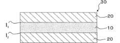
도 1은 본 발명의 회로 기판용 적층체의 일 실시 형태를 모식적으로 도시하는 단면도이다.
도 2는 보이드율 X의 산출 방법을 설명하는 도면이다.
도 3은 본 발명의 회로 기판용 적층체의 다른 실시 형태를 모식적으로 도시하는 단면도이다.
도 4는 본 발명의 회로 기판용 적층체의 다른 실시 형태를 모식적으로 도시하는 단면도이다.
도 5는 본 발명의 회로 기판용 적층체의 다른 실시 형태를 모식적으로 도시하는 단면도이다.
도 6은 본 발명의 회로 기판용 적층체에 있어서의 면의 중심으로부터 주연까지의 최단 길이를 설명하는 도면이다.
도 7은 본 발명의 실시 형태에 관한 회로 기판용 적층체의 제조 방법을 도시하는 공정 단면도이다.1 is a cross-sectional view schematically showing one embodiment of a laminate for a circuit board according to the present invention.
Fig. 2 is a diagram explaining a method for calculating the void rate X.
Fig. 3 is a cross-sectional view schematically showing another embodiment of the laminate for a circuit board of the present invention.
Fig. 4 is a cross-sectional view schematically showing another embodiment of the laminate for circuit board of the present invention.
Fig. 5 is a cross-sectional view schematically showing another embodiment of the laminate for circuit board of the present invention.
Fig. 6 is a diagram explaining the shortest length from the center of a surface to the periphery of a layered body for a circuit board according to the present invention.
7 is a process sectional view showing a manufacturing method of a laminate for a circuit board according to an embodiment of the present invention.
[회로 기판용 적층체][Laminate for circuit board]
본 발명의 회로 기판용 적층체는, 금속 질화물 소결 기판과 동판의 적층체로서, 상기 적층체는 면의 중심으로부터 주연까지의 최단 길이가 50㎜ 이상의 크기를 갖고, 상기 적층체를 적층 방향으로 절단한 절단면에 있어서 측정되는, 상기 금속 질화물 소결 기판과 동판의 접합 계면의 측정 길이 LI에 대한, 해당 접합 계면 근방, 구체적으로는, 접합 계면으로부터 동판측으로 20㎛ 폭의 범위 내에 있어서 확인되는 직경 1㎛ 이상의 보이드의 총 길이 LB의 비율인 보이드율 X가, 0.50% 이하인 것을 특징으로 한다.A laminate for a circuit board of the present invention is a laminate of a metal nitride sintered substrate and a copper plate, wherein the laminate has a minimum length of 50 mm or more from the center of the surface to the periphery, and the laminate is cut in the lamination direction. With respect to the measured length LI of the bonded interface between the metal nitride sintered substrate and the copper plate measured in one cut plane, a diameter 1 found within a range of 20 μm in the vicinity of the bonded interface, specifically, from the bonded interface to the copper plate side. It is characterized in that the void rate X, which is the ratio of the total lengthLB of voids of μm or more, is 0.50% or less.
이하, 도면을 사용하여 본 발명의 회로 기판용 적층체를 설명하지만, 본 발명은 도면에 한정되지는 않는다.Hereinafter, the circuit board laminate of the present invention will be described using drawings, but the present invention is not limited to the drawings.
도 1에는 본 발명의 회로 기판용 적층체의 일 실시 형태인 회로 기판용 적층체(30)를 나타낸다. 회로 기판용 적층체(30)는 금속 질화물 소결 기판(10)과, 해당 금속 질화물 소결 기판(10)의 표면 상에 적층된 동판(20)을 구비하고 있다. 상기 금속 질화물 소결 기판(10) 및 동판(20)은 접합되어 있고, 이들의 접합 계면(I)근방은 후술하는 바와 같이 보이드율 X가 일정 이하이다.1 shows a
본 발명의 회로 기판용 적층체(30)는 해당 적층체를 적층 방향으로 절단한 절단면에 있어서 측정되고, 상기 금속 질화물 소결 기판과 동판의 접합 계면의 측정 길이 LI에 대한, 해당 접합 계면 근방에 있어서 확인되는 직경 1㎛ 이상의 보이드의 총 길이 LB의 비율(100×LB/LI)인 보이드율 X가 0.50% 이하이다.The
상기 보이드율 X가 0.50% 이하인 것에 의해, 회로 기판용 적층체의 방열성이 양호해져, 회로 패턴 형성 시에 에칭액이 잔존하는 등의 문제가 저감되어, 제품으로서의 신뢰성이 향상된다. 이러한 관점에서, 보이드율 X는 바람직하게는 0.10% 이하이고, 보다 바람직하게는 0.03% 이하이다.When the void rate X is 0.50% or less, the heat dissipation property of the circuit board laminate is improved, problems such as remaining of the etchant during circuit pattern formation are reduced, and reliability as a product is improved. From this point of view, the void rate X is preferably 0.10% or less, and more preferably 0.03% or less.
다음으로, 접합 계면의 측정 길이 LI 및 접합 계면 근방에 있어서 확인되는 직경 1㎛ 이상의 보이드가 존재하는 총 길이 LB의 산출 방법에 대하여 설명한다.Next, the method for calculating the measured length LI of the joint interface and the total lengthLB in which a void with a diameter of 1 μm or more exists in the vicinity of the joint interface will be described.
먼저, 회로 기판용 적층체를, 그의 평면에 있어서의 중심점을 통과하는 임의의 방향으로, 적층 방향으로 절단한 절단면을 1개 이상 준비한다.First, one or more cut surfaces obtained by cutting the circuit board laminate in the lamination direction in an arbitrary direction passing through the central point in the plane are prepared.
그리고, 해당 절단면의 각 계면에 대해서, 임의의 500군데를 배율 500배의 조건에서 주사형 전자 현미경(SEM)에 의해 관찰한다. 도 2에는, 회로 기판용 적층체를 적층 방향으로 절단한 절단면을 모식적으로 도시하고 있다. 또한, 설명을 위해서, 도면에 있어서의 해칭은 생략하고 있다. 또한, 보이드를 확대 표시하고 있다. 도 2의 절단면에서는, 금속 질화물 소결 기판(10)과 동판(20)의 접합 계면(I)의 측정 길이 i는, 시야 범위로부터 200㎛이며, 상기 500군데의 계면을 관찰하면, 접합 계면의 총 길이 LI는 100000㎛(10㎝)가 된다.Then, about each interface of the cut surface, 500 random locations are observed with a scanning electron microscope (SEM) under conditions of a magnification of 500 times. Fig. 2 schematically shows a cut plane obtained by cutting the circuit board laminate in the lamination direction. Note that hatching in the drawings is omitted for explanation. In addition, voids are enlarged and displayed. In the cut plane of FIG. 2 , the measured length i of the bonding interface I between the metal nitride sintered
다음으로, 접합 계면 근방에 있어서 확인되는 직경 1㎛ 이상의 보이드가 존재하는 접합 계면의 총 길이 LB에 대하여 설명한다. 여기서 보이드의 직경이란, 절단면에 있어서 관찰된 보이드의 형상이 원형이면 그의 직경이며, 원형 이외의 형상이면, 그 형상의 둘레 상의 임의의 2점의 직선 거리의 최댓값을 의미하는 것으로 한다.Next, the total lengthLB of the joint interface in which a void with a diameter of 1 μm or more exists in the vicinity of the joint interface will be described. Here, the diameter of a void is the diameter when the shape of the void observed on the cut surface is circular, and if it is a shape other than circular, it shall mean the maximum value of the straight line distance of any two points on the circumference of the shape.
또한, 접합 계면 근방이란, 접합 계면으로부터 동판측으로 20㎛의 폭의 범위를 말한다. 구체적으로는 도 2에 있어서, 접합 계면(I)과, 해당 접합 계면(I)으로부터 동판측으로 20㎛의 위치에 있는 P 사이의 영역이 접합 계면 근방이다.In addition, the vicinity of the bonding interface refers to a range of a width of 20 µm from the bonding interface to the copper plate side. Specifically, in FIG. 2 , the region between the bonding interface I and P located at a position of 20 µm from the bonding interface I to the copper plate side is in the vicinity of the bonding interface.
즉, 접합에 기인하는 보이드는, 동판측밖에 발생하지 않기 때문에, 동판측의 보이드를 관찰하면 충분하다. 또한, 본 발명에 있어서, 후술하는 표면이 평활한 기판을 사용함으로써, 계면으로부터 금속 질화물 소결 기판측으로 20㎛의 폭에 있어서, 직경 1㎛ 이상의 보이드가 존재하지 않음을 확인하고 있다.That is, since voids resulting from bonding occur only on the copper plate side, it is sufficient to observe the voids on the copper plate side. Further, in the present invention, by using a substrate having a smooth surface described later, it was confirmed that no void having a diameter of 1 µm or more existed in a width of 20 µm from the interface to the metal nitride sintered substrate side.
또한, 접합 계면 근방에 있어서 확인되는 직경 1㎛ 이상의 보이드의 총 길이 LB란, 상기한 접합 계면의 총 길이 LI에서 관찰되는, 직경 1㎛ 이상의 개개 보이드에 대해서, 접합 계면에의 투영 길이의 총합을 의미한다. 예를 들어, 도 2에 도시하는 절단면에서는, 접합 계면(I)의 근방, 즉, 접합 계면(I)으로부터 동판측 20㎛의 범위에, 직경 1㎛ 이상의 보이드가 2개 확인되어 있어, 각각의 보이드의 접합 계면(I)에의 투영 길이는 b1 및 b2가 된다. 따라서, 상기 접합 계면의 총 길이 LI의 범위에서, 직경 1㎛ 이상의 보이드가 n개 확인된 경우, 이하의 식 (1)에 의해 LB가 구해진다.In addition, the total lengthLB of voids with a diameter of 1 μm or more observed in the vicinity of the joint interface is the projected length to the joint interface for each void with a diameter of 1 μm or more observed in the total length LI of the joint interface described above. means total. For example, in the cut surface shown in FIG. 2 , two voids with a diameter of 1 μm or more are confirmed in the vicinity of the bonding interface I, that is, in the range of 20 μm from the bonding interface I to the copper plate side, and each The projected lengths of the voids onto the bonding interface I are b1 and b2. Therefore, when n number of voids with a diameter of 1 μm or more are confirmed within the range of the total length LI of the bonded interface,LB is obtained by the following formula (1).

(식 (1)에 있어서 bi는 접합 계면 근방에 있어서 확인되는 직경 1㎛ 이상의 개개의 보이드의 접합 계면에의 투영 길이를 나타내고, n은 측정된 접합 계면의 총 길이 LI의 범위에서 관찰되는 직경 1㎛ 이상의 보이드의 수이다.)(In formula (1), bi represents the projected length of individual voids with a diameter of 1 μm or more found near the joint interface to the joint interface, and n is the diameter observed in the range of the total length LI of the measured joint interface It is the number of voids of 1 μm or more.)
또한, 종래, 보이드율의 측정에 초음파 탐상 장치가 사용되는 경우가 있는데, 이러한 장치에 의해 측정되는 보이드의 최소 직경은 기껏해야 수십㎛ 정도이고, 직경이 1㎛를 포함하는 미소한 보이드까지 측정하는 것은 실질적으로 할 수 없지만, 상술한 보이드율의 측정 방법에 의하면, 회로 기판용 적층체에 있어서 문제가 되는 범위의 보이드 존재량을 확실하게 평가할 수 있다.In addition, conventionally, there is a case in which an ultrasonic flaw detection device is used to measure the void rate, and the minimum diameter of the void measured by this device is about several tens of μm at most, and it is possible to measure even minute voids including 1 μm in diameter. Although it is practically impossible to do this, according to the method for measuring the void ratio described above, the amount of voids in the range that becomes a problem in the circuit board laminate can be reliably evaluated.
또한, 본 발명의 회로 기판용 적층체(30)는 도 3에 도시하는 바와 같이 금속 질화물 소결 기판(10)과, 해당 금속 질화물 소결 기판(10)의 양면에 마련된 동판(20)을 구비하고 있어도 된다.As shown in Fig. 3, the
이 경우, 금속 질화물 소결 기판(10)과 동판(20)의 접합 계면(I)은 2개(도 3에서는 I1 및 I2) 존재하는데, 접합 계면의 측정 길이 LI는, 절단면에 있어서 SEM으로 관찰되는 표리 각각의 접합 계면에 대해서, 하나의 계면에서의 측정 개소수(500)의 표리의 합(1000)과 1군데당의 측정 길이를 곱한 것이 된다.In this case, there are two bonded interfaces I between the metal nitride sintered
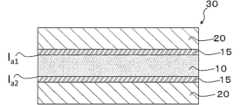
또한, 도 4에 도시하는 바와 같이, 회로 기판용 적층체(30)에 있어서의 상기 금속 질화물 소결 기판(10)과 동판(20)은, 접합층(15)을 통하여 접합되어 있어도 된다. 회로 기판용 적층체가 접합층(15)을 갖는 경우, 상기한 접합 계면의 측정 길이 LI 및 접합 계면 근방에 있어서 확인되는 직경 1㎛ 이상의 보이드의 총 길이 LB의 산출은, 금속 질화물 소결 기판(10)과 접합층(15)의 접합 계면(Ia)을 기준으로 행한다.As shown in FIG. 4 , the metal nitride sintered
또한, 후술하는 바와 같이 접합층(15)의 두께는 얇게 하는 것이 바람직하고, 접합층(15)이 얇게 형성되어 있는 경우에는, SEM에 의해 접합층을 확인할 수 없는 경우가 있다. 이러한 경우에는, 도 1에서 설명한 경우와 마찬가지로, SEM으로 관찰되는 금속 질화물 소결 기판(10)과 동판(20)의 접합 계면(I)을 기준으로 하여, LI 및 LB를 측정하고, 보이드율 X를 구한다.In addition, as will be described later, it is preferable to make the thickness of the
또한, 도 5에 도시한 바와 같이, 본 발명의 회로 기판용 적층체(30)는 금속 질화물 소결 기판(10)의 양면에 접합층(15)을 통하여 동판(20)이 마련되어 있어도 된다.As shown in FIG. 5 , in the
이 경우, 보이드율 X의 산출의 기준이 되는 금속 질화물 소결 기판(10)과 접합층(15)의 접합 계면은 2군데(도 5에서는 Ia1 및 Ia2) 존재하는데, 접합 계면의 측정 길이 LI는, 절단면에 있어서 SEM으로 관찰되는 표리 각각의 접합 계면에 대해서, 하나의 계면에서의 측정 개소수(500)의 표리의 합(1000)과 1군데당의 측정 길이를 곱한 것이 되고, 해당 접합 계면의 측정 길이 LI의 영역에 있어서 확인되는 직경 1㎛ 이상의 보이드의 총 길이 LB의 비율이 보이드율 X가 된다.In this case, there are two bonded interfaces between the metal nitride sintered
본 발명의 회로 기판용 적층체(30)는 면의 중심(C)부터 주연까지의 최단 길이가 50㎜ 이상의 크기를 갖는다. 이러한 큰 회로 기판용 적층체는, 일반적으로는 접합 계면의 보이드가 많은 경향이 있지만, 본 발명의 회로 기판용 적층체는, 상기한 바와 같이 보이드가 매우 적다. 따라서, 적층체의 생산성이 우수함과 함께, 얻어진 적층체의 방열성이 우수하고, 또한 에칭액이 잔존하는 문제 등도 저감할 수 있다. 적층체(30)의 면 중심(C)부터 주연까지의 최단 길이는, 보다 생산성을 향상시키는 관점에서, 바람직하게는 70㎜ 이상이며, 보다 바람직하게는 90㎜ 이상이며, 그리고 실용상으로는 110㎜ 이하인 것이 바람직하다.The
여기서, 면의 중심이란 회로 기판 적층체(30)의 적층 방향의 상방(또는 하방)에서 본 형상(이하 면 형상이라고도 한다)에 있어서의 중심을 의미한다. 예를 들어, 도 6에는, 회로용 적층체(30)를 적층 방향 상방에서 본 면 형상의 일례를 도시하고 있고, 해당 면 형상의 중심(C)으로부터 해당 면 형상의 주연의 임의의 점을 연결하는 직선의 최단 거리가 최단 길이 d이다.Here, the center of the plane means the center of the
또한 중심(C)은, 면 형상이 직사각형 등의 사각형이면 대각선의 교점이며, 원형이면 그 원의 중심이며, 타원이면 긴 직경과 짧은 직경의 교점이다. 또한, 면 형상이 이들 이외의 형상인 경우에는, 그 면 형상의 외접원의 중심을 본 발명에 있어서의 중심(C)으로 한다.In addition, the center C is the intersection of the diagonal lines when the surface shape is a rectangle such as a rectangle, the center of the circle when it is circular, and the intersection point between the major axis and the minor axis when it is an ellipse. In addition, when the planar shape is a shape other than these, the center of the circumscribed circle of the planar shape is set as the center (C) in the present invention.
(금속 질화물 소결 기판)(metal nitride sintered substrate)
본 발명에 있어서의 금속 질화물 소결 기판으로서는, 특별히 제한되지는 않지만 방열성의 관점에서, 질화규소 소결 기판, 질화알루미늄 소결 기판 등이 바람직하다. 그 중에서도, 인성값이 높고, 얇은 기판이더라도 균열되기 어렵기 때문에, 질화규소 소결 기판이 보다 바람직하다. 금속 질화물 소결 기판은, 질화규소 분말이나 질화알루미늄 분말 등을 소성시킴으로써 얻어진다.The metal nitride sintered substrate in the present invention is not particularly limited, but from the viewpoint of heat dissipation, a silicon nitride sintered substrate, an aluminum nitride sintered substrate, and the like are preferable. Among them, a silicon nitride sintered substrate is more preferable because it has a high toughness value and is hard to crack even if it is a thin substrate. The metal nitride sintered substrate is obtained by firing silicon nitride powder, aluminum nitride powder, or the like.
금속 질화물 소결 기판의 두께(t1)는 특별히 제한되지는 않지만, 회로 기판용 적층체의 경량화의 관점에서, 0.2 내지 1.0㎜가 적합하다.The thickness (t1 ) of the metal nitride sintered substrate is not particularly limited, but is preferably 0.2 to 1.0 mm from the viewpoint of reducing the weight of the laminate for circuit board.
금속 산화물 소결 기판은, 적층체의 면의 중심으로부터 주연까지의 최단 길이가 50㎜ 이상이라면 특별히 제한되지는 않는다. 적층체는 제조 후에 작은 사이즈로 개편화하는 것이 가능하고, 처음에 큰 적층체를 제조함으로써 제조 효율이 높아진다. 또한, 후술하는 본 발명의 적층체의 제조 방법에 의하면, 접합 계면의 보이드를 적게 하면서, 큰 적층체를 얻을 수 있다.The metal oxide sintered substrate is not particularly limited as long as the shortest length from the center of the surface of the laminate to the periphery is 50 mm or more. The laminate can be singulated into small sizes after production, and the manufacturing efficiency is increased by manufacturing a large laminate first. Moreover, according to the manufacturing method of the laminated body of this invention mentioned later, a large laminated body can be obtained, reducing the void of a joint interface.
(동판)(copper)
본 발명에 있어서의 동판에 대해서는 무산소동, 터프 피치 구리, 인 청동 등을 특별히 제한없이 사용하는 것이 가능한데, 접합 후의 응력의 관점에서 신장률이 좋은 무산소동이 적합하다. 동판의 두께(t2)에 대해서는 금속 질화물 소결 기판의 두께가 얇은 경우, 두꺼운 동판을 접합하면 접합 시의 열팽창차에 기인하는 응력에 의해 금속 질화물 소결 기판이 균열되어 버리기 때문에, 동판의 두께(t2)는 금속 질화물 소결 기판의 두께(t1)에 대한 상기 동판의 두께(t2)의 비(t2/t1)가 0.5 내지 8이 되도록 선정하는 것이 바람직하고, 1 내지 3이 되도록 선정하는 것이 보다 바람직하다. 또한, 동판의 두께(t2)는 동판이 금속 질화물 소결 기판의 편면에만 마련되어 있는 경우에는 그 동판의 두께를 의미하고, 동판이 금속 질화물 소결 기판의 양면에 마련되어 있는 경우에는, 2개의 동판의 합계 두께를 의미하는 것으로 한다.For the copper plate in the present invention, oxygen-free copper, tough pitch copper, phosphor bronze, etc. can be used without particular limitation, but oxygen-free copper having a good elongation rate is suitable from the viewpoint of stress after bonding. Regarding the thickness of the copper plate (t2 ), when the thickness of the metal nitride sintered substrate is thin, when thick copper plates are joined, the metal nitride sintered substrate cracks due to the stress caused by the difference in thermal expansion at the time of bonding, so the thickness of the copper plate (t2 ) is preferably selected so that the ratio (t2 /t1 ) of the thickness (t2 ) of the copper plate to the thickness (t1 ) of the metal nitride sintered substrate is 0.5 to 8, and is selected to be 1 to 3 It is more preferable to In addition, the thickness (t2 ) of the copper plate means the thickness of the copper plate when the copper plate is provided on only one side of the metal nitride sintered substrate, and when the copper plate is provided on both sides of the metal nitride sintered substrate, the total of the two copper plates to mean thickness.
또한 동판의 크기는, 생산성을 고려하여 접합 시에 복수의 금속 질화물 소결 기판 및 동판을 겹치는 경우가 있기 때문에, 접합 계면의 보이드 저감의 관점에서 금속 산화물 소결 기판과 동일한 크기인 것이 바람직하다.The size of the copper plate is preferably the same size as that of the metal oxide sintered substrate from the viewpoint of reducing voids at the joint interface, since a plurality of metal nitride sintered substrates and copper plates may be overlapped during bonding in consideration of productivity.
(접합층)(bonding layer)
상기한 바와 같이, 본 발명의 회로 기판용 적층체는, 금속 질화물 소결 기판과 동판이 접합층을 통하여 접합되어 있어도 된다. 접합층을 통하여 접합됨으로써, 금속 질화물 소결 기판과 동판이 보다 강고하게 접합된다.As described above, in the laminate for circuit boards of the present invention, the metal nitride sintered substrate and the copper plate may be bonded via a bonding layer. By bonding through the bonding layer, the metal nitride sintered substrate and the copper plate are bonded more firmly.
접합층은, 반응성 금속의 질화물을 포함하고 있고, 이에 의해 금속 질화물 소결 기판과 동판이 보다 강고하게 접합된다. 여기서 반응성 금속이란 예를 들어, 티타늄(Ti)이 대표적이다.The bonding layer contains a nitride of a reactive metal, whereby the metal nitride sintered substrate and the copper plate are bonded more firmly. Here, a representative example of the reactive metal is titanium (Ti).
또한, 상기 반응성 금속의 질화물은, 후술하는 회로 기판용 적층체의 제조 방법의 설명에 있어서 설명하겠지만, 회로 기판용 적층체 또는 금속 질화물 소결 기판 상에 형성시키는 반응 금속층을 구성하는 티타늄 등의 활성 금속과, 금속 질화물 소결 기판의 질소 원자의 반응물이다.Incidentally, the nitride of the reactive metal is an active metal such as titanium constituting a reactive metal layer formed on a circuit board laminate or a metal nitride sintered substrate, as will be explained in the description of the method for manufacturing a circuit board laminate to be described later. and nitrogen atoms of the metal nitride sintered substrate.
후술하는 제조 방법에 있어서 설명하는 바와 같이, 접합층의 형성 시에는, 활성 금속을 포함하는 층의 표면에 은(Ag) 등을 포함하는 산화 방지층을 존재시키는 것이 바람직하다. 상기 산화 방지층은 접합의 과정에서 동판에 확산되어 소실되는데, 이와 같이 산화 방지층을 존재시킴으로써, 회로 기판 적층체 제조 시에 있어서, 활성 금속의 산화를 방지할 수 있다.As will be described in the manufacturing method described later, when forming the bonding layer, it is preferable to have an antioxidant layer containing silver (Ag) or the like on the surface of the layer containing the active metal. The antioxidant layer diffuses into the copper plate and disappears during the bonding process. By having the antioxidant layer in this way, oxidation of the active metal can be prevented during manufacturing of the circuit board laminate.
단, 산화 방지층으로서 가장 적합하게 사용되는 은은, 동판을 에칭할 때나, 동판에 도금 처리를 실시할 때에 악영향을 미치는 경우가 있고, 또한, 회로에의 통전 시에 이온 마이그레이션을 일으키기 쉽기 때문에, 접합층 부근의 동판에 포함되는 은의 양은 적게 하는 것이 보다 바람직하다.However, silver, which is most suitably used as an anti-oxidation layer, may have an adverse effect when etching a copper plate or when plating a copper plate, and also easily causes ion migration when power is applied to a circuit. Therefore, the bonding layer It is more preferable to reduce the amount of silver contained in the nearby copper plate.
그 때문에, 상기 동판과 접합층의 계면으로부터, 동판의 두께 방향으로 20㎛의 대역에 있어서의 은의 농도가 3질량% 이하인 것이 바람직하고, 2질량% 이하인 것이 보다 바람직하다.Therefore, the concentration of silver in a 20 μm band in the thickness direction of the copper plate from the interface between the copper plate and the bonding layer is preferably 3% by mass or less, and more preferably 2% by mass or less.
상기 동판과 접합층의 계면으로부터, 동판의 두께 방향으로 20㎛의 대역에 있어서의 은의 농도는, 동판과 접합층의 계면의 은 농도와, 해당 계면으로부터 동판의 두께 방향으로 20㎛ 떨어진 부분의 은의 농도의 평균값이다. 은의 농도는, 전자선 마이크로애널라이저(EPMA)에 의해 측정할 수 있다.The silver concentration in the band of 20 μm in the thickness direction of the copper plate from the interface between the copper plate and the bonding layer is the silver concentration at the interface between the copper plate and the bonding layer and the silver concentration at a
또한, 도 5와 같이 금속 질화물 소결 기판의 양면에 접합층을 통하여 동판(10)이 마련되어 있는 경우에는, 동판과 접합층의 계면으로부터, 동판의 두께 방향으로 20㎛의 대역은 2개 존재하는데, 해당 2개의 대역에 대해서, 모두 은의 농도가 3질량% 이하인 것이 바람직하고, 2질량% 이하인 것이 보다 바람직하다.In addition, when the
또한, 후술하는 회로 기판용 적층체의 제조 방법에 의하면, 활성 금속 경납땜법을 사용하지 않고 접합층 형성할 수 있기 때문에, 접합층 부근의 동판에 포함되는 은의 양을 일정 이하로 적게 할 수 있다.In addition, according to the manufacturing method of the circuit board laminate described later, since the bonding layer can be formed without using the active metal brazing method, the amount of silver contained in the copper plate in the vicinity of the bonding layer can be reduced to a certain level or less. .
상기 접합층의 두께는 특별히 한정되지는 않지만, 0.01 내지 1㎛인 것이 바람직하고, 0.05 내지 0.6㎛인 것이 보다 바람직하다. 접합층의 두께가 이들 하한값 이상이면 접합 강도가 높아지고, 접합층의 두께가 이들 상한값 이하이면, 방열성을 양호하게 유지할 수 있다.The thickness of the bonding layer is not particularly limited, but is preferably 0.01 to 1 μm, more preferably 0.05 to 0.6 μm. When the thickness of the bonding layer is equal to or greater than these lower limits, the bonding strength increases, and when the thickness of the bonding layer is equal to or less than these upper limits, good heat dissipation can be maintained.
[회로 기판용 적층체의 제조 방법][Method of Manufacturing Circuit Board Laminate]
본 발명의 회로 기판용 적층체의 제조 방법은 특별히 한정되지는 않지만, 접합 계면의 보이드의 저감의 관점에서, 이하의 각 공정을 거쳐서 제조하는 것이 바람직하다.Although the manufacturing method of the laminated body for circuit boards of this invention is not specifically limited, It is preferable to manufacture through each following process from a viewpoint of reducing the void of a joint interface.
본 발명에 있어서의 적합한 회로 기판용 적층체의 제조 방법은,The manufacturing method of the laminate for circuit board suitable in this invention,
금속 질화물 소결 기판과 동판의 적층체인 회로 기판용 적층체의 제조 방법이며,A method for producing a laminate for a circuit board, which is a laminate of a metal nitride sintered substrate and a copper plate,
표면 조도(Ra)가 0.6㎛ 이하인 금속 질화물 소결 기판을 준비하는 공정 1과,Step 1 of preparing a metal nitride sintered substrate having a surface roughness (Ra) of 0.6 μm or less;
상기 금속 질화물 소결 기판 및 상기 동판 중 적어도 어느 표면에, 상기 금속 질화물 소결 기판 및 동판과 반응하는 금속을 포함하는 반응 금속층을 성막하는 반응 금속층 성막 공정 2와,A reactive metal layer deposition step 2 of forming a reactive metal layer containing a metal reacting with the metal nitride sintered substrate and the copper plate on at least one surface of the metal nitride sintered substrate and the copper plate;
상기 반응 금속층이 상기 금속 질화물 소결 기판과 상기 동판 사이에 있는 형태로 상기 금속 질화물 소결 기판과 상기 동판을 적층하고, 비산화 분위기 중에서, 상기 반응 금속층과 상기 동판 및 상기 금속 질화물 소결 기판 사이에서 반응이 발생하는 온도에서 상기 금속 질화물 소결 기판과 상기 동판 간에 압력을 인가하는 핫 프레스 공정 3을The metal nitride sintered substrate and the copper plate are stacked in such a manner that the reactive metal layer is between the metal nitride sintered substrate and the copper plate, and a reaction occurs between the reactive metal layer, the copper plate, and the metal nitride sintered substrate in a non-oxidizing atmosphere. A hot press process 3 of applying pressure between the metal nitride sintered substrate and the copper plate at a temperature generated
구비하는 것을 특징으로 하는 회로 기판용 적층체의 제조 방법이다.A method for manufacturing a laminate for a circuit board characterized in that it is provided.
이하 도면을 사용하여 설명한다. 도 7은, 본 발명에 있어서의 회로 기판용 적층체의 제조 방법의 일 실시 형태를 도시하고 있고, 금속 질화물 소결 기판(10)과 동판(20)이 접합층(15)을 통하여 접합된 회로 기판용 적층체(도 7의 (f))의 각 제조 공정을 도시하고 있다.Description will be made using the drawings below. 7 shows an embodiment of a method for manufacturing a laminate for circuit boards according to the present invention, a circuit board in which a metal nitride sintered
(공정 1)(Process 1)
공정 1은, 표면 조도(Ra)가 0.6㎛ 이하인 금속 질화물 소결 기판(10)(도 7의 (a))을 준비하는 공정이다.Step 1 is a step of preparing the metal nitride sintered substrate 10 (FIG. 7(a)) having a surface roughness Ra of 0.6 µm or less.
금속 질화물 소결 기판(10)으로서는, 특별히 제한되지는 않지만 방열성의 관점에서, 질화규소 소결 기판, 질화알루미늄 소결 기판 등이 바람직하다. 그 중에서도, 인성값이 높고, 얇은 기판이더라도 균열되기 어렵기 때문에, 질화규소 소결 기판이 바람직하다. 이들 금속 질화물 소결 기판(10)은 질화규소 분말이나 질화알루미늄 분말을 소성함으로써 얻을 수 있다.The metal nitride sintered
금속 질화물 소결 기판의 표면 조도(Ra)는 0.6㎛ 이하의 것이 바람직하고, 0.5㎛ 이하의 것이 바람직하다. 표면 조도(Ra)가 이들 상한값 이하이면, 접합 계면의 보이드의 생성을 억제하기 쉬워진다.The surface roughness (Ra) of the metal nitride sintered substrate is preferably 0.6 μm or less, and preferably 0.5 μm or less. When the surface roughness (Ra) is equal to or less than these upper limits, it is easy to suppress generation of voids at the bonding interface.
금속 질화물 소결 기판의 표면의 산 정점의 산술 평균 곡률(Spc)은 4.5[1/㎜] 이하인 것이 바람직하고, 4.2[1/㎜] 이하인 것이 보다 바람직하다. 상기한 표면 조도(Ra)로 조정하면서, 산 정점의 산술 평균 곡률(Spc)을 이러한 범위로 조정함으로써, 접합 계면의 보이드의 생성을 보다 억제하기 쉬워진다.The arithmetic mean curvature (Spc) of the peaks of the surface of the metal nitride sintered substrate is preferably 4.5 [1/mm] or less, and more preferably 4.2 [1/mm] or less. By adjusting the arithmetic mean curvature (Spc) of the mountain peaks within this range while adjusting to the surface roughness (Ra) described above, it becomes easier to suppress the generation of voids at the joint interface.
상기 표면 조도를 나타내는 Ra, 표면의 볼록부 상태를 나타내는 Spc의 값은, 후술하는 실시예에 있어서, 구체적으로 나타내지만, 비접촉 3차원 측정 장치(키엔스사제 상품명: VR-5000)를 사용하여 구한 값이다.The values of Ra representing the surface roughness and Spc representing the state of convex portions of the surface are specifically shown in the examples described later, but are values obtained using a non-contact three-dimensional measuring device (trade name: VR-5000 manufactured by Keyence Corporation). am.
여기서, Spc에 대하여 설명한다. 산 정점의 산술 평균 곡률 Spc란, 표면의 산 정점의 주곡률의 평균을 나타낸다. 하기의 식은, 산 정점의 산술 평균 곡률 Spc의 산출식이다. 하기 식에 있어서, z는 x, y 좌표에 있어서의 높이 방향 성분을 의미하고, n은 산 정점의 수를 나타내고, 산 정점의 산술 평균 곡률 Spc는, 표면 요철 형상의 산 정점의 근사 원의 반경의 역수의 평균값을 나타내고 있다. 이 수치가 작을수록, 산의 정점에 둥그스름한 형상이 있어, 폭이 넓은 형상으로 되어 있는 것을 나타내는 것이다.Here, Spc is explained. The arithmetic average curvature Spc of peaks represents the average of principal curvatures of peaks of the surface. The following formula is a calculation formula for the arithmetic mean curvature Spc of the peak. In the following formula, z means the height direction component in the x, y coordinates, n represents the number of mountain peaks, and the arithmetic mean curvature Spc of the mountain peak is the radius of the approximation circle of the mountain peak of the surface concavo-convex shape represents the average value of the reciprocal of The smaller this number is, the more rounded the top of the mountain is, and the wider it is.

금속 질화물 소결 기판(10)은 소성 후에 표면 연마되어 있지 않은 것을 사용하는 것이 바람직하다. 표면 연마된 금속 질화물 소결 기판(10)보다도, 소성된 채의 상태 소위 as-fire 기판을 사용하는 쪽이, 미시적인 표면 형상이 보다 평활하게 되는 경향이 있어, 접합 계면에 보이드가 생성되기 어려워지기 때문에 바람직하다. 특히, 소성 후에 표면 연마되어 있지 않은 금속 질화물 소결 기판(10)이며, 표면 조도(Ra)가 상기 범위인 금속 질화물 소결 기판(10)을 사용하는 것이 바람직하고, 표면 조도(Ra) 및 산 정점의 산술 평균 곡률(Spc)이 모두 상기 범위인 금속 질화물 소결 기판(10)을 사용하는 것이 보다 바람직하다.It is preferable to use the metal nitride sintered
또한, 소성 후의 표면 연마가 되어 있지 않다란, 금속 질화물 분말을 소결시켜서 얻어진 금속 질화물 소결 기판 표면을 평활하게 하는 연마 처리를 행하고 있지 않은 것을 의미하고, 표면에 부착되어 있는 이형제 등의 이물을 제거하기 위한 블라스트 처리 등은 행해도 된다.In addition, the fact that the surface is not polished after firing means that the polishing treatment for smoothing the surface of the metal nitride sintered substrate obtained by sintering the metal nitride powder is not performed, and foreign matter such as a release agent adhering to the surface is removed. You may perform blast processing etc. for this.
상기 표면 특성을 갖는 금속 질화물 소결 기판의 제조 방법은 특별히 제한되지는 않지만, 질화규소 소결 기판에 대해서, 대표적인 제조 방법을 예시하면, β화율이 90% 이상, 비표면적이 7 내지 20㎡/g, 결정 변형이 4.0×10⁻⁴ 이상의 질화규소 분말과 소결 보조제를 함유하고, 알루미늄 원소의 총 함유량이 800ppm 이하로 조정된 그린 시트를, 불활성 가스 분위기 및 0MPa·G 이상 0.1MPa·G 미만의 압력 하, 1200 내지 1800℃의 온도로 가열하여 질화규소를 소결하는 방법을 들 수 있다. 여기서, 압력 단위의 MPa·G의 말미의 G는 게이지 압력을 의미한다.The manufacturing method of the metal nitride sintered substrate having the above surface properties is not particularly limited, but a typical manufacturing method for a silicon nitride sintered substrate is 90% or more, a specific surface area of 7 to 20 m / g, a crystal A green sheet containing a silicon nitride powder having a strain of 4.0×10⁻⁴ or more and a sintering aid and having the total content of aluminum elements adjusted to 800 ppm or less is prepared under an inert gas atmosphere and a pressure of 0 MPa G or more and less than 0.1 MPa G at 1200 and a method of sintering silicon nitride by heating to a temperature of 1800°C. Here, G at the end of MPa·G in the pressure unit means gauge pressure.
상기 방법에 의하면, β화율이 높고, 후술하는 특정한 분쇄에 의해 얻어지는 높은 비표면적과, 높은 결정 변형을 갖는 질화규소분을 사용함으로써, 저압 또한 저온에서 치밀한 소결을 행할 수 있고, 이에 의해, 특히 질화규소 소결 기판의 표면에 있어서의 침상 결정의 성장을 억제하고, 기판 표면에 1 내지 10㎛의 세공의 형성을 억제하면서, 우수한 특성이 담보된 질화규소 소결 기판을 얻을 수 있다.According to the method, precise sintering can be performed at low pressure and low temperature by using a silicon nitride powder having a high β conversion rate, a high specific surface area obtained by specific pulverization described later, and a high crystal strain, thereby enabling particularly sintering of silicon nitride. A silicon nitride sintered substrate with excellent characteristics can be obtained while suppressing the growth of needle crystals on the surface of the substrate and suppressing the formation of pores of 1 to 10 µm on the surface of the substrate.
〔그린 시트〕[Green Sheet]
본 발명의 질화규소 소결 기판의 제조 방법에 있어서, 그린 시트는, 이하에 설명하는 특정한 질화규소 분말 및 소결 보조제를 함유한다.In the manufacturing method of the silicon nitride sintered substrate of the present invention, the green sheet contains a specific silicon nitride powder and a sintering aid described below.
<질화규소 분말><Silicon nitride powder>
(β화율)(β conversion rate)
그린 시트에 포함되는 질화규소 분말의 β화율은 80% 이상이다. β화율이 80% 이상인 질화규소 분말은, 엄밀한 제조 조건을 설정하지 않더라도 얻을 수 있기 때문에, 비교적 저비용으로 제조할 수 있다. 따라서, β화율이 높은 질화규소 분말을 사용함으로써, 질화규소 소결체의 전체의 제조 비용을 억제할 수 있다. 또한, β화율을 높게 설정함으로써, α형의 질화규소 입자가 소성 시에 β형의 질화규소 입자로 변태를 일으킬 때에 도입하는 산소량을 더욱 적게 억제할 수 있다. 여기서 질화규소 분말의 β화율은, 바람직하게는 85% 이상, 보다 바람직하게는 90% 이상이다.The β conversion rate of the silicon nitride powder contained in the green sheet is 80% or more. Since silicon nitride powder having a β conversion rate of 80% or more can be obtained without setting strict manufacturing conditions, it can be manufactured at a relatively low cost. Therefore, the overall manufacturing cost of a silicon nitride sintered compact can be suppressed by using the silicon nitride powder with a high β conversion rate. In addition, by setting the β transformation rate high, the amount of oxygen introduced when the α-type silicon nitride particles undergo transformation into the β-type silicon nitride particles during firing can be further suppressed. Here, the β conversion rate of the silicon nitride powder is preferably 85% or more, more preferably 90% or more.
또한, 질화규소 분말의 β화율이란, 질화규소 분말에 있어서의 α상과 β상의 합계에 대한 β상의 피크 강도 비율[100×(β상의 피크 강도)/(α상의 피크 강도+β상의 피크 강도)]을 의미하고, CuKα선을 사용한 분말 X선 회절(XRD) 측정에 의해 구해진다. 보다 상세하게는, C.P.Gazzara and D.R.Messier: Ceram.Bull., 56(1977), 777-780에 기재된 방법에 의해, 질화규소 분말의 α상과 β상의 중량 비율을 산출함으로써 구해진다.The β conversion rate of the silicon nitride powder is the ratio of the peak intensity of the β phase to the total of the α and β phases in the silicon nitride powder [100 × (peak intensity of the β phase) / (peak intensity of the α phase + peak intensity of the β phase)] meaning, and is determined by powder X-ray diffraction (XRD) measurement using CuKα rays. More specifically, it is obtained by calculating the weight ratio of the α phase and the β phase of the silicon nitride powder according to the method described in C.P. Gazzara and D.R.Messier: Ceram.Bull., 56 (1977), 777-780.
(비표면적)(specific surface area)
질화규소 분말의 비표면적은 7 내지 20㎡/g이다. 질화규소 분말의 비표면적이 20㎡/g을 초과하면, 고용 산소량을 낮게 하는 것이 어려워지고, 비표면적이 7㎡/g 미만이면, 고밀도이며 강도가 높은 질화규소 소결체를 얻기 어려워진다. 질화규소 분말의 비표면적은, 바람직하게는 12 내지 15㎡/g이다.The specific surface area of the silicon nitride powder is 7 to 20 m 2 /g. When the specific surface area of the silicon nitride powder exceeds 20 m 2 /g, it becomes difficult to lower the amount of dissolved oxygen, and when the specific surface area is less than 7 m 2 /g, it becomes difficult to obtain a high-density and high-strength silicon nitride sintered body. The specific surface area of the silicon nitride powder is preferably 12 to 15 m 2 /g.
또한, 본 발명에 있어서 비표면적은, 질소 가스 흡착에 의한 BET 1점법을 사용하여 측정한 BET 비표면적을 의미한다.In the present invention, the specific surface area means the BET specific surface area measured using the BET one-point method by nitrogen gas adsorption.
(결정 변형)(crystal strain)
본 발명의 질화규소 소결 기판의 제조에 있어서, 질화규소 분말은, 상기 특성과 함께 결정 변형이 4.0×10⁻⁴ 이상인 것을 사용하는 것이 바람직하다. 이러한 결정 변형이 얻어지는 질화규소 소결 기판의 표면에 있어서의 그물눈상 구조의 형성, 즉, 세공의 생성에 어떻게 작용하는지는 명확하지 않지만, 본 발명자들의 실험에 의하면, 질화규소 분말의 결정 변형을 큰 측으로 변화시킴으로써, 상기 특정 세공의 적산 용적이 감소할 수 있음이 확인되었다.In the production of the silicon nitride sintered substrate of the present invention, it is preferable to use a silicon nitride powder having the above characteristics and a crystal strain of 4.0×10⁻⁴ or more. It is not clear how such a crystal strain affects the formation of a mesh structure on the surface of the obtained silicon nitride sintered substrate, that is, the formation of pores, but according to the experiments of the present inventors, by changing the crystal strain of the silicon nitride powder to a large side, , it was confirmed that the accumulated volume of the specific pores can be reduced.
또한, 결정 변형은 실시예에 나타내는 방법에 의해 측정한 것이다.In addition, crystal strain is measured by the method shown in the Example.
질화규소 분말은, 특별히 한정되지는 않지만, 고용 산소량을 낮게 하는 관점 등으로부터, 예를 들어, 질화규소 분말을 제조할 때에, 고순도의 원료를 사용하면 된다. 예를 들어, 직접 질화법으로 질화규소 분말을 제조하는 경우에는, 사용하는 원료로서, 내부에 산소가 고용될 요인이 없는 실리콘 분말을 사용하는 것이 바람직하고, 구체적으로는, 반도체 그레이드의 실리콘 유래, 예를 들어, 상기 실리콘을 절단 등의 가공할 때에 발생하는 절삭분을 대표로 하는 실리콘 분말을 사용하는 것이 바람직하다. 상기 반도체 그레이드의 실리콘은, 벨자식 반응 용기 내에서, 고순도의 트리클로로실란과 수소를 반응시키는, 소위 「지멘스법」에 의해 얻어지는 다결정 실리콘이 대표적이다.The silicon nitride powder is not particularly limited, but from the viewpoint of lowering the amount of dissolved oxygen, for example, when producing the silicon nitride powder, a high-purity raw material may be used. For example, in the case of producing silicon nitride powder by a direct nitriding method, as a raw material to be used, it is preferable to use a silicon powder having no factor of oxygen being dissolved therein, specifically, derived from semiconductor grade silicon, e.g. For example, it is preferable to use a silicon powder representative of the cutting powder generated when processing the silicon by cutting or the like. Polycrystalline silicon obtained by the so-called "Siemens method" in which high-purity trichlorosilane and hydrogen are reacted in a bell-shaped reaction vessel is typical of the semiconductor grade silicon.
또한, 질화규소 분말의 평균 입경 D50은, 0.5 내지 3㎛인 것이 바람직하고, 0.7 내지 1.7㎛인 것이 보다 바람직하다. 이러한 평균 입경의 질화규소 분말을 사용하면, 소결이 일층 진행하기 쉬워진다. 평균 입경 D50은, 레이저 회절 산란법에 의해 측정한 50% 체적 기준의 값이다.Moreover, it is preferable that it is 0.5-3 micrometers, and, as for average particle diameterD50 of the silicon nitride powder, it is more preferable that it is 0.7-1.7 micrometers. If the silicon nitride powder having such an average particle diameter is used, sintering can be further facilitated. The average particle diameter D50 is a value on a 50% volume basis measured by a laser diffraction scattering method.
질화규소 분말에 있어서의 입경 0.5㎛ 이하의 입자의 비율은, 바람직하게는 20 내지 50질량%이며, 보다 바람직하게는 20 내지 40질량%이다. 또한, 질화규소 분말에 있어서의 입경 1㎛ 이상의 입자의 비율은, 바람직하게는 20 내지 50질량%이며, 보다 바람직하게는 20 내지 40질량%이다. 이러한 입도 분포를 갖는 질화규소 분말을 사용하면, 치밀하고 열전도율이 높은 질화규소 소결체를 얻기 쉬워진다.The proportion of particles having a particle size of 0.5 μm or less in the silicon nitride powder is preferably 20 to 50% by mass, more preferably 20 to 40% by mass. In addition, the proportion of particles having a particle size of 1 μm or more in the silicon nitride powder is preferably 20 to 50% by mass, more preferably 20 to 40% by mass. When silicon nitride powder having such a particle size distribution is used, it becomes easy to obtain a dense silicon nitride sintered body having high thermal conductivity.
이의 이유는 분명치는 않지만, β형의 질화규소 입자는, α형의 질화규소 입자와는 달리 소성 중의 용해 재석출은 일어나기 어렵고 소성 초기의 단계에서 미세 입자와 조대 입자를 일정한 밸런스로 맞춰둠으로써 보다 치밀한 소결체를 얻는 것이 가능하게 되는 것으로 생각된다.Although the reason for this is not clear, β-type silicon nitride particles, unlike α-type silicon nitride particles, are difficult to dissolve and re-precipitate during firing, and a more dense sintered body is achieved by balancing fine and coarse particles in a certain balance at the initial stage of firing. It is thought to be possible to obtain.
그린 시트 중의 질화규소 분말의 양은, 그린 시트 전량 기준으로, 바람직하게는 70질량% 이상, 바람직하게는, 80질량% 이상이다.The amount of silicon nitride powder in the green sheet is preferably 70% by mass or more, preferably 80% by mass or more, based on the total amount of the green sheet.
<질화규소 분말의 제조><Preparation of silicon nitride powder>
질화규소 분말의 제조 방법은, 상술한 특성을 갖는 질화규소 분말이 얻어지는 방법이라면 특별히 한정되지는 않는다. 질화규소 분말의 제조 방법으로서는, 예를 들어, 실리카 분말을 원료로 하여, 탄소 분말 존재 하에서, 질소 가스를 유통시켜서 질화규소를 생성시키는 환원 질화법, 실리콘 분말과 질소를 고온에서 반응시키는 직접 질화법, 할로겐화규소와 암모니아를 반응시키는 이미드 분해법 등을 적용할 수 있는데, 상술한 특성을 갖는 질화규소 분말을 제조하기 쉬운 관점에서, 직접 질화법이 바람직하고, 그 중에서도 자기 연소법을 이용하는 직접 질화법(연소 합성법)이 보다 바람직하다.The method for producing the silicon nitride powder is not particularly limited as long as it is a method for obtaining the silicon nitride powder having the characteristics described above. As a method for producing silicon nitride powder, for example, a reduction nitriding method in which silicon nitride is generated by passing nitrogen gas in the presence of carbon powder using silica powder as a raw material, a direct nitriding method in which silicon powder and nitrogen are reacted at a high temperature, and halogenation An imide decomposition method or the like in which silicon reacts with ammonia can be applied, but from the viewpoint of easy production of silicon nitride powder having the above-described characteristics, a direct nitriding method is preferable, and among them, a direct nitriding method using a self-combustion method (combustion synthesis method) more preferable than this
연소 합성법은, 실리콘 분말을 원료로서 사용하여, 질소 분위기 하에서 원료 분말의 일부를 강제 착화하여, 원료 화합물의 자기 발열에 의해 질화규소를 합성하는 방법이다. 연소 합성법은, 공지된 방법이며, 예를 들어, 일본 특허 공개 제2000-264608호 공보, 국제 공개 제2019/167879호 등을 참조할 수 있다.The self-heating synthesis method is a method of synthesizing silicon nitride by self-heating of the raw material compound by forcibly igniting a part of the raw material powder in a nitrogen atmosphere using silicon powder as a raw material. The self-propagating combustion method is a known method, and reference can be made to, for example, Japanese Patent Laid-Open No. 2000-264608, International Publication No. 2019/167879 and the like.
또한, 상기 결정 변형은 상기 연소 합성법에 의해 어느 정도 큰 결정 변형을 갖는 것이 얻어지는데, 또한 분쇄를 행함으로써, 결정 변형을 보다 크게 하는 것이 가능하다. 상기 분쇄 방법으로서는, 진동 볼 밀에 의한 분쇄가 바람직하고, 이러한 분쇄를 5 내지 15시간 행하는 것이 바람직하다.In addition, as for the crystal strain, a crystal strain having a certain degree of large crystal strain can be obtained by the above self-propagating high-temperature synthesis method, but it is possible to further increase the crystal strain by performing grinding. As the grinding method, grinding by a vibrating ball mill is preferable, and it is preferable to carry out such grinding for 5 to 15 hours.
<소결 보조제><Sintering Auxiliary>
본 발명의 질화규소 소결 기판의 제조에 사용하는 그린 시트에 있어서, 소결 보조제는 공지된 것을 특별히 제한없이 사용할 수 있지만, 산소 결합을 갖지 않는 화합물을 포함하는 소결 보조제를 사용하는 것이, 얻어지는 질화규소 소결 기판의 열전도율의 저하를 방지할 수 있기 때문에 바람직하다.In the green sheet used in the production of the silicon nitride sintered substrate of the present invention, known sintering aids can be used without particular limitation, but it is preferable to use a sintering aid containing a compound having no oxygen bond to obtain a silicon nitride sintered substrate. It is preferable because a decrease in thermal conductivity can be prevented.
상기 산소 결합을 갖지 않는 화합물로서는, 희토류 원소 또는 마그네슘 원소를 포함하는 탄질화물계의 화합물(이하, 특정한 탄질화물계의 화합물이라고도 한다) 및 질화물계의 화합물(이하, 특정한 질화물계의 화합물이라고도 한다)이 바람직하다. 이러한, 특정한 탄질화물계의 화합물 및 특정한 질화물계의 화합물을 사용함으로써 보다 효과적으로 열전도율이 높은 질화규소 소결체를 얻기 쉬워진다. 상기 특정한 탄질화물계의 화합물이, 질화규소 분말에 포함되는 산소를 흡착하는 게터제로서 기능하고, 특정한 질화물계의 화합물에 있어서는, 질화규소 소결체의 전체 산소량을 저하시켜, 그 결과 열전도율이 높은 질화규소 소결체가 얻어진다.As the compound having no oxygen bond, a carbonitride-based compound containing a rare earth element or magnesium element (hereinafter also referred to as a specific carbonitride-based compound) and a nitride-based compound (hereinafter also referred to as a specific nitride-based compound) this is preferable By using such a specific carbonitride-based compound and a specific nitride-based compound, it becomes easier to obtain a silicon nitride sintered body having high thermal conductivity more effectively. The specific carbonitride-based compound functions as a getter agent that adsorbs oxygen contained in the silicon nitride powder, and in the specific nitride-based compound, the total amount of oxygen in the silicon nitride sintered body is reduced, resulting in a silicon nitride sintered body having high thermal conductivity. lose
희토류 원소를 포함하는 탄질화물계의 화합물에 있어서, 희토류 원소로서는, Y(이트륨), La(란탄), Sm(사마륨), Ce(세륨), Yb(이테르븀) 등이 바람직하다.In the carbonitride-based compound containing a rare earth element, as the rare earth element, Y (yttrium), La (lanthanum), Sm (samarium), Ce (cerium), Yb (ytterbium), etc. are preferable.
희토류 원소를 포함하는 탄질화물계의 화합물로서는, 예를 들어, Y2Si4N6C, Yb2Si4N6C, Ce2Si4N6C, 등을 들 수 있고, 이들 중에서도, 열전도율이 높은 질화규소 소결체를 얻기 쉽게 하는 관점에서, Y2Si4N6C, Yb2Si4N6C가 바람직하다.Carbonitride compounds containing rare earth elements include, for example, Y2 Si4 N6 C, Yb2 Si4 N6 C, Ce2 Si4 N6 C, etc. Among these, thermal conductivity From the viewpoint of making it easy to obtain this high quality silicon nitride sintered body, Y2 Si4 N6 C and Yb2 Si4 N6 C are preferable.
마그네슘 원소를 포함하는 탄질화물계의 화합물로서는, 예를 들어, MgSi4N6C 등을 들 수 있다. 또한 마그네슘 원소를 포함하는 특정한 질화물계의 화합물로서는, MgSiN2 등을 들 수 있다.Examples of the carbonitride compound containing magnesium element include MgSi4 N6 C and the like. Moreover,MgSiN2 etc. are mentioned as a specific nitride type compound containing magnesium element.
이들 특정한 탄질화물계의 화합물 및 특정한 질화물계의 화합물은, 1종을 단독으로 사용해도 되고, 2종 이상을 병용해도 된다.These specific carbonitride-based compounds and specific nitride-based compounds may be used individually by 1 type, or may use 2 or more types together.
상기한 희토류 원소 또는 마그네슘 원소를 포함하는 탄질화물계의 화합물 중에서도, 특히 바람직한 화합물 및 특정한 질화물계의 화합물은, Y2Si4N6C, MgSi4N6C, MgSiN2이다.Among the carbonitride-based compounds containing the above rare earth element or magnesium element, particularly preferred compounds and specific nitride-based compounds are Y2 Si4 N6 C, MgSi4 N6 C, and MgSiN2 .
또한, 소결 보조제는, 상기 산소 결합을 갖지 않는 화합물에 추가로, 또한 금속 산화물을 포함할 수 있다. 소결 보조제가, 금속 산화물을 함유함으로써, 질화규소 분말의 소결이 진행하기 쉬워져, 보다 치밀하고 강도가 높은 소결체를 얻기 쉬워진다.Further, the sintering aid may further contain a metal oxide in addition to the compound having no oxygen bond. When the sintering aid contains a metal oxide, sintering of the silicon nitride powder is facilitated, and a more dense and high-strength sintered body is easily obtained.
금속 산화물로서는, 예를 들어, 이트리아(Y2O3), 마그네시아(MgO), 세리아(CeO) 등을 들 수 있다. 이들 중에서도, 이트리아가 바람직하다. 금속 산화물은 1종을 단독으로 사용해도 되고, 2종 이상을 병용해도 된다.Examples of the metal oxide include yttria (Y2 O3 ), magnesia (MgO), and ceria (CeO). Among these, yttria is preferable. A metal oxide may be used individually by 1 type, and may use 2 or more types together.
소결 보조제에 포함되는, 상기 특정한 탄질화물계의 화합물을 대표로 하는 산소를 갖지 않는 화합물과 금속 산화물의 질량비(산소를 갖지 않는 화합물/금속 산화물)는 바람직하게는 0.2 내지 4이며, 보다 바람직하게는 0.6 내지 2이다. 이러한 범위이면, 치밀하고, 열전도율이 높은 질화규소 소결체를 얻기 쉬워진다.The mass ratio of the oxygen-free compound represented by the specific carbonitride-based compound and the metal oxide contained in the sintering aid (oxygen-free compound/metal oxide) is preferably 0.2 to 4, more preferably 0.6 to 2. Within this range, it is easy to obtain a dense silicon nitride sintered body with high thermal conductivity.
또한, 그린 시트에 있어서의 소결 보조제의 함유량은, 질화규소 분말 100질량부에 대하여 바람직하게는 5 내지 20질량부이며, 보다 바람직하게는 7 내지 10질량부이다.The content of the sintering aid in the green sheet is preferably 5 to 20 parts by mass, more preferably 7 to 10 parts by mass, based on 100 parts by mass of the silicon nitride powder.
<결합제><Binder>
그린 시트는, 결합제를 사용하여 성형할 수 있다. 이 경우, 그린 시트는 후술하는 성형용 조성물을 시트상으로 성형하고, 이것을 필요에 따라서 건조시키고, 공지된 조건에서 탈지를 행함으로써 결합제를 제거하여 소성에 제공된다.A green sheet can be molded using a binder. In this case, the green sheet is subjected to firing by molding a molding composition described later into a sheet shape, drying it as necessary, and degreasing under known conditions to remove the binder.
결합제로서는, 특별히 한정되지는 않지만, 폴리비닐알코올, 폴리비닐부티랄, 메틸셀룰로오스, 알긴산, 폴리에틸렌글리콜, 카르복시메틸셀룰로오스, 에틸셀룰로오스, 아크릴 수지 등을 들 수 있다.Although it does not specifically limit as a binder, Polyvinyl alcohol, polyvinyl butyral, methyl cellulose, alginic acid, polyethylene glycol, carboxymethyl cellulose, ethyl cellulose, an acrylic resin, etc. are mentioned.
그린 시트의 제조에 사용하는 결합제의 함유량은, 질화규소 분말 100질량부에 대하여 바람직하게는 1 내지 30질량부이며, 성형 방법에 따라서 적절히 그의 비율을 결정하면 된다.The content of the binder used for production of the green sheet is preferably 1 to 30 parts by mass with respect to 100 parts by mass of the silicon nitride powder, and the ratio may be appropriately determined according to the molding method.
<알루미늄 원소의 총 함유량><Total content of aluminum elements>
그린 시트의 알루미늄 원소의 총 함유량(질량)은 800ppm 이하이다. 즉, 본 발명에 있어서 사용하는 그린 시트는, 알루미늄 원소의 양이 매우 적은 것이며, 이것에 의해 높은 열전도율을 갖는 질화규소 소결체를 얻는 것이 가능하게 된다. 그린 시트의 알루미늄 원소의 총 함유량은, 바람직하게는 700ppm 이하이고, 보다 바람직하게는 600ppm 이하이다.The total content (mass) of aluminum elements in the green sheet is 800 ppm or less. That is, the green sheet used in the present invention has a very small amount of aluminum element, and thereby a silicon nitride sintered body having high thermal conductivity can be obtained. The total content of aluminum elements in the green sheet is preferably 700 ppm or less, and more preferably 600 ppm or less.
〔그린 시트의 제조〕[Manufacture of green sheet]
본 발명에 있어서 사용하는 그린 시트의 제조 방법은 특별히 한정되지는 않고 예를 들어, 질화규소 분말, 및 소결 보조제를 적어도 함유하는 성형용 조성물을, 공지된 성형 수단에 의해 성형하는 방법을 들 수 있다. 공지된 성형 수단으로서는, 예를 들어, 프레스 성형법, 압출 성형법, 사출 성형법, 닥터 블레이드법 등을 들 수 있는데, 특히, 닥터 블레이드법이 적합하다.The method for producing the green sheet used in the present invention is not particularly limited, and examples thereof include a method in which a molding composition containing at least silicon nitride powder and a sintering aid is molded by a known molding means. As a known molding method, press molding method, extrusion molding method, injection molding method, doctor blade method, etc. are mentioned, for example, but the doctor blade method is especially suitable.
또한, 성형용 조성물에는, 취급 용이함이나, 성형의 용이함 등의 관점에서, 용제를 함유시켜도 된다. 용제로서는, 특별히 한정되지는 않고 알코올류, 탄화수소류 등의 유기 용제, 물 등을 들 수 있는데, 본 발명에 있어서는, 물을 사용하는 것이 바람직하다. 즉, 질화규소 분말, 소결 보조제, 및 물을 포함하는 성형용 조성물을 성형하여, 그린 시트를 얻는 것이 바람직하다. 용제로서 물을 사용하는 경우에는, 유기 용제를 사용하는 경우와 비교하여, 환경 부하가 저감되어 바람직하다.Further, the composition for molding may contain a solvent from the viewpoint of ease of handling, ease of molding, and the like. The solvent is not particularly limited, and organic solvents such as alcohols and hydrocarbons, water, and the like are exemplified. In the present invention, it is preferable to use water. That is, it is preferable to obtain a green sheet by molding a molding composition containing silicon nitride powder, a sintering aid, and water. When water is used as the solvent, compared to the case where an organic solvent is used, the environmental load is reduced, which is preferable.
〔소결 방법〕[sintering method]
본 발명의 질화규소 소결 기판의 제조 방법에 있어서는, 상기한 그린 시트를 필요에 따라서 탈지 후, 일정한 조건 하에서 소성하여, 질화규소를 소결시킨다. 상기 소성에 있어서 그린 시트에는 미리 질화붕소 분말을 포함하는 이형재를 도포하는 것이 일반적이다. 이하, 소성할 때의 조건에 대하여 설명한다.In the manufacturing method of the silicon nitride sintered substrate of the present invention, the green sheet described above is degreased as necessary and then fired under certain conditions to sinter the silicon nitride. In the firing, it is common to apply a release material containing boron nitride powder to the green sheet in advance. Hereinafter, the conditions at the time of baking are demonstrated.
소성은, 불활성 가스 분위기 하에서 행한다. 불활성 가스 분위기 하란, 예를 들어, 질소 분위기 하, 또는 아르곤 분위기 하 등을 의미한다.Baking is performed under an inert gas atmosphere. Under an inert gas atmosphere means, for example, under a nitrogen atmosphere or under an argon atmosphere.
또한, 이러한 불활성 가스 분위기 하에서, 0MPa·G 이상 0.1MPa·G 미만의 압력 하에서 소성을 행한다. 압력은, 바람직하게는 0MPa·G 이상 0.05MPa·G 이하이다.In addition, baking is performed under a pressure of 0 MPa·G or more and less than 0.1 MPa·G in such an inert gas atmosphere. The pressure is preferably 0 MPa·G or more and 0.05 MPa·G or less.
소성은, 고압을 필요로 하지 않기 때문에, 머플로, 관상로 등의 배치로에서 행할 수도 있고, 푸셔로 등의 연속로에서 행하는 것도 가능하다.Since firing does not require high pressure, it can be performed in a batch furnace such as a muffle furnace or a tubular furnace, or can be performed in a continuous furnace such as a pusher furnace.
그린 시트는, 1200 내지 1800℃의 온도로 가열하여 소성시킨다. 온도가 1200℃ 미만이면 질화규소의 소결이 진행하기 어려워지고, 1800℃를 초과하면 질화규소가 분해되기 쉬워진다. 이러한 관점에서, 소성시킬 때의 가열 온도는, 1600 내지 1800℃가 바람직하다.The green sheet is fired by heating at a temperature of 1200 to 1800°C. When the temperature is less than 1200°C, sintering of silicon nitride hardly proceeds, and when the temperature exceeds 1800°C, silicon nitride easily decomposes. From this point of view, the heating temperature at the time of baking is preferably 1600 to 1800°C.
또한, 소성 시간은, 특별히 한정되지는 않지만, 3 내지 20시간 정도로 하는 것이 바람직하다.The firing time is not particularly limited, but is preferably about 3 to 20 hours.
또한, 상기 그린 시트의 형성에 결합제를 사용하는 경우, 결합제 등의 유기 성분의 제거는, 탈지 공정을 마련하여 행하는 것이 바람직하다. 상기 탈지 조건은, 특별히 한정되지는 않지만, 예를 들어, 그린 시트를 공기 중 또는 질소, 아르곤 등의 불활성 분위기 하에서 450 내지 650℃로 가열함으로써 행하면 된다.In the case of using a binder for forming the green sheet, it is preferable to remove organic components such as the binder by providing a degreasing step. Although the degreasing conditions are not particularly limited, for example, the green sheet may be heated at 450 to 650° C. in air or under an inert atmosphere such as nitrogen or argon.
상기 소성의 실시에 의해, 상기 특징적인 특성을 갖는 질화규소 소결 기판을 얻을 수 있다.By performing the firing, a silicon nitride sintered substrate having the above characteristic characteristics can be obtained.
또한, 본 발명의 질화규소 기판은, 소성 후, 상기 블라스트 처리를 행하여 부착되는 질화붕소 분말을 포함하는 이형재 등의 부착물을 제거하여 질화규소 소결 기판으로서 사용한다.Further, the silicon nitride substrate of the present invention is used as a silicon nitride sintered substrate by subjecting the above-described blasting treatment to remove adhering substances such as a release material containing boron nitride powder after firing.
(공정 2)(Process 2)
공정 2는, 상기 금속 질화물 소결 기판(10), 상기 동판(20) 중 적어도 어느 표면에, 상기 금속 질화물 소결 기판(10) 및 동판(20)과 반응하는 금속을 포함하는 반응 금속층을 성막하는 반응 금속층 성막 공정이다.Step 2 is a reaction in which a reactive metal layer containing a metal reacting with the metal nitride sintered
공정 2에서는, 상기 공정 1에서 준비한 금속 질화물 소결 기판(10) 상에 반응 금속층(11)이 성막된다(도 7의 (b)). 반응 금속층(11)은, 고온 하에서 기판 및 동판과 반응하는 금속을 포함하고, 해당 금속으로서는 예를 들어 티타늄(Ti)이 사용된다. 티타늄은, 동판(20)에 있어서의 구리와 합금을 형성함과 함께, 금속 질화물 소결 기판(10)의 질소와 반응하여, 질화티타늄(TiN)을 형성하기 때문에, 특히 바람직하게 사용할 수 있다.In step 2, a
반응 금속층(11)의 성막은, 예를 들어 스퍼터링법에 의해 행하여지고, 그 두께는 금속 질화물 소결 기판(10)이나 동판(20)이나, 일반적으로 사용되는 납재(활성 금속 납재)보다도 대폭으로 얇게 형성되고, 그 두께는 예를 들어 0.01㎛ 내지 1.0㎛이며, 바람직하게는 0.01 내지 0.1㎛이며, 보다 바람직하게는 0.01 내지 0.05㎛이다. 반응 금속층(11)은 후술하는 바와 같이, 이것이 금속 질화물 소결 기판(10)이나 동판(20)과 반응하여 접합층을 형성하기 위해서만 사용되고, 접합층을 얇게 하기 위해서는, 얇은 것이 바람직하다.The film formation of the
티타늄은 대기 중에서는 용이하게 산화되지만, 상기 스퍼터링법은 진공중(감압 분위기 중)에서 행하여져, 공정 2(반응 금속층 성막 공정)의 동안에 반응 금속층(11)이 산화되는 것은 억제된다. 공정 2에 있어서는, 스퍼터링법과 마찬가지로 반응 금속층(11)을 산화시키지 않고 얇게 성막할 수 있는 다른 방법으로서, 진공 증착법을 사용해도 된다.Titanium is easily oxidized in the air, but the sputtering method is performed in a vacuum (in a reduced pressure atmosphere), and oxidation of the
또한, 후술하는 핫 프레스 공정이 행하여지기 전에 있어서, 반응 금속층(11)이 형성된 후에 대기 중에 취출되었을 때에 산화되는 것을 방지하기 위해서, 도 7의 (c)에 도시하는 바와 같이, 반응 금속층(11) 상에 산화 방지층(12)을 연속하여 성막하는 것이 바람직하다. 산화 방지층(12)은 반응 금속층(11)보다도 대기 중에서 산화되기 어렵고, 또한 고온 하에서는 산화 방지층(12)을 통하여 동판(20)과 반응 금속층(11)이 반응하는 것이 가능한 금속으로 구성되고, 구체적으로는, 금(Au), 은(Ag), 구리(Cu), 주석(Sn), 백금(Pt), 알루미늄(Al)의 어느 것을 사용할 수 있고, 그 중에서도 은이 바람직하다. 산화 방지층(12)은 반응 금속층(11)의 대기 중에서의 산화를 억제하기 위하여 마련되고, 접합은 주로 반응 금속층(11)에 의해 형성되기 때문에, 산화 방지층(12)은 반응 금속층(11)과 동판(20)측의 반응(합금 반응)이 가능하게 될 정도로 얇은 것이 바람직하다.In addition, before the hot press process described later is performed, in order to prevent oxidation when the
산화 방지층(12)의 두께는 특별히 한정되지는 않지만, 예를 들어 0.1 내지 1㎛이며, 바람직하게는 0.1 내지 0.6㎛이다.The thickness of the
산화 방지층(12)은 반응 금속층(11)과 마찬가지로 스퍼터링법으로 성막할 수 있기 때문에, 반응 금속층(11)이 표면에 성막된 상태(도 7의 (b))의 기판(10)을 대기 중에 취출하지 않고, 반응 금속층(11)의 성막(도 7의 (b))에 이어서 진공중(감압 분위기 중)에서 산화 방지층(12)을 스퍼터링법으로 성막할 수 있다.Since the
(공정 3)(Process 3)
공정 3은, 상기 반응 금속층(11)이 상기 금속 질화물 소결 기판(10)과 상기 동판(20) 사이에 있는 형태로 상기 금속 질화물 소결 기판(10)과 상기 동판(20)을 적층하고, 비산화 분위기 중에서, 상기 반응 금속층(11)과 상기 동판(20) 및 상기 금속 질화물 소결 기판(10) 간에 반응이 발생하는 온도에서, 상기 기판(10)과 상기 동판(20) 간에 압력을 인가하는 핫 프레스 공정이다.In step 3, the metal nitride sintered
공정 3에서는, 상기한 공정 2 후, 금속 질화물 소결 기판(10)과 별체의 동판(20)을 준비하고(도 7의 (d)), 이것을 기판(10)에 있어서의 반응 금속층(11) 등이 형성된 측과 밀착시키고, 도 7의 (e)에 도시하는 바와 같이, 두께 방향으로 압력을 인가함과 함께 가열하는 핫 프레스를 행한다(핫 프레스 공정). 여기서, 금속 질화물 소결 기판(10), 동판(20)은 하측에서 핫 프레스 기대(100), 상측에서 스페이서(110)에 의해 협지되어서 소정의 압력으로 가압된다.In step 3, after step 2 described above, a
핫 프레스 공정에서의 분위기는 비산화 분위기(예를 들어 아르곤 중)로 하는 것이 바람직하고, 진공으로 하는 것이 보다 바람직하다. 진공도는, 가열 전에 바람직하게는 0.01Pa 이하, 보다 바람직하게는 0.005Pa 이하인 것이 바람직하고, 이러한 진공도로 조정한 후, 후술하는 온도로 가열을 개시하면 된다. 또한, 승온 중에 있어서도 상기한 진공도를 유지하는 것이 바람직하다. 이러한 진공도로 조정함으로써, 보이드가 적은 적층체를 얻을 수 있다. 또한, 활성 금속 납재를 사용하는 방법에서는, 승온 중에 결합제 성분이 분해되기 때문에, 상기한 진공도로 하는 것이 어렵다.The atmosphere in the hot press process is preferably a non-oxidizing atmosphere (for example, in argon), and more preferably a vacuum. The degree of vacuum is preferably 0.01 Pa or less, more preferably 0.005 Pa or less before heating, and after adjusting the degree of vacuum, heating may be started at a temperature described later. In addition, it is preferable to maintain the above-mentioned degree of vacuum even during temperature rise. By adjusting such a degree of vacuum, a laminate with few voids can be obtained. In addition, in the method using an active metal brazing material, since the binder component decomposes during temperature rise, it is difficult to set the vacuum degree as described above.
가열하는 온도, 즉 반응 금속층과 상기 동판 및 상기 기판 간에 반응이 발생하는 온도로서는, 예를 들어 600℃ 내지 1080℃이고, 바람직하게는 650℃ 내지 1050℃이고, 보다 바람직하게는 850℃ 내지 1000℃이다. 이러한 온도로 조정할 때의 승온 속도는, 설비의 크기 등의 여러 조건에 따라 다르지만, 생산성의 관점에서 2 내지 20℃/분인 것이 바람직하다.The heating temperature, that is, the temperature at which a reaction occurs between the reactive metal layer and the copper plate and the substrate, is, for example, 600°C to 1080°C, preferably 650°C to 1050°C, more preferably 850°C to 1000°C. am. The temperature increase rate when adjusting to such a temperature varies depending on various conditions such as the size of the equipment, but is preferably 2 to 20°C/min from the viewpoint of productivity.
이러한 온도로 조정한 후, 기판과 상기 동판 사이에 압력을 인가한다. 압력은 1MPa 내지 100MPa의 범위가 바람직하다. 온도, 압력이 너무 낮은 경우에는 접합이 곤란하고, 온도, 압력이 너무 높을 경우에는 소성 변형에 의해 동판(20)의 형상이나 두께가 크게 변동한다. 예를 들어 온도가 1080℃를 초과하는 경우에는, 구리의 용융이 발생한다.After adjusting to this temperature, pressure is applied between the substrate and the copper plate. The pressure is preferably in the range of 1 MPa to 100 MPa. When the temperature and pressure are too low, bonding is difficult, and when the temperature and pressure are too high, the shape and thickness of the
이에 의해, 도 7의 (f)에 도시하는 바와 같이, 반응 금속층(11)이 주위의 재료와 반응하여 형성된 접합층(15)이 형성되고, 이에 의해 동판(20)이 기판(10)과 접합된다. 이와 같이 접합층(15)에 의해 기판(10)과 동판(20)이 접합된 본 발명의 금속 질화물 소결 기판은, 접합 계면의 보이드가 저감된다.As a result, as shown in FIG. 7(f), a
또한, 도 7에서는 접합층(15)은 강조하여 나타내져 있지만, 실제로는 이 접합층(15)의 두께는 납재를 사용한 경우에 형성되는 접합층의 두께와 비교하여 무시할 수 있을 정도가 된다.In addition, although the
동판(20)을 배선으로서 사용하는 경우에는, 도 7의 (f)에 도시하는 바와 같이 동판(20)이 기판(10)에 접합된 후에, 동판(20)은 적절히 에칭되어서 패터닝된다.In the case of using the
또한, 도 7의 예에서는 기판(10)의 상면측에 동판(20)이 접합되었지만, 하면측에도 마찬가지로 다른 동판(20)을 접합할 수도 있다. 이 경우에는, 도 7의 (b)의 반응 금속층(11), 및 필요에 따라 도 7의 (c)의 산화 방지층(12)을 하면측에도 마찬가지로 형성하고, 하면측에도 동판(20)을 마련한 상태에서 핫 프레스를 행하면 된다. 이 경우, 상기 패터닝은, 상면측과 하면측에서 개별로 혹은 동시에 행할 수 있다.Further, in the example of FIG. 7 , the
또한, 상기 예에서는, 기판(10) 상에 반응 금속층(11), 및 필요에 따라서 마련되는 산화 방지층(12)이 순차 형성된 후에 동판(20)이 접합되었지만, 반대로, 동판(20)에 있어서의 기판(10)과 상대하는 측의 면(도 7에 있어서는 하측의 면)에 반응 금속층(11), 및 필요에 따라서 마련되는 산화 방지층(12)을 순차 형성해도 된다. 이 경우에 있어서도, 상기와 마찬가지의 핫 프레스 공정을 행함으로써, 동판(20)과 기판(10)을 접합할 수 있다. 혹은, 기판(10), 동판(20)의 양자에 각각 반응 금속층(11), 및 필요에 따라서 마련되는 산화 방지층(12)을 형성해도 된다. 단, 제조 공정을 간략화하고, 또한 형성되는 접합층을 얇게 하기 위해서는, 반응 금속층(11), 및 필요에 따라서 마련되는 산화 방지층(12)은 기판(10), 동판(20) 중 한쪽에만 형성하는 것이 바람직하고, 특히 기판(10)에만 형성하는 것이 밀착성의 관점에서 보다 바람직하다.In the above example, the
상기 산화 방지층(12)은 핫 프레스에 의한 반응 시에 동판측으로 확산되기 때문에, 단독의 층으로서 확인할 수 없다.Since the
또한, 상기한 바와 같이, 핫 프레스 공정에 있어서는, 동판(20)이 소성 변형되는 경우가 있다. 이러한 소성 변형은, 회로 기판의 제조 후, 혹은 그 후의 열 사이클이 인가되었을 때의 회로 기판의 변형, 휨의 상태에 영향을 미친다. 핫 프레스 공정 후의 실온까지의 냉각 시에 소성 변형이 발생한 경우에는, 실온 시에 있어서의 동판(20)이나 접합층(15)의 응력이 저감되어, 이 회로 기판의 실온 시에 있어서의 휨을 작게 할 수 있다. 이 때문에, 핫 프레스 공정의 온도, 압력은, 접합의 상황뿐만 아니라, 이러한 회로 기판의 휨의 상황에 따라서도 설정할 수 있다. 즉, 핫 프레스 공정으로부터의 냉각 시에 있어서 동판(20)에 소성 변형을 발생시킴으로써, 회로 기판의 실온 시에 있어서의 휨(변형)을 작게 할 수 있다.In addition, as described above, in the hot press process, the
또한, 실온 시에 있어서 반응 금속층(11)(티타늄)의 최표면에 얇은 산화층이 형성된 경우에도, 핫 프레스 공정에 의해 상기와 같이 접합층(15)이 형성되도록, 핫 프레스 공정의 압력, 온도를 설정할 수도 있다. 이 경우에 있어서는, 상기 산화 방지층(12)은 불필요하다. 또한, 핫 프레스 공정 전에 산화층이 각종 처리에 의해 제거 가능한 경우에 있어서도 마찬가지이다. 단, 상기와 같이, 스퍼터링법에 의하면 산화 방지층(12)과 반응 금속층(11)을 연속적으로 형성하는 것은 용이하고, 이에 의해 핫 프레스 공정 전에 있어서의 반응 금속층(11)의 산화를 확실하게 억제할 수 있기 때문에, 스퍼터링법에 의해 반응 금속층(11), 산화 방지층(12)을 순차 형성하는 것이 특히 바람직하다. 예를 들어 반응 금속층(11)을 티타늄으로 한 경우에는, 티타늄은 공기 중에서 산화되기 때문에, 산화 방지층(12)을 형성하는 것이 바람직하다. 단, 이 산화는 서서히 진행하기 때문에, 이 상황은 반응 금속층 성막 공정부터 핫 프레스 공정까지의 시간 간격에도 의존한다. 예를 들어, 이 시간 간격이 수일 이상인 경우에는, 산화 방지층(12)은 특히 유효하지만, 이 시간 간격을 무시할 수 있을 정도로 짧은 경우에는, 산화 방지층(12)을 형성하지 않아도 된다.In addition, even when a thin oxide layer is formed on the outermost surface of the reactive metal layer 11 (titanium) at room temperature, the pressure and temperature of the hot pressing step are adjusted so that the
반응 금속층(11)으로서 사용되는 티타늄은, 동판(20)을 구성하는 구리나, 기판(10)을 구성하는 질소 등과 반응하여 합금층(접합층(15))을 형성한다. 이 때문에, 안정적으로 접합층(15)이 형성된다.Titanium used as the
활성 금속 납재를 사용한 경우에도, 마찬가지로 계면에 티타늄이 존재한다. 그러나, 티타늄의 함유량은 1% 정도로 적기 때문에, 상황은 전혀 다르고, 상기와 같은 얇게 강고한 접합층(15)만에 의한 접합은 얻어지지 않는다.Even when an active metal brazing material is used, titanium exists at the interface similarly. However, since the content of titanium is as small as 1%, the situation is completely different, and bonding by only the thin and
또한, 상기 예에서는, 반응 금속층(11)이 티타늄으로 구성되는 것으로 했지만, 상기와 마찬가지로 접합층(15)이 형성되는 한에 있어서, 반응 금속층(11)이 티타늄 이외의 재료를 함유하고 있어도 된다. 또한, 마찬가지로 기판(10)의 질소나 동판(20)측의 구리와 반응을 할 수 있고, 또한 상기와 같이 기판(10)측 또는 동판(20)측에 얇게 성막이 가능한 한에 있어서, 다른 금속을 반응 금속층(11)의 주성분으로 해도 된다.In the above example, the
반응 금속층(11)을 구성하는 티타늄의 열전도율은 동판(20)을 구성하는 구리와 비교하여 대폭으로 낮다. 이 때문에, 접합층(15) 중에 있어서 티타늄이 반응 금속층(11)인 채로 두껍게 잔존하고 있으면, 접합층(15)의 실질적인 열전도율이 저하된다. 한편, 접합에 기여하는 것은 반응 금속층(11)에 있어서의 티타늄과 동판(20)의 구리, 기판(10) 중의 질소가 반응하여 합금화한 부분만이기 때문에, 이와 같이 합금화한 부분이 형성되는 한에 있어서, 반응 금속층(11)은 얇은 것이 바람직하고, 핫 프레스 공정 후에 있어서 반응 금속층(11) 중의 티타늄이 그대로의 상태로 잔존한 부분이 적은 것이 바람직하다. 이 때문에, 도 7의 (c)에 있어서의 반응 금속층(11)의 두께는, 1㎛ 이하로 하는 것이 바람직하다. 이 두께가 1㎛를 초과하는 경우에는, 회로 기판의 열전도율이 낮아진다. 또한, 제조 시의 스루풋을 향상시키기 위해서도, 스퍼터링법에 의해 성막되는 반응 금속층(11), 산화 방지층(12)은 얇은 것이 바람직하다. 한편, 반응 금속층(11)의 두께를 스퍼터링법에 의한 성막으로 제어 가능한 두께의 하한(예를 들어 0.01㎛ 정도)으로 설정한 경우에 있어서도, 강고한 접합을 얻을 수 있다. 또한, 반응 금속층(11)의 두께가 0.01㎛ 미만인 경우에는, 막 두께의 제어가 곤란하기 때문에, 유효한 막 두께가 균일하게 얻어지지 않기 때문에 충분한 접합 강도를 얻는 것이 곤란해지는 경우가 있다. 단, 납재를 도포에 의해 형성하는 경우와 비교하여, 상기와 같이 반응 금속층(11) 등을 스퍼터링법에 의해 성막하는 경우에는, 이들을 충분히 얇게 할 수 있다. 이 때문에, 반응 금속층(11)의 두께는 0.01 내지 1㎛가 범위로 하는 것이 바람직하다.The thermal conductivity of titanium constituting the
또한, 핫 프레스 공정을 행할 때에는, 동판(20)과 기판(10)의 열팽창차가 커지기 때문에, 동판(20)과 기판(10) 사이에는 큰 전단 변형이 발생한다. 이 전단 변형을 접합 계면(접합층(15))만이 받는 것은, 접합층(15)이 얇은 경우에는 곤란해서, 접합층(15)에 의한 높은 접합 강도를 얻는 것이 곤란하지만, 핫 프레스 공정에서의 압력이나 온도를 조정함으로써, 동판(20)의 수축, 팽창을 구속할 수 있기 때문에, 이 전단 변형을 저감할 수 있다. 즉, 상기 제조 방법에 있어서는, 핫 프레스 공정에서의 압력, 온도의 설정이 특히 중요하다. 이때, 도 7의 (e)에서 사용되는 스페이서(110)의 열팽창 계수를, 기판(10)의 열팽창 계수와 근접시킴으로써, 특히 이 전단 변형을 저감할 수 있다. 이러한 스페이서(110)의 재료로서, CIP재 카본판을 사용하는 것이 특히 바람직하다.Also, when the hot press process is performed, since the thermal expansion difference between the
상기한 바와 같이 공정 1 내지 3을 거쳐서, 본 발명의 회로 기판용 적층체를 제조할 수 있다. 얻어진 회로 기판용 적층체는 개편화하기 전에 동판을 패터닝함으로써 효율적으로 회로 기판을 제조하는 것이 가능하게 된다.As described above, the circuit board laminate of the present invention can be manufactured through Steps 1 to 3. The circuit board laminate thus obtained can be efficiently manufactured by patterning the copper plate before singling it into pieces.
패터닝에 대해서는 공지된 방법을 사용하는 것이 가능하고, 동판의 표면에 레지스트로 패턴을 묘화한 후, 염화제2철 용액을 사용하여 구리를 에칭한 후, 접합층을 에칭한다. 또한 접합층은 반응성 금속의 질화물을 포함하고 있기 때문에, 통상적으로, 반응성 금속만이면 불질산으로 에칭하는 것이 가능하지만, 본 접합층에서는, 불화암모늄-과산화수소계 에칭액이나 암모니아와 과산화수소의 혼합 용액 등, 반응성 금속의 질화물에 적합한 에칭액으로 에칭할 필요가 있다.For patterning, it is possible to use a known method, and after drawing a pattern with a resist on the surface of the copper plate, the copper is etched using a ferric chloride solution, and then the bonding layer is etched. In addition, since the bonding layer contains a nitride of a reactive metal, it is usually possible to etch with hydrofluoric acid as long as it is a reactive metal, but in this bonding layer, an ammonium fluoride-hydrogen peroxide etchant, a mixed solution of ammonia and hydrogen peroxide, etc. It is necessary to etch with an etchant suitable for the nitride of the reactive metal.
또한 회로 기판용 적층체를 개편화하는 경우에는, 다이싱, 레이저 스크라이버 등, 일반적인 개편화 기술을 사용하는 것이 가능하다.Further, in the case of singling the circuit board laminate, it is possible to use a general singling technique such as dicing or a laser scriber.
실시예Example
이하, 본 발명을 더욱 구체적으로 설명하기 위하여 실시예를 나타내지만, 본 발명은 이들 실시예에 한정되는 것은 아니다.Hereinafter, examples are shown to explain the present invention more specifically, but the present invention is not limited to these examples.
또한, 실시예에 있어서, 각 측정은 이하와 같이 행하였다.In addition, in the Example, each measurement was performed as follows.
(1) 보이드율 X(1) Void rate X
실시예 및 비교예에서 제작한 회로 기판용 적층체를 다이싱 장치에 의해 절단한 후, 단면을 연마하였다. SEM(니혼덴시(주)제 전자 프로브 마이크로애널라이저 JXA-8230)에 의해 단면을 관찰하고, 접합 계면의 측정 길이 LI에 대하여 접합 계면으로부터 동판측으로 20㎛의 영역에 있어서 확인되는 직경 1㎛ 이상의 보이드의 총 길이 LB의 비율을 구하여 보이드율 X를 산출하였다. 또한, 보이드의 총 길이는 기판과 평행하게 보이드의 투영 길이를 계측하여 적산한 것이다.After cutting the circuit board laminate produced in Examples and Comparative Examples with a dicing device, the cross section was polished. The cross section was observed by SEM (JXA-8230 Electron Probe Microanalyzer JXA-8230 manufactured by Nippon Electronics Co., Ltd.), and a diameter of 1 μm or more confirmed in a region of 20 μm from the joint interface to the copper plate side with respect to the measurement length LI of the joint interface. The ratio of the total lengthLB of voids was calculated|required and the void ratio X was calculated. Further, the total length of the voids is obtained by measuring and integrating the projected lengths of the voids parallel to the substrate.
(2) 은의 농도(2) Silver concentration
상기 보이드율 X의 측정에 있어서 제작한 회로 기판용 적층체의 단면에 대해서, 동판과 접합층의 계면 부분의 은의 농도와, 계면으로부터 동판의 두께 방향으로 20㎛ 떨어진 부분의 은의 농도를 각각 5군데 측정하고, 평균값을 구하였다. 해당 평균값을, 동판과 접합층의 계면으로부터, 동판의 두께 방향으로 20㎛의 대역에 있어서의 은의 농도로서 표에 나타냈다.For the cross-section of the circuit board laminate produced in the measurement of the void rate X, the silver concentration at the interface between the copper plate and the bonding layer and the silver concentration at 20 μm away from the interface in the thickness direction of the copper plate were measured at five locations, respectively. It was measured and the average value was obtained. The average value was shown in the table as the silver concentration in a band of 20 μm in the thickness direction of the copper plate from the interface between the copper plate and the bonding layer.
또한, 각 실시예 및 비교예의 회로 기판용 적층체는, 기판의 양면에 접합층을 형성시키고 있기 때문에, 질화규소 소결 기판과 접합층의 계면으로부터, 해당 접합층 방향으로 20㎛의 대역은 2개 존재하는데, 해당 2개의 대역의 은 농도는 동일하였다.In addition, since the laminates for circuit boards of each Example and Comparative Example have bonding layers formed on both sides of the substrate, there are two bands of 20 µm in the direction of the bonding layer from the interface between the silicon nitride sintered substrate and the bonding layer. However, the silver concentrations of the two zones were the same.
은의 농도 측정은, EPMA(니혼덴시(주)제 전자 프로브 마이크로애널라이저 JXA-8230)에 의해 행하였다.The silver concentration measurement was performed by EPMA (JXA-8230 electronic probe microanalyzer JXA-8230 manufactured by Nippon Electronics Co., Ltd.).
(3) 질화규소 소결 기판의 Ra 및 Spc(3) Ra and Spc of silicon nitride sintered substrate
국제 규격 ISO 25178 표면 성상(면 조도 측정)으로 정해진 값을 사용하였다. 즉, Ra 및 Spc는, 비접촉 3차원 측정 장치(키엔스사제 상품명: VR-5000)를 사용하여, 질화규소 소결 기판에 1000㎛×1000㎛의 임의의 범위의 평가 에어리어를 측정하여 얻어진 값으로 하였다. 구체적으로는, 2㎝×2㎝의 임의의 범위의 에어리어를 정하고, 그 임의의 범위의 에어리어 내의 적어도 20군데에 있어서의 1000㎛×1000㎛의 평가 에어리어를 측정하고, 얻어진 값의 평균값으로서 나타냈다.The value determined by the international standard ISO 25178 surface properties (surface roughness measurement) was used. That is, Ra and Spc were values obtained by measuring an evaluation area in an arbitrary range of 1000 μm × 1000 μm on a silicon nitride sintered substrate using a non-contact three-dimensional measuring device (trade name: VR-5000 manufactured by Keyence Corporation). Specifically, an area of an arbitrary range of 2 cm × 2 cm was determined, and an evaluation area of 1000 μm × 1000 μm was measured at least 20 places within the area of the arbitrary range, and the obtained values were expressed as an average value.
(4) 질화규소 분말의 결정 변형(4) crystal transformation of silicon nitride powder
CuKα선을 사용한 분말 X선 회절(XRD)에 의해 이하의 수순으로 산정하였다.It was calculated in the following procedure by powder X-ray diffraction (XRD) using CuKα rays.
2θ가 15 내지 80°의 범위를 0.02°의 스텝으로 X선 검출기를 주사하여 얻어진 X선 회절 패턴으로부터, β상의 (101), (110), (200), (201) 및 (210)면의 각각의 적분폭을 산출하고, 상기 적분폭을 하기의 식 2의 Williamson-Hall식에 대입하였다. 하기의 식 2에 있어서의 「2sinθ/λ」를 X축, 「βcosθ/λ」를 Y축으로 하여 플롯하고, 최소 제곱법에 의해 얻어진 직선의 기울기로부터 결정 변형(η)을 산정하였다.From the X-ray diffraction pattern obtained by scanning the X-ray detector in the range of 2θ from 15 to 80 ° at a step of 0.02 °, the (101), (110), (200), (201) and (210) planes of the β phase Each integral width was calculated, and the integral width was substituted into the Williamson-Hall equation of Equation 2 below. "2sinθ/λ" in the following equation 2 was plotted with the X axis and "βcosθ/λ" as the Y axis, and the crystal strain (η) was calculated from the slope of the straight line obtained by the least squares method.
βcosθ/λ=η×(2sinθ/λ)+(1/Dc) (2)βcosθ/λ=η×(2sinθ/λ)+(1/Dc) (2)
(β: 적분폭(rad), θ: 브래그 각도(rad), η: 결정 변형, λ: X선 파장, Dc: 결정 직경(㎚))(β: integral width (rad), θ: Bragg angle (rad), η: crystal strain, λ: X-ray wavelength, Dc: crystal diameter (nm))
[실시예 1][Example 1]
실리콘 분말(반도체 그레이드, 평균 입경 5㎛)과, 희석제인 질화규소 분말(평균 입경 1.5㎛)을 혼합하여, 원료 분말(Si: 80질량%, Si3N4: 20질량%)을 얻었다. 해당 원료 분말을 반응 용기에 충전하여, 원료 분말층을 형성시켰다. 이어서, 해당 반응 용기를 착화 장치와 가스의 급배 기구를 갖는 내압성의 밀폐식 반응기 내에 설치하고, 반응기 내를 감압하여 탈기 후, 질소 가스를 공급하여 질소 치환하였다. 그 후, 질소 가스를 서서히 공급하고, 0.7MPa까지 상승하게 하였다. 소정의 압력에 달한 시점(착화 시)에서의 원료 분말의 벌크 밀도는 0.5g/㎤이었다.Silicon powder (semiconductor grade, average particle size: 5 μm) and silicon nitride powder (average particle size: 1.5 μm) as a diluent were mixed to obtain raw material powder (Si: 80% by mass, Si3 N4 : 20% by mass). The raw material powder was charged into a reaction vessel to form a raw material powder layer. Subsequently, the reaction vessel was installed in a pressure-resistant sealed reactor having an ignition device and a gas supply/exhaust mechanism, and after degassing by depressurizing the inside of the reactor, nitrogen gas was supplied to replace the reactor with nitrogen. After that, nitrogen gas was supplied gradually and it was made to rise to 0.7 MPa. The bulk density of the raw material powder at the time of reaching the predetermined pressure (at the time of ignition) was 0.5 g/cm 3 .
그 후, 반응 용기 내의 원료 분말의 단부에 착화해서, 연소 합성 반응을 행하고, 질화규소를 포함하는 괴상 생성물을 얻었다. 얻어진 괴상 생성물을, 서로 마찰시킴으로써 해쇄한 후, 진동 볼 밀에 적량을 투입하여 6시간의 미분쇄를 행하였다. 또한, 상기 분쇄는, 중금속 오염 방지 대책으로서 분쇄기의 내부는 우레탄 라이닝을 실시하고, 분쇄 미디어에는 질화규소를 주제로 한 볼을 사용하였다. 또한 미분쇄 개시 직전에 분쇄 보조제로서 에탄올을 1질량% 첨가하고, 분쇄기를 밀폐 상태로 하고 5.4×10⁻³의 결정 변형이 될 때까지 미분쇄를 행하여, β화율 99%의 질화규소 분말을 얻었다.Thereafter, the end of the raw material powder in the reaction container was ignited, a self-propagating high-temperature synthesis reaction was performed, and a block product containing silicon nitride was obtained. After pulverizing the obtained bulk product by rubbing against each other, an appropriate amount was fed into a vibrating ball mill, and pulverization was performed for 6 hours. Further, in the grinding, as a measure to prevent heavy metal contamination, the inside of the grinding machine was lined with urethane, and a ball made of silicon nitride was used as the grinding media. Further, immediately before the start of pulverization, 1% by mass of ethanol was added as a pulverization aid, the pulverizer was closed, and pulverization was performed until a crystal deformation of 5.4 × 10⁻³ was achieved, thereby obtaining a silicon nitride powder having a β conversion rate of 99%.
상기 방법에 의해 얻어진 질화규소 분말 100질량부, 산소 결합을 포함하지 않는 화합물 Y2Si4N6C 분말을 2질량부, MgSiN2 분말을 5질량부, 이트리아 분말을 3질량부, 결합제를 22질량부의 물을 분산매로 한 슬러리상의 성형용 조성물을 얻은 후, 상기 성형용 조성물을 닥터 블레이드법에 의해 시트 성형을 행하여, 그린 시트를 얻었다. 상기 그린 시트를, 이형재로서 질화붕소 분말을 사용하여 소성 용기 내에 설치하고, 건조 공기 중 550℃의 온도에서 탈지 처리 후, 소성로에 넣고, 질소 분위기 및 0.02MPa·G의 압력 하에서, 1780℃에서 9시간 소성을 행하여, 질화규소 소결 기판을 얻었다. 얻어진 질화규소 소결 기판은, 평균 입경 500㎛의 알루미나 지립을 기류에 의해 0.3MPa의 압력으로 블라스트 처리함으로써, 표면의 이물을 제거하여 질화규소 소결 기판을 얻었다.100 parts by mass of silicon nitride powder obtained by the above method, 2 parts by mass of Y2 Si4 N6 C powder containing no oxygen bond, 5 parts by mass of MgSiN2 powder, 3 parts by mass of yttria powder, and 22 parts by mass of binder After obtaining a slurry-like molding composition using water as a dispersion medium, the molding composition was subjected to sheet molding by a doctor blade method to obtain a green sheet. The green sheet is placed in a firing container using boron nitride powder as a mold release material, degreased in dry air at a temperature of 550°C, put into a firing furnace, and heated for 9 min at 1780°C under a nitrogen atmosphere and a pressure of 0.02 MPa G. Time baking was performed to obtain a silicon nitride sintered substrate. The resulting silicon nitride sintered substrate was subjected to blasting of alumina abrasive grains having an average particle size of 500 µm with an air flow at a pressure of 0.3 MPa to remove foreign matter on the surface to obtain a silicon nitride sintered substrate.
이와 같이 하여 얻어진 기판 사이즈 190㎜×140㎜, 두께 0.32㎜, 표면 조도가 Ra로 0.4㎛, Spc값이 4.2(1/㎜)인 질화규소 소결 기판의 양면 전체에 스퍼터로 Ti를 0.05㎛의 두께로, Ag을 0.5㎛의 두께로 이 순으로 성막하여, Ti층 및 Ag층을 형성시켰다. 그 후, 질화규소 소결 기판과 동사이즈로 두께 0.3㎜의 무산소동의 판(동판)을 질화규소 소결 기판의 양면에 적층한 후, 핫 프레스기에 세트하고, 0.005Pa까지 진공 분위기로 한 후, 10MPa의 하중을 동판 및 질화규소 소결 기판에 인가하면서 850℃까지 가열하였다. 이와 같이 하여, 질화규소 소결 기판과, 해당 기판의 양면에 접합층을 통하여 접합된 동판을 구비하는 회로 기판용 적층체를 제작하였다. 각 평가 결과를 표 1에 나타냈다.Thus obtained, a silicon nitride sintered substrate having a size of 190 mm × 140 mm, a thickness of 0.32 mm, a surface roughness of 0.4 μm in Ra and a Spc value of 4.2 (1/mm) was coated with Ti to a thickness of 0.05 μm by sputtering on both sides. , Ag was deposited in this order to a thickness of 0.5 μm to form a Ti layer and an Ag layer. Thereafter, oxygen-free copper plates (copper plates) having a thickness of 0.3 mm and the same size as the silicon nitride sintered substrate are laminated on both sides of the silicon nitride sintered substrate, and then set in a hot press machine, set in a vacuum atmosphere up to 0.005 Pa, and subjected to a load of 10 MPa. It was heated up to 850° C. while being applied to a copper plate and a silicon nitride sintered substrate. In this way, a laminate for a circuit board comprising a silicon nitride sintered substrate and copper plates bonded to both surfaces of the substrate via bonding layers was produced. Each evaluation result is shown in Table 1.
또한, 얻어진 회로 기판용 적층체에 있어서, 상기 Ti층은 Ti의 질화물을 포함하는 Ti의 반응물의 층으로서 상기 두께로 존재하고, 상기 Ag층은 동판에 확산되어 소실되어 있음을 확인하였다.Further, in the obtained laminate for circuit board, it was confirmed that the Ti layer exists as a layer of a reactant of Ti including nitride of Ti and has the above thickness, and the Ag layer diffuses into the copper plate and disappears.
[실시예 2][Example 2]
기판 사이즈 및 동판 사이즈를 110㎜×110㎜로 한 외에는 실시예 1과 동일하게 하여, 회로 기판용 적층체를 제작하였다. 각 평가 결과를 표 1에 나타냈다.A circuit board laminate was produced in the same manner as in Example 1 except that the substrate size and the copper plate size were set to 110 mm x 110 mm. Each evaluation result is shown in Table 1.
또한, 얻어진 회로 기판용 적층체에 있어서, 상기 Ti층은 Ti의 질화물을 포함하는 Ti의 반응물의 층으로서 상기 두께로 존재하고, 상기 Ag층은 동판에 확산되어 소실되어 있음을 확인하였다.Further, in the obtained laminate for circuit board, it was confirmed that the Ti layer exists as a layer of a reactant of Ti including nitride of Ti and has the above thickness, and the Ag layer diffuses into the copper plate and disappears.
[실시예 3][Example 3]
무산소동의 판(동판)의 두께를 0.8㎜로 하고, 핫 프레스 시의 압력을 15MPa로 한 외에는 실시예 1과 동일하게 하여, 회로 기판용 적층체를 제작하였다. 각 평가 결과를 표 1에 나타냈다.A circuit board laminate was produced in the same manner as in Example 1 except that the thickness of the oxygen-free copper plate (copper plate) was 0.8 mm and the pressure during hot pressing was 15 MPa. Each evaluation result is shown in Table 1.
또한, 얻어진 회로 기판용 적층체에 있어서, 상기 Ti층은 Ti의 질화물을 포함하는 Ti의 반응물의 층으로서 상기 두께로 존재하고, 상기 Ag층은 동판에 확산되어 소실되어 있음을 확인하였다.Further, in the obtained laminate for circuit board, it was confirmed that the Ti layer exists as a layer of a reactant of Ti including nitride of Ti and has the above thickness, and the Ag layer diffuses into the copper plate and disappears.
[비교예 1][Comparative Example 1]
Cu 분말 12중량%, Ag 분말 88중량%, Ti 분말 2중량%의 분말 혼합물에, 전체 페이스트에 차지하는 비율로 테르피네올 7중량%, 아크릴 수지 3중량%를 배합한 후, 3개 롤밀을 사용하여 균일하게 혼합하여, 납재와 활성 금속의 혼합물 페이스트를 조제하였다. 이 페이스트를 사이즈가 190㎜×140㎜, 두께 0.32㎜, 표면 조도가 Ra로 0.4㎛, Spc값이 4.2(1/㎜)인 질화규소 소결 기판 상에 스크린 인쇄에 의해, 전체면 또한 양면에 도포하였다. 도포 후, 페이스트를 건조시키고, 320℃의 질소 분위기 중에서 5분간 탈지를 행하였다. 또한, 질화규소 소결 기판과 동일한 사이즈로 두께 0.3㎜의 무산소동의 판을 양면에 적층한 후, 0.1kPa의 하중을 가하면서 0.005Pa까지 진공 분위기로 한 후 850℃까지 가열하여, 회로 기판용 적층체를 제작하였다. 각 평가 결과를 표 1에 나타냈다.A powder mixture of 12% by weight of Cu powder, 88% by weight of Ag powder, and 2% by weight of Ti powder was blended with 7% by weight of terpineol and 3% by weight of acrylic resin in a proportion to the total paste, and then a three-roll mill was used. and uniformly mixed to prepare a mixture paste of the brazing material and the active metal. This paste was applied to the entire surface and both surfaces by screen printing on a silicon nitride sintered substrate having a size of 190 mm × 140 mm, a thickness of 0.32 mm, a surface roughness of 0.4 µm in Ra, and a Spc value of 4.2 (1/mm). . After application, the paste was dried and degreased for 5 minutes in a nitrogen atmosphere at 320°C. In addition, oxygen-free copper plates having a thickness of 0.3 mm were laminated on both sides in the same size as the silicon nitride sintered substrate, and then heated to 850 ° C. after applying a load of 0.1 kPa to 0.005 Pa in a vacuum atmosphere, thereby forming a circuit board laminate. produced. Each evaluation result is shown in Table 1.
[비교예 2][Comparative Example 2]
기판의 사이즈를 110㎜×110㎜로 하고, 동판 사이즈를 110㎜×110㎜로 한 것 이외에는 비교예 1과 동일하게 하여 회로 기판용 적층체를 제작하였다. 각 평가 결과를 표 1에 나타냈다.A circuit board laminate was produced in the same manner as in Comparative Example 1 except that the substrate size was 110 mm x 110 mm and the copper plate size was 110 mm x 110 mm. Each evaluation result is shown in Table 1.
[참고예 1][Reference Example 1]
시판하고 있는 질화규소판(사이즈 110㎜×110㎜, 두께 0.32㎜, Ra 0.8㎛, Spc값이 6.0(1/㎜))을 사용하고, 동판 사이즈를 110㎜×110㎜로 한 것 이외에는 실시예 1과 동일하게 하여, 회로 기판용 적층체를 제작하였다. 각 평가 결과를 표 1에 나타냈다.Example 1 except that a commercially available silicon nitride plate (

각 실시예에 나타내는 회로 기판용 적층체는, 사이즈가 큼에도 불구하고 보이드율 X가 매우 낮은 것이었다. 보이드율 X가 낮기 때문에, 방열성이 높고, 나아가 에칭 시에 잔존하는 에칭액이 적어져서, 제품으로서의 신뢰성이 향상됨을 알 수 있었다.The void rate X was very low in spite of the large size of the laminated body for circuit boards shown in each Example. It was found that since the void rate X was low, the heat dissipation property was high, and the etchant remaining at the time of etching was reduced, and the reliability as a product was improved.
10: 금속 질화물 소결 기판
11: 반응 금속층
12: 산화 방지층
15: 접합층
20: 동판
30: 회로 기판용 적층체
100: 기대
110: 스페이서10: metal nitride sintered substrate
11: reactive metal layer
12: antioxidant layer
15: bonding layer
20: copper plate
30: laminate for circuit board
100: Expect
110: spacer
Claims (5)
Translated fromKoreanApplications Claiming Priority (3)
| Application Number | Priority Date | Filing Date | Title |
|---|---|---|---|
| JPJP-P-2020-136273 | 2020-08-12 | ||
| JP2020136273 | 2020-08-12 | ||
| PCT/JP2021/028505WO2022034810A1 (en) | 2020-08-12 | 2021-07-30 | Laminate for circuit board |
Publications (1)
| Publication Number | Publication Date |
|---|---|
| KR20230049628Atrue KR20230049628A (en) | 2023-04-13 |
Family
ID=80247215
Family Applications (1)
| Application Number | Title | Priority Date | Filing Date |
|---|---|---|---|
| KR1020237004222APendingKR20230049628A (en) | 2020-08-12 | 2021-07-30 | Laminates for circuit boards |
Country Status (6)
| Country | Link |
|---|---|
| US (1) | US20230292433A1 (en) |
| EP (1) | EP4197990A4 (en) |
| JP (1) | JPWO2022034810A1 (en) |
| KR (1) | KR20230049628A (en) |
| CN (1) | CN116075492B (en) |
| WO (1) | WO2022034810A1 (en) |
Families Citing this family (4)
| Publication number | Priority date | Publication date | Assignee | Title |
|---|---|---|---|---|
| WO2021111508A1 (en) | 2019-12-03 | 2021-06-10 | 日本碍子株式会社 | Bonded substrate and bonded substrate production method |
| CN118401467A (en)* | 2021-12-22 | 2024-07-26 | 株式会社德山 | Silicon nitride powder |
| DE102023103508A1 (en)* | 2023-02-14 | 2024-08-14 | Rogers Germany Gmbh | Method for producing a metal-ceramic substrate and a metal-ceramic substrate produced by such a method |
| DE102023126070A1 (en)* | 2023-09-26 | 2025-03-27 | Rogers Germany Gmbh | Method for producing a metal-ceramic substrate and metal-ceramic substrate |
Citations (1)
| Publication number | Priority date | Publication date | Assignee | Title |
|---|---|---|---|---|
| JP2016169111A (en) | 2015-03-11 | 2016-09-23 | デンカ株式会社 | Ceramic circuit board |
Family Cites Families (12)
| Publication number | Priority date | Publication date | Assignee | Title |
|---|---|---|---|---|
| JPH0810710B2 (en)* | 1984-02-24 | 1996-01-31 | 株式会社東芝 | Method for manufacturing good thermal conductive substrate |
| DE3924225C2 (en)* | 1988-07-22 | 1994-01-27 | Mitsubishi Electric Corp | Method for producing a ceramic-metal composite substrate and ceramic-metal composite substrate |
| JP4256012B2 (en) | 1999-03-23 | 2009-04-22 | 修 山田 | Method for producing BN, AlN or Si3N4 by combustion synthesis reaction |
| JP4632116B2 (en)* | 2004-03-05 | 2011-02-16 | 日立金属株式会社 | Ceramic circuit board |
| WO2013094213A1 (en)* | 2011-12-20 | 2013-06-27 | 株式会社 東芝 | Ceramic copper circuit board and semiconductor device employing same |
| JP5729519B2 (en)* | 2012-03-26 | 2015-06-03 | 日立金属株式会社 | Sintered silicon nitride substrate and manufacturing method thereof |
| JP6456676B2 (en)* | 2014-09-10 | 2019-01-23 | Jx金属株式会社 | Metal-ceramic bonding substrate and manufacturing method thereof |
| JP6904088B2 (en)* | 2016-06-30 | 2021-07-14 | 三菱マテリアル株式会社 | Copper / ceramic joints and insulated circuit boards |
| JP6965768B2 (en)* | 2017-02-28 | 2021-11-10 | 三菱マテリアル株式会社 | Copper / Ceramics Joint, Insulated Circuit Board, Copper / Ceramics Joint Manufacturing Method, Insulated Circuit Board Manufacturing Method |
| CN110537256B (en)* | 2017-04-25 | 2024-09-10 | 电化株式会社 | Ceramic circuit board, method for manufacturing same, and module using same |
| KR102643831B1 (en) | 2018-02-28 | 2024-03-07 | 가부시끼가이샤 도꾸야마 | Method for producing silicon nitride powder |
| DE102020111698A1 (en)* | 2020-04-29 | 2021-11-04 | Rogers Germany Gmbh | Method for producing a metal-ceramic substrate and a metal-ceramic substrate produced by such a method |
- 2021
- 2021-07-30CNCN202180056387.0Apatent/CN116075492B/enactiveActive
- 2021-07-30WOPCT/JP2021/028505patent/WO2022034810A1/ennot_activeCeased
- 2021-07-30EPEP21855889.8Apatent/EP4197990A4/enactivePending
- 2021-07-30USUS18/020,347patent/US20230292433A1/enactivePending
- 2021-07-30JPJP2022542798Apatent/JPWO2022034810A1/jaactivePending
- 2021-07-30KRKR1020237004222Apatent/KR20230049628A/enactivePending
Patent Citations (1)
| Publication number | Priority date | Publication date | Assignee | Title |
|---|---|---|---|---|
| JP2016169111A (en) | 2015-03-11 | 2016-09-23 | デンカ株式会社 | Ceramic circuit board |
Also Published As
| Publication number | Publication date |
|---|---|
| US20230292433A1 (en) | 2023-09-14 |
| EP4197990A1 (en) | 2023-06-21 |
| CN116075492A (en) | 2023-05-05 |
| CN116075492B (en) | 2024-06-11 |
| JPWO2022034810A1 (en) | 2022-02-17 |
| EP4197990A4 (en) | 2024-08-07 |
| TW202216339A (en) | 2022-05-01 |
| WO2022034810A1 (en) | 2022-02-17 |
Similar Documents
| Publication | Publication Date | Title |
|---|---|---|
| KR20230049628A (en) | Laminates for circuit boards | |
| JP4997431B2 (en) | Method for producing high thermal conductivity silicon nitride substrate | |
| JP5339214B2 (en) | Method for manufacturing silicon nitride substrate and silicon nitride substrate | |
| TWI445682B (en) | Alumina sintered body, and its manufacturing method and semiconductor manufacturing device parts | |
| WO2014080536A1 (en) | Metal-ceramic bonded substrate and method for producing same | |
| JP2018184333A (en) | Method of manufacturing silicon nitride substrate and silicon nitride substrate | |
| KR20210144721A (en) | Silicon nitride substrates, silicon nitride-metal composites, silicon nitride circuit boards and semiconductor packages | |
| KR20020024534A (en) | Silicon nitride powder, sintered silicon nitride, sintered silicon nitride substrate, and circuit board and thermoelectric element module comprising such sintered silicon nitride substrate | |
| JP4498678B2 (en) | Substrate and manufacturing method thereof | |
| JP7693675B2 (en) | Silicon nitride sintered substrate | |
| JPH09157054A (en) | Circuit board | |
| US20210005480A1 (en) | Multi-zone silicon nitride wafer heater assembly having corrosion protective layer, and methods of making and using the same | |
| US12120852B2 (en) | Composite material and heat dissipation part | |
| JP2025105615A (en) | Silicon nitride circuit board | |
| JP2014101248A (en) | Metal-ceramics joining substrate and method of producing the same | |
| JP2004288887A (en) | Wafer holder for semiconductor manufacturing apparatus and semiconductor manufacturing apparatus equipped with the same | |
| JP5073135B2 (en) | Aluminum nitride sintered body, production method and use thereof | |
| JP3518841B2 (en) | Substrate and method of manufacturing the same | |
| JP2000124566A (en) | Metallized substrate | |
| GB2368851A (en) | Method for manufacturing aluminium nitride sintered body in which via hole is made | |
| CN113632217B (en) | Silicon nitride substrate, silicon nitride-metal composite, silicon nitride circuit substrate, and semiconductor package | |
| EP4633348A1 (en) | Thermoelectric conversion element, thermoelectric conversion module, thermoelectric conversion system, electric power generation method, and method for producing thermoelectric conversion element | |
| JP3562042B2 (en) | Ceramic substrate and method of manufacturing the same | |
| KR20250141796A (en) | Method for producing a metal-ceramic substrate and a metal-ceramic substrate produced using the method | |
| JP2025084166A (en) | Silicon nitride sintered body and silicon nitride heat dissipation substrate |
Legal Events
| Date | Code | Title | Description |
|---|---|---|---|
| PA0105 | International application | St.27 status event code:A-0-1-A10-A15-nap-PA0105 | |
| PG1501 | Laying open of application | St.27 status event code:A-1-1-Q10-Q12-nap-PG1501 | |
| A201 | Request for examination | ||
| PA0201 | Request for examination | St.27 status event code:A-1-2-D10-D11-exm-PA0201 | |
| E902 | Notification of reason for refusal | ||
| PE0902 | Notice of grounds for rejection | St.27 status event code:A-1-2-D10-D21-exm-PE0902 | |
| E13-X000 | Pre-grant limitation requested | St.27 status event code:A-2-3-E10-E13-lim-X000 | |
| P11-X000 | Amendment of application requested | St.27 status event code:A-2-2-P10-P11-nap-X000 | |
| PE0902 | Notice of grounds for rejection | St.27 status event code:A-1-2-D10-D21-exm-PE0902 |