KR20230048000A - Method for Forming Dielectric Material with Selective Polarization for Semiconductor Devices - Google Patents
Method for Forming Dielectric Material with Selective Polarization for Semiconductor DevicesDownload PDFInfo
- Publication number
- KR20230048000A KR20230048000AKR1020237002323AKR20237002323AKR20230048000AKR 20230048000 AKR20230048000 AKR 20230048000AKR 1020237002323 AKR1020237002323 AKR 1020237002323AKR 20237002323 AKR20237002323 AKR 20237002323AKR 20230048000 AKR20230048000 AKR 20230048000A
- Authority
- KR
- South Korea
- Prior art keywords
- film
- thickness
- dielectric material
- substrate
- forming
- Prior art date
- Legal status (The legal status is an assumption and is not a legal conclusion. Google has not performed a legal analysis and makes no representation as to the accuracy of the status listed.)
- Pending
Links
Images


Classifications
- H—ELECTRICITY
- H01—ELECTRIC ELEMENTS
- H01L—SEMICONDUCTOR DEVICES NOT COVERED BY CLASS H10
- H01L21/00—Processes or apparatus adapted for the manufacture or treatment of semiconductor or solid state devices or of parts thereof
- H01L21/02—Manufacture or treatment of semiconductor devices or of parts thereof
- H01L21/02104—Forming layers
- H01L21/02107—Forming insulating materials on a substrate
- H01L21/02109—Forming insulating materials on a substrate characterised by the type of layer, e.g. type of material, porous/non-porous, pre-cursors, mixtures or laminates
- H01L21/022—Forming insulating materials on a substrate characterised by the type of layer, e.g. type of material, porous/non-porous, pre-cursors, mixtures or laminates the layer being a laminate, i.e. composed of sublayers, e.g. stacks of alternating high-k metal oxides
- H—ELECTRICITY
- H01—ELECTRIC ELEMENTS
- H01L—SEMICONDUCTOR DEVICES NOT COVERED BY CLASS H10
- H01L21/00—Processes or apparatus adapted for the manufacture or treatment of semiconductor or solid state devices or of parts thereof
- H01L21/02—Manufacture or treatment of semiconductor devices or of parts thereof
- H01L21/02104—Forming layers
- H01L21/02107—Forming insulating materials on a substrate
- H01L21/02109—Forming insulating materials on a substrate characterised by the type of layer, e.g. type of material, porous/non-porous, pre-cursors, mixtures or laminates
- H01L21/02112—Forming insulating materials on a substrate characterised by the type of layer, e.g. type of material, porous/non-porous, pre-cursors, mixtures or laminates characterised by the material of the layer
- H01L21/02172—Forming insulating materials on a substrate characterised by the type of layer, e.g. type of material, porous/non-porous, pre-cursors, mixtures or laminates characterised by the material of the layer the material containing at least one metal element, e.g. metal oxides, metal nitrides, metal oxynitrides or metal carbides
- H01L21/02175—Forming insulating materials on a substrate characterised by the type of layer, e.g. type of material, porous/non-porous, pre-cursors, mixtures or laminates characterised by the material of the layer the material containing at least one metal element, e.g. metal oxides, metal nitrides, metal oxynitrides or metal carbides characterised by the metal
- H01L21/02181—Forming insulating materials on a substrate characterised by the type of layer, e.g. type of material, porous/non-porous, pre-cursors, mixtures or laminates characterised by the material of the layer the material containing at least one metal element, e.g. metal oxides, metal nitrides, metal oxynitrides or metal carbides characterised by the metal the material containing hafnium, e.g. HfO2
- H—ELECTRICITY
- H01—ELECTRIC ELEMENTS
- H01L—SEMICONDUCTOR DEVICES NOT COVERED BY CLASS H10
- H01L21/00—Processes or apparatus adapted for the manufacture or treatment of semiconductor or solid state devices or of parts thereof
- H01L21/02—Manufacture or treatment of semiconductor devices or of parts thereof
- H01L21/02104—Forming layers
- H01L21/02107—Forming insulating materials on a substrate
- H01L21/02109—Forming insulating materials on a substrate characterised by the type of layer, e.g. type of material, porous/non-porous, pre-cursors, mixtures or laminates
- H01L21/02112—Forming insulating materials on a substrate characterised by the type of layer, e.g. type of material, porous/non-porous, pre-cursors, mixtures or laminates characterised by the material of the layer
- H01L21/02172—Forming insulating materials on a substrate characterised by the type of layer, e.g. type of material, porous/non-porous, pre-cursors, mixtures or laminates characterised by the material of the layer the material containing at least one metal element, e.g. metal oxides, metal nitrides, metal oxynitrides or metal carbides
- H01L21/02175—Forming insulating materials on a substrate characterised by the type of layer, e.g. type of material, porous/non-porous, pre-cursors, mixtures or laminates characterised by the material of the layer the material containing at least one metal element, e.g. metal oxides, metal nitrides, metal oxynitrides or metal carbides characterised by the metal
- H01L21/02189—Forming insulating materials on a substrate characterised by the type of layer, e.g. type of material, porous/non-porous, pre-cursors, mixtures or laminates characterised by the material of the layer the material containing at least one metal element, e.g. metal oxides, metal nitrides, metal oxynitrides or metal carbides characterised by the metal the material containing zirconium, e.g. ZrO2
- H—ELECTRICITY
- H01—ELECTRIC ELEMENTS
- H01L—SEMICONDUCTOR DEVICES NOT COVERED BY CLASS H10
- H01L21/00—Processes or apparatus adapted for the manufacture or treatment of semiconductor or solid state devices or of parts thereof
- H01L21/02—Manufacture or treatment of semiconductor devices or of parts thereof
- H01L21/02104—Forming layers
- H01L21/02107—Forming insulating materials on a substrate
- H01L21/02109—Forming insulating materials on a substrate characterised by the type of layer, e.g. type of material, porous/non-porous, pre-cursors, mixtures or laminates
- H01L21/02112—Forming insulating materials on a substrate characterised by the type of layer, e.g. type of material, porous/non-porous, pre-cursors, mixtures or laminates characterised by the material of the layer
- H01L21/02172—Forming insulating materials on a substrate characterised by the type of layer, e.g. type of material, porous/non-porous, pre-cursors, mixtures or laminates characterised by the material of the layer the material containing at least one metal element, e.g. metal oxides, metal nitrides, metal oxynitrides or metal carbides
- H01L21/02175—Forming insulating materials on a substrate characterised by the type of layer, e.g. type of material, porous/non-porous, pre-cursors, mixtures or laminates characterised by the material of the layer the material containing at least one metal element, e.g. metal oxides, metal nitrides, metal oxynitrides or metal carbides characterised by the metal
- H01L21/02194—Forming insulating materials on a substrate characterised by the type of layer, e.g. type of material, porous/non-porous, pre-cursors, mixtures or laminates characterised by the material of the layer the material containing at least one metal element, e.g. metal oxides, metal nitrides, metal oxynitrides or metal carbides characterised by the metal the material containing more than one metal element
- H—ELECTRICITY
- H01—ELECTRIC ELEMENTS
- H01L—SEMICONDUCTOR DEVICES NOT COVERED BY CLASS H10
- H01L21/00—Processes or apparatus adapted for the manufacture or treatment of semiconductor or solid state devices or of parts thereof
- H01L21/02—Manufacture or treatment of semiconductor devices or of parts thereof
- H01L21/02104—Forming layers
- H01L21/02107—Forming insulating materials on a substrate
- H01L21/02225—Forming insulating materials on a substrate characterised by the process for the formation of the insulating layer
- H01L21/0226—Forming insulating materials on a substrate characterised by the process for the formation of the insulating layer formation by a deposition process
- H01L21/02263—Forming insulating materials on a substrate characterised by the process for the formation of the insulating layer formation by a deposition process deposition from the gas or vapour phase
- H01L21/02271—Forming insulating materials on a substrate characterised by the process for the formation of the insulating layer formation by a deposition process deposition from the gas or vapour phase deposition by decomposition or reaction of gaseous or vapour phase compounds, i.e. chemical vapour deposition
- H01L21/0228—Forming insulating materials on a substrate characterised by the process for the formation of the insulating layer formation by a deposition process deposition from the gas or vapour phase deposition by decomposition or reaction of gaseous or vapour phase compounds, i.e. chemical vapour deposition deposition by cyclic CVD, e.g. ALD, ALE, pulsed CVD
- H—ELECTRICITY
- H01—ELECTRIC ELEMENTS
- H01L—SEMICONDUCTOR DEVICES NOT COVERED BY CLASS H10
- H01L21/00—Processes or apparatus adapted for the manufacture or treatment of semiconductor or solid state devices or of parts thereof
- H01L21/02—Manufacture or treatment of semiconductor devices or of parts thereof
- H01L21/02104—Forming layers
- H01L21/02107—Forming insulating materials on a substrate
- H01L21/02296—Forming insulating materials on a substrate characterised by the treatment performed before or after the formation of the layer
- H01L21/02318—Forming insulating materials on a substrate characterised by the treatment performed before or after the formation of the layer post-treatment
- H01L21/02356—Forming insulating materials on a substrate characterised by the treatment performed before or after the formation of the layer post-treatment treatment to change the morphology of the insulating layer, e.g. transformation of an amorphous layer into a crystalline layer
- H01L28/56—
- H—ELECTRICITY
- H10—SEMICONDUCTOR DEVICES; ELECTRIC SOLID-STATE DEVICES NOT OTHERWISE PROVIDED FOR
- H10D—INORGANIC ELECTRIC SEMICONDUCTOR DEVICES
- H10D1/00—Resistors, capacitors or inductors
- H10D1/60—Capacitors
- H10D1/68—Capacitors having no potential barriers
- H10D1/682—Capacitors having no potential barriers having dielectrics comprising perovskite structures
- H10D1/684—Capacitors having no potential barriers having dielectrics comprising perovskite structures the dielectrics comprising multiple layers, e.g. comprising buffer layers, seed layers or gradient layers
Landscapes
- Engineering & Computer Science (AREA)
- Manufacturing & Machinery (AREA)
- Microelectronics & Electronic Packaging (AREA)
- Power Engineering (AREA)
- Condensed Matter Physics & Semiconductors (AREA)
- General Physics & Mathematics (AREA)
- Physics & Mathematics (AREA)
- Computer Hardware Design (AREA)
- Chemical & Material Sciences (AREA)
- Chemical Kinetics & Catalysis (AREA)
- Crystallography & Structural Chemistry (AREA)
- Formation Of Insulating Films (AREA)
- Chemical Vapour Deposition (AREA)
- Insulated Gate Type Field-Effect Transistor (AREA)
- Semiconductor Memories (AREA)
Abstract
Translated fromKoreanDescription
Translated fromKorean본원은 2020년 8월 10일자로 출원된 미국 가특허 출원번호 제63/063,840호에 관한 것으로 이에 대한 우선권을 주장하며, 그 전체 내용은 본원에 참조로 포함된다.This application relates to and claims priority to U.S. Provisional Patent Application No. 63/063,840, filed on August 10, 2020, the entire contents of which are incorporated herein by reference.
본 발명은 반도체 프로세싱 및 반도체 디바이스에 관한 것으로, 보다 구체적으로는, 박막 증기 상 증착에 의해서, 선택형 분극을 갖는 유전체 재료를 형성하기 위한 기판 프로세싱 방법에 관한 것이다.The present invention relates to semiconductor processing and semiconductor devices, and more particularly to substrate processing methods for forming dielectric materials with selective polarization by thin film vapor phase deposition.
유전체 재료는, 전계 효과 트랜지스터(FET) 디바이스 및 동적 랜덤 액세스 메모리(DRAM) 디바이스를 포함하는, CMOS 관련 분야에 사용된다. 박막 증기 상 증착에 의해서, 선택형 분극을 갖는 유전체 재료를 형성하기 위한 새로운 방법이 필요하다.Dielectric materials are used in CMOS related applications, including field effect transistor (FET) devices and dynamic random access memory (DRAM) devices. A new method for forming dielectric materials with selective polarization by thin film vapor phase deposition is needed.
본 발명의 실시형태는, 반도체 디바이스 및 다른 디바이스에서 커패시터 및 메모리 셀로서 사용될 수 있는 고-k 막을 포함하는, 유전체 막의 구조물을 기판 상에 형성하기 위한 방법을 포함한다. 일 실시형태에 따라, 방법은 원자 층 증착의 제1의 복수의 사이클을 수행하는 것에 의해서 제1 유전체 재료의 제1 막을 기판 상에 형성하고, 그 후에, 제1 막을 열처리하는 단계로서, 제1 막의 두께는 제1 유전체 재료 내의 자발적 분극에 필요한 문턱값 두께 미만인, 단계를 포함한다. 방법은 원자 층 증착의 제2의 복수의 사이클을 수행하는 것에 의해서 제2 유전체 재료의 제2 막을 기판 상에 형성하고, 그 후에, 제2 막을 열처리하는 단계로서, 제2 막의 두께는 제1 막의 두께보다 두껍고, 제2 막은 강유전체 또는 반강유전체인, 단계를 추가로 포함한다.Embodiments of the present invention include methods for forming structures of dielectric films on a substrate, including high-k films that may be used as capacitors and memory cells in semiconductor devices and other devices. According to one embodiment, a method includes forming a first film of a first dielectric material on a substrate by performing a first plurality of cycles of atomic layer deposition, thereafter thermally treating the first film, comprising: a first film; wherein the thickness of the film is less than a threshold thickness required for spontaneous polarization within the first dielectric material. The method includes forming a second film of a second dielectric material on a substrate by performing a second plurality of cycles of atomic layer deposition, thereafter thermally treating the second film, wherein the second film has a thickness of the first film. thicker than the thickness, and the second film is ferroelectric or antiferroelectric.
일 실시형태에 따라, 반도체 디바이스는, 기판 상에, 두께가 제1 유전체 재료 내의 자발적인 분극에 필요한 문턱값 두께 미만인, 제1 유전체 재료의 제1 막, 및 기판 상에, 두께가 제1 막의 두께보다 두껍고, 강유전체 또는 반강유전체인, 제2 유전체 재료의 제2 막을 포함한다.According to one embodiment, a semiconductor device comprises: a first film of a first dielectric material, on a substrate, the thickness of which is less than a threshold thickness required for spontaneous polarization within the first dielectric material; and, on the substrate, a thickness of the first film. and a second film of a second dielectric material, which is thicker and is ferroelectric or antiferroelectric.
본원에 포함되고 본 명세서의 일부를 구성하는 첨부 도면은, 본 발명의 실시 형태를 도시하고, 전술한 본 발명의 일반적인 설명 및 후술되는 구체적인 설명과 함께, 본 발명을 설명하는 역할을 한다.
도 1은 본 발명의 실시형태에 따른 유전체 막 구조물을 제조하는 예시적인 방법의 흐름도이다.
도 2a 내지 도 2e는 본 발명의 실시형태에 따른 예시적인 유전체 막 구조물의 횡단면도를 도시한다.
도 3은 본 발명의 실시형태에 따른 예시적인 유전체 막 구조물의 횡단면도를 도시한다.
도 4는 본 발명의 실시형태에 따른 예시적인 유전체 막 구조물의 횡단면도를 도시한다.
도 5는 본 발명의 실시형태에 따른 예시적인 유전체 막 구조물의 횡단면도를 도시한다.
도 6a 및 도 6b는 본 발명의 실시형태에 따른 반도체 디바이스를 위한 예시적인 막 구조물의 횡단면도를 개략적으로 도시한다.BRIEF DESCRIPTION OF THE DRAWINGS The accompanying drawings, which are incorporated herein and constitute a part of this specification, illustrate embodiments of the invention and, together with the general description of the invention described above and the detailed description that follows, serve to explain the invention.
1 is a flow diagram of an exemplary method of fabricating a dielectric film structure in accordance with an embodiment of the present invention.
2A-2E show cross-sectional views of an exemplary dielectric film structure in accordance with an embodiment of the present invention.
3 shows a cross-sectional view of an exemplary dielectric film structure in accordance with an embodiment of the present invention.
4 shows a cross-sectional view of an exemplary dielectric film structure in accordance with an embodiment of the present invention.
5 shows a cross-sectional view of an exemplary dielectric film structure in accordance with an embodiment of the present invention.
6A and 6B schematically depict cross-sectional views of an exemplary film structure for a semiconductor device in accordance with an embodiment of the present invention.
본 개시 내용은 여러 실시형태에서 참조 번호를 반복한다. 이러한 반복은 단순함과 명료함의 목적을 위한 것이고, 그에 따라 반복되는 참조 번호는, 달리 기술되지 않는 한, 여러 실시형태 사이에서 유사한 특징부를 나타낸다.This disclosure repeats reference numerals in the various embodiments. This repetition is for purposes of simplicity and clarity, and thus repeated reference numbers indicate similar features between the various embodiments, unless stated otherwise.
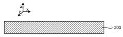
도 1 및 도 2a 내지 도 2e에 개략적으로 도시된 일 실시형태에 따라, 흐름도(1) 내의 방법은, 100에서, 기판(200)을 프로세스 챔버 내에 제공하는 단계를 포함한다. 일 예에서, 프로세스 챔버는 기판(200) 상에서 유전체 재료의 원자 층 증착(ALD)을 수행하도록 구성될 수 있다. 기판(200)은 예를 들어, 규소, 게르마늄, 규소 게르마늄, 규소 게르마늄 탄화물, 갈륨 비소 인화물, 갈륨 인듐 인화물, 규소 탄화물, 갈륨 비소, 인듐 비소화물 또는 인듐 인화물을 포함하는, 반도체 재료를 포함할 수 있다. 일 예에서, 기판(200)은 벌크 반도체 위에 위치되는 에피택셜 층을 가질 수 있다. 또한, 기판(200)은 SOI(semiconductor-on-insulator) 구조물을 포함할 수 있다. 또한 추가적으로, 기판(200)은 금속 층을 포함할 수 있다.According to one embodiment schematically illustrated in FIGS. 1 and 2A-2E , the method in flowchart 1 includes, at 100 , providing a
기판(200)은 또한, 이온 주입 및/또는 확산과 같은 프로세스에 의해서 구현된, 다양한 p-타입 도핑 영역 및/또는 n-타입 도핑 영역을 포함할 수 있다. 이러한 도핑된 영역은, 상보적 금속 산화물 반도체 전계 효과 트랜지스터(CMOSFET), 이미징 센서, 및/또는 발광 다이오드(LED)와 같은, 다양한 집적 회로(IC) 디바이스를 형성하도록 구성된 n-웰(well), p-웰, LDD(light-doped region) 및 다양한 채널 도핑 프로파일을 포함할 수 있다.
기판(200)은 또한 다양한 절연 영역을 포함할 수 있다. 절연 영역은 기판(200) 내에서 여러 디바이스 영역들을 분리한다. 절연 영역은 상이한 프로세싱 기술들을 이용하여 형성된 상이한 구조물들을 포함한다. 예를 들어, 절연 영역은 STI(shallow trench isolation) 영역을 포함할 수 있다. STI 영역의 형성은 기판(200) 내에 트렌치를 에칭하고, 규소 산화물, 규소 질화물, 및/또는 규소 산질화물과 같은 절연체 재료로 트렌치를 충진하는 것을 포함할 수 있다. 충진된 트렌치는, 규소 질화물로 트렌치가 충진된, 열 산화물 선형 층과 같은 다층 구조물을 가질 수 있다. 화학적 기계적 폴리싱(CMP)을 수행하여, 과다 절연체 재료를 폴리싱할 수 있고 절연 특징부의 상단 표면을 평탄화할 수 있다.
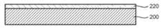
방법은, 110에서, 원자 층 증착(ALD)의 제1의 복수의 사이클을 수행하는 것에 의해서 제1 유전체 재료의 제1 막(220)을 기판(200) 상에 형성하는 단계를 추가로 포함한다. 이러한 것이 도 2b에 개략적으로 도시되어 있다. 일부 실시형태에 따라, 제1 막(220)은, SiO2(k~4)보다 큰 유전 상수를 갖는, 고 유전 상수(고-k) 재료를 포함한다. 금속 산화물의 예에서, ALD는 금속-함유 전구체 및 산화제의 포화 기체 노출을 교번적으로 수행하는 사이클을 포함할 수 있고, 여기에서 각각의 사이클은 금속-함유 전구체의 한 번의 노출, 그 후의 산화제의 한 번의 노출을 포함한다. 각각의 사이클은 금속 산화물의 하나의 원자 층 또는 그 미만을 증착시키고, 사이클의 수는 막 두께의 정확한 제어를 위해서 선택될 수 있다. 금속-함유 전구체 및 산화제 내의 리간드의 입체 장해(Steric hindrance), 및 제한된 수의 결합 사이트는 기판 표면 상의 화학 흡착을 제한할 수 있고, 그에 따라 사이클당 막 성장이 하나의 원자층 미만으로 유지될 수 있다.The method further includes, at 110 , forming a
일부 실시형태에 따라, 제1 막(220)은 지르코늄 산화물(ZrO2), 하프늄 산화물(HfO2), 또는 이들의 라미네이트(laminate) 또는 혼합물을 포함할 수 있다. HfO2는 알루미늄(Al), 가돌리늄(Gd), 란타늄(La), 규소(Si), 스트론튬(Sr) 또는 이트륨(Y) 도펀트로 도핑될 수 있다.According to some embodiments, the
일 예에서, ZrO2를 함유하는 제1 막(220)은 지르코늄-함유 전구체 및 산화제의 기체 노출을 교번적으로 수행하는 사이클을 사용하여 ALD에 의해 증착될 수 있다. 다른 예에서, ZrO2 및 HfO2의 혼합물을 함유하는 제1 막(220)은 지르코늄-함유 전구체 및 산화제, 하프늄-함유 전구체 및 산화제의 기체 노출을 교번적으로 수행하는 사이클을 이용하여 ALD에 의해 증착될 수 있다. 또 다른 예에서, 도핑된 HfO2를 함유하는 제1 막(220)은 하프늄-함유 전구체, 도펀트 가스, 및 산화제의 기체 노출을 교번적으로 수행하는 사이클을 사용하여 ALD에 의해 증착될 수 있다. 도펀트 농도는 예를 들어 약 0.1원자% 내지 약 20원자%, 약 0.1원자% 내지 약 10원자%, 또는 약 0.1원자% 내지 약 1원자%일 수 있다.In one example, the
본 발명의 실시형태는 증기 상 증착을 위해서 매우 다양한 지르코늄(Zr) 및 하프늄(Hf) 전구체를 이용할 수 있다. 예를 들어, 대표적인 예는 Zr(OtBu)4(지르코늄 tert-부톡사이드, ZTB), Zr(NEt2)4(테트라키스(디에틸아미도)지르코늄, TDEAZ), Zr(NMeEt)4(테트라키스(에틸메틸아미도)지르코늄, TEMAZ), Zr(NMe2)4(테트라키스(디메틸아미도)지르코늄 TDMAZ), Hf(OtBu)4(하프늄 tert-부톡사이드, HTB), Hf(NEt2)4(테트라키스(디에틸아미도)하프늄, TDEAH), Hf(NEtMe)4(테트라키스(에틸메틸아미도)하프늄, TEMAH) 및 Hf(NMe2)4(테트라키스(디메틸아미도)하프늄, TDMAH)를 포함한다. 일부 예에서, Air Liquide로부터 HyALDTM으로 입수할 수 있는 트리스(디메틸아미노시클로펜타디에닐하프늄(HfCp(NMe2)-3)이 하프늄 전구체로서 사용될 수 있고, Air Liquide로부터 ZyALDTM으로 입수할 수 있는 트리스(디메틸아미노시클로펜타디에닐지르코늄(ZrCp(NMe2)3))이 지르코늄 전구체로서 사용될 수 있다. 산화제는 플라즈마-여기된 O2, 물(H2O) 또는 오존(O3)을 포함하는 산소-함유 가스를 포함할 수 있다.Embodiments of the present invention may utilize a wide variety of zirconium (Zr) and hafnium (Hf) precursors for vapor phase deposition. For example, representative examples are Zr(Ot Bu)4 (zirconium tert-butoxide, ZTB), Zr(NEt2 )4 (tetrakis(diethylamido)zirconium, TDEAZ), Zr(NMeEt)4 ( tetrakis(ethylmethylamido)zirconium, TEMAZ), Zr(NMe2 )4 (tetrakis(dimethylamido)zirconium TDMAZ), Hf(Ot Bu)4 (hafnium tert-butoxide, HTB), Hf( NEt2 )4 (tetrakis(diethylamido)hafnium, TDEAH), Hf(NEtMe)4 (tetrakis(ethylmethylamido)hafnium, TEMAH) and Hf(NMe2 )4 (tetrakis(dimethylamido) ) hafnium, TDMAH). In some examples, tris(dimethylaminocyclopentadienylhafnium (HfCp(NMe2 )-3), available as HyALD™ from Air Liquide, can be used as a hafnium precursor, and Tris(dimethylaminocyclopentadienylzirconium (ZrCp(NMe2 )3 )) can be used as the zirconium precursor. The oxidizing agent comprises plasma-excited O2 , water (H2 O) or ozone (O3 ). May contain oxygen-containing gases.
Al, Gd, La, Si, Sr, 및 Y 도펀트는 충분한 반응성, 열적 안정성, 및 변동성을 갖는 임의의 도펀트 가스를 이용하여 제공될 수 있다.Al, Gd, La, Si, Sr, and Y dopants can be provided using any dopant gas having sufficient reactivity, thermal stability, and volatility.
Al 전구체의 예는 Al2Me6, Al2Et6, [Al(O(sBu))3]4, Al(CH3COCHCOCH3)3, AlBr3, AlI3, Al(O(iPr))3, [Al(NMe2)3]2, Al(iBu)2Cl, Al(iBu)3, Al(iBu)2H, AlEt2Cl, Et3Al2(O(sBu))3, 및 Al(THD)3을 포함한다.Examples of Al precursors are Al2 Me6 , Al2 Et6 , [Al(O(sBu))3 ]4 , Al(CH3 COCHCOCH3 )3 , AlBr3 , AlI3 , Al(O(iPr))3 , [Al(NMe2 )3 ]2 , Al(iBu)2 Cl, Al(iBu)3 , Al(iBu)2 H, AlEt2 Cl, Et3 Al2 (O(sBu))3 , and Al( THD)3 .
Gd 전구체의 예는 Gd(N(SiMe3)2)3, ((iPr)Cp)3Gd, Cp3Gd, Gd(THD)3, Gd[OOCCH(C2H5)C4H9]3, Gd(O(iPr))3, 및 Gd(acac)3을 포함한다.Examples of Gd precursors are Gd(N(SiMe3 )2 )3 , ((iPr)Cp)3 Gd, Cp3 Gd, Gd(THD)3 , Gd[OOCCH(C2 H5 )C4 H9 ]3 , Gd(O(iPr))3 , and Gd(acac)3 .
La 전구체의 예는 La(N(SiMe3)2)3, La(N(iPr)2)3, La(N(tBu)SiMe3)3, La(TMPD)3, ((iPr)Cp)3La, Cp3La, Cp3La(NCCH3)2, La(Me2NC2H4Cp)3, La(THD)3, La[OOCCH(C2H5)C4H9]3, La(C11H19O2)3

규소 전구체의 예는 실란(SiH4), 디실란(Si2H6), 모노클로로실란(SiClH3), 디클로로실란(SiH2Cl2), 트리클로로실란(SiHCl3), 헥사클로로디실란(Si2Cl6), 디에틸실란(Et2SiH2) 및 알킬아미노실란 화합물을 포함한다. 알킬아미노실란 화합물의 예는, 비제한적으로, 디-이소프로필아미노실란(H3Si(NPr2)), 비스(tert-부틸아미노)실란((C4H9(H)N)2SiH2), 테트라키스(디메틸아미노)실란(Si(NMe2)4), 테트라키스(에틸메틸아미노)실란(Si(NEtMe)4), 테트라키스(디에틸아미노)실란(Si(NEt2)4), 트리스(디메틸아미노)실란(HSi(NMe2)3), 트리스(에틸메틸아미노)실란(HSi( NEtMe)3), 트리스(디에틸아미노)실란(HSi(NEt2)3) 및 트리스(디메틸하이드라지노)실란(HSi(N(H)NMe2)3), 비스(디에틸아미노)실란(H2Si(NEt2)2), 비스 (디-이소프로필아미노)실란(H2Si(NPr2)2), 트리스(이소프로필아미노)실란(HSi(NPr2)3), 및 (디-이소프로필아미노)실란(H3Si(NPr2)을 포함한다.Examples of silicon precursors include silane (SiH4 ), disilane (Si2 H6 ), monochlorosilane (SiClH3 ), dichlorosilane (SiH2 Cl2 ), trichlorosilane (SiHCl3 ), hexachlorodisilane ( Si2 Cl6 ), diethylsilane (Et2 SiH2 ) and alkylaminosilane compounds. Examples of alkylaminosilane compounds include, but are not limited to, di-isopropylaminosilane (H3 Si(NPr2 )), bis(tert-butylamino)silane ((C4 H9 (H)N)2 SiH2 ), tetrakis(dimethylamino)silane (Si(NMe2 )4 ), tetrakis(ethylmethylamino)silane (Si(NEtMe)4 ), tetrakis(diethylamino)silane (Si(NEt2 )4 ) , tris(dimethylamino)silane (HSi(NMe2 )3 ), tris(ethylmethylamino)silane (HSi(NEtMe)3 ), tris(diethylamino)silane (HSi(NEt2 )3 ) and tris(dimethyl hydrazino)silane (HSi(N(H)NMe2 )3 ), bis(diethylamino)silane (H2 Si(NEt2 )2 ), bis (di-isopropylamino)silane (H2 Si( NPr2 )2 ), tris(isopropylamino)silane (HSi(NPr2 )3 ), and (di-isopropylamino)silane (H3 Si(NPr2 ) ).
Sr 전구체의 예는 비스(tert-부틸아세타미디나토)스트론튬(TBAASr), Sr-C, Sr-D, Sr(N(SiMe3)2)2, Sr(THD)2, Sr(THD)2(tetraglyme), Sr(iPr4Cp)2, Sr(iPr3Cp)2, 및 Sr(Me5Cp)2를 포함한다.Examples of Sr precursors are bis(tert-butylacetamidinato)strontium (TBAASr), Sr-C, Sr-D, Sr(N(SiMe3 )2 )2 , Sr(THD)2 , Sr(THD)2 (tetraglyme), Sr(iPr4 Cp)2 , Sr(iPr3 Cp)2 , and Sr(Me5 Cp)2 .
Y 전구체의 예는 Y(N(SiMe3)2)3, Y(N(iPr)2)3, ((iPr)Cp)3Y, Cp3Y, Y(THD)3, Y[OOCCH(C2H5)C4H9]3, Y(O(iPr))3, Y(acac)3, (C5Me5)2Y, Y(hfac)3, 및 Y(FOD)3을 포함한다.Examples of Y precursors are Y(N(SiMe3 )2 )3 , Y(N(iPr)2 )3 , ((iPr)Cp)3 Y, Cp3 Y, Y(THD)3 , Y[OOCCH(C2 H5 )C4 H9 ]3 , Y(O(iPr))3 , Y(acac)3 , (C5 Me5 )2 Y, Y(hfac)3 , and Y(FOD)3 .
전술한 전구체 뿐만 아니라 아래에 기재된 전구체에서, 다음의 일반적인 약어가 사용된다: Si: 규소; Me: 메틸; Et: 에틸; iPr: 이소프로필; nPr: n-프로필; Bu: 부틸; nBu: n-부틸; sBu: sec-부틸; iBu: 이소-부틸; tBu: tert-부틸; Cp: 시클로펜타디에닐; THD: 2,2,6,6-테트라메틸-3,5-헵탄디오네이트; TMPD: 2,2,6,6-테트라메틸피페리디드; acac: 아세틸아세토네이트; hfac: 헥사플루오로아세틸아세토네이트; 및 FOD: 6,6,7,7,8,8,8-헵타플루오로-2,2-디메틸-3,5-옥탄디오네이트.In the foregoing as well as the precursors listed below, the following common abbreviations are used: Si: silicon; Me: methyl; Et: ethyl; iPr: isopropyl; nPr: n-propyl; Bu: butyl; nBu: n-butyl; sBu: sec-butyl; iBu: iso-butyl; tBu: tert-butyl; Cp: cyclopentadienyl; THD: 2,2,6,6-tetramethyl-3,5-heptanedionate; TMPD: 2,2,6,6-tetramethylpiperidide; acac: acetylacetonate; hfac: hexafluoroacetylacetonate; and FOD: 6,6,7,7,8,8,8-heptafluoro-2,2-dimethyl-3,5-octanedionate.
기판(200) 상의 제1 막(220)의 증착 후에, 미리 결정된 기판 온도 및 기간을 이용하여 열처리 프로세스를 제1 막(220)에서 수행하여, 열처리된 제1 막(221)을 형성한다. 이러한 것이 도 2c에 개략적으로 도시되어 있다. 열처리는 제1 막(220) 내의 원자 원소들을 조직화하고, 막 응력을 감소시키며, 제1 유전체 재료의 결정학적 배향을 고정시킨다. 제1 막(220)에 대한 열처리는 약 500℃ 이하, 약 200℃ 내지 약 500℃, 약 200℃ 내지 약 300℃, 약 300℃ 내지 약 400℃, 또는 약 400℃ 내지 약 500℃의 기판 온도에서 수행될 수 있다. 일 예에서, 열처리는 제1 막(220)의 증착에서와 동일한 프로세스 챔버 내에서 수행될 수 있다. 다른 예에서, 열처리는 제1 막(220)의 증착과 다른 프로세스 챔버에서 형성될 수 있다. 열처리는 불활성 가스, 예를 들어 아르곤(Ar) 또는 질소(N2)가 존재하는 진공 조건에서 수행될 수 있다.After deposition of the
본 발명의 일 실시형태에 따라, 열처리된 제1 막(221)의 두께는 약 1.5 nm 이하일 수 있다. 금속 산화물을 포함하는 제1 유전체 재료의 경우에, 이러한 두께는 금속 산화물의 단지 몇 개의 원자의 단일 층에 상응하고, 이러한 두께는 금속 산화물 내의 자발적인 분극에 필요한 문턱값 두께 미만이다. 이는, 외부 전기장의 존재 하에서 선형으로 분극 가능한 금속 산화물 막을 초래한다. 일 예에서, 열처리된 제1 막(221)은 (111) 결정학적 배향을 갖는 텍스처링된 정방정계 ZrO2를 포함한다.According to an embodiment of the present invention, the heat-treated
일 실시형태에 따라, 유전체 재료의 부가적인 열처리된 막이, 증착 및 열처리 단계를 적어도 1차례 반복하는 것에 의해서, 열처리된 제1 막(221) 위에 형성될 수 있다. 이러한 것이 도 3에 개략적으로 도시되어 있고, 여기에서 부가적인 열처리된 막(223, 225)이, 증착 및 열처리 단계를 2차례 반복하는 것에 의해서, 열처리된 제1 막(221) 기판(200) 상에 형성된다. 일반적으로, 임의의 수의 부가적인 열처리된 막이 형성될 수 있다. 집합적으로, 열처리된 제1 막(221) 및 부가적인 열처리된 막(223, 225)은 선형 분극 가능 유전체 재료(230)를 형성한다.According to one embodiment, an additional annealed film of dielectric material may be formed over the annealed
도 1을 다시 참조하면, 방법은, 120에서, ALD의 제2의 복수의 사이클을 수행하는 것에 의해서 제2 유전체 재료의 제2 막(240)을 기판(200) 상에 형성하는 단계를 추가로 포함한다. 이러한 것이 도 2d에 개략적으로 도시되어 있다. 본 발명의 실시형태에 따라, 제2 막(240)의 두께는 제1의 열처리된 제1 막(221)의 두께보다 두껍다. 제2 막(240)은 고-k 재료를 포함할 수 있다. 일부 실시형태에 따라, 제2 막(240)은 ZrO2, HfO2, 또는 이들의 라미네이트 또는 혼합물을 포함할 수 있다. HfO2는 Al, Gd, La, Si, Sr, 또는 Y 도펀트로 도핑될 수 있다. 일 예에서, 열처리된 제1 막(220) 및 제2 막(240)이 동일 금속 산화물을 포함할 수 있다.Referring again to FIG. 1 , the method further includes, at 120 , forming a
제2 막(240)의 증착 후에, 미리 결정된 기판 온도 및 기간을 이용하여 열처리 프로세스를 수행하여, 열처리된 제2 막(241)을 형성한다. 이러한 것이 도 2e에 개략적으로 도시되어 있다. 열처리는 제2 막(240) 내의 원자 원소들을 조직화하고, 막 응력을 감소시키며, 제2 유전체 재료의 결정학적 배향을 고정시킨다. 열처리된 제2 막(241) 및 열처리된 제1 막(221)은 상이한 결정학적 배향을 가질 수 있다.After the deposition of the
제2 막(240)에 대한 열처리는 약 500℃ 이하, 약 200℃ 내지 약 500℃, 약 200℃ 내지 약 300℃, 약 300℃ 내지 약 400℃, 또는 약 400℃ 내지 약 500℃의 기판 온도에서 수행될 수 있다. 일 실시형태에 따라, 캡 층(미도시)이 열처리에 앞서서 제2 막(240)에 증착될 수 있다. 일 예에서, 캡 층은 티타늄 질화물(TiN)을 포함할 수 있다.The heat treatment of the
일 예에서, 제2 막(240)의 열처리는 제2 막(240)의 증착에서와 동일한 프로세스 챔버 내에서 수행될 수 있다. 다른 예에서, 열처리는 제2 막(240)의 증착과 다른 프로세스 챔버에서 형성될 수 있다. 열처리는 불활성 가스, 예를 들어 Ar 또는 N2가 존재하는 진공 조건에서 수행될 수 있다.In one example, the heat treatment of the
일반적으로, 열처리된 제2 막(241)의 두께는 열처리된 제1 막(221)의 두께보다 두껍고, 열처리된 제2 막(241)은 강유전체 또는 반강유전체이다. 일부 예에서, 열처리된 제2 막(241)의 두께는 약 5 nm 이상이다.In general, the heat-treated
본 발명의 다른 실시형태에 따라, 열처리된 제2 막(241)이 기판(200) 상에 형성되고, 그 후에, 열처리된 제1 막(221)이 열처리된 제2 막(241) 상에 형성된다. 이러한 것이 도 4에 개략적으로 도시되어 있다.According to another embodiment of the present invention, a heat treated
일 실시형태에 따라, 부가적인 열처리된 유전체 재료가, 증착 및 열처리 단계를 적어도 1차례 반복하는 것에 의해서, 열처리된 제1 막(221) 위에 형성될 수 있다. 이러한 것이 도 5에 개략적으로 도시되어 있고, 여기에서 부가적인 열처리된 막(223, 225)은 열처리된 제1 막(221) 상에 형성된다. 일반적으로, 임의의 수의 부가적인 열처리된 막이 형성될 수 있다. 집합적으로, 열처리된 제1 막(221) 및 부가적인 열처리된 막(223, 225)은 선형 분극 가능 유전체 재료(231)를 형성한다.According to one embodiment, an additional heat treated dielectric material may be formed over the heat treated
본 명세서에 설명된 실시형태는, 예를 들어, 전계 효과 트랜지스터(FET) 디바이스 또는 동적 랜덤 액세스 메모리(DRAM) 디바이스용 네거티브 커패시턴스(NC) 게이트 스택을 형성하기 위한 CMOS-관련 분야에서 이용될 수 있는 기판 상에 유전체 재료를 형성하는 방법을 제공한다. 유전체 재료는 예를 들어 초저전력 컴퓨팅을 위해 채널 길이가 매우 짧은 금속 산화물 반도체 전계 효과 트랜지스터(MOSFET)에서 사용하기 위해, 선택형 및 변조형 분극으로 형성될 수 있다.Embodiments described herein may be used in CMOS-related applications to form negative capacitance (NC) gate stacks for, for example, field effect transistor (FET) devices or dynamic random access memory (DRAM) devices. A method of forming a dielectric material on a substrate is provided. Dielectric materials can be formed with selective and modulated polarization for use in, for example, metal oxide semiconductor field effect transistors (MOSFETs) with very short channel lengths for ultra-low power computing.
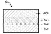
도 6a는 반도체 디바이스용 막 구조물(60)의 횡단면도를 개략적으로 도시하며, 여기서 막 구조물(60)는 제1 전도성 층(600), 제1 유전체 재료를 포함하는 제1 막(602), 제2 유전체 재료를 포함하는 제2 막(604), 및 제2 막(604) 상의 제2 전도성 층(606)을 포함한다. 제1 및 제2 전도성 층(600, 606)은 금속-함유 재료, 예를 들어 알루미늄(Al), 구리(Cu), 텅스텐(W), 니켈(Ni), 백금(Pt), 이들의 합금 또는 금속 화합물, 예를 들어 티타늄 질화물(TiN) 또는 탄탈륨 질화물(TaN)을 포함할 수 있다. 제1 및 제2 전도성 층(600, 606)은 또한 금속 실리사이드 또는 도핑된 규소를 포함할 수 있다. 일 예에서, 제1 및 제2 전도성 층(600, 606)은 n-타입 및 p-타입 FET와 양립 가능하도록 선택될 수 있다. 제1 막(602)은 열처리된 제1 막(221)에 대해서 전술한 바와 같이 형성될 수 있다. 제1 막(602)은 제1 유전체 재료 내의 자발적인 분극에 필요한 문턱값 두께 미만의 두께를 가질 수 있다. 따라서, 제1 막(602)은 외부 전기장의 존재 하에서 선형 분극될 수 있다. 제2 막(604)은 열처리된 제2 막(241)에 대해서 전술한 바와 같이 형성될 수 있다. 제2 막(604)은 제1 막(602)의 두께보다 두꺼운 두께를 가질 수 있고, 제2 유전체 재료는 자발적인 분극을 갖는다. 자발적인 분극은 강유전체 또는 반강유전체일 수 있다. 반도체 구조물(60)의 커패시턴스(C)는 도 6a에 도시된 막 및 층의 커패시턴스로 구성된다.6A schematically illustrates a cross-sectional view of a
제1 막(602)은 ZrO2, HfO2, 또는 이들의 라미네이트 또는 혼합물을 포함할 수 있다. HfO2는 Al, Gd, La, Si, Sr, 또는 Y 도펀트로 도핑될 수 있다. 제1 막(602) 및 제2 막(604)을 형성하는 예시적인 방법이 도 1 내지 도 5에 설명되어 있다.The
도 6b의 막 구조물(61)은 막 구조물(60)과 유사하고, 제1 전도성 층(600), 제2 유전체 재료를 포함하는 제2 막(604), 제1 유전체 재료를 포함하는 제1 막(602), 및 제1 막(602) 위의 제2 전도성 층(606)을 포함한다.The
막 구조물(60, 61)에 대해서 추가적인 CMOS 또는 MOS 기술 프로세싱을 수행하여, 당업계에 알려진 다양한 특징부 및 영역을 형성할 수 있다. 예를 들어, 후속 프로세싱이, 통상적인 비아 또는 콘택과 같은 수직 인터커넥트, 및 금속 라인과 같은 수평 인터커넥트를 포함하는 다층 인터커넥션을 형성할 수 있다. 다양한 인터커넥션 특징부는 구리, 텅스텐 및/또는 실리사이드를 포함하는 다양한 전도성 재료를 구현하여, 기판 내의 다양한 디바이스를 입력/출력 전력 및 신호에 커플링시키기 위한 전기 라우팅을 제공할 수 있다.Additional CMOS or MOS technology processing may be performed on the
박막 증기 상 증착에 의해서 선택형 분극을 갖는 유전체 재료를 형성하기 위한 여러 실시형태에 대해 설명하였다. 본 발명의 실시형태의 전술한 설명은 예시 및 설명의 목적을 위해 제시되었다. 개시된 정확한 형태로 본 발명이 제한되거나 전부인 것으로 의도되지 않는다. 이러한 설명 및 이하의 청구범위는, 설명을 위한 목적으로만 사용되며, 이를 제한하는 것으로 해석되어서는 안 되는 용어를 포함한다. 관련 기술분야의 당업자라면 위와 같은 교시를 고려하여 다수의 변형 및 변경이 가능하다는 것을 이해할 수 있을 것이다. 당업자는 도면에 도시된 다양한 구성 요소에 대한 다양한 등가의 조합 및 대체를 알 수 있을 것이다. 따라서, 본 발명의 범위는 이러한 상세한 설명이 아니라, 본원에 첨부된 청구범위에 의해 제한되는 것으로 의도된다.Several embodiments have been described for forming dielectric materials with selective polarization by thin-film vapor phase deposition. The foregoing description of embodiments of the present invention has been presented for purposes of illustration and description. The precise form disclosed is not intended to be exhaustive or limited to the invention. This description and the following claims contain terms that are used for purposes of explanation only and should not be construed as limiting. Those skilled in the relevant art will appreciate that many modifications and variations are possible in light of the above teachings. Various equivalent combinations and substitutions for the various components shown in the drawings will be apparent to those skilled in the art. Accordingly, it is intended that the scope of the present invention be limited not by this detailed description, but by the claims appended hereto.
Claims (20)
Translated fromKorean원자 층 증착의 제2의 복수의 사이클을 수행하는 것에 의해서 제2 유전체 재료의 제2 막을 상기 기판 상에 형성하고, 그 후에, 상기 제2 막을 열처리하는 단계로서, 상기 제2 막의 두께는 제1 막의 두께보다 두껍고, 상기 제2 막은 강유전체 또는 반강유전체인, 단계
를 포함하는, 기판 프로세싱 방법.forming a first film of a first dielectric material on a substrate by performing a first plurality of cycles of atomic layer deposition, thereafter thermally treating the first film, wherein the thickness of the first film is determined by the first film; less than the threshold thickness required for spontaneous polarization within the dielectric material; and
forming a second film of a second dielectric material on the substrate by performing a second plurality of cycles of atomic layer deposition, thereafter subjecting the second film to a heat treatment, wherein the second film has a thickness of a first thicker than the thickness of the film, and the second film is a ferroelectric or antiferroelectric;
Including, a substrate processing method.
상기 제2 막이 상기 제1 막 위에 형성되는, 방법.According to claim 1,
wherein the second film is formed over the first film.
상기 제1 막이 상기 제2 막 위에 형성되는, 방법.According to claim 1,
wherein the first film is formed over the second film.
상기 제1 및 제2 유전체 재료가 적어도 하나의 금속 산화물을 포함하는, 방법.According to claim 1,
wherein the first and second dielectric materials comprise at least one metal oxide.
상기 적어도 하나의 금속 산화물은 지르코늄 산화물, 하프늄 산화물, 또는 이들의 라미네이트 또는 혼합물을 포함하는, 방법.According to claim 4,
wherein the at least one metal oxide comprises zirconium oxide, hafnium oxide, or a laminate or mixture thereof.
상기 제1 막의 두께가 약 1.5 nm 이하인, 방법.According to claim 1,
wherein the first film has a thickness of about 1.5 nm or less.
상기 제1 막은 외부 전기장의 존재 하에서 선형 분극을 나타내는, 방법.According to claim 1,
wherein the first film exhibits a linear polarization in the presence of an external electric field.
상기 제1 막의 형성하는 것을 반복하여, 부가적인 막을 상기 제1 막 상에 형성하는 단계를 추가로 포함하고,
상기 부가적인 막은 자발적인 분극을 가지지 않는, 방법.According to claim 1,
further comprising forming an additional film on the first film by repeating the forming of the first film;
wherein the additional membrane does not have spontaneous polarization.
상기 제2 유전체 재료의 열처리에 앞서서, 캡 층을 상기 제2 막 상에 증착시키는 단계를 추가로 포함하는, 방법.According to claim 1,
depositing a cap layer on the second film prior to thermally treating the second dielectric material.
상기 제1 막을 열처리 하는 것 및 상기 제2 막을 열처리 하는 것이 불활성 가스의 존재하에서 약 650℃내지 약 900℃의 기판 온도에서 수행되는, 방법.According to claim 1,
wherein the thermally treating the first film and thermally treating the second film are performed at a substrate temperature of about 650° C. to about 900° C. in the presence of an inert gas.
원자 층 증착의 제2의 복수의 사이클을 수행하는 것에 의해서 제2 지르코늄 산화물 재료의 제2 막을 상기 기판 상에 형성하고, 그 후에, 상기 제2 막을 열처리하는 단계로서, 상기 제2 막의 두께는 제1 막의 두께보다 두껍고, 상기 제2 막은 강유전체 또는 반강유전체인, 단계
를 포함하는, 기판 프로세싱 방법.forming a first film of a first zirconium oxide material on a substrate by performing a first plurality of cycles of atomic layer deposition, thereafter thermally treating the first film, wherein the thickness of the first film is the first film; 1 less than the threshold thickness required for spontaneous polarization within the zirconium oxide material; and
forming a second film of a second zirconium oxide material on the substrate by performing a second plurality of cycles of atomic layer deposition, thereafter thermally treating the second film, wherein the second film has a thickness of a second film; thicker than the thickness of the first film, and the second film is a ferroelectric or antiferroelectric;
Including, a substrate processing method.
상기 기판 상의 제2 유전체 재료를 포함하는 제2 막으로서, 상기 제2 막의 두께는 상기 제1 막의 두께보다 두껍고, 상기 제2 막은 강유전체 또는 반강유전체인, 제2 막
을 포함하는, 반도체 디바이스.a first film comprising a first dielectric material on a substrate, wherein a thickness of the first film is less than a threshold thickness required for spontaneous polarization within the first dielectric material; and
A second film comprising a second dielectric material on the substrate, wherein the thickness of the second film is greater than the thickness of the first film, and the second film is ferroelectric or antiferroelectric.
Including, a semiconductor device.
상기 제2 막이 상기 제1 막 위에 형성되는, 디바이스.According to claim 12,
wherein the second film is formed over the first film.
상기 제1 막이 상기 제2 막 위에 형성되는, 디바이스.According to claim 12,
wherein the first film is formed over the second film.
상기 제1 및 제2 유전체 재료가 적어도 하나의 금속 산화물을 포함하는, 디바이스.According to claim 12,
wherein the first and second dielectric materials comprise at least one metal oxide.
상기 적어도 하나의 금속 산화물은 지르코늄 산화물, 하프늄 산화물, 또는 이들의 라미네이트 또는 혼합물을 포함하는, 디바이스.According to claim 15,
The device of claim 1 , wherein the at least one metal oxide comprises zirconium oxide, hafnium oxide, or a laminate or mixture thereof.
상기 제1 막의 두께가 약 1.5 nm 이하인, 디바이스.According to claim 12,
wherein the thickness of the first film is less than or equal to about 1.5 nm.
상기 제1 막은 외부 전기장의 존재 하에서 선형 분극을 나타내는, 디바이스.According to claim 12,
wherein the first film exhibits a linear polarization in the presence of an external electric field.
상기 제1 막 상의 부가적인 막을 추가로 포함하고,
상기 부가적인 막은 자발적인 분극을 가지지 않는, 디바이스.According to claim 12,
further comprising an additional film on the first film;
wherein the additional membrane does not have spontaneous polarization.
상기 제1 막은 정방정계 (111) 결정학적 배향을 가지는, 디바이스.According to claim 12,
wherein the first film has a tetragonal (111) crystallographic orientation.
Applications Claiming Priority (3)
| Application Number | Priority Date | Filing Date | Title |
|---|---|---|---|
| US202063063840P | 2020-08-10 | 2020-08-10 | |
| US63/063,840 | 2020-08-10 | ||
| PCT/US2021/043952WO2022035618A1 (en) | 2020-08-10 | 2021-07-30 | Methods for forming dielectric materials with selected polarization for semiconductor devices |
Publications (1)
| Publication Number | Publication Date |
|---|---|
| KR20230048000Atrue KR20230048000A (en) | 2023-04-10 |
Family
ID=80115248
Family Applications (1)
| Application Number | Title | Priority Date | Filing Date |
|---|---|---|---|
| KR1020237002323APendingKR20230048000A (en) | 2020-08-10 | 2021-07-30 | Method for Forming Dielectric Material with Selective Polarization for Semiconductor Devices |
Country Status (5)
| Country | Link |
|---|---|
| US (1) | US20220044922A1 (en) |
| JP (1) | JP7743144B2 (en) |
| KR (1) | KR20230048000A (en) |
| TW (1) | TW202215603A (en) |
| WO (1) | WO2022035618A1 (en) |
Families Citing this family (1)
| Publication number | Priority date | Publication date | Assignee | Title |
|---|---|---|---|---|
| KR20240165378A (en)* | 2022-03-29 | 2024-11-22 | 도쿄엘렉트론가부시키가이샤 | Double layer stack for ferroelectric tunnel junction and method for forming same |
Family Cites Families (13)
| Publication number | Priority date | Publication date | Assignee | Title |
|---|---|---|---|---|
| JP4449226B2 (en)* | 2000-05-22 | 2010-04-14 | 東京エレクトロン株式会社 | Metal oxide film modification method, metal oxide film formation method, and heat treatment apparatus |
| US6441417B1 (en)* | 2001-03-28 | 2002-08-27 | Sharp Laboratories Of America, Inc. | Single c-axis PGO thin film on ZrO2 for non-volatile memory applications and methods of making the same |
| JP2010283040A (en)* | 2009-06-02 | 2010-12-16 | Panasonic Corp | Semiconductor device and manufacturing method thereof |
| US9269785B2 (en)* | 2014-01-27 | 2016-02-23 | Globalfoundries Inc. | Semiconductor device with ferroelectric hafnium oxide and method for forming semiconductor device |
| US9391162B2 (en)* | 2014-04-04 | 2016-07-12 | Taiwan Semiconductor Manufacturing Company, Ltd. | Tunnel MOSFET with ferroelectric gate stack |
| US20160181091A1 (en)* | 2014-12-19 | 2016-06-23 | Intermolecular, Inc. | Methods for Forming Ferroelectric Phases in Materials and Devices Utilizing the Same |
| US10153155B2 (en)* | 2015-10-09 | 2018-12-11 | University Of Florida Research Foundation, Incorporated | Doped ferroelectric hafnium oxide film devices |
| US11670699B2 (en)* | 2016-12-15 | 2023-06-06 | National Yang Ming Chiao Tung University | Semiconductor device and method of manufacturing the same |
| TWI604605B (en)* | 2016-12-15 | 2017-11-01 | 國立交通大學 | Semiconductor device and method of manufacturing same |
| US10276697B1 (en)* | 2017-10-27 | 2019-04-30 | Taiwan Semiconductor Manufacturing Co., Ltd. | Negative capacitance FET with improved reliability performance |
| US10784362B2 (en)* | 2017-10-30 | 2020-09-22 | Taiwan Semiconductor Manufacturing Co., Ltd. | Semiconductor device and manufacturing method thereof |
| US10861973B2 (en)* | 2018-06-27 | 2020-12-08 | Taiwan Semiconductor Manufacturing Co., Ltd. | Negative capacitance transistor with a diffusion blocking layer |
| KR20210057587A (en)* | 2019-11-12 | 2021-05-21 | 삼성전자주식회사 | Thin film structure including dielectric material layer, method for manufacturing the same, and electronic device employing the smae |
- 2021
- 2021-07-30WOPCT/US2021/043952patent/WO2022035618A1/ennot_activeCeased
- 2021-07-30USUS17/390,399patent/US20220044922A1/enactivePending
- 2021-07-30KRKR1020237002323Apatent/KR20230048000A/enactivePending
- 2021-07-30JPJP2023509574Apatent/JP7743144B2/enactiveActive
- 2021-08-09TWTW110129234Apatent/TW202215603A/enunknown
Also Published As
| Publication number | Publication date |
|---|---|
| TW202215603A (en) | 2022-04-16 |
| US20220044922A1 (en) | 2022-02-10 |
| JP7743144B2 (en) | 2025-09-24 |
| WO2022035618A1 (en) | 2022-02-17 |
| JP2023538535A (en) | 2023-09-08 |
Similar Documents
| Publication | Publication Date | Title |
|---|---|---|
| US7304004B2 (en) | System and method for forming a gate dielectric | |
| US9178031B2 (en) | Methods of atomic-layer deposition of hafnium oxide/erbium oxide bi-layer as advanced gate dielectrics | |
| CN101427386B (en) | Selective implementation of barrier layers for threshold voltage control in CMOS device fabrication with high-k dielectrics | |
| US8440520B2 (en) | Diffused cap layers for modifying high-k gate dielectrics and interface layers | |
| US8889505B2 (en) | Method for manufacturing semiconductor device | |
| US7564114B2 (en) | Semiconductor devices and methods of manufacture thereof | |
| US20150140838A1 (en) | Two Step Deposition of High-k Gate Dielectric Materials | |
| KR20130047048A (en) | Complementary metal oxide semiconductor integrated circuit with metal gate and high-k dielectric | |
| US20080164582A1 (en) | Semiconductor devices and methods of manufacture thereof | |
| US20150255267A1 (en) | Atomic Layer Deposition of Aluminum-doped High-k Films | |
| US8927438B2 (en) | Methods for manufacturing high dielectric constant films | |
| JP5368584B2 (en) | Semiconductor device and manufacturing method thereof | |
| US20130316546A1 (en) | Methods of atomic layer deposition of hafnium oxide as gate dielectrics | |
| KR100695887B1 (en) | Method of forming a titanium nitride film and method of forming a lower electrode of a metal-insulator-metal capacitor using the titanium nitride film | |
| KR20250138821A (en) | Method of tuning film properties of metal nitride using plasma | |
| JP7743144B2 (en) | Method for forming dielectric materials with selected polarization for semiconductor devices | |
| US20050142715A1 (en) | Semiconductor device with high dielectric constant insulator and its manufacture | |
| US20080211065A1 (en) | Semiconductor devices and methods of manufacture thereof | |
| US7410812B2 (en) | Manufacture of semiconductor device having insulation film of high dielectric constant | |
| JP4643902B2 (en) | Semiconductor device and manufacturing method thereof | |
| JP2012186349A (en) | Semiconductor device and method of manufacturing the same | |
| US10121652B1 (en) | Formation of metal oxide layer | |
| US7256145B2 (en) | Manufacture of semiconductor device having insulation film of high dielectric constant |
Legal Events
| Date | Code | Title | Description |
|---|---|---|---|
| PA0105 | International application | St.27 status event code:A-0-1-A10-A15-nap-PA0105 | |
| PG1501 | Laying open of application | St.27 status event code:A-1-1-Q10-Q12-nap-PG1501 | |
| PN2301 | Change of applicant | St.27 status event code:A-3-3-R10-R13-asn-PN2301 St.27 status event code:A-3-3-R10-R11-asn-PN2301 | |
| A201 | Request for examination | ||
| E13-X000 | Pre-grant limitation requested | St.27 status event code:A-2-3-E10-E13-lim-X000 | |
| P11-X000 | Amendment of application requested | St.27 status event code:A-2-2-P10-P11-nap-X000 | |
| P13-X000 | Application amended | St.27 status event code:A-2-2-P10-P13-nap-X000 | |
| PA0201 | Request for examination | St.27 status event code:A-1-2-D10-D11-exm-PA0201 | |
| P22-X000 | Classification modified | St.27 status event code:A-2-2-P10-P22-nap-X000 | |
| D13-X000 | Search requested | St.27 status event code:A-1-2-D10-D13-srh-X000 | |
| D14-X000 | Search report completed | St.27 status event code:A-1-2-D10-D14-srh-X000 | |
| E902 | Notification of reason for refusal | ||
| PE0902 | Notice of grounds for rejection | St.27 status event code:A-1-2-D10-D21-exm-PE0902 | |
| P11-X000 | Amendment of application requested | St.27 status event code:A-2-2-P10-P11-nap-X000 |