KR20230043795A - Impurity Reduction in Silicon-Containing Films - Google Patents
Impurity Reduction in Silicon-Containing FilmsDownload PDFInfo
- Publication number
- KR20230043795A KR20230043795AKR1020227045959AKR20227045959AKR20230043795AKR 20230043795 AKR20230043795 AKR 20230043795AKR 1020227045959 AKR1020227045959 AKR 1020227045959AKR 20227045959 AKR20227045959 AKR 20227045959AKR 20230043795 AKR20230043795 AKR 20230043795A
- Authority
- KR
- South Korea
- Prior art keywords
- silicon
- plasma
- substrate
- doped
- reactant
- Prior art date
- Legal status (The legal status is an assumption and is not a legal conclusion. Google has not performed a legal analysis and makes no representation as to the accuracy of the status listed.)
- Pending
Links
Images


Classifications
- H—ELECTRICITY
- H01—ELECTRIC ELEMENTS
- H01L—SEMICONDUCTOR DEVICES NOT COVERED BY CLASS H10
- H01L21/00—Processes or apparatus adapted for the manufacture or treatment of semiconductor or solid state devices or of parts thereof
- H01L21/02—Manufacture or treatment of semiconductor devices or of parts thereof
- H01L21/02104—Forming layers
- H01L21/02107—Forming insulating materials on a substrate
- H01L21/02109—Forming insulating materials on a substrate characterised by the type of layer, e.g. type of material, porous/non-porous, pre-cursors, mixtures or laminates
- H01L21/02205—Forming insulating materials on a substrate characterised by the type of layer, e.g. type of material, porous/non-porous, pre-cursors, mixtures or laminates the layer being characterised by the precursor material for deposition
- H01L21/02208—Forming insulating materials on a substrate characterised by the type of layer, e.g. type of material, porous/non-porous, pre-cursors, mixtures or laminates the layer being characterised by the precursor material for deposition the precursor containing a compound comprising Si
- C—CHEMISTRY; METALLURGY
- C23—COATING METALLIC MATERIAL; COATING MATERIAL WITH METALLIC MATERIAL; CHEMICAL SURFACE TREATMENT; DIFFUSION TREATMENT OF METALLIC MATERIAL; COATING BY VACUUM EVAPORATION, BY SPUTTERING, BY ION IMPLANTATION OR BY CHEMICAL VAPOUR DEPOSITION, IN GENERAL; INHIBITING CORROSION OF METALLIC MATERIAL OR INCRUSTATION IN GENERAL
- C23C—COATING METALLIC MATERIAL; COATING MATERIAL WITH METALLIC MATERIAL; SURFACE TREATMENT OF METALLIC MATERIAL BY DIFFUSION INTO THE SURFACE, BY CHEMICAL CONVERSION OR SUBSTITUTION; COATING BY VACUUM EVAPORATION, BY SPUTTERING, BY ION IMPLANTATION OR BY CHEMICAL VAPOUR DEPOSITION, IN GENERAL
- C23C16/00—Chemical coating by decomposition of gaseous compounds, without leaving reaction products of surface material in the coating, i.e. chemical vapour deposition [CVD] processes
- C23C16/04—Coating on selected surface areas, e.g. using masks
- C23C16/045—Coating cavities or hollow spaces, e.g. interior of tubes; Infiltration of porous substrates
- C—CHEMISTRY; METALLURGY
- C23—COATING METALLIC MATERIAL; COATING MATERIAL WITH METALLIC MATERIAL; CHEMICAL SURFACE TREATMENT; DIFFUSION TREATMENT OF METALLIC MATERIAL; COATING BY VACUUM EVAPORATION, BY SPUTTERING, BY ION IMPLANTATION OR BY CHEMICAL VAPOUR DEPOSITION, IN GENERAL; INHIBITING CORROSION OF METALLIC MATERIAL OR INCRUSTATION IN GENERAL
- C23C—COATING METALLIC MATERIAL; COATING MATERIAL WITH METALLIC MATERIAL; SURFACE TREATMENT OF METALLIC MATERIAL BY DIFFUSION INTO THE SURFACE, BY CHEMICAL CONVERSION OR SUBSTITUTION; COATING BY VACUUM EVAPORATION, BY SPUTTERING, BY ION IMPLANTATION OR BY CHEMICAL VAPOUR DEPOSITION, IN GENERAL
- C23C16/00—Chemical coating by decomposition of gaseous compounds, without leaving reaction products of surface material in the coating, i.e. chemical vapour deposition [CVD] processes
- C23C16/22—Chemical coating by decomposition of gaseous compounds, without leaving reaction products of surface material in the coating, i.e. chemical vapour deposition [CVD] processes characterised by the deposition of inorganic material, other than metallic material
- C23C16/30—Deposition of compounds, mixtures or solid solutions, e.g. borides, carbides, nitrides
- C23C16/40—Oxides
- C23C16/401—Oxides containing silicon
- C—CHEMISTRY; METALLURGY
- C23—COATING METALLIC MATERIAL; COATING MATERIAL WITH METALLIC MATERIAL; CHEMICAL SURFACE TREATMENT; DIFFUSION TREATMENT OF METALLIC MATERIAL; COATING BY VACUUM EVAPORATION, BY SPUTTERING, BY ION IMPLANTATION OR BY CHEMICAL VAPOUR DEPOSITION, IN GENERAL; INHIBITING CORROSION OF METALLIC MATERIAL OR INCRUSTATION IN GENERAL
- C23C—COATING METALLIC MATERIAL; COATING MATERIAL WITH METALLIC MATERIAL; SURFACE TREATMENT OF METALLIC MATERIAL BY DIFFUSION INTO THE SURFACE, BY CHEMICAL CONVERSION OR SUBSTITUTION; COATING BY VACUUM EVAPORATION, BY SPUTTERING, BY ION IMPLANTATION OR BY CHEMICAL VAPOUR DEPOSITION, IN GENERAL
- C23C16/00—Chemical coating by decomposition of gaseous compounds, without leaving reaction products of surface material in the coating, i.e. chemical vapour deposition [CVD] processes
- C23C16/44—Chemical coating by decomposition of gaseous compounds, without leaving reaction products of surface material in the coating, i.e. chemical vapour deposition [CVD] processes characterised by the method of coating
- C23C16/455—Chemical coating by decomposition of gaseous compounds, without leaving reaction products of surface material in the coating, i.e. chemical vapour deposition [CVD] processes characterised by the method of coating characterised by the method used for introducing gases into reaction chamber or for modifying gas flows in reaction chamber
- C23C16/45523—Pulsed gas flow or change of composition over time
- C23C16/45525—Atomic layer deposition [ALD]
- C—CHEMISTRY; METALLURGY
- C23—COATING METALLIC MATERIAL; COATING MATERIAL WITH METALLIC MATERIAL; CHEMICAL SURFACE TREATMENT; DIFFUSION TREATMENT OF METALLIC MATERIAL; COATING BY VACUUM EVAPORATION, BY SPUTTERING, BY ION IMPLANTATION OR BY CHEMICAL VAPOUR DEPOSITION, IN GENERAL; INHIBITING CORROSION OF METALLIC MATERIAL OR INCRUSTATION IN GENERAL
- C23C—COATING METALLIC MATERIAL; COATING MATERIAL WITH METALLIC MATERIAL; SURFACE TREATMENT OF METALLIC MATERIAL BY DIFFUSION INTO THE SURFACE, BY CHEMICAL CONVERSION OR SUBSTITUTION; COATING BY VACUUM EVAPORATION, BY SPUTTERING, BY ION IMPLANTATION OR BY CHEMICAL VAPOUR DEPOSITION, IN GENERAL
- C23C16/00—Chemical coating by decomposition of gaseous compounds, without leaving reaction products of surface material in the coating, i.e. chemical vapour deposition [CVD] processes
- C23C16/44—Chemical coating by decomposition of gaseous compounds, without leaving reaction products of surface material in the coating, i.e. chemical vapour deposition [CVD] processes characterised by the method of coating
- C23C16/50—Chemical coating by decomposition of gaseous compounds, without leaving reaction products of surface material in the coating, i.e. chemical vapour deposition [CVD] processes characterised by the method of coating using electric discharges
- C23C16/505—Chemical coating by decomposition of gaseous compounds, without leaving reaction products of surface material in the coating, i.e. chemical vapour deposition [CVD] processes characterised by the method of coating using electric discharges using radio frequency discharges
- C—CHEMISTRY; METALLURGY
- C23—COATING METALLIC MATERIAL; COATING MATERIAL WITH METALLIC MATERIAL; CHEMICAL SURFACE TREATMENT; DIFFUSION TREATMENT OF METALLIC MATERIAL; COATING BY VACUUM EVAPORATION, BY SPUTTERING, BY ION IMPLANTATION OR BY CHEMICAL VAPOUR DEPOSITION, IN GENERAL; INHIBITING CORROSION OF METALLIC MATERIAL OR INCRUSTATION IN GENERAL
- C23C—COATING METALLIC MATERIAL; COATING MATERIAL WITH METALLIC MATERIAL; SURFACE TREATMENT OF METALLIC MATERIAL BY DIFFUSION INTO THE SURFACE, BY CHEMICAL CONVERSION OR SUBSTITUTION; COATING BY VACUUM EVAPORATION, BY SPUTTERING, BY ION IMPLANTATION OR BY CHEMICAL VAPOUR DEPOSITION, IN GENERAL
- C23C16/00—Chemical coating by decomposition of gaseous compounds, without leaving reaction products of surface material in the coating, i.e. chemical vapour deposition [CVD] processes
- C23C16/44—Chemical coating by decomposition of gaseous compounds, without leaving reaction products of surface material in the coating, i.e. chemical vapour deposition [CVD] processes characterised by the method of coating
- C23C16/52—Controlling or regulating the coating process
- C—CHEMISTRY; METALLURGY
- C23—COATING METALLIC MATERIAL; COATING MATERIAL WITH METALLIC MATERIAL; CHEMICAL SURFACE TREATMENT; DIFFUSION TREATMENT OF METALLIC MATERIAL; COATING BY VACUUM EVAPORATION, BY SPUTTERING, BY ION IMPLANTATION OR BY CHEMICAL VAPOUR DEPOSITION, IN GENERAL; INHIBITING CORROSION OF METALLIC MATERIAL OR INCRUSTATION IN GENERAL
- C23C—COATING METALLIC MATERIAL; COATING MATERIAL WITH METALLIC MATERIAL; SURFACE TREATMENT OF METALLIC MATERIAL BY DIFFUSION INTO THE SURFACE, BY CHEMICAL CONVERSION OR SUBSTITUTION; COATING BY VACUUM EVAPORATION, BY SPUTTERING, BY ION IMPLANTATION OR BY CHEMICAL VAPOUR DEPOSITION, IN GENERAL
- C23C16/00—Chemical coating by decomposition of gaseous compounds, without leaving reaction products of surface material in the coating, i.e. chemical vapour deposition [CVD] processes
- C23C16/56—After-treatment
- H—ELECTRICITY
- H01—ELECTRIC ELEMENTS
- H01J—ELECTRIC DISCHARGE TUBES OR DISCHARGE LAMPS
- H01J37/00—Discharge tubes with provision for introducing objects or material to be exposed to the discharge, e.g. for the purpose of examination or processing thereof
- H01J37/32—Gas-filled discharge tubes
- H01J37/32431—Constructional details of the reactor
- H01J37/3244—Gas supply means
- H01J37/32449—Gas control, e.g. control of the gas flow
- H—ELECTRICITY
- H01—ELECTRIC ELEMENTS
- H01L—SEMICONDUCTOR DEVICES NOT COVERED BY CLASS H10
- H01L21/00—Processes or apparatus adapted for the manufacture or treatment of semiconductor or solid state devices or of parts thereof
- H01L21/02—Manufacture or treatment of semiconductor devices or of parts thereof
- H01L21/02104—Forming layers
- H01L21/02107—Forming insulating materials on a substrate
- H01L21/02109—Forming insulating materials on a substrate characterised by the type of layer, e.g. type of material, porous/non-porous, pre-cursors, mixtures or laminates
- H01L21/02112—Forming insulating materials on a substrate characterised by the type of layer, e.g. type of material, porous/non-porous, pre-cursors, mixtures or laminates characterised by the material of the layer
- H01L21/02123—Forming insulating materials on a substrate characterised by the type of layer, e.g. type of material, porous/non-porous, pre-cursors, mixtures or laminates characterised by the material of the layer the material containing silicon
- H01L21/02164—Forming insulating materials on a substrate characterised by the type of layer, e.g. type of material, porous/non-porous, pre-cursors, mixtures or laminates characterised by the material of the layer the material containing silicon the material being a silicon oxide, e.g. SiO2
- H—ELECTRICITY
- H01—ELECTRIC ELEMENTS
- H01L—SEMICONDUCTOR DEVICES NOT COVERED BY CLASS H10
- H01L21/00—Processes or apparatus adapted for the manufacture or treatment of semiconductor or solid state devices or of parts thereof
- H01L21/02—Manufacture or treatment of semiconductor devices or of parts thereof
- H01L21/02104—Forming layers
- H01L21/02107—Forming insulating materials on a substrate
- H01L21/02109—Forming insulating materials on a substrate characterised by the type of layer, e.g. type of material, porous/non-porous, pre-cursors, mixtures or laminates
- H01L21/02205—Forming insulating materials on a substrate characterised by the type of layer, e.g. type of material, porous/non-porous, pre-cursors, mixtures or laminates the layer being characterised by the precursor material for deposition
- H01L21/02208—Forming insulating materials on a substrate characterised by the type of layer, e.g. type of material, porous/non-porous, pre-cursors, mixtures or laminates the layer being characterised by the precursor material for deposition the precursor containing a compound comprising Si
- H01L21/02211—Forming insulating materials on a substrate characterised by the type of layer, e.g. type of material, porous/non-porous, pre-cursors, mixtures or laminates the layer being characterised by the precursor material for deposition the precursor containing a compound comprising Si the compound being a silane, e.g. disilane, methylsilane or chlorosilane
- H—ELECTRICITY
- H01—ELECTRIC ELEMENTS
- H01L—SEMICONDUCTOR DEVICES NOT COVERED BY CLASS H10
- H01L21/00—Processes or apparatus adapted for the manufacture or treatment of semiconductor or solid state devices or of parts thereof
- H01L21/02—Manufacture or treatment of semiconductor devices or of parts thereof
- H01L21/02104—Forming layers
- H01L21/02107—Forming insulating materials on a substrate
- H01L21/02109—Forming insulating materials on a substrate characterised by the type of layer, e.g. type of material, porous/non-porous, pre-cursors, mixtures or laminates
- H01L21/02205—Forming insulating materials on a substrate characterised by the type of layer, e.g. type of material, porous/non-porous, pre-cursors, mixtures or laminates the layer being characterised by the precursor material for deposition
- H01L21/02208—Forming insulating materials on a substrate characterised by the type of layer, e.g. type of material, porous/non-porous, pre-cursors, mixtures or laminates the layer being characterised by the precursor material for deposition the precursor containing a compound comprising Si
- H01L21/02219—Forming insulating materials on a substrate characterised by the type of layer, e.g. type of material, porous/non-porous, pre-cursors, mixtures or laminates the layer being characterised by the precursor material for deposition the precursor containing a compound comprising Si the compound comprising silicon and nitrogen
- H—ELECTRICITY
- H01—ELECTRIC ELEMENTS
- H01L—SEMICONDUCTOR DEVICES NOT COVERED BY CLASS H10
- H01L21/00—Processes or apparatus adapted for the manufacture or treatment of semiconductor or solid state devices or of parts thereof
- H01L21/02—Manufacture or treatment of semiconductor devices or of parts thereof
- H01L21/02104—Forming layers
- H01L21/02107—Forming insulating materials on a substrate
- H01L21/02225—Forming insulating materials on a substrate characterised by the process for the formation of the insulating layer
- H01L21/0226—Forming insulating materials on a substrate characterised by the process for the formation of the insulating layer formation by a deposition process
- H01L21/02263—Forming insulating materials on a substrate characterised by the process for the formation of the insulating layer formation by a deposition process deposition from the gas or vapour phase
- H01L21/02271—Forming insulating materials on a substrate characterised by the process for the formation of the insulating layer formation by a deposition process deposition from the gas or vapour phase deposition by decomposition or reaction of gaseous or vapour phase compounds, i.e. chemical vapour deposition
- H01L21/02274—Forming insulating materials on a substrate characterised by the process for the formation of the insulating layer formation by a deposition process deposition from the gas or vapour phase deposition by decomposition or reaction of gaseous or vapour phase compounds, i.e. chemical vapour deposition in the presence of a plasma [PECVD]
- H—ELECTRICITY
- H01—ELECTRIC ELEMENTS
- H01L—SEMICONDUCTOR DEVICES NOT COVERED BY CLASS H10
- H01L21/00—Processes or apparatus adapted for the manufacture or treatment of semiconductor or solid state devices or of parts thereof
- H01L21/02—Manufacture or treatment of semiconductor devices or of parts thereof
- H01L21/02104—Forming layers
- H01L21/02107—Forming insulating materials on a substrate
- H01L21/02225—Forming insulating materials on a substrate characterised by the process for the formation of the insulating layer
- H01L21/0226—Forming insulating materials on a substrate characterised by the process for the formation of the insulating layer formation by a deposition process
- H01L21/02263—Forming insulating materials on a substrate characterised by the process for the formation of the insulating layer formation by a deposition process deposition from the gas or vapour phase
- H01L21/02271—Forming insulating materials on a substrate characterised by the process for the formation of the insulating layer formation by a deposition process deposition from the gas or vapour phase deposition by decomposition or reaction of gaseous or vapour phase compounds, i.e. chemical vapour deposition
- H01L21/0228—Forming insulating materials on a substrate characterised by the process for the formation of the insulating layer formation by a deposition process deposition from the gas or vapour phase deposition by decomposition or reaction of gaseous or vapour phase compounds, i.e. chemical vapour deposition deposition by cyclic CVD, e.g. ALD, ALE, pulsed CVD
- H—ELECTRICITY
- H01—ELECTRIC ELEMENTS
- H01L—SEMICONDUCTOR DEVICES NOT COVERED BY CLASS H10
- H01L21/00—Processes or apparatus adapted for the manufacture or treatment of semiconductor or solid state devices or of parts thereof
- H01L21/02—Manufacture or treatment of semiconductor devices or of parts thereof
- H01L21/02104—Forming layers
- H01L21/02107—Forming insulating materials on a substrate
- H01L21/02296—Forming insulating materials on a substrate characterised by the treatment performed before or after the formation of the layer
- H01L21/02318—Forming insulating materials on a substrate characterised by the treatment performed before or after the formation of the layer post-treatment
- H01L21/02337—Forming insulating materials on a substrate characterised by the treatment performed before or after the formation of the layer post-treatment treatment by exposure to a gas or vapour
- H01L21/0234—Forming insulating materials on a substrate characterised by the treatment performed before or after the formation of the layer post-treatment treatment by exposure to a gas or vapour treatment by exposure to a plasma
- H—ELECTRICITY
- H01—ELECTRIC ELEMENTS
- H01L—SEMICONDUCTOR DEVICES NOT COVERED BY CLASS H10
- H01L21/00—Processes or apparatus adapted for the manufacture or treatment of semiconductor or solid state devices or of parts thereof
- H01L21/02—Manufacture or treatment of semiconductor devices or of parts thereof
- H01L21/04—Manufacture or treatment of semiconductor devices or of parts thereof the devices having potential barriers, e.g. a PN junction, depletion layer or carrier concentration layer
- H01L21/18—Manufacture or treatment of semiconductor devices or of parts thereof the devices having potential barriers, e.g. a PN junction, depletion layer or carrier concentration layer the devices having semiconductor bodies comprising elements of Group IV of the Periodic Table or AIIIBV compounds with or without impurities, e.g. doping materials
- H01L21/30—Treatment of semiconductor bodies using processes or apparatus not provided for in groups H01L21/20 - H01L21/26
- H01L21/31—Treatment of semiconductor bodies using processes or apparatus not provided for in groups H01L21/20 - H01L21/26 to form insulating layers thereon, e.g. for masking or by using photolithographic techniques; After treatment of these layers; Selection of materials for these layers
- H01L21/3105—After-treatment
- H01L21/311—Etching the insulating layers by chemical or physical means
- H01L21/31105—Etching inorganic layers
- H01L21/31111—Etching inorganic layers by chemical means
- H01L21/31116—Etching inorganic layers by chemical means by dry-etching
- H—ELECTRICITY
- H01—ELECTRIC ELEMENTS
- H01J—ELECTRIC DISCHARGE TUBES OR DISCHARGE LAMPS
- H01J2237/00—Discharge tubes exposing object to beam, e.g. for analysis treatment, etching, imaging
- H01J2237/32—Processing objects by plasma generation
- H01J2237/33—Processing objects by plasma generation characterised by the type of processing
- H01J2237/332—Coating
- H01J2237/3321—CVD [Chemical Vapor Deposition]
Landscapes
- Engineering & Computer Science (AREA)
- Chemical & Material Sciences (AREA)
- Physics & Mathematics (AREA)
- Condensed Matter Physics & Semiconductors (AREA)
- Power Engineering (AREA)
- Microelectronics & Electronic Packaging (AREA)
- Computer Hardware Design (AREA)
- Manufacturing & Machinery (AREA)
- General Physics & Mathematics (AREA)
- Chemical Kinetics & Catalysis (AREA)
- General Chemical & Material Sciences (AREA)
- Mechanical Engineering (AREA)
- Organic Chemistry (AREA)
- Metallurgy (AREA)
- Materials Engineering (AREA)
- Plasma & Fusion (AREA)
- Inorganic Chemistry (AREA)
- Analytical Chemistry (AREA)
- Chemical Vapour Deposition (AREA)
- Formation Of Insulating Films (AREA)
Abstract
Translated fromKorean
Description
Translated fromKorean반도체 디바이스 제조는 예를 들어, 증착 및 에칭을 포함하는 많은 상이한 프로세스들을 수반한다. 일반적으로 증착되는 일 재료는 실리콘 옥사이드이다.Semiconductor device fabrication involves many different processes including, for example, deposition and etching. One material commonly deposited is silicon oxide.
본 명세서에 제공된 배경기술 기술 (description) 은 본 개시의 맥락을 일반적으로 제시할 목적이다. 이 배경기술 섹션에 기술된 정도의 본 명세서에 명명된 발명자들의 업적, 뿐만 아니라 출원 시 종래 기술로서 달리 인증되지 않을 수도 있는 본 기술의 양태들은 본 개시에 대한 종래 기술로서 명시적으로나 암시적으로 인정되지 않는다.The background description provided herein is intended to give a general context for the present disclosure. The work of the inventors named herein to the extent described in this Background Section, as well as aspects of the present technology that may not otherwise be identified as prior art at the time of filing, are expressly or implicitly admitted as prior art to the present disclosure. It doesn't work.
참조로서 인용cited as reference
PCT 신청 양식이 본 출원의 일부로서 본 명세서와 동시에 제출되었다. 본 출원이 동시에 제출된 PCT 신청 양식에서 식별된 바와 같이 우선권 또는 이익을 주장하는 출원 각각은 전체가 모든 목적들을 위해 본 명세서에 참조로서 인용되었다.A PCT application form is filed concurrently with this specification as part of this application. Each application claiming priority or interest as identified in the concurrently filed PCT application form is incorporated herein by reference in its entirety for all purposes.
일 양태는 기판 상에 도핑되거나 도핑되지 않은 실리콘-함유 막을 증착하기 위한 방법을 수반하고, 방법은: (a) 제 1 반응 물질에 기판을 노출하는 단계로서, 제 1 반응 물질은 실리콘-함유 반응 물질인, 기판 노출 단계; (b) 도핑되거나 도핑되지 않은 실리콘-함유 재료를 형성하기 위해 제 1 플라즈마에서 적어도 제 1 반응 물질을 반응시키는 단계, 및 기판 상에 도핑되거나 도핑되지 않은 실리콘-함유 막의 일부를 증착하는 단계로서, 도핑되거나 도핑되지 않은 실리콘-함유 막은 제 1 불순물 농도를 갖는, 제 1 반응 물질 반응 단계 및 실리콘-함유 막 증착 단계; (c) 도핑되거나 도핑되지 않은 실리콘-함유 막의 일부의 증착이 완료되기 전에, 불순물 감소 동작을 수행하는 단계로서, (i) 플라즈마 생성 가스로부터 제 2 플라즈마를 생성하는 동작으로서, 플라즈마 생성 가스는 불활성 가스 및 수소 (H2) 를 포함하고, 그리고 플라즈마 생성 가스는 실질적으로 산소 (O2) 가 없는, 제 2 플라즈마 생성 동작, 및 (ii) 기판을 제 2 플라즈마에 노출하고, 이에 따라 제 1 불순물 농도를 도핑되거나 도핑되지 않은 실리콘-함유 재료의 제 2 불순물 농도까지 감소시키는 동작을 포함하는, 불순물 감소 동작 수행 단계; 및 (d) 도핑되거나 도핑되지 않은 실리콘-함유 막이 최종 두께로 증착될 때까지 단계 (b) 또는 단계 (c) 중 적어도 하나와 함께 단계 (a) 를 반복하는 단계를 포함한다.One aspect involves a method for depositing a doped or undoped silicon-containing film on a substrate, the method comprising: (a) exposing the substrate to a first reactant material, the first reactant material comprising a silicon-containing reaction material, the step of exposing the substrate; (b) reacting at least a first reactant material in a first plasma to form a doped or undoped silicon-containing material, and depositing a portion of the doped or undoped silicon-containing film on the substrate; reacting a first reactant material and depositing a silicon-containing film, wherein the doped or undoped silicon-containing film has a first impurity concentration; (c) prior to completion of deposition of the portion of the doped or undoped silicon-containing film, performing an impurity reduction operation, wherein (i) generating a second plasma from a plasma generating gas, wherein the plasma generating gas is inert a second plasma generating operation comprising a gas and hydrogen (H2 ), and wherein the plasma generating gas is substantially free of oxygen (O2 ), and (ii) exposing the substrate to a second plasma, thereby removing the first impurity performing an impurity reduction operation comprising reducing the concentration to a second impurity concentration in the doped or undoped silicon-containing material; and (d) repeating step (a) together with at least one of step (b) or step (c) until the doped or undoped silicon-containing film is deposited to a final thickness.
다양한 실시 예들에서, 불순물은 불소, 탄소, 수소, 질소, 및 이들의 조합들 중 하나 이상이다.In various embodiments, the impurity is one or more of fluorine, carbon, hydrogen, nitrogen, and combinations thereof.
다양한 실시 예들에서, 제 2 반응 물질은 산소-함유 반응 물질이다.In various embodiments, the second reactant is an oxygen-containing reactant.
일부 실시 예들에서, 제 1 반응 물질 및 제 2 반응 물질은 동시에 기판을 포함하는 챔버로 도입된다. 일부 실시 예들에서, 제 1 반응 물질 및 제 2 반응 물질은 시간적으로 분리된 펄스들로 기판을 포함하는 챔버로 도입된다.In some embodiments, a first reactant and a second reactant are simultaneously introduced into a chamber containing a substrate. In some embodiments, the first reactant and the second reactant are introduced into the chamber containing the substrate in temporally separated pulses.
다양한 실시 예들에서, 방법은 (e) 기판을 제 2 반응 물질에 노출하는 단계를 더 포함하고, 적어도 제 1 반응 물질을 반응시키는 단계는 도핑되거나 도핑되지 않은 실리콘-함유 재료를 형성하도록 제 1 반응 물질을 제 2 반응 물질과 반응시키는 단계를 포함하고, 단계 (b) 또는 단계 (c) 중 적어도 하나와 함께 단계 (a) 를 반복하는 단계는 단계 (e) 를 반복하는 단계를 더 포함한다.In various embodiments, the method further comprises (e) exposing the substrate to a second reactant material, wherein reacting at least the first reactant reacts with the first reactant to form a doped or undoped silicon-containing material. Reacting the substance with a second reactant, wherein repeating step (a) with at least one of step (b) or step (c) further comprises repeating step (e).
다양한 실시 예들에서, 도핑되거나 도핑되지 않은 실리콘-함유 막은 기판의 표면에 형성된 리세스된 피처들 내에 증착되고, 방법은 도핑되거나 도핑되지 않은 실리콘-함유 막이 리세스된 피처들을 완전히 충진하기 전에 리세스된 피처들 내 도핑되거나 도핑되지 않은 실리콘-함유 막의 상단 부분을 에칭하기 위해 기판을 에칭 화학 물질에 노출하는 단계를 더 포함한다.In various embodiments, a doped or undoped silicon-containing film is deposited into recessed features formed in a surface of a substrate, and the method includes recessing the doped or undoped silicon-containing film before completely filling the recessed features. Exposing the substrate to an etching chemistry to etch a top portion of the doped or undoped silicon-containing film in the etched features.
다양한 실시 예들에서, 도핑되거나 도핑되지 않은 실리콘-함유 막은 기판의 표면에 형성된 리세스된 피처들 내에 증착되고, 방법은 리세스된 피처들의 하단 및 중간과 비교하여, 리세스된 피처들의 상단 근방에서 증착을 선택적으로 억제하도록 기판을 억제 화학 물질에 노출하는 단계를 더 포함한다.In various embodiments, a doped or undoped silicon-containing film is deposited in recessed features formed on a surface of a substrate, and the method provides a method of forming a layer near the top of the recessed features as compared to the bottom and middle of the recessed features. Further comprising exposing the substrate to an inhibitor chemical to selectively inhibit the deposition.
일부 실시 예들에서, 제 2 불순물 농도는 제 1 불순물 농도의 10 배 미만이다.In some embodiments, the second impurity concentration is less than 10 times the first impurity concentration.
일부 실시 예들에서, 도핑되거나 도핑되지 않은 실리콘-함유 막이 최종 두께에 도달하면, 도핑되거나 도핑되지 않은 실리콘-함유 막 내 불소의 농도는 대략 1E16 원자들/cc이다.In some embodiments, when the doped or undoped silicon-containing film reaches its final thickness, the concentration of fluorine in the doped or undoped silicon-containing film is approximately 1E16 atoms/cc.
일부 실시 예들에서, 도핑되거나 도핑되지 않은 실리콘-함유 막이 최종 두께에 도달하면, 도핑되거나 도핑되지 않은 실리콘-함유 막 내 탄소 농도는 약 1E20 원자들/cc 이하이다.In some embodiments, when the doped or undoped silicon-containing film reaches its final thickness, the carbon concentration in the doped or undoped silicon-containing film is about 1E20 atoms/cc or less.
일부 실시 예들에서, 도핑되거나 도핑되지 않은 실리콘-함유 막이 최종 두께에 도달하면, 도핑되거나 도핑되지 않은 실리콘-함유 막 내 탄소 농도는 약 5E19 원자들/cc 이하이다.In some embodiments, when the doped or undoped silicon-containing film reaches its final thickness, the carbon concentration in the doped or undoped silicon-containing film is about 5E19 atoms/cc or less.
일부 실시 예들에서, 도핑되거나 도핑되지 않은 실리콘-함유 막이 최종 두께에 도달하면, 도핑되거나 도핑되지 않은 실리콘-함유 막 내 탄소 농도는 약 2 % 이하 (원자%) 이하이다. 예를 들어, 일부 실시 예들에서, 도핑되거나 도핑되지 않은 실리콘-함유 막이 최종 두께에 도달하면, 도핑되거나 도핑되지 않은 실리콘-함유 막 내 탄소 농도는 약 0.5 % 이하 (원자%) 이하이다.In some embodiments, when the doped or undoped silicon-containing film reaches its final thickness, the carbon concentration in the doped or undoped silicon-containing film is about 2% or less (atomic percent) or less. For example, in some embodiments, when the doped or undoped silicon-containing film reaches its final thickness, the carbon concentration in the doped or undoped silicon-containing film is about 0.5% or less (atomic percent) or less.
일부 실시 예들에서, 도핑되거나 도핑되지 않은 실리콘-함유 막이 최종 두께에 도달하면, 도핑되거나 도핑되지 않은 실리콘-함유 막 내 수소 농도는 약 5E20 원자들/cc 이하이다. 예를 들어, 일부 실시 예들에서, 도핑되거나 도핑되지 않은 실리콘-함유 막이 최종 두께에 도달하면, 도핑되거나 도핑되지 않은 실리콘-함유 막 내 수소 농도는 약 1.5E20 원자들/cc 이하이다.In some embodiments, when the doped or undoped silicon-containing film reaches its final thickness, the hydrogen concentration in the doped or undoped silicon-containing film is about 5E20 atoms/cc or less. For example, in some embodiments, when the doped or undoped silicon-containing film reaches its final thickness, the hydrogen concentration in the doped or undoped silicon-containing film is about 1.5E20 atoms/cc or less.
일부 실시 예들에서, 도핑되거나 도핑되지 않은 실리콘-함유 막이 최종 두께에 도달하면, 도핑되거나 도핑되지 않은 실리콘-함유 막 내 수소 농도는 약 5 % 이하 (원자%) 이하이다. 예를 들어, 일부 실시 예들에서, 도핑되거나 도핑되지 않은 실리콘-함유 막이 최종 두께에 도달하면, 도핑되거나 도핑되지 않은 실리콘-함유 막 내 수소 농도는 약 0.75 % 이하 (원자%) 이하이다.In some embodiments, when the doped or undoped silicon-containing film reaches its final thickness, the hydrogen concentration in the doped or undoped silicon-containing film is about 5% or less (atomic percent) or less. For example, in some embodiments, when the doped or undoped silicon-containing film reaches its final thickness, the hydrogen concentration in the doped or undoped silicon-containing film is about 0.75% or less (atomic percent) or less.
일부 실시 예들에서, 도핑되거나 도핑되지 않은 실리콘-함유 막이 최종 두께에 도달하면, 도핑되거나 도핑되지 않은 실리콘-함유 막 내 질소 농도는 약 3E20 원자들/cc 이하이다.In some embodiments, when the doped or undoped silicon-containing film reaches its final thickness, the nitrogen concentration in the doped or undoped silicon-containing film is about 3E20 atoms/cc or less.
일부 실시 예들에서, 도핑되거나 도핑되지 않은 실리콘-함유 막이 최종 두께에 도달하면, 도핑되거나 도핑되지 않은 실리콘-함유 막 내 질소 농도는 약 1.5 % 이하 (원자%) 이하이다.In some embodiments, when the doped or undoped silicon-containing film reaches its final thickness, the nitrogen concentration in the doped or undoped silicon-containing film is about 1.5% or less (atomic percent) or less.
일부 실시 예들에서, 단계 (d) 동작 (i) 에서 플라즈마를 생성하는 것은 약 2 slm 내지 약 60 slm의 레이트로 불활성 가스를 흘리는 것, 약 0.5 slm 내지 약 5 slm의 레이트로 수소를 흘리는 것, 및 약 1000 W 내지 약 5000 W HF RF, 및 약 0 W 내지 약 2000 W LF RF를 포함하는 RF 전력 레벨에서 플라즈마를 생성하는 것을 포함한다.In some embodiments, step (d) generating the plasma in operation (i) includes flowing an inert gas at a rate of about 2 slm to about 60 slm, flowing hydrogen at a rate of about 0.5 slm to about 5 slm, and generating a plasma at an RF power level comprising about 1000 W to about 5000 W HF RF, and about 0 W to about 2000 W LF RF.
일부 실시 예들에서, 기판은 약 1 초 이하의 지속 기간 동안 단계 (d) 동작 (ii) 에서 플라즈마에 노출된다.In some embodiments, the substrate is exposed to the plasma in step (d) operation (ii) for a duration of about 1 second or less.
일부 실시 예들에서, 플라즈마 생성 가스의 불활성 가스는 아르곤을 포함한다.In some embodiments, the inert gas of the plasma generating gas includes argon.
일부 실시 예들에서, 플라즈마 생성 가스는 질소 (N2) 를 포함한다.In some embodiments, the plasma generating gas includes nitrogen (N2 ).
일부 실시 예들에서, 제 1 반응 물질은 실란을 포함한다. 일부 실시 예들에서, 제 1 반응 물질은 아미노실란을 포함한다.In some embodiments, the first reactant material includes silane. In some embodiments, the first reactant material includes an aminosilane.
또 다른 양태는 기판 상에 도핑되거나 도핑되지 않은 실리콘-함유 막을 증착하기 위한 장치를 수반하고, 상기 장치는: 프로세싱 챔버; 프로세싱 챔버로 반응 물질들을 도입하기 위한 프로세싱 챔버로의 유입구; 프로세싱 챔버 내에서 플라즈마를 생성하기 위한 플라즈마 생성기; 및 본 명세서에 기술된 임의의 방법들을 유발하도록 구성된 제어기를 포함한다.Another aspect involves an apparatus for depositing a doped or undoped silicon-containing film on a substrate, the apparatus comprising: a processing chamber; an inlet to the processing chamber for introducing reactants into the processing chamber; a plasma generator for generating plasma within the processing chamber; and a controller configured to trigger any of the methods described herein.
이들 및 다른 양태들은 도면들을 참조하여 이하에 더 기술된다.These and other aspects are further described below with reference to the drawings.
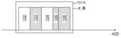
도 1a는 실리콘 옥사이드 막이 원자 층 증착을 통해 증착되는 프로세스 플로우를 예시하고, 여기서 불순물 감소가 원자 층 증착 사이클의 일부로서 포함된다.
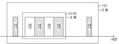
도 1b는 실리콘 옥사이드 막이 원자 층 증착을 통해 증착되는 프로세스 플로우를 예시하고, 여기서 불순물 감소는 다수의 원자 층 증착 사이클들 후에 주기적으로 수행된다.
도 1c는 실리콘 옥사이드 막이 억제-기반 증착 스킴 (scheme) 을 통해 증착되는 프로세스 플로우를 도시하고, 여기서 불순물 감소는 실리콘 옥사이드 막을 증착하는 동안 주기적으로 수행된다.
도 1d는 실리콘 옥사이드 막이 증착-에칭-증착 스킴을 통해 증착되는 프로세스 플로우를 예시하고, 여기서 불순물 감소는 실리콘 옥사이드 막을 증착하는 동안 주기적으로 수행된다.
도 1e는 실리콘 옥사이드 막이 화학적 기상 증착을 통해 증착되는 프로세스 플로우를 도시하고, 여기서 불순물 감소는 실리콘 옥사이드 막을 증착하는 동안 주기적으로 수행된다.
도 2는 본 명세서에 기술된 방법들을 구현하기 위해 사용될 수도 있는 예시적인 프로세스 스테이션을 도시한다.
도 3은 본 명세서에 기술된 방법들을 구현하기 위해 사용될 수도 있는 예시적인 멀티-스테이션 프로세싱 툴을 예시한다.
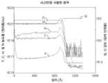
도 4a 내지 도 4c는 실리콘 옥사이드 막이 일부 방법들을 사용하여 증착된 상이한 불순물들의 농도와 관련된 실험 결과들을 도시한다.
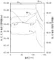
도 5a 및 도 5b는 실리콘 옥사이드 막이 주기적인 불순물 감소 없이 증착된 (도 5a) 그리고 주기적인 불순물 감소 단계를 사용하여 증착된 (도 5b) 상이한 불순물들의 농도와 관련된 실험 결과들을 도시한다.
도 6은 불순물 감소가 없는 프로세스와 불순물 감소가 일어나는 프로세스를 비교하는, 다양한 불순물들의 농도 (원자%) 를 나타낸다.
도 7a 및 도 7b는 본 명세서에 기술된 불순물 감소가 수소-관련 피크들의 감소 (도 7a) 및 실리콘-산소 관련 피크들의 증가 (도 7b) 를 발생시킨다는 것을 나타내는 (suggest) 실험적 FTIR 데이터를 도시한다.1A illustrates a process flow in which a silicon oxide film is deposited via atomic layer deposition, where impurity reduction is included as part of the atomic layer deposition cycle.
1B illustrates a process flow in which a silicon oxide film is deposited via atomic layer deposition, where impurity reduction is performed periodically after multiple atomic layer deposition cycles.
1C shows a process flow in which a silicon oxide film is deposited via a suppression-based deposition scheme, where impurity reduction is performed periodically during silicon oxide film deposition.
1D illustrates a process flow in which a silicon oxide film is deposited via a deposition-etch-deposition scheme, where impurity reduction is performed periodically during deposition of the silicon oxide film.
1E shows a process flow in which a silicon oxide film is deposited via chemical vapor deposition, wherein impurity reduction is performed periodically during deposition of the silicon oxide film.
2 shows an example process station that may be used to implement the methods described herein.
3 illustrates an example multi-station processing tool that may be used to implement the methods described herein.
4A-4C show experimental results related to concentrations of different impurities in which a silicon oxide film was deposited using some methods.
5A and 5B show experimental results related to concentrations of different impurities in which silicon oxide films were deposited without cyclic impurity reduction (FIG. 5A) and deposited using a cyclic impurity reduction step (FIG. 5B).
6 shows the concentration (atomic %) of various impurities comparing a process without impurity reduction and a process in which impurity reduction occurs.
7A and 7B show experimental FTIR data that suggest that the impurity reduction described herein results in a decrease in hydrogen-related peaks ( FIG. 7A ) and an increase in silicon-oxygen related peaks ( FIG. 7B ). .
이하의 기술 (description) 에서, 제시된 실시 예들의 완전한 이해를 제공하기 위해 수많은 구체적 상세들이 제시된다. 개시된 실시 예들은 이들 구체적인 상세들 중 일부 또는 전부 없이 실시될 수도 있다. 다른 예들에서, 공지된 프로세스 동작들은 개시된 실시 예들을 불필요하게 모호하게 하지 않기 위해 상세히 기술되지 않았다. 개시된 실시 예들이 구체적인 실시 예들과 함께 기술될 것이지만, 이는 개시된 실시 예들을 제한하는 것으로 의도되지 않았다는 것이 이해될 것이다.In the following description, numerous specific details are set forth to provide a thorough understanding of the presented embodiments. The disclosed embodiments may be practiced without some or all of these specific details. In other instances, well known process operations have not been described in detail in order not to unnecessarily obscure the disclosed embodiments. Although the disclosed embodiments will be described in conjunction with specific embodiments, it will be understood that this is not intended to limit the disclosed embodiments.
실리콘-함유 재료들은 일반적으로 반도체 디바이스들의 제조 동안 증착된다. 예시적인 실리콘-함유 재료들은 실리콘 옥사이드, 실리콘 옥시나이트라이드, 실리콘 나이트라이드, 실리콘 카보나이트라이드, 실리콘 옥시카바이드, 실리콘 카보하이드라이드를 포함한다. 실리콘-함유 재료들은 도핑되거나 도핑되지 않을 수도 있다. 도핑된 재료들은 붕소 및/또는 인과 같은 도펀트들을 포함한다. 다수의 상이한 증착 프로세스들이 이용 가능하다. 많은 경우들에서, 증기-기반 증착 프로세스들이 사용된다. 예시적인 증기-기반 증착 프로세스들은 예를 들어, 원자 층 증착 (atomic layer deposition; ALD), 플라즈마 강화된 원자 층 증착 (plasma enhanced atomic layer deposition; PEALD), 화학적 기상 증착 (chemical vapor deposition; CVD), 플라즈마 강화된 화학적 기상 증착 (plasma enhanced chemical vapor deposition; PECVD), 리모트 플라즈마 화학적 기상 증착 (remote plasma chemical vapor deposition; RPCVD), 리모트 플라즈마 원자 층 증착 (remote plasma atomic layer deposition; RPALD), 유도 커플링 플라즈마 화학적 기상 증착 (inductively coupled plasma chemical vapor deposition; ICP-CVD) 또는 고 밀도 플라즈마 화학적 기상 증착 (high density plasma chemical vapor deposition; HDP-CVD) 등을 포함한다. 일부 경우들에서, 더 복잡한 증착 스킴들 (schemes) 이 사용될 수도 있고, 이는 에칭, 억제, 및/또는 패시베이션과 같은 다른 동작들과 함께 순환 증착 동작들을 포함할 수도 있다.Silicon-containing materials are commonly deposited during the manufacture of semiconductor devices. Exemplary silicon-containing materials include silicon oxide, silicon oxynitride, silicon nitride, silicon carbonitride, silicon oxycarbide, silicon carbonhydride. Silicon-containing materials may be doped or undoped. Doped materials include dopants such as boron and/or phosphorus. A number of different deposition processes are available. In many cases, vapor-based deposition processes are used. Exemplary vapor-based deposition processes include, for example, atomic layer deposition (ALD), plasma enhanced atomic layer deposition (PEALD), chemical vapor deposition (CVD), Plasma enhanced chemical vapor deposition (PECVD), remote plasma chemical vapor deposition (RPCVD), remote plasma atomic layer deposition (RPALD), inductively coupled plasma It includes inductively coupled plasma chemical vapor deposition (ICP-CVD) or high density plasma chemical vapor deposition (HDP-CVD). In some cases, more complex deposition schemes may be used, which may include cyclic deposition operations along with other operations such as etching, suppression, and/or passivation.
불행히도, 이들 증착 프로세스들 중 다수는 실리콘-함유 막 내로 불순물의 실질적인 혼입을 발생시킨다. 이들 불순물들은 예를 들어, 불소, 탄소, 수소 및 질소를 포함할 수 있다. 이들 원소들은 형성될 디바이스들의 다양한 물리적 특성 및 전기적 특성에 부정적으로 영향을 줄 수도 있다. 예를 들어, 실리콘 옥사이드 내의 이러한 불순물들은 상대적으로 더 높은 습식 에칭 레이트를 유발할 수 있고, 이는 더 낮은 품질의 실리콘 옥사이드 막과 상관된다. 또한, 이들 불순물들의 존재는 디바이스들의 누설 전류 및 브레이크 다운 전압에 부정적으로 영향을 줄 수 있고, 이러한 막들을 전기적 절연 목적들에 적합하지 않게 만든다.Unfortunately, many of these deposition processes result in substantial incorporation of impurities into the silicon-containing film. These impurities may include, for example, fluorine, carbon, hydrogen and nitrogen. These elements may negatively affect various physical and electrical properties of the devices to be formed. For example, these impurities in silicon oxide can cause relatively higher wet etch rates, which correlate with lower quality silicon oxide films. Also, the presence of these impurities can negatively affect the leakage current and breakdown voltage of devices, making these films unsuitable for electrical isolation purposes.
탄소, 수소, 및 질소는 실리콘-함유 막을 증착하기 위해 사용되는 전구체들의 결과로서 실리콘-함유 막 내로 도입될 수도 있다. 예를 들어, 아미노실란-기반 전구체들은 기상 증착 기법들에서 일반적으로 사용된다. 이들 아미노실란-기반 전구체들은 목표된 실리콘에 더하여 탄소, 수소, 및 질소를 포함한다. 실리콘 옥사이드를 증착하기 위한 통상적인 증착 조건들 하에서, 상당한 양의 이러한 탄소, 수소, 및 질소는 증착 동안 실리콘 옥사이드 막에 바람직하지 않게 통합된다.Carbon, hydrogen, and nitrogen may be introduced into the silicon-containing film as a result of precursors used to deposit the silicon-containing film. For example, aminosilane-based precursors are commonly used in vapor deposition techniques. These aminosilane-based precursors contain carbon, hydrogen, and nitrogen in addition to the targeted silicon. Under typical deposition conditions for depositing silicon oxide, significant amounts of this carbon, hydrogen, and nitrogen are undesirably incorporated into the silicon oxide film during deposition.
탄소, 수소 및 질소 불순물들을 감소시키기 위해 다양한 동작들이 취해질 수 있다. 예를 들어, 증착 조건들은 불순물들의 혼입을 최소화하도록 제어될 수 있다. 일 특정한 예에서, 실리콘 옥사이드 막 내의 불순물들의 농도는 상대적으로 고온들 (예를 들어, 약 900 ℃ 이상) 에서 증착함으로써 감소될 수 있다. 그러나, 높은 증착 온도들은 일부 경우들에서 지나치게 제한될 수 있다.Various actions can be taken to reduce carbon, hydrogen and nitrogen impurities. For example, deposition conditions may be controlled to minimize incorporation of impurities. In one particular example, the concentration of impurities in the silicon oxide film can be reduced by depositing at relatively high temperatures (eg, about 900° C. or higher). However, high deposition temperatures may be overly restrictive in some cases.
또 다른 예에서, 할로겐-기반 실리콘-함유 전구체가 아미노실란-기반 전구체 대신 사용될 수도 있다. 예시적인 할로겐-기반 실리콘-함유 전구체들은 실리콘 테트라클로라이드 (SiCl4), 디클로로실란 (SiH2Cl2), 디요오드실란 (SiH2I2), 등을 포함하지만, 이로 제한되지 않는다. 많은 이러한 할로겐-기반 실리콘-함유 전구체들은, 특히 트리스(디메틸아미노)실란 (또한 3DMAS로 지칭되고, 화학식 C6H19N3Si를 가짐) 과 같은 일반적인 아미노실란-기반 전구체들과 비교하여 탄소, 질소, 및/또는 수소를 거의 또는 전혀 함유하지 않는다. 예를 들어, 디클로로실란 및 디요오드실란 각각은 2 개의 수소들을 포함하지만, Si:H의 비는 1:2로 상대적으로 높다. 대조적으로, 트리스(디메틸아미노)실란에서, Si:H의 비는 1:19로 훨씬 더 낮다. 할로겐-기반 실리콘-함유 전구체들이 아미노실란-기반 전구체들보다 상대적으로 더 적은 탄소, 질소 및 수소를 포함하기 때문에, 증착 동안 실리콘 옥사이드 막 내로 이들 원소들의 혼입이 더 적다. 그러나, 할로겐 종은 증착이 일어나는 프로세싱 챔버 내의 금속들을 공격하는 것으로 공지되고, 그리고 프로세싱 챔버로부터 에칭된 금속은 프로세싱될 기판들 상에 증착될 수 있다. 이와 같이, 할로겐-기반 전구체 방법들은 구현하기 어렵고 그리고 프로세싱 장비의 열화 및 기판들 상에서 불량한 결함 성능을 유발할 수 있다.In another example, a halogen-based silicon-containing precursor may be used instead of an aminosilane-based precursor. Exemplary halogen-based silicon-containing precursors include, but are not limited to, silicon tetrachloride (SiCl4 ), dichlorosilane (SiH2 Cl2 ), diiodosilane (SiH2 I2 ), and the like. Many of these halogen-based silicon-containing precursors, especially compared to common aminosilane-based precursors such as tris(dimethylamino)silane (also referred to as 3DMAS and having the formula C6 H19 N3 Si), contain carbon, contains little or no nitrogen, and/or hydrogen. For example, dichlorosilane and diiodosilane each contain two hydrogens, but the Si:H ratio is relatively high at 1:2. In contrast, in tris(dimethylamino)silane, the Si:H ratio is much lower at 1:19. Because halogen-based silicon-containing precursors contain relatively less carbon, nitrogen and hydrogen than aminosilane-based precursors, there is less incorporation of these elements into the silicon oxide film during deposition. However, halogen species are known to attack metals within the processing chamber in which deposition takes place, and metal etched from the processing chamber may deposit on substrates to be processed. As such, halogen-based precursor methods are difficult to implement and can lead to degradation of processing equipment and poor defect performance on substrates.
실리콘-함유 막 내의 불소 불순물들은 다수의 상이한 소스들로부터 유래될 수도 있다. 많은 경우들에서, 불소-함유 화학 물질은 증착이 일어나는 프로세싱 챔버를 세정하기 위해 주기적으로 사용된다. 이 세정은 내부 챔버 표면들 상의 막 빌드업 (buildup) 의 제거를 타깃할 (target) 수도 있다. 잔류 불소는 세정 동작 후에 챔버 표면들 상에 남을 수도 있고, 그리고 챔버 내에 증착된 실리콘 옥사이드 막에 남을 수 있다 (end up). 불소가 챔버 세정 동작을 통해 도입되기 때문에, 이 세정은 실리콘 옥사이드 막을 형성하도록 사용된 증착 스킴과 무관하게 실리콘 옥사이드 막 내에 불소의 혼입을 야기할 수 있다는 것이 이해된다. 또한, 이들 또는 다른 경우들에서, 실리콘-함유 막은 기판을 NF3 또는 다른 불소-함유 화학 물질에 노출시키는 것을 수반하는 특정한 증착 스킴을 사용하여 증착될 수도 있다. 이 불소-함유 화학 물질은 실리콘 옥사이드가 높은 깊이:폭 종횡비를 가질 수도 있는 리세스된 피처들 내에 증착되는, 갭 충진의 맥락에서 특히 유용하다. 이들 피처들은 피처들 내에 보이드들 또는 심들 (seams) 의 형성 없이 균일한 방식으로 충진하기 매우 어려울 수 있다. 일 예에서, 증착-에칭-증착 ("dep-etch-dep (deposition-etch-deposition)") 스킴이 사용되며, 증착, 에칭, 및/또는 패시베이션 동작들은 피처가 실리콘-함유 재료로 충진될 때 서로 순환된다. 에칭은 피처들을 폐쇄하지 않고 그리고 보이드들을 형성하지 않고 추가의 실리콘-함유 재료 증착을 허용하도록 피처가 충분히 개방된 채로 남는 것을 보장한다. 그러나, 에칭 동작(들)은 통상적으로 기판을 NF3 또는 다른 불소-함유 화학 물질에 노출시키는 것을 수반하고, 이는 실리콘-함유 막 내로 불소의 혼입을 발생시킨다.Fluorine impurities in a silicon-containing film may originate from a number of different sources. In many cases, a fluorine-containing chemical is used periodically to clean the processing chamber where deposition takes place. This cleaning may target the removal of film buildup on the interior chamber surfaces. Residual fluorine may remain on the chamber surfaces after the cleaning operation and may end up in the silicon oxide film deposited in the chamber. Since fluorine is introduced through the chamber cleaning operation, it is understood that this cleaning can cause incorporation of fluorine into the silicon oxide film regardless of the deposition scheme used to form the silicon oxide film. Additionally, in these or other cases, the silicon-containing film may be deposited using a particular deposition scheme that involves exposing the substrate to NF3 or other fluorine-containing chemistry. This fluorine-containing chemistry is particularly useful in the context of gap filling, where silicon oxide is deposited in recessed features that may have a high depth:width aspect ratio. These features can be very difficult to fill in a uniform manner without the formation of voids or seams within the features. In one example, a “dep-etch-dep (deposition-etch-deposition)” scheme is used, wherein deposition, etching, and/or passivation operations occur when the feature is filled with a silicon-containing material. circulate with each other Etching ensures that the feature remains sufficiently open to permit additional silicon-containing material deposition without closing the features and without forming voids. However, the etching operation(s) typically involves exposing the substrate to NF3 or other fluorine-containing chemistries, which result in incorporation of fluorine into the silicon-containing film.
또 다른 예에서, 억제-기반 증착 스킴이 사용되고, 억제, 증착, 및/또는 패시베이션 동작들은 피처가 실리콘-함유 재료로 충진될 때 서로 순환된다. 이 증착 스킴은 억제제-제어된 노출 (inhibitor-controlled exposure; ICE) 증착으로 지칭될 수도 있다. 억제는 피처의 상단에서 또는 상단 근방에서 증착을 선택적으로 억제하도록 기판을 NF3 또는 유사한 화학 물질에 노출하여, 보이드들 또는 심들의 형성 없이 피처를 충진하는 보텀-업 (bottom-up) 충진 메커니즘을 촉진하는 것을 수반한다. 증착-에칭-증착 스킴 및 억제-기반 증착 스킴 모두 NF3 또는 유사한 화학 물질에 대한 주기적인 노출을 수반하지만, NF3는 사용된 다른 프로세싱 조건들에 따라 상이한 효과들 (예를 들어, 에칭 대 억제) 을 가질 수도 있다는 것이 이해된다.In another example, a suppression-based deposition scheme is used, and suppression, deposition, and/or passivation operations are cycled with each other when a feature is filled with a silicon-containing material. This deposition scheme may be referred to as inhibitor-controlled exposure (ICE) deposition. Inhibition exposes the substrate to NF3 or a similar chemical to selectively inhibit deposition at or near the top of the feature, thereby creating a bottom-up fill mechanism that fills the feature without the formation of voids or seams. involves promoting Deposition-etch-deposition and inhibition-based deposition schemes both involve periodic exposure to NF3 or a similar chemistry, but NF3 exhibits different effects (e.g., etch vs. inhibition) depending on the other processing conditions used. ) is understood.
어느 경우든, NF3 또는 다른 불소-함유 화학 물질에 대한 기판의 노출은 실리콘-함유 막 내에 불소 불순물들의 혼입을 발생시킨다. 불소 불순물들을 감소시키기 위해, 상기 언급된 바와 같이, 아르곤, 수소 (H2), 및 산소 (O2) 로부터 생성된 플라즈마에 기판을 노출하는 것을 수반하는, 불순물 감소가 없는 패시베이션 동작이 사용될 수도 있다. 플라즈마는 통상적으로 상대적으로 고농도의 산소를 갖는다. 일 예에서, H2의 4-스테이션 챔버에 대한 플로우 레이트는 약 2 slm이고, O2의 4-스테이션 챔버에 대한 플로우 레이트는 약 2 slm이고, 그리고 Ar의 4-스테이션 챔버에 대한 플로우 레이트는 약 10 slm이다. 플라즈마는 통상적으로 (예를 들어, 300 ㎜ 기판을 프로세싱하기 위해 각각 4 개의 스테이션들을 갖는 챔버에 대해) 약 1250 W 내지 약 2500 W 의 RF 전력으로 생성되고, 그리고 기판은 각각의 반복 동안 약 5 내지 약 10 초의 지속 기간 동안 플라즈마에 노출된다. 4-스테이션 챔버에 대한 반응 챔버의 압력은 약 1 Torr 내지 약 10 Torr, 또는 약 2 Torr일 수도 있다. 불순물 감소가 없는 이 패시베이션 동작이 증착 동안 사용될 때, 막 내의 불소 함량은 패시베이션 동작이 없는 것보다 더 낮다. 예를 들어, 실리콘-함유 재료가 증착-에칭-증착 메커니즘 또는 억제-기반 증착 메커니즘을 통해 증착되는 다양한 경우들에서, 패시베이션 동작은 약 10 배 또는 100 배만큼 막 내의 불소 함량을 낮출 수도 있다. 예로서, 이러한 막들에 대한 통상적인 불소 농도들은 약 1E18 내지 약 1E21 원자들/cc, 또는 약 1E18 내지 약 1E20 원자들/cc이고, 가장 높은 불소 농도들은 종종 증착 동작들이 중단되고 그리고 에칭 또는 억제 동작이 사용되는 계면들/막 깊이들에서 발견된다. 실험 결과들은 이하에 더 기술된다.In either case, exposure of the substrate to NF3 or other fluorine-containing chemical causes incorporation of fluorine impurities into the silicon-containing film. To reduce fluorine impurities, a no-impurity reduction passivation operation, as noted above, may be used that involves exposing the substrate to a plasma generated from argon, hydrogen (H2 ), and oxygen (O2 ). . Plasma typically has a relatively high concentration of oxygen. In one example, the flow rate of H2 over the 4-station chamber is about 2 slm, the flow rate of O2 over the 4-station chamber is about 2 slm, and the flow rate of Ar over the 4-station chamber is It is about 10 slm. Plasma is typically generated with an RF power of about 1250 W to about 2500 W (e.g., for a chamber with 4 stations each to process a 300 mm substrate), and the substrate is between about 5 to about 2500 W for each iteration. It is exposed to plasma for a duration of about 10 seconds. The pressure of the reaction chamber for a 4-station chamber may be from about 1 Torr to about 10 Torr, or about 2 Torr. When this passivation operation without impurity reduction is used during deposition, the fluorine content in the film is lower than without passivation operation. For example, in various cases where the silicon-containing material is deposited via a deposition-etch-deposition mechanism or a suppression-based deposition mechanism, the passivation operation may lower the fluorine content in the film by a factor of about 10 or 100 times. By way of example, typical fluorine concentrations for such films are from about 1E18 to about 1E21 atoms/cc, or from about 1E18 to about 1E20 atoms/cc, with the highest fluorine concentrations often at which deposition operations are stopped and etching or suppression operations are found at the interfaces/film depths used. Experimental results are further described below.
불순물 감소 없이 패시베이션 동작으로 달성된 불소 함량의 감소는 유리하다. 그러나, 패시베이션을 사용하더라도, 불소 농도는 많은 적용 예들에 대해 목표된 것보다 더 높고, 그리고 실리콘-함유 막의 불소 함량을 더 감소시키는 것이 유리할 것이다.The reduction in fluorine content achieved with the passivation operation without impurity reduction is advantageous. However, even with passivation, the fluorine concentration is higher than desired for many applications, and it would be advantageous to further reduce the fluorine content of the silicon-containing film.
때때로 패시베이션 동작으로 지칭되는, 막 내의 불소 함량을 실질적으로 감소시키기 위해 사용될 수 있는, 불순물 감소 동작을 통합하기 위한 방법들 및 장치들이 본 명세서에 제공된다. 특정한 개시된 실시 예들은 상기 기술된 바와 같이 불순물 감소가 없는 패시베이션 동작과 상이한 프로세싱 조건들을 사용한다. 예를 들어, 본 명세서에 기술된 바와 같은 불순물 감소 동작은 불순물 감소가 없는 패시베이션 동작과 비교하여 부가적인 10 배 내지 100 배만큼 막 내의 불소 함량을 더 감소시킬 수 있다. 다양한 경우들에서, 불순물 감소 동작을 사용한 증착은 약 1E16 원자들/cc 정도의 불소 함량을 갖는 실리콘 옥사이드 막을 생성할 수도 있다.Methods and apparatus are provided herein for incorporating an impurity reduction operation, sometimes referred to as a passivation operation, that can be used to substantially reduce the fluorine content in a film. Certain disclosed embodiments use different processing conditions than the passivation operation without impurity reduction as described above. For example, an impurity reduction operation as described herein can further reduce the fluorine content in a film by an additional 10 to 100 times compared to a passivation operation without impurity reduction. In various cases, deposition using an impurity reduction operation may produce a silicon oxide film with a fluorine content on the order of about 1E16 atoms/cc.
불순물 감소 동작은 리세스된 피처들에 실리콘-함유 재료를 증착하는 맥락에서 실시될 수도 있다 (예를 들어, 약 1:1만큼 낮은 깊이:폭 종횡비를 갖는 피처들과 같은 저 종횡비 피처들, 약 100:1만큼 높은 깊이:폭 비를 갖는 피처들과 같은 고 종횡비 피처들, 및 약 이들 값들의 범위의 종횡비를 갖는 리세스된 피처들). 불순물 감소 동작은 또한 실리콘 옥사이드와 같은 실리콘-함유 재료의 블랭킷 막을 증착하는 맥락에서 실시될 수도 있다. 예시적인 애플리케이션들은 NAND 애플리케이션, DRAM 애플리케이션, 로직 애플리케이션, PCRAM 애플리케이션, 및 MRAM 애플리케이션에서 SiO2 (일부 경우들에서 SiO2/SiN) 증착을 포함한다.The impurity reduction operation may be practiced in the context of depositing a silicon-containing material in recessed features (e.g., low aspect ratio features, such as features having a depth:width aspect ratio as low as about 1:1, about high aspect ratio features, such as features with depth:width ratios as high as 100:1, and recessed features with aspect ratios in the range of about these values). Impurity reduction operations may also be performed in the context of depositing a blanket film of silicon-containing material, such as silicon oxide. Example applications include SiO2 (SiO2 /SiN) deposition in NAND applications, DRAM applications, logic applications, PCRAM applications, and MRAM applications.
유리하게, 불순물 감소 동작은 또한 실리콘-함유 막들에서 탄소 함량, 수소 함량, 및 질소 함량을 감소시키는 효과를 갖는다. 이와 같이, 불순물 감소 동작은 아미노실란-기반 전구체들 및/또는 상기 기술된 증착 기법들을 사용하여 이전에 달성 가능한 것보다 실질적으로 더 순수한 실리콘-함유 막들을 생성한다.Advantageously, the impurity reduction operation also has the effect of reducing the carbon content, hydrogen content, and nitrogen content in silicon-containing films. As such, the impurity reduction operation produces substantially purer silicon-containing films than previously achievable using aminosilane-based precursors and/or the deposition techniques described above.
또한, 불순물 감소 동작은 불순물 감소 없이 패시베이션 동작을 위해 요구되는 것보다 실질적으로 더 적은 시간에 수행될 수 있다. 즉, 불순물 감소 동작은 더 적은 시간에 더 우수한 결과들 (예를 들어, 불순물들의 더 많은 감소) 을 달성한다. 그 결과, 개별 사이클 시간들 및 전체 증착 시간들은 상당히 감소되고, 특정한 증착 장치들에 대한 증가된 쓰루풋 (throughput) 을 야기한다. 이는 상당한 개선이다.Also, the impurity reduction operation can be performed in substantially less time than required for a passivation operation without impurity reduction. That is, the impurity reduction operation achieves better results (eg, greater reduction of impurities) in less time. As a result, individual cycle times and overall deposition times are significantly reduced, resulting in increased throughput for certain deposition devices. This is a significant improvement.
증착 방법들deposition methods
특정한 개시된 실시 예들은 ALD를 수반할 수도 있다. ALD는 순차적인 자기-제한 (self-limiting) 반응들을 사용하여 재료의 박층들을 증착하는 기법이다. ALD 프로세스들은 사이클들에서 층 단위 (layer-by-layer basis) 로 막들을 증착하도록 표면-매개된 (surface-mediated) 증착 반응들을 사용한다. 일 예로서, ALD 사이클은 다음 동작들: (i) 전구체의 전달/흡착, (ii) 챔버로부터 전구체의 퍼지 (purge), (iii) 제 2 반응 물질의 전달 및 플라즈마의 선택 가능한 (optional) 점화 (ignition), 및 (iv) 챔버로부터 부산물들의 퍼지를 포함할 수도 있다. 기판의 표면 상에 막을 형성하기 위해 흡착된 전구체와 제 2 반응 물질 사이의 반응은 막 조성 및 특성들, 예컨대 불균일도 (nonuniformity), 응력, 습식 (wet) 에칭 레이트, 건식 (dry) 에칭 레이트, 전기적 특성들 (예를 들어, 파괴 전압 (breakdown voltage) 및 누설 전류), 등에 영향을 준다.Certain disclosed embodiments may involve ALD. ALD is a technique that deposits thin layers of material using sequential self-limiting reactions. ALD processes use surface-mediated deposition reactions to deposit films on a layer-by-layer basis in cycles. As an example, an ALD cycle includes the following operations: (i) delivery/adsorption of precursor, (ii) purge of precursor from the chamber, (iii) delivery of second reactant and optional ignition of plasma. (ignition), and (iv) purge of byproducts from the chamber. The reaction between the adsorbed precursor and the second reactant to form a film on the surface of the substrate depends on film composition and properties such as nonuniformity, stress, wet etch rate, dry etch rate, electrical properties (eg, breakdown voltage and leakage current), and the like.
CVD 기법과 달리, ALD 프로세스들은 층 단위로 막들을 증착하도록 표면-매개된 증착 반응들을 사용한다. ALD 프로세스의 일 예에서, 표면 활성 사이트들 (sites) 의 집단 (population) 을 포함하는 기판 표면은 기판을 하우징하는 챔버에 제공된 일 도즈 (dose) 의, 실리콘-함유 전구체와 같은 제 1 전구체의 가스상 (gas phase) 분포에 노출된다. 제 1 전구체의 물리 흡착된 (physisorbed) 분자들 및/또는 화학 흡착된 (chemisorbed) 종을 포함하는, 이 제 1 전구체의 분자들은 기판 표면 상으로 흡착된다. 본 명세서에 기술된 바와 같이 화합물이 기판 표면 상에 흡착될 때, 흡착된 층은 화합물뿐만 아니라 화합물의 유도체들도 포함할 수도 있다는 것이 이해되어야 한다. 예를 들어, 실리콘-함유 전구체의 흡착된 층은 실리콘-함유 전구체뿐만 아니라 실리콘-함유 전구체의 유도체들도 포함할 수도 있다. 제 1 전구체 도즈 후, 대부분 또는 흡착된 종만이 남도록 가스상으로 남아 있는 제 1 전구체의 대부분 또는 전부를 제거하도록 이어서 챔버가 배기된다 (evacuate). 일부 구현 예들에서, 챔버는 완전히 배기되지 않을 수도 있다. 예를 들어, 가스상의 제 1 전구체의 분압이 반응을 완화시키기에 충분히 낮도록 반응기는 배기될 수도 있다. 제 2 반응 물질, 예컨대 산소-함유 가스는 이들 분자들 중 일부가 표면 상에 흡착된 제 1 전구체와 반응하도록 챔버로 도입된다. 일부 프로세스들에서, 제 2 전구체는 흡착된 제 1 전구체와 즉시 반응한다. 다른 실시 예들에서, 제 2 반응 물질은 활성화 소스가 일시적으로 인가된 후에만 반응한다. 이어서 챔버는 결합되지 않은 (unbound) 제 2 반응 물질 분자들을 제거하기 위해 다시 배기될 수도 있다. 상기 기술된 바와 같이, 일부 실시 예들에서 챔버는 완전히 배기되지 않을 수도 있다. 막 두께를 축적하도록 부가적인 ALD 사이클들이 사용될 수도 있다.Unlike CVD techniques, ALD processes use surface-mediated deposition reactions to deposit films layer by layer. In one example of an ALD process, a substrate surface comprising a population of surface active sites is exposed to a gaseous phase of a dose of a first precursor, such as a silicon-containing precursor, provided to a chamber housing the substrate. (gas phase) distribution. Molecules of the first precursor, including physisorbed molecules and/or chemisorbed species of the first precursor, are adsorbed onto the substrate surface. It should be understood that when a compound is adsorbed onto a substrate surface as described herein, the adsorbed layer may include the compound as well as derivatives of the compound. For example, the adsorbed layer of silicon-containing precursor may include the silicon-containing precursor as well as derivatives of the silicon-containing precursor. After the first precursor dose, the chamber is then evacuated to remove most or all of the first precursor remaining in the gas phase so that most or only the adsorbed species remain. In some implementations, the chamber may not be completely evacuated. For example, the reactor may be evacuated so that the partial pressure of the gaseous first precursor is low enough to moderate the reaction. A second reactant, such as an oxygen-containing gas, is introduced into the chamber such that some of its molecules react with the first precursor adsorbed on the surface. In some processes, the second precursor reacts immediately with the adsorbed first precursor. In other embodiments, the second reactant reacts only after an activation source is temporarily applied. The chamber may then be evacuated again to remove unbound second reactant molecules. As described above, in some embodiments the chamber may not be completely evacuated. Additional ALD cycles may be used to build up film thickness.
일부 구현 예들에서, ALD 방법들은 플라즈마 활성화를 포함한다. 본 명세서에 기술된 바와 같이, 본 명세서에 기술된 ALD 방법들 및 장치들은 2011년 4월 11일 출원되고, 명칭이 "PLASMA ACTIVATED CONFORMAL FILM DEPOSITION"인 미국 특허 출원 번호 제 13/084,399 호 (현재 미국 특허 번호 제 8,728,956 호) 및 2011년 4월 11일 출원되고, 명칭이 "SILICON NITRIDE FILMS AND METHODS"인 미국 특허 출원 번호 제 13/084,305 호에 포괄적으로 기술된, 컨포멀한 막 증착 (Conformal Film Deposition; CFD) 방법들일 수도 있고, 이들 전체는 참조로서 본 명세서에 인용된다.In some implementations, ALD methods include plasma activation. As described herein, the ALD methods and apparatus described herein are disclosed in U.S. Patent Application Serial No. 13/084,399, filed April 11, 2011, entitled "PLASMA ACTIVATED CONFORMAL FILM DEPOSITION" (now U.S. Patent Application Serial No. 8,728,956) and U.S. Patent Application Serial No. 13/084,305, filed April 11, 2011, entitled "SILICON NITRIDE FILMS AND METHODS", Conformal Film Deposition ;CFD) methods, all of which are incorporated herein by reference.
도 1a 내지 도 1e는 다양한 실시 예들에서 사용될 수도 있는 다수의 증착 스킴들을 예시한다. 각각의 예시적인 증착 스킴은 단독으로 또는 도 1a 내지 도 1e에 도시된 임의의 하나 이상의 다른 증착 스킴들과 조합하여 수행될 수 있다. 도 1a는 불순물 감소 동작을 포함하도록 수정된 ALD 사이클 (101A) 을 도시한다. x-축은 시간을 나타낸다. 이 예에서, ALD 사이클 (101A) 은 도즈 동작 (102), 이어서 선택 가능한 퍼지 동작 (103), 이어서 산화 동작 (104), 이어서 불순물 감소 동작 (105), 이어서 제 2 선택 가능한 퍼지 동작 (106) 을 포함한다. 불순물 감소가 없는 ALD에서, 불순물 감소 동작 (105) 은 생략된다.1A-1E illustrate a number of deposition schemes that may be used in various embodiments. Each exemplary deposition scheme can be performed alone or in combination with any one or more of the other deposition schemes shown in FIGS. 1A-1E. Figure 1A shows an ALD cycle 101A modified to include an impurity reduction operation. The x-axis represents time. In this example, ALD cycle 101A includes a
도 1a의 실시 예를 실시할 때, 제 1 반응 물질 (예를 들어, 아미노실란-기반 전구체와 같은 실리콘-함유 전구체) 이 도즈 동작 (102) 동안 반응 챔버에 제공된다. 제 1 반응 물질은 기판의 표면 상에 흡착된다. 과잉의 제 1 반응 물질은 퍼지 동작 (103) 동안 반응 챔버로부터 제거될 수도 있다. 이는 흡착된 층을 제거하지 않고 제 1 반응 물질을 제거하기 위해 프로세스 챔버를 퍼지하고 그리고/또는 배기함으로써 수행될 수 있다. 퍼지는 질소 (N2), 아르곤 (Ar), 네온 (Ne), 헬륨 (He), 수소 (H2) 및 이들의 조합들과 같은 임의의 불활성 가스를 사용하여 행해질 수 있다.In practicing the embodiment of FIG. 1A , a first reactant material (eg, a silicon-containing precursor such as an aminosilane-based precursor) is provided to the reaction chamber during a
제 2 반응 물질 (예를 들어, 산소-함유 반응 물질) 이 산화 동작 (104) 동안 기판에 제공되고, 그리고 제 1 반응 물질 및 제 2 반응 물질은 실리콘-함유 재료를 형성하도록 기판의 표면 상에서 서로 반응한다. 일부 경우들에서, 열 에너지는 제 1 반응 물질과 제 2 반응 물질 사이의 반응을 구동하도록 사용된다. 다른 경우들에서, 플라즈마 에너지가 이 반응을 구동하도록 사용될 수도 있다.A second reactant (e.g., an oxygen-containing reactant) is provided to the substrate during
이하에 더 논의된 바와 같이, 기판은 불순물 감소 동작 (105) 동안 불순물 감소 플라즈마에 노출된다. 과잉의 반응 물질들 및 부산물들은 제 2 퍼지 동작 (106) 동안 반응 챔버로부터 제거된다. 제 2 퍼지 동작 (106) 은 퍼지 동작 (103) 에 대해 상기 기술된 임의의 프로세스 조건들을 수반할 수도 있다. 퍼지 동작 (103) 및 제 2 퍼지 동작 (106) 은 불활성 가스로 반응 챔버를 배기 및/또는 스윕핑 (sweep) 하는 것을 수반할 수도 있다. 도 1a의 ALD 사이클 (101A) 은 목표된 막 두께를 달성하기 위해 임의의 횟수로 (예를 들어, 도 1a에서 X 회) 반복될 수도 있다.As discussed further below, the substrate is exposed to an impurity reducing plasma during
유사한 실시 예에서, 불순물 감소 동작 (105) 은 도 1의 ALD 사이클 (101A) 동안 상이한 시간에 발생할 수도 있다. 일반적으로, 불순물 감소 동작 (105) 은 도즈 동작 (102) 의 후속하는 반복 전에, 퍼지 동작 (106) 전, 퍼지 동작 (106) 동안 또는 퍼지 동작 (106) 후에 발생할 수도 있다.In a similar embodiment,
도 1b는 증착이 ALD를 통해 발생하는 또 다른 예를 예시한다. 이 예에서, ALD 사이클 (101B) 은 도즈 동작 (102), 퍼지 동작 (103), 산화 동작 (104), 및 제 2 퍼지 동작 (106) 을 포함한다. 이들 동작들은 상기 기술된 동작들과 유사하고, 부가적인 막 두께를 빌드업하기 위해 임의의 횟수로 (예를 들어, 도 1b에서 X 회) 반복될 수도 있다. ALD 사이클 (101B) 이 X 회 반복된 후, 불순물 감소 동작 (105) 이 수행된다. ALD 사이클 (101B) 및 불순물 감소 동작 (105) (참조 번호 (150) 참조) 은 함께 임의의 횟수로 (예를 들어, 도 1b에서 Y 회) 반복될 수도 있다. 불순물 감소 동작 (105) 을 더 빈번하게 수행하는 것은 더 많은 불순물 감소를 발생시킬 수도 있지만, 이는 또한 증가된 프로세싱 시간 및 감소된 쓰루풋을 발생시킨다. 도 1b에 따라 증착이 발생하는 다양한 실시 예들에서, X는 약 1 내지 약 20일 수도 있고, Y는 약 1 내지 약 100일 수도 있다. Y는 목표된 최종 막 두께를 달성하도록 선택될 수도 있다. 도 1b의 방법의 특정한 실시 예에서, 증착 레이트는 대략 1 Å/사이클이고, X = 20이고, 그리고 Y = 100이고, 대략 2000 Å의 총 두께를 갖는 막을 생성한다.1B illustrates another example where deposition occurs via ALD. In this example,
이들 또는 다른 실시 예들에서, 불순물 감소 동작 (105) 은 사이클 각각에서 증착된 막의 두께에 기초한 주파수로, 주기적으로 발생할 수도 있다. 일 예에서, 불순물 감소 동작 (105) 은 1 ㎚의 실리콘-함유 막 각각이 증착된 후 반복될 수도 있다 (예를 들어, 1 ㎚의 실리콘-함유 막을 증착하고, 불순물 감소 동작 (105) 을 수행하고, 반복한다). 더 일반적으로, 불순물 감소 동작 (105) 은 실리콘-함유 막의 0.1 내지 2 ㎚ 부분/두께 각각이 증착된 후 반복될 수도 있다. 실리콘-함유 막이 블랭킷 막으로서 증착되는 경우, 블랭킷 막의 두께가 사용될 수도 있다. 실리콘-함유 막이 리세스된 피처 내에 증착되는 경우, 막의 두께는 피처의 하단으로부터 상향으로 측정될 수도 있다.In these or other embodiments, the
도 1c는 예를 들어 갭 충진의 맥락에서, 증착이 억제-기반 메커니즘 (예를 들어, ICE) 을 통해 발생하는 일 예를 도시한다. 프로세스는 억제 동작 (110) 으로 시작되고, 기판은 리세스된 피처들의 하단 및 중간과 비교하여 기판 표면 상의 리세스된 피처들의 상단 근방에서 증착을 선택적으로 억제하도록 NF3 또는 유사한 화학 물질에 노출된다. 다음에, 도즈 동작 (102), 퍼지 동작 (103), 산화 동작 (104), 및 퍼지 동작 (106) 을 포함하는 ALD 사이클 (101B) 이 수행된다. ALD 사이클 (101B) 은 임의의 횟수로 (예를 들어, 도 1c에서 X 회) 반복될 수도 있다. 다음에, 이하에 더 기술된 바와 같이, 불순물 감소 동작 (105) 이 수행된다. 불순물 감소 동작 (105) 은 불순물 감소가 없는 패시베이션 동작 대신 수행될 수도 있다. 도 1c의 예에서, 불순물 감소 동작 (105) 은 또한 억제 동작 (110) 으로부터 유래된, 기판 상에 존재하는 모든 남아 있는 억제제 종을 완전히 제거하도록 작용한다. 억제제 종은 ALD 사이클들 (101B) 동안 천천히 부식되지만; 그러나, 일부 억제제 종은 통상적으로 남아 있다. 모든 남아 있는 억제제 종을 완전히 스트립핑 제거함으로써 (stripping away), 불순물 감소 동작 (105) 은 피처의 측벽들 (예를 들어, 특히 억제 종이 존재하는 상부 측벽들) 을 원래의 억제되지 않은 상태로 복원한다 (restore). 이는 후속하는 억제 동작 (110) 이 억제를 위해 상부 측벽들을 타깃하는 균일하고, 재현 가능한 방식으로 수행될 수 있다는 것을 보장한다.1C shows an example where deposition occurs via an inhibition-based mechanism (eg, ICE), eg in the context of gap filling. The process begins with inhibit
억제 동작 (110), ALD 사이클 (101B), 및 불순물 감소 동작 (105) (참조 번호 (152) 참조) 은 함께 임의의 횟수로 (예를 들어, 도 1c에서 Z 회) 반복될 수도 있다. 도 1b의 메커니즘에서와 같이, 불순물 감소 동작 (105) 의 주파수를 증가시키는 것은 더 긴 프로세싱 시간들 및 더 낮은 쓰루풋을 희생하여 더 많은 불순물 감소를 발생시킬 수도 있다. 도 1c에 도시된 방법에 따라 증착이 발생하는 다양한 실시 예들에서, X는 약 1 내지 약 10일 수도 있고, Z는 약 1 내지 약 100일 수도 있다. 이들 또는 다른 실시 예들에서, 불순물 감소 동작 (105) 은 사이클 각각에서 증착된 막의 두께에 기초한 주파수로, 주기적으로 발생할 수도 있다. 일 예에서, 불순물 감소 동작 (105) 은 1 ㎚의 실리콘-함유 막 각각이 증착된 후 반복될 수도 있다 (예를 들어, 1 ㎚의 실리콘-함유 막을 증착하고, 불순물 감소 동작 (105) 을 수행하고, 반복한다). 더 일반적으로, 불순물 감소 동작 (105) 은 각각 실리콘-함유 막의 약 0.1 ㎚ 내지 약 20 ㎚ 또는 약 0.1 ㎚ 내지 약 10 ㎚ 부분/두께가 증착된 후 반복될 수도 있다. 실리콘-함유 재료가 리세스된 피처 내에 증착되는 경우, 실리콘-함유 막의 두께는 피처의 하단으로부터 상향으로 측정될 수도 있다.
도 1d는 예를 들어 갭 충진의 맥락에서 증착이 증착-에칭-증착 메커니즘을 통해 발생하는 일 예를 예시한다. 프로세스는 X 회 수행될 수도 있는 ALD 사이클 (101B) 로 시작된다. 다음에, 에칭 동작 (120) 이 리세스된 피처들 내에 이전에 증착된 실리콘-함유 재료를 부분적으로 에칭하여 피처들이 증착 과정 동안 폐쇄되지/막히지 (clog) 않는다는 것을 보장한다. 에칭 동작 (120) 은 다양한 실시 예들에서 플라즈마 형태로 제공될 수도 있는 NF3 또는 다른 에칭 화학 물질 (예를 들어, 종종 불소-함유 화학 물질) 에 기판을 노출하는 것을 수반할 수도 있다. ALD 사이클 (101B) 및 에칭 동작 (120) (참조 번호 (153) 참조) 은 함께 임의의 횟수로 (예를 들어, 도 1d에서 Y 회) 반복될 수도 있다. 다음에, 이하에 더 기술된 바와 같이, 불순물 감소 동작 (105) 이 수행된다. ALD 사이클 (101B), 에칭 동작 (120), 및 불순물 감소 동작 (105) (참조 번호 (154) 참조) 은 함께 임의의 횟수로 (예를 들어, 도 1d에서 Z 회) 반복될 수도 있다. 도 1d에 도시된 방법에 따라 증착이 발생하는 다양한 실시 예들에서, X는 약 1 내지 약 1000일 수도 있고, Y는 약 1 내지 약 1000일 수도 있고, 그리고 Z는 약 2 내지 약 5일 수도 있다. X는 Y와 동일하거나 상이할 수도 있다. 많은 경우들에서, X는, 실리콘-함유 막의 대부분 (예를 들어, 적어도 약 50 %, 적어도 약 75 %, 또는 적어도 약 90 %) 이 에칭 동작 (120) 및 불순물 감소 동작 (105) 이 발생하기 전에 증착되도록 Y보다 더 크다. 다양한 경우들에서, X는 충진될 피처의 사이즈에 기초하여 결정될 수도 있다.1D illustrates an example where deposition occurs via a deposition-etch-deposition mechanism, for example in the context of gap filling. The process begins with
이들 또는 다른 실시 예들에서, 불순물 감소 동작 (105) 은 사이클 각각에서 증착된 막의 두께에 기초한 주파수로, 주기적으로 발생할 수도 있다. 일반적으로, 불순물 감소 동작 (105) 은 각각 실리콘-함유 막의 약 0.1 ㎚ 내지 약 20 ㎚ 또는 약 0.1 ㎚ 내지 약 10 ㎚ 부분/두께가 증착된 후 반복될 수도 있다. 실리콘-함유 막이 리세스된 피처 내에 증착되는 경우, 막의 두께는 피처의 하단으로부터 상향으로 측정될 수도 있다.In these or other embodiments, the
도 1e는 증착이 화학적 기상 증착을 통해 발생하는 일 예를 예시한다. 방법은 실리콘-함유 반응 물질 및 산소-함유 반응 물질이, 서로 반응하고 그리고 기판의 표면 상에 실리콘-함유 재료를 증착하는, 반응 챔버로 동시에 전달되는 반응 물질 전달 동작 (130) 으로 시작된다. 반응은 열 에너지 또는 플라즈마 에너지에 의해 구동될 수도 있다. 다음에, 이하에 더 논의된 바와 같이, 불순물 감소 동작 (105) 이 수행된다. 반응 물질 전달 동작 (130) 및 불순물 감소 동작 (105) (참조 번호 (155) 참조) 은 임의의 횟수로 (예를 들어, 도 1e에서 X 회) 반복될 수도 있다. 도 1e에 도시된 방법에 따라 증착이 발생하는 다양한 실시 예들에서, X는 약 1 내지 약 1000, 예를 들어 약 1 내지 약 100 또는 약 1 내지 약 10일 수도 있다. 이들 또는 다른 실시 예들에서, 불순물 감소 동작 (105) 은 사이클 각각에서 증착된 막의 두께에 기초한 주파수로, 주기적으로 발생할 수도 있다. 일 예에서, 불순물 감소 동작 (105) 은 10 ㎚의 실리콘-함유 막 각각이 증착된 후 반복될 수도 있다 (예를 들어, 10 ㎚의 실리콘-함유 막을 증착하고, 불순물 감소 동작 (105) 을 수행하고, 반복한다). 더 일반적으로, 불순물 감소 동작 (105) 은 각각 실리콘-함유 막의 약 0.1 ㎚ 내지 약 20 ㎚ 또는 약 0.1 ㎚ 내지 약 10 ㎚ 부분/두께가 증착된 후 반복될 수도 있다.1E illustrates an example where deposition occurs via chemical vapor deposition. The method begins with a reactant
ALD 및 CVD 실시 예들이 상기 기술되었지만, 특정한 개시된 실시 예들이 플라즈마를 수반하는 임의의 증착 프로세스로 구현될 수도 있다는 것이 이해될 것이다. 비-제한적인 예들은 RPCVD, RPALD, ICP-CVD, 및 HDP-CVD를 포함한다. 다양한 실시 예들에서, 단일 반응 물질만이 플라즈마-기반 분위기에서 막을 형성하도록 사용될 수도 있고 불순물 감소 동작이 막 내의 불순물들을 감소시키도록 여전히 사용될 수 있다.Although ALD and CVD embodiments have been described above, it will be appreciated that certain disclosed embodiments may be implemented with any deposition process involving a plasma. Non-limiting examples include RPCVD, RPALD, ICP-CVD, and HDP-CVD. In various embodiments, only a single reactive material may be used to form a film in a plasma-based atmosphere and an impurity reduction operation may still be used to reduce impurities in the film.
불순물 감소 동작을 위한 프로세스 조건들Process Conditions for Impurity Reduction Operation
다양한 실시 예들에서, 불순물 감소 동작은 불활성 가스 및 수소 (예를 들어, H2) 를 포함하는 플라즈마 생성 가스로부터 생성된 플라즈마에 기판을 노출하는 것을 수반한다. 플라즈마 생성 가스는 실질적으로 산소 (예를 들어, O2 및 다른 산소-함유 종) 가 없다. 본 명세서에 사용된 바와 같이, 산소가 "실질적으로 없는" 플라즈마 생성 가스는 미량의 산소를 가질 수도 있지만; 그러나, 산소 및 산소-함유 종은 플라즈마 생성 가스의 일부로서 의도적으로 제공되지 않는다. 다양한 실시 예들에서, 불활성 가스는 아르곤을 포함한다. 대안적으로 또는 부가적으로, 다른 비활성 가스들 (noble gases) (예를 들어, 헬륨, 네온, 크립톤, 등) 이 일부 경우들에서 사용될 수도 있다. 일부 경우들에서, 플라즈마 생성 가스는 질소 (예를 들어, N2) 를 더 포함할 수도 있다. 불활성 가스에 대한 4-스테이션 챔버에 대한 예시적인 플로우 레이트들은 약 2 내지 약 60 slm일 수도 있다. 일부 경우들에서, 불활성 가스에 대한 플로우 레이트는 적어도 약 2 slm, 적어도 약 5 slm, 적어도 약 10 slm, 적어도 약 20 slm, 적어도 약 30 slm, 또는 적어도 약 40 slm일 수도 있다. 이들 또는 다른 경우들에서, 불활성 가스의 플로우 레이트는 약 60 slm 이하, 약 50 slm 이하, 약 40 slm 이하, 약 30 slm 이하, 또는 약 20 slm 이하일 수도 있다. 수소 (예를 들어, H2) 에 대한 예시적인 플로우 레이트들은 약 0.5 slm 내지 약 5 slm일 수도 있다. 일부 경우들에서, 수소의 플로우 레이트는 적어도 약 0.5 slm, 적어도 약 0.1 slm, 적어도 약 0.5 slm, 적어도 약 1 slm, 적어도 약 2 slm, 또는 적어도 약 3 slm일 수도 있다. 이들 또는 다른 경우들에서, 수소의 플로우 레이트는 약 5 slm 이하, 약 4.5 slm 이하, 약 4 slm 이하, 또는 약 3.5 slm 이하일 수도 있다. 사용되는 경우, 질소 (예를 들어, N2) 에 대한 예시적인 플로우 레이트들은 최대 약 30 slm, 일부 경우들에서 최대 약 20 slm, 또는 최대 약 10 slm일 수도 있다.In various embodiments, the impurity reduction operation involves exposing the substrate to a plasma generated from a plasma generating gas comprising an inert gas and hydrogen (eg, H2 ). The plasma generating gas is substantially free of oxygen (eg, O2 and other oxygen-containing species). As used herein, a plasma producing gas that is “substantially free” of oxygen may have trace amounts of oxygen; However, oxygen and oxygen-containing species are not intentionally provided as part of the plasma generating gas. In various embodiments, the inert gas includes argon. Alternatively or additionally, other noble gases (eg, helium, neon, krypton, etc.) may be used in some cases. In some cases, the plasma generating gas may further include nitrogen (eg, N2 ). Exemplary flow rates for a 4-station chamber for an inert gas may be from about 2 to about 60 slm. In some cases, the flow rate for the inert gas may be at least about 2 slm, at least about 5 slm, at least about 10 slm, at least about 20 slm, at least about 30 slm, or at least about 40 slm. In these or other cases, the flow rate of the inert gas may be about 60 slm or less, about 50 slm or less, about 40 slm or less, about 30 slm or less, or about 20 slm or less. Exemplary flow rates for hydrogen (eg, H2 ) may be between about 0.5 slm and about 5 slm. In some cases, the flow rate of hydrogen may be at least about 0.5 slm, at least about 0.1 slm, at least about 0.5 slm, at least about 1 slm, at least about 2 slm, or at least about 3 slm. In these or other cases, the flow rate of hydrogen may be about 5 slm or less, about 4.5 slm or less, about 4 slm or less, or about 3.5 slm or less. If used, exemplary flow rates for nitrogen (eg, N2 ) may be up to about 30 slm, in some cases up to about 20 slm, or up to about 10 slm.
플라즈마는 4 개의 스테이션들을 갖는 챔버에 대해 약 1000 및 약 6000 W 또는 약 1000 및 약 5000 W (13.56 ㎒ 용량 커플링 플라즈마에 대한 HF RF), 및 약 0 W 및 약 5000 W 또는 0 W 및 약 3000 W 또는 약 0 W 및 약 2000 W (400 ㎑ (또는 50 ㎑ 내지 2 ㎒) 플라즈마에 대한 LF RF) 를 포함하는 RF 전력에서 생성될 수도 있다. 즉, RF 전력은 단일 주파수 (HF 만) 또는 듀얼 주파수 (예를 들어, HF 및 LF) 로 제공될 수도 있다. 일부 경우들에서, 13.56 ㎒ 용량 커플링 플라즈마에 대한 HF RF는 4 개의 스테이션들을 갖는 챔버에 대해 적어도 약 1000 W, 또는 적어도 약 2000 W, 또는 적어도 약 3000 W의 전력 레벨로 제공될 수도 있다. 이들 또는 다른 경우들에서, 13.56 ㎒ 용량 커플링 플라즈마에 대한 HF RF는 4 개의 스테이션을 갖는 챔버에 대해 약 6000 W 이하, 약 5000 W 이하, 일부 경우들에서 약 4000 W 이하, 또는 약 3000 W 이하의 전력 레벨로 제공될 수도 있다. 이들 또는 다른 경우들에서, LF RF는 생략될 수도 있다. 다른 실시 예들에서, 400 ㎑ (또는 50 ㎑ 내지 2 ㎒) 플라즈마에 대한 LF RF는 4 개의 스테이션들을 갖는 챔버에 대해 적어도 약 1 W, 적어도 약 10 W, 적어도 약 50 W, 적어도 약 100 W, 적어도 약 500 W, 또는 적어도 약 1000 W의 전력 레벨로 제공될 수도 있다. 이들 또는 다른 경우들에서, 400 ㎑ (또는 50 ㎑ 내지 2 ㎒) 플라즈마에 대한 LF RF는 4 개의 스테이션들을 갖는 챔버에 대해 약 5000 W 이하, 또는 약 3000 W 이하, 또는 약 2000 W 이하, 예를 들어, 1500 W 이하, 또는 1000 W 이하, 또는 500 W 이하, 또는 200 W 이하의 전력 레벨로 제공될 수도 있다. 이들 전력 레벨들은 약 300 ㎜의 직경을 갖는 기판에 적합하고, 그리고 상이한 사이즈들의 기판들에 따라 적절히 스케일링될 (scale) 수도 있다. 예시적인 주파수들은 예를 들어, 13.56 ㎒, 27 ㎒, 및 60 ㎒를 포함하지만, 이들은 제한하는 것으로 의도되지 않는다. 플라즈마 노출 동작들 동안, 플라즈마는 약 10 % 내지 약 100 %의 듀티 사이클을 가질 수도 있다. 플라즈마는 임의의 타입의 플라즈마일 수도 있다. 일부 경우들에서, 플라즈마는 용량 커플링 플라즈마이다. 다른 경우들에서, 플라즈마는 유도 커플링 플라즈마 또는 마이크로파 플라즈마이다. 일부 실시 예들에서, 플라즈마는 리모트 플라즈마이다. 일부 실시 예들에서, 플라즈마는 전자 사이클로트론 공명 (electron cyclotron resonance; ECR) 에 의해 생성된다.The plasma is about 1000 and about 6000 W or about 1000 and about 5000 W (HF RF for 13.56 MHz capacitively coupled plasma), and about 0 W and about 5000 W or 0 W and about 3000 W for a chamber with four stations. W or about 0 W and about 2000 W (LF RF for 400 kHz (or 50 kHz to 2 MHz) plasma). That is, RF power may be provided on a single frequency (HF only) or dual frequencies (eg, HF and LF). In some cases, HF RF for a 13.56 MHz capacitively coupled plasma may be provided at a power level of at least about 1000 W, or at least about 2000 W, or at least about 3000 W for a chamber with four stations. In these or other cases, the HF RF for a 13.56 MHz capacitively coupled plasma is about 6000 W or less, about 5000 W or less, in some cases about 4000 W or less, or about 3000 W or less for a chamber with four stations. may be provided at a power level of In these or other cases, LF RF may be omitted. In other embodiments, the LF RF for a 400 kHz (or 50 kHz to 2 MHz) plasma is at least about 1 W, at least about 10 W, at least about 50 W, at least about 100 W, at least about 1 W for a chamber with four stations. It may be provided at a power level of about 500 W, or at least about 1000 W. In these or other cases, the LF RF for a 400 kHz (or 50 kHz to 2 MHz) plasma is about 5000 W or less, or about 3000 W or less, or about 2000 W or less, for a chamber with four stations, e.g. For example, it may be provided at a power level of 1500 W or less, or 1000 W or less, or 500 W or less, or 200 W or less. These power levels are suitable for a substrate with a diameter of about 300 mm, and may be scaled appropriately for substrates of different sizes. Exemplary frequencies include, for example, 13.56 MHz, 27 MHz, and 60 MHz, but these are not intended to be limiting. During plasma exposure operations, the plasma may have a duty cycle of about 10% to about 100%. The plasma may be any type of plasma. In some cases, the plasma is capacitively coupled plasma. In other cases, the plasma is an inductively coupled plasma or microwave plasma. In some embodiments, the plasma is a remote plasma. In some embodiments, the plasma is created by electron cyclotron resonance (ECR).
불순물 감소 동작 동안, 반응 챔버 내 압력은 약 0.5 내지 약 20 Torr로 유지될 수 있다. 다양한 실시 예들에서, 압력은 적어도 약 0.5 Torr, 적어도 약 1 Torr, 적어도 약 5 Torr, 또는 적어도 약 10 Torr일 수도 있다. 이들 또는 다른 경우들에서, 압력은 약 20 Torr 이하, 또는 약 15 Torr 이하, 또는 약 10 Torr 이하일 수도 있다. 기판은 온도 제어될 수도 있는 기판 지지부 상에 위치될 수도 있다. 일부 경우들에서, 기판은 불순물 감소 동작 동안, 예를 들어 기판 지지부를 통해 가열되거나 냉각될 수도 있다. 예시적인 기판 지지부 온도들은 약 -400 ℃ 내지 약 1400 ℃ 또는 약 -40 ℃ 내지 약 1000 ℃ 또는 약 150 ℃ 내지 약 650 ℃일 수도 있다. 일부 경우들에서, 기판 지지부는 적어도 약 150 ℃, 또는 적어도 약 200 ℃, 또는 적어도 약 300 ℃, 또는 적어도 약 400 ℃의 온도로 유지된다. 이들 또는 다른 경우들에서, 기판 지지부는 약 650 ℃ 이하, 또는 약 600 ℃ 이하, 또는 약 500 ℃ 이하, 또는 약 400 ℃ 이하, 또는 약 300 ℃ 이하, 또는 약 200 ℃ 이하의 온도로 유지될 수도 있다.During the impurity reduction operation, the pressure in the reaction chamber may be maintained at about 0.5 to about 20 Torr. In various embodiments, the pressure may be at least about 0.5 Torr, at least about 1 Torr, at least about 5 Torr, or at least about 10 Torr. In these or other cases, the pressure may be about 20 Torr or less, or about 15 Torr or less, or about 10 Torr or less. The substrate may be placed on a substrate support that may be temperature controlled. In some cases, the substrate may be heated or cooled during the impurity reduction operation, for example via a substrate support. Exemplary substrate support temperatures may be from about -400 °C to about 1400 °C or from about -40 °C to about 1000 °C or from about 150 °C to about 650 °C. In some cases, the substrate support is maintained at a temperature of at least about 150 °C, or at least about 200 °C, or at least about 300 °C, or at least about 400 °C. In these or other cases, the substrate support may be maintained at a temperature of about 650 °C or less, or about 600 °C or less, or about 500 °C or less, or about 400 °C or less, or about 300 °C or less, or about 200 °C or less. there is.
불순물 감소 동작 동안, 기판은 약 0.2 초 및 약 120 초 동안 플라즈마에 노출될 수도 있다. 다양한 실시 예들에서, 플라즈마 노출 지속 기간은 적어도 약 0.2 초, 또는 적어도 약 0.5 초, 또는 적어도 약 0.1 초, 또는 적어도 약 0.2 초일 수도 있다. 이들 또는 다른 실시 예들에서, 플라즈마 노출 지속 기간은 약 120 초 이하, 또는 약 10 초 이하, 또는 약 1 초 이하, 또는 약 0.5 초 이하일 수도 있다. 많은 경우들에서, 목표된 불순물 감소는 통상적으로 1 초 미만으로 매우 신속하게 달성된다. 이는 적어도 5 내지 10 초의 노출 시간을 요구하는, 상기 기술된 기존의 패시베이션 방법들에 비해 실질적인 개선 (예를 들어, 감소된 프로세싱 시간) 이다.During the impurity reduction operation, the substrate may be exposed to the plasma for about 0.2 seconds and about 120 seconds. In various embodiments, the plasma exposure duration may be at least about 0.2 seconds, or at least about 0.5 seconds, or at least about 0.1 seconds, or at least about 0.2 seconds. In these or other embodiments, the plasma exposure duration may be about 120 seconds or less, or about 10 seconds or less, or about 1 second or less, or about 0.5 seconds or less. In many cases, targeted impurity reduction is achieved very quickly, typically less than 1 second. This is a substantial improvement (eg reduced processing time) over the existing passivation methods described above, which require exposure times of at least 5 to 10 seconds.
많은 경우들에서, 불순물 감소 동작은 불순물 감소가 없는 패시베이션 동작과 비교하여, 수소 및 불활성 가스에 대해 상당히 더 높은 플로우 레이트들로 수행될 수도 있다. 불순물 감소 동작과 불순물 감소가 없는 패시베이션 동작 사이의 또 다른 차이점은 플라즈마 생성 가스에서 산소의 생략 (omission) 이다. 불순물 감소가 없는 패시베이션 동작에서, 산소는 상당한 플로우 레이트로 제공된다. 반대로, 불순물 감소 동작에서, 산소는 플라즈마 생성 가스로부터 생략된다. 또한, 불순물 감소 동작은 통상적으로 불순물 감소가 없는 패시베이션 동작보다 더 높은 RF 전력 레벨들에서 발생한다. 이러한 차이들의 결과로서, 이하의 실험 섹션에서 더 논의된 바와 같이, 불순물이 없는 패시베이션 동작과 비교하여, 불순물 감소 동작은 실리콘-함유 막으로부터 불소를 제거하는데 실질적으로 더 효과적이다 (예를 들어, 더 적은 시간에 약 10 배 내지 100 배 더 효과적임). 유리하게, 불순물 감소 동작은 또한 막 내 탄소, 수소, 및 질소의 농도를 낮춘다.In many cases, the impurity reduction operation may be performed at significantly higher flow rates for hydrogen and inert gas compared to a passivation operation without impurity reduction. Another difference between the impurity reduction operation and the passivation operation without impurity reduction is the omission of oxygen in the plasma generating gas. In passivation operation without impurity reduction, oxygen is provided at a significant flow rate. Conversely, in the impurity reduction operation, oxygen is omitted from the plasma generating gas. Also, impurity reduction operation typically occurs at higher RF power levels than passivation operation without impurity reduction. As a result of these differences, as discussed further in the Experimental section below, compared to the impurity-free passivation operation, the impurity reduction operation is substantially more effective at removing fluorine from the silicon-containing film (e.g., more about 10 to 100 times more effective in less time). Advantageously, the impurity reduction operation also lowers the concentrations of carbon, hydrogen, and nitrogen in the film.
개시된 불순물 감소 동작의 또 다른 장점은 인 시츄 (in situ) 로 수행될 수 있다는 것이다. 즉, 실리콘-함유 막이 증착되는 동일한 반응 챔버 내에서 수행될 수 있다. 불순물 감소 동작이 증착 챔버로부터 분리된 또 다른 챔버에서 발생하는 것이 가능하지만 (예를 들어, 기판이 필요에 따라 챔버들 사이에서 이송됨), 이 목적을 위해 별도의 챔버를 제공할 필요가 없다. 적절한 장치는 장치 섹션에서 이하에 더 논의된다.Another advantage of the disclosed impurity reduction operation is that it can be performed in situ. That is, it can be performed within the same reaction chamber in which the silicon-containing film is deposited. While it is possible for the impurity reduction operation to occur in another chamber separate from the deposition chamber (eg, substrates are transferred between chambers as needed), there is no need to provide a separate chamber for this purpose. Suitable devices are discussed further below in the Devices section.
불순물 감소 동작들을 위한 프로세스 조건들Process Conditions for Impurity Reduction Operations
도 1a 내지 도 1e와 관련하여 설명된 바와 같이, 본 명세서에 기술된 불순물 감소 동작은 다양한 반응 메커니즘들을 사용하여 많은 상이한 맥락들에서 실시될 수도 있다. 이와 같이, 본 명세서의 실시 예들은 증착 조건들의 특정한 세트로 제한되도록 의도되지 않는다. 그러나, 특정한 예시적인 조건들은 지침 (guidance) 으로서 제공된다.As described with respect to FIGS. 1A-1E , the impurity reduction operation described herein may be practiced in many different contexts using a variety of reaction mechanisms. As such, embodiments herein are not intended to be limited to a particular set of deposition conditions. However, certain exemplary conditions are provided as guidance.
증착이 (예를 들어, 도 1a 내지 도 1d와 관련하여 기술된 바와 같이) 원자 층 증착 사이클들을 수반하는 방법을 통해 발생하는 다양한 실시 예들에서, 다음의 반응 조건들 중 하나 이상이 사용될 수도 있다. 도즈 동작 동안, 실리콘-함유 반응 물질은 약 150 sccm 내지 약 900 sccm의 플로우 레이트로 반응 챔버에 제공될 수도 있다. 실리콘-함유 반응 물질은 기판의 표면 상에 흡착된다. 실리콘-함유 반응 물질은 실란일 수도 있고, 많은 경우에 아미노실란이다. 예시적인 아미노실란들은 이로 제한되는 것은 아니지만, 트리스(디메틸아미노)실란 (tris(dimethylamino)silane), 비스(tert-부틸아미노)실란 (bis(tert-butylamino)silane), 1,1,1,3,3,3-헥사메틸디실라잔 (1,1,1,3,3,3―hexamethyldisilazane), 고리형 (cyclic) 아자실란들, 테트라키스(디메틸아미노)실란 (tetrakis(dimethylamino)silane), 트리실릴아민 (trisilylamine), 비스(디에틸아미노)실란 (bis(diethylamino)silane), 등을 포함한다. 아미노실란은 실리콘 원자에 결합된 적어도 하나의 질소 원자를 함유하지만, 또한 수소들, 산소들, 할로겐들 및 탄소들을 함유할 수도 있다. 아미노실란들의 예들은 모노-아미노실란들 (mono-aminosilanes), 디-아미노실란들 (di-aminosilanes), 트리-아미노실란들 (tri-aminosilanes) 및 테트라-아미노실란들 (tetra-aminosilanes) (각각 H3Si(NH2)4, H2Si(NH2)2, HSi(NH2)3 및 Si(NH2)4), 뿐만 아니라 치환된 모노-아미노실란들, 디-아미노실란들, 트리-아미노실란들 및 테트라-아미노실란들, 예를 들어, t-부틸아미노실란 (t-butylaminosilane), 메틸아미노실란 (methylaminosilane), tert-부틸실란아민 (tert-butylsilanamine), 비스(tert-부틸아미노)실란 (bis(tert-butylamino)silane) (SiH2(NHC(CH3)3)2 (BTBAS)), tert-부틸실릴카바메이트 (tert-butyl silylcarbamate), SiH(CH3)-(N(CH3)2)2, SiHCl-(N(CH3)2)2, (Si(CH3)2NH)3, 디(sec-부틸아미노)실란 (di(sec-butylamino)silane; DSBAS), 디(이소프로필아미도)실란 (di(isopropylamido)silane; DIPAS), 비스(디에틸아미노)실란) (bis(diethylamino)silane; BDEAS) 등이다. 아미노실란의 추가 예는 트리실릴아민 (N(SiH3)3) 이다. 다양한 다른 실란들이 또한 사용될 수도 있다.In various embodiments in which deposition occurs via a method involving atomic layer deposition cycles (eg, as described with respect to FIGS. 1A-1D ), one or more of the following reaction conditions may be used. During the dosing operation, silicon-containing reactant material may be provided to the reaction chamber at a flow rate between about 150 sccm and about 900 sccm. A silicon-containing reactive material is adsorbed onto the surface of the substrate. The silicon-containing reactive material may be a silane, and in many cases an aminosilane. Exemplary aminosilanes include, but are not limited to, tris(dimethylamino)silane, bis(tert-butylamino)silane, 1,1,1,3 ,3,3-hexamethyldisilazane (1,1,1,3,3,3-hexamethyldisilazane), cyclic azasilanes, tetrakis(dimethylamino)silane, trisilylamine, bis(diethylamino)silane, and the like. Aminosilanes contain at least one nitrogen atom bonded to a silicon atom, but may also contain hydrogens, oxygens, halogens and carbons. Examples of aminosilanes are mono-aminosilanes, di-aminosilanes, tri-aminosilanes and tetra-aminosilanes (respectively H3 Si(NH2 )4 , H2 Si(NH2 )2 , HSi(NH2 )3 and Si(NH2 )4 ) as well as substituted mono-aminosilanes, di-aminosilanes, tri -aminosilanes and tetra-aminosilanes, e.g. t-butylaminosilane, methylaminosilane, tert-butylsilanamine, bis(tert-butylamino )silane (bis(tert-butylamino)silane) (SiH2 (NHC(CH3 )3 )2 (BTBAS)), tert-butylsilylcarbamate (tert-butyl silylcarbamate), SiH(CH3 )-(N( CH3 )2 )2 , SiHCl-(N(CH3 )2 )2 , (Si(CH3 )2 NH)3 , di(sec-butylamino)silane (DSBAS), di(isopropylamido)silane (DIPAS), bis(diethylamino)silane (BDEAS), and the like. A further example of an aminosilane is trisilylamine (N(SiH3 )3 ). A variety of other silanes may also be used.
예시적인 실리콘-함유 반응 물질들은 이로 제한되는 것은 아니지만, 실란들 (silanes), 폴리실란들 (polysilanes), 할로실란들 (halosilanes), 및 아미노실란들 (aminosilanes) 을 포함한다. 실란은 수소기 및/또는 탄소기를 함유하지만 할로겐은 함유하지 않는다. 폴리실란은 화학식 (H3Si-(SiH2)n-SiH3) 을 가질 수도 있고, 여기서 n ≥ 1이다. 실란들의 예들은 실란 (SiH4), 디실란 (Si2H6), 트리실란, 테트라실란 및 유기 실란들, 예컨대 메틸실란 (methylsilane), 에틸실란 (ethylsilane), 이소프로필실란 (isopropylsilane), t-부틸실란 (t-butylsilane), 디메틸실란 (dimethylsilane), 디에틸실란 (diethylsilane), 디-t-부틸실란 (di-t-butylsilane), 알릴실란 (allylsilane), sec-부틸실란 (sec-butylsilane), 텍실실란 (thexylsilane), 이소아밀실란 (isoamylsilane), t-부틸디실란 (t-butyldisilane), 디-t-부틸디실란 (di-t-butyldisilane), 테트라-에틸-오르토-실리케이트 (tetra-ethyl-ortho-silicate) (또한 테트라-에톡시-실란 (tetra-ethoxy-silane) 또는 TEOS로 공지됨) 등을 포함한다.Exemplary silicon-containing reactive materials include, but are not limited to, silanes, polysilanes, halosilanes, and aminosilanes. Silanes contain hydrogen and/or carbon groups but no halogens. The polysilane may have the formula (H3 Si-(SiH2 )n -SiH3 ), where n ≥ 1. Examples of silanes include silane (SiH4 ), disilane (Si2 H6 ), trisilane, tetrasilane and organic silanes such as methylsilane, ethylsilane, isopropylsilane, t -Butylsilane (t-butylsilane), dimethylsilane (dimethylsilane), diethylsilane (diethylsilane), di-t-butylsilane (di-t-butylsilane), allylsilane (allylsilane), sec-butylsilane (sec-butylsilane ), thexylsilane, isoamylsilane, t-butyldisilane, di-t-butyldisilane, tetra-ethyl-ortho-silicate (tetra -ethyl-ortho-silicate) (also known as tetra-ethoxy-silane or TEOS); and the like.
예시적인 실리콘-함유 반응 물질들은 폴리실란들 (H3Si-(SiH2)n-SiH3) (n ≥ 1), 예컨대 실란, 디실란, 트리실란, 테트라실란; 및 트리실릴아민을 포함한다:Exemplary silicon-containing reactive materials include polysilanes (H3 Si-(SiH2 )n -SiH3 ) (n ≥ 1) such as silane, disilane, trisilane, tetrasilane; and trisilylamine:

일부 실시 예들에서, 실리콘-함유 반응 물질은 알콕시실란이다. 사용될 수도 있는 알콕시실란들은 이로 제한되지 않지만, 다음을 포함한다:In some embodiments, the silicon-containing reactant is an alkoxysilane. Alkoxysilanes that may be used include, but are not limited to:
Hx-Si-(OR)y, 여기서 x = 1 내지 3, x+y = 4이고, R은 치환되거나 치환되지 않은 알킬기이고; 그리고Hx -Si-(OR)y , where x = 1 to 3, x+y = 4, R is a substituted or unsubstituted alkyl group; and
Hx(RO)y-Si-Si-(OR)yHx, 여기서 x = 1 내지 2, x+y = 3이고 R은 치환되거나 치환되지 않은 알킬기이다.Hx (RO)y -Si-Si-(OR)y Hx , where x = 1 to 2, x+y = 3 and R is a substituted or unsubstituted alkyl group.
실리콘-함유 반응 물질들의 예들은: 메틸실란; 트리메틸실란 (3MS); 에틸실란; 부타실란들; 펜타실란들; 옥타실란들; 헵타실란들; 헥사실란들; 사이클로부타실란; 사이클로헵타실란; 사이클로헥사실란; 사이클로옥타실란; 사이클로펜타실란; 1,4-디옥사-2,3,5,6-테트라실라사이클로헥산; DEMS (diethoxymethylsilane); DES (diethoxysilane); 디메톡시메틸실란; 디메톡시실란 (DMOS); MDES (methyl-diethoxysilane); MDMS (methyl-dimethoxysilane); 옥타메톡시도데카실록산 (OMODDS); tert-부톡시디실란; TMCTS (tetramethylcyclotetrasiloxane); TOMCTS (tetraoxymethylcyclotetrasiloxane); TES (triethoxysilane); 트리에톡시실록산 (TRIES); 및 트리메톡시실란 (TMS 또는 TriMOS) 을 포함한다.Examples of silicon-containing reactive materials are: methylsilane; trimethylsilane (3MS); ethylsilane; butasilanes; pentasilanes; octasilanes; heptasilanes; hexasilanes; cyclobutasilane; cycloheptasilane; Cyclohexasilane; cyclooctasilane; cyclopentasilane; 1,4-dioxa-2,3,5,6-tetrasilacyclohexane; diethoxymethylsilane (DEMS); diethoxysilane (DES); dimethoxymethylsilane; dimethoxysilane (DMOS); methyl-diethoxysilane (MDES); methyl-dimethoxysilane (MDMS); octamethoxydodecasiloxane (OMODDS); tert-butoxydisilane; tetramethylcyclotetrasiloxane (TMCTS); TOMCTS (tetraoxymethylcyclotetrasiloxane); triethoxysilane (TES); triethoxysiloxane (TRIES); and trimethoxysilane (TMS or TriMOS).
일부 실시 예들에서, 실리콘-함유 전구체는 수소 원자들을 갖는 아미노실란, 예컨대 비스디에틸아미노실란, 디이소프로필아미노실란, 비스(tert-부틸아미노)실란 (BTBAS), 또는 트리스(디메틸아미노)실란 (3DMAS) 일 수도 있다. 아미노실란 전구체들은 이로 제한되지 않지만, 다음을 포함한다: Hx-Si-(NR)y 여기서 x = 1 내지 3, x + y = 4이고 R은 유기기 또는 하이드라이드기이다.In some embodiments, the silicon-containing precursor is an aminosilane having hydrogen atoms, such as bisdiethylaminosilane, diisopropylaminosilane, bis(tert-butylamino)silane (BTBAS), or tris(dimethylamino)silane ( 3DMAS). Aminosilane precursors include, but are not limited to: Hx -Si-(NR)y where x = 1 to 3, x + y = 4 and R is an organic or hydride group.
일부 실시 예들에서, 실란이 적어도 하나의 할로겐 원자를 포함하도록 할로겐-함유 실란 또는 할로실란이 사용될 수도 있다. 할로실란은 화학식 SiXaHy를 가질 수도 있고, 여기서 X = Cl, F, I, 또는 Br이고, a+y = 4이고, 여기서 a ≥ 1이다. 할로실란은 화학식 SiXaHy(CH3)z를 가질 수도 있고, 여기서 X = Cl, F, I, 또는 Br이고, 그리고 a+y+z = 4이고, 여기서 a ≥ 1이다. 할로실란들의 예들은 요오드실란들 (iodosilanes), 브로모실란들 (bromosilanes), 클로로실란들 (chlorosilanes) 및 플루오로실란들 (fluorosilanes) 이다. 할로실란들, 특히 플루오로실란들은, 실리콘 재료들을 에칭할 수 있는 반응성 할라이드 종을 형성할 수도 있지만, 본 명세서에 기술된 특정한 실시 예들에서, 플라즈마가 스트라이킹될 (strike) 때 실리콘-함유 전구체는 존재하지 않는다. 특정한 클로로실란들은 테트라클로로실란 (tetrachlorosilane) (SiCl4), 트리클로로실란 (trichlorosilane) (HSiCl3), 디클로로실란 (dichlorosilane) (H2SiCl2), 모노클로로실란 (monochlorosilane) (ClSiH3), 클로로알릴실란 (chloroallylsilane), 클로로메틸실란 (chloromethylsilane), 디클로로메틸실란 (dichloromethylsilane), 클로로디메틸실란 (chlorodimethylsilane), 클로로에틸실란 (chloroethylsilane), t-부틸클로로실란 (t-butylchlorosilane), 디-t-부틸클로로실란 (di-t-butylchlorosilane), 클로로이소프로필실란 (chloroisopropylsilane), 클로로-sec-부틸실란 (chloro-sec-butylsilane), t-부틸디메틸클로로실란 (t-butyldimethylchlorosilane), 덱실디메틸클로로실란 (thexyldimethylchlorosilane), 모노클로로트리메틸실란 (monochlorotrimethylsilane) 등이다.In some embodiments, a halogen-containing silane or halosilane may be used such that the silane contains at least one halogen atom. The halosilane may have the formula SiXa Hy , where X = Cl, F, I, or Br, and a+y = 4, where a ≥ 1. The halosilane may have the formula SiXa Hy (CH3 )z , where X = Cl, F, I, or Br, and a+y+z = 4, where a ≥ 1. Examples of halosilanes are iodosilanes, bromosilanes, chlorosilanes and fluorosilanes. Halosilanes, particularly fluorosilanes, may form reactive halide species that can etch silicon materials, but in certain embodiments described herein, a silicon-containing precursor is present when a plasma is struck. I never do that. Specific chlorosilanes include tetrachlorosilane (SiCl4 ), trichlorosilane (HSiCl3 ), dichlorosilane (H2 SiCl2 ), monochlorosilane (ClSiH3 ), chlorosilane Allylsilane, chloromethylsilane, dichloromethylsilane, chlorodimethylsilane, chloroethylsilane, t-butylchlorosilane, di-t-butyl Di-t-butylchlorosilane, chloroisopropylsilane, chloro-sec-butylsilane, t-butyldimethylchlorosilane, thexyldimethylchlorosilane ), monochlorotrimethylsilane, and the like.
실리콘-함유 반응 물질들의 예들은 실록산들, 알킬 실란 또는 탄화수소-치환된 실란, 또는 질소-함유 탄소-함유 반응 물질을 포함한다. 예시적인 실록산들은 선형 실록산들, 고리형 실록산들, 및 케이지된 (cage) 실록산들을 포함한다. 예시적인 실록산들은 2,4,6,8-테트라메틸시클로테트라실록산 (2,4,6,8-tetramethylcyclotetrasiloxane; TMCTS), 헵타메틸시클로테트라실록산 (heptamethylcyclotetrasiloxane; HMCTS), 실세스퀴옥산 (silsesquioxane), 펜타메틸디실록산 (pentamethyldisiloxane; PMDSO) 및 테트라메틸디실록산 (tetramethyldisiloxane; TMDSO) 과 같은 디실록산들, 및 헥사메틸트리실록산 (hexamethyltrisiloxane), 헵타메틸트리실록산 (heptamethyltrisiloxane) 과 같은 트리실록산들을 포함한다. 알킬 실란들은 하나 이상의 알킬기들이 결합될 뿐만 아니라 하나 이상의 수소 원자들이 결합된 중심 실리콘 원자를 포함한다. 몇몇 실시 예들에서, 임의의 하나 이상의 알킬기들은 1 내지 5 개의 탄소 원자들을 함유한다. 탄화수소기들은 포화되거나 불포화될 수도 있다 (예를 들어, 알켄 (예를 들어, 비닐), 알킨, 및 방향족기들). 예들은 트리메틸실란 (3MS), 트리에틸실란, 펜타메틸 디실라메탄 ((CH3)2Si-CH2-Si(CH3)3), 및 디메틸실란 (2MS) 을 포함하지만 이로 제한되지 않는다. 부가적으로, 디실란들, 트리실란들, 또는 다른 고차 실란들이 모노실란들 대신 사용될 수도 있다. 일부 실시 예들에서, 실리콘 원자들 중 하나는 부착된 탄소-함유기 또는 탄화수소 기를 가질 수 있고, 실리콘 원자들 중 하나는 부착된 수소 원자를 가질 수 있다. 질소를 포함하는 탄소-함유 반응 물질들의 예들은 메틸-치환된 디실라잔들 및 트리실라잔들, 예컨대 테트라메틸디실라잔 및 헥사메틸트리실라잔을 포함한다.Examples of silicon-containing reactive materials include siloxanes, alkyl silanes or hydrocarbon-substituted silanes, or nitrogen-containing carbon-containing reactive materials. Exemplary siloxanes include linear siloxanes, cyclic siloxanes, and caged siloxanes. Exemplary siloxanes include 2,4,6,8-tetramethylcyclotetrasiloxane (TMCTS), heptamethylcyclotetrasiloxane (HMCTS), silsesquioxane, disiloxanes such as pentamethyldisiloxane (PMDSO) and tetramethyldisiloxane (TMDSO), and trisiloxanes such as hexamethyltrisiloxane and heptamethyltrisiloxane. Alkyl silanes contain a central silicon atom to which one or more alkyl groups are attached as well as one or more hydrogen atoms. In some embodiments, any one or more alkyl groups contain 1 to 5 carbon atoms. Hydrocarbon groups may be saturated or unsaturated (eg, alkene (eg, vinyl), alkyne, and aromatic groups). Examples include, but are not limited to, trimethylsilane (3MS), triethylsilane, pentamethyl disilamethane ((CH3 )2 Si-CH2 -Si(CH3 )3 ), and dimethylsilane (2MS). Additionally, disilanes, trisilanes, or other higher order silanes may be used instead of monosilanes. In some embodiments, one of the silicon atoms may have a carbon-containing group or hydrocarbon group attached, and one of the silicon atoms may have a hydrogen atom attached. Examples of carbon-containing reactants containing nitrogen include methyl-substituted disilazanes and trisilazanes such as tetramethyldisilazane and hexamethyltrisilazane.
실리콘-함유 반응 물질들의 예들은 헵타메틸사이클로테트라실록산 (HMCTS) 및 테트라메틸사이클로테트라실록산과 같은 사이클로테트라실록산들과 같은 실록산들을 포함한다. 다른 고리형 실록산들은 또한 이로 제한되는 것은 아니지만 사이클로트리실록산들 및 사이클로펜타실록산들을 포함할 수 있다. 산소 도핑된 탄화 실리콘 막들을 증착하기 위해, 적합한 전구체들의 다른 예들은, 이로 제한되는 것은 아니지만, 디실록산들, 예컨대 펜타메틸디실록산 (PMDSO), 테트라메틸디실록산 (TMDSO), 헥사메틸트리실록산, 및 헵타메틸트리실록산과 같은 선형 실록산들을 포함한다. 도핑되지 않은 탄화 실리콘을 위해, 적합한 전구체들의 예들은 예를 들어, 1 내지 5 개의 탄소 원자들을 함유하는 하나 이상의 알킬기, 알켄기, 및/또는 알킨기로 치환된 모노실란들을 포함한다. 예들은 트리메틸실란 (3MS), 디메틸실란 (2MS), 트리에틸실란 (TES), 및 펜타메틸디실라메탄을 포함하지만 이로 제한되지 않는다. 부가적으로, 디실란들, 트리실란들, 또는 다른 고차 실란들이 모노실란들 대신 사용될 수도 있다. 알킬 실란 분류로부터 이러한 디실란의 일 예는 헥사메틸디실란 (HMDS) 이다. 알킬 실란 분류로부터 디실란의 또 다른 예는 펜타메틸디실란 (PMDS) 을 포함할 수 있다. 다른 타입들의 알킬 실란들은 실리콘 원자에 결합된 탄소뿐만 아니라 실리콘 원자에 결합된 알킬기를 갖는 분기된 폴리머 구조를 가질 수 있는 알킬카보실란들을 포함할 수 있다. 예들은 디메틸 트리메틸실릴 메탄 (DTMSM) 및 비스-디메틸실릴 에탄 (BDMSE) 을 포함한다. 질소 도핑된 탄화 실리콘 (SiNC) 막들을 증착하기 위해, 적합한 전구체들의 예들은 예를 들어, 알킬디실라잔들 및 아마도 하나 이상의 실리콘 원자들에 개별적으로 결합된 아미노기 (-NH2) 및 알킬기를 포함하는 화합물들을 포함한다. 알킬디실라잔은 2 개의 실리콘 원자들에 결합된 실리잔들 (silizanes) 과 알킬기들을 포함한다. 예는 1,1,3,3-테트라메틸디실라잔 (TMDSN) 을 포함한다. 불활성 가스는 실리콘-함유 반응 물질과 함께 제공될 수도 있다. 일 예에서, 아르곤은 약 1 내지 20 slm의 레이트로 제공되고, 그리고 질소 (예를 들어, N2) 는 약 0 slm 내지 약 30 slm의 레이트로 제공된다. 또한, 수소 (H2) 는 약 0 slm 내지 약 5 slm의 플로우 레이트로 제공될 수도 있다. 반응 챔버 내 압력은 약 0.6 Torr 내지 약 20 Torr로 유지될 수도 있다. 기판은 약 150 ℃ 내지 약 650 ℃의 온도로 유지될 수도 있는, 온도-제어된 기판 지지부 상에 포지셔닝될 수도 있다.Examples of silicon-containing reactive materials include siloxanes such as heptamethylcyclotetrasiloxane (HMCTS) and cyclotetrasiloxanes such as tetramethylcyclotetrasiloxane. Other cyclic siloxanes may also include, but are not limited to, cyclotrisiloxanes and cyclopentasiloxanes. Other examples of suitable precursors for depositing oxygen doped silicon carbide films include, but are not limited to, disiloxanes such as pentamethyldisiloxane (PMDSO), tetramethyldisiloxane (TMDSO), hexamethyltrisiloxane, and linear siloxanes such as heptamethyltrisiloxane. For undoped silicon carbide, examples of suitable precursors include, for example, monosilanes substituted with one or more alkyl groups, alkene groups, and/or alkyne groups containing from 1 to 5 carbon atoms. Examples include, but are not limited to, trimethylsilane (3MS), dimethylsilane (2MS), triethylsilane (TES), and pentamethyldisilamethane. Additionally, disilanes, trisilanes, or other higher order silanes may be used instead of monosilanes. One example of such a disilane from the class of alkyl silanes is hexamethyldisilane (HMDS). Another example of a disilane from the class of alkyl silanes can include pentamethyldisilane (PMDS). Other types of alkyl silanes may include alkylcarbosilanes, which may have a branched polymer structure having an alkyl group bonded to a silicon atom as well as a carbon bonded to a silicon atom. Examples include dimethyl trimethylsilyl methane (DTMSM) and bis-dimethylsilyl ethane (BDMSE). For depositing nitrogen-doped silicon carbide (SiNC) films, examples of suitable precursors include, for example, alkyldisilazanes and possibly an amino group (—NH2 ) and an alkyl group individually bonded to one or more silicon atoms. It includes compounds that Alkyldisilazanes contain silizanes and alkyl groups bonded to two silicon atoms. Examples include 1,1,3,3-tetramethyldisilazane (TMDSN). An inert gas may be provided along with the silicon-containing reactive material. In one example, argon is provided at a rate of about 1 slm to about 20 slm, and nitrogen (eg, N2 ) is provided at a rate of about 0 slm to about 30 slm. Hydrogen (H2 ) may also be provided at a flow rate of about 0 slm to about 5 slm. The pressure in the reaction chamber may be maintained between about 0.6 Torr and about 20 Torr. A substrate may be positioned on a temperature-controlled substrate support, which may be maintained at a temperature of about 150 °C to about 650 °C.
퍼지 동작 및 제 2 퍼지 동작 동안, 반응 챔버는 흡착되지 않은 반응 물질들 및 반응 부산물들을 제거하기 위해 비 반응성 가스로 배기되고 그리고/또는 스윕핑될 수도 있다. 다른 가스들도 또한 퍼지 가스에 존재할 수도 있다. 일 예에서, 퍼지 가스는 약 1 slm 내지 약 20 slm의 플로우 레이트로 아르곤, 약 0 slm 내지 약 30 slm의 플로우 레이트로 질소 (예를 들어, N2), 약 0 slm 내지 약 5 slm의 플로우 레이트로 수소 (예를 들어, H2), 약 0 slm 내지 약 5 slm의 플로우 레이트로 산소 (예를 들어, O2), 및 약 0 slm 내지 약 5 slm의 플로우 레이트로 아산화질소 (예를 들어, N2O) 를 포함한다. 챔버 압력 및 기판 지지부 온도는 도즈 동작과 관련하여 상기 기술된 바와 같을 수도 있다.During the purge operation and the second purge operation, the reaction chamber may be evacuated and/or swept with a non-reactive gas to remove unadsorbed reactants and reaction by-products. Other gases may also be present in the purge gas. In one example, the purge gas is argon at a flow rate of about 1 slm to about 20 slm, nitrogen (eg, N2 ) at a flow rate of about 0 slm to about 30 slm, a flow of about 0 slm to about 5 slm hydrogen (eg, H2 ) at a flow rate, oxygen (eg, O2 ) at a flow rate of about 0 slm to about 5 slm, and nitrous oxide (eg, nitrous oxide) at a flow rate of about 0 slm to about 5 slm For example, N2 O). The chamber pressure and substrate support temperature may be as described above in relation to the dose operation.
산화 동작에서, 기판의 표면은 산화되고, RF 플라즈마로 세정된다. 적어도 하나의 산소-함유 반응 물질을 포함하는 가스들은 반응 챔버로 흐를 수도 있다. 예시적인 산소-함유 반응 물질들은 산소 (O2), 아산화질소 (N2O), 오존 (O3), 일산화탄소 (CO), 이산화탄소 (CO2), 등을 포함하지만, 이로 제한되지 않는다. 다른 가스들이 또한 제공될 수도 있다. 일 예에서, 다음의 가스들이 산화 동작 동안 제공될 수도 있다: 약 1 slm 내지 20 slm의 플로우 레이트로 아르곤, 약 0 slm 내지 약 30 slm의 플로우 레이트로 질소 (예를 들어, N2), 약 0 slm 내지 약 5 slm의 플로우 레이트로 수소 (예를 들어, H2), 약 0.5 slm 내지 약 5 slm의 플로우 레이트로 산소 (예를 들어, O2), 및 약 0 slm 내지 약 5 slm의 플로우 레이트로 아산화질소 (예를 들어, N2O). RF 전력은 4-스테이션 챔버에 대해 약 500 W 내지 약 6000 W의 범위로 제공될 수도 있다. 압력 및 온도는 도즈 동작과 관련하여 상기 기술된 바와 같을 수도 있다.In the oxidation operation, the surface of the substrate is oxidized and cleaned with RF plasma. Gases containing at least one oxygen-containing reactant may flow into the reaction chamber. Exemplary oxygen-containing reactants include, but are not limited to, oxygen (O2 ), nitrous oxide (N2 O), ozone (O3 ), carbon monoxide (CO), carbon dioxide (CO2 ), and the like. Other gases may also be provided. In one example, the following gases may be provided during the oxidation operation: argon at a flow rate of about 1 slm to 20 slm, nitrogen (eg, N2 ) at a flow rate of about 0 slm to about 30 slm, about hydrogen (eg, H2 ) at a flow rate of 0 slm to about 5 slm, oxygen (eg, O2 ) at a flow rate of about 0.5 slm to about 5 slm, and about 0 slm to about 5 slm Nitrous oxide (eg, N2 O) at flow rate. RF power may be provided in the range of about 500 W to about 6000 W for a 4-station chamber. Pressure and temperature may be as described above in relation to the dose operation.
억제 동작이 사용되는 경우들에서 (예를 들어, 도 1c의 억제 동작 (110) 참조), 다음 조건들 중 하나 이상이 억제 동작 동안 사용될 수도 있다. 억제 가스는 약 10 내지 300 sccm의 플로우 레이트로 반응 챔버에 제공될 수도 있다. 억제 가스 종의 예들은 질소 종, 할로겐 종 및 수소 종을 포함한다. 그러나, 기판 표면을 패시베이팅하고 후속 증착을 억제하기 위해 기판 표면 상에 흡착하거나, 기판 표면과 반응하거나, 그렇지 않으면 기판 표면과 상호 작용하는 임의의 종이 사용될 수도 있다. 다양한 실시 예들에서, 억제 동작은 플라즈마-기반 억제 또는 열적-기반 억제일 수도 있다. 플라즈마-기반 억제 동안, 구조체는 또한 억제 종으로 지칭되는 억제제 종을 형성하도록 억제 가스로부터 생성된 플라즈마에 노출된다. 억제 가스들의 예들은 질소-함유 가스들, 할로겐-함유 가스들, 및 수소-함유 가스들을 포함한다. 구체적인 예들은 질소 트리플루오라이드 (NF3), 분자 질소 (N2), 분자 수소 (H2), 암모니아 (NH3), 아민들, 디올들, 디아민들, 아미노알코올들, 티올들 또는 이들의 조합들을 포함한다. 일부 실시 예들에서, 억제 가스는 NF3, CHxFy (여기서 x + y = 4이고 y는 1 이상의 정수임), 및 황 헥사플루오라이드 (SF6) 와 같은 불소-함유 가스이다. 일부 실시 예들에서, 억제 동작은 열적-기반 억제 프로세스일 수도 있다. 예를 들어, 억제 동작은 억제 종이 기판의 표면과 반응하는 조건들 하에서 (예를 들어, 억제 동작 동안 기판을 플라즈마에 노출시키지 않고) 억제 종을 포함하는 가스에 구조체를 노출함으로써 수행될 수도 있다.In cases where an inhibit action is used (see, eg, inhibit
일부 실시 예들에서, 억제 플라즈마는 할로겐-함유 가스로부터 생성된다. 예들은 NF3, CH3F, CH2F2, CHF3, CF4, SF6, CH3Cl, CH2Cl2, CHCl3, 및 CCl4를 포함한다. 이는 표면을 패시베이팅하고 후속 증착을 억제하는 갭의 깊이 전반에 걸쳐 (그러나 가장 구체적으로 측벽들의 상단 근방에서) -F, -Cl, 또는 다른 할로겐 말단 표면들을 발생시킨다. 할로겐 함유 가스 또는 다른 억제 가스는 억제 동작 (110) 동안 챔버 또는 다른 플라즈마 생성 공간으로의 총 체적 플로우의 약 0.5 % 내지 10 %, 약 1 내지 약 5 %, 또는 약 2 %일 수도 있고, 남아 있는 플로우는 N2, Ar, 및 He와 같은 불활성 가스이다.In some embodiments, the suppression plasma is generated from a halogen-containing gas. Examples include NF3 , CH3 F, CH2 F2 , CHF3 , CF4 , SF6 , CH3 Cl, CH2 Cl2 , CHCl3 , and CCl4 . This creates -F, -Cl, or other halogen terminated surfaces throughout the depth of the gap (but most specifically near the top of the sidewalls) that passivate the surface and inhibit subsequent deposition. The halogen-containing gas or other suppression gas may be about 0.5% to 10%, about 1 to about 5%, or about 2% of the total volumetric flow to the chamber or other plasma generating space during
플라즈마가 사용되는 경우들에서, 플라즈마는 4-스테이션 챔버에 대해 약 500 W 내지 약 2000 W의 RF 전력 레벨에서 생성될 수도 있다. 기판은 약 0.1 초 내지 10초의 지속 기간 동안 플라즈마에 노출될 수도 있다. 기판 지지부 온도는 약 200 ℃ 내지 약 650 ℃일 수도 있다. 반응 챔버 내 압력은 약 0.6 Torr 내지 약 10 Torr일 수도 있다.In cases where a plasma is used, the plasma may be generated at an RF power level of about 500 W to about 2000 W for a 4-station chamber. The substrate may be exposed to the plasma for a duration of about 0.1 seconds to 10 seconds. The substrate support temperature may be between about 200 °C and about 650 °C. The pressure in the reaction chamber may be between about 0.6 Torr and about 10 Torr.
에칭 동작이 사용되는 경우들에서 (예를 들어, 도 1d의 에칭 동작 (120) 참조), 다음 조건들 중 하나 이상이 에칭 동작 동안 사용될 수도 있다. 에칭 가스는 약 50 sccm 내지 약 500 sccm의 플로우 레이트로 반응 챔버에 제공될 수도 있다. 일 예에서, 에칭 가스는 NF3를 포함한다. 다른 경우들에서, 다른 에칭 가스들이 사용될 수도 있다. 다양한 실시 예들에서, 에칭 가스는 질소 및/또는 할로겐, 예컨대 불소 또는 염소를 포함할 수도 있다. 다른 가스들, 예를 들어 억제 동작 (110) 과 관련하여 상기 기술된 가스들 중 하나 이상이 또한 반응 챔버에 제공될 수도 있다. 일반적으로, 많은 동일한 가스들이 억제 및 에칭을 위해 사용될 수도 있고, 더 낮은 플로우 레이트들은 통상적으로 억제를 발생시키고 그리고 더 높은 플로우 레이트들은 통상적으로 에칭을 발생시킨다. 기판은 에칭 가스 및/또는 다른 가스들로부터 생성된 플라즈마에 노출될 수도 있다. 플라즈마는 4-스테이션 챔버에 대해 약 750 W 내지 약 8000 W의 RF 전력 레벨에서 생성될 수도 있다. 기판은 약 1 초 내지 약 300 초의 지속 기간 동안 플라즈마에 노출될 수도 있다. 기판 지지부 온도는 약 200 ℃ 내지 약 650 ℃일 수도 있다. 반응 챔버 내 압력은 약 0.6 Torr 내지 약 2 Torr일 수도 있다.In cases where an etch operation is used (eg, see
증착이 화학적 기상 증착을 통해 발생하는 경우들에서 (예를 들어, 도 1e 참조), 다음 조건들 중 하나 이상이 사용될 수도 있다. 기판은 제 1 반응 물질 (예를 들어, 상기 기술된 것들 중 임의의 것과 같은 실리콘-함유 반응 물질) 및 제 2 반응 물질 (예를 들어, 상기 기술된 것들 중 임의의 것과 같은 산소-함유 반응 물질) 에 동시에 노출될 수도 있다. 동시에, 기판은 제 1 반응 물질과 제 2 반응 물질 사이의 가스 상 반응을 구동하도록 에너지 소스 (예를 들어, 열 에너지 및/또는 플라즈마 에너지) 에 노출될 수도 있다. 이 반응은 기판 표면 상에 증착되는 실리콘-함유 재료를 생성한다. 실리콘-함유 반응 물질은 약 150 sccm 내지 약 900 sccm의 플로우 레이트로 제공될 수도 있다. 산소-함유 반응 물질은 약 500 sccm 내지 약 20,000 sccm의 플로우 레이트로 제공될 수도 있다. 반응 챔버 내 압력은 약 2 Torr 내지 약 20 Torr로 유지될 수도 있다. 반응이 열 에너지에 의해 구동되는 경우, 기판 지지부는 약 550 ℃ 내지 약 650 ℃의 온도로 유지될 수도 있다. 반응이 플라즈마 에너지에 의해 구동되는 경우, 기판 지지부는 약 200 ℃ 내지 약 650 ℃의 온도로 유지될 수도 있고, 그리고 플라즈마는 4-스테이션 챔버에서 약 750 W 내지 약 5000 W의 RF 전력 레벨에서 생성될 수도 있다. 기판은 사이클 각각 동안 약 0.1 초 내지 약 10 초의 지속 기간 동안 제 1 반응 물질 및 제 2 반응 물질에, 그리고 반응을 구동하는 에너지 소스에 노출될 수도 있다 (예를 들어, 도 1e에 도시된 바와 같이, 사이클 각각은 반응 물질 전달 동작 (130) 및 불순물 감소 동작 (105) 을 포함함).In cases where deposition occurs via chemical vapor deposition (see, eg, FIG. 1E ), one or more of the following conditions may be used. The substrate comprises a first reactant material (eg, a silicon-containing reactant such as any of those described above) and a second reactant material (eg, an oxygen-containing reactant material such as any of those described above). ) may be exposed simultaneously. At the same time, the substrate may be exposed to an energy source (eg, thermal energy and/or plasma energy) to drive a gas phase reaction between the first and second reactants. This reaction creates a silicon-containing material that is deposited on the substrate surface. The silicon-containing reactant may be provided at a flow rate between about 150 sccm and about 900 sccm. The oxygen-containing reactant may be provided at a flow rate between about 500 sccm and about 20,000 sccm. The pressure in the reaction chamber may be maintained between about 2 Torr and about 20 Torr. When the reaction is driven by thermal energy, the substrate support may be maintained at a temperature of about 550 °C to about 650 °C. When the reaction is driven by plasma energy, the substrate support may be maintained at a temperature of about 200° C. to about 650° C., and a plasma may be generated at an RF power level of about 750 W to about 5000 W in a four-station chamber. may be The substrate may be exposed to the first and second reactants and to the energy source driving the reactions for a duration of about 0.1 seconds to about 10 seconds during each cycle (eg, as shown in FIG. 1E ). , each cycle including a
장치Device
본 명세서의 실시 예들은 임의의 적절한 장치 상에서 실시될 수도 있다. 적절한 장치는 적어도 프로세싱 챔버, 프로세싱 챔버 내에서 플라즈마를 생성하기 위한 플라즈마 생성기, 및 본 명세서에 기술된 방법들 중 하나 이상을 유발하도록 구성된 제어기를 포함할 것이다.The embodiments herein may be practiced on any suitable device. A suitable apparatus will include at least a processing chamber, a plasma generator for generating a plasma within the processing chamber, and a controller configured to trigger one or more of the methods described herein.
도 2는 ALD (atomic layer deposition), 및/또는 CVD (chemical vapor deposition) 중 어느 하나가 열적 에너지 또는 플라즈마 에너지에 의해 구동될 수도 있는, 재료를 증착하기 위해 사용될 수도 있는 프로세스 스테이션 (200) 의 실시 예를 개략적으로 도시한다. 프로세스 스테이션 (200) 은 예를 들어, 도 1a 내지 도 1e에 도시된 실시 예들을 포함하여, 본 명세서에 기술된 임의의 실시 예들을 실시하도록 사용될 수도 있다. 간략함을 위해, 프로세싱 스테이션 (200) 은 저압 분위기를 유지하기 위한 프로세스 챔버 바디 (202) 를 갖는 독립형 프로세스 스테이션으로서 도시된다. 그러나, 복수의 프로세스 스테이션들 (200) 이 공통 프로세스 툴 분위기에 포함될 수도 있다는 것이 이해될 것이다. 또한, 일부 실시 예들에서, 이하에 상세히 논의된 하드웨어 파라미터들을 포함하는, 프로세싱 스테이션 (200) 의 하나 이상의 하드웨어 파라미터들이 하나 이상의 컴퓨터 제어기들에 의해 프로그램적으로 조정될 수도 있다는 것이 인식될 것이다.2 is an implementation of a
프로세싱 스테이션 (200) 은 분배 샤워헤드 (206) 로 프로세스 가스들을 전달하기 위해 반응 물질 전달 시스템 (201) 과 유체로 연통한다 (fluidly communicate). 반응 물질 전달 시스템 (201) 은 샤워헤드 (206) 로 전달을 위해, 프로세스 가스들을 블렌딩 (blending) 및/또는 컨디셔닝하기 (conditioning) 위한 선택 가능한 혼합 용기 (mixing vessel) (204) 를 포함한다. 하나 이상의 혼합 용기 유입구 밸브들 (220) 은 프로세스 가스들의 혼합 용기 (204) 로의 도입을 제어할 수도 있다. 유사하게, 샤워헤드 유입구 밸브 (205) 는 샤워헤드 (206) 로의 프로세스 가스들의 도입을 제어할 수도 있다. 또 다른 예에서, 반응 물질 전달 시스템 (201) 은 챔버 바디 (202) 내부로 전달될 때까지 반응 물질들을 서로 분리하여 유지할 수도 있다.The
BTBAS와 같은 일부 반응 물질들은 기화 및 프로세스 스테이션으로의 후속 전달 전에 액체 형태로 저장될 수도 있다. 예를 들어, 도 2의 실시 예는 혼합 용기 (204) 로 공급될 액체 반응 물질을 기화시키기 위한 기화 지점 (203) 을 포함한다. 일부 실시 예들에서, 기화 지점 (203) 은 가열된 기화기일 수도 있다. 이러한 기화기들로부터 생성된 반응 물질 증기가 다운스트림 (downstream) 전달 파이핑 (piping) 에서 응결될 수도 있다. 응결된 반응 물질로의 양립할 수 없는 가스들의 노출은 작은 입자들을 생성할 수도 있다. 이들 작은 입자들은 파이핑을 막고, 밸브 동작을 방해하고 (impede), 기판들을 오염시키는, 등을할 수도 있다. 이들 문제들을 해결하기 위한 일부 접근법들은 잔류 반응 물질을 제거하기 위해 전달 파이핑을 스윕핑 및/또는 배기하는 것을 수반한다. 그러나, 전달 파이핑을 스윕핑하는 것은 프로세스 스테이션 사이클 시간을 증가시킬 수도 있어, 프로세스 스테이션 쓰루풋을 저하시킨다. 따라서, 일부 실시 예들에서, 기화 지점 (203) 의 다운스트림 전달 파이프는 열 추적될 수도 있다. 일부 예들에서, 혼합 용기 (204) 는 또한 열 추적될 수도 있다. 일 비제한적인 예에서, 기화 지점 (203) 의 다운스트림 파이프는 혼합 용기 (204) 에서 대략 100 ℃로부터 대략 150 ℃로 연장하는 상승하는 온도 프로파일을 갖는다.Some reactants, such as BTBAS, may be stored in liquid form prior to vaporization and subsequent delivery to a process station. For example, the embodiment of FIG. 2 includes a
일부 실시 예들에서, 반응 물질 액체는 액체 주입기에서 기화될 수도 있다. 예를 들어, 액체 주입기는 액체 반응 물질의 펄스들을 혼합 용기의 업스트림 (upstream) 의 캐리어 가스 스트림 내로 주입할 수도 있다. 일 시나리오에서, 액체 주입기는 더 높은 압력으로부터 더 낮은 압력으로 액체를 플래싱함으로써 (flash) 반응 물질을 기화시킬 수도 있다. 또 다른 시나리오에서, 액체 주입기는 가열된 전달 파이프 내에서 후속하여 기화되는 분산된 (disperse) 마이크로 액적들 (microdroplets) 로 액체를 원자화할 수도 있다. 더 작은 액적들은 더 큰 액적들보다 더 빠르게 기화될 수도 있고, 액체 주입과 완전한 기화 사이의 지연을 감소시킨다는 것이 인식될 것이다. 더 빠른 기화는 기화 지점 (203) 으로부터 다운스트림의 파이프 길이를 감소시킬 수도 있다. 일 시나리오에서, 액체 주입기는 혼합 용기 (204) 에 바로 장착될 수도 있다. 또 다른 시나리오에서, 액체 주입기는 샤워헤드 (206) 에 바로 장착될 수도 있다.In some embodiments, the reactant liquid may be vaporized in a liquid injector. For example, a liquid injector may inject pulses of a liquid reactant into a carrier gas stream upstream of the mixing vessel. In one scenario, the liquid injector may vaporize the reactant by flashing the liquid from a higher pressure to a lower pressure. In another scenario, a liquid injector may atomize the liquid into dispersed microdroplets that are subsequently vaporized within a heated delivery pipe. It will be appreciated that smaller droplets may vaporize faster than larger droplets, reducing the delay between liquid injection and complete vaporization. Faster vaporization may reduce the pipe length downstream from the
일부 실시 예들에서, 기화 지점 (203) 의 업스트림의 액체 유량 제어기 (liquid flow controller; LFC) 가 기화 및 프로세스 스테이션 (200) 으로의 전달을 위해 액체의 질량 유량 (mass flow) 를 제어하기 위해 제공될 수도 있다. 예를 들어, LFC는 LFC의 다운스트림에 위치된 열적 질량 유량 미터 (mass flow meter; MFM) 를 포함할 수도 있다. 이어서 LFC의 플런저 (plunger) 밸브가 MFM과 전기적으로 통신하는 PID (proportional-integral-derivative) 제어기에 의해 제공된 피드백 제어 신호들에 응답하여 조정될 수도 있다. 그러나, 이는 피드백 제어를 사용하여 액체 플로우를 안정화시키기 위해 1 초 이상 소요될 수도 있다. 이는 액체 반응 물질을 도즈하기 (dose) 위한 시간을 연장할 수도 있다. 따라서, 일부 실시 예들에서, LFC는 피드백 제어 모드와 직접 제어 모드 사이에서 동적으로 스위칭될 수도 있다. 일부 실시 예들에서, LFC는 LFC 및 PID 제어기의 센싱 튜브를 디스에이블함으로써 (disable) 피드백 제어 모드로부터 직접 제어 모드로 동적으로 스위칭될 수도 있다.In some embodiments, a liquid flow controller (LFC) upstream of the
샤워헤드 (206) 는 기판 (212) 을 향해 프로세스 가스들을 분배한다. 도 2에 도시된 실시 예에서, 기판 (212) 은 샤워헤드 (206) 밑에 위치되고, 페데스탈 (208) 상에 놓인 것으로 도시된다. 샤워헤드 (206) 는 임의의 적합한 형상을 가질 수도 있고, 기판 (212) 으로 프로세스 가스들을 분배하기 위해 임의의 적합한 수 및 배열의 포트들을 가질 수도 있다는 것이 인식될 것이다.The
일부 실시 예들에서, 마이크로볼륨 (207) 이 샤워헤드 (206) 아래에 위치된다. 프로세스 스테이션의 전체 볼륨이 아니라 마이크로볼륨에서 ALD 및/또는 CVD 프로세스를 수행하는 것은 반응 물질 노출 및 스윕핑 시간들을 감소시킬 수도 있고, 프로세스 조건들 (예를 들어, 압력, 온도, 등) 을 변경하기 위한 시간들을 감소시킬 수도 있고, 프로세스 스테이션 로봇들의 프로세스 가스들로의 노출을 제한할 수도 있는, 등을할 수도 있다. 예시적인 마이크로볼륨 사이즈들은 이로 제한되는 것은 아니지만, 0.1 리터 내지 2 리터의 체적들을 포함한다. 이 마이크로볼륨은 또한 생산성 쓰루풋에 영향을 준다. 사이클 당 증착 레이트가 떨어지지만, 사이클 시간 또한 동시에 감소한다. 특정한 경우들에서, 후자의 효과는 미리 결정된 (given) 타깃 두께의 막에 대한 모듈의 전체 쓰루풋을 개선하기에 충분히 극적이다.In some embodiments,
일부 실시 예들에서, 페데스탈 (208) 은 기판 (212) 을 마이크로볼륨 (207) 에 노출하고 그리고/또는 마이크로볼륨 (207) 의 체적을 가변시키도록 상승되거나 하강될 수도 있다. 예를 들어, 기판 이송 페이즈에서, 페데스탈 (208) 은 기판 (212) 으로 하여금 페데스탈 (208) 상으로 로딩되게 하도록 하강될 수도 있다. 증착 프로세스 페이즈 동안, 페데스탈 (208) 은 마이크로볼륨 (207) 내에 기판 (212) 을 포지셔닝시키도록 상승될 수도 있다. 일부 실시 예들에서, 마이크로볼륨 (207) 은 증착 프로세스 동안 고 플로우 (high flow) 임피던스 (impedance) 의 영역을 생성하도록 페데스탈 (208) 의 일부뿐만 아니라 기판 (212) 을 완전히 인클로징할 (enclose) 수도 있다.In some embodiments,
선택 가능하게, 페데스탈 (208) 은 마이크로볼륨 (207) 내에서 프로세스 압력, 반응 물질 농도, 등을 조절하기 위해 증착 프로세스의 부분들 동안 하강 및/또는 상승될 수도 있다. 프로세스 챔버 바디 (202) 가 증착 프로세스 동안 기준 압력으로 유지되는 일 시나리오에서, 페데스탈 (208) 을 하강시키는 것은 마이크로볼륨 (207) 으로 하여금 배기되게 할 수도 있다. 마이크로볼륨 대 프로세스 챔버 체적의 예시적인 비들은 이로 제한되는 것은 아니지만, 약 1:200 내지 약 1:10의 체적 비들을 포함한다. 일부 실시 예들에서, 페데스탈 높이는 적합한 컴퓨터 제어기에 의해 프로그램적으로 조정될 수도 있다는 것이 인식될 것이다.Optionally,
또 다른 시나리오에서, 페데스탈 (208) 의 높이를 조정하는 것은 플라즈마 밀도로 하여금 증착 프로세스에 포함된 플라즈마 활성화 및/또는 처리 사이클들 동안 가변되게 할 수도 있다. 증착 프로세스 페이즈의 종료 시, 페데스탈 (208) 은 페데스탈 (208) 로부터 기판 (212) 의 제거를 허용하도록 또 다른 기판 이송 페이즈 동안 하강될 수도 있다.In another scenario, adjusting the height of the
본 명세서에 기술된 예시적인 마이크로볼륨 변동들이 높이 조정 가능한 페데스탈을 참조하지만, 일부 실시 예들에서, 샤워헤드 (206) 의 포지션은 마이크로볼륨 (207) 의 체적을 가변시키도록 페데스탈 (208) 에 대해 조정될 수도 있다는 것이 인식될 것이다. 또한, 페데스탈 (208) 및/또는 샤워헤드 (206) 의 수직 포지션은 본 개시의 범위 내의 임의의 적합한 메커니즘에 의해 가변될 수도 있다는 것이 인식될 것이다. 일부 실시 예들에서, 페데스탈 (208) 은 기판 (212) 의 배향을 회전시키기 위한 회전 축을 포함할 수도 있다. 일부 실시 예들에서, 이들 예시적인 조정들 중 하나 이상이 하나 이상의 적합한 컴퓨터 제어기들에 의해 프로그램적으로 수행될 수도 있다는 것이 인식될 것이다.While the exemplary microvolume variations described herein refer to a height adjustable pedestal, in some embodiments, the position of
도 2에 도시된 실시 예를 다시 참조하면, 샤워헤드 (206) 및 페데스탈 (208) 은 플라즈마에 전력을 공급하기 위해 RF 전력 공급부 (214) 및 매칭 네트워크 (216) 와 전기적으로 통신한다. 일부 실시 예들에서, 플라즈마 에너지는 프로세스 스테이션 압력, 가스 농도, RF 소스 전력, RF 소스 주파수 및 플라즈마 전력 펄스 타이밍 중 하나 이상을 제어함으로써 제어될 수도 있다. 예를 들어, RF 전력 공급부 (214) 및 매칭 네트워크 (216) 는 목표된 조성의 라디칼 종을 갖는 플라즈마를 형성하도록 임의의 적합한 전력에서 동작될 수도 있다. 적합한 전력들의 예들은 상기에 포함되었다. 유사하게, RF 전력 공급부 (214) 는 임의의 적합한 주파수의 RF 전력을 제공할 수도 있다. 일부 실시 예들에서, RF 전력 공급부 (214) 는 고주파수 RF 전력 소스 및 저주파수 RF 전력 소스를 서로 독립적으로 제어하도록 구성될 수도 있다. 예시적인 저 주파수 RF 주파수들은, 이로 제한되는 것은 아니지만, 약 50 ㎑ 내지 약 200 ㎑의 주파수들을 포함할 수도 있다. 예시적인 고 주파수 RF 주파수들은, 이로 제한하는 것은 아니지만, 약 1.8 ㎒ 내지 약 2.45 ㎓의 주파수들을 포함할 수도 있다. 임의의 적합한 파라미터들은 표면 반응들을 위한 플라즈마 에너지를 제공하도록 이산적으로 (discretely) 또는 연속적으로 (continuously) 조절될 수도 있다는 것이 인식될 것이다. 일 비-제한적인 예에서, 플라즈마 전력은 연속적으로 전력 공급된 플라즈마들에 대해 기판 표면과의 이온 충돌 (ion bombardment) 을 감소시키도록 간헐적으로 펄싱될 수도 있다.Referring back to the embodiment shown in FIG. 2 ,
일부 실시 예들에서, 플라즈마는 하나 이상의 플라즈마 모니터들에 의해 인 시츄 모니터링될 수도 있다. 일 시나리오에서, 플라즈마 전력은 하나 이상의 전압 센서들, 전류 센서들 (예를 들어, VI 프로브들)에 의해 모니터링될 수도 있다. 또 다른 시나리오에서, 플라즈마 밀도 및/또는 프로세스 가스 농도는 하나 이상의 광 방출 분광법 (optical emission spectroscopy; OES) 센서들에 의해 측정될 수도 있다. 일부 실시 예들에서, 하나 이상의 플라즈마 파라미터들은 이러한 인 시츄 플라즈마 모니터들로부터의 측정 값들에 기초하여 프로그램적으로 조정될 수도 있다. 예를 들어, OES 센서는 플라즈마 전력의 프로그램적 제어를 제공하기 위해 피드백 루프 (feedback loop) 내에서 사용될 수도 있다. 일부 실시 예들에서, 다른 모니터들이 플라즈마 및 다른 프로세스 특성들을 모니터링하도록 사용될 수도 있다는 것이 인식될 것이다. 이러한 모니터들은 이로 제한되는 것은 아니지만, 적외선 (IR) 모니터들, 음향 모니터들 및 압력 트랜스듀서들 (transducers) 을 포함할 수도 있다.In some embodiments, the plasma may be monitored in situ by one or more plasma monitors. In one scenario, plasma power may be monitored by one or more voltage sensors, current sensors (eg, VI probes). In another scenario, plasma density and/or process gas concentration may be measured by one or more optical emission spectroscopy (OES) sensors. In some embodiments, one or more plasma parameters may be programmatically adjusted based on measurements from these in situ plasma monitors. For example, an OES sensor may be used within a feedback loop to provide programmatic control of plasma power. It will be appreciated that other monitors may be used to monitor plasma and other process characteristics in some embodiments. Such monitors may include, but are not limited to, infrared (IR) monitors, acoustic monitors and pressure transducers.
일부 실시 예들에서, 플라즈마는 입력/출력 제어 (input/output control; IOC) 시퀀싱 인스트럭션들을 통해 제어될 수도 있다. 일 예에서, 플라즈마 프로세스 페이즈에 대한 플라즈마 조건들을 설정하기 위한 인스트럭션들은 증착 프로세스 레시피 또는 불순물 감소 프로세스 레시피의 대응하는 플라즈마 활성화 레시피 페이즈에 포함될 수도 있다. 일부 경우들에서, 프로세스 레시피 페이즈들은 증착 프로세스 페이즈에 대한 모든 인스트럭션들이 해당 프로세스 페이즈와 동시에 실행되도록 순차적으로 배열될 수도 있다. 일부 실시 예들에서, 하나 이상의 플라즈마 파라미터들을 설정하기 위한 인스트럭션들은 플라즈마 프로세스 페이즈에 선행하는 레시피 페이즈에 포함될 수도 있다. 예를 들어, 제 1 레시피 페이즈는 불활성 가스 및/또는 반응 물질 가스의 플로우 레이트를 설정하기 위한 인스트럭션들, 플라즈마 생성기를 전력 설정점으로 설정하기 위한 인스트럭션들 및 제 1 레시피 페이즈에 대한 시간 지연 인스트럭션들을 포함할 수도 있다. 제 2, 후속 레시피 페이즈는 플라즈마 생성기를 인에이블 하기 (enable) 위한 인스트럭션들 및 제 2 레시피 페이즈에 대한 시간 지연 인스트럭션들을 포함할 수도 있다. 제 3 레시피 페이즈는 플라즈마 생성기를 디스에이블하기 (disable) 위한 인스트럭션들 및 제 3 레시피 페이즈에 대한 시간 지연 인스트럭션들을 포함할 수도 있다. 이들 레시피 페이즈들은 본 개시의 범위 내에서 임의의 적합한 방식으로 더 세분되고 그리고/또는 반복될 수도 있다는 것이 인식될 것이다.In some embodiments, the plasma may be controlled via input/output control (IOC) sequencing instructions. In one example, instructions for setting plasma conditions for a plasma process phase may be included in a corresponding plasma activation recipe phase of a deposition process recipe or an impurity reduction process recipe. In some cases, process recipe phases may be arranged sequentially such that all instructions for a deposition process phase are executed concurrently with that process phase. In some embodiments, instructions to set one or more plasma parameters may be included in a recipe phase preceding the plasma process phase. For example, a first recipe phase may include instructions for setting the flow rate of an inert gas and/or reactant gas, instructions for setting a plasma generator to a power set point, and time delay instructions for the first recipe phase. may also include The second, subsequent recipe phase may include instructions to enable the plasma generator and time delay instructions for the second recipe phase. The third recipe phase may include instructions to disable the plasma generator and time delay instructions for the third recipe phase. It will be appreciated that these recipe phases may be further subdivided and/or repeated in any suitable way within the scope of this disclosure.
일부 증착 프로세스들에서, 플라즈마 스트라이크들 (strikes) 은 대략 수 초 이상의 지속 기간 지속된다. 특정한 구현 예들에서, 훨씬 더 짧은 플라즈마 스트라이크들이 사용될 수도 있다. 이들은 대략 10 ㎳ 내지 1 초, 통상적으로 약 20 내지 80 ㎳일 수도 있고, 50 ㎳가 특정한 예이다. 이러한 매우 짧은 RF 플라즈마 스트라이크들은 플라즈마의 매우 신속한 안정화를 필요로 한다. 이를 달성하기 위해, 플라즈마 생성기는 임피던스 매칭이 특정한 전압으로 미리 설정되는 한편, 주파수가 플로팅되도록 구성될 수도 있다. 고 주파수 플라즈마들은 약 13.56 ㎒의 RF 주파수에서 생성될 수도 있다. 본 명세서에 개시된 다양한 실시 예들에서, 주파수는 이 표준 값과 상이한 값으로 플로팅되게 된다. 임피던스 매칭을 미리 결정된 전압으로 고정하는 동안 주파수가 플로팅하게 함으로써, 플라즈마는 일부 타입들의 증착 사이클들과 연관된 매우 짧은 플라즈마 스트라이크들을 사용할 때 중요할 수도 있는 결과를 훨씬 더 신속하게 안정화할 수 있다.In some deposition processes, plasma strikes last on the order of a few seconds or longer. In certain implementations, even shorter plasma strikes may be used. They may be on the order of 10 ms to 1 second, typically about 20 to 80 ms, with 50 ms being a particular example. These very short RF plasma strikes require very rapid stabilization of the plasma. To achieve this, the plasma generator may be configured such that the frequency is floated while the impedance matching is preset to a specific voltage. High frequency plasmas may be generated at an RF frequency of about 13.56 MHz. In various embodiments disclosed herein, the frequency is plotted at a value different from this standard value. By allowing the frequency to float while holding the impedance match at a predetermined voltage, the plasma can settle much more quickly, a result that may be important when using the very short plasma strikes associated with some types of deposition cycles.
일부 실시 예들에서, 페데스탈 (208) 은 히터 (210) 를 통해 온도 제어될 수도 있다. 또한, 일부 실시 예들에서, 증착 프로세싱 스테이션 (200) 에 대한 압력 제어가 버터플라이 밸브 (218) 에 의해 제공될 수도 있다. 도 2의 실시 예에 도시된 바와 같이, 버터플라이 밸브 (218) 는 다운스트림 진공 펌프 (미도시) 에 의해 제공된 진공을 쓰로틀한다 (throttle). 그러나, 일부 실시 예들에서, 프로세싱 스테이션 (200) 의 압력 제어는 또한 프로세싱 스테이션 (200) 으로 도입된 하나 이상의 가스들의 플로우 레이트를 가변시킴으로써 조정될 수도 있다.In some embodiments,
하나 이상의 프로세스 스테이션들이 멀티-스테이션 프로세싱 툴에 포함될 수도 있다. 도 3은 인바운드 로드 록 (302) 및 아웃바운드 로드 록 (304) 을 갖는 멀티-스테이션 프로세싱 툴 (300) 의 일 실시 예의 개략도를 도시하고, 인바운드 로드 록 (302) 및 아웃바운드 로드 록 (304) 중 하나 또는 모두는 리모트 플라즈마 소스를 포함할 수도 있다. 대기압에서, 로봇 (306) 이 카세트로부터 포드 (308) 를 통해 로딩된 기판들 또는 웨이퍼들을 대기 포트 (310) 를 통해 인바운드 로드 록 (302) 으로 이동시키도록 구성된다. 기판은 인바운드 로드 록 (302) 내의 페데스탈 (312) 상에 로봇 (306) 에 의해 배치되고, 대기 포트 (310) 는 폐쇄되고, 로드 록은 펌핑 다운된다 (pump down). 인바운드 로드 록 (302) 이 리모트 플라즈마 소스를 포함하는, 기판은 프로세싱 챔버 (314) 내로 도입되기 전에 로드 록 내에서 리모트 플라즈마 처리에 노출될 수도 있다. 또한, 기판은 예를 들어, 수분 및 흡착된 가스들을 제거하기 위해 인바운드 로드 록 (302) 내에서도 또한 가열될 수도 있다. 다음에, 프로세싱 챔버 (314) 로의 챔버 이송 포트 (316) 가 개방되고, 또 다른 로봇 (미도시) 이 프로세싱을 위한 반응기 내에 도시된 제 1 스테이션의 페데스탈 상의 반응기 내로 기판을 배치한다. 도 3에 도시된 실시 예는 로드 록들을 포함하지만, 일부 실시 예들에서, 프로세스 스테이션 내로 기판의 직접 진입이 제공될 수도 있다는 것이 인식될 것이다. 다양한 실시 예들에서, 기판이 로봇 (306) 에 의해 페데스탈 (312) 상에 배치될 때 소크 가스가 스테이션으로 도입된다.One or more process stations may be included in a multi-station processing tool. FIG. 3 shows a schematic diagram of one embodiment of a
도시된 프로세싱 챔버 (314) 는 도 3에 도시된 실시 예에서 1 내지 4로 번호가 붙여진, 4 개의 프로세스 스테이션들을 포함한다. 스테이션 각각은 가열된 페데스탈 (스테이션 1에 대해 (318) 로 도시됨) 및 가스 라인 유입구들을 갖는다. 일부 실시 예들에서, 프로세스 스테이션 각각이 상이한 목적들 또는 복수의 목적들을 가질 수도 있다는 것이 인식될 것이다. 예를 들어, 일부 실시 예들에서, 프로세스 스테이션은 ALD 프로세스 모드와 PEALD 프로세스 모드 사이에서 스위칭 가능할 수도 있다. 부가적으로 또는 대안적으로, 일부 실시 예들에서, 프로세싱 챔버 (314) 는 ALD 및 PEALD 프로세스 스테이션들에서 하나 이상의 매칭된 쌍들을 포함할 수도 있다. 도시된 프로세싱 챔버 (314) 는 4 개의 스테이션들을 포함하지만, 본 개시에 따른 프로세싱 챔버는 임의의 적합한 수의 스테이션들을 가질 수도 있다는 것이 이해될 것이다. 예를 들어, 일부 실시 예들에서, 프로세싱 챔버는 5 개 이상의 스테이션들을 가질 수도 있는 반면, 다른 실시 예들에서 프로세싱 챔버는 3 개 이하의 스테이션들을 가질 수도 있다.The illustrated
도 3은 프로세싱 챔버 (314) 내에서 기판들을 이송하기 위한 웨이퍼 핸들링 시스템 (390) 의 실시 예를 도시한다. 일부 실시 예들에서, 웨이퍼 핸들링 시스템 (390) 은 다양한 프로세스 스테이션들 사이 그리고/또는 프로세스 스테이션과 로드 록 사이에서 기판들을 이송할 수도 있다. 임의의 적합한 웨이퍼 핸들링 시스템이 채용될 수도 있다는 것이 인식될 것이다. 비-제한적인 예들은 웨이퍼 캐로절들 (carousels) 및 웨이퍼 핸들링 로봇들을 포함한다. 도 3은 또한 프로세스 툴 (300) 의 프로세스 조건들 및 하드웨어 상태들을 제어하도록 채용된 시스템 제어기 (350) 의 일 실시 예를 도시한다. 시스템 제어기 (350) 는 하나 이상의 메모리 디바이스들 (356), 하나 이상의 대용량 저장 디바이스들 (354), 및 하나 이상의 프로세서들 (352) 을 포함할 수도 있다. 프로세서 (352) 는 CPU 또는 컴퓨터, 아날로그 입력/출력 연결부 및/또는 디지털 입력/출력 연결부, 스텝퍼 모터 제어 보드들, 등을 포함할 수도 있다. 일부 실시 예들에서, 시스템 제어기 (350) 는 본 명세서에 기술된 것과 같은 동작들을 수행하기 위한 머신 판독 가능 인스트럭션들을 포함한다.3 shows an embodiment of a
일부 실시 예들에서, 시스템 제어기 (350) 는 프로세스 툴 (300) 의 액티비티들을 제어한다. 시스템 제어기 (350) 는 대용량 저장 디바이스 (354) 에 저장되고 메모리 디바이스 (356) 내로 로딩되어 프로세서 (352) 상에서 실행되는 시스템 제어 소프트웨어 (358) 를 실행한다. 대안적으로, 제어 로직은 시스템 제어기 (350) 에 하드코딩될 수도 있다. 주문형 집적 회로들 (Applications Specific Integrated Circuits; ASICs), 프로그래머블 로직 디바이스들 (Programmable Logic Devices; PLDs) (예를 들어, 필드-프로그래머블 게이트 어레이들 (field-programmable gate arrays, 또는 FPGAs)) 등이 이들 목적들을 위해 사용될 수도 있다. 이하의 논의에서, "소프트웨어 (software)" 또는 "코드 (code)"가 사용될 때마다, 기능적으로 비슷한 하드 코딩된 로직이 그 자리에 사용될 수도 있다. 시스템 제어 소프트웨어 (358) 는 타이밍, 가스들의 혼합물, 가스 플로우 양, 챔버 및/또는 스테이션 압력, 챔버 및/또는 스테이션 온도, 기판 온도, 타깃 전력 레벨들, RF 전력 레벨들, 기판 페데스탈, 척 및/또는 서셉터 (susceptor) 위치, 및 프로세스 툴 (300) 에 의해 수행되는 특정한 프로세스의 다른 파라미터들를 제어하기 위한 인스트럭션들을 포함할 수도 있다. 시스템 제어 소프트웨어 (358) 는 임의의 적합한 방식으로 구성될 수도 있다. 예를 들어, 다양한 프로세스 툴 프로세스들을 수행하는 데 사용된 프로세스 툴 컴포넌트들의 동작을 제어하기 위해 다양한 프로세스 툴 컴포넌트 서브루틴들 또는 제어 객체들이 작성될 수도 있다. 시스템 제어 소프트웨어 (358) 는 임의의 적합한 컴퓨터 판독 가능 프로그래밍 언어로 코딩될 수도 있다.In some embodiments, system controller 350 controls the activities of
일반적으로 말하면, 제어기는 인스트럭션들을 수신하고, 인스트럭션들을 발행하고, 동작을 제어하고, 세정 동작들을 인에이블하고, 엔드포인트 측정들을 인에이블하는, 등을 하는 다양한 집적 회로들, 로직, 메모리 및/또는 소프트웨어를 갖는 전자 장치들로서 규정될 수도 있다. 집적 회로들은 프로그램 인스트럭션들을 저장하는 펌웨어의 형태의 칩들, DSPs, ASICs로서 규정되는 칩들 및/또는 프로그램 인스트럭션들 (예를 들어, 소프트웨어) 을 실행하는 하나 이상의 마이크로프로세서들, 또는 마이크로제어기들을 포함할 수도 있다. 프로그램 인스트럭션들은 반도체 웨이퍼 상에서 또는 반도체 웨이퍼에 대한 특정 프로세스를 수행하기 위한 동작 파라미터들을 규정하는, 다양한 개별 설정들 (또는 프로그램 파일들) 의 형태로 제어기와 통신하는 또는 시스템과 통신하는 인스트럭션들일 수도 있다. 일부 실시 예들에서, 동작 파라미터들은 하나 이상의 층들, 재료들, 금속들, 옥사이드들, 실리콘, 실리콘 다이옥사이드, 표면들, 회로들 및/또는 웨이퍼의 다이들 (dies) 의 제조 동안에 하나 이상의 프로세싱 단계들을 달성하도록 프로세스 엔지니어들에 의해서 규정된 레시피의 일부일 수도 있다.Generally speaking, a controller receives instructions, issues instructions, controls operations, enables cleaning operations, enables endpoint measurements, and/or various integrated circuits, logic, memory, and/or It can also be defined as electronic devices with software. Integrated circuits may include chips in the form of firmware that store program instructions, chips defined as DSPs, ASICs and/or one or more microprocessors that execute program instructions (eg, software), or microcontrollers. there is. Program instructions may be instructions that communicate with a controller or communicate with a system in the form of various individual settings (or program files) that specify operating parameters for performing a particular process on or on a semiconductor wafer. In some embodiments, the operating parameters achieve one or more processing steps during fabrication of one or more layers, materials, metals, oxides, silicon, silicon dioxide, surfaces, circuits and/or dies of a wafer. It may also be part of a recipe prescribed by process engineers to
제어기는, 일부 구현 예들에서, 시스템과 통합되거나, 시스템에 커플링되거나, 그렇지 않으면 시스템에 네트워킹되거나, 또는 이들의 조합인 컴퓨터에 커플링되거나 이의 일부일 수도 있다. 예를 들어, 제어기는 웨이퍼 프로세싱의 원격 액세스를 가능하게 할 수 있는 팹 (fab) 호스트 컴퓨터 시스템의 전부 또는 일부이거나 "클라우드" 내에 있을 수도 있다. 컴퓨터는 제조 동작들의 현 진행을 모니터링하거나, 과거 제조 동작들의 이력을 조사하거나, 복수의 제조 동작들로부터 경향들 또는 성능 계측치들을 조사하거나, 현 프로세싱의 파라미터들을 변경하거나, 현 프로세싱을 따르는 프로세싱 단계들을 설정하거나, 새로운 프로세스를 시작하기 위해서, 시스템으로의 원격 액세스를 인에이블할 수도 있다. 일부 예들에서, 원격 컴퓨터 (예를 들어, 서버) 가 로컬 네트워크 또는 인터넷을 포함할 수도 있는, 네트워크를 통해 프로세스 레시피들을 시스템에 제공할 수 있다. 원격 컴퓨터는 차후에 원격 컴퓨터로부터 시스템으로 전달될 파라미터들 및/또는 설정들의 입력 또는 프로그래밍을 인에이블하는 사용자 인터페이스를 포함할 수도 있다. 일부 예들에서, 제어기는 하나 이상의 동작들 동안 수행될 프로세싱 단계들 각각에 대한 파라미터들을 특정하는, 데이터의 형태의 인스트럭션들을 수신한다. 파라미터들은 제어기가 제어하거나 인터페이싱하도록 구성되는 툴의 타입 및 수행될 프로세스의 타입에 특정적일 수도 있다는 것이 이해되어야 한다. 따라서 상기 기술된 바와 같이, 제어기는 본 명세서에 기술된 프로세스들 및 제어들과 같이, 예를 들어 공통 목적을 향해 함께 네트워킹되고 작동하는 하나 이상의 개별 제어기들을 포함함으로써, 분산될 수도 있다. 이러한 목적들을 위한 분산형 제어기의 일 예는 챔버 상의 프로세스를 제어하도록 조합되는 (예를 들어, 플랫폼 레벨에서 또는 원격 컴퓨터의 일부로서) 원격으로 위치한 하나 이상의 집적 회로들과 통신하는 챔버 상의 하나 이상의 집적 회로들일 수 있다.A controller may be part of or coupled to a computer that, in some implementations, is integrated with, coupled to the system, otherwise networked to the system, or a combination thereof. For example, the controller may be all or part of a fab host computer system that may enable remote access of wafer processing or be in the "cloud." The computer monitors the current progress of manufacturing operations, examines the history of past manufacturing operations, examines trends or performance metrics from multiple manufacturing operations, changes parameters of current processing, or processes steps following current processing. You can also enable remote access to the system to set up or start a new process. In some examples, a remote computer (eg, server) can provide process recipes to the system over a network, which may include a local network or the Internet. The remote computer may include a user interface that enables entry or programming of parameters and/or settings that are then transferred from the remote computer to the system. In some examples, the controller receives instructions in the form of data that specify parameters for each of the processing steps to be performed during one or more operations. It should be understood that the parameters may be specific to the type of tool that the controller is configured to control or interface with and the type of process to be performed. Accordingly, as described above, a controller may be distributed, such as by including one or more separate controllers networked together and operating toward a common purpose, such as the processes and controls described herein. One example of a distributed controller for these purposes is one or more integrated circuits on a chamber in communication with one or more integrated circuits located remotely (e.g., at platform level or as part of a remote computer) that are combined to control a process on the chamber. can be circuits.
비한정적으로, 예시적인 시스템들은 플라즈마 에칭 챔버 또는 모듈, 증착 챔버 또는 모듈, 스핀-린스 (spin-rinse) 챔버 또는 모듈, 금속 도금 챔버 또는 모듈, 세정 챔버 또는 모듈, 베벨 에지 에칭 챔버 또는 모듈, 물리적 기상 증착 (physical vapor deposition; PVD) 챔버 또는 모듈, 화학적 기상 증착 (chemical vapor deposition; CVD) 챔버 또는 모듈, 원자 층 증착 (atomic layer deposition; ALD) 챔버 또는 모듈, 원자 층 에칭 (atomic layer etch; ALE) 챔버 또는 모듈, 이온 주입 챔버 또는 모듈, 트랙 (track) 챔버 또는 모듈 및 반도체 웨이퍼들의 제작 및/또는 제작 시에 사용되거나 연관될 수도 있는 임의의 다른 반도체 프로세싱 시스템들을 포함할 수도 있다.Exemplary systems, without limitation, include a plasma etch chamber or module, a deposition chamber or module, a spin-rinse chamber or module, a metal plating chamber or module, a cleaning chamber or module, a bevel edge etch chamber or module, a physical physical vapor deposition (PVD) chamber or module, chemical vapor deposition (CVD) chamber or module, atomic layer deposition (ALD) chamber or module, atomic layer etch (ALE) ) chamber or module, ion implantation chamber or module, track chamber or module, and any other semiconductor processing systems that may be used in or associated with the fabrication and/or fabrication of semiconductor wafers.
상술한 바와 같이, 툴에 의해서 수행될 프로세스 단계 또는 단계들에 따라서, 제어기는, 반도체 제작 공장 내의 툴 위치들 및/또는 로드 포트들로부터/로드 포트들로 웨이퍼들의 컨테이너들을 이동시키는 재료 이송 시에 사용되는, 다른 툴 회로들 또는 모듈들, 다른 툴 컴포넌트들, 클러스터 툴들, 다른 툴 인터페이스들, 인접 툴들, 이웃하는 툴들, 공장 도처에 위치한 툴들, 메인 컴퓨터, 또 다른 제어기, 또는 툴들 중 하나 이상과 통신할 수도 있다.As described above, depending on the process step or steps to be performed by the tool, the controller may, upon material transfer moving containers of wafers from/to load ports and/or tool positions within the semiconductor fabrication plant, other tool circuits or modules, other tool components, cluster tools, other tool interfaces, neighboring tools, neighboring tools, tools located throughout the factory, main computer, another controller, or tools can also communicate.
실험Experiment
몇몇 실험들을 통해, 본 발명자들은 본 명세서에 기술된 방법들이 실리콘 옥사이드 막에서 불순물들 (예를 들어, F, C, H, 및/또는 N) 을 실질적으로 감소시키도록 사용될 수도 있다는 것을 확인하였다. 이들 결과들은 훨씬 더 짧은 프로세싱 시간들에서도 이전의 표준 패시베이션 방법들과 비교하여 상당한 개선 (예를 들어, 10 배 내지 100 배 더 큰 불소 농도 감소) 을 나타낸다.Through several experiments, the inventors have confirmed that the methods described herein may be used to substantially reduce impurities (eg, F, C, H, and/or N) in a silicon oxide film. These results represent a significant improvement (eg, a 10- to 100-fold greater fluorine concentration reduction) compared to previous standard passivation methods even at much shorter processing times.
도 4a 내지 도 4c는 일부 방법들에 따라 증착된 실리콘 옥사이드 막들에 대해 상이한 깊이들에서의 불소의 농도를 도시한다. 도 4a는 ALD만을 사용하여 증착된 실리콘 옥사이드 막에 관련된 결과들을 도시한다 (예를 들어, 도 1a 및 도 1b에 도시된 방법들과 유사하지만, 불순물 감소 동작 (105) 을 사용하지 않음). 도 4a의 ALD만 예에서, 실리콘 옥사이드 막 내 불소 농도는 대략 1E17 원자들/cc이다. 도 4a의 결과는 막 내 불소 농도뿐만 아니라 탄소, 수소, 질소, 실리콘 및 산소의 농도도 도시한다. 도 4b는 불순물 감소 없이 주기적인 패시베이션 동작을 또한 활용하는 증착-에칭-증착 스킴을 사용하여 (예를 들어, 도 1d에 도시된 방법과 유사하지만, 불순물 감소 동작 (105) 대신 불순물 감소 없이 패시베이션 동작을 사용하여) 증착된 3 개의 실리콘 옥사이드 막들 뿐만 아니라 에칭 또는 패시베이션 동작 없이 증착된 하나의 막에 관련된 결과들을 도시한다. 도 4b의 예에서, 실리콘 옥사이드 막들 내 불소 농도는 대략 1E18 내지 1E19 원자들/cc이고, 그리고 예를 들어, 에칭 동작을 수행하기 위해 증착이 중단된 계면들/깊이들에서 가장 높다. 도 4c는 증착 동작들이 고밀도 플라즈마 (HDP) 에 의해 구동되는, 불순물 감소 없이 주기적인 패시베이션 동작을 또한 활용하는 증착-에칭-증착 스킴을 사용하여 증착된 2 개의 실리콘 옥사이드 막들 (401 및 402) 에 관련된 결과들을 도시한다. 이 예에서, 막들 내의 불소 농도는 약 5E19 원자들/cc 정도였다.4A-4C show the concentration of fluorine at different depths for silicon oxide films deposited according to some methods. FIG. 4A shows results related to a silicon oxide film deposited using only ALD (eg, similar to the methods shown in FIGS. 1A and 1B , but without using impurity reduction operation 105). In the ALD only example of FIG. 4A, the fluorine concentration in the silicon oxide film is approximately 1E17 atoms/cc. The results in Fig. 4a show not only the fluorine concentration in the film, but also the concentrations of carbon, hydrogen, nitrogen, silicon and oxygen. FIG. 4B uses a deposition-etch-deposition scheme that also utilizes a periodic passivation operation without impurity reduction (e.g., similar to the method shown in FIG. 1D, but with a passivation operation without
도 5a 및 도 5b는 본 명세서에 기술된 다양한 기법들에 따라 증착된 실리콘 옥사이드 막들에서 상이한 깊이들에서 불소, 탄소, 수소, 질소, 실리콘, 및 산소의 농도를 도시한다. 도 5a에서, 실리콘 옥사이드 막은 불순물 감소 동작 없이 연속적인 열적 CVD를 사용하여 증착된다. 도 5b에서, 실리콘 옥사이드 막은 불순물 감소 동작은 증착 내내 주기적으로 수행된 도 1e와 관련하여 기술된 개질된 CVD 기법을 사용하여 증착되었다. 불순물 감소 동작은 화학적 기상 증착 동작과 교번되었다. 도 5a 및 도 5b의 결과들은 도 6 및 이하의 표 1 및 표 2에 요약된다.5A and 5B show concentrations of fluorine, carbon, hydrogen, nitrogen, silicon, and oxygen at different depths in silicon oxide films deposited according to various techniques described herein. In FIG. 5A, a silicon oxide film is deposited using continuous thermal CVD without an impurity reduction operation. In FIG. 5B, a silicon oxide film was deposited using the modified CVD technique described with respect to FIG. 1E in which impurity reduction operations were performed periodically throughout the deposition. Impurity reduction operations were alternated with chemical vapor deposition operations. The results of FIGS. 5A and 5B are summarized in FIG. 6 and Tables 1 and 2 below.
도 6은 도 5a 및 도 5b와 관련하여 기술된 바와 같이 증착된 실리콘 옥사이드 막들 내의 탄소, 수소, 및 질소의 농도를 도시한다. 프로세스 A는, 증착이 불순물 감소 동작을 수반하지 않는 연속적인 열적 화학적 기상 증착 기법에 따라 발생한, 도 5a에 도시된 결과들에 관한 것이다. 프로세스 B는, 도 1e와 관련하여 기술된 바와 같이, 증착이 증착 동안 주기적으로 수행된 불순물 감소 동작을 수반하는 개질된 화학적 기상 증착 기법에 따라 발생한, 도 5b에 도시된 결과들에 관한 것이다. 도 6에서 보고된 농도는 실리콘 옥사이드 막의 최상단 에지 및 최하단 에지를 제외한 평균 농도들이다. 도 6에 도시된 바와 같이, 불순물 감소 동작은 실리콘 옥사이드 막 내 수소 농도 (예를 들어, 약 7.70 % H에서 약 0.52 % H로 감소함), 뿐만 아니라 막 내 탄소 농도 (예를 들어, 약 2.68 % C에서 약 0.12 % C로 감소함) 에 상당한 영향을 미쳤다. 불순물 감소 동작은 또한 실리콘 옥사이드 막 내 질소 농도에 대해 눈에 띄는 효과를 가졌지만 (예를 들어, 약 1.88 % N에서 약 0.97 % N으로 감소함), 이 효과는 수소 및 탄소에 대한 효과만큼 상당하지 않다. 도 6에 보고된 값들은 RBS 및 SIMS 데이터에 기초한다. 프로세스 A는 (예를 들어, 전체 약 92.3 % 실리콘 및 산소에 대해) 약 30.3 % 실리콘 및 약 62.0 % 산소인 실리콘 옥사이드 막을 생성하였다. 대조적으로, 프로세스 B는 (예를 들어, 전체 약 99.4 % 실리콘 및 산소에 대해) 약 33.3 % 실리콘 및 66.1 % 산소인 실리콘 옥사이드 막을 생성하였다. 즉, 프로세스 B는 프로세스 A보다 실질적으로 더 순수한 막을 생성했다.6 shows the concentrations of carbon, hydrogen, and nitrogen in silicon oxide films deposited as described with respect to FIGS. 5A and 5B. Process A relates to the results shown in FIG. 5A, where the deposition occurs according to a continuous thermal chemical vapor deposition technique that does not involve an impurity reduction operation. Process B relates to the results shown in FIG. 5B, where deposition occurs according to a modified chemical vapor deposition technique involving impurity reduction operations performed periodically during deposition, as described with respect to FIG. 1E. The reported concentrations in FIG. 6 are average concentrations excluding the top edge and the bottom edge of the silicon oxide film. As shown in FIG. 6, the impurity reduction operation reduces the hydrogen concentration in the silicon oxide film (eg, from about 7.70% H to about 0.52% H), as well as the carbon concentration in the film (eg, about 2.68% H). % C to about 0.12% C). The impurity reduction action also had a noticeable effect on the nitrogen concentration in the silicon oxide film (e.g., from about 1.88% N to about 0.97% N), but this effect was as significant as the effect on hydrogen and carbon. don't The values reported in FIG. 6 are based on RBS and SIMS data. Process A produced a silicon oxide film that was about 30.3% silicon and about 62.0% oxygen (eg, for a total of about 92.3% silicon and oxygen). In contrast, process B produced a silicon oxide film that was about 33.3% silicon and 66.1% oxygen (eg, for a total of about 99.4% silicon and oxygen). That is, Process B produced a substantially purer film than Process A.
표 1은 도 6으로부터 프로세스 A와 프로세스 B를 비교할 때 상이한 불순물들의 농도를 보여준다. 다시 말하면, 프로세스 A는 도 5a에 도시된 결과들에 관한 것이고, 그리고 프로세스 B는 도 5b에 도시된 결과들에 관한 것이다. 이들 결과들은 일반적으로, 증착 동안 불순물 감소 동작이 사용되는 경우들에서, 수소 농도 및 탄소 농도의 실질적인 감소들, 뿐만 아니라 질소 농도의 더 완만한 감소를 도시하는, 도 6의 결과들과 일치한다.Table 1 shows the concentrations of the different impurities when comparing Process A and Process B from FIG. 6 . In other words, process A relates to the results shown in FIG. 5A, and process B relates to the results shown in FIG. 5B. These results are generally consistent with those of FIG. 6 , which show substantial decreases in hydrogen and carbon concentrations, as well as a more modest decrease in nitrogen concentration, in cases where an impurity reduction operation is used during deposition.
(원자들/cc)(atoms/cc)
(원자들/cc)(atoms/cc)
표 2는 표 1에 도시된 상이한 불순물들의 농도를 나타내며, 원자들/cc보다는 원자%로 보고된다. 표 2의 값들은 도 6에 보고된 값들과 일치하고, 그리고 막 각각의 불소 농도에 관한 추가 정보를 포함한다.Table 2 presents the concentrations of the different impurities shown in Table 1, reported in atomic percent rather than atoms/cc. The values in Table 2 are consistent with those reported in FIG. 6, and contain additional information about the fluorine concentration of each film.
(원자%)(atom%)
(원자%)(atom%)
이 섹션에서 제공된 이들 결과들은 불순물 감소 없이 방법들에 따라 증착된 실리콘 옥사이드 막들과 개시된 실시 예들에 따라 증착된 실리콘 옥사이드 막들을 정량적으로 비교하는데 사용될 수 있다. 일반적으로 말하면, 불순물 감소 동작은 수소 농도의 93 % 감소; 탄소 농도의 95 % 감소; 질소 농도의 43 % 감소; 및 불소 농도의 99.7 % 감소를 발생시킨다. 이들 불순물 감소는 상당하다.These results provided in this section can be used to quantitatively compare silicon oxide films deposited according to the disclosed embodiments with silicon oxide films deposited according to methods without impurity reduction. Generally speaking, the impurity reduction operation resulted in a 93% reduction in hydrogen concentration; 95% reduction in carbon concentration; 43% reduction in nitrogen concentration; and a 99.7% reduction in fluorine concentration. The reduction of these impurities is significant.
다양한 실시 예들에서, 실리콘 옥사이드 막은 다음의 특성들 중 임의의 하나 이상을 가질 수도 있다. 불소의 농도는 약 1E16 원자들/cc 정도일 수도 있다. 일부 경우들에서, 불소 농도는 약 9E16 원자들/cc 이하, 또는 약 5E16 원자들/cc 이하, 또는 약 2E16 원자들/cc 이하, 또는 약 1E16 원자들/cc 이하일 수도 있다. 불소의 농도는 약 0.3 % (원자%) 이하, 또는 약 1E-5 % (원자%) 이하일 수도 있다. 탄소의 농도는 약 9E19 원자들/cc 이하, 또는 약 5E19 원자들/cc 이하일 수도 있다. 탄소의 농도는 약 2 % (원자%) 이하, 또는 약 1 % (원자%), 또는 약 0.5 % (원자%) 이하, 또는 약 0.25 % (원자%) 이하일 수도 있다. 질소의 농도는 약 3E20 원자들/cc 이하일 수도 있다. 질소의 농도는 약 1.5 % (원자%) 이하, 또는 약 1 % (원자%) 이하일 수도 있다.In various embodiments, the silicon oxide film may have any one or more of the following characteristics. The concentration of fluorine may be on the order of about 1E16 atoms/cc. In some cases, the fluorine concentration may be about 9E16 atoms/cc or less, or about 5E16 atoms/cc or less, or about 2E16 atoms/cc or less, or about 1E16 atoms/cc or less. The concentration of fluorine may be about 0.3% (atomic %) or less, or about 1E-5% (atomic %) or less. The concentration of carbon may be less than or equal to about 9E19 atoms/cc, or less than or equal to about 5E19 atoms/cc. The concentration of carbon may be about 2% (atomic %) or less, or about 1% (atomic %) or less, or about 0.5% (atomic %) or less, or about 0.25% (atomic %) or less. The concentration of nitrogen may be less than or equal to about 3E20 atoms/cc. The concentration of nitrogen may be about 1.5% (atomic %) or less, or about 1% (atomic %) or less.
도 7a 및 도 7b는 주기적인 불순물 감소 동작이 실리콘 옥사이드 막 내 수소 농도의 실질적인 감소 (도 7a), 뿐만 아니라 실리콘 옥사이드 막 내 실리콘 농도 및 산소 농도의 상승을 발생시킨다는 것을 확인하는 FTIR 데이터를 제공한다 (도 7b). 도 7a 및 도 7b에서, "표준 증착 (Std dep)"은 불순물 감소 동작을 수반하지 않은 증착을 지칭하는 한편, "주기적 처리"는 상기 기술된 바와 같이 불순물 감소 동작을 주기적으로 수행하는 것을 수반하는 증착을 지칭한다. 수소-관련 FTIR 피크들은 (-OH 스트레칭과 관련된) 약 3675 ㎝-1, (-OH 스트레칭과 관련된) 3300 ㎝-1, 및 (H-O-H 스트레칭과 관련된) 1615 ㎝-1의 파수들 (wavenumbers) 로 예상될 것이다. 도 7a에 도시된 바와 같이, 불순물 감소 동작을 활용하지 않은 증착은 이들 파수들 각각에서 눈에 띄는 피크들을 나타내어, 실리콘 옥사이드 막 내에 상당한 양의 수소가 존재한다는 것을 나타낸다. 대조적으로, 불순물 감소 동작이 사용된 경우, 이들 피크들은 본질적으로 사라지고, 이는 수소의 농도가 훨씬 더 낮다는 것을 나타낸다. 실리콘-및 산소-관련 피크들은 (Si-O 스트레칭과 관련된) 약 1200 cm-1, (Si-O-Si 스트레칭과 관련된) 1075 cm-1, (Si-O 벤딩과 관련된) 815 cm-1, 및 (평면을 벗어난 Si-O와 관련된) 460 cm-1의 파수에서 예상될 것이다. 도 7b에 도시된 바와 같이, 불순물 감소가 없는 증착 및 불순물 감소 동작을 수반하는 증착 모두는 이들 파수들에서 피크들을 도시한다. 그러나, 피크들은 불순물 감소 동작이 사용된 경우에 더 높고, 이는 실리콘 옥사이드 막에 상대적으로 더 많은 실리콘 및 산소가 존재한다는 것을 나타낸다. 즉, 더 적은 불순물들이 존재하고, 그리고 실리콘 옥사이드 막은 더 순수하다.7A and 7B provide FTIR data confirming that the periodic impurity reduction operation results in a substantial decrease in the hydrogen concentration in the silicon oxide film (FIG. 7A), as well as an increase in the silicon concentration and oxygen concentration in the silicon oxide film. (Fig. 7b). 7A and 7B, "standard deposition (Std dep)" refers to deposition without impurity reduction operations, while "periodic processing" involves periodically performing impurity reduction operations as described above. refers to deposition. Hydrogen-related FTIR peaks are expected with wavenumbers of about 3675 cm-1 (related to -OH stretching), 3300 cm-1 (related to -OH stretching), and 1615 cm-1 (related to HOH stretching) It will be. As shown in FIG. 7A, deposition without utilizing the impurity reduction operation exhibits prominent peaks at each of these wavenumbers, indicating the presence of significant amounts of hydrogen in the silicon oxide film. In contrast, when the impurity reduction operation is used, these peaks essentially disappear, indicating a much lower concentration of hydrogen. The silicon- and oxygen-related peaks are around 1200 cm-1 (related to Si-O stretching), 1075 cm-1 (related to Si-O-Si stretching), 815 cm-1 (related to Si-O bending), and 460 cm-1 (related to out-of-plane Si-O). As shown in FIG. 7B, both the deposition without impurity reduction and the deposition with impurity reduction operations show peaks at these wavenumbers. However, the peaks are higher when the impurity reduction operation is used, indicating that relatively more silicon and oxygen are present in the silicon oxide film. That is, fewer impurities are present, and the silicon oxide film is purer.
결론conclusion
전술한 실시 예들이 이해의 명확성의 목적들을 위해 다소 상세히 기술되었지만, 특정한 변화들 및 수정들이 첨부된 청구항들의 범위 내에서 실시될 수도 있다는 것이 자명할 것이다. 본 실시 예들의 프로세스들, 시스템들, 및 장치를 구현하는 많은 대안적인 방식들이 있다는 것을 주의해야 한다. 이에 따라, 본 실시 예들은 예시적이고, 제한적이지 않은 것으로 간주될 것이며, 실시 예들은 본 명세서에 주어진 세부사항들로 한정되지 않을 것이다.Although the foregoing embodiments have been described in some detail for purposes of clarity of understanding, it will be apparent that certain changes and modifications may be practiced within the scope of the appended claims. It should be noted that there are many alternative ways of implementing the processes, systems, and apparatus of the present embodiments. Accordingly, the present embodiments are to be regarded as illustrative and not restrictive, and embodiments are not intended to be limited to the details given herein.
Claims (10)
Translated fromKorean(a) 제 1 반응 물질에 기판을 노출하는 단계로서, 상기 제 1 반응 물질은 실리콘-함유 반응 물질인, 상기 기판 노출 단계;
(b) 도핑되거나 도핑되지 않은 실리콘-함유 재료를 형성하기 위해 제 1 플라즈마에서 적어도 상기 제 1 반응 물질을 반응시키는 단계, 및 상기 기판 상에 상기 도핑되거나 도핑되지 않은 실리콘-함유 막의 일부를 증착하는 단계로서, 상기 도핑되거나 도핑되지 않은 실리콘-함유 막은 제 1 불순물 농도를 갖는, 상기 제 1 반응 물질 반응 단계 및 상기 실리콘-함유 막 증착 단계;
(c) 상기 도핑되거나 도핑되지 않은 실리콘-함유 막의 상기 일부의 상기 증착이 완료되기 전에, 불순물 감소 동작을 수행하는 단계로서,
(i) 플라즈마 생성 가스로부터 제 2 플라즈마를 생성하는 동작으로서,
상기 플라즈마 생성 가스는 불활성 가스 및 수소 (H2) 를 포함하고, 그리고
상기 플라즈마 생성 가스는 실질적으로 산소 (O2) 가 없는, 상기 제 2 플라즈마 생성 동작, 및
(ii) 상기 기판을 상기 제 2 플라즈마에 노출하고, 이에 따라 상기 제 1 불순물 농도를 상기 도핑되거나 도핑되지 않은 실리콘-함유 재료의 제 2 불순물 농도까지 감소시키는 동작을 포함하는, 상기 불순물 감소 동작 수행 단계; 및
(d) 상기 도핑되거나 도핑되지 않은 실리콘-함유 막이 최종 두께로 증착될 때까지 상기 단계 (b) 또는 상기 단계 (c) 중 적어도 하나와 함께 상기 단계 (a) 를 반복하는 단계를 포함하는, 실리콘-함유 막 증착 방법.A method of depositing a doped or undoped silicon-containing film on a substrate, comprising:
(a) exposing the substrate to a first reactant material, wherein the first reactant material is a silicon-containing reactant material;
(b) reacting at least the first reactant material in a first plasma to form a doped or undoped silicon-containing material, and depositing a portion of the doped or undoped silicon-containing film on the substrate. wherein the doped or undoped silicon-containing film has a first impurity concentration;
(c) before said deposition of said portion of said doped or undoped silicon-containing film is complete, performing an impurity reduction operation;
(i) an operation of generating a second plasma from a plasma generating gas,
The plasma generating gas includes an inert gas and hydrogen (H2 ), and
the second plasma generating operation, wherein the plasma generating gas is substantially free of oxygen (O2 ); and
(ii) exposing the substrate to the second plasma, thereby reducing the first impurity concentration to a second impurity concentration of the doped or undoped silicon-containing material; step; and
(d) repeating step (a) with at least one of step (b) or step (c) until the doped or undoped silicon-containing film is deposited to a final thickness. -containing film deposition method.
상기 불순물은 불소, 탄소, 수소, 질소, 및 이들의 조합들로 구성된 그룹으로부터 선택되는, 실리콘-함유 막 증착 방법.According to claim 1,
wherein the impurity is selected from the group consisting of fluorine, carbon, hydrogen, nitrogen, and combinations thereof.
상기 제 2 반응 물질은 산소-함유 반응 물질인, 실리콘-함유 막 증착 방법.According to claim 1,
wherein the second reactant is an oxygen-containing reactant.
(e) 상기 기판을 제 2 반응 물질에 노출하는 단계를 더 포함하고, 적어도 상기 제 1 반응 물질을 반응시키는 단계는 상기 도핑되거나 도핑되지 않은 실리콘-함유 재료를 형성하도록 상기 제 1 반응 물질을 상기 제 2 반응 물질과 반응시키는 단계를 포함하고, 상기 단계 (b) 또는 상기 단계 (c) 중 적어도 하나와 함께 상기 단계 (a) 를 반복하는 단계는 상기 단계 (e) 를 반복하는 단계를 더 포함하는, 실리콘-함유 막 증착 방법.According to claim 1,
(e) further comprising exposing the substrate to a second reactant material, wherein reacting at least the first reactant reacts the first reactant material to form the doped or undoped silicon-containing material. and reacting with a second reactant, wherein repeating step (a) with at least one of step (b) or step (c) further comprises repeating step (e). A method for depositing a silicon-containing film.
상기 제 1 반응 물질 및 상기 제 2 반응 물질은 시간적으로 분리된 펄스들로 상기 기판을 포함하는 챔버로 도입되는, 실리콘-함유 막 증착 방법.According to claim 4,
wherein the first reactant and the second reactant are introduced in temporally separated pulses into a chamber containing the substrate.
상기 제 1 반응 물질 및 상기 제 2 반응 물질은 동시에 상기 기판을 포함하는 챔버로 도입되는, 실리콘-함유 막 증착 방법.According to claim 4,
wherein the first reactant material and the second reactant material are simultaneously introduced into a chamber containing the substrate.
상기 도핑되거나 도핑되지 않은 실리콘-함유 막은 상기 기판의 표면에 형성된 리세스된 피처들 내에 증착되고, 상기 방법은 상기 도핑되거나 도핑되지 않은 실리콘-함유 막이 상기 리세스된 피처들을 완전히 충진하기 전에 상기 리세스된 피처들 내 상기 도핑되거나 도핑되지 않은 실리콘-함유 막의 상단 부분을 에칭하기 위해 상기 기판을 에칭 화학 물질에 노출하는 단계를 더 포함하는, 실리콘-함유 막 증착 방법.According to claim 1,
The doped or undoped silicon-containing film is deposited in recessed features formed in a surface of the substrate, the method wherein the doped or undoped silicon-containing film completely fills the recessed features before the doped or undoped silicon-containing film completely fills the recessed features. Exposing the substrate to an etching chemistry to etch a top portion of the doped or undoped silicon-containing film in the processed features.
상기 도핑되거나 도핑되지 않은 실리콘-함유 막은 상기 기판의 표면에 형성된 리세스된 피처들 내에 증착되고, 상기 방법은 상기 리세스된 피처들의 하단 및 중간과 비교하여, 상기 리세스된 피처들의 상단 근방에서 증착을 선택적으로 억제하도록 상기 기판을 억제 화학 물질에 노출하는 단계를 더 포함하는, 실리콘-함유 막 증착 방법.According to claim 1,
The doped or undoped silicon-containing film is deposited in recessed features formed in the surface of the substrate, the method performing a process near the top of the recessed features compared to the bottom and middle of the recessed features. and exposing the substrate to an inhibitor chemical to selectively inhibit deposition.
상기 제 2 불순물 농도는 상기 제 1 불순물 농도의 10 배 미만인, 실리콘-함유 막 증착 방법.According to any one of claims 1 to 8,
wherein the second impurity concentration is less than 10 times the first impurity concentration.
프로세싱 챔버;
상기 프로세싱 챔버로 반응 물질들을 도입하기 위한 상기 프로세싱 챔버로의 유입구;
상기 프로세싱 챔버 내에서 플라즈마를 생성하기 위한 플라즈마 생성기; 및
본 명세서에서 기술된 어느 한 항의 방법들을 유발하도록 구성된 제어기를 포함하는, 실리콘-함유 막 증착 장치.An apparatus for depositing a doped or undoped silicon-containing film on a substrate, comprising:
processing chamber;
an inlet into the processing chamber for introducing reactants into the processing chamber;
a plasma generator for generating plasma within the processing chamber; and
A silicon-containing film deposition apparatus comprising a controller configured to trigger the methods of any one of the methods described herein.
Applications Claiming Priority (3)
| Application Number | Priority Date | Filing Date | Title |
|---|---|---|---|
| US202062706033P | 2020-07-28 | 2020-07-28 | |
| US62/706,033 | 2020-07-28 | ||
| PCT/US2021/070988WO2022027016A1 (en) | 2020-07-28 | 2021-07-27 | Impurity reduction in silicon-containing films |
Publications (1)
| Publication Number | Publication Date |
|---|---|
| KR20230043795Atrue KR20230043795A (en) | 2023-03-31 |
Family
ID=80036782
Family Applications (1)
| Application Number | Title | Priority Date | Filing Date |
|---|---|---|---|
| KR1020227045959APendingKR20230043795A (en) | 2020-07-28 | 2021-07-27 | Impurity Reduction in Silicon-Containing Films |
Country Status (5)
| Country | Link |
|---|---|
| US (1) | US12412742B2 (en) |
| KR (1) | KR20230043795A (en) |
| CN (1) | CN115735261A (en) |
| TW (1) | TW202223133A (en) |
| WO (1) | WO2022027016A1 (en) |
Families Citing this family (1)
| Publication number | Priority date | Publication date | Assignee | Title |
|---|---|---|---|---|
| CN114207184A (en) | 2019-08-06 | 2022-03-18 | 朗姆研究公司 | Thermal Atomic Layer Deposition of Silicon-Containing Films |
Family Cites Families (426)
| Publication number | Priority date | Publication date | Assignee | Title |
|---|---|---|---|---|
| FR93097E (en) | 1965-10-11 | 1969-02-07 | Ibm | A method of depositing insulating films and electrical devices using such films. |
| US4158717A (en) | 1977-02-14 | 1979-06-19 | Varian Associates, Inc. | Silicon nitride film and method of deposition |
| US4419809A (en) | 1981-12-30 | 1983-12-13 | International Business Machines Corporation | Fabrication process of sub-micrometer channel length MOSFETs |
| US4500563A (en) | 1982-12-15 | 1985-02-19 | Pacific Western Systems, Inc. | Independently variably controlled pulsed R.F. plasma chemical vapor processing |
| US4575921A (en) | 1983-11-04 | 1986-03-18 | General Motors Corporation | Silicon nitride formation and use in self-aligned semiconductor device manufacturing method |
| CA1327338C (en) | 1987-02-02 | 1994-03-01 | Chorng-Ping Chang | Process for producing devices containing silicon nitride films |
| EP0313683A1 (en) | 1987-10-30 | 1989-05-03 | International Business Machines Corporation | Method for fabricating a semiconductor integrated circuit structure having a submicrometer length device element |
| US5420067A (en) | 1990-09-28 | 1995-05-30 | The United States Of America As Represented By The Secretary Of The Navy | Method of fabricatring sub-half-micron trenches and holes |
| US5091332A (en) | 1990-11-19 | 1992-02-25 | Intel Corporation | Semiconductor field oxidation process |
| WO1992012535A1 (en) | 1991-01-08 | 1992-07-23 | Fujitsu Limited | Process for forming silicon oxide film |
| US5202272A (en) | 1991-03-25 | 1993-04-13 | International Business Machines Corporation | Field effect transistor formed with deep-submicron gate |
| US5230929A (en) | 1992-07-20 | 1993-07-27 | Dow Corning Corporation | Plasma-activated chemical vapor deposition of fluoridated cyclic siloxanes |
| US5496608A (en) | 1993-09-22 | 1996-03-05 | Brother Kogyo Kabushiki Kaisha | Optical recording medium |
| US5528719A (en) | 1993-10-26 | 1996-06-18 | Sumitomo Metal Mining Company Limited | Optical fiber guide structure and method of fabricating same |
| US20010028922A1 (en) | 1995-06-07 | 2001-10-11 | Sandhu Gurtej S. | High throughput ILD fill process for high aspect ratio gap fill |
| US6342277B1 (en) | 1996-08-16 | 2002-01-29 | Licensee For Microelectronics: Asm America, Inc. | Sequential chemical vapor deposition |
| US5670432A (en) | 1996-08-01 | 1997-09-23 | Taiwan Semiconductor Manufacturing Company, Ltd. | Thermal treatment to form a void free aluminum metal layer for a semiconductor device |
| US5731235A (en) | 1996-10-30 | 1998-03-24 | Micron Technology, Inc. | Methods of forming a silicon nitrite film, a capacitor dielectric layer and a capacitor |
| US5891805A (en) | 1996-12-13 | 1999-04-06 | Intel Corporation | Method of forming contacts |
| US6039834A (en) | 1997-03-05 | 2000-03-21 | Applied Materials, Inc. | Apparatus and methods for upgraded substrate processing system with microwave plasma source |
| US6153519A (en) | 1997-03-31 | 2000-11-28 | Motorola, Inc. | Method of forming a barrier layer |
| US6225175B1 (en) | 1997-06-20 | 2001-05-01 | Texas Instruments Incorporated | Process for defining ultra-thin geometries |
| US5854105A (en) | 1997-11-05 | 1998-12-29 | Vanguard International Semiconductor Corporation | Method for making dynamic random access memory cells having double-crown stacked capacitors with center posts |
| US5856003A (en) | 1997-11-17 | 1999-01-05 | Taiwan Semiconductor Manufacturing Company, Ltd. | Method for forming pseudo buried layer for sub-micron bipolar or BiCMOS device |
| US5976990A (en) | 1998-01-09 | 1999-11-02 | Micron Technology, Inc. | Method for optimization of thin film deposition |
| US6080676A (en) | 1998-09-17 | 2000-06-27 | Advanced Micro Devices, Inc. | Device and method for etching spacers formed upon an integrated circuit gate conductor |
| US6380056B1 (en) | 1998-10-23 | 2002-04-30 | Taiwan Semiconductor Manufacturing Company | Lightly nitridation surface for preparing thin-gate oxides |
| US6197701B1 (en) | 1998-10-23 | 2001-03-06 | Taiwan Semiconductor Manufacturing Company | Lightly nitridation surface for preparing thin-gate oxides |
| US6228779B1 (en) | 1998-11-06 | 2001-05-08 | Novellus Systems, Inc. | Ultra thin oxynitride and nitride/oxide stacked gate dielectrics fabricated by high pressure technology |
| US6403416B1 (en) | 1999-01-07 | 2002-06-11 | Taiwan Semiconductor Manufacturing Company | Method for making a double-cylinder-capacitor structure for dynamic random access memory (DRAM) |
| KR100273473B1 (en) | 1999-04-06 | 2000-11-15 | 이경수 | Method for forming a thin film |
| US6313042B1 (en) | 1999-09-03 | 2001-11-06 | Applied Materials, Inc. | Cleaning contact with successive fluorine and hydrogen plasmas |
| KR100340716B1 (en) | 1999-10-29 | 2002-06-20 | 윤종용 | method for forming silicion nitride |
| KR100742473B1 (en) | 1999-11-02 | 2007-07-25 | 동경 엘렉트론 주식회사 | Apparatus and method for supercritical treatment of first and second materials |
| KR100338125B1 (en) | 1999-12-31 | 2002-05-24 | 구본준, 론 위라하디락사 | Thin Film Transistor and method for fabricating the same |
| JP5016767B2 (en) | 2000-03-07 | 2012-09-05 | エーエスエム インターナショナル エヌ.ヴェー. | Method for forming gradient thin film |
| EP1277233A2 (en) | 2000-04-25 | 2003-01-22 | Tokyo Electron Corporation | Method of depositing metal film and metal deposition cluster tool including supercritical drying/cleaning module |
| KR100366621B1 (en) | 2000-06-28 | 2003-01-09 | 삼성전자 주식회사 | Method for manufacturing conductive contact body of semiconductor device |
| US6632741B1 (en) | 2000-07-19 | 2003-10-14 | International Business Machines Corporation | Self-trimming method on looped patterns |
| US6548368B1 (en) | 2000-08-23 | 2003-04-15 | Applied Materials, Inc. | Method of forming a MIS capacitor |
| US6416822B1 (en) | 2000-12-06 | 2002-07-09 | Angstrom Systems, Inc. | Continuous method for depositing a film by modulated ion-induced atomic layer deposition (MII-ALD) |
| KR100385947B1 (en) | 2000-12-06 | 2003-06-02 | 삼성전자주식회사 | Method of forming thin film by atomic layer deposition |
| US6878402B2 (en) | 2000-12-06 | 2005-04-12 | Novellus Systems, Inc. | Method and apparatus for improved temperature control in atomic layer deposition |
| US6428859B1 (en) | 2000-12-06 | 2002-08-06 | Angstron Systems, Inc. | Sequential method for depositing a film by modulated ion-induced atomic layer deposition (MII-ALD) |
| US6632478B2 (en) | 2001-02-22 | 2003-10-14 | Applied Materials, Inc. | Process for forming a low dielectric constant carbon-containing film |
| US6448192B1 (en) | 2001-04-16 | 2002-09-10 | Motorola, Inc. | Method for forming a high dielectric constant material |
| JP3696119B2 (en) | 2001-04-26 | 2005-09-14 | 株式会社日立製作所 | Semiconductor device and manufacturing method of semiconductor device |
| CN100355058C (en) | 2001-05-04 | 2007-12-12 | 东京毅力科创株式会社 | Ionized PVD with sequential deposition and etching |
| US6709928B1 (en) | 2001-07-31 | 2004-03-23 | Cypress Semiconductor Corporation | Semiconductor device having silicon-rich layer and method of manufacturing such a device |
| US20030092280A1 (en) | 2001-11-09 | 2003-05-15 | Applied Materials, Inc. | Method for etching tungsten using NF3 and Cl2 |
| JP4116283B2 (en) | 2001-11-30 | 2008-07-09 | レール・リキード−ソシエテ・アノニム・プール・レテュード・エ・レクスプロワタシオン・デ・プロセデ・ジョルジュ・クロード | Hexakis (monohydrocarbylamino) disilane and process for producing the same |
| US6638879B2 (en) | 2001-12-06 | 2003-10-28 | Macronix International Co., Ltd. | Method for forming nitride spacer by using atomic layer deposition |
| US7108771B2 (en) | 2001-12-13 | 2006-09-19 | Advanced Technology Materials, Inc. | Method for removal of impurities in cyclic siloxanes useful as precursors for low dielectric constant thin films |
| US6911391B2 (en) | 2002-01-26 | 2005-06-28 | Applied Materials, Inc. | Integration of titanium and titanium nitride layers |
| KR20030081144A (en) | 2002-04-11 | 2003-10-17 | 가부시키가이샤 히다치 고쿠사이 덴키 | Vertical semiconductor manufacturing apparatus |
| US6518167B1 (en) | 2002-04-16 | 2003-02-11 | Advanced Micro Devices, Inc. | Method of forming a metal or metal nitride interface layer between silicon nitride and copper |
| US7041335B2 (en) | 2002-06-04 | 2006-05-09 | Applied Materials, Inc. | Titanium tantalum nitride silicide layer |
| KR100469126B1 (en) | 2002-06-05 | 2005-01-29 | 삼성전자주식회사 | Method of forming a thin film with a low hydrogen contents |
| US7169704B2 (en) | 2002-06-21 | 2007-01-30 | Samsung Electronics Co., Ltd. | Method of cleaning a surface of a water in connection with forming a barrier layer of a semiconductor device |
| JP5005170B2 (en) | 2002-07-19 | 2012-08-22 | エーエスエム アメリカ インコーポレイテッド | Method for forming ultra-high quality silicon-containing compound layer |
| US7294582B2 (en) | 2002-07-19 | 2007-11-13 | Asm International, N.V. | Low temperature silicon compound deposition |
| US6967159B2 (en) | 2002-08-28 | 2005-11-22 | Micron Technology, Inc. | Systems and methods for forming refractory metal nitride layers using organic amines |
| US6794284B2 (en) | 2002-08-28 | 2004-09-21 | Micron Technology, Inc. | Systems and methods for forming refractory metal nitride layers using disilazanes |
| US20070212850A1 (en) | 2002-09-19 | 2007-09-13 | Applied Materials, Inc. | Gap-fill depositions in the formation of silicon containing dielectric materials |
| JP4358492B2 (en) | 2002-09-25 | 2009-11-04 | レール・リキード−ソシエテ・アノニム・プール・レテュード・エ・レクスプロワタシオン・デ・プロセデ・ジョルジュ・クロード | Method for producing silicon nitride film or silicon oxynitride film by thermal chemical vapor deposition |
| US6833322B2 (en) | 2002-10-17 | 2004-12-21 | Applied Materials, Inc. | Apparatuses and methods for depositing an oxide film |
| US7531679B2 (en) | 2002-11-14 | 2009-05-12 | Advanced Technology Materials, Inc. | Composition and method for low temperature deposition of silicon-containing films such as films including silicon nitride, silicon dioxide and/or silicon-oxynitride |
| KR100496265B1 (en) | 2002-11-29 | 2005-06-17 | 한국전자통신연구원 | Method of forming a thin film in a semiconductor device |
| CN100567564C (en) | 2002-12-20 | 2009-12-09 | 应用材料有限公司 | Method and apparatus for forming high quality low temperature silicon nitride layer |
| US7172792B2 (en) | 2002-12-20 | 2007-02-06 | Applied Materials, Inc. | Method for forming a high quality low temperature silicon nitride film |
| US7713592B2 (en) | 2003-02-04 | 2010-05-11 | Tegal Corporation | Nanolayer deposition process |
| JP4329403B2 (en) | 2003-05-19 | 2009-09-09 | 東京エレクトロン株式会社 | Plasma processing equipment |
| US7205240B2 (en) | 2003-06-04 | 2007-04-17 | Applied Materials, Inc. | HDP-CVD multistep gapfill process |
| JP4410497B2 (en) | 2003-06-17 | 2010-02-03 | 東京エレクトロン株式会社 | Deposition method |
| US7125582B2 (en) | 2003-07-30 | 2006-10-24 | Intel Corporation | Low-temperature silicon nitride deposition |
| DE10335099B4 (en) | 2003-07-31 | 2006-06-08 | Advanced Micro Devices, Inc., Sunnyvale | Method for improving the thickness uniformity of silicon nitride layers for a plurality of semiconductor wafers |
| US6943097B2 (en) | 2003-08-19 | 2005-09-13 | International Business Machines Corporation | Atomic layer deposition of metallic contacts, gates and diffusion barriers |
| US6974779B2 (en) | 2003-09-16 | 2005-12-13 | Tokyo Electron Limited | Interfacial oxidation process for high-k gate dielectric process integration |
| US7601860B2 (en) | 2003-10-10 | 2009-10-13 | Advanced Technology Materials, Inc. | Composition and method for low temperature chemical vapor deposition of silicon-containing films including silicon carbonitride and silicon oxycarbonitride films |
| JP3999189B2 (en) | 2003-10-31 | 2007-10-31 | 松下電器産業株式会社 | Semiconductor device and manufacturing method thereof |
| US20050227017A1 (en) | 2003-10-31 | 2005-10-13 | Yoshihide Senzaki | Low temperature deposition of silicon nitride |
| US20050109276A1 (en) | 2003-11-25 | 2005-05-26 | Applied Materials, Inc. | Thermal chemical vapor deposition of silicon nitride using BTBAS bis(tertiary-butylamino silane) in a single wafer chamber |
| JP2005163084A (en) | 2003-12-01 | 2005-06-23 | Mitsui Chemicals Inc | Method of depositing silicon thin film |
| US7115530B2 (en) | 2003-12-03 | 2006-10-03 | Texas Instruments Incorporated | Top surface roughness reduction of high-k dielectric materials using plasma based processes |
| US7431966B2 (en) | 2003-12-09 | 2008-10-07 | Micron Technology, Inc. | Atomic layer deposition method of depositing an oxide on a substrate |
| US7291271B2 (en) | 2003-12-09 | 2007-11-06 | Separation Design Group, Llc | Meso-frequency traveling wave electro-kinetic continuous adsorption system |
| KR100583105B1 (en) | 2003-12-24 | 2006-05-23 | 주식회사 하이닉스반도체 | Endpoint detection method of chemical mechanical polishing process of semiconductor device |
| JP2005210076A (en) | 2003-12-25 | 2005-08-04 | Semiconductor Leading Edge Technologies Inc | Method for forming silicon nitride film and method for manufacturing semiconductor device using this method |
| KR100560654B1 (en) | 2004-01-08 | 2006-03-16 | 삼성전자주식회사 | Nitrogen compound for forming silicon nitride film and method of forming silicon nitride film using same |
| US20050170104A1 (en) | 2004-01-29 | 2005-08-04 | Applied Materials, Inc. | Stress-tuned, single-layer silicon nitride film |
| JP4279176B2 (en) | 2004-03-02 | 2009-06-17 | 株式会社アルバック | Method for forming silicon nitride film |
| US20070066038A1 (en) | 2004-04-30 | 2007-03-22 | Lam Research Corporation | Fast gas switching plasma processing apparatus |
| US7708859B2 (en) | 2004-04-30 | 2010-05-04 | Lam Research Corporation | Gas distribution system having fast gas switching capabilities |
| US7550067B2 (en) | 2004-06-25 | 2009-06-23 | Guardian Industries Corp. | Coated article with ion treated underlayer and corresponding method |
| US7585396B2 (en) | 2004-06-25 | 2009-09-08 | Guardian Industries Corp. | Coated article with ion treated overcoat layer and corresponding method |
| JP4396547B2 (en) | 2004-06-28 | 2010-01-13 | 東京エレクトロン株式会社 | Film forming method, film forming apparatus, and storage medium |
| JP4595702B2 (en) | 2004-07-15 | 2010-12-08 | 東京エレクトロン株式会社 | Film forming method, film forming apparatus, and storage medium |
| JP4179311B2 (en) | 2004-07-28 | 2008-11-12 | 東京エレクトロン株式会社 | Film forming method, film forming apparatus, and storage medium |
| JP4470023B2 (en) | 2004-08-20 | 2010-06-02 | レール・リキード−ソシエテ・アノニム・プール・レテュード・エ・レクスプロワタシオン・デ・プロセデ・ジョルジュ・クロード | Method for manufacturing silicon nitride film |
| US7271464B2 (en) | 2004-08-24 | 2007-09-18 | Micron Technology, Inc. | Liner for shallow trench isolation |
| US7629270B2 (en) | 2004-08-27 | 2009-12-08 | Asm America, Inc. | Remote plasma activated nitridation |
| US7910288B2 (en) | 2004-09-01 | 2011-03-22 | Micron Technology, Inc. | Mask material conversion |
| US7087536B2 (en) | 2004-09-01 | 2006-08-08 | Applied Materials | Silicon oxide gapfill deposition using liquid precursors |
| JP4517791B2 (en) | 2004-09-10 | 2010-08-04 | 凸版印刷株式会社 | Pattern formation method using silicon nitride film |
| US20060084283A1 (en) | 2004-10-20 | 2006-04-20 | Paranjpe Ajit P | Low temperature sin deposition methods |
| US7790633B1 (en) | 2004-10-26 | 2010-09-07 | Novellus Systems, Inc. | Sequential deposition/anneal film densification method |
| JP4701691B2 (en) | 2004-11-29 | 2011-06-15 | 東京エレクトロン株式会社 | Etching method |
| US7429820B2 (en) | 2004-12-07 | 2008-09-30 | Motorola, Inc. | Field emission display with electron trajectory field shaping |
| US7459100B2 (en) | 2004-12-22 | 2008-12-02 | Lam Research Corporation | Methods and apparatus for sequentially alternating among plasma processes in order to optimize a substrate |
| US7482247B1 (en) | 2004-12-30 | 2009-01-27 | Novellus Systems, Inc. | Conformal nanolaminate dielectric deposition and etch bag gap fill process |
| US20060162661A1 (en) | 2005-01-22 | 2006-07-27 | Applied Materials, Inc. | Mixing energized and non-energized gases for silicon nitride deposition |
| KR100622609B1 (en) | 2005-02-16 | 2006-09-19 | 주식회사 하이닉스반도체 | Thin Film Formation Method |
| KR100841866B1 (en) | 2005-02-17 | 2008-06-27 | 가부시키가이샤 히다치 고쿠사이 덴키 | Method for manufacturing semiconductor device and substrate processing apparatus |
| US7629267B2 (en) | 2005-03-07 | 2009-12-08 | Asm International N.V. | High stress nitride film and method for formation thereof |
| JP4258518B2 (en) | 2005-03-09 | 2009-04-30 | 東京エレクトロン株式会社 | Film forming method, film forming apparatus, and storage medium |
| JP4506677B2 (en) | 2005-03-11 | 2010-07-21 | 東京エレクトロン株式会社 | Film forming method, film forming apparatus, and storage medium |
| US7211525B1 (en) | 2005-03-16 | 2007-05-01 | Novellus Systems, Inc. | Hydrogen treatment enhanced gap fill |
| JP2006261434A (en) | 2005-03-17 | 2006-09-28 | L'air Liquide Sa Pour L'etude & L'exploitation Des Procede S Georges Claude | Method for forming silicon oxide film |
| JP4607637B2 (en) | 2005-03-28 | 2011-01-05 | 東京エレクトロン株式会社 | Silicon nitride film forming method, silicon nitride film forming apparatus and program |
| US7875556B2 (en) | 2005-05-16 | 2011-01-25 | Air Products And Chemicals, Inc. | Precursors for CVD silicon carbo-nitride and silicon nitride films |
| US7429536B2 (en) | 2005-05-23 | 2008-09-30 | Micron Technology, Inc. | Methods for forming arrays of small, closely spaced features |
| US7560390B2 (en) | 2005-06-02 | 2009-07-14 | Micron Technology, Inc. | Multiple spacer steps for pitch multiplication |
| US7651955B2 (en) | 2005-06-21 | 2010-01-26 | Applied Materials, Inc. | Method for forming silicon-containing materials during a photoexcitation deposition process |
| US7700492B2 (en) | 2005-06-22 | 2010-04-20 | Tokyo Electron Limited | Plasma etching method and apparatus, control program and computer-readable storage medium storing the control program |
| US7329586B2 (en) | 2005-06-24 | 2008-02-12 | Applied Materials, Inc. | Gapfill using deposition-etch sequence |
| JP4305427B2 (en) | 2005-08-02 | 2009-07-29 | 東京エレクトロン株式会社 | Film forming method, film forming apparatus, and storage medium |
| US8993055B2 (en)* | 2005-10-27 | 2015-03-31 | Asm International N.V. | Enhanced thin film deposition |
| US7696101B2 (en) | 2005-11-01 | 2010-04-13 | Micron Technology, Inc. | Process for increasing feature density during the manufacture of a semiconductor device |
| US7465669B2 (en) | 2005-11-12 | 2008-12-16 | Applied Materials, Inc. | Method of fabricating a silicon nitride stack |
| JP4803578B2 (en) | 2005-12-08 | 2011-10-26 | 東京エレクトロン株式会社 | Deposition method |
| KR100714305B1 (en) | 2005-12-26 | 2007-05-02 | 삼성전자주식회사 | Formation method of self-aligned double pattern |
| US8088248B2 (en) | 2006-01-11 | 2012-01-03 | Lam Research Corporation | Gas switching section including valves having different flow coefficients for gas distribution system |
| US7301210B2 (en) | 2006-01-12 | 2007-11-27 | International Business Machines Corporation | Method and structure to process thick and thin fins and variable fin to fin spacing |
| JP4434149B2 (en) | 2006-01-16 | 2010-03-17 | 東京エレクトロン株式会社 | Film forming method, film forming apparatus, and storage medium |
| KR101379015B1 (en) | 2006-02-15 | 2014-03-28 | 한국에이에스엠지니텍 주식회사 | METHOD OF DEPOSITING Ru FILM USING PEALD AND DENSE Ru FILM |
| US20070207275A1 (en) | 2006-02-21 | 2007-09-06 | Applied Materials, Inc. | Enhancement of remote plasma source clean for dielectric films |
| US7491630B2 (en) | 2006-03-15 | 2009-02-17 | Freescale Semiconductor, Inc. | Undoped gate poly integration for improved gate patterning and cobalt silicide extendibility |
| US20070238301A1 (en) | 2006-03-28 | 2007-10-11 | Cabral Stephen H | Batch processing system and method for performing chemical oxide removal |
| JP4929811B2 (en) | 2006-04-05 | 2012-05-09 | 東京エレクトロン株式会社 | Plasma processing equipment |
| JP2007281181A (en) | 2006-04-06 | 2007-10-25 | Elpida Memory Inc | Manufacturing method of semiconductor device |
| US7902074B2 (en) | 2006-04-07 | 2011-03-08 | Micron Technology, Inc. | Simplified pitch doubling process flow |
| FR2900276B1 (en) | 2006-04-25 | 2008-09-12 | St Microelectronics Sa | PEALD DEPOSITION OF A SILICON MATERIAL |
| US7875312B2 (en) | 2006-05-23 | 2011-01-25 | Air Products And Chemicals, Inc. | Process for producing silicon oxide films for organoaminosilane precursors |
| US8530361B2 (en) | 2006-05-23 | 2013-09-10 | Air Products And Chemicals, Inc. | Process for producing silicon and oxide films from organoaminosilane precursors |
| US7625820B1 (en) | 2006-06-21 | 2009-12-01 | Novellus Systems, Inc. | Method of selective coverage of high aspect ratio structures with a conformal film |
| US8232176B2 (en) | 2006-06-22 | 2012-07-31 | Applied Materials, Inc. | Dielectric deposition and etch back processes for bottom up gapfill |
| US7611980B2 (en) | 2006-08-30 | 2009-11-03 | Micron Technology, Inc. | Single spacer process for multiplying pitch by a factor greater than two and related intermediate IC structures |
| JP4929932B2 (en) | 2006-09-01 | 2012-05-09 | 東京エレクトロン株式会社 | Film forming method, film forming apparatus, and storage medium |
| WO2008035678A1 (en) | 2006-09-19 | 2008-03-27 | Tokyo Electron Limited | Plasma cleaning process and plasma cvd method |
| US7772702B2 (en) | 2006-09-21 | 2010-08-10 | Intel Corporation | Dielectric spacers for metal interconnects and method to form the same |
| US7939455B2 (en) | 2006-09-29 | 2011-05-10 | Tokyo Electron Limited | Method for forming strained silicon nitride films and a device containing such films |
| US20080139003A1 (en) | 2006-10-26 | 2008-06-12 | Shahid Pirzada | Barrier coating deposition for thin film devices using plasma enhanced chemical vapor deposition process |
| US20080119057A1 (en) | 2006-11-20 | 2008-05-22 | Applied Materials,Inc. | Method of clustering sequential processing for a gate stack structure |
| US20080124946A1 (en) | 2006-11-28 | 2008-05-29 | Air Products And Chemicals, Inc. | Organosilane compounds for modifying dielectrical properties of silicon oxide and silicon nitride films |
| US20080142483A1 (en) | 2006-12-07 | 2008-06-19 | Applied Materials, Inc. | Multi-step dep-etch-dep high density plasma chemical vapor deposition processes for dielectric gapfills |
| JP5336070B2 (en) | 2006-12-21 | 2013-11-06 | アイメック | Improved method of selective epitaxial growth process. |
| US20080213479A1 (en) | 2007-02-16 | 2008-09-04 | Tokyo Electron Limited | SiCN film formation method and apparatus |
| US20080207007A1 (en) | 2007-02-27 | 2008-08-28 | Air Products And Chemicals, Inc. | Plasma Enhanced Cyclic Chemical Vapor Deposition of Silicon-Containing Films |
| US7488659B2 (en) | 2007-03-28 | 2009-02-10 | International Business Machines Corporation | Structure and methods for stress concentrating spacer |
| US20080242032A1 (en) | 2007-03-29 | 2008-10-02 | Texas Instruments Incorporated | Carbon-Doped Epitaxial SiGe |
| US7651961B2 (en) | 2007-03-30 | 2010-01-26 | Tokyo Electron Limited | Method for forming strained silicon nitride films and a device containing such films |
| US7807578B2 (en) | 2007-06-01 | 2010-10-05 | Applied Materials, Inc. | Frequency doubling using spacer mask |
| JP5151260B2 (en) | 2007-06-11 | 2013-02-27 | 東京エレクトロン株式会社 | Film forming method and film forming apparatus |
| KR100956210B1 (en) | 2007-06-19 | 2010-05-04 | 에어 프로덕츠 앤드 케미칼스, 인코오포레이티드 | Plasma Enhanced Cyclic Deposition of Metal Silicon Nitride Thin Films |
| KR100865709B1 (en) | 2007-06-27 | 2008-10-29 | 주식회사 하이닉스반도체 | Capacitor manufacturing method having a cylindrical charge storage electrode |
| US7910497B2 (en) | 2007-07-30 | 2011-03-22 | Applied Materials, Inc. | Method of forming dielectric layers on a substrate and apparatus therefor |
| US8563229B2 (en) | 2007-07-31 | 2013-10-22 | Micron Technology, Inc. | Process of semiconductor fabrication with mask overlay on pitch multiplied features and associated structures |
| JP5098882B2 (en) | 2007-08-31 | 2012-12-12 | 東京エレクトロン株式会社 | Plasma processing equipment |
| CN101889331A (en) | 2007-09-18 | 2010-11-17 | 乔治洛德方法研究和开发液化空气有限公司 | Method for forming silicon-containing film |
| KR101168977B1 (en) | 2007-11-19 | 2012-07-26 | 삼성전자주식회사 | method of fabricating integrated circuit memory device having a growth- inhibiting layer on the interlayer insulating layer adjacent a contact hole |
| US7651959B2 (en) | 2007-12-03 | 2010-01-26 | Asm Japan K.K. | Method for forming silazane-based dielectric film |
| US8440569B2 (en) | 2007-12-07 | 2013-05-14 | Cadence Design Systems, Inc. | Method of eliminating a lithography operation |
| US20090155606A1 (en) | 2007-12-13 | 2009-06-18 | Asm Genitech Korea Ltd. | Methods of depositing a silicon nitride film |
| US7678715B2 (en) | 2007-12-21 | 2010-03-16 | Applied Materials, Inc. | Low wet etch rate silicon nitride film |
| JP4935684B2 (en) | 2008-01-12 | 2012-05-23 | 東京エレクトロン株式会社 | Film forming method and film forming apparatus |
| JP4935687B2 (en) | 2008-01-19 | 2012-05-23 | 東京エレクトロン株式会社 | Film forming method and film forming apparatus |
| JP5297048B2 (en) | 2008-01-28 | 2013-09-25 | 三菱重工業株式会社 | Plasma processing method and plasma processing apparatus |
| US20090203197A1 (en) | 2008-02-08 | 2009-08-13 | Hiroji Hanawa | Novel method for conformal plasma immersed ion implantation assisted by atomic layer deposition |
| JP2009260151A (en) | 2008-04-18 | 2009-11-05 | Tokyo Electron Ltd | Method of forming metal doped layer, film forming apparatus, and storage medium |
| US8383525B2 (en) | 2008-04-25 | 2013-02-26 | Asm America, Inc. | Plasma-enhanced deposition process for forming a metal oxide thin film and related structures |
| US8133797B2 (en) | 2008-05-16 | 2012-03-13 | Novellus Systems, Inc. | Protective layer to enable damage free gap fill |
| US7622369B1 (en) | 2008-05-30 | 2009-11-24 | Asm Japan K.K. | Device isolation technology on semiconductor substrate |
| US8298628B2 (en) | 2008-06-02 | 2012-10-30 | Air Products And Chemicals, Inc. | Low temperature deposition of silicon-containing films |
| KR20090131821A (en) | 2008-06-19 | 2009-12-30 | 삼성전자주식회사 | How to form a fine pattern |
| JP5190307B2 (en) | 2008-06-29 | 2013-04-24 | 東京エレクトロン株式会社 | Film forming method, film forming apparatus, and storage medium |
| CN101620991B (en) | 2008-07-02 | 2011-08-17 | 中芯国际集成电路制造(上海)有限公司 | Growth of atomic layer deposition epitaxial silicon of TFT flash memory cell |
| US8076208B2 (en) | 2008-07-03 | 2011-12-13 | Micron Technology, Inc. | Method for forming transistor with high breakdown voltage using pitch multiplication technique |
| US8129555B2 (en) | 2008-08-12 | 2012-03-06 | Air Products And Chemicals, Inc. | Precursors for depositing silicon-containing films and methods for making and using same |
| JP5423205B2 (en) | 2008-08-29 | 2014-02-19 | 東京エレクトロン株式会社 | Deposition equipment |
| JP4638550B2 (en) | 2008-09-29 | 2011-02-23 | 東京エレクトロン株式会社 | Mask pattern forming method, fine pattern forming method, and film forming apparatus |
| JP2010087187A (en) | 2008-09-30 | 2010-04-15 | Tokyo Electron Ltd | Silicon oxide film and method of forming the same, computer-readable storage, and plasma cvd apparatus |
| JP5233562B2 (en) | 2008-10-04 | 2013-07-10 | 東京エレクトロン株式会社 | Film forming method and film forming apparatus |
| US7745346B2 (en) | 2008-10-17 | 2010-06-29 | Novellus Systems, Inc. | Method for improving process control and film conformality of PECVD film |
| JP2010103303A (en) | 2008-10-23 | 2010-05-06 | Toshiba Corp | Magnetoresistive element and method of manufacturing the same |
| US10378106B2 (en) | 2008-11-14 | 2019-08-13 | Asm Ip Holding B.V. | Method of forming insulation film by modified PEALD |
| US8647722B2 (en) | 2008-11-14 | 2014-02-11 | Asm Japan K.K. | Method of forming insulation film using plasma treatment cycles |
| US7994002B2 (en) | 2008-11-24 | 2011-08-09 | Applied Materials, Inc. | Method and apparatus for trench and via profile modification |
| US20100136313A1 (en) | 2008-12-01 | 2010-06-03 | Asm Japan K.K. | Process for forming high resistivity thin metallic film |
| US7833906B2 (en) | 2008-12-11 | 2010-11-16 | Asm International N.V. | Titanium silicon nitride deposition |
| US9640396B2 (en) | 2009-01-07 | 2017-05-02 | Brewer Science Inc. | Spin-on spacer materials for double- and triple-patterning lithography |
| US7919416B2 (en) | 2009-01-21 | 2011-04-05 | Asm Japan K.K. | Method of forming conformal dielectric film having Si-N bonds by PECVD |
| US7972980B2 (en) | 2009-01-21 | 2011-07-05 | Asm Japan K.K. | Method of forming conformal dielectric film having Si-N bonds by PECVD |
| JP4810581B2 (en) | 2009-03-25 | 2011-11-09 | 株式会社東芝 | Nonvolatile memory device |
| DE102009014418B3 (en) | 2009-03-26 | 2010-04-15 | Heraeus Quarzglas Gmbh & Co. Kg | Drawing method for the production of cylindrical components made of quartz glass |
| US8268727B2 (en) | 2009-04-20 | 2012-09-18 | GlobalFoundries, Inc. | Methods for fabricating FinFET semiconductor devices using planarized spacers |
| KR20100128863A (en) | 2009-05-29 | 2010-12-08 | 주식회사 케이씨텍 | Atomic Layer Deposition Apparatus and Method |
| US8791034B2 (en) | 2009-06-26 | 2014-07-29 | Cornell University | Chemical vapor deposition process for aluminum silicon nitride |
| KR20110002208A (en) | 2009-07-01 | 2011-01-07 | 삼성전자주식회사 | Method of forming a semiconductor device |
| JP2011023718A (en) | 2009-07-15 | 2011-02-03 | Asm Japan Kk | METHOD FOR FORMING STRESS-TUNED DIELECTRIC FILM HAVING Si-N BOND BY PEALD |
| US8105901B2 (en) | 2009-07-27 | 2012-01-31 | International Business Machines Corporation | Method for double pattern density |
| US8119527B1 (en) | 2009-08-04 | 2012-02-21 | Novellus Systems, Inc. | Depositing tungsten into high aspect ratio features |
| US7989365B2 (en) | 2009-08-18 | 2011-08-02 | Applied Materials, Inc. | Remote plasma source seasoning |
| US8173554B2 (en) | 2009-10-14 | 2012-05-08 | Asm Japan K.K. | Method of depositing dielectric film having Si-N bonds by modified peald method |
| US8021949B2 (en) | 2009-12-01 | 2011-09-20 | International Business Machines Corporation | Method and structure for forming finFETs with multiple doping regions on a same chip |
| US8354331B2 (en) | 2009-12-01 | 2013-01-15 | International Business Machines Corporation | Multiplying pattern density by single sidewall imaging transfer |
| KR20120103719A (en) | 2009-12-22 | 2012-09-19 | 어플라이드 머티어리얼스, 인코포레이티드 | Pecvd multi-step processing with continuous plasma |
| US8703625B2 (en) | 2010-02-04 | 2014-04-22 | Air Products And Chemicals, Inc. | Methods to prepare silicon-containing films |
| JP2011192776A (en) | 2010-03-15 | 2011-09-29 | Toshiba Corp | Method of manufacturing semiconductor device |
| JP5742185B2 (en) | 2010-03-19 | 2015-07-01 | 東京エレクトロン株式会社 | Film forming apparatus, film forming method, rotation speed optimization method, and storage medium |
| US20110244142A1 (en) | 2010-03-30 | 2011-10-06 | Applied Materials, Inc. | Nitrogen doped amorphous carbon hardmask |
| US20130078376A1 (en) | 2010-04-01 | 2013-03-28 | L'air Liquide, Societe Anonyme Pour L'etude Et L'exploitation Des Procedes Georges Claude | Metal nitride containing film deposition using combination of amino-metal and halogenated metal precursors |
| US8956983B2 (en) | 2010-04-15 | 2015-02-17 | Novellus Systems, Inc. | Conformal doping via plasma activated atomic layer deposition and conformal film deposition |
| US9076646B2 (en) | 2010-04-15 | 2015-07-07 | Lam Research Corporation | Plasma enhanced atomic layer deposition with pulsed plasma exposure |
| US9390909B2 (en) | 2013-11-07 | 2016-07-12 | Novellus Systems, Inc. | Soft landing nanolaminates for advanced patterning |
| CN102906305B (en) | 2010-04-15 | 2016-01-13 | 诺发系统公司 | The method and apparatus of the injection of gas and liquid |
| US20110256734A1 (en) | 2010-04-15 | 2011-10-20 | Hausmann Dennis M | Silicon nitride films and methods |
| US9611544B2 (en) | 2010-04-15 | 2017-04-04 | Novellus Systems, Inc. | Plasma activated conformal dielectric film deposition |
| US8993460B2 (en) | 2013-01-10 | 2015-03-31 | Novellus Systems, Inc. | Apparatuses and methods for depositing SiC/SiCN films via cross-metathesis reactions with organometallic co-reactants |
| US8637411B2 (en) | 2010-04-15 | 2014-01-28 | Novellus Systems, Inc. | Plasma activated conformal dielectric film deposition |
| US9892917B2 (en) | 2010-04-15 | 2018-02-13 | Lam Research Corporation | Plasma assisted atomic layer deposition of multi-layer films for patterning applications |
| US8669185B2 (en) | 2010-07-30 | 2014-03-11 | Asm Japan K.K. | Method of tailoring conformality of Si-containing film |
| KR101147728B1 (en) | 2010-08-02 | 2012-05-25 | 주식회사 유진테크 | Method of cyclic deposition thin film |
| US8394466B2 (en) | 2010-09-03 | 2013-03-12 | Asm Japan K.K. | Method of forming conformal film having si-N bonds on high-aspect ratio pattern |
| US8580699B2 (en) | 2010-09-10 | 2013-11-12 | Applied Materials, Inc. | Embedded catalyst for atomic layer deposition of silicon oxide |
| US8138097B1 (en) | 2010-09-20 | 2012-03-20 | Kabushiki Kaisha Toshiba | Method for processing semiconductor structure and device based on the same |
| US9685320B2 (en) | 2010-09-23 | 2017-06-20 | Lam Research Corporation | Methods for depositing silicon oxide |
| WO2012039833A2 (en) | 2010-09-24 | 2012-03-29 | Applied Materials, Inc. | Low temperature silicon carbide deposition process |
| US20120213940A1 (en) | 2010-10-04 | 2012-08-23 | Applied Materials, Inc. | Atomic layer deposition of silicon nitride using dual-source precursor and interleaved plasma |
| TW201224190A (en) | 2010-10-06 | 2012-06-16 | Applied Materials Inc | Atomic layer deposition of photoresist materials and hard mask precursors |
| JP2012084707A (en) | 2010-10-13 | 2012-04-26 | Mitsubishi Heavy Ind Ltd | Apparatus and method of silicon nitride film formation |
| WO2012057889A1 (en) | 2010-10-29 | 2012-05-03 | Applied Materials, Inc. | Atomic layer deposition film with tunable refractive index and absorption coefficient and methods of making |
| US8679914B2 (en) | 2010-11-02 | 2014-03-25 | Micron Technology, Inc. | Method of forming a chalcogenide material and methods of forming a resistive random access memory device including a chalcogenide material |
| US8440571B2 (en) | 2010-11-03 | 2013-05-14 | Applied Materials, Inc. | Methods for deposition of silicon carbide and silicon carbonitride films |
| US8288083B2 (en) | 2010-11-05 | 2012-10-16 | Micron Technology, Inc. | Methods of forming patterned masks |
| US8822350B2 (en) | 2010-11-19 | 2014-09-02 | Hitachi Kokusai Electric Inc. | Method of manufacturing semiconductor device, substrate processing method and substrate processing apparatus |
| CN102479672B (en) | 2010-11-22 | 2013-10-23 | 中芯国际集成电路制造(上海)有限公司 | Method for forming silicon oxynitride layer |
| KR20120062385A (en) | 2010-12-06 | 2012-06-14 | 에스케이하이닉스 주식회사 | Method of manufacturing semiconductor memory device |
| KR101225601B1 (en) | 2010-12-16 | 2013-01-24 | 한국과학기술원 | Fabrication method of large area nanoscale pattern |
| JP5682290B2 (en) | 2010-12-20 | 2015-03-11 | 東京エレクトロン株式会社 | Method and apparatus for slimming carbon-containing thin film |
| JP5689398B2 (en) | 2010-12-21 | 2015-03-25 | 東京エレクトロン株式会社 | Method and apparatus for forming silicon nitride film |
| US8901016B2 (en) | 2010-12-28 | 2014-12-02 | Asm Japan K.K. | Method of forming metal oxide hardmask |
| KR101172272B1 (en) | 2010-12-30 | 2012-08-09 | 에스케이하이닉스 주식회사 | Method for manufacturing semiconductor device with buried bitline |
| JP2012169408A (en) | 2011-02-14 | 2012-09-06 | Taiyo Nippon Sanso Corp | Material for mask, method for forming mask, method for forming pattern, and etching protection film |
| JP5941653B2 (en) | 2011-02-24 | 2016-06-29 | 東京エレクトロン株式会社 | Silicon nitride film forming method and silicon nitride film forming apparatus |
| JP6022166B2 (en) | 2011-02-28 | 2016-11-09 | 株式会社日立国際電気 | Semiconductor device manufacturing method, substrate processing apparatus, and program |
| US8883649B2 (en) | 2011-03-23 | 2014-11-11 | International Business Machines Corporation | Sidewall image transfer process |
| JP2012221978A (en) | 2011-04-04 | 2012-11-12 | Hitachi Kokusai Electric Inc | Semiconductor device manufacturing method, substrate processing method and substrate processing apparatus |
| KR102111702B1 (en) | 2011-04-07 | 2020-05-15 | 피코순 오와이 | Atomic layer deposition with plasma source |
| US8298951B1 (en) | 2011-04-13 | 2012-10-30 | Asm Japan K.K. | Footing reduction using etch-selective layer |
| US8298954B1 (en) | 2011-05-06 | 2012-10-30 | International Business Machines Corporation | Sidewall image transfer process employing a cap material layer for a metal nitride layer |
| US8771807B2 (en) | 2011-05-24 | 2014-07-08 | Air Products And Chemicals, Inc. | Organoaminosilane precursors and methods for making and using same |
| US9006116B2 (en) | 2011-06-03 | 2015-04-14 | Hitachi Kokusai Electric Inc. | Method of manufacturing semiconductor device, substrate processing method and substrate processing apparatus |
| WO2013039881A2 (en) | 2011-09-13 | 2013-03-21 | Applied Materials, Inc. | Carbosilane precursors for low temperature film deposition |
| TW201319299A (en) | 2011-09-13 | 2013-05-16 | Applied Materials Inc | Activated silicon precursors for low temperature plasma enhanced deposition |
| KR101975071B1 (en) | 2011-09-23 | 2019-05-03 | 노벨러스 시스템즈, 인코포레이티드 | Plasma activated conformal dielectric film deposition |
| US8809169B2 (en) | 2011-09-30 | 2014-08-19 | Tokyo Electron Limited | Multi-layer pattern for alternate ALD processes |
| US9318431B2 (en) | 2011-11-04 | 2016-04-19 | Taiwan Semiconductor Manufacturing Company, Ltd. | Integrated circuit having a MOM capacitor and method of making same |
| US20130115778A1 (en) | 2011-11-04 | 2013-05-09 | Applied Materials, Inc. | Dry Etch Processes |
| US9059263B2 (en) | 2011-11-09 | 2015-06-16 | QUALCOMM Incorpated | Low-K dielectric protection spacer for patterning through substrate vias through a low-K wiring layer |
| US20130189845A1 (en) | 2012-01-19 | 2013-07-25 | Applied Materials, Inc. | Conformal amorphous carbon for spacer and spacer protection applications |
| US8592328B2 (en) | 2012-01-20 | 2013-11-26 | Novellus Systems, Inc. | Method for depositing a chlorine-free conformal sin film |
| US9200167B2 (en) | 2012-01-27 | 2015-12-01 | Air Products And Chemicals, Inc. | Alkoxyaminosilane compounds and applications thereof |
| JP5882776B2 (en) | 2012-02-14 | 2016-03-09 | 信越化学工業株式会社 | Resist underlayer film forming composition and pattern forming method |
| US8728955B2 (en) | 2012-02-14 | 2014-05-20 | Novellus Systems, Inc. | Method of plasma activated deposition of a conformal film on a substrate surface |
| US8846484B2 (en) | 2012-02-15 | 2014-09-30 | Intermolecular, Inc. | ReRAM stacks preparation by using single ALD or PVD chamber |
| JP5991609B2 (en) | 2012-02-29 | 2016-09-14 | 住友電工デバイス・イノベーション株式会社 | Manufacturing method of semiconductor device |
| WO2013137115A1 (en) | 2012-03-15 | 2013-09-19 | 東京エレクトロン株式会社 | Film forming process and film forming apparatus |
| JP6125247B2 (en) | 2012-03-21 | 2017-05-10 | 株式会社日立国際電気 | Semiconductor device manufacturing method, substrate processing method, substrate processing apparatus, and program |
| TWI602283B (en) | 2012-03-27 | 2017-10-11 | 諾發系統有限公司 | Tungsten feature fill |
| KR101862547B1 (en) | 2012-04-13 | 2018-05-31 | 삼성전자주식회사 | Method of forming a polysilicon layer and method of manufactruing semiconductir devices |
| US8936977B2 (en) | 2012-05-29 | 2015-01-20 | Globalfoundries Singapore Pte. Ltd. | Late in-situ doped SiGe junctions for PMOS devices on 28 nm low power/high performance technologies using a silicon oxide encapsulation, early halo and extension implantations |
| US8703578B2 (en) | 2012-05-29 | 2014-04-22 | Globalfoundries Singapore Pte. Ltd. | Middle in-situ doped SiGe junctions for PMOS devices on 28 nm low power/high performance technologies using a silicon oxide encapsulation, early halo and extension implantations |
| US20130320429A1 (en) | 2012-05-31 | 2013-12-05 | Asm Ip Holding B.V. | Processes and structures for dopant profile control in epitaxial trench fill |
| US9487869B2 (en) | 2012-06-01 | 2016-11-08 | Carnegie Mellon University | Pattern transfer with self-assembled nanoparticle assemblies |
| US20180347035A1 (en) | 2012-06-12 | 2018-12-06 | Lam Research Corporation | Conformal deposition of silicon carbide films using heterogeneous precursor interaction |
| US8962078B2 (en) | 2012-06-22 | 2015-02-24 | Tokyo Electron Limited | Method for depositing dielectric films |
| CN103515197A (en) | 2012-06-26 | 2014-01-15 | 中芯国际集成电路制造(上海)有限公司 | Self-aligned multi-patterning mask layer and formation method thereof |
| US9023737B2 (en) | 2012-07-11 | 2015-05-05 | Asm Ip Holding B.V. | Method for forming conformal, homogeneous dielectric film by cyclic deposition and heat treatment |
| JP6001940B2 (en) | 2012-07-11 | 2016-10-05 | 東京エレクトロン株式会社 | Pattern forming method and substrate processing system |
| US20140023794A1 (en) | 2012-07-23 | 2014-01-23 | Maitreyee Mahajani | Method And Apparatus For Low Temperature ALD Deposition |
| JP2014038968A (en) | 2012-08-17 | 2014-02-27 | Ps4 Luxco S A R L | Semiconductor device manufacturing method |
| JPWO2014030393A1 (en) | 2012-08-20 | 2016-07-28 | 日本電気株式会社 | Resistance change element and method of manufacturing resistance change element |
| US8716136B1 (en) | 2012-10-19 | 2014-05-06 | Globalfoundries Inc. | Method of forming a semiconductor structure including a wet etch process for removing silicon nitride |
| KR102207992B1 (en) | 2012-10-23 | 2021-01-26 | 램 리써치 코포레이션 | Sub-saturated atomic layer deposition and conformal film deposition |
| SG2013083241A (en) | 2012-11-08 | 2014-06-27 | Novellus Systems Inc | Conformal film deposition for gapfill |
| KR102052936B1 (en) | 2012-11-13 | 2019-12-06 | 삼성전자 주식회사 | Method for fabricating semiconductor device |
| US8784951B2 (en) | 2012-11-16 | 2014-07-22 | Asm Ip Holding B.V. | Method for forming insulation film using non-halide precursor having four or more silicons |
| US10279959B2 (en) | 2012-12-11 | 2019-05-07 | Versum Materials Us, Llc | Alkoxysilylamine compounds and applications thereof |
| US9362133B2 (en) | 2012-12-14 | 2016-06-07 | Lam Research Corporation | Method for forming a mask by etching conformal film on patterned ashable hardmask |
| US9446965B2 (en) | 2013-02-19 | 2016-09-20 | Nanotech Industrial Solutions, Inc. | Applications for inorganic fullerene-like particles |
| US8623770B1 (en) | 2013-02-21 | 2014-01-07 | HGST Netherlands B.V. | Method for sidewall spacer line doubling using atomic layer deposition of a titanium oxide |
| US9564309B2 (en) | 2013-03-14 | 2017-02-07 | Asm Ip Holding B.V. | Si precursors for deposition of SiN at low temperatures |
| US9824881B2 (en) | 2013-03-14 | 2017-11-21 | Asm Ip Holding B.V. | Si precursors for deposition of SiN at low temperatures |
| US20140273531A1 (en) | 2013-03-14 | 2014-09-18 | Asm Ip Holding B.V. | Si PRECURSORS FOR DEPOSITION OF SiN AT LOW TEMPERATURES |
| US20140271097A1 (en) | 2013-03-15 | 2014-09-18 | Applied Materials, Inc. | Processing systems and methods for halide scavenging |
| US20140273530A1 (en) | 2013-03-15 | 2014-09-18 | Victor Nguyen | Post-Deposition Treatment Methods For Silicon Nitride |
| US9721784B2 (en) | 2013-03-15 | 2017-08-01 | Applied Materials, Inc. | Ultra-conformal carbon film deposition |
| TW201441408A (en) | 2013-03-15 | 2014-11-01 | Applied Materials Inc | PEALD of films comprising silicon nitride |
| US9012336B2 (en) | 2013-04-08 | 2015-04-21 | Applied Materials, Inc. | Method for conformal treatment of dielectric films using inductively coupled plasma |
| JP6230809B2 (en) | 2013-04-22 | 2017-11-15 | 株式会社日立国際電気 | Semiconductor device manufacturing method, substrate processing apparatus, and program |
| US9343317B2 (en) | 2013-07-01 | 2016-05-17 | Micron Technology, Inc. | Methods of forming silicon-containing dielectric materials and semiconductor device structures |
| US9209274B2 (en) | 2013-07-19 | 2015-12-08 | Globalfoundries Inc. | Highly conformal extension doping in advanced multi-gate devices |
| JP6494940B2 (en) | 2013-07-25 | 2019-04-03 | ラム リサーチ コーポレーションLam Research Corporation | Void-free tungsten filling to different size features |
| KR102081195B1 (en) | 2013-08-28 | 2020-02-25 | 삼성전자주식회사 | Semiconductor Memory Device And Method Of Fabricating The Same |
| US9543158B2 (en) | 2014-12-04 | 2017-01-10 | Lam Research Corporation | Technique to deposit sidewall passivation for high aspect ratio cylinder etch |
| TWI649803B (en) | 2013-09-30 | 2019-02-01 | 蘭姆研究公司 | Gapfill of variable aspect ratio features with a composite peald and pecvd method |
| US9905415B2 (en) | 2013-10-03 | 2018-02-27 | Versum Materials Us, Llc | Methods for depositing silicon nitride films |
| US20150251917A1 (en) | 2013-10-21 | 2015-09-10 | Qualcomm Mems Technologies, Inc. | Method of patterning pillars |
| CN104576506A (en) | 2013-10-22 | 2015-04-29 | 中微半导体设备(上海)有限公司 | Method for etching silicon through hole |
| US9159579B2 (en) | 2013-10-25 | 2015-10-13 | Taiwan Semiconductor Manufacturing Company, Ltd. | Lithography using multilayer spacer for reduced spacer footing |
| US9653319B2 (en) | 2013-11-08 | 2017-05-16 | Tokyo Electron Limited | Method for using post-processing methods for accelerating EUV lithography |
| US10084016B2 (en) | 2013-11-21 | 2018-09-25 | Micron Technology, Inc. | Cross-point memory and methods for fabrication of same |
| TWI480415B (en) | 2013-11-27 | 2015-04-11 | Ind Tech Res Inst | Multimode thin film deposition apparatus and thin film deposition method |
| US9123776B2 (en) | 2013-12-04 | 2015-09-01 | Taiwan Semiconductor Manufacturing Company, Ltd. | Self-aligned double spacer patterning process |
| US9614053B2 (en) | 2013-12-05 | 2017-04-04 | Taiwan Semiconductor Manufacturing Company, Ltd. | Spacers with rectangular profile and methods of forming the same |
| US9401273B2 (en) | 2013-12-11 | 2016-07-26 | Asm Ip Holding B.V. | Atomic layer deposition of silicon carbon nitride based materials |
| WO2015106261A1 (en) | 2014-01-13 | 2015-07-16 | Applied Materials, Inc. | Self-aligned double patterning with spatial atomic layer deposition |
| TWI661072B (en) | 2014-02-04 | 2019-06-01 | 荷蘭商Asm Ip控股公司 | Selective deposition of metals, metal oxides, and dielectrics |
| US9806129B2 (en) | 2014-02-25 | 2017-10-31 | Micron Technology, Inc. | Cross-point memory and methods for fabrication of same |
| US9425078B2 (en) | 2014-02-26 | 2016-08-23 | Lam Research Corporation | Inhibitor plasma mediated atomic layer deposition for seamless feature fill |
| US9660080B2 (en) | 2014-02-28 | 2017-05-23 | Stmicroelectronics, Inc. | Multi-layer strained channel FinFET |
| US20150247238A1 (en) | 2014-03-03 | 2015-09-03 | Lam Research Corporation | Rf cycle purging to reduce surface roughness in metal oxide and metal nitride films |
| US9464352B2 (en) | 2014-05-02 | 2016-10-11 | Asm Ip Holding B.V. | Low-oxidation plasma-assisted process |
| US9406522B2 (en) | 2014-07-24 | 2016-08-02 | Applied Materials, Inc. | Single platform, multiple cycle spacer deposition and etch |
| US9728406B2 (en) | 2014-08-08 | 2017-08-08 | Applied Materials, Inc. | Multi materials and selective removal enabled reverse tone process |
| US20160049307A1 (en) | 2014-08-15 | 2016-02-18 | Yijian Chen | Patterning method for IC fabrication using 2-D layout decomposition and synthesis techniques |
| US9318334B2 (en) | 2014-08-27 | 2016-04-19 | United Microelectronics Corp. | Method for fabricating semiconductor device |
| US9190489B1 (en) | 2014-09-08 | 2015-11-17 | Lam Research Corporation | Sacrificial pre-metal dielectric for self-aligned contact scheme |
| US9576792B2 (en) | 2014-09-17 | 2017-02-21 | Asm Ip Holding B.V. | Deposition of SiN |
| US9214333B1 (en) | 2014-09-24 | 2015-12-15 | Lam Research Corporation | Methods and apparatuses for uniform reduction of the in-feature wet etch rate of a silicon nitride film formed by ALD |
| US9355837B2 (en) | 2014-09-25 | 2016-05-31 | Micron Technology, Inc. | Methods of forming and using materials containing silicon and nitrogen |
| US9875888B2 (en) | 2014-10-03 | 2018-01-23 | Applied Materials, Inc. | High temperature silicon oxide atomic layer deposition technology |
| US9791779B2 (en) | 2014-10-16 | 2017-10-17 | Tokyo Electron Limited | EUV resist etch durability improvement and pattern collapse mitigation |
| US9685332B2 (en) | 2014-10-17 | 2017-06-20 | Taiwan Semiconductor Manufacturing Company, Ltd. | Iterative self-aligned patterning |
| US9184060B1 (en) | 2014-11-14 | 2015-11-10 | Lam Research Corporation | Plated metal hard mask for vertical NAND hole etch |
| US9564312B2 (en) | 2014-11-24 | 2017-02-07 | Lam Research Corporation | Selective inhibition in atomic layer deposition of silicon-containing films |
| US9589790B2 (en) | 2014-11-24 | 2017-03-07 | Lam Research Corporation | Method of depositing ammonia free and chlorine free conformal silicon nitride film |
| CN105702575A (en) | 2014-11-25 | 2016-06-22 | 中国科学院微电子研究所 | Semiconductor device manufacturing method |
| US9449971B2 (en) | 2014-12-01 | 2016-09-20 | Taiwan Semiconductor Manufacturing Company, Ltd. | Methods of forming FinFETs |
| US9620377B2 (en) | 2014-12-04 | 2017-04-11 | Lab Research Corporation | Technique to deposit metal-containing sidewall passivation for high aspect ratio cylinder etch |
| US9997373B2 (en) | 2014-12-04 | 2018-06-12 | Lam Research Corporation | Technique to deposit sidewall passivation for high aspect ratio cylinder etch |
| EP3035379B1 (en) | 2014-12-15 | 2020-07-01 | IMEC vzw | Method for blocking a trench portion |
| US9576811B2 (en) | 2015-01-12 | 2017-02-21 | Lam Research Corporation | Integrating atomic scale processes: ALD (atomic layer deposition) and ALE (atomic layer etch) |
| US9673059B2 (en) | 2015-02-02 | 2017-06-06 | Tokyo Electron Limited | Method for increasing pattern density in self-aligned patterning integration schemes |
| US9443731B1 (en) | 2015-02-20 | 2016-09-13 | Tokyo Electron Limited | Material processing to achieve sub-10nm patterning |
| US9530646B2 (en) | 2015-02-24 | 2016-12-27 | United Microelectronics Corp. | Method of forming a semiconductor structure |
| US9472506B2 (en) | 2015-02-25 | 2016-10-18 | International Business Machines Corporation | Registration mark formation during sidewall image transfer process |
| US9748093B2 (en) | 2015-03-18 | 2017-08-29 | Applied Materials, Inc. | Pulsed nitride encapsulation |
| JP6460874B2 (en) | 2015-03-26 | 2019-01-30 | 株式会社Kokusai Electric | Semiconductor device manufacturing method, substrate processing apparatus, and program |
| US9502238B2 (en) | 2015-04-03 | 2016-11-22 | Lam Research Corporation | Deposition of conformal films by atomic layer deposition and atomic layer etch |
| US9786503B2 (en) | 2015-04-08 | 2017-10-10 | Tokyo Electron Limited | Method for increasing pattern density in self-aligned patterning schemes without using hard masks |
| US9406693B1 (en) | 2015-04-20 | 2016-08-02 | Sandisk Technologies Llc | Selective removal of charge-trapping layer for select gate transistors and dummy memory cells in 3D stacked memory |
| CN106298519A (en) | 2015-05-15 | 2017-01-04 | 联华电子股份有限公司 | Method for forming semiconductor structure |
| US9653571B2 (en) | 2015-06-15 | 2017-05-16 | International Business Machines Corporation | Freestanding spacer having sub-lithographic lateral dimension and method of forming same |
| TWI663281B (en) | 2015-06-16 | 2019-06-21 | 美商慧盛材料美國責任有限公司 | Preparation and composition of halidosilane compounds, and container containing same |
| US9508560B1 (en) | 2015-06-18 | 2016-11-29 | International Business Machines Corporation | SiARC removal with plasma etch and fluorinated wet chemical solution combination |
| US9530663B1 (en) | 2015-06-23 | 2016-12-27 | Nanya Technology Corp. | Method for forming a pattern |
| US9972504B2 (en) | 2015-08-07 | 2018-05-15 | Lam Research Corporation | Atomic layer etching of tungsten for enhanced tungsten deposition fill |
| US9748110B2 (en) | 2015-09-03 | 2017-08-29 | Tokyo Electron Limited | Method and system for selective spacer etch for multi-patterning schemes |
| US10020196B2 (en) | 2015-09-24 | 2018-07-10 | Tokyo Electron Limited | Methods of forming etch masks for sub-resolution substrate patterning |
| US9601693B1 (en) | 2015-09-24 | 2017-03-21 | Lam Research Corporation | Method for encapsulating a chalcogenide material |
| US10141417B2 (en) | 2015-10-20 | 2018-11-27 | Taiwan Semiconductor Manufacturing Company, Ltd. | Gate structure, semiconductor device and the method of forming semiconductor device |
| CN108369899B (en) | 2015-11-20 | 2023-11-17 | 东京毅力科创株式会社 | Method of forming an etch mask for sub-resolution substrate patterning |
| CN205164805U (en) | 2015-11-26 | 2016-04-20 | 醴陵市三塘瓷业有限公司 | Domestic ceramics stock mixes smashes all -in -one |
| US9576817B1 (en) | 2015-12-03 | 2017-02-21 | International Business Machines Corporation | Pattern decomposition for directed self assembly patterns templated by sidewall image transfer |
| US10283348B2 (en) | 2016-01-20 | 2019-05-07 | Versum Materials Us, Llc | High temperature atomic layer deposition of silicon-containing films |
| JP6777754B2 (en) | 2016-02-26 | 2020-10-28 | バーサム マテリアルズ ユーエス,リミティド ライアビリティ カンパニー | Compositions for depositing silicon-containing membranes and methods using them |
| US9508604B1 (en) | 2016-04-29 | 2016-11-29 | Globalfoundries Inc. | Methods of forming punch through stop regions on FinFET devices on CMOS-based IC products using doped spacers |
| US10157736B2 (en) | 2016-05-06 | 2018-12-18 | Lam Research Corporation | Methods of encapsulation |
| CN105977141A (en) | 2016-05-10 | 2016-09-28 | 上海格易电子有限公司 | Auto-aligning double patterning method |
| US10354873B2 (en) | 2016-06-08 | 2019-07-16 | Tokyo Electron Limited | Organic mandrel protection process |
| US10062563B2 (en) | 2016-07-01 | 2018-08-28 | Lam Research Corporation | Selective atomic layer deposition with post-dose treatment |
| US20180033614A1 (en) | 2016-07-27 | 2018-02-01 | Versum Materials Us, Llc | Compositions and Methods Using Same for Carbon Doped Silicon Containing Films |
| US10629435B2 (en) | 2016-07-29 | 2020-04-21 | Lam Research Corporation | Doped ALD films for semiconductor patterning applications |
| US10074543B2 (en) | 2016-08-31 | 2018-09-11 | Lam Research Corporation | High dry etch rate materials for semiconductor patterning applications |
| US10037884B2 (en) | 2016-08-31 | 2018-07-31 | Lam Research Corporation | Selective atomic layer deposition for gapfill using sacrificial underlayer |
| US9865455B1 (en) | 2016-09-07 | 2018-01-09 | Lam Research Corporation | Nitride film formed by plasma-enhanced and thermal atomic layer deposition process |
| WO2018052760A1 (en) | 2016-09-13 | 2018-03-22 | Applied Materials, Inc. | Borane mediated dehydrogenation process from silane and alkylsilane species for spacer and hardmask application |
| TWI661076B (en) | 2016-10-06 | 2019-06-01 | 南韓商圓益Ips股份有限公司 | Method of manufacturing composite layer |
| US9824884B1 (en) | 2016-10-06 | 2017-11-21 | Lam Research Corporation | Method for depositing metals free ald silicon nitride films using halide-based precursors |
| US10832908B2 (en) | 2016-11-11 | 2020-11-10 | Lam Research Corporation | Self-aligned multi-patterning process flow with ALD gapfill spacer mask |
| US10454029B2 (en) | 2016-11-11 | 2019-10-22 | Lam Research Corporation | Method for reducing the wet etch rate of a sin film without damaging the underlying substrate |
| US10134579B2 (en) | 2016-11-14 | 2018-11-20 | Lam Research Corporation | Method for high modulus ALD SiO2 spacer |
| US9837270B1 (en) | 2016-12-16 | 2017-12-05 | Lam Research Corporation | Densification of silicon carbide film using remote plasma treatment |
| KR101884555B1 (en) | 2017-02-07 | 2018-08-01 | 연세대학교 산학협력단 | Method of forming a metal oxide by plasma enhanced atomic layer deposition |
| US10655221B2 (en) | 2017-02-09 | 2020-05-19 | Asm Ip Holding B.V. | Method for depositing oxide film by thermal ALD and PEALD |
| US10975469B2 (en) | 2017-03-17 | 2021-04-13 | Applied Materials, Inc. | Plasma resistant coating of porous body by atomic layer deposition |
| US10832909B2 (en) | 2017-04-24 | 2020-11-10 | Lam Research Corporation | Atomic layer etch, reactive precursors and energetic sources for patterning applications |
| WO2019022826A1 (en) | 2017-07-24 | 2019-01-31 | Applied Materials, Inc. | Pre-treatment approach to improve continuity of ultra-thin amorphous silicon film on silicon oxide |
| US10269559B2 (en) | 2017-09-13 | 2019-04-23 | Lam Research Corporation | Dielectric gapfill of high aspect ratio features utilizing a sacrificial etch cap layer |
| US10633740B2 (en) | 2018-03-19 | 2020-04-28 | Applied Materials, Inc. | Methods for depositing coatings on aerospace components |
| WO2019199682A1 (en) | 2018-04-09 | 2019-10-17 | Lam Research Corporation | Modifying hydrophobicity of a wafer surface using an organosilicon precursor |
| US10580645B2 (en) | 2018-04-30 | 2020-03-03 | Asm Ip Holding B.V. | Plasma enhanced atomic layer deposition (PEALD) of SiN using silicon-hydrohalide precursors |
| US20190345608A1 (en) | 2018-05-08 | 2019-11-14 | Lam Research Corporation | Method of providing a plasma atomic layer deposition |
| KR102708088B1 (en) | 2018-09-24 | 2024-09-19 | 버슘머트리얼즈 유에스, 엘엘씨 | Method for producing silicon and nitrogen containing films |
| KR20250029272A (en) | 2018-09-28 | 2025-03-04 | 램 리써치 코포레이션 | Vacuum pump protection against deposition byproduct buildup |
| KR102780614B1 (en) | 2018-12-13 | 2025-03-11 | 어플라이드 머티어리얼스, 인코포레이티드 | Methods for depositing doped silicon nitride films |
| JP7164789B2 (en) | 2018-12-21 | 2022-11-02 | レール・リキード-ソシエテ・アノニム・プール・レテュード・エ・レクスプロワタシオン・デ・プロセデ・ジョルジュ・クロード | Precursors and processes for depositing Si-containing films using ALD at temperatures above 550°C |
| KR102697922B1 (en) | 2019-01-09 | 2024-08-22 | 삼성전자주식회사 | Apparatus for atomic layer deposition and method for forming thin film using the same |
| KR102672436B1 (en) | 2019-01-10 | 2024-06-04 | 삼성전자주식회사 | Method for fabricating semiconductor device |
| US20200381623A1 (en) | 2019-05-31 | 2020-12-03 | Applied Materials, Inc. | Methods of forming silicon nitride encapsulation layers |
| KR102694258B1 (en) | 2019-07-30 | 2024-08-13 | 주식회사 원익아이피에스 | Method of fabricating amorphous silicon layer |
| CN114207184A (en) | 2019-08-06 | 2022-03-18 | 朗姆研究公司 | Thermal Atomic Layer Deposition of Silicon-Containing Films |
| SG11202008980YA (en) | 2019-09-18 | 2021-04-29 | Kokusai Electric Corp | Method of manufacturing semiconductor device, substrate processing apparatus, and program |
| US12071688B2 (en) | 2020-03-31 | 2024-08-27 | Entegris, Inc. | Precursors and methods for preparing silicon-containing films |
| KR20230034217A (en) | 2020-06-03 | 2023-03-09 | 램 리써치 코포레이션 | Reduced in-feature wet etch rate ratio |
| KR20230044150A (en) | 2020-07-23 | 2023-04-03 | 램 리써치 코포레이션 | Conformal thermal CVD with controlled film properties and high deposition rate |
| JP7590078B2 (en)* | 2021-01-20 | 2024-11-26 | 東京エレクトロン株式会社 | Method and treatment apparatus for forming silicon-containing film |
| KR20240032126A (en) | 2021-07-09 | 2024-03-08 | 램 리써치 코포레이션 | Plasma-enhanced atomic layer deposition of silicon-containing films |
| KR20240046605A (en) | 2021-08-24 | 2024-04-09 | 램 리써치 코포레이션 | In-situ core protection from multi-patterning |
| KR20240093990A (en) | 2021-10-29 | 2024-06-24 | 램 리써치 코포레이션 | Atomic Layer Deposition Seam Reduction |
| JP2024540610A (en)* | 2021-11-25 | 2024-10-31 | ソウルブレイン シーオー., エルティーディー. | Film quality improving agent, thin film forming method using the same, semiconductor substrate and semiconductor device manufactured therefrom |
| CN118355473A (en) | 2021-12-03 | 2024-07-16 | 朗姆研究公司 | Conformal carbon-doped silicon nitride films and methods thereof |
| KR20240127378A (en) | 2021-12-17 | 2024-08-22 | 램 리써치 코포레이션 | Engineering Atomic Layer Deposition Pulse Sequences for Improved Conformality for Low Temperature Precursors |
| CN118696395A (en) | 2021-12-20 | 2024-09-24 | 朗姆研究公司 | Conformal Silicon Oxide Deposition Using Aminosilane and Chlorosilane Precursors |
| US20250069882A1 (en) | 2022-01-07 | 2025-02-27 | Lam Research Corporation | Silicon nitride deposition |
- 2021
- 2021-07-27CNCN202180046339.3Apatent/CN115735261A/enactivePending
- 2021-07-27USUS18/003,133patent/US12412742B2/enactiveActive
- 2021-07-27KRKR1020227045959Apatent/KR20230043795A/enactivePending
- 2021-07-27TWTW110127484Apatent/TW202223133A/enunknown
- 2021-07-27WOPCT/US2021/070988patent/WO2022027016A1/ennot_activeCeased
Also Published As
| Publication number | Publication date |
|---|---|
| US12412742B2 (en) | 2025-09-09 |
| CN115735261A (en) | 2023-03-03 |
| WO2022027016A1 (en) | 2022-02-03 |
| TW202223133A (en) | 2022-06-16 |
| US20230317449A1 (en) | 2023-10-05 |
Similar Documents
| Publication | Publication Date | Title |
|---|---|---|
| US20230175117A1 (en) | Seam mitigation and integrated liner for gap fill | |
| KR20230041972A (en) | Advanced self-aligned multiple patterning using tin oxide | |
| US20230154754A1 (en) | Loss prevention during atomic layer deposition | |
| US20250014893A1 (en) | Atomic layer deposition seam reduction | |
| US20250054751A1 (en) | Ald pulse sequence engineering for improved conformality for low temp precursors | |
| US12417943B2 (en) | Reducing intralevel capacitance in semiconductor devices | |
| US12412742B2 (en) | Impurity reduction in silicon-containing films | |
| US20250154644A1 (en) | High pressure inert oxidation and in-situ annealing process to improve film seam quality and wer | |
| US20250062118A1 (en) | High pressure plasma inhibition | |
| US20250179632A1 (en) | Surface inhibition atomic layer deposition | |
| US20250054752A1 (en) | Method to smooth sidewall roughness and maintain reentrant structures during dielectric gap fill | |
| US20250285858A1 (en) | Single wafer reactor, low temperature, thermal silicon nitride deposition | |
| US20250207246A1 (en) | Reducing capacitance in semiconductor devices | |
| KR20250099170A (en) | Fluorine reduction in silicon-containing films | |
| WO2024254272A1 (en) | Methods to provide void free trench fill for logic and memory applications | |
| KR20250107877A (en) | A robust icefill method for providing void-free trench fill for logic and memory applications |
Legal Events
| Date | Code | Title | Description |
|---|---|---|---|
| E13-X000 | Pre-grant limitation requested | St.27 status event code:A-2-3-E10-E13-lim-X000 | |
| PA0105 | International application | St.27 status event code:A-0-1-A10-A15-nap-PA0105 | |
| PG1501 | Laying open of application | St.27 status event code:A-1-1-Q10-Q12-nap-PG1501 | |
| A201 | Request for examination | ||
| P11-X000 | Amendment of application requested | St.27 status event code:A-2-2-P10-P11-nap-X000 | |
| P13-X000 | Application amended | St.27 status event code:A-2-2-P10-P13-nap-X000 | |
| PA0201 | Request for examination | St.27 status event code:A-1-2-D10-D11-exm-PA0201 | |
| PE0902 | Notice of grounds for rejection | St.27 status event code:A-1-2-D10-D21-exm-PE0902 |