KR20230042658A - Method for Producing a Three-Dimensionally Integrated Semiconductor Memory - Google Patents
Method for Producing a Three-Dimensionally Integrated Semiconductor MemoryDownload PDFInfo
- Publication number
- KR20230042658A KR20230042658AKR1020220118807AKR20220118807AKR20230042658AKR 20230042658 AKR20230042658 AKR 20230042658AKR 1020220118807 AKR1020220118807 AKR 1020220118807AKR 20220118807 AKR20220118807 AKR 20220118807AKR 20230042658 AKR20230042658 AKR 20230042658A
- Authority
- KR
- South Korea
- Prior art keywords
- individual layers
- material type
- layer stack
- vertical recess
- individual
- Prior art date
- Legal status (The legal status is an assumption and is not a legal conclusion. Google has not performed a legal analysis and makes no representation as to the accuracy of the status listed.)
- Granted
Links
Images


Classifications
- H—ELECTRICITY
- H01—ELECTRIC ELEMENTS
- H01L—SEMICONDUCTOR DEVICES NOT COVERED BY CLASS H10
- H01L21/00—Processes or apparatus adapted for the manufacture or treatment of semiconductor or solid state devices or of parts thereof
- H01L21/02—Manufacture or treatment of semiconductor devices or of parts thereof
- H01L21/04—Manufacture or treatment of semiconductor devices or of parts thereof the devices having potential barriers, e.g. a PN junction, depletion layer or carrier concentration layer
- H01L21/18—Manufacture or treatment of semiconductor devices or of parts thereof the devices having potential barriers, e.g. a PN junction, depletion layer or carrier concentration layer the devices having semiconductor bodies comprising elements of Group IV of the Periodic Table or AIIIBV compounds with or without impurities, e.g. doping materials
- H01L21/30—Treatment of semiconductor bodies using processes or apparatus not provided for in groups H01L21/20 - H01L21/26
- H01L21/302—Treatment of semiconductor bodies using processes or apparatus not provided for in groups H01L21/20 - H01L21/26 to change their surface-physical characteristics or shape, e.g. etching, polishing, cutting
- H01L21/306—Chemical or electrical treatment, e.g. electrolytic etching
- H01L21/3065—Plasma etching; Reactive-ion etching
- H—ELECTRICITY
- H01—ELECTRIC ELEMENTS
- H01L—SEMICONDUCTOR DEVICES NOT COVERED BY CLASS H10
- H01L21/00—Processes or apparatus adapted for the manufacture or treatment of semiconductor or solid state devices or of parts thereof
- H01L21/02—Manufacture or treatment of semiconductor devices or of parts thereof
- H01L21/04—Manufacture or treatment of semiconductor devices or of parts thereof the devices having potential barriers, e.g. a PN junction, depletion layer or carrier concentration layer
- H01L21/18—Manufacture or treatment of semiconductor devices or of parts thereof the devices having potential barriers, e.g. a PN junction, depletion layer or carrier concentration layer the devices having semiconductor bodies comprising elements of Group IV of the Periodic Table or AIIIBV compounds with or without impurities, e.g. doping materials
- H01L21/30—Treatment of semiconductor bodies using processes or apparatus not provided for in groups H01L21/20 - H01L21/26
- H01L21/31—Treatment of semiconductor bodies using processes or apparatus not provided for in groups H01L21/20 - H01L21/26 to form insulating layers thereon, e.g. for masking or by using photolithographic techniques; After treatment of these layers; Selection of materials for these layers
- H01L21/3105—After-treatment
- H01L21/311—Etching the insulating layers by chemical or physical means
- H01L21/31105—Etching inorganic layers
- H01L21/31111—Etching inorganic layers by chemical means
- H01L21/31116—Etching inorganic layers by chemical means by dry-etching
- H—ELECTRICITY
- H10—SEMICONDUCTOR DEVICES; ELECTRIC SOLID-STATE DEVICES NOT OTHERWISE PROVIDED FOR
- H10B—ELECTRONIC MEMORY DEVICES
- H10B41/00—Electrically erasable-and-programmable ROM [EEPROM] devices comprising floating gates
- H10B41/20—Electrically erasable-and-programmable ROM [EEPROM] devices comprising floating gates characterised by three-dimensional arrangements, e.g. with cells on different height levels
- H10B41/23—Electrically erasable-and-programmable ROM [EEPROM] devices comprising floating gates characterised by three-dimensional arrangements, e.g. with cells on different height levels with source and drain on different levels, e.g. with sloping channels
- H10B41/27—Electrically erasable-and-programmable ROM [EEPROM] devices comprising floating gates characterised by three-dimensional arrangements, e.g. with cells on different height levels with source and drain on different levels, e.g. with sloping channels the channels comprising vertical portions, e.g. U-shaped channels
- H—ELECTRICITY
- H10—SEMICONDUCTOR DEVICES; ELECTRIC SOLID-STATE DEVICES NOT OTHERWISE PROVIDED FOR
- H10B—ELECTRONIC MEMORY DEVICES
- H10B43/00—EEPROM devices comprising charge-trapping gate insulators
- H10B43/20—EEPROM devices comprising charge-trapping gate insulators characterised by three-dimensional arrangements, e.g. with cells on different height levels
- H10B43/23—EEPROM devices comprising charge-trapping gate insulators characterised by three-dimensional arrangements, e.g. with cells on different height levels with source and drain on different levels, e.g. with sloping channels
- H10B43/27—EEPROM devices comprising charge-trapping gate insulators characterised by three-dimensional arrangements, e.g. with cells on different height levels with source and drain on different levels, e.g. with sloping channels the channels comprising vertical portions, e.g. U-shaped channels
Landscapes
- Engineering & Computer Science (AREA)
- Physics & Mathematics (AREA)
- Computer Hardware Design (AREA)
- Condensed Matter Physics & Semiconductors (AREA)
- General Physics & Mathematics (AREA)
- Manufacturing & Machinery (AREA)
- Microelectronics & Electronic Packaging (AREA)
- Power Engineering (AREA)
- Plasma & Fusion (AREA)
- Semiconductor Memories (AREA)
- Chemical & Material Sciences (AREA)
- Chemical Kinetics & Catalysis (AREA)
- General Chemical & Material Sciences (AREA)
- Inorganic Chemistry (AREA)
- Drying Of Semiconductors (AREA)
Abstract
Translated fromKoreanDescription
Translated fromKorean본 명세서에 설명된 혁신적인 개념은 3차원 NAND 플래시 메모리와 같은 3차원 집적 반도체 메모리를 생산하는 기술 분야에 관한 것이다. 기존의 평면 기술(x-y 방향)에 비교하면, 3차원 집적에서는 수직 방향(z 방향)으로 소자가 추가로 생성된다. 여기에 설명된 혁신적인 개념은 건식 에칭 공정을 이용하여 3차원적 집적된 반도체 메모리를 생산하는 새로운 방법을 제공한다.The innovative concepts described herein relate to the art of producing three-dimensional integrated semiconductor memories, such as three-dimensional NAND flash memories. Compared to conventional planar technology (x-y direction), in 3D integration, additional elements are created in the vertical direction (z direction). The innovative concept described herein provides a new method for producing three-dimensional integrated semiconductor memories using a dry etching process.
소위 플래시 메모리 소자는 예를 들어 NAND 셀로 구현된다 플래시 메모리의 높은 메모리 용량을 얻기 위해, 필요한 NAND 셀들이 서로의 위에 수직으로 배열되며, 이를 3차원 시스템 통합이라고도 한다. 여러 개의 메모리 셀이 서로의 위에 수직으로 배열된 이러한 3차원 메모리 장치를 3D NAND라고도 한다.So-called flash memory elements are implemented, for example, with NAND cells. To obtain a high memory capacity of a flash memory, the necessary NAND cells are arranged vertically on top of each other, which is also referred to as three-dimensional system integration. Such a three-dimensional memory device in which several memory cells are arranged vertically on top of each other is also referred to as 3D NAND.
3D NAND 메모리를 생산하기 위한 종래의 생산 방법에서는, Si3N4-SiO2(silicon nitride-silicone(di)oxid)의 많은 개별 층들이 서로의 위에 적층되어, 수직 층 스택이 생성된다. 층 스택 내의 수직으로 에칭된 홀들에 의해, 층 스택의 개별 층들이 측면으로 노출된다. 이어서, Si3N4 층들이 SiO2에 대해 선택적으로 에칭된다. 이를 통해 생겨나는 비어 있는, 즉 채워지지 않은 열 형태의 공극(voids)은 텅스텐으로 채워지고, 그것은 나중에 메모리의 워드 라인을 형성한다.In conventional production methods for producing 3D NAND memory, many individual layers of silicon nitride-silicone(di)oxid (Si3 N4 -SiO2 ) are stacked on top of each other, creating a vertical layer stack. Vertically etched holes in the layer stack expose the individual layers of the layer stack laterally. The Si3 N4 layers are then etched selectively to SiO2 . The resulting empty or unfilled column-shaped voids are filled with tungsten, which later forms the word lines of the memory.
Si3N4를 선택적으로 SiO2에 대해 에칭하는 것은, 층 스택에서 수평 방향으로 에칭하기 위해, 미리 층 스택의 수직 홀로 흘러 들어가 홀 내에서 노출되고 접근 가능하게 된 개별 층들에 도달하는 뜨거운 인산(약 160℃)을 이용한 습식 화학 방법에 의해 수행된다.Etching Si3 N4 selectively to SiO2 is performed by hot phosphoric acid (which previously flows into a vertical hole in the layer stack and reaches the individual layers exposed and made accessible within the hole, in order to etch in a horizontal direction in the layer stack). about 160° C.) by a wet chemical method.
수직 층 스택 또는 3D NAND 메모리의 메모리 용량을 늘리기 위해서는 서로의 위에 적층되는 개별 층의 수를 늘려야 한다.Increasing the memory capacity of a vertical layer stack, or 3D NAND memory, requires increasing the number of individual layers stacked on top of each other.
분명히 이것은 수직 홀들이 항상 더 깊고 깊게 만들어져야 함을 즉, 수직 홀들의 종횡비(깊이 대 폭)가 증가해야 함을 의미한다. 이들 홀의 종횡비가 증가함으로써(현재, 예를 들어, 50:1), 습식 화학적 에칭 용액에 의해 수직 홀을 따라 SiO2에 대해 선택적으로 Si3N4의 균질한 에칭 속도(homogenous etching rate)를 얻는 것이 점점 더 어려워진다. 이것은 홀의 깊이가 증가함에 따라 홀 하단에 위치한 층들이, 동일한 에칭 지속 시간으로는 홀 입구의 상단에 위치한 층들보다 훨씬 적게 에칭된다는 것을 의미한다.Obviously, this means that vertical holes must always be made deeper and deeper, ie the aspect ratio (depth to width) of vertical holes must increase. By increasing the aspect ratio of these holes (currently, eg, 50:1), it is possible to obtain a homogenous etching rate of Si3 N4 selectively to SiO2 along vertical holes by a wet chemical etching solution. it's getting more and more difficult This means that as the depth of the hole increases, the layers located at the bottom of the hole are etched much less than the layers located at the top of the hole entrance for the same etch duration.
결과적인 문제는 층 스택 내의 개별 층들의 수가 제한되고 관련한 메모리 용량이 제한된다는 것이다. 이것은 수직 홀들이 어떤 깊이에서도 구현될 수 없다는 것을 의미하며, 그렇지 않으면 점점 더 뚜렷해지는 불균일한 에칭 속도가 발생하기 때문이다. 요즘에는 이 기술을 사용하여 약 96개까지의 개별 층들을 측면으로 에칭할 수 있다. 따라서 층 스택 내의 개별 층의 수는 대략 96개의 개별 층으로 제한된다. 그런데 이것은 또한 층 스택이 훨씬 더 많은 개별 층들을 포함하지 않을 수 있음을 의미하므로, 층 스택의 메모리 용량이 제한된다.A consequent problem is that the number of individual layers in a layer stack is limited and the associated memory capacity is limited. This means that vertical holes cannot be implemented at any depth, as otherwise an increasingly pronounced non-uniform etch rate would occur. Nowadays, up to about 96 individual layers can be laterally etched using this technique. Thus, the number of individual layers in a layer stack is limited to approximately 96 individual layers. However, this also means that the layer stack may not contain much more individual layers, thus limiting the memory capacity of the layer stack.
따라서, 개별 층의 선택적 측면 방향 제거에 있어서 에칭 속도 균일성을 증가시켜서, 이에 따라 층 스택 내의 개별 층의 수를 증가시켜 반도체 메모리의 메모리 용량을 증가시킬 수 있다는 점에서, 3D 반도체 메모리 제조에 대한 종래 방법을 개선하는 것이 바람직할 것이다.Accordingly, there is an advantage to 3D semiconductor memory fabrication in that it is possible to increase the etch rate uniformity in the selective lateral removal of individual layers, thereby increasing the number of individual layers in a layer stack, thereby increasing the memory capacity of the semiconductor memory. It would be desirable to improve prior methods.
상기 목적은 청구항 1에 따른 방법 및 청구항 6에 따른 대안적인 방법에 의해 얻어진다. 각각의 방법들의 추가적인 실시예들 및 유리한 양태들은 각각의 종속항에 기재되어 있다.This object is obtained by the method according to
본 발명의 두 가지 방법은 모두 이러한 개선된 3차원 집적 반도체 메모리를 생산하는 역할을 한다. 청구항 6의 특징을 갖는 제1 실시예에 따른 본 발명의 방법은, 무엇보다도, 기판을 제공하는 단계를 포함한다. 기판 상에, 제1 재료 유형(예를 들어, SiGe와 같은 화합물 반도체)의 여러 개별 층들과, 상이한 제2 재료 유형(예를 들어, Si와 같은 원소 반도체)의 여러 개별 층들을 교번하여 배열함으로써, 여러 개별 층들을 포함하는 층 스택이 생성된다. 각각의 개별 층들 서로의 상부에 수직으로 적층되어, 기판으로부터 상부를 향해 수직으로 연장하는 층 스택이 생성된다. 적어도 하나의 제1 수직 리세스가 이 층 스택에 구조화된다. 이 제1 수직 리세스는 상부에서 하부로, 즉 기판과 다른 방향의 층 스택 쪽에서 시작해서 기판방향으로 하부를 향해 수직으로 연장된다. 여기서, 제1 수직 리세스는 개별 층들 중 적어도 하나를 관통해서, 바람직하게는 여러 개별 층들을 관통해서, 보다 바람직하게는 층 스택의 모든 개별 층들을 관통해서 기판까지 연장된다. 지지 구조가 이 제1 수직 리세스 내에 생성된다. 이 지지 구조는 각각의 개별 층들에 연결되어 추가 공정 단계들 동안 이를 기계적으로 안정화하거나 지지한다. 또한, 상기 방법은 층 스택에 적어도 제2 수직 리세스를 구조화하는 단계를 포함한다. 이 제2 수직 리세스는 또한 상부에서 하부로, 즉 기판과 다른 방향의 층 스택 쪽에서 시작해서 기판 방향으로 하부를 향해 수직으로 연장된다. 제2 수직 리세스는 추가적으로 적어도 하나의 개별 층들을 통과하여, 바람직하게는 여러 개별 층들을 통과하여, 더욱 더 바람직하게는 층 스택의 모든 개별 층들을 통과하여 기판까지 연장된다. 제2 수직 리세스는 층 스택의 각각의 개별 층들에 대한 접근을 형성하며, 이 경우에는 이 시점에 층 스택에 존재하는 제1 및 제2 재료 유형의 개별 층들에 대한 접근을 형성한다. 제2 수직 리세스에 의해, 제1 및 제2 재료 유형의 각각의 개별 층들이 제2 수직 리세스 내에서 그리고 제2 수직 리세스를 따라 노출되고 측면 방향으로 접근가능하게 된다. 예를 들어, 에칭 가스가 제2 수직 리세스를 통해 층 스택으로 흐를 수 있고 내부에 접근 가능하게 된 제1 및 제2 재료 유형의 개별 층들에 도달할 수 있다. 상기 방법은 에칭 매체, 예를 들어 에칭 가스에 의해 측면 방향으로 지향된 에칭 공정을 적용함으로써 접근가능하게 된 제1 재료 유형의 개별 층들을 선택적으로 제거하는 단계를 포함한다. 상기 에칭 가스는 제2 수직 리세스를 통해서 층 스택에 도달하고, 여기서 부분적으로 노출되는 제1 및 제2 재료 유형의 개별 층들에 도달한다. 상기 에칭 가스는 측면 방향으로 제2 재료 유형의 개별 층들에 대해 제1 재료 유형의 개별 층들을 선택적으로 제거한다. 측면 방향은 층 스택의 (수직) 층 방향에 본질적으로 직교하는 방향을 의미한다. 따라서, 에칭 가스는 제1 수직 개구로부터 측면으로 외측을 향해 측면 방향으로(예를 들어, 수평으로) 제1 재료 유형의 개별 층을 제거한다. 이것은 제2 재료 유형의 개별 층들에 대해 제1 재료 유형의 개별 층들이 선택적으로 층 스택에서 에칭됨을 의미한다. 이렇게 제1 재료 유형의 개별 층을 선택적으로 제거한 후, 제2 재료 유형의 개별 층들만 층 스택에 남는다. 이렇게 남겨진 제2 재료 유형의 개별 층들은 여전히 지지 구조상에 지지된다. 따라서, 이미 제거된 제1 재료 유형의 개별 층들이 있었던 위치인, 남겨진 제2 재료 유형의 개별 층들 사이에는 공극(voids)이 형성된다. 또한, 제1 실시예에 따른 본 발명의 방법은 상기 생성된 공극에 제3 재료 유형을 도입함으로써 제3 재료 유형의 개별 층들을 생성하는 단계를 포함하여, 제3 재료 유형의 개별 층들이 남겨진 제2 재료 유형의 개별 층들 사이에 이러한 공극 내에 형성된다. 제3 재료 유형은 제2 재료 유형과 다르다. 또한, 상기 방법은 층 스택에 적어도 하나의 제3 수직 리세스를 구조화하는 단계를 포함한다. 이 제3 수직 리세스는 상부에서 하부로, 즉 기판과 다른 방향의 층 스택 쪽에서 시작해서 기판방향으로 하부를 향해 수직으로 연장된다. 또한, 제3 수직 리세스는 개별 층들 중 적어도 하나를 관통해서, 바람직하게는 여러 개별 층들을 관통해서, 보다 바람직하게는 층 스택의 모든 개별 층들을 관통해서 기판까지 연장된다. 상기 제3 수직 리세스는 층 스택의 각각의 개별 층들에 대한 접근을 형성하고, 이 경우, 이 때 층 스택에 존재하는 제2 및 제3 재료 유형의 개별 층들에 대한 접근을 형성한다. 상기 방법은 선택적으로 제3 재료 유형의 개별 층에 대해 상기 접근 가능하게 된 제2 재료 유형의 개별 층을 선택적으로 제거하는 단계를 포함한다. 이러한 선택적 제거는 측면 방향으로 지향하는 에칭 매체를 사용하여 에칭 공정을 적용함으로써 발생한다. 상기 에칭 매체는 에칭 가스(또한 이온화된 에칭 가스 또는 플라즈마 에칭과 같은 플라즈마) 또는 습식 화학적 에칭 용액일 수 있다. 에칭 매체는 제3 수직 리세스를 통해 층 스택 내로 들어가서, 제3 수직 리세스 내에서 접근 가능하게 된 제2 및 제3 재료 유형의 개별 층들에 도달한다. 상기 에칭 매체는 선택적으로 제3 재료 유형의 개별 층들에 대해 측면 방향으로 선택적으로 제2 재료 유형의 개별 층들을 제거하여, 제2 재료 유형을 선택적으로 제거한 후에 제3 재료 유형의 개별 층들이 남겨진다. 따라서, 이때 이미 제거된 제2 재료의 개별 층들이 있었던 위치인, 남겨진 제3 재료 유형의 개별 층들 사이에 공극이 형성된다. 본 발명의 방법은 무엇보다도 제1 재료 유형의 개별 층들이 실리콘 게르마늄을 포함하거나 실리콘 게르마늄으로 구성된다는 사실에 특징이 있다. 또한, 측면 방향으로 수행되는 상기 에칭 공정은 에칭 가스를 이용하여 건식 에칭 공정의 형태로 제1 재료 유형의 개별 층들을 선택적으로 제거하기 위해 수행된다. 이러한 층 스택을 사용함으로써, 건식 에칭 공정이 측면의 갭(gaps)(voids)의 생성에 사용될 수 있으며, 이는 종래의 습식 화학적 에칭 공정 또는 방법과 비교하여 습윤 문제가 없고 또한 확산 수송과 관련하여 상당히 최적화될 수 있다. 습식 화학적 방법과 비교하여 건식 에칭 공정은 더 큰 온도 윈도우, 가변 공정 압력 또는 상이한 공정 가스 유동과 같은 공정 최적화의 자유도가 상당히 더 높다. 이러한 옵션을 사용하면 종횡비가 지속적으로 증가함에도 불구하고 층 스택의 수직 홀을 따라 에칭 속도 균질성에 대한 선택적 에칭을 최적화할 수 있다.Both methods of the present invention serve to produce such an improved three-dimensional integrated semiconductor memory. The method of the invention according to a first embodiment having the features of claim 6 includes, among other things, providing a substrate. On a substrate, by alternating several individual layers of a first material type (eg, a compound semiconductor such as SiGe) with several individual layers of a different second material type (eg, an elemental semiconductor such as Si) , a layer stack containing several individual layers is created. Each individual layer is stacked vertically on top of one another, creating a layer stack extending vertically from the substrate upwards. At least one first vertical recess is structured in this layer stack. This first vertical recess extends vertically from top to bottom, i.e., starting from the side of the layer stack in a direction different from the substrate, toward the bottom in the direction of the substrate. Here, the first vertical recess extends through at least one of the individual layers, preferably through several individual layers, more preferably through all individual layers of the layer stack to the substrate. A supporting structure is created within this first vertical recess. This support structure is connected to each individual layer to mechanically stabilize or support it during further processing steps. The method also includes structuring at least a second vertical recess in the layer stack. This second vertical recess also extends vertically from top to bottom, ie from the side of the layer stack in a direction different from the substrate, toward the bottom in the direction of the substrate. The second vertical recess additionally extends through at least one individual layer, preferably through several individual layers, even more preferably through all individual layers of the layer stack to the substrate. The second vertical recess forms access to each individual layer of the layer stack, in this case to individual layers of the first and second material types present in the layer stack at this point in time. By means of the second vertical recess, respective individual layers of the first and second material types are exposed in and along the second vertical recess and are made laterally accessible. For example, an etching gas can flow through the second vertical recess into the layer stack and reach the individual layers of first and second material types made accessible therein. The method includes selectively removing individual layers of a first material type made accessible by applying a laterally directed etching process with an etching medium, for example an etching gas. The etching gas reaches the layer stack through the second vertical recess, where the individual layers of the first and second material types are partially exposed. The etching gas selectively removes individual layers of the first material type relative to individual layers of the second material type in a lateral direction. By lateral direction is meant a direction essentially orthogonal to the (vertical) layer direction of the layer stack. Thus, the etching gas removes the individual layer of the first material type laterally outward (eg horizontally) from the first vertical opening. This means that individual layers of the first material type are selectively etched in the layer stack relative to individual layers of the second material type. After this selective removal of individual layers of the first material type, only individual layers of the second material type remain in the layer stack. The individual layers of the second material type thus left are still supported on the support structure. Thus, voids are formed between the remaining individual layers of the second material type, where there were already removed individual layers of the first material type. Further, the method of the present invention according to the first embodiment includes creating individual layers of a third material type by introducing a third material type into the created voids, so that the individual layers of the third material type are left behind. It is formed within these voids between the individual layers of the 2 material types. The third material type is different from the second material type. The method also includes structuring at least one third vertical recess in the layer stack. This third vertical recess extends vertically from top to bottom, ie from the side of the layer stack in a direction different from the substrate, toward the bottom in the direction of the substrate. Further, the third vertical recess extends through at least one of the individual layers, preferably through several individual layers, more preferably through all individual layers of the layer stack to the substrate. The third vertical recess forms access to each individual layer of the layer stack, and in this case to individual layers of the second and third material type then present in the layer stack. The method includes selectively removing an individual layer of a second material type made accessible relative to an individual layer of a third material type. This selective removal occurs by applying an etching process using a laterally directed etching medium. The etching medium may be an etching gas (also an ionized etching gas or a plasma such as plasma etching) or a wet chemical etching solution. The etching medium enters the layer stack through the third vertical recess and reaches the individual layers of the second and third material types made accessible within the third vertical recess. The etching medium selectively removes individual layers of a second material type selectively in a lateral direction relative to individual layers of a third material type, leaving individual layers of a third material type behind after selectively removing the second material type. . Thus, voids are then formed between the individual layers of the third material type remaining, where the individual layers of the second material already removed have been. The method of the invention is characterized above all by the fact that the individual layers of the first material type comprise silicon germanium or consist of silicon germanium. Further, the etching process carried out in a lateral direction is carried out to selectively remove individual layers of the first material type in the form of a dry etching process using an etching gas. By using such a layer stack, a dry etching process can be used for the creation of lateral gaps (voids), which is free of wetting problems and significantly less with respect to diffusion transport compared to conventional wet chemical etching processes or methods. can be optimized. Compared to wet chemical methods, the dry etch process provides significantly greater freedom for process optimization, such as larger temperature windows, variable process pressures or different process gas flows. These options allow optimizing selective etching for etch rate homogeneity along vertical holes in the layer stack despite continuously increasing aspect ratios.
청구항 1의 특징을 갖는 제2 실시예에 따른 독창적인 방법은 제1 실시예(청구항 6)에 대한 대안을 제공한다. 그런데 결국 두 방법 모두 3차원 집적 반도체 메모리를 생산하는 역할을 한다. 이는 두 가지 독창적인 방법이 동일한 객관적인 기술적 목적을 해결하지만 다른 방법 단계들을 사용한다는 것을 의미한다. 예를 들어, 대안적인 제2 실시예(청구항 1)에 따른 방법은 특히, 제3 재료 유형의 개별 층들을 생성하는 유형과 관련하여 위에서 전술한 실시예(청구항 6)와 상이하다. 대안적인 제2 실시예(청구항 1)에 따르면, 제3 재료 유형의 개별 층들은 생성된 제3 재료 유형의 개별 층들이 제2 재료 유형의 개별 층들 사이에 존재하는 공극을 유지함으로써 생성되어, 상기 생성된 제3 재료 유형의 개별층들이 이전에 제2 재료 유형의 개별 층들이 위치했던 층 스택의 해당 위치에 이제 위치한다. 이는 제 1 실시예(청구항 6)에 서 설명한 여러 공정 단계, 예컨대 제 3 재료 유형의 개별 층들을 생성하기 위해 공극을 제 3 재료로 채우고, 후속적으로 제 2 재료 유형의 개별 층들을 제거하는 것과 같은 공정 단계를 하지 않아도 된다.The inventive method according to the second embodiment having the features of
이러한 대안적인 제2 실시예(청구항 1)에 따르면, 제3 재료 유형의 개별 층들은 예를 들어 제2 재료 유형의 개별 층들의 적어도 부분적 (열적) 산화에 의해 생성될 수 있다. 이는 제2 재료 유형(예: 원소 반도체 Si)의 개별 층들이 열 산화, 즉 산소와의 반응에 의해 산화물로 변환될 수 있음을 의미하며, 이는 특성의 변경 즉, 상기 개별 층들의 재료 유형의 변환을 의미한다. 예를 들어, 제2 재료 유형의 개별 층들은 먼저 전기적 반도체 재료 유형(예를 들어, 원소 반도체 Si)을 포함한다. 산화물로의 변환에 의해 이러한 개별 층들은 전기적으로 절연, 즉, 재료 유형이 원래 전기적으로 반도체성에서 전기적으로 절연성(예: 절연체 SiO2)으로 변환된다. 이는 제3 재료 유형(예를 들어, 절연체 SiO2)의 개별 층들이 열 산화에 의해 제2 재료 유형(예를 들어, 반도체 Si)의 개별 층들로부터 생성될 수 있음을 의미한다. 제2 재료 유형(예를 들어, 원소 반도체 Si)의 개별 층들은 예를 들어, 증착 방법을 적용하여 대안적으로 또는 추가적으로 코팅 재료로 코팅되는 것이 또한 가능할 것이다. 증착 재료는 예를 들어, 전기 절연 특성을 가질 수 있고, 예를 들어 산화물 또는 질화물을 포함하거나 산화물 또는 질화물로 구성될 수 있다. 따라서, 제2 재료 유형의 개별 층들이 코팅 재료로 코팅되어, 제3 재료 유형의 개별 층들이 생성될 수 있다. 여기서, 코팅 재료는 다른 특성, 즉 제2 재료 유형의 개별 층들과 상이한 재료 유형을 가질 수 있다.According to this alternative second embodiment (claim 1), the individual layers of the third material type can be produced, for example, by at least partial (thermal) oxidation of the individual layers of the second material type. This means that individual layers of the second material type (e.g. elemental semiconductor Si) can be converted into oxides by thermal oxidation, ie reaction with oxygen, which results in a change in properties, i.e. conversion of the material type of the individual layers. means For example, the individual layers of the second material type first comprise an electrical semiconductor material type (eg elemental semiconductor Si). By conversion to an oxide these individual layers are electrically insulating, ie the type of material is converted from originally electrically semiconducting to electrically insulating (eg insulator SiO2 ). This means that individual layers of a third material type (eg insulator SiO2 ) can be produced from individual layers of a second material type (eg semiconductor Si) by thermal oxidation. It will also be possible for the individual layers of the second material type (eg elemental semiconductor Si) to be alternatively or additionally coated with a coating material, for example by applying a vapor deposition method. The deposition material may have, for example, electrical insulating properties, and may include, for example, an oxide or nitride or consist of an oxide or nitride. Thus, individual layers of the second material type can be coated with the coating material to create individual layers of the third material type. Here, the coating material may have other properties, ie a material type different from the individual layers of the second material type.
여기에 설명된 3D 반도체를 생산하는 새로운 방법은 개별 층들을 선택적으로 제거하는 동안 에칭 속도 균질성을 증가시킬 수 있으며, 이에 따라 층 스택 내의 개별 층들의 개수가 증가하여 그에 따라 반도체 메모리의 메모리 용량이 증가할 수 있다.The novel method of producing 3D semiconductors described herein can increase etch rate homogeneity while selectively removing individual layers, thereby increasing the number of individual layers in a layer stack and thereby increasing the memory capacity of semiconductor memories. can do.
여러 실시예가 도면에 예시적으로 도시되어 있고 이하에서 설명될 것이다.
도 1a-1e는 종래 기술에 따른 종래 방법으로 종래의 3D 반도체 메모리를 제조하기 위한 개별 방법 단계를 설명하기 위한 개략적인 측단면도이고,
도 1f는 종래에 사용된 방법에 존재하는 문제를 설명하기 위한 종래 기술에 따른 종래 층 스택의 수직 리세스의 개략적인 측단면도이고,
도 2a-2k는 본 발명의 제1 실시예에 따른 방법에 의해 본 발명의 3D 반도체 메모리를 제조하기 위한 개별 방법 단계를 설명하기 위한 개략적인 측단면도이고,
도 3a 내지 도 3d는 본 발명의 제2 대안적인 실시예에 따른 방법에 의해 본 발명의 3D 반도체 메모리를 제조하기 위한 개별 방법 단계를 설명하기 위한 개략적인 측단면도이다.Several embodiments are exemplarily shown in the drawings and will be described below.
1A-1E are schematic cross-sectional side views for explaining individual method steps for manufacturing a conventional 3D semiconductor memory by a conventional method according to the prior art;
Fig. 1f is a schematic cross-sectional side view of a vertical recess in a conventional layer stack according to the prior art to illustrate a problem present in the conventionally used method;
2a-2k are schematic cross-sectional side views for explaining individual method steps for manufacturing a 3D semiconductor memory of the present invention by a method according to a first embodiment of the present invention;
3A to 3D are schematic cross-sectional side views illustrating individual method steps for manufacturing a 3D semiconductor memory of the present invention by a method according to a second alternative embodiment of the present invention.
이하에서, 도면을 참조하여 실시예를 더 상세히 설명할 것이며, 동일하거나 유사한 기능을 갖는 구성에는 동일한 참조 번호가 부여된다.DETAILED DESCRIPTION OF THE PREFERRED EMBODIMENTS Hereinafter, embodiments will be described in more detail with reference to drawings, and elements having the same or similar functions are assigned the same reference numerals.
본 개시 내용에서 이미지화되거나 설명된 방법 단계는 또한 도시되거나 설명된 순서와는 다른 방식으로 구현될 수 있다. 추가적으로, 장치의 특정 특징과 관련된 방법 단계는 장치의 동일한 특징으로 교환될 수 있으며, 이는 그 반대도 마찬가지이다.Method steps imaged or described in this disclosure may also be implemented in a manner other than in the order shown or described. Additionally, method steps related to a specific feature of a device may be exchanged for the same feature of the device and vice versa.
본 개시 내용 내에서 수직 방향이 언급될 때, 이것은 개별 층에 걸쳐 있는 평면에 수직인 방향이다. 만약, 예를 들어, 개별 층이 그 길이와 너비를 기준으로 x-y 평면에서 확장되는 경우 수직 방향은 그 z축에 해당할 것이다. 이 경우, 예를 들어 개별 층의 두께도 z 방향으로 측정된다. 층 스택 내에서, 각각의 개별 층들은 정확히 이 수직 방향(z-축)으로 서로의 위에 적층되어, 층 스택은 기판으로부터 시작하여 상부를 향해 수직으로 연장된다.When a vertical direction is referred to within this disclosure, it is the direction perpendicular to the plane spanning the individual layers. If, for example, an individual layer extends in the x-y plane based on its length and width, the vertical direction will correspond to its z-axis. In this case, for example, the thickness of the individual layers is also measured in the z direction. Within the layer stack, each individual layer is stacked on top of one another in exactly this vertical direction (z-axis), such that the layer stack extends vertically upwards starting from the substrate.
측면 방향(lateral direction)이 본 개시 내용 내에서 언급될 때, 이것은 개별 층에 의해 확장되는 (x-y) 평면 내에서 진행되거나 평행하게 진행되는 방향, 또는 층 스택의 수직 확장 방향(z-축)에 수직으로 진행되는 방향이다. 따라서, 수직으로 연장되는 층 스택의 경우, 측면 방향은 수평 방향과 본질적으로 동일할 수 있다.When lateral direction is referred to within this disclosure, it refers to a direction running in or parallel to the (x-y) plane extended by an individual layer, or to the vertical extension direction (z-axis) of the layer stack. is a vertical direction. Thus, for a vertically extending layer stack, the lateral direction may be essentially the same as the horizontal direction.
본 개시내용에서 상이한 재료 유형의 개별 층이 언급될 때, 이는 먼저 상이한 재료 유형이 상이한 물리적 및/또는 화학적 및/또는 전기적 특성을 갖는다는 것을 의미한다. 예를 들어, 전기 절연 재료 유형과 전기 전도성 재료 유형을 구분할 수 있다. 전기 전도성 재료 유형은 추가적으로 도체와 반도체로 구분할 수 있다. 반도체는 (도핑된) 실리콘과 같은 원소 반도체(elemental semiconductors)와 II-VI, III-III 또는 IV-IV(예: SiGe) 반도체와 같은 화합물 반도체로 다시 구분할 수 있다. 상이한 재료 유형은 또한 예를 들어 상이한 에칭 거동을 가질 수 있다. 예를 들어, 두 가지 다른 재료 유형은 서로에 대해 높은 에칭 선택비(etching selectivity)를 가질 수 있습니다. 예를 들어, 제1 재료 유형은 특정 에칭 매체와 매우 잘 반응할 수 있는 반면 제2 재료 유형은 동일한 에칭 매체와 거의 반응하지 않거나 전혀 반응하지 않아서, 제1 재료 유형은 상기 에칭 매체에 의해 구조화되고 제2 재료 유형은 거의 변경되지 않은 상태로 그대로 유지된다. 상이한 재료 유형의 개별 층들은 상이한 재료들 또는 재료 조합들을 포함할 수 있거나, 상이한 재료들 또는 재료 조합들로 구성될 수 있다.When individual layers of different material types are referred to in this disclosure, it means first of all that the different material types have different physical and/or chemical and/or electrical properties. For example, a distinction can be made between electrical insulating material types and electrically conductive material types. Electrically conductive material types can be further divided into conductors and semiconductors. Semiconductors can be further divided into elemental semiconductors such as (doped) silicon and compound semiconductors such as II-VI, III-III or IV-IV (eg SiGe) semiconductors. Different material types may also have different etch behaviors, for example. For example, two different material types can have high etching selectivities with respect to each other. For example, a first material type can react very well with a particular etching medium while a second material type reacts little or not at all with the same etching medium, so that the first material type is structured by the etching medium and The second material type remains largely unchanged. Individual layers of different material types may include different materials or material combinations, or may be composed of different materials or material combinations.
본 발명의 방법을 설명하기 전에 종래 기술에 대해 간략히 설명한다. 도 1a 내지 도 1e는 종래 기술에 따른 3차원 집적 반도체 메모리(10)의 제조 방법을 도시한다.Before describing the method of the present invention, the prior art will be briefly described. 1A to 1E show a manufacturing method of a three-dimensional
도 1a에서 볼 수 있는 바와 같이, 먼저 여러 개의 개별 층들(1, 2)이 실리콘 기판(11) 위에 서로의 상단에 교대로 배열된다. 이들은 실리콘 산화물((SiO2)의 개별 층들(1)과 실리콘 질화물(Si3N4)의 개별 층들(2)이다. 서로의 상단에 교대로 배열된 이러한 개별 층들(1, 2)은 수직 층 스택(20)을 형성한다.As can be seen in FIG. 1 a , first several
도 1b는 하나 이상의 수직 리세스(6)가 수직 층 스택(20)에 구조화되는 후속 공정 단계를 도시한다.1b shows a subsequent process step in which one or more vertical recesses 6 are structured in the
도 1c에서, 지지 구조들(5)이 수직 리세스(6)에 생성된 것을 볼 수 있다. 지지 구조들(5)은 개별 층들(1, 2)에 기계적으로 연결되고 개별 층들(1, 2)을 안정화시킨다. 제2 수직 리세스(7)는 두 지지 구조들(5) 사이에 층 스택(20)에 구조화된다. 이러한 제2 수직 리세스(7)에 의해 개별 층들(1, 2)이 측면으로 노출되어 개별 층들(1, 2)이 제2 수직 리세스(7) 내에서 자유롭게 접근 가능해진다.In FIG. 1c it can be seen that
습식 화학 에칭 공정(그림 1d) 동안, 뜨거운 인산이 제2 수직 리세스(7)를 통해 층 스택(20)으로 들어갈 수 있다. 이에 따라, 뜨거운 인산은 상기 노출된 개별 층들(1, 2)에 도달하여 실리콘 질화물 개별층들(2)을 선택적으로 에칭함으로써, 실리콘 산화물 개별 층들(1)만 남겨진다. 공극(8)이 실리콘 질화물 개별층들(2)이 이전에 있었던 위치에, 실리콘 산화물 개별층(1) 사이에 형성된다.During the wet chemical etching process (Fig. 1d), hot phosphoric acid can enter the
도 1e에서 볼 수 있는 바와 같이, 이러한 공극(8)은 텅스텐(9)으로 채워진다. 그 결과, 텅스텐 개별 층들(19)뿐만 아니라 서로의 상부에 교대로 배열된 실리콘 산화물 개별 층들(1)을 포함하는 수직 층 스택(20)이 생성된다. .As can be seen in FIG. 1e , these
위에서 이미 언급했듯이, 3D NAND 메모리 셀의 제조에 있어서 볼륨당 메모리 용량을 늘리는 것이 목적이다. 이것은 무엇보다도 실리콘 질화물(Si3N4)과 실리콘 산화물(SiO2)의 개별 층들을 서로의 위에 더욱 더 많이 번갈아 적층함으로써 얻어지지만, 이는 또한 수직 층 스택(20)의 전체 높이가 분명히 증가된다. 모든 실리콘 질화물 개별 층들(10)을 측면으로 에칭할 수 있도록, 전술한 바와 같이 제2 수직 리세스(7)가 층 스택(20)으로 도입된다. 제2 수직 리세스(7)를 통해, 뜨거운 인산이, 제2 수직 리세스(7) 내에서 각각 노출되고 접근 가능하게 된 실리콘 질화물 개별 층들(10)에 도달한다. 그런데, 층 스택(20)의 높이가 증가함에 따라, 제2 수직 리세스(7)의 종횡비도 그에 따라 증가되어야 한다. 종횡비가 증가함에 따라(현재, 예를 들어 50:1) 습식 화학적 에칭 용액으로 제2 수직 리세스(7)를 따라 SiO2에 대해 선택적으로 Si3N4의 균질한 에칭 속도를 얻는 것이 점점 더 어려워진다.As already mentioned above, the goal in the manufacture of 3D NAND memory cells is to increase the memory capacity per volume. This is achieved, among other things, by stacking more and more alternating individual layers of silicon nitride (Si3 N4 ) and silicon oxide (SiO2 ) on top of each other, but this also obviously increases the overall height of the
도 1f는 이러한 문제를 도시한다. 여기서, 단지 개략적으로, 서로의 상부에 교대로 배열된 여러 개별 층들(1, 2)을 갖는 층 스택 내의 제2 수직 리세스(7)의 단면이 도시된다. 이들은 실리콘 산화물 층들(1)과 실리콘 질화물 층들(2)이다. 실리콘 질화물 층들(2)은 실리콘 산화물 층들(1)에 대해 선택적으로 에칭 제거된다. 이를 위해 제2 수직 리세스(7) 내에서 수직 방향(도 1f에서 위에서 아래로)으로 확장하는 뜨거운 인산(hot phosphoric acid)이 사용된다.Figure 1f illustrates this problem. Here, only schematically, a cross-section of a second
도 1f에서 볼 수 있는 바와 같이, 제2 수직 리세스(7)의 하단에 위치한 개별 층들(1, 2)은 제2 수직 리세스(7)의 상단에 위치한 개별 층들(1, 2)보다 측방향으로 훨씬 적게 에칭된다. 따라서, 사용된 뜨거운 인산은 실리콘 산화물 층들(1)에 대해 실리콘 질화물 층들(10)을 선택적으로 에칭하는 동안 불균일한 에칭 속도를 초래한다. 이러한 결과는 개별 층들(1,2)의 다른 재료들뿐만 아니라 다른 습식 화학 용액들에서도 발생한다.As can be seen in FIG. 1F , the
결과적으로 층 스택 내의 개별 층들 수의 제한과 관련 메모리 용량의 제한이 문제가 된다. 이는 제2 수직 리세스(7)가 어떠한 깊이로도 구성될 수 없다는 것을 의미하며, 그렇지 않으면 더욱 더 뚜렷한 불균일한 에칭 속도가 발생한다. 요즘에는 이 기술을 사용하여 96개까지 개별 층들을 측면으로 에칭할 수 있다. 따라서, 층 스택 내의 개별 층들의 수는 96개의 개별 층으로 제한된다. 그런데, 이것은 또한 층 스택이 훨씬 더 많은 개별 층을 갖지 않을 수 있음을 의미하며, 이에 따라 층 스택의 메모리 용량이 제한된다는 것을 의미한다.As a result, the limitation of the number of individual layers in a layer stack and the associated memory capacity is an issue. This means that the second
여기에 설명된 3D 반도체를 생산하는 새로운 방법은 개별 층들을 선택적으로 제거하는 동안 에칭 속도 균질성을 증가시킬 수 있으며, 이에 따라 층 스택 내의 개별 층들의 수가 증가되어 그에 따라 반도체 메모리의 메모리 용량이 증가할 수 있다.The new method of producing 3D semiconductors described herein can increase the etch rate homogeneity while selectively removing individual layers, thereby increasing the number of individual layers in a layer stack and thereby increasing the memory capacity of the semiconductor memory. can
도 2a 내지 도 2k는 제1 양태에 따른 본 발명의 방법의 개별적인 방법 단계를 개략적으로 도시한다.2a to 2k schematically show the individual method steps of the method of the invention according to the first aspect.
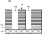
도 2a는 수직 또는 3차원 층 스택(100)을 도시한다. 층 스택(100)은 기판(200) 상에 배열된다. 기판(200) 상에 제1 재료 유형의 여러 개별 층들(101)과 제2 재료 유형의 개별 층들(102)이 교번하여 배열된다. 개별 층들(101, 102)은 예를 들어, 서로의 상부에 적층되거나, 예를 들어 에피택셜 방식으로 성장될 수 있다.2A shows a vertical or three-
제1 재료 유형의 개별 층들(101)은 예를 들어, 제1 재료를 포함할 수 있거나 제1 재료로 구성될 수 있다. 제2 재료 유형의 개별 층들(102)은 예를 들어, 제1 재료와 상이한 제2 재료를 포함하거나 제2 재료로 구성될 수 있다. 제1 및 제2 재료는 상이한 특성을 가질 수 있다.The
개별 층들(101, 102)의 재료 유형(material types) 또는 재료(materials)는 예를 들어, 서로에 대해 매우 높은 에칭 선택비를 갖도록 선택될 수 있다. 예를 들어, 제1 재료 유형의 개별 층들(101)은 화합물 반도체를 포함하거나 화합물 반도체로 구성될 수 있다. 반면, 제2 재료 유형의 개별 층들(102)은 원소 반도체를 포함하거나 원소 반도체로 구성될 수 있다. 예를 들어, 제1 재료 유형의 개별 층(101)은 IV-IV 화합물 반도체, 특히 게르마늄(Ge) 또는 실리콘 게르마늄(SiGe)을 포함하거나 게르마늄 또는 실리콘 게르마늄으로 구성될 수 있다. 한편, 제2 재료 유형의 개별 층들(102)은 실리콘(Si)을 포함하거나 실리콘으로 구성될 수 있다.The material types or materials of the
도 2a에 도시된 예에서, 제1 재료 유형(예를 들어, SiGe)의 개별 층(101)은 바닥 또는 첫번째 층으로 기판(200) 상에 배열된다. 상기 제1 층 상에, 제2 재료 유형의 추가 개별 층(102) 및 제1 재료 유형의 추가 개별 층(101)이 교번하여 배열된다. 이로써 서로의 상부에 교번하여 배열된 제1 및 제2 재료 유형의 여러 개별 층(101, 102)을 갖는 수직 층 스택(100)이 생긴다. 개별 층들(101, 102)의 순서는 또한 예를 들어, 제2 재료 유형의 개별 층(102)이 기판(200) 상의 첫번째 층으로서 배열되도록 변경될 수 있다.In the example shown in FIG. 2A , an
도 2b는 추가 공정 단계를 도시한다. 여기서, 층 스택(100)에는 하나 이상의 수직 리세스들(111)이 생성된다. 여러 수직 리세스들이 생성될 수 있으므로, 이러한 수직 리세스들(111)을 제1 수직 리세스들(111)이라고도 한다.Figure 2b shows a further process step. Here, one or more
이러한 제1 수직 리세스들(111)은 바람직하게는 적절한 에칭 방법에 의해 기판 스택(100)에 구조화된다. 제1 수직 리세스들(111)은 상부에서 하부로, 즉 기판(200)의 반대방향에 있는 층 스택(100)의 측면 또는 표면(106)으로부터 시작하여 기판(200) 방향으로 바닥에 수직으로 연장된다. 여기서, 제1 수직 리세스들(111)이 개별 층들(101, 102) 중 적어도 하나를 관통하여, 바람직하게는 여러 개의 개별 층들(101, 102)을 관통하여, 보다 바람직하게는 층 스택(100)의 모든 개별 층들(101, 102)을 관통하여 기판(200)을 향해 아래로 연장된다.These first
제1 수직 리세스들(111)은 층 스택(100)의 각각의 개별 층들(101, 102)에 대한 접근을 형성하며, 이 경우, 해당 시점에 층 스택(100)에 존재하는 제1 및 제2 재료 유형의 개별 층들(101, 102)에 대한 접근을 형성한다. 이는 개별 층들(101, 102)이 제1 수직 리세스들(111) 내에서 부분적으로 노출되어, 개별 층들(101, 102)이 제1 수직 리세스들(111)를 통해 자유롭게 접근할 수 있음을 의미한다.The first
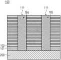
도 2c에서 알 수 있는 바와 같이, 하나의 지지 구조(105) 각각이 제1 리세스들(111) 내에 생성된다. 이 지지 구조(105)는 각각의 개별 층들(101, 102)에 연결되어 이를 기계적으로 안정화하거나 지지한다.As can be seen in FIG. 2C , one
지지 구조(105)를 생성하기 위해, 제1 수직 리세스들(111) 중 적어도 하나는 후속 NAND 메모리 셀의 게이트 및 전하 저장을 위한 절연체들을 형성하는 층 시스템으로 코팅되거나 채워질 수 있다. 제1 수직 리세스들(111)을 코팅하거나 충전하기 위해, 층들이 NAND 메모리(게이트 절연체/메모리 및 채널 컴포넌트들)의 채널 영역 및 절연체들을 생성하는데 사용된다. 코팅 또는 충전(filling)에 사용되는 재료는 예를 들어, 실리콘 산화물, 실리콘 질화물 및 실리콘으로 이루어진 그룹 중에서 하나 또는 여러 성분을 포함할 수 있다. 가능한 층 순서는 (내부에서 외부로) 실리콘 산화물-실리콘 질화물-실리콘 산화물-실리콘일 수 있다. 충전 후, 각각의 제1 수직 리세스(111)는 층 적층(depositions)에 의해 덮힐 수 있다. 수직으로 정렬된 NAND 메모리 층들을 생성하기 위한 코팅 및 충전은 이론적으로 여기에 설명된 수직 리세스들(111, 112, 113) 중 다른 하나에서 발생할 수도 있다.To create the
도 2d는 추가 공정 단계를 도시한다. 여기서, 적어도 하나의 제2 수직 리세스(112)는 예를 들어, 에칭되어, 층 스택(100)에 구조화된다. 제2 수직 리세스(112)는 또한 위에서 아래로, 즉 기판의 반대 방향에 있는 층 스택(100)의 측면(106)에서 시작하여 기판(200) 방향으로 수직하게 아래로 연장된다. 제2 리세스(112)는 추가적으로 개별 층들(101, 102) 중 적어도 하나를 관통하여, 바람직하게는 여러 개별 층들(101, 102)을 관통하여, 더욱 바람직하게는 층 스택(100)의 모든 개별 층들(101, 102)을 관통하여 기판(200)을 향해 아래로 연장된다.Figure 2d shows a further process step. Here, the at least one second
제2 수직 리세스(112)는 층 스택(100)의 각각의 개별 층(101, 102)에 대한 액세스를 형성하며, 이 경우, 해당 시점에 층 스택(100)에 존재하는 제1 및 제2 재료 유형의 개별 층들(101, 102)에 대한 접근을 형성한다. 따라서, 제2 수직 리세스(112)에 의해, 제1 및 제2 재료 유형의 각각의 개별 층들(101, 102)이 노출되고 제2 수직 리세스(112) 내에서 그리고 이를 따라 측면 방향으로 접근가능하게 된다. 예를 들어, 에칭 매체가 수직 리세스(112)를 통과하여 층 스택(100)으로 흘러 들어가 각각 접근 가능하게 된 제1 및 제2 재료 유형의 개별 층들(101, 102)에 도달할 수 있다.The second
이와 관련하여, 본 발명의 방법은 에칭 가스에 의해 측면 방향으로 지향된 건식 에칭 프로세스를 적용함으로써 접근가능하게 된 제1 재료 유형의 개별 층들(101)을 선택적으로 제거하는 단계를 포함한다. 이는 종래 기술에서 사용되는 습식 화학적 에칭 방법과 비교하여 본 발명의 중요한 차이점이다.In this regard, the method of the present invention includes selectively removing
층 스택(100)에서 특정 개별 층을 선택적으로 제거하기 위해 본 발명에서는 건식 에칭 공정을 사용하기 때문에, 처음에 언급한 습식 화학 에칭 방법에서와 같은 습윤 문제는 발생하지 않는다. 결과적으로, 종래에 사용되는 습식 에칭 프로세스와 비교하여, 제1 재료 유형의 개별층들(101)은 상당히 증가된 균질성을 갖고 층 스택(100)으로부터 제2 재료 유형의 개별 층들(102)에 대해 선택적으로 에칭될 수 있다.Because a dry etching process is used in the present invention to selectively remove certain individual layers from the
확산 수송(diffusion transport)과 관련하여, 건식 에칭 공정은 습식 화학적 방법보다 훨씬 더 최적화될 수 있다. 본 발명에 사용된 건식 에칭 공정은 공정 최적화(예를 들어, 더 큰 온도 윈도우(temperature window), 가변 공정 압력, 상이한 공정 가스 유동(process gas flow) 등)에서 훨씬 더 많은 자유도를 갖는다. 이러한 옵션들로 인해, 수직 리세스(112)의 종횡비가 지속적으로 증가함에도 불구하고, 제1 재료 유형의 개별 층들(101)을 선택적으로 에칭하는 것이 메모리 스택(100)의 제2 수직 리세스(112)를 따라 에칭 속도 균일성과 관련하여 최적화될 수 있다.Regarding diffusion transport, dry etching processes can be optimized much better than wet chemical methods. The dry etching process used in the present invention has much more freedom in process optimization (eg, larger temperature window, variable process pressure, different process gas flow, etc.). Due to these options, selectively etching the
본 발명에 사용된 건식 에칭 프로세스를 수행하기 위해, 층 스택(100)은 공정 챔버에 배치될 수 있다. 동일하게, 층 스택(100)은 특정 공정 파라미터로 그리고 여기에 설명된 방식으로 프로세스 챔버에 에칭 가스를 공급함으로써 에칭될 수 있다. 건식 에칭은 예를 들어, 낮은 압력에서 각각의 에칭 가스를 사용하여 고온(약 600℃)에서 수행될 수 있다.To perform the dry etching process used in the present invention,
예를 들어, 건식 에칭 공정은 350℃ 이상의 온도 또는 500℃ 이상의 온도에서 수행될 수 있다. 사용되는 에칭 가스는 예를 들어 염화수소(HCl)를 포함하거나 염화수소로 구성될 수 있다. 사용되는 에칭 가스는 하나의 재료 유형의 개별층들이 상이한 재료 유형의 개별 층들에 대해 층 스택(100)으로부터 가장 선택적으로 에칭될 수 있도록, 각각의 개별층들에 사용된 재료들 및/또는 상이한 재료 유형들에 대해 조정되어야 한다. 따라서, 예를 들어, HCL 가스는 순수한 실리콘의 개별 층들(102)을 유지하면서 실리콘 게르마늄의 개별 층들(101)을 선택적으로 에칭하는 데 매우 적합하다.For example, the dry etching process may be performed at a temperature of 350 °C or higher or 500 °C or higher. The etching gas used may for example contain hydrogen chloride (HCl) or consist of hydrogen chloride. The etching gas used is different from the materials used in each individual layer and/or such that individual layers of one material type can be most selectively etched from the
특정 개별 층들을 선택적으로 에칭하기 위해, 건식 에칭 공정 동안 공정 챔버로 유입된 에칭 가스는 제2 수직 리세스(112)를 통해, 먼저 수직 리세스에 부분적으로 노출된 층 스택(100)의 제1 및 제2 재료 유형의 개별 층들(101, 102)에 도달한다. 그런데, 두 가지 재료 유형은 사용된 에칭 가스와 조합되어 서로에 대해 매우 높은 에칭 선택비를 포함한다. 따라서, 사용된 에칭 가스에 의해, 하나의 재료 유형의 개별 층이 각각의 상이한 재료 유형의 개별 층에 대해 매우 선택적으로 제거될 수 있다.In order to selectively etch certain individual layers, an etching gas introduced into the process chamber during the dry etching process passes through the second
예를 들어, 에칭 가스는 제1 재료 유형의 개별 층들(101)을 바람직하게는 측면 방향으로, 제2 재료 유형의 개별 층들(102)에 대해 선택적으로 에칭할 수 있다. 측면 방향은 층 스택(100)의 (수직) 층 방향에 본질적으로 직교하는 방향을 의미한다. 층 방향은 개별 층들(101, 102)이 서로의 상부에 적층되는 방향이며, 이 경우, 예를 들어, 기판(200)에서 시작하여 수직으로 위쪽을 향한다. 이 경우, 측면 방향은 예를 들어 수평 방향일 것이다. 따라서, 제1 재료 유형의 개별 층들(101)은 제2 수직 리세스(112)로부터 시작하여 거의 수평 방향으로 층 스택(100)에서 에칭될 수 있다. 제2 재료 유형의 개별 층들(102)은 사용된 에칭에 의해 실질적으로 침범받지 않으며, 따라서 에칭되지 않고 층 스택(100)에 남게 된다.For example, the etching gas can etch
제2 수직 리세스(112)를 통해 층 스택(100)에 도달하는 에칭 가스는 각각의 하나의 유형의 개별 층에 대해 다른 하나의 유형의 개별 층을 선택적으로 제거한다. 예를 들어, 사용된 에칭 가스는 측면 방향으로 층 스택(100)으로부터 제1 재료 유형의 개별 층들(101)을 에칭할 수 있다. 여기서, 제1 재료 유형의 개별 층들(101)은 층 스택(100)으로부터 제2 재료 유형의 개별 층들(102)에 대해 선택적으로 에칭된다. 이는 제1 재료 유형의 개별 층들(101)을 선택적으로 제거한 후, 제2 재료 유형(102)의 개별 층들만 층 스택에 남겨진다는 것을 의미한다.The etching gas reaching the
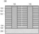
도 2e는 제1 재료 유형의 개별 층들(101)을 선택적으로 에칭한 후에 형성된 층 스택(100)을 도시한다. 제2 재료 유형의 개별 층들(102)만 남게 된다. 공극(voids)(107)이 지금은 제거된 제1 재료 유형의 개별 층들(101)이 있었던 위치에서, 남겨진 제2 재료 유형의 개별 층들(102) 사이에 형성된다. 남겨진 제2 재료 유형의 개별 층들(102)은 지지 구조들(105) 상에서 지지된다. 지지 구조들(105)은 기판(200)에 다시 연결된다.2e shows a
도 2f는 추가 공정 단계를 도시한다. 여기서, 제3 재료 유형의 개별 층들(103)이 생성된다. 이를 위해, 예를 들어, 남겨진 제2 재료 유형의 개별 층들(102) 사이에 형성된 공극(107)에 제3 재료가 도입될 수 있다. 여기서, 제3 재료 유형의 개별 층들(103)은 남겨진 개별 층들(102) 사이의 공극(107) 내에 형성된다. 이는 서로의 위에 교번하여 배열된 제2 재료 유형의 개별 층들(102) 및 제3 재료 유형의 개별 층들(103)을 포함하는 수직 층 스택(100)을 초래한다.2f shows a further process step. Here,
제3 재료 유형의 개별 층들(103)은 예를 들어, 제1 재료 및/또는 제2 재료와 상이한 제3 재료를 포함하거나 이로부터 구성될 수 있다. 제1 및/또는 제2 재료와 비교하여, 제3 재료는 상이한 특성을 가질 수 있다. 예를 들어, 제3 재료는 전기적 절연 특성을 가질 수 있다. 제3 재료는 예를 들어, 실리콘(다이)옥사이드(SiO2)를 포함하거나 실리콘(다이)옥사이드로 구성될 수 있다. 따라서, 제3 재료의 개별 층들(103)은 전기적 절연 특성을 가질 수 있다. 한편, 제2 재료 유형의 개별 층들(102)은 전기적 전도성 특성을 가질 수 있다.The
남겨진 제2 재료 유형의 개별 층들(102) 사이의 공극(107) 내로 제3 재료를 도입하는 것은 예를 들어, 첨가제 건조 공정, 바람직하게는 기상 첨가제 건조 공정에 의해 수행될 수 있다. 예를 들어, 제3 재료는 LPCVD 공정(LPCVD: low pressure chemical vapor deposition)을 적용하여 공극(107)에 도입될 수 있다. 여기서, 공정 가스는 공정 챔버(층 스택(100)이 위치하는 곳)에 도입될 수 있다. 제2 수직 리세스(112)를 통해, 공정 가스가 제2 재료 유형의 개별 층들(102) 사이의 공극(107)에 도달하고 그 안에서 확산한다(expand). 제2 재료 유형의 개별 층들(102)에 공정 가스의 가스 분자를 충돌시키는 것은 제3 재료(예를 들어, SiO2)가 남겨진 제2 재료 유형(예를 들어, Si) 사이의 공극(107)에서 성장하는 효과를 가져온다.Introducing the third material into the
도 2g는 추가 공정 단계를 도시한다. 여기서, 적어도 하나의 제3 수직 리세스(113)가 층 스택(100)에 구조화된다. 여기서, 예를 들어, 제3 재료(도 2f)로 채워진 제2 수직 리세스(112)가 동일한 위치에 제3 수직 리세스(113)를 생성하기 위해 다시 노출될 수 있다(도 3g). 대안적으로, 제3 재료(도 2f)로 채워진 제2 수직 리세스(112)가 덮힌(closed) 상태로 유지될 수 있고, 제3 수직 리세스(113)가 층 스택(100)의 다른 위치에서 생성될 수 있다. 제3 수직 리세스(113)는 도 2g에 예시적으로 도시된 바와 같이, 두 지지 구조들(105) 사이에 생성될 수 있다.Figure 2g shows a further process step. Here, at least one third
제3 수직 리세스(113)는 또한 위에서 아래로, 즉 기판(200)의 반대방향에 있는 층 스택(100)의 측면(106)에서 시작하여 기판(200) 방향으로 수직 하향으로 연장된다. 추가적으로, 제3 수직 리세스(113)는 적어도 하나의 개별 층(102, 103)을 관통하여, 바람직하게는 여러 개의 개별 층들(102, 103)을 관통하여, 보다 바람직하게는 층 스택(100)의 모든 개별 층들(102, 103)을 통과하여 기판(200)을 향해 아래로 연장된다.The third
제3 수직 리세스(113)는 층 스택(100)의 각각의 개별 층들(102, 103)에 대한 접근을 형성하며, 이 경우 해당 시점에 층 스택(100)에 존재하는 제2 및 제3 재료 유형의 개별 층들(102, 103)에 대한 접근을 형성한다. 따라서, 제2 및 제3 재료 유형의 이러한 개별 층들(102, 103)은 제3 수직 리세스(113) 내에서 노출되고 제3 수직 리세스(113)를 통해 접근 가능하게 된다.The third
또한, 본 발명의 방법은 각각의 다른 재료 유형의 개별 층에 대해 접근가능하게 된 하나의 재료 유형의 개별 층을 선택적으로 제거하는 단계를 포함한다. 이 경우, 상기 방법은 제3 재료 유형의 개별 층들(103)에 대해 선택적으로 제2 재료 유형의 개별 층들(102)을 선택적으로 제거하는 단계를 포함한다. 이러한 선택적 제거는 에칭 매체에 의해 측면 방향으로 지향된 에칭 프로세스를 적용함으로써 일어난다. 에칭 공정은 다시 건식 에칭 공정일 수 있지만 대안적으로 습식 에칭 공정일 수도 있다. 따라서, 이 에칭 단계에서, 에칭 매체는 건식 에칭을 위한 에칭 가스, 즉 플라즈마 에칭에서와 같은 플라즈마 또는 이온화된 에칭 가스이거나, 또는 습식 에칭을 위한 습식 화학적 에칭 용액일 수 있다.The method of the present invention also includes selectively removing individual layers of one material type that have been made accessible relative to individual layers of each other material type. In this case, the method comprises selectively removing
건식 에칭 공정의 경우, 불소 함유 가스(fluorine-containing gas)를 사용한 적어도 하나의 플라즈마-지원된 에칭((plasma-supported etching) 단계를 포함할 수 있다. 예를 들어, 불소 함유 가스를 사용한 등방성 CDE 공정(CDE: Chemical Dry Etching)과 같은 건식 에칭이 수행될 수 있으며, 여기서는, 예를 들어, 실리콘(개별 층들(102)의 가능한 재료)이 SiO2 (개별 층들(103)의 가능한 재료)에 대해 매우 선택적으로 에칭될 수 있다. 예를 들어, SF6이 에칭 가스로서 사용될 수 있다. 특히, 매우 높은 SF6 유동(flow), 낮은 O2 유동 및 높은 공정 압력을 갖는 플라즈마 에칭은 이 에칭에 요구되는 등방성 에칭 거동으로 Si와 SiO2 간에 매우 선택적인 에칭이 가능하게 해준다.For the dry etching process, it may include at least one plasma-assisted etching step using a fluorine-containing gas. For example, an isotropic CDE using a fluorine-containing gas. A dry etching process may be performed, such as chemical dry etching (CDE), in which, for example, silicon (a possible material of individual layers 102) reacts to SiO2 (a possible material of individual layers 103). Can be etched very selectively For example, SF6 can be used as etching gas Especially plasma etching with very high SF6 flow, low O2 flow and high process pressure is required for this etching. This isotropic etching behavior enables highly selective etching between Si and SiO2 .
제3 수직 리세스(113)를 통해, 에칭 매체(예: SF6 가스)가 제3 수직 리세스(113) 내에서 노출되고 접근 가능하게 된 제2 및 제3 재료 유형의 개별 층들(102, 103)에 도달한다. 여기서, 상기 에칭 매체는 제3 재료 유형의 개별층들(103)에 대해 측면 방향으로 제2 재료 유형의 개별 층들(102)을 선택적으로 제거하며, 제2 재료 유형의 개별 층들(102)이 선택적으로 제거된 후에는 제3 재료 유형의 개별 층들(103)만 남게 된다. 이것은 제2 재료 유형의 개별 층들(102)이 층 스택(100)에서 에칭된다는 것을 의미한다.
도 2h는 제2 재료 유형의 개별 층들(102)을 선택적으로 에칭한 후에 형성된 층 스택(100)을 도시한다. 여기서, 제3 재료 유형의 개별 층들(103)만 남게 된다. 공극(voids)(108)이 이제는 제거된, 제2 재료 유형의 개별 층들(102)이 있었던 자리에, 남겨진 제3 재료 유형의 나머지 개별 층들(103) 사이에 형성된다. 남겨진 제3 재료 유형의 개별 층들(103)은 지지 구조(105) 상에 지지된다.2H shows a
도 2j는 선택적인 추가 공정 단계를 도시한다. 제4 재료가 남겨진 제3 재료 유형의 개별 층들(103) 사이에 형성된 공극(108) 내로 도입될 수 있다. 여기서, 제4 재료 유형의 개별 층들(104)은 남겨진 제3 재료 유형의 개별 층들(103) 사이의 이러한 공극(108) 내에 형성된다. 이에 의해, 제3 재료 유형의 개별 층들(103)과 제4 재료 유형의 개별 층들(104)이 서로의 상부에 교번하여 배열된 수직 층 스택(100)이 형성된다.2j shows an optional additional process step. A fourth material may be introduced into the
제4 재료는 제3 재료와 다를 수 있다. 제4 재료는 전기적 전도성 금속, 특히 전도성이 높은 금속이거나 그것으로 이루어질 수 있다. 예를 들어, 제4 재료는 텅스텐, 코발트, 몰리브덴 또는 루테늄으로 이루어진 그룹 중 적어도 하나의 성분을 포함하거나 이 성분으로 구성될 수 있다.The fourth material may be different from the third material. The fourth material may be or consist of an electrically conductive metal, particularly a highly conductive metal. For example, the fourth material may include or consist of at least one element from the group consisting of tungsten, cobalt, molybdenum, or ruthenium.
대안적으로, 제4 재료는 도핑된 반도체를 포함하거나 그것으로 구성될 수 있다. 제4 재료는 예를 들어, 도핑된 실리콘을 포함할 수 있다.Alternatively, the fourth material may include or consist of a doped semiconductor. The fourth material may include, for example, doped silicon.
전술한 제4 재료로 수직 리세스(113)(도 2h)를 충전함으로 인해, 수직으로 배향된 구조(116)가 해당 위치에 형성되고, 이는 각각의 개별 층들(103, 104)에 기계적으로 전기적으로 모두 연결된다.By filling the vertical recess 113 (FIG. 2H) with the aforementioned fourth material, a vertically oriented
도 2k에 도시된 바와 같이, 이 수직 구조(116)는 개별 층들(103, 104)(특히, 제4 재료 유형의 전기 전도성 개별 층들(104))이 더 이상 기계적으로나 전기적으로 연결되지 않도록, 예를 들어, 적절한 에칭 프로세스에 의해 제거될 수 있다. 이것은 제4 수직 리세스(114)가 층 스택(100), 예를 들어 지지 구조들(105) 사이에서 생성될 수 있음을 의미한다. 상기 제4 수직 리세스(114)는 이전에 연결된 제4 재료 유형의 개별 층들(104) 사이뿐만 아니라 이전에 연결된 제3 재료 유형의 개별층들(103) 사이의 전기적 연결(측면 방향 또는 수평 방향으로 볼 때)을 차단할 수 있다.2k, this
따라서, 제4 재료 유형의 개별 층들(104)은 생성된 3차원 집적 반도체 메모리(1000)의 워드 라인을 각각 형성할 수 있다.Accordingly, the
도 3a 내지 도 3d는 3차원 집적 반도체 메모리를 제조하기 위한 전술한 방법 단계에 대한 대안적인 해결방안을 도시한다. 이는 아래에 설명된 방법이 상기 동일한 목적 기술 대상에 대한 대안적인 해결방안임을 의미한다.Figures 3a to 3d show an alternative solution to the above method steps for fabricating a three-dimensional integrated semiconductor memory. This means that the method described below is an alternative solution to the same object of description.
본 대안적인 해결방안에서, 도 2a 내지 2e를 참조하여 전술한 방법 단계들은 동일하게 적용된다. 따라서 전술한 모든 설명은 본 대안적인 해결방안에 대해서도 적절하게 적용된다.In this alternative solution, the method steps described above with reference to Figs. 2a to 2e apply equally. Accordingly, all of the foregoing descriptions apply as appropriate to this alternative solution.
도 3a는 도 2e에도 도시되어 있고 본 방법 단계까지 형성되는 층 스택(100)의 초기 상황을 다시 도시한다. 여기서, 당시 존재하는 층 스택(100)은 제2 재료 유형의 개별 층들(102)만을 포함한다. 공극(107)은 이러한 제2 재료 유형의 개별 층들(102) 사이에 형성된다.FIG. 3a again shows the initial situation of the
제2 재료 유형의 개별 층들(102)은 지지 구조들(105) 상에서 지지되고 제2 수직 리세스(112)는 지지 구조들(105) 사이에 위치된다. 도 2f 내지 도 2k를 참조하여 설명한 전술한 실시예는, 제3 재료 유형의 개별 층들(103)을 생성하기 위해 제3 재료가 공극(107)에 도입되었으나, 본 대안적인 실시예에서는 그 대신, 제3 재료 유형의 개별 층들(103)이 제2 재료 유형의 개별 층들(102)로부터 생성된다.
도 3b에서 알 수 있는 바와 같이, 제3 재료 유형의 개별 층들(103)이 제2 재료 유형의 개별 층들(102)이 이전에 위치해 있었던 층 스택(100)의 해당 위치에서 생성된다. 따라서, 공극(107)이 또한 새롭게 형성된 제3 재료 유형의 개별 층들(103) 사이의 이전 위치에서 유지된다.As can be seen in FIG. 3B ,
제2 재료 유형의 개별 층들(102)로부터 제3 재료 유형의 개별 층들(103)을 생성하는 것은 예를 들어, 산화에 의해 수행될 수 있다. 여기서, 예를 들어, 제2 재료 유형의 개별 층들(102)이 적어도 부분적으로 산화될 수 있으며, 이로 인해 제2 재료 유형의 개별 층들(102)이 성장된 산화물로 인해 자신의 특성, 즉 재료 유형이 변경될 수 있다. 이에 의해, 제3 재료 유형의 개별 층들(103)이 제2 재료 유형의 개별 층들(102)로부터 생성된다. 다시 말해서, 제3 재료 유형의 개별 층들(103)은 제2 재료 유형의 개별 층들(102)을 변환함으로써 생성될 수 있고, 그에 의해 그들의 재료 유형을 변경할 수 있다. 따라서, 제3 재료 유형의 개별 층들(103)은 이제 제2 재료 유형의 개별 층들(102)이 이전에 위치해 있었던 층 스택(100)의 해당 위치에 위치된다. 추가적으로, 산화 중에 산화물층이 기판(200)에 부착될 수 있다.Creating
예를 들어, 제2 재료 유형의 개별 층들(102)은 실리콘을 포함하거나 실리콘으로 구성될 수 있다. 그 다음, 이들 개별 층들은 열 산화에 의해 실리콘(다이)옥사이드(SiO2)로 변환될 수 있어, 생성되는 제3 재료 유형의 개별 층들(103)은 실리콘(다이)옥사이드를 포함한다.For example, the
실리콘의 산화 실리콘으로의 열 산화 대신에, 추가 실시예(여기에 명시적으로 도시하지 않음)는 예를 들어, 코팅 방법을 적용함으로써 제2 재료 유형의 개별 층들(102)을 코팅 재료로 코팅하는 것을 제공한다. 제2 재료 유형의 개별 층들(102)은, 예를 들어, 코팅 재료로 완전히 그리고 전체적으로 코팅되어 이러한 방식으로 코팅 재료에 의해 둘러싸일 수 있다. 상기 코팅 재료는 제2 재료 유형의 특성과 다른 특성을 가질 수 있다. 예를 들어, 상기 코팅 재료는 제2 재료 유형과 상이한 제3 재료 유형을 가질 수 있다.Instead of thermal oxidation of silicon into oxidized silicon, a further embodiment (not explicitly shown here) is to coat the
이에 의해, 정확히 그 코팅 재료로 코팅된 제2 재료 유형의 개별 층들(102)의 특성, 즉 개별 층들(102)의 재료 유형이 변경되는 것은 명백하다. 따라서, 제3 재료 유형의 개별 층들(103)은 제2 재료 유형의 개별 층들(102)을 제2 재료 유형과 상이한 제3 재료 유형을 갖는 코팅 재료로 코팅함으로써, 제2 재료 유형의 개별 층들(102)로부터 생성될 수 있다. 또는, 다시 말해서, 제3 재료 유형의 개별 층들(103)은 코팅 재료로 코팅된 제2 재료 유형의 개별 층들(102)이며, 여기서, 코팅 재료는 제3 재료 유형을 정의한다. 따라서, 제3 재료 유형의 개별 층들(103)은 코팅되지 않은 제2 재료 유형의 개별 층들(102)이 이전에 위치해 있었던 층 스택(100)의 해당 위치에 위치된다.By this, it is clear that the properties of the
예를 들어, 제2 재료 유형의 개별 층들(102)은 전기적으로 반도체 특성을 갖는 재료 유형을 가질 수 있다. 반면, 개별 층들(102)을 코팅하기 위해 사용되는 코팅 재료는 전기적 절연 특성을 갖는 재료 유형을 가질 수 있다. 예를 들어, 코팅 재료는 산화물 또는 질화물일 수 있다. 산화물 또는 질화물이 전기 전도성의 제2 재료 유형의 개별 층들(102)에 부착되어, 이에 따라 전기적 절연 재료로 코팅된 후, 개별 층들(102)이 그에 따라 전기적 절연 특성을 가지며, 이에 의해 제3 재료 유형의 개별 층들(103)을 형성한다. 따라서 본 예에서 재료 유형은 전기적으로 반도체(제2 재료 유형)에서 전기적 절연체(제3 재료 유형)으로 변경된다.For example, the
그 결과, 도 2h를 참조하여 전술한 바와 같이 층 스택(100)이 얻어진다. 따라서, 도 2h를 참조하여 논의된 모든 특징은 도 3b에 도시된 바와 같은 방법 단계에 적절하게 적용된다.As a result, a
그런데, 2개의 공정 단계, 즉 도 2f 및 도 2j에 도시된 공정 단계가 완전히 생략될 수 있음을 알 수 있다. 이것은 이 대안적인 실시예의 장점이다.However, it can be seen that two process steps, namely the process steps shown in Figs. 2f and 2j, can be omitted entirely. This is an advantage of this alternative embodiment.
도 3c는 추가 공정 단계를 도시한다. 이 단계는 본질적으로 도 2j를 참조하여 전술한 방법 단계에 대응한다. 따라서 여기에서 도 2j의 모든 특징은 도 3c에 대해서도 적절하게 적용된다.Figure 3c shows a further process step. This step essentially corresponds to the method step described above with reference to FIG. 2j. Accordingly, all features of FIG. 2j here also apply as appropriate for FIG. 3c.
여기서, 제3 재료(도 3b)의 개별 층들(103) 사이에 존재하는 공극은 제4 물질로 채워진다. 여기서, 제3 재료 유형의 개별 층들(103) 사이의 이러한 공극(107) 내에서, 제4 재료 유형의 개별 층들(104)이 형성된다. 이에 의해, 서로의 상부에 교번하여 배열된 제3 재료 유형의 개별 층들(103) 및 제4 재료 유형의 개별 층들(104)을 포함하는 수직 층 스택(100)이 형성된다.Here, the voids existing between the
제4 재료는 제3 재료(코팅 재료)와 다를 수 있다. 제4 재료는 전기적 전도성 금속, 특히 고전도성 금속을 포함하거나 이들로 구성될 수 있다. 예를 들어, 제4 재료는 텅스텐, 코발트, 몰리브덴 또는 루테늄으로 이루어진 그룹 중에서 적어도 하나의 성분을 포함하거나 그 성분으로 구성될 수 있다.The fourth material may be different from the third material (coating material). The fourth material may comprise or consist of an electrically conductive metal, in particular a highly conductive metal. For example, the fourth material may include or consist of at least one element from the group consisting of tungsten, cobalt, molybdenum, or ruthenium.
대안적으로, 제4 재료는 도핑된 반도체를 포함하거나 그것으로 구성될 수 있다. 예를 들어, 제4 재료는 도핑된 실리콘을 포함할 수 있다.Alternatively, the fourth material may include or consist of a doped semiconductor. For example, the fourth material may include doped silicon.
따라서, 제4 재료 유형의 개별 층들(104)은 전기적 전도성 특성을 가질 수 있다. 위에서 언급한 바와 같이, 제3 재료 유형의 개별 층들(103)은 예를 들어 전기적 절연 특성을 포함할 수 있다. 따라서 제3 및 제4 재료 유형은 서로 다른 특성을 가질 수 있다.Accordingly, the
도 3d는 도 2k를 참조하여 위에서 논의된 공정 단계에 본질적으로 대응하는 추가 공정 단계를 도시한다. 따라서, 도 2k의 모든 특징은 도 3d에도 적용된다. 여기서 또한, 제4 수직 리세스(114)가 예를 들어 지지 구조들(105) 사이에서 층 스택(100)에 구조화될 수 있다. 예를 들어, 적절한 에칭 공정에 의해 상기 제4 수직 리세스(114)가 층 스택(100)에 구조화될 수 있고, 이에 따라 개별 층들(103, 104)(특히 전기적 전도성인 제4 재료 유형의 개별 층들(104))은 도 2k를 참조하여 위에서 설명된 바와 같이 더 이상 기계적으로 또는 전기적으로 서로 연결되지 않는다.Figure 3d shows additional process steps corresponding essentially to the process steps discussed above with reference to Figure 2k. Accordingly, all features of FIG. 2k also apply to FIG. 3d. Here too, a fourth
따라서, 제4 재료 유형의 개별 층들(104)은 생성된 3차원 집적 반도체 메모리(1000)의 워드 라인을 각각 형성할 수 있다.Accordingly, the
전술한 두 가지 방법의 공정 단계의 끝에서, 3차원 집적 반도체 메모리(1000)가 형성된다. 이것은 특히 3D NAND 플래시 메모리일 수 있다.At the end of the process steps of the above two methods, the three-dimensional
게이트 NAND 구조는 지지구조들(105) 중 하나에 통합될 수 있거나, 층 스택(100)에 추가적인 수직 리세스를 생성하고 상기 추가적인 수직 리세스를 각각의 층으로 코팅함으로써 제4 재료(예를 들어, 텅스텐)로 층 스택을 채운 후에 생성될 수 있다.The gate NAND structure may be incorporated into one of the
여기에 설명된 본 발명의 방법에 대해, 제1 재료 유형의 개별 층들(101)이 게르마늄(Ge) 또는 실리콘 게르마늄(SiGe)을 포함하거나 이들로 구성되는 경우 특히 유리한 것으로 나타났다. Ge 또는 SiGe는 건식 에칭 방법, 특히 HCl 가스를 적용하여 매우 정밀하게 에칭될 수 있으며, 그것은 게다가 예를 들어 실리콘(개별 층들(102)의 재료)에 대해 매우 높은 선택비를 갖는다.For the inventive method described herein, it has been found to be particularly advantageous if the
그런데, 제1 재료 유형의 개별 층들(101)이 게르마늄 또는 실리콘 게르마늄 대신에 다른 재료를 포함하거나 다른 재료로 구성되는 것도 가능하다. 여기서, 제1 재료 유형은 제2 재료 유형에 비해 높은 식각 선택도를 갖는 것이 결정적이다. 이것은, 예를 들어, 제1 재료(제1 재료 유형의 개별 층들(101)에 사용됨)가 제2 재료(제2 재료 유형의 개별 층들(102)에 사용됨)에 대해 높은 선택비를 갖는다는 사실과 건식 에칭 공정을 적용함으로써 적절한 가스에 의해 제2 재료에 대해 층 스택(100)으로부터 선택적으로 에칭될 수 있다는 사실로부터 얻어질 수 있다.However, it is also possible that the
요약하면, 본 발명은 건식 에칭 공정의 도움으로, 예를 들어 절연체 층들 사이에 전도성 재료 층들을 포함하는 층 스택(100)을 생성할 수 있게 하는 방법을 설명한다.In summary, the present invention describes a method that makes it possible to create a
즉, 반도체 메모리(1000)에서 층 스택(100)을 제조하는 방법이 제공된다. 상기 방법은 기판(200)을 제공하는 단계 및 기판(200) 상에 적어도 하나의 제1 층(101)을 적층하는 단계를 포함하며, 여기서 이 층(101)은 본질적으로 실리콘 및 게르마늄으로 구성될 수 있다. 또한, 상기 방법은 제1 층(101) 상에 적어도 하나의 제2 층(102)을 적층하는 단계를 포함하며, 여기서 제2 층(102)은 본질적으로 실리콘을 포함할 수 있다. 추가적으로, 상기 방법은 적어도 제1 및 제2 층(101, 102)을 포함하는 층 스택(100)에 제1 수직 리세스(111)를 생성하는 단계를 포함하며, 여기서 상기 제1 수직 리세스(111)는 건식 에칭에 의해 생성될 수 있고 아래로 기판(200)의 표면에 도달할 수 있다. 또한, 상기 방법은 제1 수직 리세스(111)에 적어도 하나의 지지 요소(105)를 구조화하는 단계를 포함하며, 여기서 상기 지지 요소(105)는 제1 및 제2 층(101, 102) 중 하나의 표면으로부터 기판(200)의 표면으로 수직으로 연장될 수 있다. 추가적으로, 상기 방법은 적어도 제1 및 제2 층(101, 102)을 포함하는 층 스택(100)에 제2 수직 리세스(112)를 생성하는 단계를 포함한다. 제2 수직 리세스(112)는 건식 에칭에 의해 생성될 수 있으며, 아래로 기판(200)의 표면에 도달할 수 있다. 추가적인 단계는 제1 층(101)(예를 들어, 실리콘 및/또는 게르마늄을 포함)을 제거하는 단계를 포함한다. 본 발명에 따르면, 건식 에칭 공정이 사용된다. 또한, 상기 방법은 층 스택(100)을 SiO2와 같은 절연체 재료(103)로 채우는 단계를 포함한다. 상기 방법의 추가적인 단계는 절연체 재료(103)에 제3 수직 리세스(113)를 생성하는 단계를 포함하고, 여기서 상기 제3 수직 리세스(113)는 제2 층(102)(예를 들어, 실리콘)이 측면 방향으로 노출되도록, 기판(200)의 표면까지 아래로 도달할 수 있다. 또한, 상기 방법은 제2 층(102)(예를 들어, Si)을 제거하는 단계를 포함한다.That is, a method of manufacturing the
또한, 본 발명은 본 방법에 의해 제조될 수 있는 반도체 메모리(1000)의 층 스택(100)에 관한 것이다. 반도체 메모리(1000)는, 예를 들어, 3D NAND 플래시 메모리 칩 또는 3D NAND 메모리 셀일 수 있다.The present invention also relates to a layer stack (100) of a semiconductor memory (1000) that can be manufactured by the present method. The
또한, 본 발명은 3차원 집적 반도체 메모리(1000)를 제조하는 방법에 관한 것으로, 상기 방법은 기판(200)을 제공하는 단계 및 기판(200) 상에 여러 개별 층들(101, 102)을 갖는 층 스택(100)을 생성하는 단계를 포함하고, 제1 재료 유형의 여러 개별 층(101)과 상이한 제2 재료 유형의 여러 개별 층(102)을 교번하여 적층된다. 추가적으로, 상기 방법은 층 스택(100)에 적어도 하나의 제1 수직 리세스(111)를 구조화하고, 제1 수직 리세스(111) 내에 지지 구조(105)를 생성하는 단계를 포함하며, 상기 지지 구조(105)는 각각의 개별 층들(101, 102)에 연결되어 이들을 기계적으로 안정화한다. 또한, 상기 방법은 층 스택(100)에 적어도 하나의 제2 수직 리세스(112)를 구조화하는 단계를 포함하고, 여기서, 제2 수직 리세스(112)는 층 스택(100)의 각각의 개별 층들(101, 102)에 대한 접근을 제공한다. 추가로, 상기 방법은, 제2 수직 리세스(112)를 통해 층 스택(100)에 도달하고 거기에 접근 가능하게 된 제1 재료의 개별 층(101)에 도달하여 제2 재료 유형의 개별 층들(102)에 대해 선택적으로 측면 방향으로 제거하는 에칭 가스를 사용하여, 측면 방향으로 지향된 에칭 공정을 적용함으로써 접근 가능하게 된 제1 재료 유형의 개별층들(101)을 선택적으로 제거하는 단계를 포함하며, 제1 재료 유형의 개별층들(101)의 제거 후에 제2 재료 유형의 개별 층들(102)이 층 스택(100)에 남아서, 남겨진 제2 재료 유형의 개별 층들(102) 사이에 공극(107)이 형성된다. 본 발명에 따르면, 상기 방법은 제1 재료 유형의 개별 층들(101)이 실리콘 게르마늄을 포함하거나 실리콘 게르마늄으로 구성되고, 제1 재료 유형의 개별 층들(101)을 선택적으로 제거하기 위해 측면 방향으로 지향된 에칭 공정이 에칭 가스를 사용하여 건식 에칭 공정의 형태로 수행되는 것을 특징으로 한다.The present invention also relates to a method of manufacturing a three-dimensional integrated semiconductor memory (1000), the method comprising the steps of providing a substrate (200) and a layer having several individual layers (101, 102) on the substrate (200). It comprises creating a stack (100), in which several individual layers (101) of a first material type and several individual layers (102) of a second, different material type are alternately stacked. Additionally, the method comprises structuring at least one first vertical recess (111) in the layer stack (100) and creating a support structure (105) in the first vertical recess (111), said support structure (105).
제1 실시예(도 2a 내지 도 2k)에 따라 여기에 설명된 본 발명의 방법은 층 스택(100)에 제3 수직 리세스(113)를 구조화하는 단계를 포함할 수 있다. 본 발명에 따르면, 상기 단계는 제3 재료로 채워진 제2 수직 리세스(112)가 다시 노출되어 동일한 위치에 제3 수직 리세스(113)를 생성하는 것을 포함하거나, 또는 제3 재료로 채워진 제2 수직 리세스(112)가 닫힌 상태로 유지되고 제3 수직 리세스(113)가 층 스택(100)의 다른 위치에 생성되는 것을 포함할 수 있다.The inventive method described here according to the first embodiment ( FIGS. 2A to 2K ) may include structuring a third
여기에 설명된 본 발명의 방법에 따르면, 제1 및/또는 제2 및/또는 제3 및/또는 제4 수직 리세스(111, 112, 113, 114)를 생성하는 단계는 각각의 수직 리세스(111, 112, 113, 114)가 층 스택(100)을 관통하여 기판(200)까지 완전히 연장되도록 생성되는 것을 포함할 수 있다.According to the method of the invention described herein, the step of creating the first and/or second and/or third and/or fourth
본 명세서에 기술된 본 발명의 방법에 따르면, 제1 수직 리세스(111)는 제1 수직 리세스(111) 내에서 고형화되어 지지 구조(105)를 형성하는 재료로 적어도 부분적으로 채워질 수 있으며, 여기서 제1 수직 리세스(111) 내에 지지 구조(105)를 형성하는 재료로 적어도 부분적으로 채워질 수 있으며, 여기서, 제1 재료 유형의 개별 층들(101)을 선택적으로 제거한 후, 이 지지 구조(105)는 남겨진 제2 재료 유형의 개별 층들(102)을 기계적으로 지지하고 그들 간의 간격을 유지하는 역할을 하며, 제3 재료 유형의 개별 층들(103)을 생성한 후 이를 기계적으로 지지하고 그들 간의 간격을 유지하는 역할을 한다.According to the inventive method described herein, the first
여기에 설명된 본 발명의 두 실시예는 3차원 집적 반도체 메모리(1000)를 생성하거나 생산하는 역할을 한다. 이는 예를 들어 3D NAND 메모리일 수 있다.The two embodiments of the invention described herein serve to create or produce a three-dimensional
여기에 설명된 본 발명의 방법에 따르면, 제4 재료 유형의 개별 층들(104)은 생성된 3차원 집적 반도체 메모리(1000)의 워드 라인을 각각 형성할 수 있다.According to the inventive method described herein, the
상술한 실시예들은 본 발명의 원리를 설명하기 위한 것일 뿐이다. 본 명세서에 설명된 세부사항 및 배열의 수정 및 변형은 당업자에게 명백할 것으로 이해되어야 한다. 따라서, 본 발명은 첨부된 청구항들의 범위에 의해서만 제한되고 본 명세서의 실시예의 설명 및 설명을 통해 제시된 특정 세부사항에 의해 제한되지 않는다.The above-described embodiments are only intended to illustrate the principle of the present invention. It should be understood that modifications and variations of the details and arrangements described herein will become apparent to those skilled in the art. Accordingly, the present invention is limited only by the scope of the appended claims and not by the specific details presented throughout the description and description of the embodiments herein.
일부 양태들이 장치의 맥락에서 설명되었지만, 이러한 양태들이 또한 해당 방법의 설명을 나타내므로, 장치의 블록 또는 디바이스가 각각의 방법 단계 또는 방법의 특징에 해당함이 분명하다. 유사하게, 방법 단계의 맥락에서 설명된 양태들도 또한 대응하는 블록의 설명 또는 대응하는 장치의 세부사항 또는 특징을 나타낸다.Although some aspects have been described in the context of an apparatus, it is clear that a block or device of an apparatus corresponds to a respective method step or feature of a method, since these aspects also represent a description of a corresponding method. Similarly, aspects described in the context of a method step also represent a description of a corresponding block or a detail or feature of a corresponding apparatus.
Claims (15)
Translated fromKorean기판(200)을 제공하는 단계;
제1 재료 유형의 여러 개별 층들(101)뿐만 아니라 다른 제2 재료 유형의 여러 개별 층들(102)을 교번하여 적층함으로써, 상기 기판(200) 상에 여러 개별 층들(101, 102)을 포함하는 층 스택(100)을 생성하는 단계;
상기 층 스택(100)에 적어도 하나의 제1 수직 리세스(111)를 구조화하고, 상기 제1 수직 리세스(111) 안에 지지 구조체(105)를 생성하는 단계로서, 상기 지지 구조체(105)는 상기 각각의 개별 층들(101, 102)에 연결되고 상기 각각의 개별 층들(101, 102)을 기계적으로 안정시키는, 단계;
상기 층 스택(100)에 적어도 하나의 제2 수직 리세스(112)를 구조화하는 단계로서, 상기 제2 수직 리세스(112)는 상기 층 스택(100)의 상기 각각의 개별 층들(101, 102)에 대한 접근을 제공하는, 단계;
상기 제2 수직 리세스(112)를 통해 상기 층 스택(100) 안으로 들어가고, 그 안으로 접근 가능하도록 형성된 상기 제1 재료 유형의 상기 개별 층들(101)에 이르는 에칭 가스에 의해 측면 방향으로 지향된 에칭 공정을 적용하여, 접근 가능하도록 형성된 상기 제1 재료 유형의 상기 개별 층들(101)을 선택적으로 제거하고, 상기 제2 재료 유형의 상기 개별 층들(102)의 측면 방향으로 선택적으로 상기 제1 재료 유형의 상기 개별 층들(101)을 제거하여, 상기 제1 재료 유형의 상기 개별 층들(101)을 선택적으로 제거한 이후에는 상기 제2 재료 유형의 상기 개별 층들(102)이 상기 층 스택(100)에 남고, 공극(voids, 107)이 상기 제2 재료 유형의 상기 남은 개별 층들(102) 사이에 형성되는 단계;
생성되는 제3 재료 유형의 개별 층들(103) 사이에 위치하는 상기 공극(107)을 유지함으로써, 상기 제2 재료 유형의 상기 개별 층들(102)이 이전에 위치했던 상기 층 스택(100) 내의 위치들에 상기 제3 재료 유형의 상기 개별 층들(103)을 생성하는 단계를 포함하고,
상기 제1 재료 유형의 상기 개별 층들(101)은 실리콘 게르마늄을 포함하거나, 또는 실리콘 게르마늄으로 구성되고,
상기 제1 재료 유형의 상기 개별 층들(101)을 측면 방향에서 선택적으로 제거하기 위한 상기 에칭 공정은 에칭 가스를 이용함으로써 건식 에칭 공정의 형태로 수행되는 것을 특징으로 하는 방법.
In the method of manufacturing a three-dimensional integrated semiconductor memory 1000,
providing a substrate 200;
A layer comprising several individual layers (101, 102) on the substrate (200) by alternately stacking several individual layers (101) of a first material type as well as several individual layers (102) of a different second material type. creating a stack 100;
structuring at least one first vertical recess (111) in the layer stack (100) and creating a support structure (105) in the first vertical recess (111), the support structure (105) comprising: connecting to each individual layer (101, 102) and mechanically stabilizing each individual layer (101, 102);
structuring at least one second vertical recess (112) in the layer stack (100), said second vertical recess (112) in the respective individual layers (101, 102) of the layer stack (100). ) providing access to;
Etching directed laterally by means of an etching gas entering the layer stack 100 through the second vertical recess 112 and reaching the individual layers 101 of the first material type formed accessible therein. A process is applied to selectively remove the individual layers 101 of the first material type that are made accessible and optionally in the lateral direction of the individual layers 102 of the second material type. After selectively removing the individual layers 101 of the first material type, the individual layers 102 of the second material type remain in the layer stack 100. , voids 107 are formed between the remaining individual layers 102 of the second material type;
By maintaining the voids 107 located between the individual layers 103 of the third material type being created, the position within the layer stack 100 where the individual layers 102 of the second material type were previously located creating the individual layers (103) of the third material type in fields,
the individual layers (101) of the first material type comprise silicon germanium or consist of silicon germanium,
characterized in that the etching process for selectively removing the individual layers (101) of the first material type in the lateral direction is carried out in the form of a dry etching process by using an etching gas.
상기 제3 재료 유형의 상기 개별 층들(103)을 생성하는 단계는,
상기 제2 재료 유형의 상기 개별 층들(102)의 적어도 부분적인 산화를 수행하여, 상기 제2 재료 유형의 상기 개별 층들(102)이 상기 제3 재료 유형의 상기 개별 층들(103)로 변환되도록 하고, 따라서 상기 제3 재료 유형의 상기 개별 층들(103)이 이전에 상기 제2 재료 유형의 상기 개별 층들(102)이 위치했던 상기 층 스택(100) 내의 상기 위치들에 이제 위치되도록 하는 것을 포함하는, 방법.
The method of claim 1,
Creating the individual layers 103 of the third material type comprises:
performing at least partial oxidation of the individual layers (102) of the second material type, such that the individual layers (102) of the second material type are converted into the individual layers (103) of the third material type; , so that the individual layers 103 of the third material type are now positioned at the positions in the layer stack 100 where the individual layers 102 of the second material type were previously located. , method.
상기 제2 재료 유형의 상기 개별 층들(102)은 실리콘을 포함하고,
생성된 상기 제3 재료 유형의 상기 개별 층들(103)은 실리콘(다이)옥사이드를 포함하고,
상기 실리콘(다이)옥사이드는 상기 방법에 따른 열 산화에 의해 생성되는, 방법.
According to claim 1 or claim 2,
the individual layers (102) of the second material type comprise silicon;
said individual layers (103) of the third material type produced comprise silicon (di)oxide;
wherein the silicon (di) oxide is produced by thermal oxidation according to the method.
상기 제3 재료 유형의 상기 개별 층들(103)을 생성하는 단계는,
상기 제2 재료 유형과는 다른 제3 재료 유형의 코팅 물질로 상기 제2 재료 유형의 상기 개별 층들(102)을 코팅하여, 상기 코팅 재료로 코팅된 상기 개별 층들(102)이 상기 제3 재료 유형의 상기 개별 층들(103)을 형성하는 것을 포함하는, 방법.
The method of claim 1,
Creating the individual layers 103 of the third material type comprises:
Coat the individual layers 102 of the second material type with a coating material of a third material type different from the second material type so that the individual layers 102 coated with the coating material are of the third material type. and forming the individual layers (103) of
상기 코팅 재료는 전기적으로 절연 특성을 포함하는 방법.
The method of claim 4,
The method of claim 1 , wherein the coating material comprises electrically insulating properties.
기판(200)을 제공하는 단계;
제1 재료 유형의 여러 개별 층들(101)뿐만 아니라 다른 제2 재료 유형의 여러 개별 층들(102)을 교번하여 적층함으로써, 상기 기판(200) 상에 여러 개별 층들(101, 102)을 포함하는 층 스택(100)을 생성하는 단계;
상기 층 스택(100)에 적어도 하나의 제1 수직 리세스(111)를 구조화하고, 상기 제1 수직 리세스(111) 안에 지지 구조체(105)를 생성하는 단계로서, 상기 지지 구조체(105)는 상기 각각의 개별 층들(101, 102)에 연결되고 상기 각각의 개별 층들(101, 102)을 기계적으로 안정시키는, 단계;
상기 층 스택(100)에 적어도 하나의 제2 수직 리세스(112)를 구조화하는 단계로서, 상기 제2 수직 리세스(112)는 상기 층 스택(100)의 상기 각각의 개별 층들(101, 102)에 대한 접근을 제공하는, 단계;
상기 제2 수직 리세스(112)를 통해 상기 층 스택(100) 안으로 들어가고, 그 안으로 접근 가능하도록 형성된 상기 제1 재료 유형의 상기 개별 층들(101)에 이르는 에칭 가스에 의해 측면 방향으로 지향된 에칭 공정을 적용하여, 접근 가능하도록 형성된 상기 제1 재료 유형의 상기 개별 층들(101)을 선택적으로 제거하고, 상기 제2 재료 유형의 상기 개별 층들(102)의 측면 방향으로 선택적으로 상기 제1 재료 유형의 상기 개별 층들(101)을 제거하여, 상기 제1 재료 유형의 상기 개별 층들(101)을 선택적으로 제거한 이후에는 상기 제2 재료 유형의 상기 개별 층들(102)이 상기 층 스택(100)에 남고, 공극(voids, 107)이 상기 제2 재료 유형의 상기 남은 개별 층들(102) 사이에 형성되는 단계;
상기 방식으로 형성된 상기 공극(107) 안에 제3 재료를 넣음으로써 제3 재료 유형의 개별 층들(103)을 형성하여, 상기 제3 재료 유형의 개별 층들(103)이 상기 제2 재료 유형의 상기 남은 개별 층들(102) 사이의 상기 공극(107) 안에 각각 형성되는 단계;
상기 층 스택(100)에 적어도 하나의 제3 수직 리세스(113)를 구조화하는 단계로서, 상기 제3 수직 리세스(113)는 상기 층 스택(100)의 상기 각각의 개별 층들(102, 103)에 접근을 제공하는, 단계;
상기 제3 수직 리세스(113)를 통해 상기 층 스택(100) 안으로 들어가고, 그 안에 접근 가능하도록 형성된 상기 제2 재료 유형의 상기 개별 층들(102)에 이르는 에칭 매체(medium)에 의해 측면 방향으로 지향된 에칭 공정을 적용하여, 접근 가능하도록 형성된 상기 제2 재료 유형의 상기 개별 층들(102)을 선택적으로 제거하고, 측면 방향으로 선택적으로 상기 제2 재료 유형의 상기 개별 층들(102)을 제거하여, 선택적으로 제거한 이후에는 상기 제3 재료 유형의 상기 개별 층들(103)이 남고, 공극(voids, 108)이 이들 남은 제3 재료 유형의 상기 개별 층들(103) 사이에 형성되는 단계를 포함하고,
상기 제1 재료 유형의 상기 개별 층들(101)은 실리콘 게르마늄을 포함하거나 실리콘 게르마늄으로 구성되고, 및
상기 제1 재료 유형의 상기 개별 층들(101)을 선택적으로 제거하기 위한 측면 방향으로 지향된 상기 에칭 공정은 에칭 가스를 이용함으로써 건식 에칭 공정의 형태로 수행되는 것을 특징으로 하는 방법.
In the method of manufacturing a three-dimensional integrated semiconductor memory 1000,
providing a substrate 200;
A layer comprising several individual layers (101, 102) on the substrate (200) by alternately stacking several individual layers (101) of a first material type as well as several individual layers (102) of a different second material type. creating a stack 100;
structuring at least one first vertical recess (111) in the layer stack (100) and creating a support structure (105) in the first vertical recess (111), the support structure (105) comprising: connecting to each individual layer (101, 102) and mechanically stabilizing each individual layer (101, 102);
structuring at least one second vertical recess (112) in the layer stack (100), said second vertical recess (112) in the respective individual layers (101, 102) of the layer stack (100). ) providing access to;
Etching directed laterally by means of an etching gas entering the layer stack 100 through the second vertical recess 112 and reaching the individual layers 101 of the first material type formed accessible therein. A process is applied to selectively remove the individual layers 101 of the first material type that are made accessible and optionally in the lateral direction of the individual layers 102 of the second material type. After selectively removing the individual layers 101 of the first material type, the individual layers 102 of the second material type remain in the layer stack 100. , voids 107 are formed between the remaining individual layers 102 of the second material type;
Individual layers 103 of a third material type are formed by putting a third material into the voids 107 formed in the above manner so that the individual layers 103 of the third material type form the remaining layers of the second material type. respectively formed in the voids 107 between the individual layers 102;
structuring at least one third vertical recess (113) in the layer stack (100), said third vertical recess (113) in the respective individual layers (102, 103) of the layer stack (100). ) providing access to;
In a lateral direction by means of an etching medium entering the layer stack 100 through the third vertical recess 113 and reaching the individual layers 102 of the second material type made accessible therein. Applying a directed etching process to selectively remove the individual layers 102 of the second material type that are made accessible and selectively remove the individual layers 102 of the second material type in a lateral direction; , after selective removal, the individual layers (103) of the third material type remain, and voids (108) are formed between these remaining individual layers (103) of the third material type,
the individual layers (101) of the first material type comprise silicon germanium or consist of silicon germanium, and
characterized in that the etching process directed in the lateral direction for selectively removing the individual layers (101) of the first material type is carried out in the form of a dry etching process by using an etching gas.
상기 제3 재료 유형의 상기 개별 층들(103)을 남기는 반면 상기 제2 재료 유형의 상기 개별 층들(102)을 선택적으로 제거하는 것은, 불소-함유 가스들로 적어도 하나의 플라즈마-지원된(plasma-supported) 에칭 단계를 포함하는 건식 에칭 공정을 적용함으로써 수행되는 방법.
The method of claim 6,
Selective removal of the individual layers 102 of the second material type while leaving the individual layers 103 of the third material type results in at least one plasma-assisted with fluorine-containing gases. supported) method performed by applying a dry etching process comprising an etching step.
상기 제2 재료 유형의 상기 남은 개별 층들(102) 사이의 상기 공극(107)에 상기 제3 재료를 넣는 상기 단계는 상기 제2 수직 리세스(112)를 통해 이 공극(107)에 이르고 그 안에서 확산되는 공정 가스(process gas)를 포함하고, 상기 제3 재료는 상기 제2 재료 유형의 상기 남은 개별 층들(102) 사이에서 성장(grown)되는 방법.
According to claim 6 or claim 7,
The step of putting the third material into the void 107 between the remaining individual layers 102 of the second material type reaches this void 107 through the second vertical recess 112 and in it and a process gas that is diffused, wherein the third material is grown between the remaining individual layers (102) of the second material type.
상기 제3 재료를 넣는 상기 단계는 LPCVD 방법을 적용함으로써 수행되는 방법.
The method of claim 8,
The step of putting the third material is performed by applying an LPCVD method.
상기 제2 재료 유형의 상기 개별 층들(102)은 실리콘을 포함하거나 실리콘으로 구성되는 방법.
The method of claim 1 or claim 6,
wherein the individual layers (102) of the second material type comprise or consist of silicon.
상기 제3 재료 유형의 상기 개별 층들(103)은 전기적으로 절연 특성을 포함하고, 및/또는
상기 제3 재료 유형의 상기 개별 층들(103)은 실리콘(다이)옥사이드를 포함하거나 실리콘(다이)옥사이드로 구성되는 방법.
The method of claim 1 or claim 6,
The individual layers 103 of the third material type comprise electrically insulating properties, and/or
wherein the individual layers (103) of the third material type comprise or consist of silicon (di) oxide.
상기 제1 재료 유형의 상기 개별 층들(101)을 선택적으로 제거하기 위한 상기 건식 에칭 공정은 350℃ 이상의 온도에서 수행되고, 상기 에칭 가스는 염화 수소를 포함하거나 염화 수소로 구성되는 방법.
The method of claim 1 or claim 6,
wherein the dry etching process for selectively removing the individual layers (101) of the first material type is performed at a temperature above 350° C., and the etching gas comprises or consists of hydrogen chloride.
상기 제3 재료 유형의 상기 개별 층들(103)을 생성하는 상기 단계 이후에, 상기 개별 층들(103) 사이에 형성된 상기 공극(107, 108)은 제4 재료로 채워져, 제4 재료 유형의 개별 층들(104)이 상기 제3 재료 유형의 상기 개별 층들(103) 사이에 각각 형성되고, 상기 제4 재료 유형은 상기 제3 재료 유형과 다르고 전기적으로 도전성인, 방법.
The method of claim 1 or claim 6,
After the step of creating the individual layers 103 of the third material type, the voids 107 and 108 formed between the individual layers 103 are filled with a fourth material, so that the individual layers of the fourth material type (104) are each formed between the discrete layers (103) of the third material type, the fourth material type being different and electrically conductive than the third material type.
상기 제4 재료 유형의 상기 개별 층들(104)은 전기적으로 도전성의 금속, 특히 텅스텐, 코발트, 몰리브덴 또는 루테늄으로 이루어진 그룹 중에서 적어도 하나의 성분을 포함하거나, 이에 의해 구성되고, 또는
상기 제4 재료 유형의 상기 개별 층들(104)은 도핑된 반도체 특히 도핑된 실리콘을 포함하거나 이에 의해 구성되는 방법.
The method of claim 13,
the individual layers 104 of the fourth material type comprise or consist of at least one element from the group consisting of an electrically conductive metal, in particular tungsten, cobalt, molybdenum or ruthenium, or
wherein the individual layers (104) of the fourth material type comprise or consist of a doped semiconductor, in particular doped silicon.
Applications Claiming Priority (2)
| Application Number | Priority Date | Filing Date | Title |
|---|---|---|---|
| EP21197603.0 | 2021-09-20 | ||
| EP21197603.0AEP4152395A1 (en) | 2021-09-20 | 2021-09-20 | Method for manufacturing a three-dimensionally integrated semiconductor storage device |
Publications (2)
| Publication Number | Publication Date |
|---|---|
| KR20230042658Atrue KR20230042658A (en) | 2023-03-29 |
| KR102799671B1 KR102799671B1 (en) | 2025-04-28 |
Family
ID=77951470
Family Applications (1)
| Application Number | Title | Priority Date | Filing Date |
|---|---|---|---|
| KR1020220118807AActiveKR102799671B1 (en) | 2021-09-20 | 2022-09-20 | Method for Producing a Three-Dimensionally Integrated Semiconductor Memory |
Country Status (5)
| Country | Link |
|---|---|
| US (1) | US20230087266A1 (en) |
| EP (1) | EP4152395A1 (en) |
| KR (1) | KR102799671B1 (en) |
| CN (1) | CN115843178A (en) |
| TW (1) | TWI843201B (en) |
Citations (2)
| Publication number | Priority date | Publication date | Assignee | Title |
|---|---|---|---|---|
| US5155657A (en)* | 1991-10-31 | 1992-10-13 | International Business Machines Corporation | High area capacitor formation using material dependent etching |
| KR20210024641A (en)* | 2018-09-26 | 2021-03-05 | 양쯔 메모리 테크놀로지스 씨오., 엘티디. | 3D memory device and method of forming 3D memory device |
Family Cites Families (3)
| Publication number | Priority date | Publication date | Assignee | Title |
|---|---|---|---|---|
| US8445347B2 (en)* | 2011-04-11 | 2013-05-21 | Sandisk Technologies Inc. | 3D vertical NAND and method of making thereof by front and back side processing |
| CN109417073B (en)* | 2018-09-10 | 2019-12-06 | 长江存储科技有限责任公司 | Memory device using comb routing structure to reduce metal line loading |
| WO2021035603A1 (en)* | 2019-08-29 | 2021-03-04 | Yangtze Memory Technologies Co., Ltd. | Three-dimensional memory and fabrication method thereof |
- 2021
- 2021-09-20EPEP21197603.0Apatent/EP4152395A1/enactivePending
- 2022
- 2022-09-14TWTW111134638Apatent/TWI843201B/enactive
- 2022-09-19CNCN202211137868.7Apatent/CN115843178A/enactivePending
- 2022-09-20KRKR1020220118807Apatent/KR102799671B1/enactiveActive
- 2022-09-20USUS17/933,508patent/US20230087266A1/enactivePending
Patent Citations (2)
| Publication number | Priority date | Publication date | Assignee | Title |
|---|---|---|---|---|
| US5155657A (en)* | 1991-10-31 | 1992-10-13 | International Business Machines Corporation | High area capacitor formation using material dependent etching |
| KR20210024641A (en)* | 2018-09-26 | 2021-03-05 | 양쯔 메모리 테크놀로지스 씨오., 엘티디. | 3D memory device and method of forming 3D memory device |
Also Published As
| Publication number | Publication date |
|---|---|
| CN115843178A (en) | 2023-03-24 |
| TWI843201B (en) | 2024-05-21 |
| TW202314976A (en) | 2023-04-01 |
| KR102799671B1 (en) | 2025-04-28 |
| US20230087266A1 (en) | 2023-03-23 |
| EP4152395A1 (en) | 2023-03-22 |
Similar Documents
| Publication | Publication Date | Title |
|---|---|---|
| US9659955B1 (en) | Crystalinity-dependent aluminum oxide etching for self-aligned blocking dielectric in a memory structure | |
| JP6987876B2 (en) | Memory device and method | |
| US9601508B2 (en) | Blocking oxide in memory opening integration scheme for three-dimensional memory structure | |
| CN109075174A (en) | Multi-stacked three-dimensional memory device and manufacturing method thereof | |
| US10867994B2 (en) | High density capacitors formed from thin vertical semiconductor structures such as FINFETs | |
| KR20040005580A (en) | Semiconductor device with insulator and manufacturing method therefor | |
| CN107425006B (en) | A kind of metal gates manufacturing method of 3D nand memories | |
| JP2023089164A (en) | Semiconductor wafer manufacturing method | |
| CN113948455B (en) | Method for manufacturing semiconductor structure | |
| CN107527794A (en) | A kind of metal gate preparation method of 3D nand memories part | |
| KR102799671B1 (en) | Method for Producing a Three-Dimensionally Integrated Semiconductor Memory | |
| CN112103296B (en) | Method for manufacturing semiconductor structure | |
| CN111769037A (en) | Etching method for semiconductor structure and manufacturing method of 3D memory device | |
| US20230092338A1 (en) | Method for Generating Vertical Channel Structures in Three-Dimensionally Integrated Semiconductor Memories | |
| US11180362B2 (en) | Method for processing a layer structure and microelectromechanical component | |
| US20240162079A1 (en) | Multi-function etching sacrificial layers to protect three-dimensional dummy fins in semiconductor devices | |
| GB2539774B (en) | High density capacitors formed from thin vertical semiconductor structures such as FinFETs | |
| CN117650049A (en) | Semiconductor device and method for manufacturing the same | |
| CN115000007A (en) | Contact plug, manufacturing method thereof and semiconductor device | |
| CN114899192A (en) | Three-dimensional memory and preparation method thereof | |
| CN114023759A (en) | Method of fabricating semiconductor structure and semiconductor structure |
Legal Events
| Date | Code | Title | Description |
|---|---|---|---|
| PA0109 | Patent application | Patent event code:PA01091R01D Comment text:Patent Application Patent event date:20220920 | |
| PA0201 | Request for examination | Patent event code:PA02012R01D Patent event date:20221005 Comment text:Request for Examination of Application Patent event code:PA02011R01I Patent event date:20220920 Comment text:Patent Application | |
| PG1501 | Laying open of application | ||
| E902 | Notification of reason for refusal | ||
| PE0902 | Notice of grounds for rejection | Comment text:Notification of reason for refusal Patent event date:20240201 Patent event code:PE09021S01D | |
| E701 | Decision to grant or registration of patent right | ||
| PE0701 | Decision of registration | Patent event code:PE07011S01D Comment text:Decision to Grant Registration Patent event date:20250120 | |
| PG1601 | Publication of registration |