KR20230037491A - Systems, methods and program products for manufacturing photomasks - Google Patents
Systems, methods and program products for manufacturing photomasksDownload PDFInfo
- Publication number
- KR20230037491A KR20230037491AKR1020227042013AKR20227042013AKR20230037491AKR 20230037491 AKR20230037491 AKR 20230037491AKR 1020227042013 AKR1020227042013 AKR 1020227042013AKR 20227042013 AKR20227042013 AKR 20227042013AKR 20230037491 AKR20230037491 AKR 20230037491A
- Authority
- KR
- South Korea
- Prior art keywords
- photomask
- defects
- wafer
- structure patterns
- pattern
- Prior art date
- Legal status (The legal status is an assumption and is not a legal conclusion. Google has not performed a legal analysis and makes no representation as to the accuracy of the status listed.)
- Pending
Links
Images


Classifications
- G—PHYSICS
- G03—PHOTOGRAPHY; CINEMATOGRAPHY; ANALOGOUS TECHNIQUES USING WAVES OTHER THAN OPTICAL WAVES; ELECTROGRAPHY; HOLOGRAPHY
- G03F—PHOTOMECHANICAL PRODUCTION OF TEXTURED OR PATTERNED SURFACES, e.g. FOR PRINTING, FOR PROCESSING OF SEMICONDUCTOR DEVICES; MATERIALS THEREFOR; ORIGINALS THEREFOR; APPARATUS SPECIALLY ADAPTED THEREFOR
- G03F1/00—Originals for photomechanical production of textured or patterned surfaces, e.g., masks, photo-masks, reticles; Mask blanks or pellicles therefor; Containers specially adapted therefor; Preparation thereof
- G03F1/68—Preparation processes not covered by groups G03F1/20 - G03F1/50
- G03F1/70—Adapting basic layout or design of masks to lithographic process requirements, e.g., second iteration correction of mask patterns for imaging
- G—PHYSICS
- G03—PHOTOGRAPHY; CINEMATOGRAPHY; ANALOGOUS TECHNIQUES USING WAVES OTHER THAN OPTICAL WAVES; ELECTROGRAPHY; HOLOGRAPHY
- G03F—PHOTOMECHANICAL PRODUCTION OF TEXTURED OR PATTERNED SURFACES, e.g. FOR PRINTING, FOR PROCESSING OF SEMICONDUCTOR DEVICES; MATERIALS THEREFOR; ORIGINALS THEREFOR; APPARATUS SPECIALLY ADAPTED THEREFOR
- G03F7/00—Photomechanical, e.g. photolithographic, production of textured or patterned surfaces, e.g. printing surfaces; Materials therefor, e.g. comprising photoresists; Apparatus specially adapted therefor
- G03F7/70—Microphotolithographic exposure; Apparatus therefor
- G03F7/70483—Information management; Active and passive control; Testing; Wafer monitoring, e.g. pattern monitoring
- G03F7/70491—Information management, e.g. software; Active and passive control, e.g. details of controlling exposure processes or exposure tool monitoring processes
- G03F7/705—Modelling or simulating from physical phenomena up to complete wafer processes or whole workflow in wafer productions
- G—PHYSICS
- G06—COMPUTING OR CALCULATING; COUNTING
- G06F—ELECTRIC DIGITAL DATA PROCESSING
- G06F30/00—Computer-aided design [CAD]
- G06F30/30—Circuit design
- G06F30/39—Circuit design at the physical level
- G06F30/398—Design verification or optimisation, e.g. using design rule check [DRC], layout versus schematics [LVS] or finite element methods [FEM]
- G—PHYSICS
- G06—COMPUTING OR CALCULATING; COUNTING
- G06T—IMAGE DATA PROCESSING OR GENERATION, IN GENERAL
- G06T7/00—Image analysis
- G06T7/0002—Inspection of images, e.g. flaw detection
- G06T7/0004—Industrial image inspection
- G06T7/001—Industrial image inspection using an image reference approach
- G—PHYSICS
- G06—COMPUTING OR CALCULATING; COUNTING
- G06T—IMAGE DATA PROCESSING OR GENERATION, IN GENERAL
- G06T7/00—Image analysis
- G06T7/10—Segmentation; Edge detection
- G06T7/13—Edge detection
- G—PHYSICS
- G06—COMPUTING OR CALCULATING; COUNTING
- G06T—IMAGE DATA PROCESSING OR GENERATION, IN GENERAL
- G06T7/00—Image analysis
- G06T7/70—Determining position or orientation of objects or cameras
- G—PHYSICS
- G06—COMPUTING OR CALCULATING; COUNTING
- G06F—ELECTRIC DIGITAL DATA PROCESSING
- G06F2119/00—Details relating to the type or aim of the analysis or the optimisation
- G06F2119/18—Manufacturability analysis or optimisation for manufacturability
- G—PHYSICS
- G06—COMPUTING OR CALCULATING; COUNTING
- G06T—IMAGE DATA PROCESSING OR GENERATION, IN GENERAL
- G06T2207/00—Indexing scheme for image analysis or image enhancement
- G06T2207/10—Image acquisition modality
- G06T2207/10056—Microscopic image
- G06T2207/10061—Microscopic image from scanning electron microscope
- G—PHYSICS
- G06—COMPUTING OR CALCULATING; COUNTING
- G06T—IMAGE DATA PROCESSING OR GENERATION, IN GENERAL
- G06T2207/00—Indexing scheme for image analysis or image enhancement
- G06T2207/30—Subject of image; Context of image processing
- G06T2207/30108—Industrial image inspection
- G06T2207/30148—Semiconductor; IC; Wafer
Landscapes
- Engineering & Computer Science (AREA)
- Physics & Mathematics (AREA)
- General Physics & Mathematics (AREA)
- Theoretical Computer Science (AREA)
- Computer Vision & Pattern Recognition (AREA)
- Quality & Reliability (AREA)
- Computer Hardware Design (AREA)
- Evolutionary Computation (AREA)
- Geometry (AREA)
- General Engineering & Computer Science (AREA)
- Preparing Plates And Mask In Photomechanical Process (AREA)
- Testing Or Measuring Of Semiconductors Or The Like (AREA)
Abstract
Translated fromKorean
Description
Translated fromKorean관련 출원 교차 참조Cross reference to related applications
본 출원은 2020년 4월 30일에 출원된 미국 특허 가출원 제63/018,471호의 이익 및 우선권을 주장하며, 이 특허 가출원의 내용은 본 출원 내에 원용된다.This application claims the benefit and priority of US Provisional Patent Application No. 63/018,471 filed on April 30, 2020, the contents of which are incorporated herein by reference.
기술분야technology field
본 발명은 일반적으로 실리콘 웨이퍼들 상에 집적 회로들을 제조하는 데 사용되는 포토마스크들을 제조하기 위한 시스템들 및 방법들에 관한 것이다.The present invention generally relates to systems and methods for manufacturing photomasks used in the manufacture of integrated circuits on silicon wafers.
마스크 기술은 로직 및 메모리 공정들을 위한 첨단 집적 회로 기술 노드들의 진전을 가능하게 하는 핵심이다. 특히, 광학 및 EUV 리소그래피의 기존 한계를 뛰어넘을 때, 적절한 공정 윈도우(process window, PW) 및 최종 수율을 달성하기 위해 마스크에 크게 의존한다. 마스크 제조 한계는 각 차세대 첨단 집적 회로 기술로 라인 폭이 점점 작아짐에 따라 만들어지는 마스크의 정확도와 일관성을 극대화하는 방법에 대한 기술적 과제를 야기한다. 마스크 공정 개선 사항에 대한 웨이퍼 검증은 생산 라인이 최대 용량으로 가동되고 웨이퍼 특성화를 지원하기 위한 노력 수준으로 인해 매우 어렵고 시간이 많이 소요될 수 있다. 따라서, 패턴 충실도 향상 솔루션을 보다 효율적이고 효과적으로 제공하는 방법이 있다면 마스크 제조자와 웨이퍼 리소그래피 기술자에게 유용한데, 패턴 충실도에는 이에 제한되지 않지만 임계 치수 균일도(critical dimension uniformity, CDU) - 전역 및 국소, 코너 라운딩, H/V 바이어스, 복잡한 2차원 패턴 재현, LER, 해상도 향상 등이 포함된다.Mask technology is key to enabling the advancement of advanced integrated circuit technology nodes for logic and memory processes. Especially when pushing the existing limitations of optical and EUV lithography, it relies heavily on masks to achieve an appropriate process window (PW) and final yield. Mask manufacturing limitations create technical challenges in how to maximize the accuracy and consistency of the masks created as line widths get smaller and smaller with each new generation of advanced integrated circuit technology. Wafer validation for mask process enhancements can be very difficult and time consuming due to production lines running at full capacity and the level of effort to support wafer characterization. Therefore, it would be useful to mask makers and wafer lithography engineers if there was a way to more efficiently and effectively provide a pattern fidelity enhancement solution, including but not limited to pattern fidelity, critical dimension uniformity (CDU) - global and local, corner rounding. , H/V bias, complex two-dimensional pattern reproduction, LER, and resolution enhancement.
현재, 리소그래피 인식 LAMA 응용예 내에서 마스크 및 웨이퍼 분석 기술의 툴키트를 이용하여, 금속, 컨택트, 폴리 등에서 발견되는 것과 같은 1차원(1D) 및 2차원(2D) 구조 상의 웨이퍼 결함을 예측하고, 패턴 충실도 성능 향상을 위해 마스크 공정을 최적화하는 것이 가능하다. 몇 가지 예를 들자면, 비대칭 홀에 대한 마스크 공정 유발 x-y 에러, 코너 라운딩(corner rounding, CR), 및 컨택트 홀 면적 손실은 요구되는 능력을 발휘하기 위해 어떻게 최적화될지에 대한 기술적 과제를 제시한다. 또한, 해상도 미만의 보조 피처(sub-resolution assist feature, SRAF)는 이 기술로 다루어질 수 있는 추가의 기술적 과제를 제시한다. 마스크 상의 이러한 피처를 해상하는 것은 특히, 이전 세대 장비로 공정 능력을 확장하고자 할 때, 중대한 기술적 과제를 제기한다. 이러한 기술적 과제를 극복하기 위한 마스크 현상 공정이 요구된다.Currently, toolkits of mask and wafer analysis techniques are used within lithography-aware LAMA applications to predict wafer defects on one-dimensional (1D) and two-dimensional (2D) structures such as those found in metals, contacts, polys, etc., and pattern It is possible to optimize the mask process for improved fidelity performance. Mask process induced x-y errors for asymmetric holes, corner rounding (CR), and contact hole area loss, to name a few examples, present technical challenges on how to optimize for required capabilities. In addition, sub-resolution assist features (SRAF) present additional technical challenges that can be addressed with this technology. Resolving these features on the mask poses significant technical challenges, especially when trying to extend process capability to previous generation equipment. A mask development process is required to overcome these technical challenges.
또한, IC 기술 노드의 진전과 함께 마스크 성능에 대한 요구가 높아짐에 따라, 단일 빔 기록 툴과 같은 기존 툴은 더 이상 이러한 더 높은 표준을 충족하기 위해 원하는 결과를 제공하지 못할 수 있는 한편, 동시에 이러한 기존 툴이 다른 목적을 위해 반드시 쓸모 없게 되는 것은 아니다. 이에 따라, EUVL 영역과 같은 더 높은 마스크 성능 영역에서 사용할 수 있도록 기존 툴의 능력을 확장시킬 필요가 있다.Additionally, as the demands on mask performance increase with the advancement of IC technology nodes, existing tools such as single beam writing tools may no longer provide the desired results to meet these higher standards, while at the same time Existing tools do not necessarily become obsolete for other purposes. Accordingly, there is a need to extend the capabilities of existing tools for use in higher mask performance regions such as the EUVL region.
포토마스크가 전술한 문제들을 극복할 수 있는 시스템 및 방법이 개발될 수 있을 것이 요구된다.It is desired that a system and method be developed in which a photomask can overcome the aforementioned problems.
본 발명은 리소 인식 마스크 공정 보정 응용(Litho Aware Mask Process correction Application, LAMA) 기술들을 이용하는 포토마스크를 제조하기 위한 새롭고 개선된 컴퓨터 시스템들 및 방법들로 집적 회로 수율을 위한 EUVL 및 광학 리소그래피에서 패턴 충실도 향상 달성의 과제를 해결한다. 후술되는 바와 같이, LAMA는 리소그래피 성능 및 수율 패터닝을 향상시키기 위해 웨이퍼 공정들과 마스크 공정 LAMA 충실도가 조화를 이루는 다단계 데이터 흐름이다. LAMA 기술의 실시예들에서는, 기존의 포토마스크 데이터의 공간 도메인 분석 및/또는 이미 구축된 마스크의 SEM 이미지 윤곽 추출 분석에 기초하여, LAMA 게이지 패턴(gauge pattern)를 설계한다. 그 다음, 설계된 LAMA 게이지 패턴 ― 보정 포토마스크 구조들로 이루어짐 ― 을 마스크 내로 통합한다. 실시예들에서, 어떤 구조들이 마스크 데이터에 존재하는지를 결정하기 위해 설계 규칙 점검 및/또는 패턴 매칭 소프트웨어가 사용되고, 이러한 구조들 내의 결함들이 묘사 패턴 검색, 피처 통계 분석 및 설계 밀도 맵들을 포함하지만 이에 제한되지 않는 공간 도메인 분석으로 정량화된다. 이에 따라, LAMA로부터 이익을 얻을 수 있는 구조들이 식별된다. 마스크 구조들에 대한 최적의 보정 방법을 결정하는 데 요구되는 마스크 수준 데이터를 얻기 위해 초기 마스크를 사용한다. 이에 기초하여, 후속 마스크 데이터 생성에 적용될 LAMA 보정 스크립트를 제공한다. 그 다음, LAMA를 적용하여 최종 마스크를 구축한다. LAMA 보정은 생산에 사용될 마스크 데이터를 생성하기 위해 마스크 공정 보정, OPC 또는 임의의 다른 마스크 제조 단계들 동안 적용될 수 있다.The present invention provides new and improved computer systems and methods for fabricating photomasks using Litho Aware Mask Process Correction Application (LAMA) techniques for pattern fidelity in EUVL and optical lithography for integrated circuit yield. Solve the challenges of achieving improvement. As discussed below, LAMA is a multi-level data flow in which wafer processes and mask process LAMA fidelity are matched to improve lithography performance and patterning yield. In embodiments of the LAMA technique, a LAMA gauge pattern is designed based on spatial domain analysis of existing photomask data and/or SEM image contour extraction analysis of an already built mask. Then, the designed LAMA gauge pattern - consisting of calibration photomask structures - is incorporated into the mask. In embodiments, design rule checking and/or pattern matching software is used to determine which structures are present in the mask data, and defects in these structures include, but are not limited to, descriptive pattern search, feature statistical analysis, and design density maps. quantified by spatial domain analysis. Accordingly, structures that can benefit from LAMA are identified. The initial mask is used to obtain mask-level data needed to determine the optimal correction method for the mask structures. Based on this, we provide a LAMA correction script to be applied to subsequent mask data generation. Then, LAMA is applied to build the final mask. LAMA correction can be applied during mask process calibration, OPC or any other mask manufacturing steps to generate mask data to be used in production.
실시예들에서, 포토마스크를 제조하는 방법으로서, (a) 웨이퍼의 주사 전자 현미경(scanning electron microscope, SEM) 이미지로부터 웨이퍼 결함들을 검출하는 단계; (b) 이전에 제조된 포토마스크의 SEM 이미지로부터 복수의 마스크 윤곽들 ― 추출된 마스크 윤곽들은 검출된 웨이퍼 결함들에 대응할 수 있음 ― 을 추출하는 단계; (c) 추출된 복수의 마스크 윤곽들을 사용하여 시뮬레이션 제조된 웨이퍼를 생성하는 단계; (d) 시뮬레이션 제조된 웨이퍼 상의 하나 이상의 결함을 검출하는 단계; (e) 시뮬레이션 제조된 웨이퍼 상의 결함에 기초하여 포토마스크의 하나 이상의 문제되는 영역을 결정하는 단계; (f) 이전에 제조된 포토마스크의 문제되는 영역에 관한 패턴 정보를 획득하는 단계; (g) 패턴 정보의 공간 도메인 분석을 수행하는 단계; (h) 공간 도메인 분석에 기초하여, 하나 이상의 대응하는 결함을 보이는 복수의 포토마스크 구조 패턴들을 결정하는 단계; (i) 공간 도메인 분석에 기초하여 복수의 포토마스크 구조 패턴들로부터 복수의 잠재적 보정 포토마스크 구조 패턴들을 생성하는 단계 ― 복수의 잠재적 보정 포토마스크 구조 패턴들을 생성하는 단계는: (i) 하나 이상의 대응하는 결함을 보이는 복수의 포토마스크 구조 패턴들에 적용될 복수의 처리들을 선택하는 단계; 및 (ⅱ) 선택된 각 처치에 대해, 처치에 대응하는 복수의 파라미터들을 선택하는 단계; 및 (ⅲ) 선택된 파라미터들을 갖는 선택된 처리들을 하나 이상의 대응하는 결함을 보이는 복수의 포토마스크 구조 패턴들에 적용하는 단계를 포함함 ―; (j) 잠재적 보정 포토마스크 구조 패턴들을 테스트 포토마스크 내에 통합시키는 단계; (k) 테스트 포토마스크 상의 잠재적 보정 포토마스크 구조 패턴들을 분석하는 단계; (l) 복수의 잠재적 보정 포토마스크 구조 패턴들로부터 복수의 보정 포토마스크 구조 패턴들을 선택하는 단계; (m) 테스트 포토마스크 상의 복수의 보정 마스크 구조 패턴들의 분석에 기초하여 하나 이상의 포토마스크 패턴 보정 스크립트를 생성하는 단계; (n) 하나 이상의 포토마스크 패턴 보정 스크립트를 실행하여 복수의 보정 포토마스크 구조 패턴들 중 하나 이상을 전체 레이어에 대한 포토마스크 레이아웃에 적용하는 단계; (o) 최종 포토마스크 레이아웃에 기초하여 복수의 보정 포토마스크 구조 패턴들 중 하나 이상을 통합한 전체 레이어에 대한 포토마스크를 구축하는 단계; (p) 하나 이상의 보정 포토마스크 구조가 최종 포토마스크에 적용되었음을 확정하는 단계; 및 (q) 복수의 보정 포토마스크 구조 패턴들 중 하나 이상을 통합한 포토마스크에 기초하여 생성된 웨이퍼 상의 복수의 위치들이 이전에 제조된 포토마스크에 의한 하나 이상의 결함에 대응하는 결함을 보이지 않는다고 결정하는 단계를 포함한다.In embodiments, a method of manufacturing a photomask comprising: (a) detecting wafer defects from a scanning electron microscope (SEM) image of a wafer; (b) extracting a plurality of mask contours, wherein the extracted mask contours may correspond to detected wafer defects, from the SEM image of the previously fabricated photomask; (c) generating a simulated fabricated wafer using the plurality of extracted mask contours; (d) detecting one or more defects on the simulated fabricated wafer; (e) determining one or more problematic regions of the photomask based on defects on the simulated fabricated wafer; (f) acquiring pattern information about the problematic region of a previously manufactured photomask; (g) performing spatial domain analysis of the pattern information; (h) based on the spatial domain analysis, determining a plurality of photomask structural patterns exhibiting one or more corresponding defects; (i) generating a plurality of latent corrective photomask structure patterns from the plurality of photomask structure patterns based on spatial domain analysis - generating a plurality of latent corrective photomask structure patterns comprising: (i) one or more corresponding selecting a plurality of processes to be applied to a plurality of photomask structure patterns exhibiting a defect; and (ii) for each selected treatment, selecting a plurality of parameters corresponding to the treatment; and (iii) applying the selected treatments with the selected parameters to a plurality of photomask structure patterns exhibiting one or more corresponding defects; (j) incorporating potential calibration photomask structure patterns into a test photomask; (k) analyzing potential calibration photomask structure patterns on the test photomask; (l) selecting a plurality of corrective photomask structure patterns from a plurality of potential corrective photomask structure patterns; (m) generating one or more photomask pattern correction scripts based on the analysis of the plurality of correction mask structure patterns on the test photomask; (n) executing one or more photomask pattern correction scripts to apply one or more of the plurality of correction photomask structure patterns to the photomask layout for all layers; (o) building a photomask for the entire layer incorporating one or more of a plurality of corrective photomask structural patterns based on the final photomask layout; (p) confirming that one or more corrective photomask structures have been applied to the final photomask; and (q) determining that a plurality of locations on the wafer created based on a photomask incorporating one or more of the plurality of corrective photomask structure patterns do not exhibit a defect corresponding to one or more defects with a previously fabricated photomask. It includes steps to
실시예들에서, 패턴 정보는 이전에 제조된 포토마스크의 레이아웃에 대응하는 하나 이상의 데이터 파일을 포함한다.In embodiments, the pattern information includes one or more data files corresponding to the layout of a previously manufactured photomask.
실시예들에서, 공간 도메인 분석은: (i) 패턴 정보의 패턴 묘사 탐색을 수행하는 것; (ⅱ) 패턴 묘사 검색에 기초하여 패턴 정보로부터 포토마스크 구조들을 식별하는 것; 그리고 (ⅲ) 식별된 포토마스크 구조들에 대응하는 그래프를 생성하는 것을 포함한다. 실시예들에서, 하나 이상의 대응하는 결함을 보이는 복수의 포토마스크 구조 패턴들은 식별된 포토마스크 구조에 대응하는 그래프에 기초하여 식별된다.In embodiments, spatial domain analysis may include: (i) performing a pattern description search of pattern information; (ii) identifying photomask structures from the pattern information based on the pattern description search; and (iii) generating a graph corresponding to the identified photomask structures. In embodiments, a plurality of photomask structure patterns exhibiting one or more corresponding defects are identified based on a graph corresponding to the identified photomask structure.
실시예들에서, 테스트 포토마스크 상의 보정 포토마스크 구조 패턴들을 분석하는 단계는: (i) 포토마스크에 기초하여 제조 시뮬레이션 공정을 실행하는 단계; 및 (ⅱ) 제조 시뮬레이션 공정의 결과들을 평가하는 단계를 포함한다.In embodiments, analyzing the calibration photomask structure patterns on the test photomask includes: (i) running a manufacturing simulation process based on the photomask; and (ii) evaluating the results of the manufacturing simulation process.
실시예들에서, 잠재적 보정 포토마스크 구조 패턴들은 제조된 포토마스크 상의 미사용 공간 내로 통합된다.In embodiments, latent corrective photomask structure patterns are incorporated into unused space on a fabricated photomask.
실시예들에서, 포토마스크를 제조하는 방법으로서, (a) 웨이퍼의 주사 전자 현미경(SEM) 이미지로부터 웨이퍼 결함들을 검출하는 단계; (b) 이전에 제조된 포토마스크의 SEM 이미지로부터 복수의 마스크 윤곽들 ― 추출된 마스크 윤곽들은 검출된 웨이퍼 결함들에 대응함 ― 을 추출하는 단계; (c) 추출된 복수의 마스크 윤곽들을 사용하여 시뮬레이션 제조된 웨이퍼를 생성하는 단계; (d) 시뮬레이션 제조된 웨이퍼 상의 하나 이상의 결함을 검출하는 단계; (e) 시뮬레이션 제조된 웨이퍼 상의 결함에 기초하여 이전에 제조된 포토마스크의 하나 이상의 문제 영역을 결정하는 단계; (f) 이전에 제조된 포토마스크의 문제 영역에 관한 패턴 정보를 획득하는 단계; (g) 패턴 정보의 공간 도메인 분석을 수행하는 단계; (h) 공간 도메인 분석에 기초하여, 하나 이상의 대응하는 결함을 보이는 복수의 포토마스크 구조 패턴들을 결정하는 단계; (i) 공간 도메인 분석에 기초하여 복수의 포토마스크 구조 패턴들로부터 복수의 보정 포토마스크 구조 패턴들을 생성하는 단계 ― 복수의 보정 포토마스크 구조 패턴들을 생성하는 단계는: (i) 하나 이상의 대응하는 결함을 보이는 복수의 포토마스크 구조 패턴들에 적용될 복수의 처리들을 선택하는 단계; 및 (ⅱ) 선택된 각 처치에 대해, 처치에 대응하는 복수의 파라미터들을 선택하는 단계; 및 (ⅲ) 선택된 파라미터들을 갖는 선택된 처리들을 하나 이상의 대응하는 결함을 보이는 복수의 포토마스크 구조 패턴들에 적용하는 단계를 포함함 ―; (j) 복수의 보정 포토마스크 구조 패턴들에 기초하여 하나 이상의 포토마스크 패턴 보정 스크립트를 생성하는 단계; (k) 하나 이상의 포토마스크 패턴 보정 스크립트를 실행하여 복수의 보정 포토마스크 구조 패턴들 중 하나 이상을 포토마스크 레이아웃에 적용하는 단계; (l) 레이어의 최종 포토마스크 레이아웃에 기초하여 복수의 보정 포토마스크 구조 패턴들 중 하나 이상을 통합한 포토마스크를 구축하는 단계; (m) 하나 이상의 보정 포토마스크 구조가 포토마스크에 적용되었음을 확정하는 단계; 및 (n) 복수의 보정 포토마스크 구조 패턴들 중 하나 이상을 통합한 포토마스크에 기초하여 생성된 웨이퍼 상의 복수의 위치들이 이전에 제조된 포토마스크에 의한 하나 이상의 결함에 대응하는 결함을 보이지 않는다고 결정하는 단계를 포함한다.In embodiments, a method of manufacturing a photomask comprising: (a) detecting wafer defects from a scanning electron microscope (SEM) image of a wafer; (b) extracting a plurality of mask contours, the extracted mask contours corresponding to the detected wafer defects, from the SEM image of the previously fabricated photomask; (c) generating a simulated fabricated wafer using the plurality of extracted mask contours; (d) detecting one or more defects on the simulated fabricated wafer; (e) determining one or more problem areas of a previously fabricated photomask based on defects on the simulated fabricated wafer; (f) obtaining pattern information about problem areas of a previously manufactured photomask; (g) performing spatial domain analysis of the pattern information; (h) based on the spatial domain analysis, determining a plurality of photomask structural patterns exhibiting one or more corresponding defects; (i) generating a plurality of corrective photomask structure patterns from the plurality of photomask structure patterns based on spatial domain analysis - generating a plurality of corrective photomask structure patterns comprising: (i) one or more corresponding defects; selecting a plurality of processes to be applied to a plurality of photomask structure patterns exhibiting ; and (ii) for each selected treatment, selecting a plurality of parameters corresponding to the treatment; and (iii) applying the selected treatments with the selected parameters to a plurality of photomask structure patterns exhibiting one or more corresponding defects; (j) generating one or more photomask pattern correction scripts based on the plurality of correction photomask structure patterns; (k) executing one or more photomask pattern correction scripts to apply one or more of the plurality of correction photomask structure patterns to the photomask layout; (l) building a photomask incorporating one or more of a plurality of corrective photomask structure patterns based on the final photomask layout of the layer; (m) confirming that one or more corrective photomask structures have been applied to the photomask; and (n) determining that a plurality of locations on the wafer created based on a photomask incorporating one or more of the plurality of corrective photomask structure patterns do not exhibit a defect corresponding to one or more defects with a previously fabricated photomask. It includes steps to
실시예들에서, 패턴 정보는 이전에 제조된 포토마스크의 레이아웃에 대응하는 하나 이상의 데이터 파일을 포함한다.In embodiments, the pattern information includes one or more data files corresponding to the layout of a previously manufactured photomask.
실시예들에서, 공간 도메인 분석은: (i) 패턴 정보의 패턴 묘사 탐색을 수행하는 것; (ⅱ) 패턴 묘사 검색에 기초하여 패턴 정보로부터 포토마스크 구조들을 식별하는 것; 그리고 (ⅲ) 식별된 포토마스크 구조들에 대응하는 그래프를 생성하는 것을 포함한다. 실시예들에서, 하나 이상의 대응하는 결함을 보이는 복수의 포토마스크 구조 패턴들은 식별된 포토마스크 구조에 대응하는 그래프에 기초하여 식별된다.In embodiments, spatial domain analysis may include: (i) performing a pattern description search of pattern information; (ii) identifying photomask structures from the pattern information based on the pattern description search; and (iii) generating a graph corresponding to the identified photomask structures. In embodiments, a plurality of photomask structure patterns exhibiting one or more corresponding defects are identified based on a graph corresponding to the identified photomask structure.
실시예들에서, 보정 포토마스크 구조 패턴들은 이전에 제조된 포토마스크 상의 미사용 공간 내로 통합된다.In embodiments, corrective photomask structure patterns are incorporated into unused space on a previously fabricated photomask.
실시예들에서, 포토마스크를 제조하기 위한 시스템으로서, 하나 이상의 프로세싱 유닛; 및 메모리를 포함하되, 하나 이상의 프로세싱 유닛은 기계 판독 가능한 명령어들을 실행하도록 구성되며, 명령어들은 실행될 때, 시스템으로 하여금: (a) 웨이퍼의 주사 전자 현미경(SEM) 이미지로부터 웨이퍼 결함들을 검출하고; (b) 이전에 제조된 포토마스크의 SEM 이미지로부터 복수의 마스크 윤곽들 ― 추출된 마스크 윤곽들은 검출된 웨이퍼 결함들에 대응함 ― 을 추출하고; (c) 추출된 복수의 마스크 윤곽들을 사용하여 시뮬레이션 제조된 웨이퍼를 생성하고; (d) 시뮬레이션 제조된 웨이퍼 상의 하나 이상의 결함을 검출하고; (e) 시뮬레이션 제조된 웨이퍼 상의 결함에 기초하여 포토마스크의 하나 이상의 문제되는 영역을 결정하고; (f) 이전에 제조된 포토마스크의 문제되는 영역에 관한 패턴 정보를 획득하고; (g) 패턴 정보의 공간 도메인 분석을 수행하고; (h) 공간 도메인 분석에 기초하여, 하나 이상의 대응하는 결함을 보이는 복수의 포토마스크 구조 패턴들을 결정하고; (i) 공간 도메인 분석에 기초하여 복수의 포토마스크 구조 패턴들로부터 복수의 잠재적 보정 포토마스크 구조 패턴들을 생성하고 ― 복수의 잠재적 보정 포토마스크 구조 패턴들을 생성하는 것은: (i) 하나 이상의 대응하는 결함을 보이는 복수의 포토마스크 구조 패턴들에 적용될 복수의 처리들을 선택하는 것; 그리고 (ⅱ) 선택된 각 처치에 대해, 처치에 대응하는 복수의 파라미터들을 선택하는 것; 그리고 (ⅲ) 선택된 파라미터들을 갖는 선택된 처리들을 하나 이상의 대응하는 결함을 보이는 복수의 포토마스크 구조 패턴들에 적용하는 것을 포함함 ―; (j) 잠재적 보정 포토마스크 구조 패턴들을 테스트 포토마스크 내에 통합시키고; (k) 테스트 포토마스크 상의 잠재적 보정 포토마스크 구조 패턴들을 분석하고; (l) 복수의 잠재적 보정 포토마스크 구조 패턴들로부터 복수의 보정 포토마스크 구조 패턴들을 선택하고; (m) 테스트 포토마스크 상의 복수의 보정 마스크 구조 패턴들의 분석에 기초하여 하나 이상의 포토마스크 패턴 보정 스크립트를 생성하고; (n) 하나 이상의 포토마스크 패턴 보정 스크립트를 실행하여 복수의 보정 포토마스크 구조 패턴들 중 하나 이상을 전체 레이어에 대한 최종 포토마스크 레이아웃에 적용하고; (o) 최종 포토마스크 레이아웃에 기초하여 복수의 보정 포토마스크 구조 패턴들 중 하나 이상을 통합한 전체 레이어에 대한 포토마스크를 구축하고; (p) 하나 이상의 보정 포토마스크 구조가 최종 포토마스크에 적용되었음을 확정하며; (q) 복수의 보정 포토마스크 구조 패턴들 중 하나 이상을 통합한 포토마스크에 기초하여 생성된 웨이퍼 상의 복수의 위치들이 이전에 제조된 포토마스크에 의한 하나 이상의 결함에 대응하는 결함을 보이지 않는다고 결정하게 한다.In embodiments, a system for manufacturing a photomask comprising: one or more processing units; and a memory, wherein the one or more processing units are configured to execute machine readable instructions, which when executed cause the system to: (a) detect wafer defects from a scanning electron microscope (SEM) image of the wafer; (b) extracting a plurality of mask contours, the extracted mask contours corresponding to the detected wafer defects, from the SEM image of the previously fabricated photomask; (c) create a simulated fabricated wafer using the extracted plurality of mask contours; (d) detect one or more defects on the simulated manufactured wafer; (e) determining one or more problematic regions of the photomask based on defects on the simulated manufactured wafer; (f) obtaining pattern information about the problematic region of a previously manufactured photomask; (g) perform spatial domain analysis of the pattern information; (h) based on the spatial domain analysis, determining a plurality of photomask structural patterns exhibiting one or more corresponding defects; (i) generating a plurality of latent corrective photomask structure patterns from the plurality of photomask structure patterns based on spatial domain analysis - generating a plurality of latent corrective photomask structure patterns comprising: (i) one or more corresponding defects; selecting a plurality of processes to be applied to a plurality of photomask structure patterns exhibiting ; and (ii) for each selected treatment, selecting a plurality of parameters corresponding to the treatment; and (iii) applying the selected processes with the selected parameters to a plurality of photomask structure patterns exhibiting one or more corresponding defects; (j) incorporating potential calibration photomask structure patterns into a test photomask; (k) analyze potential calibration photomask structure patterns on the test photomask; (l) selecting a plurality of corrective photomask structure patterns from the plurality of potential corrective photomask structure patterns; (m) generating one or more photomask pattern correction scripts based on the analysis of the plurality of correction mask structure patterns on the test photomask; (n) executing one or more photomask pattern correction scripts to apply one or more of the plurality of correction photomask structure patterns to a final photomask layout for all layers; (o) building a photomask for the entire layer incorporating one or more of the plurality of corrective photomask structure patterns based on the final photomask layout; (p) confirm that one or more corrective photomask structures have been applied to the final photomask; (q) determine that a plurality of locations on a wafer created based on a photomask incorporating one or more of the plurality of corrective photomask structure patterns do not exhibit a defect corresponding to one or more defects with a previously fabricated photomask; do.
실시예들에서, 패턴 정보는 이전에 제조된 포토마스크의 레이아웃에 대응하는 하나 이상의 데이터 파일을 포함한다.In embodiments, the pattern information includes one or more data files corresponding to the layout of a previously manufactured photomask.
실시예들에서, 공간 도메인 분석은: (i) 패턴 정보의 패턴 묘사 탐색을 수행하는 것; (ⅱ) 패턴 묘사 검색에 기초하여 패턴 정보로부터 포토마스크 구조들을 식별하는 것; 그리고 (ⅲ) 식별된 포토마스크 구조들에 대응하는 그래프를 생성하는 것을 포함한다. 실시예들에서, 하나 이상의 대응하는 결함을 보이는 복수의 포토마스크 구조 패턴들은 식별된 포토마스크 구조에 대응하는 그래프에 기초하여 식별된다.In embodiments, spatial domain analysis may include: (i) performing a pattern description search of pattern information; (ii) identifying photomask structures from the pattern information based on the pattern description search; and (iii) generating a graph corresponding to the identified photomask structures. In embodiments, a plurality of photomask structure patterns exhibiting one or more corresponding defects are identified based on a graph corresponding to the identified photomask structure.
실시예들에서, 테스트 포토마스크 상의 보정 포토마스크 구조 패턴들을 분석하는 것은: (i) 테스트 포토마스크에 기초하여 제조 시뮬레이션 공정을 실행하는 것; 그리고 (ⅱ) 제조 시뮬레이션 공정의 결과를 육안으로 검사하는 것을 포함한다.In embodiments, analyzing the calibration photomask structure patterns on the test photomask may include: (i) running a manufacturing simulation process based on the test photomask; and (ii) visually inspecting the results of the manufacturing simulation process.
실시예들에서, 잠재적 보정 포토마스크 구조 패턴들은 이전에 제조된 포토마스크 상의 미사용 공간 내로 통합된다.In embodiments, latent corrective photomask structure patterns are incorporated into unused space on a previously fabricated photomask.
실시예들에서, 포토마스크를 제조하기 위한 시스템으로서, 하나 이상의 프로세싱 유닛; 및 메모리를 포함하되, 하나 이상의 프로세싱 유닛은 기계 판독 가능한 명령어들을 실행하도록 구성되며, 명령어들은 실행될 때, 시스템으로 하여금: (a) 웨이퍼의 주사 전자 현미경(SEM) 이미지로부터 웨이퍼 결함들을 검출하고; (b) 이전에 제조된 포토마스크의 SEM 이미지로부터 복수의 마스크 윤곽들 ― 추출된 마스크 윤곽들은 검출된 웨이퍼 결함들에 대응함 ― 을 추출하고; (c) 추출된 복수의 마스크 윤곽들을 사용하여 시뮬레이션 제조된 웨이퍼를 생성하고; (d) 시뮬레이션 제조된 웨이퍼 상의 하나 이상의 결함을 검출하고; (e) 시뮬레이션 제조된 웨이퍼 상의 결함에 기초하여 이전에 제조된 포토마스크의 하나 이상의 문제 영역을 결정하고; (f) 이전에 제조된 포토마스크의 문제 영역에 관한 패턴 정보를 획득하고; (g) 패턴 정보의 공간 도메인 분석을 수행하고; (h) 공간 도메인 분석에 기초하여, 하나 이상의 대응하는 결함을 보이는 복수의 포토마스크 구조 패턴들을 결정하고; (i) 공간 도메인 분석에 기초하여 복수의 포토마스크 구조 패턴들로부터 복수의 보정 포토마스크 구조 패턴들을 생성하고 ― 복수의 잠재적 보정 포토마스크 구조 패턴들을 생성하는 것은: (i) 하나 이상의 대응하는 결함을 보이는 복수의 포토마스크 구조 패턴들에 적용될 복수의 처리들을 선택하는 것; 그리고 (ⅱ) 선택된 각 처치에 대해, 처치에 대응하는 복수의 파라미터들을 선택하는 것; 그리고 (ⅲ) 선택된 파라미터들을 갖는 선택된 처리들을 하나 이상의 대응하는 결함을 보이는 복수의 포토마스크 구조 패턴들에 적용하는 것을 포함함 ―; (j) 복수의 보정 포토마스크 구조 패턴들에 기초하여 하나 이상의 포토마스크 패턴 보정 스크립트를 생성하고; (k) 하나 이상의 포토마스크 패턴 보정 스크립트를 실행하여 복수의 보정 포토마스크 구조 패턴들 중 하나 이상을 포토마스크 레이아웃에 적용하고; (l) 레이어의 최종 포토마스크 레이아웃에 기초하여 복수의 보정 포토마스크 구조 패턴들 중 하나 이상을 통합한 포토마스크를 구축하고; (m) 하나 이상의 보정 포토마스크 구조가 포토마스크에 적용되었음을 확정하며; (n) 복수의 보정 포토마스크 구조 패턴들 중 하나 이상을 통합한 포토마스크에 기초하여 생성된 웨이퍼 상의 복수의 위치들이 이전에 제조된 포토마스크에 의한 하나 이상의 결함에 대응하는 결함을 보이지 않는다고 결정하게 한다.In embodiments, a system for manufacturing a photomask comprising: one or more processing units; and a memory, wherein the one or more processing units are configured to execute machine readable instructions, which when executed cause the system to: (a) detect wafer defects from a scanning electron microscope (SEM) image of the wafer; (b) extracting a plurality of mask contours, the extracted mask contours corresponding to the detected wafer defects, from the SEM image of the previously fabricated photomask; (c) create a simulated fabricated wafer using the extracted plurality of mask contours; (d) detect one or more defects on the simulated manufactured wafer; (e) determining one or more problem areas of a previously fabricated photomask based on defects on the simulated fabricated wafer; (f) acquiring pattern information about the problem areas of a previously manufactured photomask; (g) perform spatial domain analysis of the pattern information; (h) based on the spatial domain analysis, determining a plurality of photomask structural patterns exhibiting one or more corresponding defects; (i) generating a plurality of corrective photomask structure patterns from the plurality of photomask structure patterns based on spatial domain analysis - generating a plurality of latent corrective photomask structure patterns to: (i) remove one or more corresponding defects; selecting a plurality of processes to be applied to a plurality of visible photomask structure patterns; and (ii) for each selected treatment, selecting a plurality of parameters corresponding to the treatment; and (iii) applying the selected processes with the selected parameters to a plurality of photomask structure patterns exhibiting one or more corresponding defects; (j) generating one or more photomask pattern correction scripts based on the plurality of correction photomask structure patterns; (k) executing one or more photomask pattern correction scripts to apply one or more of the plurality of correction photomask structure patterns to the photomask layout; (l) building a photomask incorporating one or more of the plurality of corrective photomask structural patterns based on the final photomask layout of the layer; (m) confirm that one or more corrective photomask structures have been applied to the photomask; (n) determine that a plurality of locations on a wafer created based on a photomask incorporating one or more of the plurality of corrective photomask structure patterns do not exhibit a defect corresponding to one or more defects with a previously fabricated photomask; do.
실시예들에서, 패턴 정보는 이전에 제조된 포토마스크의 레이아웃에 대응하는 하나 이상의 데이터 파일을 포함한다.In embodiments, the pattern information includes one or more data files corresponding to the layout of a previously manufactured photomask.
실시예들에서, 공간 도메인 분석은: (i) 패턴 정보의 패턴 묘사 탐색을 수행하는 것; (ⅱ) 패턴 묘사 검색에 기초하여 패턴 정보로부터 포토마스크 구조들을 식별하는 것; 그리고 (ⅲ) 식별된 포토마스크 구조들에 대응하는 그래프를 생성하는 것을 포함한다. 실시예들에서, 하나 이상의 대응하는 결함을 보이는 복수의 포토마스크 구조 패턴들은 식별된 포토마스크 구조에 대응하는 그래프에 기초하여 식별된다.In embodiments, spatial domain analysis may include: (i) performing a pattern description search of pattern information; (ii) identifying photomask structures from the pattern information based on the pattern description search; and (iii) generating a graph corresponding to the identified photomask structures. In embodiments, a plurality of photomask structure patterns exhibiting one or more corresponding defects are identified based on a graph corresponding to the identified photomask structure.
실시예들에서, 보정 포토마스크 구조 패턴들은 이전에 제조된 포토마스크 상의 미사용 공간 내로 통합된다.In embodiments, corrective photomask structure patterns are incorporated into unused space on a previously fabricated photomask.
실시예들에서, 하나 이상의 메모리 디바이스에 동작 가능하게 연결된 하나 이상의 프로세서 및 하나 이상의 메모리에 저장되고 하나 이상의 프로세서 중 하나 이상에서 실행되도록 프로그램된 복수의 모듈들을 각각 포함하는 하나 이상의 컴퓨터 시스템을 포함하는 마스크 설계 보정 시스템으로서, 복수의 모듈들은: (a) 스캐닝 모듈 ― 스캐닝 모듈은: (1) 웨이퍼 내의 레이어의 제1 주사 전자 현미경(SEM) 이미지를 스캐닝하도록; (2) 웨이퍼의 제1 SEM 이미지로부터 웨이퍼 결함들을 검출하도록; 그리고 (3) 웨이퍼 결함들을 갖는 웨이퍼 상의 위치들을 출력하도록 구성됨 ―; (b) 스캐닝 모듈에 동작 가능하게 연결된 윤곽 추출 모듈 ― 윤곽 추출 모듈은: (1) 웨이퍼 결함들을 갖는 웨이퍼 상의 위치들을 획득하도록; 그리고 (2) 웨이퍼 내의 레이어와 연관된 이전에 제조된 포토마스크의 제2 SEM 이미지로부터 복수의 마스크 윤곽들을 추출하도록 구성되며, 추출된 마스크 윤곽들은 웨이퍼의 검출된 웨이퍼 결함들에 대응하는 이전에 제조한 포토마스크 상의 위치에 대응함 ―; (c) 윤곽 추출 모듈에 동작 가능하게 연결된 시뮬레이션 모듈 ― 시뮬레이션 모듈은: (1) 추출된 복수의 마스크 윤곽들을 획득하도록; 그리고 (2) 추출된 복수의 마스크 윤곽들을 사용하여 시뮬레이션 제조된 웨이퍼를 생성하도록 구성됨 ―; (d) 시뮬레이션 모듈에 동작 가능하게 연결된 검출 모듈 ― 검출 모듈은: (1) 시뮬레이션 제조된 웨이퍼를 획득하도록; (2) 시뮬레이션 제조된 웨이퍼 상의 하나 이상의 결함을 검출하도록; (3) 시뮬레이션 제조된 웨이퍼 상의 결함을 포함하는 데이터를 출력하도록 구성됨 ―; (e) 검출 모듈에 동작 가능하게 연결된 포토마스크 분석 모듈 ― 포토마스크 분석 모듈은: (1) 시뮬레이션 제조된 웨이퍼 상의 결함을 포함하는 데이터를 획득하도록; (2) 시뮬레이션 제조된 웨이퍼 상의 결함을 포함하는 데이터에 기초하여 이전에 제조된 포토마스크의 하나 이상의 문제되는 영역을 결정하도록; 그리고 (3) 이전에 제조된 포토마스크의 문제되는 영역에 관한 패턴 정보를 생성하도록 구성됨 ―; (f) 포토마스크 분석 모듈에 동작 가능하게 연결된 공간 도메인 분석 모듈 ― 공간 도메인 분석 모듈은: (1) 이전에 제조된 포토마스크의 문제 영역에 관한 패턴 정보를 획득하도록; (2) 패턴 정보의 공간 도메인 분석을 수행하도록; 그리고 (3) 공간 도메인 분석의 결과를 출력하도록 구성됨 ―; (g) 공간 도메인 분석 모듈에 동작 가능하게 연결된 패턴 식별 모듈 ― 패턴 식별 모듈은: (1) 공간 도메인 분석의 결과를 획득하도록; (2) 결과 공간 도메인 분석의 결과에 기초하여, 하나 이상의 대응하는 결함을 보이는 복수의 포토마스크 구조 패턴들을 결정하도록; (3) 하나 이상의 대응하는 결함을 보이는 복수의 포토마스크 구조 패턴들에 대응하는 데이터를 출력하도록 구성됨 ―; (h) 패턴 식별 모듈에 동작 가능하게 연결된 패턴 생성 모듈 ― 패턴 생성 모듈은: (1) 하나 이상의 대응하는 결함을 보이는 복수의 포토마스크 구조 패턴들에 대응하는 데이터를 획득하도록; (2) 하나 이상의 대응하는 결함을 보이는 복수의 포토마스크 구조 패턴들에 적용될 복수의 처리들을 선택하도록; 그리고 (3) 선택된 각 처치에 대해, 처치에 대응하는 복수의 파라미터들을 선택하도록; (4) 선택된 파라미터들을 갖는 선택된 처리들을 하나 이상의 대응하는 결함을 보이는 복수의 포토마스크 구조 패턴들에 적용하도록; (5) 공간 도메인 분석에 기초하여 복수의 포토마스크 구조 패턴들로부터 복수의 잠재적 보정 포토마스크 구조 패턴들을 생성하도록; (6) 잠재적 보정 포토마스크 구조 패턴들을 테스트 포토마스크 내에 통합시키도록; (7) 테스트 포토마스크 상의 잠재적 보정 포토마스크 구조 패턴들을 분석하도록; (8) 복수의 잠재적 보정 포토마스크 구조 패턴들로부터 복수의 보정 포토마스크 구조 패턴들을 선택하며 출력하도록 구성됨 ―; 및 (i) 패턴 선택 모듈에 동작 가능하게 연결된 스크립트 모듈 ― 스크립트 모듈은: (1) 복수의 보정 포토마스크 구조 패턴들을 획득하도록; (2) 복수의 보정 포토마스크 구조 패턴들에 기초하여 하나 이상의 포토마스크 패턴 보정 스크립트를 생성하도록; 그리고 (3) 하나 이상의 포토마스크 패턴 보정 스크립트를 실행하여 복수의 보정 포토마스크 구조 패턴들 중 하나 이상을 포토마스크 레이아웃에 적용하도록 구성됨 ― 을 포함한다.In embodiments, a mask comprising one or more processors operatively connected to one or more memory devices and one or more computer systems each comprising a plurality of modules stored in one or more memories and programmed to execute on one or more of the one or more processors. A design calibration system comprising: (a) a scanning module - the scanning module to: (1) scan a first scanning electron microscopy (SEM) image of a layer in a wafer; (2) to detect wafer defects from the first SEM image of the wafer; and (3) configured to output locations on the wafer having wafer defects; (b) a contour extraction module operatively connected to the scanning module, the contour extraction module configured to: (1) obtain locations on a wafer having wafer defects; and (2) extract a plurality of mask contours from the second SEM image of a previously fabricated photomask associated with a layer in the wafer, wherein the extracted mask contours correspond to previously fabricated wafer defects of the wafer. Corresponds to the position on the photomask -; (c) a simulation module operatively connected to the contour extraction module, the simulation module configured to: (1) obtain a plurality of extracted mask contours; and (2) configured to create a simulated fabricated wafer using the extracted plurality of mask contours; (d) a detection module operatively connected to the simulation module, wherein the detection module is configured to: (1) obtain a simulation manufactured wafer; (2) to detect one or more defects on a simulated manufactured wafer; (3) configured to output data including defects on simulated manufactured wafers; (e) a photomask analysis module operatively connected to the detection module, wherein the photomask analysis module is configured to: (1) acquire data including defects on simulated fabricated wafers; (2) determine one or more problematic regions of a previously fabricated photomask based on data containing defects on a simulated fabricated wafer; and (3) configured to generate pattern information about the problematic region of the previously manufactured photomask; (f) a spatial domain analysis module operatively connected to the photomask analysis module, wherein the spatial domain analysis module is configured to: (1) obtain pattern information relating to problem regions of a previously fabricated photomask; (2) to perform spatial domain analysis of pattern information; and (3) configured to output a result of the spatial domain analysis -; (g) a pattern identification module operatively connected to the spatial domain analysis module, wherein the pattern identification module is configured to: (1) obtain a result of the spatial domain analysis; (2) determine, based on the result of the resulting spatial domain analysis, a plurality of photomask structure patterns exhibiting one or more corresponding defects; (3) configured to output data corresponding to a plurality of photomask structure patterns exhibiting one or more corresponding defects; (h) a pattern generation module operatively connected to the pattern identification module, the pattern generation module configured to: (1) obtain data corresponding to a plurality of photomask structure patterns exhibiting one or more corresponding defects; (2) to select a plurality of processes to be applied to a plurality of photomask structure patterns exhibiting one or more corresponding defects; and (3) for each selected treatment, select a plurality of parameters corresponding to the treatment; (4) apply selected processes with selected parameters to a plurality of photomask structure patterns exhibiting one or more corresponding defects; (5) generate a plurality of potentially corrective photomask structure patterns from the plurality of photomask structure patterns based on spatial domain analysis; (6) to incorporate potential calibration photomask structure patterns into the test photomask; (7) to analyze potential calibration photomask structure patterns on the test photomask; (8) configured to select and output a plurality of correction photomask structure patterns from a plurality of potential correction photomask structure patterns; and (i) a script module operably connected to the pattern selection module, wherein the script module is configured to: (1) obtain a plurality of corrective photomask structure patterns; (2) generate one or more photomask pattern correction scripts based on the plurality of correction photomask structure patterns; and (3) configured to execute one or more photomask pattern correction scripts to apply one or more of the plurality of correction photomask structure patterns to the photomask layout.
실시예들에서, 패턴 정보는 이전에 제조된 포토마스크의 레이아웃에 대응하는 하나 이상의 데이터 파일을 포함한다.In embodiments, the pattern information includes one or more data files corresponding to the layout of a previously manufactured photomask.
실시예들에서, 공간 도메인 분석은: (i) 패턴 정보의 패턴 묘사 탐색을 수행하는 것; (ⅱ) 패턴 묘사 검색에 기초하여 패턴 정보로부터 포토마스크 구조들을 식별하는 것; 그리고 (ⅲ) 식별된 포토마스크 구조들에 대응하는 그래프를 생성하는 것을 포함한다. 실시예들에서, 하나 이상의 대응하는 결함을 보이는 복수의 포토마스크 구조 패턴들은 식별된 포토마스크 구조에 대응하는 그래프에 기초하여 식별된다.In embodiments, spatial domain analysis may include: (i) performing a pattern description search of pattern information; (ii) identifying photomask structures from the pattern information based on the pattern description search; and (iii) generating a graph corresponding to the identified photomask structures. In embodiments, a plurality of photomask structure patterns exhibiting one or more corresponding defects are identified based on a graph corresponding to the identified photomask structure.
실시예들에서, 테스트 포토마스크 상의 보정 포토마스크 구조 패턴들을 분석하는 것은: (i) 테스트 포토마스크에 기초하여 제조 시뮬레이션 공정을 실행하는 것; 그리고 (ⅱ) 제조 시뮬레이션 공정의 결과를 육안으로 검사하는 것을 포함한다.In embodiments, analyzing the calibration photomask structure patterns on the test photomask may include: (i) running a manufacturing simulation process based on the test photomask; and (ii) visually inspecting the results of the manufacturing simulation process.
실시예들에서, 잠재적 보정 포토마스크 구조 패턴들은 이전에 제조된 포토마스크 상의 미사용 공간 내로 통합된다.In embodiments, latent corrective photomask structure patterns are incorporated into unused space on a previously fabricated photomask.
실시예들에서, 하나 이상의 메모리 디바이스에 동작 가능하게 연결된 하나 이상의 프로세서 및 하나 이상의 메모리에 저장되고 하나 이상의 프로세서 중 하나 이상에서 실행되도록 프로그램된 복수의 모듈들을 각각 포함하는 하나 이상의 컴퓨터 시스템을 포함하는 마스크 설계 보정 시스템으로서, 복수의 모듈들은: (a) 스캐닝 모듈 ― 스캐닝 모듈은: (1) 웨이퍼 내의 레이어의 제1 주사 전자 현미경(SEM) 이미지를 스캐닝하도록; (2) 웨이퍼의 제1 SEM 이미지로부터 웨이퍼 결함들을 검출하도록; 그리고 (3) 웨이퍼 결함들을 갖는 웨이퍼 상의 위치들을 출력하도록 구성됨 ―; (b) 스캐닝 모듈에 동작 가능하게 연결된 윤곽 추출 모듈 ― 윤곽 추출 모듈은: (1) 웨이퍼 결함들을 갖는 웨이퍼 상의 위치들을 획득하도록; 그리고 (2) 웨이퍼 내의 레이어와 연관된 이전에 제조된 포토마스크의 제2 SEM 이미지로부터 복수의 마스크 윤곽들을 추출하도록 구성되며, 추출된 마스크 윤곽들은 웨이퍼의 검출된 웨이퍼 결함들에 대응하는 이전에 제조한 포토마스크 상의 위치에 대응함 ―; (c) 윤곽 추출 모듈에 동작 가능하게 연결된 시뮬레이션 모듈 ― 시뮬레이션 모듈은: (1) 추출된 복수의 마스크 윤곽들을 획득하도록; 그리고 (2) 추출된 복수의 마스크 윤곽들을 사용하여 시뮬레이션 제조된 웨이퍼를 생성하도록 구성됨 ―; (d) 시뮬레이션 모듈에 동작 가능하게 연결된 검출 모듈 ― 검출 모듈은: (1) 시뮬레이션 제조된 웨이퍼를 획득하도록; (2) 시뮬레이션 제조된 웨이퍼 상의 하나 이상의 결함을 검출하도록; (3) 시뮬레이션 제조된 웨이퍼 상의 결함을 포함하는 데이터를 출력하도록 구성됨 ―; (e) 검출 모듈에 동작 가능하게 연결된 포토마스크 분석 모듈 ― 포토마스크 분석 모듈은: (1) 시뮬레이션 제조된 웨이퍼 상의 결함을 포함하는 데이터를 획득하도록; (2) 시뮬레이션 제조된 웨이퍼 상의 결함을 포함하는 데이터에 기초하여 이전에 제조된 포토마스크의 하나 이상의 문제되는 영역을 결정하도록; 그리고 (3) 이전에 제조된 포토마스크의 문제되는 영역에 관한 패턴 정보를 생성하도록 구성됨 ―; (f) 포토마스크 분석 모듈에 동작 가능하게 연결된 공간 도메인 분석 모듈 ― 공간 도메인 분석 모듈은: (1) 이전에 제조된 포토마스크의 문제 영역에 관한 패턴 정보를 획득하도록; (2) 패턴 정보의 공간 도메인 분석을 수행하도록; 그리고 (3) 공간 도메인 분석의 결과를 출력하도록 구성됨 ―; (g) 공간 도메인 분석 모듈에 동작 가능하게 연결된 패턴 식별 모듈 ― 패턴 식별 모듈은: (1) 공간 도메인 분석의 결과를 획득하도록; (2) 결과 공간 도메인 분석의 결과에 기초하여, 하나 이상의 대응하는 결함을 보이는 복수의 포토마스크 구조 패턴들을 결정하도록; (3) 하나 이상의 대응하는 결함을 보이는 복수의 포토마스크 구조 패턴들에 대응하는 데이터를 출력하도록 구성됨 ―; (h) 패턴 식별 모듈에 동작 가능하게 연결된 패턴 생성 모듈 ― 패턴 생성 모듈은: (1) 하나 이상의 대응하는 결함을 보이는 복수의 포토마스크 구조 패턴들에 대응하는 데이터를 획득하도록; (2) 하나 이상의 대응하는 결함을 보이는 복수의 포토마스크 구조 패턴들에 적용될 복수의 처리들을 선택하도록; 그리고 (3) 선택된 각 처치에 대해, 처치에 대응하는 복수의 파라미터들을 선택하도록; 그리고 (4) 선택된 파라미터들을 갖는 선택된 처리들을 하나 이상의 대응하는 결함을 보이는 복수의 포토마스크 구조 패턴들에 적용하도록; (5) 공간 도메인 분석에 기초하여 복수의 포토마스크 구조 패턴들로부터 복수의 보정 포토마스크 구조 패턴들을 생성하도록; 그리고 (i) 패턴 생성 모듈에 동작 가능하게 연결된 스크립트 모듈 ― 스크립트 모듈은: (1) 복수의 보정 포토마스크 구조 패턴들을 획득하도록; (2) 복수의 보정 포토마스크 구조 패턴들에 기초하여 하나 이상의 포토마스크 패턴 보정 스크립트를 생성하도록; 그리고 (3) 하나 이상의 포토마스크 패턴 보정 스크립트를 실행하여 복수의 보정 포토마스크 구조 패턴들 중 하나 이상을 포토마스크 레이아웃에 적용하도록 구성됨 ― 을 포함한다.In embodiments, a mask comprising one or more processors operatively connected to one or more memory devices and one or more computer systems each comprising a plurality of modules stored in one or more memories and programmed to execute on one or more of the one or more processors. A design calibration system comprising: (a) a scanning module - the scanning module to: (1) scan a first scanning electron microscopy (SEM) image of a layer in a wafer; (2) to detect wafer defects from the first SEM image of the wafer; and (3) configured to output locations on the wafer having wafer defects; (b) a contour extraction module operatively connected to the scanning module, the contour extraction module configured to: (1) obtain locations on a wafer having wafer defects; and (2) extract a plurality of mask contours from the second SEM image of a previously fabricated photomask associated with a layer in the wafer, wherein the extracted mask contours correspond to previously fabricated wafer defects of the wafer. Corresponds to the position on the photomask -; (c) a simulation module operatively connected to the contour extraction module, the simulation module configured to: (1) obtain a plurality of extracted mask contours; and (2) configured to create a simulated fabricated wafer using the extracted plurality of mask contours; (d) a detection module operatively connected to the simulation module, wherein the detection module is configured to: (1) obtain a simulation manufactured wafer; (2) to detect one or more defects on a simulated manufactured wafer; (3) configured to output data including defects on simulated manufactured wafers; (e) a photomask analysis module operatively connected to the detection module, wherein the photomask analysis module is configured to: (1) acquire data including defects on simulated fabricated wafers; (2) determine one or more problematic regions of a previously fabricated photomask based on data containing defects on a simulated fabricated wafer; and (3) configured to generate pattern information about the problematic region of the previously manufactured photomask -; (f) a spatial domain analysis module operatively connected to the photomask analysis module, wherein the spatial domain analysis module is configured to: (1) obtain pattern information relating to problem regions of a previously fabricated photomask; (2) to perform spatial domain analysis of pattern information; and (3) configured to output a result of the spatial domain analysis -; (g) a pattern identification module operatively connected to the spatial domain analysis module, wherein the pattern identification module is configured to: (1) obtain a result of the spatial domain analysis; (2) determine, based on the result of the resulting spatial domain analysis, a plurality of photomask structure patterns exhibiting one or more corresponding defects; (3) configured to output data corresponding to a plurality of photomask structure patterns exhibiting one or more corresponding defects; (h) a pattern generation module operatively connected to the pattern identification module, the pattern generation module configured to: (1) obtain data corresponding to a plurality of photomask structure patterns exhibiting one or more corresponding defects; (2) to select a plurality of processes to be applied to a plurality of photomask structure patterns exhibiting one or more corresponding defects; and (3) for each selected treatment, select a plurality of parameters corresponding to the treatment; and (4) apply the selected processes with the selected parameters to a plurality of photomask structure patterns exhibiting one or more corresponding defects; (5) generate a plurality of corrective photomask structure patterns from the plurality of photomask structure patterns based on spatial domain analysis; and (i) a script module operatively connected to the pattern generation module, wherein the script module is configured to: (1) obtain a plurality of corrective photomask structure patterns; (2) generate one or more photomask pattern correction scripts based on the plurality of correction photomask structure patterns; and (3) configured to execute one or more photomask pattern correction scripts to apply one or more of the plurality of correction photomask structure patterns to the photomask layout.
실시예들에서, 패턴 정보는 이전에 제조된 포토마스크의 레이아웃에 대응하는 하나 이상의 데이터 파일을 포함한다.In embodiments, the pattern information includes one or more data files corresponding to the layout of a previously manufactured photomask.
실시예들에서, 공간 도메인 분석은: (i) 패턴 정보의 패턴 묘사 탐색을 수행하는 것; (ⅱ) 패턴 묘사 검색에 기초하여 패턴 정보로부터 포토마스크 구조들을 식별하는 것; 그리고 (ⅲ) 식별된 포토마스크 구조들에 대응하는 그래프를 생성하는 것을 포함한다. 실시예들에서, 하나 이상의 대응하는 결함을 보이는 복수의 포토마스크 구조 패턴들은 식별된 포토마스크 구조에 대응하는 그래프에 기초하여 식별된다.In embodiments, spatial domain analysis may include: (i) performing a pattern description search of pattern information; (ii) identifying photomask structures from the pattern information based on the pattern description search; and (iii) generating a graph corresponding to the identified photomask structures. In embodiments, a plurality of photomask structure patterns exhibiting one or more corresponding defects are identified based on a graph corresponding to the identified photomask structure.
실시예들에서, 보정 포토마스크 구조 패턴들은 이전에 제조된 포토마스크 상의 미사용 공간 내로 통합된다.In embodiments, corrective photomask structure patterns are incorporated into unused space on a previously fabricated photomask.
첨부 도면들을 참조하여 본 발명의 예시적인 실시예들이 설명될 것이며, 첨부 도면들에서:
도 1은 본 발명의 실시예들에 따른, 마스크 설계 보정 시스템을 도시한다;
도 2는 본 발명의 예시적인 실시예들에 따른, 포토마스크를 생성하기 위한 공정 흐름의 흐름도를 도시한다;
도 3a 내지 도 3c는 본 발명의 예시적인 실시예들에 따른, 포토마스크를 생성하기 위한 공정의 흐름도를 도시한다;
도 4는 본 발명의 예시적인 실시예들에 따른, 윤곽 추출 툴에 대한 SEM 이미지에 의해 실행되는 예시적인 알고리즘을 도시한다;
도 5는 본 발명의 예시적인 실시예들에 따른, 윤곽 추출 툴에 대한 SEM 이미지의 출력 로그 파일의 예이다;
도 6은 본 발명의 예시적인 실시예들에 따른, 윤곽 추출 툴에 대한 SEM 이미지를 실행하는 데 사용되는 샘플 옵션들을 도시한다;
도 7은 본 발명의 예시적인 실시예들에 따른, 윤곽 추출 툴에 대한 SEM 이미지에 의해 생성된 평활화된 픽셀로 된 윤곽을 도시한다;
도 8a, 도 8b 및 도 8c는 본 발명의 예시적인 실시예들에 따른, SEM 이미지로부터 패턴 정보를 획득하기 위한 공정을 도시한다;
도 9는 본 발명의 예시적인 실시예들에 따른, 패턴 검색 컴퓨터 코드의 예를 서술한다;
도 10은 본 발명의 예시적인 실시예들에 따른, 예시적인 데이터 분석 컴퓨터 코드를 서술한다;
도 11은 본 발명의 예시적인 실시예들에 따른, 하나 이상의 결함을 보이는 하나 이상의 포토마스크 구조 패턴을 생성하는 예시적인 공정을 도시한다;
도 12는 본 발명의 예시적인 실시예들에 따른, 잠재적 보정 포토마스크 구조 패턴들을 생성하기 위해 포토마스크 구조 패턴들에 적용될 코너 라운딩 개선 및 수평/수직 바이어스의 테이블을 도시한다;
도 13은 본 발명의 예시적인 실시예들에 따른, 잠재적 보정 포토마스크 구조들의 세트를 생성하기 위해 상이한 시간들에 상이한 포토마스크 구조들에 적용될 선량 변조의 테이블을 도시한다;
도 14는 본 발명의 예시적인 실시예들에 따른, 잠재적 보정 포토마스크 구조들의 세트를 생성하기 위해 상이한 시간들에 상이한 포토마스크 구조들에 적용될 공간 피치 및 라인 피치 설계들을 도시한다;
도 15는 본 발명의 예시적인 실시예들에 따른, 잠재적 보정 포토마스크 구조들의 세트를 생성하기 위해 상이한 시간들에 상이한 포토마스크 구조들에 적용될 라인 종단 및 공간 종단 설계들을 도시한다;
도 16은 본 발명의 예시적인 실시예들에 따른, 잠재적 보정 포토마스크 구조들의 세트를 생성하기 위해 상이한 시간들에 상이한 포토마스크 구조들에 적용될 DOT/홀 직교 설계를 도시한다;
도 17은 본 발명의 예시적인 실시예들에 따른, 잠재적 보정 포토마스크 구조들의 세트를 생성하기 위해 상이한 시간들에 상이한 포토마스크 구조들에 적용될 DOT/홀 상호 교차 설계를 도시한다;
도 18은 본 발명의 예시적인 실시예들에 따른, 하나 이상의 포토마스크 구조에 보정 처리들을 적용하기 위한 규칙들을 포함하는 테이블을 도시한다;
도 19는 본 발명의 예시적인 실시예들에 따른, 상이한 포토마스크들의 SEM 이미지들(하나는 처리되지 않고, 다른 하나는 보정 포토마스크 구조들로 처리됨) 간의 비교를 도시한다;
도 20은 본 발명의 예시적인 실시예들에 따른, 처리된 마스크와 처리되지 않은 마스크 간의 접촉 개선을 도시한다;
도 21은 본 발명의 예시적인 실시예들에 따른, 상이한 포토마스크들의 SEM 이미지들(하나는 처리되지 않고, 다른 하나는 보정 포토마스크 구조들로 처리됨) 간의 비교를 도시한다.Exemplary embodiments of the present invention will be described with reference to the accompanying drawings, in which:
1 shows a mask design calibration system, in accordance with embodiments of the present invention;
2 shows a flow diagram of a process flow for generating a photomask, in accordance with exemplary embodiments of the present invention;
3A-3C show flow diagrams of a process for creating a photomask, in accordance with exemplary embodiments of the present invention;
4 shows an exemplary algorithm executed by an SEM image for a contour extraction tool, in accordance with exemplary embodiments of the present invention;
5 is an example of an output log file of SEM images for a contour extraction tool, according to exemplary embodiments of the present invention;
6 shows sample options used to run an SEM image for a contour extraction tool, in accordance with exemplary embodiments of the present invention;
7 illustrates a smoothed pixelated contour generated by an SEM image for a contour extraction tool, according to exemplary embodiments of the present invention;
8A, 8B and 8C show a process for obtaining pattern information from an SEM image, according to exemplary embodiments of the present invention;
9 illustrates an example of pattern search computer code, in accordance with exemplary embodiments of the present invention;
10 depicts exemplary data analysis computer code, in accordance with exemplary embodiments of the present invention;
11 depicts an exemplary process for creating one or more photomask structure patterns exhibiting one or more defects, in accordance with exemplary embodiments of the present invention;
12 shows a table of corner rounding enhancement and horizontal/vertical bias to be applied to photomask structure patterns to create potential corrective photomask structure patterns, in accordance with exemplary embodiments of the present invention;
13 shows a table of dose modulation to be applied to different photomask structures at different times to create a set of potentially corrective photomask structures, in accordance with exemplary embodiments of the present invention;
14 shows spatial pitch and line pitch designs to be applied to different photomask structures at different times to create a set of potential corrective photomask structures, in accordance with exemplary embodiments of the present invention;
15 shows line-terminated and space-terminated designs to be applied to different photomask structures at different times to create a set of potentially corrective photomask structures, in accordance with exemplary embodiments of the present invention;
16 shows a DOT/hole orthogonal design to be applied to different photomask structures at different times to create a set of potential corrective photomask structures, in accordance with exemplary embodiments of the present invention;
17 shows a DOT/hole intersect design to be applied to different photomask structures at different times to create a set of potential corrective photomask structures, in accordance with exemplary embodiments of the present invention;
18 shows a table containing rules for applying correction processes to one or more photomask structures, in accordance with exemplary embodiments of the present invention;
19 shows a comparison between SEM images of different photomasks (one unprocessed, the other processed with corrective photomask structures), in accordance with exemplary embodiments of the present invention;
20 illustrates contact improvement between a treated and untreated mask, in accordance with exemplary embodiments of the present invention;
21 shows a comparison between SEM images of different photomasks (one unprocessed, the other processed with corrective photomask structures), in accordance with exemplary embodiments of the present invention.
본 발명은 일반적으로 EUV 및 광학 리소그래피를 사용하여 웨이퍼들 상에 집적 회로들을 제조 시의 문제를 해결하는 마스크들을 생성하기 위한 시스템들 및 방법들에 관한 것이다.The present invention relates generally to systems and methods for creating masks that address problems in fabricating integrated circuits on wafers using EUV and optical lithography.
실시예들에서, 윤곽 추출을 사용하는 LAMA 특성화 방법이 공정 개선 사항들을 특성화하고 웨이퍼 성능을 예측하기 위해 사용될 수 있다. 요구되는 마스크 공정 개선 사항들에는 물리적 마스크 공정 구성요소들뿐만 아니라 기록 데이터 최적화 기술들, 즉 마스크 공정 보정(mask process correction, MPC) 둘 모두가 포함된다.In embodiments, a LAMA characterization method using contour extraction may be used to characterize process improvements and predict wafer performance. The required mask process improvements include both physical mask process components as well as write data optimization techniques, namely mask process correction (MPC).
EUVL에서의 마스크 패턴 충실도가 특히 중요하다. 실시예들에서, LAMA 방법을 사용하는 마스크 및 웨이퍼 공정 공동 현상을 위한 방법은 도 19에 도시된 바와 같은 컨택트 홀들을 갖는 1D 구조에 대한 마스크 충실도 개선을 실증하며, 사실상 문제는 2D이다. 이러한 현상은 포토마스크 상에서 높은 국소 CD 균일도(local CD uniformity, LCDU) 에러를 야기하며, 이는 웨이퍼 상에서 LCDU 에러를 야기한다. 이는 도 21에 도시된 바와 같이 LAMA 처리 기술들에 의해 다소 완화될 수 있다.Mask pattern fidelity in EUVL is particularly important. In embodiments, a method for mask and wafer process cavitation using the LAMA method demonstrates mask fidelity improvement for a 1D structure with contact holes as shown in FIG. 19, in fact the problem is 2D. This phenomenon causes high local CD uniformity (LCDU) errors on the photomask, which in turn causes LCDU errors on the wafer. This can be somewhat mitigated by LAMA processing techniques as shown in FIG. 21 .
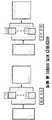
도 1은 실시예들에 따른, 마스크 설계 보정 시스템의 블록도를 도시한다. 마스크 설계 보정 시스템(100)은 예를 들어, 몇 가지 예를 들자면, 하나 이상의 데스크톱 컴퓨터, 서버급 컴퓨터, 랩톱, 태블릿, 및 스마트폰(이하, 마스크 설계 보정 시스템으로서 지칭됨)을 사용하여 구현될 수 있다. 하나 이상의 컴퓨팅 디바이스는 몇 가지 예를 들자면, 유선 또는 무선 근거리 네트워크, 광역 네트워크, 인터넷에서, 또는 클라우드 컴퓨팅 플랫폼을 통해 결합될 수 있다.1 shows a block diagram of a mask design calibration system, in accordance with embodiments. Mask
도면에 도시된 바와 같이, 마스크 설계 보정 시스템(100)은 스캐닝 모듈(105)을 포함한다. 실시예들에서, 스캐닝 모듈(105)은 웨이퍼 내의 레이어의 제1 주사 전자 현미경(SEM) 이미지를 스캐닝하도록, 웨이퍼의 제1 SEM 이미지로부터 웨이퍼 결함들을 검출하도록, 그리고 웨이퍼 결함들을 갖는 웨이퍼 상의 위치들을 출력하도록 구성된다. 윤곽 추출 모듈(110)은 웨이퍼 결함들을 갖는 웨이퍼 상의 위치들을 획득하도록, 그리고 웨이퍼 내의 레이어와 연관된 이전에 제조된 포토마스크의 제2 SEM 이미지로부터 복수의 마스크 윤곽들을 추출하도록 ― 추출된 마스크 윤곽들은 웨이퍼의 검출된 웨이퍼 결함들에 대응하는 이전에 제조한 포토마스크 상의 위치에 대응함 ― 구성된다. 시뮬레이션 모듈(115)은 추출된 복수의 마스크 윤곽들을 획득하도록, 그리고 추출된 복수의 마스크 윤곽들을 사용하여 시뮬레이션 제조된 웨이퍼를 생성하도록 구성된다. 검출 모듈(120)은 시뮬레이션 제조된 웨이퍼를 획득하도록, 시뮬레이션 제조된 웨이퍼 상의 하나 이상의 결함을 검출하도록, 그리고 시뮬레이션 제조된 웨이퍼 상의 결함을 포함하는 데이터를 출력하도록 구성된다. 포토마스크 분석 모듈(125)은 시뮬레이션 제조된 웨이퍼 상의 결함을 포함하는 데이터를 획득하도록, 시뮬레이션 제조된 웨이퍼 상의 결함을 포함하는 데이터에 기초하여 이전에 제조된 포토마스크의 하나 이상의 문제되는 영역을 결정하도록, 그리고 이전에 제조된 포토마스크의 문제되는 영역에 관한 패턴 정보를 생성하도록 구성된다. 공간 도메인 분석 모듈(130)은 이전에 제조된 포토마스크의 문제 영역에 관한 패턴 정보를 획득하도록, 패턴 정보의 공간 도메인 분석을 수행하도록, 그리고 공간 도메인 분석의 결과를 출력하도록 구성된다. 패턴 식별 모듈(135)은 공간 도메인 분석의 결과를 획득하도록, 결과 공간 도메인 분석의 결과에 기초하여, 하나 이상의 대응하는 결함을 보이는 복수의 포토마스크 구조 패턴들을 결정하도록, 그리고 하나 이상의 대응하는 결함을 보이는 복수의 포토마스크 구조 패턴들에 대응하는 데이터를 출력하도록 구성된다. 패턴 생성 모듈(140)은 하나 이상의 대응하는 결함을 보이는 복수의 포토마스크 구조 패턴들에 대응하는 데이터를 획득하도록, 하나 이상의 대응하는 결함을 보이는 복수의 포토마스크 구조 패턴들에 적용될 복수의 처리들을 선택하도록, 선택된 각 처치에 대해, 처치에 대응하는 복수의 파라미터들을 선택하도록, 선택된 파라미터들을 갖는 선택된 처리들을 하나 이상의 대응하는 결함을 보이는 복수의 포토마스크 구조 패턴들에 적용하도록, 공간 도메인 분석에 기초하여 복수의 포토마스크 구조 패턴들로부터 복수의 잠재적 보정 포토마스크 구조 패턴들을 생성하도록, 잠재적 보정 포토마스크 구조 패턴들을 테스트 포토마스크 내에 통합시키도록, 테스트 포토마스크 상의 잠재적 보정 포토마스크 구조 패턴들을 분석하도록, 그리고 복수의 잠재적 보정 포토마스크 구조 패턴들로부터 복수의 보정 포토마스크 구조 패턴들을 선택하며 출력하도록 구성된다. 스크립트 모듈(145)은 복수의 보정 포토마스크 구조 패턴들을 획득하도록, 복수의 보정 포토마스크 구조 패턴들에 기초하여 하나 이상의 포토마스크 패턴 보정 스크립트를 생성하도록, 그리고 하나 이상의 포토마스크 패턴 보정 스크립트를 실행하여 복수의 보정 포토마스크 구조 패턴들 중 하나 이상을 포토마스크 레이아웃에 적용하도록 구성된다.As shown in the figure, the mask
도 2는 본 발명의 예시적인 실시예들에 따른, 공정 흐름의 흐름도이다. 도시된 공정 흐름은 도 1에 도시된 시스템(100)과 같은 마스크 설계 보정 시스템의 실시예들에 의해 수행되는 단계들을 도시한다. 공정 흐름은 보정을 필요로 하는 마스크 구조들을 식별하기 위해 공간 도메인 분석이 수행되는 데이터 분석 단계를 포함한다. 또한, SEM 이미지 윤곽 분석이 수행될 수 있다. LAM 게이지 패턴 설계 및 임베딩 단계는 데이터 분석에 기초하여 LAMA 패턴을 설계하고, 패턴을 테스트 마스크 내로 통합시킨다. LAMA 패턴 분석 및 솔루션 단계는 테스트 마스크 상의 LAMA 패턴들을 분석하고, 맞춤 LAMA 솔루션을 구축한다. 다음으로, LAMA 패턴들이 마스크 레이아웃에 적용되고, 최종 마스크가 구축되며 검증된다. 마지막으로, 최종 마스크의 예측 웨이퍼 성능을 평가하기 위해 윤곽 추출이 수행된다.2 is a flow diagram of a process flow, in accordance with exemplary embodiments of the present invention. The depicted process flow depicts steps performed by embodiments of a mask design calibration system, such as
도 3a 내지 도 3c는 본 발명의 예시적인 실시예에 따른 방법(300)의 공정 흐름을 도시한다. 실시예들에서, 도시된 공정 흐름은 예를 들어, 몇 가지 예를 들자면, 하나 이상의 데스크톱 컴퓨터, 서버급 컴퓨터, 랩톱, 태블릿, 및 스마트폰(이하, 마스크 설계 보정 시스템으로서 지칭됨)과 같은 하나 이상의 컴퓨팅 디바이스에 의해 수행될 수 있다. 하나 이상의 컴퓨팅 디바이스는 몇 가지 예를 들자면, 유선 또는 무선 근거리 네트워크, 광역 네트워크, 인터넷에서, 또는 클라우드 컴퓨팅 플랫폼을 통해 결합될 수 있다. 실시예들에서, 네트워크는 보안 네트워크일 것이다.3A-3C show the process flow of a
방법(300)은 단계 S302에서 시작한다. 단계 S302에서, 실시예들에서, 본 방법을 수행하는 마스크 설계 보정 시스템에 의해 분석된 웨이퍼 내의 레이어의 취약점 후보들 및/또는 SEM 이미지를 식별하기 위해 공간 도메인 분석이 사용된다. 마스크 설계 보정 시스템은 예를 들어, 몇 가지 예를 들자면 라인 파단 및 마이크로 브리지와 같은 결함들에 대해 웨이퍼들의 SEM 이미지를 분석한다. 본 발명의 범주 또는 사상으로부터 벗어나지 않고 해결될 수 있는 다른 결함들이 또한 존재할 수 있다. 실시예들에서, 식별된 결함들은 분석 및/또는 보정될 포토마스크 설계에서의 대응하는 영역들을 식별하기 위해 사용될 수 있다. 실시예들에서, 단계 S302는 웨이퍼의 레이어에서의 잠재적인 핫 스팟들 또는 취약점들 또는 에러들을 식별할 수 있는 다른 공정들로 대체될 수 있다.The
단계 S304에서, 실시예들에서, 마스크 설계 보정 시스템은 포토마스크의 SEM 이미지의 마스크 윤곽을 추출하며, 여기서 포토마스크는 웨이퍼를 제조하기 위해 사용되는 대응하는 포토마스크이다. 단계 S302에서 웨이퍼의 SEM 이미지가 사용되는 실시예들에서, 포토마스크는 웨이퍼의 SEM 이미지와 연관된 웨이퍼 내의 레이어에 대응한다. 웨이퍼의 레이어 내의 핫 스팟들을 식별하기 위해 다른 공정들이 사용되는 실시예들에서, 포토마스크는 식별된 핫 스팟(들)과 연관된 웨이퍼 내의 레이어에 대응한다. 실시예들에 따르면, 결함들을 보인 SEM 이미지에서 식별된 영역들에 기초하여 마스크 윤곽이 추출된다. 실시예들에서, 추출은 몇 가지 예를 들자면, 포토마스크의 SEM 이미지, 및/또는 포토마스크에 대한 설계 데이터에 기초하여 수행될 수 있다.At step S304, in embodiments, the mask design correction system extracts a mask contour of the SEM image of the photomask, where the photomask is a corresponding photomask used to fabricate the wafer. In embodiments where an SEM image of the wafer is used in step S302, the photomask corresponds to a layer within the wafer associated with the SEM image of the wafer. In embodiments where different processes are used to identify hot spots within a layer of a wafer, the photomask corresponds to the layer within the wafer associated with the identified hot spot(s). According to embodiments, a mask contour is extracted based on areas identified in the SEM image that showed defects. In embodiments, extraction may be performed based on an SEM image of the photomask, and/or design data for the photomask, to name a few.
다음으로, 단계 S306에서, 마스크 설계 보정 시스템은 추출된 마스크 윤곽을 입력으로서 사용하여, 제조 시뮬레이션 공정을 실행한다. 시뮬레이션은 시뮬레이션 제조된 웨이퍼를 생성하며, 그 다음 이 시뮬레이션 제조된 웨이퍼는 단계 S302에서 물리적 웨이퍼 상에서 검출된 결함들과 유사한 결함들, 또는 다른 식별된 실제 및/또는 잠재적인 핫 스팟들에 대해 분석될 수 있다.Next, in step S306, the mask design correction system uses the extracted mask contour as an input to execute a manufacturing simulation process. The simulation creates a simulated manufactured wafer, which is then analyzed for defects similar to those detected on the physical wafer in step S302, or other identified actual and/or potential hot spots. can
단계 S308에서, 마스크 설계 보정 시스템은 시뮬레이션 제조된 웨이퍼 상의 하나 이상의 결함을 검출한다. 마스크 설계 보정 시스템은 몇 가지 예를 들자면, 육안 검사 툴, 광학 검사 툴, 임계 치수 측정 툴을 이용함으로써 결함들 또는 취약점 후보들을 검출할 수 있다.In step S308, the mask design correction system detects one or more defects on the simulated fabricated wafer. The mask design calibration system can detect defects or weakness candidates by using visual inspection tools, optical inspection tools, and critical dimension measurement tools, to name a few.
단계 S310에서, 마스크 설계 보정 시스템은 LAMA 마스크와 웨이퍼 조화 시뮬레이션을 사용하여 검출된 결함들에 기초하여 포토마스크의 하나 이상의 문제되는 영역을 결정한다. 실시예들에서, 하나 이상의 문제되는 영역의 위치는 각 레이어에 대한 마스크 설계에서의 추가 분석 및 보정을 위해 식별될 것이다.In step S310, the mask design correction system determines one or more problematic regions of the photomask based on the defects detected using the LAMA mask and wafer rough simulation. In embodiments, the location of one or more problematic regions will be identified for further analysis and correction in the mask design for each layer.
그 다음, 방법 300은 단계 S312로 진행한다. 단계 S312에서, 단계 S310에서 식별된 포토마스크의 하나 이상의 문제되는 영역에 관한 패턴 정보가 마스크 설계 보정 시스템에 의해 획득된다. 실시예에서, 패턴 정보는 식별된 결함들을 보이는 이전에 제조된 포토마스크의 레이아웃을 묘사하는 하나 이상의 데이터 파일의 형태일 수 있다. 실시예들에서, 패턴 정보는 아직 제조되지 않았지만, 그 외에는 보정되지 않는다면 결함들을 보일 것으로 예상되는 설계 요소들을 포함하는 것으로서 식별된 포토마스크의 설계일 수 있다.
실시예들에서, 패턴 정보는 기존 포토마스크의 주사 전자 현미경(SEM) 윤곽 추출 분석을 사용하여 획득될 수 있다. 이는 도 4에 도시된 LAMA 윤곽 추출 툴 알고리즘과 같은 윤곽 추출 알고리즘을 실행하는 윤곽 추출 툴에 SEM 이미지를 사용하여 이루어질 수 있다. 실시예들에서, 다른 윤곽 추출 알고리즘들이 본 발명의 범위 또는 사상으로부터 벗어나지 않고 사용될 수 있다. 윤곽 추출 툴에 대한 LAMA SEM 이미지의 출력 로그 파일의 예가 도 5에 예시되어 있다. 윤곽 추출 툴에 LAMA SEM 이미지를 실행하는 데 사용되는 샘플 옵션들이 도 6에 제시되어 있으며, 여기서 툴은 컴퓨팅 디바이스의 커맨드 라인 인터페이스로부터 호출된다. 도시된 바와 같이, 특정될 수 있는 옵션들은 몇 가지 예를 들자면, 픽셀 선택 공차, 평활 값 사용, 톤, 무시 영역의 사이즈, 배경 영역 사이즈, 및 X 및 Y 방향들에서의 크기 조정을 포함한다. 실시예들에서, 본 발명의 범주 또는 사상으로부터 벗어나지 않고 웨이퍼의 제조에서의 가공 단계들 또는 재료 선택에 대한 다른 변형예들이 사용될 수 있다. 실시예들에서, 윤곽 추출 툴에 대한 SEM 이미지는 도 7에 도시된 바와 같은 평활화된 픽셀로 된 윤곽을 생성할 수 있다.In embodiments, pattern information may be obtained using scanning electron microscopy (SEM) contour extraction analysis of an existing photomask. This can be done using the SEM images in a contour extraction tool that runs a contour extraction algorithm, such as the LAMA contour extraction tool algorithm shown in FIG. 4 . In embodiments, other contour extraction algorithms may be used without departing from the scope or spirit of the present invention. An example of an output log file of LAMA SEM images for the contour extraction tool is illustrated in FIG. 5 . Sample options used to run a LAMA SEM image to the contour extraction tool are presented in FIG. 6 , where the tool is invoked from a command line interface of a computing device. As shown, the options that can be specified include pixel selection tolerance, use of smoothing value, tone, ignore region size, background region size, and scaling in the X and Y directions, to name a few. In embodiments, other variations on material selection or processing steps in the fabrication of wafers may be used without departing from the scope or spirit of the present invention. In embodiments, the SEM image for the contour extraction tool may produce a smoothed pixelated contour as shown in FIG. 7 .
도 8a, 도 8b 및 도 8c는 SEM 이미지로부터 패턴 정보를 획득하기 위한 공정을 도시한다. 도면에 나타내어진 바와 같이, 도 8a는 마스크 윤곽의 SEM 이미지를 나타낸다. 마스크 윤곽은 단계 S310에서 결정된 바와 같은 마스크의 문제되는 영역, 또는 "핫 스팟" 또는 "취약점"과 연관된 마스크 설계의 적어도 일부분을 나타낸다. 도 8b는 마스크의 문제되는 영역들과 연관된 마스크 설계의 적어도 일부분과 연관된 윤곽 추출에 대한 SEM 이미지에 의한 도 8a에서의 이미지로부터 추출된 고명암 맵(high intensity map)을 나타낸다. 고명암 맵은 마스크 설계 보정 시스템이 보정으로부터 이익을 얻을 가능성이 있는 마스크의 특정 영역들을 식별할 수 있게 한다. 이러한 영역들이 식별된 후에, 마스크 설계 보정 시스템은 마스크 설계 파일(예를 들어, 도 8c에 도시된 OASIS/GDS) 또는 임의의 레이아웃 포맷 파일을 생성한다. OASIS(Open Artwork System Interchange Standard)는 EDA(Electronic Design Automation) 소프트웨어, IC 마스크 기록 툴 및 마스크 검사 툴 간의 교환을 위한 계층적 집적 회로 마스크 레이아웃 데이터 포맷에 대한 사양이다. OASIS 파일은 후속 분석을 위해 마스크 레이아웃 정보(마스크 패턴 정보를 포함)를 저장한다. 본 발명의 범주 또는 사상으로부터 벗어나지 않고 다른 레이아웃 데이터 포맷들이 사용될 수 있다.8A, 8B and 8C show a process for obtaining pattern information from SEM images. As shown in the figure, Fig. 8a shows a SEM image of the mask contour. The mask contour represents at least a portion of the mask design associated with the problem areas of the mask, or "hot spots" or "weak points" as determined in step S310. FIG. 8B shows a high intensity map extracted from the image in FIG. 8A by means of a SEM image of contour extraction associated with at least a portion of the mask design associated with problematic areas of the mask. The high-contrast map allows the mask design correction system to identify specific areas of the mask that are likely to benefit from correction. After these areas are identified, the mask design correction system creates a mask design file (e.g., OASIS/GDS shown in Fig. 8C) or any layout format file. The Open Artwork System Interchange Standard (OASIS) is a specification for a hierarchical integrated circuit mask layout data format for interchange between Electronic Design Automation (EDA) software, IC mask writing tools, and mask inspection tools. OASIS files store mask layout information (including mask pattern information) for subsequent analysis. Other layout data formats may be used without departing from the scope or spirit of the present invention.
단계 S312에서 패턴 정보가 획득되면, 방법(300)은 단계 S314로 진행한다. 방법(300)의 단계 S314에서, 마스크 설계 보정 시스템은 획득된 패턴 정보에 대한 공간 도메인 분석을 수행할 수 있다. 실시예들에 따르면, 공간 도메인 분석은 빅 데이터 분석을 사용하여 패턴 정보로부터 패턴들을 추출하는 패턴 묘사 검색을 실행함으로써 수행된다. 상용 EDA 툴을 사용하여 패턴 검색을 수행하기 위해 샘플 데이터 분석 툴이 사용될 수 있다. 실시예들에서, 패턴 검색은 몇 가지 예를 들자면, 설계 규칙 점검(Design Rule Check, DRC), 마스크 규칙 점검(Mask Rule Check, MRC), 또는 패턴 매칭(Pattern Matching, PM)으로서 지칭될 수 있다. 상용 EDA 툴 패턴 검색 코드의 예가 도 9에 서술되어 있다. 본 발명의 범위 또는 사상으로부터 벗어나지 않고 다른 패턴 검색 코드들이 사용될 수 있다. 패턴 묘사 검색 소프트웨어에 대한 입력은 예를 들어, 들어오는 디바이스 반도체 데이터와 같은 패턴 정보를 포함할 수 있다. 본 발명의 범주 또는 사상으로부터 벗어나지 않고 다른 입력 데이가 패턴 정보와 함께 사용될 수 있다.If pattern information is obtained at step S312,
패턴 묘사 검색이 수행되면, 실시예들에서, 그 다음, 추출된 패턴들이 예를 들어, 데이터 분석 코드를 사용하여 마스크 설계 보정 시스템에 의해 분석될 수 있다. 데이터 분석 코드의 예가 도 10에 서술되어 있다. 실시예들에서, 데이터 분석 코드는 LAMA로부터 이익을 얻을 수 있는 포토마스크 영역들/구조들을 나타내는 결과들을 출력한다.Once the pattern description search is performed, in embodiments, the extracted patterns may then be analyzed by a mask design correction system using, for example, data analysis code. An example of data analysis code is illustrated in FIG. 10 . In embodiments, the data analysis code outputs results representing photomask regions/structures that can benefit from LAMA.
본 발명의 범주 또는 사상으로부터 벗어나지 않고 이러한 및 다른 분석 기술들이 사용될 수 있다.These and other analytical techniques may be used without departing from the scope or spirit of the present invention.
도 3을 참조하면, 단계 S314에서 공간 도메인 분석을 수행한 후에, 방법(300)은 단계 S316으로 진행한다. 단계 S316에서, 실시예들에서, 마스크 설계 보정 시스템은 예를 들어, 패턴 정보의 공간 도메인 분석에 기초하여, 구조들이 LAMA의 적용으로부터 이익을 얻을 수 있도록, 하나 이상의 취약점 후보를 보이는 하나 이상의 포토마스크 구조 패턴을 결정한다. 예시적인 취약점 후보 및/또는 처리는 몇 가지 예를 들자면, 코너 라운딩, 수평 및 수직 바이어스, 및 선량 조절을 포함할 수 있다. 본 발명의 범주 또는 사상으로부터 벗어나지 않고 다른 취약점 후보 및/또는 처리가 LAMA 보정에 적절할 수 있다.Referring to FIG. 3 , after performing spatial domain analysis in step S314 , the
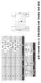
실시예들에서, 마스크 설계 보정 시스템은 예를 들어, 향후 소비자 제품들에 대해 수행될 공간/라인 공간 샘플링에 기초하여 하나 이상의 취약점 후보를 보이는 하나 이상의 포토마스크 구조 패턴을 생성한다. 본 발명의 범주 또는 사상으로부터 벗어나지 않고 다른 취약점 후보도 생성될 수 있다. 도 11에 도시된 바와 같이, 공간/라인 공간 샘플링 데이터는 데이터에 기초하여 다양한 패턴들을 생성하는 파이썬 스크립트에 입력된다. 도 11에 도시된 바와 같이, 생성된 패턴들은 몇 가지 예를 들자면, 일반 라인 피치 수평/수직, 라인 종단 수평/수직, DOT 직교/상호 교차, 일반 공간 피치 수평/수직, 공간 종단 수평/수직, 및 CNT 직교/상호 교차뿐만 아니라 로직 및 메모리 설계들에 통합되는 전형적인 구조들을 포함할 수 있다.In embodiments, the mask design correction system generates one or more photomask structure patterns exhibiting one or more vulnerability candidates based, for example, on space/line space sampling to be performed on future consumer products. Other vulnerability candidates may also be generated without departing from the scope or spirit of the present invention. As shown in Fig. 11, space/line space sampling data is input into a Python script that generates various patterns based on the data. As shown in FIG. 11, the generated patterns are normal line pitch horizontal/vertical, line termination horizontal/vertical, DOT orthogonal/intersecting, normal space pitch horizontal/vertical, spatial termination horizontal/vertical, to name a few. and CNT orthogonal/intersecting as well as typical structures integrated into logic and memory designs.
하나 이상의 결함을 보이는 하나 이상의 포토마스크 구조 패턴이 식별된 후, 방법(300)은 단계 S318로 진행한다. 단계 S318에서, 실시예들에서, 마스크 설계 보정 시스템은 단계 S316에서 식별된 포토마스크 구조 패턴들에 기초하여, 잠재적 보정 포토마스크 구조 패턴들 중 하나 이상을 생성한다. 실시예들에서, 잠재적 보정 포토마스크 구조들은 단계 S312에서 획득된 패턴 정보에 대응하는 포토마스크의 하나 이상의 레이어에 대해 생성된다. 실시예들에서, 단계 S318은 데이터 분석에 기초하여 리소 인식 마스크 공정 보정 응용(LAMA) 게이지를 설계하고 생성하는 것을 수반한다. LAMA 게이지는 테스트 포토마스크를 구축하는 데 사용될 잠재적 보정 구조들을 포함한다. 단계 S318에 대한 입력들은 제조 노하우, 웨이퍼 제조자로부터의 데이터, 및 데이터 분석으로부터 추출된 데이터 모두를 포함한다. 예를 들어, 제조 노하우는 포토마스크가 사용될 제조 공정의 제한을 포함할 수 있다. 제조 데이터는 몇 가지 예를 들자면, 최소 공간 및 폭 파라미터들, 코너 대 코너 측정치들, 및/또는 마스크 공정 충실도 특성화(이를테면, 코너 라운딩, 코너 풀백, 및 피치)를 포함할 수 있다. 보정 포토마스크 구조 패턴들을 생성하는 데 사용되는 데이터 분석의 결과들은 몇 가지 예를 들자면, 고객 설계 공간 도메인 데이터, 앵커/임계 구조들, 및/또는 LAMA 게이지에서 집중될 임계 치수 및 설계 형상 범위를 포함할 수 있다.After one or more photomask structure patterns exhibiting one or more defects are identified, the
실시예들에서, 마스크 설계 보정 시스템은 하나 이상의 대응하는 결함을 보이는 복수의 포토마스크 구조 패턴들에 적용될 복수의 처리들을 선택한다. 선택된 처리 각각에 대해, 마스크 설계 보정 시스템은 그 처리에 대응하는 복수의 파라미터들을 선택한다. 처리들 및 처리들에 대응하는 파라미터들을 선택한 후에, 마스크 설계 보정 시스템은 선택된 파라미터들을 갖는 선택된 처리들을 하나 이상의 대응하는 결함을 보이는 복수의 포토마스크 구조 패턴들에 적용한다. 이러한 방식으로, 마스크 설계 보정 시스템은 패턴 정보에 기초하여 새로운 포토마스크 구조 패턴들을 생성한다. 예를 들어, 코너 라운딩 및 선량 조절을 포함하는 상이한 처리들이 가능하다. 마스크 설계 보정 시스템은 결함들을 잠재적으로 보정할 수 있는 복수의 포토마스크 구조 패턴들을 생성하기 위해 결함이 있는 포토마스크 패턴 구조들에 다수의 처리들을 적용한다.In embodiments, the mask design correction system selects a plurality of processes to be applied to a plurality of photomask structure patterns exhibiting one or more corresponding defects. For each selected process, the mask design correction system selects a plurality of parameters corresponding to that process. After selecting the processes and parameters corresponding to the processes, the mask design correction system applies the selected processes with the selected parameters to a plurality of photomask structure patterns exhibiting one or more corresponding defects. In this way, the mask design correction system creates new photomask structure patterns based on the pattern information. Different treatments are possible including, for example, corner rounding and dose adjustment. A mask design correction system applies a number of processes to the defective photomask pattern structures to create a plurality of photomask structure patterns that can potentially correct the defects.
테스트 마스크가 사용되는 실시예들에서, 후술되는 바와 같이 복수의 잠재적 보정 구조들이 식별되고 테스트 마스크 상에 사용될 수 있다. 실시예들에서, 레이어에 대해 완성된 포토마스크가 사용될 수 있는 경우, 특정 보정 구조가 선택되고 레이어에 대해 완성된 포토마스크 설계에 적용된 다음, 포토마스크를 생성하는 데 직접 적용될 수 있다. 실시예에서, 이러한 기술들의 조합, 예를 들어, 레이어에 대해 완성된 포토마스크 설계를 포토마스크의 미사용 부분들에서의 하나 이상의 잠재적 보정 구조와 조합하여 인쇄하는 것이 사용될 수 있다.In embodiments where a test mask is used, a plurality of potential correction structures can be identified and used on the test mask as described below. In embodiments, where a photomask completed for a layer can be used, a specific correction structure can be selected and applied to the photomask design completed for a layer, and then applied directly to create the photomask. In an embodiment, a combination of these techniques may be used, for example printing a completed photomask design for a layer in combination with one or more potential correction structures in unused portions of the photomask.
실시예들에서, LAMA 게이지는 해상도를 향상시키기 위해 보다 작은 피처들에 대한 선량을 조절하고 코너 라운딩을 수행하도록 설계될 수 있다. 또한, 처리되지 않은 패턴들이 충실도 특성화에 그리고 포토마스크 제한을 정의하는 데 사용될 수 있다. 잠재적 보정 포토마스크 구조 패턴들을 생성하기 위해 사용될 수 있는 LAMA 게이지 설계들의 예들은 도 12 내지 도 17에 따른다. 본 발명의 범주 또는 사상으로부터 벗어나지 않고 다른 LAMA 게이지들이 설계되고/되거나 적용될 수 있다.In embodiments, a LAMA gauge can be designed to dose and perform corner rounding on smaller features to improve resolution. Also, unprocessed patterns can be used for fidelity characterization and to define photomask limits. Examples of LAMA gauge designs that can be used to create potentially calibrated photomask structure patterns are in accordance with FIGS. 12-17 . Other LAMA gauges may be designed and/or applied without departing from the scope or spirit of the present invention.
도 12는 잠재적 보정 포토마스크 구조 패턴들을 생성하기 위해 포토마스크 구조 패턴들에 적용될 코너 라운딩 개선 및 수평/수직 바이어스의 테이블을 도시한다. 유사하게, 도 13은 잠재적 보정 포토마스크 구조들의 세트를 생성하기 위해 상이한 시간들에 상이한 포토마스크 구조들에 적용될 선량 변조의 테이블을 도시한다. 도 14는 잠재적 보정 포토마스크 구조들의 세트를 생성하기 위해 상이한 시간들에 상이한 포토마스크 구조들에 적용될 공간 피치 및 라인 피치 설계들을 도시한다. 도 15는 잠재적 보정 포토마스크 구조들의 세트를 생성하기 위해 상이한 시간들에 상이한 포토마스크 구조들에 적용될 라인 종단 및 공간 종단 설계들을 도시한다. 도 16은 잠재적 보정 포토마스크 구조들의 세트를 생성하기 위해 상이한 시간들에 상이한 포토마스크 구조들에 적용될 DOT/홀 직교 설계를 도시한다. 도 17은 잠재적 보정 포토마스크 구조들의 세트를 생성하기 위해 상이한 시간들에 상이한 포토마스크 구조들에 적용될 DOT/홀 상호 교차 설계를 도시한다. 이러한 LAMA 게이지 설계들은 패턴 정보에서 식별된 하나 이상의 취약점을 보이는 구조들에 대응하는 잠재적 보정 포토마스크 구조들의 예들을 나타낸다. LAMA 게이지 패턴은 사이즈가 맞춤화될 수 있고, 포토마스크 상의 임의의 미사용 공간 내로의 배치의 유연성 및 용이성을 보일 수 있으며, 이는 결과적으로 추가적인 마스크 비용을 절감한다. 본 발명의 범주 또는 사상으로부터 벗어나지 않고 이러한 LAMA 게이지 설계들 중 하나 이상의 및/또는 다른 LAMA 게이지 설계들이 하나 이상의 잠재적 보정 포토마스크 구조를 형성하기 위해 사용될 수 있다.12 shows a table of corner rounding enhancement and horizontal/vertical bias to be applied to photomask structure patterns to create potential corrective photomask structure patterns. Similarly, FIG. 13 shows a table of dose modulation to be applied to different photomask structures at different times to create a set of potentially corrective photomask structures. 14 shows spatial pitch and line pitch designs to be applied to different photomask structures at different times to create a set of potentially corrective photomask structures. 15 shows line termination and space termination designs to be applied to different photomask structures at different times to create a set of potential corrective photomask structures. 16 shows a DOT/hole orthogonal design to be applied to different photomask structures at different times to create a set of potentially corrective photomask structures. 17 shows a DOT/hole intersect design to be applied to different photomask structures at different times to create a set of potential corrective photomask structures. These LAMA gauge designs represent examples of potential corrective photomask structures corresponding to structures exhibiting one or more weaknesses identified in the pattern information. The LAMA gauge pattern can be customized in size and can exhibit flexibility and ease of placement into any unused space on the photomask, which in turn saves additional mask cost. One or more of these LAMA gauge designs and/or other LAMA gauge designs may be used to form one or more potential corrective photomask structures without departing from the scope or spirit of the present invention.
다음으로, 단계 S320에서, 잠재적 보정 포토마스크 구조 패턴들이 포토마스크 설계 내로 통합된다. 실시예들에 따르면, 이 단계에서, 방법(300)을 수행하는 마스크 설계 보정 시스템은 잠재적 보정 포토마스크 구조들을 포함하는 LAMA 게이지 설계들을 판독하고, 이러한 설계 요소들을 포토마스크가 어떻게 구축될 수 있는지를 정의하는 포토마스크 데이터에 적용한다. 실시예들에 따르면, 잠재적 보정 포토마스크 구조들은 기존 포토마스크 레이아웃 상의 미사용 공간 내로 통합된다.Next, in step S320, potential corrective photomask structural patterns are incorporated into the photomask design. According to embodiments, at this step, the mask design calibration
단계 S322에서, 마스크 설계 보정 시스템은 테스트 포토마스크 상의 잠재적 보정 포토마스크 구조 패턴들을 분석한다. 실시예들에 따르면, 마스크 설계 보정 시스템은 패턴 정보에서 보인 문제가 있는 영역들이 최적화되고/되거나 수용 가능한 방식으로 보정되고/되거나 정정되었는지 여부를 결정하기 위해, 보정 포토마스크 구조들을 내부에 통합한 포토마스크 데이터에 대해 SEM 툴, CD 툴 또는 임의의 다른 광학 검사 툴을 사용하여 시뮬레이션들 및/또는 육안 검사들을 수행할 수 있다.In step S322, the mask design calibration system analyzes potential calibration photomask structure patterns on the test photomask. In accordance with embodiments, a mask design correction system may incorporate photomask structures therein to determine whether problematic areas seen in the pattern information have been optimized and/or corrected in an acceptable manner and/or corrected. Simulations and/or visual inspections may be performed on the mask data using an SEM tool, CD tool, or any other optical inspection tool.
단계 S324에서, 마스크 설계 보정 시스템은 복수의 잠재적 보정 포토마스크 구조 패턴들로부터, 복수의 보정 포토마스크 구조 패턴들을 포함하는 서브세트를 선택한다. 보정 포토마스크 구조 패턴들의 선택은 단계 S322에서 수행된 분석에 기초한다. 실시예들에서, 식별된 결함들의 가장 높은 정도의 보정을 보이는 잠재적 보정 포토마스크 구조들이 선택된다. 실시예들에서, 선택된 보정 포토마스크 구조는 두 개의 잠재적 보정 포토마스크 구조 패턴들 사이의 보간일 수 있다. 즉, 보간된 보정 포토마스크 구조 패턴은 식별된 결함들에 대한 보다 효과적인 솔루션인 것으로 결정되는 인접한 패턴들의 조합이다.In step S324, the mask design correction system selects a subset comprising a plurality of corrective photomask structure patterns from the plurality of potential corrective photomask structure patterns. The selection of the correction photomask structural patterns is based on the analysis performed in step S322. In embodiments, potential correcting photomask structures that exhibit the highest degree of correction of the identified defects are selected. In embodiments, the selected calibration photomask structure may be an interpolation between two potential calibration photomask structure patterns. That is, the interpolated corrective photomask structure pattern is a combination of adjacent patterns that is determined to be a more effective solution to the identified defects.
다음으로, 단계 S326에서, 마스크 설계 보정 시스템은 테스트 포토마스크의 분석에 기초하여 하나 이상의 포토마스크 패턴 보정 스크립트를 생성한다. 실시예들에 따르면, 마스크 설계 보정 시스템은 하나 이상의 포토마스크 구조에 보정 처리들을 적용하기 위한 규칙들을 포함하는 하나 이상의 테이블을 구축한다. 이러한 테이블의 예가 도 18에 도시되어 있다. 도시된 바와 같이, 도 18의 테이블은 테스트 포토마스크에 적용될 MRC 규칙들(이 경우, 코너 라운딩 규칙들)의 세트를 포함한다. 도 18의 테이블은 테스트 포토마스크 내로 통합되고 단계 S324에서 선택된 보정 포토마스크 구조 패턴들에 기초한다. 마스크 설계 보정 시스템은 하나 이상의 테이블에 제시된 규칙들에 기초하여 하나 이상의 포토마스크 패턴 보정 스크립트를 생성한다. 실시예들에서, 스크립트들은 NCS 언어로 생성된다. 스크립트들은 또한, 파이썬 프로그래밍 언어 또는 임의의 다른 EDA 회사 스크립팅 언어로 생성될 수 있다. 본 발명의 범주 또는 사상으로부터 벗어나지 않고 다른 스크립트들 또는 프로그래밍 언어들이 사용될 수 있다.Next, in step S326, the mask design correction system generates one or more photomask pattern correction scripts based on the analysis of the test photomask. According to embodiments, a mask design correction system builds one or more tables containing rules for applying correction processes to one or more photomask structures. An example of such a table is shown in FIG. 18 . As shown, the table of FIG. 18 contains a set of MRC rules (in this case, corner rounding rules) to be applied to the test photomask. The table of Fig. 18 is based on the calibration photomask structure patterns incorporated into the test photomask and selected in step S324. The mask design correction system generates one or more photomask pattern correction scripts based on the rules presented in one or more tables. In embodiments, scripts are created in the NCS language. Scripts can also be created in the Python programming language or any other EDA company scripting language. Other scripts or programming languages may be used without departing from the scope or spirit of the present invention.
다음으로, 단계 S328에서, 마스크 설계 보정 시스템은 원하는 IC 구조를 형성하기 위해 사용될 수 있는 포토마스크 레이아웃에 보정 포토마스크 구조들을 적용하기 위한 하나 이상의 포토마스크 패턴 보정 스크립트를 실행한다. 도 18을 참조하면, 테이블로부터 생성된 대응하는 스크립트는 최종 포토마스크를 생성하기 위해 사용될 수 있는 포토마스크 레이아웃에 열거된 규칙들을 적용하도록 실행될 것이다. 본 발명의 범주 또는 사상으로부터 벗어나지 않고 다른 스크립트들이 사용될 수 있다.Next, at step S328, the mask design calibration system executes one or more photomask pattern calibration scripts to apply the calibration photomask structures to the photomask layout that can be used to form the desired IC structure. Referring to Fig. 18, the corresponding script generated from the table will be executed to apply the listed rules to the photomask layout that can be used to create the final photomask. Other scripts may be used without departing from the scope or spirit of the present invention.
다양한 예시적인 실시예들에서, 보정 포토마스크 구조들은 레티클 플레이트 상에 적합한 방식으로 레이아웃될 수 있다. 예를 들어, 반도체 디바이스의 각 레이어가 보정 마스크 패턴들 중 하나 이상을 사용하여 형성될 수 있도록, 다수의 보정 마스크 패턴들이 플레이트 상에 형성될 수 있다. 또한, 보정 마스크 패턴들은 최종 마스크 설계를 위해 의도된 마스크 패턴들의 일부만을 포함하거나 포함하지 않는 테스트 마스크에 적용될 수 있거나, 또는 IC 제품을 형성하기 위해 사용되도록 의도된 레이어 패턴들의 전체를 통합하는 최종 마스크에 적용될 수 있다는 것이 이해되어야 한다. 또한, 예시적인 실시예들에서, IC 제조 공정 동안 마스크 상의 모든 보정 마스크 패턴이 사용될 수 있는 것은 아니고, 일부 경우들에서, 다른 보정 패턴들이 마스크 상에 존재할 수 있더라도 최적의 보정을 달성하는 보정 마스크 패턴들만 사용된다.In various exemplary embodiments, the calibration photomask structures may be laid out in a suitable manner on the reticle plate. For example, multiple correction mask patterns may be formed on the plate, such that each layer of the semiconductor device may be formed using one or more of the correction mask patterns. Further, correction mask patterns may be applied to a test mask that may or may not include only portions of mask patterns intended for final mask design, or final mask incorporating all of layer patterns intended to be used to form an IC product. It should be understood that it can be applied to Also, in exemplary embodiments, not every correction mask pattern on the mask may be used during the IC fabrication process, and in some cases, a correction mask pattern that achieves optimal correction even if other correction patterns may be present on the mask. only are used
단계 S330에서, 당업계에 알려져 있는 포토마스크 제조 기술들에 따라 전체 레이어에 대한 최종 포토마스크 레이아웃에 기초하여 레이어에 대한 완전한 설계를 통합하는 최종 포토마스크가 물리적으로 제조된다.In step S330, a final photomask incorporating the complete design for the layer is physically fabricated based on the final photomask layout for the entire layer according to photomask manufacturing techniques known in the art.
실시예들에서, 선택된 보정 패턴들이 통합된 전체 레이어뿐만 아니라, 전체 레이어의 일부분과만 연관된 보정 마스크 패턴들을 포함하는 최종 마스크 설계가 동일한 포토마스크에 인쇄될 수 있다. 이러한 실시예에서, 전체 레이어이 그 레이어에 대한 포토마스크들의 향후 버전들에 사용하기 위해 테스트될 잠재적 보정 및 잠재적 보정 패턴들 또는 유사한 설계 요소들과 소비자에게 전달될 수 있다. 이러한 실시예들에서, 별개의 테스트 마스크를 제조하고 분석하는 중간 단계들은 스킵될 수 있다.In embodiments, a final mask design comprising correction mask patterns associated with only a portion of an entire layer, as well as an entire layer into which selected correction patterns are integrated, may be printed on the same photomask. In such an embodiment, the entire layer may be delivered to the consumer with a potential correction and potential correction patterns or similar design elements to be tested for use in future versions of photomasks for that layer. In such embodiments, intermediate steps of fabricating and analyzing a separate test mask may be skipped.
단계 S332에서, 마스크 설계 보정 시스템은 하나 이상의 보정 포토마스크 구조가 최종 포토마스크에 적용되었음을 확정한다. 실시예들에 따르면, 마스크 설계 보정 시스템은 임계 치수(CD) 검사 툴을 이용하여, 결과적인 최종 포토마스크에서, 몇 가지 예를 들자면, 코너 라운딩, 및 수평/수직 바이어싱을 분석할 수 있다. 마스크 설계 보정 시스템은 CD 검사 툴을 사용하여, 마스크 SEM 윤곽들 또는 SEM 이미지를 윤곽 추출 툴로 추출하고, 이러한 윤곽들을 최종 포토마스크 레이아웃 설계와 비교한다.In step S332, the mask design calibration system determines that one or more calibration photomask structures have been applied to the final photomask. According to embodiments, the mask design correction system may use a critical dimension (CD) inspection tool to analyze the resulting final photomask for corner rounding, and horizontal/vertical biasing, to name a few examples. The mask design calibration system uses the CD inspection tool to extract the mask SEM contours or SEM image to the contour extraction tool and compares these contours to the final photomask layout design.
단계 S334에서, 마스크 설계 보정 시스템은 최종 포토마스크에 기초하여 생성된 웨이퍼 상의 복수의 위치들이 이전에 제조된 포토마스크 상에 보인 하나 이상의 결함에 대응하는 결함을 보이지 않는다고 결정한다. 실시예들에서, 최종 포토마스크 상의 다수의 위치들이 선택되고 처리되지 않은 포토마스크를 사용하여 생성되었던 이전에 제조된 웨이퍼 상의 대응하는 위치들과 비교될 수 있다. 처리된 포토마스크 웨이퍼와 처리되지 않은 포토마스크 웨이퍼는 육안 그리고 분석 툴 둘 모두를 사용하여 비교된다. 예를 들어, 도 21은 처리되지 않은 포토마스크의 SEM 이미지와 HOLE 구조에 대해 보정 LAMA 패턴으로 처리되었던 포토마스크의 SEM 이미지 간의 비교를 도시한다. 도시된 바와 같이, 처리된 포토마스크에서, 누락 패턴이 없고, 개선된 LCDU가 마스크에 대한 설계 사양을 더 근접하게 따른다.In step S334, the mask design correction system determines that the plurality of locations on the wafer created based on the final photomask do not exhibit defects corresponding to one or more defects seen on previously fabricated photomasks. In embodiments, a number of locations on the final photomask can be selected and compared to corresponding locations on a previously fabricated wafer that were created using the unprocessed photomask. The treated and untreated photomask wafers are compared using both visual and analytical tools. For example, FIG. 21 shows a comparison between an SEM image of an unprocessed photomask and a photomask that has been processed with a corrective LAMA pattern for the HOLE structure. As shown, in the processed photomask, there are no missing patterns, and the improved LCDU follows the design specifications for the mask more closely.
도 19는 상이한 포토마스크들의 SEM 이미지들(하나는 처리되지 않고, 다른 하나는 단계 S324에서 선택된 보정 포토마스크 구조들로 처리됨) 간의 비교를 도시한다. 도시된 바와 같이, 처리된 포토마스크에서, 라인 파단이 없고, 라인 폭 및 간격이 마스크에 대한 설계 사양을 더 근접하게 따른다.Fig. 19 shows a comparison between SEM images of different photomasks (one unprocessed, the other processed with the corrective photomask structures selected in step S324). As shown, in the processed photomask, there are no line breaks, and the line widths and spacing more closely follow the design specifications for the mask.
도 20은 처리된 마스크와 처리되지 않은 마스크 간의 컨택트 홀들의 개선의 예를 도시한다. 도시된 바와 같이, 처리되지 않은 윤곽은 처리된 마스크에 비해 더 많은 코너 풀백을 보인다.20 shows an example of improvement of contact holes between a treated and untreated mask. As shown, the unprocessed contour shows more corner pullback compared to the processed mask.
이러한 개선 및 다른 개선은 본 발명에 따라 보정 LAMA 패턴들을 사용함으로써 얻어질 수 있다.This and other improvements can be obtained by using corrective LAMA patterns in accordance with the present invention.
이제, 본 발명의 실시예들이 상세히 제시되고 설명되었지만, 이에 대한 다양한 변형 및 개선이 본 기술분야의 통상의 기술자에게 용이하게 명백해질 수 있다. 이에 따라, 상술한 바와 같은 본 발명의 예시적인 실시예들은 예시적인 것이며, 제한적인 것이 아니다. 본 발명의 사상 및 범위는 넓게 해석되어야 한다.Now, while embodiments of the present invention have been shown and described in detail, various modifications and improvements thereto may readily become apparent to those skilled in the art. Accordingly, the exemplary embodiments of the present invention as described above are illustrative and not restrictive. The spirit and scope of the present invention should be interpreted broadly.
Claims (33)
Translated fromKorean(a) 웨이퍼의 주사 전자 현미경(scanning electron microscope, SEM) 이미지로부터 웨이퍼 결함들을 검출하는 단계;
(b) 이전에 제조된 포토마스크의 SEM 이미지로부터 복수의 마스크 윤곽들 ― 상기 추출된 마스크 윤곽들은 상기 검출된 웨이퍼 결함들에 대응할 수 있음 ― 을 추출하는 단계;
(c) 상기 추출된 복수의 마스크 윤곽들을 사용하여 시뮬레이션 제조된 웨이퍼를 생성하는 단계;
(d) 상기 시뮬레이션 제조된 웨이퍼 상의 하나 이상의 결함을 검출하는 단계;
(e) 상기 시뮬레이션 제조된 웨이퍼 상의 결함에 기초하여 상기 포토마스크의 하나 이상의 문제되는 영역을 결정하는 단계;
(f) 상기 이전에 제조된 포토마스크의 상기 문제되는 영역에 관한 패턴 정보를 획득하는 단계;
(g) 상기 패턴 정보의 공간 도메인 분석을 수행하는 단계;
(h) 상기 공간 도메인 분석에 기초하여, 하나 이상의 대응하는 결함을 보이는 복수의 포토마스크 구조 패턴들을 결정하는 단계;
(i) 상기 공간 도메인 분석에 기초하여 상기 복수의 포토마스크 구조 패턴들로부터 복수의 잠재적 보정 포토마스크 구조 패턴들을 생성하는 단계 ― 상기 복수의 잠재적 보정 포토마스크 구조 패턴들을 생성하는 단계는:
(ⅰ) 하나 이상의 대응하는 결함을 보이는 상기 복수의 포토마스크 구조 패턴들에 적용될 복수의 처리들을 선택하는 단계; 및
(ⅱ) 선택된 각 처리에 대해, 상기 처리에 대응하는 복수의 파라미터들을 선택하는 단계; 및
(ⅲ) 상기 선택된 파라미터들을 갖는 상기 선택된 처리들을 하나 이상의 대응하는 결함을 보이는 상기 복수의 포토마스크 구조 패턴들에 적용하는 단계를 포함함 ―;
(j) 상기 잠재적 보정 포토마스크 구조 패턴들을 테스트 포토마스크 내에 통합시키는 단계;
(k) 상기 테스트 포토마스크 상의 상기 잠재적 보정 포토마스크 구조 패턴들을 분석하는 단계;
(l) 상기 복수의 잠재적 보정 포토마스크 구조 패턴들로부터 복수의 보정 포토마스크 구조 패턴들을 선택하는 단계;
(m) 상기 테스트 포토마스크 상의 상기 복수의 보정 마스크 구조 패턴들의 분석에 기초하여 하나 이상의 포토마스크 패턴 보정 스크립트를 생성하는 단계;
(n) 상기 하나 이상의 포토마스크 패턴 보정 스크립트를 실행하여 상기 복수의 보정 포토마스크 구조 패턴들 중 하나 이상을 전체 레이어에 대한 포토마스크 레이아웃에 적용하는 단계;
(o) 최종 포토마스크 레이아웃에 기초하여 상기 복수의 보정 포토마스크 구조 패턴들 중 하나 이상을 통합한 상기 전체 레이어에 대한 포토마스크를 구축하는 단계;
(p) 상기 하나 이상의 보정 포토마스크 구조가 상기 최종 포토마스크에 적용되었음을 확정하는 단계; 및
(q) 상기 복수의 보정 포토마스크 구조 패턴들 중 하나 이상을 통합한 상기 포토마스크에 기초하여 생성된 웨이퍼 상의 복수의 위치들이 이전에 제조된 포토마스크에 의한 상기 하나 이상의 결함에 대응하는 결함을 보이지 않는다고 결정하는 단계
를 포함하는, 포토마스크를 제조하는 방법.As a method of manufacturing a photomask,
(a) detecting wafer defects from a scanning electron microscope (SEM) image of the wafer;
(b) extracting a plurality of mask contours, wherein the extracted mask contours may correspond to the detected wafer defects, from an SEM image of a previously fabricated photomask;
(c) generating a simulated fabricated wafer using the extracted plurality of mask contours;
(d) detecting one or more defects on the simulated manufactured wafer;
(e) determining one or more problematic regions of the photomask based on defects on the simulated fabricated wafer;
(f) acquiring pattern information about the problematic region of the previously fabricated photomask;
(g) performing spatial domain analysis of the pattern information;
(h) based on the spatial domain analysis, determining a plurality of photomask structural patterns exhibiting one or more corresponding defects;
(i) generating a plurality of latent corrective photomask structure patterns from the plurality of photomask structure patterns based on the spatial domain analysis - the step of generating the plurality of latent corrective photomask structure patterns comprises:
(i) selecting a plurality of processes to be applied to the plurality of photomask structure patterns exhibiting one or more corresponding defects; and
(ii) for each selected process, selecting a plurality of parameters corresponding to the process; and
(iii) applying the selected processes with the selected parameters to the plurality of photomask structure patterns exhibiting one or more corresponding defects;
(j) incorporating the potential calibration photomask structure patterns into a test photomask;
(k) analyzing the potential calibration photomask structure patterns on the test photomask;
(l) selecting a plurality of corrective photomask structure patterns from the plurality of potential corrective photomask structure patterns;
(m) generating one or more photomask pattern correction scripts based on the analysis of the plurality of correction mask structure patterns on the test photomask;
(n) executing the one or more photomask pattern correction scripts to apply one or more of the plurality of correction photomask structure patterns to a photomask layout for all layers;
(o) building a photomask for the entire layer incorporating one or more of the plurality of corrective photomask structure patterns based on a final photomask layout;
(p) confirming that the one or more corrective photomask structures have been applied to the final photomask; and
(q) a plurality of locations on a wafer created based on said photomask incorporating one or more of said plurality of corrective photomask structural patterns do not exhibit defects corresponding to said one or more defects with a previously fabricated photomask. deciding not to
Including, a method for manufacturing a photomask.
상기 패턴 정보는 이전에 제조된 포토마스크의 레이아웃에 대응하는 하나 이상의 데이터 파일을 포함하는 것인, 포토마스크를 제조하는 방법.According to claim 1,
Wherein the pattern information includes one or more data files corresponding to a layout of a previously manufactured photomask.
상기 공간 도메인 분석은:
(ⅰ) 상기 패턴 정보의 패턴 묘사 탐색을 수행하는 것;
(ⅱ) 상기 패턴 묘사 검색에 기초하여 상기 패턴 정보로부터 포토마스크 구조들을 식별하는 것; 그리고
(ⅲ) 상기 식별된 포토마스크 구조들에 대응하는 그래프를 생성하는 것
을 포함하는 것인, 포토마스크를 제조하는 방법.According to claim 1,
The spatial domain analysis is:
(i) performing a pattern description search of the pattern information;
(ii) identifying photomask structures from the pattern information based on the pattern description search; and
(iii) generating a graph corresponding to the identified photomask structures;
A method for manufacturing a photomask comprising a.
상기 하나 이상의 대응하는 결함을 보이는 복수의 포토마스크 구조 패턴들은 상기 식별된 포토마스크 구조에 대응하는 그래프에 기초하여 식별되는 것인, 포토마스크를 제조하는 방법.According to claim 3,
wherein a plurality of photomask structure patterns exhibiting the one or more corresponding defects are identified based on a graph corresponding to the identified photomask structure.
상기 테스트 포토마스크 상의 상기 보정 포토마스크 구조 패턴들을 분석하는 단계는:
(ⅰ) 상기 포토마스크에 기초하여 제조 시뮬레이션 공정을 실행하는 단계; 및
(ⅱ) 상기 제조 시뮬레이션 공정의 결과들을 평가하는 단계를 포함하는 것인, 포토마스크를 제조하는 방법.According to claim 1,
Analyzing the calibration photomask structure patterns on the test photomask comprises:
(i) executing a manufacturing simulation process based on the photomask; and
(ii) evaluating the results of the manufacturing simulation process.
상기 잠재적 보정 포토마스크 구조 패턴들은 제조된 포토마스크 상의 미사용 공간 내로 통합되는 것인, 포토마스크를 제조하는 방법.According to claim 1,
wherein the latent corrective photomask structure patterns are integrated into unused space on the fabricated photomask.
(a) 웨이퍼의 주사 전자 현미경(scanning electron microscope, SEM) 이미지로부터 웨이퍼 결함을 검출하는 단계;
(b) 이전에 제조된 포토마스크의 SEM 이미지로부터 복수의 마스크 윤곽들 ― 상기 추출된 마스크 윤곽들은 상기 검출된 웨이퍼 결함들에 대응함 ― 을 추출하는 단계;
(c) 상기 추출된 복수의 마스크 윤곽들을 사용하여 시뮬레이션 제조된 웨이퍼를 생성하는 단계;
(d) 상기 시뮬레이션 제조된 웨이퍼 상의 하나 이상의 결함을 검출하는 단계;
(e) 상기 시뮬레이션 제조된 웨이퍼 상의 결함에 기초하여 상기 이전에 제조된 포토마스크의 하나 이상의 문제 영역을 결정하는 단계;
(f) 상기 이전에 제조된 포토마스크의 상기 문제 영역에 관한 패턴 정보를 획득하는 단계;
(g) 상기 패턴 정보의 공간 도메인 분석을 수행하는 단계;
(h) 상기 공간 도메인 분석에 기초하여, 하나 이상의 대응하는 결함을 보이는 복수의 포토마스크 구조 패턴들을 결정하는 단계;
(i) 상기 공간 도메인 분석에 기초하여 상기 복수의 포토마스크 구조 패턴들로부터 복수의 보정 포토마스크 구조 패턴들을 생성하는 단계 ― 상기 복수의 잠재적 보정 포토마스크 구조 패턴들을 생성하는 단계는:
(ⅰ) 하나 이상의 대응하는 결함을 보이는 상기 복수의 포토마스크 구조 패턴들에 적용될 복수의 처리들을 선택하는 단계; 및
(ⅱ) 선택된 각 처치에 대해, 상기 처치에 대응하는 복수의 파라미터들을 선택하는 단계; 및
(ⅲ) 상기 선택된 파라미터들을 갖는 상기 선택된 처리들을 하나 이상의 대응하는 결함을 보이는 상기 복수의 포토마스크 구조 패턴들에 적용하는 단계 ―;
(j) 상기 복수의 보정 포토마스크 구조 패턴들에 기초하여 하나 이상의 포토마스크 패턴 보정 스크립트를 생성하는 단계;
(k) 상기 하나 이상의 포토마스크 패턴 보정 스크립트를 실행하여 상기 복수의 보정 포토마스크 구조 패턴들 중 하나 이상을 포토마스크 레이아웃에 적용하는 단계;
(l) 레이어의 상기 최종 포토마스크 레이아웃에 기초하여 상기 복수의 보정 포토마스크 구조 패턴들 중 하나 이상을 통합한 포토마스크를 구축하는 단계;
(m) 상기 하나 이상의 보정 포토마스크 구조가 상기 포토마스크에 적용되었음을 확정하는 단계; 및
(n) 상기 복수의 보정 포토마스크 구조 패턴들 중 하나 이상을 통합한 상기 포토마스크에 기초하여 생성된 웨이퍼 상의 복수의 위치들이 이전에 제조된 포토마스크에 의한 상기 하나 이상의 결함에 대응하는 결함을 보이지 않는다고 결정하는 단계
를 포함하는, 포토마스크를 제조하는 방법.As a method of manufacturing a photomask,
(a) detecting wafer defects from a scanning electron microscope (SEM) image of the wafer;
(b) extracting a plurality of mask contours, the extracted mask contours corresponding to the detected wafer defects, from an SEM image of a previously fabricated photomask;
(c) generating a simulated fabricated wafer using the extracted plurality of mask contours;
(d) detecting one or more defects on the simulated manufactured wafer;
(e) determining one or more problem areas of the previously fabricated photomask based on defects on the simulated fabricated wafer;
(f) acquiring pattern information about the problem area of the previously manufactured photomask;
(g) performing spatial domain analysis of the pattern information;
(h) based on the spatial domain analysis, determining a plurality of photomask structural patterns exhibiting one or more corresponding defects;
(i) generating a plurality of corrective photomask structure patterns from the plurality of photomask structure patterns based on the spatial domain analysis - the step of generating a plurality of latent corrective photomask structure patterns comprises:
(i) selecting a plurality of processes to be applied to the plurality of photomask structure patterns exhibiting one or more corresponding defects; and
(ii) for each selected treatment, selecting a plurality of parameters corresponding to the treatment; and
(iii) applying the selected processes with the selected parameters to the plurality of photomask structure patterns exhibiting one or more corresponding defects -;
(j) generating one or more photomask pattern correction scripts based on the plurality of correction photomask structure patterns;
(k) executing the one or more photomask pattern correction scripts to apply one or more of the plurality of corrected photomask structure patterns to a photomask layout;
(l) building a photomask incorporating one or more of the plurality of corrective photomask structural patterns based on the final photomask layout of the layer;
(m) determining that the one or more corrective photomask structures have been applied to the photomask; and
(n) a plurality of locations on a wafer created based on the photomask incorporating one or more of the plurality of corrective photomask structural patterns do not exhibit a defect corresponding to the one or more defects with a previously fabricated photomask; deciding not to
Including, a method for manufacturing a photomask.
상기 패턴 정보는 이전에 제조된 포토마스크의 레이아웃에 대응하는 하나 이상의 데이터 파일을 포함하는 것인, 포토마스크를 제조하는 방법.According to claim 7,
Wherein the pattern information includes one or more data files corresponding to a layout of a previously manufactured photomask.
상기 공간 도메인 분석은:
(ⅰ) 상기 패턴 정보의 패턴 묘사 탐색을 수행하는 것;
(ⅱ) 상기 패턴 묘사 검색에 기초하여 상기 패턴 정보로부터 포토마스크 구조들을 식별하는 것; 그리고
(ⅲ) 상기 식별된 포토마스크 구조들에 대응하는 그래프를 생성하는 것
을 포함하는 것인, 포토마스크를 제조하는 방법.According to claim 7,
The spatial domain analysis is:
(i) performing a pattern description search of the pattern information;
(ii) identifying photomask structures from the pattern information based on the pattern description search; and
(iii) generating a graph corresponding to the identified photomask structures;
A method for manufacturing a photomask comprising a.
상기 하나 이상의 대응하는 결함을 보이는 복수의 포토마스크 구조 패턴들은 상기 식별된 포토마스크 구조에 대응하는 그래프에 기초하여 식별되는 것인, 포토마스크를 제조하는 방법.According to claim 9,
wherein a plurality of photomask structure patterns exhibiting the one or more corresponding defects are identified based on a graph corresponding to the identified photomask structure.
상기 보정 포토마스크 구조 패턴들은 이전에 제조된 포토마스크 상의 미사용 공간 내로 통합되는 것인, 포토마스크를 제조하는 방법.According to claim 7,
wherein the corrective photomask structure patterns are incorporated into unused space on a previously fabricated photomask.
하나 이상의 프로세싱 유닛; 및
메모리를 포함하되,
상기 하나 이상의 프로세싱 유닛은 기계 판독 가능한 명령어들을 실행하도록 구성되며, 상기 명령어들은 실행될 때, 상기 시스템으로 하여금:
(a) 웨이퍼의 주사 전자 현미경(SEM) 이미지로부터 웨이퍼 결함들을 검출하고;
(b) 이전에 제조된 포토마스크의 SEM 이미지로부터 복수의 마스크 윤곽들 ― 상기 추출된 마스크 윤곽들은 상기 검출된 웨이퍼 결함들에 대응함 ― 을 추출하고;
(c) 상기 추출된 복수의 마스크 윤곽들을 사용하여 시뮬레이션 제조된 웨이퍼를 생성하고;
(d) 상기 시뮬레이션 제조된 웨이퍼 상의 하나 이상의 결함을 검출하고;
(e) 상기 시뮬레이션 제조된 웨이퍼 상의 결함에 기초하여 상기 포토마스크의 하나 이상의 문제되는 영역을 결정하고;
(f) 상기 이전에 제조된 포토마스크의 상기 문제되는 영역에 관한 패턴 정보를 획득하고;
(g) 상기 패턴 정보의 공간 도메인 분석을 수행하고;
(h) 상기 공간 도메인 분석에 기초하여, 하나 이상의 대응하는 결함을 보이는 복수의 포토마스크 구조 패턴들을 결정하고;
(i) 상기 공간 도메인 분석에 기초하여 상기 복수의 포토마스크 구조 패턴들로부터 복수의 잠재적 보정 포토마스크 구조 패턴들을 생성하고 ― 상기 복수의 잠재적 보정 포토마스크 구조 패턴들을 생성하는 것은:
(ⅰ) 하나 이상의 대응하는 결함을 보이는 상기 복수의 포토마스크 구조 패턴들에 적용될 복수의 처리들을 선택하는 것; 그리고
(ⅱ) 선택된 각 처치에 대해, 상기 처치에 대응하는 복수의 파라미터들을 선택하는 것; 그리고
(ⅲ) 상기 선택된 파라미터들을 갖는 상기 선택된 처리들을 하나 이상의 대응하는 결함을 보이는 상기 복수의 포토마스크 구조 패턴들에 적용하는 것을 포함함 ―;
(j) 상기 잠재적 보정 포토마스크 구조 패턴들을 테스트 포토마스크 내에 통합시키고;
(k) 상기 테스트 포토마스크 상의 상기 잠재적 보정 포토마스크 구조 패턴들을 분석하고;
(l) 상기 복수의 잠재적 보정 포토마스크 구조 패턴들로부터 복수의 보정 포토마스크 구조 패턴들을 선택하고;
(m) 상기 테스트 포토마스크 상의 상기 복수의 보정 마스크 구조 패턴들의 분석에 기초하여 하나 이상의 포토마스크 패턴 보정 스크립트를 생성하고;
(n) 상기 하나 이상의 포토마스크 패턴 보정 스크립트를 실행하여 상기 복수의 보정 포토마스크 구조 패턴들 중 하나 이상을 전체 레이어에 대한 최종 포토마스크 레이아웃에 적용하고;
(o) 최종 포토마스크 레이아웃에 기초하여 상기 복수의 보정 포토마스크 구조 패턴들 중 하나 이상을 통합한 상기 전체 레이어에 대한 포토마스크를 구축하고;
(p) 상기 하나 이상의 보정 포토마스크 구조가 상기 최종 포토마스크에 적용되었음을 확정하며;
(q) 상기 복수의 보정 포토마스크 구조 패턴들 중 하나 이상을 통합한 상기 포토마스크에 기초하여 생성된 웨이퍼 상의 복수의 위치들이 이전에 제조된 포토마스크에 의한 상기 하나 이상의 결함에 대응하는 결함을 보이지 않는다고 결정하게
하는 것인, 포토마스크를 제조하기 위한 시스템.As a system for manufacturing a photomask,
one or more processing units; and
including memory,
The one or more processing units are configured to execute machine readable instructions, which when executed cause the system to:
(a) detect wafer defects from a scanning electron microscope (SEM) image of the wafer;
(b) extracting a plurality of mask contours, the extracted mask contours corresponding to the detected wafer defects, from the SEM image of a previously fabricated photomask;
(c) creating a simulated fabricated wafer using the extracted plurality of mask contours;
(d) detect one or more defects on the simulated manufactured wafer;
(e) determine one or more problematic regions of the photomask based on defects on the simulated manufactured wafer;
(f) obtain pattern information about the problematic region of the previously fabricated photomask;
(g) performing spatial domain analysis of the pattern information;
(h) determine, based on the spatial domain analysis, a plurality of photomask structural patterns exhibiting one or more corresponding defects;
(i) generating a plurality of latent corrective photomask structure patterns from the plurality of photomask structure patterns based on the spatial domain analysis - generating the plurality of latent corrective photomask structure patterns:
(i) selecting a plurality of processes to be applied to the plurality of photomask structure patterns exhibiting one or more corresponding defects; and
(ii) for each selected treatment, selecting a plurality of parameters corresponding to the treatment; and
(iii) applying the selected processes with the selected parameters to the plurality of photomask structure patterns exhibiting one or more corresponding defects;
(j) incorporating the latent calibration photomask structure patterns into a test photomask;
(k) analyzing the potential calibration photomask structure patterns on the test photomask;
(l) select a plurality of corrective photomask structure patterns from the plurality of potential corrective photomask structure patterns;
(m) generating one or more photomask pattern correction scripts based on the analysis of the plurality of correction mask structure patterns on the test photomask;
(n) executing the one or more photomask pattern correction scripts to apply one or more of the plurality of correction photomask structure patterns to a final photomask layout for all layers;
(o) build a photomask for the entire layer incorporating one or more of the plurality of corrective photomask structure patterns based on a final photomask layout;
(p) confirm that the one or more corrective photomask structures have been applied to the final photomask;
(q) a plurality of locations on a wafer created based on said photomask incorporating one or more of said plurality of corrective photomask structural patterns do not exhibit defects corresponding to said one or more defects with a previously fabricated photomask. decide not to
A system for manufacturing a photomask, which is to do.
상기 패턴 정보는 이전에 제조된 포토마스크의 레이아웃에 대응하는 하나 이상의 데이터 파일을 포함하는 것인, 포토마스크를 제조하기 위한 시스템.According to claim 12,
wherein the pattern information includes one or more data files corresponding to a layout of a previously manufactured photomask.
상기 공간 도메인 분석은:
(ⅰ) 상기 패턴 정보의 패턴 묘사 탐색을 수행하는 것;
(ⅱ) 상기 패턴 묘사 검색에 기초하여 상기 패턴 정보로부터 포토마스크 구조들을 식별하는 것; 그리고
(ⅲ) 상기 식별된 포토마스크 구조들에 대응하는 그래프를 생성하는 것을 포함하는 것인, 포토마스크를 제조하기 위한 시스템.According to claim 12,
The spatial domain analysis is:
(i) performing a pattern description search of the pattern information;
(ii) identifying photomask structures from the pattern information based on the pattern description search; and
(iii) generating a graph corresponding to the identified photomask structures.
상기 하나 이상의 대응하는 결함을 보이는 복수의 포토마스크 구조 패턴들은 상기 식별된 포토마스크 구조에 대응하는 그래프에 기초하여 식별되는 것인, 포토마스크를 제조하기 위한 시스템.According to claim 14,
wherein a plurality of photomask structure patterns exhibiting the one or more corresponding defects are identified based on a graph corresponding to the identified photomask structure.
상기 테스트 포토마스크 상의 상기 보정 포토마스크 구조 패턴들을 분석하는 것은:
(ⅰ) 상기 테스트 포토마스크에 기초하여 제조 시뮬레이션 공정을 실행하는 것; 그리고
(ⅱ) 상기 제조 시뮬레이션 공정의 결과를 육안으로 검사하는 것
을 포함하는 것인, 포토마스크를 제조하기 위한 시스템.According to claim 12,
Analyzing the calibration photomask structure patterns on the test photomask:
(i) executing a manufacturing simulation process based on the test photomask; and
(ii) visually inspecting the results of the manufacturing simulation process
A system for manufacturing a photomask comprising:
상기 잠재적 보정 포토마스크 구조 패턴들은 이전에 제조된 포토마스크 상의 미사용 공간 내로 통합되는 것인, 포토마스크를 제조하기 위한 시스템.According to claim 12,
wherein the latent corrective photomask structure patterns are incorporated into unused space on a previously fabricated photomask.
하나 이상의 프로세싱 유닛; 및
메모리를 포함하되,
상기 하나 이상의 프로세싱 유닛은 기계 판독 가능한 명령어들을 실행하도록 구성되며, 상기 명령어들은 실행될 때, 상기 시스템으로 하여금:
(a) 웨이퍼의 주사 전자 현미경(SEM) 이미지로부터 웨이퍼 결함들을 검출하고;
(b) 이전에 제조된 포토마스크의 SEM 이미지로부터 복수의 마스크 윤곽들 ― 상기 추출된 마스크 윤곽들은 상기 검출된 웨이퍼 결함들에 대응함 ― 을 추출하고;
(c) 상기 추출된 복수의 마스크 윤곽들을 사용하여 시뮬레이션 제조된 웨이퍼를 생성하고;
(d) 상기 시뮬레이션 제조된 웨이퍼 상의 하나 이상의 결함을 검출하고;
(e) 상기 시뮬레이션 제조된 웨이퍼 상의 결함에 기초하여 상기 이전에 제조된 포토마스크의 하나 이상의 문제 영역을 결정하고;
(f) 상기 이전에 제조된 포토마스크의 상기 문제 영역에 관한 패턴 정보를 획득하고;
(g) 상기 패턴 정보의 공간 도메인 분석을 수행하고;
(h) 상기 공간 도메인 분석에 기초하여, 하나 이상의 대응하는 결함을 보이는 복수의 포토마스크 구조 패턴들을 결정하고;
(i) 상기 공간 도메인 분석에 기초하여 상기 복수의 포토마스크 구조 패턴들로부터 복수의 보정 포토마스크 구조 패턴들을 생성하고 ― 상기 복수의 잠재적 보정 포토마스크 구조 패턴들을 생성하는 것은:
(ⅰ) 하나 이상의 대응하는 결함을 보이는 상기 복수의 포토마스크 구조 패턴들에 적용될 복수의 처리들을 선택하는 것; 그리고
(ⅱ) 선택된 각 처치에 대해, 상기 처치에 대응하는 복수의 파라미터들을 선택하는 것; 그리고
(ⅲ) 상기 선택된 파라미터들을 갖는 상기 선택된 처리들을 하나 이상의 대응하는 결함을 보이는 상기 복수의 포토마스크 구조 패턴들에 적용하는 것을 포함함 ―;
(j) 상기 복수의 보정 포토마스크 구조 패턴들에 기초하여 하나 이상의 포토마스크 패턴 보정 스크립트를 생성하고;
(k) 상기 하나 이상의 포토마스크 패턴 보정 스크립트를 실행하여 상기 복수의 보정 포토마스크 구조 패턴들 중 하나 이상을 포토마스크 레이아웃에 적용하고;
(l) 레이어의 상기 최종 포토마스크 레이아웃에 기초하여 상기 복수의 보정 포토마스크 구조 패턴들 중 하나 이상을 통합한 포토마스크를 구축하고;
(m) 상기 하나 이상의 보정 포토마스크 구조가 상기 포토마스크에 적용되었음을 확정하며;
(n) 상기 복수의 보정 포토마스크 구조 패턴들 중 하나 이상을 통합한 상기 포토마스크에 기초하여 생성된 웨이퍼 상의 복수의 위치들이 이전에 제조된 포토마스크에 의한 상기 하나 이상의 결함에 대응하는 결함을 보이지 않는다고 결정하게
하는 것인, 포토마스크를 제조하기 위한 시스템.As a system for manufacturing a photomask,
one or more processing units; and
including memory,
The one or more processing units are configured to execute machine readable instructions, which when executed cause the system to:
(a) detect wafer defects from a scanning electron microscope (SEM) image of the wafer;
(b) extracting a plurality of mask contours, the extracted mask contours corresponding to the detected wafer defects, from the SEM image of a previously fabricated photomask;
(c) creating a simulated fabricated wafer using the extracted plurality of mask contours;
(d) detect one or more defects on the simulated manufactured wafer;
(e) determine one or more problem areas of the previously fabricated photomask based on defects on the simulated fabricated wafer;
(f) acquiring pattern information about the problem area of the previously manufactured photomask;
(g) performing spatial domain analysis of the pattern information;
(h) determine, based on the spatial domain analysis, a plurality of photomask structural patterns exhibiting one or more corresponding defects;
(i) generating a plurality of corrective photomask structure patterns from the plurality of photomask structure patterns based on the spatial domain analysis - generating the plurality of latent corrective photomask structure patterns:
(i) selecting a plurality of processes to be applied to the plurality of photomask structure patterns exhibiting one or more corresponding defects; and
(ii) for each selected treatment, selecting a plurality of parameters corresponding to the treatment; and
(iii) applying the selected processes with the selected parameters to the plurality of photomask structure patterns exhibiting one or more corresponding defects;
(j) generating one or more photomask pattern correction scripts based on the plurality of correction photomask structure patterns;
(k) executing the one or more photomask pattern correction scripts to apply one or more of the plurality of correction photomask structure patterns to a photomask layout;
(l) build a photomask incorporating one or more of the plurality of corrective photomask structure patterns based on the final photomask layout of the layer;
(m) confirm that the one or more corrective photomask structures have been applied to the photomask;
(n) a plurality of locations on a wafer created based on the photomask incorporating one or more of the plurality of corrective photomask structural patterns do not exhibit a defect corresponding to the one or more defects with a previously fabricated photomask; decide not to
A system for manufacturing a photomask, which is to do.
상기 패턴 정보는 이전에 제조된 포토마스크의 레이아웃에 대응하는 하나 이상의 데이터 파일을 포함하는 것인, 포토마스크를 제조하기 위한 시스템.According to claim 18,
wherein the pattern information includes one or more data files corresponding to a layout of a previously manufactured photomask.
상기 공간 도메인 분석은:
(ⅰ) 상기 패턴 정보의 패턴 묘사 탐색을 수행하는 것;
(ⅱ) 상기 패턴 묘사 검색에 기초하여 상기 패턴 정보로부터 포토마스크 구조들을 식별하는 것; 그리고
(ⅲ) 상기 식별된 포토마스크 구조들에 대응하는 그래프를 생성하는 것을 포함하는 것인, 포토마스크를 제조하기 위한 시스템.According to claim 18,
The spatial domain analysis is:
(i) performing a pattern description search of the pattern information;
(ii) identifying photomask structures from the pattern information based on the pattern description search; and
(iii) generating a graph corresponding to the identified photomask structures.
상기 하나 이상의 대응하는 결함을 보이는 복수의 포토마스크 구조 패턴들은 상기 식별된 포토마스크 구조에 대응하는 그래프에 기초하여 식별되는 것인, 포토마스크를 제조하기 위한 시스템.According to claim 20,
wherein a plurality of photomask structure patterns exhibiting the one or more corresponding defects are identified based on a graph corresponding to the identified photomask structure.
상기 보정 포토마스크 구조 패턴들은 이전에 제조된 포토마스크 상의 미사용 공간 내로 통합되는 것인, 포토마스크를 제조하기 위한 시스템.According to claim 20,
wherein the corrective photomask structure patterns are incorporated into unused space on a previously fabricated photomask.
상기 복수의 모듈들은:
(a) 스캐닝 모듈 ― 상기 스캐닝 모듈은:
(1) 웨이퍼 내의 레이어의 제1 주사 전자 현미경(SEM) 이미지를 스캐닝하도록;
(2) 웨이퍼의 상기 제1 SEM 이미지로부터 웨이퍼 결함들을 검출하도록; 그리고
(3) 상기 웨이퍼 결함들을 갖는 상기 웨이퍼 상의 위치들을 출력하도록 구성됨 ―;
(b) 상기 스캐닝 모듈에 동작 가능하게 연결된 윤곽 추출 모듈 ― 상기 윤곽 추출 모듈은:
(1) 웨이퍼 결함들을 갖는 상기 웨이퍼 상의 상기 위치들을 획득하도록; 그리고
(2) 상기 웨이퍼 내의 상기 레이어와 연관된 이전에 제조된 포토마스크의 제2 SEM 이미지로부터 복수의 마스크 윤곽들을 추출하도록 구성되며, 상기 추출된 마스크 윤곽들은 상기 웨이퍼의 상기 검출된 웨이퍼 결함들에 대응하는 상기 이전에 제조한 포토마스크 상의 위치에 대응함 ―;
(c) 상기 윤곽 추출 모듈에 동작 가능하게 연결된 시뮬레이션 모듈 ― 상기 시뮬레이션 모듈은:
(1) 상기 추출된 복수의 마스크 윤곽들을 획득하도록; 그리고
(2) 상기 추출된 복수의 마스크 윤곽들을 사용하여 시뮬레이션 제조된 웨이퍼를 생성하도록 구성됨 ―;
(d) 상기 시뮬레이션 모듈에 동작 가능하게 연결된 검출 모듈 ― 상기 검출 모듈은:
(1) 상기 시뮬레이션 제조된 웨이퍼를 획득하도록;
(2) 상기 시뮬레이션 제조된 웨이퍼 상의 하나 이상의 결함을 검출하도록;
(3) 상기 시뮬레이션 제조된 웨이퍼 상의 결함을 포함하는 데이터를 출력하도록 구성됨 ―;
(e) 상기 검출 모듈에 동작 가능하게 연결된 포토마스크 분석 모듈 ― 상기 포토마스크 분석 모듈은:
(1) 상기 시뮬레이션 제조된 웨이퍼 상의 결함을 포함하는 데이터를 획득하도록;
(2) 상기 시뮬레이션 제조된 웨이퍼 상의 결함을 포함하는 데이터에 기초하여 상기 이전에 제조된 포토마스크의 하나 이상의 문제되는 영역을 결정하도록; 그리고
(3) 상기 이전에 제조된 포토마스크의 상기 문제되는 영역에 관한 패턴 정보를 생성하도록 구성됨 ―;
(f) 상기 포토마스크 분석 모듈에 동작 가능하게 연결된 공간 도메인 분석 모듈 ― 상기 공간 도메인 분석 모듈은:
(1) 상기 이전에 제조된 포토마스크의 상기 문제 영역에 관한 상기 패턴 정보를 획득하도록;
(2) 상기 패턴 정보의 공간 도메인 분석을 수행하도록; 그리고
(3) 상기 공간 도메인 분석의 결과를 출력하도록 구성됨 ―;
(g) 상기 공간 도메인 분석 모듈에 동작 가능하게 연결된 패턴 식별 모듈 ― 상기 패턴 식별 모듈은:
(1) 상기 공간 도메인 분석의 상기 결과를 획득하도록;
(2) 상기 결과 공간 도메인 분석의 상기 결과에 기초하여, 하나 이상의 대응하는 결함을 보이는 복수의 포토마스크 구조 패턴들을 결정하도록;
(3) 하나 이상의 대응하는 결함을 보이는 상기 복수의 포토마스크 구조 패턴들에 대응하는 데이터를 출력하도록 구성됨 ―;
(h) 상기 패턴 식별 모듈에 동작 가능하게 연결된 패턴 생성 모듈 ― 상기 패턴 생성 모듈은:
(1) 하나 이상의 대응하는 결함을 보이는 상기 복수의 포토마스크 구조 패턴들에 대응하는 데이터를 획득하도록;
(2) 하나 이상의 대응하는 결함을 보이는 상기 복수의 포토마스크 구조 패턴들에 적용될 복수의 처리들을 선택하도록; 그리고
(3) 선택된 각 처치에 대해, 상기 처치에 대응하는 복수의 파라미터들을 선택하도록;
(4) 상기 선택된 파라미터들을 갖는 상기 선택된 처리들을 하나 이상의 대응하는 결함을 보이는 상기 복수의 포토마스크 구조 패턴들에 적용하도록;
(5) 상기 공간 도메인 분석에 기초하여 상기 복수의 포토마스크 구조 패턴들로부터 상기 복수의 잠재적 보정 포토마스크 구조 패턴들을 생성하도록;
(6) 상기 잠재적 보정 포토마스크 구조 패턴들을 테스트 포토마스크 내에 통합시키도록;
(7) 상기 테스트 포토마스크 상의 상기 잠재적 보정 포토마스크 구조 패턴들을 분석하도록;
(8) 상기 복수의 잠재적 보정 포토마스크 구조 패턴들로부터 복수의 보정 포토마스크 구조 패턴들을 선택하며 출력하도록 구성됨 ―; 및
(i) 상기 패턴 선택 모듈에 동작 가능하게 연결된 스크립트 모듈 ― 상기 스크립트 모듈은:
(1) 상기 복수의 보정 포토마스크 구조 패턴들을 획득하도록;
(2) 상기 복수의 보정 포토마스크 구조 패턴들에 기초하여 하나 이상의 포토마스크 패턴 보정 스크립트를 생성하도록; 그리고
(3) 상기 하나 이상의 포토마스크 패턴 보정 스크립트를 실행하여 상기 복수의 보정 포토마스크 구조 패턴들 중 하나 이상을 포토마스크 레이아웃에 적용하도록 구성됨 ―
을 포함하는 것인, 마스크 설계 보정 시스템.A mask design calibration system comprising one or more processors operatively connected to one or more memory devices and one or more computer systems each comprising a plurality of modules stored in the one or more memories and programmed to execute on one or more of the one or more processors. As,
The plurality of modules are:
(a) scanning module - the scanning module comprises:
(1) to scan a first scanning electron microscope (SEM) image of a layer within the wafer;
(2) detect wafer defects from the first SEM image of the wafer; and
(3) configured to output locations on the wafer having the wafer defects;
(b) a contour extraction module operably connected to the scanning module, the contour extraction module comprising:
(1) to obtain the locations on the wafer with wafer defects; and
(2) extract a plurality of mask contours from a second SEM image of a previously fabricated photomask associated with the layer in the wafer, the extracted mask contours corresponding to the detected wafer defects of the wafer; Corresponds to the position on the previously prepared photomask above -;
(c) a simulation module operatively connected to the contour extraction module, the simulation module comprising:
(1) to obtain the extracted plurality of mask contours; and
(2) configured to create a simulated fabricated wafer using the extracted plurality of mask contours;
(d) a detection module operatively connected to the simulation module, the detection module comprising:
(1) to obtain the simulated manufactured wafer;
(2) detect one or more defects on the simulated manufactured wafer;
(3) configured to output data including defects on the simulated manufactured wafer;
(e) a photomask analysis module operably connected to the detection module, the photomask analysis module comprising:
(1) to obtain data including defects on the simulated manufactured wafer;
(2) determine one or more problematic regions of the previously fabricated photomask based on data including defects on the simulated fabricated wafer; and
(3) configured to generate pattern information about the problematic region of the previously manufactured photomask;
(f) a spatial domain analysis module operatively connected to the photomask analysis module, the spatial domain analysis module comprising:
(1) to obtain the pattern information about the problem region of the previously manufactured photomask;
(2) perform spatial domain analysis of the pattern information; and
(3) configured to output a result of the spatial domain analysis;
(g) a pattern identification module operatively connected to the spatial domain analysis module, the pattern identification module comprising:
(1) obtain the result of the spatial domain analysis;
(2) determine, based on the result of the resulting spatial domain analysis, a plurality of photomask structure patterns exhibiting one or more corresponding defects;
(3) configured to output data corresponding to the plurality of photomask structure patterns exhibiting one or more corresponding defects;
(h) a pattern generation module operably connected to the pattern identification module, the pattern generation module comprising:
(1) acquire data corresponding to the plurality of photomask structure patterns exhibiting one or more corresponding defects;
(2) select a plurality of processes to be applied to the plurality of photomask structure patterns exhibiting one or more corresponding defects; and
(3) for each selected treatment, select a plurality of parameters corresponding to the treatment;
(4) apply the selected processes with the selected parameters to the plurality of photomask structure patterns exhibiting one or more corresponding defects;
(5) generate the plurality of latent corrective photomask structure patterns from the plurality of photomask structure patterns based on the spatial domain analysis;
(6) incorporate the latent calibration photomask structure patterns into a test photomask;
(7) analyze the potential calibration photomask structure patterns on the test photomask;
(8) configured to select and output a plurality of correction photomask structure patterns from the plurality of potential correction photomask structure patterns; and
(i) a script module operatively connected to the pattern selection module, the script module comprising:
(1) to obtain the plurality of corrected photomask structure patterns;
(2) generate one or more photomask pattern correction scripts based on the plurality of correction photomask structure patterns; and
(3) configured to execute the one or more photomask pattern correction scripts to apply one or more of the plurality of correction photomask structure patterns to a photomask layout -
A mask design correction system comprising:
상기 패턴 정보는 이전에 제조된 포토마스크의 레이아웃에 대응하는 하나 이상의 데이터 파일을 포함하는 것인, 마스크 설계 보정 시스템.According to claim 23,
wherein the pattern information includes one or more data files corresponding to a layout of a previously manufactured photomask.
상기 공간 도메인 분석은:
(ⅰ) 상기 패턴 정보의 패턴 묘사 탐색을 수행하는 것;
(ⅱ) 상기 패턴 묘사 검색에 기초하여 상기 패턴 정보로부터 포토마스크 구조들을 식별하는 것; 그리고
(ⅲ) 상기 식별된 포토마스크 구조들에 대응하는 그래프를 생성하는 것
을 포함하는 것인, 마스크 설계 보정 시스템.According to claim 23,
The spatial domain analysis is:
(i) performing a pattern description search of the pattern information;
(ii) identifying photomask structures from the pattern information based on the pattern description search; and
(iii) generating a graph corresponding to the identified photomask structures;
A mask design correction system comprising:
상기 하나 이상의 대응하는 결함을 보이는 복수의 포토마스크 구조 패턴들은 상기 식별된 포토마스크 구조에 대응하는 그래프에 기초하여 식별되는 것인, 마스크 설계 보정 시스템.According to claim 25,
wherein a plurality of photomask structure patterns exhibiting the one or more corresponding defects are identified based on a graph corresponding to the identified photomask structure.
상기 테스트 포토마스크 상의 상기 보정 포토마스크 구조 패턴들을 분석하는 것은:
(ⅰ) 상기 테스트 포토마스크에 기초하여 제조 시뮬레이션 공정을 실행하는 것; 그리고
(ⅱ) 상기 제조 시뮬레이션 공정의 결과를 육안으로 검사하는 것
을 포함하는 것인, 마스크 설계 보정 시스템.According to claim 23,
Analyzing the calibration photomask structure patterns on the test photomask:
(i) executing a manufacturing simulation process based on the test photomask; and
(ii) visually inspecting the results of the manufacturing simulation process
A mask design correction system comprising:
상기 잠재적 보정 포토마스크 구조 패턴들은 이전에 제조된 포토마스크 상의 미사용 공간 내로 통합되는 것인, 마스크 설계 보정 시스템.According to claim 23,
wherein the latent corrective photomask structure patterns are incorporated into unused space on a previously fabricated photomask.
상기 복수의 모듈들은:
(a) 스캐닝 모듈 ― 상기 스캐닝 모듈은:
(1) 웨이퍼 내의 레이어의 제1 주사 전자 현미경(SEM) 이미지를 스캐닝하도록;
(2) 웨이퍼의 상기 제1 SEM 이미지로부터 웨이퍼 결함들을 검출하도록; 그리고
(3) 상기 웨이퍼 결함들을 갖는 상기 웨이퍼 상의 위치들을 출력하도록 구성됨 ―;
(b) 상기 스캐닝 모듈에 동작 가능하게 연결된 윤곽 추출 모듈 ― 상기 윤곽 추출 모듈은:
(1) 웨이퍼 결함들을 갖는 상기 웨이퍼 상의 상기 위치들을 획득하도록; 그리고
(2) 상기 웨이퍼 내의 상기 레이어와 연관된 이전에 제조된 포토마스크의 제2 SEM 이미지로부터 복수의 마스크 윤곽들을 추출하도록 구성되며, 상기 추출된 마스크 윤곽들은 상기 웨이퍼의 상기 검출된 웨이퍼 결함들에 대응하는 상기 이전에 제조한 포토마스크 상의 위치에 대응함 ―;
(c) 상기 윤곽 추출 모듈에 동작 가능하게 연결된 시뮬레이션 모듈 ― 상기 시뮬레이션 모듈은:
(1) 상기 추출된 복수의 마스크 윤곽들을 획득하도록; 그리고
(2) 상기 추출된 복수의 마스크 윤곽들을 사용하여 시뮬레이션 제조된 웨이퍼를 생성하도록 구성됨 ―;
(d) 상기 시뮬레이션 모듈에 동작 가능하게 연결된 검출 모듈 ― 상기 검출 모듈은:
(1) 상기 시뮬레이션 제조된 웨이퍼를 획득하도록;
(2) 상기 시뮬레이션 제조된 웨이퍼 상의 하나 이상의 결함을 검출하도록;
(3) 상기 시뮬레이션 제조된 웨이퍼 상의 결함을 포함하는 데이터를 출력하도록 구성됨 ―;
(e) 상기 검출 모듈에 동작 가능하게 연결된 포토마스크 분석 모듈 ― 상기 포토마스크 분석 모듈은:
(1) 상기 시뮬레이션 제조된 웨이퍼 상의 상기 결함을 포함하는 데이터를 획득하도록;
(2) 상기 시뮬레이션 제조된 웨이퍼 상의 결함을 포함하는 데이터에 기초하여 상기 이전에 제조된 포토마스크의 하나 이상의 문제되는 영역을 결정하도록; 그리고
(3) 상기 이전에 제조된 포토마스크의 상기 문제되는 영역에 관한 패턴 정보를 생성하도록 구성됨 ―;
(f) 상기 포토마스크 분석 모듈에 동작 가능하게 연결된 공간 도메인 분석 모듈 ― 상기 공간 도메인 분석 모듈은:
(1) 상기 이전에 제조된 포토마스크의 상기 문제 영역에 관한 상기 패턴 정보를 획득하도록;
(2) 상기 패턴 정보의 공간 도메인 분석을 수행하도록; 그리고
(3) 상기 공간 도메인 분석의 결과를 출력하도록 구성됨 ―;
(g) 상기 공간 도메인 분석 모듈에 동작 가능하게 연결된 패턴 식별 모듈 ― 상기 패턴 식별 모듈은:
(1) 상기 공간 도메인 분석의 상기 결과를 획득하도록;
(2) 상기 결과 공간 도메인 분석의 상기 결과에 기초하여, 하나 이상의 대응하는 결함을 보이는 복수의 포토마스크 구조 패턴들을 결정하도록;
(3) 하나 이상의 대응하는 결함을 보이는 상기 복수의 포토마스크 구조 패턴들에 대응하는 데이터를 출력하도록 구성됨 ―;
(h) 상기 패턴 식별 모듈에 동작 가능하게 연결된 패턴 생성 모듈 ― 상기 패턴 생성 모듈은:
(1) 하나 이상의 대응하는 결함을 보이는 상기 복수의 포토마스크 구조 패턴들에 대응하는 데이터를 획득하도록;
(2) 하나 이상의 대응하는 결함을 보이는 상기 복수의 포토마스크 구조 패턴들에 적용될 복수의 처리들을 선택하도록; 그리고
(3) 선택된 각 처치에 대해, 상기 처치에 대응하는 복수의 파라미터들을 선택하도록; 그리고
(4) 상기 선택된 파라미터들을 갖는 상기 선택된 처리들을 하나 이상의 대응하는 결함을 보이는 상기 복수의 포토마스크 구조 패턴들에 적용하도록;
(5) 상기 공간 도메인 분석에 기초하여 상기 복수의 포토마스크 구조 패턴들로부터 상기 복수의 보정 포토마스크 구조 패턴들을 생성하도록 구성됨 ―; 및
(i) 상기 패턴 생성 모듈에 동작 가능하게 연결된 스크립트 모듈 ― 상기 스크립트 모듈은:
(1) 상기 복수의 보정 포토마스크 구조 패턴들을 획득하도록;
(2) 상기 복수의 보정 포토마스크 구조 패턴들에 기초하여 하나 이상의 포토마스크 패턴 보정 스크립트를 생성하도록; 그리고
(3) 상기 하나 이상의 포토마스크 패턴 보정 스크립트를 실행하여 상기 복수의 보정 포토마스크 구조 패턴들 중 하나 이상을 포토마스크 레이아웃에 적용하도록 구성됨 ―
을 포함하는 것인, 마스크 설계 보정 시스템.A mask design calibration system comprising one or more processors operatively connected to one or more memory devices and one or more computer systems each comprising a plurality of modules stored in the one or more memories and programmed to execute on one or more of the one or more processors. As,
The plurality of modules are:
(a) scanning module - the scanning module comprises:
(1) to scan a first scanning electron microscope (SEM) image of a layer within the wafer;
(2) detect wafer defects from the first SEM image of the wafer; and
(3) configured to output locations on the wafer having the wafer defects;
(b) a contour extraction module operably connected to the scanning module, the contour extraction module comprising:
(1) to obtain the locations on the wafer with wafer defects; and
(2) extract a plurality of mask contours from a second SEM image of a previously fabricated photomask associated with the layer in the wafer, the extracted mask contours corresponding to the detected wafer defects of the wafer; Corresponds to the position on the previously prepared photomask above -;
(c) a simulation module operatively connected to the contour extraction module, the simulation module comprising:
(1) to obtain the extracted plurality of mask contours; and
(2) configured to create a simulated fabricated wafer using the extracted plurality of mask contours;
(d) a detection module operatively connected to the simulation module, the detection module comprising:
(1) to obtain the simulated manufactured wafer;
(2) detect one or more defects on the simulated manufactured wafer;
(3) configured to output data including defects on the simulated manufactured wafer;
(e) a photomask analysis module operably connected to the detection module, the photomask analysis module comprising:
(1) to obtain data including the defect on the simulated manufactured wafer;
(2) determine one or more problematic regions of the previously fabricated photomask based on data including defects on the simulated fabricated wafer; and
(3) configured to generate pattern information about the problematic region of the previously manufactured photomask;
(f) a spatial domain analysis module operatively connected to the photomask analysis module, the spatial domain analysis module comprising:
(1) to obtain the pattern information about the problem region of the previously manufactured photomask;
(2) perform spatial domain analysis of the pattern information; and
(3) configured to output a result of the spatial domain analysis;
(g) a pattern identification module operatively connected to the spatial domain analysis module, the pattern identification module comprising:
(1) obtain the result of the spatial domain analysis;
(2) determine, based on the result of the resulting spatial domain analysis, a plurality of photomask structure patterns exhibiting one or more corresponding defects;
(3) configured to output data corresponding to the plurality of photomask structure patterns exhibiting one or more corresponding defects;
(h) a pattern generation module operably connected to the pattern identification module, the pattern generation module comprising:
(1) acquire data corresponding to the plurality of photomask structure patterns exhibiting one or more corresponding defects;
(2) select a plurality of processes to be applied to the plurality of photomask structure patterns exhibiting one or more corresponding defects; and
(3) for each selected treatment, select a plurality of parameters corresponding to the treatment; and
(4) apply the selected processes with the selected parameters to the plurality of photomask structure patterns exhibiting one or more corresponding defects;
(5) configured to generate the plurality of corrective photomask structure patterns from the plurality of photomask structure patterns based on the spatial domain analysis; and
(i) a script module operatively connected to the pattern generation module, wherein the script module:
(1) to obtain the plurality of corrected photomask structure patterns;
(2) generate one or more photomask pattern correction scripts based on the plurality of correction photomask structure patterns; and
(3) configured to execute the one or more photomask pattern correction scripts to apply one or more of the plurality of correction photomask structure patterns to a photomask layout -
A mask design correction system comprising:
상기 패턴 정보는 이전에 제조된 포토마스크의 레이아웃에 대응하는 하나 이상의 데이터 파일을 포함하는 것인, 마스크 설계 보정 시스템.According to claim 29,
wherein the pattern information includes one or more data files corresponding to a layout of a previously manufactured photomask.
상기 공간 도메인 분석은:
(ⅰ) 상기 패턴 정보의 패턴 묘사 탐색을 수행하는 것;
(ⅱ) 상기 패턴 묘사 검색에 기초하여 상기 패턴 정보로부터 포토마스크 구조들을 식별하는 것; 그리고
(ⅲ) 상기 식별된 포토마스크 구조들에 대응하는 그래프를 생성하는 것
을 포함하는 것인, 마스크 설계 보정 시스템.According to claim 29,
The spatial domain analysis is:
(i) performing a pattern description search of the pattern information;
(ii) identifying photomask structures from the pattern information based on the pattern description search; and
(iii) generating a graph corresponding to the identified photomask structures;
A mask design correction system comprising:
상기 하나 이상의 대응하는 결함을 보이는 복수의 포토마스크 구조 패턴들은 상기 식별된 포토마스크 구조에 대응하는 그래프에 기초하여 식별되는 것인, 마스크 설계 보정 시스템.According to claim 31,
wherein a plurality of photomask structure patterns exhibiting the one or more corresponding defects are identified based on a graph corresponding to the identified photomask structure.
상기 보정 포토마스크 구조 패턴들은 이전에 제조된 포토마스크 상의 미사용 공간 내로 통합되는 것인, 마스크 설계 보정 시스템.According to claim 29,
wherein the calibration photomask structure patterns are incorporated into unused space on a previously fabricated photomask.
Applications Claiming Priority (3)
| Application Number | Priority Date | Filing Date | Title |
|---|---|---|---|
| US202063018471P | 2020-04-30 | 2020-04-30 | |
| US63/018,471 | 2020-04-30 | ||
| PCT/US2021/030064WO2021222688A1 (en) | 2020-04-30 | 2021-04-30 | System, method, and program product for manufacturing a photomask |
Publications (1)
| Publication Number | Publication Date |
|---|---|
| KR20230037491Atrue KR20230037491A (en) | 2023-03-16 |
Family
ID=78292778
Family Applications (1)
| Application Number | Title | Priority Date | Filing Date |
|---|---|---|---|
| KR1020227042013APendingKR20230037491A (en) | 2020-04-30 | 2021-04-30 | Systems, methods and program products for manufacturing photomasks |
Country Status (7)
| Country | Link |
|---|---|
| US (2) | US12164225B2 (en) |
| EP (1) | EP4143637A4 (en) |
| JP (2) | JP7707198B2 (en) |
| KR (1) | KR20230037491A (en) |
| CN (1) | CN116157736A (en) |
| TW (2) | TWI834969B (en) |
| WO (1) | WO2021222688A1 (en) |
Family Cites Families (19)
| Publication number | Priority date | Publication date | Assignee | Title |
|---|---|---|---|---|
| US7120285B1 (en)* | 2000-02-29 | 2006-10-10 | Advanced Micro Devices, Inc. | Method for evaluation of reticle image using aerial image simulator |
| US6925202B2 (en)* | 2001-03-20 | 2005-08-02 | Synopsys, Inc. | System and method of providing mask quality control |
| KR100610441B1 (en)* | 2001-03-20 | 2006-08-08 | 뉴메리컬 테크날러지즈 인코퍼레이티드 | System and method for providing mask defect printability analysis |
| US6768958B2 (en)* | 2002-11-26 | 2004-07-27 | Lsi Logic Corporation | Automatic calibration of a masking process simulator |
| JP2005345871A (en)* | 2004-06-04 | 2005-12-15 | Toppan Printing Co Ltd | Proximity effect correction accuracy verification apparatus, proximity effect correction accuracy verification method, and program thereof |
| US20060122724A1 (en)* | 2004-12-07 | 2006-06-08 | Photoronics, Inc. 15 Secor Road P.O. Box 5226 Brookfield, Connecticut 06804 | System and method for automatically generating a tooling specification using a logical operations utility that can be used to generate a photomask order |
| JP4874149B2 (en)* | 2007-03-29 | 2012-02-15 | 富士通セミコンダクター株式会社 | Mask pattern correction method and semiconductor device manufacturing method |
| JP5395340B2 (en)* | 2007-08-06 | 2014-01-22 | 株式会社東芝 | Process model creation method, process model creation program, and pattern correction method |
| JP6185693B2 (en) | 2008-06-11 | 2017-08-23 | ケーエルエー−テンカー・コーポレーションKla−Tencor Corporation | Systems and methods for detection of design and process defects on wafers, inspection of defects on wafers, selection to use one or more features in the design as process monitoring features, or some combination thereof |
| JP5235719B2 (en)* | 2009-02-27 | 2013-07-10 | 株式会社日立ハイテクノロジーズ | Pattern measuring device |
| JP2012243831A (en)* | 2011-05-17 | 2012-12-10 | Hitachi High-Technologies Corp | Pattern inspection device and inspection method |
| US8607169B2 (en)* | 2011-12-28 | 2013-12-10 | Elitetech Technology Co., Ltd. | Intelligent defect diagnosis method |
| JP2018056143A (en) | 2014-12-26 | 2018-04-05 | 株式会社日立ハイテクノロジーズ | Exposure condition evaluation system |
| US20160217240A1 (en) | 2015-01-28 | 2016-07-28 | Dmo Systems Limited | Methodology Of Incorporating Wafer Physical Measurement With Digital Simulation For Improving Semiconductor Device Fabrication |
| KR20240169729A (en)* | 2015-08-10 | 2024-12-03 | 케이엘에이 코포레이션 | Apparatus and methods for predicting wafer-level defect printability |
| US9965901B2 (en) | 2015-11-19 | 2018-05-08 | KLA—Tencor Corp. | Generating simulated images from design information |
| WO2019145278A1 (en) | 2018-01-26 | 2019-08-01 | Asml Netherlands B.V. | Pre-scan feature determination methods and systems |
| US10866505B2 (en) | 2018-09-21 | 2020-12-15 | Taiwan Semiconductor Manufacturing Co., Ltd. | Mask process correction |
| CN118859641A (en) | 2019-09-05 | 2024-10-29 | Asml荷兰有限公司 | Method for determining pattern defects based on developed images |
- 2021
- 2021-04-30KRKR1020227042013Apatent/KR20230037491A/enactivePending
- 2021-04-30TWTW110115801Apatent/TWI834969B/enactive
- 2021-04-30CNCN202180047279.7Apatent/CN116157736A/enactivePending
- 2021-04-30EPEP21797676.0Apatent/EP4143637A4/enactivePending
- 2021-04-30TWTW113105311Apatent/TW202422211A/enunknown
- 2021-04-30WOPCT/US2021/030064patent/WO2021222688A1/ennot_activeCeased
- 2021-04-30USUS17/245,113patent/US12164225B2/enactiveActive
- 2021-04-30JPJP2022566485Apatent/JP7707198B2/enactiveActive
- 2024
- 2024-10-29USUS18/930,032patent/US20250130489A1/enactivePending
- 2025
- 2025-07-02JPJP2025112427Apatent/JP2025134992A/enactivePending
Also Published As
| Publication number | Publication date |
|---|---|
| EP4143637A1 (en) | 2023-03-08 |
| US12164225B2 (en) | 2024-12-10 |
| JP2025134992A (en) | 2025-09-17 |
| WO2021222688A1 (en) | 2021-11-04 |
| JP2023524095A (en) | 2023-06-08 |
| CN116157736A (en) | 2023-05-23 |
| TWI834969B (en) | 2024-03-11 |
| US20250130489A1 (en) | 2025-04-24 |
| JP7707198B2 (en) | 2025-07-14 |
| TW202208978A (en) | 2022-03-01 |
| US20210341832A1 (en) | 2021-11-04 |
| TW202422211A (en) | 2024-06-01 |
| EP4143637A4 (en) | 2025-05-14 |
Similar Documents
| Publication | Publication Date | Title |
|---|---|---|
| CN106407490B (en) | System and method for discovering unknown problem patterns in chip design layout | |
| US11120182B2 (en) | Methodology of incorporating wafer physical measurement with digital simulation for improving semiconductor device fabrication | |
| US6768958B2 (en) | Automatic calibration of a masking process simulator | |
| US20150110384A1 (en) | Image inspection method of die to database | |
| TWI571701B (en) | Method of detecting photolithographic hotspots | |
| CN101720474A (en) | Process-window aware detection and correction of lithographic printing issues at mask level | |
| CN104317159A (en) | Mask graphic defect detection method and mask graphic defect detection system for | |
| CN113990770B (en) | Wafer detection method and detection device | |
| US12400314B2 (en) | Mask inspection for semiconductor specimen fabrication | |
| JP4958616B2 (en) | Hot spot narrowing device, hot spot narrowing method, hot spot narrowing program, hot spot inspection device, and hot spot inspection method | |
| JP2005156606A (en) | Optical proximity correction method | |
| CN106033171B (en) | Failure analysis method for dead spots on wafer | |
| JP2005259830A (en) | Pattern shape evaluation method and apparatus for semiconductor device | |
| Morokuma et al. | A new matching engine between design layout and SEM image of semiconductor device | |
| JP2004030368A (en) | Mask pattern appearance inspection method, program therefor, and mask pattern appearance inspection device | |
| Toyoda et al. | SEM-Contour shape analysis based on circuit structure for advanced systematic defect inspection | |
| JP7707198B2 (en) | SYSTEM, METHOD, AND PROGRAM PRODUCT FOR MANUFACTURING PHOTOMASKS - Patent application | |
| US10401837B2 (en) | Generating risk inventory and common process window for adjustment of manufacturing tool | |
| KR20230134442A (en) | Mask inspection for semiconductor specimen fabrication | |
| JP2005250360A (en) | Mask pattern verification apparatus and verification method | |
| JP6996677B2 (en) | Test pattern extraction method and extraction program | |
| JP2004354919A (en) | Verification method and verification apparatus for optical proximity correction | |
| EP4628988A1 (en) | Methods and corresponding systems for the prediction of defects in wafers and for offline wafer-less process window qualification | |
| KR20250140548A (en) | Improving the accuracy of failure rate prediction by modeling defect probability through expected critical dimensions. |
Legal Events
| Date | Code | Title | Description |
|---|---|---|---|
| PA0105 | International application | St.27 status event code:A-0-1-A10-A15-nap-PA0105 | |
| T11-X000 | Administrative time limit extension requested | St.27 status event code:U-3-3-T10-T11-oth-X000 | |
| P11-X000 | Amendment of application requested | St.27 status event code:A-2-2-P10-P11-nap-X000 | |
| P13-X000 | Application amended | St.27 status event code:A-2-2-P10-P13-nap-X000 | |
| PG1501 | Laying open of application | St.27 status event code:A-1-1-Q10-Q12-nap-PG1501 | |
| A201 | Request for examination | ||
| P11-X000 | Amendment of application requested | St.27 status event code:A-2-2-P10-P11-nap-X000 | |
| P13-X000 | Application amended | St.27 status event code:A-2-2-P10-P13-nap-X000 | |
| PA0201 | Request for examination | St.27 status event code:A-1-2-D10-D11-exm-PA0201 | |
| P22-X000 | Classification modified | St.27 status event code:A-2-2-P10-P22-nap-X000 | |
| D13-X000 | Search requested | St.27 status event code:A-1-2-D10-D13-srh-X000 | |
| D14-X000 | Search report completed | St.27 status event code:A-1-2-D10-D14-srh-X000 | |
| PE0902 | Notice of grounds for rejection | St.27 status event code:A-1-2-D10-D21-exm-PE0902 |