KR20230032084A - Antenna device and image display device including the same - Google Patents
Antenna device and image display device including the sameDownload PDFInfo
- Publication number
- KR20230032084A KR20230032084AKR1020210114487AKR20210114487AKR20230032084AKR 20230032084 AKR20230032084 AKR 20230032084AKR 1020210114487 AKR1020210114487 AKR 1020210114487AKR 20210114487 AKR20210114487 AKR 20210114487AKR 20230032084 AKR20230032084 AKR 20230032084A
- Authority
- KR
- South Korea
- Prior art keywords
- layer
- antenna element
- oxide layer
- antenna
- metal oxide
- Prior art date
- Legal status (The legal status is an assumption and is not a legal conclusion. Google has not performed a legal analysis and makes no representation as to the accuracy of the status listed.)
- Pending
Links
Images


Classifications
- H—ELECTRICITY
- H04—ELECTRIC COMMUNICATION TECHNIQUE
- H04M—TELEPHONIC COMMUNICATION
- H04M1/00—Substation equipment, e.g. for use by subscribers
- H04M1/02—Constructional features of telephone sets
- H04M1/0202—Portable telephone sets, e.g. cordless phones, mobile phones or bar type handsets
- H04M1/026—Details of the structure or mounting of specific components
- H04M1/0266—Details of the structure or mounting of specific components for a display module assembly
- H—ELECTRICITY
- H01—ELECTRIC ELEMENTS
- H01Q—ANTENNAS, i.e. RADIO AERIALS
- H01Q1/00—Details of, or arrangements associated with, antennas
- H01Q1/12—Supports; Mounting means
- H01Q1/22—Supports; Mounting means by structural association with other equipment or articles
- H—ELECTRICITY
- H01—ELECTRIC ELEMENTS
- H01Q—ANTENNAS, i.e. RADIO AERIALS
- H01Q1/00—Details of, or arrangements associated with, antennas
- H01Q1/12—Supports; Mounting means
- H01Q1/22—Supports; Mounting means by structural association with other equipment or articles
- H01Q1/24—Supports; Mounting means by structural association with other equipment or articles with receiving set
- H01Q1/241—Supports; Mounting means by structural association with other equipment or articles with receiving set used in mobile communications, e.g. GSM
- H01Q1/242—Supports; Mounting means by structural association with other equipment or articles with receiving set used in mobile communications, e.g. GSM specially adapted for hand-held use
- H01Q1/243—Supports; Mounting means by structural association with other equipment or articles with receiving set used in mobile communications, e.g. GSM specially adapted for hand-held use with built-in antennas
- H—ELECTRICITY
- H01—ELECTRIC ELEMENTS
- H01Q—ANTENNAS, i.e. RADIO AERIALS
- H01Q1/00—Details of, or arrangements associated with, antennas
- H01Q1/36—Structural form of radiating elements, e.g. cone, spiral, umbrella; Particular materials used therewith
- H—ELECTRICITY
- H01—ELECTRIC ELEMENTS
- H01Q—ANTENNAS, i.e. RADIO AERIALS
- H01Q1/00—Details of, or arrangements associated with, antennas
- H01Q1/36—Structural form of radiating elements, e.g. cone, spiral, umbrella; Particular materials used therewith
- H01Q1/38—Structural form of radiating elements, e.g. cone, spiral, umbrella; Particular materials used therewith formed by a conductive layer on an insulating support
- H—ELECTRICITY
- H01—ELECTRIC ELEMENTS
- H01Q—ANTENNAS, i.e. RADIO AERIALS
- H01Q1/00—Details of, or arrangements associated with, antennas
- H01Q1/48—Earthing means; Earth screens; Counterpoises
- H—ELECTRICITY
- H01—ELECTRIC ELEMENTS
- H01Q—ANTENNAS, i.e. RADIO AERIALS
- H01Q1/00—Details of, or arrangements associated with, antennas
- H01Q1/50—Structural association of antennas with earthing switches, lead-in devices or lightning protectors
- H—ELECTRICITY
- H01—ELECTRIC ELEMENTS
- H01Q—ANTENNAS, i.e. RADIO AERIALS
- H01Q9/00—Electrically-short antennas having dimensions not more than twice the operating wavelength and consisting of conductive active radiating elements
- H01Q9/04—Resonant antennas
- H01Q9/0407—Substantially flat resonant element parallel to ground plane, e.g. patch antenna
- H01Q9/045—Substantially flat resonant element parallel to ground plane, e.g. patch antenna with particular feeding means
- H—ELECTRICITY
- H04—ELECTRIC COMMUNICATION TECHNIQUE
- H04M—TELEPHONIC COMMUNICATION
- H04M1/00—Substation equipment, e.g. for use by subscribers
- H04M1/02—Constructional features of telephone sets
- H—ELECTRICITY
- H04—ELECTRIC COMMUNICATION TECHNIQUE
- H04M—TELEPHONIC COMMUNICATION
- H04M1/00—Substation equipment, e.g. for use by subscribers
- H04M1/02—Constructional features of telephone sets
- H04M1/0202—Portable telephone sets, e.g. cordless phones, mobile phones or bar type handsets
- H04M1/026—Details of the structure or mounting of specific components
Landscapes
- Engineering & Computer Science (AREA)
- Signal Processing (AREA)
- Computer Networks & Wireless Communication (AREA)
- Details Of Aerials (AREA)
Abstract
Translated fromKoreanDescription
Translated fromKorean본 발명은 안테나 소자 및 이를 포함하는 화상 표시 장치에 관한 것이다. 보다 상세하게는, 유전층 및 안테나 유닛을 포함하는 안테나 소자 및 이를 포함하는 화상 표시 장치에 관한 것이다.The present invention relates to an antenna element and an image display device including the same. More specifically, it relates to an antenna element including a dielectric layer and an antenna unit, and an image display device including the same.
최근 정보화 사회가 발전함에 따라 와이 파이(Wi-Fi), 블루투스(Bluetooth) 등과 같은 무선 통신 기술이 화상 표시 장치와 결합되어, 예를 들면 스마트폰 형태로 구현되고 있다. 이 경우, 안테나가 상기 화상 표시 장치에 결합되어 통신 기능이 수행될 수 있다.Recently, as the information society develops, wireless communication technologies such as Wi-Fi and Bluetooth are combined with image display devices and implemented in the form of, for example, smart phones. In this case, an antenna may be coupled to the image display device to perform a communication function.
최근 이동통신 기술이 진화하면서, 예를 들면, 고주파 혹은 초고주파 대역의 통신을 수행하기 위한 안테나가 상기 화상 표시 장치에 결합될 필요가 있다.As mobile communication technology evolves in recent years, it is necessary to combine an antenna for communication in a high frequency or ultra high frequency band with the image display device, for example.
그러나, 화상 표시 장치의 디스플레이부에 안테나의 일부 금속 패턴이 중첩되면서 화상 표시 장치의 사용자에게 시인될 수 있다. 이에 따라, 화상 표시 장치의 색감 및 화질이 저하될 수 있다.However, a portion of the metal pattern of the antenna overlaps with the display unit of the image display device and may be visually recognized by a user of the image display device. Accordingly, color and image quality of the image display device may deteriorate.
따라서, 안테나의 방사 특성을 유지 또는 향상시키면서 안테나에 포함된 금속 패턴이 시인되지 않는 안테나 소자가 설계될 필요가 있다.Therefore, it is necessary to design an antenna element in which the metal pattern included in the antenna is not visible while maintaining or improving the radiation characteristics of the antenna.
예를 들면, 한국공개특허 제2003-0095557호는 휴대용 단말기에 내장되는 안테나 구조를 개시하고 있으나, 상술한 바와 같이 방사 특성 및 시인성을 고려한 소재에 대해서는 개시하지 않는다.For example, Korean Patent Publication No. 2003-0095557 discloses an antenna structure built into a portable terminal, but does not disclose a material considering radiation characteristics and visibility as described above.
본 발명의 일 과제는 사용자에게 쉽게 시인되지 않는 안테나 소자를 제공하는 것이다.One object of the present invention is to provide an antenna element that is not easily visible to a user.
본 발명의 일 과제는 사용자에게 쉽게 시인되지 않는 안테나 소자를 포함하는 화상 표시 장치를 제공하는 것이다.One object of the present invention is to provide an image display device including an antenna element that is not easily recognized by a user.
1. 유전층; 및 상기 유전층 상에 배치되고, 금속층 및 금속 산화물층을 포함하며 상기 금속 산화물층의 두께는 60 내지 100nm인 안테나 유닛을 포함하는, 안테나 소자.1. dielectric layer; and an antenna unit disposed on the dielectric layer, including a metal layer and a metal oxide layer, wherein the metal oxide layer has a thickness of 60 to 100 nm.
2. 위 1에 있어서, 상기 금속층의 두께는 200 내지 1,000nm인, 안테나 소자.2. In the above 1, the thickness of the metal layer is 200 to 1,000nm, the antenna element.
3. 위 1에 있어서, 국제조명위원회(Commission Internationale de l'Eclairage, CIE) L*a*b* 표색계에서 a* 값 및 b* 값이 각각 -1.0 내지 0.5인, 안테나 소자.3. The antenna element according to 1 above, wherein the a* value and the b* value are -1.0 to 0.5, respectively, in the L*a*b* colorimetric system of the Commission Internationale de l'Eclairage (CIE).
4. 위 3에 있어서, 상기 a* 값 및 상기 b* 값이 각각 -0.6 내지 0.3인, 안테나 소자.4. The antenna element according to 3 above, wherein the a* value and the b* value are -0.6 to 0.3, respectively.
5. 위 1에 있어서, 상기 금속층 및 상기 금속 산화물층은 상기 유전층 상에서 순차적으로 적층되며, 상기 금속 산화물층 상에 투명 도전성 산화물층이 더 배치되는, 안테나 소자.5. The antenna element according to 1 above, wherein the metal layer and the metal oxide layer are sequentially stacked on the dielectric layer, and a transparent conductive oxide layer is further disposed on the metal oxide layer.
6. 위 1에 있어서, 상기 유전층 상에 투명 도전성 산화물층이 더 배치되고, 상기 투명 도전성 산화물층 상에 상기 금속층 및 상기 금속 산화물층이 순차적으로 배치되는, 안테나 소자.6. The antenna element according to 1 above, wherein a transparent conductive oxide layer is further disposed on the dielectric layer, and the metal layer and the metal oxide layer are sequentially disposed on the transparent conductive oxide layer.
7. 위 6에 있어서, 상기 금속 산화물층 상에 상기 투명 도전성 산화물층이 더 배치되는, 안테나 소자.7. The antenna element according to 6 above, wherein the transparent conductive oxide layer is further disposed on the metal oxide layer.
8. 위 1에 있어서, 상기 금속 산화물층 및 상기 금속층이 상기 유전층 상에서 순차적으로 적층되며, 상기 금속층 상에 투명 도전성 산화물층이 더 배치되는, 안테나 소자.8. The antenna element according to 1 above, wherein the metal oxide layer and the metal layer are sequentially stacked on the dielectric layer, and a transparent conductive oxide layer is further disposed on the metal layer.
9. 위 1에 있어서, 상기 안테나 유닛은 방사체, 상기 방사체로부터 연장되는 전송 선로, 상기 전송 선로의 말단부에 연결된 신호 패드, 및 상기 전송 선로 및 상기 신호 패드와 이격되어 상기 신호 패드를 사이에 두고 배치되는 한 쌍의 그라운드 패드를 포함하는, 안테나 소자.9. In the above 1, the antenna unit is disposed with a radiator, a transmission line extending from the radiator, a signal pad connected to an end of the transmission line, and spaced apart from the transmission line and the signal pad with the signal pad interposed therebetween An antenna element comprising a pair of ground pads to be
10. 위 9에 있어서, 상기 방사체 및 상기 전송 선로는 메쉬 구조를 포함하는, 안테나 소자.10. The antenna element according to 9 above, wherein the radiator and the transmission line include a mesh structure.
11. 위 10에 있어서, 상기 메쉬 구조는 서로 교차하는 복수의 도전 라인들을 포함하고, 상기 도전 라인들 각각의 선폭은 0.5 내지 10㎛인, 안테나 소자.11. The antenna element according to 10 above, wherein the mesh structure includes a plurality of conductive lines crossing each other, and each of the conductive lines has a line width of 0.5 to 10 μm.
12. 위 9에 있어서, 상기 신호 패드 및 상기 그라운드 패드는 속이 찬(solid) 패턴을 포함하는, 안테나 소자.12. The antenna element according to 9 above, wherein the signal pad and the ground pad include a solid pattern.
13. 위 9에 있어서, 상기 금속 산화물층은 상기 방사체 및 상기 전송 선로에만 포함되는, 안테나 소자.13. The antenna element according to 9 above, wherein the metal oxide layer is included only in the radiator and the transmission line.
14. 위 9에 있어서, 상기 금속 산화물층은 상기 방사체, 상기 전송 선로, 상기 신호 패드 및 상기 그라운드 패드에 모두 포함되는, 안테나 소자.14. The antenna element according to 9 above, wherein the metal oxide layer is included in all of the radiator, the transmission line, the signal pad, and the ground pad.
15. 디스플레이 패널; 상기 디스플레이 패널 상에 배치된 상술한 안테나 소자를 포함하는, 화상 표시 장치.15. Display panel; An image display device comprising the aforementioned antenna element disposed on the display panel.
16. 위 15에 있어서, 상기 디스플레이 패널 상에 배치된 광학층 및 상기 안테나 소자 상에 배치된 커버 윈도우를 더 포함하고, 상기 안테나 소자는 상기 광학층 및 상기 커버 윈도우 사이에 배치되는, 화상 표시 장치.16. The image display device according to 15 above, further comprising an optical layer disposed on the display panel and a cover window disposed on the antenna element, wherein the antenna element is disposed between the optical layer and the cover window. .
본 발명의 실시예들에 따르면, 안테나 유닛은 금속층 및 금속층 상에 60 내지 100nm의 두께로 형성된 금속 산화물층을 포함할 수 있다. 이 경우, 금속 산화물층이 안테나 유닛 표면에서의 반사율을 감소시켜 광반사에 따른 패턴 시인을 감소시킬 수 있다. 이에 따라, 안테나 유닛의 외부 시인을 억제하고 화상 표시 장치의 표시 품질이 개선될 수 있다.According to embodiments of the present invention, the antenna unit may include a metal layer and a metal oxide layer formed on the metal layer to a thickness of 60 to 100 nm. In this case, the metal oxide layer may reduce reflectance on the surface of the antenna unit, thereby reducing pattern visibility due to light reflection. Accordingly, external visibility of the antenna unit can be suppressed and display quality of the image display device can be improved.
또한, 금속 산화물층이 상기 두께로 형성되는 경우, 예를 들면 안테나 유닛의 저저항 특성을 유지하면서도 상술한 외부 시인 억제 효과가 구현될 수 있다.In addition, when the metal oxide layer is formed to the above thickness, for example, the aforementioned external visibility suppression effect may be implemented while maintaining the low resistance characteristic of the antenna unit.
일부 실시예들에 따르면, 금속층의 두께는 200 내지 1,000nm일 수 있다. 이 경우, 금속 산화물층과의 색 매칭이 개선되어 시인성이 더욱 감소될 수 있다.According to some embodiments, the thickness of the metal layer may be 200 to 1,000 nm. In this case, color matching with the metal oxide layer is improved, and visibility may be further reduced.
일부 실시예들에 따르면, CIE L*a*b* 표색계에서 a* 값 및 b* 값이 각각 -0.6 내지 0.5일 수 있다. 이 경우, 안테나 유닛이 적색 또는 황색으로 시인되는 것을 방지할 수 있다. 이에 따라, 안테나 유닛의 외부 시인이 더욱 방지될 수 있다.According to some embodiments, the a* value and the b* value in the CIE L*a*b* color system may be -0.6 to 0.5, respectively. In this case, it is possible to prevent the antenna unit from being viewed as red or yellow. Accordingly, external visibility of the antenna unit can be further prevented.
도 1 및 도 2는 각각 예시적인 실시예들에 따른 안테나 소자를 나타내는 개략적인 단면도이다.
도 3은 예시적인 실시예들에 따른 안테나 소자를 나타내는 개략적인 평면도이다.
도 4는 예시적인 실시예들에 따른 안테나 소자 및 회로 기판을 나타내는 개략적인 평면도이다.
도 5는 예시적인 실시예들에 따른 화상 표시 장치를 나타내는 개략적인 단면도이다.
도 6 및 도 7은 각각 예시적인 실시예들에 따른 화상 표시 장치를 설명하기 위한 개략적인 단면도 및 평면도이다.
도 8은 실시예 및 비교예들에 따른 안테나 소자의 색 및 패턴 시인성 평가 결과이다.
도 9는 실시예 및 비교예들에 따른 안테나 소자의 CIE L*a*b* 표색계의 a* 및 b* 값을 나타낸 그래프이다.1 and 2 are schematic cross-sectional views showing antenna elements according to exemplary embodiments, respectively.
3 is a schematic plan view illustrating an antenna element according to example embodiments.
4 is a schematic plan view illustrating an antenna element and a circuit board according to example embodiments.
5 is a schematic cross-sectional view illustrating an image display device according to exemplary embodiments.
6 and 7 are schematic cross-sectional and plan views for explaining an image display device according to exemplary embodiments, respectively.
8 is color and pattern visibility evaluation results of antenna elements according to Examples and Comparative Examples.
9 is a graph showing a* and b* values of a CIE L*a*b* color system of antenna elements according to Examples and Comparative Examples.
본 발명의 실시예들은 유전층 및 안테나 유닛을 포함하는 안테나 소자를 제공한다. 또한, 상기 안테나 소자를 포함하는 화상 표시 장치를 제공한다.Embodiments of the present invention provide an antenna element comprising a dielectric layer and an antenna unit. In addition, an image display device including the antenna element is provided.
이하 도면을 참고하여, 본 발명의 실시예들을 보다 구체적으로 설명하도록 한다. 다만, 본 명세서에 첨부되는 다음의 도면들은 본 발명의 바람직한 실시예를 예시하는 것이며, 전술한 발명의 내용과 함께 본 발명의 기술사상을 더욱 이해시키는 역할을 하는 것이므로, 본 발명은 그러한 도면에 기재된 사항에만 한정되어 해석되어서는 아니된다.With reference to the following drawings, embodiments of the present invention will be described in more detail. However, the following drawings attached to this specification illustrate preferred embodiments of the present invention, and serve to further understand the technical idea of the present invention together with the contents of the above-described invention, so the present invention is described in such drawings should not be construed as limited to
도 1 및 도 2는 예시적인 실시예들에 따른 안테나 소자를 나타내는 개략적인 단면도이다.1 and 2 are schematic cross-sectional views illustrating antenna elements according to exemplary embodiments.
도 1 및 도 2를 참조하면, 안테나 소자(100)는 유전층(110) 및 유전층(110) 상에 배치되는 안테나 유닛(120)을 포함할 수 있다.Referring to FIGS. 1 and 2 , the
유전층(110)은 폴리에틸렌테레프탈레이트, 폴리에틸렌이소프탈레이트, 폴리에틸렌나프탈레이트, 폴리부틸렌테레프탈레이트 등의 폴리에스테르계 수지; 디아세틸셀룰로오스, 트리아세틸셀룰로오스 등의 셀룰로오스계 수지; 폴리카보네이트계 수지; 폴리메틸(메타)아크릴레이트, 폴리에틸(메타)아크릴레이트 등의 아크릴계 수지; 폴리스티렌, 아크릴로니트릴-스티렌 공중합체 등의 스티렌계 수지; 폴리에틸렌, 폴리프로필렌, 시클로계 또는 노보넨 구조를 갖는 폴리올레핀, 에틸렌-프로필렌 공중합체 등의 폴리올레핀계 수지; 염화비닐계 수지; 나일론, 방향족 폴리아미드 등의 아미드계 수지; 이미드계 수지; 폴리에테르술폰계 수지; 술폰계 수지; 폴리에테르에테르케톤계 수지; 황화 폴리페닐렌계 수지; 비닐알코올계 수지; 염화비닐리덴계 수지; 비닐부티랄계 수지; 알릴레이트계 수지; 폴리옥시메틸렌계 수지; 에폭시계 수지; 우레탄계 또는 아크릴우레탄계 수지; 실리콘 계 수지 등을 포함하는 투명 수지 필름을 포함할 수 있다. 이들은 단독으로 혹은 2 이상이 조합되어 사용될 수 있다.The
유전층(110)은 광학 투명 점착제(Optically clear Adhesive: OCA), 광학 투명 수지(Optically Clear Resin: OCR) 등과 같은 점접착성 물질을 포함할 수도 있다. 일부 실시예들에 있어서, 유전층(110)은 실리콘 산화물, 실리콘 질화물, 실리콘 산질화물, 글래스 등과 같은 무기 절연 물질을 포함할 수 있다.The
일부 실시예들에 있어서, 유전층(110)의 유전율은 약 1.5 내지 12 범위로 조절될 수 있다. 상기 유전율이 약 12를 초과하는 경우, 구동 주파수가 지나치게 감소하여, 원하는 고주파 대역에서의 구동이 구현되지 않을 수 있다.In some embodiments, the permittivity of the
안테나 유닛(120)은 유전층(110)의 상면 상에 형성될 수 있다. 예를 들면, 복수의 안테나 유닛(120)들이 유전층(110) 또는 안테나 소자(100)의 너비 방향을 따라 어레이 형태로 배열되어 안테나 유닛 행을 형성할 수 있다.The
예시적인 실시예들에 있어서, 안테나 유닛(120)은 금속층(130) 및 금속 산화물층(140)을 포함할 수 있다.In example embodiments, the
예를 들면, 금속층(130)은 은(Ag), 금(Au), 구리(Cu), 알루미늄(Al), 백금(Pt), 팔라듐(Pd), 크롬(Cr), 티타늄(Ti), 텅스텐(W), 니오븀(Nb), 탄탈륨(Ta), 바나듐(V), 철(Fe), 망간(Mn), 코발트(Co), 니켈(Ni), 아연(Zn), 주석(Sn), 몰리브덴(Mo), 칼슘(Ca) 또는 이들 중 적어도 하나를 함유하는 합금을 포함할 수 있다. 이들은 단독으로 혹은 2 이상이 조합되어 사용될 수 있다.For example, the
일 실시예에 있어서, 금속층(130)은 저저항 및 미세 선폭 구현을 위해 은(Ag) 또는 은 합금(예를 들면, 은-팔라듐-구리(APC) 합금), 혹은 구리(Cu) 또는 구리 합금(예를 들면, 구리-칼슘(CuCa) 합금)을 포함할 수 있다. 예를 들면, 금속층(130)은 구리(Cu)를 포함할 수 있다.In one embodiment, the
예시적인 실시예들에 있어서, 금속 산화물층(140)은 상술한 금속층(130)에 포함될 수 있는 금속 또는 합금의 산화물일 수 있다. 예를 들면, 금속층(130)의 표면을 금속 산화물로 변환시켜 금속 산화물층(140)을 형성할 수 있다.In example embodiments, the
예를 들면, 상기 금속 산화물층(140)은 흑화 처리부로 제공될 수 있다. 이에 따라, 금속 산화물층(140)이 안테나 유닛(120) 표면에서의 반사율을 감소시켜 광반사에 따른 패턴 시인을 감소시킬 수 있다.For example, the
예시적인 실시예들에 있어서, 금속 산화물층(140)의 두께는 60 내지 100nm일 수 있다.In example embodiments, the thickness of the
금속 산화물층(140)의 두께가 60nm 미만인 경우 예를 들면, 적색 영역의 파장 범위(예를 들면, 630 내지 740nm 파장 범위)에서 안테나 유닛(120)의 반사율이 상승하여 적화(reddish) 현상이 발생할 수 있다. 이에 따라, 안테나 유닛(120)의 표면이 적색으로 사용자에게 시인되어 후술할 화상 표시 장치의 색감 및 명도가 저하될 수 있다.When the thickness of the
금속 산화물층(140)의 두께가 100nm를 초과하는 경우 예를 들면, 황색 영역의 파장 범위(예를 들면, 570 내지 590nm 파장 범위)에서 안테나 유닛(120)의 반사율이 상승하여 황화(yellowish) 현상이 발생할 수 있다. 이에 따라, 안테나 유닛(120)의 표면이 황색으로 사용자에게 시인되어 후술할 화상 표시 장치의 색감 및 명도가 저하될 수 있다.When the thickness of the
또한, 금속 산화물층(140)의 두께가 60 내지 100nm인 경우, 예를 들면 안테나 유닛(120)의 저저항 특성이 유지될 수 있다. 이에 따라, 우수한 신호 효율을 가지며 시인성이 감소된 안테나 소자(100)가 구현될 수 있다.In addition, when the thickness of the
예를 들면, 상기 금속 산화물층(140)이 금속층(130)의 표면을 덮어 안테나 유닛(120)의 내부식성이 향상될 수 있다. 이에 따라, 안테나 소자(100)의 구동 신뢰성이 개선될 수 있다.For example, the
일부 실시예들에 있어서, 금속층(130)의 두께는 200 내지 1,000nm일 수 있다. 이 경우, 상술한 금속 산화물층(140)과 금속층(130)의 색 매칭이 향상되면서도 안테나 소자(100)의 두께를 얇게 유지할 수 있다. 이에 따라, 안테나 유닛(120) 전체의 시인성이 감소되면서 공간 효율성이 유지 또는 향상될 수 있다.In some embodiments, the thickness of the
일부 실시예들에 있어서, 상기 안테나 소자(100)는 국제조명위원회(Commission Internationale de l'Eclairage, CIE) L*a*b* 표색계에서 a* 값 및 b* 값이 각각 -1.0 내지 0.5일 수 있다. 상기 a* 값 및 b* 값은 바람직하게는 각각 -0.6 내지 0.3일 수 있고, 더욱 바람직하게는 각각 -0.4 내지 0.25일 수 있다.In some embodiments, the
본 명세서에서 사용되는 용어 "CIE L*a*b* 표색계"는 CIE에서 1976년 표준화하여 추천한 표색계로서 해당 기술 분야에서 일반적으로 사용되는 의미로 해석될 수 있다.The term "CIE L*a*b* color system" used in this specification is a color system standardized and recommended by CIE in 1976 and can be interpreted as a meaning commonly used in the related art.
상기 표색계에서 a* 값은 예를 들면, 양수 범위에서 커질수록 적색에 가까워지며, 음수 범위에서 작아질수록 녹색에 가까워질 수 있다.In the colorimetric system, for example, the a* value may approach red as it increases in a positive range, and may approach green as it decreases in a negative range.
상기 표색계에서 b* 값은 예를 들면, 양수 범위에서 커질수록 황색에 가까워지며, 음수 범위에서 작아질수록 청색에 가까워질 수 있다.In the colorimetric system, the b* value may approach yellow as it increases in a positive range, and may approach blue as it decreases in a negative range.
상기 표색계에서 L* 값은 예를 들면, 반사율 또는 명도를 의미할 수 있다.In the colorimetric system, the L* value may mean, for example, reflectance or brightness.
상기 표색계에서 a* 값 및 b* 값이 각각 상술한 범위에 있는 경우, 안테나 유닛(120)의 지나친 적화 현상 또는 황화 현상이 억제될 수 있다. 구체적으로, a* 값 및 b* 값이 상기 범위를 만족하는 경우, a* 값이 0.5를 초과하는 경우의 적화 현상 또는 b* 값이 0.5를 초과하는 경우의 황화 현상이 방지될 수 있다. 또한, a* 값 및 b* 값이 음수 범위에서 지나치게 감소(예를 들면, 각각 -0.6 미만)하여 안테나 유닛이 녹색 또는 청색으로 시인되는 것을 함께 방지할 수 있다. 이에 따라, 안테나 유닛(120)의 시인성이 감소되고 화상 표시 장치의 화면 표시 품질이 향상될 수 있다.When the values of a* and b* in the colorimetric system are within the aforementioned ranges, excessive reddening or yellowing of the
도 2에 도시된 바와 같이, 금속층(130) 및 금속 산화물층(140)은 유전층(110) 상에서 순차적으로 적층되며, 일부 실시예들에 따르면 금속 산화물층(140) 상에 투명 도전성 산화물층(150)이 더 배치될 수 있다.As shown in FIG. 2 ,
이 경우, 금속층(130)의 부식을 추가로 억제하여 안테나 유닛(120)의 내부식성이 더욱 향상될 수 있다. 이에 따라, 안테나 소자(100)의 구동 신뢰성 및 안정성이 더욱 개선될 수 있다.In this case, corrosion resistance of the
예를 들면, 투명 도전성 산화물층(150)은 인듐주석 산화물(ITO), 인듐아연 산화물(IZO), 인듐아연주석 산화물(ITZO), 아연 산화물(ZnOx) 중 적어도 하나를 포함할 수 있다.For example, the transparent
일부 실시예들에 있어서, 안테나 유닛(120)은 금속층(130), 금속 산화물층(140) 및 투명 도전성 산화물층(150)의 적층 구조를 포함할 수 있다.In some embodiments, the
예를 들면, 상술한 금속층(130)-금속 산화물층(140)-투명 도전성 산화물층(150), 금속 산화물층(140)-금속층(130)-투명 도전성 산화물층(150) 또는 투명 도전성 산화물층(150)-금속층(130)-금속 산화물층(140)의 3층 구조, 또는 투명 도전성 산화물층(150)-금속층(130)-금속 산화물층(140)-투명 도전성 산화물층(150)의 4층 구조를 가질 수도 있다.For example, the above-mentioned metal layer 130-metal oxide layer 140-transparent
투명 도전성 산화물층(150)이 유전층(110) 상에 곧바로 적층되는 경우, 예를 들면 안테나 유닛(120)의 유전층에 대한 접착력이 향상될 수 있다. 이에 따라, 안테나 소자(100)의 구동 안정성 및 신뢰성이 향상될 수 있다.When the transparent
도 3은 예시적인 실시예들에 따른 안테나 소자를 나타내는 개략적인 평면도이다.3 is a schematic plan view illustrating an antenna element according to example embodiments.
구체적으로, 도 3은 후술할 화상 표시 장치(300) 상에 실장되는 예시적인 실시예들에 따른 안테나 소자(100)를 나타내는 개략적인 평면도이다. 예를 들면, 안테나 소자(100)는 화상 표시 장치(300)의 후술할 표시 영역(330) 및 비표시 영역(340)에 걸쳐서 형성될 수 있다.Specifically, FIG. 3 is a schematic plan view illustrating an
도 3을 참조하면, 안테나 유닛(120)은 방사체(122) 및 전송 선로(124)를 포함할 수 있다. 방사체(122)는 예를 들면, 다각형 플레이트 형상을 가지며, 전송 선로(124)는 방사체(122)의 일변으로부터 연장될 수 있다. 전송 선로(124)는 방사체(122)와 실질적으로 일체의 단일 부재로서 형성되며, 방사체(122)보다 좁은 폭을 가질 수 있다.Referring to FIG. 3 , the
안테나 유닛(120)은 신호 패드(126)를 더 포함할 수 있다. 신호 패드(126)는 전송 선로(124)의 말단부와 연결될 수 있다. 일 실시예에 있어서, 신호 패드(126)는 전송 선로(124)와 실질적으로 일체의 부재로 제공되며, 전송 선로(124)의 상기 말단부가 신호 패드(126)로 제공될 수도 있다.The
일부 실시예들에 따르면, 신호 패드(126) 주변에는 그라운드 패드(128)가 배치될 수 있다. 예를 들면, 한 쌍의 그라운드 패드(128)들이 신호 패드(126)를 사이에 두고 서로 마주보며 배치될 수 있다. 그라운드 패드(128)는 전송 선로(124) 및 신호 패드(126)와는 전기적, 물리적으로 분리될 수 있다.According to some embodiments, a
안테나 유닛(120) 또는 방사체(122)는 예를 들면, 3G, 4G, 5G 혹은 그 이상의 고주파 혹은 초고주파 대역의 공진 주파수를 갖도록 설계될 수 있다. 예를 들면, 상기 안테나 유닛(120)의 공진 주파수는 약 20 내지 45GHz 범위일 수 있다.The
일부 실시예들에 있어서, 서로 다른 사이즈를 갖는 방사체(122)들이 안테나 유전층(110) 상에 배열될 수 있다. 이 경우, 안테나 소자(100)는 복수의 공진 주파수 대역에서 방사하는 다중 방사 혹은 멀티-밴드 안테나로서 제공될 수 있다.In some embodiments,
일부 실시예들에 있어서, 방사체(122) 및 전송 선로(124)는 투과율 향상을 위해 메쉬(mesh) 구조를 포함할 수 있다. 이 경우, 방사체(122) 및 전송 선로(124) 주변에는 더미 메쉬 패턴(미도시)이 형성될 수도 있다.In some embodiments, the
일부 실시예들에 있어서, 상기 메쉬 구조는 서로 교차하는 복수의 도전 라인들을 포함하고, 도전 라인들 각각의 선폭은 0.5 내지 10㎛일 수 있고, 바람직하게는 2.0 내지 4.0㎛일 수 있다. 이 경우, 안테나 유닛(120)의 개구율을 충분히 확보하면서 안테나 신호 손실을 억제할 수 있다. 이에 따라, 상술한 금속 산화물층(140)과 함께 안테나 소자(100)의 시인을 방지하면서, 안테나 성능을 유지 또는 향상시킬 수 있다.In some embodiments, the mesh structure includes a plurality of conductive lines crossing each other, and each of the conductive lines may have a line width of 0.5 to 10 μm, preferably 2.0 to 4.0 μm. In this case, antenna signal loss can be suppressed while sufficiently securing the aperture ratio of the
신호 패드(126) 및 그라운드 패드(128)는 급전 저항 감소, 노이즈 흡수 효율 및 수평 방사 특성 향상 등을 고려하여 상술한 금속 또는 합금으로 형성된 속이 찬(solid) 패턴으로 형성될 수 있다.The
일 실시예에 있어서, 방사체(122)는 메쉬 구조를 가지며, 전송 선로(124)의 적어도 일부는 속이 찬 금속 패턴을 포함할 수 있다.In one embodiment, the
방사체(122)는 화상 표시 장치의 표시 영역 내에 배치되고, 신호 패드(126) 및 그라운드 패드(128)는 화상 표시 장치의 비표시 영역 또는 베젤 영역 내에 배치될 수 있다. 전송 선로(124)의 상기 적어도 일부 역시 비표시 영역 또는 베젤 영역 내에 배치될 수 있다.The
일부 실시예들에 있어서, 상기 금속 산화물층(140)은 방사체(122) 및 전송 선로(124)에만 포함되고, 신호 패드(126) 및 그라운드 패드(128)에는 포함되지 않을 수 있다. 이에 따라, 공정 비용이 감소되면서도 화상 표시 장치의 표시 영역 상에 배치된 방사체(122) 및 전송 선로(124)의 시인이 억제될 수 있다.In some embodiments, the
일부 실시예들에 있어서, 상기 금속 산화물층(140)은 방사체(122), 전송 선로(124), 신호 패드(126) 및 그라운드 패드(128)에 모두 포함될 수 있다. 이에 따라, 안테나 유닛(120) 형성 시 공정이 간소화되면서도 안테나 소자(100)의 시인이 억제될 수 있다.In some embodiments, the
도 4는 예시적인 실시예들에 따른 안테나 소자 및 회로 기판을 나타내는 개략적인 평면도이다.4 is a schematic plan view illustrating an antenna element and a circuit board according to example embodiments.
도 4를 참조하면, 안테나 소자(100)는 연성 인쇄 회로 기판(200)과 전기적으로 연결될 수 있다.Referring to FIG. 4 , the
연성 인쇄 회로 기판(200)은 코어층(210) 및 코어층(210)의 표면 상에 형성된 신호 배선들(220)을 포함할 수 있다.The flexible printed
일부 실시예들에 있어서, 유전층(110)이 연성 인쇄 회로 기판(200)으로 제공될 수 있다. 이 경우, 연성 인쇄 회로 기판(200)(예를 들면, 연성 인쇄 회로 기판(200)의 코어층(210))은 유전층(110)과 실질적으로 일체의 부재로서 제공될 수 있다. 또한, 후술하는 신호 배선(220)은 전송 선로(124)와 직접 연결되며 신호 패드(126)는 생략될 수도 있다.In some embodiments,
코어층(210)은 예를 들면, 폴리이미드 수지, MPI(Modified Polyimide), 에폭시 수지, 폴리 에스테르, 시클로 올레핀 폴리머(COP), 액정 폴리머(LCP) 등과 같은 유연성 수지를 포함할 수 있다. 코어층(210)은 회로 기판(200)에 포함되는 내부 절연층을 포함할 수 있다.The
신호 배선들(220)은 예를 들면, 급전 선로로 제공될 수 있다. 신호 배선들(220)은 코어층(210)의 일 면(예를 들면, 안테나 유닛(120)과 마주보는 표면) 상에 배열될 수 있다.The signal lines 220 may be provided as, for example, power supply lines. The
예를 들면, 연성 인쇄 회로 기판(200)은 코어층(210)의 상기 일 면 상에 형성되며, 상기 신호 배선들을 덮는 커버레이 필름을 더 포함할 수 있다.For example, the flexible printed
신호 배선들(220)은 안테나 유닛(120)들의 신호 패드(126)들과 연결 또는 본딩될 수 있다. 예를 들면, 연성 인쇄 회로 기판(200)의 상기 커버레이 필름을 일부 제거하여 신호 배선들(220)의 일단부를 노출시킬 수 있다. 노출된 신호 배선들(220)의 상기 일단부를 신호 패드(126) 상에 접합시킬 수 있다.The
예를 들면, 이방성 도전 필름(ACF)과 같은 도전성 접합 구조물을 신호 패드(126)들 상에 부착시킨 후 신호 배선들(220) 상기 일단부들이 위치한 연성 인쇄 회로 기판(200)의 본딩 영역(BR)을 상기 도전성 접합 구조물 상에 배치시킬 수 있다. 이후, 열 처리/가압 공정을 통해 연성 인쇄 회로 기판(200)의 본딩 영역(BR)을 안테나 소자(100)에 부착시킬 수 있으며, 신호 배선들(220)을 각 신호 패드(126)에 전기적으로 연결시킬 수 있다.For example, after attaching a conductive bonding structure such as an anisotropic conductive film (ACF) on the
도 4에 도시된 바와 같이, 신호 배선들(220)은 각각 독립적으로 안테나 유닛(120)들의 신호 패드(126)들 각각과 연결 또는 본딩될 수 있다. 이 경우, 안테나 구동 집적 회로(IC) 칩(260)으로부터 각 안테나 유닛(120)으로 독립적으로 급전 및 제어 신호가 공급될 수 있다.As shown in FIG. 4 , the
일부 실시예들에 있어서, 신호 배선(220)을 통해 소정의 개수의 안테나 유닛(120)들이 커플링될 수도 있다.In some embodiments, a predetermined number of
예시적인 실시예들에 있어서, 중개 회로 기판(250)이 연성 인쇄 회로 기판(200)과 물리적, 전기적으로 연결되도록 배치될 수 있다. 예를 들면, 상기 중개 회로 기판(250) 상에 안테나 구동 IC 칩(260)이 예를 들면, 표면 실장 기술(SMT)을 통해 실장될 수 있다.In example embodiments, the
본 출원에 사용되는 용어 "중개 회로 기판"은 연성 인쇄 회로 기판(200) 및 안테나 구동 IC 칩(260) 사이에 위치하는 커넥터, 회로 구조 또는 회로 기판 등을 포괄적으로 지칭할 수 있다.The term "intermediary circuit board" used in this application may comprehensively refer to a connector, a circuit structure, or a circuit board positioned between the flexible printed
예를 들면, 중개 회로 기판(250)은 화상 표시 장치의 메인 보드, 리지드(rigid) 인쇄 회로 기판 및 각종 안테나 패키지 기판 등을 포괄할 수 있다. 또한, 중개 회로 기판(250)은 커넥터가 실장된 메인 보드, 리지드 인쇄 회로 기판 및 각종 안테나 패키지 등을 포괄할 수 있다.For example, the
중개 회로 기판(250)이 리지드 인쇄 회로 기판인 경우, 예를 들면 중개 회로 기판(250)은 연성 인쇄 회로 기판(200)보다 높은 강도 혹은 낮은 연성을 가질 수 있다. 이에 따라, 안테나 구동 IC 칩(260)의 실장 안정성을 향상시킬 수 있다. 예를 들면, 중개 회로 기판(250)이 리지드 인쇄 회로 기판인 경우, 프리프레그(prepreg)와 같이 유리 섬유와 같은 무기 물질이 함침된 수지(예를 들면, 에폭시 수지)층을 베이스 절연층 혹은 코어층으로 포함하며, 상기 베이스 절연층 표면 및 내부에 분포하는 신호 배선들을 포함할 수 있다.When the
안테나 구동 IC 칩(260)으로부터 신호 배선들(220)을 통해 안테나 유닛(120)들로 급전 및 구동 신호가 인가될 수 있다. 예를 들면, 연성 인쇄 회로 기판(200) 내에는 안테나 구동 IC 칩(260)과 신호 배선들(220)을 전기적으로 연결시키는 회로 또는 콘택을 더 포함할 수 있다.Power supply and driving signals may be applied from the antenna driving
도 5는 예시적인 실시예들에 따른 화상 표시 장치를 나타내는 개략적인 단면도이다.5 is a schematic cross-sectional view illustrating an image display device according to exemplary embodiments.
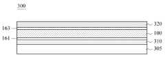
도 5를 참조하면, 화상 표시 장치(300)는 디스플레이 패널(305) 및 디스플레이 패널(305) 상에 배치된 상술한 안테나 소자(100)를 포함할 수 있다.Referring to FIG. 5 , the
예시적인 실시예들에 있어서, 상기 디스플레이 패널(305) 상에 광학층(310)이 더 포함될 수 있고, 안테나 소자(100) 상에는 커버 윈도우(320)가 배치될 수 있다.In example embodiments, an
예를 들면, 광학층(310)은 편광자 혹은 편광판을 포함하는 편광층일 수 있다.For example, the
커버 윈도우(320)는 예를 들면, 글래스(예를 들면, 초박형 글래스(Ultra-Thin Glass: UTG) 혹은 투명 수지 필름을 포함할 수 있다. 이에 따라, 안테나 소자(100)에 가해지는 외부 충격이 감소 또는 상쇄될 수 있다.The
예를 들면, 안테나 소자(100)는 광학층(310) 및 커버 윈도우(320) 사이에 배치될 수 있다. 이 경우, 안테나 유닛(120)의 아래에 배치되는 유전층(110) 및 광학층(310)이 함께 안테나 유닛(120)의 유전층으로 제공될 수 있다. 이에 따라, 적절한 유전율을 확보하여 안테나 소자(100)의 안테나 성능을 충분히 확보할 수 있다.For example, the
또한, 안테나 소자(100)가 시인면을 기준으로 광학층(310)보다 위에 배치되어도, 상술한 금속 산화물층(140)에 의해 안테나 유닛의 외부 시인이 억제될 수 있다. 이에 따라, 충분한 안테나 유전율을 확보하면서도 화상 표시 장치의 표시 품질을 개선할 수 있다.In addition, even when the
예를 들면, 광학층(310) 및 안테나 소자(100)는 제1 점접착층(161)을 통해 적층될 수 있고, 안테나 소자(100) 및 커버 윈도우(320)는 제2 점접착층(163)을 통해 적층될 수 있다.For example, the
제1 점접착층(161) 및 제2 점접착층(163)은 예를 들면, 광학 투명 점착제(OCA), 광학 투명 수지(OCR) 등과 같은 점접착성 물질을 포함할 수 있다.The first
도 6 및 도 7은 각각 예시적인 실시예들에 따른 화상 표시 장치를 설명하기 위한 개략적인 단면도 및 평면도이다.6 and 7 are schematic cross-sectional and plan views for explaining an image display device according to exemplary embodiments, respectively.
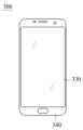
도 6 및 도 7을 참조하면, 화상 표시 장치(300)는 예를 들면, 스마트 폰 형태로 구현될 수 있으며, 도 7은 화상 표시 장치(300)의 전면부 또는 윈도우 면을 도시하고 있다. 화상 표시 장치(300)의 전면부는 표시 영역(330) 및 주변 영역(340)을 포함할 수 있다. 주변 영역(340)은 예를 들면, 화상 표시 장치의 차광부 또는 베젤부에 해당될 수 있다Referring to FIGS. 6 and 7 , the
상술한 안테나 패키지에 포함된 안테나 소자(100)는 화상 표시 장치(300)의 전면부를 향해 배치될 수 있으며, 예를 들면 디스플레이 패널(305) 상에 배치될 수 있다. 일 실시예에 있어서, 방사체(122)들은 표시 영역(330)과 적어도 부분적으로 중첩될 수도 있다.The
이 경우, 방사체(122)는 메쉬 구조를 포함할 수 있으며, 방사체(122)에 의한 투과율 저하를 방지할 수 있다. 안테나 유닛(120)에 포함된 패드들(126, 128)은 속이 찬 금속 패턴으로 형성될 수 있고, 이 경우 이미지 품질 저하 방지를 위해 주변 영역(340)에 배치될 수 있다.In this case, the
일부 실시예들에 있어서, 연성 인쇄 회로 기판(200)은 예를 들면, 디스플레이 패널(305)의 측면 굴곡 프로파일을 따라 굴곡되어 화상 표시 장치(300)의 배면부에 배치되며 안테나 구동 IC 칩(260)이 실장된 중개 회로 기판(250)(예를 들면, 메인 보드)을 향해 연장할 수 있다.In some embodiments, the flexible printed
연성 인쇄 회로 기판(200) 및 중개 회로 기판(250)은 본딩되거나 커넥터를 통해 상호 연결되어, 안테나 구동 IC 칩(260)에 의한 안테나 소자(100)로의 급전 및 안테나 구동 제어가 구현될 수 있다.The flexible printed
이하에서는, 본 발명의 이해를 돕기 위하여 구체적인 실시예들 및 비교예들을 포함하는 실험예를 제시하나, 이는 본 발명을 예시하는 것일 뿐 첨부된 특허청구범위를 제한하는 것이 아니며, 본 발명의 범주 및 기술사상 범위 내에서 실시예에 대한 다양한 변경 및 수정이 가능함은 당업자에게 있어서 명백한 것이며, 이러한 변형 및 수정이 첨부된 특허청구범위에 속하는 것도 당연한 것이다.Hereinafter, experimental examples including specific examples and comparative examples are presented to aid understanding of the present invention, but these are merely illustrative of the present invention and do not limit the scope of the appended claims, and the scope and scope of the present invention It is obvious to those skilled in the art that various changes and modifications to the embodiments are possible within the scope of the technical idea, and it is natural that such changes and modifications fall within the scope of the appended claims.
실시예 1Example 1
폴리에틸렌테레프탈레이트(PET)층 상에 스퍼터링(sputtering) 방식(90℃, 23kW 조건)으로 500nm 두께의 구리(Cu)층(예를 들면, 금속층(130)에 해당)을 형성하였다.A copper (Cu) layer (eg, corresponding to the metal layer 130) having a thickness of 500 nm was formed on the polyethylene terephthalate (PET) layer by a sputtering method (90° C., 23 kW conditions).
상기 구리층 상에 같은 조건의 스퍼터링 방식으로 61nm 두께의 구리 산화물(CuO)층(예를 들면, 금속 산화물층(140)에 해당)을 형성하였다.A copper oxide (CuO) layer (eg, corresponding to the metal oxide layer 140) having a thickness of 61 nm was formed on the copper layer by sputtering under the same conditions.
상기 구리 산화물층 상에 같은 조건의 스퍼터링 방식으로 IZO층(예를 들면, 투명 도전성 산화물층(150)에 해당)을 형성하였다.An IZO layer (for example, corresponding to the transparent conductive oxide layer 150) was formed on the copper oxide layer by a sputtering method under the same conditions.
그 후, 포토리소그래피 공정을 통해 형성된 구리층, 구리 산화물층 및 IZO층을 식각하여, 메쉬 구조를 갖는 방사체 및 전송 선로, 및 속이 찬 패턴을 갖는 신호 패드 및 그라운드 패드를 포함하는 안테나 유닛을 제조하였다.Thereafter, the copper layer, the copper oxide layer, and the IZO layer formed through a photolithography process were etched to manufacture an antenna unit including a radiator and a transmission line having a mesh structure, and a signal pad and a ground pad having a solid pattern. .
이 때, 상기 메쉬 구조에 포함된 도전 라인들의 선폭은 2.5㎛로 형성하였다.At this time, the line width of the conductive lines included in the mesh structure was formed to be 2.5 μm.
스마트폰의 디스플레이 패널 상에 편광층을 적층하고, 상기 안테나 유닛 및 PET층을 포함하는 안테나 소자를 상기 편광층 상에 적층하여 화상 표시 장치를 제조하였다.An image display device was manufactured by laminating a polarization layer on a display panel of a smart phone, and laminating an antenna element including the antenna unit and the PET layer on the polarization layer.
이 때, 안테나 소자 상에 글래스(glass)가 커버 윈도우로 적층되었다. 또한, 편광층 및 안테나 소자, 및 안테나 소자 및 커버 윈도우는 각각 OCA 점접착층을 통해 적층되었다.At this time, glass was laminated on the antenna element as a cover window. In addition, the polarization layer and the antenna element, and the antenna element and the cover window were laminated through the OCA adhesive layer, respectively.
형성된 안테나 소자의 CIE L*a*b* 표색계에서 a* 값 및 b* 값은 각각 0.05 및 -0.55로 측정 및 계산되었다.In the CIE L*a*b* color system of the formed antenna element, a* and b* values were measured and calculated as 0.05 and -0.55, respectively.
구체적으로, 분광 측색계인 CM-3600d(KONIKA MINOLTA 사 제조)의 SCI mode를 통해 안테나 소자의 상기 a* 값 및 b* 값을 계측하였다.Specifically, the a* value and the b* value of the antenna element were measured through the SCI mode of the spectrophotometer CM-3600d (manufactured by KONIKA MINOLTA).
실시예 2 내지 10Examples 2 to 10
구리층의 두께, 구리 산화물층의 두께, 도전 라인들의 선폭 및 CIE L*a*b* 표색계에서 a* 값 및 b* 값이 하기 표 1에 기재된 것과 같도록 안테나 유닛이 제조된 것을 제외하고, 실시예 1과 동일한 방법으로 안테나 유닛 및 화상 표시 장치를 제조하였다.Except that the antenna unit is manufactured such that the thickness of the copper layer, the thickness of the copper oxide layer, the line width of the conductive lines, and the a* value and b* value in the CIE L*a*b* color system are as shown in Table 1 below, An antenna unit and an image display device were manufactured in the same manner as in Example 1.
실시예 11Example 11
구리 산화물층 상에 IZO층을 형성하지 않은 것을 제외하고, 실시예 4와 동일한 방법으로 안테나 유닛 및 화상 표시 장치를 제조하였다.An antenna unit and an image display device were manufactured in the same manner as in Example 4, except that the IZO layer was not formed on the copper oxide layer.
비교예 1 내지 5Comparative Examples 1 to 5
구리 산화물층의 두께 및 CIE L*a*b* 표색계에서 a* 값 및 b* 값이 가 하기 표 1에 기재된 것과 같도록 안테나 유닛이 제조된 것을 제외하고, 실시예 1과 동일한 방법으로 안테나 유닛 및 화상 표시 장치를 제조하였다.The antenna unit is manufactured in the same manner as in Example 1, except that the antenna unit is manufactured such that the thickness of the copper oxide layer and the a* value and the b* value in the CIE L*a*b* color system are the same as those shown in Table 1 below. and an image display device.
비교예 6Comparative Example 6
구리 산화물층 및 IZO층을 형성하지 않은 것을 제외하고, 실시예 1과 동일한 방법으로 안테나 유닛 및 화상 표시 장치를 제조하였다.An antenna unit and an image display device were manufactured in the same manner as in Example 1, except that the copper oxide layer and the IZO layer were not formed.
선폭(㎛)challenge line
line width (μm)
실험예Experimental Example
(1) 시인성 평가(1) Visibility evaluation
상술한 실시예 및 비교예들에 따라 제조된 화상 표시 장치에서, 안테나 유닛이 실장된 부분을 육안으로 관찰하여, 안테나 유닛의 시인 여부를 확인하였다.In the image display device manufactured according to the above-described embodiments and comparative examples, a portion where the antenna unit is mounted was observed with the naked eye to determine whether the antenna unit was visible.
Ο: 명확히 시인됨Ο: clearly acknowledged
△: 특정 방향에서 불분명하게 시인됨△: Indistinctly recognized in a specific direction
Χ: 모든 방향에서 시인되지 않음Χ: not visible in all directions
(2) 면저항 측정(Rs, ohm/sq)(2) Sheet resistance measurement (Rs, ohm/sq)
상술한 실시예 및 비교예들에 따라 제조된 안테나 유닛을 면저항 측정기 Resist Test RT-80을 통해 측정하였다.The antenna units manufactured according to the above-described Examples and Comparative Examples were measured using a sheet resistance measuring instrument Resist Test RT-80.
구체적으로, RT-80 내 3개의 프로브가 안테나 유닛의 일 면에 접촉하여 측정하며, 100mm*100mm 면적 내에서 다섯 포인트를 측정하고, 분판 별로 총 150 포인트를 측정하여 안테나 유닛의 총 면저항을 측정하였다.Specifically, three probes in the RT-80 contact and measure one surface of the antenna unit, measure five points within an area of 100 mm * 100 mm, and measure a total of 150 points for each separation to measure the total sheet resistance of the antenna unit. .
(3) 내부식성 평가(3) Corrosion resistance evaluation
상술한 실시예 및 비교예들에 따라 제조된 안테나 유닛을 85℃, 상대습도 85% 환경에서 방치하여 최초로 부식이 관찰되는 시간을 측정하였다.The antenna unit manufactured according to the above-described Examples and Comparative Examples was left in an environment of 85° C. and 85% relative humidity, and the time at which corrosion was first observed was measured.
표 2를 참조하면, 금속층 상에 금속 산화물층이 60 내지 100nm 두께로 적층된 실시예들은 상기 두께 범위를 만족하지 않는 비교예들에 비하여 전체적으로 저저항 특성을 유지하면서도 안테나 유닛의 외부 시인이 억제되었다.Referring to Table 2, the embodiments in which the metal oxide layer was laminated on the metal layer to a thickness of 60 to 100 nm were suppressed from external visibility of the antenna unit while maintaining low resistance characteristics as a whole compared to comparative examples that did not satisfy the above thickness range. .
다만, 금속층의 두께가 200nm 미만인 실시예 7 및 금속층의 두께가 1,000nm를 초과하는 실시예 8은 금속 산화물층과의 색 정합성이 저하되어 특정 방향에서 사용자에게 불분명하게 시인되었다.However, in Example 7 in which the thickness of the metal layer was less than 200 nm and in Example 8 in which the thickness of the metal layer exceeded 1,000 nm, the color matching with the metal oxide layer was deteriorated, so that the user was clearly recognized in a specific direction.
또한, 메쉬 구조의 도전 라인들의 선폭이 0.5㎛ 미만인 실시예 9는 상대적으로 좁은 선폭에 따라 다른 실시예들에 비해 면저항이 감소하였다.In addition, in Example 9, in which the line width of the conductive lines of the mesh structure was less than 0.5 μm, sheet resistance was reduced compared to other examples due to the relatively narrow line width.
도전 라인들의 선폭이 10㎛를 초과하는 실시예 10은 메쉬 구조의 개구율이 상대적으로 저하되어 특정 방향에서 사용자에게 불분명하게 시인되었다.In Example 10, in which the line width of the conductive lines exceeds 10 μm, the aperture ratio of the mesh structure is relatively lowered, so that the user can see it indistinctly from a specific direction.
더하여, 투명 도전성 산화물층이 형성되지 않은 실시예 11은 투명 도전성 산화물층이 형성된 나머지 실시예들에 비하여 내부식성이 저하되었다.In addition, the corrosion resistance of Example 11 in which the transparent conductive oxide layer was not formed was lower than that of the other examples in which the transparent conductive oxide layer was formed.
금속 산화물층 및 투명 도전성 산화물층을 형성하지 않은 비교예 6의 경우, 산화되기 용이한 구리층이 곧바로 노출되어 안테나 유닛의 내부식성이 현저히 저하되었다.In the case of Comparative Example 6 in which the metal oxide layer and the transparent conductive oxide layer were not formed, the easily oxidized copper layer was immediately exposed, and thus the corrosion resistance of the antenna unit was remarkably reduced.
도 8은 실시예 및 비교예들에 따른 안테나 소자의 색 및 패턴 시인성 평가 결과이고, 도 9는 실시예 및 비교예들에 따른 안테나 소자의 CIE L*a*b* 표색계의 a* 및 b* 값 및 이에 따른 색상을 나타낸 그래프이다.8 is color and pattern visibility evaluation results of antenna elements according to Examples and Comparative Examples, and FIG. 9 is a* and b* of the CIE L*a*b* color system of the antenna element according to Examples and Comparative Examples. It is a graph showing values and corresponding colors.
구체적으로, 도 8 및 도 9는 금속 산화물층의 두께가 서로 상이한 실시예 1 내지 6 및 비교예 1 내지 5의 두께에 따른 색상, 시인 여부 및 a* 값/b* 값의 평가 결과이다. 도 8의 패턴 시인성 평가 시, 우하단 선분을 기준으로 그 상측에서의 안테나 유닛 시인 여부를 판단하였다.Specifically, FIGS. 8 and 9 are evaluation results of color, visibility, and a* value/b* value according to the thicknesses of Examples 1 to 6 and Comparative Examples 1 to 5 in which the thickness of the metal oxide layer is different from each other. When evaluating the visibility of the pattern of FIG. 8, it was determined whether the antenna unit was visible from the upper side based on the lower right line segment.
도 8 및 도 9를 참조하면, 금속 산화물층의 두께가 60nm 미만인 비교예 1 내지 3은 CIE L*a*b* 표색계의 a* 값이 0.5를 초과하고, 이에 따라 적화 현상이 발생하여 외부에서 붉은 계통의 패턴이 시인되었다.8 and 9, in Comparative Examples 1 to 3 in which the thickness of the metal oxide layer was less than 60 nm, the a* value of the CIE L*a*b* color system exceeded 0.5, and accordingly, a reddening phenomenon occurred and A red pattern was recognized.
또한, 금속 산화물층의 두께가 100nm를 초과하는 비교예 4 및 5는 CIE L*a*b* 표색계의 b* 값이 0.5를 초과하고, 이에 따라 황화 현상이 발생하여 외부에서 노란 계통의 패턴이 시인되었다.In addition, in Comparative Examples 4 and 5 in which the thickness of the metal oxide layer exceeds 100 nm, the b* value of the CIE L*a*b* color system exceeds 0.5, and accordingly, a yellowing phenomenon occurs, resulting in a yellowish pattern from the outside. has been admitted
도 8 및 도 9에 도시된 바와 같이, 실시예 1 내지 6에 따른 안테나 유닛은 외부 시인이 억제되며, a* 값 및 b* 값이 모두 0.5 이하로 형성되어 적화 또는 황화 현상이 방지되었다.As shown in FIGS. 8 and 9 , in the antenna units according to Examples 1 to 6, external visibility is suppressed, and both a* value and b* value are formed to be 0.5 or less, so that reddening or yellowing is prevented.
100: 안테나 소자110: 유전층
120: 안테나 유닛130: 금속층
140: 금속 산화물층150: 투명 도전성 산화물층
122: 방사체124: 전송 선로
126: 신호 패드128: 그라운드 패드
161: 제1 점접착층163: 제2 점접착층
200: 연성 인쇄 회로 기판210: 코어층
220: 신호 배선250: 중개 회로 기판
260: 안테나 구동 IC 칩300: 화상 표시 장치
305: 디스플레이 패널310: 광학층
320: 커버 윈도우100: antenna element 110: dielectric layer
120: antenna unit 130: metal layer
140: metal oxide layer 150: transparent conductive oxide layer
122: emitter 124: transmission line
126
161: first adhesive layer 163: second adhesive layer
200: flexible printed circuit board 210: core layer
220
260: antenna driving IC chip 300: image display device
305: display panel 310: optical layer
320: cover window
Claims (16)
Translated fromKorean상기 유전층 상에 배치되고, 금속층 및 금속 산화물층을 포함하며 상기 금속 산화물층의 두께는 60 내지 100nm인 안테나 유닛을 포함하는, 안테나 소자.dielectric layer; and
and an antenna unit disposed on the dielectric layer and comprising a metal layer and a metal oxide layer, wherein the metal oxide layer has a thickness of 60 to 100 nm.
상기 금속 산화물층 상에 투명 도전성 산화물층이 더 배치되는, 안테나 소자.The method according to claim 1, wherein the metal layer and the metal oxide layer are sequentially stacked on the dielectric layer,
An antenna element, wherein a transparent conductive oxide layer is further disposed on the metal oxide layer.
상기 금속층 상에 투명 도전성 산화물층이 더 배치되는, 안테나 소자.The method according to claim 1, wherein the metal oxide layer and the metal layer are sequentially stacked on the dielectric layer,
An antenna element, wherein a transparent conductive oxide layer is further disposed on the metal layer.
상기 도전 라인들 각각의 선폭은 0.5 내지 10㎛인, 안테나 소자.The method according to claim 10, wherein the mesh structure includes a plurality of conductive lines that cross each other,
The antenna element, wherein each of the conductive lines has a line width of 0.5 to 10 μm.
상기 디스플레이 패널 상에 배치된 청구항 1의 안테나 소자를 포함하는, 화상 표시 장치.display panel;
An image display device comprising the antenna element of claim 1 disposed on the display panel.
상기 안테나 소자는 상기 광학층 및 상기 커버 윈도우 사이에 배치되는, 화상 표시 장치.The method according to claim 15, further comprising an optical layer disposed on the display panel and a cover window disposed on the antenna element,
The image display device, wherein the antenna element is disposed between the optical layer and the cover window.
Priority Applications (4)
| Application Number | Priority Date | Filing Date | Title |
|---|---|---|---|
| KR1020210114487AKR20230032084A (en) | 2021-08-30 | 2021-08-30 | Antenna device and image display device including the same |
| PCT/KR2022/012853WO2023033470A1 (en) | 2021-08-30 | 2022-08-29 | Antenna device and image display apparatus comprising same |
| CN202280058307.XACN117941175A (en) | 2021-08-30 | 2022-08-29 | Antenna device and image display device including the same |
| US18/589,824US20240204389A1 (en) | 2021-08-30 | 2024-02-28 | Antenna device and image display device comprising same |
Applications Claiming Priority (1)
| Application Number | Priority Date | Filing Date | Title |
|---|---|---|---|
| KR1020210114487AKR20230032084A (en) | 2021-08-30 | 2021-08-30 | Antenna device and image display device including the same |
Publications (1)
| Publication Number | Publication Date |
|---|---|
| KR20230032084Atrue KR20230032084A (en) | 2023-03-07 |
Family
ID=85412865
Family Applications (1)
| Application Number | Title | Priority Date | Filing Date |
|---|---|---|---|
| KR1020210114487APendingKR20230032084A (en) | 2021-08-30 | 2021-08-30 | Antenna device and image display device including the same |
Country Status (4)
| Country | Link |
|---|---|
| US (1) | US20240204389A1 (en) |
| KR (1) | KR20230032084A (en) |
| CN (1) | CN117941175A (en) |
| WO (1) | WO2023033470A1 (en) |
Cited By (1)
| Publication number | Priority date | Publication date | Assignee | Title |
|---|---|---|---|---|
| CN119174057A (en)* | 2023-04-18 | 2024-12-20 | 京东方科技集团股份有限公司 | Display device and human-computer interaction device |
Citations (1)
| Publication number | Priority date | Publication date | Assignee | Title |
|---|---|---|---|---|
| KR20130095451A (en) | 2012-02-20 | 2013-08-28 | 주식회사 윈터치 | Touch screen device having antena formed on display panel or backlight unit |
Family Cites Families (27)
| Publication number | Priority date | Publication date | Assignee | Title |
|---|---|---|---|---|
| EP2957996A4 (en)* | 2013-03-22 | 2016-11-02 | Lg Chemical Ltd | Conductive pattern laminate and electronic device comprising same |
| KR20150056431A (en)* | 2013-11-15 | 2015-05-26 | 솔브레인 주식회사 | Conductive layer and manufacturing method thereof |
| CN106103094B (en)* | 2014-03-07 | 2018-11-09 | 富士胶片株式会社 | Substrate with decorative material, manufacturing method thereof, touch panel, and information display device |
| WO2018003847A1 (en)* | 2016-06-30 | 2018-01-04 | 日東電工株式会社 | Electromagnetic wave-transmitting metal member, article using same, and method for producing electromagnetic wave-transmitting metal film |
| TWI746603B (en)* | 2016-08-09 | 2021-11-21 | 南韓商東友精細化工有限公司 | Transparent electrode, touch sensor and image display device including the same |
| KR102545420B1 (en)* | 2016-11-25 | 2023-06-19 | 동우 화인켐 주식회사 | Touch sensor integrated with oled and oled display device comprising the same |
| US20190393585A1 (en)* | 2017-01-25 | 2019-12-26 | Tdk Corporation | Transparent conductive film for antennas |
| KR102361262B1 (en)* | 2017-05-30 | 2022-02-09 | 동우 화인켐 주식회사 | Touch sensor integrated with oled and oled display device comprising the same |
| KR101971441B1 (en)* | 2017-11-06 | 2019-04-23 | 동우 화인켐 주식회사 | Film antenna and display device including the same |
| KR102243515B1 (en)* | 2018-03-06 | 2021-04-21 | 동우 화인켐 주식회사 | Film antenna and display device including the same |
| KR102634290B1 (en)* | 2018-11-09 | 2024-02-06 | 동우 화인켐 주식회사 | Electrode Pad and Touch Sensor therewith |
| KR102262747B1 (en)* | 2019-04-04 | 2021-06-08 | 동우 화인켐 주식회사 | Touch sensor-antenna module and display device including the same |
| KR102619336B1 (en)* | 2019-09-11 | 2023-12-28 | 동우 화인켐 주식회사 | Antenna structure and display device including the same |
| KR102710487B1 (en)* | 2019-11-01 | 2024-09-25 | 동우 화인켐 주식회사 | Touch Sensor and Method for Manufacturing the Same |
| KR102716674B1 (en)* | 2019-12-27 | 2024-10-11 | 동우 화인켐 주식회사 | Antenna device |
| KR102655699B1 (en)* | 2020-02-20 | 2024-04-08 | 동우 화인켐 주식회사 | Antenna stack structure and display device |
| JP2021137993A (en)* | 2020-03-03 | 2021-09-16 | デクセリアルズ株式会社 | A conductive laminate, an optical device using the conductive laminate, and a method for manufacturing the conductive laminate. |
| KR102356678B1 (en)* | 2020-03-16 | 2022-01-26 | 동우 화인켐 주식회사 | Antenna device and display device including the same |
| JP2021163989A (en)* | 2020-03-30 | 2021-10-11 | 住友理工株式会社 | Film antenna and manufacturing method of the film antenna |
| KR102150998B1 (en)* | 2020-04-06 | 2020-09-02 | 동우 화인켐 주식회사 | Antenna-combined module and display device including the same |
| KR20220010332A (en)* | 2020-07-17 | 2022-01-25 | 동우 화인켐 주식회사 | Antenna package and image display device including the same |
| KR102680193B1 (en)* | 2020-07-21 | 2024-06-28 | 동우 화인켐 주식회사 | Antenna device and display device including the same |
| KR102204410B1 (en)* | 2020-07-24 | 2021-01-15 | 동우 화인켐 주식회사 | Antenna stack structure |
| KR20220029176A (en)* | 2020-09-01 | 2022-03-08 | 동우 화인켐 주식회사 | Transparent electrode laminate and touch sensor including the same |
| KR102401807B1 (en)* | 2021-02-19 | 2022-05-25 | 동우 화인켐 주식회사 | Antenna device and display device including the same |
| KR102322045B1 (en)* | 2021-02-19 | 2021-11-05 | 동우 화인켐 주식회사 | Antenna device and display device including the same |
| KR20230090624A (en)* | 2021-12-15 | 2023-06-22 | 동우 화인켐 주식회사 | Conductive pattern, antenna device including the, and image display device including the same |
- 2021
- 2021-08-30KRKR1020210114487Apatent/KR20230032084A/enactivePending
- 2022
- 2022-08-29WOPCT/KR2022/012853patent/WO2023033470A1/ennot_activeCeased
- 2022-08-29CNCN202280058307.XApatent/CN117941175A/enactivePending
- 2024
- 2024-02-28USUS18/589,824patent/US20240204389A1/enactivePending
Patent Citations (1)
| Publication number | Priority date | Publication date | Assignee | Title |
|---|---|---|---|---|
| KR20130095451A (en) | 2012-02-20 | 2013-08-28 | 주식회사 윈터치 | Touch screen device having antena formed on display panel or backlight unit |
Cited By (1)
| Publication number | Priority date | Publication date | Assignee | Title |
|---|---|---|---|---|
| CN119174057A (en)* | 2023-04-18 | 2024-12-20 | 京东方科技集团股份有限公司 | Display device and human-computer interaction device |
Also Published As
| Publication number | Publication date |
|---|---|
| US20240204389A1 (en) | 2024-06-20 |
| CN117941175A (en) | 2024-04-26 |
| WO2023033470A1 (en) | 2023-03-09 |
Similar Documents
| Publication | Publication Date | Title |
|---|---|---|
| KR102194290B1 (en) | Antenna structure and display device including the same | |
| US11710889B2 (en) | Antenna device and display device including the same | |
| US11424529B2 (en) | Antenna structure and display device including the same | |
| US11658395B2 (en) | Antenna package and image display device including the same | |
| US11973265B2 (en) | Antenna device and display device including the same | |
| US11600911B2 (en) | Antenna device and display device including the same | |
| KR102356678B1 (en) | Antenna device and display device including the same | |
| US11710896B2 (en) | Antenna device and image display device including the same | |
| US11848484B2 (en) | Antenna structure and image display device including the same | |
| US12095174B2 (en) | Antenna device and display device including the same | |
| US12046836B2 (en) | Antenna structure and image display device including the same | |
| KR20220053861A (en) | Antenna device and image display device including the same | |
| US20240204389A1 (en) | Antenna device and image display device comprising same | |
| KR102494259B1 (en) | Antenna structure and display device including the same | |
| KR102655699B1 (en) | Antenna stack structure and display device | |
| KR20220086999A (en) | Antenna structure and image display device including the same | |
| US20230327322A1 (en) | Antenna structure and display device including the same | |
| US12255414B2 (en) | Package board, antenna package including the same and image display device including the same | |
| KR102285108B1 (en) | Antenna package and image display device including the same | |
| US20250105524A1 (en) | Antenna device, antenna structure including the same and image display device including the same | |
| US20250105489A1 (en) | Antenna device, antenna structure including the same and image display device including the same | |
| US20240154299A1 (en) | Antenna structure | |
| KR20250132076A (en) | Antenna device and image display device including the same |
Legal Events
| Date | Code | Title | Description |
|---|---|---|---|
| PA0109 | Patent application | Patent event code:PA01091R01D Comment text:Patent Application Patent event date:20210830 | |
| PG1501 | Laying open of application | ||
| A201 | Request for examination | ||
| PA0201 | Request for examination | Patent event code:PA02012R01D Patent event date:20240312 Comment text:Request for Examination of Application Patent event code:PA02011R01I Patent event date:20210830 Comment text:Patent Application | |
| E902 | Notification of reason for refusal | ||
| PE0902 | Notice of grounds for rejection | Comment text:Notification of reason for refusal Patent event date:20250507 Patent event code:PE09021S01D |