KR20230030759A - Hermetic sealing package module and manufacturing method thereof - Google Patents
Hermetic sealing package module and manufacturing method thereofDownload PDFInfo
- Publication number
- KR20230030759A KR20230030759AKR1020210112814AKR20210112814AKR20230030759AKR 20230030759 AKR20230030759 AKR 20230030759AKR 1020210112814 AKR1020210112814 AKR 1020210112814AKR 20210112814 AKR20210112814 AKR 20210112814AKR 20230030759 AKR20230030759 AKR 20230030759A
- Authority
- KR
- South Korea
- Prior art keywords
- film
- substrate
- sealing ring
- stress buffer
- layer
- Prior art date
- Legal status (The legal status is an assumption and is not a legal conclusion. Google has not performed a legal analysis and makes no representation as to the accuracy of the status listed.)
- Granted
Links
Images


Classifications
- H01L27/14618—
- H—ELECTRICITY
- H10—SEMICONDUCTOR DEVICES; ELECTRIC SOLID-STATE DEVICES NOT OTHERWISE PROVIDED FOR
- H10F—INORGANIC SEMICONDUCTOR DEVICES SENSITIVE TO INFRARED RADIATION, LIGHT, ELECTROMAGNETIC RADIATION OF SHORTER WAVELENGTH OR CORPUSCULAR RADIATION
- H10F39/00—Integrated devices, or assemblies of multiple devices, comprising at least one element covered by group H10F30/00, e.g. radiation detectors comprising photodiode arrays
- H10F39/80—Constructional details of image sensors
- H10F39/804—Containers or encapsulations
- H—ELECTRICITY
- H01—ELECTRIC ELEMENTS
- H01L—SEMICONDUCTOR DEVICES NOT COVERED BY CLASS H10
- H01L23/00—Details of semiconductor or other solid state devices
- H01L23/02—Containers; Seals
- H01L23/10—Containers; Seals characterised by the material or arrangement of seals between parts, e.g. between cap and base of the container or between leads and walls of the container
- H—ELECTRICITY
- H01—ELECTRIC ELEMENTS
- H01L—SEMICONDUCTOR DEVICES NOT COVERED BY CLASS H10
- H01L23/00—Details of semiconductor or other solid state devices
- H01L23/16—Fillings or auxiliary members in containers or encapsulations, e.g. centering rings
- H01L27/1462—
- H01L27/14634—
- H01L27/1469—
- H—ELECTRICITY
- H10—SEMICONDUCTOR DEVICES; ELECTRIC SOLID-STATE DEVICES NOT OTHERWISE PROVIDED FOR
- H10F—INORGANIC SEMICONDUCTOR DEVICES SENSITIVE TO INFRARED RADIATION, LIGHT, ELECTROMAGNETIC RADIATION OF SHORTER WAVELENGTH OR CORPUSCULAR RADIATION
- H10F39/00—Integrated devices, or assemblies of multiple devices, comprising at least one element covered by group H10F30/00, e.g. radiation detectors comprising photodiode arrays
- H10F39/011—Manufacture or treatment of image sensors covered by group H10F39/12
- H10F39/018—Manufacture or treatment of image sensors covered by group H10F39/12 of hybrid image sensors
- H—ELECTRICITY
- H10—SEMICONDUCTOR DEVICES; ELECTRIC SOLID-STATE DEVICES NOT OTHERWISE PROVIDED FOR
- H10F—INORGANIC SEMICONDUCTOR DEVICES SENSITIVE TO INFRARED RADIATION, LIGHT, ELECTROMAGNETIC RADIATION OF SHORTER WAVELENGTH OR CORPUSCULAR RADIATION
- H10F39/00—Integrated devices, or assemblies of multiple devices, comprising at least one element covered by group H10F30/00, e.g. radiation detectors comprising photodiode arrays
- H10F39/80—Constructional details of image sensors
- H10F39/805—Coatings
- H—ELECTRICITY
- H10—SEMICONDUCTOR DEVICES; ELECTRIC SOLID-STATE DEVICES NOT OTHERWISE PROVIDED FOR
- H10F—INORGANIC SEMICONDUCTOR DEVICES SENSITIVE TO INFRARED RADIATION, LIGHT, ELECTROMAGNETIC RADIATION OF SHORTER WAVELENGTH OR CORPUSCULAR RADIATION
- H10F39/00—Integrated devices, or assemblies of multiple devices, comprising at least one element covered by group H10F30/00, e.g. radiation detectors comprising photodiode arrays
- H10F39/80—Constructional details of image sensors
- H10F39/809—Constructional details of image sensors of hybrid image sensors
Landscapes
- Physics & Mathematics (AREA)
- Condensed Matter Physics & Semiconductors (AREA)
- General Physics & Mathematics (AREA)
- Engineering & Computer Science (AREA)
- Computer Hardware Design (AREA)
- Microelectronics & Electronic Packaging (AREA)
- Power Engineering (AREA)
- Solid State Image Pick-Up Elements (AREA)
Abstract
Description
Translated fromKorean본 발명은 허메틱 실링 패키지 모듈 및 그 제조 방법에 관한 것으로서, 더욱 상세하게는 캐비티의 진공을 안정적으로 유지할 수 있는 허메틱 실링 패키지 모듈 및 그 제조 방법에 관한 것이다.The present invention relates to a hermetic sealing package module and a manufacturing method thereof, and more particularly, to a hermetic sealing package module capable of stably maintaining a vacuum in a cavity and a manufacturing method thereof.
포토 센서는 이미지를 촬영할 수 있도록 마련된 반도체 소자이고, 적외선 센서는 적외선을 감지할 수 있도록 마련된 반도체 소자이다. 포토 센서 및 적외선 센서(이하, "센서"라고 한다)는 기판에 접합되어 패키지 모듈로 제작된 후 모바일 기기에 탑재된다. 이를 칩 스케일 패키지(Chip Scale Package)방식이라 한다.The photo sensor is a semiconductor device provided to capture an image, and the infrared sensor is a semiconductor device provided to detect infrared rays. A photo sensor and an infrared sensor (hereinafter, referred to as "sensor") are bonded to a substrate to be manufactured as a package module and then mounted on a mobile device. This is called a chip scale package method.
예컨대 특허문헌 1 및 특허문헌 2에 제시된 종래의 패키지 모듈은 센서와 기판 사이에 캐비티가 마련되고, 캐비티가 폐루프 형상의 실링 링에 의하여 밀봉되는 구조로 제작된다.For example, the conventional package module presented in
이때, 실링 링은 금속 재질을 포함하며, 증착 방식으로 센서에 형성되고, 천이액상확산접합(transient liquid phase bonding) 방식으로 기판에 접합된다. 여기서, 천이액상확산접합 방식은 접합 시 기계적인 스트레스와 열적인 스트레스를 발생시킬 수 있고, 스트레스가 실링 링을 통해 센서로 전달되어 센서가 손상될 수 있다.At this time, the sealing ring includes a metal material, is formed on the sensor by a deposition method, and is bonded to the substrate by a transient liquid phase bonding method. Here, the transitional liquid-phase diffusion bonding method may generate mechanical stress and thermal stress during bonding, and the stress may be transmitted to the sensor through the sealing ring and may damage the sensor.
또한, 센서의 표면에는 센서의 소자를 보호하는 패시베이션막이 필수적으로 구비되어 있는데, 패시베이션막에 실링 링을 증착하면, 패시베이션막과 실링 링의 결합 부위의 결합 강도를 원하는 결합 강도로 유지하기 어렵다.In addition, a passivation film for protecting the element of the sensor is essentially provided on the surface of the sensor. If a sealing ring is deposited on the passivation film, it is difficult to maintain the bonding strength of the bonding portion between the passivation film and the sealing ring at a desired bonding strength.
종래에는 실링 링의 접합 시 센서로 전달되는 스트레스를 해소시키면서 실링 링과 센서의 결합 부위의 결합 강도를 높여줄 수 있도록, 센서의 패시베이션막 상에 스트레스 완충막(stress buffer layer)을 마련하고, 스트레스 완충막에 실링 링을 증착하였다. 이러한 방식은 센서의 패시베이션막에 실링 링을 증착시키는 것에 비해, 실링 링과 센서의 결합 강도를 높여줄 수 있고, 실링 링과 기판의 접합 시 센서로 전달되는 스트레스를 해소시킬 수 있다.Conventionally, a stress buffer layer is provided on the passivation film of the sensor to increase the bonding strength of the joint between the sealing ring and the sensor while reducing the stress transmitted to the sensor when the sealing ring is bonded. A sealing ring was deposited on the buffer film. Compared to depositing the sealing ring on the passivation film of the sensor, this method can increase the bonding strength between the sealing ring and the sensor, and can relieve stress transmitted to the sensor when the sealing ring and the substrate are bonded.
하지만 스트레스 완충막은 허메틱 실링(hermetic sealing)이 어려운 문제점이 있다. 즉, 스트레스 완충막은 덕타일한 재질의 특성 상 변형되기 쉽고, 또한, 스트레스 완충막의 표면에는 다수의 기공이 존재하기 때문에, 실링 링을 스트레스 완충막에 증착시키면, 센서와 기판 사이에 마련되는 캐비티를 밀봉을 유지하기 어려운 문제점이 있다.However, the stress buffer film has a problem in that hermetic sealing is difficult. That is, since the stress buffer film is easily deformed due to the characteristics of a ductile material, and since a large number of pores exist on the surface of the stress buffer film, when the sealing ring is deposited on the stress buffer film, a cavity provided between the sensor and the substrate is formed. There is a problem that it is difficult to maintain a seal.
이처럼 종래에는 실링 링의 접합 시의 스트레스 해소와 실링 링과 센서 간의 결합 강도의 강화를 위해 센서 표면에 스트레스 완충막을 적용하였으나, 오히려 스트레스 완충막에 의해 센서와 기판 사이의 허메틱 실링을 구현하기 어려워지는 문제가 발생하였다.As such, in the prior art, a stress buffer film was applied to the surface of the sensor to relieve stress during bonding of the sealing ring and to strengthen the bond strength between the seal ring and the sensor, but it is rather difficult to implement hermetic sealing between the sensor and the substrate by the stress buffer film. A losing problem occurred.
본 발명의 배경이 되는 기술은 하기의 특허문헌에 게재되어 있다.The background technology of the present invention is published in the following patent documents.
본 발명은 캐비티의 진공을 안정적으로 유지할 수 있으면서 센서 칩에 가해지는 스트레스를 해소시키고 실링 링의 결합 강도를 향상시킬 수 있는 허메틱 실링 패키지 모듈 및 그 제조 방법을 제공한다.The present invention provides a hermetic sealing package module capable of stably maintaining a vacuum in a cavity, relieving stress applied to a sensor chip, and improving coupling strength of a sealing ring, and a manufacturing method thereof.
본 발명의 실시 형태에 따른 허메틱 실링 패키지 모듈은, 센서 칩; 상기 센서 칩과 마주보도록 배치되는 기판; 및 상기 센서 칩과 상기 기판 사이에서 이들을 접합하는 실링 링;을 포함하고, 상기 센서 칩의 표면에는 패시베이션막 및 스트레스 완충막이 구비되며, 상기 센서 칩, 상기 기판 및 상기 실링 링에 의해 캐비티가 형성되도록, 상기 실링 링은 상기 기판에 융착되고 상기 패시베이션막에 결합되며, 상기 실링 링의 에지는 상기 스트레스 완충막에 결합된다.A hermetic sealing package module according to an embodiment of the present invention includes a sensor chip; a substrate disposed to face the sensor chip; and a sealing ring connecting the sensor chip and the substrate to each other, wherein a passivation film and a stress buffer film are provided on a surface of the sensor chip, and a cavity is formed by the sensor chip, the substrate, and the sealing ring. , the sealing ring is fused to the substrate and coupled to the passivation layer, and an edge of the sealing ring is coupled to the stress buffer layer.
상기 센서 칩은, 소자가 형성된 모재; 상기 모재 상에 형성되는 상기 패시베이션막; 및 상기 패시베이션막 상에 형성되고 일부가 제거되어 있는 상기 스트레스 완충막;을 포함하고, 상기 실링 링은, 상기 스트레스 완충막이 제거된 부위를 따라 폐루프 형상으로 연장형성되고, 상기 패시베이션막에 증착되고, 상기 기판에 구비된 결합용 패턴에 융착되며, 상기 실링 링의 에지는 상기 스트레스 완충막에 증착될 수 있다.The sensor chip, the base material on which the element is formed; The passivation film formed on the base material; and the stress buffer film formed on the passivation film and partially removed, wherein the sealing ring extends in a closed loop shape along a region from which the stress buffer film is removed, and is deposited on the passivation film. , may be fused to a coupling pattern provided on the substrate, and an edge of the sealing ring may be deposited on the stress buffer layer.
상기 센서 칩은, 소자가 형성된 모재; 상기 모재 상에 형성되는 상기 패시베이션막; 상기 패시베이션막 상에 형성되고 일부가 제거되어 있는 상기 스트레스 완충막; 및 상기 스트레스 완충막이 제거된 부위를 따라 폐루프 형상으로 형성된 금속막;을 포함하고, 상기 실링 링은, 상기 금속막을 따라 폐루프 형상으로 연장형성되고, 상기 금속막에 증착됨에 의하여 상기 패시베이션막과 결합되고, 상기 기판에 구비된 결합용 패턴에 융착되며, 상기 실링 링의 에지는 상기 스트레스 완충막에 증착될 수 있다.The sensor chip, the base material on which the element is formed; The passivation film formed on the base material; the stress buffer layer formed on the passivation layer and partially removed; and a metal film formed in a closed loop shape along a region from which the stress buffer film is removed, wherein the sealing ring extends in a closed loop shape along the metal film and is deposited on the metal film to form a contact with the passivation film. It may be bonded and fused to a bonding pattern provided on the substrate, and an edge of the sealing ring may be deposited on the stress buffer layer.
상기 금속막의 두께는 6000 옹스트롬(angstrom) 이상이고, 상기 스트레스 완충막의 두께 이하일 수 있다.A thickness of the metal layer may be greater than or equal to 6000 angstroms and less than or equal to a thickness of the stress buffer layer.
상기 금속막은 Al, Au, Ag, Ti, Cu 및 W 중 어느 하나 또는 이들의 합금을 포함할 수 있다.The metal layer may include any one of Al, Au, Ag, Ti, Cu, and W, or an alloy thereof.
상기 실링 링은 상호 접합된 복수개의 층을 구비하고, 그 전체 두께가 20 내지 75 마이크로미터(㎛)의 범위일 수 있다.The sealing ring may include a plurality of layers bonded to each other, and may have a total thickness ranging from 20 to 75 micrometers (μm).
상기 복수개의 층은, 상기 패시베이션막과 결합되는 베이스층 및 상기 결합용 패턴에 융착되는 접합층을 포함하고, 상기 베이스층의 두께는 15 내지 60 마이크로미터의 범위이고, 상기 접합층의 두께는 5 내지 15 마이크로미터의 범위일 수 있다.The plurality of layers include a base layer coupled to the passivation film and a bonding layer fused to the bonding pattern, the thickness of the base layer is in the range of 15 to 60 micrometers, and the thickness of the bonding layer is 5 micrometers. to 15 micrometers.
상기 베이스층은 Cu 재질을 포함하고, 상기 접합층은 SnAg 합금 재질을 포함할 수 있다.The base layer may include a Cu material, and the bonding layer may include a SnAg alloy material.
상기 실링 링의 폭은 35 마이크로미터 이상으로 형성될 수 있다.The sealing ring may have a width of 35 micrometers or more.
상기 스트레스 완충막 상에 형성되는 제2스트레스 완충막;을 더 포함할 수 있다.A second stress buffer layer formed on the stress buffer layer may be further included.
상기 기판은 레진(resin), 프리프레그(prepreg), 글라스 및 세라믹 중 어느 하나를 포함하고, 상기 기판의 두께는 0.5 밀리미터(㎜) 이하이고, 상기 기판의 열팽창계수(Coefficient of Thermal Expansion)는 1.2 내지 15 ppm/℃의 범위일 수 있다.The substrate includes any one of resin, prepreg, glass, and ceramic, the thickness of the substrate is 0.5 millimeters (mm) or less, and the coefficient of thermal expansion of the substrate is 1.2 to 15 ppm/°C.
상기 기판은 인쇄회로기판을 포함하고, 상기 기판은 표면에 금속 재질의 코팅막이 구비되고, 상기 기판의 전체 두께는 0.3 밀리미터(㎜) 이하이고, 상기 기판의 열팽창계수는 1.2 내지 15 ppm/℃의 범위일 수 있다.The substrate includes a printed circuit board, the substrate is provided with a coating film of a metal material on the surface, the total thickness of the substrate is 0.3 millimeters (mm) or less, the thermal expansion coefficient of the substrate is 1.2 to 15 ppm / ℃ of range can be
상기 코팅막은 구리를 포함하고, 상기 코팅막의 두께는 7 내지 40 마이크로미터의 범위로 형성될 수 있다.The coating layer includes copper, and the thickness of the coating layer may be formed in a range of 7 to 40 micrometers.
상기 캐비티는 수m 토르(Torr) 내지 100 토르의 진공으로 제어될 수 있다.The cavity may be controlled with a vacuum of several m Torr to 100 Torr.
외부로부터 상기 센서 칩으로 광 신호를 집중시킬 수 있도록 상기 센서 칩의 광 신호가 입사되는 면에 부착되고, 렌즈 또는 광학필터를 포함하는 광학계; 상기 기판과 마주보도록 배치되고, 상기 기판에 접합되는 판독집적회로기판; 상기 판독집적회로기판의 둘레를 따라 나열되고, 상기 기판에 접합되는 솔더 볼; 및 상기 광학계의 일부, 상기 센서 칩, 상기 기판 및 상기 판독집적회로기판을 피복하는 몰딩;을 포함할 수 있다.an optical system attached to a surface of the sensor chip on which an optical signal is incident and including a lens or an optical filter so as to focus an optical signal from the outside to the sensor chip; a readout integrated circuit board disposed to face the substrate and bonded to the substrate; solder balls arranged along the circumference of the readout integrated circuit board and bonded to the board; and molding covering a part of the optical system, the sensor chip, the substrate, and the readout integrated circuit board.
본 발명의 실시 형태에 따른 허메틱 실링 패키지 모듈 제조 방법은, 소자가 형성된 모재 및 기판을 준비하는 과정; 상기 모재의 표면의 패시베이션막 상에 스트레스 완충막을 형성하는 과정; 상기 스트레스 완충막의 일부를 제거하는 과정; 상기 스트레스 완충막이 제거된 부위에 실링 링을 증착하는 과정; 및 상기 기판에 상기 실링 링을 접합하는 과정;을 포함한다.A method of manufacturing a hermetic sealing package module according to an embodiment of the present invention includes preparing a base material and a substrate on which elements are formed; forming a stress buffer film on the passivation film on the surface of the base material; removing a portion of the stress buffer layer; depositing a sealing ring on a region from which the stress buffer layer is removed; and bonding the sealing ring to the substrate.
상기 스트레스 완충막을 형성하는 과정 이전에, 상기 패시베이션막 상에 금속막을 증착하는 과정; 상기 패시베이션막 상에 폐루프 형상으로 금속막이 남도록 상기 금속막의 일부를 제거하는 과정;을 더 포함할 수 있다.depositing a metal layer on the passivation layer before forming the stress buffer layer; The method may further include removing a portion of the metal layer so that the metal layer remains on the passivation layer in a closed loop shape.
상기 스트레스 완충막의 일부를 제거하는 과정은, 상기 스트레스 완충막 상에 페루프 형상으로 스트레스 완충막이 노출되도록 마스킹하는 과정; 및 노출된 스트레스 완충막을 식각하는 과정;을 포함할 수 있다.The process of removing a portion of the stress buffer film may include masking the stress buffer film so that the stress buffer film is exposed in a loop shape on the stress buffer film; and etching the exposed stress buffer layer.
상기 실링 링을 증착하는 과정은, 상기 스트레스 완충막의 전체 면 및 상기 스트레스 완충막이 제거된 부위에 패시베이션막보다 연성이 작은 제1금속층을 증착하는 과정; 상기 제1금속층의 전체 면에 제1금속층보다 용접성이 좋은 제2금속층을 증착하는 과정; 상기 스트레스 완충막이 제거된 부위 상에 남길 제1금속층 및 제2금속층의 폭이 상기 스트레스 완충막이 제거된 부위의 폭보다 크도록 제2금속층을 마스킹하는 과정; 상기 스트레스 완충막이 제거된 부위 상에 실링 링을 형성하도록 제2금속층 및 제1금속층을 식각하는 과정;을 포함할 수 있다.The process of depositing the sealing ring may include depositing a first metal layer having less ductility than the passivation film on the entire surface of the stress buffer film and a region where the stress buffer film is removed; depositing a second metal layer having better weldability than the first metal layer on the entire surface of the first metal layer; masking the second metal layer such that widths of the first metal layer and the second metal layer to be left on the region from which the stress buffer layer is removed are greater than the width of the region from which the stress buffer layer is removed; A process of etching the second metal layer and the first metal layer to form a sealing ring on the region where the stress buffer layer is removed.
상기 제1금속층을 증착하는 과정과 상기 제2금속층을 증착하는 과정은 물리기상증착(physical vapor deposition)방식으로 수행하고, 상기 제1금속층 및 제2금속층을 식각하는 과정은 플라즈마식각(Plasma etching)방식 또는 습식식각(wet etching)방식으로 수행할 수 있다.The process of depositing the first metal layer and the process of depositing the second metal layer are performed by physical vapor deposition, and the process of etching the first and second metal layers is plasma etching. method or wet etching method.
상기 실링 링을 접합하는 과정은, 상기 기판에 결합용 패턴을 형성하는 과정; 접합을 수행할 챔버의 내부를 수m 토르(Torr) 내지 100 토르의 진공 분위기로 형성하는 과정; 상기 진공 분위기에서, 상기 모재, 상기 기판 및 상기 실링 링에 의해 캐비티가 형성되도록, 상기 결합용 패턴에 상기 실링 링을 융착하는 과정;을 포함할 수 있다.The process of bonding the sealing ring may include forming a bonding pattern on the substrate; Forming a vacuum atmosphere of several m Torr to 100 Torr inside the chamber in which bonding is to be performed; A process of fusing the sealing ring to the bonding pattern so that a cavity is formed by the base material, the substrate, and the sealing ring in the vacuum atmosphere.
상기 실링 링을 융착하는 과정은 플립칩본딩(flip chip bonding)방식으로 수행하며, 천이액상확산접합(Transient Liquid Phase bonding)에 의해 금속간 화합물(intermetallic compound)을 형성할 수 있다.The process of fusing the sealing ring is performed by flip chip bonding, and an intermetallic compound may be formed by transient liquid phase bonding.
상기 실링 링을 접합하는 과정 이후에, 상기 모재에 렌즈 또는 광학필터를 부착하는 과정; 상기 기판에 판독집적회로기판을 접합하는 과정; 상기 렌즈 또는 광학필터의 일부, 상기 모재, 상기 기판 및 상기 판독집적회로기판을 몰딩하는 과정;을 포함하고, 상기 몰딩하는 과정에서, 상기 기판에 접합되어 있는 솔더 볼을 몰딩의 외부에 노출시킬 수 있다.attaching a lens or an optical filter to the base material after bonding the sealing ring; bonding a readout integrated circuit board to the board; and molding a part of the lens or optical filter, the base material, the substrate, and the readout integrated circuit board, and in the molding process, a solder ball bonded to the substrate may be exposed to the outside of the molding. there is.
본 발명의 실시 형태에 따르면, 센서 칩의 패시베이션막에 실링 링을 결합시켜서 센서 칩과 기판과 실링 링 사이의 캐비티의 허메틱 실링을 달성할 수 있고, 센서 칩의 스트레스 완충막에 실링 링의 에지를 결합시켜서 결합 부위의 결합 강도를 향상시키면서 결합 시의 스트레스를 해소시킬 수 있다.According to an embodiment of the present invention, it is possible to achieve hermetic sealing of the cavity between the sensor chip, the substrate and the sealing ring by bonding the sealing ring to the passivation film of the sensor chip, and the edge of the sealing ring to the stress buffer film of the sensor chip. It is possible to relieve stress during bonding while improving the bonding strength of the bonding site by combining.
이로부터, 센서 칩과 기판과 실링 링에 의해 형성된 캐비티의 진공을 안정적으로 유지할 수 있고, 캐비티의 진공이 파괴되어 먼지 및 수분 등의 이물이 유입되는 것을 방지할 수 있다.Accordingly, it is possible to stably maintain the vacuum of the cavity formed by the sensor chip, the substrate, and the sealing ring, and prevent foreign substances such as dust and moisture from entering due to the vacuum of the cavity being destroyed.
도 1 및 도 2는 본 발명의 실시 예에 따른 허메틱 실링 패키지 모듈의 단면도이다.
도 3은 본 발명의 실시 예에 따른 허메틱 실링 패키지 모듈의 확대도이다.
도 4는 본 발명의 실시 예에 따른 허메틱 실링 패키지 모듈의 평면도이다.
도 5는 본 발명의 변형 예에 따른 허메틱 실링 패키지 모듈의 확대도이다.
도 6은 본 발명의 다른 변형 예에 따른 허메틱 실링 패키지 모듈의 확대도이다.
도 7 내지 도 10은 본 발명의 실시 예에 따른 허메틱 실링 패키지 모듈 제조 방법을 설명하기 위한 모식도이다.1 and 2 are cross-sectional views of a hermetic sealing package module according to an embodiment of the present invention.
3 is an enlarged view of a hermetic sealing package module according to an embodiment of the present invention.
4 is a plan view of a hermetic sealing package module according to an embodiment of the present invention.
5 is an enlarged view of a hermetic sealing package module according to a modified example of the present invention.
6 is an enlarged view of a hermetic sealing package module according to another modified example of the present invention.
7 to 10 are schematic diagrams for explaining a method of manufacturing a hermetic sealing package module according to an embodiment of the present invention.
이하, 첨부된 도면을 참조하여, 본 발명의 실시 예를 상세히 설명한다. 그러나 본 발명은 이하에서 개시되는 실시 예에 한정되는 것이 아니고, 서로 다른 다양한 형태로 구현될 것이다. 단지 본 발명의 실시 예는 본 발명의 개시가 완전하도록 하고, 해당 분야에서 통상의 지식을 가진 자에게 발명의 범주를 완전하게 알려주기 위해 제공되는 것이다. 본 발명의 실시 예를 설명하기 위하여 도면은 과장될 수 있고, 실시 예의 설명과 관계없는 부분은 도면에서 생략될 수 있고, 도면상의 동일한 부호는 동일한 요소를 지칭한다.Hereinafter, embodiments of the present invention will be described in detail with reference to the accompanying drawings. However, the present invention is not limited to the embodiments disclosed below, and will be implemented in a variety of different forms. Only the embodiments of the present invention are provided to complete the disclosure of the present invention and to fully inform those skilled in the art of the scope of the invention. In order to explain the embodiments of the present invention, the drawings may be exaggerated, parts irrelevant to the description of the embodiments may be omitted from the drawings, and like reference numerals in the drawings refer to the same elements.
본 발명의 실시 예에 따른 허메틱 실링 패키지 모듈 및 그 제조 방법은 센서 칩과 실링 링과 기판의 접합 강도를 향상시키면서 이들 사이에 정의되는 캐비티의 진공을 안정적으로 유지시킬 수 있는 특징을 제시한다. 본 발명의 실시 예에 따른 허메틱 실링 패키지 모듈 및 그 제조 방법을 예컨대 진공 캐비티 구조를 가진 패키지 모듈 및 그 제조 방법이라고 지칭할 수 있고, 또한, 허메틱 실링 패키지 모듈 구조 및 그 제조 방법이라고 지칭할 수도 있다. 여기서, 허메틱 실링 패키지 모듈 구조라고 함은 본 발명의 실시 예에 따른 허메틱 실링 패키지 모듈의 후술하는 센서 칩과, 기판과, 실링 링이 결합된 구조를 지칭할 수 있고, 또한, 이러한 구조를 가지도록 제조된 제조물 즉, 패키지 모듈을 지칭할 수 있다.The hermetic sealing package module and method of manufacturing the same according to an embodiment of the present invention provide features capable of stably maintaining a vacuum of a cavity defined between them while improving bonding strength between a sensor chip, a sealing ring, and a substrate. The hermetic sealing package module and method for manufacturing the same according to an embodiment of the present invention may be referred to as, for example, a package module having a vacuum cavity structure and a method for manufacturing the same, and may also be referred to as a hermetic sealing package module structure and a method for manufacturing the same. may be Here, the hermetic sealing package module structure may refer to a structure in which a sensor chip, a substrate, and a sealing ring, which will be described later, of the hermetic sealing package module according to an embodiment of the present invention are combined, and this structure It may refer to a product manufactured to have, that is, a package module.
이러한 본 발명의 실시 예에 따른 허메틱 실링 패키지 모듈 및 그 제조 방법은 칩 스케일 패키지 방식으로 제조되는 전자 소자 패키지 모듈 예컨대 포토 센서 패키지 모듈 및 적외선 온도 센서 패키지 모듈 등에 다양하게 적용될 수 있다.The hermetic sealing package module and method of manufacturing the same according to an embodiment of the present invention may be variously applied to an electronic device package module manufactured in a chip scale package method, such as a photo sensor package module and an infrared temperature sensor package module.
도 1 및 도 2는 본 발명의 실시 예에 따른 허메틱 실링 패키지 모듈을 설명하기 위한 단면도이고, 도 3은 본 발명의 실시 예에 따른 허메틱 실링 패키지 모듈의 실링 링의 구조를 상세하게 보여주기 위한 확대도이고, 도 4는 본 발명의 실시 예에 따른 허메틱 실링 패키지 모듈의 실링 링 및 입출력 범프가 배치된 구조를 설명하기 위한 평면도이다. 여기서, 도 1은 허메틱 실링 패키지 모듈의 광학계로서 렌즈가 적용된 모습을 보여주는 단면도이고, 도 2는 허메틱 실링 패키지 모듈의 광학계로서 광학필터가 적용된 모습을 보여주는 단면도이다.1 and 2 are cross-sectional views for explaining a hermetic sealing package module according to an embodiment of the present invention, and FIG. 3 shows a structure of a sealing ring of the hermetic sealing package module according to an embodiment of the present invention in detail. FIG. 4 is a plan view for explaining a structure in which a sealing ring and input/output bumps of a hermetic sealing package module according to an embodiment of the present invention are disposed. Here, FIG. 1 is a cross-sectional view showing a lens applied as an optical system of a hermetic sealing package module, and FIG. 2 is a cross-sectional view showing an optical filter applied as an optical system of a hermetic sealing package module.
도면에서 X축 방향은 좌우 방향이고, Y축 방향은 전후 방향이며, Z축 방향은 상하 방향일 수 있다. 좌우 방향과 전후 방향을 수평 방향이라 통칭할 수 있다. 물론, 이러한 방향의 정의는 허메틱 실링 패키지 모듈의 구조를 설명하기 위한 일 예시일 뿐이다. 이들 방향은 다양하게 정의될 수 있다.In the drawing, an X-axis direction may be a left-right direction, a Y-axis direction may be a forward-backward direction, and a Z-axis direction may be a vertical direction. The left-right direction and the front-back direction may be collectively referred to as a horizontal direction. Of course, the definition of this direction is only an example for explaining the structure of the hermetic sealing package module. These directions can be defined in various ways.
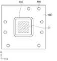
도 1 내지 도 4를 참조하면, 본 발명의 실시 예에 따른 허메틱 실링 패키지 모듈은, 센서 칩(100), 센서 칩(100)과 마주보도록 배치되는 기판(200) 및 센서 칩(100)과 기판(200) 사이에서 이들을 접합하는 실링 링(300)을 포함한다.1 to 4, the hermetic sealing package module according to an embodiment of the present invention includes a
여기서, 센서 칩(100)의 표면에는 패시베이션막(미도시) 및 스트레스 완충막(120)이 구비된다. 또한, 센서 칩(100), 기판(200) 및 실링 링(300)에 의해 캐비티(S1)가 형성되도록, 실링 링(300)은 기판(200)에 융착되고 패시베이션막에 결합되며, 실링 링(300)의 에지(311)는 스트레스 완충막(120)에 결합된다.Here, a passivation film (not shown) and a
실링 링(300)은 에지(311)가 스트레스 완충막(120)에 결합됨으로써, 센서 칩(100)과의 결합 강도가 향상될 수 있다. 그리고 실링 링(300)은 에지(311)를 제외한 소정의 부분이 센서 칩(100)의 패시베이션막에 결합됨으로써, 실링 링(300)과 센서 칩(100)의 결합 부위의 기밀성을 향상시킬 수 있다.As the
한편, 본 발명의 실시 예에 따른 허메틱 실링 패키지 모듈은, 센서 칩(100)과 기판(200)을 전기적으로 연결시키는 입출력 범프(600), 기판(200)과 마주보도록 배치되는 판독집적회로기판(710), 판독집적회로기판(710)과 기판(200)을 접합시키는 조인트(720), 판독집적회로기판(710)으로부터 이격되고, 기판(200)에 접합되는 솔더 볼(730), 외부로부터의 광 신호를 센서 칩(100)으로 집중시킬 수 있도록 센서 칩(100)에 부착되고, 렌즈 또는 광학필터를 포함하는 광학계(800)를 더 포함할 수 있다.Meanwhile, in the hermetic sealing package module according to an embodiment of the present invention, the input/
또한, 본 발명의 실시 예에 따른 허메틱 실링 패키지 모듈은, 광학계(800), 센서 칩(100), 기판(200), 판독집적회로기판(710) 및 솔더 볼(730) 중의 적어도 일부의 외면을 피복하는 복수의 몰딩(910, 920)을 더 포함할 수 있다.In addition, in the hermetic sealing package module according to an embodiment of the present invention, at least a part of the outer surface of the
캐비티(S1)는 수 밀리 토르(mTorr) 내지 100 토르(Torr)의 진공으로 제어될 수 있다. 여기서, 수 밀리 토르는 예컨대 1 밀리 토르이거나 이보다 크고 10 밀리 토르보다 작은 것을 의미할 수 있다. 캐비티(S1)의 진공이 수 밀리 토르보다 작으면 외부와의 압력 차이가 허메틱 실링 패키지 모듈의 구조에 영향을 줄 수 있다. 캐비티(S1)의 진공이 100 토르보다 크면 센서 칩(100)의 센싱 감도에 영향을 줄 수 있다. 즉, 캐비티(S1)는 수 밀리 토르(mTorr) 내지 100 토르(Torr)의 진공으로 제어됨에 따라, 구조적으로 안정되고, 센싱 감도가 양호할 수 있다.The cavity S1 may be controlled with a vacuum of several milliTorr to 100 Torr. Here, several millitorrs may mean, for example, 1 millitorr or larger and smaller than 10 millitorr. When the vacuum of the cavity S1 is smaller than several millitorr, a pressure difference with the outside may affect the structure of the hermetic sealing package module. If the vacuum of the cavity S1 is greater than 100 Torr, sensing sensitivity of the
센서 칩(100)은 가시광 이미지를 촬영할 수 있도록 형성되는 포토 센서 칩을 포함할 수 있다. 또한, 센서 칩(100)은 열화상을 촬영할 수 있도록 형성되는 온도 센서 칩을 포함할 수 있다. 물론, 센서 칩(100)은 각종 변환 소자가 형성된 반도체 칩을 포함할 수 있다.The
센서 칩(100)은, 소자가 형성된 모재(110), 모재(110) 상에 형성되는 패시베이션막(미도시), 및 패시베이션막 상에 형성되고 일부가 제거된 스트레스 완충막(120)을 포함할 수 있다. 또한, 센서 칩(100)은 캐비티(S1)의 외측에 위치하도록 모재(110) 상에 형성되고, 스트레스 완충막(120)을 관통하는 입출력 패턴(150)을 포함할 수 있다.The
또한, 허메틱 실링 패키지 모듈이 모재(110)를 관통하도록 형성되는 센서 캐비티(S2)를 더 포함하는 구조인 경우, 센서 칩(100)은 센서 캐비티(S2)의 개구들 중 일면 예컨대 하면의 개구를 밀봉시키도록 모재(110)에 장착되는 멤브레인(160)을 더 포함할 수 있다.In addition, when the hermetic sealing package module has a structure further including a sensor cavity S2 formed to penetrate the
모재(110)는 웨이퍼를 포함할 수 있다. 물론, 모재(110)는 글래스 및 세라믹을 포함하여 다양할 수 있다. 모재(110)의 일면 예컨대 하면에는 센싱 영역(C1) 및 단자 영역(C2)이 형성될 수 있다. 모재(110)는 수평 방향(X, Y)으로 소정의 면적을 가질 수 있고, 상하 방향(Z)으로 소정의 두께를 가질 수 있다. 모재(110)의 두께는 730 마이크로미터(㎛) 내지 200 마이크로미터(㎛)일 수 있다.
센싱 영역(C1)은 광 신호를 입력받아서 전기 신호를 생성할 수 있는 광전 변환 소자(미도시)를 포함할 수 있다. 단자 영역(C2)은 센싱 영역(C1)에서 생성된 전기 신호를 외부로 송신할 수 있고, 센싱 영역(C1)으로 전력 및 제어용 신호를 입력할 수 있는 복수의 단자들을 포함할 수 있다. 여기서, 광 신호는 가시광선 및 적외선 중 적어도 어느 하나를 포함할 수 있다. 이때, 광 신호는 외부로부터 모재(110)의 상면으로 입사될 수 있고, 모재(110)의 내부를 진행하여 모재(110)의 하면에 형성된 광전 변환 소자에 도달할 수 있다.The sensing region C1 may include a photoelectric conversion element (not shown) capable of receiving an optical signal and generating an electrical signal. The terminal area C2 may include a plurality of terminals capable of transmitting electrical signals generated in the sensing area C1 to the outside and inputting power and control signals to the sensing area C1. Here, the optical signal may include at least one of visible light and infrared light. At this time, the optical signal may be incident on the upper surface of the
센싱 영역(C1)은 모재(110)의 하면의 중앙에 소정 면적으로 형성되고, 단자 영역(C2)은 센싱 영역(C1)을 감싸도록 모재(110)의 하면의 둘레에 형성될 수 있다. 물론, 센싱 영역(C1)과 단자 영역(C2)이 형성되는 면은 다양할 수 있고, 해당 면에서의 센싱 영역(C1)과 단자 영역(C2)의 배치도 다양할 수 있다.The sensing region C1 may be formed with a predetermined area at the center of the lower surface of the
한편, 허메틱 실링 패키지 모듈이 센서 캐비티(S2)를 더 포함할 때, 센서 캐비티(S2)는 모재(110)의 소정 위치 예컨대 중앙을 상하 방향(Z)으로 관통하도록 형성될 수 있고, 멤브레인(160)은 센서 캐비티(S2)의 하부를 밀봉하도록 모재(110)의 하면에 위치하는 센서 캐비티(S2)의 하부 개구에 장착될 수 있다. 이때, 센싱 영역(C1)은 멤브레인(160)에 형성될 수 있다. 또한, 단자 영역(C2)은 멤브레인(160)을 감싸도록 모재(110)의 하면의 둘레에 형성될 수 있다. 센서 캐비티(S2)는 진공으로 제어될 수 있고, 광 신호는 센서 캐비티(S2)를 지나, 센싱 영역(C)의 광전 변환 소자에 입사될 수 있다. 센서 캐비티(S2)를 구비하는 센서 칩(100)은 주로 온도 센서 칩으로 활용될 수 있다. 한편, 센서 캐비티(S2)의 상부 개구는 후술하는 광학계(800)에 의해 밀봉될 수 있다.On the other hand, when the hermetic sealing package module further includes the sensor cavity S2, the sensor cavity S2 may be formed to penetrate a predetermined position, for example, the center of the
패시베이션막(미도시)은 모재(110)의 하면에 소정의 두께로 형성될 수 있다. 이때, 패시베이션막은 SiO2, Si3N4 및 TEOS 중에서 선택된 어느 하나의 재질을 포함할 수 있다. 패시베이션막은 모재(110)에 형성된 소자를 보호하는 역할을 한다.A passivation film (not shown) may be formed to a predetermined thickness on the lower surface of the
한편, 패시베이션막은 소자를 보호할 수 있도록 소정의 강도를 가지며, 브리틀(brittle)한 특성을 가지는 소정의 재질을 포함할 수 있다. 따라서, 패시베이션막에 실링 링(300)이 증착되어 결합되는 경우, 결합 부위의 기밀성이 향상될 수 있다. 즉, 패시베이션막에 실링 링(300)이 증착되어 결합되는 경우, 센서 칩(100)과 기판(200)과 실링 링(300) 사이의 캐비티(S1)의 허메틱 실링이 원활할 수 있다.On the other hand, the passivation film has a predetermined strength to protect the device, and may include a predetermined material having a brittle (brittle) characteristics. Therefore, when the sealing
한편, 패시베이션막은 브리틀한 특성 때문에 기계적인 스트레스와 열적인 스트레스에 약하다. 이에, 외부로부터의 스트레스로부터 패시베이션막을 보호할 수 있도록, 패시베이션막 상에 스트레스 완충막(120)이 소정의 두께로 형성될 수 있다.On the other hand, the passivation film is weak against mechanical stress and thermal stress due to its brittle characteristics. Accordingly, the
스트레스 완충막(stress buffer layer, 120)은 기계적인 스트레스와 열적인 스트레스로부터 강하도록 덕타일(ductile)한 특성을 가지는 소정의 재질을 포함할 수 있다. 예컨대 스트레스 완충막(120)은 폴리머, 폴리이미드 등의 재질을 포함할 수 있다. 스트레스 완충막(120)은 패시베이션막의 하면을 덮도록 연장형성되며, 소정의 두께를 가질 수 있다.The
스트레스 완충막(120)은 실링 링(300)이 배치되는 부위의 패시베이션막을 실링 링(300) 측으로 노출시키도록, 일부가 폐루프 형상으로 제거될 수 있다. 구체적으로, 모재(110)의 패시베이션막의 하면에 형성되는 스트레스 완충막(120)은 센싱 영역(C1)의 스트레스 완충막과 단자 영역(C2)의 스트레스 완충막을 포함할 수 있다. 그중 단자 영역(C2)의 스트레스 완충막은 실링 링(300)이 배치되는 부위, 입출력 패턴(150)이 형성되는 부위가 모재(110)의 패시베이션막의 하면으로부터 제거될 수 있다.A portion of the
한편, 스트레스 완충막(120)은 덕타일한 특성을 가지므로, 실링 링(300)을 스트레스 완충막(120)에 증착시켜 결합시키는 경우, 이들 간의 기밀성을 원활하게 유지하기 어렵다. 즉, 패시베이션막에 실링 링(300)이 증착되어 결합되는 경우에 비하여, 스트레스 완충막(120)에 실링 링(300)이 증착되어 결합되는 경우, 센서 칩(100)과 기판(200)과 실링 링(300) 사이의 캐비티(S1)의 허메틱 실링을 안정적으로 유지하기가 어려울 수 있다.Meanwhile, since the
입출력 패턴(150)은 모재(110)상에 마련되는 소정의 배선(미도시)를 통하여 광전 변환 소자 및 복수의 단자와 전기적으로 연결될 수 있다. 광전 변환 소자 및 복수의 단자는 입출력 패턴(150)과 입출력 범프(600)를 통해 기판(200)과 전기적으로 연결될 수 있다.The input/
기판(200)은 센서 칩(100)의 하면을 상하 방향(Z)으로 마주보도록 배치될 수 있다. 즉, 센서 칩(100)의 하측에 기판(200)이 배치될 수 있다. 기판(200)의 수평 방향(X, Y)으로의 면적은 센서 칩(100)의 수평 방향(X, Y)으로의 면적보다 클 수 있다. 즉, 기판(200)의 가장자리가 수평 방향(X, Y)으로 센서 칩(100)보다 돌출될 수 있다. 여기서, 기판(200)의 가장자리의 돌출된 부분에 몰딩(910, 920)이 지지될 수 있다. 기판(200)은 센서 칩(100)을 구조적으로 지지해줄 수 있다. 기판(200)을 통하여 센서 칩(100)과 판독집적회로기판(710) 및 솔더 볼(730)이 전기적으로 연결될 수 있다. 이러한 기판(200)은 판 형상으로 형성될 수 있고, 소정의 두께를 가질 수 있다.The
기판(200)은 본체(210)와 본체(210)의 상면 및 하면에 각기 형성되는 복수의 패턴(220, 240, 250, 260)을 포함할 수 있다. 본체(210)는 레진(resin), 프리프레그(prepreg), 글라스 및 세라믹 중 어느 하나를 포함할 수 있다. 본체(210)의 두께는 0.5 밀리미터 이하로 형성될 수 있다. 본체(210)의 두께가 0.5 밀리미터보다 크면, 허메틱 실링 패키지 모듈의 전체 두께가 원하는 소정의 두께보다 커질 수 있다. 본체(210)의 두께의 하한은 예컨대 센서(100), 솔더 볼(730) 및 판독집적회로기판(710)와 같이 본체(210)에 장착되는 구조물들에 의해 본체(210)가 휘어지지 않도록 하는 소정의 두께일 수 있다.The
본체(210)의 열팽창계수(Coefficient of Thermal Expansion)는 1.2 내지 15 ppm/℃의 범위일 수 있다. 이에, 본체(210)는 센서 칩(100)과 동일 혹은 유사한 열적 거동을 보일 수 있다. 즉, 상술한 본체(210)의 열팽창계수에 의하여, 동일한 온도에 대한 본체(210)와 센서 칩(100)의 열 팽창 정도가 같거나 유사할 수 있다.The coefficient of thermal expansion of the
또한, 본체(210)는 인쇄회로기판을 포함할 수 있다. 이때, 본체(210)의 상면에 금속 재질의 코팅막(미도시)이 구비될 수 있다. 복수의 패턴(220, 240, 250, 260) 중 본체(210)의 상면에 위치하는 패턴들은 코팅막 상에 형성될 수 있다. 코팅막에 의해 캐비티(S1)의 진공이 유지될 수 있다.In addition, the
코팅막은 구리를 포함하고, 코팅막의 두께는 7 내지 40 마이크로미터의 범위로 형성될 수 있다. 코팅막의 두께를 7 마이크로미터 미만으로 하면 코팅막과 상술한 복수의 패턴 간의 결합 강도를 원하는 소정의 결합 강도로 유지하기가 어려울 수 있다. 코팅막의 두께가 40 마이크로미터를 초과하면 기판(200)의 전체 두께가 원하는 두께보다 커질 수 있다. 본체(210)와 코팅막을 합친 기판(200)의 전체 두께는 0.3 밀리미터 이하로 형성될 수 있다. 본체(210)의 열팽창계수는 1.2 내지 15 ppm/℃의 범위일 수 있다.The coating layer includes copper, and the thickness of the coating layer may be formed in a range of 7 to 40 micrometers. If the thickness of the coating film is less than 7 micrometers, it may be difficult to maintain a desired bonding strength between the coating film and the plurality of patterns described above. If the thickness of the coating film exceeds 40 micrometers, the entire thickness of the
복수의 패턴은 실링 링(300)과 결합할 수 있도록 본체(210)의 상면에 폐루프 형상으로 형성되는 결합용 패턴(220)과, 결합용 패턴(220)의 둘레를 따라서 나열되는 복수개의 제2입출력 패턴(240)을 포함할 수 있다.The plurality of patterns include a
또한, 복수의 패턴은 조인트(720)가 접합될 수 있도록 본체(210) 하면에 형성되는 조인트 패턴(250) 및 조인트 패턴(250)으로부터 본체(210)의 가장자리 측으로 이격되며 솔더 볼(730)과 접합될 수 있도록 본체(210)의 하면에 형성되는 볼 패턴(260)을 포함할 수 있다.In addition, the plurality of patterns are spaced apart from the
결합용 패턴(220)은 실링 링(300)과 접합될 수 있다. 제2입출력 패턴(240)은 입출력 범프(600)와 접합될 수 있다. 이때, 제2입출력 패턴(240)은 입출력 범프(600) 및 입출력 패턴(150)을 통하여 센서 칩(100)의 광전 변환 소자 및 복수의 단자와 전기적으로 연결될 수 있다.The
조인트 패턴(250)은 조인트(720)와 접합될 수 있고, 조인트(720)는 판독집적회로기판(710)과 접합될 수 있다. 또한, 볼 패턴(260)은 솔더 볼(730)과 접합될 수 있다. 이때, 조인트 패턴(250) 및 볼 패턴(260) 각각은 기판(200)에 구비되는 소정의 배선 패턴들을 통하여 제2입출력 패턴(240)과 전기적으로 연결될 수 있다.The
실링 링(300)은 센서 칩(100)과 기판(200) 사이에서 이들을 접합하는 역할을 한다. 실링 링(300)은 스트레스 완충막(120)이 제거된 부위를 따라 폐루프 형상으로 연장형성되고, 상면이 센서 칩(100)의 패시베이션막에 증착되고, 하면이 기판(200)에 구비된 결합용 패턴(220)에 융착될 수 있다. 이러한 구조에 의하여, 센서 칩(100)과 기판(200)과 실링 링(300)의 사이에 캐비티(S1)가 정의될 수 있다. 여기서, 실링 링(300)은 상면의 에지(311)가 스트레스 완충막(120)에 증착되고, 에지(311)를 제외한 상면의 나머지 면이 패시베이션막에 증착될 수 있다.The sealing
예컨대 실링 링(300)의 상면 전체를 패시베이션막에 증착하면, 패시베이션막의 브리틀한 특성 때문에, 캐비티(S1)의 기밀을 안정적으로 유지할 수는 있으나, 증착된 부위의 결합 강도가 상대적으로 약할 수 있다.For example, if the entire upper surface of the sealing
반면, 실링 링(300)의 상면 전체를 스트레스 완충막(120)에 증착하면, 스트레스 완충막(120)의 덕타일한 특성 때문에, 증착된 부위의 결합 강도를 상대적으로 향상시킬 수 있으나, 캐비티(S1)의 기밀 유지가 어려울 수 있다.On the other hand, if the entire upper surface of the sealing
따라서, 실링 링(300)은 상면의 에지(311)가 스트레스 완충막(120)에 증착되어 결합 강도가 향상될 수 있고, 에지(311)를 제외한 상면의 나머지 면이 패시베이션막에 증착되어 원하는 수준의 기밀성을 확보할 수 있다. 이처럼 실링 링(300)은 상면의 부위에 따라 증착되는 대상을 다르게 하여 서로 다른 복수의 기능을 동시에 수행할 수 있다.Therefore, the
한편, 실링 링(300)의 상면의 에지(311)는 실링 링(300)의 상면의 양측 가장자리의 면을 지칭한다. 양측 가장자리는 캐비티(S1)와 가까운 내측 가장자리와 캐비티(S2)에서 먼 외측 가장자리일 수 있다. 실링 링(300)의 상면의 에지(311)를 간단하게 실링 링(300)의 에지(311)라고 표현할 수 있다. 실링 링(300)의 에지(311)를 제외한 상면의 나머지 면을 실링 링(300)의 상면의 중심이라고 하고, 간단하게 실링 링(300)의 중심이라고 지칭한다. 이를 반영하여 실링 링(300)의 기능을 다시 설명하자면, 실링 링(300)의 중심은 패시베이션막과 결합되어 캐비티(S1)의 허메틱 실링을 유지하는 기능을 수행할 수 있고, 실링 링(300)의 에지는 스트레스 완충막(120)과 결합되어 실링 링(300)과 센서 칩(100) 간의 결합 강도를 향상시키는 기능을 수행할 수 있다.Meanwhile, the
실링 링(300)은 상호 접합된 복수개의 층을 구비할 수 있다. 이때, 복수개의 층은 패시베이션막에 증착되는 베이스층(310), 및 상면이 베이스층(310)에 증착되며 하면이 결합용 패턴(220)에 융착되는 접합층(320)을 포함할 수 있다.The sealing
베이스층(310)은 실링 링(300)의 몸체 역할을 한다. 베이스층(310)은 Cu 재질을 포함할 수 있다. 베이스층(310)의 두께는 15 내지 60 마이크로미터의 범위일 수 있다. 베이스층(310)의 두께가 15 마이크로미터보다 작으면, 실링 링(300)의 결합 강도가 원하는 결합 강도보다 작을 수 있다. 즉, 베이스층(310)이 캐비티(S1)의 진공과 외부의 대가압 간의 압력 차이를 견디지 못하고, 파괴될 수 있다. 또한, 베이스층(310)의 두께가 60 마이크로미터보다 크면, 허메틱 실링 패키지 모듈의 전체 두께가 원하는 소정의 두께보다 커질 수 있고, 두께 증가에 따라 허메틱 실링 패키지 모듈의 생산 비용이 불필요하게 증가될 수 있다.The
접합층(320)은 용접성을 향상시키는 역할을 한다. 즉, 접합층(320)은 베이스층(310)을 결합용 패턴(220)에 접합시키는 역할을 한다. 이를 위하여, 접합층(320)은 SnAg 합금 재질을 포함할 수 있다. 이때, 접합층(320)의 두께는 5 내지 15 마이크로미터의 범위일 수 있다. 접합층(320)의 두께가 5 마이크로미터 미만이면, 베이스층(310)과 결합용 패턴(220)을 융착시키기 어렵고, 이들 간에 접합 불량이 발생할 수 있다. 또한, 접합층(320)의 두께가 15 마이크로미터를 초과하면 베이스층(310)과 결합용 패턴(220)을 융착시키는 도중에 접합층(320)이 흘러내릴 수 있다. 이로부터 실링 링(300)의 전체 두께는 20 내지 75 마이크로미터의 범위로 정해질 수 있다.The
실링 링(300)의 폭은 35 마이크로미터 이상으로 형성될 수 있다. 실링 링(300)의 폭은 단자 영역(S2)의 폭보다 작을 수 있다. 실링 링(300)의 폭이 35 마이크로미터 미만이면 패시베이션막 및 스트레스 완충막(120)과 충분한 면적으로 접촉할 수 없고, 실링 링(300)의 기밀성과 결합 강도를 원하는 수준으로 확보하기가 어려울 수 있다. 실링 링(300)의 폭이 단자 영역(S2)의 폭보다 크면 센싱 영역(S1)과 간섭되거나 입출력 범프(600)와 간섭될 수 있다.The sealing
입출력 범프(600)는 더미 링(500)의 둘레를 따라 나열될 수 있다. 입출력 범프(600)는 상면이 센서 칩(100)의 입출력 패턴(150)에 증착되고, 하면이 기판(200)의 제2입출력 패턴(240)에 융착될 수 있다. 입출력 범프(600)는 센서 칩(100)과 기판(200)을 전기적으로 연결시킬 수 있다. 입출력 범프(600)는 상부층(610) 및 하부층(620)을 포함할 수 있다. 상부층(610)은 전기 전도성 재질을 포함할 수 있고, 하부층(620)은 전기 전도성을 가지면서 상부층(610)보다 융점이 낮은 재질을 포함할 수 있다. 이에, 하부층(620)이 상부층(610)을 제2입출력 패턴(240)에 융착시킬 수 있고, 상부층(610)과 제2입출력 패턴(240)을 전기적으로 연결시킬 수 있다.The input/
판독집적회로기판(710)은 판독집적회로가 구비된 기판으로서, 광전 변환 소자에서 생성되는 전기 신호를 판독하고, 그 결과를 솔더 볼(730)을 통하여 외부로 송신할 수 있다. 판독집적회로기판(710)은 기판(200)의 하면과 마주보도록 배치될 수 있고, 조인트(720)를 통해 기판(200)의 조인트 패턴(250)에 접합될 수 있다. 솔더 볼(730)은 판독집적회로기판(710)의 둘레를 따라 나열되고, 기판(200)의 하면에 접합될 수 있다.The readout integrated
광학계(800)는 센서 칩(100)의 상면에 예컨대 에폭시 접합 방식으로 접착될 수 있고, 외부로부터의 광 신호를 센서 칩(100)으로 집중시킬 수 있다. 광학계(800)에 의해 센서 칩(100)의 하면의 센싱 영역(C1)에 광 신호의 초점이 형성될 수 있다. 광학계(800)는 렌즈 또는 광학필터를 포함할 수 있다.The
렌즈는 그 내부에 캐비티를 구비하는 구조일 수 있다. 렌즈 내부의 캐비티는 센서 캐비티(S2)와 연통할 수 있다. 렌즈의 두께는 600 마이크로미터(㎛) 내지 400 마이크로미터(㎛)일 수 있다. 물론, 렌즈의 구조는 다양할 수 있다. 광학필터는 예컨대 코팅글라스(coating glass)일 수 있다. 코팅글라스는 글라스기판에 원하는 파장의 광을 통과시키는 막을 부착 혹은 증착하여 제조할 수 있다. 코팅글라스에 코팅되는 막의 종류는 예컨대 IR(Infrared Ray) 막, AR(AntiReflective Coating) 막, BBRAC(Broad band AntiRflection Coating) 막 을 포함하여 다양할 수 있다. 코팅글라스의 두께는 100 마이크로미터(㎛) 내지 300 마이크로미터(㎛)일 수 있다.The lens may have a structure having a cavity therein. A cavity inside the lens may communicate with the sensor cavity S2. The thickness of the lens may be 600 micrometers (㎛) to 400 micrometers (㎛). Of course, the structure of the lens may vary. The optical filter may be, for example, coated glass. Coated glass can be manufactured by attaching or depositing a film that transmits light of a desired wavelength to a glass substrate. The type of film coated on the coating glass may be various, including, for example, an IR (Infrared Ray) film, an AR (AntiReflective Coating) film, and a BBRAC (Broad band AntiReflection Coating) film. The coating glass may have a thickness of 100 micrometers (㎛) to 300 micrometers (㎛).
몰딩(910, 920)은 기판(200)의 상부에 형성되는 상부 몰딩(910)과 기판(200)의 하부에 형성되는 하부 몰딩(920)을 포함할 수 있다. 상부 몰딩(910) 및 하부 몰딩(920)은 소정의 필름을 사용하여 진공 적층(vacuum lamination) 방식으로 형성될 수 있다. 상부 몰딩(910)은 광학계(800)의 측면과, 센서 칩(100)의 상면 및 측면과, 기판(200)의 상면을 감싸도록 형성될 수 있다. 하부 몰딩(920)은 기판(200)과 판독집적회로기판(710)과 솔더 볼(730)의 하부를 감싸도록 형성될 수 있다. 이때, 솔더 볼(730)의 하부면의 일부는 하부 몰딩(920)의 하방으로 노출될 수 있다.The
도 1 내지 도 4를 참조하여 본 발명의 실시 예를 설명하였으나, 본 발명은 하기의 변형 예들을 포함하여 다양하게 구성될 수 있다.Although embodiments of the present invention have been described with reference to FIGS. 1 to 4 , the present invention may be configured in various ways including the following modified examples.
도 5는 본 발명의 변형 예에 따른 허메틱 실링 패키지 모듈의 확대도이다.5 is an enlarged view of a hermetic sealing package module according to a modified example of the present invention.
도 5를 참조하면, 본 발명의 변형 예에 따르면, 허메틱 실링 패키지 모듈의 센서 칩(100)은 스트레스 완충막(120)이 제거된 부위를 따라 폐루프 형상으로 형성되며, 패시베이션막과 실링 링(300) 사이에서 이들을 결합시키는 금속막(130)을 더 포함할 수 있다.Referring to FIG. 5 , according to a modified example of the present invention, the
또한, 본 발명의 변형 예에 따르면, 허메틱 실링 패키지 모듈은 스트레스 완충막(120)을 피복하는 제2스트레스 완충막(400)을 더 포함할 수도 있다.Also, according to a modified example of the present invention, the hermetic sealing package module may further include a second
이때, 본 발명의 변형 예에 따른 허메틱 실링 패키지 모듈은 상술한 본 발명의 실시 예에 따른 허메틱 실링 패키지 모듈과 대부분의 구성이 유사하므로, 이하에서는 중복되는 설명을 생략하거나 간단하게 설명한다. 또한, 이하에서는 본 발명의 실시 예와 구분되는 본 발명의 변형 예에 따른 허메틱 실링 패키지 모듈의 특징을 상세하게 설명한다.At this time, since most of the configurations of the hermetic sealing package module according to the modified example of the present invention are similar to the above-described hermetic sealing package module according to the embodiment of the present invention, duplicate descriptions will be omitted or simply described. In addition, hereinafter, characteristics of the hermetic sealing package module according to a modified example of the present invention, which is distinguished from the embodiment of the present invention, will be described in detail.
금속막(130)은 모재(110)의 패시베이션막 상에 증착되어 형성되며, 실링 링(300)을 배치할 부위를 제외한 나머지가 모재(110)로부터 제거될 수 있다. 이에, 금속막(130)은 실링 링(300)의 형상과 동일한 폐루프 형상으로 형성될 수 있다. 또한, 금속막(130)은 스트레스 완충막(120)의 제거된 부위를 통하여 실링 링(300)에 노출될 수 있다. 이를 위해, 단자 영역(C2)에서 스트레스 완충막(120)은 금속막(130)이 형성되는 부위가 제거될 수 있다.The
금속막(130)과 스트레스 완충막(120)은 수평 방향(X, Y)으로 서로 연결될 수 있다. 이로부터 모재(110)에 구비된 패시베이션막의 하면 전체가 금속막(130) 및 스트레스 완충막(120)에 의해 커버될 수 있다.The
금속막(130)은 모재(110)의 하면의 단자 영역(C2)에서 센싱 영역(C1)의 둘레를 따라서 연장형성되며, 그 형상은 예컨대 폐루프 형상일 수 있다. 폐루프 형상은 링과 같은 형상일 수 있다. 이러한 금속막(130)은 모재(110)의 하면의 패시베이션막에 증착되는 방식으로 형성될 수 있다. 금속막(130)의 내측에는 센싱 영역(C1)이 위치할 수 있다.The
금속막(130)은 연성(ductile)을 가지는 재질을 포함할 수 있다. 이때, 금속막(130)이 연성을 가진다는 것은 예컨대 금속막(130)을 인장시켰을 때 금속막(130)이 소정의 길이까지는 끊어지지 않고 늘어날 수 있다는 것을 의미한다. 이때, 연성이 클수록 금속막(130)이 끊어지지 않고 늘어나는 길이가 길 수 있다. 금속막(130)이 가지는 연성의 크기는 예컨대 금속막(130)으로 인장 실험을 하여 금속막(130)의 처음 길이와 금속막(130)이 끊어지기 전의 늘어난 길이의 비율을 이용하여 구할 수 있다. 또한, 금속막(130)은 스트레스 완충막(120)에 비하여 단단한 특성을 가지며, 금속 소재가 가지는 특성 상 스트레스 완충막(120)보다 조직이 치밀하기 때문에, 허메틱 실링을 유지할 수 있으면서 스트레스도 해소시킬 수 있다. 즉, 금속막(130)은 패시베이션막의 기능과 스트레스 완충막(120)의 기능을 모두 수행할 수 있다.The
즉, 금속막(130)은 모재(110)에 대한 SBL(Stress Buffer Layer)의 역할을 수행할 수 있으면서도, 캐비티(S1)의 진공과 외부의 대기압 간의 압력 차이를 견디고 실링 링(300)과 결합을 유지할 수 있는 소정 크기의 범위로 연성을 가질 수 있다.That is, the
이를 위해, 금속막(130)은 Al, Au, Ag, Ti, Cu 및 W 중 어느 하나 또는 이들의 합금을 포함할 수 있다. 이에, 금속막(130)은 원하는 크기 범위의 연성을 가질 수 있다. 또한, 금속막(130)은 패시베이션막을 대신하여 실링 링(300)과 결합되며 실링 링(300)을 견고하게 지지할 수 있다. 또한, 금속막(130)은 실링 링(300)을 형성하기 위한 시드 메탈(seed metal)의 역할도 수행할 수 있다.To this end, the
금속막(130)의 상하 방향(Z)으로의 두께는 6000 옹스트롬(angstrom) 이상이고, 스트레스 완충막(120)의 두께 이하일 수 있다. 예컨대 금속막(130)의 두께가 6000 옹스트롬 미만이면, 금속막(130)이 SBL의 역할을 수행하기 어려울 수 있다. 예컨대 기계적인 스트레스 혹은 열적인 스트레스가 금속막(130)에서 소산되지 못하고 모재(110)의 하면에 전달될 수 있다. 또한, 금속막(130)의 두께가 스트레스 완충막(120)의 두께를 초과하면, 센서 칩(100)의 전체 두께가 증가하여 허메틱 실링 패키지 모듈의 전체 두께를 원하는 두께로 제작하기 어려울 수 있다.A thickness of the
따라서, 금속막(130)은 상하 방향(Z)으로의 두께가 상술한 두께 범위를 가짐에 따라서, 모재(110)로 가해지는 기계적인 스트레스 및 열적인 스트레스를 차단시킬 수 있으면서, 센서 칩(100)의 전체 두께가 증가하는 것을 방지할 수 있다.Therefore, as the thickness of the
실링 링(300)은 금속막(130)에 증착될 수 있다. 이때, 실링 링(300)은 그 폭이 금속막(130)의 폭 보다 클 수 있다. 이때, 실링 링(300)의 에지(311)는 스트레스 완충막(120)에 증착되고, 에지(311)를 제외한 실링 링(300)의 중심이 금속막(130)에 증착될 수 있다.The sealing
물론, 실링 링(300)의 폭이 금속막(130)의 폭보다 작을 수도 있다. 이 경우에, 실링 링(300)은 에지(311)와 중심 모두 금속막(130)에 증착될 수 있다.Of course, the width of the sealing
제2스트레스 완충막(400)은 스트레스 완충막(120) 상에 형성될 수 있고, 실링 링(300)이 위치하는 부위와 입출력 패턴(150)이 위치하는 부위가 제거될 수 있다. 제2스트레스 완충막(400)은 입출력 패턴(150)의 에지와 상호 중첩될 수 있다. 제2스트레스 완충막(400)은 스트레스 완충막(120)과 재질 및 두께가 동일할 수 있다.The second
한편, 실링 링(300)의 폭이 금속막(130)의 폭보다 작은 경우에, 제2스트레스 완충막(400)은 금속막(130)의 에지와 상호 중첩될 수 있도록 스트레스 완충막(120) 상에 형성될 수 있다. 따라서, 제2스트레스 완충막(400)은 금속막(130)의 에지가 모재(110)의 하면으로부터 하방으로 들뜨는 것을 방지해줄 수 있다.Meanwhile, when the width of the sealing
도 6은 본 발명의 다른 변형 예에 따른 허메틱 실링 패키지 모듈의 확대도이다.6 is an enlarged view of a hermetic sealing package module according to another modified example of the present invention.
도 6을 참조하면, 본 발명의 다른 변형 예에 따른 허메틱 실링 패키지 모듈은, 실링 링(300)을 둘러싸도록 배치되고, 센서 칩(100)과 기판(200)을 결합하는 더미 링(500)을 더 포함할 수 있다. 여기서, 허메틱 실링 패키지 모듈의 센서 칩(100)은 금속막(130)과 입출력 패턴(150) 사이에서 폐루프 형상으로 연장형성되며, 스트레스 완충막(120)의 외부로 노출되고, 더미 링(500)과 결합되며, 금속 재질을 포함하는 더미막(140)을 더 포함할 수 있다.Referring to FIG. 6 , a hermetic sealing package module according to another modified example of the present invention includes a
이하, 본 발명의 실시 예 및 변형 예와 구분되는 본 발명의 다른 변형 예에 따른 허메틱 실링 패키지 모듈의 특징을 상세하게 설명하고, 중복되는 설명은 생략하거나 간단하게 설명한다.Hereinafter, features of the hermetic sealing package module according to another modification of the present invention, which are distinguished from the embodiment and modification of the present invention, will be described in detail, and overlapping descriptions will be omitted or simply described.
더미막(140)은 금속막(130)의 외측에서 폐루프 형상으로 형성될 수 있다. 더미막(140)은 더미 링(500)을 형성하기 위한 시드 메탈의 역할을 할 수 있다. 이러한 더미막(140)은 상술한 금속막(130)과 재질 및 두께가 동일할 수 있다. 더미막(140)은 모재(110)의 패시베이션막의 하면에 증착될 수 있다.The dummy layer 140 may be formed in a closed loop shape outside the
더미막(140)의 에지는 제2스트레스 완충막(400)에 커버되어 보호될 수 있다. 이에 따라, 금속막(130), 더미막(140) 및 입출력 패턴(150)과 스트레서 완충막(120)은 수평 방향(X, Y)으로 서로 연결될 수 있다. 이에, 모재(110)의 패시베이션막의 하면 전체가 금속막(130), 더미막(140) 및 입출력 패턴(150)과 스트레스 완충막(120)에 의해 커버될 수 있다.An edge of the dummy film 140 may be covered and protected by the second
더미 링(500)은 실링 링(300)의 역할을 보조할 수 있다. 더미 링(500)은 제1층부재(510) 및 제2층부재(520)를 포함할 수 있다. 제1층부재(510)는 더미막(140)의 하면을 따라서 폐루프 형상으로 연장형성될 수 있고, 제2층부재(520)는 제1층부재(510)의 하면에 형성될 수 있다. 제1층부재(510) 및 제2층부재(520)는 증착 방식으로 형성될 수 있다. 제1층부재(510)는 실링 링(300)의 베이스층(310)에 대응할 수 있다. 제2층부재(520)는 실링 링(300)의 접합층(320)에 대응할 수 있다. 이때, 대응한다는 것은 재질, 두께 및 폭 등의 특징이 동일하게 형성되는 것을 의미한다.The
제2스트레스 완충막(400)은 스트레스 완충막(120)의 하면을 따라 연장형성되며, 단자 영역(C2)에서 더미막(140)이 형성되는 부위가 제거될 수 있다. 제2스트레스 완충막(400)은 더미막(140)의 에지와 상호 중첩되고, 실링 링(300)의 측면, 더미 링(500)의 측면 및 입출력 범프(600)의 측면과 접촉될 수 있다.The second
기판(200)은 결합용 패턴(220)의 외측에서 본체(210)의 상면을 따라 폐루프 형상으로 형성되며 더미 링(500)과 결합하는 더미 패턴(230)을 더 포함할 수 있다. 더미 패턴(230)의 둘레를 따라 복수개의 제2입출력 패턴(240)이 나열될 수 있다.The
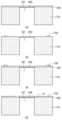
도 7 내지 도 10은 본 발명의 실시 예에 따른 허메틱 실링 패키지 모듈 제조 방법을 설명하기 위한 모식도이다. 도 7의 (a), (b), (c) 및 (d)는 센서 칩의 모재 상에 입출력 패턴과 스트레스 완충막을 형성하는 모습을 순서대로 보여주는 모식도이다. 도 8의 (a)와 (b)는 센서 칩의 스트레스 완충막 상에 실링 링과 입출력 범프가 형성되는 모습을 예시적으로 보여주는 모식도이다.7 to 10 are schematic diagrams for explaining a method of manufacturing a hermetic sealing package module according to an embodiment of the present invention. 7 (a), (b), (c), and (d) are schematic diagrams sequentially showing how to form an input/output pattern and a stress buffer film on a base material of a sensor chip. 8(a) and (b) are schematic diagrams exemplarily showing how sealing rings and input/output bumps are formed on the stress buffer film of the sensor chip.
도 9의 (a) 및 (b)는 기판 상에 복수의 패턴 및 솔더 볼을 형성하는 모습을 예시적으로 보여주는 모식도이다. 또한, 도 10의 (a) 및 (b)는 센서 칩과 기판과 판독집적회로기판과 렌즈를 적층 및 결합시키는 모습을 예시적으로 보여주는 모식도이다.9(a) and (b) are schematic diagrams illustrating the formation of a plurality of patterns and solder balls on a substrate by way of example. In addition, (a) and (b) of FIG. 10 are schematic diagrams illustratively showing how the sensor chip, the board, the readout integrated circuit board, and the lens are stacked and coupled.
도 1 내지 도 10을 참조하여, 본 발명의 실시 예에 따른 허메틱 실링 패키지 모듈 제조 방법을 상세하게 설명한다.1 to 10, a method for manufacturing a hermetic sealing package module according to an embodiment of the present invention will be described in detail.
본 발명의 실시 예에 따른 허메틱 실링 패키지 모듈 제조 방법은, 소자가 형성된 모재(110) 및 기판(200)을 준비하는 과정, 모재(110)의 표면의 패시베이션막 상에 스트레스 완충막(120)을 형성하는 과정; 스트레스 완충막(120)의 일부를 제거하는 과정, 스트레스 완충막(120)이 제거된 부위에 실링 링(300)을 증착하는 과정, 및 기판에(200) 실링 링(100)을 접합하는 과정을 포함한다.A method of manufacturing a hermetic sealing package module according to an embodiment of the present invention includes a process of preparing a
우선, 소자가 형성된 모재(110)를 준비한다. 모재(110)는 일면에 센싱 영역 및 단자 영역이 구비되어 있고, 센싱 영역 및 단자 영역은 패시베이션막(미도시)에 의해 보호되어 있는 상태일 수 있다. 물론, 모재(110)의 일면에 센싱 영역과 단자 영역을 형성한 후, 센싱 영역과 단자 영역을 덮도록 모재(110)의 일면에 패시베이션막을 형성함으로써, 소자가 형성된 모재(110)를 준비할 수 있다. 한편, 모재(110)는 센서 캐비티(S2)와 센서 캐비티(S2)의 하부 개구를 밀봉하는 멤브레인(160)를 구비할 수 있고, 센싱 영역은 멤브레인(160)에 형성될 수 있다.First, a
모재(110)를 준비하는 과정은 모재(110) 상의 소정 위치에 입출력 패턴(150)을 형성하는 과정을 포함할 수 있다. 이때, 도 7의 (a) 및 (b)에 도시된 것처럼, 증착 및 식각의 과정을 통해, 모재(110)의 패시베이션막 상의 입출력 범프(600)를 위치시킬 부분에 입출력 패턴(150)을 형성할 수 있다.The process of preparing the
이후, 기판(200)을 준비한다. 도 9의 (a) 및 (b)을 참조하면, 기판(200)의 상면에 결합용 패턴(220), 제2입출력 패턴(240)을 형성하고, 기판(200)의 하면에 조인트 패턴(250), 볼 패턴(260)을 형성한다. 이때, 증착 및 식각을 수행하여 이들 패턴을 형성할 수 있다. 이후, 조인트 패턴(250)에 솔더 볼(730)을 실장한다.After that, the
이후, 모재(110)의 표면의 패시베이션막 상에 스트레스 완충막(120)을 형성한다. 도 7의 (c)를 참조하면, 모재(110)와 입출력 패턴(150) 상에 스트레스 완충막(120)을 증착한다.Then, the
다음으로, 도 7의 (d)를 참조하면, 스트레스 완충막(120)의 일부를 제거한다. 이때, 스트레스 완충막(120) 상에 페루프 형상으로 스트레스 완충막(120)이 노출되도록 마스킹할 수 있다. 이때, 스트레스 완충막(120)이 노출되는 위치는 실링 링(300)을 형성하고자 하는 위치일 수 있다. 즉, 실링 링(300)을 형성하고자 하는 위치가 폐루프 형상으로 개구된 마스크(미도시)를 스트레스 완충막(120)상에 형성할 수 있다. 이때, 마스크에는 입출력 패턴(150)을 노출시키기 위한 복수개의 개구가 함께 준비될 수 있다. 이후, 마스크로부터 노출된 부분의 스트레스 완충막(120)을 식각함으로써, 모재(110) 상에 복수의 홀(H)을 형성하고, 입출력 패턴(150)을 노출시킬 수 있다. 이후, 마스크를 (120)으로부터 제거할 수 있다.Next, referring to (d) of FIG. 7 , a portion of the
이후, 스트레스 완충막(120)이 제거된 부위에 실링 링(300)을 증착한다.Then, the sealing
도 8의 (a) 및 (b)를 참조하면, 스트레스 완충막(120)의 전체 면 및 스트레스 완충막(120)이 제거된 부위에 소정의 연성을 가지는 금속을 포함하는 제1금속층을 증착하고, 제1금속층의 전체 면에 제1금속층보다 용접성이 좋은 금속을 포함하는 제2금속층을 증착할 수 있다. 이때, 물리기상증착방식으로 제1금속층과 제2금속층을 순차적으로 증착한다. 이후, 스트레스 완충막(120)이 제거된 부위의 패시베이션막 상에 베이스층(310)과 접합층(320)이 형성될 수 있도록, 포토 공정을 통하여 폐루프 형상으로 제2금속층이 노출되도록 마스킹한다. 이때, 금속막(130) 상에 남길 제1금속층 및 제2금속층의 폭이 금속막(130)의 폭보다 크도록 제2금속층을 마스킹한다. 이후, 금속막(130) 상에 실링 링(300)을 형성하도록 플라즈마식각방식 또는 습식식각방식으로 제2금속층 및 제1금속층을 순차 식각하여 베이스층(310)과 접합층(320)을 형성할 수 있다. 물론, 금속막(130) 상에 실링 링(300)을 증착하는 과정에서, 입출력 범프(600)도 동일한 방식으로 증착 및 식각을 통하여 형성할 수 있다.Referring to (a) and (b) of FIG. 8 , a first metal layer including a metal having a predetermined ductility is deposited on the entire surface of the
다음으로, 기판(200)에 실링 링(300)을 접합한다. 기판(200)과 실링 링(300)의 접합을 수행할 챔버의 내부를 수 밀리 토르 내지 100 토르의 진공 분위기로 형성한다.Next, the sealing
이후, 도 10의 (a)에 도시된 것처럼, 진공 분위기에서, 센서 칩(100), 기판(200) 및 실링 링(300)에 의해 캐비티가 형성되도록, 결합용 패턴(220)에 실링 링(300)을 융착할 수 있다. 이때, 제2입출력 패턴(240)에 입출력 범프(600)를 융착할 수 있다. 이때, 플립칩본딩방식으로 이들을 융착할 수 있다. 이때, 이들의 융착되는 부분에는 천이액상확산접합방식으로 금속간 화합물(intermetallic compound)을 형성할 수 있다.Subsequently, as shown in (a) of FIG. 10 , in a vacuum atmosphere, a sealing ring ( 300) can be fused. At this time, the input/
한편, 결합용 패턴(220)에 실링 링(300)을 융착하여, 기판(200)과 센서 칩(100)을 결합시키는 과정 이전에 기판(200)에 판독집적회로기판(710)을 먼저 플립칩본딩방식으로 접합시킬 수 있고, 혹은, 기판(200)과 센서 칩(100)을 결합시킨 이후에 기판(200)에 판독집적회로기판(710)을 접합시킬 수 있다. 즉, 기판(200)에 판독집적회로기판(710)을 접합하는 순서는 다양할 수 있다.On the other hand, before the process of bonding the
이후, 도 10의 (b)에 도시된 것처럼, 예컨대 에폭시를 이용하여 센서 칩(100)의 상면에 광학계(800)를 부착하고, 기판(200)의 하면에 판독집적회로기판(710)를 접합시킬 수 있다. 또한, 광학계(800)의 측면과, 센서 칩(100)의 상면 및 측면과, 기판(200)의 상면 및 하면과, 판독집적회로기판(710)과 솔더 볼(730)의 하부를 감싸도록 몰딩(910, 920)을 형성하여, 허메틱 실링 패키지 모듈을 제조할 수 있다. 여기서, 광학계(800)는 렌즈 또는 광학필터일 수 있다.Subsequently, as shown in (b) of FIG. 10, the
한편, 본 발명의 변형 예들에 따른 허메틱 실링 패키지 모듈 제조 방법은, 스트레스 완충막을 형성하는 과정 이전에, 패시베이션막 상에 금속막을 증착하고, 패시베이션막 상에서 실링 링(300)을 위치시킬 부위에 금속막이 폐루프 형상으로 남도록 금속막의 일부를 제거하는 과정을 더 포함할 수 있다. 즉, 모재(110)의 패시베이션막의 전체 면에 소정의 금속막 층을 증착하고, 금속막(130)이 남도록 금속막 층을 식각할 수 있다. 이때, 증착 공정과 포토 공정과 식각 공정이 사용될 수 있다. 여기서, 식각 공정은 플라즈마식각방식 또는 습식식각방식을 적용할 수 있다. 한편, 이 과정은 입출력 패턴(150)을 형성하는 과정과 동시에 혹은 소정의 순서로 순차 수행될 수 있다.Meanwhile, in the method of manufacturing a hermetic sealing package module according to modified examples of the present invention, before forming a stress buffer film, a metal film is deposited on the passivation film, and a metal film is deposited on the passivation film at a portion where the sealing
또한, 본 발명의 변형 예들에 따른 허메틱 실링 패키지 모듈 제조 방법은, 기판(200)을 준비하는 과정에서 결합용 패턴(220)과 제2입출력 패턴(240) 사이에 더미 패턴(230)을 더 형성할 수 있다. 또한, 스트레스 완충막(120)의 일부를 제거하는 과정에서 금속막(130)과 더미 패턴(230)을 노출시킬 수 있다. 또한, 실링 링(300)을 증착하는 과정에서 실링 링(300)과 입출력 범프(600) 사이에 더미 링(500)을 형성할 수 있고, 이후에 제2스트레스 완충막(400)을 형성할 수 있다.In addition, in the method of manufacturing a hermetic sealing package module according to modified examples of the present invention, in the process of preparing the
본 발명의 상기 실시 예는 본 발명의 설명을 위한 것이고, 본 발명의 제한을 위한 것이 아니다. 본 발명의 상기 실시 예에 개시된 구성과 방식은 서로 결합하거나 교차하여 다양한 형태로 조합 및 변형될 것이고, 그에 따른 변형 예들도 본 발명의 범주로 볼 수 있음을 주지해야 한다. 즉, 본 발명은 청구범위의 범주 내에서 서로 다른 다양한 형태로 구현될 것이며, 본 발명이 해당하는 기술 분야에서의 업자는 본 발명의 청구범위의 범주 내에서 다양한 실시 예가 가능함을 이해할 수 있을 것이다.The above embodiments of the present invention are for explanation of the present invention and are not intended to limit the present invention. It should be noted that the configurations and methods disclosed in the above embodiments of the present invention may be combined or modified in various forms by combining or crossing each other, and modifications thereof may also be considered within the scope of the present invention. That is, the present invention will be implemented in various different forms within the scope of the claims, and those skilled in the art to which the present invention pertains will understand that various embodiments are possible within the scope of the claims of the present invention.
100: 센서 칩 110: 모재
120: 스트레스 완충막 130: 금속막
200: 기판 300: 실링 링
400: 제2스트레스 완충막 500: 더미 링
600: 입출력 범프 710: 판독집적회로기판
720: 조인트 730: 솔더 볼
800: 렌즈 910, 920: 몰딩100: sensor chip 110: base material
120: stress buffer film 130: metal film
200: substrate 300: sealing ring
400: second stress buffer film 500: dummy ring
600: input/output bump 710: readout integrated circuit board
720: joint 730: solder ball
800:
Claims (23)
Translated fromKorean상기 센서 칩과 마주보도록 배치되는 기판; 및
상기 센서 칩과 상기 기판 사이에서 이들을 접합하는 실링 링;을 포함하고,
상기 센서 칩의 표면에는 패시베이션막 및 스트레스 완충막이 구비되며,
상기 센서 칩, 상기 기판 및 상기 실링 링에 의해 캐비티가 형성되도록, 상기 실링 링은 상기 기판에 융착되고 상기 패시베이션막에 결합되며, 상기 실링 링의 에지는 상기 스트레스 완충막에 결합되는 허메틱 실링 패키지 모듈.sensor chip;
a substrate disposed to face the sensor chip; and
A sealing ring between the sensor chip and the substrate to bond them; includes,
A passivation film and a stress buffer film are provided on the surface of the sensor chip,
A hermetic sealing package in which a cavity is formed by the sensor chip, the substrate, and the sealing ring, the sealing ring being fused to the substrate and coupled to the passivation film, and an edge of the sealing ring being coupled to the stress buffer film. module.
상기 센서 칩은,
소자가 형성된 모재;
상기 모재 상에 형성되는 상기 패시베이션막; 및
상기 패시베이션막 상에 형성되고 일부가 제거되어 있는 상기 스트레스 완충막;을 포함하고,
상기 실링 링은, 상기 스트레스 완충막이 제거된 부위를 따라 폐루프 형상으로 연장형성되고, 상기 패시베이션막에 증착되고, 상기 기판에 구비된 결합용 패턴에 융착되며, 상기 실링 링의 에지는 상기 스트레스 완충막에 증착되는 허메틱 실링 패키지 모듈.The method of claim 1,
The sensor chip,
base material on which the element is formed;
The passivation film formed on the base material; and
The stress buffer film formed on the passivation film and partially removed; includes,
The sealing ring is formed to extend in a closed loop shape along a region from which the stress buffering film is removed, is deposited on the passivation film, and is fused to a bonding pattern provided on the substrate, and an edge of the sealing ring is the stress buffering Hermetic sealing package module deposited on the film.
상기 센서 칩은,
소자가 형성된 모재;
상기 모재 상에 형성되는 상기 패시베이션막;
상기 패시베이션막 상에 형성되고 일부가 제거되어 있는 상기 스트레스 완충막; 및
상기 스트레스 완충막이 제거된 부위를 따라 폐루프 형상으로 형성된 금속막;을 포함하고,
상기 실링 링은, 상기 금속막을 따라 폐루프 형상으로 연장형성되고, 상기 금속막에 증착됨에 의하여 상기 패시베이션막과 결합되고, 상기 기판에 구비된 결합용 패턴에 융착되며, 상기 실링 링의 에지는 상기 스트레스 완충막에 증착되는 허메틱 실링 패키지 모듈.The method of claim 1,
The sensor chip,
base material on which the element is formed;
The passivation film formed on the base material;
the stress buffer layer formed on the passivation layer and partially removed; and
A metal film formed in a closed loop shape along a region from which the stress buffer film is removed;
The sealing ring is formed to extend in a closed loop shape along the metal film, is bonded to the passivation film by being deposited on the metal film, and is fused to a bonding pattern provided on the substrate, and the edge of the sealing ring is A hermetic sealing package module deposited on a stress buffer film.
상기 금속막의 두께는 6000 옹스트롬(angstrom) 이상이고, 상기 스트레스 완충막의 두께 이하인 허메틱 실링 패키지 모듈.The method of claim 3,
The thickness of the metal film is 6000 angstroms or more, and the hermetic sealing package module is less than or equal to the thickness of the stress buffer film.
상기 금속막은 Al, Au, Ag, Ti, Cu 및 W 중 어느 하나 또는 이들의 합금을 포함하는 허메틱 실링 패키지 모듈.The method of claim 3,
The metal film is a hermetic sealing package module comprising any one of Al, Au, Ag, Ti, Cu and W or an alloy thereof.
상기 실링 링은 상호 접합된 복수개의 층을 구비하고, 그 전체 두께가 20 내지 75 마이크로미터(㎛)의 범위인 허메틱 실링 패키지 모듈.According to claim 2 or claim 3,
The sealing ring has a plurality of layers bonded to each other, and the total thickness thereof is in the range of 20 to 75 micrometers (μm).
상기 복수개의 층은, 상기 패시베이션막과 결합되는 베이스층 및 상기 결합용 패턴에 융착되는 접합층을 포함하고,
상기 베이스층의 두께는 15 내지 60 마이크로미터의 범위이고,
상기 접합층의 두께는 5 내지 15 마이크로미터의 범위인 허메틱 실링 패키지 모듈.The method of claim 6,
The plurality of layers include a base layer coupled to the passivation film and a bonding layer fused to the bonding pattern,
The thickness of the base layer is in the range of 15 to 60 micrometers,
The thickness of the bonding layer is in the range of 5 to 15 micrometers Hermetic sealing package module.
상기 베이스층은 Cu 재질을 포함하고,
상기 접합층은 SnAg 합금 재질을 포함하는 허메틱 실링 패키지 모듈.The method of claim 7,
The base layer includes a Cu material,
The bonding layer is a hermetic sealing package module comprising a SnAg alloy material.
상기 실링 링의 폭은 35 마이크로미터 이상으로 형성되는 허메틱 실링 패키지 모듈.According to claim 2 or claim 3,
A hermetic sealing package module wherein the sealing ring has a width of 35 micrometers or more.
상기 스트레스 완충막 상에 형성되는 제2스트레스 완충막;을 더 포함하는 허메틱 실링 패키지 모듈.The method of claim 3,
The hermetic sealing package module further comprising a second stress buffer film formed on the stress buffer film.
상기 기판은 레진(resin), 프리프레그(prepreg), 글라스 및 세라믹 중 어느 하나를 포함하고,
상기 기판의 두께는 0.5 밀리미터(㎜) 이하이고,
상기 기판의 열팽창계수(Coefficient of Thermal Expansion)는 1.2 내지 15 ppm/℃의 범위인 허메틱 실링 패키지 모듈.The method of claim 1,
The substrate includes any one of resin, prepreg, glass, and ceramic,
The thickness of the substrate is 0.5 millimeter (mm) or less,
The thermal expansion coefficient of the substrate (Coefficient of Thermal Expansion) is in the range of 1.2 to 15 ppm / ℃ Hermetic sealing package module.
상기 기판은 인쇄회로기판을 포함하고,
상기 기판은 표면에 금속 재질의 코팅막이 구비되고,
상기 기판의 전체 두께는 0.3 밀리미터(㎜) 이하이고,
상기 기판의 열팽창계수는 1.2 내지 15 ppm/℃의 범위인 허메틱 실링 패키지 모듈.The method of claim 1,
The substrate includes a printed circuit board,
The substrate is provided with a coating film of a metal material on the surface,
The overall thickness of the substrate is 0.3 millimeters (mm) or less,
The thermal expansion coefficient of the substrate is in the range of 1.2 to 15 ppm / ° C. Hermetic sealing package module.
상기 코팅막은 구리를 포함하고,
상기 코팅막의 두께는 7 내지 40 마이크로미터의 범위로 형성되는 허메틱 실링 패키지 모듈.The method of claim 12,
The coating film contains copper,
The thickness of the coating film is formed in the range of 7 to 40 micrometers Hermetic sealing package module.
상기 캐비티는 수m 토르(Torr) 내지 100 토르의 진공으로 제어되는 허메틱 실링 패키지 모듈.The method of claim 1,
The cavity is a hermetic sealing package module controlled by a vacuum of several m Torr to 100 Torr.
외부로부터 상기 센서 칩으로 광 신호를 집중시킬 수 있도록 상기 센서 칩의 광 신호가 입사되는 면에 부착되고, 렌즈 또는 광학필터를 포함하는 광학계;
상기 기판과 마주보도록 배치되고, 상기 기판에 접합되는 판독집적회로기판;
상기 판독집적회로기판의 둘레를 따라 나열되고, 상기 기판에 접합되는 솔더 볼; 및
상기 광학계의 일부, 상기 센서 칩, 상기 기판 및 상기 판독집적회로기판을 피복하는 몰딩;을 포함하는 허메틱 실링 패키지 모듈.The method of claim 1,
an optical system attached to a surface of the sensor chip on which an optical signal is incident and including a lens or an optical filter so as to focus an optical signal from the outside to the sensor chip;
a readout integrated circuit board disposed to face the substrate and bonded to the substrate;
solder balls arranged along the circumference of the readout integrated circuit board and bonded to the board; and
A hermetic sealing package module comprising: a molding covering a portion of the optical system, the sensor chip, the substrate, and the readout integrated circuit board.
상기 모재의 표면의 패시베이션막 상에 스트레스 완충막을 형성하는 과정;
상기 스트레스 완충막의 일부를 제거하는 과정;
상기 스트레스 완충막이 제거된 부위에 실링 링을 증착하는 과정; 및
상기 기판에 상기 실링 링을 접합하는 과정;을 포함하는 허메틱 실링 패키지 모듈 제조 방법.A process of preparing a base material and a substrate on which a device is formed;
forming a stress buffer film on the passivation film on the surface of the base material;
removing a portion of the stress buffer layer;
depositing a sealing ring on a region from which the stress buffer layer is removed; and
A method of manufacturing a hermetic sealing package module, comprising bonding the sealing ring to the substrate.
상기 스트레스 완충막을 형성하는 과정 이전에,
상기 패시베이션막 상에 금속막을 증착하는 과정;
상기 패시베이션막 상에 폐루프 형상으로 금속막이 남도록 상기 금속막의 일부를 제거하는 과정;을 더 포함하는 허메틱 실링 패키지 모듈 제조 방법.The method of claim 16
Prior to the process of forming the stress buffer film,
depositing a metal film on the passivation film;
The method of manufacturing the hermetic sealing package module further comprising removing a portion of the metal film so that the metal film remains on the passivation film in a closed loop shape.
상기 스트레스 완충막의 일부를 제거하는 과정은,
상기 스트레스 완충막 상에 페루프 형상으로 스트레스 완충막이 노출되도록 마스킹하는 과정; 및
노출된 스트레스 완충막을 식각하는 과정;을 포함하는 허메틱 실링 패키지 모듈 제조 방법.According to claim 16 or claim 17,
The process of removing a part of the stress buffer film,
masking the stress buffer film so that the stress buffer film is exposed in a loop shape on the stress buffer film; and
A method for manufacturing a hermetic sealing package module comprising: etching the exposed stress buffer film.
상기 실링 링을 증착하는 과정은,
상기 스트레스 완충막의 전체 면 및 상기 스트레스 완충막이 제거된 부위에 패시베이션막보다 연성이 작은 제1금속층을 증착하는 과정;
상기 제1금속층의 전체 면에 제1금속층보다 용접성이 좋은 제2금속층을 증착하는 과정;
상기 스트레스 완충막이 제거된 부위 상에 남길 제1금속층 및 제2금속층의 폭이 상기 스트레스 완충막이 제거된 부위의 폭보다 크도록 제2금속층을 마스킹하는 과정;
상기 스트레스 완충막이 제거된 부위 상에 실링 링을 형성하도록 제2금속층 및 제1금속층을 식각하는 과정;을 포함하는 허메틱 실링 패키지 모듈 제조 방법.The method of claim 18
The process of depositing the sealing ring,
depositing a first metal layer having less ductility than the passivation layer on the entire surface of the stress buffer layer and the region where the stress buffer layer is removed;
depositing a second metal layer having better weldability than the first metal layer on the entire surface of the first metal layer;
masking the second metal layer such that widths of the first metal layer and the second metal layer to be left on the region from which the stress buffer layer is removed are greater than the width of the region from which the stress buffer layer is removed;
and etching the second metal layer and the first metal layer to form a sealing ring on the region from which the stress buffer film is removed.
상기 제1금속층을 증착하는 과정과 상기 제2금속층을 증착하는 과정은 물리기상증착(physical vapor deposition)방식으로 수행하고,
상기 제1금속층 및 제2금속층을 식각하는 과정은 플라즈마식각(Plasma etching)방식 또는 습식식각(wet etching)방식으로 수행하는 허메틱 실링 패키지 모듈 제조 방법.The method of claim 19
The process of depositing the first metal layer and the process of depositing the second metal layer are performed by physical vapor deposition,
The process of etching the first metal layer and the second metal layer is performed by a plasma etching method or a wet etching method.
상기 실링 링을 접합하는 과정은,
상기 기판에 결합용 패턴을 형성하는 과정;
접합을 수행할 챔버의 내부를 수m 토르(Torr) 내지 100 토르의 진공 분위기로 형성하는 과정;
상기 진공 분위기에서, 상기 모재, 상기 기판 및 상기 실링 링에 의해 캐비티가 형성되도록, 상기 결합용 패턴에 상기 실링 링을 융착하는 과정;을 포함하는 허메틱 실링 패키지 모듈 제조 방법.According to claim 16 or claim 17,
The process of bonding the sealing ring,
Forming a bonding pattern on the substrate;
Forming a vacuum atmosphere of several m Torr to 100 Torr inside the chamber in which bonding is to be performed;
and fusing the sealing ring to the bonding pattern so that a cavity is formed by the base material, the substrate, and the sealing ring in the vacuum atmosphere.
상기 실링 링을 융착하는 과정은 플립칩본딩(flip chip bonding)방식으로 수행하며, 천이액상확산접합(Transient Liquid Phase bonding)에 의해 금속간 화합물(intermetallic compound)을 형성하는 허메틱 실링 패키지 모듈 제조 방법.The method of claim 16
The process of fusing the sealing ring is performed by flip chip bonding, and a method of manufacturing a hermetic sealing package module in which an intermetallic compound is formed by transient liquid phase bonding. .
상기 실링 링을 접합하는 과정 이후에,
상기 모재에 렌즈 또는 광학필터를 부착하는 과정;
상기 기판에 판독집적회로기판을 접합하는 과정;
상기 렌즈 또는 광학필터의 일부, 상기 모재, 상기 기판 및 상기 판독집적회로기판을 몰딩하는 과정;을 포함하고,
상기 몰딩하는 과정에서, 상기 기판에 접합되어 있는 솔더 볼을 몰딩의 외부에 노출시키는 허메틱 실링 패키지 모듈 제조 방법.The method of claim 16
After the process of bonding the sealing ring,
attaching a lens or an optical filter to the base material;
bonding a readout integrated circuit board to the substrate;
A process of molding a part of the lens or optical filter, the base material, the substrate, and the readout integrated circuit board;
A method of manufacturing a hermetic sealing package module in which the solder balls bonded to the substrate are exposed to the outside of the molding during the molding process.
Priority Applications (1)
| Application Number | Priority Date | Filing Date | Title |
|---|---|---|---|
| KR1020210112814AKR102610614B1 (en) | 2021-08-26 | 2021-08-26 | Hermetic sealing package module and manufacturing method thereof |
Applications Claiming Priority (1)
| Application Number | Priority Date | Filing Date | Title |
|---|---|---|---|
| KR1020210112814AKR102610614B1 (en) | 2021-08-26 | 2021-08-26 | Hermetic sealing package module and manufacturing method thereof |
Publications (2)
| Publication Number | Publication Date |
|---|---|
| KR20230030759Atrue KR20230030759A (en) | 2023-03-07 |
| KR102610614B1 KR102610614B1 (en) | 2023-12-07 |
Family
ID=85512561
Family Applications (1)
| Application Number | Title | Priority Date | Filing Date |
|---|---|---|---|
| KR1020210112814AActiveKR102610614B1 (en) | 2021-08-26 | 2021-08-26 | Hermetic sealing package module and manufacturing method thereof |
Country Status (1)
| Country | Link |
|---|---|
| KR (1) | KR102610614B1 (en) |
Citations (7)
| Publication number | Priority date | Publication date | Assignee | Title |
|---|---|---|---|---|
| JP2000323614A (en)* | 1999-03-29 | 2000-11-24 | Interuniv Micro Electronica Centrum Vzw | Image sensor ball grid array package and method of manufacturing the same |
| KR100498708B1 (en)* | 2004-11-08 | 2005-07-01 | 옵토팩 주식회사 | Electronic package for semiconductor device and packaging method thereof |
| KR20060047180A (en)* | 2004-05-14 | 2006-05-18 | 마츠시타 덴끼 산교 가부시키가이샤 | Optical device and manufacturing method |
| KR100976813B1 (en)* | 2010-04-23 | 2010-08-20 | 옵토팩 주식회사 | Eectronic device package and method of manufacturing the same |
| KR101142347B1 (en) | 2011-09-09 | 2012-07-06 | 옵토팩 주식회사 | Photo sensor package module and manufacturing method |
| KR101440308B1 (en) | 2013-02-21 | 2014-09-18 | 옵토팩 주식회사 | Semiconductor device and method of manufacturing the same |
| KR20160091509A (en)* | 2015-01-23 | 2016-08-03 | 옵토팩 주식회사 | Photo sensor package module |
- 2021
- 2021-08-26KRKR1020210112814Apatent/KR102610614B1/enactiveActive
Patent Citations (7)
| Publication number | Priority date | Publication date | Assignee | Title |
|---|---|---|---|---|
| JP2000323614A (en)* | 1999-03-29 | 2000-11-24 | Interuniv Micro Electronica Centrum Vzw | Image sensor ball grid array package and method of manufacturing the same |
| KR20060047180A (en)* | 2004-05-14 | 2006-05-18 | 마츠시타 덴끼 산교 가부시키가이샤 | Optical device and manufacturing method |
| KR100498708B1 (en)* | 2004-11-08 | 2005-07-01 | 옵토팩 주식회사 | Electronic package for semiconductor device and packaging method thereof |
| KR100976813B1 (en)* | 2010-04-23 | 2010-08-20 | 옵토팩 주식회사 | Eectronic device package and method of manufacturing the same |
| KR101142347B1 (en) | 2011-09-09 | 2012-07-06 | 옵토팩 주식회사 | Photo sensor package module and manufacturing method |
| KR101440308B1 (en) | 2013-02-21 | 2014-09-18 | 옵토팩 주식회사 | Semiconductor device and method of manufacturing the same |
| KR20160091509A (en)* | 2015-01-23 | 2016-08-03 | 옵토팩 주식회사 | Photo sensor package module |
Also Published As
| Publication number | Publication date |
|---|---|
| KR102610614B1 (en) | 2023-12-07 |
Similar Documents
| Publication | Publication Date | Title |
|---|---|---|
| US7262475B2 (en) | Image sensor device and method of manufacturing same | |
| US8633558B2 (en) | Package structure for a chip and method for fabricating the same | |
| US8164191B2 (en) | Semiconductor device | |
| US8513756B2 (en) | Semiconductor package and manufacturing method for a semiconductor package as well as optical module | |
| US8716109B2 (en) | Chip package and fabrication method thereof | |
| US9034729B2 (en) | Semiconductor device and method of manufacturing the same | |
| US20110115036A1 (en) | Device packages and methods of fabricating the same | |
| JP5342838B2 (en) | Camera module and manufacturing method thereof | |
| JP2020077855A (en) | Chip package and manufacturing method thereof | |
| JP2009076629A (en) | Semiconductor device and manufacturing method thereof | |
| CN106098645A (en) | The encapsulating structure of semiconductor device | |
| WO2014083746A1 (en) | Optical device and method for production of optical device | |
| US10347616B2 (en) | Chip package and manufacturing method thereof | |
| JP3614840B2 (en) | Semiconductor device | |
| US8338918B2 (en) | Method for manufacturing a semiconductor device, method for detecting a semiconductor substrate and semiconductor chip package | |
| KR102610614B1 (en) | Hermetic sealing package module and manufacturing method thereof | |
| TWI722124B (en) | Semiconductor light receiving module and manufacturing method of semiconductor light receiving module | |
| US6730536B1 (en) | Pre-drilled image sensor package fabrication method | |
| JP7688993B2 (en) | Far-infrared sensor package and manufacturing method thereof, and far-infrared sensor and manufacturing method thereof | |
| WO2023189153A1 (en) | Method for manufacturing optical semiconductor package | |
| US6548759B1 (en) | Pre-drilled image sensor package | |
| US7205095B1 (en) | Apparatus and method for packaging image sensing semiconductor chips | |
| TWI893563B (en) | Packaging structure and manufacturing method thereof | |
| US20250098356A1 (en) | Semiconductor package | |
| WO2010131391A1 (en) | Semiconductor device and electronic device provided with same |
Legal Events
| Date | Code | Title | Description |
|---|---|---|---|
| PA0109 | Patent application | St.27 status event code:A-0-1-A10-A12-nap-PA0109 | |
| PA0201 | Request for examination | St.27 status event code:A-1-2-D10-D11-exm-PA0201 | |
| P11-X000 | Amendment of application requested | St.27 status event code:A-2-2-P10-P11-nap-X000 | |
| P13-X000 | Application amended | St.27 status event code:A-2-2-P10-P13-nap-X000 | |
| D13-X000 | Search requested | St.27 status event code:A-1-2-D10-D13-srh-X000 | |
| D14-X000 | Search report completed | St.27 status event code:A-1-2-D10-D14-srh-X000 | |
| E902 | Notification of reason for refusal | ||
| PE0902 | Notice of grounds for rejection | St.27 status event code:A-1-2-D10-D21-exm-PE0902 | |
| PG1501 | Laying open of application | St.27 status event code:A-1-1-Q10-Q12-nap-PG1501 | |
| AMND | Amendment | ||
| P11-X000 | Amendment of application requested | St.27 status event code:A-2-2-P10-P11-nap-X000 | |
| P13-X000 | Application amended | St.27 status event code:A-2-2-P10-P13-nap-X000 | |
| E601 | Decision to refuse application | ||
| PE0601 | Decision on rejection of patent | St.27 status event code:N-2-6-B10-B15-exm-PE0601 | |
| X091 | Application refused [patent] | ||
| AMND | Amendment | ||
| E13-X000 | Pre-grant limitation requested | St.27 status event code:A-2-3-E10-E13-lim-X000 | |
| P11-X000 | Amendment of application requested | St.27 status event code:A-2-2-P10-P11-nap-X000 | |
| P13-X000 | Application amended | St.27 status event code:A-2-2-P10-P13-nap-X000 | |
| PX0901 | Re-examination | St.27 status event code:A-2-3-E10-E12-rex-PX0901 | |
| PX0701 | Decision of registration after re-examination | St.27 status event code:A-3-4-F10-F13-rex-PX0701 | |
| X701 | Decision to grant (after re-examination) | ||
| PR0701 | Registration of establishment | St.27 status event code:A-2-4-F10-F11-exm-PR0701 | |
| PR1002 | Payment of registration fee | St.27 status event code:A-2-2-U10-U11-oth-PR1002 Fee payment year number:1 | |
| PG1601 | Publication of registration | St.27 status event code:A-4-4-Q10-Q13-nap-PG1601 | |
| R18-X000 | Changes to party contact information recorded | St.27 status event code:A-5-5-R10-R18-oth-X000 | |
| P22-X000 | Classification modified | St.27 status event code:A-4-4-P10-P22-nap-X000 |