KR20230027392A - Display device and driving method of the same - Google Patents
Display device and driving method of the sameDownload PDFInfo
- Publication number
- KR20230027392A KR20230027392AKR1020210109083AKR20210109083AKR20230027392AKR 20230027392 AKR20230027392 AKR 20230027392AKR 1020210109083 AKR1020210109083 AKR 1020210109083AKR 20210109083 AKR20210109083 AKR 20210109083AKR 20230027392 AKR20230027392 AKR 20230027392A
- Authority
- KR
- South Korea
- Prior art keywords
- sensing
- voltage
- control signal
- code
- value
- Prior art date
- Legal status (The legal status is an assumption and is not a legal conclusion. Google has not performed a legal analysis and makes no representation as to the accuracy of the status listed.)
- Pending
Links
- 238000000034methodMethods0.000titleclaimsdescription21
- 239000003990capacitorSubstances0.000claimsdescription25
- 238000010586diagramMethods0.000description12
- 101100049574Human herpesvirus 6A (strain Uganda-1102) U5 geneProteins0.000description8
- 101150061776Kcnip3 geneProteins0.000description8
- 101150064834ssl1 geneProteins0.000description8
- 230000000052comparative effectEffects0.000description6
- 239000008186active pharmaceutical agentSubstances0.000description3
- 230000000694effectsEffects0.000description3
- 239000004065semiconductorSubstances0.000description3
- 230000007423decreaseEffects0.000description2
- 230000014509gene expressionEffects0.000description2
- 238000005070samplingMethods0.000description2
- 229920006395saturated elastomerPolymers0.000description2
- 229910021417amorphous siliconInorganic materials0.000description1
- 238000012986modificationMethods0.000description1
- 230000004048modificationEffects0.000description1
- 230000003071parasitic effectEffects0.000description1
- 229910021420polycrystalline siliconInorganic materials0.000description1
- 230000011664signalingEffects0.000description1
- 239000010409thin filmSubstances0.000description1
Images


Classifications
- G—PHYSICS
- G09—EDUCATION; CRYPTOGRAPHY; DISPLAY; ADVERTISING; SEALS
- G09G—ARRANGEMENTS OR CIRCUITS FOR CONTROL OF INDICATING DEVICES USING STATIC MEANS TO PRESENT VARIABLE INFORMATION
- G09G3/00—Control arrangements or circuits, of interest only in connection with visual indicators other than cathode-ray tubes
- G09G3/20—Control arrangements or circuits, of interest only in connection with visual indicators other than cathode-ray tubes for presentation of an assembly of a number of characters, e.g. a page, by composing the assembly by combination of individual elements arranged in a matrix no fixed position being assigned to or needed to be assigned to the individual characters or partial characters
- G09G3/22—Control arrangements or circuits, of interest only in connection with visual indicators other than cathode-ray tubes for presentation of an assembly of a number of characters, e.g. a page, by composing the assembly by combination of individual elements arranged in a matrix no fixed position being assigned to or needed to be assigned to the individual characters or partial characters using controlled light sources
- G09G3/30—Control arrangements or circuits, of interest only in connection with visual indicators other than cathode-ray tubes for presentation of an assembly of a number of characters, e.g. a page, by composing the assembly by combination of individual elements arranged in a matrix no fixed position being assigned to or needed to be assigned to the individual characters or partial characters using controlled light sources using electroluminescent panels
- G09G3/32—Control arrangements or circuits, of interest only in connection with visual indicators other than cathode-ray tubes for presentation of an assembly of a number of characters, e.g. a page, by composing the assembly by combination of individual elements arranged in a matrix no fixed position being assigned to or needed to be assigned to the individual characters or partial characters using controlled light sources using electroluminescent panels semiconductive, e.g. using light-emitting diodes [LED]
- G09G3/3208—Control arrangements or circuits, of interest only in connection with visual indicators other than cathode-ray tubes for presentation of an assembly of a number of characters, e.g. a page, by composing the assembly by combination of individual elements arranged in a matrix no fixed position being assigned to or needed to be assigned to the individual characters or partial characters using controlled light sources using electroluminescent panels semiconductive, e.g. using light-emitting diodes [LED] organic, e.g. using organic light-emitting diodes [OLED]
- G09G3/3275—Details of drivers for data electrodes
- G—PHYSICS
- G09—EDUCATION; CRYPTOGRAPHY; DISPLAY; ADVERTISING; SEALS
- G09G—ARRANGEMENTS OR CIRCUITS FOR CONTROL OF INDICATING DEVICES USING STATIC MEANS TO PRESENT VARIABLE INFORMATION
- G09G3/00—Control arrangements or circuits, of interest only in connection with visual indicators other than cathode-ray tubes
- G09G3/20—Control arrangements or circuits, of interest only in connection with visual indicators other than cathode-ray tubes for presentation of an assembly of a number of characters, e.g. a page, by composing the assembly by combination of individual elements arranged in a matrix no fixed position being assigned to or needed to be assigned to the individual characters or partial characters
- G09G3/22—Control arrangements or circuits, of interest only in connection with visual indicators other than cathode-ray tubes for presentation of an assembly of a number of characters, e.g. a page, by composing the assembly by combination of individual elements arranged in a matrix no fixed position being assigned to or needed to be assigned to the individual characters or partial characters using controlled light sources
- G09G3/30—Control arrangements or circuits, of interest only in connection with visual indicators other than cathode-ray tubes for presentation of an assembly of a number of characters, e.g. a page, by composing the assembly by combination of individual elements arranged in a matrix no fixed position being assigned to or needed to be assigned to the individual characters or partial characters using controlled light sources using electroluminescent panels
- G09G3/32—Control arrangements or circuits, of interest only in connection with visual indicators other than cathode-ray tubes for presentation of an assembly of a number of characters, e.g. a page, by composing the assembly by combination of individual elements arranged in a matrix no fixed position being assigned to or needed to be assigned to the individual characters or partial characters using controlled light sources using electroluminescent panels semiconductive, e.g. using light-emitting diodes [LED]
- G09G3/3208—Control arrangements or circuits, of interest only in connection with visual indicators other than cathode-ray tubes for presentation of an assembly of a number of characters, e.g. a page, by composing the assembly by combination of individual elements arranged in a matrix no fixed position being assigned to or needed to be assigned to the individual characters or partial characters using controlled light sources using electroluminescent panels semiconductive, e.g. using light-emitting diodes [LED] organic, e.g. using organic light-emitting diodes [OLED]
- G09G3/3225—Control arrangements or circuits, of interest only in connection with visual indicators other than cathode-ray tubes for presentation of an assembly of a number of characters, e.g. a page, by composing the assembly by combination of individual elements arranged in a matrix no fixed position being assigned to or needed to be assigned to the individual characters or partial characters using controlled light sources using electroluminescent panels semiconductive, e.g. using light-emitting diodes [LED] organic, e.g. using organic light-emitting diodes [OLED] using an active matrix
- G09G3/3233—Control arrangements or circuits, of interest only in connection with visual indicators other than cathode-ray tubes for presentation of an assembly of a number of characters, e.g. a page, by composing the assembly by combination of individual elements arranged in a matrix no fixed position being assigned to or needed to be assigned to the individual characters or partial characters using controlled light sources using electroluminescent panels semiconductive, e.g. using light-emitting diodes [LED] organic, e.g. using organic light-emitting diodes [OLED] using an active matrix with pixel circuitry controlling the current through the light-emitting element
- G—PHYSICS
- G09—EDUCATION; CRYPTOGRAPHY; DISPLAY; ADVERTISING; SEALS
- G09G—ARRANGEMENTS OR CIRCUITS FOR CONTROL OF INDICATING DEVICES USING STATIC MEANS TO PRESENT VARIABLE INFORMATION
- G09G3/00—Control arrangements or circuits, of interest only in connection with visual indicators other than cathode-ray tubes
- G09G3/20—Control arrangements or circuits, of interest only in connection with visual indicators other than cathode-ray tubes for presentation of an assembly of a number of characters, e.g. a page, by composing the assembly by combination of individual elements arranged in a matrix no fixed position being assigned to or needed to be assigned to the individual characters or partial characters
- G09G3/22—Control arrangements or circuits, of interest only in connection with visual indicators other than cathode-ray tubes for presentation of an assembly of a number of characters, e.g. a page, by composing the assembly by combination of individual elements arranged in a matrix no fixed position being assigned to or needed to be assigned to the individual characters or partial characters using controlled light sources
- G09G3/30—Control arrangements or circuits, of interest only in connection with visual indicators other than cathode-ray tubes for presentation of an assembly of a number of characters, e.g. a page, by composing the assembly by combination of individual elements arranged in a matrix no fixed position being assigned to or needed to be assigned to the individual characters or partial characters using controlled light sources using electroluminescent panels
- G09G3/32—Control arrangements or circuits, of interest only in connection with visual indicators other than cathode-ray tubes for presentation of an assembly of a number of characters, e.g. a page, by composing the assembly by combination of individual elements arranged in a matrix no fixed position being assigned to or needed to be assigned to the individual characters or partial characters using controlled light sources using electroluminescent panels semiconductive, e.g. using light-emitting diodes [LED]
- G09G3/3208—Control arrangements or circuits, of interest only in connection with visual indicators other than cathode-ray tubes for presentation of an assembly of a number of characters, e.g. a page, by composing the assembly by combination of individual elements arranged in a matrix no fixed position being assigned to or needed to be assigned to the individual characters or partial characters using controlled light sources using electroluminescent panels semiconductive, e.g. using light-emitting diodes [LED] organic, e.g. using organic light-emitting diodes [OLED]
- G09G3/3225—Control arrangements or circuits, of interest only in connection with visual indicators other than cathode-ray tubes for presentation of an assembly of a number of characters, e.g. a page, by composing the assembly by combination of individual elements arranged in a matrix no fixed position being assigned to or needed to be assigned to the individual characters or partial characters using controlled light sources using electroluminescent panels semiconductive, e.g. using light-emitting diodes [LED] organic, e.g. using organic light-emitting diodes [OLED] using an active matrix
- G09G3/3258—Control arrangements or circuits, of interest only in connection with visual indicators other than cathode-ray tubes for presentation of an assembly of a number of characters, e.g. a page, by composing the assembly by combination of individual elements arranged in a matrix no fixed position being assigned to or needed to be assigned to the individual characters or partial characters using controlled light sources using electroluminescent panels semiconductive, e.g. using light-emitting diodes [LED] organic, e.g. using organic light-emitting diodes [OLED] using an active matrix with pixel circuitry controlling the voltage across the light-emitting element
- G—PHYSICS
- G09—EDUCATION; CRYPTOGRAPHY; DISPLAY; ADVERTISING; SEALS
- G09G—ARRANGEMENTS OR CIRCUITS FOR CONTROL OF INDICATING DEVICES USING STATIC MEANS TO PRESENT VARIABLE INFORMATION
- G09G3/00—Control arrangements or circuits, of interest only in connection with visual indicators other than cathode-ray tubes
- G09G3/20—Control arrangements or circuits, of interest only in connection with visual indicators other than cathode-ray tubes for presentation of an assembly of a number of characters, e.g. a page, by composing the assembly by combination of individual elements arranged in a matrix no fixed position being assigned to or needed to be assigned to the individual characters or partial characters
- G09G3/2092—Details of a display terminals using a flat panel, the details relating to the control arrangement of the display terminal and to the interfaces thereto
- G09G3/2096—Details of the interface to the display terminal specific for a flat panel
- G—PHYSICS
- G09—EDUCATION; CRYPTOGRAPHY; DISPLAY; ADVERTISING; SEALS
- G09G—ARRANGEMENTS OR CIRCUITS FOR CONTROL OF INDICATING DEVICES USING STATIC MEANS TO PRESENT VARIABLE INFORMATION
- G09G3/00—Control arrangements or circuits, of interest only in connection with visual indicators other than cathode-ray tubes
- G09G3/20—Control arrangements or circuits, of interest only in connection with visual indicators other than cathode-ray tubes for presentation of an assembly of a number of characters, e.g. a page, by composing the assembly by combination of individual elements arranged in a matrix no fixed position being assigned to or needed to be assigned to the individual characters or partial characters
- G09G3/22—Control arrangements or circuits, of interest only in connection with visual indicators other than cathode-ray tubes for presentation of an assembly of a number of characters, e.g. a page, by composing the assembly by combination of individual elements arranged in a matrix no fixed position being assigned to or needed to be assigned to the individual characters or partial characters using controlled light sources
- G09G3/30—Control arrangements or circuits, of interest only in connection with visual indicators other than cathode-ray tubes for presentation of an assembly of a number of characters, e.g. a page, by composing the assembly by combination of individual elements arranged in a matrix no fixed position being assigned to or needed to be assigned to the individual characters or partial characters using controlled light sources using electroluminescent panels
- G09G3/32—Control arrangements or circuits, of interest only in connection with visual indicators other than cathode-ray tubes for presentation of an assembly of a number of characters, e.g. a page, by composing the assembly by combination of individual elements arranged in a matrix no fixed position being assigned to or needed to be assigned to the individual characters or partial characters using controlled light sources using electroluminescent panels semiconductive, e.g. using light-emitting diodes [LED]
- G09G3/3208—Control arrangements or circuits, of interest only in connection with visual indicators other than cathode-ray tubes for presentation of an assembly of a number of characters, e.g. a page, by composing the assembly by combination of individual elements arranged in a matrix no fixed position being assigned to or needed to be assigned to the individual characters or partial characters using controlled light sources using electroluminescent panels semiconductive, e.g. using light-emitting diodes [LED] organic, e.g. using organic light-emitting diodes [OLED]
- G09G3/3225—Control arrangements or circuits, of interest only in connection with visual indicators other than cathode-ray tubes for presentation of an assembly of a number of characters, e.g. a page, by composing the assembly by combination of individual elements arranged in a matrix no fixed position being assigned to or needed to be assigned to the individual characters or partial characters using controlled light sources using electroluminescent panels semiconductive, e.g. using light-emitting diodes [LED] organic, e.g. using organic light-emitting diodes [OLED] using an active matrix
- G—PHYSICS
- G09—EDUCATION; CRYPTOGRAPHY; DISPLAY; ADVERTISING; SEALS
- G09G—ARRANGEMENTS OR CIRCUITS FOR CONTROL OF INDICATING DEVICES USING STATIC MEANS TO PRESENT VARIABLE INFORMATION
- G09G3/00—Control arrangements or circuits, of interest only in connection with visual indicators other than cathode-ray tubes
- G09G3/20—Control arrangements or circuits, of interest only in connection with visual indicators other than cathode-ray tubes for presentation of an assembly of a number of characters, e.g. a page, by composing the assembly by combination of individual elements arranged in a matrix no fixed position being assigned to or needed to be assigned to the individual characters or partial characters
- G09G3/22—Control arrangements or circuits, of interest only in connection with visual indicators other than cathode-ray tubes for presentation of an assembly of a number of characters, e.g. a page, by composing the assembly by combination of individual elements arranged in a matrix no fixed position being assigned to or needed to be assigned to the individual characters or partial characters using controlled light sources
- G09G3/30—Control arrangements or circuits, of interest only in connection with visual indicators other than cathode-ray tubes for presentation of an assembly of a number of characters, e.g. a page, by composing the assembly by combination of individual elements arranged in a matrix no fixed position being assigned to or needed to be assigned to the individual characters or partial characters using controlled light sources using electroluminescent panels
- G09G3/32—Control arrangements or circuits, of interest only in connection with visual indicators other than cathode-ray tubes for presentation of an assembly of a number of characters, e.g. a page, by composing the assembly by combination of individual elements arranged in a matrix no fixed position being assigned to or needed to be assigned to the individual characters or partial characters using controlled light sources using electroluminescent panels semiconductive, e.g. using light-emitting diodes [LED]
- G09G3/3208—Control arrangements or circuits, of interest only in connection with visual indicators other than cathode-ray tubes for presentation of an assembly of a number of characters, e.g. a page, by composing the assembly by combination of individual elements arranged in a matrix no fixed position being assigned to or needed to be assigned to the individual characters or partial characters using controlled light sources using electroluminescent panels semiconductive, e.g. using light-emitting diodes [LED] organic, e.g. using organic light-emitting diodes [OLED]
- G09G3/3266—Details of drivers for scan electrodes
- H—ELECTRICITY
- H10—SEMICONDUCTOR DEVICES; ELECTRIC SOLID-STATE DEVICES NOT OTHERWISE PROVIDED FOR
- H10K—ORGANIC ELECTRIC SOLID-STATE DEVICES
- H10K59/00—Integrated devices, or assemblies of multiple devices, comprising at least one organic light-emitting element covered by group H10K50/00
- H10K59/10—OLED displays
- H10K59/12—Active-matrix OLED [AMOLED] displays
- H10K59/121—Active-matrix OLED [AMOLED] displays characterised by the geometry or disposition of pixel elements
- G—PHYSICS
- G09—EDUCATION; CRYPTOGRAPHY; DISPLAY; ADVERTISING; SEALS
- G09G—ARRANGEMENTS OR CIRCUITS FOR CONTROL OF INDICATING DEVICES USING STATIC MEANS TO PRESENT VARIABLE INFORMATION
- G09G2300/00—Aspects of the constitution of display devices
- G09G2300/08—Active matrix structure, i.e. with use of active elements, inclusive of non-linear two terminal elements, in the pixels together with light emitting or modulating elements
- G09G2300/0809—Several active elements per pixel in active matrix panels
- G09G2300/0819—Several active elements per pixel in active matrix panels used for counteracting undesired variations, e.g. feedback or autozeroing
- G—PHYSICS
- G09—EDUCATION; CRYPTOGRAPHY; DISPLAY; ADVERTISING; SEALS
- G09G—ARRANGEMENTS OR CIRCUITS FOR CONTROL OF INDICATING DEVICES USING STATIC MEANS TO PRESENT VARIABLE INFORMATION
- G09G2300/00—Aspects of the constitution of display devices
- G09G2300/08—Active matrix structure, i.e. with use of active elements, inclusive of non-linear two terminal elements, in the pixels together with light emitting or modulating elements
- G09G2300/0809—Several active elements per pixel in active matrix panels
- G09G2300/0842—Several active elements per pixel in active matrix panels forming a memory circuit, e.g. a dynamic memory with one capacitor
- G—PHYSICS
- G09—EDUCATION; CRYPTOGRAPHY; DISPLAY; ADVERTISING; SEALS
- G09G—ARRANGEMENTS OR CIRCUITS FOR CONTROL OF INDICATING DEVICES USING STATIC MEANS TO PRESENT VARIABLE INFORMATION
- G09G2310/00—Command of the display device
- G09G2310/02—Addressing, scanning or driving the display screen or processing steps related thereto
- G09G2310/0202—Addressing of scan or signal lines
- G09G2310/0216—Interleaved control phases for different scan lines in the same sub-field, e.g. initialization, addressing and sustaining in plasma displays that are not simultaneous for all scan lines
- G—PHYSICS
- G09—EDUCATION; CRYPTOGRAPHY; DISPLAY; ADVERTISING; SEALS
- G09G—ARRANGEMENTS OR CIRCUITS FOR CONTROL OF INDICATING DEVICES USING STATIC MEANS TO PRESENT VARIABLE INFORMATION
- G09G2310/00—Command of the display device
- G09G2310/02—Addressing, scanning or driving the display screen or processing steps related thereto
- G09G2310/0264—Details of driving circuits
- G09G2310/0297—Special arrangements with multiplexing or demultiplexing of display data in the drivers for data electrodes, in a pre-processing circuitry delivering display data to said drivers or in the matrix panel, e.g. multiplexing plural data signals to one D/A converter or demultiplexing the D/A converter output to multiple columns
- G—PHYSICS
- G09—EDUCATION; CRYPTOGRAPHY; DISPLAY; ADVERTISING; SEALS
- G09G—ARRANGEMENTS OR CIRCUITS FOR CONTROL OF INDICATING DEVICES USING STATIC MEANS TO PRESENT VARIABLE INFORMATION
- G09G2310/00—Command of the display device
- G09G2310/08—Details of timing specific for flat panels, other than clock recovery
- G—PHYSICS
- G09—EDUCATION; CRYPTOGRAPHY; DISPLAY; ADVERTISING; SEALS
- G09G—ARRANGEMENTS OR CIRCUITS FOR CONTROL OF INDICATING DEVICES USING STATIC MEANS TO PRESENT VARIABLE INFORMATION
- G09G2320/00—Control of display operating conditions
- G09G2320/02—Improving the quality of display appearance
- G09G2320/0233—Improving the luminance or brightness uniformity across the screen
- G—PHYSICS
- G09—EDUCATION; CRYPTOGRAPHY; DISPLAY; ADVERTISING; SEALS
- G09G—ARRANGEMENTS OR CIRCUITS FOR CONTROL OF INDICATING DEVICES USING STATIC MEANS TO PRESENT VARIABLE INFORMATION
- G09G2320/00—Control of display operating conditions
- G09G2320/02—Improving the quality of display appearance
- G09G2320/0285—Improving the quality of display appearance using tables for spatial correction of display data
- G—PHYSICS
- G09—EDUCATION; CRYPTOGRAPHY; DISPLAY; ADVERTISING; SEALS
- G09G—ARRANGEMENTS OR CIRCUITS FOR CONTROL OF INDICATING DEVICES USING STATIC MEANS TO PRESENT VARIABLE INFORMATION
- G09G2320/00—Control of display operating conditions
- G09G2320/02—Improving the quality of display appearance
- G09G2320/029—Improving the quality of display appearance by monitoring one or more pixels in the display panel, e.g. by monitoring a fixed reference pixel
- G09G2320/0295—Improving the quality of display appearance by monitoring one or more pixels in the display panel, e.g. by monitoring a fixed reference pixel by monitoring each display pixel
- G—PHYSICS
- G09—EDUCATION; CRYPTOGRAPHY; DISPLAY; ADVERTISING; SEALS
- G09G—ARRANGEMENTS OR CIRCUITS FOR CONTROL OF INDICATING DEVICES USING STATIC MEANS TO PRESENT VARIABLE INFORMATION
- G09G2330/00—Aspects of power supply; Aspects of display protection and defect management
- G09G2330/02—Details of power systems and of start or stop of display operation
- G09G2330/028—Generation of voltages supplied to electrode drivers in a matrix display other than LCD
- G—PHYSICS
- G09—EDUCATION; CRYPTOGRAPHY; DISPLAY; ADVERTISING; SEALS
- G09G—ARRANGEMENTS OR CIRCUITS FOR CONTROL OF INDICATING DEVICES USING STATIC MEANS TO PRESENT VARIABLE INFORMATION
- G09G2330/00—Aspects of power supply; Aspects of display protection and defect management
- G09G2330/12—Test circuits or failure detection circuits included in a display system, as permanent part thereof
- G—PHYSICS
- G09—EDUCATION; CRYPTOGRAPHY; DISPLAY; ADVERTISING; SEALS
- G09G—ARRANGEMENTS OR CIRCUITS FOR CONTROL OF INDICATING DEVICES USING STATIC MEANS TO PRESENT VARIABLE INFORMATION
- G09G2370/00—Aspects of data communication
- G09G2370/08—Details of image data interface between the display device controller and the data line driver circuit
Landscapes
- Engineering & Computer Science (AREA)
- Physics & Mathematics (AREA)
- Computer Hardware Design (AREA)
- General Physics & Mathematics (AREA)
- Theoretical Computer Science (AREA)
- Geometry (AREA)
- Microelectronics & Electronic Packaging (AREA)
- Control Of Indicators Other Than Cathode Ray Tubes (AREA)
Abstract
Description
Translated fromKorean본 발명은 표시 장치 및 이의 구동 방법에 관한 것으로서, 더욱 상세하게는 외부 보상 방식이 적용되는 표시 장치 및 이의 구동 방법에 관한 것이다.The present invention relates to a display device and a driving method thereof, and more particularly, to a display device to which an external compensation scheme is applied and a method for driving the same.
정보 디스플레이에 관한 관심이 고조되고 휴대가 가능한 정보 매체를 이용하려는 요구가 높아지면서, 표시 장치에 대한 요구 및 상업화가 중점적으로 이루어지고 있다.As the interest in information display increases and the demand for using portable information media increases, the demand for and commercialization of display devices are focused.
표시 장치는 복수의 주사선들 및 데이터선들에 접속되는 화소들을 이용하여 영상을 표시한다. 이를 위하여, 화소들 각각은 발광 소자 및 구동 트랜지스터를 구비한다.The display device displays an image using pixels connected to a plurality of scan lines and data lines. To this end, each of the pixels includes a light emitting element and a driving transistor.
구동 트랜지스터는 데이터선으로부터 공급된 데이터 신호에 대응하여 발광 소자로 공급되는 전류량을 제어한다. 발광 소자는 구동 트랜지스터로부터 공급되는 전류량에 대응하여 소정 휘도의 빛을 생성한다.The driving transistor controls the amount of current supplied to the light emitting element in response to the data signal supplied from the data line. The light emitting element generates light with a predetermined luminance in response to the amount of current supplied from the driving transistor.
표시 장치가 균일한 화질의 영상을 표시하기 위해서 화소들 각각에 포함된 구동 트랜지스터는 데이터 신호에 대응하여 균일한 전류를 발광 소자로 공급하여야 한다. 하지만, 화소들 각각에 포함된 구동 트랜지스터는 편차가 존재할 수 있는 고유의 특성값을 갖는다.In order for the display device to display an image of uniform quality, a driving transistor included in each of the pixels must supply a uniform current to the light emitting element in response to a data signal. However, a driving transistor included in each of the pixels has a unique characteristic value that may vary.
이에 따라, 화소들 각각에 포함되는 구동 트랜지스터의 편차를 센싱하여, 화소들에 공급되는 데이터 신호를 보상할 필요성이 요구된다.Accordingly, it is necessary to compensate for data signals supplied to the pixels by sensing deviations of the driving transistors included in each of the pixels.
본 발명은 센싱 값을 검출할 수 있는 센싱 전압 범위를 확보하기 위한 표시 장치 및 이의 구동 방법을 제공하는 것을 목적으로 한다.An object of the present invention is to provide a display device and a method of driving the same for securing a sensing voltage range capable of detecting a sensing value.
본 발명의 일 실시예에 따른 영상을 표시하는 표시 기간 및 구동 트랜지스터의 특성을 센싱하는 센싱 기간을 포함하도록 구동되는 표시 장치에 있어서, 데이터선 및 센싱선에 연결된 화소들; 상기 데이터선으로 영상 데이터 신호및 센싱 데이터 신호 중 하나를 공급하는 데이터 구동부; 상기 센싱선으로 상기 화소들에 초기화 전압을 공급하는 전압 공급부; 및 상기 센싱선을 통해 상기 화소들 중 적어도 하나의 화소로부터 센싱 값을 수신하고, 상기 센싱 값을 센싱 기준 값과 비교하여, 상기 센싱 데이터 신호 및 상기 초기화 전압 중 적어도 하나를 제어하기 위한 센싱 전압 제어 신호를 생성하는 센싱부를 포함한다.A display device driven to include a display period for displaying an image and a sensing period for sensing characteristics of a driving transistor according to an embodiment of the present invention, comprising: pixels connected to data lines and sensing lines; Video data signal through the data lineand a data driver supplying one of the sensing data signals. a voltage supply unit supplying an initialization voltage to the pixels through the sensing line; and sensing voltage control for controlling at least one of the sensing data signal and the initialization voltage by receiving a sensing value from at least one of the pixels through the sensing line and comparing the sensing value with a sensing reference value. It includes a sensing unit that generates a signal.
상기 센싱부는, 상기 센싱선에 연결되고, 입력단을 통해 제공되는 아날로그 센싱 값을 센싱 디지털 코드로 변환하는 아날로그 디지털 컨버터를 포함할 수 있다.The sensing unit may include an analog-to-digital converter connected to the sensing line and converting an analog sensing value provided through an input terminal into a sensing digital code.
상기 센싱부는, 상기 아날로그 디지털 컨버터의 입력단에 연결되고, 상기 아날로그 센싱 값과 센싱 기준 전압을 비교하여, 상기 센싱 전압 제어 신호를 생성하는 전압 비교부를 더 포함할 수 있다.The sensing unit may further include a voltage comparison unit that is connected to an input terminal of the analog-to-digital converter and generates the sensing voltage control signal by comparing the analog sensing value with a sensing reference voltage.
상기 전압 비교부는, 상기 아날로그 센싱 값이 상기 센싱 기준 전압보다 크면, 제1 센싱 전압 제어 신호를 생성하고, 상기 아날로그 센싱 값이 상기 센싱 기준 전압보다 작으면, 제2 센싱 전압 제어 신호를 생성할 수 있다.The voltage comparator may generate a first sensing voltage control signal when the analog sensing value is greater than the sensing reference voltage, and generate a second sensing voltage control signal when the analog sensing value is less than the sensing reference voltage. there is.
상기 센싱 디지털 코드를 수신하고, 상기 센싱 디지털 코드와 최대 센싱 코드 또는 최소 센싱 코드를 비교하여, 비교 값에 따라 상기 센싱 전압 제어 신호를 생성하는 코드부를 더 포함할 수 있다.The method may further include a code unit configured to receive the sensing digital code, compare the sensing digital code with a maximum sensing code or a minimum sensing code, and generate the sensing voltage control signal according to a comparison value.
상기 코드부는, 상기 센싱 디지털 코드와 상기 최대 센싱 코드의 비교값이 미리 결정된 기준 범위보다 작으면, 제1 센싱 전압 제어 신호를 생성하고, 상기 센싱 디지털 코드와 상기 최소 센싱 코드의 비교값이 미리 결정된 기준 범위보다 작으면, 제2 센싱 전압 제어 신호를 생성할 수 있다.The code unit generates a first sensing voltage control signal when the comparison value between the sensing digital code and the maximum sensing code is smaller than a predetermined reference range, and the comparison value between the sensing digital code and the minimum sensing code is determined in advance. If it is smaller than the reference range, a second sensing voltage control signal may be generated.
입력 영상 데이터에 상기 센싱 디지털 코드를 반영하여 보상 영상 데이터를 생성하고, 상기 보상 영상 데이터를 상기 데이터 구동부에 제공하는 타이밍 제어부를 더 포함할 수 있다.The controller may further include a timing control unit generating compensation image data by reflecting the sensing digital code in input image data and providing the compensation image data to the data driver.
상기 코드부는 상기 센싱 디지털 코드와 최대 센싱 코드 또는 최소 센싱 코드를 비교하여, 비교 값이 미리 결정된 기준 범위에 해당하지 않으면, 상기 센싱 디지털 코드를 상기 타이밍 제어부에 제공할 수 있다.The code unit may compare the sensing digital code with a maximum sensing code or a minimum sensing code, and if the comparison value does not correspond to a predetermined reference range, the sensing digital code may be provided to the timing controller.
상기 타이밍 제어부는 상기 센싱 전압 제어 신호를 수신하고, 상기 센싱 전압 제어 신호에 기초하여, 상기 센싱 데이터 신호를 변경하기 위한 신호를 상기 데이터 구동부에 공급하며, 상기 센싱 전압 제어 신호에 기초하여, 상기 초기화 전압을 변경하기 위한 신호를 상기 전압 공급부에 공급할 수 있다.The timing controller receives the sensing voltage control signal, supplies a signal for changing the sensing data signal to the data driver based on the sensing voltage control signal, and performs the initialization based on the sensing voltage control signal. A signal for changing the voltage may be supplied to the voltage supply unit.
상기 화소들은 주사선 및 제어선에 연결되고, 상기 화소들 중 각 화소는, 발광 소자; 제1 노드에 접속된 게이트 전극, 제1 전원선을 통해 제1 구동 전압에 접속된 제1 전극, 및 상기 발광 소자의 제1 전극에 접속된 제2 전극을 포함하는 제1 트랜지스터; 상기 주사선에 접속된 게이트 전극, 상기 데이터선에 접속된 제1 전극, 및 상기 제1 노드에 접속된 제2 전극을 포함하는 제2 트랜지스터; 상기 제어선에 접속된 게이트 전극, 상기 센싱선에 접속된 제1 전극, 및 상기 제1 트랜지스터의 제2 전극에 접속된 제2 전극을 포함하는 제3 트랜지스터; 및 상기 제1 노드와 상기 제1 트랜지스터의 제2 전극 사이에 접속되는 스토리지 커패시터를 포함할 수 있다.The pixels are connected to scan lines and control lines, and each pixel among the pixels includes a light emitting element; a first transistor including a gate electrode connected to a first node, a first electrode connected to a first driving voltage through a first power line, and a second electrode connected to the first electrode of the light emitting element; a second transistor including a gate electrode connected to the scan line, a first electrode connected to the data line, and a second electrode connected to the first node; a third transistor including a gate electrode connected to the control line, a first electrode connected to the sensing line, and a second electrode connected to the second electrode of the first transistor; and a storage capacitor connected between the first node and a second electrode of the first transistor.
상기 구동 트랜지스터는 상기 제1 트랜지스터이고, 상기 표시 기간에 상기 주사선에 주사 신호가 공급되고, 상기 제어선에 제어 신호가 공급될 수 있다.The driving transistor may be the first transistor, and a scan signal may be supplied to the scan line and a control signal may be supplied to the control line during the display period.
일 실시예에 따른 영상을 표시하는 표시 기간 및 구동 트랜지스터의 특성을 센싱하는 센싱 기간을 포함하도록 구동되는 표시 장치에 있어서, 데이터선 및 센싱선에 연결된 화소들; 상기 데이터선으로 영상 데이터 신호및 센싱 데이터 신호 중 하나를 공급하는 데이터 구동부; 상기 센싱선으로 상기 화소들에 초기화 전압을 공급하는 전압 공급부; 및 상기 센싱선을 통해 상기 화소들 중 적어도 하나의 화소로부터 아날로그 센싱 값을 수신하고, 상기 아날로그 센싱 값을 센싱 디지털 코드로 변환하고, 상기 센싱 디지털 코드와 최대 센싱 코드 또는 최소 센싱 코드를 비교하여, 비교 값에 따라 상기 센싱 데이터 신호 및 상기 초기화 전압 중 적어도 하나를 제어하기 위한 센싱 전압 제어 신호를 생성하는 센싱부를 포함한다.A display device driven to include a display period for displaying an image and a sensing period for sensing characteristics of a driving transistor, according to an exemplary embodiment, comprising: pixels connected to data lines and sensing lines; Video data signal through the data lineand a data driver supplying one of the sensing data signals. a voltage supply unit supplying an initialization voltage to the pixels through the sensing line; and receiving an analog sensing value from at least one of the pixels through the sensing line, converting the analog sensing value into a sensing digital code, and comparing the sensing digital code with a maximum sensing code or a minimum sensing code, and a sensing unit configured to generate a sensing voltage control signal for controlling at least one of the sensing data signal and the initialization voltage according to a comparison value.
상기 센싱부는, 상기 센싱 디지털 코드와 상기 최대 센싱 코드의 비교값이 미리 결정된 기준 범위보다 작으면, 제1 센싱 전압 제어 신호를 생성하고, 상기 센싱 디지털 코드와 상기 최소 센싱 코드의 비교값이 미리 결정된 기준 범위보다 작으면, 제2 센싱 전압 제어 신호를 생성할 수 있다.The sensing unit generates a first sensing voltage control signal when the comparison value between the sensing digital code and the maximum sensing code is smaller than a predetermined reference range, and the comparison value between the sensing digital code and the minimum sensing code is determined in advance. If it is smaller than the reference range, a second sensing voltage control signal may be generated.
입력 영상 데이터에 상기 센싱 디지털 코드를 반영하여 보상 영상 데이터를 생성하고, 상기 보상 영상 데이터를 상기 데이터 구동부에 제공하는 타이밍 제어부를 더 포함할 수 있다.The controller may further include a timing control unit generating compensation image data by reflecting the sensing digital code in input image data and providing the compensation image data to the data driver.
상기 센싱부는 상기 센싱 디지털 코드와 최대 센싱 코드 또는 최소 센싱 코드를 비교하여, 비교 값이 미리 결정된 기준 범위에 해당하지 않으면, 상기 센싱 디지털 코드를 상기 타이밍 제어부에 제공할 수 있다.The sensing unit may compare the sensing digital code with a maximum sensing code or a minimum sensing code, and if the comparison value does not correspond to a predetermined reference range, the sensing digital code may be provided to the timing controller.
상기 타이밍 제어부는 상기 센싱 전압 제어 신호를 수신하고, 상기 센싱 전압 제어 신호에 기초하여, 상기 센싱 데이터 신호를 변경하기 위한 신호를 상기 데이터 구동부에 공급하며, 상기 센싱 전압 제어 신호에 기초하여, 상기 초기화 전압을 변경하기 위한 신호를 상기 전압 공급부에 공급할 수 있다.The timing controller receives the sensing voltage control signal, supplies a signal for changing the sensing data signal to the data driver based on the sensing voltage control signal, and performs the initialization based on the sensing voltage control signal. A signal for changing the voltage may be supplied to the voltage supply unit.
일 실시예에 따른 데이터선 및 센싱선에 연결된 화소들을 포함하고, 영상을 표시하는 표시 기간 및 상기 화소들 각각에 포함된 구동 트랜지스터의 특성을 센싱하는 센싱 기간을 포함하도록 구동되는 표시 장치의 구동 방법에 있어서, 상기 센싱 기간에 상기 데이터선으로 센싱 데이터 신호 및 상기 센싱선으로 초기화 전압을 공급하는 단계; 상기 센싱선을 통해 상기 화소들 중 적어도 하나의 화소부터 아날로그 센싱 값을 수신하는 단계; 및 상기 아날로그 센싱 값을 센싱 기준 전압과 비교하여, 상기 데이터 전압 및 상기 초기화 전압 중 적어도 하나를 제어하기 위한 센싱 전압 제어 신호를 생성하는 단계를 포함한다.A method of driving a display device including pixels connected to a data line and a sensing line and driven to include a display period for displaying an image and a sensing period for sensing characteristics of a driving transistor included in each of the pixels. In the sensing period, supplying a sensing data signal to the data line and an initialization voltage to the sensing line; receiving an analog sensing value from at least one of the pixels through the sensing line; and generating a sensing voltage control signal for controlling at least one of the data voltage and the initialization voltage by comparing the analog sensing value with a sensing reference voltage.
상기 센싱 전압 제어 신호를 생성하는 단계는, 상기 아날로그 센싱 값이 상기 센싱 기준 전압보다 크면, 제1 센싱 전압 제어 신호를 생성하고, 상기 아날로그 센싱 값이 상기 센싱 기준 전압보다 작으면, 제2 센싱 전압 제어 신호를 생성하는 단계를 포함할 수 있다.The generating of the sensing voltage control signal may include generating a first sensing voltage control signal when the analog sensing value is greater than the sensing reference voltage, and generating a second sensing voltage when the analog sensing value is less than the sensing reference voltage. It may include generating a control signal.
상기 아날로그 센싱 값을 수신하고, 상기 아날로그 센싱 값을 센싱 디지털 코드로 변환하는 단계를 더 포함할 수 있다.The method may further include receiving the analog sensing value and converting the analog sensing value into a sensing digital code.
상기 센싱 디지털 코드를 수신하고, 상기 센싱 디지털 코드와 최대 센싱 코드 또는 최소 센싱 코드를 비교하여, 비교 값에 따라 상기 센싱 전압 제어 신호를 생성하는 단계를 더 포함할 수 있다.The method may further include receiving the sensing digital code, comparing the sensing digital code with a maximum sensing code or a minimum sensing code, and generating the sensing voltage control signal according to a comparison value.
일 실시예에 따르면, 표시 장치는 센싱 값을 검출하고, 센싱 데이터 신호 및 초기화 전압 중 적어도 하나를 제어함으로써, 구동 트랜지스터의 특성 또는 발광 소자의 특성이 변경되더라도, 센싱 값을 검출할 수 있는 센싱 전압 범위를 확보할 수 있다.According to an exemplary embodiment, the display device detects the sensed value and controls at least one of the sensed data signal and the initialization voltage so that the sensed value can be detected even when the characteristics of the driving transistor or the light emitting device are changed. range can be obtained.
일 실시예에 따른 효과는 이상에서 예시된 내용에 의해 제한되지 않으며, 더욱 다양한 효과들이 본 명세서 내에 포함되어 있다.Effects according to an embodiment are not limited by the contents exemplified above, and more various effects are included in the present specification.
도 1은 일 실시예에 따른 표시 장치를 도시한 블록도이다.
도 2는 도 1의 표시 장치에 포함되는 화소의 일 예를 도시한 회로도이다.
도 3은 도 1의 표시 장치의 동작의 일 예를 도시한 타이밍도이다.
도 4는 일 실시예에 따른 화소 및 센싱부의 일 예를 도시한 도면이다.
도 5는 일 실시예에 따른 센싱부 및 센싱 전압 제어부를 도시한 도면이다.
도 6은 일 실시예에 따른 화소 및 센싱부의 일 예를 도시한 도면이다.
도 7은 일 실시예에 따른 표시 장치의 센싱 전압 범위를 도시한 그래프이다.
도 8은 비교예에 따른 표시 장치의 센싱 전압 범위를 도시한 그래프이다.
도 9 및 도 10은 일 실시예에 따른 표시 장치의 구동 방법을 나타낸 순서도들이다.1 is a block diagram illustrating a display device according to an exemplary embodiment.
FIG. 2 is a circuit diagram illustrating an example of a pixel included in the display device of FIG. 1 .
FIG. 3 is a timing diagram illustrating an example of an operation of the display device of FIG. 1 .
4 is a diagram illustrating an example of a pixel and a sensing unit according to an exemplary embodiment.
5 is a diagram illustrating a sensing unit and a sensing voltage control unit according to an exemplary embodiment.
6 is a diagram illustrating an example of a pixel and a sensing unit according to an exemplary embodiment.
7 is a graph illustrating a sensing voltage range of a display device according to an exemplary embodiment.
8 is a graph illustrating a sensing voltage range of a display device according to a comparative example.
9 and 10 are flowcharts illustrating a method of driving a display device according to an exemplary embodiment.
본 발명은 다양한 변경을 가할 수 있고 여러 가지 형태를 가질 수 있는 바, 특정 실시예들을 도면에 예시하고 본문에 상세하게 설명하고자 한다. 그러나, 이는 본 발명을 특정한 개시 형태에 대해 한정하려는 것이 아니며, 본 발명의 사상 및 기술 범위에 포함되는 모든 변경, 균등물 내지 대체물을 포함하는 것으로 이해되어야 한다.Since the present invention may have various changes and various forms, specific embodiments are illustrated in the drawings and described in detail in the text. However, it should be understood that this is not intended to limit the present invention to the specific disclosed form, and includes all modifications, equivalents, and substitutes included in the spirit and scope of the present invention.
제1, 제2 등의 용어는 다양한 구성요소들을 설명하는데 사용될 수 있지만, 상기 구성요소들은 상기 용어들에 의해 한정되어서는 안 된다. 상기 용어들은 하나의 구성요소를 다른 구성요소로부터 구별하는 목적으로만 사용된다. 예를 들어, 본 발명의 권리 범위를 벗어나지 않으면서 제1 구성요소는 제2 구성요소로 명명될 수 있고, 유사하게 제2 구성요소도 제1 구성요소로 명명될 수 있다. 단수의 표현은 문맥상 명백하게 다르게 뜻하지 않는 한, 복수의 표현을 포함한다.Terms such as first and second may be used to describe various components, but the components should not be limited by the terms. These terms are only used for the purpose of distinguishing one component from another. For example, a first element may be termed a second element, and similarly, a second element may be termed a first element, without departing from the scope of the present invention. Singular expressions include plural expressions unless the context clearly dictates otherwise.
본 출원에서, "포함하다" 또는 "가지다" 등의 용어는 명세서 상에 기재된 특징, 숫자, 단계, 동작, 구성요소, 부품 또는 이들을 조합한 것이 존재함을 지정하려는 것이지, 하나 또는 그 이상의 다른 특징들이나 숫자, 단계, 동작, 구성요소, 부분품 또는 이들을 조합한 것들의 존재 또는 부가 가능성을 미리 배제하지 않는 것으로 이해되어야 한다.In this application, the terms "include" or "have" are intended to designate that there is a feature, number, step, operation, component, part, or combination thereof described in the specification, but one or more other features It should be understood that it does not preclude the possibility of the presence or addition of numbers, steps, operations, components, parts, or combinations thereof.
이하, 본 발명의 실시예들과 관련된 도면들을 참고하여, 본 발명의 실시예에 따른 표시 장치에 대해 설명하도록 한다.Hereinafter, a display device according to an embodiment of the present invention will be described with reference to drawings related to embodiments of the present invention.
도 1은 일 실시예에 따른 표시 장치를 도시한 블록도이다.1 is a block diagram illustrating a display device according to an exemplary embodiment.
도 1을 참조하면, 표시 장치(1000)는 화소부(100), 타이밍 제어부(200), 주사 구동부(300), 데이터 구동부(400), 센싱부(500), 및 전압 공급부(600)를 포함할 수 있다.Referring to FIG. 1 , a
표시 장치(1000)는 평면 표시 장치, 플렉서블(flexible) 표시 장치, 커브드(curved) 표시 장치, 폴더블(foldable) 표시 장치, 벤더블(bendable) 표시 장치일 수 있다. 또한, 표시 장치는 투명 표시 장치, 헤드 마운트(head-mounted) 표시 장치, 웨어러블(wearable) 표시 장치 등에 적용될 수 있다. 또한, 표시 장치(1000)는 스마트폰, 태블릿, 스마트 패드, TV, 모니터 등의 다양한 전자 기기에 적용될 수 있다.The
한편, 표시 장치(1000)는 유기 발광 표시 장치, 무기 발광 표시 장치 등으로 구현될 수 있다. 다만, 이는 예시적인 것으로서, 표시 장치(1000)의 구성이 이에 한정되는 것은 아니다.Meanwhile, the
일 실시예에서, 표시 장치(1000)는 영상을 표시하는 표시 기간 및 화소(PX)들 각각에 포함된 구동 트랜지스터의 특성을 센싱하는 센싱 기간을 포함하도록 구동될 수 있다. 표시 장치(1000)의 구동 방법은 후술하는 도 3을 참조하여 상세히 살펴본다.In an embodiment, the
화소부(100)는 데이터선들(DL1 내지 DLm, 단, m은 자연수), 주사선들(SL1 내지 SLn, 단, n은 자연수), 제어선들(CL1 내지 CLn), 및 센싱선들(SSL1 내지 SSLm)에 각각 연결되는 화소(PX)들을 구비한다. 화소(PX)들은 후술하는 전압 공급부(600)로부터 제1 구동 전압(VDD), 제2 구동 전압(VSS), 및 초기화 전압(VINT)을 공급받을 수 있다.The
한편, 도 1에서는 n개의 주사선들(SL1 내지 SLn)이 도시되었지만, 본 발명이 이에 한정되지는 않는다. 일례로, 화소(PX)의 회로 구조에 대응하여 화소부(100)에는 하나 이상의 제어선, 주사선, 발광 제어선, 센싱선 등이 추가로 형성될 수 있다.Meanwhile, although n scan lines SL1 to SLn are illustrated in FIG. 1 , the present invention is not limited thereto. For example, one or more control lines, scan lines, emission control lines, sensing lines, and the like may be additionally formed in the
타이밍 제어부(200)는 외부로부터 공급되는 동기 신호들에 대응하여 데이터 구동 제어 신호(DCS), 주사 구동 제어 신호(SCS), 및 전원 구동 제어 신호(PCS)를 생성할 수 있다. 타이밍 제어부(200)에서 생성된 주사 구동 제어 신호(SCS)는 주사 구동부(300)로 공급되고, 데이터 구동 제어 신호(DCS)는 데이터 구동부(400)로 공급되며, 전원 구동 제어 신호(PCS)는 전압 공급부(600)로 공급될 수 있다.The
주사 구동 제어 신호(SCS)에는 주사 시작 신호, 제어 시작 신호, 및 클럭 신호들이 포함될 수 있다. 주사 시작 신호는 주사 신호의 타이밍을 제어할 수 있다. 제어 시작 신호는 제어 신호의 타이밍을 제어할 수 있다. 클럭 신호들은 주사 시작 신호 및/또는 제어 시작 신호를 쉬프트시키기 위하여 사용될 수 있다.The scan driving control signal SCS may include a scan start signal, a control start signal, and clock signals. The scan start signal may control the timing of the scan signal. The control start signal may control the timing of the control signal. Clock signals can be used to shift the scan start signal and/or control start signal.
데이터 구동 제어 신호(DCS)에는 소스 시작 신호 및 클럭 신호들이 포함될 수 있다. 소스 시작 신호는 데이터의 샘플링 시작 시점을 제어할 수 있다. 클럭 신호들은 샘플링 동작을 제어하기 위하여 사용될 수 있다.The data driving control signal DCS may include a source start signal and clock signals. The source start signal may control the sampling start point of data. Clock signals can be used to control the sampling operation.
전원 구동 제어 신호(PCS)는 제1 구동 전압(VDD), 제2 구동 전압(VSS), 및 초기화 전압(VINT)의 공급 및 전압 레벨들을 제어할 수 있다.The power driving control signal PCS may control supply and voltage levels of the first driving voltage VDD, the second driving voltage VSS, and the initialization voltage VINT.
타이밍 제어부(200)는 센싱부(500)의 동작을 제어할 수 있다. 예를 들어, 타이밍 제어부(200)는 센싱선(SSL1 내지 SSLm)들을 통해 화소(PX)들에 초기화 전압(VINT)을 공급하는 타이밍 및/또는 센싱선들(SSL1 내지 SSLm)을 통해 화소(PX)에서 생성된 전류를 센싱하는 타이밍을 제어할 수 있다.The
또한, 일 실시예에서, 타이밍 제어부(200)는 센싱부(500)로부터 센싱 전압 제어 신호를 수신하고, 센싱 전압 제어 신호에 기초하여 센싱 데이터 신호 및/또는 초기화 전압(VINT)을 변경하기 위한 신호를 데이터 구동부(400) 및/또는 전압 공급부(600)에 제공할 수 있다.Also, in one embodiment, the
타이밍 제어부(200)는 센싱부(500)에서 제공된 센싱 디지털 코드(SSD)에 기초하여 화소(PX)들의 특성 값을 보상하는 보상 값을 생성할 수 있다. 예를 들어, 타이밍 제어부(200)는 화소(PX)에 포함되는 구동 트랜지스터의 문턱 전압 변화, 이동도 변화, 및 발광 소자의 특성 변화 등을 반영하여 입력 영상 데이터(IDATA)를 보상할 수 있다.The
타이밍 제어부(200)는 입력 영상 데이터(IDATA)에 센싱 디지털 코드(SSD)를 반영하여 생성된 보상 영상 데이터(CDATA)를 데이터 구동부(400)에 공급할 수 있다. 입력 영상 데이터(IDATA) 및 보상 영상 데이터(CDATA)는 표시 장치(1000)에 설정된 계조 범위에 포함되는 계조 정보들을 포함할 수 있다.The
주사 구동부(300)는 타이밍 제어부(200)로부터 주사 구동 제어 신호(SCS)를 수신할 수 있다. 주사 구동 제어 신호(SCS)를 공급받은 주사 구동부(300)는 주사선들(SL1 내지 SLn)로 주사 신호를 공급하고, 제어선들(CL1 내지 CLn)로 제어 신호를 공급할 수 있다.The
일례로, 주사 구동부(300)는 주사선들(SL1 내지 SLn)로 주사 신호를 순차적으로 공급할 수 있다. 주사선들(SL1 내지 SLn)로 주사 신호가 순차적으로 공급되면 화소(PX)들이 수평라인 단위로 선택될 수 있다. 이를 위하여, 주사 신호는 화소(PX)들에 포함된 트랜지스터가 턴-온될 수 있도록 게이트 온 전압(예를 들면, 논리 하이 레벨)으로 설정될 수 있다.For example, the
마찬가지로, 주사 구동부(300)는 제어선들(CL1 내지 CLn)로 제어 신호를 공급할 수 있다. 제어 신호는 화소(PX)에 흐르는 구동 전류(즉, 구동 트랜지스터를 통해 흐르는 전류)를 센싱(또는, 추출)하는 데에 이용될 수 있다. 주사 신호와 제어 신호가 공급되는 타이밍 및 파형은 표시 기간 및 센싱 기간에 따라 다르게 설정될 수 있다.Similarly, the
한편, 도 1에는 하나의 주사 구동부(300)가 주사 신호와 제어 신호를 모두 출력하는 것으로 도시되었으나, 이에 한정되는 것은 아니다. 예를 들어, 주사 구동부(300)는 주사 신호를 화소부(100)에 공급하는 제1 주사 구동부 및 제어 신호를 화소부(100)에 공급하는 제2 주사 구동부를 포함할 수 있다.Meanwhile, although one
데이터 구동부(400)는 타이밍 제어부(200)로부터 데이터 구동 제어 신호(DCS)를 공급받을 수 있다. 데이터 구동부(400)는 센싱 기간에 화소 특성 검출을 위한 데이터 신호(예를 들어, 센싱 데이터 신호)를 화소부(100)에 공급할 수 있다. 데이터 구동부(400)는 표시 기간에 보상 영상 데이터(CDATA)에 기초하여 영상 표시를 위한 데이터 신호(예를 들어, 영상 데이터 신호)를 화소부(100)에 공급할 수 있다.The
표시 기간 동안, 센싱부(500)는 센싱선들(SSL1 내지 SSLm)을 통해 영상 표시를 위한 소정의 기준 전압을 화소부(100)에 공급할 수 있다.During the display period, the
센싱 기간 동안, 센싱부(500)는 센싱선들(SSL1 내지 SSLm)을 통해 화소(PX)들 중 적어도 하나의 화소(PX)로부터 제공되는 센싱 값을 수신하고, 센싱 값을 센싱 기준 값과 비교하여, 센싱 전압 범위를 변경하기 위한 센싱 전압 제어 신호를 생성할 수 있다. 예를 들면, 센싱부(500)는 센싱 데이터 신호 및 초기화 전압(VINT) 중 적어도 하나를 제어하기 위한 센싱 전압 제어 신호를 생성할 수 있다.During the sensing period, the
구체적으로, 센싱 기간 동안 센싱부(500)는 센싱선들(SSL1 내지 SSLm)을 통해 소정의 기준 전압(예를 들면, 초기화 전압(VINT))이 화소(PX)들에 공급되도록 하고, 화소(PX)로부터 추출되는 전류 또는 전압을 제공받을 수 있다. 화소(PX)로부터 추출되는 전류 또는 전압은 센싱 값에 대응하고, 센싱 값은 구동 트랜지스터의 특성 정보 또는 발광 소자의 정보 등을 포함할 수 있다.Specifically, during the sensing period, the
그러나, 구동 트랜지스터의 특성 또는 발광 소자의 특성 변경으로 인해, 구동 트랜지스터의 게이트 전극에 인가되는 센싱 데이터 신호(또는, 센싱 데이터 전압)가 구동 트랜지스터의 문턱 전압보다 작으면, 센싱부(500)는 센싱선들(SSL1 내지 SSLm)로부터 센싱 값을 검출할 수 없게 된다. 이러한 경우, 타이밍 제어부(200)는 화소(PX)의 특성 변화에 기초하여 입력 영상 데이터(IDATA)를 제대로 보상하지 못하고, 데이터 구동부(400)에 적절한 보상 영상 데이터(CDATA)를 제공할 수 없게 된다.However, when the sensing data signal (or sensing data voltage) applied to the gate electrode of the driving transistor is smaller than the threshold voltage of the driving transistor due to a change in the characteristics of the driving transistor or the light emitting element, the
이에 따라, 일 실시예에 따른 센싱부(500)는 센싱 값(예를 들면, 센싱 전압 또는 센싱 전류)을 검출하고, 센싱 값을 센싱 기준 값과 비교하여, 센싱 데이터 신호 및 초기화 전압(VINT) 중 적어도 하나를 제어함으로써, 구동 트랜지스터의 특성 또는 발광 소자의 특성이 변경되더라도, 센싱 값을 검출할 수 있는 센싱 전압 범위를 확보할 수 있다. 여기서, 센싱 값은 아날로그 센싱 값 또는 센싱 디지털 코드에 해당할 수 있고, 센싱 기준 값은 센싱 기준 전압, 최대 센싱 코드, 최소 센싱 코드 중 어느 하나에 해당할 수 있다.Accordingly, the
도 1에서는 센싱부(500)가 타이밍 제어부(200)와 별개의 구성인 것으로 도시되었으나, 센싱부(500)의 적어도 일부의 구성은 타이밍 제어부(200)에 포함될 수 있다. 예를 들어, 센싱부(500)와 타이밍 제어부(200)는 하나의 구동 IC로 형성될 수 있다. 나아가, 데이터 구동부(400) 또한 타이밍 제어부(200)에 포함될 수 있다. 따라서, 센싱부(500), 데이터 구동부(400), 및 타이밍 제어부(200) 중 적어도 일부는 하나의 구동 IC로 형성될 수 있다.In FIG. 1 , the
전압 공급부(600)는 전원 구동 제어 신호(PCS)에 기초하여 제1 구동 전압(VDD), 제2 구동 전압(VSS), 및 초기화 전압(VINT)을 화소부(100)에 공급할 수 있다. 일 실시예에서, 제1 구동 전압(VDD)은 구동 트랜지스터의 제1 전극의 전압(예를 들어, 드레인 전압)을 결정할 수 있고, 제2 구동 전압(VSS)은 발광 소자의 캐소드 전압을 결정할 수 있다. 또한, 초기화 전압(VINT)은 센싱 기간에서 구동 트랜지스터의 특성을 센싱할 수 있는 소정의 기준 전압을 제공할 수 있다.The
이하에서는, 도 2를 참조하여 일 실시예에 따른 표시 장치에 포함되는 화소에 관하여 살펴본다.Hereinafter, pixels included in the display device according to an exemplary embodiment will be described with reference to FIG. 2 .
도 2는 도 1의 표시 장치에 포함되는 화소의 일 예를 도시한 회로도이다. 도 2에서는 설명의 편의를 위하여 j번째 행(수평라인)에 위치하며, k번째 열에 위치하는 화소(PX)를 도시하였다.FIG. 2 is a circuit diagram illustrating an example of a pixel included in the display device of FIG. 1 . In FIG. 2 , for convenience of explanation, the pixel PX located in the j-th row (horizontal line) and the k-th column is illustrated.
도 2를 참조하면, 화소(PX)는 발광 소자(LD), 제1 트랜지스터(T1, 구동 트랜지스터), 제2 트랜지스터(T2), 제3 트랜지스터(T3), 및 스토리지 커패시터(Cst)를 포함할 수 있다.Referring to FIG. 2 , the pixel PX may include a light emitting element LD, a first transistor T1 (a driving transistor), a second transistor T2, a third transistor T3, and a storage capacitor Cst. can
발광 소자(LD)의 제1 전극(애노드 또는 캐소드)은 제2 노드(N2)에 접속되고 제2 전극(캐소드 또는 애노드)은 제2 전원선(PL2)을 통해 제2 구동 전압(VSS)에 접속된다. 발광 소자(LD)는 제1 트랜지스터(T1)로부터 공급되는 전류량에 대응하여 소정 휘도의 빛을 생성한다.The first electrode (anode or cathode) of the light emitting element LD is connected to the second node N2, and the second electrode (cathode or anode) is applied to the second driving voltage VSS through the second power line PL2. connected The light emitting element LD generates light with a predetermined luminance in response to the amount of current supplied from the first transistor T1.
제1 트랜지스터(T1)의 제1 전극은 제1 전원선(PL1)을 통해 제1 구동 전압(VDD)에 접속되고, 제2 전극은 발광 소자(LD)의 제1 전극에 접속될 수 있다. 제1 트랜지스터(T1)의 게이트 전극은 제1 노드(N1)에 접속될 수 있다. 제1 트랜지스터(T1)는 제1 노드(N1)의 전압에 대응하여 발광 소자(LD)로 흐르는 전류량을 제어할 수 있다.A first electrode of the first transistor T1 may be connected to the first driving voltage VDD through a first power line PL1, and a second electrode may be connected to the first electrode of the light emitting element LD. A gate electrode of the first transistor T1 may be connected to the first node N1. The first transistor T1 may control the amount of current flowing through the light emitting element LD in response to the voltage of the first node N1.
제2 트랜지스터(T2)의 제1 전극은 데이터선(DLk)에 접속되고, 제2 전극은 제1 노드(N1)에 접속될 수 있다. 제2 트랜지스터(T2)의 게이트 전극은 주사선(SLj)에 접속될 수 있다. 제2 트랜지스터(T2)는 주사선(SLj)으로 주사 신호가 공급될 때 턴-온되어 데이터선(DLk)으로부터의 데이터 신호를 제1 노드(N1)로 전달할 수 있다.A first electrode of the second transistor T2 may be connected to the data line DLk, and a second electrode may be connected to the first node N1. A gate electrode of the second transistor T2 may be connected to the scan line SLj. The second transistor T2 is turned on when a scan signal is supplied to the scan line SLj to transfer the data signal from the data line DLk to the first node N1.
제3 트랜지스터(T3)는 센싱선(SSLk)과 제1 트랜지스터(T1)의 제2 전극(즉, 제2 노드(N2)) 사이에 접속될 수 있다. 즉, 제3 트랜지스터(T3)의 제1 전극은 센싱선(SSLk)에 접속될 수 있고, 제2 전극은 제1 트랜지스터(T1)의 제2 전극에 접속될 수 있으며, 제3 트랜지스터(T3)의 게이트 전극은 제어선(CLj)에 접속될 수 있다. 제3 트랜지스터(T3)는 제어선(CLj)으로 제어 신호가 공급될 때 턴-온되어 센싱선(SSLk)과 제2 노드(N2, 즉, 제1 트랜지스터(T1)의 제2 전극)를 전기적으로 접속시킬 수 있다.The third transistor T3 may be connected between the sensing line SSLk and the second electrode (ie, the second node N2) of the first transistor T1. That is, the first electrode of the third transistor T3 can be connected to the sensing line SSLk, the second electrode can be connected to the second electrode of the first transistor T1, and the third transistor T3 A gate electrode of may be connected to the control line CLj. The third transistor T3 is turned on when a control signal is supplied to the control line CLj and electrically connects the sensing line SSLk and the second node N2 (that is, the second electrode of the first transistor T1). can be connected to.
일 실시예에서, 제3 트랜지스터(T3)가 턴-온되면, 초기화 전압(VINT)이 제2 노드(N2)로 공급될 수 있다. 다른 실시예에서, 제3 트랜지스터(T3)가 턴-온되면, 제1 트랜지스터(T1)에서 생성된 전류가 센싱부(500, 도 1 참조)로 공급될 수 있다.In one embodiment, when the third transistor T3 is turned on, the initialization voltage VINT may be supplied to the second node N2. In another embodiment, when the third transistor T3 is turned on, the current generated by the first transistor T1 may be supplied to the sensing unit 500 (see FIG. 1 ).
스토리지 커패시터(Cst)는 제1 노드(N1)와 제2 노드(N2) 사이에 접속될 수 있다. 스토리지 커패시터(Cst)는 제1 노드(N1)와 제2 노드(N2) 사이의 전압 차에 대응하는 전압을 저장할 수 있다.The storage capacitor Cst may be connected between the first node N1 and the second node N2. The storage capacitor Cst may store a voltage corresponding to a voltage difference between the first node N1 and the second node N2.
한편, 본 발명의 실시예에서 화소(PX)의 회로 구조는 도 2에 의하여 한정되지 않는다. 일례로, 발광 소자(LD)는 제1 전원선(PL1)과 제1 트랜지스터(T1)의 제1 전극 사이에 위치될 수도 있다. 또한, 제1 트랜지스터(T1)의 게이트 전극(즉, 제1 노드(N1))과 드레인 전극 사이에는 기생 커패시터가 형성될 수도 있다.Meanwhile, in the embodiment of the present invention, the circuit structure of the pixel PX is not limited by FIG. 2 . For example, the light emitting element LD may be positioned between the first power line PL1 and the first electrode of the first transistor T1. In addition, a parasitic capacitor may be formed between the gate electrode (ie, the first node N1 ) and the drain electrode of the first transistor T1 .
한편, 도 2에서는 트랜지스터들(T1, T2, T3)을 NMOS로 도시하였지만, 본 발명이 이에 한정되지는 않는다. 일례로, 트랜지스터들(T1, T2, T3) 중 적어도 하나는 PMOS로 형성될 수 있다. 또한, 도 2에 도시된 트랜지스터들(T1, T2, T3)은 산화물 반도체, 비정질 실리콘 반도체, 다결정 실리콘 반도체 중 적어도 하나를 포함하는 박막 트랜지스터일 수 있다.Meanwhile, although the transistors T1, T2, and T3 are shown as NMOS in FIG. 2, the present invention is not limited thereto. For example, at least one of the transistors T1 , T2 , and T3 may be formed of a PMOS. Also, the transistors T1 , T2 , and T3 shown in FIG. 2 may be thin film transistors including at least one of an oxide semiconductor, an amorphous silicon semiconductor, and a polycrystalline silicon semiconductor.
이하에서는, 도 3을 참조하여, 도 1 및 도 2의 표시 장치 및 화소의 구동 방법에 관하여 살펴본다.Hereinafter, with reference to FIG. 3 , the display device and pixel driving method of FIGS. 1 and 2 will be described.
도 3은 도 1의 표시 장치의 동작의 일 예를 도시한 타이밍도이다.FIG. 3 is a timing diagram illustrating an example of an operation of the display device of FIG. 1 .
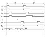
도 1 내지 도 3을 참조하면, 표시 장치(1000)는 영상을 표시하는 표시 기간(DP) 및 화소(PX)들 각각에 포함된 구동 트랜지스터(또는, 제1 트랜지스터(T1))의 특성을 센싱하는 센싱 기간(SP)을 포함하도록 구동될 수 있다.1 to 3 , the
일 실시예에서, 센싱 기간(SP)에는 화소(PX)로부터 센싱된 특성 정보(예를 들면, 센싱 디지털 코드(SSD))에 기초하여 입력 영상 데이터(IDATA)가 보상될 수 있다.In an embodiment, during the sensing period SP, the input image data IDATA may be compensated based on characteristic information (eg, sensing digital code SSD) sensed from the pixel PX.
표시 기간(DP) 동안 주사 구동부(300)는 주사선들(SL1 내지 SLn)로 주사 신호를 순차적으로 공급할 수 있다. 표시 기간(DP) 동안 주사 구동부(300)는 제어선들(CL1 내지 CLn)로 제어 신호를 순차적으로 공급할 수 있다. 또한, 표시 기간(DP) 동안 센싱선들(SSL1 내지 SSLm)로 정전압인 초기화 전압(VINT)이 공급될 수 있다.During the display period DP, the
j번째 수평라인에 대하여, 주사 신호와 제어 신호는 실질적으로 동시에 공급될 수 있다. 따라서, 제2 트랜지스터(T2) 및 제3 트랜지스터(T3)는 동시에 턴-온 또는 턴-오프될 수 있다.For the j-th horizontal line, the scanning signal and the control signal can be supplied substantially simultaneously. Accordingly, the second transistor T2 and the third transistor T3 may be turned on or off at the same time.
제2 트랜지스터(T2)가 턴-온되면 보상 영상 데이터(CDATA)에 대응하는 영상 데이터 신호(DS)가 제1 노드(N1)로 공급될 수 있다.When the second transistor T2 is turned on, the image data signal DS corresponding to the compensation image data CDATA may be supplied to the first node N1.
제3 트랜지스터(T3)가 턴-온되면 초기화 전압(VINT)이 제2 노드(N2)로 공급될 수 있다. 따라서, 스토리지 커패시터(Cst)는 영상 데이터 신호(DS)와 초기화 전압(VINT)의 전압 차에 대응하는 전압을 저장할 수 있다. 여기서, 초기화 전압(VINT)은 정전압으로 설정되기 때문에 스토리지 커패시터(Cst)에 저장되는 전압은 영상 데이터 신호(DS)에 의해 안정적으로 결정될 수 있다.When the third transistor T3 is turned on, the initialization voltage VINT may be supplied to the second node N2. Accordingly, the storage capacitor Cst may store a voltage corresponding to a voltage difference between the image data signal DS and the initialization voltage VINT. Here, since the initialization voltage VINT is set to a constant voltage, the voltage stored in the storage capacitor Cst can be stably determined by the image data signal DS.
제j 주사선(SLj) 및 제j 제어선(CLj)으로 주사 신호 및 제어 신호의 공급이 중단되면, 제2 트랜지스터(T2) 및 제3 트랜지스터(T3)가 턴-오프될 수 있다.When the supply of the scan signal and the control signal to the j th scan line SLj and the j th control line CLj is stopped, the second transistor T2 and the third transistor T3 may be turned off.
이후, 제1 트랜지스터(T1)는 스토리지 커패시터(Cst)에 저장된 전압에 대응하여 발광 소자(LD)로 공급되는 전류량(구동 전류)을 제어할 수 있다. 이에 따라, 발광 소자(LD)는 제1 트랜지스터(T1)의 구동 전류에 대응하는 휘도로 발광할 수 있다.Then, the first transistor T1 may control the amount of current (driving current) supplied to the light emitting element LD in response to the voltage stored in the storage capacitor Cst. Accordingly, the light emitting element LD may emit light with a luminance corresponding to the driving current of the first transistor T1.
센싱 기간(SP) 동안 주사 구동부(300)는 주사선들(SL1 내지 SLn)로 주사 신호를 순차적으로 공급할 수 있다. 또한, 센싱 기간(SP) 동안 주사 구동부(300)는 제어선들(CL1 내지 CLn)로 제어 신호를 순차적으로 공급할 수 있다.During the sensing period SP, the
센싱 기간(SP)에 공급되는 제어 신호의 길이는 표시 기간(DP)에 공급되는 제어 신호의 길이보다 길 수 있다. 또한, 센싱 기간(SP)에, 제j 제어선(CLj)으로 공급되는 제어 신호의 일부는 제j 주사선(SLj)으로 공급되는 주사 신호와 중첩할 수 있다. 제어 신호의 길이는 주사 신호의 길이보다 길 수 있다. 예를 들어, 제j 제어선(CLj)으로 공급되는 제어 신호는 제j 주사선(SLj)으로 공급되는 주사 신호와 동시에 공급되기 시작하고, 제어 신호가 주사 신호보다 더 오랫동안 공급될 수 있다.The length of the control signal supplied to the sensing period SP may be longer than the length of the control signal supplied to the display period DP. Also, during the sensing period SP, a portion of the control signal supplied to the jth control line CLj may overlap the scan signal supplied to the jth scan line SLj. The length of the control signal may be longer than that of the scan signal. For example, the control signal supplied to the jth control line CLj starts to be supplied simultaneously with the scan signal supplied to the jth scan line SLj, and the control signal may be supplied longer than the scan signal.
주사 신호와 제어 신호가 동시에 공급되면, 제2 및 제3 트랜지스터들(T2, T3)이 턴-온된다. 제2 트랜지스터(T2)가 턴-온되면 센싱을 위한 센싱 데이터 신호(SGV, 또는 센싱 데이터 전압)가 제1 노드(N1)로 공급될 수 있다. 이와 동시에 제3 트랜지스터(T3)의 턴-온에 의해 제2 노드(N2)에 초기화 전압(VINT)이 공급될 수 있다. 이에 따라, 스토리지 커패시터(Cst)에 센싱 데이터 신호(SGV)와 초기화 전압(VINT)의 전압 차에 대응하는 전압이 저장될 수 있다.When the scan signal and the control signal are simultaneously supplied, the second and third transistors T2 and T3 are turned on. When the second transistor T2 is turned on, a sensing data signal (SGV, or sensing data voltage) for sensing may be supplied to the first node N1. At the same time, when the third transistor T3 is turned on, the initialization voltage VINT may be supplied to the second node N2. Accordingly, a voltage corresponding to a voltage difference between the sensing data signal SGV and the initialization voltage VINT may be stored in the storage capacitor Cst.
이후, 주사 신호의 공급이 중단되면 제2 트랜지스터(T2)가 턴-오프될 수 있다. 제2 트랜지스터(T2)가 턴-오프되면 제1 노드(N1)가 플로팅된다. 그러면, 제1 트랜지스터(T1)는 센싱 데이터 신호(SGV)에 대응하는 센싱 전류를 제2 노드(N2)로 공급하고, 이에 따라 제2 노드(N2)의 전압이 상승될 수 있다.Then, when the supply of the scan signal is stopped, the second transistor T2 may be turned off. When the second transistor T2 is turned off, the first node N1 is floated. Then, the first transistor T1 supplies the sensing current corresponding to the sensing data signal SGV to the second node N2, and accordingly, the voltage of the second node N2 may increase.
이하에서는, 도 4 내지 도 6을 참조하여, 일 실시예에 따른 표시 장치의 센싱 방법에 관하여 상세히 살펴본다.Hereinafter, a sensing method of a display device according to an exemplary embodiment will be described in detail with reference to FIGS. 4 to 6 .
도 4는 일 실시예에 따른 화소 및 센싱부의 일 예를 도시한 도면이고, 도 5는 일 실시예에 따른 센싱부 및 센싱 전압 제어부를 도시한 도면이며, 도 6은 일 실시예에 따른 화소 및 센싱부의 일 예를 도시한 도면이다.4 is a diagram illustrating an example of a pixel and a sensing unit according to an exemplary embodiment, FIG. 5 is a diagram illustrating a sensing unit and a sensing voltage controller according to an exemplary embodiment, and FIG. 6 is a diagram illustrating a pixel and a sensing unit according to an exemplary embodiment. It is a drawing showing an example of the sensing unit.
도 4 내지 도 6을 참조하면, 일 실시예에 따른 화소(PX)는 센싱선(SSL)에 연결될 수 있고, 센싱선(SSL)은 센싱부(500)에 연결될 수 있다.Referring to FIGS. 4 to 6 , the pixel PX according to an exemplary embodiment may be connected to a sensing line SSL, and the sensing line SSL may be connected to the
센싱부(500)는 센싱 커패시터(Csen), 제1 스위치(SW1), 제2 스위치(SW2), 제3 스위치(SW3), 제1 커패시터(C1), 및 제2 커패시터(C2)를 포함할 수 있다.The
제1 스위치(SW1)는 초기화 전압(VINT)이 인가되는 전원선과 센싱선(SSL) 사이에 연결될 수 있다. 전술한 도 2 및 도 3을 참조하면, 제1 스위치(SW1)는 표시 기간(DP) 동안 초기화 전압(VINT)이 인가되는 전원선과 센싱선(SSL)을 연결할 수 있고, 센싱 기간(SP) 동안 주사 신호와 제어 신호가 동시에 공급되어, 제2 및 제3 트랜지스터들(T2, T3)이 턴-온될 때, 초기화 전압(VINT)이 인가되는 전원선과 센싱선(SSL)을 연결할 수 있다. 이 때, 제1 스위치(SW1)가 턴-온되었다고 할 수 있다. 나머지 기간 동안 제1 스위치(SW1)는 센싱선(SSL)과 제2 스위치(SW2)를 연결할 수 있다.The first switch SW1 may be connected between the power line to which the initialization voltage VINT is applied and the sensing line SSL. Referring to FIGS. 2 and 3 described above, the first switch SW1 may connect the power line to which the initialization voltage VINT is applied and the sensing line SSL during the display period DP, and may connect the sensing line SSL during the sensing period SP. When the second and third transistors T2 and T3 are turned on by simultaneously supplying the scan signal and the control signal, the power line to which the initialization voltage VINT is applied and the sensing line SSL may be connected. At this time, it can be said that the first switch SW1 is turned on. During the remaining period, the first switch SW1 may connect the sensing line SSL and the second switch SW2.
센싱 커패시터(Csen)는 센싱선(SSL)에 접속될 수 있다. 제1 스위치(SW1)가 초기화 전압(VINT)이 인가되는 전원선과 연결되지 않는 경우(즉, 턴-오프되는 경우), 화소(PX)의 제3 트랜지스터(T3)가 턴-온 상태일 때, 센싱 커패시터(Csen)에는 제2 노드(N2)로부터 센싱된 전압이 충전될 수 있다. 즉, 센싱 커패시터(Csen)에는 제2 노드(N2)를 통해 제공되는 화소(PX)의 특성 정보가 저장될 수 있다. 이에 따라, 센싱 커패시터(Csen)에 충전된 전압(또는, 전하량)에 기초하여 센싱선(SSL)으로 흐르는 센싱 전류가 산출될 수 있다. 이 때, 센싱 커패시터(Csen)에 충전된 전압 및 센싱 전류는 센싱 값(또는, 아날로그 센싱 값)이라 지칭할 수 있다. 도 4 및 도 6에 도시되지 않았지만, 센싱선(SSL)과 센싱 커패시터(Csen) 사이에는 저항이 위치할 수 있다.The sensing capacitor Csen may be connected to the sensing line SSL. When the first switch SW1 is not connected to the power line to which the initialization voltage VINT is applied (ie, turned off) and the third transistor T3 of the pixel PX is turned on, A voltage sensed from the second node N2 may be charged in the sensing capacitor Csen. That is, characteristic information of the pixel PX provided through the second node N2 may be stored in the sensing capacitor Csen. Accordingly, the sensing current flowing through the sensing line SSL may be calculated based on the voltage (or the amount of charge) charged in the sensing capacitor Csen. In this case, the voltage and the sensing current charged in the sensing capacitor Csen may be referred to as a sensing value (or an analog sensing value). Although not shown in FIGS. 4 and 6 , a resistor may be positioned between the sensing line SSL and the sensing capacitor Csen.
제2 스위치(SW2)는 센싱선(SSL)과 제3 노드(N3) 사이에 연결될 수 있고, 제1 커패시터(C1)는 제3 노드(N3)와 기준 전압(예를 들면, 접지 전원) 사이에 연결될 수 있다. 제2 스위치(SW2)가 턴-온되는 동안, 제1 커패시터(C1)는 센싱 커패시터(Csen)에 저장된 제1 트랜지스터(T1)의 특성 정보를 샘플링할 수 있다.The second switch SW2 may be connected between the sensing line SSL and the third node N3, and the first capacitor C1 may be connected between the third node N3 and a reference voltage (eg, ground power). can be connected to While the second switch SW2 is turned on, the first capacitor C1 may sample characteristic information of the first transistor T1 stored in the sensing capacitor Csen.
제3 스위치(SW3)는 제3 노드(N3)와 제4 노드(N4) 사이에 연결될 수 있고, 제2 커패시터(C2)는 제4 노드(N4)와 기준 전압(예를 들면, 접지 전원) 사이에 연결될 수 있다. 제3 스위치(SW3)가 턴-온되면, 제1 커패시터(C1) 및 제2 커패시터(C2)는 전하를 공유할 수 있고, 제3 노드(N3)의 전압 및 제4 노드(N4)의 전압은 변동될 수 있다.The third switch SW3 may be connected between the third node N3 and the fourth node N4, and the second capacitor C2 may be connected between the fourth node N4 and a reference voltage (eg, ground power supply). can be connected between them. When the third switch SW3 is turned on, the first capacitor C1 and the second capacitor C2 can share charges, and the voltage of the third node N3 and the voltage of the fourth node N4 can fluctuate.
또한, 센싱부(500)는 아날로그 디지털 컨버터(analog-to-digital convertor; ADC)(510), 전압 비교부(520), 및 코드부(530)를 포함할 수 있다. 일 실시예에서, 센싱부(500)는 ADC(510) 및 코드부(530)만 포함할 수 있다.In addition, the
도 4 및 도 5에 도시된 센싱부(500)는 아날로그 센싱 값을 센싱 기준 전압과 비교하여, 센싱 전압 범위를 변경하기 위한 센싱 전압 제어 신호를 생성할 수 있다. 도 6에 도시된 센싱부(500)는 센싱 디지털 코드를 최대 센싱 코드 또는 최소 센싱 코드와 비교하여, 센싱 전압 범위를 변경하기 위한 센싱 전압 제어 신호를 생성할 수 있다. 또한, 도 4 및 도 5에 도시된 센싱부(500)는 아날로그 센싱 값 및 센싱 디지털 코드를 모두 비교하여, 센싱 전압 범위를 변경하기 위한 센싱 전압 제어 신호를 생성할 수도 있다.The
ADC(510)는 제4 노드(N4)를 통해 제1 입력단(IN1)에 제공되는 아날로그 센싱 값을 데이터 값(예를 들어, 센싱 디지털 코드(SSD))으로 변환할 수 있다. 이때, ADC(510)는 제1 입력단(IN1)의 아날로그 센싱 값에 제2 입력단(IN2)에 제공되는 기준 전압(Vref)과의 차분 전압을 반영하여, 센싱 디지털 코드(SSD)로 변환할 수 있다. 여기서, 제1 입력단(IN1)을 입력단이라 지칭할 수 있고, 기준 전압(Vref)은 센싱선(SSL)에 제공되는 초기화 전압(VINT)과 동일할 수 있다.The
디지털 형태의 센싱 신호(예를 들어, 센싱 디지털 코드(SSD))는 후술하는 코드부(530)를 통해 타이밍 제어부(200)에 제공될 수 있고, 타이밍 제어부(200)는 센싱부(500)에서 제공된 센싱 디지털 코드(SSD)에 기초하여 화소(PX)들의 특성 값을 보상하는 보상 값을 생성할 수 있다.A digital sensing signal (for example, a sensing digital code (SSD)) may be provided to the
전압 비교부(520)는 ADC(510)의 제1 입력단(또는, 제4 노드(N4))에 연결될 수 있다. 전압 비교부(520)는 아날로그 센싱 값과 센싱 기준 전압(Vsref)을 비교하여, 센싱 전압 제어 신호(CS)를 생성할 수 있다. 일 실시예에서, 전압 비교부(520)는 OP-AMP로 구현될 수 있으나, 본 발명이 이에 한정되는 것은 아니다.The
전압 비교부(520)는 센싱 전압 제어 신호(CS)를 센싱 전압 제어부(250)에 제공할 수 있다. 여기서, 센싱 전압 제어 신호(CS)는 제1 센싱 전압 제어 신호 및 제2 센싱 전압 제어 신호를 포함할 수 있다. 제1 센싱 전압 제어 신호는 센싱 데이터 신호 및 초기화 전압(VINT) 중 적어도 하나를 이전 센싱 데이터 신호 및 이전 초기화 전압(VINT)보다 낮게 변경하기 위한 신호일 수 있고, 제2 센싱 전압 제어 신호는 센싱 데이터 신호 및 초기화 전압(VINT) 중 적어도 하나를 이전 센싱 데이터 신호 및 이전 초기화 전압(VINT)보다 높게 변경하기 위한 신호일 수 있다.The
일 실시예에서, 전압 비교부(520)는 아날로그 센싱 값이 센싱 기준 전압(Vsref)보다 크면, 제1 센싱 전압 제어 신호를 생성할 수 있고, 아날로그 센싱 값이 센싱 기준 전압(Vsref)보다 작으면, 제2 센싱 전압 제어 신호를 생성할 수 있다.In an embodiment, the
코드부(530)는 ADC(510)로부터 센싱 디지털 코드(SSD)를 수신할 수 있고, 센싱 디지털 코드(SSD)를 타이밍 제어부(200)에 공급할 수 있다.The
또한, 코드부(530)는 수신된 센싱 디지털 코드(SSD)와 최대 센싱 코드 또는 최소 센싱 코드를 비교하여, 비교 값에 따라 센싱 전압 제어 신호(CS)를 생성할 수 있다.Also, the
구체적으로, 코드부(530)는 센싱 디지털 코드(SSD)와 최대 센싱 코드의 비교 값이 미리 결정된 기준 범위보다 작으면, 제1 센싱 전압 제어 신호를 생성할 수 있고, 센싱 디지털 코드(SSD)와 최소 센싱 코드의 비교 값이 미리 결정된 기준 범위보다 작으면, 제2 센싱 전압 제어 신호를 생성할 수 있다. 즉, 코드부(530)는 센싱 디지털 코드(SSD)가 최대 센싱 코드에 미리 결정된 범위에 해당할만큼 근접하면, 센싱 데이터 신호 및 초기화 전압(VINT) 중 적어도 하나를 이전 센싱 데이터 신호 및 이전 초기화 전압(VINT)보다 낮게 변경하기 위한 제1 센싱 전압 제어 신호를 생성할 수 있다. 코드부(530)는 센싱 디지털 코드(SSD)가 최소 센싱 코드에 미리 결정된 범위에 해당할만큼 근접하면, 센싱 데이터 신호 및 초기화 전압(VINT) 중 적어도 하나를 이전 센싱 데이터 신호 및 이전 초기화 전압(VINT)보다 높게 변경하기 위한 제2 센싱 전압 제어 신호를 생성할 수 있다.Specifically, the
또한, 코드부(530)는 센싱 디지털 코드(SSD)와 최대 센싱 코드 또는 최소 센싱 코드를 비교하여, 비교 값이 미리 결정된 기준 범위에 해당하지 않으면, 센싱 디지털 코드(SSD)를 타이밍 제어부(200)에 제공할 수 있다. 즉, 코드부(530)는 센싱 디지털 코드(SDD)가 최대 센싱 코드 또는 최소 센싱 코드와 미리 결정된 범위에 근접하지 않으면, 적절한 센싱 전압 범위에 해당한다고 파악될 수 있는바, 센싱 전압 제어 신호(CS)를 생성하지 않을 수 있다.In addition, the
센싱 전압 제어부(250)는 타이밍 제어부(200)에 포함될 수 있다. 센싱 전압 제어부(250)는 전압 비교부(520) 및/또는 코드부(530)로부터 센싱 전압 제어 신호(CS)를 수신할 수 있다. 구체적으로, 센싱 전압 제어부(250)는 센싱부(500)가 전압 비교부(520)를 포함하고, 아날로그 센싱 값과 센싱 기준 전압을 비교하여, 센싱 전압 범위를 변경하기 위한 센싱 전압 제어 신호를 생성할 때, 전압 비교부(520)로부터 센싱 전압 제어 신호(CS)를 수신할 수 있다. 센싱 전압 제어부(250)는 센싱부(500)가 코드부(530)를 포함하고, 센싱 디지털 코드를 최대 센싱 코드 또는 최소 센싱 코드와 비교하여, 센싱 전압 범위를 변경하기 위한 센싱 전압 제어 신호를 생성할 때, 코드부(530)로부터 센싱 전압 제어 신호(CS)를 수신할 수 있다.The
센싱 전압 제어부(250)는 센싱 전압 제어 신호(CS)에 기초하여 센싱 데이터 신호를 변경하기 위한 신호를 데이터 구동부(400)에 제공할 수 있다. 예를 들어, 센싱 전압 제어부(250)는 제1 센싱 전압 제어 신호를 수신하면, 센싱 데이터 신호를 이전 센싱 데이터 신호보다 낮게 변경하기 위한 신호를 데이터 구동부(400)에 제공할 수 있다. 또한, 센싱 전압 제어부(250)는 제2 센싱 전압 제어 신호를 수신하면, 센싱 데이터 신호를 이전 센싱 데이터 신호보다 높게 변경하기 위한 신호를 데이터 구동부(400)에 제공할 수 있다.The
또한, 센싱 전압 제어부(250)는 센싱 전압 제어 신호(CS)에 기초하여 초기화 전압(VINT)을 변경하기 위한 신호를 전압 공급부(600)에 제공할 수 있다. 예를 들어, 센싱 전압 제어부(250)는 제1 센싱 전압 제어 신호를 수신하면, 초기화 전압(VINT)을 이전 초기화 전압보다 낮게 변경하기 위한 신호를 전압 공급부(600)에 제공할 수 있다. 또한, 센싱 전압 제어부(250)는 제2 센싱 전압 제어 신호를 수신하면, 초기화 전압(VINT)을 이전 초기화 전압보다 높게 변경하기 위한 신호를 전압 공급부(600)에 제공할 수 있다.Also, the sensing
일 예로, 센싱 전압 제어부(250)가 제1 센싱 전압 제어 신호에 기초하여 데이터 구동부(400) 및 전압 공급부(600)에 센싱 데이터 신호 및 초기화 전압(VINT)을 이전 센싱 데이터 신호 및 이전 초기화 전압보다 낮게 변경하기 위한 신호를 제공하면, 화소(PX)의 제1 노드(N1, 도 2 참조)로 이전 센싱 데이터 신호보다 낮은 센싱 데이터 신호가 제공될 수 있고, 화소(PX)의 제2 노드(N2, 도 2 참조)로 이전 초기화 전압보다 낮은 초기화 전압(VINT)이 제공될 수 있다. 변경된 센싱 데이터 신호(또는, 센싱 데이터 전압)와 초기화 전압(VINT) 사이는 화소(PX)에 포함된 구동 트랜지스터의 센싱 값을 검출할 수 있는 센싱 전압 범위에 해당하므로, 화소(PX)의 제1 노드(N1, 도 2 참조)에 대응하여 구동 트랜지스터가 제어하는 구동 전류가 제2 노드(N2, 도 2 참조)를 통해 센싱부(500)로 공급될 수 있다. 즉, 센싱 전압 제어 신호를 반영하여 변경된 센싱 데이터 신호 및 초기화 전압(VINT)에 의해, 구동 트랜지스터의 센싱 값을 검출할 수 있는 센싱 전압 범위를 확보할 수 있다.For example, the sensing
이에 따라, 일 실시예에 따른 표시 장치는 센싱 값을 검출하고, 센싱 데이터 신호 및 초기화 전압 중 적어도 하나를 제어함으로써, 구동 트랜지스터의 특성 또는 발광 소자의 특성이 변경되더라도, 센싱 값을 검출할 수 있는 센싱 전압 범위를 확보할 수 있다.Accordingly, the display device according to an exemplary embodiment may detect the sensed value even when the characteristics of the driving transistor or the light emitting device are changed by detecting the sensed value and controlling at least one of the sensed data signal and the initialization voltage. A sensing voltage range can be secured.
이하에서는 도 7 및 도 8을 참조하여, 비교예 및 일 실시예에 따른 표시 장치의 효과를 살펴본다.Hereinafter, with reference to FIGS. 7 and 8 , effects of a display device according to a comparative example and an exemplary embodiment will be described.
도 7은 일 실시예에 따른 표시 장치의 센싱 전압 범위를 도시한 그래프이고, 도 8은 비교예에 따른 표시 장치의 센싱 전압 범위를 도시한 그래프이다.7 is a graph illustrating a sensing voltage range of a display device according to an exemplary embodiment, and FIG. 8 is a graph illustrating a sensing voltage range of a display device according to a comparative example.
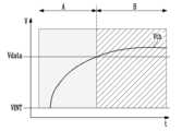
도 7을 참조하면, 시간이 지남에 따라 구동 트랜지스터의 문턱 전압(Vth)은 증가하다 소정의 시간에서 포화될 수 있다. 이때, 구동 트랜지스터의 문턱 전압(Vth)은 데이터 전압(Vdata) 보다 낮은 전압에서 포화될 수 있다. 이때, 데이터 전압(Vdata)은 도 1 및 도 3을 참조하여 설명한 데이터 구동부(400)로부터 데이터선(DL)에 제공된 센싱 데이터 신호(SGV)에 기초한 전압일 수 있다.Referring to FIG. 7 , the threshold voltage Vth of the driving transistor may increase over time and then become saturated at a predetermined time. In this case, the threshold voltage Vth of the driving transistor may be saturated at a voltage lower than the data voltage Vdata. In this case, the data voltage Vdata may be a voltage based on the sensing data signal SGV provided to the data line DL from the
일 실시예에서, 표시 장치는 센싱 기간 동안 제공된 구동 트랜지스터의 문턱 전압(Vth)이 초기화 전압(VINT)보다 크고 데이터 전압(Vdata)보다 작을 때, 구동 트랜지스터의 특성 변화를 센싱할 수 있다. 즉, 표시 장치는 B 영역에서 구동 트랜지스터의 특성 변화를 센싱할 수 있다. 반면, A 영역은 구동 트랜지스터의 문턱 전압(Vth)이 초기화 전압(VINT)보다 작아, 구동 트랜지스터에 구동 전류가 흐를 수 없으므로, 표시 장치는 구동 트랜지스터의 특성 변화를 센싱할 수 없다.In one embodiment, the display device may sense a change in characteristics of the driving transistor when the threshold voltage Vth of the driving transistor provided during the sensing period is higher than the initialization voltage VINT and lower than the data voltage Vdata. That is, the display device may sense a change in characteristics of the driving transistor in region B. On the other hand, in region A, since the threshold voltage Vth of the driving transistor is lower than the initialization voltage VINT, the driving current cannot flow through the driving transistor, and thus the display device cannot sense a change in characteristics of the driving transistor.
일 실시예에서, 표시 장치는 센싱 기간 동안 센싱 값을 검출하고, 구동 트랜지스터의 특성 또는 발광 소자의 특성이 변경되더라도, 센싱 데이터 신호 및 초기화 전압(VINT) 중 적어도 하나를 제어할 수 있다. 즉, 일 실시예에 따른 표시 장치는 A 영역보다 B 영역의 시간을 넓게 확보할 수 있으므로, 다시 말하면, 센싱 값을 검출할 수 있는 센싱 전압 범위을 넓게 확보할 수 있으므로, 센싱 기간 동안 구동 트랜지스터의 특성 변화를 원활하게 센싱할 수 있다.In an embodiment, the display device may detect a sensed value during the sensing period and control at least one of the sensing data signal and the initialization voltage VINT even when the characteristics of the driving transistor or the characteristics of the light emitting device are changed. That is, since the display device according to an exemplary embodiment can secure a wider time period in area B than area A, in other words, a wider sensing voltage range in which sensing values can be detected, characteristics of the driving transistor during the sensing period. Changes can be sensed smoothly.
도 8을 참조하면, 비교예에 따른 표시 장치의 A 영역의 시간은 도 7을 참조하여 설명한 일 실시예에 따른 표시 장치의 A 영역의 시간보다 증가하고, 비교예에 따른 표시 장치의 B 영역의 시간은 도 7을 참조하여 설명한 일 실시예에 따른 표시 장치의 B 영역의 시간보다 감소함을 확인할 수 있다.Referring to FIG. 8 , the time of area A of the display device according to the comparative example is longer than that of area A of the display device according to the exemplary embodiment described with reference to FIG. 7 , and the time of area B of the display device according to the comparative example is longer. It can be seen that the time is reduced compared to the time of the region B of the display device according to the exemplary embodiment described with reference to FIG. 7 .
즉, 비교예에서 표시 장치는 센싱 기간 동안 B 영역의 시간이 감소하고, A 영역의 시간이 증가함에 따라, 구동 트랜지스터의 특성 변화를 센싱할 수 있는 시간이 감소할 수 있다.That is, in the display device of Comparative Example, as the time of region B decreases and the time of region A increases during the sensing period, the time for sensing the change in characteristics of the driving transistor may decrease.
따라서, 도 7 및 도 8을 참조하면, 일 실시예에서 표시 장치는 센싱 기간 동안 센싱 값을 검출하고, 센싱 데이터 신호 및 초기화 전압 중 적어도 하나를 제어할 수 있으므로, 구동 트랜지스터의 특성 또는 발광 소자의 특성이 변경되더라도, 센싱 값을 검출할 수 있는 센싱 전압 범위를 확보할 수 있음을 확인할 수 있다.Accordingly, referring to FIGS. 7 and 8 , in one embodiment, the display device may detect a sensed value during the sensing period and control at least one of the sensed data signal and the initialization voltage, and thus the characteristics of the driving transistor or the light emitting device may be controlled. Even if the characteristics are changed, it can be confirmed that a sensing voltage range capable of detecting a sensing value can be secured.
이하에서는, 도 9 및 도 10을 참조하여, 일 실시예에 따른 표시 장치의 구동 방법을 살펴본다.Hereinafter, a method of driving a display device according to an exemplary embodiment will be described with reference to FIGS. 9 and 10 .
도 9 및 도 10은 일 실시예에 따른 표시 장치의 구동 방법을 나타낸 순서도들이다.9 and 10 are flowcharts illustrating a method of driving a display device according to an exemplary embodiment.
도 9를 참조하면, 일 실시예에 따른 표시 장치의 구동 방법은 센싱 기간에 센싱 데이터 신호 및 초기화 전압을 화소에 공급하는 단계(S910), 화소로부터 센싱 값(또는, 아날로그 센싱 값)을 수신하는 단계(S920), 아날로그 센싱 값과 센싱 기준 전압을 비교하는 단계(S930), 아날로그 센싱 비교 값에 대응하는 센싱 전압 제어 신호를 생성하는 단계(S940), 센싱 전압 제어 신호에 기초하여 센싱 데이터 신호 및/또는 초기화 전압을 제어하는 단계(S950), 아날로그 센싱 값을 센싱 디지털 코드로 변환하는 단계(S960), 및 입력 영상 데이터에 센싱 디지털 코드를 반영하여 보상 영상 데이터를 생성하는 단계(S970)를 포함할 수 있다.Referring to FIG. 9 , a method of driving a display device according to an exemplary embodiment includes supplying a sensing data signal and an initialization voltage to a pixel in a sensing period (S910), and receiving a sensing value (or an analog sensing value) from the pixel. Step (S920), comparing the analog sensing value and the sensing reference voltage (S930), generating a sensing voltage control signal corresponding to the analog sensing comparison value (S940), based on the sensing voltage control signal, a sensing data signal and / or controlling an initialization voltage (S950), converting an analog sensing value into a sensing digital code (S960), and generating compensation image data by reflecting the sensing digital code on input image data (S970) can do.
여기서, 아날로그 센싱 값을 센싱 기준 전압과 비교하여 센싱 전압 제어 신호를 생성할 때, 아날로그 센싱 값이 센싱 기준 전압에 해당하지 않으면(NO), 표시 장치는 아날로그 센싱 비교 값에 대응하는 센싱 전압 제어 신호를 생성할 수 있다(S940). 구체적으로, 아날로그 센싱 값이 센싱 기준 전압보다 크면, 제1 센싱 전압 제어 신호를 생성하고, 아날로그 센싱 값이 센싱 기준 전압보다 작으면, 제2 센싱 전압 제어 신호를 생성할 수 있다.Here, when generating the sensing voltage control signal by comparing the analog sensing value with the sensing reference voltage, if the analog sensing value does not correspond to the sensing reference voltage (NO), the display device displays the sensing voltage control signal corresponding to the analog sensing comparison value. can be generated (S940). Specifically, the first sensing voltage control signal may be generated when the analog sensing value is greater than the sensing reference voltage, and the second sensing voltage control signal may be generated when the analog sensing value is less than the sensing reference voltage.
일 실시예에서, 아날로그 센싱 값이 센싱 기준 전압에 해당하면(YES), 표시 장치는 센싱 전압 제어 신호를 생성하지 않고, 아날로그 센싱 값을 센싱 디지털 코드로 변환하는 단계(S960)로 구동할 수 있다.In an embodiment, if the analog sensing value corresponds to the sensing reference voltage (YES), the display device may be driven in a step of converting the analog sensing value into a sensing digital code (S960) without generating a sensing voltage control signal. .
또한, 일 실시예에 따른 표시 장치는 센싱 전압 제어 신호에 기초하여 센싱 데이터 신호 및/또는 초기화 전압을 제어하고, 변경된 센싱 데이터 신호 및/또는 초기화 전압을 센싱 기간에 화소에 공급할 수 있다(S910). 이후, 화소로부터 센싱 값을 수신하여(S920), 아날로그 센싱 값을 센싱 기준 전압과 비교했을 때(S930), 아날로그 센싱 값이 센싱 기준 전압에 해당하면(YES), 표시 장치는 센싱 전압 제어 신호를 생성하지 않고, 아날로그 센싱 값을 센싱 디지털 코드로 변환하고(S960), 입력 영상 데이터에 센싱 디지털 코드를 반영하여 보상 영상 데이터를 생성할 수 있다(S970).Also, the display device according to an embodiment may control the sensing data signal and/or initialization voltage based on the sensing voltage control signal, and supply the changed sensing data signal and/or initialization voltage to the pixel during the sensing period (S910). . Thereafter, when a sensing value is received from the pixel (S920) and the analog sensing value is compared with the sensing reference voltage (S930), if the analog sensing value corresponds to the sensing reference voltage (YES), the display device transmits a sensing voltage control signal. Instead of generating, the analog sensing value is converted into a sensing digital code (S960), and the sensing digital code is reflected in the input image data to generate compensation image data (S970).
이에 따라, 일 실시예에 따른 표시 장치는 센싱 값을 검출하고, 센싱 데이터 신호 및 초기화 전압 중 적어도 하나를 제어함으로써, 구동 트랜지스터의 특성 또는 발광 소자의 특성이 변경되더라도, 센싱 값을 검출할 수 있는 센싱 전압 범위를 확보할 수 있다.Accordingly, the display device according to an exemplary embodiment may detect the sensed value even when the characteristics of the driving transistor or the light emitting device are changed by detecting the sensed value and controlling at least one of the sensed data signal and the initialization voltage. A sensing voltage range can be secured.
도 10을 참조하면, 일 실시예에 따른 표시 장치의 구동 방법은 센싱 기간에 센싱 데이터 신호 및 초기화 전압을 화소에 공급하는 단계(S1010), 화소로부터 센싱 값(또는, 아날로그 센싱 값)을 수신하는 단계(S1020), 아날로구 센싱 값을 센싱 디지털 코드로 변환하는 단계(S1030), 센싱 디지털 코드가 최대 센싱 코드 또는 최소 센싱 코드와 미리 결정된 범위에 해당하는지 비교하는 단계(S1040), 센싱 전압 제어 신호를 생성하는 단계(S1050), 센싱 전압 제어 신호에 기초하여 센싱 데이터 신호 및/또는 초기화 전압을 제어하는 단계(S1060), 및 입력 영상 데이터에 센싱 디지털 코드를 반영하여 보상 영상 데이터를 생성하는 단계(S1060)를 포함할 수 있다.Referring to FIG. 10 , a method of driving a display device according to an exemplary embodiment includes supplying a sensing data signal and an initialization voltage to a pixel in a sensing period (S1010), and receiving a sensing value (or analog sensing value) from the pixel. Step (S1020), converting the analog sensing value into a sensing digital code (S1030), comparing the sensing digital code with the maximum sensing code or the minimum sensing code within a predetermined range (S1040), sensing voltage control Generating a signal (S1050), controlling a sensing data signal and/or an initialization voltage based on the sensing voltage control signal (S1060), and generating compensation image data by reflecting a sensing digital code on input image data. (S1060) may be included.
여기서, 센싱 디지털 코드가 최대 센싱 코드 또는 최소 센싱 코드와 미리 결정된 범위에 해당하면(YES), 표시 장치는 센싱 디지털 코드와 최대 센싱 코드 또는 최소 센싱 코드 사이의 비교 값에 대응하는 센싱 전압 제어 신호를 생성할 수 있다(S1040). 구체적으로, 센싱 디지털 코드와 최대 센싱 코드의 비교 값이 미리 결정된 기준 범위보다 작으면 제1 센싱 전압 제어 신호를 생성할 수 있고, 센싱 디지털 코드와 최소 센싱 코드의 비교 값이 미리 결정된 기준 범위보다 작으면, 제2 센싱 전압 제어 신호를 생성할 수 있다.Here, if the sensing digital code corresponds to the maximum sensing code or the minimum sensing code and a predetermined range (YES), the display device generates a sensing voltage control signal corresponding to a comparison value between the sensing digital code and the maximum sensing code or the minimum sensing code. It can be created (S1040). Specifically, when the comparison value between the sensing digital code and the maximum sensing code is smaller than the predetermined reference range, the first sensing voltage control signal may be generated, and the comparison value between the sensing digital code and the minimum sensing code is smaller than the predetermined reference range. If not, a second sensing voltage control signal may be generated.
일 실시예에서, 센싱 디지털 코드가 최대 센싱 코드 또는 최소 센싱 코드와 미리 결정된 범위에 해당하지 않으면(NO), 표시 장치는 센싱 전압 제어 신호를 생성하지 않고, 입력 영상 데이터에 센싱 디지털 코드를 반영하여 보상 영상 데이터를 생성할 수 있다(S1070).In one embodiment, if the sensing digital code does not correspond to the maximum sensing code or the minimum sensing code and a predetermined range (NO), the display device does not generate a sensing voltage control signal and reflects the sensing digital code to input image data. Compensation image data may be generated (S1070).
또한, 일 실시예에 따른 표시 장치는 센싱 전압 제어 신호에 기초하여 센싱 데이터 신호 및/또는 초기화 전압을 제어하고, 변경된 센싱 데이터 신호 및/또는 초기화 전압을 센싱 기간에 화소에 공급할 수 있다(S1010). 표시 장치는 화소로부터 센싱 값을 수신하여(S1020), 아날로그 센싱 값을 센싱 디지털 코드로 변환할 수 있다(S1030). 이후, 표시 장치는 센싱 디지털 코드가 최대 센싱 코드 또는 최소 센싱 코드와 미리 결정된 범위에 해당하지 않으면(NO), 표시 장치는 센싱 전압 제어 신호를 생성하지 않고, 입력 영상 데이터에 센싱 디지털 코드를 반영하여 보상 영상 데이터를 생성할 수 있다(S1070).Also, the display device according to an embodiment may control the sensing data signal and/or initialization voltage based on the sensing voltage control signal, and supply the changed sensing data signal and/or initialization voltage to the pixel during the sensing period (S1010). . The display device may receive a sensing value from a pixel (S1020) and convert the analog sensing value into a sensing digital code (S1030). Then, if the sensing digital code does not correspond to the maximum sensing code or the minimum sensing code and a predetermined range (NO), the display device does not generate a sensing voltage control signal and reflects the sensing digital code to the input image data. Compensation image data may be generated (S1070).
이에 따라, 일 실시예에 따른 표시 장치는 센싱 값을 검출하고, 센싱 데이터 신호 및 초기화 전압 중 적어도 하나를 제어함으로써, 구동 트랜지스터의 특성 또는 발광 소자의 특성이 변경되더라도, 센싱 값을 검출할 수 있는 센싱 전압 범위를 확보할 수 있다.Accordingly, the display device according to an exemplary embodiment may detect the sensed value even when the characteristics of the driving transistor or the light emitting device are changed by detecting the sensed value and controlling at least one of the sensed data signal and the initialization voltage. A sensing voltage range can be secured.
이상에서는 본 발명의 바람직한 실시예를 참조하여 설명하였지만, 해당 기술 분야의 숙련된 당업자 또는 해당 기술 분야에 통상의 지식을 갖는 자라면, 후술될 특허청구범위에 기재된 본 발명의 사상 및 기술 영역으로부터 벗어나지 않는 범위 내에서 본 발명을 다양하게 수정 및 변경시킬 수 있음을 이해할 수 있을 것이다.Although the above has been described with reference to preferred embodiments of the present invention, those skilled in the art or those having ordinary knowledge in the art do not deviate from the spirit and technical scope of the present invention described in the claims to be described later. It will be understood that the present invention can be variously modified and changed within the scope not specified.
따라서, 본 발명의 기술적 범위는 명세서의 상세한 설명에 기재된 내용으로 한정되는 것이 아니라 특허청구범위에 의해 정해져야만 할 것이다.Therefore, the technical scope of the present invention is not limited to the contents described in the detailed description of the specification, but should be defined by the claims.
100: 화소부200: 타이밍 제어부
300: 주사 구동부400: 데이터 구동부
500: 센싱부600: 전압 공급부
510: ADC520: 전압 비교부
530: 코드부250: 센싱 전압 제어부100: pixel unit 200: timing control unit
300: scan driver 400: data driver
500: sensing unit 600: voltage supply unit
510: ADC 520: voltage comparator
530: code unit 250: sensing voltage control unit
Claims (20)
Translated fromKorean데이터선 및 센싱선에 연결된 화소들;
상기 데이터선으로 영상 데이터 신호및 센싱 데이터 신호 중 하나를 공급하는 데이터 구동부;
상기 센싱선으로 상기 화소들에 초기화 전압을 공급하는 전압 공급부; 및
상기 센싱선을 통해 상기 화소들 중 적어도 하나의 화소로부터 센싱 값을 수신하고, 상기 센싱 값을 센싱 기준 값과 비교하여, 상기 센싱 데이터 신호 및 상기 초기화 전압 중 적어도 하나를 제어하기 위한 센싱 전압 제어 신호를 생성하는 센싱부를 포함하는 표시 장치.A display device driven to include a display period for displaying an image and a sensing period for sensing characteristics of a driving transistor,
pixels connected to the data line and the sensing line;
Video data signal through the data lineand a data driver supplying one of the sensing data signals.
a voltage supply unit supplying an initialization voltage to the pixels through the sensing line; and
A sensing voltage control signal configured to receive a sensing value from at least one of the pixels through the sensing line, compare the sensing value with a sensing reference value, and control at least one of the sensing data signal and the initialization voltage. A display device including a sensing unit that generates
상기 센싱부는,
상기 센싱선에 연결되고, 입력단을 통해 제공되는 아날로그 센싱 값을 센싱 디지털 코드로 변환하는 아날로그 디지털 컨버터를 포함하는 표시 장치.In paragraph 1,
The sensing unit,
A display device comprising an analog-to-digital converter connected to the sensing line and converting an analog sensing value provided through an input terminal into a sensing digital code.
상기 센싱부는,
상기 아날로그 디지털 컨버터의 입력단에 연결되고, 상기 아날로그 센싱 값과 센싱 기준 전압을 비교하여, 상기 센싱 전압 제어 신호를 생성하는 전압 비교부를 더 포함하는 표시 장치.In paragraph 2,
The sensing unit,
and a voltage comparator connected to an input terminal of the analog-to-digital converter and generating the sensing voltage control signal by comparing the analog sensing value with a sensing reference voltage.
상기 전압 비교부는,
상기 아날로그 센싱 값이 상기 센싱 기준 전압보다 크면, 제1 센싱 전압 제어 신호를 생성하고,
상기 아날로그 센싱 값이 상기 센싱 기준 전압보다 작으면, 제2 센싱 전압 제어 신호를 생성하는 표시 장치.In paragraph 3,
The voltage comparator,
When the analog sensing value is greater than the sensing reference voltage, generating a first sensing voltage control signal;
A display device that generates a second sensing voltage control signal when the analog sensing value is less than the sensing reference voltage.
상기 센싱 디지털 코드를 수신하고, 상기 센싱 디지털 코드와 최대 센싱 코드 또는 최소 센싱 코드를 비교하여, 비교 값에 따라 상기 센싱 전압 제어 신호를 생성하는 코드부를 더 포함하는 표시 장치.In paragraph 4,
and a code unit configured to receive the sensing digital code, compare the sensing digital code with a maximum sensing code or a minimum sensing code, and generate the sensing voltage control signal according to a comparison value.
상기 코드부는,
상기 센싱 디지털 코드와 상기 최대 센싱 코드의 비교값이 미리 결정된 기준 범위보다 작으면, 제1 센싱 전압 제어 신호를 생성하고,
상기 센싱 디지털 코드와 상기 최소 센싱 코드의 비교값이 미리 결정된 기준 범위보다 작으면, 제2 센싱 전압 제어 신호를 생성하는 표시 장치.In paragraph 5,
The code part,
When a comparison value between the sensing digital code and the maximum sensing code is smaller than a predetermined reference range, a first sensing voltage control signal is generated;
and generating a second sensing voltage control signal when a comparison value between the sensing digital code and the minimum sensing code is less than a predetermined reference range.
입력 영상 데이터에 상기 센싱 디지털 코드를 반영하여 보상 영상 데이터를 생성하고, 상기 보상 영상 데이터를 상기 데이터 구동부에 제공하는 타이밍 제어부를 더 포함하는 표시 장치.In paragraph 6,
The display device further includes a timing controller generating compensation image data by reflecting the sensing digital code in input image data and providing the compensation image data to the data driver.
상기 코드부는 상기 센싱 디지털 코드와 최대 센싱 코드 또는 최소 센싱 코드를 비교하여, 비교 값이 미리 결정된 기준 범위에 해당하지 않으면, 상기 센싱 디지털 코드를 상기 타이밍 제어부에 제공하는 표시 장치.In paragraph 7,
wherein the code unit compares the sensing digital code with a maximum sensing code or a minimum sensing code and, when the comparison value does not fall within a predetermined reference range, provides the sensing digital code to the timing controller.
상기 타이밍 제어부는 상기 센싱 전압 제어 신호를 수신하고, 상기 센싱 전압 제어 신호에 기초하여, 상기 센싱 데이터 신호를 변경하기 위한 신호를 상기 데이터 구동부에 공급하며, 상기 센싱 전압 제어 신호에 기초하여, 상기 초기화 전압을 변경하기 위한 신호를 상기 전압 공급부에 공급하는 표시 장치.In paragraph 8,
The timing controller receives the sensing voltage control signal, supplies a signal for changing the sensing data signal to the data driver based on the sensing voltage control signal, and performs the initialization based on the sensing voltage control signal. A display device supplying a signal for changing a voltage to the voltage supply unit.
상기 화소들은 주사선 및 제어선에 연결되고,
상기 화소들 중 각 화소는,
발광 소자;
제1 노드에 접속된 게이트 전극, 제1 전원선을 통해 제1 구동 전압에 접속된 제1 전극, 및 상기 발광 소자의 제1 전극에 접속된 제2 전극을 포함하는 제1 트랜지스터;
상기 주사선에 접속된 게이트 전극, 상기 데이터선에 접속된 제1 전극, 및 상기 제1 노드에 접속된 제2 전극을 포함하는 제2 트랜지스터;
상기 제어선에 접속된 게이트 전극, 상기 센싱선에 접속된 제1 전극, 및 상기 제1 트랜지스터의 제2 전극에 접속된 제2 전극을 포함하는 제3 트랜지스터; 및
상기 제1 노드와 상기 제1 트랜지스터의 제2 전극 사이에 접속되는 스토리지 커패시터를 포함하는 표시 장치.In paragraph 1,
The pixels are connected to scan lines and control lines,
Each pixel among the pixels,
light emitting device;
a first transistor including a gate electrode connected to a first node, a first electrode connected to a first driving voltage through a first power line, and a second electrode connected to the first electrode of the light emitting element;
a second transistor including a gate electrode connected to the scan line, a first electrode connected to the data line, and a second electrode connected to the first node;
a third transistor including a gate electrode connected to the control line, a first electrode connected to the sensing line, and a second electrode connected to the second electrode of the first transistor; and
and a storage capacitor connected between the first node and a second electrode of the first transistor.
상기 구동 트랜지스터는 상기 제1 트랜지스터이고,
상기 표시 기간에 상기 주사선에 주사 신호가 공급되고, 상기 제어선에 제어 신호가 공급되는 표시 장치.In paragraph 10,
The driving transistor is the first transistor,
A display device wherein a scan signal is supplied to the scan line and a control signal is supplied to the control line during the display period.
데이터선 및 센싱선에 연결된 화소들;
상기 데이터선으로 영상 데이터 신호및 센싱 데이터 신호 중 하나를 공급하는 데이터 구동부;
상기 센싱선으로 상기 화소들에 초기화 전압을 공급하는 전압 공급부; 및
상기 센싱선을 통해 상기 화소들 중 적어도 하나의 화소로부터 아날로그 센싱 값을 수신하고, 상기 아날로그 센싱 값을 센싱 디지털 코드로 변환하고, 상기 센싱 디지털 코드와 최대 센싱 코드 또는 최소 센싱 코드를 비교하여, 비교 값에 따라 상기 센싱 데이터 신호 및 상기 초기화 전압 중 적어도 하나를 제어하기 위한 센싱 전압 제어 신호를 생성하는 센싱부를 포함하는 표시 장치.A display device driven to include a display period for displaying an image and a sensing period for sensing characteristics of a driving transistor,
pixels connected to the data line and the sensing line;
Video data signal through the data lineand a data driver supplying one of the sensing data signals.
a voltage supply unit supplying an initialization voltage to the pixels through the sensing line; and
An analog sensing value is received from at least one of the pixels through the sensing line, the analog sensing value is converted into a sensing digital code, the sensing digital code is compared with a maximum sensing code or a minimum sensing code, and the comparison is performed. and a sensing unit configured to generate a sensing voltage control signal for controlling at least one of the sensing data signal and the initialization voltage according to a value.
상기 센싱부는,
상기 센싱 디지털 코드와 상기 최대 센싱 코드의 비교값이 미리 결정된 기준 범위보다 작으면, 제1 센싱 전압 제어 신호를 생성하고,
상기 센싱 디지털 코드와 상기 최소 센싱 코드의 비교값이 미리 결정된 기준 범위보다 작으면, 제2 센싱 전압 제어 신호를 생성하는 표시 장치.In paragraph 12,
The sensing unit,
When a comparison value between the sensing digital code and the maximum sensing code is smaller than a predetermined reference range, a first sensing voltage control signal is generated;
and generating a second sensing voltage control signal when a comparison value between the sensing digital code and the minimum sensing code is less than a predetermined reference range.
입력 영상 데이터에 상기 센싱 디지털 코드를 반영하여 보상 영상 데이터를 생성하고, 상기 보상 영상 데이터를 상기 데이터 구동부에 제공하는 타이밍 제어부를 더 포함하는 표시 장치.In paragraph 13,
The display device further includes a timing controller generating compensation image data by reflecting the sensing digital code in input image data and providing the compensation image data to the data driver.
상기 센싱부는 상기 센싱 디지털 코드와 최대 센싱 코드 또는 최소 센싱 코드를 비교하여, 비교 값이 미리 결정된 기준 범위에 해당하지 않으면, 상기 센싱 디지털 코드를 상기 타이밍 제어부에 제공하는 표시 장치.In paragraph 14,
wherein the sensing unit compares the sensing digital code with a maximum sensing code or a minimum sensing code, and when the comparison value does not fall within a predetermined reference range, provides the sensing digital code to the timing controller.
상기 타이밍 제어부는 상기 센싱 전압 제어 신호를 수신하고, 상기 센싱 전압 제어 신호에 기초하여, 상기 센싱 데이터 신호를 변경하기 위한 신호를 상기 데이터 구동부에 공급하며, 상기 센싱 전압 제어 신호에 기초하여, 상기 초기화 전압을 변경하기 위한 신호를 상기 전압 공급부에 공급하는 표시 장치.In clause 15,
The timing controller receives the sensing voltage control signal, supplies a signal for changing the sensing data signal to the data driver based on the sensing voltage control signal, and performs the initialization based on the sensing voltage control signal. A display device supplying a signal for changing a voltage to the voltage supply unit.
상기 센싱 기간에 상기 데이터선으로 센싱 데이터 신호 및 상기 센싱선으로 초기화 전압을 공급하는 단계;
상기 센싱선을 통해 상기 화소들 중 적어도 하나의 화소부터 아날로그 센싱 값을 수신하는 단계; 및
상기 아날로그 센싱 값을 센싱 기준 전압과 비교하여, 상기 데이터 전압 및 상기 초기화 전압 중 적어도 하나를 제어하기 위한 센싱 전압 제어 신호를 생성하는 단계를 포함하는 표시 장치의 구동 방법.A method of driving a display device including pixels connected to a data line and a sensing line and driven to include a display period for displaying an image and a sensing period for sensing characteristics of a driving transistor included in each of the pixels, the method comprising:
supplying a sensing data signal to the data line and an initialization voltage to the sensing line during the sensing period;
receiving an analog sensing value from at least one of the pixels through the sensing line; and
and generating a sensing voltage control signal for controlling at least one of the data voltage and the initialization voltage by comparing the analog sensing value with a sensing reference voltage.
상기 센싱 전압 제어 신호를 생성하는 단계는,
상기 아날로그 센싱 값이 상기 센싱 기준 전압보다 크면, 제1 센싱 전압 제어 신호를 생성하고, 상기 아날로그 센싱 값이 상기 센싱 기준 전압보다 작으면, 제2 센싱 전압 제어 신호를 생성하는 단계를 포함하는 표시 장치의 구동 방법.In paragraph 17,
Generating the sensing voltage control signal,
and generating a first sensing voltage control signal when the analog sensing value is greater than the sensing reference voltage, and generating a second sensing voltage control signal when the analog sensing value is less than the sensing reference voltage. driving method.
상기 아날로그 센싱 값을 수신하고, 상기 아날로그 센싱 값을 센싱 디지털 코드로 변환하는 단계를 더 포함하는 표시 장치의 구동 방법.In paragraph 18,
The method of driving a display device further comprising receiving the analog sensing value and converting the analog sensing value into a sensing digital code.
상기 센싱 디지털 코드를 수신하고, 상기 센싱 디지털 코드와 최대 센싱 코드 또는 최소 센싱 코드를 비교하여, 비교 값에 따라 상기 센싱 전압 제어 신호를 생성하는 단계를 더 포함하는 표시 장치의 구동 방법.
In paragraph 19,
The method of driving a display device further comprising receiving the sensing digital code, comparing the sensing digital code with a maximum sensing code or a minimum sensing code, and generating the sensing voltage control signal according to a comparison value.
Priority Applications (5)
| Application Number | Priority Date | Filing Date | Title |
|---|---|---|---|
| KR1020210109083AKR20230027392A (en) | 2021-08-18 | 2021-08-18 | Display device and driving method of the same |
| CN202280055705.6ACN117813646A (en) | 2021-08-18 | 2022-08-16 | Display device and driving method thereof |
| PCT/KR2022/012184WO2023022468A1 (en) | 2021-08-18 | 2022-08-16 | Display device and driving method therefor |
| US17/890,097US12334007B2 (en) | 2021-08-18 | 2022-08-17 | Display device and method of driving the same |
| US19/239,909US20250308461A1 (en) | 2021-08-18 | 2025-06-16 | Display device and method of driving the same |
Applications Claiming Priority (1)
| Application Number | Priority Date | Filing Date | Title |
|---|---|---|---|
| KR1020210109083AKR20230027392A (en) | 2021-08-18 | 2021-08-18 | Display device and driving method of the same |
Publications (1)
| Publication Number | Publication Date |
|---|---|
| KR20230027392Atrue KR20230027392A (en) | 2023-02-28 |
Family
ID=85229103
Family Applications (1)
| Application Number | Title | Priority Date | Filing Date |
|---|---|---|---|
| KR1020210109083APendingKR20230027392A (en) | 2021-08-18 | 2021-08-18 | Display device and driving method of the same |
Country Status (4)
| Country | Link |
|---|---|
| US (2) | US12334007B2 (en) |
| KR (1) | KR20230027392A (en) |
| CN (1) | CN117813646A (en) |
| WO (1) | WO2023022468A1 (en) |
Families Citing this family (2)
| Publication number | Priority date | Publication date | Assignee | Title |
|---|---|---|---|---|
| KR20240079379A (en)* | 2022-11-29 | 2024-06-05 | 엘지디스플레이 주식회사 | Sensing circuit and display device using the same |
| KR20240120566A (en)* | 2023-01-31 | 2024-08-07 | 엘지디스플레이 주식회사 | Display device |
Family Cites Families (19)
| Publication number | Priority date | Publication date | Assignee | Title |
|---|---|---|---|---|
| US7183582B2 (en)* | 2002-05-29 | 2007-02-27 | Seiko Epson Coporation | Electro-optical device and method of manufacturing the same, element driving device and method of manufacturing the same, element substrate, and electronic apparatus |
| JP4932415B2 (en)* | 2006-09-29 | 2012-05-16 | 株式会社半導体エネルギー研究所 | Semiconductor device |
| KR101518324B1 (en)* | 2008-09-24 | 2015-05-11 | 삼성디스플레이 주식회사 | Display device and driving method thereof |
| US8358256B2 (en)* | 2008-11-17 | 2013-01-22 | Global Oled Technology Llc | Compensated drive signal for electroluminescent display |
| US8922464B2 (en) | 2011-05-11 | 2014-12-30 | Semiconductor Energy Laboratory Co., Ltd. | Active matrix display device and driving method thereof |
| KR101481676B1 (en)* | 2011-12-26 | 2015-01-13 | 엘지디스플레이 주식회사 | Light emitting display device |
| KR102027169B1 (en) | 2012-12-21 | 2019-10-01 | 엘지디스플레이 주식회사 | Organic light emitting display device and method for driving the same |
| KR101787856B1 (en)* | 2012-12-31 | 2017-11-15 | 엘지디스플레이 주식회사 | Transparent display apparatus and method for controlling the same |
| KR102427553B1 (en)* | 2015-12-01 | 2022-08-02 | 엘지디스플레이 주식회사 | Current integrator and organic light emitting diode display including the same |
| KR102597608B1 (en) | 2016-09-30 | 2023-11-01 | 엘지디스플레이 주식회사 | Organic light emitting display device and method for driving the same |
| KR102636683B1 (en)* | 2016-12-30 | 2024-02-14 | 엘지디스플레이 주식회사 | Orgainc emitting diode display device |
| CN107424560B (en)* | 2017-08-24 | 2020-03-13 | 京东方科技集团股份有限公司 | Method and device for detecting threshold voltage of driving transistor in display panel |
| CN107705754B (en)* | 2017-10-16 | 2020-06-12 | 京东方科技集团股份有限公司 | A driving method and driving circuit of an organic electroluminescence element, and a display device |
| KR102513528B1 (en)* | 2018-07-16 | 2023-03-24 | 삼성디스플레이 주식회사 | Organic light emitting display device and a method of driving the same |
| KR102520551B1 (en) | 2018-11-09 | 2023-04-10 | 엘지디스플레이 주식회사 | Method for sensing characteristic value of circuit element and display device using it |
| KR102784306B1 (en)* | 2019-03-18 | 2025-03-24 | 삼성디스플레이 주식회사 | Display device and driving method of the same |
| KR102693254B1 (en)* | 2019-08-20 | 2024-08-12 | 삼성디스플레이 주식회사 | Display device and driving method thereof |
| KR102730941B1 (en) | 2019-10-30 | 2024-11-19 | 삼성디스플레이 주식회사 | Display device and method of driving display device |
| CN111583872B (en)* | 2020-06-11 | 2021-03-12 | 京东方科技集团股份有限公司 | Pixel compensation device, pixel compensation method and display device |
- 2021
- 2021-08-18KRKR1020210109083Apatent/KR20230027392A/enactivePending
- 2022
- 2022-08-16CNCN202280055705.6Apatent/CN117813646A/enactivePending
- 2022-08-16WOPCT/KR2022/012184patent/WO2023022468A1/ennot_activeCeased
- 2022-08-17USUS17/890,097patent/US12334007B2/enactiveActive
- 2025
- 2025-06-16USUS19/239,909patent/US20250308461A1/enactivePending
Also Published As
| Publication number | Publication date |
|---|---|
| US12334007B2 (en) | 2025-06-17 |
| US20230055768A1 (en) | 2023-02-23 |
| US20250308461A1 (en) | 2025-10-02 |
| CN117813646A (en) | 2024-04-02 |
| WO2023022468A1 (en) | 2023-02-23 |
Similar Documents
| Publication | Publication Date | Title |
|---|---|---|
| KR102552298B1 (en) | Display device and driving method thereof | |
| US11398184B2 (en) | Pixel driving circuit, display apparatus, and method for driving pixel driving circuit | |
| CN108231007B (en) | Display device and driving method thereof | |
| CN114613328B (en) | Pixel circuit | |
| US20220036818A1 (en) | A pixel circuit with a time-shared signal line, a pixel compensation method, and a display apparatus | |
| TWI674568B (en) | Organic light emitting display | |
| US9824627B2 (en) | Display circuit and display apparatus | |
| US20080074357A1 (en) | Electric circuit, driving method thereof, electro-optical device, and electronic apparatus | |
| JP2016126317A (en) | Organic light emitting display | |
| US20200273428A1 (en) | Display device | |
| US20250308461A1 (en) | Display device and method of driving the same | |
| US10665163B2 (en) | Pixel circuit, driving method thereof, array substrate and display device | |
| KR20180006532A (en) | Display device and driving method thereof | |
| CN112470210A (en) | Clock and voltage generating circuit and display device including the same | |
| CN114495818A (en) | Electroluminescent display device | |
| CN117275391A (en) | display device | |
| CN112017573A (en) | Display device, controller, driving circuit, and driving method | |
| JP4946074B2 (en) | Display device, driving method thereof, and electronic apparatus | |
| KR20230050546A (en) | Display device and driving method of the same | |
| KR101752778B1 (en) | Organic Electroluminescent display device and method of driving the same | |
| CN113785345B (en) | Display device and driving method thereof | |
| CN113409712A (en) | Detection method of display device | |
| US12100347B2 (en) | Display device and driving method of the display device | |
| CN115995198A (en) | Display device and method of driving display device | |
| KR102706727B1 (en) | Display and driving method thereof |
Legal Events
| Date | Code | Title | Description |
|---|---|---|---|
| PA0109 | Patent application | Patent event code:PA01091R01D Comment text:Patent Application Patent event date:20210818 | |
| PG1501 | Laying open of application | ||
| A201 | Request for examination | ||
| PA0201 | Request for examination | Patent event code:PA02012R01D Patent event date:20240805 Comment text:Request for Examination of Application | |
| E902 | Notification of reason for refusal | ||
| PE0902 | Notice of grounds for rejection | Comment text:Notification of reason for refusal Patent event date:20250215 Patent event code:PE09021S01D |