KR20230020068A - Display device - Google Patents
Display deviceDownload PDFInfo
- Publication number
- KR20230020068A KR20230020068AKR1020210101533AKR20210101533AKR20230020068AKR 20230020068 AKR20230020068 AKR 20230020068AKR 1020210101533 AKR1020210101533 AKR 1020210101533AKR 20210101533 AKR20210101533 AKR 20210101533AKR 20230020068 AKR20230020068 AKR 20230020068A
- Authority
- KR
- South Korea
- Prior art keywords
- pad
- substrate
- groove
- display area
- disposed
- Prior art date
- Legal status (The legal status is an assumption and is not a legal conclusion. Google has not performed a legal analysis and makes no representation as to the accuracy of the status listed.)
- Pending
Links
Images


Classifications
- H—ELECTRICITY
- H10—SEMICONDUCTOR DEVICES; ELECTRIC SOLID-STATE DEVICES NOT OTHERWISE PROVIDED FOR
- H10K—ORGANIC ELECTRIC SOLID-STATE DEVICES
- H10K59/00—Integrated devices, or assemblies of multiple devices, comprising at least one organic light-emitting element covered by group H10K50/00
- H10K59/10—OLED displays
- H10K59/12—Active-matrix OLED [AMOLED] displays
- H10K59/129—Chiplets
- H—ELECTRICITY
- H01—ELECTRIC ELEMENTS
- H01L—SEMICONDUCTOR DEVICES NOT COVERED BY CLASS H10
- H01L25/00—Assemblies consisting of a plurality of semiconductor or other solid state devices
- H01L25/18—Assemblies consisting of a plurality of semiconductor or other solid state devices the devices being of the types provided for in two or more different main groups of the same subclass of H10B, H10D, H10F, H10H, H10K or H10N
- H—ELECTRICITY
- H01—ELECTRIC ELEMENTS
- H01L—SEMICONDUCTOR DEVICES NOT COVERED BY CLASS H10
- H01L24/00—Arrangements for connecting or disconnecting semiconductor or solid-state bodies; Methods or apparatus related thereto
- H01L24/01—Means for bonding being attached to, or being formed on, the surface to be connected, e.g. chip-to-package, die-attach, "first-level" interconnects; Manufacturing methods related thereto
- H01L24/02—Bonding areas ; Manufacturing methods related thereto
- H01L24/04—Structure, shape, material or disposition of the bonding areas prior to the connecting process
- H01L24/06—Structure, shape, material or disposition of the bonding areas prior to the connecting process of a plurality of bonding areas
- H—ELECTRICITY
- H01—ELECTRIC ELEMENTS
- H01L—SEMICONDUCTOR DEVICES NOT COVERED BY CLASS H10
- H01L25/00—Assemblies consisting of a plurality of semiconductor or other solid state devices
- H01L25/03—Assemblies consisting of a plurality of semiconductor or other solid state devices all the devices being of a type provided for in a single subclass of subclasses H10B, H10D, H10F, H10H, H10K or H10N, e.g. assemblies of rectifier diodes
- H01L25/04—Assemblies consisting of a plurality of semiconductor or other solid state devices all the devices being of a type provided for in a single subclass of subclasses H10B, H10D, H10F, H10H, H10K or H10N, e.g. assemblies of rectifier diodes the devices not having separate containers
- H01L25/075—Assemblies consisting of a plurality of semiconductor or other solid state devices all the devices being of a type provided for in a single subclass of subclasses H10B, H10D, H10F, H10H, H10K or H10N, e.g. assemblies of rectifier diodes the devices not having separate containers the devices being of a type provided for in group H10H20/00
- H01L25/0753—Assemblies consisting of a plurality of semiconductor or other solid state devices all the devices being of a type provided for in a single subclass of subclasses H10B, H10D, H10F, H10H, H10K or H10N, e.g. assemblies of rectifier diodes the devices not having separate containers the devices being of a type provided for in group H10H20/00 the devices being arranged next to each other
- H—ELECTRICITY
- H10—SEMICONDUCTOR DEVICES; ELECTRIC SOLID-STATE DEVICES NOT OTHERWISE PROVIDED FOR
- H10H—INORGANIC LIGHT-EMITTING SEMICONDUCTOR DEVICES HAVING POTENTIAL BARRIERS
- H10H20/00—Individual inorganic light-emitting semiconductor devices having potential barriers, e.g. light-emitting diodes [LED]
- H10H20/80—Constructional details
- H10H20/85—Packages
- H10H20/857—Interconnections, e.g. lead-frames, bond wires or solder balls
- H—ELECTRICITY
- H10—SEMICONDUCTOR DEVICES; ELECTRIC SOLID-STATE DEVICES NOT OTHERWISE PROVIDED FOR
- H10K—ORGANIC ELECTRIC SOLID-STATE DEVICES
- H10K50/00—Organic light-emitting devices
- H10K50/80—Constructional details
- H10K50/86—Arrangements for improving contrast, e.g. preventing reflection of ambient light
- H—ELECTRICITY
- H10—SEMICONDUCTOR DEVICES; ELECTRIC SOLID-STATE DEVICES NOT OTHERWISE PROVIDED FOR
- H10K—ORGANIC ELECTRIC SOLID-STATE DEVICES
- H10K59/00—Integrated devices, or assemblies of multiple devices, comprising at least one organic light-emitting element covered by group H10K50/00
- H10K59/10—OLED displays
- H10K59/12—Active-matrix OLED [AMOLED] displays
- H10K59/127—Active-matrix OLED [AMOLED] displays comprising two substrates, e.g. display comprising OLED array and TFT driving circuitry on different substrates
- H10K59/1275—Electrical connections of the two substrates
- H—ELECTRICITY
- H10—SEMICONDUCTOR DEVICES; ELECTRIC SOLID-STATE DEVICES NOT OTHERWISE PROVIDED FOR
- H10K—ORGANIC ELECTRIC SOLID-STATE DEVICES
- H10K59/00—Integrated devices, or assemblies of multiple devices, comprising at least one organic light-emitting element covered by group H10K50/00
- H10K59/10—OLED displays
- H10K59/12—Active-matrix OLED [AMOLED] displays
- H10K59/131—Interconnections, e.g. wiring lines or terminals
- H—ELECTRICITY
- H10—SEMICONDUCTOR DEVICES; ELECTRIC SOLID-STATE DEVICES NOT OTHERWISE PROVIDED FOR
- H10K—ORGANIC ELECTRIC SOLID-STATE DEVICES
- H10K71/00—Manufacture or treatment specially adapted for the organic devices covered by this subclass
- H10K71/50—Forming devices by joining two substrates together, e.g. lamination techniques
- H—ELECTRICITY
- H01—ELECTRIC ELEMENTS
- H01L—SEMICONDUCTOR DEVICES NOT COVERED BY CLASS H10
- H01L2224/00—Indexing scheme for arrangements for connecting or disconnecting semiconductor or solid-state bodies and methods related thereto as covered by H01L24/00
- H01L2224/01—Means for bonding being attached to, or being formed on, the surface to be connected, e.g. chip-to-package, die-attach, "first-level" interconnects; Manufacturing methods related thereto
- H01L2224/02—Bonding areas; Manufacturing methods related thereto
- H01L2224/04—Structure, shape, material or disposition of the bonding areas prior to the connecting process
- H01L2224/05—Structure, shape, material or disposition of the bonding areas prior to the connecting process of an individual bonding area
- H01L2224/0554—External layer
- H01L2224/05573—Single external layer
- H—ELECTRICITY
- H01—ELECTRIC ELEMENTS
- H01L—SEMICONDUCTOR DEVICES NOT COVERED BY CLASS H10
- H01L2224/00—Indexing scheme for arrangements for connecting or disconnecting semiconductor or solid-state bodies and methods related thereto as covered by H01L24/00
- H01L2224/01—Means for bonding being attached to, or being formed on, the surface to be connected, e.g. chip-to-package, die-attach, "first-level" interconnects; Manufacturing methods related thereto
- H01L2224/02—Bonding areas; Manufacturing methods related thereto
- H01L2224/04—Structure, shape, material or disposition of the bonding areas prior to the connecting process
- H01L2224/06—Structure, shape, material or disposition of the bonding areas prior to the connecting process of a plurality of bonding areas
- H01L2224/061—Disposition
- H01L2224/0612—Layout
- H01L2224/0615—Mirror array, i.e. array having only a reflection symmetry, i.e. bilateral symmetry
- H01L2224/06154—Mirror array, i.e. array having only a reflection symmetry, i.e. bilateral symmetry covering only portions of the surface to be connected
- H01L2224/06155—Covering only the peripheral area of the surface to be connected, i.e. peripheral arrangements
- H—ELECTRICITY
- H01—ELECTRIC ELEMENTS
- H01L—SEMICONDUCTOR DEVICES NOT COVERED BY CLASS H10
- H01L2224/00—Indexing scheme for arrangements for connecting or disconnecting semiconductor or solid-state bodies and methods related thereto as covered by H01L24/00
- H01L2224/01—Means for bonding being attached to, or being formed on, the surface to be connected, e.g. chip-to-package, die-attach, "first-level" interconnects; Manufacturing methods related thereto
- H01L2224/02—Bonding areas; Manufacturing methods related thereto
- H01L2224/07—Structure, shape, material or disposition of the bonding areas after the connecting process
- H01L2224/08—Structure, shape, material or disposition of the bonding areas after the connecting process of an individual bonding area
- H01L2224/081—Disposition
- H01L2224/0812—Disposition the bonding area connecting directly to another bonding area, i.e. connectorless bonding, e.g. bumpless bonding
- H01L2224/08135—Disposition the bonding area connecting directly to another bonding area, i.e. connectorless bonding, e.g. bumpless bonding the bonding area connecting between different semiconductor or solid-state bodies, i.e. chip-to-chip
- H01L2224/08145—Disposition the bonding area connecting directly to another bonding area, i.e. connectorless bonding, e.g. bumpless bonding the bonding area connecting between different semiconductor or solid-state bodies, i.e. chip-to-chip the bodies being stacked
- H01L2224/08147—Disposition the bonding area connecting directly to another bonding area, i.e. connectorless bonding, e.g. bumpless bonding the bonding area connecting between different semiconductor or solid-state bodies, i.e. chip-to-chip the bodies being stacked the bonding area connecting to a bonding area disposed in a recess of the surface of the body
- H—ELECTRICITY
- H01—ELECTRIC ELEMENTS
- H01L—SEMICONDUCTOR DEVICES NOT COVERED BY CLASS H10
- H01L2224/00—Indexing scheme for arrangements for connecting or disconnecting semiconductor or solid-state bodies and methods related thereto as covered by H01L24/00
- H01L2224/01—Means for bonding being attached to, or being formed on, the surface to be connected, e.g. chip-to-package, die-attach, "first-level" interconnects; Manufacturing methods related thereto
- H01L2224/02—Bonding areas; Manufacturing methods related thereto
- H01L2224/07—Structure, shape, material or disposition of the bonding areas after the connecting process
- H01L2224/08—Structure, shape, material or disposition of the bonding areas after the connecting process of an individual bonding area
- H01L2224/081—Disposition
- H01L2224/0812—Disposition the bonding area connecting directly to another bonding area, i.e. connectorless bonding, e.g. bumpless bonding
- H01L2224/08151—Disposition the bonding area connecting directly to another bonding area, i.e. connectorless bonding, e.g. bumpless bonding the bonding area connecting between a semiconductor or solid-state body and an item not being a semiconductor or solid-state body, e.g. chip-to-substrate, chip-to-passive
- H01L2224/08221—Disposition the bonding area connecting directly to another bonding area, i.e. connectorless bonding, e.g. bumpless bonding the bonding area connecting between a semiconductor or solid-state body and an item not being a semiconductor or solid-state body, e.g. chip-to-substrate, chip-to-passive the body and the item being stacked
- H01L2224/08225—Disposition the bonding area connecting directly to another bonding area, i.e. connectorless bonding, e.g. bumpless bonding the bonding area connecting between a semiconductor or solid-state body and an item not being a semiconductor or solid-state body, e.g. chip-to-substrate, chip-to-passive the body and the item being stacked the item being non-metallic, e.g. insulating substrate with or without metallisation
- H—ELECTRICITY
- H01—ELECTRIC ELEMENTS
- H01L—SEMICONDUCTOR DEVICES NOT COVERED BY CLASS H10
- H01L24/00—Arrangements for connecting or disconnecting semiconductor or solid-state bodies; Methods or apparatus related thereto
- H01L24/01—Means for bonding being attached to, or being formed on, the surface to be connected, e.g. chip-to-package, die-attach, "first-level" interconnects; Manufacturing methods related thereto
- H01L24/02—Bonding areas ; Manufacturing methods related thereto
- H01L24/04—Structure, shape, material or disposition of the bonding areas prior to the connecting process
- H01L24/05—Structure, shape, material or disposition of the bonding areas prior to the connecting process of an individual bonding area
- H—ELECTRICITY
- H01—ELECTRIC ELEMENTS
- H01L—SEMICONDUCTOR DEVICES NOT COVERED BY CLASS H10
- H01L24/00—Arrangements for connecting or disconnecting semiconductor or solid-state bodies; Methods or apparatus related thereto
- H01L24/01—Means for bonding being attached to, or being formed on, the surface to be connected, e.g. chip-to-package, die-attach, "first-level" interconnects; Manufacturing methods related thereto
- H01L24/02—Bonding areas ; Manufacturing methods related thereto
- H01L24/07—Structure, shape, material or disposition of the bonding areas after the connecting process
- H01L24/08—Structure, shape, material or disposition of the bonding areas after the connecting process of an individual bonding area
- H—ELECTRICITY
- H01—ELECTRIC ELEMENTS
- H01L—SEMICONDUCTOR DEVICES NOT COVERED BY CLASS H10
- H01L25/00—Assemblies consisting of a plurality of semiconductor or other solid state devices
- H01L25/16—Assemblies consisting of a plurality of semiconductor or other solid state devices the devices being of types provided for in two or more different subclasses of H10B, H10D, H10F, H10H, H10K or H10N, e.g. forming hybrid circuits
- H01L25/167—Assemblies consisting of a plurality of semiconductor or other solid state devices the devices being of types provided for in two or more different subclasses of H10B, H10D, H10F, H10H, H10K or H10N, e.g. forming hybrid circuits comprising optoelectronic devices, e.g. LED, photodiodes
Landscapes
- Engineering & Computer Science (AREA)
- Microelectronics & Electronic Packaging (AREA)
- Power Engineering (AREA)
- Physics & Mathematics (AREA)
- Computer Hardware Design (AREA)
- Condensed Matter Physics & Semiconductors (AREA)
- General Physics & Mathematics (AREA)
- Manufacturing & Machinery (AREA)
- Optics & Photonics (AREA)
- Devices For Indicating Variable Information By Combining Individual Elements (AREA)
Abstract
Translated fromKoreanDescription
Translated fromKorean본 발명은 비표시영역을 줄인 표시 장치에 관한 것이다.The present invention relates to a display device having a reduced non-display area.
정보화 사회가 발전함에 따라 화상을 표시하기 위한 표시 장치에 대한 요구가 다양한 형태로 증가하고 있다. 표시 장치는 화상을 표시하는 표시영역 및 화상을 표시하지 않는 비표시영역을 포함하고 있다. 최근에는 표시 장치의 비표시영역의 면적을 줄여 표시 장치의 표시영역을 확대하고자 하는 연구가 활발하게 진행되고 있다.As the information society develops, demands for display devices for displaying images are increasing in various forms. The display device includes a display area displaying images and a non-display area not displaying images. Recently, research to expand the display area of the display device by reducing the area of the non-display area of the display device has been actively conducted.
표시 장치는 표시 패널 및 표시 패널을 구동하기 위한 구동칩 및 인쇄 회로 보드를 포함할 수 있다. 이러한 구동칩 및 인쇄 회로 보드는 표시 패널의 비표시영역에 배치될 수 있다.The display device may include a display panel, a driving chip for driving the display panel, and a printed circuit board. The driving chip and the printed circuit board may be disposed in a non-display area of the display panel.
본 발명의 실시예는 구동칩 및 인쇄 회로 보드가 배치된 비표시영역을 줄인 표시 장치를 제공하고자 한다.An embodiment of the present invention is to provide a display device in which a non-display area in which a driving chip and a printed circuit board are disposed is reduced.
본 발명의 일 실시예는, 표시영역 및 상기 표시영역을 적어도 일부 둘러싸는 비표시영역을 포함하고, 상기 비표시영역과 중첩하며 두께 방향으로 함몰된 그루브를 구비한 제1기판; 상기 제1기판 상에 배치되며, 상기 표시영역과 중첩하는 복수의 화소들; 상기 그루브 내에 배치된 구동칩; 및 평면도에서 상기 구동칩과 중첩하도록 상기 비표시영역에 배치된 인쇄 회로 보드;를 포함하는, 표시 장치를 개시한다.An embodiment of the present invention includes a first substrate including a display area and a non-display area at least partially surrounding the display area, and having a groove overlapping the non-display area and recessed in a thickness direction; a plurality of pixels disposed on the first substrate and overlapping the display area; a driving chip disposed in the groove; and a printed circuit board disposed in the non-display area to overlap the driving chip in a plan view.
일 실시예에 있어서, 상기 그루브의 외측에 배치되며 상기 인쇄 회로 보드와 전기적으로 연결된 제1패드; 상기 그루브 내에 배치되며 상기 구동칩과 전기적으로 연결된 제2패드; 및 상기 제1패드로부터 상기 제2패드로 연장된 연결배선;을 더 포함하고, 상기 구동칩 및 상기 인쇄 회로 보드는 서로 전기적으로 연결될 수 있다.In one embodiment, the first pad disposed outside the groove and electrically connected to the printed circuit board; a second pad disposed in the groove and electrically connected to the driving chip; and a connection wire extending from the first pad to the second pad, and the driving chip and the printed circuit board may be electrically connected to each other.
일 실시예에 있어서, 평면도에서 상기 제1패드 및 상기 제2패드는 상기 제1기판의 가장자리가 연장되는 방향을 따라 나란히 배치될 수 있다.In one embodiment, in a plan view, the first pad and the second pad may be arranged side by side along a direction in which an edge of the first substrate extends.
일 실시예에 있어서, 상기 그루브 내에 배치되며 상기 구동칩과 전기적으로 연결된 제3패드; 및 상기 제3패드로부터 상기 표시영역으로 연장된 팬아웃배선;을 더 포함하고, 평면도에서 상기 제1패드, 상기 제2패드, 및 상기 제3패드는 상기 제1기판의 가장자리가 연장되는 방향을 따라 나란히 배치될 수 있다.In one embodiment, a third pad disposed in the groove and electrically connected to the driving chip; and a fan-out wiring extending from the third pad to the display area, wherein in a plan view, the first pad, the second pad, and the third pad represent directions in which an edge of the first substrate extends. can be placed side by side.
일 실시예에 있어서, 상기 그루브는 상기 표시영역과 인접하게 배치된 제1가장자리, 상기 제1패드 및 상기 제2패드 사이를 가로지르는 제2가장자리, 및 상기 제1기판의 가장자리와 인접한 제3가장자리를 포함하고, 상기 연결배선은 상기 제1가장자리 및 상기 제2가장자리 중 적어도 하나를 가로지르도록 연장될 수 있다.In an embodiment, the groove may include a first edge disposed adjacent to the display area, a second edge intersecting between the first pad and the second pad, and a third edge adjacent to the edge of the first substrate. Including, the connection wire may extend to cross at least one of the first edge and the second edge.
일 실시예에 있어서, 상기 그루브 내에 배치되며 상기 구동칩과 전기적으로 연결된 제3패드; 상기 제3패드로부터 상기 표시영역으로 연장된 팬아웃배선; 상기 팬아웃배선과 전기적으로 연결된 데이터선;를 더 포함하고, 상기 데이터선은 상기 복수의 화소들 중 어느 하나와 전기적으로 연결될 수 있다.In one embodiment, a third pad disposed in the groove and electrically connected to the driving chip; a fan-out wiring extending from the third pad to the display area; A data line electrically connected to the fan-out line may be further included, and the data line may be electrically connected to any one of the plurality of pixels.
일 실시예에 있어서, 상기 비표시영역은 상기 그루브와 중첩하는 그루브영역 및 상기 그루브영역의 외측에 배치된 주변영역을 포함하며, 상기 그루브영역에서 상기 제1기판의 두께는 상기 주변영역에서 상기 제1기판의 두께보다 작을 수 있다.In one embodiment, the non-display area includes a groove area overlapping the groove and a peripheral area disposed outside the groove area, and the thickness of the first substrate in the groove area is the thickness of the first substrate in the peripheral area. It may be smaller than the thickness of one substrate.
일 실시예에 있어서, 상기 그루브의 깊이는 상기 구동칩의 두께보다 클 수 있다.In one embodiment, the depth of the groove may be greater than the thickness of the driving chip.
일 실시예에 있어서, 상기 제1기판과 대향하는 제2기판; 상기 제1기판 및 상기 제2기판 사이에 배치된 표시요소층; 및 상기 제2기판 상에 배치된 반사방지층;을 더 포함할 수 있다.In one embodiment, the second substrate facing the first substrate; a display element layer disposed between the first substrate and the second substrate; and an antireflection layer disposed on the second substrate.
일 실시예에 있어서, 상기 제1기판은 글라스를 포함할 수 있다.In one embodiment, the first substrate may include glass.
본 발명의 다른 실시예는, 표시영역 및 상기 표시영역을 적어도 일부 둘러싸는 비표시영역을 포함하고, 상기 비표시영역과 중첩하며 두께 방향으로 함몰된 그루브를 구비한 제1기판; 상기 제1기판 상에 배치되며, 상기 표시영역과 중첩하는 복수의 화소들; 상기 그루브 내에 배치된 구동칩; 상기 비표시영역에 배치된 인쇄 회로 보드; 상기 그루브의 외측에 배치되며 상기 인쇄 회로 보드와 전기적으로 연결된 제1패드; 및 상기 그루브 내에 배치되며 상기 구동칩과 전기적으로 연결된 제2패드;를 포함하고, 평면도에서 상기 제1패드 및 상기 제2패드는 상기 제1기판의 가장자리가 연장되는 방향을 따라 나란히 배치된, 표시 장치를 개시한다.Another embodiment of the present invention includes a first substrate including a display area and a non-display area at least partially surrounding the display area, and having a groove overlapping the non-display area and recessed in a thickness direction; a plurality of pixels disposed on the first substrate and overlapping the display area; a driving chip disposed in the groove; a printed circuit board disposed in the non-display area; a first pad disposed outside the groove and electrically connected to the printed circuit board; and a second pad disposed in the groove and electrically connected to the driving chip, wherein in a plan view, the first pad and the second pad are arranged side by side along a direction in which an edge of the first substrate extends. start the device
일 실시예에 있어서, 상기 인쇄 회로 보드는 평면도에서 상기 구동칩과 중첩할 수 있다.In one embodiment, the printed circuit board may overlap the driving chip in a plan view.
일 실시예에 있어서, 상기 제1패드로부터 상기 제2패드로 연장된 연결배선;을 더 포함하고, 상기 구동칩 및 상기 인쇄 회로 보드는 서로 전기적으로 연결될 수 있다.In an embodiment, the device may further include a connection wire extending from the first pad to the second pad, and the driving chip and the printed circuit board may be electrically connected to each other.
일 실시예에 있어서, 상기 그루브는 상기 표시영역과 인접하게 배치된 제1가장자리, 상기 제1패드 및 상기 제2패드 사이를 가로지르는 제2가장자리, 및 상기 제1기판의 가장자리와 인접한 제3가장자리를 포함하고, 상기 연결배선은 상기 제1가장자리 및 상기 제2가장자리 중 적어도 하나를 가로지르도록 연장될 수 있다.In an embodiment, the groove may include a first edge disposed adjacent to the display area, a second edge intersecting between the first pad and the second pad, and a third edge adjacent to the edge of the first substrate. Including, the connection wire may extend to cross at least one of the first edge and the second edge.
일 실시예에 있어서, 상기 그루브 내에 배치되며 상기 구동칩과 전기적으로 연결된 제3패드; 및 상기 제3패드로부터 상기 표시영역으로 연장된 팬아웃배선;을 더 포함하고, 평면도에서 상기 제1패드, 상기 제2패드, 및 상기 제3패드는 상기 제1기판의 가장자리가 연장되는 방향을 따라 나란히 배치될 수 있다.In one embodiment, a third pad disposed in the groove and electrically connected to the driving chip; and a fan-out wiring extending from the third pad to the display area, wherein in a plan view, the first pad, the second pad, and the third pad represent directions in which an edge of the first substrate extends. can be placed side by side.
일 실시예에 있어서, 상기 팬아웃배선과 전기적으로 연결된 데이터선;을 더 포함하고, 상기 데이터선은 상기 복수의 화소들 중 어느 하나와 전기적으로 연결될 수 있다.In one embodiment, a data line electrically connected to the fan-out line may be further included, and the data line may be electrically connected to any one of the plurality of pixels.
일 실시예에 있어서, 상기 비표시영역은 상기 그루브와 중첩하는 그루브영역 및 상기 그루브영역의 외측에 배치된 주변영역을 포함하며, 상기 그루브영역에서 상기 제1기판의 두께는 상기 주변영역에서 상기 제1기판의 두께보다 작을 수 있다.In one embodiment, the non-display area includes a groove area overlapping the groove and a peripheral area disposed outside the groove area, and the thickness of the first substrate in the groove area is the thickness of the first substrate in the peripheral area. It may be smaller than the thickness of one substrate.
일 실시예에 있어서, 상기 그루브의 깊이는 상기 구동칩의 두께보다 클 수 있다.In one embodiment, the depth of the groove may be greater than the thickness of the driving chip.
일 실시예에 있어서, 상기 제1기판과 대향하는 제2기판; 상기 제1기판 및 상기 제2기판 사이에 배치된 표시요소층; 및 상기 제2기판 상에 배치된 반사방지층;을 더 포함할 수 있다.In one embodiment, the second substrate facing the first substrate; a display element layer disposed between the first substrate and the second substrate; and an antireflection layer disposed on the second substrate.
일 실시예에서, 상기 제1기판은 글라스를 포함할 수 있다.In one embodiment, the first substrate may include glass.
상기한 바와 같이 본 발명의 실시예인 표시 장치는 비표시영역과 중첩하며 두께 방향으로 함몰된 그루브를 구비한 제1기판 및 그루브 내에 배치된 구동칩을 포함할 수 있다. 따라서, 표시 장치의 비표시영역이 감소될 수 있으며, 표시영역이 확대될 수 있다.As described above, a display device according to an embodiment of the present invention may include a first substrate having a groove overlapping a non-display area and recessed in a thickness direction, and a driving chip disposed in the groove. Therefore, the non-display area of the display device can be reduced and the display area can be enlarged.
도 1은 본 발명의 일 실시예에 따른 표시 장치를 개략적으로 나타낸 평면도이다.
도 2는 도 1의 표시 장치를 A-A'선에 따라 개략적으로 나타낸 단면도이다.
도 3은 표시 패널의 어느 한 화소를 개략적으로 나타낸 등가회로도이다.
도 4는 도 1의 표시 장치의 B 부분을 확대한 확대도이다.
도 5는 도 4의 표시 장치를 C-C'선에 따라 개략적으로 나타낸 단면도이다.
도 6은 도 4의 표시 장치를 D-D'선에 따라 개략적으로 나타낸 단면도이다.
도 7은 도 1의 표시 장치의 E-E'선에 따라 개략적으로 나타낸 단면도이다.
도 8은 비교예에 따른 표시 장치를 개략적으로 나타낸 평면도이다.
도 9는 도 8의 표시 장치를 F-F'선에 따라 개략적으로 나타낸 단면도이다.
도 10a, 도 10b, 및 도 10c는 본 발명의 다양한 실시예에 따른 표시 장치를 개략적으로 도시한 평면도이다.1 is a plan view schematically illustrating a display device according to an exemplary embodiment of the present invention.
FIG. 2 is a schematic cross-sectional view of the display device of FIG. 1 taken along the line A-A'.
3 is an equivalent circuit diagram schematically illustrating a pixel of a display panel.
FIG. 4 is an enlarged view of portion B of the display device of FIG. 1 .
FIG. 5 is a cross-sectional view schematically illustrating the display device of FIG. 4 along line C-C′.
FIG. 6 is a cross-sectional view schematically illustrating the display device of FIG. 4 along line D-D′.
FIG. 7 is a schematic cross-sectional view of the display device of FIG. 1 taken along line E-E'.
8 is a plan view schematically illustrating a display device according to a comparative example.
FIG. 9 is a cross-sectional view schematically illustrating the display device of FIG. 8 along the line F-F′.
10A, 10B, and 10C are plan views schematically illustrating display devices according to various exemplary embodiments of the present disclosure.
본 발명은 다양한 변환을 가할 수 있고 여러 가지 실시예를 가질 수 있는 바, 특정 실시예들을 도면에 예시하고 상세한 설명에 상세하게 설명하고자 한다. 본 발명의 효과 및 특징, 그리고 그것들을 달성하는 방법은 도면과 함께 상세하게 후술되어 있는 실시예들을 참조하면 명확해질 것이다. 그러나 본 발명은 이하에서 개시되는 실시예들에 한정되는 것이 아니라 다양한 형태로 구현될 수 있다.Since the present invention can apply various transformations and have various embodiments, specific embodiments will be illustrated in the drawings and described in detail in the detailed description. Effects and features of the present invention, and methods for achieving them will become clear with reference to the embodiments described later in detail together with the drawings. However, the present invention is not limited to the embodiments disclosed below and may be implemented in various forms.
이하, 첨부된 도면을 참조하여 본 발명의 실시예들을 상세히 설명하기로 하며, 도면을 참조하여 설명할 때 동일하거나 대응하는 구성 요소는 동일한 도면번호를 부여하고 이에 대한 중복되는 설명은 생략하기로 한다.Hereinafter, embodiments of the present invention will be described in detail with reference to the accompanying drawings, and when describing with reference to the drawings, the same or corresponding components are given the same reference numerals, and overlapping descriptions thereof will be omitted. .
이하의 실시예에서, 제1 제2 등의 용어는 한정적인 의미가 아니라 하나의 구성 요소를 다른 구성 요소와 구별하는 목적으로 사용되었다.In the following embodiments, terms such as first and second are used for the purpose of distinguishing one component from another component without limiting meaning.
이하의 실시예에서, 단수의 표현은 문맥상 명백하게 다르게 뜻하지 않는 한, 복수의 표현을 포함한다.In the following examples, expressions in the singular number include plural expressions unless the context clearly dictates otherwise.
이하의 실시예에서, 포함하다 또는 가지다 등의 용어는 명세서 상에 기재된 특징, 또는 구성요소가 존재함을 의미하는 것이고, 하나 이상의 다른 특징들 또는 구성요소가 부가될 가능성을 미리 배제하는 것은 아니다.In the following embodiments, terms such as include or have mean that features or elements described in the specification exist, and do not preclude the possibility that one or more other features or elements may be added.
이하의 실시예에서, 막, 영역, 구성 요소 등의 부분이 다른 부분 위에 또는 상에 있다고 할 때, 다른 부분의 바로 위에 있는 경우뿐만 아니라, 그 중간에 다른 막, 영역, 구성 요소 등이 개재되어 있는 경우도 포함한다.In the following embodiments, when a part such as a film, region, component, etc. is said to be on or on another part, not only when it is directly above the other part, but also when another film, region, component, etc. is interposed therebetween. Including if there is
도면에서는 설명의 편의를 위하여 구성 요소들이 그 크기가 과장 또는 축소될 수 있다. 예컨대, 도면에서 나타난 각 구성의 크기 및 두께는 설명의 편의를 위해 임의로 나타내었으므로, 본 발명이 반드시 도시된 바에 한정되지 않는다.In the drawings, the size of components may be exaggerated or reduced for convenience of explanation. For example, since the size and thickness of each component shown in the drawings are arbitrarily shown for convenience of description, the present invention is not necessarily limited to the illustrated bar.
어떤 실시예가 달리 구현 가능한 경우에 특정한 공정 순서는 설명되는 순서와 다르게 수행될 수 있다. 예를 들어, 연속하여 설명되는 두 공정이 실질적으로 동시에 수행될 수도 있고, 설명되는 순서와 반대의 순서로 진행될 수 있다.If an embodiment is otherwise implementable, a specific process sequence may be performed differently from the described sequence. For example, two processes described in succession may be performed substantially simultaneously, or may be performed in an order reverse to the order described.
이하의 실시예에서, 막, 영역, 구성 요소 등이 연결되었다고 할 때, 막, 영역, 구성 요소들이 직접적으로 연결된 경우뿐만 아니라, 막, 영역, 구성요소들 중간에 다른 막, 영역, 구성 요소들이 개재되어 간접적으로 연결된 경우도 포함한다. 예컨대, 본 명세서에서 막, 영역, 구성 요소 등이 전기적으로 연결되었다고 할 때, 막, 영역, 구성 요소 등이 직접 전기적으로 연결된 경우뿐만 아니라, 그 중간에 다른 막, 영역, 구성 요소 등이 개재되어 간접적으로 전기적 연결된 경우도 포함한다.In the following embodiments, when films, regions, components, etc. are connected, not only when the films, regions, and components are directly connected, but also when other films, regions, and components are interposed between the films, regions, and components. It also includes cases where it is intervened and connected indirectly. For example, when a film, region, component, etc. is electrically connected in this specification, not only is the film, region, component, etc. directly electrically connected, but another film, region, component, etc. is interposed therebetween. Including cases of indirect electrical connection.
표시 장치는 화상을 표시하는 장치로서, 게임기, 멀티미디어기기, 초소형 PC와 같이 휴대가 가능한 모바일 기기일 수 있다. 후술할 표시 장치는 액정 표시 장치(Liquid Crystal Display), 전기영동 표시 장치(Electrophoretic Display), 유기 발광 표시 장치(Organic Light Emitting Display), 무기 EL 표시 장치(Inorganic Light Emitting Display), 전계 방출 표시 장치(Field Emission Display), 표면 전도 전자 방출 표시 장치(Surface-conduction Electron-emitter Display), 양자점 표시 장치(Quantum dot display), 플라즈마 표시 장치(Plasma Display), 음극선관 표시 장치(Cathode Ray Display) 등을 포함할 수 있다. 이하에서는, 본 발명의 일 실시예에 따른 표시 장치로서, 유기 발광 표시 장치를 예로 하여 설명하지만, 본 발명의 실시예들은 전술한 바와 같은 다양한 방식의 표시 장치가 사용될 수 있다.The display device is a device for displaying an image, and may be a portable mobile device such as a game machine, a multimedia device, and a mini PC. Display devices to be described later include a liquid crystal display, an electrophoretic display, an organic light emitting display, an inorganic light emitting display, and a field emission display ( Field Emission Display), Surface-conduction Electron-emitter Display, Quantum dot display, Plasma Display, Cathode Ray Display, etc. can do. Hereinafter, an organic light emitting display device will be described as an example of a display device according to an embodiment of the present invention, but various types of display devices as described above may be used in the embodiments of the present invention.
도 1은 본 발명의 일 실시예에 따른 표시 장치(1)를 개략적으로 나타낸 평면도이다.1 is a plan view schematically illustrating a
도 1을 참조하면, 표시 장치(1)는 화상을 표시할 수 있다. 일 실시예에서, 표시 장치(1)는 표시 패널(DP), 구동칩(D-IC), 및 인쇄 회로 보드(PCB)를 포함할 수 있다. 표시 패널(DP)은 제1기판(10), 화소(PX), 스캔선(SL), 데이터선(DL), 및 팬아웃배선(FWL)을 포함할 수 있다.Referring to FIG. 1 , the
일 실시예에서, 제1기판(10)은 글라스를 포함할 수 있다. 다른 실시예에서, 제1기판(10)은 폴리에테르술폰(polyethersulfone), 폴리아릴레이트(polyarylate), 폴리에테르 이미드(polyetherimide), 폴리에틸렌 나프탈레이트(polyethylene naphthalate), 폴리에틸렌 테레프탈레이트(polyethylene terephthalate), 폴리페닐렌 설파이드(polyphenylene sulfide), 폴리이미드(polyimide), 폴리카보네이트(polycarbonate), 셀룰로오스 트리 아세테이트, 셀룰로오스 아세테이트 프로피오네이트(cellulose acetate propionate) 등과 같은 고분자 수지를 포함할 수 있다. 일 실시예에서, 제1기판(10)은 전술한 고분자 수지를 포함하는 베이스층 및 배리어층(미도시)을 포함하는 다층 구조일 수 있다. 이하에서는 제1기판(10)이 글라스를 포함하는 경우를 중심으로 상세히 설명하기로 한다.In one embodiment, the
제1기판(10)은 표시영역(DA) 및 비표시영역(NDA)을 포함할 수 있다. 표시영역(DA)은 표시 패널(DP)이 화상을 표시하는 영역일 수 있다. 화소(PX)는 표시영역(DA)에 배치될 수 있다. 일 실시예에서, 복수의 화소(PX)들은 표시영역(DA)에 배치될 수 있다. The
비표시영역(NDA)은 표시 패널(DP)이 화상을 표시하지 않는 영역일 수 있다. 비표시영역(NDA)은 표시영역(DA)을 적어도 일부 둘러쌀 수 있다. 일 실시예에서, 비표시영역(NDA)은 표시영역(DA)을 전체적으로 둘러쌀 수 있다. 비표시영역(NDA)에는 표시 패널(DP)의 구동회로 및/또는 전원배선 등이 배치될 수 있다.The non-display area NDA may be an area in which the display panel DP does not display an image. The non-display area NDA may enclose at least a portion of the display area DA. In one embodiment, the non-display area NDA may entirely surround the display area DA. A driving circuit and/or power wiring of the display panel DP may be disposed in the non-display area NDA.
그루브(Gv)는 제1기판(10)에 구비될 수 있다. 일 실시예에서, 그루브(Gv)는 비표시영역(NDA)과 중첩할 수 있다. 일 실시예에서, 그루브(Gv)는 표시영역(DA)으로부터 도 1의 -y 방향으로 이격될 수 있다. 일 실시예에서, 하나의 그루브(Gv)는 비표시영역(NDA)과 중첩할 수 있다. 다른 실시예에서, 복수의 그루브(Gv)들은 비표시영역(NDA)과 중첩할 수 있다.The groove Gv may be provided on the
그루브(Gv)는 제1기판(10)의 두께 방향으로 함몰될 수 있다. 예를 들어, 그루브(Gv)는 도 1의 -z 방향으로 함몰된 형상일 수 있다. 그루브(Gv)는 구동칩(D-IC)을 수용하기 위한 것일 수 있다.The groove Gv may be recessed in the thickness direction of the
화소(PX)는 표시영역(DA)에 배치될 수 있다. 화소(PX)는 빛을 방출할 수 있다. 따라서, 표시 패널(DP)은 복수의 화소(PX)들이 방출된 빛을 이용하여 화상을 표시할 수 있다. 일 실시예에서, 복수의 화소(PX)들은 제1기판(10) 상에 배치될 수 있다. 복수의 화소(PX)들은 표시영역(DA)과 중첩할 수 있다. 복수의 화소(PX)들은 제1방향 및/또는 제1방향과 교차하는 제2방향을 따라 배열될 수 있다. 일 실시예에서, 제1방향 및 제2방향은 서로 예각을 이루거나, 둔각을 이루거나, 직각을 이룰 수 있다. 이하에서는 제1방향이 x 방향 또는 -x 방향이고, 제2방향이 y 방향 또는 -y 방향인 경우를 중심으로 상세히 설명하기로 한다.The pixel PX may be disposed in the display area DA. The pixel PX may emit light. Accordingly, the display panel DP may display an image using light emitted from the plurality of pixels PX. In one embodiment, a plurality of pixels PX may be disposed on the
화소(PX)는 화소회로(PC) 및 표시요소(DPE)를 포함할 수 있다. 화소회로(PC)는 스캔 신호를 전달하는 스캔선(SL) 및 데이터 신호를 전달하는 데이터선(DL)과 전기적으로 연결될 수 있다. 화소회로(PC)는 상기 스캔 신호 및 상기 데이터 신호를 전달받아 표시요소(DPE)를 구동시킬 수 있다.The pixel PX may include a pixel circuit PC and a display element DPE. The pixel circuit PC may be electrically connected to a scan line SL that transmits a scan signal and a data line DL that transmits a data signal. The pixel circuit PC may receive the scan signal and the data signal to drive the display element DPE.
일 실시예에서, 표시요소(DPE)는 유기 발광층을 포함하는 유기발광다이오드(organic light emitting diode)일 수 있다. 또는, 표시요소(DPE)는 발광 다이오드(LED)일 수 있다. 발광 다이오드(LED)의 크기는 마이크로(micro) 스케일 또는 나노(nano) 스케일일 수 있다. 예를 들어, 발광 다이오드는 마이크로(micro) 발광 다이오드일 수 있다. 또는, 발광 다이오드는 나노로드(nanorod) 발광 다이오드일 수 있다. 나노로드 발광 다이오드는 갈륨나이트라이드(GaN)를 포함할 수 있다. 일 실시예에서, 나노로드 발광 다이오드 상에 색변환층을 배치할 수 있다. 상기 색변환층은 양자점을 포함할 수 있다. 또는, 표시요소(DPE)는 양자점 발광층을 포함하는 양자점 발광 다이오드(Quantum dot Light Emitting Diode)일 수 있다. 또는, 표시요소(DPE)는 무기 반도체를 포함하는 무기 발광 다이오드일 수 있다.In one embodiment, the display element DPE may be an organic light emitting diode including an organic light emitting layer. Alternatively, the display element DPE may be a light emitting diode (LED). The size of the light emitting diode (LED) may be a micro scale or a nano scale. For example, the light emitting diode may be a micro light emitting diode. Alternatively, the light emitting diode may be a nanorod light emitting diode. The nanorod light emitting diode may include gallium nitride (GaN). In one embodiment, a color conversion layer may be disposed on the nanorod light emitting diode. The color conversion layer may include quantum dots. Alternatively, the display element DPE may be a quantum dot light emitting diode including a quantum dot light emitting layer. Alternatively, the display element DPE may be an inorganic light emitting diode including an inorganic semiconductor.
스캔선(SL)은 스캔 신호를 전달할 수 있다. 일 실시예에서, 스캔선(SL)은 제1방향(예를 들어, x 방향 또는 -x 방향)을 따라 연장될 수 있다. 스캔선(SL)은 화소(PX)와 전기적으로 연결될 수 있다. 일 실시예에서, 스캔선(SL)은 복수의 화소(PX)들 중 어느 하나와 전기적으로 연결될 수 있다. 일 실시예에서, 스캔선(SL)은 구동회로(미도시)로부터 스캔 신호를 전달받을 수 있다.The scan line SL may transmit a scan signal. In one embodiment, the scan line SL may extend along a first direction (eg, an x direction or a -x direction). The scan line SL may be electrically connected to the pixel PX. In one embodiment, the scan line SL may be electrically connected to any one of the plurality of pixels PX. In one embodiment, the scan line SL may receive a scan signal from a driving circuit (not shown).
데이터선(DL)은 데이터 신호를 전달할 수 있다. 일 실시예에서, 데이터선(DL)은 제2방향(예를 들어, y 방향 또는 -y 방향)을 따라 연장될 수 있다. 데이터선(DL)은 화소(PX)와 전기적으로 연결될 수 있다. 일 실시예에서, 데이터선(DL)은 복수의 화소(PX)들 중 어느 하나와 전기적으로 연결될 수 있다.The data line DL may transmit a data signal. In one embodiment, the data line DL may extend along the second direction (eg, y direction or -y direction). The data line DL may be electrically connected to the pixel PX. In one embodiment, the data line DL may be electrically connected to any one of the plurality of pixels PX.
팬아웃배선(FWL)은 비표시영역(NDA)으로부터 표시영역(DA)으로 연장될 수 있다. 일 실시예에서, 팬아웃배선(FWL)은 데이터선(DL)과 전기적으로 연결될 수 있다. 일 실시예에서, 팬아웃배선(FWL)은 데이터선(DL)과 일체로 구비될 수 있다. 다른 실시예에서, 팬아웃배선(FWL)은 데이터선(DL)과 상이한 배선으로 데이터선(DL)과 전기적으로 연결된 배선일 수 있다.The fan-out wiring FWL may extend from the non-display area NDA to the display area DA. In one embodiment, the fanout line FWL may be electrically connected to the data line DL. In one embodiment, the fan-out line FWL may be integrally provided with the data line DL. In another embodiment, the fanout line FWL may be a wire electrically connected to the data line DL as a different wire from the data line DL.
팬아웃배선(FWL)은 표시영역(DA)으로부터 비표시영역(NDA)에 구비된 그루브(Gv)로 연장될 수 있다. 일 실시예에서, 팬아웃배선(FWL)은 그루브(Gv)에서 구동칩(D-IC)과 전기적으로 연결될 수 있다.The fan-out wiring FWL may extend from the display area DA to the groove Gv provided in the non-display area NDA. In one embodiment, the fan-out wiring FWL may be electrically connected to the driving chip D-IC in the groove Gv.
구동칩(D-IC)은 제어 신호들과 전원전압을 인가받을 수 있다. 일 실시예에서, 구동칩(D-IC)은 표시 패널(DP)을 구동하기 위한 신호들과 전압들을 생성하여 출력할 수 있다. 구동칩(D-IC)에서 생성된 신호들 및/또는 전압들은 팬아웃배선(FWL)을 통해 전달될 수 있다. 구동칩(D-IC)은 집적 회로(integrated circuit)를 포함할 수 있다. 구동칩(D-IC)은 그루브(Gv) 내에 배치될 수 있다. 일 실시예에서, 구동칩(D-IC)은 그루브(Gv)에 수용될 수 있다. 이를 다시 말하면, 구동칩(D-IC)은 그루브(Gv)에 실장될 수 있다.The driving chip D-IC may receive control signals and power voltage. In one embodiment, the driving chip D-IC may generate and output signals and voltages for driving the display panel DP. Signals and/or voltages generated by the driving chip D-IC may be transmitted through the fan-out wiring FWL. The driving chip D-IC may include an integrated circuit. The driving chip D-IC may be disposed in the groove Gv. In one embodiment, the driving chip D-IC may be accommodated in the groove Gv. In other words, the driving chip D-IC may be mounted in the groove Gv.
인쇄 회로 보드(PCB)는 표시 패널(DP)에 전기적으로 연결될 수 있다. 일 실시예에서, 인쇄 회로 보드(PCB)는 구동칩(D-IC)과 전기적으로 연결될 수 있다. 일 실시예에서, 인쇄 회로 보드(PCB)는 구동칩(D-IC)에 제어 신호들과 전원전압을 인가할 수 있다. 일 실시예에서, 인쇄 회로 보드(PCB)에는 집적회로가 배치될 수 있다.The printed circuit board (PCB) may be electrically connected to the display panel (DP). In one embodiment, the printed circuit board (PCB) may be electrically connected to the driving chip (D-IC). In one embodiment, the printed circuit board (PCB) may apply control signals and power voltage to the driving chip (D-IC). In one embodiment, an integrated circuit may be disposed on a printed circuit board (PCB).
인쇄 회로 보드(PCB)는 비표시영역(NDA)에 배치될 수 있다. 일 실시예에서, 인쇄 회로 보드(PCB)는 평면도에서 구동칩(D-IC)과 중첩할 수 있다. 따라서, 비표시영역(NDA)에서 구동칩(D-IC) 및 인쇄 회로 보드(PCB)가 차지하는 면적을 줄일 수 있다. 즉, 표시 패널(DP)의 하단에 배치된 비표시영역(NDA)이 줄어들 수 있다. 또한, 표시 패널(DP)에서 표시영역(DA)이 차지하는 면적이 확대될 수 있다.The printed circuit board (PCB) may be disposed in the non-display area (NDA). In one embodiment, the printed circuit board (PCB) may overlap the driving chip (D-IC) in a plan view. Accordingly, an area occupied by the driving chip D-IC and the printed circuit board PCB in the non-display area NDA may be reduced. That is, the non-display area NDA disposed at the bottom of the display panel DP may be reduced. Also, an area occupied by the display area DA in the display panel DP may be enlarged.
일 실시예에서, 인쇄 회로 보드(PCB)는 구부러질 수 있는 연성 인쇄 회로 보드(flexible printed circuit board)일 수 있다. 다른 실시예에서, 인쇄 회로 보드(PCB)는 단단하여 잘 구부러지지 않는 강성 인쇄 회로 보드(rigid printed circuit borad)일 수 있다. 또는 경우에 따라 강성 인쇄 회로 보드 및 연성 인쇄 회로 보드를 모두 포함하는 복합 인쇄 회로 보드일 수 있다.In one embodiment, the printed circuit board (PCB) may be a flexible printed circuit board that can be bent. In another embodiment, the printed circuit board (PCB) may be a rigid printed circuit board that is rigid and does not bend easily. or, in some cases, a composite printed circuit board including both a rigid printed circuit board and a flexible printed circuit board.
도 2는 도 1의 표시 장치(1)를 A-A'선에 따라 개략적으로 나타낸 단면도이다. 도 2에 있어서, 도 1과 동일한 참조부호는 동일부재를 의미하므로 중복된 설명은 생략하기로 한다.FIG. 2 is a schematic cross-sectional view of the
도 2를 참조하면, 표시 장치(1)는 표시 패널(DP)을 포함할 수 있다. 표시 패널(DP)은 제1기판(10), 표시요소층(20), 제2기판(30), 밀봉부재(40), 및 반사방지층(50)을 포함할 수 있다.Referring to FIG. 2 , the
표시요소층(20)은 제1기판(10) 상에 배치될 수 있다. 표시요소층(20)은 표시요소를 포함할 수 있다. 일 실시예에서, 표시요소층(20)은 복수의 표시요소들을 포함할 수 있다.The
도시하지는 않았으나, 표시요소층(20) 및 제1기판(10) 사이에는 화소회로층이 배치될 수 있다. 상기 화소회로층은 화소회로를 포함할 수 있다. 일 실시예에서, 화소회로층은 복수의 화소회로들을 포함할 수 있다.Although not shown, a pixel circuit layer may be disposed between the
제2기판(30)은 표시요소층(20) 상에 배치될 수 있다. 일 실시예에서, 표시요소층(20)은 제1기판(10) 및 제2기판(30) 사이에 배치될 수 있다. 제2기판(30)은 투명한 부재일 수 있다. 일 실시예에서, 제2기판(30)은 글라스를 포함할 수 있다. 제1기판(10) 및 제2기판(30)은 밀봉부재(40)로 결합될 수 있다. 따라서, 제1기판(10) 및 제2기판(30) 사이의 내부공간이 밀봉되는 구조일 수 있다. 이 때 내부공간에는 흡습재 및/또는 충진재가 배치될 수 있다.The
밀봉부재(40)는 제1기판(10) 및 제2기판(30) 사이에 배치될 수 있다. 밀봉부재(40)는 실런트일 수 있으며, 다른 실시예에서, 밀봉부재(40)는 레이저에 의해서 경화되는 물질로 구성될 수 있다. 예를 들어, 밀봉부재(40)는 프릿(frit)일 수 있다. 구체적으로 밀봉부재(40)는 유기 실런트인 우레탄계 수지, 에폭시계 수지, 아크릴계 수지, 또는 무기 실런트인 실리콘(silicone) 등으로 이루어질 수 있다. 우레탄계 수지로서는, 예를 들어, 우레탄 아크릴레이트 등을 사용할 수 있다. 아크릴계 수지로는, 예를 들어, 부틸아크릴레이트, 에틸헥실아크레이트 등을 사용할 수 있다. 한편, 밀봉부재(40)는 열에 의해서 경화되는 물질로 구성될 수 있다.The sealing
다른 실시예에서, 표시요소층(20) 상에는 제2기판(30) 대신 봉지층이 배치될 수 있다. 상기 봉지층은 표시요소층(20)을 덮는 적어도 하나의 무기봉지층 및 적어도 하나의 유기봉지층을 포함할 수 있다. 일 실시예에서, 적어도 하나의 무기봉지층 및 적어도 하나의 유기봉지층은 교대로 적층될 수 있다. 무기봉지층은 알루미늄산화물(Al2O3), 티타늄산화물(TiO2), 탄탈산화물(Ta2O5), 징크산화물(ZnO), 실리콘산화물(SiO2), 실리콘질화물(SiNx), 실리콘산질화물(SiON) 중 하나 이상의 무기물을 포함할 수 있다. 유기봉지층은 폴리머(polymer)계열의 물질을 포함할 수 있다. 폴리머 계열의 소재로는 아크릴계 수지, 에폭시계 수지, 폴리이미드 및 폴리에틸렌 등을 포함할 수 있다. 일 실시예로, 유기봉지층은 아크릴레이트(acrylate)를 포함할 수 있다. 또 다른 실시예에서, 상기 봉지층 및 제2기판(30)은 표시요소층(20) 상에 동시에 배치될 수도 있다.In another embodiment, an encapsulation layer may be disposed on the
반사방지층(50)은 제2기판(30) 상에 배치될 수 있다. 반사방지층(50)은 표시 장치(1)를 향해 입사하는 빛의 반사율을 감소시킬 수 있다. 일 실시예에서, 반사방지층(50)은 위상지연자(retarder) 및/또는 편광자(polarizer)를 포함할 수 있다. 위상지연자는 필름타입 또는 액정 코팅타입일 수 있고, λ/2 위상지연자 및/또는 λ/4 위상지연자를 포함할 수 있다. 편광자 역시 필름타입 또는 액정 코팅타입일 수 있다. 필름타입은 연신형 합성수지 필름을 포함하고, 액정 코팅타입은 소정의 배열로 배열된 액정들을 포함할 수 있다. 위상지연자 및 편광자는 보호필름을 더 포함할 수 있다.The
다른 실시예에서, 반사방지층(50)은 블랙매트릭스와 컬러필터들을 포함할 수 있다. 컬러필터들은 표시 장치(1)의 복수의 표시요소들 각각에서 방출되는 빛의 색상을 고려하여 배열될 수 있다. 컬러필터들 각각은 적색, 녹색, 또는 청색의 안료나 염료를 포함할 수 있다. 또는, 컬러필터들 각각은 전술한 안료나 염료 외에 양자점을 더 포함할 수 있다. 또는, 컬러필터들 중 일부는 전술한 안료나 염료를 포함하지 않을 수 있으며, 산화티타늄과 같은 산란입자들을 포함할 수 있다.In another embodiment, the
다른 실시예에서, 반사방지층(50)은 상쇄간섭 구조물을 포함할 수 있다. 상쇄간섭 구조물은 서로 다른 층 상에 배치된 제1반사층과 제2반사층을 포함할 있다. 제1반사층 및 제2반사층에서 각각 반사된 제1반사광과 제2반사광은 상쇄 간섭될 수 있고, 그에 따라 외부광 반사율이 감소될 수 있다.In another embodiment, the
일부 실시예에서, 제2기판(30) 및 반사방지층(50) 사이에는 터치센서층이 배치될 수 있다. 터치센서층은 외부의 입력, 예를 들어, 터치 이벤트에 따른 좌표정보를 획득할 수 있다.In some embodiments, a touch sensor layer may be disposed between the
도 3은 표시 패널의 어느 한 화소(PX)를 개략적으로 나타낸 등가회로도이다.3 is an equivalent circuit diagram schematically illustrating one pixel PX of the display panel.
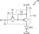
도 3을 참조하면, 화소(PX)는 화소회로(PC) 및 화소회로(PC)에 전기적으로 연결된 표시요소(DPE)를 포함할 수 있다. 화소회로(PC)는 구동 박막트랜지스터(T1), 스위칭 박막트랜지스터(T2), 및 스토리지 커패시터(Cst)를 포함할 수 있다. 화소(PX)는 표시요소(DPE)를 통해 예를 들어, 적색, 녹색, 또는 청색의 빛을 방출하거나, 적색, 녹색, 청색, 또는 백색의 빛을 방출할 수 있다.Referring to FIG. 3 , the pixel PX may include a pixel circuit PC and a display element DPE electrically connected to the pixel circuit PC. The pixel circuit PC may include a driving thin film transistor T1, a switching thin film transistor T2, and a storage capacitor Cst. The pixel PX may emit, for example, red, green, or blue light or red, green, blue, or white light through the display element DPE.
스위칭 박막트랜지스터(T2)는 스캔선(SL) 및 데이터선(DL)에 연결되며, 스캔선(SL)으로부터 입력되는 스캔전압 또는 스캔신호(Sn)에 따라 데이터선(DL)으로부터 입력된 데이터전압 또는 데이터신호(Dm)를 구동 박막트랜지스터(T1)로 전달할 수 있다.The switching thin film transistor T2 is connected to the scan line SL and the data line DL, and the scan voltage input from the scan line SL or the data voltage input from the data line DL according to the scan signal Sn. Alternatively, the data signal Dm may be transferred to the driving thin film transistor T1.
스토리지 커패시터(Cst)는 스위칭 박막트랜지스터(T2)와 구동전압선(PL)에 연결되며, 스위칭 박막트랜지스터(T2)로부터 전달받은 전압과 구동전압선(PL)에 공급되는 제1전원전압(ELVDD)의 차이에 해당하는 전압을 저장할 수 있다.The storage capacitor Cst is connected to the switching thin film transistor T2 and the driving voltage line PL, and the difference between the voltage received from the switching thin film transistor T2 and the first power voltage ELVDD supplied to the driving voltage line PL. The corresponding voltage can be stored.
구동 박막트랜지스터(T1)는 구동전압선(PL)과 스토리지 커패시터(Cst)에 연결되며, 스토리지 커패시터(Cst)에 저장된 전압 값에 대응하여 구동전압선(PL)으로부터 표시요소(DPE)를 흐르는 구동 전류를 제어할 수 있다. 표시요소(DPE)는 구동 전류에 의해 소정의 휘도를 갖는 빛을 방출할 수 있다. 표시요소(DPE)의 대향전극(예를 들어, 캐소드)는 제2전원전압(ELVSS)을 공급받을 수 있다.The driving thin film transistor T1 is connected to the driving voltage line PL and the storage capacitor Cst, and generates a driving current flowing from the driving voltage line PL to the display element DPE in response to a voltage value stored in the storage capacitor Cst. You can control it. The display element DPE may emit light having a predetermined luminance by a driving current. A counter electrode (eg, a cathode) of the display element DPE may receive the second power voltage ELVSS.
도 3은 화소회로(PC)가 2개의 박막트랜지스터와 1개의 스토리지 커패시터를 포함하는 것을 도시하고 있으나, 화소회로(PC)는 3개 또는 그 이상의 박막트랜지스터를 포함할 수 있다.3 shows that the pixel circuit PC includes two thin film transistors and one storage capacitor, but the pixel circuit PC may include three or more thin film transistors.
도 4는 도 1의 표시 장치(1)의 B 부분을 확대한 확대도이다. 도 4에 있어서, 도 1과 동일한 참조부호는 동일부재를 의미하므로 중복된 설명은 생략하기로 한다.FIG. 4 is an enlarged view of portion B of the
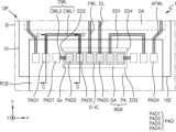
도 4를 참조하면, 표시 장치(1)는 표시 패널(DP), 구동칩(D-IC), 및 인쇄 회로 보드(PCB)를 포함할 수 있다. 표시 패널(DP)은 제1기판(10), 패드(PAD), 연결배선(CWL), 팬아웃배선(FWL), 추가팬아웃배선(AFWL), 및 데이터선(DL)을 포함할 수 있다.Referring to FIG. 4 , the
일 실시예에서, 제1기판(10)은 글라스를 포함할 수 있다. 제1기판(10)은 표시영역(DA) 및 비표시영역(NDA)을 포함할 수 있다. 표시영역(DA)은 화상을 표시하는 영역일 수 있다. 화소는 표시영역(DA)에 배치될 수 있다. 일 실시예에서, 복수의 화소들은 표시영역(DA)에 배치될 수 있다.In one embodiment, the
비표시영역(NDA)은 화상을 표시하지 않는 영역일 수 있다. 비표시영역(NDA)은 표시영역(DA)을 적어도 일부 둘러쌀 수 있다. 비표시영역(NDA)은 그루브영역(GA) 및 주변영역(PA)을 포함할 수 있다.The non-display area NDA may be an area not displaying an image. The non-display area NDA may enclose at least a portion of the display area DA. The non-display area NDA may include a groove area GA and a peripheral area PA.
그루브영역(GA)은 비표시영역(NDA) 중 그루브(Gv)와 중첩하는 영역일 수 있다. 주변영역(PA)은 그루브영역(GA)의 외측에 배치될 수 있다. 일 실시예에서, 주변영역(PA)은 그루브영역(GA)을 적어도 일부 둘러쌀 수 있다. 예를 들어, 주변영역(PA)은 그루브영역(GA)을 전체적으로 둘러쌀 수 있다. 일 실시예에서, 그루브영역(GA)은 비표시영역(NDA) 중 주변영역(PA)에 비해 제1기판(10)의 두께 방향으로 함몰된 영역일 수 있다.The groove area GA may be an area overlapping the groove Gv in the non-display area NDA. The peripheral area PA may be disposed outside the groove area GA. In one embodiment, the peripheral area PA may enclose at least a portion of the groove area GA. For example, the peripheral area PA may entirely surround the groove area GA. In one embodiment, the groove area GA may be a recessed area in the thickness direction of the
그루브(Gv)는 제1기판(10)에 구비될 수 있다. 일 실시예에서, 그루브(Gv)는 비표시영역(NDA)과 중첩할 수 있다. 일 실시예에서, 그루브(Gv)는 그루브영역(GA)과 중첩할 수 있다. 그루브(Gv)는 제1기판(10)의 두께 방향으로 함몰될 수 있다. 예를 들어, 그루브(Gv)는 도 4의 -z 방향으로 함몰된 형상일 수 있다. 그루브(Gv)는 구동칩(D-IC)을 수용하기 위한 형상일 수 있다.The groove Gv may be provided on the
그루브(Gv)는 가장자리를 포함할 수 있다. 일 실시예에서, 그루브(Gv)의 가장자리를 경계로 그루브영역(GA) 및 주변영역(PA)을 구획할 수 있다. 일 실시예에서, 그루브(Gv)는 제1가장자리(ED1), 제2가장자리(ED2), 제3가장자리(ED3), 및 제4가장자리(ED4)를 포함할 수 있다. 제1가장자리(ED1)는 표시영역(DA)과 인접하게 배치될 수 있다. 즉, 제1가장자리(ED1)의 일측에는 표시영역(DA)이 배치될 수 있다. 제3가장자리(ED3)는 제1기판(10)의 가장자리(10E)와 인접하게 배치될 수 있다. 이를 다시 말하면, 제3가장자리(ED3)는 제1기판(10)의 가장자리(10E) 및 제1가장자리(ED1) 사이에 배치될 수 있다. 제2가장자리(ED2) 및 제4가장자리(ED4)는 각각 제1가장자리(ED1)의 말단으로부터 제3가장자리(ED3)의 말단으로 연장될 수 있다.The groove Gv may include an edge. In one embodiment, the groove area GA and the peripheral area PA may be partitioned with the edge of the groove Gv as a boundary. In one embodiment, the groove Gv may include a first edge ED1 , a second edge ED2 , a third edge ED3 , and a fourth edge ED4 . The first edge ED1 may be disposed adjacent to the display area DA. That is, the display area DA may be disposed on one side of the first edge ED1. The third edge ED3 may be disposed adjacent to the
패드(PAD)는 표시 장치(1)의 구성요소를 표시 패널(DP)에 전기적으로 연결시킬 수 있다. 패드(PAD)는 비표시영역(NDA)에 배치될 수 있다. 일 실시예에서, 패드(PAD)는 복수개로 구비될 수 있다. 복수의 패드(PAD)들은 서로 이격될 수 있다. 복수의 패드(PAD)들은 제1패드(PAD1), 제2패드(PAD2), 제3패드(PAD3), 및 제4패드(PAD4)를 포함할 수 있다.The pad PAD may electrically connect components of the
제1패드(PAD1)는 그루브(Gv)의 외측에 배치될 수 있다. 제4패드(PAD4)는 그루브(Gv)의 외측에 배치될 수 있다. 이를 다시 말하면, 제1패드(PAD1) 및 제4패드(PAD4)는 주변영역(PA)에 배치될 수 있다. 일 실시예에서, 제1패드(PAD1)는 복수개로 구비될 수 있다. 일 실시예에서, 제4패드(PAD4)는 복수개로 구비될 수 있다.The first pad PAD1 may be disposed outside the groove Gv. The fourth pad PAD4 may be disposed outside the groove Gv. In other words, the first pad PAD1 and the fourth pad PAD4 may be disposed in the peripheral area PA. In one embodiment, a plurality of first pads PAD1 may be provided. In one embodiment, a plurality of fourth pads PAD4 may be provided.
제2패드(PAD2)는 그루브(Gv) 내에 배치될 수 있다. 제3패드(PAD3)는 그루브(Gv) 내에 배치될 수 있다. 이를 다시 말하면, 제2패드(PAD2) 및 제3패드(PAD3)는 그루브영역(GA)에 배치될 수 있다. 일 실시예에서, 제3패드(PAD3)는 복수개로 구비될 수 있다. 일 실시예에서, 제4패드(PAD4)는 복수개로 구비될 수 있다.The second pad PAD2 may be disposed in the groove Gv. The third pad PAD3 may be disposed in the groove Gv. In other words, the second pad PAD2 and the third pad PAD3 may be disposed in the groove area GA. In one embodiment, a plurality of third pads PAD3 may be provided. In one embodiment, a plurality of fourth pads PAD4 may be provided.
평면도에서 제1패드(PAD1) 및 제2패드(PAD2)는 나란히 배치될 수 있다. 일 실시예에서, 평면도에서 제1패드(PAD1) 및 제2패드(PAD2)는 제1기판(10)의 가장자리(10E)를 따라 나란히 배치될 수 있다. 이를 다시 말하면, 평면도에서 제1패드(PAD1) 및 제2패드(PAD2)는 제1방향(예를 들어, x 방향 또는 -x 방향)을 따라 나란히 배치될 수 있다.In a plan view, the first pad PAD1 and the second pad PAD2 may be disposed side by side. In an embodiment, in a plan view, the first pad PAD1 and the second pad PAD2 may be disposed side by side along the
평면도에서 제1패드(PAD1), 제2패드(PAD2), 및 제3패드(PAD3)는 나란히 배치될 수 있다. 일 실시예에서, 평면도에서 제1패드(PAD1), 제2패드(PAD2), 및 제3패드(PAD3)는 제1기판(10)의 가장자리(10E)를 따라 나란히 배치될 수 있다. 이를 다시 말하면, 평면도에서 제1패드(PAD1), 제2패드(PAD2), 및 제3패드(PAD3)는 제1방향(예를 들어, x 방향 또는 -x 방향)을 따라 나란히 배치될 수 있다.In a plan view, the first pad PAD1 , the second pad PAD2 , and the third pad PAD3 may be disposed side by side. In an embodiment, in a plan view, the first pad PAD1 , the second pad PAD2 , and the third pad PAD3 may be disposed side by side along the
평면도에서 제1패드(PAD1), 제2패드(PAD2), 제3패드(PAD3), 및 제4패드(PAD4)는 나란히 배치될 수 있다. 일 실시예에서, 평면도에서 제1패드(PAD1), 제2패드(PAD2), 및 제4패드(PAD4)는 제1기판(10)의 가장자리(10E)를 따라 나란히 배치될 수 있다. 따라서, 표시 패널(DP)에서 제2방향(예를 들어, y 방향 또는 -y 방향)으로 복수의 패드(PAD)들이 차지하는 비표시영역(NDA)의 면적을 줄일 수 있다.In a plan view, the first pad PAD1 , the second pad PAD2 , the third pad PAD3 , and the fourth pad PAD4 may be disposed side by side. In an embodiment, in a plan view, the first pad PAD1 , the second pad PAD2 , and the fourth pad PAD4 may be disposed side by side along the
연결배선(CWL)은 제1패드(PAD1)로부터 제2패드(PAD2)로 연장될 수 있다. 일 실시예에서, 연결배선(CWL)은 제1패드(PAD1) 및 제2패드(PAD2)를 전기적으로 연결시킬 수 있다. 일 실시예에서, 연결배선(CWL)은 그루브(Gv)로 연장될 수 있다. 이를 다시 말하면, 연결배선(CWL)은 주변영역(PA)에서 그루브영역(GA)으로 연장될 수 있다.The connection wire CWL may extend from the first pad PAD1 to the second pad PAD2. In one embodiment, the connection wire CWL may electrically connect the first pad PAD1 and the second pad PAD2. In one embodiment, the connection line CWL may extend into the groove Gv. In other words, the connection line CWL may extend from the peripheral area PA to the groove area GA.
연결배선(CWL)은 제1가장자리(ED1) 및 제2가장자리(ED2) 중 적어도 하나를 가로지르도록 연장될 수 있다. 일 실시예에서, 제2가장자리(ED2)는 제1패드(PAD1) 및 제2패드(PAD2) 사이에 배치될 수 있다. 제4가장자리(ED4)는 제1패드(PAD1) 및 제2패드(PAD2) 사이에 배치될 수 있다. 연결배선(CWL)은 제1연결배선(CWL1) 및 제2연결배선(CWL2)을 포함할 수 있다. 제1연결배선(CWL1)은 제1가장자리(ED1)를 가로지르도록 연장될 수 있다. 예를 들어, 제1연결배선(CWL1)은 제1패드(PAD1)로부터 제2방향(예를 들어, y 방향 또는 -y 방향)으로 연장될 수 있다. 그 다음, 제1연결배선(CWL1)은 제1방향(예를 들어, x 방향 또는 -x 방향)으로 연장될 수 있다. 그 다음, 제1연결배선(CWL1)은 -y 방향으로 연장될 수 있으며, 제1가장자리(ED1)를 가로지를 수 있다. 제2연결배선(CWL2)은 제2가장자리(ED2)를 가로지르도록 연장될 수 있다. 예를 들어, 제2연결배선(CWL2)은 제1패드(PAD1)로부터 제1방향(예를 들어, x 방향 또는 -x 방향)으로 연장될 수 있으며, 제2가장자리(ED2)를 가로지를 수 있다. 일 실시예에서, 제2연결배선(CWL2)은 제4가장자리(ED4)를 가로지르도록 연장될 수 있다. 예를 들어, 제2연결배선(CWL2)은 제1패드(PAD1)로부터 제1방향(예를 들어, x 방향 또는 -x 방향)으로 연장될 수 있으며, 제4가장자리(ED4)를 가로지를 수 있다.The connection wire CWL may extend to cross at least one of the first edge ED1 and the second edge ED2. In one embodiment, the second edge ED2 may be disposed between the first pad PAD1 and the second pad PAD2. The fourth edge ED4 may be disposed between the first pad PAD1 and the second pad PAD2. The connection wire CWL may include a first connection wire CWL1 and a second connection wire CWL2. The first connection line CWL1 may extend to cross the first edge ED1. For example, the first connection wire CWL1 may extend from the first pad PAD1 in a second direction (eg, a y direction or a -y direction). Then, the first connection line CWL1 may extend in a first direction (eg, an x direction or a -x direction). Then, the first connection line CWL1 may extend in the -y direction and cross the first edge ED1. The second connection wire CWL2 may extend to cross the second edge ED2. For example, the second connection line CWL2 may extend from the first pad PAD1 in a first direction (eg, an x direction or a -x direction) and cross the second edge ED2. there is. In one embodiment, the second connection line CWL2 may extend to cross the fourth edge ED4. For example, the second connection line CWL2 may extend from the first pad PAD1 in a first direction (eg, an x direction or a -x direction) and cross the fourth edge ED4. there is.
일 실시예에서, 연결배선(CWL)은 제3가장자리(ED3)를 가로지르지 않을 수 있다. 이러한 경우, 제2방향(예를 들어, y 방향 또는 -y 방향)으로 비표시영역(NDA)의 면적을 줄일 수 있다. 일부 실시예에서, 연결배선(CWL)은 제3가장자리(ED3)를 가로지를 수 있다.In one embodiment, the connection line CWL may not cross the third edge ED3. In this case, the area of the non-display area NDA may be reduced in the second direction (eg, the y-direction or the -y-direction). In some embodiments, the connection line CWL may cross the third edge ED3.
팬아웃배선(FWL)은 제3패드(PAD3)로부터 표시영역(DA)으로 연장될 수 있다. 일 실시예에서, 팬아웃배선(FWL)은 그루브영역(GA)으로부터 주변영역(PA)으로 연장될 수 있다. 팬아웃배선(FWL)은 주변영역(PA)으로부터 표시영역(DA)으로 연장될 수 있다. 일 실시예에서, 팬아웃배선(FWL)은 복수개로 구비될 수 있다.The fan-out wiring FWL may extend from the third pad PAD3 to the display area DA. In one embodiment, the fan-out wiring FWL may extend from the groove area GA to the peripheral area PA. The fan-out wiring FWL may extend from the peripheral area PA to the display area DA. In one embodiment, a plurality of fan-out lines (FWL) may be provided.
일 실시예에서, 팬아웃배선(FWL)은 데이터선(DL)과 전기적으로 연결될 수 있다. 일 실시예에서, 팬아웃배선(FWL)은 데이터선(DL)과 일체로 구비될 수 있다. 다른 실시예에서, 팬아웃배선(FWL)은 데이터선(DL)과 상이한 배선으로 데이터선(DL)과 전기적으로 연결된 배선일 수 있다.In one embodiment, the fanout line FWL may be electrically connected to the data line DL. In one embodiment, the fan-out line FWL may be integrally provided with the data line DL. In another embodiment, the fanout line FWL may be a wire electrically connected to the data line DL as a different wire from the data line DL.
추가팬아웃배선(AFWL)은 제4패드(PAD4)로부터 연장될 수 있다. 추가팬아웃배선(AFWL)은 제4패드(PAD4)로부터 표시영역(DA)으로 연장될 수 있다. 일 실시예에서, 추가팬아웃배선(AFWL)은 복수개로 구비될 수 있다.The additional fan-out wiring AFWL may extend from the fourth pad PAD4. The additional fan-out wiring AFWL may extend from the fourth pad PAD4 to the display area DA. In one embodiment, a plurality of additional fan-out wires (AFWL) may be provided.
구동칩(D-IC)은 그루브(Gv) 내에 배치될 수 있다. 일 실시예에서, 구동칩(D-IC)은 그루브(Gv)에 수용될 수 있다. 구동칩(D-IC)은 그루브(Gv)에 실장될 수 있다. 구동칩(D-IC)은 제2패드(PAD2)와 전기적으로 연결될 수 있다. 구동칩(D-IC)은 제3패드(PAD3)와 전기적으로 연결될 수 있다. 따라서, 구동칩(D-IC)에서 생성된 신호들 및/또는 전압들은 팬아웃배선(FWL)을 통해 전달할 수 있다.The driving chip D-IC may be disposed in the groove Gv. In one embodiment, the driving chip D-IC may be accommodated in the groove Gv. The driving chip D-IC may be mounted in the groove Gv. The driving chip D-IC may be electrically connected to the second pad PAD2. The driving chip D-IC may be electrically connected to the third pad PAD3. Accordingly, signals and/or voltages generated by the driving chip D-IC may be transmitted through the fan-out wiring FWL.
인쇄 회로 보드(PCB)는 비표시영역(NDA)에 배치될 수 있다. 일 실시예에서, 인쇄 회로 보드(PCB)는 평면도에서 구동칩(D-IC)과 중첩할 수 있다. 따라서, 비표시영역(NDA)에서 구동칩(D-IC) 및 인쇄 회로 보드(PCB)가 차지하는 면적을 줄일 수 있다. 즉, 표시 패널(DP)의 하단에 배치된 비표시영역(NDA)이 줄어들 수 있다.The printed circuit board (PCB) may be disposed in the non-display area (NDA). In one embodiment, the printed circuit board (PCB) may overlap the driving chip (D-IC) in a plan view. Accordingly, an area occupied by the driving chip D-IC and the printed circuit board PCB in the non-display area NDA may be reduced. That is, the non-display area NDA disposed at the bottom of the display panel DP may be reduced.
인쇄 회로 보드(PCB)는 표시 패널(DP)에 전기적으로 연결될 수 있다. 인쇄 회로 보드(PCB)는 제1패드(PAD1)와 전기적으로 연결될 수 있다. 따라서, 인쇄 회로 보드(PCB) 및 구동칩(D-IC)은 서로 전기적으로 연결될 수 있다. 예를 들어, 인쇄 회로 보드(PCB) 및 구동칩(D-IC)은 제1패드(PAD1), 연결배선(CWL), 및 제2패드(PAD2)를 통해 서로 전기적으로 연결될 수 있다. 따라서, 인쇄 회로 보드(PCB)는 제어 신호들 및/또는 전원전압을 구동칩(D-IC)에 인가할 수 있다.The printed circuit board (PCB) may be electrically connected to the display panel (DP). The printed circuit board (PCB) may be electrically connected to the first pad (PAD1). Therefore, the printed circuit board (PCB) and the driving chip (D-IC) may be electrically connected to each other. For example, the printed circuit board (PCB) and the driving chip (D-IC) may be electrically connected to each other through a first pad (PAD1), a connection line (CWL), and a second pad (PAD2). Accordingly, the printed circuit board (PCB) may apply control signals and/or power supply voltage to the driving chip (D-IC).
인쇄 회로 보드(PCB)는 제4패드(PAD4)와 전기적으로 연결될 수 있다. 따라서, 인쇄 회로 보드(PCB)에서 생성된 신호들 및/또는 전압들은 추가팬아웃배선(AFWL)을 통해 전달될 수 있다. 또는 표시 패널(DP)에서 생성된 신호는 추가팬아웃배선(AFWL)을 통해 인쇄 회로 보드(PCB)로 전달될 수 있다. 예를 들어, 표시 패널(DP)에서 획득된 좌표정보는 추가팬아웃배선(AFWL)을 통해 인쇄 회로 보드(PCB)를 통해 전달될 수 있다.The printed circuit board (PCB) may be electrically connected to the fourth pad (PAD4). Accordingly, signals and/or voltages generated in the printed circuit board (PCB) may be transmitted through the additional fan-out wiring (AFWL). Alternatively, signals generated by the display panel DP may be transferred to the printed circuit board PCB through the additional fan-out wiring AFWL. For example, coordinate information obtained from the display panel DP may be transmitted through the printed circuit board PCB through the additional fan-out wiring AFWL.
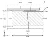
도 5는 도 4의 표시 장치(1)를 C-C'선에 따라 개략적으로 나타낸 단면도이다. 도 6은 도 4의 표시 장치(1)를 D-D'선에 따라 개략적으로 나타낸 단면도이다. 도 5 및 도 6에 있어서, 도 4와 동일한 참조부호는 동일부재를 의미하므로 중복된 설명은 생략하기로 한다.FIG. 5 is a cross-sectional view schematically illustrating the
도 5 및 도 6을 참조하면, 표시 장치(1)는 표시 패널(DP), 구동칩(D-IC), 및 인쇄 회로 보드(PCB)를 포함할 수 있다. 표시 패널(DP)은 제1기판(10), 패드, 및 연결배선(CWL)을 포함할 수 있다.Referring to FIGS. 5 and 6 , the
제1기판(10)은 상면(10US) 및 하면(10LS)을 포함할 수 있다. 제1기판(10)의 상면(10US) 및 제1기판(10)의 하면(10LS)은 서로 반대되는 면일 수 있다. 제1기판(10)의 가장자리(10E)를 포함할 수 있다. 제1기판(10)의 가장자리(10E)는 제1기판(10)의 상면(10US)으로부터 제1기판(10)의 하면(10LS)으로 연장될 수 있다. 제1기판(10)의 가장자리(10E)는 제1기판(10)의 상면(10US) 및 제1기판(10)의 하면(10LS)을 서로 연결할 수 있다.The
제1기판(10)은 표시영역 및 비표시영역(NDA)을 포함할 수 있다. 비표시영역(NDA)은 상기 표시영역을 적어도 일부 둘러쌀 수 있다. 비표시영역(NDA)은 그루브영역(GA) 및 주변영역(PA)을 포함할 수 있다.The
그루브영역(GA)은 비표시영역(NDA) 중 그루브(Gv)와 중첩하는 영역일 수 있다. 주변영역(PA)은 그루브영역(GA)의 외측에 배치될 수 있다. 일 실시예에서, 주변영역(PA)은 그루브영역(GA)을 적어도 일부 둘러쌀 수 있다. 일 실시예에서, 그루브영역(GA)은 비표시영역(NDA) 중 주변영역(PA)에 비해 제1기판(10)의 두께 방향으로 함몰된 영역일 수 있다. 그루브영역(GA)은 비표시영역(NDA) 중 주변영역(PA)에 비해 제1기판(10)의 상면(10US)이 함몰된 영역일 수 있다.The groove area GA may be an area overlapping the groove Gv in the non-display area NDA. The peripheral area PA may be disposed outside the groove area GA. In one embodiment, the peripheral area PA may enclose at least a portion of the groove area GA. In one embodiment, the groove area GA may be a recessed area in the thickness direction of the
그루브영역(GA)에서 제1기판(10)의 두께(10t2)는 주변영역(PA)에서 제1기판(10)의 두께(10t1)보다 작을 수 있다. 그루브영역(GA)에서 제1기판(10)의 두께(10t2)는 그루브영역(GA)에서 제1기판(10)의 상면(10US) 및 제1기판(10)의 하면(10LS) 사이의 거리일 수 있다. 주변영역(PA)에서 제1기판(10)의 두께(10t1)는 주변영역(PA)에서 제1기판(10)의 상면(10US) 및 제1기판(10)의 하면(10LS) 사이의 거리일 수 있다.A thickness 10t2 of the
그루브(Gv)는 제1기판(10)에 구비될 수 있다. 일 실시예에서, 그루브(Gv)는 비표시영역(NDA)과 중첩할 수 있다. 일 실시예에서, 그루브(Gv)는 그루브영역(GA)과 중첩할 수 있다. 그루브(Gv)는 제1기판(10)의 두께 방향으로 함몰될 수 있다. 예를 들어, 그루브(Gv)는 도 6의 -z 방향으로 함몰된 형상일 수 있다. 그루브(Gv)는 구동칩(D-IC)을 수용하기 위한 형상일 수 있다. 일 실시예에서, 그루브(Gv)는 제1기판(10)에 습식 식각 및/또는 건식 식각하여 형성될 수 있다. 일 실시예에서, 그루브(Gv)는 제1기판(10)을 습식 식각한 후, 건식 식각하여 형성될 수 있다.The groove Gv may be provided on the
일 실시예에서, 그루브(Gv)는 제1면(S1) 및 제2면(S2)으로 정의될 수 있다. 제1면(S1) 및 제2면(S2)은 그루브영역(GA)과 중첩하는 제1기판(10)의 상면(10US)일 수 있다. 제1면(S1)은 제1기판(10)의 상면(10US) 중 제1기판(10)의 하면(10LS)과 가장 가까운 면일 수 있다. 일 실시예에서, 제1면(S1)은 평평할 수 있다. 일 실시예에서, 그루브(Gv)의 깊이(Gvd)는 도 6의 z 방향으로 주변영역(PA)에서 제1기판(10)의 상면(10US) 및 제1면(S1) 사이의 거리일 수 있다. 일 실시예에서, 그루브영역(GA)에서 제1기판(10)의 두께(10t2) 및 그루브(Gv)의 깊이(Gvd)의 합은 주변영역(PA)에서 제1기판(10)의 두께(10t1)일 수 있다. 제2면(S2)은 제1면(S1)으로부터 주변영역(PA)의 제1기판(10)의 상면(10US)으로 연장된 면일 수 있다. 일 실시예에서, 제2면(S2)은 경사질 수 있다.In one embodiment, the groove (Gv) may be defined as the first surface (S1) and the second surface (S2). The first surface S1 and the second surface S2 may be the upper surface 10US of the
그루브(Gv)는 가장자리를 포함할 수 있다. 일 실시예에서, 그루브(Gv)의 가장자리는 제2면(S2) 및 주변영역(PA)에서 제1기판(10)의 상면(10US)이 만나는 부분일 수 있다. 일 실시예에서, 그루브(Gv)의 가장자리를 경계로 그루브영역(GA) 및 주변영역(PA)을 구획할 수 있다. 일 실시예에서, 그루브(Gv)는 제1가장자리(ED1) 및 제3가장자리(ED3)를 포함할 수 있다. 제1가장자리(ED1)는 표시영역과 인접하게 배치될 수 있다. 제3가장자리(ED3)는 제1기판(10)의 가장자리(10E)와 인접하게 배치될 수 있다. 이를 다시 말하면, 제3가장자리(ED3)는 제1기판(10)의 가장자리(10E) 및 제1가장자리(ED1) 사이에 배치될 수 있다.The groove Gv may include an edge. In an embodiment, an edge of the groove Gv may be a portion where the second surface S2 and the upper surface 10US of the
패드는 표시 장치(1)의 구성요소를 표시 패널(DP)에 전기적으로 연결시킬 수 있다. 패드는 비표시영역(NDA)에 배치될 수 있다. 일 실시예에서, 패드는 복수개로 구비될 수 있다. 복수의 패드들은 서로 이격될 수 있다. 일 실시예에서, 복수의 패드들은 제1패드(PAD1) 및 제2패드(PAD2)를 포함할 수 있다.The pad may electrically connect components of the
제1패드(PAD1)는 그루브(Gv)의 외측에 배치될 수 있다. 이를 다시 말하면, 제1패드(PAD1)는 주변영역(PA)에 배치될 수 있다. 제2패드(PAD2)는 그루브(Gv) 내에 배치될 수 있다. 이를 다시 말하면, 제2패드(PAD2)는 그루브영역(GA)에 배치될 수 있다.The first pad PAD1 may be disposed outside the groove Gv. In other words, the first pad PAD1 may be disposed in the peripheral area PA. The second pad PAD2 may be disposed in the groove Gv. In other words, the second pad PAD2 may be disposed in the groove area GA.
연결배선(CWL)은 제1패드(PAD1)로부터 제2패드(PAD2)로 연장될 수 있다. 일 실시예에서, 연결배선(CWL)은 제1패드(PAD1) 및 제2패드(PAD2)를 전기적으로 연결시킬 수 있다. 일 실시예에서, 연결배선(CWL)은 그루브(Gv)로 연장될 수 있다. 이를 다시 말하면, 연결배선(CWL)은 주변영역(PA)에서 그루브영역(GA)으로 연장될 수 있다. 연결배선(CWL)은 주변영역(PA)에서 제1기판(10)의 상면(10US)으로부터 제2면(S2)으로 연장될 수 있다. 연결배선(CWL)은 제2면(S2)으로부터 제1면(S1)으로 연장될 수 있다.The connection wire CWL may extend from the first pad PAD1 to the second pad PAD2. In one embodiment, the connection wire CWL may electrically connect the first pad PAD1 and the second pad PAD2. In one embodiment, the connection line CWL may extend into the groove Gv. In other words, the connection line CWL may extend from the peripheral area PA to the groove area GA. The connection wire CWL may extend from the upper surface 10US of the
도시하지는 않았으나, 팬아웃배선은 그루브(Gv)로 연장될 수 있다. 이를 다시 말하면, 팬아웃배선은 주변영역(PA)에서 그루브영역(GA)으로 연장될 수 있다. 팬아웃배선은 주변영역(PA)에서 제1기판(10)의 상면(10US)으로부터 제2면(S2)으로 연장될 수 있다. 팬아웃배선은 제2면(S2)으로부터 제1면(S1)으로 연장될 수 있다.Although not shown, the fan-out wiring may extend into the groove Gv. In other words, the fan-out wiring may extend from the peripheral area PA to the groove area GA. The fan-out wiring may extend from the upper surface 10US of the
도 5 및 도 6에서 연결배선(CWL)은 제1패드(PAD1) 및 제2패드(PAD2)와 일체로 구비된 것을 도시하고 있으나, 다른 실시예에서, 연결배선(CWL)은 제1패드(PAD1) 및 제2패드(PAD2) 중 적어도 하나와 일체로 구비되지 않을 수 있다. 이러한 경우, 연결배선(CWL)은 제1패드(PAD1) 및 제2패드(PAD2) 중 적어도 하나와 상이한 배선일 수 있으며, 연결배선(CWL)은 제1패드(PAD1) 및 제2패드(PAD2)와 전기적으로 연결될 수 있다.5 and 6 show that the connection wire CWL is integrally provided with the first pad PAD1 and the second pad PAD2, but in another embodiment, the connection wire CWL is provided with the first pad ( It may not be integrally provided with at least one of PAD1) and the second pad PAD2. In this case, the connection wire CWL may be a different wire from at least one of the first pad PAD1 and the second pad PAD2, and the connection wire CWL may be a wire that is different from the first pad PAD1 and the second pad PAD2. can be electrically connected with
구동칩(D-IC)은 그루브(Gv) 내에 배치될 수 있다. 일 실시예에서, 구동칩(D-IC)은 그루브(Gv)에 수용될 수 있다. 구동칩(D-IC)은 그루브(Gv)에 실장될 수 있다. 일 실시예에서, 구동칩(D-IC)은 구동칩전극(D-ICE)을 포함할 수 있다. 구동칩전극(D-ICE)은 제2패드(PAD2)와 전기적으로 연결될 수 있다. 일 실시예에서, 구동칩전극(D-ICE) 및 제2패드(PAD2)는 이방성 도전 필름을 통해 전기적으로 연결될 수 있다. 다른 실시예에서, 구동칩전극(D-ICE) 및 제2패드(PAD2)는 솔더링부에 의해 서로 전기적으로 연결될 수 있다. 또 다른 실시예에서, 구동칩전극(D-ICE) 및 제2패드(PAD2)는 직접 전기적으로 연결될 수 있다. 예를 들어, 구동칩전극(D-ICE)의 일부 및 제2패드(PAD2)의 일부는 서로 용융되어 접합될 수 있다.The driving chip D-IC may be disposed in the groove Gv. In one embodiment, the driving chip D-IC may be accommodated in the groove Gv. The driving chip D-IC may be mounted in the groove Gv. In one embodiment, the driving chip D-IC may include a driving chip electrode D-ICE. The driving chip electrode D-ICE may be electrically connected to the second pad PAD2. In one embodiment, the driving chip electrode D-ICE and the second pad PAD2 may be electrically connected through an anisotropic conductive film. In another embodiment, the driving chip electrode D-ICE and the second pad PAD2 may be electrically connected to each other by a soldering part. In another embodiment, the driving chip electrode D-ICE and the second pad PAD2 may be directly electrically connected. For example, a part of the driving chip electrode D-ICE and a part of the second pad PAD2 may be melted and bonded to each other.
일 실시예에서, 구동칩(D-IC)의 두께(D-ICt)는 그루브(Gv)의 깊이(Gvd)보다 작을 수 있다. 구동칩(D-IC)의 두께(D-ICt)는 도 6의 z 방향으로 구동칩전극(D-ICE)의 하면으로부터 구동칩(D-IC)의 상면까지의 거리일 수 있다. 그루브(Gv)의 깊이(Gvd)는 구동칩(D-IC)의 두께(D-ICt)보다 클 수 있다. 따라서, 구동칩(D-IC)은 그루브(Gv)에 전체적으로 수용될 수 있다.In an embodiment, the thickness D-ICt of the driving chip D-IC may be smaller than the depth Gvd of the groove Gv. The thickness D-ICt of the driving chip D-IC may be a distance from the lower surface of the driving chip electrode D-ICE to the upper surface of the driving chip D-IC in the z direction of FIG. 6 . The depth Gvd of the groove Gv may be greater than the thickness D-ICt of the driving chip D-IC. Accordingly, the driving chip D-IC may be entirely accommodated in the groove Gv.
인쇄 회로 보드(PCB)는 비표시영역(NDA)에 배치될 수 있다. 일 실시예에서, 인쇄 회로 보드(PCB)는 평면도에서 구동칩(D-IC)과 중첩할 수 있다. 따라서, 비표시영역(NDA)에서 구동칩(D-IC) 및 인쇄 회로 보드(PCB)가 차지하는 면적을 줄일 수 있다. 즉, 표시 패널(DP)의 하단에 배치된 비표시영역(NDA)이 줄어들 수 있다.The printed circuit board (PCB) may be disposed in the non-display area (NDA). In one embodiment, the printed circuit board (PCB) may overlap the driving chip (D-IC) in a plan view. Accordingly, an area occupied by the driving chip D-IC and the printed circuit board PCB in the non-display area NDA may be reduced. That is, the non-display area NDA disposed at the bottom of the display panel DP may be reduced.
인쇄 회로 보드(PCB)는 표시 패널(DP)에 전기적으로 연결될 수 있다. 일 실시예에서, 인쇄 회로 보드(PCB)는 인쇄 회로 보드 전극(PCBE)을 포함할 수 있다. 인쇄 회로 보드 전극(PCBE)은 제1패드(PAD1)와 전기적으로 연결될 수 있다. 일 실시예에서, 인쇄 회로 보드 전극(PCBE) 및 제1패드(PAD1)는 이방성 도전 필름을 통해 전기적으로 연결될 수 있다. 다른 실시예에서, 인쇄 회로 보드 전극(PCBE) 및 제1패드(PAD1)는 솔더링부에 의해 서로 전기적으로 연결될 수 있다. 또 다른 실시예에서, 인쇄 회로 보드 전극(PCBE) 및 제1패드(PAD1)는 직접 전기적으로 연결될 수 있다. 예를 들어, 인쇄 회로 보드 전극(PCBE)의 일부 및 제1패드(PAD1)의 일부는 서로 용융되어 접합될 수 있다.The printed circuit board (PCB) may be electrically connected to the display panel (DP). In one embodiment, a printed circuit board (PCB) may include a printed circuit board electrode (PCBE). The printed circuit board electrode PCBE may be electrically connected to the first pad PAD1. In one embodiment, the printed circuit board electrode PCBE and the first pad PAD1 may be electrically connected through an anisotropic conductive film. In another embodiment, the printed circuit board electrode PCBE and the first pad PAD1 may be electrically connected to each other by a soldering part. In another embodiment, the printed circuit board electrode PCBE and the first pad PAD1 may be directly electrically connected. For example, a part of the printed circuit board electrode PCBE and a part of the first pad PAD1 may be melted and bonded to each other.
인쇄 회로 보드(PCB) 및 구동칩(D-IC)은 서로 전기적으로 연결될 수 있다. 예를 들어, 인쇄 회로 보드(PCB) 및 구동칩(D-IC)은 제1패드(PAD1), 연결배선(CWL), 및 제2패드(PAD2)를 통해 서로 전기적으로 연결될 수 있다. 따라서, 인쇄 회로 보드(PCB)는 제어 신호들 및/또는 전원전압을 구동칩(D-IC)에 인가할 수 있다.The printed circuit board (PCB) and the driving chip (D-IC) may be electrically connected to each other. For example, the printed circuit board (PCB) and the driving chip (D-IC) may be electrically connected to each other through a first pad (PAD1), a connection line (CWL), and a second pad (PAD2). Accordingly, the printed circuit board (PCB) may apply control signals and/or power supply voltage to the driving chip (D-IC).
도 7은 도 1의 표시 장치(1)의 E-E'선에 따라 개략적으로 나타낸 단면도이다.FIG. 7 is a schematic cross-sectional view of the
도 7을 참조하면, 표시 장치(1)는 표시 패널(DP)을 포함할 수 있다. 표시 패널(DP)은 제1기판(10), 화소회로층(PCL), 및 표시요소층(20)을 포함할 수 있다. 화소회로층(PCL) 및 표시요소층(20)은 제1기판(10) 상에 차례로 배치될 수 있다.Referring to FIG. 7 , the
일 실시예에서, 제1기판(10)은 표시영역(DA)을 포함할 수 있다.In one embodiment, the
화소회로층(PCL) 및 제1기판(10) 사이에는 배리어층(미도시)을 더 포함할 수 있다. 배리어층은 외부 이물질의 침투를 방지하는 배리어층으로, 실리콘질화물(SiNX), 실리콘산화물(SiO2)과 같은 무기물을 포함하는 단일 층 또는 다층일 수 있다.A barrier layer (not shown) may be further included between the pixel circuit layer PCL and the
화소회로층(PCL)은 제1기판(10) 상에 배치될 수 있다. 화소회로층(PCL)은 박막트랜지스터(TFT) 및 박막트랜지스터(TFT)의 구성요소들 아래 또는/및 위에 배치되는 버퍼층(111), 제1게이트절연층(112), 제2게이트절연층(113), 층간절연층(114), 및 유기절연층(115)을 포함할 수 있다.The pixel circuit layer PCL may be disposed on the
버퍼층(111)은 제1기판(10) 상에 배치될 수 있다. 버퍼층(111)은 실리콘질화물(SiNX), 실리콘산질화물(SiON), 및 실리콘산화물(SiO2)과 같은 무기 절연물을 포함할 수 있으며, 전술한 무기 절연물을 포함하는 단층 또는 다층일 수 있다.The
박막트랜지스터(TFT)는 반도체층(Act) 게이트전극(GE), 소스전극(SE), 및 드레인전극(DE)을 포함할 수 있다. 반도체층(Act)은 폴리 실리콘을 포함할 수 있다. 또는, 반도체층(Act)은 비정질(amorphous) 실리콘을 포함하거나, 산화물 반도체를 포함하거나, 유기 반도체 등을 포함할 수 있다. 반도체층(Act)은 채널영역(Act1) 및 채널영역(Act1)의 양측에 각각 배치된 소스영역(Act2) 및 드레인영역(Act3)을 포함할 수 있다.The thin film transistor TFT may include a semiconductor layer Act, a gate electrode GE, a source electrode SE, and a drain electrode DE. The semiconductor layer Act may include polysilicon. Alternatively, the semiconductor layer Act may include amorphous silicon, an oxide semiconductor, or an organic semiconductor. The semiconductor layer Act may include a channel region Act1 and a source region Act2 and a drain region Act3 respectively disposed on both sides of the channel region Act1.
게이트전극(GE)은 채널영역(Act1)과 중첩할 수 있다. 게이트전극(GE)은 저저항 금속 물질을 포함할 수 있다. 게이트전극(GE)은 몰리브덴(Mo), 알루미늄(Al), 구리(Cu), 티타늄(Ti) 등을 포함하는 도전 물질을 포함할 수 있고, 상기의 재료를 포함하는 다층 또는 단층으로 형성될 수 있다.The gate electrode GE may overlap the channel region Act1. The gate electrode GE may include a low-resistance metal material. The gate electrode GE may include a conductive material including molybdenum (Mo), aluminum (Al), copper (Cu), titanium (Ti), or the like, and may be formed as a multilayer or single layer including the above material. there is.
반도체층(Act)과 게이트전극(GE) 사이의 제1게이트절연층(112)은 실리콘산화물(SiO2), 실리콘질화물(SiNX), 실리콘산질화물(SiON), 알루미늄산화물(Al2O3), 티타늄산화물(TiO2), 탄탈산화물(Ta2O5), 하프늄산화물(HfO2), 또는 징크산화물(ZnO)등과 같은 무기 절연물을 포함할 수 있다.The first
제2게이트절연층(113)은 게이트전극(GE)을 덮을 수 있다. 제2게이트절연층(113)은 제1게이트절연층(112)과 유사하게 실리콘산화물(SiO2), 실리콘질화물(SiNX), 실리콘산질화물(SiON), 알루미늄산화물(Al2O3), 티타늄산화물(TiO2), 탄탈산화물(Ta2O5), 하프늄산화물(HfO2), 또는 징크산화물(ZnO) 등과 같은 무기 절연물을 포함할 수 있다.The second
제2게이트절연층(113) 상부에는 스토리지 커패시터(Cst)의 상부 전극(Cst2)이 배치될 수 있다. 상부 전극(Cst2)은 그 아래의 게이트전극(GE)과 중첩할 수 있다. 이 때, 제2게이트절연층(113)을 사이에 두고 중첩하는 게이트전극(GE) 및 상부 전극(Cst2)은 스토리지 커패시터(Cst)를 구성할 수 있다. 즉, 게이트전극(GE)은 스토리지 커패시터(Cst)의 하부 전극(Cst1)으로 기능할 수 있다. 이와 같이, 스토리지 커패시터(Cst)와 박막트랜지스터(TFT)가 중첩될 수 있다. 일부 실시예에서, 스토리지 커패시터(Cst)는 박막트랜지스터(TFT)와 중첩되지 않을 수 있다.An upper electrode Cst2 of the storage capacitor Cst may be disposed on the second
상부 전극(Cst2)은 알루미늄(Al), 백금(Pt), 팔라듐(Pd), 은(Ag), 마그네슘(Mg), 금(Au), 니켈(Ni), 네오디뮴(Nd), 이리듐(Ir), 크롬(Cr), 칼슘(Ca), 몰리브덴(Mo), 티타늄(Ti), 텅스텐(W), 및/또는 구리(Cu)를 포함할 수 있으며, 전술한 물질의 단일층 또는 다층일 수 있다.The upper electrode Cst2 is made of aluminum (Al), platinum (Pt), palladium (Pd), silver (Ag), magnesium (Mg), gold (Au), nickel (Ni), neodymium (Nd), or iridium (Ir). , chromium (Cr), calcium (Ca), molybdenum (Mo), titanium (Ti), tungsten (W), and/or copper (Cu), and may be a single layer or multiple layers of the above materials. .
층간절연층(114)은 상부 전극(Cst2)을 덮을 수 있다. 층간절연층(114)은 실리콘산화물(SiO2), 실리콘질화물(SiNX), 실리콘산질화물(SiON), 알루미늄산화물(Al2O3), 티타늄산화물(TiO2), 탄탈산화물(Ta2O5), 하프늄산화물(HfO2), 또는 징크산화물(ZnO) 등을 포함할 수 있다. 층간절연층(114)은 전술한 무기 절연물을 포함하는 단일층 또는 다층일 수 있다.The interlayer insulating
소스전극(SE) 및 드레인전극(DE)은 각각 층간절연층(114) 상에 배치될 수 있다. 소스전극(SE) 및 드레인전극(DE)은 전도성이 좋은 재료를 포함할 수 있다. 소스전극(SE) 및 드레인전극(DE)은 몰리브덴(Mo), 알루미늄(Al), 구리(Cu), 티타늄(Ti) 등을 포함하는 도전 물질을 포함할 수 있고, 상기의 재료를 포함하는 다층 또는 단층으로 형성될 수 있다. 일 실시예로, 소스전극(SE) 및 드레인전극(DE)은 Ti/Al/Ti의 다층 구조를 가질 수 있다.The source electrode SE and the drain electrode DE may be disposed on the
유기절연층(115)은 유기절연층을 포함할 수 있다. 유기절연층(115)은 Polymethylmethacrylate(PMMA)나 Polystyrene(PS)과 같은 일반 범용고분자, 페놀계 그룹을 갖는 고분자 유도체, 아크릴계 고분자, 이미드계 고분자, 아릴에테르계 고분자, 아마이드계 고분자, 불소계고분자, p-자일렌계 고분자, 비닐알콜계 고분자, 및 이들의 블렌드와 같은 유기 절연물을 포함할 수 있다.The organic insulating layer 115 may include an organic insulating layer. The organic insulating layer 115 is a general purpose polymer such as polymethylmethacrylate (PMMA) or polystyrene (PS), a polymer derivative having a phenolic group, an acrylic polymer, an imide polymer, an arylether polymer, an amide polymer, a fluorine polymer, p -Can include organic insulators such as xylene-based polymers, vinyl alcohol-based polymers, and blends thereof.
표시요소층(20)은 화소회로층(PCL) 상에 배치될 수 있다. 표시요소층(20)은 표시요소로서 유기발광다이오드(OLED) 및 화소정의막(240)을 포함할 수 있다. 유기발광다이오드(OLED)는 예컨대, 적색, 녹색, 또는 청색 빛을 방출하거나, 적색, 녹색, 청색, 또는 백색의 빛을 방출할 수 있다. 유기발광다이오드(OLED)는 화소전극(210), 발광층(220), 및 대향전극(230)을 포함할 수 있다.The
화소전극(210)은 유기절연층(115) 상에 배치될 수 있다. 화소전극(210)은 유기절연층(115)의 컨택홀을 통해 박막트랜지스터(TFT)와 전기적으로 연결될 수 있다. 화소전극(210)은 인듐틴산화물(ITO; indium tin oxide), 인듐징크산화물(IZO; indium zinc oxide), 징크산화물(ZnO; zinc oxide), 인듐산화물(In2O3: indium oxide), 인듐갈륨산화물(IGO; indium gallium oxide) 또는 알루미늄징크산화물(AZO; aluminum zinc oxide)와 같은 도전성 산화물을 포함할 수 있다. 다른 실시예로, 화소전극(210)은 은(Ag), 마그네슘(Mg), 알루미늄(Al), 백금(Pt), 팔라듐(Pd), 금(Au), 니켈(Ni), 네오디뮴(Nd), 이리듐(Ir), 크롬(Cr) 또는 이들의 화합물을 포함하는 반사막을 포함할 수 있다. 다른 실시예로, 화소전극(210)은 전술한 반사막의 위/아래에 ITO, IZO, ZnO 또는 In2O3로 형성된 막을 더 포함할 수 있다.The
화소전극(210) 상에는 화소전극(210)의 중앙부를 노출하는 개구(240OP)를 갖는 화소정의막(240)이 배치될 수 있다. 화소정의막(240)은 유기절연물 및/또는 무기절연물을 포함할 수 있다. 개구(240OP)는 유기발광다이오드(OLED)에서 방출되는 빛의 발광영역(EA)을 정의할 수 있다. 예컨대, 개구(240OP)의 폭이 발광영역(EA)의 폭일 수 있다.A pixel-defining
화소정의막(240)의 개구(240OP)에는 발광층(220)이 배치될 수 있다. 발광층(220)은 소정의 색상의 빛을 방출하는 고분자 또는 저분자 유기물을 포함할 수 있다. 도시되지는 않았으나, 발광층(220)의 아래와 위에는 각각 제1기능층 및 제2기능층이 배치될 수 있다. 제1기능층은 예컨대, 홀 수송층(HTL: Hole Transport Layer)을 포함하거나, 홀 수송층 및 홀 주입층(HIL: Hole Injection Layer)을 포함할 수 있다. 제2기능층은 발광층(220) 위에 배치되는 구성요소로서, 선택적(optional)이다. 제2기능층은 전자 수송층(ETL: Electron Transport Layer) 및/또는 전자 주입층(EIL: Electron Injection Layer)을 포함할 수 있다. 제1기능층 및/또는 제2기능층은 후술할 대향전극(230)과 마찬가지로 제1기판(10)을 전체적으로 커버하도록 형성되는 공통층일 수 있다.An
대향전극(230)은 발광층(220) 상에 배치될 수 있다. 대향전극(230)은 일함수가 낮은 도전성 물질로 이루어질 수 있다. 예컨대, 대향전극(230)은 은(Ag), 마그네슘(Mg), 알루미늄(Al), 백금(Pt), 팔라듐(Pd), 금(Au), 니켈(Ni), 네오디뮴(Nd), 이리듐(Ir), 크롬(Cr), 리튬(Li), 칼슘(Ca) 또는 이들의 합금 등을 포함하는 (반)투명층을 포함할 수 있다. 또는, 대향전극(230)은 전술한 물질을 포함하는 (반)투명층 상에 ITO, IZO, ZnO 또는 In2O3과 같은 층을 더 포함할 수 있다.The
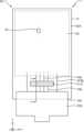
도 8은 비교예에 따른 표시 장치(1-1)를 개략적으로 나타낸 평면도이다. 도 9는 도 8의 표시 장치(1-1)를 F-F'선에 따라 개략적으로 나타낸 단면도이다.8 is a plan view schematically illustrating a display device 1-1 according to a comparative example. FIG. 9 is a schematic cross-sectional view of the display device 1-1 of FIG. 8 taken along the line F-F'.
도 8 및 도 9을 참조하면, 표시 장치(1-1)는 표시 패널(DP-1), 구동칩(D-IC), 및 인쇄 회로 보드(PCB)를 포함할 수 있다. 표시 패널(DP-1)은 제1기판(10), 화소(PX), 제1패드(PAD1), 제2패드(PAD2), 제3패드(PAD3), 연결배선(CWL), 팬아웃배선(FWL), 및 추가팬아웃배선(AFWL)을 포함할 수 있다.Referring to FIGS. 8 and 9 , the display device 1 - 1 may include a display panel DP- 1 , a driving chip D-IC, and a printed circuit board (PCB). The display panel DP-1 includes a
제1기판(10)은 표시영역(DA) 및 비표시영역(NDA)을 포함할 수 있다. 비교예에서, 비표시영역(NDA)에서 제1기판(10)은 그루브를 구비하지 않을 수 있다. 이를 다시 말하면, 비표시영역(NDA)에서 제1기판(10)의 두께(10t)는 일정할 수 있다. 제1기판(10)의 상면(10US) 및 제1기판(10)의 하면(10LS)은 제1방향(예를 들어, x 방향 또는 -x 방향) 및/또는 제2방향(예를 들어, y 방향 또는 -y 방향)으로 연장될 수 있다.The
제1패드(PAD1), 제2패드(PAD2), 및 제3패드(PAD3)는 제2방향(예를 들어, y 방향 또는 -y 방향)을 따라 나란히 배치될 수 있다.The first pad PAD1 , the second pad PAD2 , and the third pad PAD3 may be disposed side by side along the second direction (eg, the y direction or the -y direction).
구동칩(D-IC)은 제1기판(10)의 상면(10US) 상에 배치될 수 있다. 구동칩(D-IC)은 구동칩전극(D-ICE)을 포함할 수 있다. 비교예에서, 구동칩전극(D-ICE)은 제1구동칩전극(D-ICE1) 및 제2구동칩전극(D-ICE2)을 포함할 수 있다. 제1구동칩전극(D-ICE1)은 제2패드(PAD2)와 전기적으로 연결될 수 있다. 제2구동칩전극(D-ICE2)은 제3패드(PAD3)와 전기적으로 연결될 수 있다.The driving chip D-IC may be disposed on the upper surface 10US of the
인쇄 회로 보드(PCB)는 구동칩(D-IC)과 나란히 배치될 수 있다. 인쇄 회로 보드(PCB) 및 구동칩(D-IC)은 제2방향(예를 들어, y 방향 또는 -y 방향)으로 나란히 배치될 수 있다. 인쇄 회로 보드(PCB)는 인쇄 회로 보드 전극(PCBE)을 포함할 수 있다. 인쇄 회로 보드 전극(PCBE)은 제1패드(PAD1)와 전기적으로 연결될 수 있다.The printed circuit board (PCB) may be arranged in parallel with the driving chip (D-IC). The printed circuit board (PCB) and the driving chip (D-IC) may be disposed side by side in the second direction (eg, y direction or -y direction). The printed circuit board (PCB) may include a printed circuit board electrode (PCBE). The printed circuit board electrode PCBE may be electrically connected to the first pad PAD1.
비교예에서, 구동칩(D-IC) 및 인쇄 회로 보드(PCB)는 제2방향(예를 들어, y 방향 또는 -y 방향)으로 나란히 배치될 수 있다. 따라서, 제2방향(예를 들어, y 방향 또는 -y 방향)으로 비표시영역(NDA)의 길이가 늘어날 수 있다.In the comparative example, the driving chip (D-IC) and the printed circuit board (PCB) may be disposed side by side in a second direction (eg, y direction or -y direction). Accordingly, the length of the non-display area NDA may increase in the second direction (eg, the y-direction or the -y-direction).
이와 다르게 본 실시예에서, 제1기판(10)이 비표시영역(NDA)과 중첩하며 두께 방향으로 함몰된 그루브를 구비하며 구동칩(D-IC)이 상기 그루브 내에 배치될 수 있다. 따라서, 제2방향(예를 들어, y 방향 또는 -y 방향)으로 비표시영역(NDA)의 길이가 줄어들 수 있다.Unlike this, in this embodiment, the
도 10a, 도 10b, 및 도 10c는 본 발명의 다양한 실시예에 따른 표시 장치(1)를 개략적으로 도시한 평면도이다. 도 10a, 도 10b, 및 도 10c에 있어서, 도 1과 동일한 참조부호는 동일부재를 의미하므로 중복된 설명은 생략하기로 한다.10A, 10B, and 10C are plan views schematically illustrating a
도 10a, 도 10b, 및 도 10c를 참조하면, 표시 장치(1)는 표시 패널(DP), 구동칩(D-IC), 및 인쇄 회로 보드(PCB)를 포함할 수 있다. 표시 패널(DP)은 제1기판(10) 및 화소(PX)를 포함할 수 있다.Referring to FIGS. 10A, 10B, and 10C , the
제1기판(10)은 표시영역(DA) 및 비표시영역(NDA)을 포함할 수 있다. 표시영역(DA)은 표시 패널(DP)이 화상을 표시하는 영역일 수 있다. 화소(PX)는 표시영역(DA)에 배치될 수 있다. 비표시영역(NDA)은 화상을 표시하지 않는 영역일 수 있다.The
그루브(Gv)는 제1기판(10)에 구비될 수 있다. 그루브(Gv)는 제1기판(10)의 두께 방향으로 함몰될 수 있다. 그루브(Gv)는 구동칩(D-IC)을 수용하기 위한 것일 수 있다. 일 실시예에서, 그루브(Gv)는 비표시영역(NDA)과 중첩할 수 있다. 도 10a를 참조하면, 그루브(Gv)는 표시영역(DA)으로부터 도 10a의 x 방향으로 이격될 수 있다. 도 10b를 참조하면, 그루브(Gv)는 표시영역(DA)으로부터 도 10b의 -x 방향으로 이격될 수 있다. 도 10c를 참조하면, 그루브(Gv)는 표시영역(DA)으로부터 도 10c의 y 방향으로 이격될 수 있다. 이와 같이 그루브(Gv)의 위치는 다양하게 변경될 수 있다.The groove Gv may be provided on the
이와 같은 본 발명은 도면에 도시된 일 실시예를 참고로 하여 설명하였으나 이는 예시적인 것에 불과하며 당해 분야에서 통상의 지식을 가진 자라면 이로부터 다양한 변형 및 실시예의 변형이 가능하다는 점을 이해할 것이다. 따라서, 본 발명의 진정한 기술적 보호 범위는 첨부된 특허청구범위의 기술적 사상에 의하여 정해져야 할 것이다.Although the present invention has been described with reference to an embodiment shown in the drawings, it will be understood that this is only exemplary and those skilled in the art can make various modifications and variations of the embodiment. Therefore, the true technical scope of protection of the present invention should be determined by the technical spirit of the appended claims.
1: 표시 장치
10, 20, 30, 50: 제1기판, 표시요소층, 제2기판, 반사방지층
ED1, ED2, ED3: 제1가장자리, 제2가장자리, 제3가장자리
PAD1, PAD2, PAD3: 제1패드, 제2패드, 제3패드
CWL: 연결배선
D-IC: 구동칩
DA, NDA: 표시영역, 비표시영역
DL, SL: 데이터선, 스캔선
DP: 표시 패널
FWL: 팬아웃배선
GA, PA: 그루브영역, 주변영역
Gv: 그루브
PCB: 인쇄 회로 보드
PX: 화소1: display device
10, 20, 30, 50: first substrate, display element layer, second substrate, antireflection layer
ED1, ED2, ED3: 1st edge, 2nd edge, 3rd edge
PAD1, PAD2, PAD3: 1st pad, 2nd pad, 3rd pad
CWL: connection wiring
D-IC: driving chip
DA, NDA: display area, non-display area
DL, SL: data line, scan line
DP: display panel
FWL: Fanout wiring
GA, PA: groove area, peripheral area
Gv: Groove
PCB: printed circuit board
PX: pixels
Claims (20)
Translated fromKorean상기 제1기판 상에 배치되며, 상기 표시영역과 중첩하는 복수의 화소들;
상기 그루브 내에 배치된 구동칩; 및
평면도에서 상기 구동칩과 중첩하도록 상기 비표시영역에 배치된 인쇄 회로 보드;를 포함하는, 표시 장치.a first substrate including a display area and a non-display area at least partially surrounding the display area, and having a groove overlapping the non-display area and recessed in a thickness direction;
a plurality of pixels disposed on the first substrate and overlapping the display area;
a driving chip disposed in the groove; and
and a printed circuit board disposed in the non-display area to overlap the driving chip in a plan view.
상기 그루브의 외측에 배치되며 상기 인쇄 회로 보드와 전기적으로 연결된 제1패드;
상기 그루브 내에 배치되며 상기 구동칩과 전기적으로 연결된 제2패드; 및
상기 제1패드로부터 상기 제2패드로 연장된 연결배선;을 더 포함하고,
상기 구동칩 및 상기 인쇄 회로 보드는 서로 전기적으로 연결된, 표시 장치.According to claim 1,
a first pad disposed outside the groove and electrically connected to the printed circuit board;
a second pad disposed in the groove and electrically connected to the driving chip; and
Further comprising a connection wire extending from the first pad to the second pad,
The driving chip and the printed circuit board are electrically connected to each other.
평면도에서 상기 제1패드 및 상기 제2패드는 상기 제1기판의 가장자리가 연장되는 방향을 따라 나란히 배치된, 표시 장치.According to claim 2,
In a plan view, the first pad and the second pad are arranged side by side along a direction in which an edge of the first substrate extends.
상기 그루브 내에 배치되며 상기 구동칩과 전기적으로 연결된 제3패드; 및
상기 제3패드로부터 상기 표시영역으로 연장된 팬아웃배선;을 더 포함하고,
평면도에서 상기 제1패드, 상기 제2패드, 및 상기 제3패드는 상기 제1기판의 가장자리가 연장되는 방향을 따라 나란히 배치된, 표시 장치.According to claim 2,
a third pad disposed in the groove and electrically connected to the driving chip; and
A fan-out wiring extending from the third pad to the display area;
In a plan view, the first pad, the second pad, and the third pad are arranged side by side along a direction in which an edge of the first substrate extends.
상기 그루브는 상기 표시영역과 인접하게 배치된 제1가장자리, 상기 제1패드 및 상기 제2패드 사이를 가로지르는 제2가장자리, 및 상기 제1기판의 가장자리와 인접한 제3가장자리를 포함하고,
상기 연결배선은 상기 제1가장자리 및 상기 제2가장자리 중 적어도 하나를 가로지르도록 연장된, 표시 장치.According to claim 2,
The groove includes a first edge disposed adjacent to the display area, a second edge intersecting between the first pad and the second pad, and a third edge adjacent to the edge of the first substrate;
The connection wire extends to cross at least one of the first edge and the second edge.
상기 그루브 내에 배치되며 상기 구동칩과 전기적으로 연결된 제3패드;
상기 제3패드로부터 상기 표시영역으로 연장된 팬아웃배선;
상기 팬아웃배선과 전기적으로 연결된 데이터선;를 더 포함하고,
상기 데이터선은 상기 복수의 화소들 중 어느 하나와 전기적으로 연결된, 표시 장치.According to claim 1,
a third pad disposed in the groove and electrically connected to the driving chip;
a fan-out wiring extending from the third pad to the display area;
Further comprising a data line electrically connected to the fan-out wiring;
The data line is electrically connected to one of the plurality of pixels.
상기 비표시영역은 상기 그루브와 중첩하는 그루브영역 및 상기 그루브영역의 외측에 배치된 주변영역을 포함하며,
상기 그루브영역에서 상기 제1기판의 두께는 상기 주변영역에서 상기 제1기판의 두께보다 작은, 표시 장치.According to claim 1,
The non-display area includes a groove area overlapping the groove and a peripheral area disposed outside the groove area,
A thickness of the first substrate in the groove area is smaller than a thickness of the first substrate in the peripheral area.
상기 그루브의 깊이는 상기 구동칩의 두께보다 큰, 표시 장치.According to claim 1,
A depth of the groove is greater than a thickness of the driving chip.
상기 제1기판과 대향하는 제2기판;
상기 제1기판 및 상기 제2기판 사이에 배치된 표시요소층; 및
상기 제2기판 상에 배치된 반사방지층;을 더 포함하는, 표시 장치.According to claim 1,
a second substrate facing the first substrate;
a display element layer disposed between the first substrate and the second substrate; and
The display device further includes an anti-reflection layer disposed on the second substrate.
상기 제1기판은 글라스를 포함하는, 표시 장치.According to claim 1,
The display device of claim 1 , wherein the first substrate includes glass.
상기 제1기판 상에 배치되며, 상기 표시영역과 중첩하는 복수의 화소들;
상기 그루브 내에 배치된 구동칩;
상기 비표시영역에 배치된 인쇄 회로 보드;
상기 그루브의 외측에 배치되며 상기 인쇄 회로 보드와 전기적으로 연결된 제1패드; 및
상기 그루브 내에 배치되며 상기 구동칩과 전기적으로 연결된 제2패드;를 포함하고,
평면도에서 상기 제1패드 및 상기 제2패드는 상기 제1기판의 가장자리가 연장되는 방향을 따라 나란히 배치된, 표시 장치.a first substrate including a display area and a non-display area at least partially surrounding the display area, and having a groove overlapping the non-display area and recessed in a thickness direction;
a plurality of pixels disposed on the first substrate and overlapping the display area;
a driving chip disposed in the groove;
a printed circuit board disposed in the non-display area;
a first pad disposed outside the groove and electrically connected to the printed circuit board; and
A second pad disposed in the groove and electrically connected to the driving chip;
In a plan view, the first pad and the second pad are arranged side by side along a direction in which an edge of the first substrate extends.
상기 인쇄 회로 보드는 평면도에서 상기 구동칩과 중첩하는, 표시 장치.According to claim 11,
The display device of claim 1 , wherein the printed circuit board overlaps the driving chip in a plan view.
상기 제1패드로부터 상기 제2패드로 연장된 연결배선;을 더 포함하고,
상기 구동칩 및 상기 인쇄 회로 보드는 서로 전기적으로 연결된, 표시 장치.According to claim 11,
Further comprising a connection wire extending from the first pad to the second pad,
The driving chip and the printed circuit board are electrically connected to each other.
상기 그루브는 상기 표시영역과 인접하게 배치된 제1가장자리, 상기 제1패드 및 상기 제2패드 사이를 가로지르는 제2가장자리, 및 상기 제1기판의 가장자리와 인접한 제3가장자리를 포함하고,
상기 연결배선은 상기 제1가장자리 및 상기 제2가장자리 중 적어도 하나를 가로지르도록 연장된, 표시 장치.According to claim 13,
The groove includes a first edge disposed adjacent to the display area, a second edge intersecting between the first pad and the second pad, and a third edge adjacent to the edge of the first substrate;
The connection wire extends to cross at least one of the first edge and the second edge.
상기 그루브 내에 배치되며 상기 구동칩과 전기적으로 연결된 제3패드; 및
상기 제3패드로부터 상기 표시영역으로 연장된 팬아웃배선;을 더 포함하고,
평면도에서 상기 제1패드, 상기 제2패드, 및 상기 제3패드는 상기 제1기판의 가장자리가 연장되는 방향을 따라 나란히 배치된, 표시 장치.According to claim 11,
a third pad disposed in the groove and electrically connected to the driving chip; and
A fan-out wiring extending from the third pad to the display area;
In a plan view, the first pad, the second pad, and the third pad are arranged side by side along a direction in which an edge of the first substrate extends.
상기 팬아웃배선과 전기적으로 연결된 데이터선;을 더 포함하고,
상기 데이터선은 상기 복수의 화소들 중 어느 하나와 전기적으로 연결된, 표시 장치.According to claim 15,
Further comprising a data line electrically connected to the fan-out wiring,
The data line is electrically connected to one of the plurality of pixels.
상기 비표시영역은 상기 그루브와 중첩하는 그루브영역 및 상기 그루브영역의 외측에 배치된 주변영역을 포함하며,
상기 그루브영역에서 상기 제1기판의 두께는 상기 주변영역에서 상기 제1기판의 두께보다 작은, 표시 장치.According to claim 11,
The non-display area includes a groove area overlapping the groove and a peripheral area disposed outside the groove area,
A thickness of the first substrate in the groove area is smaller than a thickness of the first substrate in the peripheral area.
상기 그루브의 깊이는 상기 구동칩의 두께보다 큰, 표시 장치.According to claim 11,
A depth of the groove is greater than a thickness of the driving chip.
상기 제1기판과 대향하는 제2기판;
상기 제1기판 및 상기 제2기판 사이에 배치된 표시요소층; 및
상기 제2기판 상에 배치된 반사방지층;을 더 포함하는, 표시 장치.According to claim 11,
a second substrate facing the first substrate;
a display element layer disposed between the first substrate and the second substrate; and
The display device further includes an anti-reflection layer disposed on the second substrate.
상기 제1기판은 글라스를 포함하는, 표시 장치.According to claim 11,
The display device of claim 1 , wherein the first substrate includes glass.
Priority Applications (3)
| Application Number | Priority Date | Filing Date | Title |
|---|---|---|---|
| KR1020210101533AKR20230020068A (en) | 2021-08-02 | 2021-08-02 | Display device |
| US17/741,870US20230034834A1 (en) | 2021-08-02 | 2022-05-11 | Display apparatus |
| CN202210900077.9ACN115701631A (en) | 2021-08-02 | 2022-07-28 | display device |
Applications Claiming Priority (1)
| Application Number | Priority Date | Filing Date | Title |
|---|---|---|---|
| KR1020210101533AKR20230020068A (en) | 2021-08-02 | 2021-08-02 | Display device |
Publications (1)
| Publication Number | Publication Date |
|---|---|
| KR20230020068Atrue KR20230020068A (en) | 2023-02-10 |
Family
ID=85037337
Family Applications (1)
| Application Number | Title | Priority Date | Filing Date |
|---|---|---|---|
| KR1020210101533APendingKR20230020068A (en) | 2021-08-02 | 2021-08-02 | Display device |
Country Status (3)
| Country | Link |
|---|---|
| US (1) | US20230034834A1 (en) |
| KR (1) | KR20230020068A (en) |
| CN (1) | CN115701631A (en) |
Families Citing this family (2)
| Publication number | Priority date | Publication date | Assignee | Title |
|---|---|---|---|---|
| CN114898662B (en)* | 2022-05-06 | 2023-09-26 | 武汉天马微电子有限公司 | Module and substrate |
| CN118244524A (en)* | 2024-02-08 | 2024-06-25 | 武汉华星光电技术有限公司 | Display panel, display device |
Family Cites Families (6)
| Publication number | Priority date | Publication date | Assignee | Title |
|---|---|---|---|---|
| JP3613151B2 (en)* | 2000-07-04 | 2005-01-26 | 松下電器産業株式会社 | Display device |
| KR101714539B1 (en)* | 2010-08-24 | 2017-03-23 | 삼성디스플레이 주식회사 | Organic light emitting display device |
| WO2017142817A1 (en)* | 2016-02-18 | 2017-08-24 | Sxaymiq Technologies Llc | Backplane structure and process for microdriver and micro led |
| KR102539495B1 (en)* | 2016-05-25 | 2023-06-05 | 엘지디스플레이 주식회사 | Flexible display panel and flexible display device |
| CN109860224B (en)* | 2017-11-30 | 2021-05-14 | 京东方科技集团股份有限公司 | Display substrate and manufacturing method thereof, display panel, and display device |
| KR102812578B1 (en)* | 2020-02-10 | 2025-05-26 | 삼성디스플레이 주식회사 | Display device and method of fabricating the same |
- 2021
- 2021-08-02KRKR1020210101533Apatent/KR20230020068A/enactivePending
- 2022
- 2022-05-11USUS17/741,870patent/US20230034834A1/enactivePending
- 2022-07-28CNCN202210900077.9Apatent/CN115701631A/enactivePending
Also Published As
| Publication number | Publication date |
|---|---|
| CN115701631A (en) | 2023-02-10 |
| US20230034834A1 (en) | 2023-02-02 |
Similar Documents
| Publication | Publication Date | Title |
|---|---|---|
| KR102850625B1 (en) | Display Panel and Display Device | |
| KR102797540B1 (en) | Display Device and Method of manufacturing of the display device | |
| US12376462B2 (en) | Display device | |
| US20230329032A1 (en) | Display device | |
| US12185591B2 (en) | Display device with improved reliability and method of manufacturing the display device | |
| KR20210027715A (en) | Display device | |
| US11716885B2 (en) | Display panel including corner display area and display apparatus including the same | |
| KR20230020068A (en) | Display device | |
| US20250048876A1 (en) | Display panel and display apparatus | |
| US11422654B2 (en) | Input detection unit and electronic device including same | |
| CN219459677U (en) | Display device | |
| US20230134423A1 (en) | Display panel and display apparatus | |
| US11825708B2 (en) | Display panel and display device including first and second wirings | |
| KR20230056103A (en) | Display device and method for manufacturing of the display device | |
| KR20230118220A (en) | Display device | |
| US12446443B2 (en) | Display panel and display device | |
| KR20230115409A (en) | Display device | |
| US20230147646A1 (en) | Display panel and display device | |
| KR20230078904A (en) | Display device and method of manufacturing of the display device | |
| KR20230050548A (en) | Display panel and display device | |
| KR20240038213A (en) | Display device | |
| KR20230099766A (en) | Display device | |
| KR20240077529A (en) | Display apparatus | |
| KR20230160682A (en) | Display apparatus | |
| KR20210086814A (en) | Display Apparatus |
Legal Events
| Date | Code | Title | Description |
|---|---|---|---|
| PA0109 | Patent application | Patent event code:PA01091R01D Comment text:Patent Application Patent event date:20210802 | |
| PG1501 | Laying open of application | ||
| A201 | Request for examination | ||
| PA0201 | Request for examination | Patent event code:PA02012R01D Patent event date:20240802 Comment text:Request for Examination of Application |