KR20230019313A - Display panel and display apparatus including the same - Google Patents
Display panel and display apparatus including the sameDownload PDFInfo
- Publication number
- KR20230019313A KR20230019313AKR1020210100135AKR20210100135AKR20230019313AKR 20230019313 AKR20230019313 AKR 20230019313AKR 1020210100135 AKR1020210100135 AKR 1020210100135AKR 20210100135 AKR20210100135 AKR 20210100135AKR 20230019313 AKR20230019313 AKR 20230019313A
- Authority
- KR
- South Korea
- Prior art keywords
- disposed
- display area
- display
- area
- connection wire
- Prior art date
- Legal status (The legal status is an assumption and is not a legal conclusion. Google has not performed a legal analysis and makes no representation as to the accuracy of the status listed.)
- Pending
Links
Images


Classifications
- H—ELECTRICITY
- H10—SEMICONDUCTOR DEVICES; ELECTRIC SOLID-STATE DEVICES NOT OTHERWISE PROVIDED FOR
- H10K—ORGANIC ELECTRIC SOLID-STATE DEVICES
- H10K59/00—Integrated devices, or assemblies of multiple devices, comprising at least one organic light-emitting element covered by group H10K50/00
- H10K59/10—OLED displays
- H10K59/12—Active-matrix OLED [AMOLED] displays
- H10K59/123—Connection of the pixel electrodes to the thin film transistors [TFT]
- H01L27/1214—
- H—ELECTRICITY
- H10—SEMICONDUCTOR DEVICES; ELECTRIC SOLID-STATE DEVICES NOT OTHERWISE PROVIDED FOR
- H10D—INORGANIC ELECTRIC SEMICONDUCTOR DEVICES
- H10D86/00—Integrated devices formed in or on insulating or conducting substrates, e.g. formed in silicon-on-insulator [SOI] substrates or on stainless steel or glass substrates
- H10D86/40—Integrated devices formed in or on insulating or conducting substrates, e.g. formed in silicon-on-insulator [SOI] substrates or on stainless steel or glass substrates characterised by multiple TFTs
- H—ELECTRICITY
- H10—SEMICONDUCTOR DEVICES; ELECTRIC SOLID-STATE DEVICES NOT OTHERWISE PROVIDED FOR
- H10K—ORGANIC ELECTRIC SOLID-STATE DEVICES
- H10K59/00—Integrated devices, or assemblies of multiple devices, comprising at least one organic light-emitting element covered by group H10K50/00
- H10K59/10—OLED displays
- H10K59/12—Active-matrix OLED [AMOLED] displays
- H10K59/121—Active-matrix OLED [AMOLED] displays characterised by the geometry or disposition of pixel elements
- H10K59/1213—Active-matrix OLED [AMOLED] displays characterised by the geometry or disposition of pixel elements the pixel elements being TFTs
- H—ELECTRICITY
- H10—SEMICONDUCTOR DEVICES; ELECTRIC SOLID-STATE DEVICES NOT OTHERWISE PROVIDED FOR
- H10K—ORGANIC ELECTRIC SOLID-STATE DEVICES
- H10K59/00—Integrated devices, or assemblies of multiple devices, comprising at least one organic light-emitting element covered by group H10K50/00
- H10K59/10—OLED displays
- H10K59/12—Active-matrix OLED [AMOLED] displays
- H10K59/121—Active-matrix OLED [AMOLED] displays characterised by the geometry or disposition of pixel elements
- H10K59/1216—Active-matrix OLED [AMOLED] displays characterised by the geometry or disposition of pixel elements the pixel elements being capacitors
- H—ELECTRICITY
- H10—SEMICONDUCTOR DEVICES; ELECTRIC SOLID-STATE DEVICES NOT OTHERWISE PROVIDED FOR
- H10K—ORGANIC ELECTRIC SOLID-STATE DEVICES
- H10K59/00—Integrated devices, or assemblies of multiple devices, comprising at least one organic light-emitting element covered by group H10K50/00
- H10K59/10—OLED displays
- H10K59/12—Active-matrix OLED [AMOLED] displays
- H10K59/124—Insulating layers formed between TFT elements and OLED elements
- H—ELECTRICITY
- H10—SEMICONDUCTOR DEVICES; ELECTRIC SOLID-STATE DEVICES NOT OTHERWISE PROVIDED FOR
- H10K—ORGANIC ELECTRIC SOLID-STATE DEVICES
- H10K59/00—Integrated devices, or assemblies of multiple devices, comprising at least one organic light-emitting element covered by group H10K50/00
- H10K59/10—OLED displays
- H10K59/12—Active-matrix OLED [AMOLED] displays
- H10K59/131—Interconnections, e.g. wiring lines or terminals
- H—ELECTRICITY
- H10—SEMICONDUCTOR DEVICES; ELECTRIC SOLID-STATE DEVICES NOT OTHERWISE PROVIDED FOR
- H10K—ORGANIC ELECTRIC SOLID-STATE DEVICES
- H10K59/00—Integrated devices, or assemblies of multiple devices, comprising at least one organic light-emitting element covered by group H10K50/00
- H10K59/80—Constructional details
- H10K59/87—Passivation; Containers; Encapsulations
- H10K59/873—Encapsulations
- H10K59/8731—Encapsulations multilayered coatings having a repetitive structure, e.g. having multiple organic-inorganic bilayers
Landscapes
- Engineering & Computer Science (AREA)
- Microelectronics & Electronic Packaging (AREA)
- Physics & Mathematics (AREA)
- Geometry (AREA)
- Devices For Indicating Variable Information By Combining Individual Elements (AREA)
- Electroluminescent Light Sources (AREA)
Abstract
Description
Translated fromKorean본 발명의 실시예들은 표시 패널 및 이를 구비하는 표시 장치에 관한 것으로서, 더 상세하게는 전자요소인 컴포넌트가 배치되는 영역에서도 이미지가 디스플레이될 수 있도록 표시영역이 확장된 표시 패널 및 이를 구비하는 표시 장치에 관한 것이다.Embodiments of the present invention relate to a display panel and a display device including the same, and more particularly, to a display panel having an extended display area so that an image can be displayed even in an area where a component, which is an electronic element, is disposed, and a display device including the same It is about.
근래에 표시 장치는 그 용도가 다양해지고 있다. 또한, 표시 장치의 두께가 얇아지고 무게가 가벼워 그 사용의 범위가 광범위해지고 있는 추세이다.In recent years, the use of display devices has been diversified. In addition, the thickness of the display device is thin and the weight is light, so the use range is widening.
표시 장치가 다양하게 활용됨에 따라 표시 장치의 형태를 설계하는데 다양한 방법이 있을 수 있고, 또한 표시 장치에 접목 또는 연계할 수 있는 기능이 증가하고 있다.As the display device is used in various ways, there may be various methods for designing the shape of the display device, and functions that can be grafted or connected to the display device are increasing.
본 발명의 실시예들은 전자요소인 컴포넌트가 배치되는 영역에서도 이미지가 디스플레이될 수 있도록 표시영역이 확장된 표시 패널 및 이를 구비하는 표시 장치를 제공하고자 한다. 그러나 이러한 과제는 예시적인 것으로, 이에 의해 본 발명의 범위가 한정되는 것은 아니다.Embodiments of the present invention are intended to provide a display panel with an extended display area and a display device including the same so that an image can be displayed even in an area where a component, which is an electronic element, is disposed. However, these tasks are illustrative, and the scope of the present invention is not limited thereby.
본 발명의 일 실시예는, 제1표시소자가 배치된 제1표시영역, 및 제2표시소자가 배치된 제2표시영역을 포함하는 기판; 상기 제1표시영역에 배치되며, 상기 제1표시소자와 연결된 제1화소회로; 상기 제2표시영역의 외부에 배치되며, 상기 제2표시소자와 연결된 제2화소회로; 상기 기판 상에 배치되며, 상기 제2표시영역에 대응하는 그루브를 구비한 무기절연층; 상기 그루브 내부에 배치하며, 상기 제2표시소자와 상기 제2화소회로를 연결하는 연결배선;을 포함하며, 상기 연결배선은 상기 제2화소회로에 포함된 도전층 중 적어도 하나와 동일한 물질로 구비되며, 상기 연결배선은 상기 제2표시영역에 배치된 위치에 따라 서로 다른 폭을 가진 부분을 포함하는, 표시 패널을 제공한다.An embodiment of the present invention is a substrate including a first display area on which a first display element is disposed, and a second display area on which a second display element is disposed; a first pixel circuit disposed in the first display area and connected to the first display element; a second pixel circuit disposed outside the second display area and connected to the second display element; an inorganic insulating layer disposed on the substrate and having a groove corresponding to the second display area; and a connection wire disposed inside the groove and connecting the second display element and the second pixel circuit, wherein the connection wire is made of the same material as at least one of the conductive layers included in the second pixel circuit. and the connection wiring includes portions having different widths according to positions disposed in the second display area.
일 실시예에 있어서, 상기 연결배선 상에 배치되며, 상기 그루브를 채우는 유기절연층;을 더 포함할 수 있다.In one embodiment, it may further include an organic insulating layer disposed on the connection wire and filling the groove.
일 실시예에 있어서, 상기 제2화소회로는, 제1게이트전극과 실리콘 반도체로 구비된 제1반도체층을 포함하는 제1박막트랜지스터를 포함하며, 상기 연결배선은 상기 제1게이트전극과 동일한 물질로 동일한 층에 구비될 수 있다.In an exemplary embodiment, the second pixel circuit includes a first thin film transistor including a first gate electrode and a first semiconductor layer made of a silicon semiconductor, and the connection wiring is made of the same material as the first gate electrode. may be provided on the same layer as
일 실시예에 있어서, 상기 제2화소회로는, 제1게이트전극과 실리콘 반도체로 구비된 제1반도체층을 포함하는 제1박막트랜지스터; 및 상기 제1게이트전극과 일체로 구비된 하부전극 및 상기 하부전극 상에 배치된 상부전극을 구비하는 스토리지 커패시터;를 포함하며, 상기 연결배선은 상기 상부전극과 동일한 물질로 동일한 층에 구비될 수 있다.In one embodiment, the second pixel circuit may include: a first thin film transistor including a first gate electrode and a first semiconductor layer made of a silicon semiconductor; and a storage capacitor including a lower electrode integrally formed with the first gate electrode and an upper electrode disposed on the lower electrode, wherein the connection wiring may be formed of the same material as the upper electrode and provided on the same layer. there is.
일 실시예에 있어서, 상기 제2화소회로는, 제1게이트전극과 실리콘 반도체로 구비된 제1반도체층을 포함하는 제1박막트랜지스터; 및 상기 제1게이트전극과 다른 층에 배치된 제2게이트전극과 산화물 반도체로 구비된 제2반도체층을 포함하는 제2박막트랜지스터;를 포함하며, 상기 연결배선은 상기 제2게이트전극과 동일한 물질로 동일한 층에 구비될 수 있다.In one embodiment, the second pixel circuit may include: a first thin film transistor including a first gate electrode and a first semiconductor layer made of a silicon semiconductor; and a second thin film transistor including a second semiconductor layer made of an oxide semiconductor and a second gate electrode disposed on a different layer from the first gate electrode, wherein the connection wiring is made of the same material as the second gate electrode. may be provided on the same layer as
일 실시예에 있어서, 상기 제2화소회로는, 제1게이트전극, 제1소스전극, 제1드레인전극, 및 실리콘 반도체로 구비된 제1반도체층을 포함하는 제1박막트랜지스터를 포함하며, 상기 연결배선은 상기 제1소스전극과 동일한 물질로 구비될 수 있다.In one embodiment, the second pixel circuit includes a first thin film transistor including a first gate electrode, a first source electrode, a first drain electrode, and a first semiconductor layer made of a silicon semiconductor, wherein the The connection wiring may be made of the same material as the first source electrode.
일 실시예에 있어서, 상기 제2화소회로는, 제1게이트전극, 제1소스전극, 제1드레인전극, 및 실리콘 반도체로 구비된 제1반도체층을 포함하는 제1박막트랜지스터를 포함하며, 상기 연결배선은 상기 제1게이트전극과 동일한 물질로 구비된 제1도전층, 및상기 제1소스전극과 동일한 물질로 구비된 제2도전층이 적층되어 구비될 수 있다.In one embodiment, the second pixel circuit includes a first thin film transistor including a first gate electrode, a first source electrode, a first drain electrode, and a first semiconductor layer made of a silicon semiconductor, wherein the The connection wiring may be provided by stacking a first conductive layer made of the same material as the first gate electrode and a second conductive layer made of the same material as the first source electrode.
일 실시예에 있어서, 상기 제2표시영역은 가장자리에 배치된 제1서브영역, 상기 제1서브영역과 이격된 제3서브영역, 및 상기 제1서브영역과 상기 제3서브영역 사이에 배치된 제2서브영역을 포함하며, 상기 제1서브영역에 배치된 상기 연결배선은 제1폭, 상기 제2서브영역에 배치된 상기 연결배선은 제2폭, 상기 제3서브영역에 배치된 상기 연결배선은 제3폭을 가지고, 상기 제3폭은 상기 제2폭 보다 크고, 상기 제2폭은 상기 제1폭 보다 크게 구비될 수 있다.In an embodiment, the second display area includes a first sub area disposed at an edge, a third sub area spaced apart from the first sub area, and disposed between the first sub area and the third sub area. It includes a second sub area, wherein the connection wire disposed in the first sub area has a first width, the connection wire disposed in the second sub area has a second width, and the connection wire disposed in the third sub area has a first width. The wiring may have a third width, the third width may be greater than the second width, and the second width may be greater than the first width.
일 실시예에 있어서, 상기 제2표시영역의 우측 및 좌측에 배치된 제3표시영역;을 더 포함하며, 상기 제2화소회로는 상기 제3표시영역에 배치되고, 상기 연결배선은 상기 제3표시영역으로부터 상기 제2표시영역으로 연장될 수 있다.In one embodiment, the device further includes a third display area disposed to the right and left of the second display area, wherein the second pixel circuit is disposed in the third display area, and the connection wiring is disposed in the third display area. It may extend from the display area to the second display area.
일 실시예에 있어서, 상기 제2표시영역의 상측에 배치된 주변영역;을 더 포함하며, 상기 제2화소회로는 상기 주변영역에 배치되고, 상기 연결배선은 상기 주변영역으로부터 상기 제2표시영역으로 연장될 수 있다.In one embodiment, the device further includes a peripheral area disposed above the second display area, wherein the second pixel circuit is disposed in the peripheral area, and the connection wiring extends from the peripheral area to the second display area. can be extended to
일 실시예에 있어서, 상기 기판은 상기 제2표시영역과 이격되며, 제4표시소자가 배치된 제4표시영역을 더 포함하고, 상기 표시 패널은, 상기 제4표시영역의 외부에 배치되며, 상기 제4표시소자와 연결된 제4화소회로; 및 상기 제4표시소자와 상기 제4화소회로를 연결하는 추가 연결배선;을 더 포함하며, 상기 추가 연결배선은 상기 연결배선과 형상 및 재질 중 적어도 하나가 다르게 구비될 수 있다.In one embodiment, the substrate further includes a fourth display area spaced apart from the second display area and in which a fourth display element is disposed, and the display panel is disposed outside the fourth display area; a fourth pixel circuit connected to the fourth display element; and an additional connection wire connecting the fourth display element and the fourth pixel circuit, wherein the additional connection wire may have a different shape and/or material from at least one of the connection wire.
일 실시예에 있어서, 상기 추가 연결배선의 폭은 상기 제4표시영역에서 일정하게 구비될 수 있다.In one embodiment, the additional connection wire may have a constant width in the fourth display area.
일 실시예에 있어서, 상기 기판은 상기 제1표시영역 내측에 배치된 개구영역을 더 포함하며, 상기 개구영역은 이미지를 디스플레이하지 않을 수 있다.In one embodiment, the substrate further includes an opening area disposed inside the first display area, and the opening area may not display an image.
본 발명의 다른 실시예는, 제1표시소자가 배치된 제1표시영역, 및 제2표시소자가 배치된 제2표시영역을 포함하는 표시 패널; 및 상기 표시 패널의 하부에서 상기 제2표시영역에 대응하도록 배치된 컴포넌트;를 포함하며, 상기 표시 패널은, 기판; 상기 제1표시영역에 배치되며, 상기 제1표시소자와 연결된 제1화소회로; 상기 제2표시영역의 외부에 배치되며, 상기 제2표시소자와 연결된 제2화소회로; 상기 기판 상에 배치되며, 상기 제2표시영역에 대응하는 그루브를 구비한 무기절연층; 상기 그루브 내부에 배치하며, 상기 제2표시소자와 상기 제2화소회로를 연결하는 연결배선;을 포함하며, 상기 연결배선은 상기 제2화소회로에 포함된 도전층 중 적어도 하나와 동일한 물질로 구비되며, 상기 연결배선은 상기 제2표시영역에 배치된 위치에 따라 서로 다른 폭을 가진 부분을 포함하는, 표시 장치를 제공한다.Another embodiment of the present invention is a display panel including a first display area on which a first display element is disposed and a second display area on which a second display element is disposed; and a component arranged under the display panel to correspond to the second display area, wherein the display panel includes: a substrate; a first pixel circuit disposed in the first display area and connected to the first display element; a second pixel circuit disposed outside the second display area and connected to the second display element; an inorganic insulating layer disposed on the substrate and having a groove corresponding to the second display area; and a connection wire disposed inside the groove and connecting the second display element and the second pixel circuit, wherein the connection wire is made of the same material as at least one of the conductive layers included in the second pixel circuit. and the connection wiring includes portions having different widths according to positions disposed in the second display area.
일 실시예에 있어서, 상기 연결배선 상에 배치되며, 상기 그루브를 채우는 유기절연층;을 더 포함할 수 있다.In one embodiment, it may further include an organic insulating layer disposed on the connection wire and filling the groove.
일 실시예에 있어서, 상기 제2화소회로는, 제1게이트전극과 실리콘 반도체로 구비된 제1반도체층을 포함하는 제1박막트랜지스터를 포함하며, 상기 연결배선은 상기 제1게이트전극과 동일한 물질로 동일한 층에 구비될 수 있다.In an exemplary embodiment, the second pixel circuit includes a first thin film transistor including a first gate electrode and a first semiconductor layer made of a silicon semiconductor, and the connection wiring is made of the same material as the first gate electrode. may be provided on the same layer as
일 실시예에 있어서, 상기 제2화소회로는, 제1게이트전극, 제1소스전극, 제1드레인전극, 및 실리콘 반도체로 구비된 제1반도체층을 포함하는 제1박막트랜지스터를 포함하며, 상기 연결배선은 상기 제1게이트전극과 동일한 물질로 구비된 제1도전층, 및상기 제1소스전극과 동일한 물질로 구비된 제2도전층이 적층되어 구비될 수 있다.In one embodiment, the second pixel circuit includes a first thin film transistor including a first gate electrode, a first source electrode, a first drain electrode, and a first semiconductor layer made of a silicon semiconductor, wherein the The connection wiring may be provided by stacking a first conductive layer made of the same material as the first gate electrode and a second conductive layer made of the same material as the first source electrode.
일 실시예에 있어서, 상기 제2표시영역은 가장자리에 배치된 제1서브영역, 상기 제1서브영역과 이격된 제3서브영역, 및 상기 제1서브영역과 상기 제3서브영역 사이에 배치된 제2서브영역을 포함하며, 상기 제1서브영역에 배치된 상기 연결배선은 제1폭, 상기 제2서브영역에 배치된 상기 연결배선은 제2폭, 상기 제3서브영역에 배치된 상기 연결배선은 제3폭을 가지고, 상기 제3폭은 상기 제2폭 보다 크고, 상기 제2폭은 상기 제1폭 보다 크게 구비될 수 있다.In an embodiment, the second display area includes a first sub area disposed at an edge, a third sub area spaced apart from the first sub area, and disposed between the first sub area and the third sub area. It includes a second sub area, wherein the connection wire disposed in the first sub area has a first width, the connection wire disposed in the second sub area has a second width, and the connection wire disposed in the third sub area has a first width. The wiring may have a third width, the third width may be greater than the second width, and the second width may be greater than the first width.
일 실시예에 있어서, 상기 표시 패널은 상기 제2표시영역과 이격된 제4표시영역을 더 포함하고, 상기 표시 패널의 하부에서 상기 제4표시영역에 대응하도록 배치된 추가 컴포넌트를 더 포함하며, 상기 제4표시영역에 배치된 추가 연결배선은 상기 연결배선과 형상 및 재질 중 적어도 하나가 다르게 구비될 수 있다.In one embodiment, the display panel further includes a fourth display area spaced apart from the second display area, and further includes an additional component disposed under the display panel to correspond to the fourth display area, The additional connection wire disposed in the fourth display area may have a different shape and/or material from the connection wire.
일 실시예에 있어서,상기 추가 연결배선의 폭은 상기 제4표시영역에서 일정하게 구비될 수 있다.In one embodiment, the additional connection wire may have a constant width in the fourth display area.
상기한 바와 같이, 본 실시예들에 의한 표시 패널 및 표시 장치는, 컴포넌트가 배치되는 제2표시영역에는 화소회로가 배치되지 않는 바, 보다 넓은 투과영역을 확보하여 투과율을 개선할 수 있다.As described above, in the display panel and display device according to the present exemplary embodiments, since no pixel circuit is disposed in the second display area where components are disposed, a wider transmission area may be secured and transmittance may be improved.
또한, 본 실시예들에 따른 표시 패널 및 표시 장치는 제2표시영역에 배치된 연결배선이 금속으로 구비되고, 폭이 다른 영역을 구비하는 바, 전압 강하 현상을 최소화하는 동시에 균일한 광투과율을 확보할 수 있다.In addition, the display panel and display device according to the present exemplary embodiments include areas having different widths in which connection wires disposed in the second display area are made of metal, thereby minimizing a voltage drop phenomenon and achieving uniform light transmittance. can be secured
물론 이러한 효과에 의해 본 발명의 범위가 한정되는 것은 아니다.Of course, the scope of the present invention is not limited by these effects.
도 1은 본 발명의 일 실시예에 따른 표시 장치를 개략적으로 도시하는 사시도이다.
도 2는 일 실시예에 따른 표시 장치의 단면의 일부를 개략적으로 도시하는 단면도이다.
도 3은 일 실시예에 따라 도 1의 표시 장치에 포함될 수 있는 표시 패널을 개략적으로 나타내는 평면도이다.
도 4는 일 실시예에 따라 도 1의 표시 장치에 포함될 수 있는 표시 패널을 개략적으로 나타내는 평면도이다.
도 5는 도 4의 표시 패널의 개략적인 단면도이다.
도 6은 본 발명의 일 실시예에 따른 표시 패널의 일부를 나타낸 개략적인 단면도이다.
도 7은 본 발명의 일 실시예에 따른 표시 패널의 일부를 나타낸 개략적인 단면도이다.
도 8은 본 발명의 일 실시예에 따른 표시 패널의 일부를 나타낸 개략적인 단면도이다.
도 9는 본 발명의 일 실시예에 따른 표시 패널의 일부를 나타낸 개략적인 단면도이다.
도 10은 본 발명의 일 실시예에 따른 표시 패널의 일부를 나타낸 개략적인 단면도이다.
도 11은 본 발명의 일 실시예에 따른 표시 패널의 일부를 나타낸 개략적인 단면도이다.
도 12는 본 발명의 일 실시예에 따른 표시 패널의 일부를 나타낸 개략적인 평면 배치도이다.
도 13은 본 발명의 일 실시예에 따른 표시 패널의 일부를 나타낸 개략적인 평면 배치도이다.
도 14는 본 발명의 일 실시예에 따른 표시 패널의 일부를 나타낸 개략적인 평면도이다.
도 15는 도 14의 일부 영역을 확대하여 나타낸 평면 배치도이다.
도 16은 본 발명의 일 실시예에 따른 표시 패널의 일부를 나타낸 개략적인 평면도이다.1 is a perspective view schematically illustrating a display device according to an exemplary embodiment of the present invention.
2 is a cross-sectional view schematically illustrating a portion of a cross-section of a display device according to an exemplary embodiment.
FIG. 3 is a plan view schematically illustrating a display panel that may be included in the display device of FIG. 1 according to an exemplary embodiment.
FIG. 4 is a plan view schematically illustrating a display panel that may be included in the display device of FIG. 1 according to an exemplary embodiment.
5 is a schematic cross-sectional view of the display panel of FIG. 4 .
6 is a schematic cross-sectional view showing a portion of a display panel according to an exemplary embodiment of the present invention.
7 is a schematic cross-sectional view showing a part of a display panel according to an exemplary embodiment of the present invention.
8 is a schematic cross-sectional view showing a portion of a display panel according to an exemplary embodiment of the present invention.
9 is a schematic cross-sectional view showing a portion of a display panel according to an exemplary embodiment of the present invention.
10 is a schematic cross-sectional view illustrating a portion of a display panel according to an exemplary embodiment.
11 is a schematic cross-sectional view showing a portion of a display panel according to an exemplary embodiment of the present invention.
12 is a schematic plan arrangement view illustrating a part of a display panel according to an exemplary embodiment of the present invention.
13 is a schematic plan arrangement view illustrating a part of a display panel according to an exemplary embodiment of the present invention.
14 is a schematic plan view illustrating a portion of a display panel according to an exemplary embodiment of the present invention.
FIG. 15 is an enlarged plan view of a partial area of FIG. 14 .
16 is a schematic plan view illustrating a portion of a display panel according to an exemplary embodiment.
본 발명은 다양한 변환을 가할 수 있고 여러 가지 실시예를 가질 수 있는 바, 특정 실시예들을 도면에 예시하고 상세한 설명에 상세하게 설명하고자 한다. 본 발명의 효과 및 특징, 그리고 그것들을 달성하는 방법은 도면과 함께 상세하게 후술되어 있는 실시예들을 참조하면 명확해질 것이다. 그러나 본 발명은 이하에서 개시되는 실시예들에 한정되는 것이 아니라 다양한 형태로 구현될 수 있다.Since the present invention can apply various transformations and have various embodiments, specific embodiments will be illustrated in the drawings and described in detail in the detailed description. Effects and features of the present invention, and methods for achieving them will become clear with reference to the embodiments described later in detail together with the drawings. However, the present invention is not limited to the embodiments disclosed below and may be implemented in various forms.
이하, 첨부된 도면을 참조하여 본 발명의 실시예들을 상세히 설명하기로 하며, 도면을 참조하여 설명할 때 동일하거나 대응하는 구성 요소는 동일한 도면부호를 부여하고 이에 대한 중복되는 설명은 생략하기로 한다.Hereinafter, embodiments of the present invention will be described in detail with reference to the accompanying drawings, and when describing with reference to the drawings, the same or corresponding components are assigned the same reference numerals, and overlapping descriptions thereof will be omitted. .
이하의 실시예에서 층, 막, 영역, 판 등의 각종 구성요소가 다른 구성요소 "상에" 있다고 할 때, 이는 다른 구성요소 "바로 상에" 있는 경우 뿐 아니라 그 사이에 다른 구성요소가 개재된 경우도 포함한다. 또한 설명의 편의를 위하여 도면에서는 구성 요소들이 그 크기가 과장 또는 축소될 수 있다. 예컨대, 도면에서 나타난 각 구성의 크기 및 두께는 설명의 편의를 위해 임의로 나타낸 것으로, 본 발명이 반드시 도시된 바에 한정되지 않는다.In the following embodiments, when various elements such as layers, films, regions, and plates are said to be “on” other elements, this is not only when they are “directly on” other elements, but also when other elements are interposed therebetween. Including cases where In addition, for convenience of description, the size of components may be exaggerated or reduced in the drawings. For example, the size and thickness of each component shown in the drawings are arbitrarily shown for convenience of explanation, and the present invention is not necessarily limited to those shown.
이하의 실시예에서, x축, y축 및 z축은 직교 좌표계 상의 세 축으로 한정되지 않고, 이를 포함하는 넓은 의미로 해석될 수 있다. 예를 들어, x축, y축 및 z축은 서로 직교할 수도 있지만, 서로 직교하지 않는 서로 다른 방향을 지칭할 수도 있다.In the following embodiments, the x-axis, y-axis, and z-axis are not limited to the three axes of the Cartesian coordinate system, and may be interpreted in a broad sense including these. For example, the x-axis, y-axis, and z-axis may be orthogonal to each other, but may refer to different directions that are not orthogonal to each other.
도 1은 본 발명의 일 실시예에 따른 표시 장치(1)를 개략적으로 도시하는 사시도이다.1 is a perspective view schematically illustrating a
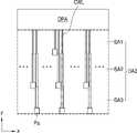
도 1을 참조하면, 표시 장치(1)는 표시영역(DA)과 표시영역(DA) 외측의 주변영역(DPA)을 포함한다. 표시영역(DA)은 제1표시영역(DA1) 및 제2표시영역(DA2)를 포함할 수 있다. 제1표시영역(DA1)은 제2표시영역(DA2)을 적어도 일부 둘러싸도록 배치될 수 있다. 제1표시영역(DA1)은 메인 표시영역일 수 있으며, 제2표시영역(DA2)는 컴포넌트가 배치되는 컴포넌트영역인 동시에 보조 표시영역일 수 있다. 즉, 제1표시영역(DA1)과 제2표시영역(DA2)각각은 개별적으로 또는 함께 이미지를 디스플레이 할 수 있다. 주변영역(DPA)은 표시소자들이 배치되지 않은 일종의 비표시영역일 수 있다. 표시영역(DA)은 주변영역(DPA)에 의해 전체적으로 둘러싸일 수 있다.Referring to FIG. 1 , the
도 1은 제1표시영역(DA1) 안쪽에 컴포넌트가 배치되는 하나의 제2표시영역(DA2)이 위치하는 것을 도시한다. 다른 실시예로, 표시 장치(1)는 2개 이상의 제2표시영역(DA2)들을 가질 수 있고, 복수 개의 제2표시영역(DA2)들의 형상 및 크기는 서로 상이할 수 있다. 표시 장치(1)의 상면에 대략 수직인 방향에서 보았을 시, 제2표시영역(DA2)의 형상은 원형, 타원형, 사각형 등의 다각형, 별 형상 또는 다이아몬드 형상 등 다양한 형상을 가질 수 있다. 그리고 도 1에서는 표시 장치(1)의 상면에 대략 수직인 방향에서 보았을 시 대략 사각형 형상을 갖는 제1표시영역(DA1)의 (+y 방향) 상측 중앙에 제2표시영역(DA2)이 배치된 것으로 도시하고 있으나, 제2표시영역(DA2)은 사각형인 제1표시영역(DA1)의 일측, 예컨대 우상측 또는 좌상측에 배치될 수도 있다.1 shows that one second display area DA2 in which components are disposed is located inside the first display area DA1. In another embodiment, the
표시 장치(1)는 복수의 화소들을 이용하여 이미지를 제공할 수 있다. 상기 화소는 적색, 녹색, 청색을 표시할 수 있는 부화소를 포함할 수 있다. 상기 화소는 복수의 부화소들의 집합으로 구성될 수 있다.The
부화소는 하나의 표시소자의 발광영역으로 구현될 수 있다. 표시소자는 화소전극(애노드), 대향전극(캐소드), 및 화소전극과 대향전극 사이에 배치된 발광층을 포함할 수 있으며, 발광영역은 상기 발광층이 발광되는 영역으로 정의될 수 있다. 일 실시예에서, 발광영역은 화소전극의 가장자리를 덮고 중앙부를 노출시키는 화소정의막의 개구영역으로 정의될 수 있다. 마찬가지로, 부화소는 상기 화소정의막의 개구영역으로 정의될 수 있다.A subpixel may be implemented as a light emitting area of one display device. The display device may include a pixel electrode (anode), a counter electrode (cathode), and a light emitting layer disposed between the pixel electrode and the counter electrode, and the light emitting area may be defined as an area where the light emitting layer emits light. In one embodiment, the light emitting area may be defined as an opening area of the pixel defining layer covering the edge of the pixel electrode and exposing the central portion. Similarly, a subpixel may be defined as an opening area of the pixel defining layer.
발광층은 실질적으로 적색, 녹색, 청색을 표시할 수 있는 유기물질을 포함할 수 있다. 발광층은 제1전극(애노드)와 제2전극(캐소드)가 중첩되는 면적에 따라 실제 발광되는 발광영역 및 발광되지 않는 비발광영역을 포함할 수 있다.The light emitting layer may substantially include organic materials capable of displaying red, green, and blue colors. The light-emitting layer may include a light-emitting area that actually emits light and a non-light-emitting area that does not emit light according to an overlapping area between the first electrode (anode) and the second electrode (cathode).
본 명세서에서, 화소는 부화소와 동일한 개념으로 사용될 수 있다. 즉, 화소는 하나의 표시소자의 발광영역으로 구현될 수 있다. 경우에 따라서, 화소 또는 부화소는 표시소자와 동일한 개념으로 사용될 수 있다.In this specification, a pixel may be used as the same concept as a sub-pixel. That is, a pixel may be implemented as a light emitting area of one display device. In some cases, a pixel or a sub-pixel may be used as the same concept as a display element.
표시 장치(1)는 제1표시영역(DA1)에 배치된 복수 개의 제1화소(Pm)들과 제2표시영역(DA2)에 배치된 복수 개의 제2화소(Pa)들을 이용하여 이미지를 제공할 수 있다.The
제2표시영역(DA2)에는 복수 개의 제2화소(Pa)들이 배치될 수 있다. 복수 개의 제2화소(Pa)들은 빛을 방출하여, 소정의 이미지를 제공할 수 있다. 제2표시영역(DA2)에서 디스플레이 되는 이미지는 보조 이미지로, 제1표시영역(DA1)에서 디스플레이 되는 이미지에 비해서 해상도가 낮을 수 있다.A plurality of second pixels Pa may be disposed in the second display area DA2 . The plurality of second pixels Pa may emit light to provide a predetermined image. The image displayed on the second display area DA2 is an auxiliary image and may have a lower resolution than the image displayed on the first display area DA1.
제2표시영역(DA2)에는 표시 패널의 하부에 전자요소인 컴포넌트(40, 도 2 참조)가 배치될 수 있다. 컴포넌트(40)는 적외선 또는 가시광선 등을 이용하는 카메라로서, 촬상소자를 구비할 수도 있다. 또는 컴포넌트(40)는 태양전지, 플래시(flash), 조도 센서, 근접 센서, 홍채 센서일 수 있다. 또는 컴포넌트(40)는 음향을 수신하는 기능을 가질 수도 있다. 이러한 컴포넌트(40)의 기능이 제한되는 것을 최소화하기 위해, 제2표시영역(DA2)에 배치된 제2화소(Pa)를 구동하는 제2화소회로는 제2표시영역(DA2)에 배치되지 않고, 제3영역(AR3)에 배치될 수 있다. 일 실시예에서, 제3영역(AR3)은 주변영역(DPA)일 수 있다. 다른 실시예에서, 제3영역(AR3)은 제1표시영역(DA1)과 제2표시영역(DA2) 사이에 배치되어 이미지를 제공하는 표시영역일 수 있다.In the second display area DA2 , a component 40 (refer to FIG. 2 ) that is an electronic element may be disposed below the display panel. The
본 발명의 일 실시예에 따른 표시 패널 및 이를 구비하는 표시 장치의 경우, 제2표시영역(DA2)을 통해 광이 투과하도록 할 시, 광 투과율은 약 10% 이상, 보다 바람직하게 40% 이상이거나, 25% 이상이거나 50% 이상이거나, 85% 이상이거나, 90% 이상일 수 있다.In the case of a display panel and a display device including the display panel according to an embodiment of the present invention, when light is transmitted through the second display area DA2, the light transmittance is about 10% or more, more preferably 40% or more, or , 25% or more, or 50% or more, or 85% or more, or 90% or more.
도 2는 일 실시예에 따른 표시 장치(1)의 단면의 일부를 개략적으로 도시하는 단면도이다.2 is a cross-sectional view schematically illustrating a portion of a cross section of a
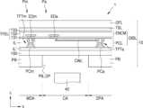
도 2를 참조하면, 표시 장치(1)는 표시 패널(10) 및 상기 표시 패널(10)과 중첩 배치된 컴포넌트(40)을 포함할 수 있다. 표시 패널(10) 상부에는 표시 패널(10)을 보호하는 커버 윈도우(미도시)가 더 배치될 수 있다.Referring to FIG. 2 , the
표시 패널(10)은 컴포넌트(40)와 중첩되는 영역인 제2표시영역(DA2) 및 메인 이미지가 디스플레이되는 제1표시영역(DA1)을 포함한다. 표시 패널(10)은 기판(100), 기판(100) 상의 표시층(DISL), 터치스크린층(TSL), 광학기능층(OFL) 및 기판(100) 하부에 배치된 패널 보호 부재(PB)를 포함할 수 있다.The
표시층(DISL)은 박막트랜지스터(TFTm, TFTa)를 포함하는 회로층(PCL), 표시소자인 발광 소자(light emitting element, EDm, EDa)를 포함하는 표시소자층, 및 박막봉지층(TFEL) 또는 밀봉기판(미도시)과 같은 밀봉부재(ENCM)를 포함할 수 있다. 기판(100)과 표시층(DISL) 사이, 표시층(DISL) 내에는 절연층(IL, IL')이 배치될 수 있다.The display layer DISL includes a circuit layer PCL including thin film transistors TFTm and TFTa, a display element layer including light emitting elements EDm and EDa as display elements, and a thin film encapsulation layer TFEL. Alternatively, a sealing member (ENCM) such as a sealing substrate (not shown) may be included. Insulating layers IL and IL′ may be disposed between the
기판(100)은 유리, 석영, 고분자 수지 등의 절연 물질로 이루어질 수 있다. 기판(100)은 리지드(rigid) 기판이거나 벤딩(bending), 폴딩(folding), 롤링(rolling) 등이 가능한 플렉서블(flexible) 기판일 수 있다.The
표시 패널(10)의 제1표시영역(DA1)에는 제1화소회로(PCm) 및 이와 연결된 제1표시소자(EDm)가 배치될 수 있다. 제1화소회로(PCm)은 적어도 하나의 박막트랜지스터(TFTm)을 포함하며, 제1표시소자(EDm)의 발광을 제어할 수 있다. 제1화소(Pm)는 제1표시소자(EDm)의 발광에 의해서 구현될 수 있다.A first pixel circuit PCm and a first display element EDm connected thereto may be disposed in the first display area DA1 of the
표시 패널(10)의 제2표시영역(DA2)에는 제2표시소자(EDa)가 배치되어 제2화소(Pa)를 구현할 수 있다. 제2표시영역(DA2)은 보조 표시영역으로, 제2표시영역(DA2)의 해상도는 제1표시영역(DA1) 보다 작을 수 있다. 즉, 제2표시영역(DA2)에 배치된 제2표시소자(EDa)들의 단위 면적당 개수는 제1표시영역(DA1)에 배치된 제1표시소자(EDm)들의 단위 면적 당 개수보다 작을 수 있다.The second display element EDA is disposed in the second display area DA2 of the
본 실시예에서, 제2표시소자(EDa)를 구동하는 제2화소회로(PCa)는 제2표시영역(DA2)에 배치되지 않고, 제2표시영역(DA2)의 외부에 배치될 수 있다. 일 실시예로서, 제2화소회로(PCa)는 제2표시영역(DA2)에 배치되지 않고, 주변영역(DPA)에 배치될 수 있다. 다른 실시예로서, 제2화소회로(PCa)는 제1표시영역(DA1)과 제2표시영역(DA2)의 사이에 배치되는 제3표시영역에 배치될 수 있는 등 다양한 변형이 가능할 수 있다. 즉, 제2화소회로(PCa)는 제2표시소자(EDa)와 중첩하지 않게 배치될 수 있다.In this embodiment, the second pixel circuit PCa driving the second display element EDA is not disposed in the second display area DA2 but may be disposed outside the second display area DA2. As an example, the second pixel circuit PCa may not be disposed in the second display area DA2 but may be disposed in the peripheral area DPA. As another embodiment, the second pixel circuit PCa may be disposed in a third display area disposed between the first display area DA1 and the second display area DA2, and various modifications may be possible. That is, the second pixel circuit PCa may be disposed not to overlap with the second display element EDA.
제2화소회로(PCa)는 적어도 하나의 박막트랜지스터(TFTa)를 포함하며, 연결배선(CWL)에 의해서 제2표시소자(EDa)와 전기적으로 연결될 수 있다. 제2화소회로(PCa)는 제2표시소자(EDa)의 발광을 제어할 수 있다. 제2화소(Pa)는 제2표시소자(EDa)의 발광에 의해서 구현될 수 있다.The second pixel circuit PCa includes at least one thin film transistor TFTa, and may be electrically connected to the second display element EDA through the connection line CWL. The second pixel circuit PCa may control light emission of the second display element EDA. The second pixel Pa may be implemented by light emission from the second display element EDA.
또한, 제2표시영역(DA2)은 컴포넌트(40)로부터 방출되는 빛/신호 나 컴포넌트(40)로 입사되는 빛/신호가 투과(transmission)되는 투과 영역을 포함할 수 있다. 제2표시영역(DA2)에서 투과 영역은 제2표시소자(EDa)의 화소전극(애노드)이 배치되지 않는 나머지 영역일 수 있다. 투과 영역은 제2표시소자(EDa)가 발광되는 영역 이외의 영역일 수 있다. 투과 영역은 제2화소(Pa)들 사이의 영역을 포함할 수 있다. 투과 영역은 제2표시소자(EDa)들 사이의 영역을 포함할 수 있다.Also, the second display area DA2 may include a transmission area through which light/signals emitted from the
투과 영역에는 절연층(IL, IL')에 포함될 수 있는 버퍼층, 게이트절연층 등의 무기절연막이 배치될 수 있다. 투과 영역에는 절연층(IL, IL')에 포함될 수 있는 유기절연막이 포함될 수 있다. 투과 영역에는 대향전극(캐소드)가 배치될 수 있다. 투과 영역에는 박막봉지층(TFEL)의 무기봉지층 및/또는 유기봉지층이 배치될 수 있다. 투과 영역에는 금속 및/또는 투명 전도성 물질로 형성된 배선이 배치될 수 있다. 투과 영역에는 기판(100), 편광판 및 접착제, 윈도우, 패널 보호 부재(PB)가 배치될 수 있다.An inorganic insulating layer such as a buffer layer or a gate insulating layer that may be included in the insulating layers IL and IL' may be disposed in the transmission region. An organic insulating layer that may be included in the insulating layers IL and IL' may be included in the transmission region. A counter electrode (cathode) may be disposed in the transmission region. An inorganic encapsulation layer and/or an organic encapsulation layer of the thin film encapsulation layer TFEL may be disposed in the transmission region. A wiring made of metal and/or a transparent conductive material may be disposed in the transmission area. The
제2표시영역(DA2)에는 제2표시소자(EDa)와 연결배선(CWL)만 배치되고, 제2표시영역(DA2)에 배치된 제2표시소자(EDa)의 면적당 개수는 제1표시영역(DA1)에 배치된 제1표시소자(EDm)의 면적당 개수보다 적게 구비되는 바, 제2표시영역(DA2)의 광 투과율은 높게 구비될 수 있다.In the second display area DA2, only the second display elements EDA and the connection line CWL are disposed, and the number per area of the second display elements EDA disposed in the second display area DA2 is equal to the number of second display elements EDA disposed in the first display area DA2 Since the number per area of the first display device EDm disposed in DA1 is less than that, the light transmittance of the second display area DA2 may be high.
표시소자인 제1표시소자(EDm) 및 제2표시소자(EDa)는 박막봉지층(TFEL)으로 커버되거나, 밀봉기판으로 커버될 수 있다. 일부 실시예에서, 박막봉지층(TFEL)은 도 2에 도시된 바와 같이 적어도 하나의 무기봉지층 및 적어도 하나의 유기봉지층을 포함할 수 있다. 일 실시예로, 박막봉지층(TFEL)은 제1 및 제2무기봉지층(131, 133) 및 이들 사이의 유기봉지층(132)을 포함할 수 있다.The display elements, the first display element EDm and the second display element EDA, may be covered with the thin film encapsulation layer TFEL or covered with a sealing substrate. In some embodiments, the thin film encapsulation layer TFEL may include at least one inorganic encapsulation layer and at least one organic encapsulation layer as shown in FIG. 2 . As an example, the thin film encapsulation layer TFEL may include first and second inorganic encapsulation layers 131 and 133 and an
제1무기봉지층(131) 및 제2무기봉지층(133)은 실리콘산화물(SiO2), 실리콘질화물(SiNx), 실리콘산질화물(SiOxNy), 알루미늄산화물(Al2O3), 티타늄산화물(TiO2), 탄탈산화물(Ta2O5), 하프늄산화물(HfO2)과 같은 하나 이상의 무기 절연물을 포함할 수 있으며, 화학기상증착법(CVD) 등에 의해 형성될 수 있다. 유기봉지층(132)은 폴리머(polymer)계열의 소재를 포함할 수 있다. 폴리머 계열의 소재로는 실리콘계 수지, 아크릴계 수지, 에폭시계 수지, 폴리이미드 및 폴리에틸렌 등을 포함할 수 있다.The first
제1무기봉지층(131), 유기봉지층(132) 및 제2무기봉지층(133)은 제1표시영역(DA1) 및 제2표시영역(DA2)을 커버하도록 일체로 형성될 수 있다.The first
표시 요소인 제1표시소자(EDm) 및 제2표시소자(EDa)가 밀봉기판(미도시)으로 밀봉되는 경우, 밀봉기판은 표시 요소를 사이에 두고 기판(100)과 마주보도록 배치될 수 있다. 밀봉기판과 표시 요소 사이에는 갭이 존재할 수 있다. 밀봉기판은 글래스를 포함할 수 있다. 기판(100)과 밀봉기판 사이에는 프릿(frit) 등으로 이루어진 실런트가 배치되며, 실런트는 전술한 주변영역(DPA)에 배치될 수 있다. 주변영역(DPA)에 배치된 실런트는 표시영역(DA)을 둘러싸면서 측면을 통해 수분이 침투하는 것을 방지할 수 있다.When the first display element EDm and the second display element EDA, which are display elements, are sealed with a sealing substrate (not shown), the sealing substrate may be disposed to face the
터치스크린층(TSL)은 외부의 입력, 예컨대 터치 이벤트에 따른 좌표정보를 획득할 수 있다. 터치스크린층(TSL)은 터치전극 및 터치전극과 연결된 터치 배선들을 포함할 수 있다. 터치스크린층(TSL)은 자기 정전 용량 방식 또는 상호 정전 용량 방식으로 외부 입력을 감지할 수 있다.The touch screen layer TSL may acquire coordinate information according to an external input, for example, a touch event. The touch screen layer TSL may include touch electrodes and touch wires connected to the touch electrodes. The touch screen layer (TSL) may sense an external input using a self-capacitance method or a mutual capacitance method.
터치스크린층(TSL)은 박막봉지층(TFEL) 상에 형성될 수 있다. 또는, 터치스크린층(TSL)은 터치기판 상에 별도로 형성된 후 광학 투명 접착제(OCA)와 같은 점착층을 통해 박막봉지층(TFEL) 상에 결합될 수 있다. 일 실시예로서, 터치스크린층(TSL)은 박막봉지층(TFEL) 바로 위에 직접 형성될 수 있으며, 이 경우 점착층은 터치스크린층(TSL)과 박막봉지층(TFEL) 사이에 개재되지 않을 수 있다.The touch screen layer TSL may be formed on the thin film encapsulation layer TFEL. Alternatively, the touch screen layer TSL may be separately formed on the touch substrate and then bonded to the thin film encapsulation layer TFEL through an adhesive layer such as an optically clear adhesive (OCA). As an example, the touch screen layer TSL may be formed directly on the thin film encapsulation layer TFEL, and in this case, the adhesive layer may not be interposed between the touch screen layer TSL and the thin film encapsulation layer TFEL. there is.
광학기능층(OFL)은 반사 방지층을 포함할 수 있다. 반사 방지층은 외부에서 표시 장치(1)를 향해 입사하는 빛(외부광)의 반사율을 감소시킬 수 있다. 일부 실시예에서, 광학기능층(OFL)은 편광 필름일 수 있다. 일부 실시예에서, 광학기능층(OFL)은 블랙매트릭스와 컬러필터들을 포함하는 필터 플레이트로 구비될 수 있다.The optical functional layer (OFL) may include an antireflection layer. The antireflection layer may reduce reflectance of light (external light) incident toward the
패널 보호 부재(PB)는 기판(100)의 하부에 부착되어, 기판(100)을 지지하고 보호하는 역할을 할 수 있다. 패널 보호 부재(PB)는 제2표시영역(DA2)에 대응하는 개구(PB_OP)를 구비할 수 있다. 패널 보호 부재(PB)에 개구(PB_OP)를 구비함으로써, 제2표시영역(DA2)의 광 투과율을 향상시킬 수 있다. 패널 보호 부재(PB)는 폴리에틸렌 테레프탈레이트(polyethyeleneterepthalate, PET) 또는 폴리이미드(polyimide, PI)를 포함하여 구비될 수 있다.The panel protecting member PB may be attached to the lower portion of the
제2표시영역(DA2)의 면적은 컴포넌트(40)가 배치되는 면적에 비해서 크게 구비될 수 있다. 이에 따라, 패널 보호 부재(PB)에 구비된 개구(PB_OP)의 면적은 상기 제2표시영역(DA2)의 면적과 일치하지 않을 수 있다. 그러나, 본 발명은 이에 한정되지 않는다. 예컨대, 패널 보호 부재(PB)는 개구(PB_OP)를 구비하지 않고, 제2표시영역(DA2)에 대응하여 연속적으로 배치될 수 있다.The area of the second display area DA2 may be larger than the area where the
또한, 제2표시영역(DA2)에는 복수의 컴포넌트(40)가 배치될 수 있다. 상기 복수의 컴포넌트(40)는 서로 기능을 달리할 수 있다. 예컨대, 복수의 컴포넌트(40) 는 카메라(촬상소자), 태양전지, 플래시(flash), 근접 센서, 조도 센서, 홍채 센서 중 적어도 두 개를 포함할 수 있다.In addition, a plurality of
도 3은 일 실시예에 따라 도 1의 표시 장치에 포함될 수 있는 표시 패널을 개략적으로 나타내는 평면도이다.FIG. 3 is a plan view schematically illustrating a display panel that may be included in the display device of FIG. 1 according to an exemplary embodiment.
도 3을 참조하면, 표시 패널(10)을 이루는 각종 구성 요소들은 기판(100) 상에 배치된다. 기판(100)은 표시영역(DA) 및 표시영역(DA)을 둘러싸는 주변영역(DPA)을 포함한다. 표시영역(DA)은 메인 이미지가 디스플레이 되는 제1표시영역(DA1)과, 보조 이미지가 디스플레이 되는 제2표시영역(DA2)을 포함한다. 보조 이미지는 메인 이미지와 함께 하나의 전체 이미지를 형성할 수도 있고, 보조 이미지는 메인 이미지로부터 독립된 이미지일 수도 있다.Referring to FIG. 3 , various components constituting the
제1표시영역(DA1)에는 복수의 제1화소(Pm)들이 배치된다. 제1화소(Pm)들은 각각 유기발광다이오드(OLED)와 같은 표시소자로 구현될 수 있다. 상기 제1화소(Pm)를 구동하는 제1화소회로(PCm)는 제1표시영역(DA1)에 배치되며, 제1화소회로(PCm)는 제1화소(Pm)와 중첩되어 배치될 수 있다. 각 제1화소(Pm)는 예컨대 적색, 녹색, 청색 또는 백색의 광을 방출할 수 있다. 제1표시영역(DA1)은 밀봉부재로 커버되어, 외기 또는 수분 등으로부터 보호될 수 있다.A plurality of first pixels Pm are disposed in the first display area DA1. Each of the first pixels Pm may be implemented as a display device such as an organic light emitting diode (OLED). The first pixel circuit PCm driving the first pixel Pm is disposed in the first display area DA1, and the first pixel circuit PCm may overlap the first pixel Pm. . Each of the first pixels Pm may emit, for example, red, green, blue, or white light. The first display area DA1 may be covered with a sealing member and may be protected from external air or moisture.
제2표시영역(DA2)은 전술한 바와 같이 제1표시영역(DA1)의 일측에 위치거나, 표시영역(DA)의 내측에 배치되어 제1표시영역(DA1)에 의해 둘러싸일 수 있다. 제2표시영역(DA2)에는 복수의 제2화소(Pa)들이 배치된다. 복수개의 제2화소(Pa)들은 각각 유기발광다이오드와 같은 표시소자에 의해서 구현될 수 있다. 상기 제2화소(Pa)를 구동하는 제2화소회로(PCa)는 제2표시영역(DA2)과 가까운 주변영역(DPA)에 배치될 수 있다. 예컨대, 제2표시영역(DA2)이 표시영역(DA)의 상측에 배치되는 경우, 제2화소회로(PCa)는 주변영역(DPA)의 상측에 배치될 수 있다. 제2화소회로(PCa)와 제2화소(Pa)를 구현하는 표시소자는 y 방향으로 연장되는 연결배선(CWL)에 의해 연결될 수 있다. 각 제2화소(Pa)는 예컨대, 적색, 녹색, 청색 또는 백색의 광을 방출할 수 있다. 제2표시영역(DA2)은 밀봉부재로 커버되어, 외기 또는 수분 등으로부터 보호될 수 있다.As described above, the second display area DA2 may be located on one side of the first display area DA1 or may be disposed inside the display area DA and surrounded by the first display area DA1. A plurality of second pixels Pa are disposed in the second display area DA2 . Each of the plurality of second pixels Pa may be implemented by a display element such as an organic light emitting diode. The second pixel circuit PCa driving the second pixel Pa may be disposed in the peripheral area DPA close to the second display area DA2. For example, when the second display area DA2 is disposed above the display area DA, the second pixel circuit PCa may be disposed above the peripheral area DPA. The second pixel circuit PCa and the display device implementing the second pixel Pa may be connected by a connection wire CWL extending in the y direction. Each second pixel Pa may emit, for example, red, green, blue, or white light. The second display area DA2 may be covered with a sealing member and may be protected from outside air or moisture.
제2표시영역(DA2)의 해상도는 제1표시영역(DA1)의 해상도의 약 1/2, 3/8, 1/3, 1/4, 2/9, 1/8, 1/9, 1/16 등일 수 있다. 예컨대 제1표시영역(DA1)의 해상도는 약 400ppi 이상이고, 제2표시영역(DA2)의 해상도는 약 200ppi 또는 약 100ppi 일 수 있다.The resolution of the second display area DA2 is approximately 1/2, 3/8, 1/3, 1/4, 2/9, 1/8, 1/9, 1 of the resolution of the first display area DA1. /16, etc. For example, the resolution of the first display area DA1 may be about 400 ppi or more, and the resolution of the second display area DA2 may be about 200 ppi or about 100 ppi.
화소(Pm, Pa)들을 구동하는 화소회로들 각각은 주변영역(DPA)에 배치된 외곽회로들과 전기적으로 연결될 수 있다. 주변영역(DPA)에는 제1 스캔 구동회로(SDRV1), 제2 스캔 구동회로(SDRV2), 단자부(PAD), 구동전압 공급라인(11) 및 공통전압 공급라인(13)이 배치될 수 있다.Each of the pixel circuits driving the pixels Pm and Pa may be electrically connected to outer circuits disposed in the peripheral area DPA. A first scan driving circuit SDRV1 , a second scan driving circuit SDRV2 , a terminal part PAD, a driving
제1 스캔 구동회로(SDRV1)는 메인 스캔선(SLm)을 제1화소(Pm)들을 구동하는 제1화소회로(PCm)들 각각에 스캔 신호를 인가할 수 있다. 제1 스캔 구동회로(SDRV1)는 메인 발광 제어선(ELm)을 통해 각 화소회로에 발광 제어 신호를 인가할 수 있다. 제2 스캔 구동회로(SDRV2)는 제1표시영역(DA1)을 중심으로 제1 스캔 구동회로(SDRV1)의 반대편에 위치할 수 있으며, 제1 스캔 구동회로(SDRV1)와 대략 평행할 수 있다. 제1표시영역(DA1)의 제1화소(Pm)들의 화소회로 중 일부는 제1 스캔 구동회로(SDRV1)와 전기적으로 연결될 수 있고, 나머지는 제2 스캔 구동회로(SDRV2)에 전기적으로 연결될 수 있다.The first scan driving circuit SDRV1 may apply a scan signal to each of the first pixel circuits PCm driving the first pixels Pm through the main scan line SLm. The first scan driving circuit SDRV1 may apply an emission control signal to each pixel circuit through the main emission control line ELm. The second scan driving circuit SDRV2 may be positioned on the opposite side of the first scan driving circuit SDRV1 with respect to the first display area DA1, and may be substantially parallel to the first scan driving circuit SDRV1. Some of the pixel circuits of the first pixels Pm of the first display area DA1 may be electrically connected to the first scan driving circuit SDRV1, and the rest may be electrically connected to the second scan driving circuit SDRV2. there is.
단자부(PAD)는 기판(100)의 일측에 배치될 수 있다. 단자부(PAD)는 절연층에 의해 덮이지 않고 노출되어 표시 회로 보드(30)와 연결된다. 표시 회로 보드(30)에는 표시 구동부(32)가 배치될 수 있다.The terminal part PAD may be disposed on one side of the
표시 구동부(32)는 제1 스캔 구동회로(SDRV1)와 제2 스캔 구동회로(SDRV2)에 전달하는 제어 신호를 생성할 수 있다. 표시 구동부(32)는 데이터 신호를 생성하며, 생성된 데이터 신호는 팬아웃 배선(FW) 및 팬아웃 배선(FW)과 연결된 메인 데이터선(DLm)을 통해 제1화소회로(PCm)들에 전달될 수 있다.The
표시 구동부(32)는 구동전압 공급라인(11)에 구동전압(ELVDD)을 공급할 수 있고, 공통전압 공급라인(13)에 공통전압(ELVSS)을 공급할 수 있다. 구동전압(ELVDD)은 구동전압 공급라인(11)과 연결된 구동전압선(PL)을 통해 화소들(Pm, Pa)의 화소회로에 인가되고, 공통전압(ELVSS)은 공통전압 공급라인(13)과 연결되어 표시소자의 대향전극에 인가될 수 있다.The
구동전압 공급라인(11)은 제1표시영역(DA1)의 하측에서 x 방향으로 연장되어 구비될 수 있다. 공통전압 공급라인(13)은 루프 형상에서 일측이 개방된 형상을 가져, 제1표시영역(DA1)을 부분적으로 둘러쌀 수 있다.The driving
도 3에서는 제2표시영역(DA2)이 하나인 경우를 도시하고 있으나, 제2표시영역(DA2)은 복수로 구비될 수 있다. 이 경우, 복수의 제2표시영역(DA2)은 서로 이격되어 배치되며, 하나의 제2표시영역(DA2)에 대응하여 제1카메라가 배치되고, 다른 제2표시영역(DA2)에 대응하여 제2카메라가 배치될 수 있다. 또는, 하나의 제2표시영역(DA2)에 대응하여 카메라가 배치되고, 다른 제2표시영역(DA2)에 대응하여 적외선 센서가 배치될 수 있다. 복수의 제2표시영역(DA2)의 형상 및 크기는 서로 다르게 구비될 수 있다.Although FIG. 3 shows a case where there is only one second display area DA2, a plurality of second display areas DA2 may be provided. In this case, the plurality of second display areas DA2 are spaced apart from each other, and the first camera is disposed corresponding to one second display area DA2 and the second camera is disposed corresponding to the other second display area DA2. 2 cameras can be placed. Alternatively, a camera may be disposed corresponding to one second display area DA2 and an infrared sensor may be disposed corresponding to another second display area DA2. The plurality of second display areas DA2 may have different shapes and sizes.
한편, 제2표시영역(DA2)은 원형, 타원형, 다각형 또는 비정형 형상으로 구비될 수 있다. 일부 실시예에서, 제2표시영역(DA2)은 팔각형으로 구비될 수 있다. 제2표시영역(DA2)은 사각형, 육각형 등 다양한 형태의 다각형으로 구비될 수 있다. 제2표시영역(DA2)은 제1표시영역(DA1)에 의해서 둘러싸일 수 있다.Meanwhile, the second display area DA2 may have a circular, elliptical, polygonal or irregular shape. In some embodiments, the second display area DA2 may have an octagonal shape. The second display area DA2 may be provided in various shapes of polygons such as a quadrangle and a hexagon. The second display area DA2 may be surrounded by the first display area DA1.
도 4는 일 실시예에 따라 도 1의 표시 장치에 포함될 수 있는 표시 패널을 개략적으로 나타내는 평면도이다. 도 5는 도 4의 표시 패널의 개략적인 단면도이다. 도 4 및 도 5에 있어서, 도 2 및 도 3과 동일한 참조부호는 동일한 부재를 일컫는 바, 이들의 중복 설명은 생략한다.FIG. 4 is a plan view schematically illustrating a display panel that may be included in the display device of FIG. 1 according to an exemplary embodiment. 5 is a schematic cross-sectional view of the display panel of FIG. 4 . In FIGS. 4 and 5, the same reference numerals as those in FIGS. 2 and 3 denote the same members, and duplicate descriptions thereof are omitted.
도 4 및 도 5를 참조하면, 기판(100)의 표시영역(DA)은 제1표시영역(DA1), 제2표시영역(DA2), 및 상기 제1표시영역(DA1) 및 제2표시영역(DA2) 사이에 위치하는 제3표시영역(DA3)을 포함한다.4 and 5, the display area DA of the
제1표시영역(DA1)은 메인 이미지가 디스플레이되는 영역일 수 있다. 제2표시영역(DA2) 및 제3표시영역(DA3)은 보조 이미지가 디스플레이되는 영역일 수 있다. 보조 이미지는 메인 이미지와 함께 하나의 전체 이미지를 형성할 수도 있고, 보조 이미지는 메인 이미지로부터 독립된 이미지일 수도 있다.The first display area DA1 may be an area where the main image is displayed. The second display area DA2 and the third display area DA3 may be areas where auxiliary images are displayed. The auxiliary image may form one whole image together with the main image, and the auxiliary image may be an image independent of the main image.
제3표시영역(DA3)은 제2표시영역(DA2)의 적어도 일측에 배치될 수 있다. 도 4에 있어서, 제3표시영역(DA3)은 제2표시영역(DA2)의 좌우에 배치되는 것으로 도시하고 있으나, 본 발명은 이에 한정되지 않는다. 제3표시영역(DA3)은 제2표시영역(DA2)의 상하에 배치되거나 제2표시영역(DA2)을 둘러싸도록 배치될 수 있는 등 다양한 변형이 가능하다.The third display area DA3 may be disposed on at least one side of the second display area DA2. In FIG. 4 , the third display area DA3 is illustrated as disposed on the left and right sides of the second display area DA2, but the present invention is not limited thereto. The third display area DA3 may be arranged above and below the second display area DA2 or may be arranged to surround the second display area DA2, and various modifications are possible.
제3표시영역(DA3)에는 복수의 제3화소(Pt)들이 배치된다. 제3화소(Pt)들은 각각 유기발광다이오드(OLED)와 같은 표시소자로 구현될 수 있다. 상기 제3화소(Pt)를 구동하는 제3화소회로(PCt)는 제3표시영역(DA3)에 배치되며, 제3화소회로(PCt)는 제3화소(Pt)와 중첩되어 배치될 수 있다. 각 제3화소(Pt)는 예컨대 적색, 녹색, 청색 또는 백색의 광을 방출할 수 있다. 제3표시영역(DA3)은 밀봉부재로 커버되어, 외기 또는 수분 등으로부터 보호될 수 있다.A plurality of third pixels Pt are disposed in the third display area DA3. Each of the third pixels Pt may be implemented as a display device such as an organic light emitting diode (OLED). The third pixel circuit PCt driving the third pixel Pt is disposed in the third display area DA3, and the third pixel circuit PCt may overlap the third pixel Pt. . Each of the third pixels Pt may emit, for example, red, green, blue, or white light. The third display area DA3 is covered with a sealing member and can be protected from outside air or moisture.
제3표시영역(DA3)에는 제2표시영역(DA2)의 제2화소(Pa)를 구동하는 제2화소회로(PCa)가 배치된다. 즉, 제3표시영역(DA3)는 전술한 제3영역(AR3)로 기능할 수 있다. 제3표시영역(DA3)에는 제2화소회로(PCa)와 제3화소회로(PCt)가 교번적으로 배치될 수 있다. 제2화소회로(PCa)와 제2화소(Pa)를 구현하는 제2표시소자(EDa)는 x 방향으로 연장되는 연결배선(CWL)에 의해 연결될 수 있다.A second pixel circuit PCa driving the second pixel Pa of the second display area DA2 is disposed in the third display area DA3. That is, the third display area DA3 may function as the aforementioned third area AR3. In the third display area DA3, the second pixel circuit PCa and the third pixel circuit PCt may be alternately disposed. The second pixel circuit (PCa) and the second display element (EDa) implementing the second pixel (Pa) may be connected by a connection wire (CWL) extending in the x direction.
제3표시영역(DA3)의 해상도는 제2표시영역(DA2)의 해상도와 동일하게 구비될 수 있다. 또는 제3표시영역(DA3)의 해상도는 제2표시영역(DA2)의 해상도보다 크고 제1표시영역(DA1)의 해상도보다 작게 구비될 수 있다.The resolution of the third display area DA3 may be the same as that of the second display area DA2. Alternatively, the resolution of the third display area DA3 may be greater than that of the second display area DA2 and smaller than that of the first display area DA1.
예컨대, 제3표시영역(DA3)의 해상도는 제1표시영역(DA1)의 해상도의 약 1/2, 3/8, 1/3, 1/4, 2/9, 1/8, 1/9, 1/16 등일 수 있다. 예컨대, 제1표시영역(DA1)의 해상도는 약 400ppi 이상이고, 제2표시영역(DA2) 및 제3표시영역(DA3)의 해상도는 약 200ppi 또는 약 100ppi 일 수 있다.For example, the resolution of the third display area DA3 is about 1/2, 3/8, 1/3, 1/4, 2/9, 1/8, 1/9 of the resolution of the first display area DA1. , 1/16, etc. For example, the resolution of the first display area DA1 may be about 400 ppi or higher, and the resolutions of the second display area DA2 and the third display area DA3 may be about 200 ppi or about 100 ppi.
일 실시예에서, 제1화소회로(PCm), 제2화소회로(PCa), 및 제3화소회로(PCt)는 동일하게 구비될 수 있다. 그러나, 본 발명은 이에 한정되지 않는다. 제1화소회로(PCm), 제2화소회로(PCa), 및 제3화소회로(PCt)는 다르게 구비될 수 있는 등 다양한 변형이 가능하다.In an exemplary embodiment, the first pixel circuit PCm, the second pixel circuit PCa, and the third pixel circuit PCt may be identically provided. However, the present invention is not limited thereto. The first pixel circuit (PCm), the second pixel circuit (PCa), and the third pixel circuit (PCt) may be provided differently, and various modifications are possible.
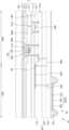
도 6은 본 발명의 일 실시예에 따른 표시 패널(10)의 일부를 나타낸 개략적인 단면도로, 제1표시영역(DA1)의 일부를 개략적으로 도시한 단면도이다.6 is a schematic cross-sectional view of a portion of the
도 6을 참조하면, 표시 패널(10)의 제1표시영역(DA1)에는 기판(100) 상에 제1화소회로(PCm)이 배치되고, 상기 제1화소회로(PCm)과 연결된 제1표시소자로써 유기발광다이오드(OLED)가 배치될 수 있다. 또한, 기판(100)과 제1화소회로(PCm) 사이에는 하부 도전층(BML)이 더 배치될 수 있다.Referring to FIG. 6 , in the first display area DA1 of the
본 실시예에 따른 제1화소회로(PCm)는 실리콘 반도체를 포함하는 제1박막트랜지스터(TFT1), 및 산화물 반도체를 포함하는 제2박막트랜지스터(TFT2)를 포함한다. 제1화소회로(PCm)은 스토리지 커패시터(Cst)를 더 포함할 수 있다.The first pixel circuit PCm according to the present embodiment includes a first thin film transistor TFT1 including a silicon semiconductor and a second thin film transistor TFT2 including an oxide semiconductor. The first pixel circuit PCm may further include a storage capacitor Cst.
제1박막트랜지스터(TFT1)는 실리콘 반도체를 포함하는 제1반도체층(AS1), 제1반도체층(AS1)과 절연된 제1게이트전극(G1)을 포함한다. 제1박막트랜지스터(TFT1)은 제1반도체층(AS1)과 연결된 제1소스전극(SE1) 및/또는 제1드레인전극(DE1)을 포함할 수 있다. 제1박막트랜지스터(TFT1)는 구동 박막트랜지스터로서 기능할 수 있다.The first thin film transistor TFT1 includes a first semiconductor layer AS1 including a silicon semiconductor and a first gate electrode G1 insulated from the first semiconductor layer AS1. The first thin film transistor TFT1 may include a first source electrode SE1 and/or a first drain electrode DE1 connected to the first semiconductor layer AS1. The first thin film transistor TFT1 may function as a driving thin film transistor.
제2박막트랜지스터(TFT2)는 산화물 반도체를 포함하는 제2반도체층(AO2), 제2반도체층(AO2)과 절연된 제2게이트전극(G2)을 포함한다. 제2박막트랜지스터(TFT2)는 제2반도체층(AO2)과 연결된 제2소스전극(SE2) 및/또는 제2드레인전극(DE2)을 포함할 수 있다. 제2박막트랜지스터(220)는 스위칭 박막트랜지스터로서 기능할 수 있다. 또는 제2박막트랜지스터(220)는 구동 박막트랜지스터가 아닌 다른 어떠한 박막트랜지스터일 수도 있다.The second thin film transistor TFT2 includes a second semiconductor layer AO2 including an oxide semiconductor and a second gate electrode G2 insulated from the second semiconductor layer AO2. The second thin film transistor TFT2 may include a second source electrode SE2 and/or a second drain electrode DE2 connected to the second semiconductor layer AO2. The second thin film transistor 220 may function as a switching thin film transistor. Alternatively, the second thin film transistor 220 may be any thin film transistor other than the driving thin film transistor.
일 실시예에 따르면, 구동 박막트랜지스터로서 기능하는 제1박막트랜지스터(TFT1)의 제1반도체층(AS1)은 신뢰성이 우수한 다결정 실리콘으로 구성하고, 스위칭 박막트랜지스터에 대응되는 제2박막트랜지스터(TFT2)의 제2반도체층(AO2)은 누설전류가 적은 산화물 반도체로 구성할 수 있다.According to an embodiment, the first semiconductor layer AS1 of the first thin film transistor TFT1 functioning as a driving thin film transistor is made of highly reliable polycrystalline silicon, and the second thin film transistor TFT2 corresponding to the switching thin film transistor The second semiconductor layer AO2 of may be formed of an oxide semiconductor with low leakage current.
구체적으로, 디스플레이소자의 밝기에 직접적으로 영향을 미치는 구동 박막 트랜지스터의 경우 높은 신뢰성을 갖는 다결정 실리콘으로 구성된 반도체층을 포함하도록 구성하며, 이를 통해 고해상도의 표시 장치를 구현할 수 있다.Specifically, in the case of a driving thin film transistor that directly affects the brightness of a display device, it is configured to include a semiconductor layer made of polycrystalline silicon having high reliability, and through this, a high-resolution display device can be implemented.
산화물 반도체를 포함하는 박막트랜지스터는 높은 캐리어 이동도(high carrier mobility) 및 낮은 누설전류를 가져 구동 시간이 길더라도 전압 강하가 크지 않는 특성이 있다. 이는 산화물 반도체를 포함하는 박막트랜지스터는 저주파 구동 시에도 전압 강하에 따른 화상의 색상 변화가 크지 않으므로, 저주파 구동이 가능함을 의미한다. 따라서, 구동 회로가 산화물 반도체로 구성된 반도체층을 포함하는 박막 트랜지스터를 포함하는 경우, 구동 회로에 포함된 모든 박막트랜지스터들이 다결정 실리콘으로 구성된 반도체층을 포함하는 경우보다 소비 전력이 낮아질 수 있다.A thin film transistor including an oxide semiconductor has high carrier mobility and low leakage current, so that even if the driving time is long, the voltage drop is not large. This means that the thin film transistor including the oxide semiconductor can be driven at a low frequency because the color change of the image due to the voltage drop is not large even when the thin film transistor is driven at a low frequency. Accordingly, when the driving circuit includes a thin film transistor including a semiconductor layer made of an oxide semiconductor, power consumption may be lower than when all the thin film transistors included in the driving circuit include a semiconductor layer made of polysilicon.
본 실시예들에 있어서는 구동 박막트랜지스터를 제외한 나머지 박막트랜지스터들 중 적어도 하나가 산화물 반도체로 구성된 활성층을 포함하도록 구성함으로써, 디스플레이 장치의 소비 전력을 감소시킬 수 있다.In the present embodiments, at least one of the thin film transistors other than the driving thin film transistor is configured to include an active layer made of an oxide semiconductor, thereby reducing power consumption of the display device.
또한, 본 실시예에 따른 제1박막트랜지스터(TFT1)의 하부에는 제1박막트랜지스터(TFT1)와 중첩된 하부 도전층(BML)이 배치된다. 하부 도전층(BML)에는 정전압이 인가될 수 있다. 하부 도전층(BML)이 제1박막트랜지스터(TFT1)의 하부에 배치됨에 따라 제1박막트랜지스터(TFT1)은 주변 간섭 신호들의 영향을 적게 받아 신뢰성이 더욱 향상될 수 있다.In addition, a lower conductive layer BML overlapping the first thin film transistor TFT1 is disposed under the first thin film transistor TFT1 according to the present embodiment. A constant voltage may be applied to the lower conductive layer BML. As the lower conductive layer BML is disposed under the first thin film transistor TFT1, the first thin film transistor TFT1 is less affected by neighboring interference signals, and thus reliability can be further improved.
한편, 본 실시예에서는 표시 요소로써 유기발광다이오드가 채용된 것을 예를 들고 있으나, 다른 실시예로 표시 요소로써 무기 발광 소자, 또는 양자점 발광 소자가 채용될 수 있다.Meanwhile, in this embodiment, an organic light emitting diode is employed as a display element, but an inorganic light emitting element or a quantum dot light emitting element may be employed as a display element in another embodiment.
이하, 표시 패널(10)에 포함된 구성들이 적층된 구조에 대해서 설명하도록 한다.Hereinafter, a structure in which components included in the
기판(100)은 유리, 석영, 고분자 수지 등의 절연 물질로 이루어질 수 있다. 기판(100)은 리지드(rigid) 기판이거나 벤딩(bending), 폴딩(folding), 롤링(rolling) 등이 가능한 플렉서블(flexible) 기판일 수 있다. 기판(100)은 상기 물질의 단층 또는 다층구조를 가질 수 있으며, 다층구조의 경우 무기층을 더 포함할 수 있다. 일부 실시예에서, 기판(100)은 유기물/무기물/유기물의 구조를 가질 수 있다.The
버퍼층(111)은 기판(100) 상에 위치하여, 기판(100)의 하부로부터 이물, 습기 또는 외기의 침투를 감소 또는 차단할 수 있고, 기판(100) 상에 평탄면을 제공할 수 있다. 버퍼층(111)은 산화물 또는 질화물과 같은 무기물, 또는 유기물, 또는 유무기 복합물을 포함할 수 있으며, 무기물과 유기물의 단층 또는 다층 구조로 이루어질 수 있다. 일부 실시예에서, 버퍼층(111)은 실리콘산화물(SiO2) 또는 실리콘질화물(SiNX)으로 구비될 수 있다.The
하부 도전층(BML)은 기판(100)과 버퍼층(111) 사이에 배치될 수 있다. 하부 도전층(BML)은 전도성 물질로 구비될 수 있다. 일부 실시예예서, 하부 도전층(BML)은 투명한 전도성 물질로 구비될 수 있다. 예컨대, 하부 도전층(BML)은 인듐주석산화물(ITO; indium tin oxide), 인듐아연산화물(IZO; indium zinc oxide), 아연산화물(ZnO; zinc oxide), 인듐산화물(In2O3: indium oxide), 인듐갈륨산화물(IGO; indium gallium oxide) 또는 알루미늄아연산화물(AZO; aluminum zinc oxide)와 같은 도전성 산화물을 포함할 수 있다. 하부 도전층(BML)은 제1박막트랜지스터(TFT1)과 중첩되어 배치되며, 하부 도전층(BML)에는 정전압이 인가될 수 있다. 기판(100)과 하부 도전층(BML) 사이에는 외기의 침투를 차단하는 배리어층(미도시)이 더 포함될 수 있다. 배리어층은 산화물 또는 질화물과 같은 무기물, 또는 유기물, 또는 유무기 복합물을 포함할 수 있으며, 무기물과 유기물의 단층 또는 다층 구조로 이루어질 수 있다.The lower conductive layer BML may be disposed between the
버퍼층(111) 상에는 실리콘 반도체를 포함하는 제1반도체층(AS1)이 배치되며, 제1반도체층(AS1)은 폴리 실리콘 또는 비정질 실리콘을 포함할 수 있다. 제1반도체층(AS1)은 채널영역과 불순물이 도핑된 소스 영역 및 드레인 영역을 포함할 수 있다.A first semiconductor layer AS1 including a silicon semiconductor is disposed on the
제1반도체층(AS1)을 덮도록 제1게이트절연층(112)이 구비될 수 있다. 제1게이트절연층(112)은 실리콘산화물(SiO2), 실리콘질화물(SiNx), 실리콘산질화물(SiOxNy), 알루미늄산화물(Al2O3), 티타늄산화물(TiO2) 등과 같은 무기 절연물을 포함할 수 있다. 제1게이트절연층(112)은 전술한 무기 절연물을 포함하는 단일층 또는 다층일 수 있다.A first
제1게이트절연층(112) 상부에는 상기 제1반도체층(AS1)과 중첩되도록 제1게이트전극(GE1)이 배치된다. 제1게이트전극(GE1)은 몰리브덴(Mo), 알루미늄(Al), 구리(Cu), 티타늄(Ti) 등을 포함하며 단층 또는 다층으로 이루어질 수 있다. 일 예로, 제1게이트전극(GE1)은 Mo의 단층일 수 있다.A first gate electrode GE1 is disposed on the first
제2게이트절연층(113)은 상기 제1게이트전극(GE1)을 덮도록 구비될 수 있다. 제2게이트절연층(113)은 실리콘산화물(SiO2), 실리콘질화물(SiNx), 실리콘산질화물(SiOxNy), 알루미늄산화물(Al2O3), 티타늄산화물(TiO2), 등과 같은 무기 절연물을 포함할 수 있다. 제2게이트절연층(113)은 전술한 무기 절연물을 포함하는 단일층 또는 다층일 수 있다.A second
제1게이트전극(GE1) 상에는 스토리지 커패시터(Cst)가 중첩되어 형성될 수 있다. 스토리지 커패시터(Cst)는 하부전극(CE1) 및 상부전극(CE2)을 포함한다. 하부전극(CE1)과 상부전극(CE2) 사이에는 제2게이트절연층(113)이 배치될 수 있다. 이 때, 제1게이트전극(GE1)은 제1박막트랜지스터(TFT1)의 게이트전극으로서의 기능뿐만 아니라, 스토리지 커패시터(Cst)의 하부전극(CE1)으로서의 기능도 수행할 수 있다. 즉, 제1게이트전극(G1)과 하부전극(CE1)은 일체(一體)일 수 있다. 제2게이트절연층(113) 상에는 하부전극(CE1)과 적어도 일부 중첩되도록 상부전극(CE2)이 배치된다.A storage capacitor Cst may be overlapped and formed on the first gate electrode GE1 . The storage capacitor Cst includes a lower electrode CE1 and an upper electrode CE2. A second
제2게이트절연층(113) 상에는 제1배선(WL1) 및 하부 게이트전극(BGE)이 배치될 수 있다. 제1배선(WL1)은 제1박막트랜지스터(TFT1) 또는 제2박막트랜지스터(TFT2)에 전달되는 신호를 전달할 수 있다. 하부 게이트전극(BGE)은 제2박막트랜지스터(TFT2)의 제2반도체층(AO2)와 중첩되어 제2박막트랜지스터(TFT2)에 게이트 신호를 인가할 수 있다. 이 경우, 제2박막트랜지스터(TFT2)는 제2반도체층(AO2)의 상부 및 하부에 게이트 전극이 배치되는 이중 게이트 전극 구조를 구비할 수 있다.A first wire WL1 and a lower gate electrode BGE may be disposed on the second
하부 게이트전극(BGE)은 제1배선(WL1)의 일부로 구비될 수 있다. 이 경우, 제1배선(WL1)은 제2박막트랜지스터(TFT2)에 게이트 신호를 전달할 수 있다.The lower gate electrode BGE may be provided as a part of the first wire WL1. In this case, the first wire WL1 may transmit a gate signal to the second thin film transistor TFT2.
제2게이트절연층(113)은 산화물 또는 질화물을 포함하는 무기물을 포함할 수 있다. 예컨대, 제2게이트절연층(113)은 실리콘산화물(SiO2), 실리콘질화물(SiNx), 실리콘산질화물(SiON), 알루미늄산화물(Al2O3), 티타늄산화물(TiO2)등을 포함할 수 있다.The second
제1층간절연층(115)은 상기 상부전극(CE2), 제1배선(WL1) 및 하부 게이트전극(BGE)을 덮도록 형성될 수 있다. 제1층간절연층(115)은 실리콘산화물(SiO2), 실리콘질화물(SiNx), 실리콘산질화물(SiOxNy), 알루미늄산화물(Al2O3), 티타늄산화물(TiO2)등을 포함할 수 있다. 제1층간절연층(115)은 전술한 무기 절연물을 포함하는 단일층 또는 다층일 수 있다.The first
제1층간절연층(115) 상에는 산화물 반도체를 포함하는 제2반도체층(AO2)이 배치될 수 있다. 제2반도체층(AO2)은 채널영역과, 채널영역 양측에 배치된 소스 영역 및 드레인 영역을 포함할 수 있다. 제2반도체층(AO2)은 인듐(In), 갈륨(Ga), 주석(Sn), 지르코늄(Zr), 하프늄(Hf), 티타늄(Ti) 및 아연(Zn)을 포함하는 군에서 선택된 적어도 하나 이상의 물질의 산화물을 포함할 수 있다. 일부 실시예에서, 제2반도체층(AO2)은 ZnO에 인듐(In)과 갈륨(Ga)과 같은 금속이 함유된 IGZO(In-Ga-Zn-O) 반도체일 수 있다.A second semiconductor layer AO2 including an oxide semiconductor may be disposed on the first
제2반도체층(AO2)의 소스영역 및 드레인영역은 산화물 반도체의 캐리어 농도를 조절하여 도전성화하여 형성될 수 있다. 예컨대, 제2반도체층(AO2)의 소스영역 및 드레인영역은 산화물 반도체에 수소(H) 계열 가스, 불소(F) 계열의 가스, 또는 이들의 조합을 이용한 플라즈마 처리를 통해서 캐리어 농도를 증가시킴으로서 형성될 수 있다.The source and drain regions of the second semiconductor layer AO2 may be formed by adjusting the carrier concentration of the oxide semiconductor to make them conductive. For example, the source region and the drain region of the second semiconductor layer AO2 are formed by increasing the carrier concentration through plasma treatment using a hydrogen (H)-based gas, a fluorine (F)-based gas, or a combination thereof in an oxide semiconductor. It can be.
제2반도체층(AO2) 상에는 제2게이트전극(GE2)이 배치되며, 제2반도체층(AO2)과 제2게이트전극(GE3) 사이에는 제2층간절연층(117)이 배치될 수 있다. 제2게이트전극(GE2)은 제2반도체층(AO2)과 중첩되도록 배치되며, 제2층간절연층(117)에 의해서 제2반도체층(AO2)과 절연된다.A second gate electrode GE2 may be disposed on the second semiconductor layer AO2 , and a second
제2층간절연층(117)은 실리콘산화물(SiO2), 실리콘질화물(SiNx), 실리콘산질화물(SiOxNy), 알루미늄산화물(Al2O3), 티타늄산화물(TiO2), 탄탈산화물(Ta2O5), 하프늄산화물(HfO2), 또는 아연산화물(ZnO2)등을 포함할 수 있다. 제2층간절연층(117)은 전술한 무기 절연물을 포함하는 단일층 또는 다층일 수 있다.The second
제2게이트전극(GE2) 상에는 제3층간절연층(119)이 배치되며, 제3층간절연층(119) 상에는 제1반도체층(AS1)과 연결된 제1소스전극(SE1) 및/또는 제1드레인전극(DE1), 제2반도체층(AO2)과 연결된 제2소스전극(SE2) 및/또는 제2드레인전극(DE2)이 배치될 수 있다. 또한, 제3층간절연층(119) 상에는 데이터신호를 전달하기 위한 데이터선, 구동전압을 전달하기 위한 구동전압선이 배치될 수 있다. 상기 제1소스전극(SE1), 제1드레인전극(DE1), 제2소스전극(SE2), 또는 제2드레인전극(DE2)은 이러한 데이터선 또는 구동전압선과 직접 또는 다른 박막트랜지스터를 통해서 연결될 수 있다.A third
제3층간절연층(119)은 실리콘산화물(SiO2), 실리콘질화물(SiNx), 실리콘산질화물(SiOxNy), 알루미늄산화물(Al2O3), 티타늄산화물(TiO2), 탄탈산화물(Ta2O5), 하프늄산화물(HfO2), 또는 아연산화물(ZnO2)등을 포함할 수 있다. 제3층간절연층(119)은 전술한 무기 절연물을 포함하는 단일층 또는 다층일 수 있다.The third
제1소스전극(SE1) 및/또는 제1드레인전극(DE1), 제2소스전극(SE2) 및/또는 제2드레인전극(DE2)은 금속, 전도성 산화물 등 도전성이 높은 물질로 구비될 수 있다. 예컨대, 제1소스전극(SE1) 및/또는 제1드레인전극(DE1), 제2소스전극(SE2) 및/또는 제2드레인전극(DE2)은 알루미늄(Al), 구리(Cu), 티타늄(Ti) 등을 포함한 단층 또는 다층으로 이루어질 수 있다. 일부 실시예에서, 제1소스전극(SE1) 및/또는 제1드레인전극(DE1), 제2소스전극(SE2) 및/또는 제2드레인전극(DE2) 순차적으로 배치된 티타늄, 알루미늄, 및 티타늄(Ti/Al/Ti)의 삼중층으로 구비될 수 있다.The first source electrode SE1 and/or the first drain electrode DE1, the second source electrode SE2, and/or the second drain electrode DE2 may be made of a highly conductive material such as metal or conductive oxide. . For example, the first source electrode SE1 and/or the first drain electrode DE1, the second source electrode SE2 and/or the second drain electrode DE2 may be made of aluminum (Al), copper (Cu), titanium ( Ti) and the like may be made of a single layer or multiple layers. In some embodiments, the first source electrode SE1 and/or the first drain electrode DE1, the second source electrode SE2 and/or the second drain electrode DE2 are sequentially disposed in titanium, aluminum, and titanium. It may be provided with a triple layer of (Ti/Al/Ti).
상기 제1소스전극(SE1) 및/또는 제1드레인전극(DE1), 제2소스전극(SE2) 및/또는 제2드레인전극(DE2) 상에는 유기절연층(120)이 배치된다. 유기절연층(120)은 단층 또는 다층으로 구비될 수 있다. 예컨대, 유기절연층(120)은 제1유기절연층(121), 제2유기절연층(122), 제3유기절연층(123)이 적층되어 구비될 수 있다. 이 경우, 제1유기절연층(121) 상에는 제2배선(WL2), 제2유기절연층(122) 상에는 제3배선(WL3)이 배치될 수 있다. 제2배선(WL2) 및 제3배선(WL3)은 제1화소회로(PCm)에 다양한 신호 및/또는 전압을 전달할 수 있다.An organic insulating
유기절연층(120)은 감광성 폴리이미드, 폴리이미드(polyimide), Polystyrene(PS), 폴리카보네이트(PC), BCB(Benzocyclobutene), HMDSO(Hexamethyldisiloxane), Polymethylmethacrylate(PMMA)나, Polystyrene(PS)과 같은 일반 범용고분자, 페놀계 그룹을 갖는 고분자 유도체, 아크릴계 고분자, 이미드계 고분자, 아릴에테르계 고분자, 아마이드계 고분자, 불소계 고분자, p-자일렌계 고분자, 또는 비닐알콜계 고분자 등을 포함할 수 있다.The organic insulating
또는, 유기절연층(120)은 실록산계 유기물질로 구비될 수 있다. 실록산계 유기물질은 헥사메틸디실록산(Hexamethyldisiloxane), 옥타메틸트리실록산(Octamethyltrisiloxane), 데카메틸테트라실록산(Decamethyltetrasiloxane), 도데카메틸펜타실록산(Dodecamethylpentasiloxane) 및 폴리디메틸실록산(Polydimethylsiloxanes)을 포함할 수 있다. 유기절연층(120)은 박막트랜지스터들을 덮는 보호막 역할을 할 수 있다. 제1유기절연층(121), 제2유기절연층(122), 제3유기절연층(123)은 모두 동일한 물질로 형성되거나, 적어도 하나는 다른 물질로 형성되는 등 다양한 변형이 가능하다.Alternatively, the organic insulating
유기절연층(120) 상에는 화소전극(310), 대향전극(330) 및 그 사이에 개재되며 발광층(320)을 갖는 유기발광다이오드(OLED)가 위치할 수 있다.On the organic insulating
화소전극(310)은 유기절연층(120)에 정의된 콘택홀을 통해 제1드레인전극(DE1)에 연결될 수 있으며, 제1드레인전극(DE1)에 의해 제1박막트랜지스터(TFT1)의 제1드레인영역(D1)에 연결될 수 있다. 화소전극(310)은 제1박막트랜지스터(TFT1)와 직접 연결되거나, 발광을 제어하는 기능을 하는 다른 박막 트랜지스터(미도시)를 경유하여 제1박막트랜지스터(TFT1)와 간접적으로 연결될 수도 있다.The
화소전극(310)은 인듐주석산화물(ITO; indium tin oxide), 인듐아연산화물(IZO; indium zinc oxide), 아연산화물(ZnO; zinc oxide), 인듐산화물(In2O3: indium oxide), 인듐갈륨산화물(IGO; indium gallium oxide) 또는 알루미늄아연산화물(AZO; aluminum zinc oxide)와 같은 도전성 산화물을 포함할 수 있다. 화소전극(310)은 은(Ag), 마그네슘(Mg), 알루미늄(Al), 또는 이들의 화합물을 포함하는 반사막을 포함할 수 있다. 예컨대, 화소전극(310)은 전술한 반사막의 위/아래에 ITO, IZO, ZnO 또는 In2O3로 형성된 막들을 갖는 구조를 가질 수 있다. 이 경우, 화소전극(310)은 ITO/Ag/ITO로 적층된 구조를 가질 수 있다.The
유기절연층(120) 상부에는 화소정의막(125)이 배치될 수 있다. 이 화소정의막(125)은 화소전극(310)의 가장자리를 덮으며, 화소전극(310)의 중앙부가 노출되도록 하는 개구를 가짐으로써 화소를 정의하는 역할을 할 수 있다. 즉, 화소정의막(125)의 개구에 의해서 유기발광다이오드(OLED)의 발광영역, 즉, 제1화소(Pm)의 크기 및 형상이 정의될 수 있다.A
또한, 화소정의막(125)은 화소전극(310)의 가장자리와 화소전극(310) 상부의 대향전극(330)과의 사이의 거리를 증가시킴으로써 화소전극(310)의 가장자리에서 아크 등이 발생하는 것을 방지하는 역할을 한다. 이와 같은 화소정의막(125)은 폴리이미드, 폴리아마이드(Polyamide), 아크릴 수지, 벤조사이클로부텐, HMDSO(hexamethyldisiloxane) 및 페놀 수지 등과 같은 유기 절연 물질로, 스핀 코팅 등의 방법으로 형성될 수 있다.In addition, the pixel-defining
일부 실시예에서, 화소정의막(125)은 블랙의 색상을 갖는 안료 또는 염료를 포함하는 절연물(예, 유기절연물)을 포함할 수 있다. 이와 같이 차광막으로 구비된 화소정의막(125)은 인접 화소들 간의 혼색을 방지하여 시인성을 개선할 수 있다.In some embodiments, the pixel-defining
유기발광다이오드(OLED)의 발광층(320)은 저분자 또는 고분자 물질을 포함할 수 있으며, 적색, 녹색, 청색 또는 백색의 빛을 방출할 수 있다.The
발광층(320)의 아래와 위에는 각각 제1공통층(미도시) 및/또는 제2공통층(미도시)이 배치될 수 있다. 제1공통층은 발광층(320) 아래에 배치되는 구성요소로서, 예컨대, 홀 수송층(HTL: Hole Transport Layer)을 포함하거나, 홀 수송층 및 홀 주입층(HIL: Hole Injection Layer)을 포함할 수 있다. 제2공통층은 발광층(320) 위에 배치되는 구성요소로서, 전자 수송층(ETL: Electron Transport Layer) 및/또는 전자 주입층(EIL: Electron Injection Layer)을 포함할 수 있다. 일부 실시예에서 제2공통층은 구비되지 않을 수 있다.A first common layer (not shown) and/or a second common layer (not shown) may be respectively disposed below and above the
발광층(320)이 화소정의막(125)의 개구(OP1, OP2)에 대응하도록 각 화소마다 배치되는데 반해, 제1공통층 및 제2공통층은 각각 후술할 대향전극(330)과 마찬가지로 기판(100)의 표시영역(DA)을 전체적으로 커버하도록 일체로 형성된 공통층일 수 있다.While the
발광층(320)의 상부에는 대향전극(330)이 배치된다. 대향전극(330)은 일함수가 낮은 도전성 물질을 포함할 수 있다. 예컨대, 대향전극(330)은 은(Ag), 마그네슘(Mg), 알루미늄(Al), 백금(Pt), 리튬(Li), 칼슘(Ca) 또는 이들의 합금 등을 포함하는 (반)투명층을 포함할 수 있다. 또는, 대향전극(330)은 전술한 물질을 포함하는 (반)투명층 상에 ITO, IZO, ZnO 또는 In2O3과 같은 층을 더 포함할 수 있다. 대향전극(330)은 복수의 유기발광다이오드들에 있어서 일체(一體)로 형성되어 복수의 화소전극(310)들에 대응할 수 있다.A
제1표시영역(DA1)에서 제1화소(Pm)를 구현하는 유기발광다이오드(OLED)는 제1화소회로(PCm)과 중첩되어 배치된다. 즉, 유기발광다이오드(OLED)의 화소전극(310)은 제1화소회로(PCm)에 포함된 적어도 하나의 박막트랜지스터와 중첩할 수 있다.The organic light emitting diode OLED implementing the first pixel Pm in the first display area DA1 is overlapped with the first pixel circuit PCm. That is, the
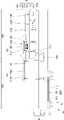
도 7은 본 발명의 일 실시예에 따른 표시 패널(10)의 일부를 나타낸 개략적인 단면도로, 제2표시영역(DA2) 및 제3영역(AR3)의 일부를 개략적으로 도시한 단면도이다. 제3영역(AR3)은 전술한 제3표시영역(DA3)이거나 주변영역(DPA)일 수 있다. 도 7에 있어서, 도 6과 동일한 참조부호는 동일한 부재를 일컫는 바, 이들의 중복설명은 생략한다.7 is a schematic cross-sectional view showing a part of the
도 7을 참조하면, 표시 패널(10)의 제2표시영역(DA2)에는 제2화소(Pa)를 구현하는 제2표시요소로써 유기발광다이오드(OELD')가 배치될 수 있다. 표시 패널(10)의 제3영역(AR3)에는 제2표시요소와 연결된 제2화소회로(PCa)가 배치될 수 있다.Referring to FIG. 7 , an organic light emitting diode OELD′ may be disposed as a second display element implementing the second pixel Pa in the second display area DA2 of the
제2화소회로(PCa)는 실리콘 반도체를 포함하는 제1박막트랜지스터(TFT1), 산화물 반도체를 포함하는 제2박막트랜지스터(TFT2), 및 스토리지 커패시터(Cst)를 포함할 수 있다. 기판(100)과 제2화소회로(PCa) 사이에는 하부 도전층(BML)이 더 배치될 수 있다. 하부 도전층(BML)은 제1박막트랜지스터(TFT1)와 중첩될 수 있다. 제2화소회로(PCa)에 포함된 구성은 제1화소회로(PCm)의 포함된 구성과 유사한 바, 제1화소회로(PCm)에 대한 설명으로 제2화소회로(PCa)에 대한 설명을 갈음한다.The second pixel circuit PCa may include a first thin film transistor TFT1 including a silicon semiconductor, a second thin film transistor TFT2 including an oxide semiconductor, and a storage capacitor Cst. A lower conductive layer BML may be further disposed between the
제2표시영역(DA2)의 외부, 즉, 제3영역(AR3)에 배치된 제2화소회로(PCa)는 연결배선(CWL)에 의해서 제2표시영역(DA2)에 배치된 제2표시요소인 유기발광다이오드(OLED)와 전기적으로 연결될 수 있다.The second pixel circuit PCa disposed outside the second display area DA2, that is, in the third area AR3, is a second display element disposed in the second display area DA2 by the connection line CWL. It may be electrically connected to a phosphorus organic light emitting diode (OLED).
연결배선(CWL)은 제2화소회로(PCa)에 포함된 도전층 중 적어도 하나와 동일한 물질로 구비되며, 제2화소회로(PCa)에 포함된 도전층 중 적어도 하나와 동시에 형성될 수 있다.The connection line CWL is made of the same material as at least one of the conductive layers included in the second pixel circuit PCa, and may be formed simultaneously with at least one of the conductive layers included in the second pixel circuit PCa.
도 7을 참조하면, 연결배선(CWL)은 제1박막트랜지스터(TFT1)의 제1게이트전극(GE1)과 동일한 물질로 동일한 층에 구비될 수 있다. 연결배선(CWL)은 몰리브덴(Mo), 알루미늄(Al), 구리(Cu), 티타늄(Ti) 등의 금속을 포함하며 단층 또는 다층으로 이루어질 수 있다. 연결배선(CWL)은 제1게이트절연층(112) 상에 배치될 수 있다. 연결배선(CWL)은 제1게이트전극(GE1)이 형성되는 공정에서 동시에 형성될 수 있다.Referring to FIG. 7 , the connection line CWL may be formed of the same material as the first gate electrode GE1 of the first thin film transistor TFT1 and may be provided on the same layer. The connection wire CWL includes a metal such as molybdenum (Mo), aluminum (Al), copper (Cu), or titanium (Ti) and may be formed of a single layer or multiple layers. The connection wire CWL may be disposed on the first
연결배선(CWL)을 제2화소회로(PCa)에 포함된 도전층이 아닌 별도의 물질, 예컨대, 투명 전도성 산화물로 구비하는 경우 연결배선을 형성하기 위한 별도의 공정이 추가되어야 하는 바, 공정 시간 및 공정 비용이 증가할 수 있다. 또한, 연결배선(CWL)을 투명 전도선 산화물로 구비하는 경우, 금속보다 비저항이 높기에 제2표시영역(DA2)에 배치된 유기발광다이오드(OLED')들의 휘도가 낮아질 수 있다.When the connection line CWL is formed of a separate material, for example, a transparent conductive oxide, rather than the conductive layer included in the second pixel circuit PCa, a separate process for forming the connection line must be added. and process costs may increase. In addition, when the connection line CWL is formed of a transparent conductive line oxide, the luminance of the organic light emitting diodes OLED' disposed in the second display area DA2 may be lowered because the resistivity is higher than that of metal.
본 실시예에 있어서, 연결배선(CWL)을 제1게이트전극(GE1)과 동일한 공정에서 형성함에 따라, 공정 시간 및 공정 비용이 단축될 수 있다. 또한, 연결배선(CWL)을 제1게이트전극(GE1)과 동일한 금속으로 형성함에 따라, 유기발광다이오드(OLED')들의 균일한 휘도를 확보할 수 있다. 한편, 연결배선(CWL)이 투명하지 않은 금속으로 배치됨에 따라 제2표시영역(DA2)의 광 투과율이 위치에 따라 균일하지 않을 수 있는 데, 본 실시예에서는, 연결배선(CWL)의 폭을 위치에 따라 조절함으로써 제2표시영역(DA2)의 광 투과율은 위치에 따라 균일해질 수 있다. 이에 대해서는 후술하기로 한다.In this embodiment, since the connection line CWL is formed in the same process as the first gate electrode GE1, process time and process cost can be reduced. In addition, as the connection wire CWL is formed of the same metal as the first gate electrode GE1, uniform luminance of the organic light emitting diodes OLED' can be secured. Meanwhile, since the connection line CWL is made of non-transparent metal, the light transmittance of the second display area DA2 may not be uniform depending on the location. In this embodiment, the width of the connection line CWL is By adjusting according to the position, the light transmittance of the second display area DA2 can be uniform according to the position. This will be described later.
본 실시예에서, 표시 패널의 무기절연층(IL)은 제2표시영역(DA2)에 대응하는 그루브(GV)를 구비하며, 연결배선(CWL)의 적어도 일부는 상기 그루브(GV) 내부에 배치될 수 있다.In this embodiment, the inorganic insulating layer IL of the display panel has a groove GV corresponding to the second display area DA2, and at least a portion of the connection wire CWL is disposed inside the groove GV. It can be.
예컨대, 버퍼층(111), 제1게이트절연층(112), 제2게이트절연층(113), 제1층간절연층(115), 제2층간절연층(117), 및 제3층간절연층(119)을 통칭하여 무기절연층(IL)이라고 하면, 무기절연층(IL)은 제2표시영역(DA2)에 대응하는 그루브(GV)를 가질 수 있다.For example, the
그루브(GV)는 무기절연층(IL)의 일부가 제거되어 구비될 수 있다. 예컨대, 버퍼층(111), 제1게이트절연층(112)은 제2표시영역(DA2)에 걸쳐 연속적으로 배치되며, 제2게이트절연층(113), 제1층간절연층(115), 제2층간절연층(117) 및 제3층간절연층(119)은 제2표시영역(DA2)에 대응하는 개구들을 구비할 수 있다. 이러한 개구들은 별도의 공정을 통해서 각각 형성되거나 동일한 공정을 통해서 동시에 형성될 수 있다. 이러한 개구들이 별도의 공정으로 형성되는 경우, 그루브(GV)의 내측면은 매끄럽지 않고 계단 형상과 같은 단차를 가질 수도 있다.The groove GV may be provided by removing a part of the inorganic insulating layer IL. For example, the
연결배선(CWL)이 제1박막트랜지스터(TFT1)의 제1게이트전극(GE1)과 동일한 공정으로 통해서 형성되는 바, 그루브(GV)는 연결배선(CWL)이 형성된 후에 형성될 수 있다. 이 경우, 연결배선(CWL)의 일 단은 그루브(GV)에 의해서 노출되지 않을 수 있다.Since the connection line CWL is formed through the same process as the first gate electrode GE1 of the first thin film transistor TFT1, the groove GV may be formed after the connection line CWL is formed. In this case, one end of the connection wire CWL may not be exposed by the groove GV.
제1유기절연층(121)은 그루브(GV) 내부에 배치된 연결배선(CWL)을 덮으며, 상기 그루브(GV)를 채우도록 배치될 수 있다. 연결배선(CWL)은 제2표시영역(DA2)에서 제1게이트절연층(112)과 제1유기절연층(121) 사이에 배치될 수 있다. 제1유기절연층(121)은 무기절연층(IL) 보다 광 투과율이 높을 수 있다. 이에 따라, 제2표시영역(DA2)의 광 투과율이 더욱 향상될 수 있다. 한편, 제1유기절연층(121)은 유기물질의 특성 상 연결배선(CWL)에 인가될 수 있는 충격을 흡수하여 연결배선(CWL)에 크랙 등이 형성되지 않도록 보호하는 역할을 할 수 있다.The first organic insulating
연결배선(CWL)의 일 단은 브릿지배선(BWL)을 통해서 제2화소회로(PCa)와 연결될 수 있다. 일 실시예에 있어서, 브릿지배선(BWL)은 제2유기절연층(122) 상에 배치되며, 컨택홀들을 통해서 각각 제2화소회로(PCa)의 박막트랜지스터 및 연결배선(CWL)과 연결될 수 있다. 다른 실시예로서, 브릿지배선(BWL)은 제1유기절연층(121) 상에 배치되거나, 제3층간절연층(119) 상에 배치되는 등 다양한 변형이 가능하다. 연결배선(CWL)의 타단은 제1컨택전극(CM1)을 통해서 유기발광다이오드(OLED')의 화소전극(310)과 접속될 수 있다. 제1컨택전극(CM1)은 제2유기절연층(122), 제1유기절연층(121)을 관통하는 컨택홀을 통해서 연결배선(CWL)의 타단과 접속될 수 있다. 화소전극(310)은 제3유기절연층(123)을 관통하는 컨택홀을 통해서 제1컨택전극(CM1)과 접속될 수 있다.One end of the connection line CWL may be connected to the second pixel circuit PCa through the bridge line BWL. In one embodiment, the bridge wiring BWL is disposed on the second organic insulating
제2표시영역(DA2)에 배치된 화소정의막(125')은 제1표시영역(DA1)에 배치된 화소정의막(125)와 이격되어 배치될 수 있다. 화소정의막(125')은 차광 물질을 포함할 수 있다. 예컨대, 화소정의막(125')은 블랙의 색상을 갖는 안료 또는 염료를 포함하는 절연물(예, 유기절연물)을 포함할 수 있다. 이와 같이 차광막으로 구비된 화소정의막(125')은 인접 화소들 간의 혼색을 방지하고, 컴포넌트(40, 도 2 참조)에 의해 표시 패널(10)로 반사된 광을 흡수하여 시인성을 개선할 수 있다. 화소정의막(125')이 차광 물질을 포함함에 따라, 제2표시영역(DA2)에 배치되는 화소정의막(125')은 각 제2화소(Pa) 마다 패터닝되어 구비될 수 있다. 화소정의막(125')은 화소전극(310)의 가장자리를 덮고, 중앙부를 노출하는 개구를 구비하는 바, 화소정의막(125')의 평면 형상은 링 형상 또는 도넛 형상으로 구비될 수 있다. 일부 실시예에서, 화소정의막(125')의 개구는 평면상 원형일 수 있다. 또는, 화소정의막(125')의 개구는 타원형, 모서리가 둥근 다각형의 형상일 수 있다.The
도 8 내지 도 11은 본 발명의 일 실시예들에 따른 표시 패널(10)의 일부를 나타낸 개략적인 단면도이다. 도 8 내지 도 11에 있어서, 도 6 및 도 7과 동일한 참조부호는 동일한 부재를 일컫는 바, 이들의 중복설명은 생략한다.8 to 11 are schematic cross-sectional views of parts of the
도 8을 참조하면, 연결배선(CLW)은 스토리지 커패시터(Cst)의 상부전극(CE2)과 동일한 물질로 동일한 층에 구비될 수 있다. 연결배선(CWL)은 몰리브덴(Mo), 알루미늄(Al), 구리(Cu), 티타늄(Ti) 등의 금속을 포함하며 단층 또는 다층으로 이루어질 수 있다. 연결배선(CWL)은 제2게이트절연층(113) 상에 배치될 수 있다. 연결배선(CWL)은 상부전극(CE2)이 형성되는 공정에서 동시에 형성될 수 있다.Referring to FIG. 8 , the connection wire CLW may be made of the same material as the upper electrode CE2 of the storage capacitor Cst and may be provided on the same layer. The connection wire CWL includes a metal such as molybdenum (Mo), aluminum (Al), copper (Cu), or titanium (Ti) and may be formed of a single layer or multiple layers. The connection wire CWL may be disposed on the second
그루브(GV)는 무기절연층(IL)의 일부가 제거되어 구비될 수 있다. 예컨대, 버퍼층(111), 제1게이트절연층(112), 제2게이트절연층(113)은 제2표시영역(DA2)에 걸쳐 연속적으로 배치되며, 제1층간절연층(115), 제2층간절연층(117) 및 제3층간절연층(119)은 제2표시영역(DA2)에 대응하는 개구들을 구비할 수 있다. 이러한 개구들은 별도의 공정을 통해서 각각 형성되거나 동일한 공정을 통해서 동시에 형성될 수 있다. 이러한 개구들이 별도의 공정으로 형성되는 경우, 그루브(GV)의 내측면은 매끄럽지 않고 계단 형상과 같은 단차를 가질 수도 있다. 그루브(GV)는 연결배선(CWL)이 형성된 후에 형성될 수 있다.The groove GV may be provided by removing a part of the inorganic insulating layer IL. For example, the
제1유기절연층(121)은 그루브(GV) 내부에 배치된 연결배선(CWL)을 덮으며, 그루브(GV)를 채우도록 배치될 수 있다. 연결배선(CWL)은 제2표시영역(DA2)에서 제2게이트절연층(113)과 제1유기절연층(121) 사이에 배치될 수 있다.The first organic insulating
도 9를 참조하면, 연결배선(CLW)은 제2박막트랜지스터(TFT2)의 제2게이트전극(GE2)과 동일한 물질로 동일한 층에 구비될 수 있다. 연결배선(CWL)은 몰리브덴(Mo), 알루미늄(Al), 구리(Cu), 티타늄(Ti) 등의 금속을 포함하며 단층 또는 다층으로 이루어질 수 있다. 연결배선(CWL)은 제2층간절연층(117) 상에 배치될 수 있다. 연결배선(CWL)은 제2게이트전극(GE2)이 형성되는 공정에서 동시에 형성될 수 있다.Referring to FIG. 9 , the connection wire CLW may be formed of the same material and on the same layer as the second gate electrode GE2 of the second thin film transistor TFT2. The connection wire CWL includes a metal such as molybdenum (Mo), aluminum (Al), copper (Cu), or titanium (Ti) and may be formed of a single layer or multiple layers. The connection wire CWL may be disposed on the second
그루브(GV)는 무기절연층(IL)의 일부가 제거되어 구비될 수 있다. 예컨대, 버퍼층(111), 제1게이트절연층(112), 제2게이트절연층(113), 제1층간절연층(115), 제2층간절연층(117)은 제2표시영역(DA2)에 걸쳐 연속적으로 배치되며, 제3층간절연층(119)은 제2표시영역(DA2)에 대응하는 개구들을 구비할 수 있다. 그루브(GV)는 연결배선(CWL)이 형성된 후에 형성될 수 있다.The groove GV may be provided by removing a part of the inorganic insulating layer IL. For example, the
제1유기절연층(121)은 그루브(GV) 내부에 배치된 연결배선(CWL)을 덮으며, 그루브(GV)를 채우도록 배치될 수 있다. 연결배선(CWL)은 제2표시영역(DA2)에서 제2층간절연층(117)과 제1유기절연층(121) 사이에 배치될 수 있다.The first organic insulating
도 10을 참조하면, 연결배선(CLW)은 제1박막트랜지스터(TFT1)의 제1소스전극(SE1) 및/또는 제1드레인전극(DE1)과 동일한 물질로 구비될 수 있다. 제1소스전극(SE1) 및/또는 제1드레인전극(DE1)은 무기절연층(IL) 상부에 배치될 수 있다. 연결배선(CWL)은 몰리브덴(Mo), 알루미늄(Al), 구리(Cu), 티타늄(Ti) 등의 금속을 포함하며 단층 또는 다층으로 이루어질 수 있다. 연결배선(CWL)은 제1소스전극(SE1) 및/또는 제1드레인전극(DE1)이 형성되는 공정에서 동시에 형성될 수 있다.Referring to FIG. 10 , the connection wire CLW may be made of the same material as the first source electrode SE1 and/or the first drain electrode DE1 of the first thin film transistor TFT1. The first source electrode SE1 and/or the first drain electrode DE1 may be disposed on the inorganic insulating layer IL. The connection wire CWL includes a metal such as molybdenum (Mo), aluminum (Al), copper (Cu), or titanium (Ti) and may be formed of a single layer or multiple layers. The connection wire CWL may be formed simultaneously in the process of forming the first source electrode SE1 and/or the first drain electrode DE1.
그루브(GV)는 무기절연층(IL)의 일부가 제거되어 구비될 수 있다. 예컨대, 버퍼층(111)은 제2표시영역(DA2)에 걸쳐 연속적으로 배치되며, 제1게이트절연층(112), 제2게이트절연층(113), 제1층간절연층(115), 제2층간절연층(117) 및 제3층간절연층(119)은 제2표시영역(DA2)에 대응하는 개구들을 구비할 수 있다. 이러한 개구들은 별도의 공정을 통해서 각각 형성되거나 동일한 공정을 통해서 동시에 형성될 수 있다. 이러한 개구들이 별도의 공정으로 형성되는 경우, 그루브(GV)의 내측면은 매끄럽지 않고 계단 형상과 같은 단차를 가질 수도 있다.The groove GV may be provided by removing a part of the inorganic insulating layer IL. For example, the
그루브(GV) 내부에는 연결배선(CWL)이 배치되고, 상기 연결배선(CWL)을 덮으며, 그루브(GV)를 채우도록 제1유기절연층(121)이 배치될 수 있다. 연결배선(CWL)은 제2표시영역(DA2)에서 버퍼층(111)과 제1유기절연층(121) 사이에 배치될 수 있다. 본 실시예에서, 연결배선(CWL)은 제1소스전극(SE1) 및/또는 제1드레인전극(DE1)과 동일한 공정에서 형성되는 바, 그루브(GV)가 연결배선(CWL) 보다 먼저 형성될 수 있다.A connection wire CWL may be disposed inside the groove GV, and a first organic insulating
도 11을 참조하면, 연결배선(CWL)은 제1박막트랜지스터(TFT1)의 제1게이트전극(GE1)과 동일한 층으로 형성된 제1도전층(CWLa), 및 제1박막트랜지스터(TFT1)의 제1박막트랜지스터(TFT1)의 제1소스전극(SE1) 및/또는 제1드레인전극(DE1)과 동일한 물질로 구비된 제2도전층(CWLb)이 적층되어 구비될 수 있다. 연결배선(CWL)은 몰리브덴(Mo), 알루미늄(Al), 구리(Cu), 티타늄(Ti) 등의 금속을 포함하며 단층 또는 다층으로 이루어질 수 있다. 연결배선(CWL)의 제1도전층(CWLa)는 제1게이트전극(GE1)이 형성되는 공정에서 동시에 형성될 수 있다. 연결배선(CWL)의 제2도전층(CWLb)은 제1소스전극(SE1) 및/또는 제1드레인전극(DE1)이 형성되는 공정에서 동시에 형성될 수 있다.Referring to FIG. 11 , the connection line CWL includes the first conductive layer CWLa formed of the same layer as the first gate electrode GE1 of the first thin film transistor TFT1 and the first conductive layer CWLa of the first thin film transistor TFT1. A second conductive layer CWLb made of the same material as the first source electrode SE1 and/or the first drain electrode DE1 of the one thin film transistor TFT1 may be stacked and provided. The connection wire CWL includes a metal such as molybdenum (Mo), aluminum (Al), copper (Cu), or titanium (Ti) and may be formed of a single layer or multiple layers. The first conductive layer CWLa of the connection line CWL may be formed at the same time as the first gate electrode GE1 is formed. The second conductive layer CWLb of the connection line CWL may be formed simultaneously in the process of forming the first source electrode SE1 and/or the first drain electrode DE1.
그루브(GV)는 무기절연층(IL)의 일부가 제거되어 구비될 수 있다. 예컨대, 버퍼층(111) 및 제1게이트절연층(112)은 제2표시영역(DA2)에 걸쳐 연속적으로 배치되며, 제2게이트절연층(113), 제1층간절연층(115), 제2층간절연층(117) 및 제3층간절연층(119)은 제2표시영역(DA2)에 대응하는 개구들을 구비할 수 있다. 이러한 개구들은 별도의 공정을 통해서 각각 형성되거나 동일한 공정을 통해서 동시에 형성될 수 있다. 이러한 개구들이 별도의 공정으로 형성되는 경우, 그루브(GV)의 내측면은 매끄럽지 않고 계단 형상과 같은 단차를 가질 수도 있다. 그루브(GV)는 제1도전층(CWLa)가 형성된 후에 형성되고, 제2도전층(CWLb)은 그루브(GV)가 형성된 후에 형성될 수 있다.The groove GV may be provided by removing a part of the inorganic insulating layer IL. For example, the
제1유기절연층(121)은 그루브(GV) 내부에 배치된 연결배선(CWL)을 덮으며, 그루브(GV)를 채우도록 배치될 수 있다. 연결배선(CWL)은 제2표시영역(DA2)에서 제1게이트절연층(112)과 제1유기절연층(121) 사이에 배치될 수 있다.The first organic insulating
도 12는 본 발명의 일 실시예에 따른 표시 패널의 일부를 나타낸 개략적인 평면 배치도이다. 구체적으로, 제2표시영역(DA2) 및 그 양측에 배치된 제3표시영역(DA3)을 도시하고 있다.12 is a schematic plan arrangement view illustrating a part of a display panel according to an exemplary embodiment of the present invention. Specifically, the second display area DA2 and the third display area DA3 disposed on both sides of the second display area DA2 are shown.
도 12를 참조하면, 제2표시영역(DA2)에는 제2화소(Pa)들이 배치되고 있다. 제2화소(Pa)들은 펜타일(PenTileTM) 구조, 스트라이프 구조, 델타 구조 등 다양한 화소 배치 구조로 배치될 수 있다. 제3표시영역(DA3)은 제2표시영역(DA2)의 우측 및 좌측에 배치될 수 있다. 제3표시영역(DA3)에는 제2화소(Pa)들을 구동하는 제2화소회로(PCa, 도 4 참조)들이 배치될 수 있다. 제2표시영역(DA2)에 대응하여 컴포넌트(40)가 배치될 수 있다.Referring to FIG. 12 , second pixels Pa are disposed in the second display area DA2 . The second pixels Pa may be arranged in various pixel arrangement structures such as a PenTile™ structure, a stripe structure, and a delta structure. The third display area DA3 may be disposed on the right and left sides of the second display area DA2. Second pixel circuits PCa (refer to FIG. 4 ) driving the second pixels Pa may be disposed in the third display area DA3 . A
제3표시영역(DA3)에 배치된 제2화소회로(PCa)들 각각은 연결배선(CWL)에 의해서 제2화소(Pa)를 구현하는 표시소자와 연결될 수 있다. 연결배선(CWL)은 x방향 또는 -x방향으로 연장될 수 있다. 예컨대, 제2표시영역(DA2)의 좌측에 배치된 제3표시영역(DA3)으로부터 제2표시영역(DA2)으로 연장되는 연결배선(CWL)은 x방향으로 연장되고, 제2표시영역(DA2)의 우측에 배치된 제3표시영역(DA3)으로부터 제2표시영역(DA2)으로 연장되는 연결배선(CWL)은 -x방향으로 연장될 수 있다.Each of the second pixel circuits PCa disposed in the third display area DA3 may be connected to a display element implementing the second pixel Pa through a connection line CWL. The connection wire CWL may extend in the x direction or the -x direction. For example, the connection wire CWL extending from the third display area DA3 disposed on the left side of the second display area DA2 to the second display area DA2 extends in the x direction, and extends in the x direction. ), the connection wire CWL extending from the third display area DA3 disposed on the right side to the second display area DA2 may extend in the -x direction.
본 실시예에서, 연결배선(CWL)은 제2표시영역(DA2)에 배치된 위치에 따라 서로 다른 폭을 가진 부분을 포함할 수 있다.In this embodiment, the connection wire CWL may include portions having different widths according to positions disposed in the second display area DA2.
제2표시영역(DA2)은 제1서브영역(SA1), 제2서브영역(SA2),및 제3서브영역(SA3)을 포함할 수 있다. 제1서브영역(SA1)은 제2표시영역(DA2) 중 제3표시영역(DA3)과 인접한 가장자리에 배치된 영역일 수 있다. 제3서브영역(SA3)은 제2표시영역(DA2) 중 중심부에 배치된 영역일 수 있다. 제2서브영역(SA2)은 제1서브영역(SA1)과 제3서브영역(SA3) 사이에 배치된 영역일 수 있다.The second display area DA2 may include a first sub area SA1 , a second sub area SA2 , and a third sub area SA3 . The first sub area SA1 may be an area disposed at an edge adjacent to the third display area DA3 in the second display area DA2. The third sub area SA3 may be an area disposed in the center of the second display area DA2. The second sub area SA2 may be an area disposed between the first sub area SA1 and the third sub area SA3.
제2표시영역(DA2)에 배치된 복수의 연결배선(CWL)들은 제1서브영역(SA1)까지 연장된 제1연결배선(CWL1), 제2서브영역(SA2)까지 연장된 제2연결배선(CWL2), 제3서브영역(SA3)까지 연장된 제3연결배선(CWL3)을 포함할 수 있다.The plurality of connection lines CWL disposed in the second display area DA2 include a first connection line CWL1 extending to the first sub area SA1 and a second connection line extending to the second sub area SA2. (CWL2) and a third connection wire (CWL3) extending to the third sub area (SA3).
이 경우, 제1서브영역(SA1)에는 제1연결배선(CWL1), 제2연결배선(CWL2), 및 제3연결배선(CWL3)이 모두 배치되는 데 반해, 제2서브영역(SA2)에는 제2연결배선(CWL2), 및 제3연결배선(CWL3)만 배치되고, 제3서브영역(SA3)에는 제3연결배선(CWL3)만 배치될 수 있다.In this case, the first connection line CWL1, the second connection line CWL2, and the third connection line CWL3 are all disposed in the first sub area SA1, whereas in the second sub area SA2 Only the second connection wire CWL2 and the third connection wire CWL3 may be disposed, and only the third connection wire CWL3 may be disposed in the third sub area SA3.
제1연결배선(CWL1), 제2연결배선(CWL2), 및 제3연결배선(CWL3)이 불투명한 금속으로 배치되고, 동일한 두께로 형성된다면 제1서브영역(SA1), 제2서브영역(SA2),및 제3서브영역(SA3)의 광 투과율이 각각 다르게 형성되어, 컴포넌트(40)가 수신/송신하는 광 또는 신호가 영역에 따라 균일하지 못할 수 있다.If the first connection line CWL1 , the second connection line CWL2 , and the third connection line CWL3 are made of opaque metal and formed to have the same thickness, the first subregion SA1 and the second subregion ( SA2) and the third sub-region SA3 may have different light transmittances, so that light or signals received/transmitted by the
본 실시예에서는, 연결배선(CWL)이 제2표시영역(DA2)에 배치된 위치에 따라 다른 폭을 가지도록 구비하여, 제2표시영역(DA2)의 광 투과율을 균일하게 하여 컴포넌트(40)의 기능 수행이 향상될 수 있도록 할 수 있다.In the present embodiment, the connection wire CWL is provided to have different widths depending on the position in the second display area DA2, so that the light transmittance of the second display area DA2 is made uniform and thus the
제1서브영역(SA1)에 배치된 연결배선(CWL)은 제1폭(wt1), 제2서브영역(SA2)에 배치된 연결배선(CWL)은 제2폭(wt2), 제3서브영역(SA3)에 배치된 연결배선(CWL)은 제3폭(wt3)을 가질 수 있다. 제3폭(wt3)은 제2폭(wt2) 보다 크고, 제2폭(wt2)은 제1폭(wt1)보다 클 수 있다. (wt3 > wt2 > wt1) 이 때, 제1폭(wt1), 제2폭(wt2), 제3폭(wt3)은 연결배선(CWL)이 길이 방향으로 연장된 방향의 수직 방향에 따른 폭일 수 있다. 일부 실시예에서, 제1폭(wt1)은 약 2 ~ 2.5 μm, 제2폭(wt2)은 약 2.5 ~ 3 μm, 제3폭(wt3)은 약 3 ~ 3.5 μm일 수 있다.The connection wire CWL disposed in the first sub area SA1 has a first width wt1, and the connection wire CWL disposed in the second sub area SA2 has a second width wt2 and a third sub area The connection wire CWL disposed at SA3 may have a third width wt3. The third width wt3 may be larger than the second width wt2 , and the second width wt2 may be larger than the first width wt1 . (wt3 > wt2 > wt1) In this case, the first width (wt1), the second width (wt2), and the third width (wt3) may be widths in a direction perpendicular to the direction in which the connection wire (CWL) extends in the longitudinal direction. there is. In some embodiments, the first width wt1 may be about 2 to 2.5 μm, the second width wt2 may be about 2.5 to 3 μm, and the third width wt3 may be about 3 to 3.5 μm.
제1연결배선(CWL1)은 제1서브영역(SA1)에만 배치되는 바, 제1연결배선(CWL1)은 제1폭(wt1)으로만 형성될 수 있다. 제2연결배선(CWL2)은 제1폭(wt1)을 가진 부분과 제2폭(wt2)을 가진 부분을 포함할 수 있다. 제3연결배선(CWL3)은 제1폭(wt1)을 가진 부분, 제2폭(wt2)을 가진 부분, 및 제3폭(wt3)을 가진 부분을 포함할 수 있다.Since the first connection line CWL1 is disposed only in the first sub area SA1, the first connection line CWL1 may be formed only to have the first width wt1. The second connection wire CWL2 may include a portion having a first width wt1 and a portion having a second width wt2. The third connection wire CWL3 may include a portion having a first width wt1, a portion having a second width wt2, and a portion having a third width wt3.
도 13은 본 발명의 일 실시예에 따른 표시 패널의 일부를 나타낸 개략적인 평면 배치도이다. 구체적으로, 제2표시영역(DA2) 및 그 상측에 배치된 주변영역(DPA)을 도시하고 있다.13 is a schematic plan arrangement view illustrating a part of a display panel according to an exemplary embodiment of the present invention. Specifically, the second display area DA2 and the peripheral area DPA disposed above the second display area DA2 are illustrated.
도 13을 참조하면, 제2표시영역(DA2)에는 제2화소(Pa)들이 배치되고 있다. 주변영역(DPA)은 제2표시영역(DA2)의 상측에 배치될 수 있다. 주변영역(DPA)에는 제2화소(Pa)들을 구동하는 제2화소회로(PCa, 도 3 참조)들이 배치될 수 있다.Referring to FIG. 13 , second pixels Pa are disposed in the second display area DA2 . The peripheral area DPA may be disposed above the second display area DA2. Second pixel circuits PCa (refer to FIG. 3 ) that drive the second pixels Pa may be disposed in the peripheral area DPA.
주변영역(DPA)에 배치된 제2화소회로(PCa)들 각각은 연결배선(CWL)에 의해서 제2화소(Pa)를 구현하는 표시소자와 연결될 수 있다. 연결배선(CWL)은 -z방향으로 연장될 수 있다. 본 실시예에서, 연결배선(CWL)은 제2표시영역(DA2)에 배치된 위치에 따라 서로 다른 폭을 가진 부분을 포함할 수 있다.Each of the second pixel circuits PCa disposed in the peripheral area DPA may be connected to a display element implementing the second pixel Pa through a connection line CWL. The connection line CWL may extend in the -z direction. In this embodiment, the connection wire CWL may include portions having different widths according to positions disposed in the second display area DA2.
제2표시영역(DA2)은 제1서브영역(SA1), 제2서브영역(SA2),및 제3서브영역(SA3)을 포함할 수 있다. 제1서브영역(SA1)은 제2표시영역(DA2) 중 주변영역(DPA)과 인접한 가장자리에 배치된 영역일 수 있다. 제3서브영역(SA3)은 제1서브영역(SA1)과 이격되어 배치된 영역일 수 있다. 제2서브영역(SA2)은 제1서브영역(SA1)과 제3서브영역(SA3) 사이에 배치된 영역일 수 있다.The second display area DA2 may include a first sub area SA1 , a second sub area SA2 , and a third sub area SA3 . The first sub area SA1 may be an area disposed at an edge adjacent to the peripheral area DPA in the second display area DA2. The third sub area SA3 may be an area spaced apart from the first sub area SA1. The second sub area SA2 may be an area disposed between the first sub area SA1 and the third sub area SA3.
제2표시영역(DA2)에 배치된 복수의 연결배선(CWL)들은 제1서브영역(SA1)까지 연장된 제1연결배선(CWL1), 제2서브영역(SA2)까지 연장된 제2연결배선(CWL2), 제3서브영역(SA3)까지 연장된 제3연결배선(CWL3)을 포함할 수 있다.The plurality of connection lines CWL disposed in the second display area DA2 include a first connection line CWL1 extending to the first sub area SA1 and a second connection line extending to the second sub area SA2. (CWL2) and a third connection wire (CWL3) extending to the third sub area (SA3).
제1서브영역(SA1)에 배치된 연결배선(CWL)은 제1폭(wt1), 제2서브영역(SA2)에 배치된 연결배선(CWL)은 제2폭(wt2), 제3서브영역(SA3)에 배치된 연결배선(CWL)은 제3폭(wt3)을 가질 수 있다. 제3폭(wt3)은 제2폭(wt2) 보다 크고, 제2폭(wt2)은 제1폭(wt1)보다 클 수 있다. (wt3 > wt2 > wt1) 이 때, 제1폭(wt1), 제2폭(wt2), 제3폭(wt3)은 연결배선(CWL)이 길이 방향으로 연장된 방향의 수직 방향에 따른 폭일 수 있다. 일부 실시예에서, 제1폭(wt1)은 약 2 ~ 2.5 μm, 제2폭(wt2)은 약 2.5 ~ 3 μm, 제3폭(wt3)은 약 3 ~ 3.5 μm일 수 있다.The connection wire CWL disposed in the first sub area SA1 has a first width wt1, and the connection wire CWL disposed in the second sub area SA2 has a second width wt2 and a third sub area The connection wire CWL disposed at SA3 may have a third width wt3. The third width wt3 may be larger than the second width wt2 , and the second width wt2 may be larger than the first width wt1 . (wt3 > wt2 > wt1) In this case, the first width (wt1), the second width (wt2), and the third width (wt3) may be widths in a direction perpendicular to the direction in which the connection wire (CWL) extends in the longitudinal direction. there is. In some embodiments, the first width wt1 may be about 2 to 2.5 μm, the second width wt2 may be about 2.5 to 3 μm, and the third width wt3 may be about 3 to 3.5 μm.
제1연결배선(CWL1)은 제1서브영역(SA1)에만 배치되는 바, 제1연결배선(CWL1)은 제1폭(wt1)으로만 형성될 수 있다. 제2연결배선(CWL2)은 제1폭(wt1)을 가진 부분과 제2폭(wt2)을 가진 부분을 포함할 수 있다. 제3연결배선(CWL3)은 제1폭(wt1)을 가진 부분, 제2폭(wt2)을 가진 부분, 및 제3폭(wt3)을 가진 부분을 포함할 수 있다.Since the first connection line CWL1 is disposed only in the first sub area SA1, the first connection line CWL1 may be formed only to have the first width wt1. The second connection wire CWL2 may include a portion having a first width wt1 and a portion having a second width wt2. The third connection wire CWL3 may include a portion having a first width wt1, a portion having a second width wt2, and a portion having a third width wt3.
도 14는 본 발명의 일 실시예에 따른 표시 패널의 일부를 나타낸 개략적인 평면도이고, 도 15는 도 14의 일부 영역을 확대하여 나타낸 평면 배치도이다. 구체적으로, 도 15는 도 14의 제4표시영역을 도시한다.FIG. 14 is a schematic plan view illustrating a portion of a display panel according to an exemplary embodiment, and FIG. 15 is an enlarged plan view illustrating a partial area of FIG. 14 . Specifically, FIG. 15 shows the fourth display area of FIG. 14 .
도 14 및 도 15를 참조하면, 일 실시예에 따른 표시 패널은 제1표시영역(DA1), 제2표시영역(DA2), 및 제4표시영역(DA4)을 포함할 수 있다. 제4표시영역(DA4)은 제2표시영역(DA2)와 이격되어 배치될 수 있다. 제1표시영역(DA1)은 제4표시영역(DA4)을 적어도 일부 둘러싸도록 배치될 수 있다. 제1표시영역(DA1)은 메인 표시영역일 수 있으며, 제2표시영역(DA2) 및 제4표시영역(DA4)는 컴포넌트가 배치되는 컴포넌트영역인 동시에 보조 표시영역일 수 있다. 즉, 제1표시영역(DA1), 제2표시영역(DA2), 및 제4표시영역(DA4) 각각은 개별적으로 또는 함께 이미지를 디스플레이 할 수 있다.Referring to FIGS. 14 and 15 , the display panel according to an exemplary embodiment may include a first display area DA1 , a second display area DA2 , and a fourth display area DA4 . The fourth display area DA4 may be spaced apart from the second display area DA2. The first display area DA1 may be disposed to at least partially surround the fourth display area DA4. The first display area DA1 may be a main display area, and the second display area DA2 and the fourth display area DA4 may be component areas where components are disposed and may be auxiliary display areas. That is, each of the first display area DA1 , the second display area DA2 , and the fourth display area DA4 may display an image individually or together.
제2표시영역(DA2)과 제4표시영역(DA4)에 대응하여 표시 패널의 하부에는 각각 제1컴포넌트(41), 및 제2컴포넌트(42)가 배치될 수 있다. 제1컴포넌트(41)와 제2컴포넌트(42)의 기능은 서로 상이할 수 있다. 제1컴포넌트(41)와 제2컴포넌트(42)의 기능에 따라, 제2표시영역(DA2)과 제4표시영역(DA4)의 광 투과율은 서로 다르게 구비될 수 있다. 제2표시영역(DA2)에 대한 설명은 도 12를 참조하여 설명한 것으로 갈음한다.A
도 15를 참조하면, 제4표시영역(DA4)에는 제4화소(Pa')들이 배치되고 있다. 제4화소(Pa')를 구동하는 제4화소회로(PCa')는 제4표시영역(DA4)의 외부에 배치될 수 있다. 예컨대, 제4화소회로(PCa')는 제4표시영역(DA4)의 양측에 배치된 제5표시영역(DA5)에 배치될 수 있다. 한편, 제5표시영역(DA5)에는 이미지를 구현하는 제5화소들 및 이를 구동하는 제5화소회로들이 배치될 수 있다.Referring to FIG. 15 , fourth pixels Pa′ are disposed in the fourth display area DA4 . The fourth pixel circuit PCa' driving the fourth pixel Pa' may be disposed outside the fourth display area DA4. For example, the fourth pixel circuit PCa' may be disposed in the fifth display area DA5 disposed on both sides of the fourth display area DA4. Meanwhile, fifth pixels that implement images and fifth pixel circuits that drive them may be disposed in the fifth display area DA5.
제5표시영역(DA5)에 배치된 제4화소회로(PCa')들 각각은 연결배선(CWL')에 의해서 제4화소(Pa')를 구현하는 표시소자와 연결될 수 있다. 연결배선(CWL')은 x방향 또는 -x방향으로 연장될 수 있다.Each of the fourth pixel circuits PCa' disposed in the fifth display area DA5 may be connected to a display element implementing the fourth pixel Pa' through a connection line CWL'. The connection wire CWL' may extend in the x direction or the -x direction.
본 실시예에서, 제4표시영역(DA4)에 배치된 연결배선(CWL')의 형상 및/또는 재질은 제2표시영역(DA2, 도 12)에 배치된 연결배선(CWL)과 다르게 구비될 수 있다.In this embodiment, the shape and/or material of the connection wire CWL' disposed in the fourth display area DA4 may be different from that of the connection wire CWL disposed in the second display area DA2 (FIG. 12). can
일부 실시예에서, 제4표시영역(DA4)에 배치된 연결배선(CWL')은 일정한 폭을 가지고 배치될 수 있다. 연결배선(CWL')이 불투명한 금속으로 일정한 폭을 가지고 있어 광 투과율이 비균일하다고 하더라도 제2컴포넌트(42)의 성능에 문제가 없는 경우, 연결배선(CWL')은 일정한 폭으로 구비될 수 있다. 또는, 연결배선(CWL')은 서로 다른 폭을 가지는 부분이 있다고 하더라도, 제2표시영역(DA2)의 연결배선(CWL)의 폭과 다르게 구비될 수 있다.In some embodiments, the connection wire CWL' disposed in the fourth display area DA4 may be disposed with a constant width. If there is no problem in the performance of the
한편, 일부 실시예에서, 제4표시영역(DA4)에 배치된 연결배선(CWL')은 투명 전도성 물질로 구비될 수 있다. 예컨대, 연결배선(CWL')은 투명한 전도성 산화물(Transparent Conducting Oxide, TCO)로 구비될 수 있다. 연결배선(CWL)은 인듐주석산화물(ITO; indium tin oxide), 인듐아연산화물(IZO; indium zinc oxide), 아연산화물(ZnO; zinc oxide), 인듐산화물(In2O3: indium oxide), 인듐갈륨산화물(IGO; indium gallium oxide) 또는 알루미늄아연산화물(AZO; aluminum zinc oxide)와 같은 도전성 산화물을 포함할 수 있다. 제4표시영역(DA4)의 광 투과율을 제2표시영역(DA2) 보다 높이기 위해서 제4표시영역(DA4')에 배치된 연결배선(CWL')을 투명 전도성 물질로 구비할 수 있다.Meanwhile, in some embodiments, the connection wire CWL' disposed in the fourth display area DA4 may be made of a transparent conductive material. For example, the connection line CWL′ may be made of a transparent conducting oxide (TCO). Connection wiring (CWL) is indium tin oxide (ITO), indium zinc oxide (IZO), zinc oxide (ZnO), indium oxide (In2 O3 : indium oxide), indium A conductive oxide such as indium gallium oxide (IGO) or aluminum zinc oxide (AZO) may be included. In order to increase light transmittance of the fourth display area DA4 than that of the second display area DA2, the connection wire CWL' disposed in the fourth display area DA4' may be made of a transparent conductive material.
도 16은 본 발명의 일 실시예에 따른 표시 패널의 일부를 나타낸 개략적인 평면도이다.16 is a schematic plan view illustrating a portion of a display panel according to an exemplary embodiment.
도 16을 참조하면, 표시 패널은 개구영역(OA)을 더 포함할 수 있다.Referring to FIG. 16 , the display panel may further include an open area OA.
개구영역(OA)은 그 하부에 제3컴포넌트(43)가 배치되는 영역일 수 있다. 개구영역(OA)은 제3컴포넌트(43)으로부터 외부로 출력되거나 외부로부터 제3컴포넌트(43)를 향해 진행하는 빛 또는/및 음향이 투과할 수 있는 투과영역(transmission area)으로 이해될 수 있다. 본 발명의 일 실시예로, 개구영역(OA)을 통해 빛이 투과하는 경우, 광 투과율은 약 50% 이상, 보다 바람직하게 70% 이상이거나, 75% 이상이거나 80% 이상이거나, 85% 이상이거나, 90% 이상일 수 있다. 개구영역(OA)은 표시요소가 배치되지 않는 영역으로 이미지를 제공할 수 없는 영역일 수 있다. 본 실시예에서, 개구영역(OA)은 표시영역(DA) 내측에 배치되어, 개구영역(OA)을 둘러싸도록 메인 화소들, 제1화소(Pm, 도 1)들이 배치될 수 있다.The opening area OA may be an area where the
제2표시영역(DA2) 및 제4표시영역(DA4)에는 그 하부에 각각 제1컴포넌트(41) 및 제2컴포넌트(42)가 배치될 수 있다. 또한, 제2표시영역(DA2) 및 제4표시영역(DA4)은 화소들(Pa, Pa')이 배치되어, 소정의 이미지를 제공할 수 있다.The
일부 실시예에서, 개구영역(OA)의 광 투과율은 제2표시영역(DA2) 및 제4표시영역(DA4)의 광 투과율에 비해서 크게 구비될 수 있다. 이에 따라, 개구영역(OA)는 광 투과율이 높아야 하는 컴포넌트, 예컨대, 카메라 등이 배치될 수 있으며, 제2표시영역(DA2) 및 제4표시영역(DA4)에는 적외선을 감지하는 센서나 조도 센서 등이 배치될 수 있다.In some embodiments, the light transmittance of the opening area OA may be greater than those of the second display area DA2 and the fourth display area DA4 . Accordingly, a component requiring high light transmittance, such as a camera, may be disposed in the opening area OA, and a sensor for detecting infrared rays or an illuminance sensor may be disposed in the second display area DA2 and the fourth display area DA4. etc. can be placed.
이와 같이 본 발명은 도면에 도시된 일 실시예를 참고로 하여 설명하였으나 이는 예시적인 것에 불과하며 당해 분야에서 통상의 지식을 가진 자라면 이로부터 다양한 변형 및 실시예의 변형이 가능하다는 점을 이해할 것이다. 따라서, 본 발명의 진정한 기술적 보호 범위는 첨부된 특허청구범위의 기술적 사상에 의하여 정해져야 할 것이다.As such, the present invention has been described with reference to one embodiment shown in the drawings, but this is merely exemplary, and those skilled in the art will understand that various modifications and variations of the embodiment are possible therefrom. Therefore, the true technical scope of protection of the present invention should be determined by the technical spirit of the appended claims.
1: 표시 장치
10: 표시 패널
100: 기판
111: 버퍼층
112: 제1게이트절연층
113: 제2게이트절연층
117: 제2층간절연층
119: 제3층간절연층
120: 유기절연층
121: 제1유기절연층
122: 제2유기절연층
123: 제3유기절연층
125: 화소정의막
CWL: 연결배선
DA1: 제1표시영역
DA2: 제2표시영역
DA3: 제3표시영역1: display device
10: display panel
100: substrate
111: buffer layer
112: first gate insulating layer
113: second gate insulating layer
117: second interlayer insulating layer
119: third interlayer insulating layer
120: organic insulating layer
121: first organic insulating layer
122: second organic insulating layer
123: third organic insulating layer
125: pixel defining film
CWL: connection wiring
DA1: first display area
DA2: second display area
DA3: third display area
Claims (20)
Translated fromKorean상기 제1표시영역에 배치되며, 상기 제1표시소자와 연결된 제1화소회로;
상기 제2표시영역의 외부에 배치되며, 상기 제2표시소자와 연결된 제2화소회로;
상기 기판 상에 배치되며, 상기 제2표시영역에 대응하는 그루브를 구비한 무기절연층;
상기 그루브 내부에 배치하며, 상기 제2표시소자와 상기 제2화소회로를 연결하는 연결배선;을 포함하며,
상기 연결배선은 상기 제2화소회로에 포함된 도전층 중 적어도 하나와 동일한 물질로 구비되며, 상기 연결배선은 상기 제2표시영역에 배치된 위치에 따라 서로 다른 폭을 가진 부분을 포함하는, 표시 패널.a substrate including a first display area on which a first display element is disposed, and a second display area on which a second display element is disposed;
a first pixel circuit disposed in the first display area and connected to the first display element;
a second pixel circuit disposed outside the second display area and connected to the second display element;
an inorganic insulating layer disposed on the substrate and having a groove corresponding to the second display area;
A connection wire disposed inside the groove and connecting the second display element and the second pixel circuit;
The connection wire is made of the same material as at least one of the conductive layers included in the second pixel circuit, and the connection wire includes portions having different widths depending on positions disposed in the second display area. panel.
상기 연결배선 상에 배치되며, 상기 그루브를 채우는 유기절연층;을 더 포함하는, 표시 패널.According to claim 1,
The display panel further includes an organic insulating layer disposed on the connection wire and filling the groove.
상기 제2화소회로는, 제1게이트전극과 실리콘 반도체로 구비된 제1반도체층을 포함하는 제1박막트랜지스터를 포함하며,
상기 연결배선은 상기 제1게이트전극과 동일한 물질로 동일한 층에 구비된, 표시 패널.According to claim 1,
The second pixel circuit includes a first thin film transistor including a first gate electrode and a first semiconductor layer made of a silicon semiconductor,
The connection wire is provided on the same layer as the first gate electrode and made of the same material as the display panel.
상기 제2화소회로는,
제1게이트전극과 실리콘 반도체로 구비된 제1반도체층을 포함하는 제1박막트랜지스터; 및
상기 제1게이트전극과 일체로 구비된 하부전극 및 상기 하부전극 상에 배치된 상부전극을 구비하는 스토리지 커패시터;를 포함하며,
상기 연결배선은 상기 상부전극과 동일한 물질로 동일한 층에 구비된, 표시 패널.According to claim 1,
In the second pixel circuit,
a first thin film transistor including a first gate electrode and a first semiconductor layer made of silicon semiconductor; and
A storage capacitor including a lower electrode integrally formed with the first gate electrode and an upper electrode disposed on the lower electrode;
The connection wire is provided on the same layer as the upper electrode and made of the same material as the display panel.
상기 제2화소회로는,
제1게이트전극과 실리콘 반도체로 구비된 제1반도체층을 포함하는 제1박막트랜지스터; 및
상기 제1게이트전극과 다른 층에 배치된 제2게이트전극과 산화물 반도체로 구비된 제2반도체층을 포함하는 제2박막트랜지스터;를 포함하며,
상기 연결배선은 상기 제2게이트전극과 동일한 물질로 동일한 층에 구비된, 표시 패널.According to claim 1,
In the second pixel circuit,
a first thin film transistor including a first gate electrode and a first semiconductor layer made of silicon semiconductor; and
A second thin film transistor including a second semiconductor layer made of an oxide semiconductor and a second gate electrode disposed on a different layer from the first gate electrode,
The connection wire is provided on the same layer as the second gate electrode and made of the same material as the display panel.
상기 제2화소회로는, 제1게이트전극, 제1소스전극, 제1드레인전극, 및 실리콘 반도체로 구비된 제1반도체층을 포함하는 제1박막트랜지스터를 포함하며,
상기 연결배선은 상기 제1소스전극과 동일한 물질로 구비된, 표시 패널.According to claim 1,
The second pixel circuit includes a first thin film transistor including a first gate electrode, a first source electrode, a first drain electrode, and a first semiconductor layer made of a silicon semiconductor,
The connection wire is made of the same material as the first source electrode, the display panel.
상기 제2화소회로는, 제1게이트전극, 제1소스전극, 제1드레인전극, 및 실리콘 반도체로 구비된 제1반도체층을 포함하는 제1박막트랜지스터를 포함하며,
상기 연결배선은 상기 제1게이트전극과 동일한 물질로 구비된 제1도전층, 및상기 제1소스전극과 동일한 물질로 구비된 제2도전층이 적층되어 구비된, 표시 패널.According to claim 1,
The second pixel circuit includes a first thin film transistor including a first gate electrode, a first source electrode, a first drain electrode, and a first semiconductor layer made of a silicon semiconductor,
The connection wire is provided by stacking a first conductive layer made of the same material as the first gate electrode and a second conductive layer made of the same material as the first source electrode.
상기 제2표시영역은 가장자리에 배치된 제1서브영역, 상기 제1서브영역과 이격된 제3서브영역, 및 상기 제1서브영역과 상기 제3서브영역 사이에 배치된 제2서브영역을 포함하며,
상기 제1서브영역에 배치된 상기 연결배선은 제1폭, 상기 제2서브영역에 배치된 상기 연결배선은 제2폭, 상기 제3서브영역에 배치된 상기 연결배선은 제3폭을 가지고,
상기 제3폭은 상기 제2폭 보다 크고, 상기 제2폭은 상기 제1폭 보다 크게 구비된, 표시 패널.According to claim 1,
The second display area includes a first sub area disposed at an edge, a third sub area spaced apart from the first sub area, and a second sub area disposed between the first sub area and the third sub area. and
The connection wire disposed in the first sub area has a first width, the connection wire disposed in the second sub area has a second width, and the connection wire disposed in the third sub area has a third width;
wherein the third width is greater than the second width, and the second width is greater than the first width.
상기 제2표시영역의 우측 및 좌측에 배치된 제3표시영역;을 더 포함하며,
상기 제2화소회로는 상기 제3표시영역에 배치되고, 상기 연결배선은 상기 제3표시영역으로부터 상기 제2표시영역으로 연장된, 표시 패널.According to claim 8,
It further includes; third display areas disposed on the right and left sides of the second display area;
The display panel of claim 1 , wherein the second pixel circuit is disposed in the third display area, and the connection wire extends from the third display area to the second display area.
상기 제2표시영역의 상측에 배치된 주변영역;을 더 포함하며,
상기 제2화소회로는 상기 주변영역에 배치되고, 상기 연결배선은 상기 주변영역으로부터 상기 제2표시영역으로 연장된, 표시 패널.According to claim 8,
It further includes a peripheral area disposed above the second display area,
wherein the second pixel circuit is disposed in the peripheral area, and the connection wire extends from the peripheral area to the second display area.
상기 기판은 상기 제2표시영역과 이격되며, 제4표시소자가 배치된 제4표시영역을 더 포함하고, 상기 표시 패널은,
상기 제4표시영역의 외부에 배치되며, 상기 제4표시소자와 연결된 제4화소회로; 및
상기 제4표시소자와 상기 제4화소회로를 연결하는 추가 연결배선;을 더 포함하며,
상기 추가 연결배선은 상기 연결배선과 형상 및 재질 중 적어도 하나가 다르게 구비된, 표시 패널.According to claim 1,
The substrate further includes a fourth display area spaced apart from the second display area and in which a fourth display element is disposed, and the display panel comprises:
a fourth pixel circuit disposed outside the fourth display area and connected to the fourth display element; and
Further comprising an additional connection wire connecting the fourth display element and the fourth pixel circuit;
The additional connection wire is provided with a different shape and at least one material from the connection wire, the display panel.
상기 추가 연결배선의 폭은 상기 제4표시영역에서 일정하게 구비된, 표시 패널.According to claim 11,
The display panel of claim 1 , wherein the additional connection wire has a constant width in the fourth display area.
상기 기판은 상기 제1표시영역 내측에 배치된 개구영역을 더 포함하며, 상기 개구영역은 이미지를 디스플레이하지 않는, 표시 패널.According to claim 1,
The display panel of claim 1 , wherein the substrate further includes an opening area disposed inside the first display area, wherein the opening area does not display an image.
제1표시소자가 배치된 제1표시영역, 및 제2표시소자가 배치된 제2표시영역을 포함하는 표시 패널; 및
상기 표시 패널의 하부에서 상기 제2표시영역에 대응하도록 배치된 컴포넌트;를 포함하며, 상기 표시 패널은,
기판;
상기 제1표시영역에 배치되며, 상기 제1표시소자와 연결된 제1화소회로;
상기 제2표시영역의 외부에 배치되며, 상기 제2표시소자와 연결된 제2화소회로;
상기 기판 상에 배치되며, 상기 제2표시영역에 대응하는 그루브를 구비한 무기절연층;
상기 그루브 내부에 배치하며, 상기 제2표시소자와 상기 제2화소회로를 연결하는 연결배선;을 포함하며,
상기 연결배선은 상기 제2화소회로에 포함된 도전층 중 적어도 하나와 동일한 물질로 구비되며, 상기 연결배선은 상기 제2표시영역에 배치된 위치에 따라 서로 다른 폭을 가진 부분을 포함하는, 표시 장치.In the display device,
a display panel including a first display area on which a first display element is disposed, and a second display area on which a second display element is disposed; and
and a component arranged under the display panel to correspond to the second display area, wherein the display panel includes:
Board;
a first pixel circuit disposed in the first display area and connected to the first display element;
a second pixel circuit disposed outside the second display area and connected to the second display element;
an inorganic insulating layer disposed on the substrate and having a groove corresponding to the second display area;
A connection wire disposed inside the groove and connecting the second display element and the second pixel circuit;
The connection wire is made of the same material as at least one of the conductive layers included in the second pixel circuit, and the connection wire includes portions having different widths depending on positions disposed in the second display area. Device.
상기 연결배선 상에 배치되며, 상기 그루브를 채우는 유기절연층;을 더 포함하는, 표시 장치.According to claim 14,
The display device further includes an organic insulating layer disposed on the connection wire and filling the groove.
상기 제2화소회로는, 제1게이트전극과 실리콘 반도체로 구비된 제1반도체층을 포함하는 제1박막트랜지스터를 포함하며,
상기 연결배선은 상기 제1게이트전극과 동일한 물질로 동일한 층에 구비된, 표시 장치.According to claim 14,
The second pixel circuit includes a first thin film transistor including a first gate electrode and a first semiconductor layer made of a silicon semiconductor,
The connection wire is made of the same material as the first gate electrode and is provided on the same layer.
상기 제2화소회로는, 제1게이트전극, 제1소스전극, 제1드레인전극, 및 실리콘 반도체로 구비된 제1반도체층을 포함하는 제1박막트랜지스터를 포함하며,
상기 연결배선은 상기 제1게이트전극과 동일한 물질로 구비된 제1도전층, 및상기 제1소스전극과 동일한 물질로 구비된 제2도전층이 적층되어 구비된, 표시 장치.According to claim 14,
The second pixel circuit includes a first thin film transistor including a first gate electrode, a first source electrode, a first drain electrode, and a first semiconductor layer made of a silicon semiconductor,
The connection wire is provided by stacking a first conductive layer made of the same material as the first gate electrode and a second conductive layer made of the same material as the first source electrode.
상기 제2표시영역은 가장자리에 배치된 제1서브영역, 상기 제1서브영역과 이격된 제3서브영역, 및 상기 제1서브영역과 상기 제3서브영역 사이에 배치된 제2서브영역을 포함하며,
상기 제1서브영역에 배치된 상기 연결배선은 제1폭, 상기 제2서브영역에 배치된 상기 연결배선은 제2폭, 상기 제3서브영역에 배치된 상기 연결배선은 제3폭을 가지고, 상기 제3폭은 상기 제2폭 보다 크고, 상기 제2폭은 상기 제1폭 보다 크게 구비된, 표시 장치.According to claim 14,
The second display area includes a first sub area disposed at an edge, a third sub area spaced apart from the first sub area, and a second sub area disposed between the first sub area and the third sub area. and
The connection wire disposed in the first sub area has a first width, the connection wire disposed in the second sub area has a second width, and the connection wire disposed in the third sub area has a third width; The third width is larger than the second width, and the second width is larger than the first width.
상기 표시 패널은 상기 제2표시영역과 이격된 제4표시영역을 더 포함하고, 상기 표시 패널의 하부에서 상기 제4표시영역에 대응하도록 배치된 추가 컴포넌트를 더 포함하며, 상기 제4표시영역에 배치된 추가 연결배선은 상기 연결배선과 형상 및 재질 중 적어도 하나가 다르게 구비된, 표시 장치.According to claim 14,
The display panel further includes a fourth display area spaced apart from the second display area, and further includes an additional component disposed under the display panel to correspond to the fourth display area, The additional connection wire disposed is provided with a different shape and at least one material from the connection wire.
상기 추가 연결배선의 폭은 상기 제4표시영역에서 일정하게 구비된, 표시 장치.According to claim 19,
The display device of claim 1 , wherein the additional connection wire has a constant width in the fourth display area.
Priority Applications (6)
| Application Number | Priority Date | Filing Date | Title |
|---|---|---|---|
| KR1020210100135AKR20230019313A (en) | 2021-07-29 | 2021-07-29 | Display panel and display apparatus including the same |
| US17/707,102US12171122B2 (en) | 2021-07-29 | 2022-03-29 | Display panel and display apparatus including the same |
| CN202210825919.9ACN115701247A (en) | 2021-07-29 | 2022-07-13 | Display panel and display device including the same |
| CN202221814585.7UCN218004860U (en) | 2021-07-29 | 2022-07-13 | display panel |
| EP22186922.5AEP4125132B1 (en) | 2021-07-29 | 2022-07-26 | Display panel and display apparatus including the same |
| US18/978,835US20250127000A1 (en) | 2021-07-29 | 2024-12-12 | Display panel and display apparatus including the same |
Applications Claiming Priority (1)
| Application Number | Priority Date | Filing Date | Title |
|---|---|---|---|
| KR1020210100135AKR20230019313A (en) | 2021-07-29 | 2021-07-29 | Display panel and display apparatus including the same |
Publications (1)
| Publication Number | Publication Date |
|---|---|
| KR20230019313Atrue KR20230019313A (en) | 2023-02-08 |
Family
ID=83115478
Family Applications (1)
| Application Number | Title | Priority Date | Filing Date |
|---|---|---|---|
| KR1020210100135APendingKR20230019313A (en) | 2021-07-29 | 2021-07-29 | Display panel and display apparatus including the same |
Country Status (4)
| Country | Link |
|---|---|
| US (2) | US12171122B2 (en) |
| EP (1) | EP4125132B1 (en) |
| KR (1) | KR20230019313A (en) |
| CN (2) | CN115701247A (en) |
Families Citing this family (2)
| Publication number | Priority date | Publication date | Assignee | Title |
|---|---|---|---|---|
| CN117457663A (en)* | 2023-02-22 | 2024-01-26 | 武汉华星光电半导体显示技术有限公司 | Display panel |
| CN116568078A (en)* | 2023-06-16 | 2023-08-08 | 京东方科技集团股份有限公司 | Display substrate and display device |
Family Cites Families (9)
| Publication number | Priority date | Publication date | Assignee | Title |
|---|---|---|---|---|
| US8947627B2 (en) | 2011-10-14 | 2015-02-03 | Apple Inc. | Electronic devices having displays with openings |
| CN108376696B (en) | 2017-09-30 | 2020-08-25 | 云谷(固安)科技有限公司 | Terminals and Displays |
| CN114550605A (en) | 2019-12-02 | 2022-05-27 | 武汉天马微电子有限公司 | Display panel and display device |
| KR20210081513A (en) | 2019-12-23 | 2021-07-02 | 삼성디스플레이 주식회사 | Display panel and electronic device including the same |
| KR102850208B1 (en) | 2019-12-24 | 2025-08-22 | 엘지디스플레이 주식회사 | Organic light emitting display apparatus |
| CN111180494B (en) | 2020-01-03 | 2023-05-26 | 武汉天马微电子有限公司 | Display panel and display device |
| CN111710276B (en) | 2020-06-24 | 2024-08-23 | 武汉天马微电子有限公司 | Display panel and display device |
| KR20220026002A (en)* | 2020-08-24 | 2022-03-04 | 삼성디스플레이 주식회사 | Display panel and display apparatus including the same |
| CN112186021B (en) | 2020-09-30 | 2023-08-22 | 武汉天马微电子有限公司 | Display panel and display device |
- 2021
- 2021-07-29KRKR1020210100135Apatent/KR20230019313A/enactivePending
- 2022
- 2022-03-29USUS17/707,102patent/US12171122B2/enactiveActive
- 2022-07-13CNCN202210825919.9Apatent/CN115701247A/enactivePending
- 2022-07-13CNCN202221814585.7Upatent/CN218004860U/enactiveActive
- 2022-07-26EPEP22186922.5Apatent/EP4125132B1/enactiveActive
- 2024
- 2024-12-12USUS18/978,835patent/US20250127000A1/enactivePending
Also Published As
| Publication number | Publication date |
|---|---|
| US20250127000A1 (en) | 2025-04-17 |
| CN218004860U (en) | 2022-12-09 |
| US12171122B2 (en) | 2024-12-17 |
| CN115701247A (en) | 2023-02-07 |
| EP4125132B1 (en) | 2025-03-05 |
| US20230036991A1 (en) | 2023-02-02 |
| EP4125132A1 (en) | 2023-02-01 |
Similar Documents
| Publication | Publication Date | Title |
|---|---|---|
| KR102801008B1 (en) | Display apparatus | |
| US12089455B2 (en) | Display device | |
| US11393883B2 (en) | Display panel including conductive layer between TFT and substrate, and a display device including display panel and sensor | |
| US20240107839A1 (en) | Display panel and display apparatus including the same | |
| US11386850B2 (en) | Display panel and display apparatus including the same | |
| KR20210074447A (en) | Display apparatus | |
| KR102707313B1 (en) | Display device | |
| US12295223B2 (en) | Display panel and display apparatus including the same | |
| US12127440B2 (en) | Display device | |
| US12262614B2 (en) | Display panel and display apparatus including the same | |
| KR20210002283A (en) | Display apparatus and Method of manufacturing of the same | |
| KR102763280B1 (en) | Display panel and display apparatus including the same | |
| US20250127000A1 (en) | Display panel and display apparatus including the same | |
| KR20230005014A (en) | Display apparatus | |
| KR20230049190A (en) | Display apparatus | |
| US12433099B2 (en) | Display panel and display apparatus including the same | |
| CN114078926A (en) | Display panel and display device comprising same | |
| KR20220115709A (en) | Display panel and display apparatus including the same | |
| KR20230006692A (en) | Display apparatus | |
| KR20220166402A (en) | Display panel and display apparatus including the same | |
| KR20220120804A (en) | Display panel and display device having same | |
| KR20230037107A (en) | Display panel and display apparatus including the same | |
| KR20230016098A (en) | Display panel and display apparatus including the same |
Legal Events
| Date | Code | Title | Description |
|---|---|---|---|
| PA0109 | Patent application | St.27 status event code:A-0-1-A10-A12-nap-PA0109 | |
| P22-X000 | Classification modified | St.27 status event code:A-2-2-P10-P22-nap-X000 | |
| P22-X000 | Classification modified | St.27 status event code:A-2-2-P10-P22-nap-X000 | |
| PG1501 | Laying open of application | St.27 status event code:A-1-1-Q10-Q12-nap-PG1501 | |
| A201 | Request for examination | ||
| PA0201 | Request for examination | St.27 status event code:A-1-2-D10-D11-exm-PA0201 | |
| P22-X000 | Classification modified | St.27 status event code:A-2-2-P10-P22-nap-X000 | |
| PE0902 | Notice of grounds for rejection | St.27 status event code:A-1-2-D10-D21-exm-PE0902 |